

Kenwood KVT-719DVD, KVT-29DVDY, KVT-739DVD, KVT-729DVD, KVT-729DVDY Service Manual
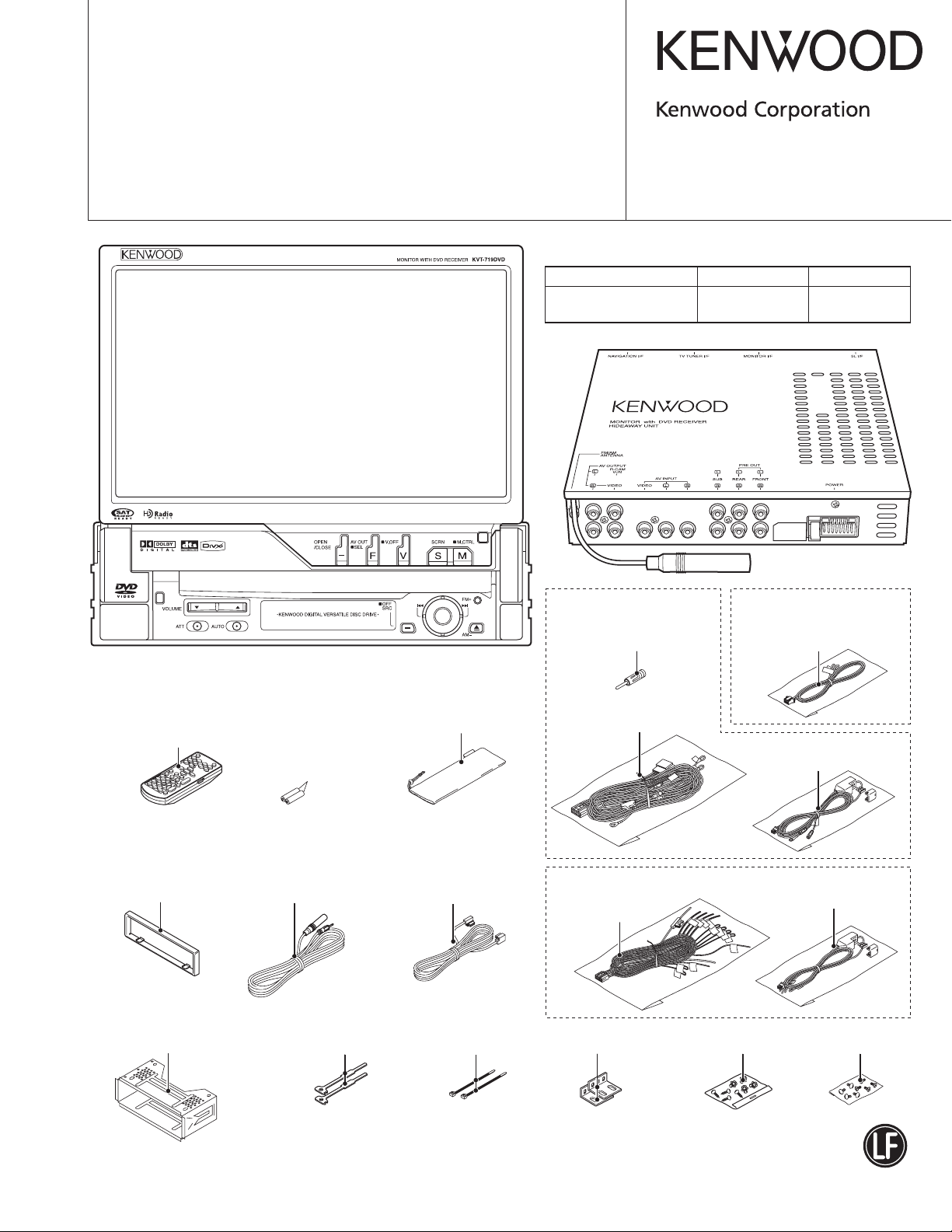
MONITOR WITH DVD RECEIVER
KVT-719DVD/729DVD
/729DVDY/739DVD
SERVICE MAN UAL
TDF SPARE-PANEL
MODEL TDF PANEL No. TDF NAME
KVT-719DVD/729DVD
/729DVDY/739DVD
© 2007-3 PRINTED IN JA PA N
B53-0507-00 (N) 552
Y33-2760-60 TDF-719DVD
Illustrations is KVT-719DVD
Remote controller
(A70-2082-15 : RC-DV330) M,X type
(A70-2083-15 : RC-DV340) E,K,R type
SIZE AAA BATTERY
(NOT SUPPLIED)
Illustrations is RC-DV340
Escutcheon
(B07-3159-02)
Mounting hardware assy
(J21-9823-03)
Cord with plug (6m)
(E30-6483-05)
Lever
(D10-4674-04) x2
Carrying case
(W01-1661-05)
Cord with plug (6m)
(E30-6688-05)
Wire band
(J61-0620-05) x2
E type M,X type
Antenna adaptor
(T90-0552-05)
DC cord (6m)
(E30-6681-15)
K,M,R,X type
DC cord (6m)
(E30-6680-05)
Mounting hardware
(J22-0054-14) x2
Screw set
(N99-1753-05)
Cord with plug (1m)
(E30-6693-05)
DC cord (35cm)
(E30-6676-15)
DC cord (35cm)
(E30-6675-05)
Screw set
(N99-1775-05)
This product uses Lead Free solder.
This product complies with the
RoHS directive for the European market.
KVT-719DVD/729DVD
/729DVDY/739DVD
The IC106 in the DIGITAL I/O UNIT (X88-2020-11) is not a replaceable component.
●
In case of defective of this IC, replace the entire unit (X88-2020-11).
The IC5, IC21, and IC60 in the DVD unit (X37-1120-03) are not replaceable components.
●
In case of defective of any of these ICs, replace the DVD mechanism assembly. (The IC5 has a device key, which shall be
made consistent with the S/No. of the mechanism assembly after replacement. Thus you cannot replace only the board.)
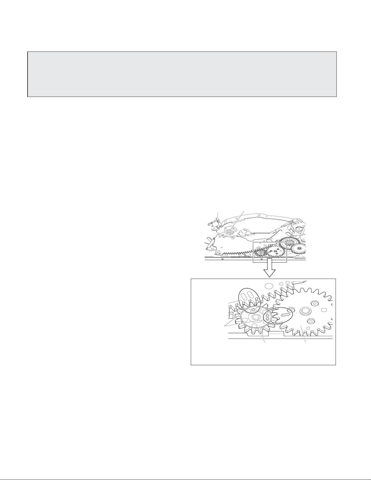
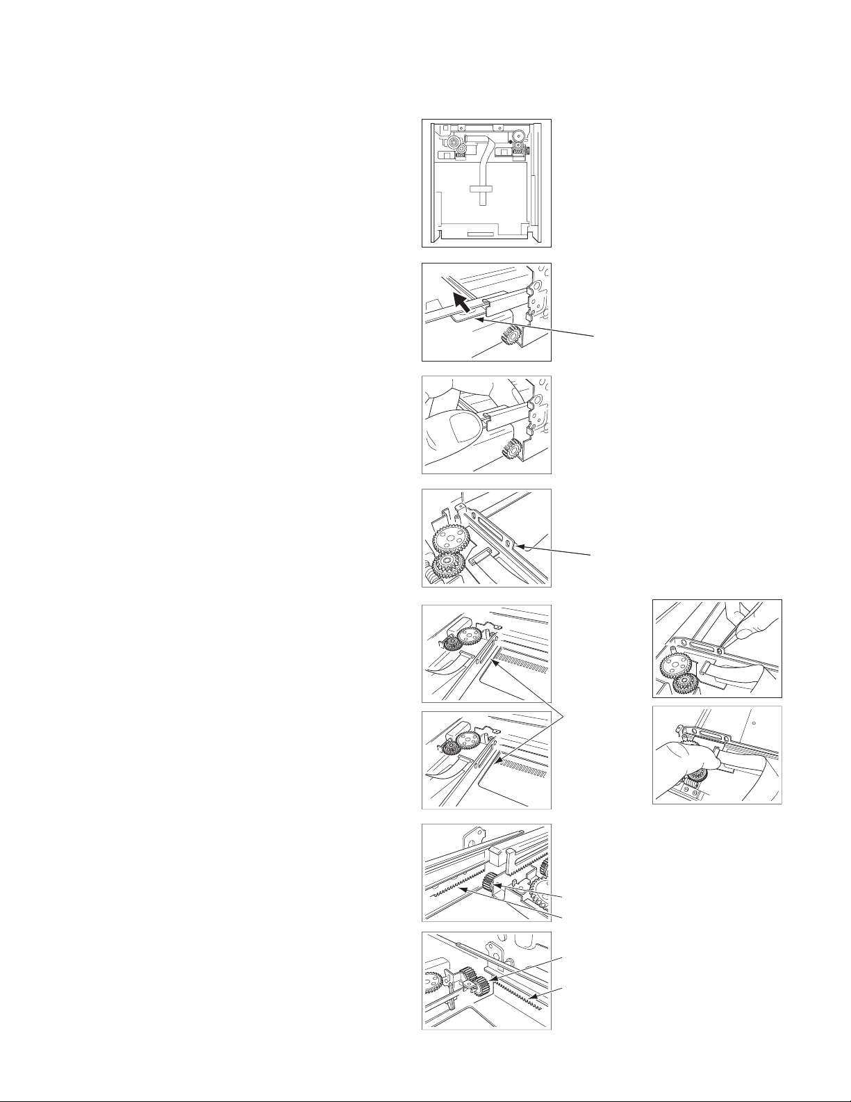
GEAR POSITION IN A DVD MECHANISM
In assembling the Traverse UD arm, Drive cam assembly,
Drive gear 5 and Drive gear 4C, align register marks on
these components.
Inscriptions
(register marks)
on gears
Align 6 marks
as shown in the
figure
Traverse UD arm
Drive cam assembly
Drive gear 5
Do not forcibly press gears to engage their teeth
but freely let the gears fall under their own weight
and engage their teeth.
Drive gear 4C
2
KVT-719DVD/729DVD
/729DVDY/739DVD
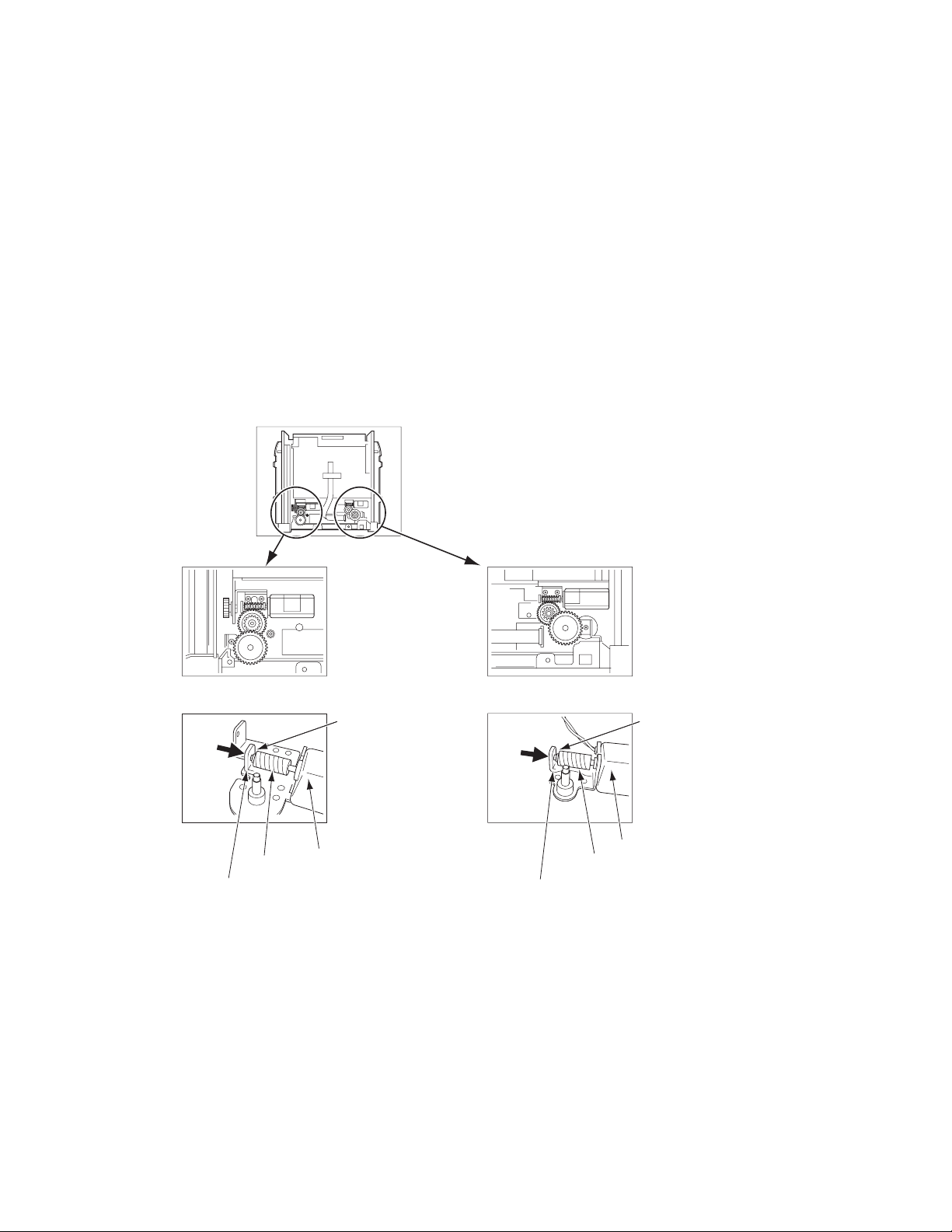
CAUTIONS IN ASSEMBLING PANEL DRIVE MECHANISM (A10-5171)
Observe the instructions described in this document when
you are going to replace the parts or components that are
shown in this document.
1. Replacement of motor fl at spring
• When mounting the flat spring that shall be in contact
with the worm gear, press the spring toward the direction
shown with an arrow so that there will be no gap between
the tip of the gear and the spring and then mount the
spring. The gear shall be pressure-inserted into the
motor.
• Note that there are two motors. Above operation of
mounting the fl at spring is required on both of them.
Tilt drive gear train
Worm
Flat Spring
Mount the flat spring
while pressing it
towards the direction
shown with an arrow so
that there will be no
clearance.
DC Motor
Slide drive gear train
Mount the flat spring
while pressing it
towards the direction
shown with an arrow so
that there will be no
clearance.
DC Motor
Worm
Flat Spring
3
KVT-719DVD/729DVD
/729DVDY/739DVD
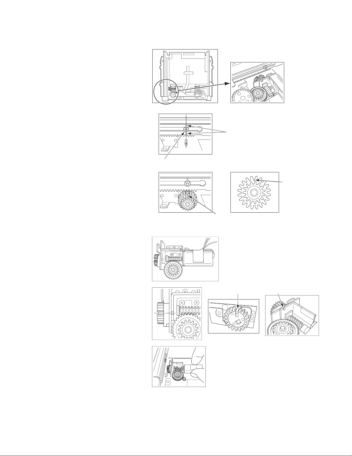
CAUTIONS IN ASSEMBLING PANEL DRIVE MECHANISM (A10-5171)
2. Phase matching among gears
• Monitor tilt is driven under the control of the
rotary sensor and the phase matching among
gears and sensor is required.
The procedure for the phase matching is
described in the rest of this subsection.
Tilt drive gear train
1) Align the mark on the rack with the pin. (When
the monitor is folded down at 0 degree, the
rack is located at the position where the mark
and pin are aligned.
T-Rack-A Pin
Location of mark
on the Rack
2) Insert the gear while keeping aligning the rack
pin with the notched section on the tilt gear 7.
3) Pre-assemble the tilt motor bracket assembly
(BKT Assy).
4) Align the notch on the sensor BKT with the
concave section of the sensor in the Assy.
Tilt Gear 7
Location of
notched section
Location of
notched section
Sensor Tilt Sensor Bkt
5) While keeping the conditions stated in 3) and
4), insert the tilt motor BKT Assy transversally,
and fi x the motor.
4
KVT-719DVD/729DVD
/729DVDY/739DVD
CAUTIONS IN ASSEMBLING PANEL DRIVE MECHANISM (A10-5171)
3. Insertion of slider
• This subsection describes cautions for inserting the
slider (slide section inside of the unit) into the outer
chassis.
1) On the rail at the left side of the slider, there is a part
called a stabilizer that is used to minimize play in right
and left sides.
The slide is made of resin. (Note that the rail is shown
at the right side of the slider in the picture.)
When inserting the slider, press the stabilizer towards
the direction shown with a blue arrow and insert it into
the groove on the rail.
2) PCB holder is pushed out towards the downside
of the picture due to the spring force and thus the
chassis and photo refl ection sheet may be get caught
by the holder during the assembly.
Insert the slider while slightly lifting up the holder with
a pair of tweezers or any other similar device.
(Slider -Slide section inside of the unit)
Stabilizer
PCB Holder
Hold and lift up the holder
with a pair of tweezers.
3) Insert the gear after confirming that the both of D
shaft gears at the right and left sides of the slider are
aliened with the tip of the right and left racks on the
chassis.
(Otherwise the slider will be inserted sidelong.
These portions
tend to be get
caught.
Push the opposite side of
the PCB holder towards
the downside of the picture
and lift up the portions
that may get caught.
D shaft gear
Rack gear
D shaft gear
Rack gear
5
KVT-719DVD/729DVD
6
/729DVDY/739DVD
J1
DC CN
IC501,502
MECHA
7.5V or 5V
CN501
(X35-471)
IC100
-12V
(X35-471)
LED SW
OPEN/CLOSE
FNC/VSEL/
SCREEN//MODE
INVERTER
CIRCUIT
BL14V
CN1
BU DET
ACC DET
IC1
BU3.3V
PON 3.3V
Q22
SW14V
IC101
DC/DC
MECHA
7.5V or 5V
IC102
DC/DC
SW3.3V
Q43
LED9V
Q31
DVDA8 V
AREF
Q35
A8V
MOTOR
DRIVER
EX M+/M-
RI M+/M-
SW A/B/C
V5V
DC/DC
12.5V
18.5V
INV PWM
ENABLE
PWM
to BACK LIGHT
(X14-983)
PON
SMOTOR M/P
TMOTOR M/P
Z SWT/CNT
R SENS
CN300
KEY1
OPEN/CLOSE
CN302
CN303
BU DET
D5V
V5V
TC3.3V
USB5V
P5V
XDATA
YDATA
OPEN/CLOSE
KEY3
SRC
REMO
RESET
HPOSI1/2/3/4
MODE1/2/3
MIRROR
NT/PAL
TC3.3V
Y0
X0
X1
XDATA
YDATA
to TOUCH PANEL
CN501
CN401
iPod
IC400 IC401
ISO ISO
iPod COMP
IC201
BU3.3V
J501
SPDIF
AUDIO SEL
SW1/2/3/4
AUTO
SPDIF
DVD
IC407 (MAIN)
A8VV5V
IC408 (SUB)
A8V
iPod
USB
SYS-COM
SEL CLK
SEL DATA
IC402
V IN SW1/2/3
SERIAL
PARALLEL
V OUT SW
SW3.3V
RESET
RGB SW1/2
DVD R/G/B
IC403
V5V
RGB SW
IC404
V5V
GAN SYNC SW
GAN VSW
RGB SW
VCOM IN
VR/VG/VB
Q304,306-308
BUFF
IC301
IC303
DELAY
SW3.3V
VCOM
R/G/B
POLS
to X35 to X16
V5V
BL14V
LED9V
TP3.3V
TC3.3V
PON3.3V
to X14
BLK/HSY
VSY/CPV
NCLP
DOT CLK
POLS
STH
SERIAL
PARALLEL
TIMING
CONTROLLER
+12.5V
SP CLK
SP DATA
PWM
X0/X1/Y0
HSY ADJ
ENABLE
INV SW
INV PWM
SP CLK
SP DATA
IC301
IC302
to INV
V5V
-12V
18.5V
BL14V
LED9V
TP3.3V
TC3.3V
PON3.3V
GAN
R/G/B
GAMMA IC
MECHA8V
VCOM
NCLP
R/G/B
VIDEO IN SW
D5V
X16 ILL
LED9V
GAN COMP
LED R
LED G
(MID)
V5V
LED B
OSD R/G/B
OSD BLK
CIR RX
CIR TX
CIR INI
CIR RST
CPV
CIR STBY
DOT CLK
CIRMREQ
STH
CIR SREQ
VSY
CIR CON
HSY
CIR BU DET
HSY
EX M+/MRI M+/MSW A/B/C
Z SWT/CNT
R SENS
CN104
FILD DET
OSD MODE
ZACTION
BLK
AUTO DIM
to X35
CPV2
TP3.3V
PON3.3V
CPH1
HDIR
CX
STV1/2
UPSD
OE1/2/3
STH1/2
R/G/B
VCOM
to LCD PANEL
CN503
LCD PANELTOUCH PANELBACK LIGHT
AUTO DIM
V5V
IC401
-12V
AUTO
DIMMER
TC3.3V
18.5V
MINI LCD
IC405
MECHA
(MID)
DVD MUTE
IC406
LED
SW
CN503
CN101
CN201
VIDEO
OUT SW
V5V
J101
J201
IC450
(MID)
SERIAL
PARALLEL
LED R
LED9V
(MID)
MINI DATA
MINI CLK
MINI CS
LED9V
KEY2
MINI DATA
SW3.3V
LED R
LED G
LED B
AMUTE
MAIN
SUB
SCL
LED G
LED R
MINI CLK
MINI CS
V5V
SDA
KEY2
SRC
RESET
EJECT
REMO
(MID)
MINI DATA
MINI CLK
MINI CS
(MID)
to X14
to X16
LED G
to X16
DET
PAN EL
GND
SRC
RESET
DVD SCL
DVD SD A
DVD RESET
DISC DET
DVD R/G/B
DVD COMP
X34 COMP
X34 R/G/B
GRA R/G/B
GRA SYNC
D5V
LED B
PANEL DET
(MID)
LED B
EJECT
EJECT/
SRC/
RESET
VOL/
VOL+
ATT/
DISP
M CLK
M REQ
M DATA
SYS ON
S REQ
S DATA
RESET
VOUT
X16 ILL
KEY2
SRC
RESET
EJECT
REMO
D5V
REMO
REMO
FM
AM
SW3.3V
DSI
X16 ILL
IC201
SW
REMO
BU3.3V
SW3.3V
to DVD MECHA
to X34
to X88
(X16-392)
SI
BU3.3V
(X16-392)
LED9V
LED R
LED G
D5V
X16 ILL
P5V
V5V
D5V
A8V
AREF
CN502CN503
USB5V
V5V
SW3.3V
BU3.3V
A8V
CN501
DVD MECHA
J501
(X88-200)
J1
DC CN
Q51
Q53
IC904
9V (MID)
Q71
IC910,911
1/2VCC (MID)
Q61
IC301
POWER IC
IC106
LEVEL SHIFT
MUTE (SYS BU-DET)
RESET
REMO
IC501,502
IC332
REG
SW3.3V
IC105
REG
USB5V
USB1
BU5V
SW5V
A8V
V5V
A8V
A5V
1.8V
(X34-475)
BU DET
PWIC STBY
PARKING
REVERSE
ILLUMI
W REMO
P CON
ANT CON
EXT CON
LINE MUTE
BU
BU5V
CN327
USB2
5V (MID)5V
IC309
BEEP
MUTE
M CLK
M REQ
M DATA
SYS ON
S REQ
S DATA
USB5V
OSD R/G/B
OSD IC
J2
RELAY SW
RELAY DET1/2
MUTE
RELAY SW1/2
IC201
A8V
BU5V SW5V
DET MUTE E2PROM
PON
OFFSET DET
BU MUTE
W REMO
V5V
SW3.3V
BU3.3V
A8V
STH
DOT CLK
IC322 IC104
OSD BCK/FILD DET
OSD MODE
HSY/VSY
CPV
OSD CLK
OSD DATA
OSD CE
CPLD
GRA SYNCVSYNC
HSYNC
IC106
CS6
CS0
IC201,205
IC211 IC202,203
NOR FLASH
128Mbit 256Mbit
SDRAM
IC901
J351
5V AMP
(MID)
PRE OUT
REAR
IC902
IC903
5V AMP
(MID)
BU5V BU5V BU5V BU5V
MUTE MUTE MUTE MUTE
OUTPUT SECTION
E-VOL
MAIN
SUB
TUNER
INPUT
SECTION
LX
NAVI
I2C SCL/SDA
MUTE 0/1/2/A/B/C
PWIC DC DET
BU5V
IC101
LX DATA S
AM +B
AUDIO
u-COM
TV SC DATA
IC105
SEL DATA
SEL CLK
SERIAL
PARALLEL
SW5V
TV RESET
SW5V
MIX REMO
to X14
CIR SDATA
CIR MDATA
CIR INI
CIR RST
CIR STBY
CIR MREQ
CIR SREQ
CIR CON
CIR BU DET
CIR RST
IC302
VIDEO ENC
SP CLK
GRA R/G/B
EP R/G/B
MEDIA PROCESSOR
SCL
SDA
CP READY
ADDRESS
DATA
IC207
iPod
AUTHENTICATION
IC200
BUFF
AV OUTFRONT
SUB
5V AMP
(MID)
AVOUT
IC202 (MAIN)
IC203 (SUB)
AUDIO
SEL
LX RST
LX CON
LX MUTE
LX CLK
LX REQ M
LX REQ S
LX DATA M
TUN SMET
TUN SCL
TUN SDA
TUN IFC
RDS QAUAL
RDS DATA
RDS AFS
RDS NOISE
TV SC CON
TV JUDGE
TV CLK
TV MC REQ
TV SC REQ
TV MC DATA
NAVI TX
AUTO SW 1/2
V SYNC DET
A IN SEL 1/2/3/4
V IN SEL 1/2/3
V OUT SEL 1/2/3
X100 IC301
X'TAL
14.7456MHz
IC100
IC101 (MID)
OVER CURRENT
PROTECT
X202
32,768kHz
A8V
RDS CLK
NAVI RX
IC305
2ch DAC
ENB (MID)
ENA
AVIN1
TV
X14 AUDIO
RGB MUTE
RGB SW
USB L/R
LPF
SCLK
LRCLK
MCLK
SDO0
J401
BU
FLGB (MID)
FLGA
LX
USB1
5V
CN101
USBp0
USBm0
USB CN
W251
A251
F/E
E2PROM
IC251
RDS IC
IC805
VSYNC SW
V IN SEL 1/2/3
V OUT SEL 1/2/3
USB2
5V (MID)
SW5V
A8V
AVIN1
USBp1
BACK CAM
USBm1
J703
AV IN 1
IC723
A8V
VIN
X14 VIDEO
RGB OUT
AVIN1
IC802,
806,810
VIDEO SW
AV IN
BACK CAM
AVIN1
V5VV5V
BACK CAM
BACK CAM
IC804
VIDEO SW
IC803
VIDEO SW
J702
NAVI I/F TV-TUNER I/F
AV OUT
NAVI
V5V
V5V
X14 VIDEO
NAVI
TV
NAVI TX
NAVI RX
MIX REMO
TV SC DATA
TV MC DATA
TV SC REQ
TV MC REQ
TV CLK
TV JUDGE
TV SC CON
TV RST
IC701
J701
A8V
BU
IC807809
ISOISO
TV
RGB MUTE
NAVI RGB
RGB SW
RGB SW
TV RGB
V5V
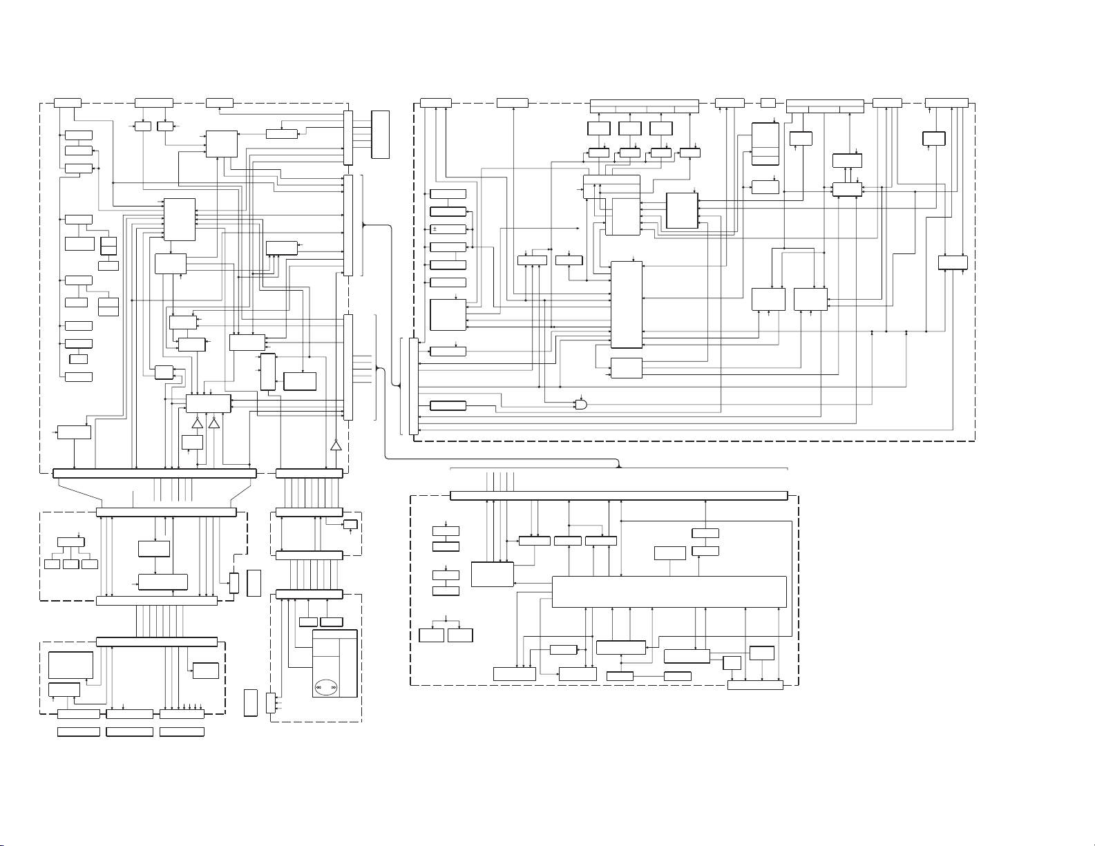
BLOCK DIAGRAM
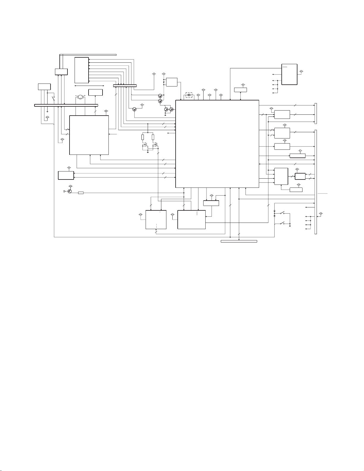
BLOCK DIAGRAM
KVT-719DVD/729DVD
/729DVDY/739DVD
(X37-112)
HALL IC
SW EIEND
D3.3V
LIM-SW
SPINDLE
MOTOR
HALL BIAS
U.V.W COIL
IC54
SDRAM
IF-SEL
HALL SENSOR
IC10
3
H1H,H1L,HB
3
A1,A2,A3
P5V
D3.3V
D3.3V
Q25
KDP2C
OPTICAL
PICKUP
LO/EJ
DC MOTOR
M
FG
DISC
PDIC VCC
DVD LD/CD LD
HFM
VREFH
IMON/VR DVD/VR CD
PDIC I/V OUT
THERMISTER
FO+-,TR+-
2PHASE
STEPPING
FO6,RO6
MOTOR &
ACTUATER
DRIVER
SPIN,IN2-6,MUTE
BMS
EXADT11
4
FO5,RO5
FO4,RO4
CONNECTOR
(28P)
P5V
FO2,RO2
FO3,RO3
VREF,EC
STBY
VHALF
IC21
A5V A5V
IC39
FLASH
DQ0-15
ROM
23
Q12,13
2
A0-20
IOPDET
A3.3V V3.3V
27MHz
D3.3V
D-FF
NEXCE
Q1,Q2
PLL3.3V D1.2V
DQM2
P12(CE)
IC55
LOGIC
CLR
CLK
Q3-8
DVN
F/E+B/E+MCU
NEXWE
NEXWE
D3.3V
A19
NEXOE
P15
EXADR16-19
EXADT0-15
IC1
Q10,11
IOP
(AD0)
LPC01/LPC02
DRV0
VREFH
2
LPC1/LPC2
9
A,B,C,D,E,F,FE1,FE2,RF
TEMP(AD1)
VHALF
2
DQM3,P9
7
DRV1,DRV2,DRV3,DRV4
PWM0,PWM1,P10
FG,P5
21
NWE,NCAS,NRAS,NCSM,MCK0
BA0-1,MA0-11,DQM0-1
16
MDQ0-15
EXADT
0-15
8
E
W,G
D1-8
IC9
E2PROM
NRST
P6,P14
P0,P3
DD0-15,DA0-1,CS1FX,CS3FX
30
INTREQ,IORDY,DASP,PDIAG
ATAPI I/F
P7,P8
DMARQ,DIOW,DIORDMACK
RESET
D3.3V
SRCK,LRCK
DAC0-3OUT
MASTER
CONNECTOR
(30P)
4
A3.3V
Q27
Q14,15
16 4
IC5 IC42
D3.3V D3.3V
ADOUT0-2
DAC4OUT
IECOUT
P1,P2
ADOUT3
DACCK
D1.2V
D3.3V
A3.3V
PLL3.3V
V3.3V
D3.3V
2
POR
SW1
SW2
IC53
BUFFER
IC57
3
VIDEO AMP
2
CLAMP/BIAS,
POWER SAVE
IC12
VIDEO AMP
IC15
PON
L+
L-
AUDIO
R+
DAC
R-
6
SW LOST
D7
SW LOEND
SW REG
A5V
A5V
IC49
4
IC60
3
2
3
3.3V to 1.2V
2
A8V
IC50,51
L.P.F
A8V
5V REG
D5V
A5V
A8V
P5V
D5V
CONNECTOR
CONNECTOR
D1.2V
(10P)
(50P)
2
2
ADATA0-2
BCK/LRCK
PD
Y/G,Pb/B,Pr/R
VIDEO
SPDIF
AMUTE
SDA,SCL
AREFL
AREFR
Lch
Rch
MASTER/SLAVE
RESET
DISC DET
IFSELIF-SEL
CONNECTOR(35P)
7

KVT-719DVD/729DVD
/729DVDY/739DVD
COMPONENTS DESCRIPTION
VIDEO CONTROL UNIT (X14-983x-xx)
●
Ref. No. Application / Function Operation / Condition / Compatibility
IC1 3.3V regulator BU_3.3V
IC2 3.3V regulator TC3.3V
IC10 OP AMP AREF power supply (4V)
IC101 DC-DC control IC DC-DC control (Mechanism 7.5V, V5V)
IC102 DC-DC control IC DC-DC control (SW3.3V, D5V)
IC201 MPU System µ-com
IC202 Reset IC Reset IC
IC203 E2MROM Save settings
IC205 AND Inverter PWM buffer
IC301 Chroma gamma Chroma gamma
IC302 NOT HSY reverse buffer
IC303 Monostable multivibrator HSYNC delay
IC304 NOT HSYNC delay
IC400 VIDEO ISO AMP iPod video signal
IC401 AUDIO ISO AMP iPod audio signal
IC402 Serial/parallel conversion Extension of µ-com port
IC403 Video switch X34 RGB or Graphic RGB
IC404 Video switch IC403 RGB or DVD RGB
IC405 Video switch iPod or DVD or Graphic or X34 Composite signal
IC406 Video switch For AVOUT (To X34)
IC407 Audio selector MAIN
IC408 Audio selector SUB
IC501 Motor driver Tilt
IC502 Motor driver Slide
IC503 NOT Remote controller signal waveform shaping
Q1 SW ACC_DET detection circuit
Q2~10 SW BU_DET detection circuit
Q13 Short protection BU power supply regulator (8.5V)
Q14 8.5V regulator BU power supply regulator (8.5V)
Q15~17 8.5V regulator control BU power supply regulator (8.5V)
Q19~21 SW P-ON 14V control
Q22 SW FET P-ON 14V ON/OFF
Q23,24 Emitter follower Analogue power supply reference circuit
Q25,26 SW T_P3.3V switch
Q31 8V regulator DVD A8V regulator
Q32~34 8V regulator control DVD A8V regulator
Q35 8V regulator A8V regulator
Q36~38 8V regulator control A8V regulator
Q43 9V regulator LED9V regulator
Q44~46 9V regulator control LED9V regulator
8
KVT-719DVD/729DVD
/729DVDY/739DVD
COMPONENTS DESCRIPTION
Ref. No. Application / Function Operation / Condition / Compatibility
Q101 SW DC-DC output voltage switching
Q103,106
Q108,111
Q104 SW DC-DC SW FET (5V or 8V)
Q105 SW DC-DC SW FET (5V)
Q109 SW DC-DC SW FET (3.3V)
Q110 SW DC-DC SW FET (5V)
Q201 SW µ-com reset SW
Q203 SW KEY RESET
Q204,205
Q206,207
Q208~210
Q301 Buffer Composite signal
Q304 Buffer VCOM
Q305 MUTE IC301 SYNC OUT MUTE
Q306 Buffer RGB Signal_R
Q307 Buffer RGB Signal_G
Q308 Buffer RGB Signal_B
Q309 Buffer HSY SYNC
Q401 Buffer Graphic SYNC
Q501 MUTE DVD MUTE (Lch)
Q502 MUTE DVD MUTE (Rch)
Q503 SW DVD MUTE control
Q504 Buffer SPDIF signal
Q508 Buffer Remote control signal
SW DC-DC protection control
SW LED SW (Red)
SW LED SW (Green)
SW TDF power supply SW
SWITCH UNIT (X16-3920-10)
●
Ref. No. Application / Function Operation / Condition / Compatibility
IC201 Remote controller photoreceptor Remote controller photoreceptor
Q101 For switching DSI signal DSI signal control
Q206 For switching LED Switch LED_Red or LED_Green
ELECTRIC UNIT (X34-475x-xx)
●
Ref. No. Application / Function Operation / Condition / Compatibility
IC61 3 terminal regulator V5V generation
IC71 3 terminal regulator Audio8V and Tuner8V generation
IC101 Pin 100 µ-com Primarily, audio board control
IC102 Voltage detection IC µ-com reset voltage (4.2V) monitoring
IC104 Logic IC (AND) Remote controller data switching (REMO/WREMO)
IC105 Serial and parallel conversion IC Audio/Video selector control data output from µ-com
IC106 Logic IC (AND x 4) 5V step-up for the signal data between the unit and BOX
9

KVT-719DVD/729DVD
/729DVDY/739DVD
COMPONENTS DESCRIPTION
Ref. No. Application / Function Operation / Condition / Compatibility
IC201 Electronic volume IC Audio volume control and audio signal selection
IC202 Logic IC (multi plexer) Audio signal selection (Main)
IC203 Logic IC (multi plexer) Audio signal selection (Sub)
IC251 RDS decoder IC RDS signal processing and demodulation
IC301 Power IC Power amplifi er for speaker output
IC501 Isolation amplifi er IC Audio signal GND isolation (X14 source_MAIN)
IC502 Isolation amplifi er IC Audio signal GND isolation (X14 source_SUB)
IC701 Isolation amplifi er IC Audio signal GND isolation (TV-CH)
IC702 Logic IC (AND) NAVI remote controller data switching
IC723 Isolation amplifi er IC Audio signal GND isolation (AV-IN)
IC802 Video switch Video signal output switching (for monitoring the unit)
IC803,804
IC805 Video switch Video signal detection SW
IC806 Video switch Video signal output switching (for monitoring the unit)
IC807 Video switch Video signal selection (R)
IC808 Video switch Video signal selection (G)
IC809 Video switch Video signal selection (B)
IC810 Video switch Video signal output switching (for monitoring the unit)
Q1 Transistor REVERSE detection circuit
Q2 Transistor PARKING detection circuit
Q3 Transistor ILLUMI detection circuit
Q4 Transistor BU detection circuit
Q6 Transistor BU detection circuit
Q7~10 Transistor P_CON output circuit
Q11,12 Transistor ANT_CON output circuit
Q13 Transistor EXT_CONT output circuit
Q14,15 Transistor RELAY control circuit
Q51 Transistor BU5V generation
Q52~54 Transistor BU5V circuit
Q61 Transistor V5V generation
Q62 Transistor V5V circuit
Q70 Transistor P-ON circuit
Q71 Transistor Audio8V and Tuner8V generation
Q72 Transistor Audio8V and Tuner8V circuit
Q81~85 Transistor RELAY control circuit
Q91~95 Transistor RELAY control circuit
Q101,102
Q103 Transistor RESET detection circuit (TV)
Q104,105
Q107 Transistor MUTE circuit (DVD)
Q251,252
Video switch Video signal output switching (AV-OUT)
Transistor RESET detection circuit
Transistor MUTE circuit (RESET)
Transistor On when AM (Tuner8V)
10
KVT-719DVD/729DVD
/729DVDY/739DVD
COMPONENTS DESCRIPTION
Ref. No. Application / Function Operation / Condition / Compatibility
Q351 Transistor Pre-OutMute Mute transistor (FL)
Q352 Transistor Pre-OutMute circuit (Front, Rear)
Q353 Transistor Pre-OutMute Mute transistor (FR)
Q354 Transistor Pre-OutMute Mute transistor (RL)
Q355 Transistor Pre-OutMute Mute transistor (RR)
Q356 Transistor Pre-OutMute Mute transistor (SUB L)
Q357 Transistor Pre-OutMute circuit (SUB)
Q358 Transistor Pre-OutMute Mute transistor (SUB R)
Q359 Transistor Pre-OutMute Mute transistor (AV-OUT L)
Q360 Transistor Pre-OutMute circuit (AV-OUT)
Q361 Transistor Pre-OutMute Mute transistor (AV-OUT R)
Q802~808
Q809 Transistor TV_MUTE circuit (R)
Q810 Transistor TV_MUTE circuit (G)
Q811 Transistor TV_MUTE circuit (B)
Q813 Transistor TV_MUTE circuit (R)
Q814 Transistor TV_MUTE circuit (G)
Q815 Transistor TV_MUTE circuit (B)
Transistor Synchronizing separator circuit
VIDEO UNIT (X35-4710-10)
●
Ref. No. Application / Function Operation / Condition / Compatibility
IC1 Inverter control IC Control and drive of the inverter circuit for the back light
IC101 DC/DC converter IC
IC102 Mono-multi Delay 5V power supply for DC/DC IC
IC103 NOT Reverse
IC301 Serial/parallel conversion Extension of µ-com port
IC302 AND Buffer to delay V.SYNC
IC303 PLL LPF LPF for PLL control (VT voltage control)
IC304 Timing controller IC Control of LCD module
IC401 Dimmer sensor Detection for auto-dimmer
Q1 Dimmer SW Turn on or off in response to the PWM control signal to dimmer the back light
Q2,3 Inverter driver Drive the inverter circuit
Q4 Switch SW to change the free run frequency for inverter control IC
Q5 5V constant voltage 5V power supply for inverter control IC
Q301 VCO For PLL oscillation
Q303 Buffer For PLL clock
Q501 Touch panel Y1 SW Y0 (X0) SW: On in response to Y (X) axis input and off in response to X (Y) axis input
Q502 Touch panel X1/Y0 SW
Q503 Touch panel Y1 SW Y1 SW: Turn on in response to Y axis input and apply voltage
+12.5V power supply for VCOM amplifi er (Gamma IC) and -12.0V/+18.5V power supply for LCD
X1 SW: Turn on in response to sensing of the touch on the panel or X axis input and apply voltage
11
KVT-719DVD/729DVD
/729DVDY/739DVD
COMPONENTS DESCRIPTION
DIGITAL I/O UNIT (X88-2020-11)
●
Ref. No. Application / Function Operation / Condition / Compatibility
IC100
IC104 Exclusive OR Gate EP_SYNC (composite sync) output
IC105
IC106 System-On-Chip Processor Media Processor
IC108 Inverter E_HSYNC Buffer
IC200 Triple Inverter Sub Clock Buffer
IC201 Octal Bus Transceiver Flash Memory data line switching (DA0~7)
IC202,203
IC205 Octal Bus Transceiver Flash Memory data line switching (DA8~15)
IC207 iPod Authentication Coprocessor iPod Authentication
IC211 NOR Flash Memory 128Mbit Flash Memory for program data and graphic data
IC301 Stereo DAC Audio signal digital/analog converter
IC302 Color TV signal encoder Graphic signal digital/analog converter
IC305 Dual OP-Amp.(LPF) Stereo DAC Output LPF
IC309 On-Screen Display Controller On-Screen Display analog signal output
IC316 Triple Inverter Dot Clock(14.4MHz) Buffer
IC322 CPLD 2/3 frequency dividing and PAL thinning control (compression processing circuit)
IC332 Low Dropout Voltage Regulator A8V → A5V(for Stereo DAC and LPF)
IC336 Triple Schmitt Inverter VSY, HSY Buffer
IC337 Triple Schmitt Inverter CPV, STH Buffer
Q302 General Purpose Transistor OSD ROUT Current Amplifi er
Q303 General Purpose Transistor OSD GOUT Current Amplifi er
Q304 General Purpose Transistor OSD BOUT Current Amplifi er
Fixed Current Limit
Power Distribution Switch
Low Dropout Voltage
Linear Regulator
SDRAM 256Mbit SDRAM for work memory
Large current distribution switch for USB1
SW3.3V → 1.8V (for EP9307IRZ)
DVD UNIT (X37-1120-03)
●
Ref. No. Application / Function Operation / Condition / Compatibility
IC1 One chip LSI for DVD player
IC5 FLASH ROM To retain F/W for one chip LSI (Nonvolatile memory)
IC9 EEP ROM To retain data for one chip LSI (Nonvolatile memory)
IC10 Driver IC Fo coil / Tr coil / SP motor / SLD motor / LO-EJ motor drive
IC12 1ch video AMP +6dB amplifi er with internal composite video output fi lter
IC15 Audio DAC DA converter for 2ch analogue audio output
IC21 2-output switching REG 5V
IC39 OP-AMP for Iop measurement For Iop measurement
IC42 Logic IC for port extension For port extension
IC49 Low voltage logic For S/PDIF signal amplitude conversion (3.3V
IC50 OP-AMP for audio LPF LPF for 2ch analogue audio output (Rch)
IC51 OP-AMP for audio LPF LPF for 3ch analogue audio output (Lch)
RF signal processing / Servo processing / Decoding processing / AV decoding processing
→
3.3V/1.2V
→
12
1.2V)
KVT-719DVD/729DVD
/729DVDY/739DVD
COMPONENTS DESCRIPTION
Ref. No. Application / Function Operation / Condition / Compatibility
IC54 SDRAM To retain data for one chip LSI (Nonvolatile memory)
IC55,56 Logic IC for port extension For port extension
IC57 3ch video amplifi er With built-in fi lter +6dB amplifi er for component/RGB video output
IC60 Power supply for 5.0V 8V
Q1 Transistor with internal resistor LO_MUTE control
Q2 Transistor with internal resistor For FG signal
Q3 Transistor with internal resistor For BMS
Q4 Transistor with internal resistor DRMUTE control
Q10 Front end transistor for APC Control of CD laser diode emission
Q11 Front end transistor for APC Control of DVD laser diode emission
Q12 Rear end transistor for APC Control of CD laser diode emission
Q13 Rear end transistor for APC Control of DVD laser diode emission
Q14 MOS-FET ON/OFF control of CD laser diode
Q15 MOS-FET ON/OFF control of DVD laser diode
Q20 MOS-FET for level shifter Level shifter for I2C clock
Q21 MOS-FET for level shifter Level shifter for I2C data
Q24 MOS-FET For Iop measurement
Q25 Transistor with internal resistor IFSEL control
Q27 Transistor with internal resistor HFM ON/OFF control
Q28 Transistor for APC For CD laser diode protection (Current limiter)
Q29 Transistor for APC For DVD laser diode protection (Current limiter)
→
5V (Exclusively for audio DAC)
13

KVT-719DVD/729DVD
/729DVDY/739DVD
MICROCOMPUTER’S TERMINAL DESCRIPTION
SYSTEM µ-COM: 703261YGC315A (X14: IC201)
●
Pin No.
1 AVREF0
2 AVSS
3 V_MUTE O For video mute H: ON, L: OFF
4 HSY_ADJ/HSY_ADJ O Free run adjustment HSY frequency control
4 HSY_ADJ/NC O (KOS)
5 AVREF1
6 DSI/SI O DSI control (KVT)
6 DSI/SI O SI control (DDX)
6 NC O (KOS)
7
7 CIR_BU_DET/STATUS0 O
8 FLMD0 I Used when writing µ-com
9 VDD
10 REGC
11 VSS
12 X1 4.953MHz
13 X2
14 RESET
15 XT1 32.768kHz
16 XT2
17
17 PANEL_DET/NC O (DDX)
18 VSY (VD) I V-SYNC input
19 BU_DET I Backup detection H: Reduced voltage detection
20
20 OSD_MODE/NC O (KOS)
21 ACC_DET I ACC detection H: ACC reduced voltage detection
22γ_CS O Communication CS with Chroma γ-IC
23γ_ DATA O Communication data with Chroma γ-IC
24γ_CLK O Communication clock with Chroma γ-IC
25 CIR_MDATA O Communication with media processor
26 CIR_SDATA I Communication with media processor
27 CIR_INI O Media processor initial
28 CIR_RESET O Reset of media processor
Pin Name I/O Application
CIR_BU_DET/CIR_BU_DET
PANEL_DET/PANEL_DET
O
SD_MODE/OSD_MODE
O
O Output when the screen mode is cinema/zoom Refer to “NTSC_PAL”
When BU_DET has been detected, make the core
recognize the detection.
Cope with the special only when the mechanism
endurance jig (KVT).
I
Front panel mounting/dismounting detection (KVT/KOS)
Truth Value
Tab le
.
Processing Operation Description
H: Panel dismounted
L: Panel mounted
Normally fi xed to “L” and output “H”
only in the case of reset recovery
14
MICROCOMPUTER’S TERMINAL DESCRIPTION
Pin No.
29 CIR_STB I Standby of media processor
30 CIR_MREQ O Request to media processor
31 CIR_SREQ I Request from media processor
32 CIR_CON O Permission to operate media processor
33 EVSS
34 EVDD
35 SDA I/O Communication data with E2P
36 SCL O Communication clock with E2P
37 SIPA_CLK1/SIPA_CLK1 O Serial/parallel IC communication clock (KVT/DDX)
37 SIPA_CLK1/NC O (KOS)
38 SIPA_DATA1/PLL_EN O Enable PLL_IC (KOS)
Pin Name I/O Application
KVT-719DVD/729DVD
/729DVDY/739DVD
Truth Value
Tab le
Processing Operation Description
SIPA_DATA1/SIPA_DATA1
38
39 PGOOD I DC-DC_IC error detection
40 NC O
40 STATUS1/SYNC_DET I
40 STATUS1/NC O
41 DISC_DET/DISC_DET I Detection of disc (KVT/DDX) L: Detected (Disc is found)
41 DISC_DET/NC O (KOS)
DVD_RESET/DVD_RESET
42
DVD_RESET/MON_SYS_ON
42
43 DVD_SDA/DVD_SDA I/O Communication data with DVD mechanism (KVT/DDX)
DVD_SDA/MON_S_DATA
43
44 DVD_SCL/DVD_SCL O
44
DVD_SCL/MON_M_DATA
45 INV_PWM/INV_PWM O Inverter frequency control (KVT/DDX) PWM output
45 INV_PWM/MON_RESET O Reset of monitor µ-com (KOS)
46 POWER_START O DC-DC_IC soft start L: Start, H: Stop
47 POWER_PWM O Oscillation frequency control of DC-DC_IC PWM output
O Serial/parallel IC communication data (KVT/DDX)
Cope with the special only when the mechanism
endurance jig (KVT)
Detection of composite signal in the monitor output (KOS)
O DVD mechanism resetting (KVT/DDX)
O Monitor µ-com ON/OFF control (KOS)
O Communication data with monitor µ-com (KOS)
Communication clock with DVD mechanism (KVT/DDX)
I Communication with monitor µ-com (KOS)
48 PON O Power ON/OFF control H: ON, L: OFF
49 PWM/REMO_PWM O
49 PWM/PWM O LCD brightness control (KVT/DDX) PWM output
50 HSY (HD) I H-SYNC input Count H
51 MCNT/PLL_MDATA O Data output to PLL_IC (KOS/X88FCT special)
51 MCNT/MCNT O P-MECHA power supply voltage switching (KVT) H: 7.5V, L: 5V (KVT)
51 MCNT/MCNT O T-MECHA power supply voltage switching (DDX) H: 8V, L: 5V (DDX)
52 INV_SW/PLL_CLK O
Convert the touch on the screen into the remote
controller code (KOS)
Communication clock with PLL_IC (KOS/X88FCT special)
PWM output
15

KVT-719DVD/729DVD
/729DVDY/739DVD
MICROCOMPUTER’S TERMINAL DESCRIPTION
Pin No.
52 INV_SW/INV_SW O Inverter free run frequency switching (KVT/DDX)
53 SYS_SDATA I Data input from AUDIO µ-com
54 SYS_MDATA O Data output to AUDIO µ-com
55 SYS_CLK O Communication clock with AUDIO µ-com
56 SYS_SREQ I Request from AUDIO µ-com
57 TYPE3/STATUS2 O
57 TYPE3 O Setup of destination
58 SRC/MON_POWER I Monitor power ON/OFF input (KOS)
58 SRC/SRC I Source key (KVT/DDX)
59 SYS_MREQ O Request to AUDIO µ-com
60 SYS_ON O AUDIO µ-com ON/OFF control
61
61
61 OPEN_CLOSE/NC O (KOS)
62 TYPE1 I Setup of destination
63 TYPE2 I Setup of destination
64 NTSC_PAL/NTSC_PAL I NTSC/PAL determination input H: NTSC, L: PAL
65 TMOTOR_M/PLL_EN O Enable PLL_IC (X88FCT jig special)
65
65 TMOTOR_M/TILT_M- O Tilt mechanism tilt control (DDX)
65 TMOTOR_M/NC O (KOS)
66 TMOTOR_P/PMOTOR_P O Panel mechanism tilt control (KVT)
66 TMOTOR_P/TILT_M+ O Tilt mechanism tilt control (DDX)
66 TMOTOR_P/NC O (KOS)
67 SMOTOR_M/SD_DET1 I SD card detection (DDX)
67
67 SMOTOR_M/NC O (KOS)
68 SMOTOR_P/SD_DET2 I SD card detection (DDX)
68 SMOTOR_P/SMOTOR_P O Panel mechanism slide control (KVT)
68
69 BVSS
70 BVDD
71 WRT_E2P I Used when writing E2P
72 MINI_CLK/MINI_CLK O Mini liquid crystal control clock (Mid at KVT)
72
72 MINI_CLK/NC O Lo/DDX at KVT
Pin Name I/O Application
Cope with the special only when the mechanism
endurance jig (KVT)
OPEN_CLOSE/OPEN_CLOSE
OPEN_CLOSE/OPEN_CLOSE
TMOTOR_M/TMOTOR_M
SMOTOR_M/SMOTOR_M
SMOTOR_P/SP_ACC_DET
MINI_CLK/RGBOUT_MUTE
I OPEN/CLOSE key on P-MECHA (KVT)
I Eject key (DDX)
O Panel mechanism tilt control (KVT)
O Panel mechanism slide control (KVT)
Speaker input detection → “H” when the speaker input
I
is found (KOS)
Mute RGB output when the connected monitor is other
O
than the special monitor (KOS)
Truth Value
Tab le
Processing Operation Description
q
q
q
L: Speaker input is not found
16
KVT-719DVD/729DVD
/729DVDY/739DVD
MICROCOMPUTER’S TERMINAL DESCRIPTION
Truth Value
Pin No.
73 ILL_R/ILL_R O Key illumi red ON/OFF (Lo at KVT) H: ON, L: OFF
73 ILL_R/KEY_ILL O Key illumination ON/OFF (DDX) H: ON, L: OFF
73 ILL_R/MINI_DATA O Mini liquid crystal control data (Mid at KVT)
73 ILL_R/NC O KOS
74 ILL_G/JIG_EJ I Can operate without tilt mechanism (DDX) L: Normal
74 ILL_G/ILL_G O Key illumi green ON/OFF (Lo at KVT) H: ON, L: OFF
74 ILL_G/MINI_CS O Mini liquid crystal control chip select (Mid at KVT)
74 ILL_G/NC O KOS
75 FIELD_DET/FIELD_DET I Determination of video signal fi eld (KVT/DDX)
75 FIELD_DET/SYNC_SEL O
76 FLMD1 I Used when writing µ-com
77 ENABLE/ENABLE O Backlight ON/OFF (KVT/DDX) H: ON, L: OFF
77 ENABLE/REMO_SEL O Remote controller output switching (KOS)
78 Y0/OEM_SW O
78 Y0/Y0 O Touch panel control (KVT/DDX)
79 X1/γ_VIN_SW2 O Chroma γ COMP/RGB input switching (KOS)
79 X1/X1 O Touch panel control (KVT/DDX)
80 X0/γ_SYNC_SW2 O Chroma γ SYNC input switching (KOS)
80 X0/X0 O Touch panel control (KVT/DDX)
81 SW_A/SW_A I Detection of panel mechanism (KVT)
81 SW_A/HPOS1 O Display “H” position adjustment (DDX)
81 SW_A/RGB_SW3 O RGB switching control (KOS)
82 SW_B/SW_B I Detection of panel mechanism (KVT)
82 SW_B/HPOS2 O Display “H” position adjustment (DDX)
82 SW_B/VIN_SW4 O RGB switching control (KOS)
83 SW_C/SW_C I Detection of panel mechanism (KVT)
83 SW_C/HPOS3 O Display “H” position adjustment (DDX)
83 SW_C/VIN_SW5 O COMP switching control (KOS)
84 ZACT_SW/ZACT_SW I Detection of panel mechanism (KVT)
84 ZACT_SW/HPOS4 O Display “H” position adjustment (DDX)
84
85 SIPA_CLK2/SIPA_CLD2 O Serial/parallel IC communication clock (KVT)
85 SIPA_CLK2/MODE1 O Screen mode switching (DDX)
85 SIPA_CLK2/RGB_MUTE O RGB mute control (KOS)
Pin Name I/O Application
Switching of composite signal in the monitor output (KOS)
Is the connected monitor the special (dedicated)
monitor or not? (KOS)
ZACT_SW/COMP_MUTE
O COMP mute control (KOS)
Tab le
Processing Operation Description
H: DVD player operation with the
accessory remote controller
L: DVD player operation with the
other controller than accessory
remote controller
H: Special (Dedicated)
L: OEM (Default)
H: When OEM_SW is “L” and at
full graphic
17
KVT-719DVD/729DVD
/729DVDY/739DVD
MICROCOMPUTER’S TERMINAL DESCRIPTION
Pin No.
86
86
86 SIPA_DATA2/MODE2 O Screen mode switching (DDX)
87 LED_SW/AOUT_SW6 O Audio out switching (KOS)
87 LED_SW/LED_SW O
87 LED_SW/MODE3 O Screen mode switching (DDX)
88 MIRROR/EJECT I Eject key (KVT)
88 MIRROR/MIRROR O Reverse control of back monitor mirror (DDX)
88 MIRROR/NC O (KOS)
89 VCOM/VCOM I For γ curve automatic adjustment (KVT/DDX)
89 VCOM/NC O (KOS)
90 VR/VR I
91 VG/VG I
92 VB/VB I
93 KEY1/KEY1 I (KVT)
93 KEY1/KEY3 I (DDX)
93 KEY1/NC O (KOS)
94 KEY2/KEY2 I (KVT)
94 KEY2/NT_PAL O NTSC/PAL output for X35 (DDX/KOS) NTSC: L, PAL: H
95 R_SENS/R_SENS I Detection of panel mechanism tilt (KVT)
95 R_SENS/R_SENS I Detection of tilt mechanism tilt (DDX)
95 R_SENS/NC O (KOS)
96 ZACT_CONT/LEN_ON O Disc LED ON/OFF (Mid at DDX) H: ON, L: OFF
96
96 ZACT_CONT/NC O Lo/KOS at DDX
97 AUTO_DIM/AUTO_DIM I Auto dimmer input (KVT)
97 AUTO_DIM/NC O DDX/KOS
98 YDATA/YDATA I Touch data input (KVT/DDX)
98 YDATA/NC O (KOS)
99 XDATA/XDATA I Touch data input (KVT/DDX)
99 XDATA/NC O (KOS)
100 TYPE0 I Setup of destination
Pin Name I/O Application
SIPA_DATA2/AOUT_SW5
SIPA_DATA2/SIPA_DATA2
ZACT_CONT/ZACT_CONT
O Audio out switching (KOS)
O Serial/parallel IC communication data (KVT)
LED goes on or off in conjunction with OPEN/CLOSE (KVT)
For γ curve and PHASE/TINT automatic adjustment
(KVT/DDX)
For PHASE/TINT automatic adjustment (KOS)
For γ automatic adjustment (KVT/DDX)
For RGB level automatic adjustment (KOS)
For γ curve and PHASE/TINT automatic adjustment
(KVT/DDX)
For PHASE/TINT automatic adjustment (KOS)
I Panel mechanism slide position detection (KVT)
Truth Value
H: ON, L: OFF
Tab le
q
Processing Operation Description
18
KVT-719DVD/729DVD
/729DVDY/739DVD
MICROCOMPUTER’S TERMINAL DESCRIPTION
Truth Value Table
KVT/DDX/KOS Setup of destination
q
MODEL Category Destination TYPE3 TYPE2 TYPE1 TYPE0
K000
E 000
M0 0 0
V/X 0 0 0
R00 0
K001
E001
M0 0 1
V/X 0 01
R00 1
K010
E010
M0 1 0
V/X 0 1 0
R010
K011
E011
M0 1 1
V/X 0 1 1
R01 1
K 100
E100
M 100
V/X 100
R 100
K101
E101
M1 0 1
V/X 1 0 1
R10 1
K110
E110
M1 1 0
V/X 1 1 0
R110
TYPE0 is AD input. Refer to the next table (TYPE0 Setup Voltage) for the “∗”.
Lo
Mid
KVT
DDX
KOS
AVN
KVT
DDX
KOS
∗
∗
∗
∗
∗
∗
∗
∗
∗
∗
∗
∗
∗
∗
∗
∗
∗
∗
∗
∗
∗
∗
∗
∗
∗
∗
∗
∗
∗
∗
∗
∗
∗
∗
∗
TYPE0 Setup Voltage
Destination
K
E 0.42 0.83 1.23
M 1.24 1.65 2.06
V/X 2.07 2.48 2.88
R 2.89 3.30
min Mid point voltage max
0.00 0.00 0.41
µ-com setup value
19
KVT-719DVD/729DVD
/729DVDY/739DVD
MICROCOMPUTER’S TERMINAL DESCRIPTION
NTSC_PAL Setup
GRA - 1
DVD - 1 1 Lo: IN1
VD Yes 0 - Lo: IN1
NTSC
PA L
None None 0 - Hi: IN2
iPod - 1 0 Lo: IN1
None - 1 0 Hi: IN2
TV - 0 - Lo: IN1
NAVI - 1 1 Lo: IN1
DVD - 1 1 Lo: IN1
VD Yes 0 - Lo: IN1
None None 0 - Hi: IN2
iPod - 1 1 Lo: IN1
None - 1 1 Hi: IN2
TV - 0 - Lo: IN1
Audio
VSYNC_DET D8 D15
0
γ
D9
0: NTSC, 1:PAL
1 Hi: IN2
T/C
SYNC_SW NT_PAL
Lo
Hi
OSD_MODE (Thinning measure between CPLD OFF/ON control)
NTSC PAL (NT_PAL: Hi)
FULL
NORMAL
JUST
ZOOM
CINEMA (ZOOM2)
Lo
Hi
Lo
20

KVT-719DVD/729DVD
/729DVDY/739DVD
MICROCOMPUTER’S TERMINAL DESCRIPTION
AUDIO µ-COM: 703030BYGCJ30 (X34: IC101)
●
Pin No.
1 TV_JUDGE I TV-BOX new/old detection
2 TUN_SCL O F/E I2C clock output terminal
3 NAVI_RX I Navi control data input
4 NAVI_TX O Navi control data output
5 TV_MC_REQ O Communication request to TV_COM
6 EVDD
7 EVSS
8 TV_SC_CON O Start-up request to TV_COM
9 BEEP O BEEP When BEEP: Pulse output
10 MIX_REMO I Remote controller input
11 SYS_SREQ O Communication request to SYS_COM
12 SYS_MDATA I SYS_COM communication data input
13 SYS_SDATA O SYS_COM communication data output
14 SYS_MCLK I SYS_COM communication clock
15 SYS_MREQ I SYS_COM communication request input
16 EXT_CON O EXT-CONT output
17 VSYNC_DET I Video detection
18 VPP
19 RGB_MUTE O MUTE RGB except when NAVI or SECAM
20 RGB_SW O NAVI/SECAM switching
21 AIN_SEL5 O Audio in switching (KOS)
21 NC O KVT/DDX Only
22 AIN_SEL6 O Audio in switching (KOS)
22 NC O KVT/DDX Only
23 R_QUAL I RDS decoder QUAL input terminal
24 R_DATA I RDS decoder DATA input terminal
25 R_AFS_H I/O Constant number switching when noise detected
26 AM+B O AM power supply ON H: When AM, L: EXCEPT
27 AUTO_SW_1 O SW for video detection H: AVIN1, AVIN2, L: BACK CAMERA
28 AUTO_SW_2 O Video detection, NTSC/PAL determination H: AVIN2, L: AVIN1, BACK CAMERA
29 SEL_CLK O CLK for Audio and Video selector
30 SEL_DATA O DATA for Audio and Video selector
31 RESET
32 XT1
33 XT2
34 REGC
35 X2
36 X1
37 VSS
Pin Name I/O Application
Truth Value
Tab le
Processing Operation Description
21
KVT-719DVD/729DVD
/729DVDY/739DVD
MICROCOMPUTER’S TERMINAL DESCRIPTION
Pin No.
38 VDD
39 CLKOUT
40 PRE_MUTESW O PREout sub woofer MUTE H: MUTE OFF, L: MUTE ON
41 PRE_MUTER O PREout rear MUTE H: MUTE OFF, L: MUTE ON
42 PRE_MUTEF O PREout front MUTE H: MUTE OFF, L: MUTE ON
43 RELAY_SW1 O ON/OFF of external equipment relay control H: Relay ON, L: Relay OFF
44 RELAY_SW2 O ON/OFF of external equipment relay control H: Relay ON, L: Relay OFF
45 RELAY_SW3 O ON/OFF of external equipment relay control H: Relay ON, L: Relay OFF
45 NC O Low Only L fi xed
46 RELAY_SW4 O ON/OFF of external equipment relay control H: Relay ON, L: Relay OFF
46 NC O Low Only L fi xed
47 RELAY_DET1 I Detection of external equipment relay control
48 RELAY_DET2 I Detection of external equipment relay control
49 RELAY_DET3 I Detection of external equipment relay control
49 NC O Low Only L fi xed
50 RELAY_DET4 I Detection of external equipment relay control
50 NC O Low Only L fi xed
51 ILL_DET I ILL detection L: Illumi ON
52 PAK_DET I Parking detection H: Parking ON
53 REV_DET I Reverse detection L: Reverse ON
54 P_CON O P-CON control output
55 BVDD
56 BVSS
57 ANT_CON O P-ANT control output H: ANT UP, L: ANT DOWN
58 NC O
59 PWIC_STBY O PWIC standby H: POWER ON, L: POWER OFF
60 PWIC_MUTE O PWIC_FR MUTE L: MUTE ON
61 AUD_MUTEC O E-VOL inputSEL_C MUTE L: MUTE ON, H: MUTE OFF
62 AUD_MUTEB O E-VOL inputSEL_B MUTE L: MUTE ON, H: MUTE OFF
63 AUD_MUTEA O E-VOL inputSEL_A MUTE L: MUTE ON, H: MUTE OFF
64 AUD_MUTE2 O E-VOL center, SWMUTE L: MUTE ON, H: MUTE OFF
65 AUD_MUTE1 O E-VOL rear MUTE L: MUTE ON, H: MUTE OFF
66 AUD_MUTE0 O E-VOL front MUTE L: MUTE ON, H: MUTE OFF
67 AUD_SDA I/O E-VOL data output
67 AUD_SDA I/O
Pin Name I/O Application
ROM correstion E2PROM communication data
input/output
Truth Value
Tab le
Processing Operation Description
When RELAY_SW1 is Hi, L: Normal, H: Error
(Hi when SW1 is Low)
When RELAY_SW2 is Hi, L: Normal, H: Error
(Hi when SW2 is Low)
When RELAY_SW3 is Hi, L: Normal, H: Error
(Hi when SW3 is Low)
When RELAY_SW4 is Hi, L: Normal, H: Error
(Hi when SW4 is Low)
L: When STANDBY or POWER OFF
EXCEPT: H
22
KVT-719DVD/729DVD
/729DVDY/739DVD
MICROCOMPUTER’S TERMINAL DESCRIPTION
Pin No.
68 AUD_SCL O E-VOL clock output
68 AUD_SCL O
69 PON O A8V,V5V,SW5V ON/OFF
70 LX_RST O Hardware-reset to slave unit
71 AVDD
72 AVSS
73 AVREF
74 PWIC_DCDET I SP_FR output DC offset detection L: When detected
75 LINE_MUTE I LINE-MUTE input detection
76 NC
77 A_WRT_E2P I Used when writing E2PROM H: When writing E2PROM
78 LX_MUTE I MUTE request from slave unit
79 A_TYPE0 I Destination (Voltage reading)
80 A_TYPE1 I KVT or DDX
81 A_TYPE2 I OEM or Other
82 A_TYPE3 I Hi or Low
83 TUN_IFC I F/E IFC OUT input terminal H: Station found, L: Station not found
84 TUN_SMET I S meter input
85 R_NOISE I FM noise detection terminal
86 RIP_MUTE O Power IC inside H: MUTE OFF, L: MUTE ON
87 BU_DET I BU reduced voltage detection H: Reduced voltage detection
88 TV_SC_REQ I Communication request from TV_COM
89 SYS_ON I SYS_COM communication control input H: Start up request from AUDIO_µ-com
90 R_CLK I RDS decoder CLK input terminal
91 LX_REQ_S I Communication request from slave unit
92 LX_REQ_M O Communication request to slave unit
93 LX_CON O Start-up request to slave unit
94
94 LX_DATA_S I Data from slave unit
95
95 LX_DATA_M O Data to slave unit
96 A_FLASH_SCK I Clock from Flash re-write terminal writer
96 LX_CLK O LX BUS clock
97 TV_SC_DATA I DATA input from TV_COM
98 TV_MC_DATA O DATA output to TV_COM
99 TV_BP_CLK O CLK output to TV_COM
100 TUN_SDA I/O F/E I2C data input/output terminal
Pin Name I/O Application
ROM correstion E2PROM communication clock
output
A_FLASH_MDATA
A_FLASH_SDATA
I Data from Flash re-write terminal writer
O Data to Flash re-write terminal writer
Truth Value
Tab le
w
q
q
q
Processing Operation Description
H: Only when in RESET sequence
L: Other output
Normal: 1.6V, TEL MUTE: 1V or lower
NAVI MUTE: 2.5V or higher
Refer to the truth value table
Refer to the truth value table
Refer to the truth value table
Refer to the truth value table
23
KVT-719DVD/729DVD
/729DVDY/739DVD
MICROCOMPUTER’S TERMINAL DESCRIPTION
Truth Value Table
TYPE1, 2 and 3 Truth Value Table
q
Category TYPE3 TYPE2 TYPE1 TYPE0
KVT Hi MODEL 1 0 0
KVT Low MODEL 0 0 0
DDX Hi MODEL 1 0 1
DDX Low MODEL 0 0 1
KOS Hi MODEL 1 1 0
KOS Low MODEL 0 1 0
AVN MODEL 0 1 1
TYPE0 Setup Voltage
w
Destination
K 0.00 0.00 0.62
E 0.63 1.25 1.87
M 1.88 2.50 3.12
V/X 3.13 3.75 4.37
R 4.38 5.00
Refer to the next table (TYPE0 Setup Voltage) for the “∗1”.
µ-com setup value
min Mid point voltage max
1
∗
1
∗
1
∗
1
∗
1
∗
1
∗
1
∗
TYPE0 is AD input.
Detection of interrupt signal (if there is a signal or not)
Decide if there is a signal or not based on the number of pulses that is coming in the VSYNC_DET terminal (Pin 17) within 100ms.
Name of control line VSYNC_DET
µ-com terminal number 17
No 3 or less
Is there a signal or not?
Yes. 4~7
No 8~
24

KVT-719DVD/729DVD
/729DVDY/739DVD
MICROCOMPUTER’S TERMINAL DESCRIPTION
MEDIA MICROPROCESSOR: EP9307IRZ (X88: IC106)
●
Pin No. Pin Name I/O Application Processing Operation Description
A1 #CS1 I Watchdog startup
A10 RXDVAL I (ETHER I/F for design)
A11 MIITXD1 O (ETHER I/F for design)
A12 CRS I (ETHER I/F for design)
A13 MIN_CE O Not used (For High model Mini liquid crystal chip enable)
A14 NC
A17 NC I
A2 #CS7 I BOOT bus width select
A3 SDCLKEN O SDRAM clock enable
A4 DA31 I/O Data bus
A5 DA29 I/O Data bus
A6 DA27 I/O Data bus
A7 NC
A8 #RD O Memory read
A9 MIIRXD3 I (ETHER I/F for design)
B1 AD25 O Address bus
B10 MIIRXD1 I (ETHER I/F for design)
B11 MIITXD2 O (ETHER I/F for design)
B12 TXEN O (ETHER I/F for design)
B13 MIN_D_CONT O
B14 NAND_R_#B O Not used (NAND Flash READY/BUSY) L: BUSY, H: READY
B15 NC
B16 DA_MCLK O AUDIO DAC Master clock I2S
B17 3.3V
B2 #CS2 I Watchdog startup
B2 #CS2 O SRAM chip select
B3 #CS6 I BOOT bus width select
B3 #CS6 O Nor Flash chip select
Not used
(For High model Mini liquid crystal data buffer control)
L: Data output to mini liquid crystal
H: Data input from mini liquid crystal
B4 AD20 O Address bus
B5 DA30 I/O Data bus
B6 AD18 O Address bus
B7 EP_STBY O Permission to turn OFF the mother power supply
B8 AD17 O Address bus
B9 RXCLK I (ETHER I/F for design)
C1 AD23 O Address bus
C10 MIIRXD2 I (ETHER I/F for design)
25

KVT-719DVD/729DVD
/729DVDY/739DVD
MICROCOMPUTER’S TERMINAL DESCRIPTION
Pin No. Pin Name I/O Application Processing Operation Description
C11 TXCLK I (ETHER I/F for design)
C12 MIITXD0 O (ETHER I/F for design)
C13 CLD I (ETHER I/F for design)
C14 OSD_CE O OSD communication chip enable SPI
C15 TRSTN I (JTAG I/F for design)
C16,C17 NC
C2 DA26 I/O Data bus
C3 #CS3 O SRAM chip select
C5 AD24 O Address bus
C6 AD19 O Address bus
C7 EP_SREQ O EP9307 communication request
C8 #WR O Memory write
C9 MDIO I/O (ETHER I/F for design)
D1 #SDCS3 O SDRAM chip select
D10 MDC O (ETHER I/F for design)
D11 RXERR I (ETHER I/F for design)
D12 MIITXD3 O (ETHER I/F for design)
D13 IPOD_BSY I iPod READY/BUSY L: BUSY, H: READY
D14 LOW_#MID I Setup of destination H: LOW model, L: MID model
D15~D17 NC
D2 DA23 I/O Data bus
D3 SDCLK O SDRAM clock
D4 DA24 I/O Data bus
D5 MIN_CLK O
D6 EP_MREQ I SysCom communication request
D7 DA28 I/O Data bus
D8 #EP_INI I Reset start notifi cation
D9 AD16 O Address bus
Not used
(For High model Mini liquid crystal communication clock)
Commercial product: 100MHz
Thermal expansion product: 92MHz
E1 #SDCS2 O SDRAM chip select
E10 vddr
E11 MIIRXD0 I (ETHER I/F for design)
E12 TXERR O (ETHER I/F for design)
E13 EP_CON I Permission to operate PE9307
E14 USB1_ERR I 5V over current detection in USB1 L: Over current is detected.
E15 USB1_EN O Control of USB1 5V over current detection IC L: USB5V OFF, H: USB5V ON
E16 NC
26
KVT-719DVD/729DVD
/729DVDY/739DVD
MICROCOMPUTER’S TERMINAL DESCRIPTION
Pin No. Pin Name I/O Application Processing Operation Description
E17 NC
E2 #SDWE O SDRAM write enable
E3 DA22 I/O Data bus
E4 AD3 O Address bus
E5 DA15 I/O Data bus
E6 AD21 O Address bus
E7 DA17 I/O Data bus
E8,E9 vddr
F1 #RAS O SDRAM RAS
F10 vddc
F11 gndr
F12 EP_BUDET I Momentary power down notifi cation
F13 NC
L: Normal operation
H: Momentary power down detection
F14 ADC_GND
F15~F17 NC
F2 #SDCS1 O SDRAM chip select
F3 #SDCS0 O SDRAM chip select
F4 #DQM3 O Memory data mask
F5 AD5 O Address bus
F6~F8 gndr
F9 vddc
G1 #DQM0 O Memory data mask
G12 gndr
G13 USB0_ERR I 5V over current detection in USB0 L: Over current is detected
G14 EGPIO10/DREQ1 L: Over current is detected
G15~G17 NC
G2 #CAS O SDRAM CAS
G3 DA21 I/O Data bus
G4 AD22 O Address bus
G5 vddr
G6 gndr
H1 DA18 I/O Data bus
H10 gndc
H12 gndr
H13 vddr
H14 USB0_EN O Control of USB0 5V over current detection IC L: USB5V OFF, H: USB5V ON
H15 #EP_RST0 I Power on reset
27

KVT-719DVD/729DVD
/729DVDY/739DVD
MICROCOMPUTER’S TERMINAL DESCRIPTION
Pin No. Pin Name I/O Application Processing Operation Description
H16 MIN_DO O Not used (For High model Mini liquid crystal data output)
H17 NC
H2 DA20 I/O Data bus
H3 DA19 I/O Data bus
H4 DA16 I/O Data bus
H5 vddr
H6 vddc
H8,H9 gndc
J1 AD6 O Address bus
J10 gndc
J12 vddc
J13 vddr
J14 OSD_ROMSEL I OSD ROM select L: Built-in, H: External
J15 MIN_DI O Not used (For High model Mini liquid crystal data input)
J16 #CS0 O Nor Flash chip select
J17 NAND_CLE O Not used (NAND Flash Command latch enable)
J2 DA14 I/O Data bus
J3 AD7 O Address bus
J4 DA13 I/O Data bus
J5 vddr
J6 vddc
J8 gndc
K1 AD4 O Address bus
K10 gndc
K12 vddc
K13 NAND_#CE O Not used (NAND Flash Chip enable)
K14 PLL_VDD Main oscillator power supply 1.8V
K15 NAND_ALE O Not used (NAND Flash Address latch enable)
K16 NAND_#RE O Not used (NAND Flash Read enable)
K17 NAND_#WE O Not used (NAND Flash Write enable)
K2 DA12 I/O Data bus
K3 DA10 I/O Data bus
K4 DA11 I/O Data bus
K5 vddr
K6 gndr
K8,K9 gndc
L1 DA9 I/O Data bus
28

KVT-719DVD/729DVD
/729DVDY/739DVD
MICROCOMPUTER’S TERMINAL DESCRIPTION
Pin No. Pin Name I/O Application Processing Operation Description
L12 gndr
L13 NAND_D7 O Not used (NAND Flash Data bus)
L14 NAND_D5 O Not used (NAND Flash Data bus)
L15 PLL_GND Main oscillator GND
L17 XTALO Main clock 14.7456MHz
L2 AD2 O Address bus
L3 AD1 O Address bus
L4 DA8 I/O Data bus
L5 NC
L6 gndr
M1 NC
M10,M11 gndr
M12 NAND_D6 O Not used (NAND Flash Data bus)
M13 NAND_D4 O Not used (NAND Flash Data bus)
M14 NAND_D1 O Not used (NAND Flash Data bus)
M15 NAND_D0 O Not used (NAND Flash Data bus)
M16 NAND_D3 O Not used (NAND Flash Data bus)
M17 NAND_D2 O Not used (NAND Flash Data bus)
M2 AD0 O Address bus
M3 #DQM1 O Memory data mask
M4 #DQM2 O Memory data mask
M5 E_R5 O Video data bus (Red)
M6,M7 gndr
M8 vddc
M9 vddc
N1 E_R2 O Video data bus (Red)
N10 vddr
N11 I2C_SCL O Communication clock (I2C)
N11 I2C_SCL I BOOT mode L: External BOOT, H: Internal BOOT
N12 DA_SDO0 O AUDIO DAC data I2S
N12 DA_SDO0 I BOOT bus width select
N13 CTS I (UART I/F for design)
N14 RXD0 I (UART I/F for design)
N15 TXD0 O (UART I/F for design)
N16 UART_TXD1 O (UART I/F for design)
N17 UART_TXD2 O EP9307 communication data
N2 E_R4 O Video data bus (Red)
29

KVT-719DVD/729DVD
/729DVDY/739DVD
MICROCOMPUTER’S TERMINAL DESCRIPTION
Pin No. Pin Name I/O Application Processing Operation Description
N3 E_R3 O Video data bus (Red)
N4 E_R1 O Video data bus (Red)
N5 E_R0 O Video data bus (Red)
N6 DA5 I/O Data bus
N7~N9 vddr
P1 SPCLK O Video dot clock
P10 TCK I (JTAG I/F for design)
P11 BOOT1 I Test mode select
P12 I2C_SDA I/O Communication data (I2C)
P12 I2C_SDA I Test mode select
P13 G_LED O Green LED
P14 R_LED O Red LED
P15 NC
P16 UART_RDX1 I (UART I/F for design)
P17 UART_RDX2 I System µ-com communication data
P2 E_G4 O Video data bus (Green)
P3 E_G5 O Video data bus (Green)
P4 E_B3 O Video data bus (Blue)
P5 AD15 O Address bus
P6 AD13 O Address bus
P7 AD12 O Address bus
P8 DA2 I/O Data bus
P9 AD8 O Address bus
R1 E_G3 O Video data bus (Green)
R10 TDI I (JTAG I/F for design)
R11 BOOT0 I Test mode select
R12 DA_LRCLK O AUDIO DAC Sample rate clock I2S
R13 OSD_DATA O OSD communication data SPI
R14 NC
R15 USB0_NEG I/O USB0 data
R16 DA_SCLK O AUDIO DAC Data bit clock I2S
R17 USB0_POS I/O USB0 data
R2 E_HSYNC O Video H-SYNC
R3 E_G0 O Video data bus (Green)
R4 E_B5 O Video data bus (Blue)
R5 E_B0 O Video data bus (Blue)
R6 AD14 O Address bus
30
 Loading...