

kenwood KDC-V7521, KDC-V7521Y Service Manual
CD RECEIVER
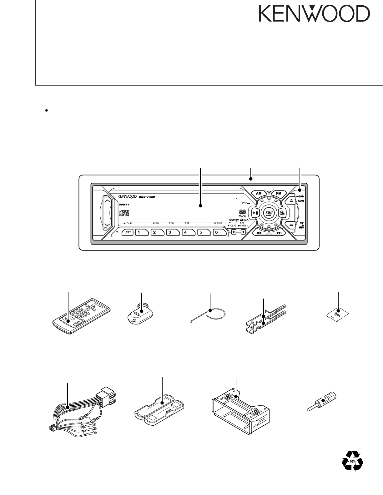
Escutcheon assy
(B07-3007-03)
Front glass
(B10-4161-01)
Panel assy
(A64-2582-02)
KDC-V7521/Y
This service manual does not include information on the CD mechanism assembly (exploded view, parts list,
schematic diagram or mechanism operation description).
For such information, please refer to the CD mechanism assembly service manual (X92-4030-0X, X92-4440-0X,
: B51-7867-00).
DC cord
(E30-4942-05): KDC-V7521Y
(E30-4956-05): KDC-V7521
Antenna adaptor
(T90-0523/0534-05)
Screw set
(N99-1704-05)
Lever
(D10-4562-04)
(D10-4621-04):KDC-V7521
Mounting hardware assy
(J21-9716-03)
Torsion coil spring
(G01-2924-04)
Plastic cabinet assy
(A02-1497-13)
Remote controller assy
(A70-2025-05)
Remote controller assy
(A70-0886-15)
KDC-V7521/Y
SERVICE MANUAL
© 2001-11 PRINTED IN JAPAN
B51-7869-00 (N) 1940
2
KDC-V7521/Y
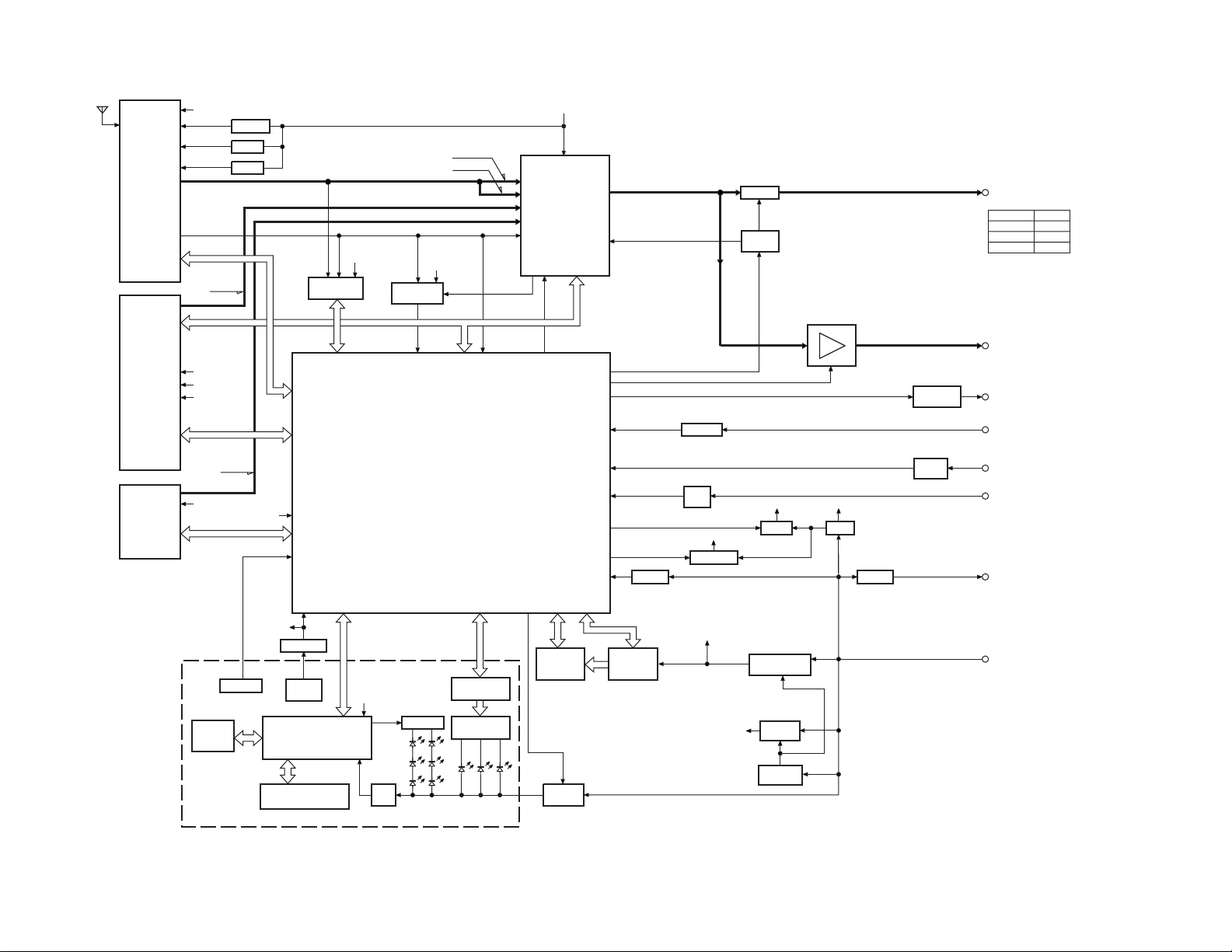
A1,Q53
AUDIO OUT
F/E
S-METER
IFC OUT
PLL DATA
PLL CLK
CD
SCL
SDA
SW1
SW2
SW3
MUTE L
MUTE R
RST
STOP
LO/EJ
MO SW
CH
RST
REQ C
CLK
DATA H
CH-CON
REQ H
DATA C
SW5V
Q43,44
Q45,46
1200mV
SERVO+B
A8V
BU5V
BACK UP
KEY
MATRIX
PLL+B
FM+B
AM+B
1200mV
IC2
REMO
IC14
Q52
DECODER
IC1
BU5V
REMO
RESET
MUTE
DRIVER
IC16
RESET IC
RESET
SW
IC1
LCD
DRIVER
ED1
LCD
(BACK LIGHT V-ILL)
RDS
RDCK
SW5V
QUAL
RDDA
L CE
L CLK
L DATAL
L DATAS
(X16- )
PANEL 5V
Q5
LCD
AVR
SW5V
Q36
NOISE
BUFFER
NOISE
SYSTEM MI-COM
Q3,4
G/R SW V-I
251mV
230mV
SCL
SDA
DA SDA
DA SCL
IC3
DAC
CONVERTER
V-ILL
IC2
FM
AM
CD
CH
QUAL
ILL+B
A8V
E-VOL
AFS
AFS
SRM SW1
SRM DET
SRM SW2
SRM
MECHA.
ILLUM
+B
MUTE
P MUTE
SW5V
PANEL5V
SRM SW3
SRM SUB-
SRM SUB+
Q10-13
Q30
BU DET.
SRM
MOTOR
DRIVER
IC15
Q15
DIMMER
Q31
ACC
DET.
Q50,51
SERVO+B
PANEL 5V
PANEL 5V
A8V
Q37-40
MUTE
MUTE
DRIVER
Q3
Q9
SERVO AVR
IC3
Q4-6
Q7,8
IC8
Q32,33,35
SW5V
SW5V
A8V
SW14V
IC4
POWER IC
BU5V
Q1,2
BU5V
Q26-29
P CON
Q14
EX.AMP
CONTROL
2WAY
MUTE
PRE OUT
OUTPUT VOLTAGE
CD 3600mV
1372mV
FM
AM
CHANGER
855mV
3600mV
SP-OUT
EX.AMP CONTROL
DIMMER
TEL-MUTE
NAVI-MUTE
ACC
P-CONT
A-CONT
BACK UP
BLOCK DIAGRAM
KDC-V7521/Y
COMPONENT DESCRIPTION
●SWITCH UNIT (X16-154X-XX, X16-1892-70)
Ref.No.
IC1 LC75808W LCD driver with key matrix
IC2 RS-171 Remote sensor IC
IC3 M62333FP D/A converter
Q1 DTA114EUA or KRA302 Key permission SW
Q3 2SC4081 Red LED SW When a base goes Hi, RED LEDs are turned on.
Q4 2SC4081 Green LED SW
Q5 2SC4081 VLCD AVR For LCD driver IC
Q6 DTA114EUA or KRA302 REMO SW
Q50-55 UMX2N Constant current driver
Q62 2SC4081 Buffer
Q63 2SC4081 Buffer
Q64 2SC4081 Buffer
Component name Application/Function Operation/Condition/Compatibility
The brightness control of red, green and blue colour
For the key scanning start and the key detection SW
When a base goes Hi, GREEN LEDs are turned on.
While a base goes Lo, PAN 5V is supplied to the
Remote sensor IC.
The current control of red, green and blue LEDs
for the variable illumination
The control voltage of the constant current driver
for red colour
The control voltage of the constant current driver
for green colour
The control voltage of the constant current driver
for blue colour
●ELECTRIC UNIT (X25-9392-7X, X25-8762-72)
Ref.No.
IC1 UPD703033GC139 System MI-COM.
IC2 TDA7407D E. VOL & N.C. MPX IC
IC3 M5237ML AVR IC
IC4 TA8273H Power IC
IC8 or TC74HC02AF Mute logic 2-input NOR x 4
IC14 TDA7479D RDS decoder
IC15 LB1930M Motor driver IC For SRM mechanism drive
IC16 S-80837ANNP Reset IC
Q1 2SB1548 (P)
Q2 2SC4081 or 2SD1819A Q1 and Q2 are inverted Darlington connection.
Q3 2SA1576A or 2SB1218A SW 5V
Q4 2SB1548 (P) A8V AVR Q4 is combined with IC3, and it outputs +8.3V.
Q5 DTC144EUA or UN5213
Q6 DTA124EUA or KRA303
Q7 DTA124EUA or KRA303
Q8 DTC144EUA or UN5213
Component name Application/Function Operation/Condition/Compatibility
IC is combined with Q4, and it works as the error
detection, the driver.
HD74HC02FP
or 74VHC02SJ
When BU 5V voltage is less than 3.7V, IC outputs Lo.
BU 5V AVR
A8V AVR SW While Q5's base goes Hi, Q6 is turned on, and
SW14V SW While Q8's base goes Hi, Q7 is turned on, A8V
While BACKUP is applied, AVR outputs +5V.
While a base goes Lo, SW 5V is supplied to the
microprocessor peripheral circuits.
A8V AVR ON/OFF control
A8V AVR is working.
A8V AVR and SERVO +B AVR ON/OFF control
AVR and SERVO +B AVR are working.
3
KDC-V7521/Y
COMPONENT DESCRIPTION
Ref.No.
Q9 2SD2375 SERVO +B AVR
Q10 2SB1184
Q11 2SC4081 or 2SD1819A
Q12 DTC144EUA or UN5213
Q13 DTA124EUA or KRA303
Q14 DTA123JK or KRA105S EXT. AMP CON. SW
Q15 DTC144EUA or UN5213 Small lamp detection SW
Q26 2SB1277 (Q, R)
Q29 DTC114YUA or UN5214 Works during POWER ON mode.
Q27 2SA1576A or 2SB1218A P-CON. protection SW
Q28 DTA124EUA or KRA303 P-CON. protection inhibit SW
Q30 2SC4081 or 2SD1819A BU detection SW
Q31 2SC4081 or 2SD1819A ACC detection SW
Q32 DTA124EUA or KRA303 Mute driver for L Ch.
Q33 DTA124EUA or KRA303 Mute driver for R Ch.
Q35 DTC124EUA or UN5212 E. VOL mute SW
Q36 2SC4081 or 2SD1819A Noise buffer
Q37 DTC143TUA or KRC410 Audio mute SW (Front L) When Q37's base goes Hi, Pre-output is muted.
Q38 DTC143TUA or KRC410 Audio mute SW (Front R) When Q38's base goes Hi, Pre-output is muted.
Q39 DTC143TUA or KRC410 Audio mute SW (Rear L) When Q39's base goes Hi, Pre-output is muted.
Q40 DTC143TUA or KRC410 Audio mute SW (Rear R) When Q40's base goes Hi, Pre-output is muted.
Q43 DTC124EUA or UN5212
Q44 2SB1277 (Q, R)
Q45 DTC124EUA or UN5212
Q46 2SB1277 (Q, R)
Q50 DTC144EUA or UN5213
Q51 2SA1576A or 2SB1218A
Q52 2SC4081 or 2SD1819A Composite signal output buffer
Q53 DTC144EUA or UN5213 IFC buffer Waveform shaping
Component name Application/Function Operation/Condition/Compatibility
When Q9's base goes Hi, SERVO +B AVR
outputs +7.6V.
While Q11's base goes Hi, AVR outputs +10.7V.
ILL +B AVR Works during POWER ON mode with a panel
attached to the set.
ILL +B AVR ON/OFF control
ILL +B SW While Q12's base goes Hi, Q13 is turned on, and
ILL +B AVR is working.
When a base goes Lo, Q14 is turned on, and
control pulse waveform shape is outputted.
When vehicle small lamps turn on, Q15 is turned
on .
P-CON SW
FM +B SW A8V is supplied to the F/E.
AM +B SW A8V is supplied to the F/E.
PAN 5V SW
When Q29's base goes Hi, Q26 is turned on .
Protect Q26 by turning ON when P-CON output
is grounded.
Prevents Q27 tuning ON during start-up after
power ON.
While BACKUP is applied, a base goes Hi, and
Q30 is turned on.
When momentary power down has detected, a
base goes Lo, and Q30 is turned off.
While ACC is applied, a base goes Hi, and Q31
is turned on.
When BU detection SW or System RESET or MICOM.'s Pre-mute is working, a base goes Lo,
and Q32 and Q33 are turned on.
When BU detection SW or MI-COM.'s mute is
working, a base goes Hi, and Q35 is turned on.
When Q43's base goes Hi, Q44 is turned on, and
Works during FM reception mode.
When Q45's base goes Hi, Q46 is turned on, and
Works during AM reception mode.
While a panel is attached to the set, Q50 and Q51
are turned on, and BU 5V is supplied to the panel.
4
KDC-V7521/Y
MICROCOMPUTER’S TERMINAL DESCRIPTION
● IC1 (ELECTRIC UNIT : X25-9392-7X, X25-8762-72)
Pin No.
1 AM+B O AM+B control Hi : During AM reception
2 FM+B O FM+B control
3 AFS O Noise detection time constant switching terminal
4 PLL-DATA I/O Data input/output with F/E
5 PLL-CLK I/O Clock output to F/E
6 EVDD - Positive power supply connection terminal Connected to BU 5V lines.
7 EVSS - Ground connection terminal Connected to GND lines.
8 N.C. O Not used (N.C.)
9 BEEP O BEEP sound output
10 REMO I Data input from the remote control light sensor
11 PRE-MUTE L O Pre-out mute control (L)
12 PRE-MUTE R O Pre-out mute control (R)
13 IC2-SDA I/O Data line with IC2,CD mechanism MI-COM.
14 IC2-CLK O Clock line with IC2,CD mechanism MI-COM.
15,16 N.C. O Not used (N.C.)
17 DA-SDA / DIM-CON O
18 TEST - Test terminal Not used (Connected to GND lines)
19 P-MUTE O Power IC mute control output
20 P-STBY O Power IC standby control output
21 MUTE O IC2 mute control output OPEN (Hi) : Mute ON, Lo : Mute OFF
22,23 N.C. O Not used (N.C.)
24 ACC-DET I ACC detection terminal Lo : ACC ON, Hi : ACC OFF
25 DIMMER I Small lights detection input Lo : During vehicle small lamps turn on.
26 SW5V O SW 5V control output Lo : POWER ON mode
27 EXT-AMP-CONT O External amp. control output Bass boost LOW__Hi : 130msec, Lo : 70msec
28 P-CON O Power control output Lo : POWER OFF mode, Hi : POWER ON mode
29 ANT-CON O Antenna control output Hi : During TUNER mode or TI reception
30 P-ON O SW 14V control output Hi : POWER ON mode
31 RESET I Reset input terminal Lo : System reset
32 XT1 I Sub clock resonator connection terminal Clock count during POWER OFF mode
Pin Name I/O Description Processing Operation
Hi : During FM reception, Hi : During FM reception
if with RDS, RDBS
Hi : During FM reception, Lo : During FM seek or
AF search
When M MUTE L input is Lo during CD source
selected, PRE MUTE L outputs Lo.
When M MUTE R input is Lo during CD source
selected, PRE MUTE R outputs Lo.
Data output to D/A converter (V-LED model) Data line with D/A converter
/ Dimmer control output
/ Hi : Dimmer OFF, Pulse wave shape : Dimmer ON
Lo : Mute (during POWER OFF, ALL OFF, TEL
MUTE)
Lo : Power IC OFF, Hi : Power IC ON, ALL OFF
mode
Bass boost OFF__Hi : 160msec, Lo : 40msec
Bass boost HI__ Hi : 100msec, Lo : 100msec
5
KDC-V7521/Y
MICROCOMPUTER’S TERMINAL DESCRIPTION
Pin No.
33 XT2 - Sub clock resonator connection terminal
34 REGC -
35 X2 - Main clock resonator connection terminal POWER OFF mode or momentary power down
36 X1 I Main clock resonator connection terminal
37 VSS - Ground connection terminal Connected to GND lines.
38 VDD - Positive power supply connection terminal Connected to BU 5V lines.
39 CLKOUT O Internal system clock output Not used (N.C.)
40,41 N.C. O Not used (N.C.)
42 TYPE0 I Destination type selection terminal 0
43 TYPE1 I Destination type selection terminal 1
44 TYPE2 I Destination type selection terminal 2
45 N.C. O Not used (N.C.)
46 IC2 TYPE0 I IC2 setting terminal Lo : Initial value
47 IC2 TYPE1 I IC2 setting terminal Lo : Initial value
48 CH-REQH O Request output to changers Lo : Request
49 CH-RST O Reset output to changers : Reset
50 CH-MUTE I Mute request from changers Hi : Mute request
51 CH-CON O Changer control Lo : Standby mode, Hi : Operation mode
52 ILL-ON O Illumination AVR on/off control output Hi : POWER ON mode except panel detached
53 M-MUTE L I Mute request (L Ch.) from CD MECHA. MI-COM. Lo : Mute request
54 M-MUTE R I Mute request (R Ch.) from CD MECHA. MI-COM. Lo : Mute request
55 BVDD - Positive power supply connection terminal Connected to BU 5V lines.
56 BVSS - Ground connection terminal Connected to GND lines.
57 M-RST O Reset output to CD mechanism MI-COM. Lo : Reset
58 M-STOP O Stop request to CD mechanism MI-COM. Lo : Stop mode, Hi : Operation mode
59 N.C. O Not used (N.C.)
60 LO/EJ I/O CD mechanism loading/Eject switching output Lo : Loading, Hi : Eject, Hi-Z : Stop or Break
61 MOSW O CD mechanism loading motor control output Hi : CD loading/eject action or Break, Lo : other
62 N.C. O Not used (N.C.)
63 CD-SW3 I Down & limit switch detection input Hi : Chucking, Lo : Pickup most inner position
64 DA-SDA/NC O Clock output to D/A converter (V-LED model)
65 LCE O CE output to LCD driver IC
66-69 N.C. O Not used (N.C.)
70 AV CONT O A/D converter reference voltage control output Hi : Active, Connected to AVREF terminal
71 AVDD -
Pin Name I/O Description Processing Operation
Capacitor conection terminal for regulator inside
microprocessor
Oscillation : POWER ON mode, Oscillation stop :
detected
Lo : Panel detached, momentary power down
detected
A/D converter positive power supply connection
terminal
Connected to BU 5V lines.
6
KDC-V7521/Y
MICROCOMPUTER’S TERMINAL DESCRIPTION
Pin No.
72 AVSS - A/D converter ground connection terminal Connected to GND lines.
73 AVREF I A/D converter reference voltage input terminal
74 PHONE I PHONE detection input
75 SRM-SW3 I Mask mechanism position SW3 input
76 SRM-SW1 I Mask mechanism position SW1 input
77 SRM-SW2 I Mask mechanism position SW2 input
78 SRM-DET I Mask mechanism detection input
79 NOISE I FM noise detection input
80 S-METER I S-meter input from F/E
81 R-DATA I Data input from the RDS decoder IC
82 R-QUAL I Quality input from the RDS decoder IC
83 IFC-OUT I F/E IFC OUT input terminal Lo : Station detected, Hi : Not detected
84,85 N.C. I Not used(pull down to GND lines)
86 SRM-B O SRM mechanism submotor control output
87 R-CLK I Clock input from the RDS decoder IC
88 CH-REQC I Request input from changers Lo : Request
89 KEY-REQ I Communication request from LCD driver IC
90 CD-SW1 I Loading SW detection input Lo : Loading start
91 CD-SW2 I 12cm disc detection SW input Lo : 12cm disc detected
92 SRM+B O SRM mechanism submotor control output
93 BU-DET I Momentary power down detection input
94 CH-DATAC I Data input from changers
95 CH-DATAH O Data output to changers
96 CH-CLK I/O Clock input/output with changers
97 L-DATA L I Data input from the LCD driver IC
98 L-DATA S O Data output to the LCD driver IC
99 L-CLK I/O
100 PAN5V O Panel 5V control Hi : Panel attached, Lo : Panel detached
Pin Name I/O Description Processing Operation
1V or less : TEL MUTE, 2.5V or greater : NAVI
MUTE
Panel : (SW1,SW2,SW3)=(Lo,Lo,Hi)
Angle : (SW1,SW2,SW3)=(Hi,Hi,Lo)
Eject : (SW1,SW2,SW3)=(Hi,Hi,Hi)
Mask : (SW1,SW2,SW3)=(Lo,Lo,Lo)
Lo : Mechanism detected, Hi : mechanism not
detected
Except RDS, RBDS model : Not used (pull down
to GND lines)
Except RDS, RBDS model : Not used (pull down
to GND lines)
Standby : (SRM+B,SRM-B)=(Lo,Lo)
Clock wise : (SRM+B,SRM-B)=(Hi,Lo)
Counter clock wise : (SRM+B,SRM-B)=(Lo,Hi)
Break : (SRM+B,SRM-B)=(Hi,Hi)
Except RDS, RBDS model : Not used (pull down
to GND lines)
Hi : When momentary power down detected or BU OFF
Lo : BU ON
Clock output to the LCD driver IC
/Panel detaching detection input(LCD Driver)
Lo : Panel attached
7
 Loading...