

Kenwood KD-CU-4549-SD, KD-CBT-648-U, KD-CBT-41-U, KDC-4751-SD, KD-CU-549-BT Service Manual
...
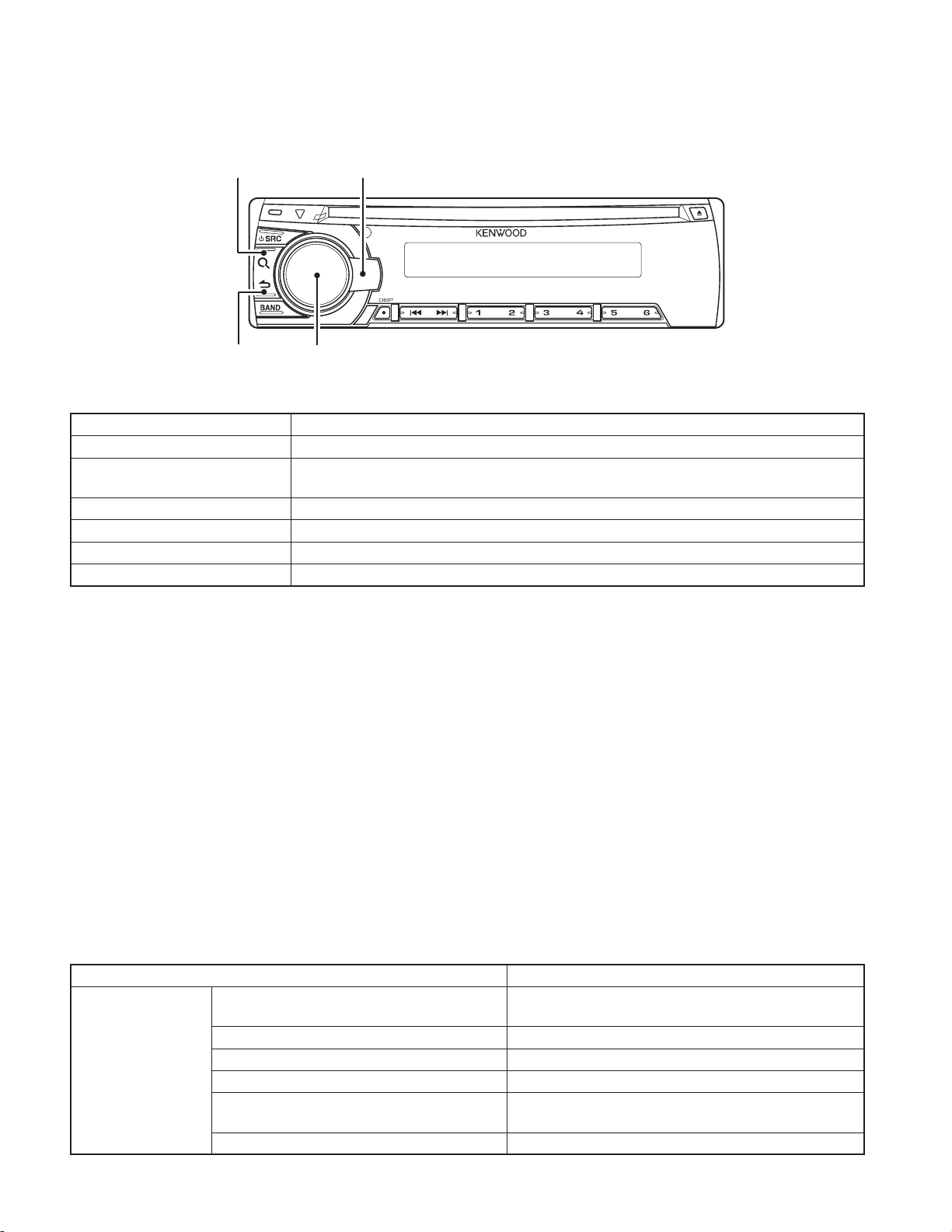
CD RECEIVER
KDC-348U/4751SD
KDC-BT41U/BT648U
KDC-U4549/U4549SD/U549BT
KDC-X395/X695
© 2011-4 PRINTED IN JA PAN
SERVICE MANUAL
Tuner setting adjustment after replacing E2PROM
After replacing E2PROM (IC203 on X34), tuner setting adjustment is needed.
The adjustment is that to perform the “TUNER Setting Adjustment Mode” (Page 13).
B53-0844-00 (N) 303
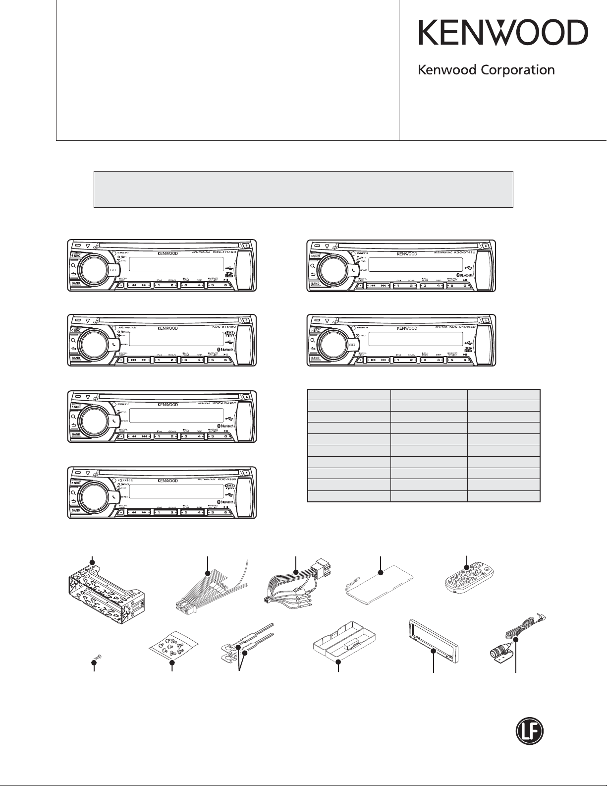
KDC-4751SD : Panel assy (A64-5245-02)
KDC-BT648U : Panel assy (A64-5240-02)
KDC-U549BT : Panel assy (A64-5244-12)
KDC-X695 : Panel assy (A64-5241-12)
KDC-BT41U : Panel assy (A64-5242-12)
KDC-U4549SD : Panel assy (A64-5246-12)
TDF SPARE-PANEL
MAIN UNIT NAME TDF PARTS No. TDF NAME
KDC-348U Y33-3490-11 TDF-113D
KDC-4751SD Y33-3482-73 TDF-4751SD
KDC-BT41U
KDC-BT648U
KDC-U4549 Y33-3490-21 TDF-U4549
KDC-U4549SD Y33-3480-22 TDF-U4549SD
KDC-U549BT Y33-3480-21 TDF-U549BT
KDC-X395 Y33-3490-10 TDF-113DX
KDC-X695 Y33-3480-11 TDF-116DX
Y33-3482-71 TDF-BT41U
Y33-3480-10 TDF-BT116D
Mounting hardware assy
(J22-2049-03)
* Tap screw (2x8)
(N80-2008-48)
* Depends on the model. Refer to the parts list.
* Screw set
(N99-1757-15)
* DC cord
(E30-6933-05)
Lever
(D10-7139-04) x2
* DC cord
(E30-6934-05)
* Plastic cabinet assy
(A02-2757-13)
* Carrying case
(W01-xxxx-xx)
This product uses Lead Free solder.
This product complies with the
* Remote controller assy (RC-405)
(A70-2104-05)
* Trim plate
(xxx-xxxx-xx)
* Microphone (3m)
(W01-1768-15)
PbF
RoHS directive for the European market.
KDC-348U/4751SD/BT41U/BT648U
2
/U4549/U4549SD/U549BT/X395/X695
ELECTRIC UNIT (X34- )
W551
ATOMIC
TUNER
(4MHz)
2
TYPE
1,2
∗
J921
IC501
BU5V
2
2
MIC CN
DME1
IC301
LEVEL
SHIFT
IC201
IC202
RESET
S301
RESET SW
J701
PRE-OUT
FRONT/REAR/NF
Q701-706
PRE
MUTE
A8V
SERVO+B
BU5V
CD
MECHA
J3
USB CN
S1
ROTARY
ENCODER
IC2
REMOTE
KEY
MATRIX
BU3.3V
J301
J1
9
2219 8 6
1
(2.8V)
BU
∗
J601
LX-BUS
BU3.3V
4VPRE+B
IC401
BU5V
∗
MAIN CLOCK = 48MHz (CRYSTAL 12MHz)
BU3.3V
IC601,
602
LEVEL
SHIFT
22
SYSTEM u-COM
SUB CLOCK = 32.768kHz (QUARTZ)
211
5
USB5V
OEM RC
ED1
A8V
E-VOL
IC203
PANEL3.3V
SW3.3V
FL+B
CONNECTOR
FL
E2P
ROM
IC801
1
SW3.3V
ILLUMI+B
POWER IC
IC802
LEVEL
SHIFT
to GND
CN DET
KEY
ILLUMI
BU
Q707,708
MUTE
∗
IC451
1
SPE-ANA
2
AGC AMP
SW3.3V
∗
IC261
iPod
AUTHENTICATION
SWREG5V
1333
∗
CN901
SD SLOTSD3.3V
J2
AUX CN
1
5
BU5V
BU DET
∗
∗
A901
BT
MODULE
∗
IC921
ANALOG
SW
∗
CN1
MIC CN
SWREG5V
IC901
BT3.3V
SWREG5V
J1
DC-CN
FRONT L/R
POWER
SUPPLY
IC
REAR L/R
P-CON
P-ANT
OEM RC
MUTE
ILLUMI
ACC
BU
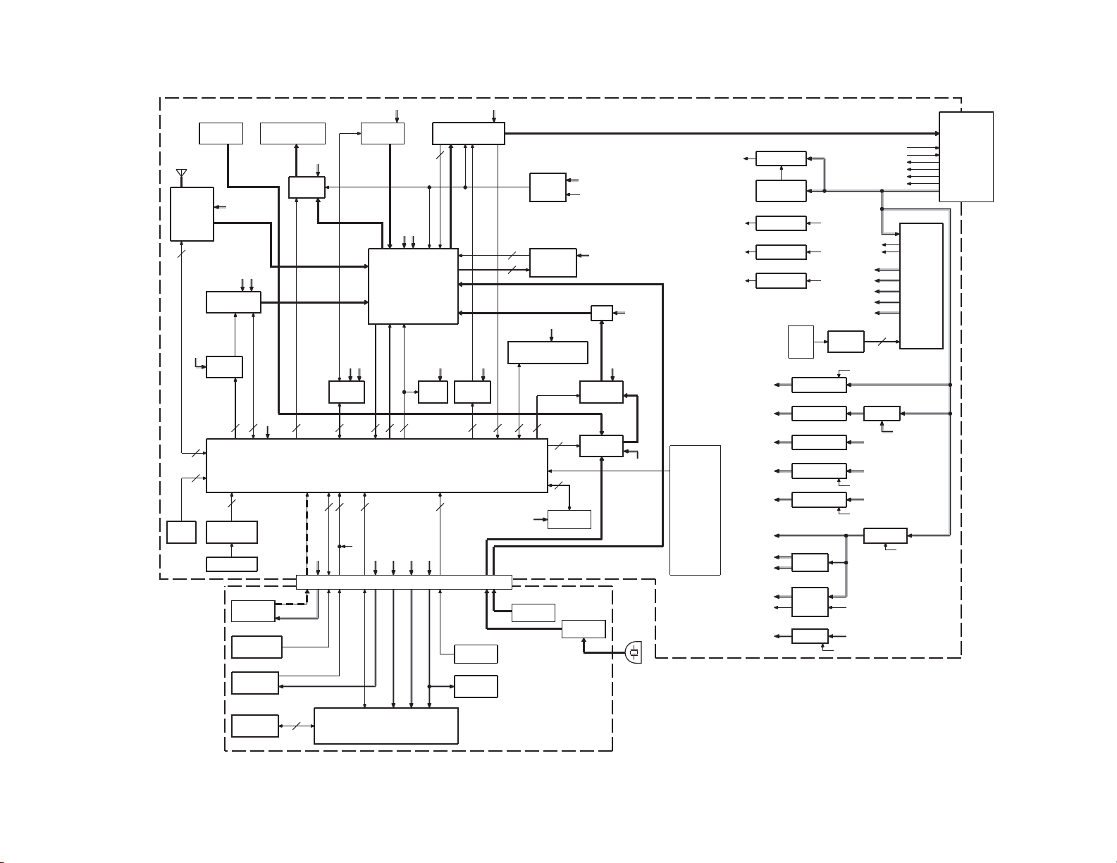
BLOCK DIAGRAM
Q301
BU-DET
ACC-DET
ILLUMI-DET
LINE-MUTE
AM+BLPF
∗
OME-RC
PS1-1
PS1-2
PS1-3
PS2-1
ACC-DET
BU-DET
ILL-DET
LINE MUTE
PON-4VPRE
PON-SW3
PON-PAN3
PON-SWERG
FSEL
SW-VBUS
VBUS-OC
∗
SD-PWR
BU DET
Q102
SURGE
DET
Q101
ACC DET
∗
Q105
ILLUMI DET
D105
LINE MUTE
4VPRE+B
SERVO+B
BU3.3V
SW3.3V
PANEL3.3V
FL+B
SWREG5V
BT3.3V
SW3.3V
USB5V
VBUS OC SW VBUS
SD3.3V BU3.3V
PS1-1
PS1-2
PS1-3
PS2-1
∗
Q91,92
4VPRE+B
Q1,2
SERVO+B
Q103
BU3.3V
∗
Q302
SW3.3V
Q301
PANEL3.3V
∗
IC902
BT3.3V
IC71
HI-SIDE
SW
∗
Q951
SD3.3V
ACC
ILLUMI
MUTE
Q5-10
LEVEL
SHIFT
SD PWR
ILLUMI+B
P-CON
P-ANT
OEM RC
MUTE
ILLUMI
ACC
P-CON
P-ANT
A8V
AM+B
BU5V
SW5V
4
PON-4VPRE
Q3,4
SW14V
BU5V
BU3.3V
PON-SW3
BU3.3V or SW3.3V
PON-PAN3
Q51
DC/DC5V
IC1
SWREG5V
PON-SWREG
FSEL
SWITCH UNIT (X16- )
BLOCK DIAGRAM
KDC-348U/4751SD/BT41U/BT648U
/U4549/U4549SD/U549BT/X395/X695
DPU1
ACB
EF
FO COIL
TR COIL
DM1
SPINDLE
MOTOR
DM2
LOADING &
SLED
MOTOR
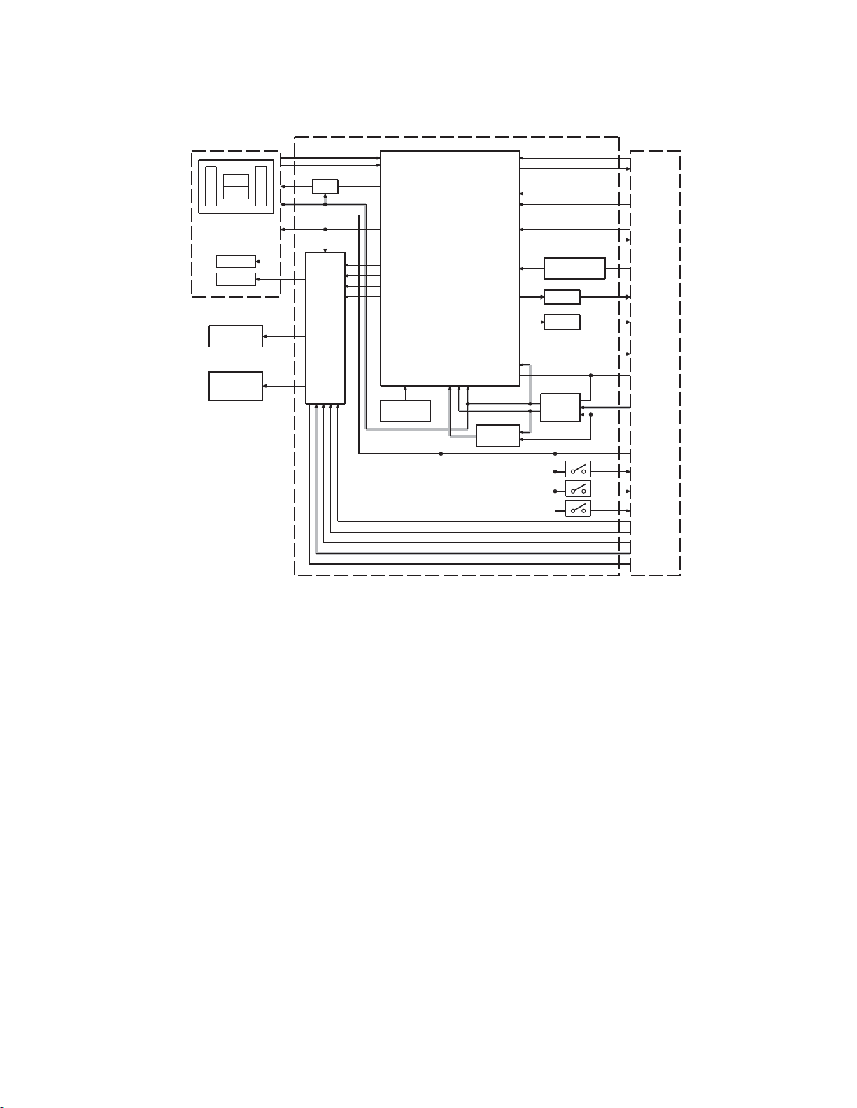
CD PLAYER UNIT (X32-6250-02)
IC4
SIGNAL A/B/C/E/F
Q1
APC
IC3
FO OUT
TR OUT
MOTOR
DRIVER
DM OUT
FM OUT
PD
LD
VREF
FO OUT
TR OUT
DM OUT
FM OUT
X1
CLOCK
16.934MHz
RF AMP
SERVO
PROCESSOR
MP3 DECODER
WMA DECODER
AAC DECODER
1M bit SRAM
MOTHER
BOARD
SRAM STB
SO
SI
BUCK
+
+
+
+
+
D GND
D1.5V
CCE
PIO0
MRST MRST
ZDET MUTE L/R
A3.3V
AGND
BU1.5V
D3.3V
Q14
D1.5V
OUTPUT
R15
LEVEL SHIFT
RESISTOR
C43
Lch Lch
Rch
FILTER
C44
FILTER
IC5
BU1.5V/
D3.3V
REG
(X34- )
SRAM STB
SO
SI
BUCK
CCE
PIO0
Rch
A.GND
BU5V
P.ON
D.GND
S1
LOS-SW
S2
12EJE-SW
LOE-SW
DRV MUTE
LO/EJ
MOTOR
S7.5V
S.GND
3

KDC-348U/4751SD/BT41U/BT648U
/U4549/U4549SD/U549BT/X395/X695
COMPONENTS DESCRIPTION
ELECTRIC UNIT (X34-696x-xx)
●
Ref. No. Application / Function Operation / Condition / Compatibility
IC1 Power Supply IC Outputs 5Vx2, 8V, 8.3V, 10.3V, P-CON, P-ANT.
IC21 3.3V AVR IC Power supply for BU+3.3V to μ-COM.
IC51 SW REG Power supply for D+5.1V to USB and panel.
IC71 Hi-side SW USB over-current detection.
IC201 System μ-COM Controls FM/AM tuner, CD mechanism, panel, volume.
IC202 Reset IC Lo when detection voltage goes below 2.8V.
IC203 E2PROM For log memory.
IC261 iPod Authentication IC For Apple authentication.
IC301 3.3V to 5V Level shift.
IC401 E-VOL Controls the source and volume.
IC501 ATomIC RDS Tuner IC.
IC601,602 3.3V to 5V Level shift.
IC801 Power IC Amplifi es the front L/R and the rear L/R to 50W maximum.
IC802 3.3V to 5V Level shift.
IC901 BT LPF Bluetooth output low pass fi lter.
IC902 3.3V AVR Power supply for BT/SD+3.3V.
IC921 Switch IC MIC switching signal (Panel microphone/ Rear microphone)
Q1,2 SERVO+B AVR When Q2’s base goes Hi, AVR outputs 7.5V.
Q3,4 Control SW for SERVO+B ON when Q3’s base goes Hi.
Q5,6 Control SW for IC1 ON when Q5’s base goes Hi.
Q7,8 Control SW for IC1 ON when Q7’s base goes Hi.
Q9,10 Control SW for IC1 ON when Q9’s base goes Hi.
Q51 FREQ CONT SW for IC51 1.1MHz when the base goes Lo, 1.7MHz when the base goes Hi.
Q91,92 4V PREOUT+B AVR When Q92’s base goes Hi, AVR outputs 12V.
Q93,94 CONT SW for 4V PREOUT+B ON when Q94’s base goes Hi.
Q101 ACC DET ON when the base goes Hi during ACC is applied.
Q102 Surge DET When the base goes Hi, surge voltage is detected.
Q103 BU DET ON when the base goes Hi during BU is applied.
Q104 Mute CONT ON when the base goes Hi.
Q301 PAN3.3V SW ON when the base goes Lo.
Q302 SW3.3V SW ON when the base goes Lo.
Q701,702 Pre-out Mute SW When one of 2 bases goes Hi, pre-out is muted.
Q703,704 Pre-out Mute SW When one of 2 bases goes Hi, pre-out is muted.
Q705,706 Pre-out Mute SW When one of 2 bases goes Hi, pre-out is muted.
Q707,708 Mute Driver for Pre-out ON when the base goes Lo.
Q921 MIC SW CONT Rear MIC when the base goes Lo, panel MIC when the base goes Hi.
Q951 SD3.3V SW ON when the base goes Lo.
4
KDC-348U/4751SD/BT41U/BT648U
/U4549/U4549SD/U549BT/X395/X695
COMPONENTS DESCRIPTION
CD PLAYER UNIT (X32-6250-02)
●
Ref. No. Application / Function Operation / Condition / Compatibility
IC3 4ch BTL Driver
IC4 Servo DSP with built-in Audio DAC With built-in MP3/WMA/ACC decoder and 1M-bit-SRAM.
IC5 BU1.5V/D3.3V REG.
Q1 APC (Auto Power Control) Drives LD (Laser Diode).
Q14 D1.5V Output
D2 Laser Diode Protection
D3,4 Static Electricity Countermeasure Prevents malfunction by static electricity.
Driver for focusing & tracking coil, driver for sled & spindle motor, and operation
for disc loading & ejection.
Power supply for BU1.5V.
Power supply for digital/analogue/audio 3.3V.
Switches ON/OFF at one end of BU1.5V line which is separated into 2 directions.
Uses output voltage as D1.5V.
Prevents reverse bias which is applied to laser.
Laser destruction prevention.
5
KDC-348U/4751SD/BT41U/BT648U
/U4549/U4549SD/U549BT/X395/X695
MICROCOMPUTER’S TERMINAL DESCRIPTION
System μ-COM : IC201 (X34- : ELECTRIC UNIT)
●
Pin No. Pin Name I/O Application
1,2 NC - Not used
3 AVSS - Reference GND for A/D converter
4 VREFH - Reference power supply for A/D converter
5 RESET
6 MODE I Mode Connects to GND
7 IPOD SDA I/O
8 IPOD SCL O I2C clock output for iPod authentication IC
9 IPOD RST
10 ROTARY CW I VOL encoder input Pulse width detection
11 VFD DATA I/O VFD data input/output VFD data input/output
12 VFD PAN DATA I VFD data input VFD data input
13 VFD CLK O VFD clock output 125kHz
14 ROTARY CCW I VOL encoder input Pulse width detection
15 DVSS - GND
16 VFD RST
17 VFD CE O VFD control request
18 PON SW3
19 BSIF LRCK O BS LRCK output
20 BSIF BCK O BS BCK output
21 BSIF DATA O BS DATA output
22 BSIF GATE O Data transfer starting signal
23 BSIF ST REQ I Data input request signal
24 MIC SW O BT microphone switching (KDC-BT648U) L: Panel microphone, H: Rear microphone
25 PON PANEL3
26 NC - Not used Output L fi xed
27 PANEL DET I Panel connection detection H: No panel, L: Panel attached
28 NC - Not used Output L fi xed
29 CD BREAK O CD motor brake
30 CD LOEJ O CD motor control
31 CD PON I/O CD mechanism power supply control output H: Power supply ON, Hi-Z: Power supply OFF
32 CD LOE LIM SW I CD detection (Chucking SW) H: Loading completed, L: No disc
33 CD SRAM STBY
34 CD REQ I Communication request from mechanism DSP H: Data request
35 CD LOS SW I CD loading detection
36 CD SO O Serial interface transmission
37 CD SI I Serial interface reception
38 CD CLK O Serial interface clock output 1MHz
39 BEEP O Beep output 2kHz/1kHz
40 CD DISC12 SW I 12cm disc detection
I Reset input
I2C data input/output for iPod authentication IC
O Reset signal for iPod authentication IC
O VFD driver reset output
I/O SW3.3V control ON: L, OFF: Hi-Z
I/O PAN3.3V control
O Decoder SRAM standby control L: SRAM standby
Truth Value
Table
q
q
Processing / Operation / Description
Connects to GND even when A/D converter is
not used
Connects to +B even when A/D converter is not
used
H: Reset cancelled, L: Reset
Momentary power down or panel detached or
11 minutes after ACC OFF: L
ON: L, Momentary power down or panel de-
tached or 11 minutes after ACC OFF: Hi-Z
Refer to the truth value table
Refer to the truth value table
6
KDC-348U/4751SD/BT41U/BT648U
/U4549/U4549SD/U549BT/X395/X695
MICROCOMPUTER’S TERMINAL DESCRIPTION
Truth Value
Pin No. Pin Name I/O Application
41 ZDET IN I 0-bit mute request H: Mute request, L: Normal play
42 CD RST
43 CD CCE
44 CD DRIVE MUTE
45 CD MOTOR O CD motor switching control
46 NC - Not used Output L fi xed
47 DVCC3 - Power supply
48 DVSS - GND
49,50 NC - Not used Output L fi xed
51 SD CD
52 SD PWR
53 BT RST
53 SD CS
54~56 NC - Not used Output L fi xed
57 PS1-1 O Power supply IC control
58 PS1-2 O Power supply IC control
59 PS1-3 O Power supply IC control
60 PS2-1 O Power supply IC control
61 NC - Not used Output L fi xed
62 FSEL1 O SW-REG frequency switching
63 NC - SW-REG frequency switching Output L fi xed
64 PON SW-REG O SW-REG ON/OFF L: OFF, H: ON
65 BT SYS DATA O Data output to BT
65 SD DO O Data output to SD
66 BT BT DATA I Data input from BT
66 SD DI I Data input from SD
67 SD CLK O Clock output to SD
68~70 NC - Not used Output L fi xed
71 ILLUMI DET
72 BU DET
73 ACC DET
74 NC - Not used Output L fi xed
75 PON 4V-PRE I/O 4V-PRE power supply control (eXcelon model) H: ON, Hi-Z: OFF
76 SA RST
77 SA CLK O Clock output for spectrum analyzer
78 MUTE 0
79 MUTE 1
80 MUTE 2
O CD mechanism reset H: Normal, L: Reset
O CD mechanism chip enable
O CD motor driver mute output
I SD card insert detection L: SD found
I/O SD block power supply control L: POWER ON, Hi-Z: POWER OFF
O BT module reset L: BT reset, H: Normal
O CS output to SD
I Dimmer illumination detection L: ON, H: OFF
I Momentary power-down detection
I ACC detection ACC found: L, No ACC: H
O Reset output for spectrum analyzer H: Reset cancelled, L: Reset
O Front direct mute
O Rear direct mute
O Other direct mute
Table
q
w
w
w
w
Processing / Operation / Description
Refer to the truth value table
Refer to the truth value table
Refer to the truth value table
Refer to the truth value table
Refer to the truth value table
BU found: L,
No BU or momentary power down: H (Operates
less than 4ms after momentary power down)
L: Mute ON (Time constant solo setting: 10ms),
H: Normal
L: Mute ON (Time constant solo setting: 10ms),
H: Normal
L: Mute ON (Time constant solo setting: 10ms),
H: Normal (Countermeasure against IC2 shock
noise)
7
KDC-348U/4751SD/BT41U/BT648U
/U4549/U4549SD/U549BT/X395/X695
MICROCOMPUTER’S TERMINAL DESCRIPTION
Pin No. Pin Name I/O Application
81 MUTE AFS
82 PWIC MUTE
83 PWIC STBY
84 PWIC DC ERR I
85 LX DATA M O Data to slave unit SIO mode transmission
86 LX DATA S I Data from slave unit SIO mode reception
87 LX CLK I/O LX-BUS clock SIO mode clock (125kHz or 107kHz)
88 NC - Not used Output L fi xed
89 DVCC3 - Power supply
90 DVSS - GND
91 SW DIO - For on-board writing
92 SW CLK - For on-board writing
93 TRACE CLK - For debug
94 TRACE DATA 0 - For debug
95 TRACE DATA 1 - For debug
96 TRACE DATA 2 - For debug
97 TRACE DATA 3 - For debug
98 AUD SDA I/O I2C data input/output (E-VOL IC control)
99 AUD SCL O I2C clock input/output (E-VOL IC control)
100 LX RST O Forced reset to slave unit H: Reset, L: Normal
101 LX MUTE I Mute request from slave unit H: Mute ON, L: Mute OFF
102 LX REQ M O Communication request to slave unit
103 LX CON O Start-up request to slave unit H: Slave unit ON, L: Slave unit OFF
104 USB PON O USB P.ON output H: ON, L: OFF
105 USB OC
106 NC - Not used Output L fi xed
107 MUTE PRE
108 MUTE PRE SW
109 LX REQ S I Communication request from slave unit For external interrupt
110 TUN SDA I/O I2C data input/output (Tuner IC control)
111 TUN SCL O I2C clock output (Tuner IC control) I2C clock frequency: 200kHz
112 REMO I
113 REMO I Remote control signal input
114 REG VCC3 - Power supply
115 XT1 I Low frequency resonator connection Sub clock: 32.768kHz
116 XT2 O Low frequency resonator connection Sub clock: 32.768kHz
117 CVCC3 - Power supply
118 X1 I High frequency resonator connection Main clock: 12MHz
119 CVSS - GND
I/O AFS mute
O Power IC mute
O Power IC standby control POWER ON: H, POWER OFF: L
Detection of power IC’s +B and GND short-
circuited
I USB over-current detection L: Detected, H: Normal
O External preout mute O-bit or momentary power down: L, L: Mute ON
O External preout mute (SUB) O-bit or momentary power down: L, L: Mute ON
Input signal of remote control reception and
wired remote control
Truth Value
Table
Processing / Operation / Description
L: Mute ON (Time constant solo setting: 0.5ms),
Hi-Z: Normal
STANDBY source or momentary power down: L,
TEL mute: L
Communication with E2PROM for system
μ-COM data keeping
Communication with E2PROM for system
μ-COM data keeping
Pulse width detection
Even pin No.112 is being short-circuited, input
signal can be ignored in software
8
KDC-348U/4751SD/BT41U/BT648U
/U4549/U4549SD/U549BT/X395/X695
MICROCOMPUTER’S TERMINAL DESCRIPTION
Truth Value
Pin No. Pin Name I/O Application
120 X2 O High frequency resonator connection Main clock: 12MHz
121 DVCC3 - Power supply
122 DVSS/REGVSS - GND
123 USB D+ I/O USB data connection
124 USB D- I/O USB data connection
125 NM IN I Non-maskabe interrupt
126 TEST1 - For test Output L fi xed
127 TEST2 - For test Output L fi xed
128,129 NC - Not used Output L fi xed
130 AVCC3 - Power supply
131 SA IN I Input data for spectrum analyzer
132 AUD DC ERR
133 NC - Not used
134 LINE MUTE I Line mute detection
135~138 NC - Not used
139 TYPE 1 I Destination switching
140 TYPE 2 I Destination switching
141,142 NC - Not used
143 SERIAL DET I For serial number writing
144 NC - Not used
I DC offset detection
Table
Processing / Operation / Description
TEL mute: Below 1V (Model without BT func-
tion), NAVI mute: Over 2.5V
Truth value table
CD motor control
q
CD MOTOR (Pin 45) CD LOEJ (Pin 30) CD BRAKE (Pin 29)
Standby L L L
Eject H H L
Load H L L
Brake H H/L H
Power supply IC control SEL1 (Pin No.10 of IC1)
w
PS1-2 (Pin 58) PS1-3 (Pin 59) PS2-1 (Pin 60) ILLUMI P-CON P-ANT
L L L OFF OFF OFF
L L H ON OFF OFF
H L H ON ON OFF
H H H ON ON ON
Power supply IC control SEL1 (Pin No.11 of IC1)
w
PS1-1 (Pin 57) AUDIO/SW5/AM
L OFF
HON
HON
9
KDC-348U/4751SD/BT41U/BT648U
/U4549/U4549SD/U549BT/X395/X695
1. Panel
SEARCH
ACCENT
TEST MODE
RETURN
VOL
2. How to enter each Test Mode
Test Mode name Operation
Production Test Mode Press and hold [1] key and [3] key and reset.
Service Test Mode
Service information clear mode Press and hold [2] key and [5] key and reset.
DC Error Information Mode Press and hold [3] key and [6] key and reset.
Version display mode *1 While pressing and holding [RETURN] key, press [DISP] key.
Forced update mode Press and hold [1] key and [SEARCH] key and reset.
Transition to Test Mode shall be available during DC Error detection.
✳
*1: The model that does not support fi rmware update function will not also support the version display mode.
In the STANDBY source, while pressing and holding [2] key, press [6] key for 7 seconds.
(Starting to press [2] key and [6] key at the same time can not be entered into the mode)
3. How to release each Test Mode
• Reset
• Momentary voltage drop
• ACC OFF
• POWER OFF
• Panel Detach
• Arbitrary key operation (fi rmware and version display only)
4. Production Test Mode
How to enter the production test mode
●
Press and hold [1] key and [3] key and reset.
Default status immediately after the mode activation
●
It shall be same as normal RST start in other settings than the following.
Details
Period to prohibit TEL/LINE MUTE immediately
after activation (normally 10 seconds)
Initial CD mechanism operation at start-up Prohibited
Difference in action
10
Write-in to E2PROM when detecting a DC error Prohibited
Demo Mode ON/OFF Setting Menu Prohibited
Power supply during ACC OFF (Back Up On)
BEEP sound Beep with short-pressing in any functions
1 second
MUTE terminal turns OFF after 2 seconds (When the terminal
is turned OFF, the CD mechanism does not function)
KDC-348U/4751SD/BT41U/BT648U
/U4549/U4549SD/U549BT/X395/X695
TEST MODE
Details
Volume 30 (-10dB)
BASS BOOST/LOUD OFF
Various setting value
Mode structure
●
Some Test Modes change according to the current source.
The following table shows the current source in Set and the related test mode status.
POWER OFF -
Standby STANDBY Test Mode
TUNER TUNER Test Mode
CD CD Test Mode
SD -
BT BT Test Mode (BT built-in model)
USB -
AUX -
EQ NATURAL
Fader/Balance Center
DEMO Mode Setting OFF
AUX Setting ON1
Model source Test mode
Basic operation of the [ACCENT] keys
●
BT built-in model
Source Condition Operation
Other than BT Mode/HF interruption
Transmit possible condition (displaying phone number) Transmit
BT Mode
HF interruption
SD built-in model
Source Condition Operation
Other than SD SRC
SD SRC
Transmit impossible condition BT Mode clear
Receiving Off Hook (connect)
Transmitting Off Hook (disconnect)
Connected Off Hook (disconnect)
Connected (receiving interruption) Interruption receiving Menu
Connected (receiving interruption Menu) Invalid
Connected (interruption connected) Disconnect (Parrot dependent)
SD inserted SD SRC
SD not inserted Invalid
BT Mode source
Easy Setting
■
Easy Setting
■
(Invalid)
■
Invalid
■
-
-
11
KDC-348U/4751SD/BT41U/BT648U
/U4549/U4549SD/U549BT/X395/X695
TEST MODE
USB model
Source Condition Operation
iPod inserted iPod SRC
Other than iPod SRC
iPod SRC
Mode content
●
Syscon shall display the following information after entering this mode. The operation shown below shall be workable.
Display content Details
÷÷÷÷÷÷÷
STANDBY Test Mode Specifi cation
●
Operation Display content Details
Syscom version display
BT module version
1 (Toggle)
2 (Toggle)
3 (Toggle) All lights ON/OFF
4 (Toggle)
USB
model only
5 (Toggle) Preout switch
display
Information display
Mechanism model name
Mechanism version
All lights ON
Serial No. display
All lights ON
Information display iPod
verifi cation IC mount
status display
All lights ON/TEST
iPod not inserted Invalid
All lights ON
SYS01–200
SYS03–200
BT HXXXSXXXXX
9B20:
SN :00000000
:
:
:
iPod :
iPod :OK
iPod :NG
iPod :
SWP RE R E AR
SWP RE S UB – W
Syscom version
SYS01: BT/USB 13 digit model
SYS03: SD MODEL
BT module/version displlay (Target model: BT)
Mechanism model name and mechanism version
display
All lights ON (Switch with other display)
Serial No. display (8-digit)
Display as it is in hex
✳
All lights ON (Switch with other display)
All lights ON/OFF with toggle
iPod verifi cation IC mount status display
Blank: Verifying
OK: Verifi cation IC mounted
NG: Verifi cation IC not mounted
∗∗
: Non-iPod support model
∗∗
All lights ON (Switch to other display)
Switch Preout with toggle
(KDC-4751SD/BT41U/U549BT)
Invalid
■
Invalid
iPod By Hand Mode
■
6 (Toggle) All lights ON/OFF Switches between all lights ON and all lights OFF
SOURCE
transition
RETURN Mode release
■
DISP Display blinks once when key is pressed.
BAND
SEARCH
Mode release Return to Normal mode
Return to Normal mode
Display blinks once when key is pressed.
Display blinks once when key is pressed.
12
TEST MODE
Tuner Test Mode Specifi cation
●
The following display shall be indicated according to the TUNER status.
Status Display content Details
TUNER IC Normal Error
Adjustment not imple-
mented
RDS Specifi ed data
reception
Operations
Operation
ACCENT
BAND
SEARCH
DISP
■
TUNER IC display
BAND switch
operation
S meter voltage
judgment display
Shift to TUNER
setting adjust-
ment mode
TUN CON NG
ERR
∗
Blink in 2Hz
RDS TE ST
ATOM RDS
FM1 – 3 A 9 7.9 A
S–MTR xx:OK
S–MTR xx:NG
S–MTR xx:––
∗
Display content Details
A97.9A
KDC-348U/4751SD/BT41U/BT648U
/U4549/U4549SD/U549BT/X395/X695
Communication to TUNER IC not available (indicated unless
the mode is in Clock Display Mode).
For models that TUNER adjustment is necessary but not done
(adjustment value: 0x00 or 0xFF), the following TUNER Test
Mode functions are valid (“∗ERR∗” display is continuing).
Turn OFF P-CON forcibly if PS=RDS TEST is received.
P-CON recovers with Power OFF/ON.
Display TUNER IC version
Execute Band Switch as shown in the following table
every time Band key is pressed in each type.
S meter value xx: Current S meter value
Determination result OK: Within S meter voltage spec
NG: Out of S meter voltage spec
– – : No LEVEL OFFSET adjustment
Shift to TUNER setting adjustment mode after switching
to 98.3MHz
SG setting values
Frequency: 98.3MHz, Modulation frequency: 1kHz,
Modulation mode: MONO, Modulation: OFF,
Deviation: 40kHz, ANT input level: 34dBμV
TUNER Setting Adjustment Mode
1)
Operation (Operation after performance of above-mentioned “Shift to TUNER setting adjustment mode” item)
Operation
BAND
■
(Toggle)
RETURN Mode release
AUTO Adjust-
ment Mode
Display content Details
Select TUNER adjustment method (AUTO) using [BAND] key.
S-xx: Current S meter value (Hex)
A S–xx L–xx
L-xx: Level offset value (Hex)
In case that the level offset value is not adjusted (0xFF
✳
or 0x00), display “– –”.
Return to TUNER Test Mode
2) Operation in AUTO Adjustment Mode
Operation
VOL
PUSH
Adjustment start
Display content Details
A S–xx L–xx
Start adjustment (Start Auto adjustment, and transit to Suc-
cess/Failure display depending on the adjustment result)
13
KDC-348U/4751SD/BT41U/BT648U
/U4549/U4549SD/U549BT/X395/X695
TEST MODE
3) Status display during adjustment
Status Display content Details
Adjustment success
Adjustment failure
ADJ OK :x x
ADJ NG
4) Operation of return to TUNER Test Mode
Operation
RETURN Mode release Return to TUNER Test Mode.
BAND switch list
Type BAND1 BAND2 BAND3 BAND4 BAND5 BAND6 Details
K
E
M
FM1 FM2 FM3
q
FM1 FM2 FM3
q
FM1 FM2 FM3
q
Display content Details
When the adjustment value write-in to E2PROM (IC203 on X34)
has been completed. xx: Level offset value (HEX)
When the adjustment value write-in to E2PROM (IC203 on X34)
has failed
AM - -
w
MW/LW - -
w
MW SW1 SW2
w
q→w
q→w
q→w
CD Test Mode Specifi cation
●
It shall be the same as normal RST start in other than the below setting.
Content Details
Playback track from top No.9
Default for Display mode Play time
Operations in CDDA playback
Operation
3
4
5
6
Special track
up
Special track
down
Special jump
operation
Special jump
operation
Special jump
operation
Special jump
operation
Display content Details
Every time pressed, track up/down performed as below.
No.9→No.15→No.10→No.22→No.12→No.13→No.14→No.9
However, playback is from No.1 for discs with 8 tracks or
less.
If transferred to tracks other than the above with B. Skip,
up/down is performed 1 track at a time to the nearest track
Jump to No.28
(Scratch 0.7mm for MUSIC line vibration test)
Jump to No.14 (Damaged disc TCD-731RA Tr14)
Jump to No.15
• Set Volume value at 27 (2.5V PREOUT MODEL)
• Set Volume value at 29 (4V PREOUT MODEL)
(for error operation FCT check of 20Hz 0dB DC protection)
Jump to No.9 if the track No.22 is playing.
Jump to No.22 if the track No.9 is playing.
BT test mode specifi cation (BT built-in model)
●
Initial condition of the BT MODE (BT source) will display as following.
Status Display content Details
BT MODE
BT MODE
14
BT MODE display
Operations during BT MODE
Operation
KDC-348U/4751SD/BT41U/BT648U
/U4549/U4549SD/U549BT/X395/X695
TEST MODE
Display content Details
ACCENT
■
SEARCH
■
BAND
■
Clear the BT
related memory
information *1
BT device
search
Internal loop
back ON *2
INIT IALIZE
BT INIT :OK
BT I N I T :NG
(The display blinks)
SEARCH I NG
xxxxxxxxxxxxx
UNKNOWN
INT LOOP F
INT LOOP R
Clear the BT MODE (BT source) and transition to the last
source. (Target model: BT)
Press and hold this key for 2 seconds. The character string
as shown in the left cell is displayed while the BT related
memory is being initialized. (Target model: BT)
This is to initialize the BT related memory to its factory de-
fault condition.
When the initialization is successfully completed, “…OK”
(upper) is displayed, and when the initialization is abnor-
mally completed, “…NG” (lower) is displayed.
(Target model: BT)
Press and hold this key for 1 second to initiate the BT de-
vice search.
The search is terminated when 1 device is found.
(Target model: BT)
When a device is found after the search, the name of that
device is displayed. (Target model: BT)
When no device is found at the completion of the search.
Only for this case, perform the search again by pressing the
[VOL PUSH] key briefl y. (Target model: BT)
After the completion of the search, press and hold the
[BAND] key for 1 second to exit from the test mode.
(Target model: BT)
• Set the Volume to 22 and turn the internal loop back func-
tion ON by pressing and holding for 1 second.
• INT LOOP F: Display internal loop back by FRONT micro-
phone
• INT LOOP R: Display internal loop back by REAR micro-
phone
• Microphone setting initial value is FRONT for model with
microphone setting.
• Display microphone position for each model for model
without microphone setting.
• Details of display will not change except [F or R] if it is
ON.
+AM233 (Target model: BT)
Operations during internal loop back (only with KDC-BT648U)
Operation
DISP
(Toggle)
Switch micro-
phone
Display content Details
INT LOOP R
INT LOOP F
Microphone REAR setting
Microphone FRONT setting
*1: This is a function to clear the BT memory information recorded in the EEPROM and the FLASH memory to be initialized with
the “Data fl ash clear” function, and to write the specifi c values to initialize it to its factory default condition.
Factory default condition
• Clearing of the pairing information (FLASH memory of the BT module)
• Clearing of the preset telephone numbers (EEPROM)
• Writing “KENWOOD BT CD/R-3P1” in the friendly name (FLASH memory of the BT module)
15
 Loading...