

Kenwood KD-C519FM, KDC-C719, KDC-C719Y Service Manual
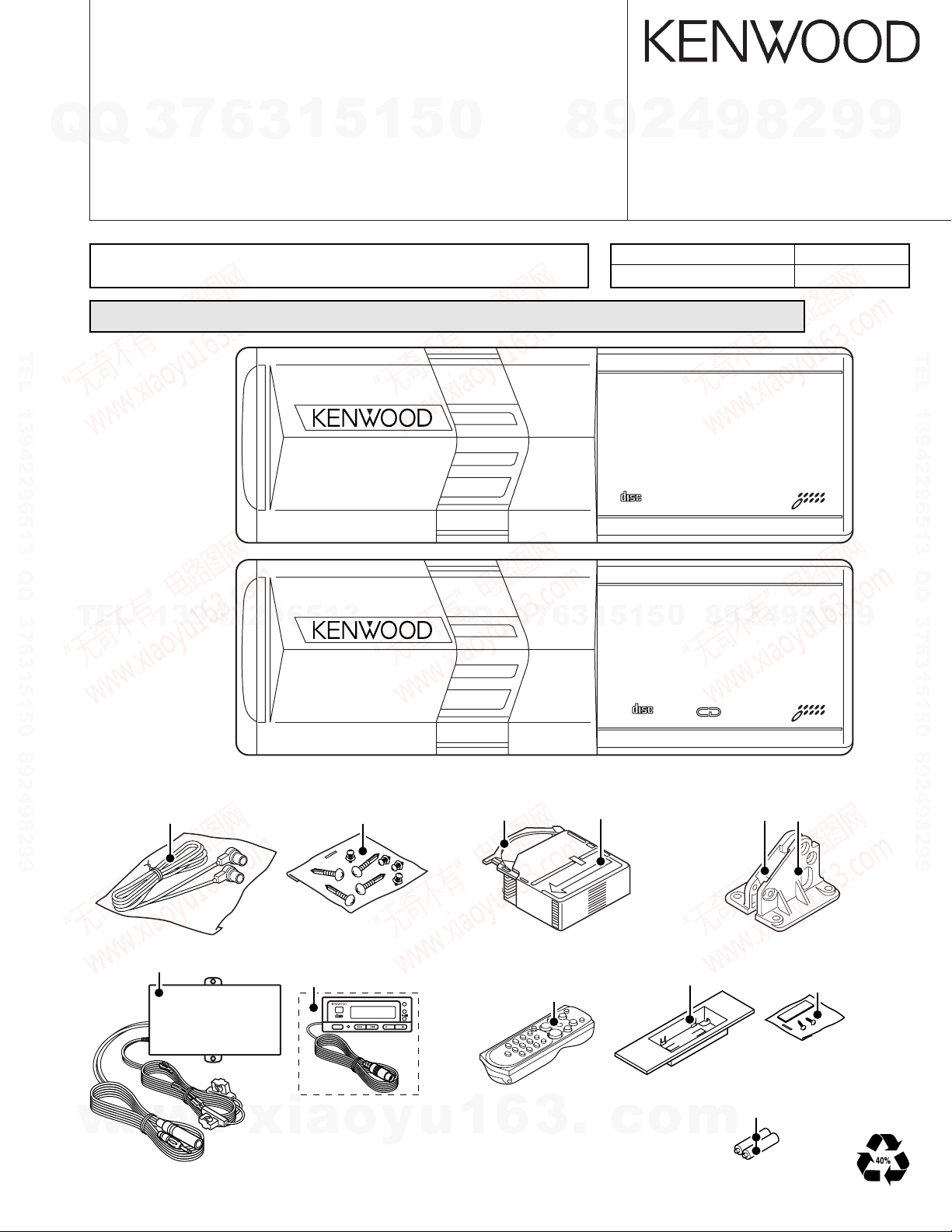
CD AUTO CHANGER
KDC-C519FM
Q
Q
3
7
6
3
1
5
1
5
0
KDC-C719/Y
SERVICE MANUAL
The MECHANISM OPERATION is the same as model KDC-C710.
Please refer to the service manual of model KDC-C710 (B51-7104-00).
When transporting these models, always attach CAUTION CARD and STEPPED SCREW (for transportation).
TEL 13942296513 QQ 376315150 892498299
Illustration is
KDC-C519FM.
Illustration is
KDC-C719/Y.
8
4
2
9
© 2002-11 PRINTED IN JAPAN
B51-7993-00 (N) 3379
Service jig
For initial position setting
COMPACT DISC AUTO CHANGER KDC-C519FM
NEW ANTI VIBRATION MECHANISM
COMPACT
CD-R/RW
DIGITAL AUDIO
9
8
2
W05-0635-00
1BIT 4D/A CONVER
DISC
10
9
9
Parts No.
TEL 13942296513 QQ 376315150 892498299
TEL
CORD WITH PLUG
(E30-4291-05 or E30-4954-15)
w
13942296513
CASE (A01-2819-08)
: KDC-C519FM
w
w
.
SCREW SET
(N99-1645-15)
DISPLAY UNIT ASSY
(T95-0247-08)
: KDC-C519FM
xia
COMPACT
DIGITALAUDIO
PWR
o
TRACK DISC
y
REP
RDM
3
Q
Q
TRAY
(J99-0614-01)
REMOTO CONTROLLER
ASSY(A70-2032-05)
RC-504FM
: KDC-C519FM
u
1
6
1
3
6
7
HOLDER ASSY
(J19-5146-02)
3
.
4
2
9
8
0
5
1
5
COMPACT DISC AUTO CHANGER KDC-C719
NEW ANTI VIBRATION MECHANISM DISC NAME PRESET
COMPACT
CD-R/RW
DIGITAL AUDIO
HOLDER ASSY
(B07-2138-08)
: KDC-C519FM
c
o
TEXT
BRACKET (L)
(J19-5018-03)
MAGICTAPE ASSY
(W01-0763-08)
: KDC-C519FM
BATTERY
(SIZE:AAA)
Not supplied as
service parts
m
2
8
9
DISC
10
BRACKET (R)
(J19-5019-03)
9
9
2
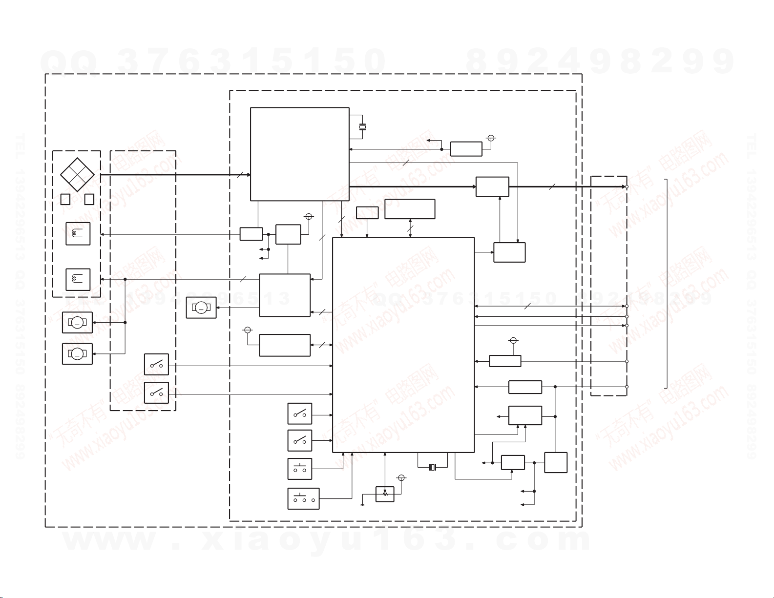
SW5V
LIM SW
L.P.S.
EJ SW
ARM SW
12.5MHz
X2
SPINDLE/LO-EJ
SLED
LOE SW
TR COIL
FO COIL
BTL
EEPROM
&TEXT DECODER
APC
SA5V
Q1
S8V
SYSTEM u-COM
IC7
IC1
RF AMP&SARVO DSP
16.93MHz
X1
P-ON
Q10
Q15,16
Q20
BU. DET
IC8
7
13
4
5
8
2
IC5
MG SW
8V AVR
S8V
S-RAM
24
C
2
BU14V
CH RST
AUDIO
OUT
5
5VREG
IC4
DA5V
S8V
3
HOT
IC9
RESET
7V/9V
5V
Q21,22
M5V1
M5V2
SW5V
S3
S2
S1
SW5V
M
M
&DC MOTOR
DRIVER
ELEVATOR
M
AVR
SA5V
Q9
&D/A CONVERTER
&SCF
MUTE
0bit
Q6,7
MUTE
Q4,5,8
SD5V
FE
A
D
B
PD
M5V2
AVR
CH-MUTE
CH-CON
5L I/F
IC11
COMM SW
S4
to
HEAD
UNIT
ASSY (X13)
(X32)
(X13)
(X92)
PICKUP
KDC-C519FM/C719/Y
Q
TEL 13942296513 QQ 376315150 892498299
Q
3
TEL
w
w
7
6
13942
w
.
2
x
3
1
96513
i
5
a
o
1
y
5
u
0
Q
1
Q
6
3
7
3
6
8
3
.
1
9
5
c
1
2
5
o
4
0
m
9
8
9
2
8
4
9
2
8
2
9
9
9
TEL 13942296513 QQ 376315150 892498299
BLOCK DIAGRAM
9
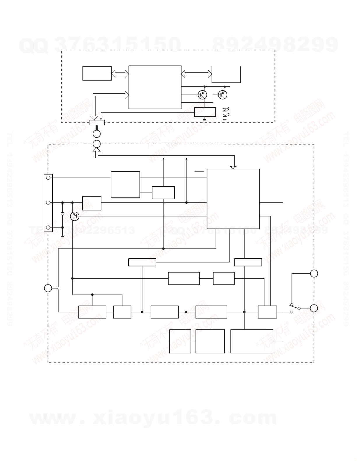
BLOCK DIAGRAM
KDC-C519FM/C719/Y
7
Q
Q
TEL 13942296513 QQ 376315150 892498299
ACC
BATT
GND
TEL
3
13942296513
6
KEY MATRIX
CN1
CN103
IC1
AVR
(+5V)
3
CN101
CN101
1
5
Q1,6
ACC
DETECTION
1
IC1
2,50-56
LCD DRIVER
19-22,32,66
5
RESET
DRIVER
0
6-43
3
1
Q4,5
Q
Q
IC2
REMOTE
SENSER
HOLD
VDD
P ON PLL
7
3
9
8
LCD1
VDD
IC2
19-22,32,66
67
u-COM
31
63
12-17 26 61
1
5
1
3
6
2
29,30,60
74,77
5
4
0
9
8
9
8
2
4
2
9
8
9
2
9
9
TEL 13942296513 QQ 376315150 892498299
9
CD-CH
13P
CN102
SIGNAL
(L/R)
+V(RF STAGE)
+V(AUDIO)
IC101
ISOLATION
AMP. L.P.F.
2nd.
Q308
MODE 1,2
IC102
IC4
AVR(+5.6V)
EMPHASIS
Q101,201
CH-CONTROL
ALC
DRIVER
IC301
FM-St.
MODULATOR
IC302
ALC
DETECTION
AMP
RIPPLE
FILTER
MPX
Q310
MODE 1,2
Q306,
PILOT
MIX
307
Q304,305
LEVEL CONTROL
Q309
AUDIO MUTE
RF
STAGE
RL1
CN104
ANT IN
CN105
To
RADIO
w
w
w
.
xia
o
y
u
1
6
3
.
c
o
m
3
KDC-C519FM/C719/Y
COMPONENT DESCRIPTION
7
Q
Q
● CD PLAYER UNIT (X32-5470-0x)
Ref. No.
IC1 UPD63711AGC Servo IC
IC4 KIA78L05F +5V AVR Analogue output circuit power supply for D/A converter.
TEL 13942296513 QQ 376315150 892498299
IC5 LA6576 Motor driver 1. Input selection.
IC7
IC8 BR24C02F-W EEPROM LPS data back-up memory.
TEL
IC9 S-80830CNNP Reset IC When BU 5V voltage is less than 3.0V, IC outputs “Lo”.
IC11 LC3564BT-70 S RAM CD-TEXT data memory.
Q1 MCH6101 APC Laser diode auto power control.
Q4 DTA124EK 0 bit mute (L CH.) When 0 bit mute is activated, an emitter goes “Hi”, and Q4 outputs “Hi”.
Q5 DTA124EUA 0 bit mute (R CH.) When 0 bit mute is activated, an emitter goes “Hi”, and Q5 outputs “Hi”.
Q6 DTC343TK Mute SW (L CH.)
Q7 DTC343TK Mute SW (R CH.)
Q8 DTA124EK A mute drive
Q9 2SB1202 Servo 5V AVR Q9 is combined with IC5’s pin 26 and 27 , and works as a driver of AVR.
Q10 2SB1295 P-ON 5V SW
Q11 DTC124EK Reset SW When System Reset has activated, a base goes “Hi”, and Q11 is turned on.
Q13 DTC124EUA CH CON SW
Q14 DTA143EUA CH MUTE SW
Q16 2SC4081 SRV 8V AVR Q16 is combined with Q15 (X92-), and works as a pre-driver of AVR.
Q17 DTA143EK
Q18 DTC124EUA
Q19 DTC124EUA 7/9V SW
Q20 DTC124EK BU DETECTION SW
Q21 2SB1202
w
Q22 2SC4081 Q21 and Q22 are inverted Darlington connection.
3
Component Name Application/Function Operation/Condition/Compatibility
UPD784214GC098
13942296513
w
w
6
.
xia
1
5
1
3
Mechanism MI-COM. Mechanism and servo control.
SRV 8V AVR SW When Q18's base goes “Hi”, Q17 is turned on, and SVR 8V AVR is working.
BU 5V AVR
o
5
0
RF amplifier built in digital servo and data processor IC. Focusing, tracking, sled
and spindle servo processing. Detection of dropout, anti-shock, track crossing and
off-track conditions.
Automatic adjustment (focusing, tracking, gain, offset and balance) operations.
Digital signal processing (DSP, PLL, sub-codes, CD-TEXT decode, CIRC error
correction, audio data interpolaration) operations.
Focusing coil, tracking coil, spindle motor and sled motor driver.
VO1~VO4 and VOL outputs ON/OFF function.
While MUTE1 goes “Hi”, VO1 outputs are turned on.
While MUTE2 goes “Hi”, VO2~VO4 and VOL outputs are turned on.
VIN1 amplifier function (input selection and VREF selection)
While VIN SW terminal goes “Lo”, IC pin 15, 16 and 17 inputs are selected.
While VIN SW terminal goes “Hi”, IC pin 15, 18 and 19 inputs are selected.
2. VREF selection.
While VIN SW terminal goes “Lo”, internal VREF (2.5V typical) is selected.
While VIN SW terminal goes “Hi”, external VREF (IC pin 30 input) is selected.
7
3
Q
Q
When 0 bit mute or A mute drive is activated, a base goes “Hi”, and L channel audio
signal is muted.
When 0 bit mute or A mute drive is activated, a base goes “Hi”, and R channel audio
signal is muted.
When audio mute of IC7 is activated, a base goes “Lo”, and audio mute drive signal
is outputted.
While base goes “Lo”, P-ON 5V is supplied to the microprocessor peripheral circuits.
While CH CON or CH-CON2 mode is selected, a base goes “Hi”, and Q13 is turned on.
When MUTE REQUEST to H/U is outputted, a base goes “Lo”, and Q14 is turned on.
When a base goes “Hi”, Q19 is turned on, and SVR 8V AVR is outputting +7V.
When a base goes “Lo”, Q19 is turned off, and SVR 8V AVR is outputting +8.5V.
While BACKUP is applied, a base goes “Hi”, and Q20 is turned on.
When momentary power down has detected, a base goes “Lo”, and Q20 is turned off.
While BACKUP is applied, AVR outputs +5V.
y
u
1
6
3
6
8
3
.
9
1
1
5
c
2
5
o
4
0
m
9
8
9
8
2
4
2
9
8
9
2
9
9
TEL 13942296513 QQ 376315150 892498299
9
4
KDC-C519FM/C719/Y
COMPONENT DESCRIPTION
7
Q
Q
Ref. No.
● RF MODULATOR UNIT
Ref. No.
TEL 13942296513 QQ 376315150 892498299
TEL
3
Component Name Application/Function Operation/Condition/Compatibility
Q30 DTC114YUA Eccentric disc SW
Q31 DTC124EUA VIN SW
Component Name Application/Function Operation/Condition/Compatibility
IC1 UPC7805AHF BU 5V AVR While BACKUP is applied, AVR outputs +5V.
IC2 LC72329-9B24 System MI-COM. System control.
IC4 NJM78L05UA 5V AVR Power supply for FM modulator and RF amplifier.
IC101 NJM2060M Isolation amp.
IC102 NJM4565MD Low pass filter
IC301 BA1405F FM ST modulator
IC302 NJM4565MD
Q1 DTC124EK ACC detection When Q4 is turned on, Q1 is turned on during ACC applied.
Q2 2SA1782(T,U)
Q3 DTC124EK
Q4 DTC143TK Reset SW
Q5 DTC143TK CH RESET SW
13942296513
Q6 DTA124EK Hold detection SW
Q8 DTC143TK Relay driver
Q9 2SC4640(T,U) Ripple filter Power supply for RF amplifier
Q101 2SK2158
Q201 2SK2158
Q303 2SA1162(GR) Pilot mix amp.
Q304 2SK2158 Level control SW Level 1/2 : OFF, Level 3/4 : ON
Q305 2SK2158 Level control SW Level 2/4 : OFF, Level 1/3 : ON
Q306 2SK508L RF oscillator buffer
Q307 2SC2714(Y) RF amp.
Q308 2SK2158 Mode (1/2) SW Mode 1 : ON, Mode 2 : OFF
Q309 2SK2158 Audio mute POWER ON mode : OFF, POWER OFF mode : ON
Q310 2SK2158 Mode (1/2) SW Mode 1 : OFF, Mode 2 : ON
6
1
5
1
3
1/2 VCC driver,
ALC detection amp.
POWER SW When Q3’s base goes “Hi”, Q2 is turned on, and RF modulator circuit is working.
ALC control SW
5
0
When an eccentric disc is detected, Q30 is turned on, and a preceding beam is
made to be delayed.
While spindle servo or disc loading/eject mode is selected, a base goes “Hi”, and
Q31 is turned on.
When RESET SW on display unit is pressed, Q4, Q1 and Q6 are turned off, and
IC2 is holding.
When RESET SW on display unit is pressed, Q5 is turned off, and SYSTEM
7
RESET signal is outputted to CD changer.
Q
When RESET SW on display unit is pressed or ACC is OFF, Q6 is turned off, and
IC2 is holding.
FM modulator output / Vehicles antenna input switching.
When a base goes “Hi”, FM modulator output is selected.
Q
3
6
8
3
9
1
5
1
2
5
4
0
9
8
9
8
2
4
2
9
8
9
2
9
9
TEL 13942296513 QQ 376315150 892498299
9
● DISPLAY UNIT
Ref. No.
w
Component Name Application/Function Operation/Condition/Compatibility
IC1 LC75852W
IC2 PNA4602M
Q1 DTC144EK
Q2 DTB123YK
Q3 DTA144EK
w
w
Q4 DTC144EK
Q5 DTA144EK sensor.
.
LCD driver with key-matrix
Remote control light senser
LED ON/OFF SW When Q1’s base goes “Hi”, Q2 is turned on, and LED is turned on.
Key-matrix permition SW
xia
IC2 ON/OFF SW
o
y
Ready on key-matrix
u
1
6
3
.
c
o
When Q4’s base goes “Hi”, Q5 is turned on, and 5V is supplied to remote control
m
5
KDC-C519FM/C719/Y
MICROCOMPUTER’S TERMINAL DESCRIPTION
7
Q
Q
● Mechanism Microcomputer : UPD784214GC098 (X32- : IC7)
Pin No. Pin Name I/O Description Processing Operation
1 NOR/RW O CD-DA/CD-RW Switching Not used (N.C.)
2 TSTB O CD-TEXT parameter strobe
3 P-CON O P-CON output Not used (N.C.)
4 FOK I Focus OK input “Hi” : Focus OK
5XTALEN O Servo IC oscillation stop control “Hi” : Oscillation stop
6 RST O Servo IC reset terminal “Lo” : Reset
7SAO O Servo IC command/parameter setting terminal
TEL 13942296513 QQ 376315150 892498299
8 SSTB O
9 VDD - Positive power supply connection terminal Connected to D 5V lines
10 X2 - Main clock resonator connection terminal 2
11 X1 I Main clock resonator connection terminal 1
12 VSS - Ground connection terminal Connected to GND lines
13 XT2 - Sub clock resonator connection terminal 2 Not used (N.C.)
14 XT1 I Sub clock resonator connection terminal 1 Not used (connected to GND lines)
15 RESET I System reset input “Lo” : System reset
16 FOGUP I Vibration detect input “Hi” : Vibration detect
17 MGSW I Magazine switch input “Hi” : Magazine in
18 EJSW I Eject switch input “Hi” : Eject switch ON
19 COMMSW I 5-line communication old/new switch input “Hi” : New communication, “Lo” : Old communication
20 PACK I Text data pack synchronous signal input “Hi”→“Lo” : The head of the pack data
TEL
21 CH-CON I Changer control input “Hi” : Standby mode, “Lo” : Operation mode
22 BUDET I Momentary power down detection input
23 AVDD 24 AVREF0 I A/D converter reference voltage input Connected to PON 5V lines
25 HOT I Rise in temperature detection input
26 LPS I LPS Mechanical deck position detection input
27 LOESW I Loading complete switch input “Lo” : Loading complete
28 LIMSW I Limit switch input “Lo” : Pickup most inner position
29 TOFF I Tracking OFF mode terminal Not used (pull down to GND lines)
30 ADJSEL I Servo automatic adjustment ON/OFF terminal Not used (pull down to GND lines)
31 TBANK I Tracking gain switching mode terminal Not used (pull down to GND lines)
32 SIM2 I Destination input 2 Not used (pull down to GND lines)
33 AVSS - A/D, D/A converter ground connection terminal Connected to GND lines
34 LPSCO O LPS A/D converter reference power control output Not used (N.C.)
35 AMUTE O Audio mute output “Lo” : Audio mute ON
36 AVREF1 I D/A converter reference voltage input Connected to D 5V lines
37 SDI I Servo IC communication serial data input
38 SDO O Servo IC communication serial data output
39 SCK O Servo IC communication serial clock output
40 DATAH I Data input from H/U
41 DATAC O Data output from the changer
42 HCLK I/O Communication clock input/output with H/U
43 RECQC O Communication request to H/U “Lo” : Communication requested
w
44 CHMUTE O Audio mute request to H/U “Lo” : Audio mute requested
3
13942296513
w
w
6
.
xia
1
5
1
y
5
u
0
Q
Q
1
3
6
3
Servo IC command/parameter setting strobe terminal
A/D converter positive power supply connection terminal
o
7
3
4
2
9
8
“Hi” : Parameter setting, “Lo” : Address resister setting
“Hi”→“Lo” : Serial data latch
0
5
1
5
1
3
6
“Hi” : When momentary power down detected or
BU OFF “Lo” : BU ON
Connected to D 5V lines
.
c
o
9
9
8
m
2
8
4
2
9
8
2
9
9
9
TEL 13942296513 QQ 376315150 892498299
9
6
KDC-C519FM/C719/Y
MICROCOMPUTER’S TERMINAL DESCRIPTION
7
Q
Q
Pin No. Pin Name I/O Description Processing Operation
45 TSI I Text data input from servo IC
46 TSO O Text data output to servo IC
47 TSCK O Text data clock to servo IC
48~55 A0~A7 O Address setting terminal for S RAM
56~63 D0~D7 I/O Data input/output terminal with S RAM
64~68 A8~A12 O Address setting terminal for S RAM
69~71 A13~A15 O Chip enable setting terminal for S RAM Not used (pull down to GND lines)
72 VSS - Ground connection terminal Connected to GND lines
TEL 13942296513 QQ 376315150 892498299
73 A16 O Chip enable setting terminal for S RAM Not used (pull down to GND lines)
74 A17 O Chip enable setting terminal for S RAM
75 RAMOK O Pickup check judging terminal for production Not used (N.C.)
76 ELVADJ I Mechanism deck ascent/descent position terminal Not used (pull up to D 5V lines)
77 RD O Read-out to S RAM control output
78 WR O Write to S RAM control output
79 WAIT I Waiting time insertion input when accessing S RAM Not used (pull down to GND lines)
80 ASTB O Chip selection to S RAM Not used (N.C.)
81 VDD - Positive power supply connection terminal Connected to D 5V lines
82 PUSEL I Pickup type select terminal Pull up to D 5V lines
83 REQH I Communication request from H/U “Lo” : Communication requested
84 SPLO+ O Spindle/Loading control terminal
85 SPLO- O Spindle/Loading control terminal
TEL
86 ELV+ O Mechanism deck ascent/descent terminal
87 ELV- O Mechanism deck ascent/descent terminal
88 SIM1 I Destination input 1
89 SEARCH O Search mode output Not used (N.C.)
90 TEST1 I Test mode terminal 1 for test mode Not used (pull down to GND lines)
91 TEST2 I Test mode terminal 2 for test mode Not used (pull down to GND lines)
92 8/7V O Motor driver IC power voltage control output “Hi” : 7V, “Lo” : 8.5V
93 EEPWR I EEPROM write mode terminal for production Not used (pull down to GND lines)
94 TEST/VPP I Flash ROM program mode terminal Not used (connected to GND lines)
95 SRVSEL I
96 SLNSA I Sled non-sensitive area ON/OFF terminal Not used (pull down to GND lines)
97 SDA I/O Data input/output with EEPROM
98 SCL O Clock output to EEPROM
99 PON O PON output “Lo” : AVR & LPS POWER ON
100 ARMSW I Arm switch input “Hi” : Arm switch ON
3
13942296513
6
1
5
1
3
Servo active mode terminal (no mechanism movement)
5
0
Q
Q
3
7
4
2
9
8
0
5
1
5
1
3
6
“Lo” : adapted for CD-TEXT, “Hi” : not adapted for CD-TEXT
Not used (pull down to GND lines)
9
8
9
2
8
4
2
9
8
9
2
9
9
TEL 13942296513 QQ 376315150 892498299
9
● System Microcomputer : LC72329-9B24 (RF Modulator Unit : IC2)
Pin No. Pin Name I/O Description Processing Operation
1 XIN I Main clock resonator connection terminal
2 TEST2 I Test mode terminal 2 for test mode Not used (pull down to GND lines)
3, 4 PG3, PG2 I Not used (pull down to GND lines)
5 PG1 I Not used (pull up to +5V lines)
6 PG0 I Not used (pull down to GND lines)
7~9 PH3~PH1 O Not used (pull down to GND lines)
w
w
10 PH0 MUTE1 O Not used (N.C.)
w
.
xia
o
y
u
1
6
3
.
c
o
m
7
KDC-C519FM/C719/Y
MICROCOMPUTER’S TERMINAL DESCRIPTION
7
Q
Q
Pin No. Pin Name I/O Description Processing Operation
11 PF3 MUTE0 O Not used (N.C.)
12 PF2 REQC I Communication request input form CH “Lo” : Communication requested
13 PF1 REQH O Communication request output to CH “Lo” : Communication requested
14 PF0 CHCON O Control output to CH “Hi” : Operation mode, “Lo” : Standby mode
15 PE3 DATA IN I Data input from CH
16
17 PE1 SCK O Clock output to CH
18 PE0 O Not used (N.C.)
TEL 13942296513 QQ 376315150 892498299
19
20 PD2 CLK O Clock output to LCD
21 PD1 RST O Reset output to LCD “Lo” : Reset
22 PD0 CE O CE output to LCD
23~25 PC3~PC1 Not used (N.C.)
26 PC0 SEPA O Separation select output “Hi” : Mode 1, “Lo” : Mode 2
27, 28 PB3, PB2 O Not used (N.C.)
29 PB1 GAIN1 O GAIN1 output “Hi” : Level 1/3, “Lo” : Level 2/4
30 PB0 GAIN2 O GAIN2 output “Hi” : Level 3/4, “Lo” : Level 1/2
31 VDD +5V - Positive power supply connection terminal Connected to +5V lines.
32 PA3 DATA IN I Data input from LCD
33~35 PA2~PA0 I Not used (connected to GND lines)
36 PI31 S28 O Not used (N.C.)
TEL
37 PI21 S27 O Not used (N.C.)
38 PI11 S26 O Not used (N.C.)
39 PI01 S25 O Not used (N.C.)
40~58 S24~S6 O Not used (N.C.)
59 ALC LOW S5 O Not used (N.C.)
60 MUTE S4 O Mute output “Hi” : POWER OFF mode, “Lo” : POWER ON mode
61 SEP ATT S3 O Separation attenuator output “Hi” : Mode 2, “Lo” : Mode 1
62 RELAY S2 O Relay SW control
63 P ON S1 O P ON output “Hi” : RF modulator circuit is active
64,65 COM2, COM1 O Not used (N.C.)
66 REMO INT I Remote control sensor input
67 HOLD I Hold input “Lo” : Microprocessor stop
68 RES I Not used (pull up to +5V lines)
69 AOI I Not used (pull down to GND lines)
70 HCTR I Not used (pull down to GND lines)
71 LCTR I Not used (pull down to GND lines)
72 SNS I Not used (pull down to GND lines)
73 VDD - Positive power supply connection terminal Connected to +5V lines
74 FMIN I FM input
75 AMIN I AM input Not used (pull down to GND lines)
76 VSS - Ground connection terminal Connected to GND lines
77 EO1 O FM frequency control output
78 EO2 O Not used (N.C.)
79 TEST1 I Test mode terminal 1 for test mode Not used (pull down to GND lines)
w
80 XOUT - Main clock resonator connection terminal
3
PE2 DATA OUT
PD3 DATA OUT
13942296513
w
w
6
O Data output to CH
O Data output to LCD
.
xia
3
1
5
o
1
y
5
u
0
Q
Q
1
3
6
7
3
4
2
9
8
0
5
1
5
1
3
6
“Hi” : RF modular output, “Lo” : Vehicle antenna output
.
c
o
9
9
8
m
2
8
4
2
9
8
2
9
9
9
TEL 13942296513 QQ 376315150 892498299
9
8
W05-0635-00
ADJUSTMENT
KDC-C519FM/C719/Y
7
Q
Q
● RF MODULATOR UNIT
1. DC balance adjustment (VR301)
2. PLL control voltage adjustment (VC301)
TEL 13942296513 QQ 376315150 892498299
3. Modulation level adjustment (VR303)
3
While observing the waveform with an oscilloscope at pin
13 of IC301, adjust VR301 to minimize the waveform level.
First set the transmission frequency to *87.9MHz with the
commander, then adjust VC301 so that the DC Voltage at
the + pole of C317, measured using a multi-meter or digital
tester, is +3V±0.1V).
* NOTE : E type is 87.7MHz.
The method uses a standard receiver or tuner.
Adjust VR303 so that the output level from the standard
receiver or tuner is as specified.
6
3
1
5
1
5
0
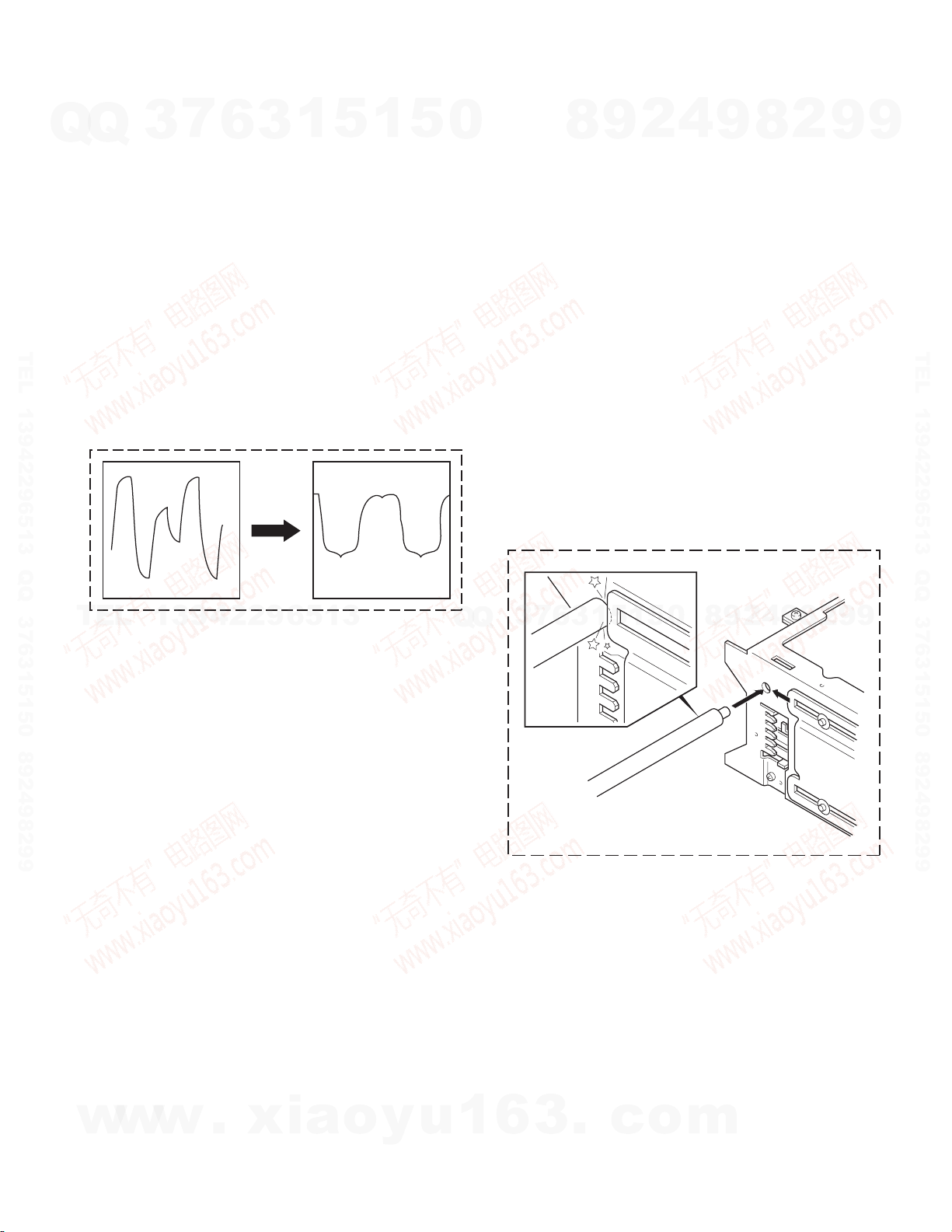
● L.P.S. initial position adjustment procedure
1. Connect the changer to the HEAD UNIT (H/U).
2. While holding the magazine eject button of the changer,
press the reset button of the H/U.
3. After about 3 seconds, release the magazine eject button.
4. Press the SRC button of the H/U to enter the CD-CH mode,
and the H/U's display section indicates “E-88”.
5. Move the mechanism deck to around the 1st stage by pressing the DISC- or DISC+ button.
6. Insert the adjustment tool (W05-0635-00) into the tool hole
on the changer mechanism.
7. Then press the DISC+ button to move the mechanism deck
until the mechanism's slider hits the adjustment tool.
8. When the motor locks (stops), press the REPEAT key of
the H/U.
When the REPEAT key is pressed, the mechanism moves
automatically to the 1st stage and the initial position adjustment completes. (The data is written in the EEPROM at
this time.)
8
9
2
4
9
8
2
9
9
TEL 13942296513 QQ 376315150 892498299
TEL
13942296513
Q
0
5
1
5
1
3
6
7
3
Q
● Caution : Note on IC8 (EEPROM)
Be sure to use the W05-0869-00 when replacing the
EEPROM. IC8 stores the digital servo data of the pickup
servo.
Therefore, if the EEPROM does not store servo data, ERROR76 (E-76) will indicate the H/U’s display section at the
moment CD is played.
8
9
2
4
9
8
2
9
9
w
w
w
.
xia
o
y
u
1
6
3
.
c
o
m
9
 Loading...