POWER AMPLIFIER
KAC-X10D
SERVICE MANUAL
© 2006-12 PRINTED IN JAPAN
B53-0487-00 (N) 719
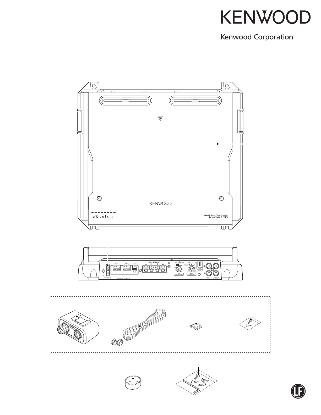
Dressing Panel
(A21-6568-01) : K type
(A21-6569-01) : M type
K type only
M type only
Remote control
(X16-6000-10)
KCA-WR10
Fuse (40A)
(F52-0016-05)
Modular cable
(E30-6240-15)
6m
Accessories
(W01-1606-05)
Mouting hardware
(J22-0301-14)
Screw set
(N99-1794-05)
Screw set
(N99-1766-05)
This product uses Lead Free solder.
KAC-X10D
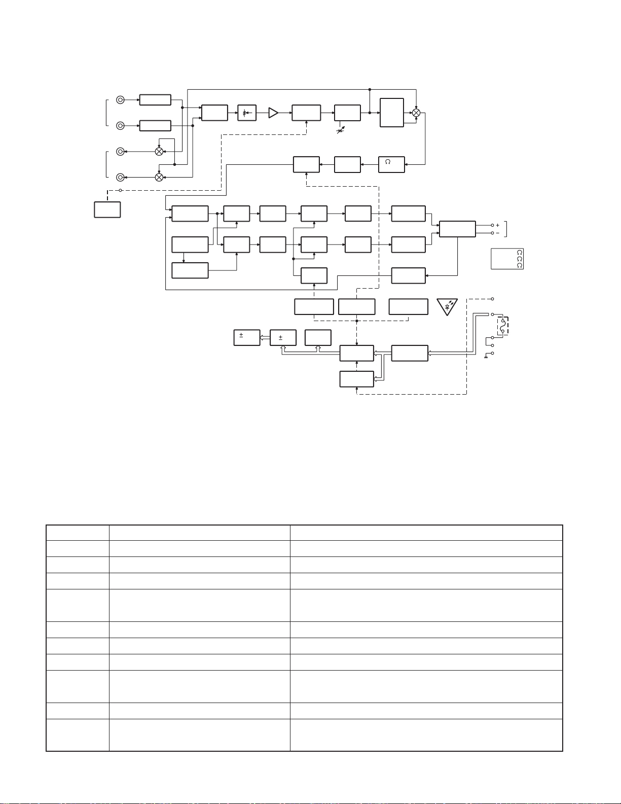
BLOCK DIAGRAM
LEVEL
FREQ
L
LINE IN
(0.2-5V)
R
L
LINE OUT
R
REM
0-18dB
40-100Hz
IC1
ISO-AMP
IC2
ISO-AMP
LINE OUT
SEL.
S1
S1
IC10 (2/2)
IC10 (1/2)
SUMMING
AMP
TRIANGLE
WAVE
IC12 (1/2)
I.N.V
IC4 (1/2)
L/R MIX
SENS.
VOLIC5 (2/2),6,7
IC4 (2/2)
IC11
COMP
IC13
COMP
Q319-322
15V
AVR
IC14,16
DEAD
TIME
IC15,16
DEAD
TIME
B
IC9
I.F.S
15Hz
25Hz
1
LIMIT
Q325
+HB
AVR
IC8
L.P.F
Q2
MUTE
Q16-19
IC37
THERMAL
DET
IC36
Q301,302
POWER
ON/OFF
FREQ
(40-200Hz)
DRIVE
DRIVE
DC/DC
CON
BASS
BOOST
Q3,4 IC38
ATT
Q6,7 Q8-11
LEVEL
SHIFT
Q14,15
LEVEL
SHIFT
Q5,22
D-AMP
ON/OFF
IC34
OVERLOAD
DET
Q701-704
FINAL
MOS-FET
Q705-708
FINAL
MOS-FET
IC17
NF AMP
IC35
DC-OFFSET
DET
L1
LC FILTER
S2
I.S.F
SEL.
LC FILTER
POWER
INDI.
300W / 4
600W / 2
600W / 1
P-CON
BATT.
GND
(BTL)
SP-OUTPUT
COMPONENTS DESCRIPTION
● AUDIO UNIT (X09-8590-10)
Ref. No. Application / Function Operation / Condition / Compatibility
IC1,2 Isolation AMP Removal of common mode noise on input signal
IC3 Buffer AMP Buffer AMP for RCA output
IC4 Mixing AMP and buffer AMP It mixes input stereo signals into monaural signals. GAIN=0dB
IC5~7 Bass Boost circuit (remote control operation)
IC8 L.P.F 40~200Hz -24dB/oct
IC9 I.S.F OFF/15Hz/25Hz switchable -24dB/oct
IC10 D-class phase input AMP
IC11 PWM signal generating circuit
IC12 Triangular wave reversal and DC servo circuit It feeds back the triangular wave reversal and DC voltage offset.
IC13 PWM signal generating circuit and latch circuit
It boosts signals by the operation of the remote control.
GAIN=0~+18dB, fc=40~100Hz
Generation of triangular wave, and generation of PWM signal by
comparing triangular and sine wave.
Circuit to generate PWM signal by comparing triangular and sine wave.
Circuit to latch when 1Ω load is detected.
2

KAC-X10D
COMPONENTS DESCRIPTION
Ref. No. Application / Function Operation / Condition / Compatibility
IC14~16 Dead time generating circuit
IC17 NF circuit It applies negative return from output to D-class first phase.
IC31 Short-circuit detection Detection of short-circuit between output and GND
IC32 ASO and short-circuit detection Detection of current-voltage and output short-circuit.
IC33 Detection signal latch It latches detection signal for a given length of time.
IC34 Detection circuit
IC35 Rectifying circuit It rectifies output voltage.
IC36 DC/DC converter It generates signals to make dual power supply from single power supply.
IC37 Mute circuit It generates Mute signal.
IC38 Clipper
IC39 Resonance detection It detects resonance generated in output short-circuit.
Q2~4 ATT,MUTE It applies ATT-1,ATT-2 and MUTE.
Q5,22 5V-SW
Q6~21 Level shift and gate drive. It performs D-class AMP level shift and MOS-FET gate drive.
Q301 Abnormal voltage detection It turns off P-CON when abnormal voltage is applied to power supply.
Q302,303,307,308
Q304,305 MUTE-SW It turns on and off MUTE.
Q306 PW (OFF)-SW
Q309~312 DC/DC-FET drive DC/DC-FET gate driver
Q313~318 DC/DC-FET Switching FET for generating AMP secondary power supply
Q319~322 ±15V power supply It generates ±15V from secondary power supply ±B.
Q323,324 Tracking circuit It adjusts ±15V attenuation curve when power is turned off.
Q325 High-tap power supply circuit It generates +HB higher than +B to drive MOS-FET.
Q326,327,337~339
Q328,329 Output voltage rectifying circuit It applies bias on the signal with output voltage rectified.
Q330~334 DC offset detection It detects abnormal output DC voltage.
Q335 Failure SW It generates detection signals when a failure occurs.
Q336 1Ω detection malfunction prevention circuit
Q701~708 MOS-FET It amplifies the switching level to ±B.
PW-SW It turns on AMP main body when it detects voltage in P-CON.
Current balance detection It detects the current balance on + and - side while it detects the current.
It generates dead time not to penetrate the high-side and low-side PWM signal.
It sends detection signal to each circuit when a failure is detected, and
turn off the circuit.
It limits the audio signal amplitude and suppresses power when 1Ω is detected.
It controls ON and OFF of D-class AMP gate driver circuit power supply 5V.
It turn off AMP power when abnormal detections (over current, shortcircuit and DC offset) is detected.
It prevents malfunction of 1Ω detection in voltage instability when AMP
power is turned on.
3
KAC-X10D
CIRCUIT DESCRIPTION
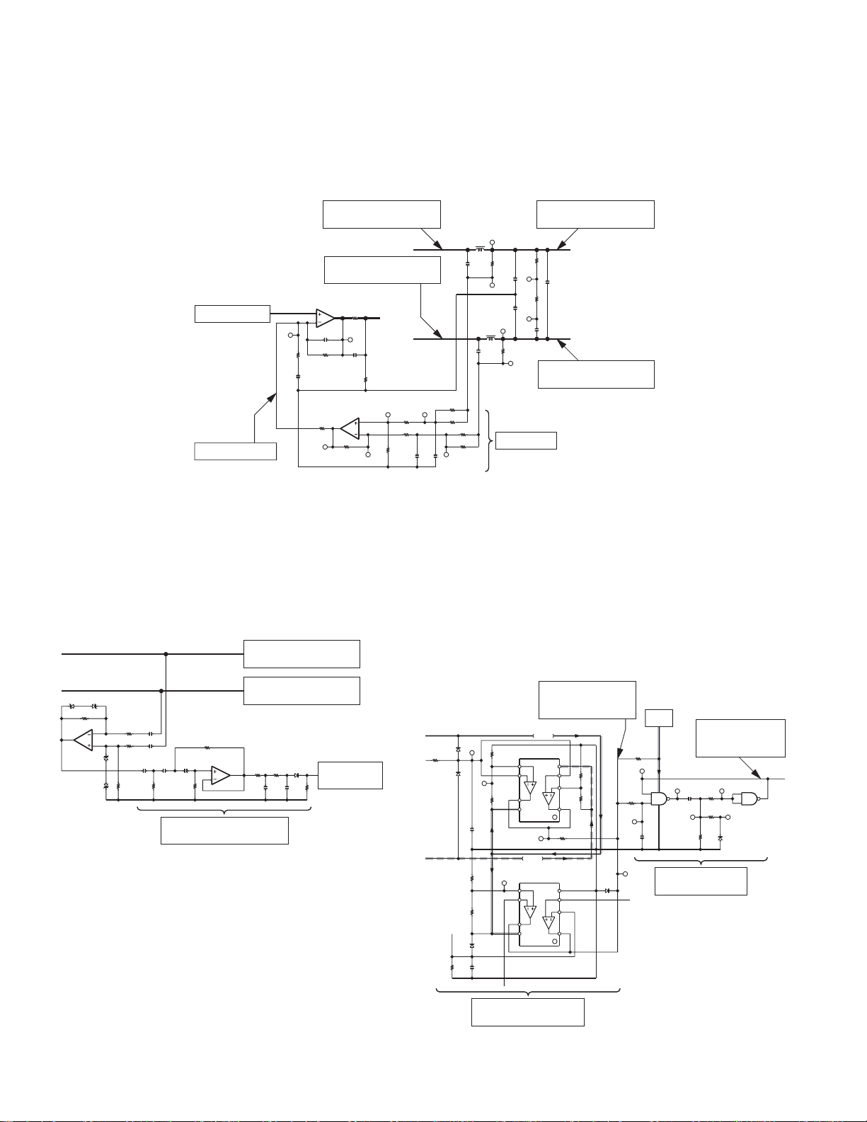
● NF Circuit
It applies NF from rear and front of LC filter. For BTL output, it
receives each output by differential amplification and applies
feedback to the first phase.
POWER AMP OUTPUT +
(RECT ANGULAR W AVE)
POWER AMP OUTPUT (RECT ANGULAR W AVE)
IC10
(2/2)
TP157
R105
C85
1K
47u25
+
5
6
C59 56P
R106
R172
1K
1M
IC17
(1/2)
SIGNAL INPUT
NF SIGNAL LINE
7
1
R171
3.3K
R107
10K
TP161
C60
1000P
328
R108
10K
TP252
TP253
R170
3.3K
R168
12K
R169
12K
POWER AMP OUTPUT +
(SINE WA VE)
TP246
L5
2.2
5W
R162
24K
C70
R160
0.015
2.2
C72
TP244
C73
TP247
L6
C71
24K
R161
0.015
R164 24K
TP250
R165 24K
R166 24K
R167 24K
TP251TP254
C76
C77
0.056
0.056
NF CIRCUIT
10
C75
2.2
5W
R163
2.2
TP249 TP248
10
C74
TP245
POWER AMP OUTPUT (SINE WA VE)
● Resonance Detection Circuit
It detects resonant waveforms generated at output when the
power AMP ± output is dead-shorted (0Ω).
It sends detected signals to the control circuit.
POWER AMP OUTPUT +
(SINE WA VE)
POWER AMP OUTPUT -
6
IC39
(2/2)
85
7
4
(SINE WA VE)
R4431KR445
D348
1K
C356
C357
0.033
0.022
R444
10K
to CONTROL
CIRCUIT
D347 D346
R439
47K
1
IC39
(1/2)
R438
C352
47K
D349D350
R447
R446
47K
3300P
C358
3300P
C353
C354
C355
0.01
0.033
0.033
47K
22K
10K
R441
R440
RESONANCE WA VEFORM
PICK UP LPF
R442
2.2K
2
3
● Pulse Shaping Circuit
It detects with either one of abnormal detections (current voltage, resonance detection or unbalance current detection) at
the previous phase.
It generates a certain width of pulse about 10msec even if
input pulse width is small when input is pulled by Lo.
DETECTION
CIRCUIT OUTPUT
R381
1K
R378
20K
D331D344
TP255
C349
R380
R379
D325
C334
IC31
1K
R382
5
6
TP258
7
10K
8
R383
V+
1000P
TP407
-15VA
TP259
IC32
4.7K
5
6
15K
7
81
V+
1000P
Hi/Lo (NORMAL : Hi)
+15VA
4
V-
3
1K
R432
2
10K
R433
1
R434
10K
D342
4
V-
3
2
+5V
R384
10K
TP263
1
R385
1K
2
7
TP262
C336
1000P
PULSE DURATION
TP260
SHAPING CIRCUIT
14
10mS
PALSE DURATION
OUTPUT
TP264
3
IC33 IC33
(1/4)
C337
0.047
TP265
R388
R386
10K
R387
1K
330K
TP267
D326
TP266
4
5
(2/4)
6
UNUSUAL DETECTION
CIRCUIT
4
CIRCUIT DESCRIPTION
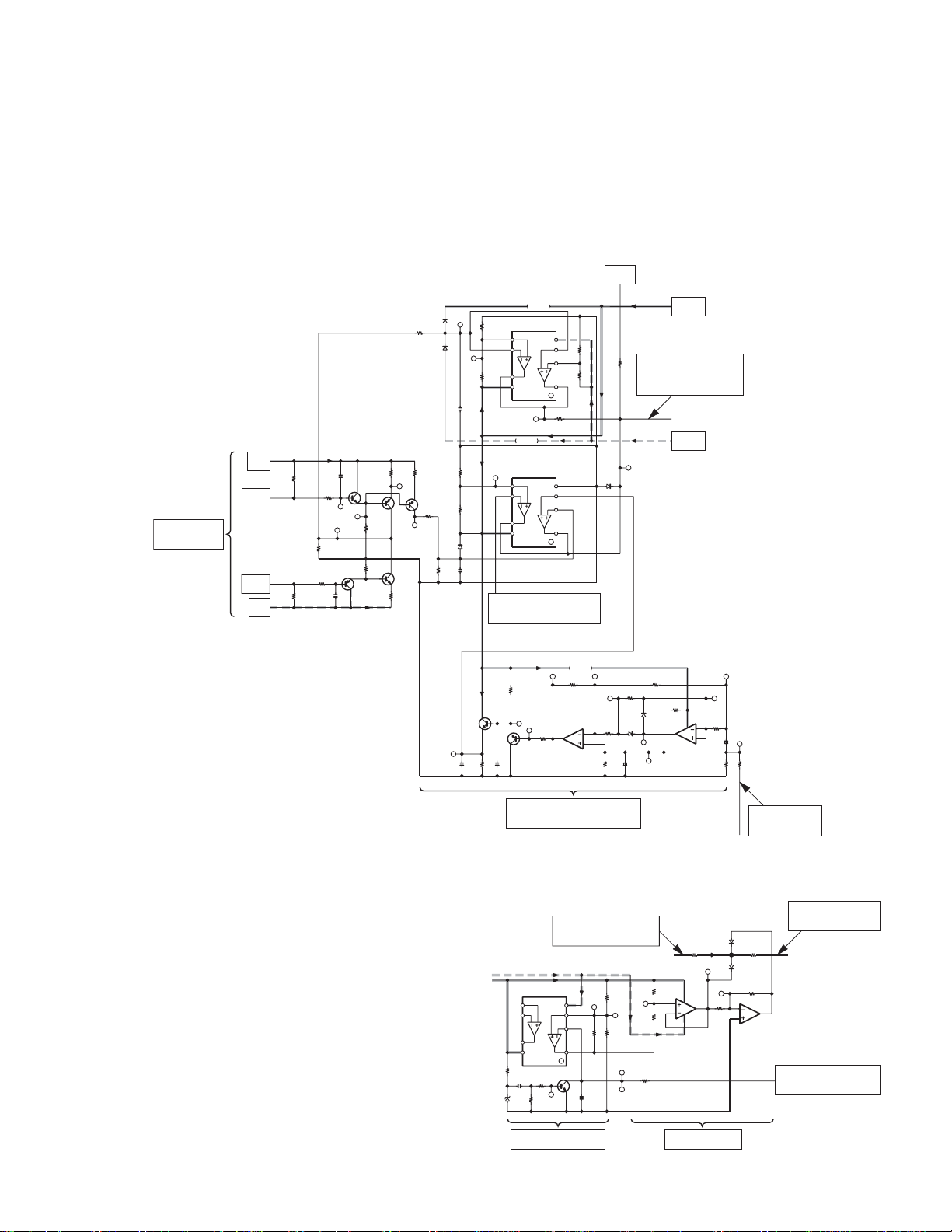
● Abnormal Detection Circuit
It compares signal levels of the current detecting circuit and
output voltage rectification circuit with a comparator. If current
> voltage, the detecting circuit operates to stop D-class circuit.
In the current detecting circuit, current flows into only one side
of the detecting resistance when one side of output is deadshorted to GND.
R381
D331D344
1K
CURRENT
DETECTION
+B
FET
FET
C333
5W
0.02
R156
R374
3.3K
TP238
TP405
62K
R408
R409
Q338 Q339
3.6K
5W
0.02
C350
R157
-B
1000P
1000P
TP239
Q326
R376
R424
Q337
33K
33K
R853
R430
3K
3.3K
R375
TP240
Q327
R377
2.2K
TP241
20K
R378
3K
It detects also unbalance operation.
Resonance detecting signals detected with the new circuit
description X10D_2 are also input to this circuit causing abnormal detection.
1K
TP255
R382
5
6
TP258
7
10K
8
R383
C349
1000P
TP259
4.7K
R380
R379
D325
C334
5
6
15K
7
81
1000P
RESONANCE
DETECTION SIGNAL
IC31
V+
TP407
-15VA
IC32
V+
+15VA
KAC-X10D
+5V
+15V
4
V-
3
1K
R432
2
10K
R433
1
R434
10K
4
V-
3
2
DETECTION
10K
R384
CIRCUIT OUTPUT
Hi/Lo (NORMAL : Hi)
TP260
D342
-15V
TP261
● 1Ω Detection Circuit
The detecting circuit operates and limits the input signal when
the level sent from the current detecting circuit e xceeds a certain level. (Diode clip)
It detects at the current level that flows only when 1Ω is ap-
plied, and does not cancel unless P-con is turned off. (Latch
circuit)
C339
0.68
TP278 TP281
10K
R397
Q328
TP274
TP275
R398
1K
Q329
0.01
220K
C340
R396
OUTPUT VOLTA GE
RECTIFICATION CIRCUIT
IC13
5
6
7
81
V+
C351
4.7K
R437
R436
1
1K
TP397
100K
R435
D345
+15VA
TP277
R399
TP279
20K
7
IC35
(2/2)
INPUT SIGNAL
(for SMALL SIGNAL)
4
V-
3
2
Q336
C348
6
5
R404
R423 15K
1000P
R402
10K
1.3K
TP399
R421R422 4.3K
C341
15K
TP183
TP184
TP398
R401
20K
D329
TP282
10u50
+
TP283
TP146
R847
1K
R400
20K
R425
R426
D330
R403
12K
1
IC35
(1/2)
30K
38
2
43K
TP280
R405
20K
28
3
+
TP144
1
C342
R406
TP145
R427
10K
10u50
10K
D339D340
R407
6
5
TP284
R428
24K
POWER AMP
+ OUTPUT
INPUT SIGNAL
(to POWER AMP)
R67
5.6K
10K
7
IC38
(2/2)
CURRENT
DETECTION LEVEL
4
R95
3.9K
4
IC38
(1/2)
RATCH CIRCUIT DIOD CLIPER
5
A B C D E
E
3
KAC-X10D
1
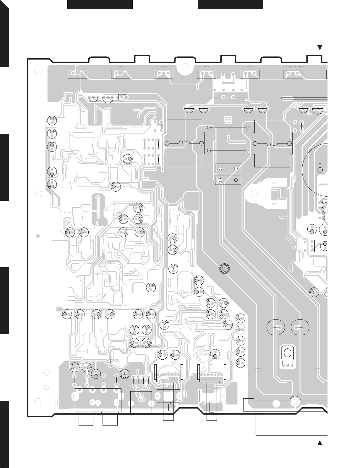
PC BOARD (COMPONENT SIDE VIEW)
AUDIO UNIT X09-8590-10 (J76-0347-01)
W105
Q704
BEBE
Q8
C70
R160
W2
Q9
C
R169
R168
R166
R164
R167
R165
W102
BEBE BEBE
L6
C71
R161
C77
C76
Q20
Q15
W103
R159
W104
C78
C79
Q703
C68C69
R158
Q7
Q12
L5
C75
C74
R163
W101
GDS GDS GDS GDS GDSGDS
Q705Q706 Q707Q708
BEBE
2
C61
C828
C829
Q16
Q17
BE
Q18
C85
3
C826
C57
C827
C329
C330
C341
C332
C346
C342
C347
C832
C833
4
R162
D320
D321
D322
D323
C328
R359
C327
BE
Q325
C25
C338
C31
C305
C32
C28
C22
C
5
C837 C838
C17
C18
6
R31
R32
C822C823
C16
R45
C3
R1
J1
C4
R2
C824
C82 C83
R71
R69
R70
J2
C825
R851
C35
C24
C15
C49
VR1 VR2
S1
C821
C820
C50
C26
C84
S2
C51
C52
C53
C54
C903 C902
C73
C72
P2
7
6
 Loading...