

Kenwood KACPS-521, KACX-521 Service manual
POWER AMPLIFIER
KA C-PS52 1
KA C-X52 1
SERVICE MANUAL
© 2004-2 PRINTED IN JAPAN
B53-0139-00 (N) 2439
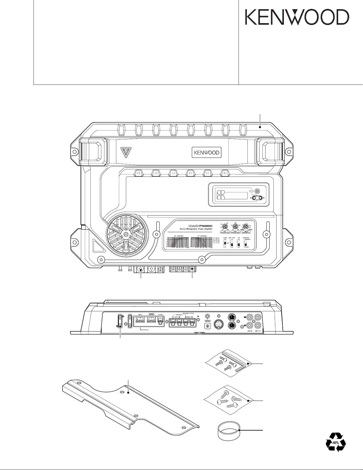
Heat sink
(F01-1751-01)
Screw
(N07-0003-08)
30
30
FUSE(30A×2)
POWER IN
Fuse (30A)
(F52-0015-05)
Cover
(F07-1138-12): KAC-X521
(F07-1139-12): KAC-PS521
Screw
(N09-4214-08)
5
4
3
2
1
VOLTFAN
CURRTEMP
6
7
8
9
0
MENU
RESETREMOTETO H/UID NUMBER
Screw set
(N99-1752-05)
Screw set
(N99-1577-15)
Accessory
(W01-1606-05)
KA C-PS521/X521
(X09-5760-10)
BLOCK DIAGRAM
to H/U
to POWER AMP
BAT
GND
P-CONT
IC1,10 IC1
I.S.A I.F.S
(X08-4150-10)
V PROT.
L.P.F
IC5
H.P.F
ED1 IC7
LCD
IC6
Q356,358
IC2 Q61
DC/DC
CONVERTER
LCD
DRIVER
u-COM
Q66
5V AVR
FAN AVR FAN
IC3,4,6
Q69
SW 5V
AVR
AMP
CONT.
TEMP
PROT.
+15V AVR
Q62
-15V AVR
Q101,102
MUTE
DC PROT
CURRENT PROT
POWER AMP
COMPONENTS DESCRIPTION
● PREAMPLIFIER UNIT (X08-4150-10)
Ref. No Application / Function Operation / Condition / Compatibility
IC1 Infrasonic filter Controlled by microprocessor
IC3 Tone and volume variable
IC4 6dB voltage amplification
IC5
IC6
IC7 LCD driver Controlled by microprocessor
● AUDIO UNIT (X09-5760-10)
Ref. No Application / Function Operation / Condition / Compatibility
IC1 Buffer
IC2 DC/DC converter
IC3 AMP communication buffer
HPF
LPF
Lch : 6dB voltage amplification
Rch : Signal 180 reverse and 6dB voltage amplification
2

KA C-PS521/X521
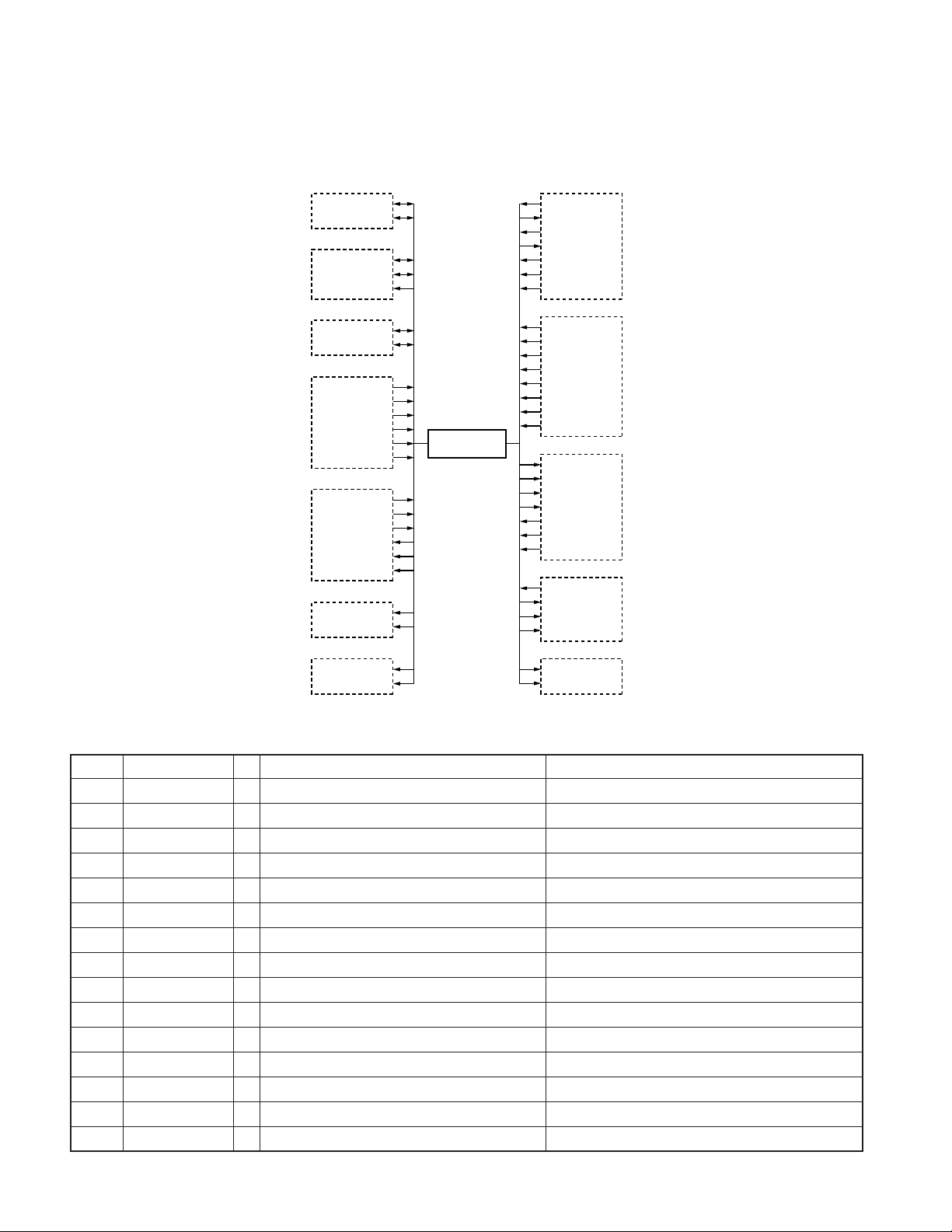
COMPONENTS DESCRIPTION
Ref. No Application / Function Operation / Condition / Compatibility
IC5 H/U communication buffer
IC6 Microprocessor
IC7 Reset IC
IC8 E2PROM
IC9 Current detection
IC10 Isolation amplifier
Q50 5V AVR
Q51~54 DC/DC output driver
Q55~60 DC/DC
Q61 +15V AVR
Q62,63 -15V AVR
Q64,65 DC/DC converter (IC2) ON/OFF Controlled by microprocessor
Q66,68 5V AVR
Q69 5V AVR ON/OFF
Q70,71 Power supply detection
Q81 +15V AVR
Q91,92 When P-CON is OFF, DC/DC driver stop speedy
Q97 AMP communication stability power supply
Q101,102 Mute
Q103~112 A class first stage amplifier
Q113~118 A class 2nd stage amplifier
Q119,120 Final temperature compensation
Q121~124 Amplifier current detection
Q125~132 Final driver
Q133~140 Final
Q141 Mute control
Q142~145 Amplifier limiter
Q146,147 Amplifier current detection
Q148,149 DC detection
Q301~307 H/U communication output driver
Q313 H/U communication output driver
Q314 H/U communication ON/OFF
Q341~344 H/U communication input driver
Q346 H/U communication output driver
Q347~349 AMP and H/U communication ON/OFF control
Q351,352 BATT voltage output
Q353~358 Fan stability power supply
Q403 LCD backlight LED control
Q404 LED control
3
KA C-PS521/X521
MICROCOMPUTER’S TERMINAL DESCRIPTION
● MICROPROCESSOR : 784224YGC117 (X09 : IC6) ◊ Block Digram
AMP communication I/F LX BUS I/F
AMP_SCL
AMP_SDA
Audio control
AUDIO_SCL
AUDIO_SDA
AUDIO_MUTE
E2PROM I2C
communication
E2P_SCL
E2P_SDA
Destination, AMP ID
DIP-SW1
DIP-SW2
DIP-SW3
DIP-SW4
MODEL1
MODEL2
Protection control
DC-DET
D-CUR
AB-CUR
Illumination control
LCD-ILL
WHITE-LED
Mute control
MUTE1
MUTE2
ATT1
ATT2
ATT3
AMP µ-com
784224YGC117
LX_REQ_M
LX_REQ_S
LX_DATA_M
LX_DATA_S
LX_CLK
LX_RST
HU_BU
Display data monitor
AD-I
AD-V
TEMP1
TEMP2
TEMP3
TEMP4
TEMP5
TEMP6
Power supply control
COMM-SW
D-PWER
POWER-ON
5VSW
V_DOWN
PCON
LX_CON
LCD driver I/F
L_DATA_L
L_DATA_A
L_CLK
L_CE
Fan control
FAN1
FAN2
◊ Terminal Function
Pin No. Pin Name I/O Function Processing Operation Description
1~3 TEMP4~TEMP6 I Temperature detection 4~6
4AVSS - GND
5 L_CE O CE output to LCD driver H : LCD driver CE
6 LX_REQ_S O Data transmit request to H/U H : OFF, L : ON
7AVREF1 - DA reference voltage
8 L_DATA_L I Data input from LCD driver
9 L_DATA_A O Data output to LCD driver
10 L_CLK O CLK output to LCD driver
11 LX_DATA_M I Data input from H/U
12 LX_DATA_S O Data output to H/U
13 LX_CLK I CLK input from H/U
14 LX_BU I LX BUS communication, H/U connect detection H : Not connect (Except master amplifier), L : Connect
15 NC O Not used
16 SDA_AMP I/O Data input/output AMP communication
17 NC O Not used
4

KA C-PS521/X521
MICROCOMPUTER’S TERMINAL DESCRIPTION
Pin No. Pin Name I/O Function Processing Operation Description
18 SCL_AMP I/O CLK input/output AMP communication
19 AUDIO_SCL I/O CLK input/output with audio chip
20 AUDIO_SDA I/O Data input/output with audio chip
21 AUDIO_MUTE O Mute output to audio chip H : Mute OFF, L : Mute ON
22 E2P_SCL I/O CLK input/output with E2PROM
23 E2P_SDA I/O Data input/output with E2PROM
24 NC O Not used
25~28
29 MODEL1 I Model setting 1
30 MODEL2 I Model setting 2
31,32 NC O Not used
33 VSS1 - GND
34~37 NC O Not used
38 LCD-ILL O LCD backlight switch H : ON, L : OFF
39 WHITE-LED O Triangle illumination switch H : ON, L : OFF
40 NC O Not used
41~43 ATT1~ATT3 O Output attenuate due to rise in temperature 1~3 H : Attenuate, L : Not attenuate
44,45 NC O Not used
46 COMM-SW O Communication IC power switch H : ON, L : OFF
47~50 NC O Not used
51 D-PWER O D class amplifier power supply control H : ON, L : OFF (2ch/4ch L fixed)
52 DC-DET I Speaker output DC voltage detection H : Normal, L : Abnormal
53 NC O Not used
54 POWER-ON O Amplifier power supply control H : ON (D/AB class), L : OFF
55 5VSW O 5VSW H : OFF, L : ON
56 MUTE1 O Amplifier section input stage mute control H : OFF, L : ON
57 MUTE2 O Driver stage pop-noise mute control H : OFF, L : ON
58 FAN1 O Fan rotation control H : Operate, L : Stop
59 FAN2 O Fan speed control H : Low speed, L : High speed
60 RESET - Hard reset H : Normal, L : Reset
61 PCON I Amplifier power control H : OFF, L : ON
62 LX_CON I LX-BUS communication control H : OFF, L : ON
63 LX_REQ_M I Data receive request from H/U H : ON, L : OFF
64 NC O Not used
65 V_DOWN I Momentary power down detection H : ON (Power down detection), L : OFF (L fixed)
66 NC O Not used
67 VSS0 - GND
68 VD1 - VDD
69 X2 - Main clock input 1
70 X1 - Main clock input 2
DIP-SW1~DIP-SW4
I AMP address setting
5
KA C-PS521/X521
MICROCOMPUTER’S TERMINAL DESCRIPTION
Pin No. Pin Name I/O Function Processing Operation Description
71 TEST - Flash ROM writing
72 XT2 - Not used
73 XT1 - Not used
74 VDD0 - VDD
75 AVDD - VDD
76 AD-I I First current detection (for display)
77 AD-V I BU voltage detection (for display)
78~80 TEMP1~TEMP3 I Temperature detection 1~3
◊ Logic Table
1) Destination
The destination in AMP does not mean the sales regions but
specific models.
The following are the models. When reset is released, it is
checked only once.
Model name MODEL1 (29pin) MODEL2 (30pin)
KAC-PS811D/X811D Low Low
KAC-PS521/X521 Low High
KAC-PS621/X621 High Low
KAC-PS541/X541 High High
2) AMP ID
AMP ID is checked only ohce at the time reset is released or
when the microcomputer is released from the low consumption mode.
When set to AMP ID 8/9 no remote control is possible.
DIP-SW1 DIP-SW2 DIP-SW3 DIP-SW4
AMP ID
(25pin) (26pin) (27pin) (28pin)
0 High High High High
1Low High High High
2 High Low High High
3Low Low High High
4 High High Low High
5Low High Low High
6 High Low Low High
7Low Low Low High
8 High High High Low
9Low High High Low
3) Fan speed
Operation FAN1 (58pin) FAN2 (59pin)
Stop Low High/Low
Low speed High High
High speed High Low
6
AD-I
D309
(2/2)
IC9
(1/2)
IC9
AMP RECT
MPU AD-PORT
OUTPUT
VOLT AGE
DETECTION
LEVEL
10u35
270
1K
10K
7
5
6
15K
0.01 0.01
10K
1
8
13K
470
3
2
47
L5
4
+
● Current detection circuit
Amplify and rectify potential differences at
two points in the primary-side current circuit
and send it to the AD-port of the MPU and
obtain data for displaying current value.
KA C-PS521/X521
CIRCUIT DESCRIPTION
● Constant current output circuit
Remove troubles caused by the potential
differences between the constant current
output and the GND, so that the GND potential differences between the H/U and the
AMP is not overlapped in the AMP to H/U
communication.
● I2C buffer
Using an IC for I2C communication, between-AMP communication is conducted so
that there will be no trouble from GND potential differences.
J3
12
to OTHER AMP
TRANSMISSON
RECEIVE
J4
42
3
1
10
11
957
8
6
3421
78
6105
11
13
9
to H/U
REQC
H/U-GND
H/U GND
270
CLK
270
DATA
10u25
4.3K
D301
4.3K
D302
IC3
47 47
100K
Q301
Q303
VCCSX
1
1.8K
6
785
SY
RY
RX
TX
2
3
12K
Q305
20K
CONSTANT
CURRENT
TY
1.8K
GND
4
1.5K
from
MPU
Q307
10K
10K
1.5K
AMP
GND
to MPU
TRANSMISSON
RECEIVE
10K
BOTH DIRECTION
BUFFER
ADJUSTMENT
2.5mV
After Power on PC board
No. Item Alignment Point Method Align For Note Fig.
1 IDEL CURRENT
VR1 (Lch) Connect a DC voltmeter between
VR2 (Rch) check land A, B. 2 minutes (X09-576)
7
A B C D E
KAC-PS521/X52 1
1
PC BOARD (COMPONENT SIDE VIEW)
PREAMPLIFIER UNIT X08-4150-10 (J76-0010-12)
CN1
122
2
S7
S8
S9
124
3
R101
R102
R103
R104
ED1
16
17
1
64
R114
IC7
4
32
33 48
49
R115
C104
R111
R105
C101
R107
R108
R112
R106
C102
C103
R11
C105
C31
R12
103A
503C
503C
200mV
5V
INPUT SENS
C32
HI PASS
200Hz
50Hz
200Hz50Hz
LOW PASS
R8
R7
C68
C67
R64
C12
R63
C66
C65
R66
R65
C63
C64
8
VR2
VR1
VR3
R39
R40
IC1
7
C11
114
S1
S2
1
S3
HPF
S4
1
R6
C4
C6
R2
R4
R1
R3
C5
C3
R5
R33
ON OFF
OFFON
C107
R117
STMONO
1
I.S.F
1
ANP CONT
LPFOFF
R109
R110
D2
5
12
CN2
6
WH2
13
C35
R31
C25
C19
R72
R42
R41
R43
R74
C33
C74
R44
R46
C34
C28
R76
C75
R45
14 8
IC5
17
C27
R23
R27
R25
R28
R26
C22
R24
C24
R30
R29
C23
C21
C73
R32
R73
C39
R77
R52
C20
C26
C29
R17
R70
R79
C17
R55
R69
R78
R19
4
1
4
C48
R22
R21
C9
C10
R9
R10
C40
C18
C37
1
IC4
C38
IC6
C49
C41
C42
8
C30
R20
C43
C44
C45
5
R18
R56
R38
R34
C61
8
5
R13
C16
D1
R116
1
IC3
10
C13
C15
20
R14
R15
R16
11
X08-4150-10
Ref. No. Address
IC1 2D
IC3 6D
IC4 6D
IC5 6C
IC6 6D
IC7 4B
7
Refer to the schematic diagram for the values of resistors and capacitors.
8
 Loading...