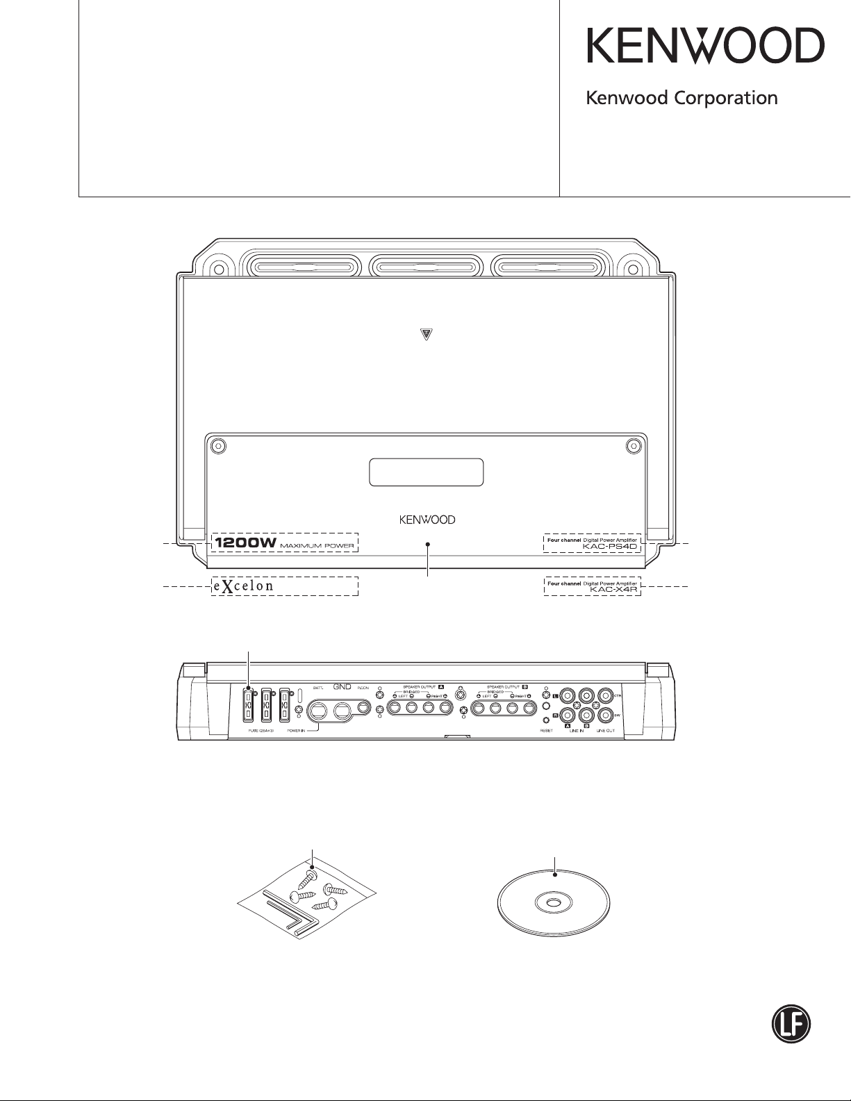
POWER AMPLIFIER
KAC-PS4D/X4R
SERVICE MANUAL
© 2007-4 PRINTED IN JA PA N
B53-0520-00 (N) 426
KAC-PS4D
KAC-X4R
Fuse (25A)
(F52-0014-05)
Dressing Panel
(A21-6578-01) : KAC-X4R
(A21-6579-01) : KAC-PS4D
Screw & Wrench Key set
(N99-1795-05)
KAC-PS4D
KAC-X4R
Compact disc
(W01-1701-05)
This product uses Lead Free solder.
This product complies with the
RoHS directive for the European market.
KAC-PS4D/X4R
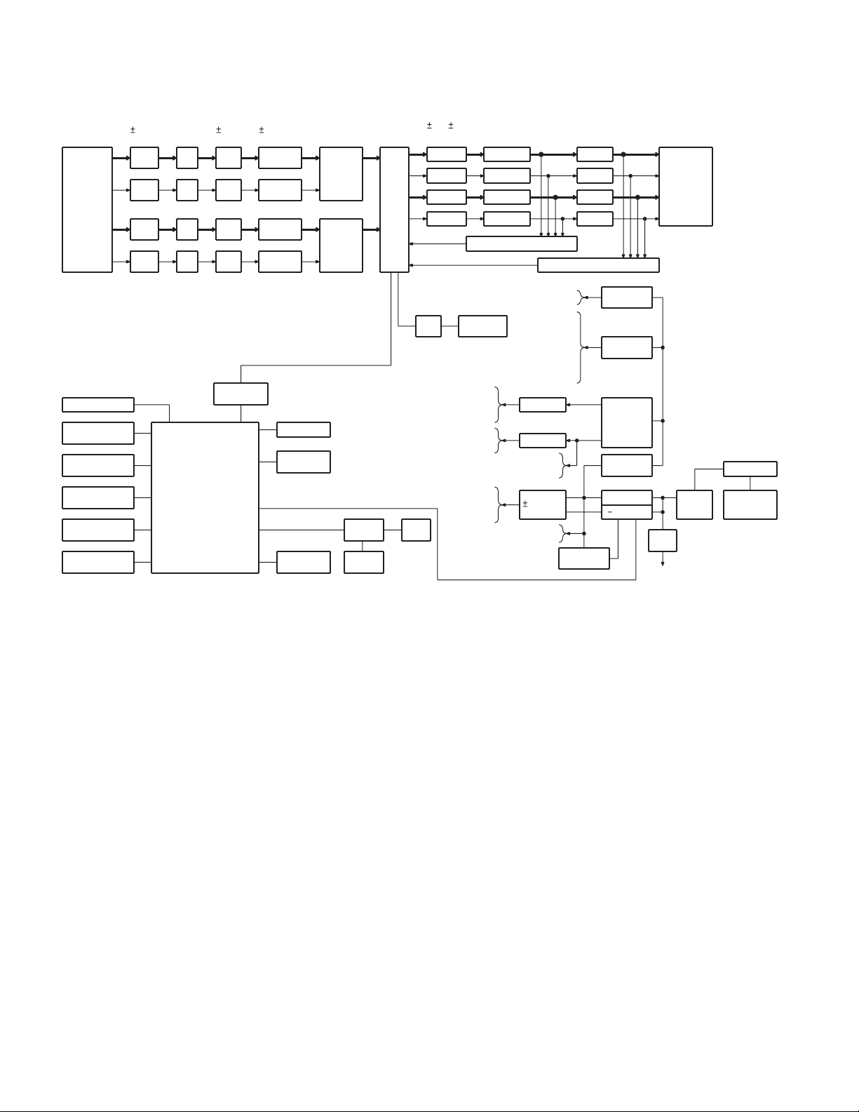
BLOCK DIAGRAM
15V 15V 15V 5V,3.3V
ISO ARCA IN AL VR AMP SE to DIF
RCA IN AR
RCA IN BL
RCA IN BR
E2PROM
CURRENT
DETECTOR
VOLTAGE
DETECTOR-1
VOLTAGE
DETECTOR-2 COMPUTER
TEMPERATURE
DETECTOR
OUTPUT DC
DETECTOR
ISO A
ISO A
VR
VR
IC900
MICRO
AMP
AMP
5V-3V
INTERFACE
SE to DIFISO A AMPVR
SE to DIF
SE to DIF
RESET IC
PCON
DETECTOR
ROTARY
ENCODER
ADC Ach
ADC Bch
FL
DRIVER
SLIDE
SWITCH
IC1IC307
DSP
HV, 15V
12V,5V,3.3V,1.8V
DRIVER
DRIVER
DRIVER
DRIVER
IC310
DAC
L/R
5V, 3.3V
P/S FDFWD
ADC
FEED BACK
DAC
SPDIF
FINAL
ANTI PUMP
ISO AMP
SE to DIF
FEED BACK
P/S FDFWD
FL
PWR FET
PWR FET
PWR FET
PWR FET
FEEDBACK, DPSC, ADCS
RCA OUT
L/R
IC705
IC512
FINAL
ANTI PUMP
FEED BACK
IC500
FINAL
ANTI PUMP
ON/OFF CONTROL
FILTER
FILTER
FILTER
FILTER
OVERCURRENT DETECTION
IC511
DSP
P/S FDFWD
DAC
DSP
ADC
SPDIF
USB
ANTI PUMP
FEED BACK
A5V REG
D5V REG
15V REG
IC101,102,201,202
PWM
CONTROL
1.8V SW
REG
IC510
3.3V SW
REG
IC503
12V REG
+14.5V SW
REG
TRANSFORMER*2
+HV REG
HV REG
SP OUT AL
SP OUT AR
SP OUT BL
SP OUT BR
Q911
BU5V
REG
MICRO
LC
FILTER
FUSE
BATT14.4V
GND
2

KAC-PS4D/X4R
COMPONENTS DESCRIPTION
PREAMPLIFIER UNIT (X08-4350-10)
●
Ref. No. Application / Function Operation / Condition / Compatibility
IC1 AR/BRch 8dB buffer-amp
IC2 AL/BLch 8dB buffer-amp
IC100 FL driver and Key Matrix Communicate with microcomputer (on X09 unit).
AUDIO UNIT (X09-8620-10)
●
Ref. No. Application / Function Operation / Condition / Compatibility
IC1 DSP (digital amplifi er processor)
IC3 reset detect 3.3V VDD for DSP etc
IC100,200,604 buffer
IC101,102,201,202 MOS FET driver
IC301,302,401,402 Isolation amp to reduce common mode noise
IC303,304,403,404 Amp for differential input of AD converter
IC306 Buffer amp for common voltage of AD converter
IC307 4ch AD converter for analog input
IC309 Low pass fi lter for Line out
IC310 DAC for pre-out
IC500 Error Amp for +/-16V regulator
IC502 SW power supply control IC
IC503 12V voltage regulator
IC507 buffer for sync clk
IC509 14.5V SW regulator
IC510,511 dcdc converter for 3.3V and 1.8V
IC512 5V voltage regulator
IC601 Amp for differential input of AD converter
IC602 Buffer amp for common voltage of AD converter
IC603,704,804 AD Converter for feedback
IC605 FET driver for (Q601,602) (Anti-pump circuit)
IC701,702,801,802 Amp for differential input of AD converter
IC703 Buffer amp for common voltage of AD converter
IC705 5V voltage regulator
IC900 system micro
IC901 control line 3.3V ↔ 5V translation buffer
IC902 E2PROM for installer memory, error log.
IC904 Amp for sensing GND voltage
Q101~104,201~204 SW transistor for SP output line
Q105~108,205~208 Current protection detect
Q109,110,209,210 on/off SW of N_HB_ERR (SP out over current det.)
Q111,112,114,115,
Q211,212,214,215
Speaker mute TR
3

KAC-PS4D/X4R
COMPONENTS DESCRIPTION
Pin No. Application / Function Operation / Condition / Compatibility
Q113,116,213,216 SP Mute driver
Q301,401 Mute circuit of Line out
Q302 Mete driver of Line out
Q303 AND circuit of SW5V & Preout Mute
Q503~508 Driver of SW power supply
Q509~516 SW transistor for SW regulator
Q517 AVR of +16V
Q520 AVR of -16V
Q521~523 AVR on/off control (1.8V → 3.3V on)
Q524 Interception circuit of VFL
Q525 Secondarily stage of Darlington AVR of VFL and FIL+
Q526 primary stage of Darlington AVR of VFL and FIL+
Q527~529 Secondarily stage of Darlington AVR of FIL+
Q530 primary stage of Darlington AVR of FIL+
Q531 Interception circuit of VFL
Q533 fi xed current supply of +/-16V
Q601,602 SW transistor for Anti-pump circuit
Q603,604 current detect for Anti-Pump circuit
Q605 on/off SW of N_PSCURR (Anti-pump over current det.)
Q901 On/off SW of SW5V
Q902 Logo LED driver
Q903 inverter of +40V detect circuit
Q904 Interception circuit of B14V
Q905 On/off SW of Q904
Q906,907 SP DC detect circuit
Q908 Interception circuit of SW5V
Q909 Protect circuit for Vdd5V
Q910 NF control for Vdd5V
Q911 Interception circuit of BU5V
Q912 On/off SW of SW14V
Q913 Interception circuit of SW14V
Q914,915 P-con detector
Q916 BATT14V down detector
Q917 Inverter of FAN CTRL line from µ-con
Q918 On/off SW of FAN+B
Q920 Secondarily stage of Darlington AVR of FAN+B
Q922,923 On/off SW of SP MUTE
Q924 Inverter of OUT_OF_BOOT line
4

KAC-PS4D/X4R
MICROCOMPUTER’S TERMINAL DESCRIPTION
SYSTEM µ-COM 78F0536GK011A (X09-862 : IC900)
●
Pin No.
1 /P_CON I Clear the stop mode by P-CON ON
2~5 NC O Not used Output L fi xed
6 /RESET I Reset
7 OVF I ADC overfl ow detection H: When the overfl ow is detected displays on VFD
8 NC O Not used Output L fi xed
9 FLASH_W I Used when writing in the fl ash
10,11 NC O Not used Output L fi xed
12 REGC -
13 VSS - Connect to GND
14 EVSS - Connect to GND
15 VDD - Connect to VDD
16 EVDD - Connect to VDD
17 D2_CLK I/O D2 control (75kHz max) I2C BUS
18 D2_DATA I/O D2 control I2C BUS
19 /N-ERROR I Over current detection
20 NC O Not used Output L fi xed
21 /OC_DET I Over current detection
22 /D2_RESET O Reset TENZING L=RESET
23 /D2_RST_DET I Tenzing reset detection
24,25 NC O Not used Output L fi xed
26 /PREOUT_MUTE O Mute the pre-out L: MUTE ON
27 /DSP_MUTE O Mute TENZING L: MUTE ON
28~30 NC O Not used Output L fi xed
31 /SP_MUTE O Mute the speaker output L: MUTE ON
32 OUT_OF_BOOT I
33 BOOT_CTRL (Not Used) I
34 ROTARY_CW I Encoder pulse input Detect pulse phase difference
35 ROTARY_CCW I Encoder pulse input Detect pulse phase difference
36 14V_SW O SW14V ON/OFF
Pin Name I/O Application Processing / Operation / Description
L: Clear the stop mode (INTP0)
H: (P120)
L: Enter the protection mode when the over current is
detected. Turn off the amplifi er power supply and display the
error (E-03).
Automatically recover in 200msec.
Check current every 1ms, and when “L” is detected 15 times
in succession the over current is detected and enter the over
current protection mode. Turn off the amplifi er power supply
and display the error (E-03).
Automatically recover in 200msec.
When Low is detected at pin23 while the pin22 of the µ-com
is High,temporarily turn off the amplifier and reboot the
system.
Receive BOOT completion status from
TENZING
DSP BOOT control
(No µ-com control)
L: Tenzing BOOT completion (DSP is in its operation)
L: BOOT from µ-com
H: BOOT from EEPROM
SW14V ON/OFF
Amplifi er power supply ON: H, Initial condition L
5

KAC-PS4D/X4R
MICROCOMPUTER’S TERMINAL DESCRIPTION
Pin No.
37 5V_SW O SW5V ON/OFF
38 VD DOWN I
39 FAN_CTRL O FAN control H: FAN_ON
40 PON_ILLUM O LOGO LED+B SW H: ON, L: OFF, Initial condition L
41 PON_FL O
42 /VFD_INH (/BLK) O Inhibit FL driver display H: Display, L: No display
43 VFD_CE O
44 VFD_DATA_M (FVD.DI) O
45 VFD_DATA_S (FVD.DO) I
46 VFD_CLK O
47 AVREF - DA REF voltage
48 AVSS -
49 AD_V I Detects BU voltage (For display) Displays the voltage and condition.
50 AD_I I Detects primary current (For display) Converts into the current and displays current value.
51 TEMP6 I
52 TEMP5 I
53 TEMP4 I
54 TEMP3 I
55 TEMP2 I
56 TEMP1 I
57 NC O Not used Output L fi xed
58 E2P_SCL I/O To memorize D2 setting
59 E2P_SDA I/O To memorize D2 setting
60,61 NC O Not used Output L fi xed
62 B_DET I
63 /DC_DET I Output DC OFFSET voltage detection L: Enters into the voltage error protection operations.
64 USB_DET (Not Used) I USB detection
Pin Name I/O Application Processing / Operation / Description
SW5V ON/OFF
Power supply ON: H, Initial condition L
Detection of voltage at momentary
power down
FL power supply (Grid and Filament)
control
Temperature detection 6 (at power
supply side) (For display and protection)
Temperature detection 5 (at power
supply side) (For display and protection)
Temperature detection 4 (at power
supply side) (For display and protection)
Temperature detection 3(at power
supply side) (For display and protection)
Temperature detection 2 (at power
supply side) (For display and protection)
Temperature detection 1 (at power
supply side) (For display and protection)
B voltage over voltage detection
(Not Used)
H: Processing to detect voltage at momentary power down
(Enter the stop mode when the P-CON is down.)
H: ON, L: OFF
Displays the temperature and overheat protection.
Displays the temperature and overheat protection.
Displays the temperature and overheat protection.
Displays the temperature and overheat protection.
Displays the temperature and overheat protection.
Displays the temperature and overheat protection.
Plan: Enters the protection operation when the voltage is
higher than a certain value.
(Not Used)
• Software does not have a detection function.
• Make sure to pull down/up when it is required to remove
the external circuit!
H: When USB is detected, do not make D2 setup from the
µ-com.
• No processing is included.
6
TEST MODE
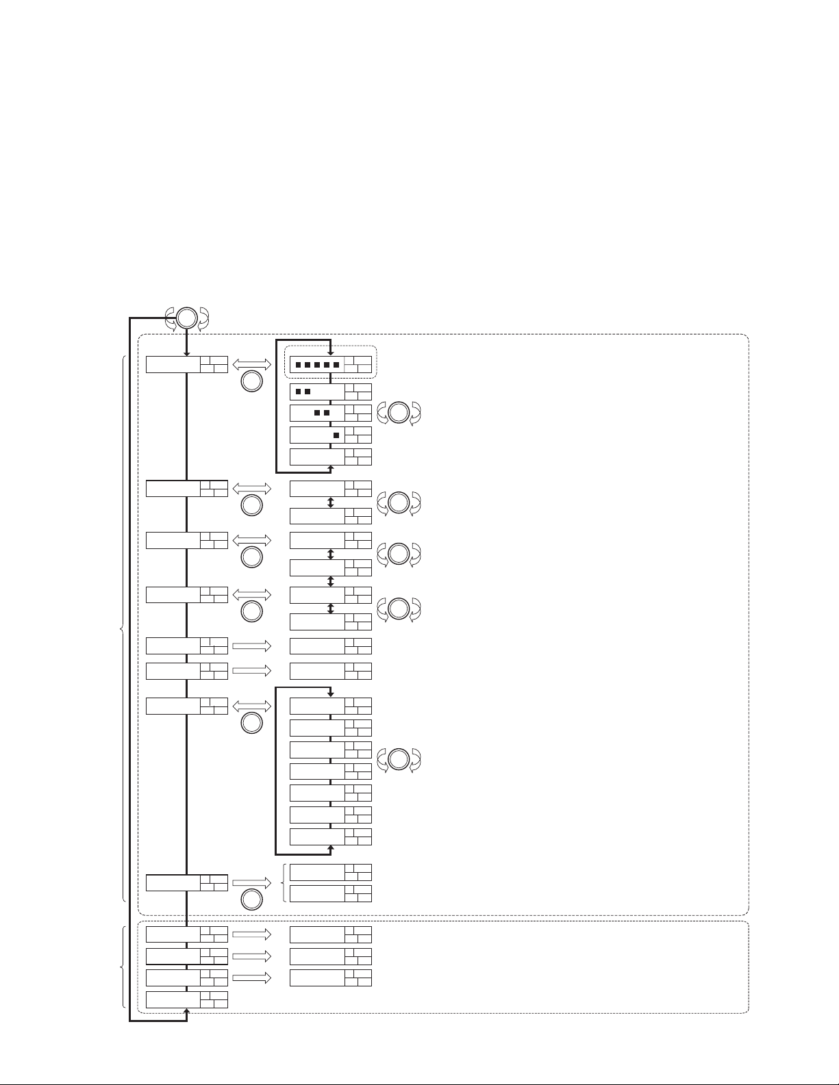
How to enter the test mode and how to clear the test mode
●
• How to enter
In the backup connection condition (when the battery is
being connected), turn ON the P_CON while keep pushing
the rotary push key.
* Set up SETTING SW from the INFORMATION side.
• How to clear
P_CON OFF or reset to clear the mode.
* Do not clear the mode if the protection recovers auto-
matically.
Tur n
KAC-PS4D/X4R
Items in the test mode and test operations
●
• INFORMATION display (Display of conditions)
In the test mode, the following items can be checked in
addition to the normal INFORMATION display.
Each item can be selected with the rotary encoder and the
settings can be changed with the push key.
Additional items shown in the test mode
OVER
o
DIRG
Hz dB
Push
OVER
o
S-LEP
Hz dB
Push
OVER
o
NAF
Hz dB
Push
OVER
o
DEL
Hz dB
Push
OVER
o
REV
Hz dB
OVER
o
W/F
Hz dB
Initial condition
....
..
..
/TWSC
TS
NO
NO
OVER
o
Hz dB
OVER
o
Hz dB
OVER
o
Hz dB
OVER
o
Hz dB
OVER
o
Hz dB
OVER
o
Hz dB
OVER
o
Hz dB
OVER
o
FFO
Hz dB
OVER
o
Hz dB
OVER
o
FFO
Hz dB
OVER
o
Hz dB
OVER
o
003.V
Hz dB
OVER
o
721.F
Hz dB
●Segment check of FL display tube
Change the display segment in the following sequence of order.
All on m GRID1 on m GRID2 on m GRID3 on m All of
Tur n
●PRE-OUT setting
Set up PRE-OUT output to be CENTER-SW and STEREO.
Tur n
●Check of FAN switching
In the FAN switching mode, it is possible to select to rotate or stop the FAN regardless of
the present temperature.
Tur n
●Check of LED switching
In the LED switching mode, it is possible to select to turn on or off the LED.
Tur n
●Version display
It is possible to check the version of the M-com.
●DSP version display
Display the firmware version of the DSP.
●Display the error log.
OVER
o
L-GOE
Hz dB
Push
C99 99
P9999
T9999
D99 99
O99 99
N99 99
S9999
OVER
o
Hz dB
OVER
o
Hz dB
OVER
o
Hz dB
OVER
o
Hz dB
OVER
o
Hz dB
OVER
o
Hz dB
OVER
o
Hz dB
• Display the time for P-CON ON.
Max: 9999 hours, The time up to one hour is displayed with the step of 10 minutes. “C 50M”
• Output ON time (The time while the sound is being output from the speaker.)
Max: 9999 hours, The time up to one hour is displayed with the step of 10 minutes. “C 50M”
• The number of times when the temperature protection is detected
Max: Count up to 9999 times.
Tur n
• The number of times when DC error protection is detected.
Max: Count up to 9999 times.
• The number of times when over current error protection is detected.
Max: Count up to 9999 times.
• The number of times when DSP error is detected.
Max: Count up to 9999 times.
• The number of times when the system error is detected.
Max: Count up to 9999 times.
in the normal mode
Condition display Items shown
OVER
o
KOCL
OVER
o
R
CL-M
Hz dB
Push
OVER
o
TLOV
Hz dB
OVER
o
RTRUC
Hz dB
OVER
o
PMET
Hz dB
OVER
o
OMED
Hz dB
Hz dB
OVER
o
GNCL
Hz dB
OVER
o
V34.1
Hz dB
OVER
o
A81
Hz dB
OVER
o
C87
Hz dB
●Clear the error log and installer memories.
Initialize EEPROM.
• After clearing, display the result of it.
7
KAC-PS4D/X4R
CIRCUIT DESCRIPTION
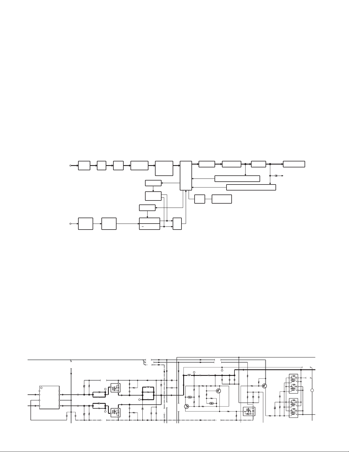
Flow of PS4D/X4R signal line and power supply
●
controls
• Block diagram
The signal from the pin jack is converted into the differential
signal via the isolation amplifi er, variable resistor, and single
end.
It is converted into the digital signal in the AD converter and
it is signal-conditioned in the DSP so that it can be amplifi ed
by the PWM digital amplifi er.
It is PWM-amplifi ed to the analog signal by the driver and
power MOSFET to the level that can be output from the
speaker.
ISO ARCA IN AL VR AMP SE to DIF
ADC Ach
DRIVER
U-PUMP
DRIVER
The signal right after this step is converted into the digital
signal in the AD converter and is feed-backed to the DSP.
The main signal is output from SP via the low pass filter.
In addition, current of the main signal is monitored in the
over current detection circuit and when the over current is
detected the output level is controlled by the DSP.
The signal for pre-out is output to the pin jack via the DA
converter used for the pre-out.
The 14V of the battery is converted to +/-40V in the SW
regulator. The voltage is controlled in the feed-forward and
anti-pumping circuits.
DSP
DAC RCA OUT
L/R
DRIVER
FEEDBACK, DPSC, ADCS
L/R
PWR FET
FILTER
OVERCURRENT DETECTION
SP OUT AL
OC DET
BATT14.4V
GND
Main signal amplifi er circuit with PWM
●
LC
FILTER
FUSE
+HV REG
HV REG
• Main signal amplifi er circuit with PWM
The audio signal that is DA-converted is converted into the
signal for PWM in the DSP.
Its level is shifted in the IC101 and it is converted into the
PWM signal whose amplitude is +/- B. The “+” side of the
amplitude is controlled by Q101 of the PchMOSFET and the
“-” side is controlled by Q103 of the NchMOSFET.
+HV
+3.3V
R127
82
1/2W
TP180
R128
82
1/2W
D115
HV
L103
120nH
R147 39
1/2W
R145 39
1/2W
C113
C111 0.47
D117
0.033
1
2
3
4
IC101
NC1
INA
GND
INB
NC8
OUTA
VCC
OUTB
8
7
6
5
+12V
C101
C103
C1291C105
+HV
TP184
10K
R101
D105
0.1
0.1
R105 4.7
D107
R107
33
TP185
10K
R103
0.1
D103 D101
Q101
Q103
R93
1/2W
C63 82
100P
C65
100P
82
R95
1/2W
FF
Over current is detected by R109 and R149. The signal level
is lowered in the DSP when the over current is detected.
Q107 is used to detect the “+” side of the switching current
and Q105 is used to detect the “-” side of the current.
+HV
+3.3V
TP172
HV
C107
220u50
+
C109
0.47
+HV
+3.3V
L101
15uH
TH103
Q107
R153
R113
22K
1.2K
R109
0.022
1W
R111
390
1.2K
R115
C115 4700P
R117
390
R149
0.027
1W
C117
4700P
TH101
R151
22K
C119
HVHV
TP171
1
C121
Q105
R119 4.7K
0.1
C123
R121
3300P
1.5K
10K
R125
Q109
R137
47K
D109
R138
C125
47K
100P
Q113
R139
10K
D112
C139
R140
0.022
47K
2K
R123
FD-BL
Q112
BL
12
Q111
8
EDCBA
KAC-PS4D/X4R
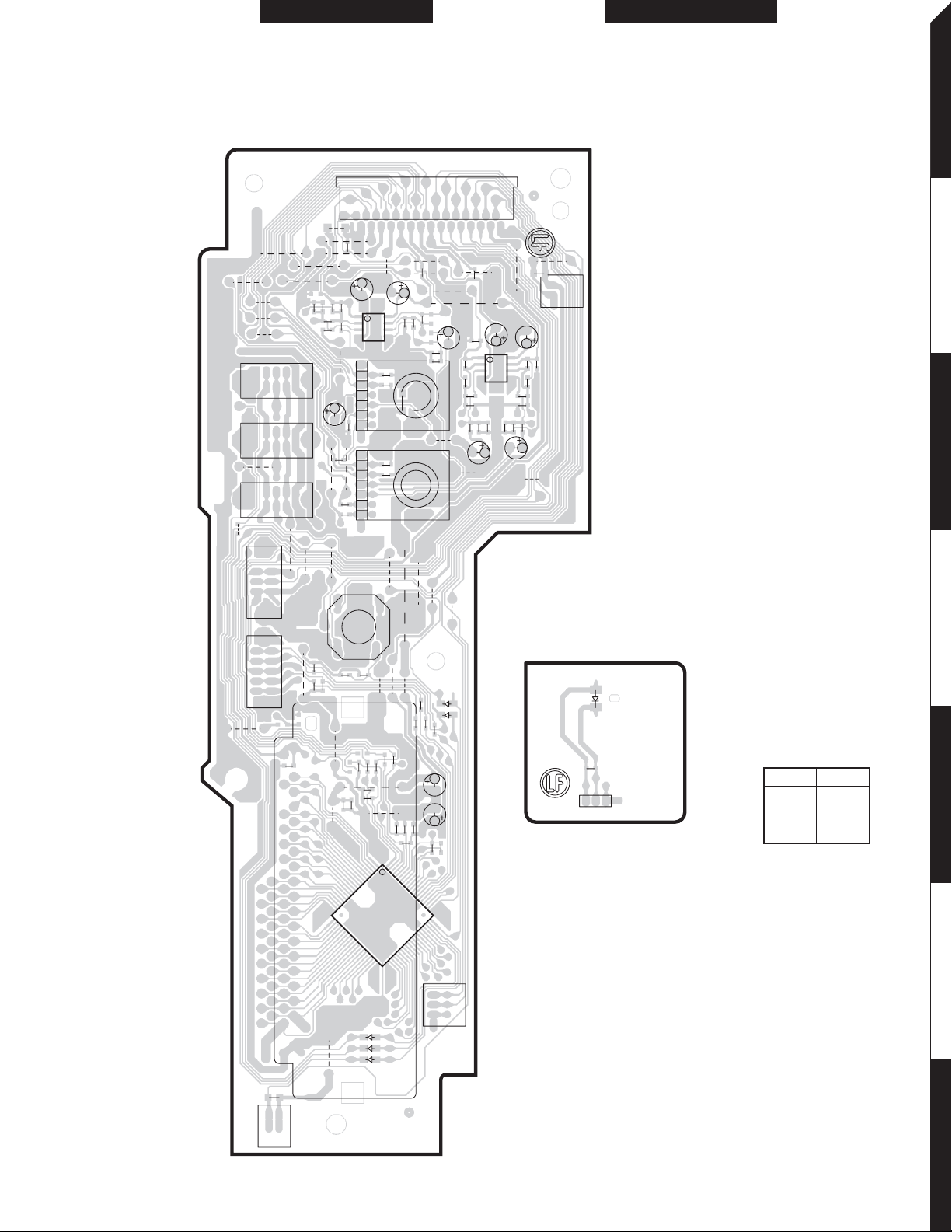
PC BOARD (FOIL SIDE VIEW)
PREAMPLIFIER UNIT X08-4350-10 A/2 (J76-0378-12)
CN1
129
W45
230
42
C113
W35
W8
W17
C32
W40
C4
C8
R8
R116
W16
R107
R12
R113
W20
W6
W1
C16
W4
R4
R102
W44
R20
R16
W25
R1
R2
C31
C12
R3
W19
ROTARY
S100
R105
R29
W42
1
IC2
4
VR2
VR1
ENCODER
C102
R101
C107
W3
C105
C106
C110
C24
PUSH
W11
R100
1
R26
R25
W2
R28
R27
W34
8
5
W15
R104
R115
80
W10
R103
B-ch
R108
A-ch
C23
R15
W12
W9
C108
C7
R202
R112
C101
W41
W14
R19
R33
R111
R110
C15
R7
C3
R11
W13
W33
W23
R109
C104
W36
S105
S104
W22
S103
W46
(SET/INFO)
(A/B/PRE)
W5
W43
W30
W27
W26
(B:ST/MONO)
W24
(A:ST/MONO)
(AB/A)
S102
W18
S101
W7
41
W38
R106
W48
W28
D104
D105
C109
C100
C10
W21
R18
C14
C11
C28
R6
W39
R34
1
IC1
4
C6
R14
C2
R10
INPUT SENSITIVITY
C22
8
5
R9
W37
R17
C13
C5
R13
R5
C1
C9
W31
X08 B/2
C118
C27
CN4
C21
1
W29
1
2
3
4
D100
C112
WH1
13
X08-4350-10
Ref. No. Address
IC1
IC2
IC100
3C
2B
6B
5
CN3
C117
20
21
2
1
ED1
12
W47
IC100
40
D101
D102
D103
61
60
41
CN2
1
3
Refer to the schematic diagram for the values of resistors and capacitors.
6
7
9
F G H I J
4
1
R136
2
DDDDD DDD
D117
KAC-PS4D/X4R
1
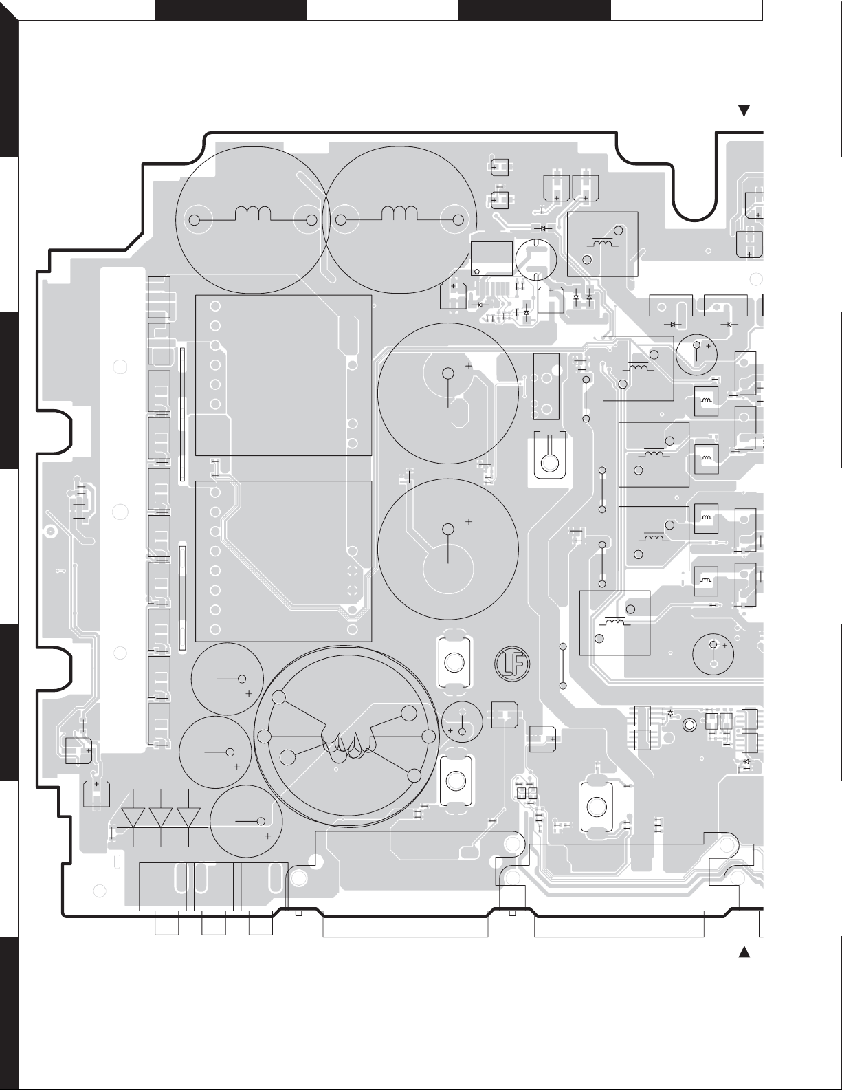
PC BOARD (COMPONENT SIDE VIEW)
AUDIO UNIT X09-8620-10 (J76-0376-21)
C940
R884
L508
L507
C565
2
IC509
1
7
R546
C535
R539
R540
R593
C562
R595
C518
C538
D514
D511D512
3
Q510
R523
SDGSDGSDGSDGSDGSDGSDG
L502
C563
C533
Q512
R525
C510
C509
R530
R531
4
R529
Q514
Q516
Q509
R527
R522
TH1
TH2
L501
W2 W1
C536
C534
R594
1
4
R596
D515
P1
R885
D506
L506
WH1
C519
C567
C122
C124
C222
C224
C568
L601
Q601
D507
D508
C220
C219
C120
L101
L102
L202
D607
L201
Q602
SDG
D608
L204
TH4
L203
L104
TH5
L103
TH6
C543
C544
SDG
Q204
C208
GDSGDSGDSGDS
TH3
R
R
C70
Q203
R99
C69
Q104
R96
C66
R95
Q103
C65
Q511
R524
C508
Q513
D501
Q515
R526
R528
D502
CN4
D503
CN3
C507
C503
CN2
5
R500
C504
C506
C941
6
L503
R243
Q216
EB
Q116
EB
R142
R141
R143
D113
C108
SGG
GGS S
C140
Q114
Q115
R14
W4
C942
C566
NP
C915
C119
Q214
DDDD DDDDSGGSS SSG
R244
D213
G
E1
R242
C142
R241
Q215
R946
R966
W5
BEBE
Q907
C945
C943
C948
C944
J2
R965
R961
R962
Q906
R963
R964
R233
C227
C235
C237
W6
C233
41
R234
C236
C234
C238
J4
C228
7
10
 Loading...