

Page 1
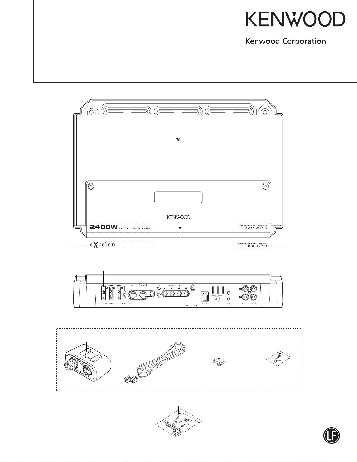
POWER AMPLIFIER
KAC-PS1D/X1R
SERVICE MANUAL
© 2007-1 PRINTED IN JAPAN
B53-0490-00 (N) 820
KAC-PS1D
KAC-X1R
KAC-PS1D only
Fuse (25A)
(F52-0014-05)
Remote control
(X16-6000-10)
KCA-WR10
Dressing Panel
(A21-6576-01) : KAC-X1R
(A21-6577-01) : KAC-PS1D
Modular cable
(E30-6240-15)
6m
Mouting hardware
(J22-0301-14)
KAC-PS1D
KAC-X1R
Screw set
(N99-1766-05)
Screw set
(N99-1795-05)
This product uses Lead Free solder.
Page 2
KAC-PS1D/X1R
(X08-431)(X09-856)
SENS. V OL
VR1
VR1
LINE IN
(0.2-5V)
R ISO-AMP
L
LINE OUT
SEL.
LINE OUT
R
IC10,11
ISO-AMPL
IC10,11
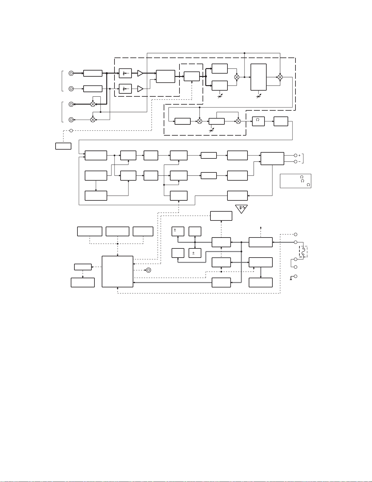
BLOCK DIAGRAM
IC2
IC3
IC3
IC1
L/R MIX
IC55-57
BASS
BOOST
IC6
S3
I.N.V I.S.F
I.N.V
SEL.
L.P.F
(400Hz)
IC4
L.P.F
VR3 VR4
IC7
FREQ
(15-60Hz)
L.P.F
SEL.
S1
FREQ
(40-200Hz)
S4
I.S.F
SEL.
IC8
B.R.F
-12dB
IC24
1
LIMIT
-6dB
S2
FREQ
(40-200Hz)
Q101,102,131
MUTE
ATT
B.R.F
SEL.
REM
LEVEL
0-18dB
FREQ
40-100Hz
IC13(2/2)
SUMMING
AMP
IC20(1/2)
TRIANGLE
WAVE
IC20
(2/2)
I.N.V
IC19(2/2,) IC6,7,
Q179,180
DC-OFFSET
DET
IC1
IC11(X08- )
DRIVER
FL
IC14
COMP
IC15
COMP
Q174-178
OVERLOAD THERMAL
DET
u-COM
TH1,2
DET
IC15,16
DEAD
TIME
IC16,21
DEAD
TIME
ROT ARY
PUSH SW
Q44,45,157,189
LEVEL
SHIFT
Q42,43,156,188
LEVEL
SHIFT
Q150,151
D-AMP
ON/OFF
Q25,26,
28,32
15V
AVR
Q50-53
FL
AVR
Q159,164-167,
Q158,160-163,
Q31,33,34
+HB
AVR
B
191,193
DRIVE
190,192
DRIVE
BATT.
CURRENT
IC3
DC/DC
CON
Q1,2
POWER
ON/OFF
Q3-5
+5V
AVR
Q170,171,
186,187
FINAL
MOS-FET
Q168,169,
184,185
FINAL
MOS-FET
IC13(1/2)
NF AMP
POWER
INDI.
BA TT. VOLT
(to u-COM)
LC FILTER
Q37,38,83
FAN AVR
FAN
LC FILTER
600W/4
1200W/2
1200W OVER/1
P-CON
BATT.
GND
(BTL)
SP-OUTPUT
2
Page 3

KAC-PS1D/X1R
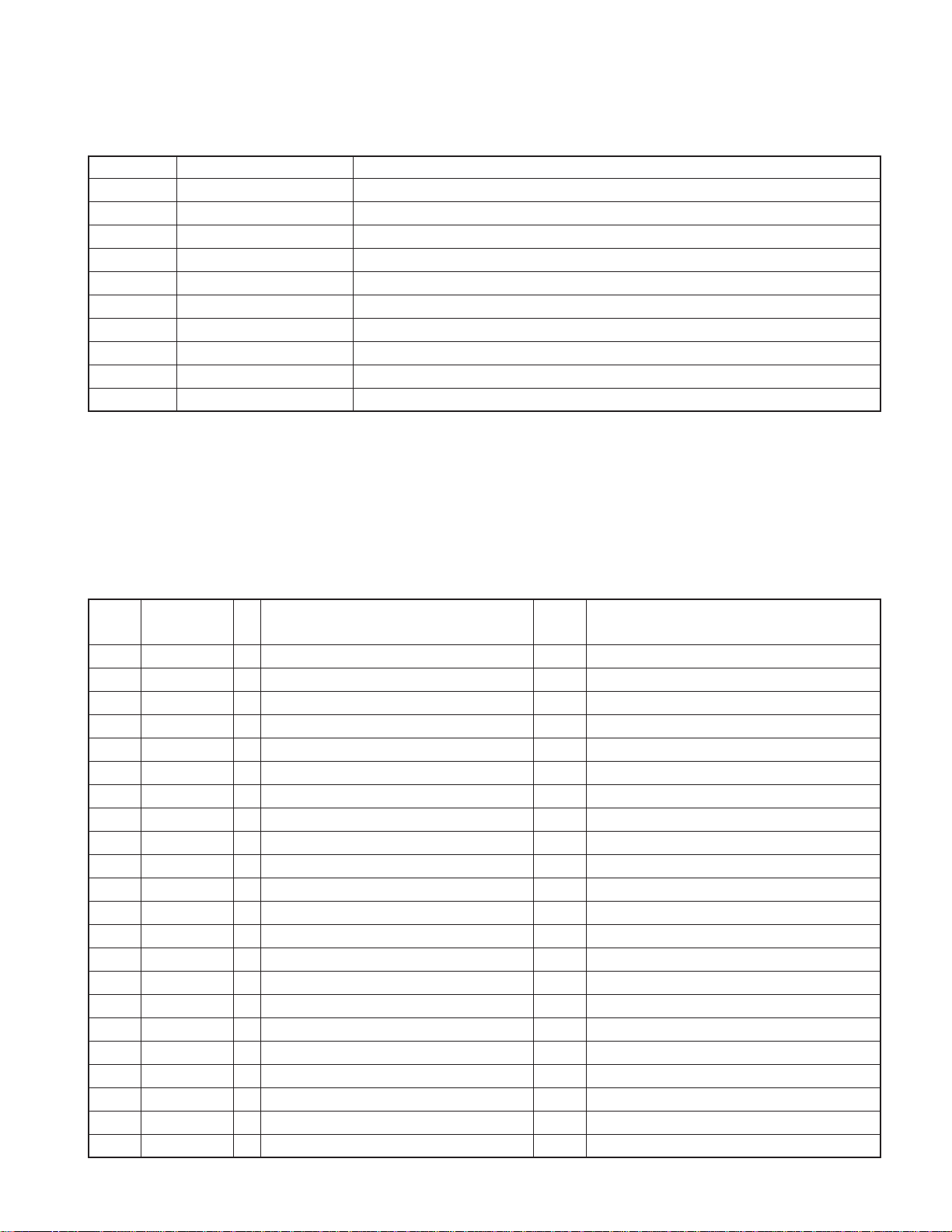
COMPONENTS DESCRIPTION
● AUDIO UNIT (X09-8560-10)
Ref. No. Application / Function Operation / Condition / Compatibility
IC1 µ-com Overall control.
IC3 DC/DC converter driver Generates the gate waveform for switching.
IC5 (2/2) Comparator
IC6 (1/2) Comparator Detects ASO. Compares current with voltage to detect short in the output.
IC6 (2/2) Comparator
IC7 (1/2) Comparator
IC7 (2/2) Comparator
IC10,11 Isolation AMP Removes the common mode noises in the input signal.
IC12 Buffer AMP Buffer AMP for RCA output.
IC13 (1/2) Signal amplification
IC13 (2/2) Signal amplification
IC14 (1/2), Comparator,
IC20 (1/2) Signal amplification
IC14 (2/2) Comparator
IC15,16,21 NAND gate To gate pulse of the D-class amplifier.
IC17 NAND gate
IC18 Signal amplification
IC19 (1/2) Signal amplification
IC19 (2/2) Signal amplification Amplifies the DC offset at the SP + terminal, and applies to the DC servo.
IC20 (2/2) Signal amplification
IC22 Filter
IC24 Signal amplification
IC55~57
Q1,2 POWER ON SWITCH
Q3~5
Q6 SW5V control Turns ON/OFF 5V to the SW5V line in response to the output from pin 20 of the µ-com.
Q7 Pcon over voltage control
BassBoost circuit Boosts the signal with the operations from the remote control.
(Remote control operation) GAIN=0~+18dB, fc=40~100Hz
5V constant voltage
power supply
Compares the analog signal with the triangular wave and generates the PWM waveform for
the minus output-side amplifier of the BTL.
Detects the resonance waveform that is caused when the plus and minus terminals are
shorted in the vicinity of the SP terminals, and protects from the short.
Detects over current with the waveform shaped in IC17 and sends the result of the detection
to the µ-com and the TR used to control the D-class amplifier.
When SP+ or SP- terminal output is shorted to the ground, the current in the + power supply
and that in the - power supply are unbalanced. The unbalance in the current is converted into
DC voltage in Q176 and Q177, and when the voltage exceeds the preset value the output is
reversed and the protection function is activated.
Amplifies the output voltage between the SP + and SP - terminals and generates the NF signal.
Amplifies differences between the input and feedback signals. Initial stage of the D-class amplifier.
Triangular wave generation.
Compares the analog signal with the triangular wave and generates the PWM waveform for
the plus output + side amplifier of the BTL.
Retains the pulse width and keeps holds a certain width when IC6 and IC7 (2/2) detect its
individual over current.
Amplifies and rectifies the output voltage at the SP + terminal, and generates DC voltage that
is proportional to the output.
Amplifies the potential differences caused by current running in the GND pattern, and sends
it to the µ-com to obtain current.
Generates the inverted waveform of the triangular wave that is generated in IC14 (1/2) and IC20 (1/2).
Filters and rectifies the resonance waveform that is caused when the plus and minus terminals
are shorted in the vicinity of the SP terminals, and sends the resultant DC voltage to IC6 (2/2).
When 1Ω load is detected, lowers the voltages at pins 1 and 7 and decreases the signal
clipping level in order to limit the SP output.
Turns ON/OFF DC/DC converter power supply in response to the output from pin 8 of the µ-com.
It is used as the constant voltage power supply of 5V for the µ-com and the SW5V.
Blocks the ON signal to the Pcon and places the Pcon in the OFF condition when the battery
voltage is too high.
3
Page 4

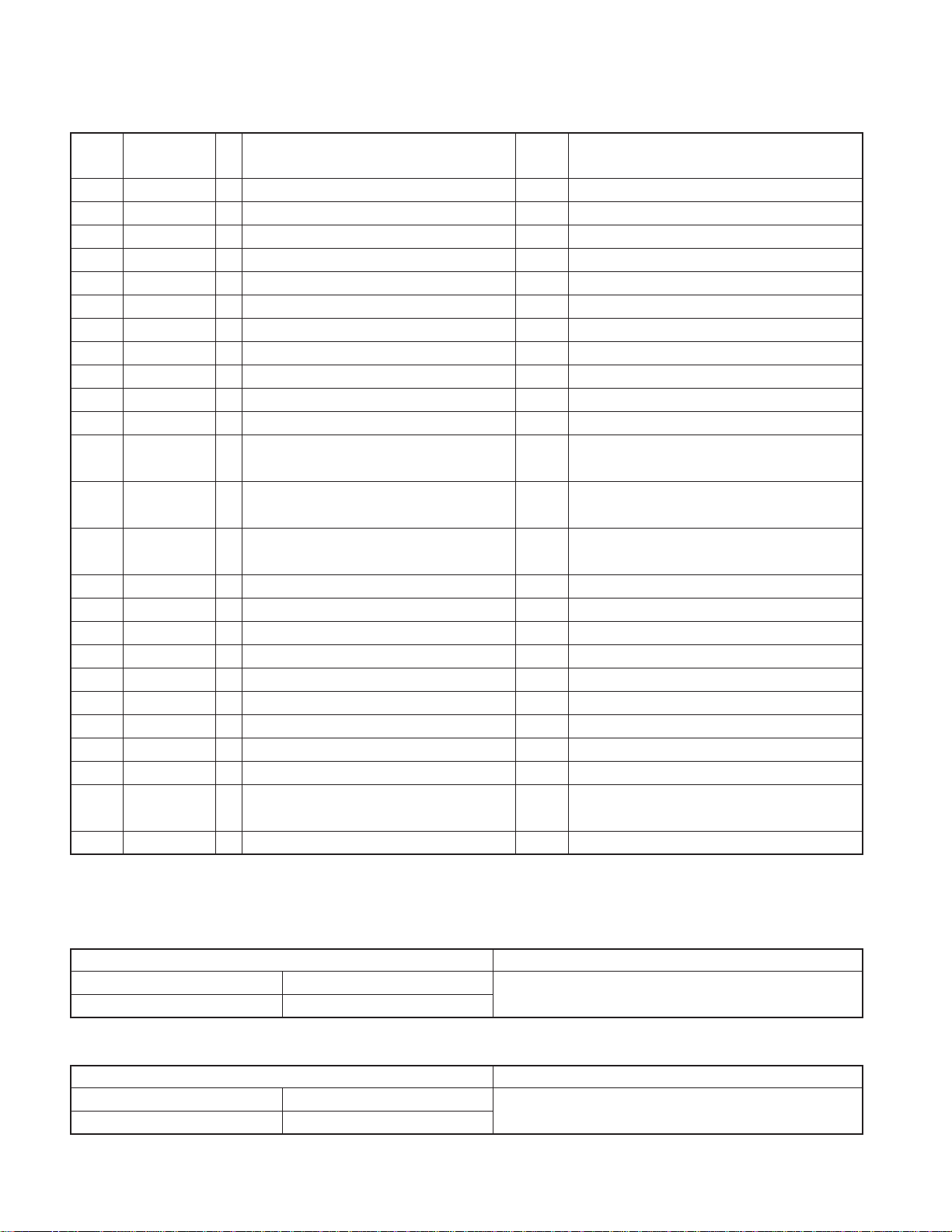
KAC-PS1D/X1R
COMPONENTS DESCRIPTION
Ref. No. Application / Function Operation / Condition / Compatibility
Q8 Pcon Switch
Q10,11 DD converter gate control
Q13~16 DD converter gate driver Drives the switching FET gate in the DD converter.
Q17~20,
Q22~24,27 side.
Q25,26
Q28,32
Q29,30 voltage power supply is
Q31,33,34
Q36~38,
Q41,83 Darlington connection in Q37 to turn ON/OFF by the µ-com.
Q39 Limiter level control
Q42~45,
Q156~167, PWM shaping circuit Generates the pulse signal for the gate drive of the high side and low side.
Q188~193
Q168~171,
Q184~187
Q47,48 Power supply SW for FL Turns ON/OFF the FL power supply from pin 22 of the µ-com.
Q50~53
Q54,55
Q101,129 MUTE Mutes the audio signal from pin 56 of the µ-com to prevent applying the shock noise.
Q102,
Q131~133 increases. For 1.5dB respectively.
Q125,126 ADV
Q150,151 D-SW Turns ON/OFF the D-class amplifier stage from the µ-com or protection.
Q179,180 DC detection Turns ON when DC is detected at the SP terminal and sends it to pin 64 of the µ-com.
Q181,182 ASO detection Voltage amplification circuit used when the ASO is detected
Q174,
Q176~178 protects against the ground fault.
Q175 ASO detection Current amplification circuit used when the ASO is detected
Q603 LOGO-LED Turns on the LOGO LED from pin 4 of the µ-com.
DD converter switching FET
+15V constant voltage In order to compensate HFE in Q26, both TRs in Q25 are connected with the Darlington
power supply connection and the constant voltage of +15V is obtained.
-15V constant voltage In order to compensate HFE in Q28, both TRs in Q32 are connected with the Darlington
power supply connection and the constant voltage of -15V is obtained.
Tracking when -15V constant
turned OFF
+15V constant voltage
power supply for high voltage
Power supply for F AN
FET for output Generates the PWM output waveform by the switching.
Constant voltage power
supply for FL filament
Constant voltage power
supply SW for FL filament
ATT
Ground fault detection
Places the amplifier in the ON condition by sending “L” to pin 1 of the µ-com when the Pcon
terminal becomes “H” while the battery voltage is in the normal range.
Turns ON/OFF DD converter gate drive pulse in response to the output from pin 8
(Power_On) of the µ-com.
Repeats switching the transformer’s primary side to generate high voltage at the secondary
Adjusts the voltage drop in the -15V constant voltage power supply to the voltage in +15V
side while the power OFF.
Power supply for the gate drive signal in the output FET high side.
In order to compensate HFE in Q38 and Q83, Q41 and Q36 are connected with the
When 1Ω load is detected, CEs are ON and the voltages at pins 1 and 7 of IC24 are dropped
in order to limit the signal amplitude.
Supplies the constant voltage of 2.3V to the FL filament.
Turns ON/OFF the FL filament power supply from pin 22 of the µ-com.
Lowers the volume when temperature at the output FET or in the vicinity of the transformer
Reads the power supply voltage value to show it with the FL. Turns OFF when the power
supply is OFF to save the backup current.
When SP+ or SP- output is shorted to the ground, sends the signal to pin 6 of the IC7 and
4
Page 5
KAC-PS1D/X1R
COMPONENTS DESCRIPTION
● PREAMPLIFIER UNIT (X08-4310-10)
Ref. No. Application / Function Operation / Condition / Compatibility
IC1 (1/2) Signal amplification Mixes Lch and Rch to make Mono signal.
IC1 (2/2) Signal amplification Buffer to send the signal that comes through LPF and Bass Boost to the Line Out.
IC2 Frequency fixed LPF LPF fixed at 400Hz.
IC3 Signal amplification Amplifies the signal that comes through SensVol and outputs it with low impedance.
IC4 Frequency variable LPF LPF with variable frequency between 40~200Hz.
IC5,6 (1/2) Band-cut filter Attenuates the frequency in the specific range between 40~100Hz.
IC6 (2/2) Reverse circuit Changes the phase by 180 degrees.
IC7 Frequency variable HPF Attenuates the frequency in the range of 15~60Hz that is lower than the specific frequency.
IC8 (1/2) Signal amplification Amplifies the signal component to reduce noises in the subsequent BRF stages.
IC11 FL driver Communicate with the µ-com, generates the data for FL display and reads in KEY.
MICROCOMPUTER’S TERMINAL DESCRIPTION
● MICROCOMPUTER: 78F0533GK011A (X09-856: IC1)
Pin No. Pin Name I/O Application
1 P_CON I
2 D_CURENT I Detects the D-class over current Enters into the protection operations.
3NCONot used Output L fixed
4 PON_ILLUM O LOGO LED+B SW H: ON, L: OFF, Initial condition “L”
5FAN1 O FAN rotation control q H: Rotation, L: Stop, Initial condition "L"
6 RESET I Reset
7 D_POWER O D-class amplifier power supply control H: D-class ON, L: D-class OFF
8
9 FLASH_W I Used when writing in the flash
10,11 NC O Not used Output L fixed
12 REGC 13 VSS 14 EVSS 15 VDD 16 EVDD 17,18 NC O Not used Output L fixed
19 NC O
20 5V_SW O SW5V ON: L L: SW5V ON, Initial condition “L”
21 NC O Not used Output L fixed
22 PON_FL O FL power supply (Grid and Filament) control H: ON, L: OFF
23~33 NC O Not used Output L fixed
34 ROTARY_CW I Encoder pulse input Detects pulse width
POWER_ON_1
Clears the stop mode by turning the P-CON ON
O Amplifier power supply control H: Amplifier power supply ON, Initial condition “L”
Truth Value
Table
Processing Operation Description
L: Clear the stop mode
5
Page 6
KAC-PS1D/X1R
MICROCOMPUTER’S TERMINAL DESCRIPTION
Pin No. Pin Name I/O Application
35
36~38 NC O Not used Output L fixed
39 REF5V_OUT O Supplies to AVREF (pin 47) Output H fixed
40,41 NC O Not used Output L fixed
42 VFD_INH O Panel VFD driver INH Driver output switching
43 VFD_CE O Panel VFD driver CE Command control terminal of the driver
44 VFD_DATA_M O Panel VFD driver data line µ-com → driver input
45 VFD_DATA_S I Panel VFD driver data line µ-com → driver input
46 VFD_CLK O Panel VFD driver communication CLK Communication clock
47 AVREF - DA REF voltage Receives the reference voltage from pin 39.
48 AVSS -
49 IMP_DET I Detects load IMP at SP terminal
50 TEMP2 I
51 TEMP1 I
52 NC O Not used Output L fixed
53 AD_V I Detects BU voltage (For display) Displays the voltage and condition.
54 NC O Not used Output L fixed
55 AD_I I Detects primary current (For display)
56 MUTE1 O Mute control of the amplifier input stage L: MUTE1 ON, H: MUTE1 OFF, Initial condition “L”
57 NC O Not used
58~60 NC O Not used Output L fixed
61 ATT1 O Output signal level attenuation control L: Output attenuation, Initial condition “L”
62 ATT2 O Output signal level attenuation control L: Output attenuation, Initial condition “L”
63 LIMIT O
64 DC_DET I Output DC OFFSET voltage detection Enters into the voltage error protection operations.
ROTARY_CCW
IEncoder pulse input Detects pulse width
Temperature detection 1 (at output TR side)
(For display and protection)
Temperature detection 1 (at power supply side)
(For display and protection)
Limits the peak value of the D-class amplifier
input signal
Truth Value
Table
w Clips the audio signal quickly with “H”
Processing Operation Description
Reads the impedance and turns on the limiter
when it is 1Ω load.
Displays the temperature and overheat protection.
Displays the temperature and overheat protection.
Converts into the current and displays current value.
Truth value table
q FAN (Pin 5)
Calculated temperature based on the detected voltage at TMP_1 (pin 31) Note
Lower than 35°C Remains as L In the case of “H” output, it recovers to “L” when the temperature
35°C or higher H output decreases to 30°C.
w LIMIT (Pin 63)
Voltage detected at IMP_DET (pin 49) Note
Lower than 3.8V Remains as L
3.8V or higher H output
Recovers by P-CON OFF or RST.
6
Page 7
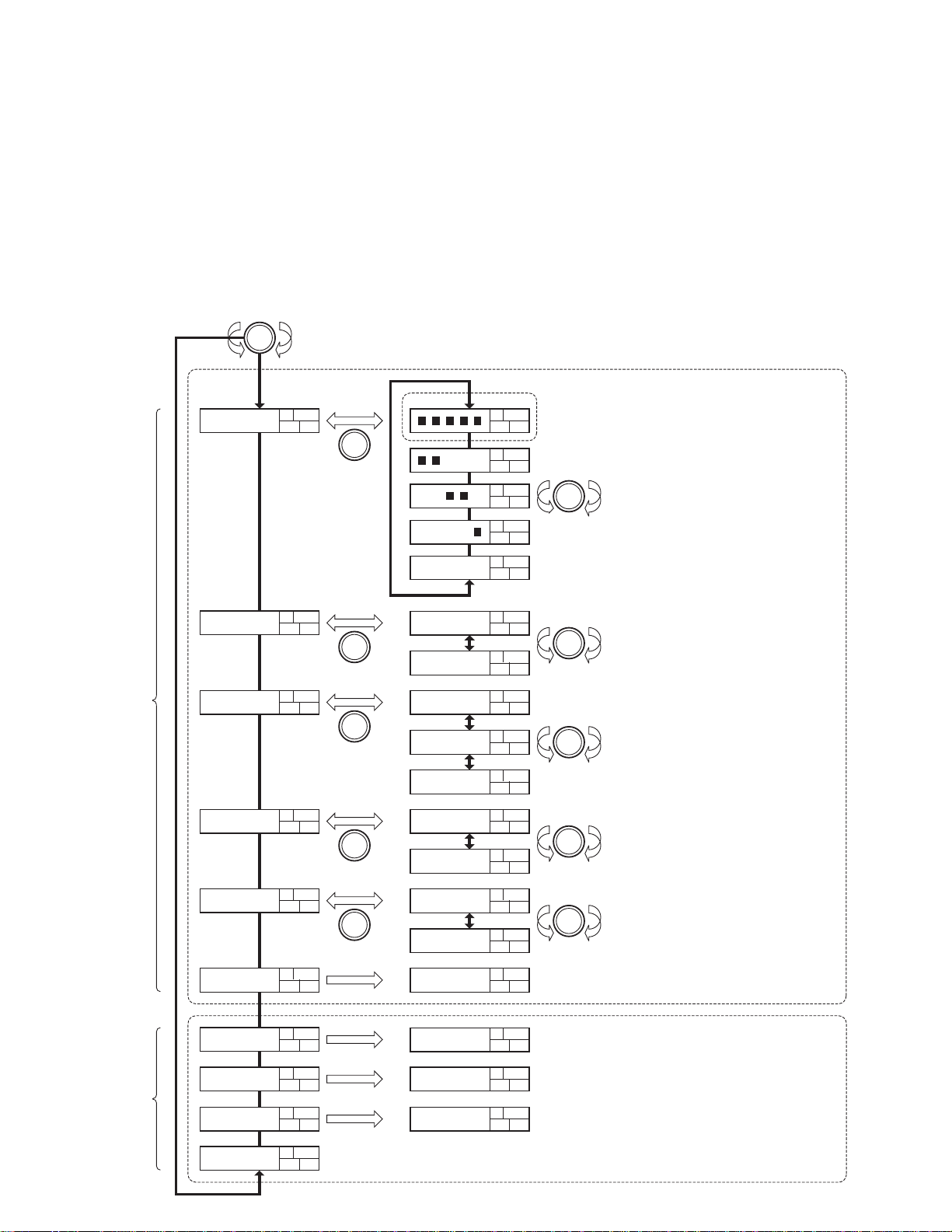
TEST MODE
●
How to enter the test mode and how to c lear the test mode
• How to enter
In the backup connection condition (when the battery is being
connected), turn ON the P_CON while keep pushing the rotary
push key.
• How to clear
P_CON OFF or reset to clear the mode. (Clear the mode even
in case of the protection.)
* Do not clear the mode if the protection recovers automatically .
Turn
KAC-PS1D/X1R
● Items in the test mode and test operations
• INFORMATION display (Display of conditions)
In the test mode, the following items can be checked in addition
to the normal INFORMATION display.
Each item can be selected with the rotary encoder and the settings can be changed with the push key.
Additional items shown in the test mode
°
DIRG
Hz dB
Push
....
..
..
OVER
NAF
TTA
°
Hz dB
Push
OVER
°
Hz dB
Push
OVER
°
IMTIL
Hz dB
Push
OVER
°
Hz dB
OVER
°
Hz dB
OVER
°
Hz dB
OVER
°
Hz dB
OVER
°
Hz dB
OVER
°
FFO
Hz dB
OVER
°
NO
Hz dB
OVER
°
0TTA
Hz dB
OVER
°
1TTA
Hz dB
OVER
°
2TTA
Hz dB
OVER
°
FFO
Hz dB
OVER
°
NO
Hz dB
Turn
Turn
Turn
Turn
• Segment check of FL display tube
Change the display segment in the following
sequence of order.
All on → GRID1 on → GRID2 on →
GRID3 on → All of
• Check of FAN switching
In the FAN switching mode, it is possible to
select to rotate or stop the FAN regardless
of the present temperature.
• Check of ATT switching
In the ATT switching mode, it is possible to
switch the ATT regardless of the present
temperatur.
• Check of LIMIT switching
In the LIMIT switching mode, it is possible to
switch LIMIT regardless of the presently
detected impedance of speaker.
OVER
Initial condition
in the normal mode
Condition display Items shown
OVER
DEL
REV
°
Hz dB
Push
OVER
°
Hz dB
OVER
°
TLOV
Hz dB
OVER
°
RTRUC
Hz dB
OVER
°
PMET
Hz dB
OVER
°
OMED
Hz dB
OVER
°
FFO
Hz dB
OVER
°
NO
Hz dB
OVER
°
203.V
Hz dB
OVER
°
V34.1
Hz dB
OVER
°
A81
Hz dB
OVER
°
C87
Hz dB
Turn
• Check of LED switching
In the LED switching mode, it is possible to
select to turn on or off the LED.
•Version display
It is possible to check the version of the µ-com.
7
Page 8
KAC-PS1D/X1R
CIRCUIT DESCRIPTION
●
Short detection circuit between SP+ and SP- terminals
If the SP+ and SP- terminals are shorted in the vicinity of the
terminals, the self oscillation occurs in the D-class amplifier.
The oscillation in opposite phase is caused between the +
and - terminals of the BTL, and this oscillation is applied to the
differential amplifier, IC22 (2/2) to limit the amplitude with the
zener diodes such that the voltage does not exceed the withstand voltage.
to COMPARATOR
from SP+ OUTPUT
TERMINAL
from SP- OUTPUT
TERMINAL
C207 0.01
C208 0.01
C198
3300P
C199
3300P
R339
47K
R340
47K
D173 D172
● Power supply circuit for FL
• V-FL
V-FL is the power supply for grid of FL. D48 is used to select
either the battery or +15V power supply that has higher voltage.
The power supply voltage is set to constant 13V in D49. The
power is turned ON/OFF with Q54 and is applied to FL driver.
• FIL+
Power is supplied by the battery and the voltage is set to 2.3V
in D49 so that it is applied to the filament of FL.
The power is turned ON/OFF in Q48 in response to the FLON signal from the µ-com.
TP5
R341 47K
The output from pin 7 of IC22 is rectified through the band
pass filter whose center frequency is about 3kHz.
The DC voltage generated after the rectification is applied to
the comparator, (IC6 (2/2)) and generates “L” at pin 7 of IC6
when the voltage exceeds the preset threshold.
BPF
TP9 TP30
R345
2.2K
TP27
IC22(1/2)
C202
3
1
2
0.033
10K
R344
TP31 TP32
R3461KR347
1K
C203
0.033
C204
D176
0.022
0V
TP33
10K
R348
IC22
(2/2)
8
5
6
4
R342 47K
D174 D175
TP103
RESONANCE DET.
TP6
C200
0.01
7
0V
R343
TP7
C201
0.033
22K
● Ground fault detection circuit
When SP+ or SP- output terminal is shorted to the ground,
the current running in the +B power supply and that in the -B
power supply are unbalanced.
The current unbalance (±) is measured by R203 and R204
and the currents are mixed in R225.
When the currents become out of balance due to the above
shorting to the ground, the voltage is caused across R225.
When this voltage exceeds the threshold decided by R256
and R257, the “L” output is generated at pin 7 of IC7.
As a result, the over current protection operation is activated.
R73
Q50
1
D48
4.9V
Q48
22K
R99
100
R66
R87
4.7K
TP337
D49
Q47Q55
R307
R304
10
10
R80
Q51
1
R81
Q52
1
2.5V
R74 47
R72 47
Q53
47u25
R71 47
R79
2.2K
+
D46
+
C47
TP289
47u25
C46
14.4V
4.7
R88
4.7
R98
R89
13.4V
4.7
4.7 4.7
R90
R97
4.7
R96
4.7
R95
4.7
R94
Q54
4.7
R91
4.7
R92
4.7
R93
Q187
Q186
Q185
Q184
R203
0.01
5W
R204
R213
3.3K
R223
3.3K
0.01
1.5K
R219
C172
0.047
Q174
Q176
C184 1000P
R259
R225 62K
33K
R226
Q177
Q178
0.047
R224
1.5K
C178
5W
D165 D164
1K
TP104
R257
R256
R820
1K
10K
1
TP383
5
6
7
8
TP105
IC7
V+
R292 10K
C183 0.01
1
R830
D169
4
V-
3
2
10K
10K
R287
R291
1
TP385
10K
TP384
R286
0.01
C189
D171
8
Page 9
KAC-PS1D/X1R
0V
IC14
IC19(2/2)
D137D138
D117
D115
D119
D118
D116
D114
(1/2)
IC20
TP57
TP52
TP53 TP55
TP60
TP54
TP102
TP101
5
6
7
1
C136
150K
R338
100K
R337
1
C135
10K
R151
6.2K
R149
6.2K
R148
6.8K
R146
0.01
C127
10K
R147
1
R803
10K
R145
330P
C126
1
R804
10K
R142
0.01
C503
0.01
C504
8
3
4
2
1
8
V+
1
7
5
6
243
V-
TP100
470K
R336
from SP+ OUTPUT
TERMINAL
TRIANGLE WA VE
GENERATE CIRCUIT
CIRCUIT DESCRIPTION
● Pulse shaping circuit
When either output from the ASO detection (IC6-pin 1), ground fault detection
(IC7-pin 7) or short detection (IC6-pin 7)
is “L”, the pulse with a constant width of
about 10msec is generated even if the
input pulse width is small. The input to
the pulse shaping circuit is pin 5 of IC17
and the output from the circuit is pin 3 of
IC17.
2.2K
R217
18K
R233
● Servo circuit
Amplifies DC offset voltage that is output to SP+
terminal in IC19 (2/2).
Feedbacks the output from pin 7 of IC19 to the triangular wave generation circuit.
Corrects DC offset voltage at SP+ terminal towards
0V by incorporating the feedback in the triangular
waves that are applied at pin 6 of IC14.
C184 1000P
D165 D164
TP104
R254
TP382
R253
D22
R49
C175
6800P
R257
R256
4.7K
15K
18K
R820
1K
10K
TP383
D140
D170
1
IC7
5
6
7
8
V+
R292 10K
TP105
C183 0.01
IC6
5
6
7
8
V+
1.0V
COMPARATOR
TP106
V-
V-
4
3
2
1
D171
4
3
2
1
TP108
7
R830
C189
1
R291
0.01
2
R290
10K
10K
D169
6
IN
10K
R287
R286
TP392
C185 0.68
R271
R272
1K
TP384
TP385
10K
Q181
C186 0.01
R266 220K
PULSE SHAPING
CIRCUIT
TP387
IC17
(2/4)
10K
TP386
C190
1000P
10K
R270
TP393
Q182
4
5
R269
TP388
14
C192
6
0.047
7
0.01
C191
TP391
TP394
R279
20K
IC18
(2/2)
86
7
5
R278
1K
12K
0.01
C194
R282
R280
TP389
R296
10K
R281
1.3K
330K
TP395
R283
10K
R308
D167
20K
1K
C197
D166
IC17(1/4)
1
2
TP390
100P
R284 20K
D168
1
C193
10u50
TP396
IC18
(1/2)
+
3
9
10
12
13
4
IC17(3/4)
IC17(4/4)
R285
2
3
C195
0.01
R822
1
11
20K
8
OUT
R821
1
C196
10u50
10K
R289
R288
24K
+
● LIMIT circuit
IC24 (1/2) is a voltage follower and IC24 (2/2) is a reverse
amplifier that has no gain.
Q39 is turned ON/OFF in response to H/ L of LIMIT (pin
63) from the µ-com.
Voltage at pin 3 of IC24 becomes 2.2V and 5V in response
to ON/OFF of Q39.
When the u-com detects 1Ω load, the input signal is clamped
at ±2.8V, in which 0.6V of vf from D205 and D206 is added,
and peak value of the signal is limited.
● NF circuit
Differentially amplifies the signal in IC13 (1/2) f or the BTL output and applies negative feedback signal to pin 6 of IC13 (2/
2).
L7
3.3K
R188 24K
C157
0.056
C171
0.015
C173
0.015
R187 24K
C160
0.056
86uH
R214
24K
L8
86uH
R216
24K
R189 24K
R186 24K
9
+ SIDE PWM OUTPUT
- SIDE PWM OUTPUT
+15V
-15V
TP46
C122
R137
R136
47u25
INPUT
SIGNAL
TP327
TP331
10K
R258
Q39
R328
TP329
10K
5V
R327
5.1V
0.01
C42
13K
C301
R825
0.01
1
TP306
C300
0.01
2
R824
1
TP305
IC24
(1/2)
83
4
1
R323
2.7K
5.1V
D205
OUTPUT
SIGNAL
TP330
R331
IC24(2/2)
R330
3.3K
3.3K
6
5
7
D206
+
R134 15K
1K
R135 5.1K
C123 0.1
TP47
470
R138 1K
R8291R828
85
6
4
IC13(2/2)
C124 56P
R139 1M
1
C817
0.01
0V
C816
0.01
R140
7
10K
TP51
C158
1000P
10K
R141
TP49TP48
IC13(1/2)
R171
1K
0V
NF AMP
1
R173 3.3K
R183 12K
3
R184 12K
2
R174
NF SIGNAL
Page 10

A B C D E
9
R
R9
Q42
4
7
Q161
Q
5
KAC-PS1D/X1R
1
PC BOARD (COMPONENT SIDE VIEW)
AUDIO UNIT X09-8560-10 (J76-0345-01)
Q159
R28
D19
EB
R182
BE
Q167
R196
R93
R10
BE
BE
R169
Q45
R180
BE
R83
R25
R48
R84
R179
BE
B
R160
Q44
Q157
R161
R168
BE
Q166
R195
R197
R201
C38
R36
C19
C20
C39
Q189
E
R177
Q158
BE
R178
Q187
R307
R175
Q156
BE
BE
Q43
R166
R235
Q193
B
BE
R238
R239
R167
Q164
E
BE
Q165
Q191
Q171
GDS GDS GDS G
TH2
R35
P2
C14
C182
C47
R73
R316
Q41
C56
R315
BE
Q83
Q38
Q36
D32
Q37
R319
R320
BE
BE
C55
R92
BE
BE
R318
R317
BE
R71
C46
R91
J3
R159
Q163
Q50
C13
R223
C178
R226
R176
BE
EB
R200
Q177
BE
BE
Q178
R80
BE
R72
Q53
BE
D46
R90
R192
Q170
Q51
R79
Q162
R194
R213
C172
R224
R215
R81
BE
R74
R88
R89
Q52
Q47
Q48
7
R2
Q17
B
B
B
Q1
BEE
Q
EB
R181
C21
L4
L5
D17
2
D18
D20
R98
R97
R96
R94
R95
C1
J2
Q34
R805
D12
R55
D13
L2
Q17Q18
R34
R37R39
W3
Q19Q20
W2
R46
Q27
R59
Q4
Q22
W4
R58
C16
C34
R51
C17
C18
C33
W5
L3
TH1
C15
C24
R86R85
D16
R78
R29
BE
Q31
R76
3
C25
R823
C35
BE
R77
BE
Q33
R75
R806R809 R808
R807
R52
R53
C36
R56
R60
R61
1
8
IC3
Q10
R309
R32
C3
C5
916
D10 D11
Q13
Q16
BE BE
R26
R27
BEBE
R33
Q14
D4
C6
EB
Q3
R3
Q5
R7
BEBE
Q11
R310
Q15
R8
R9
BE
Q6
R4
R5
BEBE
D5
R6
C37
4
Q23
5
C4
C7
6
R14
Q7
BE BE
R12
C2
R1
R2
Q8
R11
D7
D6
R13
E
Q1
B
Q2
BE
C8
Q24
GDS GDS GD S GDS GD S GD S GDS GD S
R47 R57
D1
C11
L1
D2
D3
CN1
CN2
W1
CN3
7
10
Page 11

BE
R158
BE
B
Q42
E
R165
BE
Q190
Q161
R191
Q186
GDS GDS GD SGDSGDS
94
R306
C162
R204
R203
R261
R297
C181
Q174
BE
R213
R224
1
C172
R215
R88
R89
Q52
Q47
Q48
BE
Q176
BE
R218
Q175
Q54
BEBEBE
Q55
R66
R9
EB
R225
R219
C151
R827
R826
D132
D49
R87
D48
Q188
R236
R199
R821
R822
D168
D166
R193
R220
C551
R234
BE
Q192
Q169
C187
D162
D160
C136
85
C502
IC19
C501
14
R335
C152
C194
C195
C554
R554
R162
D150
R156
Q150
Q151
BE
R237
C177
R273
R276
R264
Q180
R338
R333
R269
R279
85
IC18
14
R285
R283
C552
C553
R551
R553
13
BE
BE
R164
EB
R263
R262
Q179
C135
R334
R284
R278
C196
R281
24
R157
R274
BEBE
R336
C204
R348
R552
R337
R280
D140
C900
R277
C199
D137
R558
7
814
R154
C129
D122
Q160
Q185
R305
IC901
C188
43
C902
12
R901
D163
D161
D174
D175
C207
D138
R347
C203
D176
D501
D552
1
IC15
R155
D123
IC16
814
C166
R602
R609
C602
L6
C901
R340
R342
C198
R339
85
IC22
R341
C208
14
R344
R346
C202
R345
C201
Q182
BE
C193
R270
BE
D170
C186
R289
Q181
D169
R288
R266
C185
C512
R123
C555
C130
R205
D152
R190
R603
D171
R820
R124
D121
R152
R607
C607
C32
C604
Q126
C200
R343
S10
R198
D133
R290
17
Q168
C810
L7
C176
C614
1
C603
17 32
R229
R228
BE
BE
Q125
D172
C191
C197
D173
R282
R296
R292
R830
C189
R502
R501
R131
R304
R810
C812
C616
R637
C615
IC1
R646
R644
R645
BE
R640
Q603
IC17
1
R272
C190
R259
D164
85
C183
IC7
14
R291
R287
R286
C511
C205
R271
C184
D165
R811
R636
4964
814
7
R257
R816
R256
C905
C617
R619
R612
R618
Q184
R638
48
3316
R611
85
R49
D151
71
IC21
814
C167
R210
R211
C168
C173
C169
C171
R214
P1
C159
C621
R240
R50
C618
D21
R614
R613
R616
R617
R621
C620
R620
C619
4
58
IC903
D167
C192
R254
R253
R308
IC6
14
D22
R233
R217
C175
C117
S901
C509
R163
R170
8
5
R185
C504
IC20
4
1
R145
C126
D116
R146
C174
R206
D153
D118
Q26
R813
BE BE
C811
R812
C206
R216
R647
R248
R639
R615
C558
14 1
C559
R513
C517
1
C601
R908
C801
C120
R114
C112
R118
C114
C106
R106
R108
R831
C108
R116
R110
C110
R112
C821
D104
R104
C104
D134
C102
C137
C131
R905
C818
R815
R906 C906
D119
D117
8
851
851
R102
J4
Refer to the schematic diagram for the values of resistors and capacitors.
R817
C813
C556
IC56
R510
IC11
IC10
D102
C503
R142
C516
C515
R814
C519
C802
D101
R153
C127
D114D115
R149
R511
R509
R101
R148
C557
4
4
R147
Q28
7
D103
R103
D120
R151
R514
C111
R117
C105
C101
R172
85
IC5
14
R150
85
IC14
14
R506
C518
R512
IC57
415
R515
R907
C119
R113
C113
R105
C107
R115
R109
C109
C103
R111
D135
C118
J1
R41
R107
R804
R560
R504
R503
8
C133
R125
C164
R819
R818
C819
R803
Q30
D14
B
E
R23
R38
R42
Q25
Q129
C514
58
IC55
14
R505
C520
R516
C823
R801
R802
C824
R143 R144
5
IC12
R241
D105
C156
R128
D15
R44
C26
R24
R40
R21 R22
BE
EB
R43
Q32
C28 C29
C160
L8
R247
Q132
C150
R245
R246
BE
R230
R314
R312
R232
R231
R313
R563
C513
C568
R578
230
129
C134
R242
R126
R832
148
C822
D106
C154
C153
C155
R129R130
R127
KAC-PS1D/X1R
X09-8560-10
Ref. No. Address
IC1 5G
IC3 4A
IC5 2H
IC6 6G
IC7 6G
IC10 5H
IC11 5H
IC12 5H
IC13 3I
C124
C123
R330
D205
IC14 2H
IC15 2G
IC16 2G
IC17 5G
IC18 6F
IC19 5F
IC20 2H
IC21 2G
IC22 5G
IC24 4I
IC55 5H
IC56 5H
IC57 5H
Q1 5A
Q2 6A
Q3 4A
Q4 5A
Q5 5A
Q6 4A
Q7 5A
Q8 5A
Q10 4A
Q11 4A
Q13 4A
Q14 4A
Q15 4A
Q16 4A
Q17 3B
Q18 3B
Q19 4B
Q20 4B
Q22 5B
Q23 5B
Q24 5B
Q25 2H
Q26 2H
Q27 4B
Q28 2H
Q29 2I
Q30 2H
Q31 3A
Q32 2I
Q33 3A
Q34 2A
Q36 5D
Q37 5D
Q38 5E
Q39 4I
Q41 5E
Q42 2F
R186
R189
R183
R174
C161
Q133
R187
R188
Q102
Q131
R244
D136
BE
Q29
R184
BEBE BE
R243
R332
D8
C223
BE
C27
BE
R133
D113
R173
C42
R328
R258
CN4
R45
IC13
R311
Q39
C816
C122
R323
R327
BE
C157
R171
R829
R828
R140
C817
1
R139
485
R137
R136
Q101
C121
R132
R825
R824
C300
C301
1
8
IC24
45
R141
C158
R138
R135
R134
D206
R331
JIHGF
Ref. No. Address
Q43 2E
Q44 2D
Q45 2D
Q47 6E
Q48 6E
Q50 5E
Q51 5E
Q52 5E
Q53 6E
Q54 5F
Q55 6F
Q83 5E
Q101 3I
Q102 3I
Q125 5G
Q126 5G
Q129 4H
Q131 3I
Q132 4I
Q133 4I
Q150 2F
Q151 2F
Q156 2E
Q157 2D
Q158 2E
Q159 1D
Q160 2F
Q161 2F
Q162 2E
Q163 2E
Q164 2E
Q165 2D
Q166 2D
Q167 2D
Q168 2G
Q169 2F
Q170 2E
Q171 2D
Q174 5F
Q175 5F
Q176 5F
Q177 5E
Q178 5E
Q179 5F
Q180 5F
Q181 6G
Q182 5G
Q184 2G
Q185 2G
Q186 2F
Q187 2E
Q188 2F
Q189 2E
Q190 2F
Q191 2D
Q192 2F
Q193 2E
Q603 5G
1
2
3
4
5
6
7
11
Page 12

K L M N O
KAC-PS1D/X1R
1
PC BOARD (FOIL SIDE VIEW)
AUDIO UNIT X09-8560-10 (J76-0345-01)
2
3
4
TP326
SCK
TP332
SO
TP328
SI
TP56
GND
TP256
VPP
TP314
RST
TP354
VDD
5
6
7
12
Page 13

TSRQP
KAC-PS1D/X1R
1
2
3
4
5
6
Refer to the schematic diagram for the values of resistors and capacitors.
7
13
Page 14

U V W X Y
KAC-PS1D/X1R
1
PC BOARD (COMPONENT SIDE VIEW)
PREAMPLIFIER UNIT X08-4310-10 A/2 (J76-0350-01)
CN1
129
230
40-200
-12dB
ON
ON
40Hz 200Hz
-6dB
OFF
L.P.F
400
OFF
OFF
2
SENSB.R.FI.S.F
C133
VR3
503(C)
S1S3 S4
S2
I.N.V I.S.F B.R.F L.P.F
VR1
C104C105
200Hz40Hz
VR4VR5
3
60Hz15Hz 200mV5V
C129 C130
C123
C124
4
C122
C120
S5
42
41
5
C2
13
6
X14 B/2
CN2
2
1
13
WH1
7
ED1
12
CN3
Refer to the schematic diagram for the
values of resistors and capacitors.
14
Page 15

ADACABAAZ
KAC-PS1D/X1R
PC BOARD (FOIL SIDE VIEW)
PREAMPLIFIER UNIT X08-4310-10 A/2 (J76-0350-01)
TP34
R108
SWITCH UNIT (REMOTE CONTROL)
X16-6000-10 (J76-0408-01)
D1
C1
LEVEL
VR2
+5V
R3
GND
R2
13
24
J1
X08-4310-10
Ref. No. Address
IC1 3AC
IC2 3AC
IC3 3AC
IC4 2AC
IC5 4AA
IC6 4AB
IC7 4AC
IC8 3AB
IC11 6AB
R142
R145
C119
TP92
58
TP36
VR1
FREQ
R1
IC5
TP122
TP120
TP83
TP81
TP77
TP68
TP66
TP64
TP40
TP37
TP30
TP19
TP17
TP15
TP91
TP86
R144
41
TP121
TP119
TP82
TP80
TP73
TP67
TP65
TP63
TP39
TP32
TP28
TP18
TP16
R150
TP124
TP128
R143
R162
R146
C121
C3
TP126
TP129
TP123
TP125
TP127
C803
R803
R807
TP33
20
21
R115
R116
R114
R113
R141
TP97
TP96
TP95
C807
R140
R137
TP43
BB-OUT
R138
R139
R9
TP42
BB-I-GND
TP131
TP118
R148
R147
R3
C905
C902
R4
TP58
FIL-O-G
BB-IN
TP132
TP100
RCA-OUT-L
BB-O-GND
TP133
R163
5
8
R160
R816
C806
R149
R6
R2
C903 C904
TP60
TP59
1
40
RCA OUT-LPF
FILTER-OUT
+15V
TP98
TP29
TP69
RCA-OUT-R
TP31
TP84
TP99
RCA-OUT-G
4
IC8
1
TP109
C808
14
IC6
TP175
R7
TP57
TP61
R8
C906
R1
R12
TP71
TP44
80
IC11
41
SENS GND
TP26
S-I-GND
TP25
TP27
SENS-ILN
R817
TP176
58
TP56
TP55
C1
C4
R152
-15V
TP24
S-INR
R164
R119
C131
R10
DGND
TP23
TP46
R129
C134
C901
61
60
D-GND
TP2
TP1
R127
C112
TP70
TP47
R104
C100
R105
TP169
R117
R109
R157
R153
TP102
R5
R11
TP130
FAN+B
TP10
R128
R130
TP62
SW5V
TP21
R132
R120
TP106
R151
VFL
TP5
TP75
C115
TP49
C125
R155
FIL+
TP7
R131
TP173
R809
C135
TP172
R822
C107
LEGO-LED
CLK
TP12
TP9
CW
CE
TP8
TP22
TP72
R133
R814
C801
C114
1
4
C804
TP41
14
C101
TP48
R121
14
C810
R111
14
TP108
R818
C812
14
C126
R156
TP107
TP4
DO
DI
TP11
TP20
CCW
TP6
IC4
IC2
TP38
IC1
IC3
IC7
TP177
R154
X14 B/2
BLK
TP3
R136
R815
85
C805
58
TP51
58
C809
58
R819
C811
58
TP178
C802
TP45
R821
TP171
TP174
R102
TP50
C102
R107
R159
R158
C117
C103
R112
C128
TP74
R134
R106
TP170
C108
R118
R103
R110
R161
C127
TP110
R811
TP35
1
2
3
4
5
6
Refer to the schematic diagram for the
values of resistors and capacitors.
TP150
D100
C132
TP148
C601
TP116
TP115
D601
7
15
Page 16

A B C D E
2
2
5
E
0
5
1
3
4
2
1
1
9
KAC-PS1D/X1R
1
2
3
(X16-6000-10)
4
8.2K
TP4
TP5
J1
R2
D1
C1
0.01
TP3
432
B30-1764-05D1 :
INPUT
OUTPUT
470
VR2
10K
R1
15K
TP6
VR1
10K
5
LOGO-LED
X08
CN1
2/2
SENS-INR
6
A
SENS IN GND
SENS GND
SENS-INL
RCA-OUT-R
RC--OUT-LPF
RCA OUT-G
FILTER-OUT
RCA-OUT-L
BB-O-GND
BB-I-GND
7
LR
LR
R3
TP7
TP2
TP1
1
REMOTE
BLK
DO
CCW
CW
CLK
STB
FIL+
V-FL
SW5V
FAN+B
GND
GND
-15V
+15V
FIL-O-G
BB-IN
BB-OUT
J1
T1
T2
T3
T4
CN4
30
29
28
27
DI
26
25
24
23
22
21
20
19
18
17
16
15
14
13
12
11
10
8
6
4
2
(X09-8560-10)
TP39
C90610R906
TP15
0.01
TP36
R815
C818
TP23
J4
1
+
2
F
3
L
4
G
TP262
TP271
TP264
TP269
TP266
TP267
TP273
TP270
TP265
TP263
TP272
TP268
TP274
TP275
TP276
TP277
TP284
TP285
TP286
TP287
TP291
TP292
9
TP297
TP298
7
TP299
TP356
5
TP399
TP303
3
TP304
TP341
1
TP1
TP2
TP3
TP11
TP40
D135
C118 0.01
C137 0.01
D134
100
7P
TP24
TP34
23
22
21
19
16
12
9
7
3
2
R551 22K
TP35
R554 10
R552 10K
R553 10K
42
45
35
44
34
46
43
C551 100P
2
TP37
C552 100P
TP551
C553 100P
1
2
C155
C156
TP552
C554 100P
R101
1K
R102
1K
R129
1000P
1000P
R130
5.1V
TP553
D501
+15V
-15V
C101
1000P
C102
1K
1K
C512 10u50
SW5V
+15.0V
C28
C29
-15.0V
C103
33u50
C104
33u50
+
-15V
47u25
47u25
-15V
+
1000P
R127
R128
+
+
+
TP8
10K
R103
R104
47K
47K
R502 24K
C511 10u50
+15V
TP311
TP410
Q30
TP310
10K
R44
TP309
15K
R45
TP312
+15V
10K
+
TP352
Q29
TP411
TP353
C153
10u50
C154
10u50
R501 24K
TP355
TP358
D101 IC10
R105
4.7K
D103
D102
R106
4.7K
D104
+
+
D106
BUFF
R558
680
D552
C555 10u50
TP359TP360
820
R41
TP307
R42
4.7K
R43
10
TP308
Q28
+
Q26
R21
C26
C27
R22
C105
R107
R108
C106
0V
100
47u25
47u25
100
ISO
TP12
(1/2)
3
8
33P
2
R109 10K
C107 47P
TP10
10K
10K
C108 47P
R110 10K
IC10
TP21
(2/2)
6
33P
5
4
D105
85
7
IC12
(2/2)
1
IC12
4
(1/2)
1
+
C513 10u50
TP502
1
9,12,16
40.0V
R813
6.8
Q25
22K
R38
R23
1K
++
D15 D14
R24
1K
22K
R40
Q32
R814
10
C801
10u50
++
R111
1
10K
TP14
TP22
R112
10K
7
TP347
R241
10K
6
R125
12K
R126
12K
2
R242
10K
3
TP348
R56310R560
TP501
IC55
+
(1/2)
C514 10u50
2
IC55
(2/2)
5
6
6.8
R812
R805
6.8
R811
R806
6.8
R810
R807
6.8
R809
R808
R115
10K
C109
100P
C110
100P
R116
10K
C133
10u50
R143
R144
C134
10u50
83
4
+15V
-15V
C802
10u50
IC11
TP16
(1/2)
3
8
33P
C111
2
C112
S10
33P
R117 10K
C113 100PR113 10K
R118 10K
6
5
4
IC11
(2/2)
TP28
TP18
C131 7P
R905 5.6K
R114 10K C114 100P
TP19
TP17
-15V
+
47K
47K
+
FIL OUT/THROUGH
-15V
10
-15V
R505
1.5K
R504
TP504
39K
2.5V
4.7K
R503
0.2V
C556 0.01
TP92TP94
C13
R35 47KR36 47K
4700uF56
++
C14
4700uF56
-49.0V-48.0V
R506
10K
TP505
2.1V
C557 0.01
TP93
TP95
2.5V
L4
C38
1000P
C19
1000P
C20
1000P
L5
C39
1000P
2.5V
6.8
6.8
6.8
6.8
1
5.1V
TP503
7
+49.0V
+15V
+15V
TP25
TP26
D12
1/2W
1/2W
1/2W
D13
1/2W
1
7
8
R83
R25
R48
10
R84
C119
33u50
+
0V
C120
33u50
7
+
65432
V+
VCNTB
2.5V
GND
VREF
9
C558
10u50
10
10
10
TP506
R8317PC821
100
R8327PC822
100
TP13
TP20
R907
100
TP41
R908
100
C117
10u50
+
R123 47K
R131 47K
47K
R124
1
B.B LEVEL and FR
R509
30K
2.5V
1
VCNTA
OP-INA
EVOUTA
OPOUTA
EVOUTB
OPOUTB
OP-INB
REFIN
11
12
10
13
+
+
C559
10u50
TP507
L2
15
14
13
12
11
10
9
L3
13
12
11
10
9
R80
C82
C82
R80
TP2
C
0.
IC
OP+INA
OP+INB
14
1
2
3
4
5
6
7
8
1
2
3
4
5
6
7
8
X09-8560-10 (1/4), X16-6000-10 (1/1)
16
Page 17

JIHGF
7
V
4
C
3
EVOUTB
56K
C172
C
K
2
1
2
KAC-PS1D/X1R
R801 10
17PC821
C823 7P
C822
C824 7P
7P
R802 10
907
12
00
R908
100
16
1
C117
TP29
10u50
9
+
47K
1
EL and FREQUENCY
2.5V
R509
30K
C515
0.047
IC56
2
1
OP-INA
OP+INA
OPOUTA
12
2
3
R510
OPOUTB
OP-INB
OP+INB
13
14
2.5V
TP507
1 1
SW5V SW5V
1
2
3
4
5
6
7
8
1
2
3
4
5
6
7
8
2 2
C516
0.047
2.5V
2.5V
TP508
C517
10u50
+
R51
C33
348
2
470
+14.4V
10
6800P
SW5V
C819
R804
1
C504
0.01
2
3
C503
0.01
R803
1
C509
R170 10K
IC20(2/2)
5
6
R172
3.9K
0.01
C164
+B
R145
10K
TP53 TP55
TP62
R152
47u25
432
V-
5
1.1K
+
0.01
8
4
C126
330P
IC20
(1/2)
6
TP61
7
1
R142
10K
R150
D121
C127
3 9K
1
2
0.01
7
C174
-B2
R147
TP88
1
8
14
7
IC15
(1/4)
0.01
V+
R146
6.8K
TP52
3
R185
10K
1.1K
D151
4
5
R154
D122
1
2
IC14
1
243
V-
V+
C129
IC21
(1/4)
14
7
6
10
TP64
3
7
TP65
6
R155
10K
D123
TP66
8
9
IC15(4/4)
IC16(3/4)
100P
IC21
(3/4)
10
9
TP89
R205
10K
8
TP60
TP68
2
112
8
10
9
5
IC15
(2/4)
TP63
10K
D152
100P
C166
TP57
D114
R149
6.2K
R148
6.2K
D115
D119
D116
TP67
IC15
(3/4)
13
12
47P
C130
311
TP90
R206
10K
11
13
IC16(4/4)
IC21
(4/4)
13
12
14
4
5
7
R160
4.7K
TP76
11
D153
47P
C167
TP91
8
IC16
(2/4)
R158
4.7K
TP79
IC57
(1/2)
TP509
1
+15V
R511
2.5V
4.7K
+15V-1
TP54
+15V
-15V
+15V-1+15V-1
390
R153
D120
R163
10K
R819
1
R818
1
IC5
COMPARATOR
15K
R512R514
+
C518
10u50
22K
R5133KR515
330
+
1u50
C519
-B2
TP510
+B
C520 22P
R516 22K
IC57(2/2)
6
5
SW5V
+B
7
C568
10u50
+
R578
3
TP327
2
47K
TP331
R258
10K
Q39
TP329
R328
10K
13K
R825
R327
5.1V
0.01
0.01
C42
C301
1
C300
TP306
0.01
1
R824
TP305
TP330
R331
D205
R330
3.3K
3.3K
IC24(2/2)
6
5
IC24
(1/2)
83
5.1V
1
2
4
DC/DC CONVERTER
Q18
Q17
1/2W
22
C15
3300u16
+
C16
3300u16
+
C17
3300u16
+
R55
C18
10 1/2W
3300u16
+
C34
6800P
Q24
+15V +15V
-15V
R37
R34
22
22 22
R57
R47
Q23
Q20Q19
R3922R46
22
R58
Q27Q22
Q13
22
TP281
R32
4.7K
TP280
R33
4.7K
22
R59
Q16
Q15
TP282TP283
R309
R310
Q14
TP279
Q10
56
R26
R27
56
1.5K
1.5K
TP278
Q11
D10
D11
TP405
C37
47u25
6.8K
R53
390
C36 1000P
R56
20K
11K
R52
C35
47u25
+
4
5
R60
IC16
(1/4)
6
IC21
(2/4)
+
R151
D117
D118
TP80
R61
TP404
TP59
TP58
10K
TP109
C905
TP77
Q44
6
Q42
7
TP300
150K
+15V-1
TP75
Q151
TP74
10K
R157
Q150
D150
10K
R156
1.8K
R162
C900
0.01
POWER
51
Q167
1.8K
TP70
0.01
TP4
R165
R164
D206
5.1V
BU14V
TP69
R169
TP73
Q45
R161
4.7K
680
680
R235
R168
Q189
1.1K
R167
1.8K
R166
Q43
R159
4.7K
680
680
R234
Q188
1.1K
+15V
-15V
TP302
R132
C121
1.8K
47u25
++
2.7K
R323
Q131
TP351
2.7K
R244
D136
1
7
DC/DC CONTROL
+14.4V
IC3
1
2
3
4
5
6
7
8
-15V
IN1+
IN1-
FBACK
DTC
CT
RT
GND
C1
IN2+
IN2REF
OUTCTRL
VCC
C2
E2
E1
470
R181
Q159
Q157
750
R179
TP78
470
R177
Q158
Q156
750
R175
Q161
TP81
ATT MUTE
11K
R311
R243
Q102 Q101
TP71
2.7K
R332
D8
2
R823
16
15
14
13
12
11
10
9
R195
R191
TP44
1
9.1K
R180
Q191Q165
R176
TP72TP350
R133
D113
1
R182430
220
R178
430
220
3
27
10
R196
R197
47K
Q166
R201
Q193
R239
R192
R237
C122
47u25
R134 15K
R73
1
R80
1
R81
1
2.5V
+
TP289
Q53
C46
47u25
220
27
220
R135 5.1K
Q50
Q51
Q52
R74 47
+
R136
D46
R194
R200
R193
R199
R190
R198
1K
R72 47
10
47K
Q169
47K 10
Q168
10
47K
TP46
R137
C123 0.1
R71 47
R79
2.2K
220
R238
Q164
51
Q163
Q162
Q192Q190
220
R236
Q160
2.7K
3
22
C47
47u25
+B
TP47
470
R138 1K
R307
TP82
R306
R305
TP84
R304
6
IC13(2/2)
TP48
4.7
R98
4.7
R97
4.7
R96
4.7
R95
4.7
R94
TP381
R28 56K
C21 47u25
Q187Q171
10
Q186Q170
10
TP83
Q185
10
Q184
10
TP85
1
R8291R828
85
7
4
C124 56P
R139 1M
14.4V
4.7
R88
R89
4.7 4.7
R90
4.7
R91
4.7
R92
4.7
R93
63.5V
R75
4.7
R76
4.7
+
TP49
13.4V
21
C24
R140
10K
C158
1000P
Q54
R85
47u25
C817
0.01
C816
0.01
4.7
C162
D48
Q55
TP51
4.9V
R77
+
0.047
63
47
R141
10K
R87
Q34
Q33
Q31
C810
C810
C812
R816
R817
C813
C811
R86
R78
D16
100
D49
22
R203
0.01
5W
0V
R213
3.3K
15P
15P
15P
15P
100
100
15P
15P
R204
1
47
47
Q47
R29
R2
3.3
5W
0.01
I
R17
1K
0
Q
R66
4.7K
X09-8560-10 (2/4)
17
Page 18

K L M N O
0
5
A
P
1
R
2.7K
0.01
K
220u16
0
C
22K
R141
KAC-PS1D/X1R
Q34
47
76V
R86
Q33
77
47
Q31
47
R78
D16
R203
0.01
5W
R213
3.3K
15P
15P
C810
C810
15P
15P100
C812
R816
100
R817
15P
C813
C811
15P
R204
0V
R29
R223
3.3K
0.01
D20
D18
D19
D17
5.6K
+
C25
47u50
C172
0.047
Q174
Q176
R226
Q177
Q178
C178
0.047
5W
-15V
NF AMP
IC13(1/2)
51
R171
1K
10K
Q48
8
100
R66
R87
D49
Q47
V0V
22
1
3
0V
4.7K
1
R173 3.3K
22K
R99
TP337
TP398
19
C56 0.01
23
3
2
R315
R316
TP290
R320
7
R277
39K
0V
R276
39K
R830
C189
R274
R273
4
4
1
0.01
10K
10K
R291
6
+15V-1
6
2
R290
10K
IC17
(2/4)
TP386
C190
10K
Q182
Q180
R264
R263
TP99
1000P
TP393
100K
Q179
100K
TP387
TP388
6
C191
TP391
TP394
7
0.01
R262
22K
4.9V
C210
C192
0.047
0.01
86
R278
12K
560P
R279
20K
IC18
(2/2)
5
C209
TP389
R282
R280
560P
14
4
5
7
R269
1K
C194
TP397
D169
10K
TP96
C188
C187
+
100u10
+
100u10
TP97
R287
TP392
C185 0.68
D162
D163
D161
D160
10K
R271
TP384
TP385
10K
R286
Q181
R266 220K
TP98
10K
R272
1K
R270
C186 0.01
DC DETECTION
6
7
TP252
C614
0.01
C32 0.01
C607
1000P
7
7
8
20
22
1
2
4
5
6
R602
2.2K
R609
1K
C604
0.47
R603 10K
TP317
TP318
TP314
TP315
TP316
TP256
TP56
TP354
TP319
TP320
TP346
5.1V
4.9V
4.9V
4.9V
4.9V
0V
0V
0V
1
2
3
4
5
6
7
8
9
10
11
12
13
14
15
16
PCON
D-CUR
LOGO-ON
FAN1
RST
D-POWER
POWER-ON
GND
GND
VDD5 UCOM
61
62
63
64
1K
R607
TP253
TP254
TP257
4.9V
4.9V
646362616059585756555453525150
ATT1
ATT2
LIMIT
DC-DET
5V-SW
181920
17
TP345
0V
D140
TP106
D170
1
R820
TP383
IC7
1K
5
R257
R254
R253
D22
R49
2.2
R248
R256
TH2
12K
4.7K
15K
18K
C177
C205
0.01
C206
0.01
C159
0.01
-15V
10K
2.2
3
TEMP
R240
6
7
8
TP105
IC6
5
6
7
8
1.0V
COMPARATOR
2.2
R261
2.2
R297
4.7
C181
TH1
50
51
12K
5
+15V
C184 1000P
D165 D164
TP104
1K
R259
1.6K
R218
Q175
R217
R233
C171
C173
R188 24K
R187 24K
C160
0.056
14.4V
Q36
+
10u50
2.2K
18K
L7
86uH
0.015
R214
24K
L8
86uH
0.015
R216
24K
R189 24K
0.056
SW5V
BU14V
FAN+B
TP400
TP403
C175
TP401
TP50
Q41
TP382
6800P
C176
R186 24K
+14.4V
0V
1.5K
R219
R225 62K
R215 33K
4.7
2W
R211
C169
1500P
C168
1500P
4.7
2W
R210
33K
1.5K
R224
+15V
R183 12K
R184 12K
3.3K
C157
R174
3
Q83
10
Q38
10
100
100
R318
R317
Q37
R319
1.5K
C55
10K
D32
4
2 2
4
V-
3
2
1
V+
R292 10K
D171
C183 0.01
4
V-
3
2
1
V+
TP108
5 5
0V
5
6
5W5W
4.7
C182
3 3
TP402
R296
10K
330K
TP395
R281
10K
1.3K
60
TP335
SDA
21
R308
D167
R283
TP334
SCL
FL-ON
22
4.9V
1K
20K
D166
232425
TP339
IC17(1/4)
1
2
TP390
100P
C197
D168
C193
10u50
TP396
4
565955
TP258
4.9V
MUTE1
IC1
u-COM
3
IC17(3/4)
9
10
IC17(4/4)
12
13
R284 20K
IC18
(1/2)
2
1
3
4
C195
+
0.01
R822
1
+14.4V
-15V
BU14V
53
R637 1K
R636 1K
3.3V
0.2V
ADI
ADV
2627282930
SW5V
-15V
8
11
R821
R285
20K
C196
R289
+15V
SW5V
51
R638 1K
TEMP1
BU14
1
10u50
10K
R647 1K
31
+15V
+
R288
24K
49
50
R639 1K
49
TEMP2
32
64
49
C621
TP554
GND
IMP-DET
CLK
DO
STB
BLK
CCW
CW
0.01
DI
RESON
IC22
TP5
R339
47K
R340
47K
R341 47K
D173 D172
DC OFFSET DET.
IC19(2/2)
D137D138
5
6
TP101
150K
R338
+14.4V
SW5V
R8
47K
4.7K
+
C5
20
47u25
8
-3.7V
C150
10u50
R230 47K
-3.7V
C161
10u50
R247 47K
-3.7V
++ +
C223
10u50
R314 47K
IC903
1
2
3
4
NOT USED
2
(2/2)
5
6
R342 47K
D174 D175
TP103
C136
1
TP207TP212
R6 510
D5
TP209
R7
R232
R231 15K
R245
R246 15K
R312
R313 15K
A0
A1
A2
GND
TP102
7
Q5
1K
1K
TP219
TP255
1K
TP349
1K
TP357
Q125
8
4
0V
R5 33K
TP208
VCC
WP
SCL
SDA
TP229
TP234
7
7
TP181
Q126
BU14
R826
5V
AVR
C4
Q129
Q132
Q133
TP179
1
TP170
1u50
8
7
6
5
AD-V
R228
TP231
TP6
D132
10K
C200
0.01
R827
R4
+
R644
0V
Q3
56
61
62
100
R646
1
R220
10K
180
1K
C151
100
Q4
D133
Q6
R343
TP
R3
C601
R611
T
TP7
10u50
C3
TP86
C198
3300P
5
C199
6
R336
470K
+15V
R337
C207 0.01
C208 0.01
-15V
TP100
C135
100K
3300P
1
6
5
2,7
55
Q6
5
6
6
D21
C618 0.01
R50 100K
TP259
0.8V
48
47
TP332
46
TP326
45
TP328
44
TP325
43
TP340
42
41
40
39
38
TP324
37
36
TP322
35
TP323
34
33
C617 0.01
TP260
TP261
R615 100
R614 100
R613 100
R616 100
R617 100
C620 0.01
R621 10K
R620 10K
C619 0.01
C6 0.1
3
1
2
C616 0.01
C615 0.01
TP313
TP210TP211
R9
46
45
44
43
42
35
34
X09-8560-10 (3/4)
18
Page 19

TSRQP
Q
Q
5
A
T
C4
1
KAC-PS1D/X1R
RESONANCE DET.
1
TP9 TP30
R345
22K
+
D4
C202
0.033
TP174
+++
C2
100u10
1
6
TP27
R344
C501
0.01
IC19(1/2)
0.2V
14.4V
TP202
TP204
10u50
L6
C603
0.01
C602
+
4.9V
2.2K
10K
C502
0.01
1
R335 330
C152
10u50
BU14V
4.7uH
IC22(1/2)
3
2
83
4
+
DC/DC
SW
Q1
R2
Q2
R14
10K
TP6
TP7
C200
0.01
C201
0.033
0V
R343
R826
1
R827
1
TP171
R220
1K
TP170
C151
10u50
D132
Q3
V
VR
R3
100K
R4
10K
Q4
1u50
C3
220u16
129
0V
56
132
61
133
62
1
TP172
0V
2
0V
R1
TP203
4.7K
TP218
Q8
IC901
3
NC
4
VSS
NOT USED
TP31 TP32
R3461KR347
1K
TP175TP176
L1
10K
R13
3.9K
+
C7
10u50
VOUT
C203
D3
D7
VDD
R334
100
R333
10
TP213
TP215
0.033
TP362
TP361
D2
Q7
R12
2
1
C204
TP363
1.5K
D176
0.022
TP364
D1
C11
0.01
R10
D6
TP365
0V
TP366
C8 0.22
3.3K
TP214
R11
R901
TP33
R348
TP367
TP368
47K
10K
25A
TP198
3.3K
C902
J2
1200W/
TP370
TP369
CN3 CN2 CN1
25A
25A
W1
C1
10u50
TP371
TP372
TP373
TP374
TP375
TP376
TP377
TP378
TP379
TP380
S901
0.1
4600W/
2 49.0V
11200W/
TP38
TP42
TP43
TP45
49.0V
34.6V
J2
J3
P2
P1
BATT
GND
P-CON
SP OUT
2SA992-A
2SC1845-A
2SC2235-F
2SA1576A
2SB1375-F
2SD2012-F
2SC4081
DTA114EUA
DTC114EUA
B
C
E
2
3
4
4,53,59,60
0.01
C601
8
7
6
5
R611
2.7K
TP86
R612
2.7K
TP87
R618
100
R619
100
SW5V
AD-V
R228
10K
P181
P179
26
4
TP231
9
4
R644
100
R646
180
D133
TP228
Q603
R645
100K
C901
TP233
47u25
R640
+
R229 3K
330
IC1 : 78F0533GK011A
IC3 : TL494IDR
IC5-7,14 : BA2903F
IC10-13 : RC4580IDR
IC15-17,21 : SN74HC00D
IC18-20,22,24,55,57
59
IC56 : NJM2172V-ZBTE2
IC901,903 NOT USED:
60
D1-3 : RM4ZLF-J4NF
D4 : S5566B-Q
D5 : UDZS4.7B
D6 : UDZS6.8B
D7,16 : UDZS15B
D8,10,11,22,113-118,121-123,
136-138,140,150-153,
160-171,176,205,206,501
53
4
D12 : FCH20A15
D13 : FRH20A15
D14,15 : UDZS16B
D17-20 : 1SS133
D21,119,120,132,133,552
D32 : UDZS12B
D46 : UDZS3.9B
D48,101,102,105
D49 : UDZS13B
D103,104,106: LM1MA142WA-G
D134,135 : UMZ6.8N
D172-175 : UDZS10B
: BA4560RF
: 1SS355
: UDZS5.1B
: LM1MA142WK-G
SIGNAL LINE
GND LINE
B LINE
B LINE
Q1,48 : 2SB1241
Q2,41,47,55,126 : DTC114EUA
Q3 : 2SB1238
Q4,5,7,8,37,39,53,101,102,
131,150,179-181 : 2SC4081
Q6,29,30,43,45,182 : 2SA1576A
Q10,11,36,54,125,129,132,
133,151 : DTA114EUA
Q13,16 : 2SC4097
Q14,15,160,162,164,166
Q17-20,22-24,27 : STP60NF06FP
Q25,156,157,174,178
Q26 : 2SD2012-F
Q28 : 2SB1375-F
Q31,33,34,38,50-52,83
Q32,42,44,175-177,188,189
Q158,159 : 2SA1370
Q161,165,190-193 : 2SC2235-F
Q163,167 : 2SC3415S
Q168-171,184-187 : IRFB33N15DPBF
Q603 : 2SC945AA(Q,P)
: 2SB1427
: 2SC1845-A(F,E)
: 2SD1863
: 2SA992-A(F,E)
CAUTION : For continued safety, replace safety critical
components only with manufacturer’s recommended parts
(refer to parts list).
Indicates safety critical components. To reduce the
risk of electric shock, leakage-current or resistance measurements shall be carried out (exposed parts are acceptably insulated from the supply circuit) before the
appliance is returned to the customer.
• DC voltages are as measured with a high impedance
5
6
voltmeter. Values may vary slightly due to variations
between individual instruments or/and units.
7
KAC-PS1D/X1R (1/2)
X09-8560-10 (4/4)
19
Page 20

U V W X Y
T
C101
5
0
7
TP32 12
p
KAC-PS1D/X1R
1
2
LOGO-LED
X09CN4
1/2
A
3
4
5
6
7
X08-4310-10 (1/2)
20
SENS IN GND
RCA-OUT-LPF
FILTER-OUT
FAN
FAN+B
D-GND
D-GND
SENS-INR
SENS GND
SENS-INL
RCA-OUT-R
RCA OUT-G
RCA-OUT-L
FIL-O-G
BB-O-GND
BB-OUT
BB-I-GND
LOGO-LED
LOGO-LED 1
IC1-4,8 : RC4580IDR
IC11 LC75756E:
D100
D601
CN1
BLK
30
DO
29
CCW
28
DI
27
CW
26
CLK 7925
CE
24
23
FIL+
22
VFL
21
SW5V
20
19
18
17
16
-15V
15
14
13
12
+15V
11
10
9
8
7
6
5
4
BB-IN
3
2
1
CN2
1
D-GND
NC23
CN3
D-GND
1
2FAN+B
(X08- ) (B/2)
WH1
D-GND
2
NC 3
R803
10
R807
10
TP149
TP3
TP20
TP6
TP11
TP8
TP9
TP22
TP12
TP7
TP5
TP21
TP10
TP1
TP2
TP23
TP24
TP25
TP26
TP27
TP29
TP31
TP69
TP84
TP98
TP99
TP132
TP133
TP100
TP118
TP131
TP147
C132
TP150
D601
POWER
IND.
: BA4560RFIC5-7
1SS355:
: B30-1743-05
76
77
28
80
26
78
4
SW5V
23
19
16
12
10
9
6
3
2
C803
7P
C807
7P
TP148
0.01
D100
TP116
0.01
C601
TP115
SIGNAL LINE
GND LINE
B LINE
B LINE
1
2
3
23
19
(X08-4310-10) (A/2)
3
2
C2
10u16
4.8V
C904
100P
TP55
76
C906
TP56
100P
77
TP57
78
TP42
79
TP43
80
4
13.4V
TP126
12
R113 430
R115 47K
C1
+
R8 470
R1 470
R2 470
R3 470
R4 470
TP58
16
R114 430
C4
0.01
TP61
C902
R116 47K
TP36
TP35
TP34
TP33
TP4
R10
33P
12K
TP44
TP71
TP59
100P
R109 1K
R110 1K
VR1
10K(A)
SENS
64
R5
R11
10K
C901
0.01
TP627273
TP130
R12
TP60
100P
C905
470
4.7K
C903
R127
C112
C809
R128
10K
R129
8.2K
100P
10K
0.15
61
62
63
64
65
66
67
68
69
70
71
74
75
76
77
78
79
80
0.01
R822
R130
TP70
KS5
KS6
KI1
KI2
KI3
KI4
KI5
P1
P2
P3
P4
VSS
OSCO
OSCI
VDD
BLK
DO
CE
CL
DI
10
3
10
R821
IC3
(1/2)
348
1
2
R111
TP169
0.01
C810
IC3(2/2)
5
6
TP170
VR3
50K
180K
TP72
0V
C114
0.033
2
3
IC4(1/2)
1
58
59
60
KS3
KS4
KEY SCAN
GENERAL PORT
OUTPUT
CLOCK GENERATOR
CCB INTERFACE
G2
G1
1
2
3
G2
G3
g
6
1.5K
C107
R117
7
1.5K
R112
L.P.F(40-200)
78956
R131
7.5K
1
58
565754
55
S1
KS1
KS2
S52
VFL
G3
5
6
4
P30G1P29
f
h
r
e
(1G-3G)
100P
1K
C108
R118
S2
S51
d
C115
7
a
-15V
10
R119
20K
R120
20K
TP172
TP171
1K 100P
423
R133
7.5K
R132
9.1K
TP75
0.15
S3
S4
FL DRIVER
S50
S49
8
P28
P27
j
p
+15V
2
3
0V
1
C135
0.01
100P
TP174
7
4
C802
R121
IC1
(2/2)
0.01
7
C130
10u35
+
10K
R814
R815
9
TP38
C10
0.04
R104
R10
10K
10K
TP13
R163
TP41
3
2
IC8(1/2)
R164 10K
C134 22P
3.3K
IC8(2/2)
5
6
TP47
8
1
4
T
7
TP46
10
10
47K
R136
IC1(1/2)
3
2
58
6
TP45
0V
TP74
R102
15K
10K
R103
R134
100K
TP173
6
5
C801
C117
0.033
4
8
1
IC4(2/2)
49
9
515253
S550S6
IC11
S48
10
P26
S47
P25
S8
S7
S46
S45
11
12
P23
P24
48
S9
S44
13
P22
47
S11
S10
S42
S43
15
14
P21
P20
44
4546424341
S12
S15
S13
S14
S41
S39
S4018S38
16
19
17
P19
P18
P16
P17
4
S16
40
S17
39
S18
38
S19
37
S20
36
S21
35
S22
34
P1
S23
33
P2
S24
32
P3
S25
31
P4
S26
30
P5
S27
29
P6
S28
28
P7
S29
27
P8
S30
26
P9
S31
25
P10
S32
24
P11
S33
23
P12
S34
22
P13
S35
21
P14
S36
S37
20
P15
1G
1a 2a
b
k
m
n
c
ED1
1
2
F+F+NP
3
4
P1
NP
5TP15
4
P1
Dp1 D
P5P6P4
P3
P2
8
6
9
7
TP18
TP19
TP16
TP17
P2
P5
P3
P4
10
TP28
P6
P7
11
TP30
P7
Page 21

ADACABAAZ
3
3K
TP18
8
KAC-PS1D/X1R
-15V
+15V
10
R811
TP38
C100
L.P.F(400)
0.047
TP48
R105
R104
10K
10K
TP47
C101
TP41
C133
8
3
2
IC8(1/2)
R164 10K
C134 22P
.
IC8(2/2)
5
6
10u35
1
+
4
0V
TP14
7
0.022
R137
R138
3
2
IC2(1/2)
10K
2.2K
0V
1
TP49
BRF(40-200)
R141
R140 100K
5.1K
R139
470
R106
10K
R142
TP50
2.2K
C102
0.047
TP51
R107
10K
C103
VR4 50K(C)
R143
12K
TP86
TP91
TP92
R145
3.3K
C120
10u35
+
0.022
R144
5
6
IC2
(2/2)
5
6
4.7K
C119
IC5(2/2)
12
0.01
10
R809
C804
0.01
C805
0.01
0V
C104
8
10u35
7
+
4
B.R.F
OFF/-6dB/-12dB
2
3
4
5
897
10
R162 6.8K
3.3K
R146
IC5
(1/2)
2
4
1
3
8
7
0V
S5
16
C121
TP97
0V
R147
22P
10
S1
S2
11
TP95
L.P.F SEL
400/40-200
4
5
1
2
47K
R108
IC6
(1/2)
TP96
3
2
R149 10K
2.2K
R148
CAUTION : For continued safety, replace safety critical
6
87
3
+
C105
10u35
-15V
+15V
components only with manufacturer’s recommended parts
(refer to parts list).
Indicates safety critical components. To reduce the
risk of electric shock, leakage-current or resistance measurements shall be carried out (exposed parts are acceptably insulated from the supply circuit) before the
appliance is returned to the customer.
• DC voltages are as measured with a high impedance
voltmeter. Values may vary slightly due to variations
between individual instruments or/and units.
47K
R150
+
C122
10u35
0V
TP176
R817
0.01
TP175
C806 0.01
10
R816
10
8
1
4
C808
1
2
3
SW5V
I.N.V
P10
P11
P12
P13
P14
OFF/ON
P1
P2
P3
P4
P5
P6
P7
P8
P9
7
C123
R152
TP102
4
1
10u3510K
S3
5
6
2
3
R151 R154
47K
+
R153
10K
C131 100P
IC6(2/2)
6
5
87
47K
7
1
TP106
C125
+
C124
10u35
0.47
R155 47K
0V
2a 1a 2a 1a
Dp2 Dp1 Dp2
P5P6P4
9
11
10
TP30
TP19
TP28
P6
P5
P4
P11
P14
P15
P12
P13
P9
P10
P7
P8
12
16
15
13
14
TP32
TP63
TP39
TP40
TP64 17
TP37
P11
P9
P8
P7
P10
P12
P13
18
TP65
P14
19
TP66
P15
20
TP67
P16
P16
P17
21
TP68
P17
I.S.F
OFF/ON
5
41
2
C126
0.47
P18
22
23
TP73
TP77
P18
R6 4.7K
R7 4.7K
S4
6
3
R157 16K
TP107
36K
R156
P20
P19
24
TP80
P20
P19
8
C811
0.01
C812
0.01
25
TP81
P21
P21
3
2
26
TP82
P22
P22
28
8
4
P23
TP83
P23
R9 4.7K
26
64
R160
TP109
0V
C127
0.47
1
IC7
TP108
(1/2)
TP178
TP177
3G2G
P27
P26
P25
P24
31
293028
TP121
TP122
TP119
TP12027TP128
P24
P25
P27
P26
58
12K
C128
0.47
TP110
R819 10
R818 10
P28
32
TP129
P28
4
15Hz-60Hz
24dB/Oct
VR5 50K(C)
-15V
ANODE CONNECTION
R159
9.1K
R158
91K
IC7(2/2)
G1
36
TP125
G1
G2
37
TP124
G2
7
0V
G3
TP123
G3
2.5V
NP
C129
10u35
+
NP
403938
R161
41
47K
F-
F-
42
C3
0.01
5
6
P30
P29
NX
35
33
34
TP127
P29
P30
KAC-PS1D/X1R (2/2)
+15V
PIN
NAME
P1
P2
P3
P4
P5
P6
P7
P8
P9
P10
P11
P12
P13
P14
P15
P16
P17
P18
P19
P20
P21
P22
P23
P24
P25
P26
P27
P28
P29
P30
1G 2G 3G
Dp2
Dp2
Dp1
Dp1
2d
2d
1d
1d
2c
2c
1c
1c
2n
2n
1n
1n
2r
2r
1r
1r
2p
2p
1p
1p
2e
2e
1e
1e
2m
2m
1m
1m
2g
2g
1g
1g
2b
2b
1b
1b
2k
2k
1k
1k
2h
2h
1h
1h
2j
2j
1j
1j
2f
2f
1f
1f
2a
2a
1a
1a
5
1d
1c
1n
1r
1p
1e
1m
1g
(Hz)
1b
1k
(dB)
1h
1j
1f
(OVER)
1a
X08-4310-10 (2/2)
6
7
21
Page 22

KAC-PS1D/X1R
32
ONLY USED KAC-PS1D
774
31
D
70
26
1
13
RC1
(X16-6000-10)
772
75
771
EXPLODED VIEW
28
10
(X08-)
(B/2)
F
G
723
x2
17
716
G
720
7
x2
720
BA
1
29
6
C
11
2
8
C
22
9
75
φ3x8
A
φ3x12
B
M4x8
C
φ2x8
D
φ3x10
E
φ2x6
F
φ3x12
G
2
H
J
K
L
M
φ3x8
φ3x8
φ3x12
φ3x10
φ2.6x6
: N09-5524-05
: N09-6216-05
: N09-6433-05
: N80-2008-43
: N80-3010-43
: N82-2006-48
: N83-3012-48
: N89-3008-48
: N09-6135-05
: N09-6217-05
: N09-6447-05
: N89-2606-48
744
741
x5
B
x2
42
715
M
727
x10
725
H
42
721
(X08)
22
B
(X08-4310-10)
(A/2)
733
H
716
725
ED1
H
Bx2
H
x2
B
K
x10
(X09-8560-10)
x2
734
736
H
S10
J1
S901
H
x2
H
H
FC1
718
J
J4
J
740
716
x2
3
703
x2
B
B
J
J
x2
J2
F1
J3
L
x4
x3
738
4
H
E
22
E
E
H
x4
H
x3
H
x3
H
x3
A
H
D
x3
x2
E
Parts with the exploded numbers larger than 700 are not supplied.
Page 23

PARTS LIST
✽ New parts
Parts without Parts No. are not supplied.
Les articles non mentionnes dans le Parts No. ne sont pas fournis.
Teile ohne Parts No. werden nicht geliefert.
A
Ref. No.
N
d
d
Parts No. Description
e
w
KAC-PS1D/X1R
11B
21B
21B
PA1 3B
61B
61B
71B
81B
91B
10 1A
11 1B B43-0336-04 BADGE
-
-
13 1A E30-6240-15 MODULAR CABLE E1
FC1 2B
17 1A F09-1846-15 FAN
F1 3B F52-0014-05 FUSE (BLADE TYPE) 25A
22 1B
✽
A21-6574-11 DRESSING PANEL
✽
A21-6576-01 DRESSING PANEL K
✽
A21-6577-01 DRESSING PANEL E1
✽
A64-4088-02 PANEL
✽
B03-5090-12 DRESSING PLATE K
✽
B03-5091-12 DRESSING PLATE E1
✽
B07-3198-04 ESCUTCHEON
✽
B07-3199-04 ESCUTCHEON
✽
B10-4939-13 FRONT GLASS
✽
B19-2423-03 LIGHTING BOARD
✽
B64-3522-00
✽
B64-3523-00
✽
B64-3523-00
✽
E39-0887-05 FLAT CABLE
✽
G11-3716-04 CUSHION
INSTRUCTION MANUAL (ENG.FRE.SPA
INSTRUCTION MANUAL (GER.DUT.)
INSTRUCTION MANUAL (ITA.POR.)
Desti-
nation
E1
E1
KAC-PS1D/X1R
A
Ref. No.
C114 CK73GB1H333K CHIP C 0.033UF K
C115 CK73FB1E154K CHIP C 0.15UF K
C117 CK73GB1H333K CHIP C 0.033UF K
C119 CK73GB1H103K CHIP C 0.010UF K
C120 CD04AS1V100M ELECTRO 10UF 35WV
C121 CC73GCH1H220J CHIP C 22PF J
C122-124 CD04AS1V100M ELECTRO 10UF 35WV
C125-128 CK73FB1E474K CHIP C 0.47UF K
C129,130 CD04AS1V100M ELECTRO 10UF 35WV
C131 CC73GCH1H101J CHIP C 100PF J
C132 CK73GB1H103K CHIP C 0.010UF K
C133 CD04AS1V100M ELECTRO 10UF 35WV
C134 CC73GCH1H220J CHIP C 22PF J
C135 CC73GCH1H101J CHIP C 100PF J
C601 CK73GB1H103K CHIP C 0.010UF K
C801,802 CK73GB1H103K CHIP C 0.010UF K
C803 CC73GCH1H070D CHIP C 7.0PF D
C804-806 CK73GB1H103K CHIP C 0.010UF K
C807 CC73GCH1H070D CHIP C 7.0PF D
C808-812 CK73GB1H103K CHIP C 0.010UF K
C901 CK73GB1H103K CHIP C 0.010UF K
C902-906 CC73GCH1H101J CHIP C 100PF J
N
d
d
Parts No. Description
e
w
Desti-
nation
-
26 1A J22-0301-14 MOUNTING HARDWARE E1
28 1B
29 1B
31 1A N99-1766-05 SCREW SET E1
32 1A
A3AN09-5524-05 SET SCREW (3X8)
B2AN09-6216-05 TAPTITE SCREW (3X12)
C1B
D3BN80-2008-43 PAN HEAD TAPTITE SCREW
E3BN80-3010-43 PAN HEAD TAPTITE SCREW
F1AN82-2006-48
G1AN83-3012-48 PAN HEAD TAPTITE SCREW
H3AN89-3008-48
RC1 1A✽X16-6000-10 SWITCH UNIT E1
✽
H54-3950-03 ITEM CARTON CASE K
✽
H54-3951-03 ITEM CARTON CASE E1
✽
K28-0222-04 KNOB ASSY
✽
K28-0223-04 KEY TO P
✽
N99-1795-05 SCREW & WRENCH KEY SET
✽
N09-6433-05 DRESSED SCREW (M4X8)
BINDING HEAD TAPTITE SCREW
BINDING HEAD TAPTITE SCREW
PREAMPLIFIER UNIT (X08-4310-10)
D601 B30-1743-05 LED (RED LED)
C1 CK73GB1H103K CHIP C 0.010UF K
C2 CD04AT1C100M ELECTRO 10UF 16WV
C3 CK73GB1H103K CHIP C 0.010UF K
C4 CC73GCH1H330J CHIP C 33PF J
C100 CK73GB1H473K CHIP C 0.047UF K
C101 CK73GB1H223K CHIP C 0.022UF K
C102 CK73GB1H473K CHIP C 0.047UF K
C103 CK73GB1H223K CHIP C 0.022UF K
C104,105 CD04AS1V100M ELECTRO 10UF 35WV
C107,108 CC73GCH1H101J CHIP C 100PF J
C112 CK73FB1E154K CHIP C 0.15UF K
E1 : KAC-PS1D (Europe) K : KAC-X1R (North America)
CN1 E41-2203-05 FLAT CABLE CONNECTOR
CN2 E41-1700-05 PIN ASSY
CN3 E41-1699-05 PIN ASSY
WH1
R1-5 RK73GB2A471J CHIP R 470 J 1/10W
R6,7 RK73GB2A472J CHIP R 4.7K J 1/10W
R8 RK73GB2A471J CHIP R 470 J 1/10W
R9 RK73GB2A472J CHIP R 4.7K J 1/10W
R10 RK73GB2A123J CHIP R 12K J 1/10W
R11 RK73GB2A103J CHIP R 10K J 1/10W
R12 RK73GB2A472J CHIP R 4.7K J 1/10W
R102 RK73GB2A153J CHIP R 15K J 1/10W
R103-107 RK73GB2A103J CHIP R 10K J 1/10W
R108 RK73GB2A473J CHIP R 47K J 1/10W
R109,110 RK73GB2A102J CHIP R 1.0K J 1/10W
R111,112 RK73GB2A152J CHIP R 1.5K J 1/10W
R113,114 RK73GB2A431J CHIP R 430 J 1/10W
R115,116 RK73GB2A473J CHIP R 47K J 1/10W
R117,118 RK73GB2A102J CHIP R 1.0K J 1/10W
R119,120 RK73GB2A203J CHIP R 20K J 1/10W
R121 RK73GB2A103J CHIP R 10K J 1/10W
R127,128 RK73GB2A103J CHIP R 10K J 1/10W
R129 RK73GB2A822J CHIP R 8.2K J 1/10W
R130 RK73GB2A184J CHIP R 180K J 1/10W
R131 RK73GB2A752J CHIP R 7.5K J 1/10W
R132 RK73GB2A912J CHIP R 9.1K J 1/10W
R133 RK73GB2A752J CHIP R 7.5K J 1/10W
R134 RK73GB2A104J CHIP R 100K J 1/10W
R136 RK73GB2A473J CHIP R 47K J 1/10W
R137 RK73GB2A103J CHIP R 10K J 1/10W
R138 RK73GB2A222J CHIP R 2.2K J 1/10W
R139 RK73GB2A512J CHIP R 5.1K J 1/10W
✽
E39-0921-05 WIRING HARNESS
Indicates safety critical components.
23
Page 24

KAC-PS1D/X1R
PARTS LIST
PREAMPLIFIER UNIT (X08-4310-10)
A
Ref. No.
R140 RK73GB2A104J CHIP R 100K J 1/10W
R141 RK73GB2A471J CHIP R 470 J 1/10W
R142 RK73GB2A222J CHIP R 2.2K J 1/10W
R143 RK73GB2A123J CHIP R 12K J 1/10W
R144 RK73GB2A472J CHIP R 4.7K J 1/10W
N
d
d
Parts No. Description
e
w
Desti-
nation
A
Ref. No.
C24 CD04BJ1E470M ELECTRO 47UF 25WV
C25 CD04BJ1H470M ELECTRO 47UF 50WV
C26-29 CD04BJ1E470M ELECTRO 47UF 25WV
C32 CK73GB1H103K CHIP C 0.010UF K
C33,34 CK45FB1H682K CERAMIC 6800PF K
N
d
d
Parts No. Description
e
w
Desti-
nation
R145,146 RK73GB2A332J CHIP R 3.3K J 1/10W
R147 RK73GB2A100J CHIP R 10 J 1/10W
R148 RK73GB2A222J CHIP R 2.2K J 1/10W
R149 RK73GB2A103J CHIP R 10K J 1/10W
R150,151 RK73GB2A473J CHIP R 47K J 1/10W
R152,153 RK73GB2A103J CHIP R 10K J 1/10W
R154,155 RK73GB2A473J CHIP R 47K J 1/10W
R156 RK73GB2A363J CHIP R 36K J 1/10W
R157 RK73GB2A163J CHIP R 16K J 1/10W
R158 RK73GB2A912J CHIP R 9.1K J 1/10W
R159 RK73GB2A913J CHIP R 91K J 1/10W
R160 RK73GB2A123J CHIP R 12K J 1/10W
R161 RK73GB2A473J CHIP R 47K J 1/10W
R162 RK73GB2A682J CHIP R 6.8K J 1/10W
R163 RK73GB2A332J CHIP R 3.3K J 1/10W
R164 RK73GB2A103J CHIP R 10K J 1/10W
R803 RK73GB2A100J CHIP R 10 J 1/10W
R807 RK73GB2A100J CHIP R 10 J 1/10W
R809 RK73GB2A100J CHIP R 10 J 1/10W
R811 RK73GB2A100J CHIP R 10 J 1/10W
R814-819 RK73GB2A100J CHIP R 10 J 1/10W
R821,822 RK73GB2A100J CHIP R 10 J 1/10W
VR1 R31-0238-05 VARIABLE RESISTOR
VR3-5 R31-0241-05 VARIABLE RESISTOR
✽
S1
S2
S3,4
S5 T99-0474-05 ROTARY ENCODER
D100 1SS355 DIODE
ED1
IC1-4 RC4580IDR ANALOGUE IC
IC5-7 BA4560RF ANALOGUE IC
IC8 RC4580IDR ANALOGUE IC
IC11
S62-0879-05 SLIDE SWITCH
✽
S62-0880-05 SLIDE SWITCH
✽
S62-0879-05 SLIDE SWITCH
✽
CNA-03SS10T
✽
LC75756E MOS-IC
FLUORESCENT INDICATOR TUBE
AUDIO UNIT (X09-8560-10)
C1 CD04AU1H100M NP ELEC 10UF 50WV
C2 CD04BJ1H100M ELECTRO 10UF 50WV
C3 CD04AR1C221M ELECTRO 220UF 16WV
C4 CD04BJ1H010M ELECTRO 1.0UF 50WV
C5 CD04BJ1E470M ELECTRO 47UF 25WV
C6 CK73GB1H104K CHIP C 0.10UF K
C7 CD04BJ1H100M ELECTRO 10UF 50WV
C8 CQ93FMG1H224J MYLAR 0.22UF J
C11 CK45FB1H103K CERAMIC 0.010UF K
C13,14
C15-18 C90-6816-05 ELECTRO 3300UF 16WV
C19,20
C21 CD04BJ1E470M ELECTRO 47UF 25WV
E1 : KAC-PS1D (Europe) K : KAC-X1R (North America)
✽
C90-6838-05 ELECTRO 4700UF 56WV
✽
C91-2293-05 MF-C 1000PF 200WV
C35 CD04BJ1E470M ELECTRO 47UF 25WV
C36 CK73GB1H102K CHIP C 1000PF K
C37 CD04BJ1E470M ELECTRO 47UF 25WV
C38,39
C42 CK73GB1H103K CHIP C 0.010UF K
C46,47 CD04BJ1E470M ELECTRO 47UF 25WV
C55 CD04BJ1H100M ELECTRO 10UF 50WV
C56 CK73GB1H103K CHIP C 0.010UF K
C101,102 CK45FB1H102K CERAMIC 1000PF K
C103,104 CD04BJ1V330M ELECTRO 33UF 35WV
C105,106 CC73GCH1H330J CHIP C 33PF J
C107,108 CC73GCH1H470J CHIP C 47PF J
C109,110 CC73GCH1H101J CHIP C 100PF J
C111,112 CC73GCH1H330J CHIP C 33PF J
C113,114 CC73GCH1H101J CHIP C 100PF J
C117 CD04BJ1H100M ELECTRO 10UF 50WV
C118 CK73GB1H103K CHIP C 0.010UF K
C119,120 CD04BJ1V330M ELECTRO 33UF 35WV
C121,122 CD04BJ1E470M ELECTRO 47UF 25WV
C123 CK73GB1H104K CHIP C 0.10UF K
C124 CC73GCH1H560J CHIP C 56PF J
C126 CC73GCH1H331J CHIP C 330PF J
C127 CK73GB1H103K CHIP C 0.010UF K
C129 CC73GCH1H101J CHIP C 100PF J
C130 CC73GCH1H470J CHIP C 47PF J
C131 CC73GCH1H070D CHIP C 7.0PF D
C133,134 CD04BJ1H100M ELECTRO 10UF 50WV
C135,136 CK73FB1C105K CHIP C 1.0UF K
C137 CK73GB1H103K CHIP C 0.010UF K
C150-154 CD04BJ1H100M ELECTRO 10UF 50WV
C155,156 CK45FB1H102K CERAMIC 1000PF K
C157 CQ93FMG1H563J MYLAR 0.056UF J
C158 CK73GB1H102K CHIP C 1000PF K
C159 CK73GB1H103K CHIP C 0.010UF K
C160 CQ93FMG1H563J MYLAR 0.056UF J
C161 CD04BJ1H100M ELECTRO 10UF 50WV
C162
C164 CK73GB1H103K CHIP C 0.010UF K
C166 CC73GCH1H101J CHIP C 100PF J
C167 CC73GCH1H470J CHIP C 47PF J
C168,169
C171 CF92FV1H153J MF-C 0.015UF J
C172 CK73GB1H473K CHIP C 0.047UF K
C173 CF92FV1H153J MF-C 0.015UF J
C174 CK73GB1H103K CHIP C 0.010UF K
C175 CK73GB1H682K CHIP C 6800PF K
C176,177
C178 CK73GB1H473K CHIP C 0.047UF K
C181,182
C183 CK73GB1H103K CHIP C 0.010UF K
✽
C91-2293-05 MF-C 1000PF 200WV
✽
C91-2292-05 MF-C 0.47UF 200WV
✽
C91-2295-05 MF-C 1500PF 100WV
✽
C91-2291-05 MF-C 2.2UF 100WV
✽
C91-2290-05 MF-C 4.7UF 250WV
Indicates safety critical components.
24
Page 25

AUDIO UNIT (X09-8560-10)
A
Ref. No.
C184 CK73GB1H102K CHIP C 1000PF K
C185 CK73FB1C684K CHIP C 0.68UF K
C186 CK73GB1H103K CHIP C 0.010UF K
C187,188 CD04BJ1A101M ELECTRO 100UF 10WV
C189 CK73GB1H103K CHIP C 0.010UF K
C190 CK73GB1H102K CHIP C 1000PF K
C191 CK73GB1H103K CHIP C 0.010UF K
C192 CK73GB1H473K CHIP C 0.047UF K
C193 CD04BJ1H100M ELECTRO 10UF 50WV
C194,195 CK73GB1H103K CHIP C 0.010UF K
N
d
d
Parts No. Description
e
w
PARTS LIST
Desti-
nation
Ref. No.
42 3A
CN1-3 J13-0602-05 FUSE HOLDER
L1
L2
L3
L4,5
L6 L41-4795-33
L7,8
A
d
d
KAC-PS1D/X1R
N
Parts No. Description
e
w
✽
F20-2410-04 INSULATING BOARD
✽
L33-2406-05 CHOKE COIL
✽
L19-0803-05
✽
L19-0799-05
✽
L33-2409-05 CHOKE COIL
✽
L33-2408-05 CHOKE COIL
TRANSFORMER FOR CONVERTER
TRANSFORMER FOR CONVERTER
SMALL FIXED INDUCTOR (4.7U)
Desti-
nation
C196 CD04BJ1H100M ELECTRO 10UF 50WV
C197 CC73GCH1H101J CHIP C 100PF J
C198,199 CK73GB1H332K CHIP C 3300PF K
C200 CK73GB1H103K CHIP C 0.010UF K
C201-203 CK73GB1H333K CHIP C 0.033UF K
C204 CK73GB1H223K CHIP C 0.022UF K
C205 CK73GB1H103K CHIP C 0.010UF K
C206 CQ93FMG1H103J MYLAR 0.010UF J
C207,208 CK73GB1H103K CHIP C 0.010UF K
C223 CD04BJ1H100M ELECTRO 10UF 50WV
C300,301 CK73GB1H103K CHIP C 0.010UF K
C501-504 CK73GB1H103K CHIP C 0.010UF K
C509 CD04BJ1E470M ELECTRO 47UF 25WV
C511-514 CD04BJ1H100M ELECTRO 10UF 50WV
C515,516 CK73GB1H473K CHIP C 0.047UF K
C517,518 CD04BJ1H100M ELECTRO 10UF 50WV
C519 CD04BJ1H010M ELECTRO 1.0UF 50WV
C520 CC73GCH1H220J CHIP C 22PF J
C551-554 CC73GCH1H101J CHIP C 100PF J
C555 CD04BJ1H100M ELECTRO 10UF 50WV
C556,557 CK73GB1H103K CHIP C 0.010UF K
C558,559 CD04BJ1H100M ELECTRO 10UF 50WV
C568 CD04BJ1H100M ELECTRO 10UF 50WV
C601 CK73GB1H103K CHIP C 0.010UF K
C602 CD04BJ1A101M ELECTRO 100UF 10WV
C603 CK73GB1H103K CHIP C 0.010UF K
C604 CK73FB1E474K CHIP C 0.47UF K
C607 CK73GB1H102K CHIP C 1000PF K
C614-621 CK73GB1H103K CHIP C 0.010UF K
C801,802 CD04BJ1H100M ELECTRO 10UF 50WV
E3BN80-3010-43 PAN HEAD TAPTITE SCREW
J3BN09-6135-05 TAPTITE SCREW (3X8 B-T)
K3BN09-6217-05 TAPTITE SCREW (3X12)
L3BN09-6447-05 TAPTITE SCREW (3X10 P-T)
M2AN89-2606-48
R1 RK73GB2A103J CHIP R 10K J 1/10W
R2 RK73GB2A472J CHIP R 4.7K J 1/10W
R3 RK73GB2A104J CHIP R 100K J 1/10W
R4 RK73GB2A103J CHIP R 10K J 1/10W
R5 RK73GB2A333J CHIP R 33K J 1/10W
R6 RK73GB2A511J CHIP R 510 J 1/10W
R7 RK73GB2A102J CHIP R 1.0K J 1/10W
R8 RK73GB2A473J CHIP R 47K J 1/10W
R9 RK73GB2A472J CHIP R 4.7K J 1/10W
R10 RD14BB2C332J RD 3.3K J 1/6W
R11 RK73GB2A332J CHIP R 3.3K J 1/10W
R12 RK73GB2A152J CHIP R 1.5K J 1/10W
R13 RK73GB2A392J CHIP R 3.9K J 1/10W
R14 RK73GB2A103J CHIP R 10K J 1/10W
R21,22 RK73GB2A101J CHIP R 100 J 1/10W
R23,24 RK73GB2A102J CHIP R 1.0K J 1/10W
R25 RD14DB2H100J SMALL-RD 10 J 1/2W
R26,27 RK73GB2A152J CHIP R 1.5K J 1/10W
R28 RK73GB2A563J CHIP R 56K J 1/10W
R29 RK73GB2A562J CHIP R 5.6K J 1/10W
R32,33 RK73GB2A472J CHIP R 4.7K J 1/10W
R34 RK73GB2A220J CHIP R 22 J 1/10W
R35,36 RK73EB2E473J CHIP R 47K J 1/4W
R37 RK73GB2A220J CHIP R 22 J 1/10W
R38 RK73EB2E223J CHIP R 22K J 1/4W
BINDING HEAD TAPTITE SCREW
C810-813 CC73GCH1H150J CHIP C 15PF J
C816,817 CK73GB1H103K CHIP C 0.010UF K
C818 CC73GCH1H070D CHIP C 7.0PF D
C819 CK73GB1H103K CHIP C 0.010UF K
C821-824 CC73GCH1H070D CHIP C 7.0PF D
C900 CK73GB1H103K CHIP C 0.010UF K
C901 CD04BJ1E470M ELECTRO 47UF 25WV
C902 CK73GB1H104K CHIP C 0.10UF K
C905,906 CK73GB1H103K CHIP C 0.010UF K
CN4 E41-2203-05 FLAT CABLE CONNECTOR
J1
J2
J3
J4 E58-0966-15 RECTANGULAR RECEPTACLE
E1 : KAC-PS1D (Europe) K : KAC-X1R (North America)
✽
E63-0948-05 PIN JACK
✽
E70-0846-05 SCREW TERMINAL BOARD
✽
E70-0847-05 SCREW TERMINAL BOARD
R39 RK73GB2A220J CHIP R 22 J 1/10W
R40 RK73EB2E223J CHIP R 22K J 1/4W
R41 RK73GB2A821J CHIP R 820 J 1/10W
R42 RK73GB2A472J CHIP R 4.7K J 1/10W
R43 RK73GB2A100J CHIP R 10 J 1/10W
R44 RK73GB2A103J CHIP R 10K J 1/10W
R45 RK73GB2A153J CHIP R 15K J 1/10W
R46,47 RK73GB2A220J CHIP R 22 J 1/10W
R48 RD14DB2H100J SMALL-RD 10 J 1/2W
R49 RK73GB2A223J CHIP R 22K J 1/10W
R50 RK73GB2A104J CHIP R 100K J 1/10W
R51 RD14DB2H100J SMALL-RD 10 J 1/2W
R52 RK73GB2A113J CHIP R 11K J 1/10W
R53 RK73GB2A391J CHIP R 390 J 1/10W
R55 RD14DB2H100J SMALL-RD 10 J 1/2W
Indicates safety critical components.
25
Page 26

KAC-PS1D/X1R
PARTS LIST
AUDIO UNIT (X09-8560-10)
A
Ref. No.
R56 RK73GB2A203J CHIP R 20K J 1/10W
R57-59 RK73GB2A220J CHIP R 22 J 1/10W
R60 RK73GB2A682J CHIP R 6.8K J 1/10W
R61 RK73GB2A154J CHIP R 150K J 1/10W
R66 RK73GB2A472J CHIP R 4.7K J 1/10W
N
d
d
Parts No. Description
e
w
Desti-
nation
A
Ref. No.
R169 RK73GB2A182J CHIP R 1.8K J 1/10W
R170 RK73GB2A103J CHIP R 10K J 1/10W
R171 RK73GB2A102J CHIP R 1.0K J 1/10W
R172 RK73GB2A392J CHIP R 3.9K J 1/10W
R173,174 RD14BB2C332J RD 3.3K J 1/6W
N
d
d
Parts No. Description
e
w
Desti-
nation
R71,72 RK73GB2A470J CHIP R 47 J 1/10W
R73 RK73GB2A1R0J CHIP R 1.0 J 1/10W
R74 RK73GB2A470J CHIP R 47 J 1/10W
R75,76 RK73GB2A4R7J CHIP R 4.7 J 1/10W
R77,78 RK73GB2A470J CHIP R 47 J 1/10W
R79 RK73GB2A222J CHIP R 2.2K J 1/10W
R80,81 RK73GB2A1R0J CHIP R 1.0 J 1/10W
R83,84 RD14DB2H100J SMALL-RD 10 J 1/2W
R85 RK73GB2A4R7J CHIP R 4.7 J 1/10W
R86 RK73GB2A470J CHIP R 47 J 1/10W
R87 RK73GB2A101J CHIP R 100 J 1/10W
R88-98 RK73EB2E4R7J CHIP R 4.7 J 1/4W
R99 RK73GB2A223J CHIP R 22K J 1/10W
R101,102 RD14BB2C102J RD 1.0K J 1/6W
R103,104 RK73GB2A103J CHIP R 10K J 1/10W
R105,106 RK73GB2A472J CHIP R 4.7K J 1/10W
R107-110 RK73GB2A103J CHIP R 10K J 1/10W
R111-118 RK73GH2A103D CHIP R 10K D 1/10W
R123,124 RK73GB2A473J CHIP R 47K J 1/10W
R125,126 RK73GB2A123J CHIP R 12K J 1/10W
R127,128 RK73GB2A473J CHIP R 47K J 1/10W
R129,130 RD14BB2C102J RD 1.0K J 1/6W
R131 RK73GB2A473J CHIP R 47K J 1/10W
R132 RK73GB2A182J CHIP R 1.8K J 1/10W
R133 RK73GB2A272J CHIP R 2.7K J 1/10W
R134 RK73GB2A153J CHIP R 15K J 1/10W
R135 RK73GB2A512J CHIP R 5.1K J 1/10W
R136 RK73GB2A102J CHIP R 1.0K J 1/10W
R137 RK73GB2A471J CHIP R 470 J 1/10W
R138 RK73GB2A102J CHIP R 1.0K J 1/10W
R175 RK73GB2A751J CHIP R 750 J 1/10W
R176 RK73EB2E431J CHIP R 430 J 1/4W
R177 RK73GB2A471J CHIP R 470 J 1/10W
R178 RK73GB2A510J CHIP R 51 J 1/10W
R179 RK73GB2A751J CHIP R 750 J 1/10W
R180 RK73EB2E431J CHIP R 430 J 1/4W
R181 RK73GB2A471J CHIP R 470 J 1/10W
R182 RK73GB2A510J CHIP R 51 J 1/10W
R183,184 RD14BB2C123J RD 12K J 1/6W
R185 RK73GB2A112J CHIP R 1.1K J 1/10W
R186-189 RD14BB2C243J RD 24K J 1/6W
R190 RK73EB2E100J CHIP R 10 J 1/4W
R191 RK73EB2E221J CHIP R 220 J 1/4W
R192 RK73EB2E270J CHIP R 27 J 1/4W
R193,194 RK73EB2E100J CHIP R 10 J 1/4W
R195 RK73EB2E221J CHIP R 220 J 1/4W
R196 RK73EB2E270J CHIP R 27 J 1/4W
R197 RK73EB2E100J CHIP R 10 J 1/4W
R198-201 RK73GB2A473J CHIP R 47K J 1/10W
R203,204
R205,206 RK73GB2A103J CHIP R 10K J 1/10W
R210,211 RS14KB3D4R7JP
R213 RK73GB2A332J CHIP R 3.3K J 1/10W
R214 RD14BB2C243J RD 24K J 1/6W
R215 RK73GB2A333J CHIP R 33K J 1/10W
R216 RD14BB2C243J RD 24K J 1/6W
R217 RK73GB2A222J CHIP R 2.2K J 1/10W
R218,219 RK73GB2A302J CHIP R 3.0K J 1/10W
R220 RK73GB2A102J CHIP R 1.0K J 1/10W
R223 RK73GB2A332J CHIP R 3.3K J 1/10W
✽
R92-5169-05 METAL PLATE RESISTOR
FL-PROOF RS
4.7 J 2W
R139 RK73GB2A105J CHIP R 1.0M J 1/10W
R140-142 RK73GB2A103J CHIP R 10K J 1/10W
R143,144 RK73GB2A473J CHIP R 47K J 1/10W
R145 RK73GB2A103J CHIP R 10K J 1/10W
R146 RK73GB2A682J CHIP R 6.8K J 1/10W
R147 RK73GB2A103J CHIP R 10K J 1/10W
R148,149 RK73GB2A622J CHIP R 6.2K J 1/10W
R150 RK73GB2A392J CHIP R 3.9K J 1/10W
R151 RK73GB2A103J CHIP R 10K J 1/10W
R152 RK73GB2A112J CHIP R 1.1K J 1/10W
R153 RK73EB2E391J CHIP R 390 J 1/4W
R154-157 RK73GB2A103J CHIP R 10K J 1/10W
R158-161 RK73GB2A472J CHIP R 4.7K J 1/10W
R162 RK73GB2A182J CHIP R 1.8K J 1/10W
R163 RK73GB2A103J CHIP R 10K J 1/10W
R164 RK73GB2A112J CHIP R 1.1K J 1/10W
R165 RK73GB2A681J CHIP R 680 J 1/10W
R166 RK73GB2A182J CHIP R 1.8K J 1/10W
R167 RK73GB2A112J CHIP R 1.1K J 1/10W
R168 RK73GB2A681J CHIP R 680 J 1/10W
E1 : KAC-PS1D (Europe) K : KAC-X1R (North America)
26
R224 RK73GB2A302J CHIP R 3.0K J 1/10W
R225 RK73GB2A623J CHIP R 62K J 1/10W
R226 RK73GB2A333J CHIP R 33K J 1/10W
R228 RK73GB2A103J CHIP R 10K J 1/10W
R229 RK73GB2A302J CHIP R 3.0K J 1/10W
R230 RK73GB2A473J CHIP R 47K J 1/10W
R231 RK73GB2A153J CHIP R 15K J 1/10W
R232 RK73GB2A102J CHIP R 1.0K J 1/10W
R233 RK73GB2A223J CHIP R 22K J 1/10W
R234,235 RK73GB2A681J CHIP R 680 J 1/10W
R236-239 RK73EB2E221J CHIP R 220 J 1/4W
R240 RK73GB2A123J CHIP R 12K J 1/10W
R241,242 RK73GB2A103J CHIP R 10K J 1/10W
R243 RK73GB2A113J CHIP R 11K J 1/10W
R244 RK73GB2A272J CHIP R 2.7K J 1/10W
R245 RK73GB2A102J CHIP R 1.0K J 1/10W
R246 RK73GB2A153J CHIP R 15K J 1/10W
R247 RK73GB2A473J CHIP R 47K J 1/10W
R248 RK73GB2A123J CHIP R 12K J 1/10W
R253 RK73GB2A153J CHIP R 15K J 1/10W
Indicates safety critical components.
Page 27

PARTS LIST
AUDIO UNIT (X09-8560-10)
A
Ref. No.
R254 RK73GB2A472J CHIP R 4.7K J 1/10W
R256 RK73GB2A103J CHIP R 10K J 1/10W
R257 RK73GB2A102J CHIP R 1.0K J 1/10W
R258 RK73GB2A103J CHIP R 10K J 1/10W
R259 RK73GB2A102J CHIP R 1.0K J 1/10W
R261
R262 RK73GB2A223J CHIP R 22K J 1/10W
R263,264 RK73GB2A104J CHIP R 100K J 1/10W
R266 RK73GB2A224J CHIP R 220K J 1/10W
R269 RK73GB2A102J CHIP R 1.0K J 1/10W
N
d
d
Parts No. Description
e
w
✽
R92-5142-05 METAL PLATE RESISTOR
Desti-
nation
KAC-PS1D/X1R
A
Ref. No.
R504 RK73GB2A393J CHIP R 39K J 1/10W
R505 RK73GB2A152J CHIP R 1.5K J 1/10W
R506 RK73GB2A103J CHIP R 10K J 1/10W
R509 RK73GB2A303J CHIP R 30K J 1/10W
R510 RK73GB2A471J CHIP R 470 J 1/10W
R511 RK73GB2A472J CHIP R 4.7K J 1/10W
R512 RK73GB2A153J CHIP R 15K J 1/10W
R513 RK73GB2A331J CHIP R 330 J 1/10W
R514 RK73GB2A223J CHIP R 22K J 1/10W
R515 RK73GB2A302J CHIP R 3.0K J 1/10W
N
d
d
Parts No. Description
e
w
Desti-
nation
R270,271 RK73GB2A103J CHIP R 10K J 1/10W
R272 RK73GB2A102J CHIP R 1.0K J 1/10W
R273,274 RK73GB2A103J CHIP R 10K J 1/10W
R276,277 RK73GB2A393J CHIP R 39K J 1/10W
R278 RK73GB2A123J CHIP R 12K J 1/10W
R279 RK73GB2A203J CHIP R 20K J 1/10W
R280 RK73GB2A132J CHIP R 1.3K J 1/10W
R281 RK73GB2A103J CHIP R 10K J 1/10W
R282 RK73GB2A334J CHIP R 330K J 1/10W
R283-285 RK73GB2A203J CHIP R 20K J 1/10W
R286,287 RK73GB2A103J CHIP R 10K J 1/10W
R288 RK73GB2A243J CHIP R 24K J 1/10W
R289-292 RK73GB2A103J CHIP R 10K J 1/10W
R296 RK73GB2A103J CHIP R 10K J 1/10W
R297
R304-307 RK73EB2E100J CHIP R 10 J 1/4W
R308 RK73GB2A102J CHIP R 1.0K J 1/10W
R309,310 RK73GB2A560J CHIP R 56 J 1/10W
R311 RK73GB2A912J CHIP R 9.1K J 1/10W
R312 RK73GB2A102J CHIP R 1.0K J 1/10W
R313 RK73GB2A153J CHIP R 15K J 1/10W
R314 RK73GB2A473J CHIP R 47K J 1/10W
R315,316 RK73GB2A100J CHIP R 10 J 1/10W
R317,318 RK73GB2A101J CHIP R 100 J 1/10W
R319 RK73GB2A152J CHIP R 1.5K J 1/10W
R320 RK73GB2A103J CHIP R 10K J 1/10W
R323 RK73GB2A272J CHIP R 2.7K J 1/10W
R327 RK73GB2A133J CHIP R 13K J 1/10W
R328 RK73GB2A103J CHIP R 10K J 1/10W
R330,331 RK73GB2A332J CHIP R 3.3K J 1/10W
✽
R92-5142-05 METAL PLATE RESISTOR
R516 RK73GB2A223J CHIP R 22K J 1/10W
R551 RD14BB2C223J RD 22K J 1/6W
R552,553 RD14BB2C103J RD 10K J 1/6W
R554 RD14BB2C100J RD 10 J 1/6W
R558 RK73EB2E681J CHIP R 680 J 1/4W
R560 RK73GB2A100J CHIP R 10 J 1/10W
R563 RK73GB2A100J CHIP R 10 J 1/10W
R578 RK73GB2A473J CHIP R 47K J 1/10W
R602 RK73GB2A222J CHIP R 2.2K J 1/10W
R603 RK73GB2A103J CHIP R 10K J 1/10W
R607 RK73GB2A102J CHIP R 1.0K J 1/10W
R609 RK73GB2A102J CHIP R 1.0K J 1/10W
R611,612 RK73GB2A272J CHIP R 2.7K J 1/10W
R613-619 RK73GB2A101J CHIP R 100 J 1/10W
R620,621 RK73GB2A103J CHIP R 10K J 1/10W
R636-639 RK73GB2A102J CHIP R 1.0K J 1/10W
R640 RK73GB2A331J CHIP R 330 J 1/10W
R644 RK73GB2A101J CHIP R 100 J 1/10W
R645 RK73GB2A104J CHIP R 100K J 1/10W
R646 RK73GB2A181J CHIP R 180 J 1/10W
R647 RK73GB2A102J CHIP R 1.0K J 1/10W
R801,802 RK73GB2A100J CHIP R 10 J 1/10W
R803,804 RK73GB2A1R0J CHIP R 1.0 J 1/10W
R805-813 RK73EB2E6R8J CHIP R 6.8 J 1/4W
R814 RK73EB2E100J CHIP R 10 J 1/4W
R815-817 RK73GB2A101J CHIP R 100 J 1/10W
R818-830 RK73GB2A1R0J CHIP R 1.0 J 1/10W
R831,832 RK73GB2A101J CHIP R 100 J 1/10W
R901 RK73GB2A473J CHIP R 47K J 1/10W
R905 RD14BB2C562J RD 5.6K J 1/6W
R332 RK73GB2A272J CHIP R 2.7K J 1/10W
R333 RK73GB2A100J CHIP R 10 J 1/10W
R334 RK73GB2A101J CHIP R 100 J 1/10W
R335 RK73GB2A331J CHIP R 330 J 1/10W
R336 RK73GB2A474J CHIP R 470K J 1/10W
R337 RK73GB2A104J CHIP R 100K J 1/10W
R338 RK73GB2A154J CHIP R 150K J 1/10W
R339-342 RK73GB2A473J CHIP R 47K J 1/10W
R343 RK73GB2A223J CHIP R 22K J 1/10W
R344 RK73GB2A103J CHIP R 10K J 1/10W
R345 RK73GB2A222J CHIP R 2.2K J 1/10W
R346,347 RK73GB2A102J CHIP R 1.0K J 1/10W
R348 RK73GB2A103J CHIP R 10K J 1/10W
R501,502 RK73GB2A243J CHIP R 24K J 1/10W
R503 RK73GB2A472J CHIP R 4.7K J 1/10W
E1 : KAC-PS1D (Europe) K : KAC-X1R (North America)
R906 RK73GB2A100J CHIP R 10 J 1/10W
R907,908 RK73GB2A101J CHIP R 100 J 1/10W
S10 S62-0842-05 SLIDE SWITCH
S901 S68-0806-05 PUSH SWITCH
D1-3 RM4ZLF-J4NF DIODE
D4 S5566B-Q DIODE
D5 UDZS4.7B ZENER DIODE
D6 UDZS6.8B ZENER DIODE
D7 UDZS15B ZENER DIODE
D8 1SS355 DIODE
D10,11 1SS355 DIODE
D12
D13
D14,15 UDZS16B ZENER DIODE
✽
FCH20A15 DIODE
✽
FRH20A15 DIODE
Indicates safety critical components.
27
Page 28

KAC-PS1D/X1R
AUDIO UNIT (X09-8560-10)
A
Ref. No.
D16 UDZS15B ZENER DIODE
D17-20 1SS133 DIODE
D21 UDZS5.1B ZENER DIODE
D22 1SS355 DIODE
D32 UDZS12B ZENER DIODE
N
d
d
Parts No. Description
e
w
PARTS LIST
Desti-
nation
Ref. No.
Q29,30 2SA1576A TRANSISTOR
Q31 2SD1863 TRANSISTOR
Q32 2SA992-A(F,E) TRANSISTOR
Q33,34 2SD1863 TRANSISTOR
Q36 DTA114EU A DIGITAL TRANSISTOR
A
d
d
N
Parts No. Description
e
w
Desti-
nation
D46 UDZS3.9B ZENER DIODE
D48 LM1MA142WK-G DIODE
D49 UDZS13B ZENER DIODE
D101,102 LM1MA142WK-G DIODE
D103,104 LM1MA142WA-G DIODE
D105 LM1MA142WK-G DIODE
D106 LM1MA142WA-G DIODE
D113-118 1SS355 DIODE
D119,120 UDZS5.1B ZENER DIODE
D121-123 1SS355 DIODE
D132,133 UDZS5.1B ZENER DIODE
D134,135 UMZ6.8N ZENER DIODE
D136-138 1SS355 DIODE
D140 1SS355 DIODE
D150-153 1SS355 DIODE
D160-171 1SS355 DIODE
D172-175 UDZS10B ZENER DIODE
D176 1SS355 DIODE
D205,206 1SS355 DIODE
D501 1SS355 DIODE
D552 UDZS5.1B ZENER DIODE
IC1
IC3 TL494IDR ANALOGUE IC
IC5-7 BA2903F ANALOGUE IC
IC10-13 RC4580IDR ANALOGUE IC
IC14 BA2903F ANALOGUE IC
IC15-17 SN74HC00D MOS-IC
IC18-20 BA4560RF ANALOGUE IC
IC21 SN74HC00D MOS-IC
IC22 BA4560RF ANALOGUE IC
✽
78F0533GK011A MICROCONTROLLER IC
Q37 2SC4081 TRANSISTOR
Q38 2SD1863 TRANSISTOR
Q39 2SC4081 TRANSISTOR
Q41 DTC114EUA DIGIT AL TRANSIST OR
Q42 2SA992-A(F,E) TRANSISTOR
Q43 2SA1576A TRANSISTOR
Q44 2SA992-A(F,E) TRANSISTOR
Q45 2SA1576A TRANSISTOR
Q47 DTC114EUA DIGIT AL TRANSIST OR
Q48 2SB1241 TRANSISTOR
Q50-52 2SD1863 TRANSISTOR
Q53 2SC4081 TRANSISTOR
Q54 DTA114EU A DIGITAL TRANSISTOR
Q55 DTC114EUA DIGIT AL TRANSIST OR
Q83 2SD1863 TRANSISTOR
Q101,102 2SC4081 TRANSISTOR
Q125 DTA114EU A DIGITAL TRANSISTOR
Q126 DTC114EUA DIGIT AL TRANSIST OR
Q129 DTA114EU A DIGITAL TRANSISTOR
Q131 2SC4081 TRANSISTOR
Q132,133 DTA114EU A DIGIT AL TRANSIST OR
Q150 2SC4081 TRANSISTOR
Q151 DTA114EU A DIGITAL TRANSISTOR
Q156,157 2SC1845-A(F,E) TRANSISTOR
Q158,159 2SA1370 TRANSISTOR
Q160 2SB1427 TRANSISTOR
Q161 2SC2235-F TRANSISTOR
Q162 2SB1427 TRANSISTOR
Q163 2SC3415S TRANSISTOR
Q164 2SB1427 TRANSISTOR
IC24 BA4560RF ANALOGUE IC
IC55 BA4560RF ANALOGUE IC
IC56 NJM2172V-ZBTE2 ANALOGUE IC
IC57 BA4560RF ANALOGUE IC
Q1 2SB1241 TRANSISTOR
Q2 DTC114EU A DIGITAL TRANSIST OR
Q3 2SB1238 TRANSISTOR
Q4,5 2SC4081 TRANSISTOR
Q6 2SA1576A TRANSISTOR
Q7,8 2SC4081 TRANSISTOR
Q10,11 DTA114EUA DIGITAL TRANSISTOR
Q13 2SC4097 TRANSISTOR
Q14,15 2SB1427 TRANSISTOR
Q16 2SC4097 TRANSISTOR
Q17-20 STP60NF06FP FET
Q22-24 STP60NF06FP FET
Q25 2SC1845-A(F,E) TRANSISTOR
Q26 2SD2012-F TRANSISTOR
Q27 STP60NF06FP FET
Q28 2SB1375-F TRANSISTOR
E1 : KAC-PS1D (Europe) K : KAC-X1R (North America)
28
Q165 2SC2235-F TRANSISTOR
Q166 2SB1427 TRANSISTOR
Q167 2SC3415S TRANSISTOR
Q168-171
Q174 2SC1845-A(F,E) TRANSISTOR
Q175-177 2SA992-A(F,E) TRANSISTOR
Q178 2SC1845-A(F,E) TRANSISTOR
Q179-181 2SC4081 TRANSISTOR
Q182 2SA1576A TRANSISTOR
Q184-187
Q188,189 2SA992-A(F,E) TRANSISTOR
Q190-193 2SC2235-F TRANSISTOR
Q603 2SC945AA(Q,P) TRANSISTOR
TH1,2 NCP18XH103J0S THERMISTOR
✽
IRFB33N15DPBF FET
✽
IRFB33N15DPBF FET
SWITCH UNIT (REMOTE CON.) (X16-6000-10)
70 1A A02-2738-02 PLASTIC CABINET E1
✽
D1
C1 CK73GB1H103K CHIP C 0.010UF K E1
B30-1764-05 LED (3216 RED) E1
Indicates safety critical components.
Page 29

PARTS LIST
SWITCH UNIT (REMOTE CON.) (X16-6000-10)
A
Ref. No.
J1 E58-0966-15 RECTANGULAR RECEPTACLE E1
75 1A K23-1093-03 KNOB E1
D1AN80-2008-43 PAN HEAD TAPTITE SCREW E1
R1 RK73GB2A153J CHIP R 15K J 1/10W E1
R2 RK73GB2A822J CHIP R 8.2K J 1/10W E1
R3 RK73GB2A471J CHIP R 470 J 1/10W E1
VR1,2 R31-0243-05 VARIABLE RESISTOR E1
N
d
d
Parts No. Description
e
w
Desti-
nation
Ref. No.
KAC-PS1D/X1R
A
N
d
d
Parts No. Description
e
w
Desti-
nation
E1 : KAC-PS1D (Europe) K : KAC-X1R (North America)
Indicates safety critical components.
29
Page 30

KAC-PS1D/X1R
SPECIFICATIONS
CEA-2006
RMS Watts per channel @ 4Ω, 1% THD+N ........... 600W x 1
Signal to Noise Ratio (Reference: 1W into 4Ω) ...........80dBA
Audio Section
Max Power Output...................................................... 2400W
Rated Power Output (+B=12.0V)
(4Ω) (20Hz~200Hz, 0.5% THD).......................... 400W x 1
(2Ω) (100Hz, 0.5% THD) .................................... 800W x 1
(1Ω).................................................................. ≥800W x 1
Rated Power Output (+B=14.4V)
(4Ω) (20Hz~200Hz, 0.5% THD).......................... 600W x 1
(4Ω) (DIN45324, +B=14.4V) ............................... 600W x 1
(2Ω) (100Hz, 0.5% THD) .................................. 1200W x 1
(1Ω)................................................................ ≥1000W x 1
Frequency Response (+0, -3dB).........................5Hz~400Hz
Sensitivity (rated output)
MAX ............................................................................ 0.2V
MIN ............................................................................. 5.0V
Input Impedance ........................................................... 10kΩ
Signal to Noise Ratio................................................... 105dB
Low Pass Filter Frequency (-24dB/oct.) ...
Infrasonic Filter Frequency (-24dB/oct.).. 15~60Hz (variable)
Band Reject Filter...................................... OFF/ -6dB/ -12dB
Band Reject Filter Frequency................ 40~200Hz (variable)
Phase Inverter........................... 0° (Normal)/ 180° (Reverse)
Bass Boost Circuit..................................... 0~18dB (variable)
Bass Boost Frequency .......................... 40~100Hz (variable)
40~200Hz (variable)
General
Operating Voltage......................... 14.4V (11~16V allowable)
Current Consumption ...................................................... 75A
Installation Size (W x H x D)
.................340 x 60 x 225mm (13-3/8 x 2-3/8 x 8-7/8 inch)
Weight ...........................................................3.8kg (8.38 lbs)
KENWOOD follows a policy of continuous advancements
in development. For this reason specifications may be
changed without notice.
INSTALLATION
340 mm
279 mm
Ø6
225 mm
194.5 mm
 Loading...