

Kenwood GX-204KE, GX-204KH, GX-204LE, GX-204RE, GX-204SE Service Manual
...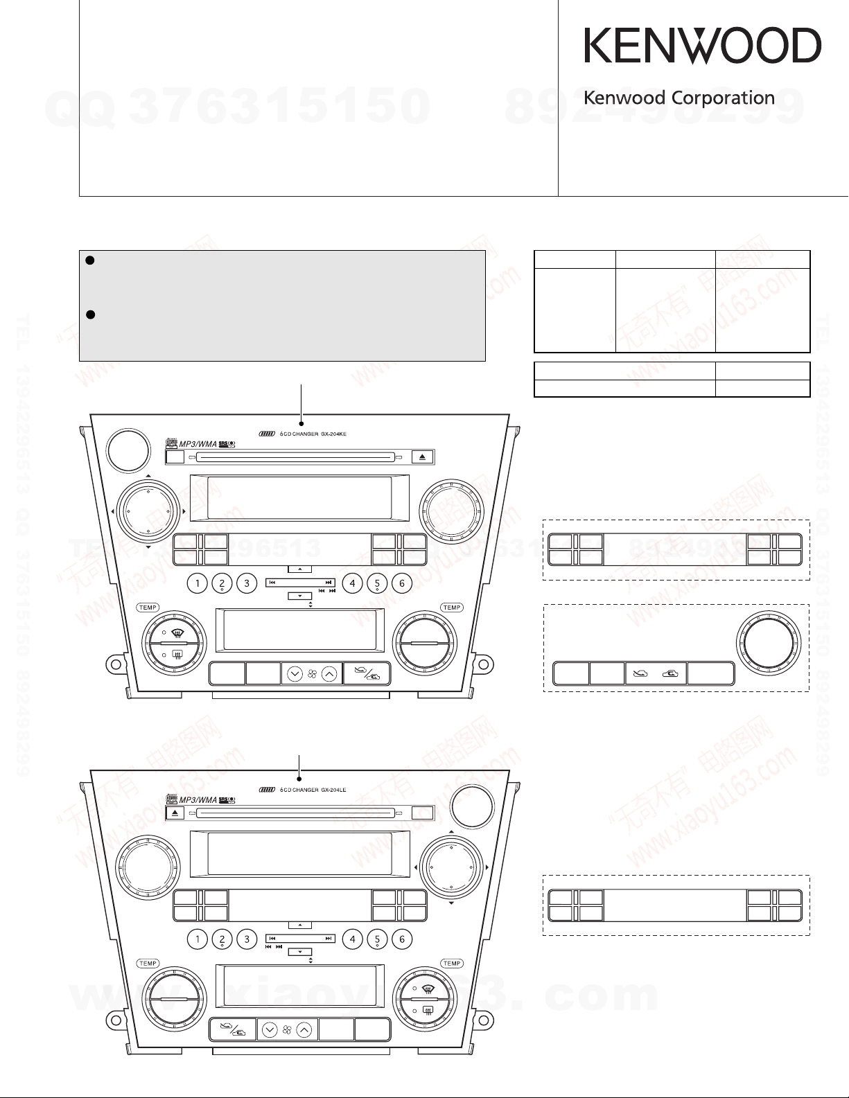
CD & HEATER CONTROL RECEIVER
GX204KEF2/KHF2
GX204LEF2/REF2
Q
Q
3
7
6
3
1
5
1
5
0
GX204SEF2
SERVICE MANUAL
SUBARU GENUINE
The knobs with numbers larger than 700 on exploded view are not
supplied for service parts because it is difficult to apply grease.
TEL 13942296513 QQ 376315150 892498299
Please change to panel assy when you need repair to the knob.
The 6CD mechanism has not supplied repair parts for each part
(for Optical Laser pickup, motor etc). If you need repair to the 6CD
mechanism please change to mechanism assy (D40-2214-15).
(Y33-2570-23): GX204KEF2
(Y33-2570-24): GX204KHF2
(Y33-2572-73): GX204REF2
RPT RDM
TONE BAL
GX204KEF2
AUX
TEL
13942296513
CD
FM
LOAD
AM
DISP PAGE
SCAN LOCAL
A/S
Panel assy
Q
PUSH ON/VOL
Q
3
7
4
2
9
8
© 2006-6 CREATED IN JAPAN
B53-0427-00 (N) 0
Model Model Name Parts No.
GX-204KE GX204KEF2 86201AG290
GX-204KH GX204KHF2 86201AG250
GX-204LE GX204LEF2 86201AG460
GX-204RE GX204REF2 86201AG350
GX-204SE GX204SEF2 86201AG550
DC cord for service E30-3801-15
ANT extension cord for service E30-6255-05
GX204REF2
RDS VOL ADJ
6
3
1
NEWS T.I
5
1
A/S
5
DISP
PAGE
0
9
8
9
2
8
4
2
9
8
9
2
9
REG LO/DX
RPT RDM
9
9
TONE BALSCAN
TEL 13942296513 QQ 376315150 892498299
GX204LEF2
PUSH ON/VOL
w
w
w
FRONT
TONE BAL
SCAN DISP
A/S PAGE
AUTO
.
OFF
MODE
A/C
Panel assy
TUNE/TRACK
xia
FOLDER
FOLDER
TUNE/TRACK
AUTO
OFF
(Y33-2570-12): GX204SEF2
(Y33-2572-74): GX204LEF2
LOAD
REG LO/DX
RPT RDM
NEWS T.I
RDS VOL ADJ
o
y
u
1
MODE
A/C
FRONT
CD
AUXAM
FM
6
3
MODE
GX204KHF2
GX204SEF2
TONE BAL
SCAN
A/S
.
c
LOCAL
o
A/C
m
AUTO
OFF
RPT RDM
DISP PAGE
GX204KEF2/KHF2/LEF2
GX204REF2/SEF2
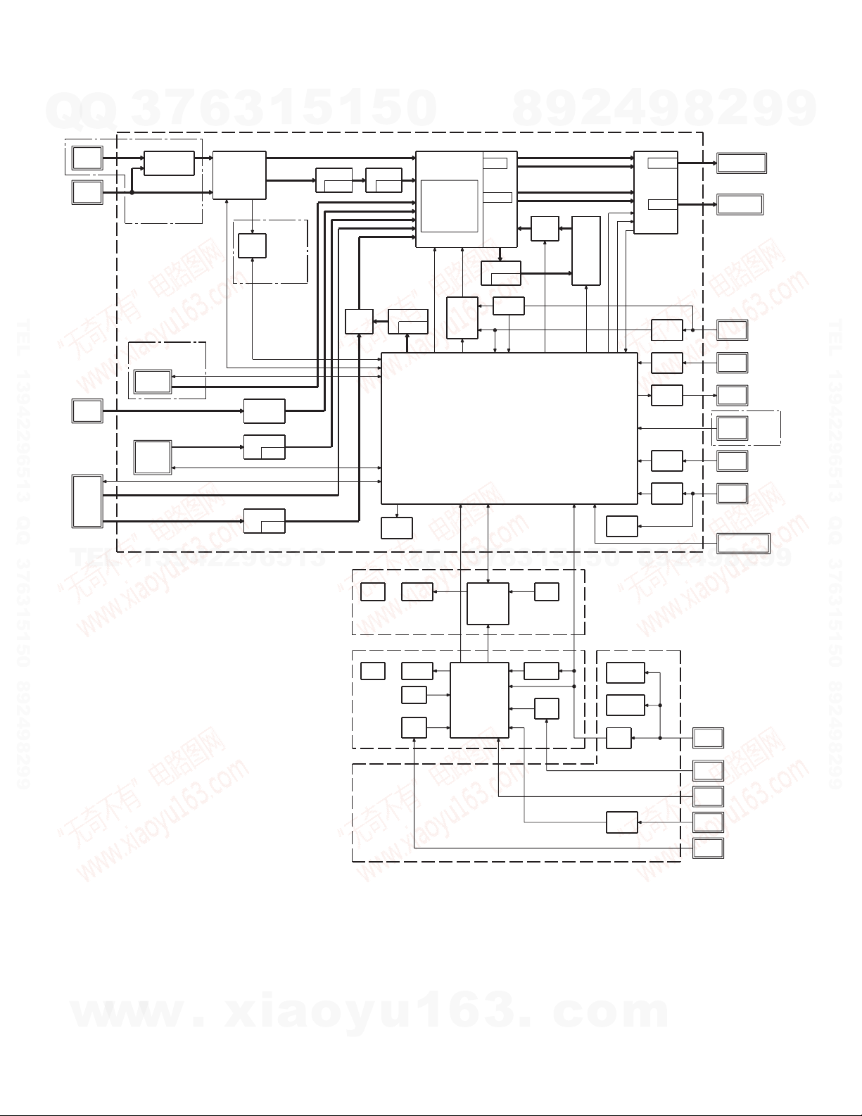
BLOCK DIAGRAM
Q
Q
SUB
ANT
MAIN
ANT
3
(X14-967)
IC121 A1
DIVERSITY
USED
(0-00) (0-21)
6
FM/AM
FRONT-END
7
TEL 13942296513 QQ 376315150 892498299
USED
(0-00)
MD
0.8Vrms
MECHA
AUX
EXT
UNIT
TEL
AUX 1.4Vrms(MAX)
0.8Vrms
6CD
MECHA
EXT CH 1.3Vrms
NAVI 1.2Vrms
13942296513
3
RDS
IC551
IC201
ISO+LPF
IC222
1
FM
270mVrms
AM
215mVrms
IC141
USED
(2-71) (2-72)
ISO
0.0dB
ISO
0.0dB
5
N/C LPF
-3.8dB -4.5dB
1
MIX
(X34-401)
5
LED
0
IC221
E VOL
FM MPX
7BAND EQ
FM : -0.3dB
AM : +15.6dB
CD : +6.6dB
MD : +6.6dB
EXT CH :+2.6dB
AUX : +2.6dB
NAVI : -20.0dB
(VOL. MAX)
IC751 IC802
MUTE
LOGIC
BEEP
Q
VFD KEY
Q
MUTE
3
IC501
7
PANEL
u-COM
IC801
DC/DC
AVR
Q602
ATT
-20.0dB
0.0dB
FAD
BAL
-30.0dB
ATT
-12.7dB
RESET
BU DET
SYSTEM
u-COM
6
8
FRONT
REAR
RESET
3
MUTE
1
9
SRS-MUTE
5
IC251
1
SRSWOW
2
5
4
P-MUTE
Q692
LED
AVR
0
STANDBY
DIAGNOSTIC
9
IC401
+26.0dB
4ch
POEWR
AMP
+26.0dB
8
Q721
BU
DET
Q711
ACC
DET
Q352
ANT
CONT
Q806
ILLDET
Q805
ILL+
DET
9
8
2
4
2
9
FRONT SP
REAR SP
BU
ACC
P ANT
TEL
MUTE
ILL-
ILL+
SATELLITE
2
8
9
USED
(2-71)
(2-72)
9
9
TEL 13942296513 QQ 376315150 892498299
9
w
w
w
.
xia
o
(X34-405)
LED
(X00-410)
y
u
Q5
VFD
KEY
ILLDET
1
IC1
6
HTR-C
u-COM
3
.
IC2
RESET
Q7
ACC
DET
c
Q73
Q51
Q41
Q31
o
DC/DC
(UP)
DC/DC
(DOWN)
IGN
AVR
LED
AVR
m
IGN
ACC
UART
ILL+
ILL-
2
GX204KEF2/KHF2/LEF2
GX204REF2/SEF2
COMPONENTS DESCRIPTION
7
Q
Q
● POWER SUPPLY UNIT (X00-4100-00)
TEL 13942296513 QQ 376315150 892498299
● SYNTHESIZER UNIT (X14-967x-xx)
TEL
w
3
Ref. No. Application / Function Operation / Condition / Compatibility
Q31 Power supply for illumination LED Stabilizes illumination LED voltage (8.1V) and supplies required current.
Q41 Power supply for IGN5V Stabilizes IGN5V voltage (5.1V) and supplies required current.
Q51 Step-down DC/DC switching Converts voltage by switching.
Q53 Power supply for VFD filament Stabilizes VFD filament voltage (2.9V) and supplies required current.
Q54 Power supply for VFD filament Configures Darlington with Q53.
Q55 Power supply SW for VFD filament
Q61 Power supply for DC/DC converter Stabilizes DC/DC input voltage (9.5V) and supplies required current.
Q62 Power supply for DC/DC converter Configures Darlington with Q61.
Q71 Step-up DC/DC timing control Controls step-up DC/DC switching.
Q72 Step-up DC/DC switching Converts voltage by switching.
Q73 Step-up DC/DC output voltage switching Detects output voltage and controls switching timing.
Ref. No. Application / Function Operation / Condition / Compatibility
IC121 FM diver IC FM diver
IC141 RDS demodulation IC Demodulates RDS
IC143 Amplifier for filters RDS noise amplifier
IC171 AM noise canceller IC AM noise canceller
IC201 Amplifier for isolation 6CD isolation
IC221 Audio control IC BASS/MID/TRE, MPX, mute, electric volume
IC251 Audio control IC WOW control
IC301 Amplifier for midpoint potential output Outputs midpoint potential (6.8V, 4V).
IC391 Servo 8V power supply Servo 8V power supply driver
IC401 Power amplifier IC Power amplifier with 4CH
IC521 I2C bus IC Sie-BUS communication
IC551 Isolation IC AUX isolation
IC651 D3.3V power supply Power supply driver for 6CD mechanism Bu3.3V.
IC671 D5V power supply Power supply driver for 6CD/MD mechanism DSP5V.
IC681 C3.3V power supply Power supply driver for 6CD mechanism DSP3.3V.
IC751 Mute logic IC For hardware mute.
IC801 System µ-com System control
IC802 Reset IC Detects system reset.
IC952 Level shift IC Level-shifting (3.3V → 5V)
Q101 IF count detection Outputs Lo when IF count is detected.
Q102 AM power supply switch Outputs 8V when AM.
Q103 RDS data buffer Outputs RDS buffer
Q121 Diver switch Detects diver ON/OFF.
Q122 FM S meter switch Outputs S meter voltage when FM.
Q123 Diver IC power supply switch Outputs Hi when AM_OFF.
Q124 Diver IC power supply switch Outputs Lo when AM.
13942296513
w
w
6
.
xia
3
1
5
o
1
5
0
ON/OFF filament power supply by µ-com FL_FIL_ON signal. (ON with µ-com L output)
7
3
Q
Q
y
u
1
6
3
6
8
3
.
9
1
1
5
c
2
5
o
4
0
m
9
8
9
8
2
4
2
9
8
9
2
9
9
TEL 13942296513 QQ 376315150 892498299
9
3
GX204KEF2/KHF2/LEF2
GX204REF2/SEF2
COMPONENTS DESCRIPTION
7
Q
Q
Ref. No. Application / Function Operation / Condition / Compatibility
Q141 Noise amplifier Switches constant when noise is detected.
Q142 Noise amplifier Noise detection output buffer
Q143 Noise amplifier Switches constant when noise is detected.
Q221 Mute switch Mute within the electric volume.
Q222 Switch within the electric volume For switching FM/AM within the electric volume.
Q223,224
Q301 Midpoint circuit discharge switch Discharges the midpoint voltage when ACC_OFF.
TEL 13942296513 QQ 376315150 892498299
Q303 Midpoint circuit discharge switch Detects P-ON for discharging midpoint voltage when ACC_OFF.
Q304 Midpoint circuit discharge switch Discharges the midpoint voltage when ACC_OFF.
Q331 Servo 8V power supply switch Detects P-ON for servo 8V.
Q332 Servo 8V power supply switch Driver for servo 8V.
Q333 Servo 8V power supply switch Darlington for servo 8V.
Q351 Power supply switch for P-ANT Detects Acc for P-ANT.
Q352 Power supply switch for P-ANT Driver for P-ANT.
Q353 Power supply switch for P-ANT Darlington for P-ANT.
Q354 P-ANT short detection switch Detects P-ANT short.
Q371~373
Q391 Audio8V power supply switch Detects P-ON for Audio8V.
Q392 Audio8V power supply switch Driver for Audio8V.
TEL
Q521 Current buffer for SYS_ON Outputs Hi when SYS_ON is Lo.
Q522 Current buffer for SYS_OFF Outputs Hi when SYS_OFF is Lo.
Q523 Bus_OFF detection Inputs Hi when Sie-Bus system is OFF.
Q524 Bus_ON detection Inputs Hi when Sie-Bus system is ON.
Q525 Hardware reset switch Outputs Lo when hardware reset is detected.
Q526 Sie-Bus reset detection switch Outputs Hi when Sie-Bus reset is detected.
Q551 AUX detection switch Outputs Hi when AUX is detected.
Q601 Power supply switch for DC/DC45V Detects DC/DC switch.
Q602 Power supply switch for DC/DC45V Driver for DC/DC45V power supply.
Q603 Power supply switch for DC/DC45V Darlington for DC/DC45V power supply.
Q604~606
Q621 Switch for filament power supply Detects DC/DC switch.
Q622 Switch for filament power supply Driver for filament power supply.
Q623 Switch for filament power supply Darlington for filament power supply.
Q624 Power supply switch for DC/DC45V Detects DC/DC switch.
Q625 Power supply switch for DC/DC45V Driver for DC/DC45V power supply.
Q626 Switch for filament power supply Driver for filament power supply.
Q651 Switch for Bu5V power supply Driver for Bu5V power supply.
Q652 Switch for Bu5V power supply Darlington for Bu5V power supply.
Q671 Switch for D5V power supply Detects P-ON for D5V power supply.
Q672 Switch for D5V power supply Outputs Lo when AM.
w
Q673 Switch for D5V power supply Supplies D5V power supply when AM.
3
Mute switch SRS-WOW mute
DC offset detection switch Detects DC offset voltage.
13942296513
Switching for DC/DC45V power supply For DC/DC45V power supply.
w
w
6
.
xia
3
1
5
o
1
y
5
u
0
Q
Q
1
3
6
7
3
6
8
3
.
9
1
1
5
c
2
5
o
4
0
m
9
8
9
8
2
4
2
9
8
9
2
9
9
TEL 13942296513 QQ 376315150 892498299
9
4
GX204KEF2/KHF2/LEF2
GX204REF2/SEF2
COMPONENTS DESCRIPTION
7
Q
Q
TEL 13942296513 QQ 376315150 892498299
3
Ref. No. Application / Function Operation / Condition / Compatibility
Q674 Switch for D5V power supply Outputs Lo when AM.
Q691 Switch for ILL power supply Detects ILL+ for ILL power supply.
Q692 Switch for ILL power supply Driver for ILL power supply.
Q693 Switch for ILL power supply Darlington for ILL power supply.
Q694 Switch for ILL power supply Driver for ILL power supply.
Q711 Acc detection switch Outputs Lo when Acc_ON.
Q721 Bu detection switch Outputs Lo when Bu_ON.
Q722 Over-voltage detection switch Detects Bu over-voltage.
Q801 P-ON5V power supply switch Driver for P-ON5V power supply.
Q802 Sie-BUS mute output Outputs Hi when mute ON.
Q803 Switch for ILL- level shift Converts ILL- (13.2V → 5V).
Q804 ILL+ detection switch Detects ILL+.
Q805 Switch for ILL- level shift Converts ILL- (13.2V → 5V).
Q806 ILL- detection switch Detects ILL-.
Q807 Switch for SRS-WOW mute Outputs Hi when mute ON.
Q808 Switch for level-shift Level-shifting (5V → 3.3V)
Q809 Switch for 6CD mute Outputs Lo when mute is requested from 6CD mechanism.
Q810 Switch for level-shift Level-shifting (5V → 3.3V)
6
3
1
5
1
5
0
8
9
2
4
9
8
2
9
9
TEL 13942296513 QQ 376315150 892498299
TEL
● SWITCH UNIT (X34-401x-xx) (AUDIO)
Ref. No. Application / Function Operation / Condition / Compatibility
IC501 Audio panel µ-com Fluorescent indicator tube, Key matrix control
Q501 For cut-off bias setting PNP transistor
Q502
● SWITCH UNIT (X34-405x-xx) (H/C)
Ref. No. Application / Function Operation / Condition / Compatibility
IC1 Heater control panel µ-com
IC2 Reset IC When µ-com power supply voltage is 4.2V or less, reset the µ-com.
IC3 E2PROM Stores ROM correction data
Q1 UART+ Interface for UART communication (transmission) with vehicle.
Q2 UART- Interface for UART communication (reception) with vehicle.
Q3 Power switch ON/OFF VH voltage application of VFD.
Q4 Power switch ON/OFF Q3 by taking IGN_DET and DD_ON logic.
Q5 ILL- signal detection Transmit ILL- signal from vehicle to µ-com and Q13.
Q7 ACC voltage detection Detects ACC voltage from the vehicle.
Q11 Illumination LED control switch Controls ON/OFF and the luminance of LED for front DEF.
Q12 Illumination LED control switch Controls ON/OFF and the luminance of LED for rear DEF.
w
Q13 Illumination LED control switch Controls ON/OFF and the luminance of LED for key illumination.
13942296513
For fluorescent indicator tube
power switch PNP transistor
w
w
.
xia
o
8
0
5
1
5
1
3
6
7
3
Q
Q
When displaying with fluorescent indicator tube, filament (-) terminal is approximately 3.0V.
Base voltage L: ON, H: OFF
Vehicle ECU, communication with audio-side µ-com, key import,
display data transmission, illumination control
y
u
1
6
3
.
c
o
m
9
2
4
9
8
2
9
9
5
GX204KEF2/KHF2/LEF2
GX204REF2/SEF2
MICROCOMPUTER’S TERMINAL DESCRIPTION
7
Q
Q
● SYSTEM MICROCOMPUTER: 703037HYGM04A (X14: IC801)
Pin No. Pin Name I/O Application
1 SP_DATA_S O System µ-com → Panel µ-com data output UART 19200bps
2 TUN_SDA I/O F/E I2C data input/output terminal
3NCONot used Output L fixed
4 TUN_SCL I/O F/E I2C clock output terminal
5NCONot used Output L fixed
TEL 13942296513 QQ 376315150 892498299
6 SH_DATA_H I HTR-C µ-com → System µ-com data output UART 4800bps
7 SH_DATA_S O System µ-com → HTR-C µ-com data output UART 4800bps
8 CDX_MTS O 6CD communication request output L: Communication request to 6CD, H: Other
9 EVDD 5V potential
10 EVSS GND potential
11 BEEP O BEEP output 3kHz BEEP output (pulse), L: Not active
12 AM_BYPS O D5V bypass power ON in AM H: AM, L: Other
13 TEL_MUTE I TEL_MUTE request input (E type only) L: TEL_MUTE request
13 NC O Not used (In other than E type) Output L fixed
14 ILL_DET+ I ILL+ detection ILL ON: L
15 ILL_DET- I ILL- detection (pulse input)
TEL
16 VOL_SDA I/O E_VOL I2C data input/output
17 VOL_SCL I/O E_VOL I2C clock output
18~20 NC O Not used Output L fixed
21 IC/VPP (FLASH writing) (FLASH writing)
22~25 NC O Not used Output L fixed
26 BUS_DI I Sie-BUS data IN BUS data input
27 BUS_DO O Sie-BUS data OUT BUS data output
28 CDX_RST O 6CD reset L: Reset, H: Other
29 PON_5V O AVR control (Audio, MECHA) L: Power ON, H: OFF (stable time 400m)
30 ON_REQ I Sie-BUS ON request L: System ON request
31 SYS_ON O Sie-BUS ON output L: System ON
32 SYS_OFF O Sie-BUS OFF output L: System OFF
33 BUS_STBY O BUS_IC standby control H: System ON
34 RESET System reset input L: Reset, Reset voltage: 4.2V
35,36 XT1, XT2 Sub system clock oscillator terminal Not used
37 REGC
38,39 X2, X1 Main system clock oscillator terminal 12.582MHz
40 VSS - GND potential
41 VDD - 5V potential
42 CLKOUT Not used
w
43 HARD_RESET O Hardware reset output H: Reset, L: Other
3
13942296513
w
w
6
.
xia
3
1
5
o
1
y
5
u
0
Q
Q
1
3
6
Truth V alue
7
3
Table
6
4
2
9
8
Processing Operation Description
H: ON, L: OFF, pulse input
Adjusts luminance with duty ratio.
1
3
.
1
5
c
5
o
0
m
8
9
9
8
2
4
2
9
8
9
2
9
9
TEL 13942296513 QQ 376315150 892498299
9
6
GX204KEF2/KHF2/LEF2
GX204REF2/SEF2
MICROCOMPUTER’S TERMINAL DESCRIPTION
7
Q
Q
Pin No. Pin Name I/O Application
TEL 13942296513 QQ 376315150 892498299
TEL
w
3
44 P_STBY O P-AMP standby control L: STAND-BY, H: Other
45 P_MUTE O P-AMP mute control L: MUTE, H: Other
46 P_SVR O For P-AMP discharge L: Normally, H: Discharging
47 SRS_MODE1 O SRS-WOW mode selection 1 e SRS_FOCUS ON: H
48 SRS_MODE2 O SRS-WOW mode selection 2 e SRS_TruBass ON: H
49 SRS_MODE3 O SRS-WOW mode selection 3 e SRS_3D-Stereo ON: H
50 DC/DC_PRO I Filament power supply output short detection
51 ANT_CON O ANT AMP power supply control H: ACC ON, L: Other
52 TUN_DIVER O FM diversity antenna control (M type only)
52 NC O Not used (In other than M type) Output H (OFF) fixed (After TUNER start up)
53 PON_AM O AM power supply control H: AM, L: Other
54 TUN_IFC I F/E IFC OUT input terminal H: Station found, L: Station not found
55 DC/DC_CON O DC/DC power supply control DC/DC ON: H
56 VOL_MUTE O E_VOL MUTE output MUTE ON with High (IC terminal=Low)
57 SRS_MUTE O MUTE output for SRS SRS_MUTE ON: L
58 BVDD 5V potential
59 BVSS GND potential
60 IGN_DET_CON O IGN detection operation check H: IGN detected, L: Other
61,62 NC O Not used Not used
63~65 TYPE1~TYPE3 I Destination setting terminal 1~3 q Refer to the truth value table
66 AUX_DET I AUX detection
67 TUN_AFS O
67 NC O Not used (In other than E type) Output H (other) fixed (while TUNER on)
68 CDX_MUTE I 6CD mute request H: Mute request from 6CD, L: Other
69 CDX_DDCNT I 6CD servo power supply ON request H: ON request from 6CD, L: Other
70 CDX_STM I 6CD communication request input L: Communication request to 6CD, H: Other
71 CDX_ACC O 6CD ACC H: 6CD on, L: Other
72,73 TYPE4, TYPE5 I Vehicle yearly revision setting terminal 1, 2 q L: A06 audio
74 AVDD 5V potential
75 AVSS GND potential
76 AVREF A/D port reference voltage input
77 RDS_QUAL I RDS quality (E type only) RDS quality
77 NC I Not used (In other than E type) Input Hi-Z
78 RDS_DATA I RDS data (E type only) RDS data input
78 NC I Not used (In other than E type) Input Hi-Z
13942296513
w
w
6
.
xia
1
5
1
y
5
u
3
Constant switching when noise detected
(E type only)
o
0
Q
Q
1
3
6
7
3
8
Truth V alue
Table
3
6
.
4
2
9
Processing Operation Description
H: Normally, With L 100ms x 10_1s, set DC/
DC_CON to OFF and write the log into EEPROM.
H (OFF): In test mode or L (ON): Switch (initial: H)
L (ON): In normal mode
0
5
1
5
1
H: AUX detected
(Can be detected after PON stabilized)
L: In AF search, H: Other
c
o
9
9
8
m
2
8
4
2
9
8
9
2
9
9
TEL 13942296513 QQ 376315150 892498299
9
7
GX204KEF2/KHF2/LEF2
GX204REF2/SEF2
MICROCOMPUTER’S TERMINAL DESCRIPTION
7
Q
Q
Pin No. Pin Name I/O Application
79 REMOCON I Vehicle satellite switch input r Resistance dividing vehicle remote control
80 NC I Not used Not used
81 DIAG I Terminal for test mode L: Test mode, H: Normal
82 P_DCERR_DET I DC offset detection
83 NC I Not used Not used
84 IGN_DET I IGN detection H: IGN ON, L: IGN OFF
TEL 13942296513 QQ 376315150 892498299
85 RDS_NOISE I FM noise detection (E type only)
85 NC I Not used (In other than E type) Input Hi-Z
86 TUN_SMETER I S meter voltage input
87,88 NC I Not used Not used
89 SP_REQ_S O System µ-com → Panel µ-com request H: ON, L: OFF
90 SP_REQ_P I Panel µ-com → System µ-com request H: ON request
91 ACC_DET I ACC detection L: ACC ON, H: ACC OFF, Detected voltage: 8.5V
92 OFF_REQ I Sie-BUS OFF request L: System OFF request
93 BU_DET I BU detection
94 SP_RST O Reset to panel µ-com
TEL
95 SP_BKUP O Voltage down detection output to panel µ-com L: Voltage down, H: Normal
96 RDS_CLK I RDS clock (E type only) RDS clock
96 NC O Not used (In other than E type) Output L fixed
97 CDX_DSTM I 6CD data input Communication speed 250kHz
97 FLASH_SI I Flash writing data input
98 CDX_DMTS O 6CD data output Communication speed 250kHz
98 FLASH_SO O Flash writing data output
99 CDX_SCK I 6CD clock input Communication speed 250kHz
99 FLASH_CLK I Flash writing clock input
100 SP_DATA_P I Panel µ-com → System µ-com data output UART 19200bps
3
13942296513
6
3
1
5
1
5
0
Q
Q
Truth V alue
7
3
Table
6
4
2
9
8
Processing Operation Description
At 1.6V or higher and 100ms x 20=2s Offset detection
L: BU ON, H: BU OFF (at momentary power down),
Detected voltage: 8.5V
H: Normal, L: Reset, Immediately after reset,
when communication reset occurs, RESET.
5
1
3
1
5
0
9
8
9
2
8
4
2
9
8
2
9
9
9
TEL 13942296513 QQ 376315150 892498299
9
Truth Value T able
q Point of destination setting terminal
TYPE1 (63pin) TYPE2 (64pin) TYPE3 (65pin) TYPE4 (72pin) TYPE5 (73pin) Destination
LLLLLGX204JE,JH
LLHLLGX204KE,KH
LHLLLGX204RE
LHHLL HLL LL HLHLLGX204SE
w
w
w
HHLLLGX204LE
HHHL L -
8
.
xia
o
y
u
1
6
3
.
c
o
m
GX204KEF2/KHF2/LEF2
GX204REF2/SEF2
MICROCOMPUTER’S TERMINAL DESCRIPTION
7
Q
Q
e SRS mode switching
SRS_MODE1 SRS_MODE2 SRS_MODE3
TEL 13942296513 QQ 376315150 892498299
r REMOCON voltage table
3
47pin 48pin 49pin
LLLOFF
LLH3D-Stereo
LHLTruBass
HLLFOCUS
HHHWOW
6
MUTE
operation
3
1
VOL+
operation
5
1
Mode
VOL-
operation
5
0
MODE
operation
SEEK
operation
8
9
SEEK
operation
2
4
No
operation
9
8
2
9
9
TEL 13942296513 QQ 376315150 892498299
TEL
0V 5V
● PANEL (AUDIO) MICROCOMPUTER: MB90562A-419E (X34-401: IC501)
Pin No. Pin Name I/O Application Processing Operation Description
1NCONot used Output L fixed
2~5 KR3~KR6 I Key scan pulse input terminal
6~9 KS1~KS4 O Key scan pulse output terminal
10,11 NC O Not used Output L fixed
12 AVCC Power supply input for A/D converter VCC
13 AVR REF voltage input for A/D converter SW_5V potential
14 AVSS GND connection for A/D converter GND potential
15 SP_DATA_S I Data from system µ-com → panel µ-com output Communication speed 19200bps, 50ms interval
16 SP_DATA_P O Data from panel µ-com → system µ-com output Communication speed 19200bps, 20ms interval
17 SP_REQ_P O Request from panel µ-com → system µ-com
18 SP_BKUP I
19 MD0 I For FLASH ROM writing Hi: Normal mode, Lo: FLASH writing mode
20 SP_RST I Reset input from system µ-com Reset request from system µ-com Lo
w
21 MD1 I For FLASH ROM writing Hi: Normal and FLASH writing mode, Lo: Not set-up
13942296513
w
w
1.18 1.40 1.65 1.95 2.21 2.56 2.71 3.11 3.26 3.70 3.78 4.25 4.46 4.95
Inputs voltage reduction from system µ-com detection
.
xia
o
y
u
Q
Q
1
6
3
6
7
3
5
1
3
L: Momentary power down detected, H: Normal
.
c
1
0
5
o
9
8
m
2
4
9
8
2
9
9
9
GX204KEF2/KHF2/LEF2
GX204REF2/SEF2
MICROCOMPUTER’S TERMINAL DESCRIPTION
7
Q
Q
Pin No. Pin Name I/O Application Processing Operation Description
22 MD2 I For FLASH ROM writing Hi: FLASH writing mode, Lo: Normal mode
23 X0 µ-com clock oscillator 4.0MHz (ceramic oscillator)
24 X1 µ-com clock oscillator 4.0MHz (ceramic oscillator)
25 VSS1 Power supply GND GND potential
26 P00 I FLASH writing method setting
27 P01 I FLASH writing method setting
28 NC O Not used Output L fixed
TEL 13942296513 QQ 376315150 892498299
29 SW_5V O SW series 5V power supply Lo: ON, Hi: OFF
30 POWER I POWER Lo: ON, Hi: OFF
31 ENC_DW I Rotary encoder SW (B phase wave form) Port monitoring of pulse with 1ms cycle timer
32 ENC_UP I Rotary encoder SW (A phase wave form) Port monitoring of pulse with 1ms cycle timer
33 NC O Not used Output L fixed
34 SP_REQ_S I Request from system µ-com → panel µ-com Hi: ON, Lo: OFF
35~38 NC O Not used Output L fixed
39 KR7 I Key scan pulse input terminal
40,41 KR2, KR1 I Key scan pulse input terminal
42 NC O Not used Output L fixed
43 FL_BLK O
TEL
44~47 NC O Not used Output L fixed
48 SDA I/O Serial data for E2PROM Input/output to E2PROM
49 SCL O Serial clock for E2PROM Output to E2PROM
50 VSS2 Power supply GND GND potential
51 NC O Not used Output L fixed
52 TYPE1 I Destination setting H: Left-hand steering, L: Right-hand steering
53 NC O Not used Output L fixed
54 BRIGHT I Change logic when brightness changes Operation: When “H”, bright data is finalized at UART
55 HTR I For determining bright terminal valid/invalid Operation: When “H”, bright terminal is valid
56 NC O Not used Output L fixed
57 VCC Power supply input Bu5V potential
58 C - Voltage stabilizing process terminal 0.1µF condenser connection
59 NC O Not used Output L fixed
60 FL_SO O FL data output terminal
61 FL_CLK O FL clock output terminal
62 FL_LAT O FL data latch control terminal
63,64 NC O Not used Output L fixed
3
13942296513
6
1
5
1
3
FL data blanking output terminal Adjusts luminance with duty ratio.
(FL tube luminance adjustment) Hi: OFF, Lo: ON
5
0
Q
Q
3
7
6
8
3
9
1
5
1
2
5
4
0
9
8
9
8
2
4
2
9
8
9
2
9
9
TEL 13942296513 QQ 376315150 892498299
9
10
w
w
w
.
xia
o
y
u
1
6
3
.
c
o
m
GX204KEF2/KHF2/LEF2
GX204REF2/SEF2
MICROCOMPUTER’S TERMINAL DESCRIPTION
7
Q
Q
● PANEL (HEATER CONTROL) MICROCOMPUTER: MB89537A1010E (X34-405: IC1)
Pin No. Pin Name I/O Application Processing Operation Description
TEL 13942296513 QQ 376315150 892498299
TEL
w
3
1 SH_DATA_H O HTR-C µ-com → System µ-com data output Communication speed: 4800bps
2 SH_DATA_S I System µ-com → HTR-C µ-com data output Communication speed: 4800bps
3 MOD2 I
4 TYPE1 I Destination setting
5 TYPE2 I Destination setting 4V or higher: SINGLE, 2V or lower: DUAL
6 TYPE3 I Destination setting 4V or higher: 15~29°C, 2V or lower: 18~32°C
7~11 NC O Not used Output L fixed
12 AVCC - A/D converter power supply terminal
13 AVR - A/D converter standard voltage input terminal
14 AVSS - A/D converter power supply terminal
15 NC I Not used Input fixed
16 ACC_DET I ACC detection L: ACC ON, H: ACC OFF, Detected voltage: 8.9V
17~19 NC I Not used Input fixed
20 RST - Reset input terminal L: Reset
21 MD0 - Input terminal for memory access mode setting H: When writing FLASH µ-com, L: Other
22 MD1 - Input terminal for memory access mode setting H: When writing FLASH µ-com, L: Other
23 X0 - Oscillator connection terminal 12.288MHz
24 X1 - Oscillator connection terminal 12.288MHz
25 VSS - Power supply terminal
26,27 NC O Not used Output L fixed
28 HTR O Terminal for determining bright terminal valid/invalid ON, and at the point when the air-conditioner data is
29 BRIGHT O Output terminal for bright information from vehicle
30 FLASH_MOD I Input terminal for FLASH writing setting Always L input
31 R-DEF O Rear DEF indicator control terminal
31 P22 I Input terminal for FLASH writing setting H: When writing FLASH µ-com
32 F-DEF O Front DEF indicator control terminal
33 KEY_DET O Panel key operation check
34 ENC_L3 I Rotary encoder (left) pulse count input terminal
35 ENC_L2 I Rotary encoder (left) pulse count input terminal
36 ENC_L1 I Rotary encoder (left) pulse count input terminal
37 ENC_R3 I Rotary encoder (right) pulse count input terminal
13942296513
w
w
6
.
xia
1
5
1
y
5
u
0
Q
1
3
Memory access mode setting input terminal
for when FLASH
o
Q
3
6
7
3
4
2
9
8
Always L input
4V or higher: Left-hand steering,
2V or lower: Right-hand steering
0
5
1
5
1
3
6
Start operating when the heater control µ-com IGN
finalized at UART, ON. H: ON, L: OFF
At the point when the bright data is finalized at
UART, ON. H: ON, L: OFF
LED luminance control by PWM control,
2 steps brightness, 4ms cycle PWM
LED luminance control by PWM control,
2 steps brightness, 4ms cycle PWM
When key or encoder is input, “H” is output at 100ms
(in test mode only)
.
c
o
9
9
8
m
2
8
4
2
9
8
9
2
9
9
TEL 13942296513 QQ 376315150 892498299
9
11
GX204KEF2/KHF2/LEF2
GX204REF2/SEF2
MICROCOMPUTER’S TERMINAL DESCRIPTION
7
Q
Q
Pin No. Pin Name I/O Application Processing Operation Description
38 ENC_R2 I Rotary encoder (right) pulse count input terminal
39 ENC_R1 I Rotary encoder (right) pulse count input terminal
40,41 KR3, KR2 I Key scan pulse input terminal
41 P10 I Input terminal for FLASH writing setting H: When writing FLASH µ-com
42,43 KR1, KR0 I Key scan pulse input terminal
44~46 KS2~KS0 I/O Key scan pulse output terminal
47 NC O Not used Output L fixed
TEL 13942296513 QQ 376315150 892498299
48 SCL I/O Outputs clock to E2PROM
49 SDA I/O Outputs serial data to E2PROM
50
51,52 NC O Not used Output L fixed
53 HTR_ECU_TX O HTR-C µ-com → HTR-C ECU 4800bps
54 HTR_ECU_RX I HTR-C ECU → HTR-C µ-com 4800bps
55 FL_BLK O FL display tube blank control terminal
56 ILL_DET- I ILL- detection (pulse input)
57 VCC - Power supply terminal
58 ILL_DET+ I ILL+ detection ILL ON: H
TEL
59 FL_FIL_ON I/O FL tube filament power supply control SW Hi-Z: OFF, L: ON. Timing is the same as DC_DC_ON
60 FL_LAT O FL data latch control terminal Execute output OFF count while not displayed.
61 FL_CLK O FL clock output terminal Sync clock output while VFD serial communication
61 FLASH_CLK O
62 FL_SO O FL data output terminal Display data transmission to VFD
62 FLASH_SO O
63 FLASH_SI I
63 NC O For mask µ-com, Not used Output L fixed
64 DC_DC_ON I/O FL tube power supply control terminal Hi-Z: ON, L: OFF
3
FLASH: [C]
MASK: [NC] in MASK products, NC (no connection)
13942296513
6
-
1
5
1
3
In FLASH products, connect 0.1µF, and
Clock output to ROM writer Clock transmission to ROM writer
(For FLASH µ-com only) (communication speed is dependent on ROM writer)
Data output to ROM writer Data transmission to ROM writer
(For FLASH µ-com only) (communication speed is dependent on ROM writer)
Data input from ROM writer Data reception from ROM writer
(For FLASH µ-com only) (communication speed is dependent on ROM writer)
5
0
Q
Q
3
7
4
2
9
8
FL display tube luminance control by PWM control
H: Blank (display OFF)
0
5
1
5
1
3
6
9
8
9
2
8
4
2
9
8
9
2
9
9
TEL 13942296513 QQ 376315150 892498299
9
12
w
w
w
.
xia
o
y
u
1
6
3
.
c
o
m
EDCBA
GX204KEF2/KHF2/LEF2
GX204REF2/SEF2
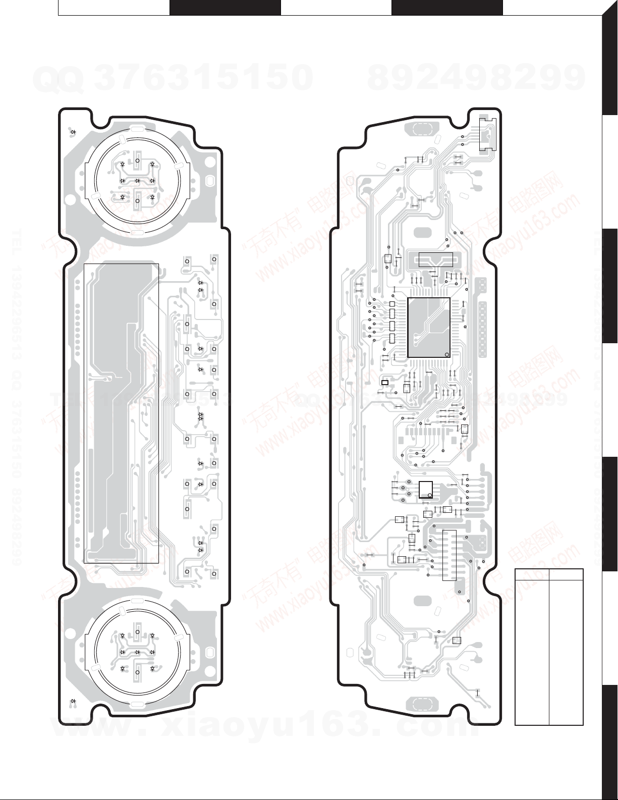
PC BOARD
(COMPONENT SIDE VIEW) (FOIL SIDE VIEW)
7
Q
Q
SWITCH UNIT
X34-405x-xx (J74-1712-12)
3
D11
D19
D5
S13
D29
S7
6
D28
D27D18
D7
TEL 13942296513 QQ 376315150 892498299
111122022 3
TEL
w
Refer to the schematic diagram for the values of resistors and capacitors.
13942296513
ED1
S16
D24
D16
D17
D26
D25
D6
D4
S23
D10
w
w
.
xia
3
S9
S18
S3
S14
S5
S21
S10
S1
1
S24
D9
D21
D13
D22
D23
D20
D30
D12
D31
D8
S17
5
S19
S8
S15
S6
S2
S12
S4
S20
S11
S22
o
1
y
5
u
0
Q
Q
1
SWITCH UNIT
X34-405x-xx (J74-1712-12)
R92
R98
7
3
6
3
TP46
TP48
TP50
TP52
TP54
6
TP30
8
Q12
TP45
TP47
TP49
TP51
TP53
TP55
TP56
R17
R15
IC2
12
R69
3
R102
R68
R70
R72
R91
.
TP59
BE
TP57
TP83
34
1
Q13
TP19
TP37
TP16
R1
9
TP44
R93
R113
C17
R112
R24
33 51
CP4
CP3
CP2
CP1
C4
R11
R13
TP61
E
B
Q1
5
R111
TP36
TP33
TP12
BE
Q5
R37
R25
E
B
Q2
R71
c
R86
R104
R62
32
52
R3
1
TP35
TP11
58
TP14
R97
R96
BE
R14
C3
R84
R76
R78
2
R87
R88
R82
C8
C9
R105
R101
IC1
C1
R4
R60
R6
5
R20
R23
R100
TP34
TP32
TP21
IC3
C12
BE
Q4
R10
R5
TP82
TP10
TP15
R2
TP22
R79
o
4
TP27
TP24
R90
R115
TP25
TP28
TP29
X1
R65
C13
TP5
R64
TP6
20
19
1
64
R107
R106
R44
R16
R9
R7
R8
R108
8
0
R18
R21
R27
R49
R29
TP31
R110
41
R99
C16
Q3
BE
R19
R22
R103
TP1
115
TP7
TP18
TP20
TP23
TP58
Q11
R89
BE
m
8
9
CN4
16
TP26
R59
C11
TP9
R54
C6
TP62
R12
2
9
TP84
TP85
TP86
Q7
BE
R51
R50
R109
TP39
TP40
TP41
TP42
TP43
TP38
C15
TP2
216
CN2
TP8
TP13
TP60
TP17
R114
2
8
9
4
X34-405x-xx
Ref. No. Address
9
9
9
2
IC1 3D
IC2 4C
IC3 5D
Q1 4D
Q2 5D
Q3 5D
Q4 5D
Q5 5D
Q7 4D
Q11 6D
Q12 3C
Q13 5C
1
9
2
TEL 13942296513 QQ 376315150 892498299
3
4
5
6
7
13
 Loading...