

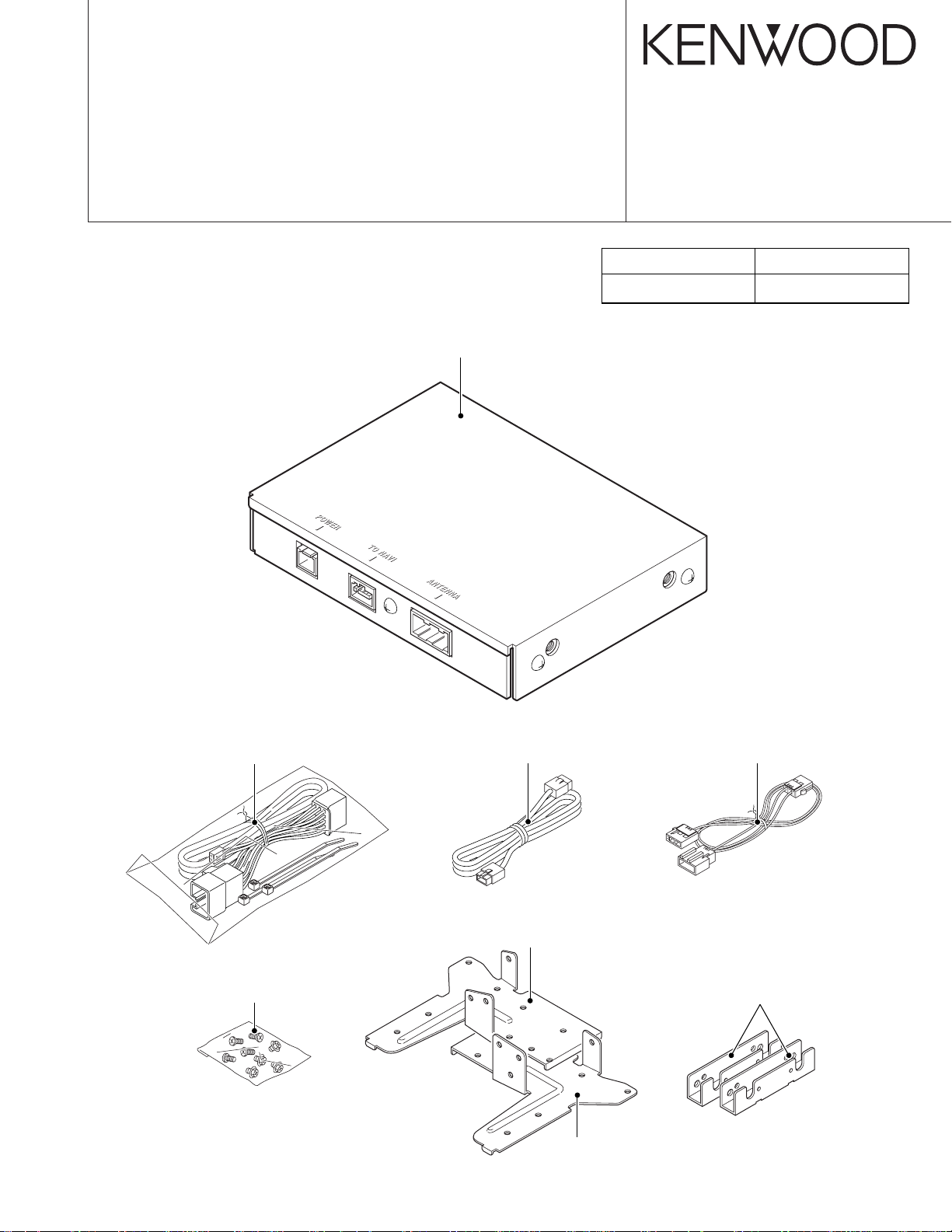
TRAFFIC MESSAGE CHANNEL RECEIVER
FNA- TM320
SERVICE MANUAL
© 2003-7 CREATED IN JAPAN
B53-0083-00 (N) 0
SUBARU GENUINE
MODEL PARTS No.
FNA-TM320 H001EAG100
Metallic cabinet
(A01-2822-02)
DC cord assy
(E30-6259-05)
Screw set
(N99-1746-05)
Cord with connector
(E30-6251-15)
Mounting hardware (R)
(J22-0084-12)
Mounting hardware (L)
(J22-0083-12)
Cord with connector
(E30-6247-15)
Mounting hardware
(J22-0087-04)
x2
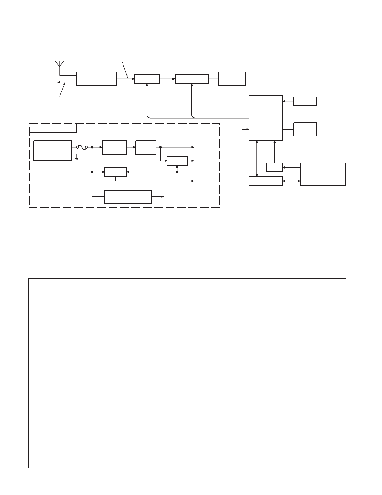
FNA- TM320
BLOCK DIAGRAM
ANT IN
ANT OUT
ANT IN : +0dB
POWER SUPLLY
BU +13.2V
POWER
SUPLLY
CONNECTOR
ANT IN : +10dB
Q300,301
ANT
DISTRIBUTOR
Q100,105 Q101
Q108- 111
A1 IC400
TMC F/E
T PLL-CE
T PLL-DAT
T PLL-CLK
PD
TMC SM
TMC SD
BU
LIMITER
8V AVR
Q106
VOLT AGE DOWN
DETECTION
BU 5V
AVR
TMC CLK
T DATA
T QUAR
Q103
5V SW
BUDET
DECODER
BU5V
5V
SYS-ON
8V
OSC
4.332MHz
BU DE
SYS-ON
IC500
IC200
u-COM
IC203
TX
RX
RS422 I/F
BUF
IC201
RESET
OSC
16MHz
P-ON
NAVI
I/F CONNECTOR
COMPONENTS DESCRIPTION
● ELECTRIC UNIT (X25-9822-71)
Ref. No. Application/Function Operation/Condition/Compatibility
IC100 Power supply control IC Power supply control for BU5V. Composes stable power supply in combination with Q101.
IC200 System microcomputer
IC201 Reset IC Output Lo, when the voltage of the 5V microcomputer system goes at less than 4.2V.
IC203 Buffer Reverse buffer for P-ON IN signal.
IC400 Data decoder RDS data demodulation circuit.
IC500 Serial communication RS422 serial communication driver and receiver.
Q100 Voltage limiter Contains the BU voltage to 16V or less in combination with Q105.
Q101 BU5V power supply Power supply output driver for BU 5V. Composes stable power supply in combination with IC100.
Q103 5V 5V power supply.
Q104 P ON SW When base becomes Hi, Q104 comes ON, supplying BU to 8V lines of the internal circuits.
Q105 Voltage limiter Contains the BU voltage to 16V or less in combination with Q100.
Q106 BU detection SW
Q107 P ON SW When base becomes Hi, Q104 comes ON, supplying BU to 5V lines of the internal circuits.
Q108,109,112
Q300 AMP RF input amplifier.
Q301 AMP RF divide output signal amplifier.
Q302 AMP F/E RF input signal amplifier.
8V power supply 8V Power Supply.
This is turned ON when BU comes ON.
When momentary reduction is detected, or when BU is OFF, goes OFF.
2

FNA- TM320
MICROCOMPUTER’S TERMINAL DESCRIPTION
● SYSTEM MICROCOMPUTER : M30620FCAFP4Q7 (X25-982 : IC200)
Pin No. Pin Name I/O Function Processing Operation Description
1- Not used (N.C.)
2 TMC-ON O TMC tuner ON/OFF Not used (N.C.)
3~7 - Not used (N.C.)
8 BYTE I External data bus width switching input L : 16 bit, H : 8 bit
9 CNVss I Processor mode switching
10,11 - Not used (N.C.)
12 RESET I System reset L : Reset operation
13 XOUT O System clock output System clock output to Xtal
14 Vss I Power supply input terminal (GND) Power supply input terminal (GND)
15 XIN I System clock input System clock input from Xtal
16 Vcc I Power supply input terminal (BU5V) Power supply input terminal (BU5V)
17 NMI I NMI external interrupt input Pull up to BU5V by returning resistor
18,19 - Not used (N.C.)
20 P-ONIN I P-ON Input L : POW ON, H : POW OFF
21~28 - Not used (N.C.)
29 SCL O I2C clock output Serial communication clock output
30 SDA I/O I2C data output Serial communication data output
31 F-TXD O FLASH I/F data output Flash microcomputer memory data output terminal
32 F-RXD I FLASH I/F data input Flash microcomputer memory data input terminal
33 FS-CLK O FLASH I/F clock output Flash microcomputer I/F clock output terminal
34 F-BUSY O FLASH I/F Flash microcomputer I/F
35 TXD O NAVI communication transmission NAVI serial communication transmission
36 RDX I NAVI communication reception NAVI serial communication reception
37~40 41 F-EPM I FLASH I/F Flash microcomputer I/F
42 - Not used (N.C.)
43 BU DET I BU reduction detection L : Normal, H : Input voltage (8.5V or less detection)
44,45 - Not used (N.C.)
46 F-CE O FLASH I/F Flash microcomputer I/F
47,48 - Not used (N.C.)
49 SYS-ON O 5V, 8V control L : 5V, 8V OFF, H : 5V, 8V ON
50,51 - Not used (N.C.)
52 F-PU I Terminal for FLASH write Pull up input for writing to flash microcomputer
53~59 - Not used (N.C.)
60 TYPE1 I Destination selection Switching for charging
61 TYPE2 I Destination selection Switching for market models/OEM
62 Vcc I Power supply input terminal +5V Power supply input terminal (BU5V)
63 - Not used (N.C.)
L : Single chip mode and memory expansion mode,
H : Microprocessor mode
3

FNA- TM320
MICROCOMPUTER’S TERMINAL DESCRIPTION
Pin No. Pin Name I/O Function Processing Operation Description
64 Vss I Power supply input terminal (GND) Power supply input terminal (GND)
65~74 - Not used (N.C.)
75 TMC-CLK I TMC clock input
76,77 - Not used (N.C.)
78 TQUAL I TMC reception condition detection TMC reception condition detection
79 TDATA I TMC data input TMC data reception
80 - Not used (N.C.)
81 PLL-DATA O PLL serial data output F/E PLL serial data output
82 PLL-CLK O PLL serial clock output F/E PLL serial clock output
83 PLL-CE O PLL data enable output F/E PLL data enable output
84 - Not used (N.C.)
85 TMC-SD I Station detection Station detected reception at F/E
86 TREQ I Seek request reception L : Seek operation, H : Normal reception condition
87 Pdo I IF count input F/E IF count input
88~92 - Not used (N.C.)
93 TMCSM I Station detection F/E station detected meter input
94 TNOISE I Noise level detection Not used (N.C.)
95 - Not used (N.C.)
96 Avss I Analog power supply input (GND) Analog power supply input (GND)
97 - Not used (N.C.)
98 VREF I Reference voltage input A/D conversion reference voltage input
99 Avcc I Analog power supply input +5V Analog power supply input (BU5V)
100 PEFCON O Reference voltage output A/D conversion reference voltage output
4
 Loading...