

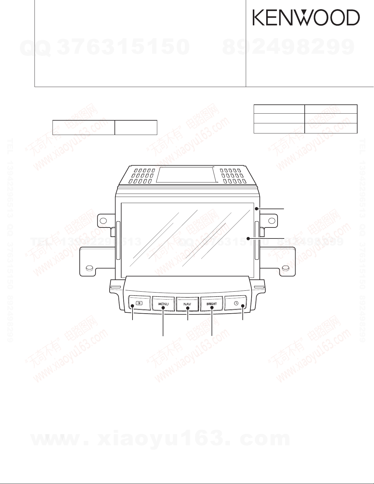
7-inch MULTI DISPLAY
FGZ806EF2/EOP
7
Q
Q
TEL 13942296513 QQ 376315150 892498299
3
SERVICE MANUAL
SUBARU GENUINE
Destination Europe
6
3
1
5
1
5
0
8
4
2
9
© 2004-9 CREATED IN JAPAN
B53-0202-00 (N) 0
MODEL PARTS No
FGZ806EF2 86281SA000
FGZ
9
806EOP
PANEL
(A64-2772-21)
8
2
9
9
.
H001ESA120
TEL 13942296513 QQ 376315150 892498299
TEL
13942296513
KNOB (SCREEN)
(K24-4161-24)
KNOB (NAV)
(K24-4163-24)
KNOB (MENU)
(K24-4162-24)
Q
Q
3
6
7
3
KNOB (CLOCK)
(K24-4165-24)
KNOB (BRIGHT)
(K24-4164-24)
1
5
1
5
0
LIQUID CRYSTAL
(B38-1156-05)
4
2
9
8
9
8
2
9
9
w
w
w
.
xia
o
y
u
1
6
3
.
c
o
m
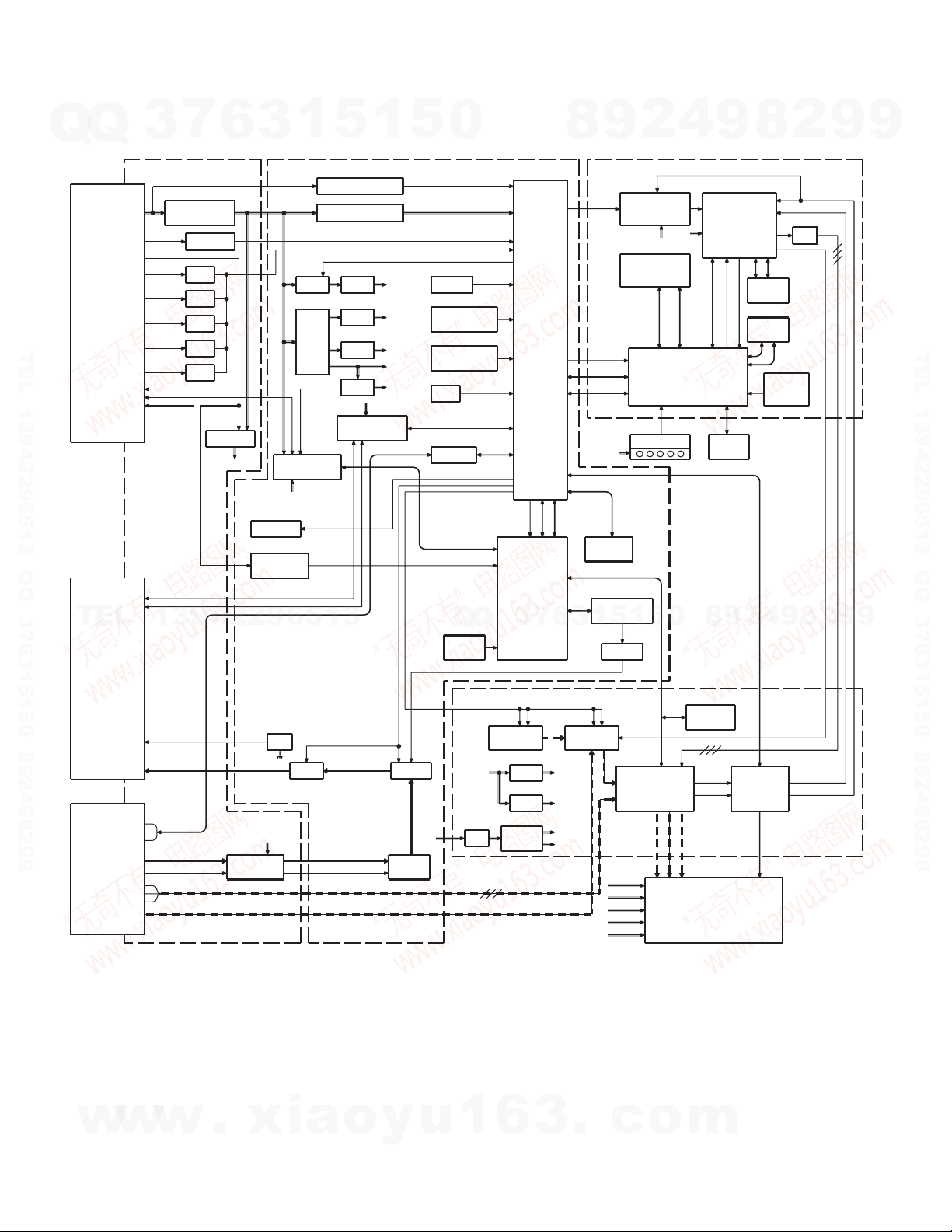
FGZ806EF2/EOP
BLOCK DIAGRAM
7
Q
Q
J803 (B/3)
1-16PIN
CAR
CONNECTOR
12. ILLUMI(PWM)
4. CAR SPEED
TEL 13942296513 QQ 376315150 892498299
10. REVERSE
J803 (C/3)
17-36PIN
AUDIO UNIT
TEL
24. AUDIO MUTE
17. BUS OFF
34. A-OUT(L)
32. A-OUT(R)
35. NAVI-GND
36. NAVI-AUDIO
J805 (B/3)
NAVI UNIT
10. NAVI-RX
11. NAVI-TX
12. NAVI-A-L
7. NAVI-A-GND
(X14- ) (B/3)(C/3)
2. +BATT
4. ACC
8. IGNITION
7. PARKING
11. ILLUMI
(SMALL)
6. CAN-H
5. CAN-L
16. PTT
1. GND
3. GND
15. GND
20. F-BUS+
22. F-BUS-
19. GND
21. GND
23. RESET
26. BUS ON
18. +B
33. A-GND
8. NAVI-A-R
1. NAVI-R
5. NAVI-G
9. NAVI-B
13. C-SYNC
2.6. GND
3
F800
INPUT
PROTECTION
Q803
Q801
Q804
Q800
Q805
Q806
13942296513
MONO
L/R
AUDIO-GND
ACC DET
DET
DET
DET
DET
DET
Q806,
810
ILLUMI+B
ILLUMI-V
6
IC800
ISOLATION
AMP
1
3
SYNTHESIZER UNIT
(X14- ) (A/3)
Q26,28
+B VOL TAGE DET
+B
IC20 Q49
DC/DC
Q42 Q47
SW
IC19
CAN
TRASCEIVER
Q43
PTT-SW
Q5
ILLUMI
PWM DET.
Q45,52
SW
P7.5V
IC8
P5V
Q17
MUTE
5
1
P-ON
SW
REG.
Q31
REG.
REG. P7.5V
BU5V
IC17
IE BUS
TRASCEIVER
L
R
5
0
IC18
Q27,30
IC1
P5V
P-15.5V
P18.5V
P8.5V
IC10
RESET
X4
15MHz
MAIN CLOCK
X2
32.768kHz
SUB CLOCK
TH800
TH
CONTROL/DATA
IC16
BUFFER
X3
10MHz
CLOCK
IC13
SW-OP
+B B/L INV
MIX
IC5
BU5V
SYSTEM
u-COM
RESET
IC3
CAN
u-COM
7
3
Q
Q
V SIGNAL SW
IC200,201 IC203
IC31
SW
N/A SW
VIDEO SW
IC212
IC211
L35,36
6
P5VREG.P7.5V
P3VREG.
VFL H
VFL L
8
3
SYNC SW
SWTCH UNIT
(X16- )
ILLUMI-V
I2C BUS
IC7
I2C BUS
2
9
ELECTRIC UNIT
(X25- )
V-SYNC
IC2,3
DOT CLOCK
DATA
SIGNAL
GENERATOR
P8.5V
IC19
FLASH ROM
DATA
IC12
RESET
HARD KEY
E2PROM
8KB
IC4
VOICE
SYNTHESIS
1
1
5
IC6
E-VOL
IC202
VIDEO SIGNAL
PROCESSOR
P18.5V
P-15.5V
P5V
VFL H
VFL L
5
R
4
IC4
P5V
ADDRESS
GRAPHIC
u-COM
0
VIDEO UNIT
(X35- )
IC205
EEPROM
1KB
RGB
HD
VD
B
G
LCD
9
GRAPHIC
CONTROL
RESET
CONTROL
TOUCH
PANEL
9
8
8
SDRAM
(8MB)
INT
IC11
SDRAM
(8MB)
2
IC102
TIMING
CONTROL
IC5
MAIN
CLOCK
7.08MHz
9
4
2
VD
HD
IC6
D/A
X1
8
9
RGB
C-SYNC
2
9
9
TEL 13942296513 QQ 376315150 892498299
9
2
w
w
w
.
xia
o
y
u
1
6
3
.
c
o
m

FGZ806EF2/EOP
COMPONENTS DESCRIPTION
7
Q
Q
● SYNTHESIZER UNIT (X14-912x-xx)
TEL 13942296513 QQ 376315150 892498299
TEL
w
3
Ref. No. Application / Function / Operation / Condition
IC1 Reset IC (when resets at the time of backup power supply is OFF)
IC2 Inverter IC (audio unit control and microprocessor program writing)
IC3
IC5 setting audio unit and NAVI unit of the control video sauce, the screen zoom, and the brightness of the control and the
IC7 EEP-ROM (memory of a receiving TV station name and touch-panel compensation data for memory)
IC8 CAN transceiver (communication with a car unit)
IC9 Reset IC (detection of the 5V power supply )
IC10 OP AMP IC (LR sound MIX of NAVI audio and bias of power supply an internal audio circuit)
IC12 Analog SW (port SW at the time of microprocessor program writing)
IC13 OP AMP with SW (change of a NAVI sound and an ADA sound)
IC16 Buffer IC (the microprocessor is protected from a communication line with a NAVI unit)
IC17 BUS transceiver (communication with an audio unit)
IC18 Regulator IC (5V power supply of a system microprocessor)
IC19 Regulator IC (analog system 7.5V power supply)
IC20 DC/DC controller IC (power supply of without system microprocessor and key illumination circuit)
IC21 Reset IC (it resets at the time of the abnormal of function for system microprocessor)
IC800 Isolation AMP (noise removal of a NAVI audio sound)
Q1 Audio MUTE SW
Q2 DC/DC controller power supply
Q4
Q5 Key illumination tone light detection (it turns on at the time of a illumination PWM input)
Q6 Temperature detection SW (at the time of ACC → ON is ON : temperature detection mode start)
Q7~11 Video setup SW (it is ON/OFF by screen mode and adjustment)
Q12,15,16 Audio control SW (at the time of the audio communication is ON : Q16 is ON, at the time of OFF : Q15 is ON)
Q17 Audio MUTE (at the time of power supply ON/OFF MUTE is ON)
Q18 Audio control SW (at the time of the audio communication is ON : Q16 is ON, at the time of OFF : Q15 is ON)
Q19 Microprocessor power supply SW (at the time of CAN microprocessor program writing is OFF)
Q20 Audio SW (at the time of ADA audio out is ON)
Q24
Q25 Microprocessor power supply SW (at the time of CAN microprocessor program writing is OFF)
Q26 Voltage detection (at the time of Q26 : ON backup power supply voltage detection)
Q28 Voltage detection (at the time of Q26 : ON backup power supply voltage detection)
Q29,30 Constant voltage power supply (backup 5V power regulator)
Q31 Constant voltage power supply (at the time of Q61 is ON : +18.5V output)
Q32 DC/DC controller power supply
Q33 Over-current detection (at the time of 18.5V over-current detection the controller power supply is OFF)
13942296513
w
w
6
CAN microprocessor (control of a setup and ADA voice synthesis of the connection existence distinction quality of image of
a communication rear camera and an AUX terminal with a car unit and TV tuner)
System microprocessor (surveillance of communication internal electrical power source control and a power supply with the
graphic microprocessor of a CAN microprocessor, and the abnormalities in temperature)
Microprocessor reset SW (at the time of power-supply ON/OFF is ON : CAN microprocessor is reset mode)
Power supply voltage dropout detection (when turns off at the time of backup power supply voltage dropout)
.
xia
3
1
5
o
1
y
5
u
0
Q
Q
1
3
6
7
3
6
8
3
.
9
1
1
5
c
2
5
o
4
0
m
9
8
9
8
2
4
2
9
8
9
2
9
9
TEL 13942296513 QQ 376315150 892498299
9
3
FGZ806EF2/EOP
COMPONENTS DESCRIPTION
7
Q
Q
Ref. No. Application / Function / Operation / Condition
Q34~37 DC/DC controller power supply
Q38 Over-current detection (at the time of 8.5V over-current detection the controller power supply is OFF)
Q39,41
Q40 DC/DC switching (primary side switching of a transformer)
Q42 DC/DC switching (primary side switching of a transformer)
Q43 DC/DC switching (switching of 5V power supply)
Q44 Over-current detection (at the time of –15.5V over-current detection the controller power supply is OFF)
TEL 13942296513 QQ 376315150 892498299
Q46 DC/DC controller power supply
Q47 Constant voltage power supply (–15.5V constant voltage power supply)
Q48 Over-current detection (at the time of 5V over-current detection the controller power supply is OFF)
Q49 DC/DC switching (switching of 5V power supply)
Q50 Audio MUTE (at the time of power supply ON/OFF MUTE is ON)
Q53 DC/DC controller power supply
Q55,56,58
Q57 Constant voltage power supply (at the time of Q61 is ON : +18.5V output)
Q61 Constant voltage power supply (at the time of Q61 is ON : +18.5V output)
Q64 Constant voltage power supply (backup 5V power regulator)
Q66~69 Timer (at the time of a system microprocessor reckless run Q67 is OFF)
Q700~702 Audio connection detection (at the time of audio connection Q700 is ON)
TEL
Q800 PARKING detection (at the time of car PARKING is ON)
Q801 Speed detection (at the time of a speed pulse input is ON)
Q802 Reset input (at the time of Q802 ON when system microprocessor is reset mode)
Q803 ACC detection (at the time of car ACC → ON : ON)
Q804 IGN detection (at the time of car Ignition → ON : ON)
Q805 Reverse detection (at the time of car reverse : ON)
Q806 SMALL detection (at the time of car SMALL → ON : ON)
Q807~811 Key illumination tone light power supply regulator (it is illumination VCC (7V) with the duty cycle according to PWM output)
3
DC/DC controller power supply
Video setup SW (it is ON/OFF by screen mode and adjustment)
13942296513
6
3
1
5
1
5
0
Q
Q
3
7
6
8
3
9
1
5
1
2
5
4
0
9
8
9
8
2
4
2
9
8
9
2
9
9
TEL 13942296513 QQ 376315150 892498299
9
● ELECTRIC UNIT (X25-941x-xx)
Ref. No. Application / Function / Operation / Condition
IC2 PLL Oscillator IC
IC3 Inverter (DOT CLOCK)
IC4 Graphic control IC
IC5 The memory for graphic control IC
IC6 Video D/A converter
IC7 Inverter (DACK SIGNAL)
IC10 OR gate IC
IC11 The memory for graphic microprocessors
IC12 Graphic microprocessor
w
w
IC19 Graphic bitmap data & program data memory
4
w
.
xia
o
y
u
1
6
3
.
c
o
m
FGZ806EF2/EOP
COMPONENTS DESCRIPTION
7
Q
Q
TEL 13942296513 QQ 376315150 892498299
● VIDEO UNIT (X35-425x-xx)
TEL
w
3
Ref. No. Application / Function / Operation / Condition
IC20 Inverter (SYNC. SIGNAL)
IC22 Inverter
IC23 AND gate
IC24 Synchronized signal generator
IC26 5V AVR
IC27,28 Inverter (SYNC. SIGNAL)
Q2~5 The transistor for touch-panel detection
Ref. No. Application / Function / Operation / Condition
IC31 Switching regulator (for back light 7.5V power supply)
IC101 Operational amplifier (oscillating circuit : low path output)
IC102 Timing controller (LCD driver IC)
IC200,201 Video switch (input video signal change)
IC202 Synchronous separation
IC203 Chrome decoder, gamma correction (an input video signal conversion to LCD drive signal)
IC205 EEP-ROM (I2C memory backup)
IC207 Operational amplifier (V-COM buffer)
IC209 Buffer containing 3 circuits (synchronized signal output buffer)
IC211 3V Regulator
IC212 5V Regulator
IC217 Inverter (for side black reverse signal )
Q1 ACC ON/OFF SW (for back light power supply)
Q2 +B SW (for back light power supply)
Q3,4 ACC ON/OFF SW (for back light power supply)
Q31,32 SW REG output (FET drive)
Q33 DC/DC converter SW (for back light power supply)
Q35,36 Inverter oscillation change SW
Q37~39 Back light tone light (for PWM pules drive)
Q40 Transistor for over-current protection (back light power supply)
Q41 An over-current for over voltage protection (back light power supply)
Q42 FET for the back light lighting SW
Q43 The transistor for the back light lighting SW
Q101 Transistor for oscillating circuits (a timing controller for a standard oscillation)
Q102 LCD reverse signal control (LCD up-and-down side reverse control transistor)
Q203,204 V-COM buffer
Q205,206 Video signal buffer
Q209,210 Synchronized signal muting (timing controller : at the time of adjustment muting)
X200 Synchronous separation reference oscillator (15.734kHz)
X201 Color reference oscillator (3.58MHz)
13942296513
w
w
6
.
xia
3
1
5
o
1
y
5
u
0
Q
Q
1
3
6
7
3
6
8
3
.
9
1
1
5
c
2
5
o
4
0
m
9
8
9
8
2
4
2
9
8
9
2
9
9
TEL 13942296513 QQ 376315150 892498299
9
5
FGZ806EF2/EOP
MICROCOMPUTER’S TERMINAL DESCRIPTION
7
Q
Q
● SYSTEM MICROPROCESSOR (X14-912x-xx : IC5)
Pin No. Pin Name I/O Purpose / Description / Processing / Operation
1 C-SYSDATA O System microprocessor data output
2 CANCLK O System microprocessor clock output
3 SPD I Speed pulse input
4 PON2 O PON7.5V control output
5 PON3 O PON18.5V control output
6 WDP O Watch dog pulse output
TEL 13942296513 QQ 376315150 892498299
7 PTT O The PTT output for a telephone
8 BYTE - Un-connecting
9 CNVSS I It is high at the time of rewriting
10 XCIN I Sub clock input
11 XCOUT O Sub clock output
12 RESET I Reset input
13 XOUT O Clock output
14 VSS - Ground
15 XIN I Clock input
16 VCC - Power supply
17 NMI I Interruption input
18 CANREQ I System microprocessor Request-to-Send input
19 NC - Un-connecting
TEL
20 CANCON O CAN microprocessor control output
21 AUDIO-BUS+ I AUDIO BUS communication end detection input
22 BUS ON REQ I AUDIO BUS ON detection input
23 BUS OFF REQ I AUDIO BUS OFF detection input
24 BRIGHT O BRIGHT control output
25~27 NC - Un-connecting
28 STB O AUDIO BUS communication standby output
29 SI I AUDIO BUS communication data reception input
30 SO O AUDIO BUS communication data transmitting output
31 NAVI-TXD O Usually, a NAVI communication transmitting data output
32 NAVI-RXD I It is NAVI communication receiving data input at the time of usual
33 BUS SYS ON O It is an AUDIO BUS system-on output at the time of usual
34 BUS SYS OFF O AUDIO BUS system-off output
35 SYSDATA O System microprocessor data output
36 SHDATA I System microprocessor data input
37 SHCLK O System microprocessor clock output
38 SHRST O Graphic microprocessor reset output
39 SHINI O Graphic microprocessor initial output
40 SHRDY I The notice input of a state which can be graphic communicated
41 EPM I Flash write-in EPM input
42 SHCON O Graphic microprocessor standby control output
w
43 SHSTBY I The completion input of graphic microprocessor standby shift
44 SYSCS O System microprocessor Request-to-Send output
6
3
13942296513
w
w
6
.
xia
3
1
5
o
1
y
5
u
0
Q
Q
1
3
6
7
3
6
8
3
.
9
1
1
5
c
2
5
o
4
0
m
9
8
9
8
2
4
2
9
8
9
2
9
9
TEL 13942296513 QQ 376315150 892498299
9

FGZ806EF2/EOP
MICROCOMPUTER’S TERMINAL DESCRIPTION
7
Q
Q
TEL 13942296513 QQ 376315150 892498299
TEL
w
3
Pin No. Pin Name I/O Purpose / Description / Processing / Operation
45 SH VMUTE I Graphic microprocessor image muting demand input
46 CE I Flash write-in CE input
47 TOUCH EN O Graphic microprocessor touch key analysis permission output
48 TOUCH I Notice input of graphic microprocessor touch key-on
49 PLLCE O The clock generating IC mode output for Q2i
50 PLLSDA O The clock generating IC data output for Q2i
51 PLLSCK O The clock generating IC clock output for Q2i
52 BL-ON O Back light switch output
53 VIDEO Swa O TV/REAR changeover switch output
54 NC - Un-connecting
55 VIDEO SWb O DVD changeover switch output
56 SYNC Swa O VIDEO/NAVI SYNCRO un-connecting changeover switch output
57 SYNC SWb O GRAPHICS SYNCRO un-connecting changeover switch output
58 VIDEO SWc O DVD-CH/NAVI-AUX changeover switch output
59 VIDEO SWd O AUX changeover switch output
60 HPOSI1 O Level position adjusted power
61 HPOSI2 O Level position adjusted power
62 VCC - Power supply
63 SCAN1 O Screen mode changeover switch output
64 VSS - Ground
65 SCAN2 O Screen mode changeover switch output
66 NTSC/PAL O NTSC/PAL changeover switch output
67 VMUTE O Video muting control output
68 +BDET SW O +B voltage detector circuit control output
69 REVERSE I Reverse detection input
70 PARKING I Parking detection input
71 P-ON O Power supply control output
72 FAULT O FAULT display output
73 ACC I ACC voltage detection input
74 BUDET I +B voltage variation detection input
75 SHCS I Graphic microprocessor Request-to-Send input
76 IGN I Ignition voltage detection input
77 ADA-INT O NAVI voice changeover switch output
78 AUDIO-MUTE O AUDIO muting signal output
79 TV O TV voice muting output
80 MUTE1 O MUTE1 signal output
81 TYPE0 I It forces and is a setting input
82 TYPE1 I It forces and is a setting input
83 MUTE2 O MUTE2 signal output
84 E2PSCL O IIC clock output
85 E2PSDA O IIC data input and output
86 INH - Un-connecting.
87 HPOSI3 O Level position adjusted power
13942296513
w
w
6
.
xia
3
1
5
o
1
y
5
u
0
Q
Q
1
3
6
7
3
6
8
3
.
9
1
1
5
c
2
5
o
4
0
m
9
8
9
8
2
4
2
9
8
9
2
9
9
TEL 13942296513 QQ 376315150 892498299
9
7
FGZ806EF2/EOP
MICROCOMPUTER’S TERMINAL DESCRIPTION
7
Q
Q
Pin No. Pin Name I/O Purpose / Description / Processing / Operation
88 HPOSI4 O Level position adjusted power
89 AUDIODET I Audio voltage detection input
90 TEMPDET I High temperature temperature detection input
91 BLDET2 I Back light voltage detection input
92 BLDET I Back light voltage detection input
93 +BDET I +B voltage detection input
94 DC/DC DET I PON5V voltage detection input
TEL 13942296513 QQ 376315150 892498299
95 CANRESET O CAN microprocessor reset output
96 AVSS - Analog ground input
97 C-SYSREQ O System microprocessor Request-to-Send output
98 VREF - Reference voltage
99 AVCC - Analog power supply
100 CANDATA I System microprocessor data input
● GRAPHIC MICROPROCESSOR (X25-941x-xx : IC12)
Pin No. Pin Name I/O Purpose / Description / Processing / Operation
1~5 NC - Un-connecting
6 VSS1 - Ground
7~11 A0~A4 O Address bus output
12 VCC1 - Power supply
TEL
13 A5 O Address bus output
14 VSS2 - Ground
15~25 A6~A16 O Address bus output
26 VCC2 - Power supply
27 A17 O Address bus output
28 VSS3 - Ground
29, 30 NC - Un-connecting
31 RAS O DRAM row address Strobe output
32 CASL O DRAM low rank side column address Strobe output
33 NC - Un-connecting
34 CASH O DRAM higher rank side column address Strobe output
35 VSS4 - Ground
36 RDWR O DRAM write-in Strobe output
37~39 A18~A20 O Address bus output
40 VCC3 - Power supply
41 A21 O Address bus output
42 VSS5 - Ground
43 RD O External device read-out Strobe output
44 NC - Un-connecting
45 SH VMUTE O Graphic microprocessor video mute request output
46 NC - Un-connecting
w
47 WRH O An external device higher rank side write-in output
48 WRL O An external device low rank side write-in output
8
3
13942296513
w
w
6
.
xia
3
1
5
o
1
y
5
u
0
Q
Q
1
3
6
7
3
6
8
3
.
9
1
1
5
c
2
5
o
4
0
m
9
8
9
8
2
4
2
9
8
9
2
9
9
TEL 13942296513 QQ 376315150 892498299
9

FGZ806EF2/EOP
MICROCOMPUTER’S TERMINAL DESCRIPTION
7
Q
Q
TEL 13942296513 QQ 376315150 892498299
TEL
w
3
Pin No. Pin Name I/O Purpose / Description / Processing / Operation
49 CS1 O Chip selection output (inside register of Q2i)
50 CS0 O Chip selection output (flash ROM)
51~53 NC - Un-connecting
54 CS2 O Chip selection output (Q2iUGM)
55 VSS6 - Ground
56 ROM RESET O Flash ROM reset output
57 ROM RY/BY I Flash ROM lady busy input
58 NC - Un-connecting.
59 DACK O Q2iDMA transmission Strobe output
60 NC - Un-connecting.
61 VSS7 - Ground input
62 DREQ I Q2iDMA transmission demand input
63 VCC4 - Power supply
64~68 NC - Un-connecting.
69 SYSCS I Graphic microprocessor Request-to-Send input
70 IRL I Q2i interrupt request input
71 VSS8 - Ground
72 SHCON I Graphic microprocessor standby control input
73~76 D12~D15 I/O Data bus input and output
77 VCC5 - Power supply
78 D11 I/O Data bus input and output
79 VSS9 - Ground
80~84 D6~D10 I/O Data bus input and output
85 VCC6 - Power supply
86 D5 I/O Data bus input and output
87 VSS10 - Ground
88~92 D0~D4 I/O Data bus input and output
93 VSS11 - Ground
94 XTAL I Crystal oscillator input
95 MD3 I Mode setting input of operation
96 EXTAL I Crystal oscillator input
97 MD2 I Mode setting input of operation
98 NMI I Non maskable interrupt input
99 VCC7 - Power supply
100 NC - Un-connecting
101 WAIT I Q2i wait cycle insertion input
102 MD1 I Mode setting input of operation
103 MD0 I Mode setting input of operation
104 PLLVCC I The power supply input for built-in PLL
105 PLLCAP I The capacity input for built-in PLL
106 PLLVSS I The grand input for built-in PLL
107 NC - Un-connecting
108 SHRST I Reset input
13942296513
w
w
6
.
xia
3
1
5
o
1
y
5
u
0
Q
Q
1
3
6
7
3
6
8
3
.
9
1
1
5
c
2
5
o
4
0
m
9
8
9
8
2
4
2
9
8
9
2
9
9
TEL 13942296513 QQ 376315150 892498299
9
9
FGZ806EF2/EOP
MICROCOMPUTER’S TERMINAL DESCRIPTION
7
Q
Q
Pin No. Pin Name I/O Purpose / Description / Processing / Operation
109~111 NC - Un-connecting
112 VCC8 - Power supply
113 Y– O The switching output for a touch-panel input
114 X– O The switching output for a touch-panel input
115 Y+ O The switching output for a touch-panel input
116 X+ O The switching output for a touch-panel input
117 VSS12 - Ground
TEL 13942296513 QQ 376315150 892498299
118 KEYDATA1 I Touch-panel data input (Y)
119 KEYDATA2 I Touch-panel data input (X)
120 NC - Un-connecting.
121 KEY5 I Key switch input
122 KEY4 I Key switch input
123 KEY3 I Key switch input
124 AVSS - Analog ground
125 KEY2 I Key switch input
126 KEY1 I Key switch input
127 VREF - Reference voltage
128 AVCC - Analog power supply
129 VSS13 - Ground
130 SYSDATA I Graphic microprocessor data input
TEL
131 SHDATA O Graphic microprocessor data output
132 SYSCLK I Graphic microprocessor clock input
133 ROM RXD I Flash ROM write-in data input
134 ROM TXD O Flash ROM write-in data output
135 VCC9 - Power supply
136 SHSTBY O The completion output of graphic microprocessor standby shift
137 TOUCH O Notice output of graphic microprocessor touch key-on
138 SHCS O System microprocessor Request-to-Send output
139 NC - Un-connecting
140 SHRDY O The notice output of a state which can be graphic microprocessor communicated
141 VSS14 I Grand input
142 NC - Un-connecting
143 TOUTH EN I Graphic microprocessor touch key analysis permission input
144 SHINI I Graphic microprocessor initial input
3
13942296513
6
3
1
5
1
5
0
Q
Q
3
7
6
8
3
9
1
5
1
2
5
4
0
9
8
9
8
2
4
2
9
8
9
2
9
9
TEL 13942296513 QQ 376315150 892498299
9
● GRAPHIC CONTROL IC (X25-941x-xx : IC4)
Pin No. Pin Name I/O Purpose / Description / Processing / Operation
1 DREQ O DMA request
2D0 I/O CPU data input and output
3D1 I/O CPU data input and output
4 CVCC1 - Power supply
w
w
5D2 I/O CPU data input and output
w
6 CGND1 - Ground
10
.
xia
o
y
u
1
6
3
.
c
o
m
FGZ806EF2/EOP
MICROCOMPUTER’S TERMINAL DESCRIPTION
7
Q
Q
TEL 13942296513 QQ 376315150 892498299
TEL
w
3
Pin No. Pin Name I/O Purpose / Description / Processing / Operation
7~11 D3~D7 I/O CPU data input and output
12 CGND2 - Ground input
13 D8 I/O CPU data input and output
14 D9 I/O CPU data input and output
15 D10 I/O CPU data input and output
16 CVCC2 - Power supply
17, 18 D11, D12 I/O CPU data input and output
19 CGND3 - Ground
20~22 D13~D15 I/O CPU data input and output
23 PGND - Ground
24 CAP0 - The external capacity terminal for multiplication circuit
25 PVCC - Power supply
26 CS0 I Chip selection 0 (UGM)
27 CS1 I Chip selection 1 (internal register)
28 RD I Lead Strobe
29 WE0 I The write-in pulse 0 (low rank side)
30 WE1 I The write-in pulse 1 (higher rank side)
31 DACK I DMA acknowledge
32 MODE0 I Mode terminal 0 of operation
33 MODE1 I Mode terminal 1 of operation
34 MODE2 I Mode terminal 2 of operation
35 TEST O Test terminal
36 RESET I Reset
37 CLK0 I Q2i operation clock
38 GND1 - Ground input
39, 40 A1, A2 I CPU address input
41 VCC1 - Power supply input
42~49 A3~A10 I CPU address input
50 GND2 - Ground
51~60 A11~A20 I CPU address input
61, 62 A21, A22 - Un-connecting
63 GND3 - Ground
64~68 MD0~MD4 I/O Memory data input and output
69 GND4 - Ground
70 MD5 I/O Memory data input and output
71 VCC2 - Power supply
72~78 MD6~MD12 I/O Memory data input and output
79 GND5 - Ground
80, 81 MD13, MD14 I/O Memory data input and output
82 VCC3 - Power supply
83 MD15 I/O Memory data input and output
84 MWE O A memory write-in pulse
85 MRAS0 O A low selection signal
13942296513
w
w
6
.
xia
3
1
5
o
1
y
5
u
0
Q
Q
1
3
6
7
3
6
8
3
.
9
1
1
5
c
2
5
o
4
0
m
9
8
9
8
2
4
2
9
8
9
2
9
9
TEL 13942296513 QQ 376315150 892498299
9
11
FGZ806EF2/EOP
MICROCOMPUTER’S TERMINAL DESCRIPTION
7
Q
Q
Pin No. Pin Name I/O Purpose / Description / Processing / Operation
86 MRAS1 O A low selection signal
87 MLCAS O Low rank side column selection signal
88 MUCAS O Higher rank side column selection signal
89 GND6 - Ground
90 MOE O Memory read-out pulse
91~93 MA0~MA2 O Memory address output
94 VCC4 - Power supply
TEL 13942296513 QQ 376315150 892498299
95~98 MA3~MA6 O Memory address output
99 GND7 - Ground input
100~104 MA7~MA11 O Memory address output
105 GND8 - Ground
106 CLK1 I The dot clock for a display
107 VCC5 - Power supply
108 FCLK O 1/2 display dot clock
109 ODDF I/O The pulse which shows the odd number field
110 GND9 - Ground
111 DCLK O Display clock output
112 CDE O Color detection
113 VCC6 - Power supply
114 DISP O Display period pulse
TEL
115 CSYNC O Composite synchronize signal output
116 GND10 - Ground
117 HSYNC O Horizontal synchronize signal output
118 VSYNC O Vertical synchronize signal output
119~121 DD0~DD2 O Display data output
122 GND11 - Ground
123~125 DD3~DD5 O Display data output
126 VCC7 - Power supply
127, 128 DD6, DD7 O Display data output
129 GND12 - Ground
130~134 DD8~DD12 O Display data output
135 GND13 - Ground
136 DD13 O Display data output
137 VCC8 - Power supply
138~141 DD14~DD17 O Display data output
142 CGND4 - Ground
143 IRL O Interrupt request
144 WAIT O CPU weight
3
13942296513
6
3
1
5
1
5
0
Q
Q
3
7
6
8
3
9
1
5
1
2
5
4
0
9
8
9
8
2
4
2
9
8
9
2
9
9
TEL 13942296513 QQ 376315150 892498299
9
12
w
w
w
.
xia
o
y
u
1
6
3
.
c
o
m
ADJUSTMENT
FGZ806EF2/EOP
7
Q
Q
● VIDEO UNIT (X35-425x-xx)
• Start a set in test mode at the time of video board adjustment.
•How to enter to test mode : Pushing operation of 2 ke ys right (cloc k)-and-left (image adj.) both ends side and a touch panel. And
• After starting : perform substrate adjustment for a video board by a design mode → VIDEO ADJ key with reference to the
• Adjust a picture position by After starting : (AUX) Manufacture mode → POSI (NAVI)
• VIDEO ADJ mode : it is the rectangle color frog of middle at the time of adjustment item selection. It is considered as an
TEL 13942296513 QQ 376315150 892498299
TEL
3
supply to power is ON.
following item.
adjustment end by choosing a rectangle again after adjustment.
No.
Adjustment item
1Inverter power It is considered as Bright : DUTY 100% after VR30 7.5±0.1V - TP577
regulation VIDEO ADJ - key selection.
2 Timing Consider it as microcomputer : SYNC (9 pin : VR101 15.734±0.01kHz Input selector : TP138
controller TP138 of IC102) MUTE → H after Adj key AUX input
free-run selection. non-signal
frequency VR101 (H-FREE) is turned and the frequency
13942296513
3 Chrome IC It is made the chroma IC adjustment mode of - - Input selector : -
adjustment a static test mode. AUX or RGB
3-A Chrome VCO 1 of IC202, 4, and 5 pin are dropped on GND, CH16 15.734±0.01kHz An input TP320
adjustment and a touch panel adjusts TP320 in f shop non-signal
3-B Black limiter Carry out the monitor of the waveform of TP527 CH5 3.5V±0.1V Incoming signal : TP527
3-C White limiter Carry out the monitor of the waveform of TP527 CH10 3.5V±0.1V Incoming signal : TP527
6
The voltage of TP577 at this time is adjusted to
7.5±0.1V.
of the NDSH output at this time is adjusted to
15.734±0.01kHz.
counter.
Carry out the monitor of TP138 of IC102, and
adjust VR101 in f shop counter.
with an oscilloscope. 10 STEP (NTSC)
Adjst the amplitude value so that the waveform /RGB
between the pedestal to the negative pedestal
is 3.5V±0.1V.
with an oscilloscope. 10 STEP (NTSC)
Adjst the amplitude value so that the waveform /RGB
between the 8 step signal to the negative 8 step
signal is 3.5V±0.1V .
3
1
5
1
5
The adjustment method
0
Q
Q
Adjustment
7
3
part
4
2
9
8
Adjustment value Conditions
0
5
1
5
1
3
6
9
8
9
8
2
4
2
9
8
9
Test point
9
2
9
TEL 13942296513 QQ 376315150 892498299
9
w
w
w
.
xia
o
y
u
1
6
3
.
c
o
m
13
FGZ806EF2/EOP
ADJUSTMENT
7
Q
Q
No.
3-D Bright Carry out the monitor of the waveform of TP527 CH6 2.5V±0.1V Incoming signal : TP527
3-E Contrast Carry out the monitor of the waveform of TP527 CH13 3.0V±0.1V Incoming signal : TP527
TEL 13942296513 QQ 376315150 892498299
3-F Gamma 1 Carry out the monitor of the waveform of TP527 CH11 1.2V±0.1V Incoming signal : TP527
3-G Gamma 2 Carry out the monitor of the waveform of TP527 CH12 2.9V±0.1V Incoming signal : TP527
TEL
3-H Y gain Carry out the monitor of the waveform of TP527 CH2 2.3V±0.1V Incoming signal : TP527
3-I R sub bright Carry out the monitor of the waveform of TP528 CH8 2.1V±0.1V Incoming signal : TP528
3-J B sub bright Carry out the monitor of the waveform of TP526 CH9 2.1V±0.1V Incoming signal : TP526
3
Adjustment item
adjustment with an oscilloscope. 10 STEP (NTSC)
13942296513
6
Adjst the amplitude value so that the waveform /RGB
between the 2 step signal to the negative 2 step
signal is 2.5V±0.1V .
with an oscilloscope. 10 STEP (NTSC)
Adjst the amplitude value so that the waveform /RGB
between the 9 step signal to the negative 9 step
signal is 3.0V±0.1V .
with an oscilloscope. 10 STEP (NTSC)
Adjst the amplitude value so that the waveform /RGB
between the pedestal to the 3 step signal is
1.2V±0.1V.
with an oscilloscope. 10 STEP (NTSC)
Adjst the amplitude value so that the waveform /RGB
between the pedestal to the 10 step signal is
2.9V±0.1V.
with an oscilloscope. 10 STEP (NTSC)
Adjst the amplitude value so that the waveform /AUX
between the pedestal to the 9 step signal is
2.3V±0.1V.
with an oscilloscope. 10 STEP (NTSC)
Adjst the amplitude value so that the waveform /RGB
between the 2 step signal to the negative 2 step
signal is 2.1V±0.1V .
with an oscilloscope. 10 STEP (NTSC)
Adjst the amplitude value so that the waveform /RGB
between the 2 step signal to the negative 2 step
signal is 2.1V±0.1V .
1
3
5
The adjustment method
1
5
0
Q
Q
Adjustment
part
7
3
4
2
9
8
Adjustment value Conditions
0
5
1
5
1
3
6
9
8
9
8
2
4
2
9
9
Test point
2
8
9
9
TEL 13942296513 QQ 376315150 892498299
9
14
w
w
w
.
xia
o
y
u
1
6
3
.
c
o
m
ADJUSTMENT
FGZ806EF2/EOP
7
Q
Q
TEL 13942296513 QQ 376315150 892498299
TEL
3
No.
Adjustment item
3-K R sub contrast Carry out the monitor of the waveform of TP528 CH14 2.2V±0.1V Incoming signal : TP528
3-L B sub contrast Carry out the monitor of the waveform of TP526 CH15 2.2V±0.1V Incoming signal : TP526
3-M VCOM Carry out the monitor of the waveform of TP517 CH1 5.8V±0.1V Incoming signal : TP517
4 Screen display
starting position MODE (NAVI) MENU -- or (AUX) it chooses. icon
adjustment Screen position adjustment of the position in a screen may
13942296513
5 Flicker It adjusts so that the flicker level will be VR102 Flicker minimum Gray drawing Screen
6Touch-panel After usually starting a set in the mode and Panel top - - Screen
6
with an oscilloscope. 10 STEP (NTSC)
Adjst the amplitude value so that the waveform /RGB
between the 10 step signal to the negative 10
step signal is 2.2V±0.1V.
with an oscilloscope. 10 STEP (NTSC)
Adjst the amplitude value so that the waveform /RGB
between the 10 step signal to the negative 10
step signal is 2.2V±0.1V.
with an oscilloscope. 10 STEP (NTSC)
The amplitude of the adjst the wave of VCOM is /RGB
5.8V±0.1V
A menu mode -- returning -- POSI of manufacture
adjustment is carried out by a touch panel.
minimum on screen.
pressing an information key, a SET icon and a icon
touch compensation icon are chosen.
The target which appeared in the screen is
pushed in order of the lower left and the upper
right.
3
1
5
1
5
The adjustment method
0
Q
Q
Adjustment
Panel top It adjusts so that the Mono range Screen
7
3
part
4
2
9
8
Adjustment value Conditions
position of the picture
become in the center.
5
1
3
6
1
5
0
9
8
9
8
2
4
2
9
8
9
Test point
9
2
9
TEL 13942296513 QQ 376315150 892498299
9
w
w
w
.
xia
o
y
u
1
6
3
.
c
o
m
15

A B C D E
C
R326
3
0
D18
2
N
2
FGZ806EF2/EOP
1
2
TEL 13942296513 QQ 376315150 892498299
3
PC BOARD (COMPONENT SIDE VIEW)
Q
Q
P801
3
D817
7
X14 B/3
C816
D820
6
D811
J803
3
L801
D812
1
R824
2
1
R895
5
1
L800
F800
5
R701
Q702
EB
Q700
EB
R700
0
TH800
F802
C705
16
15
C704
R893
D834
2
1
C899
C898
R812
C896
2
1
CN805
8
R813
D806
C897
9
18
17
CN803
D838
36
35
2
R897
D825
R896
Q808
EB EB
Q809
4
EB
R850
9
EB
R849
30
29
Q811
4
8
R865
Q810
J805
1
R892
2
C806
C802
2
1
9
12
D816
9
R877
C817
C857
C873
9
D8
L8
C
TEL 13942296513 QQ 376315150 892498299
SYNTHESIZER UNIT X14-9122-73 A/3 (J74-1655-02)
Q62
R23
EB
C138
R67R25
C272
C124
D29
R247
.
R226
R368
R60
R33
C283 R69
C125
BE
R228
R369
R70
R27
C282
R254
R233
C53
R256
R232
L5
R245
R250
EB
R363
R76
R36
C281
C46
CN13
X3
R127
IC3
R87
R38
C278
R281
R62
R91
R29
C276
C277
24
Q65
R252
R355
R354
DS
Q22
DS
Q60
R106
R114
R107
R163
C275
IC4
G
R249
EB
R248
EB
Q21
G
R251
R80
R84
R28
R37
C279
C280
L2
D7
C71
xia
Q20
C37
R79
R68
C273
C274
C247
R136
100
81
D8
R135
R139
R173R170
L8
C291
R155
R156
C289
R379
C244
1213
1
R259
R258
1
2
C38
C290
R161
R152
R171
R172
C292
R10
R367
R49
R366
R40
R82
L4
54
13
Q66
W5
C69
R246
C67
R244
o
29
30
Q1
R31
C239
C174
C3
R261
D6
C39
R11
C210
R13
C235
R19
R56
C8
R53
R45
R46
C241
R48
R50
R51C242
100
R64
R397
IC21
EB
X1
R352
Q23
C63
C59
y
R238
R78
R365
Q6
EB
EB EB
Q3
Q51
EB
EB
R385
R74
C22
C209
C207
C229
C206
R88
R77
R92
R85
R99
R96
80 51
130
C13
R374
C18
X2
C173
C62
R289
R303
R286
C24
16 9
C23
18
EB
R262
C44
R220
R219
u
C41
C42
C36
R212
4
5
6
7
TEL
P1
CN11
R6
P3
w
w
13942296513
29
30
C139
R370
R8
15
1
R1
R2
R3
R371
R359
R17
R353
30 1
31
R361
R360 R7
R18
R350
50
R55
51 80
R16
R349
R61
R52
R42R35
R5
R34
R26
R4
C286
C285
R260
14
IC15
58
R285
Q52
DS
G
R231
DS
G
Q45
C65
Q17
R237
C58
C61
R241
D5
w
C51
R230
R223
Q
R120
R162
C228
C227
R102
R100
IC5
W4
R112
L3
IC6
C40
R214
R211
1
Q
Q2
C225
C226
R103
R129
C181
X4
R205
C33
C32
CN15
Q30
R108
C224
R133
R111
C184
L6
L7
6
C218
R137
R141
R199
R169
R154
R165
C45
EB
Q10
3
C217
R140
R110
Q7
7
BE
C213
C216
R142
R146
R153
5081
31
R158
R160
R215
IC2
148
L9
Q8
3
EBEBEB
Q9
R157
R159
R182
R183
R184
R186
R187
R188
R190
R192
C197
R174
R176
R177
5
6
C81
R175
R202
IC16
C64
Q11
R222
1
7
EB
1
3
1
2
C214
C212
Q19
BE
60
2
R216
C54
C50
8
1
45
14
IC12
8
EB
C66
Q16
EB
R217
Q15
.
R130
1
5
EB
Q64
F1
C215
Q25
EB
R257
R253
59
1
C48C43
Q18
EB
EB
C97
Q12
c
Q27
8
0
5
BE
C77
C74
C78
D12
D9
C90
EB
Q32
R278
C83
CN16
D10
C84
R283
R280
C128
R225
C172
C171
134
o
C151
C161
C155
C162
CN14
m
C163
C164
2
9
R279
D14
C86
C85
R206
R282
51
IC19
C170C168
C165
C166
4
C73
C129
L11
9
R293
D30
Q53
C87
8
L15
C108
EB
C47
R309
R308
L12
C118
L10
C101
R319
C99
C104
R324
2
R323
R333
C112
C103
R327
9
C120
CC
C107
9
16
R332
R295
Q43
R328
C89
IC
C111
9
EBB
C136
R
D
R294
16

JIHGF
C112
FGZ806EF2/EOP
1
7
C817
D819
L802
CN804
3
C834
C835
D832
L803
Q
Q
6
R877
TEL 13942296513 QQ 376315150 892498299
C857
C873
TEL
C120
CC
0
C107
01
C103
8
16
R332
R327
104
324
R323
R333
w
2
13942296513
Q49
EBB
GDS
Q43
R338
89
C93
R376
D22
R294
R326
C4
D18
R318
C102
R307
1
C98
Q40
EBB
R314
L1
w
C137
R300
R311
CC
L20
R284
IC20
C136
R328
C111
C89
R295
w
R299
R306
R288
C100
D16
L13
D831
R891
C815
L18
C113
15
106
R400
.
6
C833
R867
30
29
C932
WH800
D27
Q44
C131
C126
P2
C88
C836
EB
R329
xia
3
R868
2
1
20
19
L19
C114
C105
R316
P800
D822
C708
1
C95
5
o
1
X14 C/3
R862
R861
R859
R857
R855
R834
C842
C860
C844
C862
C853
C854
y
5
4
2
J800
1
19
1
CN800
20
19
2
1
3
1
J806
2
P802
u
0
D830
20
D827
D828
2
D829
J802
Q
Q
3
1
1
6
3
9
8
X14-9122-73
Ref No. Address
IC2 6D
IC3 5B
IC5 5C
IC12 6D
IC16 6D
IC19 6E
IC20 5F
IC21 6C
Q1 4C
Q2 4C
Q6 4C
Q7 7C
Q8 7D
Q9 7D
5
1
3
6
7
3
Q10 7C
Q11 7D
Q12 7D
Q15 7D
Q16 7D
Q17 7B
Q18 6D
Q19 5D
Q20 7B
Q25 5D
Q27 4D
Q30 4C
Q32 5D
Q40 6F
Q43 5F
Q44 6F
Q49 5F
Q53 6E
Q64 4D
Q66 6C
Q700 2C
Q702 2C
Q808 2D
Q809 2D
Q810 2E
Q811 2E
Refer to the schematic
.
c
diagram for the values of
resistors and capacitors.
1
2
5
o
4
0
m
9
8
8
SWITCH UNIT
X16-1862-71
(J74-1652-02)
4
2
9
2
D101
D102
9
D103
D104
D105
8
9
S1
S2
2
S3
S4
S5
9
KEY1
KEY2
9
KEY3
KEY4
KEY5
9
2
TEL 13942296513 QQ 376315150 892498299
3
4
5
6
7
17

K L M N O
C5
R24
6
R398
R30
9
D
D
FGZ806EF2/EOP
1
2
TEL 13942296513 QQ 376315150 892498299
3
PC BOARD (FOIL SIDE VIEW)
Q
Q
X14 C/3
3
R860
R858
R856
R854
R863
7
6
3
C922
W8
C924
D836
D835
1
R869
5
1
X14 B/3
41
IC801
58
C832
C904
C929
C931
C935
C933
C934
D833
C927
C837
5
R833
R827
R832
0
IC800
D823
R844
C875
14
85
R847
C874
C872
C858
C877
C818
C876
D821
R818
C859
R866
C871
R822
8
C805
R821
R808
D837
R811
9
R851
R814
C852
2
C820
R852
C819
R898
C870
R845
4
R899
R704
D824
C822
C823
9
R816
C881
C880
C901
R826
C903
R815
C900
8
C882
C883
C902
R825
D815
C824
C879
2
R810
Q802
EB
C813
D814
9
C710
C709
R809
C878
C825
D700
R
R705
C937
Q801
9
TEL 13942296513 QQ 376315150 892498299
SYNTHESIZER UNIT X14-9122-73 A/3 (J74-1655-02)
4
5
6
7
TEL
C912
C911
R800
w
w
C861
13942296513
C843
C863
C845
C864
C846
C866
C848
C868
C850
R802
C701
C700
R853
C707
C706
R801
w
.
C115
D17
xia
D19
R336
R345
C91
R340
R341
R342
C133
R296
C130
ECB
BCE
R347
D31
D21
o
R378
R337
Q48
R339
R377
C134
C135
Q47
D26
C106
EBB
R343
y
Q
D20
D2
R395
C123
R275
3
R291
C96
C52
Q36
R312
C82
R276
EB
C75
R313
R264
D13
C169
R290
Q37
R265
BE
R277
.
BE
BE
EB
EB
D1
R266
R396
Q61
Q57
Q39
Q41
Q24
R267
EB
Q35
EB
BE
Q34
D32
C167
c
C109
R292
EB
S
C132
R301
D
Q38
BCE
1
R304
D23
Q46
R330
R302
C94
G
R320
C92
D15
ECB
R305
6
Q31
BBE
CC
D25
R335
R334
C110
R331
C117
R346
CC
R344
Q42
R401
D24
R298
R287
EB
u
R297
Q33
R394
R204
C116
C119
C146
C148
C150
C154
C149
o
31
R269
45
C142
C80
C147
IC18
R274
EB
R201
C195
R209
R194
R218
R227
R362
R399
85
IC17
1
m
D28
Q29
C189
C191
C196
R203
R195
4
Q26
C192
R193
R224
EB
C190
C193
C49
R268
R270
R179
R213
R191
R164
R273
R185
R189
R138
Q56
BE
R167
C186
R178
C194
R134
Q58
BE
R148
BEBE
Q55
Q28
R131
C219
C185
R128
C220
C20
D11
C79
R271
C230
R124
Q63
D35
EB
C238
C7
R73
C205
C223
R115
R94
C240
R123
R119
R117
C231
C221
C222
R8
R168
C182
C21
R121
R101
C246
C19
C178
C6
C26
C25
85
IC10
1
4
9
9
2
8
9
4
2
9
8
0
5
1
5
1
3
6
7
3
Q
18

TSRQP
C30
D11
D814
FGZ806EF2/EOP
1
7
Q
Q
TEL 13942296513 QQ 376315150 892498299
655-02)
TEL
C79
R271
R124
20
w
3
R900
D839
D700
R705
C710
C709
R809
D801
C878
C825
C937
Q801
Q63
D35
EB
C238
C7
R73
C205
C223
R30
R115
R94
R398
C240
R119
R117
C221
C222
R168
C182
C21
R121
C19
C6
IC10
w
1
R86
C246
4
R101
C178
C26
C25
R47
C175
R63
C5
R24
R263
R123
C231
85
R848
EB
Q806
R846
R841
D803
R806
C892
D810
EB
C936
13942296513
R65
C208
R81
R44
R57
R59
R32
C9
R39
R375
IC1
13
R66
EB
EB
Q68
EB
Q69
R348
w
6
Q805
Q807
EB
C893
BE
Q800
14 8
17
R41
R58
C2
45
C1
Q67
85
1
D807
R210
C72
R242
C60
R239
IC14
D804
R807
R804
Q5
BE
C232
BE
R20
IC8
C236
C895
C894
D800
Q50
R373
R310
C127
4
.
R207
R72
R843
R840
R805
R208
C28
C27
EB
C891
C890
BE
R22
C237
D4
R240
C886
Q59
C29
C10
xia
3
D802
C889
C888
C809
C884
R803
C887
C885
R150
R388
R122
R125
C253
C245
R109
R104
C34
C35
R180
85
C30
14
C12
C70
C68
D3
C812
R116
R118
EB
R181
R831
C803
IC7
D701
C810
C254
R200
1
Q804
R894
C702
C804
D805
C17
R105
C16
C15
R95
R144
C11
Q4
54
13
C31
R98
R75
EB
C14
R93
R839
IC9
R836
C703
R90
R97
R390
5
C814
BE
R703
Q701
R830
R823
C800
C801
C248
R71
R83
C252
R15
R364
C251
R14
R54
R43
C268
R392
C55
85
IC13
1
o
1
R702
D702
R835
C807
C808
R358
R391
C284
R234
y
C811
R357
R12
R389
4
Q803
EB
R356
R255
R838
R89
R243
5
R837
C271
C270
u
0
D818
BE
Q
R393
1
Q
6
3
9
8
X14-9122-73
Ref No. Address
IC1 6P
IC7 6Q
IC8 5P
IC9 6Q
IC10 7O
IC13 7Q
IC17 7O
IC18 4O
IC800 2M
Q4 5Q
Q5 4P
Q24 5N
Q26 5O
Q28 5O
Q29 4O
Q31 7M
Q33 7M
Q34 5N
Q35 5N
Q36 5N
5
1
3
6
7
3
Q37 5N
Q38 7M
Q39 5N
Q41 5N
Q42 6M
Q46 5M
Q47 6M
Q48 5M
Q50 5P
Q55 7O
Q56 7O
Q57 7N
Q58 7O
Q61 6N
Q67 6P
Q68 6P
Q69 6P
Q701 2Q
Q800 3P
Q801 3P
Q802 3O
Q803 2Q
Q804 2Q
Q805 2P
Q806 2P
Q807 2P
Refer to the schematic
.
c
diagram for the values of
resistors and capacitors.
1
2
5
o
4
0
m
9
8
8
SWITCH UNIT
X16-1862-71
(J74-1652-02)
4
2
9
D6
C2
C4
D7
C5
C3
R2
9
R3
R4
2
C1
R6
R7
C8
8
R8
C9
R9
C10
R10
C11
D8
D9
R5
9
191
C6
2
C7
R1
P2P1
9
9
202
CN2
C12
9
2
TEL 13942296513 QQ 376315150 892498299
3
4
5
6
7
19

U V W X Y
FGZ806EF2/EOP
1
2
PC BOARD (COMPONENT SIDE VIEW)
7
Q
Q
VIDEO UNIT X35-4252-71 (J74-1651-02)
3
P1
6
3
1
5
1
5
0
TEL 13942296513 QQ 376315150 892498299
R308
D62
R113
R158
W111
L31
R201
C275
85
85
R101
C106
R104
R107
R112
R111
IC102
W110
R109
C107
C103
31
C105
R153
C31
148
14
IC209
45
C104
R103
R102
R108
R105
C115
49
32
R151
R152
IC202
R266
R110
IC101
R106
C114
R128
3348
R150
58
C216
D101
D102
EB
Q101
R149
R265
C221
C215
C109
C113
W113
C125
R148
17
C239
C247
VR101
L102
R124
C117
D209
13
IC217
D31
C219
R123
R127
R136
R281
W114
3
4
5
6
TEL
C286
I
D208
C101
C288
C287
P6
C1
F1
118
CN1
13942296513
IC212
OG
C68
C204
C67
L101
C200
C201
R126
R130
C202
C65
P3
X200
C69
GIO
C108
C110
C116
C119
C120
W107
IC211
C205
IC201
41
C203
41
IC200
C64
C508
R114
R503
W120
C112
64
116
R140
17
W108
W112
W109
C236
C249
C265
L215
C289
45
C47
C41
C217
C259
C248
C253
C252
C254
L213
C232
L34
C238
C251
R246
EB
R248
C235
17 32
R210
C299
8
1
4
IC31
5
C237
16 33
C255
C48
Q205
R221
R211
C298
5
4
C40
R54
R55
R36
R56
1
VR30
R37
C33
8
3
Q
Q
P4
C234
L206
C233
C242
C230
1
IC203
C241
4964
48
R208
R209
VR102
C277
C505
C506
130
IC205
C46
C243
CN3
7
C240
C507
R44
L32
C37
6
C353
C45
C222
8
3
X201
C214
9
EB
1
C35
Q35
Q38
Q39
5
EBEB
1
C273
C274
C272
2
W1
C309
C310
W3
C315
134
5
14
IC207
85
4
0
P2
9
8
2
9
9
TEL 13942296513 QQ 376315150 892498299
CN2
9
9
2
8
9
4
2
9
8
CN5
X35-4252-71
Ref No. Address
IC31 4W
IC101 5V
IC102 6V
IC200 5V
P5
C271
14
C269
C270
IC201 5V
IC202 4V
IC203 5W
IC205 6W
IC207 6X
IC209 4V
IC211 5V
IC212 5U
IC217 7V
Q35 2X
Q38 3X
Q39 3X
Q101 6V
Q205 4W
w
w
7
w
.
xia
o
y
u
1
6
3
.
c
o
m
Refer to the schematic diagram for
the values of resistors and capacitors.
20

ADACABAAZ
FGZ806EF2/EOP
PC BOARD (FOIL SIDE VIEW)
7
Q
Q
VIDEO UNIT X35-4252-71 (J74-1651-02)
3
Q36
TEL 13942296513 QQ 376315150 892498299
TP19
C307
C308
TP201
C313
C314
C317
C318
C319
C320
C321
TEL
TP521
TP205
TP206
TP394
R223
TP316
Q204
w
w
R264
C43
TP203
TP212
TP213
C325
C330
C324
C331
C333
C328
C338
C332
C337
C336
C329
C335
C334
C316
Q209 Q43
13942296513
Q210
TP209
C342
C341
TP219
C340
C339
TP127
TP227
TP128
TP222
TP224
TP223
TP225
TP221
TP220
TP226
TP396
TP392
TP518
C268
R222
TP393
TP400
TP397
EB
EB
R225R224
L212L211
TP402
w
TP47
EB
R263
BE
TP17
TP18
TP16
GDS
TP14
TP231
EBEB
TP352
TP208
TP229
TP255
TP228
TP398
R228
R229
Q203
.
6
TP50
TP49
TP44
Q37
Q42
R50
R51
EB
TP211
TP210
TP217
TP561
TP549
C290
C291
TP530
W117
C357
C358
C359
C360
C361
C362
xia
3
TP46
TP45
C44
TP577
TP202
Q41
TP15
TP311
TP277
R276
L216
TP551
TP504
TP516
TP520
C356
TP526
TP527
TP528
15 51
L36
L35
TP204
D32
R48
EB
TP285
TP343
L205
TP273
C292
R280
C352
R215
R214
R213
1
TP12
R45
R43
R46
R47
C42
R49
W6
TP525
TP513
TP293
TP291
TP287
TP282
TP512
EB
TP576
TP20
TP214
TP300
TP345
R207
C226
C225
TP336
TP335
TP274
TP281
C351
TP514
C350
C349
Q40
TP34
TP36
TP294
TP286
C229
TP395
TP503
C348
5
C39
TP11
Q31
EB
R38
TP573
TP296
TP289
TP215
TP290
TP280
C296
C297
R254
R255
TP276
R306
R305
C347
C346
o
Q32
TP35
R240
TP292
C227
TP279
TP275
R257
R256
C256
TP544
C343
TP501
C344
C345
1
EB
R41
Q206
TP302
TP295
C228
TP284
TP331
L209
TP502
TP506
TP507
y
TP37
R40
R39
TP39
R247
TP574
D205
C244
TP299
C245
C246
TP301
R219
C264
TP327
C266
R220
TP361
TP360
TP505
5
TP38
TP40
TP263
R250
R241
TP297
TP321
TP330
C267
TP332
TP328
TP508
GDS
C34
R42
C276
TP266
EB
TP575
D204
TP303
TP307
TP320
TP314
TP322
TP323
R216
TP362
TP509
TP510
u
0
C207
R200
L202
L203
TP304
C250
TP312
TP319
TP317
L208
TP555
TP546
TP554
TP511
TP10
Q
R242
D203
TP298
TP218
TP313
R217
TP333
TP136
TP132
TP142
TP144
1
TP7
Q33
TP42
C206
TP258
TP259
Q
TP353
TP334
TP315
TP67
TP123
R139
TP260
R205
TP350
TP216
TP308
TP309
L207
TP318
TP108
TP111
TP122
R132
R135
TP146
TP147
TP8
TP265
C212
TP261
TP262
3
R204
TP563
TP256
TP306
C220
TP310
TP107
TP109
TP105
TP112
TP126
R116
C118
R121
TP149
R160
Q102
TP153
6
C32
C38
TP31
R5
TP4
TP267
C210
R203
C211
L201
L200
TP106
TP130
TP150
TP148
TP271
7
TP103
TP116
3
C209
R304
TP257
C218
TP244
TP248
TP529
R117
C111
TP119
TP324
TP151
TP152
EB
TP547
TP559
TP233
TP270
TP268
C208
6
TP249
TP102
TP160
TP113
TP114
R141
R142
C123
8
12
C306
R310
TP5
R202
R236
TP564
D202
TP104
TP133
TP154
9
CN4
D210
Q2
TP2
R2
EBEBEB
Q3
Q4
TP269
TP272
5
1
3
TP560
TP562
D206
TP251
R235
R231
R232
D201
TP246
R233
TP250
C503
C502
L502
C501
L501
TP115
TP117
TP118
TP120
R119
R122
R133
TP131
R137
TP138
TP139
TP141
R143
C124
TP155
TP159
W106
TP156
TP237
TP523
.
c
2
EB
TP1
R1
TP3
C2
R4
R3
Q1
TP6
TP565
TP253
5
1
TP241
R234
TP566
TP405
TP567
TP568
TP68
C504
C102
R502
R501
TP101
TP124
TP125
TP522
TP135
TP137
TP143
TP524
TP140
TP145
o
4
W203
0
TP238
TP239
C66
TP519
TP515
TP234
TP230
TP236
TP240
TP207
9
TP232
TP235
8
TP242
TP243
9
TP406
2
2
8
9
4
X35-4252-71
Ref No. Address
Q31 3AA
Q32 4AA
Q33 3AB
Q36 2Z
Q37 3Z
Q40 3AA
Q41 4AA
Q42 3Z
Q43 4Z
Q102 7AB
Q203 6Z
Q204 6Z
Q206 4AA
Q209 4Z
Q210 4Z
9
9
2
8
Q1 4AC
Q2 3AB
Q3 4AC
Q4 4AB
m
Refer to the schematic diagram f or the
values of resistors and capacitors.
9
9
1
2
TEL 13942296513 QQ 376315150 892498299
3
4
5
6
7
21

AE AF AG AH AI
FGZ806EF2/EOP
1
2
TEL 13942296513 QQ 376315150 892498299
3
4
PC BOARD (COMPONENT SIDE VIEW)
7
Q
Q
ELECTRIC UNIT X25-9412-72 (J74-1650-12)
TEL
3
13
IC7
CN32
C32
45
R29
C30
R45
C29
R44
R300
R43
R310
71
W247
W248
W249
13942296513
6
C3
144 109
1
C9
C15
C16
C17
R42
36
R41
37
43
12
A1
110
R298
CN31
C28
3
C2
IC4
C42
1
R258
R257
CP18
R273
R272
IC28
R3
4513
5
C1
R233
72
R48
R299
X2
R5
108
C33
73
C61
R256
R47
R144
R286
1
IC22
C7
C14
R26
R28
R31
C18
CP20
CP19
R46
C25
C67
5134
IC23
R7
L3
C38
C69
R122
R121
R120
C68
CP8
R287
5
CP26
R27
R30
W234
R119
R118
R117
0
IC20
13451345
C6
CP27
R305
C183
IC27
C194
CP21
C12
IC3
CP31
C34
C31
CP30
C187
R271
CP17
R93
C39
R94
R95
R97
R99
R103
R110
R113
C45
R114
R115
R116
CP7 CP6 CP5
Q
C213
C5
81
1345
916
3154
R20
C27
L4
R80
R79
37
72
73 108
Q
R78
R6
R77
C13
R303
R76
C54
IC2
C26
W246
C101
C100
R127
C209
R308
IC12
X1
3
R8
C184
C99
R23
L2
C98
C53
7
C185
C93
C11 C8
L1
C92
R280
R126
6
8
C211
C78
C91
C90
R276
R277
R279
R145
3
L13
C24
136
R148
R295
9
L12
144
109
R125
C58
C57
R151
1
R59
5
C77
C49
R58
R81
R83
R88
R90
R91
R92
R96
R98
R101
R56
CP22
CP23
1
2
C80
C79
5
4
CP25
0
9
8
8
X25-9412-72
Ref No. Address
4
2
9
2
IC2 2AG
IC3 2AG
IC4 2AF
IC7 2AE
IC12 3AH
IC20 2AG
IC22 2AG
IC23 4AG
IC27 2AG
IC28 3AF
2
8
9
9
9
9
TEL 13942296513 QQ 376315150 892498299
9
(FOIL SIDE VIEW)
ELECTRIC UNIT X25-9412-72 (J74-1650-12)
X25-9412-72
CP38
C76
C74
602
CN30
R123
C44
C177
C178
w
D3
C20
C21
159
C86
C87
C88
CP1
R171
C60
R157
C50
W314
W316
.
W315
IC26
O
5
6
w
7
G
I
CP24
W313
W312
w
22
CP40
CP39
22 12
23
IC6
33
34
R54
R53
R55
C22
R302
R304
C40
C97
C41
C89
C95
C94
C96
CP2 CP3
Q4
R169
EB
EB
Q3
R309
C140
D2
C138
Q5
C51
C136
EB
Q2
C133
CP4
EB
C52
C131
xia
C141
C137
C132
C139
44
R170
R168
R156
C59
C129
C130
CP37
11
C102
C127
C128
1
C148
CP36
C149
C126
C19
R40
C103
C125
D4
R14
R15
R16
C104
C109
R301
C107
C106
C111
C112
C113
o
D5
23
44
C105
C110
L5
W241
R289
R288
C188
C62
y
5
8
22
C190
R12
R13
IC5 IC11
C23
1
CP29
C63
R291
C186
R292
IC24
L18
L17
L16
L15
L7
IC10
R172
24 1
R294
R290
4
IC19
1
C181
R166
25 48
u
1
L14
CP32
CP33
C189
CP28
C192
C81
C82
R100
C84
1
354
R173
6
1
R102
C83
R311
C43
C37
C200
C199
C193
L6
L9
C197
C198
3
C180
C195
C196
44
2322
.
C201
C85
R87
R85
R2
R1
R297
R296
c
CP35
CP34
o
m
Refer to the schematic diagram for the values of resistors and capacitors.
Ref No. Address
IC5 5AG
IC6 5AF
IC10 6AG
IC11 5AH
IC19 6AG
IC24 6AG
IC26 5AE
Q2 7AF
Q3 7AF
Q4 6AF
Q5 6AF

A B C D E
G
N
N
N
AV
U
V
Q
1
Q
DTA144EUA
2SA1576A
2SD2114K
7
3
6
3
MA143
1
5
1
5
0
(X14-912x-xx)
MODEL NAME
FGZ201F2
FGZ201ERF2
FGZ201ADAF2
FGZ201ELF2
FGZ806EF2
FGZ806EOP
TC7SET08FU
2SB1188
2
2SC2411K
2SC4081
NJM4580V
TC7WHU04FU
TC7WH126FU
TEL 13942296513 QQ 376315150 892498299
FGZ806EF2/EOP
C709,
C702,703,
UNIT
BA
No.
888-893
0-00
YES
2-71
0-01
2-72 NO NO YESNO
2-73
2200P
NO
2200P
YES
2200P
NO
2200P
9
8
NO
0.1
IC800,801
Q700,701,803-806,
808,811
Q702,809
Q800,801
Q802
Q807
Q810
D700-702,800-804,822,834
D805
D806,814,815,823,827-830
D807,810,824,839
D811,812
D816,819,821,831-833,
835-837 : MA143
D817
D818
D820 : U5ZA27C(TE24L)
D825
D838
TDA8579T-T:
: 2SC4081
:DTA124EUA
:
∗
: DTC124EUA
:
∗
2SB1203-FA:
:
MA3220-H
:
MAZK270D
:
MA3056WA
::DAN202U
HZS6B1L
:
AM01ZNF
:
DE5LC20U
::HZS7C2L
HZM6.8FA
C911,
710
912
YES
2200P
NO
NO
YES
2
NO
NO
NO
1
4
C936,
937
NO
NO
NO
NO
YES
D700
YES
NO
YES
9
NO
Q800,
801
DTA124EUA
DTA124EUA
DTA124EUA
DTA124EUA
UNR511H
8
Q807
R705
DTA124EUA1K3.3K
DTA124EUA
DTA124EUA
2
DTA124EUA
DTA143EUA
VIDEO LINE
AUDIO LINE
GND LINE
B LINE
B LINE
YES
NO
YES
NO
R803,
804,807
3.3K
3.3K
3.3K
9
R840 R843
22K
10K
22K 10K
22K
10K
22K
10K
9
8.2K 4.7K
W8
NO
YES
NO
YES
from
CAR
INTERFACE
TEL 13942296513 QQ 376315150 892498299
3
4
TEL
5
6
DTA124EUA
DTA143EUA
DTC124EUA
NJM2107F
DTC144EUA
NJM4565MD
TC7SH32FU
13942296513
DAN202U
DAP202U
DA204U
CAUTION : For continued safety, replace safety critical
components only with manufacturer’s recommended parts
(refer to parts list).
Indicates safety critical components. To reduce the
risk of electric shock, leakage-current or resistance measurements shall be carried out (exposed parts are acceptably insulated from the supply circuit) before the
appliance is returned to the customer.
HA12187FP
Q
Q
∗
A
from
REAR
CAMERA
EXT NAVI(AUX)
7
3
from
TV
TUNER
UNIT
REAR V
GUIDE
REAR
6
SC-DATA
SC-REQ
MC-DATA
MC-REQ
BP-CLK
SC-CON
RESET
TA GND
TV-R
GND
DET
GND
GND
GND
GND
GND
TV V
GND
TV-L
J806
J800
3
J802
+B
+B
P802
(X14- ) (C/3)
1
2
3
4
5
1
1
2
3
4
5
6
7
8
9
10
11
12
13
14
15
16
17
18
19
20
TP803
TP807
TP852
TP802
TP804
TP805
TP808
TP810
TP811
TP812
TP813
TP814
TP815
TP809
TP816
TP817
TP818
1
C853C854
∗
5
0.10.1
TP819
C912
C700
C707
TP996
TP740
TP747
0
TP957
C868 C850
220P 220P
C866 C848
220P 220P
C864 C846
220P 220P
C863 C845
220P
220P 220P
220P 220P
C860 C842
220P 220P
∗
C911
C701
2200P2200P
C706
2200P2200P
R863 75
R854 1K
R855 1K
R856 1K
R857 1K
R858 1K
R859 1K
R860 1K
R861 1K
R862 1K
8
TP966
TP964
TP962
TP961
TP958
TP960
TP959
R834
1K
R802
1K
R853
1K
9
R801
75
220P
C843C861
C844C862
2
R800
75
4
TP860
D829
D828
D827
D830
9
TP870
TP855
TP858
TP856
8
TP857
TP859
TP861
TP862
TP863
TP864
TP865
TP866
TP867
TP869
TP868
2
1
2
3
4
5
6
7
8
9
10
11
12
13
14
15
16
17
18
19
CN800
TUB
TUB
GND
GND
REARV
REARDET
NAVIAUX
9
9
NAVIDET
TV
GUIDE
SCDATA
SCREQ
MCDATA
MCREQ
BPCLK
SCCON
TRST
TV A GND
TVL
TVR20
from
AUDIO
BUS
from
NAVI
UNIT
1
2
3
4
5
6
7
8
9
10
11
12
13
A
AU
AU
N
w
w
7
• DC voltages are as measured with a high impedance
voltmeter. Values may vary slightly due to variations
w
.
between individual instruments or/and units.
xia
o
y
u
1
6
3
.
c
o
m
X14-9122-73 B,C/3 (1/3)
23

F G H I J
5
P
0
4
4
7
FGZ806EF2/EOP
SYNTHESIZER UNIT (X14-912x-xx) (B/3)
8
O
ES
O
ES
ES
om
AR
TERFACE
TEL 13942296513 QQ 376315150 892498299
from
AUDIO
BUS
from
NAVIGATION
UNIT
10
11
12
13
1
2
3
4
5
6
7
AUDI -GND
8
AUDIO IN-R
9
AUDIO IN-L
NAVI-SYNC
P801
Q
CAN-L
CAN-H
PARKING
REVERSE
ILL(SMALL)
ILL(PWM)
BUS OFF
BUS+
RESET
MUTE
BUS ON
AUDIO-R
BUS-AGND
AUDIO-L
NAVI-GND
NAVI-AUDIO
NAVI-R
DGND
NC
REMO
NAVI-G
V-GND
NAVI-B
RX
TX
J803
1
GND
Q
2
+B
3
GND
ACC
4
5
6
7
8
IGN
SPD
9
10
11
12
13
NC
14
NC
GND
15
16
PTT
17
18
+B
GND
19
20
GND
21
22
BUS-
23
24
25
NC
26
NC
27
28
NC
NC
29
30
NC
NC
31
32
33
34
35
36
TEL
J805
P800
TP836
3
TP842
TP820
TP837
TP821
TP838
TP822
TP823
TP839
TP824
TP840
TP752
TP825
TP956
TP826
TP835
TP827
TP841
TP828
TP829
TP830
TP831
TP832
7
4
5
6
7
8
9
10
11
12
16
17
18
20
22
23
24
26
32
33
34
C702
6
∗
TP735
C703
∗
4
5
TP979
TP980
6
7
TP983
8
TP985
9
TP984
13942296513
519
6210
13
7311
8412
TP706 TP710 TP722
D811
R830
3.3K
2.2K
1
R894
3
R823
C803
C804
C810
C809
C884
C885
C888
∗
C889
∗
C886
C887
TP854
TP850
C873
TP973
C857
220P
220P
220P
220P
∗
R803
2200P
2200P
R895
R824
∗
R804
2200P
D801
2200P
220P
220P
2.2K
D800
TP981
CAN L
TP705
D812
2.2K
2.2K
TP707
R892 220K
5
C811
1200P
D702
CAN H
L800
D805
D807
TP711
0.1
C936
∗
PARKING
TP709 TP720 TP723
R831
3.3K
IGN
TP982
C802
22u16
D810
+
TP972 TP851
D701
C872
C858
R821
1K
220P
220P
C812
1200P
TP721
0.1
C937
∗
SPD
TP853
TP971
R866 220K
1
R702
22K
ACC DET
22K
22K
R836
22K
R839
22K
22K
TP703
TP736
C871
C859
TP742
R703
6
5
∗
Q800
10K
∗
Q801
220P
220P
R835
R822
1K
22K
Q701
5
12K
Q804
TP704
R865 220K
19
18
C805
2.2
R877
22
C806
2.2
D816
Q803
R838 12K
20
TP708
17
0
Q
Q
D819
TP713
D821
10
TP712
9
TP989
17
18
TP746
23
TP992
TP991
24
26
TP990
9
TP849
TP974
8
C896
2200P
C897
2200P
C704
2200P
C705
2200P
C902
2200P
C903
2200P
C901
2200P
C900
2200P
C898
2200P
C899
2200P
2
C876
C877
R813
1K
R893
3.3K
D834
R825
10K
R826
1K
R812
1K
4
220P
220P
R832
D806
TP743
D815
1K
2
TP724
TP725
9
R844 22K
22K
Q702
8
D823
17
BUS OFF
22K
TP745
0.1
C813
AMUTE
D824
BUS ON
2
9
TP744
T
R701
22K
R700
Q802
22K
22K
TP729
R84
1K
9
18
9
22K
9
R847 22K
TEL 13942296513 QQ 376315150 892498299
TP714 TP726
R805
3.3K
8
C890
∗
D802
C891
∗
R806
11
3.3K
C892
∗
D803
C893
∗
TP716
∗
R807
12
C894C895
2200P2200P
D804
∗
R705
16
100
C709
2200P
∗
∗
C710
2200P
∗
R809
20
100
C878
1500P
C825
1500P
C824
1500P
TP911 TP976 TP751 TP988 TP987 TP986
C879
R810
1500P
22
100
3
6
7
3
IC800
4.5V
LIN+
4.5V
2
IN-
4.5V
3
RIN+
TP737
4
SVRR
+
C835
22u16
∗
R840
9
R843
∗
TP715 TP727
R841
22K
R846
D839
TP728
PTT
D700
D814
10
5
1
ISOLATION AMP
VCC
LOUT
ROUT
4.5V
GND
∗
9
10K
Q807
Q805
REVERSE
22K
22K
BUS+
BUS-
1
81
7
6
5
0V
2
Q806
ILL SMALL
TP800
ILL PWM
5
TP891
7.5V
4.0V
4.0V
C817 10
C818 0.01
R848
22K
R900
22K
4
0
21
22
23
26
8
L802
10uH
w
w
X14-9122-73 B,C/3 (2/3)
24
w
2A
F802
C904 100P
TP871
.
TP886
1
D836 D835
5
6
C922 100P
6
432
5
xia
∗
W8
D822
8
7
8
7
C924 100P
TP876
o
10
C708 100P
10
9
y
11
C927 100P
12
11
u
12
13
14
14
13
15
C929 100P
1
16
C931 100P
TP883
16
15
6
17
C932 100P
3
C934 100P
R867 220K
TP953
18
17
C933 100P
.
R869 220K
TP884
C935 100P
R868 220K
c
C834
22u16
+
C833
D831
TP885
20
19
o
C832
2.2
TP738
TP719
2.2
WH800
TP717
TP718
R891
22
D832
m
D833
TP739
4.5V
4.5V
4.5V
C836
22u16
1
2
3
4
+
ISOLATION
AMP
IC801
LIN+
INRIN+
SVRR
4.5V
VCC
LOUT
ROUT
GND
8
7
6
5

ONMLK
FGZ806EF2/EOP
24
US OFF
Q
Q
TP744
TP741
22K
R701
22K
TP745
22K
R700
Q802
22K
AMUTE
24
S ON
22K
TP729
R845
1K
TEL 13942296513 QQ 376315150 892498299
TEL
R833
3
18
R847 22K
ION
8
7.5V
VCC
4.0V
7
LOUT
4.0V
6
ROUT
0V
5
GND
7
3
Q700
RESET
21
15
16
11
6
12
22K
R849
TP731
TP730
Q808
10K
R850
13942296513
TP847
1K
220P
C874
TP975
220P
C875
TP954
L803
10uH
30
29
C815
10
C837
0.01
3
TP701
+7V AVR
Q809
AUDIO R
TP978
32
33
34
TP977
R808 75
R811 75
1
C800
2200P
C801
2200P
22K
22K
C882
C883
C880
C881
R818 75
TP702
220P
220P
220P
220P
R827 75
TP833
D837
47K
R852
AUDIO L
5
C807
0.022
C808
0.022
TP732
∗
B
D818
+B DET
TP748
R896
22
R899
22K
TP749
R851
4.7K
R815
120
R704
10
R816
120
TP888
1
D817
TP900
D820
TP901
Q810
R897
2.2K
C819
D838
F800
5A
TP733
1000P
TP898
TP889
140uH
5
R837
2.2K
TP887
Q811
TP734
D825
TP968
TP897
TP899
L801
C820
20
26
7
0
0.01
C816
C814
0.33
R898 10K
25
R814
120
Q
220P
C852
220P
C870
5
TP895
2200u35
Q
+
TP894
3
7
6
8
3
C823
1
0.01
9
0.01
C822
17
18
19
20
21
22
23
24
26
12
11
14
13
16
15
TH800
5
100K
17
5
6
9
10
11
12
10
15
16
17
18
20
21
25
26
8
6
29
30
TP890
TP906
TP801
TP908
TP907
TP910
TP909
TP912
TP913
TP915
TP914
TP917
TP916
TP919
TP918
TP921
TP920
TP922
TP936
TP935
TP938
TP937
TP940
TP939
1
TP924
TP923
TP806
TP943
TP926
TP925
TP928
TP927
TP930
TP929
TP932
TP931
TP934
TP933
TP750
TP955
TP944
TP946
TP945
TP948
TP947
TP950
TP949
TP952
TP951
2
TP942
5
4
10
12
13
14
15
16
17
18
19
0
10
12
13
14
15
16
17
18
19
CN803
1
+B(BU)
2
+B(BU)
3
+B(BU)
4
+B(BU)
5
GND
6
GND
7
GND
8
GND
9
P-ON5V
P-ON7.5V
11
P-ON-15.5V
P-ON18.5V
ILL VCC
+B(DET)
GND
GND
ACC DET
IGN
PARKING
20
SPD
21
REVERSE
22
ILL(SMALL)
23
ILL(PWM)
24
ILL SW
25
GND
26
PTT
27
SC.REQ
28
SC.DATA
29
MC.REQ
30
MC.DATA
CN804
SC.CON
1
BP CLK
2
TEMP.DET
3
T.RST
4
CAN-H
5
CAN-L
6
GND
7
GND
8
BUS+
9
BUSBUS-ON
11
BUS-OFF
GND
GUIDE
RESET
AUDIO MUTE
TX
RX
GND
BUS AGND
20
21
AUDIODET
NAVI AUDIO
22
NAVI-R
23
NAVI-L
24
AUDIO-R
25
AUDIO-L
26
NAVIDET
27
REAR.DET
28
TV.R
29
TV.L
30
9
8
9
8
X14-A/3CN15
2/4
A
2
X14-A/3CN13
2/4
B
4
2
9
8
9
2
9
9
9
1
2
TEL 13942296513 QQ 376315150 892498299
3
4
5
6
w
w
w
.
xia
CN805
1718 111216 15 14 13
GND
P-ON7.5V
P-ON18.5V
P-ON-15.5V
DVD
GND
o
y
NAVI SYNC
NAVI B
NAVI G
GND
NAVI R
u
NAVI(AUX)
5678910 2341
TV
GND
GND
REAR
1
+B(BU)
6
FGZ806EF2/EOP (1/4)
+B(BU)
3
.
c
o
m
X35CN1
4/4
C
X14-9122-73 B,C/3 (3/3)
7
25

P Q R S T
0
3
0u
6
∗
FGZ806EF2/EOP
1
22K
22K
22K
100K
R365
NO
NO
R56
Q
Q
R41
R13,264,
R11
Q3,51,
IC5
2
IC3
TEL 13942296513 QQ 376315150 892498299
CN11
EDCF
3
4
5
6
7
UNIT
MODEL NAME
(X14-912x-xx)
IC1,9
IC2
IC3
IC4
IC5
IC6
IC7
IC8
IC10,14
IC12
IC13
IC15,16
IC17
TEL
IC18
IC19
IC20
IC21
Q1,2,6,50
Q3,15,18,36,39,41,51,59,66,67
Q4,12,16,35,53,61,68,69
Q5,7-11,25,26,55,56,58,62,63
Q17
Q19,46
Q20-24,29,32,37,44
Q27,30
Q28,33,34,57,64
Q31,40,43,47
Q38,48
Q42,49
Q45,52,60,65
D1
D2-5,14,20
D6,8,15,29
D7,28,35
D9,18,19
D10,27
D11,32
D12
D13
D16,21,24,31
D17,25
D22,23,26
D30
CAUTION : For continued safety,
replace safety critical components
only with manufacturer’s recommended parts (refer to parts list).
Indicates safety critical components. To reduce the risk of electric
shock, leakage-current or resistance measurements shall be carried out (exposed parts are acceptably insulated from the supply circuit) before the appliance is re-
w
turned to the customer.
YES
NO
YES
YES
NO
NO
YES
389,392
NO
YES
YES
NO
YES
YES
59,62,63
M30624FGAFP6S3
M30624FGAFP9Q5
M30624FGAFP9Q6
M306NBFCTFP5Q0
M306NBFCTFP5Q0
M306NBFCTFP5Q0
M306NBFCTFP9Q7
E40-3273-05
E40-3273-05
E40-3273-05
E40-3273-05
NO
NO
NO NONO YESNOYES 22K
YES
NO
YES
YES
No.
2-71
0-01
2-72 NO M30624FGAFP6S3
0-00
FGZ201F2
FGZ201ADAF2
FGZ201ERF2
FGZ201ELF2
:
S-80943CNMC
:
TC7WHU04FU
:
∗
: MSM66P56-001
:
∗
TC9260F
:
S-24CS08AFJ-TB
:
TJA1054
:
NJM4565MD
:
TC4066BFT(N)
:
NJM2120M
:
TC7WH126FU
:
HA12187FP
:
S-816A50AMC-T2
:
BA00ASFP
:
BA9743AFV
:
S-80925CNMC
:
:
: MA143
:
:
:
:
:
:
:
:
::HZM16N(B2)
w
YES
7
3
NO
YES
NO
M30624FGAFP9R1 NO
M306NBFCTFP9R2
E41-0954-05
NO
NO
2-73
FGZ806EF2
FGZ806EOP
X14-B/3CN803
1/4
A
6
13942296513
:DTA124EUA
:DTA144EUA
: DTC144EUA
: DTC124EUA
: 2SD2114K
2SB1188(Q,R)
:
: 2SC4081
2SB1203-FA
:
: 2SA1576A
: FMY6
: IMT1A
: 2SJ327Z
: 2SJ106(BL)
MA3056-M
DAP202U
DAN202U
1SR154-400
HZS6B1L
MA3047-H
HZS161L
HZM20N(B)
1SS184
EC31QS06TE12L:
HZS11B2L
AUDIO LINE
GND LINE
B LINE
B LINE
w
X14-B/3CN804
1/4
B
.
SYNTHESIZER UNIT (X14-912x-xx) (A/3)
CN15
1
TP88
TP104
TP103
TP102
TP101
TP100
TP97
TP96
TP94
TP93
TP92
TP91
TP90
TP89
D35
TP87
TP86
TP85
TP84
TP83
TP47
TP46
TP45
TP44
TP42
TP40
TP270
TP278
TP38
TP36
TP35
TP34
TP32
TP31
TP30
TP29
TP28
TP339
TP149
TP25
TP23
TP22
TP21
TP20
TP19
TP18
5
TP152
TP276
TP105
TP367
TP362
TP26
TP24
3
GND
GND
GND
GND
PON5V
PON7.5V
PON-15.5V
PON18.5V
ILLVCC
+B DET
GND
GND
ACC
IGN
PARKING
SPD
REV
ILLSMALL
ILLPWM
ILLSW
GND
PTT
SC REQ
SC DATA
MC REQ
MC DATA
CN13
SC CON
BP CLK
TRESET
CANH
CANL
GND
GND
AUDIO-BUS+
AUDIO-BUS-
BUSON
BUSOFF
GND
GUIDE
RESET
AUDIOMUTE
GND
BUS AGND
AUDIO
NAVI-AUDIO
NAVI-R
NAVI-L
AUDIO-R
AUDIO-L
AUX DET
REAR DET
TVR
TVL 30
1
+B
2
+B
3
+B
4
+B
5
6
7
8
9
10
11
12
13
14
15
16
17
18
19
20
21
22
23
24
25
26
27
28
29
30
1
2
3
TH
4
5
6
7
8
9
10
11
12
13
14
15
16
17
TX
18
RX
19
20
21
22
23
24
25
26
27
28
29
xia
TP156
F1
2A
73
76
70
3
69
22
3
72
7
27
28
38
5
40
7
42
5
6
9
10
11
12
25
15
16
17
18
20
89
23
25
26
27
26
29
30
o
1
90
y
5
u
0
Q
Q
1
10uH
C120
C118
L15
10
10
L10
10uH
C81
47u35
D23
Q43
TP390
R278
10K
100K
R279
+
10K
R274
0.1
C80
6
C98
1500P
R311
6.8K
TP529
3
Q32
TP374
C142
• DC voltages are as measured with a high impedance voltmeter. Values may
X14-9122-73 A/3 (1/6)
26
vary slightly due to variations between individual instruments or/and units.
4
2
9
8
L13
10uH
Q40
+
C90
47u35
C112 10
C111 10
C93
0.33
R299
R300
100K
56K
R307
R306
33K
33K
TP528
7
Q30
Q29
0.1
3
10K
R318
0.01
C100
R331
220
TP158
C110 470P
C83
TP542
TP370
D12
2V
1.5V
TP531
TP532
1.0V
TP533
1.3V
TP534
1.3V
470P
C102
TP530
1.8V
TP527
+5V
R334 5.6K
TP525
2.2K
3
TP541
D28
C78
.
R330
2.2K
10u16
1
Q39
Q35
D9
C73
+
1.6V
0V
Q49
R338 10K
TP526
5
47K
TP95
+
470u16
c
TP535 TP546 TP551
R335
6
1
Q34
R333 5.6K
DC/DC
CONTROLLER
IC20
1
2
ERR
3
4
5
6
7
8
TP159
D25
1
47K
47K
R290
4.7K
47K
TP549
Q27
C77 0.01
D22
osc
COMP
L18
100uH
C113
5
TP165
47K
47K
Q36
Q64
R130
100
TP252
TP376
o
SWITCHING
C104
56u10
0
2.2K
R323
2.2K
470P
R324
VREF
LOCK
ERR
oscosc
TP536
100K
R337
+
47K
R340
TP537
R347
100K
TP553
Q37
TP77
R269
10K
TP378
VOLTAGE
DET.
4.7K
R271
m
TP562
16
15
14
13
12
11
10
9
TP540
8
C96
2.0V
0V
TP384
TP396
C79
9
TP162
10K
R314
2.5V
0V
1.3V
1.3V
1.9V
1.7V
C107
0.33
C130
TP157
47K
47K
R313
0.1
R312
Q28
D11
0.1
0.01
9
47K
10K
IC18
3
2
1
Q42
TP561
TP538
TP539
TP554
TP543
TP544
TP547
Q41
ON/OFF
VSS
EXT
R308
TP160
2
TP555
TP552
TP550
8
TP560
C94
0.33
R301
33K
33K
470P
C103
R336
0.22
1/2W
Q48
+5V
CURRENT
4
CONTROL
VOUT
Q26
C89 0.1
Q53
R319
C101
C108 10
VIN
22K
R270
22K
R268
2
TP161
10K
R295
D18
R302
R309
TP524
47K
C99
1000P
10K
0.01
R326
220
9
R339 22K
C109 0.01
4
5
R273
22K
TP385
TP386
22K
22K
93
68K
33K
C129
1
TP545
8
4.7K
R292
5V AVR
2.0V
5.0V
R267
47K
TP391
68
47K
TP548
R341 470K
C133 0.047
2
10K
R345
Q46
4.7K
R291
9
L2
1
2
7
4
5
TP364
L19
22uH
R342 33K
D27
9
TP558
TP557
D20
TP
D10
TP
TP
47K
R266
47K
C75
R265
9
1
C114
22
9
0.01
TEL 13942296513 QQ 376315150 892498299

YXWVU
K
T
10K
BUS
GND
R341
470K
001
0
10
8
5
R
7
FGZ806EF2/EOP
Q
Q
1
2
7
4
5
TP364
L20
3
10
8
9
3
6
6
TP566
TP330
TP564
71
7
TEL 13942296513 QQ 376315150 892498299
R327
548
L19
22uH
R342 33K
+
D27
C114
220u16
TP558
TP557
R266
R265
C115 0.1
13942296513
TP466
77
47K
R264
∗
+
C74
22u16
TP377
Q24
74
0.01
D10
47K
47K
D20
TP380
TP379
TP381
C75
TEL
Q46
1
3
TP569
R401
10
R377
D31
R400
22
R378
TP1
D21
22K
220K
R332
C91
4700P
TP567
D7
TP447
C41
2.2
C42
2.2
23
47K
47K
TP465
TP515
TP563
R296
D19
R254
47K
R220
22K
R219
22K
C134
C135
100K
1
D24
4700P
1
C126
TP568
4700P
C136
0.01
R328 120K
TP576
D17
C95
39u16
TP461
R245
4.7K
TP451
R250
C44
TP556
0.22
2.2
TP570
C71
C40
5
10
C105
R316
100K
10
R329
D16
10
C88
R376
100K
0.47
C132
+
TP578
Q17
TP452
Q20
47K
220P
C32 10
TP565
TP573
2.2
C131
R320
330K
R394 100K
100K
R297
47K
R304
C65
47K
R247
R348
R205
C33 0.01
Q44
TP572
TP163
TP579
2.2
D5
22K
12K
1
-15.5V
CURRENT
CONTROL
Q33
100K
R287
R294
0.47
1/2W
TP457
R241
R233
22K
TP501
TP487
TP486
TP483
47K
R214
47K
R212
560
TP166
R298
R237
TP462
R228
R211
470K
2.2
C36
C137
TP575
47K
TP584
R305
22K
22K
5
D15
R288
22
R284
2.2
100K
Q38
D30
180K
47P
C58
22K
R234
2.2
C55
4.0V
4.0V
4.0V
7.5V
0
TP577
L12
22uH
TP164
+8.5V
CURRENT
CONTROL
Q
TP460
TP455
10
C61
NAVI AUDIO MIX
/BIAS AVR
IC10
5
BIN+
6
BIN-
7
BOUT
8
V+
AOUT
D14
AIN+
AIN-
-15.5V
AVR
2.2K
R276
Q
4.0V
4.0V
4.0V
7.5V
V-
R346 220K R343 2.2K
Q31
TP583
4
0V
3
4.0V
2
4.0V
1
4.0V
Q47
TP571
D26
+18.5V AVR
220K
R275
2.2K
R206
C87
220u16
C51 47P
R230 22K
3
AUDIO SW
NAVI/ADA
IC13
5
OUT
6
BIN-
7
BIN+
8
V+
TP574
R344
TP581
+7.5V
AVR
+
TP514
TP504
100
Q61
IC19
TP586
C86
AIN-
AIN+
SW
47K
47K
0.33
7
V-
R396
Q57
220K
4
3
2
1
C117 0.1
TP585
1
3.5V
8.2K
R293
6
0V
4.0V
4.0V
5.0V
5
CTL
8
TP2
L1
10uH
C4
C106 0.1
TP580
R277
R395
220K
C52
TP582
0.1
0.1
C82
VCC
2
3
0V
8.5V
+
C47
10u16
3
TP448
15
100
D13
GND
1
∗
0.1
4
7.5V
C85
C
9
D2
TP16
0.1
C92
OUT
5
1.3V
R280
220K
R282
12K
0.1
2.2K
R283
5
TP458
TP456
TP453
TP454
R263
470K
R262
2
L11
10uH
0.1
C123
C
TP340
R2251C128
220
TP587
C84
5
1
R223
22K
R226
22K
1M
R352
47K
10u16
Q23
5
+
L7
4
0
10uH
50
59
2
8
9
BUS
TRANSCEIVER
4
18
R222
100
17
TP369
100K
R218
0V
∗
D
26
4
2
9
8
1M
R261
25
3
29
L3
10uH
C26
TP477
TP346
0.01
C46
100P
9
TP345
D29
TP348
Q65
8
R281
470K
D6
Q60
R62
470K
22K
22K 22K
TP375
Q52
2
9
L9
10uH
AUDIO
IE-BUS
IC16
1
G1
2
A1
3
Y2
4
GND
TP482
9
100K
R252
R249
D8
TP347
TP344
R248
R251
100K
TP471
78
4.7K
4.7K
Q45
22K
9
Q2
9
TP74
C64 10
C66 0.01
20
R231
470K
TP343
C70
Q22
C63
TP495
TP476
TP459
C68
Q21
TP363
9
TP395
0V
5.0V
876
5
STB
VCC
BUS+
S1
ROUT
S2
1
2
3
4
TP
TEL 13942296513 QQ 376315150 892498299
29
30
TP368
R2
1
TP
C50
100K
R362
R242
TP480
560
D4
7.5V
IC14
TV AUDIO
BUFF.
TP4
TP469
Q5
90
22K
22
1K
10K
R373
50
VCC
30
2.2
10
2.2
73
TP139
28
G2
Y1
A2
IC17
TP382
Q6Q1
22K
5.0V
8
7
6
5
D3
22K
R65
w
w
w
.
xia
P3
o
y
u
1
6
3
.
c
o
m
16
X14-9122-73 A/3 (2/6)
27

Z AA AB AC AD
55
25
VIDEO SWb
FGZ806EF2/EOP
7
BIN-
4.0V
C67
470K
23
IC2
TP331
∗
59
R259
3
4.0V
2.2
47K
47K
3
11
12
TP404
OFF : 5.0V
5.0V
ON : 0V
0V
4
321
A2
Y3
GND
Y2A3Y1
5
678
5.0V
5.0V
ON : 0V
OFF : 5.0V
R399
100K
R224
100K
470K
2.2
C69
13942296513
TP475
TP333
5
47K
R246
BIN+
V-
AIN+
4
0V
R244
47K
Q51
74
79
47K
TP341
∗
Q59
TP342
47K
Q
Q
9
10
0V
5.0V
876
5
STB
VCC
BUS-
BUS+
S1
ROUTS2GND
1
2
3
4
0V
TP383
TEL 13942296513 QQ 376315150 892498299
29
30
TP387
TP368
R227
100
TP394
10
0.01
C50
C54
100K
R362
480
IC14
AUDIO
FF.
469
90
R242
D4
R373
560
7.5V
TP470
1K
Q50
22K
22K
8
R240
560
TP366
V+
C60
47P
R239
22K
TEL
TP481
7
B UT
AIN-
AOUT
1
2
4.0V
4.0V
R238
22K
C59
47P
∗
Q3
835080
47K
47K
TP371
TP372
3
6
TP464
R258
6
47K
Q15
47K
100K
R217
0V
A1
INVERTER
VCC
5.0V
C1
0.01
0V
3
IC1 IC21
RESET RESET
BACKUP
OFF
VSS
NC
4
R257
10K
3
5.0V
2
VDD
C2
Q19
1K
R253
22K
22K
4.0V0V
1
5
0.01
Q25
OUT
CD
R68
TP415
TP416
1
C45 0.01
1K
15
TP70
C49 10
C37 0.01
5
1
Q18
47K
47K
Q12
5.0V
IC12
ANALOG
SW
TP397
10
C6
4.0V
0V
2.5V
2
3
VSS
VDD
NC
51
4
0V
TP172TP414
C3
0.01
L4
10uH
C29
L8
TP49
10uH
0.01
C39
C38
22
47K
47K
76543
VSS
CONT3
I/O3
8
9
0V
0V 0V
TP400
TP398
CD OUT
TP260
TP168
10
0.01
C30
5.0V
IC7
0V
+
CAN
DRIVER
220u6.3
5
TP401
Q16
47K
47K
I/O2
CONT2
ON : 0V
OFF : 5.0V
O/I3
TP402
33
Q66
47K
47K
TP173
876
WP
VCC
1
TP427
IC8
TP406
O/I4
10
34
R286
R289
TP389 TP388
A0A1A2
2
3
100K
R210
14
0
31
32
2
O/I1
O/12
I/O4
CONT4
11
12
TP403
TP17
C62
330K
R303
C72
TP175
Q
220K
84
120
R181
R180
5
SCL
GND
4
0V
13
BAT
GND
INH
1
2
TP108
TP429
13
5.0V
10
470
1
TP405
CONT1
Q
85
SDA
5.0V
5V
0V
TXD
1
1
I/O1
VDD
14
5.0V
Q67
47K
47K
Q68
47K
47K
120
TP393 TP392
EEP ROM
5V
1V
12111098
RXD
345
5.0V
TP431
TP430
2
6
CANL
ERR
100
C43 0.01
5
TP435
R207
1.5K
CANH
5.0V
TP432
3
R208
1.5K
VCC
STB
97
C48 10
5.0V
6
5.0V
TP436
47K
EN
95
Q69
RTL
47K
7
7
TP174
TP438
0V
RTH
WAKE
TP169
4V
0V
6
6
8
9
3
9
12
1
5
1
2
R216 100K
35
R204 100K
36
37
38
C197 100P
C196 100P
39
40
C195 100P
R209 100K
R178 10K
C194 100P
42
5
43
C193 100P
R213 100K
C192 100P
44
45
C191 100P
R201 100K
R179 10K
C190 100P
47
48
C189 100P
R203 100K
49
50
4
R199 100K
31
31
32
32
R202 100K
33
33
R215 100K
34
34
0
R174
470
R195
470
R194 470
R193 470
R192 1K
R191
1K
R190
1K
R189
1K
R188
1K
R187
1K
R186
1K
R185
1K
R184
1K
R182
470
R183 470
9
R177
470
R176
470
R175
470
8
9
TP190
TP189
TP188
TP187
TP186
TP185
TP184
TP183
TP182
TP181
TP180
TP179
TP178
TP177
TP155
TP154
TP153
TP151
TP150
TP148
5V
0V
0V
0V
2
8
31
NAVI-TXD
32
NAVI-RXD
5V
0V
33
BUS SYS ON
34
BUS SYS OFF
35
SYSDATA
36
SHDATA
37
SHCLK
38
SHRST
39
SHINI
40
SHRDY
41
EPM
42
SHCON
4
43
SHSTBY
44
SYSCS
45
SH VMUTE
46
CE
47
TOUCH EN
48
TOUCH
49
PLLCE
50
PLLSDA
TP191
TP135
TP135
9
R159
5.0V
5.0V
51
470
2
30
R165 10K
100
R160
R158 100
5V
0V
3029282726
SO
5V
0V
5V
0V
5V
0V
5.0V
0V
5.0V
2
8
0V
PLL SCK
BL-ON
52
53
TP192
1K
R153
R157C212 100P
52
9
28
29
R154
TP138
SI
STB
5.0V
5V
0V
9
5V
0V
0V
VIDEO SWa
TP193
TP194
1K
53
C213 100P
C184 100P
R164 100K
100
TP140
TP143
NC AUDIO CS
NC AUDIO C/D
9
NC54
55
54
TP195
R146 1K
R148 100K
9
TEL 13942296513 QQ 376315150 892498299
w
X14-9122-73 A/3 (3/6)
28
w
w
.
xia
o
y
u
1
6
3
.
c
P1
o
m

AIAHAGAFAE
3
29
SI
VIDEO
SW
FGZ806EF2/EOP
7
28
R164 100K
100
R154
TP140
TP138
2827262524
STB
NC AUDIO CS
5V
0V
5V
0V
0V
NC54
54
TP193
TP194
TP195
1K
R148 100K
C213 100P
3
23
C184 100P
C185 100P
R110 100K
1K
R141
R138 1K
TP144
TP143
TP145
23
BRIGHT
BUS OFFREQ
NC AUDIO C/D
5.0V
NC AUDIO BUS RST
ON : 0V
OFF : 5.0V
5V
0V
13942296513
VIDEO SWb
SYNC SWa
55
56
57
TP196
TP197
1K
1K
R142
R140
R146 1K
55
56
C214 100P
C215 100P
Q
Q
TEL 13942296513 QQ 376315150 892498299
5.0V
TEL
a
5
22
C186 100P
R134 1K
TP409
TP408
TP146
TP125
TP147
22
2120191817
BUS ONREQ
SYNC SWb
VIDEO SWc
58
59
TP198
TP199
1K
1K
R133
R137
58
57
C216 100P
C217 100P
6
R167 47K
TP410
R129
TP129
5.0V
AUDIO-BUS+
VIDEO SWd
59
C218 100P
20
C181 100P
1K
TP130
CAN CON
NC AUDIO-IRQ
5V
0V
HPOSI 1
60
TP200
1K
R131
60
C219 100P
3
18
TP411
C182 100P
1K
R124
TP131
5.0V
CAN REQ
5.0V
HPOSI 2
61
62
TP201
1K
R128
61
C220 100P
R168 100K
TP132
R121
1K
NMI
VCC
R123
C230 10
TP202
1
C21 0.01
5.0V
16
VCC
5V
0V
15MHz/1Vpp
SCAN 1
VSS
636465
64
0V
0V
1K
63
C231 100P
5
X4
15P
C20
15.000MHz
TP219
0V
151413
XIN
VSS
REVERSE ON : 0V
REVERSE OFF : 5.0V
SCAN 2
66
TP203
TP204
1K
R117
R119 1K
65
C221 100P
1
15P
C19
47
R112
TP413
TP137
TP43
5.0V
12
XOUT
RESET
15MHz/3Vpp
SYSTEM
MICROPROCESSOR
5.0V
NTSC/PAL
VMUTE
68
67
TP206
TP205
1K
1K
R111
R115
66
67
C223 100P
C222 100P
5
0.1
C5
C18
TP412
W4
TP39
11
XCOUT
∗
IC5
+BDET SW
REVERSE
69
TP207
1K
R1081KR103
69
68
C225 100P
C224 100P
0
18P
18P
C13
X2
32.768kHz
TP117
10
32.768kHz/2Vpp
PARKING ON : 5.0V
PARKING OFF : 0V
PARKING
70
TP208
70
R169 47K
C226 100P
R101
10K
C246
TP121
100P
0V
9
XCIN
CNVSS
32.768kHz/1Vpp
Q
Q
5.0V 0V
P-ON
71
TP209
1K
R102
71
R162 47K
C227 100P
0V
8
BYTE
72
TP210
1K
R100
R120 100K
7
∗
22K
3
Q63
22K
3
ON : 0V
OFF : 5.0V
FAULT
72
C228 100P
8
R24 100K
C178 100P
R66 1K
TP516
TP66
TP56
7
L=400ms
PTT
H=100ms
6
7
0V
ACC
73
TP211
1K
R991KR96
73
73
C22 100P
R385 100K
76
C127 100P
R310 100K
R375
TP176
5V
0V
3
IGN-ON : 0V
IGN-OFF : 5.0V
BUDET
74
TP212
74
74
C229 100P
77
93
6
1K
6
WDP
1
R94
R73 100K
9
5
TP420
C173 100P
1K
R374
TP71
5.0V
5
PON3
5
NAVI : 0V
ADA : 5.0V
SHCS
75
76
TP214
TP213
1K
1K
R92
75
C205 100P
TP421
TP98
1
IGN
R64
5.0V
4
4
PON2
C206 100P
2
C174 100P
R397 100K
1K
TP99
5
ADA-INT
77
TP215
1K
R881KR85
R74 47K
4
C175 100P
1K
R86
0-5.0V
3
SPD
0
C209 100P
5V
0V
78
TP216
C207 100P
9
1
2
R63 10K
TP418
TP419
470
R82
R78 470
TP109
TP107
2
1
CAN.CLK
C.SYSDATA
CAN.DATA
5V
0V
C.SYSREQ
CAN.RST
DC/DCDET
1.4-2.3V
4V
1V
TEMPDET
AUDIODET
9
8
HPOSI 4
HPOSI 3
E2PSDA
0V5.0V
AUDIO-MUTETVMUTE1
79
80
TP217
1K
R81
R77
79
78
80
R72 47K
C208 100P
8
5V
0V
5V
0V
AVCC
VREF
AVSS
5.0V
+BDET
4.0V
BLDET
BLDET2
3.5V
5.0V
2
INH
5.0V
E2PSCL
MUTE2
5.0V
TYPE1
TYPE0
5.0V
TP218
1K
C210 100P
4
100
99
99
98
98
97
96
95
94
93
92
91
90
89
88
87
86
85
84
83
82
81
0V
0V
9
5.0V
5.0V
2
TP236
5.0V
TP235
TP234
TP233
TP232
TP231
TP230
TP229
TP228
8
TP227
TP226
TP225
TP224
TP223
TP222
TP221
TP220
TP327
TP328
R50 1K
TP399
R49 1K
R48 1K
R47 1K
R46
1K
R45
1K
R44
1K
R398
1K
R22
2
1K
R20
1K
TP407
R53
1K
R59
100
R58
100
R57
1K
TP365
9
R40 100K
R51
470
C244 100P
C242 100P
C241 100P
C240 100P
R10 100K
C239 100P
R31 100K
C8 100P
C7 100P
R30 47K
C238 100P
C237 100P
9
C236 100P
R19 47K
C235 100P
R39 5.6K
R32 5.6K
C232 100P
∗
∗
∗
∗
9
100
C9 0.01
92
91
9
88
87
R41 100K
R56 100K
R13 100K
R11 100K
TEL 13942296513 QQ 376315150 892498299
97
95
24
90
89
85
84
83
90
.
51
c
o
m
X14-9122-73 A/3 (4/6)
29
w
w
w
.
xia
o
y
u
1
6
3

AJ AK AL AM AN
29
1
R23 100K
0V
0V
V
V
FGZ806EF2/EOP
Q
C35
Q
TP334
4.0V
0.1
47K
R200
5.0V
0V
C31
0.01
RESET
+5V DET.
IC9
1
OUT
2
VDD
3
VSS
3
CD
NC
5
4
TP332
0V
C34
6
5
22K
22P
22K
66
7
TEL 13942296513 QQ 376315150 892498299
80797877767574737271706968
R366
TP326
100
81
R367
24
TEL
90
L5
10uH
82
83
C289 100P
R104 100K
R172 100K
C292 100P
95
R171
97
C27
C290 100P
100
100K
10
R161
100
R379
C291
C28
100K
81
I2CSDA
TP325
82
I2CSCL
TP324
1K
83
SYNCMUTE
84
0V
85
86
87
88
89
90
91
92
13942296513
93
TP312
94
R156
1K
95
5.0V
CANEN
0V
96
GND
TP311
R155
100P
1K
97
5.0V
CANSTB
5.0V
98
TP48
TP310
5.0V
VCC8
99
VCC8
100
CANERR
CAN RXD
CAN TXD
1
2
3
TP250
TP249
TP335
R139 470
R136 470
1
2
R135 47K R79 1K
0.01
R152
1K
3
TP424
22K
22K
65
5V
0V
5.0V
ILL PWM
ILL PWM
4
TP251
C247
100P
Q5
22K
3
22
6
22K
1
22K
22K
63
5V
0V
MCDATA
5
TP253
TP254
R127 470
R388 100K
5
TP338
5
1
5
7
∗
E
SCDATA
678
R122
R125 470
R150 100K
TP434TP426
11
22K
22K
61
67
C274 100P
R170 100K
1K1K1K
R114
67
EVOCK
5V
0V
CANREQ
CNVSS
9
10
TP256
TP257
1K
R116
C253 100P
18
TP296
66
9
10
66
EV0DATA
11
R163 100K
RESET
12
5.0V
12
Q11Q9 Q58Q7 Q55Q10Q8 Q56
22K
22K
60
C273 100P
R173 100K
R106
TP295
0V
BPCLK
GND
TP255
470
R118
10K
C254
100P
7
TP441TP423
87
C275 100P
R107
5V
0V
TP238
C245 0.1
R109 47K
22K
22K
65
TP297
65
EV0STB
Q4
47K
0
9
TP443TP425
88
R354 100K
C11
0.01
0V
64
GND
Q
10MHz/4Vpp
47K
95
22K
22K
63
C276 100P
1K
R355
TP298
5.0V
63
62
NAR1
Q
10MHz/2Vpp
131415
TP41
47
R105
TP329
27P
C17
8
R29 100K
VCC8
XOUT
0V
X3
C14
TP444
67
GND
27P
22K
22K
C277 100P
1K
R91
TP299
61
3
XIN
TP239
10.000MHz
8
15
61
60
R38 100K
R37 100K
C278 100P
C279 100P
1K
R84
R87
TP300
60
SNDST
SNDCMD
∗
IC3
3
6
7
CAN
MICROPROCESSOR
5V
0V
NMI
VCC8
16
18
17
5.0V
5.0V
TP241
TP240
1K
R363
R98
C16
100K
0.01
C15
10
R90 100K
C252 100P
4
2
9
PON5V
PON5V
GND
GND
GND
GND
P-ON8.5
TP275
R36 100K
R70
0
ETCDI
21
0V
56
C282 100P
1K
TP304
56
SNDSW I3
TP243
R83
R71 47K
C248 100P
GND
R27 100K
R69
8
ILLSMALL
22
232425
5.0V
1K
PON5V
CN16
12345678910 11 12 13 14 15 16 17 18 19 20 2
TP106
58
59
1K
TP301
59
SNDSW I0
1
CSYSREQ
19
5.0V
R364
97
R28 100K
5
CANCON
TP242
1K
20
C251 100P
C280 100P
1K
R80
TP302
58
1
5V
0V
20
TP259
1K
R54
R75 100K
6
57
1K
R76
57
SNDSW I1
SNDSW I2
5
SCREQ
TP237
20
C281 100P
TP303
R392 100K
∗
9
P-ON8.5
TP110
TP559
55
C283 100P
1K
TP305
55
SNDSW I4
9
ILL SW
TP33
25
GND
SHRST
38
R33 100K
R67
REAR GUIDE
5.0V
1K
100P
R232
R256
100K
22K
∗
Q62
8
TP112
54
1K
TP306
54
SNDSW I5
2
TP261
C53
22K
SHINI
SHRDY
TP111
404243
39
C272 100P
R61
TP307
4
C139 0.1
SHSTBY
TP114
53
C284 100P
1K
53
SNDSW I6
9
TP245
R3681KR369
R370 47K
2
SHCON
SYSCS
TP113
TP116
R25 100K
R34 100K
1K
R52
TP308
52
8
REAR
AUX
26
27
5.0V
5.0V
1K
26
27
9
SHCS
TP115
754435
52
C285 100P
SNDRST
2
TP246
C138 0.1
R371 47K
GND
GND
51
R26 100K
1K
R42
TP309
51
SNDBUSY
9
ETCSTB
28
0V
TP247
R60 100K
SYSDATA
TP119
C286 100P
9
5
0
5V
0V
9
TEL 13942296513 QQ 376315150 892498299
w
X14-9122-73 A/3 (5/6)
30
w
w
.
xia
o
y
u
1
6
3
.
c
o
m

TP115
7
SHCS
GND
GND
TP119
753735
51
R26 100K
1K
R42
TP309
51
SNDBUSY
5V
0V
5V
0V
0V
ETCSTB
282930
0V
TP247
R60 100K
R371 47K
3
SHDATA
SYSDATA
SHCLK
GND
TP118
TP120
36
R35 100K
C286 100P
5.0V
CE
0V
TRST
0V
EPM
5.0V
SCCON
5V
0V
MCREQ
13942296513
5V
0V
CAN CLK
CSYSDATA
CAN DATA
FBUSY
FCLK
F RXD
F TXD
ETCDI
ETCDO
0V
0V
TP248
R353 10K
R23 100K
Q
Q
18 19 20 21 22 23 24 25 26 27 28 29 30 31 32 33 34 35 36 37 38 39 40 41 42 43 44 45 46 47 48 49 50 51 52 53 54 55 56 57 58 59
TEL 13942296513 QQ 376315150 892498299
100K
C285 100P
TEL
TOUCH EN
TP122
47
50
49
48
47
46
45
44
43
42
41
40
39
38
37
36
35
34
33
32
31
GND
TP124
TP277
TP273
TP272
TP271
TP269
TP268
TP267
TP266
TP265
TP264
TP263
TP262
6
TOUCH
SH-VMUTE
TP123
45
48
R95 470
TP433
R12 470
R14 470
TP437
TP440
R15 470
R17 470
TP442
GND
GND
R55
1K
R89
1K
R43
1K
R97
470
R93
470
3
PLLSDA
TP126
TP127
50
R16 10K
R393 100K
C271 100P
R18 10K
C270 100P
C268 100P
R391 100K
R390 100K
R144 100K
R356 100K
R357 100K
R358 100K
R359 100K
PLLSCK
GND
51
40
38
2
1
100
34
33
32
31
1
PLLCE
TP128
49
GRA-R
GND
5
GRA-G
GRA-B
383736
R365
∗
42
GND
GND
TP133
1
GRA-HD
GRA-VD
TP134
41
42
67
66
65
55
54
53
52
51
63
10uH
DISP
44
TP492
TP493
TP488
TP499
L6
10uH
TP500
TP498
TP491
TP494
TP496
TP497
C24
0.1
L2
TP136
C23
TP167
10
5
CSYNC
NTSL/PAL
GND
43
4.0V
0.01
C25
TP489
∗
F
6
20
4.0V
4.0V
IC15
C125
GND
7.5V
5.0V
5.0V
0V
5.0V
0.01
TP142
0
REMO
ILL VCC
ILL VCCNCNCNCNC
ELEC. VOL
IC6
9
DATA
10
STB
11
A-GND2
12
LD2-2
13
LD1-2
14
IN2
15
OUT2
16
VDD
VOICE SYNTHESIS
IC4
13
A0
14
A1
15
A2
16
TEST
17
RESET
18
VPP
19
NC19
20
BUSY
21
NC21
22
Q
Q
XT/ CR
23
AOUT
24
GND
R389
100K
∗
R285
47K
TP337
7
8
G2
VCC
G1
1
5.0V
R260
47K
10
C124
R243
100
A-GND1
OSC3
OSC2
OSC1
A1
2
LD2-1
LD1-1
OUT1
VSS
SW3
SW2
SW1
SW0
RND
PGM
NC6
NC4
VDD
R255
TP336
CK
CS
IN1
100
6
Y1
Y2
3
GNDY2X2Y1X1
585756
8
0V
7
6
4.0V
5
4
3
TP506
2
TP507
1
0V
12
11
10
9
8
7
6
5
4
TP27
7
3
3
2
5.0V
1
0.01
C10
5
A2GND
4
0V
GND
15
28
60
6
TP37
8
59
TP490
5
TP508
TP509
TP510
TP511
TP512
TP513
TP505
3
W5
TP502
10
C12
27
9
56
57
58
59
60
61
1
X1
4.000MHz
5
1
2
5
D32
D1
4
15
0
ASARAQAPAO
FGZ806EF2/EOP
X25-
9
2
9
CN30
9
3/4
D
X35CN2
4/4
E
9
59
58
57
56
41
42
83
44
43
38
37
36
59
58
57
56
55
53
91
24
92
52
5
6
7
8
9
10
11
8
81
82
12
32
33
34
9
C171 1000P
C97 1000P
C172 1000P
C116 1000P
C119 1000P
C146 1000P
C147 1000P
C148 1000P
C149 1000P
C150 1000P
C151 1000P
C154 1000P
C155 1000P
C161 1000P
C162 1000P
C163 1000P
9
C164 1000P
C165 1000P
C166 1000P
C167 1000P
C168 1000P
C169 1000P
C170 1000P
R8 470
9
R7 470
R361 470
31
R360 470
R350 470
R349 470
R5 470
9
R4 470
12
R6 470
31
R3 470
32
R2 470
33
R1 470
34
8
TP170
2
TP274
TP82
TP81
TP80
TP79
TP78
TP76
TP75
TP171
TP73
TP72
TP69
TP68
TP41
TP67
TP65
TP64
TP63
TP62
TP61
TP60
TP59
4
TP58
TP57
TP55
TP54
TP53
TP52
TP51
TP50
TP15
TP14
TP31
TP12
TP11
TP10
TP9
TP8
TP7
TP6
TP5
TP4
TP3
2
1
2
3
4
5
6
7
8
9
10
11
12
13
14
15
16
17
18
19
20
21
22
23
24
9
25
26
27
28
29
30
31
32
33
15
14
13
12
11
10
9
8
7
6
5
4
3
2
1
CN14
X1
Y1
X2
Y2
NTSC/PAL
SCAN2
SCAN1
HPOSI4
HPOSI3
HPOSI2
HPOSI1
LCD.HD
LCD.VD
SYNC MUTE
V MUTE
GRA.YS
GRA.SYNC
GRA-B
GRA-G
GRA-R
GND
AUXSW
DVDCHSW
GRAPHSW
8
V/NSW
DVDSW
TV/REARSW
GND
12C SDA
I2C SCL
BL DET2
BRIGHT
BL DET
BL ON34
∗
CN11
CNVSS2
RESET2
TXD2
RXD2
FSCLK2
BUSY2
GND
CNVSS1
RESET1
TXD1
RXD1
FSCLK1
BUSY1
PON5V1
BU5V
1
2
TEL 13942296513 QQ 376315150 892498299
3
4
5
6
w
w
w
.
xia
o
y
u
1
6
3
.
c
o
P2
m
FGZ806EF2/EOP (2/4)
X14-9122-73 A/3 (6/6)
7
31

AT AU AV AW AX
C
D
C
I
S
S
S
D
D
D
D
D
D
C
D
D
D
D
D
D
D
D
C
D
D
D
D
G
R
W
R
FGZ806EF2/EOP
1
Q
Q
2
TEL 13942296513 QQ 376315150 892498299
X14A/3-
3
4
5
6
CN16
2/4
D
TEL
CAUTION : For continued safety,
replace safety critical components
only with manufacturer’s recommended parts (refer to parts list).
Indicates safety critical components. To reduce the risk of electric
shock, leakage-current or resistance measurements shall be carried out (exposed parts are acceptably insulated from the supply circuit) before the appliance is returned to the customer.
• DC voltages are as measured
with a high impedance voltmeter. Values may vary slightly due
to variations between individual
instruments or/and units.
w
ELECTRIC UNIT (X25-941x-xx)
TP176
CN30
P-ON5
P-ON5
GND
P-ON5
GND
GND
P-ON8.5
GND
GND
P-ON8.5
SHRST
GND
SHRDY
SHINI
SHSTBY
SHCON
SYSCS
SHCS
GND
GND
SYSDATA
SHDATA
GND
SHCLK
TOUCH EN
GND
SH-VMUTE
TOUCH
GND
GND
PLLSDA
PLLSCK
GND
PLLCE
GRA-R
GND
GRA-B
GRA-G
GND
GND
GRA-VD
GRA-HD
DISP
CSYNC
GND
NTSC/PAL
GND
REMO
ILL-VCC
ILL-VCC
GND
GND
w
7
8.5V
TP182
TP582
C74
TP186
TP188
TP189
TP190
TP191
TP192
TP193
TP196
TP197
TP199
TP200
TP202
TP203
TP206
TP207
TP209
TP210
TP212
TP213
TP216
TP217
TP218
TP219
TP223
TP230
TP232
TP233
TP235
0.01
10uH
C79
L9
140
144
136
138
130
131
132
143
137
13
14
11
44
36
40
41
43
115
119
116
10
6
72
69
118
5V AVR
IC26
GND
.
C180
0.01
OUTIN
0V
3
5.0V
D3
C7610C80
xia
3
1
2
3
4
5
6
7
8
9
10
11
12
13
14
15
16
17
18
19
20
21
22
23
24
25
26
27
28
29
30
31
32
33
34
35
36
37
38
39
40
41
42
43
44
45
46
47
48
49
13942296513
50
NC
51
NC
52
NC
53
NC
54
Y2
55
56
Y1
57
X2
58
59
X1
60
w
0.01
1
5
L1
10uH
133
132
131
130
128
127
125
124
15.734kHz
INVERTER
(SYNC. SIGNAL)
o
1
CP40 100
CP39 100
5V
0V
IC27
4
OUT
5
VCC
5.0V
0.1
C183
IC20
INVERTER
(SYNC. SIGNAL)
15.734kHz
5V
0V
5.0V
C6
5V
0V
5.0V
y
5
TP249
TP250
TP251
TP252
TP253
0V
TP257
TP258
68uH
15.734kHz
GND
4
5
0.01
3.9K
R299
0V
TP254
L13
R305
10
3
2
IN
1
NC
0.01
C211
IC20
OUT
VCC
W241
IC28
4
OUT
5
VCC
u
0
0.1
C22
C24
0V
11
12
R0
13
G7
14
G6
15
G5
16
G4
17
G3
18
G2
19
G1
20
G0
21
B7
22
B6
CP38
100
Q
22
C78
L12
68uH
22
C77
0V
15.734kHz
IC27
INVERTER
(SYNC. SIGNAL)
GND
TP563
GND
10
CP37
100
R1
232425
TP259
C11
C8
5V
0V
IN
NC
R292
1K
IN
NC
1
C19
138
139
136
134
TP290
TP288
TP289
1098765432
R2
R3
R4
5V
0V
5V
0V
IC6
VIDEO D/A
CONVERTER
5.0V
5V
0V
B5B4B3B2DVDD2
2627282930
TP260
TP263
TP261
TP262
C20
0.1
121
123
120
119
3
Q
15.734kHz
15.734kHz
C194
0.1
TP522
330P
R8
C209
1K
33P
470
W246
0.1
R308
C213
R6
300 0.47
C5
0.1
IC3
INVERTER
(DOT CLOCK)
15.734kHz
5V
0V
3
0V
2
TP534
1
D4
0V
3
15.734kHz
2
5V
1
1V
6
7
2
9
8
0.1
141
140
CP36
100
5.0V
0V
DVDD1
DGND1
DGND2B1B0
0V
TP267
7
2.5V
TP521
TP520
5.0V
2.5V
1.5V
TP519
0V 9.59MHz
TP523
9.59MHz
5V
0V
3
TP284
TP285
TP283
0V
R5
R6
R7
5V
0V
0.7V
0V
0.7V
0V
CLK
AVDD1
VREF
31
32
33
5.0V
C21
5.0V
0.1
3
6
5V
PLL OSCILLATOR IC
0V
IC2
1
REF
2
PD
3
VDDA
4
AMPI
5
AMPO
6
VSSA
7
XI
8
XO
IC3
4
OUT
5
VCC
100K
R289
TP558
0V
8
IC24
1
5.0V
TP559
R294
.
R40
TP281
1
IREF
AGND1
OUTR
AVDDR
AGNDR
NC41
OUTG
AVDDG
AGNDG
NC37
OUTB
AVDDB
AGNDB
TP269
9.59MHz
1
C12
0.01
C68
R288
7
XT
P/N
RESRT
2
100K
6.2K
1.3V
44
43
42
41
40
39
38
37
36
35
34
5V
0V
5
VDD
LOCK
S2
S1
M2
M1
CKO
VSS
GND
IN
NC
27P
3.579545MHz
1.5K
TP557
3.58MHz
0V
VD
TP561
c
5.0V
0V
5.0V
0V
5.0V
0V
1
16
15
14
13
12
11
10
9
3
2
1
X2
5V
0V
15.734kHz
CSYNC
3
R290
TP517
C13
0V
0V
1.5K
0.7V
0V
R302
100
220
R53
∗
R303
220
R54
100
∗
0.1
C184
R304
220
R55
100
∗
TP271
C185
5
5.0V
R23
2.2K
0.01
TP524
C69
TP556
6
XT
5V
0V
R291
TP560
5.6K
TP562
o
4
44
0.1
C27
40
36
0.1
0
5V
0V
14
13
11
TP518
270
R20
9.59MHz
3.58MHz
27P
0V
5
VSS
C181
VDD
4
5.0V
m
9
C26
10
∗
W247
∗
W248
∗
W249
8
5V
0V
5V
0V
5V
0V
4V
0V
SYNC
GENERATOR
0.1
8
L4
10uHL210uH
2
9
43
C34
C1
0.1
4
C2
0.1
C3
0.1
10
R233
5.0V
R256
2.4K
R257
C31
10K
R5
270
5.0V
9
10K
41
2
0.01
5
VCC
IN
NC
1
2
TP292
TP294
TP295
R3
8
10K
0V
TP300
TP301
10K
R258
119
TP564
120
TP565
121
TP566
123
TP567
124
TP568
125
TP569
127
TP570
128
TP571
130
TP572
131
TP573
132
TP574
133
TP575
134
TP576
136
TP577
5.0V
138
TP578
139
TP579
140
TP580
141
TP581
0V
143
TP326
144
TP327
1
4
OUT
GND
3
15.734kHz
IC22
INVERTE
0V
0V
TP297
5.0V
2
TP298
5.0V
9
5V
0V
5.0V
109
110
111
112
113
114
115
9
116
117
118
D5
119
120
121
122
123
124
125
126
127
128
129
130
131
132
133
134
135
136
137
138
139
140
141
142
143
144
5V
0V
9
O
G
D
C
V
D
9
C
G
H
V
D
D
D
G
D
D
D
V
D
D
G
D
D
D
D
D
G
D
V
D
D
D
D
C
I
TEL 13942296513 QQ 376315150 892498299
X25-9412-72 (1/4)
32

BCBBBAAZAY
A
A
A
A
A
A
A
A
B
W
C
E
W
C
A
A
A
A
A
A
A
A
A
3
3
2
A
0
7
6
S
E
3
2
8
7
6
5
2
4
3
2
&
R
FGZ806EF2/EOP
Q
Q
3
C187
0.1
10uH
6
L3
10
0.01
C25
C23
7
TEL 13942296513 QQ 376315150 892498299
0.1
C7
15.734kHz
5V
0V
IC22
INVERTER
V
5.0V
2
109
110
0V
111
4
112
5
113
P297
114
.0V
115
TEL
P298
116
0
117
01
118
D5
119
4
120
5
121
6
122
123
7
124
8
125
9
126
127
0
128
1
129
130
2
131
3
132
4
133
5
134
6
135
136
7
137
138
8
139
9
140
0
141
1
142
.0V
143
6
144
7
5V
0V
9.59MHz
ODDF
5V
0V
GND9
DCLK
15.734kHz
5V
CDE
0V
VCC6
DISP
13942296513
CSYNC
GND10
15.734kHz
HSYNC
VSYNC
DD0
DD1
DD2
GND11
DD3
DD4
DD5
VCC7
DD6
DD7
GND12
DD8
DD9
DD10
DD11
DD12
GND13
DD13
VCC8
DD14
DD15
DD16
DD17
CGND4
IRL
WAIT
5.0V
5V
0V
60Hz
5V
0V
5V
0V
0V
5V
0V
5V
0V
0V
5V
0V
0V
5V
0V
5.0V
108
FCLK
TP328
CP27
100
R7
270
TP433
5.0V
0V
107
106
105
104
103
CLK1
MA11
VCC5
5V
0V
DREQD0D1
1
MA10
GND8
9.59MHz
5V
0V
5V
0V
CVCC1D2CGND1D3D4D5D6D7CGND2D8D9
2
345
678
0V
5.0V
D1
D2
D0
0.1
C9
3
0.1
C190
IC5
GRAPHIC
CONTROLLER
WORK MEMORY
101
102
0V
CP26
TP429
TP428
TP427
102
101
100
99
MA9
MA8
MA7
GND7
0V
5V
0V
5V
0V
9
10
D5
D3
D4
1
100
100
11
12
0V
D6
D7
5.0V
TP424
TP425
9897969594
MA6
131415
D8
5
TP481
222120191817161514
232425
0V
TP423
MA5
5V
0V 0V
D9
C15
1
5
0
91
92
95
93
TP483
TP482
A2
A3
VCC3
5V 5V
0V
VSS1A4A5A6A7A8A9OEUCAS
TP498
TP499
969798
0.1
C14
969798
5.0V
CP21
TP422
MA3
MA4
VCC4
5V5V
0V
85
84
88
90
MOE
R13
R15
47K
0V
47K
131211
TP506
88
R26 100
TP415
GND6
MUCAS
NC12
NC13
LCAS
32
333435
R14
47K
R16
47K
87
87
R27 100
TP414
MLCAS
CP29
NC33
R28 100
MRAS1
TP486
TP485
TP484
A1
2627282930
TP500
100
TP487
47K
R12
A0
WE
RAS
NC16
NC17
0V
5V
0V
31
TP501
TP503
TP502
TP504
TP505
90
101
102
100
91
92
93
95
TP420
TP418
TP419
TP417
93929190898887868584838281
MA1
MA2
MA0
5V
0V
Q
IC4
GRAPHIC
CONTROLLER
5V
5V
0V
2.5V
D10
CVCC2
D11
D12
CGND3
D13
D14
D15
PGND
CAP0
1617181920
5.0V
D11
D10
0.1
21
0V
D12
D13
D14
22
232425
0V
D15
TP351
C17
PVCC
5.0V
C16
470P
R45 10K
3K
R290.1
72
73
100 100
TP489
TP488
TP490
10
9
8
DQ8
DQ7
NC11
5V5V
NC34
DQ9
DQ10
36
TP508
TP507
84
TP411
MWE
5V
0V
CS1
27
74
C18
83
R31 100
TP410
MD15
R44 10K
0.1
5.0V
R43
CP20
VCC3
R300
100
3
RD
28
100
10K
75
TP509
81
TP408
MD14
7
5V
0V
29
TP356
CP30
85
TP412
MRAS0
5V
0V
Q
CS0
26
26
100
R30 100
27
70
DQ6
WE0
5V
0V
37
TP407
80
5V
0V
TP491
7
DQ11
TP510
76
807877
MD13
6
R41 10K
R42 10K
68
DQ5
38
0V
9
8
0.1
67
C189
CP28
5.0V
TP494
TP493
6
5
DQ4
VCC2
DQ12
VSS2
DQ13
39
40
0V
TP511
TP512
CP31
100
78
77
76
CP19
100
TP404
TP405
TP403
79787776757473
MD11
MD12
MD10
GND5
5V
0V
5V
0V
5
1
3
5V
0V
5V
0V
5V
0V
5V
0V
7.99MHz
5V
0V
5.0V
5V
0V
WE1
DACK
MODE0
MODE1
31
32
30
333435
0V
0V
5.0V
TP358
R310
10K
TP357
66
4
DQ3
0V0V
DQ14
41
80
757473
TP402
MD9
VCC2
GND4
GND3
GND2
GND1
MODE2
2
TP495
321
42
TP513
TP400
TP401
MD8
MD6
MD5
MD4
1
MD3
MD2
MD1
MD0
A22
A21
A20
A19
A18
A17
A16
A15
A14
A13
A12
A11
A10
A9
A8
A7
A6
A5
A4
A3
VCC1
A2
A1
CLK0
TEST
RESET
36
TP362
TP363
65
DQ2
DQ15
81
MD7
TP496
5V
0V
TP514
72
71
70
69
68
5
67
66
65
64
63
62
61
60
59
58
57
56
55
54
53
52
51
50
49
48
47
46
45
44
43
42
41
40
39
38
37
5.0V
5.0V
4
64
5.0V
DQ1
VCC1
DQ16
VSS3
43
44
0V
83
TP399
5.0V
TP397
TP395
0
TP394
TP393
TP392
TP391
0V
A20
A19
A18
A17
A16
A15
A14
A13
A12
A11
A10
A9
A8
A7
A6
A5
A4
A3
A2
A1
TP364
A1
330
R298
3
OUT
4
VCC
IC7
4
OUT
5.0V
5
VCC
0.01
C32
INVERTER
(DACK SIGNAL)
5V
0V
0V
0V
R46
100
TP398
R47
100
R48
100
CP18
100
9
8
5.0V
GND
OE
GND
IN
NC
72
70
68
9
67
66
65
64
2
1
3
2
1
0V
0V
8
C33
0.01
2
C28
0.1
C29
0.01
C30
10
59
L6
4
TP436
C188
10uH
2
L7
10uH
0.1
9
C85
0.1
C192
C193
8
9
9
GRAPHIC BITMAP DATA
TP437
PROGRAM DATA MEMO
0.01
C63
10K
∗
R166
C61
10
C62
0.1
D0
D8
D9
D2
D10
D3
0.1
D11
D4
D12
D5
D13
D6
D14
D7
D15
R311
0.1
10K
2
C42
A5
A6
A7
A8
A9
A10
34
R85
10K
32
R87
10K
CP34
100
D8
D9
D10
D11
CP35
100
D12
D13
D14
D15
TP446
D1
9
10
C37
0V
TP448
5.0V
5.0V
5V
0V
C430.01
0V
0V
0V
0V
9
0.01
25
26
27
28
29
30
31
32
33
34
35
36
37
38
39
40
41
42
43
44
45
46
47
48
23
24
25
26
27
28
29
30
31
32
33
34
35
36
37
38
39
40
41
42
43
44
IC19
A0
TEL 13942296513 QQ 376315150 892498299
5V
0V
CE
VSS1
OE
DQ0
DQ8
DQ1
DQ9
DQ2
DQ10
DQ3
DQ11
VCC
DQ4
DQ12
DQ5
DQ13
DQ6
DQ14
DQ7
DQ15
VSS2
BYTE
A16
IC11
GRAPHIC MICROPRO
WORK MEMORY
5V
0V
5V
0V
RY/
N
RES
N
5V
0V
5V
0V
IC11
VSS1
A4
A5
A6
A7
A8
A9
OE
UCAS
LCAS
NC33
NC34
DQ9
DQ10
DQ11
DQ12
VSS2
0V
DQ13
DQ14
DQ15
DQ16
VSS3
VCC
A
5V
A
0V
5V
A
0V
NC1
NC1
RA
5V
0V
W
5V
0V
NC1
NC1
NC1
DQ
5V
DQ
0V
DQ
5V
DQ
0V
VCC
DQ
5V
DQ
0V
DQ
5V
DQ
0V
VCC
IC10
1
IN1
2
IN2
3
GND
OR GATE IC
VCC
5V
0V
OUT
w
w
w
.
xia
o
y
u
1
6
3
.
c
o
m
X25-9412-72 (2/4)
33

BD BE BF BG BH
TP83
TP
70
5
R115
50V
FGZ806EF2/EOP
7
Q
Q
TMAP DATA &
ATA MEMORY
A1
24
A1
TEL 13942296513 QQ 376315150 892498299
5V
0V
A2
A3
5V
A4
0V
A5
A6
A7
A17
5V
A18
0V
RY/BY
WP
NC13
RESET
WE
NC10
A19
5V
A8
0V
A9
A10
5V
0V
A11
A12
A13
A14
A15
A2
23
A3
22
A4
21
A5
20
A6
19
A7
18
A8
17
A18
16
A19
15
TP95
14
TP460
R172
13
12
10K
11
TP461
R173
10
47K
9
A20
8
A9
7
A10
6
A11
5
A12
4
A13
3
A14
2
A15
1
A16
A17
TEL
MICROPROCESSOR
MORY
5.0V
TP554
22
VCC3
21
A3
A4
20
5V
A2
A3
19
A1
A2
18
A0
A1
17
R100
16
10K
15
31
14
WE
36
R102
13
10K
12
11
CP33
100
10
D7
9
D6
8
D5
7
D4
6
5.0V
CP32
100
5
D3
4
D2
3
D1
2
D0
1
5.0V
5
5.0V
4
5V
0V
TE IC
0V
NC17
NC16
RAS
5V
0V
5V
0V
NC13
NC12
NC11
DQ8
5V
DQ7
0V
DQ6
5V
DQ5
0V
VCC2
DQ4
5V
DQ3
0V
DQ2
5V
DQ1
0V
VCC1
VCC
5V
0V
OUT
3
L5
∗
C186
5V
0V
5.0V
W234
C41
0.1
13942296513
C40
0.1
C83
0.1
C84
0.1
C82
0.1
C81
0.1
5V
0V
6
0.1
22
0.01
C38
C39
TP34
A1
TP35
A2
TP36
A3
TP37
A4
TP38
A5
TP39
A6
TP40
A7
TP41
A8
TP42 TP17
A9
TP43
A10
TP44
A11
TP45
A12
TP46
A13
TP47
A14
TP48
A15
TP49
A16
TP50 TP26
A17
TP51
31
TP52
32
TP53
34
TP54
36
CP1 100
CP2 100
CP3 100
CP4 100
R76
100
R77 100
R78 100
R79 100
R80 100
3
TP8
TP9
TP10
TP11
TP13
TP14
TP15
TP16
TP18
TP19
TP20
TP21
TP22
TP23
TP24
51P
C86
51P
C90
51P
C94
51P
C98
TP29
TP30
TP32
TP33
1
51P
C87
C91
51P
51P
C95
51P
C99
C102
33P
C148
C149
51P
C88
C92
C96
C100
33P
51P
51P
51P
51P
5
TP1
TP6
0V
TP7
TP12
51P
C89
0V
51P
C93
51P
C97
51P
C101
0V
33P
0V
C103
33P
C104
1
5.0V
1
NC
2
NC
3
NC
4
NC
5
NC
6
VSS1
7
A0
8
A1
9
A2
10
A3
11
A4
12
VCC1
13
A5
14
VSS2
15
A6
16
A7
17
A8
18
A9
19
A10
20
A11
21
A12
22
A13
23
A14
24
A15
25
A16
26
VCC2
27
A17
28
VSS3
29
NC
30
NC
31
RAS
32
CASL
33
NC
34
CASH
35
VSS4
36
RDWR
TP175
5.0V
5.0V
144
R81
144
SHINI
5
143
R59
100K
1K
R83
TP174
0V
143
TOUCH EN
5V
0V
5V
0V
5V
0V
5V
0V
5V
0V
5V
0V
5V
0V
CP17
100
R58
1K
142
TP55
TP85
47K
TP173
0V
141
NC
37
0
140
R88 1K
TP172
140
139
VSS14
SHRDY
5.0V
Q
A18
38
TP56
R271
10K
TP86
A18
TP171
NC
5V
0V
A19
R272
10K
A19
138
R90 1K
TP170
138
SHCS
Q
39
TP57
TP87
R91 1K
TP169
0V
137
A20
C105
51P
C106
51P
C107
51P
R273
10K
A20
C44
137
R92 1K
TOUCH
5.0V
0.1
136
TP168
0V
136
SHSTBY
5V
40
5.0V
135
VCC9
VCC3
TP167
0V
134
3
A21
41
TP58
C109
133
134
TP166
0V
133
ROM TXD
ROM RXD
7
0.1
132
R96
TP165
132
SYSCLK
5V
0V
VSS5RDNC
42
434445
0V
R301
TP59
R56
470
6
8
131
100K
470
R98
TP164
131
SHDATA
5V
0V0V
3
SH VMUTENCWRH
0V
100
TP61
100
R93
0.1
C177
130
R123
470
R101
TP163
130
SYSDATA
1
464748
TP64
TP63
100
R95
R94
9
C178
L14
W312
100K
0V
5.0V
129
128
127
AVCC
VSS13
5V
0V
5
5V
0V
WRL
TP65
100
R97
TP92
2
0.1
125
126
600
600
L15
W313
(R312)
(R313)
CP22
AVREF
GRAPHIC
MICROPROCESSOR
5
1
CS1
CS0NCNCNCCS2
51
49
50
C110
51P
C111
51P
C112
51P
C113
TP66
51P
100
100
R99
TP93
27
CP24
100
10K
52
4
TP162
126
IC12
0
535455
5V
0V
R103
TP94
TP161
KYE1
TP70
100
26
9
TP160
125
124
123
KYE2
AVSS
5V
0V
8
VSS6
ROM RESET
5657585960
0V
0V
0V
TP71
8
L16
W314
TP159
122
KYE3
KYE4
5V
0V
4
2
9
ROM ST/BYNCDACKNCVSS7
61
0V
0V
TP74
TP72
100
R110
R121
10K
TP97
59
0.1
C45
600
(R314)
TP76
R113
100
123
62
5.0V
L17
W315
9
DREQ
R120
10K
1
122
2
600
(R315)
636465
5.0V
9
CP2
121
10K
600
L18
W316
(R316)
CP23
100
5V
0V
8
VCC4NCNCNCNCNCSYSCS
R122
10K
TP158
2
R118
10K
R119
100K
TP157
121
KYE5
666768
TP96
120
(KYE6)
5V
0V
9
5V
0V
TP82
R114
TP156
119
KYE DATA2
9
69
1K
9
TEL 13942296513 QQ 376315150 892498299
w
X25-9412-72 (3/4)
34
w
w
.
xia
o
y
u
1
6
3
.
c
o
m

121
66
7
TP157
120
5V
0V
NCNCNC
686970
67
5V
0V
TP96
3
CP25
10K
5V
0V
TP155
TP154
TP156
TP153
0V
119
118
117
116
115
X+
Y+
VSS12
(KYE6)
KYE DATA1
KYE DATA2
13942296513
SYSCS
IRL
VSS8
SHCON
71
72
5.0V
0V
5.0V
TP84
TP83
TP82
R114
1K
R115
1K
R116
100
R117
100K
143
144
Q
Q
TEL 13942296513 QQ 376315150 892498299
KYE5
TEL
118
10K
119
00K
6
Q2-5
TOUCH PANEL VOLTAGE DETECTOR
0.1
C49
22K
22K
Q5
22K
TP152
TP151
5.0V
TP148
TP149
114
113
112
111
110
109
X-
Y-
NC
NC
VCC8
2.5V
7.08MHz
7.08MHz
4V
0.7V
5V
0V
5V
0V
5V
0V
5V
0V
(REMO)
SHRST
PLL VSS
PLL CAP
PLL VCC
VCC7
EXTAL
VSS11
5V
0V
VSS10
5.0V
VCC6
5V
0V
VCC5
5V
0V
MD0
MD1
WAIT
NM1
MD2
MD3
XTAL
0V
D10
0V
VSS9
D12
D13
D14
D15
NC
NC
D0
D1
D2
D3
D4
D5
D6
D7
D8
D9
D11
5V
0V
72
69
3
22K
22K
Q4
22K
Q3
108
107
106
105
104
103
102
101
100
99
98
97
96
95
94
93
92
91
90
89
88
87
86
85
84
83
82
81
80
79
78
77
76
75
74
73
5.0V
0V
5.0V
0V
0V
5.0V
0V
0V
C140
C136
C131
C128
R157
R309
10K
33K
TP130
5.0V
TP127
33P
33P
33P
33P
22K
C139
C141
C130
C127
1
22K
Q2
0.01
C60
R125
100
R148
3K
TP122
TP118
33P
C138
33P
C133
33P
C129
33P
C126
5
1
R168
10
R169
10
R170
D2
33K
C59
R156
10K
R287
5.0V 5.0V
C58
470P
TP125
TP124
TP123
R280
100K
TP119
R127
TP147
100
TP117 TP146
TP116
TP114 TP143
33P
33P
C137
TP113
TP112
TP111
TP110
33P
33P
C132
TP109
TP108
TP107
33P
TP106
TP105
TP104
TP103
TP102
33P
33P
C125
0.01
CP5 100
CP6 100
CP7 100
CP8 100
5.0V
5
VCC
IN1
1
TP126
R276
100
R277
100
R126
100
10
R171
10
4
OUT
IN2
GND
2
3
R286
10K
0.1
C67
R151
200
R145
X1
7.080MHz
TP145
TP144TP115
TP142
TP141
TP140
TP139
TP138
TP137
TP136
TP135
TP134
TP133
TP132
TP131
5
116
115
118
119
5.0V
IC23
AND
GATE
0V
103
R295
100K
102
R279
100K
10K
C53
18P
C54
18P
D0
D2
D3
D4
D5
D6
D7
D8
D9
D10
D11
D12
D13
D14
D15
0
126
125
123
122
Q
121
Q
100K
R144
C57
0.01
C50
0.1
D1
C51
0.1
C52
0.1
TP536
R296
470
102
TP537
R297
8
470
103
TP538
R1
470
133
TP539
R2
470
134
TP237
0.01
C201
C195
TP240
100P
C196
TP241
100P
C197
TP242
100P
C198
TP243
100P
C199
TP244
100P
TP245
C200
100P
SWITCH UNIT (X16-186x-xx)
CN2
20
GND 19
18
ILL-VCC
17
16
ILL-VCC
15
14
GND 13
12
KYE1
11
10
KYE2
8
KYE397
6
KYE4
5
3
6
7
3
4
KYE5
3
2
NC
1
∗
P1
∗
P2
TP18
C2C3
C4
C5
C6
C12
1
2
3
4
5 GND
7NC
1
2
3
4
5
6
7
8
9
10
0.01
0.01
0.01
0.01
0.010.01
CN32
MD1
9
MD0
ROM-RDX
ROM-TXD
P-ON56
CN31
GND
ILL-VCC
ILL-VCC
GND
KYE1
KYE2
KYE3
KYE4
KYE5
(KYE6)
1
∗
D101
∗
C7 0.01
∗
D102
∗
D2
C8 0.01
∗
D103
∗
C9 0.01
∗
D104
∗
C10 0.01
∗
D105
∗
D5
C11 0.01
(X25-941x-xx)
MODEL NAME IC19
4
2
FGZ201F2
FGZ201ERF2
FGZ201ELF2
FGZ201ADAF2
FGZ202GF2
FGZ806EF2
FGZ806EOP
IC2 : TC9246F
IC3,7,20,22,27,28 : TC7SHU04F
IC4 : HD64412FI
IC5,11 : MSM5118165FP60
IC6 : BU3616K
IC10 : TC7SH32FU
IC12 : HD6437041AG57E
IC19 :
IC23 : TC7SET08FU
IC24 : MSM5258MS-K
IC26 TA78DS05F:
Q2,3 DTC124EUA
Q4,5
D2
D3
D4,5
TP3 TP8
R6
100
TP13
TP14
TP15
TP16
TP17
R7
100
R8
100
R9
100
5
R10
100
KEY1
KEY2S2
KEY3S3
KEY4S4
KEY5S5
∗
∗
∗
∗
∗
R1
R2
R3
R4
R5
C1 0.01
K1
K2
K3
K4
0
K5
K1
K2
K3
K4
K5
D9
5
D1
D3
D4
TP4 TP9
D8
TP5 TP10
TP6 TP11
D7
TP7 TP12
1
D6
S1
BMBLBKBJBI
FGZ806EF2/EOP
UNIT
0-00
0-01
0-02
2-72
TP1
No.
9
MBM29F160TE6S8
MBM29F160TE1R42-71
MBM29F160TE6S9
MBM29F160TE5R5
MBM29F160TE9R3
∗
:
DTA124EUA
:
:HZM6.8FA
DAN202U
:
DA204U
:
GND LINE
D1-5
D6-8
D9
D101-105 B30-1709-05:
(X16-186x-xx)
MODEL NAME
FGZ201F2/ADAF2
FGZ201ELF2/ERF2
FGZ202GF2
FGZ806EF2
FGZ806EOP
9
8
B LINE
8
2
R53YES
YES
YES
B30-1601-05:
MA3056WA
:
MA3082-M
:
4
55
NO
NO
UNIT
No.
0-00
0-01
2-71
9
L5
W247
2
10uH
10uH
10uH
1uH
1uH
D1-
5
YES
YES
NO
8
W248,
9
YES
NO YES
YES NO
NO
NO
D101-
105
NO
NO
YES
2
249
NO
NO
NO
P1,
NO
NO
YES
9
2
9
R1-
5
1.8K
1.8K
2.7K
9
1
2
TEL 13942296513 QQ 376315150 892498299
3
4
5
6
w
w
w
.
xia
o
y
u
FGZ806EF2/EOP (3/4)
1
6
3
.
c
o
m
X25-9412-72 (4/4), X16-1862-71 (1/1)
7
35

BN BO BP BQ BR
1
2
T
C
2
C
B
O
C
C
G
TP
TP334
+
FGZ806EF2/EOP
1
Q
Q
2
X14B/3CN805
1/4
C
TEL 13942296513 QQ 376315150 892498299
3
4
5
6
TEL
X14A/3CN14
2/4
E
TOUCH
PANEL
SWITCH
ASSY
TV/REAR SW
DVD CH SW
SYNC-MUTE
VIDEO UNIT (X35-425x-xx)
P6
P2
P1
7
3
CN1
1
+B
2
+B
3
BL GND
4
BL GND
5
TV
6
REAR
7
NAVI AUX
8
GND
9
NAVI R
10
NAVI G
11
NAVI B
12
NAVI SYNC
13
DVD-CH
14
GND
15
P-ON 7.5V
16
P-ON18.5V
17
P-ON-12V
18
GND
P5
P4
P3
CN2
34
BL ON
33
BL DET
32
BRIGHT
31
BLDET2
30
SCLK
29
SDATA
28
GND
27
26
DVD SW
13942296513
25
V/N SW
24
GRAPH SW
23
22
AUX SW
21
GND
20
GRA R
19
GRA G
18
GRA B
GRA SYNC 17
GRA YS 16
V-MUTE
15
14
LCD VD
13
LCD HD 12
HPOSI1
11
HPOSI2
10
HPOSI3
9
HPOSI4 8
7
SCAN1
SCAN2
6
NTSC/PAL
5
Y2 4
X2
3
Y1
2
X1
1
CN5
Y2
1
X2
2
Y1
3
X1
4
TP230
TP242
TP243
TP406
TP232
TP233
TP234
TP235
TP236
TP237
TP238
TP239
TP240
TP241
TP405
TP201
TP202
TP203
TP204
TP205
TP206
TP207
TP208
TP209
TP210
TP211
TP212
TP213
TP214
TP215
TP216
TP217
TP218
TP231
TP220
TP221
TP222
TP223
TP224
TP225
TP226
TP227
TP228
TP229
TP219
6
NR
NG
NB
+
C287
10u25
+
C288
100u25
34
33
32
31
SCL
SDA
27
26
25
24
14
15
16
17
5
4
11
9
1
2
3
4
5
6
19
Y2
X2
Y1
X1
Y2
X2
Y1
X1
3
C286
100u25
C307 1000P
C308 1000P
C309 1000P
C310 1000P
C313 1000P
C314 1000P
C315 1000P
C316 1000P
C317 1000P
C318 1000P
∗
R319 220
∗
R320 220
∗
R321 220
C324 1000P
C325 1000P
C328 1000P
C329 1000P
C330 1000P
C331 1000P
C332 1000P
C333 1000P
C334 1000P
C335 1000P
C336 1000P
C337 1000P
C338 1000P
C339 1000P
C340 1000P
C341 1000P
C342 1000P
+
1
5
1
C200
10u16
27
C201
10u16
26
C202
10u16
25
C204
10u16
24
C205 R236
10u16
TP566
+
TP567
+
TP568
+
TP564
TP251
+
+
TP562
5
TP244
R231
100
TP246
R232
100
R233
100
100
R235
TP253TP565
R234
100
100
0
0V
D201
C203
10u25
0V
D206
VIDEO
BUFFER
Q
7.5V
7.5V
C66
C69
1
2
3
4
1
2
3
4
IC200
IC201
1
1
VIDEO SELECTOR
VIN1
15.7kHz
SW1
or
VIN2
SW2
D202
VIDEO SELECTOR
VIN1
15.7kHz
SW1
or
VIN2
SW2
R250
1K
TP561
Q205
3
Q
R246
10K
5.0V AVR
IC212
OUT
IN
GND
3.0V AVR
IC211
IN OUT
GND
0V 0V
4
2
9
8
8
0V
GND
TP248
7
VOUT
5.0V
6
V+
5
VIN3
TP250
TP249
+
C215
22u16
0V
8
GND
TP255
7
VOUT
TP256
5.0V
6
V+
5
VIN3
+
C216
C218
22u16
C276
Q206
1
TP551
R276
330 R255
6
7
L216
47uH
1K
R248
C290 39P
R304
C275
10K
270
10u16
R247
TP560
TP563
D208
TP68
5.0V
0.01
C68
C67
D62
TP67
3.0V
0.01
C65
C64
L200
10uH
0.01
C220
L201
10uH
5
R305
R306
1
TP549
TP257
0.01
1
3
C291 3P
+
10u25
++
10u25
5.6K
5.6K
L202
L209
47uH
5
10uH
R280
C292
33P
R200
C219
C217
220u16
C255
1K
TP266
360 1
C207
0.01
+
SCL
SDA
+
C256
0.01
22u16
VR102
10K
0
TP544
C222
2.2u50
R257 R254
10K
C277
2.2u50
C225
C226 0.15
C214
2.2u50
L205
47uH
C227 0.1
C228 0.022
C229
1
C230
8P
910K
R205
C206
330P
TP352
R256
8
+
TP276
+
1
+
C240
TP345
TP343
3.579545MHz
9
TP258
TP259
TP260
R265
100
R266
100
TP263
TP350
0V
10K
9
10K
TP273
TP274
10K
TP275
TP277
TP279
TP280
TP281
TP282
+
C241
22u16
TP284
TP285
R207
5.1K
TP287
X201
0V
1
2
3
4
8
R204
TP261
TP262
IC209
A1
Y2
A3
GND
2
3.0V
0.01
IC202
1K
1
CSOUT
2
SYCIN
3
VCC
4
VD
5
HD
6
DGREF
7
SW
BUFFER
15.7kHz
60Hz
4
TP336
49
50
51
52
53
54
55
56
57
58
59
60
61
62
63
64
TP288 TP286
2
SYNC. SEPARA
5.0V
60Hz
15.7kHz
TP353
VCC
Y1
A2
Y3
C296 10P
8
9
PONR
COMDC
SECOM
YIN
CF1
CF2
YDET
ACCDET
CIN
VCC5
GND3
KILLDET
APCDET
SCOUT
NTSC
PAL
9
or
500kHz
L203
10uH
8
5.0V
7
6
5
20
SCL
SDA
R208 120
R209 120
2
47
48
SDATA
SCLCK
2.7V
4.1V
5.0V
0V
4.7V
2.5V
3.58MHz
PALN1RYIN
BYOUT
RYOUT
2
3
TP291
TP290
TP289
TP294
L206
47uH
15.7kHz
VCO
C259
22u16
+
C221
0.01
21
C297 10P
9
5.0V
5
4
TP292
0V
V
V
TP335
9
BYIN
6
TP293
9
TEL 13942296513 QQ 376315150 892498299
VCC1
w
w
w
.
xia
o
y
u
1
6
3
.
c
o
m
7
X35-4252-71 (1/3)
36

BWBVBUBTBS
z
2
3
47
L203
P
5
OSCO
100
K
5
K
2
TP132
R209
120
FGZ806EF2/EOP
7
15.7kHz
VCOOUT
C259
10uH
22u16
+
C221
0.01
21
SCL
C297 10P
SCLCK
5.0V 2.0V
RYIN
BYOUT
BYIN
5
4
TP291
TP292
TP293
L206
47uH
w
3
C212
3.5V
14
VS
0V
13
GND
TP267
12
LPF
11
VCO1
TP269
10
VCO2
TP270
9
8
BGP
TP271
0V
IC205
1
TEST
A0
2
A1
3
A2
4
GND
EEP ROM
MEMORY
BACK UP
5.0V
TP333
TP334
TP332
TP335
13942296513
45
46
44
VCC4
NSYNC
SYNCIN
15.7kHz
15.7kHz
0.7Vp-p
VREF
VCC1
6
7
TP298
TP297
100
+
R240
C233
22u16
C234
4.7u25
C243
TP573
22u16
+
D205 D204 D203
C242
0.01
w
Q
Q
C. SEPARATOR
500kHz
TEL 13942296513 QQ 376315150 892498299
0V
0
TEL
7V
1V
7V
5V
MHz
TP294
w
6
1
TP265
C211
R203
C210
4.7
3K
4700P
TP268
C209
150P
C208
1.8K
R202
1000P
X200
15.734kHz
VCC
SCL
SDA
TP331
RIN1
8
NR
390
R201
TP272
L213
10uH
TP362
C232
0.01
5.0V
8
7
10P
C298
C299
6
5
120
R211
R210
SDA
0.47
C267
R221 10K
3.3K
C266 0.022
R220
0V
TP330
42
43
41
1.8V
VCO
GND2
AFCDET
60kHz
1.8V
IC203
CHROMA DECODER &
RGB COMPENSATION
0.7Vp-p0.7Vp-p
GIN1
9
TP300
TP299
100
R241
C235
TP574
+++
4.7u25
NG
R242
C236
TP575
+
.
10P
120
C265
TP328
4.8V
10
100
4.7u25
xia
3
TP361
TP360
SCL
+
22u16
3.0V
40
VDD
BIN1
NB
R223
2.2K
C268
1000P
R219 1M
39
LDET
RDET
11
3.4V
TP295
C244 1
1
5
L211
10uH
0.01
+
C271
C270
15u35
+
C269
10u25
IC207
TP392
1
TP393
2.2K
R222
C264 0.022
TP327
38
NRGB
0.7Vp-p
GDET
12
3.4V
TP296
C245 1
AOUT
2
AIN-
3
AIN+
-15.5V
4
V-
TP394
Q204 Q203
R224
22 22
R216 1.8K
TP324
TP323
0V
36
37
35
VSS
POL
VSYNC
60Hz
ROUTDET
7.5V
GOUTDET
BOUTDET
0.7Vp-p
GIN2
RIN2
BDET
13
15
14
3.4V
TP302
TP303
TP301
C237 4.7u25
C238 4.7u25
C246 1
15
14
o
1
C274
10u25
TP397
TP402
22
21
R217 2.7K
TP322
TP321
33
34
CSYNC
SCPOUT
PWM
3.0V
VCC3
VCOM
2.5V
ROUT
VCC2
2.5V
DVF
0V
GND1
2.5V
GOUT
2.5V
BOUT
V18
V17
BIN2
16
TP304
+
+
C239 4.7u25
16
+
VCOM
AMP
HD
VD
0.7Vp-p
y
BOUT
BIN-
BIN+
32
31
30
29
28
27
26
25
24
23
22
21
20
19
18
17
V+
5
C272
10u25
7.5V
8
7
6
5
R225
TP320
TP319
TP318
TP317
TP316
TP315
TP314
TP313
TP312
TP311
TP310
TP309
TP308
TP307
15.7kHz
17
u
+
2.2u50
2.2u50
2.2u50
C273
TP398
TP395
C249
+
C250
C248
+
C247
+
0
L212
10uH
0.01
Q
R
0.01
G
B
TP306
1
R228 7.5K R229 2.7K
Q
C253
10u16
C252
0.01
C251
0.01
C254
10u16
L208
L207
+
+
47uH
TP400TP396
47uH
6
3
F1
1.5A
+
C1
100u25
IC101
7
4
3
8
C2
0.01
C103 0.01
TP102
3
6
D209
5
TP555
.
Q4
TP5
22K
TP554
22K
R281
1K
SYNC.
MUTE
9
Q3
22K
22K
ACC
ON/OFF SW
15.7kHz
5.0V
4
5
V+
OUT
IN-
IN+
V-
1
2
3
0V
2.5V
2.5V
R101
5
1
15.7kHz
TP546
5.0V
INVERTER
C289
0.01
L101
L215
10uH
22uH
c
2.9V
C104
68K
C106
1
Q209
22K
4
5
IC31
IC101
IC102
IC200,201
IC202
IC205
IC207
IC209
2
TP1
R3
2.2K
R4
10K
TP105
C105
0.1 68K
TP103
560P
VCO
CONTROL
TP160
TP104
0.1
R104
5
20
22K
IC217
Y
VCC
+
C101
22u16
TP101
o
+B SW
4
TP4
Q2
R1
10K
1K
R2
1/2W
TP6
Q1
W203
1M
R103
R102
C107 0.01
R105
24K
R108
47K
R107 4.7K
4.7K
0
Q210
22K
22K
3
GND
2
A
1
NC
TP547
15.7kHz
0.01
C102
TL5001ID
:
NJM2107F
:
TC160G11AF1146
:
NJM2535V
:
NJW1303V
:
AN2546FH-AV
:IC203
S-24C01B
:
NJM4580V
:
m
TC7W34FU
:
0V
TP2
TP3
R106
15K
8
9
D101
21
L31
22uH
C31
100u25
C32 0.01
C38 10
R5 3.9K
C47
10u16
C48 0.01
TP35
TP34
R56
4.7K
8.2K
R109
2.7K
R110
2K
VR101
VCO
ADJ
R117 4.7K
9
TP118
59
DC/DC CHOPPER
7.5V
2
8
TP31
1K
R38
+
TP36
160kHz
+
13.2V
1.1V
C33
R37
100P
100K
TP576
VR30
+7.5V ADJ
2K
TP111
TP106
TP108
L102
6.8uH
TP107
D102
TP109
0.01
C109
0.01
C115
TP113
R111 100
53
R112 100
9
4
2
54
R113
100
57
C108
100
R114
12P
C503
L501
C501
22P
∗
∗
C504
L502
C502
12P
∗
∗
R502
100
3.9K
R501
IC211
IC212 Q2
IC217
9
TP10
Q33
Q31
10K
R40
R39
39
TP37
Q32
TP38
C111
C113
1000P
C114
100P
TP112
TP114
TP115
8
0.01
TP117
C508
1
2
3
4
R124
TP116
120P
TP119
W120
C112
0.01
5.0V
:
:
:
IC31
5.0V
4.5V
NJU7222U30
NJU7223DL1-50
TC7S14F
GND
0V
OUT
RT
VCC
FBACK
DTC
1.0V
0.2V
INPUT
SCP
R36
39K
TP122
Q101
R128
3.3K
330
C117
47P R136
49
VDD5
50
PDOS
51
TSTD
52
0V
VSS5
53
STH1
54
9
9
2
STH2
55
0V
VSS6
56
HDIR
57
CX
58
VDD6
59
CPH
3.9K
R503
60
VSS7
61
SCK
62
VSS8
TP120
63
SCKE
64
VDD7
TP125
C110
0.01
C116
0.01
R121
4.7K
R116
4.7K
5.0V
9
D31
SWITCHING
REGULATOR
8
7
1.0V
6
1.6V
C41
10u16
5
+
TP42
R123
2.7K
R127
100
C118
TP123
0V
48
47
VSS4
15.7kHz
15.7kHz
7.8kHz
15.7kHz
0V
HPOS1
1
2
TP124
R119 100
R122 100
1
C39
C34
T
+
10
C40
220u16
R41
47K
R42
82K
1
L34
100uH
TP39
TP40
TEL 13942296513 QQ 376315150 892498299
0.01
TP130
5.0V
1M
TP126
454643
44
LPFI
OSCI
LPFO
VDD4
14.4MH
5.0V or 0V
HPOS3
HPOS2
HPOS4
3
4
TP131
TP128
TP127
R133
R126
R13
4.7
4.7K
R130
R13
4.7
4.7K
2
3
4
Q1,31
Q3,38
Q4,39
Q32,4
Q33,4
Q35-3
Q101
X35-4252-71 (2/3)
37

FGZ806EF2/EOP
4
C34
CBCABZBYBX
1
INVERTER
CPV
NHD
NVD
PAL
R49
RV
.
W6
4.7K
6
33
31
32
31
30
29
28
27
26
25
24
23
22
21
20
19
18
17
TP138
15.734kHz
0.01kHz
10K
R50
TP16
Q43 Q39
W3
34
0V
5.0V
0V
5.0V
0V
0V
D31
D32
D62,208-210
D101
D102
D201-206
+B SW
1
3
Q42
TP14
TP19
1K
R51
TP18
TP15
W1
32
Q102
R148 100
R149 100
R150 100
R151 100
R152 100
TP151
R153 100
W110
W111
22
21
W108
RB060L-40
:
MA3110-M
:
DAN202U
:
MA8051-M
:
MA335
:
DA204U
:
22K
22K
22K
22K
32
31
30
29
28
25
C125
0.01
R158
4.7K
22K
22K
SW
60Hz
TP146
TP147
TP148
TP149
TP150
TP152
TP153
TP154
TP155
TP156
W109
TP159
xia
Q
CURRENT
CONTROL
R54
2
1/2W
R55
2
1/2W
R43
2
1/2W
R45
2
1/2W
R139
TP132
5.0V
42
VSS3
OSCO
Q40
4.7K
SIZE
Q
C45
220u16
TP136
3940413738
XCKI
TST4
TP11
+
10
C40
220u16
ING
TOR
R41
47K
R42
82K
1
TEL 13942296513 QQ 376315150 892498299
TP130
5.0V
R136
1M
6
454344
OSCI
VDD4
14.4MHz
TEL
IC102
TFT TIMING
CONTROLLER
5.0V or 0V 0V
MODE3
MODE2
MODE1
HPOS4
TP128
R126
4.7K
R130
4.7K
4
Q2 :
Q3,38
Q4,39,43,102,209,210
Q32,40,206
Q33,42
Q35-37
Q101
R135
4.7K
R132
4.7K
TP131
R133
5
100
C119
0.01
5
6
TP133
C120
0.01
100
R137
6
:
:
:
:
:
:
w
:
7
TP135
W107
2SC4081Q1,31,41,205
2SB1203-FA
DTA124EUA
DTC124EUA
2SA1576A
2SJ327Z
2SD1803
2SC2411K
TP12
TP20
D32
+
TP142
36
TST2
TST3
0V
60Hz
15.7kHz
NBLK
9
8
TP138
TP137
R141 100
R140 560
w
3
TP13
R46
Q41
1K
R48
9.1K
C42 0.1
R47 1K
+
C46
220u16
0.01
C123
W113
W114
5.0V
TP144
343533
TST1
SVSEP
13942296513
NDSH
NDSV
VSS1
11
12
10
0V
TP139
R142 100
9
11
19
Q203
Q204
XCKE
5.1kHz
15.7kHz
15.7kHz
7.8kHz
NCLP
13
TP140
560
R143
0V
POLS
VDD3
TP145
:
:
NGOE1
NGOE2
NGOE3
60Hz
0V
60Hz
MIRROR
POLC
COMPS
151416
5.0V
TP143
TP141
W106
0.01
C124
2SC4097
2SA1577
STV2
GDIR
VDD2
STV1
HSRV
VSS2
UPSD
VDD1
w
7
5
Q38
22K
22K
560
R263
∗
TP17
10K
R264
INVERTERDIMMER
ON/OFF SW
1
C306
4.7K
R160
(X35-425x-xx)
MODEL NAME
FGZ201F2/ADAF2
FGZ201ELF2/ERF2
FGZ202GF2
FGZ806EF2
o
FGZ806EOP
TP577
DC7.5V
1
L32
47uH
TP577
TP47
Q37
C43
0.15
100K
R310
y
D210
C344 120P
C345 120P
C346 120P
C347 120P
C348 120P
C349 120P
C350 120P
59
57
53
0.1V
5
0
TP44
R44
1K
1/2W
Q35
TP45
TP46
Q36
C35 0.22
INVERTER
DRIVER
C44 0.15
TP501
TP502
TP503
100P
C3431C505
TP504
TP505
25
TP506
TP507
28
TP508
29
TP509
30
Q
Q
TP510
31
TP511
32
TP512
22
C351
100P
C506
TP513
TP514
1
TP515
100P
C352
C507
TP516
TP518
330P
C353
TP519
W117
TP521TP520
C356
TP522
330P
C357
∗
TP523
TP524
C358
TP525
∗
R215
TP526
100
330P
C359
B
R214
G
100
TP527
330P
C360
R213
TP528
100
C361
C362
UNIT
No.
0-00
0-01
2-71
u
C356
120P
120P
270P
330P
TP529
TP530
C358
51P
51P
68P
1
R
54
∗
FGZ806EF2/EOP (4/4)
C37 0.1
C362
120P
120P
220P
6
TP49
TP50
1
2
3
4
5
6
7
8
9
10
11
12
13
14
15
16
17
18
19
20
21
22
23
24
25
26
28
29
30
6P
CN3
3
NC
VGL
NC
VSS
STV1
U/D
CPV
OE3
OE2
OE1
STV2
VDD
VDD
NC
VGH
NC
VCOM
VSS
VSS
CPH
VSS
CX
L/R
STH1
VSS
VB
VG27
VR
STH2
NC
C502C501
6
7
L501,
3P
3P6P
0.56uH
5P10P
3
8
L35
LCD1
502
1uH
1uH
9
L36
1
3
TFT
LCD ASSY
R263
560 1/4W
560 1/2W
560 1/2W
.
TP8
1
2
TP7
TP559
R308
560
1
5
VIDEO LINE
GND LINE
B LINE
B LINE
R319-
321
NO
YES
YES
c
4
2
LCD1
CN4
5
LCD
BACKLIGHT
0
8
9
9
8
2
4
CAUTION : For continued
safety, replace safety critical
components only with
manufacturer’s recommended parts (refer to parts
list).
Indicates safety critical
components. To reduce the
risk of electric shock, leakage-current or resistance
measurements shall be carried out (exposed parts are
acceptably insulated from the
supply circuit) before the appliance is returned to the customer.
• DC voltages are as mea-
sured with a high impedance voltmeter. Values
may vary slightly due to
variations between individual instruments or/and
units.
o
m
2
9
8
9
2
9
2
3
4
5
6
7
9
TEL 13942296513 QQ 376315150 892498299
9
X35-4252-71 (3/3)
38

FGZ806EF2/EOP
EXPLODED VIEW (UNIT)
7
Q
Q
1
TEL 13942296513 QQ 376315150 892498299
TEL
2
3
A
M2x4
B
M3x6
C
2x6
D
3x6
D
13942296513
6
: N34-2004-48
: N35-3006-48
: N82-2006-48
: N89-3006-48
(X14-) (B/3)
3
D
x2
1
762
D
762
LCD1
5
D
740
1
731
x2
5
B
x2
(X14-) (A/3)
FC2
213
213
0
Q
Q
D
x2
(X25-)
D
x2
D
C
7
3
C
732
6
8
FC1
C
3
9
761
725
x2
1
5
1
C
2
5
C
4
D
x2
FC2
0
BA
D
(X35-)
8
213
C
9
D
x2
D
9
x2
8
700
2
4
230
2
222
D
9
D
8
9
9
730
x2
x2
D
x2
760
9
9
2
LCD1
TEL 13942296513 QQ 376315150 892498299
230
1
223
224
6
225
3
3
w
w
w
Parts with the exploded numbers larger than 700 are not supplied.
.
xia
o
y
205
u
704
226
.
213
C
PA1
C
x2
701
210
o
711
C
(X16-)
765
m
C
C
x2
227
c
A
x2
A
x2
C
x2
C
x2
39

FGZ806EF2/EOP
PARTS LIST
✽ New parts
Parts without Parts No. are not supplied.
Les articles non mentionnes dans le Parts No. ne sont pas fournis.
Q
Teile ohne Parts No. werden nicht geliefert.
Ref. No.
205 3A
PA13BA64-2772-21 PANEL (MONITOR)
LCD1 2A
210 3B E29-1921-03 CONDUCTIVE RUBBER
FC1 1B
FC2 2A E39-0525-05 FLAT CABLE
TEL 13942296513 QQ 376315150 892498299
213 2B G16-1461-04 SHEET (LCD GND)
- H21-1155-04
222 2B J39-0856-05 SPACER
223 3B
224 3B
225 3B
226 3B
227 3B
A3BN34-2004-48
B1AN35-3006-48
C2BN82-2006-48
D1AN89-3006-48
230 3A S79-0822-05
C1-3 CK73GB1H103K CHIP C 0.010UF K
C4,5 CK73GB1H104K CHIP C 0.10UF K
C6 CK73EB0J106K CHIP C 10UF K
C7,8 CC73GCH1H101J CHIP C 100PF J
C9 CK73GB1H103K CHIP C 0.010UF K
C11 CK73GB1H103K CHIP C 0.010UF K
C13 CC73GCH1H180J CHIP C 18PF J
C14 CC73GCH1H270J CHIP C 27PF J
C15 CK73EB0J106K CHIP C 10UF K
C16 CK73GB1H103K CHIP C 0.010UF K
C17 CC73GCH1H270J CHIP C 27PF J
C18 CC73GCH1H180J CHIP C 18PF J
C19,20 CC73GCH1H150J CHIP C 15PF J
C21 CK73GB1H103K CHIP C 0.010UF K
C22 CC73GCH1H101J CHIP C 100PF J
C26 CK73GB1H103K CHIP C 0.010UF K
C27 CK73EB0J106K CHIP C 10UF K
C28 CK73GB1H103K CHIP C 0.010UF K
C29 CK73EB0J106K CHIP C 10UF K
C30,31 CK73GB1H103K CHIP C 0.010UF K
C32 CK73DF1C106Z CHIP C 10UF Z
C33 CK73GB1H103K CHIP C 0.010UF K
C34 CC73GCH1H220J CHIP C 22PF J
C35 CK73GB1H104K CHIP C 0.10UF K
C36 CK73FB1A225K CHIP C 2.2UF K
C37,38 CK73GB1H103K CHIP C 0.010UF K
C39 C92-1429-05 ELECTRO 220UF 6.3WV
C40 CC73GCH1H221J CHIP C 220PF J
C41,42 CK73FB1A225K CHIP C 2.2UF K
E : Europe K : North America M : Other Areas W : Without Europe
Q
A
N
d
e
d
w
✽
✽
✽
✽
✽
✽
✽
✽
TEL
SYNTHESIZER UNIT (X14-9122-73)
w
w
7
3
Parts No. Description
A64-3306-22 PANEL (KEY-COVER)
B38-1156-05 LIQUID CRYSTAL
E39-0652-05 FLAT CABLE
K24-4161-24 KNOB (SCREEN)
K24-4162-24 KNOB (MENU)
K24-4163-24 KNOB (NAV)
K24-4164-24 KNOB (BRIGHT)
K24-4165-24 KNOB (CLOCK)
6
FGZ806EF2/EOP
PROTECTION SHEET (SCREEN)
TRUSS HEAD MACHINE SCREW
BINDING HEAD MACHINE SCREW
BINDING HEAD TAPTITE SCREW
BINDING HEAD TAPTITE SCREW
SWITCH ASSY (TOUCH PANEL UNIT)
3
1
5
13942296513
w
.
xia
o
1
y
5
Desti-
nation
u
0
3
6
A
d
d
7
3
Ref. No.
C43 CK73GB1H103K CHIP C 0.010UF K
C44 CK73FB1A225K CHIP C 2.2UF K
C45 CK73GB1H103K CHIP C 0.010UF K
C47 C92-0671-05 ELECTRO 10UF 16WV
C48,49 CK73EB0J106K CHIP C 10UF K
C50 CK73GB1H103K CHIP C 0.010UF K
C51 CC73GCH1H470J CHIP C 47PF J
C52 CK73GB1H104K CHIP C 0.10UF K
C53 CC73GCH1H101J CHIP C 100PF J
C54 CK73EB0J106K CHIP C 10UF K
C55 CK73FB1A225K CHIP C 2.2UF K
C58 CC73GCH1H470J CHIP C 47PF J
C61 CK73DF1C106Z CHIP C 10UF Z
C62 CK73EB0J106K CHIP C 10UF K
C64 CK73EB0J106K CHIP C 10UF K
C65 CK73FB1A225K CHIP C 2.2UF K
C66 CK73GB1H103K CHIP C 0.010UF K
C71 CK73GB1A224K CHIP C 0.22UF K
C72 CK73GB0J105K CHIP C 1.0UF K
C73 C94-0017-05 ELECTRO 470UF 16WV
C74 C92-0672-05 ELECTRO 22UF 16WV
C75 CK73GB1H103K CHIP C 0.010UF K
C77 CK73GB1H103K CHIP C 0.010UF K
C78 C92-0671-05 ELECTRO 10UF 16WV
C79,80 CK73GB1H104K CHIP C 0.10UF K
Q
Q
C81 C92-1491-05 ELECTRO 47UF 35WV
C82 CK73GB1H104K CHIP C 0.10UF K
C83 CK73FB1C105K CHIP C 1.0UF K
C84 C92-0671-05 ELECTRO 10UF 16WV
C85 CK73GB1H104K CHIP C 0.10UF K
C86 CK73FB1C334K CHIP C 0.33UF K
C87 C92-1610-05 ELECTRO 220UF 16WV
C88 C93-1289-05 CERAMIC 10UF Z
C89 CK73GB1H104K CHIP C 0.10UF K
C90 C92-1491-05 ELECTRO 47UF 35WV
C91 CK73GB1H472K CHIP C 4700PF K
C92 CK73GB1H104K CHIP C 0.10UF K
C93,94 CK73GB1A334K CHIP C 0.33UF K
C95 C92-1476-05 ELECTRO 39UF 16WV
C96 CK73GB1H104K CHIP C 0.10UF K
C97 CK73GB1H102K CHIP C 1000PF K
C98 CK73GB1H152K CHIP C 1500PF K
C99 CK73GB1H102K CHIP C 1000PF K
C100,101 CK73GB1H103K CHIP C 0.010UF K
C102-104 CC73GCH1H471J CHIP C 470PF J
C105 C93-1289-05 CERAMIC 10UF Z
C106 CK73GB1H104K CHIP C 0.10UF K
C107 CK73GB1H103K CHIP C 0.010UF K
C108 C93-1289-05 CERAMIC 10UF Z
C109 CK73GB1H103K CHIP C 0.010UF K
C110 CC73GCH1H471J CHIP C 470PF J
C111,112 C93-1289-05 CERAMIC 10UF Z
C113 C92-1474-05 ELECTRO 56UF 10WV
C114 C92-1610-05 ELECTRO 220UF 16WV
C115 CK73GB1H104K CHIP C 0.10UF K
1
4
2
9
8
N
Parts No. Description
e
w
0
5
1
5
1
3
6
.
c
o
m
Indicates safety critical components.
9
8
9
8
2
4
2
9
8
9
Desti-
nation
9
2
9
TEL 13942296513 QQ 376315150 892498299
9
40

PARTS LIST
FGZ806EF2/EOP
7
Ref. No.
w
3
A
d
d
13942296513
w
Q
Q
SYNTHESIZER UNIT (X14-9122-73)
C116 CK73GB1H102K CHIP C 1000PF K
C117 CK73GB1H104K CHIP C 0.10UF K
C118 C93-1289-05 CERAMIC 10UF Z
C119 CK73GB1H102K CHIP C 1000PF K
C120 C93-1289-05 CERAMIC 10UF Z
C123 CK73GB1H104K CHIP C 0.10UF K
C126 CK73GB0J105K CHIP C 1.0UF K
C127 CC73GCH1H101J CHIP C 100PF J
C128 CK73FB1C105K CHIP C 1.0UF K
TEL 13942296513 QQ 376315150 892498299
C129 CK73GB0J105K CHIP C 1.0UF K
C130 CK73GB1A334K CHIP C 0.33UF K
C131 CK73FB1A225K CHIP C 2.2UF K
C132 CK73GB1A474K CHIP C 0.47UF K
C133 CK73GB1H473K CHIP C 0.047UF K
C134,135 CK73GB1H472K CHIP C 4700PF K
C136 CK73GB1H103K CHIP C 0.010UF K
C137 CK73FB1A225K CHIP C 2.2UF K
C138,139 CK73GB1H104K CHIP C 0.10UF K
C142 CK73GB1H104K CHIP C 0.10UF K
C146-151 CK73GB1H102K CHIP C 1000PF K
C154,155 CK73GB1H102K CHIP C 1000PF K
C161-172 CK73GB1H102K CHIP C 1000PF K
C173-175 CC73GCH1H101J CHIP C 100PF J
C178 CC73GCH1H101J CHIP C 100PF J
C181,182 CC73GCH1H101J CHIP C 100PF J
TEL
C184-186 CC73GCH1H101J CHIP C 100PF J
C189-197 CC73GCH1H101J CHIP C 100PF J
C205-210 CC73GCH1H101J CHIP C 100PF J
C212-229 CC73GCH1H101J CHIP C 100PF J
C230 CK73EB0J106K CHIP C 10UF K
C231,232 CC73GCH1H101J CHIP C 100PF J
C235-242 CC73GCH1H101J CHIP C 100PF J
C244 CC73GCH1H101J CHIP C 100PF J
C245 CK73GB1H104K CHIP C 0.10UF K
C246-248 CC73GCH1H101J CHIP C 100PF J
C251-254 CC73GCH1H101J CHIP C 100PF J
C268 CC73GCH1H101J CHIP C 100PF J
C270,271 CC73GCH1H101J CHIP C 100PF J
C289-292 CC73GCH1H101J CHIP C 100PF J
C702,703 CK73GB1H104K CHIP C 0.10UF K
C704,705 CK73GB1H222K CHIP C 2200PF K
C800,801 CK73GB1H222K CHIP C 2200PF K
C802 C94-0025-05 ELECTRO 22UF 16WV
C803,804 CC73GCH1H221J CHIP C 220PF J
C805,806 CK73EB1C225K CHIP C 2.2UF K
C807,808 CK73GB1H223K CHIP C 0.022UF K
C809,810 CC73GCH1H221J CHIP C 220PF J
C811,812 CK73GB1H122K CHIP C 1200PF K
C813 CK73GB1H104K CHIP C 0.10UF K
C814 CK73GB1H103K CHIP C 0.010UF K
C816
C817 CK73DF1C106Z CHIP C 10UF Z
C818 CK73GB1H103K CHIP C 0.010UF K
C819 CK73GB1H102K CHIP C 1000PF K
C820 CK73FB1C334K CHIP C 0.33UF K
w
E : Europe K : North America M : Other Areas W : Without Europe
6
N
Parts No. Description
e
w
✽
C90-5615-05 ELECTRO 2200UF 35WV
.
xia
3
1
5
o
1
y
5
u
0
Desti-
nation
Q
Q
1
Ref. No.
C822,823 CK73GB1H103K CHIP C 0.010UF K
C824,825 CK73GB1H152K CHIP C 1500PF K
C835 C94-0025-05 ELECTRO 22UF 16WV
C852 CC73GCH1H221J CHIP C 220PF J
C857-859 CC73GCH1H221J CHIP C 220PF J
C870-877 CC73GCH1H221J CHIP C 220PF J
C878,879 CK73GB1H152K CHIP C 1500PF K
C880-883 CC73GCH1H221J CHIP C 220PF J
C884-887 CK73GB1H222K CHIP C 2200PF K
C888-893 CK73GB1H104K CHIP C 0.10UF K
C894-903 CK73GB1H222K CHIP C 2200PF K
C936,937 CK73GB1H104K CHIP C 0.10UF K
CN11
CN13 E41-0297-05 PIN ASSY
CN14 E40-9744-05 FLAT CABLE CONNECTOR
CN15 E41-0297-05 PIN ASSY
CN16 E41-0232-05 PIN ASSY
CN803,804
CN805 E41-0377-05 PIN ASSY
J803 E58-0934-05 RECTANGULAR RECEPTACLE
J805 E56-0809-05 CYLINDRICAL RECEPTACLE
P1-3 E23-0149-05 TERMINAL
P800,801 E23-0149-05 TERMINAL
F1 F53-0215-05 FUSE (2A)
7
3
F800 F53-0212-05 FUSE (UL,CSA) (5A)
L1 L41-1005-33
L3-5 L41-1005-33
L7-11 L41-1005-33
L12 L33-1177-05 CHOKE COIL (22UH)
L13 L33-1857-05 CHOKE COIL (10UH)
L15 L33-1857-05 CHOKE COIL (10UH)
L18 L33-1166-05 CHOKE COIL (100UH)
L19 L33-1177-05 CHOKE COIL (22UH)
L20 L19-0723-05
L800 L79-0981-05 LINE FILTER
L801 L33-1082-05 CHOKE COIL (140UH)
L802 L41-1005-33
X2 L77-2739-05
X3 L77-2749-05
X4 L77-2094-05
R1-8 RK73EB2E471J CHIP R 470 J 1/4W
R10 RK73GB2A104J CHIP R 100K J 1/10W
R12 RK73GB2A471J CHIP R 470 J 1/10W
R13 RK73GB2A104J CHIP R 100K J 1/10W
R14,15 RK73GB2A471J CHIP R 470 J 1/10W
R16 RK73GB2A103J CHIP R 10K J 1/10W
R17 RK73GB2A471J CHIP R 470 J 1/10W
R18 RK73GB2A103J CHIP R 10K J 1/10W
R19 RK73GB2A473J CHIP R 47K J 1/10W
R20 RK73GB2A102J CHIP R 1.0K J 1/10W
R22 RK73GB2A102J CHIP R 1.0K J 1/10W
R23-25 RK73GB2A104J CHIP R 100K J 1/10W
R30 RK73GB2A473J CHIP R 47K J 1/10W
6
3
6
8
A
d
d
3
.
4
2
9
N
Parts No. Description
e
w
✽
E41-0954-05 PIN ASSY
E41-0284-05 PIN ASSY
8
0
5
1
5
1
c
o
m
2
8
9
2
8
9
4
2
9
SMALL FIXED INDUCTOR (10UH)
SMALL FIXED INDUCTOR (10UH)
SMALL FIXED INDUCTOR (10UH)
TRANSFORMER FOR CONVERTER
SMALL FIXED INDUCTOR (10UH)
CRYSTAL RESONATOR (32.768KHZ)
CRYSTAL RESONATOR (10.00MHZ)
CRYSTAL RESONATOR (15.00MHZ)
Indicates safety critical components.
9
9
9
nation
9
Desti-
TEL 13942296513 QQ 376315150 892498299
41

FGZ806EF2/EOP
PARTS LIST
7
Q
SYNTHESIZER UNIT (X14-9122-73)
Ref. No.
R31 RK73GB2A104J CHIP R 100K J 1/10W
R32 RK73GB2A562J CHIP R 5.6K J 1/10W
R39 RK73GB2A562J CHIP R 5.6K J 1/10W
R40 RK73GB2A104J CHIP R 100K J 1/10W
R43-50 RK73GB2A102J CHIP R 1.0K J 1/10W
R51 RK73GB2A471J CHIP R 470 J 1/10W
R53-55 RK73GB2A102J CHIP R 1.0K J 1/10W
R56 RK73GB2A104J CHIP R 100K J 1/10W
R57 RK73GB2A102J CHIP R 1.0K J 1/10W
R58,59 RK73GB2A101J CHIP R 100 J 1/10W
TEL 13942296513 QQ 376315150 892498299
R60 RK73GB2A104J CHIP R 100K J 1/10W
R63 RK73GB2A103J CHIP R 10K J 1/10W
R64 RK73GB2A102J CHIP R 1.0K J 1/10W
R65 RK73GB2A103J CHIP R 10K J 1/10W
R66-68 RK73GB2A102J CHIP R 1.0K J 1/10W
R71,72 RK73GB2A473J CHIP R 47K J 1/10W
R73 RK73GB2A104J CHIP R 100K J 1/10W
R74 RK73GB2A473J CHIP R 47K J 1/10W
R75 RK73GB2A104J CHIP R 100K J 1/10W
R77 RK73GB2A102J CHIP R 1.0K J 1/10W
R78 RK73GB2A471J CHIP R 470 J 1/10W
R79 RK73GB2A102J CHIP R 1.0K J 1/10W
R81 RK73GB2A102J CHIP R 1.0K J 1/10W
R82 RK73GB2A471J CHIP R 470 J 1/10W
R83 RK73GB2A102J CHIP R 1.0K J 1/10W
R85,86 RK73GB2A102J CHIP R 1.0K J 1/10W
R88,89 RK73GB2A102J CHIP R 1.0K J 1/10W
R90 RK73GB2A104J CHIP R 100K J 1/10W
R92 RK73GB2A102J CHIP R 1.0K J 1/10W
R93 RK73GB2A471J CHIP R 470 J 1/10W
Q
TEL
3
A
N
d
d
Parts No. Description
e
w
13942296513
6
3
1
5
1
5
Desti-
nation
0
Ref. No.
R130 RK73GB2A101J CHIP R 100 J 1/10W
R131 RK73GB2A102J CHIP R 1.0K J 1/10W
R133,134 RK73GB2A102J CHIP R 1.0K J 1/10W
R135 RK73GB2A473J CHIP R 47K J 1/10W
R136 RK73GB2A471J CHIP R 470 J 1/10W
R137,138 RK73GB2A102J CHIP R 1.0K J 1/10W
R139 RK73GB2A471J CHIP R 470 J 1/10W
R140-142 RK73GB2A102J CHIP R 1.0K J 1/10W
R144 RK73GB2A104J CHIP R 100K J 1/10W
R146 RK73GB2A102J CHIP R 1.0K J 1/10W
R148 RK73GB2A104J CHIP R 100K J 1/10W
R150 RK73GB2A104J CHIP R 100K J 1/10W
R152,153 RK73GB2A102J CHIP R 1.0K J 1/10W
R154 RK73GB2A101J CHIP R 100 J 1/10W
R155-157 RK73GB2A102J CHIP R 1.0K J 1/10W
R158 RK73GB2A101J CHIP R 100 J 1/10W
R159 RK73GB2A471J CHIP R 470 J 1/10W
R160 RK73GB2A101J CHIP R 100 J 1/10W
R161 RK73GB2A104J CHIP R 100K J 1/10W
R162 RK73GB2A473J CHIP R 47K J 1/10W
R164 RK73GB2A104J CHIP R 100K J 1/10W
R165 RK73GB2A103J CHIP R 10K J 1/10W
R167 RK73GB2A473J CHIP R 47K J 1/10W
R168 RK73GB2A104J CHIP R 100K J 1/10W
R169 RK73GB2A473J CHIP R 47K J 1/10W
Q
Q
R171,172 RK73GB2A104J CHIP R 100K J 1/10W
R174-177 RK73GB2A471J CHIP R 470 J 1/10W
R178,179 RK73GB2A103J CHIP R 10K J 1/10W
R180,181 RK73GB2A121J CHIP R 120 J 1/10W
R182,183 RK73GB2A471J CHIP R 470 J 1/10W
A
d
d
3
7
4
2
9
8
N
Parts No. Description
e
w
0
5
1
5
1
3
6
9
8
9
8
2
4
2
9
8
9
Desti-
nation
9
2
9
TEL 13942296513 QQ 376315150 892498299
9
R94 RK73GB2A102J CHIP R 1.0K J 1/10W
R95 RK73GB2A471J CHIP R 470 J 1/10W
R96 RK73GB2A102J CHIP R 1.0K J 1/10W
R97 RK73GB2A471J CHIP R 470 J 1/10W
R98 RK73GB2A104J CHIP R 100K J 1/10W
R99,100 RK73GB2A102J CHIP R 1.0K J 1/10W
R101 RK73GB2A103J CHIP R 10K J 1/10W
R102,103 RK73GB2A102J CHIP R 1.0K J 1/10W
R104 RK73GB2A104J CHIP R 100K J 1/10W
R105 RK73GB2A470J CHIP R 47 J 1/10W
R108 RK73GB2A102J CHIP R 1.0K J 1/10W
R109 RK73GB2A473J CHIP R 47K J 1/10W
R110 RK73GB2A104J CHIP R 100K J 1/10W
R111 RK73GB2A102J CHIP R 1.0K J 1/10W
R112 RK73GB2A470J CHIP R 47 J 1/10W
R115-117 RK73GB2A102J CHIP R 1.0K J 1/10W
R118 RK73GB2A103J CHIP R 10K J 1/10W
R119 RK73GB2A102J CHIP R 1.0K J 1/10W
R120 RK73GB2A104J CHIP R 100K J 1/10W
R121 RK73GB2A102J CHIP R 1.0K J 1/10W
R122 RK73GB2A471J CHIP R 470 J 1/10W
R123,124 RK73GB2A102J CHIP R 1.0K J 1/10W
R125 RK73GB2A471J CHIP R 470 J 1/10W
R127 RK73GB2A471J CHIP R 470 J 1/10W
R128,129 RK73GB2A102J CHIP R 1.0K J 1/10W
w
w
w
E : Europe K : North America M : Other Areas W : Without Europe
.
xia
o
y
u
R184-192 RK73GB2A102J CHIP R 1.0K J 1/10W
R193-195 RK73GB2A471J CHIP R 470 J 1/10W
R199 RK73GB2A104J CHIP R 100K J 1/10W
R200 RK73GB2A473J CHIP R 47K J 1/10W
R201-204 RK73GB2A104J CHIP R 100K J 1/10W
R205 RK73GB2A123J CHIP R 12K J 1/10W
R206 RK73GB2A222J CHIP R 2.2K J 1/10W
R207,208 RK73GB2A152J CHIP R 1.5K J 1/10W
R209,210 RK73GB2A104J CHIP R 100K J 1/10W
R211 RK73GB2A474J CHIP R 470K J 1/10W
R212 RK73GB2A473J CHIP R 47K J 1/10W
R213 RK73GB2A104J CHIP R 100K J 1/10W
R214 RK73GB2A473J CHIP R 47K J 1/10W
R215-218 RK73GB2A104J CHIP R 100K J 1/10W
R219,220 RK73GB2A223J CHIP R 22K J 1/10W
R222 RK73GB2A101J CHIP R 100 J 1/10W
R223 RK73GB2A223J CHIP R 22K J 1/10W
R224 RK73GB2A104J CHIP R 100K J 1/10W
R225 RK73GB2A221J CHIP R 220 J 1/10W
R226 RK73GB2A223J CHIP R 22K J 1/10W
R227 RK73GB2A101J CHIP R 100 J 1/10W
R228 RK73GB2A223J CHIP R 22K J 1/10W
R230 RK73GB2A223J CHIP R 22K J 1/10W
R232 RK73GB2A102J CHIP R 1.0K J 1/10W
R233,234 RK73GB2A223J CHIP R 22K J 1/10W
1
6
3
.
c
o
m
Indicates safety critical components.
42

PARTS LIST
FGZ806EF2/EOP
7
Ref. No.
3
A
d
d
13942296513
Q
Q
SYNTHESIZER UNIT (X14-9122-73)
R237 RK73GB2A223J CHIP R 22K J 1/10W
R241 RK73GB2A561J CHIP R 560 J 1/10W
R245 RK73GB2A472J CHIP R 4.7K J 1/10W
R247 RK73GB2A473J CHIP R 47K J 1/10W
R250 RK73GB2A473J CHIP R 47K J 1/10W
R253 RK73GB2A102J CHIP R 1.0K J 1/10W
R254 RK73GB2A473J CHIP R 47K J 1/10W
R256 RK73GB2A104J CHIP R 100K J 1/10W
R257 RK73GB2A103J CHIP R 10K J 1/10W
TEL 13942296513 QQ 376315150 892498299
R264 RK73GB2A473J CHIP R 47K J 1/10W
R265-267 RK73EB2E473J CHIP R 47K J 1/4W
R268 RK73GH2A223D CHIP R 22K D 1/10W
R269 RK73GB2A103J CHIP R 10K J 1/10W
R270 RK73GB2A223J CHIP R 22K J 1/10W
R271 RK73GH2A472D CHIP R 4.7K D 1/10W
R273 RK73EH2E223D CHIP R 22K D 1/4W
R274 RK73GB2A103J CHIP R 10K J 1/10W
R275 RK73GB2A224J CHIP R 220K J 1/10W
R276 RK73GB2A222J CHIP R 2.2K J 1/10W
R277 RK73GB2A101J CHIP R 100 J 1/10W
R278 RK73GB2A103J CHIP R 10K J 1/10W
R279 RK73GB2A104J CHIP R 100K J 1/10W
R280 RK73GB2A224J CHIP R 220K J 1/10W
R282 RK73GH2A123D CHIP R 12K D 1/10W
R283 RK73GH2A222D CHIP R 2.2K D 1/10W
TEL
R284 RK73GB2A104J CHIP R 100K J 1/10W
R286 RK73GB2A334J CHIP R 330K J 1/10W
R287 RK73GB2A104J CHIP R 100K J 1/10W
R288 RK73EB2E220J CHIP R 22 J 1/4W
R289 RK73GB2A224J CHIP R 220K J 1/10W
6
N
Parts No. Description
e
w
3
1
5
1
5
0
Desti-
nation
Q
Q
Ref. No.
R327 RK73GB2A224J CHIP R 220K J 1/10W
R328 RK73GH2A124D CHIP R 120K D 1/10W
R329 RK73EB2E100J CHIP R 10 J 1/4W
R330 RK73EB2E222J CHIP R 2.2K J 1/4W
R331 RK73GB2A221J CHIP R 220 J 1/10W
R332 RK73GH2A223D CHIP R 22K D 1/10W
R333,334 RK73GB2A562J CHIP R 5.6K J 1/10W
R335 RK73GB2A222J CHIP R 2.2K J 1/10W
R336 R92-3099-05 CHIP R 0.22 J 1/2W
R337 RK73GB2A104J CHIP R 100K J 1/10W
R338 RK73GB2A103J CHIP R 10K J 1/10W
R339 RK73GB2A223J CHIP R 22K J 1/10W
R340 RK73GB2A473J CHIP R 47K J 1/10W
R341 RK73GB2A474J CHIP R 470K J 1/10W
R342 RK73GH2A333D CHIP R 33K D 1/10W
R343 RK73GB2A222J CHIP R 2.2K J 1/10W
R344 RK73GB2A101J CHIP R 100 J 1/10W
R345 RK73GH2A103D CHIP R 10K D 1/10W
R346 RK73GB2A224J CHIP R 220K J 1/10W
R347 RK73GB2A104J CHIP R 100K J 1/10W
R348 RK73GB2A223J CHIP R 22K J 1/10W
R349,350 RK73EB2E471J CHIP R 470 J 1/4W
R353 RK73GB2A103J CHIP R 10K J 1/10W
R356-359 RK73GB2A104J CHIP R 100K J 1/10W
R360,361 RK73EB2E471J CHIP R 470 J 1/4W
7
3
R362 RK73GB2A104J CHIP R 100K J 1/10W
R363,364 RK73GB2A102J CHIP R 1.0K J 1/10W
R365 RK73GB2A223J CHIP R 22K J 1/10W
R366,367 RK73GB2A101J CHIP R 100 J 1/10W
R368,369 RK73GB2A102J CHIP R 1.0K J 1/10W
6
8
A
d
d
3
9
N
e
w
1
4
2
Parts No. Description
8
0
5
1
5
9
9
8
2
4
2
9
8
9
2
9
9
Desti-
nation
TEL 13942296513 QQ 376315150 892498299
9
R290-292 RK73GB2A472J CHIP R 4.7K J 1/10W
R293 RK73GB2A822J CHIP R 8.2K J 1/10W
R294 R92-3352-05 CHIP R 0.47 J 1/2W
R295 RK73GB2A103J CHIP R 10K J 1/10W
R296,297 RK73GB2A104J CHIP R 100K J 1/10W
R298 RK73GB2A473J CHIP R 47K J 1/10W
R299 RK73GH2A104D CHIP R 100K D 1/10W
R300 RK73GH2A563D CHIP R 56K D 1/10W
R301 RK73GH2A333D CHIP R 33K D 1/10W
R302 RK73GH2A683D CHIP R 68K D 1/10W
R303 RK73GB2A471J CHIP R 470 J 1/10W
R304 RK73GB2A473J CHIP R 47K J 1/10W
R305 RK73GB2A184J CHIP R 180K J 1/10W
R306-309 RK73GH2A333D CHIP R 33K D 1/10W
R310 RK73GB2A104J CHIP R 100K J 1/10W
R311 RK73GB2A682J CHIP R 6.8K J 1/10W
R312 RK73GB2A103J CHIP R 10K J 1/10W
R313 RK73GB2A473J CHIP R 47K J 1/10W
R314 RK73GB2A103J CHIP R 10K J 1/10W
R316 RK73GB2A104J CHIP R 100K J 1/10W
R318,319 RK73GB2A103J CHIP R 10K J 1/10W
R320 RK73GB2A334J CHIP R 330K J 1/10W
R323 RK73EB2E222J CHIP R 2.2K J 1/4W
R324 RK73GB2A222J CHIP R 2.2K J 1/10W
R326 RK73GB2A221J CHIP R 220 J 1/10W
w
w
w
E : Europe K : North America M : Other Areas W : Without Europe
.
xia
o
y
u
1
R370,371 RK73GB2A473J CHIP R 47K J 1/10W
R373-375 RK73GB2A102J CHIP R 1.0K J 1/10W
R376 RK73GB2A104J CHIP R 100K J 1/10W
R377,378 RK73GB2A473J CHIP R 47K J 1/10W
R379 RK73GB2A102J CHIP R 1.0K J 1/10W
R385 RK73GB2A104J CHIP R 100K J 1/10W
R388-394 RK73GB2A104J CHIP R 100K J 1/10W
R395,396 RK73GB2A224J CHIP R 220K J 1/10W
R397 RK73GB2A104J CHIP R 100K J 1/10W
R398 RK73GB2A102J CHIP R 1.0K J 1/10W
R399 RK73GB2A104J CHIP R 100K J 1/10W
R400 RK73EB2E220J CHIP R 22 J 1/4W
R401 RK73EB2E100J CHIP R 10 J 1/4W
R700-702 RK73GB2A223J CHIP R 22K J 1/10W
R703 RK73GB2A123J CHIP R 12K J 1/10W
R803,804 RK73EB2E102J CHIP R 1.0K J 1/4W
R805,806 RK73EB2E332J CHIP R 3.3K J 1/4W
R807 RK73EB2E102J CHIP R 1.0K J 1/4W
R808 RK73EB2E750J CHIP R 75 J 1/4W
R809,810 RK73EB2E101J CHIP R 100 J 1/4W
R811 RK73EB2E750J CHIP R 75 J 1/4W
R812,813 RK73EB2E102J CHIP R 1.0K J 1/4W
R814 RK73EB2E121J CHIP R 120 J 1/4W
R818 RK73EB2E750J CHIP R 75 J 1/4W
R821,822 RK73EB2E102J CHIP R 1.0K J 1/4W
6
3
.
c
o
m
Indicates safety critical components.
43

FGZ806EF2/EOP
PARTS LIST
7
Q
SYNTHESIZER UNIT (X14-9122-73)
Ref. No.
R823,824 RK73EB2E222J CHIP R 2.2K J 1/4W
R825 RK73EB2E103J CHIP R 10K J 1/4W
R826 RK73EB2E102J CHIP R 1.0K J 1/4W
R827 RK73EB2E750J CHIP R 75 J 1/4W
R830,831 RK73EB2E332J CHIP R 3.3K J 1/4W
R832,833 RK73EB2E102J CHIP R 1.0K J 1/4W
R835,836 RK73GB2A223J CHIP R 22K J 1/10W
R837 RK73EB2E222J CHIP R 2.2K J 1/4W
R838 RK73GB2A123J CHIP R 12K J 1/10W
R839 RK73GB2A103J CHIP R 10K J 1/10W
TEL 13942296513 QQ 376315150 892498299
R840 RK73GB2A822J CHIP R 8.2K J 1/10W
R841 RK73GB2A223J CHIP R 22K J 1/10W
R843 RK73GB2A472J CHIP R 4.7K J 1/10W
R844 RK73GB2A223J CHIP R 22K J 1/10W
R845 RK73GB2A102J CHIP R 1.0K J 1/10W
R846 RK73GB2A103J CHIP R 10K J 1/10W
R847-849 RK73GB2A223J CHIP R 22K J 1/10W
R850 RK73GB2A103J CHIP R 10K J 1/10W
R851 RK73GB2A472J CHIP R 4.7K J 1/10W
R852 RK73GB2A473J CHIP R 47K J 1/10W
R865,866 RK73GB2A224J CHIP R 220K J 1/10W
R877 RK73EB2E220J CHIP R 22 J 1/4W
R892 RK73EB2E224J CHIP R 220K J 1/4W
R893 RK73EB2E332J CHIP R 3.3K J 1/4W
R894,895 RK73EB2E222J CHIP R 2.2K J 1/4W
R896 RK73EB2E220J CHIP R 22 J 1/4W
R897 RK73EB2E222J CHIP R 2.2K J 1/4W
R898 RK73GB2A103J CHIP R 10K J 1/10W
R899,900 RK73GB2A223J CHIP R 22K J 1/10W
W4 R92-1252-05 CHIP R 0 OHM J 1/16W
Q
TEL
3
A
N
d
d
Parts No. Description
e
w
13942296513
6
3
1
5
1
5
Desti-
nation
0
Ref. No.
D31 1SS184 DIODE
D32 MA3047-H ZENER DIODE
D35 DAN202U DIODE
D701,702 MA3220-H ZENER DIODE
D800-804 MA3220-H ZENER DIODE
D805 MAZK270D ZENER DIODE
D806 MA3062WA ZENER DIODE
D807 DAN202U DIODE
D810 DAN202U DIODE
D811,812 HZS6B1L ZENER DIODE
D814,815 MA3056WA ZENER DIODE
D816 MA143 DIODE
D817 AM01ZNF DIODE
D818 DE5LC20U DIODE
D819 MA143 DIODE
D820 U5ZA27C(TE24L) DIODE
D821 MA143 DIODE
D823 MA3056WA ZENER DIODE
D824 DAN202U DIODE
D825 HZS7C2L ZENER DIODE
D834 MA3220-H ZENER DIODE
D837 MA143 DIODE
D839 DAN202U DIODE
IC1 S-80943CNMC ANALOGUE IC
IC2 TC7WHU04FU MOS-IC
Q
Q
IC3
IC5
IC7 S-24CS08AFJ-TB ROM IC
IC8 TJA1054 MOS-IC
IC9 S-80943CNMC ANALOGUE IC
A
d
d
3
7
4
2
9
8
N
Parts No. Description
e
w
0
5
1
5
1
3
6
✽
M306NBFCTFP9R2 MICROCONTROLLER IC
✽
M30624FGAFP9R1 MICROCONTROLLER IC
9
8
9
2
8
4
2
9
8
9
Desti-
nation
9
2
9
TEL 13942296513 QQ 376315150 892498299
9
W8 R92-1252-05 CHIP R 0 OHM J 1/16W
D1 MA3056-M ZENER DIODE
D2 MA143 DIODE
D5 MA143 DIODE
D7 DAN202U DIODE
D9 1SR154-400 DIODE
D10 HZS6B1L ZENER DIODE
D11 MA3047-H ZENER DIODE
D12 HZS161L ZENER DIODE
D13 HZM20N(B) ZENER DIODE
D14 MA143 DIODE
D15 DAP202U DIODE
D16 1SS184 DIODE
D17 EC31QS06TE12L DIODE
D18,19 1SR154-400 DIODE
D20 MA143 DIODE
D21 1SS184 DIODE
D22,23 HZM16N(B2) ZENER DIODE
D24 1SS184 DIODE
D25 EC31QS06TE12L DIODE
D26 HZM16N(B2) ZENER DIODE
D27 HZS6B1L ZENER DIODE
D28 DAN202U DIODE
D30 HZS11B2L ZENER DIODE
w
w
w
E : Europe K : North America M : Other Areas W : Without Europe
.
xia
o
y
u
IC10 NJM4565MD ANALOGUE IC
IC12 TC4066BFT(N) MOS-IC
IC13 NJM2120M ANALOGUE IC
IC16 TC7WH126FU MOS-IC
IC17 HA12187FP ANALOGUE IC
IC18 S-816A50AMC-T2 ANALOGUE IC
IC19 BA00ASFP ANALOGUE IC
IC20 BA9743AFV ANALOGUE IC
IC21 S-80925CNMC ANALOGUE IC
IC800 TDA8579T-T ANALOGUE IC
Q1,2 DTA124EUA DIGIT AL TRANSIST OR
Q4 DTC144EUA DIGIT AL TRANSIST OR
Q5 DTC124EUA DIGIT AL TRANSIST OR
Q6 DT A124EU A DIGIT AL TRANSIST OR
Q7-11 DTC124EUA DIGITAL TRANSIST OR
Q12 DTC144EU A DIGITAL TRANSISTOR
Q15 DTA144EUA DIGITAL TRANSISTOR
Q16 DTC144EU A DIGITAL TRANSISTOR
Q17 2SD2114K TRANSISTOR
Q18 DTA144EUA DIGITAL TRANSISTOR
Q19 2SB1188(Q,R) TRANSISTOR
Q20 2SC4081 TRANSISTOR
Q24 2SC4081 TRANSISTOR
Q25,26 DTC124EUA DIGIT AL TRANSIST OR
Q27 2SB1203-FA TRANSISTOR
1
6
3
.
c
o
m
Indicates safety critical components.
44

PARTS LIST
FGZ806EF2/EOP
7
Ref. No.
3
A
d
d
13942296513
Q
Q
SYNTHESIZER UNIT (X14-9122-73)
Q28 2SA1576A TRANSISTOR
Q29 2SC4081 TRANSISTOR
Q30 2SB1203-FA TRANSISTOR
Q31 FMY6 TRANSISTOR
Q32 2SC4081 TRANSISTOR
Q33,34 2SA1576A TRANSISTOR
Q35 DTC144EU A DIGITAL TRANSISTOR
Q36 DTA144EUA DIGITAL TRANSIST OR
Q37 2SC4081 TRANSISTOR
TEL 13942296513 QQ 376315150 892498299
Q38 IMT1A TRANSISTOR
Q39 DTA144EUA DIGITAL TRANSIST OR
Q40 FMY6 TRANSISTOR
Q41 DTA144EUA DIGITAL TRANSIST OR
Q42 2SJ327Z FET
Q43 FMY6 TRANSISTOR
Q44 2SC4081 TRANSISTOR
Q46 2SB1188(Q,R) TRANSISTOR
Q47 FMY6 TRANSISTOR
Q48 IMT1A TRANSISTOR
Q49 2SJ327Z FET
Q50 DTA124EUA DIGITAL TRANSIST OR
Q53 DTC144EU A DIGITAL TRANSISTOR
Q55,56 DTC124EUA DIGIT AL TRANSIST OR
Q57 2SA1576A TRANSISTOR
Q58 DTC124EU A DIGITAL TRANSISTOR
TEL
Q61 DTC144EU A DIGITAL TRANSISTOR
Q64 2SA1576A TRANSISTOR
Q66,67 DT A144EU A DIGIT AL TRANSIST OR
Q68,69 DTC144EUA DIGIT AL TRANSIST OR
Q700,701 2SC4081 TRANSISTOR
6
N
Parts No. Description
e
w
3
1
5
1
5
0
Desti-
nation
Q
Q
Ref. No.
C7 CK73GB1C104K CHIP C 0.10UF K
C8 CK73GB1H104K CHIP C 0.10UF K
C9 CK73GB1C104K CHIP C 0.10UF K
C11 CK73GB1H104K CHIP C 0.10UF K
C12,13 CK73GB1H103K CHIP C 0.010UF K
C14,15 CK73GB1C104K CHIP C 0.10UF K
C16 CC73GCH1H471J CHIP C 470PF J
C17-22 CK73GB1C104K CHIP C 0.10UF K
C23 CK73GB1H103K CHIP C 0.010UF K
C24-26 C93-1291-05 CERAMIC 10UF K
C27 CK73GB1H104K CHIP C 0.10UF K
C28 CK73GB1C104K CHIP C 0.10UF K
C29 CK73GB1H103K CHIP C 0.010UF K
C30 C93-1291-05 CERAMIC 10UF K
C31-33 CK73GB1H103K CHIP C 0.010UF K
C34 C93-1291-05 CERAMIC 10UF K
C37 CK73GB1H103K CHIP C 0.010UF K
C38 C93-1290-05 CERAMIC 22UF M
C39 CK73GB1H103K CHIP C 0.010UF K
C40,41 CK73GB1C104K CHIP C 0.10UF K
C42 C93-1291-05 CERAMIC 10UF K
C43 CK73GB1H103K CHIP C 0.010UF K
C44,45 CK73GB1C104K CHIP C 0.10UF K
C49-52 CK73GB1C104K CHIP C 0.10UF K
C53,54 CC73GCH1H180J CHIP C 18PF J
7
3
C57 CK73GB1H103K CHIP C 0.010UF K
C58 CC73GCH1H471J CHIP C 470PF J
C59,60 CK73GB1H103K CHIP C 0.010UF K
C61 C93-1291-05 CERAMIC 10UF K
C62 CK73GB1C104K CHIP C 0.10UF K
6
8
A
d
d
3
9
N
e
w
1
4
2
Parts No. Description
8
0
5
1
5
9
9
8
2
4
2
9
8
9
2
9
9
Desti-
nation
TEL 13942296513 QQ 376315150 892498299
9
Q702 DTA124EU A DIGIT AL TRANSIST OR
Q800,801 UNR511H TRANSISTOR
Q802 DTC124EUA DIGITAL TRANSIST OR
Q803-806 2SC4081 TRANSISTOR
Q807 DTA143EU A DIGIT AL TRANSIST OR
Q808 2SC4081 TRANSISTOR
Q809 DTA124EU A DIGIT AL TRANSIST OR
Q810 2SB1203-FA TRANSISTOR
Q811 2SC4081 TRANSISTOR
TH800 NTH4G42B104F01 THERMISTOR
SWITCH UNIT (X16-1862-71)
D101-105
C1-12 CK73GB1H103K CHIP C 0.010UF K
CN2 E41-0019-05 FLAT CABLE CONNECTOR
R1-5 RK73EB2E272J CHIP R 2.7K J 1/4W
R6-10 RK73GB2A101J CHIP R 100 J 1/10W
D6-8 MA3056WA ZENER DIODE
D9 MA3082-M ZENER DIODE
C1-3 CK73GB1C104K CHIP C 0.10UF K
C5 CK73GB1H104K CHIP C 0.10UF K
C6 CK73GB1H103K CHIP C 0.010UF K
w
w
E : Europe K : North America M : Other Areas W : Without Europe
✽
B30-1709-05 LED
ELECTRIC UNIT (X25-9412-72)
w
.
xia
o
y
u
1
C63 CK73GB1H103K CHIP C 0.010UF K
C67 CK73GB1H104K CHIP C 0.10UF K
C68,69 CC73GCH1H270J CHIP C 27PF J
C74 CK73GB1H103K CHIP C 0.010UF K
C76 CK73GB1H103K CHIP C 0.010UF K
C77,78 C93-1290-05 CERAMIC 22UF M
C79,80 C93-1291-05 CERAMIC 10UF K
C81-85 CK73GB1C104K CHIP C 0.10UF K
C86-102 CC73GCH1H510J CHIP C 51PF J
C103,104 CC73GCH1H330J CHIP C 33PF J
C105-107 CC73GCH1H510J CHIP C 51PF J
C109 CK73GB1C104K CHIP C 0.10UF K
C110-113 CC73GCH1H510J CHIP C 51PF J
C125-133 CC73GCH1H330J CHIP C 33PF J
C136-141 CC73GCH1H330J CHIP C 33PF J
C148,149 CC73GCH1H330J CHIP C 33PF J
C177,178 CK73GB1C104K CHIP C 0.10UF K
C180 CK73GB1H103K CHIP C 0.010UF K
C181 CK73GB1H104K CHIP C 0.10UF K
C183-190 CK73GB1H104K CHIP C 0.10UF K
C192,193 CK73GB1H104K CHIP C 0.10UF K
C194 CC73GCH1H331J CHIP C 330PF J
C195-200 CC73GCH1H101J CHIP C 100PF J
C201 CK73GB1H103K CHIP C 0.010UF K
C209 CC73GCH1H330J CHIP C 33PF J
6
3
.
c
o
m
Indicates safety critical components.
45

FGZ806EF2/EOP
PARTS LIST
7
A
d
d
3
N
Parts No. Description
e
w
✽
L41-6805-33
13942296513
Q
ELECTRIC UNIT (X25-9412-72)
Ref. No.
C211 CK73GB1H103K CHIP C 0.010UF K
C213 CK73GB1A474K CHIP C 0.47UF K
CN30 E41-0234-05 SOCKET FOR PIN ASSY
CN31 E40-9631-05 FLAT CABLE CONNECTOR
CN32 E40-9706-05 PIN ASSY
L1-3 L40-1001-78
L4 L33-1998-05
L5 L40-1092-78
L6,7 L40-1001-78
TEL 13942296513 QQ 376315150 892498299
L9 L40-1001-78
L12,13
L14-18 L92-0329-05 CHIP FERRITE
X1 L77-2770-05
X2 L77-2818-05
CP1-8 R90-1014-05 MULTI-COMP 100 X4
CP17-22 R90-1014-05 MULTI-COMP 100 X4
CP23 R90-1019-05 MULTI-COMP 100 X2
CP24 R90-0714-05 MULTI-COMP 10K X4
CP25 R90-0726-05 MULTI-COMP 10K X2
CP26 R90-1014-05 MULTI-COMP 100 X4
CP27 R90-1019-05 MULTI-COMP 100 X2
CP28-35 R90-1014-05 MULTI-COMP 100 X4
CP36 R90-1019-05 MULTI-COMP 100 X2
CP37-40 R90-1014-05 MULTI-COMP 100 X4
R1,2 RK73EB2E471J CHIP R 470 J 1/4W
R3 RK73GB2A103J CHIP R 10K J 1/10W
R5 RK73GB2A271J CHIP R 270 J 1/10W
R6 RK73GH2A301D CHIP R 300 D 1/10W
R7 RK73GB2A271J CHIP R 270 J 1/10W
Q
TEL
6
SMALL FIXED INDUCTOR (10UH)
SMALL FIXED INDUCTOR (10UH)
SMALL FIXED INDUCTOR (1UH)
SMALL FIXED INDUCTOR (10UH)
SMALL FIXED INDUCTOR (10UH)
SMALL FIXED INDUCTOR (68UH)
CRYSTAL RESONATOR (7.08MHZ)
CRYSTAL RESONATOR (3.579545MHZ)
3
1
5
1
5
Desti-
nation
0
Ref. No.
R100 RK73GB2A103J CHIP R 10K J 1/10W
R101 RK73GB2A471J CHIP R 470 J 1/10W
R102 RK73GB2A103J CHIP R 10K J 1/10W
R103 RK73GB2A101J CHIP R 100 J 1/10W
R110 RK73GB2A101J CHIP R 100 J 1/10W
R113 RK73GB2A101J CHIP R 100 J 1/10W
R114 RK73GB2A102J CHIP R 1.0K J 1/10W
R115 RK73GB2A101J CHIP R 100 J 1/10W
R116 RK73GB2A102J CHIP R 1.0K J 1/10W
R117 RK73GB2A104J CHIP R 100K J 1/10W
R118 RK73GB2A103J CHIP R 10K J 1/10W
R119 RK73GB2A104J CHIP R 100K J 1/10W
R120-122 RK73GB2A103J CHIP R 10K J 1/10W
R123 RK73GB2A104J CHIP R 100K J 1/10W
R125-127 RK73GB2A101J CHIP R 100 J 1/10W
R144 RK73GB2A104J CHIP R 100K J 1/10W
R145 RK73GB2A103J CHIP R 10K J 1/10W
R148 RK73GB2A302J CHIP R 3.0K J 1/10W
R151 RK73GB2A201J CHIP R 200 J 1/10W
R156,157 RK73GB2A333J CHIP R 33K J 1/10W
R166 RK73GB2A103J CHIP R 10K J 1/10W
R168-171 RK73GB2A100J CHIP R 10 J 1/10W
R172 RK73GB2A103J CHIP R 10K J 1/10W
R173 RK73GB2A473J CHIP R 47K J 1/10W
R233 RK73GB2A242J CHIP R 2.4K J 1/10W
Q
Q
R256-258 RK73GB2A103J CHIP R 10K J 1/10W
R271-273 RK73GB2A103J CHIP R 10K J 1/10W
R276,277 RK73GB2A101J CHIP R 100 J 1/10W
R279,280 RK73GB2A104J CHIP R 100K J 1/10W
R286,287 RK73GB2A103J CHIP R 10K J 1/10W
A
d
d
3
7
4
2
9
8
N
Parts No. Description
e
w
0
5
1
5
1
3
6
9
8
9
8
2
4
2
9
8
9
Desti-
nation
9
2
9
TEL 13942296513 QQ 376315150 892498299
9
R8 RK73GB2A102J CHIP R 1.0K J 1/10W
R12-16 RK73GB2A473J CHIP R 47K J 1/10W
R20 RK73GB2A271J CHIP R 270 J 1/10W
R23 RK73GB2A222J CHIP R 2.2K J 1/10W
R26-28 RK73GB2A101J CHIP R 100 J 1/10W
R29 RK73GB2A302J CHIP R 3.0K J 1/10W
R30,31 RK73GB2A101J CHIP R 100 J 1/10W
R40 RK73GB2A622J CHIP R 6.2K J 1/10W
R41-45 RK73GB2A103J CHIP R 10K J 1/10W
R46-48 RK73GB2A101J CHIP R 100 J 1/10W
R56 RK73GB2A104J CHIP R 100K J 1/10W
R58 RK73GB2A473J CHIP R 47K J 1/10W
R59 RK73GB2A104J CHIP R 100K J 1/10W
R76-80 RK73GB2A101J CHIP R 100 J 1/10W
R81 RK73GB2A102J CHIP R 1.0K J 1/10W
R83 RK73GB2A102J CHIP R 1.0K J 1/10W
R85 RK73GB2A103J CHIP R 10K J 1/10W
R87 RK73GB2A103J CHIP R 10K J 1/10W
R88 RK73GB2A102J CHIP R 1.0K J 1/10W
R90-92 RK73GB2A102J CHIP R 1.0K J 1/10W
R93-95 RK73GB2A101J CHIP R 100 J 1/10W
R96 RK73GB2A471J CHIP R 470 J 1/10W
R97 RK73GB2A101J CHIP R 100 J 1/10W
R98 RK73GB2A471J CHIP R 470 J 1/10W
R99 RK73GB2A101J CHIP R 100 J 1/10W
w
w
w
E : Europe K : North America M : Other Areas W : Without Europe
.
xia
o
y
u
R288 RK73GB2A152J CHIP R 1.5K J 1/10W
R289 RK73GB2A104J CHIP R 100K J 1/10W
R290 RK73GB2A152J CHIP R 1.5K J 1/10W
R291 RK73GB2A562J CHIP R 5.6K J 1/10W
R292 RK73GB2A102J CHIP R 1.0K J 1/10W
R294,295 RK73GB2A104J CHIP R 100K J 1/10W
R296,297 RK73EB2E471J CHIP R 470 J 1/4W
R298 RK73GB2A331J CHIP R 330 J 1/10W
R299 RK73GB2A392J CHIP R 3.9K J 1/10W
R300-304 RK73GB2A101J CHIP R 100 J 1/10W
R305 RK73GB2A100J CHIP R 10 J 1/10W
R308 RK73GB2A471J CHIP R 470 J 1/10W
R309-311 RK73GB2A103J CHIP R 10K J 1/10W
W234 R92-1252-05 CHIP R 0 OHM J 1/16W
W241 R92-1252-05 CHIP R 0 OHM J 1/16W
W246 R92-1252-05 CHIP R 0 OHM J 1/16W
W312-316 R92-1252-05 CHIP R 0 OHM J 1/16W
D2 HZM6.8FA ZENER DIODE
D3 DAN202U DIODE
D4,5 DA204U DIODE
IC2 TC9246F MOS-IC
IC3 TC7SHU04F MOS-IC
IC4 HD64412FI MOS-IC
IC5 MSM5118165FP60 DRAM IC
1
6
3
.
c
o
m
Indicates safety critical components.
46

PARTS LIST
FGZ806EF2/EOP
7
Ref. No.
w
3
A
d
d
13942296513
w
Q
Q
ELECTRIC UNIT (X25-9412-72)
IC6 BU3616K MOS-IC
IC7 TC7SHU04F MOS-IC
IC10 TC7SH32FU MOS-IC
IC11 MSM5118165FP60 DRAM IC
IC12 HD6437041AG57E MICROCONTROLLER IC
IC19
IC20 TC7SHU04F MOS-IC
IC22 TC7SHU04F MOS-IC
IC23 TC7SET08FU MOS-IC
TEL 13942296513 QQ 376315150 892498299
IC24 MSM5258MS-K ANALOGUE IC
IC26 TA78DS05F ANALOGUE IC
IC27,28 TC7SHU04F MOS-IC
Q2,3 DTC124EUA DIGITAL TRANSISTOR
Q4,5 DTA124EUA DIGIT AL TRANSIST OR
A1 W02-3152-05 OSCILLATING MODULE
C1 C92-1486-05 ELECTRO 100UF 25WV
C2 CK73GB1H103K CHIP C 0.010UF K
C31 C92-1486-05 ELECTRO 100UF 25WV
C32 CK73GB1H103K CHIP C 0.010UF K
C33 CC73GCH1H101J CHIP C 100PF J
C34 CK73FB1C105K CHIP C 1.0UF K
C35 C93-1222-05 CERAMIC 0.22UF J
C37 C93-1127-05 PPS-C 0.10UF J
C38,39 C93-1289-05 CERAMIC 10UF Z
TEL
C40 C92-1610-05 ELECTRO 220UF 16WV
C41 C92-0671-05 ELECTRO 10UF 16WV
C42 CK73GB1C104K CHIP C 0.10UF K
C43,44 CK73FB1C154K CHIP C 0.15UF K
C45,46 C92-1610-05 ELECTRO 220UF 16WV
C47 C92-0671-05 ELECTRO 10UF 16WV
C48 CK73GB1H103K CHIP C 0.010UF K
C64 CK73GB1H103K CHIP C 0.010UF K
C65 C92-0676-05 ELECTRO 10UF 25WV
C66 CK73FB1C105K CHIP C 1.0UF K
C67 CK73GB1H103K CHIP C 0.010UF K
C68 C92-0676-05 ELECTRO 10UF 25WV
C69 CK73FB1C105K CHIP C 1.0UF K
C101 C92-0672-05 ELECTRO 22UF 16WV
C102,103 CK73GB1H103K CHIP C 0.010UF K
C104 CC73GCH1H561J CHIP C 560PF J
C105,106 CK73GB1C104K CHIP C 0.10UF K
C107 CK73GB1H103K CHIP C 0.010UF K
C108 CC73GCH1H120J CHIP C 12PF J
C109-112 CK73GB1H103K CHIP C 0.010UF K
C113 CC73GCH1E102J CHIP C 1000PF J
C114 CC73GCH1H101J CHIP C 100PF J
C115,116 CK73GB1H103K CHIP C 0.010UF K
C117 CC73GCH1H470J CHIP C 47PF J
C118-120 CK73GB1H103K CHIP C 0.010UF K
C123-125 CK73GB1H103K CHIP C 0.010UF K
C200-202 C92-0671-05 ELECTRO 10UF 16WV
C203 C92-1488-05 NP-ELECT 10UF 25WV
C204,205 C92-0671-05 ELECTRO 10UF 16WV
w
E : Europe K : North America M : Other Areas W : Without Europe
6
N
Parts No. Description
e
w
✽
MBM29F160TE9R3 ROM IC
VIDEO UNIT (X35-4252-71)
.
xia
3
1
5
o
1
y
5
u
0
Desti-
nation
Q
Q
1
Ref. No.
C206 CK73FB1C105K CHIP C 1.0UF K
C207 CC73GCH1H331J CHIP C 330PF J
C208 CC73GCH1E102J CHIP C 1000PF J
C209 CC73GCH1H151J CHIP C 150PF J
C210 CK73GB1H472K CHIP C 4700PF K
C211 CK73EB1A475K CHIP C 4.7UF K
C212 CK73FB1C105K CHIP C 1.0UF K
C214 C92-0687-05 ELECTRO 2.2UF 50WV
C215,216 C92-0672-05 ELECTRO 22UF 16WV
C217 C92-1610-05 ELECTRO 220UF 16WV
C218-221 CK73GB1H103K CHIP C 0.010UF K
C222 C92-0687-05 ELECTRO 2.2UF 50WV
C225 CK73FB1C105K CHIP C 1.0UF K
C226 CK73FB1C154K CHIP C 0.15UF K
C227 CK73GB1H104K CHIP C 0.10UF K
C228 CK73GB1H223K CHIP C 0.022UF K
C229 CK73FB1C105K CHIP C 1.0UF K
C230 CC73GCH1H080D CHIP C 8.0PF D
C232 CK73GB1H103K CHIP C 0.010UF K
C233 C92-0672-05 ELECTRO 22UF 16WV
C234-239 C92-0675-05 ELECTRO 4.7UF 25WV
C240 C92-0672-05 ELECTRO 22UF 16WV
C241,242 CK73GB1H103K CHIP C 0.010UF K
C243 C92-0672-05 ELECTRO 22UF 16WV
C244-246 CK73FB1C105K CHIP C 1.0UF K
7
3
C247-249 C92-0687-05 ELECTRO 2.2UF 50WV
C250-252 CK73GB1H103K CHIP C 0.010UF K
C253,254 C92-0671-05 ELECTRO 10UF 16WV
C255 C92-0672-05 ELECTRO 22UF 16WV
C256 CK73GB1H103K CHIP C 0.010UF K
C259 C92-0672-05 ELECTRO 22UF 16WV
C264 CK73GB1H223K CHIP C 0.022UF K
C265 C92-0672-05 ELECTRO 22UF 16WV
C266 CK73GB1H223K CHIP C 0.022UF K
C267 CK73FB1C474K CHIP C 0.47UF K
C268 CK73GB1H102K CHIP C 1000PF K
C269 C92-0676-05 ELECTRO 10UF 25WV
C270 C92-1821-05 ELECTRO 15UF 35WV
C271 CK73GB1H103K CHIP C 0.010UF K
C272 C92-0676-05 ELECTRO 10UF 25WV
C273 CK73GB1H103K CHIP C 0.010UF K
C274 C92-0676-05 ELECTRO 10UF 25WV
C275 C92-0671-05 ELECTRO 10UF 16WV
C276 CK73FB1C105K CHIP C 1.0UF K
C277 C92-0687-05 ELECTRO 2.2UF 50WV
C286 C92-1486-05 ELECTRO 100UF 25WV
C287 C92-0676-05 ELECTRO 10UF 25WV
C288 C92-1486-05 ELECTRO 100UF 25WV
C289 CK73GB1H103K CHIP C 0.010UF K
C290 CC73GCH1H390J CHIP C 39PF J
C291 CC73GCH1H030C CHIP C 3.0PF C
C292 CC73GCH1H330J CHIP C 33PF J
C296-299 CC73GCH1H100D CHIP C 10PF D
C306 CK73FB1C105K CHIP C 1.0UF K
C307-310 CK73GB1H102K CHIP C 1000PF K
6
3
6
8
A
d
d
3
.
9
N
e
w
1
4
2
Parts No. Description
8
0
5
1
5
c
o
m
8
9
4
2
9
Indicates safety critical components.
2
9
8
9
2
9
9
Desti-
nation
TEL 13942296513 QQ 376315150 892498299
9
47

FGZ806EF2/EOP
PARTS LIST
7
A
d
d
w
3
N
Parts No. Description
e
w
13942296513
✽
L41-6895-33
✽
L41-4705-33
✽
L41-4705-33
✽
L41-5685-33
w
Q
VIDEO UNIT (X35-4252-71)
Ref. No.
C313-318 CK73GB1H102K CHIP C 1000PF K
C324,325 CK73GB1H102K CHIP C 1000PF K
C328-342 CK73GB1H102K CHIP C 1000PF K
C343 CC73GCH1H101J CHIP C 100PF J
C344-350 CC73GCH1H121J CHIP C 120PF J
C351,352 CC73GCH1H101J CHIP C 100PF J
C353 CC73GCH1H331J CHIP C 330PF J
C356 CC73GCH1H271J CHIP C 270PF J
C357 CC73GCH1H331J CHIP C 330PF J
C358 CC73GCH1H680J CHIP C 68PF J
TEL 13942296513 QQ 376315150 892498299
C359-361 CC73GCH1H331J CHIP C 330PF J
C362 CC73GCH1H221J CHIP C 220PF J
C501 CC73GCH1H100D CHIP C 10PF D
C502 CC73GCH1H050C CHIP C 5.0PF C
C503 CC73GCH1H220J CHIP C 22PF J
C504 CC73GCH1H120J CHIP C 12PF J
C505 CK73EB1E105K CHIP C 1.0UF K
C506 C93-1290-05 CERAMIC 22UF M
C507 CK73EB1E105K CHIP C 1.0UF K
C508 CC73GCH1H121J CHIP C 120PF J
CN1 E41-0378-05 PIN ASSY
CN2 E40-9781-05 FLAT CABLE CONNECTOR
CN3 E41-0231-05 FLAT CABLE CONNECTOR
CN4 E40-9484-05 PIN ASSY
CN5 E40-9637-05 FLAT CABLE CONNECTOR
P1-6 E23-0747-05 TERMINAL
F1 F53-0198-05 FUSE (1.5A)
L31 L33-1177-05 CHOKE COIL (22UH)
L32 L33-1893-05 CHOKE COIL (47UH)
L34 L33-1166-05 CHOKE COIL (100UH)
L35,36 L19-0731-05
L101 L41-2205-33
L102
L200-203 L41-1005-33
L205-209
L211-213 L41-1005-33
L215 L41-1005-33
L216
L501,502
X200 L78-0549-05 RESONATOR (15.734KHZ)
X201 L77-2818-05
R1 RK73GB2A103J CHIP R 10K J 1/10W
R2 R92-0365-05 CHIP R 1.0K J 1/2W
R3 RK73GB2A222J CHIP R 2.2K J 1/10W
R4 RK73GB2A103J CHIP R 10K J 1/10W
R5 RK73EB2E392J CHIP R 3.9K J 1/4W
R36 RK73GB2A393J CHIP R 39K J 1/10W
R37 RK73GB2A104J CHIP R 100K J 1/10W
R38 RK73GB2A102J CHIP R 1.0K J 1/10W
R39 RK73GB2A390J CHIP R 39 J 1/10W
R40 RK73GB2A103J CHIP R 10K J 1/10W
R41 RK73GB2A473J CHIP R 47K J 1/10W
R42 RK73GB2A823J CHIP R 82K J 1/10W
E : Europe K : North America M : Other Areas W : Without Europe
Q
TEL
w
6
TRANSFORMER FOR CONVERTER
SMALL FIXED INDUCTOR (22UH)
SMALL FIXED INDUCTOR (6.8UH)
SMALL FIXED INDUCTOR (10UH)
SMALL FIXED INDUCTOR (47UH)
SMALL FIXED INDUCTOR (10UH)
SMALL FIXED INDUCTOR (10UH)
SMALL FIXED INDUCTOR (47UH)
SMALL FIXED INDUCTOR (0.56UH)
CRYSTAL RESONATOR (3.579545MHZ)
.
xia
3
1
5
o
1
y
5
Desti-
nation
u
0
3
6
A
d
d
7
3
Ref. No.
R43 R92-3359-05 CHIP R 2.0 F 1/2W
R44 R92-0365-05 CHIP R 1.0K J 1/2W
R45 R92-3359-05 CHIP R 2.0 F 1/2W
R46,47 RK73GB2A102J CHIP R 1.0K J 1/10W
R48 RK73GH2A912D CHIP R 9.1K D 1/10W
R49 RK73GH2A472D CHIP R 4.7K D 1/10W
R50 RK73GB2A103J CHIP R 10K J 1/10W
R51 RK73GB2A102J CHIP R 1.0K J 1/10W
R54,55 R92-3359-05 CHIP R 2.0 F 1/2W
R56 RK73GB2A472J CHIP R 4.7K J 1/10W
R101,102 RK73GB2A683J CHIP R 68K J 1/10W
R103 RK73GB2A105J CHIP R 1.0M J 1/10W
R104 RK73GB2A472J CHIP R 4.7K J 1/10W
R105 RK73GB2A243J CHIP R 24K J 1/10W
R106 RK73GB2A153J CHIP R 15K J 1/10W
R107 RK73GB2A472J CHIP R 4.7K J 1/10W
R108 RK73GB2A473J CHIP R 47K J 1/10W
R109 RK73GB2A822J CHIP R 8.2K J 1/10W
R110 RK73GB2A272J CHIP R 2.7K J 1/10W
R111-114 RK73GB2A101J CHIP R 100 J 1/10W
R116,117 RK73GB2A472J CHIP R 4.7K J 1/10W
R119 RK73GB2A101J CHIP R 100 J 1/10W
R121 RK73GB2A472J CHIP R 4.7K J 1/10W
R122 RK73GB2A101J CHIP R 100 J 1/10W
R123 RK73GB2A272J CHIP R 2.7K J 1/10W
Q
Q
R124 RK73GB2A332J CHIP R 3.3K J 1/10W
R126 RK73GB2A472J CHIP R 4.7K J 1/10W
R127 RK73GB2A101J CHIP R 100 J 1/10W
R128 RK73GB2A331J CHIP R 330 J 1/10W
R130 RK73GB2A472J CHIP R 4.7K J 1/10W
R132 RK73GB2A472J CHIP R 4.7K J 1/10W
R133 RK73GB2A101J CHIP R 100 J 1/10W
R135 RK73GB2A472J CHIP R 4.7K J 1/10W
R136 RK73GB2A105J CHIP R 1.0M J 1/10W
R137 RK73GB2A101J CHIP R 100 J 1/10W
R139 RK73GB2A472J CHIP R 4.7K J 1/10W
R140 RK73GB2A561J CHIP R 560 J 1/10W
R141,142 RK73GB2A101J CHIP R 100 J 1/10W
R143 RK73GB2A561J CHIP R 560 J 1/10W
R148-153 RK73GB2A101J CHIP R 100 J 1/10W
R158 RK73GB2A472J CHIP R 4.7K J 1/10W
R160 RK73GB2A472J CHIP R 4.7K J 1/10W
R200 RK73GB2A361J CHIP R 360 J 1/10W
R201 RK73GB2A391J CHIP R 390 J 1/10W
R202 RK73GB2A182J CHIP R 1.8K J 1/10W
R203 RK73GB2A302J CHIP R 3.0K J 1/10W
R204 RK73GB2A102J CHIP R 1.0K J 1/10W
R205 RK73GB2A914J CHIP R 910K J 1/10W
R207 RK73GB2A512J CHIP R 5.1K J 1/10W
R208-211 RK73GB2A121J CHIP R 120 J 1/10W
R213-215 RK73GB2A101J CHIP R 100 J 1/10W
R216 RK73GB2A182J CHIP R 1.8K J 1/10W
R217 RK73GB2A272J CHIP R 2.7K J 1/10W
R219 RK73GB2A105J CHIP R 1.0M J 1/10W
R220 RK73GB2A332J CHIP R 3.3K J 1/10W
1
4
2
9
8
N
Parts No. Description
e
w
0
5
1
5
1
3
6
.
c
o
m
Indicates safety critical components.
9
8
9
8
2
4
2
9
8
9
Desti-
nation
9
2
9
TEL 13942296513 QQ 376315150 892498299
9
48

PARTS LIST
FGZ806EF2/EOP
7
Ref. No.
3
A
d
d
13942296513
Q
Q
VIDEO UNIT (X35-4252-71)
R221 RK73GB2A103J CHIP R 10K J 1/10W
R222,223 RK73GB2A222J CHIP R 2.2K J 1/10W
R224,225 RK73EB2E220J CHIP R 22 J 1/4W
R228 RK73GB2A752J CHIP R 7.5K J 1/10W
R229 RK73GB2A272J CHIP R 2.7K J 1/10W
R231 RK73GB2A101J CHIP R 100 J 1/10W
R232-234 RK73EB2E101J CHIP R 100 J 1/4W
R235,236 RK73GB2A101J CHIP R 100 J 1/10W
R240-242 RK73EB2E101J CHIP R 100 J 1/4W
TEL 13942296513 QQ 376315150 892498299
R246,247 RK73GB2A103J CHIP R 10K J 1/10W
R248 RK73GB2A102J CHIP R 1.0K J 1/10W
R250 RK73GB2A102J CHIP R 1.0K J 1/10W
R254-257 RK73GB2A103J CHIP R 10K J 1/10W
R263 R92-2018-05 CHIP R 560 J 1/2W
R264 RK73GB2A103J CHIP R 10K J 1/10W
R265,266 RK73GB2A101J CHIP R 100 J 1/10W
R276 RK73GB2A331J CHIP R 330 J 1/10W
R280,281 RK73GB2A102J CHIP R 1.0K J 1/10W
R304 RK73GB2A271J CHIP R 270 J 1/10W
R305,306 RK73GB2A562J CHIP R 5.6K J 1/10W
R308 RK73FB2B561J CHIP R 560 J 1/8W
R310 RK73GB2A104J CHIP R 100K J 1/10W
R319-321 RK73GB2A221J CHIP R 220 J 1/10W
R501 RK73GB2A101J CHIP R 100 J 1/10W
R502,503 RK73GB2A392J CHIP R 3.9K J 1/10W
TEL
VR30 R32-0244-05
VR101 R32-0244-05
VR102 R32-0235-05
W1 R92-1252-05 CHIP R 0 OHM J 1/16W
W3 R92-1252-05 CHIP R 0 OHM J 1/16W
6
N
Parts No. Description
e
w
1
5
3
SEMI FIXED VARIABLE RESISTOR (2K)
SEMI FIXED VARIABLE RESISTOR (2K)
SEMI FIXED VARIABLE RESISTOR (10K)
1
5
0
Desti-
nation
Q
Q
Ref. No.
Q2 2SB1203-FA TRANSISTOR
Q3 DT A124EU A DIGIT AL TRANSIST OR
Q4 DTC124EUA DIGIT AL TRANSIST OR
Q31 2SC4081 TRANSISTOR
Q32 2SA1576A TRANSISTOR
Q33 2SJ327Z FET
Q35-37 2SD1803 TRANSISTOR
Q38 DTA124EU A DIGIT AL TRANSIST OR
Q39 DTC124EUA DIGITAL TRANSIST OR
Q40 2SA1576A TRANSISTOR
Q41 2SC4081 TRANSISTOR
Q42 2SJ327Z FET
Q43 DTC124EUA DIGITAL TRANSIST OR
Q101 2SC2411K TRANSISTOR
Q102 DTC124EUA DIGITAL TRANSISTOR
Q203 2SC4097 TRANSISTOR
Q204 2SA1577 TRANSISTOR
Q205 2SC4081 TRANSISTOR
Q206 2SA1576A TRANSISTOR
Q209,210 DTC124EUA DIGITAL TRANSISTOR
7
3
6
8
A
d
d
3
9
N
e
w
1
4
2
Parts No. Description
8
0
5
1
5
9
9
8
2
4
2
9
8
9
2
9
9
Desti-
nation
TEL 13942296513 QQ 376315150 892498299
9
W6 R92-1252-05 CHIP R 0 OHM J 1/16W
W106-114 R92-1252-05 CHIP R 0 OHM J 1/16W
W117 R92-1252-05 CHIP R 0 OHM J 1/16W
W120 R92-1252-05 CHIP R 0 OHM J 1/16W
W203 R92-1252-05 CHIP R 0 OHM J 1/16W
D31 RB060L-40 DIODE
D32 MA3110-M ZENER DIODE
D62 DAN202U DIODE
D101 MA8051-M ZENER DIODE
D102 MA335
D201-206 DA204U DIODE
D208-210 DAN202U DIODE
IC31 TL5001ID ANALOGUE IC
IC101 NJM2107F ANALOGUE IC
IC102 TC160G11AF1146 MOS-IC
IC200,201 NJM2535V ANALOGUE IC
IC202 NJW1303V ANALOGUE IC
IC203 AN2546FH-AV ANALOGUE IC
IC205 S-24C01B ROM IC
IC207 NJM4580V ANALOGUE IC
IC209 TC7W34FU MOS-IC
IC211 NJU7222U30 ANALOGUE IC
IC212 NJU7223DL1-50 ANALOGUE IC
IC217 TC7S14F MOS-IC
Q1 2SC4081 TRANSISTOR
w
w
w
E : Europe K : North America M : Other Areas W : Without Europe
.
xia
VARIABLE CAPACITANCE DIODE
o
y
u
1
6
3
.
c
o
m
Indicates safety critical components.
49

FGZ806EF2/EOP
SPECIFICATIONS
7
Q
Q
TEL 13942296513 QQ 376315150 892498299
3
Monitor Unit
Screen size ................................................................................................................. 7.0 inches wide
Display system .......................................................................................... Transparent TN LCD panel
Drive system ................................................................................................TFT active matrix system
Number of pixels ..................................................................... 336,960 pixels (480 H x 234 V x RGB)
Effective pixels .........................................................................................................................99.99%
Pixel arrangement ....................................................................................... RGB striped arrangement
Back lighting............................................................................................................Cold cathode tube
General
Operating voltage................................................................................................. 14.4V DC (11~16V)
Operational temperature range ...................................................................................–10°C to +60°C
Storage temperature range .........................................................................................–30°C to +80°C
6
KENWOOD follows a policy of continuous advancements in development.
For this reason specifications may be changed without notice.
Although the effective pixels for the liquid crystal panel is given as 99.99% or more, 0.01% of
pixels may not light or may light incorrectly.
3
1
5
1
5
0
8
9
2
4
9
8
2
9
9
TEL 13942296513 QQ 376315150 892498299
TEL
KENWOOD CORPORATION
2967-3, Ishikawa-machi, Hachioji-shi, Tokyo, 192-8525 Japan
KENWOOD USA CORPORATION
P.O. Box 22745, 2201 East Dominguez Street, Long Beach, CA 90801-5745, U.S.A.
KENWOOD ELECTRONICS CANADA INC.
6070 Kestrel Road, Mississauga, Ontario, Canada L5T 1S8
KENWOOD ELECTRONICS LATIN AMERICA S.A.
P.O. Box 55-2791, Paitilla Plaza Credicorp Bank Panama Piso #9,
Oficina #901 Calle 50, Panama, Rep. De Panama
KENWOOD ELECTRONICS BRASIL LTDA.
Alameda Ministro Rocha Azevedo No. 456 Edificio Jaú,
10° Andar Cerqueira César, Cep 01410-001 São Paulo, SP, Brasil
KENWOOD ELECTRONICS UK LTD.
Kenwood House, Dwight Road, Watford, Herts, WD18 9EB, United Kingdom
KENWOOD ELECTRONICS DEUTSCHLAND GMBH
Rembrücker Str. 15, 63150 Heusenstamm, Germany
KENWOOD ELECTRONICS FRANCE S.A.
w
13, Boulevard Ney, 75018 Paris, France
KENWOOD ELECTRONICS BELGIUM N.V.
Leuvensesteenweg 248J, B-1800 Vilvoorde, Belgium
13942296513
w
w
.
xia
o
y
u
9
4
2
9
8
0
5
1
5
1
3
6
7
3
Q
Q
KENWOOD ELECTRONICS ITALIA S.p.A.
Via G. Sirtori 7/9, 20129 Milano, Italy
KENWOOD IBÉRICA S.A.
Bolivia, 239-08020 Barcelona, Spain
KENWOOD ELECTRONICS AUSTRALIA PTY. LTD.
(
A.C.N. 001 499 074
16 Giffnock Avenue, Centrecourt Estate, North Ryde, N.S.W. 2113, Australia
KENWOOD ELECTRONICS (HONG KONG) LTD.
Unit No. 3712-3724, Tower 1, Metroplaza, No. 223 Hing Fong Road, Kwai Fong, N.T., Hong Kong
KENWOOD ELECTRONICS GULF FZE
P.O. Box 61318, Jebel Ali, Dubai, U.A.E.
KENWOOD ELECTRONICS (THAILAND) CO., LTD.
2nd Floor, 956 Udom Vidhya Building, Rama IV Road, Silom, Bangrak, Bangkok 10500, Thailand
KENWOOD ELECTRONICS SINGAPORE PTE LTD.
1 Ang Mo Kio Street 63, Industrial Park 3, Singapore 569110
1
6
KENWOOD ELECTRONICS MALAYSIA SDN BHD
#4.01 Level 4, Wisma Academy Lot 4A, Jalan 19/1, 46300 Petaling Jaya, Selangor, Malaysia
3
)
.
c
o
m
8
2
9
9
 Loading...