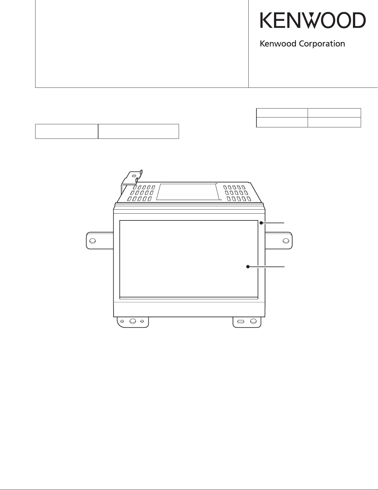
7-inch MULTI-DISPLAY
FGZ000UF2
SERVICE MANUAL
© 2005-7 CREATED IN JAPAN
B53-0302-00 (N) 0
SUBARU GENUINE
Destination North America
MODEL
FGZ000UF2 86281XA00A
PANEL
(A64-3397-01)
LCD
(B38-1100-05)
PARTS No.
FGZ000UF2
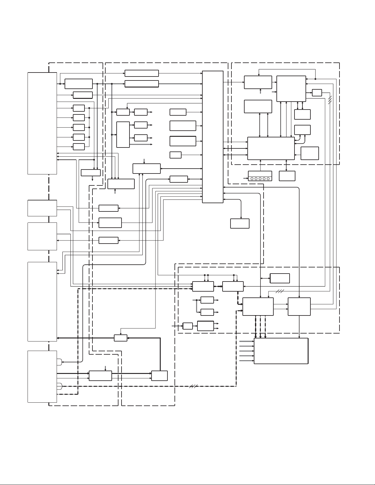
BLOCK DIAGRAM
J803 (B/3)
1-16PIN
CAR
CONNECTOR
2. +BATT
4. ACC
12. ILLUMI(PWM)
4. CAR SPEED
8. IGNITION
7. PARKING
10. REVERSE
11. ILLUMI
(SMALL)
6. CAN-H
5. CAN-L
16. PTT
1. GND
3. GND
15. GND
J800 (C/3)
RCA
1. AUX-V-IN2
2. AUX-DET
3. GND
J806 (C/3)
REAR
CAMERA
1. REAR-V-IN3
2. GND
3. GUIDE
(X14- ) (B/3)(C/3)
F800
INPUT
PROTECTION
Q803
ACC DET
Q801
DET
Q804
DET
Q800
DET
Q805
DET
Q806
DET
Q806,
810
ILLUMI+B
ILLUMI-V
SYNTHESIZER UNIT
(X14- ) (A/3)
Q26,28
+B VOL TAGE DET
+B
REG.
IC20 Q49
DC/DC
Q42 Q47
SW
IC8
CAN
TRASCEIVER
P5V
Q63
PTT-SW
Q5
ILLUMI
PWM DET.
Q62
REAR-SW
P-ON
SW
REG.
Q31
REG.
BU5V
IC17
IE BUS
TRASCEIVER
IC18
Q27,30
P5V
P-15.5V
P18.5V
P8.5V
IC1
RESET
X4
20MHz
MAIN CLOCK
X2
32.768kHz
SUB CLOCK
TH800
TH
CONTROL/DATA
IC16
BUFFER
IC22
BU5V
SYSTEM
u-COM
ELECTRIC UNIT
(X25- )
IC2,3
DOT CLOCK
DATA
SIGNAL
GENERATOR
IC19
FLASH ROM
IC12
RESET
SWTCH UNIT
(X16- )
ILLUMI-V
I2C BUS
I2C BUS
HARD KEY
IC7
E2PROM
8KB
V-SYNC
IC4
P5V
P8.5V
DATA
CONTROL
ADDRESS
GRAPHIC u-COM
TOUCH
PANEL
GRAPHIC
CONTROL
INT
IC11
RESET
SDRAM
(8MB)
SDRAM
(8MB)
MAIN
CLOCK
7.08MHz
IC5
VD
HD
IC6
RGB
D/A
C-SYNC
X1
J803 (C/3)
17-36PIN
AUDIO UNIT
20. F-BUS+
22. F-BUS-
19. GND
21. GND
23. RESET
24. AUDIO MUTE
26. BUS ON
17. BUS OFF
36. NAVI-AUDIO
J805 (B/3)
NAVI UNIT
10. NAVI-RX
11. NAVI-TX
8. NAVI-A-R
12. NAVI-A-L
7. NAVI-A-GND
1. NAVI-R
5. NAVI-G
9. NAVI-B
13. NAVI-SYNC
2.6. GND
18. +B
MONO
L/R
AUDIO-GND
P7.5V
IC800
ISOLATION
AMP
MUTE
Q17
VIDEO UNIT
(X35- )
V SIGNAL SW
IC200,201 IC203
IC31
+B B/L INV
IC10
L
R
MIX
SW
VIDEO SW
IC212
IC211
L35,36
N/A SW
SYNC SW
P5VREG.P7.5V
P3VREG.
VFL H
VFL L
IC202
VIDEO SIGNAL
PROCESSOR
P18.5V
P-15.5V
P5V
VFL H
VFL L
IC205
E2PROM
1KB
RGB
IC102
HD
TIMING
VD
CONTROL
B
R
G
LCD
2

FGZ000UF2
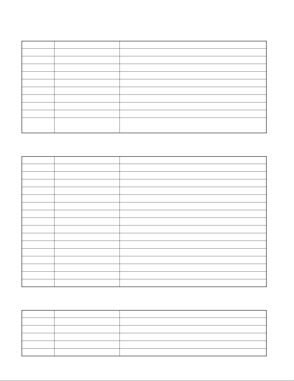
COMPONENTS DESCRIPTION
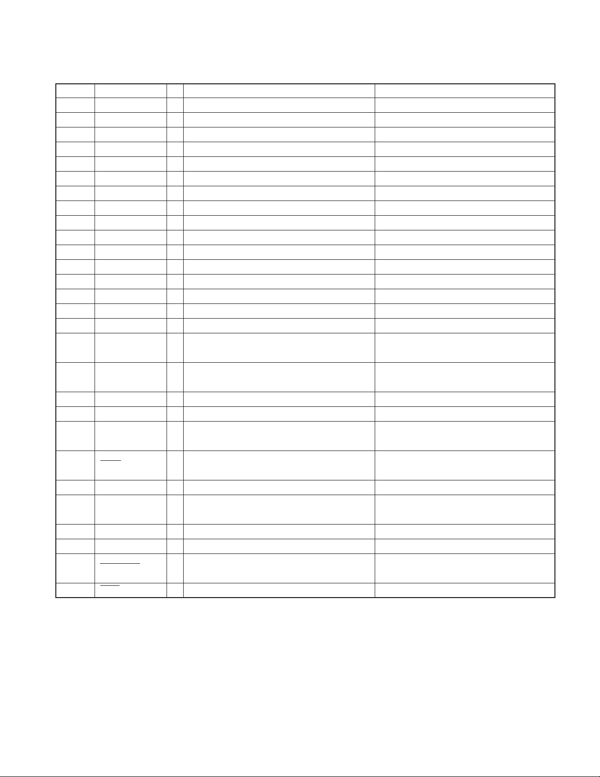
● SYNTHESIZER UNIT (X14-9490-10)
Ref. No. Application / Function Operation / Condition / Compatibility
IC1 Reset IC Backup 5V voltage monitoring. Resetting system µ-com at B.U OFF.
IC7 E2PROM Memory for reception TV station and touch panel compensation.
IC8 CAN transceiver Communication with vehicle unit.
IC9 Reset IC Detects 5V power supply ON.
IC10 Ope amp
IC16 Buffer Protects µ-com from communication line of the NAVI unit.
IC17 BUS transceiver Communication with the audio unit.
IC18 Regulator 5V power supply for system µ-com.
IC20 DC/DC controller Power supply in general (Other than system µ-com, key Illumination).
IC21 Reset IC Resetting abnormalities of the system µ-com.
IC22 System µ-com
IC23 Buffer Audio unit control. Writing to µ-com.
IC800 Isolation amplifier Removing noise from NAVI unit.
Q1,17,50,74 Audio mute Mute ON at power supply ON/OFF.
Q2,32,34~37,
Q39,41,46,53 IC20 power supply is turned OFF, when over current detected with DC/DC output.
Q4,31,57,61 Constant voltage power supply When Q61 is ON, outputs +18.5V.
Q5
Q6 Temperature detection SW When ACC ON, goes ON and starts temperature detection.
Q8~11,55,56,58 Video setting detection SW ON/OFF according to screen mode and adjustment.
Q12,15,18 Audio control SW When audio communication ON, Q18 is ON, when OFF, Q15 is ON.
Q14,47 Constant voltage power supply -15.5V constant voltage power supply.
Q24
Q26,28 Voltage detection When Q26 is ON, backup power supply voltage detection.
Q27,29,30,64 Constant voltage power supply Backup 5V power supply regulator.
Q33 Over current detection When detecting 18.5V over current, controller power supply OFF.
Q38 Over current detection When detecting 7.5V over current, controller power supply OFF.
Q40,42 DC/DC switching Switching of primary-side of transformer.
Q43,49 DC/DC switching 5V power supply switching.
Q44 Over current detection When detecting -15.5V over current, controller power supply OFF.
Q48 Over current detection When detecting 5V over current, controller power supply OFF.
Q62 Rear camera control SW ON at adjustment of rear camera and marker.
Q66~69 Watchdog timer Q67 is OFF at system µ-com run off.
DC/DC controller power supply
Key Illumination light adjustment
detection
Power supply momentary power
down detection
Bias power supply for internal audio circuit.
Mixing L/Rch of NAVI sound.
Controlling CAN communication and graphic µ-com.
Setting video source, screen zooming and brightness.
Communication with audio & NA VI units.
Monitoring internal power supply and abnormalities power supply and temperature.
When ACC is ON, IC20 power supply is turned ON.
ON when illumination PWM is input.
OFF at backup power supply momentary power down.
3
FGZ000UF2
COMPONENTS DESCRIPTION
Ref. No. Application / Function Operation / Condition / Compatibility
Q70,71 Low voltage power supply 7.5V power supply SW (ACC : ON).
Q700~702 Audio connection detection When audio is connected, Q700 is ON.
Q800 Parking detection ON when vehicle is parking.
Q801 Vehicle speed detection ON when vehicle speed pulse is input.
Q802 Reset input System µ-com is reset when Q802 is ON.
Q803 ACC detection ON when vehicle ACC is ON.
Q804 Ignition detection ON when vehicle ignition is turned ON.
Q805 Reverse detection ON when vehicle is reversed.
Q806 Small detection ON when vehicle small light is turned ON.
Q807~811
Key Illumination light adjustment
power supply regulator
● ELECTRIC UNIT (X25-9410-11)
Ref. No. Application / Function Operation / Condition / Compatibility
IC2 PLL oscillation IC Clock signal for graphic display.
IC3 Inverter Dot clock inverter.
IC4 Graphic controller Graphic display control.
IC5 Graphic controller work RAM Work area of graphic controller.
IC6 Video signal D/A conversion Converts the 8-bit signal from graphic controller to RGB signals.
IC7 Inverter DACK signal inverter.
IC10 OR gate OR output of 2 write enable signals.
IC11 Graphic µ-com work RAM Work area of graphic µ-com.
IC12 Graphic µ-com Graphic display control.
IC19
IC20 Inverter Synchronization signal inverter.
IC22 Inverter Graphic display area inverter.
IC23 AND gate Reset timing compensation.
IC26 3-terminal regulator Conversion from 8.5V to 5V.
IC27 Inverter Synchronization signal inverter.
Q2~5 Touch panel voltage detection Voltage detection at touch panel ON.
Display program, display bitmap data
In accordance with PWM duty, Illumination VCC (7V) is output.
Storage of graphic display data and program data.
● VIDEO UNIT (X35-4252-71)
Ref. No. Application / Function Operation / Condition / Compatibility
IC31 Switching regulator For backlight 7.5V power supply.
IC101 Ope amp Oscillation circuit low-pass output.
IC102 Timing controller LCD driver IC.
IC200,201 Video switch Input video signal switching.
IC202 Synchronization separation Separation of input video signals into horizontal and vertical synchronization.
4

FGZ000UF2
COMPONENTS DESCRIPTION
Ref. No. Application / Function Operation / Condition / Compatibility
IC203
IC205 E2PROM I2C memory backup.
IC207 Ope amp V-COM buffer.
IC209 Buffer with 3 circuits Synchronization signal output buffer.
IC211 3V regulator Constant voltage generation IC.
IC212 5V regulator Constant voltage generation IC.
IC217 Inverter For reversing side-black signal.
Q1 ACC ON/OFF SW For backlight power supply.
Q2 +B SW For backlight power supply.
Q3,4 ACC ON/OFF SW For backlight power supply.
Q31,32 SW regulator output buffer For FET drive.
Q33 DC/DC converter SW For backlight power supply.
Q35,36 Inverter oscillator SW For inverter.
Q37~39 Backlight adjustment SW For PWM light adjustment.
Q40 Over current protection For over current protection of backlight power supply.
Q41 Over current/voltage protection For over current/voltage protection of backlight power supply.
Q42,43 Backlight SW For turning backlight ON.
Q101 Oscillation circuit For reference oscillation of timing controller.
Q102 LCD control reversal For LCD up/down reversal control.
Q203,204 V-COM buffer For V-COM buffer.
Q205,206 Video signal buffer For viideo signal buffer.
Q209,210 Synchronization signal muting For muting at adjustment of timing controller.
X200
X201 Color demodulation 3.58MHz
Chroma decoder gamma compensation
Synchronization separation
reference oscillator
Conversion of input video signal into signal suitable for LCD input.
500kHz
5
FGZ000UF2
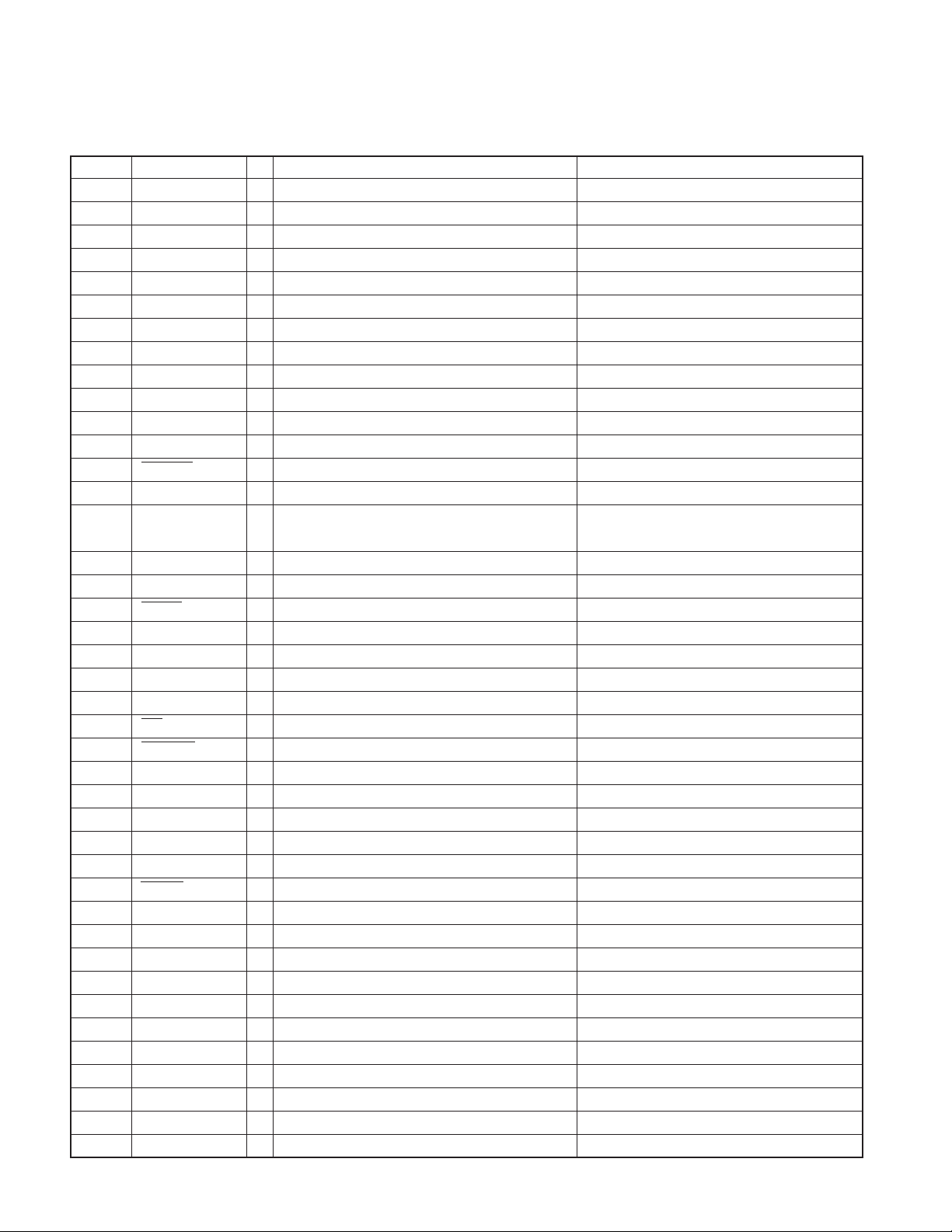
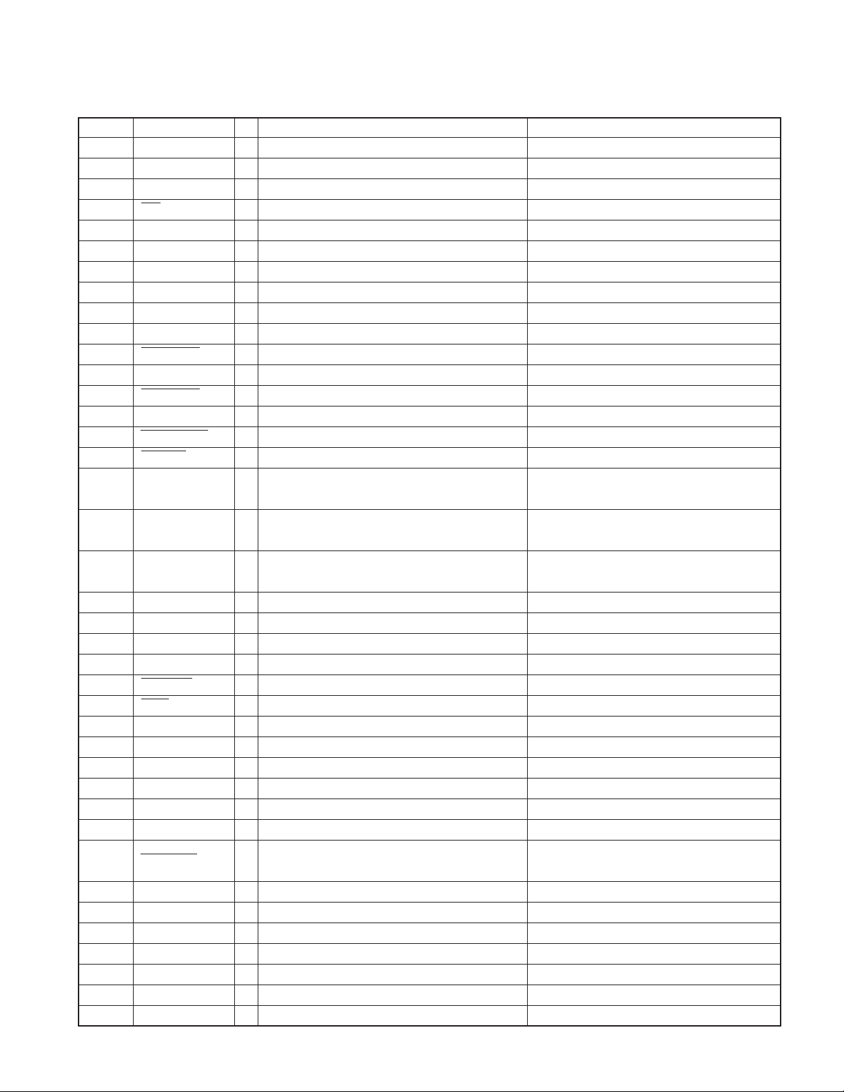
MICROCOMPUTER’S TERMINAL DESCRIPTION
● SYSTEM µ-com : IC22 (X14 : SYNTHESIZER UNIT)
Pin No. Pin Name I/O Application Processing Operation Description
1NAVI-TXD O
2NC-Not connected Not used
3 ILL PWM I ILLUMI PWM input (Cycle) PWM input
4 ILL PWM I ILLUMI PWM input (Oscillation width) PWM input
5 E2PSDA I/O IIC clock output (E2PROM) H, L output
6 E2PSCL O IIC data input/output (E2PROM) H, L output
7 SPD I Vehicle speed pulse input H, L input
8 WDP O Watchdog pulse output H, L output
9,10 NC - Not connected Not used
11 TYPE0 I Destination setting input H, L-fixed
12 NC I Not connected H, L-fixed
13 CAN EN O CAN communication enable H, L output
14 CAN STB O CAN communication standby H, L output
15 BYTE - Not used L-fixed
16 CNVSS I 5V at ROM writing
17 XCIN I Sub-clock input H, L input
18 XCOUT O Sub-clock output H, L output
19 RESET I Reset input H, L input, L : RESET
20 XOUT O Main clock input H, L output
21 VSS1 - GND GND
22 XIN I Main clock output H, L input
23 VCC1 - Power supply input VCC5V
24 NMI I NMI interruption input H-fixed
25 CAN ERR I CAN communication condition input H, L input, L : Error
26~29 NC - Not connected Not used
30 CAN IN I CAN reception data input H, L output
31 CAN OUT O CAN reception data output H, L input
32 NC - Not connected Not used
33 BRIGHT O Backlight control output PWM output
34 VMUTE O Video mute control output H, L output, L : MUTE
35 NC - Not connected Not used
36 I2CSCL O IIC clock output (E2PROM) H, L output
37 I2CSDA I/O IIC clock output (E2PROM) H, L input/output
38 TXD1 - Not used Not used
39 VCC2 - Power supply input VCC5V
40 RXD1 - Not used Not used
41 VSS2 - GND GND
42 SCLK - Not used Not used
43 BUSY - Not used Not used
44 SYSDATA O Data output (For video control processing) H, L output
45 SHDATA I Data input (For video control processing) H, L input
Transmission data output for normal NAVI communication
H, L output
H : Microprocessor mode, L : Single chip mode,
L : Memory expansion mode
6
FGZ000UF2
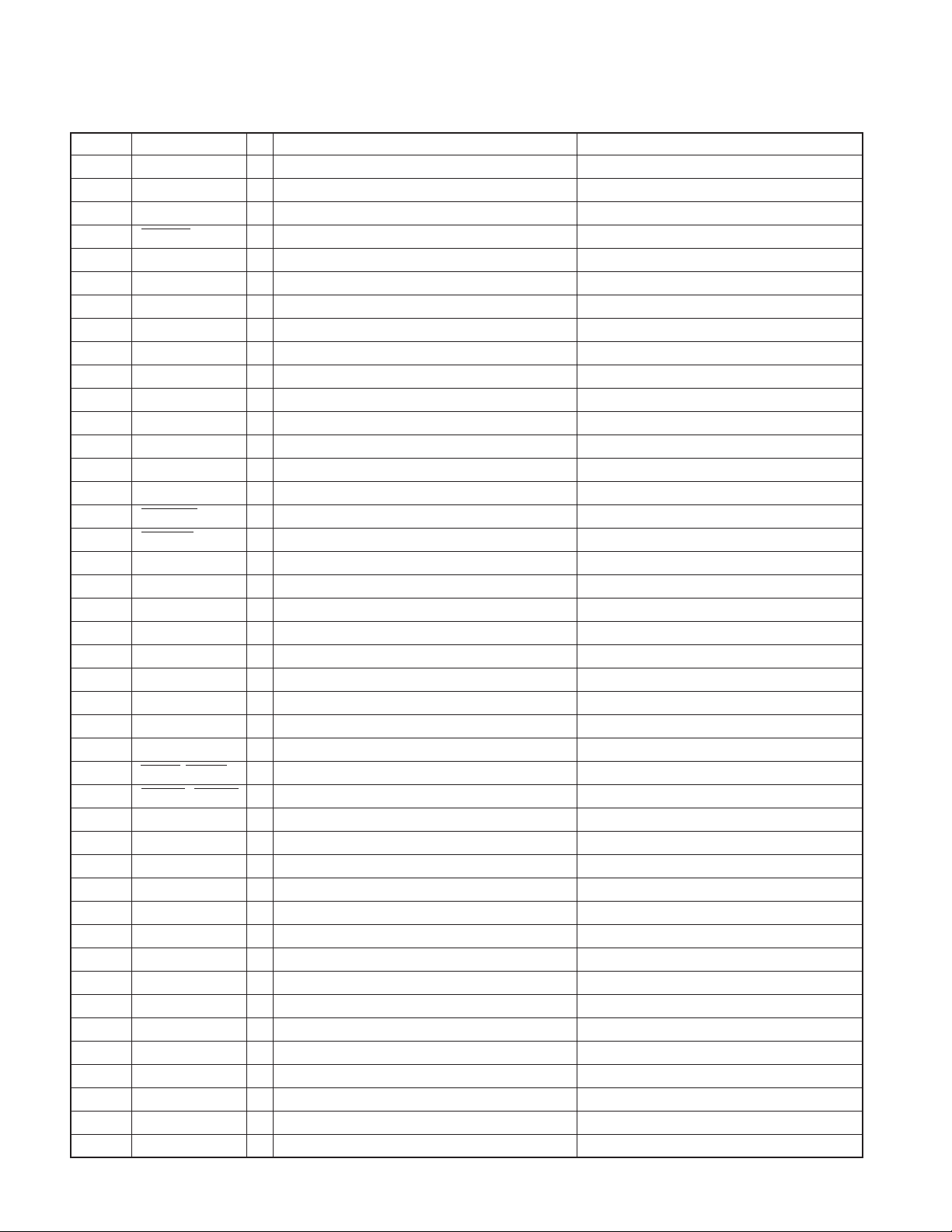
MICROCOMPUTER’S TERMINAL DESCRIPTION
Pin No. Pin Name I/O Application Processing Operation Description
46 SHCLK O Clock output (For video control processing) H, L output
47 SYSCS O
48 SHCS I Clock input (For video control processing) H, L input, L : Transmission request
49 STB O AUDIO BUS communication standby output H, L output, L : Standby
50 SI I AUDIO BUS communication data reception input H, L input
51 SO O AUDIO BUS communication data reception output H, L output
52 REAR GUIDE O Rear camera guide control output H, L output
53 NC - Not used Not used.
54 EMP I ROM write EPM input L-fixed
55 NC - Not used Not used
56 NAVI MUTE O NAVI voice signal output (At startup) H, L output, L : MUTE
57 VSS3 - GND GND
58 AUDIO DET I Audio voltage detection input H, L input, H : IE-BUS used
59 VCC3 - Power supply input VCC5V
60 AUDIO MUTE O AUDIO mute signal output H, L output, L : MUTE
61 NAVI INT O NAVI voice signal output (At output) H : Bch (CODEC AUDIO), L : Ach (NAVI AUDIO)
62 P ON1 O Power supply control output
63 P ON2 O PON7.5V control output
64 P ON3 O PON18.5V control output
65 CE I ROM writing CE input H-fixed
66 PLLCE O Q2i clock generation IC mode output H, L output, H : Program counter used PLL mode
67 PLLSDA O Q2i clock generation IC data output H, L output
68 PLLSCK O Q2i clock generation IC clock output H, L output
69 SHRESET O Graphic µ-com reset output H, L output, L : RESET
70 SHINI O Graphic µ-com initial output H, L output, L : INIT
71 SHRDY I
72 SHSTBY I Graphic µ-com standby transition complete input H, L input, H : Transition complete
73 SHCON O Graphic µ-com standby control output H, L output, L : Standby
74 VCC4 - Power supply input VCC5V
75 SH VMUTE I Graphic µ-com video mute request input H, L output, H : Video mute request
76 VSS4 - GND input GND
77 TOUCH EN O Graphic µ-com touch key analysis permission output
78 TOUCH I Graphic µ-com touch key ON notification input H, L input, H : Touch key ON, L : Touch key OFF
79 PTT O PTT output for telephone H, L output, H : ACTIVE
80 FAULT O FAULT display output H, L output
81 ON REQ - Not used Not used
82 OFF REQ - Not used Not used
83 BUS SYS ON - Not used Not used
84 BUS SYS OFF - Not used Not used
Transmission request output (For video control processing)
Graphic communication enable condition notification input
H, L output, L : Transmission request
H, L output
H : Power supply ON, L : Power supply OFF
H, L output
H : Power supply ON, L : Power supply OFF
H, L output
H : Power supply ON, L : Power supply OFF
H, L input, H : Communication preparation complete
H, L output
H : Analysis prohibited, L : Analysis permitted
7
FGZ000UF2
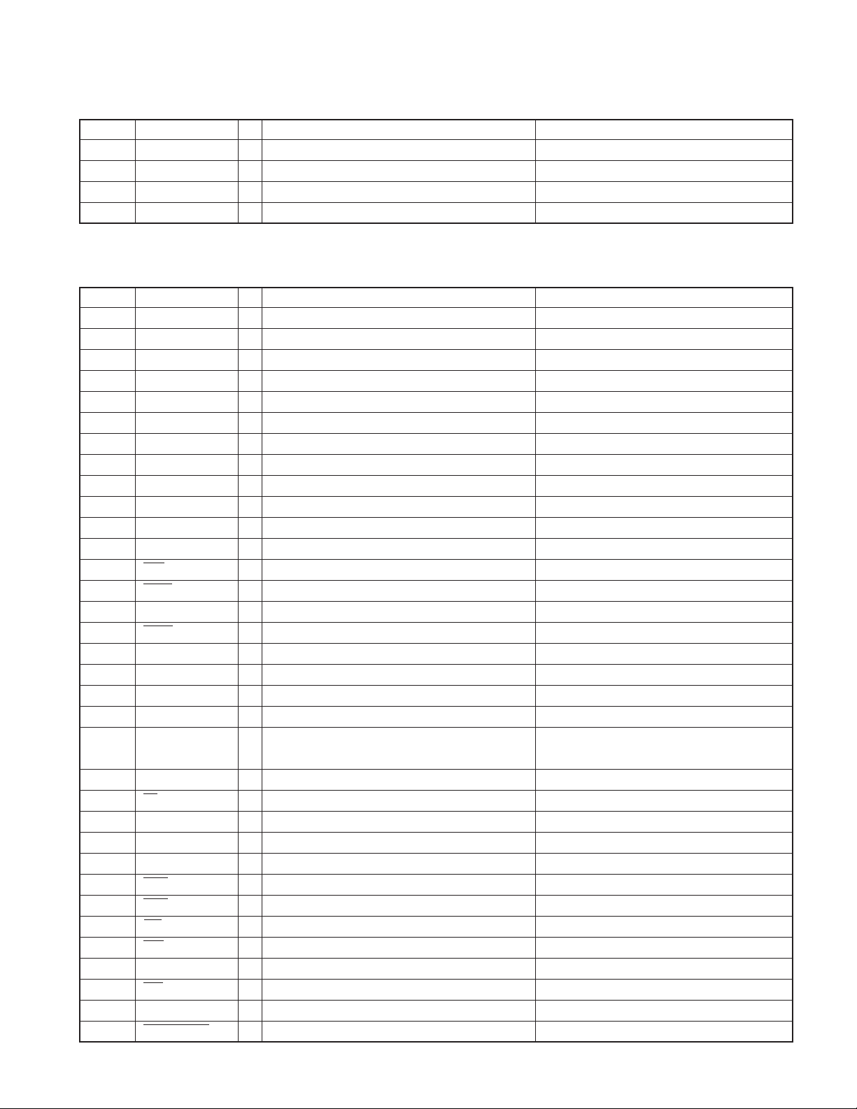
MICROCOMPUTER’S TERMINAL DESCRIPTION
Pin No. Pin Name I/O Application Processing Operation Description
85 NAVI ON O NAVI voice MUTE
86 BEEP ON O BEEP sound signal
87 NC - Not connected Not used
88 KEYDET I Key terminal connection detection H, L input, L : Detection
89 NC - Not used Not used
90 BL ON O Backlight switch output H, L output, H : Backlight ON
91 VCC5 - Power supply input VCC5V
92 SYNCMUTE O Video MUTE signal H, L output, H : MUTE
93 VSS5 - GND input GND
94,95 NC - Not connected Not used
96 +BDET I +B voltage detection input
97 TEMPDET I High temperature detection
98 PARKING I Parking detection input H, L input, H : Parking ON, L : Parking OFF
99 REVERSE I Reverse detection input H, L input, H : Reverse OFF, L : Reverse ON
100 IGN I Ignition voltage detection input H, L input
101 ILLSMALL I ILLUMI ON input H, L input, L : ILLUMI ON
102 ACC DET I ACC ON detection H, L input, H : ACC OFF, L : ACC ON
103 BUDET I +B voltage fluctuation detection input H, L input
104 NC - Not connected Not used
105 +BDET SW O +B voltage detection circuit control output H, L output
106 NC - Not connected Not used
107 AUX DET I AUX connection detection H, L input, H : Connection
108 REAR DET I Rear camera connection detection H, L input, L : Connection
109 NC - Not connected Not used
110,111 KEY-IN1,KEY-IN2 I Key input
112~116 NC - Not connected Not used
117,118 SCAN1,SCAN2 O Display mode selection switch output H, L output
119~122 HPOSI1~HPOSI4 O Horizontal position adjustment output H, L output
123 TV/REAR SW O AUX/REAR SW H, L output
124 DVD SW O RSE SW H, L output
125 V/N SW O NAVI SW H, L output
126 GRA SW O GRAPHIC SW H, L output
127~129 NC - Not connected Not used
130 VSS6 - GND input GND
131 NC - Not connected Not used
132 VCC6 - Power supply input VCC5V
133 RSE DET I RSE connection detection
134,135 NC - Not connected Not used
136 DC DC DET I PON5V voltage detection input H, L input
137 NC I Not connected Not used
138 BL DET2 - Backlight voltage detection input Analog input
139 BL DET1 I Backlight voltage detection input H, L input
140 AVSS - GND input GND
8
FGZ000UF2
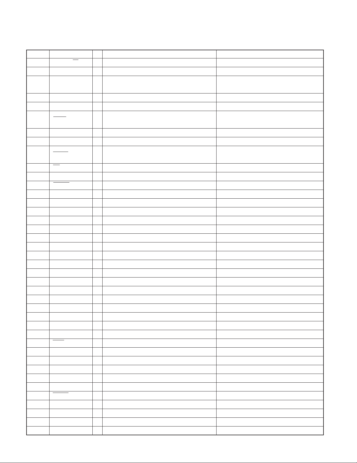
MICROCOMPUTER’S TERMINAL DESCRIPTION
Pin No. Pin Name I/O Application Processing Operation Description
141 NC - Not connected Not used
142 VREF I Reference voltage input VCC5V
143 AVCC - Power supply input VCC5V
144 NAVI-RXD I Normal NAVI communication reception data input H, L input
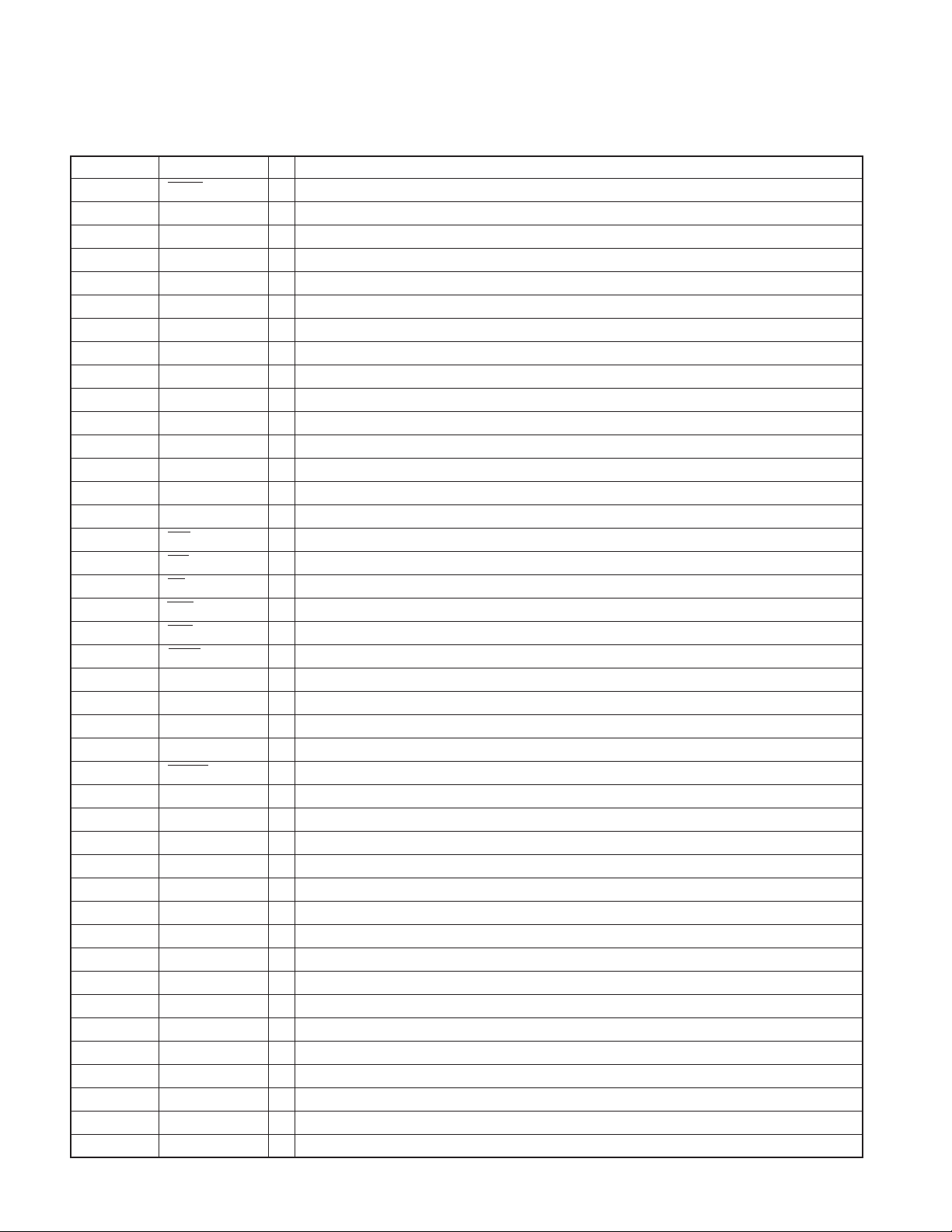
● GRAPHIC µ-com : IC12 (X25 : ELECTRIC UNIT)
Pin No. Pin Name I/O Application Processing Operation Description
1~5 NC - Not connected L-output
6 VSS I Ground input
7A0-Not connected L-output
8~11 A1~A4 O Address bus output H, L-output
12 VCC - Power supply input
13 A5 O Address bus output H, L-output
14 VSS - Ground input
15~25 A6~A16 O Address bus output H, L-output
26 VCC - Power supply input
27 A17 O Address bus output H, L-output
28 VSS - Ground input
29,30 NC - Not connected L-output
31 RAS O DRAM row address strobe output L : Row address strobe
32 CASL O DRAM low-side column address strobe output L : Column address strobe
33 NC - Not connected L-output
34 CASH O DRAM upper-side column address strobe input L : Column address strobe
35 VSS - Ground input
36 RDWR O DRAM write strobe output H : Read, L : Write
37~39 A18~A20 O Address bus output H, L-output
40 VCC - Power supply input
41 A21 - Not connected
42 VSS - Ground input
43 RD O External device read strobe output L : Read strobe
44 NC - Not used
45 SH VMUTE - Not connected L-output
46 NC - Not connected L-output
47 WRH O External device upper-side write output L : Write
48 WRL O External device lower-side write output L : Write
49 CS1 O Chip select output (Q2i internal register) L : Chip select
50 CS0 O Chip select output (Flash ROM) L : Chip select
51~53 NC - Not connected L-output
54 CS2 O Chip select outpout (Q2i UGM) L : Chip select
55 VSS - Ground input
56 ROM RESET - Not connected L-output
Not used since upper address is not used.
L-output
9
FGZ000UF2
MICROCOMPUTER’S TERMINAL DESCRIPTION
Pin No. Pin Name I/O Application Processing Operation Description
57 ROM RY/BY - Not connected L-output
58 NC - Not connected L-output
59 DACK O Q2i DMA transfer strobe output
60 NC - Not connected L-output
61 VSS - Ground input
62 DREQ I Q2i DMA transfer request input
63 VCC - Power supply input
64~68 NC - Not connected L-output
69 SYSCS I
70 IRL I Q2i interruption request input L : Interruption request
71 VSS - Ground input
72 SHCON I Graphic µ-com standby control input L : Standby
73~76 D15~D12 I/O Data bus input/output H, L-input/output
77 VCC - Power supply input
78 D11 I/O Data bus input/output H, L-input/output
79 VSS - Ground input
80~84 D10~D6 I/O Data bus input/output H, L-input/output
85 VCC - Power supply input
86 D5 I/O Data bus input/output H, L-input/output
87 VSS - Ground input
88~92 D4~D0 I/O Data bus input/output H, L-input/output
93 VSS - Ground input
94 XTAL I Crystal oscillator input
95 MD3 I Operation mode setting input H-input
96 EXTAL I Crystal oscillator input
97 MD2 I Operation mode setting input L-input
98 NMI I Non-maskable interruption input L-input
99 VCC - Power supply input
100 NC - Pull-up L-input
101 WAIT I Q2i wait cycle insertion input L : Wait cycle insertion
102,103 MD1, MD0 I Operation mode setting input H or L-input (Normal : L, Write : H)
104 PLLVCC I Power supply input for built-in PLL
105 PLLCAP I Power supply input for built-in PLL
106 PLLVSS I Ground input for built-in PLL
107 NC - Not connected L-output
108 SHRST I Reset input L : Reset
109 NC - Not connected Not used, L-output
110,111 NC - Not connected L-output
112 VCC - Power supply input
113 Y- O Switching output for touch panel input H, L-output
Graphic µ-com transmission request input
(System µ-com transmission request output)
H : Not used as transf er strobe is not used.
L-output
L : Not used as transfer request is not sued.
L-input
L : Transmission request
10
FGZ000UF2
MICROCOMPUTER’S TERMINAL DESCRIPTION
Pin No. Pin Name I/O Application Processing Operation Description
114 X- O Switching output for touch panel input H, L-output
115 Y+ O Switching output for touch panel input H, L-output
116 X+ O Switching output for touch panel input H, L-output
117 VSS I Ground input
118 KEYDATA1 I Touch panel data input (Y) Analog input
119 KEYDATA2 I Touch panel data input (X) Analog input
120 KEY6 - Not used. L-fixed
121~123 KEY5~KEY3 I Key switch input H, L-input
124 AVSS I Analog ground input
125,126 KEY2, KEY1 I Key switch input H, L-input
127 VREF I Reference voltage input
128 AVCC - Analog power supply input
129 VSS - Ground input
130 SYSDATA I
131 SHDATA O
132 SYSCLK I
133 ROM RXD I Flash ROM write data input
134 ROM TXD O Flash ROM write data output
135 VCC - Power supply input
136 SHSTBY O Graphic µ-com standby transition complete output H : Transition complete
137 TOUCH O
138 SHCS O
139 NC - Not connected L-output
140 SHRDY O
141 VSS - Ground input
142 NC - Not connected L-output
143 TOUCH EN I Graphic µ-com touch key analysis permission input
144 SHINI I Graphic µ-com initial input L : Not used as RESET is not used
Graphic µ-com data input (system µ-com data output)
Graphic µ-com data output (system µ-com data input)
Graphic µ-com clock input (system µ-com clock output)
Graphic µ-com touch key ON notice output
PTT-key ON notice output
System µ-com transmission request output
(Graphic µ-com transmission request input)
Graphic µ-com communication enable condition
notice output
H, L-input
H, L-input
H, L-input
Normally L-input
Data input when writing to flash ROM
Normally L-output
Data output when writing to flash ROM
H : Touch key ON, L : Touch key OFF
L : Transmission request
H : Communication preparation complete
H : Analysis prohibited
L : Not used as analysis permission is not used
11
FGZ000UF2
MICROCOMPUTER’S TERMINAL DESCRIPTION
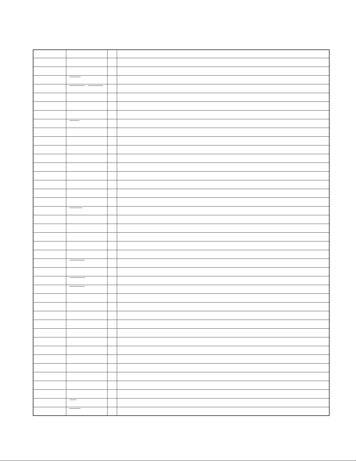
● GRAPHIC CONTROLLER : IC4 (X25 : ELECTRIC UNIT)
Pin No. Pin Name I/O Processing Operation Description
1 DREQ O DMA request
2, 3 D0, D1 I/O CPU data
4 CVCC1 - Power supply
5D2 I/O CPU data
6 CGND1 - Ground
7~11 D3~D7 I/O CPU data
12 CGND2 - Ground
13~15 D8~D10 I/O CPU data
16 CVCC2 - Power supply
17, 18 D11, D12 I/O CPU data
19 CGND3 - Ground
20~22 D12~D15 I/O CPU data
23 PGND - Ground
24 CAP0 - External volume terminal for communication circuit
25 PVCC - P ower supply
26 CS0 I/O Chip selection 0 (UGM)
27 CS1 I/O Chip selection 1 (Internal register)
28 RD I Read strobe
29 WE0 I Write pulse 0 (lower side)
30 WE1 I Write pulse 1 (upper side)
31 DACK I DMA acknowledge
32 MODE0 I Operation mode terminal 0
33 MODE1 I Operation mode terminal 1
34 MODE2 I Operation mode terminal 2
35 TEST I Test terminal
36 RESET I Reset
37 CLK0 I Q2i operation clock
38 GND1 - Ground
39, 40 A1, A2 I CPU address
41 VCC1 - Power supply
42~49 A3~A10 I CPU address
50 GND2 - Ground
51~60 A11~A20 I CPU address
61, 62 A21, A22 - Not connected
63 GND3 - Ground
64~68 MD0~MD4 I/O Memory data
69 GND4 - Ground
70 MD5 I/O Memory data
71 VCC2 - Power supply
72~78 MD6~MD12 I/O Memory data
79 GND5 - Ground
80, 81 MD13, MD14 I/O Memory data
12
FGZ000UF2
MICROCOMPUTER’S TERMINAL DESCRIPTION
Pin No. Pin Name I/O Processing Operation Description
82 VCC3 - Power supply
83 MD15 I/O Memory data
84 MWE O Memory write pulse
85, 86 MRAS0, MRAS1 O Lower selection signal
87 MLCAS O Lower column selection signal
88 MUCAS O Lower column selection signal
89 GND6 - Ground
90 MOE O Memory read pulse
91~93 MA0~MA2 O Memory address
94 VCC4 - Power supply
95~98 MA3~MA6 O Memory address
99 GND7 - Ground
100~104 MA7~MA11 O Memory address
105 GND8 - Ground
106 CLK1 I Display dot clock
107 VCC5 - Power supply
108 FCLK O 1/2 display dot clock
109 ODDF I/O Pulse indicating odd number field
110 GND9 - Ground
111 DCLK O Display clock
112 CDE O Color detection
113 VCC6 - Power supply
114 DISP O Display period pulse
115 CSYNC O Composite synchronization signal
116 GND10 - Ground
117 HSYNC O Horizontal synchronization
118 VSYNC O Vertical synchronization
119~121 DD0~DD2 O Display data
122 GND11 - Ground
123~125 DD3~DD5 O Display data
126 VCC7 - Power supply
127, 128 DD6, DD7 O Display data
129 GND12 - Ground
130~134 DD8~DD12 O Display data
135 GND13 - Ground
136 DD13 O Display data
137 VCC8 - Power supply
138~141 DD14~DD17 O Display data
142 CGND4 - Ground
143 IRL O Interruption request
144 WAIT O CPU wait
13
FGZ000UF2
TEST MODE
Outline
● How to Enter the Test Mode
Turn the power on while pressing on the 2 operation keys of
“MENU” and “AUDIO” on FRC000UF2, and the touch panel
on FGZ000UF2.
After ACC ON, keep on pressing on the 2 keys and the touch
panel until the image (Opening Screen) appears on the screen.
After the display of opening screen, the screen will display
test items.
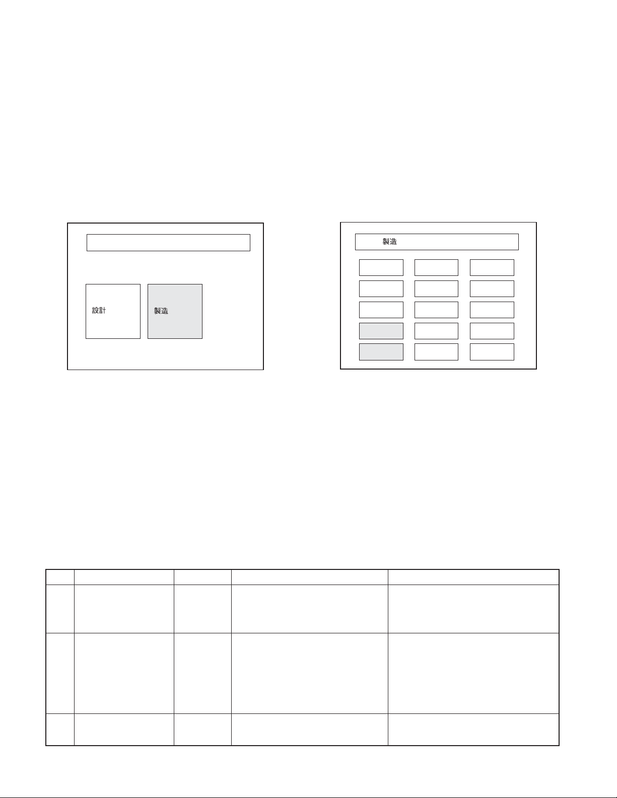
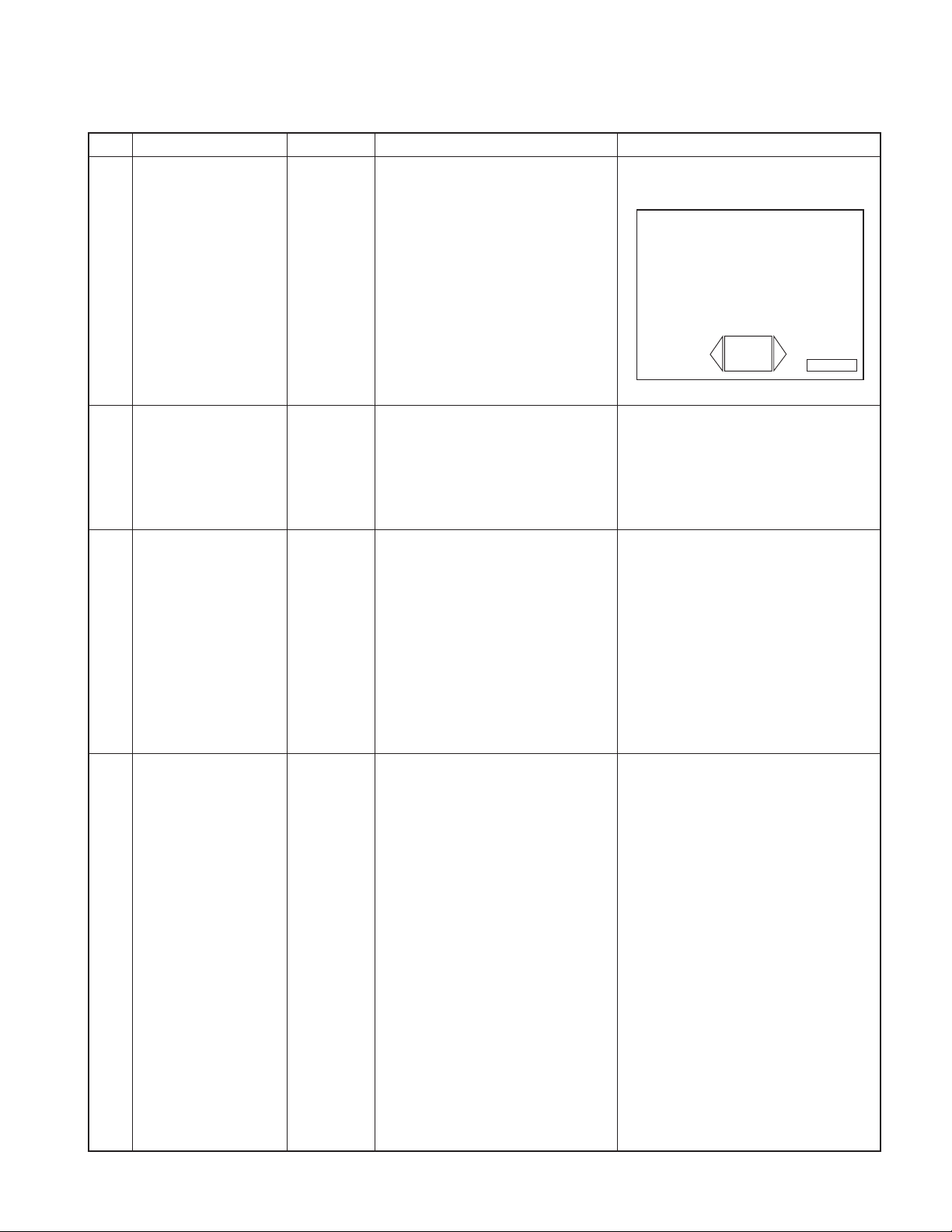
TEST MODE MENU (KENWOOD)
MODE
MODE
Test mode screen
Manufacturing Mode (Screen position adjustment)
● Outline of the Specifications
When the Manufacturing Mode is entered, the Item Selection
Screen is displayed and, when a button for a certain item is
pressed, the item will be selected. When providing the service, the start position adjustment in the screen display only
will be used.
MODE MENU (KENWOOD)
SCREEN(G)
SCREEN(A)
AUX
POSI(NAVI)
POSI(AUX)
Manufacturing mode selection screen
TV
NAVI
NIGHT
SOFT SW
HARD SW
STATUS
REAR
CONNECT
UCOM
TO MENU
● How to Release the Test Mode
The Test Mode is released when the ACC is turned off.
When releasing the test mode, the following are the default
condition:
• Screen adjustment
• TV NAME
• Maintenance information
● List of Specifications
No. Item Screen Operation Specification Remarks
1 SCREEN (G) NAVI Adjustment (Initial position: center) q The screen is switched depending on
q Brightness adjustment Minimum (0) ↔ Center (10) ↔ Max. (20) destination.
w Contrast adjustment w Color bar input when NAVI is used.
2 SCREEN (A) AUX Adjustment (Initial position: center) q White 100% is input by VIDEO input.
q Brightness adjustment Minimum (0) ↔ Center (10) ↔ Max. (20)
w Contrast adjustment
e Tint
r Color depth
3AUX AUX q White 50% is input by AUX input.
q Image stroke (1) No OSD
14
FGZ000UF2
TEST MODE
No. Item Screen Operation Specification Remarks
4 POSITION (NAVI) NAVI Adjustment (Initial C) q Adjustment screen in input through NAVI
q Screen position Right/Left keys are made with graphics, input.
adjustment which shifts the screen to right and left.
Adjustment range: 0~F.
NAVI
0E
5 POSITION (AUX) AUX Adjustment (Initial D) q Adjustment screen is input through VIDEO
q Screen position Right/Left keys are made with graphics, input.
adjustment which shifts the screen to right and left.
Adjustment range: 0~F.
TO MENU
6TVTVAdjustment (Initial: Center) q In order to switch sounds, AUDIO unit is
q Brightness adjustment -1 ↔ Center (14) ↔ +1 required.
w Contrast adjustment -1 ↔ Center (14) ↔ +1
e Tint -1 ↔ Center (10) ↔ +1
r Color depth -1 ↔ Center (10) ↔ +1
t Screen size Switching goes in the following order:
y Channel
u Sound TV sound is switched ON/OFF.
7NAVINAVI (RGB)
q White balance No OSD Contrast → Default w White 50% input
w Flicker Tint → Default e White 100% input
e Maximum brightness Color depth → Default r Confirmation on the RED, GREEN, and
r Brightness line, BLUE luster screens.
reduction line t Same as above.
t Point missing, y Color bar input
line missing u
y Screen beat i Color bar input
u
Gradation characteristics
i Color reproduction !0 White 50% input
o Confirmation on
visionary angle
!0 Screen roughness
!1 Image cross-talk (2)
FULL→JUST→ZOOM→NORMAL reception
NAVI screen, with maximum brightness set.
q White 100% input
Confirmation on crush of white and black.
o Color bar input
15
FGZ000UF2
No. Item Screen Operation Specification Remarks
8 NIGHT NAVI (RGB)
q Night screen No OSD Contrast → Default
brightness Tint → Default
9 SOFT SW Graphic Numeric displays on four corners of the
q Touch panel operation screen. When a number is pressed, the
10 HARD SW Graphic q By the switch information correspond-
q Hard switch (Hard switch ing to the external switch, the tint is
confirmation
screen) w
11 STATUS Graphic q Displays internal temperature of LCD
q Heater operation w Displays voltage
w Confirmation on e Displays version
excess current r Displays destination
e µ-com version
r Destination
12 REAR Rear camera The “marker adjustment signal” is
q
Rear image confirmation
w Guide line adjustment time the screen is pressed. Using this
13 CONNECT Graphic ● Vehicle unit ● Vehicle Unit (Condition)
q Confirmation on the q Integrated ECU By monitoring the communication condition,
vehicle unit w Meter “normal” or “abnormal” is displayed.
w Confirmation on the e Air-conditioner Alongside the vehicle unit items, the condi
connection unit ● Vehicle unit tions of the CAB BUS line are displayed.
e Confirmation on the q Audio (F-BUS) When a line is cut (one line out of two
vehicle signal w NA VI communication lines), “abnormal” is displayed.
r Confirmation on e Rear camera In other cases, “normal” is displayed.
vehicle CAN r TV tuner * When two lines re cut, this cannot be
image connected with the rear camera each
TEST MODE
NAVI screen, with minimum brightness set.
Color depth → Default
pressed number is displayed on the
screen in a large size.
switched each time the switch is pressed.
The key illumination is forced to turn on.
the guideline position is adjusted.
t AUX detected and “normal” is displayed.
● Vehicle signal * On the CAN format, the communication is
q Illumination possible with only one communication line.
w Illumination PWM This may cause the unit to display “normal”.
e IGN ● Vehicle unit (Connection)
r Parking The connection condition is monitored and
t Vehicle speed
y Reverse ● Vehicle signal
q White 100% input, with NAVI (RGB) input.
“connected” and “not connected” are displayed.
The terminal conditions are displayed.
16
