

Kenwood DV-6050 Service manual
MULTIPLE DVD/VCD/CD PLAYER
73
0
POWER
STANDBY
ON OFF
4
¢
DISC SKIP
SEQUENCE MODE
DISC 1
DISC 2
DISC 3 DISC 4
DISC 5
70%
DV-6050
SERVICE MANUAL
© 2002-10 PRINTED IN KOREA
B51-5831-00 (K/K) 1382
Knob(POWER)
(K27-2503-08)
Top cover
(A01-3854-08)
Cabinet panel
(A60-2323-08)
Con DIN socket
(E68-0018-08)
Crystal Window
(B10-3936-08)
Con phono socket
(E63-1311-08)x2
Button
(K29-8238-08)
Button
(K27-2502-08)
Clamp AC cord
(J42-0350-08)
Con DIN socket
(E63-1192-08)
In compliance with Federal Regulations, following are reproduction of labels on, or inside the product relating to laser
product safety.
Caution : No connection of ground line if disassemble
the unit. Please connect the ground line on
rear panel, PCBs, Chassis and some others.
Con phono socket
(E63-1244-08)
KENWOOD Corp. certifies this equipment conforms to DHHS
Regulations No.21 CFR 1040. 10, Chapter 1, subchapter J.
DANGER : Laser radiation when open and interlock defeated.
AVOID DIRECT EXPOSURE TO BEAM.
Slide switch
(S62-0115-08)
Wire-MCRDM
(E30-7250-08)
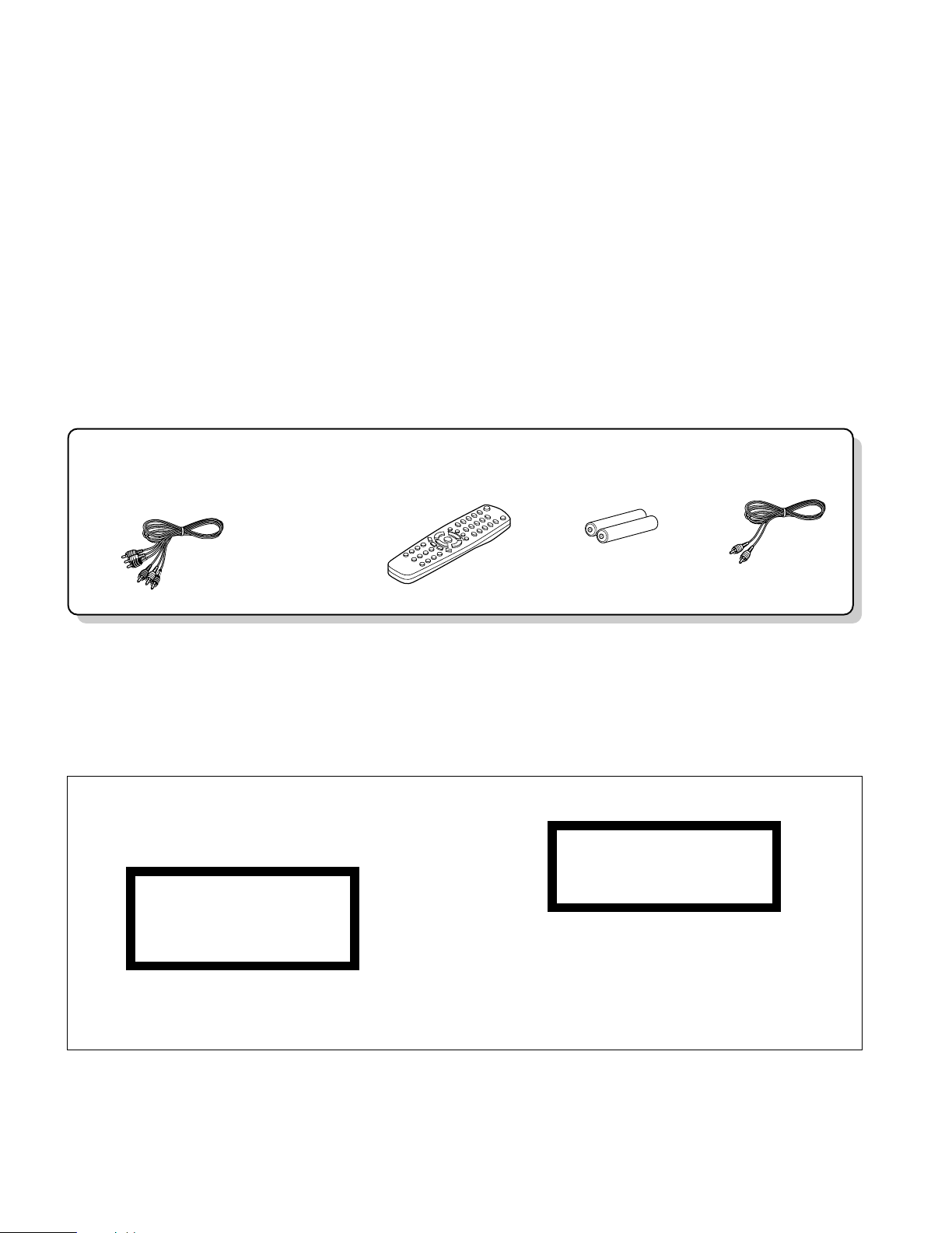
Batteries(R03/AA) ...(2)
Please confirm that the following accessories are present.
Audio video cord (Red, White, Yellow) ...(1)
(E30-2990-08)
Remote control unit ...(1)
(A70-1631-08)
Coaxial cable ...(1)
(E30-7235-08)
DV-6050
The marking of products using lasers
(For countries other than U.S.A., U.S.-
Military and Canada)
The marking this product has been classified as Class
1. It means that there is no danger of hazardous
radiation outside the product.
Location: Back panel
CLASS 1
LASER PRODUCT
Inside this laser product, a laser diode classified as
Class 2 laser radiation is contained as alerted by the
internal caution label shown above. Do not stare into
beam.
Location: DVD laser pick-up unit cover inside this
product
CAUTION
VISIBLE LASER RADIATION
WHEN OPEN. DO NOT
CONTENTS / ACCESSORIES
Contents
CONTENTS / ACCESSORIES .................................. 2
DISASSEMBLY FOR REPAIR....................................3
CIRCUIT DESCRIPTION ............................................4
ADJUSTMENT ..........................................................19
INTERCONNECTION DIAGRAM .............................20
PC BOARD .............................................................. 21
Accessories
SCHEMATIC DIAGRAM .......................................... 28
EXPLODED VIEW ....................................................43
PARTS LIST..............................................................44
SPECIFICATIONS ......................................Back cover
2
DV-6050
1 x9
x2
4
2
POWER
SWITCH
LEVER
3
3
4
4
N314
N315
N312
4
3
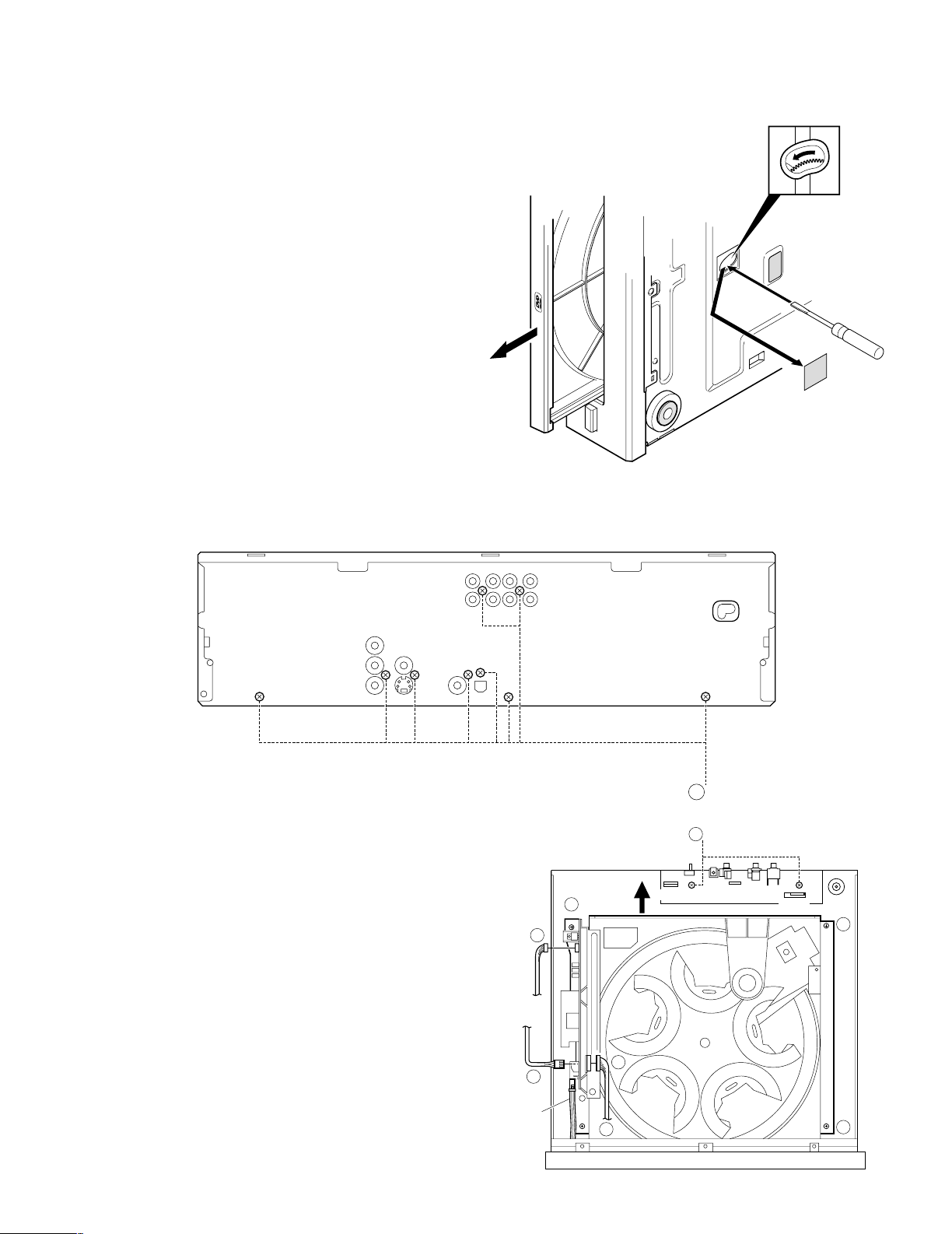
DISASSEMBLY FOR REPAIR
1. How to open the tray if it does not come out.
1. Remove the plastic plate.
2. Turn the gear fully CCW using a flat driver and so on in
the drawing through the hole on the loading chassis bottom.
3. Pull out the tray frontward by hand when it comes just
out.
Disassembling and Assembling the DVD mechanism, DVD B'D and OUT B'D FTMS for Video Signal Adjustment
1. To release the rear panel, remove screws (1x9)and optical cap.
2. Remove screws (2x2) and OUT B'D FTMS.
3. Remove connectors (3X3), power switch lever and screws (4x4).
Fig. 1
Fig. 2
3
DV-6050
x4
5
BOTTOM VIEW
CN1
CN74
CN15
CN53
CN33
CN55
CN2
CN1
CN33
CN53
CN15
CN2
GND
Use an Instalting Material
DISASSEMBLY FOR REPAIR
4. Pull out the DVD mechanism horizontally.
5. Up-side-down the DVD mechanism.
Fig. 3
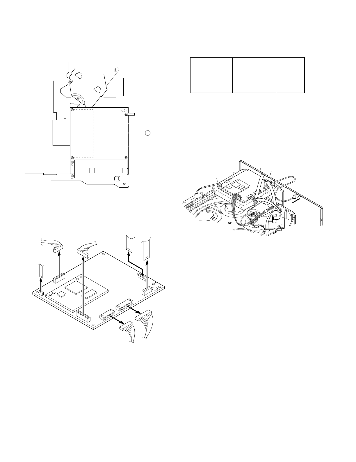
6. Remove screws (5x4) and DVD B'D.
7. Unplug the connectors ( CN15,CN53,CN55,CN74) and
disconnect 3 flexible cables (CN1,CN2,CN33).
10. Connect a jig (E35-2113-05) to CN33 instead of an original flexible cable (E35-1990-05).
CN33
(Flexible cable)
Original E35-1990-05 22cm
*
11. Plug in the connectors (CN15,CN53) and connect 2 flexi-
JIG E35-2113-05 35cm
* (This is a jig for video signal adjustment, after adjusted
it put back to an original flexible cable.)
ble cables (CN1,CN2).
* Note : The connectors (CN55, CN74) are for audio sig-
nal line so that no necessary to put it back when
video signal output adjustment.
Parts No. Remark
ó
Fig. 4
8. For the assembly procedure, follow the item 5 to 3 in
reverse.
9. Set up the DVD B'D on the top as figure 5.
Fig. 5
12. Follow the item 2 and 1 in reverse.
13. Gruond DVD B'D and rear panel as figure 5.
14. Follow the video signal output adjustment procedure.
4
DV-6050
VDAC : NTSC/PAL ENCODER
VOUT
FLI2200
CS4382
IC6
IC10
IC30
IC28
IC41
IC32
IC50
IC3
IC1
ADV7170SU
ADV7196
IC26
IC11
IC10
M95040
IC11
TVP503 AN8703FH VOUT
AVIF 2 SPDIF
3
6chOUT
2chOUT
88
MN5B00
3
SIO1 3
816
BUS 16
BU2092FV
3 SST39VF160 3
I2C
SIO0 API 3
PU
FEP
MN103S26E
SODC
AV Decoder
MN67 7531
64M SDRAM
VDAC
ADAC
SERIALPARALLER
FLASH
ROM
16M bits
EEROM
4k bytes
SETUP
REGION
KEY
SUB µcom
MN101C35D
KEY
FL
LED
MECHA.
CONTROL
REMOTE
CONTROLLER
WATER MARK
DETECTION
DVD µcom
MN102LP62G
Progre
ssive
VDAC
DRAM
2Mbyte
Driver ADAC
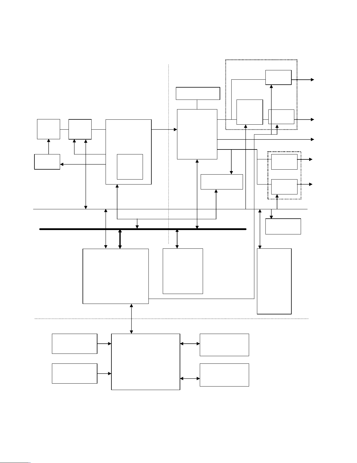
CIRCUIT DESCRIPTION
1. Microcomputer Periphery Block Diagram
5
DV-6050
CIRCUIT DESCRIPTION
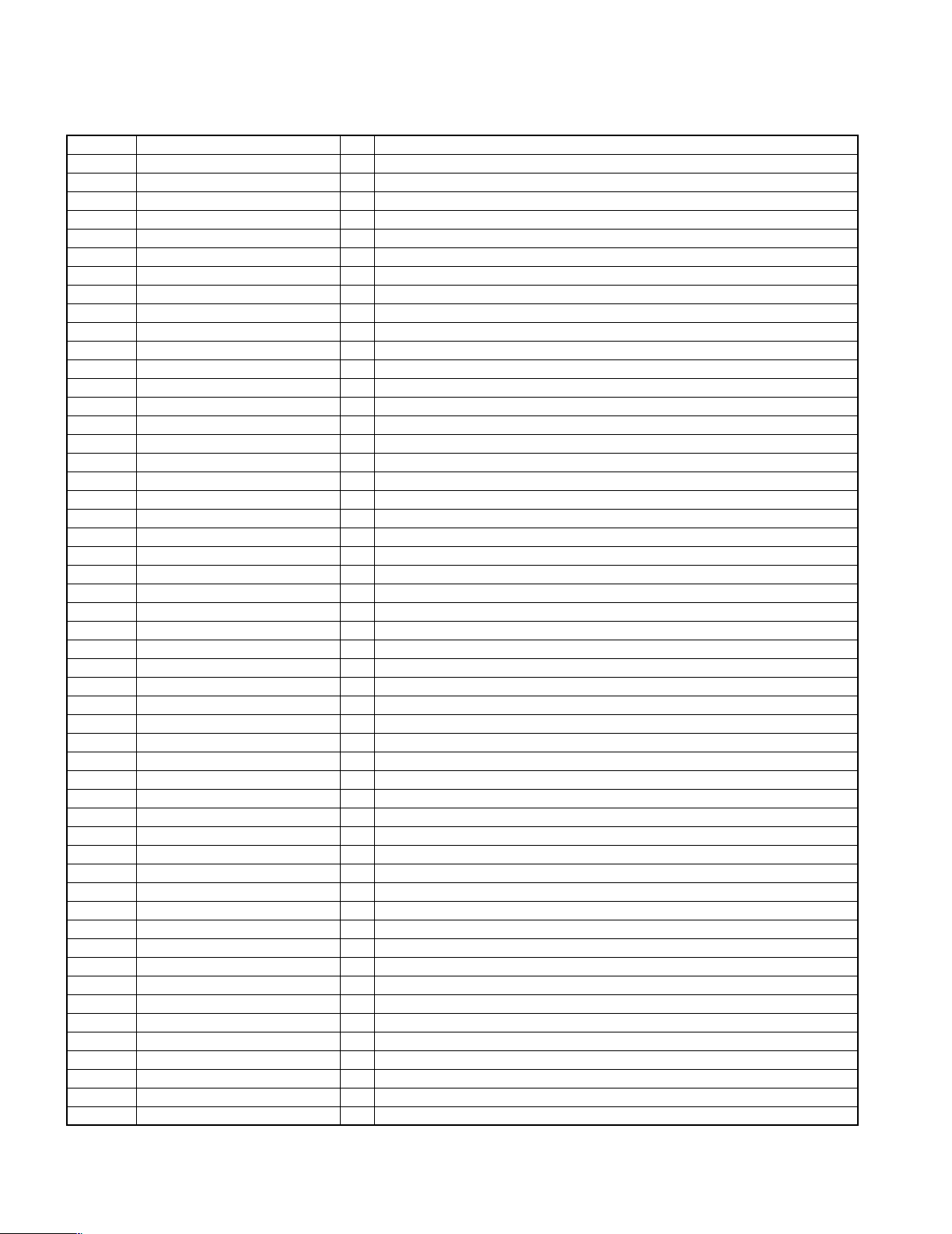
1-1 Pin Description of Sub Microcomputer : MN101C35D (FRONT, IC11)
Pin No. Pin Name I/O Pin Description
1 DATA OUT O Communication data output to DVD system microcomputer.
2 DATA IN I Communication data input from DVD system microcomputer.
3 CLOCK I Communication clock input from DVD system microcomputer.
4~7 NC O Unused.
8 VDD - Positive power supply (+5.0V).
9 X-TAL O Master clock (8.0MHz) output.
10 EXTAL I Master clock (8.0MHz) input.
11 VSS - GND
12 NC I Unused.
13 NC O Unused.
14 NC(MMCD) I Unused.
15 VREF - AD converter reference voltage.
16~18 AD INPUT KEY (1~3) I AD input key (1~3).
19 INPUT REGION TYPE 2 I AD input region type 2 (0V).
20 INPUT MODEL TYPE I AD input model type (5.0V).
21 INPUT REGION TYPE 1 I AD input region type 1(0.64V).
22 UP SW - Unused.
23 DOWN SW - Unused.
24 VREF + - AD converter reference voltage.
25 CE I Chip enable input.
26 RST I Reset signal input.
27 OPEN SW I Open switch input from mechanism.
28 CLOSE SW I Close switch input from mechanism.
29 ROULETTE CCW O Control port of rotary motor.
30 ROULETTE CW O Control port of rotary motor.
31 OPEN/CLOSE MOTOR CCW O Control port of tray motor.
32 OPEN/CLOSE MOTOR CW O Control port of tray motor.
33 REMOCON CONTROL I Input port of remote controller signal.
34 MECHA DISC SENSOR I Detection port of disc sensor for mechanism.
35 MECHA POSITION SENSOR I Detection port of position sensor for mechanism.
36,37 NC I Unused.
38 OPEN/CLOSE CHECK I Unused.
39 EEPROM DATA OUT O EEPROM serial data out.
40 EEPROM DATA IN I EEPROM serial data input.
41 EEPROM CLOCK OUT O EEPROM serial clock input.
42 LED OUT 1(DISC1) O On/off control port for disc 1 LED.
43 LED OUT 2(DISC2) O On/off control port for disc 2 LED.
44 LED OUT 3(DISC3) O On/off control port for disc 3 LED.
45 LED OUT 4(DISC4) O On/off control port for disc 4 LED.
46 LED OUT 5(DISC5) O On/off control port for disc 5 LED.
47 EEPROM CS O Chip select output to EEPROM.
48~50 NC O Unused.
51 G14 O Unused.
52 G13 O Unused.
53~64 G12~G1 O FL grid output (G12~G1).
65~86 P02~P23 O FL segment output (P02~P23).
87 P01 O FL segment output (P01).
88~96 NC O Unused.
97 VIDEO MUTE O Video mute control.
98 AUDIO MUTE O Audio mute control.
99 POWER CONTROL O Power relay control.
100 VPP - FL negative power supply.
6
DV-6050
CIRCUIT DESCRIPTION
1-2 Pin Description of DVD Microcomputer : MN102LP62G (DVD AUDIO FRONT END, IC26)
Pin No. Pin Name I/O Pin Description
1 WAIT I Bus wait port.
2
3 NWEL O Bus read port for AV Decoder/RAM.
4
5 RAMCS(SRAM) O SRAM chip select.
6 ODCCS O ODC chip select.
7 AVCS(AVDEC) O AV decoder chip select.
8 ROMCS(ROM) O Flash ROM chip select.
9 SCLOCK(VDAC) I/O VDAC 12C clock.
10 SDATA(VDAC) I/O VDAC 12C data.
11 FRD(ROM) O Flash ROM read port.
12 WORD I CSO bus width.
13~16 CPUADR(0~3) O Bus address (0~3).
17 VDD - Supply voltage (+3.3V).
18 SYSCLK(AVDEC) O External clock output for AV decoder.
19 VSS - Connected to ground.
20 XI I Unused.
21 XO O Unused.
22 VDD - Supply voltage (+3.3V).
23 OSCI(CLK135) I System clock input (13.5MHz).
24 OSCO O Unused.
25 MODE I Processor mode selection.
26~33 CPUADR4~11 O Bus address (4~11).
34 AVDD - Supply voltage (+3.3V).
35~42 CPUADR12~19 O Bus address (12~19).
43 VSS - Connected to ground.
44 CPUADR20 O Bus address (20).
45 CDH O Switching of DAC. CD
46 HFMON O HF monitor output of ADSC.
47 25BSY O Writing busy data output. Normal Busy
48 KMODE I Selection of writing mode for the ROM. Writing Normal
49 196BSY I Busy data input. Normal Busy
50 FROMWR O Enable control for writing jig.
51 TRVSW I Input port of traverse switch. Off On
52 AMUTE O Audio mute control.
53 FEPRST O FEP reset output.
54 VDD - Supply voltage (+3.3V).
55 FEPEN O Enable output to FEP (traverse).
56 NC O Unused.
57 STBSACD O Unused.
58 STBSP1 O Strobe output to serial-parallel converter.
59 STBDAC1 O Strobe output to ADAC.
60 STBPSL O Strobe output.
61 VSS - Connected to GND.
62 MSREADY I SACD ready signal input.
63 E2CS O Chip select to EEPROM.
64 PROGSW I Input port of program switch. Progressive Interlace
65 ICRST O Reset signal output to periphery ICs.
66 VDD - Supply voltage (+3.3V).
NRD(ODC/AVDEC
/SRAM)
NWEH(ODC/AVDEC
/SRAM/ROM)
O Bus read port for ODC/AV Decoder/SRAM.
O Bus read port for ODC/AV Decoder/SRAM/ROM.
Expension
Logic
HL
Mode
Except
CD
7
DV-6050
CIRCUIT DESCRIPTION
Pin No. Pin Name I/O Pin Description
67 SCLK0 O
68 SI0 I
69 SO0 O
70 SCLK1 O SIO1 clock output for control ICs.
71 SI1 I SIO1 data input for control ICs.
72 SO1 O SIO1 data output for control ICs.
73 PULL UP0 I Unused.
74 PULL UP1 I Unused.
75 NMI I Unused.
76 SODCINT0 I Interruption port from SODC.
77 SODCINT1 I Interruption port from SODC.
78 AVINT0 I Interruption 0 port from AV decoder.
79 WMINT I Interruption port from Water Mark Detector.
80 AVINT1 I Interruption port 1 from AV decoder.
81 ADSEP I Unused.
82 RST I Reset signal input.
83 VDD - Supply voltage (+3.3V).
84~91 CPUDT0~7 I/O Bus data (0~7) input and output.
92 VSS - Connected to GND.
93~100 CPUDT8~15 I/O Bus data (8~15) input and output.
SIO0 clock output to communicate between main
microcomputer and DVD system microcomputer.
SIO0 data input to communicate between main
microcomputer and DVD system microcomputer.
SIO0 data output to communicate between main
microcomputer and DVD system microcomputer.
Logic
HL
2. Key Matrix ✽ Pin Numbers of Sub Microcomputer
Voltage
0V PLAY/PAUSE STOP DISC1
0.64V - - -
1.35V OPEN/CLOSE SKIP UP/NEXT DISC2
2.18V DISC SKIP SKIP DOWN/PREV DISC3
2.75V - - DISC4
3.40V - - DISC5
AD INPUT KEY 1 AD INPUT KEY 2 AD INPUT KEY 3
✽ Pin 16 ✽ Pin 17 ✽ Pin 18
3. Pin Description of IC's
3-1 4ch BTL Driver : BA5823FM (DVD AUDIO FRONT END, IC5)
Pin No. Pin Name I/O Pin Description
1 BIAS1 I Input of bias1.
2 VIN1 I CH1 input.
3 VIN2 I CH2 input.
4 OPIN (+) I Not inverted input of OP-AMP.
5 OPIN (-) I Inverted input of OP-AMP.
6 OPOUT O Output of OP-AMP.
7 AGND - Analog ground.
8 MGND - GND
9 P.VCC2 - Power supply (+5.0V)
10 MUTE2 - Mute control of CH2.
11 DGND - Digital ground.
12 V02 (-) O Driver CH2 output (-).
13 V02 (+) O Driver CH2 output (+).
14 V01 (-) O Driver CH1 output (-).
15 V01 (+) O Driver CH1 output (+).
8
CIRCUIT DESCRIPTION
Pin No. Pin Name I/O Pin Description
16 V04 (+) O Driver CH4 output (+).
17 V04 (-) O Driver CH4 output (-).
18 V03 (+) O Driver CH3 output (+).
19 V03 (-) O Driver CH3 output (-).
20 MGND - GND
21 MUTE4 - Mute control of CH4.
22 P. VCC2 - Power supply (+9.0V)
23 MGND - PRE VCC
25 RREVCO - Terminated to VCC (+9.0V).
25 VIN3 I CH3 input.
26 LDIN I Loading input of CH4.
27 BIAS2 I Input of bias2.
28 TRIN I Traverse input of CH4.
29 MUTE3 - Mute control of CH3.
30 CNT - Control pin.
3-2 Front End Processor IC : AN8703FH (DVD AUDIO FRONT END, IC6)
Pin No. Pin Name I/O Pin Description
1 LPC1 I Laser pin input (DVD head).
2 LPCO1 O Laser drive output (DVD head)pin.
3 LPC2 I Laser pin input (CD head).
4 LPC02 O Laser drive output (CD head)pin.
5 VFO SHORT - Setting pin for RF short mode.(Terminated to ground.)
6 TBAL I Tracking balance control input.
7 FBAL I Focus balance control input.
8 POFLT - Detection filter of phase difference.
9 DTRD - Data read.
10 DGT - ID gate.(Terminated to ground.)
11 STANDBY - Setting pin for standby mode.
12 SEN I Serial transfer enable input.
13 SCK I Serial transfer clock input.
14 STDI I Serial transfer data input.
15 RSCL - Connection pin for reference current generation resistance.
16 JLINE - Connection pin for input resistance.
17 TEN I Inverted input pin of tracking error output amplifier.
18 TEOUT O Tracking error signal output.
19 AGCBAL - AGC balance.
20 ASOUT O Focus addition output.
21 FEN I Inverted input pin of focus error output amplifier.
22 FEOUT O Focus error signal output.
23 AGCOFST - AGC off set.
24 MON - Monitor pin for checking.
25 AGCLVL - AGC level.
26 GND2 - Ground for AGC.
27 VREF2 O VREF for AGC.
28 VCC2 - Power supply for AGC.
29 VHALF O VCC3/2
30 DFLTON O AGC/equalizer output (-)
31 DFLTOP O AGC/equalizer output (+)
32 DCFLT - Capacitance connection for filter output.
33 GND3 - Ground for logic.
34 RFDIFO O Radial differential signal output.
35 RFOUT O RF addition amp output
36 VCC3 - Power supply for logic.
37 RFC - RF delay correction amplifier filter.
DV-6050
9
DV-6050
CIRCUIT DESCRIPTION
Pin No. Pin Name I/O Pin Description
38 DCRF - DC cut filter pin for RF addition amplifier.
39 OFTR O OFTR output pin.
40 BDO O BDO output pin.
41 RFENV O RF envelope output.
42 BOTTOM - RF envelope bottom detection filter pin.
43 PEAK - RF envelope peak detection filter pin.
44 AGCG - AGC loop filter pin.
45 AGCO - AGC off set elimination filter pin.
46 TESTSG I Single signal input for test.
47 RFINP I RF differential signal input (+).
48 RFINN I RF differential signal input (-).
49 VIN5 I Internal RF (CD) input pin 1.
50 VIN6 I Internal RF (CD) input pin 2.
51 VIN7 I Internal RF (CD) input pin 3.
52 VIN8 I Internal RF (CD) input pin 4.
53 VIN9 I External RF (DVD) input pin 2.
54 VIN10 I External RF (DVD) input pin 1.
55 VCC1 - Power supply for servo.
56 VREF1 O VREF for servo.
57 VIN1(VB) I Internal RF (DVD) input pin 1.
58 VIN2VC) I Internal RF (DVD) input pin 2.
59 VIN3(VD) I Internal RF (DVD) input pin 3.
60 VIN4(VA) I Internal RF (DVD) input pin 4.
61 GND1 - Ground for servo.
62 VIN11(VE) I 3 beam sub (CD) RF input pin 2.
63 VIN12(VF) I 3 beam sub (CD) RF input pin 1.
64 HDTYPE - Switching pin of reference voltage or APC circuit polarity for DVD.
3-3 Digital Servo Control IC : MN103S26E (DVD AUDIO FRONT END, IC10)
Pin No. Pin Name I/O Pin Description
1 NINT0 O Unused.
2,5 NINT(1,2) O Interruption signal (1,2) to DVD CPU.
3,31,57,78,125,143,
156,162,169
4,19,32,60,77,81,
126,144,155,163, VSS - GND
170
6 WAITODC O Wait signal to DVD CPU.
7 NMRST O Reset output to DVD CPU (unused).
8 DASPST I Initial set point of DASP signal.
9~17,22~30 CPUADR(17~0) I Address (17~0) from DVD CPU.
18,76,152 VDD18 - Power supply (+1.8V) for IO.
20,58 DRAMVDD18 - Power supply (+1.8V) for DRAM.
21,59 DRAMVSS - Ground for DRAM.
33 DRAMVDD3 - Power supply (+3.3V) for DRAM.
34 MCS I Chip select signal from DVD CPU.
35 NWR I Write signal from DVD CPU.
36 NRD I Read signal from DVD CPU.
37~44 CPUDT(7~0) I/O DVD CPU data (7~0).
45 CLKOUT O Unused.
46 MMOD I Switching signal for test mode.
47 NRST I Reset input.
48 MSTPOL I Switching pin of polarity for master pin.
49 SCLOCK I Debug serial clock.
50 SDATA I Debug serial data.
VDD3 - Power supply (+3.3V) for IO.
10
CIRCUIT DESCRIPTION
Pin No. Pin Name I/O Pin Description
51 OFTR I Input of off track signal.
52 BDO I Input of drop out signal.
53~56,61~64 PWM(1~8) I/O General PWM (1~8)output.
65 TBAL O Tracking balance adjustment output.
66 FBAL O Focus balance adjustment output.
67 TRSDRV O Traverse drive output.
68 SPDRV O Spindle drive output.
69 FG I Input of motor FG.
70 TILTP O Tilt drive output (+).
71 TILT O Tilt drive reference output.
72 TILTN O Tilt drive output (-).
73 TX O Output signal of digital out (unused).
74 DTRD O Switching signal of frequency control for data section (unused).
75 IDGT O Switching signal of CAPA section (unused).
79 OSCI1 I Input of crystal oscillator (16.9344MHz).
80 OSCO1 O Output of crystal oscillator (unused).
82 TSTSG O EQ calibration signal.
83 VFOSHORT O Output pin of VFO short (unused).
84 JLINE O Setting pin of J-LINE.
85,94,102,113 AVSS - Ground for analog.
86 ROUT O Audio output of MASH Rch (unused).
87 LOUT O Audio output of MASH Lch (unused).
88,99,109,116 AVDD - Power supply (+3.3V) for analog.
89 VCOF I Control voltage for JFVCO.
90 TRCRS I Signal input for track cross formation.
91 CMPIN I WOBBLE comparator input (unused).
92 LPFOUT O LPF output (unused).
93 LPFIN I LPF input.
95 HRFOUT O HPF output (unused).
96 HRFIN I HPF input.
97 CSLFLT I Capacitor for CPDET (unused).
98 RFDIF I RF input for CPDET.
100 PLFLT2 I Capacitor 2 for PLL.
101 PLFLT1 I Capacitor 1 for PLL.
103 RV1 I Resistance for reference current source.
104 VREFH I Reference voltage input (+2.2V).
105 PLPLG I Resistance for PLL phase gain setting (unused).
106 VHALF I Reference voltage input (+1.65V).
107 DSLF2 I Capacitor 2 for DSL.
108 DSLF1 I Capacitor 1 for DSL.
110 NARF I Equivalent RF (-) input.
111 ARF I Equivalent RF (+) input.
112 JITOUT O Output pin for jitter monitor.
114 DAC0 O Output pin of tracking drive.
115 DAC1 O Output pin of focus drive.
117 AD0 I FE input.
118 AD1 I TEph/TE3b/Tepp input.
119 AD2 I AS input.
120 AD3 I RF envelope input.
121 AD4 I Input of phase difference for tangential (unused).
122 AD5/CAPAC2 I Upper CAPA envelope input /hold capacitor
123 AD6CAPAC1 I Lower CAPA envelope input /hold capacitor
124 TECAPA I Tracking error signal for CAPA.
127~130 MON(10~13) O Internal signal monitor (unused).
131 NEJECT I/O Detection pin of eject.
DV-6050
11
DV-6050
Pin No. Pin Name I/O Pin Description
132 NTRYCL I/O Detection pin of tray close.
133 NDASP I/O ATAPI drive active/slave input and output (unused).
134 NCS3FX I Selection of ATAPI host chip.
135 NCS1FX I Selection of ATAPI host chip.
136 DA2 I/O ATAPI host address.
137 DA0 I/O ATAPI host address (unused).
138 NPDIAG I/O Diagnosis input/output from ATAPI slave to master (unused).
139 DA1 I/O ATAPI host address (unused).
140 NIOCS16 O Selection of ATAPI host data bus width (unused).
141 INTREQ O ATAPI host interrupt request.
142 NDMACK I ATAPI host DMA request.
145 IORDY O ATAPI host ready output.
146 NIORD I/O ATAPI host data read.
147 NIOWR I/O ATAPI host data write.
148 DMARQ O ATAPI host DMA request (unused).
149~151,157~161,
164~168,171~173
153 PO I Terminated to ground.
154 UATASEL I Terminated to ground (unused).
174 VDDH - Reference power supply (+3.3V) for ATAPI.
175 NRESET I ATAPI host reset input.
176 MASTER I ATAPI master/slave selection.
CIRCUIT DESCRIPTION
HDD (0~15) I/O ATAPI host data (0~15).
3-4 Clock Generator : SM8703CV (DVD AUDIO FRONT END, IC14)
Pin NO. Pin Name I/O Pin Description
1 VDD - Digital power supply.
2 VSS - Digital ground.
3 MO1 O 27MHz fixed output pin 1.
4 MCK I Serial interface bit clock input.
5 MLEN I Serial interface latch enable input.
6 VDDA - Analog power supply.
7 VSSA - Analog ground.
8 XTI I Crystal resonator connection pin.
9 XTO O Crystal resonator connection pin.
10,11,17,21 RSV - Unused.
12 SO1 O 33.8688MHz fixed output pin.
13 VSS2 - Ground 2 for output.
14 VDD2 - Power supply 2 for output.
15 SO4 O Output for 512fs.
16 SO3 O Output for 512fs.
18 VSS1 O Ground 1 for output.
19 VDD1 - Power supply 1 for output.
20 SO2 O Output for 384fs.
22 SO5 O Output for 768fs.
23 FSEL/MDT I
24 MO2 O 27MHz fixed output pin 2.
Parallel mode : Sampling frequency Select Signal Input
Serial mode : Control Data Input
12
CIRCUIT DESCRIPTION
3-5 Serial Parallel IC : BU2092FV (DVD AUDIO FRONT END, IC28)
Pin No. Pin Name I/O Pin Description
Q0(5) SWIDE1 O Unused.
Q1(6) SWIDE2 O Unused.
Q2(7) Bass Manage O High : When bass management
Q3(8) LPF SEL O Switching Low Pass Filter
Q4(9) DACRST O Reset for Audio DAC
Q5(10) PROGH O High : When progressive
Q6(11) RGBL O Unused.
Q7(14) DWIDE1 O Unused.
Q8(15) YCL/DWIDE2 O Unused.
Q9(16) TNOCHG O Unused.
Q10(17) CLKSEL1 O Switching of sampling frequency
Q11(18) CLKSEL2 O Switching of MP3 clock
3-6 8-Channel D/A Converter : CS4382 (AUDIO, I400)
Pin No. Pin Name I/O Pin Description
1,3,45,47 DSDA(1~4) I Direct stream digital input (unused).
2,44,46,48 DSDB(1~4) I Direct stream digital input (unused).
4 VD - Positive power supply for the digital section.
5,31 GND - Analog ground.
6 MCLK I Master clock input.
7,10 LRCK(1,2) I L/R clock input.
8,11,13,14 SDIN(1~4) I Serial audio data input.
9,12 SCLK(1,2) I Audio output bit clock.
15 SCL/CCLK I Serial clock for the serial audio interface.
16 SDA/CDIN I/O
17 AD0/CS I
18 VLC I Control port power.
19 RESET I Reset signal input.
20 FILT+ O Positive reference voltage for the internal sampling circuits.
21 VQ O Filter connection for internal quiescent voltage.
22 MUTEC234 O Power down or if the master clock to left/right frequency ratio is incorrect.
23,24 AOUTB4(-,+) O Differential analog output for super woofer channel.
25,26 AOUTA4(+,-) O Differential analog output for center channel.
27,28 AOUTB3(-,+) O Differential analog output for RS channel.
29,30 AOUTA3(+,-) O Differential analog output for LS channel.
33,34 AOUTB2(-,+) O Differential analog output for FR channel.
35,36 AOUTA2(+,-) O Differential analog output for FL channel.
37,38 AOUTB1(-,+) O Differential analog output for mix R channel.
39,40 AOUTA1(+,-) O Differential analog output for mix L channel.
32 VA - Positive power supply for the analog section.
41 MUTEC1 O Mute control output.
42 DSD SCLK I Serial clock for the direct stream digital audio interface. (unused).
43 VLS I Serial audio interface power.
SDA is a data I/O line in two-wire mode.
CD IN is the input data line for the control port interface in SPI mode.
AD0 is a chip address pin in two-wire mode, CS is the chip select
signal for SPI format.
DV-6050
13
DV-6050
CIRCUIT DESCRIPTION
3-7 Video Deinterlacer : FLI2200 (VIDEO DEINTERLACER, IC1)
Pin No. Pin Name I/O Pin Description
Test outputs
112,113 TEST(00, 01) O
Test inputs
41,50,51,108
109,111 be tied low for normal operation.
Power Supply Connections(Not shown on Block diagram)
1,33,63,73,84,95,105,
114,123,137,144,151, VDD33 -
167
2,17,34,55,64,74,85,
96,106,115,124,132, VSS - Ground connections. Connect to the digital ground plane.
138,145,152,159,168
43 AVSS -
16,54,107,158 AVDD25 -
42 AVDD - to a separately decoupled +2.5 volt power supply and decouple
Control Signals
49 RESETB I
53 OE O be enabled ; when it is set low the outputs will be set into a
56~58 IFORMAT(2~0) I Input signal format control.
59~61 OFORMAT(2~0) O Output signal format control.
44,45 DADDR(1,0) - control bus to be programmed to prevent conflict with the
46 MODE - slave mode; allowing the device to programmed from an
47 SDA I/O 2-wire serial control bus data.
48 SCL I 2-wire serial control bus clock.
40 PIXCLK I Pixel clock input. This clock is used to drive all the circuits in the FL12200.
62 N/P/IN/OUT I/O NTSC/PAL input or output.
Control Signals(contd.)
52 NOMEM I No memory mode control input.
Input Signals
18~27 G/YIN(0~9) I 10-bit green or luminance signal input bus.
6~15 B/CbIN(0~9) I 10-bit blue or Cb chroma signal input bus.
28~32 R/CrIN(0~4)
35~39 R/CrIN(5~9)
3 HSYNCREFI I Horizontal sync or reference.
4 VSYNCREFI I Vertical sync or reference.
5 FIELDIN I Field identifier input.
Output Signals
65~72 G/YOUT(2~9)
75,76 G/YOUT0,1
93,94 B/CbOUT8,9
97~104 B/CbOUT(0~7)
TEST(0~5) -
These pins are test outputs and should be left unconnected in
normal operation.
These pins are used for test purposes only and should always
Pad Ring digital power connections. Connect to the digital +3.3
volt power supply and decouple to the digital ground plane.
Ground connection for the clock PLL circuits.
Connect to the digital ground plane.
Core Logic digital power connections. Connect to the digital
+2.5 volt power supply and decouple to the digital ground plane.
Analog power connections for the clock PL Lcircuit. Connect
directly to the AVSS pin.
Reset. When this input is set low it will reset all the internal
registers to the default states.
When this pin is set high the the outputs of the FL12200 will
high-impedance state.
The settings of DADDR(1,0) allow the device address of the
other devices connected to the bus.
When this pin is set low the control bus will operate in the
external controller.
I 10-bit red or Cr chroma signal input bus.
O Green or luminance output bus.
O Blue or Cb chrominance output bus.
14
 Loading...