

Kenwood DV-605, DVFR-5060-S Service manual
70%
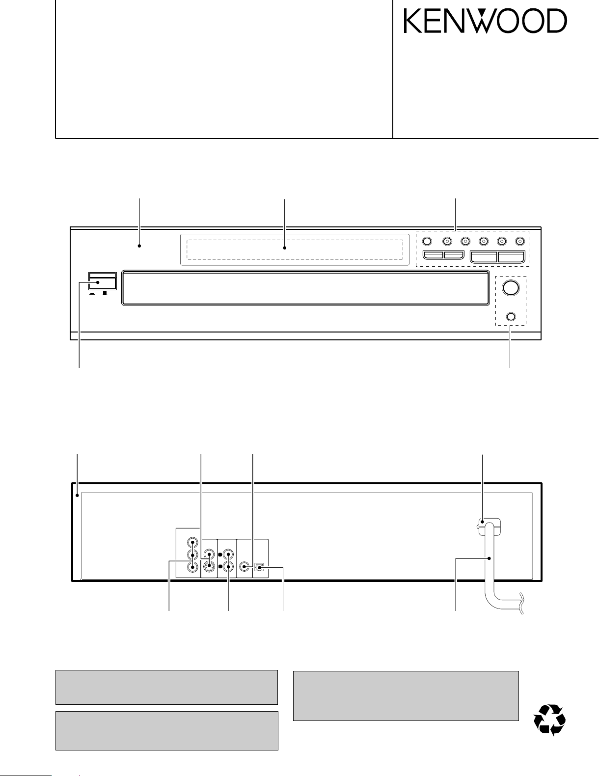
MULTIPLE DVD/VCD/CD PLAYER
76
0
POWER
ON OFF
4
¢
DISC SKIP
SEQUENCE
MODE
DISC 1
DISC 2
DISC 3 DISC 4
DISC 5
AUDIO
OUTPUT
VIDEO
OUTPUT
S-VIDEO
OPTICALCOAXIAL
L
R
COMPONENT
VIDEO OUTPUT
Cr
Cb
Y
DV-605/DVF-R5060-S
SERVICE MANUAL
© 2002-7 PRINTED IN KOREA
B51-5802-00 (K/K) 1402
Knob(POWER) *
(K27-)
Top cover *
(A01-)
Cabinet panel *
(A60-)
DIN socket
(E68-0018-08)
Phono socket
(E63-1244-08)
Crystal Window *
(B10-)
Button *
(K29-)
Button *
(K27-)
AC power cord bushing
(J42-0350-08)
Phono socket
(E63-1192-08)
Phono socket
(E63-1227-08)
In compliance with Federal Regulations, following are reproduction of labels on, or inside the product relating to laser
product safety.
Caution : No connection of ground line if disassemble
the unit. Please connect the ground line on
rear panel, PCBs, Chassis and some others.
Oscillating module
(GP1F32T)
AC power cord
(E30-7250-08)
* Refer to parts list on page 19.
KENWOOD Corp. certifies this equipment conforms to DHHS
Regulations No.21 CFR 1040. 10, Chapter 1, subchapter J.
DANGER : Laser radiation when open and interlock defeated.
AVOID DIRECT EXPOSURE TO BEAM.
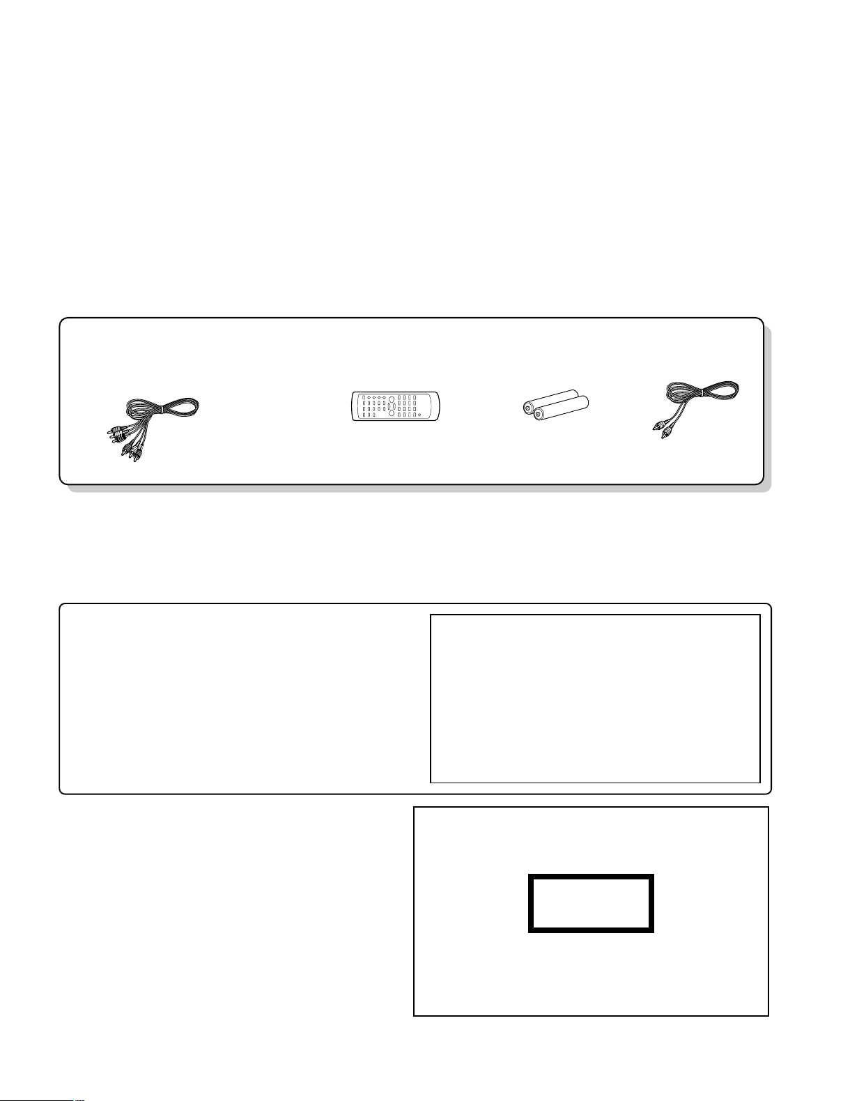
Batteries(R6/AA) ...(2)
Please confirm that the following accessories are present.
Audio video cord (Red, White, Yellow) ...(1)
(E30-2990-08)
Remote control unit ...(1)
(A70-1570-08)
Coaxial cable ...(1)
(E30-7235-08)
DV-605/DVF-R5060-S
The marking of products using lasers
(For countries other than U.S.A., U.S.-Military and Canada)
The marking this product has been classified as Class 1. It
means that there is no danger of hazardous radiation outside
the product.
Location: Back panel
CLASS 1
LASER PRODUCT
Operation to reset
÷ Please note that resetting the microprocessor clears the
contents stored in, it returns the microprocessor to the condition when it left the factory.
1 In Power ON condition, keep the DISC 3 key and the 4
(Skip) key pressed at the same time.
2 When both keys are pressed, the region code of the unit,
the software version, etc. will be displayed on the display. (When nothing is done, the display of this information continues.) Example: 72. 14.02:05
3 Press the DISC 4 key and the
44
44
4 key at the same time.
"BYE" will be shown on the display.
4 Press the POWER ON/OFF switch to go to Power OFF.
5 When Power ON is performed with the POWER ON/OFF
switch, the settings become the default factory settings.
The microprocessor may fall into malfunction (impossibility to operate erroneous display, etc.) when the
power cord is unplugged while power is ON or due to
an external factor. In this case, execute the following
procedure to reset the microprocessor and return it to
normal condition.
CONTENTS / ACCESSORIES / CAUTIONS
Contents
CONTENTS / ACCESSORIES / CAUTIONS............. 2
DISASSEMBLY FOR REPAIR....................................3
BLOCK DIAGRAM ......................................................4
ADJUSTMENT ............................................................4
PC BOARD ................................................................ 5
Accessories
SCHEMATIC DIAGRAM .......................................... 11
EXPLODED VIEW ....................................................17
PARTS LIST..............................................................19
SPECIFICATIONS ......................................Back cover
Cautions
2
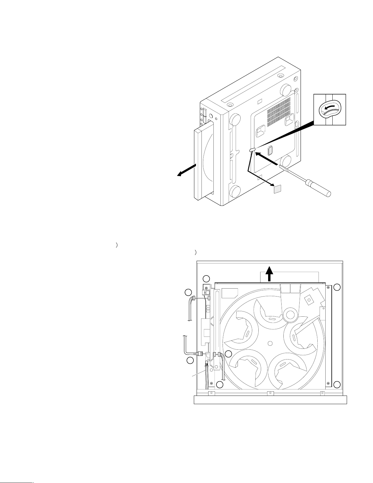
DISASSEMBLY FOR REPAIR
PLASTIC
PLATE
2
3
4
4
44
1
POWER
SWITCH
LEVER
1. How to open the tray if it does not come out.
(Fig.1)
1. Remove the plastic plate.
2. Turn the gear fully CCW using a flat driver and so on in the
drawing through the hole on the loading chassis bottom.
3. Pull out the tray frontward by hand when it comes just out.
DV-605/DVF-R5060-S
2. How to remove the DVD mechanism. (Fig.2)
1. Remove connectors (1~3 and power switch lever.
2. To separate the DVD mechanism, remove screws (4x4
and pull it out backward.
Fig. 1
Fig. 2
3
+5VS
FL AC
FL AC
-27V
ADDR+
F-WE
F-DE
F-RESET
ADDR+
D-RAS0-
RDNOTWR
DATA +
D-CAS0-
D-CAS1-
F-CE
F-OE(DRAM OE)
+5V6S
TXD
RXD
RESET MAIN
IRQ2
+3V3-RESET
EXIT-DATA
EXIT-BCLK
EX IT-D ATAVALI D
EXT-PSTART/ERROR
F/E SDATA
+9V MOTOR VCC
+9V MOTOR VCC
+3.3V DIGITAL VCC
+5V DIGITAL VCC
F/E SCL
PCM-DATA
DAC LATI25
DAC SCKDSD
DAC SDIDEM
DAC MUTEB
CSBWL
PCM MCLK
PCM LRC
PCMCLK
AUDIO MUTE
CVBS-OUT
Y-OUT
C-OUT
I (Y)-OUT
I (Y)-OUT
I (Y)-OUT
P (Cr)-OUT
P (Cb)-OUT
P (Y)-OUTP SCAN CLK
P SCAN DATA
P SCAN STB
VIA2-VIA8
GND
SPDIF
VIDEO MUTE
PIXCLK-27MHZ
SDA SCL
L AUDIO
R AUDIO
F-OE(DRAM OE)
DAC ZERO
DATA +
AC CORD
+9V ANALOG VCC
-9V ANALOG VCC
+5V DIGITAL VCC
+3.3V DIGITAL VCC
+9V MOTOR VCC
5V FRONT
IC91 FL
M29F400T-90N1
8MBIT
FLASH MEMORY
IC41
HY57V651610BLTC-8
SDRAM-64MBIT
IC31
125MHz
IC21
MPEG
STI5519
IC61
DAC
WM8728
L.P.F
L.P.F
BA4560
MUTE
JK82
Lch
Rch
MIXED
IC11
PM0026
PROGRASSIVE
I/P
TR
DRIVER FOR
75 ohm x2
IC12
PROGRASSIVE
6CH/6dB/FOR
MM1568
DVD
SWITCHING
CVBS-VIDEO
JK83A
JK83B
S-VIDEO
Y
JK84
Cr
Cb
RCA 3V
JK87
ON/OFF
P SCAN
SW
BUFFER COAXIAL
JK81
OPTICAL
IC85
IC51
74HCU04
HEX INVERTER
IC22
EEPROM
M24C02
Q61R
Q61L
SMPS
TVM MECHA
F/E & MECHA
DV-605
DV-605/DVF-R5060-S
No. ITEM INPUT SETTING
OUTPUT SETTING
ALIGNMENT
POINT
ALIGNMENT
FOR
FIG.
1
Progressive
Y LEVEL
100% COLOR
BAR DISC
Connect the oscilloscope to
Y output(JK84) with 75-ohms resistor.
Output Mode: Progressive
VR11
Y-signal=
1000mV±100mV
FIG.1
1000mV
±100mV
Y
4.7µs
-286
0
714
(100IRE)
[mV]
white
yellow
cyan
green
magenta
red
blue
black
714
641
516
443
324
252
127
54
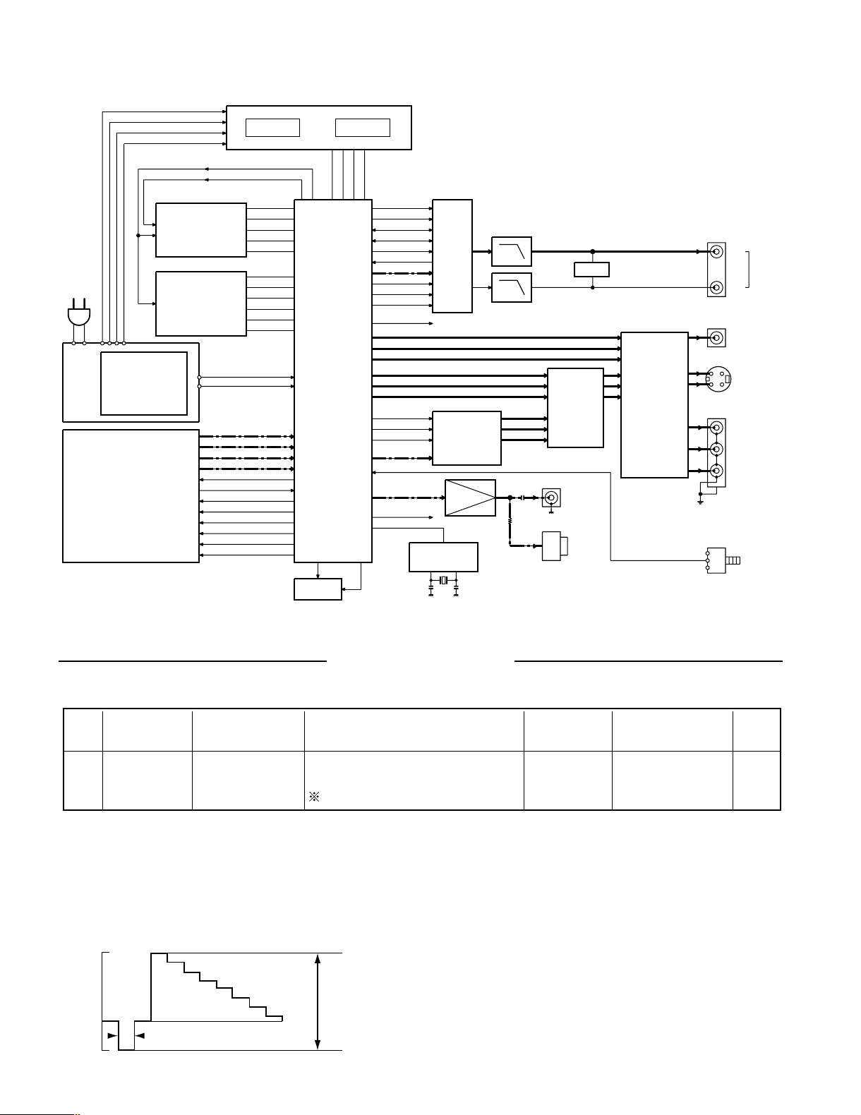
BLOCK DIAGRAM
Adjustment Method & Precautions
1. Play Back 100% White Pattern
2. Channel 2 : OSC Probe, Composite(JK83-A)
3. Channel 1 : OSC Probe, Y(JK84) output
Channel 2 : Trigger
4. OSC Time / Div Control
5. VR11Variable : See the Scope Wave
4
Fig. 1
ADJUSTMENT
DV-605/DVF-R5060-S
CIRCUIT DESCRIPTION
1. Pin Description of MPEG Processor (Main, IC21)
Pin No. Pin Name I/O Pin Description
PIOs and communication
1 PIO2(5) DAC SDIDEM IN/OUT I/O DAC data input and output.
2 PIO2(6) DAC MUTEB IN/OUT I/O DAC mute control.
3 PIO2(7) DAC CSBIWL OUT O DAC chip select.
6 PIO3(0) PRO SCAN ON/OFF I P. Scan switch input.
7 PIO3(1) I/O Unused.
8 PIO3(2) O PROG-H
9 PIO3(3) O PM0026A (IC11) Clock
10 PIO3(4) IR REMOCON I/O IR Remote controller signal output (Unused).
11 PIO3(5) O PM0026A (IC11) data
12 PIO3(6) O PM0026A (IC11) STB
13 PIO3(7) DVD RESET I/O Power- on reset of front-end module.
Front-end
16 B DATA I I2S Data
17 B BCLK I I2S Bit clock
18 B FLAG I I2S Error flag
19 B SYNC I/O I2S Sector / ABS time
Reserved
20 B WCLK I/O Unused.
21 B V4 I/O Unused.
22 NRSS OUT I/O Unused.
23 VDD RGB - Supply voltage for RGB (+2.5VA).
24 VSS RGB - GND
Video DAC
25,26,27 B/G/R (OUT) O B/G/R signal outputs.
28 V REF RGB I Reference voltage input for DAC RGB.
29 I REF RGB I Reference current input for DAC RGB.
30 VDD YCC - Supply voltage for YCC (+2.5VA).
31 VSS YCC - GND
32~34 Y/C/CV (OUT) O Y/C/CV signal outputs.
35 V REF YCC I Reference voltage input for DAC YCC.
36 I REF YCC I Reference current input for DAC YCC.
PIOs and communication
39~46 PI04(0~7) I/O YC(0~7)
Audio DAC
48 VDD PCM - Supply voltage for PCM (+2V5).
49 VSS PCM - Ground for PCM.
51 DAC SCLK (BCK) O DAC over sampling clock.
52 DAC PCMOUT0 DATA O DAC PCM data out 0.
53 DAC PCMOUT1 O DAC PCM out 1 (unused).
54 DAC PCMOUT2 O DAC PCM out 2 (unused).
55 DAC PCMCLK O DAC PCM clock.
56 DAC LRCLK O DAC PCM Left/Right clock.
57 SPDIF OUT O Audio digital data output.
Shared memory interface
66~69 SMI ADR(3~0) O SDRAM address bus.
58~63 SMI ADR(4~9) O SDRAM address bus.
70~73 SMI ADR(10~13) O SDAM address bus.
74 SMI CS(0) O Chip select bank 0.
75 SMI CS(1) - Unused.
76 SMI RAS O SDRAM RAS
77 SMI CAS O SDRAM CAS
78 SMI WE O SDRAM write enable.
79 SMI DQML O DQ MASK enable low.
5
DV-605/DVF-R5060-S
CIRCUIT DESCRIPTION
Pin No. Pin Name I/O Pin Description
80 SMI DQMU O DQ MASK enable up.
82 SMI CLKIN I SDRAM clock input.
84~93 SMI DATA(0~9) I/O SDRAM data bus.
95 SMI CLKOUT O SDRAM clock out.
97~102 SDI DATA(10~15) I/O SDRAM data bus.
Reserved
103 ADC SCLK I/O Digital audio port clock (Unused).
104 ADC LRCLK I/O ADC sample rate clock (Unused).
105 ADC DATA I ADC digital audio data input (Unused).
106 ADC PCMCLK O Crystal input or master clock input (Unused).
JTAG
109 TRST I Test reset from emulator module.
110 TMS I Test mode select.
111 TDO O Test data out to emulator module.
112 TDI I Test data input from emulator module.
113 TCK I Test clock input from emulator module.
Timers
114 PWM2 I/O Unused.
115 PWM1 I/O ROM boot option port (voltage low = emulator booting).
116 PWM0 I/O Unused.
EMI Interface
117 CPU OE I/O Flash ROM output enable.
118 CPU PRO CLK O SDRAM clock (unused).
Clock & Reset
120 PIX CLK I 27MHz main clock input.
122 VDD PLL - Supply voltage for PLL (+2V5).
123 VSS PLL - Ground for PLL.
124 RESET I Chip reset input.
Interrupt
125 IRQ(2) I Interrupt request 2 from front-end module.
126 IRQ(1) I Unused.
127 IRQ(0) I Unused.
EMI Interface
128 CPU BE(0) O BYTE0 Enable
129 CPU BE(1) O BYTE1 Enable
130 CPU RW O Unused.
131 CPU WAIT I Wait state (connected to ground)
132 CPU CE(3) O Chip select bank 3
133 CPU CE(2) O Chip select bank 2
134 CPU CE(1) O Unused.
135 CPU CE(0) O Unused.
138 CPU RAS1 I/O Unused.
139 CPU CAS0 O Unused.
140 CPU CAS1 O Unused.
141~148 CPU DATA(0~7) I/O Flash ROM data input/output (0~7).
151~158 CPU DATA(8~15) I/O Flash ROM data input/output (8~15).
161~170 CPU ADR(1~10) O Flash ROM address (1~10).
173~183 CPU ADR(11~21) O Flash ROM address (11~21).
PIOs and communication
186 PIO0(0) T STROBE I/O UART0 Data
187 PIO0(1) MOD SW I/O ATAPI RD
188 PIO0(2) VFD STB O VFD strobe output.
189 PIO0(3) VFD CLK O VFD clock output.
190 PIO0(4) VFD DATA OUT O VFD data output.
191 PIO0(5) VFD DATA IN I Data input from VFD.
6
DV-605/DVF-R5060-S
CIRCUIT DESCRIPTION
Pin No. Pin Name I/O Pin Description
192
193
194 PIO1(0) SDA I/O SSCO Data (MTSR out / MRST in)
195 PIO1(1) SCL I/O SSCO Clock
196
197 PIO1(3) TXD(JIG) I/O UART2 TXD
200 PIO1(4) RXD(JIG) I/O UART2 RXD
201 PIO1(5) FRONT TXDI I/O UART1 TXD
202 TRIGGER IN I/O Trigger input from JIG.
203 TRIGGER OUT I/O Trigger output from JIG.
204 PIO2(0) VIDEO MUTE I/O Video mute control.
205 PIO2(1) FRONT RXD I/O UART1 RXD
206 PIO2(2) AUDIO MUTE O Audio mute control.
207 PIO2(3) DAC LAT12S OUT O DAC latch output.
208 PIO2(4) DAC SCKDSD OUT O DAC system clock output.
Power supply
4,47,81,107
136,159,184
14,37,64,94
119,149,171 VDD2 5 - 2.5V Power supply.
198
5,15,38,50,65
83,96,108,121
137,150,160
172,185,199
PIO0(6) SLIDER SENSOR
OPEN/CLOSE (DRAWER POSITION )
PIO0(7) SLIDER IN
(DRAWER CCW/CTRL)
PIO1(2) SLIDER OUT
(DRAWER CW CTRL)
VDD3 3 - 3.3V Power supply.
VSS - GND
I/O Detection port of slider sensor for DVD mechanism.
I/O Control port of slider (IN) for DVD mechanism.
I/O Control port of slider (OUT) for DVD mechanism.
2. Pin Description of IC's
2-1 Progressive Convert DAC : PM0026A (Main, IC11)
Pin No. Pin Name I/O Description
1 VDD3 - Positive supply voltage (+3.3V) for pad ring.
2~8 VIB9~VIB3 I Connected to digital ground.
9~11 GND - Digital ground for core.
12~14 VIB2~VIB0 I Connected to digital ground.
15,16 DOS1, DOS0 I Connected to digital ground.
17~19 TEST2~TEST1 I Connected to digital ground.
20 VDD3 - Positive supply voltage (+3.3V) for pad ring.
21 VDD2 - Digital positive supply voltage (+2.5V) for core.
22 AGND - Analog ground for D/A converter.
23 DAO Y O Y analog output.
24 AVDD2 - Positive supply voltage (+2.5V) for D/A converter.
25 DAO B O Cb analog output.
26 AGND - Analog ground for D/A converter.
27 DAO R O Cr analog output.
28 AVDD2 - Positive supply voltage (+2.5V) for D/A converter.
29 VREF I Reference voltage input for 3DACs.
30 FSADJ I/O Current source for full scale adjustment of 3DACs.
31 AVDD2 - Positive supply voltage (+2.5V) for D/A converter.
32 VG O Compensation pin for gate voltage of DAC current cells.
33 AGND - Analog ground for D/A converter.
34 CLMP O Unused.
35 SPR7/V09 O Unused.
7
DV-605/DVF-R5060-S
CIRCUIT DESCRIPTION
Pin No. Pin Name I/O Description
36 GND - Digital ground for core.
37~39
40,41 VDD3 - Positive supply voltage (+3.3V) for pad ring.
42 GND - Digital ground for core.
43~45
46 SPR0/V02 O
47 VO1 O Pixel data output.
48 VO0 O Pixel data output (LSB).
49 VDD3 - Positive supply voltage (+3.3V) for pad ring.
50~52 GND - Digital ground for core.
53 RMA5 I Address input for monitoring internal register (MSB).
54~56 RMA4~RMA2 I Address input for monitoring internal register.
57 GND - Digital ground for core.
58 CLK I System clock input (27MHz).
59 SRP I System reset input (negative).
60 VDD3 - Positive supply voltage (+3.3V) for pad ring.
61 VDD2 - Digital positive supply voltage (+2.5V) for core.
62 CSB I Chip select input of MPU serial interface.
63 SDATA I Data input of MPU serial interface.
64 SCLK I Clock input of MPU serial interface.
65 RMA1 I Address input for monitoring internal register.
66 RMA0 I Address input for monitoring internal register (LSB).
67 CKPOL - Internal clock. polarity control input.
68 VIA9 I Pixel port A input (MSB).
69~76 VIA8~VIA1 I Pixel port A input
77 VIA0 I Pixel port A input (LSB).
78 NVS I/O Active low vertical sync.
79 NHS I/O Active low horizontal sync.
80 VDD3 - Positive supply voltage (+3.3V) for pad ring.
SPR4/V06~
SPR6/V08 MPU interface / pixel data output.
SPR1/V03~
SPR3/V05 MPU interface / pixel data output.
Multi-purpose parallel output converted from serial data through
O
Multi-purpose parallel output converted from serial data through
O
Multi-purpose parallel output converted from serial data through
MPU interface (LSB) / pixel data output.
2-2 Video Driver : MM1568 (Main, IC12)
Pin No. Pin Name I/O Description
1,34 VCC1,2 - VCC
2 CIN I Croma input.
3,15 MUTE (1,2) O Mute select (Unused).
4,6 VIN, YIN I Video input (Composite or Y).
5 YC MIX - YC MIX select (GND).
7 BIAS - Bias
8,10,17,20,
23,26,29,32
9,11 NC - Unused.
12 CYIN I Luminance input
13 CLP - Input clamp select (Unused).
14,16 CbIN, CrIN I Component input.
18 CrOUT
21 CbOUT
24 CYOUT O Signal output.
27 YOUT
30 VOUT
19 CrSAG
22 CbSAG
25 CYSAG O SAG correction.
28 YSAG
31 VSAG
33 COUT O Croma output.
GND - GND
8
 Loading...