Kenwood DS-300, DP-4090, DP-5090 Service manual
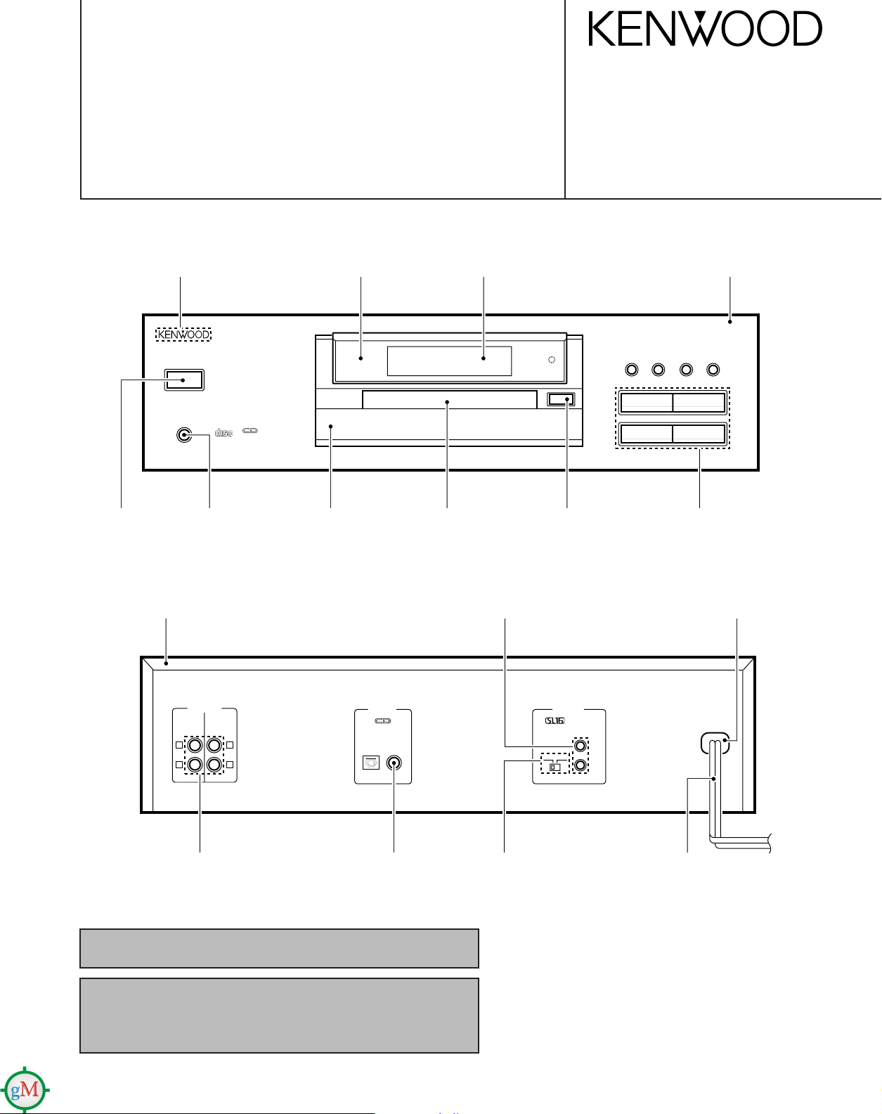
COMPACT DISC PLAYER
DP-4090/DP-5090/D-S300
SERVICE MANUAL
© 1997-6/B51-5324-00 (K/K) 2172
76
¢4
1
¡
SEARCH
TEXT DISPLAY PEAK SEARCH
PHONES
POWER
-ON –OFF
DIGITAL AUDIO
COMPACT
0
TEXT
L
R
L
R
LINE 1 LINE 2
OUTPUT
DIGITAL
OUTPUT
SYSTEM
CONTROL
OPTICAL COAXIAL
SL16 XS 8
ƒ
TEXT
KENWOOD badge
(B43-0302-04)
Front glass
(B10-2300-04)
Color filter
(B11-0346-04)
Panel *
(A60-)
Metallic cabinet
(A01-3398-01)
Power cord *
(E30-)
Phono jack *
(E63-)
Phono jack *
(E63-)
Slide switch
(S31-2094-05)
Minitature phono jack *
(E11-)
Power cord bushing
(J42-0083-05)
Knob (BUTTON)
(K27-2178-04)
Phone jack
(E11-0190-05)
Dressing panel *
(A21-)
Door
(A52-0312-14)
Soft tape
(G11-2314-04)
Soft tape
(G11-2272-04)
In compliance with Federal Regulations, following are reproductions of
labels on, or inside the product relating to laser product safety.
KENWOOD-Corp. certifies this equipment conforms to DHHS Regulations
No. 21 CFR 1040. 10, Chapter 1, Subchapter J.
DANGER : Laser radiation when open and interlock defeated.
AVOID DIRECT EXPOSURE TO BEAM.
Illust is DP-5090.
* Refer to parts list on page 27.
CONTENTS / ACCESSORIES / CAUTION
DP-4090/5090/D-S300
2
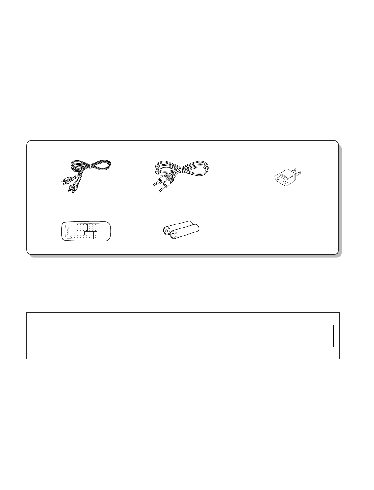
Accessories
CONTENTS / ACCESSORIES / CAUTION.................2
EXTERNAL VIEW........................................................3
DISASSEMBLY FOR REPAIR.....................................4
BLOCK DIAGRAM.......................................................5
CIRCUIT DESCRIPTION.............................................6
ADJUSTMENT.............................................................9
PC BOARD ................................................................10
SCHEMATIC DIAGRAM............................................15
EXPLODED VIEW .....................................................24
PATS LIST.................................................................27
SPECIFICATIONS.....................................................33
Contents
REMOTE CONTROL UNIT
RC-P0505
Audio cord (1)
(E30-0505-05)
System control cord (1)
(E30-2733-05)
AC plug adaptor (1)
(E03-0115-05)
M type only
Batteries (R6/AA) (2)
DP-R4080 only
Remote control unit (1)
(A70-1048-05: RC-P0703)
DP-R4080 only
Battery cover: (A09-0356-08)
Note related to transportation and movement
Before transporting or moving this unit, carry out the following
operations.
1. Turn the power ON but do not load a disc.
2. Wait a few seconds and verify that the display shown appears.
Wait further a few seconds.
3. Turn the power OFF.
Caution
12345
12 345
67 8910
11 12 13 14 15
16 17 18 19 20
no d SC
I
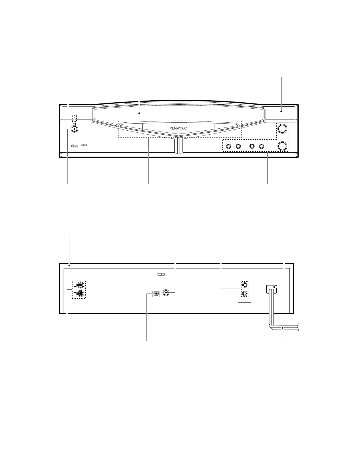
EXTERNAL VIEW
DP-4090/5090/D-S300
3
¢4
COMPACT DISC PLAYER D-S300
REPEAT
D.R.I.V.E.
RANDOM
6
7
0
TEXT
DIGITAL AUDIO
COMPACT
ON/STANDBY
L
R
LINE OUTPUT DIGITAL OUTPUT
OPTICAL COAXIAL
SISTEM
CONTROL
TEXT
Indicator
(B12-0312-04)
Front glass
(B12-2360- 12)
Panel
(A60-1141-11)
Metallic cabinet
(A01-3442-01)
Phono jack *
(E63-)
Miniature phone jack *
(E11-)
Knob
(K29-6671-02)
Dressing panel assy *
(A21-)
Knob
(K29-6671-02)
Phono jack *
(E63-)
Oscillating module
(W02-1114-05)
AC power cord
(B30-2829-05)
Power cord bushing
(J42-0083-05)
Illust is D-S300.
* Refer to parts list on page 27.
DP-4090/5090/D-S300
4
DISASSEMBLY FOR REPAIR
1
2
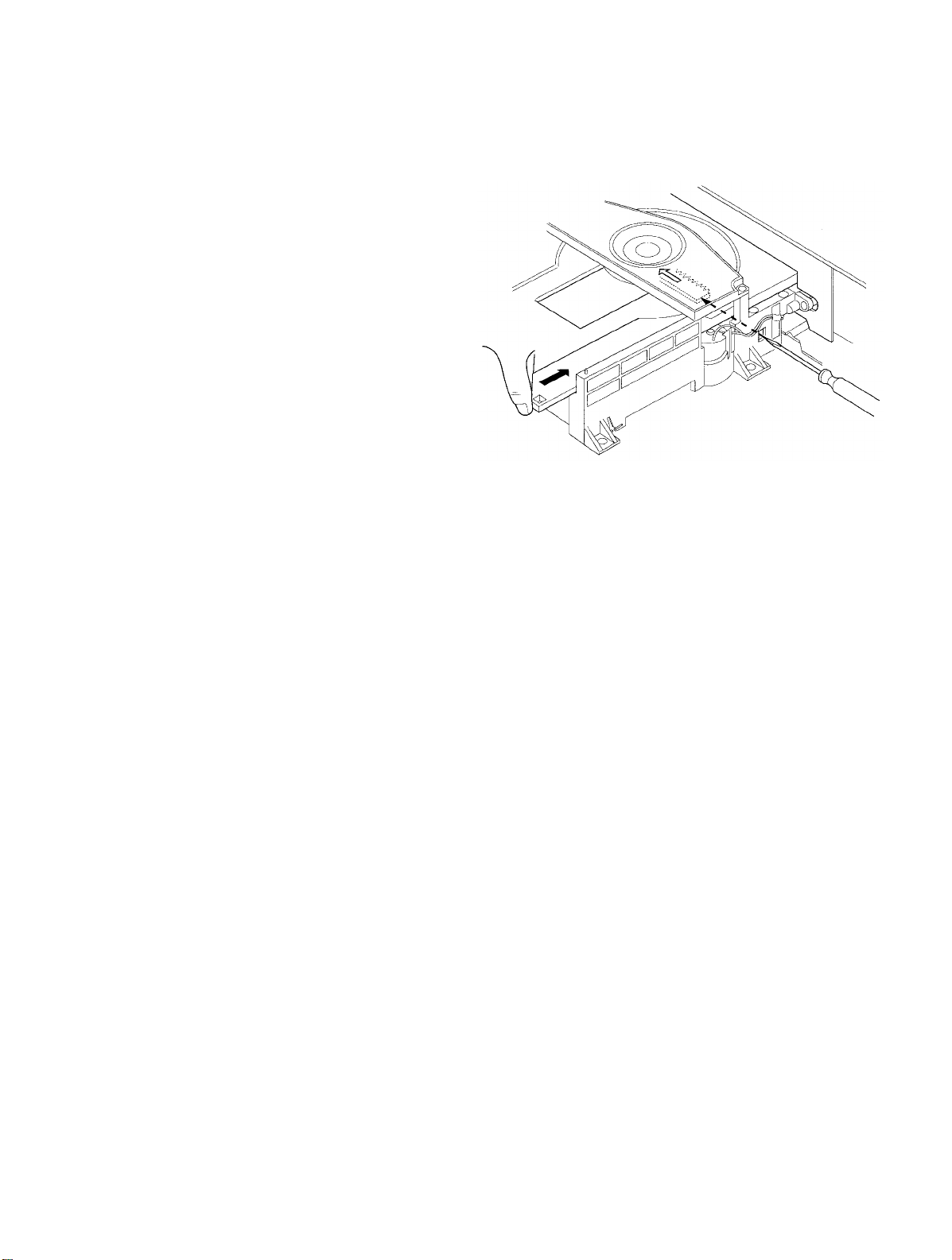
The method that takes out a tray.
1. Plug thin driver etc.to a square hole. And, press a rack gear
in the direction of an arrow(
1).
2. Press the back side of a tray toward an arrow(2) with a finger. At this time, draw a tray from a front side because a
tray appears on the side of a front.
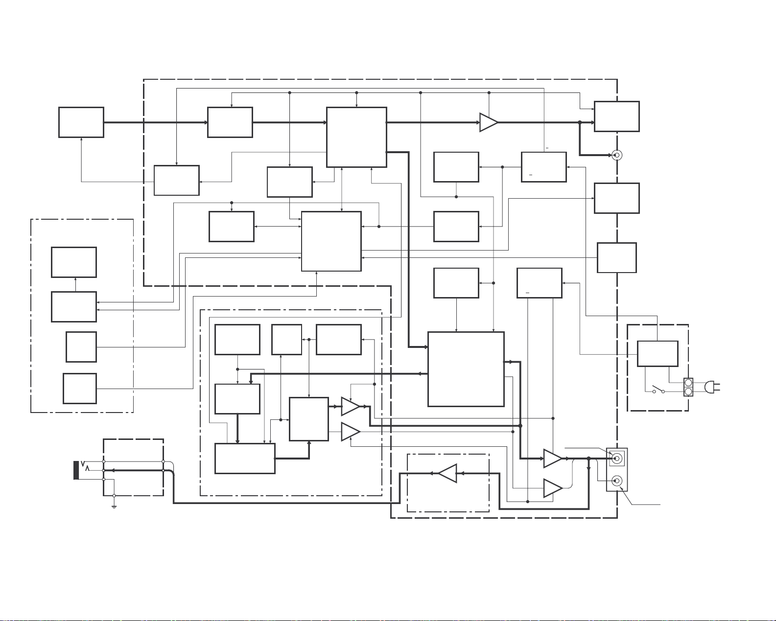
5
BLOCK DIAGRAM
IC1
IC16
ACTUATOR
DRIVER
IC18
CD TEXT
LC8917OM
IC21
256K
S-RAM
ED1
FL
FIP15 X MIBA
FL DRIVER
LC75710NE
IC1
KEY
INPUT
REMOCON
SENSOR
EXCEPT
D-S300
HEADPHONES
J4
IC2
CDX2507AQ
D.S.P
UPD78055GC
u-COM
IC19
DIGITAL
+5V POWER
X'TAL
34MHz
ANALOG
+5V POWER
D,F
SM5843
D-LATCH
MCKO
16MHz
24bit DAC
KAN05
+5V POWER
SUPPLY
(DIGITAL)
+5V
D.OUT
DATA
BCK
LRCK
u-COM
+5V POWER
SUPPLY
X'TAL
16.9MHz
KAN 03
D.R.I.V.E
DAC
IC3
IC15
RECTIFIER
(DIGITAL)
9V
D21
D22
RECTIFIER
(ANALOG)
11V
-11V
+11V
A2
OPTICAL
OUT
J2
COAX OUT
Q5,6
J3
SYSTEM
CONTROL
S3
XS8/SL16
SW
TRANSFORMER
L.P.F
IC13,14
J1
LINE OUT
1 L/R
2 L/R
CDM-30
CXA1782BQ
RF & SERVO
+5V
+5V
HEADPHONES
AMP
+
+
+
9V
2
1
X25-592 (DP-4090/5090)
X25-593 (D-S300)
X32
X14-444
X32-331X-XX
DP-4090/5090 ONLY
DP-5090 ONLY
DP-4090/5090 ONLY
DP-4090/5090
ONLY
X32
DP-4090
D-S300
DP-4090/5090/D-S300
DP5090
DP-4090/5090/D-S300
6
CIRCUIT DESCRIPTION
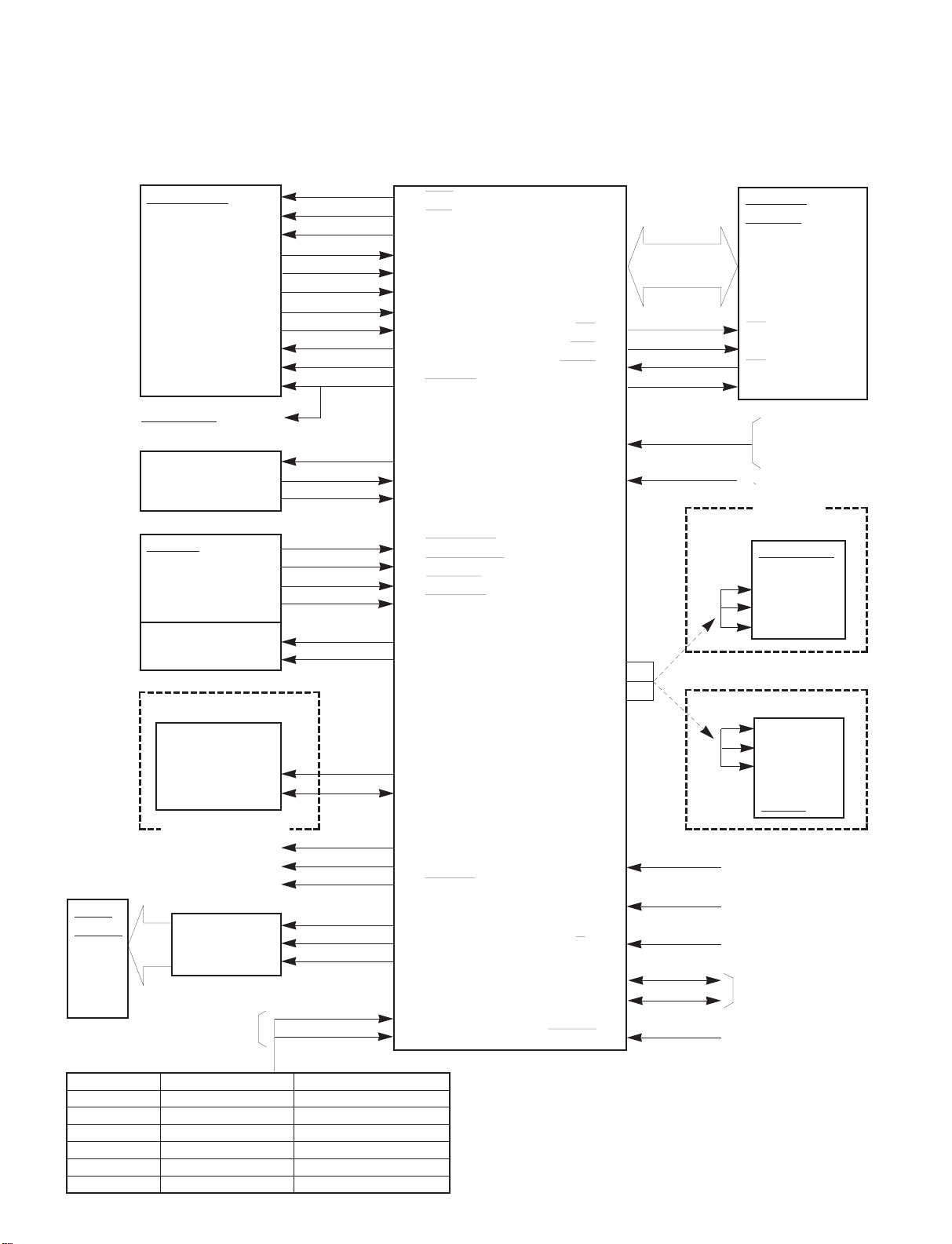
1. Main Microprocessor : uPD78055GC-A02 (X32-, IC19)
1-1 Microprocessor periphery block diagram
55 CLK
56 LAT
57 DATA 19 ~ 26
58 SENSE (AD0 ~ AD7)
73 FOK 27 ~ 32
62 SCOR (A8 ~ A13)
16 SUBQ
66 GFS RD 40
18 SQCK WR 41
59 MON WAIT 42
54 MUTEG ASTB 43
TYPE 76
10 SCLK
8 SRDT DEFECT 50
63 DQSY
uPD 78055GC-A02
39 OPEN_SW
38 CLOSE_SW
36 SLT_SW
37 POS_SW
44 OPENM
45 CLOSEM MLEN 1
MCK 2
MDT 3
6 CLK
5 SDA
15 STANBY
46 LDC A/D PEAK 79
80 RMUTE
REM 61
12 DATA
13 CLK 8/16bit
14 CE
SDATA 53
SBUSY 52
77 A/D KEY0
78 A/D KEY1 RESET 60
CXD2507AQ
CLK
XLT
DATA
SENS
FOK
SCOR
SQSO
GFS
SQCK
MON
S300 / 4090 MUTE
X32 IC19
X32 IC2
SM5843ASI MUTE
DP-5090
LC89170M SCLK
(CD TEXT) SRDT
DQSY
X32 IC18
HM62256
BLFP 8T
(SRAM)
OE
WE
CE
LE
5.0V : D-S300
2.5V : DP-5090
0.0V : DP-4090
CDM-30
MECHA SW
LOADING
DRIVER
SM5843ASI
MLEN
MCK
MDT
DP-5090
X32 IC3
SGATE
SCK
SDATA
KAN03
X2C00P
(EEPROM)
SLK
SDA
X32 IC25
DP-5090 / DP-4090
STANDBY LED
LASER ON / OFF
ANALOG METE
LC75712E
(DOT DRIVER)
FIP15
XM1BA
(FL)
A/D KEY
A / D PEAK SEARCH
DEFECT
PORT VOLT A/D0 A/D1
4. 8 ~ 4. 2 OPEN / CLOSE POWER (*2)
4. 2 ~ 3. 4 PLAY / PAUSE TEXT DISPLAY (*1)
3. 4 ~ 2. 5 STOP PEAK SEARCH (*1)
2. 5 ~ 1. 6 UP FF (*1)
1. 6 ~ 0. 8 DOWN FB (*1)
0. 8 ~ 0. 2 REPEAT (*2) RANDOM (*2)
(*1) DP-5090/DP-4090 ONLY
(*2) D-S300 ONLY
X32 IC21
X25 IC1
X14 IC4
REMOCON
8bit / 16bit
SERIAL COMMUNICATION
RESET

DP-4090/5090/D-S300
7
CIRCUIT DESCRIPTION
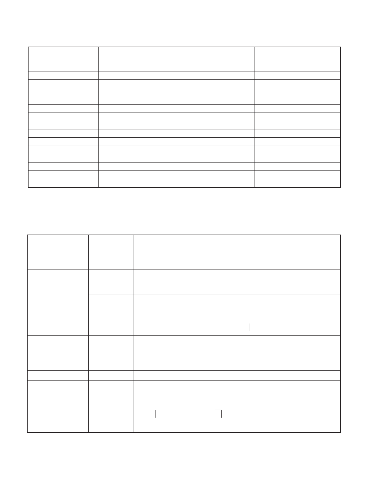
Pin No. Name I/O Description Active
1 MLEN O SM5843ASI/KAN03 Enable output
2 MCK O SM5843ASI/KAN03 Clock output
3 MDT O SM5843ASI/KAN03 Data output
4 AVSS – Vss (GND)
5 SDA I/O X24C00P(EEPROM) Data input / output
6 SCL O X24C00P(EEPROM) Clock output
7 AVREF1 I Vdd (+5V)
8 SRDT I LC89170M(CD TXT DECODER) Data input
9 NC O No used
10 SCLK O LC89170M(CD TXT DECODER) Clock output
11 NC O No used
12 DATA O LC75712E (DOT DRIVER) Data output
13 CLK O LC75712E (DOT DRIVER) Clock output
14 CE O LC75712E (DOT DRIVER) CE output
15 STBY O STANDBY_LED H : LED_ON
16 SUBQ I Q_data input
17 NC O No used
18 SQCK O Q_data reading clock output
19-26 AD0 - AD7 I/O HM62256BLFP8T (SRAM) ADR / data input / output
27-32 A8 - A13 O HM62256BLFP8T (SRAM) Address output
33 VSS – GND
34, 35 NC O No used
36 SLT SW I CDM-30 start limit switch input L : Switch_ON
37 SLOW SW I CDM-30 tray (open / close) deceleration L : Switch_ON
38 CLOSE SW I CDM-30 close switch input L : Close
39 OPEN SW I CDM-30 open switch input L : Open
40 RD O Read strobe signal output
41 WR O Write strobe signal output
42 WAIT I External waiting signal input (no used)
43 ASTB O Address strobe signal output
44 OPEN MOTOR O Tray motor control (open) H : Open / T.U.down
45 CLOSE MOTOR O Tray motor control (close) H : Close / T.U.ip
46 LCD O Laser signal output L : Laser diode ON
47-49 NC O No used
50 DEFECT I A cracked disc detection input H : Detected
51 8 / 16bit I “8bit , 16bit change-over” H : 16bit
52 S.BUSY I/O Serial busy signal input / output
53 S.DATA I/O Serial data signal input / output
54 MON O CXD2507AQ spindle motor ON / OFF change-over
55 CLK O CXD2507AQ clock output
56 LATCH O CXD2507AQ latch output
57 DATA O CXD2507AQ data output
58 SENSE I CXD2507AQ sense output
59 MUTEG O Digital mute control L : Mute_ON
60 RESET I Reset input L : Reset
61 REM I Remocon signal input
62 SCOR I Sub code frame sync detection signal
63 DQSY I Text data reading permission signal input
1-2 Pin description
DP-4090/5090/D-S300
8
DIRCUIT DESCRIPTION
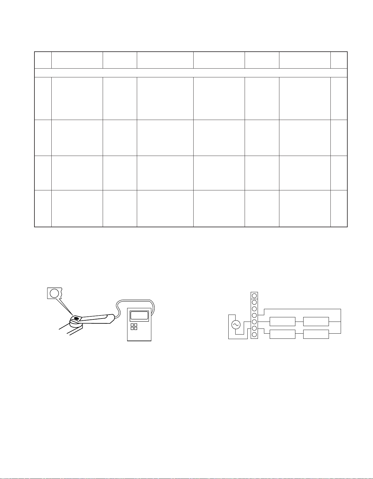
2. Test mode
2-1 Setting the test mode
÷ The microprocessor built in the unit can be put to TEST
MODE by just pressing the UP key when set to power on.
2-2 Key vs Function in test mode
keys Display Description Remarks
UP ¢
(Keep to press up
key and AC ON)
TEST Tray opens automatically. Setting the test mode
PLAY/PAUSE 6
8 30 – – : – –
(1) Focus servo – – – – ON
(2) Tracking servo – – OFF
(3) Feed servo – – – – OFF
TE-balance adjustment
‰ 05 00 : 00
(1) Focus servo – – – – ON
(2) Tracking servo – – – ON
(3) Feed servo – – – – – ON
Focus gain / Tracking
gain and FE- balance
adjustment
UP ¢
î FL all light up î dot demonstration mode ì
ììì
normal test mode indication нмммм
* FF 1
FEED OUT
Move the pick - up to the direction of the outer circumference.
* FB ¡
FEED IN
Move the pick - up to the direction of the inner circumference.
* STOP 7
TEST 00 Disc will be stopped.
*
8 BIT SYNC
16 BIT SYNC
8 bit sync and 16 bit sync will be displayed by changing
the SL16/XS8 switch on the rear panel.
* PEAK SEARCH
Change the output level cyclically.
ì Max î -10dB î Min
ммммммнммммм
DOWN 4 ‰ 01
Cancellation of the test mode and 01 play.
* DP 4090/DP-5090 only
The following keys are not operate in the test mode.
• TEXT DISPLAY KEY (DP-4090/DP-5090)
• REPEAT / RANDOM KEY (D-S300)
Pin No. Name I/O Description Active
64, 65 NC O No used
66 GFS I Frame signal input from CXD2507AQ
67 NC O No used
68 VDD – Power supply (+5V)
69 X2 – system clock input
70 X1 I system clock input
71 IC – GND
72 XT2 – No used
73 FOK I F.OK signal input
74 AVDD – Vdd
75 AVREF0 I Vdd
76 50 / 40 I Model discrimination 5V : D-S300 / 2. 5V : DP-5090 /
0V : DP-4090
77, 78 A / D0 ,A/D1 I A/D key input
79 PEAK I A/D peak search input
80 RMUTE O Analog mute control
DP-4090/5090/D-S300
9
ADJUSTMENT
FIG.
GND
+
_
L.P.F.
+
+
L.P.F.
VTVM
VTVM
1
2
3
4
5
6
7
1.2 kHz
50 mVrms
(a)
No. ITEM
INPUT
SETTINGS
OUTPUT
SETTINGS
ALIGNMENT
POINTS
ALIGN
FOR
PLAYER
SETTINGS
1 LASER POWER
−
Apply the sensor section
of optical power meter
on the pickup lens.
−
On the power from
0.08 to 0.15 mW,
when the diffraction
grating is correctly
aligned with the RF
level of 1.0 Vp-p or
more.
While pressing the
UP key, turn the AC
ON. (Test mode)
Press the
PLAY/PAUSE key,
then confirm that the
display is "03".
(a) Laser power
Pickup
3
FOCUS ERROR
BALANCE
Test disc
Type 4
Connect an oscilloscope
as follows.
CH1 : RF (CN2 pin 1)
CH2 : FE (CN2 pin 2)
FE BALANCE
VR1
Optimum eye pattern
Press the
PLAY
/PAUSE
key,
then confirm that the
display is "05".
Note:
Type 4 disc : SONY YEDS-18 Test Disc or equivalent.
LPF: Around 47 kΩ+ 390 pF or so.
0.08~0.15 mW
Optical power meter
2
TRACKING ERROR
BALANCE
Test disc
Type 4
Connect an oscilloscope
as follows.
CH1 : RF (CN2 pin 1)
CH2 : TE (CN2 pin 6)
TE BALANCE
VR2
Symmetry between
upper and lower pat-
terns
Press the
PLAY/PAUSE key,
then confirm that the
display is "03".
CN2
(e) Tracking gain
(e)
4
TRACKING GAIN
Test disc
Type 4
Apply signal of
1.2 kHz,
50mVrms to
CN2 pin 5-6.
Connect a LPF to CN2
pin 5-6 to which you
connect an oscilloscope
or AC voltmeters.
TRACKING
GAIN
VR3
Two VTVMs should
read the same value.
Press the
PLAY/PAUSE key,
then confirm that the
display is "05".
Step 1~4 are in TEST MODE
 Loading...