

Page 1

Model 7074General Purpose Multiplexer Card
Instruction Manual
A GREATER MEASURE OF CONFIDENCE
Page 2

W ARRANTY
Keithley Instruments, Inc. warrants this product to be free from defects in material and workmanship for a period of 1 year
from date of shipment.
Keithley Instruments, Inc. warrants the following items for 90 days from the date of shipment: probes, cables, rechargeable
batteries, diskettes, and documentation.
During the warranty period, we will, at our option, either repair or replace any product that proves to be defective.
To exercise this warranty, write or call your local Keithley representative, or contact Keithley headquarters in Cle veland, Ohio.
You will be given prompt assistance and return instructions. Send the product, transportation prepaid, to the indicated service
facility . Repairs will be made and the product returned, transportation prepaid. Repaired or replaced products are warranted for
the balance of the original warranty period, or at least 90 days.
LIMIT A TION OF W ARRANTY
This warranty does not apply to defects resulting from product modification without Keithley’s express written consent, or
misuse of any product or part. This warranty also does not apply to fuses, software, non-rechargeable batteries, damage from
battery leakage, or problems arising from normal wear or failure to follow instructions.
THIS WARRANTY IS IN LIEU OF ALL OTHER WARRANTIES, EXPRESSED OR IMPLIED, INCLUDING ANY
IMPLIED WARRANTY OF MERCHANTABILITY OR FITNESS FOR A PARTICULAR USE. THE REMEDIES PROVIDED HEREIN ARE BUYER’S SOLE AND EXCLUSIVE REMEDIES.
NEITHER KEITHLEY INSTRUMENTS, INC. NOR ANY OF ITS EMPLOYEES SHALL BE LIABLE FOR ANY DIRECT,
INDIRECT, SPECIAL, INCIDENTAL OR CONSEQUENTIAL DAMAGES ARISING OUT OF THE USE OF ITS
INSTRUMENTS AND SOFTWARE EVEN IF KEITHLEY INSTRUMENTS, INC., HAS BEEN ADVISED IN ADVANCE
OF THE POSSIBILITY OF SUCH DAMAGES. SUCH EXCLUDED DAMAGES SHALL INCLUDE, BUT ARE NOT LIMITED TO: COSTS OF REMOVAL AND INSTALLATION, LOSSES SUSTAINED AS THE RESULT OF INJURY TO ANY
PERSON, OR DAMAGE TO PROPERTY.
Keithley Instruments, Inc. • 28775 Aurora Road • Cleveland, OH 44139 • 440-248-0400 • Fax: 440-248-6168 • http://www.keithley.com
BELGIUM: Keithley Instruments B.V.
CHINA: Keithley Instruments China Y uan Chen Xin Building, Room 705 • 12 Yumin Road, Dewai, Madian • Beijing 100029 • 8610-62022886 • F ax: 8610-62022892
FRANCE: Keithley Instruments Sarl 3, allée des Garays • 91127 Palaiseau Cedex • 01-64 53 20 20 • Fax: 01-60 11 77 26
GERMANY: Keithley Instruments GmbH Landsberger Strasse 65 • 82110 Germering • 089/84 93 07-40 • Fax: 089/84 93 07-34
GREAT BRITAIN: Keithley Instruments Ltd
INDIA: Keithley Instruments GmbH Flat 2B, WILOCRISSA • 14, Rest House Crescent • Bangalore 560 001 • 91-80-509-1320/21 • Fax: 91-80-509-1322
ITALY: Keithley Instruments s.r.l. Viale S. Gimignano, 38 • 20146 Milano • 02-48 39 16 01 • Fax: 02-48 30 22 74
NETHERLANDS: Keithley Instruments B.V. Postbus 559 • 4200 AN Gorinchem • 0183-635333 • Fax: 0183-630821
SWITZERLAND: Keithley Instruments SA Kriesbachstrasse 4 • 8600 Dübendorf • 01-821 94 44 • Fax: 01-820 30 81
TAIWAN: Keithley Instruments Taiwan 1 Fl. 85 Po Ai Street • Hsinchu, Taiwan, R.O.C. • 886-3572-9077 • Fax: 886-3572-903
Bergensesteenweg 709 • B-1600 Sint-Pieters-Leeuw • 02/363 00 40 • Fax: 02/363 00 64
The Minster • 58 Portman Road • Reading, Berkshire RG30 1EA • 0118-9 57 56 66 • Fax: 0118-9 59 64 69
9/00
Page 3

Model 7074 General Purpose Multiplexer Card
Instruction Manual
©1989, Keithley Instruments, Inc.
All rights reserved.
Cleveland, Ohio, U.S.A.
Document Number: 7074-901-01 Rev. B
Page 4

Manual Print History
The print history shown below lists the printing dates of all Revisions and Addenda created for this manual. The
Revision Level letter increases alphabetically as the manual undergoes subsequent updates. Addenda, which are
released between Revisions, contain important change information that the user should incorporate immediately into
the manual. Addenda are numbered sequentially. When a new Revision is created, all Addenda associated with the
previous Revision of the manual are incorporated into the new Revision of the manual. Each new Revision includes
a revised copy of this print history page.
Revision A (Document Number 7074-901-01)................................................................................... January 1989
Addendum A (Document Number 7074-901-02)............................................................................. February 1996
Revision B (Document Number 7074-901-01)..................................................................................... March 2001
All Keithley product names are trademarks or registered trademarks of Keithley Instruments, Inc.
Other brand and product names are trademarks or registered trademarks of their respective holders.
Page 5

Safety Precautions
The following safety precautions should be observed before using
this product and any associated instrumentation. Although some instruments and accessories would normally be used with non-hazardous voltages, there are situations where hazardous conditions
may be present.
This product is intended for use by qualified personnel who recognize shock hazards and are familiar with the safety precautions required to avoid possible injury. Read the operating information
carefully before using the product.
The types of product users are:
Responsible body is the individual or group responsible for the use
and maintenance of equipment, for ensuring that the equipment is
operated within its specifications and operating limits, and for ensuring that operators are adequately trained.
Operators use the product for its intended function. They must be
trained in electrical safety procedures and proper use of the instrument. They must be protected from electric shock and contact with
hazardous live circuits.
Maintenance personnel perform routine procedures on the product
to keep it operating, for example, setting the line voltage or replacing consumable materials. Maintenance procedures are described in
the manual. The procedures explicitly state if the operator may perform them. Otherwise, they should be performed only by service
personnel.
Service personnel are trained to work on live circuits, and perform
safe installations and repairs of products. Only properly trained service personnel may perform installation and service procedures.
Keithley products are designed for use with electrical signals that
are rated Installation Category I and Installation Category II, as described in the International Electrotechnical Commission (IEC)
Standard IEC 60664. Most measurement, control, and data I/O signals are Installation Category I and must not be directly connected
to mains voltage or to voltage sources with high transient over -voltages. Installation Category II connections require protection for
high transient over-voltages often associated with local AC mains
connections. The user should assume all measurement, control, and
data I/O connections are for connection to Category I sources unless otherwise marked or described in the Manual.
Exercise extreme caution when a shock hazard is present. Lethal
voltage may be present on cable connector jacks or test fixtures. The
American National Standards Institute (ANSI) states that a shock
hazard exists when voltage levels greater than 30V RMS, 42.4V
peak, or 60VDC are present.
that hazardous voltage is present in any unknown circuit before
measuring.
Users of this product must be protected from electric shock at all
times. The responsible body must ensure that users are prevented
access and/or insulated from every connection point. In some cases,
connections must be exposed to potential human contact. Product
users in these circumstances must be trained to protect themselves
from the risk of electric shock. If the circuit is capable of operating
at or above 1000 volts,
exposed.
Do not connect switching cards directly to unlimited power circuits.
They are intended to be used with impedance limited sources.
NEVER connect switching cards directly to AC mains. When connecting sources to switching cards, install protective devices to limit fault current and voltage to the card.
Before operating an instrument, make sure the line cord is connected to a properly grounded power receptacle. Inspect the connecting
cables, test leads, and jumpers for possible wear, cracks, or breaks
before each use.
When installing equipment where access to the main power cord is
restricted, such as rack mounting, a separate main input power disconnect device must be provided, in close proximity to the equipment and within easy reach of the operator.
For maximum safety, do not touch the product, test cables, or any
other instruments while power is applied to the circuit under test.
ALWAYS remove power from the entire test system and discharge
any capacitors before: connecting or disconnecting cables or jumpers, installing or removing switching cards, or making internal
changes, such as installing or removing jumpers.
Do not touch any object that could provide a current path to the common side of the circuit under test or power line (earth) ground. Always
make measurements with dry hands while standing on a dry , insulated
surface capable of withstanding the voltage being measured.
A good safety practice is to expect
no conductive part of the circuit may be
Page 6
The instrument and accessories must be used in accordance with its
specifications and operating instructions or the safety of the equipment may be impaired.
Do not exceed the maximum signal levels of the instruments and accessories, as defined in the specifications and operating information, and as shown on the instrument or test fixture panels, or
switching card.
When fuses are used in a product, replace with same type and rating
for continued protection against fire hazard.
Chassis connections must only be used as shield connections for
measuring circuits, NOT as safety earth ground connections.
If you are using a test fixture, keep the lid closed while power is applied to the device under test. Safe operation requires the use of a
lid interlock.
If a screw is present, connect it to safety earth ground using the
wire recommended in the user documentation.
!
The symbol on an instrument indicates that the user should refer to the operating instructions located in the manual.
The symbol on an instrument shows that it can source or measure 1000 volts or more, including the combined effect of normal
and common mode voltages. Use standard safety precautions to
avoid personal contact with these voltages.
The
WARNING heading in a manual explains dangers that might
result in personal injury or death. Alw ays read the associated infor mation very carefully before performing the indicated procedure.
The
CAUTION heading in a manual explains hazards that could
damage the instrument. Such damage may invalidate the warranty.
Instrumentation and accessories shall not be connected to humans.
Before performing any maintenance, disconnect the line cord and
all test cables.
To maintain protection from electric shock and fire, replacement
components in mains circuits, including the power transformer, test
leads, and input jacks, must be purchased from Keithley Instruments. Standard fuses, with applicable national safety approvals,
may be used if the rating and type are the same. Other components
that are not safety related may be purchased from other suppliers as
long as they are equivalent to the original component. (Note that selected parts should be purchased only through Keithley Instruments
to maintain accuracy and functionality of the product.) If you are
unsure about the applicability of a replacement component, call a
Keithley Instruments office for information.
To clean an instrument, use a damp cloth or mild, water based
cleaner. Clean the exterior of the instrument only. Do not apply
cleaner directly to the instrument or allow liquids to enter or spill
on the instrument. Products that consist of a circuit board with no
case or chassis (e.g., data acquisition board for installation into a
computer) should never require cleaning if handled according to instructions. If the board becomes contaminated and operation is affected, the board should be returned to the factory for proper
cleaning/servicing.
2/01
Page 7

7074-D General Purpose Eight 1 xl 2
Multiplexer Card (Dry Reed)
MULTIPLEX CONFIGURATION: Eight 1x12 banks. Adjacent banks can be connected together. Jun
can be removed to isolate any bank from the backplane.
CONTACT CONFIGURATION: 3 pole Form A (HI, LO, GUARD).
CONNECTOR TYPE: Four 75 pin connectors for bank connections, one 38 pin connector for row
connections.
MAXIMUM SIGNAL LEVEL: ZOOV, 1A tarry/0.5A switched, 1OVA peak (resistive load).
COMMON MODE VOLTAGE: ZOOV maximum behveen any 2 pins or chassis.
CONTACT LIFE:
Cold Switching: 108 closures.
At Maximum Signal Level: 105 closures.
CHANNEL RESISTANCE (per conductor): <0.6Q initial, <1.6R at end of contact life.
CONTACT POTENTIAL: <5pV per contact pair (HI to LO, <1 minute after actuation).
OFFSET CURRENT: <lOOpA.
ISOLATION:
Bank: >lOlOQ, <lOpF.
Channel: >lOIOQ <lOpF.
Differential: >109R, 55pF nominal.
Common Mode: >lOgn, 300pF nominal.
CROSSTALK:
Bank: <-55dB at IMHz, 5OQ load.
Channel: c-55dB at IMHz, 5OQ load.
INSERTION LOSS (lMHz, 5OS2 source, 5OQ load): O.ldB typical.
3dB BANDWIDTH (50R load): 1OMHz typical.
RELAY DRIVE CURRENT(per relay): 15mA.
RELAY SETTLING TIME: <3msec.
ENVIRONMENT:
Operating: 0” to 5O”C, up to 35°C @ 70% R.H.
Storage: -25” to 65°C.
ACCESSORIES SUPPLIED: Instruction manual, 8 spare backplane jumpers.
ACCESSORIES AVAILABLE:
Bank Connector Accessories:
Model 7074~CITz
Model 7074HCT:
Model 7074-m
Model 7074MTC.20:
Model 7074MTR:
Model 7074RTc:
Row Connector Accessories:
Model 7078-CIT:
Model 7078.HCT:
Model 7078-KIT:
Model 7078~MTC-5:
Model 7078MTC-20:
Model 7078MTR:
Specifications subject to change without notice.
All specifications applicable to eight 1x12 configuration only.
Contact Extraction Tool
Hand Crimping Tool
Mass Terminated Plug with Contacts
Mass Terminated Cable Assembly, 6m(20 ft.)
Mass Terminated Receptacle with Contacts
Relay Test Shorting Connector
Contact Insertion and Extraction Tools
Hand Crimping Tool
Mass Terminated Plug with Contacts
Mass Terminated Cable Assembly, 1.5m (5 ft.)
Mass Terminated Cable Assembly, 6x1(20 ft.)
Mass Terminated Receptacle with Contacts
Page 8

7074-M General Purpose Eight 1x12
Multiplexer Card (Mercury Wetted Reed)
MULTIPLEX CONFIGURATION: Eight 1x12 banks. Adjacent banks can be connected together.
Jumpers can be removed to isolate any bank from the backplane.
CONTACT CONFIGURATION: 3 pole Form A (HI, LO, GUARD).
CONNECTOR TYPE: Four 75 pin connectors for bank connections, one 38 pin connector for row
connections.
MAXIMUM SIGNAL LEVEL: 2OOV, 3A cany/2A switched, SOVA peak (resistive load).
COMMON MODE VOLTAGE: ZOOV maximum between any 2 pins or chassis.
CONTACT LIFE:
Cold Switching: 109 closures.
At Maximum Signal Level: 108 closures.
CHANNEL RESISTANCE (per conducted: co.60 initial, cO.7Q at end of contact life.
CONTACT POTENTIAL: <IO&V per contact pair (HI to LO, <I minute after actuation).
OFFSET CURRENT: <lOOpA.
ISOLATION:
Bank: >lOl&, <IOpF.
Channel: >lO%-L, <lOpF.
Differential: >I094 55pF nominal.
Common Mode: >lOgQ. 300nF nominal.
CROSSTALK:
Bank: <-55dB at IMHz, 5OQ load.
Channel: <-55dB at IMHz, 5On load.
INSERTION LOSS (lMHz, 5OQ source, 5OQ load): O.ldB typical.
3dB BANDWIDTH (5OQ load): 1OMHz typical.
RELAY DRIVE CURRENT(per relay): 5OmA.
RELAY SETTLING TIME: <3msec.
ENVIRONMENT:
Operating: 0” to 5O”C, up to 35°C @ 70% R.H.
Storage: -25 to 65°C.
ACCESSORIES SUPPLIED: Instruction manual, 8 spare backplane jumpers.
ACCESSORIES AVAILABLE:
Bank Connector Accessories:
Model 7074~CIT: Contact Extraction Tool
Model 7074-HCT: Hand Crimping Tool
Model 7074-KIT: Mass Terminated Plug with Contacts
Model 7074-MTC-20: Mass Terminated Cable Assembly, 6m (20 ft.)
Model 7074-MTR:
Model 7074-RTC: Relay Test Shorting Connector
Row Connector Accessories:
Model 7078~CIT:
Model 7078-HCT: Hand Crimping Tool
Model 7078-KIT:
Model 7078-MTC-5:
Model 7078-MTC-20: Mass Terminated Cable Assembly, 6m (20 ft.)
Model 7078-MTR: Mass Terminated Receptacle with Contacts
Specifications subject to change without notice.
All specifications applicable to eight 1x12 configuration only.
.
Mass Terminated Receptacle with Contacts
Contact Insertion and Extraction Tools
Mass Terminated Plug with Contacts
Mass Terminated Cable Assembly, 1.511-t (5 ft.)
Page 9
HOW TO USE THIS MANUAL
Contains information on Model 7074 features, specifications, and accessories.
Details installation of the Model 7074 General Purpose Multiplexer Card within the Model 707 Switching Matrix, ccw
ers card signal paths, and describes connections.
Gives typical applications for the Model 7074.
Contains performance verification procedures, troubleshooting information, and principles of operation for the multiplexer card.
SECTION 1
General Information
SECTION 2
Operation
SECTION 3
Applications
SECTION 4
Service Information
Lists replacement parts, and also includes component layout
and schematic drawings for the Model 7074.
SECTION 5
Replaceable Parts
Page 10

Table of Contents
SECTION 1 —
1.1 INTRODUCTION . . . . . . . . . . . . . . . . . . . . . . . . . . . . . . . . . . . . . . . . . . . . . . . . . . . . . . . . . . . . . . . . . . . . 1-1
1.2 FEATURES . . . . . . . . . . . . . . . . . . . . . . . . . . . . . . . . . . . . . . . . . . . . . . . . . . . . . . . . . . . . . . . . . . . . . . . . . . 1-1
1.3 WARRANTY INFORMATION . . . . . . . . . . . . . . . . . . . . . . . . . . . . . . . . . . . . . . . . . . . . . . . . . . . . . . . . . 1-1
1.4 MANUAL ADDENDA . . . . . . . . . . . . . . . . . . . . . . . . . . . . . . . . . . . . . . . . . . . . . . . . . . . . . . . . . . . . . . . . 1-1
1.5 SAFETY SYMBOLS AND TERMS . . . . . . . . . . . . . . . . . . . . . . . . . . . . . . . . . . . . . . . . . . . . . . . . . . . . . . 1-1
1.6 SPECIFICATIONS . . . . . . . . . . . . . . . . . . . . . . . . . . . . . . . . . . . . . . . . . . . . . . . . . . . . . . . . . . . . . . . . . . . . 1-2
1.7 UNPACKING AND INSPECTION . . . . . . . . . . . . . . . . . . . . . . . . . . . . . . . . . . . . . . . . . . . . . . . . . . . . . . 1-2
1.7.1 Inspection for Damage . . . . . . . . . . . . . . . . . . . . . . . . . . . . . . . . . . . . . . . . . . . . . . . . . . . . . . . . . . . . . . 1-2
1.7.2 Shipment Contents . . . . . . . . . . . . . . . . . . . . . . . . . . . . . . . . . . . . . . . . . . . . . . . . . . . . . . . . . . . . . . . . . 1-2
1.7.3 Instruction Manual . . . . . . . . . . . . . . . . . . . . . . . . . . . . . . . . . . . . . . . . . . . . . . . . . . . . . . . . . . . . . . . . . 1-2
1.8 REPACKING FOR SHIPMENT . . . . . . . . . . . . . . . . . . . . . . . . . . . . . . . . . . . . . . . . . . . . . . . . . . . . . . . . . 1-2
1.9 OPTIONAL ACCESSORIES . . . . . . . . . . . . . . . . . . . . . . . . . . . . . . . . . . . . . . . . . . . . . . . . . . . . . . . . . . . . 1-2
1.9.1 BANK Receptacle Accessories . . . . . . . . . . . . . . . . . . . . . . . . . . . . . . . . . . . . . . . . . . . . . . . . . . . . . . . . 1-2
1.9.2 ROW Receptacle Accessories . . . . . . . . . . . . . . . . . . . . . . . . . . . . . . . . . . . . . . . . . . . . . . . . . . . . . . . . . 1-3
SECTION 2 —
2.1 INTRODUCTION . . . . . . . . . . . . . . . . . . . . . . . . . . . . . . . . . . . . . . . . . . . . . . . . . . . . . . . . . . . . . . . . . . . . 2-1
2.2 HANDLING PRECAUTIONS . . . . . . . . . . . . . . . . . . . . . . . . . . . . . . . . . . . . . . . . . . . . . . . . . . . . . . . . . . 2-1
2.3 ENVIRONMENTAL CONSIDERATIONS . . . . . . . . . . . . . . . . . . . . . . . . . . . . . . . . . . . . . . . . . . . . . . . . 2-1
2.4 MULTIPLEXER CARD CONFIGURATION . . . . . . . . . . . . . . . . . . . . . . . . . . . . . . . . . . . . . . . . . . . . . . 2-1
2.4.1 Rear Panel . . . . . . . . . . . . . . . . . . . . . . . . . . . . . . . . . . . . . . . . . . . . . . . . . . . . . . . . . . . . . . . . . . . . . . . . . 2-1
2.4.2 1
2.4.3 Multiplexer Bank Jumpers . . . . . . . . . . . . . . . . . . . . . . . . . . . . . . . . . . . . . . . . . . . . . . . . . . . . . . . . . . . 2-2
2.4.4 Backplane Connection Jumpers . . . . . . . . . . . . . . . . . . . . . . . . . . . . . . . . . . . . . . . . . . . . . . . . . . . . . . . 2-7
2.4.5 Switching ConÞgurations . . . . . . . . . . . . . . . . . . . . . . . . . . . . . . . . . . . . . . . . . . . . . . . . . . . . . . . . . . . . 2-7
2.5 CARD INSTALLATION AND REMOVAL . . . . . . . . . . . . . . . . . . . . . . . . . . . . . . . . . . . . . . . . . . . . . . . 2-10
2.6 CONNECTION METHODS . . . . . . . . . . . . . . . . . . . . . . . . . . . . . . . . . . . . . . . . . . . . . . . . . . . . . . . . . . . 2-11
2.6.1 Connection Methods . . . . . . . . . . . . . . . . . . . . . . . . . . . . . . . . . . . . . . . . . . . . . . . . . . . . . . . . . . . . . . . . 2-11
2.6.2 Connection Methods Using Mass Terminated Cables . . . . . . . . . . . . . . . . . . . . . . . . . . . . . . . . . . . . 2-12
2.6.3 Connection Method Using Connector Kits . . . . . . . . . . . . . . . . . . . . . . . . . . . . . . . . . . . . . . . . . . . . . 2-17
2.6.4 Wiring Receptacles (Models 7074-MTR and 7078-MTR) . . . . . . . . . . . . . . . . . . . . . . . . . . . . . . . . . . 2-25
2.7 TYPICAL CONNECTION SCHEMES . . . . . . . . . . . . . . . . . . . . . . . . . . . . . . . . . . . . . . . . . . . . . . . . . . . 2-28
2.7.1 Single Mainframe, Single Multiplexer Card System . . . . . . . . . . . . . . . . . . . . . . . . . . . . . . . . . . . . . 2-28
2.7.2 Expanding the Multiplexer Using Multiple Cards . . . . . . . . . . . . . . . . . . . . . . . . . . . . . . . . . . . . . . . 2-29
2.7.3 Using the Multiplexer with Matrix Cards . . . . . . . . . . . . . . . . . . . . . . . . . . . . . . . . . . . . . . . . . . . . . . 2-29
2.8 MULTIPLEXER PROGRAMMING . . . . . . . . . . . . . . . . . . . . . . . . . . . . . . . . . . . . . . . . . . . . . . . . . . . . . . 2-33
2.8.1 Banks and Rows . . . . . . . . . . . . . . . . . . . . . . . . . . . . . . . . . . . . . . . . . . . . . . . . . . . . . . . . . . . . . . . . . . . . 2-33
2.8.2 Front Panel Multiplexer Programming Procedure . . . . . . . . . . . . . . . . . . . . . . . . . . . . . . . . . . . . . . . 2-33
2.8.3 IEEE-488 Bus Programming . . . . . . . . . . . . . . . . . . . . . . . . . . . . . . . . . . . . . . . . . . . . . . . . . . . . . . . . . . 2-33
General Information
Operation
×
12 Multiplexer Banks . . . . . . . . . . . . . . . . . . . . . . . . . . . . . . . . . . . . . . . . . . . . . . . . . . . . . . . . . . . . . 2-2
Page 11

2.9 MEASUREMENT CONSIDERATIONS . . . . . . . . . . . . . . . . . . . . . . . . . . . . . . . . . . . . . . . . . . . . . . . . . . 2-34
2.9.1 Path Isolation . . . . . . . . . . . . . . . . . . . . . . . . . . . . . . . . . . . . . . . . . . . . . . . . . . . . . . . . . . . . . . . . . . . . . . 2-34
2.9.2 Magnetic Fields . . . . . . . . . . . . . . . . . . . . . . . . . . . . . . . . . . . . . . . . . . . . . . . . . . . . . . . . . . . . . . . . . . . . 2-35
2.9.3 Electromagnetic Interference (EMI) . . . . . . . . . . . . . . . . . . . . . . . . . . . . . . . . . . . . . . . . . . . . . . . . . . . 2-35
2.9.4 Ground Loops . . . . . . . . . . . . . . . . . . . . . . . . . . . . . . . . . . . . . . . . . . . . . . . . . . . . . . . . . . . . . . . . . . . . . 2-35
2.9.5 Keeping Connectors Clean . . . . . . . . . . . . . . . . . . . . . . . . . . . . . . . . . . . . . . . . . . . . . . . . . . . . . . . . . . . 2-36
2.9.6 Shielding . . . . . . . . . . . . . . . . . . . . . . . . . . . . . . . . . . . . . . . . . . . . . . . . . . . . . . . . . . . . . . . . . . . . . . . . . . 2-36
2.9.7 Guarding . . . . . . . . . . . . . . . . . . . . . . . . . . . . . . . . . . . . . . . . . . . . . . . . . . . . . . . . . . . . . . . . . . . . . . . . . . 2-36
2.9.8 Multiple Card Considerations . . . . . . . . . . . . . . . . . . . . . . . . . . . . . . . . . . . . . . . . . . . . . . . . . . . . . . . . 2-37
2.9.9 AC Frequency Response . . . . . . . . . . . . . . . . . . . . . . . . . . . . . . . . . . . . . . . . . . . . . . . . . . . . . . . . . . . . . 2-37
SECTION 3 —
3.1 INTRODUCTION . . . . . . . . . . . . . . . . . . . . . . . . . . . . . . . . . . . . . . . . . . . . . . . . . . . . . . . . . . . . . . . . . . . . 3-1
3.2 RESISTOR TESTING . . . . . . . . . . . . . . . . . . . . . . . . . . . . . . . . . . . . . . . . . . . . . . . . . . . . . . . . . . . . . . . . . 3-1
3.2.1 2-Wire Resistance Tests . . . . . . . . . . . . . . . . . . . . . . . . . . . . . . . . . . . . . . . . . . . . . . . . . . . . . . . . . . . . . . 3-1
3.2.2 4-Wire Resistance Tests . . . . . . . . . . . . . . . . . . . . . . . . . . . . . . . . . . . . . . . . . . . . . . . . . . . . . . . . . . . . . . 3-2
3.2.3 Low-Level Resistance Measurements . . . . . . . . . . . . . . . . . . . . . . . . . . . . . . . . . . . . . . . . . . . . . . . . . 3-3
3.2.4 Example Resistor Test Program . . . . . . . . . . . . . . . . . . . . . . . . . . . . . . . . . . . . . . . . . . . . . . . . . . . . . . . 3-4
3.3 TRANSISTOR TESTING. . . . . . . . . . . . . . . . . . . . . . . . . . . . . . . . . . . . . . . . . . . . . . . . . . . . . . . . . . . . . . . 3-4
3.3.1 Current Gain Tests . . . . . . . . . . . . . . . . . . . . . . . . . . . . . . . . . . . . . . . . . . . . . . . . . . . . . . . . . . . . . . . . . . 3-4
3.3.2 Common-Emitter Characteristics Tests . . . . . . . . . . . . . . . . . . . . . . . . . . . . . . . . . . . . . . . . . . . . . . . . 3-6
3.3.3 Example Transistor Test Program . . . . . . . . . . . . . . . . . . . . . . . . . . . . . . . . . . . . . . . . . . . . . . . . . . . . . 3-6
3.4 TESTING WITH MATRIX CARDS . . . . . . . . . . . . . . . . . . . . . . . . . . . . . . . . . . . . . . . . . . . . . . . . . . . . . . 3-7
3.4.1 Multiplexer and Matrix Card Connections . . . . . . . . . . . . . . . . . . . . . . . . . . . . . . . . . . . . . . . . . . . . . 3-7
3.4.2 Resistivity Tests . . . . . . . . . . . . . . . . . . . . . . . . . . . . . . . . . . . . . . . . . . . . . . . . . . . . . . . . . . . . . . . . . . . . 3-7
3.4.3 Example Resistivity Test Program . . . . . . . . . . . . . . . . . . . . . . . . . . . . . . . . . . . . . . . . . . . . . . . . . . . . 3-10
SECTION 4 —
4.1 INTRODUCTION . . . . . . . . . . . . . . . . . . . . . . . . . . . . . . . . . . . . . . . . . . . . . . . . . . . . . . . . . . . . . . . . . . . . 4-1
4.2 HANDLING AND CLEANING PRECAUTIONS . . . . . . . . . . . . . . . . . . . . . . . . . . . . . . . . . . . . . . . . . 4-1
4.3 RELAY TEST PROGRAM SETUP . . . . . . . . . . . . . . . . . . . . . . . . . . . . . . . . . . . . . . . . . . . . . . . . . . . . . . . 4-1
4.3.1 Recommended Equipment . . . . . . . . . . . . . . . . . . . . . . . . . . . . . . . . . . . . . . . . . . . . . . . . . . . . . . . . . . . 4-2
4.3.2 Connections . . . . . . . . . . . . . . . . . . . . . . . . . . . . . . . . . . . . . . . . . . . . . . . . . . . . . . . . . . . . . . . . . . . . . . . 4-2
4.3.3 Running the Test . . . . . . . . . . . . . . . . . . . . . . . . . . . . . . . . . . . . . . . . . . . . . . . . . . . . . . . . . . . . . . . . . . . 4-2
4.4 PERFORMANCE VERIFICATION . . . . . . . . . . . . . . . . . . . . . . . . . . . . . . . . . . . . . . . . . . . . . . . . . . . . . . 4-2
4.4.1 Environmental Conditions . . . . . . . . . . . . . . . . . . . . . . . . . . . . . . . . . . . . . . . . . . . . . . . . . . . . . . . . . . . 4-3
4.4.2 Recommended Test Equipment . . . . . . . . . . . . . . . . . . . . . . . . . . . . . . . . . . . . . . . . . . . . . . . . . . . . . . . 4-3
4.4.3 Performance Record . . . . . . . . . . . . . . . . . . . . . . . . . . . . . . . . . . . . . . . . . . . . . . . . . . . . . . . . . . . . . . . . 4-4
4.4.4 Initial Preparation . . . . . . . . . . . . . . . . . . . . . . . . . . . . . . . . . . . . . . . . . . . . . . . . . . . . . . . . . . . . . . . . . . 4-4
4.4.5 Path Resistance Tests . . . . . . . . . . . . . . . . . . . . . . . . . . . . . . . . . . . . . . . . . . . . . . . . . . . . . . . . . . . . . . . . 4-5
4.4.6 Offset Current Tests . . . . . . . . . . . . . . . . . . . . . . . . . . . . . . . . . . . . . . . . . . . . . . . . . . . . . . . . . . . . . . . . . 4-9
4.4.7 Contact Potential Tests . . . . . . . . . . . . . . . . . . . . . . . . . . . . . . . . . . . . . . . . . . . . . . . . . . . . . . . . . . . . . . 4-10
4.4.8 Path Isolation Tests . . . . . . . . . . . . . . . . . . . . . . . . . . . . . . . . . . . . . . . . . . . . . . . . . . . . . . . . . . . . . . . . . 4-11
4.4.9 Differential and Common Mode Isolation Tests . . . . . . . . . . . . . . . . . . . . . . . . . . . . . . . . . . . . . . . . . 4-12
4.5 SPECIAL HANDLING OF STATIC-SENSITIVE DEVICES . . . . . . . . . . . . . . . . . . . . . . . . . . . . . . . . . 4-16
Applications
Service Information
Page 12

4.6 DISASSEMBLY . . . . . . . . . . . . . . . . . . . . . . . . . . . . . . . . . . . . . . . . . . . . . . . . . . . . . . . . . . . . . . . . . . . . . . . 4-16
4.6.1 Disassembly . . . . . . . . . . . . . . . . . . . . . . . . . . . . . . . . . . . . . . . . . . . . . . . . . . . . . . . . . . . . . . . . . . . . . . . 4-16
4.6.2 Rear Shield Removal and Replacement . . . . . . . . . . . . . . . . . . . . . . . . . . . . . . . . . . . . . . . . . . . . . . . . 4-17
4.7 TROUBLESHOOTING . . . . . . . . . . . . . . . . . . . . . . . . . . . . . . . . . . . . . . . . . . . . . . . . . . . . . . . . . . . . . . . . 4-17
4.7.1 Recommended Equipment . . . . . . . . . . . . . . . . . . . . . . . . . . . . . . . . . . . . . . . . . . . . . . . . . . . . . . . . . . . 4-17
4.7.2 Using the Extender Card . . . . . . . . . . . . . . . . . . . . . . . . . . . . . . . . . . . . . . . . . . . . . . . . . . . . . . . . . . . . 4-17
4.7.3 Input/Output Connections . . . . . . . . . . . . . . . . . . . . . . . . . . . . . . . . . . . . . . . . . . . . . . . . . . . . . . . . . . 4-18
4.7.4 Troubleshooting Procedure . . . . . . . . . . . . . . . . . . . . . . . . . . . . . . . . . . . . . . . . . . . . . . . . . . . . . . . . . . 4-18
4.7.5 Relay Replacement Precautions . . . . . . . . . . . . . . . . . . . . . . . . . . . . . . . . . . . . . . . . . . . . . . . . . . . . . . . 4-19
4.8 PRINCIPLES OF OPERATION . . . . . . . . . . . . . . . . . . . . . . . . . . . . . . . . . . . . . . . . . . . . . . . . . . . . . . . . . 4-19
4.8.1 Block Diagram . . . . . . . . . . . . . . . . . . . . . . . . . . . . . . . . . . . . . . . . . . . . . . . . . . . . . . . . . . . . . . . . . . . . . 4-19
4.8.2 ID Data Circuits . . . . . . . . . . . . . . . . . . . . . . . . . . . . . . . . . . . . . . . . . . . . . . . . . . . . . . . . . . . . . . . . . . . . 4-20
4.8.3 Relay Control . . . . . . . . . . . . . . . . . . . . . . . . . . . . . . . . . . . . . . . . . . . . . . . . . . . . . . . . . . . . . . . . . . . . . . 4-20
4.8.4 Power-on Safeguard . . . . . . . . . . . . . . . . . . . . . . . . . . . . . . . . . . . . . . . . . . . . . . . . . . . . . . . . . . . . . . . . 4-21
SECTION 5 —
5.1 INTRODUCTION . . . . . . . . . . . . . . . . . . . . . . . . . . . . . . . . . . . . . . . . . . . . . . . . . . . . . . . . . . . . . . . . . . . . 5-1
5.2 PARTS LISTS . . . . . . . . . . . . . . . . . . . . . . . . . . . . . . . . . . . . . . . . . . . . . . . . . . . . . . . . . . . . . . . . . . . . . . . . 5-1
5.3 ORDERING INFORMATION . . . . . . . . . . . . . . . . . . . . . . . . . . . . . . . . . . . . . . . . . . . . . . . . . . . . . . . . . . 5-1
5.4 FACTORY SERVICE . . . . . . . . . . . . . . . . . . . . . . . . . . . . . . . . . . . . . . . . . . . . . . . . . . . . . . . . . . . . . . . . . . 5-1
5.5 COMPONENT LAYOUT AND SCHEMATIC DIAGRAM . . . . . . . . . . . . . . . . . . . . . . . . . . . . . . . . . . 5-1
Replaceable Parts
Page 13
SECTION 2 - Operation
List Of Illustrations
Figure 2-l
Figure 2-2
Figure 2-3
Figure 2-4
Figure 2-5
Figure 2-6
Figure 2-7
Figure 2-8
Figure 2-9
Figure 2-10
Figure 2-l 1
Figure 2-12
Figure 2-13
Figure 2-14
Figure 2-15
Figure Z-16
Figure 2-17
Figure 2-18
Figure 2-19
Figure 2-20
Figure 2-21
Figure 2-22
Figure 2-23
Figure 2-24
Figure 2-25
Figure 2-26
Figure 2-27
Figure 2-28
Figure 2-29
Figure 2-30
Figure 2-31
Figure 2-32
Figure 2-33
Figure 2-34
Figure 2-35
Figure 2-36
Figure 2-37
Figure 2-38
Model 7074 Rear Panel ..............................
Model 7074 Multiplexer Organization (Factory Configuration)
Model 7074 Card Showing Jumper Locations
Eight 1 x 12 Multiplexer Configured (No jumpers installed)
Four 1 x 24 Multiplexer Configuration
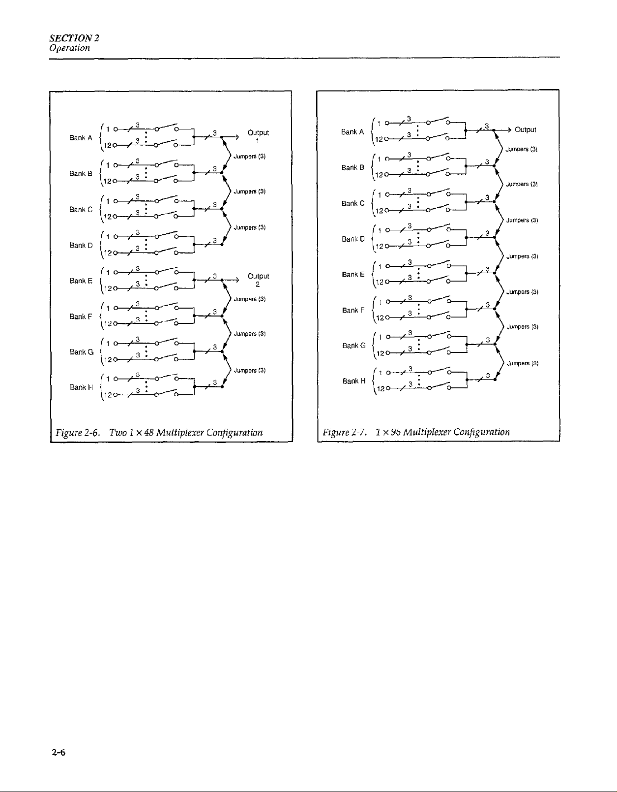
Two 1 x 48 Multiplexer Configuration
1 x 96 Multiplexer Configuration
Model 7074 Multiplexers Connected to Model 7071 Rows using Backplane Jumpers
Guarded Switching ................................................
Unguarded Switching .............................
4.Wire DMM Switching ...........................
SMU Connections .................................
Model 7074 Installation .............................
Connections Using Mass Terminated Cables
Connecting 75-I% Plug to Bank Receptacle
Connecting 38.Pin Plug to ROW Receptacle
Connecting Method using MTC Cables Cut in Half
Cable Preparation
38-I% Plug Cable Position
38-I% Plug (7078-KIT) Wire Color Coding
75-I+ Disassembly ...............................
75-l% Plug Cable Positions
75-I% Plug (7074-KIT) Wire Color Colding
Model 7078Xit (ROW A-H) Plug Contact Assignments
Model 7074~KIT (Bank) Plug Contact Assignments
Bank Receptacle Connector (Wiring side view)
ROW A-H Receptacle Connector
Single Card System Example
Multiple Card System Example
Using the Multiplexer with a Model 7071 Matrix Card
Using the Multiplexer with a Model 7071-4
Path Isolation Resistance ...........................
Voltage Attenuation by Path Isolation Resistance
Power Line Ground Loops
Eliminating Ground Loops
Shielding Example
Guarded Circuit
Typical Guarded Signal Connections
................................
......................................
.........................
.........................
........................
......................
.........................
.........................
...
............
.................
.................
.............
..............
.............
........
.............
.............
....
.......
.....
.............
........
2-2
2-3
2-4
2-5
2-5
2-6
2-6
2-7
2-8
2-8
2-9
2-9
Z-10
2-13
2-14
2-14
2-15
2-18
2-18
2-19
2-20
2-21
2-22
2-23
2-24
2-26
2-27
2-28
Z-30
2-31
2-32
2-34
2-34
2-35
2-36
2-36
2-37
2-38
Page 14
Figure 2-39
Figure Z-40 Model 7074 Frequency Response (RL = lMQ, 1 x 96 Configuration) 2-39
Figure 2-41
Figure 242 Model 7074 Frequency Response (Rr = 504 Eight 1 x 12 Configuration 2-41
Figure 243 Model 7074 Frequency Response (RL = 5OQ Eight 1 x 12 Configuration 242
AC Frequency Response Test Configuration
Model 7074 Frequency Response (RL = 50Q 1 x 96 Configuration 2-40
2-38
:SECTION 3 - Applications
Figure 3-l 2-Wire Resistance Testing
Figure 3-2 4-Wire Resistance Testing
Figure 3-3 Low Resistance Testing .................................... 3-3
Figure 3-4 Configuration for Current Gain and Common-Emitter Tests
Figure 3-5
Figure 3-6 Connecting Multiplexer and Matrix Cards Together
Figure 3-7 Resistivity Test Configurations ..............................
Figure 3-8 Measurement Required for Resistivity Test
Typical Common-Emitter Characteristics
..................................
..................................
........
...................... 3-6
..............
..................... 3-9
3-1
3-2
3-5
3-7
3-8
SECTION 4 - Service Information
Figure 4-l
Figure 4-2
Figure 4-3
Figure 4-4
Figure 4-5
Figure 4-6
Figure 4-7
Figure 4-8
Figure 4-9
Figure 4-10
Figure 4-11
Figure 4-12
Figure 4-13
Figure 4-14
Figure 4-15
Figure 4-16
Test Cable Preparation .....................................................
Connecting the Test Cable to the Model 7074 .....................................
Connecting Test Leads to Receptacle ...........................................
ROW A-H Receptacle Contact Assignments (Rear Panel View)
Bank Receptacle Assignments (Rear Panel View)
Connections for Path Resistance Test ...........................................
Differential Offset Current Test Connections
Common Mode Offset Current Test Connections ..................................
Contact Potential Test Connections ............................................
Path Isolation Test Connections ..............................................
Differential Isolation Test Connections .........................................
Connections for Common Mode Isolation Tests ...................................
Card Disassembly
RearShieldLocation
IDDataTiming
Model7074BlockDiagram..
.........................................................
.......................................................
...........................................................
................................................
..................................
.....................................
.......................
4-2
4-3
4-5
4-6
4-7
4-8
4-9
4-10
4-l 1
4-12
4-14
4-15
4-16
4-17
4-19
4-20
Page 15
SECTION 2 - Operation
List of Tables
Table 2-l
Table 2-2
Table 2-3
Cables, Receptacles, and Special Tools
Model 7074-MTC Cable Color Codes
Model 7078.MTC Cable Color Codes
SECTION 4 - Service Information
Table 4-l
Table 4-2
Table 4-3
Table 4-4
Table 4-5
Table 4-6
Recommended Verification Equipment
Performance Record
Path Isolation Test Summary
Differential and Common Mode Isolation Test Summary
Recommended Troubleshooting Equipment
Troubleshooting Procedure
...........................
..............
...............
...............
.............
.....................
......................
.........
...........
...........
...........
...........
...........
...........
...........
2-12
2-16
2-17
4-4
4-5
4-13
4-15
4-1s
4-18
Page 16
SECTION 1
General Information
1 .l INTRODUCTION
This section contains general information about the
Model 7074.
Section 1 is arranged in the following manner:
1.2 Feafures
1.3 Warranty Information
1.4 Manual Addenda
1.5 Safety Symbols and Terms
1.6 Specifications
1.7 Unpacking and Inspection
1.8 Repacking for Shipment
1.9 Optional Accessories
1.2 FEATURES
The Model 7074 General Purpose Multiplexer Card con-
sists of eight banks of 1 x 12 multiplexers that can be configured in various combinations. Three-pole switching
(HI, LO, guard) is provided for any of the 96 inputs.
Easy jumper configuration of single, dual, quad, or octal multiplexer banks.
Each of the eight multiplexer banks can be connected
to the 3-p& general-purpose backplane pathways
with user-installed jumpers, allowing simple internal
connections to the rows of those matrix cards.
Five mass-termination receptacles located on the rear
panel for quick-disconnect input and output connections.
1.3 WARRANTY INFORMATION
Warranty information is located on the inside front cover
of this instruction manual. Should your Model 7074 require warranty service, contact the Keithley representative or authorized repair facility in your area for further
information. When returning the card for repair, be sure
to fill out and include the service form at the back of this
manual in order to provide the repair facility with the
necessary information.
1.4 MANUAL ADDENDA
Any improvements or changes concerning the multi-
plexer card or manual will be explained in an addendum
included with the the unit. Be sure to note these changes
and incorporate them into the manual before using or
servicing the card.
1.5 SAFETY SYMBOLS AND TERMS
The following symbols and terms may be found on an instrument or used in this manual.
The Model 7074 is available with either dry or mercurywetted reed relays. The dry-reed version (Model 7074-D)
has lower thermal offset performance, while the mercury-wetted version (Model 7074-M) offers minimal contact bounce for and constant contact resistance overlife.
Throughout this manual, Model 7074 is used to refer to
both versions unless otherwise indicated.
Key features of the Model 7074 include:
The A
user should refer to the operating instructions located in
the instruction manual.
The symbol on an instrument shows that 1kV or
greater may be present on the terminal(s). Use standard
symbol on an instrument indicates that the
1-l
Page 17
SECTION I
General Information
safety precautions to avoid personal contact with these
voltages.
The WARNING heading used in this manual explains
dangers that might result in personal injury or death. Always read the associated information very carefully before performing the indicated procedure.
The CAUTION heading used in this manual explains
hazards which could damage the multiplexer card. Such
damage may invalidate the warranty.
1.6 SPECIFICATIONS
Model 7074-D and Model 7074-M specifications may be
found at the front of this manual. Note that some specifications, such as contact life, path resistance, and contact
potential, differ between the two versions of the card.
These specifications are exclusive of the matrix mainframe specifications, which are located in the Model 707
Instruction Manual.
removing the plastic wrapping, place the manual in the
binder after the mainframe instruction manual. Note that
a manual identification tab is included and should precede the multiplexer card instruction manual.
If an additional instruction manual is required, order the
manual package, Keithley part number 7074-901-00. The
manual package includes an instruction manual and any
pertinent addenda.
1.8 REPACKING FOR SHIPMENT
Should it become necessary to return the Model 7074 for
repair, carefully pack the unit in its original packing carton or the equivalent, and include the following~information:
Advise as to the warranty status of the multiplexer
card.
Write ATTENTION REPAIR DEPARTMENT on the
shipping label.
Fill out and include the service form located a’t theback
of this manual.
1.7 UNPACKING AND INSPECTION
1.7.1 Inspection for Damage
Upon receiving the Model 7074, carefully unpack it from
its shipping carton and inspect the card for any obvious
signs of physical damage. Report any such damage to the
shipping agent immediately. Save the original packing
carton for possible future reshipment.
1.7.2 Shipment Contents
The following items are included with every Model 7074
order:
. Model 7074-D or 7074-M Multiplexer Card
l Model 7074 Instruction Manual
l Eight spare configuration jumpers
l Additional accessories as ordered
1.7.3 Instruction Manual
1.9 OPTIONAL ACCESSORIES
The following paragraphs discuss optional cables, connecting kits, and special tools that are available for use
with the Model 7074.
1.9.1 BANK Receptacle Accessories
The following accessories are designed for use with the
four BANK receptacles.
Model 7074-CIT Contact Extraction Tool -The Model
7074~CR includes a tool that is used to remove wire
crimp tail contacts from 75-pin “rack and panel” plugs
and receptacles.
Model 7074-HCT Hand Crimping Tool - The Model
7074-HCT is used to attach wire crimp tail contacts (for
75-pin connectors) to #l&3 to #26 AWG stranded wire.
However, provided contacts should only be used with
#20 to #24 AWG wire.
The Model 7074 Instruction Manual is three-hole drilled
so that it can be added to the three-ring binder of the
Model 707 Switching Matrix Instruction Manual. After
1-2
Model 7074-KIT Connector Kit-The Model 7074~KIT
contains the parts to assemble one 75pin “rack and
Page 18

General Information
SECTION1
panel” plug. This plug will mate to the BANK receptacle
on the rear panel of the card. Parts contained in the kit include the plug, 80 wire crimp tail contacts (for use with
#20 to #24 AWG wire), four corner pins, one tunable
male jackscrew, one tunable female jackscrew, and one
shield.
Model 7074-MTC-20 Mass Terminated Cable Assembly - The Model 7074~MTC-20 is a 20-foot (6-meters),
72-conductor cable terminated with a “rack and panel”
plug on both ends. This cable connects to the the BANK
receptacles on the rear panel of the card. This cable can be
cut in half to provide two separate cables, each of which
can be connected to one of the BANK receptacles. The unterminated ends of the cables are then connected to instrumentation and DUTs.
Model 7074-MTR Mass Terminated Receptacle with
Contacts-The Model 7074~MTR includes a 75-pin con-
nector, 80 crimp tail contacts, (for #20 to #24AWG wire),
one fixed female jackscrew, one fixed male jackscrew,
and four corner pins. The Model 7074-MTR mates with
the Model 7074MTC cables and the Model 7074-KIT
plug kit.
Model 707%CIT Contact Insertion and Extraction Tools
-The Model 7078~CIT includes an insertion tool that is
used to insert wire crimp tail contacts into 38-pin “rack
and panel” plugs and receptacles. Conversely, the extraction tool is required for the removal of the contacts.
Model 707%HCT Hand Crimping Tool - The Model
707%HCT is used to attach wire crimp tail contacts to #18
to #26 AWG stranded wire.
Model 7078-KIT Connector Kit-The Model 707%KIT
contains the parts to assemble one 38-pin “rack and
panel” plug. This plug will mate to the ROW A-H recep-
tacle on the rear panel of the card. Parts contained in the
kit include the plug, plug housing and 40 wire crimp tail
contacts.
Model 707%MTC-5 Mass Terminated Cable Assembly
-The Model 7078MTC is a 5-foot (1.5~meters), 36-conductor cable terminated with a “rack and panel” plug on
both ends. This cable connects to ROW A-H receptacle on
the rear panel of the card. This cable can be cut in half to
provide two separate cables when using two or more
Model 7074 cards. The unterminated ends of the cables
are then connected to instrumentation and DUTs.
Model 7074-RTC Relay Test Shorting Plug - The
Model 7074-RTC is intended for use with the relay test
software, as described in paragraph 4.2. The Model
7074-RTC consists of a 75-pin plug with pins and jumper
wires.
1.9.2 ROW Receptacle Accessories
The following accessories are intended for use with the
ROW A-H receptacle.
Model 707%MTC-20 Mass Terminated Cable Assembly - Thii cable is the same as the Model 707%MTC-5,
except that it is 20.feet (6-m&& in length.
Model 707%MTR Mass Terminated Receptacle with
Contacts-The Model 707%MTR includes a 3%pin connector and 40 crimp tail contacts. The Model 707%MTR
mates with the Model 7078-MTC cables and the Model
7078-KIT plug kit.
l-3
Page 19
SECTION 2
Operation
2.1 INTRODUCTION
This section contains information on multiplexer configuration, card connections, installation, and programming, and is arranged as follows:
2.2 Handling Precautions: Discusses precautions that
should be taken when handling the card to avoid contamination that could degrade performance.
2.3 Environmental Considerations: Outlines environmental aspects of using the Model 7074.
2.4 Multiplexer Card Configuration: Discusses the multiplexer rear panel as well as multiplexer configuration,
and expansion by jumpering two or more multiplexer
sections together.
2.5 Card Installation and Removal: Details installation
in and removal from the Model 707 Switching Matrix
mainframe.
2.6 Connection Methods: Discusses card connectors, cables, and ways to connect the card to other instruments
and test fixtures.
2.7 Typical Connection Schemes: Gives typical connections to other cards, mainframes, and test instrumentation.
safety precautions located at the front of this
manual before using the multiplexer card.
2.2 HANDLING PRECAUTIONS
To maintain high impedance isolation, care should be
taken when handling the multiplexer card to avoid contamination from such foreign materials as body oils. Such
contamination can substantially lower leakage resistances, degrading performance. To avoid any possible
contamination, always grasp the card by the handle or
the card edges. Do not touch board surfaces, components, or edge connectors.
Dirt build-up over a period of time is another possible
source of contamination. To avoid this problem, operate
the mainframe and matrix card only in a clean environment. If contamination is suspected, clean the card as discussed in Section 4. Also, the performance verification
procedures in Section 4 can be used to test the card for
low leakage resistances that could indicate contamination.
2.3 ENVIRONMENTAL CONSIDERATIONS
For rated performance, the card should be operated
within the temper&w and humidity limits given in the
specifications at the front of this manual.
2.8 Multiplexer Programming: Summarizes programming steps to control the multiplexer card from the
Model 707 Switching Matrix.
2.9 Measurement Considerations: Reviews a number of
considerations when making measurements using the
Model 7074.
WARNING
The information in this section is intended
for qualified personnel who have experience
with potentially hazardous voltages. Do not
attempt to perfolm these procedures unless
you are qualified to do so. Carefully read the
2.4 MULTIPLEXER CARD CONFIGURATION
The following paragraphs discuss the rear panel of the
card, the eight 1 x 12 multiplexers of the Model 7074, as
well as how to connect two or moremultiplexer banks together to make multiplexers as large as 1 x 96.
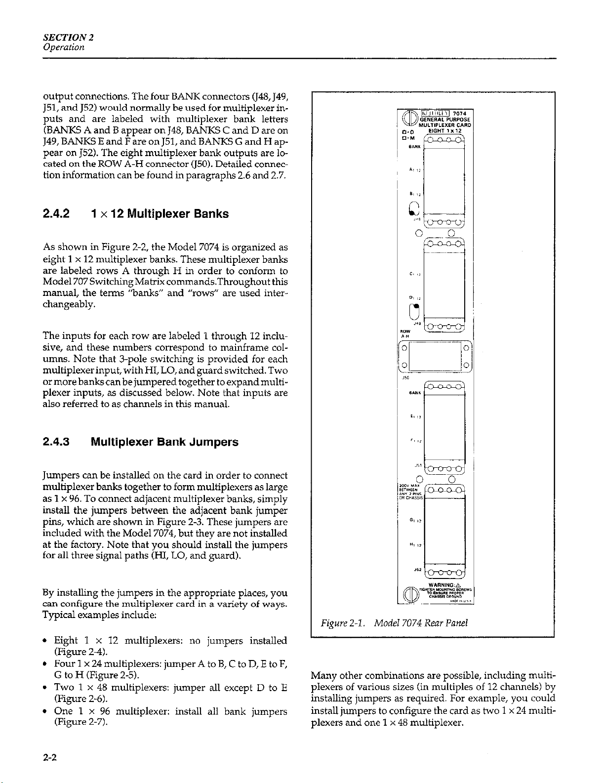
2.4.1 Rear Panel
The rear panel of the Model 7074 is shown in Figure 2-1.
The rear panel has a total of five receptacles for input/
2-1
Page 20
SECTION2
Operation
output connections. The four BANK connectors (148, J49,
J51, and J52) would normally be used for multiplexer in-
puts and are labeled with multiplexer bank letters
(BANKS A and B appear on J48, BANKS C and D are on
J49, BANKS E and F are on J51, and BANKS G and H appear on J52). The eight multiplexer bank outputs are lo-
cated on the ROW A-H connector (JSO). Detailed connection information can be found in paragraphs 2.6 and 2.7.
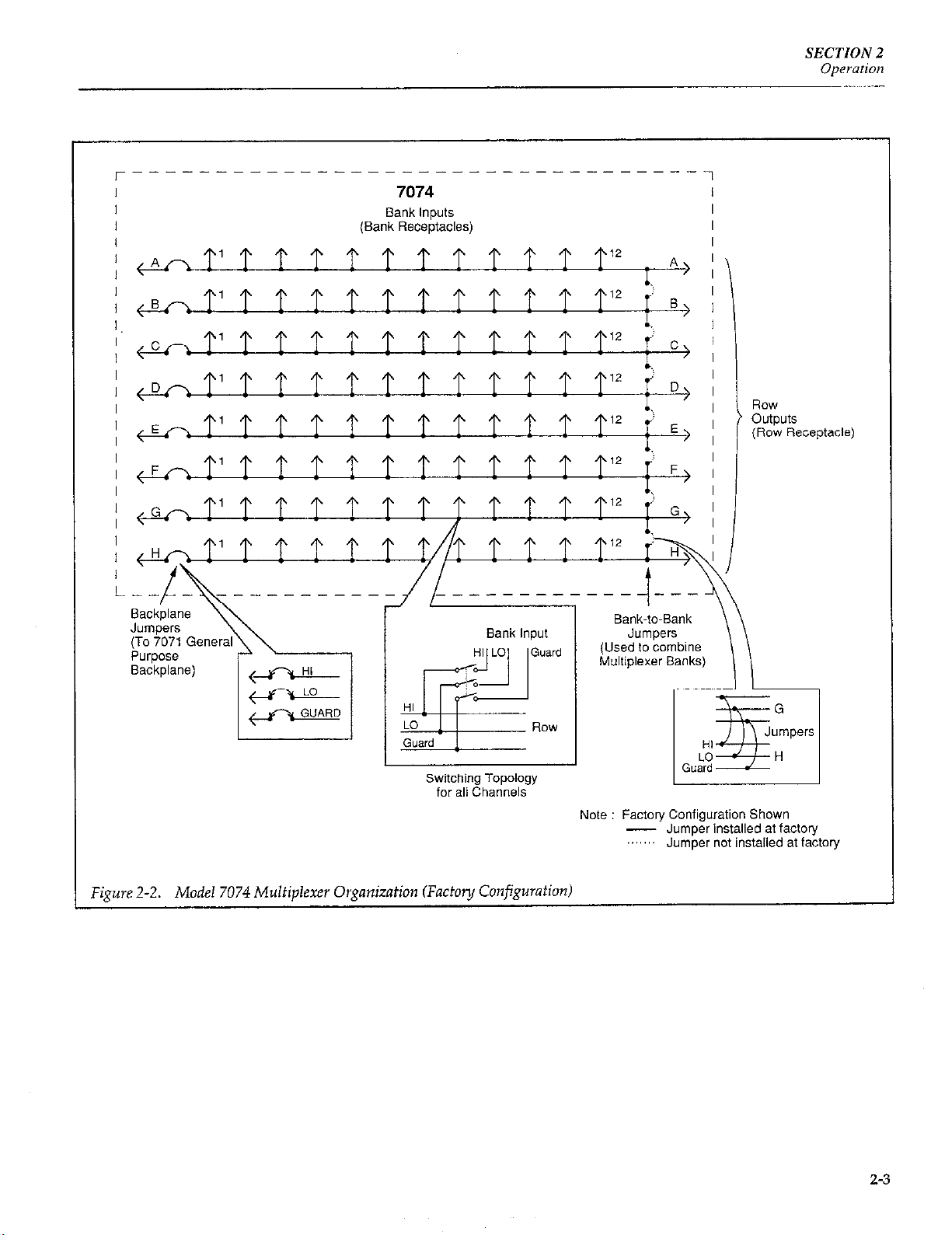
2.4.2
As shown in Figure 2-2, the Model 7074 is organized as
eight 1 x 12 multiplexer banks. These multiplexer banks
are labeled rows A through H in order to conform to
Model 707 Switching Matrix commands.Throughout this
manual, the terms “banks” and “rows” are used interchangeably.
The inputs for each row are labeled 1 through 12 inclusive, and these numbers correspond to mainframe columns. Note that 3-p& switching is provided for each
multiplexer input, with HI, LO, and guard switched. Two
or more banks canbe jumpered together to expand multiplexer inputs, as discussed below. Note that inputs are
also referred to as channels in this manual.
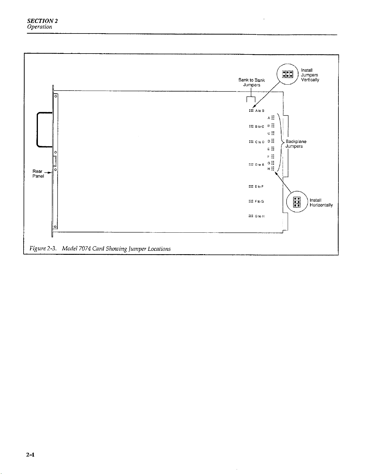
2.4.3
Jumpers can be installed on the card in order to connect
multiplexer banks together to form multiplexers as large
as 1 x 96. To connect adjacent multiplexer banks, simply
install the jumpers between the adjacent bank jumper
pins, which are shown in Figure 2-3. These jumpers are
included with the Model 7074, but they are not installed
at the factory. Note that you should install the jumpers
for all three signal paths (HI, LO, and guard).
1 x 12 Multiplexer Banks
Multiplexer Bank Jumpers
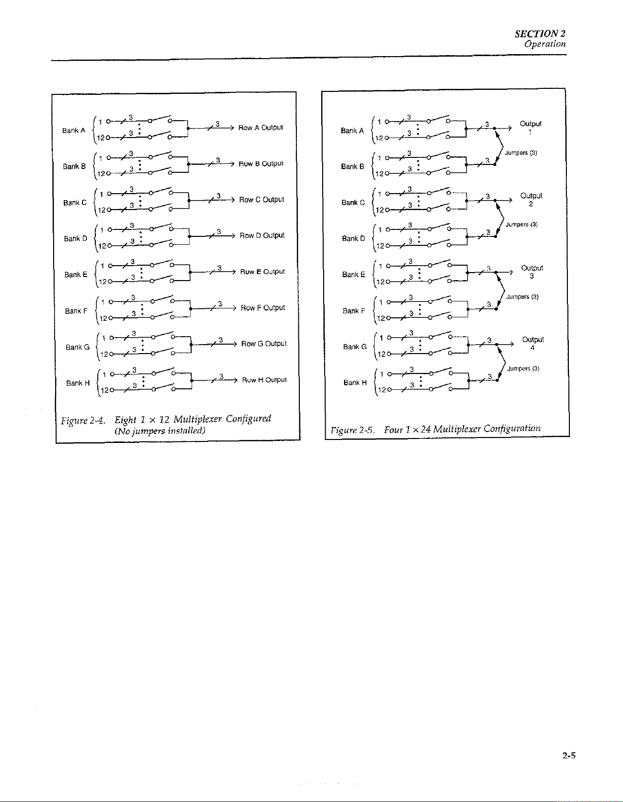
By installing the jumpers in the appropriate places, you
can configure the multiplexer card in a variety of ways.
Typical examples include:
l Eight 1 x 12 multiplexers: no jumpers installed
(Figure 2-4).
l Four 1 x 24 multiplexers: jumper A to B, C to D, E to F,
G to H (Figure 2-5).
l Two 1 x 48 multiplexers: jumper all except D to E
(Figure 2-6).
l One 1 x 96 multiplexer: install all bank jumpers
(Figure 2-7).
2-2
Figure 2-l. Model 7074 Rear hnel
1
Many other combinations are possible, including multiplexers of various sizes (in multiples of 12 channels) by
installing jumpers as required. For example, you could
install jumpers to configure the card as two 1 x 24 multiplexers and one 1 x 48 multiplexer.
Page 21
SECTION 2
Opr&XI
for all Channels
Figure 2-2. Model 7074 Multiplexer Organization (Factmy Configuration)
Note : Factory Configuration Shown
- Jumper installed at factory
“““’ Jumper not installed at factory
2-3
Page 22
SECTION 2
Operation
0
Rear 0 -
Panel
::: - AlOB
::: EbaF
0
Figure 2-3. Model 7074 Card Showing Jumper Locations
::: F,OG
::: GbH
Z-4
Page 23
SECTION 2
Operation
-
Figure 2-4. Eight 1 x 12 Multiplexer Configured
(No jumpers installed)
Figure 2-5.
Four 2 x 24 Multiplexer Configuvntion
2-S
Page 24
SECTION 2
Operarion
?gure 2-6.
Two 1 x 48 Multiplexer Confi,quration
Tgure 2-7.
1 x 96 Multiplexer Configuration
2-6
Page 25
SECTION 2
Operarion
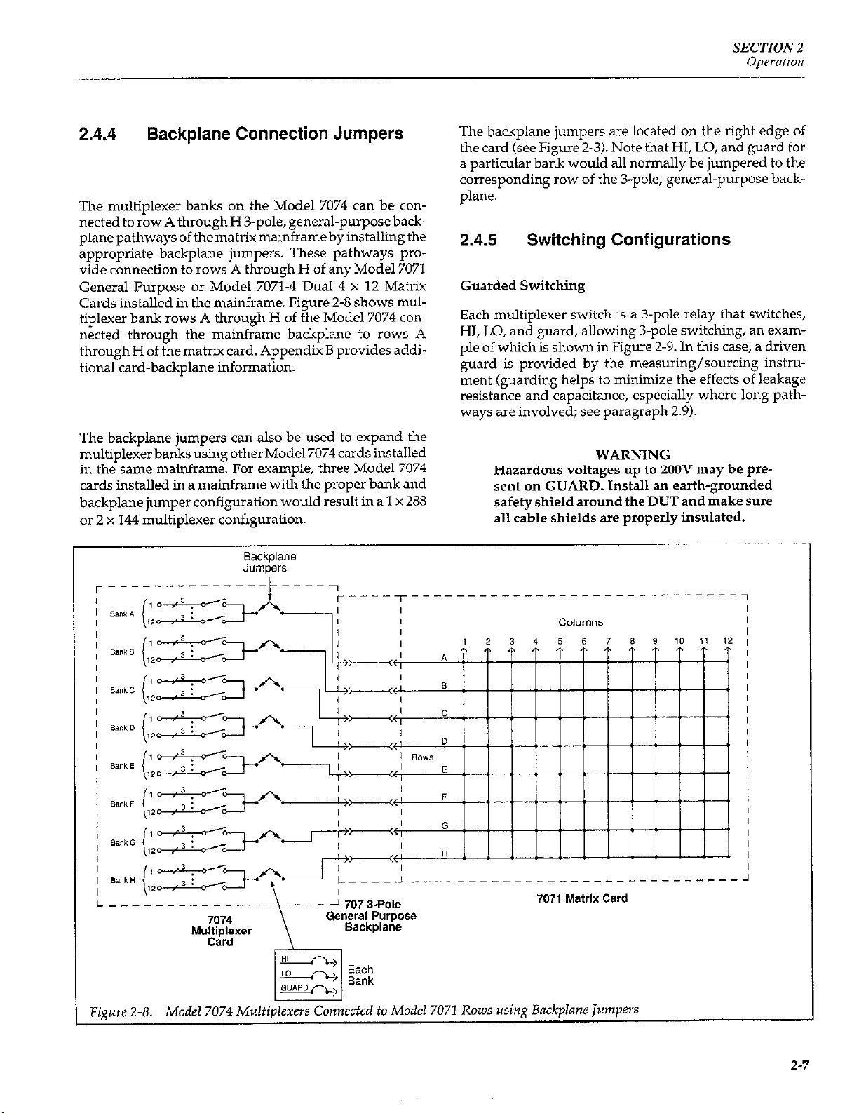
2.4.4 Backplane Connection Jumpers
The multiplexer banks on the Model 7074 can be connected to row A through H 3-p&, general-purpose backplane pathways of the matrix mainframeby installing the
appropriate backplane jumpers. These pathways provide connection to rows A through H of any Model 7071
General Purpose or Model 7071-4 Dual 4 x 12 Matrix
Cards installed in the mainframe. Figure 2-8 shows multiplexer bank rows A through H of the Model 7074 connected through the mainframe backplane to rows A
through H of the matrix card. Appendix B provides additional card-backplane information.
The backplane jumpers can also be used to expand the
multiplexerbanksusingotherModel7074cardsinstalled
in the same mainframe. For example, three Model 7074
cards installed in a mainframe with the proper bank and
backplane jumper configuration would result in a 1 x 288
or 2 x 144 multiplexer configuration.
The backplane jumpers are located on the right edge of
the card (see Figure 2-3). Note that HI, LO, and guard for
a particular bank would all normally be jumpered to the
corresponding row of the 3-pole, general-purpose backplane.
2.4.5 Switching Configurations
Guarded Switching
Each multiplexer switch is a 3-p& relay that switches,
HI, LO, and guard, allowing 3-p& switching, an exam-
ple of which is shown in Figure 2-9. In this case, a driven
guard is provided by the measuring/sourcing instmment (guarding helps to minimize the effects of leakage
resistance and capacitance, especially where long pathways are involved; see paragraph 2.9).
WARNING
Hazardous voltages up to 2OOV may be present on GUARD. Install an earth-grounded
safety shield around the DUT and make sure
all cable shields are properly insulated.
Backplane
Jumpers
---~q[----r ------------- ~~“m, -----------IZU
7071 Matrix Card
I
/
Figure 2-8. Model 7074 Multiplexers Connected to Model 7071 Rows using B&plane Jumpers
2-7
Page 26
SECTION 2
Operation
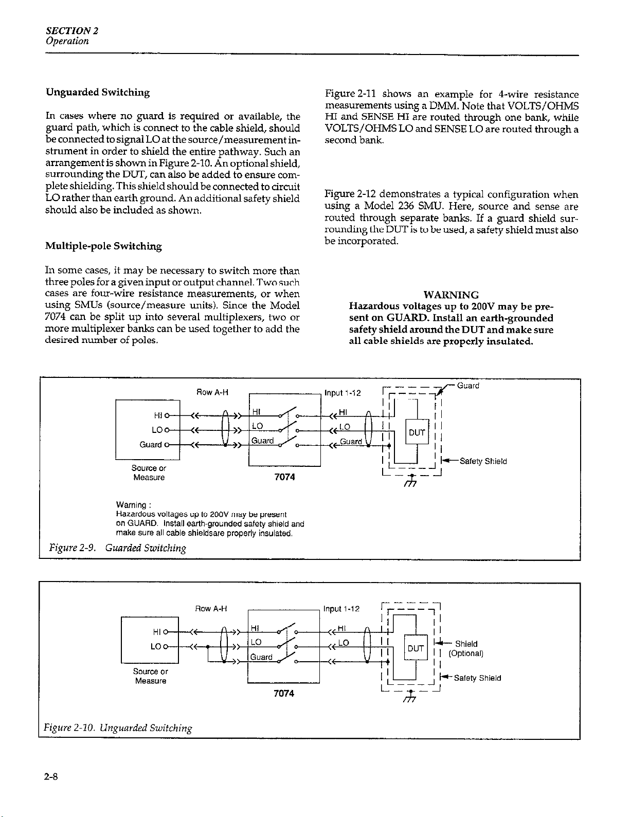
Unguarded Switching
In cases where no guard is required or available, the
guard path, which is connect to the cable shield, should
be connected to signal LO at the source/measurement instrument in order to shield the entire pathway. Such an
arrangement is shown in Figure Z-10. An optional shield,
surrounding the DUT, can also be added to ensure complete shielding. This shield should be connected to circuit
LO rather than earth ground. An additional safety shield
should also be included as shown.
Multiple-pole Switching
In sc~me cases, it may be necessary to switch more than
three poles for a given input or output channel. Two such
cases are four-wire resistance measurements, or when
using SMUs
(source/measure
units). Since the Model
7074 can be split up into several multiplexers, two or
more multiplexer banks can be used together to add the
desired number of poles.
Figure 2-11 shows an example for 4-wire resistance
measurements using a DMM. Note that VOLTS/OHMS
HI and SENSE HI are routed through one bank, while
VOLTS/OHMS LO and SENSE LO are routed through a
second bank.
Figure 2-12 demonstrates a typical configuration when
using a Model 236 SMU. Here, source and sense are
routed through separate banks. If a guard shield SLITrounding the DUT is to be used, a safety shield must also
be incorporated.
WARNING
Hazardous voltages up to ZOOV may be present on GUARD. Install an earth-grounded
safety shield around the DUT and make sure
all cable shields are properly insulated.
-
Warning :
Hazardous voltages up to ZOOV may be present
on GUARD. install ear?h-grounded safety shield and
make sure all cable shieldsare properly insulated.
Figure 2-9. Guarded Switching
Figure 2-10. Unguarded Switching
-Safety Shield
2-8
Page 27
SECTION 2
Operarim
Figure Z-11. 4.Wire
DMM Switching
236
SMU
Warning :
Hazardous voltages up to 110” may be present
on GUARD. ,hs,a,l earth-grounded sa‘ety shield and
make sure al, cable shields are properly insulated.
=igure 2-12. SMU Connections
2-9
Page 28
SECTION 2
Operation
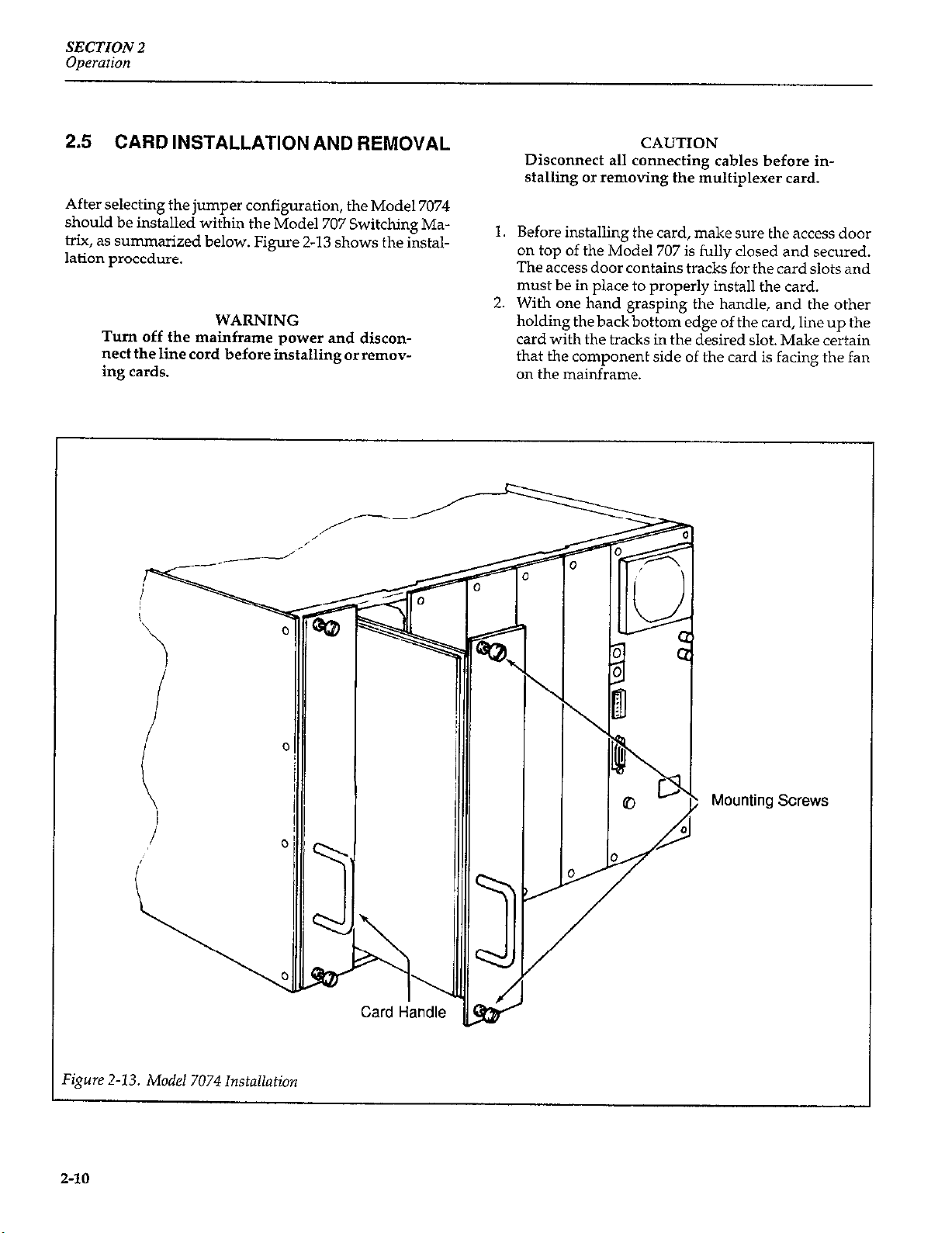
2.5
After selecting the jumper configuration, the Model 7074
should be installed within the Model 707 Switching Matrix, as summarized below. Figure 2-13 shows the install&ion procedure.
CARD INSTALLATION AND REMOVAL
WARNING
Turn off the mainframe power and disconnect the line cord before installing orremoving cards.
CAUTION
Disconnect all connecting cables before in-
stalling or removing the multiplexer card.
l. Before installing the card, make sure the access door
on top of the Model 707 is fully closed and secured.
The access door contains tracks for the card slots and
must be in place to properly install the card.
2. With one hand grasping the handle, and the other
holding the back bottom edge of the card, line up the
card with the tracks in the desired slot. Make certain
that the component side of the card is facing the fan
on the mainframe.
‘igure Z-13. Model 7074 Installation
Z-10
Mounting Screws
Page 29
SECTION 2
Operarion
CAUTION CAUTION
Do not touch the card surfaces oranycompo- Do not touch the card surfaces oranycomponents to avoid contamination
grade card performance.
Slide the card into the mainframe until it is properly
seated in the edge connectors at the back of the slot.
Once the card is properly seated, secure it to the
mainframe by finger tightening the spring-loaded
screws.
WARNING
The mounting screws must be secured to ensure a proper chassis ground connection between the card and the mainframe. Failure to
properly secure this ground connection may
result in personal injury or death due to electric shock.
To remove a card, first turn off the power and disconnect the line cord from the mainframe. Disconnect all cables from the multiplexer card. Loosen the
mounting screws, then pull the card out of the mainframeby the handle. When theback of the card clears
the mainframe, support it by grasping the bottom
edge near the rear of the card.
that
that
could de- nents to avoid contamination
could de-
2.6 CONNECTION METHODS
The Model 7074 has two types of “rack and panel” receptacles mounted on the rear panel. The four BANK (input)
receptacles are 75.pin receptacles that will mate with
either the optional mass terminated cables (Models
7074~MTC-5 or 7074~MTC-20) or the plug provided with
the optional connector kit (Model 7074~KIT). The ROW
A-H (output) receptacle is a 3%pin connector that will
mate with either the optional mass terminated cables
(Models 7078-MTC-5 or 7078-MTC-20) or the plug provided with the optional connector kit (Model 7078~KIT).
Model numbers for the two groups of cables, plugs, receptacles, and special tools are similar and are called out
together. Table 2-l summarizes the cables, receptacles,
and special tools that canbe obtained directly from Keithley Instruments. To avoid confusion, remember that all
7074 numbers pertain to the four BANK receptacles, and
all 7078 numbers are associated with the ROW A-H receptacle.
NOTE
The term receptacle refers to a connector
mounted on the rear panel of the multiplexer
card (and the connector supplied with the
Model 7074.MTR and 7078~MTR kits). The
term plug refers to a connector that attaches to
a cable such as the Model 7074.MTC and
7078-MTC cables, and the plugs supplied
with the Model 7074XIT and 7078-KIT kits.
2.6.1 Connection Methods
There are several ways to make connections to the Model
7074. These include:
Unmodified Mass Terminated Cable Method (Models
7074-MTC and 7078-MTC) - This method is probably
the most convenient method to make connections to the
multiplexer card. Using the whole cable (both plugs in-
tact) makes it most convenient to connect the multiplexer
card to a test fixture that uses the same “rack and panel”
receptacles as the multiplexer card. Additional receptacles that mate with these cables can be ordered from
Keithley Instruments; order Model 7074-MTR for the
BANK receptacles, or Model 707%MTR for the ROW
A-H receptacle. Detailed information on wiring these re-
ceptacles is located in paragraph 2.6.4.
Modified Mass Terminated Cable Method -By cutting
each MTC cable in half (or wherever appropriate), two
separate cables, unterminated at one end, will result.
These cables can then be hard-wired to DUTs or to your
test fixture. The plug on each Model 7074-MTC cable will
then connect to one of the BANK (input) receptacles, and
the plug on one end of a Model 7078-MTC cable will connect to the ROW A-H receptacle on the card.
The following paragraphs discuss how to make connections using the two connector types. Since the procedures
for the two connector types are virtually identical, only
one procedure for each type is given. Where applicable,
differences between the two connector types are called
out separately.
Connector Kit Method (Models 7074-KIT and
7078-KIT) - These kits contain plugs that mate to the
“rack and panel” receptacles, and they are designed for
custom-built mass terminated cables. An alternative to
building a complete cable from scratch is to cut the Model
2-11
Page 30

SECTION 2
Operadon
Table 2-1. Cables, Receptacles, and Special Tools
Model or Part
Model 7074~CIT: Extraction Tool
Model 7074-HCT: Hand Crimping Tool
Model 7074-m Connection Kit
Model 7074-MTC: Mass Terminated Cable
Model 7074~MTR: Mass Terminated Receptacle Contains one 75-pin “rack and panel” receptacle and contact sock-
Model 707%ClTz Insertion and Extraction Tools Used to install/remove wire crimp tails into/from 3%pin “rack
Model 707%HCT: Hand Crimping Tool
Model 7078-m Connection Kit
Model 707%MTC: Mass Terminated Cable
Description
Used to remove wire crimp tails in 75-pin “rack and panel” plugs
and receptacle
Used to connect wire crimp tails to #lt? to #26 gauge wire.
Contains one “rack and panel” plug, housing and 80 wire crimp
tail pins. Note: These pins are intended for use with #20 to #24
AWG wires.
6-meter (20 ft.) 72 conductor cable terminated with 75-pin “rack
and panel” plugs. Mates to “rack and panel” receptacles.
ets. Note: These sockets are intended for use with #20 to #24
AWG wire.
and panel” plugs and receptacles.
Used to connect wire crimp tails to #18 to #26 gauge wire.
Contains one 38-pin “rack and panel” plug, housing, and 40 wire
crimp tails.
6-meter (20 ft.), 36 conductor cable terminated with “rack and
panel” plugs. Mates to 3%pin “rack and panel” receptacles.
Model 707%MTR: Mass Terminated Receptacle
NOTE: All Model 7074 numbers pertain to BANK receptacles/plugs. All Model 7078 numbers pertain to ROW receptacle/plug
7074~MTC or 707%MTC cable at a length that is suitable
and then attach the plug to it.
WARNING
To avoid electrical shock, which could result
in injury or death, make sure all power is off
and stored energy in external circuitry is discharged before making any connections to
the multiplexer card. Do not exceed the voltage and current ratings for the card or connecting cables as stated in the specifications
and safety precautions at the front of this
manual. Do not connect this card to unlimited power circuits or directly to ac mains. Install appropriate protection devices to limit
fault currents from any supply connected to
this card.
3%pin “rack and panel” receptacle and contact pins.
CAUTION
Contamination will degrade the performance of the multiplexer card. To avoid contamination, always grasp the card by the
handle and side edges. Do not touch the edge
connectors of the card, and do not touch the
board surfaces or components. On “rack and
panel” receptacles and plugs, do not touch
areas adjacent to the electrical contacts.
2.6.2
Connection Methods Using Mass
Terminated Cables
The Model 7074~MTC-20 is a 6meter (20-foot), 75-conductor cable terminated with a 75.pin “rack and panel”
plug on each end. This cable is used to connect the BANK
(input) receptacles on the rear panel of the card to external equipment.
2-12
Page 31

SECTION 2
Operation
Similarly, the Model 7078.MTC-5 is a 1.5 meter &foot),
36-conductor cable terminated with a 3%pin “rack and
panel” plug on each end. The Model 7078-MTC-20 is the
same except that it is 6 meters (20 feet) in length. These cables are used to connect the ROW A-H receptacle on the
Direct Connections
Figure 2-14 shows how these cables can be used to con-
nect inputs and outputs of the multiplexer card to external “rack and panel” receptacles. The external recepta-
cles can then be hard wired to other connectors or wired
rear panel of the card to external instrumentation and test directly to instrumentation and DUTs. See paragraph
circuits.
2.6.4 for receptacle wiring information.
Figure 2-14. Connections Using Mass Terminated Cables
2-13
Page 32

SECTION 2
Operation
Connecting MTC Cables to the Multiplexer Card
Use the following procedure to connect the Model
7074~MTC and 7078-MTC cables to the multiplexer card:
1. Install the multiplexer card in the Model 707 mainframe as explained in paragraph 2.5.
WARNING
Turn off power to all instruments and discharge all capacitors before making ccmnections. Do not connect the Model 7074 to unlimited power circuits or directly to ac
mains. Install appropriate protection devices to limit fault currents from any Supply
connected to the multiplexer card.
CAUTION
Be careful not to bend the plug pins when
making connections.
2. Place the plug of the cable on the appropriate “rack
and panel” receptacle as shown in Figure 2-15
(BANK) or Figure Z-16 (ROW A-H). For the BANK
(input) receptacles, align the two locking screws of
theplugwiththescrewsinthereceptacle(maletofemale and female to male). For the ROW A-H receptacle, align the plug such that the large diameter keying pin of the plug fits into the large keyway of the
receptacle
ROW
RKX?piXle
(Top view)
Figure 2-16. Connecting38-Pin Plug to RO~WReceptacle
3. Using a screwdriver, turn the locking screw(s) clockwise until the plug is fully mated to the receptacle
(for the BANK plugs, both screws must be secured).
Disconnecting Cables
To
disconnect a cable from the multiplexer card, first
loosen the locking screw(s) completely using ,a scxmvdriver. Grasp the plug by its body, then wiggle it from
side to side or with a slight rotary motion while pulling
back on the plug.
CAUTION
Never pull on the cable itself. Always grasp
the body of the plug to remove cables.
-Panel
/
Bank
Receptacle
i
Figure 2-15. Connecting 754% Plug to Bank
Receptacle
2-14
Cutting MTC Cables
Another way to use the Model 7074-MTC or 707%MTC
cables is to remove one of the plugs. Cutting the Model
707%MTC-5 cable in half will provide two 2 l/2-foot cables. Cutting the Model 7074-MTC-20 or 7078-MTC-20
cable in half will provide two IO-foot cables. Each cable
can then be mated to a BANK (input) or ROW receptacle,
as shown in Figure Z-17.
The wire end of each cable can then be wired to another
connector or wired directly to instrumentation or DUTs.
Each cable contains bundles of wires each of which corresponds to a bank or channel. Each bundle contains three
wires; a bare wire (guard) and two insulated wires that
have a unique color combination for identification pur-
poses, with one wire HI, and the other wire LO. Table 2-2
provides the color combinations for each bundle of the
Page 33

SECTION 2
Operation
One half of Model
7074-MTC Cable
One half of Model 7078.MTC Cable
Model 7074~MTC (BANK) cables, and Table 2-3 summarizesthecolorcodingfortheModel707B-MTC(ROW) cables.
For example, with the cable connected to the ROW A-H
receptacle of the multiplexer card, Bank E can be identified by locating the bundle that has ablack insulated wire
(H) and a brown insulated wire CL). The bare wire in the
bundle is guard (G).
WARNING
The three wires in the brown and white bun-
dle should be collectively connected to common system ground of the test system to assure continued protection against a possible
shock hazard. These wires are connected to
Model 7074 chassis ground.
Insulating the Cable Wrappings
The outer wrapping of each bundle is insulated while the
inner wrapping is conductive (guard). When the cable is
cut, it is likely that the conductive side of the bundle
wrapping will become exposed. Thus, each bundle, as
well as each bare wire, should be insulated as outlined
below.
2-15
Page 34

SECTION 2
Operation
Table 2-2. Model 7074-MTC Cable Color Codes
Input #*
Al
A2
A3
A4
A5
A6
A7
A8
A9
A10
All
A12
Bl
82
83
EM
85
ii;
B8
B9
B10
Bll
812
‘Designation refers to row and input number. A also applies to rows C, E, and G. B also applies
to rows D, F, and H.
WARNING: Pins 40,41, and 42 and brawn/white cable bundle wires are earth ground and must be
connected to plug shell.
pin
-
31
12
28
8
32
13
29
i:
14
30
11
70
49
73
52 Yellow 46
71
50
74 Blue 80
53
72
51 White 45 Black 57 Clear
75
54
- -
High
GW3l 37
White 4 Blue
Brown 34
Yellow
Orange 38 Black 26 Clear
Blue 5
Red 35
Green 2
Green 39 White 27 Clear
Green
Red
Red
Yellow
Black
White 79 Orange 65 Clear
Yellow
Red
Green
Blue
Orange
Yellow 48
pin
1
7 Blue
36
3
76
43
77 Blue
44
47 Red 59 Clear
78 Red 64 Clear
82 Blue 67 Clear
LOW
Orange 25
Green 22
Green 15 Clear
Black 20
Black
Black
Brown
Orange
White 62
Brown 55
Black
White
Brown 66
Red
Pin#
-
18
23 Clear
16 Clear
21 Clear
24 Clear
17 Clear
58 Clear
63
56 Clt?X
60
Guard
Clear
Clear
Clear
Clear
Clear
Clear
Clear
Clear
Clear
2-16
Page 35

SECTION2
Operarion
TableZ-3. Model 707%MTC Cable Color
Codes
wire set
ROW A
rehd*
H
Insulation Color
Black
Blue
ROW B
ROW C
k
H
k
H
Bare Wiie
Red
BRW,Tl
Bare Wiie
Black
Red
ROW D
ROWE
ROW F
ROW G
ROW H
‘H = High
L=Law
k
H
L
G
H
L
G
H
L
G
H
L
G
H
L
G
Bare
Wire
Red
Y&WJ
Bare
Wire
Black
BIOWll
Bare Wiie
Red
Blue
Bare Wire
Black
OElIlge
Bare Wire
Red
GRY2n
Bare Wire
G =Guard
2.6.3
Connection Method Using Connector Kits
The Models 7074-KIT and 7078-KIT each contain the
parts of one “rack and panel” plug. The Model 7074~KIT
contalnsa75.pinplugandisintended tomatewithoneof
the BANK (input) receptacles, while the Model 7078~KIT
contains a 38-pin plug that mates with the ROW A-H receptacle. These kits will allow you to build your own custom cables that connect with the BANK (input) and ROW
A-H receptacles on the Model 7074. For example, since a 1
x 96 configuration is not uncommon, it may be simpler to
make your own cable because you would need only one
paired cable instead of the eight provided by MTC cables.
The “rack and panel” plugs will mate to the receptacles
on the multiplexer card in the same manner as the Model
7074MTC and 7078-MTC cables. The other end of the cables can be wired directly to instrumentation or DLJTs, or
to other connectors.
Basically, there are two ways you can wire these cables:
(1) use the same cables as those used with the MTC cables, and (2) wire up you own cables or groups of cables
to the plugs. Each of these methods is discussed below.
ROW A-H Plug MTC Cable Wiring
NOTE NOTE
The following procedure shows how to prop- The following procedure shows how to properly connect a 36-conductor cable to a 38-pin erly connect a 36-conductor cable to a 38-pin
plug. The cable used in the procedure is as- plug. The cable used in the procedure is assumed to be the same one used in the Model sumed to be the same one used in the Model
7078-MTC and is available from Belden (P/N 7078-MTC and is available from Belden (P/N
9734). 9734).
CAUTION
Each cable bundle must be insulated as covered below, or damage to instruments connected to the Model 7074 may result.
Procedure:
1. PlacealengthofTeflon~,bingovereachbarewire.
2. Place a length of shrink tubing over the bundle such
that the frayed end of the bundle wrapping is completely covered and part of the Teflon@ tubing is
covered.
3. Heat the shrink tubing.
Perform the following steps to connect the 36-conductor
Belden cable to the Model 7078~KIT plug:
1. Feed one end of the cable through the plug housing.
Slide the housing far enough down the cable to set it
out of the way.
NOTE
Refer to Figure 2-18 for the following cable
preparation steps.
2. Using a sharp knife, remove l-3/4” of insulation
from the end of the cable. Be careful not to cut into
2-17
Page 36

SECTION 2
Opcrarion
the insulated shield of any of the internal wire bundies.
3. Remove 1” of insulated shielding from each of the
bundles of wires.
4. Insulate the bare guard wire of each bundle so that
they do not short out to each other. The insulation
must have a 200V UL rating.
5. Remove l/8” of insulation from each of the insulated wires.
6. Using the Model 7078-HCT crimping tool, connect a
wire crimp tail to each of the wires. The wires are #24
gaugesoGesure touse the slot labeled “20-24” on the
tool.
7. Insulate the locking screw of the plug with shrink
tubing as shown in Figure Z-19.
Bare
wire
-7
8. Orient the cable to the plug as shown in Figure 2-19.
Using Figure 2-20 as a guide, insert the wire crimp
tails into the plug.
NOTE
Figure2-20 shows where the wires of each ws wnere the wires of each
bundle belong. The wires in each bundle have The wires in each bundle have
a unique color combination that is different combination that is different
from the color combination of any other bun- :ombination of any other bun-
shown from the cable side. dle. The plug is shown from the cable side.
9. Slide the housing over the plug, and install the four
screws that secure the housing to the plug.
10. Tighten the two cable clamp screws on the housing.
Belden 9734 or
Figure 2-18. Cable Preparation
Large Diameter Keying Pin
Figure 2-19. 38-W Plug Cable Position
Z-18
Belden 9734 Cable
Page 37

Terminal
A
SECTION 2
Operation
c = mar
Bn = Brown
R = Red
BU = BItA?
Bk = Black
Y = Yellow
G = Green
W = White
cl = orange
Plug (Viewed from wiring side.)
Figure 2-20. 38.Pin Plug (7078~KIT) Wire Color Coding
2-19
Page 38

SECTION 2
Operation
BANK Plug MTC Cable Wiring
NOTE
The following procedure shows how to properly connect a 75-conductor cable to a 75-pin
plug. The cable used in the procedure is assumed to be the same one used in the Model
7074~MTC
and is available from BeldenB
(P/N 9995).
Perform the following steps to connect the 75-conductor
Belden@ cable to the Model 7074~KIT plug (see
Figure Z-21):
1. Cut the cable to the desired length.
NOTE
Refer to Figure 2-18 for cable preparation
steps2through5.Thesestepsapply toallbundies excent for the bundle with the brown and
1
white wires, which will be connected to the
plug housing shield.
2. Cut a 1” length of flexible plastic tubing with a l/8”
to 3/X” wall thickness, then place the tubing over
the end of the cable, and push it out of way. This tubing will act as a strain relief bushing and give the cable clamp a better grip.
Figure 2-21. 75-Pin Disassembly
corner Pins
A. Front View
6. Rear View
z-20
Page 39

SECTION 2
Operation
3.
Using a sharp knife, remove l-3/4” of insulation
from the end of the cable. Be careful not to cut into
the insulated shield of any of the internal wire bundles.
4. Remove 1” of insulated shielding from each of the
bundles of wires.
5. Insulate the bare guard wire of each bundle so that
they do not short out to each other. The insulation
must have a 200V UL rating.
6. Remove l/8” of insulation from each of the insu-
lated wires.
7. Using the Model 7074-HCT crimping tool, connect a
wire crimp tail to each of the wires (except for the
wires in &brown/white bundle). The wires are #24
gauge so be sure to use the slot labeled “20-24” on the
tool.
8. Insulate the locking screws of the plug with shrink
tubing as shown in Figure 2-22.
9. Orient the cable to the plug as shown in Figure 2-22.
Using Figure 2-23 as a guide, insert the wire crimp
tails into the plug.
NOTE
Figure 2-23 shows where the wires of each
bundle belong. The wires in each bundle have
a unique color combination that is different
from the color combination of any other bundle. The plug is shown from the cable side.
10. Remove l/8” of insulation from the insulated wires
in the brown/white bundle, then twist all three
wires from the brown/white bundle together.
Crimp a screw lug onto the end of the twisted wires
11. Strip l/8” of insulation from each end of three
#22-24 gauge wires, then twist one end of the three
Ground Screw
Cable Ground Wires
Locking Screw
Strain Relief B
Figure 2-22. 75-Pin Plug Cable Positions
I\
Shrink Tubing
Warning :
2-21
Page 40

SECTION 2
Operation
C = Clear (Bare wire)
Bn = Brown
R=Red
BU = Blue
Sk = Black
Y = Yellow
G = Green
W = White
0 = orange
Plug (Viewed from cable side)
‘igure Z-23. 75-Pin Plug (7074~KIT) Wire Color Colding
wires together, and crimp a screw lug onto the end of
the twisted wires. Install wire crimp tails on the
other ends of the three wires, then install the crimp
tails into the chassis ground locations of the plug (see
Figure Z-23).
12. Connect both sets of ground wires from steps 9 and
10 to the user-installed ground screw on the upper
half of the housing (see Figure 2-22).
WARNING
The cable and plug ground wires must be
connected to the plug housing in order to ensure continued protection against a possible
shock hazard.
Warning :
= Ground terminals
Connect these terminals
and browniwhite bundle
wires from cable to plug
shell (See text).
13. Reassemble the housing on the plug body, put the
bushinginplace, then tighten the cable clamp SCI~WS
around the bushing.
ROW A-H Plug Custom Cable Wiring
Use the procedure below to connect your own cable or
groups of cables to the Model 7078-KIT plugs. Contact assignments for the Model 7078~KIT (ROW A-H) plug are
shown in Figure 2-24.
1. Feed one end of the cable(s) through the plug housing. Slide the housing far enough down the cable to
set it out of the way.
2-22
Page 41

SECTION 2
Operation
1
Figure 2-24. Model 7078-W (ROW A-H) Plug Contact Assignments
2. Using a sharp knife, remove l-3/4” of insulation
from the end of each cable. For shielded cables, be
careful not to cut into the insulated shield of any of
the internal wire bundles.
3. Remove 1” of insulated shielding from each of the
cables or bundles of wires.
4. If you are using shielded cables, insulate the bare
guard wire of each bundle so that they do not short
out to each other. The insulation must have a 200V
UL rating.
5. Remove l/8” of insulation from each of the insulated wires.
Using the Model 7078-HCT crimping tool, connect a
6.
wire crimp tail to each of the wires. Be sure to use the
correct slot for the gauge of the wire you are using.
Insulate the locking screw of the plug with shrink
7.
tubing as shown in Figure Z-19.
Using Figure 2-24 as a guide, insert the wire crimp
8.
tails into the plug.
9. Slide the housing over the plug and install the four
10. Tighten the two cable clamp screws on the housing.
BANK Plug Custom Cable Wiring
Use the procedure below to connect your own cable or
groups of cables to the Model 7074-m plugs. Contact assignments for the Model 7074~KIT (BANK) plug are
shown in Figure 2-25. Figure 2-21 and Figure 2-22 show
the plug configurations and assembly.
1. Disassemble the plug housing (see Figure 2-21), then
2. Using a sharp kniie, remove l-3/4” of insulation
screws that secure the housing to the plug.
slide the cable end(s) through the cable clamp.
from the end of each cable. For shielded cables, be
careful not to cut into the insulated shield of any of
the internal wire bundles.
2-23
Page 42

SECTION 2
Operation
A4 A6 A& A10
I I A? I 47 I
1. H=HI. L=LO. G=GUARD
2. A refers to Bank A; also
applies to Banks C, E, and G.
3.
B refers to Bank 8, also
applies tO
4.
Plug is viewed from wiring
side.
WARNING :
Banks D. F. and H.
B3 65 87 B9
?gigure 2-25. Model 7074XlT (Bank) Plug Contact Assignments
3. Remove 1” of insulated shielding from each of the
cables or bundles of wires.
4. If you are using shielded cables, insulate the bare
guard wire of each bundle so that they do not short
out to each other. The insulation must have a ZOOV
UL rating.
5. Remove l/8” of insulation from each of the insulated wires.
6. Using the Model 7074-HCT crimping tool, connect a
wire crimp tail to each of the wires. Be sure to use the
correct slot for the gauge of the wire you are using.
= Chassis ground.
connect to plug
shell and grounding
wires in cable.
(See text).
7. Insulate the locking screws of the plug with shrink
tubing as shown in Figure 2-22.
8.
Using Figure 2-25 as a guide, insert the wire crimp
tails into the plug.
9. Remove l/8” of insulation from three insulated
wires in your cable then twist all three wires together. Crimp a screw lug onto the end of the twisted
wires. Note that these three wires are to be dedicated
ground wires and must not be used as signal lines. At
the DUT or instrument end, these wires should be
connected to chassis ground.
2-24
Page 43

SECTION 2
Operation
10.
Strip l/8” of insulation from each end of three
2-l/2” #22-24 gauge wires, then twist one end of the
three wires together, and crimp a screw lug onto the
end of the twisted wires. Install wire crimp tails on
the other ends of the three wires, then install the
crimp tails into the chassis ground locations of the
plug (see Figure 2-25).
Connect both sets of ground wires (via the screw
11.
lugs) from steps 9 and 10 to the user-installed
ground screw on the upper half of the housing (see
Figure 2-22).
WARNING
The ground wires must be connected to the
plug housing in order to ensure continued
protection against shock hazards.
Reassemble the plug housing on the plug, then
12.
tighten the screws on the cable clamp.
2.6.4
Wiring Receptacles (Models
7074-MTR and 7078-MTR)
The Models 7074MTR and 7078.MTR receptacle kits
contain “rack and panel” receptacles that are intended to
mate with the MTC cable plugs as well as the plugs in the
KIT connector kits. The Model 7074~MTR mates with
BANK cables plugs, and the Model 7078MTR mates
with ROW A-H cable plugs. These receptacles provide a
convenient way to connect the multiplexer card to test
fixtures and instruments on your test setup.
Follow the general procedure below to connect wires to
one of the “rack and panel” receptacles. Note that special
crimp and insertion tools are recommended for this procedure (see Table 2-l).
Remove 1/8”of insulation from the wires that are to
1.
be connected to the receptacle.
2.
Using the Model 7074-HCT or 707%HCT crimping
tool, connect a wire crimp tail to each of the wires.
Figure 2-26 provides contact identification for
3.
BANK (input) receptacles, and Figure 2-27 illustrates ROW A-H receptacles. Using these illustrations as a guide, insert the wire crimp tails into the receptacle. Use the 7078-CTT insertion tool to push
each wire crimp tail completely into the receptacle.
No insertion tool is required for the Model
7074-MTR receptacles. Contacts may be inserted by
hand or with needle nose pliers.
WARNING
The three ground terminals on 75-pin
(BANK) receptacles must be connected to
DUT test fixture or instrument chassis
ground to ensure continued protection
against possible shock hazards.
NOTE
Figure 2-26 and Figure 2-27 show the receptacles as viewed from the wiring side of the re-
2-25
Page 44

SECTION 2
Operation
A10 A0 A6 A4
Al2
A9
Al 1
NOTES
1. Receptacle viewed from wiring
side.
2. H=HI. L=LO. G=GUARD
3.
A refers to E&k A; also
applies to Banks C. E, and G.
4. B refers to Bank B. also
aDDlies to Banks D, F, and H.
5. titimber = input number
(e.g. Al2 = Bank A, input 12)
WARNING : Shaded dots indicate
ground
B9 87 65 B3
Figure Z-26. Bank Receptacle Connector (Wiring side viewJ
2-26
Page 45

SECTION 2
Operation
Rcw Receptacle
Figure 2-27. ROW A-H Receptacle Connector
2-27
Page 46

SECTION 2
Operation
2.7 TYPICAL CONNECTION SCHEMES 2.7.1
Single Mainframe, Single Multiplexer Card System
Figure 2-28 shows typical connections for a single multiThe following paragraphs discuss typical schemes to
connect Model 7074 cards to other instrumentation. Single card and multiple-card systems are discussed as are
typical connections to a Model 7071 or 7071-4 General
Purpose Matrix Card. instrument or group of instruments.
plexer card system. In this example, the instruments are
connected to the row outputs, and the DUTs are con-
netted to the bank inputs. This configuration would al-
low you to test a large number of devices with the same
Figure 2-28. Single Card System Example
A. Connections
B. Simplified Equivalent Circuit
2-28
Page 47

Note
that
Model 7074~MTC cables cut in halfare used for
the DUT connections (two such cables cut in half provide
four connecting cables). A single Model 7078-MTC cable
with one plug cut off is used to connect the inshuments to
the bank outputs. As an alternative to this arrangement,
you could wire a Model 7078.MTR receptacle and then
connect the MTC cable to that receptacle.
2.7.2 Expanding the Multiplexer Using
Multiple Cards
The number of input channels on the multiplexer can be
expanded by adding more Model 7074 cards to the system. For example, three Model 7074 cards, properly configured, will give you one of the following configurations
of 3-p& switching:
One 1 x 288 multiplexer
Two 1 x 144 multiplexers
Four 1 x 72 multiplexers
Eight 1 x 36 multiplexers
Figure 2-29 shows a typical system using three Model
7074 Multiplexer Cards. In this instance, the DUTs are
connected to the multiplexer inputs, while the instruments are connected to the row outputs. This arrangement provides one 1 x 288 multiplexer.
In addition to the connections shown, the backplane
jumpers on each card must be installed for each set of
banks to be paralleled (note that no external bank junpering is required because the banks are automatically
connected together through the 3-pole general purpose
backplane when appropriate backplane jumpers are in-
SECTION 2
Operation
stalled). Also, you must install the bank jumpers for the
desired bank configuration.
2.7.3 Using the Multiplexer with Matrix
Cards
The Model 7074 can be used in conjunction with Model
7071 or Model 7071-4 Matrix cards to add additional
switching capabilities to their matrices. As shown in
Figure2-30, connections from the row outputs of the
multiplexer card to the rows of the Model 7071 Matrix
Card can be made internally through the 3-pole general
purpose backplane by installing the backplane jumpers
on the multiplexer card.
If the two cards are located in different mainframes, the
necessary connections between the two cards can be
made by using a Model 7078~MTC cable, as shown in
Figure Z-31. In this example, the multiplexer card is being
used with a Model 7071-4 Dual 4 x 12 Matrix Card, which
is configured as a 4 x 24 matrix using on-card jumpers
(the Model 7071-4 can also be used as one 8 x 12 or two
separate 4 x 12 matrices). Note
A-H is connected to the ROW receptacle on the Model
7071-4 using a Model 7078.MTC cable.
CAUTION
If any bank-to-bank jumpers are installed,
the corresponding matrix card IOWS may be
shorted together if the same backplane
jumpers are installed. Similarly, rows can be
shorted through a Model 707%MTC cable
connected between Model 7074 ROW A-H
and Model 7071 or 7071-4 ROW. To avoid
shorting matrix card rows, remove all Model
7074 bank-to-bank jumpers.
that
Model 7074 ROW
2-29
Page 48

SECTION 2
Operation
A. Connections
B. Simplified Equivalent Circuit
Cigure 2-29. Multiple Card System Example
230
Page 49

00 c
SECTION 2
Operarion
---
A. Connections
l----1
r
-1
c
0 :
o-
I
@we 2-30.
6. Equivalent Circuit
Using
the Multiplexer with n Model 7071 Matrix Card
2-31
Page 50

SECTION 2
Operation
-
1
1
-
-I
-
1
1
0
-
0
oo c
l-
A. Connections [eA)
c
II:
II-
B. Simplified Equivalent Circuit
Figure Z-31. Using the Multiplexer with a Model 70724
r-32
Page 51

SECTION 2
Operation
2.8 MULTIPLEXER PROGRAMMING 2.8.3
Use the following general procedure to program the mul-
tiplexer card from the Model 707 Switching Matrix, either
from the front panel, or over the IEEE-488 bus. For detailed programming information, refer to the Model 707
Instruction Manual.
2.8.1 Banks and Rows
Asdiscussedinparagraph2.4.2, theMode17074isconfigwed as eight banks of muItiplexers, each of which has 12
inputs. The banks are in rows A through H, and the inputs are 1 through 12 inclusive.
When programming the multiplexer card from the
Model 707 Switching Matrix, keep in mind that bank
rows on the Model 7074 correspond to rows on the mainframe. Similarly, bank inputs on the multiplexer correspond to columns on the mainframe. For example, assume that you wish to close the bank D, input8 relay. You
would then select row D, column 8 for closure on the
mainframe.
Send the commands in the sequence below to close specific bank inputs and rows on the Model 7074. Refer to
Section 4 of the Model 707 Instruction Manual for detailed IEEE-488 programming information.
1. Send the command “ROX” to return the Model 707 to
default operating conditions.
2. Send the command letter “C” followed by the row,
input combination to be closed. For example, to close
rowA,input 11,send thecommandstring”CAllX”.
Note that relay will close when the command is re-
ceived.
3. To open the relay, use the “IV” command followed
by the row andinput. For example, send “NA12X” to
open row A, input 12. The relay will open when the
command is received by the mainframe.
Example Program 1: Single-bank Scanning
The program below demonstrates the basic techniques
for scanning through all 12 channels of a specific bank
(bank A in this example). The program, which is written
in Hewlett-Packard BASIC 4.0, incorporates a fixed delay
of one second for settling time. Typically, code for the
measurement instrument would be placed immediately
after the WAIT statement used for the delay.
IEEE-488 Bus Programming
2.8.2
Front Panel Multiplexer Programming Procedure
Follow the general procedure below to manually close
and open specific bank, input relays. For automatic sequencing from the front panel, store each bank and input
as a setup in successive memory locations; see the Model
707 Instruction Manual for complete details.
1. Press RESET to return the Model 707 to default operating conditions.
2. Select AUTOMATIC relay operation.
3. Using the front panel buttons, key in the desired
bank and input, then press the CLOSE key. For ex-
ample, to close bank A, input 12, press: A 12 CLOSE.
Note that the mainframe displays the closed bank
and input in row-column format on the front-panel
display.
4. To open the presently selected bank and input, simply press the OPEN key.
5. Repeat steps 3 and 4 for all required bank inputs and
rows in the desired sequence.
PROGRAM COMMENTS
10 REMOTE 718
20 OUTPUT 718 :‘ROX
30 FORI=1TOi2
40 OUTPUT 718 ~‘CA”YX ”
50 WAIT 1 One second settling time.
60 FtCEtDISER’S MEASUREMENT ln~en measurement code here.
70 OUTPUT 718 .‘NAY’X
80 NEXTI ’ ”
90 END
Put 707 in remote.
Reset 707.
Loop for all 12 channels.
Close row A, input I.
Open row A. input I.
Loop back for next channel.
Example Program 2: Multiple-bank Scanning
The program below, which is also written in HP BASIC
4.0, demonstrates how to scan through all 96 channels in
sequence. The sequence starts with bank A, scans
through all 12 inputs, and then continues with banks B
through H in sequence. Again, a fixed settling time of one
second is included after the relay is closed. Code for the
measurement instrument would typically be added im-
2-33
Page 52

SECTION2
Operation
mediately after the WAIT statement that defines the settling time.
PROGRAM
10 REMOTE 718
20 FOR1.65T072
30 FORJ-iTOi2
40 OUTPUT 718 ; “C’;CHR$(Il;J;‘X
50 WAIT1
60 REM USER’S MEASUREMENT
CODE
70 OUTPUT718 :‘N”;CHR$(I);J;‘X
60 NEXTJ
90 NEXT
100 END
COMMENTS
Put 707 in remote.
Loop for A-H ASCII values.
Loop for all 12 inputs.
Close row CHR$(I), input J.
Wait one second senling time.
Insert meawement code here.
Open row CHR$(I), input J.
Loop back for neti channel.
Loop back lor “ext bank.
2.9 MEASUREMENT CONSIDERATIONS
Many measurements made with the Model 7074 are subject to various types of noise that can affect measurement
accuracy. The following paragraphs discuss possible
noise sources that might affect these measurements and
ways to minimize their effects.
r----i r _
I I
L----J
DUT
RDur = Source Resistance of DUT
Eour = Source Resistance of DUT
RpnTH = Path Isolation Resistance
KIN = Input Resistance of Measuring Instrument
----
II 1 I I
Multiplexer
Cd
7 r-z--
M@%lJre
Instrument
-l
I
2.9.1
Path Isolation
The path isolation is simply the equivalent impedance
between any two test paths in a measurement system.
Ideally, the path isolation should be infinite, but the actual resistance and distributed capacitance of cables and
connectors results in less than infinite path isolation val-
ues for these devices.
Path isolation resistance forms a signal path that is in par-
allel with the equivalent resistance of the DUT, as shown
in Figure Z-32. For low-to-medium device resistance values, path isolation resistance is seldom a consideration;
however, it can seriously degrade measurement accu-
racy when testing high-impedance devices. The voltage
measured across such a device, for example, can be substantially attenuated by the voltage divider action of the
device source resistance and path isolation resistance, as
shown in Figure 2-33. Also, leakage currents can be gen-
erated through these resistances by voltage sources in the
system.
E
OUT =
E DUT RPATH
ROUT + RPATH
Figure 2-33. Voltage Attenuation by Path Isolation Re
sistance
as low as possible. Although the distributed capacitance
of the multiplexer card is generally fixed by design, there
is one area where you do have control over the capacitance in your test system: the connecting cables. To minimize capacitance, keep all cables as short as possible.
Any differential isolation capacitance affects dc measurement settling time as well as ac measurement accuracy.
Thus, it is often important that such capacitance be kept
2-34
The effects of path resistance and capacitance can be
minimized by using guarding whenever possible. Paragraph 2.9.7 discusses guarding in more detail.
Page 53

SECTION 2
Operation
2.9.2 Magnetic Fields
When a conductor cuts through magnetic lines of force,
a very small current is generated. This phenomenon will
frequently cause unwanted signals to occur in the test
leads of a switching matrix system. If the conductor has
sufÞcient length, even weak magnetic Þelds can create
sufÞcient signals to affect low-level measurements.
Although such effects can occur with dc signals when
conductors are moved, they are usually more pronounced with ac sources.
Two ways to reduce these effects are: (1) reduce the
lengths of the test leads, and (2) minimize the exposed
circuit area. In extreme cases, magnetic shielding may
be required. Special metal with high permeability at low
ßux densities (such as mu metal) are effective at reducing these effects.
Even when the conductor is stationary, magneticallyinduced signals may still be a problem. Fields can be
produced by various signals such as the ac power line
voltage. Large inductors such as power transformers
can generate substantial magnetic Þelds, so care must be
taken to keep the switching and measuring circuits a
good distance away from these potential noise sources.
At high current levels, even a single conductor can generate signiÞcant Þelds. These effects can be minimized
by using twisted pairs, which will cancel out most of the
resulting Þelds.
2.9.3 Electromagnetic Interference (EMI)
The effect on instrument performance can be considerable if enough of the unwanted signal is present.
The equipment and signal leads should be kept as far
away as possible from any EMI sources. Additional
shielding of the multiplexer card, signal leads, measuring instruments, and sources will often reduce EMI to
an acceptable level. In extreme cases, a specially constructed screen room may be required to sufÞciently
attenuate the troublesome signal. Connecting unused
shields to ground may also help.
Many instruments incorporate internal Þltering that
may help to reduce RFI effects in some situations. In
some cases, external Þltering may also be required. Such
Þltering, however, may have detrimental effects on the
desired signal.
2.9.4 Ground Loops
When two or more instruments are connected together,
care must be taken to avoid unwanted signals caused by
ground loops. Ground loops usually occur when
sensitive instrumentation is connected to other
instrumentation with more than one signal return path
such as power line ground. As shown in Figure 2-34, the
resulting ground loop causes current to ßow through
the instrument LO signal leads and then back through
power line ground. This circulating current develops a
small but undesirable voltage between the LO terminals
of the two instruments. This voltage will be added to
the source voltage, affecting the accuracy of the
measurement.
The electromagnetic interference characteristics of the
Model 7074 General Purpose Multiplexer Card comply
with the electromagnetic compatibility (EMC) requirements of the European Union as denoted by the CE
mark. However, it is still possible for sensitive measurements to be affected by external sources. In these
instances, special precautions may be required in the
measurement setup.
Sources of EMI include:
•
radio and television broadcast transmitters
•
communications transmitters, including cellular
phones and handheld radios
•
devices incorporating microprocessors and high
speed digital circuits
•
impulse sources as in the case of arcing in highvoltage environments
Signal Leads
Instrument 1
Ground
Loop
Current
Instrument 2 Instrument 3
Power Line Ground
Figure 2-34. Power Line Ground Loops
Figure 2-35 shows how to connect several instruments
together to eliminate this type of ground loop problem.
Here, only one instrument is connected to power line
ground.
2-35
Page 54

SECTION 2
Operation
should be used only in clean, dry environments to avoid
contamination.
If the connector insulators should become contaminated,
either by inadvertent touching, or from air-borne deposits, they can be cleaned with a cotton swab dipped in
clean methanol. After thorough cleaning, they should be
allowed to dry for several hours in a low-humidity environment before use, or they canbe dried more quickly using dry nitrogen.
Q-m? 2-35. Eliminating Ground Loops
Ground loops are not normally a problem with instruments having isolated LO terminals. However, all instruments in the test setup may not be designed in this manner. When in doubt, consult the manual for each instrumentation in the test setup.
2.9.5 Keeping Connectors Clean
As is the case with any high-resistance device, the integ-
rity of connectors can be damaged if they are not handled
properly. If the connector insulation becomes contamitiated, the insulation resistance will be substantially re-
duced, affecting high-impedance measurement paths.
Oils and salts from the skin can contaminate connector
insulators, reducing their resistance. Also, contaminants
present in the air can be deposited on the insulator sur-
face. To avoid these problems, never touch the connector
insulating material. In addition, the multiplexer card
2.9.6
Shielding
Proper shielding of all signal paths and devices under
test is important to minimize noise pickup in virtually
anyswitchingsystem. Otherwise,interferencefromsuch
noise sources as line frequency and RF fields can seriously corrupt a measurement.
Inorder for shielding to be effective, theshield surrounding HI and LO signal paths should be connected to signal
LO at the test instrument (or chassis ground for instruments without isolated LO terminals). Figure 2-36 shows
an example of shielding. Note, however, that the shield
should not be connected to LO or ground if the shield is to
be driven at guard potential; guarding is discussed in the
followingparagraph.Also,shieldsshouldnotbeallowed
to float, even if signal leads are not connected.
2.9.7 Guarding
Guarding is important in high-impedance circuits where
leakage resistance and capacitance could have degrading
Measuring
l”StMllWl,
Figure 2-36. Shielding Example
2-36
Connect cable I
shield to LO
L---J
7074 Card
Connect cable
shield to DUT
shield (If used)
Page 55

SECTION 2
Operation
effects on the measurement. Guarding consists of using a
shield surrounding the conductors that are carrying the
high-impedance signal. This shield is driven by a low-impedance amplifier to maintain the shield at signal potential. For the mass terminated cables, the shield that surrounds each twisted pair can be separately guarded.
Guarding minimizes leakage resistance effects by driving the cable shield with a unity-gain amplifier, as shown
in Figure 2-37. ‘Since the amplifier has a high input im-
pedance, it minimizes loading on the high-impedance
signal lead. Also, the low output impedance ensures that
the shield remains at signal potential, so that virtually no
leakage current flows through the leakage resistance, RL.
In a similar manner, guarding also reduces the effective
cable capacitance, resulting in much faster measure-
ments on high-impedance circuits. If instrument zero
check is enabled before measurement, any distributed ca-
pacitance is charged through the low impedance of the
buffer amplifier rather than by the source, settling times
are shortened considerably by guarding.
In order to use guarding effectively with the Model 7074,
the cable shield for the signal pair to be guarded should
be connected to the guard output of the sourcing or meas-
uring instrument. Figure 2-38 shows typical connections.
Guard should be properly carried through as close as
possible to the device under test to be completely effec-
tive. Typically, a guard shield around the DUT is used, as
shown in Figure 2-38.
WARNING
Be sure that all cable shields carrying guard
are properly insulated to avoid possible personal
contact
with hazardous guard voltages. If a guard shield around the DUT is
used, an earth-grounded safety shield, SUP
rounding guard, must be provided to avoid a
possible shock hazard.
2.9.8
Multiple Card Considerations
Several cards installed in one mainframe can be connected together to expand the multiplexer or to add mul-
tiplexing capability to Model 7071 Matrix Cards. When
properly configured with the backplane jumpers, the
banks of these cards are routed through the 3-pole gen-
eral purpose backplane of the mainframe.
Since connecting two or more cards together effectively
parallels the pathways, some degradation in card specifications can be expected when connecting two or more
cards together to expand a multiplexer or matrix, as the
case may be. For that reason, the specifications for the
Model 7074 given at the front of this manual are applicable only with one card that uses the same backplane pathways installed in the mainframe.
2.9.9 AC Frequency Response
The AC frequency response of the Model 7074 is impor-
tant to
ing paragraphs discuss a test configuration for determin-
those who are switching AC signals. The follow-
F----1
Figure 2-37. Guarded Circuit
Cable Shield
r---7
HI
L----l
Switch
2-37
Page 56

SECTION 2
OpWatiOTZ
source or
Measuring
l”*t”ment
Warning :
,. ,.
nazaraous “wages may be ,xesent on GUARD.
Insulate cable shields and install earth-grounded safety
shield to avoid contact.
Figure Z-38. Typical Guarded Signal Connections
ing AC frequency and also give typical response with different load resistance and card configurations.
Test Configuration
Figure 2-39 shows the test configuration for measuring
AC frequency response of the Model 7074. The signal
source is assumed to have a source resistance, Rs, of 50R
in all cases. Note that the load resistance, RL, is either 5OQ
or IMQ depending on test conditions.
7074 Card
Cable Capacitance Considerations
All test results discussed here are exclusive .of ,cable capacitance effects. If you are connecting long cables to the
multiplexer card, the effects of distributed capacitance of
the cables, could reduce the bandwidth considerably.
The approximate -3dB point canbe calculated as follows:
f
-3&r=
Here, R is the effective parallel resistance (RL or Rs), and C
is the effective distributed capacitance.
1
1
7074
Card
NOTE : 707 Chassis tied lo measurement
device chassis.
?gure 2-39. AC Frequency Response Test Configuration
2-38
For example, assume a resistance of 1Mfl and a distrib-
uted capacitance of 100pF. The approximate -3dB point
is:
f .33B= 1,590Hz
1 x 96 Configuration Response Curves
Typical AC response curves with the card configured for
1 x 96 operation are shown in Figure 2-40 and
Page 57

SECTION 2
OpCWti0fl
Figure Z-41. Figure Z-40 shows the results with a 1MR
load, and Figure 2-41 shows results with a 5OQ load.
1 x 12 Configuration Response Curves
Figure 2-42 and Figure 2-43 show typical results with the
REF LEVEL
0. OOOdB
/DIV
3.
OOOdB
MARKER 4 841 150. OOOHz
MAG <A/R>
card configured as eight 1 x 12 multiplexers. Figure 2-42
shows response with a 50R load, and Figure 2-43 shows
response with a 1MQ load.
2.924dB
Conditions :
Row A tied to Backplane
Hi 2 Closed
R, = 500
RL=lMQ
Magnitude (3dBIDIV)
Phase (45O/DIV)
lb
START 5.
Figure 2-40. Model 7074 Frequenc~~ Response
100
OOOHz STOP
1K
10K 1OOK 1M 10M
10 000 000.
(XL = IMQ, 1 x 96 Configurationi
OOOHz
2-39
Page 58

SECTION 2
Operation
REF LEVEL /OIV
0. OOOdB
3.
OOOdB
MARKER 5 991 101. 600Hz
MAG <A/R>
2.990dB
Conditions :
Row A tied to Backplane
H12 Closed
R,=Fi,=50fi
Magnitude (3dBIDIV)
Phase (4WDIV)
START 5. OOOHz
Figure 2-41. Model 7074 Frequency Response (XL = 50Q 1 x 96 Configuration
J
Z-40
Page 59

SECTION 2
Ooeration
REF LEVEL
0. OOOdB
/DIV
3.
OOOdB
MARKER 9 305 933. OOOHz
MAG <A/R>
-3.007dB
Conditions :
All rows connected to Backplane
H12 Closed
Rs=RL=50cl
Magnitude (3dEvDIV)
Phase (45”lDIV)
START 5. OOOHz STOP 30 000
Figure 2-42.
Model 7074 Frequency
Response (RI = 5OQ Eight 1 x 12 Configuration
000. OOOHz
2-41
Page 60

SECTION 2
Operation
REF LEVEL
0. OOOdB
/DIV
3. OOUdB
I Illi 1 I
10
START 5. DOOHz
Figure 2-43. Model 7074
100
MARKER 6 299 501. OOOHz
MAG (A/R>
I i III
1K
Frequency Response (RL = 5021, Eight 1 x 12 Configuration
10K
1OOK 1M 10M
STOP 30 000 000. OOOHZ
3.066dB
I
Conditions :
All rows connected to
H12 Closed
R, = 5oa
Fi~=lMn
Magnitude (3dEI/DIV)
Phase (45”iDiV)
Ii
Backplane
2-42
Page 61

SECTION 3
Applications
3.1 INTRODUCTION
Applications for the Model 7074 Multiplexer Card will
depend on your particular needs. This section presents
some typical applications for the Model 7074, and it is arranged as follows:
3.2 Resistor Teskng: Outlines three types of resistor
tests, including 2-w& and 4-w& DMM tests, and lowresistance tests using a separate current source and
nanovoltmeter.
3.3 Transistor Testing: Covers typical transistor tests
such as current gain and common-emitter characteristics.
3.4 Testing with Matrix Cards: Shows how to use the
Model 7074 with matrix cards like the Model 7071 to en-
hance test system capabilities.
Several example application programs, which are written in Hewlett-Packard BASIC 4.0, are included in this
section. These programs are included only as examples to
demonstrate fundamental programming techniques,
and are not intended to suit specific needs.
3.2.1 2-Wire Resistance Tests
Figure 3-l shows a typical test setup for making Z-wire
resistance measurements. The Model 7074 Card provides
the switching function, while the resistance measurements are made by a Model 199 DMM. Since only 2-p&
switching is required for this application, one Mode17074
Card can be used to switch up to 96 resistors (additional
multiplexer banks can be added, if desired, by connecting
cards together).
L---A L---_I
7074 (1 X96 MUX)
A. Test Configuration
r---i r---i
r---i
DUTs
,Ofi\
The mercury reed (Model 7074-M) and dry-reed (Model
7074-D) versions of the card may affect these applications
differently. The dry reed version has lower offset voltage,
but shorter contact life. See the specifications for card dif-
ferences.
3.2 Resistor Testing
The Model 7074 can be used to test a large number of resistors using only one test instrument or group of instrw
merits. Such tests include 2-wire and 4.wire resistance
measurements using a DMM, and low-resistance measurements using a current source and nanovoltmeter, as
discussed in the following paragraphs.
i---j i---i l---J
!3. Simplified Equivalent Circuit
Figure 3-1.
Short runs of #18 AWG or larger wire are recommended
to minimize errors due to connecting wires. Various
other techniques such as shorting one multiplexer input
with heavy wire can be used to correct for nominal path
resistance. With the shorted channel closed, enable the
2-Wire Resistance Testing
3-l
Page 62

SECTION 3
Applications
DMM zero feature, and leave zero enabled while making
measuements.
r--s7
-----
3.2.2
More precise measurements over a wider range of system and DUT conditions can be obtained by using the
4-wire measurement scheme shown in Figure 3-2. Here,
separatesenseleadsfrom theModell96 DMMarerouted
through the multiplexer to the resistor under test. The extra set of sense leads minimizes the effects of voltage
drops across the test leads. Note, however, that an extra
two poles of switching are required for each resistor to be
tested. For that reason, only 48 resistors per card can be
tested using this configuration.
Although the 4-wire connection scheme does minimize
problems caused by voltage drops, there is one other po-
tentially troublesomeareaassociated with low resistance
measurements: thermal EMFs caused by the relay con-
tacts. In order to compensate for thermal EMFs, the off-
set-compensated ohms feature of the Model 196 DMM
should be used. To use this feature, short the HI and LO
terminals of one of the bank inputs, (at the card BANK
connector) then close the relay. Enable zero on the Model
196, then select offset-compensated ohms.
4-Wire Resistance Tests
L---J
7074,2x4* MUX,
:oxMiixJ
r---i
I
/ ::RI
I
I
L---J
D”T
I
I
I
I
I
For even lower resistance measurements, use the Model
580 Micro-ohmmeter. This instrument can make resis-
tance measurements with lo&? resolution.
3-2
Figure 3-2.
4.Wire Resistance Testing
Page 63

SECTION3
Applicarions
3.2.3 Low-Level Resistance Measurements
Many times, it is necessary to make resistance measurements with either lower voltage sensitivity or higher currents than are available with ordinary DMh4s. Examples
of cases where low-level resistance measurements may
be necessary include the testing of PC board traces, con-
tacts, bus bars, and low-resistance shunts.
Figure 3-3 shows a typical test configuration for a switch-
ing system capable of testing a number of low-resistance
devices. The Model 220 Current Source forces current
through the device under test, while the Model 181
Nanovoltmeter measures the resulting voltage across the
device.
Since low voltage levels are being measured, thermal
EMF offsets generated by relay and connector contacts
will have a detrimental effect on measurement accuracy
unless steps are taken to avoid them. Thermal EMF ef-
fects can be virtually eliminated by taking two voltage
measurements, E, and El, the first with the current, I,
flowing in one direction, and the second with a current, I,
of the same magnitude flowing in the opposite direction.
The resistance can then be calculated as follows:
%- El
R=-
21
r--s1
e----.
220 current source
?gure 3-3. Low Resistance Testing
,*I
Nanovoltmeter
r---7
r---i
7074 MUX
L---J
,074 (2x48 MUX)
r---i
DUT
3-3
Page 64

SECTION 3
Applications
Note that simply reversing the current source polarity
will result in a 2.X accuracy specification change. To avoid
this problem, matrix switching could be added to the test
system to reverse the current. See paragraph 3.4.
3.2.4
Example Resistor Test Program
The example program below demonstrates programming techniques for testing resistors using the Z-wire test
configuration shown in Figure 3-1. The program assumes that the Model 7074 is located in slot 1 of the mainframe, and that all 96 inputs are to be used for testing. The
program sequences through all 96 inputs, taking a resistance reading on each channel and displaying the results.
A one-second delay is incorporated into the program for
settling.
PROGRAM
10 REMOTE 718
20 REMOTE 726
30 OUTPUT 718 ;‘ROX
40 OUTPUT 726 ;‘F2ROGlT%
50 FOR / = 65 TO 72
60 FOR J = 1 TO 12
70 OUTPUT 718 ; ‘C”;CHR$(I);J;‘X
90 WAIT,
90 TRIGGER 726
100 ENTER 726 ;A$
1 IO PRlNT ‘BANK ‘;CHR$(I):
CHANNEL”;J;‘READING:‘;A$
120 OUTPUT718:‘N’;CHR$(I);J:‘X”
130
NEXTJ
140 NEXT
150 END
imp for A-H ASCII values.
Loop for all 12 inputs.
Close row CHR$(I), input J.
Wail one second sealing time.
Trigger 199 reading.
Get 199 resistance reading.
Display row, input, reading
Open bank CHR$(I). input J.
Loop back for next input.
Loop back Ior next row.
tests, as well as tests to determine the common-emitter
characteristics of the device. The following paragraphs
discuss these tests and give typical equipment configura-
tions for the tests.
3.3.1
Current Gain Tests
The dc or static common-emitter current gain of a transistor can be determined by biasing the transistor for a specific value of collector current, I=, and then measuring the
base current, le. The dc common-emitter current gain, 6,
of the transistor is then determined as follows:
Figure 3-4 shows the test configuration and equivalent
circuit for the current gain test. The Model 224 Current
Source is used to source the base current, 1~. The Model
230VoltageSourcesupplies thecollector-emitter voltage,
VCE, and the collector current, Ic, is measured by the
Model 196 DMM. Switching among the transistors being
tested is, of course, performed by the Model 7074 Multi-
plexer Card.
In order to perform the current gain test, the voltage
source is first set to the desired value of VCE. The current
source is then set to a base current value that will result in
the desired value of k as measured by the DMM. The current gain can then be calculated as outlined above.
3.3 TRANSISTOR TESTING
Typical transistor tests that can be performed with the aid
of the Model 7074 include current gain tests, leakage
3-4
In order to reduce errors caused by voltage burden, use a
higher current range on the Model 196 DMM. Doing so
will result in the loss of one or two decades of resolution,
but 3 l/2 or 4 l/2 digit resolution will probably be ade-
quate for most situations.
Page 65

SECTION 3
Applicadons
Figure 3-4.
Configuration
I
!3.
Simplified
for
Current Gain and Common-Emitter Tests
1
Equivalent Circuit
J
3-5
Page 66

SECTION 3
Applications
3.3.2
Common-Emitter Characteristic
Tests
Common-emitter characteristics are determined by setting the base current, Ie, to specific values. At each IB
value, the collector-emitter voltage, VCE, is swept across
the desired range at specific intervals, and the collector
current, Ic, is then measured. When the data are plotted,
the result is the familiar family of common-emitter
curves (Figure 3-5).
0
1
2 3 4
VCE , volts
‘igure 3-5. Typical Common-Emitter Chnracteristics
The same test configuration that is used for current gain
tests can be used for measuring common-emitter characteristics (Figure3-4). The Model 7.24 is used to set thebase
current, I&, to the desired values. The Model 230 Voltage
Source provides the collector-emitter voltage, VCE, and
the Model 196 DMM measures the collector current, 4.
3.3.3
Example Transistor Test Program
5
IEEE488 interface). The program will allow the operator
to type in the desired voltage source (VCE) and current
source (IIJ) values.
Note that the program assumes that the Model 7074 is lo-
cated in slot 1 of the mainframe, and that 48 transistors
are to be tested for current gain. Because of the switching
configuration used, two bank-input combinations must
be closed simultaneously. For example, Row A, Input 1,
and Row E, Input 1 will be closed at the same time.
PROGRAM
10 REMOTE 716
20 REMOTE 7t3
30 REMOTE 719
40 REMOTE 707
50
CLEAR7
60 OUTPUT 716
70
OUTPUT713
60
OUTPUT719
90
OUTPUT 707
100 INPUT ‘VCE VALUE (0.IOivi’, Vce
110
IF ABS(Vce) ,101 THEN GOT0
120
OUTPUT 713
120
INPUT “I8 VALUE (0-iOiMA)“,lb
130
IF ABS(lb) ,iOiE-3 THEN GOT0
l!m
.__
140 OUTPUT 719 ;‘l’:lb;“X
150
IF AES(Vce)> 30 THEN PRINT
“WARNING: HAZARDOUS “OLT-
AGE WILL SE APPLIED TO DE-
VICE DURING TEST
160 INPUT’PRESS ENTERTO BE-
GIN”.A$
170 OUTPUT719 ;‘FlX
160 OUTPUT713 ;‘FiX
190 FOR I-65T0 66
200
Ci$=CHR$(I)
210
CZ$=CHR$(l+4)
220
FOR J.1 TO 12
230
OUTPUT 716 ;“c’;Ci$;J;‘X
240
OUTPUT 716 ;“C’;CZ$;J;‘X
250
WAIT,
260
TRIGGER 707
270
ENTER 707 ;b
260
PRINT ‘BANK “:Cl$;’ CHANNEL’:
J;“DEVICE CURRENT GAIN:“; lc,,b
290
OUTPUT 716 :N”:Cl$:J;‘X
300 OUTPUT 713 ;‘N’;CZ$;J;‘X
310
NEMJ
320
NEXT,
330 OUTPUT 713 ;‘FOX
340 OUTPUT 719 <FOX
350
END
;‘AOX
;‘lZX
;‘“tOX
:‘F3ROGlT3X
;‘v”:Vce;X
COMMENTS
Put 707 in remote.
Put 230 in remote.
Put 224 in remote.
Put 196 in remote.
Clear instruments.
Reset 707.
230 20mA wren1 limit.
224
10” compliance limit.
196 DCA,autoraoge,oneshol
trigger.
Input “CE value.
Check voltage limits.
Program 230 voltage.
Input IBYabe.
Check current limits.
Program 2*4 c”Re”t.
Display hazard warning.
Pause lor slail signal from opera-
10,.
Turn on 224 output.
Turn on 230 ou10u1.
Loop for ASCII A-0 values.
Define row A-D command letter.
Define row F-H command letter.
Loop ior all 12 inputs in bank.
Close row A-D, input J.
Close row E-H. input J.
Wail one second tar settling.
Trigger 196 reading.
Gel 196 current reading (Ic).
Display row A-D, input J reading.
Open row A-D. input J.
Open row E-H, input J.
Loop back for next input.
Loop back 101 next row.
Turn oli 230 output.
Turn oil 224 output.
The example program below shows general techniques
for performing current gain tests using the test setup
shown in Figure 3-4 (note that the Model 224 Current
Source must be equipped with the optional Model 2243
3-6
Page 67

SECTION 3
Applications
3.4 TESTING WITH MATRIX CARDS
The Model 7074 can be added to a matrix switching system to enhance the test capabilities of that system. The
following paragraphs discuss an overall multiplexer/
matrix switching system and also briefly outline a typical
test that can be made with such a system.
3.4.1
Multiplexer and Matrix Card Connections
Figure 3-6 shows a typical system using Model 7071 and
7074 cards together. In this instance, the multiplexer card
is configured as eight 1 x 12 multiplexers. Note that rows
A through H of the card are connected to rows A through
H of the matrix through the backplane of the mainframe;
no external wiring is necessary to connect the two cards
together.
In this application, the DUTs are connected to the bank
inputs on the multiplexer card, allowing a large number
of DUTs to be switched through the matrix card. Also, the
instruments are connected to the columns on the matrix
card. This particular configuration is best suited for applications requiring a large number of DUTs to be connected to a several instruments. In other cases, the test
configuration may call for a large number of instruments
and few DUTs. In those situations, the instruments
would be connected to the multiplexer inputs, and the
DUG would be connected to the columns.
3.4.2 Resistivity Tests
The general test configuration shown in Figure 3-7 can be
used to perform resistivity tests on semiconductors. Such
tests can yield important information such as doping
concentration.
As shown in Figure 3-7, the Model 7074 switches a large
number of samples for the test. The Model 7071 Matrix
Card allows any device test node to be connected to any
instrument terminal. The Model 220 Current Source
forces a current through the DUT, and the Model 196
DMM measures the voltage across the device. In order to
minimize errors caused by
sample loading,
the Model
Backplane
Jumpers
L-----------------A 70,3.po,e
7074
MUgIl
General Purpose
Backplane
7071 Matrix Card
Figure 3-6. Connecting Multiplexer and M&ix Cuds Together
3-7
Page 68

SECTZON 3
Applicarions
r-----
---r-------------1
Backplane
Jumpers (3)
I
r
_
(
1
c
220 :-current I
Source Lee
7071 Matrix Card
A. Connections
r----
I
I
-3
)i /
__I
I
I
I Pa
L-.---A
7071 Matrix
Card
6. Simplified Equivalent Circuit (One measurement leg shown)
1
r----
I v 0
L----J
7071 Matrix
Card
1
I
I
I
I ?-I I
I i<
I
I
I
I
Page 69

196 should be used on the 300mV or 3V ranges. Also, re-
sistance values should be 1MQ or less.
In order to perform the tests, a current (from the Model
220) is applied to two terminals, and the voltage is measured (by the Model 196) across the two opposite terminals. A total of eight such measurements are required, as
shown in Figure 3-8.
Figure 3-8. Measurement Required
for
Resistivity Test
3-9
Page 70

SECTION 3
Applications
Once the measurements have been taken, the resistivity
can be calculated. Two values of resistivity, CQ and be, are
initially computed as follows:
1.1331f,ts(lV,+V8-V5-V7)
CSg=
I
Where:
oA and GB are the resistivities in Q-cm,
ts is the sample thickness in cm,
VI through Vs are the voltages measured by the Model
196,
I is the current through the sample in amperes,
fA and fB are geometrical factors based on sample symmetry Cf.& = fn =I for perfect symmetry).
Once GA and BB are known, the average resistivity, oAvG,
can be determined as follows:
3.4.3
Example Resistivity Test Program
the first 12 4-terminal samples (DLJT 1 to DUT 12) for the
sake of simplicity,
PROGRAM
10 DIM A(12.8)
20 REMOTE 718
30 REMOTE 707
40 REMOTE 712
50 CLEAR7
60 OUTPUT 707 ;“FOROG<X
70 OUTPUT 712 ;‘V3OX
80 OUTPUT 718 ;‘ROX
90 INPUT ‘220 CURRENT
(clOlmA)‘,Il
I”0
II = ABS(I1)
IF I, >,01E-3 THEN
li0
GOT0 90
120 OUTPUT712’Y’li’X
130 INPUT”PRE& INFER
TO START”&
140 FORI=lTOiZ
150 OUTPUT 71.3 :“CA”;I;
‘By: “,c’;I:‘,D’:I;“x
160 DCcTrmF
,IC1,Y,.-
FORJ-iTO
170
130 READG$
190 190 OUTPti? 718 :“c’;C$;‘X OUTPti? 718 :“c’;C$;‘X
2”” WAIT,
200 WAIT,
210 OUTPUT 707 :ZlY
210 OUTPUT 707 :ZlY
220 WAIT1
220 WAIT1
230 OUTPUT 712 ;‘FtX
230 OUTPUT 712 ;‘FtX
240 WAIT1
240 WAIT1
250 ENTER 707 : AO.JI
250 ENTER 707 ; A&J)
260 OUTPUT 712 ;‘FOX
270 OUTPUT 707 ;“ZOX
290 OUTPUT 718: ‘wC$;‘X
290 NEXTJ
300 OUTPUT 718 :‘N~;I;‘,B’:
I: ~.c’:I:‘,D’;I;‘x
310 NEXT
320 INPUT “ENTER SAMPLE
THICKNESS (CM)“,T
330 FOR Ial TO 12
340 Pa.i.i331’T/ll’(A(l,2)tA
0.4) -A&l)-A&3))
350 Pb=i.i331’Till’(A(I,6)tA
(18) -A&5)-A(l.7))
360 Pavg.(PatPb)/Z
370 PRlNT ‘DEVICE’:I;‘RESI
TIVITY=‘; Pavg;‘OHM-
CM
COMMENTS
Iimensio” reading array.
311707 in remote.
‘ut 196 in remote.
‘IIt 2 20 in remote.
clear inslruments.
196[
)CV. auto range. data lormat
ZO 30V compliance.
?s?t 707.
Input 220 cvrrent.
Use posiiive axrent only.
Check cumz”I limits.
Program 220 currenf.
Pause Ior operator signal.
Loopiorall12 DUTs.
Close 7074 inputs..
Restore data pointer.
Loop for all eight readings.
Read 7071 command string.
Close 7071 crosspoints.
Wail one second for seling.
Zero the 196.
One second settling time.
Turn on 220 ou,p”t
One second senling time.
Get 196 readinastore in arrav.
Turn off 220 o&t.
Turn oil 196 zero.
Open 7071 crosspoints.
Loop back and make next measuieme&
Open 7074 inpuls
Loop back and measure next DUT.
Input sample thickness.
Loop for all 12 devices
Compute A.
Compute B.
Loop back Ior next device
7071 command strings.
The program shown below demonstrates programming
fundamentals for making resisiivity tests using the test
sehlp shownin Figure 3-7. The program assumes that the
Model 7074 is located in slot 1, and the Model 7071 is located in slot 2 of the mainframe. Also note that the Model
196 is connected to colunms 1 and 2, while the Model 220
is connected to columns 3 and 4. The test is restricted to
3-10
430 DATA ‘Ai3.Bi4.C16,Di5
440 DATA’A13,B14,ClS,D16
450 DATA ‘A15,B13.C14,Dl6
460 DATA “A16,Bi3.C14,Dl5
470 END
Page 71

SECT
ON4
Service In
4.1 INTRODUCTION
This section contains information necessary to service the
Model 7074 Multiplexer Card and is arranged as follows:
4.2 Handling and Cleaning Precautions: Discusses
handling precautions and methods to clean the card
should it become contaminated.
4.3 Relay Test Program Seh~p: Explains how to connect
the multiplexer card to the mainframe for the relay test
program.
4.4 Performance Verification: Covers the procedures
necessary to determine if the card meets stated specifications.
4.5 Special Handling of Static-Sensitive Devices: Reviews precautions necessary when handling static-sensi-
tive devices.
4.6 Disassembly: Details disassembly of the Model
7074 and also outlines important reassembly points.
4.7 Troubleshooting: Presents some troubleshooting
tips for the Model 7074 including relay replacement precautions.
formation
4.2 HANDLING AND CLEANING PRECAUTIONS
Because of the high-impedance areas on the Model 7074,
care should be takenwhen handling or servicing the card
to prevent possible contamination. The following precautions should be taken when servicing the card.
Handle the card only by the edges and handle. Do
not touch any board surfaces or components not associated with the repair. Do not touch areas adjacent
to electrical contacts. When servicing the card, wear
clean, cotton gloves.
Do not store or operate the card in an environment
where dust could settle on the circuit board. Use dry
nitrogen gas to clean dust off the board if necessary.
Should it become necessary to use solder on the circuit board, use a flux that is rosin RMA based. Remove the flux from the work areas when the repair
has been completed. Use Freon@ TMS or TE or the
equivalent along with clean cotton swabs or a clean,
soft brush to remove the flux. Take care not to spread
the flux to other areas of the circuit board. Once the
flux has been removed, swab only the repaired area
with methanol, then blow dry the board with dry nitrogen gas.
After cleaning, the card should be placed in a 50°C
low-humidity environment for several hours before
use.
4.3 RELAY TEST PROGRAM SETUP
4.8 Principles of Operation: Briefly discusses circuit
operation.
WARNING
The information in this section is intended
only for qualified service personnel. Some
of the procedures may expose you to hazardous voltages that could result in personal injury or death. Do not attempt to perform
these procedures unless you are qualified to
do so.
The relays on Model 7074 canbe tested using the test software supplied with the Model 707 Switching Matrix. The
following paragraphs discuss the test equipment and
connections. For detailed information on using the test
software, consult Section 6 of the Model 707 Instruction
Manual.
If your copy of the test software does not support the
Model 7074, contact the Sales Department for a free upgrade. Model numbers are:
for IBM PC/XT/AT: 707%RTS-1
for HP Series 200/300: 707%RTS-2
4-1
Page 72

SECTION 4
Service Inform&m
4.3.1 Recommended Equipment
. Model 707 Switching Matrix
l Model 7074-RTC Relay Test Connector (75-pin) plug
(available accessory)
l Model 7078XIT 38-pin plug (1)
l 20-24 gauge stranded hook-up wire
. Relay test software (supplied with Model 707)
. IBM PC compatible or Hewlett-Packard Series 200 or
300 cmnpu ?r
. Relay test terminal block (supplied with Model 707)
4.3.2
Connections
The test cable should be prepared using the information
shown in Figure 4-1. The relay connector should be connect to the ROW A-H plug using Z-foot lengths of
stranded hook-up wire. Use the crimp and insertion tools
to make connections to the plugs (see Table 2-l in Section
2).
Figure 4-2 shows how to connect the prepared test cable
to the Model 7074. Connect the 38.pin plug to the ROW
A-H connector, and be sure to connect the test connector
to the RELAY TEST jack on the rear panel of the Model
707.
The Model 7074-RTC relay test connector plug should be
connected to BANK A-B to begin the test.
4.3.3
Running the Test
Follow the instructions given in the Model 707 Instruction Manual to perform the relay test. The computer will
advise you as to which relay, if any, fails to pass the test.
After testing banks A and B, you must move the jumper
plug to thenext bank receptacles and repeat the test until
all banks are tested.
4.4 PERFORMANCE VERIFICATION
The following paragraphs discuss performance verifica-
tion procedures for the Model 7074, including path resis-
tance, offset current, contact potential, and isolation.
The procedures in this section are rather lengthy due to
the large number of bank and channel combinations that
4-2
are checked. As an alternative to this extensive testing, it
may be desirable to check only those paths that are going
to be used, or those that are suspected of being below
standards.
Page 73

SECTION 4
Service Infomnarion
IIIIU II
Fip~ 4-2.
The procedures in this section make external equipment
connections to the multiplexer at the receptacles. Connection techniques to “rack and panel” receptacles are
covered in paragraph 4.3.2.
The performance verification procedures must be performed with only one multiplexer card (the one being
checked) installed in the Model 707 mainframe. Also, the
Model 707 must not be daisy-chained to another Model
Contamination will degrade the perform-
ance of the multiplexer card. To avoid contamination, always grasp the card by the
handle and side edges. Do not touch the edge
connectors of the card, and do not touch the
board surfaces or components. On “rack and
panel” connector blocks, do not touch areas
adjacent to the electrical contacts.
Connecting the Test Cable to the Model 7074
CAUTION
II II II
707 Switching Matrix
II I 0
NOTE
Failure of any performance verification test
may indicate that the multiplexer card is con-
taminated. See paragraph 4.2 to clean the
card. If the test still fails after cleaning, try
cleaning the backplane (see the Model 707 Instruction Manual).
Test Connector
4.4.1 Environmental Conditions
All verification measurements should be made at an ambient temperature between 0°C and 35°C and at a relative
humidity of less than 70%. If the multiplexer card has
been subjected to temperature or humidity extremes, allow the card to environmentally stabilize for at least one
hour before performing any tests.
4.4.2 Recommended Test Equipment
Table 4-1 summarizes the equipment necessary to make
the performance verification tests, along with the application for each item.
4-3
Page 74

SECTION 4
Service Information
Table 4-1. Recommended Verification Equipment
Description
DMM
Electrometer w/
voltage source
Nanovoltmeter
Trim cable
(unterminated)
Low thermal cable
(unterminated)
BANK contact*
ROW A-H contact**
* 20 required
*’ 36 required
NOTE
Do not connect the Model 7074 to the mainframe using a Model 7070 extender card; the
Mode17074must beinstalled within themainframe for the performance verification tests.
Also, no other cards can be installed in the
mainframe during testing.
4.4.3
The results of the various performance verification tests
can be recorded in Table 4-2 for future reference. Space
has been provided for additional information such as
date and operator’s name.
Performance Record
Model
Keithley 196
Keithley 617
Keithley 181
Keithley 7025
Keithley 1484
Part # CS-676
Part # CS-426
Specifications
300R ; 0.01%
lOpA, 100pA; 1.6%
1oov source; 0.2%
2mV; 0.015%
-
Application
Path resistance
Offset current isolation
Contact potential
Offset current isolation
Contact potential
All
All
Test Connections
In order to complete the verification tests, it will be neces-
sary for you to connect the equipment test leads to the
BANK and ROW A-H receptacles on the rear panel of the
card. The most convenient way to do so is to attach a
crimp tail contact to the end of each test lead, then place a
small length of heat-shrink tubing over the wire-contact
junction. After crimping, insert the contact into the appropriate terminal on the BANK or ROW A-H receptacle.
Figure 4-3 shows an example of how to connect these
contacts to the receptacles. Use the Model 7074-HCT
(BANK) or 7078-HCT (ROW A-H) for crimping. Crimp
tail contacts can be ordered from Keithley: order CS-426
for the OUT connector, (IS-676 for the BANK connectors.
Receptacle Contact Assignments
4.4.4 initial Preparation
Bank and Backplane Jumpers
All of the performance verification tests require that the
internal bank and backplane jumpers be removed. See
paragraph 2.4 for complete details.
4-4
Figure 4-4 shows the contact assignment for ROW A-H
receptacle, and Figure4-5 shows the contact assignment
for the BANK receptacles. These two drawings should be
used as reference for making connections for all the verification tests.
NOTE
The receptacles shown in Figure 4-4 and
Figure 4-5 are viewed from the rear panel of
the multiplexer card.
Page 75

Table 4-2. Performance Record
ServiceInformation
SECTION 4
Date:
Time:
Performed By:
Serial Number:
Crimp tail contact
on end ot wire
cigure 4-3.
Connecting Test Leads to Receptacle
Input Jumpers
Some of the tests require that additional channel or bank
terminals be jumpered together. Use clean #20 to #24
gauge copper wire for the jumpers. Each jumper should
be no more than a couple of inches in length to minimize
path resistance. The Keitbley Model 7074-HCT or
707%HCT Hand Crimping Tool can be used to attach the
crimp tails to the copper wires. After crimping, insert the
contacts into the receptacle where indicated.
4.4.5
Path Resistance Tests
Perform the following steps to verify that each contact of
every relay is closing properly and that the resistance is
within specification.
NOTE
Refer to Figure 4-6 for the following proce-
dure.
4-5
Page 76

SECTION 4
Service Information
Figure 44.
ROW A-H Receptacle
(Rear panel view)
ROW A-H Receptacle Contact Assignments (Rear Pnncl View)
4-6
Page 77

A4 A6 I
A4 A6 A8 A10
1 iA5
A9
NOTES
1. H=HI. L=LO, G=GUARD
2. A refers lo Bank A; also
2. A refers lo Bank A; also
applies lo Banks C, E. and G.
applies lo Banks C, E. and G.
3. B refers to Bank B. also
3. B refers to Bank B. also
applies to Banks D, F, and H.
applies to Banks D, F, and H.
4. Plug is viewed from wiring
side.
= Chassis ground
SECTION 4
Service Infornxzrion
Figure 4-5. Figure 4-5.
B10
83 65 67 B9 83 B5 B7 B9
Bank Receptacle Assignments (Rear Panel View) Bank Receptacle Assignments (Rear Panel View)
4-7
Page 78

SECTION 4
Service Information
1. Turn the Model 707 off if it is on.
2. Turn on the Model 196, and allow it to warm up for
one hour before making measurements.
3. Install the Model 7074 in the mainframe, and secure
it with the mounting screws. Turn on the Model 707
power after installation.
4. Using the prepared jumper wires, connect all terminals of the Bank A multiplexer inputs together to
form one common terminal, as shown in Figure 4-6.
See Figure 4-4 for contact identification.
5. Set the Model 196 to the 3OOQ range, and connect
four test leads to the OHMS and OHMS SENSE input jacks.
6. Short the four test leads together, and zero the Model
196. Leave zero enabled for the entire test.
7. Connect OHMS HI and OHMS SENSE HI of the
Model 196 to the common terminal (jumper on the
BANK A receptacle). It is recommended that the
physical connections be made at inputs 1 and 12 of
Row A, as shown in Figure 4-6.
8. Connect OHMS LO and OHMS SENSE LO to the HI
(H) terminal of Input 1, on the BANK A receptacle.
Ohms Sense HI
9. From the front panel of the Model 707, close the Bank
A, Channel 1 relay. Verify that the resistance of this
path is <1.6fi (Model 7074-D) or <0.6Q (Model
7074-M).
10. Open Row A, Input 1, and close Row A, Input 2. Verify that the resistance of this path is within the limits
given in step 9.
11. Using the basic procedure of steps 9 and IO, check
the resistance of Row A HI (H) terminal paths for Inputs 3 through 12 of Row A.
12. Move the OHMS LO and OHMS SENSE LO test
leads to the LO(L) terminal of Row A, Input 1.
13. Repeat steps 9 through 11 to check the LO (L) terminal paths of Row A.
14. Move the OHMS LO and OHMS SENSE LO test
leads to the guard (G) terminal of Row A, Input 1.
15. Repeat steps 9 through 11 to check the guard (G) terminal paths of Row A.
16. Repeat the basic procedure in steps 1 through 15 for
Rows B through H.
Ohms
SenseLO
111 111 IT”
3gure 4-6. Connections for Path Resistance Test
I
Ill 111 111
Balk Inputs
Model 7074
111 IT! ITT IT” IT”
Page 79

4.4.6
These tests check leakage current between HI (H) and LO
(L) (differential offset current) and from HI and LO to
guard (G) (common mode offset current) of each pathway. In general, these tests are performed by simply
measuring the leakage current with an electrometer. In
the following procedure, the Model 617 is used to measure the leakage current. Test connections are shown in
Figure 4-7.
Perform the following procedure to check offset current:
1. Turn the Model 707 off if it is on, and remove any
2. Connect the trim cable to the Model 617, and install a
3. If not already installed, place the multiplexer card in
Offset Current Tests
jumpers or wires attached to the BANK or ROW A-H
receptacles.
crimp tail contact on the HI (red) and LO (black) wire
of the trim cable. Do not connect the trim cable to the
multiplexer card at this time.
slot 1 of the Model 707, then tighten the mounting
screws securely.
4.
Turn on the Model 617, and allow the unit to warm
up for two hours before testing. After warmup, select the ZOOpA range, and enable zero check and zero
correct in that order. Leave zero correct enabled for
the entire procedure. Also, be certain that V-Q,
GUARD is OFF.
5.
Connect the triax cable to Row A HI and LO, as
shown in Figure 4-7. Use the contact assignment layout shown in Figure 4-5 as a guide.
6. Turn on the Model 707, then program the unit to
close Row A, Input 1.
7. On the Model 617, disable zero check, and allow the
reading to settle. Verify that that the reading is
<lOOpA. This specification, which is the offset (leakage) current of the pathway, applies to both the
Model 7074-D and the Model 7074-M.
8. Enable zero check on the Model 617, and open Row
A, Input 1 from the front panel of the Model 707.
9. Repeat the basic procedure in steps 6 through 8 to
check the rest of the pathways (Row A, Inputs 2
through 12) of the row.
10. Change the electrometer connections to Row 8, and
repeat the basic procedure in steps 6 through 9 to
check Row B, Inputs Bl through B12.
Figure 4-7.
L----------------------l
Bank Inputs
Model 7074
Differential Oj$et Curvent Test Connections
-
4-9
Page 80

SECTION 4
Senh2 Inforn2ation
11. Repeat the basic procedure in steps 6 through 10 for
the remaining rows (Rows C through H).
12. Change the electrometer connections, as shown in
Figure 4-8. Note that electrometer HI is connected to
HI and LO of the Row A output, which are jumpered
together. Electrometer LO is connected to the guard
terminal.
13. Repeat steps 6 through 12 to check common mode
offset current.
4.4.7 Contact Potential Tests
These tests check the EMF generated by each relay contact pair (H and L) for each pathway. The tests simply
consist of using a nanovoltmeter (Model 181) to measure
the contact potential.
Perform the following procedure to check contact potential of each path:
1. Using 12 prepared jumper wires, short HI to LO of all
12 multiplexer inputs at the BANK A receptacle as
shown in Figure 4-9. Terminal identification is pro-
vided in Figure 4-5.
2. Turn on the Model 181, and allow the unit to warm
up for four hours for rated accuracy.
3. Select the 2mV range on the Model 181, short the input leads, and press ZERO to null out internal offsets. Leave ZERO enabled for the entire procedure.
4. If not already installed, insert the Model 7074 in slot 1
of the mainframe, and secure it with the mounting
screws.
5. Turn on the Model 707.
6. Program the Model 707 to close Row A, Input 1.
7. After settling, verify that the reading on the Model
181 is <5pV (Model 7074-D), or <lOpV (Model
7074-M). This measurement represents the contact
potential of the pathway, and should be taken less
than one minute after actuation.
8. From the Model 707, open Row A, Input 1.
9. Repeat the basic procedure in steps 6 through 8 to
check the rest of the pathways (Row A, Inputs 2
through 12) of the row.
10. Change the nanovoltmeter to Row B, and repeat the
basic procedure in steps 6 through 9 to check Row 8,
Inputs 1 through 12.
11. Repeat the basic procedure in steps 6 through 10 for
the remaining rows (Rows C through H).
p&aure C”rrenf)
Figure 4-8.
1
Model 617 I
Common Mode Offset Curvent Test Connections
4-10
Page 81

SECTION4
Service Informarion
L--------------------l
Figure 4-9. Contact Potentid Test Connections
4.4.8 Path Isolation Tests
These tests check the leakage resistance (isolation) be-
tween adjacent paths. A path is defined as the HI (H), LO
(L), guard (G) circuit from a bank to a channel that results
by closing a particular relay. In general, the test is performed by applying a voltage (1OOV) across two adjacent
paths and then measuring the leakage current across the
paths. The isolation resistance is then calculated as R =
V/I. In the following procedure, the Model 617 functions
as both a voltage source and an ammeter. In the V/I function, the Model 617 internally calculates the resistance
from the known voltage and current levels and displays
the resistive value.
!3mlk Inputs
Model 7074
1. Turn the Model 707 off if it is on, and remove any
jumpers or test leads installed on the receptacles.
2. Turn on the Model 617, and allow the unit to warm
up for two hours before testing.
3. If not already installed, place the multiplexer card in
slot 1 of the Model 707, and secure it with the mounting SCIl?“vS.
4. Turn on the Model 707.
WARNING
The following steps use high voltage (100%
Be sure to remove power from the circuit be-
fore making connection changes.
NOTE
Refer to Figure 4-10 for the following procedure.
5. On the Model 617, select the 2pA range, and enable
zero check and zero correct in that order. Leave zero
correct enabled for the entire procedure.
6. Connect the electrometer to the Model 7074, as
shown in Figure 4.10. Be sue to include the jumpers
where indicated on the diagram.
4-11
Page 82

SECTION 4
Service Information
L--------------------~
Figure 4-10. Path Isolation Test Connections
7. On the Model 617, select the 20pA range and release
zero check.
8. On the Model 617, press SUI’l’RESS to cancel offset
current, then enable zero check.
9. On the Model 617, set the voltage source for +lOOV,
and select the 2OnA current range. Make sure the
voltage source is in standby.
10. Place the Model 617 in the V/I measurement function by pressing SHIFT OHMS.
11. Program the Model 707 to close Row A, Input 1 and
Row B, Input 2.
12. On the Model 617, disable zero check and press OPERATE to source +lOOV.
13. After allowing thereading on the Model 617 to settle,
verify that it is zlOGR (10’“). This measurement is
the leakage resistance (isolation) between Row A, In-
put 1 and Row B, Input 2.
14. Place the Model 617 voltage source in standby, and
enable zero check.
15. Change the electrometer connections so that it is con-
nected to Rows B and C.
16. Program the Model 707 to close Row B, Input 2 and
Row C, Input 3.
17. On the Model 617, disable zero check and press OPERATE to source +lOOV.
Salk Inputs
Model 7074
18. Afterallowingthereadingon theModel tosettle,
verify that it is >lOGQ (10’0).
19. Using Table 4-3 as a guide, repeat the basic procedure of steps 15 through 19 for the rest of the path
pairs (test numbers 3 through 11 in the table).
4.4.9 Differential and Common Mode
Isolation Tests
These tests check the leakage resistance (isolation) between HI (H) and LO (L) (differential), and from HI and
LO to guard (G) (common mode) of every bank and channel. In general, the test is performed by applying a voltage (1OOV) across the terminals and then measuring the
leakage current. The isolation resistance is then calculated as R = V/I. In the following procedure, the Model
617 functions as a voltage source and an ammeter. In the
V/I function, the Model 617 internally calculates the resistance from the known voltage and current levels and
displays the resistance value.
1. Turn the Model 707 off if it is on and remove any
jumpers and test leads installed on the receptacles.
4-12
Page 83

Test
Number
Table 4-3. Path Isolation Test Summary
Path Isolation
Test Equipment Location
SECTION 4
Service Informarion
Relays Closed*
1 Row A, Input 1 to Row B, Input 2
2 Row 8, Input 2 to Row C, Input 3
3
Bank C, Input 3 to Row D, Input 4
4 Row D, Input 4 to Row E, Input 5
5 Row E, Input 5 to Row F, Input 6
6 Row F, Input 6 to Row G, Input 7
7
Row G, Input 7 to Row H, Input 8
8 Row G, Input 8 to Row H, Input 9
9 Row G, Input 9 to Row H, Input 10
10 Row G, Input 10 to Row H, Input 11
11 Row G, Input 11 to Row H, Input 12
‘Row and
input,
programmed as Row and Column on mainhme.
Row A and Row B
Row B and Row C
Row C and Row D
Row D and Row E
Row E and Row F
Row F and Row G
Row G and Row H
Row G and Row H
Row G and Row H
Row G and Row H
Row G and Row H
Al and B2
B2 and C3
C3 and D4
D4 and E5
E5 and F6
F6 and G7
G7 and H8
G8 and H9
G9 and HlO
GlO and Hll
G11 and H12
2. If not already installed, place the multiplexer card in
slot 1 of the Model 707, and secure it with the mounting screws.
WARNING
The following steps use high voltage UOOV).
Be sure to remcwe power from the circuit before making connection changes.
3. Turn on the Model 617, and allow the unit to warm
up for two hours for rated accuracy.
4. On the Model 617, select the 2pA range, and enable
zero check and zero correct in that order. Leave zero
correct enabled for the entire procedure.
5. On the Model 617, set the voltage source for +lOOV,
and select the 2OOnA current range. Make sure the
voltage scmrce is still in standby.
6. Place the Model 617 in the V/I measurement function by pressing SHIFT OHMS.
7. With the Model 617 in standby, connect the electrometer to Row A of the multiplexer card, as shown
inFigure4-11.
8. Make sure all the relays are open (press RESET on
the Model 707).
9. On the Model 617, disable zero check, and press OPERATE to source 1OOV.
10. After allowing the reading on the Model 617 to settle,
verify that it is zlGQ (109). This measurement is the
differential leakage resistance (isolation) of Row A.
11. Place the Model 617 in standby, and enable zero
check.
12. Program the Model 707 to close Row A, Input 1.
13. On the Model 617, disable zero check and press OPERATE to source +lOOV.
14. After allowing thereadingon theModel to settle,
verify that it is also >lGR (log). This measurement
checks the differential isolation of Input 1.
15. Using Table 4-4 as a guide, repeat the basic proce-
dure of steps 8 through 14 for the rest of the inputs
and rows (test numbers 3 through 20 of the table).
16. Turn off the voltage source, and change the electrometer connections, as shown in Figure 4-12.
17. Repeat steps 4 through 15 to check common mode
isolation. Verify that each reading is >500MQ (5 x
lo*) for the common mode isolation tests only.
4-13
Page 84

SECTION4
Service Information
i--------------------l
Figure 4-11. Diffmntinl Isolation Test Connections
Bank Inputs
Model 7074
4-14
Page 85

Table 4-4. Differential and Common Mode Isolation Test Summary
SECTION 4
Servire Informarion
Test
NO.
1
2
3
4
5
6
7
8
9
10
11
12
13
14
15
16 ROW
17 ROW
18
19 ROW
20
Differential or Relay(s)*
Common Mode Test
ROW
10
11
12
ROW
ROW
ROW
ROW
2
3
4
5
6
7
8
9
1
Closed
NOIW
Al
A2
A3
A4
A5
A6
A7
A8
A9
A10
All
A12
Al and Bl
Al and Cl
Al and Dl
Al and El
Al and Fl
Al and Gl
Al and Hl
Fiaure 4-12. Connections
&ql Ill Ill Ill
I
J&.J.p 111 111 111 111 !ll 111 111 111 111 111
I : -:
, G
1 Lyi ITT rri
I En i !A -!I 4; -: -!: -!i !: !I “i -Ai
HIG "LO *ic "ie "lci "LO *Lo PtlG HLG "LE "LO HLG G
L------------------
for
Common Mode Isolation Tests
-----------------
41
111 I&q1 Ill 111 !!i q$
! !!T y I!! 111 !!i I!! I!! !I! !fl L&
~ri pi rli Iii rli Iii Iii Iii I e"
--
Bank ,nputS
Model 7074
., :
-0
. :
1
:
k
:
0
r
0
:
G
:
e
:
J
4-15
Page 86

SECTION 4
Service Information
4.5 SPECIAL HANDLING OF STATIC-SENSITIVE DEVICES
CMOS and other high-impedance devices are subject to
possible static discharge damage because of the high-impedance levels involved. When handling such devices,
use the precautions listed below.
NOTE
In order to prevent damage, assume that all
parts are static sensitive.
1. Such devices should be transported and handled
only in containers specially designed to prevent or
dissipate static build-up. Typically, these devices
will be received in anti-static containers made of
plastic or foam. Keep these parts in their original
containers until ready for installation or use.
2. Remove the devices from their protective containers
only at a properly-grounded work station. Also
ground yourself with an appropriate wrist strap
while working with these devices.
3. Handle the devices only by the body; do not touch
the pins or tenninals.
4. Any printed circuit board into which the device is to
be inserted must first be grounded to the bench or table.
5. Use only anti-static type de-soldering tools and
grounded-tip soldering irons.
4.6 DISASSEMBLY
CAUTION
When disassembling or reassembling the
card. be careful not to touch circuit board
surfaces or areas around electrical connections to avoid possible contamination.
4.6.1 Disassembly
Refer to Figure 4-13, and disassemble the Model 7074 as
follows.
1.
Remove the screws that secure the top shield, then
remove the shield.
2.
If the PC board is to be separated from the rear panel,
first tag the wires and wire bundles for identification, then unplug the connecting wires from the circuit board.
Remove the four screws that secure the PC board to
3.
the rear panel, and separate the circuit board from
the rear panel.
4.
To remove one of the connectors, fist remove all the
mounting nuts, then pull the connector out from the
rear while guiding the attached wires through the
holes.
In general, the card can be reassembled by reversing the
above procedure. When reassembling, be careful not to
pinch the wires between the top shield and the standoffs.
Also, note that the edge of the top shield without the lip
should be oriented towards the rear panel.
4-16
Page 87

SECTION 4
Senice 1nfomarion
4.6.2
Rear Shield Removal and Replacement
A copper-cladded shield is located on the rear side of the
PC board in order to provide protection from static discharge. The copper shield is electrically connected to
chassis ground of the multiplexer card through one of the
standoffs.
In order to service the multiplexer card, it may be necessary to remove the rear shield. Referring to Figure 4-14,
perform the following procedure to remove and install
the rear shield:
1. Remove the top shield, as discussed in paragraph
4.6.1.
2. Remove the eight screws that secure the rear shield
to the PC board, then remove the shield from the PC
board.
3. To reinstall the shield, reverse the above procedure.
Make sue the metal side of the shield is faciw outward.
CAUTION
Make sure all screws are installed and secured properly to enawe good mechanical
integrity and electrical contact.
4.7 TROUBLESHOOTING
4.7.1
Table 4-5 summarizes the recommended equipment for
general troubleshooting.
Recommended Equipment
4.7.2 Using the Extender Card
In order to gain access to the test points and other circuitry on the Model 7074, the card must be plugged into
theModel7070UniversalAdapterCardused as anextender card, which, in turn, must be plugged into the desired
slot of the mainframe. The Model 7070 must be configured as an extender card by placing the configuration
jumper in the EXTEND position. See the documentation
supplied with the Model 7070 for complete details on usini the card.
Page 88

Table 4-5. Recommended Troubleshooting
Equipment
T
Description
DMM (Keithley 196) Measure dc voltage
Dual-trace, triggered sweep Check clock and logic
oscilloscope, dc to SOMHz
Application
pulses
4.7.3
For some troubleshooting step?., it may be necessary to
connect test instruments to the BANK or ROW A-H receptacles on the rear panel. General instructions for making connections, including BANK and ROW A-H receptacle contact assignments, are located’in paragraph 4.4.3.
Input/Output Connections
Extender Card (Keithley Allow circuit access
7070)
I
NOTE
Use the extender card only for troubleshootine: do not use the extender card for oerform-
Y
ante verification tests.
Table 4-6. Troubleshooting Procedure
?b” I Tk=m/Comnnnent I Cnmment 1 Reouired Condition*
1 TPl
TP3
2
TP5
3
4
TP4
5
TP9
6
TP6
7
TPlO
8
TP8
TP7
9
10
U30 thou U41, pins
11 thru 18
+6V supply
+5v supply
CLR ADDR line**
NEXT ADDR line**
CLK line
IDDATA line**
Power up safeguard
RELAY DATA line
STROBE line
R&v Drivers
+6V dc
+5V dc
High logic pulse at beginning of each card identification byte
transfer sequence (upon power up).
Low logic pulse before each byte transfer.
1.79MHz clock
Card identification logic pulse train (on power up).
Remains high during power up.
Logic pulse train to load relay configuration registers.
High logic pulse to strobe relay configuration registers,
+6V for open relays =OV for closed relays.
4.7.4
Table 4-6 summarizes the troubleshooting~ocedure for
the multiplexer card. Some of the troubleikootig steps
refer to theID data timingdiagramshowninF~~4-15.
In addition to the procedure shown, the relay&&s outlined in paragraph 4.3.3 can be used to aid in
troubleshooting. Also, refer to paragraph 4;6 for an over-
view of opera&g principles. I v .
Troubleshooting Procedure
4-18
Page 89

CARDSEL
Semite Iq%rnmtion
SECTION4
NEXTADDR (TP4)
Fixwe 4-15.
CLRADDR (TP5)
CLK (TP9)
IDDATA (TP6)
Note : ID data sequence CICC”~S on power-up only.
ID Data Timing
r-l
xxxxxxxxx
CLRADDR pulse occurs only once.
D7 D6 D5 D4 D3 D2 Dl DO
Hi-Z
4.7.5 Relay Replacement Precautions
Atypicalfailuremodeforswitchingcardsisforanumber
of relay coils to bum out simultaneously. This situation
results in the desoldering of a large number of pins, with
a good chance of pulling up traces on the PC board. To
prevent such damage, use extreme care when replacing
relays.
In order to remove relays or other components, first remove all the solder using solder wick or other desolderingaid. Becarefulnot toapply toomuch heat,as doingso
may result in lifted traces. Once all solder has been removed, carefully remove the relay by hand. DO NOT pry
up on the relay body with a screwdriver because the re-
sulting force could lift the surrounding trace.
Because of the necessity of these precautions, only skilled
technical personnel should attempt to replace relays. If
no qualified technicians are available, it is recommended
that you return the card to the Keithley repair department for repair.
4.8 PRINCIPLES OF OPERATION
The following paragraphs discuss the basic operating
principles for the Model 7074. A schematic diagram of the
multiplexer card may be found in drawing number
7074-106, located at the end of Section 5.
4.8.1 Block Diagram
Figure4-16 shows a simplified block diagram of the
Model 7074. Key elements include the buffer (U44), ID
data circuits (U27, U43, and U44), relay drivers
(U30.U41) and relays (Kl-K96), and power-on safe guard
(U42). The major elements are discussed below.
4-19
Page 90

SECTION 4
Service Informarion
NEXTADDR-
RELAYDATA
lJ44
I
Figure 4-l 6.
1
L8.2
Model 7074 Block Diagram
ID Data Circuits
Upon power up, the card identification data information
from each card is read by the mainframe. This ID data includes such information as card ID, hardware settling
time for the card, and a relay configuration table, which
tells the mainframe which relays to close for a specific
crosspoint.
ID data is contained within an on-card ROM, U27. In order to read this information, the sequence below is performed upon power up. Figure 4-15 shows the general
timing of this sequence.
1. The CARDSEL line is brought low, enabling the
ROM outputs. This line remains low throughout the
ID data transmission sequence.
2. The CLRADDR line is pulsed high to clear the ad-
dress counter and set it to zero. At this point, a ROM
address of zero is selected. This pulse only occurs
once.
I
3. The NEXTADDR line is set low. NEXTADDR going
low increments the counter and enables parallel
loading of the parallel-to-serial converter. NEX-
TADDR is kept low long enough for the counter to
increment and for the ROM outputs to stabilize. This
sequence functions because the load input of the parallel-to-serial converter is level sensitive rather than
edge sensitive. The first ROM address is location 1,
not 0.
4. The CLK line clocks the parallel-to-serial converter
to shift all eight data bits from the converter to the
mainframe via the IDDATA line.
The above process repeats until all the necessary ROM lo-
cations have been read. A total of 498 bytes of information are read by the mainframe during the card ID sequence.
4.8.3
Relay Control
The relays are controlled by serial data transmitted via
the RELAYDATA line. A total of 16 bytes for each card
4-20
Page 91

are shifted in serial fashion into latches located in the 12
relay drivers, U30-U41. The serial data is fed in through
the DATA lines under control of the CLK signal. As data
overflows oneregister,itisfedout theQ’Slineofthatregister to the next IC down the chain.
Once all 16 bytes have been shifted into the card, the
STROBE line is set high to latch the relay information into
the Q outputs of the relay drivers, and the appropriate relays are energized (assuming the driver outputs are enabled, as discussed below). Logic convention is such that
the corresponding relay driver output must be low to energize the associated relay, while the output is high when
the relay is de-energized.
energizeuponpower-up.ThehyoANDgates,U42,make
up an R-S flip-flop. Initially, the Q output of the flip-flop
(pin 3 of U42) is set high upon power up. Since the OEN
terminals of the relay drivers U30-U41 are held high,
their outputs are disabled, and all relays remain de-energized regardless of the relay data information present at
that time.
The first STROBE pulse that comes along (in order to load
relay data) clears the R-S flip-flop, setting the OEN lines
of U30-U41 low to enable their outputs. This action allows the relays to be controlled by the transmitted relay
data information.
4.8.4 Power-on Safeguard
A power-on safeguard circuit, made up of U42 and associate components, ensures that relays do not randomly
A bold-off period of approximately 470msec in included
in the safeguard circuit to guard against premature enabling of the relays. The time constant of the hold-off period is determined by the relative values of Rl and C20.
4-27
Page 92

SECTION 5
Replaceable Parts
5.1 INTRODUCTION
This section contains a list of replaceable electrical and
mechanical parts for the Model 7074, as weII as a component layout drawing and schematic diagram of the multiplexer card.
5.2 PARTS LISTS
Electrical parts for the card are listed in order of circuit
designation in Table 5-l. Table 5-2 summarizes mechani-
cal parts.
5.3 ORDERING INFORMATION
To place an order, or to obtain information about replace-
ment parts, contact your Keithley representative or the
factory (see the inside front cover of this manual for addresses). When ordering parts, be sure to include the following information:
1. Card model number (7074)
2. Card serial number
3. Part description
4. Circuit designation, if applicable
5. Keithley part number
5.4 FACTORY SERVICE
If the card is to be returned to Keithley Instruments for repair, perform the following:
1. Complete the service form located at the back of this
manual, and include it with the unit.
2. Carefully pack the card in the original packing carton or the equivalent.
3. Write ATTENTION REPAIR DEPARTMENT on the
shipping label.
Note that it is not necessary to return the matrix main-
frame with the card.
5.5 COMPONENT LAYOUT AND SCHEMATIC DIAGRAM
Figure 5-l is the component layout for the circuit board.
Figure 5-2 shows a schematic diagram of the board.
5-l
Page 93

MODEL 7074, PARTS LIST
CIRCUIT
DESIG.
C18,C19
c20
c21 ,c22
C35,C36 CAP,270pF,20%,lOOV,CERAMIC/FERRITE
c37 CAP,.O1uF,lO%,lOOOV,CEAAMlC
C6..C&Cl6,C17
DESCRIPTION
BRACKET, REAR PANE
CABLEASSEMBLYJNPUT
CORNERSOCKET
EXTRUSlON,REAR PANEL
FIXED JACKSCREW (FEMALE)
FIXED JACKSCREW (MALE)
SHIELD, BOTTOM
SHIELD,TOP
HANDLE
REAR PANEL ASSEMBLY
RECEPTACLE 14.PIN
SOCKETGONTACT
CONNECTOR,PIN SOCKET
CONTACT
STANDOFF
mm
SOCKET
CAP,lOuF,-20+100%,25V,ALUM ELEC
CAP,47uF,lO%,lGV,ALlJM ELEC
CAP,.OluF,20%,50V,CERAMlC
CAP,.luF,20%.50V,CERAMlC
KEITHLEY
PART NO.
7074.309
7074-306
CS-692
707-318
cs-66
cs-660
7074-308
7074-307
HH-36-l
7074.030
cs-371.14
CS-676
CS-236
CS-426
ST-1 37-4
PO-9-3
SO-69
c-314-10
C-321 -47
C-237-.01
C-386.270P
C-64-.01
C-365-.1
CR1
CR2
Jl ..J24
J25..J32
J46,49,51,52
J50
K1..K96
Ki ..K96
Ri
R2
R3
R4
R5
R6
TPl ..TPiO
DIODE,SILICON,lN4148 (DO-35)
DIODE,SCHOTTKY,lN5711
CONN,MALE 14.PIN
CONN,MALE 3-PIN
RECEPTACLE, CONNECTOR
SCCKET,CONNECTOR
RELAY (7074D)
RELAY (7074M)
RES,47K,5%,1/4W,COMPOSlTlON OR FILM
RES,1OK.5%,l/4W,COMPOSlTlON OR FILM
RES,4.7K,5%.1/4W.COMPOSlTlON OR FILM
RES,ll K,5%,1/4W,COMPOSITION OR FILM
RES,910,5%,1/4W,COMPOSlTlON OR FILM
RES,200,5%,1/4W,COMPOSITION OR FILM
CONN,TEST POINT
RF-28
RF-69
cs-681-14
cs-681-3
CS-678
cs-593
RL-67
RL-127
R-76.47K
R-76-l OK
R-76.4.7K
R-76-1 1 K
R-76-91 0
R-76-200
cs-553
Page 94

U27
u3o..u41
U42
u43
u44
u45
PROGRAMMED ROM
IC,8-BIT SERIAL IN-LTCH DRIVE,UNC-5841A
IC,QUAD 2 INPUT NAND,74HCTOO
IC,8 BIT PARALLEL TO SERIAL,74HCT165
IC, LINE DRVR,W/3-STATE OUTPUT,74HC244
IC,l2 STAGE BINARY COUNTER,74HCT4040
7074-D-800
16.536
IC-399
IC-548
IC-489
IC-545
Wl
W2-WI 6
STIFFENER,BOARD
CONN,DUAL 3 PIN
J-16
CS-672-3
Page 95

Page 96

Page 97

Page 98

Page 99

Appendix A
Configuration Worksheet
Page 100

APPENDIX A
Configuration Worksheet
,.
w Lt.
 Loading...