

Page 1

I
nstruction Manua
l
s
Models 7012-S and 7012-C
4 × 10 Matrix Card
Contains Operating and Servicing Information
7012-901-01 Rev. B / 11-93
Page 2

WARRANTY
Keithley Instruments, Inc. warrants this product to be free from defects in material and workmanship for a period of 1 year
from date of shipment.
Keithley Instruments, Inc. warrants the following items for 90 days from the date of shipment: probes, cables, rechargeable
batteries, diskettes, and documentation.
During the warranty period, we will, at our option, either repair or replace any product that proves to be defective.
To exercise this warranty, write or call your local Keithley representative, or contact Keithley headquarters in Cleveland, Ohio.
You will be given prompt assistance and return instructions. Send the product, transportation prepaid, to the indicated service
facility . Repairs will be made and the product returned, transportation prepaid. Repaired or replaced products are warranted fo r
the balance of the original warranty period, or at least 90 days.
LIMITATION OF WARRANTY
This warranty does not apply to defects resulting from product modification without Keithley’s express written consent, or
misuse of any product or part. This warranty also does not apply to fuses, software, non-rechargeable batteries, damage from
battery leakage, or problems arising from normal wear or failure to follow instructions.
THIS WARRANTY IS IN LIEU OF ALL OTHER WARRANTIES, EXPRESSED OR IMPLIED, INCLUDING ANY
IMPLIED WARRANTY OF MERCHANTABILITY OR FITNESS FOR A PARTICULAR USE. THE REMEDIES PROVIDED HEREIN ARE BUYER’S SOLE AND EXCLUSIVE REMEDIES.
NEITHER KEITHLEY INSTRUMENTS, INC. NOR ANY OF ITS EMPLOYEES SHALL BE LIABLE FOR ANY DIRECT ,
INDIRECT, SPECIAL, INCIDENTAL OR CONSEQUENTIAL DAMAGES ARISING OUT OF THE USE OF ITS
INSTRUMENTS AND SOFTWARE EVEN IF KEITHLEY INSTRUMENTS, INC., HAS BEEN ADVISED IN ADVANCE
OF THE POSSIBILITY OF SUCH DAMAGES. SUCH EXCLUDED DAMA GES SHALL INCLUDE, BUT ARE NOT LIMITED TO: COSTS OF REMOVAL AND INSTALLATION, LOSSES SUSTAINED AS THE RESULT OF INJURY TO ANY
PERSON, OR DAMAGE TO PROPERTY.
Keithley Instruments, Inc. • 28775 Aurora Road • Cle v eland, OH 44139 • 440-248-0400 • Fax: 440-248-6168 • http://www.k eithley.com
BELGIUM: Keithley Instruments B.V. Bergensesteenweg 709 • B-1600 Sint-Pieters-Leeuw • 02/363 00 40 • Fax: 02/363 00 64
CHINA: Keithley Instruments China
FRANCE: Keithley Instruments Sarl B.P. 60 • 3, allée des Garays • 91122 Palaiseau Cédex • 01 64 53 20 20 • Fax: 01 60 11 77 26
GERMANY: Keithley Instruments GmbH Landsberger Strasse 65 • D-82110 Germering • 089/84 93 07-40 • Fax: 089/84 93 07-34
GREAT BRITAIN: Keithley Instruments Ltd
INDIA: Keithley Instruments GmbH Flat 2B, WILOCRISSA • 14, Rest House Crescent • Bangalore 560 001 • 91-80-509-1320/21 • Fax: 91-80-509-1322
ITALY: Keithley Instruments s.r.l. Viale S. Gimignano, 38 • 20146 Milano • 02/48 30 30 08 • Fax: 02/48 30 22 74
NETHERLANDS: Keithley Instruments B.V. Postbus 559 • 4200 AN Gorinchem • 0183-635333 • Fax: 0183-630821
SWITZERLAND: Keithley Instruments SA Kriesbachstrasse 4 • 8600 Dübendorf • 01-821 94 44 • Fax: 01-820 30 81
TAIWAN: Keithley Instruments Taiwan 1 Fl. 85 Po Ai Street • Hsinchu, Taiwan, R.O.C. • 886-3572-9077• Fax: 886-3572-903
Y uan Chen Xin Building, Room 705 • 12 Y umin Road, De wai, Madian • Beijing 100029 • 8610-62022886 • F ax: 8610-62022892
The Minster • 58 Portman Road • Reading, Berkshire RG30 1EA • 0118-9 57 56 66 • Fax: 0118-9 59 64 69
10/99
Page 3

Models 7012-S and 7012-C Instruction Manual
©1991, Keithley Instruments, Inc.
All Rights Reserved
Cleveland, Ohio, U. S. A.
Page 4
New Contact Information
Keithley Instruments, Inc.
28775 Aurora Road
Cleveland, OH 44139
Technical Support: 1-888-KEITHLEY
Monday – Friday 8:00 a.m. to 5:00 p.m (EST)
Fax: (440) 248-6168
Visit our website at http://www.keithley.com
Page 5

Manual Print History
The print history shown below lists the printing dates of all Revisions and Addenda created for this manual. The
Revision Level letter increases alphabetically as the manual undergoes subsequent updates. Addenda, which are
released between Revisions, contain important change information that the user should incorporate immediately
into the manual. Addenda are numbered sequentially. When a new Revision is created, all Addenda associated
with the previous Revision of the manual are incorporated into the new Revision of the manual. Each new Revision includes a revised copy of this print history page.
Many product updates and revisions do not require manual changes and, conversely, manual corrections may be
done without accompanying product changes. Therefore, it is recommended that you review the Manual Update
History.
Revision A (Document Number 7012-901-01) ........................................................................November 1991
Addendum A (Document Number 7012-901-02) ........................................................................January 1992
Revision B (Document Number 7012-901-01).........................................................................November 1993
All Keithley product names are trademarks or registered trademarks of Keithley Instruments, Inc.
Other brand and product names are trademarks or registered trademarks of their respective holders
Page 6

Safety Precautions
The following safety precautions should be observed before using
this product and any associated instrumentation. Although some instruments and accessories would normally be used with non-hazardous voltages, there are situations where hazardous conditions
may be present.
This product is intended for use by qualified personnel who recognize shock hazards and are familiar with the safety precautions required to avoid possible injury. Read the operating information
carefully before using the product.
The types of product users are:
Responsible body is the individual or group responsible for the use
and maintenance of equipment, for ensuring that the equipment is
operated within its specifications and operating limits, and for ensuring that operators are adequately trained.
Operators use the product for its intended function. They must be
trained in electrical safety procedures and proper use of the instrument. They must be protected from electric shock and contact with
hazardous live circuits.
Maintenance personnel perform routine procedures on the product
to keep it operating, for example, setting the line voltage or replacing consumable materials. Maintenance procedures are described in
the manual. The procedures explicitly state if the operator may perform them. Otherwise, they should be performed only by service
personnel.
Service personnel are trained to work on live circuits, and perform
safe installations and repairs of products. Only properly trained service personnel may perform installation and service procedures.
Users of this product must be protected from electric shock at all
times. The responsible body must ensure that users are prevented
access and/or insulated from every connection point. In some cases,
connections must be exposed to potential human contact. Product
users in these circumstances must be trained to protect themselves
from the risk of electric shock. If the circuit is capable of operating
at or above 1000 volts, no conductive part of the circuit may be
exposed.
As described in the International Electrotechnical Commission
(IEC) Standard IEC 664, digital multimeter measuring circuits
(e.g., Keithley Models 175A, 199, 2000, 2001, 2002, and 2010) are
Installation Category II. All other instruments’ signal terminals are
Installation Category I and must not be connected to mains.
Do not connect switching cards directly to unlimited power circuits.
They are intended to be used with impedance limited sources. NEV ER connect switching cards directly to A C mains. When connecting
sources to switching cards, install protective devices to limit fault
current and voltage to the card.
Before operating an instrument, make sure the line cord is connected to a properly grounded power receptacle. Inspect the connecting
cables, test leads, and jumpers for possible wear, cracks, or breaks
before each use.
For maximum safety, do not touch the product, test cables, or any
other instruments while power is applied to the circuit under test.
ALWAYS remove power from the entire test system and discharge
any capacitors before: connecting or disconnecting cables or jumpers, installing or removing switching cards, or making internal
changes, such as installing or removing jumpers.
Exercise extreme caution when a shock hazard is present. Lethal
voltage may be present on cable connector jacks or test fixtures. The
American National Standards Institute (ANSI) states that a shock
hazard exists when voltage levels greater than 30V RMS, 42.4V
peak, or 60VDC are present. A good safety practice is to expect
that hazardous voltage is present in any unknown circuit bef ore
measuring.
Do not touch any object that could provide a current path to the
common side of the circuit under test or power line (earth) ground.
Always make measurements with dry hands while standing on a
dry, insulated surface capable of withstanding the voltage being
measured.
Page 7

The instrument and accessories must be used in accordance with its
specifications and operating instructions or the safety of the equipment may be impaired.
Do not exceed the maximum signal levels of the instruments and accessories, as defined in the specifications and operating information, and as shown on the instrument or test fixture panels, or
switching card.
When fuses are used in a product, replace with same type and rating
for continued protection against fire hazard.
Chassis connections must only be used as shield connections for
measuring circuits, NOT as safety earth ground connections.
If you are using a test fixture, keep the lid closed while power is applied to the device under test. Safe operation requires the use of a
lid interlock.
If a screw is present, connect it to safety earth ground using the
wire recommended in the user documentation.
!
The symbol on an instrument indicates that the user should refer to the operating instructions located in the manual.
The symbol on an instrument shows that it can source or measure 1000 volts or more, including the combined effect of normal
and common mode voltages. Use standard safety precautions to
avoid personal contact with these voltages.
The WARNING heading in a manual explains dangers that might
result in personal injury or death. Alw ays read the associated information very carefully before performing the indicated procedure.
The CAUTION heading in a manual explains hazards that could
damage the instrument. Such damage may invalidate the warranty.
Instrumentation and accessories shall not be connected to humans.
Before performing any maintenance, disconnect the line cord and
all test cables.
To maintain protection from electric shock and fire, replacement
components in mains circuits, including the power transformer, test
leads, and input jacks, must be purchased from Keithley Instruments. Standard fuses, with applicable national safety approvals,
may be used if the rating and type are the same. Other components
that are not safety related may be purchased from other suppliers as
long as they are equivalent to the original component. (Note that selected parts should be purchased only through Keithley Instruments
to maintain accuracy and functionality of the product.) If you are
unsure about the applicability of a replacement component, call a
Keithley Instruments office for information.
T o clean an instrument, use a damp cloth or mild, water based cleaner. Clean the exterior of the instrument only. Do not apply cleaner
directly to the instrument or allow liquids to enter or spill on the instrument. Products that consist of a circuit board with no case or
chassis (e.g., data acquisition board for installation into a computer)
should never require cleaning if handled according to instructions.
If the board becomes contaminated and operation is affected, the
board should be returned to the factory for proper cleaning/servicing.
Rev.10/99
Page 8
7012 SPECIFICATIONS
MODEL 7012-S 4×10 Matrix with Screw Terminals.
MODEL 7012-C 4×10 Matrix with Mass Terminated Connector.
MATRIX CONFIGURATION: 4 rows by 10 columns. Jumpers can be
removed to isolate any row from the backplane.
CONTACT CONFIGURATION: 2-pole Form A (Hi, Lo).
CONNECTOR TYPE:
7012-S: Screw terminal, #16AWG maximum wire size, with .092 inch
O.D. 28 Conductors maximum. #22AWG typical wire size
with .062 inch O.D. 88 Conductor maximum.
7012-C: 96-Pin male Euro card connector. Mates to female twisted wire
cable, crimp or solder connector.
MAXIMUM SIGNAL LEVEL:
DC Signals: 110V DC between any two pins, 1A switched. 30VA
(resistive load).
AC Signals: 125V RMS or 175V AC peak, between any two pins,
1A switched, 60VA (resistive load).
COMMON MODE VOLTAGE: 175V peak, any pin to chassis.
CONTACT LIFE:
Cold Switching: 108 closures.
At Maximum Signal Levels: 105 closures.
7012 4x10 Matrix
7012 4x10 Matrix
CHANNEL RESISTANCE (per conductor): < 1Ω.
CONTACT POTENTIAL:
7012-S: < 500 nV per contact pair (Hi, Lo).
< 1.5 µV per single contact.
7012-C: < 1 µV per contact pair (Hi, Lo).
< 3 µV per single contact.
OFFSET CURRENT: < 100 pA.
ACTUATION TIME: 3 ms.
ISOLATION:
Path: >10
Differential: >10
Common Mode: >10
9
Ω, < 50 pF.
9
Ω, < 200 pF.
9
Ω, < 400 pF.
CROSS TALK (1MHz, 50Ω Load): < -40 dB.
INSERTION LOSS (50Ω Source, 50 Load): < 0.1dB below 1MHz, < 3 dB
below 2MHz.
RELAY DRIVE CURRENT (per relay): 16mA.
ENVIRONMENT:
Operation:0°C to 50°C, up to 35°C < 80% RH.
Storage: -25°C to 65°C.
Specifications subject to change without notice.
12345678910
>>>>>>>>>>>>>>>>>>>
>
1
>
>
2
>
>
3
>
>
4
>
HI
Matrix Crosspoint
LO
Matrix Crosspoint
>
J
J
>
Backplane
>
J
J
>
Backplane
>
J
J
>
Backplane
>
J
J
>
Backplane
>
Page 9

Table of Contents
1.1 Introduction ..................................................................................................................................................... 1-1
1.2 Features............................................................................................................................................................. 1-1
1.3 Warranty information..................................................................................................................................... 1-2
1.4 Manual addenda ............................................................................................................................................. 1-2
1.5 Safety symbols and terms .............................................................................................................................. 1-2
1.6 Specifications ................................................................................................................................................... 1-2
1.7 Unpacking and inspection ............................................................................................................................. 1-2
1.7.1 Inspection for damage............................................................................................................................ 1-2
1.7.2 Shipping contents.................................................................................................................................... 1-2
1.7.3 Instruction manual.................................................................................................................................. 1-3
1.8 Repacking for shipment ................................................................................................................................. 1-3
1.9 Optional accessories........................................................................................................................................ 1-3
2.1 Introduction ..................................................................................................................................................... 2-1
2.2 Basic matrix configuration (4
2.3 Typical matrix switching schemes................................................................................................................ 2-3
2.3.1 Single-ended switching.......................................................................................................................... 2-3
2.3.2 Differential switching............................................................................................................................. 2-4
2.3.3 Sensing...................................................................................................................................................... 2-4
2.3.4 SMU connections..................................................................................................................................... 2-5
2.4 Matrix expansion............................................................................................................................................. 2-5
2.4.1 Two-card switching systems................................................................................................................. 2-5
2.4.2 Mainframe matrix expansion ................................................................................................................ 2-9
3.1 Introduction ..................................................................................................................................................... 3-1
3.2 Handling precautions..................................................................................................................................... 3-1
3.3 Connections...................................................................................................................................................... 3-1
3.3.1 Backplane row jumpers.......................................................................................................................... 3-2
3.3.2 Screw terminal connector card.............................................................................................................. 3-2
3.3.3 Multi-pin (mass termination) connector card..................................................................................... 3-4
3.4 Typical connection schemes .......................................................................................................................... 3-9
3.4.1 Single card system................................................................................................................................... 3-9
3.4.2 Two-card system..................................................................................................................................... 3-9
3.4.3 Two-mainframe system........................................................................................................................ 3-14
3.5 Model 7012 installation and removal......................................................................................................... 3-14
×
10) ............................................................................................................... 2-1
i
Page 10

4.1 Introduction...................................................................................................................................................... 4-1
4.2 Power limits...................................................................................................................................................... 4-1
4.3 Mainframe control of matrix card................................................................................................................. 4-1
4.3.1 Channel assignments .............................................................................................................................. 4-2
4.3.2 Front panel control.................................................................................................................................. 4-4
4.3.3 IEEE-488 bus operation........................................................................................................................... 4-4
4.4 Matrix switching examples ............................................................................................................................ 4-5
4.4.1 Thick film resistor network testing....................................................................................................... 4-5
4.4.2 Transistor testing................................................................................................................................... 4-10
4.5 Measurement considerations....................................................................................................................... 4-13
4.5.1 Path isolation.......................................................................................................................................... 4-13
4.5.2 Magnetic fields....................................................................................................................................... 4-14
4.5.3 Radio frequency interference............................................................................................................... 4-14
4.5.4 Ground loops ......................................................................................................................................... 4-14
4.5.5 Keeping connectors clean..................................................................................................................... 4-15
4.5.6 AC frequency response......................................................................................................................... 4-15
5.1 Introduction..................................................................................................................................................... 5-1
5.2 Handling and cleaning precautions.............................................................................................................. 5-1
5.3 Performance verification ................................................................................................................................ 5-2
5.3.1 Environmental conditions...................................................................................................................... 5-2
5.3.2 Recommended equipment..................................................................................................................... 5-2
5.3.3 Matrix card connections ......................................................................................................................... 5-3
5.3.4 Channel resistance tests.......................................................................................................................... 5-3
5.3.5 Offset current tests................................................................................................................................... 5-4
5.3.6 Contact potential tests............................................................................................................................. 5-6
5.3.7 Path isolation tests................................................................................................................................... 5-7
5.3.8 Differential and common-mode isolation tests................................................................................... 5-9
5.4 Special handling of static-sensitive devices............................................................................................... 5-11
5.5 Principles of operation.................................................................................................................................. 5-12
5.5.1 Block diagram ........................................................................................................................................ 5-12
5.5.2 ID data circuits....................................................................................................................................... 5-13
5.5.3 Relay control........................................................................................................................................... 5-13
5.5.4 Relay power control.............................................................................................................................. 5-14
5.5.5 Power-on safeguard.............................................................................................................................. 5-14
5.6 Troubleshooting............................................................................................................................................. 5-15
5.6.1 Troubleshooting equipment................................................................................................................. 5-15
5.6.2 Troubleshooting access......................................................................................................................... 5-15
5.6.3 Troubleshooting procedure.................................................................................................................. 5-15
6.1 Introduction...................................................................................................................................................... 6-1
6.2 Parts lists ............................................................................................................................................................6-1
6.3 Ordering information...................................................................................................................................... 6-1
6.4 Factory service.................................................................................................................................................. 6-1
6.5 Component layouts and schematic diagrams ............................................................................................. 6-2
ii
Page 11

List of Illustrations
Figure 2-1 Model 7012 simplified schematic.......................................................................................................... 2-1
Figure 2-2 Model 7001 analog backplane ............................................................................................................... 2-2
Figure 2-4 Single-ended switching example .......................................................................................................... 2-3
Figure 2-3 Matrix row connections to backplane .................................................................................................. 2-3
Figure 2-5 Differential switching example ............................................................................................................. 2-4
Figure 2-6 Sensing example...................................................................................................................................... 2-4
Figure 2-7 SMU connections..................................................................................................................................... 2-5
Figure 2-8 Two separate 4
Figure 2-9 Narrow matrix example (4
Figure 2-10 Wide matrix example (8
Figure 2-11 Mixed card type example....................................................................................................................... 2-9
Figure 2-12 Partial matrix expansion (8
×
10 matrices................................................................................................................. 2-6
×
20) ........................................................................................................... 2-7
×
10)................................................................................................................ 2-8
×
20) ........................................................................................................ 2-10
Figure 3-1 Backplane row jumpers.......................................................................................................................... 3-2
Figure 3-2 Screw terminal connector card.............................................................................................................. 3-3
Figure 3-3 Typical terminal block connections...................................................................................................... 3-3
Figure 3-4 Cable clamp for screw terminal connector card ................................................................................. 3-4
Figure 3-5 Multi-pin connector card terminal identification............................................................................... 3-5
Figure 3-6 Typical round cable connection techniques ........................................................................................ 3-7
Figure 3-7 Model 7011-MTR connector pinout...................................................................................................... 3-8
Figure 3-8 Model 7011-KIT-R (with cable) assembly............................................................................................ 3-8
Figure 3-9 Single card system example (multi-pin connector card) ................................................................. 3-10
Figure 3-10 Single card system example (screw terminal connector card)........................................................ 3-11
Figure 3-11 Two-card system example (multi-pin connector card).................................................................... 3-12
Figure 3-12 Two-card system example (screw terminal connector card) .......................................................... 3-13
Figure 3-13 Two-mainframe system example (multi-pin connector card) ........................................................ 3-15
Figure 3-14 Two-mainframe system example (screw terminal connector card)............................................... 3-16
Figure 3-15 Model 7012-S card installation in Model 7001 .................................................................................. 3-18
Figure 3-16 Model 7012-C card installation in Model 7001 ................................................................................. 3-19
Figure 4-1 Channel status display ........................................................................................................................... 4-2
Figure 4-2 Display organization for multiplexer channels .................................................................................. 4-3
Figure 4-3 Model 7012 programming channel assignments................................................................................ 4-3
Figure 4-4 Thick film resistor network testing....................................................................................................... 4-6
Figure 4-5 Four-terminal ohms measurements ..................................................................................................... 4-7
Figure 4-6 Voltage divider checks ........................................................................................................................... 4-9
Figure 4-7 Transistor testing................................................................................................................................... 4-10
Figure 4-8 DC parameter checks............................................................................................................................ 4-12
Page 12

Figure 4-9 Common-emitter characteristics of an NPN silicon Transistor ...................................................... 4-13
Figure 4-10 Path isolation resistance........................................................................................................................ 4-13
Figure 4-11 Voltage attenuation by path isolation resistance .............................................................................. 4-13
Figure 4-12 Power line ground loops ...................................................................................................................... 4-15
Figure 4-13 Eliminating ground loops .................................................................................................................... 4-15
Figure 5-1 Path resistance testing............................................................................................................................. 5-3
Figure 5-2 Common-mode offset current testing................................................................................................... 5-5
Figure 5-3 Differential offset current testing .......................................................................................................... 5-5
Figure 5-4 Contact potential testing......................................................................................................................... 5-6
Figure 5-5 Path isolation testing (guarded) ............................................................................................................ 5-8
Figure 5-6 Differential isolation testing................................................................................................................. 5-10
Figure 5-7 Common-mode isolation testing......................................................................................................... 5-10
Figure 5-8 Model 7012 block diagram ................................................................................................................... 5-12
Figure 5-9 Start and stop sequences....................................................................................................................... 5-13
Figure 5-10 Transmit and acknowledge sequence................................................................................................. 5-14
Page 13

List of Tables
Table 3-1 Mass termination accessories ................................................................................................................ 3-4
Table 5-1 Verification equipment........................................................................................................................... 5-2
Table 5-2 Path isolation tests................................................................................................................................... 5-8
Table 5-3 Differential and common-mode isolation testing............................................................................. 5-11
Table 5-4 Recommended Troubleshooting Equipment.................................................................................... 5-15
Table 5-5 Troubleshooting procedure ................................................................................................................. 5-16
v/vi
Page 14

1
General Information
1.1 Introduction
This section contains general information about the
Model 7012 4
There are two basic versions of this matrix card; the
Model 7012-S and the Model 7012-C. The Model 7012S assembly consists of a screw terminal connector card
and the relay card. External test circuits are wired
directly to the screw terminals of the connector card.
Also available from Keithley is the Model 7012-ST. This
is an extra screw terminal connector card. With an extra
connector card, you can wire a second test system
without disturbing the wiring conÞguration of the Þrst
test system.
The Model 7012-C assembly consists of a multi-pin
(mass termination) connector card and the relay card.
External test circuit connections to the matrix are made
via the 96-pin male DIN connector on the connector
card. Keithley offers a variety of optional accessories
that can be used to make connections to the connector
card (see paragraph 1.9).
The rest of Section 1 is arranged in the following manner:
×
10 Matrix card.
1.4 Manual addenda
1.5 Safety symbols and terms
1.6 SpeciÞcations
1.7 Unpacking and inspection
1.8 Repacking for shipment
1.9 Optional accessories
1.2 Features
The Model 7012 is a two-pole, dual, 4
by 10 columns) matrix card. Some of the key features
include:
¥ Low contact potential and offset current for mini-
mal effects on low-level signals.
¥ The connector board detaches from the relay board
allowing easy access to the screw terminals (Model
7012-S) and backplane row jumpers.
¥ Backplane row jumpers. Cutting jumpers discon-
nects matrix rows from the Model 7001 analog
backplane.
×
10 (four rows
1.2 Features
1.3 Warranty information
1-1
Page 15

General Information
1.3 Warranty information
Warranty information is located on the inside front
cover of this instruction manual. Should your Model
7012 require warranty service, contact the Keithley representative or authorized repair facility in your area for
further information. When returning the matrix card
for repair, be sure to Þll out and include the service
form at the back of this manual in order to provide the
repair facility with the necessary information.
1.4 Manual addenda
Any improvements or changes concerning the matrix
card or manual will be explained in an addendum included with the card. Addenda are provided in a page
replacement format. Simply replace the obsolete pages
with the new pages.
1.5 Safety symbols and terms
The following symbols and terms may be found on an
instrument or used in this manual.
1.6 Specifications
Model 7012 speciÞcations are found at the front of this
manual. These speciÞcations are exclusive of the matrix mainframe speciÞcations.
1.7 Unpacking and inspection
1.7.1 Inspection for damage
The Model 7012 is packaged in a re-sealable, anti-static
bag to protect it from damage due to static discharge
and from contamination that could degrade its performance. Before removing the card from the bag, observe
the following precautions on handling.
Handling precautions:
1. Always grasp the card by the side edges and shields.
Do not touch the board surfaces or components.
2. When not installed in a Model 7001 mainframe,
keep the card in the anti-static bag and store it in the
original packing carton.
The symbol on an instrument indicates that the
user should refer to the operating instructions located
in the instruction manual.
The symbol on an instrument shows that high voltage may be present on the terminal(s). Use standard
safety precautions to avoid personal contact with these
voltages.
The WARNING heading used in this manual explains
dangers that might result in personal injury or death.
Always read the associated information very carefully
before performing the indicated procedure.
The CAUTION heading used in this manual explains
hazards that could damage the matrix card. Such damage may invalidate the warranty.
!
After removing the card from its anti-static bag, inspect
it for any obvious signs of physical damage. Report
any such damage to the shipping agent immediately.
1.7.2 Shipping contents
The following items are included with every Model
7012 order:
¥ Model 7012 4
¥ Model 7012 Instruction Manual
¥ Additional accessories as ordered
×
10 Matrix Card
1-2
Page 16

General Information
1.7.3 Instruction manual
The Model 7012 Instruction Manual is three-hole
drilled so that it can be added to the three-ring binder
of the Model 7001 Instruction Manual. After removing
the plastic wrapping, place the manual in the binder
following the mainframe instruction manual. Note that
a manual identiÞcation tab is included and should precede the matrix card instruction manual.
If an additional instruction manual is required, order
the manual package, Keithley part number 7012-901-
00. The manual package includes an instruction manual and any pertinent addenda.
1.8 Repacking for shipment
Should it become necessary to return the Model 7012
for repair, carefully pack the unit in its original packing
carton or the equivalent, and include the following information:
¥ Advise as to the warranty status of the matrix card.
1.9 Optional accessories
The following accessories are available for use with the
Model 7012:
Model 7012-ST
is identical to the one provided with the Model 7012-S
assembly. An extra screw terminal connector card allows you to wire a second test system without disturbing the wiring conÞguration of the Þrst connector card.
Model 7011-KIT-R
96-pin female DIN connector that will mate directly to
the connector on the Model 7012-C or to a standard 96pin male DIN bulkhead connector (see Model 7011MTR). This connector uses solder cups for connections
to external circuitry. It includes an adapter for a round
cable and the housing.
Model 7011-MTC-2
sembly is terminated with a 96-pin female DIN connector on each end. It will mate directly to the connector
on the Model 7012-C and to a standard 96-pin male
DIN bulkhead connector (see Model 7011-MTR).
This screw terminal connector card
This connection kit includes a
This two-meter round cable as-
¥ Write ATTENTION REPAIR DEPARTMENT on
the shipping label.
¥ Fill out and include the service form located at the
back of this manual.
Model 7011-MTR
connector uses solder cups for connections to external
circuitry. It will mate to the Model 7011-KIT-R connector and Model 7011-MTC-2 cable assembly.
This 96-pin male DIN bulkhead
1-3
Page 17
2
Matrix Switching Basics
2.1 Introduction
This section covers the basics for matrix switching and
is arranged as follows:
2.2 Basic matrix conÞguration: Covers the basic 4
10 matrix conÞguration. The signiÞcance of the
backplane jumpers is also covered here.
2.3 Typical matrix switching schemes: Explains
some of the basic ways a matrix can be used to
source or measure. Covers single-ended switching, differential (ßoating) switching, and sensing.
2.4 Matrix expansion: Discusses the various matrix
conÞgurations that are possible by using multiple cards.
2.2 Basic matrix configuration (4
A simpliÞed schematic of the Model 7012 matrix card
is shown in Figure 2-1. The card is conÞgured as a 4
10 matrix. Each of the 40 crosspoints is made up of a
two-pole switch. By closing the appropriate crosspoint
switch, any matrix row can be connected to any column in the matrix.
×
10)
×
Column
110
23456789
1
2
Rows
3
4
Crosspoint (1 of 40)
HI
LO
Figure 2-1
Model 7012 simplified schematic
Backplane jumpers
Notice in Figure 2-1 there are four pairs of backplane
jumpers located on the relay card. With the jumpers installed, the matrix card is connected to the analog back-
×
plane of the Model 7001 allowing matrix expansion
with a second 7001 card installed in the mainframe.
With the jumpers removed (cut), the matrix card is isolated from another card installed in the mainframe.
Backplane
Jumpers
(4 pairs)
To 7001
Analog
Backplane
2-1
Page 18
Matrix Switching Basics
The three-pole analog backplane of the mainframe is
shown in Figure 2-2. It is through this analog backplane where the rows of a Model 7012 matrix card installed in one slot can be connected to the rows (or
banks) of a compatible card installed in the other slot of
the mainframe.
Figure 2-3 shows how each row of the Model 7012 is
connected to the backplane. Notice that, since the Model 7012 is a two-pole card, there is no connection made
to the Guard terminal of the backplane. The Model
7012 is shipped from the factory with the backplane
row jumpers installed.
Model 7001
Card 1 Card 2
Row 1 or Bank A
H
Removing (cutting) the backplane jumpers isolates the
card from the backplane, and subsequently, any card
installed in the other slot. For information on removing
the jumpers, refer to paragraph 3.3.1.
NOTE
The Model 7001 does not provide an
analog backplane for the non-701X series cards. As a result, anyone of these
cards installed in one slot in the mainframe is electrically isolated from any
card installed in the other slot. The only
way to connect a Model 7012 to one of
these cards is to wire them together.
Analog
Backplane
H
L
G
H
L
G
H
L
G
H
L
G
H = High
L = Low
G = Guard
Row 2 or Bank B
Row 3 or Bank C
Row 4 or Bank D
Row = Matrix Card (7012)
Bank = Mux Card (7011)
L
G
H
L
G
H
L
G
H
L
G
Figure 2-2
Model 7001 analog backplane
2-2
Page 19
Matrix Switching Basics
7012
Matrix Row
(1 of 4)
H
L
H = High
L = Low
G = Guard
Backplane
Jumpers
Figure 2-3
Matrix row connections to backplane
Row Columns
HI
LO
7001
Analog
Backplane
H
L
G
2.3 Typical matrix switching schemes
The following paragraphs describe some basic switching schemes that are possible with a two-pole switching matrix. These switching schemes include some
various shielding conÞgurations to help minimize
noise pick up in sensitive measurement applications.
These shields are shown connected to chassis ground.
For some test conÞgurations, shielding may prove to
be more effective connected to circuit common. Chassis
ground is accessible at the rear panel of the Model 7001.
2.3.1 Single-ended switching
In the single-ended switching conÞguration, the source
or measure instrument is connected to the DUT
through a single pathway as shown in Figure 2-4.
H
DUT
L
Optional
Shield
Source or
Measure
Figure 2-4
Single-ended switching example
7012
2-3
Page 20
Matrix Switching Basics
2.3.2 Differential switching
The differential or ßoating switching conÞguration is
shown in Figure 2-5. The advantage of using this conÞguration is that the terminals of the source or measure
instrument are not conÞned to the same matrix crosspoint. Each terminal of the instrument can be connected to any matrix crosspoint.
Rows Columns
HI
LO
Source or
Measure
2.3.3 Sensing
Figure 2-6 shows how the matrix card can be conÞg-
ured to use instruments that have sensing capability.
The main advantage of using sensing is to cancel the effects of matrix card path resistance (<1
tance of external cabling. Whenever path resistance is a
consideration, sensing should be used.
H
L
DUT
H
L
7012
Ω
) and the resis-
Figure 2-5
Differential switching example
Source HI
Sense HI
Sense LO
Source LO
Source or
Measure
Figure 2-6
Sensing example
Rows Columns
H
L
DUT
H
L
7012
2-4
Page 21
Matrix Switching Basics
2.3.4 SMU connections
Figure 2-7 shows how a Keithley Model 236, 237 or 238
Source Measure Unit could be connected to the matrix
card. By using triax cables that are unterminated at one
end, the driven guard and chassis ground are physically extended all the way to the card.
2.4 Matrix expansion
With the use of additional matrix cards and mainframes, larger matrices can be conÞgured. Each Model
Rows Columns
Output HI
Guard
7001 Switch System mainframe will accommodate up
to two cards, and up to six mainframes can be connected together. Thus, a switch system using as many as 12
cards in six mainframes can be conÞgured.
2.4.1 Two-card switching systems
Each Model 7001 Switch System mainframe can accommodate two cards to allow the following switching
conÞgurations.
H
L
Figure 2-7
SMU connections
Sense HI
Guard
Sense LO
Output LO
Output LO
Triax
Cables (3)
236/237/238
WARNING : Hazardous voltages may be present on
GUARD. Make sure all cable shields are
properly insulated before applying power.
H
L
7012
DUT
2-5
Page 22
Matrix Switching Basics
Separate switching systems
Two single-card systems can be conÞgured by removing the backplane jumpers from one of the cards. The
two cards will be controlled by the same mainframe,
but they will be electrically isolated from each other.
Figure 2-8 shows an example using two Model 7012
matrix cards.
Card 1
7012
110
1
2
Rows
3
Columns
Narrow matrix expansion (4
A narrow 4 row
×
20 column matrix is conÞgured by
×
20 matrix)
simply installing two “as shipped” Model 7012s in the
Model 7001 mainframe. By leaving the backplane
jumpers installed, the rows of the matrix card installed
in slot 1 (CARD 1) are automatically connected to the
rows of the matrix card installed in slot 2 (CARD 2)
through the analog backplane. The 4
×
shown in Figure 2-9.
Card 2
7001
Analog
Backplane
110
7012
Columns
20 matrix is
1
2
Rows
3
4
4 x 10 Matrix
Figure 2-8
Two separate 4 × 10 matrices
4
4 x 10 Matrix
Jumpers
Removed
2-6
Page 23
Matrix Switching Basics
Card 1
7012
110
1
2
Rows
3
4
Notes : Backplane jumpers on both
cards must be installed.
Columns
4 x 20 Matrix
Figure 2-9
Narrow matrix example (4 × 20)
Wide matrix expansion (8
A wide 8 row
×
10 column matrix is shown in Figure 2-
×
10 matrix)
10. For this conÞguration, the 10 columns of the two
matrix cards must be physically hard-wired together.
Also note that the backplane jumpers on one of the
cards must be removed in order to isolate the rows of
the two cards from each other.
Mixing card types
Different types of cards can be used together to create
some unique switching systems. For example, you
Card 2
7001
Analog
Backplane
11 20
7012
Columns
could have a Model 7012 matrix card installed in one
slot and a Model 7011 multiplexer card installed in the
other slot.
Figure 2-11 shows a possible switching system using a
matrix card and a multiplexer card. The backplane
jumpers for both the matrix and multiplexer cards
must be installed. This allows matrix rows to be connected to multiplexer banks. On the multiplexer card,
the bank-to-bank jumpers must be removed to maintain isolation between matrix rows. See the instruction
manual for the Model 7011 for complete information
on the multiplexer card.
2-7
Page 24
Matrix Switching Basics
External
Column
Jumpers
Card 1
7012
110
1
2
Rows
3
4
Columns
Jumpers
Removed
7001 Analog
Backplane
1
2
Rows
3
4
Figure 2-10
Wide matrix example (8 × 10)
7012
Card 2
8 x 10 Matrix
2-8
Page 25
Matrix Switching Basics
110
1
2
Rows
3
4
Notes : 1. Models 7011 and 7012 backplane jumpers must be installed.
2. Model 7011 bank-to-bank jumpers must be removed.
Figure 2-11
Mixed card type example
Card 1
7012
Columns
4 x 10 Matrix
7001
Backplane
Card 2
7011
110
110
110
110
Inputs
Bank A
Bank B
Bank C
Bank D
Quad 1 x 10 Mux
2.4.2 Mainframe matrix expansion
Matrices using up to 12 matrix cards are possible by using six Model 7001 mainframes together. Using 12
Model 7012 matrix cards provides 480 cross-points.
In general, connecting the rows of a card in one mainframe to the rows of a card in a second mainframe increases the column numbers of the matrix. For
example, if the rows of a 4
frame are connected to the rows of a 4
second mainframe, the resulting matrix would be 4
40. Paragraph 3.4.3 explains how to connect a test system using two mainframes.
Partial matrix implementation
A fully implemented matrix provides a relay at each
potential crosspoint. For example, a fully implemented
8
×
20 matrix utilizing four 4
160 crosspoints. A partially implemented 8
would contain fewer crosspoints.
×
20 matrix in one main-
×
20 matrix in a
×
10 matrix cards contains
×
20 matrix
An example of a partially implemented 8
shown in Figure 2-12. The partial matrix is still considered 8
×
20, but contains only 120 crosspoints using
three Model 7012 matrix cards installed in two Model
7001 mainframes.
Matrix card #1 (7012 #1) installed in one of the slots of
the Þrst mainframe (7001 #1) provides a 4
The other slot of the Þrst mainframe should be left
empty. If another switching card is left in that slot,
make sure it is isolated from the analog backplane (i.e.
backplane jumpers removed). The two matrix cards
(7012 #2 and #3) installed in the second mainframe
×
(7001 #2) are conÞgured as a an 8
×
10 matrix as explained in paragraph 2.4.2 (Wide Matrix Expansion).
Keep in mind that the rows of card #2 must be isolated
from the rows of card #3. This is accomplished by removing the jumpers on one of the two cards. Finally,
the partially implemented 8
×
20 matrix is realized by
externally hard-wiring the rows of card #1 to the rows
of card #2.
×
20 matrix is
×
10 matrix.
2-9
Page 26
Matrix Switching Basics
An obvious advantage of a partial matrix is that fewer
matrix cards are needed. Another reason to use a partial matrix is to keep speciÞc devices from being connected directly to other devices. For example, a source
connected to rows 5, 6, 7 or 8 (Figure 2-12) cannot be
7001 #1
7012 #1
Columns
10
Rows
Rows
1
1
2
3
4
5
6
7
8
connected to a column of Model 7012 #1 with one “accidental” crosspoint closure. Three speciÞc crosspoints
must be closed in order to route the source signal to a
column of card #1.
7001 #2
External
Row
Jumpers
11
7012 #2
Columns
20
Figure 2-12
Partial matrix expansion (8 × 20)
7012 #3
2-10
Page 27

3
Card Connections & Installation
3.1 Introduction
WARNING
The procedures in this section are intended only for qualiÞed service personnel. Do not perform these
procedures unless qualiÞed to do so.
Failure to recognize and observe normal safety precautions could result
in personal injury or death.
The information in this section is arranged as follows:
3.2 Handling precaution: Explains precautions that
must be followed to prevent contamination to the
matrix card assembly. Contamination could degrade the performance of the matrix card.
3.3 Connection:
ternal circuitry to the two available connector
cards for the matrix; the screw terminal connector card and the multi-pin connector card.
Covers the basics for connecting ex-
3.2 Handling precautions
To maintain high impedance isolation, care should be
taken when handling the relay card to avoid contamination from such foreign materials as body oils. Such
contamination can substantially lower leakage resistances, thus degrading performance.
To avoid possible contamination, always grasp the relay and connector cards by the side edges or shields.
Do not touch the board surfaces or components. On
connectors, do not touch areas adjacent to the electrical
contacts. Dirt build-up over a period of time is another
possible source of contamination. To avoid this problem, operate the mainframe and matrix card in a clean
environment.
If a card becomes contaminated, it should be thoroughly cleaned as explained in paragraph 5.2.
3.4 Typical connection scheme: Provides some typi-
cal connection schemes for single card, two-card
and two-mainframe system conÞgurations.
3.5 Model 7012 installation: Provides a procedure to
install the matrix card assembly in the Model
7001 mainframe.
3.3 Connections
This paragraph provides the basic information needed
to connect your external test circuitry to the matrix. It
includes the removal/installation of the backplane row
jumpers on the relay card, and detailed information on
the two available connector cards.
3-1
Page 28
Card Connections & Installation
WARNING
The following connection information is intended to be used by qualiÞed service personnel. Failure to
recognize and observe standard safety precautions could result in personal injury or death.
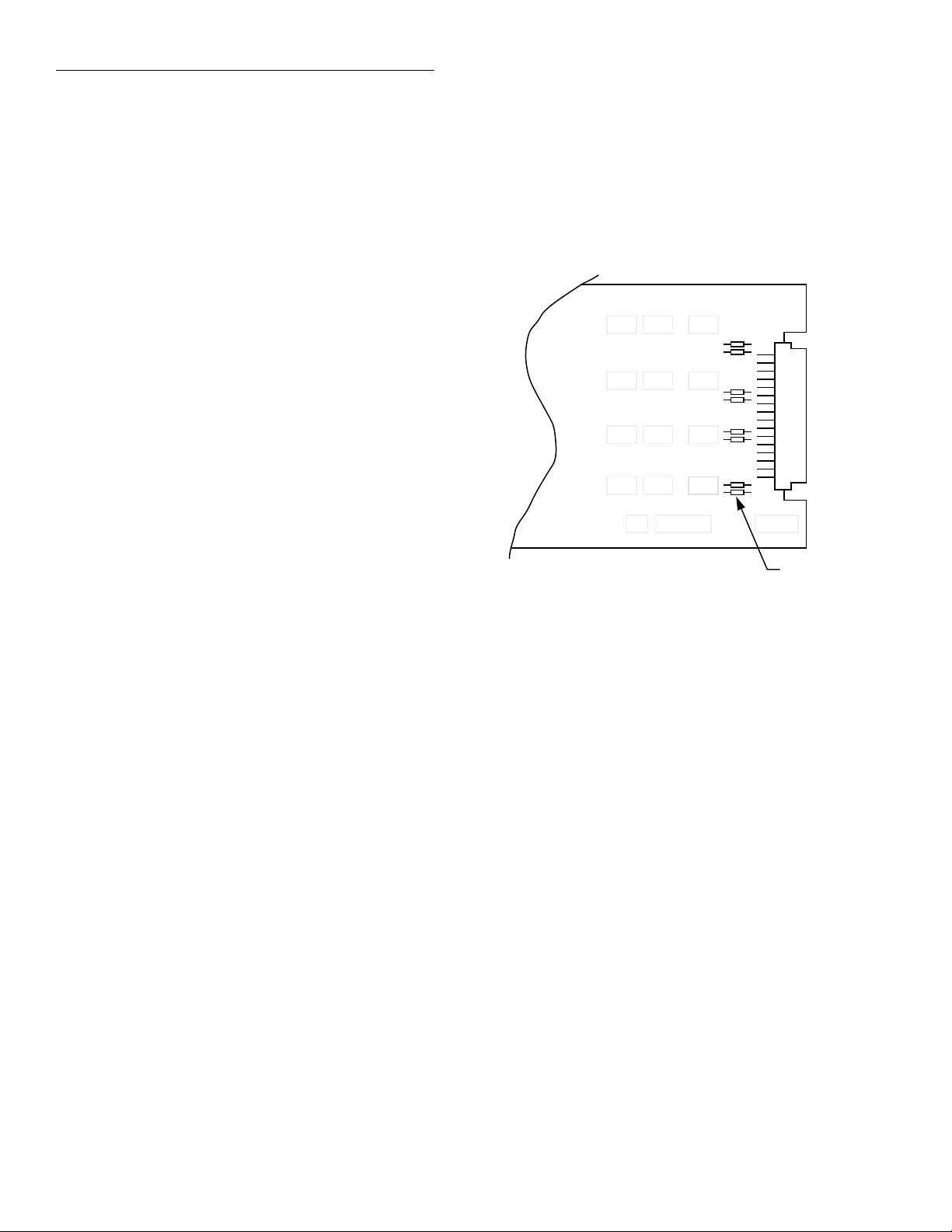
3.3.1 Backplane row jumpers
The Model 7001 mainframe has an analog backplane
that allows the rows of a Model 7012 matrix to be internally connected to a compatible switching card installed in the other slot (see paragraph 2.4.1 for details).
The backplane row jumpers for the matrix card assembly are located on the relay card as shown in Figure 3-
1. The card is shipped from the factory with the jumpers installed.
2. Physically remove a cut jumper by unsoldering it
from the PC board.
3. Install a new #22 AWG jumper wire (Keithley P/N
J-15) and solder it to the PC board.
4. Remove the solder ßux from the PC board. The
cleaning procedure is explained in paragraph 5.2.
7012 Relay Card
Row 1
Row 2
Row 3
Row 4
H
L
H
L
H
L
H
L
Jumper removal
Perform the following steps to remove backplane row
jumpers:
1. If mated together, separate the relay card from the
connector card by removing the mounting screw
and then pulling the two cards away from each
other. Remember to only handle the cards by the
edges and shields to avoid contamination.
2. Use Figure 3-1 to locate the jumper(s) that are to be
removed.
3. It is not necessary to physically remove the jumpers from the PC board. Using a pair of wire cutters,
cut one lead of each jumper.
Jumper installation
Referring to Figure 3-1 for jumper locations, perform
the following steps to install backplane row jumpers:
1. If mated together, separate the relay card from the
connector card by removing the mounting screw
and then pulling the two cards away from each
other. Remember to only handle the cards by the
edges and shields to avoid contamination.
Jumpers
Figure 3-1
Backplane row jumpers
3.3.2 Screw terminal connector card
The screw terminal connector card is shown in Figure
3-2. Connections are made directly to the screw terminals of the four terminal blocks. Each screw terminal
will accommodate #16-22 AWG wire.
Wiring procedure
Perform the following procedure to wire circuitry to
the screw terminal connector card:
WARNING
Make sure all power is off and any
stored energy in external circuitry is
discharged.
3-2
Page 29

Figure 3-3
Typical terminal block connections
H
L
H
L
H
L
COL 1
COL 2
COL 3
DUT
#16 - 22 AWG Wires
Card Connections & Installation
1. If mated together, separate the connector card from
the relay card by removing the mounting screw
and then pulling the two cards away from each
other. Remember to only handle the cards by the
edges and shields to avoid contamination.
2. Using an insulated screwdriver, connect the circuitry to the appropriate terminals. Figure 3-3
shows how Column 1 of the matrix would be connected to a DUT.
3. Referring to Figure 3-4, remove the top half of the
cable clamp as follows:
A. Loosen the cable clamp screw enough to disen-
gage it from the bottom half of the cable clamp.
B. Using your thumb and foreÞnger, press the re-
taining clips inward and, with your other
hand, remove the top half of the clamp.
4. Route wires under wire guide/connector shim.
5. Route the wires through the bottom half of the cable clamp.
6. Replace the top half of the clamp. It simply snaps
onto the bottom half of the clamp. Tighten the cable clamp screw. The clamp serves as a strain relief
for terminal block wires.
7. Mate the connector card to the relay card. The
Model 7012 is now ready to be installed in the
Model 7001 mainframe. See paragraph 3.5 for details.
Figure 3-2
Screw terminal connector card
3-3
Page 30

Card Connections & Installation
Screw
Clips
Figure 3-4
Cable clamp for screw terminal connector card
3.3.3 Multi-pin (mass termination) connector card
Since connections to external circuitry are made at the
96-pin male DIN bulkhead connector, there is no need
to separate the connector card from the relay card. If
the connector card is separated from the relay card,
carefully mate them together. Make sure to handle the
cards by the edges and shields to avoid contamination.
Terminal identiÞcation for the DIN connector of the
multi-pin connector card is provided by Figure 3-5.
This connector will mate to a 96-pin female DIN connector.
Keithley has a variety of cable and connector accessories available to accommodate connections from the
connector card to test instrumentation and DUT (devices under test). In general, these accessories, which
are summarized in Table 3-1, utilize a round cable assembly for connections.
Table 3-1
Mass termination accessories
Model Description
7011-KIT-R 96-pin female DIN connector and
housing for round cable.
7011-MTC-2 Two-meter round cable assembly
terminated with a 96-pin female
DIN connector on each end.
7011-MTR 96-pin male DIN bulkhead connec-
tor.
3-4
Page 31

Pins of the Model 7012-C mass termination connector can be identified in one of three ways:
1. Matrix row (1-4) or column (1-10).
2. Connector designation, consisting of rows a-c and columns 1-32.
3. Schematic and component layout designation (1-96).
The following pinout diagrams show the correspondence between these arrangements:
3231302928272625242322212019181716151413121110987654321
c
b
a
Card Connections & Installation
View from pin side
of connector
Matrix
Terminal
Row 1 HI
LO
Row 2 HI
LO
Row 3 HI
LO
Row 4 HI
LO
Connector
Desig.
1a-32c
8c
8b
6c
6b
4c
4b
2c
2b
Schematic
Desig.
1-96
72
40
70
38
68
36
66
34
Matrix
Terminal
Col 1 HI
LO
Col 2 HI
LO
Col 3 HI
LO
Col 4 HI
LO
Col 5 HI
LO
Col 6 HI
LO
Col 7 HI
LO
Col 8 HI
LO
Col 9 HI
LO
Col 10 HI
LO
Connector
Desig.
1a-32c
32c
32b
30c
30b
28c
28b
26c
26b
24c
24b
22c
22b
20c
20b
18c
18b
16c
16b
14c
14b
Schematic
Desig.
1-96
96
64
94
62
92
60
90
58
88
56
86
54
84
52
82
50
80
48
78
46
Notes:
1. Refer to the schematic for shield pins.
2. Short pins 1a to 1b on the mating connector (pins 1 and 33 on schematic) to allow the output relays on the connector card to close.
Figure 3-5
Multi-pin connector card terminal identification
3-5
Page 32

Card Connections & Installation
Typical connection techniques
All external circuitry, such as instrumentation and
DUTs, that you wish to connect to the matrix card must
be terminated with a single 96-pin female DIN connector. The following connection techniques provide some
guidelines and suggestions for wiring your circuitry.
WARNING
Before beginning any wiring procedures, make sure all power is off and
any stored energy in external circuitry is discharged.
NOTE
It is recommended that external circuitry be connected (plugged in) after
the Model 7012 assembly is installed
in the Model 7001 mainframe and
with the 7001 power off. Installation is
covered in paragraph 3.5.
Round cable assemblies
Figure 3-6 shows typical
round cable connection techniques using accessories
available from Keithley.
In Figure 3-6A, connections are accomplished using a
Model 7011-MTC-2 cable and a Model 7011-MTR bulkhead connector. The two-meter round cable is terminated with a 96-pin female DIN connector at each end.
This cable mates directly to the multi-pin connector
card and to the bulkhead connector. The bulkhead connector has solder cups to allow direct connection to instrumentation and DUT. Figure 3-7 provides pinout for
the bulkhead connector. The view shown is from the
solder cup end of the connector.
In Figure 3-6B, connections are accomplished using a
Model 7011-MTC-2 cable assembly that is cut in half.
The 96-pin female DIN connector on one end of the cable mates directly to the multi-pin connector card. The
unterminated end of the cable is wired directly to instrumentation and DUT. The other half of the cable assembly could be used for a second switching card.
Output relays
The multi-pin connector card uses a
relay for each of the four output banks. These output
relays are normally open to prevent any hazardous
voltages (via the mainframe backplane) from appearing on the pins of the male DIN connector. The output
relays will only close when the Model 7011-MTC-2 cable assembly is connected to card. If building you own
cable assembly, you must make sure that it shorts pins
1a to 1b of the card connector (Figure 3-8) when it is
mated to the card. Shorting pins 1a to 1b allows the
output relays to close.
In Figure 3-6C, connections are accomplished using a
custom-built cable assembly that consists of a Model
7011-KIT-R connector and a suitable round cable. Hitachi cable p/n N2807-P/D-50TAB is a 50-conductor
round cable. Two of these cables can be used to provide
100 conductors. The connector has solder cups to accommodate the individual wires of the unterminated
cable. Figure 3-8 provides an exploded view of the connector assembly and shows how the cable is connected.
The connector end of the resultant cable assembly
mates directly to the multi-pin connector card. The unterminated end of the cable assembly is wired directly
to instrumentation and DUT.
3-6
Page 33

T
A)
Multi-Pin
Connector
Card
Card Connections & Installation
Wire instrumentation
and DUT to bulkhead
connector (See Figures
3-5 and 3-7 for terminal
identification)
7011-MTC-2
cable assembly
7011-MTR
bulkhead connector
B)
Connector
Card
Multi-Pin
Multi-Pin
C)
Connector
Card
Figure 3-6
ypical round cable connection techniques
Wire directly to
instrumentation
and DUT
7011-MTC-2
(Cut in Half)
Wire directly to
instrumentation
and DUT
Cable
7011-Kit-R
Connector Kit
Notes : Figure 3-8 provides an exploded view showing
how the connector (with cable) is assembled.
Cable Hitachi p/n N2807-P/D-50TAB is a
50-conductor cable. Two of these cables
can be used to supply 100 conductors.
3-7
Page 34

Card Connections & Installation
Note : See Figure 3-5 for terminal identification.
Figure 3-7
Model 7011-MTR connector pinout
3231302928272625242322212019181716151413121110987654321
c
b
a
View from solder
cup side of
connector
Figure 3-8
Model 7011-KIT-R (with cable) assembly
3-8
Page 35

Card Connections & Installation
3.4 Typical connection schemes
The following information provides some typical connection schemes for single card, two-card, and twomainframe system conÞgurations. Connection
schemes for the multi-pin connector card use some of
the techniques presented in paragraph 3.3.2. Keep in
mind that these are only examples to demonstrate various ways to wire a test system. Connection details for
both connector cards (multi-pin and screw terminal
connector cards) are provided in paragraph 3.3.
3.4.1 Single card system
Figure 3-9 shows how external connections can be
made to a single card system that uses the multi-pin
connector card. Instrumentation and DUT are hardwired to the Model 7011-MTR male bulkhead connector. This connector has solder cups that will accept wire
size up to #24 AWG. The test system is connected to the
matrix using the Model 7011-MTC-2 round cable assembly. This cable mates directly to both the external
bulkhead connector and the Model 7012-C matrix card
assembly. Notice that the bulkhead connector is shown
mounted to a Þxture to help keep the cabling stable
during the test.
The single card system in Figure 3-10 is identical to the
system in the previous illustration, except for the connection scheme. The system in Figure 3-10 uses the terminal block connector card. With this card, single
conductor connections are made directly from the terminal blocks of the connector card to instrumentation
and DUT.
When using a single card system, make sure that the
card remains electrically isolated from any other
switching cards. There are several ways to ensure isolation for a single card in the Model 7001 mainframe:
1. Vacate the other mainframe slot. If there is a Model
701X card installed in the other slot, remove it.
2. Remove the backplane jumpers on the matrix card.
This will disconnect the card from the analog backplane of the mainframe.
3. Remove the backplane jumpers from the switching
card installed in the other slot.
3.4.2 Two-card system
Both Figure 3-11 and Figure 3-12 show a system using
two matrix cards installed in one Model 7001 mainframe to conÞgure a 4
connection schemes, row connections of the two matrix
cards are accomplished internally through the backplane of the Model 7001 mainframe. To connect rows
internally, the backplane row jumpers of both matrix
cards must be installed.
Figure 3-11 shows how external connections can be
made for the multi-pin connector cards. In this example, a single Model 7011-MTC-2 round cable assembly
is cut in half to provide two cables, each of which is unterminated at one end. The unterminated ends of the
two cables are hard-wired to instrumentation and DUT
as shown in the drawing. The other ends of these cables
mate directly to the Model 7012-C matrix card assemblies.
Figure 3-12 shows how external connections can be
made for the screw terminal connector card. Single
conductor connections are made directly from the
screw terminals of the connector card to instrumentation and DUT.
20 test matrix. In both these
×
3-9
Page 36

Card Connections & Installation
Instrument
Row 1
Fixture for
Bulkhead
Connector
7012-C
Instrument
Instrument
Instrument
Row 2
28 Individual Conductors
Row 3
Row 4
12345678910
DUT Test Fixture
Instruments
7011-MTR
Bulkhead
Connector
DUT
12 345678910
12 345678910
1
2
3
4
DUT
Columns
Rows
7011-MTC-2
Cable Assembly
Figure 3-9
Single card system example (multi-pin connector card)
3-10
Equivalent Circuit
Page 37

Instrument
Instrument
Instrument
Instrument
Row 1
Row 2
Row 3
Row 4
Card Connections & Installation
7012-S
12345678910
DUT Test Fixture
12345678910
12345678910
1
Instruments
2
3
4
Equivalent Circuit
Figure 3-10
Single card system example (screw terminal connector card)
DUT
DUT
Columns
Rows
3-11
Page 38

Card Connections & Installation
Instrument
Row 1
Row 2
Instrument
Row 3
Instrument
Row 4
Instrument
12345678910
DUT Test Fixture
1234 5678910
1234 5678910
1
Instruments
2
3
4
Note : Backplane row jumpers for
both matrix cards must be
installed.
7011-MTC-2
Cable Assembly
(Cut in half to
provide two cables)
7001
7012-C
7012-C
12345678910
DUT Test Fixture
7001
Backplane
DUT
DUT
DUT
1234 5678910
1234 5678910
Column Column
CARD 1 CARD 2
Backplane Row
Jumpers installed
DUT
C
A
R
D
1
C
A
R
D
2
Row
Figure 3-11
Two-card system example (multi-pin connector card)
3-12
Equivalent Circuit
Page 39

T
Card Connections & Installation
Instrument
Instrument
Instrument
Instrument
Instruments
Row 1
Row 2
Row 3
Row 4
12345678910
DUT Test Fixture
DUT
DUT
1234 5678910
1234 5678910
1
2
3
4
Column Column
Note : Backplane
row jumpers for
both cards must
be installed.
7012-S
7012-S
12345678910
7001
Backplane
7001
C
A
R
D
1
C
A
R
D
2
DUT Test Fixture
DUT
DUT
1234 5678910
1234 5678910
Row
CARD 1 CARD 2
Figure 3-12
wo-card system example (screw terminal connector card)
Backplane Row
Jumpers installed
Equivalent Circuit
3-13
Page 40

Card Connections & Installation
3.4.3 Two-mainframe system
Figure 3-13 and Figure 3-14 show a system using three
matrix cards in two Model 7001 mainframes to conÞgure a 4
Two-card System (see previous paragraph), except that
a third matrix card (installed in a second mainframe) is
added.
Figure 3-13 shows the connection scheme for the multipin connector cards. External circuit connections to the
Model 7001 #1 mainframe are identical to the ones
used for the Two-card System. The third matrix card
(installed in Model 7001 #2 mainframe) shows how a
custom-built cable can be used to make connections to
external circuitry. A suitable round cable can be terminated with a 96-pin female DIN connector (Model
7011-KIT-R) that will mate to the Model 7012-C matrix
card assembly. The unterminated end of the cable is
connected directly to instrumentation and DUT. Notice
that the row connections for the third matrix card are
made at the instruments.
Figure 3-14 shows connections for the screw terminal
connector card. Single conductor connections are made
directly from the screw terminals of the connector card
to instrumentation and DUT
×
30 test matrix. This system is similar to the
3.5 Model 7012 installation and removal
This paragraph explains how to install and remove the
Model 7012 matrix card assembly from the Model 7001
mainframe.
WARNING
Installation or removal of the Model
7012 is to be performed by qualiÞed
service personnel. Failure to recognize and observe standard safety precautions could result in personal
injury or death.
NOTE
If using the screw terminal connector
card, make sure your external circuitry is wired to the card (as explained in
paragraph 3.3.1) before installing the
card assembly in the Model 7001
mainframe.
CAUTION
To prevent contamination to the matrix card that could degrade performance, only handle the card
assembly by the edges and shields.
3-14
Page 41

Card Connections & Installation
DUT Test Fixture
12345678910
Instrument
Instrument
Instrument
Instrument
12345678910
DUT Test Fixture
7011-MTC-2
Cable Assembly
(Cut in half to
provide two cables)
7011-Kit-R
Connector Kit
Cable
7001 #2
C
A
7012-C
7012-C
7001 #1
7012-C
7012-C
R
D
1
C
A
R
D
2
C
A
R
D
1
C
A
R
D
2
Trigger Link
I
N
O
U
T
Trigger Link
I
N
O
U
T
12345678910
DUT Test Fixture
Trigger
Link
Cable
Note : Backplane
row jumpers for
both cards in
7001 #1 must be
installed.
7001 #1 7001 #2
7001
Backplane
DUT
Instruments
1234 5678910
DUT
1234 5678910
1
2
3
4
1234 5678910
1234 5678910
Column Column Column
CARD 1 CARD 2 CARD 3
Backplane Row
Jumpers installed
Equivalent Circuit
Figure 3-13
Two-mainframe system example (multi-pin connector card)
DUT
DUT
DUT
1234 5678910
1234 5678910
DUT
External Row Jumpers
Row
3-15
Page 42

Card Connections & Installation
12345678910
Instrument
DUT Test Fixture
7012-S
Not Used
7001 #2
C
A
Trigger Link
R
D
1
I
N
C
A
O
R
D
U
2
T
Trigger
Link
Cable
Instruments
Instrument
Instrument
Instrument
12345678910
DUT Test Fixture
DUT
1234 5678910
1234 5678910
1
2
3
4
DUT
Column Column Column
CARD 1 CARD 2 CARD 3
7001 #1
C
A
7012-S
7012-S
Trigger Link
R
D
1
I
N
C
A
O
R
D
U
2
T
Note : Backplane
row jumpers for
both cards in
7001 #1 must be
installed.
12345678910
DUT Test Fixture
7001 #1 7001 #2
7001
Backplane
DUT
DUT
1234 5678910
1234 5678910
Backplane Row
Jumpers installed
1234 5678910
1234 5678910
DUT
DUT
Row
Equivalent Circuit
Figure 3-14
Two-mainframe system example (screw terminal connector card)
3-16
External Row Jumpers
Page 43

Card Connections & Installation
Matrix card installation
Perform the following steps to install the matrix card
assembly in the Model 7001 mainframe:
WARNING
Turn off power from all instrumentation (including the Model 7001 mainframe) and disconnect their line
cords. Make sure all power is removed and stored energy in external
circuitry is discharged.
1. Mate the connector card to the relay card if they are
separated. Install the supplied 4-40 screw at the
end of the card to secure the assembly. Make sure
to handle the cards by the edges and shields to prevent contamination.
2. Facing the rear panel of the Model 7001, select the
slot (CARD 1 or CARD 2) that you wish to install
the card in.
3. Referring to Figure 3-15 for Model 7012-S installation, or Figure 3-16 for Model 7012-C installation,
feed the matrix card assembly into the desired slot
such that the edges of the relay card ride in the
rails.
4. With the ejector arms in the unlocked position,
push the card assembly all the way into the mainframe until the arms engage into the ejector cups.
Then push both arms inward to lock the card into
the mainframe.
5. For the 7012-C, also install the screw shown in Figure 3-16.
Matrix card removal
To remove the matrix card assembly, Þrst unlock it by
pulling the latches outward, then pull the card assembly out of the mainframe. Remember to handle the card
assembly by the edges and shields to avoid contamination that could degrade performance.
3-17
Page 44

Card Connections & Installation
Unlock car d
Unlock card
Ejector Arms (2)
Ejector Arms (2)
Figure 3-15
Model 7012-S card installation in Model 7001
3-18
Lock card
Lock car d
Page 45

1
Screw
Screw
Unlock card
2
Unlock car d
Card Connections & Installation
Ejector Arms (2)
Ejector Arms (2)
Screw
2
Figure 3-16
Model 7012-C card installation in Model 7001
1
Lock card
Lock car dScrew
3-19
Page 46

4
Operation
4.1 Introduction
The information in this section is arranged as follows:
4.2 Power limits: Summarizes the maximum power
limits of the Model 7012 matrix card assembly.
4.3 Mainframe control of matrix card: Summarizes
programming steps to control the matrix card
from the Model 7001 Switch System mainframe.
4.4 Multiplexer switching examples: Provides some
typical applications for using the Model 7012.
4.5 Measurement considerations: Reviews a num-
ber of considerations when using the Model 7012
to make measurements.
4.2 Power limits
CAUTION
To prevent damage to the card, do not
exceed the maximum signal level
speciÞcations of the card.
Maximum signal levels
To prevent overheating or damage to the relays, never
exceed the following maximum signal levels:
DC signals: 110V between any two pins (termi-
nals), 1A switched, 30VA (resistive
load)
AC signals: 125V rms or 175V AC peak be-
tween any two pins (terminals), 1A
switched, 60VA (resistive load)
4.3 Mainframe control of matrix card
The following information pertains to the Model 7012
matrix card. It assumes that you are familiar with the
operation of the Model 7001 mainframe.
If you are not familiar with the operation of the mainframe, it is recommended that you proceed to Getting
Started (Section 3) in the Model 7001 Instruction Manual after reading the following information.
4-1
Page 47

Operation
4.3.1 Channel assignments
The Model 7001 has a channel status display (Figure 4-
1) that provides the real-time state of each available
channel. The left portion of the display is for slot 1
(Card 1), and the right portion is for slot 2 (Card 2).
Notice that the matrix organization of the channel status display corresponds directly to the 4
tion of the matrix card. With a matrix card installed, the
top row of the display corresponds to Row 1 of the matrix card. The 10 columns of the matrix are labeled 1
through 10 on the display. The next rows down correspond to Rows 2, 3, and 4 respectively.
Matrix organization of the channel status display corresponds to the 4
×
10 organization of the matrix card
×
10 organiza-
7001 Display
as shown in Figure 4-2. Each channel is designated as a
row/column crosspoint.
To control the matrix card from the mainframe, each
matrix crosspoint must have a unique CHANNEL assignment. The CHANNEL assignments for the matrix
card are provided in Figure 4-3. Each CHANNEL assignment is made up of the slot designator (1 or 2) and
the matrix crosspoint. To be consistent with Model
7001 operation, the slot designator, row and column
are separated by exclamation points (!). Some examples of CHANNEL assignments:
CHANNEL 1!1!1 = Slot 1, Row 1, Column 1
CHANNEL 1!4!10 = Slot 1, Row 4, Column 10
CHANNEL 2!2!9 = Slot 2, Row 2, Column 9
CHANNEL 2!3!4 = Slot 2, Row 3, Column 4
1 234567891012345678910
= Open Channel
= Closed Channel
Figure 4-1
Channel status display
CARD 1 CARD 2
4-2
Page 48

Operation
Column
123456 78910
R1,C1 R1,C3 R1,C4 R1,C5 R1,C6 R1,C7 R1,C8 R1,C9 R1,C10
1
R1,C2
2
R2,C1 R2,C2 R2,C3 R2,C4 R2,C5 R2,C6 R2,C7
Row
3
R3,C1 R3,C2 R3,C3 R3,C4 R3,C5 R3,C6 R3,C7 R3,C8 R3,C9 R3,C10
4
R4,C1 R4,C2 R4,C3 R4,C4 R4,C5 R4,C6 R4,C7 R4,C8 R4,C9 R4,C10
R = Row
C = Column
Figure 4-2
Display organization for multiplexer channels
1 2 3 4 5 6 7 8 9 10
1!1!1
1!2!1
1!1!2
1!2!2
1!1!3
1!2!3
1!1!4
1!2!4
1!1!5
1!2!5
1!1!6
1!2!6
1!1!7
1!2!7
R2,C8
R2,C9 R1,C10
1!1!8
1!2!8
1!1!9
1!2!9
1!1!10
1!2!10
1!3!1
1!3!2
1!3!3
A. Slot 1 (Card 1)
1!4!1
1!4!2
1!4!3
1 2 3 4 5 6 7 8 9 10
2!1!1
2!2!1
2!3!1
2!1!2
2!2!2
2!3!2
2!1!3
2!2!3
2!3!3
B. Slot 2 (Card 2)
2!4!1
2!4!2
2!4!3
Examples : 1!2!4 = Slot 1, Row 2, Column 4
2!3!6 = Slot 2, Row 3, Column 6
Figure 4-3
Model 7012 programming channel assignments
1!3!4
1!4!4
2!1!4
2!2!4
2!3!4
2!4!4
1!3!5
1!4!5
2!1!5
2!2!5
2!3!5
2!4!5
1!3!6
1!4!6
2!1!6
2!2!6
2!3!6
2!4!6
1!3!7
1!4!7
2!1!7
2!2!7
2!3!7
2!4!7
1!3!8
1!4!8
2!1!8
2!2!8
2!3!8
2!4!8
1!3!9
1!4!9
2!1!9
2!2!9
2!3!9
2!4!9
1!3!10
1!4!10
2!1!10
2!2!10
2!3!10
2!4!10
4-3
Page 49

Operation
4.3.2 Front panel control
Closing and opening channels
A matrix crosspoint is closed form the front panel by
simply keying in the channel assignment and pressing
CLOSE. For example, to close Row 3, Column 4 crosspoint of a matrix card installed in slot 2, key in the following channel list and press CLOSE:
SELECT CHANNELS 2!3!4
The above closed channel can be opened by pressing
OPEN or OPEN ALL. The OPEN key opens only the
channels speciÞed in the channel list, and OPEN ALL
opens all channels.
The following display is an example of a channel list
that consists of several channels:
SELECT CHANNELS 2!1!1, 2!1!3, 2!2!1-2!2!5
Notice that channel entries are separated by commas
(,). A comma is inserted by pressing ENTER or the right
cursor key ( ). The channel range is speciÞed by using the hyphen (-) key to separate the range limits.
Pressing CLOSE will close all the channels speciÞed in
the channel list. Pressing OPEN (or OPEN ALL) will
open the channels.
A manual scan can be performed by using the RESET
default conditions of the Model 7001. RESET is selected
from the SAVESETUP menu of the main MENU. When
RESET is performed, the mainframe is conÞgured for
an inÞnite number of manual scans. The Þrst press of
STEP takes the mainframe out of the idle state. The
next press of STEP will close the Þrst channel speciÞed
in the scan list. Each subsequent press of STEP will select the next channel in the scan list.
4.3.3 IEEE-488 bus operation
Bus operation is demonstrated using HP BASIC 4.0.
The programming statements assume that the primary
address of the mainframe is 07.
Closing and opening channels
The following SCPI commands are used to close and
open channels:
:CLOSe <list>
:OPEN <list>|ALL
The following statement closes channels 1!1!1, and
1!1!3 through 1!1!6:
Scanning channels
Matrix crosspoints are scanned by creating a scan list
and conÞguring the Model 7001 to perform a scan. The
scan list is created in the same manner as a channel list
(see Closing and Opening Channels). However, the
scan list is speciÞed from the “SCAN CHANNEL” display mode. (The SCAN LIST key toggles between the
channel list and scan list.) The following shows an example of a scan list:
SCAN CHANNELS 2!1!1, 2!1!3, 2!2!1-2!2!5
When a scan is performed, the channels speciÞed in the
scan list will be scanned in the order that they are presented in the scan list.
OUTPUT 707; “:clos (@ 1!1!1, 1!1!3:1!1!6)”
Notice that the colon (:) is used to separate the range
limits.
Either of the following statements will open channels
1!1!1, and 1!1!3 through 1!1!6:
OUTPUT 707; “:open (@ 1!1!1, 1!1!3:1!1!6)”
OUTPUT 707; “:open all”
Scanning channels
There are many commands associated with scanning.
However, it is possible to conÞgure a scan using as little as four commands. These commands are listed as
follows:
4-4
Page 50

Operation
*RST
:TRIGger:SEQuence:COUNt:AUTO ON”
:SCAN <list>
:INIT
The Þrst command resets the mainframe to a default
scan conÞguration. The second command automatically sets the channel count to the number of channels in
the scan list, the third command deÞnes the scan list,
and the fourth command takes the Model 7001 out of
the idle state.
The following program will perform a single scan
through all 40 channels of a multiplexer card installed
in slot 1:
10 OUTPUT 707; “*RST”
20 OUTPUT 707; “:trig:seq:coun:auto on”
30 OUTPUT 707; “:scan (@ 1!1!1:1!4!10)”
40 OUTPUT 707; “:init”
50 END
5 OUTPUT 707; “:open all”
10 OUTPUT 707; “*RST”
20 OUTPUT 707; “:trig:seq:coun:auto on”
25 OUTPUT 707; “:trig:del 0.25”
30 OUTPUT 707; “:scan (@ 1!1!1:1!4!10)”
40 OUTPUT 707; “:INIT”
50 END
Line 5 Opens all channels.
Line 25 Sets a 1/4 second delay after each channel
closes.
4.4 Matrix switching examples
Some applications to test thick Þlm resistor networks
and transistors are provided in the following paragraphs. These applications are intended to demonstrate the versatility of using the matrix card in test
systems.
Line 10 Selects a default conÞguration for the scan.
Line 20 Sets channel count to the scan-list-length.
Line 30 DeÞnes the scan list.
Line 40 Take the Model 7001 out of the idle state. The
scan is conÞgured to start as soon as this
command is executed.
When the above program is run, the scan will be completed in approximately 240msec (3msec delay for each
relay close and a 3msec delay for each open), which is
too fast to view from the front panel. An additional relay delay can be added to the program to slow down
the scan for viewing. The program is modiÞed by adding line 25 to slow down the scan. Also, Line 5 is added
to the beginning of the program to ensure that all channels are open before the scan is started.
4.4.1 Thick film resistor network testing
A dedicated matrix system for testing thick Þlm resistor networks is shown in Figure 4-4. This particular
system provides two different methods to check thick
Þlms; four-wire resistance measurements, and voltage
measurements using an applied voltage.
The system shown in Figure 4-4 tests two 4-element
thick Þlms, but can be expanded to test more by simply
using additional Model 7012 matrix cards. The Model
7001 will accommodate two matrix cards. Daisy-chainin six Model 7001s expands the system to 12 matrix
cards allowing 24 four-element thick Þlms to be tested.
4-5
Page 51

Operation
Measure V or
4-terminal Ω
Source V
Model 196
Model 230
Ohms Sense
Volts Ohms
Volts/Ohms HI
Ohms Sense HI
Volts/Ohms LO
Ohms Sense LO
Output
Sense Output
Common
Sense Common
TF-1 TF-2
R1R2R3R
1 345 6789102
1
2
Rows
3
4
LHLHLHLHL HLHLHLHLHL
H
4
Cols
7012
R1R
2
4
3
H
L
H
L
H
L
H
L
R
R
Figure 4-4
Thick film resistor network testing
Four-terminal ohms measurements
For general purpose testing, the Keithley Model 196
can be used to make four-terminal resistance measurements of each thick Þlm. As shown in Figure 4-5,
OHMS HI and OHMS SENSE HI are connected to one
matrix row, and OHMS LO and OHMS SENSE LO are
connected to another matrix row. With this conÞgura-
tion, the resistance of each resistor element and/or
combined elements can be measured by closing the appropriate crosspoints. In Figure 4-5, crosspoints 1!1
(Row 1, Column 1) and 2!3 (Row 2, Column 3) are
closed to measure the combined resistance of R1 and
R2.
The effects of thermal EMFs generated by relay contacts and connections can be cancelled by using the offset compensated ohms feature of the Model 196. (The
Model 7012 has been designed to keep relay EMF at a
minimal level.) To compensate for thermal EMFs, close
two crosspoints (such as 1!1!1 and 1!2!1), this will short
the input of the Model 196, enable zero to cancel internal offset, and then enable offset compensated ohms.
4-6
Page 52

Operation
Thick Film
R
R
1
R
2
R
3
4
Model 196
Volts/Ohms HI
Ohms Sense HI
Volts/Ohms LO
Ohms Sense LO
X = Closed Crosspoints
R
1
HL LH HLHL
196
Rows
R
2
Ω
Equivalent Circuit
HL1HL2HL3HL
H
1
X
L
H
2
L
R
R
3
4
HL
X
4
HL
5
Cols
Figure 4-5
Four-terminal ohms measurements
4-7
Page 53

Operation
Voltage divider checks
For thick Þlm resistor networks that are to be used as
voltage dividers, it may be desirable to test them using
voltages that simulate actual operating conditions.
This is a particularly useful test for resistor networks
that have a voltage coefÞcient speciÞcation. The test
system in Figure 4-4 uses a Keithley Model 230 to
source voltage and the Model 196 to measure voltage.
A consideration in these checks is the effect of the Model 196 input impedance on voltage measurements. The
input impedance is shunted across the resistor being
measured. The resultant divider resistance is the parallel combination of the resistor under test and the input
impedance. As long as the input impedance is much
larger than the resistor being tested, the error introduced into the measurement will be minimal. Minimum input impedance requirements are, of course,
determined by the accuracy needed in the measurement. The input impedances of the Model 196 are as
follows: 300mV and 3V ranges, 1G
300V range, 10.1M
Ω
. For better input impedance re-
; 30V range, 11M
Ω
Ω
quirements, the Keithley Model 617 Electrometer can
be incorporated into the test system to measure voltage.
Another factor to be considered when checking low
voltage dividers is thermal EMFs generated by the matrix card. (The Model 7012 has been designed to keep
relay EMF at a minimal level.) A matrix card crosspoint
can generate up to 5
µ
V of thermal EMF. Thus, when
making low voltage measurements be sure to account
for this additional error.
Even though four-terminal connections are made at the
Model 196 and the resistor networks, the sense leads
are internally disconnected from the input of the DMM
when the volts function is selected. The simpliÞed test
system is shown in Figure 4-6.
The thick Þlm is tested by applying a voltage across the
resistor network and measuring the voltage across
each resistor element and/or across combined elements. In Figure 4-6, crosspoints 1!3!1 and 1!4!4 are
closed to apply voltage across the network, and crosspoints 1!1!3 and 1!2!4 are closed to measure the voltage
drop across R3.
;
4-8
Page 54

Operation
Thick Film
R
1
R
2
R
3
R
4
Model 196
Measure V
Model 230
Source V
Output
Sense Output
Common
Sense Common
HLHLHLHL
1234
HI
H
1
L
LO
H
2
L
Rows
H
3
X
L
H
4
L
X = Closed Crosspoints
R
1
HL
5
Cols
X
X
X
Model 7012
R
2
R
3
R
4
Figure 4-6
Voltage divider checks
H H H H
V
196
+/-
230
Equivalent Circuit
H
4-9
Page 55

Operation
4.4.2 Transistor testing
A matrix system for testing DC parameters of transistors is shown in Figure 4-7. This system uses two
Source Measure Units (SMU). There are three SMUs
available from Keithley; the Model 236 Source Measure
Unit, Model 237 High Voltage Source Measure Unit
and Model 238 High Current Source Measure Unit.
Keep in mind that if using the Models 237 (high voltage
capability) or 238 (high current capability), do not exceed the maximum signal levels of the matrix card.
Maximum allowable DC signals are 110V and 1A, 30W
with resistive load.
This system tests three transistors, but can be expanded to test more by simply using additional Model 7012
matrix cards. The Model 7001 will accommodate two
matrix cards. Daisy-chaining six Model 7001s expands
the system to 12 matrix cards allowing 36 or more transistors to be tested.
NOTE
The Model 7012 is a general purpose
matrix card and cannot be used to
check FETs or transistors that have
high gain or low power. To test these
devices, a matrix card with low offset
current and high isolation characteristics must be used.
SMU #1
Output HI
Sense HI
Sense LO
Output LO
SMU #2
Output HI
Sense HI
Sense LO
Output LO
Figure 4-7
Transistor testing
123
1
2
Rows
3
4
HL HL HL
456
Columns
HL HL HL
7012
789
HL HL HL
10
HL
H
L
H
L
H
L
H
L
4-10
Page 56

Operation
DC parameter checks
With a transistor conÞgured as a common-emitter ampliÞer, the test system shown in Figure 4-8 can be used
to determine the following DC parameters: Collector
current (I
rent (I
), base current (I
C
) and base-to-emitter voltage (V
E
), current gain, emitter cur-
B
BE
).
Figure 4-8 shows which crosspoints to close to conÞg-
ure the ampliÞer circuit. SMU #1 is conÞgured to
source voltage and measure current. It is used to power
the collector circuit (V
current (I
). SMU #2 is conÞgured to source current
C
) and measure the collector
CE
and measure voltage. It is used to provide the base current (I
base-to-emitter voltage (V
(I
) for the transistor, and will also measure the
B
) and base current (I
C
). With collector current
BE
) known, the current gain can
B
be calculated as follows:
I
Gain
C
-----=
I
B
Common-emitter characteristic curves
A proÞle of the transistor operating characteristics can
be obtained by measuring the collector current over a
speciÞed voltage range (V
currents (I
). For example, Figure 4-9 shows the charac-
B
) for different base bias
CE
teristics of a typical NPN silicon transistor at base bias
currents (I
) of 20
B
µ
A, 40
µ
A, 60
µ
A, and 80
µ
A.
Extensive trigger capabilities facilitate synchronization
of the Keithley Source Measure Unit operations. By
performing a subordinate sweep, SMU #1 will perform
a staircase sweep at every base bias current level set by
SMU #2. On every step of each staircase sweep, SMU
#1 will source a voltage level (V
subsequent collector current (I
) and measure the
CE
). For the characteris-
C
tics shown in Figure 4-9, four staircase sweeps were
performed; one staircase sweep at each base bias level.
Refer to a Keithley Source Measure Unit instruction
manual for details on performing sweeps.
The emitter current (I
) can be determined by using
E
Kirchoff’s Current Law as follows:
I
+=
EICIB
4-11
Page 57

Operation
SMU #1
A
±
Source V
Measure I
I
C
V
BE
I
E
Equivalent Circuit
SMU #1
Output HI
Sense HI
Sense LO
Output LO
I
B
SMU #2
A = Measure I
± = Source V
V = Measure V
V
↑ = Source I
X
1
2
X
Figure 4-8
DC parameter checks
Source I
Measure V
SMU #2
Output HI
Sense HI
Sense LO
Output LO
Rows
3
4
HL HL HL
X = Closed Crosspoint
X
X
7012
4-12
Page 58

Operation
10
8
6
, ma
c
I
4
2
012345
V , volts
CE
+80 µa
+60 µa
+40µa
+20 µa
I
B
Figure 4-9
Common-emitter characteristics of an NPN silicon
Transistor
4.5 Measurement considerations
= 0
sideration; however, it can seriously degrade
measurement accuracy when testing high-impedance
devices. The voltage measured across such a device, for
example, can be substantially attenuated by the voltage divider action of the device source resistance and
path isolation resistance, as shown in Figure 4-11. Also,
leakage currents can be generated through these resistances by voltage sources in the system.
R
DUT
R
PATH
E
DUT
DUT
= Source Resistance of DUT
R
DUT
E
= Source EMF of DUT
DUT
R
= Path Isolation Resistance
PATH
R
= Input Resistance of Measuring Instrument
IN
Matrix
Card
R
IN
Measure
Instrument
V
Many measurements made with the Model 7012 are
subject to various effects that can seriously affect lowlevel measurement accuracy. The following paragraphs discuss these effects and ways to minimize
them.
4.5.1 Path isolation
The path isolation is simply the equivalent impedance
between any two test paths in a measurement system.
Ideally, the path isolation should be inÞnite, but the actual resistance and distributed capacitance of cables
and connectors results in less than inÞnite path isolation values for these devices.
Path isolation resistance forms a signal path that is in
parallel with the equivalent resistance of the DUT, as
shown in Figure 4-10. For low-to-medium device resistance values, path isolation resistance is seldom a con-
Figure 4-10
Path isolation resistance
R
DUT
E
DUT
DUT
R
PATH
R
PATH
R
+
PATH
E
DUT
=
E
OUT
R
Figure 4-11
Voltage attenuation by path isolation resistance
4-13
Page 59

Operation
Any differential isolation capacitance affects DC measurement settling time as well as AC measurement accuracy. Thus, it is often important that such capacitance
be kept as low as possible. Although the distributed capacitance of the matrix card is generally Þxed by design, there is one area where you do have control over
the capacitance in your system; the connecting cables.
To minimize capacitance, keep all cables as short as
possible.
4.5.2 Magnetic fields
When a conductor cuts through magnetic lines of force,
a very small current is generated. This phenomenon
will frequently cause unwanted signals to occur in the
test leads of a switching matrix system. If the conductor has sufÞcient length, even weak magnetic Þelds like
those of the earth can create sufÞcient signals to affect
low-level measurements.
Two ways to reduce these effects are: (1) reduce the
lengths of the test leads, and (2) minimize the exposed
circuit area. In extreme cases, magnetic shielding may
be required. Special metal with high permeability at
low ßux densities (such as mu metal) is effective at reducing these effects.
Even when the conductor is stationary, magneticallyinduced signals may still be a problem. Fields can be
produced by various signals such as the AC power line
voltage. Large inductors such as power transformers
can generate substantial magnetic Þelds, so care must
be taken to keep the switching and measuring circuits
a good distance away from these potential noise sources.
At high current levels, even a single conductor can generate signiÞcant Þelds. These effects can be minimized
by using twisted pairs, which will cancel out most of
the resulting Þelds.
4.5.3 Radio frequency interference
RFI (Radio Frequency Interference) is a general term
used to describe electromagnetic interference over a
wide range of frequencies across the spectrum. Such
RFI can be particularly troublesome at low signal levels, but is can also affect measurements at high levels if
the problem is of sufÞcient severity.
RFI can be caused by steady-state sources such as radio
or TV signals, or some types of electronic equipment
(microprocessors, high speed digital circuits, etc.), or it
can result from impulse sources, as in the case of arcing
in high-voltage environments. In either case, the effect
on the measurement can be considerable if enough of
the unwanted signal is present.
RFI can be minimized in several ways. The most obvious method is to keep the equipment and signal leads
as far away from the RFI source as possible. Shielding
the matrix switching card, signal leads, sources, and
measuring instruments will often reduce RFI to an acceptable level. In extreme cases, a specially-constructed screen room may be required to sufÞciently
attenuate the troublesome signal.
Many instruments incorporate internal Þltering that
may help to reduce RFI effects in some situations. In
some cases, additional external Þltering may also be required. Keep in mind, however, that Þltering may have
detrimental effects on the desired signal.
4.5.4 Ground loops
When two or more instruments are connected together,
care must be taken to avoid unwanted signals caused
by ground loops. Ground loops usually occur when
sensitive instrumentation is connected to other instrumentation with more than one signal return path such
as power line ground. As shown in Figure 4-12, the resulting ground loop causes current to ßow through the
instrument LO signal leads and then back through
power line ground. This circulating current develops a
small but undesirable voltage between the LO terminals of the two instruments. This voltage will be added
to the source voltage, affecting the accuracy of the measurement.
4-14
Page 60

Operation
Signal Leads
Instrument 1 Instrument 2 Instrument 3
Ground Loop
Current
Power Line Ground
Figure 4-12
Power line ground loops
Figure 4-13 shows how to connect several instruments
together to eliminate this type of ground loop problem.
Here, only one instrument is connected to power line
ground.
Instrument 1 Instrument 2 Instrument 3
manner. When in doubt, consult the manual for all instrumentation in the test setup.
4.5.5 Keeping connectors clean
As is the case with any high-resistance device, the integrity of connectors can be damaged if they are not
handled properly. If connector insulation becomes contaminated, the insulation resistance will be substantially reduced, affecting high-impedance measurement
paths.
Oils and salts from the skin can contaminate connector
insulators, reducing their resistance. Also, contaminants present in the air can be deposited on the insulator surface. To avoid these problems, never touch the
connector insulating material. In addition, the multiplexer card should be used only in clean, dry environments to avoid contamination.
Power Line Ground
Figure 4-13
Eliminating ground loops
Ground loops are not normally a problem with instruments having isolated LO terminals. However, all instruments in the test setup may not be designed in this
If the connector insulators should become contaminated, either by inadvertent touching, or from air-borne
deposits, they can be cleaned with a cotton swab
dipped in clean methanol. After thoroughly cleaning,
they should be allowed to dry for several hours in a
low-humidity environment before use, or they can be
dried more quickly using dry nitrogen.
4.5.6 AC frequency response
The AC frequency response of the Model 7012 is important in test systems that switch AC signals. Refer to
the speciÞcations at the front of this manual.
4-15
Page 61

Operation
4-16
Page 62

5
Service Information
WARNING
The information in this section is intended only for qualiÞed service personnel. Some of the procedures may
expose you to hazardous voltages
that could result in personal injury or
death. Do not attempt to perform
these procedures unless you are
qualiÞed to do so.
5.1 Introduction
This section contains information necessary to service
the Model 7012 matrix card and is arranged as follows:
5.2 Handling and cleaning precautions: Discusses
handling procedures and cleaning methods for
the matrix card.
5.3 Performance veriÞcation: Covers the procedures
necessary to determine if the card is operating
properly.
5.4 Special handling of static-sensitive devices:
Reviews precautions necessary when handling
static-sensitive devices.
5.2 Handling and cleaning precautions
Because of the high impedance circuits on the Model
7012, care should be taken when handling or servicing
the card to prevent possible contamination, which
could degrade performance. The following precautions should be taken when handling the matrix card.
Do not store or operate the card in an environment
where dust could settle on the circuit board. Use dry nitrogen gas to clean dust off the card if necessary.
Handle the card only by the side edges. Do not touch
any board surfaces, components, or connectors. Do not
touch areas adjacent to electrical contacts. When servicing the card, wear clean cotton gloves.
If making solder repairs on the circuit board, use an
OA-based (organic activated) ßux. Remove the ßux
from these areas when the repair is complete. Use pure
water along with plenty of clean cotton swabs to remove the ßux. Take care not to spread the ßux to other
areas of the circuit board. Once the ßux has been removed, swab only the repaired area with methanol,
then blow dry the board with dry nitrogen gas.
5.5 Principles of operation: Brießy discusses circuit
operation.
5.6 Troubleshooting: Presents some troubleshooting
tips for the matrix card.
After cleaning, the card should be placed in a 50
humidity environment for several hours.
C low
°
5-1
Page 63

Service Information
5.3 Performance verification
The following paragraphs discuss performance veriÞ-
cation procedures for the Model 7012, including path
resistance, offset current, contact potential, and isolation.
With the Model 7012’s backplane jumpers installed, the
performance veriÞcation procedures must be performed with only one matrix card (the one being
checked) installed in the Model 7001 mainframe. These
conditions do not apply if the backplane jumpers are
removed.
CAUTION
Contamination will degrade the performance of the matrix card. To avoid
contamination, always grasp the card
by the side edges. Do not touch the
connectors, and do not touch the
board surfaces or components. On
plugs and receptacles, do not touch
areas adjacent to the electrical contacts.
NOTE
Failure of any performance veriÞca-
tion test may indicate that the matrix
card is contaminated. See paragraph
5.2 to clean the card.
5.3.1 Environmental conditions
All veriÞcation measurements should be made at an
ambient temperature between 18
relative humidity of less than 70%.
°
and 28
°
C, and at a
5.3.2 Recommended equipment
Table 5-1 summarizes the equipment necessary for performance veriÞcation, along with an application for
each unit.
Table 5-1
Verification equipment
Description Model or part SpeciÞcations Applications
DMM Keithley Model 196 300
Electrometer w/voltage source Keithley Model 617 20pA; 1.6%
Sensitive DVM Keithley Model 182 3mV; 0.015% Contact potential
Triax cable (unterminated) Keithley Model 7025
Low thermal cable
(unterminated)
Keithley Model 1484
Ω
; 0.01% Path resistance
Offset current, isolation
20nA, 200nA; 0.25%
100V source; 0.2%
Offset current
Contact potential
5-2
Page 64

Service Information
5.3.3 Matrix card connections
The following information summarizes methods that
can be used to connect test instrumentation to the two
connector cards. Detailed connection information is
provided in Section 3.
Model 7012-S
wired directly to the screw terminals of the connector
card. Jumper wires should be kept as short as possible.
Model 7012-C
nections to the matrix card is by hard-wiring a 96-pin
female DIN connector and then mating it to the connector on the Model 7012-C. Row and column shorting
connections can also be done at the connector. The connector in the Model 7011-KIT-R connection kit (see Table 3-1) can be used for this purpose. Pin identiÞcation
for the multi-pin connector for the matrix card is provided by Figure 3-5.
Instrumentation can simply be hard-
One method to make instrument con-
CAUTION
After making solder connections to a
connector, remove solder ßux as explained in paragraph 5.2. Failure to
clean the solder connections could
result in degraded performance preventing the card from passing veriÞ-
cation tests.
Before pre-wiring any connectors plugs, study the following test procedures to fully understand the connection requirements.
5.3.4 Channel resistance tests
Referring to Figure 5-1, perform the following steps to
verify that each contact of every relay is closing properly and that the resistance is within speciÞcation.
Model 196
(Measure 4-Wire Ohms)
Ohms
Sense LO
Note : Set up shown is configured
to test the high (H) terminal
of row 1 through crosspoints
1!1 through 1!12.
Figure 5-1
Path resistance testing
Ohms Sense HI
Ohms HI
Ohms LO
1 34567 89
1
2
Rows
3
4
Jumpers
Columns
2
Model 7012
10
H
L
H
L
H
L
H
L
5-3
Page 65

Service Information
1. Turn the Model 7001 off if it is on.
2. As shown in Figure 5-1, connect all terminals of
matrix columns 1-10 together to form one common
terminal.
3. Set the Model 196 to the 300
four test leads to the OHMS and OHMS SENSE input.
4. Short the four test leads together and zero the
Model 196. Leave zero enabled for the entire test.
5. Connect OHMS HI and OHMS SENSE HI of the
Model 196 to the common terminal. It is recommended that the physical connections be made at
columns 1 and 10 as shown in the illustration.
6. Connect OHMS LO and OHMS SENSE LO to the
high (H) terminal of Row 1.
7. Install the Model 7012 in slot 1 (CARD 1) of the
Model 7001.
8. Turn on the Model 7001 and program it to close
Channel 1!1!1 (Slot 1, Row 1, Column 1). Verify that
the resistance of this channel is <1
9. Open Channel 1!1!1 and close 1!1!2. Verify that the
resistance of this channel is <1
10. Open Channel 1!1!2 and close 1!1!3. Verify that the
resistance of this channel is <1
11. Repeat the basic procedure of opening and closing
channels to check the resistance of Row 1 high (H)
terminal paths for Columns 4 through 10 (Channels 1!1!4 through 1!1!10).
12. Turn off the Model 7001 and connect the OHMS
LO and OHMS SENSE LO test leads of the Model
196 DMM to the low (L) terminal of Row 1.
13. Repeat steps 8 through 11 to check the low (L)
channel paths of Row 1.
14. Turn off the Model 7001 and repeat the basic procedure in steps 7 through 13 for Rows 2, 3 and 4.
Ω
range and connect
.
Ω
Ω
.
Ω
.
5.3.5 Offset current tests
These tests check leakage current from high (H) to low
(L) (differential), and from high (H) and low (L) to
chassis (common mode) for each pathway. In general,
these tests are performed by simply measuring the
leakage current with an electrometer. In the following
procedure, the Model 617 is used to measure leakage
current.
Referring to Figure 5-2, perform the following procedure to check offset current:
1. Turn the Model 7001 off if it is on.
2. Connect the Model 617 electrometer to Row 1 of
the matrix card as shown in Figure 5-2. Note that
electrometer HI is connected to both high (H) and
low (L) of Row 1. Electrometer LO is connected to
chassis ground, which is accessible at the rear panel of the mainframe.
3. Install the matrix card in slot 1 (CARD 1) of the
Model 7001.
4. On the Model 617, select the 200pA range, and enable zero check and zero correct in that order.
Leave zero correct enabled for the entire procedure.
5. Turn on the Model 7001
6. Program the Model 7001 to close Channel 1!1!1.
7. On the Model 617, disable zero check and verify
that it is <100pA. This measurement is the leakage
current of the pathway.
8. On the Model 617, enable zero check and on the
Model 7001, open Channel 1!1!1.
9. Repeat the basic procedure in steps 6 through 8 to
check the rest of the pathways (Channels 1!1!2
through 1!1!10) of the row.
10. Turn off the Model 7001 and connect the Model 617
to Row 2. Repeat the basic procedure in steps 6
through 9 to check Channels 1!2!1 through 1!2!10.
11. Repeat the basic procedure in step 10 to check
Rows 3 and 4.
12. Turn off the Model 7001.
13. To check differential offset current, connect the
Model 617 to Row 1 as shown in Figure 5-3, and repeat steps 4 through 12.
5-4
Page 66

Model 7025
Unterminated
Triax Cable
Service Information
INPUT
MODEL 617
(Measure Current)
Note : Setup shown is configured
to test Row 1 pathways for
offset current.
Figure 5-2
Common-mode offset current testing
Model 7025
Unterminated
Triax Cable
INPUT
MODEL 617
(Measure Current)
Note : Setup shown is configured
to test Row 1 pathways for
offset current.
HI
LO
LO
1
2
Rows
3
4
HL HL HL HL HL HL HL HL HL HL
Chassis ground is
accessible at rear
panel of the 7001.
HI
1
2
Rows
3
4
HL HL HL HL HL HL HL HL HL HL
1 3456789102
Columns
H
L
H
L
H
L
H
L
Model 7012
Columns
1 3456789102
H
L
H
L
H
L
H
L
Figure 5-3
Differential offset current testing
Model 7012
5-5
Page 67

Service Information
5.3.6 Contact potential tests
These tests check the EMF generated by each relay contact pair (H and L) for each pathway. The tests simply
consist of using a sensitive digital voltmeter (Model
182) to measure the contact potential.
Perform the following procedure to check contact potential of each path:
1. Turn the Model 7001 off if it is on.
2. Place a short between HI to LO on each input column 1-10.
3. Connect all row HI together on the common bus.
4. Connect all row LO together on the common bus.
5. Place a short between HI to LO on the rows.
6. Connect the Model 182 input leads to HI and LO of
the rows.
7. Install the Model 7012 in the Model 7001 slot 1 and
turn the Model 7001 on.
8. Allow the Models 7012, 7001, and 182 to warm up
for two hours.
9. Select the 3mV range on the Model 182.
10. Press REL READING on the Model 182 to null out
internal offsets. Leave REL READING enabled for
the entire procedure.
11. Turn the Model 7001 off. Remove the Model 7012
front slot 1. Cut the short from HI to LO on the
rows.
12. Install the Model 7012 in the Model 7001 slot 1 and
turn power on.
13. Wait 15 minutes.
14. Program the Model 7001 to close Channel 1!1!1.
15. After settling, verify that the reading on the Model
182 is <500mV (7012-S). This measurement represents the contact potential of the pathway.
16. From the Model 7001, open Channel 1!1!1.
17. Repeat steps 14 through 16 for all 40 crosspoints.
Model 1484
Low Thermal Cable
(Unterminated)
KEITHLEY
182 SENSITIVE DIGITAL VOLTMETER
Model 182
Note : Setup shown is configured
to test Row 1 crosspoints
for contact potential.
TRG
SRQ
REM
TALK
LSTN
Figure 5-4
Contact potential testing
Low Thermal shortclean high purity
copper (1 of 10)
Columns
HI
LO
1 3456789102
1
2
Rows
3
4
HL HL HL HL HL HL HL HL HL HL
Model 7012
H
L
H
L
H
L
H
L
5-6
Page 68

Service Information
5.3.7 Path isolation tests
These tests check the leakage resistance (isolation) between adjacent paths. A path is deÞned as the high (H)
and low (L) circuit from a row to a column that results
by closing a particular crosspoint. In general, the test is
performed by applying a voltage (+100V) across two
adjacent paths and then measuring the leakage current
across the paths. The isolation resistance is then calculated as R = V/I. In the following procedure, the Model
617 functions as both a voltage source and an ammeter.
In the V/I function, the Model 617 internally calculates
the resistance from the known voltage and current levels, and displays the resistance value.
1. Turn the Model 7001 off if it is on.
2. Jumper the high (H) terminal to the low (L) terminal for each row (see Figure 5-5).
3. Connect the Model 617 to Rows 1 and 2 as shown
in Figure 5-5. Make sure the voltage source is in
standby. Also, make sure there are no other connections to the card.
4. Install the Model 7012 in slot 1 of the Model 7001.
WARNING
The following steps use high voltage
(100V). Be sure to remove power
from the circuit before making connection changes.
5. On the Model 617, select the 2pA range, and enable
zero check and zero correct in that order. Leave
zero correct enabled for the entire procedure.
6. On the Model 617, select the 20pA range and release zero check.
7. On the Model 617, press suppress to cancel offset
current and then enable zero check.
8. On the Model 617, set the voltage source for +100V
and select the 200nA current range. Make sure the
voltage source is in standby.
9. Place the Model 617 in the V/I measurement function by pressing SHIFT OHMS.
10. Turn on the Model 7001 and program it to close
Channels 1!1!1 (Row 1, Column 1) and 1!2!2 (Row
2, Column 2).
11. On the Model 617, disable zero check and press
OPERATE to source +100V.
12. After allowing the reading on the Model 617 to settle, verify that it is >1G
leakage resistance (isolation) between Row 1, Column 1 and Row 2, Column 2.
13. Place the Model 617 in standby and enable zero
check.
14. Turn off the Model 7001.
15. Disconnect the Model 617 from Rows 1 and 2, and
in a similar manner, reconnect it to Rows 2 and 3
(picoammeter high to Row 2 and voltage source
high to Row 3).
16. Turn on the Model 7001 and program it to close
Channels 1!2!2 and 1!3!3.
17. On the Model 617, disable zero check and press
OPERATE to source +100V.
18. After allowing the reading on the Model 617 to settle, verify that it is >1G
19. Using Table 5-2 as a guide, repeat the basic procedure in steps 13 through 18 for the rest of the path
pairs (starting with test #3).
. This measurement is the
Ω
Ω
.
5-7
Page 69

Service Information
Banana to Banana Cable
Ground Link
Removed
INPUT
Source V and
Measure V/I
Note : Setup shown is configured
to test isolation between
row 1 column 1, and row 2
column 2.
Model 617
Unterminated
Banana Cables
Model 7025
Unterminated
Triax Cable
HI
(Red)
HI
Jumpers
(1 of 4)
Columns
1 3456789102
1
2
Rows
3
4
HL HL HL HL HL HL HL HL HL HL
Model 7012
H
L
H
L
H
L
H
L
Figure 5-5
Path isolation testing (guarded)
Table 5-2
Path isolation tests
Test
no. Path isolation Test equipment locations Channels closed
1 Row 1, Col 1 to Row 2, Col 2 Row 1 and Row 2 1!1!1 and 1!2!2
2 Row 2, Col 2 to Row 3, Col 3 Row 2 and Row 3 1!2!2 and 1!3!3
3 Row 3, Col 3 to Row 4, Col 4 Row 3 and Row 4 1!3!3 and 1!4!4
4 Row 3, Col 4 to Row 4, Col 5 Row 3 and Row 4 1!3!4 and 1!4!5
5 Row 3, Col 5 to Row 4, Col 6 Row 3 and Row 4 1!3!5 and 1!4!6
6 Row 3, Col 6 to Row 4, Col 7 Row 3 and Row 4 1!3!6 and 1!4!7
7 Row 3, Col 7 to Row 4, Col 8 Row 3 and Row 4 1!3!7 and 1!4!8
8 Row 3, Col 8 to Row 4, Col 9 Row 3 and Row 4 1!3!8 and 1!4!9
9 Row 3, Col 9 to Row 4, Col 10 Row 3 and Row 4 1!3!9 and 1!4!10
5-8
Page 70

Service Information
5.3.8 Differential and common-mode isolation tests
These tests check the leakage resistance (isolation) between high (H) and low (L) (differential), and from
high and low to chassis (common-mode) of every row
and column. In general, the test is performed by applying a voltage (100V) across the terminals and then measuring the leakage current. The isolation resistance is
then calculated as R = V/I. In the following procedure,
the Model 617 functions as a voltage source and an ammeter. In the V/I function, the Model 617 internally calculates the resistance from the known voltage and
current levels, and displays the resistance value.
1. Turn the Model 7001 off if it is on.
2. Connect the Model 617 to Row 1 as shown in Figure 5-6. Make sure the voltage source is in standby.
Also, make sure there are no other connections to
the card.
3. Install the Model 7012 in slot 1 of the Model 7001.
WARNING
The following steps use high voltage
(100V). Be sure to remove power
from the circuit before making connection changes.
4. On the Model 617, select the 2pA range, and enable
zero check and zero correct in that order. Leave
zero correct enabled for the entire procedure.
5. On the Model 617, set the voltage source for +100V,
and select the 200nA current range. Make sure the
voltage source is still in standby.
6. Place the Model 617 in the V/I measurement function by pressing SHIFT OHMS.
7. Turn on the Model 7001, but do not program any
channels to close. All channel crosspoints must be
open.
8. On the Model 617, disable zero check and press
OPERATE to source 100V.
9. After allowing the reading on the Model 617 to settle, verify that it is >1G
leakage resistance (isolation) of Row 1.
10. Place the Model 617 in standby and enable zero
check.
11. Program the Model 7001 to close Channel 1!1!1.
12. On the Model 617, disable zero check and press
OPERATE to source +100V.
13. After allowing the reading on the Model 617 to settle, verify that it is also >1G
checks the isolation of Column 1.
14. Using Table 5-3 as a guide, repeat the basic procedure in steps 10 through 13 for the rest of the columns and rows (test numbers 3 through 14 of the
table).
15. Place the Model 617 in standby and turn the Model
7001 off.
16. For each matrix row, jumper the high (H) terminal
to the low (L) terminal as shown in Figure 5-7.
17. Connect the Model 617 to Row 1 as shown in Figure 5-7, and repeat steps 7 through 15 to check
common-mode isolation.
Ω
. This measurement is the
Ω
. This measurement
5-9
Page 71

Service Information
Banana to Banana Cable
Ground Link
Removed
INPUT
Source V and
Measure V/I
Model 617
Unterminated
Banana Cable
Figure 5-6
Differential isolation testing
Model 7025
Unterminated
Triax Cable
HI
(Red)
HI
Columns
1 3456789102
1
2
Rows
3
4
HL HL HL HL HL HL HL HL HL HL
Model 7012
H
L
H
L
H
L
H
L
Banana to Banana Cable
Ground Link
Removed
INPUT
Source V and
Measure V/I
Model 617
Unterminated
Banana Cable
Figure 5-7
Common-mode isolation testing
(Red)
Jumpers
(1 of 4)
Model 7025
Unterminated
Triax Cable
HI
HI
Rows
Chassis Ground
is accessible
at 7001 rear panel
Columns
1 3456789102
1
2
3
4
HL HL HL HL HL HL HL HL HL HL
Model 7012
H
L
H
L
H
L
H
L
5-10
Page 72

Service Information
Table 5-3
Differential and common-mode isolation testing
Differential or
Test
no.
1 Row 1 None
2 Column 1 1!1!1
3 Column 2 1!1!2
4 Column 3 1!1!3
5 Column 4 1!1!4
6 Column 5 1!1!5
7 Column 6 1!1!6
8 Column 7 1!1!7
9 Column 8 1!1!8
10 Column 9 1!1!9
11 Column 10 1!1!10
12 Row 2 1!1!1 and 1!2!1
13 Row 3 1!1!1 and 1!3!1
14 Row 4 1!1!1 and 1!4!1
common-mode
test Channels closed
5.4 Special handling of static-sensitive
devices
CMOS and other high-impedance devices are subject
to possible static discharge damage because of the
high-impedance levels involved. The following precautions pertain speciÞcally to static-sensitive devices.
However, since many devices in the Model 7012 are
static-sensitive, it is recommended that they all be
treated as static-sensitive.
1. Such devices should be transported and handled
only in containers specially designed to prevent or
dissipate static build-up. Typically, these devices
will be received in anti-static containers made of
plastic or foam. Keep these parts in their original
containers until ready for installation.
2. Remove the devices from their protective containers only at a properly grounded work station. Also,
ground yourself with a suitable wrist strap while
working with these devices.
3. Handle the devices only by the body; do not touch
the pins.
4. Any printed circuit board into which the device is
to be inserted must Þrst be grounded to the bench
or table.
5. Use only anti-static type de-soldering tools and
grounded-tip soldering irons.
5-11
Page 73

Service Information
5.5 Principles of operation
The following paragraphs discuss the basic operating
principles for the Model 7012, and can be used as an
aid in troubleshooting the matrix card. The schematic
drawing of the matrix card is shown on drawing number 7012-106, located at the end of Section 6.
CLK
Relay
Drivers
U100U104
To Mainframe
Data
Strobe
Enable
5.5.1 Block diagram
Figure 5-8 shows a simpliÞed block diagram of the
Model 7012. Key elements include the relay drivers
and relays, as well as the ROM, which contains card ID
and conÞguration information. These various elements
are discussed in the following paragraphs.
Relays
User connections
+3.5V (Steady State)
+5.7 (≈ 100 msec during
relay actuation)
To Mainframe
Figure 5-8
Model 7012 block diagram
ID CLK
ID DATA
+6V, +14.6V
ROM
U105
Relay
Power
Control
Q100, Q101
U106, U107
5-12
Page 74

Service Information
5.5.2 ID data circuits
Upon power-up, card identiÞcation information from
each card is read by the mainframe. This ID data includes such information as card ID, hardware settling
time, and relay conÞguration information.
ID data is contained within an on-card EEPROM
(U105). In order to read this information, the sequence
described below is performed on power-up.
1. The IDDATA line (pin 6 of U105) is set from high to
low while the IDCLK line (pin 5 of U105) is held
high. This action initiates a start command to the
ROM to transmit data serially to the mainframe
(Figure 5-9).
2. The mainframe sends the ROM address location to
be read over the IDDATA line. The ROM then
transmits an acknowledge signal back to the mainframe, and it then transmits data at that location
back to the mainframe (Figure 5-10).
3. The mainframe then transmits an acknowledge
signal, indicating that it requires more data. The
ROM will then sequentially transmit data after
each acknowledge signal it receives.
4. Once all data is received, the mainframe sends a
stop command, which is a low-to-high transition
of the IDDATA line with the IDCLK line held high
(see Figure 5-9).
5.5.3 Relay control
Card relays are controlled by serial data transmitted
via the relay DATA line. A total of Þve bytes for each
card are shifted in serial fashion into latches located in
the card relay driver ICs. The serial data is clocked in
by the CLK line. As data overßows one register, it is fed
out the Q’S line of the register down the chain.
Once all Þve bytes have shifted into the card, the
STROBE line is set high to latch the relay information
into the Q outputs of the relay drivers, and the appropriate relays are energized (assuming the driver outputs are enabled, as discussed below). Note that a relay
driver output goes low to energize the corresponding
relay.
ID CLK
ID DATA
Figure 5-9
Start and stop sequences
Start Bit Stop Bit
5-13
Page 75

Service Information
ID CLK
IDDATA
(Data output
from mainframe
or ROM)
IDDATA
(Data output
from mainframe
or ROM)
Start
Figure 5-10
Transmit and acknowledge sequence
189
Acknowledge
5.5.4 Relay power control
A relay power control circuit, made up of U106, U107,
Q100, Q101, and associated components, keeps power
dissipated in relay coils at a minimum, thus reducing
possible problems caused by thermal EMFs.
During steady-state operation, the relay supply voltage, +V, is regulated to +3.5V to minimize coil power
dissipation. When a relay is Þrst closed, the STROBE
pulse applied to U106 changes the parameters of the relay supply voltage regulator, Q100, allowing the relay
supply voltage, +V, to rise to +5.7V for about 100msec.
This brief voltage rise ensures that relays close as
quickly as possible. After the 100msec period has
elapsed, the relay supply voltage (+V) drops back
down to its nominal steady-state value of +3.5V.
5.5.5 Power-on safeguard
NOTE
The power-on safeguard circuit discussed below is actually located on the
digital board in the Model 7001 mainframe.
A power-on safeguard circuit, made up of U114 (a Dtype ßip-ßop) and associated components, ensures
that relays do not randomly energize on power-up and
power-down. This circuit disables all relays (all relays
are open) during power-up and power-down periods.
The PRESET line on the D-type ßip-ßop is controlled
by the 68302 microprocessor, while the CLK line of the
D-type ßip-ßop is controlled by a VIA port line on the
68302 processor. The Q output of the ßip-ßop drives
each switch card relay driver IC enable pin (U100U104, pin 8).
When the 68302 microprocessor is in the reset mode,
the ßip-ßop PRESET line is held low, and Q out immediately goes high, disabling all relays (relay driver IC
enable pins are high, disabling the relays.) After the reset condition elapses (
≈
200msec), PRESET goes high
while Q out stays high. When the Þrst valid STROBE
pulse occurs, a low logic level is clocked into the Dtype ßip-ßop, setting Q out low and enabling all relay
drivers simultaneously. Note that Q out stays low, (enabling relay drivers) until the 68302 processor goes into
a reset condition.
5-14
Page 76

Service Information
5.6 Troubleshooting
5.6.1 Troubleshooting equipment
Table 5-4 summarizes recommended equipment for
troubleshooting the Model 7012.
Table 5-4
Recommended Troubleshooting Equipment
Manufacturer
Description
Multimeter Keithley 196 Measure DC voltages
Oscilloscope TEK 2243 View logic waveforms
5.6.2 Troubleshooting access
In order to gain access to the relay card top surface to
measure voltages under actual operation conditions,
perform the following steps:
and model Application
WARNING
Lethal voltages are present within
the Model 7001 mainframe. Some of
the procedures may expose you to
hazardous voltages. Observe standard safety precautions for dealing
with live circuits. Failure to do so
could result in personal injury or
death.
CAUTION
Observe the following precautions
when troubleshooting or repairing
the switch card:
To avoid contamination, which could
degrade card performance, always
handle the card only by the handle
and side edges. Do not touch edge
connectors, board surfaces, or components on the card. Also, do not
touch areas adjacent to electrical contacts on connectors.
1. Disconnect the connector card from the relay card.
2. Remove the Model 7001 cover.
3. Install the relay card in the CARD 1 slot location.
4. Turn on Model 7001 power to measure voltages
(see following paragraph).
5.6.3 Troubleshooting procedure
Table 5-5 summarizes switch card troubleshooting.
Use care when removing relays from
the PC board to avoid pulling traces
away from the circuit board. Before
attempting to remove a relay, use an
appropriate de-soldering tool, such
as a solder sucker, to clear each
mounting hole completely free of
solder. Each relay pin must be free to
move in its mounting hole before removal. Also, make certain that no
burrs are present on the ends of the
relay pins.
5-15
Page 77

Service Information
Table 5-5
Troubleshooting procedure
Step Item/Component Required Condition Comments
1 GND pad All voltages referenced to digital ground
(GND pad).
2 +6V pad +6VDC Relay voltage.
3 +5V pad +5VDC Logic voltage.
4 +14.6V pad +14.6VDC Relay bias voltage.
5 +V pad +3.5VDC* Regulated relay voltage.
6 U105, pin 5 ID CLK pulses During power-up only.
7 U105, pin 6 ID DATA pulses During power-up only.
8 U100, pin 7 STROBE pulse End of relay update sequence.
9 U100, pin 2 CLK pulses During relay update sequence only.
10 U100, pin 3 DATA pulses During relay update sequence only.
11 U100-U104, pins 10-18 Low with relay energized;
Relay driver outputs.
high with relay de-energized.
*+3.5VDC present at +V pad under steady-state conditions. This voltage rises to +5.7VDC for about 100msec when relay conÞguration is
changed.
5-16
Page 78

6
Replaceable Parts
6.1 Introduction
This section contains replacement parts information,
schematic diagrams, and component layout drawings
for the Model 7012-S and 7012-C.
6.2 Parts lists
Parts lists for the various circuit boards are included in
tables integrated with schematic diagrams and component layout drawings for the boards. Parts are listed alphabetically in order of circuit designation.
6.3 Ordering information
To place an order, or to obtain information concerning
replacement parts, contact your Keithley representative or the factory (see inside front cover for addresses).
When ordering parts, be sure to include the following
information:
1. Card model number (7012-S or 7012-C)
2. Card serial number
3. Part description
4. Circuit description, if applicable
5. Keithley part number
6.4 Factory service
If the card is to be returned to Keithley Instruments for
repair, perform the following:
1. Complete the service form at the back of this manual and include it with the card.
2. Carefully pack the card in the original packing carton.
3. Write ATTENTION REPAIR DEPT on the shipping
label.
Note: It is not necessary to return the mainframe with
the card.
6-1
Page 79

Replaceable Parts
6.5 Component layouts and schematic diagrams
Component layout drawings and schematic diagrams
are included on the following pages integrated with
the parts lists:
Table 1 Parts List, Relay Card for 7012-S and 7012-C.
7011-100 Component Layout, Relay Card for 7012-S
and 7012-C.
7011-106 Schematic, Relay Card for 7012-S and 7012-C.
NOTE
The Model 7011 and 7012 use the same
relay card, only the connector cards
are different.
Table 2 Parts List, Screw Terminated Connector
Card for 7012-S.
7012-160 Component Layout, Screw Terminated Con-
nector Card for 7012-S.
7012-166 Schematic, Screw Terminated Connector
Card for 7012-S.
Table 3 Parts List, Mass Terminated Connector Card
for 7012-C.
7012-170 Component Layout, Mass Terminated Con-
nector Card for 7012-C.
7012-176 Schematic, Mass Terminated Connector
Card for 7012-C.
6-2
Page 80

Replaceable Parts
Table 1. Relay Board for Model 7012-S and 7012-C, Parts List
Circuit Desig. Description Keithley Part No.
EJECTOR ARM
ROLL PIN (FOR EJECTOR ARMS)
SHIELD
SOCKET (FOR U105)
2-56X1/4 PHILLIPS PAN HD (FOR SCANNER SHIELD)
2-56X3/8 PHILLIPS PAN HEAD (P2001 TO STANDOFF)
4-40X1/4 PHILLIPS PAN HD SEMS SCREW
7011-301
DP-6-1
7011-305
SO-72
2-56X1/4PPH
2-56X3/8PPH
4-40X1/4PPHSEM
(SCANNER BOARD TO TERMINAL BOARD)
C100-105,107-109,118,119
C106
C110,111
C112
C113,114
C115-117
4-40X3/16 PHIL. PAN HD SEMS (FOR Q100)
CAP,.1UF,20%,50V,CERAMIC
CAP,.1UF,20%,50V,CERAMIC
CAP,1UF,20%,50V, CERAMIC
CAP, 0.001uF, 20%, 500V, CERAMIC
CAP, 10UF,-20+100%,25V,ALUM ELEC
CAP,150PF,10%,1000V,CERAMIC
4-40X3/16PPHSEM
C-365-.1
C-365-.1
C-237-1
C-22-.001
C-314-10
C-64-150P
J1002,1003 CONNECTOR, MALE CS-736-2
K100-139 RELAY, ULTRA-SMALL POLARIZED TF2E-5V RL-149
P2001 CONNECTOR, RIGHT ANGLE MALE CS-775-1
Q100
Q101
R100
R101
R102,103
R104
R105
R106
TRANS, NPN PWR, TIP31, (TO-220AB)
TRANS,N CHAN MOSPOW FET,V11713 (TO-92)
RES, 2.49K, 1%, 1/8W, METAL FILM
RES, 1.15K, 1%, 1/8W, METAL FILM
RES, 560, 10%, 1/2W, COMPOSITION
RES,1K,1%,1/8W,METAL FILM
RES,220K,5%,1/4W,COMPOSITION OR FILM
RES,10K,5%,1/4W,COMPOSITION OR FILM
TG-253
TG-195
R-88-2.49K
R-88-1.15K
R-1-560
R-88-1K
R-76-220K
R-76-10K
U100-104
U105
U106
U107
IC, 8-BIT SERIAL-IN LATCH DRIVER, 5841A
EPROM PROGRAM
IC,RETRIG MONO MULTIVIB,74HC123
IC,AJD SHUNT REGULATOR,TL431CLP
IC-536
7012-800-***
IC-492
IC-677
W100-107 JUMPER J-15
*** Order current Þrmware revision level.
6-3
Page 81

E2
DELETED SO-72.
CHG’D U105 FROM IC-737 TO TC17-100.
25917
KK
6/18/01
TC17-100 BOARD ASS’Y.
ORIENT ARROW TOWARDS
PIN 1 OF DEVICE.
Page 82

25917
2
Page 83

TC17-100
25917
2
Page 84

Replaceable Parts
Table 2. Screw Terminal Board for Model 7012-S, Parts List
Circuit Desig. Description Keithley Part No.
CABLE CLAMP
CAPTIVE SCREW (FOR TOP CLAMP)
CONNECTOR SHIM (FOR P1002, 1003)
SHIELD
STRIP, POLYURETHANE (FOR BOTTOM CLAMP)
TOP CLAMP
2-56X7/16 PHILLIPS PAN HEAD
7011-304-2
FA-243-1
7011-309
7011-305
2001-345-1
7011-302
2-56X7/16PPH
(FOR TERMINAL SHIELD BOARD)
J1004,1006
J1005,1007
CONN, 6 PIN
CONN, 8 PIN
TE-115-6
TE-115-8
P1002,1003 CONNECTOR, FEMALE CS-748-3
6-5
Page 85

Page 86

Page 87

Replaceable Parts
Table 3. Mass Terminated Connector Card for 7012-C, Parts List
Circuit Desig. Description Keithley Part No.
BRACKET
CONNECTOR SHIM
SHIELD
STANDOFF
7011-307
7011-309
7011-311
ST-203-1
C101 CAP,.1UF,20%,50V,CERAMIC C-365-.1
CR101-104 DIODE,SILICON,IN4148 (DO-35) RF-28
E101,102 BEAD, FERRITE CT-9
J1004 CONN, 96-PIN, 3 ROWS CS-514
K101-104 RELAY, ULTRA-SMALL POLARIZED TF2E-4.5V RL-162
P1002,1003 CONNECTOR, FEMALE CS-748-3
Q101 TRANS,NPN SILICON,BUK456-1000B TG-47
R101,102
R103
RES, 220,10%, 1/2W, COMPOSITION
RES,100K,5%,1/4W,COMPOSITION OR FILM
R-1-220
R-76-100K
6-7
Page 88

Page 89

Page 90

Service Form
Model No. Serial No. Date
Name and Telephone No.
Company
List all control settings, describe problem and check boxes that apply to problem.
Intermittent
❏
❏
IEEE failure
Front panel operational
❏
Display or output (check one)
Drifts
❏
Unstable
❏
❏
Overload
❏
Calibration only
Data required
❏
(attach any additional sheets as necessary)
Show a block diagram of your measurement system including all instruments connected (whether power is turned on or not).
Also, describe signal source.
Analog output follows display
❏
❏
Obvious problem on power-up
All ranges or functions are bad
❏
Unable to zero
❏
Will not read applied input
❏
❏
CertiÞcate of calibration required
Particular range or function bad; specify
❏
❏
Batteries and fuses are OK
Checked all cables
❏
Where is the measurement being performed? (factory, controlled laboratory, out-of-doors, etc.)
What power line voltage is used? Ambient temperature? ¡F
Relative humidity? Other?
Any additional information. (If special modiÞcations have been made by the user, please describe.)
Be sure to include your name and phone number on this service form
.
Page 91

Keithley Instruments, Inc.
28775 Aurora Road
Cleveland, Ohio 44139
Printed in the U.S.A.
 Loading...