

Page 1

INSTRUCTION MANUAL
MODEL 174
DIGITAL MULTIMETER
COPYRIGHT, 1977, KEITHLEY INSTRUMENTS, INC.
THIRD PRINTING, AUGUST, 1980, CLEVELAND, OHIO, U.S.A.
DOCUMENT NO. 28263, REV. 8
Page 2

CONTENTS
INSTRUCTION MANUAL
Digital Multlmeter
Model 174
kction
:ONTENTS.
LLUSTRATlbNs : : : : : : : : : : : : : : : : : : : : : : : : : : : : : : : : : : : i;i
iPECIFICATIONS.
. GENERAL INFORMATION
I-1. INTRODUCTION.
l-2.
l-3.
l-4.
.. INITIAL PREPARATION
2-l.
2-2.
2-3.
o--- .- .._ .
i.
FtKAIlNti INSTRUCTIONS.
3-l. G ~iENERAL
3-2. HOW TO SELEC-
3-3.
3-4.
3-5.
3-6.
3-J.
3-8.
ACCESSORIES
..
4-l. G
4-2.
4-3.
4-4.
4-5.
4-6.
4-7.
;I,“:
4-10. MODEL 1723 IEEE INTERFACE
FEATURES.
WARRANTY INF6RMA;I6N: : : : : : : : : : : : : : : : : : : : : : : : : : : l-l
CHANGE NOTICE
GENERAL
INSPECTION.
PREPARl iTION FOR USE
HOW TO SELECT FUNCTION.
HOW TO SELECT RANGE
HOW TO MEASURE VOLTAGE.
HOW TO MEASURE RESISTANCE
HOW TO MEASURE CURRENT. .
FURTHER MEASUREMENT CONSIDERATiOk: : : : : : : : : : : : : : : : : : . . 3-g
,ENERAL
,^__.
MuutL I/ZU KECHAKG
MODEL I
RACK MC
PROBES AND SHUNTi : : : : : : : : : : : : : : : : : : : : : : : : : : : : 4-23
CONVENIENCE CABLES AND CONNECTORS
LOW-THERMAL CABLES. .
MODEL
MODEL
..................................
..............................
..............................
..............................
..............
.................
..
..............................................
............................
....................
--T POWER.
..................................
.-z, ................................
---~~---EABLE BATTERY PACK.
I722
DIGITAL INTERFACE.
XJNTING
1727
DIGITAL OUThi cAeLE iE+ ’ ’ ’ ’ : : : : : : . * * * ’ ’ ’ ’
1743
MAINTENANCE KIT.
..........................
.........................
...........................
........
.......
......................
....................
.... : : : :
........................
: : : : : : :
: : : : : : : : : : : : : : : : :
.................
......
...........
: : : : : : : :
.....
,: : : : : 2-l
. . 3-9
. 2
: 4-24
.
Page
iv
l-l
I’-1
l-l
l-1
2-1
2-l
2-l
3-l
3-l
3-1
3-3
3-5
3-6
3-8
4-l
4-6
4-21
4-24
4-24
4-26
4-25
!
ii
AA
Page 3

INSTRUCTION MANUAL
Dlgllel Mulllmeler
Model 174
CONTENTS (Cont'd)
#ection
. THEORY OF OPERATION . . . . . . . . . . . . . . . . . . . . . .
15
5-l. GENERAL.........................::::::::5-,
5-2.
5-3.
5-4.
5-8. ANALOG-TO-DIGITAL CONVERTER (Schematic
5-9.
5-10. DIGITAL BOARD (Schematic 28209E). . : : : : : : : : : : : : : : 1 : : : . 5-23
5-l
MAINTENANCE . . . . . . . . . . . . . . . . . . . . . . . . . : : : : : : : : : 6-1
’ 6-1.
6-2.
6-3.
6-4.
6-5.
REPLACEABLE PARTS. . . . . . . . . . . . . . . . . . . . . . . . . . . . . . . 7-l
7
* J-l.
7-2.
7-3.
SIGNALFLOW...............................
SWITCHING (Schematic
NANOVOLT PREAMP (Schematic
MODEL
MODEL
MODEL
1740
AC OPTION (Schematic
1744
OHMS OPTION (Schematic
1745
AMMETER OPTION (Schematic
27935E). . . . . . . . . . . . . .
279370
E block diagram, Figur; i2.j : : : : : . 5-4
279440)
27941Cj : : : : : : : : : : 1 : : : : . 5-8
2794OC). .
2J936F). : : : : : : : : : : : : , 5-12
DISPLAY BOARD (Schematic
I. POWER SUPPLY (Schematic 279380) . . . . . . . . . . . .
GENERAL.................................6-I
REQUIRED TEST EQUIPMENT . . . . . . . . . . . . . . . . . . . . . , . . . 6-1
PERFORMANCE VERIFICATION . . . . , , . . . . . . . . . . . . . , . . , . 6-1
ADJUSTMENT/CALIBRATION PROCEDURE . . . . . . . . . . . . . , . . . . . .
TROUBLESHOOTING. . . . . . . . . . . . . . . . . . , . . . . . . . . . .
GENERAL...... . . . . . . . . . . . . . . . . . . . . . . . . ...7-I
ORDERING INFORMATION . . . . . . . . . . . . . . . . . . . . . . . . . . 7-l
SCHEMATICS . . , . . . . . . . . . . . . . . . . . . . . . . . . . . . . 7-l
279391)). .
Page
5-l
5-l
. 5-2
. 5-5
. 5-12
. 5-21
5-25
6-g
6-21
i
AA
ii;
Page 4

ILLUSTRATIONS
INSTRUCTION MANUAL
Dlgital
Multlmeter
Model174
igure No.
I
2
T,
65
ii
9
IO
Ila Connector Pin Identification For Model 174/1722. ...........
lib
6
14
15
16
17
18
I9
20
21 Diagram of Signal Flow
22
23
24
2
27
28
::
::
;t
35
36
37
38
2’0
41
::
2:
:;
48
49
50
Title
Dimensional Data
Rear Panel Connections
View of Chassis With Cover Removed . .
Installation of Models
Typical Display For Non-Valid Function ................
Front Panel Controls and Input Terminals ...............
Manual Ranging on the Model
Model
Installation of Model 1728 ......................
Installation of Model
Connector Pin Identification For Model
Installation of Model 1722 Digital Interface .............
Location of Jumpers t Pull-Ups For Model
Model 1722 Block Diagram
Model 1007 Dual Rack Mounting Kit.
Model 2000 Rack Mounting Kit .....................
Model 1746A Low-Thermal Shorting Plug
Model 1747A Low-Thermal Cable Set ...................
Model 1743 Maintenance Kit ......................
Typical Installation of Extender Card on Model 1722. .........
Simplified Diagram of Nanovolt Preamp. ................
Diagram of AC Attenator (Model
Diagram of AC/DC Converter (Model 1740). ...............
Simplified Diagram of Model 1744 Ohms Option .............
Detailed Diagram of Model 1744 Ohms Option .............. 5-IC
Basic Functional Blocks of A/O Converter ...............
Basic Charge Balance Converter ....................
Operating Waveforms of A/D Converter .................
Simplified Schematic
Simplified Diagram of Complete A/O Converter .............
A/O Converter System Timing. ..................... 5-21
Digital Display Multiplex Scheme ...................
Test Circuit For
Test Circuit For 3uA Verification. .................. 6-7
Model
Model
Waveform For A/D Calibration .....................
Model
Model
Component Layout, PC-412 (Part I). ....................... : : 1 : : : :
Component Layout, PC-412 (Part 2).
Component Layout, PC-421 .......................
Component Layout, PC-410 .......................
Component Layout, PC-414
Component Layout, PC-408 .......................
Component
Componen r. Layout,
Component Layout, Model
Component
1728
Rechargeable Battery Pack .................
I74
Top View With Cover Removed.
I74
Calibration Adjustments. ..................
I74
Chassis Assembly ......................
I74
Bottom Cover Assembly.
Layout,
Layout, Model
...........................
........................
1740,
1744, 1745: : : : : : : : : : : : : : : :
174. ...................
1722
Digital Interface .............
174/1722. ........... 4- I(
1722. ............
....................... 4-I(
..................
.................
........................
1740) .................
.........................
30
mV DC Accuracy Check ............... 6-3
................
..................
.......................
~~-409
Model 1728 .....................
.......................
1722,
1722,
Upper Board (PC-415) . * * . . * . + ' ' 7-67
Lower Board (PC-416) * * * * . * * ' ' *
Page
v
1-2
1-4
2-3
3-2
3-4
3-5
4-3
4-4
4-7
4-9
4- 11
4-l:
4- 2C
4-2;
4-Z:
4-Z!
4-2;
4-2t
5-l
5-4
5-5
5-7
5-9
5-1:
5-IL
5-11
5-1;
5-2C
5-
2i
6-1~
6-11
6-11
6-25
6-21
7-53
7-54
7-57
7-58
7-59
7-60
7-61
7-62
J-65
iv
BB
Page 5

SPECIFICATIONS
AS AN AUTOJMANUAL RANGINQ DC VOLTMETER
INSTRUCTION MANUAL
Dlgital MullimeIer
Model 174
WITI AUTO/MANUAL RANGING AC VOLTAGE OPTION ,740
vi
ASANACAMMSTER WlTHOPTlONSl740ANO~7~5
AA
Page 6

INSTRUCTION MANUAL
DigItat MultImeter
Model 174
t
8.5" (217mm)
I
FIGURE I.
Dimensional Data.
Page 7

INSTRUCTION MANUAL
DigItal MultImeter
Model 174
GENERAL INFORMATION
SECTION I.
l-l. INTRODUCTION.
measuring instrument,
l-2. FEATURES.
Standard
a.
Sensitivity to 0.1 microvolt dc.
I.
30000
2.
0.013% basic dc accuracy
t :
Manual, automatic or remote ranging.
Lo to CASE isolation to 10’0.
5.
Optional.
b.
1. Model 1728 Rechargeable Battery Pack.
Model 1722 Digital Interface.
Model 1723 IEEE Iriterface.
;:
Model 1740 AC Option.
5:
Model 1744 Ohmmeter Option.
6. Model 1745 Ammeter Option.
l-3.
manua I .
ized repair facility as given on the inside front cover of this manual.
WARRANTY INFORMATION.
count display for high resolution.
If there is a need for service,
The Model 174 Digital Multimeter is a wide-range, general purpose
capable of measuring ac/dc voltage, ac/dc current, and resistance.
The warranty is stated on the inside front cover of the
GENERAL INFORMATION
contact your Keithley representative or author-
l-4.
the manual will be explained on a change notice sheet attached to the inside back cover
of the manual.
CHANGE NOTICE.
The A symbol can be found in various places in this Instruction Manual.
fully read the associated
ling of the instrument. Damage to the instrument may occur if these precautions
are ignored.
The\ symbol can be found in various places in the Instruction Manual.
symbol indicates those areas on the instrument which are potential shock hazards.
Carefully read the associated WARNING statements with regard to proper use and
handling of the instrument.
cautions are ignored.
Improvements or changes to the instrument not incorporated into
IMPORTANT
Care-
CAUTION
statements with regard to proper use and hand-
This
Serious personal injury may result if these pre-
AA
1-l
Page 8

GENERAL INFORMATION
INSTRUCTION MANUAL
Digital Multimeter
Model 174
'HILLIPS
iCREWS
3mV DC,
REMOVE TOP COVER 30mV DC,
TO GAIN ACCESS ANALOG
TO CHASSIS (4 SCREWS)
OUTPUT
CONNECTION TO
MODEL 1722 OR
1723 INTERFACE
PHILLIPS
SCREWS
l-2
LINE
FUSE
F401
FIGURE 2. Rear Panel Connections.
LiNE
INPUT
P405
AA
Page 9

INSTRUCTION MANUAL
Dlgltat MultImeter
Model 174
GENERAL INFORMATION
TABLE I-l
Summary of Options and Accessories
ptions:
Model 1740 AC Option
Model 1744 Ohmmeter Option
Model 1745 Ammeter Option
upplied Accessories:
Model 1746~ Low-Thermal Short
mther Accessories:
Model 1600 High Voltage Probe
Model 1651 50-Ampere Shunt
Model
Model 1685 Clamp-On AC Current Probe
Model
Model 1723 IEEE Interface
Model 1727 Digital Interface Cable Set
1682
RF Probe
1722
Digital Interface
Remarks:
Factory or Field-Installed. To field-
install, refer to Section
Factory or Field-Installed.
install, refer to Section 2, paragraph Z-3d
Factory or Field-Installed.
install, refer
See ACCESSORIES, Section 4, paragraph 4-7a.
See ACCESSORIES, Section 4, paragraph 4-5a.
See ACCESSORIES, Section 4, paragraph 4-5b.
See ACCESSORIES, Section 4, paragraph 4-5~.
See ACCESSORIES, Section 4, paragraph 4-jd.
See ACCESSORIES, Section 4, paragraph 4-3.
Described in separate Instruction Manual.
See ACCESSORIES, Section 4, paragraph 4-8.
to
Section 2, paragraph
2, paragrap” 2-3~
To field-
To field-
2-3e
Model 1728 Rechargeable Battery Pack
Model 1743 Maintenance Kit
Modell747A Low-Thermal Input Leads
See ACCESSORIES, Section
See ACCESSORIES, Section 4, paragraph 4-9.
See ACCESSORIES, Section 4, paragraph 4-7b.
4, paragraph
4-2.
BB
l-3
Page 10

GENERAL INFORMATION
LINE
SWITC :HES -
INSTRUCTION MANUAL
Digital Multimeter
Model 174
-MOUNTING
BRACKET
SHIELD FOR
'NANOVOLT
PREAMP
l-4
MODEL
MODEL
MODEL
1740
1744
1745
VIOLET WIRE
,TO MODEL
1740
-FUSE
FIOOI
FIGURE 3. View of Chassis With Cover Removed.
AA
Page 11

INSTRUCTION MANUAL
Dlgltal Multlmeter
Model 174
INITIAL PREPARATION
SECTION 2. INITIAL PREPARATION.
2-l.
preparation for use.
2-2.
ly before shipment. Upon receiving the instrument,
may have occurred during transit.
the electrical specifications,
2-3. PREPARATION FOR USE. The Model 174 may require soie preparation before placing the
instrument in use, depending on the field-installable options or accessories to be used.
For line operation the Line Voltage switches and Line Fuse should be checked to verify
correct settings or value for the line power voltage to be used.
Models 1722, 1723, or 1728 are to be field-installed, the top cover will need to be removed.
See ACCESSORIES, Section 4 in this manual.
are to be field-installed,
in following paragraphs c, d, and e must be used.
GENERAL.
INSPECTION.
a. How to Set the Internal Line Voltage Switches (S4Ol and 5402). The Model 174
has two slide switches located on the main circuit board as shown in Figure 3. The
top cover must be removed to gain access to the circuit board as shown in Figure 2.
This section provides information needed for incoming inspection and
The Model 174 was carefully inspected both mechanically and electricai-
check for any obvious damages which
Report any damages to the shipping agent. To verify
follow the procedures given in Section 6.
If any one of accessory
If any of the Models 1740, 1744, 1745 Options
the top cover must be removed and the installation procedures
WARNING
Disconnect the line cord before removing the top cover of the instrument.
voltage is present at various points on the circuit board and represents a SHOCK
HAZARD.
TABLE 2-l.
Summary of Line Voltage Settings
Line Fuse Requirement.
b.
line-operated power supply.
fuse rating is 1/2A for 90-125V range, l/4A for IgO-250V range. The line fuse is
located on the rear panel as shown in Figure 2.
The Model 174 uses a single line fuse to protect the
The fuse is a 3 AE, slow-blow type.
Verify that the
Line
2-l
Page 12

INITIAL PREPARATION
INSTRUCTION
Digital MultImeter
MANUAL
Model 174
C.
How to Install the Model 1740 AC VOLTS Option.
wire.
Install the plug-in board for the Model 1740 on the Model 174 chassis at PSOI and P502
as shown in Figure 4.
edge guides which support the board.
instrument.
d. How to Install the Model 1744 OHMS Option.
1744 is installed on the Model I74 chassis at P503 as shown in Figure 4.
side of ~~-408 faces the front of the Instrument.
e.
Model 1745 is installed on the Model I74 chassis at P504 and P505
The component side of PC-409 faces the front of the instrument. Check fuse FIOOI for
proper rating and condition.
rating.
The AMPERES circuit must be calibrated prior to use as in Section 6-49.
Connect the “violet” input lead (P301) coming from the Function Switch to Jl203.
The plug-in board (PC-414) edges should mate with the teflon card
The component side of PC-414 faces the front of the
IMPORTANT
The AC VOLTS circuit must be calibrated prior to use as in Section 6-4e.
IMPORTANT
The entire 174 Calibration Procedure must be performed prior to use as in Section 6-4.
How to Install the Model 1745 AMPERES Option.
Replacement fuse is a Keithley Part No. FU-39; 4 amperes
IMPORTANT
Cut the tie wrap holding the “violet”
The plug-in board (PC-408) for the Model
The component
The plug-in board (PC-409) for the
as
shown in Figure 4.
2-2
AA
Page 13

INSTRUCTION MANUAL
Digital Mulllmeler
Model
174
INITIAL PREPARATION
FIGURE 4.
Installation of Models 1740, 1744, 1745.
2-3
Page 14
NITIAL PREPARATION
Summary of Detailed
INSTRUCTION MANUAL
Digital Multimeter
Model 174
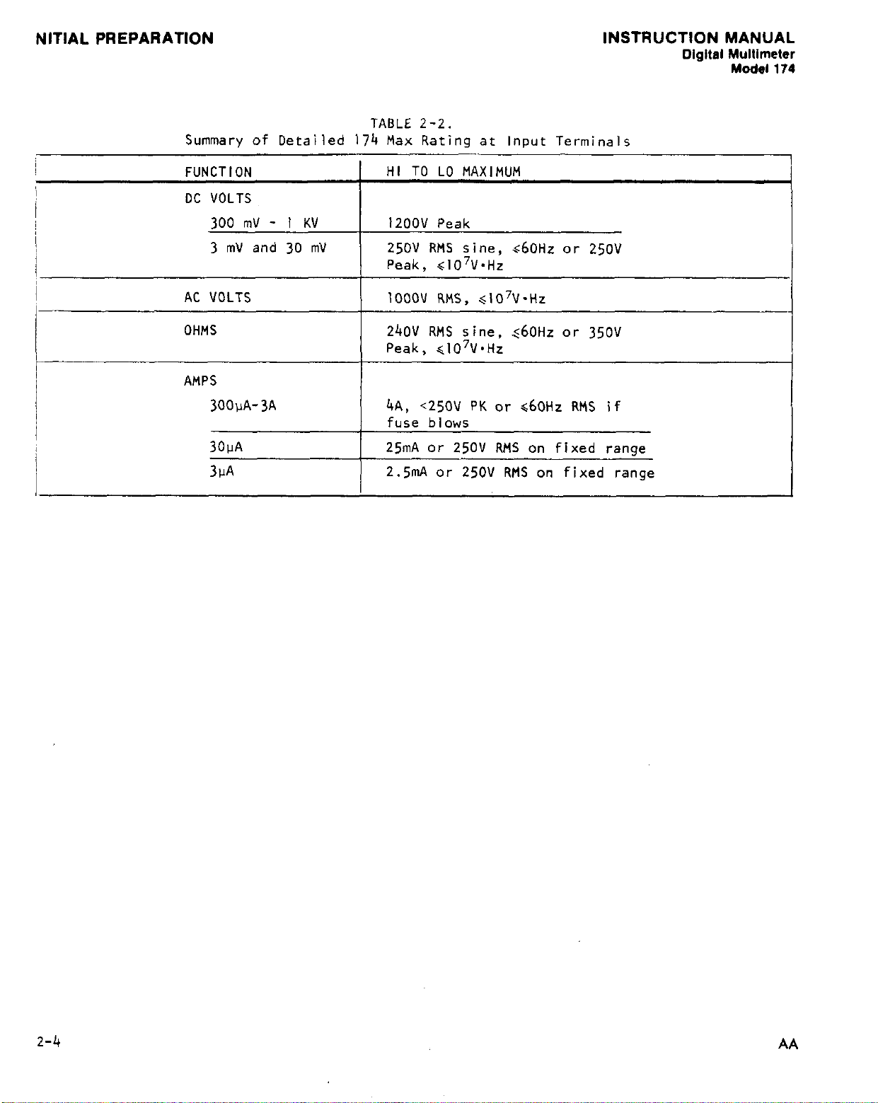
TABLE 2-2.
74 Max Rating at Input Terminals
I-
FUNCTION
DC VOLTS
300 mV - 1 KV
3 mV and 30 mV
AC VOLTS
OHMS
AMPS
3OOpA-3A
30~A
3uA
HI TO LO MAXIMUM
12OOV Peak
250V RMS sine, <60Hz
Peak
. <lO'V~Hz
IOOOV RMS, ,<lO'V.Hz
240V RMS sine, ~60Hz or 350~
Peak
, <lO'V*Hz
~250~ PK or c60Hz RMS if
4A,
fuse blows
25mA or 25OV RMS on fixed range
2.5mA or 25OV RMS on fixed range
or
250~
2-4
AA
Page 15

INSTRUCTION MANUAL
DIgItal MultImeter
Model 174
OPERATING INSTRUCTIONS
SECTION 3.
3-l.
measurement of voltage, current, and resistance,
3-2.
able nickel-cadmium batteries.
tion. The I ine-voltage supply is built-in.
(2 m) long.
four ranges, from a ininimum of 90 V rms to a maximum of 250 V rms. Table 2-1 (pg 2-l)
summarizes the I ine voltages permitted.
GENERAL.
HOW TO SELECT POWER.
The
accessory
purchase of the Model 174 or may be purchased and field-installed at a later time
if so desired.
a. How to Operate From Line Power.
Set the internal line voltage switches (S4Ol and 5402) to the appropriate position
1.
as described in Section 2, paragraph 2-3a.
2. Attach the line cord (CO-7) to the Model I74 at power input receptacle (P405) on
the rear panel. If a shorter I ine cord is desired,
Cord (2 foot long).
This section provides information needed to operate the Model 174 for
The Model 174 may be powered from line voltage or recharge-
The Model 1728 must be installed to permit battery opera-
Model 1728 Rechargeable Battery Pack may be ordered at the time of
OPERATING INSTRUCTIONS.
when the appropriate option is
The power cord is detachable and is 6 feet
NOTE
The Model 174 can be powered from line voltage over
order Keithley Model 7003 Power
installed.
Check the line fuse for proper rating as described in Section 2, paragraph 2-3,
3.
4. Plug the line cord into a source of line power.
Depress LINE pushbutton.
5.
NOTE
Power on will be indicated by a lighted display with one or more digits and measurement
units showing.
b. How To Operate From Battery Power.
Install the Model 1728 Rechargeable Battery Pack. (See Section 4, paragraph 4-Z.)
I.
2. Depress BAT pushbutton.
If the LOW BAT indicator is lighted in BAT mode, refer to Section 4-2~ for re-
3.
charging;
otherwise, the Model 174 may be used for measurements.
3-l
Page 16

OPERATING INSTRUCTIONS
NOTE
The Model 1728 is shipped from the factory in uncharged condition. Therefore, the
Model 1728 should be installed and charged prior to use.
been charged for at least I6 hours,
at least 3 hours.
Summary of Operation in Line and Bat Modes
the Model 174 can be powered continuously for
TABLE 3-2.
Condition of Instrument
After the Model 1728 has
INSTRUCTION MANUAL
Digital Multimeter
Madei 174
Line Power Connected
Button Depressed 1728 Not Installed
LINE ON
BAT
NEITHER
LINE NOR BAT
OFF
OFF
Line Power Connected Line Power Not Connected
1728 Installed 1728 Installed
ON
Batterv trickle charaed.
ON
Battery slowly discharged.
OFF
Battery charged at maximum
rate.
OFF
ON
OFF
3-2
LIGHTED DECIMAL 60lNTS.
FIGURE 5.
Typical Display For Non-Valid Function.
AA
Page 17

INSTRUCTION MANUAL
Dlgltal MultImeter
Model 174
OPERATING INSTRUCTIONS
3-3.
switch (5302).
ac voltage function.
voltage function.
to
HOW TO SELECT FUNCTION.
a. V AC (~1.
The Model
Option 1740 is installed. If this option is not installed the Model I74 will display
all four decimal points to indicate a non-valid function as shown in Figure
b. vDc(=)
res 1 stance ohms) function.
-9
The Model
installeo:
mal points to indicate a non-valid function as shown in Figure
1. HIR. When the FUNCTION Switch is set to Hln, the Model I74 permits resistance
measurements in
2.
measurements in 6 ranges from 300~ to 30MR.
I74
174
LOR. When the FUNCTION Switch is set to LOQ, the Model I74 permits resistance
When the Function Switch is set to V AC the Model 174 will be set to
Refer to paragraph 3-6 for operating information.
can be used to measure ac voltage only when the Averaging AC Voltage
. When the Function Switch is to V DC the Model 174 will be set to dc
Refer to paragraph 3-b for operating information.
When the Function Switch is set to HI0 or LOR the Model I74 will be sef
can be used to measure resistance only when the Ohmmeter Option 1744 is
If this option is not installed,
6
ranges from 3K0 to 300MO.
Function is selected by means of a front panel rotary
IMPORTANT
5.
Refer to paragraph 3-6 for operating information.
IMPORTANT
the Model 174 will display all four deci-
5.
Full range voltage is 3 V.
Full ranoe voltage is 300 mv.
d. A DC (ZJ. When the FUNCTION Switch is set to A DC the Model 174 will be set to dc
current function. Refer to paragraph 3-7 for operating information. Neither auto-
ranging nor remote ranging are available on Amperes.
IMPORTANT
The Model I74 can be used to measure dc current only when the DC Amneter Option I745
is installed.
decimal points to indicate a non-valid function as shown in Figure 5.
e. A AC (“J).
ac current function. Refer to paragraph 3-7 for operating information.
autoranging nor remote ranging are available on Amperes.
The Model I74 can be used to measure ac current only when both the AC Voltage Option
1740 and the DC Amneter Option 1745 are installed. If these options are not installed
the Model
as shown In Figure
If this option is not installed the Model 174 will display all four
Whkn the FUNCTION Switch is set to A AC the Model I74 will be set to
Neither
IMPORTANT
I74
will display all four decimal points to indicate a non-valid function
5.
AA
3-3
Page 18

OPERATING INSTRUCTIONS
INSTRUCTION MANUAL
Digital Multimeter
Model 174
LOW
BATTERY
mv
ZERO
FUNCTION
-‘ITCH
3-4
LINE BAT
PZN
SEE FIGURE 7
FOR RANGE SELECTION
DETAILS
FIGURE 6.
Front Panel Controls and Input Terminals.
VALID FOR
VOLTS AND
OHMS ONLY
CASE
GROUND LO HI
J304 J303
INPUT INPUT
J302
AA
Page 19
INSTRUCTION MANUAL
OPERATING INSTRUCTIONS
Digllsl MulIlmeIar
Model 174
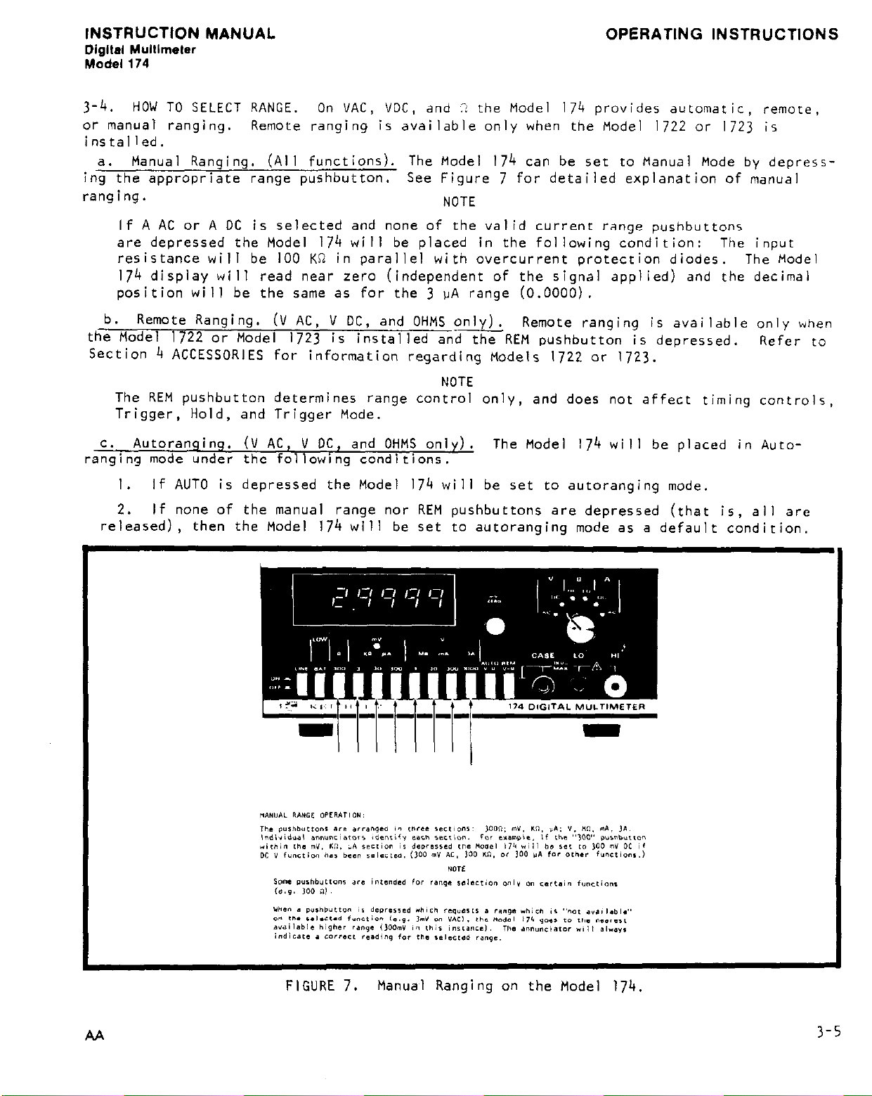
3-4. HOW TO SELECT RANGE. On VAC, VDC, and :1 the Model I74 provides automatic, remote,
or manual ranging. Remote ranging is available only when the Model 1722 or 1723 is
installed.
Manual Ranging. (Al I functions).
a.
ing the appropriate range pushbutton.
ranging.
If A AC or A DC is selected and none of the valid current range pushbuttons
are depressed the Model 174 will be placed in the following condition: The input
resistance will be 100 KR in parallel with overcurrent protection diodes.
174 display will read near zero (independent of the signal applied) and the decimal
position will be the same as for the 3 uA range (0.0000).
b.
Remote Ranging. (V AC, V DC, and OHMS only).
the Model 1722 or Model 1723 is installed and the REM oushbutton is depressed.
Section 4 ACCESSORIES for information regarding Models I722 or 1723.
The REM pushbutton determines range control only,
Trigger, Hold, and Trigger Mode.
C.
Autoranging. (V AC, V DC, and OHMS only).
ranging mode under the following conditions.
The Model 174 can be set to Hanual Mode by depress-
See Figure 7 for detailed explanation of manual
NOTE
The Model
Remote ranging is available only when
Refer to
NOTE
and does not affect timing controls,
The Model I74 will be placed in Auto-
If AUTO is depressed the Model I74 will be set to autoranging mode.
I.
2. If none of the manual range nor REM pushbuttons are depressed (that is, all are
released),
then the Model 174 will be set to autoranging mode as a default condition.
AA
FIGURE 7.
Manual Ranging on the Model 174.
3-5
Page 20

OPERATING INSTRUCTIONS
NOTE
The following rules govern the autoranging feature:
a) When the display exceeds 29999, the Model 174 upranges (that is, it changes to
less sensitivity and the decimal point and measuring unit changes appropriately).
b) When the display reaches 02599 the Model I74 downranges (that is, it changes
to greater sensitivity and the decimal' point and measuring unit changes appropriately)
until it reaches the most sensitive range (except 3mV dc and 30 nV dc).
INSTRUCTION MANUAL
Digital Multimeter
Yodet~74
3-5.
30mV, 300mV, 3V, 3OV, 3OOV, and IOOOV DC.
Model 174 measures ac voltage in five ranges, 300 mV, 3V, 3OV, 3OOV, and IOOOV.
HOW TO MEASURE VOLTAGE.
Maximum input voltage depends on the range selected.
allowable continous input for each range on AC and DC. Do not exceed these voltages
or damage to the instrument will occur.
The Model 174 measures dc voltage in seven ranges:
When the Model 1740 Option is installed, the
CAUTION
Table 3-3 gives the maximum
TABLE 3-3.
Maximum Allowable Continuous Input
IOOOV rms (<lO'V.Hz
1000~ rms (<lO'V.Hz
IOOOV rms
IOOOV rms (<lO'V*Hz
1OOOV rms
(*107V.Hr
(<lO'V~Hz
*NOTE
12OOV Peak
1200V Peak
12OOV Peak
12OOV Peak
3mV,
When 3mV or 30mV range pushbuttons are depressed,
and thus the allowable input will be 1000 V rms
DC Voltage. The Model 174 detects dc voltages from f0.1 microvolts/digit to t1200
voy;s (1200.0 display). The maximum display is 29999. When the display exceeds 29999,
a 3 remains lighted, but ail other digits are blanked.
volts on the highest range.
Select V DC on Switch 5302.
1.
2. Depress AUTO, REM or desired Manual Range pushbutton.
Connect the signal to be measured between HI and LO terminals. The terminals are
3.
designed to accept banana or "bunch pin" plugs,
1747 Low-Thermal coaxial input cable.
below IO microvolts dc resolution.
4. Observe the displayed digits, polarity sign,
ment unit (mV or V).
A "zero" reading will always be displayed as -.OOOO.
3-6
If no polarity sign is indicated,
These leads are recommended for measurements
the 300mV range will be selected
(<IO'V*Hz).
The display blinks above 1200.0
such as the accessory Keithley Model
decimal point location, and measure-
a positive polarity is implied.
AA
Page 21

INSTRUCTION MANUAL
Digital Multimeter
Model 174
OPERATING INSTRUCTIONS
On the 3 mV and 30 mV DC ranges the front panel "mV ZERO" control must
5.
adjusted to obtain rated accuracy.
Make low-thermal connections to the Model
a)
Model 1747 cable or satisfactory equivalent is recommended.
b) Set the Model 174 to the 3 mV range.
Allow the thermal emfs generated by the input connections
C)
d) Some circuits may need to be enclosed in polyurethane foam, a cardboard box,
or other suitable enclosure to prevent zero fluctuations due to air movement at the
connection point.
Make certain that a "Zero Signal"
e)
be measured (e.g., a zero current condition for a resistance thermometer measurement).
f) Adjust the "mV ZERO" control for a display indication of-.0000 mV f .OOOl mV.
The "mV ZERO"
effect on any
Proceed
9)
h) The "mV
control operates only on the 3 mV DC and 30 mV DC ranges.
other range or function.
with the measurement and apply the signal.
ZERO" control setting will also be valid for the 30 mV range if used.
condition is established for the circuit to
NOTE
174
as described above. Use of tne
to
stabilize.
be
It has no
AC Voltage.
b.
(1000.0 display).
The Maximum display is 29999.
all other digits are blanked.
Maximum input voltage is 1000 V rms or
I.
Select V ac on Switch 5302.
Depress AUTO, REM or desired Manual Range pushbutton.
2.
Connect the signals to be measured between HI and LO terminals.
3.
are designed to accept banana or "bunch pin" plugs,
1747 Low-Thermal coaxial input cable.
4.
Observe the displayed digits, decimal point location,
v) .
The Model 174 detects ac voltages from IO microvolt5 to 1000 volts
The Model
174
is average-reading,
When the display exceeds 29999, a 3 remains lighted, but
The displa
blinks above 1000.0 volts on the highest range.
7
10 V*Hz on all ranges.
calibrated in terms of rms sinewave
(The terminals
such as the accessor Keithley Model
and measurement unit (mV or
3-7
Page 22

OPERATING INSTRUCTIONS
INSTRUCTION MANUAL
Digital Multimeter
Model 174
3-6.
measures resistance from IO milliohms/digit to 300 megohms. The maximum display is 29999.
When the display exceeds 29999, a 3 remains lighted,
Maximum allowable input voltage is 240V rms or 350 V peak up to 60 Hz.
the resistance under test at full range is 3 volts. The Model 174 measures from 3Kn to
300 megohms full range in HI mode.
the resistance under test at full range is 300 millivolts.
3OOC to 30 megohms full range in LO Mode.
HI and LO terminals. For measurement on low resistance ranges where lead resistance may
cause an error the following procedure should be performed.
HOW TO MEASURE RESISTANCE. When the Model 1744 Option is installed, the Model 174
but all other digits are blanked.
a. HI Ohms Measurement.
I. Select Hlfl on Switch 5302.
2. Connect the resistance under test between HI and LO terminals.
Depress AUTO, REM, or the desired Manual Range pushbutton.
3.
4. Observe the displayed digits, decimal point location, and measurement unit (Kfi or
MR) .
b. LO Ohms Measurement. When Switch 5302 is set to LOO,
1. Select LO n on Switch S302.
2. Connect the resistance under test between HI and LO terminals.
Depress AUTO, REM, or the desired Manual Range pushbutton.
3.
Observe the displayed digits, decimal point location, and measurement unit (iI,
4.
KR, or Mn).
Lead Resistance Compensation.
c.
When Switch S302 is set to HIR, the voltage developed across
the voltage developed across
The Model 174 measures from
The Model I74 measures the total resistance between
1. Connect the measuring circuit to the INPUT terminals on the 174 using appropriate
test leads or cables.
2. Substitute a temporary short circuit in place of the circuit to be measured.
fn the case of the Model 1747, temporarily clip together the alligator connectors.
3.
4.
Record the reading on the Model 174 as RO (residual lead resistance under a
shorted condition).
Remove the shorted condition and connect the active circuit to be measured.
5.
6. Record the new reading in the Model 174 as R,.
The true value of “Ri’ is R = R - Rg, within the stated accuracy of the Model
7.
174.
method.
No additional errors in theTresi:tance measurement are added when using this
3-8
AA
Page 23
INSTRUCTION MANUAL
Digital Multlmeler
Modal 174
OPERATING INSTRUCTIONS
3-7.
measures dc current in seven ranges:
both the Model I740 and 1745 Options are installed, the Model 174 measures ac current over
the same ranges. Range selection is via manual range pushbuttons only.
peres. The maximum display is 29999. When the display exceeds 29999, a 3 remains lighted
but all other digits are blanked.
HOW TO MEASURE CURRENT.
The Model I74 DMM is protected by a 4 ampere fuse on all ranges except 3uA and
3OuA.
250V input voltage. If the fuse is blown,
should be installed in the fuse holder on the 1745 option.
MAINTENANCE, Paragraph 6-5, for fuse replacement.
a. DC Current.
I. Select A dc on Switch S302.
2.
3.
4.
ment unit (uA,. mA, or A).
implied.
On the 3uA and 30uA ranges the maximum allowable input corresponds to a
The Model 174 DMM detects dc currents from to.1 nanoamperes to ?3 am-
Depress the desired Manual Range pushbutton.
Connect the signal to be measured at the HI and LO terminals.
Observe the displayed digits, polarity sign, decimal point location, and measure-
A "zero" reading will always be displayed as -.OOOO.
When the Model 1745 option is installed, the Model 174
3uA, 30uA, 300pA, 3mA,
CAUTION
a replacement Keithley Part No. FU-39
If no polarity sign is indicated, a positive polarity is
30mA, 300mA, and 3A. When
Refer to Section 6,
b. AC Current. The Model I74 DMM detects ac currents from 0.1 nanoamperes/digit to
3 amperes in AC function. The Model 174 is average reading calibrated in rms of a sine
wave. The maximum display is 29999. When the display exceeds 29999, a 3 remains lighted,
but all other digits are blanked.
Select A AC on Switch S302.
I.
Depress the desired Manual Range pushbutton.
2.
Connect the signal to be measured at the HI and LO terminals.
3.
Observe the displayed digits, decimal point location, and measurement unit (PA,
4.
ma or A).
3-8.
FURTHER MEASUREMENT CONSIDERATIONS.
Grounding Considerations.
a.
the line cord are provided to avoid electrical shock in the event of an electrical
malfunction. The ground (CASE) terminal,
ground,
ground is at a safe potential at all times.
Always ensure that the instrument Is grounded either through the third wire on
the line cord or through a separate connection between CASE terminal and reliable
earth ground.
injury due to electrical shock.
serves as a return current path and ensures that the instrument chassis
Failure to follow these precautions could result in serious personal
The CASE terminal and the third wire ground on
when properly connected to a reliable
WARNING
AA
3-9
Page 24

OPERATING INSTRUCTIONS
INSTRUCTION MANUAL
Digital Multimeter
Model 174
How to Use the Model 174 Off-Ground.
b.
at’potentials of up to ilOO volts.
(CASE terminal) is specified at 103n shunted by less than O.OluF. In general, the LO
terminal should be connected to the point in the measurement circuit which has the lowest
impedance to power I ine ground or the “effective guard” or “shield” mode in the circuit.
If the measurement circuit is independent of power line ground LO and CASE should be
connected to a cornnon point in the circuit.
c.
3mV/30mV Accuracy. The 3mV/30mV accuracy specifications assume that the instrument
has been in thermal equilibrium with the environment for I hour or more, and that the
front panel
obtain a “zero” indication of -.OOOO mV ? .OOOl mV. The “mV Zero” control is used in
this manner to compensate for thermal emfs generated in the circuits connected to the
input terminals. These externally generated thermal emfs must re,nain constant during
the measurement in order to obtain stated accuracy.
d.
300mV Accuracy. The 300mV accuracy is given down to 1% of range. Below 1% of
range an additional .
the 1% level, but gradually as the level is decreased below 3OOuV.
e.
mV Analoq Output.
is specified.
ranges and functions output voltages up to +l5V may exist.
varying within this span,
Analog Output” point is the output of the nanovolt preamp, which has a fixed gain of 100,
and no switching is done,
the “mV Analog Output” provides continous Xl00 output for signal levels as low as the
Model 174 noise level (typically IOOnV to 15OnV p-p, up to 30mV).
“mV ZERO” control has been used imnediately prior to the measurement to
l5mV is added to the accuracy. This does not occur immediately at
This output is active only on 3mV and 30mV ranges. No accuracy
Typically the output is within 2 (2 x accuracy spec + digit). On other
or have step changes within this span. Notice that the “mV
except in the A/D converter between 3mV and 30mV ranges. Thus,
Isolation from the
The “LO” terminal can be operated off ground
“LO” terminal to power I ine ground
Output may be randomly
f. Overload on 3mVdc and 30mVdc.
from DC up
lO7V *
exceed the overload specification on the 3mV/30mV ranges until IO ms after the range
change command is given. (e.g. IOms after Load Range goes active or a new range pushbutton is depressed).
4.
Offset Current. The offset current is adjusted to IOpA at the factory or by
executing the calibration procedure given in Section 6-4.
with time and temperature, but is is unlikely to exceed 200pA at any environment within
the specified region up to 6 months after calibration.
that peak-to-peak noise in the Model 174 will be larger (than that exhibited with a
short circuit) for source resistances in excess of about 30KG to 70Kfi.
Settling Time. Table 3-4 gives typical and worst expected settling times express-
h.
ed as the number of conversions (320 ms) for the Model 174. The numbers in the table
assume that the proper range and function have been selected and previous transients have
“settled” before a “step change” in the signal is applied.
effects of input cabling time constants.
to
60HZ.
HZ product. When switching from 3mV/30mV to higher ranges the voltage must not
Up to 180~ RMS may be applied continuously at any frequency up to
Up to 250V may be continuously applied at frequencies
Offset current wi 1 I change
Short term variations are such
The numbers do not include
3-10
AA
Page 25
INSTRUCTION MANUAL
Digltsl MultImeter
Model 174
OPERATING INSTRUCTIONS
TABLE
Source R
3mV, 30mV
3mV, 30mV
OHMS
DC AMPS
AC VOLTS
AC AMPS
particular Model I74 will have repeatable settling time characteristics for a fixed
or low) source resistance.
oft instruments ('Itypical values") and the maximum settling time of a "slow" but properly
peratinq instrument ("worst expected values").
All except
3OOMn HI
30Mn LO
3OOMn HI
30MR LO
All
All
All
<lOKn
i-OOKn
LEnd Range
End Range
Any
<lOOKn
Any
The above is a rough indication of what can be expected of
-4.
Number of Conversions Required to
Settle to Within 0.01% of a "Step
Change".
Tvpical
I
20
AA
3-11
Page 26

Page 27

INSTRUCTION MANUAL
Dlgllel Multimeter
Model 174
ACCESSORIES
SECTION
4-l.
Model
1722 Digital Interface,
probes, test leads,
only be installed and used one at a time.
4-2.
use, or for complete freedom from ac power lines for critical measurements where near-
infinite commonmode rejection is needed.
recharging is needed from the built-in charger.
operation from full charge. The Model I728 recharges completely in I6 hours with instrument off.
screwdriver and adds I,
-25°C to +35’C when installed in the Model 174.
“NC--
GENERAL. This section describes various accessories available for use with the
174.
Models
Section 2 INITIAL PREPARATION and Section 3 OPERATING INSTRUCTIONS.
MODEL
These accessories include the Model 1728 Rechargeable Battery Pack, the Model
the Model 1723 IEEE Interface,
and other convenience accessories.
1740, 1744,
1728
RECHARGEABLE BATTERY PACK.
Trickle char
Model 1722. 1723 and
and
1745
are field-installable options which are described in
es with instrument on.
;i
kg
(3
pounds) to
1728
can only be installed and used one at a time.
4.
ACCESSORIES
rack mounting kits and various
Model 1722, 1723 and 1728 can
NOTE
The Model 1728 powers the 174 for portable
A front panel low-battery indicator shown when
174.
NOTE
Ni-Cd rechargeable batteries give
The Model 1728 is field installable with
Storage and ambient operating temperatures
3
hours
The Model 1728 Rechargeable Battery Pack can be installed by the user within the
Model I74 at any time. However (
1723 IEEE Interface is already installed,the Model 1728 cannot be used simultaneously
a, How to l’nstall the Model I728 Recharqeable Battery Pack.
nished with the Model 1728 are already installed in the battery pack.
pack includes 7 rechargeable “C” cells (1.2V, 2 AMP tir) and two 19.2 volt packs
(sixteen l.2V cells per pack). See Figure 8.
Check she fuses on the Battery Pack.
I .
F403. All are 1 ampere, 3AB or 3AG, Slo-Blo types, Keithley Part No. FU-IO.
Check for proper installation of batteries in the Battery Pack.
2.
battery cells are to be installed see paragraph 4-2d.
To install the Battery Pack,
3.
shown in Figure 2.
circuit board. Temporarily remove the plastic spacers installed on the Mode) I74
chassis. Separate the two halves of the spacer and reinstall on the Model 1728
board as shown in Figure
assembly.
(P401, P402) taking care to orient the connectors as shown. If the Model 1740 AC
Option is installed,
to permit access to connector P4Ol as in Fiaure 9.
on the spacers with the pack oriented as shown in Figure 9 and tighten down the four
screws which hold the Model
tighten down the four Phillips screws.
Plug the two 5-wire connectors (J401, J402)
Carefully renwve the top cover to gain access to the printed
9.
it will be necessary to temporarily renwve the 1740 pc board
1728
if the Model I722 Digital Interface or the Model
The batteries fur-
The battery
Three fuses are used, F401, F402, and
If replacement
loosen four Phillips screws on the top cover as
The rubber “0” ring retains the spacer and screw
into the mating receptacles
Place~the Model 1728 in position
to the Model I74 chassis. Replace the top cover and
AA
4-l
Page 28

ACCESSORIES
b.
How to Check Batteries.
INSTRUCTION MANUAL
Digital MultImeter
Modal 174
IMPORTANT
The Model 1728 is shipped from the factory in an uncharged condition.
the pack should be installed in the Model 174 and charged prior to usa
The Model
I.
battery condition.
The LOW BAT indicator will be lighted when the
2.
operating voltage.
LINE or OFF to permit recharging of the Pack.
c. How to Charge the Batteries. The Model 1728 provides built-in recharging circui try.
rapid rate when the Model
and may shorten the life of the batteries.
d.
rechargings before replacement is necessary.
batteries,
the batteries used in the Model 1728.
The Model 174 must be connected to line voltage.
Overcharging the batteries will raise the internal temperature of the battery pack
How to Replace Batteries.
use only the equivalent types as supplied by the factory. Table 4-l summarizes
I74
has a built-in LOW BAT indicator
When the indicator turns on, the
I74
is set to OFF.
CAUTION
The rechargeable batteries will normally provide many
TABLE
Summary of Batteries Used in the Model 1728.
However,
4-l.
to permit easy determination of
Battery Pack goes below normal
Model I74 should be switched to
Recharging occurs at the most
if it is necessary to replace the
Therefore,
Description
I .2v “C” ccl I
(2 AMP-HR)
+19.2V pack
(16-l.2V cells)
-19.2V pack
(16-l .2v ccl IS)
Quantity Vo I tage Keithley Part No.
7
I +19.2V BA-31
I -19.2v BA-3 I
8.4~
BA-30
4-2
AA
Page 29

INSTRUCTION MANUAL
Digital MultImeter
Model 174
J4Ol
ACCESSORIES
(MATES WITH)
P4Ol
F401
r,uunc 0.
PIO(I~I I/L" nechargeable Battery Pack.
Page 30

ACCESSORIES INSTRUCTION MANUAL
Digital MultImeter
Med.4
174
4-4
FIGURE 9.
Installation of Model 1728.
AA
Page 31

INSTRUCTION MANUAL
Dlgltal Mulllmeter
Model 174
e. Circuit Description. (See also Schematic 26758c.j
The Model 1728 provides il9.2 volts and +8.4 volts from nickel-cadimum bat-
I .
teries. BT401 and ET402 are 19.2 volt,
by IA, 3AG Slo-Blo fuses.
and is also fused by a IA, 3AG, Slo-Blo fuse.
charging circuit which is operated from i29.5V unregulated supplied by the DMM linepower supply.
2. BT40l Charging.
CR401 and CR402 and resistor ~402 place a diode drop across R401.
current is the maximum charging current.
plying current through Q401.
is set to OFF. A trickle charge is maintained when the DMH is line operated.
reduced current is obtained by inserting a limiting resistor in series with the
charging circuit (not shown on Schematic 26758C).
charged at a C/IO rate (45 mA for ET401 & BT402, & 2OOmA for BT403). When trickle
charged, the charge rate varies according to line voltage t battery condition from a
minimum of C/l00 rate to a maximum of C/20 rate. Thus,
fully charge the batteries, but is intended to put sufficient charge into them for
short intermittent use.
ET403 is an 8.4~ pack composed of seven 1.2 volt “C” cells
‘BT401 is
charged
The maximum charging current occurs only when the DHH
.45 AH nickel cadmimum packs which are Fused
The Model 1728 has a built-in re-
via a constant current from Q401. Diodes
Diode CR403 prevents the battery From SUD-
In full charge,
trickle charge may never
ACCESSORIES
The resulting
the batteries are
The
3. ET402 & ET403 Charging.
Q402 or Q4Ol respectively.
except that they are powered by unregulated ?29.5V.
BT402 G ET403 are charged via a constant current from
These circuits operate similarly to the above circuit.
AA
4-5
Page 32

ACCESSORIES
4-3. MODEL 1722 DIGITAL INTERFACE.
General.
a.
control lines.
This accessory is available either "factory installed" or "field-installable".
Model 1722 consists of a two-layer circuit with card-edge and mating output connectors.
Installation.
b.
Disconnect the Model 174,line cord from line voltage.
I.
Depress LINE pushbutton to discharge any voltages on power supply capacitors, etc.
2.
Loosen and remove the four Phillips screws on the top cover as shown in Figure 2.
3.
4. Lift off the top cover and set aside.
Temporarily remove the four spacer assemblies held down by a slotted strew.
5.
Reassemble the spacers as shown in FigurelO.Be careful to install the "0" ring
6.
over the screw to hold the assembly together prior to installing the Model I722 board,
The Model 1722 provides binary coded decimal outputs (8421) and range
Outputs are open-collector positive true unless otherwise specified.
INSTRUCTION MANUAL
Digital Multimeter
The
Model 114
Place the Model 1722 in the location shown in FigureIOwith the cables oriented
7.
properly.
8. Plug the Model 1722 connectors JlOO3, JIOOI, and J1002 into mating connectors
P403, P404, and P701 respectively.
9.
T401 as shown in Figure 10.
IO.
Diaital Output Connector Terminations.
~lk6 ('to-pin) and PI101 (26-pin).
(IO-ft. long) cables mate with PIoo~/PIIOI connectors. See Figure 1, for pin
identification.
See detailed view for orientation of connectors.
See detailed view for orientation of connectors
Connect the ground return wire from the Model 1722 to the screw on transformer
Reinstall the top cover.
The Model 1722 uses two card-edge connectors
Accessory Model 1727-03 (3 ft. long) or Model 1727-10
4-6
AA
Page 33

INSTRUCTION MANUAL
DigItal
Model174
Multimeter
ACCESSORIES
Jim,
1
I II
I I II 7.
2 TOP SPACER
\
.F BOTTOM SPACER (27812
~"0" RING (GA-j)
ABOVE HARDWARE
IS FURNISHED
WITH MODEL 174.
(27812a)
kltiUHt IO.
Installation of Model 1722 Digital Interface.
Page 34

ACCESSORIES
TABLE 4-2.
General Characteristics of Model 1722 Digital Interface.
IGITAL OUTPUTS:
Logic: BCD (8421) Open-collector positive true unless otherwise specified.
Data: 4 full digits, I partial digit (0,
Function: 4-bit code (0, AC VOLTS)
Polarity: HIGH 3+.
Overflow:
Autorange:
Automode:
-AG (m): HIGH (logic "0" 5 no output change occuring.)
Logic Levels: HIGH : open collector to output LO. LOW Z closure to output LO. Output
device (2N5134) greater than 20V breakdown,
pull-up resistors may be installed on these open collector outputs.
is reconnnended when using internal 5 volt power supply.
JTPUT TIMING: Data is updated typically every 320 msec (non-trigger mode).
is typically 1.2 msec. Data will appear at an output only if its respective strobe is
active. The FLAG will go low (Logic "0") typically 2 tnsec before update and go high
typically 100 vsec after update.
flag is high. If FLAG RESET is activated, the FLAG will reset (go to Logic "0") until
the end of the next data update.
fMOTE CONTROLS:
Strobe: Strobe lines permit word serializing in 4-bit increments or multiples thereof.
HIGH inhibits controlled output lines from conduction, LOW enables conduction.
Range In: 4-bit exponential code.
Load Range:
Hold:
conversions).
Printer Hold: Same as hold but grouped with outputs for convenience in inte;facing
printer.
Trigger Mode: LOW enables TRIGGER control.
Trigger Mode Disable:
Trigger:
Flag Reset: LOW sets FLAG jFLAG) to LOW (HIGH).
Control Logic Levels t Source Requirements:
voltaqe between +2.4V and 5V referred to output LO.
w_jthin O:~V while sinking +I.6 milliamperes (ITTL load). The Hm, Tm,
TRIGGER MODE DISABLE, TRIGGER, and FLAG RESET lines control the Model 174 regardless
of front panel setting.
in "V" and "Sl" functions, when the front panel "REM" (remote) pushbutton is depressed
LOW q > 29999.
LOW ; range change.
HIGH : autorange mode.
Data can be expected to be unchanging so long as the
Low enables remote ranging as set by Range code.
LOW inhibits display update,
LOW disables TRIGGER.
LOW to HIGH transiti initiates a new A/D conversion.
LOAD RANGE and Range Input Codes control range selection onl
output update and autorange (A/D continues
I, 2, 3) and exponential range code.
<0.5V at 5mA sink (3TTl loads).
HIGH 5 either an open circuit or a
LOW ! closure to output LO
INSTRUCTION MANUAL
Digital Mulllmeler
Internal
4.7K minimum value
Update time
Model174
jOLATION:
by IO9 n and 5OOpF, 1200 VDC, IOOOV runs AC maximum.
controls are located from chassis ground by IO6
4-8
All digltal outputs and remOte controls are isolated from 174 analog input
All digital outputs and remote
R and O.OlpF; 250V runs maximum.
Page 35

INSTRUCTION MANUAL
Dlgttal Multlmeter
Model 174
ACCESSORIES
TABLE 4-3.
Sumnary of Remote Commands at PllOl
(See also Figure 12)
Pin No. Comnand
I
2
3
4
5
6
CASE GND
COMMON
COMMON
AUTORANGED STROBE
TRIGGER MODE
AUTOMODE STROBE
7 HOLD
a
9 LOAD RANGE
IO
II
12
OVERFLOW STROBE
FLAG/FLAG STROBE
RI
FUNCTION STROBE
13 R2
Pin No.
14
15
16
17
la
19
20 IO3 STROBE
21
22
23
24
25
26
Command
RANGE STROBE
R4
POLARITY STROBE
R8
IO' STROBE
TRIGGER
FLAG RESET
IO' STROBE
TRIGGER MODE DISABLE
lOI STROBE
AUTORANGED
IO0 STROBE
PI006
AA
PIIOI
I
,
t
L ----- --------__- ---- J
----__----------------------,
r
i
I
L
---a--------- 1 3 9 1315 ----------------- 17 19 212325 27 29 31 I
FIGURE Ila. Connector Pin Identification For Model 174/1722,
2 4 6 6 1012141616 20222426
I,, ,
1 3 5
2 4 6 6 10121416162022242628303234363'340 I
I, , , , ( , , ( , , , , , , , , , , ,-q
7 , 9
, , 1 , , , , , .d
11131c17192123-25
5 7 11 33 35 37 3g
i
1
4
I
4-P
Page 36

ACCESSORIES
-
-
- Y
Pin No.
20
I
*
2
ii
9
IO
I1
I2
13
I4
15
I6
17
18
19
TABLE 4-4.
Suwnary of Digital Output at ~1006
(See also Figure 12.)
Signal
CASE GND
COMMON
COMMON
COMMON
COMMON
PRINTER HOLD
AUTOMODE
VEXT
R8
VOLTS
R4
AMPS
R2
AC
RI
OHMS
lo’+-8
103-e
104-4
103-4
INSTRUCTION MANUAL
Digital Multimeter
Model 174
Signal
104-Z
lD3-2
104-l
103-l
102-8
101-8
102-4
IO’-4
102-Z
100-4
FLAG
100-z
OVERFLOW
100-I
POLARITY
4-10
--m-m--- -------- -----~
r
I
I
PI101
t
------------------------
l-
i
PI006 )
I
L
-----.-------------------------
FIGURE lib.
t ; 2 8 1012141616 20222426
1
11v1.11.11**
a 3 5 7 9 11131E1719212325
2 4 6
7 I I I I ( , I 1 I , , 1 , , , , I , I
1 3 5 7 9 111315
8 10 121416162022242626 303234 36 3840 I
1?1921232527293133353739 I
Connector Pin identification For Model 174/1722.
1
i
I
-
---1
,
I
1
AA
Page 37

INSTRUCTION MANUAL
Dlgltal Mulflmeter
Model174
(Mode
1722 Ran
TABLE 4-5.
d Function Cod
g For MO
in
ACCESSORIES
1 174)
'UNCTION
IC VOLTS
.ow R
OUTPUT
FUNCTION
CODE (1)
VAAC R
100 0
IO1 0 rC VOLTS
000 I
RANGE
3 mV
30 mV
300 mv
303 i
300 v
1200 v
300 mV
3 v
30 v
300 v
1000 v
300 R
3 kn
30 kR
300 kn
3 MR
30 MO
OUTPUT
RANGE
CODE (I)
R8 R4 % Rl
0011
0 1 0 0
0 I 0 I
0 I,0
0 I I I
0 0 0
0 0 1
0 I 0 I
0 II0
0 Ill
IO 0 0
IO 0 I
0 0 I 0
0011
0 I 0 0
0 IO 1
0 II0
0 1 II
(EXP)
INPUT
RANGE
CODE (I) (2)
R8 R4 R2 Rl
III1
I IO 0
IO II
I 0 I 0
I 0 0 1
I 0 0 0
0
II I
0 110
I I I I
IO IO
1 0 0 I
IO 0 0
0 III
0 II0
Ill1
110 I
I I 0 0
IO II
IO IO
IO 0 I
IO 0 0
AUTORANGE AUTORANGE
AUTORANGE AUTORANGE
AUTORANGE AUTORANGE
II R 001 0
3 kn
30 kQ 0 I 0 0
300 kn
3 Mn
30 Mfl
300 MR
11) Coding in this table is defined to be HIGH (POSITIVE) TRUE. "1" = HIGH and "0" = I
LOW. Refkr to output and remote control logic levels for definitions of HIGH t LOW.
,2) Note that except for AUTORANGE CODE,
PUT RANGE CODE, I.=. the INPUT RANGE CODE is the LOW TRUE BCD code of (EXP).
(3) Note that (EXP) is oiiectly the exponent of IO if the numerical readings are
defined as follows:
VOLTS: Unit = uV
OHMS:
AMPS:
AA
0011
0 10 I
0 II0
0 III
IO 0 0
INPUT G RANGE CODE is the compliment of the OUT-j
Uni~t = R
Unit = nA
1111
I IO0
IO I I
IO IO
IO 0 I
IO 0 0
0 III
AUTORANGE AUTORANGE
4-11
Page 38

ACCESSORIES
INSTRUCTION MANUAL
Dlgltal Multimeter
Model 174
TABLE 4-5. (Con't)
(Model 1722 Range & Function Coding For Model 174)
OUTPUT
FUNCTION
CODE (I)
UAACQ
010 0
011 0
d.
HOW to Select Vext Using Internal Jumper.
internal or external voltage references and internal pull-up resistors. (See Figure 16.)
LANGE
3 UA
30 IJA
100 PA
3 mA
30 mA
100 mA
3 A
3 uA
30 uA
100 PA
3: 2
;OO mA
3 A
OUTPUT
RANGE
CODE (I)
RB RI, Rz Rl
0 0 1 I
0 1 0 0
0 IO I
0 110
0 Ill
10 0 0
IO 0 I
001 I
0 IO 0
0 IO I
0 II0
0 III
IO 0 0
10 01
The Model 1722 may be wired for use with
(EXP)
3
4
===l==-
INPUT
RANGE
CODE (I) (2)
Ra R4
NO AUTORANGE OR
REMOTELY PROGRAMMED
CURRENT RANGES.
R2
RI
I
I. Jumper A.
the external reference Vext (pin 8, ~1006).
2.
Jumper B.
the internal reference (+5V .
Jumper C.
3.
reference.
reference is rated at 40 mA maximum.
The pull-up resistors are not connected in this instance. The +5 volt
When this jumper is installed,
When this
When this jumper is installed, Vext is connected to internal t5V
'urnper is installed,
j
the pull-up resistors are connected to
the pull-up resistors are connected to
4-12 AA
Page 39

INSTRUCTION MANUAL
Olgllrl Mulllmeter
Model 174
ACCESSORIES
TABLE 4-6.
Digital Output Lines Grouped By Function.
Name
IO0 STROBE
100-l
100-2
100-4
100-8
IO1 STROBE
101-l
101-2
IO’-4
lo’-8
IO2 STROBE
102-l
102-2
102-4
102-8
IO3 STROBE
IO’-,
103-2
103-4
IO4 STROBE
104-l
104-2
104-4
104-8
‘OLARITY STROBE
{ANGE STROBE
-RI
-R2
-R4
-R8
Pi006
Pin
Name
FUNCTION STROBE
-VOLTS
-AMPS
-AC
-OHMS 16
OVERFLOW STROBE
-OVERFLOW
AUTOMODE STROBE
-AlJTOMODE
AUTORANGED STROBE
-AUTORANGED
PRINTER HOLD
TRIGGER MODE
-tEiD
LOAD RANGE
NO.
10
I2
14
38
7
6
RI
R2
R4
R8
--
I8
23
21
I9
I7
--
i
--
16
I4
15
13
II
TRIGGER
FLAG RESET
TRIGGER MODE DISABLE
COMMON
,CASE
FLAG/Fm STROBE
FM
FLAG
VEXT
2,3,4,5
I
--
36
34
8
PI101
Pin
NO.
-
12
8
6
4
25
:
9
II
13
15
17
I9
::
2,3
I
IO
AA
4-13
Page 40

ACCESSORIES
INSTRUCTION MANUAL
Digital Multimeter
Model 174
PI006 Pl,lOl
.,,
3=
GND
JlOOl
1
4-14
JIOOZ
JlOO3
FIGURE 12.
Models 1722 Digital Interface.
AA
Page 41

INSTRUCTION MANUAL
DigItal MultImeter
Model 174
ACCESSORIES
PI006
~---3 =
GND
,L
S
JlOO2
FIGURE 13.
NOTE :
UPPER BOARD PC-4
NOT SHOWN.
JlOO3
Location of Jumpers and Pull-Ups For Model
16
1722
4-15
Page 42

ACCESSORIES
INSTRUCTION MANUAL
Digilal Multimeler
Model 174
Detailed Explanation of Model 1722.
e.
end of the Manual .)
1. TRIGGER MODE AND TRIGGER (Timing Diagram 23248E): When TRIGGER MODE is active
(Low),
Conversion starts within 1.6 milliseconds after RISING TRIGGER.
120 milliseconds after start of conversion.
not be updated and the FLAG will stay at HIGH (unless reset by FLAG RESET).
RANGE IN code (Table65) at the beginning of the next conversion. As long as LOAD
RANGE is held low the instrument will remain on its programmed range, provided the “REM”
pushbutton on the front panel is depressed.
of Table 4-5 will result in the nearest valid range to that programmed.
always set the DMM to the newly programmed range.
will be held until the end of the first complete conversion on the new range.
a REMOTE CONTROL update prior to data output.
case of HOLD.
change could result in erroneous data.
the FLAG be examined no sooner than IO psec after activation of the HOLD bit.
is low wait until it goes to HIGH before expecting the mbit to have been accepted.
Other REMOTE CONTROL bits such as -and TRIGGER,
code can be kept active for longer than an output data update time, I.e. >3.2 msec to
insure proper REMOTE CONTROL acceptance.
output data and display will not be updated.
2. m:
LOAD RANGE: When LOAD RANGE is low the 174 will go to the range as set by the
3.
4.
REMOTE CONTROLS:
If either ITOlIYor PRINTER HOLD is low,the output data and the display will
Referring to timing schematic 2824913 it is possible to just miss
A HOLD just missed (unknown to the user) just before data begins to
(Schematics and Timing Diagrams are at the
TRIGGER MODE enables TRIGGER.
Integration starts
RANGE IN codes programed outside the limits
LOAD RANGE will
However,
This can be misleading especially in the
To check If this occurred, it is suggested that
the display and output data
If flag
wand the RANGE IN
TRIGGER MODE DISABLE: When in TRIGGER MODE and triggering the autorange mode,
5.
normal operation will give an output for each range encountered during the autoranqe.
However,
-and m. This will prevent the FLAG from being set and ignore further
triggering until the final range is reached.
after the second conversion on the final range.
trigger mode operation.
f. Circuit Description.
I . Overal I Block Diagram.
associated clock lines are first isolated.
split.
to parallel form and then to the output buffers.
block which decides where the data is going, out or in, and also generates the flag.
Control input data and strobes are first buffered by the input buffer block.
strobes go to the output buffer to gate the outputs.
the input register and control block where they are converted from parallel to serial
form and sent to the isolation block.
decides, based on control data input, whether there is to be an output update.
isolation for the I722 is provided by transformer TIOOI which is powered by a second-
ary winding of the DMM power transformer.
SEiCLK and INCLK each drive an emitter follower made up of transistors 41036, Q1035,
and 41037 whose loads are LED’s in the opto-isolators are pulled up by resistors
RIOIO, RI009 and ~1018, which is driven by QlO34 similar to the three just mentioned.
The output pullup on ~1018 is on the DMM mainframe.
isolation is taken directly from the DMMc5 volts through RlOl6 and Cl018 and CTOl7,
which provide the coupling.
if this is undesirable the
As shown in Figure 14 Serial data from the DMM and its
Output data DOWNDAT goes to the output register block where it is converted
Signal Isolation.
The bidirectional data line SERDAT and the two clock lines
-output bit can be tied to TRIGGER MODE
The FLAG will indicate a valid reading
Then operation will revert to normal
Bidirectional data line SERDAT is then
The clock lines go to the control
The
The control data inputs go to
The input register and control block also
Power
Power for the DMM side of the
4-16
56
Page 43

INSTRUCTION MANUAL
Dlgltal Mulllmeter
Model 174
ACCESSORIES
Power Supply.
3.
plied via pins B and C on JIOIA.
Switching for the power for TlOOl provided at JlOO3 Pins A and B and comes
mainframe through its Power On switch.
and run through an integrated circuit +5V regulator TRIOOI,
by ClOl5, CIOOZ, ClOO3, C1004, 1~1014.
ground by a green wire to a screw on the DMM mainframe or transformer. Also common
mode filtering is performed by RI008 and Cl006 between output low and chassis ground.
4.
Control Block. UPCLK, the isolatra form of INCLK,
of El017 timer.
threshhold input of UlOl7.
edge goes into trigger.
ever, since this threshhold is clamped low through diode CRIOOZ.
to time out in the time period of the clock pulses on INCLK until the last rising edge
of INCLK, at which time it will clock out at 30 microseconds, therefore UPTIME, the
output of UlOl7, will be length of the INCLK pulse stream plus approximately 30
microseconds,
This is done by clocking DOWNCLK with UPTIME in flip-flop UlOl5A.
downtime also defines the time when the flag is set high, that is when data has
finished’being updated. Setting the flag low during data change time, or resetting
the flag,
thru UlOl4C d U1014D where it is called GATECLK and goes to the output register.
5. Output Register.
l009A & 8, IOIA & 8, IOIIA f, B.
are used. Serial data enters U1008B and is clocked through all of the shift registers
by the parallel clock, GATECLK. At the end of the clocking time all 30 bits have been
shifted in and are presented in parallel to the output buffer.
6.
Output Drive and Buffer.
gates UIOOI thru 1007 and UlO12 and 1013.
and drive transistors QIOOI through 1030 to output connector Rl006.
7. Input Buffers. Strobe lines are buffered by UIIOI and UllO2 and go out to the
output drive and buffer block.
UllO5.
false triggering.
UllO4 is a Schmitt trigger and is put on certain control lines to prevent
which is the time in which data will be flowing from the 174 to the DhH.
is accomplished in two ways:
LOW voltage ac ~rorn the seconddry of the DMM transformer is sup-
via the D"M
The secondary of TlOOl is rectified, filtered
where it is again filtered
The core of TIOOI is connected to chassis
is run to the trigger input
A buffered version of UPCLK is also run via diode gate CR1002 to the
UlOl7 is such that its output will go high when a falling
A filter made up of RI007 and Cl008 will try to charge, how-
It will not be able
The beginning of
FR or UPDATE.
The output register is made up of shift registers Ul008A & 8
It is a 32-bit shift register, of which only 30 bits
Parallel data on the output registers goes to output
Here they are gated with the output strobes
Remote control inputs are buffered by Ul104, ullll,
Downtime also gates DOWNCLK
AA
4- I 7
Page 44

ACCESSORIES
INSTRUCTION MANUAL
Digital Mullimeter
Model 174
- ---. I~--- I-- I
4-18
FIGURE
Mod~el 1722 Block Diagram
14.
Page 45

INSTRUCTION MANUAL
Dlgltsl MultImeter
MQdd 174
ACCESSORIES
4-4.
either single or dual mounting configuration,
Description:
The Model 2000 is a rack mounting kit which converts any half-rack style “Ml’ instrument
from bench mounting to rack mounting in a standard IT-inch rack. The dimensions are
3-l/2 in. high x I9 in. wide.
panel and angle bracket which can be mounted on either side of a half-rack instrument.
I tern
UO.
RACK MOUNTING.
Description
21
22
27
28
Angle Bracket
Screws, #6-32 x 5/E, Phillips
Blank Panel
Screws , 46-32 x l/2, Phillips
The Model 174 can be rack mounted in a full rack (19 inch width) in
MODEL 2000 SINGLE RACK MOUNTING KIT
The hardware included in this kit consists of a blank
TAI 3LI
E
4-7.
Parts List
FI
3r Model ;
Qtv
Req ’ d
I
too
0.
Kei thley
Part No.
267380
__
247818
--
T
Illustration
29
30
31
1
Screws, X10-32 x 3/E, Socket Hd.
Angle Bracket (Staked)
Kep Nut, 16-32
--
267418
--
I
I
AA
4-19
Page 46

ACCESSORIES
Assembly Instructions: (Refer to Figure 15)
I. Before assembling the rack kit,
rack frame (either left or right position).
Once the position of the instrume,lt has been determined, the “side dress” panels
(I:;m II) on each side of the instrument should be removed.
24) to a’llow the side dress panels to slide toward the rear.
with longer screws (I tern 22) furnished with the kit.
The bottom cover feet and tilt bail assemblies may be removed if desired. Orig-
3.
inal hardware,
future conversion back to bench mounting.
Attach “angle bracket” (Item 21) to left and right side of instrument using two
4.
#6-32 x 5/8 inch Phillips screws (Item 22).
l/2 inch Phillips screw (Item 28) furnished with the kit,
use two #6-32 x 5/8 inch Phillips screws and two Kep nuts.
Attach “blank panel” (Item 27) using two #IO-32 x 318 inch Socket Hd screws (Item
5.
29) furnished with the kit.
side dress panels, feet and tilt bail assemblies should be retained for
determine the position of the instrument in the
For I4 inch instrument use one #6-32 x
INSTRUCTION MANUAL
DIgital MultImeter
Model 114
Remove four screws (Item
The screws are replaced
For II inch long instruments
4- 20
FIGURE 15.
Model 2000 Rack Mounting Kit.
AA
Page 47

INSTRUCTION MANUAL
Digital MultImeter
Model 174
ACCESSORIES
MODEL 1007 DUAL RACK MOUNTING KIT
Description:
The Model 1007 is a dual rack mounting kit
with overall dimensions 3-l/2 in. (64 mm)
high and I9 in. (483 mm) wide.
ware included in this kit consists of two
Angle Brackets,
extra mounting screws.
one Mounting Clamp, and
The hard-
Application:
The Model 1007 converts any half-rack, style
I’M” instrument from bench .?ounti”g to rack
mounting in a standard l9-inch rack.
kit may also be used for rack mounting IV-
inch ful I rack ividth instruments.
The
The Model 1007 Rack Mounting Kit can be tised to mount instruments of II inch or I4 incn
depth. The user should decide the position of the instruments to be rack mounted.
Assembly Instructions refer to instruments positioned as above and identified as instrument “A” and “8”.
TABLE 4-8.
Parts List
I
N
-
0.
22
23
24
25
26
27
28
Description
I
Angle Bracket
Screw, ,#6-32 x 518, Phillips Pan Hd
Mounting Cl amp
Screw, 16-32 x I, Phillips Pan Hd
Kep Nut #6-32
Screw, #6-32 x l/2, Phillips Pan Hd
Screw, ,#6-32 x 718, Phillips Pan Hd
: F
or ModI
Req’d
!
Qtv
2
6
1
I
3
2
I
1007.
Keithley
Part No.
274108
247988
-_
--
__
--
Tile
1
i
AA
I
1
1
4-21
Page 48

ACCESSORIES INSTRUCTION MANUAL
Digital Multimeter
Modal 174
Assembly Instructions: (Refer to Figure 16)
Before assembling the rack kit,
I .
the instruments can be mounted in either location, their position should be determined by
the user’s measurement.
sitioned as shown. For mounting IY-inch full rack width instruments, disregard steps 2
through
2. Once the position of each instrument has been determined, the “side dress” panels
on both sides of each instrument should be removed.
the screws (Item 8, original hardware) in two places.
the rear of the instrument to remove.
*,?
(Item 7) and replace the screws to hold the mounting clamp in place.
4. Tighten the screws (Item 8) on instrument “6”.
the “corner bracket”
5.
The mounting clamp is installed on instrument
With the screws removed, insert the “mounting clamp” behind the “corner bracket”
The following instructions refer to instruments “A” and “B” po-
(Item 7) on instrument “5” as shown.
deternine the position of each instrument. S i “ce
Removal is accomplished by loosening
Slide the “side dress” panels to
“A” using the original hardware (Item
Insert the “mounting clamp” behind
When mounting instruments having the same depth,
5.
26) are required to secure the two instrument together.
different depth, do not use kep nut (Item
6.
Attach a” “angle bracket” (It em 22) on each instrument using hardware (Item 23) in
place of the original hardware (Item
ets using 1!6-32 x l/2 Phillips screws (Item 27). For II in. long instruments use :6-32
x
5/8
Phillips screw (Item 23)
The bottom cover feet and tilt bail assemblies nay be removed if necessary.
7.
8. The original hardware, side dress panels,
retained for future conversion back to bench mounting.
with -6-32 kep nut (I tern
8).
26)
but substitute shorter screw (Item 28).
For 14 in.
feet and tilt bail assemblies should be
a screw (I
When mounting instruments of
long instruments fasten angle brack-
tell
25)
and kep nut (I ten
26).
4-22
FIGURE
Model 1007 Dual Rack Mounting Kit.
16.
AA
Page 49

INSTRUCTION MANUAL
DlglW MuMmeter
Model 174
ACCESSORIES
4-5.
Model
The Model 1600 is a divider probe for measurement of high voltage up to 40 kilovolts dc.
The probe is optimized for use with a dc voltmeter having a 10 megohms input resistance.
Thus,
SPECIFICATIONS:
Voltage Range:
Input Resistance:
Division Ratio: 1000:1
Ratio Accuracy (with IOMQ Load):
Ratio Stability: +O.Ol% per 'C; +O.l% per year.
Heating Effects: Self-heating due to application of high voltage for periods in excess
"AC response at 1kV is flat within ?lO% from 20Hz to 120 Hz.
on input impedance of multimeter used.
PROBES AND SHUNTS.
174.
the Model 1600 should be used on 30V or high dc voltage ranges.
of I minute will cause a maximum of 0.2% additional error at 40kV (error is less at
lower voltages).
They are intended for use on various voltage or current ranges.
0 to
1000 megohms.
The following probes and shunts extend the capabilities of
MODEL 1600 HIGH VOLTAGE PROBE
40,000
volts dc."
C1.5%
?2.0% at 20kV and 30kV
+3.0%
i4.0%
MODEL 1651 CURRENT SHUNT
at 25kV, decreasing to
at IOkV and 40kV, and
at IkV.
Division ratio is dependent
the
The Model
least 100 microvolts resolution.
be used on the 30mV dc range on the Model 174, however,
zero instability.
The Model
for use with a DC voltmeter having IO megohms input resistance.
used on the 300mV or
to reduce the effective input resistance.
SPECIFICATIONS:
Voltage Range:
Transfer Accuracy: +5%,
ing,
Input Impedance: 4Mfi shunted by 2 pF.
Maximum Allowable Input: 30V rms ac, 2oOV dc.
Accessories Supplied:
adapter.
1651
calibrated in rtns of a sine wave.
is a 0.001 ohm shunt (+I%) for use with an AC or DC voltmeter having at
The shunt is rated at up to 50 amperes.
MODEL 1682 RF PROBE
1682
is an RF probe for measurement up to IOOHHz.
shunt the input terminals with a IOMR metal-film resistor
0.25
3V
ranges,
to
30
volts f-m.
1OOkHz to IOOMHz (20"-3O'C); usable IkHz to IGHz; peak respond-
Straight tip, hook tip, ground clip, hf adapter, banana plug
heating effects may cause some
The shunt can
The Model 1682 is optimized
If the Model 1682 is
AA
4-23
Page 50

ACCESSORIES
MODEL 1685 CLAMP-ON AC CURRENT PROBE
The Model 1685 is a clamp-on current probe for measurement of ac current up to 200 amperes.
The Model 1685 is used with an AC Voltmeter and provides an output of 0.1 volt rms per
ampere.
SPECIFICATIONS:
Range:
Accuracy:
Temperature Coefficient:
ampere range.
Maximum Allowable Current: 300 amperes rms.
Maximum Conductor Voltage: 600 volts rms.
Conversion Ratio:
2, 20 and 200 amperes rms.
?4% of range at 60 Hz.
+6% of range at 50 Hz.
+O.O5%/"C on the 20 and 200 ampere ranges.
0.1 volt rms per ampere.
INSTRUCTION MANUAL
Digital Multimeter
Model 174
+0.3%/"C on the 2
4-6. CONVENIENCE CABLES AND CONNECTORS.
effective use of the Model 174 on the 300mV and higher ranges.
MODEL 1681 CLIP-ON TEST LEAD KIT
The Model 1681 is a set of test leads, 48 in. (1,2m) in length, terminated by a banana
plug and spring-action clip-on probe.
MODEL 1683 UNIVERSAL TEST LEAD KIT
The Model 1683 is a set of flexible test leads, 40 in. (lm) in length, with interchangeable screw-on adapters.
4-7,.
LOW-THERMAL CABLES.
MODELl746A LOW THERMAL SHORT
The Model17464 is supplied with each Model
connectors make a sliding contact along the inside of the input terminal.
This minimizes variations in thermal emfs and resistance. The low thermal
short is used to verify proper operation on the 3mV DC and 3OOD LO ranges.
The following cables and connection kits enable
174.
The "bunth pin" type
MODELl747A LOW THERMAL INPUT CABLE
The Modell747A is a low-thermal input cable with "bunch pin" type connectors
to mate with the Model 174 input, and copper alligator clips for convenient
connection to the circuit under test. The cable is 3 feet long and is tested
to 1011 0 insulation resistance during manufacture.
Since many other types of banana plugs may create thermal emfs which vary in
excess of the Model 174 input variations,
low voltage dc measurements on 3mV DC and 30mV DC ranges. The cable is also
useful as a shielded high impedance cable for AC or high resistance measurements.
4-24
the Model1747A is recommended for
BB
Page 51

INSTRUCTION MANUAL
Dlgltal MultImeter
Model 174
ACCESSORIES
FIGURE 17.
FIGURE 18.
Modell746A Low-Thermal Shorting Plug
Modell747A Low-Thermal Cable Set
4-8.
26- and 40- conductor ribbon cable terminated by mating card-edge connectors to the
Model 1722.
long (3,l m).
4- 9 .
488-1975 gus Interface that provides the logic and control functions necessary to inter-
face the Keithley Model 174.
within the Model 174.
Model 1723 Instruction Manual.
BB
MODEL 1727 OIGITAL OUTPUT CABLE SET.
The Model 1727-03 is 3 feet long (I m), and the Model 1727-10 is ten feet
The pins on the connectors are identified in Figure Il. (page 4-9).
MODEL 1723 IEEE INTERFACE.
The Model 1723 has a single interface board that mounts
installation and operating instructions are furnished in the
The Model 1723 is a microprocessor-based IEEE Standard
The Model 1727 is a cable set consisting of
4-25
Page 52

ACCESSORIES
INSTRUCTION MANUAL
Dlgital Multimeter
Model 174
4-10. MODEL 1743 MAINTENANCE KIT.
sary for adjustment/calibration and troubleshooting of the Model 174.
Summary of Items Furnished With the Model 1743.
This kit contains the following items which are neces-
TABLE 4-10.
r
'tern
I
la
lb
IC
Id
2
3
4
5
6
7
8
9
IO
II
12
I3
I4
15
Description
-
-I-
Extender cable set for Digital Board, PC-421.
9 brown,1 gray conductors.
and PVOZ on PC-412.
9 yellow1 brown conductors.
and P903 on PC-412.
9 gray, l'blue conductors.
and P904 on PC-412.
9 blue, 1 yellow conductors.
and PqO5 on PC-412.
Extender card for Model 1744 Ohms Board (PC-408). This
extender card is labeled as PC-439 and enables the ohms board
to be extended for access to circuit test points, etc.
Extender card for Model 1745 Current Board (PC-409).
This extender card is labeled as PC-440 and enables the
Current Board to be extended for access to circuit test points,
etc.
Extender card for Model 1740 AC Board (PC-414). This extender
card is labeled as PC-441 and enables the AC Board to be
extended for access to circuit test points, etc.
Extender card for upper board (~~-416) of Model 1722 Digital
Interface. This extender card is labeled as PC-437 and
enables the upper board to be extended for access to the
lower board (PC-415).
card assembly in Figure 20.
PC Card Extractor.
servicing.
Cable Assembly. 2 brown,1 white conductors. Connects
between JlOD2 on Model 1722 and P7Ol on PC-421.
Cable Assembly, I brown,1 white conductors. Connects
between J1003 on Model 1722 and P403 on PC-412.
Cable Assembly, 3 brown,1 white conductors. Connects
between JIOOI on Model 1722 and P404 on PC-412.
Test Lead Assembly, I red,1 black conductors. Connects
between TPlOl and TP102 on PC-412 and Oscilloscope. See
Section 6, MAINTENANCE.
Test Lead Assembly, I green conductor. Connects between
TP702an PC-421 and Oscilloscope LOW as described in
Section 6, MAINTENANCE.
Test Lead Assembly.
the Model 1740 AC Option is installed. Extends the violet
wire connection from function switch to
Calibration Cover (requires thumb screws).
Thumb Screws (4 pieces). Used to fasten the Calibrati.on
Cover.
Instruction Manual.
Verification and Adjustment/Calibration information in
Section 6. MAINTENANCE.
See the illustration of the extender
Enables the removal of pc boards for
I violet conductor. Used only when
Model 174 (Contains Performance
Connects between J702 on PC-421
Connects between J703 on PC-421
Connects between J704 on PC-421
Connects between J705 on PC-421
Model
1740.
Keithley
Part No.
28706C
286968
286VVB
28702~
286106
21257A
287098
287108
287118
28623~
28622~
28707A
287121)
28263
4-26
BB
Page 53

INSTRUCTION MANUAL
DIgital MultImeter
Model 174
ACCESSORIES
AA
FIGURE 13.
Model
1743
Maintenance Kit
I4
-27
Page 54

ACCESSORIES INSTRUCTION MANUAL
Digital MultImeter
Model 174
w-416
~
-EXTENDER CARD
2861oe(~c-437)
4-28
FIGURE 20. Typical Installation of Extender Card on Model
1722.
AA
Page 55

INSTRUCTION MANUAL
Digital
Model 174
Multimeter
THEORY OF OPERATION
SECTION 5.
5-l. GENERAL.
and options.
5-2.
fr:nt) )
components and switching details are shown on the Switching schematic 27935E.
circuits shown in Figure 21,
rear), and relays K50l and K502.
(UYOI, Zone M-3) to the A/D input (A/D SIG).
“AZI” and “A/D CAL” to autocal ibrate the A/D converter.
“A/D SIG” which autozeros the A/D and integrates the signal for 200ms.
(Deck 3) accomplishes the necessary switching for AZI, AZZ, and A/D CAL. The A/D converter
is shown on schematic 27936F which includes the LSI device (UlO3). The A/D converter and
switching are located on the Mother board (PC-412).
of segment and timing lines a through g, dp, Ml, and NMC.
a clock line (SERCLK), which provides appropriate timing signals for a shift register,
connect to the Model I722 or 1723 digital interface through the digital board (PC-421,
schematic 28209E, Zone H-l, I-l).
SIGNAL FLOW.
The “input switching”
relay K503, and the rear 2 sections of range pushbuttons (S3Ol). All these
b. The “input switching”
c. The A/D makes 2 sequential measurements during each conversion. The first is betweer
d. The output of U103 goes to the display board (PC-410, schematic 279390) in the form
This section contains circuit descriptions for the Model 174 mainframe
The overall flow diagram is shown in Figure 21.
network consists of switch 5302 (deck 4 front and deck l
connects the signal to one of the various signal conditioning
then to the output switching consisting of 5302 (deck I,
The signal then goes through an active ac filter
THEORY OF OPERATION.
The second is between “AZZ” and
Switch 5302
A serial output (SERDAT) and
Page 56

THEORY OF OPERATION
INSTRUCTION MANUAL
Digital Multimeter
Model174
In addition to these signal flow schematics,
ise;hown on schematic 279380.
schematic 26758C.
Each separate model number (e.g.
designations. Mating connector numbers are noted on the various Model 174 schematics.
5-3.
provides six positions:
summarized in Table 5-l.
SWITCHING (Schematic 27935E).
a. Function Switch 5302.
ECK NO. FRONT/REAR
I
I
Front Switches INPUT LO.
Rear
The optional battery pack, Model 1728 is shown on
NOTE
174, 1728) has any independent set of schematic
The front panel rotary function switch has four decks and
ACV, DCV, HIR, LOR, DCA, ACA.
TABLE 5-l.
Summary of Function Switching
ACTION OF SWITCH
Selects signal conditioning output for A/D converter.
the power supply (located on PC-412)
The purpose of each deck is
2
2
3
3
4
4
b. Range Switch S3Ol.
Manual Range Pushbuttons (3OOQ through IOOOV, 3A): Pins l-2-3 and 7-8-V on all
I.
pushbuttons, pins 4-5-6 of 300 (V-Ma-mA) pushbutton,
pushbutton encode 4-bit, low-true, 1248 BCD range code on NRIS, NRZS, NR4S, and NR8S.
Pins 4-5-6 and 10-11-12 of 3A pushbutton, pins 10-11-12 of 300mA pushbutton, and pins
10-11-12 of 3OuA pushbutton connect AMPS input (5302, deck 4, front, pin 8) to the
specific current range input on P504 or P505.
in this set are depressed, AMPS input is connected to the 3uA input.
30uA pushbutton and 10-11-12 of the 3uA pushbutton connect the "current protect" line
to amps input if neither of these ranges is selected.
ors are diode protected on the 300uA through 3A ranges.
button connect the A/D input (via S302, deck I, rear, pin 5) to the "3uA input"
when that range is selected,or to the "30uA input"
when 30uA or higher range is selected.
REM is depressed,
pushbuttons are mechanically interlocked so that only one may be depressed at a given
time.
Front Encodes the 3-bit function code to integrated circuit UlO3
on VI, AC DC and R lines.
Rear Selects inputs for "NBI" indication. section 5-Ye.
Front Selects A/D CAL and AZ1 input.
Rear Selects AZ2 input.
Front Switches INPUT HI.
Rear Connects AC input to on DC.
with ZMR.
Notice that if none of the pushbuttons
(via 30uA pushbutton pins 11-12)
When no range is selected or 3000, AUTO, or
the A/D input is open,
and the display reads near zero.
Loads the Model 1745 output
and pins 10-11-12 of 30 (V-Mfi-mA)
Pin 4-5-6 of the
Thus the current sensing resist-
Pins 4-5-6 of the 3uA push-
All range
5-2
AA
Page 57

INSTRUCTION MANUAL
THEORY OF OPERATION
Dlgltsl Multimeter
Model 174
2. “AUTO” Pushbutton. Electrically this switch does nothing. Mechanically it is
interlocked with the other range pushbuttons,
range code is selected (NRIS = NRZS = NR4S = NR8S = t5V).
“REM” Pushbutton. When this pushbutton is depressed “NREM” is active (OV).
3.
other range pushbuttons are mechanically interlocked,
c. Relay Operation.
Relay K503 (Zone B-3) connects INPUT HI to the nanovolt preamp input on 3mV DC and
I.
30mV DC ranges. The relay is constructed with two coils; one of the coils is always
energized.
2. Relay K502 (Zone G-4) connects the nanovolt preamp output to the A/D input
(through CLAMP) when on 3mV DC and 30mV DC ranges, where is is energized.
connects the CATT line to CLAMP when not energized on other DCV ranges.
Relay K501 (Zone H-5).
3.
so that when it is depressed, the AUTO
The relay
The
a) 300mV and 3V Ranges:
through overload protection resistors R523 and R524.
b) 30V through IOOOV Ranges:
the attenuator through ~516.
DC Volts Zero Controls.
d.
Potentiometer R509 (Zone L-3) is a 300mV Zero adjustment which develops a small
I.
current (< +I5 PA) through R5ll. The control is used to set AZ1 (in DC V function)
equal to the voltage at INPUT LO.
2. Potentiometer R513 (Zone F-7).
to make the voltage at R507 equal to the voltage at
e.
DC Attenuator.
1. Overload Protection. (R523, R5.24, R522, C503,
3V DC ranges if an overload is applied to Input HI,
The remainder of the overvoltage will be dissipated
on a shield to the rear of the display board.
protect KS01 from transients with a large V-Hz product.
1OO:l Ratio. (R515, R503, R505, in Zone G-5, F-5, and F-6) If Q5Ol is off, this
2.
is a simple lOO:l divider.
1000: I Ratio.
fo&d by the ratio of R515 to the parallel combination of CR503 + R505) and CR504 +
R506 + Q501 on resistance.)xThis ratio is independently adjusted using R506.
When Q50i is turned on (by control line H) a lOOO:l divider is
K50l is not energized and connects CATT to DCV INPUT HI
K501 is energized and connects CATT to the output of
The same circuit as used for 300mV zero is used
Input LO on 3OV DC range.
in Zone H-4, H-5) On 300mV DC and
CATT will clamp at t (4 to 7V).
in R523 and R524 which are mounted
and C503 as well as C501 and C502
R522
The ratio is adjusted by R505.
j-4. NANOVOLT PREAMP (Schematic 279370 and block diagram, Figure 22).
a. Input Fi 1 ter. The preamplifier filter is a 2-stage R-C filter designed to with-
stand 250 rms sinewave or 250 v dc. Diodes CR601 and CR602 provide overload protection
for the modulator stage that follows.
b. Modulator. The FET modulator (Q604) is a monolithic “Series-Shunt” chopper.
Additional filtering is included to protect against fast-rise inputs and spikes generated
by the chopping action. The “chopped”
with an amplitude of (VIN - V,) peak-to-peak.
AA
signal at the modulator output is a square-wave
5-3
Page 58

THEORY OF OPERATION
The
AC Amplifier.
by%pacitor
pair (Q603) followed by operational amplifier U602.
and is set by a feedback resistor newtork ~612 and 17613. DC gain is unity.
C609
and resistor
square-wave output is capacitively coupled to the ac amplifier
R614.
The ac amplifier consists of a differential FET
Fedback ac gain is nominally 1000,
INSTRUCTION MANUAL
Digital Multimeter
Model 174
d. Demodulator.
switch Q602).
and proportional to (V,N - VF).
Closed Loop Gain. Overall dc gain is lOO:i and is adjusted via potentiometer R604.
Components which determine the dc gain are resistors ~604, R615, and R616.
Millivolt Zero. The zero circuit consists of I megohm resistor (R617), potentio-
rneE,r
is factory set for optimum zero span.
through feedback resistor R616.
Q6Oi A, B and ~602.
means of potentiometer R603 which sets the rise time to the gate of FET Q604A.
st>ng of resistor divider taps R622A through R622P.
zero span.
which develops the compensating zero offset voltage at the input.
wiz tailored rise and fall times,
current is adjusted by means of tailoring the rise time to the gate of the series
switch (Q604A) using R603.
~623
FET Driver Circuit.
q
h. The mV Zero circuit consists of I megohm resistor (R617) potentiometer ~623 and a
i.
The oscillator and FET drive generates complementary 520 Hz square wave drives,
The output of the demodulator is a square wave referenced to signal common
and a string of resistor divider taps R622 (A-P).
The zero circuit generates a zeroing current through feedback resistor ~616,
The ac output is direct coupled to the half-wave demodulator (FET
The moveable jumper J601
The zero circuit generates a zeroing current
Complementary 520 Hz square waves are generated for driving
Rise and fall times are tailored.
to drive the modulator and demodulator.
Offset current is adjusted by
The moveable jumper J6Ol selects
Offset
Figure 22.
Simplified Diagram of Nanovolt Preamp.
AA
Page 59

Page 60

THEORY OF OPERATION
5. Amplifier Ul203 is powered from +3V (+15V-VR1204 voltage) and -15V. When the
amplifier is overloaded,
DC voltage off capacitors Cl210 and Cl2.11.
ranging.
the average voltage at the output is -6 volts which keeps
TABLE 5-2.
1740
Gain Chart.
INSTRUCTION MANUAL
Dlgital Multimeter
Model 174
This minimizes settling time when auto-
RANGE CONTROL LINES
/ A/D GAIN ATTENUATION
300
mV
3
300
1000 v
v
v
il
;I
$10
%I00
t1000
-L
b.
AC/DC Converter.
I. The AC/DC converter is a transconductance amplifier. The simpl’ified circuit
shown in Figure 24 illustrates the basic operation.
converted to a current (Ii”) as a result of the summing amplifier configuration.
Current lin flows through FET Ql2Ol when negative and through diode CR1201 when
positive.
flowing through Rout.
referenced to a negative voltage (-l5V)
2. The AC converter consists of dual FET Ql203, operational amplifier UIZOI, MOS
FET Q1201, diode CRl201, and transistor Q1202.
RI215 and R1212.
is located in the feedback loop of the converter amplifier.
driven from the output of the amplifier for negative current input.
Thus Eout is a halfwave rectified signal. Eout is developed by IIN
The positive (+) terminal of the converter amplifier is
The output resistance is determined by RI207 and R1201.
Xl0
Xl
Xl
Xl
Xl
to
allow voltage swing across FET 41201.
ov
+5v
I-t
The input resistance is determined by
DIOO
ov
ov
ov ov
ov
ov
ov
+5v
The AC input voltage (Ein) is
DIOOO DIQ
ov
ov
ov
ov
+5v
FET Q1201
The gate of this FET is
3. For positive input current the feedback path for lJl201 and FET Ql2O3 (a, b) is
through diode CR1201 and transistor Q1202.
side of Rl215,
the gate of Ql203 (pin 3).
This turns on the base emitter junction of Ql202 and pulls current throuqh diode CRl201,
so that the connection path is through Rl215, Rl212, CR1201, and Q1202 (emitter to
collector) to the -15V supply.
is to equalize the output load on amplifier Ul2Ol for each polarity, and to avoid
parasitic oscillation which might occur in Ul201,
loading.
current flows into the summing junction of the amplifier, which is
This current causes the output of Ql20l to go negative.
The reason for using transistor Ql202 and not a diode
When the signal is positive at the input
because of unequal output current
5-6
AA
Page 61

INSTRUCTION MANUAL
Digital Multlmeter
Model 174
THEORY OF OPERATION
4. When the input voltage is
Rl215, causing Ql201 output to go positive and forward bias QIZOI gate.
turns on QIZOI, pulling current through resistors RI207 and RI201 from signal grotind
Thus Ql2Ol only conducts for negative input signals; the output current is a halfcycle negative going sinewave.
which provides fi I tering. The action of the filter allows a 3V output with only 6
volts available from Ql201.
The transfer gain of the AC/DC converter is unity.
causes a I volt DC output.
5. Ql2O3 is a dual FET, used as source followers with source resistors RI213 ana
Rl214. The IOmV adjustment feeds a small correction current to the summing junction
to adjust for leakage current errors.
system gain on the 300mV and 3V ranges.
the DC filter (whose input is RI206 and Cl205 in this case.)
Cl210 and Cl211 are the only blocking capacitors needed on the AC/DC converter
6.
input.
reaching the output.
7. The AC/DC system common is the -6 volt reference. It is composed of voltage
follower lJl202 and input divider RI210 and Rl2lI.
impedance AC path between -6V and signal low to minimize AC noise pickup.
The capacitors keep voltage offsets produced by Ul203, Ql203, and Ul201 from
negative,
This output current flows through Cl201 and RI207
Without Cl201 more than a 9 volt swing would be needed.
current will flow 0t1t resistor RI212 and
This ac:lor!
A one volt AC RMS sinewave input
The I volt (I kHz) adjustment calibrates the
Additional output filtering is provided by
Cl206 is used to provide a low
Ein
o--)
41202
RI
RI
207
201
Page 62

THEORY OF OPERATION
INSTRUCTION MANUAL
Dlgilal Multimeter
Model 174
5-b.
shown in Figure
resistor Rx.
unknown resistor value and the value of the constant current.
voltage (VREF) and resistors (R) determine the value of the constant current which deter-
mines full range resistance sensitivity.
Range
300 R
3OOKn
3OOMn
MODEL 1744 OHMS OPTION. (Schematic 2794113)
a. Simplified Description. The basic philosophy for the Model 1744 ohms circuit is
3KQ
30Kn
3MR
30Mn
25.
The output voltage of the operational amplifier is proportional to the
HI OHMS
m
3.3v
.33v 3v
3.3v
.33v
3.3v
.33v
l-m
A constant current equal to VREF : R is forced through the unknown
Properly scaled reference
TABLE 5-3
Summary of Ohms Ranges
LO OHMS
Full Range
Volts at
A/D Input
.3v
.3v
.3v
‘R
ImA
I OOnA
I OpA 0 I
IpA
IOOnA 0 0
IOnA 0 0
Range Logic
A] B/ C
I 0
I 0
0 I
- --
3v
3v
3v
3v
3v
‘R
ImA
I OOpA
IOvA
IPA
I OOnA
IOnA
Range
LO
1
gic
-_
I
‘REF
C
3.3v .3v
1
0
I
0
I
0
.33v
3.3v .3v
.33v
3.3v .3v
.33v .3v
-
l
0
I
0
I
0
-
b. Detailed Description.
A more detailed diagram of the ohms converter is shown in Figure
I.
surement scheme is based on a “pseudo four-terminal” method.
is made possible by the four modes of operation of the A/D converter:
(AZI), AUTO CALIBRATE (ACAL), AUTO ZERO 2 (AZ’,?), and SIGNAL INTEGRATE. AZI input is
measured for 40 ms and this zero level is stored.
calibration voltage is measured for 40 ms.
between A/D reference calibration and AZI.
across R.
also flows through Rx the calibration is fixed.
defined as the zero level for signal measurement and is stored in the A/D.
measures the input at the bottom of Rx for 200 ms.
ference between signal input and AZ2 which is the voltage across Rx.
the value of Rx and is displayed after appropriate scaling.
essentially a ratio measurement between the voltage across R
Notice that the voltage at the top of R,
ment (rU1102 offset and lead resistance drop) and the voltage at the bottom of R
negative.
at high resistance values.
Since R is a fixed, stable resistor,
Thus, the HI terminal is guarded and relatively fast response is achizved
The A/D calibrates itself to the difference
Thus,
is essentially at signal low of the instru-
During ACAL the A/D reference
it is calibrated to the voltage
the value of IR is now known. Since IR
AZ2 is measured for 40 ms. This is
The A/D thus measures the dif-
The four-terminal scheme
The: measurement is
x and the voltage across R.
26.
The mea-
AUTO ZERO I
The A/D
This represents
is
5-8
AA
Page 63

INSTRUCTION MANUAL
Dlgllal MultImeter
Model 174
THEORY OF OPERATION
4bvb
+
INPUT
INPUT LO
V
REF
R
IR
i
A
OPERATIONAL
AMPLIFIER
vO
= lRRX
AA
FIGURE 25.
Simplified Diagram of Model 1744 Ohms Option.
5-T
Page 64

THEORY OF OPERATION
3.3 o
INSTRUCTION MANUAL
Digital Multimeter
Model 174
‘REF
.33
CURRENT HI
__j A/D CAL
5- 10
LO
0
CURRFNT LO
FIGURE 26.
)A/D SIG
Detailed Diagram of Model 1744 Ohms Option.
AA
Page 65

INSTRUCTION MANUAL
Dlgltsl Mulllmcler
Model 174
2.
The ranging is accomplished by selecting one of six current steps:
IuA, IOuA, lOOvA, ImA.
ohms ranges is possible.
THEORY OF OPERATION
IOnA,
Since the A/D Converter has ranges 0.3~ and 3V. a total of 12
I OOnA,
Switching of VREF is performed by FET switches QllO3 and Ql104.
3.
(A, B, C) is controlled by the U103.
volts or +.33444 volts depending on the logic level of “C” (JIIOI, pin 2).
circuit IJIIOI is a buffer.
Resistors RIIOZ, RIIOI, and the “on”
4.
“W
what is called “R5” in Figure
“R6” in Figure 26.
“mirror” 41108 and Ql109, common-base transistor 41107, and load resistors RI112 and
Rl113.
provided by resistor network Rll20,
UllO2 forces a current through resistor Rlll9, transistor all09 (connected as a
diode), and resistor Rlll6.
bias resistor RI114 and reference voltage of VRIIOI.
biasing. Capacitor Cl102 decreases output noise and assures loop stability.
in Figure
if they are switched into the circuit.
5. The operational amplifier is composed of integrated circuit UllO2, current
U1102 is a differential FET input operational amplifier. Offset adjustment is
The base of transistor Qll07 is held at approximately -4 volts by the action of
The diode CR1102 from the junction of RI112 and RI113 limits the amount of
6.
power delivered to them and the current injected to the +15V supply under overload
conditions.
The diode CR1103 in the collector of QllO7 is likewise for overload protection and
keeps the base-collector junction of QllO7 from ever being forward biased, as this
could cause too much current to be drawn through RI114 and Rlll5. QIIIO, CR1106 and
Qllll protect UllO2 during overload as seen in Figure 26.
When the ohms circuit is functioning properly,
7.
exists, an alternate feedback loop comes into play, thus keeping the AZ1 point near
ground.
input terminals are open circuited, the output of UllO2 starts going positive, increasing the current through QIIOY which is mirrored in Qll07.
current to Qll07 is limited,
resistor Rill4, turning on Qll06 ..Lich pulls current through Qllll keeping the AZ1
point near ground.
26.
RI112 and RI113 determine open circuit voltage at the input terminals.
Qlll in conjunction with RI118 and QllO6 provide for this. When the
Resistors Rl103, R1105, and the “on”
26.
Notice that RREF is the parallel combination of R6 and R4 or R5
This current is then “mirrored” in the collector of QllO8.
additional base current in QllO7 flows through its base
Switches QllO3 and 41104 select either +3.3444
resistance of QIIOI make up what is called
resistance of Qll02 make up
Resistors RI104 and RI107 make up what is called
RIIZI, Rll23, Rll22, and Rll06. The output of
Resistor RI115 is used for zener
and an open circuit condition
Since the collector
Lange logic
Integrated
AA
5-i I
Page 66

THEORY OF OPERATION
INSTRUCTION MANUAL
Digital
Multimeter
Model 174
5-7.
the range pushbuttons (5301) and are arranged in a four-terminal measuring scheme.
A/D converter sensitivity is 300 millivolts full range.
the input is protected by a 4 ampere fuse (FIOOI),
the input to 2 diode drops for either positive or negative inputs.
UIOOI guards the center connection of the diode bridge.
r
MODEL 1745 AMMETER OPTION (Schematic 27940C).
TABLE 5-4
Summary of the Model
Cal
Range
3uA
3OuA
3OOuA
3mA
30mA
300mA 1 R
3A
hunt Resistance
I OOKR
IOKn
I KR
100 n
IO n
0.1 R
Adjustment
RIOOI
RI002
RI003
RI004
RI005
RI006
RI 007
The shunt resistors are switched by
On the 300 PA through 3A ranges
and by diode bridge CRIOOI which clamps
Unity gain amplifier
1745 Ranges
Current
Protect Ci rcui t
Input Pin
JIOOI, pin I
JIOOI, pin 2
JIOOI, pin 3
JIOOI, pin 4
JIOOI, pin 5
JlOO2, pin I
JlOO2, pin 2
Active
NO
NO
YES
YES
YES
YES
YES
The
-I
5-8.
ANALOG-TO-DIGITAL CONVERTER. (Schematic 27936F)
a.
Introduction.
1.
The A/D converter,
digital representation of an analog voltage applied to its input. The basic functional blocks involved in this process are shown in Figure 27.
has several distinct rodes of operation, broadly grouped as “signal-measurement
mode” and “error-correction mode”.
voltage input to display output occurs in two major blocks.
Converter) generates a digital pulse train whose frequency is proportional to the
input voltage. The second block (digital chip) contains circuitry which counts the
incoming pulses for a fixed time period, producing a total count which is proportional
to the average of the input voltage over that time period.
2.
The digital chip (a custom MOS LSI circuit) which performs the pulse counting
function also performs a number of other functions necessary for the analog-todigital converter, and for other portions of the DMM.
this digital subsystem will not be given in the following discussion.
various of its outputs which are necessary for the operation of the remainder of the
A/D converter wi I I be referred to when necessary.
The first step of the A/D conversion process,
3.
tion,
put pulse train has the property that its average frequency bver a given time period
is proportional to the average of the input voltage over the same time period.
the charge balance technique has the property that the digital output is a representation of the true integral of the analog input over any specified sampling time.
circuitry which performs the V/F function is explained in detail in Section 5-8b.
is performed using a principal known as charge balancing.
as its name implies,
It can be seen that the transformation from
performs the function of generating a
This A/D converter
The first block (V/F
Details of the operation of
However ,
the Voltage-to-Frequency conver-
The resulting out-
Thus,
The
5-
I2
AA
Page 67

INSTRUCTION MANUAL
Dlgllal MultImeter
Model 174
THEORY OF OPERATION
SlGNAL
INPUT
\
rl”LlIPLklL”
A
-.-
,tH*RGE-BALANCE
SYSTEM)
> <
A I
CONTROL
SIGNALS
V
OlOlTAL
LSI
CH I P
FRONT
PANEL
CORRECTION SIGNAL
<
PULSE
NAlN
OUTPUT
CONTROL 5
<
>
AUTO-ZERO
AN0
AUTO-CALIBRATE
SYSTE"
I’\
!
I
I
IGNALS
> DISPLAY IHFORnATlO”
>OlGlTAL INTERFACE ,NFOR”ATlOH
FIGURE 27.
Basic Functional Blocks of A/D Converter.
4. The charge-balance circuitry described in Section 5-8b, although highly linear,
has certain intrinsic scale factor and zero offset errors.
verter these errors are corrected for by the use of additional circuitry.
In the complete A/D con-
This so-
called Auto-Zero and Auto-Calibrate circuitry is described in Section 5-7~.
5-7d contains a description of overall A/D converter system operation, combining the
circuit functions described in sections
5-7b
and 5-7~ into a complete A/D conversion
cycle.
b. Voltage-to-Frequency Converter.
The simplified circuit shown in Figure 28 illustrates the basic principles of the
I.
charge-balance V/F converter.
the integrating capacitor voltage,
current Ix is integrated by the capacitor, V
positive than the threshhold of the comparator (time tl in Figure 29).
output voltage Vc. which is a logical variable,
Its operating waveforms are shown in Figure 29. Assume
Vi, to be initially negative.
As the input signal
i rises and eventually becomes nwre
The comparator
then rises to a logic ‘one’.
next positive-going edge of the clock CID (time t2 in Figure 29), this ‘one’ is
latched by the flip flop and appears as the latched output QR. At t3, the out-of-
AA
Section
At the
5- I
Page 68

THEORY OF OPERATION
INSTRUCTION MANUAL
Digital Mullimeter
Modal 174
COMPARATOR
b
L
+
VC
2-Y QR
CID
IrP
(CLOCK) -ii
klti”Kt 28. Basic Charge-Bala,Ke
phase clock, Cl, goes high and enables the output of the AND gate, thereby turning on
the current switch.
current lr
bringing Vi
Vi crosses the comparator threshhold in a negative direction and V, goes to a logical
‘zero’.
is still a zero and therefore the flip flop output also becomes a zero.
current consequently is not turned on during that clock period, and in fact stays off
until the next time the integrator voltage once again rises abode the comparator
threshhold.
is forced to flow out of the integrating capacitor, discharging it and
to a negative value. Sometime (t4) during this reference current pulse,
At the next positive-aoina e’qe of clock CID,
For the next half clock period, from t3 to ts, the reference
Converter.
(t6), the comparator voltage V,,
The reference
5- 14
AA
Page 69

INSTRUCTION MANUAL
Digital Multlmeler
Model
174
THEORY OF OPEAATIO
2. For relatively large values of the input,
capacitor to be recharged above the comparator threshhold is relatively small, and
the charging-discharging cycle described will occur at a high frequency.
values of input current,
ingly longer and the events described will occur at a lower rate.
rate of reference current pulses (and digital output pulses) is a function of the
input current.
Notice that the amOunt of charge removed from the integrating capacitor during
3.
each discharge cycle is equal to the product of the reference current, Jr, and onehalf the clock period.
time period is equal to the total charge that flowed in during the same time period
(within a resolution of one discharge increment) the uniformity of size of the
reference current pulse guarantees that the total number of such pulses is precisely
proportional to the time-integral of the input current.
the recharging time of the integrator will be correspond-
Since the total charge removed from the capacitor in any giver
the time required for the integrating
For lower
Thus the repetitior
AA
CUTPUT
PULSE
CID
J
L-i 1 A
1 I
FIGURE ,29. Operating Waveforms of A/D Converter.
1
I
1
r
5-l 5
Page 70

THEORY OF OPERATION
INSTRUCTION MANUAL
Digital Multimeter
Model 174
4. Figure 30 is a simplified
to perform
already discussed, Figure 30 shows three major circuit elements not previously
mentioned.
=)
high impedance input to the A/D converter.
gain of IO, giving the A/D converter in effect two voltage ranges, selected tiy the
line labeled GIO (an output from the LSI chip).
b) The transconductance amplifier,
MOS FET (QlO4) and resistors,
buffer amplifier LIZ02 into a proportional current,
integrating capacitor.
C)
of op amp UIOI provide a fixed current component of Ix, in addition to the variable
component Is (which is proportional to the input voltage).
rent, labeled lo, allows the overall A/D converter to handle both positive and nega-
tive input voltages. With this arrangement,
of its maximum possible value when the input voltage to the entire converter is
zero.
subtracting a fixed number from the accumulated count before displaying it.
d) The remaining circuitry in Figure 30 is functionally equivalent (with some
added details) to the basic charge-balance loop shown in Figure 28.
output signals QR and CLK are used by the digital subsystem, in effect, to recon-
stitute the pulse train discussed in connection with Figure 29.
the V/F conversion.
The input buffer amplifier, U202, serves two functions. First is provides a
The reference diode and the resistor connected from it to the summing junction
This transposition is accounted for in the digital subsystem (LSI chip) by
schematic
In addition to some added details of the circuitry
converts the voltage which appears at the output of
diagram of the circuitry actually employed
Second,
consisting of op amp UIOI and its associated
the output pulse frequency is one half
it provides a selectable voltage
Ix, which is used to charge the
This fixed offset cur-
The digital
c.
Auto-Zero and Auto-Cal ibrate Circuitry.
I . The charge balance system shown in Figure 28 is inherently highly linear, but
both its zero and full-scale calibration (scale factor) are susceptible to drift with
time and temperature, due to a variety of effects.
related circuit functions,
intrinsic et-rors can be cancelled, resulting in a.system whose scale factor is
essentially as stable as the voltage of a reference zener diode and whose zero sta-
bility is limited principally by thermo-electric offsets.
achieve this performance are described in this section.
2.
It can be shown that all zero-error sources in the charge balance system (such
as offset voltage drift of amplifiers LIZ02 and UIOI,
UIOI, etc.) can be represented as a total effective error current at the summing
junction of amplifier UIOI.
error current at the emitter of the reference current output transistor, QIOZB. It
is thus possible to correct for all such errors by introducing an appropriate COTrection current at each of these two locations in the circuit.
Auto-Cal and Auto-Zero circuitry, then,
two currents and to supply them during the measurement of the input signal.
3. The method used to “discover
follows: Consider first the Auto-Zero operation.
volt input would cause the charge-balance loop to deliver reference-current pulses to
the integrator at exactly l/2 the clock frequency (see Section 5-7b4c).
Zero mode,
digitally forced to deliver reference-current pulses at precisely l/2 the clock
frequency.
amplifier (lx) does not exactly match thins forced reference current; the difference
the buffer input is supplied with zero volts, and the current switch is
The current being delivered to the integrator through the transconductance
referred to as Auto-Zero and Auto-Calibrate, these
In a similar way, all gain errors are equivalent to an
is to discover the proper values of these
” the proper value of the correction signals is as
Through the use of a pair of
The techniques.used to
input current drift of amplifier
The function of the
In an error-free system, a zero-
In the Auto-
5-16
AA
Page 71

INSTRUCTION MANUAL
Digital Multimeter
Model 174
THEORY OF OPERATION
AA
FIGURE 30.
Simplified Schematic.
5-l
Page 72

THEORY OF OPERATION
INSTRUCTION MANUAL
Digital Multimeter
model 174
exactly equals the correction current required to cancel the dffset errors.
inteqrator voltage, Vi, exhibits a charge balance sawtooth waveform like that shown
in Figure 29,
difference current.
flows into the summing junction of amplifier UIOI so that the slope of the ramp is
equal to zero.
The Auto-Calibrate system works in an analogous manner, with three differences
4.
of detail:
The voltage supplied to the input of buffer amplifier U202 is
a)
voltage which the charge balance system can measure.
b) The current switch is forced to a frequency equal to the clock frequency
rather than one half of it.
The feedback correction current is delivered to the emitter of the reference
Cl
current output transistor (QlO2B).
The circuitry which performs the operations described above is shown in Figure
3lF’together with most of the charge balance system redrawn from Figure 28.
circuitry is grouped in five major blocks:
Input Multiplexer,
a)
b) Reference current forcing circuitry,
Comparator fi I ter,
c)
d) Auto-Zero feedback and storage circuitry,
superimposed on a much slower ramp whose slope is proportional to this
The auto-zero feedback system adjusts a correction current which
In this way,
all zero errors are precisely cancelled.
the
Thus the
exact amount
The added
Auto-Cal feedback and storage circuitry.
e)
This circuitry will be described block by block with reference to the above
6.
description of its basic mode of operation.
The input multiplexer supplies the necessary
a)
the buffer amplifier at appropriate times,
signal source when that signal is to be measured. The multiplexer consists of JFET
switches controlled by signals from the LSI chip. The two adjustable capacitors
shown in Figure 31 are used primarily to neutralize the JFET switching charge in
order to minimize the A/D input current.
b) The reference current forcing circuitry controls the input of the comparator
latch flip flop. In the Auto-Zero mode, it forces the output of this flip flop to
alternate between one and zero on successive clock periods. The resulting reference
current pulse rate is equivalent to an output frequency from the charge balance
system of l/2 the clock frequency.
one constantly with the result that the reference current is on at every opportunity;
reference-current pulse frequency thus equals the clock frequency.
FON and COFF, are used to control these two operating modes:
both Auto-Zero and Auto-Calibrate, and COFF is a logic “0” during Auto-Zero and “I”
otherwise.
The block labeled “Comparator Filter”, not previously mentioned, serves an
C)
important function in the Auto-Zero and Auto-Calibrate feedback loops. As discussed
above,
and Auto-Cal purposes is the slow ramp arising from the effective error currents.
Because this t-amp has superimposed on it a relatively high frequency triangle wave-
form,
the component of the integrator voltage which is of interest for Auto-Zero
the combination of comparator and comparator-filter functions as a switching-
In the Auto-Calibrate mode QR is forced to a
and connects the buffer amplifier to the
“known” voltages to the input of
Two chip outputs,
FON is a logic “1” during
5-18
BB
Page 73

INSTRUCTION MANUAL
THEORY OF OPERATION
Dlgltel MultImeter
Model 174
mode (class D) amplifier for the ramp voltage, with gain equal to tne ratio of the -
Vc switch to the triangle amplitude.
the switching output of the comparator so that only the low-frequency amplified ramp
signal is passed on to the remainder of the Auto-Zero (or ACAL) feedback loop.
d) The Auto-Zero feedback and storage block completes the control loop used to
generate the Auto-Zero correction current.
capacitors and consider only the direct signal path via the Auto-Zero loop switch
and the JFET source follower.
ductance amplifier,
comparator fi I ter),
FET source and UIOI summing junction.
constitute a simple low-frequency and dc feedback loop which will strive to adjust
the voltage across the integrating capacitor to a value near zero.
tion has been achieved,
on the desired value,
must now be exactly balanced by the switched reference current.
The remainder of the auto-zero system operation is quite simple. Once the stable
closed loop condition has been achieved, one of the two capacitor switches is then
closed and the gate voltage on the source follower (which has the value necessary to
produce the correct value of IAZ) is stored on that capacitor. When the loop
finally opens at the end of the Auto-Zero phase,
lished during the Auto-Zero phase thus remains in effect until the next Autc-Zero
operation.
integrating capacitor,
auto-zero loop switch,
then the Auto-Zero correction current IAZ must have taken
since the total current being fed to the integrating capacitor
Consider the following circuit elements:
The comparator-filter’s function is to srwoth
lgnqre for the moment the two storage
Transconswitching rode amplifier (comparator and
source follower and the resistor between
Examination shows that these circuit elements
Once this condi-
the value of IAZ which was estab-
switch
The Auto-Cal feedback and storage block works in a manner identical to that of
e)
the Auto-Zero feedback and storage block,
is fed to the emitter of Ql028 instead of the summing junction of UIOI. Al though
the Auto-Zero and Auto-Cal correction operations interact to some degree, a few
sequential iterations of these operations suffice to establish the correct values
of the two correction currents.
Overall A/D System Operation.
d.
In the preceeding two sections the structure and function of each major analog
I.
circuit block has been explained.
in which these elements are combined in a complete A/D conversion.
is based on Figure
conversion.
The first major division of the conversion period is into an error-correction
2.
segment (120 ms long) and a signal-measurement segment (200 ms long).
former, the input multiplexer supplies known reference voltages to the V/F block,
and (as described in Section 5-7~) the correction currents IAZ and IACAL are estab-
I ished. During the latter,
signal voltage applied to its input,
chip.
count and displays the result.)
3.
three 40-msec. phases.
gain is held constant at either IX or IOX (depending on DHM range and function).
During the AZ1 phase,
voltage, and the Auto-Zero feedback loop is closed.
correct any system zero-errors is established,
(see Figure
(As the next conversion period begins,
The error-correction segment of the conversion cycle is further divided into
31)
causes the source-follower gate voltage which produces this current
an overall A/D converter timing diagram showing one complete
32,
the now error-corrected V/F converter has the unknown
During the first two of these phases, the buffer amplifier
the input multiplexer supplies the buffer with a zero-reference
This section contains a description of the manner
and its output pulses are counted by the digital
with the exception that its output current
The description
During the
the chip processes the resulting pulse-
The value of IAZ required to
and the closure of the AZCI switch
Page 74

THEORY OF OPERATION
INSTRUCTION MANUAL
Digital Mulfimeter
Model 174
5-27
Figure 31.
Simplified Diagram of Complete A/D Converter
AA
Page 75

INSTRUCTION MANUAL
THEORY OF OPERATION
Dlgltal MultImeter
Model 174
to be stored on the corresponding Auto-Zero storage capacitor,
4. During the ACAL phase, the multiplexer connects the buffer input to a full-scale
reference voltage (either 3.34 or 0.334V, depending on buffer gain), and a similar
process results in a scale-factor correction voltage being stored in the Auto-Cal
storage capacitor.
5. Buffer gain during the AZ2 phase is always the same as it is during the signal-
measurement phase; it may differ from its value during AZI and ACAL.
(possibly) changed buffer gain,
second Auto-Zero operation is required to prepare the V/F converter for an errorcorrected signal measurement.
stored on the capacitor controlled by the AZCZ switch (Figure 31).
the effective system offsets may have changed so the
This new value of the Auto-Zero correction voltage is
ONE A/D CONVERSION
Because of the
-4
L
ERROR SIGNAL
CORRECTION MEASUREMENT
FIGURE 32. A/D Converter System Timing.
5-Y.
drivers, and timing mux generator. The entire display,
function indicators are fully multiplexed.
(timing mux).
generated by LSI UlO3 (Schematic 27936F).
t3, t4, and t5. The cornnon anodes of the digits and function indicators are driven by
the appropriate "mu&' line. The "mux" timing is also used with the Model 1722 or 1723
digital interfaces.
are 191.5 microseconds, while to and tl are twice as long (383 microseconds).
and function indicators.
DISPLAY BOARD (Schematic 279390).
a. This schematic shows the display digits, the LED function indicators, alI display
The "mux" times are generated by shift register ~801.
The total "mux" cycle is I.53 milliseconds.
b.
The data "mux" lines drive the cathodes of the display segments (a,b,c,d,e,f,g,dp)
The data "mux" signals are generated by UlO3.
A
SIGNAL INTEGRATE
200ms
/
including (polaritv) sign and
This is accomplished with six time slots
Inputs to ~801 are
The time slots are identified at to, tl, t2,
Periods t2 through t5
c. The tl period controls the IO4
brightness compared to other dlgits the data"mux 'I lines are activated for one half the
tl period or 191.5 microseconds.
digit and the polarity sign. To keep constant
The IO" digit is blanked unless it is a I, 2, or 3.
AA
5-2'
Page 76

THEORY OF OPERATION
The anode driver transistors are saturating switches (Q810 through Q815). The seg-
me:; driver transistors are emitter followers (Q802 through Q809).
resistors are R802A throuah R802H.
Resistor ~803 and capacitor
itor ~801 decouples integrated circuit ~801 from the power supply.
resistor R808 prevent parasitic oscillation of segment driver transistors.
Pin I5 NfJI line will turn on all decimal points when the function selected Is not
e.
installed.
~801 is turned on by ~804.
LEGMENT
LINES
~801 and ~804 accomplish this when the appropriate option is not insta!lcd;
~802
DRIVES DISPLAY SEGMENT OF
Segment current is approximately 30 milliamperes peak.
decouple current spikes'from the 5 volt supply.
TABLE 5-5
Display Data MUX Lines.
INDICATOP LIGHT DURING
INSTRUCTION MANUAL
Digital Multimeter
Model174
The current limiting
Capac-
Diode CR801 and
a for last 'r.of tl,
mV indicator
V indicator
MR indicator
5-22
FIGURE 33. Digital Display Multiplex Scheme.
AA
Page 77

INSTRUCTION MANUAL
Digital
Multimeter
MO&l 174
THEORY OF OPERATION
S-10.
a. Circuit Partitioning on Schematic 2820YE.
J7b; (pins 10,
circuit to Zone K, not including Q7'22, Q719, or Q720.
schematic.
b. Detailed Circuit Description.
4,'i; J705, pins 9,
connector J704, pins 2, 6; J705, pins 7, IO; J702, pins 3, 7, 6, 2 (near the bottom of
the schematic).
DIGITAL BOARD (Schematic 28209E).
Relay Drive Circuit. This circuit is located from Zone A to Zone H not including
8, I, 4),
2. Interface Logic. This circuit is located from the right edge of the relay drive
Phase Lock Loop Circuit. This circuit is located on the remainder of the
3.
Relay Drive Circuit. This circuit develops relay drive signals (J704, pins I, 3,
8, 6, 3, 4,
Logic Outputs DIOOO, DIOO, DIO. These signals are HI-true drive lines for
a)
relays on the Model 1740 AC Volts Option. Logic is derived from the "VI" line (J702,
pin 7) which is a signal determined by the Function Switch setting, "RL" line (J702,
pin 3). "H"
from A/D Line "GIO" of UlO3. "GIO" controls the 300mV or 3V A/D sensitivity at
certain portions of the A/D conversion cycle.
during the time when "GIO" is valid, Thus, "GIOL" remains valid until "NAZC2" updates "GIOL" (during the next conversion).
line (J705, pin 71, and "GIOL" line. "GIOL" is buffered and is derived
P701 (pins C, B, A), J705 (Pin 2), or J704 (Pin j).
near the top of the schematic). Logic inputs are from
"NAZCZ" clocks the flip-flop U705B
b) Logic Output ACS. This signal turns on transistor Ql204 (located on Model 1740
AC Option) when on 30 VAC, 300 VAC, or 1000 VAC ranges. Transistor Q712 is on when
"RL" is "LOW".
Logic output NH3V: A "LOW" state forces the A/D to 3V sensitivity regardless
C)
of "GIOL" state in particular, on 30 V range the A/D is set to 3V sensitivity.
Logic is perfor;ed by U706C, U709A, U7llA, and U707A, D.
"Gl OL" , "ACDC", "RL",
d) Logic Output NATTRL: This signal drives relay K501 which is part of the dc
attenuator. Logic is the complement of "RL" from UlO3.
Logic Output NVPARL: This signal turns on relay KS02 (Q707 turns on) when on
d
the 3mV DC and 30mV DC ranges.
lines as inputs.
f) Logic Outputs NSET and NCLEAR:
ranges only. "NCLEAR" is active on all other ranges and functions.
transistors Q708 or Q717 saturate and connect either
(VR701).
Logic is performed by U706B (as for NVPARL). U712A generates a complementary signal
for Q702 and NSET.
2.
Interface Logic.
to
u103
4
information from either the Model I722 or 1723 (on SDAT, Zone H-3), or range control
information from the front panel through shift register U708 (Zone J-7), U7Ol timing
logic (Zone l-5) and 4711, which drives "SERDAT".
Transistors Q703 and Q702 drive transistors Q708 and 4717 respectively.
(sERDAT line, zone I-l).
U703 is a bilateral switch (4 in parallel) which selects between range control
and "N3VR5" ("N3VR5"is always pulled up by R744).
Logic is performed by U706B using "RL", "H", and "Z"
"NSET" is active on the 3mV DC and 30mV DC
"NSET" or "NCLEAR" to -12 volts
This circuit controls range selection through the serial input
Input signals used are
When active,
AA 5-23
Page 78

THEORY OF OPERATION INSTRUCTION MANUAL
Digital Multimeter
Model 174
b) U703 control is performed by Q701 (Zone J-2) whose output is high (U703 on)
whenever Rmis "LOW" (REM pushbutton is depressed).
is controlled by U712C (Zone J-3).
"HIGH" (thus Q701 is "HIGH",
R4, and R8 periods of
"SDAT" from the interface controls the timing (through TRIG mode, TRIGGER, and HOLD
bits on "SDAT" and "SERDAT"), and the front panel controls range selection when REM
is not depressed.
the
U703 ison) at all time5 except during LOAD RANGE, Rl, R2,
INCLK pulse train. (See timing diagram 28247E). Thus the
Input to U712C is RNG TIM (U702, pin 5) which is
When REM is not depressed, Q701
The right NOR gate (pins 3, 4, 5, 6) of U7Ol
c)
and REML (pin 4). The range control data (RI,
This data is generated by shift register U708 which is clocked by INCLK (Zone I-l)
from UlO3.
d) The other NOR gate (pins II, 12, 13, 4)
range limits in UlO3 by setting SERDAT low during
28247E).
controls SERDAT even though U703 is on.
Phase Lock Loop.
3.
U716 (Zone N2) is a phase lock loop circuit whose output (pin 4) operates at
a)
nominally 5.2kH.z.
"locks" this 650 Hz output (pin 3) to tqB (pin 14) after level shifting by Q722
(Zone K-l) and Q72l (Zone L-l).
every 1.53ms.
b) U714 and U713A divide the 5.2 kHz output by 5.
to generate 50% duty cycle, 520 Hz, complementary signals at SYNC I and SYNC 2. These
signals are used to operate the chopper amplifier in the nanovolt preamp.
4.
On-Board Supplies.
supplies to various circuits on PC-421.
Resistors R738 (Zone J-3) and R737 (Zone J-5) adjust level.
SDAT is uncommitted by the Model 1722 or 1723 during t4 time, thus Q7ll
U715 divides this frequency by 8 to 650 Hz at U715, pin IO.
t+8 occurs
Q7lV (Zone K-3) and Q718 (Zone N-6) provide +lIV and -1OV
208
is controlled by RNG TIM (pin 3)
R2, R4, and R8) is on U7Ol pin 5.
of ~701 selects the appropriate end
"ABR" time (See Timing Diagram
times every 32Oms conversion
U713 divides this output by 2
or'
U716
5-24 AA
Page 79

INSTRUCTION MANUAL
Digltal MultImeter
Model 174
5-11. POWER SUPPLY (Schematic 279380).
& This schematic contains the battery switching, line voltage switching, line trans-
former and voltage regulators for the entire instrument.
used.
delivers +I5 volts to m0st of the circuitry on the Model 174.
regulator which is used as the positive supply to the LSI chip (UlO3 on schematic
27936F). VR40l is a +5 volt regulator which is used to drive the display, the digital
logic circuitry in the A/D converter and most relays.
b
2
complete regulated circuitry and reference elements built in.
transformer T401,
nected to the transformer is a full wave rectifier composed of CR402 and 2 filter
capacitors C401 and C402, which supplies about 30 volts to Q403 and Q4Ol and the
battery charging circuitry.
L
be charged through the unregulated voltages.
resistors R401,
resistors drop the charging current to a trickle charge level.
VR402 is a ?I5 volt regulator (i3% accuracy) with typically 0.1% regulation and
VR402 is a ?I5 volt dual tracking regulator.
or from tl9.2 volt batteries in the Model 1728 Battery Pack.
If the Model 1728 Battery Pack is installed in the Model 174 the batteries will
When the instrument is line powered
R402, and ~408 feed the charge inputs on the battery pack.
It is an integrated circuit with
Three separate regulators are
THEORY OF OPERATION
VR404 is a +8 volt
It is either driven by
These
Con-
d.
The preregulated V+ input to VR402 supplies the +8 volt regulator VR404.
input goes through dropping resistor R403 to further reduce the voltage down to an
acceptable level for VR404.
transformer secondary (pins 7 and 81, full wave rectifier CR401 and preregulator Q402.
This voltage also charges the 8.4 batteries.
e, In BAT mode the’t19.2 volt batteries and the +8.4 volt batteries connect to the
input terminals of YR401 and VR402.
ohm resistor (R403).
the Model 1722 for its regulated 5 volt supply.
off, power is also removed from the Model 1722.
Transformer T40l has two internal shields.
f.
IOynd one primary shield is tied to power ground.
tion. When switch 5402 is at ll7V position,
connected in parallel and the Model I74 is set for nominal 117V operation.” When
switch 5402 is at 234V position,
is set for nominal 234 operation).”
Switch S4Ol has two positions: NORM and LO. If set to NORM, the I ine voltage
range is 105-125 volts or 210-250 volts.
is 90-110 or 195-235 volts.
The LINE Switch also supplies ac voltage from the transformer to
The input for VR40l (+5V regulator) is derived from
The 8 volt regulator (VR404) is fed through the 270
Thus, when the Model 174 power is turned
One secondary shield is tied to pin
This shielding provides line isola-
the dual primary windings of T40l are
the primary windings are in series and the Model 174
“NOTE
If set to LO,
the I ine voltage range
Th i s
AA
5-25
Page 80

Page 81

INSTRUCTION MANUAL
Dlgilal Multimeter
Model 174
MAINTENANCE
SECTION 6.
6-1.
Included are procedures for electrical Performance Verification, Adjustment/Calibration,
Troubleshooting, and Fuse Replacement.
6-2.
is given in Table 6-l.
Alternate test equipment may be substituted if specifications eoual the stated character-
istics
GENERAL. This section contains information necessary to rsaintain the instrument.
REQUIRED TEST EQUIPMENT.
TEM
E
A
DESCRIPTION
DC Calibrator
Test equipment for Adjustment/Calibration is given in Table 6-8.
Test Equipment For Performance Verification
Recomnended test equipment for Performance Verification
TABLE 6-1.
SPECIFICATION
o.zv, zv, zov, zoov, IOOOV
MAINTENANCE.
MFR.
Fluke,
MFR. MODEL
343A
to.ooz% or 2ouv
AC Calibrator
0.2v, 2v, 2ov, zoov
H-P
745A
t0.0228
AC Calibrator/Amplifier
IOOOV @ *0.04x
H-P
745A/746A
Decade Resistor
current Source
Current Source
IMR Resistor
IOOR Per Step k-Terminal
Low Thermal Resistor
6-3.
of the instrument.
range of 20°C to 30°C and relative humidity less than 70%.
specification at any point, perform a complete calibration as given in paragraph 6-4.
If the instrument is "IN WARRANTY", that is,
of shipment,
It is recommended that this verification be performed every 6 months.
of the A/D and I744 Ohmmeter Option,
allowable limits,
be recalibrated independently from the A/D.
PERFORMANCE VERIFICATION.
All measurements should be made at an ambient temperature within the
contact your Keithley representative or the factory.
only that function need be recalibrated.
2Kfi, lOKn, 20KR, 200KR
IMa, 2Mn, lOMR,20MR, ~0.01%
200Mfi, 0.1%
200uA, 2mA, 20mA, 20.006%
200mA, 2A +0.02%
>1/8w;
kO.Ol% tolerance
Use the following procedures to verify basic operation
tl% tolerance
it has been less than 6 months after date
if the instrument does not indicate within the
ESI
Fluke
Fluke
K-l
ESI
If the instrument is out of
The 3 and 30 mVdc ranges may
RS725
3330B
382A
R-86-inn
SRI010
With the exception
AA
6-l
Page 82

MAINTENANCE
INSTRUCTION MANUAL
Dlgital Multimeter
Model 174
IMPORTANT
The Performance Verification should be performed by qualified personnel using
accurate and reliable test equipment as given in Table 6-l.
taken to avoid electrical shock when the calibration or other maintenance is
performed with the line cord connected to ac power.
NOTE
This Procedure is intended to verify only the basic accuracy of the Model I74 in
voltage, current,
better than the measurement accuracy.
Table
In these instances the Allowable Reading in terms of the “Absolute Accuracy”
should be used.
a. Stabilization.
hour prior to performing the Performance Verification.
b.
I. Select DC V function.
2.
3.
4.
6-l
IS not Xl0 better because such equipment is not commercially available.
Input Resistance Check (DC Volts).
Select the
Set the Calibrator (A) to the IO-Volt range.
Set the Calibrator output to 0 volts.
and resistance modes.
Recommended verification period is every 6 months.
Allow the Model I74 to stabilize with power on for a least one
3
volt DC range.
Test equipment accuracy should be Xl0
In many cases the equipment listed in
Care should be
Record the Model I74 reading and identify as VOO.
5.
Set the Calibrator output to 2 volts.
6.
Record the Model 174 reading and identify as V20.
7.
a. Connect the I Megohm Resistor (G) between the Calibrator output high and the Model
I74 input HI.
Repeat steps 3,
9.
IO.
Calculate VZO-VOO, and identify as “A”.
Il. Calculate V21-VOI, and identify as “6”.
12.
Verify that
resistance is greater than IO3 ohms.
c. Voltage Accuracy Check.
I. DC Voltage (300mV to IOOOV Ranges).
Select DC V and AUTORANGE.
a)
b) Connect the DC Calibrator (A) to the Model
Set the DC Calibrator to the output specified in Table 6-2.
Cl
d) Verify that the Model I74 is within the limits specified under “Absolute
Accuracy”.
Repeat steps c) and d) with negative vol tag=.
e)
4, 5, and 6 except identify the readings as VOI and V2l respectively.
“A”-“B” does not exceed 20 digits.
This will ensure that the input
174.
6-2
AA
Page 83

INSTRUCTION MANUAL
Dlgltal MultImeter
Model 174
MAINTENANCE
TABLE 6-2.
DC Voltage Performance Check (300 mV to IOOOV)
Voltage
Range Applied Relative Accuracy*
300 mV 0.20000 Vdc 199.97
3:
;
2.0000 20.000 Vdc Vdc I.9997 19.997 to to 2.0003 20.003 1.9996 19.996
Allowable Reading ZO'C-30-C
to
300 v 200.00 Vdc 199.97 t0 200.03 199.96 to 200.04
i
;kDoes not include the uncertainty of the DC
Calibrator.
1000 v 1000.0 .Vdc 999.8 to 1000.2 999.7 to 1000.3
2. DC Voltage (30 mV Range).
Select DCV and 30 mV range.
a)
b) Connect the DC Calibrator (A), YKQ Decade Resistor (D), and Lcu-
Thermal Resistor (H) as shown in Figure 34.
DC
CA
Absolute Accuracy""
200.03 199.95
**Does include the uncertainty of the DC
Calibrator given in Table 6-1.
to
200.05
to
to 20.004 2.0004
AA
FIGURE 34. Test Circuit For 30 mV DC Accuracy Check.
6-3
Page 84

MAINTENANCE
Set the DC Calibrator to an output of 0.000000 V.
c)
d) Adjust the Model 174 "mV ZERO" control for -0.0000 mV t.0001 mV display.
Set the DC Calibrator to an output of +2.000000 V.
4
f) Verify that the Model 174 reading is between +19.991 and +20.009 mV dc.
Due to the design of the nanovolt amplifier within the Model 174,the 3 mV range
will be in calibration when the 30 mV range is verified as above.
specific verification procedure is given for the 3 mV range.
AC Voltage (Model 1740 AC Option).
3.
Select AC V and AUTORANGE.
a)
b) Connect the AC Calibrator (6) to the Model 174.
Set the AC Calibrator to the output specified in Table 6-3 (for applied
C)
voltages between 200 mV and 200V.)
d) Set the frequency to 50 Hz. Repeat verification at 20 kHz.
INSTRUCTION MANUAL
Digilal Multimeter
Model174
IMPORTANT
Therefore, no
For the 1000 volt range connect the High Voltage Amplifier to the output of
e)
the AC Calibrator. (See the manufacturers instructions).
f) Set the AC Calibrator/High Voltage Amplifier combination (C) for an output
of 1000 volts ac rms.
Verify the readings given in Table 6-3 (Absolute Accuracy) for frequencies
9)
of 50 Hz and 20 kHz.
TABLE 6-3.
AC Voltage Performance Check
Voltage
Range Applied
300 mv ZOO.OOmV 199.54 to 200.46
3: 1: 20.000 2.0000 v v I.9954 19954 to to 20.046 2.0046.
300 v 200.00 v 199.54 to 200.46
1000 v 1000.0 v 997.4 to 1002.6
Relative Accuracy:'
Allowable Reading 20°C - 30°C
1 Absolute Accuracy**
mv 199.50 to 200.50 mv
V V 1.9950 19.950 to to 2.0050 20.050 V v
V 199.42 to 200.58 v
V 997.0 to 1003.0 v
*Does m include the uncertainty of the AC "*Does include the uncertainty of the AC
Calibrator. Calibrator given in Table 6-l.
6-4
AA
Page 85

INSTRUCTION MANUAL
Dlgltal Mulltmeter
Model 174
MAINTENANCE
d. Resistance Accuracy Check.
1.
HI Ohms.
Select HI OHMS and AUTORANGE.
a)
b) Connect Decade Resistor (D) to the Modal 174.
In order to compensate for lead resistance error,
4
test leads, set the Decade Resistor dials to 0 and subtract the zero reading from the
Model 174 display in the following tests.
d) Set the Decade Resistor to the resistance specified in Table 6-4.
Verify that the Model 174 is within the limits specified under "Absolute
4
Accuracy".
Resistance performance Check (HI OHMS)
Resistance
Range Setting
3
KR 2.0000 KR
30 KR 20.000 KR
300
Kn 200.00 Kn
3 Mfl 2.0000 Mn
30 MR 20.000 Mn'
300
Mn 200.00 MQ
(Model 1744 Ohms Option).
measure the resistance of the
TABLE
Relative Accuracy* Absolute Accuracy""
1.9993 to 2.0007 I.9991 to 2.0009
6-4.
Allowable Reading, 20°C - 30°C
19.993 to 20.007 19.991 to 20.009
199.93 to 200.07 199.91 to 200.09
I.9989 to 2.0011 1.9987 to 2.0013
19.959 to 20.041 19.967 to 20.042
196.59
to 203.41 196.39 to 203.61
*Does not include the uncertainty of the De-
cade Resistor.
i'"Does include the uncertainty of the De-
cade Resistor given in Table 6-l.
AA
6-5
Page 86

MAINTENANCE INSTRUCTION MANUAL
Digital Multimeler
Model174
2.
LO Ohms.
Select LO OHMS and AUTORANGE.
a)
b) Connect Decade Resistor (D) to the Model
Measure the resistance of the test leads by setting the Decode Resistor dials to
C)
0 and subtract this reading from the Model I74 display in the following tests.
d) Set the Decade Resistor to the resistance specified in Table 6-5.
174.
Verify that the Model
4
Accuracy".
Resistance Performance Check (LO OHMS)
Resistance
Range Setting
300 n
3
Kfi
30
KQ
300
Kfi
3 MO
30 Mri
;': Does not include the uncertainty of the
Decadeesistor.
200.00 R
2.0000 KR
20.000 KR
200.00 KR
2.0000 Ma
20.000 MR
174
is within the limits specified under "Absolute
TABLE
Relative Accuracy:'
199.92
1.9993
19.993
199.89
IV.959
IV.799
6-5.
Allowable Reading, 20'~ - 30°C
Absolute Accuracy*"
to 200.08
to 2.0007
to 20.007
to 200.11
to 20.041
to 20.201
""Does include the uncertainty of the
Decade Resistor given in Table 6-1.
199.90 to
I.9991
19.991 to
199.87 to
1.9957 to
19.797 to
2OO.lO
to
2.0009
20..009
200.13
2.0043
20.203
6-6
Page 87

INSTRUCTION MANUAL
Dlgital MultImeter
Model 174
e. Current Accuracy Check (Model
I.
DC Current (300 UA to 3A Ranges).
Select DC A.
a)
b) Connect Current Source (E) to the Model 174.
c) Set the Current Source to ;he current specified in Table 6-6.
d) Select the appropriate range on the Mode! 174.
Verify that the Model I74 is within the limits specified under "Absolute
d
Accuracy".
f) Repeat steps c),
current
Range
uA 200.00 IA
300
2 2.0000 20.000 mA mA
3;
mA 200.00 mA
300
A
3
Applied
1.0000 A
d), and e) using a negative input.
DC Current Performance Check
1745
Current Option).
TABLE 6-6.
Allowable Reading, 20°C - 30'~
Relative Accuracy*
199.87 to 200.13
1.9988 to to 2.0012 20.012
19.988
199.86
1.9982 to 2.0018 1.9978 to 2.0022
to 200.14
Absolute Accuracy;'*
199.86 to 200.14
1.9987 to 2.0013
19.987 to 20.013
198.82 to
201.18
aDoes not include the uncertainty of the
currentsource.
DECADE RESISTOR
I--- --
n,
OC CALIBRATOR (A)
I
----
w
A* Does include the uncertainty of the
Current Source.
r\
HI
MODEL 174
LO
0
CASE
AA
FIGURE 35.
Test Circuit For 3uA Verification.
L-7
Page 88

MAINTENANCE
DC Current (3uA and 30uA Ranges)
2.
Select DC A
a)
b) Select 30uA range.
Connect the DC Calibrator (A) and series IMfl Decade Resistor (D) to the Model
Cl
174 input terminals, as shown in Figure 35.
d) Set the DC Calibrator to 20.200 volts dc.
Verify that the Model 174 is within the limits shown in Table 6-7 under
d
"Absolute Accuracy".
NOTE
The DC Calibrator output is adjusted to compensate for voltage drop across the 1Mn
Decade Resistor.
tolerances include the uncertainty of the Decade Resistor (D).
f) Repeat steps d) and e) using a negative input.
g) Select the 3 uA range.
h) Connect the DC Calibrator (A) and series 10~~ Decade Resistor (D) to the
Model
174
input terminals, as shown in Figure 35.
The input voltage across the Model 174 will be 0.2 Volts. The
INSTRUCTION MANUAL
Digital Mullimeter
Model 174
i) Set the DC Calibrator to 20.200 volts dc.
Verify that the Model 174 is within the limits shown in Table 6-7 under
j)
"Absolute Accuracy".
k) Repeat steps i) and j) using a negative input.
TABLE 6-7.
DC Current Performance Check (3pA and 30pA Ranges).
Current
Range
3UA
30~4
*Does not include the uncertainty of
the Current Source.
Applied
7-d
20uA
Allowable Reading, 20°C - 30°C
Relative Accuracy*
I.9978 to 2.0022
I.9988 to 2.0012
**Does include the uncertainty of
Absolute Accuracy**
I.9976 to 2.0024
1.9986 to 2.0014
the Current Source.
6-8
AA
Page 89

INSTRUCTION MANUAL
Dlgllel Multimeter
Model 174
MAINTENANCE
6-4.
when a specification has been determined to be out of tolerance.
instrument to the published specifications,
(paragraph 6-3) should be used.
laboratory conditions (25°C ? I’C ambient and relative humidity less than 70%).
ADJUSTMENT/CALIBRATION PROCEDURE.
The calibration procedure should be performed under
If the Model 1744 Ohms Option is field-installed, the entire adjustment
I.
procedure must be performed to ensure that rated accuracy is achieved.
2.
If the Model 1740 AC Option is field-installed, section 6-4e must be
performed to ensure that rated accuracy is achieved. The other functions
are not affected by the installation of the Model 1740.
If the Model 1745 Current Option is field-installed, section 6-49
3.
must be performed to ensure that rated accuracy is achieved.
a. How to Install the Model 1743 Callbratfon Cover.
I. Disconnect the line cord from ac power outlet.
2.
Depress the LINE pushbutton to discharge any voltages developed across
capacitors in the power supply.
Remove the four Phillips screws on the top and lift off the top cover.
3.
4. Temporarily disconnect and remove the Model 1728, 1722, or 1723 options
(if installed at this time).
The following adjustments should be performed
For checking the
the Performance Verification procedure
NOTE
Check the Line Switches 5401 and 5402 for proper setting.
5.
6.. Connect the following calibration leads furnished with the Model 1743 Maintenance
Kit.
Connect the single green wire to Test Lead TP702 (Power Supply Common) shown
a)
in Figure 36.
b) Connect the 2-wire test lead (red, black) to test points TPlOl/TPlO2 shown
in Figure 36..
as viewed from, the front panel.
Before the Calibration Cover is fastened down
7.
red and black wites through the holes in the Calibration Cover corresponding to Tp702
and TPlOl/TPl02 respectively.
8.
Place the Calibration Cover in position and fasten down using the “Thumb S~rews~’
furnished with the klt.
b.
Power-Up and Stabilization.
I.
Connect the line cord to ac power.
2.
Depress LINE.
Allow the Model
3.
place for at least I hour.
It is important that the calibration sequence be followed exactly in the order
given, because the adjustments are interrelated and dependent on prior callbra-
tion steps.
The red lead is positioned on the left side of the instrument (TPIOI)
, pass the free ends of the green,
174
to stabilize with the Model 1743 Calibration Cover in
NOTE
AA
6-g
Page 90

MAINTENANCE
lNSTWCTlON MANUAL
Digital Multlmeter
Model 174
LINE
VOLTAGE
jWITCHE5
TPIOI,
IED AND
J~REs cc
iERE (SE
P402
S4Ol
r
; Ls402
TPl02
BLACK
INNECT
:E TEXT
-,
I
REAR PANEL
,i
I
-P404
-TP702
GREEN WIRE
CONNECTS HEf
NANOVOLT
- PREAMP
SHIELD
(LO)
TP70 I
(GIOL)
P701
P403
P40 I
FRONT PANFI
-SIDE
BRACKEl
-INPUT HI TO
MODEL 1740
OPTION
FUSE ~1001
(1745
OPT I ON)
CURREF
AA
Page 91

INSTRUCTION MANUAL
Digital Multimater
Model174
MAINTENANCE
R505
~506
RiO9
R513
.OCATED
\PPROX.
\S SHOWN
:IRCLES.
FtGURE 37.
Model 174 Calibration Adjustments.
Page 92

MAINTENANCE
INSTRUCTION MANUAL
Digital Multimeter
Model 174
TABLE 6-8.
List of Test Equipment Required For Adjustment/Calibration
TEM DESCRIPTION
A
B
C
D
E
E
G
H
J
K Maintenance Kit
L
DC Calibrator +0.290005\1
AC Calibrator
AC Calibrator/Amplifier
Decade Resistor
Current Source
I
Current
Oscilloscope
Microvoltmeter
DMM
Test Circuit
Low-Thermal
Test Leads
Source
Minimum SPECIFICATION NEEDED
+2.90005v
+29.0005v
+2go.o05v
+1000.05v
c29.2gv
IOmV, IV, IOV, IOOV, +0.022%
@ IkHz, 20kHz
IOOOV +0.04% &' IkHz, 20kHz H-P
2Kfi, 20Kn, 200KR, IMn, 2MR,
IOMfi, 20MG, ro.Ol%
290pA, 2.9mA, IOmA, +0.006%
200mA, IA +0.02%
5mV/Div.,
With IOMRProbe.
IOuV Full Scale, C2%
1.00000 ?O.OOl%
Resistor, 2MR, I%, 0.2W Parallel
Capacitor, IpF, 50V
Calibration Cover, Calibration K-l
Leads, Extender Cards and Cables.
Low-Thermal,
All CO.OOZ%
\
i
Dual Trace, Tektronix 465
Combination K-l ~-215-1~
>
Coaxial Input Leads K-i
MFR
Fluke
H-P
ESI
Fluke
Fluke
K-l
K-l
K-l R-253-2M
MFR MODEL
343A
745A
745A/746A
RSi25
33308
382~
155
5900
1743
1747
M
N
A NOTE: For the 30pA and 300pA ranges,
Low-Thermal
Short
IOOR Per Step 4-Terminal 10.01% Tolerance
Low-Thermal Resistor
Calibrator (A) and series connected Decade Resistor (D), as in Figure 35.
(Furnished with the Model 174)
6-12
K-l 1746
ESI SRI010
a Current Source must be composed of the DC
AA
Page 93

INSTRUCTION MANUAL
DigItal Multlmrtar
Model174
c.
A/D Calibration.
NOTE
This procedure must precede the analog section calibration to ens&e that
the Model
I. Capture Range Adjustments.
a) Set to DC V function and 300mV range.
174
will meet all rated specifications.
MAINTENANCE
b) Connect the Model
Make sure the 2 wire test lead (furnished with the Model
C)
connected at TPlOl and TPl02, as described in paragraph b-4 a,
d) Connect Oscilloscope (G) between the following points:
I) Oscilloscope External Trigger to "red" at TPIOI (FON), using lOtIn Probe.
2) Oscilloscope Vertical Input to "black" at TP102 (Prefilter), using IOHn Probe.
3) Oscilloscope GND to "green" ground at TP702 (LOW).
1746
Low-Thermal Short to the input.
1743
6,
Maintenance Kit) is
b).
AA
Page 94

MAINTENANCE INSTRUCTION MANUAL
Digital Multimeter
Model 174
Set the Oscilloscope controls as follows:
=)
I) Trigger:
2) Vertical:
3) Time Base: 20 ms/division
For the following adjustment refer to the trace shown in Figure 38.
f)
g) Adjust potentiometer RI03 (Auto Cal ACAL) for a level of +IV ?-0.2V during
the Auto Cal time period.
Adjust potentiometer R201 (Auto Zero AZI) for a level of +lV +0.2V during
h)
the AZ1 period.
Adjust potentiometer R217 (Auto Zero AZ2) for a level of +lV iO.2V during
i)
the AZ2 period.
Repeat steps h), i), and j) until all levels are within +iV f0.2V simultaneously.
j)
The following steps k) I) through k) 3) are required only if the Model 1744 Ohms
Option is installed.
k) Set to LO0 function and 3 k0 range.
I) Adjust potentiometer RI106 (n BIAS) for a level of +lV CO.2V during Auto
Zero AZI and Auto Zero AZ2 periods.
2) Adjust potentiometer ~208 (0.3V Ref) for a level of +lV iO.ZV during Auto
Cal ACAL period.
+, DC coupled
DC, O.SV/division (.OSV/Division x IO in Probe).
NOTE
3) Repeat steps I) and 2) until both conditons are met simultaneously.
SIGNAL INTEGRATION
PREFILTER ,
OUTPUT
FON+
I AZl
I
I
I
H----l 20 ms -b/4-200 ms -------+
; ACAL j
I
FIGURE 38. Waveform For A/D Calibration
I
AZ2 I
I
-\A+
I
I
I
I
6-14
AA
Page 95

INSTRUCTION MANUAL
Digital MultImeter
Model 174
2.
Zero and Offset Current Adjustments (300mV range).
Set to V DC function and 300 mV range.
=I
b) Connect the Model 1746 Low-Thermal Short to the input.
Record the Model 174 reading.
C)
Remove the Model
d)
Connect the Test Circuit (J) across input HI and LO.
4
f) Adjust variable capacitor C203 (Input Current) to achieve the same Model 174
reading as in step c) within +2 digits+.
Remove the Test Circuit.
9)
The following steps h) through j) are required only if the Model 1744 Ohms Option
is installed.
h) Connect the Model 1746 Low-Thermal Short.
Set to LO R function and 3 KR range.
i)
Adjust variable capacitor C205 (ohms Zero) for a zero reading on the Model 174.
j)
Set to DC V function and 300 mV range.
k)
I) Adjust potentiometer R509 (300 mV Zero) for a zero reading.
1746.
NOTE
MAINTENANCE
Verify that during the 200 ms Integration period the output at TP102 (Prefilter
ml
has no more than IO transitions from positive slope to negative slope (and vice-versa
d.
DC Voltage Calibration.
I * Zero and Offset Current Adjustments (3 mV and 30 mV ranges).
Set to DC V function and 30 mV range.
=)
b) Connect the Model
Verify that the mV ZERO Control (Rb23) has a control range of 5OuV ?12uV,
c)
passing through zero no less than 5 digits from either end position of the mV Zero
Control.
If the zero is less than
move jumper
ing capabili'ty. Repeat test JO verify the change.
d) Set to 3 mV range.
Connect the Model 1746 Low-Thermal Short.
4
f) Adjust the mV Zero Control for a zero reading +2 digits.
Remove the Model 1746
9)
h) Connect the 100 KSi Resistor (D) acrc~ss the input.
Jbo3
to the next position in the direction which allows greater zero-
1746
Low-Thermal Short.
NOTE
5
digits from the end position of the mV Zero Control,
,;.
AA
Adjust potentiometer Rb03 (Offset Current) for a zero reading ?2 digits.
i)
Repeat steps e) through i) until both condition; are satisfied.
j)
6-15
Page 96

MAINTENANCE
Gain Adjustment For 30 mV Range.
2.
Set to DCV function and 3 mV range.
3)
b) Connect the DC Calibrator (A) and (D) 9Kn Decade Resistor and lOOn Low-Thermal
Resistor (M) as shown in Figure 34, on page 6-3.
Set the DC Calibrator for 0.000000 V dc.
C)
d) Adjust the "mV ZERO" control for a display of -.OOOOmV.
Select 3OmV Range.
d
f) Set the DC Calibrator for +2.90005 V dc.
INSTRUCTION MANUAL
Digital Multimeter
MQdd 174
g) Adjust potentiometer
d. DC Voltage Calibration.
Zero Adjustments.
3.
Set to DCV function and 300 mV range.
a)
b) Connect the DC Calibrator (A) to the Model 174 input.
Set the DC Calibrator for an output of +5uV (See NOTE below).
C)
It may be necessary to compensate for dc offset of the DC Calibrator.
if the dc calibrator offset is
to +~711v to compensate for the offset.
with microvoltmeter (H) to set the + 5uV input.
d) Adjust potentiometer
“-00.00” and “+OO.Ol”.
Set the Model 174 to 30 V range.
d
f) Set the DC Calibrator (A) for an output of +.0005V.
g) Adjust potentiometer R5l3 (30V Zero) for a display which flashes between
"-0.000" and "+O 001"
. .
~604 (30
R509
mV Gain) for a display of
NOTE
-2uV dc, then the DC Calibrator should be adjusted
Monitor the voltage at the Model 174 input
(3OOmV Zero) for a display which flashes between
+29.000
mV to
~29.001
For example,
mV.
6-16
AA
Page 97

INSTRUCTION MANUAL
Dlgltal Multlmeter
Model 174
4.
Full Range Calibration,
Connect the DC Calibrator to the input terminals.
a)
b) Set the instrument to the range given in Table 6-10.
MAINTENANCE
c) Set the DC Calibrator to the"App1ied Input' level given in Table
d) Adjust the control given in Table 6-10 to achieve the display specified.
Range Setting
3v
300
v
30
v
1200
v
;**Display should flash alternately between readinqs when
the DC Calibrator is set to the applied input or to
a setting of ~0.1 digit of applied input (e.g. 2.90004
to 2.90006 v).
NOTE
Perform the calibration in the exact order given.
TABLE 6-10
Full Range DC Calibration
Applied Input
+2.90005
+290.005 v
+29.0005 v
+1000.05 v
V
Control
2.9
V ADJ (R213)
290 V ADJ (R505)
Xl0 GAIN (R209)
I KV ADJ (R506)
6-10.
Display Required+:'
+2.9000
+290.00
+29.000 to +29.001 v
+1000.0 to +1000.1 v
to +2.9001 v
to
+290.01
v
I
AA
Page 98

MAINTENANCE
INSTRUCTION MANUAL
Digital Multimeter
Model 174
e. AC Voltage Calibration.
Option is installed.
Set the Model I74 to AC V function and AUTORANGING.
I .
Connect the AC Calibrator (B) to the input terminals.
2.
For voltages greater than 100 volts,
the High Voltage Amplifier (C) as per manufacturers operating instructions.
Set the AC Calibrator to the voltage and frequency specified in Table 6-11.
3.
4.
Adjust the control given in the table to achieve the appropriate display.
The steps must be performed in the exact order given in Table 6-11.
Full Range AC Calibration (Model 1740 Only)
Range Setting Applied Input
./300 mV
c 3 v
30 v
300 v 100 v
1000 v
1000 v
(;
3: ;
300 v
1
IO mV
I v
IO v
1000 v
1000 v
I v
IO v
100 v
This procedure is required only if the Model 1740 AC
NOTE
use the AC Calibrator (B) along with
NOTE
TABLE 6-11.
Frequency Control
1kHz RI202 (IkHz Adj)
IkHz RI201 (IkHz Adj)
1kHz
IkHz RI204 (IkHz Adj)
IkHz
20kHz
20kHz Cl218 (20kHz Adj)
20kHz
20kHz Cl214 (20kH.z Adj)
RI205 (IkHz Adj)
RI203 (IkHz Adj)
Cl220, Cl219 (20kHz Adj)
Cl213 (20kHz Adj)
Display Required
009.99 to 010.01
0.9999 to 1.0001
ov.ggg to 10.001
099.99 to 100.01
0999.9 to 1000.1
0399.9 to 1000.1
0.9999 to 1.0001
ov.gvv to 10.001
99.99 to
100.01
+ These adjustments are interactive.
twice in order to achieve all conditions simultaneously.
6-18
It may be necessary to perform the adjustments
AA
Page 99

INSTRUCTION MANUAL
Dlgltal Multlmeter
Model I74
Ohms Calibration. This procedure is required only if the Model 1744 Ohms Option is
f.
installed.
Connect Decade Resistor (D) to the Model 174. Set to IOMQ.
1.
MAINTENANCE
2. Set the Model
Adjust potentiometer II1104 (10 Ma Adj) for a reading of 10.000 MR.
3.
Set the Model I74 to LOn function.
4.
Adjust potentiometer ~1106 (n Bias) for 10.000 MR.
5.
6.
Repeat steps 2 through 5 until both readings are within 21 digit simultaneously.
7.
Verify that the test leads furnished with the Model 1743 Maintenance Kit are
connected as in paragrapf? 6-4 a. page 6-9.
Connect "green" between LOW and Oscilloscope low.
a)
b) Connect "black" between Pre-filter Output and Oscilloscope vertical input using
IO X Probe.
c) Connect "red" between TPIOI (FON) and Oscilloscope trigger.
Set the Oscilloscope controls as follows:
8.
Gain:
Time Base:
Trigger: EXT.
Set the Model 174 to LO R function and AUTORANGE.
9.
IO. Connect the Model 1746 Low-Thermal Short.
Adjust potentiometer R208 (0.3V Ref) for +IV +O.lV during the Auto Cal time period
II.
as shown in Figure 38,
174
to HIR function and AUTORANGE.
(See also Figure 36.)
.sv/div. (.OsV/Div. X IO in Probe).
20 ms/div.
6-14,
Verify that the Oscilloscope trace is +lV ?0.3V during the Auto Zero time period
al*;hown in Figure 38, Page 6-14.
Check the calibration in steps 1 through 12 to ensure that conditions have not
13.
changed. Readjust potentiometers Rll04,
desired conditions.
14.
Set the Model 174 to HI R function and AUTORANGE.
Connect Decade Resistor (D) to the Model 174.
15.
16.
Set the Decade Resistor to 290.000K 0.
Adjust potentiometer RI103 (290Ka Adj) for a reading of 290.00 +I digit.
17.
Set the Decade Resistor to On.
18.
Record the residual resistance (Rg) as displayed on the Model
19.
20. Set the Decade Resistor to 2.9OOfl + R01.
Adjust potentiometer RI102 (2.9Kn Adj) for a reading equal to 2.9000K + R,,
21.
*I digit.
Ri106,
and R208 as necessary to achieve the
174.
6-19
Page 100

MAINTENANCE
INSTRUCTION MANUAL
Digital Multimeter
Model 174
Current Calibration.
9.
Option is installed.
Set the Model 174 to DC A function.
I .
Set the Model I74 to 3A range.
2.
Connect Current Source (F) to the Model 174.
3.
Set the Current Source (F) for +2A.
4.
Adjust potentiometer RI007 for a reading of 2.000A t1 digit.
5.
Set the Model 174 to 300mA range.
6.
Set the Current Source (F) for 290 mA.
7.
Adjust potentiometer RI006 for a reading of 290.00 mA il digit.
8.
Set the Model 174 to 3OmA range.
9.
IO. Set the Current Source (E) for 29mA.
II. Adjust potentiometer R1005 for a reading of 29.000 mA +I digit.
12. Set the Model 174 to 3 mA range.
Set the Current Source (E) for 2.9000 mA.
13.
14. Adjust potentiometer RI004 for a reading of 2.9000 mA ?I digit.
Set the Model I74 to 300pA range.
15.
16.
Set the Current Source (E) for 290.00uA.
Adjust potentiometer RI003 for a reading of 290.00vA +I digit.
17.
This procedure is required only if the Model 1745 Ammeter
18. Set the Model 174 to 30pA range.
Connect DC Calibrator (A) and IMR Decade Resistor (D) to form a current source
19.
and connect to the Model 174, as in Figure 35 on page 6-7.
20.
Set the DC Calibrator (A) to 29.29V.
21.
Adjust potentiometer RI002 for a reading of 29.000pA fl digit.
22.
Set the Model 174 to 3pA range.
Change the Decade Resistor (D) to IDMR.
23.
24.
Check that the DC Calibrator setting is 29.2gV.
25.
Adjust potentiometer RIO01 for a reading of 2.90OOpA ~5 digits.
END OF CALIBRATION/ADJUSTMENT PROCEDURE.
6-20
AA
 Loading...