

Page 1
Models 172A, 173A
Instruction Manual
Contains Operating and Servicing Information for the
Models 172A, 173A Digital Multimeter
Publication Date: August 1978
Keithley Instruments, Inc.
Instrument Division
Cleveland, Ohio, U.S.A.
Document Number: 29662, Rev. B
Page 2

Page 3
INSTRUCTION MANUAL
Digltal Multlmster
Models
172A. 173A
INSTRUCTION MANUAL
Digital Multimeter
MODELS 172A/173A
COPYRIGHT 1978, KEITHLEY INSTRUMENTS, INC.
PRINTEU APRIL, 1981, CLEVELAND, OHIO, U.S.A.
DOCUMENT NO. 29662, REV. B
Page 4
CONTENTS
INSTRUCTION MANUAL
DigItal
Mod.1~
Mulllmrtw
17ZA. 173A
,ction
INTENTS ......................................
.LuSTRATIoNs
GENERAL INFORMATION
l-l.
l-2.
l-3.
I-4.
l-5.
1-6.
1-7.
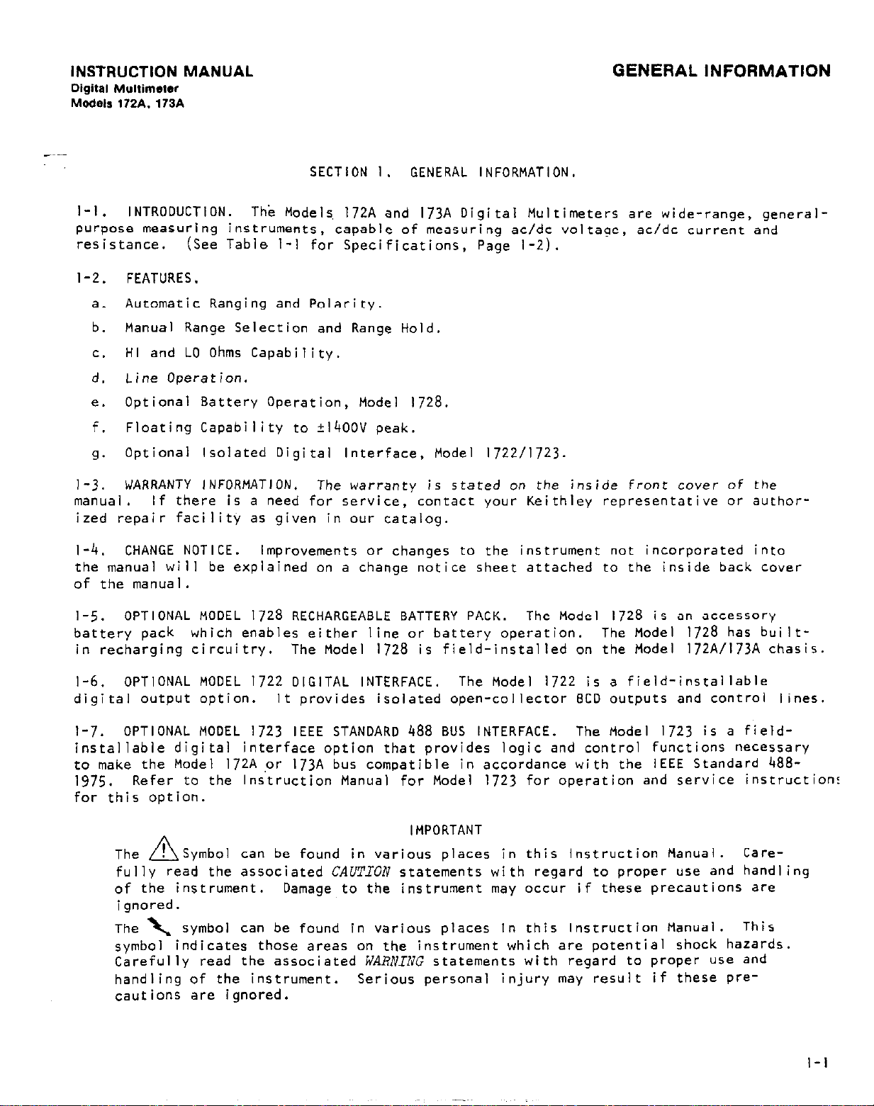
IECIFiCATIONS.
INITIAL PREPARATION
2-1.
2-2.
2-3.
OPERATING INSTRUCTIONS.
3-l.
3-2.
;I;'
3-5:
3-6.
3-7. HOW TO MEASURE CURRENT. (MODEL 173A ONLY)
3-8.
3-9.
3-10.
3-11.
3-12.
3-13.
3-14.
. ACCESSORIES.
4-1.
4-2.
4-3.
4-4.
4-5.
4-6.
4-7.
THEORY OF OPERATION
. 5-l.
5-2.
5-3.
5-4.
5-5.
5-6.
...................................
INTROOUCTION.
FEATURES
WARRANTY INFORMATION.
CHANGE NOTICE
OPTIONAL MODEL 1728 RECHARGEABLE BATTERY PACK
OPTIONAL MODEL 1722 DIGITAL INTERFACE
OPTIONAL MODEL 1723 IEEE STANDARD 488 BUS INTERFACE
GENERAL
INSPECTION.
PREPARATION FOR USE
GENERAL
HOW TO SELECT POWER
HOW TO SELECT FUNCTION.
HOW TO SELECT RANGE
HOW TO MEASURE VOLTAGE.
HOW TO MEASURE CURRENT. (MODEL 172A ONLY)
HOW TO MEASURE RESISTANCE
FURTHER MEASUREMENT CONSIDERATIONS.
HOW TO USE MODEL 172A/l73A OFF-GROUND
HOW TO USE OPTIONAL PROBES AND SHUNTS
HOW TO USE THE MODEL 1722 DIGITAL INTERFACE
COMMENTS RELATIVE TO THE MODEL 172A/l73A SPECIFICATIONS
MODEL 1728 OPERATING Tips
GENERAL..................................4- I
POWER OPTIONS
ISOLATED DIGITAL OUTPUT
RACK MOUNTING
PROBE AND SHUNTS.
CABLES AND CONNECTORS
MISCELLANEOUS
GENERAL.................................5- I
OVERALL OPERATION
INPUT SIGNAL CONDITIONING
A/O CONVERTER AND DIGITAL CIRCUITS (SCHEMATIC 29145E, SHEET 2).
DISPLAY BOARD, SCHEMATIC 274040
POWER SUPPLY, SCHEMATIC 29145E.
MODEL 1728 RECHARGEABLE BATTERY PACK, SCHEMATIC 26758C.
MODEL 1722 DIGITAL INTERFACE.
.................................
..................................
................................
..
..............................
.............................. 1-I
..........................
..............................
..............................
...............................
...........................
............................
..............................
.....
..............................
..............................
..............................
..............................
...........................
.........................
...........................
.........................
........................
..................................................
.........................
............................
..........................
............................
........................
.....................
.....................
......................
..................
................
................
...................
..................
..................
..............
...............
...........
.........
.........
.....
Page
I-l
l-1
l-l
I-I
l-1
I-I
I-1
I-'
2-l
.2-l
2-l
2-I
3-l
..3- 1
3-l
3-2
3-3
3-4
3-5
3-6
3-7
3-8
3-11
3-12
3-13
3-25
if:;5
4-l
4-1
4-i
4-4
4-5
4-5
5-l
5-l
5-l
5-15
S-21
5-21
5-23
5-25
I
ii
Page 5
INSTRUCTION MANUAL
Digital MultImeter
Models 172A. 173A
CONTENTS (CON'S)
iect ion
;. MAINTENANCE.
6-i.
6-2. REQUIRED TEST EQUIPMENT.
6-5.
6-6.
6-7.
6-8.
REPLACEABLE PARTS.
7.
7-l.
7-2.
7-3.
7-4.
7-a.
7-Y.
7-10.
GENERAL
PERFORMANCE VERIFICATION
CALIBRATION REQUIREMENTS
PREPARATION FOR CALIBRATION.
CALIBRATION PROCEDURE.
TROUBLESHOOTING AND REPAIR
FUSE REPLACEMENT
GENERAL.................................7- 1
ORDERING INFORMATION
FACTORY SERVICE.
REPLACEABLE PARTS LIST
CROSS REFERENCE OF MANUFACTURERS
COVERS AND PANELS.
COMPONENT DESIGNATIONS FOR ~~-446.
SCHEMATICS
COMPONENT LAYOUTS.
SPARE PARTS KIT.
...................................................................
..............................
...............................
Page
;I;
........................ 6-l
........................
........................
......................
.........................
.......................
............................
..........................
............................ 7-l
.........................
....................
...........................
...................
...........................
............................ 7-5
6-l
6-7
6-8
6-Y
6-15
6-21/Z
7-1
7-I
7-l
7-2
7-2
7-2
7-2
7-2
iii
Page 6
ILLUSTRATIONS
INSTRUCTION MANUAL
Digital MuItlm*ter
Mod&172A.l73A
GURE NO.
1-l
l-2
l-3
l-4
2-l
2-2
2-3
;::
::i
;:;
3-7
3-a
3-9
3-10
3-11
3-12
4-l
4-2
5-l
::;
5-4
5-5
5-6
5-J
5-a
5-9
5-10
5-11
5-12
;:;;
:I;;
::g
6-l
6-2
J-1
TITLE PAGE
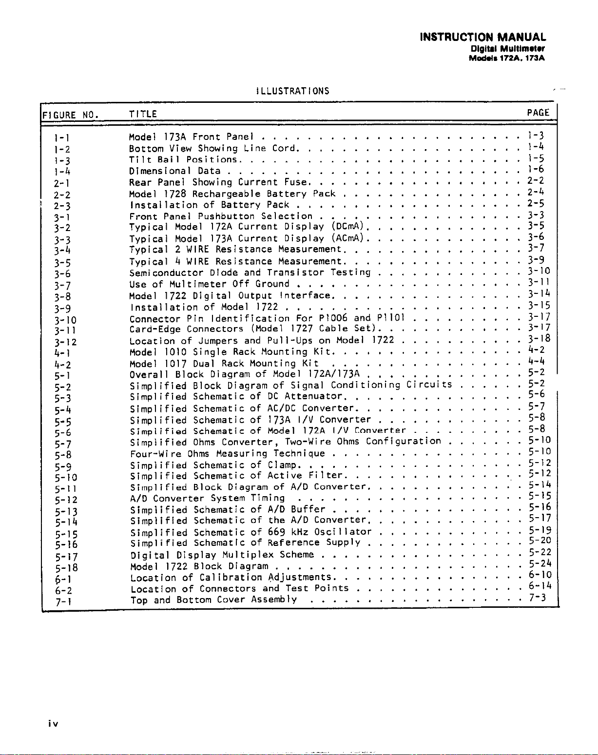
Model l73A Front Panel
Bottom View Showing Line Cord.
Tilt Bail Positions.
Dimensional Data
Rear Panel Showing Current Fuse.
Model
Installation of Battery Pack
Front Panel Pushbutton Selection
Typical Model 172A Current Display (DCnA).
Typical Model l73A Current Display (ACmA).
Typical 2 WIRE Resistance Measurement.
Typical 4 WIRE Resistance Measurement.
Semiconductor Diode and Transistor Testing
Use of Multimeter Off Ground
Model 1722 Digital Output Interface.
Installation of Model I722
Connector Pin Identification For ~1006 and PllOl
Card-Edge Connectors (Model 1727 Cable Set).
Location of Jumpers and Pull-ups on Model 1722
Model 1010 Single Rack Mounting Kit.
Model 1017 Dual Rack Mounting Kit
Overall Block Diagram of Model 172A/l73A
Simplified Block Diagram of Signal Conditioning Circuits
Simplified Schematic of DC Attenuator. .....
Simplified Schematic of AC/DC Converter.
Simplified Schematic of
Simplified Schematic of Model l72A I/V Converter
Simplified Ohms Converter, Two-Wire Ohms Configuration .......
Four-Wire Ohms Measuring Technique
Simplified Schematic of Clamp.
Simplified Schematic of Active Filter.
Simplified Block Diagram of A/D Converter.
A/D Converter System Timing
Simplified Schematic of A/D Buffer
Simplified Schematic of the A/D Converter,
Simplified Schematic of 669 kHz Oscillator
Simplified Schematic of Reference Supply
Digital Display Multiplex Scheme
Model 1722 Block Diagram .
Location of Calibration fidjustments.
Location of Connectors and Test Points
TOD and Bottom Cover Assembly
1728
Rechargeable Battery Pack
..........................
.......................
........................
....................
....................
.....................
173A
I/V Converter
....................
.......................................
...................
..................
................
..................
...............
...............
................
................
.................
.................
...................
.............
..............................
................
...............
...................
.............
.............
.............
..........
............
...........
..............
................
.....................................
.............
...........................
.,
.
1-3
l-4
l-5
1-6
2-2
2-4
2-5
3-3
3-5
3-6
3-7
3-V
3-10
3-11
3-14
3-15
3-17
3-17
3-18
4-2
4-4
5-2
5-2
5-6
5-7
5-8
5-8
5-10
5-10
5-12
5-12
5-14
5-15
5-16
5-17
5-19
5-20
5-22
5-24
6-10
6-14
7-3
iv
Page 7
INSTRUCTION MANUAL
Digital
Multimeter
Models
-~-
172A. 173A
SECTION 1.
GENERAL INFORMATION
GENERAL INFORMATION.
I-l.
purpose measuring instruments,
resistance.
l-2.
1-3. WARRANTY INFORMATION. The warranty is stated on the inside Front cover of the
manual.
ized repair facility as given in our catalog.
l-4.
the manual will be explained on a change notice sheet attached to the inside back cover
of the manual.
l-5.
battery pack
in recharging circuitry.
INTROOUCTION. Thk Models, l72A and 173A Digital Multimeters are wide-range, general-
capable of measuring ac/dc voltage, ac/dc current and
(See Table 1-I for Specifications, Page l-2).
FEATURES.
a. Automatic Ranging and Polarity.
Manual Range Selection and Range Hold.
b.
HI and LO Ohms Capability.
c.
Line Operation.
d.
e. Optional Battery Operation, Model 1728.
Floating Capability to +14OOV peak.
f.
Optional Isolated Digital Interface, Model 1722/1723.
9.
If there is a need for service,
CHANGE NOTICE. Improvements or changes to the instrument not incorporated into
OPTIONAL MODEL
which enables either line or battery operation.
1728
RECHARGEABLE BATTERY PACK.
The Model 1728 is field-installed on the Model 172A/l73A chasis.
contact your Keithley representative or author-
The Model 1728 is an accessory
The Model 1728 has built-
l-6. OPTIONAL MODEL 1722 DIGITAL INTERFACE.
digital output option. It provides isolated open-collector ECD outputs and control lines.
1-7.
installable digital interface option that provides logic and control functions necessary
to
1975.
for this option.
OPTIONAL MOOEL 1723 IEEE STANDARD 488 BUS INTERFACE. The Model 1723 is a field-
make the Model 172A or l73A bus compatible in accordance with the IEEE Standard 48B-
Refer to the Instruction Manual for Model 1723 for operation and service instruction!
IMPORTANT
The A
fully read the associated
of the instrument. Damage to the instrument may occur if these precautions are
ignored.
The \ symbol can be found in various places in this Instruction Manual.
symbol indicates those areas on the instrument which are potential shock hazards.
Carefully read the associated
handling of the instrument.
cautions are ignored.
Symbol can be found in various places in this Instruction Manual.
CAUTION
statements with regard to proper use and handling
WARNING
Serious personal injury may result if these pre-
The Model 1722 is a field-installable
Care-
This
statements with regard to proper use and
l-l
Page 8
GENERAL INFORMATION
TABLE 1-1.
SPECIFICATIONS
INSTRUCTION MANUAL
Digital Multimet*r
Models 112A,. 113A
Page 9
INSTRUCTION MANUAL
Digital
Models
--
Multimeter
172A. 173A
GENERAL INFORMATION
FUNCTION AND UNITS DISPLAY (mV)
I
INPUT HI AND LO. UPPER
PAIR
FIGURE l-1.
Model 173A Front Panel.
1-3
Page 10
r
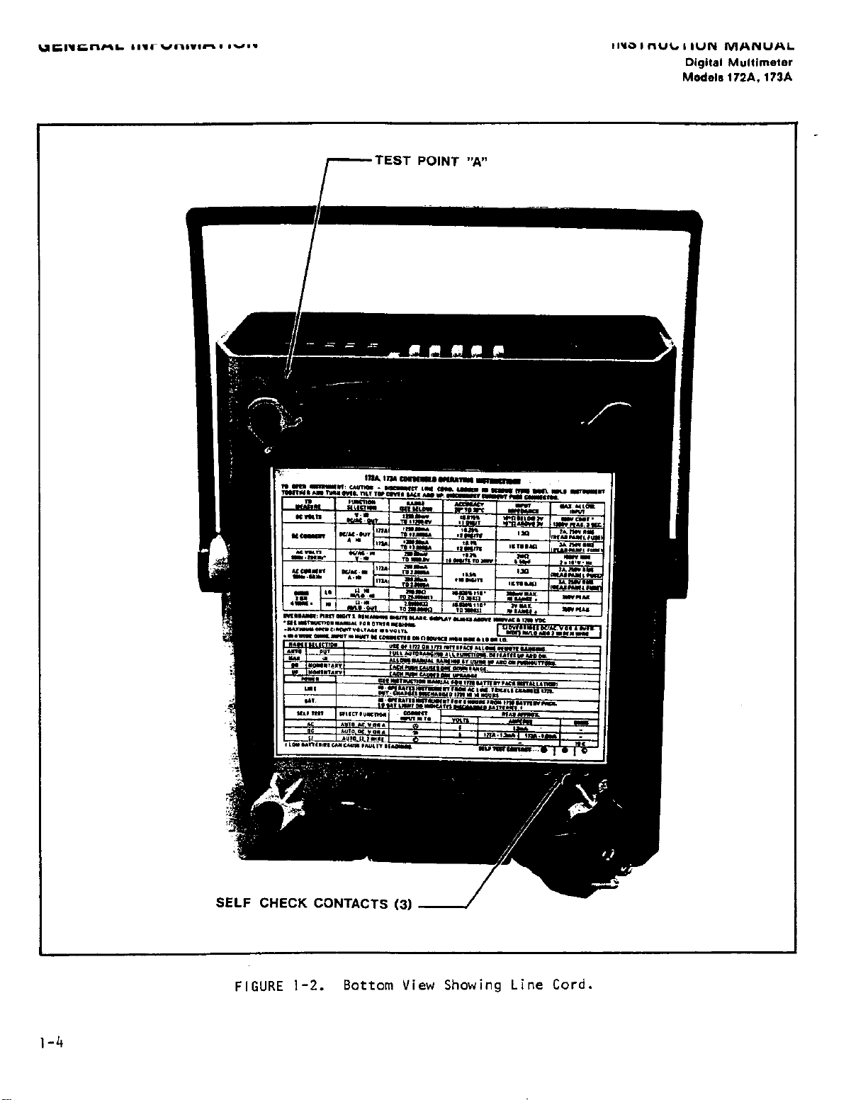
TEST POINT “A”
IN= I nub I I”N MANUAL
Digital Multimeter
Models 172A.
173A
1-4
FIGURE l-2.
Bottom View Showing Line Cord.
Page 11
INSTRUCTION MANUAL
Digital Multimster
Models 172A. 173A
NORMAL BENCH POSITION
GENERAL INFORMATION
I
c
I
-I
LEVEL POSITION - TILTBAIL AT FRONT
4%
45”
POSITION
HANGING POSITION
-I y
LEVEL POSITION - TILTBAIL AT REAR
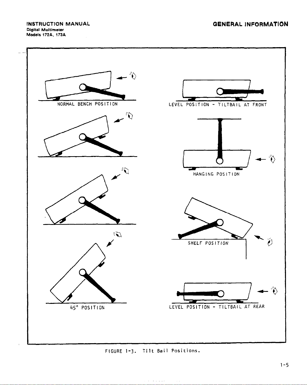
FIGURE
l-3.
Tilt Bail Positions.
Page 12
GENERAL INFORMATION
INSTRUCTION MANUAL
Digital Multimeter
Models 172A.
i73A
1-6
ht 5,-----l ht 5,-----l
O~MENSIONS IN MILLIMETERS (INCHES) O~MENSIONS IN MILLIMETERS (INCHES)
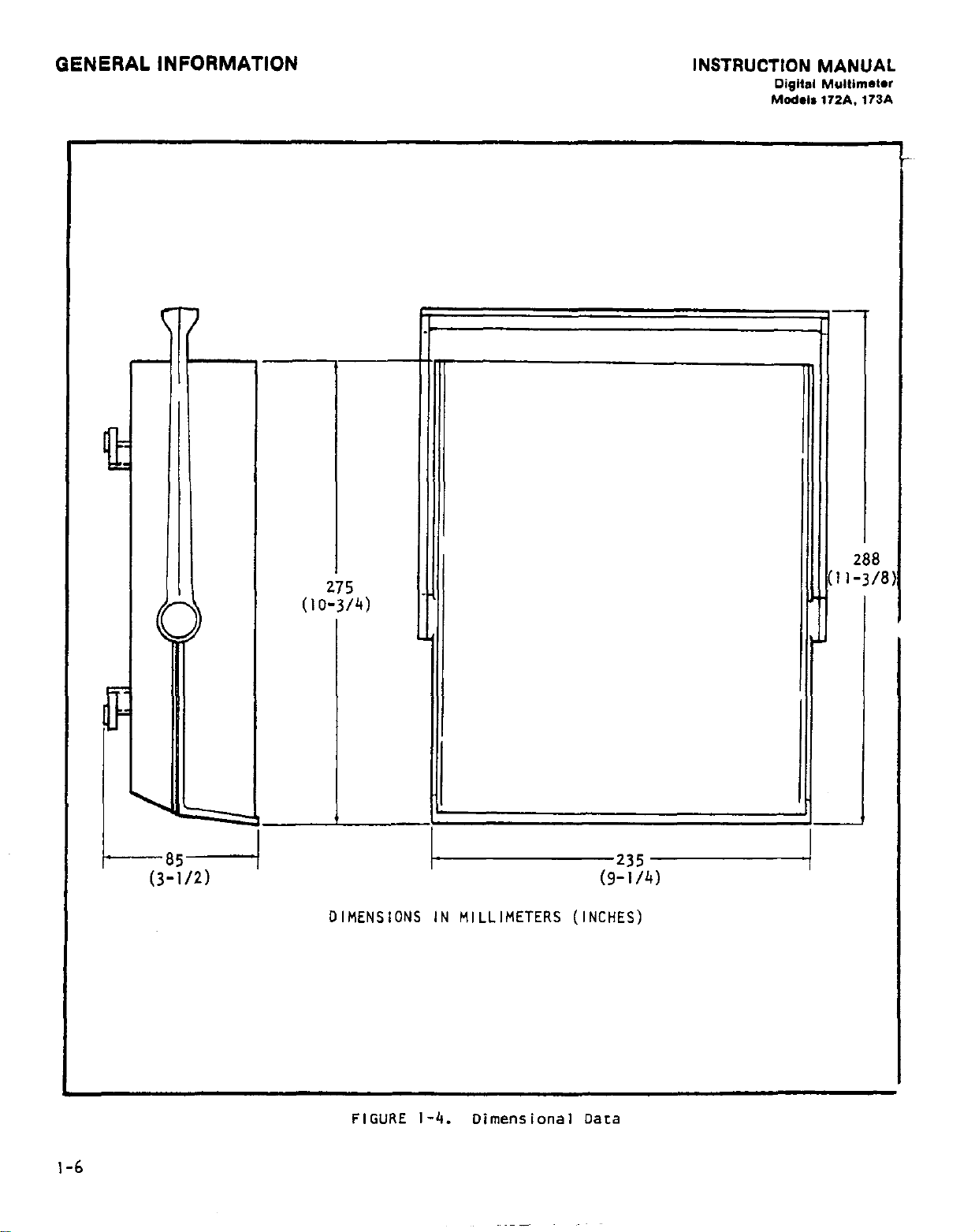
FIGURE l-4.
Dimensional Data
Page 13
INSTRUCTION MANUAL
Digital Multimeter
Models 172A. 173A
SECTION 2. INITIAL PREPARATION.
2-i. GENERAL. This section provides information needed for incoming inspection and
preparation for use.
2-2. INSPECTION. The Model 172A/173A was carefully inspected both mechanically and
electrically before shipment.
ages which may have occurred during transit. Report any damages to the shipping agent.
To verify the electrical specifications, follow the procedures given in Section 6.
Upon receiving the instrument, clieck for any obvious dam-
INITIAL PREPARATION
2-3.
can be powered from line voltage or from rechargeable nickel-cadmium batteries (when the
optional Model 1728 Rechargeable Battery Pack is installed).
with
is stored by wrapping the cord around the base of the instrument as shown in Figure 4.
PREPARATION FOR USE. The Model 172A/l73A is shipped ready-to-use. The instrument
Line Power. The Model 172A/l73A has an attached three-wire line cord which mates
a.
third-wire grounded receptacles (NEHA 5-l5P). The permanently installed line cord
CAUTION
This instrument has an internal line power selector switch that must be set
A
to 234V position for operation above 125 volts rms, 50-60 Hz.
How to set the Internal Line Voltage Switch (S6Ol).
I.
two position slide switch located on the main circuit board.
volts,
gain access to the circuit board as described in MAINTENANCE section.
t
the switch setting and fuse must be changed.
WARNING
Disconnect the line cord before removing the top cover of the instrument.
Line voltage is present at various points on the circuit board and represents
a SHOCK HAZARD.
NOTE
Optional line voltage range is available when wiring modifications are made to
transformer T60l
as
shown on schematic 29145E.
The top cover must be removed to
The Model 172A/l73A has a
For operation above 125
----~
1
/
Summary of Standard and Optional Line Voltages.
Standard
105 to 125 V rms
210 to 250 V rms
TABLE 2-l.
I
opt1 -nab
90 - 105 V rms -
Transformer wiring
must be modified.
I
I
2-l
Page 14
INITIAL PREPARATION
FUSE F501
INS: I
ItUG
I ION
oigwd MYlllnle*er
Models 172A. 173A
MANUAL
2-2
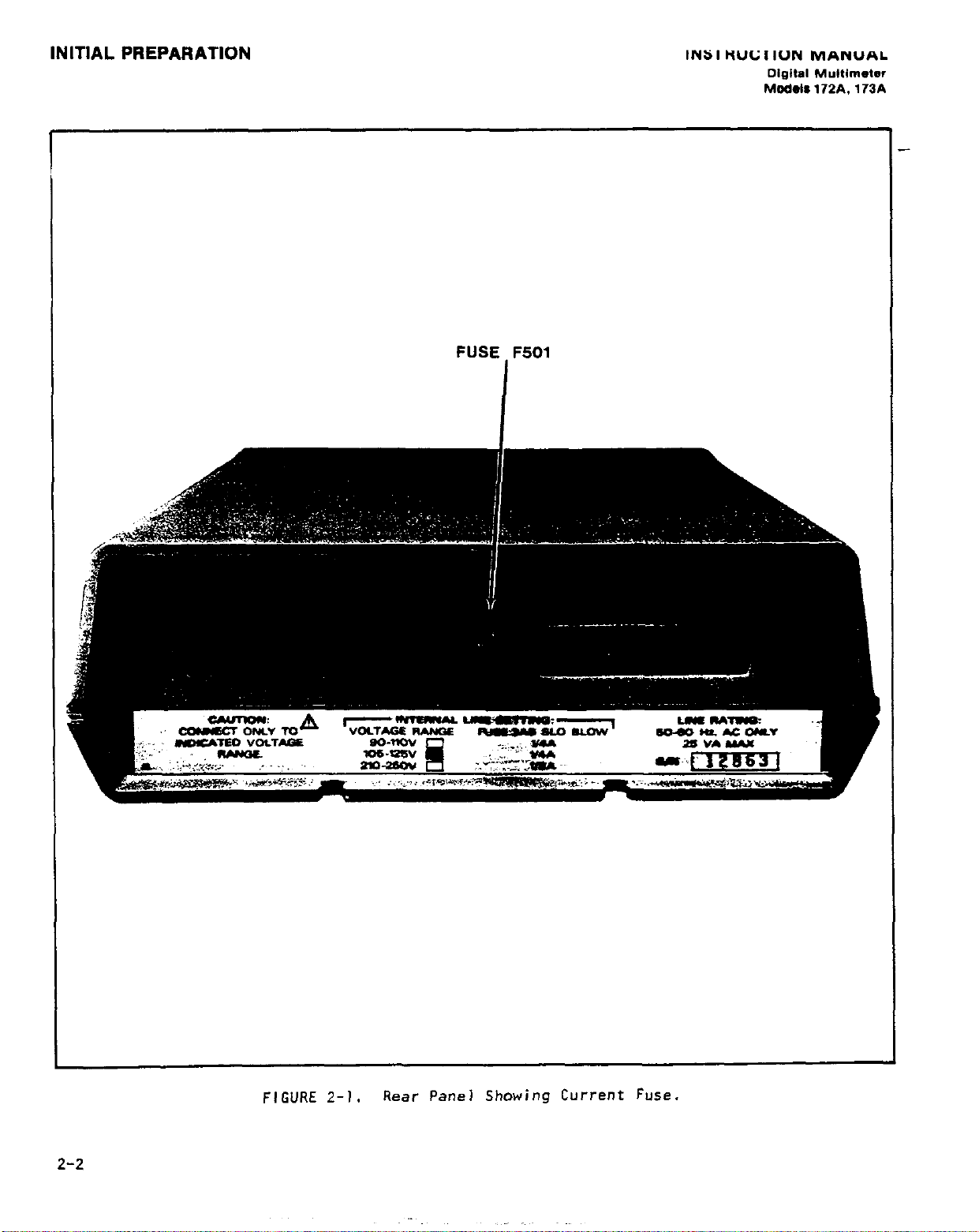
FIGURE 2-l.
Rear Panel Showing Current Fuse.
Page 15
INSTRUCTION MANUAL
Digital
Models 172A. 173A
Multimeter
Line Fuse Requirement. The Model 172A/l73A uses a single line fuse to protect
2.
the line-operated power supply. The fuse is a 3 AB or 3 AG, slow-blow type.
with I/4 ampere for II7 volts operation or l/8 ampere for 234 volrs.
IMPORTANT
Replace fuse with correct rating, otherwise, damage to the instrument could result.
A
3.
How to Replace the Line Fuse.
as shown in Figure 6-2 (Page b-14).
the circuit board as described in Section 6.
FU-20 (1/8A) for 234V.
Disconnect the line cord before removing the top cover of the instrument. ‘Line
voltage is present at various points on the circuit board and represent a SHOCK
t
HAZARD.
The fuse installed on the rear panel of the Model 172A/l73A is used only for
A
current range protection.
Battery Power. To operate the Model 172A/l73A from batteries, the Model 1723
b.
Rechargeable Battery Pack must be installed. The /*ode1 1728 can be either field or
factory-installed (at the time the Model 172A/l73A is purchased).
This fuse is not a line voltage protection fuse.
The fuse is installed on the main circuit board
The top cover must be removed to gain access to
Use Keithiey FU-I7 (l/4A) for II7 V;
WARN I NG
CAUT I ON
-
INITIAL PREPARATION
Rep lace
NOTE
The Model 1728 Rechargeable Battery Pack can be installed by the user within me
Model 172A/l73A at any time.
already installed, the Model 1728
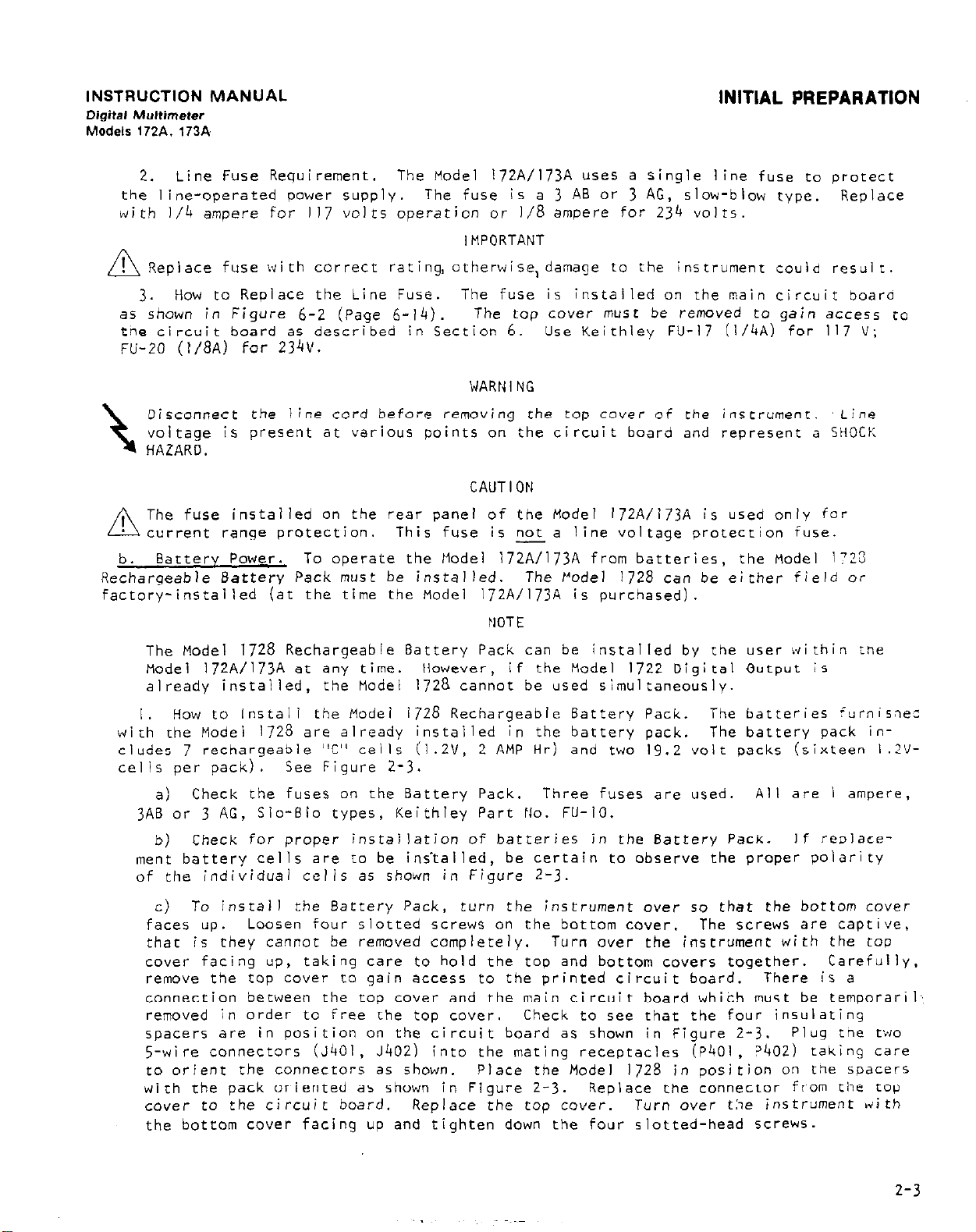
How to Install the Model 1728 Rechargeable Battery Pack.
I .
with the Model 1728 are already installed in the battery pack. The battery pack in-
cludes 7 rechargeable “C” cells (l.2V, 2 AMP Hr) and two 19.2 volt packs (sixteen I.?‘/cells per pack).
Check the fuses on the Battery Pack. Three fuses are used.
=)
3AB or 3 AG, Slo-Blo types, Keithley Part Ho. FU-IO.
b) Check for proper installation of batteries in the Battery Pack.
ment battery cells are to be insYalled,
of the individual cells as shown in Figure 2-3.
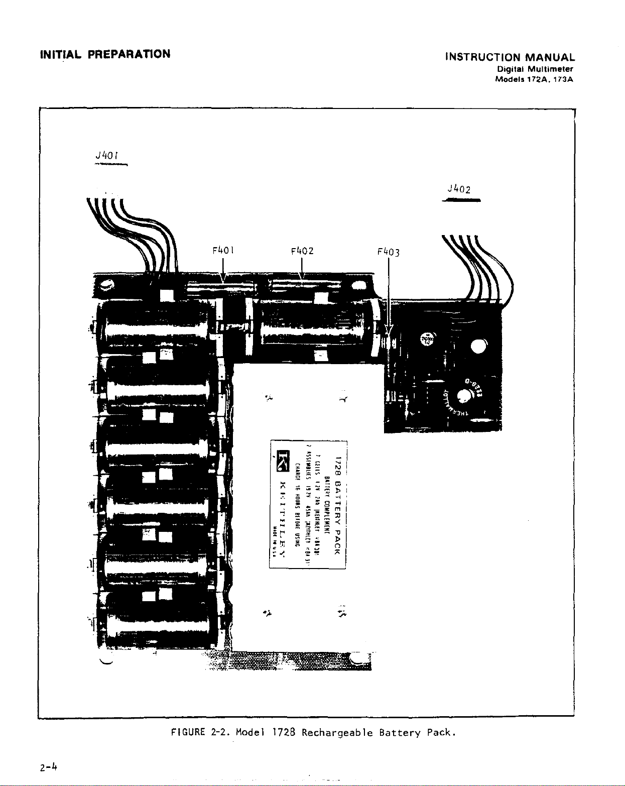
To install the Battery Pack,
C)
faces up.
that is they cannot be removed completely. Turn over the instrument with the top
cover facing up, taking care to hold the top and bottom covers together.
remove the top cover to gain access to the printed circuit board.
connection between the top cover and the main circuit board which must be temporaril
removed in order to free the top cover. Check to see that the four insulating
spacers are in position on the circuit board as shown in Figure 2-3.
s-wire connectors (J401, J402)
to orient the connectors as shown. Place the Model I728 in position on tne spacers
with the pack oriented as shown in Figure 2-3. Replace the connector from the top
cover to the circuit board. Replace the top cover.
the bottom cover facing up and tighten down the four slotted-head screws.
See Figure 2-3.
Loosen four slotted screws on the bottom cover.
However, if the Model I722 Digital Output is
cannot be used simultaneously.
The batteries furnisnec
All are I ampere,
If reolace-
be certain to observe the proper polarity
turn the instrument over so that the bottom cover
The screws are captive,
There is a
Plug tile two
into the mating receptacles (P4Ol
Turn over t,\e instrument iiith
, ?402) taking care
Carefully,
2-3
Page 16
INIT!AL PREPARATION
J401
INSTRUCTION MANUAL
Digital Mullimatsr
Models 172A. 173.4
J402
2-4
FIGURE 2-2. Model 1728 Rechargeable Battery Pack.
Page 17
INSTRUCTION MANUAL
Digital Multimeter
Models 172A. 173A
Disconnect the line cord on the instrument before the Battery Pack is installed.
Line voltage is present at various places on the circuit board and is a SHOCK
t
HAZARD.
INITIAL PREPARATION
WARNING
FIGURE 2-3. Installation of Battery Pack.
2-5
Page 18
INITIAL PREPARATION
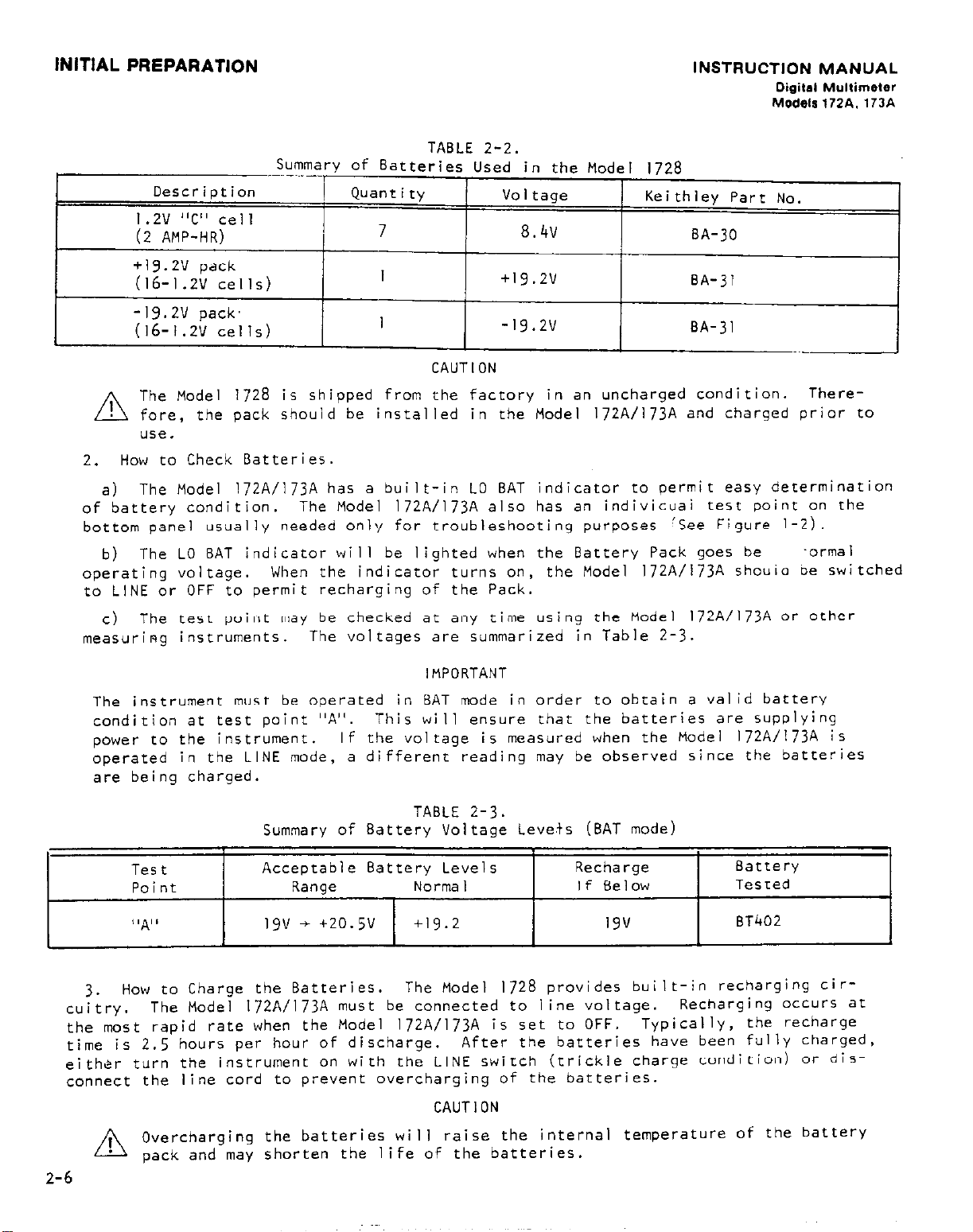
Description
I 2v "C" cell
(; AMP-HR)
TABLE 2-2.
SummarY of Batteries Used in the Model 1728
Quantity
7
Voltage
8.4~
Keithley Part NO.
INSTRUCTION MANUAL
Digital Multimeter
Models 172A1.173A
BA-30
+19.2V pack
(I&1.2v cells)
-19.2V pack,
(16-1.2V cells)
The Model 1728 is shipped from the factory in an uncharged condition.
fore, the pack should be installed in the Model 172A/l73A and charged prior to
A
"Se.
How to Check Batteries.
2.
The Model 172A/l73A has a built-in LO BAT indicator to permit easy determination
a)
of battery condition.
bottom panel usually needed only for troubleshooting purposes 'See Figure l-2).
b) The LO BAT indicator will be lighted when the Battery Pack goes be
operating voltage.
to LINE or OFF to permit recharging of the Pack.
The test point may be checked at any time using the Model l72A/173A or other
C)
measuring instruments.
The instrument must be operated in BAT mode in order to obtain a valid battery
condition at test point
power to the instrument.
operated in the LINE mode,
are being charged.
The Model 172A/l73A also has an indivicuai test point on the
When the indicator turns on,
The voltages are summarized in Table 2-3.
"A". This will ensure that the batteries are supplying
I
I
CAUTION
IMPORTANT
If the voltage is measured when the Model 172A/l73A is
a different reading may be observed since the batteries
+19.2v
-19.2v
the Model 172A/l73A shouio oe switched
BA-31
BA-31
There-
.orma I
TABLE 2-3.
Summary of Battery Voltage Levets (BAT mode)
I
I
Battery
Tested
BT402
the recharge
I
I
cuitry.
the most rapid rate when the Model 172A/l73A is set to OFF.
time is 2.5 hours per hour of discharge.
eithhr turn the instrument on with the LINE switch (trickle charge condition) or dis-
connect the line cord to prevent overcharging of the batteries.
2-6
Test
Point
4 ‘Al I
How to Charge the Batteries.
3.
The Model 172A/l73A must be connected to line voltage.
Overcharging the batteries will raise the internal temperature of the battery
pack and may shorten the life of the batteries.
Acceptable Battery Levels Recharge
I I I
I
Range
igv +
+20.5v
Norma I If Below
The Model 1728 provides built-in recharging cir-
After the batteries have been fully charged,
CAUTION
19v
Recharging occurs at
Typically,
1
I
Page 19
INSTRUCTION MANUAL
Digital Multimeter
Models 172A. 173A
OPERATING INSTRUCTIONS
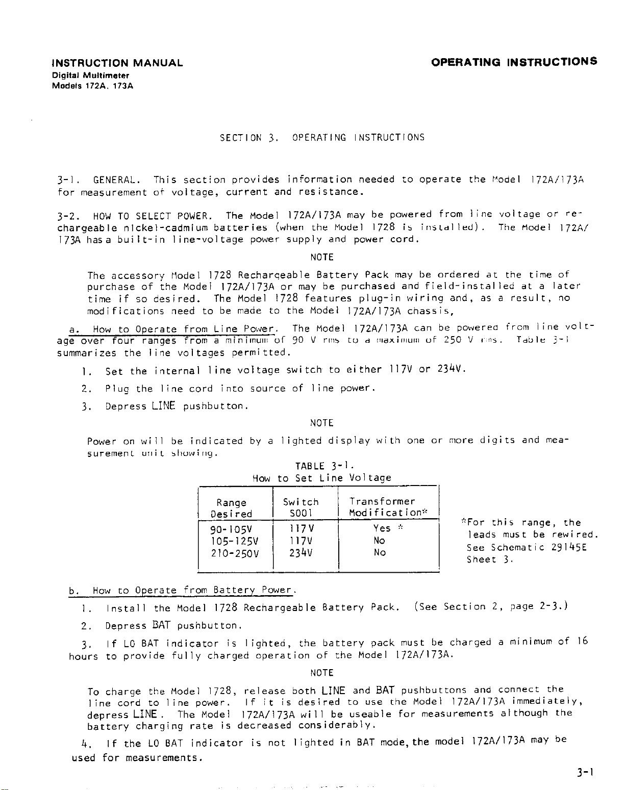
SECTION 3.
3-l. GENERAL. This section provides information needed to operate the tlodel l72A/iJjh
for measurement of voltage, current and resistance.
3-2. HOW TO SELECT POWER.
chargeable nickel-cadmium batteries (when the Model 1728 is installed). The Model 172.V
lJ3A hasa built-in line-voltage power supply and power cord.
The accessory Model 1728 Recharqeable Battery Pack may be ordered at the time of
purchase of the Model lJ2A/lJ3A or may be purchased and field-installed at a later
time if so desired.
modifications need to be made to the Model lJ2A/l73A chassis,
How to Operate from Line Power.
a.
age over four ranges from a minimum of 90 V rrn5 to a maximum of 250 V vs.
summarizes the line voltages permitted.
Set the internal line voltage switch to either ll7V or 234V.
I.
2. Plug the line cord into source of line power.
Depress LINE pushbutton.
3.
The Model 172A/l73A may be powered from line voltage or re-
The Model 1728 features plug-in wiring and, as a result, no
OPERATING INSTRUCTIONS
NOTE
The Model I
NOTE
JZA/lJjA can
be powereo from I ine volt-
Table 5-i
Power on will be indicated by a lighted display with one or more digits and measurement unit showing.
TABLE 3-1.
How to Set Line Voltage
How to Operate from Battery Power.
b.
Install the Model 1728 Rechargeable Battery Pack.
I
2. Depress BAT pushbutton.
If LO BAT indicator is lighted,
3.
hours to provide fully charged operation of the Model l72A/l73A.
To charge the Model 1728,
line cord to line power.
depress LINE. The Model lJZA/l73A will be useable for measurements although the
battery charging rate is decreased considerably.
release both LINE and BAT pushbuttons and connect rhe
If it is desired to use the Model lJ2A/lJ3A immediately,
the battery pack must be charged a minimum of 16
NOTE
(See Section 2, page 2-3.)
If the LO BAT indicator is not lighted in BAT mode,the model 172A/173A maY be
4.
used for measurements.
3-l
Page 20
OPERATING INSTRUCTIONS
The Model
Model 1728 should be installed and charged prior to use.
been charged for at least 16 hours,
for at least 6 hours.
1728
is shipped from the factory in uncharged condition. Therefore the
Summarv of Ooeration in LINE and BAT Modes
INSTRUCTION MANUAL
Digital MultImeter
Models ,72A. 173A
NOTE
After the Model 1728 has
the Model 172A/l73A can be powered continuously
TABLE 3-2.
I
Line Power Connected
Button Depressed 1728 npt installed
LINE
BAT OFF
NEITHER
LINE NOR BAT
3-3.
V, A and R.
Voltage.
current.
will be AC or DC. When depressed, AC is selected.
HOW TO SELECT FUNCTION.
a. v.
I.
2.
b. A.
I.
2.
c.
This pushbutton must be used with DC/AC to select either DC voltage or AC
DC Voltage.
AC Voltage.
This pushbutton must be used with DC/AC to select either DC current or AC
DC Current.
AC Current.
DC/AC.
This pushbutton selects whether the selected voltage or current Function
ON
OFF OFF
Function is selected by means of four pushbuttons:
Depress V. Release DC/AC.
Depress V. Depress DC/AC.
Depress A. Release DC/AC.
Depress A. Depress DC/AC.
Condition of Instrument
Line Power Connected
1728
Battery trickle charged.
Battery slowly discharged.
Battery charged at max-
Line Power Not Connected
installed 1728 installed
ON
ON
OFF
ON
OFF
1
DC/AC,
3-2
d. R.
Depress R to measure resistance.
NOTE
V, A, and R pushbuttons are interlocked so that only one pushbutton is depressed
at a time.
the input HI and LO terminals and no measurement can be made.
millivolts indicator will be lighted in this instance.)
A overrides HI/LO and 2 WIRE/4 WIRE.
However,
it is possible to have all pushbuttons out which disconnects
(The volts or
R overrides DC/AC.
v or
Page 21
INSTRUCTION MANUAL
Digital Multimeter
Models 17’2A. ,73A
OPERATING INSTRUCTIONS
FIGURE 3-l. Front Panel Pushbutton Selection.
3-4. HOW TO SELECT RANGE. The Model 172A/l73A provides automatic or manuai ranging.
The AUTO/MAN pushbutton determines the ranging mode, where AUTO = fully automatic
ranging.
AUTO. When released, the Model l72A/173A
a.
automatically selects the appropriate
range in accord with the following rules.
I. When the display exceeds 29999 the Model lj’2A/l73A upranges (that is. it changes
to less sensitivity and the decimal point moves appropriately).
2.
When the display reaches 02599 the Model 172A/l73A downranges (that is, it
changes to greater sensitivity and the decimal point moves appropriateiy).
MAN. When depressed,
b.
the range is placed to hold.
The user can cause the Model
172mto uprange or downrange by using the UP RANGE and DN RANGE pushbuttons.
When DN RANGE is momentarily depressed, the Model 172A/i73A will downrange one
I.
decade of sensitivity. Each time the pushbutton is depressed and released, one down-
range will occur until most sensitive range is obtained.
When UP RANGE is momentarily depressed,
2.
decade of sensitivity.
Each time the pushbutton is depressed and released, one uprange
the Model 172A/l73A will uprange one
will occur until least sensitive range is obtained.
3-3
Page 22
OPERATING INSTRUCTIONS
INSTRUCTION MANUAL
Digital Multimeter
Models 172A. 173A
?-5.
ranges :
HOW TO MEASURE VOLTAGE.
0.3v, 3V, 3OV, 300V and \zOOV DC (IOOOVAC).
The Model 172A/l73A measures ac and dc voltage in five
CAUTION
Table 3-3 gives the maximum
Do not exceed these volt-
A
Maximum input voltage depends on the range selected.
allowable continous input for each range on AC and DC.
ages or damage to the instrument will occur.
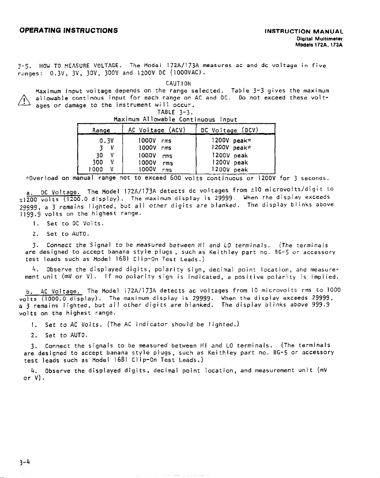
TABLE 3-3.
Maximum Allowable Continuous Input
Range
0.3v
3 v
30 v
300 v
AC Voltage (ACV)
1000v rms
1000v rms
IOOOV rills
1ooov rnls
DC Voltage (DCV)
1200V peak"
12OC'v peak*
12OOV peak
12OOV peak
1000 v IOOOV rms 12OOV peak
*Overload on manual range not to exceed 600 volts continuous or 1200~ for 3 seconds.
The Model \72A/l73A detects dc voltages from i10 microvolts/digit to
,l%$&?%%.O display).
The maximum display is 29999. When the display exceeds
pggg, a 3 remains lighted, but all other digits are blanked. The display blinks above
1199.9 volts on the highest range.
I. Set to DC Volts.
2. Set to AUTO.
Connect the Signal to be measured between HI and LO terminals.
3.
(The terminals
are designed to accept banana style plugs, such as Keithley part no. BG-5 or accessory
test leads such as Model 1681 Clip-On Test Leads.)
Observe the displayed digits, polarity sign, decimal point location, and measure-
4.
ment unit (mV or V).
AC Voltage.
b.
volts (1000.0 display).
a 3 remains lighted, but all other digits are bianked.
If no polarity sign is indicated, a positive polarity is implied.
The Model iJ2A/i73A detects ac voltages from 10 microvolts rms to 1000
The maximum display is 29999. When the display exceeds 29999,
The display blinks above 999.9
volts on the highest range.
Set to AC Volts. (The AC indicator should be lighted.)
I.
Set to AUTO.
2.
Connect the signals to be measured between HI and LO terminals.
3.
(The terminals
are designed to accept banana style plugs, such as Keithley part no. BG-5 or accessory
test leads such as Model 1681 Clip-On Test Leads.)
Observe the displayed digits, decimal point location, and measurement unit (mV
4.
or V).
3-4
Page 23
INSTRUCTION MANUAL
Digital Multimeter
Models 172A. 173A
OPERATING INSTRUCTtONE
3-6.
in two ranges:
DMM is capable of displaying 2.9999A.
A
amperes.
MAN mode it is possible to select 30A, 300A t 3000A Ranges,but2A Max is still the limit.
to 2 amperes vn5. When the input exceeds 2 amperes, the current Fuse will blow.
HOW TO MEASURE CURRENT. (MODEL 172~0~~~).
0.3A, and 2A.
The Model 172Ais protected by a 2 ampere fuse on all ranges.
a replacement Keithley Part No.
holder. (See Figure 2-l).
a. DC Current. The Model 172Adetects dc currents from ?I0 microamperes/digit to r2
When the input exceeds 2 amperes, the current fuse will blow. When using the
1. Set to DC Amperes.
Set to AUTO.
2.
Connect the signal to be measured at the HI terminal.
3.
4. Observe the displayed digits, polarity sign, decimal point location, and measure-
ment unit (mA, or A).
AC Current. The Model l7ZA DMM detects ac currents from IO microamperes rnsidigir
b.
Set to AC Amperes. (The AC indicator should be lighted).
1.
Set to Auto.
2.
Connect the signal to be measured at the HI terminal.
3.
Observe the displayed digits,
4.
mA or AC A).
If no polarity sign is indicated, a positive polarity is implied.
The current is limited by the current fuse even thouqh the
CAUTION
FU-13 should be installed in the rear panel fuse
decimal point location and measurement unit !AC
The Modell72A measures ac and dc current
If the fuse is blown,
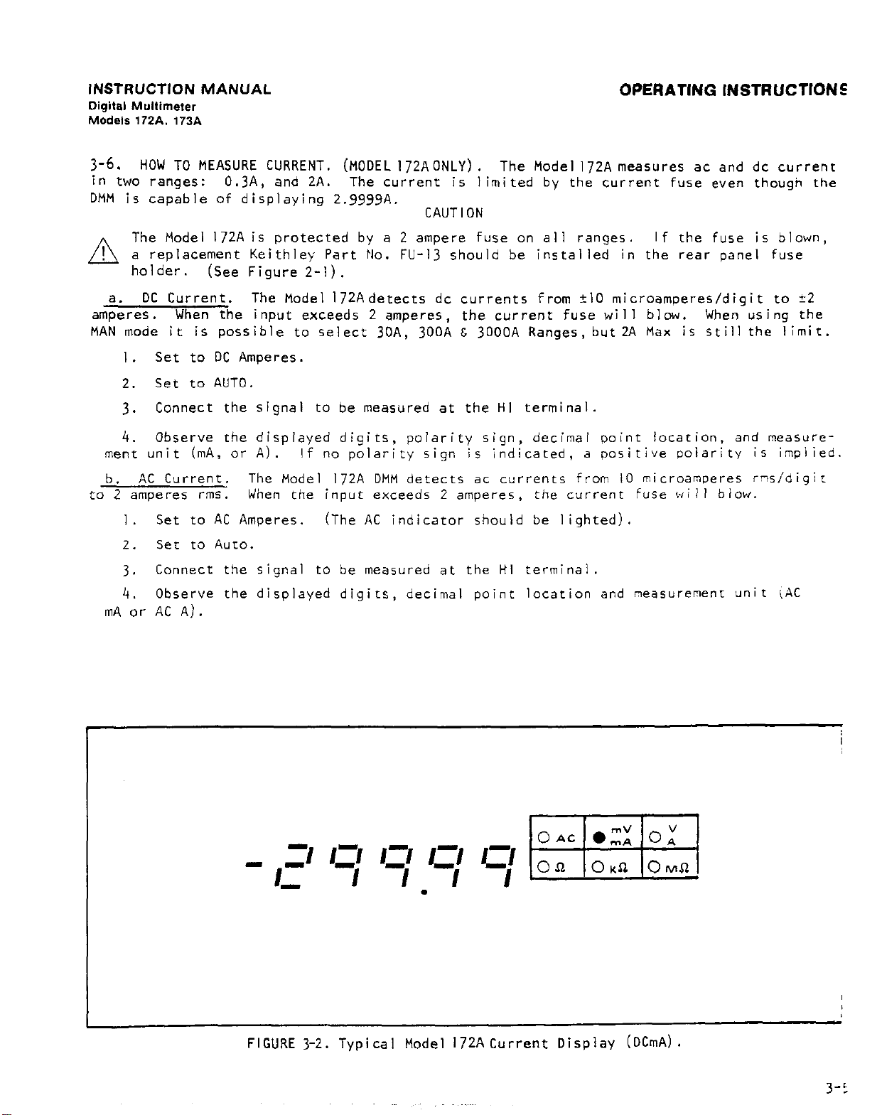
FIGURE 3-2. Typical Model 172ACurrent Display (DCmA).
3-r
Page 24
OPERATING INSTRUCTIONS
INSTAUCTION MANUAL
Digital Multimeter
Models 172A. 1?3A
3-7.
A
amperes. The maximum display is 29999.
lighted, but all other digits are blanked.
to 3 amperes rms.
remains lighted, but all other digits are blanked.
HOW TO MEASURE CURRENT. (MOOELl73AONLY.) The Mode1173A measures ac and
dc current in five ranges: 0.3mA. 3mA, 30mA, 0.3A, and 3A.
CAUTION
The Model 173A DMM is protected by a 3 ampere fuse on al I ranges.
blown, a replacement Keithley Part No.
fuse holder. (See Figure 2-l).
a. DC current.
I. Set to DC Amperes.
2. Set to AUTO.
Connect the signal to be measured at the HI terminal.
3.
4. Observe the displayed digits, polarity sign, decimal point location, and measure-
ment unit (,A, mA, or A). If no polarity sign is indicated, a positive polarity is
implied.
AC Current.
b.
1. Set to AC Amperes. (The AC indicator should be lighted.)
The Modell73A DMM detects dc currents from +I0 nanoamperes to 23
The Model 173ADMM detects ac currents from IO nanoamperes
The maximum display is 29999.
FU-2 should be installed in the rear panel
When the display exceeds 29999, a 3 remains
When the display exceeds 29999, a 3
If the fuse is
rms/digi t
2. Set to AUTO.
Connect the signal to be measured at the ill terminal.
3.
4. Observe the displayed digits, decimal point location, and measurement tinit (ACiA,
AC ma, or AC A).
3-6
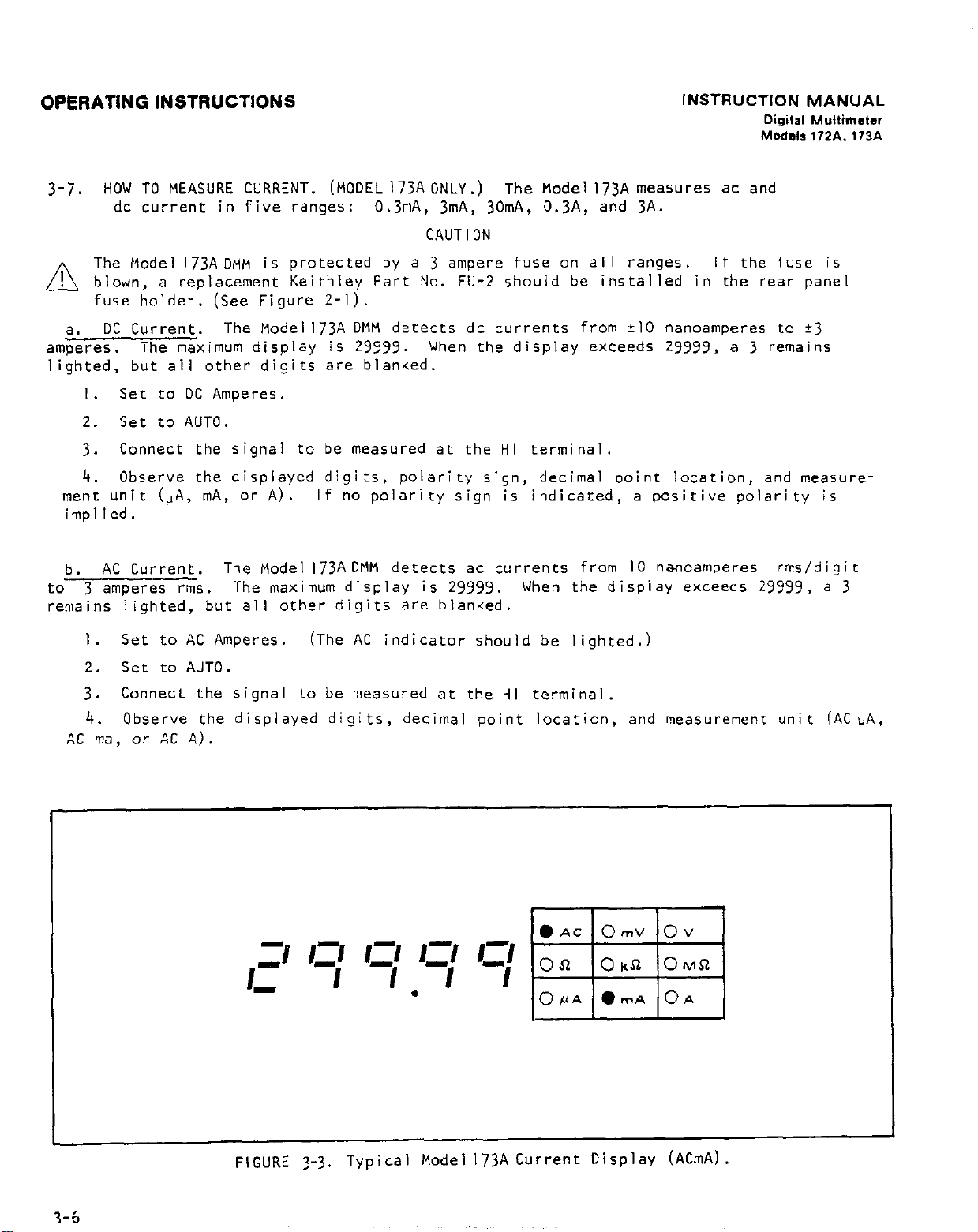
FIGURE 3-3. Typical Model l73A Current Display (ACmA).
Page 25
INSTRUCTION MANUAL
Digital Multimeter
Models 172A. 173A
OPERATING INSTRUCTIONS
3-a. HOW TO MEASURE RESISTANCE.
ohms/digit to 300 megohms. The maximum display is 29999.
The Modell72A/173A measures resistance from IO milli-
When the display exceeds
29999, a 3 remains lighted, but all other digits are blanked.
a.
HI Ohms Measurement.
age developed across the resistance under test at full range is 3 volts.
173A
measures
I.
2.
from 100 ms2 to 300 megohms in HI mode.
Set to HI Ohms.
Set to 2 WIRE.
When the HI/LO pushbutton is released (set to HI), the volt-
The Model 172A/
NOTE
When the Model l72A/l73A IS set to 2 WIRE,the lower set of HI and LO input terminals
is not connected. When set to 4 WIRE, the higherset of HI an(7 LO input terminals
is used as “voltage sensing” terminals.
See Section 3-9 for more detailed infor-
mation.
3. Set to AUTO.
Connect the resistance under test between the upper set of HI and LO terminals.
4.
Observe the displayed digits, decimal point location, and measurement unit (2,
5.
Kn, or MR).
b.
LO Ohms Measurement.
When the HI/LO pushbutton is depressedtset to LO),
age developed across the resistance under test at full range is 300 miljjvolts.
Model 172A/l73A measures from IO mR to 30 megohms in LO mode.
the volt-
The
Set to LO Ohms.
I .
2. Set to 2 WIRE.
Set to AUTO.
3.
Connect the resistance under test between the upper set of HI and LO terminals.
4.
Observe the displayed digits, decimal point location, and measurement unit !n,
5.
Kn, or Mfi).
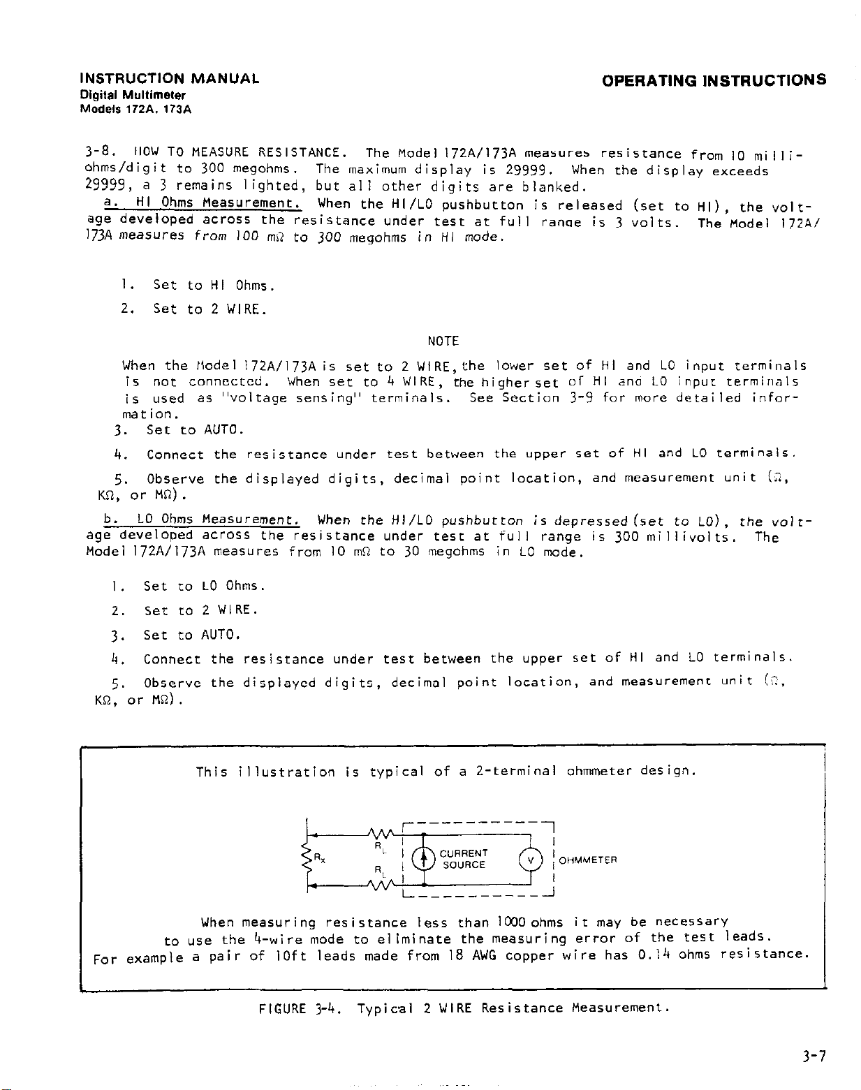
This illustration is typical of a 2-terminal ohmmeter design.
When measuring resistance less than ICOOohms it may be necessary
to use the 4-wire mode to eliminate the measuring error of the test leads.
For example a pair of IOft leads made from 18 AWG copper wire has 0.14 ohms resistance.
FIGURE 3-4. Typical 2 WIRE Resistance Measurement.
3-7
Page 26
OPERATING INSTRUCTIONS
INSTRUCTION MANUAL
Digital Multimeter
Model. ,72A. 173A
3-V.
FURTHER MEASUREMENT CONSIDERATIONS.
DC Voltage Measurements.
a.
I.
Overloads.
When
the display exceeds _tlZOO.OV DC all digits blink to indicate
an overload condition.
Input Resistance.
2.
IO MO on the 3OV, 3OOV, and 3000V ranges.
considered when evaluating total accuracy of measurement.
Accuracy.
3.
a % of range.
The Model l72A/l73A accuracy is specified in terms of % of reading and
For a full range reading of 299.99 mV DC the accuracy of measurement
would be t (0.03 mV + 0.01 mV) or 20.04 mV.
Input resistance is 1,000 Mf? on the 3OOmV and 3V ranges:
The effects of circuit loading should be
(See Accuracy.)
Measurements from relatively high source
resistances could cause an additional reading error. The amount of error due to
loading can be determined by the following relationship:
% error = 100 x Rs i (Rs + RI)
where
Rs = source resistance in ohms
RI = input resistance of Model 172A/173A inohms
4. Self-Test Feature. The Model 172A/I73A has a bottcm
functional check in DC Volts. To use this feature,
circled 8 contact.
Verify a display of approximately 5 volts dc with V depressed. -o
connect the input HI terminai :o
cover
voltage contacf for
check dc current, depress A and verify a disolay of 1.3 mA (172~): I mA (i73A).
AC Voltage Measurements
b.
I. Overloads.
When the display exceeds 1000.0 V AC (
rms) all digits blink to in-
dicate an overload condition.
2. Input Impedance.
picofarads.
The effects of circuit loading should be considered when evaluating the
total accuracy of measurement.
3.
AC-to-DC
ConverSiOn.
calibrated in terms of the root-mean-square (rms) of a sine wave.
The input impedance is 2 megohms shunted by less than 50
(See Accuracy.)
The Model 172A/173A operates as an average-readinq
The calibration is
exact for sinusoidal waveforms in the specified frequency range.
Frequency Response.
4.
The frequency range given in the specifications is the mini-
mum and maximum frequencies which accuracy is valid.
Accuracy.
5.
many digits.
additional reading error.
[72A/173A accuracy is specified in terms of % of reading and so
Measurements from relatively high source impedance could cause an
The amount of error due to loading can be determined by
the following relationship:
voltmeter.
% error = 100 x Zs fSZin
where Zs = source impedance
Zin = effective input impedance of tlodel 172A/l73A
6. Self-Test Feature. The Model 172A/l73A has a bottom cover voltage contact for
functional check in AC volts. To use this feature,
connect the input HI terminal to
circled A contact. Verify a display of approximately 6 volts ac. To chec.i ac current,
depress A and verify a display of 1.2 mA.
NOTE
AC Self-test features are operable on line power only.
3-8
Page 27
INSTRUCTION MANUAL
Digital Multimeter
Models 172A. 173A
Current Measurements.
c.
OPERATING INSTRUCTIONS
I. Overloads.
Shunt Resistance.
2.
input terminals at full range.
Fuses are as follows: Modell72A: 2A Model 173A: 3A
The Model 173Adevelops approximately 300 millivolts across the
The172Ahas 1.3 R on all ranges.
For example, on the 300 milli-ampere range the shunt resistor is 1.3 ohm, which results
in a voltage drop of 0.3 x I.3 = 390 millivolts at full range.
ACCUrXy.
3.
so many digits.
sistance is not greater than 1000 times the shunt resistor.
l72A/l73A accuracy is specified in terms of a % of reading and
An additional reading error should be considered if the source re-
The amount of error can
be determined by the following relationship:
where Rin = shunt resistance of the Model 172A/i73A
Rs = source resistance.
Resistance Measurements.
d.
Maximum Allowable Voltage Input.
I.
The maximum input should not exceed 250V ~~15
sine wave or ?25OV dc.
Polarity of Ohms.
2.
The Model 172A/l73A provides a positive voitaqe at the PI
terminal.
Maximum Open-Circuit Voltage.
3.
HI or LO ohms,
the maximum voltage developed between HI and LO is +5 'dolts.
When the HI and LO terminals are open in either
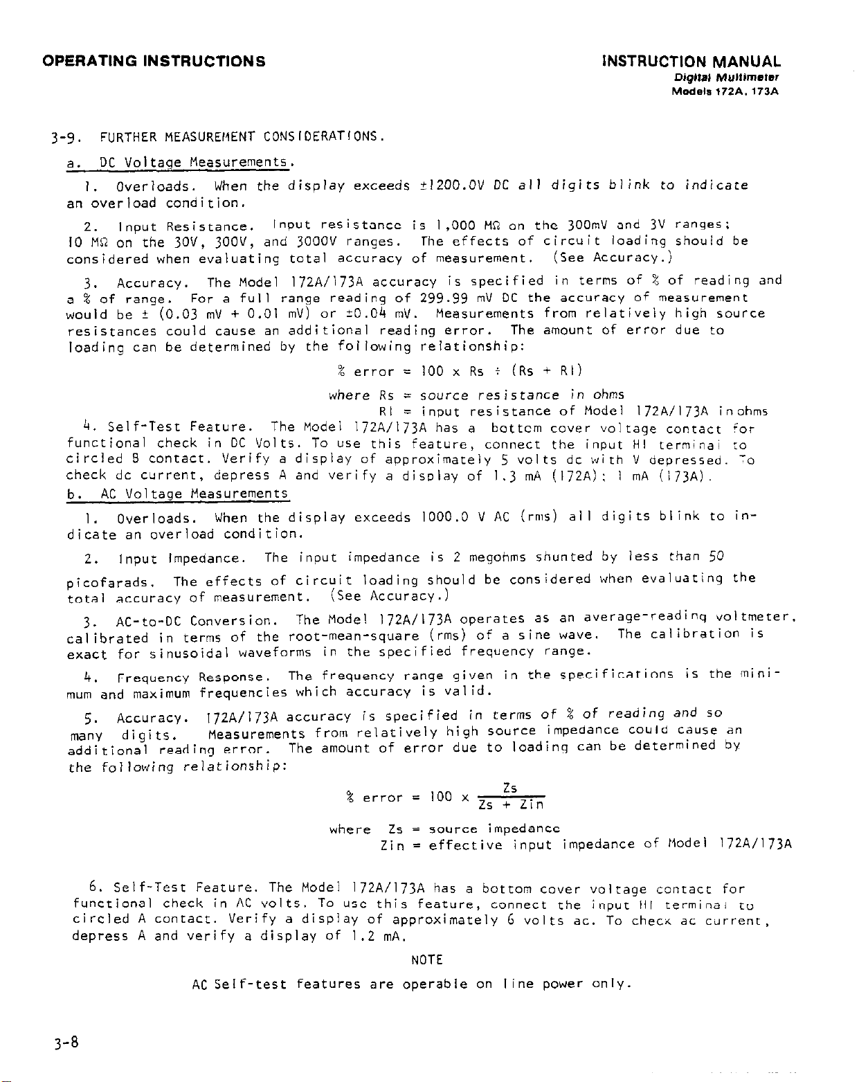
This illustration is typical of a 4-terminal measuring technique
using a separate Voltmeter and Current Source.
The Model 1?2A/l73A
combines these features.
"HI" LEADS
"LOW" LEADS
When using the 4-WIRE method, connect one
'lcurrent" leads to R SOURCE input.
;?SOURCE
HIGH
9 SOURCE LOW
Pair Of
connect a
second pair of "voltage" leads to HI and LO.
Then set to 4 WIRE.
Care should be taken to connect "current" leads
and "voltage" leads properly. The LO terminal
and n Source low must always connect to the same
side of the unknown resistance.
FIGURE 3-5.
Typical 4 WIRE Resistance Measurement.
3-9
Page 28
OPERATING INSTRUCTIONS
INSTRUCTION MANUAL
Digital MuWmeter
Model.
172A. 173A
4.
terminals
Four-terminal Measurements.
to the DMM ohmmeter source.
The 4-WIRE mode connects the lower set of n SOURCE
As shown in Figure 3-5 the lower terminals
are the current carrying terminals while the upper terminais are the voltage sensing
terminals.
This arrangement eliminates the error due to voltage drop across the cur-
rent-carrying leads.
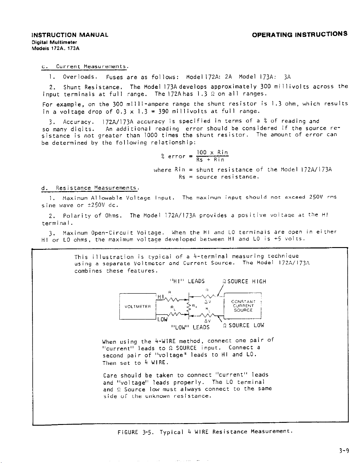
Semiconductor Diode and Transistor Testing.
5.
test diodes and transistors to determine the relative condition of the device.
semiconductor diodes,
forward direction.
I milliampere.
Since the HI terminal is positive with respect to LO terminal, con-
nections should be made as shown
the voltage applied must be sufficient to cause conduction in the
The “HI OHMS” mode provides a voltage up to 3 volts at a current upto
in
Figure 3-6 to cause forward conduction of diodes.
The Model 172A/l73A can be used to
For
Since the maximum current is available on the 3 KR range, depress AUTO/MAN (Set to
MAN) and manually range to the 3 KR range (down-range).
6. Self-Test Feature. The Model 172A/l73A has a bottom cover voltage contact for
functional check in OHMS. To use this feature,
Connect input HI terminal to circled C contact.
place theDMH in OHM!; and 2-lWIRE mode.
Verify a display of approximately 10
ki lohms.
3-10
CONDUCTION
CONDUCTION
H’ (+)
EMITTER-TO-BASE
9
LO- B
ANODE
TYPICAL DIODE
TYPICAL PNP TRANSISTOR
FIGURE 3-G. Semiconductor Diode and Transistor Testing.
Page 29
INSTRUCTION MANUAL
Digital Multimeter
Models 172A. 173A
OPERATING INSTRUCTIONS
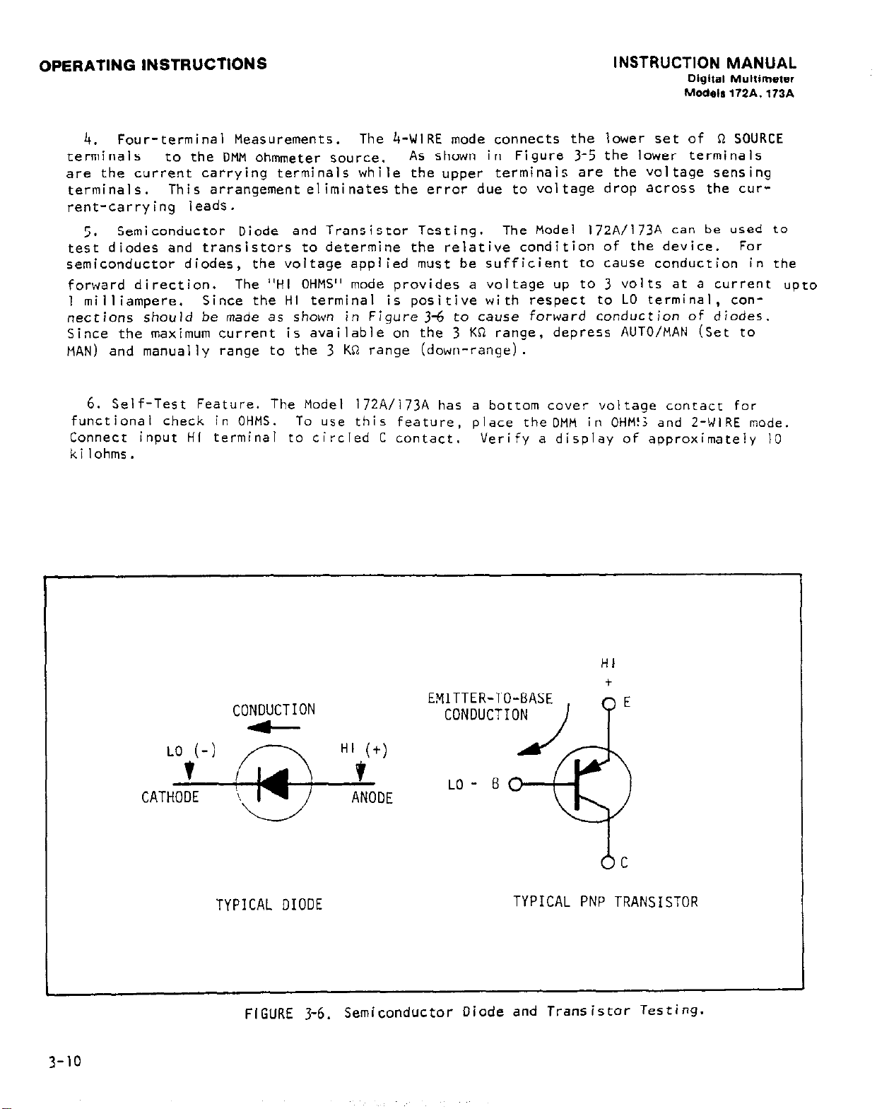
3-10.
ground at potentials of up to i14OOV. Isolation from the “LO” terminal to power line
ground is specified at IOOOMQ, or 10'0 (shunted by 3OOpF). Typically, the isolation
resistance from LO to GNO is two decades greater than IO30 (IO 1 Q).
excellent isolation,
loading (from LO to GND) of a floating source. At IOOOV above ground, the Model 172A/
173Awill require, typically, only IOnA from the source. The excellent isolation also
accounts for the high common-mode rejection ratio of the Model 172A/l73A. Even with the
“HI” terminal driven and a source resistance of IkR, 1000 VDC (from HI to GNO) will
produce typically only 1OuV DC error. This error voltage is determined directly from
the ratio of the source resistance to the “isolation”
The “isolation”
present. In the Model 172A/l73A this capacitance is specified at 3OOpF. At a frequency
of 60H2, 300 picofarads has a reactance of approximately IOHR.
driven and a source impedance of IkR, a IOOOV p-p, 60 Hz, common-mode signal will
produce a voltage of only IOOmV p-p across the input terminals.
p-p signal will be further rejected by the input filter and A-D converter 50 that the
total rejection at the digital display is at least I20 dB
impedance). For DC voltage measurements,
the Model 172A/l73A LO terminal is driven, rather than the HI terminal.
a need for even greater isolation from LO to power line ground, or where there is a need
to float at potentials greater than 1400 volts above power line ground the Model 1728
Battery Pack should be used.
HOW TO USE MODEL 172A/l73A OFF-GROUND. The "LO"
operating the Model 172A/l73A off ground results in very little
, - lOOOV -
IOllrl
10-BA
capacitance from LO to GND is important when AC common-mode signals are
'across Ik = I x IkR = 10-a x IO3 = IDuVDC
rejection is much greater than specified when
terminal can be operated off
Because of this
resistance (See Figure 3-7).
With the HI terminal
This IOOmV
(HI driven, IkR source
Where there is
+
1
EXTERNAL
SOURCE
1 ooov
DC
ilNpT[--------
FIGURE 3-7.
RESISTANCE
GROUND
Use of Multimeter Off Ground.
-1
/
I
I
I
I
_-;
3-11
Page 30
OPERATING INSTRUCTIONS
INSTRUCTION MANUAL
Digital Multimeter
Models 172A. 173A
3-11. HOW TO USE OPTIONAL PP9BFS AND SHUNTS.
Model 1600 High Voltage Probe. Set the Model 172A/l73A to DC volts and 30 volt
a.
ra”gtZ. The input resistance on the 30 volt range is IO megohms so that no shunt resistor
is needed. The Model 1682 has a 1OOO:l division ratio. For maximum safety review the
instructions furnished with the Model 1600 probeabove 30kV, switch to the 300V range.
CAUTION
The alligator clip (ground) must be connected to the source low so that high volt-
A
age is not applied between low and ground.
occur if the alligator clip is r!otconnected.
Model 1682 RF Probe. Set the Model 172A/l73A to DC volts and 30 volt range. The
b.
Severe damage to the instrument will
Model 1682 has a IVdc output corresponding to 1 V rms input over the range 100 kHz to
TOO MHz.
IMPORTANT
For use on the 3 volt range the banana plug adapter (with IO megohm resistor)
should be used since the Model 172A/l73A
input resistance is >I000 megohms on the
3 volt and 0.3 volt ranges.
Model 1685 Clamp-On AC Current Probe.
c.
Set the Model 172A/l73A to AC volts and 0.3
volt range. The Model 1685 provides a 0.1 volt rms output corresponding to a I ampere
rms input.
Review the instructions furnished with the Model 1685 to achieve best pos-
sible accuracy.
Model 1651 Current Shunt.
d.
and 0.3 volt range.
Connect the voltage leads to the Model 172A/l73A input terminals.
Set the Model l72A/l73A to AC or DC volts (as appropriate)
Connect separate-leads (not furnished) between the source and the Model 1651 hex-head
bolts.
The Model 1651 shunt resistance is 0.001 ohm which produces a sensitivity of I
millivolt per ampere.
3-12
Page 31

INSTRUCTION MANUAL
Digital Multimeter
Models 172A. 173A
OPERATING INSTRUCTIONS
3-12
control I ines.
This accessory is available either “factory installed” or “field-installable”.
HOW TO USE THE MODEL 1722 DIGITAL INTERFACE.
a.
Genera 1. The Model 1722 provides binary coded decimal outputs (8421) and range
Outputs are open-collector positive true unless otherwise specified.
The
Model 1722 consists of a two-layer circuit with card-edge and mating outputconnectors,
Installation.
b.
Disconnect the Model l72A/l73A line cord from line voltage.
I .
Turn the instrument over so that the bottom cover faces up.
2.
Loosen four slotted screws on the bottom cover. The screws are captive,
3.
that is,
4.
they cannot be removed completely.
Turn over the instrument with the top cover facing up, taking care to hold
the top and bottom covers together.
5.
Carefully
remove
the top cover
to
gain access to the printed circuit board.
There is one connection between the top cover and the main circuit board which must
be temporarily removed in order to free the top cover.
Remove the Model 1728 Rechargeable Battery Pack (if installed).
6.
Carefully
disconnect connectors from the mother board.
NOTE
The Models 1722 and 1728 cannot be installed on the Model 172A/l73A cnassis
at the same time.
Check to see that the four insulating spacersare in position on the circuit
7.
board as shown in Figure 3-Y.
Place the Model 1722 on the spacers as shown in Figure 3-9.
8.
Lift up the Model 1722 slightly to gain access to the Model 172A/l73A motner
9.
board, and plug in connectors JlOO3, JlOO2, and JIOOI (in order given).
Connect ground return wire from the Model 1722 to the extra lug on
IO.
transformer TIOI.
Replace the connections to the top cover.
11.
Reinstall the top cover.
12.
Turn the instrument over and tighten the four screws.
13.
Connector Terminations. The Model 1722 uses two card-edge connectors ~1006 (40-
c.
pin) and PI101 (26-pin).
Ribbon cable style of mating connectors may be used with these
cardedge connectors as shown in Table 3-5.
TABLE 3-5.
Sumnary of Mating Connectors
Crimped Ribbon-Cable Style
3462-0000
3464-0000
PI 101
~1006
Manufacturer
3M
3M
3-1:
Page 32

OPERATING INSTRUCTIONS
INSTRUCTION MANUAL
Digital Multimeter
Models 172A.
173A
~1006
1 1
PllOl
,/....~.-q .'. GND
3-14
1002
FIGURE 3-8. Model 1722 Digital Output
JlOO3
Interface.
Page 33

INSTRUCTION MANUAL
Digital Multimeter
Models 172A. 173A
OPERATING INSTRUCTIONS
FIGURE
Installation of Model 1722.
3-9.
3-15
Page 34

OPERATING INSTRUCTIONS
INSTRUCTION MANUAL
Digital Mullimetsr
Models 172A. 173A
Pin No.
I
2
t
5
6
;
9
L.
11
12
13
14
A5 --
16
1;
19
20
Signal
CASE GND
COMMON
COMMON
COMMON
COMMON
PRINTER HOLD
AUTOMODE VEXT
R8
VOLTS
R4
AMPS
R2
AC
Rl
OHMS
lo'-8
103-8
104-4
103-4
Pin No.
21
22
:'4
25
26
27 28
29
3 3:
::
34
35
36
37
38
Signal
104-2
103-Z
104-I
103-I
102-8
IO'-8
102-4 IO'-4
102-I
101-Z
102-I
101-i
103-8
m
103-4
FLAG
103-z
OVERFLOW
102-1
POLARITY
3-16
TABLE 3-7.
Summary of Remote Conrnands at PllOl
Pin No. Command
I CASE GND" 14
COMMON
:
4
2
i
9
IO FLAG/FLAG STROBE
11
12
13
COMMON 16 POLARITY STROBE
AUTORANGED STROBE
TRIGGER MODE I8
AUTOMODE STROBE
HOLD 20
OVERFLOW STROBE 21
-LOAD RANGE 22
RI
FUNCTION STROBE AUTORANGED
R2
--
Pin No. Comwnd
RANGE STROBE
15
17
IV
23
24
R4
R8
IO4 STROBE
TRIGGER
I03 STROBE
FLAG RESET
lo2 STROBE
TR GGER MODE DISABLE
I
10 STROBE
IO0 STROBE
Page 35

INSTRUCTION MANUAL
Digital Multimeter
Models 172A. 173A
OPERATING INSTRUCTION5
r----------
I
1 PIIOI
I 7 9
L ______ ----------,----I
r----------------------------l
I
, PI006
t---------------------- -_---_ -1
FIGURE 3-10.
2 4 6 8 10
1' ' J
1 3'5
2 4 6 8 10 121416 182022242628303234 363840
1 3 5 7 9 111315 17192123252729313335 3739
Connector Pin identification for ~1006 and PIIOI.
_---------_
1214 1618 20 222426
1113151719212325 I
1
I
I
I
I
FIGURE 3-11.
How to Select Vext Using Internal Jumper. The Model 1722 may be wired for use with
d.
internal or external voltage references and internal pull-up resistors. (See Figure 3-9).
Jumper A. When this jumper is installed,
1.
the external reference Vext (pin a, ~1006).
Jumper 5.
2.
the internal reference (+SV).
Jumper C.
3.
reference. The pull-up resistors are not connected in this instance. The +5 volt
reference is rated at 40 mA maximum.
When this jumper is installed, the pull-up resistors are connected LO
When this jumper is installed,
Card-Edge Connectors (Model I727 Cable Set)
the pull-up resistors are connected to
Vext is connected to internal +5V
3-17
Page 36

OPERATING INSTRUCTIONS
INSTRUCTION MANUAL
DigiW Mullimatsr
3-18
JlOO2
J I003
FIGURE 3-12.
Location of Jumpers and Pull-Ups on Model 177-z.
Page 37

INSTRUCTION MANUAL
Digiial
Mullimster
Models 172A.. 173A
Digital
OPERATING lNSlf?UCTION~
TABLE 3-8.
Outwt Lines Grouped By Function
Name
IO0 m
100-I
100-2
100-4
loo-8
IO1 STROBE
101-l
101-2
IO’-4
lo’-8
IO2 STROBE
102-I
102-2
102-4
102-8
IO3 STROBE
103-I
is-2
103-4
103-8
IO4 STROBE
104-l
104-z
is+-4
lo’-8
POLARITY STROBE
RANGE STROBE
-Rl
-R2
-R4
-R8
~1006
Pin
NO.
-39
37
35
33
--
;:
28
26
-31
29
27
25
--
24
22
20
18
-23
21
;;
--
-I5
13
11
9
PI101
Pin
NO.
26
24
22
18
16
14
Name
FUNCTION STROBE
-VOLTS
-AMPS
-AC
TRIGGER MODE
HOLD
LOAD RANGE
RI
R2
R4
R8
TRIGGER
FLAG RESET
TRIGGER MODE DISABLE
COMMON
CASE
FLAG/G STROBE
FLAG
FLAG
VEXT
PI 006
Pin
No.
IO I
12
I6
PI 101
: Pin
1 No.
12
I
/
I 8
3-
Page 38

OPERATING INSTRUCTIONS
INSTRUCTION MANUAL
TABLE 3-9.
General Characteristics of Model 1722 Digital Interface.
)IGITAL OUTPUTS:
Logic: BCD (8421) Open-collector positive true unless otherwise specified.
Data: 4 full digits, I partial digit (0, 1, 2, 3) and exponential range code
Digital Mullimeter
Models 172A. 173A
Function:
4-bit code (Q, AC VOLTS, AMPS)
Polarity: HIGH E +.
Overflow: LOW 5 > 29999.
dutorange:
Automode:
:LAG (m): HIGH (logic "0" Z
Logic Levels: HIGH Z open collector to output LO.
device (2N5134) greater than 2OV breakdown, <0.5V at 5mA sink (3TTL loads).
pull-up resistors may be installed on these open collector outputs.
LOW = range change.
HIGH E autorange mode.
no output change occuring.
LOW : closure to output LO.
Internal
4.7K minimum
Output
value is recommended when "sing internal 5 volt power supply.
IUTPUT TIMING: Data is updated typically every 320 msec (non-trigger mode).
Update
time is typically 1.2 msec. Data will appear at an output only if its respective
strobe is active.
go high typically 100 vsec after update.
long as the flag is high. If FLAG RESET is activated,
The FLAG will go low (Logic "0") typically 2 msec before update and
Data can be expected to be unchanging so
the FLAG will reset (go to Logic
"0") until the end of the next data update.
:EMOTE CONTROLS:
Strobe:
Strobe lines permit word serializing in 4-bit increments or multiples thereof.
HIGH inhibits controlled output lines from conduction, LOW enables conduction.
Range In: 4-bit exponential code.
L& Range:
Low enables remote ranging as set by Range code.
Hold: LOW inhibits display update, output update and autorange (A/O continues
conversions).
Printer Hold:
Same a5 hold but grouped with outputs for convenience in interfacing
printer.
Trigger Mode:
Trigger Mode Disable:
Trigger:
LOW enables TRIGGER control.
LOW disables TRIGGER.
LOW to HIGH transition initiates a new A/O conversion.
Flag Reset: LOW Set5 FLAG (FLAG) t0 Low (HIGH).
Control Logic Levels G Source Requirements:
voltage between c2.4V and 5V referred to output LO.
HIGH : either an open circuit or a
LOW : closure to OUtpUt LO
within 0.8~ while sinking +1.6 milliamperes (ITTL load). When TRIGGER MODE, HOLD
and LOAD RANGE code bits are all HIGH (inactive) the 172A/173A is under Front panel
control.
These REMOTE CONTROL inputs have priority and will override any front
panel setting once activated.
I
SOLATION:
All digital outputs and remote controls are isolated from 172A/173A analog
input by IO3 R and 5OOpF, 1200 VOC, IOOOV rrns AC maximum. All digital outputs and
remote controls are isolated from chassis ground by I06 Q and O.OluF; 250V TRY maximum. 1
L
3-20
Page 39

INSTRUCTION MANUAL
Digital Multimeter
Models 172A. 173A
OPERATING INSTRUCTIONS
e. Detailed Explanation of Model
TRIGGER MODE AND TRIGGER:
(See Schematic 28248E)
HOLD:
LOAD RANGE:
REMOTE CONTROLS:
When TRIGGER MODE is active (Low), output data and dis-
play will not be updated.
Conversion starts within
Integration starts 120 milliseconds after start of
conversion.
If either HOLD or PRINTER HOLD is low the output data
and the display will not be updated and the FLAG will
stay at HIGH (unless reset by FLAG RESET).
When LOAD RANGE is low the 172A/l73A will go to the range
as set by the RANGE IN code (Table 3-10) at the beginn-
ing of the next conversion.
held low,each instrument will remain on its programned
range overriding front panel UPRANGE, DOWNRANGE and
AUTORANGE. RANGE IN codes programmed outside the limits
of Table 3-10 will result in the nearest valid ranqe
to that programmed. LOAD RANGE will always cause a DMM
range change. However, the display and output data will
be held (not updated) during TRIGGER MODE or HOLD.
Referring to timing schematic 28249D.it is possible to
just miss a REMOTE CONTROL update prior to data output.
This can be misleading,especially in the case of HOLD.
A HOLD just missed (unknown to the user), just before
data begins to change,could result in erroneous data.
To check if this occurred, it is suggested that the
FLAG be examined no sooner than IO usec after activation
of the HOLD bit. If flag is low wait until it goes to
HIGH before expecting the HOLD bit to have been accepted.
Other REMOTE CONTROL bits such as TRIGGER MODE and
TRIGGER, LOAD RANGE and the RANGE IN code can be kept
active for longer than an output data update time, i.e.
>3.2 msec to insure proper REMOTE CONTROL acceptance.
1722.
TRIGGER MODE enables TRIGGER.
1.6
milliseconds after TRIGGER.
As long as LOAD RANGE is
TRIGGER MODE DISABLE:
(See Schematic 282490)
When in TRIGGER MODE and triggering into an autoranging
condition,
range encountered during the autorange.
this is undesirable the AUTORANGED output bit can be
tied to TRIGGER MODE DISABLE and FLAG RESET.
prevent the FLAG from being set and ignore further
triggering until the final range is reached.
normal operation will give an output for each
However, if
This will
3-21
Page 40

OPERATING INSTRUCTIONS
INSTRUCTION MANUAL
Digital Mullimeler
Models 172A. 173A
v
ext:
LINE GROUND:
GROUNDS:
CONNECTORS:
ENVIRONMFNT:
Installed in a 172A/l73A:
f. Modifications to Model 172A/173A Specifications. When operating a 17ZA/173A with a
1722 in TRIGGER MODE, only the accuracy specifications for the top two ohms ranges change
as follows:
internal jumpers (user installed'select internal or
external voltage reference for user-installed pullup
resistors for all open-collector outputs, 3r applies
internal c5v to v
internal +5V is 48%).
mended is 4.7K.
One pin on each output connector.
4 pins for digital outputs, 2 pins for remote control.
One 40-pin card edge and one 26-pin card edge.
Operating O'C to 55'C, humidity 80% @ 35°C
Storage:
-25O to +65’C
(maximum external cuTrent load on
Minimum pull-up resistor recom-
HI S 300M11 Range:
HI R 30MS-I Range: From 0.15% of reading to 0.2% of reading.
LO R 30MQ Range: From 0.5% of reading to 1% of reading.
LO 0 3MR Range: From 0.1% of reading to 0.15% of reading.
Also when operating in TRIGGER MODE, repeatability of readings may be up to:
0.5% on 300MR Hi 0 and 30MR Lo n ranges, and
0.05% on 30MR Hi 0 and 3MR Lo R ranges.
Accuracy of all other ohms ranges and all other functions is not affected by the Model
1722 when operating in TRIGGER MODE.
From 1% of reading to 1.5% of reading.
3-22
Page 41

INSTRUCTION MANUAL
Digital Multimetw
Models 172A 173A
OPERATING INSTRUCTIONS
TABLE 3-10
MODEL 1722 RANGE & FUNCTION CODING FOR MODEL 172A
RANGE j OUTPUT
RANGE
CODE (I)
VAACR
AC VOLTS / 1 0 1 0
LOW R
HI R
000 I
001 0
~ R8R4R2Rl
300 mV '0101
3.ov :o II 0
30 v :o I I I
300 v IO 0 0
1200 v 'IO 0 I
300 mV
3: ::
300 v
1000 v
300 mA
2 A
300 mA
2 A
300 n
3 kR
30 kn
300 kn
3 MR
30 MC2
3 kci
30 kil
300 kn
3 MR
30 Mn
300 MR
0 IO I
0 I I 0
0 Ill
IO 0 0
IO 0 I
t
0 IO I
0 II0
L
0 I 0 1
0 I10
0 0 I 0
0011
0 IO 0
0 IO 1
0 1 I 0
0 III
0011
0 10 0
0 IO 1
0 I 1 0
0 Ill
i
I 0 0 0
'1111
IO IO
IO 0 I
; I10 0 III 0 0
9 0 110
II I I AUTORANGE
I
I
1 0 1
110 0 0
!3
9 :o 1 IO
65 Ii;;;
2 10 1 0 0 I 0 1
: II0 0
4 IO II
2 IO I 0 0 IO I
7 I 0 0 0
i 'IO II
65 I IO 0 0 I 0 I
;o I I I
I
1 I I I
/II;1
Ill1
III00
IO 0 0
0 Ill
I 0
0 0
AUTORANGE
AUTORANGE
AUTORANGE
-1
AUTORANGE
I
AUTORANGE
(I) Coding in this table is defined to be HIGH (POSITIVE) TRUE. "1" = HIGH and "0" =
LOW.
(2) Function code for Model l72A current is volts.
(3) Note that except for AUTORANGE CODE,
PUT RANGE CODE, i.e.
Refer to output and remote control logic levels for definitions of HIGH t LOW.
INPUT E. RANGE CODE is the compliment of the OUT-
the INPUT RANGE CODE is the LOW TRUE BCD code of (EXP).
3-23
Page 42

OPERATING INSTRUCTIONS
MODEL 1722 RANGE G FUNCTION CODING FOR MODEL l73A
(Same as Table 3-lOexcept as follows)
TABLE 3-11
INSTRUCTION MANUAL
Digital Mullimstsr
Moddr
172A. r73A
FUNCTION
DC AMPS 010
[AC AMPS 011
OUTPUT
FUNCTION
CODE (I)
V A AC Q
0
0
RANGE
300
UA
3
mA
30
mA
300
mA
3
300
!JA
3
mA
30
mA
300
mA
3
A
A
OUTPUT
RANGE
CODE (1)
R8
R4
R2
R1
0 I 0 I 2
0 I I 0
0 I I I
I 0 0 0 i
1 0 0 I i y
0 I 0 I _ 5
0 1 I 0 j 6
0 I I I 7
100018 ~
100 I 9
(EXP)
INPUT
RANGE
CODE (1)
R8 R4
I 1 I 1
I 0 I 0
1 0 0 I
I 0 0 0
0 1 I I
0 I I 0
j j ; ; ;
I 0 0 0
0 I I I
0 I I 0
R~ R~
1
(3)
AUTORANGE
AUTORANGE
3-24
Page 43

INSTRUCTION MANUAL
Digital Multimeter
Models 17ZA. 173A
3-13. COMMENTS RELATIVE TO THE MODE-C 172A/l73A SPECIFICATIONS. Above I ampere there is
decrease in accuracy.
coefficient of the resistors that are used in these currents.
acy will not Bxceed those values that are listed in the specification sheet.
prolonged operation at the high currents (for instance,
3 amperes on the Model 173A) may give temporary zera shifts because of the thermals which
are generated due to the self heating of the devices.
3-14. MODEL 1728 OPERATING TIPS. Although the manufacturers of the nickel cadmium batt-
eries used in the 1728 claim that their cells can be charged at a C/IO rate indefinitely,
once a cell is fully charged,
increases the temperature of the cell. If cells are overcharged ar C/IO rate for extend-
ed periods of time (weeks),
the 1728 not be overcharged for extended periods to maximize useful battery life.
charging should have no effect on useful battery life.
hibit a memory effect.
short periods of time (I or 2 hours) the 1728 may not be able to provide the full operar-
ing time of 6 hours.
This decrease in accuracy is due toself heatingand the temperature
the energy fed to the cell is converted to heat, which
this may cause cell degradation. Keithley reconmenas that
Nickel Cadmium batteries also ex-
If the 1728 is only used to operate the instrument For relativelr
OPERATING INSTRUCTIONS
This degradation
2 amperes on the Model 172A. or
in accur-
However (
Trick1
Do not operate the Multimeter in BAT mode after the LO BAT indicator is lighted.
discharge characteristic of Nickel Cadmium batteries is such that it maintains a fairly
constant 1.2V through most of its discharge cycle.
the cell voltage drops fairly rapidly to zero volts.
pack drops to zero it is reverse charged by the rest of the cells in series with it.
Although the ceils used in the 1728 are guaranteed by the manufacturer :o withstand reverse charge for 10% of their discharge time,
reverse charge cells,
The cells used in the 1728 should give a minimum of 250 discharge/charge cycles and
typically 500 discharge/charge cycles.
day) the battery pack should give a minimum of one year operation and typically two years
Longer life should be expected for less frequent useage.
as more rapid cell degradation may occur.
Thus, based on daily useage (5 day week, one per
it is not a good practice to continually
At the end of the discharge curve
After a given ceil in the battery
The
3-s
Page 44

OPERATING INSTRUCTIONS
Summary of Fuses and Miscellaneous Replaceable Parts
INSTRUCTION MANUAL
Digital Mullimeter
Mode,, 172A. 173A
TABLE 3-12
ITEM
Fuse, 3 A0/3 AG, l/4 A, Slo-Blo
Fuse, 3 AB/3 AG, l/8 A, Slo-Blo
Fuse, 3 AB/3 AG, 1 A, Slo-Blo
FUSS, 3 AB/3 AG, 2 A Quick
FUSS, 3 AB/3 AG, 3 A Quick
Top Cover (less metalcal)
Bottom Cover (less metalcal)
Handle (less insert)
Insert
. .
Rubber Foot FE-IO
WHERE USED
117v Line Volts
234V Line Volts
Model 1728
Model 172AAmperes
Modell73A Amperes
KEITHLEY PART NO.
FU-I7
FU-20
FU-IO
FU-13
FU-2
28969c
289688
25729D
260YOA
3-26
Page 45

INSTRUCTION MANUAL
Digital Multimeter
Models 172A. 173A
ACCESSORIES
SECTION 4.
4-I. GENERAL. This section describes the various accessories and options available for
use with the Model 172A/l73A Digital Multimeter.
4-2. POWER OPTIONS. The Model 172A/173A can be powered by line voltage (105-l25V
standard) or rechargeable Battery Pack (Model 1728).
able as described in Section 2.
installable.
4-3.
factory-installed or field-installable,
(paragraph 3-12.)
4-4. RACK MOUNTING.
width) in either a single or dual mounting configuration.
ISOLATED DIGITAL OUTPUT. The Model 1722 Digital Output Interface is available
The Model 1722, 1723 and I728 cannot be installed and used at the same time since
these options occupy the same location on the Model 172A/l73A chassis.
The Model 172A/l73A~ can be rack mounted in a full rack (19 inch
MODEL 1010 SINGLE RACK MOUNTING KIT
The Model 1728 is available factory-installed or field-
ACCESSORIES
Other line voltage ranges are avail.
Complete specifications are given in Section 3
I MPORTANT
Description: Application:
The Model 1010 is a single rack mounting
kit with overall dimensions 5-l/4 in. (I33 instrument for Standard 5-l/4 in. (I33 N)
mm) high and 19 in. (483 mm) wide.
hardware included in this kit includes a (280 mm) depth behind the front panel.
IY inch wide panel and other miscellaneous
hardware.
Parts List:
tern
40.
I
2
3
4
5
6
7
Description
Front Panel
Support Plate (Shelf)
Bracket, Left Side
Bracket,
Slotted Screw, #6-32 x 2-l/4 in.
Flat Washer, #6
Phillips Screw, #E-32 x I/‘2 in.
Right Side
The x I9 in. (483 mm) rack mounting with II in.
The Model 1010 adapts one Keithley Style “K”
dual rack mounting of Style “K” instruments
the Model 1017 Dual Rack Mounting Kit must
be used.
Qtv
Req’d
1
I
I
I
2
2
IO
Kei thley
Part No.
26599
26599C
266008
266018
-_-
--
I I lustration
For
-
4
Page 46

ACCESSORIES
Assembly Instructions:
Using two Phillips Screws (Item 7) attach Support Plate (Item 2) to Front Panel
I.
(Item I).
Using four Phillips Screws (Item 7),
2.
3 and 4) to Front Panel (Item I).
INSTRUCTION MANUAL
Digital Multimeter
Models
attach left and right side Brackets (Items
172A. 173A
Using four Phillips Screws (Item 7).
3.
port Plate (Item 2).
4. Assembly of rack hardware is complete except for mounting of Instrument.
5. Rotate
dle can be removed completely if desired by separating top and bottom covers.)
6. Remove two Slotted Screws (l-l/4 in. long) used to hold top and bottom covers to-
gether near front feet.
Position Instrument so that holes in bottom of Instrument align with two front
7.
holes on Support Plate.
Using two Slotted Screws (Item 5) and two Flat Washers (Item 6). secure Instru-
8.
ment to support Plate.
“handle” of Instrument so that handle is toward rear of Instrument.
secure left and right side Brackets to Sup-
(Han-
4-2
FIGURE 4-l. Model 1010 Single Rack tlountinq Kit.
Page 47

INSTRUCTION MANUAL
Digital M”ll,nw,W
MDdels 172A. 173A
ACCESSORIES
MODEL 1017 DUAL RACK MOUNTING KIT
Description:
The Model 1017 is a single/dual mounting kit
with overall dimensions 5-l/4 in. (133 mm)
high and I3 in. (483 mm) wide.
The hardware mm) x IY in.
included in this kit includes a I3 inch wide
pane I (
and other miscellaneous hardware.
Parts List:
tern
0.
I
2
3
4
5
6
7
Description
Front Panel
Support Plate (Shelf)
Bracket, Left Side
Bracket, Right Side
Slotted Screw, X6-32 x 2-l/4 in.
Flat Washer, #6
Phillips Screw, X8-32 x l/2 in.
Application:
The Model 1017 adapts two Keithley Style
“K” instruments for’standard 5-l/4 in. (133
(483 mm) rack mounting with II
in. (280 mm) depth behind the front panel.
QtY
Req’d
I
Kei thley
Part No.
28092D
Illustration
28094~
280968
280978
__
Blank Cover Plate
8
9
Hole Plug
Kep Nut, U8
Assembly Instructions: (See
Figure
62, page 4-4.)
280986
HP-20
__
I. Using four Phillips screws (Item 7) attach left and right hand Side Plates (Items
3 and 4) to the Support Plate (I tern 2).
2. Using three Kep Nuts (Item 9) attach the Support Plate (Item 2) to Front Panel
(Item I).
Fasten the Side Plates to the Front Panel using two additional Kep Nuts (Item 9).
;:
Assembly of rack hardware is complete except for mounting of the Instrument(s).
The plastic tilt bail/handle on each instrument must be removed before mounting.
5.
The top and bottom covers of the instrument must be disassembled in order to remove the
handle.
Loosen four screws on the bottom cover.of the instrument, lift off the top cover,
and remove handle. Replace the top cover and tighten the four screws on the bottom cover.
6. Remove two Slotted Screws (l-l/4 in.
gether near the front feet on each instrument.
long) used to hold top and bottom covers to-
These screws are captive and a needle-
nose pliers should be used to pull the screw out after it is loosened with a screwdriver.
Position the Instrument so that holes in the bottom of the Instrument align with
7.
the two front holes in the Support Plate.
8. Using two Slotted screws (Item 5) and two Flat Washers (Item 6) secure the Instru-
ment to the Support Plate.
4-3
Page 48

ACCESSORIES
INSTRUCTION MANUAL
Digital
Mc.dsls 17ZA,
MultImeter
173A
FIGURE 4-2,
4-5.
Model
Description: The Model I600 is a divider probe for measurement of high voltage up to
Description: The Model 1682 is an RF probe for measurement up to 100 MHz. The Model
Description:
PROBE AN0 SHUNTS.
The following probes and shunts extend the capabilities of the
172A/173A.
MODEL 1600 HIGH VOLTAGE PROBE
40
ki Iowl ts dc. The probe is optimized for use with a dc voltmeter having IO
megohms input resistance.
1682
up to 200 amperes. The Model 1685 is used with an AC voltmeter and provides an output of 0.1 volt rms per ampere.
is optimized for use with a dc voltmeter having 10 Megohms input resistance.
MODEL 1685 CLAMP-ON AC CURRENT PROBE
The Model 1685 is a clamp-on current probe for measurement of ac current
Model
MODEL 1682 RF PROBE
1017
Dual Rack Mounting Kit.
Page 49

INSTRUCTION MANUAL
DigItal Multimeter
Models 172A. 173A
MODEL 1651 CURRENT SHUNT
Description:
having at least 100 microvolts resolution,
The Model 1651 is a 0.001 ohm shunt for use with an AC or DC voltmeter
ACCESSORIES
The shunt is rated at up to 50 amperes.
4-6.
use
Description: The Model 1683
Description: The Model 1681 is a set of test leads, 48 in. (1,2m) in length, terminated
Description: The Model
Description:
CABLES AND CONNECTORS.
of the Model
with interchangeable screw-on adapters.
by a banana plug and spring-action clip-on probe.
172A/lJ3A.
1727
cable terminated by mating card-edge connectors to the model 1722.
is 3 feet long (I m), and the Model
The Model 7004 cable is a shielded cable,
terminated by 2 tinned leads plus shield. Two banana plug adapters are furnished for
use with Models
lJ2A/lJ3A.
The following cables and connection Kits enable effective
MODEL 1683 UNIVERSAL TEST LEAD KIT
is a
set of
MODEL 1681 CLIP-ON TEST LEAD KIT
MODEL 1727 DIGITAL OUTPUT CABLE SET
is a cable set consisting of 26- and 40- conductor ribbon
MODEL 7004 SHIELDED CABLE
flexible test
1727-10
is ten feet long (3,l m).
leads, 40 in. (lm) in length.
The Model 1727-3
42
inches (I.1 m) long and is
Application: The Model 7004 cable is useful when making low-level voltage connections
to the Model
may be connected to the GUARD terminal.
4-7.
Description: The Model
MISCELLANEOUS.
ability to adjustment controls on the Model
test leads and a copy of this manual.
JO2/7029
Low-Voltage Scanner,
MODEL 1725A MAINTENANCE KIT
lJ25A
contains a specially punched calibration cover for access-
both analog INPUT and OUTPUT. The shield
lJZA/lJ3A
chassis.
The kit also contain
Page 50

MODEL 702/7029 LOW-VOLTAGE SCANNER
INS I HUC; I ION MANUAL
Digital Multimeter
Models 172A. 173A
Description:
The Model 702/7029 is a ten-channel low-voltage
be used for manual, scan,
or remote scanning operation.
scanner.
The 702/7029 can
MODEL 750 PRINTER WITH MODEL 7501-1722 PRINTER INTERFACE
Description: The Model 750 is an Ia-column printer which is plug-to-plug compatible
Page 51

INSTRUCTION MANUAL
Digital Multimeter
Models 172A. 173A
THEORY OF OPERATION
SECTION 5. THEORY OF OPERATION
5-I.
1728
that the Theory of Operation for the Model 1723,
is provided under separate cover,
contained in this section are broken down into the following major categories.
5-2.
Figure 5-l.
current,
circuit. The output from the signal conditioning circuit is a filtered dc voltage in thr
range of either 0 to +3 volts or 0 to 1300 millivolts, which is directly prdportional to
the input signal within the measurement range.
the signal conditioning circuitry into digital pulses by the charge balance technique,
and these pul~as are accumulated by the digital circuitry during the measurement conversion period.
determine the correct polarity and value of the digitized input signal, which is then
displayed with the appropriate polarity, range,
the LED display. The A/D converter auto calibrates and autozeros itself, as well as the
signal conditioning circuitry, to obtain a high measurement accuracy.
GENERAL.
Battery Pack option and Model
Overall Operation.
a.
Input Signal Conditioning.
b.
A/D Converter and Digital Circuits.
c.
d. Display Board.
Power Supply.
e.
f. Battery Pack (Model 1728).
Digital Interface (Model 1722).
9.
OVERALL OPERATION. The overall signal flow of the Model 172A/l73A DHM is shown in
Input Signal Conditioning.
a.
or an ac voltage or current) is applied to the appropriate signal conditioning
A/D Converter and Diqital Circuits. The A/D converter changes the voltage out of
b.
This section contains circuit descriptions for the Model 172A/173A, Model
1722
Digital Interface option.
IEEE Standard 488 Bus Interface option
see Model 1723 instruction Manual.)
An input to the DMM (a resistance, a dc voltage or
At the end of this period, the digital circuitry uses the total count to
decimal point location and function on
(It should be noted
The descriptions
Digital Interface Options.
c.
be made available as an output by using either the Model I722 Digital Interface or the
Model 1723 IEEE Standard 488 Bus Interface.
also be used to program range, trigger a conversion,
172A/l73A.
Power Supply. The power supply furnishes regulated dc voltages for all of the DHH
d.
circuitry, and receives its power from either the ac line or the optional Model 1728
Rechargeable Battery Pack.
5-3.
contained on the main printed circuit board (mother board) ~~-466 and shown on schematic
29145E (Sheet I).
attenuator,
(I/V) converter circuitry is located on the current board ~~-406 for the Model l73A and
mounted on a shield for Model 172A.
INPUT SIGNAL CONDITIONING.
These circuits consist of input switching, an ohms converter, a dc
an ac/dc converter,
The display information of the Model 172A/l73A can aIs<
Both of these optically isolated options car
or hold the reading of the Model
Most of the input signal conditioning circuitry is
a clamp and an active filter.
Both circuits are shown on Schematic 27478Q.
The current to voltage
5-
Page 52

THEORY OF OPERATION
INSTRUCTION MANUAL
LINE
INPUT
POWER
SUPPLY
SIGNAL
+ CONDITIONING
1J2A/173A
CURRENT
FIGURE 5-I.
1728
4 b
TO ALL
’ & DIGITAL CKTS
Overall Block Diaqram of Model
BATT PACK
(OPTION)
A/D CONVERTER
1722/1723
DIGITAL I’FACE
(OPTIONS)
*
+ DIGITAL
172A/l73A.
FRONT PANEL
DISPLAY
INPUTS/OUTPUTS
5-2
INP
FIGURE 5-2.
ATTENUATOR
Simplified Block Diagram of Signal Conditioning Circuits.
TO
AID
SIG.
Page 53

INSTRUCTION MANUAL
Digital MultImeter
Models 172A. i73A
THEORY OF OPERATION
Overall Operation.
tidily as shown in the simplified block diagram (Figure 5-Z).
selects the applicable path for the input signal. For example, an ac current input would
be routed through switch “A” to the I/V converter.
converter would be routed through the “Q” switch and the “DC/AC” switch to the AC/DC
converter, and the dc voltage output of this circuit would then be routed to the AD
converter through the clamp and active filter. The required switching and signal
conditioning for an ohms or voltage input can also be readily determined from the diagram,
and is left to the user. The front panel switching and signal conditioning circuits will
be described in greater detail in the following paragraphs.
Switching.
b.
the Model lJ2A/lJ3A.
information on function selection and range selection switching is given in Paragraphs
5-3i and 3j, respectively.
SWITCH
LINE
LINE
BAT
BAT
Front panel pushbutton switches control power, function and ranging for
STYLE
Push-Push
Push-Push
Push-Push
Push-Push
Signal routing in the signal conditioning circuitry is essen-
Front panel switching
The ac voltage output from the I/V
A summary of the switching is given in Table 5-l. Additional
TABLE
Summary of Pushbutton Switching.
SETTING
In (On)
Out (Off)
In (On)
Out (Off)
5-l .
REMARKS
DHM is powered by ac line power. Battery
pack (if installed) has a trickle charge.
DMM is disconnected from line power.
pack (if installed) is charged at maximum
rate if line cord is connected to power.
DMM is powered by internal Battery Pack.
DMM is disconnected from Battery Pack.
Batter
AUTO/MAN
AUTO/MAN
DN Range
UP Range
Push-Push
Push-Push
Momentarv
Momentary
In
Out
In
In
NOTE
Interlock prevents both LINE and BAT
buttons IN at the same time.
buttons musr be set to OUT before either
can be set to IN.
single depression
to IN, a second depression will release the
pushbutton to OUT.
DMM is set to MAN (Manual Mode).
range, depress either DN RANGE or UP RANGE.
See also REMOTE PROGRAMMING OPTION.
DMM is set to AUTO (Automatic Ranging Mode.)
DMM range is set automatically.
Momentary depression causes the DMH to down
range one decade to greater sensitivity.
Operable only when AUTO/MAN is IN.
Momentary depression causes the DMM to up
range one decade to lesser sensitivity.
Operable only when AUTO/MAN is IN.
Push-Push means that a
will
place the pushbutton
Both push-
Push-
To change
5-3
Page 54

THEORY OF OPERATION
INSTRUCTION MANUAL
DigitsI Mullimet*r
Modela 172A. 173A
TABLE 5-l. (CONIT)
Summary of Pushbutton Switching
SWI-CH
V
A
n
STYLE
“Interlock
*Interlock
Push-Push
Push-Push
Push-Push
Push-Push
SETTING
In
In
In
In
out
In
Out
REMARKS
DMM is set to V mode.
Overriaes A and R
functions due to interlocked pushbuttons.
DMM~is set to A mode.
Overrides V and 5
functions due to interlocked pushbuttons.
DMM is set to n mode.
Overrides V and A
functions due to interlocked pushbuttons,
also overrides DC/AC switch.
:‘:NOTE
If V, A, and R pushbuttons are OUT simultan-
eously,
no function will be selected, the
input terminals will be open-circuited, and
the DMM will display V.
The displayed read-
ing is meaningless.
DMM is set to measure AC (either V or A).
Not functional when set to R.
DMM ib set to measure DC (either V or A).
DMM is set to low ohms function.
DMM is set to high ohms function.
2 WI RE/4 WI RE”*
2
WIRE/4 WIRE””
Push-Push
Push-Push
In
Out
DMM is set for 4-WIRE ohms measurements.
Upper pair of terminals are used for Volt-
age sensing.
used for ohms source.
Lower pair of terminals are
Lower pair of
terminals are useable only in 4-WIRE 3 mode
and are open circuited for all other
conditions.
DMil is set for conventional 2-WIRE ohms
measurements.
be used.
Upper pair of terminals must
Lower pair of terminals are open-
circuited.
Only functional when set to R.
5-4
Page 55

INSTRUCTION MANUAL
Digital Multimeter
Models 172A. 173A
THEORY OF OPERATION
I) The dc attenuator is shown on the simplified schematic (Figure 5-3).
and 3V ranges, K202 is de-energized as shown and no attenuation occurs.
K202 will energize. This means that the output on the 3OV and 300V ranges will be l/l00
of the input as derived from the following equation.
I ODK
150K + 9.75M + IOOK =
2) For 1200 voltrange,
the input. Thus, for all dc ranges, a full scale dc voltage input will result in either
a ?3 volt or ?300 millivolt output from the attenuator, and the A/D converter gain
(buffer) will be XI or XI0 accordinqly. Table 5-2 lists the respective gains for dc
voltage (and ac voltage) ranges.
switch Q206 will also be on, which makes tie output l/l000 of
TABLE 5-2.
Gain Chart For AC/DC Voltase
I
100
RANGE CONTROL L I NE8
RLD
On the 300mV
&bove r3 volts.
1
H
+a v
+a v
0 v
0 v
0 v
AC/DC Converter.
d.
I) The basic transfer function of the AC/DC converter is a shown on the simplified
schematic (Figure 5-4).
Above 3 volts,
than -3Vdc. The dc output is a half-wave rectified sine wave, and the converter is
average responding, calibrated to the rms value of a sine wave.
2) Cl blocks dc inputs,
R and C provide some output filtering,
C4,
later.)
3) In actual circuit operation (as shown on Schematic 29145E, Sheet 1) feedback
resistance of lJ201 is controlled by K201 and K101.
shown,
With only K20l energized, gain is ilOO,
The relays are controlled by the relay drivers shown in the lower left corner
schematic.
lines from LSI circuit UVOI.
the overall gain of the ac/dc converter is unity (i.e. I VACrms input = -1Vdc 1
feedback resistance (Rf) is reduced to keep the output always less
The relay drivers are, in turn,
The resistor
and the dc offset voltage of the amplifier is autozeroed oi
See Table 5-2 for gain chart of the ac voltage ranges.
values were ielected SO the
along with the active filter (to be descri!
With both relays de-energized as
and with both relays energized gain is +lOOO.
controlled by signals front the RLD and H
-12 v
-12 v
-12 v
-12 v
+8 v
IVacrmsin = -IVdcOU-
Of
the
Page 56

THEORY OF OPERATION
INSTRUCTION MANUAL
Digilal Mulllm*1er
Models 172A. 173A
IOOOP
.Ol 1:
R216
27k
FIGURE 5-3.
9.75M
ac
Simplified Schematic of DC Attenuator.
R
OUT
5-6
Basic Transfer Function:
FIGURE 5-4.
Simplified Schematic of AC/DC Converter.
Page 57

INSTRUCTION MANUAL
Digital Multimeter
Models 172A. 173A
e.
Current-to-Voltaqe (I/V) Converter.
THEORY OF OPERATION
I) Model 173A I/V Converter.
(Figure 5-5).
input current by measuring the voltage drop across a resistance placed in series with
the current.
K505) to give an output voltage between 0 and 300 millivolts.
that K503 is closed.
30mA = 300mV.
converted to an ac voltage,
the DC attenuator circuit or the AC/DC converter before being applied to the A/D
converter. Signal routing is controlled by the DC/AC pushbutton and the gains employed
are the same as those given in Table 5-2 for the 300mV range.
I/V converter consists of a 3 ampere medium acting fuse (F5Ol) and a diode bridge (CR50
The fuse is rear panel accessible.
positive or negative polarity.
connections of the diodes so that less than one digit error is introduced on the 300uA
range, which has IO nanoampere sensitivity. Refer to Schematic 27478D for the remainde
of this discussion.
Model l73A current function.
(See Table 5-3).
to energize its range relay. Diodes are used to block the range lines when -12V is
applied and input dividers are used to drop +8V to +5 volts for application to U502.
Spike suppression diodes are used across the relay coils to prevent damage to the relay
drivers. Potentiometers ~506,
I/V converter.
physically located on current ~~-406 and shown on Component Layout diagram 27884C in
Section 7.
An input current is converted to a voltage directly proportional to the
This is accomplished by closing the appropriate range relay (K501 through
The current will now flow through 9E + 0.9r: + O.lc = IOQ, and
Since a dc current is converted to a dc voltage and an ac current is
Range control lines (A, B and C from LSI chip UP’JI) autoranqe the
The output from U502 turns on the applicable relay driver transistor
With the exception of the fuse,
The converter is shown on the simplified schematic
For example:
the output of the I/V converter is routed through either
input protection for the
CR501 limits the voltage to 2 diode:drops in either
Unity gain buffer amplifier U5Ol guards the center
The lines are decoded by the BCD to decimal decoder U502
R509 and R512 provide adjustments for calibrating the
all of the I/V converter circuitry is
Consider
TABLE 5-3.
173A Current Ranging
RANGE LINE
RANGE
RESISTANCE
IK
I OOR
IOR
IR
O.lQ
2) Model l72A I/V Converter. This current converter (shown in Figure 5-6) consists
of a I ohm resistor (Rl54)
through the resistor developing an output voltage from 0 to 2 volts.
475mA input will produce an output voltage of 475mV.
produce an ac voltage and a dc input will produce a dc voltage, the output of the I/V
converter is routed through either the DC attenuator or the AC/DC converter before beir
applted to the A/D converter.
button, and the gains used are the same as those given in Table S-2 for the 300mV (3000
and a 2A orotection fuse (F501).
Routing is controlled by the position of the DC/AC push-
RELAY
OPERATED
A
I
Since an ac current input will
LEVELS
B c
The input current passes
For example: a
5-i
Page 58

THEORY OF OPERATION
INSTRUCTION MANUAL
DigItal Mulllmeter
Models ,c?A. 173A
IN
F501 RANGE
3A
HI
INPUT
PROTECTION
-r
RANGE
.v
.I R512
R5o7, R508,
R509
R510, R5l I,
I
FIGURE 5-5.
FIGURE 5-6.
Simplified Schematic of 173A I/V Converter.
F501
2A 2A
IN IN
Simplified Schematic of Model l72A I/V Converter.
OUTPUT OUTPUT
0 LO
5-8
Page 59

INSTRUCTION MANUAL
Digital
MultImeter
Models 172A. 173A
THEORY OF OPERATION
and 3V (ZA) ranges.
shield above the display board.
F501 is accessible from the rear panel and R514 is mounted on a
The Circuit is shown at the bottom of Schematic 2747&,
which also contains the I/V converter for the yodel 173~.
f. Ohms Converter.
1) The ohms converter circuit basically consists of a current generator and summing
amplifier.
Simplified operation for the two wire ohms configuration is shown ip
Figure 5-7.
2) The current is generated by applying either 3.34 or ,334 Volts (Ohms Cal. Voltage)
from buffer amplifier UlOl to the Range resistors.
The unknown resistances (Rx) is
placed in the feedback loop of the summing amplifier (U202) to force the current through
the unknown resistor.
measurement can be determined by the equation -vodc =
Thus,
the output signal to the A/D converter for an
I-RX. The current flowing through
on
range
R, is determined by the equation I = vOhms CAL.
R
Range
Six decade currents are generated by the six combinationsof the three range resistors and
two levels of ohms cal voltage.
LOR range and 3M HIR range (3V max.)
3) See Table 5-4 for ohms ranges.
Examp I e :
.334v=
IliA. This current is used on 300Kf
334K
High ohms puts the A/D converter on the 3 Volt
range, allowing 6 resistance ranges which can turn on semiconductor junctions for on
scale readings.
LOW ohms puts the A/D converter on the 3OOmV range, allowing 6 resis-
tance ranges which do not turn on semiconductor junctions for on scale readings.
4) There at-e time and temperature drifts associated with amplifiers UIOI and U202.
These effects are compensated for by the A/D converter.
the A/D converter in 0 function is the output of UIOI.
compensated for every conversion cycle.
zero” I is calibrated to every conversion cycle.
The negative input of U202 is what “auto-
Therefore,
is a function only of the stability of the Range resistor.
The reference used to calibrate
Therefore,
any drift in UIOI is
ohms current stability
The lead drop in the high
terminal of the ohms source amplifier is compensated for by connecting it to “auto-
zero” 2 when in the ohms mode.
Z-wire ohms the leads connect at the front panel binding post.
ohms system exists up to the front panel terminals.
“Auto-zero” 2 is the zero for the input signal. In
Therefore,
a 4-terminal
See A/D converter discussion for
a more thorough explanation of error correction.
5) The ohms converter circuit has been further simplified and redrawn to show the
4-Wire ohms configuration in Figure 5-8.
As previously described,
a.
the circuit measures a resistor by putting a constant
current through Rx and measuring the voltage drop across Rx, which is accomplished by
putting Rx in the feedback of a summing amplifier (a AMP) whose input is a reference
(n Vref) voltage through an input resistor (RR).
AZ-l, ACAL, AZ-Z, t A/D Signal are the 4 A/D inputs.
b.
This A/D operation comp-
ensates for time E. temperature variation of Q VRef and R Amp, as well as compensating
for lead resistance.
The A/D looks at each of these inputs in the time Sequence as
follows:
1) AZ-1 looks at R AMP input for 40 ms and stores this zero level.
ACAL looks at n VREF for 40 ms and calibrates itself to the difference be-
2)
tween AZ-I and ACAL. Thus,
it is calibrated to the voltage
js a fixed stable resistor the value of I is
now
known.
~CTOSS
Since I flows through Rx
R9.
Since RR
the calibration is fixed.
3) AZ-2 looks at the voltage at the top of Rx for 40 ms. This is defined as the
zero level for signal measurement and is stored in A/D.
5-V
Page 60

THEORY OF OPERATION INSTRUCTION MANUAL
Digital Mulllmeter
MocJels
172A. 173A
RANGE R’S
A1
x1 or
3.34v
OR .334v WB
OHMS CAL
VOLTAGE
FIGURE 5-7.
7
OUTPUT
AUTOZERO
3.34k
---@+Y
s2
fM
0.1 05
(>HI
I
L--T-- -I
VOLTAGE
INPUT
LO
I
x
Simplified Ohms Converter, Two-Wire Ohms Configuration.
\INPUT HI
-..
-) AZ-2
/
0
5-10
(I-- 1
RX
Ix 1
1 O
0
\
/ INPUT LO
\
a SOURCE
HI
\
/
RSOURCE
LO
FIGURE 5-8.
VOLYAGE
REF
Four-Wire Ohms Measuring Technique.
*A/D SIGNAL
A CAL
+ AZ-l
Page 61

INSTRUCTION MANUAL
Digital Mullimeler
Modds 172A. 173A
4) A/D Signal looks at the bottom of RX for 200 milliseconds. The A/D thus measure
the difference between A/D Signal and AZ-2 without polarity sign.
Rx is displayed.
C.
The measurement is essentially a ratio measurement between the voltage across
Rx and the voltage across Rn.
d.
llote that the voltage at the top of RX is essentially at signal LO of the
instrument (+- nAMP offset and lead resistance drop) and the voltage at the bottom of
Rx is negative.
response is achieved at high resistance values,
5) Refer to sheet I of Schematic 29145E for the remainder of the ohms converter
circuit discussion.
driven from the A-line and QlO7 is driven from the B-line.
used and decoded to operate the Modell73A autoranging current. When on, QIIO
switches the gain of UIOI from one
resistors. Each resistor consists of an adjustment potentiometer, a fixed resistor
and the on resistance of a FET (no FET for 33.4Mn).
amp1 ifier. This amplifier is overload protected by QlOb base emitter junction
connected to signal ground,
clamp transistor.
on the output side of U202 are allowed (by action of Q205 and CR205.
operating conditions Q205 is operated in the saturated mode.
conditions, Q2O5 becomes a current source with its collector to emitter breakdown
handling large voltage excursions when signals are positive with respect to the
ohms source high.
high, CR205 reverse biases,
high voltages will cause current to flow through R205 (120KQ)
the +15 volt supply.
power rating of R205 (a l/2-watt resistor),
Thus, the high impedance terminal is guarded and relative fast
The ohms switching FET QIIO is driven by the C-line, QlO5 is
to
ten.
and QlO8 base emitter junction connected through
Thus,
Conversely,
the input swing is clamped.
if signals are negative with respect to ohms source
cutting off that portion of the circuit. Al\ of these
The maximum limitation of 250 volts runs is a function of the
QlO5 and QlO7 switch-in the range
Amplifier LIZ02 is a FET input
Very large voltage excursions
and ~205’s 400 volt breakdown.
THEORY OF OPERATION
The voltage across
These lines are also
Under norma I
However,
which is connected to
under overlo,
QIOV
TABLE 5-4.
OHMS RANGES
RANGE RANGE
HIR Lon R
3%
300K
3%
300M
3000
3K 3.34K
30K 334 K
300K 334 K
3M 33.4M
3OM 33.4M
3.34K
REF OHMS
VI
3.34'/
.334v
3.34v
334V Iv.4
;.34v lOOnA
.334'/
CURRENT
I mA
IO!IUA
IOuA
IOnA
RANGE LINES
A
tav - I2V
+8v -12v -12v
-12v
-12v +av
- 12v
-12v
E! C
+8v +8v
-12v
- I2V +3v
-12v -12v
+Ev
I
Clamp Circuit (Figure 5-9).
9.
The clamp prevents damage to the input circuitry of the A/D converter and the
1)
active filter by limiting the maximum input voltage to approximately plus and minus
5 volts.
capacitor (C209) in the dc attenuator to eliminate any relay arcing whenever high voltage inputs are applied to the instrument during range switching.
used to minimize leakage current.
It also functions in conjunction with the 150 Kohm resistor (R217) and 0.3ltii
Low leakage FETS are
5-l
Page 62

THEORY OF OPERATION
- Q704
INSTRUCTION MANUAL
Dig,,., M”lmll.1.r
Moclda
172A. 173A
IN R”
-5v e
FIGURE 5-9.
R707
- C702
IN
0
OUT
0
- Q703
Simplified Schematic of Clamp.
.
OUT
0
c701
5-‘I 2
FIGURE 5-10.
0
41
~604
~601
Simplified Schematic of Active Filter.
~603
Page 63

INSTRUCTION MANUAL
Dlgilal
MultImeter
Models 172A. t73pI
2) As shown on Sheet I of Schematic 29145E, the -5volts is supplied t&Q703 by zener
diode VR70l and resistor R710, which is connected to -15 volts.
h. Active Filter (Figure 5-10).
1) The DC filter is used in front of the A/D converter on all functions. The comp-
onent values used in the circuit provide 25O:l attenuation to 50 Hz on dc volts, and
i7OO:t filtering on ac volts output at 50 Hz.
overshoot by having the following component relationships:
It* + R707 = 1.5 (~603) and c702 = 1.5 (~601).
of 200K0, 49.9Ka of which is R707.
ent upon range and function, as given in Table 5-5.
that the effect of A/D converter input current is autozeroed out (see A/D converter
discussion, Paragraph 5-4). The filter does not contribute any dc offsets to the signal
path.
tion for lJ602.
They are blocked by C702 and C701. C903 (not shown) provides frequency
Active Filter Input Components.
The other 150KR comes from various sources, depend-
TABLE 5-5.
Minimum rise time is achieved without
The filter requires an input resistance
The 200KO is also maintained so
j-10
R’:
THEORY OF OPERATION
~70’2 = ~701, ~604 = ~603.
compensa-
R217
R213, R209, RZl5B, R208
12oov
ACV ALL
0.
U9hi. Th& are contro\led by the front panel switches AUTO/MAN. DN 6 UP, according to
Table 5-6.
changed.
Ran e Selection.
RSA & RSB are edge sensitive,
This causes one uprange or one downrange per button push.
Range Switches
AUTO/MAN
OUT
IN
IN
IN
ALL
I
Ranging is accomplished by RSA F. RSB lines going to LSI Fircuit
DN
X
OUT
IN
OUT
Cl02
I
causing range changes when their levels are
TABLE 5-6.
Range Selection.
Range Lines
UP
X
OUT
OUT
IN
RSA RSB
t8V ov
+8v
~213. ~209. 214. R215B. R2l5C,
R208, Q206
1x10⁶
R704
ACTION
ov +av
OV
ov
+8v
AUTORANGE
HOLDRANGE
DOWNRANGE
UPRANGE
X = DON’T CARE
5-1:
Page 64

THEORY OF OPERATION
Function Switching.
.i.
FUNCTION
v
INSTRUCTION MANUAL
0lgit.l uultlme1.r
Models
172A. 173A
TABLE 5-7.
Function Selection.
FUNCTION SWITCHES FUNCTION LINES (UVOi)
DC/AC
A
R HI/LO R
AC/DC
VI
DCV DCI
ACV
ACI
HIR
LOQ
IN
3UT
IN OUT
OUT
OUT
OUT
IN
IN
OUT
OUT OUT
OUT
IN
OUT
OUT
OUT OUT X +Ev
IN
X
X
OUT
IN
IN IN
X
X
X +8v ov
+8v +Ev +8v
+Ev
+8v
ov
+8v (172A)
OV (173A)
+Ev
‘2 11:::1
OUT ov ov +8v
ov
+8v
+8v
X 5 DON’T CARE
Function selection is accomplished by connecting function lines R, AC/DC, & VI
according to Table 5-7.
A/D CAL
0
A/D S,G-
AZ I-
AZ 20
BUFFER
The function lines are level sensitive.
-
r”’ b$
t
ACT.
- INT. -
I
*‘STORE
CONPARATOR
t
DiGITAL
SECTION
Mb.NY
OUTPUTS ,NP”TS
“AH”
5-14
FIGURE s-12.
REF.,. -
b
I SW
DRIV.
A-CAL
STORE
4
-
Simplified Block Diagram of A/D Converter.
I
CLOCK
I
r
Page 65

INSTRUCTION MANUAL
Digital MultImeter
Models 172A. 173A
THEORY OF OPERATION
- 5-4.
is shown in Figure 5-11.
specified time period is directly proportional to the dc voltage applied.
capability to measure its own offsets and gain errors as well as those of circuitry in
front of it (i.e., ac/dc converter,
cancels the effect of these errors by storing appropriate correction voltages in autozero and auto-calibrate storage. A conversion cycle consists of four different operating
modes, as shown in Figure
A/O buffer. The difference voltage between ACAL and AZ-1 is the calibration voltage,
while the difference between signal integrate and AZ-2 is the measured voltage.
converter uses the charge balancing conversion technique, and polarity detection is
accomplished digitally.
scale integration (LSI) circuit.
not be given in the A/D converter discussion.
necessary for the operation of the remainder of the A/O converter will be referred to
when necessary.
is built around an active integrating circuit and a comparator circuit which at first
glance may appear similar to a dual-slope converter. However,
different,
(charge/discharge cycle) is zero, and the digital output from the converter is a function
of the number of integrating cycles that occur during the measurement conversion period
(signal integrate). The number of integrating cycles in turn, depend upon the level of
the input signal. In the Model 172A/173A, the input to the A/O converter is offset to
- handle bipolar input signals and the number of integrating cycles (output counts~f increases as the input voltage increases in the positive direction.
3VOC range,
+3v (60,000 counts).
displayed from 0 to 30,000 counts and that 30,000 counts would have to be subtracted in
order to display zero with a zero volt input.
digital circuits.
A/D CONVERTER AND DIGITAL CIRCUITS.
a. Introduction.
A simplified block diagram of the A/O Converter and Digital Circuits
The A/O converter generates a digital pulse train which over a
5-12.
Almost all of the digital tasks are handled by a custom large
Charqe-Balancinq Technique.
b.
In
the charge balance converter,
a -3 volt input would produce zero counts,
It can be seen from the example that .a minus sign would have to be
(Schematic 29145E. Sheet 2).
It has the
dc attenuator and ohms converter). The converter then
During each mode, a different input is connected to the
The
Note: details of the operation of the LSI chip will
However, various of its outputs which are
The charge-balancing converter of the Model 172A/l73A
its operation is quite
the net charge for an integrating cycle
For example: on the
zero volts (30,000 counts) and
Both of these tasks are handled by the
4
L
ERROR
CORRECTION
FIGURE
ONE A/O CONVERSION
A
5-12.
A/O Converter System Timing.
c
SIGNAL INTEGRATE
200ms
J
SIGNAL
MEASUREMENT
5-15
Page 66

THEORY OF OPERATION
INSTRUCTION MANUAL
Digital MultImeter
Moclet, 112A.
173A
Basic Operation of the A/D Converter.
c.
converter are described as follows:
I) AZ-l.
functions), or summing junction of the ohms amplifier in R function. The switching rate
for zero input is forced into the current switch drivers.
a dc correction voltage to auto-zero storage.
the active integrator forming a negative feedback loop which quickly stabilizes.
2) Auto-Calibrate.
(3.3444 Vdc in V and A functions,
continues to apply AZ-l correction voltage to the active integrator.
switch drivers are forced to switch at the appropriate rate for reference input, and
a dc correction voltage from the comparator is applied to auto-Cal storage.
correction voltage is stored and continually applied to the reference current source
which changes the reference current removed from the active integrator, completing
another negative feedback loop.
3) AZ-2.
is connected to input LO (zero circuit for dc V and A functions, ac/dc converter for
ac V and A, or input HI for n).
4) Signal Integrate.
for dc V and A, ac/dc converter output in ac V and A, or input LO in 0). AZ-2 and ACAL
voltages are still applied,
A/D conversion is now made,
A/D Buffer.
d.
functions.
necessary inputs to the A/D converter to provide .the four basic modes of operation. The
driving signals (Zl, Z2,
ugo1.
3V and 0.3V ranges, respectively.
every other R range.
xl0 on 300mV, 3OV, LDfi, 300mA on l72A and all current ranges of l73A. A gain of xl is
used elsewhere.
The second function of the buffer is to provide two gains (xl and x10) which give
The buffer input is connected to reference low (signal LO in V and A
In this mode, the buffer input is connected to the reference
or the ohms reference in 0).
The same procedure as AZ-l is followed, with the exception that the buffer
The buffer is connected to signal input (dc attenuator output
which provide compensation for zero and gain errors. The
and displayed during the next conversion cycle.
The buffer (shown in Simplified Schematic, Figure 5-13) performs two
It has four multiplexing JFET switches (Sl through S4) that connect the
R and NS) for the multiplexing switches come from LSI circuit
Buffer gain during AZ-l and ACAL is xl for V, A and
Buffer gain during AZ-Z is the same as signal integrate, which is
LSI chip U901 controls S5 and 56 (Q7O2 and Q7Ol) via the GIO line.
The four basic operating modes of the A/D
The comparator output applies
This voltage is stored and applied to
Auto-zero storage
The current
This
r
,
5-16
A/D CAL
SIG. INT.
AZ-l
AZ-2
INPUTS
o ‘3@Q7ll
0
FIGURE 5-13. Simplified Schematic of A/D Buffer.
S2
Q708
OUTPUT
- -
Yk
Ik
*
1
I
Page 67

INSTRUCTION MANUAL
Digital Multimeter
Models 172A. 172A
THEORY OF OPERATION
0
v.
I"- :;
'in"-,
REFERENCE CURRENT
SOURCE
Ri
Dl
'r
+v
RZ
Qv"
4- 'z
'i
I I
I
ACTIVE
INTEGRATOR
REFERENCE CURRENT
SWITCH
*
AUTOZERO
QZ
STORAGE
COMPARATOR
CURRENT SWITCH
DRIVER
DIGITAL PULSE TRAIN (QR)
C
a
b
Rf
2hh
Cf
i
D TO U9Dl
AUTO CnL STORAGE
A/D Converter Simplified Schematic Description (Figure 5-14).
e.
I) The active integrator,
ACAL storage circuits are shown on the simplified schematic diagram.
the A/D converter becomes unipolar, using only one reference current.
inputs are applied to Ri, the nominal value of lz
1~ - Iin 50.
60,000
sensing.
,
the exception that it is shifted up from zero count to center on the approximate 66,900
counts produced by the clock during signal integrate.
can detect overrange conditions in both polarities and to permit a signal settling time,
J after connecting it to the buffer,
counts.
Thus, -3 volts is zero cOUnts, 0 volts is 30,000 counts and +3 volts is
The LSI circuit (U9Ol) counts in this way, providing digital polarity
It should be noted that a 60,000 count span is used as described above, with
reference current switch and driver, comparator, AZ and
After the buffer,
Since bipolar
is such that if Vin = -3 volts,
This is done so that LSI circuit
before beginning the conversion.
5-17
Page 68

THEORY OF OPERATION
INSTRUCTION MANUAL
Digital Mulllmrtrr
MehI, 172A. 173A
2) Charge balance A/D conversion is used.
output pulse train has the property that its average frequency over a given time period
is proportional to the average of the input voltage over the same time period.
the digital output is a representation of the true
any specificed sampling time.
comparator, current switch driver,
source.
is such that the.obtput of ~604 is initially at some positive level.
nal current (I in) is integrated by the capacitor,
eventually becomes more negative than the comparator threshold.
goes to logic zero, which is inverted to logic 1 by the inverter and applied to the “Cl”
input of the flip flop.
latched by the flip flop and appears as the set output QR, and the c output of the flip
flop turns on the current switch.
the integrating capacitor,
threshold in the positive direction.
flip flop and the next positive going edge of the CLOCK signal resets the flip flop,
which terminates the pulse on the QR line and turns off the current switch.
verter will remain in this state until the next time that the integrator voltage
crosses the threshold of the comparator in the negative direction. For relative large
values of the input,
where the comparator threshold is exceeded will be relatively short and the integration
cycle (charging versely, with lower values of input current,
be longer and the events described will occur at a lower rate.
rate of current pulses (and digital output pulses) is a function of input current. It _
should be noted that the current switch driver circuitry shown has been greatly simplifir
for this discussion.
half of the output pulse on the QR line,
clock which centers the current pulse on the digital output pulse to eliminate edge
problems.
discharge cycle is equal to the product Of lr
pulses are uniform in size.
time period is equal to the total charge that flowed in (within a resolution of one
discharge increment).
that the total number of such pulses is proportional to the time-integral of the input
current.
3) The auto-zero correction is always applied to the active integrator, but during
AZ-l and AZ-Z, the switch Sc
The rest of the time it is stored on capacitor C,.
by forced switching of the current source at the “zero” input rate.
offset,
developed at the output of the comparator by Rf and filtered by Cf. Auto-zero correct-
ion is supplied as negative feedback to the integrator input.
be considered as a contribution to input current since it affects the charge portion
of the integration cycle.
For this description, assume that the charge on the integrating capacitor (ci)
At the next positive going edge of the Clock, this “one” is
the time required for the capacitor to be recharged to the point
discharging cycle) described will occur at a high frequency.
In actual operation,
Since the amount of current removed from the integrating capacitor during each
The uniformity of size of the reference current pulse guarantees
this equates to a midscale current input.
The basic converter consists of the active integrator,
reference current switch and the reference current
The reference current lr is forced to flow out of
discharging it,and the output of ~604 crosses the comparator
This results in a logic 0 at the “D” input of the
The total charge removed from the capacitor in any given
is closed which allows correction of the auto-zero signal.
With this conversion method, the resulting I
Thus,
integral
the output of ~605 ramps negative and
the charging time of the integrator will
the current pulse is limited in time
and is turned on and off by a 90” out of phase
and one-half clock period, the current
The correction signal is generated
The correction signal is the dc
of the analog input over
As the input sig-
The comparator output
The con-
Con-
Thus, the repetition
to
Since the input is
Auto-zero correction can
one-
level
5-18
Page 69

INSTRUCTION MANUAL
Digttal Mulllmeter
Models t72A. i73A
THEORY OF OPERATION
V
4) The auto-calibrate correction is continually applied to the reference current
circuit. Sc is closed during Auto-Cal to update the correction voltage, and is stored
on capacitor Cc.
correction,
current input rate.
charge removed from Ci during the discharge cycle since the source”on” time is fixed
at one-half the clock period.
5) In the reference current circuit,
emitter resistor R2 connects to a negative voltage (-V). The current through R, (I)
is approximately equal to lr + Ic
I, will vary inversely with respect to a change of It.
6) The reference current switch consists of two diodes, and is controlled by the
current switch driver circuitry. Reference current is_removed from the summing junction
of the active integrator when D] is conducting.
conducts cutting off DI.
proportional to the output.
during AZ-I, AZ-2 and ACAL is not shown.
Oscillator. The oscillator (shown in Figure 5-15) is crystal controlled and operates
atfapproximately
oscillator runs at twice the clock rate for the following two reasons:
It allows the current switch to be on only one-half of the clock period, so
I)
that there is always an off time even when the current switch is on for consecutive
clock cycles.
A/D converter.
with the exception that forced current switching is done at the full-scale
Auto-Calibrate correction is generated similiarly to auto-zero
Auto-calibrate correction varies lr and thus, sets the amount of
the base of Qr is referenced to ground and the
(neglecting base current of Qr).
When Q of the D flip flop is high, D2
The Q output of the flip flop is the digital pulse train
The circuitry which forces predetermined switching rates
669
kHz.
This eliminates a gross nonlineraty problem from the charge-balance
It is divided down 2:l to produce the A/D converter clock.
Since I is constant,
The
It allows the current to be switched on and off with a 90” phase shifted clock sigr
enerated by the oscillator) so that there will be no timing problems with the edges
$2)the current pu1 ses.
CYOI
47pF
FIGURE 5-15.
~807
18KQ
TO CLOCK
DIVIDER
CMOS
I NVERTERS
Simplified Schematic of 669 ktiz Oscillator.
5-19
Page 70

THEORY OF OPERATION
~602
INSTRUCTION MANUAL
PRECISION
DIVIDER
Dlgltal
Multimater
Models 17ZA. 17JA
FIGURE 5-16.
Reference
9.
reference supply (shown in Figure 5-16) furnishes the stable known voltages required to
auto calibrate the A/D converter. These voltages are also used in the ohms converter
circuitry.
zener diode. It is driven from a constant current (nominally 7.5mA) developed by amplifier ~601.
The output divider resistors ar.e part of a precision resistor network which provides very
stable reference voltages.
selected (depending on the zener voltage) to provide a nominal 200uA of current to the
divider.
accordingly.
h.
LSI circuit U901. It keeps track of the flinction and range, allows auto or manual ranging
generates the display information, controls the A/O converter timing, provides ranging
lines for the signal conditioning circuitry, and provides information for the optional
digital interfaces, as well as controlling them.
The zener voltage is between 6.15 and 6.5 volts, with the resistors matched
Digital Section.
SUDPlY.
The heart of the reference supply is a stable,
With the zener current well regulated, it is immune to power supply variations
The digital section is composed almost entirely of the custom
Simplified Schematic of Reference Supply.
Although not actually a part of the A/D converter circuitry, the
low temperature coefficient
R606 and the input resistors of the divider are specially
5-20
Page 71

INSTRUCTION MANUAL
Digital MultImeter
Modah 172A,.173A
THEORY OF OPERATION
5-5.
- a. This schematic shows the display digits,
drivers and multiplex timing genera.tor.
function indicators, is fully multiplexed.
(timing mux).
:",e LSI circuit (USOI, Schematic 29145E).
indicators are driven from the appropriate mux line, see figure 5-17.
occur in the operating digital interfaces (see Section 5-8, 1722).
in the sequence t0 thru t5,
,microseconds each.
segments and the function indicators.
in the LSI circuit U901, Sheet 3 of Schematic 29145E.
zero,
indicator and minus sign twice as long as the digits. Since "AC" and "-" are activated
during tl,
same brightness as the other digits, a,
are on for half of t) time.
driver transistors are emitter followers (Q307 thru Q314). R302A thru R302H are current
limiting resistors. Segment current is approximately 30 milliamperes peak. R303 & C30l
decouple current spikes from the 5 volt power supply. C302 decouples U3Ol from power
-'
\
SUPPlY.
5-6.
regulators, line transformer,
172A/173A.
provides the regulated +I5 volts and the
deliver the ?I5 volts used by most of the circuitry in the l72A/l73A.
regulated +I5 volts is supplied to the input of the ~8 volt regulator (VROO4) and the
regulated -15 volts is supplied to Zener diode ~~801 via R80l to develop -12 volts.
Both of these voltages (+8 and -12) are fed to the LSI chip (U9Ol). The -12 volts is
atso fed direct to the Switch Driver circuitry and the +8 volts is fed indirectly to this
circuitry by the pullup resistors associated with U9Ol.
receive either r29.5 volts (unregulated) from the line transformer (TOOI) and full-wave
rectifier (CROOI), or kl9.2 volts from the batteries in the Model 1728 Battery Pack.
unregulated voltages are higher than the regulators need because they are used to re-
charge the battery pack.
voltages are fed direct to the Battery pack connectors (P401, 402).
volt regulator (VROOl).
circuitry in the A/D converter, and all relays.
Optical Isolator circuitry whenever the Mode)
the 172A/l73A.
If a Model 1728 battery pack is installed in the Model 172A/l73A the batteries of the
Model 1728 will be charged through the unregulated voltages. When the instrument is
line powered, resistors,
These resistors drop the charging current down to the trickle charge level.
viously mentioned,
,
+I5 volt output of VR003.
former secondary
DISPLAY BOARD, SCHEMATIC 27404D.
The entire display,
The mux times are generated by shift register ~301 whose inputs come from
, t3, t4, '5.
The data mux lines, a, b, c, d, e, f,
b.
c. The 10,000 digit only indicates I, 2, or 3 in overrange.
it is blanked by the data mux lines.
the 10,000 digit time, tl is as long as t0. To keep the 10,000 digit the
The anode driver transistors are saturating switches (Q3Ol thru Q306). The segment
d.
CR301 and R304 prevent parasitic oscillation of segment driver transistors.
POWER SUPPLY, SCHEMATIC 29145E.
The common anodes of each digit and the comnwn anodes of the function
t0 and t) are 383 microseconds each, and t2 thru t5 are 191
One complete mux cycle is 1.53 milliseconds.
See Table 5-8.
b, c, d, e and g data mux lines for this digit
Sheet three of this schematic contains the voltage
line voltage switching and powei switching for the Models
There are four separate integrated circuit voltage regulators used.
-15 volt regulator is VROD2.
If the instrument is off, but the line cord powered, unr=gul=t=d
This regulator is used to drive the display, the digital logic
R005, R006 and RD07 feed the charge inputs on the battery pack.
the 8 volt regulator, VRD04, gets its input from the regulated
The input for VROOI (5V regulator) is derived from trans-
7
and 8, full-wave rectifier CR002 and A003.
the LED function indicators, all display
including minus sign and
This is accomplished with six time slots
These time slots are referrred to as tO..tl,
These mux times
The mux times occur
g. and dp drive the cathodes of the display
The data mux lines are generated
If the 10,000 digit is
It is necessary to operate the function
VR003
These two regulator:
In addition, the
The two I5 volt regulators
The
There is also a +5
This +5 volts is also used to drive the
1722/1723 Interface Option is installed in
As pre-
This unregulated +)4.5
5-21
Page 72

THEORY OF OPERATION
INSTRUCTION MANUAL
Digilal Multim*tw
Madais lIZA. 173A
8 LINES
t5 t4
a a a a
b b b
C
d d d d
e
f
9
C C C
e
I f
9
e e
f f
9 9
TABLE
Display Data MUX Lines.
DRIVES DISPLAY SEGMENT OF INDICATOR LIGHT DURING
t3 t2
a
b b b for last $ of t,,
C
d
e e Same as above.
f
/ AC indicator
9
5-8.
t’
a for last + of t,,
Off other half
Off other half.
c Same as above.
d Same as above.
all of t'
g for last % of t,
Off other half
mV indicator-173A
mV/mA indicator-172A
V indicator-173A
V/A indicator-172A
uA indicator-173A
not used-'72A
mA indicator-l73A
not used-172A
A indicator-l73A
not used-'72A
R indicator
k0 indicator
t0
dp
POLARITY--
dp
dp
dp
dp
"-" indicator MfI indicator
All of t,
5-22
FIGURE 5-17.
Digital Display Multiplex Scheme.
Page 73

INSTRUCTION MANUAL
Digital Mullimeiar
Models 172A. 173A
THEORY OF OPERATION
also charges the 8.4V batteries,
./
t
t
i
3
the batteries connect to the input terminals of VROOZ, VR003 and ~~001.
applies ac voltage from the transformer to the Model 1722 for its regulated 5 volt supply
Thus,
Transformer TODI has two internal shields,
primary shield tied to power ground,
dual primary of TOOI is tied in parallel by switch 5001,
for II7 volt operation.
operation,
connections 5 and 6 and connections 2 and 3 on the primaries.
change that must be made on the printed circuit board, and is a factory option.
There are two connectors for the Model 1728 battery pack, P402 and P4Ol.
terminals are on the bottom of the instrument.
check and an “ohms” self-check. Connect from the appropriate self-check terminal to
the input high terminal to exercise the instrument.
voltages and currents are only approximate.
the instrument allows checking of the +19.2 volt battery in the Model 1728. Normally the
low battery light will indicate when the batteries have become low and need recharging.
However,
5-7.
i19.2 volts and +8.4 volts from nickel-cadmium batteries. ET401 and BT402 are 19.2 volt,
.45 AH nickel cadmium packs which are fused by IA, 3AG SIo-Blo fuses. ET403 is an 8.4W
pack composed of seven 1.2 volt “C” cells and is also fused by a IA, 3AG. Slo-Blo fuse.
The Model 1728 has a built-in recharging circuit which operates from -~29.5V (unregulated)
supplied by the DMM line-power supply.
and CR402 and resistor R402 place a diode drop across R40l.
the maximum charging current.
through Q401.
trickle charge is maintained when the DMM is line operated.
obtained by inserting a limiting resistor in series with the charging circuit (not shown
on Schematic 26758C).
for BR40l 1. BT402, f. 200mA for BT403). When trickle charged, the charge rate varies
according to line voltage E battery condition from a minimum of C/l00 rate to a maximum
of C/20 rate.
to put sufficient charge into them for short intermittent use.
or Q403, respectively.
that they are powered by unregulated ?29.5V.
the Model 1728, and provides a drive signal to turn on the front panel low battery indi-
cator if either battery’s voltage drops below a predetermined level.
levels are: ET403 (+7.2V), BT40l (17.lV) and ET402 (-17.V). These levels were selected
to ensure that a low battery indication will be given before operation of the associated
regulator circuits in the DMM can be adversely affected.
circuit is U401, which is connected as an open-loop comparator.
for each battery is described as follows:
turning the I72A or l73A off also turns off the 1722.
Switch SO01 also puts these primaries in series, for 230 volt
as indicated on the schematic.
the test point could be used to troubleshoot for a defective cell.
MODEL 1728 RECHARGEABLE BATTERY PACK, SCHEMATIC 26758C.
a. BT401 Charoinq. BT40l is charged via.a constant current from Q401. Diodes CR401
The maximum charging current occurs only when the DMH is set to OFF. A
In full charge, the batteries are charged at a C/IO rate (45 mA
Thus,
BT402 & BT403 Charaino.
6.
Low Battery Detector.
C.
trickle charge may never fully charge the batteries, but is intendal
These circuits operate similarly to the above circuit, except
In BAT mode,
This shielding provides line isolation.
Diode CR403 prevents the battery from supplying current
BT402 G BT403 are charged via constant currents from ~402
This circuit monitors the voltage of all three batteries in
the tl9.2 volts and the +8.4 volts from
The line switch
one secondary shield tied to pin IO, and one
When the
the Model 172A/173A is connected
Provision for 100 volt line is interchanging
This is a physical wiring
The se If-check
There is an “ac” self-check, “dc” self-
The self-check is not accurate, the
A battery test point (“A”) on the bottom of
The Model 1728 provides
The resulting current is
The reduced current is
The approximate
The heart of the detector
Low voltage detection
1
I) BT403. The threshold of the comparator is set at approximately +7.2 volts by a
divider consisting of R407 and R4lO connected between the regulated +I5 volts and
5-2
Page 74

rHEORY OF OPERATION
lNSTRUCTlON MANUAL
Dlgllal
Multimeter
Mo‘ld8
172A, i72A
5-24
.z z
i i
I
5-18. Model 1722 Block Diagram.
Page 75

INSTRUCTION MANUAL
Digilal Multimeter
Models 172A.173A
THEORY OF OPERATION
-,
common.
resistor ~408.
comparator output switches positive,
2) BT402.
of R411 and R412, and a NPN transistor (Q404) is used along with the comparator.
The emitter of Q404 is connected to the regulated -15 volts, and its base level is set
by the divider connected between common and ET402 through fuse F402. With the voltage
of BT402 at -19.2 volts,
imately I volt.
on, dropping the inverting input of U401 below the threshold voltage and the low batte
indicator is turned on by the output of U401.
3) BT401.
with the exception that when Q405 is turned on the threshold voltage of U4OI is raised
above the +8.4 volts supplied by BT401.
switches positive,
4) It should be noted that the switching levels described above can vary slightly,
be=se of the i5% tolerance of the regulated power supplies in the OHM.
5-8.
a.
associated clock lines are first isolated.
Output data OOWNOAT goes to the output register block where it is converted to parallel
form and then to the output buffers. The clock lines go to the control block which
decides where the data is going, out or in,
input data and strobes are first buffered by the input buffer block.
the output buffer to gate the outputs. The control. data inputs go to the input register
and control block where they are converted from parallel to serial form and sent to the
isolation block. The input register and control block also decides, based on control
data input,
provided by transformer TIDOI which is powered by a secondary winding of the DMH power
transformer.
BT403 is connected to the inverting input of U401 through fuse <403 and
When the voltage of BT403 drops below the comparator threshold, the
turning on the low battery indicator.
For detecting a low voltage condition of BT402, a divider consisting
the base-emitter junction of Q404 is reverse biased by approx
When the voltage drops below approximately -17.1 volts, Q404 is turne
Low voltage detection of ET401 is similar to that described for BT402.
The result is the same. The output of U401
turning on the low battery indiiator.
MODEL 1722 DIGITAL INTERFACE.
Overall Block Diagram.
whether there is to be an output update. Power isolation for the 1722 is
As shown in Figure
Bidirectional data line SERDAT is then sDlit
and also generates -the flag.
5-18,
Serial data from the DHM and its
The strobes go to
Control
Siqnal Isolation.
b.
the two clock lines (SERCLK and INCLK),
QlO36) whose load is an LED in its respective opto-isolator (UIOIV, UlO21 and UlO20).
The outputs of these opto-isolators are pulled up by Rl009, RI012 and R1009, respective1
~1018 is driven by Q1034 in a similar manner to the three opto-isolators just mentioned,
and its output pullup is on the DMM mainframe.
power SUDDIV.
c.
via pins B and C on J1001. Switching for the power for TIOOI, provided at J1003 Pins A.
and B, comes via the DMM mainframe through its Power ON switch.
is rectified, filtered and run through an integrated circuit (+5V regulator TRIDOI)
whose output is filtered by ClOl5, ClOO2, ClOO3, C1004, ClO14. The core of TIOOI is
connected to chassis ground by a green wire to a screw on the DMH mainframe or transforr
Also common mode filtering is performed by ~1008 and cl006 connected between output low
and chassis ground.
Control Block. UPCLK, the isolated form of INCLK,
d.
El017 timer.
threshhold input of UlOl7. UlDl7 is such that its output will go high when a falling
edge goes into trigger. A filter made up of RI007 and Cl008 will tw to charqe. however
since this threshhold is clamped low through diode CR1002. it will not be able to time
A buffered version of UPCLK is also run via diode gate CR1002 to the
(See Schematic 27902E).
each drive an emitter follower (Ql035, QlO37 or
Low voltage ac from the secondary of the DMM transformer is supplie
The bidirectional data line (SERDAT) B
The secondary of TIOOI
is run to the t-rigger input of
5-2:
Page 76

THEORY OF OPERATION
INSTRUCTION MANUAL
DigItal Multlm*mr
Models
out in the time period of the clock puises on INCLK until the last rising edge of INCLK, at which time it will clock out at 30 microseconds.
U1017, will be length of the INCLK pulse stream plus approximately 30 mi*croseconds. This
is the time in which data wi.lI be flowing from the 1722 to the OMH.
a conversion is started by clocking DOWNCLK with UPTIME in flip-flop Ul015A. The
beginning of downtime also defines the time when the flag is set high, that is, when
data has finished being updated.
setting the flag,
DOWNCLK thru UlOl4C & UlOl40 where it is called GATECLK and goes to the output register.
Output Resister. The output register is made up of shift registers U1008A t B,
,,;,A & B IOIOA & 8, IOIIA & 8.
used.
parallel clock, GATECLK.
in and are presented in parallel to the output buffer.
Se;ial data enters ~10086 and is clocked through all of the shift registers by the
is accomplished in two ways:
At the end of the clocking time all 30 bits have been shifted
Setting the flag low during data change time, or re-
It is a 32-bit shift register, of which only 30 are
Therefore, UPTIME, the output of
The beginning of
FR or UPDATE. Downtime also gates
172A. t73A
f. Output Drive and Buffer.
UIOOI thru 1007 and UlOl2 and 1013. Here,
through drive transistors (QIOOI thru 1030) to the output connector PlOO6.
Input Buffers. Strobelines are buffered by UllOl and UllO2 and go out to the output
9.
drive and buffer block.
is a Schmitt trigger, which is put on certain control lines to prevent false triggering
(see Schematic 28019E).
Additional information concerning the operation of the Model I722 is given
in Section 3.
diagrams provided in Section 7 (Timing Diagrams:
Remote control inputs are buffered by UllO4, Ullll, Ul105. UllO4
This additional information is referenced to three timing
Parallel data on the output registers goes to output gates
the data is gated with the output strobes
NOTE
28247E, 28248E and 28249E).
5-26
Page 77

INSTRUCTION MANUAL
Digital Multimeter
Models 112A. 173A
SECTION 6.
6-l. GENERAL.
Included are procedures for electrical Performance Verification, Adjustment/Calibration
Troubleshooting,
6-2.
is given in Table 6-1.
Alternate test equipment may be substituted if specifications equal or exceed the
stated characteristics.
l-FM
A
B
C
D
E
REQUIRED TEST EQUIPMENT.
I "FZr*lPTl"M
I ,.I I
F
G
“*““,.,, .-8.
DC Calibrator
AC Calibrator
High Voltage Amplifier
(Used with Model 745A)
Decade Resistor
Current Source
Ohmmeter
IMn Resistor
This section contains information necessary to maintain the instrument.
and Fuse Replacement.
Recommended test equipment for Performance Verification
Test equipment for Adjustment/Calibration is given in Table 6-6
TABLE 6-1.
List of Test Equipment for Performance Verification.
I <PFTIFlCATl"N
-. _-.. ._... ._,.
cO.ZV through ?I000 Vdc
0.2 through 20 v rms
ZOOV through 1000.0 v rms
2KR through IOMR
200MR +O.l%
200uA through 20 mA
200mA and 2A +0.02%
IO'21 21% 10sn ?5%
~I/Ew, +I% tolerance
-
MAINTENANCE.
+0.002% or 2OuV
?0.022% + 1ouv
iO.O4%
kO.Ol%
to.
006%
1 MFR 1 MFR MODEL
FLUKE
HP
HP
ESI
CADDOCK
FLUKE
FLUKE
KI
KI
343A
745A
746A
DE62
HG750
33308
382A
616
R-88-lMQ
6-3.
personnel using accurate and reliable test equipment as given in Table 6-l.
following procedures to verify basic operation and accuracy of the instrument. All
measurements should be made at an ambient temperature within the range of 20°C to 3O'C
and with a relative humidity of less than 80%.
at any point,
ment is "IN WARRANTY",
'V
PERFORMANCE VERIFICATION. Performance Verification should be performed by qualified
Use the
If the instrument is out of specification
perform a complete calibration as given in Paragraph 6-4.
contact your Keithley representative or the factory.
NOTE
This procedure is intended to verify only the basic accuracy of the Node1 l72A/
l73A in voltage, current, and resistance modes.
be X5 better than the measurement accuracy.
in Table 6-l is not X5 better, because such equipment is not readily available.
For this reason, the expected error contribution of the listed test equipment is
Test equipment accuracy should
In many cases the equipment listed
If the instru-
Page 78

MAINTENANCE
INSTRUCTION MANUAL
Digital MYllirneter
ModsIr
given in the performance verification tables and should be added to the specified
accuracy tolerance of the instrument to obtain the allowable readings.
“Source Error” assumes that the test equipment has been calibrated to the manufact-
urerls specifications.
Initial Conditions.
a.
must meet the following conditions:
If the instrument has been subjected to extremes of temperature, allow internal
I)
temperatures to stabilize for one hour minimum at the environmental conditions speci-
fied in Paragraph 6-3.
Before beginning the verification procedure, the instrument
The listed
172A.
113A
2) Turn on the Model 172A/l73A and allow it to stabilize for one hour.
ment may be powered from either line power or from battery pack power, as long a5 the
battery pack has been fully charged a5 described in Paragraph 2-3b.
WARNING
Some procedures require the use of high voltage.
t
b.
I) Select DC V function.
2) Select MAN and 3 volt range.
3) Connect the DC Calibrator (A) to the Model 172A/l73A.
4) Apply I volt dc to the Model 172A/l73A and record the reading.
5) Connect the I Megohm resistor (G) between calibrator HI and input HI of
172A/l73A.
6) Apply I volt dc to Model 172A/l73A and verify that the displayed reading is within
IO digits of the reading in step 4. This verifies that the input resistance
7) Select the 30 volt DC range using UP RANGE pushbutton.
8) Measure the input resistance between HI and LO using ohmmeter (F).
9) Input resistance should be IO.megohms *2-l/2%.
contact with live circuits which could cause electrical shock resulting
in severe bodily injury or death.
Input Resistance Check. (DC VOLTS).
Take care to prevent
The instra-
is :>103n.
DC Voltage Accuracy Check.
c.
I) Set to DC Volts and AUTO.
2) Connect the DC Calibrator (A) to the instrument.
3) Set the DC Calibrator to the output specified in Table 6-2
4) Verify that the instrument reading is within the limits specified.
5) Repeat steps 3) and 4) with negative voltages.
6-2
Page 79

INSTRUCTION MANUAL
Digita, M”ltim*,*r
Models 172A. 173A
MAINTENANCE
TABLE 6-2.
DC Voltage Performance Check.
RANGE APPLIED
VOLTAGE
300mV
3V
30 v
300 v
1000 v
* The Manufacturer's specified uncertainty of the DC Calibrator (A).
calibrator is used,
allowable reading.
the 300mV range would be 199.96 to 200.04 with a zero source error.
the source uncertainty, the reading would be 199.94 to 200.06.
** Tolerances above one half digit have been rounded off to the next higher digit
because of the approximate 0.5 digit flash point of the least significant digit
of the display.
d.
1) Select AC Volts and AUTO.
2) Connect the AC Calibrator (B) to the instrument.
to 20kH.z.
+0.20000Vdc
?Z.OOOOVdc
c20,OOOVdc
r200.00Vdc
+IOOO.OVdc tlOOO.OVdc
AC Voltage Accuracy Check.
NOMINAL
DISPLAY
"200.00mVdc
12.0000Vdc r3d
*20.000Vdc
c200.00Vdc
add uncertainty to the 172A/l73A tolerance to obtain the
For example,
the allowable I year 20" to 30°C reading on
ToLERANcE (SPECIFIED
ACCURACY) IN DIGITS;"
24 hr,
25 f 1°C
?3d
+3d +4d
+3d
+2d
6 mo.
i4d
+4d
+4d
?2d i3d
SOURCE
ERROK*
20 to 30°C
I year
+4d
t4d
+4d
+4d
Set the calibrator frequency
?2d
t0.4d
?0.4d
?0.4d
i0.2d
If this
Including
3) Apply 200mVac to the instrument. The reading must be within the limits specified
in Table 6-3.
4) For the 3 and 30 volt ranges, apply the required voltages stated in Table 6-3
and verify that the readings are within specifications.
5) To check the 300 and 1000 volt ranges,
the output of the AC Calibrator per the manufacturer's instructions.
amplifier output to the Model 172A/173A input terminals.
200.00 Vrms at 20kHz for checking the 300V range,
the IOOOV range.
6) To check accuracy at 50 Hz,
30V range and verify that the reading is within the specified limits.
7) To check accuracy at IOOkHz, apply the voltage specified in Table 6-3 for the
200mV range and verify that the reading is within specified limits.
Verify that the'readings are within the specified limits in Table 6-3.
apply the voltage specified in Table 6-3 for the
connect the High Voltage Amplifier (c) to
connect the
Set the calibrator to supply
and 1000.0 Vrms at IOkHz to check
6-3
Page 80

,MAINTENANCE
TABLE 6-3.
AC Voltage Performance Check.
INSTRUCTION MANUAL
Digital MultImeter
Model8
172A. 173A
APPLIED
NOMINAL
VOLTAGE DISPLAY
TOLERANCE (SPECIFIED
ACCURACY) IN DIGITS
SOURCE
ERROR'
20 to 30°C
@ 20 KHz
300mY
3 v
30 v
300 v
0.2000 Vrms
2.0000 Vrms
20.000 Vrms
200.00 Vrms
200.00
2.0000
20.000
200.00
+ 46 digits
+ 46 digit5
t 46 digits
+ 46 digits
t 7 digits
+ 6 digits
? 6 digit5
i; 8 digits
@ IOkHz
1000 v
1000.0 Vrms
1000.0
? 31 digits
* 4 digits
@ 50Hz
30 v
20.000 Vrms
20.000
i 220 digits
2 15 digits
@ IOOkHz
300mV
0.2000 Vrms
200.00
2 220 diqits
* The Manufacturer's specified uncertainty of the AC Calibrator (B).
calibrator is used,
Resistance Accuracy Check.
e.
add uncertainty to Tolerance to obtain allowable reading.
i 20 digits
If this
I) Select R, HI and 2 WIRE.
2) Select AUTO.
3) Connect the Decade Resistor (D) to the instrument input terminals. Set the
decade resistor to zero and record the resistance of the test leads.
Subtract the
lead resistance from the resistance reading on the Model 172A/l73A in the following
steps.
4) Set the decade resistor to the resistance values given in Table 6-4. Verify
that the readings are within specified limits for HI ohms.
5) Select LO ohms and repeat th'e decade resistor settings given in Table 6-4. Verify
that the readings are within specified limits for LO ohms.
6-4
Page 81

INSTRUCTION MANUAL
Digital Multimeter
Models 172A. l73A
RESISTANCE
SETTING
TABLE 6-4.
Resistance Performance Check.
NOMINAL
DISPLAY
TOLERANCE (SPECIFIED
ACCURACY) IN DIGITS
20" to 30°C
HI
MAINTENANCE
T-
SOURCE
ERROR;'
LO
200.00 n
2.0000 KQ
20.000 KR
200.00 K0
2.0000 MR
20.000 MR
200.00 Ma
.er's specific
200MQ
if these items are used for the accuracy check.
Current Accuracy Check (Model 173A Only).
f.
1) Select DC and A.
2) Select AUTO.
3) Connect Current Source (E) to the instrument input terminals.
4) Set the current
reading is within specified limits.
resistor.
Add uncertainty to the Tolerance to obtain allowable reading
source
200.00
2.0000
20.000
200.00
2.0000
20.000
200.00
I
:d
uncertainty for the Decade Resistor (D) and the 0.1X
to the currents given in.Table 6-5. Verify that each
I L
+ 8 digits
+ 8d t 8d
+ 8d k IOd
f: Ild
t 37d
t 30ld
-I-
f. 8 digit!
i 8d
i 3ld
t l6Od
? 2 digits
t 2d
2 2d
+_ 2d
t 2d
i 2d
+ 20d
I
..^
6
Page 82

MAIN I IzNANGC
TABLE 6-5.
DC Current Accuracy Check (Model 173A Only).
RANGE
CURRENT
NOMINAL
APPLIED DISPLAY
TOLERANCE (SPECIFIED
ACCURACY) IN DIGITS
SOURCE
ERROR"
2o” to 3O’C
300 A
3mA
30mA
300mA
3A
i200.00 A
+2.0000mA
i20.000mA
+200.00mA
i2.0000 A 2.0000
;k Manufacturer's specified uncertainty for Current Sources (E).
200.00
2.0000
20.000
200.00
~22 digits
+22 digits
+22 digits
k22 digits
t22 digits+*
+I digit
+I digit
-rl digit
+4 digit
?4 digit
If these sources
are used, add uncertainty to Tolerance to obtain allowable reading.
*A Self heating effects of currents greater than I ampere can double the percentage
of reading error (i.e., prolonged application of >lA can cause tolerance to
increase to +42 digits).
g. Current Accuracy Check (Model 172A Only).
I) Select DC and A.
2) Select AUTO.
3) Connect Current Source (E) to the instrument input terminals.
4) Set the current swrce to 200mA.
5) Set the current source to IA:
Verify a reading of 199.48 to 200.52mA*.
Verify a reading of 0.9373 to l.O027A;*.
"NOTE
Readings do not account for
source
inaccuracy.
Add 0.02% uncertainty to read-
ing if Current Source (E) is used (i.e., +4 digits to step 4 and f2 digits to
step 5).
Page 83

INSTRUCTION MANUAL
Digital Multimeter
Models 172A. 173A
MAINTENANCE
TABLE 6-5.
Recommended Test Equipment For Calibration.
‘EM
A
DESCRIPTION
DC Calibrator
AC Calibrator
Decade Resistor
current Source”
DMH
Test Circuit
An alternate Current Source may be assembled using a precision IR resistor
stabilized at constant teniperature,
adjusted to obtain a 1.0000 V reading across the IR resistor.
to accurately monitor the voltage drop.
SPECIFICATION
+2.yoooov, +2y.oooov, +2yo.ooov,
+lOOO.OOV, to within 20 ppm
IV @ IkHz
IV, IOOV @ 5kHz
2Kn through IOHn +O.Ol%
IA, lOOmA, IOmA +O.OZ%
1.0000v r 0.001%
Resistor, 2Hn
Capacitor, IuF
“NOTE
and a Keithley Model 227 which hasbeen
Paralleled
1
HFR
Fluke
HP
ESI
Fluke
KI
KI
KI
Use DHM (E)
MODEL
343A
745A
US725
383A
5900
R-253-21
C-215-1
6-4.
12 months) or whenever the Performance Verification (in this section) indicates that the
Model 172A/l73A is out of specifications.
make dc voltage measurements to the 6 month or 24 hour accuracy specification, the cal-
ibration cycle will have to be shortened accordingly.
Procedure cannot be performed properly,
section, or contact your Keithley representative or the factory as described in the
Verification Procedure.
in Table 6-9. Alternate test may be used.
must be at least five times better than the Model 172A/l73A specifications, or equal to
Table 6-l specifications.
tion source accuracy should be no worse than 0.003% total.
where other than five times better accuracy is required and these exceptions are noted
in the calibration procedure.
CALIBRATION REQUIREMENTS. In general,
Calibration should be performed by qualified personnel using accurate and reliable
test equipment.
Recommended Test Eauipment.
a.
For example, to achieve a dc accuracy of 0.015%. the calibra-
Recommended test equipment for calibration is listed
calibration should be performed yearly (every
It should be noted that if it is desired to
If any step in the Calibration
refer to Troubleshooting information in this
NOTE
However,
the accuracy of the test equipment
There are several exceptions
6-7
Page 84

AAINTENANCE
INSTRUCTION MANUAL
Dlgital Mulllmrler
Models
172A. 173A
Environmental Conditions.
b.
tions having an ambient temperature of 25°C ?l”C, and a relative humidity of less than
30%. If calibration is not done at 25’C, a +5”C temperature range around that temperature
is allowed, but this will result in a shift of the specification temperature range. For
example, if calibration is performed at 23”C,
ification will then be I year l8”-28°C.
tures outside of the calibration temperature range,
dity,
environmental conditions before begihning the calibration procedure.
r5.
onsists of installing the Model l725A calibration cover and allowing a sufficient time
‘or the instrument to warm up after-installation of the calibration cover.
Ising the Model l725A calibration cover.
.73A adjustments,
:rature.
allow one hour minimum for the instrument to stabilize at the specified calibration
PREPARATION FOR CALIBRATION. Preparation of the Model 172A/l73A for calibration
a.
screws in the bottom panel.
tallation of the Model l725A Calibration Cover. Calibration should be performed
while allowing the instrument to reach normal internal operating temp-
Install the cover as follows:
Disconnect the line cord before removing the top cover.
on capacitors, depress the LINE pushbutton after disconnecting the line cord.
t
I) Turn off power and disconnect the line cord.
2) Turn the instrument over so that the bottom cover is facing up, loosen the four
Calibration should be performed under laboratory condi-
the stated 1 year 20”-30°C accuracy spec-
If the instrument has been subjected to tempera-
or to higher than 80% relative humi-
This cover permits access to the Model l72A/
WARNING
To discharge voltage
These screws are held captive by rubber O-rings.
3) Hold the top and bottom covers together to prevent their separation and turn the
DMM over to normal position.
4) Carefully lift off the to
to the rear panel (current fuse .
5) If the Model 1722 or 1723 Digital Interface is installed, disconnect its connect-
ions to the DMM motherboard and remove interface board(s) along with the instrument
top cover.
6) If the Model 1728 Battery Pack is installed,
in Figure 2-3 and remove the battery pack from the DMM.
7) Connect P503 from the calibra.tion cover current fuse to J503 from the Model l72A/
l73A current board,.and position the calibration cover in place on the Model 172A/173A.
b. Warm UD. Connect the line cord and turn power on the instrument by depressing the
LINE pushbutton. Allow a one hour warm-up time before beginning the calibration procedure,
cover and disconnect the connector from the wires going
P
disconnect its connectors as shown
5-8
Page 85

INSTRUCTION MANUAL
Digital Multimeter
Models 172A. 173A
MAINTENANCE
6-6.
-2
of performing the procedures outlined as follows:
CALIBRATION PROCEDURE.
The calibration/adjustment of the Model 172A/l73A consists
I. Precalibration.
2.
DC voltage calibration.
AC voltage calibration.
3.
4. Ohms calibration.
DC current calibration (Model l73A only).
5.
Precalibration and DC voltage calibration must be done in that order.
precalibration and DC voltage calibration,
AC voltage, ohms and DC current calibration
After completing
can be interchanged with each other if desired. Since adjustments within a procedure
are interrelated and dependent on prior calibration steps,
order given to ensure proper calibration of the instrument.
they must be done only in the
The circled numbers within
the procedures indicate the given order of adjustments for the complete calibration.
These numbers are also repeated in Figure 6-l,
procedural grouping (ie., precalibration,
which shows the adjustment locations by
DC voltage calibration and etc.) and serves
as an aid to perform the calibration procedure using the calibration cover.
following adjustments to calibrate the Model l72A/l73A and restore its operation to
specified limits.
WARN I NG
Some procedures require the use of high voltage.
Take care to prevent
contact with live circuits which could cause electrical shock resulting
Use an insulated tool when making adjustments.
Precalibration.
a.
in injury or death.
Perform the
Input Current Adjustment.
1)
Set the DMM to MAN; 300 mV DC range.
a.
NOTE
The input short used in the following steps should be no more than IOmR (lO“fi).
This can be verified by observing no mare than a 1 digit increase when switching
from 3Kn LO range to 300R LO range.
The .short should also have low thermal EHFs,
which can be determined by reversing the connections on the dc 300mV range and
observing that there is no change in the zero reading.
Connect a short between input HI and LO.
b.
Record the reading on the DMM.
c.
flemove the short and connect the Test circuit (F) across input HI and 1-0.
d.
Page 86

rlNTENANCE
-----(
PRECAL
DJUSTMENTS 1
WIS
ERO
,
2 R713
I
I
’ RblO@
1 R612 @
; ii;,
2.9v
CAL
I
, R116@90 KG
; RI17 02.9 Kn I
I
OHMS
I
CAL
I
ADJUSTNENTS
INSTRUCTION MANUAL
Digital Mulllmetef
Models 172A. 173A
I
AC VOLTS
1 CAL
ADJUSTMENTS
I ’
I I
I
I
I
I
ADJ.
I
ALIJ.
FIGURE 6-1.
IRRENT
---
I
-, DC VOLTS
CAL ADJIJSTNENTS
30V 300mV ’
DC CURRENT
CAL ADJUSTMENTS
( l73A ONLY)
I
I
R512
@,A
ADJ,
FRONT PANEL
IKV 29ov ZERO ZERO 1 @“04
R,?,$ !ii?T %4
Location of Calibration Adjustments.
I
;
I
I
IO
Page 87

INSTRUCTION MANUAL
Digital
Models 172A.
Mullimeter
113A
MAINTENANCE
I e.
0
step c.
reading.)
acceptable.
Each digit difference between input shorted and 2Mfll/IuF applied is 5 picoamperes dc
2) Ohms Zero Adjustment.
2 d. Adjust potentiometer R713 (ohms zero) for’s zero or zero flashing one reading
0”’
on the DMM.
b. DC Voltaqe Calibration.
I) Zero Adjustments.
a.
Adjust potentiometqr R714 (input current) to obtain the same reading as in
(Minimize physical movement around input as this will cause a shift in the
f.
Repeat steps b. thru e.
a.
Set the OMM to Z-WIRE and LO ohms.
Select 3KR range.
b.
Apply short between input HI and LO.
e. Select 30K0 range.
f.
Slightly readjust R713 to obtain a zero or zero flashing one reading.
Select DCV 300mV range.
t0
assure equal readings (within + I digit is
NOTE
Connect the DC Calibrator (A) to the input terminals.
b.
NOTE
It may be necessary to compensate for dc offset of the DC Calibrator.
if the dc offset is -2 uV dc then the DC Calibrator should be adjusted +2 uV to
compensate for the offset.
Set the DC Calibrator to apply +lOOpV, +luV to OMM input.
($1
@Ii
2) Full range Adjustments.
Adjust potentiometer R204 (300mV zero) for a 00.10 reading
Select 30Vdc range.
e.
Set the DC Calibrator to apply +IOmV +_lOOuV to DMM input.
Adjust potentiometer ~207 (30V zero) for a 0.010 reading on DHH.
Connect the DC Calibrator to the input terminals.
a.
b. Set the instrument to the range given in Table 6-T.
Set
C.
d.
the DC Calibrator to provide the "Applied Input" given in Table 6-10.
Adjust the control given in Table 6-10 to achieve the specified display.
Perform the calibration in the exact order given.
Use a Keithley Model I55 to determine calibrator offset
on
NOTE
For example,
OHtl.
6-
Page 88

RANGE
3V
300
v
TABLE 6-7.
Full Range DC Calibration
INSTRUCTION MANUAL
Digital M”ltml*tar
Modala172A.
i73A
30
1200 v
v
29v
f 0.003%
IOOOV ?: 0.003% IKV ADJ (R214)
Il;i Xl0 GAIN (R612) 1
L,I
C.
AC Volta e Calibration.
I) Select AC V and MAN ranging.
2) Connect AC Calibrator (8) to the input terminals.
3) IV at IkHz Adjustment.
Select 3V range.
a.
Apply 1 Vat +0.04% at I kHz.
($:
4) IOOV at 50kH.z Adjustment.
IO c*
Ob.
5) IV at 50kH.z Adjustment.
Adjust potentiometer RI04 (IV,
Select 300V range.
a.
Apply IOOV 20.1% at 50 kHz.
Adjust variable capacitor C204 (IOOV, 50kHz) for a 100.00 i3 digit reading.
Select 3V range
a.
Apply IVac iO.l% at 50kHz.
IkHz) for a 1.0000 ?I digit reading.
29.000
1000.0
6-12
0::
d.
I) lOM0 Adjustment.
resistor (C) may be used, it has 0.01% accuracy.)
12 d.
OC’
13 f.
0=.
EXAMPLE:
IO.015 (l/IO A digits = 15 digits).
Adjust variable capacitor (C201 (IV, 50kHz) for a 1.0000 +3 digit reading.
Ohms Calibration.
Select 0 (ohms) and MAN ranging.
a.
Select 30MQ HI range, 2 wire.
b.
Connect a IOMn + 0.03% resistor between input upper terminals.
Adjust potentiometer RI15 (IOMR HI) for a 10.00 reading on the display.
Select 3OMa LO range; record the change in digits from IOMR HI range.
Adjust potentiometer R211 (IOMR LO) for IOMQ + l/IO A digits.
If IOMR LO was reading 9.850 (A digits = 150), adjust for a reading of
(Decade
Page 89

INSTRUCTION MANUAL
Digit+ MultImeter
Modrlr 172A. 173A
MAINTENANCE
Repeat steps d. through f.
IO?000 + IO digits on LOn.
2) 290Kn Adjustment.
a. Select 3OOKn HI, 2 wire.
. Connect the decade resistor (c) between input (upper) terminals. Set decade
resistor for 290.000KR.
14 t.
Ob
3) 2.9Kn Adjustment.
Set the decade resistor to 2.9000Kn.
I5 c.
Ob
e. DC Current Calibration (Model l73A Onlv).
I) I Ampere Adjustment.
16 d.
OC‘
2)
Adjust potentiometer ~116 (290Kn) for a reading of 290.00 ?I digit.
Select 3KQ HIQ, 4 wire.
a.
. Connect the decade resistor to the instrument using the 2-wire configuration.
Adjust potentiometer RI17 (2.9Kn) for a reading of 2.9000 +I digit.
Select DCA and MAN ranging.
a.
Select 3A range.
b.
Connect the current sdurce (D) to the Hodel l73A and apply +I ampere.
Adjust potentiometer R5\2 (IA) for a reading of 1.0000 ?I digit.
IOOmA Adjustment.
a. Set the current source for lOO.OOmA.
until the reading is 10.000 i 2 digits on HI :: and
Select
17 c.
Ob.
3) IOmA Adjustment.
18 c.
Ob.
f. Current Calibration for Model 172A. No adjustments can be made.
which determlnes accuracy is reststor R514 (In, O.l%, low, KU).
Adjust potentiometer R509 (lOOmA) for a reading of 100.00 fl digit.
Set the current source for 10.00mA.
a.
Select 3OmA range.
Adjust potentiometer R506 (lOmA) for a reading of 10.000 *I digit.
3OOd
range.
Primary .component
6-l:
Page 90

MAINTENANCE
LINE FUSE
FOOI
I
J/P1007
LINE VOLTAGE
SWITCH SO01
iNSTRUCTION MANUAL
PI001
/
GREEN
WIRE
6-14
FRONT
PANEL
FIGURE 6-2. Location of Connectors and Test Points.
CURRENT
BOARD
(173A ONLY)
J:O3
- P502
-P501
Page 91

INSTRUCTION MANUAL
Digital Multlmeler
Models 172A. 173A
MAINTENANCE
6-7.
section is intended only for qualified personnel having a basic understanding of analog
and digital principles and components used in a precision electronic test instrument.
Since
or its performance reverified,
required.
the Keithley representative in your area should be contacted in the ewnt repair of the
instrument is needed.
repair and return the Model 172A/l73A to service,
useful to help you isolate the fault or make the repair.
the following instructions be read carefully and that the Theory of Operation and
Calibration Procedure both be reviewed,
172A/173A.
the Model 172A/l73A for troubleshooting or to replace a part, the following procedure
should be followed:
TROUBLESHOOTING AND REPAIR.
most repairs (or replacement of parts) will require that the unit be recalibrated
If the required personnel or facilities are not available, or if doubt exists
If it has been determined that you have the means to properly
For instruments that are still under warranty, (less than 12 months since date
of shipment),
any point or if abnormal operation is indicated, contact your Keithley representati
or the factory before attempting any troubleshooting or repair, other than fuse
replacement.
Disassembly.
a.
Disconnect the line cord before removing the top cover.
t
I) Turn off power and disconnect the line cord.
voltage on capacitors, depress the LINE pushbutton after disconnecting
the line cord.
if the instrument’s performance is outside of specifications at
If there is a need to renwve the top cover and partially disassemble
The troubleshooting and repair information in this
a facility having calibration test equipment may also be
the following instructions may prove
It is strongly recommended that
before any attempt is made to repair the Model
NOTE
WARNING
To discharge
2) Turn the instrument over so that the bottom cover is facing up, loosen the
four screws in the bottom panel.
3) Holt the top and bottom covers together to prevent their separation and turn
the DMM over to normal position.
4) Carefully lift off the top cover and disconnect the connector.from the wires
going to the rear panel (current fuse).
5) If the Model I722 or 1723 Digital Interface is installed, disconnect its
connectors to the DMM motherboard and remove interface board(s) along with the
instrument top cover.
61 If the Model 1728 Batterv Pack is installed,
_,
in Figure 2-3 and remove the bettery pack from the DMM.
If the RF shield on the main printed circuit board is removed and
recalibration of the AC voltage circuits may be required.
the shield is disturbed during troubleshooting or repair, perform
verification check to determine whether recalibration is needed.
7) The main printed circuit board RF shield is held in place by 4
Remove the shield only if absolutely necessary,
necessitate recalibrating the AC voltage circuit.
(See Figure 3-9).
These screws are held captive by rubber O-rings.
disconnect its connectors as shown
NOTE
replaced.
If the
as its removal and replacement may
position of
the AC voltage
spring clips.
6-
Page 92

INSTRUCTION MANUAL
Dlgitrl Multim*trr
Mod.18
172A. 173A
8) To gain
first, remove
access to the display board components (or to remwe the display board),
the current board (173A) or the display board RF shield (172A) by disconnecting its connector to the main printed circuit board and removing the 2 attaching
screws.
Special Handling of Static Sensitive Devices. C/MOS devices are designed to
b.
function at very low voltage levels for low power consumption. For this reason, a nor-
mal static charge build up on your person or clothing can be sufficient to destroy
these devices.
or its options,
The following steps list the static sensitive devices in your instrument,
and provide instructions on how to avoid damaging them when they must be
remo,/ed/replaced+
I) Static sensitive devices:
Keithley Part Number Reference Designation
IC-103 ~1015, ~1106
IC-108
U803, UlOl4, UllO7
IC-135 U502
IC-I36
~1008 thru UlOll
IC-138 UIOOI thru U1007, UlOl2, UIOI3, UllO9
;;I#:
~805, UIII~
UIIOI thru UllO3. UllO5
LSI-4 uqo I
28090A U603
2) The above integrated circuits should be handled and transported only in pro- _
tective containers.
tective foam.
Keep the devices in their original containers until ready for use.
Typically they will be received in metal tubes or static pro-
3) Rerove the devices from their protective containers only at a properly grounded
work bench or table, and only after grounding yourself by using a wrist strap.
4) Handle the devices only by the body. Do not touch the pins.
5) Any printed circuit board into which a device is tp be inserted must also be
grounded to the bench or table.
6) Use only anti-static type solder suckers.
7) Use only grounded tip soldering irons.
8) After soldering the device into the board,
mating receptacle,
the device is adequately’protected and normal handling can be
resumed.
c. Troubleshootinq Hints.
variety of possible malfunctions.
list all possible symptoms, therefore,
Table 6-8 describes the Symptoms and Probable Cause for a
It is beyond the scope of this Instruction Manual to
it is suggested that you contact the Keithley
representative in your area, or the Factory,
6-16
or properly inserting it into the
in the event your instrument needs repair.
Page 93

INSTRUCTION MANUAL
Digital MultImeter
Models
.-
172A. 173A
MAINTENANCE
TABLE 6-8.
Troubleshootina Hints
SYMPTOM
No display
a)
(LINE mode)
b) No display.
(BAT mode)
d) Display is blank,
or some segment on.
PROBABLE CAUSE
I) Line voltage switch
(SOOI) set incorrectly.
2) Fuse FOOI is missing
or open.
3) Line voltage connector
J1007 improperly connected to pc board at
PlOO7.
4) Batteries need rechargi”!
(Check for LO BAT indica.
tion.)
2) Battery fuses blow”.
3) Batteries improperly installed on battery pack.
Battery cables improperl!
4.
installed.
I) Display cable P301 not
properly connected.
2) LSI module improperly
installed.
3) Power supply malfunction
I) Clock waveform is missi\!
:ORRECTIVE ACTION
Check connection to line power.
Check LINE switch setting to
conform to line voltage available
See Figure 6-2.
Check fuse. Replace with proper
rating.
Check connection to pc board as
show” in Figure 6-2.
Connect instrument to line power
Release LINE.
Check F401,
Check battery pack for proper
polarity on all batteries.
See Figure 2-3.
Check battery connections at
P402 and P401 as in Figure 2-3.
Check plug P301 and mating
connector J301.
pins are making proper contact
(pins should not be bent).
for proper orientation of the
connector.
Check UYOI for proper instailation.
are making contact (pins should
not be bent).
Check power supply voltages as
described in Table 6-Y.
Check pin 4 of LSI UYOI for a
clock waveform of approx. 334 kH
swinging between +4V and 0V. If
waveform is present, LSI U901 is
probably faulty.
not present,
U804, U805 or Crystal YYOI may
be faulty.
Make certai” all pins
Check fuse
F402 and F403.
Hake certain al
Chec
If waveform is
integrated circuits
6-17
Page 94

MAINTENANCE
TABLE 6-8 (coN~T)
INSTRUCTION MANUAL
Digllrl Mulllm~lw
Models
172A, 1?3A
:) One display bar
missing on all
digits.
f) One digit missing.
10,000 digit missing. Q30 I
9)
(except if reading is
less than 10,000
counts)
h) Function indicator
off.
Faulty reading on
i)
R function.
Faulty reading on
j)
Current function.
k) Faulty reading on
all functions.
I) Faulty connection be-
tween P301 & J301.
2) Cathode driver circui try faulty. See
schematic 27404~.
I) Faulty connection be-
tween P301 t J301.
2) Anode drive circuitry If units digit missing, check
faulty.
27404D. When “ON” voltage should be
Trans i star Q306
I)DMM set for 4 WIRE ohms Set to 2 WIRE.
and fi SOURCE terminals
are not connected.
2)DMM set for 4 WIRE ohms
but leads are reversed.
Current fuse F5Ol is Replace fuse on rear panel.
blown.
A/D converter circuitry. Check for proper Capture Range of
See schematic 29145E,
Sheet 2.
See schematic collector of Q305 for signal.
Check plug P3Ol and mating conn-
ector J301. Make certain all pins
are making contact.
“a” bar: Check R302 pin I4 for
signal.
should be approx. +l.av.
“b” bar: Check R3O2 Pin 16
“c” bar: Check R302 pin I5
“d” bar:
“e” bar:
“f” bar:
“g” bar:
decimal point: Check R302 pin II
Check plug P301 and mating
connector J301.
approx. 418~.
missing, check collector of Q304.
If hundreds digit missing, check
collector Q303.
digit, minus sign and function
indicator missing, check collector Q302.
On 10,000 digit, check collector
Q301.
problem could be transistor or
integrated circuit U301.
Connect HI input to the same side
of unknown as the + ii SOURCE Lead
A/D converter as described in
Table 6-10.
When “ON”, vo I tage
Check R302 pin 9
Check R302 pin I2
Check R302 pin IO
Check R302 pin I3
If terns digit
If thousands
If no signals are present
6-18
Page 95

INSTRUCTION MANUAL
Digital Multimeter
Models
172A. 173A
MAINTENANCE
-.
TABLE 6-3
Line Power Checks
step
Item/Component
Required Condition Remarks
I SO01 Line Voltage Must be set to 230V
switch".
appropriate.
or
115V a~
2 FOOI Line Fuse ;* Continuity.
3 J/PlOO7* Properly mated.
4 ~1008 line cord
5
Plugged into live receptacle.
Turn on power (Line switch). NOTE: Output from CR002
should be) +12.6V. out-
put from CR001 ) ?26V.
6 +5V pad"
7 +av pad"
+5vo1ts -e5%.
+avo1ts +5%
output of VROOI.
Output of VR004, input
to VROOI.
8 +l5V pad?:
-12V pad';
9
+15vo1ts ? 5%
-12volts -c5%
output of VR003.
~~801 t ~801
IO
-15V pad"
-15volts -e5%
output of VROOZ
NOTE: Hot
may indicate shorted
load.
+ On main printed circuit board (See Figure 6-2 for location, and see sheet
3 of Schematic 29145E for circuit details).
SIGNAL INTEGRATION
PREFILTER ,
OUTPUT
I AZl
I
I
I
; ACAL I
I
AZ2 I
I
I I
I
I
FON2
~YIZO rns.-1‘200 m5F
regulator
I
FIGURE 6-3.
Waveform for Capture Range Check.
6-19
Page 96

MAINTENANCE
TABLE 6-10
tvu Lonverter Lapture Kange LnecK
t=p-
I 28623A Test Lead a) Connect plug such that Black lead
2
(tern/Component
@at-t of l725A
maintenance Kit)
28622~
(P/O 1725A)
Test Lead a) Connect plug (Green wire) to
to Tp8Ol; Red lead to TP802.
b) Connect terminal of red lead to
oscilloscope EXT. TRIGGER.
c) Connect terminal of black lead
to oscilloscope VERTICAL INPUT.
PIOOI, Pin A.
b) Connect terminal of green wire
to oscilloscope GND.
Required Condition
INSTRUCTION MANUAL
Dlgllel Multlmolw
Modal.
Remarks
See Figure 6-2.
See Figure 6-2.
172A. 173A
3 Oscilloscope
Controls
4 172A/l73A
Settings
5 Check waveform,
Figure 6-3.
a) TRIGGER: +, DC coupled.
b)VERTICAL: DC, 0.5V/division.
c) TIME BASE: ZOmS/division.
a) Turn on power.
b) Set to MAN; 300mVDC range.
c) Short INPUT HI to LO.
All signals AZI, ACAL & AZ2 should
be +lVdc +IVdc. signals (AZI, ACAL. At21
If one or more correction
are out of capture range,
See sheet 2 of Schematic'
29145E for circuit details
Note: There is some interaction between circuits.
6-20
Page 97

INSTRUCTION MANUAL
Digital Mullimeter
Models
172A. 173A
MAINTENANCE
6-8. FUSE REPLACEMENT.
internally in the Model 172A/l73A.
To replace an internal fuse, proceed as follows:
Disconnect the line cord before removing the case cover
2 Turn off power and disconnect the line cord.
b. Turn the DMM bottom side up and loosen the four screws in the bottom cover.
These screws are held captive by rubber O-rings..
c. Hold the top and bottom covers together to prevent their separation and turn
thrDMM over to normal position.
& Lift off the top cover.
Replacement of Battery Pack fuses.
e.
I) Leave the Battery pack in place and connected.
2)
Remove either F401,
with a IA, 25OV, 3AG SLO-BLO fuse (Keithley part number FU-IO).
With the exception of the current fuse, all fuses are located
To replace the current fuse, proceed to step g.
\,
F402 or F403 (shown in Figure 2-2) and replace it
WARN I NG
F401, F402 and F403.
3) Reinstall top cover.
Replacement of Line Fuse FOOI.
f.
I) Once the top cover is removed,
other components.
Remove FOOI ,
2)
SLO-BLO fuse (Keithley part number FU-17) for 117V line operation, or
a 1/8A, 25OV, 3AG SLO-BLO fuse (Keithley part number FU-20) for 230V
line operation.
3) Reinstall top cover.
9. Curr=“t Fuse F501.
I) The current fuses in accessible from the rear panel as shown in Figure 2-I.
2)
Replace F501 as follows:
Model l73A:
Model 172A:
shown Figure
3A, 25ov, 3AG (Keithley #FU-2).
2A, 25oV, 3AG (Keithley #FU-13).
! CAUTION
n
FOOI is accessible without removing any
6-2,
and replace it with a 1/4A, 25OV. 3AG
Do not install fuses with higher ratings than specified.
damage may cxcur.
Instrument
6-21/2:
Page 98

Page 99

INSTRUCTION MANUAL
Digital Multimeter
Models
172A, 173A
REPLACEABLE PARTS
.J
7-l. GENERAL.
parts. Included,
Reference Tables,
and Schematics.
Factory Service.
7-2.
your instrument.
manufacturer’s pert number, or ordered from your Keithley representative or the factory
by using the Keithley part number.
Replaceable Parts List, where applicable.
standard parts are used, but they are either specially selected or matched.
are identified in the parts list only by Keithley part number and must be ordered from
Keithley to ensure that they meet critical circuit requirements.
instruments performance will result if these items are replaced with standard components.
To place an order or to obtain additional information concerning replacement parts, con-
tact your Keithley representative or the Factory.
information:
ORDERING INFORMATION. Where possible,
Instrument Model Number.
a.
Instrument Serial Number.
b.
Part Description.
c.
Circuit Designation (where applicable).
d.
This section contains information necessary for ordering replacement
to assist YOU in locating and identifying components, are crossthe Replaceable Parts List,
Also included are instructions telling you how to order parts and obtain
These items are further described in the following paragraphs.
These parts may be ordered directly from the manufacturer by using the
SECTION 7.
Both of these pert numbers are included in the
REPLACEABLE PARTS.
Ilustrations, Component Layout Diagrams
standard component parts have been used in
It should be noted that in some instances,
A degradation of the
When ordering,
include the following
These items
Keithley Part Number.
e.
7-3.
please complete the service form which follows this section and return it with the inst-
rument.
if it is not available,
substitute container is used, wrap the instrument in paper or plastic sheeting and
surround it with at least four inches of excelsio- or other shock-absorbing material.
See the inside of the front cover for the address of the Factory, or other Service Cent=!
7-4.
schematic circuit designation of the components and includes the following information:
Ii:; of manufacturers, Table 7-l).
In addition to the columnar information above,
the parts list that identifies the applicable schematic and component layout diagrams.
FACTORY SERVICE.
Package the instrument for shipment in its original shipping carton, or
REPLACEABLE PARTS LIST.
Circuit Designation.
a.
Description of Part.
b.
Three letter Mariufacturer’s code (this code is used to access the cross-reference
Manufacturer’s designation (part number).
d.
Keithley part number.
e.
If the instrument is to be returned to the factory for service,
use a suitable substitute container that is rigid.
This list is arranged in alphabetical order of the
heading information is contained within
When a
7-
Page 100

REPLACEABLE PARTS
INSTRUCTION MANUAL
CNgita, M”lmle1.r
Models
172A. 173A
7-5.
manutacturers.
urer's codes given in the Replaceable Parts List.
name,
7-6.
condensed operating instruction label (a metalcal) are not included in the Replaceable
Parts List.
parts by using the applicable Keithley part numbers given.
7-7, COMPONENT DESIGNATIONS FOR PC-446.
components on the main printed circuit PC-446,
Component Layout Diagram 28795D (Page 7-32) to physically locate a component when its
circuit designation is known.
circuit designations and includes the item number and zone location of the components,
referenced to the Component Layout diagram. Table 7-3 is located on Page 7-31.
7-8. SCHEMATICS.
schematic describes the input switching, ac/dc conversion, filtering, attenuating, relay
drivers and ohms source.
the analog-to-digital converter and the reference supply circuitry.
the line power supply and the digital section. (See schematic 26758C for the Model I728
Rechargeable Battery Pack.)
CROSS-REFERENCE OF MANUFACTURERS.
The list is arranged in alphabetical order of the three letter manufactaddress and 5-digit federal supply code.
COVERS AND PANELS. Covers,
These items are shown in Figure 7-l and listed in Table 7-2. Order these
~~-446, input Signal Conditioning.
a.
~~-446, A/D Converter (29145E, Sheet 2 of 3, Paqe 7-29).
b.
c. ~~-446, Power Supply (29145E, Sheet 3 of 3, Page 7-30).
panels and other miscellaneous items such as the
The listing is arranged in the alphabetical order of the
Table 7-l provides a cross-reference list of
The Table includes the manufacturer's
Table 7-3 is a cross-reference listing of the
which can be used in conjunction with the
(29145E, Sheet I of 3, Page
7-213).
This schematic describes
This schematic describes
This
-
PC-403, Display (27404D, Page 7-34).
d.
circuitry.
Current Circuitry (27478D, Paqe 7-35).
ci:&itry for both the Models 172A and l73A.
Model 173A only).
Model 1728 Recharqeable Battery Pack (26758C, Paqe 7-36),.
f.
series is 400.
q. PC-415. Model 1722 Diqital Interface, Bottom (27902E, Paqe 7-37).
describes the Model 1722 circuitry.
~~-416. Model 1722 Diqital Interface, Upper (28019E, Paqe 7-38).
h.
describes the Model 1722 circuitry. Circuit designation series is 1100.
Timinq diaqrams for Model 1722.
i.
I) 28247E. Page 7-40.
2) 28248E, Page 7-40.
3)
7-9.
parts of the printed circuit boards used in the Model 172A/l73A, the optional Model 1728
Battery Pack and the optional Model 1722 Digital Interface.
Model I728 and,Model 1722 identify the parts by circuit designation which relate directly --I
to the Replaceable Parts List.
COMPONENT LAYOUTS.
Circuit designation series is 3-00.
Circuit designation series is 1000.
28249D. Page 7-41.
Component layout diagrams are used to illustrate the component
The other component layouts use item numbers to identify
This schematic describes the display driver
This schematic describes the current
Circuit designation series is 500.
Circuit designation
This schematic
This schematic
The component layouts for
(PC-406
7-2
 Loading...