

Page 1
2007. 6. 15 1/4
SEMICONDUCTOR
TECHNICAL DATA
KPF500G03A ~ KPF102G03A
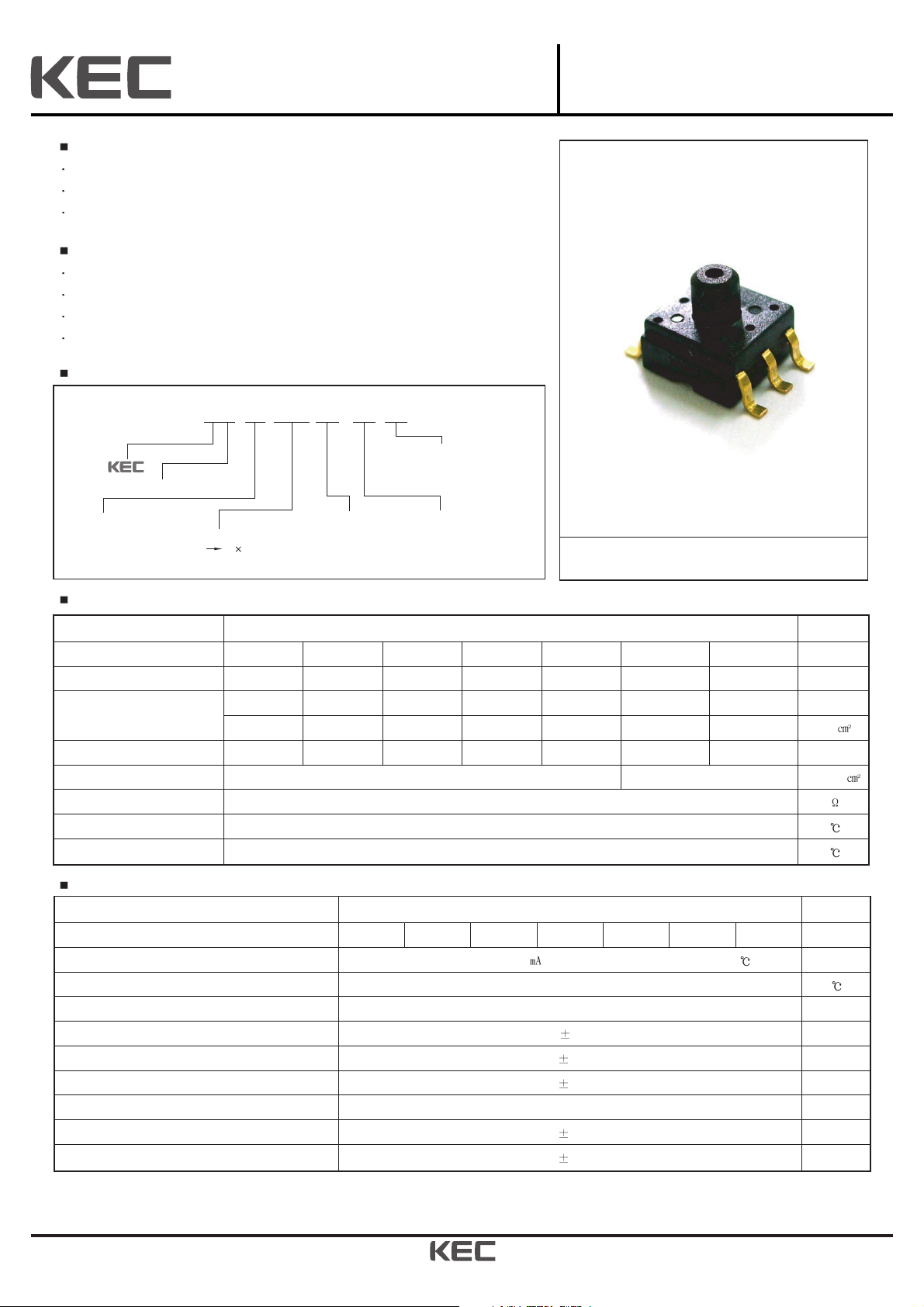
Semiconductor Pressure Sensor
Revision No : 2
FEATURES
Broad Pressure Range : 50~1,000kPa.
High Sensitivity, Excellent Linearity.
Highly Stable in Temperature Change.
APPLICATIONS
Medical Deivces.
Industrial Instrumentations.
Pressure Switch, Water Height Control, Pneumatic Devices etc.
Home Appliances.
MAXIMUM RATING
MODEL NUMBER FOR ORDERING
ELECTRICAL CHARACTERISTICS
Comment) 1. Operating humidity 25~80%RH. (unless otherwise noted)
2. Please, consult us when you use any other pressure media except air.
ITEM SPEC. UNIT
Classification 500 101 201 401 601 801 102 -
Test Condition
Operating Input Current 1.5 constant, Ambient Temperature Ta=25
-
Compensational Temperature Range 0 ~ 50
Full Scale Voltage 60 ~ 140 mV
Offset Voltage
20
mV
Linearity
0.3
%FS
Pressure Hysteresis
0.5
%FS
Mechanical Response Time 2 msec
Temperature Coefficient Of Offset (TCO)
5.0
%FS
Temperature Coefficient Of Sensitivity (TCS)
2.5
%FS
N
ITEM SPEC. UNIT
Model No. KPF500G03A KPF101G03A KPF201G03A KPF401G03A KPF601G03A KPF801G03A KPF102G03A -
Classification 500 101 201 401 601 801 102 -
Rated Pressure
50 100 200 400 600 800 1000 kPa
0.51 1.02 2.04 4.08 6.12 8.16 10.20
kgf/
Measurable Pressure Range -50 ~ 50 -100 ~ 100 -100 ~ 200 -100 ~ 400 -100 ~ 600 -100 ~ 800 -100 ~ 1000 kPa
Maximum Pressure Load Twice of Rated Pressure 1.5 Times of Reated Pressure
kPa(kgf/ )
Bridge Impedance 3000 ~ 6000
Operating Temperature -20 ~ 100
Storage Temperature -40 ~ 120
KP F GA00000
Silicon Pressure Sensor
ON/OFF Chip
:ON Chip (Amplified)
F:OFF Chip (Not Amplified)
Rated Pressure
123 12 10
3
=12,000kPa
Measuring Pressure
A : Absolute Pressure
D : Differential Pressure
G : Gage Pressure
Package Pin Configuration
No Mark : Standard
A : Type 1
Package Type
00 : Die
01~ : Package Series
PSM1
Page 2
2007. 6. 15 2/4
KPF500G03A ~ KPF102G03A
Revision No : 2
CHARACTERISTIC GRAPHS
RELIABILITY TEST
ITEMS TEST CONDITIONS
Life Test
High Temp. Storage
120 , 1000hrs
Low Temp. Storage
-40 , 1000hrs
Steady State Operating
25 5 , 1 million times, Rated Pressure
Low Temp. Operating
-20 , 1 million times, Rated Pressure
High Temp. Operating
100 , 1 million times, Rated Pressure
Temperature / Humidity Operating
40 , 90%RH, 1 million times, Rated Voltage
Environment Test
Heat Resistance
260 , 10 seconds
Temp. Cycle
-40 ~120 , 30minutes/1Cycle, 100Cycles
Mechanical Test
Vibration
Amplitude : 1.5mm, Frequency : 10~55Hz,
X, Y, Z(3-directions), 2 hrs each direction
Drop 75cm height, 2 times
Lead Fatigue
Tensile Strength : 9.8N(1kgf), 10seconds
Bending Strength : 4.9N(0.5kgf), Right/Left 90 , 1time
Solderability
230 , 5 seconds
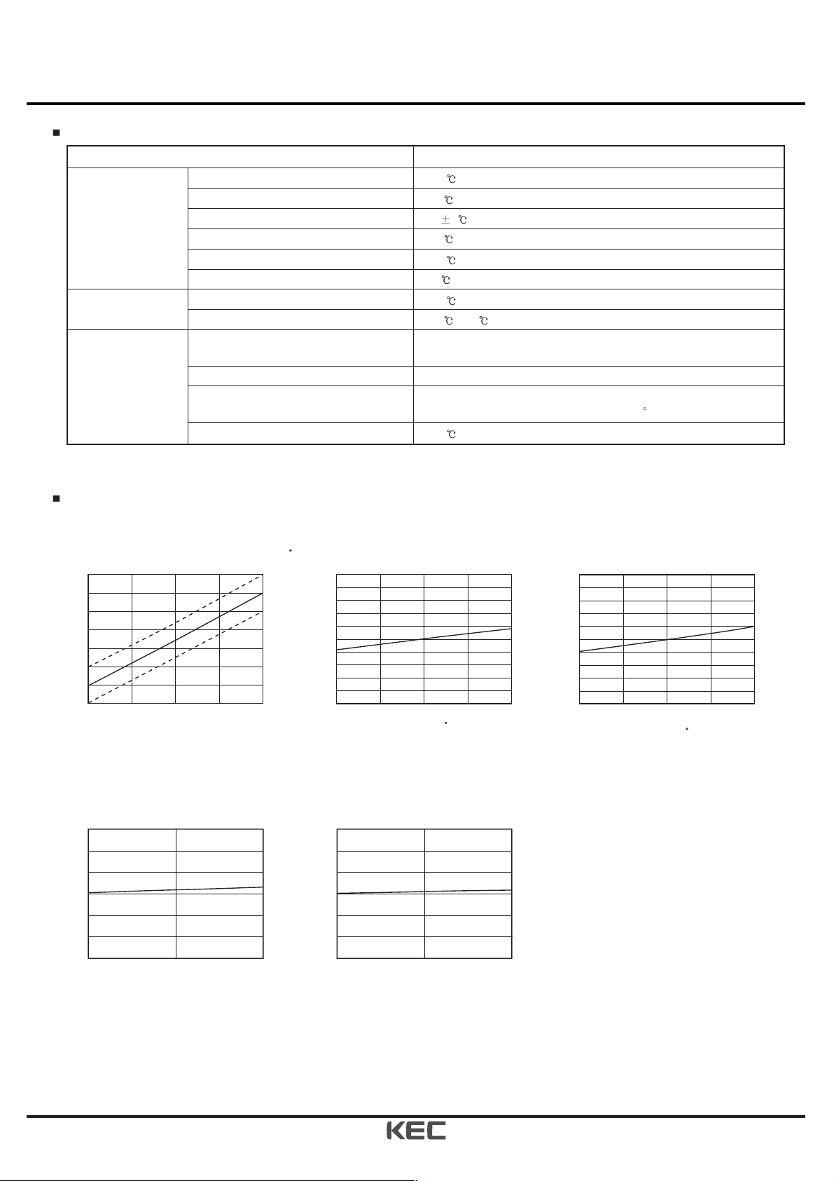
1. Full Scale Voltage Characteristics
Operating Input Current : 1.5mA, Temperature : 25 C
120
100
80
60
40
20
Full Scale Voltage (mV)
0
-20
0
1/2Pr Pr
Rated Pressure (kPa)
4. High Temperature continuous Operating Test
100°C, 1 million times : After testing, offset and full scale voltage variation is very small.
Offset Voltage Variation
3
2
1
0
-1
-2
Offset Voltage Variation (%FS)
-3
0
500,000 1,000,000
Pressure Cycle
2. Temperature Coefficient of Offset (TCO)
Operating Input Current : 1.5mA, Spec. : 5.0 %FS
5.0
4.0
3.0
2.0
1.0
0
-1.0
TCO (%FS)
-2.0
-3.0
-4.0
-5.0
0
Full Scale Voltage Variation
3
2
1
0
-1
-2
Full Scale Voltage Variation (%FS)
-3
0
25 50
Temperature ( C)
500,000 1,000,000
Pressure Cycle
_
+
3. Temperature Coefficient of Sensitivity (TCS)
Operating Input Current : 1.5mA, Spec. : 2.5%FS
2.5
2.0
1.5
1.0
0.5
0
-0.5
TCS (%FS)
-1.0
-1.5
-2.0
-2.5
0
25 50
Temperature ( C)
_
+
Page 3

2007. 6. 15 3/4
KPF500G03A ~ KPF102G03A
Revision No : 2
PACKAGE DIMENSIONS AND PC BOARD PATTERN (Unit :mm)
PIN CONFIGURATION
0.25
7
10.5
0.15
7
Max 15
0.8
Φ1.1Pressure Inlet
Φ3
3
3.5
0.8
_
+
2.5 0.25
_
+
2.5 0.25
Logo
1
Model No
2
Lot No
3
Terminal No. Me
1
2
3
(
(+)Input
(+)Output
4
5
6
(-)Output
aning
-)Output
Open
(-)Input
Remark
1.7
6
5
4
Land-pads
Constan
current
sou
rce
1.4
2.5
2.5
9.4
i = 1.5mA
+
2
t
R2
3
R3
R1
1
R4
5
V
-
6
Page 4

2007. 6. 15 4/4
KPF500G03A ~ KPF102G03A
Revision No : 2
Note
1. Mounting on printed circuit boards
When mounting a transistor on a printed circuit, it is assumed that
lead wires will be processed or reformed due to space limitation or
relations with other components. Even if no such special
processing reforming is conducted exercise care on the following
points :
(a) Make the spaces of lead wire inserting holes on the printed
circuit board the same as those of lead wires on a transistor.
(b) Even if The spaces are not the same, do not pull the lead
wires or push heavily against the sensor element.
(c) Use a spacer for form a lead maintain space between a sensor
and a printed circuit board, rather than closely contacting
them with each other.
(d) When forming a lead prior to mounting onto a board
- Bend the lead at a point 3mm or more apart from the
body(Lead root).
- Bend one lead wire after securing the other lead wire. (near
the main body)
- Keep space between the sensor main body and and a fixing
jig.
- When bending the lead along the jig, be careful not to
damage it with an edge of the jig.
- Follow other precautions described in respective standard
(e) When mounting a sensor onto a heat sink
- Use the specified accessory.
- Drill threaded holes on the heat kink as per specifications
and keep the surface free from burrs and undulations.
- Use KEC’s recommended silicon grease.
- Tighten the screw within the specified torque.
- Never apply a pneumatic screwdriver to a transistor main
body.
(f) Do not bend or stretch the lead wires repeatedly.
When pulling in the axial directions, apply 500g or 600g
power, depending on the shapes of lead wires.
2. Soldering
When soldering a sensor to a printed circuit board, the soldering
temperature is usually so high that it adversely affects the sensor.
Normally, tests are conducted at a soldering temperature of 265
for 10 seconds or 300 for 3 seconds. Be sure to complete
soldering procedures under these conditions of temperature and
time.
Be careful to select a type of flux that will neither corrode the
lead wires nor affect the electrical characteristics of a sensor.
The basic precautions for soldering procedures are as follows :
(a) Complete soldering procedures in a time as short as possible.
(b) Do not apply stress to a sensor after soldering by correcting
or modifying its location or direction.
(c) For a sensor employing a heat sink, mount it on the heat sink
first: then solder this unit to a printed circuit board after
confirming that it is fully secured.
(d) Do not directly solder the heat-radiating portion of a sensor
to a printed circuit board.
(e) In flow solder jobs, sensors are apt to float on the solder due
to solder surface tension. When adjusting the locations of
sensor, be careful not to apply excessive stress to the roots of
the sensor lead wires.
(f) When using a soldering iron select those which have less
leakage, and be sure to ground the soldering iron.
3. Cleaning a circuit board
After soldering, circuit boards must be cleaned to remove flux.
Observe the following precautions while cleaning them
(a) When cleaning circuit boards to remove flux, make sure that
no residual reactive ions such as Na or Cl ions remain. Note
that organic solvents react with water to generate hydrogen
chloride and other corrosive gases which can degrade device
performance.
(b) Do not rub the indication marks with a brush or one’s fingers
when cleaning or while a cleaning agent is applied to the
markings.
(c) There are ultrasonic wave cleaning methods which offer a
high cleaning effect within a short time. Since there methods
involve a complicated combination of factors such as the
cleaning bath size, ultrasonic wave vibrator output, and
printed circuit board mounting method, there is fear that the
service life of airtight seal-type sensors may be extremely
shortened. Therefore, as far as possible avoid using the
ultrasonic wave cleaning method.
- Basic requirements of ultrasonic wave cleaning method.
Frequency : 27~29kHz
Output : 300W or less (300W/ or less)
Recommended solvents : Refer to details above
Cleaning time : 30seconds or less
Application circuit
The Pressure sensor is designed to convert a voltage by means of
constant current drive and then, if nesessary, it amplifies the
voltage for use. The circuit shown below is a typical example of a
circuit in which the pressure sensor is used.
Constant Current
Circuit Unit
Pressure
Sensor
Amplifier Circuit Unit
OP
AMP
OP
AMP
OP
AMP
 Loading...