

Page 1
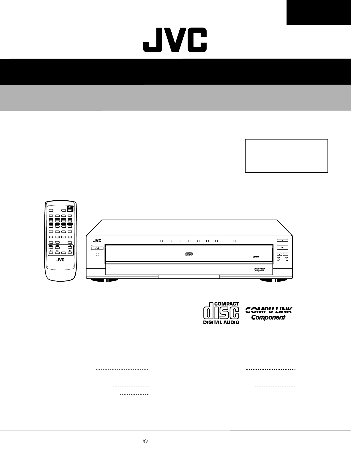
SERVICE MANUAL
COMPACT DISC AUTOMATIC CHANGER
XL-FZ700BK
Area suffix
J ------------------- U.S.A.
C ---------------- Canada
XL-FZ700BK
OPEN/
CLOSE
REPEAT
DISC 1 DISC 2 DISC 3 DISC 4
DISC 5 DISC 6 DISC 7 DISCSKIP
PROGRAM CANCEL CALLRANDOM
2341
6785
10 +109
RM-SXLFZ700J
REMOTE CONTROL
STANDBY/ON
STANDBY
STANDBY/ON
Contents
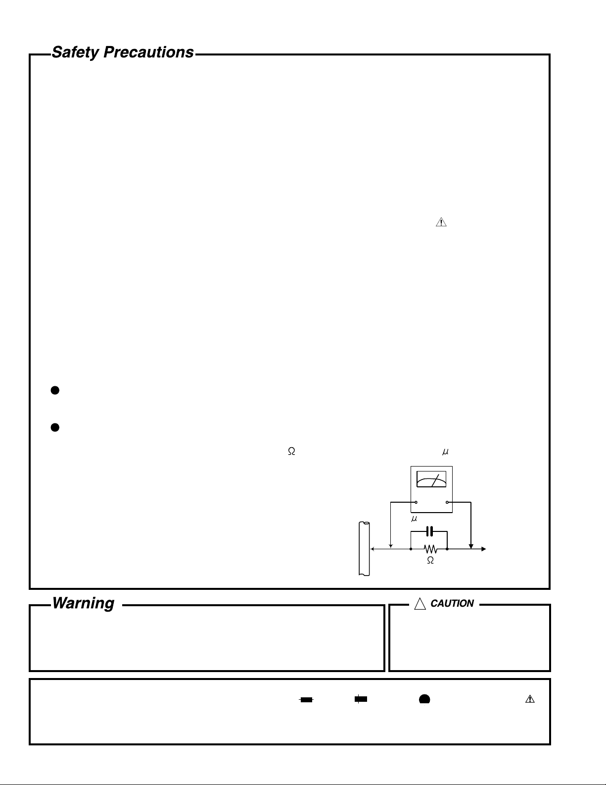
Safety precautions
Importance administering
point on the safety
Preventing static electricity
CD-R/RW PLAYBACK
1BIT P
. E .
M D
. D .
CONVERTER
DISC 1 DISC 2 DISC 3 DISC 4 DISC 5 DISC 6 DISC 7
XL-FZ700 COMPACT DISC AUTOMATIC CHANGER
1-2
Disassembly method
Adjustment method
1-3
Description of major ICs
1-4
EXCHANGE/DISC SKIP
7
-
PLAY & EXCHANGE
OPEN/CLOSE
PLAY
PAUSE
STOP
DISC
SKIP
1-5
1-19
1-19~26
COPYRIGHT 2002 VICTOR COMPANY OF JAPAN, LTD.
No.21073
Mar. 2002
Page 2
XL-FZ700BK
1. This design of this product contains special hardware and many circuits and components specially for safety
purposes. For continued protection, no changes should be made to the original design unless authorized in
writing by the manufacturer. Replacement parts must be identical to those used in the original circuits. Services
should be performed by qualified personnel only.
2. Alterations of the design or circuitry of the product should not be made. Any design alterations of the product
should not be made. Any design alterations or additions will void the manufacturer`s warranty and will further
relieve the manufacture of responsibility for personal injury or property damage resulting therefrom.
3. Many electrical and mechanical parts in the products have special safety-related characteristics. These
characteristics are often not evident from visual inspection nor can the protection afforded by them necessarily
be obtained by using replacement components rated for higher voltage, wattage, etc. Replacement parts which
have these special safety characteristics are identified in the Parts List of Service Manual. Electrical
components having such features are identified by shading on the schematics and by ( ) on the Parts List in
the Service Manual. The use of a substitute replacement which does not have the same safety characteristics
as the recommended replacement parts shown in the Parts List of Service Manual may create shock, fire, or
other hazards.
4. The leads in the products are routed and dressed with ties, clamps, tubings, barriers and the like to be
separated from live parts, high temperature parts, moving parts and/or sharp edges for the prevention of
electric shock and fire hazard. When service is required, the original lead routing and dress should be
observed, and it should be confirmed that they have been returned to normal, after re-assembling.
5. Leakage currnet check (Electrical shock hazard testing)
After re-assembling the product, always perform an isolation check on the exposed metal parts of the product
(antenna terminals, knobs, metal cabinet, screw heads, headphone jack, control shafts, etc.) to be sure the
product is safe to operate without danger of electrical shock.
Do not use a line isolation transformer during this check.
Plug the AC line cord directly into the AC outlet. Using a "Leakage Current Tester", measure the leakage
current from each exposed metal parts of the cabinet, particularly any exposed metal part having a return
path to the chassis, to a known good earth ground. Any leakage current must not exceed 0.5mA AC (r.m.s.).
Alternate check method
Plug the AC line cord directly into the AC outlet. Use an AC voltmeter having, 1,000 ohms per volt or more
sensitivity in the following manner. Connect a 1,500 10W resistor paralleled by a 0.15 F AC-type capacitor
between an exposed metal part and a known good earth ground.
Measure the AC voltage across the resistor with the AC
voltmeter.
Move the resistor connection to each exposed metal part,
particularly any exposed metal part having a return path to
the chassis, and meausre the AC voltage across the resistor.
Now, reverse the plug in the AC outlet and repeat each
measurement. Voltage measured any must not exceed 0.75 V
AC (r.m.s.). This corresponds to 0.5 mA AC (r.m.s.).
0.15 F AC TYPE
1500 10W
Good earth ground
AC VOLTMETER
(Having 1000
ohms/volts,
or more sensitivity)
Place this
probe on
each exposed
metal part.
!
1. This equipment has been designed and manufactured to meet international safety standards.
2. It is the legal responsibility of the repairer to ensure that these safety standards are maintained.
3. Repairs m ust be made in accordance with the relevant safety standards.
4. It is essential that safety critical components are replaced by approved parts.
5. If mains voltage selector is provided, check setting for local voltage.
Burrs formed during molding may
be left over on some parts of the
chassis. Therefore, pay attention to
such burrs in the case of
preforming repair of this system.
In regard with component parts appearing on the silk-screen pr inted side (parts side) of the PWB diagrams, the
parts that are printed over with black such as the resistor ( ), diode ( ) and ICP ( ) or identified by the " "
mark nearby are critical for safety.
(This regulation does not correspond to J and C version.)
1-2
Page 3
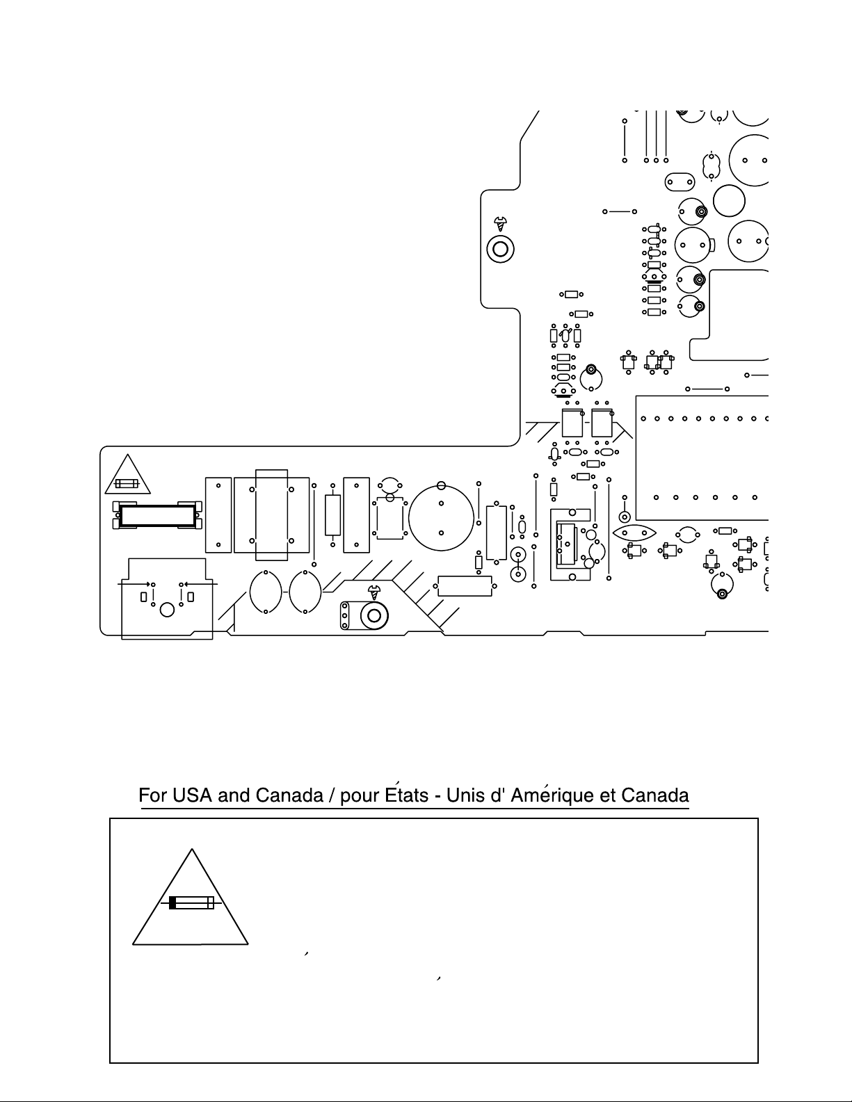
XL-FZ700BK
Importance administering point on the safety
R963
R900
D991
R965
R969
1.6A /125V
FC901 FC902
F901
J901
B1081
B1082
L901
C905 C906
R902
B1611
EP901
C902 C903
C919
D901
C907
R905
R906
B1221
R907
B1131
K902
C915
B1083
R960
C993
B1421
R961
Q991
B1222
D911
R911
HS901
PC901
C918
R910
C992
IC901
B1223
C913
R908
B1811
C908
B1132
C917
B1226
PC902
D974
D972
D973
R976
Q953
R974
R975
R973
R901
D956
B1812
B1813
D957
C997
B1814
D902D903
D954
C981
C996
C989
C909
L957
C995
B1224
D904
L959
C987
C979
L955
B1225
D908
R903
R904
D910
C910
C914
Power supply board (Forward side)
Caution: For continued protection against risk
of fire, replace only with same type 1.6A/125V
for F901.
This symbol specifies type of fast operating fuse.
Precaution: Pour eviter risques de feux, remplacez
le fusible de surete de et F901 comme le meme type
que 1.6A/125V.
Ce sont des fusibles suretes qui functionnes rapide.
^
1-3
Page 4
XL-FZ700BK
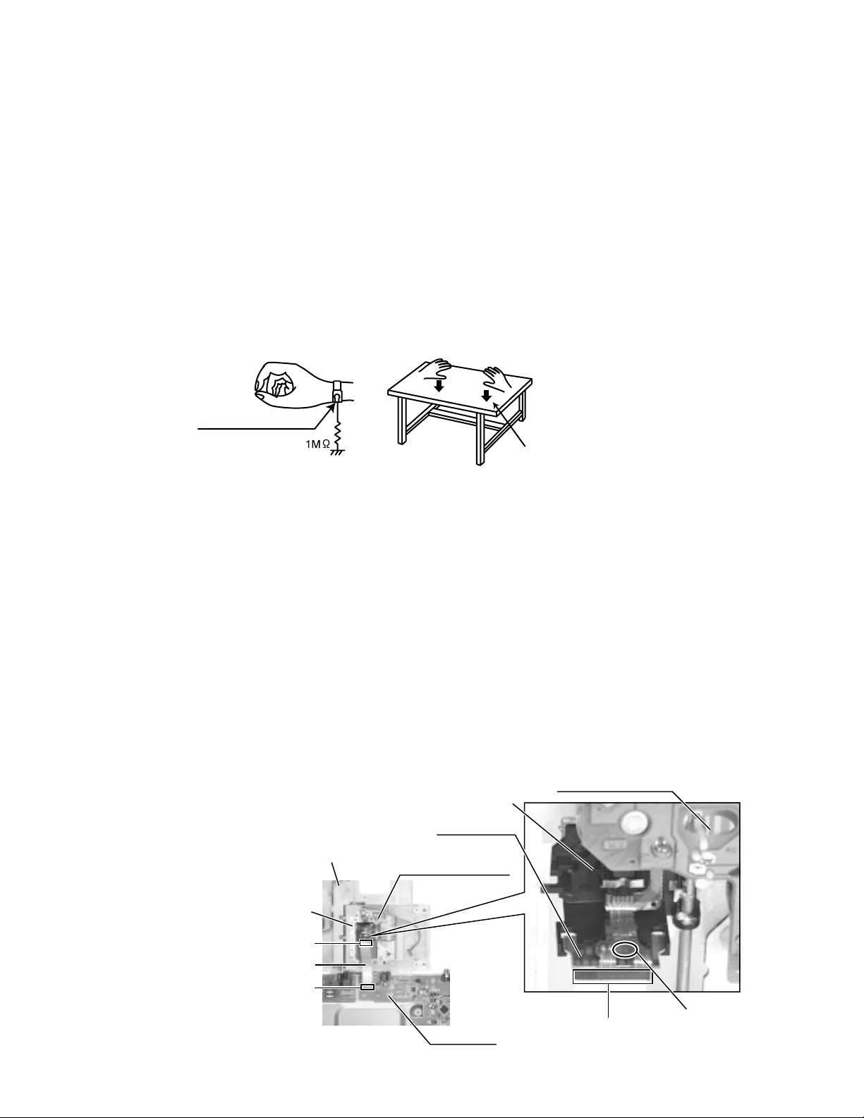
Preventing static electricity
1.Grounding to prevent damage by static electricity
Electrostatic discharge (ESD), which occurs when static electricity stored in the body, fabric, etc. is discharged,
can destroy the laser diode in the traverse unit (optical pickup). Take care to prevent this when performing repairs.
2.About the earth processing for the destruction prevention by static electricity
Static electricity in the work area can destroy the optical pickup (laser diode) in devices such as CD players.
Be careful to use proper grounding in the area where repairs are being performed.
2-1 Ground the workbench
Ground the workbench by laying conductive material (such as a conductive sheet) or an iron plate over
it before placing the traverse unit (optical pickup) on it.
2-2 Ground yourself
Use an anti-static wrist strap to release any static electricity built up in your body.
(caption)
Anti-static wrist strap
Conductive material
(conductive sheet) or iron plate
3. Handling the optical pickup
1. In order to maintain quality during transport and before installation, both sides of the laser diode on the
replacement optical pickup are shorted. After replacement, return the shorted parts to their original condition.
(Refer to the text.)
2. Do not use a tester to check the condition of the laser diode in the optical pickup. The tester's internal power
source can easily destroy the laser diode.
4.Handling the traverse unit (optical pickup)
1. Do not subject the traverse unit (optical pickup) to strong shocks, as it is a sensitive, complex unit.
2. Cut off the shorted part of the flexible cable using nippers, etc. after replacing the optical pickup. For specific
details, refer to the replacement procedure in the text. Remove the anti-static pin when replacing the traverse
unit. Be careful not to take too long a time when attaching it to the connector.
3. Handle the flexible cable carefully as it may break when subjected to strong force.
4. It is not possible to adjust the semi-fixed resistor that adjusts the laser power. Do not turn it.
Attention when traverse mechanism unit is decomposed
*Please refer to "Disassembly method" in the text for how to remove.
Solder soldering part on the
1.
flexible board, before the
card wire is removed from
the connector on the flexible
board or the connector
CN601 on the main board.
(Disconnecting the flexible
Loading base assembly
Traverse
mechanism
(reverse side)
unit
CD mechanism board
Pickup unit
Flexible board
wire without soldering may
cause damage to the pickup.)
Please remove solder after
2.
connecting the flexible wire
Connector
Card wire
CN601
with when you install picking
up in the substrate.
Main board
CD mechanism board
Connector
Soldering part
1-4
Page 5
XL-FZ700BK
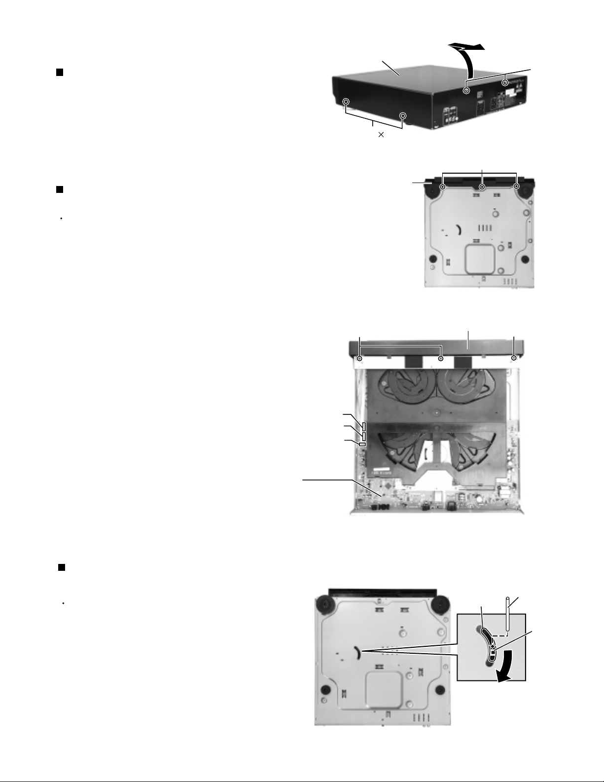
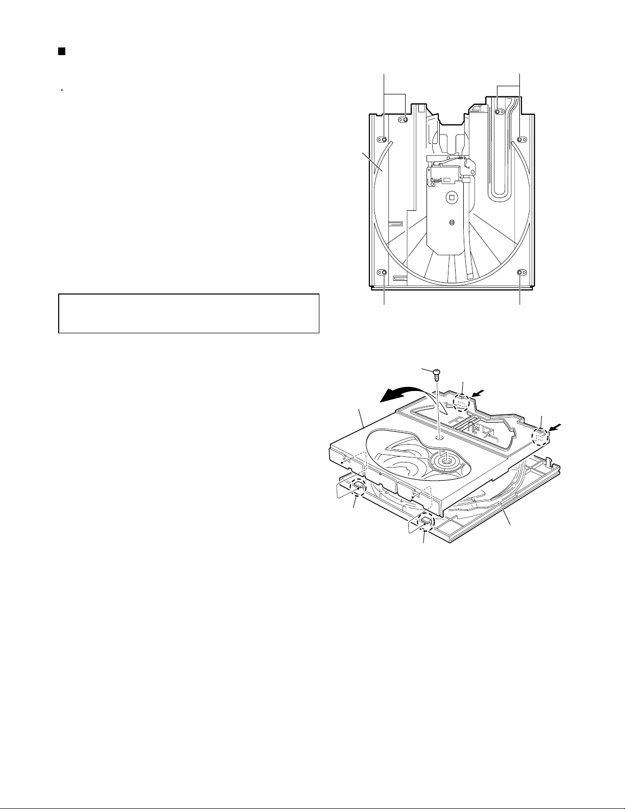
Disassembly method
Removing the top cover (See Fig.1)
1.
Remove the four screws A attaching the top cover
on the both sides of the body.
2.
Remove the two screws B on the back of the body.
3.
Remove the top cover from behind in the direction of
the arrow while pulling both sides outward.
Removing the front panel assembly
(See Fig.2 and 3)
Prior to performing the following procedure, remove
the top cover.
1.
Remove the three screws C attaching the front panel
assembly on the bottom of the body.
2.
Remove the three screws D attaching the front panel
assembly.
3.
Disconnect the card wire from the connector CN805,
CN801 and CN803 on the main board and detach
the front panel assembly toward the front.
Top cover
A
2
Front panel assembly
(bottom side)
D
Fig.1
C
Fig.2
Front panel assembly
B
D
Removing the main try assembly
(See Fig.4 and 5)
Prior to performing the following procedure, remove
the top cover and front panel assembly.
Hook a bar on the hole of the load base, then turn
1.
the load base clockwise. Then the main tray
assembly will be opened.
Disconnect the card wire from the connector CN841
2.
on the relay board.
CN805
CN801
CN803
Main board
(bottom side)
Fig.3
Load base
(a part)
A bar
Hole
While preventing the hook a from getting caught on
3.
the hook b, draw out the main tray assembly from
the loading base assembly.
Fig.4
1-5
Page 6
XL-FZ700BK
(Rear side)
Main tray assembly
(Front side)
CN841(On the relay board)
Removing the loading base assembly
(See Fig.6)
Prior to performing the following procedure, remove
the top cover and main tray assembly.
1.
Remove the seven screws E(top side:6, front side:1)
attaching the loading base assembly.
Hook a
(Main tray assembly)
Hook b
(Loading base assembly)
Loading base assembly
Fig.5
(Top side)
E
Main tray assembly
Loading base assembly
(Front side)
Loading base assembly
2.
Disconnect the harness from the connector CN602,
CN808 and CN809 on the main board.
CAUTION!!
Before removing the card wire which
connects the flexible board and main board,
solder the soldering part and make it shortcircuit.
Moreover, while having removed the card
wire, don't remove this solder.
3.
Disconnect the card wire from the connector CN601
on the main board.
Removing the rear panel (See Fig.7)
Prior to performing the following procedure, remove
the top cover.
1.
Remove the four screws F and one screw G
attaching each board to the rear panel .
2.
Remove the three screws H attaching the rear panel
on the back of the body.
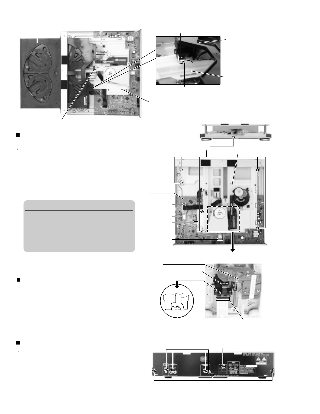
Removing the relay board (See Fig.8)
Prior to performing the following procedure, remove
the top cover, front panel assembly, main tray
assembly and loading base assembly.
Main board
CN809
CN808
CN602
CN601
CD mechanism board
Soldering part
F
(Loading base assembly reverse side
Traverse mechanism unit)
Pickup unit
Flexible board
Connector
Card wire(To connector
CN601 on the main board)
Fig.6
G
1.
Disconnect the harness from the connector CN810
and CN811 on the main board.
2.
Remove the two screws I attaching the relay board.
1-6
H
Fig.7
Page 7
XL-FZ700BK
y
)
Removing the main board (See Fig.8)
Prior to performing the following procedure, remove
the top cover, front panel assembly, main tray
assembly and loading base assembly.
1.
Disconnect the harness from the connector CN810,
CN811, CN951, CN953, CN955 and CN957 on the
main board.
2.
Remove the four screws J attaching the main board.
3.
Remove the four screws F attaching the main board
to the rear panel (see fig. 7).
Removing the power supply board
(See Fig.8)
Prior to performing the following procedure, remove
the top cover, front panel assembly, main tray
assembly and loading base assembly.
1.
Disconnect the harness from the connector CN951,
CN953, CN955 and CN957 on the main board.
2.
Remove the four screws K attaching the power
supply board.
CN955
/CN957
CN951
/CN953
CN810
/CN811
Main board
Relay board
I
J
Power supply board
K
after removing
3.
Remove the one screw G attaching the power supply
board to the rear panel (see fig. 7).
4.
Remove the protect sheet if needed.
<Front panel assembly section>
Removing the operation switch board,
power switch board and display board
(See Fig.1 and 2)
Prior to performing the following procedure, remove
the top cover and the front panel assembly.
1.
Remove the six screws A attaching the operation
switch board on the inner of the front panel
assembly. Disconnect the card wire from the
connector CN804 and CN861 on the operation
switch board, if needed.
2.
Remove the two screws B attaching the power
switch board on the inner of the front panel
assembly. Disconnect the card wire from the
connector CN862 on the power switch board, if
needed.
3.
Remove the two screws C attaching the display
board on the inner of the front panel assembly.
Disconnect the card wire from the connector CN802
and CN806 on the display board, if needed.
4.
Remove the switch buttons, if needed.
Operation switch board
A
Display board
CN802
CN804
CN806
Fig.8
Power switch board
C
Fig.1
Switch button
Fig.2
Protect sheet
Front panel assembly
CN861
Front panel assembl
(inner side)
CN862
(inner side
B
1-7
Page 8
XL-FZ700BK
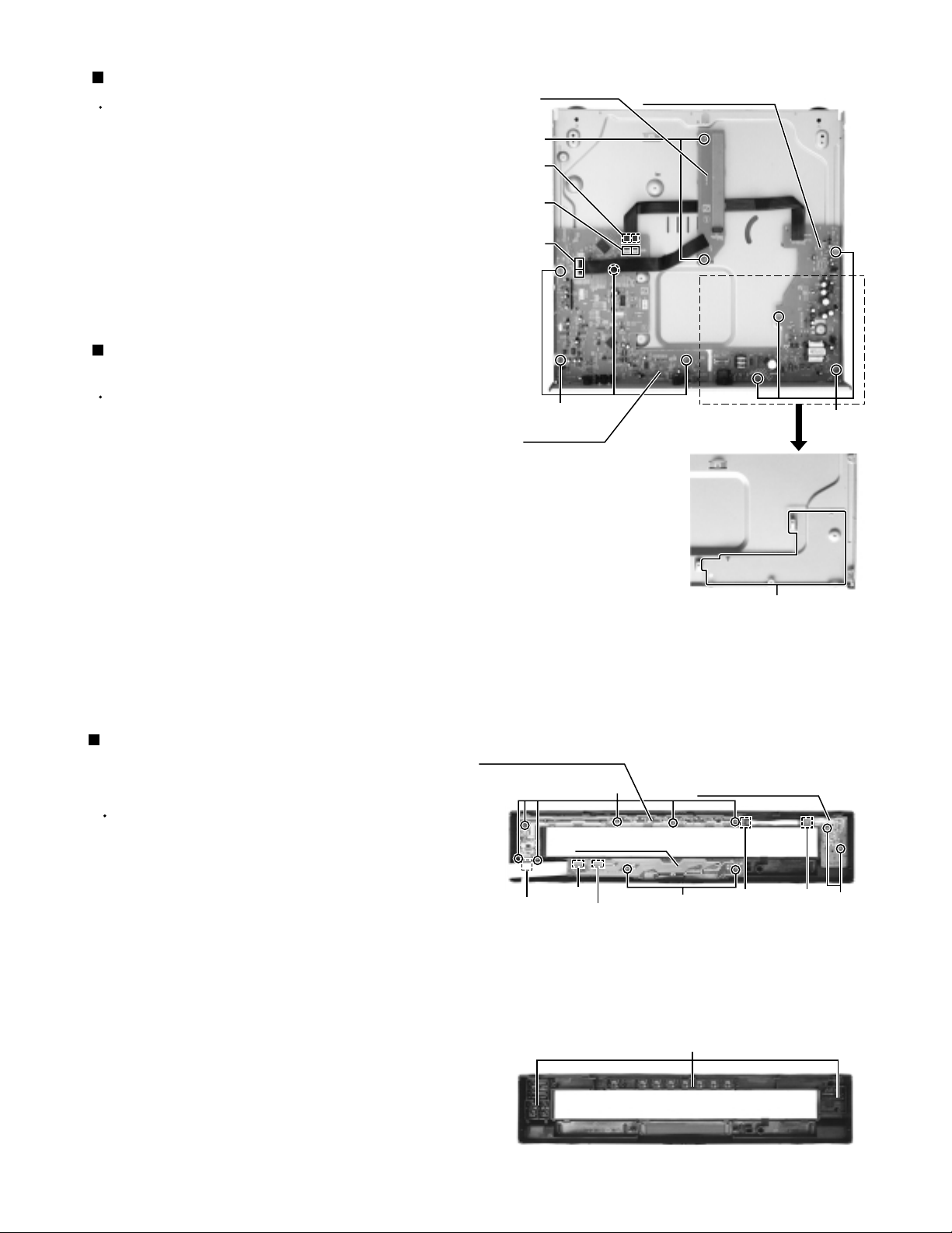
<Main tray assembly unit>
Prior to performing the following procedures, remove
the top cover, the front panel assembly and the main
tray assembly.
Main tray assembly
Removing the fitting (See Fig.1)
1.
Remove the fitting on the front side of the main tray
assembly while releasing the four joints a upward.
Hook
Fitting
Lifts for above while pulling the hook
in three places to front side.
Removing the photo sensor board and
the sub tray drive motor assembly
(See Fig.2)
1.
Turn over the main tray assembly and remove the
two screws A attaching the photo sensor board.
Joints a
Fitting
Joints a
Fig.1
Sub tray drive motor assembly
B
B
A
2.
Disconnect the card wire from connector CN82 on
the photo sensor board.
REFERENCE:
3.
Remove the two screws B attaching the sub tray
drive motor assembly.
Make sure to disconnect the card wire
from the photo sensor board. If the
photo sensor board is pulled out from
the main tray without disconnecting the
card wire, the cam switch side inside of
the main tray may be damaged.
When reassembling,
Attach the two wires to the part b on the photo
sensor board, and before reattaching the photo
sensor board, connect the card wire to connector
CN82 and pass the card wire extending from
connector CN81 through the notch c of the main
tray.
CN81
Part b
Photo sensor board
CN82
Notch c
Main tray
Card wire
Fig.2
1-8
Page 9
Removing the main tray cover and the
main tray (See Fig.3 and 4)
Prior to performing the following procedure, remove
the fitting.
1.
Remove the six screws C attaching the main tray
on the bottom side of the main tray assembly.
2.
Remove the screw D attaching the main tray cover
on the upper side of the main tray assembly.
3.
Push the two joint tabs d on the back of the main
tray assembly to release the main tray cover from
the tray bottom. Disengage the joint tabs e of the
main tray from the main tray cover.
XL-FZ700BK
CC
Main tray
assembly
CAUTION:
After removing the main tray cover, can not
up side down !
Main tray cover
Joint tab e
CC
Fig.3
D
Joint tab e
Joint tab d
Joint tab d
Main tray
Fig.4
1-9
Page 10

XL-FZ700BK
Sub tray position and operation check
(See Fig.5 and 6)
Prior to performing the following procedures, remove
the fitting and the main tray cover.
CAUTION:
Make sure the sub trays are set as shown
in Fig.5. When moving the sub trays, put
the sub trays which come to the position (4)
and (5) forward in turn.
Prior to moving the sub trays by hand, the
sub tray drive motor assembly must be
removed in advance referring to the
preceding page.
Do not put the sub trays forward except at
the position (4) and (5).
(3)
(2)
(4)
Sub tray (1)
(7)
(6)
(5)
Fig.5
Removing the U/D cam (U) (See Fig.7)
Prior to performing the following procedure, remove
the main tray cover.
1.
Remove the two screws E attaching the U/D cam
(U) on the upper side of the main tray assembly.
2.
Remove the U/D cam (U).
Fig.6
E
1-10
U/D cam (U)
Fig.7
Page 11

Removing the sub trays (See Fig.8 to 14)
Prior to performing the following procedure, remove
the main tray cover and the U/D cam (U).
XL-FZ700BK
CAUTION:
Remove the sub tray assembly (4), (5), (3),
(6), (2), (7) and (1) in order. When
reattaching, observe the following
procedure without fail.
1.
Remove the sub tray (4) and (5) from the main tray
upward.
2.
Remove the sub tray (3) and (6) upward.
3.
Similarly, remove the sub tray (2) and (7) upward.
4.
At last, remove the sub tray (1) upward.
Reattaching the sub tray
1.
Reattach the sub tray (1) while fitting the part f to the
groove of the ACT. gear (1) marked g.
(3)
Sub tray (2)
Sub tray (4)
(6)
(5)
Fig.8
(1)
(7)
Fig.9
CAUTION:
After checking that it is in the state of Fig.
19, the sub tray 1 is attached.
2.
Reattach the sub tray (2) while inserting the shaft h
into the groove i of the main tray, and at the same
time, fitting the part j to the groove of the ACT. gear
(1) marked k .
Move the sub tray (2) toward the tray (1).
CAUTION:
When Sub tray drive motor assembly is not
attached, notice sub tray about the position
to incorporate in order to move freely.
3.
Similarly, reattach the sub tray (7).
Shaft h
Marked k
Groove i
Sub tray (2)
Part j
Sub tray (1)
Sub tray (7)
Part f
Marked g
Fig.10
ACT. gear(1)
1-11
Page 12

XL-FZ700BK
4.
Reattach the sub tray (3) while inserting the shaft l
into the groove m of the main tray, and at the same
time, putting the shaft n on the U/D cam (L). Then,
move the sub tray (3) toward the sub tray (2) until it
stops.
5.
Reattach the sub tray (6) as well as the sub tray (3),
and move the sub tray (6) toward the sub tray (7)
until it stops.
REFERENCE:
At this point, the sub tray (3) and (6) are
on top of the sub tray (2) and (7),
respectively.
6.
Reattach the sub tray (4) and (5) while fitting the part
o to the ACT. gear (2) on the main tray, respectively.
CAUTION:
Make sure the part o of the sub tray (4)
and (5) engage with the ACT. gear (2)
correctly on the center of the main tray.
7.
Reattach the U/D cam (U) on the upper side of the
main tray assembly with the two screws E (see fig.7).
Sub tray (4)
Shaft l
Sub Tray (3)
Part o
Groove m
Shaft n
Sub tray (2)
ACT. gear (2)
Fig.11
CAUTION:
Sub tray (6)
Sub tray (7)
Make sure that the trays are attached to
the correct position and that they can be
moved. To move the sub trays manually,
the sub tray drive motor assembly must
be removed in advance.
Sub tray (5)
Part o
ACT. gear (2)
Sub tray (3)
Sub tray (2)
Fig.12
Sub tray (6)
Sub tray (7)
1-12
Fig.14Fig.13
Page 13

XL-FZ700BK
Removing the cam switch board assembly
(See Fig.15 to 17)
Prior to performing the following procedure, remove
the main tray cover, the U/D cam (U) and the sub
trays.
1.
Remove the screw F attaching the gear cover.
Release the two tabs marked p by pushing inward
from the bottom side.
2.
Remove the cam gear (2) upward.
3.
Disconnect the card wire from connector CN83 on
the cam switch board assembly.
4.
Remove the two screws G attaching the cam switch
board assembly.
CAUTION:
When reattaching the cam gear (2), set the
position of the boss and the triangular mark
and hole as shown in Fig.17.
Tabs marked p
G
F
Fig.15
Cam switch board assembly
Cam gear (2)
Gear cover
CN83
G
CAUTION:
Keep in mind that U/D cam (L) and ACT.
gear (1) will fall if the main tray assembly is
turned over.
Fig.16
High tooth
Triangular mark
Position the high tooth
and the triangular mark
Hole
A hole and a triangular
mark become right above.
Triangular mark
Set the position of the boss
Fig.17
1-13
Page 14

XL-FZ700BK
Removing the ACT. gear (1), U/D cam (L),
cam gear (1) and ACT. gear (2)
(See Fig.18 and 19)
U/D cam (L)
Prior to performing the following procedure, remove
the main tray cover, the U/D cam (U) and the sub
trays.
1.
Draw out the U/D cam (L).
2.
Draw out the ACT. gear (1).
3.
Draw out the cam gear (1).
4.
Draw out the ACT. gear (2) while pushing the two
tabs q toward inward.
CAUTION:
When reassembling, make sure the position
of each gear referring to Fig.19 and
reattach the ACT. gear (2) first.
ACT. gear (1)
ACT. gear (2)
Cam gear (1)
Fig.18
ACT. gear (1)
Cam gear (1)
U/D cam (L)
ACT. gear (2)
Tabs q
Fig.19
1-14
Page 15

XL-FZ700BK
<Loading base assembly unit>
Prior to performing the following procedures, remove
the top cover, the front panel assembly, the main
tray assembly, the loading base assembly.
Removing the elevator base
(See Fig.20 and 21)
REFERENCE:
1.
Remove the load gear(1) and load gear(2) form the
load base.
2.
Turn over the loading base assembly and remove
the two screws Q.
3.
Remove the elevator base upward.
It is not necessary to remove the traverse
mechanism assembly from the elevator
base. As the removing procedure of the
traverse mechanism, please refer to
“Removing the traverse mechanism
assembly”.
Slide gear
Elevator base
Shafts
Fig.20
Slide gear
Q
Reattaching the elevator base
REFERENCE:
1.
Reattach the elevator base to the loading base
assembly while fitting the two shafts on the side of
the elevator base to the grooves of the slide gear.
2.
Reattach the two screws Q.
From above the loading base, turn the
load base counterclockwise until the slide
gear stops at the back end as shown in
Fig.21.
Load gear(1)
Load base
Load gear(2)
Fig.21
1-15
Page 16

XL-FZ700BK
Removing the belt / load base / slide gear
(See Fig.22 to 24)
Prior to performing the following procedures, remove
the elevator base.
1.
Remove the belt on the upper side of the loading
base assembly.
2.
Remove the screw R attaching the pulley gear.
3.
Remove the pulley gear, the load gear(1), the load
gear(2) and the belt respectively.
4.
Remove the screw S and remove the load base
upward pushing two claws inside.
5.
Remove the two screws T and the slide gear
upward.
CAUTION: When reattaching the slide gear
and the load base,
1.
Move the slide gear toward the front until it stops
(Fig.25).
Loading base assembly
Belt
R
Pulley gear
Fig.22
Load gear(1)
Pulley gear
Load gear(2)
S
2.
Make sure that the part d of the load base is out of
alignment with the switch e and that the gear f is
disengaged from the slide gear.
Slide gear
Switch e
Load base
Claw
Loading base assembly
Fig.23
T
Slide gear
Load base
1-16
Part d
Gear f
Fig.24Fig.25
Page 17

XL-FZ700BK
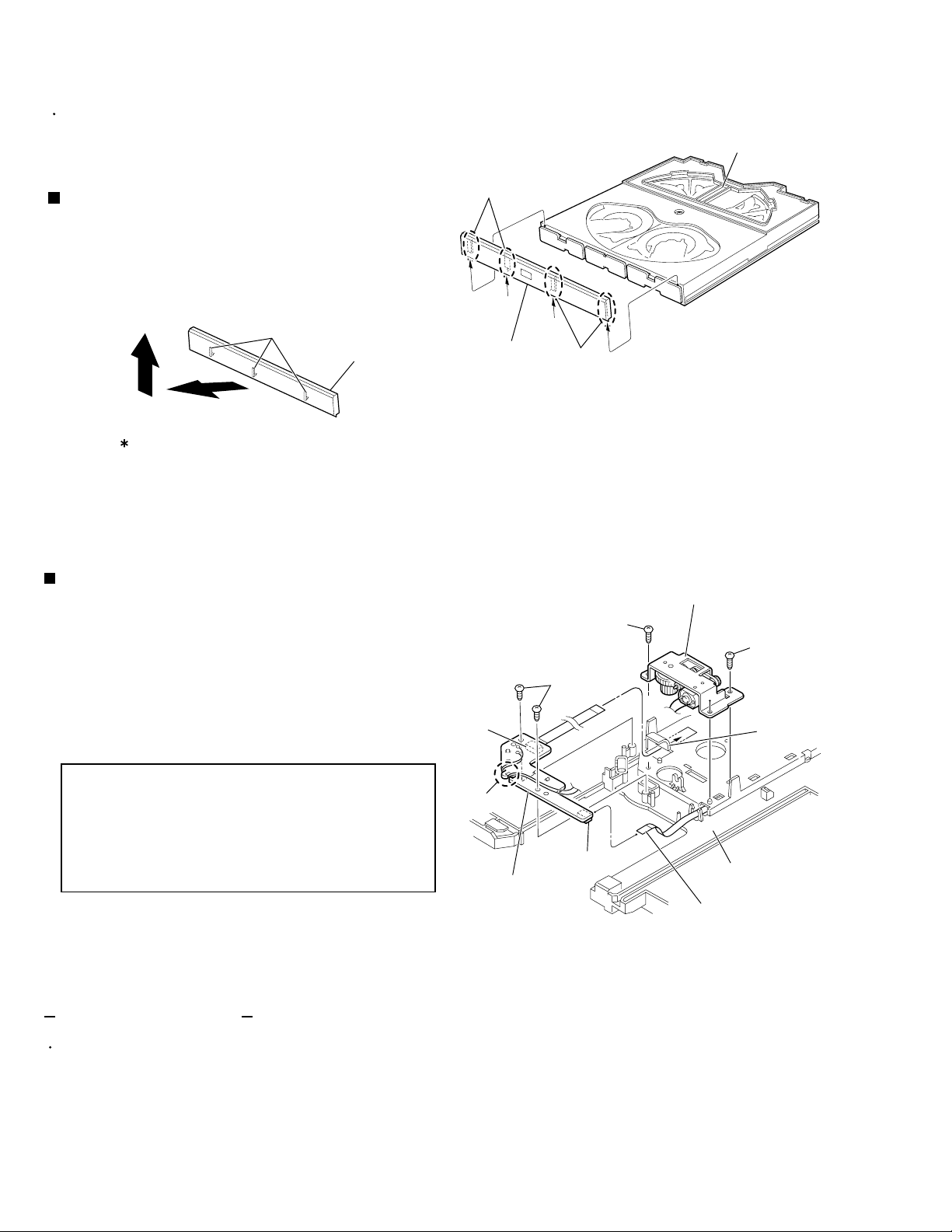
Removing the loading motor / loading
motor board (See Fig.26 and 27)
1.
Remove the two screws U attaching the loading
motor on the upper side of the loading base
assembly.
2.
Turn over the loading base assembly and unsolder
the two soldering g on the loading motor board.
3.
Remove the two screws V and remove the loading
motor board.
4.
Spread apart the two tabs h and pull out the loading
motor.
CAUTION:
When reattaching the loading motor board ,
settle the wires on the four hooks i on the
loading base assembly and draw the other
end to the left as shown in Fig.28.
Removing the tray switch board
(See Fig.28)
U
Loading motor
Fig.26
V
Loading motor board
1.
Turn over the loading base assembly, and remove
the tray switch board while spreading apart the two
tabs j.
Hooks i
Tray switch board
Tabs j
Loading motor board
Soldering g
Tabs h
Loading motor
Fig.27Fig.28
1-17
Page 18

XL-FZ700BK
<Traverse mechanism unit>
Removing the pickup (See Fig.1 and 2)
1.
Rotate the cam gear in the direction of the arrow a,
and move the pickup unit to around a center.
2.
Open the stopper stopping the shaft in the direction
of the arrow b, and move in the direction of the arrow
c and extract the shaft.
3.
Draw out and remove the pickup unit from the
engagement a.
Note:
Please check having attached engagement a of the
pickup unit and the chassis base correctly in the
case of a re-assembly.
4.
Remove the four engagement b attaching the CD
rack from the back of the pickup unit.
Pickup unit
Engagement a
Pickup unit
b
Stopper Stopper
Shaft
Cam gear
c
Fig.1
Pickup unit
Chassis base
Traverse mechanism unit
Shaft
a
Shaft
Removing the CD mechanism board
(See Fig.3)
1.
In the bottom side of CD mechanism assembly,
unsolder the four soldering parts attaching the
spindle motor and the feed motor to CD mechanism
board, respectively.
2.
Remove the one screw A attaching the CD
mechanism board.
Removing the spindle motor & feed motor
(See Fig.4)
Prior to performing the following procedure, remove
the CD mechanism board.
1.
In the upper side of CD mechanism assembly,
remove the two screws B attaching the spindle motor
and two screws C attaching the feed motor.
Engagement b
Soldering part
B
Engagement b
Fig.2
Feed motor
Fig.3
Engagement b
CD rack
Soldering part
Spindle motor
CD mechanism board
A
1-18
Spindle motor
Feed motor
C
Fig.4
Page 19

Adjustment method
There is no adjustment part in this model.
Description of major ICs
PQ05RD21 (IC951) : Regulator
1. Block diagram
XL-FZ700BK
Vin 1
2 Vo
IC
4 Vc
3
GND
STR-G6651(IC901) : Switching regulator
1. Block diagram
VIN
4
START
REG
T.S.D
O.V.P
LATCH
O.S. C
Vth(2)
Comp.2
DRIVE
Comp.1
1
D
2
S
Vth(1)
5
O.C.P/F.B
3
GND
1-19
Page 20

XL-FZ700BK
MN6627482WA (IC651) : Digital servo & Digital signal processer D/A converter
1. Pin layout
2.Block diagram
LRCKIN(MSEL)
BCLK(SSEL)
SRDATAIN
(PSEL)
IOSEL
CLVS
CRC
BLKCK
CLDCK
SBCK
SUBC
DEMPH
RESY
SSEL
SQCK
SUBQ
AVSS2
AVDD2
PCK
EFM
PLLF
PLLF2
DSLF
IREF
DRF
ARF
RSEL
PSEL
MLD
MCLK
MDATA
VCOF2)
VCOF
BYTCK
SMCK
FCLK
PMCK
CSEL
MSEL
X2
X1
STAT
DIGITAL
DEEMPHSIS
SUB
CODE
BUFFER
DSL.
PLL
VCO
VCO
TIMING
GENERATION
PITCH
CONTROL
20 ~ 1
21
~
40
41 ~ 60
8TIMES
OVER SAMPLING
DIGITAL FILTER
CD-TEXT
BUFFER
EFM
DEMODULATION
SYNC
INTERPOLATION
SUBCODE
DEMODULATION
MICRO
COMPUTER
INTERFACE
COVERTER
A/D
80
~
61
1BIT
DAC
PWM
LOGIC
16k
SRAM
CIRC
ERROR
CORRECTION
DEINTERLEAVE
SERVO
CPU
PWM
(R)
PWM
(L)
OUTPUT
INPUT PORT
DIGITAL
AUDIO
INTERFACE
CLV
SREVO
INTER POLATION
SOFT MUTING DIGITAL
ATTENUATION
PEAK DETECTIVE
AUTO CUE
D/A
CONVERTER
PORT
SERVO
TIMING GENERATOR
AVSS1
-
+
-
+
AVDD1
OUTR
OUTL
FLAG
IPFLAG
TX
ECM
ECS
PC
LRCK
SRDATA
BCLK
DMUTE
TOFS
KICK
VREF
TRV
TVD
TRD
FOD
TBAL
FBAL
/TLOCK
/FLOCK
LDON
WVEL
SENSE
1-20
VDD
VSS
DVSS1
DVDD1
/RST
/TEST
FE
TE
RFENV
TRCRS
VDET
BDO
OFT
/RFDET
Page 21

3. Pin function
Pin
Symbol
No.
BCLK
1
2
LRCK
SRDATA
3
4
DVDD1
DVSS1
5
TX
6
7
MCLK
MDATA
8
MLD
9
10
SENSE
11
FLOCK
12
TLOCK
13
BLKCK
14
SQCK
15
SUBQ
16
DMUTE
STAT
17
RST
18
19
SMCK
20
PMCK
21
TRV
22
TVD
23
PC
24
ECM
25
ECS
26
KICK
TRD
27
28
FOD
29
VREF
30
FBAL
31
TBAL
FE
32
TE
33
34
RF ENV
35
VDET
OFT
36
37
TRCRS
38
RFDET
BDO
39
LDON
40
I/O
O
Bit clock output for SRDATA
R/L detect signal output
O
O
Serial data output
II
Power supply (Digital)
Connected to GND
Digital audio interface signal output
O
CPU command clock signal input
I
(Data is latched at signal's rising point)
CPU command data input
I
I
CPU command load signal input (L: load)
Sense signal output
O
O
Focus lock signal output (L: lock)
O
Tracking lock signal output (L: lock)
sub-code/block/clock signal output
O
I
Outside clock for sub-code Q resister input
Sub-code Q data output
O
III
Connected to GND
Status signal
O
(CRC, STCNT, CLVS, TTSTOP, JCLVS, SQOK)
Reset signal input (L:Reset)
I
Not used
Not used
O
Traverse enforced output 3-state
O
Traverse drive output
I
Not used
Spindle motor drive signal (Enforced
O
mode output) 3-State
Spindle motor drive signal (Servo error
O
signal output)
Kick pulse output 3-state
O
Tracking drive output
O
O
Focus drive output
Reference voltage input pin for D/A
output block
I
(TVD, ECS, TRD, FOD, FBAL, TBAL, TOFS)
Focus Balance adjust signal output
O
O
Tracking Balance adjust signal output
Focus error signal input (Analog input)
I
Tracking error signal input (Analog input)
I
I
RF envelope signal input (Analog input)
Vibration detect signal input (H:detect)
I
Off track signal input (H:off track)
I
Track cross signal input (Analog input)
I
RF detect signal input (L:detect)
I
Drop out signal input (H: drop out)
I
Laser ON signal output (H:on)
O
Function
Pin
No.
41
42
43
44
45
46
47
48
49
50
51
52
53
54
55
56
57
58
59
60
61
62
63
64
65
66
67
68
69
70
71
72
73
74
75
76
77
78
79
80
Symbol
PLLF2
TOFS
WVEL
ARF
IREF
DRF
DSLF
PLLF
VCOF
AVDD2
AVSS2
EFM
PCK
VCOF2
SUBC
SBCK
VSS
X1
X2
VDD
BYTCK
GCTL
FCLK
IPFLAG
FLAG
CLVS
CRC
DEMPH
RESY
IOSEL
TEST
AVDD1
OUT L
AVSS1
OUT R
RSEL
CSEL
PSEL
MSEL
SSEL
I/O
Not used
O
I
Not used
I
Not used
I
RF signal input
Reference current input pin
I
Bias pin for DSL
I
I/O
Loop filter pin for DSL
Loop filter pin for PLL
I/O
I
Connected to GND
I
Power supply (Analog)
Connected to GND (Analog)
Not used
III
Not used
I
Loop filter pin for Digital servo 33.8688MHz VCO
I
Not used
I
Not used
Connected to GND (for X'tal oscillation
I
circuit)
Input of 16.9344MHz X'tal oscillation circuit
I
Not used
O
I
Power supply (for X'tal oscillation circuit)
I
Not used
RF amp. gain control for CD-RW
O
I
Not used
I
Not used
I
Not used
I
Not used
I
Not used
Deemphasis detect signal output (H: on)
O
I
Not used
IIII
pull up
pull up
Power supply (Analog)
Not used
II
Connected to GND (Analog)
Not used
II
pull up
Connected to GND
I
Connected to GND
I
Connected to GND
I
Pull up
Function
XL-FZ700BK
1-21
Page 22

XL-FZ700BK
UPD780205GF-076 (IC801) : Microcontroller
1.Pin layout
100 ~ 81
1
80
2.Pin function
Pin No.
Symbol
1
VDD
2
P37
3
P36/BUZ
4
P35/PCL
5
P34/TI2
6
P33/TI1
7
P32/TO2
8
P31/TO1
9
P30/TO0
10
RESET
11
X2
12
X1
13
IC
14
XT2
15
P04/XT1
16
VDD
17
P27/SCK0
18
P26/SO0/SB1
19
P25/SI0/SB0
20
P24/BUSY
21
P23/STB
22
P22/SCK1
23
P21/SO1
24
P20/SI1
25
AVSS
26
P17/AN17
27
P16/AN16
28
P15/AN15
29
P14/AN14
30
P13/AN13
31
P12/AN12
32
P11/AN11
33
P10/AN10
34
AVDD
35
AVREF
36
P03/INTP3
37
P02/INTP2
38
P01/INTP1
39
P00/INTP0/TI0
40
VSS
30
31 ~ 50
I/O
I
Positive power supply (Digital)
O
Disc table motor L
O
Disc table motor R
O
Loading mecha motor UP
O
Loading mecha motor DOWN
I
Sub-tray detect
I
Disc detect
I
Tray in switch
I
Tray out switch
I
System reset
-
Main system clock oscillation
I
Main system clock oscillation
-
Connected to GND
-
Not used
I
Connected to GND
-
Power supply (Digital)
O
Sub-code Q clock
I
Sub-code Q block clock
I
Sub-code Q data
I
Status
I
Sense
O
CD Command clock
O
CD Command data
O
CD Command load
-
Connected to GND
I
Exchange switch
I
Cam switch 4
I
Cam switch 3
I
Cam switch 1
I
Mecha up/down switch
I
Key3
I
Key2
I
Key1 (power)
-
Power supply (Analog)
I
A/D converter reference voltage
O
Audio muting
I
Remocon in
O
Compulink out
I
Compulink in
-
Connected to GND
51
Function
Pin No.
41
42
43
44
45
46
47
48
49
50
51-54
55-62
63-70
71-73
74-78
79
80-87
88-94
95-100
Symbol
P74
P73
P72
P71
P70
VDD
P127/FIP52
P126/FIP51
P125/FIP50
P124/FIP49
P123/FIP48
-P120/FIP45
P117/FIP44
-P110/FIP37
P107/FIP36
-P100/FIP29
P97/FIP28
-P95/FIP26
P94/FIP25
-P90/FIP21
VLOAD
P87/FIP20
-P80/FIP13
FIP12
-FIP6
FIP5
-FIP0
I/O
O
Stand-by LED
I/O
(Power LED)
O
CD LSI reset
I
Tracking lock
I
Focus lock
I/O
Power supply
(Digital)
I
RF detect
O
Driver muting
I
Rest switch
O
Power on
I/O
Not used
I/O
Not used
I/O
Not used
O
Not used
O
Segment 20
-Segment 16
-
Power supply
(FL display)
O
Segment 15
-Segment 8
O
Segment 7
-Segment 1
O
Grid 6 to Grid 1
Function
1-22
Page 23

AN22000A-W (IC601) : Digital servo head amp.
XL-FZ700BK
1.Block diagram
A
+
C
-
+
B
+
D
-
+
F
-
+
CBDO
BDO
SUBT
SUBT
COFTR
CAGC
RFN
4 5 6 7 8 11 12 13 14
RFOUT
RF_EQ
A
32
C
31
B
30
D
29
E
27
AMP
AMP
AMP
RFIN
NRFDET
GCA
GCA
GCA
ARF
AGC BDO OFTR
BCA
BCA
BCA
OFTR
3TENV
+
+
9
10
15
22
23
21
20
CEA
3TOUT
NRFDET
FEN
FEOUT
TEN
TEOUT
E
-
+
2. Pin function
Pin No.
Function
1
APC amp. input terminal
2
APC amp. output terminal
3
Power terminal
4
Inversion input terminal
for RF addition amplifier
5
RF add amp. output terminal
6
AGC input terminal
7
Capacity connecting terminal
for AGC loop filer
8
AGC output terminal
9
Capacity connecting terminal
for HPF amplifier
10
3TENV output terminal
VREF
TEBPF
F
28
17
+
-
Pin No.
11
12
13
14
15
16
17
18
19
20
21
GCAAMP
GCTL
Function
Capacity connecting terminal for envelope
detection at the dark side of RF
BDO output terminal
Capacity connecting terminal for envelope
detection at the dark side of RF
OFTR output terminal
NRFDET output terminal
Ground
VREF output terminal
VDET output terminal
VDET input terminal
TE amp. output terminal
TE amp. reverse input terminal
BCA
TBAL
VDET
+
FBAL
Pin No.
22
23
24
25
26
27
28
29
30
31
32
19
VDET
18
2
LD
PD
1
316252624
VCCGND
Function
FE amp. reverse input terminal
FE amp. output terminal
GCTL & APC terminal
FBAL control terminal
TBALcontrlo terminal
Tracking signal input terminal 1
Tracking signal input terminal 2
Focus signal input terminal 4
Focus signal input terminal 2
Focus signal input terminal 3
Focus signal input terminal 1
1-23
Page 24

XL-FZ700BK
BA6956AN (IC451, IC452) : Reversible motor driver
1.Block diagram
TSD
CONTROL LOGIC
1 2 3 4 5 6 7 8 9
VREF
OUT2
RNF
VM
OUT1
Vcc
FIN
GND
RIN
2. Pin function 3. Truth table
Pin No.
Symbol
1
VREF
2
OUT2
3
4
5
6
7
8
9
RNF
OUT1
VM
Vcc
FIN
GND
RIN
Function
Output high voltage level control terminal
Output terminal for motor
GND of driver division
Output terminal for motor
Power supply for driver division
Power supply for signal division
Input terminal for control logic
GND
Input terminal for control logic
FIN
H
L
H
L
RIN
L
H
H
L
NJM4580D (IC303) : L.P.F.
1. Pin layout
A OUT
A -IN
A +IN
1
2
A
3
B
8
7
6
+
V
B OUT
B -IN
OUT1
H
L
L
OPEN
OUT2
L
H
L
OPEN
MODE
Forward rotation mode
Reverse rotation mode
Break Mode
Stand-by mode
2.Block diagram
1-24
V
INPUT
V
-
4
+
V
B +IN
5
+
OUTPUT
-
Page 25

LA6541-X (IC641) : Servo driver
1. Block diagram
XL-FZ700BK
Vcc Vref Vin4 Vg4 Vo8 Vo7
24 23
11k
ohm
22
21
20
19
Vcc
Gnd
Vo6 Vo5 Vg3 Vin3 Cd Res
18
17 16
15
- +
- +
Level
shift
Level
shift
11k
ohm
1
2
3456
Vcc Mute Vin1 Vg1 Vo1 Vo2 Vo3 Vo4 Vg2 Vin2 Reg
B T L
driver
B T L
driver
Gnd
B T L
driver
B T L
driver
7 8 9101112
Level
shift
Level
shift
2. Pin function
Pin No. Symbol Function
1
2
3
4
5
6
7
8
9
10
11
12
13
14
15
16
17
18
19
20
21
22
23
24
Vcc
Mute
Vin1
Vg1
Vo1
Vo2
Vo3
Vo4
Vg2
Vin2
Reg Out
Reg In
Res
Cd
Vin3
Vg3
Vo5
Vo6
Vo7
Vo8
Vg4
Vin4
Vref
Vcc
Power supply (Shorted to pin 24)
All BTL amplifier outputs ON/OFF
BTL AMP 1 input pin
BTL AMP 1 input pin (For gain adjustment)
BTL AMP 1 output pin (Non inverting side)
BTL AMP 1 output pin (Inverting side)
BTL AMP 2 output pin (Inverting side)
BTL AMP 2 output pin (Non inverting side)
BTL AMP 2 input pin (For gain adjustment)
Not used
Not used
Not used
Not used
Not used
Not used
BTL AMP 3 input pin (For gain adjustment)
BTL AMP 3 output pin (Non inverting side)
BTL AMP 3 output pin (Inverting side)
BTL AMP 4 output pin (Inverting side)
BTL AMP 4 output pin (Non inverting side)
BTL AMP 4 input pin (For gain adjustment)
Not used
Level shift circuit's reference voltage application
Power supply (Shorted to pin 1)
11k
ohm
11k
ohm
14
out
13
RESET
Regulator
Reg
In
1-25
Page 26

XL-FZ700BK
MN35503 (IC301) : D/A converter
1.Pin layout
1
MA
2
DIN
BCK
MB
CKO
M1
NC
3
4
5
6
7
8
9
10
11
12
13
14
LRCK
DVDD2
DVSS2
OUT1C
AVDD1
OUT1D
AVSS1
3.Pin function
28
27
26
25
24
23
22
21
20
19
18
17
16
15
PD0
MD
MC
M3
DVDD1
XIN
XOUT
DVSS1
M2
OUT2C
NC
AVDD2
OUT2D
AVSS2
2.Block diagram
2
DIN
3
LRCK
4
BCK
9
M1
20
M2
25
M3
1
MA
5
MB
MC
26
27
MD
OUT1C
OUT1D
10
13
IF
BLOCK
MODE
CONTROL
BLOCK
PEM
BLOCK
DF BLOCK
DE-EMPHASIS
IIR FILTER BLOCK
ATTENVATER
8fs OVER SAMPLING
DIGITAL FILTER
1ST ORDER NOISE
SHAPER BLOCK
VANS NOISE
SHAPER BLOCK
PEM
BLOCK
D/A BLOCK
OSC
BLOCK
28
23
22
7
19
16
PD0
XIN
XOUT
CKO
OUT2C
OUT2D
Pin
No.
1
2
3
4
5
6
7
8
9
10
11
12
13
14
Symbol
MA
DIN
LRCK
BCK
MB
DVDD2
CKO
DVSS2
M1
OUT1C
NC
AVDD1
OUT1D
AVSS1
I/O
Connected to ground
Data input
I
L/R clock input
I
Bit clock input
I
De-emphasis ON signal
I
Digital power supply2
Clock output
I
Digital ground 2
Connected to ground
1C PEM output
O
Non connection
Analog power supply 1
1D PEM output
O
Analog ground 1
-
Function
Pin
No.
15
16
17
18
19
20
21
22
23
24
25
26
27
28
Symbol
AVSS2
OUT2D
AVDD2
NC
OUT2C
M2
DVSS1
XOUT
XIN
DVDD1
M3
MC
MD
PD0
I/O
Analog ground 2
2D PEM output
O
Analog power supply 2
Non connection
2C PEM output
O
Connected to ground
Digital ground 1
Crystal oscillator output
O
Crystal oscillator input
I
Digital power supply 1
Connected to ground
Connected to ground
Reset signal input
I
Not used
-
Function
1-26
Page 27

< MEMO >
XL-FZ700BK
1-27
Page 28

XL-FZ700BK
VICTOR COMPANY OF JAPAN, LIMITED
AUDIO & COMMUNICATION BUSINESS DIVISION
PERSONAL & MOBILE NETWORK BUSINESS UNIT. 10-1,1chome,Ohwatari-machi,Maebashi-city,371-8543,Japan
(No.21073)
200203(V)
 Loading...