

Page 1
22042200302
UX-Z7MDR
SERVICE MANUAL
MICRO COMPONENT MD SYSTEM
UX-Z7MDR
Area Suffix
E -------- Continental Europe
TABLE OF CONTENTS
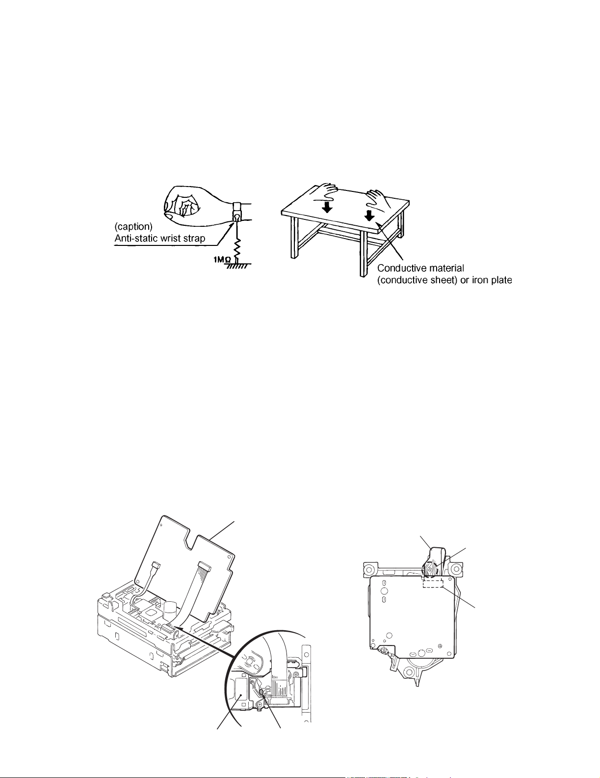
1 Important Safety Precautions . . . . . . . . . . . . . . . . . . . . . . . . . . . . . . . . . . . . . . . . . . . . . . . . . . . . . . . . . . . 1-2
2 Disassembly Method. . . . . . . . . . . . . . . . . . . . . . . . . . . . . . . . . . . . . . . . . . . . . . . . . . . . . . . . . . . . . . . . . . . 1-5
3 Adjustment method. . . . . . . . . . . . . . . . . . . . . . . . . . . . . . . . . . . . . . . . . . . . . . . . . . . . . . . . . . . . . . . . . . . 1-37
4 Description of major ICs. . . . . . . . . . . . . . . . . . . . . . . . . . . . . . . . . . . . . . . . . . . . . . . . . . . . . . . . . . . . . . . 1-44
COPYRIGHT © 2003 VICTOR COMPANY OF JAPAN, LTD.
No.22042
2003/02
Page 2
UX-Z7MDR
Important Safety Precautions
1.1 Safety Precautions
(1) This design of this product contains special hardware and
many circuits and components specially for safety purposes.
For continued protection, no changes should be made to the
original design unless authorized in writing by the manufacturer. Replacement parts must be identical to those
used in the original circuits. Services should be performed by qualified personnel only.
(2) Alterations of the design or circuitry of the product should
not be made. Any design alterations of the product should
not be made. Any design alterations or additions will void
the manufacturers warranty and will further relieve the
manufacture of responsibility for personal injury or property
damage resulting therefrom.
(3) Many electrical and mechanical parts in the products have
special safety-related characteristics. These characteristics are often not evident from visual inspection nor can the
protection afforded by them necessarily be obtained by using replacement components rated for higher voltage, wattage, etc. Replacement parts which have these special safety
characteristics are identified in the Parts List of Service Manual. Electrical components having such features are identified by shading on the schematics and by ( ) on the
Parts List in the Service Manual. The use of a substitute replacement which does not have the same safety characteristics as the recommended replacement parts shown in the
Parts List of Service Manual may create shock, fire, or other hazards.
(4) The leads in the products are routed and dressed with ties,
clamps, tubings, barriers and the like to be separated from
live parts, high temperature parts, moving parts and/or
sharp edges for the prevention of electric shock and fire
hazard. When service is required, the original lead routing
and dress should be observed, and it should be confirmed
that they have been returned to normal, after reassembling.
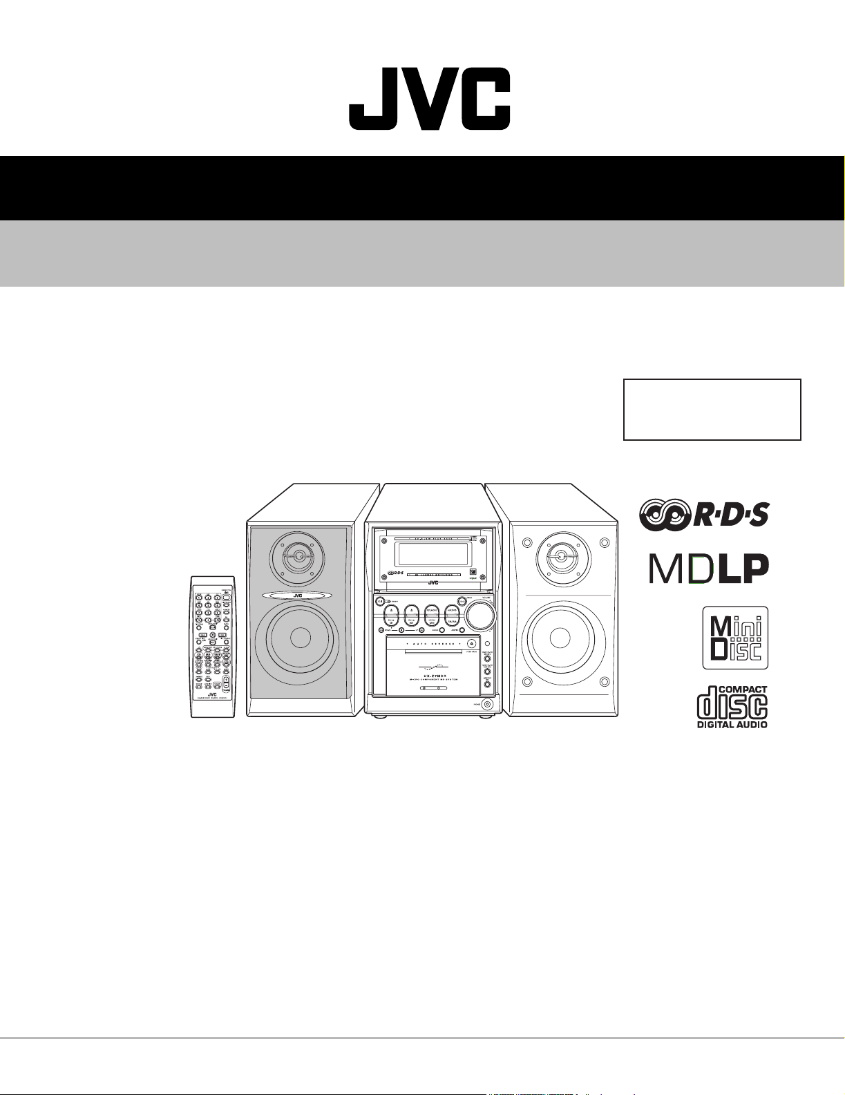
(5) Leakage shock hazard testing)
After reassembling the product, always perform an isolation
check on the exposed metal parts of the product (antenna
terminals, knobs, metal cabinet, screw heads, headphone
jack, control shafts, etc.) to be sure the product is safe to
operate without danger of electrical shock.
Do not use a line isolation transformer during this check.
• Plug the AC line cord directly into the AC outlet. Using a
"Leakage Current Tester", measure the leakage current
from each exposed metal parts of the cabinet, particularly any exposed metal part having a return path to the
chassis, to a known good earth ground. Any leakage current must not exceed 0.5mA AC (r.m.s.).
• Alternate check method
Plug the AC line cord directly into the AC outlet. Use an AC
voltmeter having, 1,000 ohms per volt or more sensitivity in
the following manner. Connect a 1,500 ohm 10W resistor
paralleled by a 0.15 µF AC-type capacitor between an
SECTION 1
exposed metal part and a known good earth ground.
Measure the AC voltage across the resistor with the AC
voltmeter.
Move the resistor connection to each exposed metal part,
particularly any exposed metal part having a return path to
the chassis, and measure the AC voltage across the resistor.
Now, reverse the plug in the AC outlet and repeat each
measurement. Voltage measured any must not exceed 0.75
V AC (r.m.s.). This corresponds to 0.5 mA AC (r.m.s.).
1.2 Warning
(1) This equipment has been designed and manufactured to
meet international safety standards.
(2) It is the legal responsibility of the repairer to ensure that
these safety standards are maintained.
(3) Repairs must be made in accordance with the relevant
safety standards.
(4) It is essential that safety critical components are replaced
by approved parts.
(5) If mains voltage selector is provided, check setting for local
voltage.
1.3 Caution
Burrs formed during molding may be left over on some parts
of the chassis.
Therefore, pay attention to such burrs in the case of preforming repair of this system.
1.4 Critical parts for safety
In regard with component parts appearing on the silk-screen
printed side (parts side) of the PWB diagrams, the parts that are
printed over with black such as the resistor ( ), diode ( )
and ICP ( ) or identified by the " " mark nearby are critical
for safety.
When replacing them, be sure to use the parts of the same type
and rating as specified by the manufacturer. (Except the JC version)
1-2 (No.22042)
Page 3
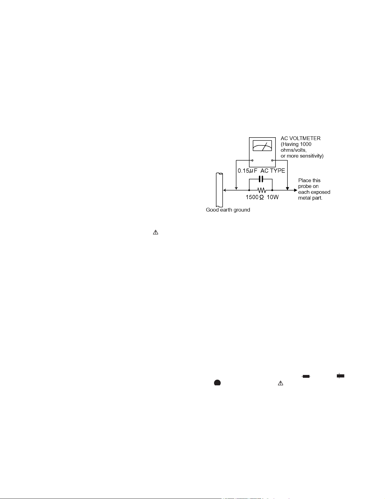
1.5 Preventing static electricity
Electrostatic discharge (ESD), which occurs when static electricity stored in the body, fabric, etc. is discharged,
can destroy the laser diode in the traverse unit (optical pickup). Take care to prevent this when performing repairs.
1.5.1 Grounding to prevent damage by static electricity
Static electricity in the work area can destroy the optical pickup (laser diode) in devices such as DVD players.
Be careful to use proper grounding in the area where repairs are being performed.
(1) Ground the workbench
Ground the workbench by laying conductive material (such as a conductive sheet) or an iron plate over it before placing the
traverse unit (optical pickup) on it.
(2) Ground yourself
Use an anti-static wrist strap to release any static electricity built up in your body.
UX-Z7MDR
(3) Handling the optical pickup
• In order to maintain quality during transport and before installation, both sides of the laser diode on the replacement optical
pickup are shorted. After replacement, return the shorted parts to their original condition.
(Refer to the text.)
• Do not use a tester to check the condition of the laser diode in the optical pickup. The tester's internal power source can easily
destroy the laser diode.
1.6 Handling the traverse unit (optical pickup)
(1) Do not subject the traverse unit (optical pickup) to strong shocks, as it is a sensitive, complex unit.
(2) Cut off the shorted part of the flexible cable using nippers, etc. after replacing the optical pickup. For specific details, refer to the replace-
ment procedure in the text. Remove the anti-static pin when replacing the traverse unit. Be careful not to take too long a time
when attaching it to the connector.
(3) Handle the flexible cable carefully as it may break when subjected to strong force.
(4) I t is not possible to adjust the semi-fixed resistor that adjusts the laser power. Do not turn it.
1.7 Attention when traverse unit is decomposed
*Please refer to "Disassembly method" in the text for the CD pickup unit.
• Apply solder to the short land before the flexible wire is disconnected from the connector on the CD pickup unit.
(If the flexible wire is disconnected without applying solder, the CDpickup may be destroyed by static electricity.)
• In the assembly, be sure to remove solder from the short land after connecting the flexible wire.
Main board
Flexible wire
Shorting round
Pickup Solder part b
CN601 on
mechanism
P.C. board
(No.22042)1-3
Page 4
UX-Z7MDR
1.8 Important for laser products
(1) CLASS 1 LASER PRODUCT
(2) DANGER : Invisible laser radiation when open and inter
lock failed or defeated. Avoid direct exposure to beam.
(3) CAUTION : There are no serviceable parts inside the
Laser Unit. Do not disassemble the Laser Unit. Replace the
complete Laser Unit if it malfunctions.
(4) CAUTION : The compact disc player uses invisible laser
radiation and is equipped with safety switches which
prevent emission of radiation when the drawer is open and
the safety interlocks have failed or are de feated.
It is dangerous to defeat the safety switches.
VARNING
Osynlig laserstrålning är denna del är öppnad och spårren är
urkopplad. Betrakta ej strålen.
VARO
Avattaessa ja suojalukitus ohitettaessa olet alttiina näkymättömälle lasersäteilylle. Älä katso säteeseen.
REPRODUCTION AND POSITION OF LABELS
(5) CAUTION : If safety switches malfunction, the laser is able
to function.
(6) CAUTION : Use of controls, adjustments or performance of
procedures other than those specified herein may result in
hazardous radiation exposure.
CAUTION
Please use enough caution not to see the beam directly
or touch it in case of anadjustment or operation check.
ADVARSEL
Usynlig laserstråling ved åbning, når sikkerhedsafbrydere er
ude af funktion. Undgå udsasttelse for stråling.
ADVARSEL
Usynlig laserstråling ved åpning, når sikkerhetsbryteren er
avslott. unngå utsettelse for stråling.
WARNING LABEL
CLASS 1
LASER PRODUCT
DANGER : Invisibie laser radiation
when open and interlock or
defeated.
AVOID DIRECT EXPOSURE TO
BEAM (e)
VARO : Avattaessa ja suojalukitus
ohitettaessa olet alttiina
näkymättömälle lasersäteilylle.Älä
katso säteeseen. (d)
VARNING : Osynlig laserstrålning är
denna del är öppnad och spårren är
urkopplad. Betrakta ej strålen. (s)
ADVARSEL :Usynlig laserstråling
ved åbning , når
sikkerhedsafbrydere er ude af
funktion. Undgå udsættelse for
stråling. (f)
1-4 (No.22042)
Page 5
SECTION 2
A
A
r
Disassembly Method
UX-Z7MDR
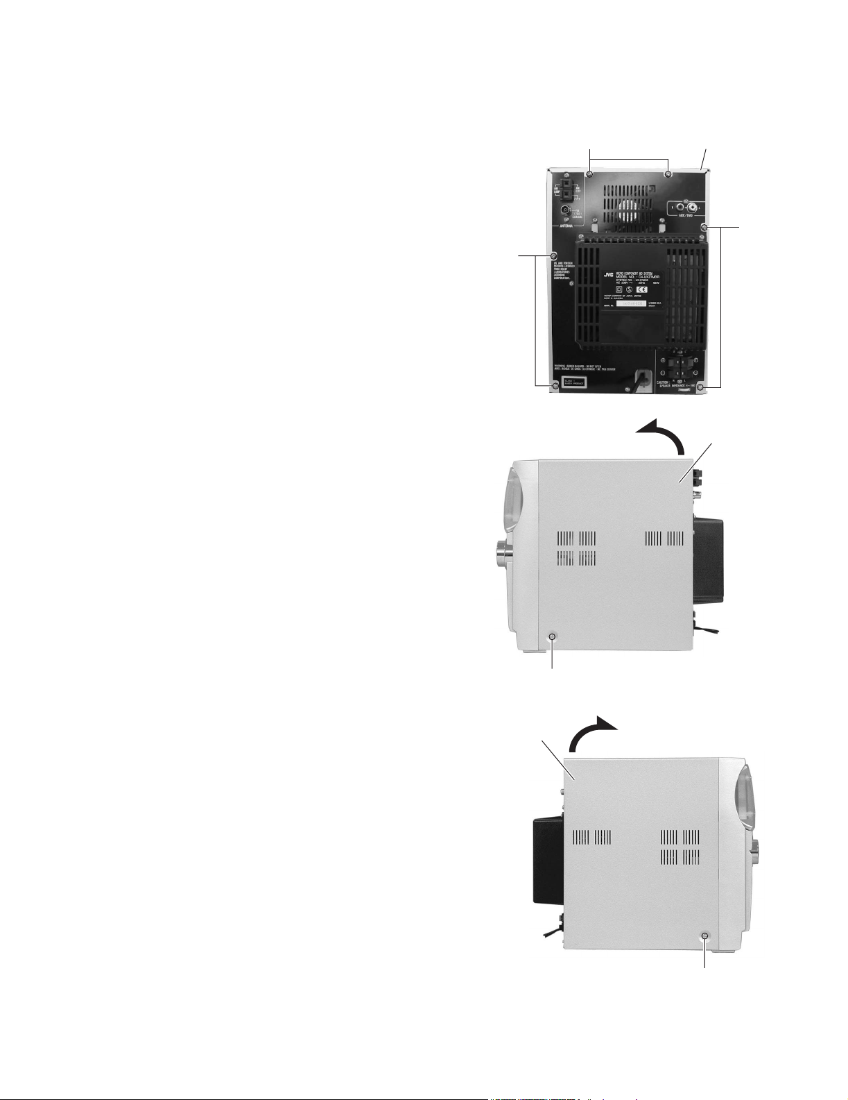
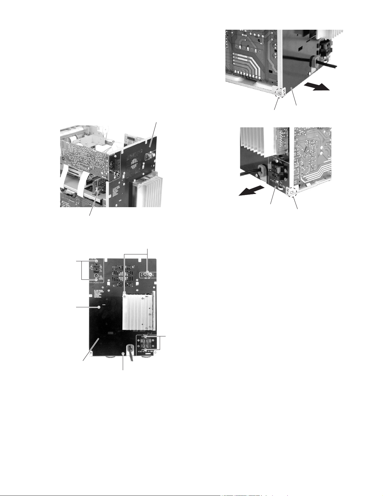
2.1 Main body
2.1.1 Removing the metal cover
(See Fig.1 to 3.)
(1) Remove the six screws A on the rear part of the main body
that attach the metal cover.
(2) Remove the two screws B on each side of the main body
that attach the metal cover.
(3) Lift the rear part of the metal cover upward while releasing
the lower sides of the metal cover in the right and left direction. The metal cover will be removed.
A
Matal cover
Fig.1
Matal cove
B
Fig.2
Matal cover
B
Fig.3
(No.22042)1-5
Page 6
UX-Z7MDR
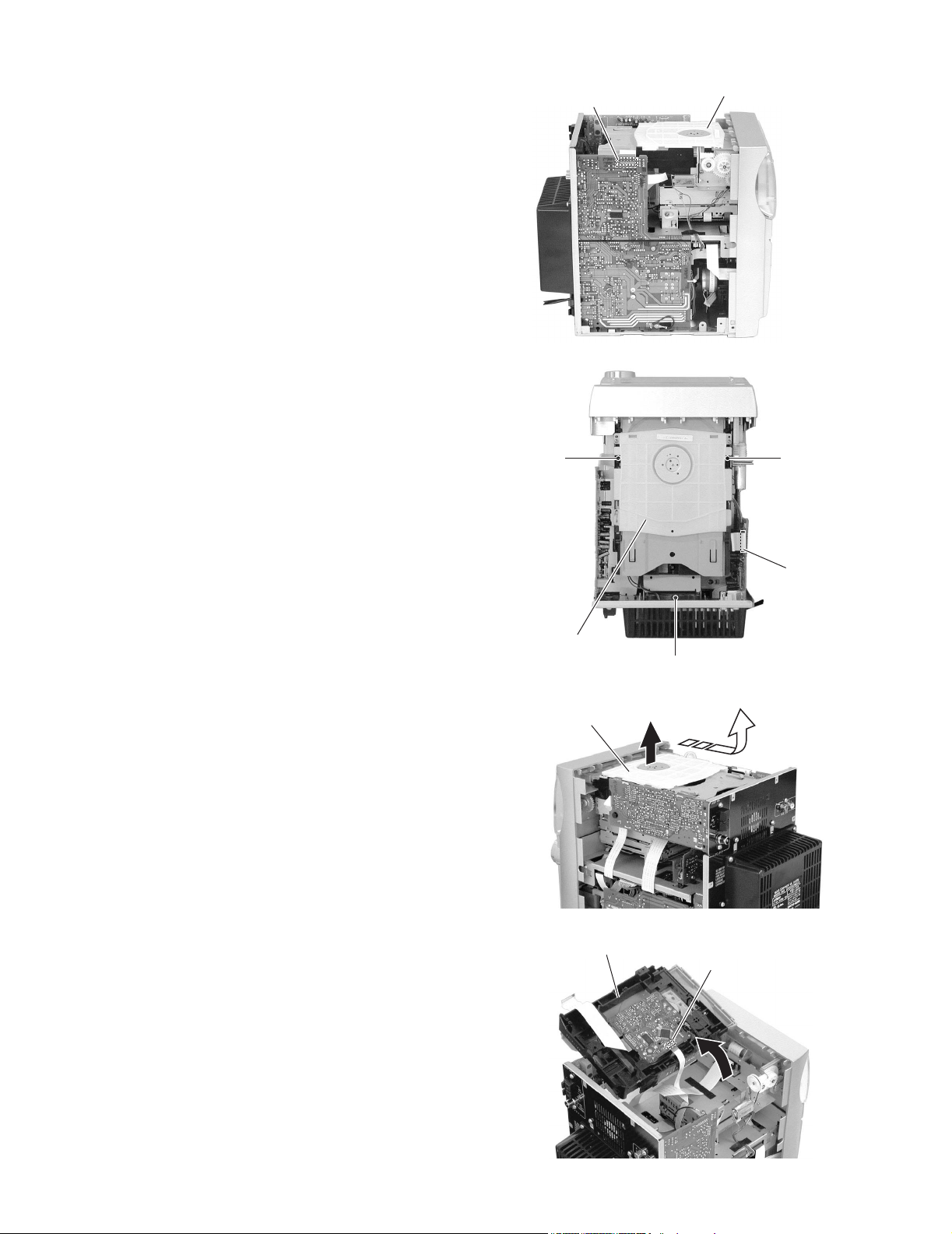
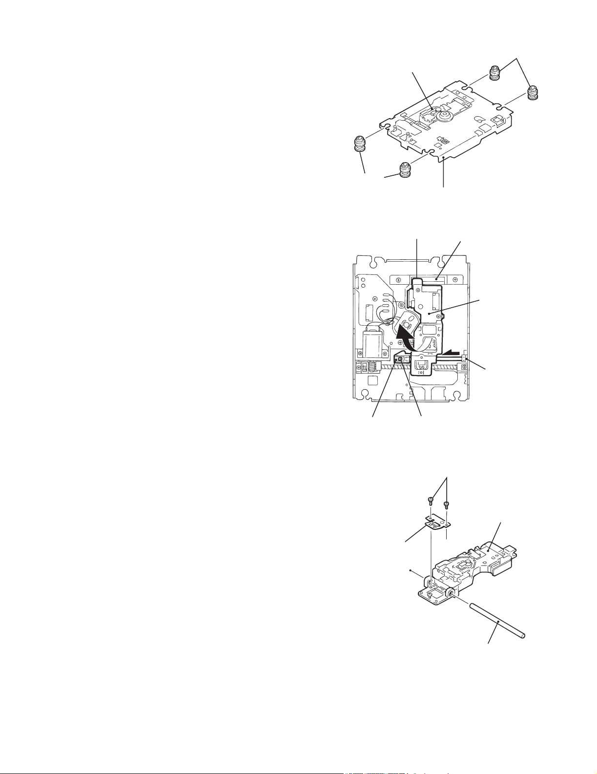
2.1.2 Removing the CD mechanism assembly
(See Fig.4 to 7.)
• Prior to this procedure, remove the metal cover.
(1) Remove the card wire from the connector CN302 on amp
board on the left side of the main body.
(2) Remove the three screws C on top of the body that attach
the CD mechanism assembly.
(3) Lift the CD mechanism assembly upward and move it
backward to remove.
(4) Remove the card wire from CN606 on CD servo board, on
the bottom of the CD mechanism assembly.
Amp board
CN302
C
CD mechanism ass'y
Fig.4
C
CD mechanism ass'y
CD mechanism ass'y
CD mechanism ass'y
Amp board
CN302
C
Fig.5
Fig.6
CD servo board
CN606
1-6 (No.22042)
Fig.7
Page 7
UX-Z7MDR
y
j
y
2.1.3 Removing the front panel
(See Fig.8 to11.)
• Prior to this procedure, remove the metal cover and the CD
mechanism assembly.
(1) Remove the card wire from the connector CN705 on micon
board, in the center of the right side of the main body.
(2) Remove the plastic rivet in the right side of the main body
that attaches tuner board.
(3) Remove the card wire from the connector CN301 on amp
board in the center of the left side of the main body.
Remove the card wire from the connector CN704 on micon
board.
Remove the wire from each connector CN703 and CN710
respectively.
(4) Remove the card wire from the connector CN452 on FL
connection board on top of the main body.
(5) Remove the two screws D on the right and left sides of the
main body that attach the front panel assembly.
(6) Remove the two screws E on the bottom of the main body
that attach the front panel assembly.
(7) Remove the joint "a" on the bottom of the main body and
the joint "b" on the right and left sides respectively by using
a screwdriver. Remove the front panel assembly in the
front direction.
Plastic rivet
Front panel ass'y
Tuner board
FL connect board
CN710
CN452
CN703
Fig.10
Front panel ass'
Micon board
CN704
Front panel ass'
EE
D
Micon board
CN705
Amp board
CN301
CN710
joint b
Fig.8
Front panel ass'y
joint b
Fig.9
oint a
Fig.11
D
Micon board
CN704
CN703
(No.22042)1-7
Page 8
UX-Z7MDR
j
c
2.1.4 Removing the tuner board
(See Fig.12.)
• Prior to this procedure, remove the metal cover.
(1) Remove the card wire on the right side of the main body
from the connector CN1 on the tuner board.
(2) Remove the plastic rivet on the right side of the main body
that attaches the tuner board.
(3) Remove the two screws F on the rear side of the main body
that attach the tuner board.
2.1.5 Removing the rear cover
(See Fig.13.)
• Prior to this procedure, remove the metal cover and the CD
mechanism assembly.
(1) Remove the two screws G on the rear side of the main
body that attach the rear cover.
CN1
Plastic rivet
G
Tuner doard
F
Fig.12
Rear panel
G
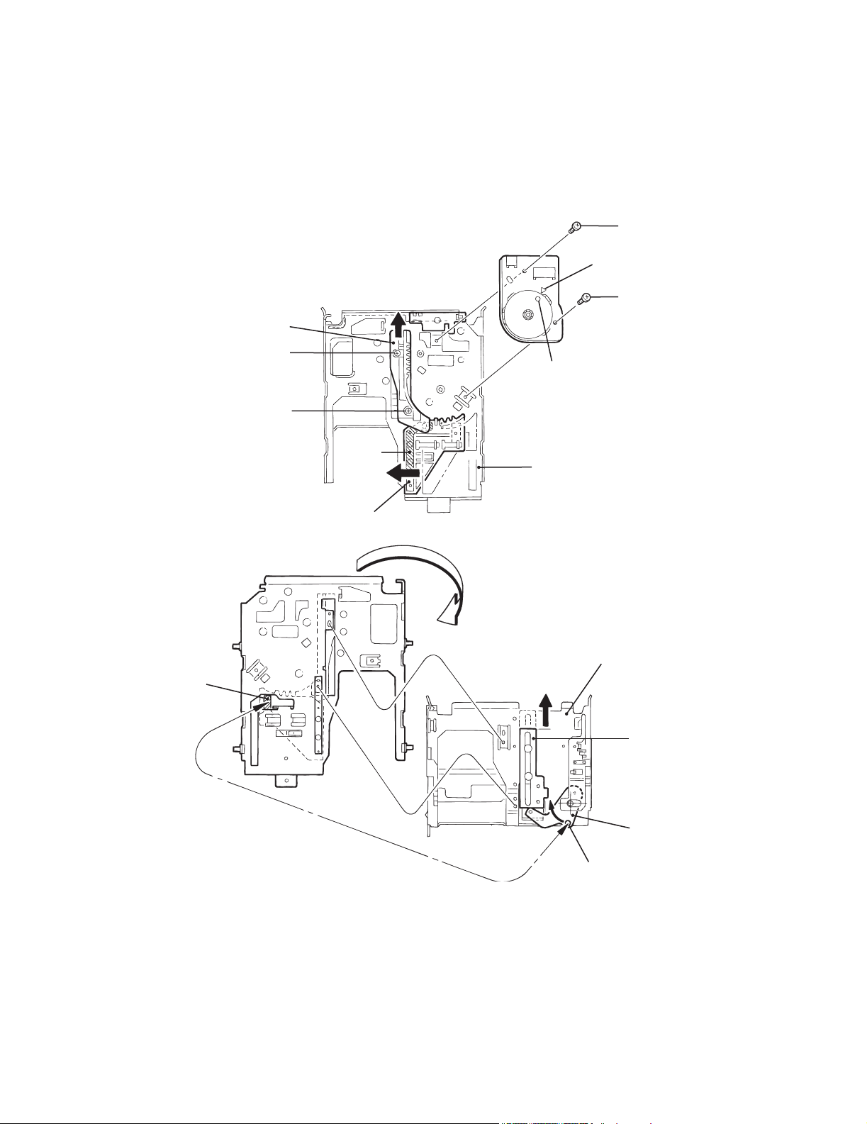
2.1.6 Removing the fan
(See Fig.14 to 16.)
• Prior to this procedure, remove the metal cover, the CD mech-
anism assembly, and the rear cover.
(1) Remove the wire from the connector CN603 on the MD
connect board in the right side of the main body.
(2) Remove the four screws H on the rear side of the main
body that attach the fan.
(3) Move the fan bracket that attaches the fan from inside the
rear panel upward to remove the two fixing points "c". Fan
will be detached at the same time.
Notice
When attaching the fan, attach the two "e" to the two "d" respectively before pressing the fan with fan bracket.
Fan
Rear panel
H
H
oint c
hook d
Rear cover
Fan blacket
Fan
Fig.13
Rear panel
Fig.15
Fan
joint
hole e
MD connect board
1-8 (No.22042)
CN603
Fig.14
hook d
hole e
Fig.16
Page 9
2.1.7 Removing the rear panel
(See Fig.17 to 20.)
• Prior to this procedure, remove the metal cover, the CD mech-
anism assembly, and the rear cover.
(1) Remove the wire from the connector CN603 on MD con-
nect board on the right side of the main body.
(2) Remove the eight screws F on the rear side of the main
body that attach the rear panel.
(3) Remove the two joint "f" on the right and left bottom of the
rear panel.
Notice
The fan assembly will be kept attached to the rear panel.
Rear panel
UX-Z7MDR
Rear panel
joint f
Fig.19
MD connect doard
CN603
F
F
Rear panel
Fig.17
Fig.18
F
F
F
Rear panel
Fig.20
joint f
(No.22042)1-9
Page 10
UX-Z7MDR
y
A
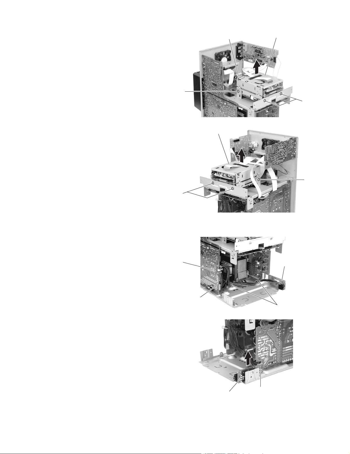
2.1.8 Removing the MD mechanism assembly
(See Fig.21 and 22.)
• Prior to this procedure, remove the metal cover, the CD mech-
anism assembly, and the rear cover.
(1) Remove the card wire from the connector CN601 on the
MD connect board in the rear part of the MD mechanism
assembly.
(2) Remove the four screws H on the front side and the rear
side that attach the MD mechanism assembly.
Remove the MD mechanism assembly upward.
MD connect board
H
MD mechanism ass'y
CN601
MD mechanism ass'
H
Fig.21
H
2.1.9 Removing the headphone board
(See Fig.23 and 24.)
• Prior to this procedure, remove the metal cover, the CD mech-
anism assembly, and the rear cover.
(1) Remove the wire from the connector CN101 on the amp
board on the left side of the main body.
(2) Remove the band that fixes the wire to the amp board. Re-
move the wire from the two clamps in the bottom chassis.
(3) Remove the screw I on the right side of the main body that
attaches the headphone board.
H
Fig.22
Band
Headphone board
mp board
CN101
clamp
Fig.23
1-10 (No.22042)
Headphone board
Fig.24
I
Page 11
UX-Z7MDR
A
2.1.10 Removing the amp board and heat sink
(See Fig.25 and 26.)
• Prior to this procedure, remove the metal cover, the CD mech-
anism assembly, the front panel assembly, and the rear cover.
(1) Remove the wire from the connector CN101 and CN102 on
the amp board on the left side of the main body. Remove
the band that fixes the wire. Remove the card wire from the
connector CN303.
(2) Remove the two screws J that attach the amp board.
(3) Pull out and remove the connector CN304 and CN305 on
the amp board outward. Remove the two joint "g" that fix
the bottom chassis.
Notice
The heat sink will be kept attached to the amp board. The
heat sink can be removed without removing the amp
board.
(4) Remove the three screws K that attach the heat sink.
mp board
Heat sink
J
Heat sink
joint g
CN303
J
Fig.25
K
CN304
joint g
CN305
Band
CN102
CN101
Amp board
K
Fig.26
2.1.11 Removing the MD connect board
(See Fig.27.)
• Prior to this procedure, remove the metal cover, the CD mech-
anism assembly, and the rear cover.
(1) Remove the card wire from the connector CN601 on the
MD connect board.
(2) Remove the two screws L on the rear side of the main body
that attach the MD connect board.
(3) Pull out the connector CN604 on the MD connect board in
the rear direction.
MD connect board
CN601
L
L
Fig.27
CN604
(No.22042)1-11
Page 12
UX-Z7MDR
s
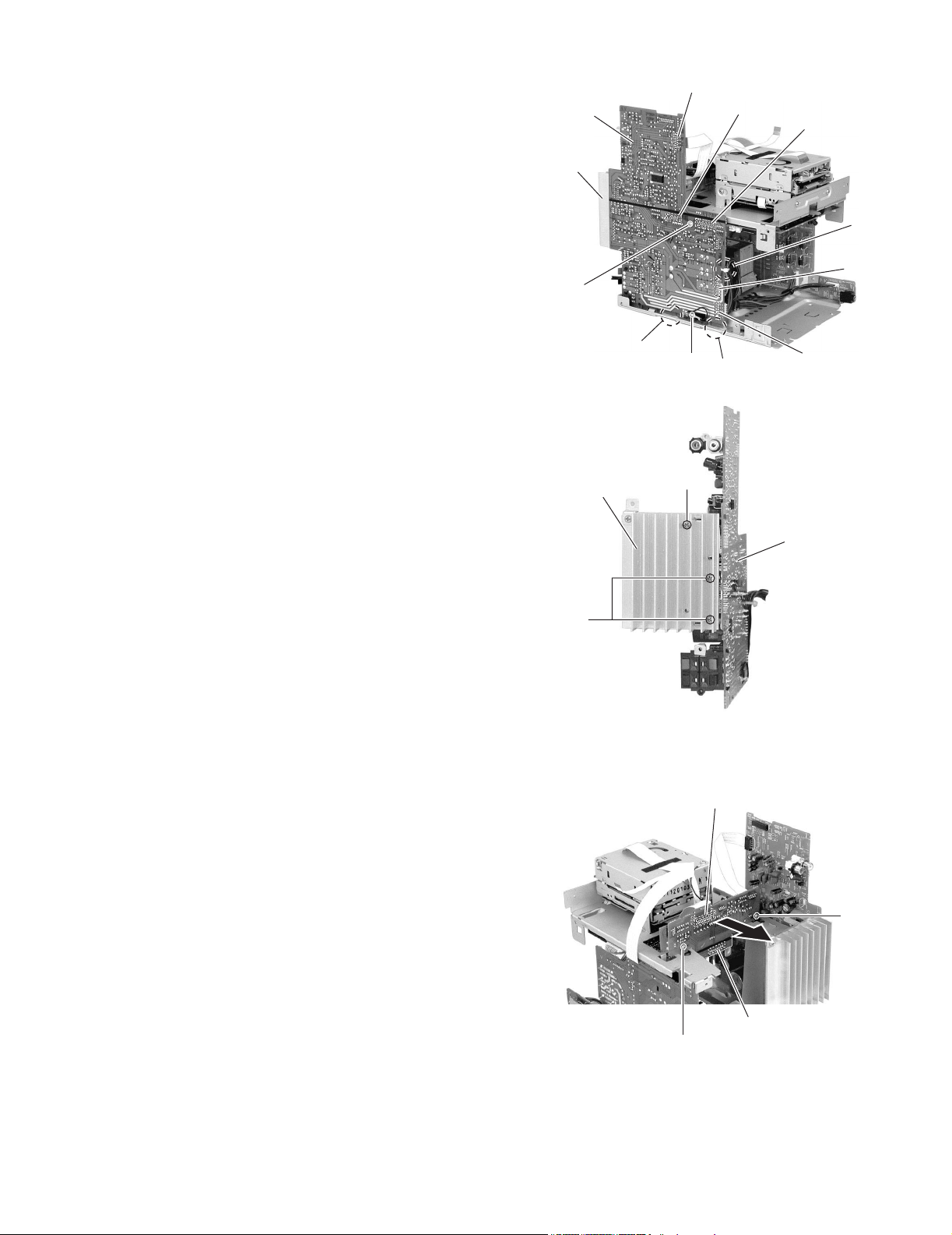
2.1.12 Removing the MD base chassis/the micon board
(See Fig.28 to 30.)
• Prior to this procedure, remove the metal cover, the CD mech-
anism assembly, the front panel assembly,
the rear cover, the amp board, and the MD connect board.
Notice
The MD base chassis/the micon board can be removed without removing the MD mechanism assembly.
(1) Remove the wire from the micon board connector CN707
in the center of the right side of the main
body. Remove the card wire from the connector CN708.
(2) Remove the screw M on top of the main body that attaches
the MD base chassis.
Notice
The MD mechanism assembly will be kept attached to
the MD base chassis.
(3) Remove the two screws N that attach the micon board. Re-
move the two joint "h" that fix the MD base chassis.
MD mechanism ass'y
Micon board
CN707
MD mechanism ass'y
MD base chassis
CN708
Fig.28
MD base chassi
M
Fig.29
N
joint h
Fig.30
Micon board
1-12 (No.22042)
Page 13
UX-Z7MDR
y
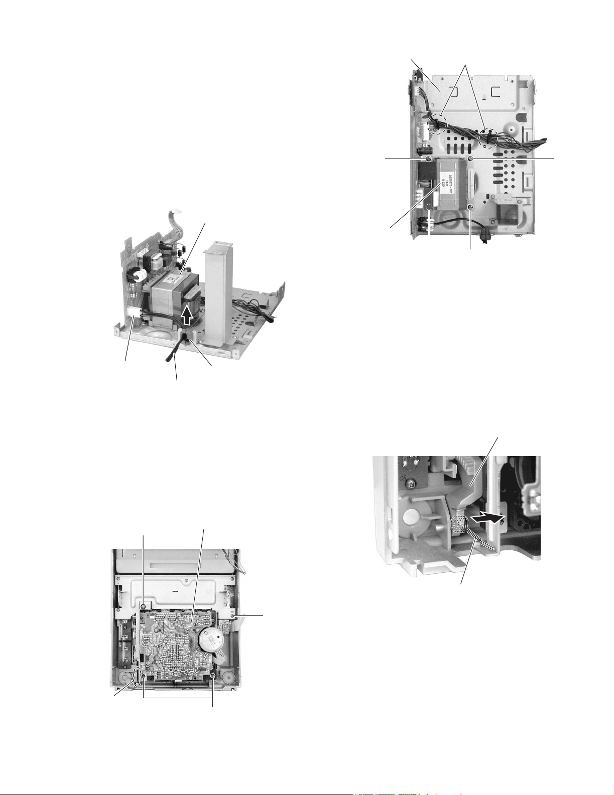
2.1.13 Removing the power trans assembly
(See Fig.31 and 32.)
• Prior to this procedure, remove the metal cover, the CD mech-
anism assembly, the front panel assembly, the rear cover, the
amp board, and the MD base chassis.
(1) Move the power cord stopper upward from the rear part of
the main body to remove. Remove the power supply cord
from the connector CN901 on the power trans board.
Notice
The power cord can be removed without removing the
power trans assembly.
(2) Remove the four screws O on top of the main body that at-
tach the power trans assembly. Remove the wire from the
two clamps on the bottom chassis.
Power trans assembly
Bottom chassis
clamp
OO
Power trans
assembly
O
Fig.32
Power trans board
CN901
Power cord
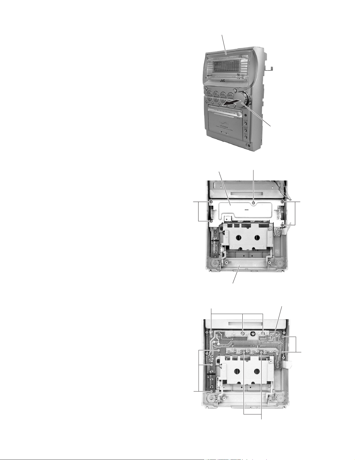
2.2 Front panel assembly
• Prior to this procedure, remove the metal cover, the CD mech-
anism assembly, and the front panel assembly.
2.2.1 Removing the cassette mechanism assembly
(See Fig.33 and 34.)
(1) Remove the spring that is attached to the cassette door
from inside the front panel.
(2) Remove the four screws P that attach the cassette mecha-
nism assembly.
Cassette mechanism assembl
P
cord stopper
Fig.31
P
Cassette door
Spring
Fig.34
Spring
P
Fig.33
(No.22042)1-13
Page 14
UX-Z7MDR
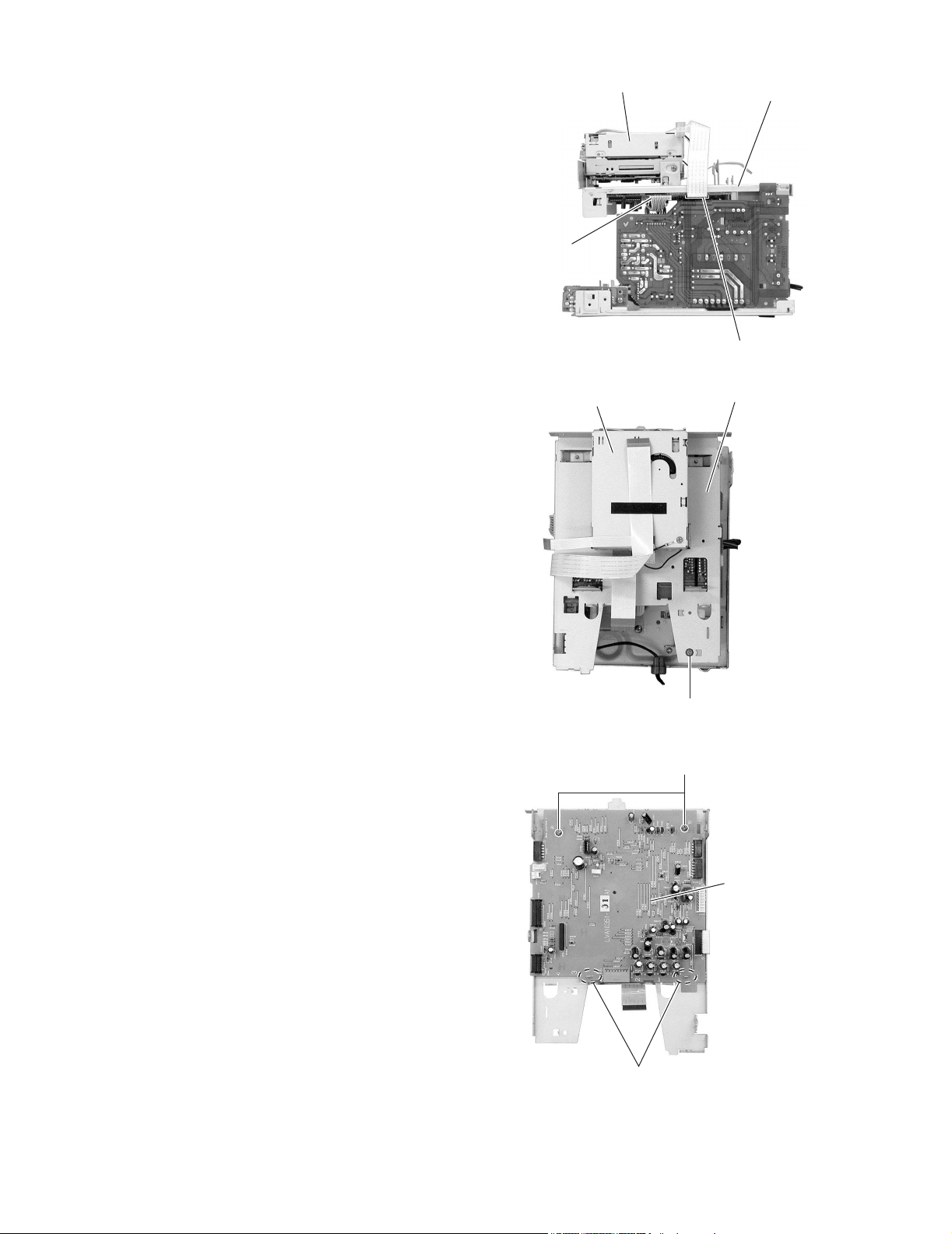
2.2.2 Removing the key board
(See Fig.35 to 37.)
• Prior to this procedure, remove the cassette mechanism as-
sembly.
(1) Pull out the volume knob in the front side of the front panel
to remove.
(2) Remove the five screws Q that attach the bracket (1) from
inside the front panel.
(3) Remove the ten screws R that attach the key board.
Front panel assembly
Bracket(1)
Volume knob
Fig.35
Q
Q
Front panel
R
Q
Fig.36
Key boad
R
1-14 (No.22042)
R
R
Fig.37
Page 15
UX-Z7MDR
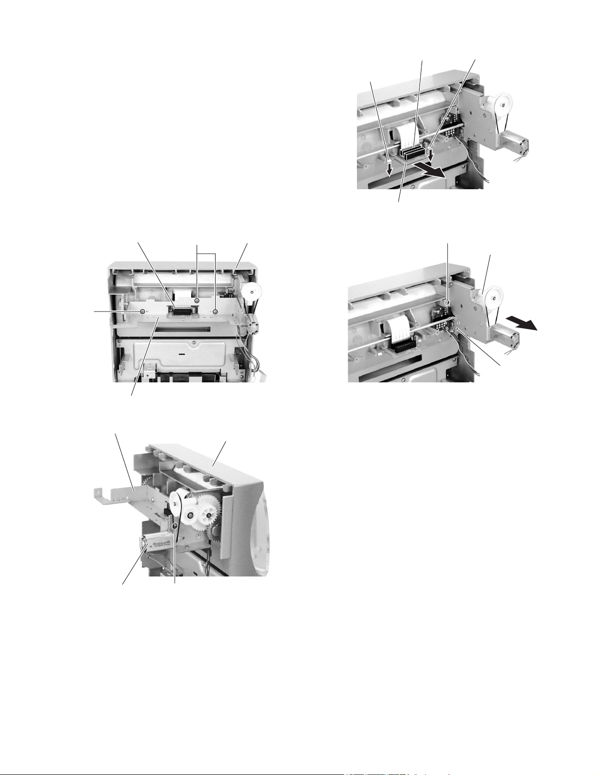
2.2.3 Removing the FM connection board
(See Fig.38 to 40.)
(1) Remove the three screws S and the screw T that attach the
bracket (2) from inside the front panel.
(2) Remove the card wire from the connector CN451 on the FL
connection board.
(3) Press the tab in the front panel and the one in joint "i"
downward to remove. Pull out the FL connection board to
remove.
2.2.4 Removing the drive motor assembly
(See Fig.38, 39, and 41.)
(1) Remove the three screws S and the screw T that attach the
bracket (2) from inside the front panel.
(2) Remove the screw U that attaches the drive motor assem-
bly. Remove the tab in joint "j" that fixes the front panel. Pull
out the drive motor assembly to remove.
FL connect board
CN451
S
Front panel
S
CN451
joint i
FL connect board
joint i
Fig.40
U
Drive motor
Bracket(2)
Bracket(2)
Drive motor
joint j
Fig.41
Fig.38
Front panel
T
Fig.39
(No.22042)1-15
Page 16
UX-Z7MDR
j
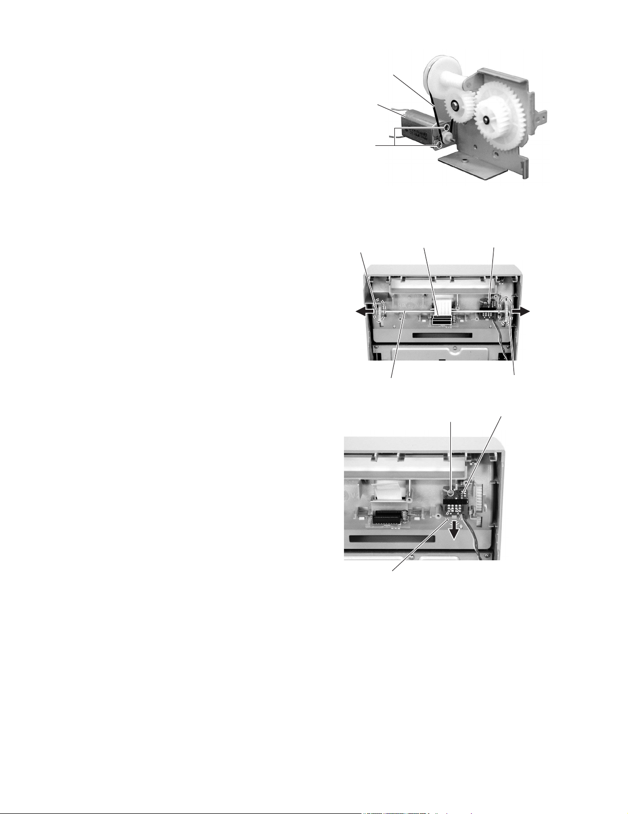
2.2.5 Removing the belt/drive motor
(See Fig.42.)
• Prior to this procedure, remove the drive motor assembly.
(1) Remove the belt from the pulley.
(2) Remove the two screws V that attach the drive motor.
2.2.6 Removing the switch board
(See Fig.43 and 44.)
• Prior to this procedure, remove the bracket (2) / the drive motor
assembly.
(1) Remove the card wire from the connector CN451 on FL
connection board.
(2) Remove the joint "k" by releasing it outward. And then, re-
move the joint "l" in the same way.
(3) Remove the screw W that attaches the switch board. Re-
move the tab on the joint "m" that fixes the front panel.
Drive motor
oint l
Belt
V
FL connect board
Fig.42
CN451
Switch board
Shift gear
Fig.43
W
joint m
Fig.44
joint k
Switch board
1-16 (No.22042)
Page 17
UX-Z7MDR
r
j
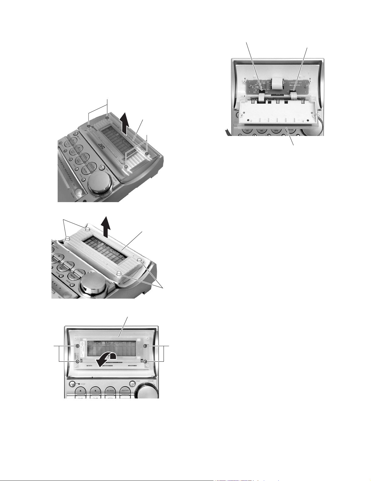
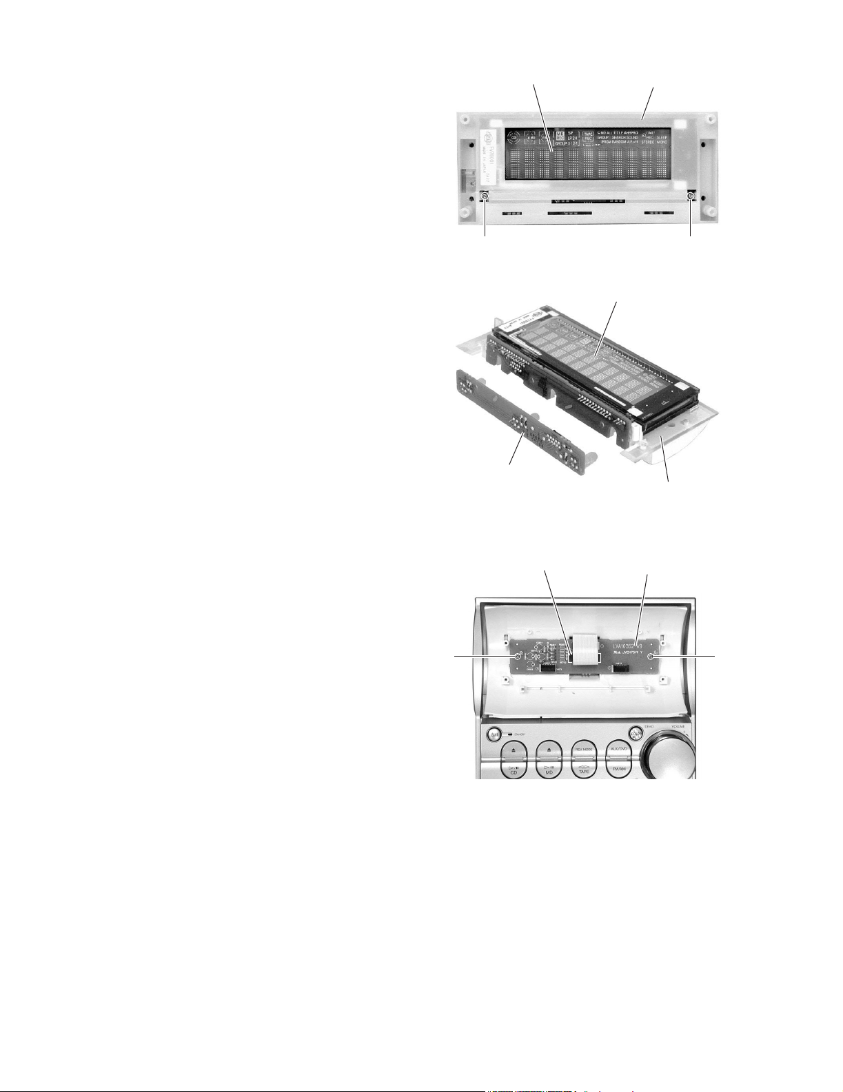
2.2.7 Removing the FL display
(See Fig.45 to 50.)
(1) Remove the four screws X on the front side of the front pan-
el that attach the case cover.
(2) Pull out the FL panel from the bosses of the four joint "n"
on the FL display cover.
(3) Remove the four screws Y that attach the FL display cover.
Remove the card wire from the connector CN671 and CN
672 on the FL connect board inside the FL display cover.
X
Case cove
X
FL connect board
CN671
CN672
FL cover
Fig.48
Fig.45
oint n
FL panel
joint n
Fig.46
FL cover
YY
Fig.47
(No.22042)1-17
Page 18
UX-Z7MDR
(4) Remove the two screws Z on the front side of the FL dis-
play cover that attach the FL display.
(5) FL board and lens will be detached from the FL display.
FL
FL cover
ZZ
Fig.49
FL
2.2.8 Removing the FL connect board
(See Fig.51.)
• Prior to this procedure, remove the FL display cover.
(1) Remove the card wire from the connector CN673 on the FL
connect board.
(2) Remove the two screws Z’ that attach the FL connect
board.
FL board
CN673
Fig.50
Lens
FL connect board
Z'Z'
Fig.51
1-18 (No.22042)
Page 19
UX-Z7MDR
r
r
2.3 CD Mechanism Assembly
2.3.1 Removing the CL. Base Assembly and Tray
(Refer to Figs. 1 to 5.)
(1) Remove the two screws A fastening the CL. base assembly
from the top of the CD mechanism assembly.
(2) Move the CL. base assembly diagonally upwards as in-
dicated by the arrow to release it from the two hooks a.
(3) Turn the idle gear in the arrow-marked direction from the
upper side of the CD mechanism assembly. Accordingly,
the TRAMECHA assembly moves downwards.
Note:
When drawing out the tray, shift down the TRAMECHA
assembly to the position where the tray does not contact
the T-T assembly of the TRAMECHA assembly.
(4) Draw out the tray frontwards for removing it.
Note:
When reinstalling the tray:
• Turn the idle gear so that the part b of the tray gear is
positioned in the part c shown in Fig. 4. (Eject position)
• Engage the right and left hooks d and e of the tray with
the right and left grooves of the TRAMECHA assembly
respectively for retaining the tray.
CL. base assembly
A
Hook a
A
Hook a
Tray gear
TRAMECHA assembly
Idle gear
Tray
Fig.3
Part c
Part b
Fig.4
TRAMECHA
assembly
Tray
Fig.1
Fig.2
Idle gea
Tray gear
Hook d
Idle gea
Fig.5
Hook d
Tray
(No.22042)1-19
Page 20
UX-Z7MDR
r
r
2.3.2 Removing the TRAMECHA Assembly
(Refer to Figs. 6 to 9.)
• Remove the CL. base assembly and tray.
Reference:
The TRAMECHA assembly can be removed without removal
of the mechanism P.C. board.
(1) If the TRAMECHA assembly is lowered and it is located out
of the PLAY position, turn the idle gear in the arrow-marked
direction so that the hole in the part f of the tray gear meets
the hole on the CL. base assembly. (Set the TRAMECHA
assembly at the PLAY position.)
(2) Remove the three screws B fastening the
TRAMECHA assembly and then remove the
TRAMECHA assembly upwards from the front side.
(3) At the same time, remove the spring from the groove of the
CH. base assembly in the part g of the TRAMECHA assembly.
Note:
When reinstalling the TRAMECHA assembly:
• Check to see if the spring is properly engaged with
groove of the CH. base assembly in the part g of the
TRAMECHA assembly.
• After making sure that the three insulators of the
TRAMECHA assembly are properly set on the bosses of the L. base assembly's guide, fasten them
with the screws.
TRAMECHA
assembly
B
Part g
B
Idle gear
Tray gea
B
Fig.6
Tray gea
Part f
L. base assembly
Fig.7
Spring
Part g
Fig.8
Spring
Groove of CH. base assembly
Fig.9
1-20 (No.22042)
Page 21

2.3.3 Removing the Mechanism P.C. Board
(Refer to Fig 10.)
Reference:
The mechanism P.C. board can be removed without removal
of the TRAMECHA assembly.
Note:
Before disconnecting the flexible wire coming from the pickup
from the connector, be sure to solder its shorting round.
If the flexible wire is connected without soldering, it may cause
breakdown of the pickup.
(1) Solder the shorting round of the flexible wire connected
with the mechanism P.C. board from the back of the mechanism assembly.
(2) Disconnect the flexible wire from the connector CN601 on
the mechanism P.C. board.
(3) Remove the three screws C fastening the mechanism P.C.
board.
(4) Unsolder the two points of the part h and one point of the
part i of the mechanism P.C. board. Then, remove the
mechanism P.C. board upwards.
Note:
When reinstalling the mechanism P.C. board, connect the flexible wire coming from the pickup to the connector first and then
remove the solder from the shorting round of the flexible cable.
Flexible wire
C
UX-Z7MDR
Soldered
part h
C
Shorting round
CN601 on
mechanism
P.C. board
C
Soldered part i
Fig.10
(No.22042)1-21
Page 22

UX-Z7MDR
2.3.4 Removing the Pickup(Refer to Figs. 11 to 14.)
• Remove the CL. base assembly and tray.
• Remove the TRAMECHA assembly.
Reference:
The pickup can be removed without removal of the mechanism
P.C. board.
Note:
Before disconnecting the flexible wire coming from the pickup
from the connector, be sure to solder its shorting round.
If the flexible wire is connected without soldering, it may cause
breakdown of the pickup.
(1) Solder the shorting round of the flexible wire connected
with the mechanism P.C. board from the back of the TRAMECHA assembly.
(2) Disconnect the flexible wire from the connector CN601 on
the mechanism P.C. board.
(3) Turn the idle gear in the arrow-marked direction from the top
of the TRAMECHA assembly so that the pickup assembly is
shifted to the reverse side of the T-T assembly.
Move the pickup assembly until the part j of the rack plate
in the lower part of the pickup assembly comes out of the
CH. base assembly.
(4) Remove the two screws D retaining the shaft of the pickup
assembly. Next, disengage the hook k from the CH. base
assembly and then remove the pickup assembly together
with the shaft.
(5) Pull the shaft out of the pickup.
(6) Remove the two screws E fastening the rack plate from the
pickup.
(7) Remove the screw F retaining the P.S. spring from the
pickup.
Part j of
rack plate
Idle gear
D
Flexible wire
CH. base
assembly
Pickup assembly
Shorting round
CN601 on
mechanism
P.C. board
Fig.11
T-T assembly
Pickup assembly
Fig.12
Part k
Shaft
jPart j
Rack plateE
CH. base
assembly
D
Fig.13
Pickup
P.S. spring
F
E
Fig.14
1-22 (No.22042)
Page 23

UX-Z7MDR
2.3.5 Reinstalling the Pickup Assembly
(Refer to Figs. 15 and 16.)
Reference:
Refer to the explanation of "Removing the Pickup" on the
preceding page.
(1) Fit the P.S. spring and rack plate to the pickup.
(2) Insert the shaft into the pickup.
(3) Engage the hook k of the pickup assembly with the CH.
base assembly first, and set the part j of the rack plate in
the opening I next. Then, reinstall the pickup assembly
while shifting it to the T-T side (inward) so that the part m
of the rack plate is positioned as shown in Fig. 16.
(4) Move the pickup assembly to the center position and fasten
the shaft with the two screws D. (Make sure that the part n
of the rack plate is correctly engaged with the middle gear.)
(5) After passing the flexible wire coming from the pickup
through the opening of the CH. base assembly, connect it
to the connector CN601.
Note:
When reinstalling the pickup assembly, remove the solder from the shorting round after connecting the flexible
wire coming from the pick to the connector CN601.
Part k
Part j
2.3.6 Removing the Feed Motor Assembly
(Refer to Fig. 17.)
• Remove the CL. base assembly and tray.
• Remove the mechanism P.C. board.
Remove the two screws E fastening the feed motor assembly
from the top of the mechanism assembly.
E
Feed motor assembly
Fig.17
Part I
Part m
Pickup
assembly
CH. base
assembly
Fig.15
Middle gear
Fig.16
Rack plate
Part n
(No.22042)1-23
Page 24

UX-Z7MDR
b
r
2.4 MD mechanism assembly
2.4.1 Removing the main board (See Fig.1 and 2)
(1) Turn over the body and disconnect the card wire from con-
nector CN408 and the flexible wire from CN407 on the
main board.
(2) Remove the two screws A attaching the main board. Slide
the main board in the direction of the arrow to release the
two joints a with the single flame.
(3) Solder part b on the pickup in the body. Disconnect the
flexible harness from connector CN321 and CN451 on the
underside of the main board. Then remove the main board.
AA
(Bottom)
Main board
CN408
CN407
2.4.2 Removing the mechanism cover (See Fig.3)
(1) Remove the four screws B on both sides of the body.
(2) Move the mechanism cover toward the front to disengage
the front hook of the mechanism cover from the internal
loading assembly (Joint c). Then remove the mechanism
cover upward.
Joint c
B
Fook
Joint c
Mechanism cove
B
Fig.3
Joint b Joint b
Fig.1
CN451
Pickup Solder part
Fig.2
Main board
CN321
1-24 (No.22042)
Page 25

2.4.3 Removing the head lifter (See Fig.4 to 6)
(1) Move the head lifter on top of the body in the direction of the arrow and turn around.
(2) Detach the spring from the hook of the body. Remove the head lifter with the spring.
(3) If necessary, remove the spring from the head lifter.
Head lifter
Spring
Head lifter
Fig.5
UX-Z7MDR
Fig.4
2.4.4 Removing the head assembly (See Fig.7)
(1) Remove the screw C on the upper side of the body.
Remove the head assembly while pulling the flexible harness from the body.
Head lifter
Spring
Fig.6
Fig.4,5,6
Head assembly
C
Fig.7
(No.22042)1-25
Page 26

UX-Z7MDR
2.4.5 Removing the Loading assembly (See Fig.8 and 9)
Ref:
The loading assembly, the traverse mechanism assembly and
the single flame will be removable after removing the loading
assembly from the body.
• Prior to performing the following procedure, remove the main
board, the mechanism cover, the head lifter and the head assembly.
(1) Remove the three screws D on the upper side of the body.
(2) Move the loading assembly forward to disengage it from
the traverse mechanism assembly (Joint d). Then remove
it upward.
(3) Remove the traverse mechanism assembly from the single
flame.
D
D
Loading assembly
Joint d
D
Fig.8
Loading assembly
Traverse mechanism
assembly
1-26 (No.22042)
Fig.9
Single flame
Page 27

UX-Z7MDR
)
2.4.6 Loading assembly
2.4.6.1 Removing the slide base (L) / (R)
(See Fig.10)
(1) Remove the two screws E on the upper side of the loading
assembly.
(2) Remove the slide base (L) outward. (Release it from the
joint bosses E.)
(3) Remove the slide base (R) outward.
2.4.6.2 Removing the loading mechanism assembly
(See Fig.11)
(1) Detach the loading mechanism assembly upward to re-
lease the four pins on both sides from the loading motor,
paying attention to the part e of the loading mechanism
base.
Slide base (R)
E'
E
Slide base (L
E
E'
Fig.10
Part e
2.4.7 Loading mechanism assembly
2.4.7.1 Removing the loading motor
(See Fig.12 and 13)
(1) Disconnect the harnesses from the wire holder and from
connector CN612 on the cam switch board.
(2) Remove the screw F attaching the loading motor and re-
lease the joint f.
(3) Remove the belt from the loading motor assembly.
(4) Remove the two screws G attaching the loading motor.
2.4.7.2 Removing the cam gear and the cam switch board (See Fig.12)
(1) Remove the slit washer attaching the cam gear and pull out
the cam gear.
(2) Disconnect the harness from the wire holder and from con-
nector CN612 on the cam switch board.
(3) Remove the two screws H and the clamp. Remove the
cam switch board.
Loading mechanism
assembly
Loading motor assembly
Joint f CN612
F
Loading mechanism base
Fig.11
Wire holder
H
Cam switch board
Slit washer
H
Cam gear
Fig.12
Loading motor
G
Fig.13
Belt
(No.22042)1-27
Page 28

UX-Z7MDR
y
2.4.7.3 Removing the cartridge holder assembly (See Fig.14 and 15)
(1) Remove the two screws I on the upper side of the loading assembly.
Slide bar
I
Cartridge holder assembly
I
Eject bar
2.4.7.4 Removing the slide bar and the eject bar (See Fig.14 and 15)
• Prior to performing the following procedure, remove the car-
tridge holder assembly.
(1) Remove the slide bar upward.
(2) Move the eject bar outward until it stops as shown in
Fig.14. Push the convex part g on the bottom of the body
and remove the eject bar from the chassis.
Eject bar
Part g
Fig.14
I
Slide bar
k
Eject bar
1-28 (No.22042)
UD base
Cartridge holder assembl
Fig.15
Page 29
UX-Z7MDR
2.4.8 Traverse mechanism assembly
2.4.8.1 Removing the Insulators (See Fig.16)
(1) Disengage the four insulators from the notches of the
traverse mechanism chassis.
2.4.8.2 Removing the pickup unit (See Fig.17)
(1) Turn over the traverse mechanism assembly and remove
the screw J attaching the shaft holder (F).
(2) Move the shaft inward and remove it from the shaft holder
(R).
(3) Detach the shaft side of the pickup unit upward and release
the joint h with the pickup guide. Then remove the pickup
unit with the shaft.
Pickup unit
Insulators
Insulators
Traverse machanism chassis
Fig.16
Joint h
Pickup guide
Pickup unit
2.4.8.3 Removing the pickup (See Fig.18)
(1) Draw out the shaft from the pickup.
(2) Remove the two screws K attaching the rack spring.
Shaft holder (F)
Rack spring
Shaft holder (R)
J
Fig.17
K
Pickup
Shaft
Fig.18
(No.22042)1-29
Page 30

UX-Z7MDR
2.4.8.4 Removing the feed motor assembly
(See Fig.15, 20)
• It is not necessary to remove the pickup unit.
(1) For the white and black harnesses extending from the feed
motor assembly, unsolder the soldering i on the traverse
mechanism board.
(2) Remove the two screws L attaching the feed motor assem-
bly.
(3) Remove the two screws N attaching the feed motor brack-
et.
2.4.8.5 Removing the traverse mechanism board (See Fig.19)
• Prior to performing procedure, remove the feed motor assem-
bly.
(1) For the red and black harnesses extending from the spin-
dle motor, unsolder the soldering j on the traverse mechanism board.
(2) Remove the screw M attaching the traverse mechanism
board.
Traberse mechanism board Soldering j
M
Soldering i
Feed motor assembly
L
Fig.19
Feed motor
Feed motor bracket
N
Fig.20
1-30 (No.22042)
Page 31
UX-Z7MDR
2.4.9 Reattaching the loading assembly
(1) Reattach the eject bar to the UD base. (Fig.15 and 21)
(2) Reattach the slide bar to the loading mechanism chassis while fitting the boss marked k to the eject bar slot. (Fig.21)
(3) Slide the slide bar and the eject bar in the direction of the arrow in Fig.20 and reattach the cartridge holder assembly using the
two screws I. (Fig.21 and 22)
ATTENTION:
Make sure the pin of the eject lever marked l is fitted to the slot of the eject bar marked m at the bottom of the loading mechanism chassis after moving the eject lever and the loading slider of the cartridge holder assembly in the direction of the arrow.
(Refer to Fig.22)
Slide bar
I
I
Eject bar
UD base (Bottom)
Cam switch board
H
Point marked
H
Cam switch boss
Ditch
UD base
Fig.21
Ditch m
Cartridge holder assembly
Loading slider
Eject lever
l
Fig.22
(No.22042)1-31
Page 32

UX-Z7MDR
(4) Reattach the wire holder to the UD base while engaging the UD base hook marked u to the wire holder slot marked t (At the
same time, the boss on the reverse side of the wire holder is fitted to the UD base round hole).
(5) Reattach the cam switch board using the two screws H. (Fig.23)
(6) Turn the cam switch to bring the boss to the point marked on the cam switch board. Reattach the cam gear using a slit washer
while fitting the cam gear slot to the cam switch boss. (Fig.23)
ATTENTION:
When reattaching the cam gear, the cam switch boss should be fitted to the cam gear slot, and the triangle mark of the cam
gear should be aligned to the hole of the eject bar as shown in Fig.23.
(7) Reattach the loading motor assembly, using the screw F. Connect the harness extending from the loading motor to connector
CN612 on the switch board and fix it with the wire holder. (Fig.23)
Loading motor assembly
F
Eject lever
Slide bar CN612
Fig.23
Cam gear
n
Point marked
Boss
Cam switch
Cam switch board
Cam gear
(Triangle mark)
Eject lever
1-32 (No.22042)
Page 33

UX-Z7MDR
(8) Reattach the UD base while engaging the four pins on both
sides of the UD base to the notches of the loading mechanism base and placing the edge (marked e’) of the cartridge holder assembly under the hook e of the loading
mechanism base. (Fig.24)
Pin
Hook e'
Pin
Hook e
Hook e'
Loading mechanism base
Fig.24
(9) Reattach the slide base (R) while fitting the two pins on an-
other side of the UD base to the slots of the slide base (R).
(Fig.25)
Slide base (R)
Part v
E
Slide base (R)
Cam gear
Part v
Fig.26
(10) Reattach the slide base (L) on the slide base (R) while fit-
ting the two pins on another side of the UD base to the slots
of the slide base (L) (Fig.26). Make sure the two slots of the
slide base (L) are fitted to the two bosses marked E’ and
tighten the two screws E. (Fig.27)
E'
Slide base (L)Slide base (R)
Part w
E
Pin
Slide base (L)
Pin
Part w
Fig.25
ATTENTION:
Fit the part v of the slide base (R) to the part w on the inward side of the cam gear rib. (Fig.26)
E'
Fig.27
Ref:
To expedite the work, bring up the UD base slightly when
fitting each pin to the appropriate notch.
(No.22042)1-33
Page 34

UX-Z7MDR
w
2.5 Cassette mechanism section
2.5.1 Removing the playback / recording & eraser head
(See Fig. 1 to 3)
(1) While shifting the trigger arms seen on the right side of the
head mount in the arrow direction, turn the flywheel R in
counterclockwise direction until the head mount has gone
out with a click (See Fig. 1).
(2) When the flywheel R is rotated in counterclockwise direc-
tion, the playback / recording & eraser head will be turned
in counterclockwise direction from the position in Fig. 2 to
that in Fig. 3.
(3) At this position, disconnect the flexible P.C. board (outgo-
ing from the playback / recording & eraser head) from the
connector CN31 on the head amplifier & mechanism con-
trol P.C. board.
(4) Remove the flexible P.C. board from the chassis base.
(5) Remove the spring 1 from behind the playback / recording
& eraser head.
(6) Loosen the reversing azimuth screw retaining the playback
/ recording & eraser head.
(7) Take out the playback / recording & eraser head from the
front of the head mount.
(8) The playback / recoring & eraser head should also be re-
moved similarly according to steps 1 to 7 above.
2.5.2 Reassembling the playback / recording & eraser head
(See Fig.3)
(1) Reassemble the playback head from the front of the head
mount to the position as shown in Fig. 3.
(2) Fix the reversing azimuth screw.
(3) Set the spring 1 from behind the playback / recording &
eraser head.Attach the flexible P.C. board to the chassis
base, as shown in Fig. 3.
(4) Attach the flexible P.C. board to the chassis base, as
shown in Fig. 3.
(5) The playback / recording & eraser head should also be re-
assembled similarly to step 1 to 4 above.
Cassette mechanism
Fig.1
Playback / Recording &
eraser head
Flexible
board
CN31
Head amplifier & mechanism
control P.C. board
Fig.2
Playback / Recording &
eraser head
Flywheel R
Trigger armHead mount
Spring 1
Trigger arm
Flywheel R
Reversing azimuth scre
Spring 1
Head mount
Flexible
board
Head amplifier & mechanism control
P.C. board
Fig.3
1-34 (No.22042)
Page 35

UX-Z7MDR
y
r
2.5.3 Removing the head amplifier & mechanism control
board
(See Fig. 4)
(1) Remove the cassette mechanism assembly.
(2) After turning over th cassette mechanism assembly, re-
move the three screws A retaining the head amplifier &
mechanism control board.
(3) Disconnect the connector CN32 on the board including the
connector CN 1 on the reel pulse P.C. board.
(4) When necessary, remove the 4 pin parallel wire soldered
to the main motor.
A
CN32
A
Belt
Main motor
assembly
B
CN31
Head amplifier &
mechanism control
board
A
4pin parallel wire
B
2.5.4 Removing the main motor assembly
(1) Remove the two screws B retaining the main motor assem-
bly (See Fig. 4 and 5).
(2) While raising the main motor, remove the capstan belt from
the motor pulley (See Fig. 5).
CAUTION:
Be sure to handle the capstan belt so carefully that this
belt will not be stained by grease and other foreign matter. Moreover, this belt should be hanged while referring
to the capstan belt hanging method in Fig. 5 and 6.
Main motor
assembly
Capstan belt
Motor
pulle
Fig.5
Flexible board
Fig.4
Mechanism moto
Main
motor
assembly
Capstan belt
Main motor
assembly
Flywheel
Fig.6
Fig.7
assembly
Motor
pulley
Motor pulleyCapstan belt
(No.22042)1-35
Page 36

UX-Z7MDR
2.5.5 Removing the flywheel
(See Fig. 8 and 9)
(1) Remove the head amplifier & mechanism control P.C.
board.
(2) Remove the main motor assembly.
(3) After turning over the cassette mechanism, remove the two
slit washers 1 and fixing the capstan shafts R and L, and
pull out the flywheel R and L respectively from behind the
cassette mechanism.
Flywheel R Flywheel L
Capstan
shaft R
Slit
washer 1
Fig.8
Slit
washer 1
Capstan
shaft L
Flywheel R Flywheel L
Fig.9
2.5.6 Removing the reel pulse P.C. board and solenoid
(See Fig. 10)
(1) Remove the five pawls a to e reattaining the reel pulse board.
(2) From the surface of the reel pulse board parts, remove the two pawls f and g retaining the solenoid.
Reel pulse board
a b c d e
g
f
Solenoid
Fig.10
1-36 (No.22042)
Page 37

3.1 MD adjustment(Auto adjust)
(1) Setting of MD adjustment (2) Initialize of EEPROM
UX-Z7MDR
SECTION 3
Adjustment method
Press MD REC button and
POWER button together,
then connect AC cord.
INDICATION
"TEST MODE1"
Power to ON by MD PLAY
button by main body,then MD
to stop by STOP button on
meinbody.
INDICATION
"TEST MODE1"
Complete setting
(3) Adjust the laser power
Set to MD
adjustment mode
set to MD
adjustment mode
INDICATION
"TEST MODE1"
Press PLAY MODE
button of remote controller
INDICATION
"TEST MODE1"
Comolete the Initialize
of EEPROM
Press 4 button of
remote controller
Insert the sensor of
laser power meter
Press 2 button of
remote controller
Setting the PLAYBACK
LASER POWER
Laser power to
up by F.SKIP button
of remote controller
Adjust to
morthsn 0.68mW or
same as 0.68mW
Press STOP button of
remote controller
Laser power to
down by B.SKIP button
of remote controller
Setting the RECORDING
LASER POWER
Laser power to up
by F.SKIP button of
remote controller
Adjust to
less than 6.23mW or
same as 6.23mW
Press STOP button of
remote controller
Eject the sensor to laser
power meter by EJECT
button of main body
Complete the RECORDING
LASER POWER adjustment
Laser power to down
by B.SKIP button of
remote controller
Complete the PLAYBACK
LASER POWER adjustment
(No.22042)1-37
Page 38

UX-Z7MDR
(4) Disc adjustment(Auto adjust)
Set to MD adjustment
mode
Insert Pre-Mastard disc
Press PLAY / button
of remote controller
INDICATION
"ON TUNING"
START the AUTO
ADJUSTMENT
Adjustment
OK?
Yes
INDICATION
"ON TUNING"
Press STOP button
of remote controller
Press EJECT button
of main body,then took
out Recordable disc
NO
INDICATION
"NG ERR;**
Adjustment
OK?
Yes
INDICATION
"ON TUNING"
Press STOP button
of remote controller
Press EJECT button
of main body,then took
out Pre-Masterd disc
Insert Recordable disc
Press MD PLAY /
button of remote controller
INDICATION
"ON TUNING"
Start the AUTO
ADJUSTMENT
NO
INDICATION
"NG ERR ; **
Complete the AUTO
ADJUSTMENT
Press STANDBY/ON button of
main body or remote controller
Release the TEST MODE
then power OFF
RESET by disconnect
the AC cord
CODE
00
01
02
03
04
05
06
07
08
09
0A
0B
0C
0D
0E
FF
Adjustment NG part
Not complete the AUTO ADJUSTMENT
Rest swith detection
Focus ON
Pit area EF barance,Tr offset adj
Pit area ABCD level adj
Pit area Focus servo AGC
Pit area Tracking servo AGC
Pit area Focus bias adj
GRV area EF baranee,TR offset adj
GRV area ABCD level adj
GRV area Focus servo AGC
GRV area Tracking servo AGC
GRV area Focus bias adj
Temp
EEPROM write
AUTO ADJUST complte
1-38 (No.22042)
Page 39

3.2 Cassette adjustment
3.2.1 Cassette mechanism section 3.2.2 Cassette mechanism section (Back side)
UX-Z7MDR
Head azimuth
adjusting screw
(Forward side)
3.2.3 Cassette AMP board
MOTOR SPEED
VR37
BIAS ADJ
VR31
Head azimuth
adjusting screw
(Reverse side)
VR37
C308
C310
R315
R314
L301
R327
B155
VR31
C221
Q302
C319
R313
C314
RECRAGRECL
C313
C317
C121
B112
SW8V
L303
C316
Head azimuth
adjusting screw
(Forward side)
Head azimuth
adjusting screw
(Reverse side)
Playback/Recording &
eraser head
B102
B152
C302
R103
1
C301
C111
B164
C306
R304
C109
B158
8
B106
C101
6
B166
R116
R212
R211
C211
R216
9
9
IC32
B101
C201
B109B108
C209
MB
PBRAGPBL
MS
MG
1
CN34
Q305
R310
R335
C106
Q103
R305
B198
R353
C307
R303
R122
Q101
C103
B163
Q321
R221
10
B156
C303
R115
R101
B157
R108
C113
R110
R109
R102
C110
C104
R301
R121
1
C108
C107
9
B151
R112
R111
C102
R107
CN33
R342
C213
R210
R209
C207
B159
16
R341
C208
R207
B200
1
B110
CN31
1
R205
R208
B160
R340
R105
C105
R343
C206
R345
NC
C305
R201
1IC31
TAP
C304
B113
C202
C210
Q331
RRE
C375
C205
B161
R215
R339
C203
C334
R106
R206
5VMGSOL
R203
R204
C204
B168
PHO
B153
R104
R222
R202
C333
C332
R375
Q201
PLA
C331
Q372
Q203
R331
FRE
B167
16
1
10
70u
CN32
B162
R372
R373
C371
Q375
R371
R376
C374
R338
C376
B
E
D375
Q376
B
Q371
E
R337
R336
9
IC33
8
(No.22042)1-39
Page 40

UX-Z7MDR
3.2.4 Tape Recorder Section
Items
Confirmation of
head angle
Confirmation of
tape speed
3.2.5 Reference Values for Confirmation Items
Items
Difference
between the
forward and
reverse speed
Wow & flutter Test tape
Measurement
conditions
Test tape
: VT703L (8kHz)
Measurement output
terminal
: Speaker terminal
Speaker R
(Load resistance: 4 ohm)
: Headphone terminal
Test tape
: VT712 (3kHz)
Measurement output terminal
: Headphone terminal
Measurement
conditions
Test tape
: VT712 (3kHz)
Measurement output terminal
: Speaker terminal Speak-
er R
(Load resistance: 4 ohm)
Measurement output terminal
: Headphone
: VT712 (3kHz)
Measurement output terminal
: Headphone terminal
Measurement method Standard Values Adjusting positions
1 Playback the test tape VT703L (8kHz)
2 With the recording & playback mechanism,
adjust the head azimuth screw so that the forward and reverse output levels become maximum. After adjustment lock the head
azimuth at least by half turn.
3 In either case this adjustment should be per-
formed in both the forward and reverse directions with the head azimuth screw.
Adjust VR37 so that the frequency counter
reading becomes 2,940~3,090Hz when playing back the test tape VT712 (3kHz) with playback and recording mechanism after ending
forward winding of the tape.
Measurement method Standard Values Adjusting positions
When the test tape VT712 (3kHz) has been
played back with the recording and playback
mechanism at the beginning of forward winding, the frequency counter reading of the difference between both of the mechanism should
be 6.0Hz or less.
When the test tape VT712 (3kHz) has been
played back with the recording and playback
mechanism at the beginning of forward winding, the frequency counter reading of wow &
flutter should be 0.25% or less (WRMS).
Maximum output Adjust the head
azimuth screw only
when the head has
been changed.
Tape speed
of deck
: 2,940 ~ 3,090Hz
6.0Hz or less Head azimuth screw
0.25% or less
(WRMS)
VR37
1-40 (No.22042)
Page 41

3.2.6 Electrical Performance
Items
Adjustment of
recording bias
current
(Reference
Value)
Adjustment of
recording and
playback
frequency
characteristics
Measurement
conditions
Mode
: Forward or reverse mode
• Recording mode
• Test tape
: AC-514 to TYPE ll and
AC-225 to TYPE l
Measurement output terminal
: Both recording and
headphone terminals
Reference frequency
: 1kHz and 10kHz
(REF.: -20dB)
Test tape
: AC-514 to TYPE ll
Measurement input
terminal
: OSC IN
Measurement method Standard Values Adjusting positions
1 With the recording and playback mechanism
load the test tapes(AC-514 to TYPE ll and
AC-225 to TYPE l ), and set the mechanism
to the recording and pausing condition in advance.
2 After connecting 100 ohm in series to the re-
corder head measure the bias current with a
valve voltmeter at both of the terminals.
3 After resetting the [PAUSE] mode start re-
cording. At this time adjust VR31 for Lch and
VR32 for Rch so that the recording bias current values become 4.0µA (TYPE l ) and
4.20µA (TYPE ll ).
1 With the recording and playback mechanism
load the test tapes (AC-514 to TYPE ll ), and
set the mechanism to the recording and
pausing condition in advance.
2 While repetitively inputting the reference fre-
quency signal of 1kHz and 10kHz from OSC
IN record and playback the rape.
3 While recording and playback the test tape in
TYPE ll ,adjust VR31 for Lch and VR32 for
Rch so that the output deviation between
1kHz and 10kHz becomes -1dB 2dB.
AC-225
: 4.20µA
AC-514
: 4.0µA
Output deviation
between
1kHz and 10kHz
: -1dB 2dB
UX-Z7MDR
VR31
VR31
3.2.7 Reference Values for Electrical Function Confirmation Items
Items
Recording
bias frequency
Eraser current
(Reference
value)
Measurement
conditions
Forward or reverse
• Test tape
: TYPE ll (AC-514)
Measurement terminal
: BIAS TP on P.C. board
Forward or reverse
• Recording mode
• Test tape
: AC-514 to TYPE ll and
AC-225 to TYPE l
Measurement terminal
: Both of the eraser head
terminals
Measurement method Standard Values Adjusting positions
1 While changing over to and from BIAS 1 and
2, confirm that the frequency is changed.
2 With the recording and playback mechanism
load the test tape.
(AC-514 to TYPE ll ), and set the mechanism
to the recording and pausing condition in advance.
3 Confirm that the BIAS TP frequency on the
P.C. board is 100kHz 6kHz.
1 While recording and playback mechanism,
load the test tapes (AC-514 to TYPE ll and
AC-225 to TYPE l), and set the mechanism to
the recording and pausing conditions in advance.
2 After setting to the recording conditions, con-
nect 1W in series to the eraser head on connect 1W in series to the eraser head on the
recording and playback mechanism side and
measure the eraser current from both of the
eraser terminals.
100 kHz
6 kHz
TYPE ll
: 120 mA
TYPE l
: 75 mA
(No.22042)1-41
Page 42

UX-Z7MDR
3.3 Flow of functional operation until TOC read
Power ON
Play Key
Slider turns REST
SW ON.
Automatic tuning
of TE offset
Check Point
Confirm that the voltage at the pin5
of CN801 is "H"\"L"\"H".
Tracking error waveform at TOC reading
Approx.3sec
Tracking
servo
off states
Automatic measurement
of TE amplitude and
automatic tuning of
TE balance
VREF
pin 25 of
IC601(TE)
Approx
1.8V
Disc states
to rotate
Tracking
servo
on states
Disc to be
braked to stop
TOC reading
finishes
500mv/div
2ms/div
Fig.1
Laser ON
Detection of disc
Automatic tuning of
Focus offset
Automatic measurement of
Focus S-curve amplitude
Disc is rotated
Focus servo ON
(Tracking servo ON)
Automatic measurement of
Tracking error amplitude
Automatic tuning of
Tracking error balance
Check that the voltage at the
pin40 of IC651 is + 5V?
Confirm that the Focus error
S-cuve signal at the pin28 of
IC651 is approx.2Vp-p
Confirm that the signal from
pin24 IC651 is 0V as a
accelerated pulse during
approx.400ms.
Confirm the waveform of
the Tracking error signal.
at the pin 25 of IC601 (R604)
(See fig-1)
1-42 (No.22042)
Automatic tuning of
Focus error balance
Automatic tuning of
Focus error gain
Automatic tuning of
Tracking error gain
TOC reading
Play a disc
Confirm the eys-pattern
at the lead of TP1
Page 43

UX-Z7MDR
3.4 Maintenance of laser pickup
(1) Cleaning the pick up lens
Before you replace the pick up, please try to clean the lens
with a alcohol soaked cotton swab.
(2) Life of the laser diode
When the life of the laser diode has expired, the following
symptoms will appear.
1.The level of RF output (EFM output : ampli tude of eye
pattern) will below.
Is the level of
RFOUT under
1.25V 0.22Vp-p?
NO
Replace it.
YES
O.K
(3) Semi-fixed resistor on the APC PC board
The semi-fixed resistor on the APC printed circuit board
which is attached to the pickup is used to adjust the laser
power. Since this adjustment should be performed to
match the characteristics of the whole optical block, do not
touch the semi-fixed resistor.
If the laser power is lower than the specified value, the laser diode is almost worn out, and the laser pickup should
be replaced.
If the semi-fixed resistor is adjusted while the pickup is
functioning normally, the laser pickup may be damaged
due to excessive current.
3.5 Replacement of laser pickup
Turn off the power switch and, disconnect the
power cord from the ac outlet.
Replace the pickup with a normal one.(Refer
to "Pickup Removal" on the previous page)
Plug the power cord in, and turn the power on.
At this time, check that the laser emits for
about 3seconds and the objective lens moves
up and down.
Note: Do not observe the laser beam directly.
Play a disc.
Check the eye-pattern at TP1.
Finish.
(No.22042)1-43
Page 44

UX-Z7MDR
A
4.1 AK4519VF-X (IC480) : A/D D/A converter
• Pin layout
SECTION 4
Description of major ICs
• Block diagram
1
2
3
4
5
6
7
8
9
10
11
12
AINL
VCML
AINR
VCMR
VRAD
ARDV
VCOM
AOUTL
24
23
22
21
20
19
18
17
16
15
14
13
VA AGND VB VD DGND
Modulator
Modulator
Common Voltage
LPF
Modulator
Decimation
Filter
Decimation
Filter
8x
Interpolator
Clock
Divider
Serial I/O
Interface
MCLK
CMODE
LRCK
SCLK
SDTO
SDTI
OUTR
LPF
Modulator
PWAD PWDA
• Pin Function
Pin
Symbol I/O Function
No.
1 VRDA I Voltage Reference Input Pin for DAC, VA
2 VRAD I Voltage Reference Input Pin for ADC, VA
3 AINR I RCH Analog Input Pin
4 VCMR O Rch Common Voltage Output Pin, 0.45xVA
5 VCML O Lch Common Voltage Output Pin, 0.45xVA
6 AINL I Lch Analog Input Pin
7 PWAD I ADC Power-Down Mode Pin "L":Power
Down
8 PWDA I DAC Power-Down Mode Pin "L":Power
Down
9 MCLK I Master Clock Input Pin
10 LRCK I Input/Output Channel Clock Pin
11 SCLK I Audio Serial Data Clock Pin
8x
Interpolator
Pin
Symbol I/O Function
No.
12 SDTO O Audio Serial Data Output Pin
13 DGND - Digital Ground Pin
14 VD - Digital Power Supply Pin
15 SDTI I Audio Serial Data Input Pin
16 CMODE I Master Clock Select Pin
17 DEM1 I De-emphasis Frequency Select Pin
18 DEM0 I De-emphasis Frequency Select Pin
19 AOUTL O Lch Analog Output Pin
20 AOUTR O Rch Analog Output Pin
21 VCOM O Common Voltage Output Pin, 0.45xVA
22 AGND - Analog Ground Pin
23 VB - Substrate Pin
24 VA - Analog Power Supply Pin
1-44 (No.22042)
Page 45

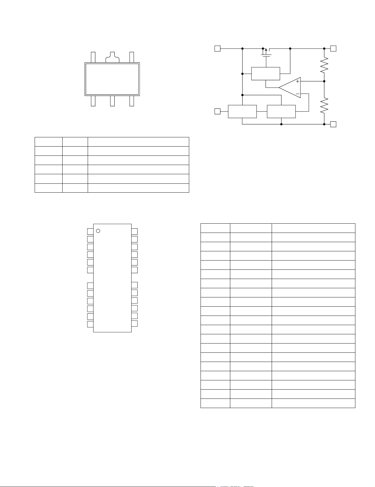
4.2 AN22000A-W (IC601) : RF & SERVO AMP
• Terminal layout
ACBDPDF
323130292827262524232221201918
123456789
LD
PD
VCC
RFN
PDE
RFIN
RFOUT
TBAL
FBAL
ARF
CAGC
GCTRL
CEA
FEOUT
FEN
TEN
TEOUT
TEBPF
10111213141516
BDO
OFTR
CBDO
3TOUT
COFTR
• Block diagram
32
31
30
29
27
28
RFOUT
RF_EQ
AMP
AMP
AMP
AMP17GCA BCA
+
-
624754 8
RFIN
AGC
NRFDET
GCA BCA
GCA BCA
GCA BCA
GCTL26TBAL
11 12
BDO
SUBT
SUBT
FBAL
25 16 3
VDET
VREF
17
GND
RFDET
13 14
OFTR
3TENV
VDET
UX-Z7MDR
• Pin function
Pin
Symbol I/O Function
No.
1 PD I APC Amp. input terminal
2 LD O APC Amp. output terminal
3 VCC - Power supply terminal
4 RFN I RF adder Amp. inverting input terminal
5 RFOUT O RF adder Amp. output terminal
6 RFIN I AGC input terminal
7 CAGC I Input terminal for AGC loop filter capacitor
8 ARF O AGC output terminal
9 CEA I Capacitor connecting terminal
for HPF-Amp.
9
10
10 3TOUT O 3 TENV output terminal
11 CBDO I Capacitor connecting terminal for envelope
detection on the darkness side
12 BDO O BDO output terminal
15
22
13 COFTR I Capacitor connecting terminal for envelope
detection on the light side
14 OFTR O OFTR output terminal
-
+
23
15 NRFDET O NRFDET output terminal
16 GND - Ground
21
-
+
20
17 VREF O VREF output terminal
18 VDET O VDET output terminal
19 TEBPF I VDET output terminal
20 TEOUT O TE Amp. output terminal
21 TEN I TE Amp. inverting input terminal
19
22 FEN I FE Amp. inverting input terminal
23 FEOUT O FE Amp. output terminal
18
24 GCTL O GCTL & APC terminal
25 FBAL O FBAL control terminal
26 TBAL O TBAL control terminal
-
+
2
LD
27 E I Tracking signal input terminal 1
28 F I Tracking signal input terminal 2
29 D I Focus signal input terminal 4
PD
1
30 B I Focus signal input terminal 3
31 C I Focus signal input terminal 2
32 A I Focus signal input terminal 1
(No.22042)1-45
Page 46

UX-Z7MDR
2
10
T
O
4.3 AN7317 (IC32) : R / P amp.
• Pin layout & block diagram
16
1
60k
60k
15
112k
Pre
Pre
112k
2
• Pin functions
Pin No. Function
1 Channel 1 playback amplifier input
2 Channel 1 playback amplifier negative feedback
3 Channel 1 playback amplifier output
4 Channel 1 record amplifier input
5 Channel 1 record amplifier output
6 ALC low-cut
7ALC time
8 Ground
9Vcc
10 Ripple filter
11 Record-Amplifier mute
12 Channel 2 record amplifier output
13 Channel 2 record amplifier input
14 Channel 2 playback amplifier output
15 Channel 2 playback amplifier negative feedback
16 Channel 2 playback amplifier input
14
13 12 11 10 9
30k
30k
3
Pre
Pre
45678
Mute R.R
ALC
4.4 BU4094BCF-X (IC33) : Shift / store registor
• Pin layout • Block diagram
16 15 14 13 12 11 10 9
VDD
ENABLE
STROVE DATA CLOCK Q1 Q2 Q3 Q4 Vss
Q5 Q6 Q7 Q8 Q'S Q'SOUTPUT
1 2 3 4 5 6 7 8
1-46 (No.22042)
DATA
CLOCK
STROBE
UTPUT
ENABLE
3
1
8-STAGE
SHIFT REGISTER
8-BIT
LATCHES
15
3-STATE
OUTPUTS
Q1
PARALLEL OUTPUT
Q8
Q'S
QS
SERIAL
OUTPU
9
Page 47
4.5 XC62HR3502P-X (IC291) : Regulator
S
• Pin layout • Block diagram
54
VIN
UX-Z7MDR
VOUT
Current
Limit
123
CE
• Pin function
Pin No. Symbol Function
1 VSS Ground
2 VIN Supply voltage input
3 CE Chip enable
4 NC Non connect
5 VOUT Regulated output voltage
4.6 GM71VS17400CLT5 (IC390,IC790) : DRAM
•Pin layout •Pin function
Vcc 1
I/O1 2
I/O2 3
WE 4
RAS 5
A11 6
A10 8
A0 9
A1 10
A2 11
A3 12
Vcc 13
26 Vss
25 I/O4
24 I/O3
23 CA
22 OE
21 A9
19 A8
18 A7
17 A6
16 A5
15 A4
14 Vss
Pin No. Symbol Function
1 Vcc Power supply (+3.3V)
2 I/O1 Date input/output
3 I/O2 Date input/output
4 WE Read/write enable
5 RAS Addres stroke
6 A11 Addres input
7-Not use
8 A10 Address input
9~12 A0~A3 Address input
13 Vcc Power supply (+3.3V)
14 Vss GND
15~19 A4~A8 Addres input
20 - Not use
21 A9 Address input
22 OE Output enable
23 CAS Calum address stroke
24 I/O3 Date input/output
25 I/O4 Date input/output
26 Vss GND
Output
Control
Voltage
Reference
VSS
(No.22042)1-47
Page 48

UX-Z7MDR
4.7 MN662790RSC(IC651):Digital servo & processor
• Pin layout
60 41
61
40
80
21
1 20
• Pin function
Pin No. Symbol I/O Description
1 BCLK O Bit clock output for SRDATA
2 LRCK O Identifying signal output of L,R
3 SRDATA O Serial data output
4 DVDD1 - Power supply for digital circuit
5 DVSS1 - Connect to ground for digital circuit
6 TX O Digital audio interface output signal
7 MCLK I Micom command clock signal input
8 MDATA I Micom command data signal input
9 MLD I Micom command load signal input L:load
10 SENSE - Non connect
11 FLOCK - Non connect
12 TLOCK - Non connect
13 BLKCK O Sub code block clock signal (Command execution : CD-TEXT data readout enabling signal (DQSY) out-
put)
14 SQCK I Export clock signal input for sub code Q resister
15 SUBQ O Sub code Q data output
16 DMUTE I Muting input H:muting
17 STAT O Status signal output
18 LSI_RST I Reset signal input L:reset
19 SMCK O Clock signal output MSEL is H : 8.4672 MHz MSEL is L : 4.2336 MHz
20 CSEL I Oscillation frequency specification terminal H:33.8688 MHz L:16.9344 MHz
21 TEST2 - TEST2 terminal usually : open
22 TVD O Traverse drive output
23 PC - Non connect
24 ECM O Spindle motor drive signal output (Compulsion mode output)
25 ECS O Spindle motor drive signal output (Servo error signal output)
26 VDETMON - Non connect
27 TRD O Tracking drive signal output
28 FOD O Focus drive signal output
29 VREF - Reference voltage for DA output section
30 FBAL O Focus balance adjust signal output
31 TBAL O Tracking balance adjust signal output
32 FE I Focus error signal input (analog input)
33 TE I Tracking error signal input (analog input)
34 RFENV I RF Envelope signal input (analog input)
35 TEST3 I TEST3 Terminal usually : Fixation L
36 OFT I Off track signal input H : off track
37 TRCRS I Track cross signal input (analog input)
1-48 (No.22042)
Page 49

Pin No. Symbol I/O Description
38 RFDET I RF detection signal input L : detection
39 BDO I Dropout signal input H : dropout
40 LDON I Non connect
41 PLLF2 I/O Terminal for loop filter characteristic switch for PLL
42 DSLBDA - Non connect
43 WVEL - Non connect
44 ARF I RF Signal output
45 IREF I Standard electric current input terminal
46 DRF I Bias terminal for DSL
47 DSLF I/O Loop filter terminal for DSL
48 PLLF I/O Loop filter terminal for PLL
49 VCOF I/O Loop filter terminal for VCO
50 AVDD2 - Power supply terminal for analog circuit
51 AVSS2 - Connect to ground terminal for analog circuit
52 EFM - Non connect
53 DSLB O PLL extraction clock output
54 VCOF2 I/O Loop filter terminal for VCO
55 SUBC O Sub code serial output
56 SBCK I Clock signal input for sub code serial output
57 VSS - Connect to ground terminal for oscillation circuit
58 X1 I Oscillation circuit input terminal f=16.9344 MHz,33.8688 MHz
59 X2 O Oscillation circuit output terminal f=16.9344 MHz,33.8688 MHz
60 VDD - Power supply terminal for oscillation circuit
61 BYTCK - Non connect
62 LDON O Laser ON signal output H : ON
63 GCTRL O General I/O port
64 IPFLA - Non connect
65 FLAG O Flag signal output
66 CLVS - Non connect
67 CRC - Non connect
68 DEMPH O De-emphasis detection signal output
69 RESY - Non connect
70 IOSEL I Mode switch terminal
71 TEST I TEST terminal usually : H
72 AVDD1 - Power supply terminal for analog circuit (for audio output section)
73 OUTL O Lch audio output
74 AVSS1 - Connect to ground terminal for analog circuit (for audio output section)
75 OUTR O Rch audio output
76 DQSY I RF signal polarity specification terminal
77 VCC5V - Power supply terminal (5V)
78 PSEL O IOSEL=H TEST terminal IOSEL=L SRDATA input
79 MSEL O IOSEL=H SMCK terminal output (frequency switch terminal) IOSEL=L LRCK input
80 SSEL O IOSEL=H SUBQ terminal output mode switch terminal IOSEL=L BCLK input
UX-Z7MDR
(No.22042)1-49
Page 50

UX-Z7MDR
4.8 GP1UM261XK (IC602) : Receiver
• Pin layout
Vout
• Block diagram
GND
Vcc
4.9 M63008FP-X (IC604) : 5ch Actuator driver
• Pin layout
CH3IN
OUT3
REG+
REGB
• Block diagram
Vm1
5
VBS2
CH1
CH2
VBS1
VREF
X5
X5
E2
E1
VBS1
VBS1
VBS1
VBS1
IN1+
IN1-
OUT1
VM1(+)
VM1(-)
VM2(+)
VM2(-)
OUT2
IN2-I
IN2+
VREFO
VREF
REGB
REG+
3
6
7
9
8
12
13
14
15
16
21
20
2
VREG
1
IN3-
VBS2
IN1+
VBS1
SS,GND
Vm2
IN3+
N.C
IN1-
Vm1
OUT1
R
R
Vrefm1
1.25V
19 17
MUTE1 MUTE2
BIAS
VM3-
VM1-
VBS1
Low,Open
MUTE ON
VM3+
VM1+
4
1~4
CH
GND
GND
Vm1
VBS1
B.P.F.LimiterAmp
VM4+
VM2+
VBS2
18
Demodulator
VM4-
VM5+
VM5-
IN2-
VM2-
OUT2
39
Vm2
VREFO
HI :Sleep
SLEEP
5CH
TSD
10 113233
GND (4PIN)
OUT5
IN5-
IN2+
MUTE1
Vrefm2
R
R
IN5+
IN4+
MUTE2
SS,GND
Integrator
Comparator
GND Vdd Vout
IN4-
OUT4
VREF
VREFO
VBS2
E3
VBS2
CH3
X8
VBS2
CH4
X8
E4
VBS2
CH5
X8
VBS2
E5
Vm2
38
40
37
41
42
34
35
31
30
23
24
22
29
28
26
25
27
IN3IN3+
OUT3
CH3 IN
VM3(+)
VM3(-)
VM4(+)
VM4(-)
IN4IN4+
OUT4
VM5(+)
vm5(-)
IN5IN5+
OUT5
1-50 (No.22042)
Page 51

4.10 LB1641 (IC402) : DC Motor driver
•Pin layout
1
GND
2
OUT1
3
P1
4
VZ
5
IN1
6
IN2
7
VCC1
8
VCC2
9
P2
10
OUT2
4.11 BD7910FV-X (IC450) : Pre driver
• Block diagram
20 19 18 17 16 15 14 13 12 11
UX-Z7MDR
• Truth table
Input Output Mode
IN1 IN2 OUT1 OUT2
0000 Brake
1 0 1 0 CLOCKWISE
0 1 0 1 COUNTER-CLOCKWISE
1100 Brake
- +
Vregin
1 2 3 4 5 6 7 8 9 10
- +
VG
SVcc
Pre driver
Mute
EFM
• Pin function
Pin No. Symbol I/O Function
1 Vreg IN I Regulator input and regulator power supply
2 Reg GN - Regulator GND
3 NC - Non connect
4 VG I Voltage input for power MOS drive
5 SVCC O EFM high level output voltage
6 PDGND - Pre-driver GND
7 EFM I EFM signal input
8 MUTE I Mute control (Low active)
9 NC O Non conncet
10 NC O Non connect
11 NC - Non connect
12 VOD2 O Sync.output (Lower power MOS,drain)
13 VSS - Hbridge GND (Lower power MOS,source)
14 VOD1 O Sync.output (Lower power MOS,drain)
15 VOS1 O Source output (Upper power MOS,source)
16 VDD - H bridge power supply terminal(Upper power MOSsource)
17 VOS2 O Source output (Upper power MOSsource)
18 Reg DRV O External PNP drive output for regulator
19 Reg OUT O Reglator output (Emitter follower output)
20 Reg NF - Regulator feedbaack terminal
(No.22042)1-51
Page 52

UX-Z7MDR
4.12 BA3126N(IC31) : R/P Switch
S W
R E C
G
P / B
S W
C O N T .
G N D
V c c
123456789
4.13 BR93LC66F-X (IC403):EEPROM
• Terminal layout • Pin Functions
Symbol I/O Function
NC
VCC
CS
SK
1
2
3
4
8
NC
7
GND
6
DO
5
DI
VCC - Power supply
GND - Connect to GND
CS I Chip select input
SK I Serial clock input
DI I Start bit, OP-code,address, serial data input
DO O
4.14 CXA2523AR (IC300) : MD servo
• Block diagram
BOTM
ABCD34FE33AUX32ADFG31ADAGC30ADIN29ADFM28SE27CSLED26TE25WBLADJ
36 35
P / B
S W
G
S W
R E C
Serial data output
Internal state display output of READY/BUSY
PEAK
RF
MORFO
37
38
39RFAGC
40AGCI
41COMPO
42COMPP
43ADDC
44OPO
45OPN
46RFO
47MORFI
48
AGC, EQ
Peak, Bottom Detector
Comp
USER
USER
OP Amp
RF Amp
1 2
I
J
3VC4A5B6C7D8E9F10PD11
ADIP Amp TE/SE Amp
MUX FE Amp
ABCD Amp
3T Detector
I-V Amp APC
CPU
Command I/F
TEMP Amp
12
APC
PCREF
24
Vcc
23
3TADJ
22 EQADJ
21 VREF
20 F0CNT
19 XSTBY
18 XLAT
17 SCLK
16 SWDT
15 TEMP R
14 TEMP I
13 GND
1-52 (No.22042)
Page 53

• Pin function
Pin No. Symbol I/O Function
1 I I I-V converted RF signal I input.
2 J I I-V converted RF signal J input.
3 VC O Vcc/2 voltage output.
4 A I A current input for main beam servo signal.
5 B I B current input for main beam servo signal.
6 C I C current input for main beam servo signal.
7 D I D current input for main beam servo signal.
8 E I E current input for side beam servo signal.
9 F I F current input for side beam servo signal.
10 PD I Reflection light quantity monitor signal input.
11 APC O Laser APC output.
12 APCREF I Reference voltage input for the laser power intensity setting.
13 GND - Connect to GND.
14 TEMPI I Connects the temperature sensor.
15 TEMP R I Connects the temperature sensor. outputs the reference voltage.
16 SWDT I Data input for microcomputer serial interface.
17 SCLK I Shift clock input for microcomputer serial interface.
18 XLAT I Latch signal input for microcomputer serial interface.Latched when low.
19 XSTBY I Standby setting pin. Normal operation when high Standby when low.
20 F0CNT I Internal current source setting pin.
21 VREF O Reference voltage output.
22 EQADJ I/O Equalizer center frequency setting pin.
23 3TADJ I/O BPF3T center frequency setting pin.
24 Vcc - Power supply.
25 WBLADJ I/O BPF22 center frequency setting pin.
26 TE O Tracking error signal output.
27 CSLED - Connects the sled error signal LPF capacitor.
28 SE O Sled error signal output.
29 ADFM O ADIP FM signal output.
30 ADIN I ADIP signal comparator input.
31 ADAGC - Connects the ADIPAGC capacitor.
32 ADFG O ADIP2 binary value signal output.
33 AUX O 13 output / temperature signal output. Switched with serial commands.
34 FE O Focus error signal output.
35 ABCD O Reflection light quantity signal output for the main beam servo detector.
36 BOTM O RF/ABCD bottom hold signal output.
37 PEAK O Peak hold signal output for the RF/ABCD signals.
38 RF O RF equalizer output.
39 RFAGC - Connects the RFAGC capacitor.
40 AGCI I RFAGC input.
41 COMPO O User comparator output.
42 COMPP I User comparator non-inverted input.
43 ADDC I/O Connects the capacitor for ADIP amplifier feedback circuit.
44 OPO O User operational amplifier output.
45 OPN I User operational amplifier inverted input.
46 RFO O RF amplifier output. Eye pattern checkpoint.
47 MORFI I Input of the groove RF signal with AC coupling.
48 MORFO O Groove RF signal output.
UX-Z7MDR
(No.22042)1-53
Page 54

UX-Z7MDR
4.15 CXD2662R (IC350) : DSP
• Pin layout
• Block diagram
59
PCO
60
FILI
61
FILO
62
CLTV
100
EFM
57
RFI
54
ASYI
56
BIAS
ASYO
53
78
ADFG
95
FGIN
94
SPFD
93
SPRD
79
F0CNT
75 ~ 51
76
50
~~
100
26
1 ~ 25
PLL
EFM / ACIRC
ENCODER / DECODER
COMP
ADIP DECODER
SPINDLE
SERVO
OSCI
OSCO
XTSL
16 17 18 29
CLOCK
GENERATOR
each block
SAMPLING
RATE
CONVERTER
FS256
LRCK
XBCK
FS4
MDDT1
90 52
27 28
SHOCK RESISTANT
MEMORY CONTROLLER
ATRAC/ATRAC3
ENCODER/DECODER
DIGITAL
AUDIO
I/F
XRAS
46
XCAS
44
XWE
4
12
4
47
XOE
43
A00~A11
D0~D3
14
XINT
15
TX
DADT
26
ADDT
25
XBCKI
24
4
LRCKI
23
DATA I
22
2
DIN~DIN1
DOUT
21
APC
FE
TE
SE
PEAK
BOTM
ABCD
AUX1
DCHG
VC
ADIO
ADRT
ADRB
DTRF
CKRF
XLRF
12
11
84
88
89
86
85
92
91
83
DQSY
SQSY
LDDR
FFDR
FRDR
TFDR
TRDR
SFDR
SRDR
APCREF
77
66
75
74
63
64
65
67
76
68
69
71
72
82
81
80
ANALOG MUX
AUTO
SEQUENCER
A/D
CONVERTER
SERVO
DSP
each block each block
SENS
MONITOR
CONTROL
MNT0
MNT1
MNT2
CPU I/F
5689 12 34 13
10 7
WDT
XLAT
XRST
SCLK
SRDT
MNT3
SUBCODE
PROCESSOR
PWM
GENERATOR
RECP
1-54 (No.22042)
Page 55

• Pin function (CXD2662R)
Pin No. Symbol I/O Function
1 MNT0 I/O Monitor output.
2 MNT1 O Monitor output.
3 MNT2 O Monitor output.
4 MNT3 O Monitor output.
5 SWDT I Data input for microcomputer serial interface.
6 SCLK I Shift clook input for microcomputer serial interface.
7 XLAT I Latch input for microcomputer serial interface.Latched at the falling edge.
8 SRDT O Data output for microcomputer serial interface.
9 SENS O Outputs the internal status corresponding to the microcomputer serial interface address.
10 XRST I Reset input. Low : reset
11 SQSY O Disc subcode Q sync / ADIP sync output.
12 DQSY O Subcode Q sync output in U-bit CD or MD format when the Digital In source is CD or MD.
13 RECP I Laser power switching input.
High : recording power ; low ; playback power
14 XINT O Interruption request output. Low when the interruption status occurs.
15 TX I Enable signal input for recoding data output. High : enabled
16 OSCI I Crystal oscillation circuit input.
17 OSCO O Crystal oscillation circuit output. (inverted output of the OSCI pin)
18 OSCO I OSCI input frequency switching.
XTSL1(command) = low and XTSL = high : 512Fs (22.5792MHz)
XTSL1(command) = low and XTSL = low : 1024Fs (45.1584MHz)
XTSL1(command) = high : 2048Fs (90.3168MHz)
19 DIN0 I Digital audio interface signal input 1.
20 DIN1 I Digital audio interface signal input 2.
21 DOUT O Digital audio interface signal output.
22 DATAI I Test pin. Connect to GND.
23 LRCKI I Test pin. Connect to GND.
24 XBCKI I Test pin. Connect to GND.
25 ADDT I Data input from A / D converter.
26 DADT O REC monitor output / decoded audio data output.
27 LRCK O LA clock (44.1kHz) output to the external audio block.
28 XBCK O Bit clock (2.8224kHz) output to the external audio block.
29 FS256 O 256Fs output.
30 DVDD - Digital power supply.
31 A03 O External DRAM address output.
32 A02 O External DRAM address output.
33 A01 O External DRAM address output.
34 A00 O External DRAM address output.
35 A10 O External DRAM address output.
36 A04 O External DRAM address output.
37 A05 O External DRAM address output.
38 A06 O External DRAM address output.
39 A07 O External DRAM address output.
40 A08 O External DRAM address output.
41 A11 O External DRAM address output.
42 DVSS - Digital ground.
43 XOE O External DRAM output enable.
44 XCAS O External DRAM CAS output.
45 A09 O External DRAM address output.
46 XRAS O External DRAM RAS output.
47 XWE O External DRAM write enable.
48 D1 I/O External DRAM data bus.
49 D0 I/O External DRAM data bus.
50 D2 I/O External DRAM data bus.
UX-Z7MDR
(No.22042)1-55
Page 56

UX-Z7MDR
Pin No. Symbol I/O Function
51 D3 I/O External DRAM data bus.
52 MDDTI I MD-DATA mode 1 switching input. (Low : normal mode ; high : MD-DATA mode 1)
53 ASYO O Playback EFM full-swing input. (Low : vss ; high : Vdd)
54 ASYI I Playback EFM comparator slice voltage input.
55 AVDD - Analog power supply.
56 BIAS I Playback EFM comparator bias current input.
57 RFI I Playback EFM RE signal input.
58 AVSS - Analog ground.
59 PCO O Phase comparison output for master PLL of playback digital PLL and recording EFM PLL.
60 FILI I Filter input for master PLL of playback digital PLL and recording EFM PLL.
61 FILO O Filter output for master PLL of playback digital PLL and recording EFM PLL.
62 CLTV I Internal VCO control voltage input for master PLL of playback digital EFM PLL and
63 PEAK I Peak hold signal input for quantity of light.
64 BOTM I Bottom hold signal input for quantity of light.
65 ABCD I Signal input for quantity of light.
66 FE I Focus error signal input. Auxillary input 1.
67 AUXI I Auxillary input 1.
68 VC I Center voltage input.
69 ADIO I Monitor output for A / D converter input signal.
70 AVDD - Analog power supply.
71 ADRT I Voltage input for the upper limit of the A / D converter operating range.
72 ADRB I Voltage input for the lower limit of the A / D converter operating range.
73 AVSS - Analog ground.
74 SE I Sled error signal input.
75 TE I Tracking error signal input.
76 DCHG I Connect to he low-inpedance power supply.
77 APC I Error signal input for laser digital APC.
78 ADFG I ADIP binary FM signal (22.05 +/- 1kHz) input.
79 F0CNT O CXA2523 current source setting output.
80 XLRF O CXA2523 control latch output. Latched at the falling edge.
81 CKRF O CXA2523 control shift clock output.
82 DTRF O CXA2523 control data output.
83 APCREF O Reference PWM output for laser APC.
84 LDDR O PWM output for laser digital APC.
85 TRDR O Tracking servo drive PWM output. (-)
86 TFDR O Tracking servo drive PWM output. (+)
87 DVDD - Digital power supply.
88 FFDR O Focus servo drive PWM output. (+)
89 FRDR O Focus servo drive PWM output. (-)
90 FS4 O 4Fs output. (176.4kHz)
91 SRDR O Sled servo drive PWM output. (-)
92 SFDR O Sled servo drive PWM output. (+)
93 SPRD O Spindle servo drive output. (PWM (-) or polarity)
94 SPFD O Spindle servo drive output. (PWM (+) or PWM absolute value)
95 FGIN I Spindle CAV servo FG input.
96 TEST1 I Test pin. Connect to GND.
97 TEST2 I Test pin. Connect to GND.
98 TEST3 I Test pin. Connect to GND.
99 DVSS - Digital ground.
100 EFMO O Low when playback ; EFM (encoded data) output when recording.
recording EFM PLL.
1-56 (No.22042)
Page 57

4.16 L4909 (IC910) : Regulator
A
•Pin layout
1 2 34 56 78 9101112131415
• Block diagram
UX-Z7MDR
EN1
EN2
EN3
OC
TRIG
GND
THERMAL
SHUTDOWN
6
7
9
5
4
8
ENABLE
CONTROL
OVER
CURRENT
CHECK
REFERENCE
GENERATOR
REG1
REG2
REG3
• Pin functions
Pin No. Symbol Function
1 FB1 REG1 feedback voltage input
2 VO1 REG1 output voltage
3 VINA Input DC supply voltage
4 TRIG Trigger for external SCR (crowbar protection)
5 OC Over current warning output
6 EN1 REG1 enable input
7 EN2 REG2 enable input
8 GND Analog ground
9 EN3 REG3 enable input
10 FB3 REG3 feedback voltage input
11 VO3 REG3 output voltage
12 N.C. Not connected
13 VINB Input DC supply voltage
14 VO2 REG2 output voltage
15 FB2 REG2 feedback voltage input
REF+20%
REF
REG1
REG2
REG3
3,13
14
15
11
10
VIN
VINB
2
VO1
1
FB1
VO2
FB2
VO3
FB3
(No.22042)1-57
Page 58

UX-Z7MDR
4.17 LA1838 (IC1): FM AM IF AMP&detector, FM MPX Decoder
• Block Diagram
30
ALC
BUFF
FM
S-METER
FM IF
1
29
AM
OSC
S-CLRVE
PM
DET
2
28
REG
AM
MIX
SD
COMP
AM/FM
IF-BUFF
3
27
FM
RF.AMP
AM IF
4
26
AGC
AM
S-METER
GND
25
24
DET
TUNING
DRIVE
5
6
STEREO
DRIVE
7
22
23
VCC
89
P-DET
VCO
384KHz
21
DECODER
ANIT-BIRDIE
STEREO
5N
SW
10
20
FF
38k
11
18
19
MUTE
FF
/
19k
2
12 13
FF
19k
17 16
/LS
14
PILOT
DET
15
• Pin Function
Pin No. Symbol I/O Function
1 FM IN I This is an input terminal of FM IF signal.
2 AM MIX O This is an out put terminal for AM mixer.
3 FM IF I Bypass of FM IF
4 AM IF I Input of AM IF Signal.
5 GND - This is the device ground terminal.
6
7
TUNED
STEREO
O When the set is tunning,this terminal becomes "L".
O Stereo indicator output. Stereo "L", Mono: "H"
8 VCC - This is the power supply terminal.
9 FM DET - FM detect transformer.
10 AM SD - This is a terminal of AM ceramic filter.
11 FM VSM O Adjust FM SD sensitivity.
12 AM VSM O Adjust AM SD sensitivity.
13 MUTE I/O When the signal of IF REQ of IC121(LC72131) appear, the signal of FM/AM IF output. //Muting
control input.
14
15
FM/AM
MONO
/ST
I Change over the FM/AM input. "H" :FM, "L" : AM
O Stereo : "H", Mono: "L"
16 L OUT O Left channel signal output.
17 R OUT O Right channel signal output.
18 L IN I Input terminal of the Left channel post AMP.
19 R IN I Input terminal of the Right channel post AMP.
20 RO O Mpx Right channel signal output.
21 LO O Mpx Left channel signal output.
22 MPX IN I Mpx input terminal
23 FM OUT O FM detection output.
24 AM DET O AM detection output.
25 AM AGC I This is an AGC voltage input terminal for AM
26 AFC - This is an output terminal of voltage for FM-AFC.
27 AM RF I AM RF signal input.
28 REG O Register value between pin 26 and pin28 besides the frequency width of the input signal.
29 AM OSC - This is a terminal of AM Local oscillation circuit.
30 OSC BUFFER O AM Local oscillation Signal output.
1-58 (No.22042)
Page 59

4.18 LA4628 (IC905) : Power amp.
A
•Pin layout
UX-Z7MDR
• Block diagram
PRE GND
1
2
13
14
Vcc
2
RIPPLE
FILTER
PREDRIVER
1
3
4
IN
PREDRIVER
BIAS
CIRCUIT
STANDBY
SW
PREDRIVER
POWER
LOAD SHORT
PROTECTOR
POWER
OVER VOLTAGE/
SURGE PROTECTOR
THERMAL
SHUT DOWN
POWER
OUTPUT PPIN TO VCC
SHORT PROTECTOR
OUTPUT PIN TO GND
SHORT PROTECTOR
Vcc
OUTPUT PIN TO GND
SHORT PROTECTOR
1314-OUT1
POWER
12
GND
11
+OUT1
-OUT2
9
6
IN2
POP NOISE
PREVENTION
CIRCUIT
4.19 TC7S08F-W (IC340) : Buffer
• Pin layout • Block diagram
IN
PREDRIVER
5
7
POWER
LOAD SHORT
PROTECTOR
OUTOUT PIN TO VCC
SHORT PROTECTOR
10
8
POWER
GND2
+OUT2
Vcc
IN B
IN A
1
2
5 4VDD
Y
3
Vss
OUT X
B
GND
(No.22042)1-59
Page 60
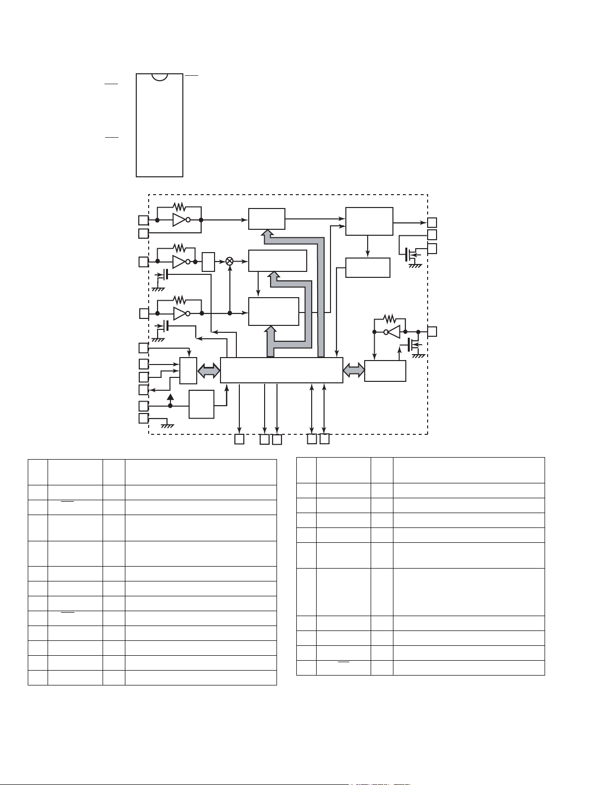
UX-Z7MDR
4.20 LC72136N (IC2) : PLL frequency synthesizer
• Pin layout
1
XT
FM/AM
CE
DI
CLOCK
DO
FM/ST/VCO
AM/FM
SDIN
2
3
4
5
6
7
8
9
10
11
22
21
20
19
18
17
16
15
14
13
12
XT
GND
LPFOUT
LPFIN
PD
VCC
FMIN
AMIN
IFCONT
IFIN
• Block diagram
1
22
16
15
3
4
5
6
17
21
C
I/F
2B
Power
on
Reset
1/2
Data Shift Register & Latch
7821113
• Pin function
Pin
Symbol I/O Function
No.
1 XT I X'tal oscillator connect (75kHz)
2FM
/AM O LOW:FM mode
3 CE I When data output/input for 4pin(input)
and 6pin(output): H
4 DI I Input for receive the serial data from
controller
5 CLOCK I Sync signal input use
6 DO O Data output for Controller Output port
7 FM/ST/VCO O Low: MW mode
8AM
/FM O Open state after the power on reset
9 LW I/O Input/output port
10 MW I/O Input/output port
11 SDIN I/O Data input/output
12 IFIN I IF counter signal input
Reference
Driver
Swallow Counter
Swallow Counter
1/16,1/17 4bit
1/16,1/17 4bit
12bit
Programmable
DriverS
Phase
Detector
Charge Pump
Unlock
Detector
Universal
Counter
Pin
Symbol I/O Function
No.
18
19
20
12
13 IFCONT O IF signal output
14 - Not use
15 AMIN I AM Local OSC signal output
16 FMIN I FM Local OSC signal input
17 VCC - Power suplly(VDD=4.5-5.5V)
When power ON:Reset circuit move
18 PD O PLL charge pump output (H: Local
OSC frequency Height than Reference frequency.L: Low Agreement:
Height impedance)
19 LPFIN I Input for active lowpassfilter of PLL
20 LPFOUT O Output for active lowpassfilter of PLL
21 GND - Connected to GND
22 XT
I X'tal oscillator(75KHz)
1-60 (No.22042)
Page 61
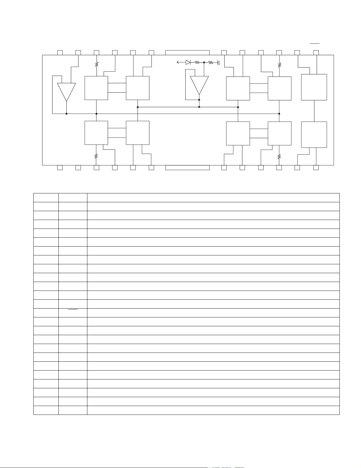
4.21 LA6541-X (IC801) : Servo driver
• Pin layout & Block diagram
Vcc Vref Vin4 Vg4 Vo8 Vo7
24 23
22
21
11k
ohm
UX-Z7MDR
20
19
Gnd
Vcc
Vo6 Vo5 Vg3 Vin3 Cd Res
18
17 16
15
14
13
11k
ohm
- +
- +
Level
shift
Level
shift
B T L
driver
B T L
driver
11k
ohm
1
Vcc Mute Vin1 Vg1 Vo1 Vo2 Vo3 Vo4 Vg2 Vin2 Reg
2
3456
Gnd
78 9101112
• Pin function
Pin No. Symbol Description
1 Vcc Power supply (Shorted to pin 24)
2 Mute All BTL amplifier outputs ON/OFF
3 Vin1 BTL AMP 1 input pin
4 Vg1 BTL AMP 1 input pin (For gain adjustment)
5 Vo1 BTL AMP 1 input pin (Non inverting side)
6 Vo2 BTL AMP 1 input pin (Inverting side)
7 Vo3 BTL AMP 2 input pin (Inverting side)
8 Vo4 BTL AMP 2 input pin (Non inverting side)
9 Vg2 BTL AMP 2 input pin (For gain adjustment)
10 Vin2 BTL AMP 2 input pin
11 Reg Out External transistor collector (PNP) connection. 5V power supply output
12 Reg In External transistor (PNP) base connection
13 Res
Reset output
14 Cd Reset output delay time setting (Capacitor connected externally)
15 Vin3 BTL AMP 3 input pin
16 Vg3 BTL AMP 3 input pin (For gain adjustment)
17 Vo5 BTL AMP 3 output pin (Non inverting side)
18 Vo6 BTL AMP 3 output pin (Inverting side)
19 Vo7 BTL AMP 4 output pin (Inverting side)
20 Vo8 BTL AMP 4 output pin (Non inverting side)
21 Vg4 BTL AMP 4 output pin (For gain adjustment)
22 Vin4 BTL AMP 4 output pin
23 Vref Level shift circuit's reference voltage application
24 Vcc Power supply (Shorted to pin 1)
B T L
driver
B T L
driver
Level
shift
Level
shift
11k
ohm
out
RESET
Regulator
Reg
In
(No.22042)1-61
Page 62

UX-Z7MDR
/
4.22 LA72723(IC3): RDS demodulation
• Pin layout
VREF
MPXIN
Vdda
Vssa
FLOUT
CIN
TES
XOUT
• Block Diagram
1
2
3
4
5
6
7
8
+5V
Vdda
Vssa
MPXIN
TEST
RDS-ID/READY
16
RDCL
15
RDDA
14
RST
13
MODE
12
Vddd
11
Vssd
10
XIN
9
REFERENCE
VOLTAGE
ANTI ALIASING
FILTER
TEST
VREF
57kHz
(SCF)
BPF
FLOUT
SMOOTHING
FILTER
CLK(4.332MHz)
OSC
VREF
CIN
+
PLL
(57kHz)
-
CLOCK
RECOVERY
(1187.5Hz)
DATA
DECODER
RAM
(128-bits)
RDS-ID
DETECT
Vddd
Vssd
RDDA
RDCL
MODE
RST
RDS-ID
READY
+5V
XIN
XOUT
• Pin functions
Pin No. Symbol I/O Function
1 VREF O Reference voltage output (Vdda/2)
2 MPXIN I Baseband (multiplexed) signal input
3 Vdda - Analog power supply (+5V)
4 Vssa - Analog ground
5 FLOUT O Subcarrier input (filter output)
6 CIN I Subcarrier input (comparator input)
7 TEST I Test input
8 XOUT O Crystal oscillator output (4.332MHz)
9 XIN I Crystal oscillator input (exeternal reference input)
10 Vssd - Digtal ground
11 Vddd - Digtal power supply
12 MODE I Read mode setting (0:master, 1:slave)
13 RST I RDS-ID/RAM reset (positive polarity)
14 RDDA O RDS data output
15 RDCL I/O RDS clock output (master mode)/RDS clock input (slave mode)
16 RDS-ID/READY O RDS-ID/READY output (negative polarity)
1-62 (No.22042)
Page 63

4.23 XC62ER3602M-X (IC400) : Regulator
T
•Pin layout
54
UX-Z7MDR
1
23
• Block diagram
V
DD
EXT
CE
• Pin function
Pin No. Symbol Function
1V
2V
3V
SS
IN
OUT
GND
Power supply input
Regulator output
4 EXT Base current control terminal
5 CE Chip enable
Current
Limit
+
-
Voltage
Reference
V
OU
V
SS
4.24 TK11140SC-W (IC485) : Regulator
•Pin layout
on / off control 1
GND 2
Np (Vref) 3
• Block diagram
VIN
Rin=550k
on / off Ccont.
6 Vin
4 Vout
VOUT
Thermal Sensor
Bandgap Reference
Cnp
GND
(No.22042)1-63
Page 64

UX-Z7MDR
4.25 LC75345M-X (IC901) : E.volume
• Pin layout
36 35 34 33 32 31 30 29 28 27 26 25 24 23 22 21 20 19
• Block diagram
CL
DI
VDD
CE
ROPOUT
RINM
VSS
LOPOUT
LSELO
RINP
LINM
LVRIN
ROOUT
RSB
LINP
LOUT
LTRE
RBASS2
RBASS1
LSB
LBASS2
RTRE
RVRIN
LTRE
LBASS1
LBASS1
RSELOR5R4
LVRIN
LSELO
LBASS2
LSB
L5
R3
L4
LOUT
R2
L3
R1
L2
Vref
181716151413121110987654321
L1
L5
L4
L3
L2
L1
Vref
R1
R2
R3
R4
R5
14
15
16
17 18
19
20
21
22 23
24
13
12
11
LVref
RVref
CONTROL
CIRCUIT
LOGIC
CIRCUIT
CONTROL
CIRCUIT
10
9
8
CCB
INTERFACE
7
6
LINP
5
LINM
LOPOUT
34
VSS
2
CE
1
DI
36
CL
35
VDD
34
ROPOUT
33
RINM
32
RINP
1-64 (No.22042)
25
RESLO
26
RVRIN
27
RTRE
28
RBASS1
29
RBASS2
30
RSB
31
ROUT
Page 65

• Pin function
Pin No. Symbol Function
1 DI Serial data and clock input pin for control.
2 CE Chip enable pin.
3 VSS Ground pin.
4 LOPOUT Output pin of general-purpose operation amplifier.
5 LINM Non-inverted input pin of general-purpuse operation amplifier.
6 LINP Non-inverted input pin of general-purpuse operation amplifier.
7 LOUT ATT + equalizer output pin.
8 LSB Capacitor and resistor connection pin comprising filters for bass and super-bass band.
9 LBASS2 Capacitor and resistor connection pin comprising filters for bass and super-bass band.
10 LBASS1 Capacitor and resistor connection pin comprising filters for bass and super-bass band.
11 LTRE Capacitor and resistor connection pin comprising treble band filter.
12 LVRIN Volume input pin.
13 LSELO Input selector output pin.
14 L5 Input signal pin.
15 L4 Input signal pin.
16 L3 Input signal pin.
17 L2 Input signal pin.
18 L1 Input signal pin.
19 Vref 0.5 x VDD voltage generation block for analog ground.
20 R1 Input signal pin.
21 R2 Input signal pin.
22 R3 Input signal pin.
23 R4 Input signal pin.
24 R5 Input signal pin.
25 RSELO Input selector output pin.
26 RVRIN Volume input pin.
27 RTRE Capacitor connection pin comprising treble band filter.
28 RBASS1 Capacitor and resistor connection pin comprising filter for bass and super-bass band.
29 RBASS2 Capacitor and resistor connection pin comprising filter for bass and super-bass band.
30 RSB Capacitor and resistor connection pin comprising filter for bass and super-bass band.
31 ROUT ATT + equalizer output pin.
32 RINP Non inverted input pin of general-purpose operation amplifier.
33 RINM Non inverted input pin of general purpose operation amplifier.
34 ROPOUT Output pin of general-purpose operation amplifier.
35 VDD Supply pin.
36 CL Serial data and clock input pin for control.
UX-Z7MDR
(No.22042)1-65
Page 66

UX-Z7MDR
VICTOR COMPANY OF JAPAN, LIMITED
AV & MULTIMEDIA COMPANY 10-1,1chome,Ohwatari-machi,Maebashi-city,371-8543,Japan
(No.22042)
Printed in Japan
200302WPC
 Loading...