

Page 1
UX-L46V/UX-L36V
UX-L46V/UX-L36V
SERVICE MANUAL
COMPACT COMPONENT SYSTEM
UX-L46V/UX-L36V
STANDBY / ON
STANDBY / ON
REC SURROUND AHB PRO.
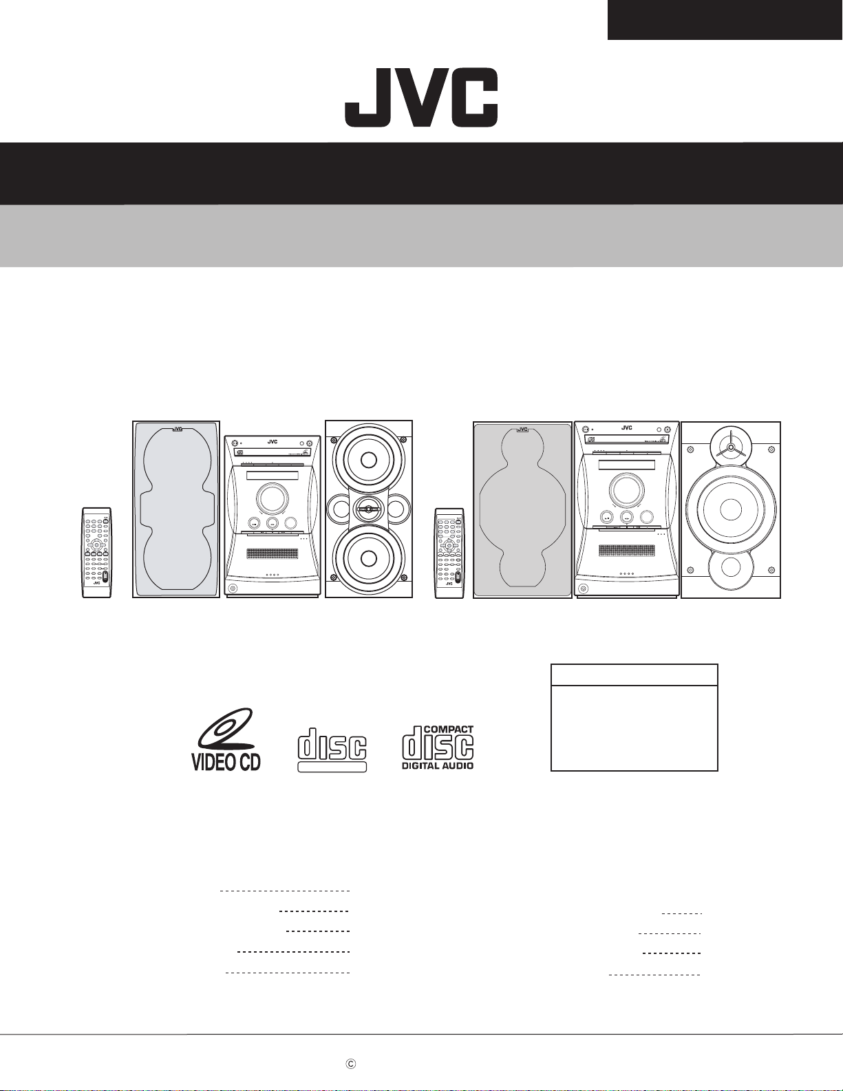
MICRO COMPONENT SYSTEM UX-L46V
VOLUME
CLOCK/TIMER AUX/MD
REC REV. MODE AHB PRO.
MICRO COMPONENT SYSTEM UX-L36V
CLOCK/TIMER AUX/MD
VOLUME
1
2
4
5
7
8
10
BASS
PREV
SET
DOWN
CD
/
/SELECT
CD
REV.MODEFM MODE
RETURN PRGM RANDOM REPEAT
ON
KARAOKE
SCREEN SURROUND AHB PRO
MPX
PBC
DIGITAL
ECHO
STILL
RM-SUXL46V REMOTE CONTROL
STANDBY/ON
3
DISPLAY
6
CLOCK
/TIMER
9
SLEEP
+10
TREBLE
UP
NEXT
CANCEL
AUX/MD
FM/AMTAPE
AUTO
PRESET
VIDEO
INTRO
DIMMER
VOLUME
SELECT
CD TAPE
PREV
RETURN VCD NUMBER
PHONES
SP-UXL46V SP-UXL46VCA-UXL46V
Contents
Safety precautions
Preventing static electricity
Important for laser products
Disassembly method
Adjustment method
DOWN
AUTO REVERSE
+—
FM/AM
UP
NEXT
PUSH
OPEN
COMPACT
DIGITAL VIDEO
1-2
1-3
1-4
1-5
1-21
+—
SELECT
1
2
5
4
7
8
10
BASS
PREV
SET
/
CD
TAPE FM/AM AUX/MD
CD
REV.MODEFM MODE
RETURN PRGM RANDOM REPEAT
ON
SCREEN
KARAOKE
PBC
MPX
DIGITAL
ECHO
STILL
—
RM-SUXL36V REMOTE CONTROL
STANDBY/ON
3
6
DISPLAY
CLOCK
9
/TIMER
+10
SLEEP
UP
TREBLE
NEXT
CANCEL
DOWN
AUTO
PRESET
AHB PRO
VIDEO
INTRO
DIMMER
VOLUME
CD TAPE
DOWN
PREV
RETURN VCD NUMBER
AUTO REVERSE
PHONES
FM/AM
UP
NEXT
SP-UXL36V SP-UXL36VCA-UXL36V
UX-L46V/UX-L36V
Area Suffix
US ------------------ Singapore
UN ----------------------- Asean
UX ---------------- Saudi Arabia
UF ------------------------- China
Flow of functional operation
until TOC read (CD)
Maintenance of laser pickup
Replacement of laser pickup
Description of major ICs
PUSH
OPEN
1-25
1-26
1-26
1-27~46
COPYRIGHT 2002 VICTOR COMPANY OF JAPAN, LTD.
No.21143
Sep. 2002
1-1
Page 2
UX-L46V/UX-L36V
1. This design of this product contains special hardware and many circuits and components specially for safety
purposes. For continued protection, no changes should be made to the original design unless authorized in
writing by the manufacturer. Replacement parts must be identical to those used in the original circuits. Services
should be performed by qualified personnel only.
2. Alterations of the design or circuitry of the product should not be made. Any design alterations of the product
should not be made. Any design alterations or additions will void the manufacturer`s warranty and will further
relieve the manufacture of responsibility for personal injury or property damage resulting therefrom.
3. Many electrical and mechanical parts in the products have special safety-related characteristics. These
characteristics are often not evident from visual inspection nor can the protection afforded by them necessarily
be obtained by using replacement components rated for higher voltage, wattage, etc. Replacement parts which
have these special safety characteristics are identified in the Parts List of Service Manual. Electrical
components having such features are identified by shading on the schematics and by ( ) on the Parts List in
the Service Manual. The use of a substitute replacement which does not have the same safety characteristics
as the recommended replacement parts shown in the Parts List of Service Manual may create shock, fire, or
other hazards.
4. The leads in the products are routed and dressed with ties, clamps, tubings, barriers and the like to be
separated from live parts, high temperature parts, moving parts and/or sharp edges for the prevention of
electric shock and fire hazard. When service is required, the original lead routing and dress should be
observed, and it should be confirmed that they have been returned to normal, after re-assembling.
5. Leakage currnet check (Electrical shock hazard testing)
After re-assembling the product, always perform an isolation check on the exposed metal parts of the product
(antenna terminals, knobs, metal cabinet, screw heads, headphone jack, control shafts, etc.) to be sure the
product is safe to operate without danger of electrical shock.
Do not use a line isolation transformer during this check.
Plug the AC line cord directly into the AC outlet. Using a "Leakage Current Tester", measure the leakage
current from each exposed metal parts of the cabinet, particularly any exposed metal part having a return
path to the chassis, to a known good earth ground. Any leakage current must not exceed 0.5mA AC (r.m.s.).
Alternate check method
Plug the AC line cord directly into the AC outlet. Use an AC voltmeter having, 1,000 ohms per volt or more
sensitivity in the following manner. Connect a 1,500 10W resistor paralleled by a 0.15 F AC-type capacitor
between an exposed metal part and a known good earth ground.
Measure the AC voltage across the resistor with the AC
voltmeter.
Move the resistor connection to each exposed metal part,
particularly any exposed metal part having a return path to
the chassis, and meausre the AC voltage across the resistor.
Now, reverse the plug in the AC outlet and repeat each
measurement. Voltage measured any must not exceed 0.75 V
AC (r.m.s.). This corresponds to 0.5 mA AC (r.m.s.).
0.15 F AC TYPE
1500 10W
Good earth ground
AC VOLTMETER
(Having 1000
ohms/volts,
or more sensitivity)
Place this
probe on
each exposed
metal part.
!
1. This equipment has been designed and manufactured to meet international safety standards.
2. It is the legal responsibility of the repairer to ensure that these safety standards are maintained.
3. Repairs must be made in accordance with the relevant safety standards.
4. It is essential that safety critical components are replaced by approved parts.
5. If mains voltage selector is provided, check setting for local voltage.
Burrs formed during molding may
be left over on some parts of the
chassis. Therefore, pay attention to
such burrs in the case of
preforming repair of this system.
In regard with component parts appearing on the silk-screen printed side (parts side) of the PWB diagrams, the
parts that are printed over with black such as the resistor ( ), diode ( ) and ICP ( ) or identified by the " "
mark nearby are critical for safety.
(This regulation does not correspond to J and C version.)
1-2
Page 3
Preventing static electricity
UX-L46V/UX-L36V
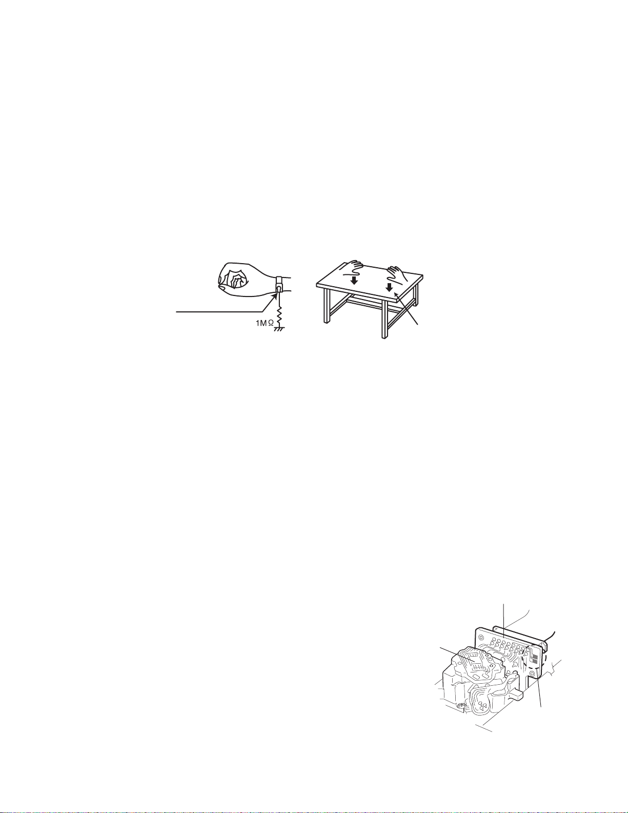
1.Grounding to prevent damage by static electricity
Electrostatic discharge (ESD), which occurs when static electricity stored in the body, fabric, etc. is discharged,
can destroy the laser diode in the traverse unit (optical pickup). Take care to prevent this when performing repairs.
2.About the earth processing for the destruction prevention by static electricity
Static electricity in the work area can destroy the optical pickup (laser diode) in devices such as CD players.
Be careful to use proper grounding in the area where repairs are being performed.
2-1 Ground the workbench
Ground the workbench by laying conductive material (such as a conductive sheet) or an iron plate over
it before placing the traverse unit (optical pickup) on it.
2-2 Ground yourself
Use an anti-static wrist strap to release any static electricity built up in your body.
(caption)
Anti-static wrist strap
Conductive material
(conductive sheet) or iron plate
3. Handling the optical pickup
1. In order to maintain quality during transport and before installation, both sides of the laser diode on the
replacement optical pickup are shorted. After replacement, return the shorted parts to their original condition.
(Refer to the text.)
2. Do not use a tester to check the condition of the laser diode in the optical pickup. The tester's internal power
source can easily destroy the laser diode.
4.Handling the traverse unit (optical pickup)
1. Do not subject the traverse unit (optical pickup) to strong shocks, as it is a sensitive, complex unit.
2. Cut off the shorted part of the flexible cable using nippers, etc. after replacing the optical pickup. For specific
details, refer to the replacement procedure in the text. Remove the anti-static pin when replacing the traverse
unit. Be careful not to take too long a time when attaching it to the connector.
3. Handle the flexible cable carefully as it may break when subjected to strong force.
4. It is not possible to adjust the semi-fixed resistor that adjusts the laser power. Do not turn it
Attention when traverse unit is decomposed
*Please refer to "Disassembly method" in the text for pick-up and how to
detach the substrate.
1.Solder is put up before the card wire is removed from connector on
the CD substrate as shown in Figure.
(When the wire is removed without putting up solder, the CD pick-up
assembly might destroy.)
2.Please remove solder after connecting the card wire with
when you install picking up in the substrate.
CD pickup
Pickup board
Shorting round
(Soldering)
1-3
Page 4
UX-L46V/UX-L36V
Important for laser products
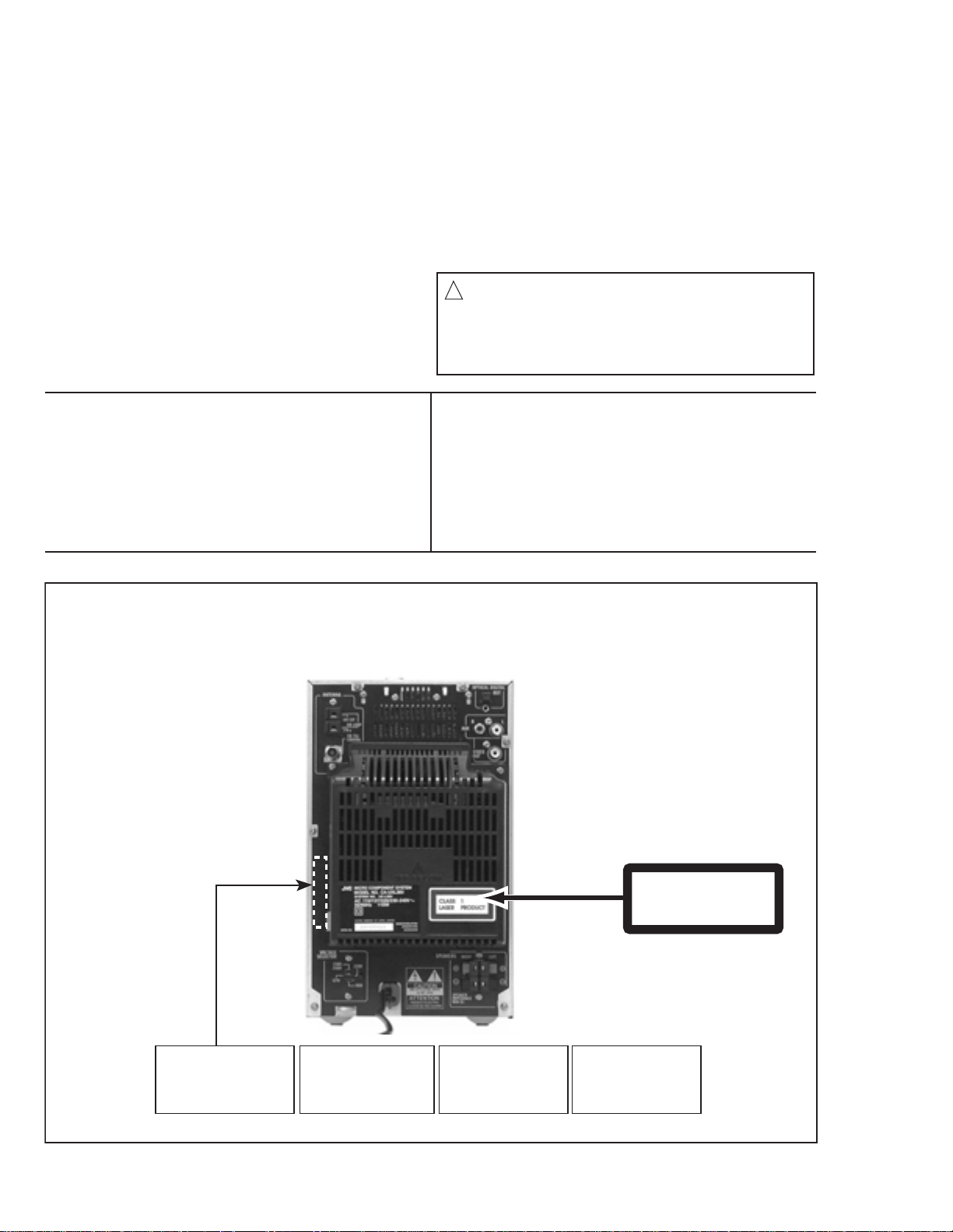
1.CLASS 1 LASER PRODUCT
2.DANGER : Invisible laser radiation when open and inter
lock failed or defeated. Avoid direct exposure to beam.
3.CAUTION : There are no serviceable parts inside the
Laser Unit. Do not disassemble the Laser Unit. Replace
the complete Laser Unit if it malfunctions.
4.CAUTION : The compact disc player uses invisible
laserradiation and is equipped with safety switches
whichprevent emission of radiation when the drawer is
open and the safety interlocks have failed or are de
feated. It is dangerous to defeat the safety switches.
VARNING : Osynlig laserstrålning är denna del är öppnad
och spårren är urkopplad. Betrakta ej strålen.
VARO : Avattaessa ja suojalukitus ohitettaessa olet
alttiina näkymättömälle lasersäteilylle.Älä katso
säteeseen.
5.CAUTION : If safety switches malfunction, the laser is able
to function.
6.CAUTION : Use of controls, adjustments or performance of
procedures other than those specified herein may result in
hazardous radiation exposure.
CAUTION
!
Please use enough caution not to
see the beam directly or touch it
in case of an adjustment or operation
check.
ADVARSEL : Usynlig laserstråling ved åbning , når
sikkerhedsafbrydere er ude af funktion. Undgå
udsættelse for stråling.
ADVARSEL : Usynlig laserstråling ved åpning,når
sikkerhetsbryteren er avslott. unngå utsettelse
for stråling.
REPRODUCTION AND POSITION OF LABELS
WARNING LABEL
DANGER : Invisibie laser radiation
when open and interlock or
defeated.
AVOID DIRECT EXPOSURE TO
BEAM (e)
VARO : Avattaessa ja suojalukitus
ohitettaessa olet alttiina
näkymättömälle lasersäteilylle.Älä
katso säteeseen. (d)
VARNING : Osynlig laserstrålning är
denna del är öppnad och spårren är
urkopplad. Betrakta ej strålen. (s)
CLASS 1
LASER PRODUCT
ADVARSEL :Usynlig laserstråling
ved åbning , når
sikkerhedsafbrydere er ude af
funktion. Undgå udsættelse for
stråling. (f)
1-4
Page 5
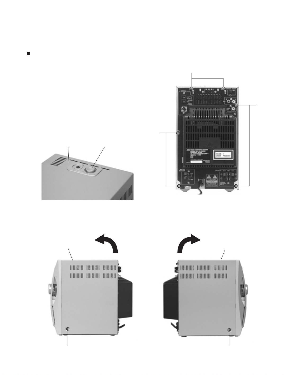
Disassembly method
<Main body>
Removing the Metal cover
(See Fig.1~4)
1.
Pull out the microphone volume knob on the rear top
of the body.
2.
Remove the six screws A on the back of the main
body.
3.
Remove the screw B on each side and remove the
cover in the direction of the arrow.
Microphone volume knobMetal cover
UX-L46V/UX-L36V
A
A
A
Metal cover
Fig.2Fig.1
Metal cover
B
Fig.3 Fig.4
B
1-5
Page 6
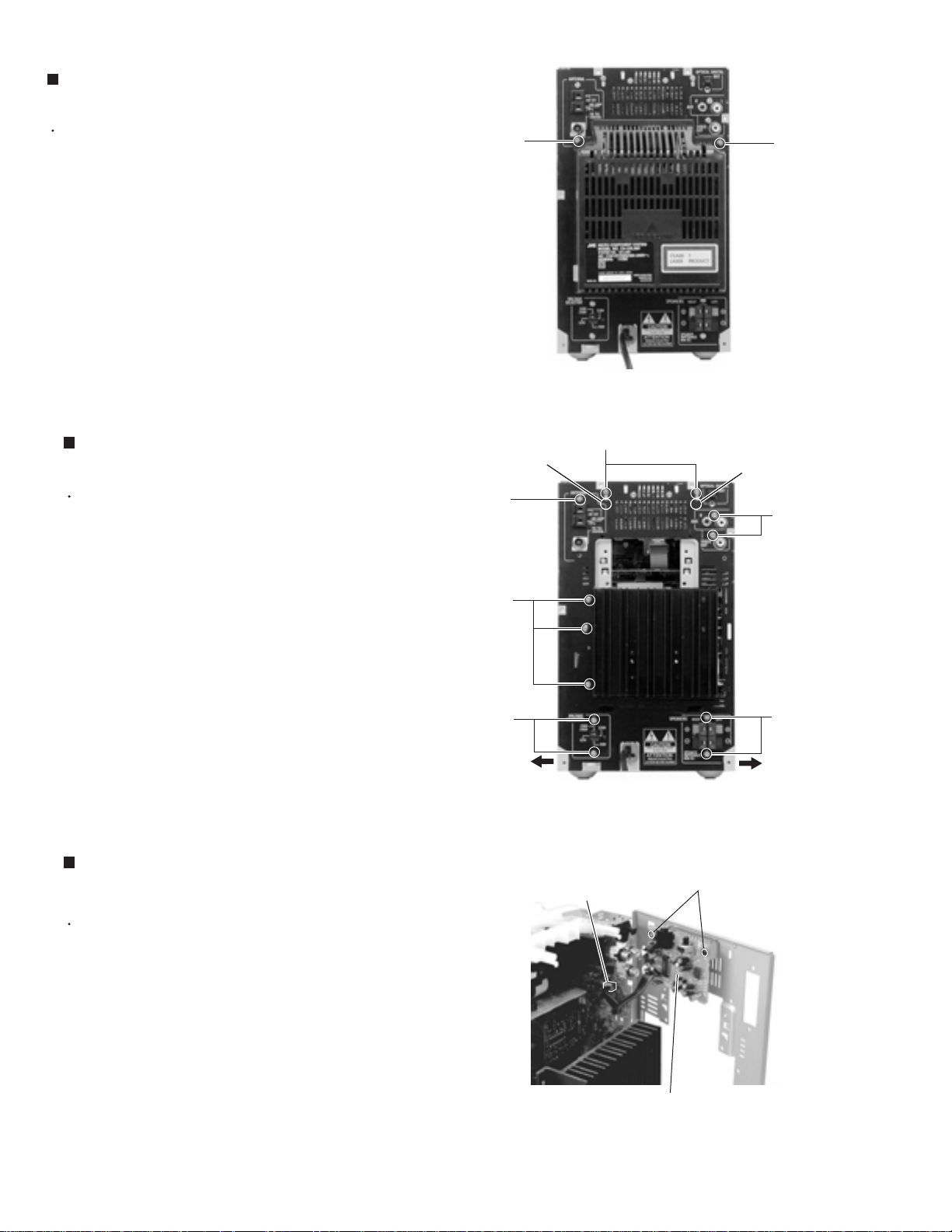
UX-L46V/UX-L36V
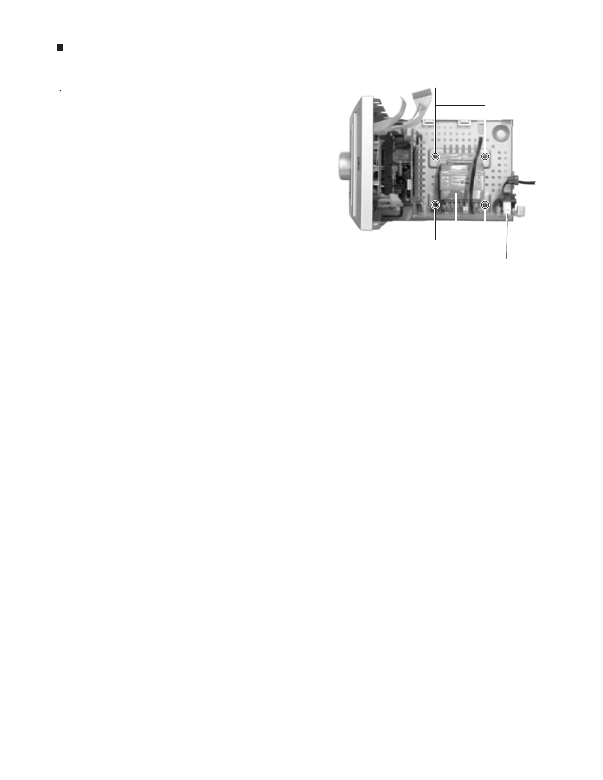
Removing the Rear cover
(See Fig.5)
Remove the metal cover.
1.
Remove the two screws C retaining the rear cover.
Removing the Rear panel
(See Fig.6,7)
Remove the metal cover and the rear cover.
1.
Remove the twelve screws D retaining the rear
panel. Release the two joints a on the rear side and
the joint b on each side.
D
C
C
Fig.5
D
a
a
D
2.
Disconnect the wire from connector CN919 on the
main board of the body.
The rear panel comes off with the microphone
volume board.
Removing the mic volume board
(See Fig.7)
Prior to performing the following procedure, remove
the metal cover, rear cover and the rear panel.
1.
Remove the two screws E retaining the mic volume
board on the back of the rear panel.
2.
Disconnect the wire from connector CN919 on the
main board.
D
D
b
Main board
CN919
D
b
Fig.6
E
1-6
Microphne volume board
Fig.7
Page 7
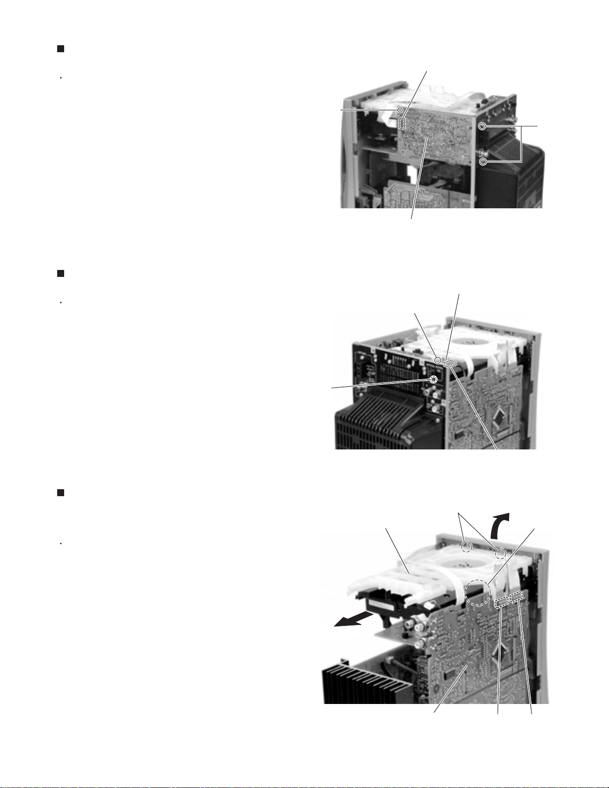
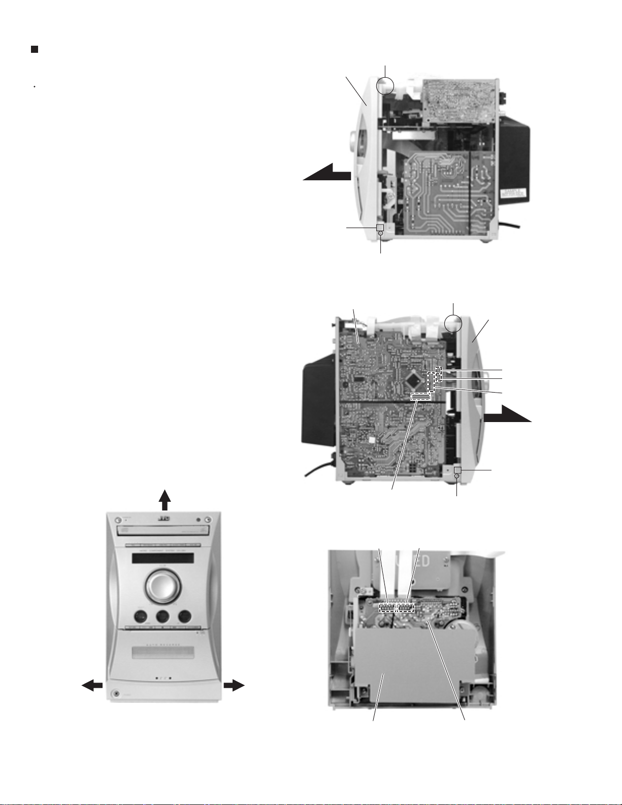
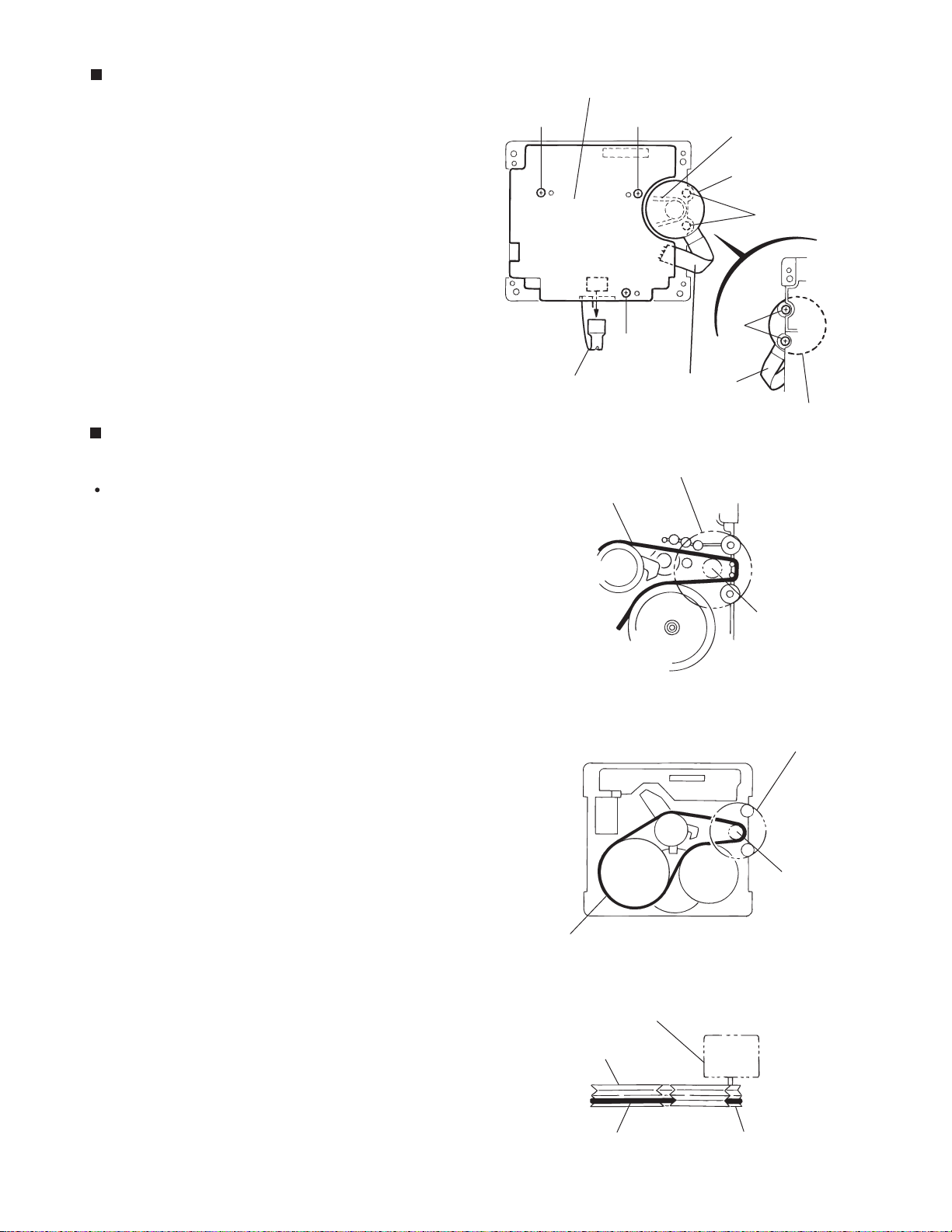
Removing the Tuner board
(See Fig.8)
Remove the metal cover.
1.
Disconnect the card wire from connector CN1 on the
tuner board.
2.
Remove the two screws F on the rear side and the
screw G on the side.
Removing the Optical digital board
(See Fig.9)
Remove the metal cover.
UX-L46V/UX-L36V
CN1
G
F
Tuner board
Fig.8
Optical digital board
I
1.
Disconnect the shield wire from connector CN905 on
the optical digital board.
2.
Remove the screw H on the rear side and the screw
I on the upper side.
Removing the CD-R/RW mechanism
assembly
(See Fig.10)
Remove the metal cover, the rear cover, the rear
panel, the tuner board and the optical digital board.
1.
Disconnect the card wire from connector CN903 and
CN904 on the main board.
2.
Pull the joint c in the direction of the arrow and
remove the CD-R/RW mechanism assembly
backward while releasing the joint d.
H
CD-R/RW mechanism
assembly
CN905
Fig.9
c
d
Main board
Fig.10
CN904
CN903
1-7
Page 8
UX-L46V/UX-L36V
Removing the Main board/ the Heat sink
board (See Fig.11~13)
Remove the metal cover, the rear cover and the rear
panel.
Disconnect the card wire from connector CN902,
1.
CN903, CN904 and CN905 on the main board and
remove the CD-R/RW mechanism assembly.
REFERENCE:
2.
Disconnect the vocal board from connector CN920
on the main board.
REFERENCE:
3.
Remove the two screws I attaching the main board.
4.
Disconnect the card wire from connector CN931,
CN935, CN933, CN934, CN913, CN901, CN900 and
CN917 on the main board.
Refer to the method of removing the
CD-R/RW mechanism assembly and
Fig.8.
The vocal board can be detached
without removing the main board.
Optical digital board
CN905
e
CN915
Main board
CN920
CD-R/RW mechanism assembly
CN902 CN904
CN916
I
CN903
Main board
I
Fig.11
Vocal board
5.
Remove the band f and disconnect the card wire
from connector CN951 on the power transformer
assembly. Remove the main board / the heat sink
board from the body.
6.
Release the joint e of the main board and disconnect
connector CN944 and CN945 of the heat sink board
from connector CN915 and CN916 of the main board
respectively.
7.
Remove the two screws J attaching the heat sink
bracket and heat sink board.
Main board
Heat sink
J
CN933
CN934
CN913
CN931
Fig.12
CN935
Main board
Heat sink
CN900
CN917
1-8
CN944
Fig.14
CN945
Heat sink board
CN901
CN951
Fig.13
f
Power transformer
assembly
Page 9
Removing the Power transformer
assembly (See Fig.15)
Remove the metal cover, the rear cover, the rear
panel, the CD-R/RW mechanism assembly and the
main board.
Disconnect the power cord from connector J1000 on
1.
the power transformer assembly.
Remove the four screws K.
2.
UX-L46V/UX-L36V
K
KK
J1000
Power transformer
assembly
Fig.15
1-9
Page 10
UX-L46V/UX-L36V
Removing the Front panel assembly
(See Fig.16~19)
Remove the metal cover.
1.
Remove the screw L on each side. Pull the joint h
on both sides and lift the front panel assembly to
release the joint g .
2.
Disconnect connector CN931, CN935, CN933 and
CN934 on the main board.
3.
Disconnect the card wire from connector CN33 and
CN34 on the cassette mechanism board.
Front panel
assembly
h
Main board
g
L
Fig.16
g
Front panel
assembly
CN933
CN934
CN931
h
g
CN935
L
Fig.17
CN34
CN33
1-10
hh
Fig.18
Cassette mechanism
assembly
Fig.19
Cassette mechanism
board
Page 11
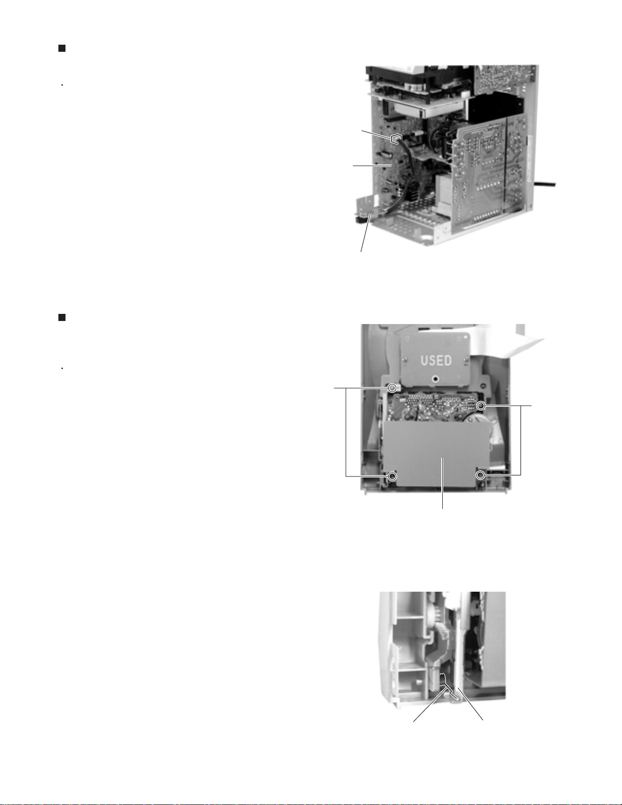
Removing the Phones board
(See Fig.20)
Prior to performing the following procedure, remove
the metal cover and the front panel assembly.
1.
Disconnect connector CN913 on the main board.
UX-L46V/UX-L36V
CN913
Main board
Phones board
Fig.20
Removing the Cassette mechanism
assembly
(See Fig.21)
Prior to performing the following procedure, remove
the metal cover and the front panel assembly.
1.
Remove the four screws M retaining the cassette
mechanism assembly.
2.
Remove the cassette door spring from bracket.
M
M
Cassette mechanism
assembly
Fig.21-1
Cassette door spring
Fig.21-2
Bracket
1-11
Page 12
UX-L46V/UX-L36V
<Cassette Mechanism Section>
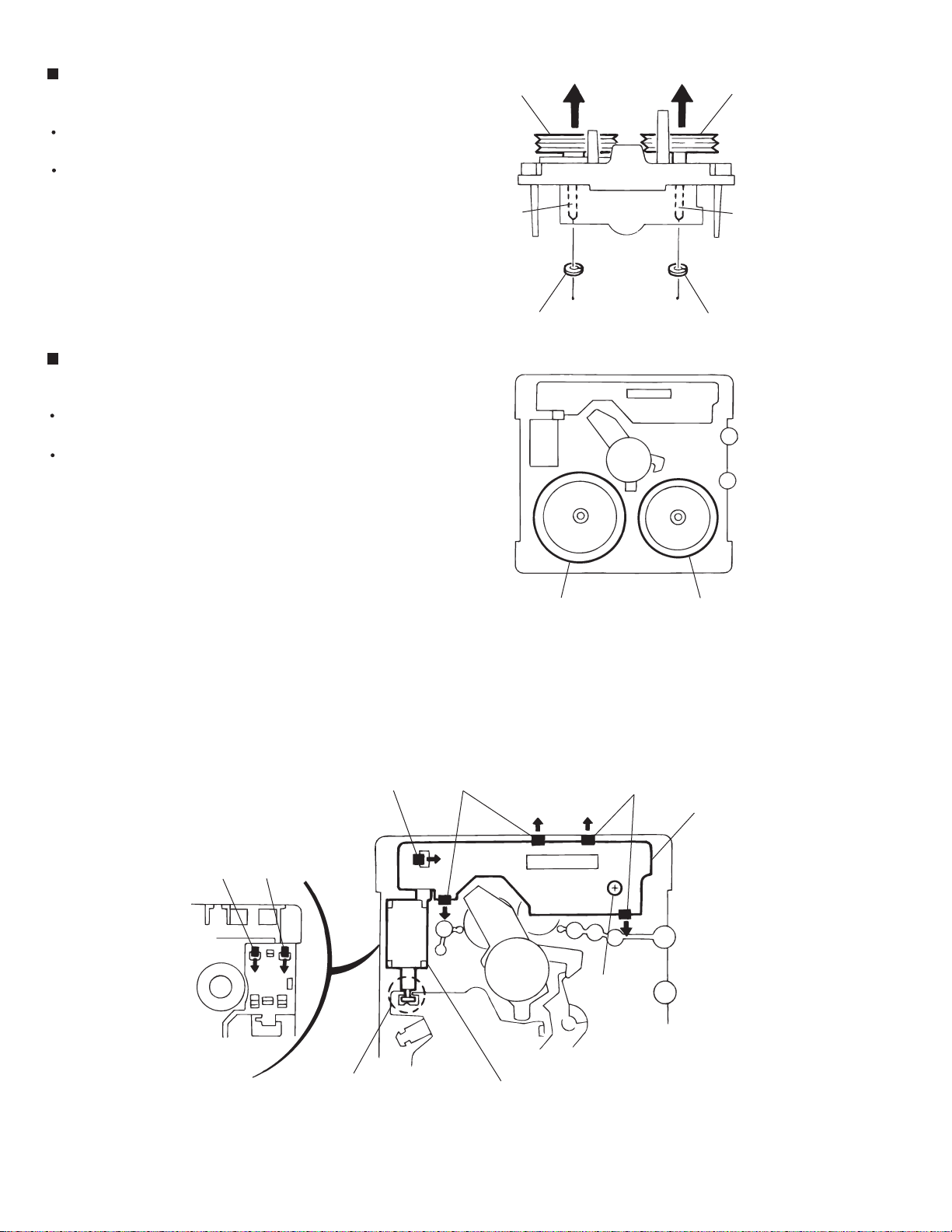
Removing the Recording, Playback / Erasing
Head (Refer to Figs. 1 to 3.)
1. Shifting the trigger arm seen in the right side of the
head mount in the arrow-marked direction, turn the
flywheel (R) counterclockwise until the head mount
clicks while moving frontwards. (See Fig. 1.)
2. Turn the flywheel (R) counterclockwise. The
playback head accordingly turns counterclockwise
from the position shown in Fig. 2 to that in Fig. 3.
3. Leaving the playback head in the position shown in
Fig. 3, disconnect the flexible wire coming from the
playback head from the connector CN31 on the
head amplifier & mechanism control P.C. board.
4. Remove the flexible wire from the hook b of the
chassis base.
5. Remove the spring a from the back of the head.
Head mount
Head (REC, PB/Erasing)
Flexible wire
Cassette mechanism
Flywheel (R)
Trigger arm
Fig. 1
Spring a
Trigger arm
6. Loosen the reversing azimuth screw A that fastens
the head.
7. Remove the recording, playback/erasing head from
the front side (head side) of the head mount.
Reinstalling the Recording, Playback /
Erasing Head
1. Install the recording, playback/erasing head from the
front side of the head mount as shown in Fig. 3.
2. Tighten the reversing azimuth screw A.
3. Install the spring a from the back of the head.
4. Set the flexible wire at the hook b of the chassis
base.
5. Connect the flexible wire coming from the head to
the connector CN31 on the head amplifier &
mechanism control P.C. board.
Head amp. & mechanism
control P.C. board
Head (REC, PB/Erasing)
Spring a
Flexible wire
Hook b
CN31
Fig. 2
CN31
Fig. 3
Hook b
Head amp. & mechanism
control P.C. board
Flywheel (R)
Reversing azimuth
screw A
Head mount
1-12
Page 13
UX-L46V/UX-L36V
Removing the Head Amplifier & Mechanism
Control P.C. Board (Refer to Figs. 4 and 5.)
1. Disconnect the flexible wire from the connector
CN31 on the head amplifier & mechanism control
P.C. board mounted on the back of the cassette
mechanism assembly.
2. Remove the three screws B fastening the head
amplifier & mechanism control P.C. board.
3. Disconnect the connector CN32 of the head
amplifier & mechanism control P.C. board from the
connector CN1 on the reel pulse P.C. board.
Note: Remove the 4-pin parallel wire soldered to the
main motor depending on the situation.
Removing the Main Motor Assembly (Refer
to Figs. 4 to 7.)
The main motor assembly can be removed without
removal of the head amplifier & mechanism control
P.C. board.
Head amp. & mechanism
control P.C. board
BB
CN32
CN31
B
Flexible P.C. board 4-pin parallel wire
Fig. 4
Main motor assembly
Capstan belt
Main motor assembly
Belt
Main motor
assembly
C
C
1. Remove the two screws C fastening the main motor
assembly.
2. Lifting the main motor assembly slightly upwards,
disengage the capstan belt from the motor pulley.
Note: Be careful not to soil the capstan belt with grease
or the like. When reinstalling the main motor
assembly, refer to Fig. 6 and Fig. 7 for engaging
the capstan belt.
Capstan belt
Main motor assembly
Motor pulley
Fig. 5
Main motor assembly
Motor pulley
Fig. 6
Flywheel
Capstan belt
Motor pulley
Fig. 7
1-13
Page 14
UX-L46V/UX-L36V
Removing the Flywheel (Refer to Figs. 8
and 9.)
Remove the head amplifier & mechanism control
P.C. board.
Remove the main motor assembly.
Flywheel (R)
Flywheel (L)
1. Remove the slit washers c and d that fasten the
capstan shafts (L) and (R) from the front side of the
cassette mechanism assembly, and then draw out
the flywheels (L) and (R) from the back side of the
cassette mechanism assembly in the arrow-marked
direction for removing them.
Removing the Reel Pulse P.C. Board /
Solenoid (Refer to Fig. 10.)
Remove the head amplifier & mechanism control
P.C. board.
Remove the main motor assembly.
1. Remove the screw D fastening the reel pulse P.C.
board.
2. Disengage the five hooks e that retain the reel
pulse P.C. board by pressing each in the arrowmarked direction.
3. Disengage the two hooks f that retain the solenoid
by pressing each from the front side of the cassette
mechanism assembly in the arrow-marked
direction.
Capstan
shaft (R)
Slit washer d
Flywheel (R)
Fig. 8
Fig. 9
Capstan
shaft (L)
Slit washer c
Flywheel (L)
Note: When reinstalling the reel pulse P.C. board and
solenoid, make sure that the hook g of the
solenoid is properly engaged.
Hook e
Hook f
Hook f
Hook g
Hook e
Fig. 10
Hook e
Reel pulse P.C. board
D
Solenoid
1-14
Page 15
UX-L46V/UX-L36V
<CD mechanism assembly section>
Removing the video board
(See Fig.1, 2)
1.
Remove the four screws A attaching the video
board cover on the bottom of the CD mechanism
assembly.
2.
Disconnect the card wire from connector CN101 on
the video board.
3.
Remove the video board cover and the video board.
A
Video board
CN101
Fig.1
A
A
Fig.2
Video board
1-15
Page 16

UX-L46V/UX-L36V
Removing the CD servo board
(See Fig.3~5)
Video board assembly
CAUTION:
Solder the shorting round before disconnecting
the card wire extending from the pickup. If
you do not follow this instruction, the pickup
may be damaged.
1.
Remove the two screws B attaching the video board
assembly and the CD servo board at the bottom of
the CD mechanism assembly.
2.
Disconnect the card wire from connector CN101 on
the video board assembly.
Move the video board assembly forward to release
the joint a , and remove.
REFERENCE:
The video board assembly can be
removed solely. To remove the video
board, see Fig.1 and 2.
3.
Disconnect the card wire from connector CN606 on
the CD servo board. Turn over the CD servo board
as shown in Fig.3 and put aside temporarily.
4.
Solder the shorting round on the pickup board in the
CD pickup section.
Joint a
CN101
B
Fig.3
CD servo board
5.
Disconnect the card wire from connector CN601 and
the wire from CN801 on the CD servo board.
CAUTION:
When reassembling, make sure to unsolder
the shorting round after connecting the card
wire from the pickup to the connector.
CD servo board
CN801
CN601
CN651
CN652
CN606
CN801
CN601
Shorting round
Pickup board
CD pickup
CD pickup
1-16
Fig.4
Shorting round
(Soldering)
Fig.5
Page 17

UX-L46V/UX-L36V
Removing the clamper base / tray
(See Fig.6~8)
1.
Bring up the fitting in the direction of the arrow to
release the three joints b.
2.
On the front side of the body, move the cam plate
lever to the center.
3.
Remove the stopper screw C and pull out the tray
toward the front.
4.
Remove the four screws D attaching the clamper
base.
5.
From the rear side, remove the clamper base
upward.
Tray
Joint b
Fig.6
Fitting
Joint b
Tray
D
C
Clamper
D
Cam plate
(Lever)
Fig.7
Clamper base
D
Tray
Fig.8
1-17
Page 18

UX-L46V/UX-L36V
Removing the CD mechanism assembly
(See Fig.9,10)
Prior to performing the following procedure, remove
the clamper base / tray and the CD servo board.
1.
Remove the screw E attaching the CD mechanism
assembly.
2.
Move the CD mechanism assembly backward to
release the two joints c of the CD base on the front
side.
CAUTION:
When reassembling, fit the front part of the
CD mechanism assembly to the two
chassis joints c and attach the four
dampers correctly.
CD mechanism assembly
damper
damper
CD mechanism assembly
E
damper
damper
c
Fig.9
E
CD base
c
Fig.10
1-18
Page 19

Removing the loading motor / loading
motor board (See Fig.11, 12)
Prior to performing the following procedure, remove
the clamper base / tray and the CD servo board.
1.
From upside of the loading base, remove the belt
from the motor pulley.
2.
Remove the two screws F attaching the loading
motor.
3.
At the bottom of the body, release the three joints d
outward and pull out the loading motor board from
the shaft. The loading motor comes off with the
loading board.
4.
Unsolder the two soldered points e on the loading
motor board and remove the loading motor.
REFERENCE:
When removing the loading motor board
only, unsolder the two soldering e on the
loading motor and release the three joints d.
Soldering e
Loading motor
Loading motor
Belt
F
Fig.11
d
Loading motor board
UX-L46V/UX-L36V
F
Motor pulley
c
Fig.12
1-19
Page 20

UX-L46V/UX-L36V
Removing the C.D. gear (1), (2) and (3)
(See Fig.13~16)
Prior to performing the following procedure, remove
the CD servo board.
1.
Remove the two screws G attaching the CD base on
the bottom of the loading base.
2.
Remove the rear part of the CD base upward and
pull out the shaft f of the CD base from the camplate
on the front side of the loading base.
REFERENCE:
3.
Remove the leaf spring on the upside of the loading
base.
4.
Remove the screw H attaching the cam plate fitting.
5.
Remove the screw I and the cam plate upward.
The CD mechanism assemly comes off
with the CD base.
G G
f
CD base
(Bottom)
Fig.13
CD mechanism assembly
Loading base
G
6.
Remove the belt from the C.D. gear (1).
7.
Pull out the C.D. gear (1), (2) and (3) respectively.
Cam plate fitting
H
Cam plate
I
G
CD base
Loading base
Fig.14
C.D. gear (3)
Belt
1-20
Spring
C.D. gear (2)
C.D. gear (1)
Fig.16Fig.15
Page 21

Adjustment method
UX-L46V/UX-L36V
Measurement Instruments Required for
Adjustment
1. Low frequency oscillator
This oscillator should have a capacity to output
0dBs to 600 at an oscillation frequency of
50Hz-20kHz.
2. Attenuator impedance : 600
3. Electronic voltmeter
4. Distortion meter
5. Frequency counter
6. Wow & flutter meter
7. Test tape
VT703L : Head azimuth
VT712 : Tape speed and running unevenness
(3kHz)
VT724 : Reference level (1kHz)
8. Blank tape
TYPE : AC-225
TYPE : AC-514
9. Torque gauge : For play and back tension
FWD(TW2111A), REV(TW2121a) and
FF/REW(TW2231A)
10. Test disc: CTS-1000
Measurement conditions
Power supply voltage
AC110V/127V/220V/230V 240V , adjustable
Reference output : Speaker : 0.775V/4
: Headphone : 0.077V/32
Reference frequency and
input level ------------------------------ 1kHz, AUX : -8dBs
Measurement output terminal ------- at Speaker J3002
Load resistance --------------------------- 4
Radio Input signal
AM frequency --------------------------------------- 400Hz
AM modulation ---------------------------------------- 30%
FM frequency --------------------------------------- 400Hz
FM frequency deviation ------------------------ 22.5kHz
Tuner section
FM tuning range: 87.5MHz 108.00MHz
AM tuning range:
At 9kHz intervals: 531kHz 1,710kHz
At 10kHz intervals: 530kHz 1,710kHz
Voltage applied to tuner +B : DC5.7V
VT : DC 12V
Reference measurement
output 26.1mV(0.28V)/3
Input positions AM : Standard loop antenna
FM : TP1 (hot) and TP2 (GND)
Standard measurement position of volume
Function switch to Tape
Beat cut switch to Cut
Super Bass/Active hyper Bass to OFF
Bass Treble to Center
Adjustment of main volume to reference output
VOL : 28
Precautions for measurement
1. Apply 30pF and 33k to the IF sweeper output
side and 0.082 F and 100k in series to the
sweeper input side.
2. The IF sweeper output level should be made as
low as possible within the adjustable range.
3. Since the IF sweeper is a fixed device, there is no
need to adjust this sweeper.
4. Since a ceramic oscillator is used, there is no need
to perform any MIX adjustment.
5. Since a fixed coil is used, there is no need to adjust
the FM tracking.
6. The input and output earth systems are separated.
In case of simultaneously measuring the voltage in
both of the input and output systems with an
electronic voltmeter for two channels, therefore, the
earth should be connected particularly carefully.
7. In the case of BTL connection amp., the minus
terminal of speaker is not for earthing. Therefore, be
sure not to connect any other earth terminal to this
terminal. This system is of an BTL system.
8. For connecting a dummy resistor when measuring
the output, use the wire with a greater code size.
9. Whenever any mixed tape is used, use the band
pass filter (DV-12).
1-21
Page 22

UX-L46V/UX-L36V
<<
Arrangement of Adjusting Position
>>
Cassette mechanism section
Head azimuth
adjusting screw
(Forward side)
Cassette AMP board
VR37
C308
R314
MOTOR SPEED
VR37
L301
B155
VR31
BIAS ADJ
VR31
Head azimuth
adjusting screw
(Reverse side)
MB
PBRAGPBL
RECRAGRECL
MS
SW8V
MG
1
CN34
C307
R313
C310
R315
C314
Q302
R327
C317
C319
C221
B112
C313
C316
C121
L303
R310
R335
B198
R353
Q305
C106
Q103
R305
R303
R122
Q101
C103
B163
Q321
R221
10
B156
C303
R115
B157
R108
R101
C113
R110
R109
R102
C110
C104
R301
R121
1
C108
C107
9
B151
R112
R111
C102
R107
B152
C302
R103
1
C301
C111
C306
B164
Cassette mechanism section (Back side)
Head azimuth
adjusting screw
(Forward side)
Playback/Recording &
eraser head
R304
C109
B158
8
B106
C101
6
B166
R116
R212
R211
C211
R216
9
IC32
9
C201
B101
B109B108
C209
CN33
R342
C213
R210
R209
C207
B159
16
B102
R341
C208
R207
1
CN31
B200
B110
1
R208
R205
B160
R343
R340
R105
C105
C206
R345
NC
C305
R201
1IC31
TAP
C304
B113
C202
C210
Q331
RRE
C375
C205
C203
B161
R215
R339
C334
R106
R206
5VMGSOL
R203
R204
B153
R104
R222
C204
B168
PHO
R202
C333
C332
PLA
R375
Q201
Q203
C331
FRE
Q372
R331
B167
R371
C376
10
70u
Q375
CN32
R376
R372
R373
B162
C371
16
1
C374
R338
B
E
D375
Q376
B
Q371
E
R337
R336
9
IC33
8
Head azimuth
adjusting screw
(Reverse side)
1-22
Page 23

Tape Recorder Section
UX-L46V/UX-L36V
Items
Confirmation
of head angle
Measurement
conditions
Test tape
: VT703L (8kHz)
Measurement output
terminal
: Speaker terminal
Speaker R
(Load resistance: 4 )
: Headphone terminal
Measurement method
1 Playback the test tape VT703L (8kHz)
2 With the recording & playback mechanism,
adjust the head azimuth screw so that the
forward and reverse output levels become
maximum. After adjustment, lock the head
azimuth at least by half turn.
3 In either case, this adjustment should be
performed in both the forward and reverse
directions with the head azimuth screw.
Confirmation
of tape speed
Test tape
: VT712 (3kHz)
Measurement output
terminal
: Headphone terminal
Adjust VR37 so that the frequency counter
reading becomes 2,940~3,090Hz when
playing back the test tape VT712 (3kHz) with
playback and recording mechanism after
ending forward winding of the tape.
Reference Values for Confirmation Items
Standard
Values
Maximum
output
Tape speed
of deck
: 2,940 ~
3,090Hz
Adjusting
positions
Adjust the head
azimuth screw
only when the
head has been
changed.
VR37
Items
Difference
between the
forward and
reverse speed
Measurement
conditions
Test tape
: VT712 (3kHz)
Measurement output
terminal
: Speaker terminal
Speaker R
(Load resistance: 4 )
Measurement output
terminal
: Headphone
Wow & flutter Test tape
: VT712 (3kHz)
Measurement output
terminal
: Headphone terminal
Measurement method
Standard
Values
When the test tape VT712 (3kHz) has been
played back with the recording and playback
mechanism at the beginning of forward
winding, the frequency counter reading of the
difference between both of the mechanism
should be 6.0Hz or less.
When the test tape VT712 (3kHz) has been
played back with the recording and playback
mechanism at the beginning of forward
winding, the frequency counter reading of
wow & flutter should be 0.25% or less
(WRMS).
6.0Hz or
less
0.25% or
less
(WRMS)
Adjusting
positions
Head azimuth
screw
1-23
Page 24

UX-L46V/UX-L36V
Electrical Performance
Items
Adjustment of
recording bias
current
(Reference
Value)
Adjustment of
recording and
playback
frequency
characteristics
Measurement
conditions
Mode: Forward or
reverse mode
Recording mode
Test tape
: AC-514 to TYPE
and AC-225 to
TYPE
Measurement output
terminal
: Both recording and
headphone terminals
Reference frequency
: 1kHz and 10kHz
(REF.: -20dB)
Test tape
: AC-514 to TYPE
Measurement input
terminal
: OSC IN
Measurement method
Standard
Values
1 With the recording and playback
mechanism, load the test tapes (AC-514 to
TYPE
and AC-225 to TYPE ), and set
the mechanism to the recording and
pausing condition in advance.
2 After connecting 100 in series to the
recorder head, measure the bias current
with a valve voltmeter at both of the
terminals.
3 After resetting the [PAUSE] mode, start
recording. At this time, adjust VR31 for Lch
and VR32 for Rch so that the recording
bias current values become 4.0 A (TYPE
) and 4.20 A (TYPE ).
1 With the recording and playback
mechanism, load the test tapes (AC-514 to
TYPE
), and set the mechanism to the
recording and pausing condition in
advance.
2 While repetitively inputting the reference
frequency signal of 1kHz and 10kHz from
OSC IN, record and playback the rape.
3 While recording and playback the test tape
in TYPE , adjust VR31 for Lch and VR32
for Rch so that the output deviation
between 1kHz and 10kHz becomes
-1dB 2dB.
AC-225
: 4.20
AC-514
: 4.0 A
Output
deviation
between
1kHz and
10kHz
: -1dB
Adjusting
positions
VR31
A
VR31
2dB
Reference Values for Electrical Function Confirmation Items
Items
Recording
bias
frequency
Measurement
conditions
Forward or reverse
Test tape
: TYPE (AC-514)
Measurement
terminal : BIAS TP on
P.C. board
Measurement method
1 While changing over to and from BIAS 1
and 2, confirm that the frequency is
changed.
2 With the recording and playback
mechanism, load the test tape.
(AC-514 to TYPE ), and set the
mechanism to the recording and pausing
condition in advance.
3 Confirm that the BIAS TP frequency on the
P.C. board is 100kHz 6kHz.
Eraser
current
(Reference
value)
Forward or reverse
Recording mode
Test tape
: AC-514 to TYPE
and AC-225 to
TYPE
Measurement
terminal : Both of the
eraser head terminals
1 While recording and playback mechanism,
load the test tapes (AC-514 to TYPE
and AC-225 to TYPE ), and set the
mechanism to the recording and pausing
conditions in advance.
2 After setting to the recording conditions,
connect 1W in series to the eraser head on
the recording and playback mechanism
side, and measure the eraser current from
both of the eraser terminals.
Standard
Values
100 kHz
6 kHz
TYPE
: 120 mA
TYPE
: 75 mA
Adjusting
positions
1-24
Page 25

Flow of functional operation until TOC read (CD)
Power ON
Power Key
Slider turns REST
SW ON.
Automatic tuning
of TE offset
Check that the voltage at the pin4
of CN601 is 0V (a moment)?
UX-L46V/UX-L36V
Check Point
VREF
Tracking error waveform at TOC reading
pin 20 of
IC601(TE)
Approx
1.8V
Tracking
servo
Disc statas
to rotate
off statas
Automatic measurement
of TE amplitude and
automatic tuning of
TE balance
Approx.3sec
Tracking
servo
on statas
Disc to be
braked to stop
TOC reading
finishes
500mv/div
2ms/div
Fig.1
Laser ON
Detection of disc
Automatic tuning of
Foucus offset
Automatic measurement of
Focus A-curve amplitude
Disc is rotated
Focus servo ON
(Tracking servo ON)
Automatic measurement of
Tracking error amplitude
Automatic tuning of
Tracking error balance
Check that the voltage at the
pin2 of IC601 is 0V?
Confirm that the Focus error
S-cuve siganl at the pin23 of
IC601 is approx.2Vp-p
Confirm that the siganl from
pin22 IC603 is 0V as a
accelerated pulse during
approx.400ms.
Confirm the waveform of
the Tracking error signal
at the pin20 of IC601
(See fig-1)
Automatic tuning of
Focus error balance
Automatic tuning of
Focus error gain
Automatic tuning of
Tracking error gain
TOC reading
Play a disc
Confirm the eys-pattern
at the lead of TP1
1-25
Page 26

UX-L46V/UX-L36V
Maintenance of laser pickup
(1) Cleaning the pick up lens
Befor you replace the pick up, please try to
clean the lens with a alcohol soaked cotton
swab.
(2) Life of the laser diode (Fig.1)
When the life of the laser diode has expired,
the following symptoms wil appear.
(1) The level of RF output (EFM output:ampli
tude of eye pattern) will below.
Is RF output
1.1 0.15Vp-p?
YES
O.K
NO
Replace it.
Replacement of laser pickup
Turn off the power switch and,disconnect the
power cord from the ac outlet.
Replace the pickup with a normal one.(Refer
to "Pickup Removal" on the previous page)
Plug the power cord in,and turn the power on.
At this time,check that the laser emits for
about 3seconds and the objective lens moves
up and down.
Note: Do not observe the laser beam directly.
Play a disc.
(Fig.1)
(3) Semi-fixed resistor on the APC PC board
The semi-fixed resistor on the APC printed
circuit board which is attached to the pickup
is used to adjust the laser power.Since this
adjustment should be performed to match the
characteristics of the whole optical block,
do not touch the semi-fixed resistor.
If the laser power is lower than the specified
value,the laser diode is almost worn out, and
the laser pickup should be replaced.
If the semi-fixed resistor is adjusted while
the pickup is functioning normally,the laser
pickup may be damaged due to excessive current.
Check the eye-pattern at TP1.
Finish.
1-26
Page 27

Description of major ICs
LC75345M-X (IC901) : E.volume
1. Pin layout
CL
VDD
ROPOUT
RINM
RINP
ROOUT
36 35 34 33 32 31 30 29 28 27 26 25 24 23 22 21 20 19
DI
CE
VSS
LOPOUT
LINM
LINP
RSB
LOUT
RBASS2
RBASS1
LSB
LBASS2
RTRE
RVRIN
LTRE
LBASS1
RSELOR5R4
L5
LVRIN
LSELO
R3
L4
R2
L3
R1
L2
UX-L46V/UX-L36V
Vref
181716151413121110987654321
L1
2. Block diagram
14
L5
15
L4
16
L3
17 18
L2
L1
19
Vref
20
R1
21
R2
22 23
R3
R4
24
R5
LSELO
13
LVRIN
12
LTRE
11
LVref
RVref
CONTROL
CIRCUIT
LOGIC
CIRCUIT
CONTROL
CIRCUIT
LBASS1
10
LBASS2
9
LSB
8
CCB
INTERFACE
LOUT
7
6
LINP
5
LINM
LOPOUT
34
VSS
2
CE
1
DI
36
CL
35
VDD
34
ROPOUT
33
RINM
32
RINP
25
RESLO
26
RVRIN
27
RTRE
28
RBASS1
29
RBASS2
30
RSB
31
ROUT
1-27
Page 28

UX-L46V/UX-L36V
ES3883F (IC104) : VCD companion chip
1.Pin function
80
81
~
100
2.Blockdiagram
CD ROM
Kit
ROM
~
51
50
~
31
1
30~
CD-ROM Controller
Interrupt
Control
Audio DAC
NTSC/PAL Video
Remote
receiver
Speakers
Television
Vista ES3880
(Video CD)
Remote
Control
DSC
PLL
Echo/Surround/Vocal Assist
Preamp
Volume Control
Preamp
Volume Control
VFD
Driver
VFD
Panel
DRAM
Mic 1
Mic 2
3.Pin function
Pin No.
1,25:26,31,72,75,77,91,100
5,16,32,66,73,78,90
6
7
9
11
70
69
68
67
14
18
20
34
35
36
38
39
40
81,83,85,93,95,97,99,8
10
12
13
15
17
19
Symbol I/O Function
I
VSS
VCC
DSC_C
AUX0
AUX1
AUX2
AUX3
AUX4
AUX5
AUX6
AUX7
AUX8
AUX9
AUX10
AUX11
AUX12
AUX13
AUX14
AUX15
DSC_D[7:0]
DSC_S
DCLK
EXT_CLK
RESET_B
MUTE
MCLK
TWS
SPLL_OUT
Ground.
I
Voltage supply 5v.
I
Clock programming to access internal registers.
I/O
Servo Foward or Control Pin.
I/O
Servo Reverse or Control Pin.
I/O
Servo LDON or Control Pin.
I/O
Servo CW/Limit or Control Pin.
I/O
Servo CCW/Close or Control Pin.
I/O
Servo Data or Control Pin.
I/O
Servo XLAT or Control Pin/VFD_DO.
I/O
Servo BRKM/Sense or Control Pin/VFD_DI.
I/O
Servo Mute/Open or Control Pin/VFD_CLK.
I/O
Servo SQS0 or Control Pin.
I/O
Servo SQCK or Control Pin.
I/O
3880 IRQ or Interrupt Output or Control Pin.
I/O
CD C2PO or Interrupt input or Control Pin.
I/O
Serial Interrupt/CD-Mute or Control Pin.
I/O
Servo SCOR(S0S1) or Interrupt Input or Control Pin.
I/O
Interrupt Input or Control Pin.
I/O
Data for programming to access Internal registers.
I
Strobe for programming to access Internal registers.
O
Dual-purpose pin DCLK is the MPEG decoder clock.
I
EXT_CLK is the external clock EXT_CLK is an input during bypass PLL mode.
I
Video reset(active-low).
O
Audio mute.
I
Audio master clock.
I
Dual-purpose pin TWS is the transmit audio frame sync.
O
SPLL_OUT is the select PLL output.
1-28
Page 29

Number
21
22
23
Name
TSD
TBCK
RWS
SEL_PLL1
UX-L46V/UX-L36V
I/O Function
I
Transmit audio data input.
I
Transmit audio bit clock.
O
Dual-purpose pin RWS is the audio frame sync.
I
Pins SEL_PLL[1.0] select the PLL clock frequency for the DCLK output.
SEL_PLL1
0
0
1
1
SEL_PLL0
0
0
0
1
DCLK
Bypass PLL(input mode)
27 MHz(output mode)
32.4 MHz(output mode)
40.5 MHz(output mode)
ES3883F(2/2)
24
2:4,27:30,76
33
37
41,51
42
43
44
45:46
47:48
49
50
52
53
54
55
56:57,62:63
58
59,60
61
64
65
71
74
79
80
82
84
86:89,92,94,96,98
RSTOUT_B
NC
RSD
SEL_PLL0
RBCK
SER_IN
VSSAA
VCM
VREFP
VCCAA
AOR+,AORAOL-,AOL+
MIC1
MIC2
VREF
VREFM
RSET
COMP
VSSAV
CDAC
VCCAV
YDAC
VDAC
ACAP
XOUT
XIN
PCLK
2XPCLK
HSYN_B
VSYN_B
YUV[7:0]
O
Reset output(active-low).
No connect.Do not connect to these pins.
O
Dual-purpose pin. RSD is the receive audio data input.
I
SEL_PLL0 along with SEL_PLL1 select the PLL clock frequency for the
DCLK output.See the table for pin number 23.
O
Dual-purpose pin.RBCK is the receive audio bit clock.
I
SER_IN is the serial input DSC mode.
0-Parallel DSC mode.
1-Serial DSC mode.
I
Audio Analog Ground.
I
ADC Common Mode Reference(CMR) buffer output.CMR is approximately
2.25V.Bypass to analog ground with 47 F electrolytic in parallel with 0.1 F.
I
DAC and ADC maximum reference.
Bypass to VCMR with 10 F in parallel with 0.1 F.
I
Analog VCC, 5V.
O
Right channel output.
O
Left channel input.
I
Microphone input 1.
I
Microphone 2.
I
Internal resistor divider generates Common Mode Reference(CMR) voltage.
Bypass to analog ground with 0.1 F.
I
DAC and ADC minimum reference.
Bypass to VCMR with 10 F in parallel with 0.1 F.
I
Full scale DAC current adjustment.
I
Compensation pin.
I
Video Analog Ground
O
Modulates chrominance output.
I
Video VCC, 5V
O
Y Iuminance data bus for screen video port.
O
Composite video output.
I
Audio CAP.
O
Crystal output.
I
27 MHz crystal input.
I/O
13.5 MHz pixel clock.
I/O
27 MHz(2 times pixel clock).
O
Horizontal sync(active-low).
O
Vertical sunc(active-low).
I
YUV data bus for screen video port.
1-29
Page 30

UX-L46V/UX-L36V
LA6541-X (IC801) : Servo driver
1. Pin Layout & block diagram
Vcc Vref Vin4 Vg4 Vo8 Vo7
24 23
11k
ohm
22
21
20
19
Vcc
Gnd
Vo6 Vo5 Vg3 Vin3 Cd Res
18
17 16
- +
- +
Level
shift
Level
shift
11k
ohm
1
2
3456
Vcc Mute Vin1 Vg1 Vo1 Vo2 Vo3 Vo4 Vg2 Vin2 Reg
B T L
driver
B T L
driver
Gnd
B T L
driver
B T L
driver
7 8 9101112
Level
shift
Level
shift
2. Pin function
Pin
Symbol Function
No.
1
10
11
12
13
14
15
16
17
18
19
20
21
22
23
24
2
3
4
5
6
7
8
9
Vcc
Mute
Vin1
Vg1
Vo1
Vo2
Vo3
Vo4
Vg2
Vin2
Reg Out
Reg In
Res
Cd
Vin3
Vg3
Vo5
Vo6
Vo7
Vo8
Vg4
Vin4
Vref
Vcc
Power supply (Shorted to pin 24)
All BTL amplifier outputs ON/OFF
BTL AMP 1 input pin
BTL AMP 1 input pin (For gain adjustment)
BTL AMP 1 input pin (Non inverting side)
BTL AMP 1 input pin (Inverting side)
BTL AMP 2 input pin (Inverting side)
BTL AMP 2 input pin (Non inverting side)
BTL AMP 2 input pin (For gain adjustment)
BTL AMP 2 input pin
External transistor collector (PNP) connection. 5V power supply output
External transistor (PNP) base connection
Reset output
Reset output delay time setting (Capacitor connected externally)
BTL AMP 3 input pin
BTL AMP 3 input pin (For gain adjustment)
BTL AMP 3 output pin (Non inverting side)
BTL AMP 3 output pin (Inverting side)
BTL AMP 4 output pin (Inverting side)
BTL AMP 4 output pin (Non inverting side)
BTL AMP 4 output pin (For gain adjustment)
BTL AMP 4 output pin
Level shift circuit's reference voltage application
Power supply (Shorted to pin 1)
15
11k
ohm
14
13
RESET
Regulator
11k
ohm
out
Reg
In
1-30
Page 31

LB1641 (IC802) : DC motor driver
1. Pin layout
UX-L46V/UX-L36V
1 2 3 4 5 6 7 8 9
GND OUT1 P1
VZ IN1 IN2
VCC1
VCC2 P2
10
OUT2
2. Pin function
Input Output
IN1 IN2 OUT1 OUT2
0 0 0 0
1 0 1 0
0 1 0 1
1 1 0 0
COUNTER-CLOCKWISE
Mode
Brake
CLOCKWISE
Brake
AT27C020-70JCU3 (IC102) : OTP EPROM 2MBIT
1.Terminal layout
A12
A15
A16
VPP
432
A7
A6
A5
A4
A3
A2
A1
A0
O0
5
6
7
8
9
10
11
12
13
1
14151617181920
01
02
030405
GND
VCC
PGM
323130
A17
29
28
27
26
25
24
23
22
21
06
A14
A13
A8
A9
A11
OE
A10
CE
07
2.Pin function
A0-A17
O0-O7
CE
OE
PGM
Pin No. Function
Addresses
Outputs
Chip Enable
Output Enable
Program Strobe
3.Blockdiagram
ADDRESS
VCC
GND
VPP
OE
CE
PGM
A0-A7
INPUTS
OE,CE AND
PROGRAM LOGIC
Y DECODER
X DECODER
DATA OUTPUTS
O0-O7
OUTPUT
BUFFERS
Y-GATING
CELL MATRIX
IDENTIFICATION
1-31
Page 32

UX-L46V/UX-L36V
AN7317 (IC32) : ALC & Pre amplifier
Pre-in
Pre-NF
16 15
60k
Pre
112k
Pre-out
14
Rec-in12Rec-out11Rec-Mute10R.R.
13
30k
Rec
AN7317
1
Pre-in
60k
Pre-NF
Pre
112k
2
30k
3
Pre-out4Rec-in5Rec-out
Pin No. Pin Descriptions
1
2
3
4
5
6
7
8
9
10
11
12
13
14
15
16
Channel 1 Playback Amplifier Input
Channel 1 Playback Amplifier Negative Freedback
Channel 1 Playback Amplifier Output
Channel 1 Record Amplifier Input
Channel 1 Record Amplifier Output
ALC Low-Cut
ALC Time
Ground
Vcc
Ripple Filter
Record - Amplifier Mute
Channel 2 Record Amplifier Output
Channel 2 Record Amplifier Input
Channel 2 Playback Amplifier Output
Channel 2 Playback Amplifier Negative Freedback
Channel 2 Playback Amplifier Input
Rec
Mute R.R.
A L C
6
ALC
Low-cut
7
ALC
Time
Vcc
9
8
GND
1-32
Page 33

AN22000A-W (IC601) : RF head amp.
1. Pin layout
1234 5678910111213141516
2. Block diagram
14
OFTR
13
COFTR
12
BDO
11
BCDO
3TOUT
CEA
9
OFTR
BDO
10
3TENV
NRFDET
15
FEN
22
FEOUT
23
SUBT
TEN
21
20
SUBT
19
17181920212223242526272829303132
18
VDET
UX-L46V/UX-L36V
PDLDVDETTEBPFTEOUT
2
1
3
16
2526
VCC
GND
8
ARF
7
CAGC
RFIN
56
RFOUT
4
RFN
3. Pin function
Pin No.
Function
APC amp input terminal.
1
APC amp output terminal.
2
Power supply.
3
RF amp negative input terminal.
4
RF amp output terminal.
5
AGC input terminal.
6
AGC loop filter capacitor connection terminal.
7
AGC output terminal.
8
Capacitor connection terminal for HPF-amp.
9
3TENV output terminal.
10
Capacitor connection terminal for RF enberope detection.
11
BDO output terminal.
12
Capacitor connection terminal for RF enverope detection.
13
OFTR output terminal.
14
NRDET output terminal.
15
Ground terminal.
16
AGC
RF_EQ
NRFDET
24
GCTL TBAL FBAL
GCA BCA
AMP
32
31
A
C
GCA BCA
AMP
30
29
B
D
GCA BCA
AMP
27
E
Pin No.
GCA BCA
AMP
28
F
Function
VREF output terminal.
17
VDET output terminal.
18
VDET input terminal.
19
TE amp. output terminal.
20
TE amp. negative input terminal.
21
FE amp. negative input terminal.
22
FE amp. output terminal.
23
GCTL & APC terminal.
24
FBAL control terminal.
25
TBAL control terminal.
26
Tracking signal input terminal 1.
27
Tracking signal input terminal 2.
28
Focus signal input terminal 4.
29
Focus signal input terminal 3.
30
Focus signal input terminal 2.
31
Focus signal input terminal 1.
32
17
VREF
1-33
Page 34

UX-L46V/UX-L36V
TDA7294 (IC940, IC941) : Audio amp.
1. Pin layout
2. Block diagram
15
14
13
12
11
10
9
8
7
6
5
4
3
2
1
BOOTSTRAP
-Us (POWER)
OUT
+Us (POWER)
N.C.
N.C.
MUTE
STAND-BY
-Us (SIGNAL)
+Us (SIGNAL)
BOOTSTRAP
N.C.
SUR
NON INUERTING INPUT
INVERTING INPUT
STAND-BY GND
+Vs
IN+
IN-
BIPOLAR
TRANSCONDUCTANCE
INPUT STAGE
LEVEL SHIFTING
BA15218 (IC611) : OP amp.
STAGE
BOOTSTRAP
OUTPUT
-Vs
MOS CUTPUT STAGEMOS GHAIN &
SHORT CIRCUIT
PROTECTION
1-34
EE
1OUT1
2-IN1
-
8
7
V
CC
OUT2
1
3+IN1
+
-
-IN2
6
2
4
+
5V
+IN2
Page 35

MN662748RPMFA (IC651) : DSP
1. Terminal layout
80~61
1
60
UX-L46V/UX-L36V
20
21~40
2. Pin function
Pin
No
1 BCLK
2 LRCK
3 SRDATA
4 DVDDI
5 DVSSI
6TX
7 MCLK
8 M DATA
9 MLD
10 SENSE
11 FLOCK
12 TLOCK
13 BLKCK
14 SQCK
15 SUBQ
16 DMUTE
17 STAT
18 RST
19 SMCK
20 PMCK
21 TRV
22 TVD
23 PC
24 ECM
25 ECS
26 KICK
27 TRD
28 FOD
29 VREF
30 FBAL
31 TBAL
32 FE
33 TE
34 RFENV
35 VDET
36 OFT
37 TRCRS
38 /RFDET
39 BDO
40 LDON
41
Symbol Function
I/O I/O
-
Not use
-
Not use
-
Not use
-
Power supply for digital circuit
-
GND for digital circuit
-
Not use
I
Micro computer command
clock signal input
I
Micro computer command
data input
I
Micro computer command
load signal input (L: Load)
-
Not use, connect to TP716
-
Not use, connect to TP717
-
Not use, connect to TP718
O
Sub code block clock
signal output
I
External clock input for sub
code Q register input
O
Sub code Q data output
-
Not use, connect to TP719
O
Status signal input
I
Reset signal input (L: Reset)
-
Not use
-
Not use, connect to TP720
O
Traverse enforced output
O
Traverse drive output
-
Not used
O
Spindle motor drive signal
(Enforced mode output)
O
Spindle motor drive signal
(Servo error signal output)
O
Kick pulse output
O
Tracking drive output
O
Focus drive output
I
Reference voltage
for D/A output block
O
Focus balance adjust
signal output
O
Tracking balance adjust
signal output
I
Focus error signal input
(Analog input)
I
Tracking error signal input
(Analog input)
RF envelope signal input
I
(Analog input)
Vibration detect signal
I
input (H:Detect)
Off track signal input
I
(H:Off track)
Track cross signal input
I
RF detect signal input
I
(L:Detect)
Drop out signal input
I
(H:Drop out)
Laser on signal output
O
(H:ON)
Pin
No
41 PLLF2
42 TOFS
43 WVEL
44 ARF
45 IREF
46 DRF
47 DSLF
48 PLLF
49 VCOF
50 AVDD2
51 AVSS2
52 EFM
53 PCK
54 VCOF2
55 SUBC
56 SBCK
57 VSS
58 X1
59 X2
60 VDD
61 BYTCK/TRVSTP
62 CLDCK
63 FCLK
64 IPFLAG
65 FLAG
66 CLVS
67 CRC
68 DEMPH
69 RESY
70 IOSEL
71 /TEST
72 AVDD1
73 OUTL
74 AVSS1
75 OUTR
76 RSEL
77 CSEL
78 PSEL
79 MSEL
80 SSEL
Symbol Function
-
Not use
Not use
Not use
RF signal input
I
Reference current input
I
Bias pin for DSL
I
Loop filter pin for DSL
I/O
Loop filter pin for PLL
I/O
Loop filter pin for VCO
I/O
Power supply for analog
circuit
GND for analog circuit
Not use, connect to TP724
Clock output for PLL
O
Loop filter pin for Digital
I/O
servo VCO
Not use
Not use
GND for crystal oscillation
circuit
Input for crystal oscillation
I
circuit (f=16.9344MHz)
Output for crystal oscillation
O
circuit (f=16.9344MHz)
Power supply for crystal
oscillation circuit
Not use
Sub code frame clock
O
signal output
Not used
Interpolation flag signal
O
output, Connect to TP721
Flag signal output,
O
Connect to TP722
Not use
Not use
De-emphasis detect signal
O
output, Connect to TP723
Not use
Mode select pin, Connect
I
to DVDD1 (H fix)
Test pin, Connect to
I
DVDD1 (H fix)
Power supply for analog
circuit
L-channel audio output
O
GND for analog circuit
R-channel audio output
O
RF signal polarity setting pin,
I
Connect to DVDD1 (H fix)
Oscillation frequency setting
I
pin, Connect to GND (L fix)
IOSEL=H, Test pin,
I
Connect to GND (L fix)
IOSEL=H, SMCK output,
I
Frequency select pin
IOSEL=H, SMCK output,
I
SUBQ output mode select pin
1-35
Page 36

UX-L46V/UX-L36V
MN101C30AEF (IC851) : CD micon
1. Pin layout
48 ~ 33
49
~
64
2. Pin Function
SymbolPin No. I/O Function
1
2
3
4
5
6
7
8
9
10
11
12
13
14
15
16
17
18
19
20
21
22
23
24
25
26
27
28
29
30
31
32
NC
NC
NC
NC
FLAG
VREF+
VDD
OSC2
OSC1
VSS
XI
XO
NC
MSTAT
KCMND
KCLK
MRDY
SUBQ
SQCK
NC
CDMRST
P.ON
uDSASTB
uDSADAT
uDSAACK
NC
BLKCK
P.ON
NC
NC
NC
DSASTB
1 ~ 16
I
CONNECT TO GND
I
CONNECT TO GND
I
CONNECT TO GND
I
CONNECT TO GND
I
FLAG SIGNAL INPUT
-
AD +5V
-
+5V
O
I
8MHz
-
GND
I
CONNECT TO GND
O
I
CONNECT TO GND
O
I
O
O
I
Subcode Q Data Input
O
Clk input For Sub Q Reg.
I
CONNECT TO GND
I
MICON RESET
O
CD LSI Supply Enable
I/O
I/O
I/O
O
OPEN
I
SUBCODE BLOCK CLOCK SIGNAL
I
DETECTION of /P.ON STATUS
I
CONNECT TO GND
I
CONNECT TO GND
I
CONNECT TO GND
I/O
32
~
17
33
34
35
36
37
38
39
40
41
42
43
44
45
46
47
48
49
50
51
52
53
54
55
56
57
58
59
60
61
62
63
64
SymbolPin No. I/O Function
DSADAT
DSAACK
NC
NC
NC
NC
NC
NC
NC
NC
NC
NC
NC
NC
NC
NC
REST
DRMUTE
CLSW
OPSW
OPEN
CLOS
NC
LSI RST
STAT
MDATA
MCLK
MLD
VREFTLOCK
FLOCK
SENSE
I/O
I/O
I
CONNECT TO GND
I
CONNECT TO GND
I
CONNECT TO GND
I
CONNECT TO GND
I
CONNECT TO GND
I
CONNECT TO GND
I
CONNECT TO GND
I
CONNECT TO GND
I
CONNECT TO GND
I
CONNECT TO GND
I
CONNECT TO GND
I
CONNECT TO GND
I
CONNECT TO GND
I
CONNECT TO GND
I
REST SW Input
O
Mute for Driver IC
I
I
O
O
I
CONNECT TO GND
O
CD LSI RESET
I
STATUS INPUT FROM CD LSI
I/O
CD LSI MDATA (SERIAL DATA)
O
CD LSI MCLK (SERIAL CLOCK)
O
Command Load Signal O/P
I
CONNECT TO GND
I
TRACKING SERVO LOCK
I
FOCUS SERVO LOCK
I
SENSE SIGNAL INPUT
1-36
Page 37

MN101C38CER (IC931) : Micro controller
1. Pin layout
51 ~ 75
UX-L46V/UX-L36V
50
~
26
2. Pin Function
SymbolPin No. I/O Function
1
2
3
4
5
6
7
8
9
10
11
12
13
14
15
16
17
18
19
20
21
22
23
24
25
26
27
28
29
30
31
32
33
34
35
36
37
38
39
40
41
42
43
44
45
46
47
48
49
50
COM3
COM2
COM1
COM0
VLC3
VLC2
VLC1
VDD
OSC2
OSC1
VSS
GND
NC
MMOD
VREFSAFETY0
SAFETY1
TAPE0
TAPE1
KEY0
KEY1
MODEL
NC
VREF+
MCMD
MSTAT
NC
SDATA
NC
SCK
F_CD
RST
/MPX
BCTL
VOLCE
/ECHO
CDMUTE
/REM
NC
NC
NC
NC
/SMUTE
SPKMUTE
/AHB
DIMCTL
LEDCTL
SURR
NC
SEG12
25 ~ 1
O
O
O
O
-
-
-
-
O
I
I
O
I
I
I
I
I
I
I
I
I
I/O
I/O
I/O
I/O
I/O
I/O
I/O
I/O
I/O
I/O
I/O
I/O
I/O
I
I
I
I
I
I/O
I/O
I/O
I/O
I/O
I/O
I/O
I/O
76
~
100
LCD BIAS GROUND
LCD BIAS GROUND
LCD BIAS GROUND
LCD BIAS GROUND
LCD BIAS VOLTAGE
LCD BIAS VOLTAGE
LCD BIAS VOLTAGE
5V
MAIN OSC
MAIN OSC
GROUND
Connect To Ground (Unused)
No Connection (Unused)
GROUND
GROUND
Irregular voltage detection 0
Irregular voltage detection 1
Tape Switch 0
Tape Switch 1
Unit Key input 0
Unit Key input 1
Model L30/L40 Detect
No Connection (Unused)
5V
UART Transmit
UART Receive
No Connection (Unused)
Serial Data (Tuner PLL / Tape IC)
No Connection (Unused)
Serial Clock (Tuner PLL / Tape IC)
CD-Function
Main Micon Reset ('L'=RESET)
FM Stereo Detection ('L'=STEREO)
Switched 5V controller ('H'=5V' off)
Volumn Chip Enable
Trigger echo for mic
Mute the cd
Remote control input
No Connection (Unused)
No Connection (Unused)
No Connection (Unused)
No Connection (Unused)
System mute
Speaker mute
Active Hyper Bass On/Off ('L'=ON)
LCD DIM Control
Power Standby LED control
SURROUND IC
No Connection (Unused)
SEGMENT OUTPUT
51
52
53
54
55
56
57
58
59
60
61
62
63
64
65
66
67
68
69
70
71
72
73
74
75
76
77
78
79
80
81
82
83
84
85
86
87
88
89
90
91
92
93
94
95
96
97
98
99
100
SymbolPin No. I/O Function
/CDMRST
/KARAOKE
NC
PRT
STTA
REEL/PHOTO
VOLP
VOLM
TUST/CE
F_TU
NC
NC
POUT
BUP
NC
NC
SEG13
SEG14
SEG15
SEG16
SEG17
SEG18
SEG19
SEG20
SEG21
SEG22
SEG23
SEG24
SEG25
SEG26
SEG27
SEG28
SEG29
SEG30
SEG31
SEG32
SEG33
SEG34
SEG0
SEG1
SEG2
SEG3
SEG4
SEG5
SEG6
SEG7
SEG8
SEG9
SEG10
SEG11
I/O
CD micon reset
I/O
Karaoke Function
I/O
No Connection (Unused)
I/O
Protector
I/O
Tape IC Strobe
I/O
Tape End Detection
I/O
Volumn Plus
I/O
Volumn Minus
I/O
Tuner PLL Strobe
I/O
Tuner Function ('H'=TUNER)
I/O
No Connection (Unused)
I/O
No Connection (Unused)
I/O
Power On/Off ('H'=Power On)
I/O
Back up power detect ('H'=BACKUP)
I/O
No Connection (Unused)
I/O
No Connection (Unused)
I/O
SEGMENT OUTPUT
I/O
SEGMENT OUTPUT
I/O
SEGMENT OUTPUT
I/O
SEGMENT OUTPUT
I/O
SEGMENT OUTPUT
I/O
SEGMENT OUTPUT
I/O
SEGMENT OUTPUT
I/O
SEGMENT OUTPUT
O
SEGMENT OUTPUT
O
SEGMENT OUTPUT
O
SEGMENT OUTPUT
O
SEGMENT OUTPUT
O
SEGMENT OUTPUT
O
SEGMENT OUTPUT
O
SEGMENT OUTPUT
O
SEGMENT OUTPUT
O
SEGMENT OUTPUT
O
SEGMENT OUTPUT
O
SEGMENT OUTPUT
O
SEGMENT OUTPUT
O
SEGMENT OUTPUT
O
SEGMENT OUTPUT
O
SEGMENT OUTPUT
O
SEGMENT OUTPUT
O
SEGMENT OUTPUT
O
SEGMENT OUTPUT
O
SEGMENT OUTPUT
O
SEGMENT OUTPUT
O
SEGMENT OUTPUT
O
SEGMENT OUTPUT
O
SEGMENT OUTPUT
O
SEGMENT OUTPUT
O
SEGMENT OUTPUT
O
SEGMENT OUTPUT
1-37
Page 38

UX-L46V/UX-L36V
BA3837 (IC902) : MIC mixer
1. Block diagram
C
16
B
15
14
A
ROUT
13
LP
12
LP
11
LP
10
RIN
9
VCC
2. Pin function
Pin No.
1
1
2
3
4
5
6
7
8
9
10
11
12
13
14
15
16
LOGIC
+
-
2
MIC
Symbol
VCC
MIC IN
LOUT
FK
TK
LIN
BIAS
GND
RIN
LPF1
LPF2
LPF3
ROUT
CONTA
CONTB
CONTC
-
+
3
LOUT
-
SW2 SW1
4
FK
I/O
Power supply
Microphone mixing input
I
O
O
O
O
O
Channel L output
Non connect
Non connect
Channel L input
I
Signal bias
I
Connect to GND
Channel R input
I
Connects to LPF time constant element
Connects to LPF time constant element
LPF outpout
Channel R output
Mode select input A
I
Mode select input B
I
Mode select input C
I
-
+
+
-
+
R
L-R
L+R
-
+
+
L
+
-
TK
5
6
LIN
7
BIAS
8
GND
Description
1-38
Page 39

BU9253AS (IC602) : LPF & Echo mix.
1. Pin layout & block diagram
GND
ECHO VR
BIAS
DAINT IN
1
2
3
4
5
OSC
COUNTER
18
17
16
15
14
UX-L46V/UX-L36V
CR
MUTE
VCC
ADINT IN
DAINT OUT
DALPF IN
DALPF OUT
MIX OUT
2. Pin function
Pin No. Symbol
1
2
ECHO VR
3
4
5
6
7
8
9
DAINT IN
DAINT OUT
DALPF IN
DALPF OUT
MIX OUT
10
11
12
13
14
ADLPF IN
ADLPF OUT
ADINT OUT
ADINT IN
15
16
17
18
6
7
8
9
GND
BIAS
MIX IN
VCC
NC2
MUTE
CR
- +
D/A
MIX
SRAM
I/O
I
-
I
O
I
O
O
I
I
O
O
I
-
-
I
-
A/D
13
ADINT OUT
12
ADLPF OUT
- +
11
ADLPF IN
10
MIX IN
Descriptions
Connect GND
Echo level control
Non connect
Analog part DC bias
DA side integrator input
DA side integrator output
DA side LPF input
DAside LPF output
Mix AMP output for original tone& echo tone
Mix AMP input pin for original tone
AD side LPF input
AD side LPF output
AD side integrator output
AD side integrator input
Power supply
Non connect
Mute control signal input
CR pin for oscillator
1-39
Page 40

UX-L46V/UX-L36V
GLT44016-35J4-X (IC103) : Dram
1. Pin layout
Vcc
DQ
DQ
DQ
DQ
Vcc
DQ
DQ
DQ
DQ
NC
NC
WE
RAS
NC
A
Vcc
1
1
2
2
3
3
4
4
5
6
5
7
6
8
7
9
8
10
11
12
13
14
15
0
16
A
1
17
A
2
18
A
3
19
20
2. Block diagram
OE
WE
UCAS
LCAS
RAS
40
Vss
39
DQ
38
37
36
35
34
33
32
31
30
29
28
27
26
25
24
23
22
21
16
DQ
15
DQ
14
DQ
13
Vss
DQ
12
DQ
11
DQ
10
DQ
9
NC
LCAS
UCAS
OE
8
A
A
7
A
6
A
5
A
4
Vss
RAS
GENERATOR
CLOCK
3. Pin function
Pin Name
0~A8
A
RAS
UCAS
LCAS
WE
OE
1
~DQ
DQ
Vcc
Vss
NC
CAS
CLOCK
GENERATOR
Function
Address inpits
Row address strobe
Columu address strobe / upperbyte control
Columu address strobe / lower byte control
Write enable
Output enable
16
Dara inputs / outputs
+5V power supply
Ground
No connection
WE
CLOCK
GENERATOR
OE
GENERATOR
CLOCK
Vcc
Vss
Data I/O BUS
COLUMN DECODERS
REFRESH
COUNTER
Y
9
A
0
A
1
A
7
A
8
ADDRESS BUFFWRS
AND PREDECODERS
X0 - X
8
SeNSE AMPLIFIERS
- Y
0
8
512 16
512 16
ROW
DECODERS
512
MEMORY
ARRAY
I/O
BUFFER
I/O1
I/O2
I/O3
I/O4
I/O5
I/O6
I/O7
I/O8
I/O9
I/O10
I/O11
I/O12
I/O13
I/O14
I/O15
I/O16
1-40
Page 41

ES3880FL (IC101) : MPEG decoder
1. Terminal layout
3. Pin function
Symbol I/O
Pin No.
Symbol I/O Function
1
2
3
4~12
13~28
29
30
31
32~39
40
41
42
43
44
45~49
50
51
52
53
54
55~62
63
64
65
66
67
68~79
80
81
VDD
RAS#
DWE#
DA0~8
DBUS0~15
RESET#
VSS
VDD
YUV0~7
VSYNC
HSYNC
CPUCLK
PCLK2X
PCLK
AUX0~4
VSS
VDD
AUX6
AUX5
AUX7
LD0~7
LWR#
LOE#
LCS3#
LCS1#
LCS0#
LA0~11
VSS
VPP
3.3V power supply
Row address strobe
DRAM write enable
DRAM multiplexed row and column address bus
DRAM data bus
System reset
Ground
3.3V power supply
YUV[7:0] 8-bit video data bus
Vertical sync
Horizontal sync
RISC and system clock input. CPUCLK is used
only if SEL_PLL[1:0] = 00 to bypass PLL.
Doubled 54MHz pixel clock
27MHz pixel clock
Auxiliary control pins 4:0
AUX0 and AUX1 are open collectors.
Ground
3.3V power supply
Auxiliary control pins 6
Auxiliary control pins 5
Auxiliary control pins 7
RISC interface data bus
RISC interface write enable
RISC interface output enable
RISC interface chip select
RISC interface chip select
RISC interface chip select
RISC interface address bus
Ground
5.0V power supply
O
O
O
I/O
I
-
O
I/O
I/O
I
I/O
I/O
I/O
-
-
I/O
I/O
I/O
I/O
O
O
O
O
O
O
-
-
80 ~ 51
1 ~ 30
100 ~ 81
31 ~ 50
82~87
88
89
90
91
92
93
94
95
96
97
98
99
100
LA12~17
ACLK
AOUT
SEL_PLL0
ATCLK
ATFS
SEL_PLL1
DA9
DOE#
AIN
ARCLK
ARFS
TDMCLK
TDMDR
TDMFS
CAS#
VSS
RISC interface address bus
Master clock for external audio DAC
Audio interface serial data output when
selected.
System and DSCK output clock
frequency selection at reset time. The
matrix below lists the available clock
frequencies and their respective PLL
bit settings.
SEL_PLL1 SEL_PLL0 DCLK
0 0 Bypass PLL (input mode)
0 1 54MHz (output mode)Default
1 0 67.5MHz (output mode)
1 1 81.0MHz (output mode)
Audio transmit bit clock
Audio transmit frame sync
Refer to the description and matrix for
SEL_PLL0 pin 89.
DRAM multiplexed row and column
address line 9
DRAM output enable
Audio serial data input
Audio receive bit clock
Audio receive frame sync
TDM serial clock
TDM serial data receive
TDM frame sync
DRAM column address strobe
Ground
O
I/O
O
I
I/O
O
I
O
O
I
I
I
I
I
I
O
-
Pin No.
Function
2. Block diagram
RISC
Processor
Misc.
Processor
Interface
Serial
Audio
Interface
LA[17:0]
LD[7:0]
LCS3#, LCS#[1:0]
LWR#
LOE#
ACLK
ATCLK
AIN
AOUT
ARFS
ATFS
ARCLK
SEL_PLL[1:0]
TDMCLK
TDMDR
TDMFS
CPUCLK
RESET#
YUV[7:0]
PCLK2X
PCLK
VSYNC
HSYNC
Screen
Display
AUX
DRAM
AUX[7:0]
RAS#
DA[9:0]
DBUS[15:0]
DOE#
DWE#
CAS#
TDM
Interface
Serial Audio
Interface
TDM
Interface
Huffman
Decoder
64x32 ROM
32x32 SRAM
Registers
DRAM Interface
2Kx32 ROM
512x32 SRAM
DRAM DMA
Controller
On Screen
Display
Video Output
MPEG
Processor
UX-L46V/UX-L36V
1-41
Page 42

UX-L46V/UX-L36V
LA1838 (IC1) : FM AM IF amp & detector, FM MPX decoder
1. Block Diagram
30
ALC
BUFF
FM
S-METER
FM IF
1
2. Pin Function
Pin
Symbol
No.
FM IN
1
AM MIX
2
3
FM IF
AM IF
4
GND
5
6
TUNED
STEREO
7
8
VCC
9
FM DET
10
AM SD
FM VSM
11
AM VSM
12
13
MUTE
14
FM/AM
MONO/ST O
15
29
28
AM
OSC
SD
COMP
S-CLRVE
PM
DET
2
I/O
I
This is an input terminal of FM IF
REG
AM
MIX
AM/FM
IF-BUFF
3
27
FM
RF.AMP
AM IF
4
26
AGC
AM
S-METER
GND
Function
DET
TUNING
DRIVE
5
signal.
This is an out put terminal for AM
O
mixer.
I
Bypass of FM IF
Input of AM IF Signal.
I
I
This is the device ground terminal.
When the set is tuning, this terminal
O
becomes "L".
O
Stereo indicator output. Stereo "L",
Mono: "H"
III
This is the power supply terminal.
I
FM detect transformer.
I
This is a terminal of AM ceramic filter.
O
Adjust FM SD sensitivity.
O
Adjust AM SD sensitivity.
I/O
When the signal of IF REQ of IC121(
LC72131) appear, the signal of FM/AM
IF output. //Muting control input.
Change over the FM/AM input.
I
"H" :FM, "L" : AM
Stereo : "H", Mono: "L"
25
21
DECODER
ANIT-BIRDIE
STEREO
5N
SW
10
I/O
O
O
I
20
FF
38k
11
Left channel signal output.
Right channel signal output.
Input terminal of the left channel post
24
STEREO
DRIVE
6
7
22
23
VCC
89
Pin
Symbol
No.
16
L OUT
17
R OUT
18
L IN
P-DET
VCO
384KHz
18
19
MUTE
FF
/
19k
2
12 13
FF
19k
/
LS
Function
17 16
PILOT
DET
15
14
AMP.
Input terminal of the right channel
19
R IN
I
post AMP.
Mpx Right channel signal output.
20
21
22
23
24
25
RO
LO
IF IN
FM OUT
AM DET
AM AGC
O
O
Mpx Left channel signal output.
I
Mpx input terminal
FM detection output.
O
AM detection output.
O
This is an AGC voltage input terminal
I
for AM
I
26
AFC
This is an output terminal of voltage
for FM-AFC.
27
28
AM RF
REG
AM RF signal input.
I
Register value between pin 26 and pin28
O
desides the frequency width of the
input signal.
29
AM OSC
I
This is a terminal of AM Local
oscillation circuit.
30
OSC BUFFER
AM Local oscillation Signal output.
O
1-42
Page 43

LC72136N (IC2) : PLL frequency synthesizer
1. Pin layout
FM/AM
CLOCK
FM/ST/VCO
AM/FM
2. Block diagram
XT
CE
DI
DO
SDIN
1
2
3
4
5
6
7
8
9
10
11
22
21
20
19
18
17
16
15
14
13
12
XT
GND
LPFOUT
LPFIN
PD
VCC
FMIN
AMIN
IFCONT
IFIN
UX-L46V/UX-L36V
1
22
16
15
3
4
5
6
17
21
3. Pin function
Pin
Symbol
No.
1
2
3
4
5
6
7
8
9
10
11
XT
FM/AM
CE
DI
CLOCK
DO
FM/ST/VCO
AM/FM
SDIN
Reference
Driver
Swallow Counter
1/2
C
2
B
I/F
Powe r
on
Reset
Function
I/O
X'tal oscillator connect (75kHz)
I
LOW:FM mode
O
When data output/input for 4pin(input) and
I
Swallow Counter
1/16,1/17 4bit
1/16,1/17 4bit
12bit
Programmable
DriverS
Data Shift Register & Latch
782
6pin(output): H
Input for receive the serial data from
I
controller
Sync signal input use
I
Data output for Controller
O
Output port
"Low": MW mode
O
Open state after the power on reset
O
Not use
-
Not use
-
Data input/output
I/O
Phase
Detector
Charge Pump
Unlock
Detector
Universal
Counter
11
13
Pin
Symbol
No.
IFIN
12
IFCONT
13
14
AMIN
15
FMIN
16
VCC
17
18
19
20
12
I/O
Function
IF counter signal input
I
IF signal output
O
Not use
-
AM Local OSC signal output
I
FM Local OSC signal input
I
Power suplly(VDD=4.5-5.5V)
-
When power ON:Reset circuit move
PLL charge pump output(H: Local OSC
18
PD
O
frequency Height than Reference frequency.
L: Low Agreement: Height impedance)
Input for active lowpassfilter of PLL
19
20
21
22
LPFIN
LPFOUT
GND
XT
I
Output for active lowpassfilter of PLL
O
Connected to GND
-
X'tal oscillator(75KHz)
I
1-43
Page 44

UX-L46V/UX-L36V
L4909 (IC942) : Regulator
1. Pin layout
123456789101112131415
2. Block diagram
EN1
EN2
EN3
OC
TRIG
GND
3. Pin functions
Pin No.
1
2
3
4
5
6
7
8
9
10
11
12
13
14
15
6
7
9
5
4
8
THERMAL
SHUTDOWN
ENABLE
CONTROL
CURRENT
Symbol
FB1
VO1
VINA
TRIG
OC
EN1
EN2
GND
EN3
FB3
VO3
N.C.
VINB
VO2
FB2
REFERENCE
GENERATOR
REG1
REG2
REG3
OVER
CHECK
REF
REF+20%
Function
REG1 feedback voltage input
REG1 output voltage
Input DC supply voltage
Trigger for external SCR (crowbar protection)
Over current warning output
REG1 enable input
REG2 enable input
Analog ground
REG3 enable input
REG3 feedback voltage input
REG3 output voltage
Not connected
Input DC supply voltage
REG2 output voltage
REG2 feedback voltage input
REG1
REG2
REG3
3,13
14
15
11
10
VINA
VINB
2
VO1
1
FB1
VO2
FB2
VO3
FB3
1-44
Page 45

RT9161 / A-27CG-X (IC105) : Regulator
1. Pin layout 2. Block diagram
UX-L46V/UX-L36V
VIN
Error Amp
+
-
123
GND VIN
VOUT
1.2V
Reference
(TAB)
3. Pin function
Pin Name Function
VOUT
GND
VIN
Output Voltage
Ground
Power Input
BU4094BCF-X (IC33) : Shift / Store registor
1. Pin layout 2. Block diagram
VOUT
GND
16 15 14 13 12 11 10 9
VDD OUTPUT
ENABLE
STROVE DATA CLOCK Q1 Q2 Q3 Q4 Vss
Q5 Q6 Q7 Q8 Q'S Q'S
1 2 3 4 5 6 7 8
BA3126N (IC31) : R / P switch
DATA
CLOCK
STROBE
OUTPUT
ENABLE
2
8-STAGE
3
SHIFT REGISTER
1
8-BIT
LATCHES
15
3-STATE
OUTPUTS
Q1
PARALLEL OUTPUT
Q8
10
9
Q'S
QS
SERIAL
OUTPUT
S W
R E C
G
123456789
P / B
S W
C O N T .
G N D
V c c
P / B
G
S W
S W
R E C
1-45
Page 46

UX-L46V/UX-L36V
GP1UM261XK (IC750) : Detecting unit for remote control
1.Block diagram
RL
B.P.FLimiterAmp
Demodulator
TC7S08F-W (IC106) : Buffer
1. Pin layout 2. Block diagram
Vss
1
54VDD
A
2
3
OUT X
B
IN B
IN A
Integrator
GND Vcc Vout
Comp arator
Vcc
Y
TC7W08FU-X (IC107) : Nand gate
1. Pin layout & Block diagram 2. Truth table
1-46
1A
1B
2Y
GND
1
2
3
4
8
Vcc
A B Y
7
1Y
6
2B
5
2A
GND
L
L
H
H
L
H
L
H
L
L
L
H
Page 47

< MEMO >
UX-L46V/UX-L36V
1-47
Page 48

UX-L46V/UX-L36V
UX-L46V/UX-L36V
VICTOR COMPANY OF JAPAN, LIMITED
AUDIO & COMUNICATION BUSINESS DIVISION
PERSONAL & MOBILE NETWORK BUSINESS UNIT. 10-1,1chome,Ohwatari-machi,Maebashi-city,371-8543,Japan
1-48
(No.21143)
Printed in Japan
200209
 Loading...