

Page 1

SERVICE MANUAL
MICRO COMPONENT SYSTEM
UX-L40/UX-L30
UX-L40/UX-L30
UX-L40/UX-L30
BASS
SET
CD TAPE
CD
REV.MODEFM MODE
PRGM RANDOM REPEAT
RM-SUXL40U REMOTE CONTROL
UP
DOWN
SURROUNDAHB PRO
STANDBY / ON
COMPACT
DIGITAL AUDIO
STANDBY/ON
DISPLAY
CLOCK
/TIMER
SLEEP
TREBLE
CANCEL
FM/AM
AUX/MD
AUTO
PRESET
DIMMER
VOLUME
PHONES
SP-UXL40 SP-UXL40CA-UXL40
CD-R/RW PLAYBACK
REC SURROND AHB PRO
CLOCK/TIMER AUX/MD
MICRO COMPONENT SYSTEM UX-L40
VOLUME
+–
CD TAPE
FM/AM
UP
DOWN
BASS TREBLE
AUTO REVERSE
STANDBY/ON
1
3
2
4
5
6
DISPLAY
CLOCK
7
9
8
PUSH
OPEN
10
UP
BASS
SET
DOWN
CD/TAPE FM/AM AUX/MD
CD
REV.MODEFM MODE
PRGM RANDOM REPEAT
RM-SUXL30U REMOTE CONTROL
/TIMER
+10
SLEEP
TREBLE
CANCEL
AUTO
PRESET
AHB PRO
DIMMER
VOLUME
SP-UXL30 SP-UXL30CA-UXL30
UX-L40
Area Suffix
US ----------------- Singapore
UP ----------------------- Korea
UW ------- Brazil,Mexico,Peru
STANDBY / ON
COMPACT
DIGITAL AUDIO
PHONES
CD-R/RW PLAYBACK
REC REV. MODE AHB PRO
CLOCK/TIMER AUX/MD
MICRO COMPONENT SYSTEM UX-L30
VOLUME
+–
CD TAPE
FM/AM
UP
DOWN
BASS TREBLE
AUTO REVERSE
PUSH
OPEN
UX-L30
Area Suffix
US ----------------- Singapore
UP ----------------------- Korea
UW ------- Brazil,Mexico,Peru
UJ -------------------- U.S.Military
Contents
Safety precautions
Preventing static electricity
Important for laser products
Disassembly method
Adjustment method
1-2
1-3
1-4
1-5
1-19
Flow of functional operation
until TOC read (CD)
Maintenance of laser pickup
Replacement of laser pickup
Description of major ICs
COPYRIGHT 2002 VICTOR COMPANY OF JAPAN, LTD.
1-24
1-25
1-25
1-26~35
No.21105
Jul. 2002
1-1
Page 2
UX-L40/UX-L30
1. This design of this product contains special hardware and many circuits and components specially for safety
purposes. For continued protection, no changes should be made to the original design unless authorized in
writing by the manufacturer. Replacement parts must be identical to those used in the original circuits. Services
should be performed by qualified personnel only.
2. Alterations of the design or circuitry of the product should not be made. Any design alterations of the product
should not be made. Any design alterations or additions will void the manufacturer`s warranty and will further
relieve the manufacture of responsibility for personal injury or property damage resulting therefrom.
3. Many electrical and mechanical parts in the products have special safety-related characteristics. These
characteristics are often not evident from visual inspection nor can the protection afforded by them necessarily
be obtained by using replacement components rated for higher voltage, wattage, etc. Replacement parts which
have these special safety characteristics are identified in the Parts List of Service Manual. Electrical
components having such features are identified by shading on the schematics and by ( ) on the Parts List in
the Service Manual. The use of a substitute replacement which does not have the same safety characteristics
as the recommended replacement parts shown in the Parts List of Service Manual may create shock, fire, or
other hazards.
4. The leads in the products are routed and dressed with ties, clamps, tubings, barriers and the like to be
separated from live parts, high temperature parts, moving parts and/or sharp edges for the prevention of
electric shock and fire hazard. When service is required, the original lead routing and dress should be
observed, and it should be confirmed that they have been returned to normal, after re-assembling.
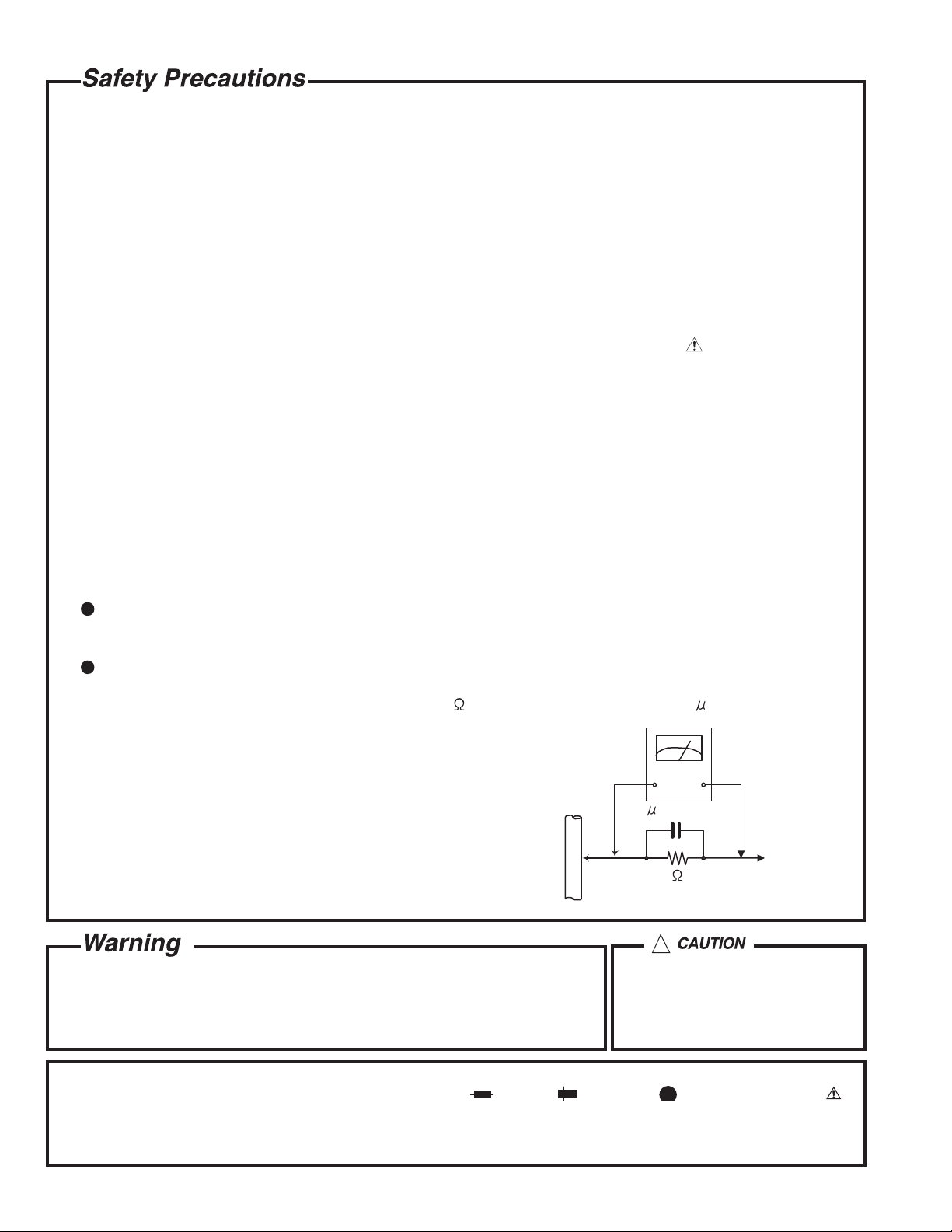
5. Leakage currnet check (Electrical shock hazard testing)
After re-assembling the product, always perform an isolation check on the exposed metal parts of the product
(antenna terminals, knobs, metal cabinet, screw heads, headphone jack, control shafts, etc.) to be sure the
product is safe to operate without danger of electrical shock.
Do not use a line isolation transformer during this check.
Plug the AC line cord directly into the AC outlet. Using a "Leakage Current Tester", measure the leakage
current from each exposed metal parts of the cabinet, particularly any exposed metal part having a return
path to the chassis, to a known good earth ground. Any leakage current must not exceed 0.5mA AC (r.m.s.).
Alternate check method
Plug the AC line cord directly into the AC outlet. Use an AC voltmeter having, 1,000 ohms per volt or more
sensitivity in the following manner. Connect a 1,500 10W resistor paralleled by a 0.15 F AC-type capacitor
between an exposed metal part and a known good earth ground.
Measure the AC voltage across the resistor with the AC
voltmeter.
Move the resistor connection to each exposed metal part,
particularly any exposed metal part having a return path to
the chassis, and meausre the AC voltage across the resistor.
Now, reverse the plug in the AC outlet and repeat each
measurement. Voltage measured any must not exceed 0.75 V
AC (r.m.s.). This corresponds to 0.5 mA AC (r.m.s.).
0.15 F AC TYPE
1500 10W
Good earth ground
AC VOLTMETER
(Having 1000
ohms/volts,
or more sensitivity)
Place this
probe on
each exposed
metal part.
!
1. This equipment has been designed and manufactured to meet international safety standards.
2. It is the legal responsibility of the repairer to ensure that these safety standards are maintained.
3. Repairs must be made in accordance with the relevant safety standards.
4. It is essential that safety critical components are replaced by approved parts.
5. If mains voltage selector is provided, check setting for local voltage.
Burrs formed during molding may
be left over on some parts of the
chassis. Therefore, pay attention to
such burrs in the case of
preforming repair of this system.
In regard with component parts appearing on the silk-screen printed side (parts side) of the PWB diagrams, the
parts that are printed over with black such as the resistor ( ), diode ( ) and ICP ( ) or identified by the " "
mark nearby are critical for safety.
(This regulation does not correspond to J and C version.)
1-2
Page 3
UX-L40/UX-L30
Preventing static electricity
1.Grounding to prevent damage by static electricity
Electrostatic discharge (ESD), which occurs when static electricity stored in the body, fabric, etc. is discharged,
can destroy the laser diode in the traverse unit (optical pickup). Take care to prevent this when performing repairs.
2.About the earth processing for the destruction prevention by static electricity
Static electricity in the work area can destroy the optical pickup (laser diode) in devices such as CD players.
Be careful to use proper grounding in the area where repairs are being performed.
2-1 Ground the workbench
Ground the workbench by laying conductive material (such as a conductive sheet) or an iron plate over
it before placing the traverse unit (optical pickup) on it.
2-2 Ground yourself
Use an anti-static wrist strap to release any static electricity built up in your body.
(caption)
Anti-static wrist strap
Conductive material
(conductive sheet) or iron plate
3. Handling the optical pickup
1. In order to maintain quality during transport and before installation, both sides of the laser diode on the
replacement optical pickup are shorted. After replacement, return the shorted parts to their original condition.
(Refer to the text.)
2. Do not use a tester to check the condition of the laser diode in the optical pickup. The tester's internal power
source can easily destroy the laser diode.
4.Handling the traverse unit (optical pickup)
1. Do not subject the traverse unit (optical pickup) to strong shocks, as it is a sensitive, complex unit.
2. Cut off the shorted part of the flexible cable using nippers, etc. after replacing the optical pickup. For specific
details, refer to the replacement procedure in the text. Remove the anti-static pin when replacing the traverse
unit. Be careful not to take too long a time when attaching it to the connector.
3. Handle the flexible cable carefully as it may break when subjected to strong force.
4. It is not possible to adjust the semi-fixed resistor that adjusts the laser power. Do not turn it
Attention when traverse unit is decomposed
*Please refer to "Disassembly method" in the text for pick-up and how to
detach the substrate.
Shorting round
1.Solder is put up before the card wire is removed from connector on
the CD substrate as shown in Figure.
(When the wire is removed without putting up solder, the CD pick-up
assembly might destroy.)
2.Please remove solder after connecting the card wire with
when you install picking up in the substrate.
Flexible wire
Shorting round
CN601 on
mechanism
board
1-3
Page 4
UX-L40/UX-L30
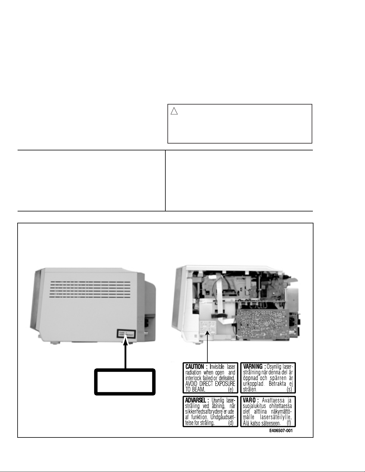
Important for laser products
1.CLASS 1 LASER PRODUCT
2.DANGER : Invisible laser radiation when open and inter
lock failed or defeated. Avoid direct exposure to beam.
3.CAUTION : There are no serviceable parts inside the
Laser Unit. Do not disassemble the Laser Unit. Replace
the complete Laser Unit if it malfunctions.
4.CAUTION : The compact disc player uses invisible
laserradiation and is equipped with safety switches
whichprevent emission of radiation when the drawer is
open and the safety interlocks have failed or are de
feated. It is dangerous to defeat the safety switches.
VARNING : Osynlig laserstrålning är denna del är öppnad
och spårren är urkopplad. Betrakta ej strålen.
VARO : Avattaessa ja suojalukitus ohitettaessa olet
alttiina näkymättömälle lasersäteilylle.Älä katso
säteeseen.
5.CAUTION : If safety switches malfunction, the laser is able
to function.
6.CAUTION : Use of controls, adjustments or performance of
procedures other than those specified herein may result in
hazardous radiation exposure.
CAUTION
!
Please use enough caution not to
see the beam directly or touch it
in case of an adjustment or operation
check.
ADVARSEL : Usynlig laserstråling ved åbning , når
sikkerhedsafbrydere er ude af funktion. Undgå
udsættelse for stråling.
ADVARSEL : Usynlig laserstråling ved åpning,når
sikkerhetsbryteren er avslott. unngå utsettelse
for stråling.
REPRODUCTION AND POSITION OF LABELS
WARNING LABEL
CLASS 1
LASER PRODUCT
1-4
Page 5
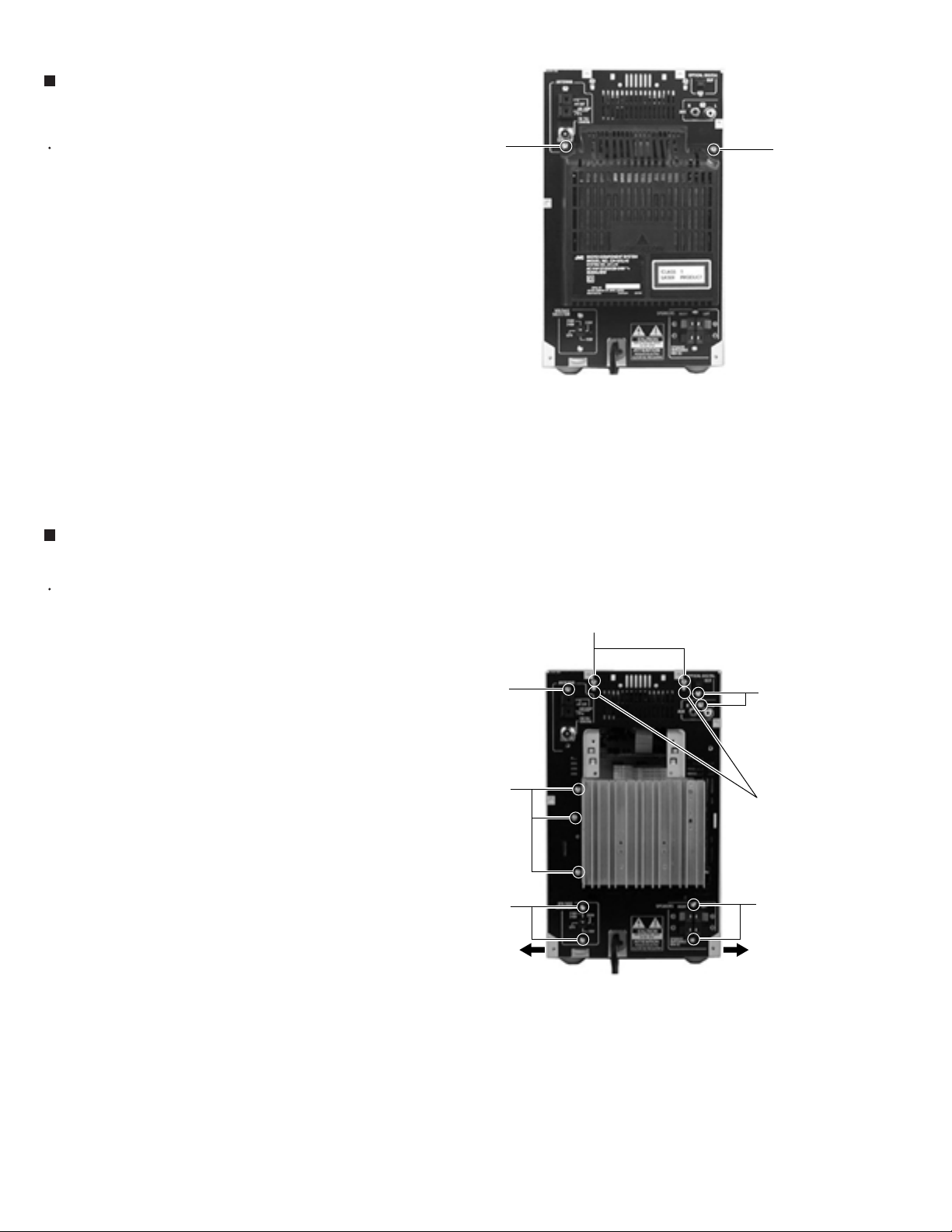
Disassembly method
<Main body>
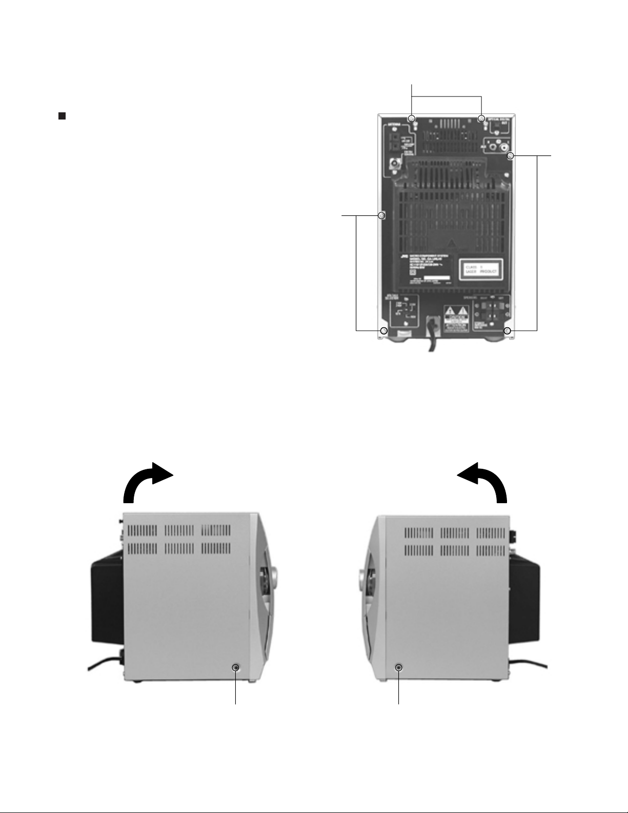
Removing the Metal cover
(See Fig.1 to 3)
UX-L40/UX-L30
A
1.
Remove the six screws A on the back of the main
body.
2.
Remove the screw B on each side and remove the
cover in the direction of the arrow.
A
A
Fig.1
B
B
Fig.2Fig.3
1-5
Page 6
UX-L40/UX-L30
Removing the Rear cover
(See Fig.4)
Remove the metal cover.
1.
Remove the two screws C retaining the rear cover.
Removing the Rear panel
(See Fig.5)
Remove the metal cover and the rear cover.
C
C
Fig.4
1.
Remove the twelve screws D retaining the rear
panel. Release the two joints a on the rear side and
the joint b on each side.
D
D
D
D
a
DD
bb
Fig.5
1-6
Page 7
Removing the Tuner board
(See Fig.6)
Remove the metal cover.
1.
Disconnect the card wire from connector CN1 on the
tuner board.
UX-L40/UX-L30
2.
Remove the two screws E on the rear side and the
screw F on the side.
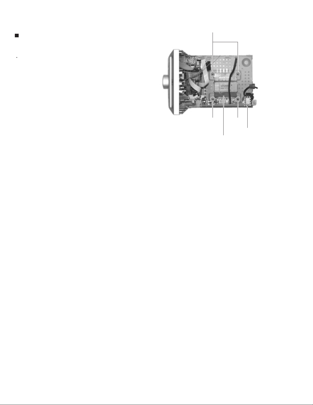
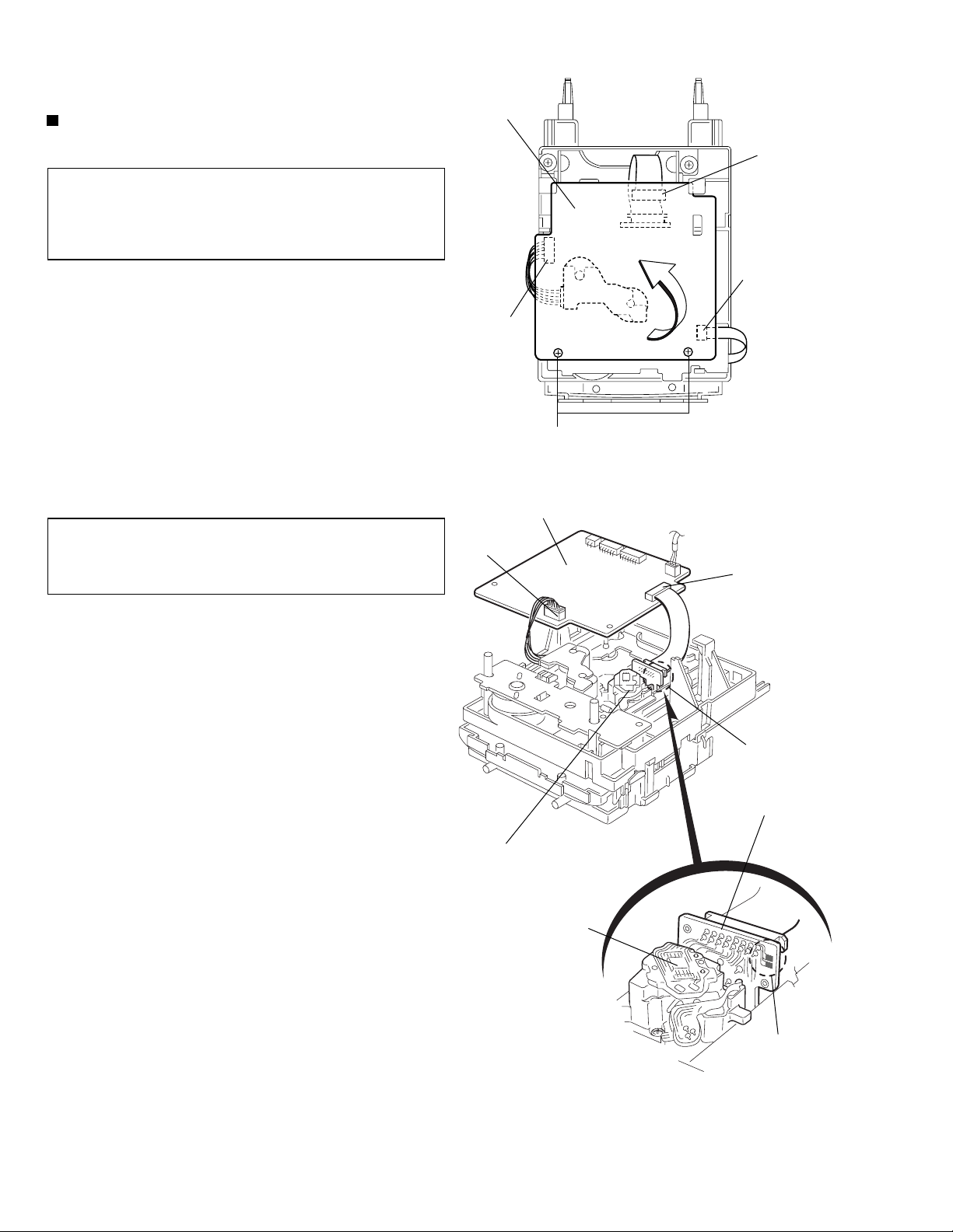
Removing the Optical digital board
(See Fig.7)
Remove the metal cover.
F
E
CN1
Tuner board
Fig.6
Optical digital board
H
1.
Disconnect the shield wire from connector CN905 on
the optical digital board.
2.
Remove the screw G on the rear side and the screw
H on the upper side.
G
CN905
Fig.7
1-7
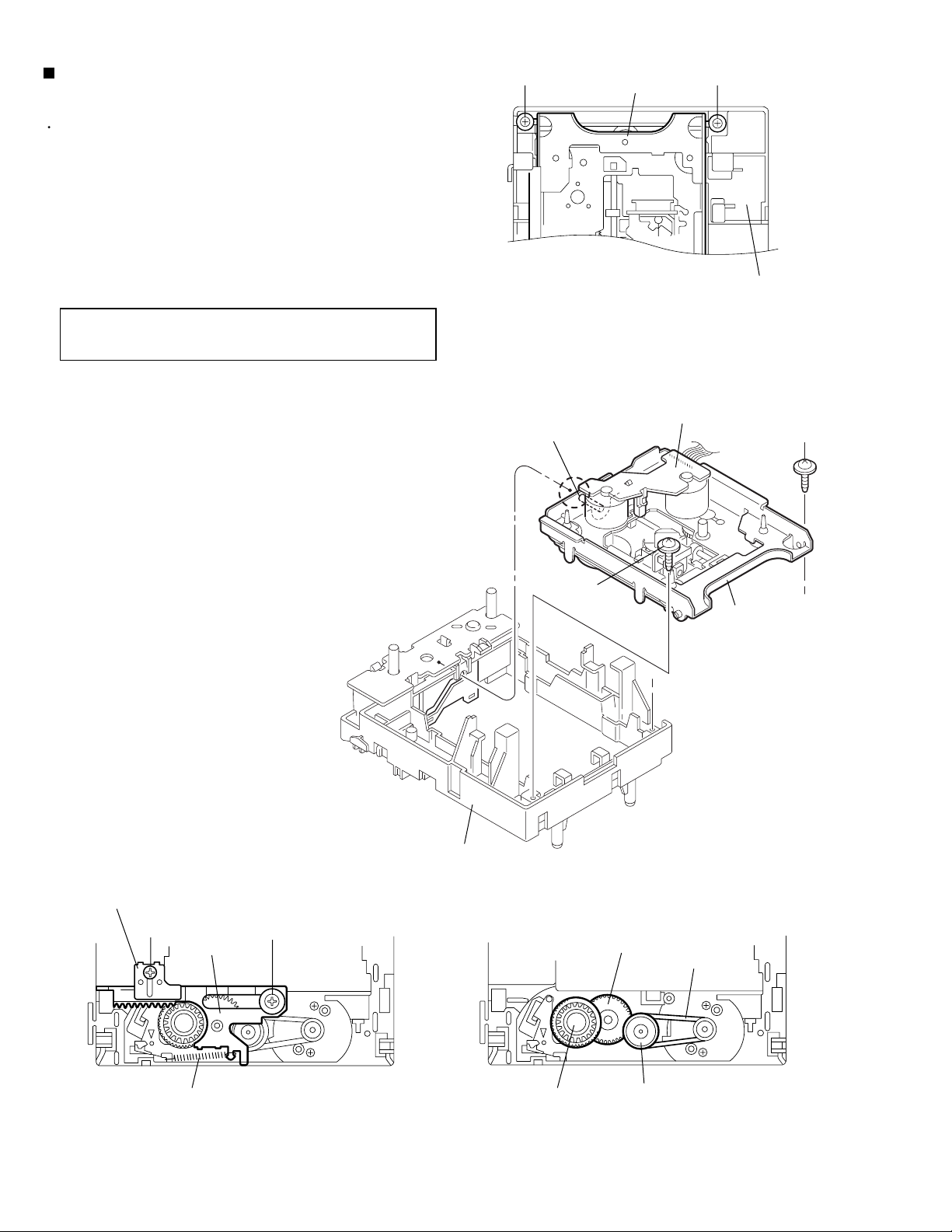
Page 8
UX-L40/UX-L30
Removing the CD-R/RW mechanism
assembly (See Fig.8)
Remove the metal cover, the rear cover, the rear
panel, the tuner board and the optical digital board.
1.
Disconnect the card wire from connector CN903 and
CN904 on the main board.
2.
Pull the joint c in the direction of the arrow and
remove the CD-R/RW mechanism assembly
backward while releasing the joint d.
CD-R/RW mechanism
assembly
c
d
CN903
CN904
Fig.8
Main board
1-8
Page 9
UX-L40/UX-L30
Removing the Main board/ the Heat sink
board (See Fig.9 to 11)
Remove the metal cover, the rear cover and the rear
panel.
1.
Disconnect the card wire from connector CN902,
CN903, CN904 and CN905 on the main board and
remove the CD-R/RW mechanism assembly.
REFERENCE:
2.
Remove the two screws I to remove the main board.
3.
Disconnect the card wire from connector CN931,
CN935, CN933, CN934, CN913, CN901, CN900 and
CN917 on the main board.
4.
Remove the band f and disconnect the card wire
from connector CN951 on the power transformer
assembly. Remove the main board / the heat sink
board from the body.
Refer to the method of removing the
CD-R/RW mechanism assembly and
Fig.8.
CD-R/RW mechanism assembly
CN905
CN902 CN904
CN903
e
CN915
I
CN916
I
Main board
Fig.9
5.
Release the joint e of the main board and disconnect
connector CN944 and CN945 of the heat sink board
from connector CN915 and CN916 of the main board
respectively.
Main board
Heat sink board
CN944
CN945
CN933
CN934
CN913
CN901
CN931
CN935
CN951
Main board
Heat sink board
CN900
CN917
f
Power transformer
assembly
Fig.10Fig.11
1-9
Page 10
UX-L40/UX-L30
Removing the Power transformer
assembly (See Fig.12)
Remove the metal cover, the rear cover, the rear
panel, the CD-R/RW mechanism assembly and the
main board.
Disconnect the power cord from connector J1000 on
1.
the power transformer assembly.
Remove the four screws J.
2.
J
JJ
J1000
Power transformer
assembly
Fig.12
1-10
Page 11
UX-L40/UX-L30
Removing the Front panel assembly
(See Fig.13 to 16)
Remove the metal cover.
Remove the screw K on each side. Pull the joint h
1.
on both sides and lift the front panel assembly to
release the joint g.
Disconnect connector CN931, CN935, CN933 and
2.
CN934 on the main board.
Disconnect the card wire from connector CN33 and
3.
CN34 on the cassette mechanism board.
Front panel
assembly
h
Main board
g
K
Fig.13
g
Front panel
assembly
CN34 CN33
CN935 CN931
Fig.14
g
CN933
CN934
h
K
Cassette mechanism
assembly
Cassette mechanism
board
hh
Fig.15Fig.16
1-11
Page 12
UX-L40/UX-L30
Removing the Phones board
(See Fig.17)
Prior to performing the following procedure, remove
the metal cover and the front panel assembly.
1.
Disconnect connector CN913 on the main board.
Main board
CN913
Phones board
Fig.17
Removing the Cassette mechanism
assembly (See Fig.18)
Prior to performing the following procedure, remove
the metal cover and the front panel assembly.
1.
Remove the four screws L retaining the cassette
mechanism assembly.
L
L
Cassette mechanism
assembly
Fig.18
1-12
Page 13
Removing the Control board
(See Fig.19)
Prior to performing the following procedure, remove
the metal cover and the front panel assembly.
1.
Remove the seven screws M to remove the control
board.
UX-L40/UX-L30
M
Removing the Volume board
(See Fig.20 and 21)
Prior to performing the following procedure, remove
the metal cover and the front panel assembly.
Control board
N
M
Fig.19
N
1.
Remove the four screws N attaching the volume
panel on the front panel assembly.
2.
Remove the six screws O attaching the volume
board on the volume panel, and remove the volume
board.
O
Fig.20
Volume panel
Volume board
O
O
Fig.21
1-13
Page 14
UX-L40/UX-L30
<CD mechanism assembly section>
Removing the CD servo board
(See Fig.1, 2)
CAUTION:
1.
Remove the two screws A on the bottom of the
loading base.
2.
Disconnect the card wire from connector CN606 on
the CD servo board. Turn over the CD servo board
as shown in Fig.2 and put aside temporarily.
3.
Solder the shorting round on the pickup board in the
CD pickup section.
4.
Disconnect the card wire from connector CN601 and
the wire from CN801 on the CD servo board.
CAUTION:
Solder the shorting round before disconnecting
the card wire extending from the pickup. If
you do not follow this instruction, the pickup
may be damaged.
When reassembling, make sure to unsolder
the shorting round after connecting the card
wire from the pickup to the connector.
CD servo board
CN601
CN606
CN801
A
Fig.1
CD servo board
CN801
CN601
1-14
Shorting round
Pickup board
CD pickup
CD pickup
Shorting round
(Soldering)
Fig.2
Page 15
UX-L40/UX-L30
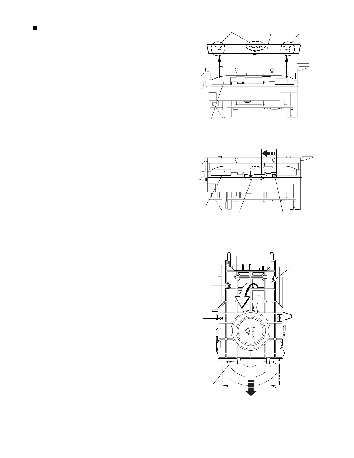
Removing the clamper base / tray
(See Fig.3 ~ 5)
1.
Bring up the fitting in the direction of the arrow to
release the three joints a.
2.
On the front side of the body, move the cam plate
lever to the center.
3.
Remove the stopper screw B and pull out the tray
toward the front.
4.
Remove the four screws C attaching the clamper
base.
5.
From the rear side, remove the clamper base
upward.
Tray
Joint a
Fig.3
Fitting
Joint a
Tray
C
B
Clamper
C
Cam plate
(Lever)
Fig.4
Clamper base
C
Tray
Fig.5
1-15
Page 16
UX-L40/UX-L30
Removing the CD mechanism assembly
(See Fig.6, 7)
Prior to performing the following procedure, remove
the clamper base / tray and the CD servo board.
1.
Remove the screw D attaching the CD mechanism
assembly.
2.
Move the CD mechanism assembly backward to
release the two joints b of the CD base on the front
side.
CAUTION:
When reassembling, fit the front part of the
CD mechanism assembly to the two
chassis joints b and attach the four
dampers correctly.
CD mechanism assembly
damper
damper
CD mechanism assembly
D
damper
damper
b
Fig.6
D
CD base
b
Fig.7
1-16
Page 17
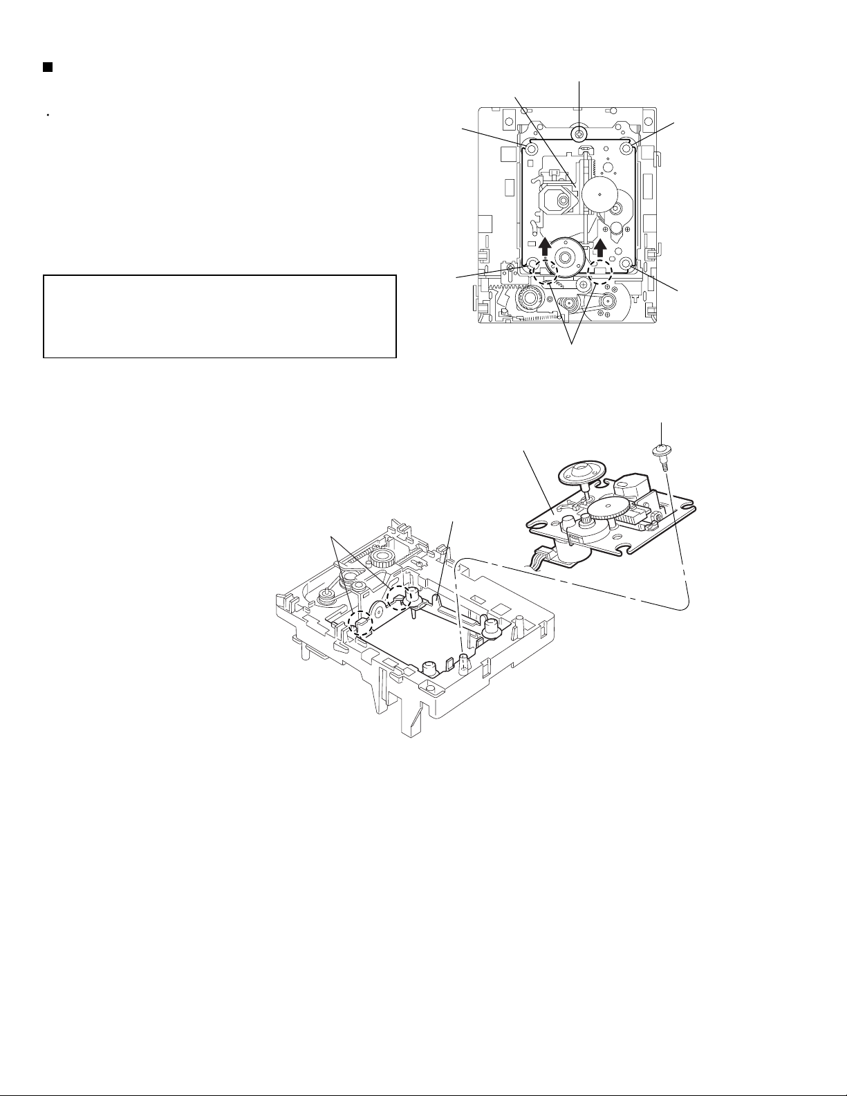
Removing the loading motor / loading
motor board (See Fig.8, 9)
Prior to performing the following procedure, remove
the clamper base / tray and the CD servo board.
1.
From upside of the loading base, remove the belt
from the motor pulley.
2.
Remove the two screws E attaching the loading
motor.
3.
At the bottom of the body, release the three joints c
outward and pull out the loading motor board from
the shaft. The loading motor comes off with the
loading board.
4.
Unsolder the two soldered points d on the loading
motor board and remove the loading motor.
REFERENCE:
When removing the loading motor board
only, unsolder the two soldering d on the
loading motor and release the three joints c.
Soldering d
Loading motor
Loading motor
Belt
E
Fig.8
c
Loading motor board
UX-L40/UX-L30
E
Motor pulley
c
Fig.9
1-17
Page 18
UX-L40/UX-L30
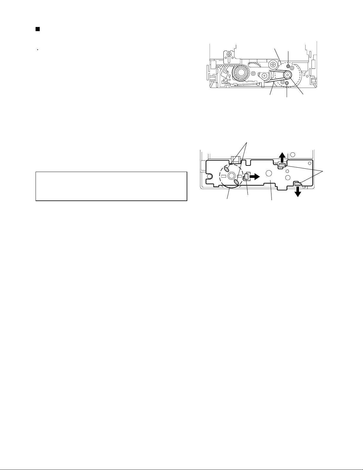
Removing the C.D. gear (1), (2) and (3)
(See Fig.10 ~ 13)
Prior to performing the following procedure, remove
the CD servo board.
1.
Remove the two screws F attaching the CD base on
the bottom of the loading base.
2.
Remove the rear part of the CD base upward and
pull out the shaft e of the CD base from the camplate
on the front side of the loading base.
REFERENCE:
3.
Remove the leaf spring on the upside of the loading
base.
4.
Remove the screw G attaching the cam plate fitting.
5.
Remove the screw H and the cam plate upward.
The CD mechanism assemly comes off
with the CD base.
FF
e
CD base
(Bottom)
Loading base
Fig.10
CD mechanism assembly
F
6.
Remove the belt from the C.D. gear (1).
7.
Pull out the C.D. gear (1), (2) and (3) respectively.
Cam plate fitting
G
Cam plate
H
F
CD base
Loading base
Fig.11
C.D. gear (3)
Belt
1-18
Spring
C.D. gear (2)
C.D. gear (1)
Fig.13Fig.12
Page 19
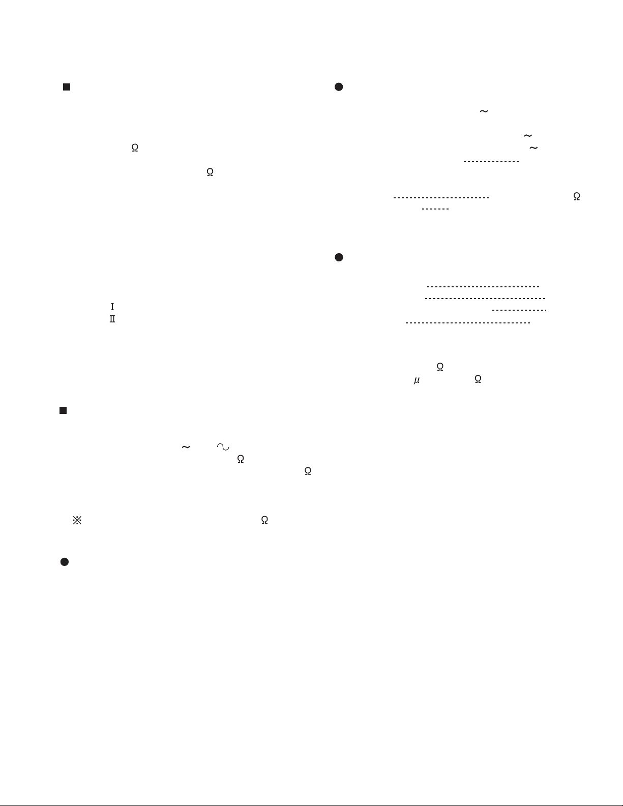
Adjustment method
UX-L40/UX-L30
Measurement Instruments Required for
Adjustment
1. Low frequency oscillator
This oscillator should have a capacity to output
0dBs to 600
50Hz-20kHz.
2. Attenuator impedance : 600
3. Electronic voltmeter
4. Distortion meter
5. Frequency counter
6. Wow & flutter meter
7. Test tape
VT703L : Head azimuth
VT712 : Tape speed and running unevenness
(3kHz)
VT724 : Reference level (1kHz)
8. Blank tape
TYPE
TYPE : AC-514
9. Torque gauge : For play and back tension
FWD(TW2111A), REV(TW2121a) and
FF/REW(TW2231A)
10. Test disc: CTS-1000
Measurement conditions
Power supply voltage
AC110V/127V/220V/230V 240V , adjustable
Reference output : Speaker : 0.775V/4
: Headphone : 0.077V/32
Reference frequency and
input level ------------------------------ 1kHz, AUX : -8dBs
Measurement output terminal ------- at Speaker J3002
Load resistance --------------------------- 4
Radio Input signal
AM frequency --------------------------------------- 400Hz
AM modulation ---------------------------------------- 30%
FM frequency --------------------------------------- 400Hz
FM frequency deviation ------------------------ 22.5kHz
at an oscillation frequency of
: AC-225
Tuner section
FM tuning range: 87.5MHz 108.00MHz
AM tuning range:
At 9kHz intervals: 531kHz 1,710kHz
At 10kHz intervals: 530kHz 1,710kHz
Voltage applied to tuner +B : DC5.7V
VT : DC 12V
Reference measurement
output 26.1mV(0.28V)/3
Input positions AM : Standard loop antenna
FM : TP1 (hot) and TP2 (GND)
Standard measurement position of volume
Function switch to Tape
Beat cut switch to Cut
Super Bass/Active hyper Bass to OFF
Bass Treble to Center
Adjustment of main volume to reference output
VOL : 28
Precautions for measurement
1. Apply 30pF and 33k
side and 0.082 F and 100k in series to the
sweeper input side.
2. The IF sweeper output level should be made as
low as possible within the adjustable range.
3. Since the IF sweeper is a fixed device, there is no
need to adjust this sweeper.
4. Since a ceramic oscillator is used, there is no need
to perform any MIX adjustment.
5. Since a fixed coil is used, there is no need to adjust
the FM tracking.
6. The input and output earth systems are separated.
In case of simultaneously measuring the voltage in
both of the input and output systems with an
electronic voltmeter for two channels, therefore, the
earth should be connected particularly carefully.
7. In the case of BTL connection amp., the minus
terminal of speaker is not for earthing. Therefore, be
sure not to connect any other earth terminal to this
terminal. This system is of an BTL system.
8. For connecting a dummy resistor when measuring
the output, use the wire with a greater code size.
9. Whenever any mixed tape is used, use the band
pass filter (DV-12).
to the IF sweeper output
1-19
Page 20
UX-L40/UX-L30
<<
Arrangement of Adjusting Position
>>
Cassette mechanism section
Head azimuth
adjusting screw
(Forward side)
Cassette AMP board
VR37
C308
R314
MOTOR SPEED
VR37
L301
B155
VR31
BIAS ADJ
VR31
Head azimuth
adjusting screw
(Reverse side)
MB
PBRAGPBL
RECRAGRECL
MS
SW8V
MG
1
CN34
C307
R313
C310
R315
C314
Q302
R327
C317
C319
C221
B112
C313
C121
L303
C316
R310
R335
B198
R353
Q305
C106
Q103
R305
R303
R122
Q101
C103
B163
Q321
R221
10
B156
C303
R115
B157
R108
R101
C113
R110
R109
R102
C110
C104
R301
R121
1
C108
C107
9
B151
R112
R111
C102
R107
B152
C302
R103
1
C301
C111
C306
B164
Cassette mechanism section (Back side)
Head azimuth
adjusting screw
(Forward side)
Playback/Recording &
eraser head
R304
C109
B158
8
B106
C101
6
B166
R116
R212
R211
C211
R216
9
IC32
9
C201
B101
B109B108
C209
CN33
R342
C213
R210
R209
C207
B159
16
B102
R341
C208
R207
1
B110
CN31
B200
1
R205
R208
B160
R343
R340
R105
C105
C206
R345
NC
C305
R201
1IC31
TAP
B113
C304
RRE
C202
C210
Q331
C375
C205
C203
B161
R215
R339
C334
R106
R206
5VMGSOL
R204
R203
B153
R104
R222
C204
B168
PHO
R202
C333
C332
R375
Q201
PLA
Q203
C331
Q372
R331
B167
FRE
R371
C376
10
70u
Q375
CN32
R376
R372
R373
B162
C371
16
1
C374
R338
B
E
D375
Q376
B
Q371
E
R337
R336
9
IC33
8
Head azimuth
adjusting screw
(Reverse side)
1-20
Page 21
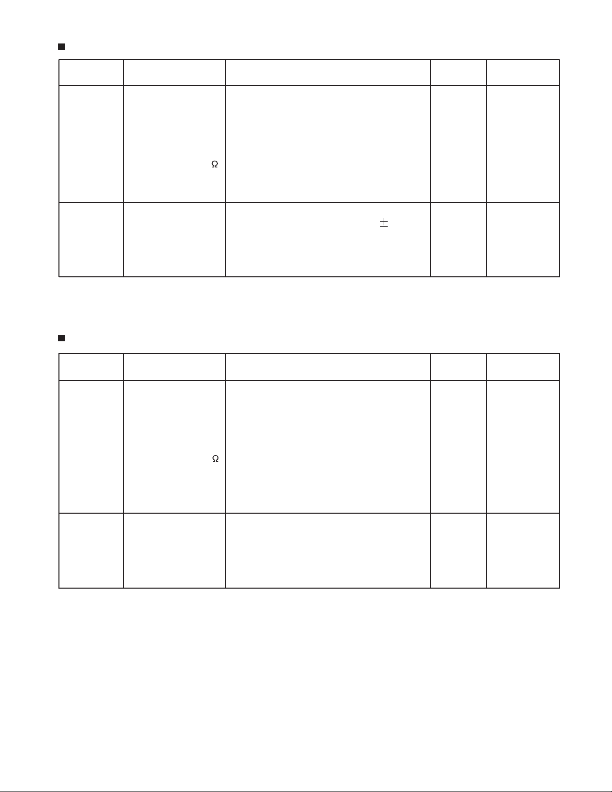
Tape Recorder Section
UX-L40/UX-L30
Items
Confirmation
of head angle
Measurement
conditions
Test tape
: VT703L (8kHz)
Measurement output
terminal
: Speaker terminal
Speaker R
(Load resistance: 4 )
: Headphone terminal
Measurement method
1 Playback the test tape VT703L (8kHz)
2 With the recording & playback mechanism,
adjust the head azimuth screw so that the
forward and reverse output levels become
maximum. After adjustment, lock the head
azimuth at least by half turn.
3 In either case, this adjustment should be
performed in both the forward and reverse
directions with the head azimuth screw.
Confirmation
of tape speed
Test tape
: VT712 (3kHz)
Measurement output
terminal
: Headphone terminal
Adjust VR37 so that the frequency counter
reading becomes 2,940~3,090Hz when
playing back the test tape VT712 (3kHz) with
playback and recording mechanism after
ending forward winding of the tape.
Reference Values for Confirmation Items
Standard
Values
Maximum
output
Tape speed
of deck
: 2,940 ~
3,090Hz
Adjusting
positions
Adjust the head
azimuth screw
only when the
head has been
changed.
VR37
Items
Difference
between the
forward and
reverse speed
Measurement
conditions
Test tape
: VT712 (3kHz)
Measurement output
terminal
: Speaker terminal
Speaker R
(Load resistance: 4 )
Measurement output
terminal
: Headphone
Wow & flutter Test tape
: VT712 (3kHz)
Measurement output
terminal
: Headphone terminal
Measurement method
Standard
Values
When the test tape VT712 (3kHz) has been
played back with the recording and playback
mechanism at the beginning of forward
winding, the frequency counter reading of the
difference between both of the mechanism
should be 6.0Hz or less.
When the test tape VT712 (3kHz) has been
played back with the recording and playback
mechanism at the beginning of forward
winding, the frequency counter reading of
wow & flutter should be 0.25% or less
(WRMS).
6.0Hz or
less
0.25% or
less
(WRMS)
Adjusting
positions
Head azimuth
screw
1-21
Page 22
UX-L40/UX-L30
Electrical Performance
Items
Adjustment of
recording bias
current
(Reference
Value)
Adjustment of
recording and
playback
frequency
characteristics
Measurement
conditions
Mode: Forward or
reverse mode
Recording mode
Test tape
: AC-514 to TYPE
and AC-225 to
TYPE
Measurement output
terminal
: Both recording and
headphone terminals
Reference frequency
: 1kHz and 10kHz
(REF.: -20dB)
Test tape
: AC-514 to TYPE
Measurement input
terminal
: OSC IN
Measurement method
Standard
Values
1 With the recording and playback
mechanism, load the test tapes (AC-514 to
TYPE
and AC-225 to TYPE ), and set
the mechanism to the recording and
pausing condition in advance.
2 After connecting 100 in series to the
recorder head, measure the bias current
with a valve voltmeter at both of the
terminals.
3 After resetting the [PAUSE] mode, start
recording. At this time, adjust VR31 for Lch
and VR32 for Rch so that the recording
bias current values become 4.0 A (TYPE
) and 4.20 A (TYPE ).
1 With the recording and playback
mechanism, load the test tapes (AC-514 to
TYPE
), and set the mechanism to the
recording and pausing condition in
advance.
2 While repetitively inputting the reference
frequency signal of 1kHz and 10kHz from
OSC IN, record and playback the rape.
3 While recording and playback the test tape
in TYPE , adjust VR31 for Lch and VR32
for Rch so that the output deviation
between 1kHz and 10kHz becomes
-1dB 2dB.
AC-225
: 4.20
AC-514
: 4.0 A
Output
deviation
between
1kHz and
10kHz
: -1dB
Adjusting
positions
VR31
A
VR31
2dB
Reference Values for Electrical Function Confirmation Items
Items
Recording
bias
frequency
Measurement
conditions
Forward or reverse
Test tape
: TYPE (AC-514)
Measurement
terminal : BIAS TP on
P.C. board
Measurement method
1 While changing over to and from BIAS 1
and 2, confirm that the frequency is
changed.
2 With the recording and playback
mechanism, load the test tape.
(AC-514 to TYPE ), and set the
mechanism to the recording and pausing
condition in advance.
3 Confirm that the BIAS TP frequency on the
P.C. board is 100kHz 6kHz.
Eraser
current
(Reference
value)
Forward or reverse
Recording mode
Test tape
: AC-514 to TYPE
and AC-225 to
TYPE
Measurement
terminal : Both of the
eraser head terminals
1 While recording and playback mechanism,
load the test tapes (AC-514 to TYPE
and AC-225 to TYPE ), and set the
mechanism to the recording and pausing
conditions in advance.
2 After setting to the recording conditions,
connect 1W in series to the eraser head on
the recording and playback mechanism
side, and measure the eraser current from
both of the eraser terminals.
Standard
Values
100 kHz
6 kHz
TYPE
: 120 mA
TYPE
: 75 mA
Adjusting
positions
1-22
Page 23

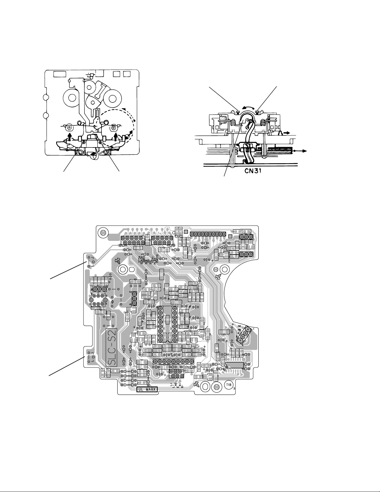
Extension code connecting method
CD mechanism assembly
UX-L40/UX-L30
1-23
Page 24

UX-L40/UX-L30
Flow of functional operation until TOC read (CD)
Power ON
Power Key
Slider turns REST
SW ON.
Automatic tuning
of TE offset
Check that the voltage at the pin4
of CN601 is 0V (a moment)?
Check Point
VREF
Tracking error waveform at TOC reading
pin 20 of
IC601(TE)
Approx
1.8V
Tracking
servo
Disc statas
to rotate
off statas
Automatic measurement
of TE amplitude and
automatic tuning of
TE balance
Approx.3sec
Tracking
servo
on statas
Disc to be
braked to stop
TOC reading
finishes
500mv/div
2ms/div
Fig.1
Laser ON
Detection of disc
Automatic tuning of
Foucus offset
Automatic measurement of
Focus A-curve amplitude
Disc is rotated
Focus servo ON
(Tracking servo ON)
Automatic measurement of
Tracking error amplitude
Automatic tuning of
Tracking error balance
Check that the voltage at the
pin2 of IC601 is 0V?
Confirm that the Focus error
S-cuve siganl at the pin23 of
IC601 is approx.2Vp-p
Confirm that the siganl from
pin22 IC603 is 0V as a
accelerated pulse during
approx.400ms.
Confirm the waveform of
the Tracking error signal
at the pin20 of IC601
(See fig-1)
1-24
Automatic tuning of
Focus error balance
Automatic tuning of
Focus error gain
Automatic tuning of
Tracking error gain
TOC reading
Play a disc
Confirm the eys-pattern
at the lead of TP1
Page 25

UX-L40/UX-L30
Maintenance of laser pickup
(1) Cleaning the pick up lens
Befor you replace the pick up, please try to
clean the lens with a alcohol soaked cotton
swab.
(2) Life of the laser diode (Fig.1)
When the life of the laser diode has expired,
the following symptoms wil appear.
(1) The level of RF output (EFM output:ampli
tude of eye pattern) will below.
Is RF output
1.1 0.15Vp-p?
YES
O.K
NO
Replace it.
Replacement of laser pickup
Turn off the power switch and,disconnect the
power cord from the ac outlet.
Replace the pickup with a normal one.(Refer
to "Pickup Removal" on the previous page)
Plug the power cord in,and turn the power on.
At this time,check that the laser emits for
about 3seconds and the objective lens moves
up and down.
Note: Do not observe the laser beam directly.
Play a disc.
(Fig.1)
(3) Semi-fixed resistor on the APC PC board
The semi-fixed resistor on the APC printed
circuit board which is attached to the pickup
is used to adjust the laser power.Since this
adjustment should be performed to match the
characteristics of the whole optical block,
do not touch the semi-fixed resistor.
If the laser power is lower than the specified
value,the laser diode is almost worn out, and
the laser pickup should be replaced.
If the semi-fixed resistor is adjusted while
the pickup is functioning normally,the laser
pickup may be damaged due to excessive current.
Check the eye-pattern at TP1.
Finish.
1-25
Page 26

UX-L40/UX-L30
Description of major ICs
LC75345M-X (IC901) : E.volume
1. Pin layout
CL
VDD
ROPOUT
RINM
RINP
ROOUT
RSB
36 35 34 33 32 31 30 29 28 27 26 25 24 23 22 21 20 19
DI
CE
VSS
LOPOUT
LINM
LINP
LOUT
RBASS2
RBASS1
LSB
LBASS2
RTRE
RVRIN
LTRE
LBASS1
RSELOR5R4
L5
LVRIN
LSELO
R3
L4
R2
L3
R1
L2
Vref
181716151413121110987654321
L1
2. Block diagram
14
L5
15
L4
16
L3
17 18
L2
L1
19
Vref
20
R1
21
R2
22 23
R3
R4
24
R5
LSELO
13
LV RI N
12
LT RE
11
LVref
RVref
CONTROL
CIRCUIT
LOGIC
CIRCUIT
CONTROL
CIRCUIT
LBASS1
10
LBASS2
9
LSB
8
CCB
INTERFACE
LOUT
7
6
LINP
5
LINM
LOPOUT
34
VSS
2
CE
1
DI
36
CL
35
VDD
34
ROPOUT
33
RINM
32
RINP
1-26
25
RESLO
26
RVRIN
27
RTRE
28
RBASS1
29
RBASS2
30
RSB
31
ROUT
Page 27

3. Pin function
UX-L40/UX-L30
Pin No.
1
2
3
4
5
6
7
8
9
10
11
12
13
14
15
16
17
18
19
20
21
22
23
24
25
26
27
28
29
30
31
32
33
34
35
36
Symbol
DI
CE
VSS
LOPOUT
LINM
LINP
LOUT
LSB
LBASS2
LBASS1
LTRE
LVRIN
LSELO
L5
L4
L3
L2
L1
Vref
R1
R2
R3
R4
R5
RSELO
RVRIN
RTRE
RBASS1
RBASS2
RSB
ROUT
RINP
RINM
ROPOUT
VDD
CL
Function
Serial data and clock input pin for control.
Chip enable pin.
Ground pin.
Output pin of general-purpose operation amplifier.
Non-inverted input pin of general-purpuse operation amplifier.
Non-inverted input pin of general-purpuse operation amplifier.
ATT + equalizer output pin.
Capacitor and resistor connection pin comprising filters for bass and super-bass band.
Capacitor and resistor connection pin comprising filters for bass and super-bass band.
Capacitor and resistor connection pin comprising filters for bass and super-bass band.
Capacitor and resistor connection pin comprising treble band filter.
Volume input pin.
Input selector output pin.
Input signal pin.
Input signal pin.
Input signal pin.
Input signal pin.
Input signal pin.
0.5 x VDD voltage generation block for analog ground.
Input signal pin.
Input signal pin.
Input signal pin.
Input signal pin.
Input signal pin.
Input selector output pin.
Volume input pin.
Capacitor connection pin comprising treble band filter.
Capacitor and resistor connection pin comprising filter for bass and super-bass band.
Capacitor and resistor connection pin comprising filter for bass and super-bass band.
Capacitor and resistor connection pin comprising filter for bass and super-bass band.
ATT + equalizer output pin.
Non inverted input pin of general-purpose operation amplifier.
Non inverted input pin of general purpose operation amplifier.
Output pin of general-purpose operation amplifier.
Supply pin.
Serial data and clock input pin for control.
1-27
Page 28

UX-L40/UX-L30
LA6541-X (IC801) : Servo driver
1. Pin Layout & block diagram
Vcc Vref Vin4 Vg4 Vo8 Vo7
24 23
11k
ohm
22
21
20
19
Vcc
Gnd
Vo6 Vo5 Vg3 Vin3 Cd Res
18
17 16
- +
- +
Level
shift
Level
shift
11k
ohm
1
2
3456
Vcc Mute Vin1 Vg1 Vo1 Vo2 Vo3 Vo4 Vg2 Vin2 Reg
B T L
driver
B T L
driver
Gnd
B T L
driver
B T L
driver
7 8 9101112
Level
shift
Level
shift
2. Pin function
Pin
No.
1
2
3
4
5
6
7
8
9
10
11
12
13
14
15
16
17
18
19
20
21
22
23
24
Symbol
Vcc
Mute
Vin1
Vg1
Vo1
Vo2
Vo3
Vo4
Vg2
Vin2
Reg Out
Reg In
Res
Cd
Vin3
Vg3
Vo5
Vo6
Vo7
Vo8
Vg4
Vin4
Vref
Vcc
Power supply (Shorted to pin 24)
All BTL amplifier outputs ON / OFF
BTL AMP 1 input pin
BTL AMP 1 input pin (For gain adjustment)
BTL AMP 1 input pin (Non inverting side)
BTL AMP 1 input pin (Inverting side)
BTL AMP 2 input pin (Inverting side)
BTL AMP 2 input pin (Non inverting side)
BTL AMP 2 input pin (For gain adjustment)
BTL AMP 2 input pin
External transistor collector (PNP) connection. 5V power supply output
External transistor (PNP) base connection
Reset output
Reset output delay time setting (Capacitor connected externally)
BTL AMP 3 input pin
BTL AMP 3 input pin (For gain adjustment)
BTL AMP 3 output pin (Non inverting side)
BTL AMP 3 output pin (Inverting side)
BTL AMP 4 output pin (Inverting side)
BTL AMP 4 output pin (Non inverting side)
BTL AMP 4 output pin (For gain adjustment)
BTL AMP 4 output pin
Level shift circuit's reference voltage application
Power supply (Shorted to pin 1)
Function
15
11k
ohm
14
13
RESET
Regulator
11k
ohm
out
Reg
In
1-28
Page 29

TDA7294 (IC940, IC941) : Audio amp.
1. Pin layout
15
14
13
12
11
10
9
8
7
6
5
4
3
2
1
2. Block diagram
BOOTSTRAP
UX-L40/UX-L30
-Us (POWER)
OUT
+Us (POWER)
N.C.
N.C.
MUTE
STAND-BY
-Us (SIGNAL)
+Us (SIGNAL)
BOOTSTRAP
N.C.
SUR
NON INUERTING INPUT
INVERTING INPUT
STAND-BY GND
+Vs
IN+
IN-
BIPOLAR
TRANSCONDUCTANCE
INPUT STAGE
LEVEL SHIFTING
STAGE
BOOTSTRAP
OUTPUT
-Vs
MOS CUTPUT STAGEMOS GHAIN &
SHORT CIRCUIT
PROTECTION
1-29
Page 30

UX-L40/UX-L30
AN22000A-W (IC601) : RF head amp.
1. Pin layout
2. Block diagram
14
OFTR
13
COFTR
12
BDO
11
BCDO
CEA
9
OFTR
BDO
1234 5678910111213141516
3TOUT
10
3TENV
NRFDET
15
FEN
22
FEOUT
23
SUBT
TEN
21
20
SUBT
19
17181920212223242526272829303132
18
VDET
PDLDVDETTEBPFTEOUT
2
1
3
VCC
16
GND
252624
8
ARF
7
CAGC
RFIN
56
RFOUT
4
RFN
3. Pin function
Pin No.
Function
APC amp input terminal.
1
APC amp output terminal.
2
Power supply.
3
RF amp negative input terminal.
4
RF amp output terminal.
5
AGC input terminal.
6
AGC loop filter capacitor connection terminal.
7
AGC output terminal.
8
Capacitor connection terminal for HPF-amp.
9
3TENV output terminal.
10
Capacitor connection terminal for RF enberope detection.
11
BDO output terminal.
12
Capacitor connection terminal for RF enverope detection.
13
OFTR output terminal.
14
NRDET output terminal.
15
Ground terminal.
16
AGC
RF_EQ
NRFDET
GCTL TBAL FBAL
GCA BCA
AMP
32
31
A
C
GCA BCA
AMP
30
29
B
D
GCA BCA
AMP
27
E
Pin No.
GCA BCA
AMP
28
F
Function
VREF output terminal.
17
VDET output terminal.
18
VDET input terminal.
19
TE amp. output terminal.
20
TE amp. negative input terminal.
21
FE amp. negative input terminal.
22
FE amp. output terminal.
23
GCTL & APC terminal.
24
FBAL control terminal.
25
TBAL control terminal.
26
Tracking signal input terminal 1.
27
Tracking signal input terminal 2.
28
Focus signal input terminal 4.
29
Focus signal input terminal 3.
30
Focus signal input terminal 2.
31
Focus signal input terminal 1.
32
17
VREF
1-30
Page 31

MN662748RPMFA (IC651) : DSP
1. Terminal layout
80~61
1
60
UX-L40/UX-L30
20
21~40
2. Pin function
Pin
No
1 BCLK
2 LRCK
3 SRDATA
4 DVDDI
5 DVSSI
6TX
7 MCLK
8 M DATA
9 MLD
10 SENSE
11 FLOCK
12 TLOCK
13 BLKCK
14 SQCK
15 SUBQ
16 DMUTE
17 STAT
18 RST
19 SMCK
20 PMCK
21 TRV
22 TVD
23 PC
24 ECM
25 ECS
26 KICK
27 TRD
28 FOD
29 VREF
30 FBAL
31 TBAL
32 FE
33 TE
34 RFENV
35 VDET
36 OFT
37 TRCRS
38 /RFDET
39 BDO
40 LDON
41
Symbol Function
I/O I/O
-
Not use
-
Not use
-
Not use
-
Power supply for digital circuit
-
GND for digital circuit
-
Not use
I
Micro computer command
clock signal input
I
Micro computer command
data input
I
Micro computer command
load signal input (L: Load)
-
Not use, connect to TP716
-
Not use, connect to TP717
-
Not use, connect to TP718
O
Sub code block clock
signal output
I
External clock input for sub
code Q register input
O
Sub code Q data output
-
Not use, connect to TP719
O
Status signal input
I
Reset signal input (L: Reset)
-
Not use
-
Not use, connect to TP720
O
Traverse enforced output
O
Traverse drive output
-
Not used
O
Spindle motor drive signal
(Enforced mode output)
O
Spindle motor drive signal
(Servo error signal output)
O
Kick pulse output
O
Tracking drive output
O
Focus drive output
I
Reference voltage
for D/A output block
O
Focus balance adjust
signal output
O
Tracking balance adjust
signal output
I
Focus error signal input
(Analog input)
I
Tracking error signal input
(Analog input)
RF envelope signal input
I
(Analog input)
Vibration detect signal
I
input (H:Detect)
Off track signal input
I
(H:Off track)
Track cross signal input
I
RF detect signal input
I
(L:Detect)
Drop out signal input
I
(H:Drop out)
Laser on signal output
O
(H:ON)
Pin
No
41 PLLF2
42 TOFS
43 WVEL
44 ARF
45 IREF
46 DRF
47 DSLF
48 PLLF
49 VCOF
50 AVDD2
51 AVSS2
52 EFM
53 PCK
54 VCOF2
55 SUBC
56 SBCK
57 VSS
58 X1
59 X2
60 VDD
61 BYTCK/TRVSTP
62 CLDCK
63 FCLK
64 IPFLAG
65 FLAG
66 CLVS
67 CRC
68 DEMPH
69 RESY
70 IOSEL
71 /TEST
72 AVDD1
73 OUTL
74 AVSS1
75 OUTR
76 RSEL
77 CSEL
78 PSEL
79 MSEL
80 SSEL
Symbol Function
-
Not use
Not use
Not use
RF signal input
I
Reference current input
I
Bias pin for DSL
I
Loop filter pin for DSL
I/O
Loop filter pin for PLL
I/O
Loop filter pin for VCO
I/O
Power supply for analog
circuit
GND for analog circuit
Not use, connect to TP724
Clock output for PLL
O
Loop filter pin for Digital
I/O
servo VCO
Not use
Not use
GND for crystal oscillation
circuit
Input for crystal oscillation
I
circuit (f=16.9344MHz)
Output for crystal oscillation
O
circuit (f=16.9344MHz)
Power supply for crystal
oscillation circuit
Not use
Sub code frame clock
O
signal output
Not used
Interpolation flag signal
O
output, Connect to TP721
Flag signal output,
O
Connect to TP722
Not use
Not use
De-emphasis detect signal
O
output, Connect to TP723
Not use
Mode select pin, Connect
I
to DVDD1 (H fix)
Test pin, Connect to
I
DVDD1 (H fix)
Power supply for analog
circuit
L-channel audio output
O
GND for analog circuit
R-channel audio output
O
RF signal polarity setting pin,
I
Connect to DVDD1 (H fix)
Oscillation frequency setting
I
pin, Connect to GND (L fix)
IOSEL=H, Test pin,
I
Connect to GND (L fix)
IOSEL=H, SMCK output,
I
Frequency select pin
IOSEL=H, SMCK output,
I
SUBQ output mode select pin
1-31
Page 32

UX-L40/UX-L30
MN101C38CEK1 (IC931) : Micro controller
1. Pin layout
51 ~ 75
50
~
26
2. Pin Function
SymbolPin No. I/O Function
1~4
5~7
20, 21
8
9
10
11
12
13
14
15
16
17
18
19
22
23
24
25
26
27
28
29
30
31
32
33
34
35
36
37
38
39
40
41
42
43
44
45
COM3~0
VLC3~1
VDD
OSC2
OSC1
VSS
NC
NC
MMOD
VREFSAFETY0
SAFETY1
TAPE0
TAPE1
KEY0, 1
DOOR_RST
CDSAFETY
VREF+
SDATA
NC
SCK
NC
QRIN
SQCK
F_CD
/RST
MPX
BCTL
VOLCE
NC
PROTR
REM
RDSCK
BLKCK
FLAG
STAT
SMUTE
SPKMUTE
AHB
25 ~ 1
LCD Bias co mmon
LCD Bias voltage
5V
Main oscillation 12MHz
O
Main oscillation 12MHz
I
Ground
No use. Fixed to VSS.
I
No use. Open
O
Fixed to ground
I
Ground
Irregular voltage detection 0
I
Irregular voltage detection 1
I
Tape Switch 0
I
Tape Switch 1
I
Unit KEY INPUT
I
Rest/close switch detect port
I
CD safety voltage detect port
I
5V
Serial data (Tuner/ PLL IC)
I/O
No use. OUTPUT LOW
O
Serial clock (Tuner/ PLL IC)
O
No use. OUTPUT LOW
O
Q-code data input port
I
Q-code serial clock
O
CD Function ("H"= CD)
O
RESET
I/O
FM stereo detection ( 'L'= stereo)
I
During Back up set H, other case L.
O
This back up means plug out.
O
volume chip enable
O
No use. OUTPUT LOW
I
Protector detect. When detect
PROTR=L, set SPKMUTE to 'L'.
I
Remoto control input
I
RDS clock
I
Block clock input port
I
Error Correction Count Input
I
CD status input port
O
MUTE ON=L
O
Speaker mute.When detect
PROTR=L, set SPKMUTE to 'L'.
O
Active Hyper Bass On/Off
AHB OFF=H, AHB1, 2=L
76
~
100
46
47
48
49
50
51
52
53
54
55
56
57
58
59
60
61
62
63
64
65
66
67~88
89~100
SymbolPin No. I/O Function
DIMCTL
LEDCTL
SURR
NC
SEG12
MDATA
MCLK
XRST
MLD
STTA
REEL
VOL+
VOL-
PERIOD
F_TU
CLOSE
OPEN
P_OUT
BUP
BTLMUTE
NC
SEG13~34
SEG0~11
LCD DIM control. DIMMER ON =L
O
Power standby LED control
O
STANDBY = L, POWER ON = H
Surround IC control, H:=Surroud on
O
No use. Open
O
SEGMENT OUTPUT
O
CD data input port
O
CD data clock
O
CD reset
O
CD command ready signal
O
Tape IC strobe
O
Reel pulse input
I
Volume plus
I
Volume minus
I
Tuner pLL strobe
O
Tuner function ('H'=Tuner)
O
Door close motor control output
O
Door open motor control output
O
Power on/off ('H'=Power ON)
O
I
Back up power detect. When detect 'H',
goto backup mode (STOP mode).
O
BTL mute control port. MUTE ON =L
During non CD play , MUTE ON.
O
No use. OUTPUT LOW
O
SEGMENT OUTPUT
O
SEGMENT OUTPUT
1-32
Page 33

L4909 (IC942) : Regulator
1. Pin layout
1 2 34 56 78 9101112131415
2. Block diagram
UX-L40/UX-L30
EN1
EN2
EN3
OC
TRIG
GND
3. Pin functions
Pin No.
1
2
3
4
5
6
7
8
9
10
11
12
13
14
15
6
7
9
5
4
8
THERMAL
SHUTDOWN
ENABLE
CONTROL
CURRENT
Symbol
FB1
VO1
VINA
TRIG
OC
EN1
EN2
GND
EN3
FB3
VO3
N.C.
VINB
VO2
FB2
REFERENCE
GENERATOR
REG1
REG2
REG3
OVER
CHECK
REF
REF+20%
Function
REG1 feedback voltage input
REG1 output voltage
Input DC supply voltage
Trigger for external SCR (crowbar protection)
Over current warning output
REG1 enable input
REG2 enable input
Analog ground
REG3 enable input
REG3 feedback voltage input
REG3 output voltage
Not connected
Input DC supply voltage
REG2 output voltage
REG2 feedback voltage input
REG1
REG2
REG3
3,13
14
15
11
10
VINA
VINB
2
VO1
1
FB1
VO2
FB2
VO3
FB3
1-33
Page 34

UX-L40/UX-L30
KIA78S06P-T (IC932) : Regulator
1. Pin layout 2. Block diagram
3 INPUT
Q14
Q1
R9
1 2 3
Z1
Q16
R11 R10
LB1641 (IC802) : DC motor driver
1. Pin layout
R1
Q2 Q7
Q3
Q4
2. Pin function
Q6
R3
R2
Q8
C1
R4
Q9
Q5
Q10
Q11
Q12
R8
Q13
R7R5R6
1 OUTPUT
2 COMMON
1 2 3 4 5 6 7 8 9
GND OUT1 P1
VZ IN1 IN2
VCC1
VCC2 P2
NJM4580E-W (IC652) : Ope amp.
A OUT 1
A -IN 2
A +IN 3
10
OUT2
8 V+
7 B OUT
6 B -IN
Input Output
IN1 IN2 OUT1 OUT2
0 0 0 0
1 0 1 0
0 1 0 1
1 1 0 0
Mode
Brake
CLOCKWISE
COUNTER-CLOCKWISE
Brake
1-34
V- 4
5 B +IN
Page 35

GP1FA550TZ (ICJ902) : Fiber-optic transmitter unit
1.Pin layout 2.Pin function
1
Vin
2
Vcc
3
GND
321
UX-L40/UX-L30
GP1UM261XK (IC750) : Detecting unit for remote control
1.Block diagram
B.P.FLimiterAmp
Demodulator
Integrator
RL
Comp arator
GND Vcc Vout
1-35
Page 36

UX-L40/UX-L30
UX-L40/UX-L30
VICTOR COMPANY OF JAPAN, LIMITED
AUDIO & COMUNICATION BUSINESS DIVISION
PERSONAL & MOBILE NETWORK BUSINESS UNIT. 10-1,1chome,Ohwatari-machi,Maebashi-city,371-8543,Japan
1-36
(No.21105)
Printed in Japan
200207
Page 37

UX-L40/UX-L30
SCHEMATIC DIAGRAMS
MICRO COMPONENT SYSTEM
UX-L40/UX-L30
CD-ROM No.SML200207
STANDBY / ON
COMPACT
DIGITAL AUDIO
REC SURROND AHB PRO
MICRO COMPONENT SYSTEM UX-L40
VOLUME
CD TAPE
DOWN
BASS TREBLE
AUTO REVERSE
PHONES
BASS
SET
CD TAPE
REV.MODEFM MODE
CD
PRGM RANDOM REPEAT
RM-SUXL40U REMOTE CONTROL
STANDBY/ON
DISPLAY
CLOCK
/TIMER
SLEEP
TREBLE
UP
CANCEL
DOWN
FM/AM
AUX/MD
AUTO
PRESET
SURROUNDAHB PRO
DIMMER
VOLUME
SP-UXL40 SP-UXL40CA-UXL40
UX-L40
Area Suffix
US ----------------- Singapore
UP ----------------------- Korea
UW ------- Brazil,Mexico,Peru
Contents
Block diagram
Standard schematic diagrams
Printed circuit boards
CD-R/RW PLAYBAC
CLOCK/TIMER AUX/MD
+–
FM/AM
UP
STANDBY / ON
K
STANDBY/ON
1
3
2
4
5
6
DISPLAY
CLOCK
7
9
8
PUSH
OPEN
10
BASS
SET
/
CD
TAPE FM/AM AUX/MD
CD
REV.MODEFM MODE
PRGM RANDOM REPEAT
RM-SUXL30U REMOTE CONTROL
/TIMER
+10
SLEEP
UP
TREBLE
CANCEL
DOWN
AUTO
PRESET
AHB PRO
DIMMER
VOLUME
COMPACT
DIGITAL AUDIO
REC REV. MODE AHB PRO
MICRO COMPONENT SYSTEM UX-L30
VOLUME
CD TAPE
DOWN
BASS TREBLE
AUTO REVERSE
PHONES
CD-R/RW PLAYBAC
CLOCK/TIMER AUX/MD
+–
FM/AM
UP
K
PUSH
OPEN
SP-UXL30 SP-UXL30CA-UXL30
UX-L30
Area Suffix
US ----------------- Singapore
UP ----------------------- Korea
UW ------- Brazil,Mexico,Peru
UJ -------------------- U.S.Military
2-1
2-2
2-9~13
COPYRIGHT 2002 VICTOR COMPANY OF JAPAN, LTD.
No.21105SCH
Jul. 2002
Page 38

In regard with component parts appearing on the silk-screen printed side (parts side) of
the PWB diagrams, the parts that are printed over with black such as the resistor ( ),
diode ( ) and ICP ( ) or identified by the " " mark nearby are critical for safety.
(This regulation does not correspond to J and C version.)
Page 39

Block diagram
UX-L40/UX-L30
TU1
FM RF
L1
AM RF
& OSC
CN31
M
LM+
LM-
/OPEN
/CLOSE
IFOUT
OSCOUT
IC2
PLL
AMRF
AFC
AMOSC
LVA10166-A1
L+,LR+,R-
FW31
CN32
CN1
FMN-009
CN001
CN601
A,B,C,D
E,F
LD,PD
T+,T-
F+,F-
CN606
MUTE/IFOUT
FM/AM
SQIN
ST/MONO
AMOSC
FM OUT
STEREO,CK
CE,DATA
IC31
HEAD
SWITCH
MOTOR
DRIVE
SOLENOLIDE
DRIVE
FMH-036-6
IC601
RF & SERVO
AMP
IC802
LOADING
MOTOR
DRIVER
IC1
FMDET
AM DET
IC32
PB/REC
AMP
MS,PBL,PBR
RECL,RECR
IC33
PORT
EXTENSION
SQL,KEY1,PLAY,PHOTO
OPTICAL OUT
J902
CN905
TBAL
FBAL
FE,TE
GCTL
RFDET
OFT
BDO
ARF
RFENV
OPEN,CLOSE
W605
D.OUT
IC651
DSP
STTA
SDATA
SCK
STAT
/RST
SQCK
SUBQ
MCLK
MDATA
MLD
OUTL
OUTR
/REST
LOUT
ROUT
RDDA
RDCL
CN902 CN900 CN901
CN1
CN34 CN33
CN651
CN904
CN652
CN903
FMC-028
TUL,TUR
TUDATA
TUST
TUCK
MPX
PBL,PBR
PHOTO
PLAY,KEY1
SAFETY1
SCK,SDATA
STTA
STAT
/RST
SQCK
SUBQ
MCLK
MDATA
MLD
/REST
OPEN_SW
CLOSE_SW
OPEN
CLOSE
5
FM/AM
FMA-006
J1
ANT
4
R/P
HEAD
REEL
REEL
PULSE
SWITCH
3
2
SOLENOID
PICKUP
LOADING
OPEN
SWITCH
CD
M
FMH-036-4
MATRIX
OUTL,OUTR
KEY
KEYD
FW750
CN917
IC931
SYSTEM
MICOM
IC901
REMOCON
REM
CN918
REM
KEYD
SAFETY0
VOLDA,VOLCE
FMH-036-3
KEY
MATRIX
KEY1
CN731
CN931
IC901
VOLUME
CONTROL
LCD
COM0-3,
S0-S34
CN732
CN935
COM0-3
S0-S34
KEY1
OUTL
OUTR
LOUT
ROUT
CN917
FW950
CN918
CN945
CN915
CN944
CN916
JA940
SPEAKER
OUTPUT
FMH-036-1
FMH-036-2
SIGL
SIGR
LOUT
ROUT
ONLY FOR
B/E/EN/EV
/UB/A
T1001
T1000
IC942
VOLTAGE
CONTROL
IC940
POWER
AMP
IC941
POWER
AMP
ONLY FOR
B/E/EN/EV
/UB/UP/UF/A
L1000
CN951
FW945
J1000
AC INPUT
M
M
/REST
FM+
FM-
SM+
SM-
CN801
IC801
FCS/SP/FE/TR
BTL DRIVER
REST
SWITCH
FEED
SPINDLE
1
A B C D E F G
TRD
FOD
ECM
ECS
TVD
J900
AUX IN
AUXL
AUXR
CN913
FW500
J5000
HEAD PHONE
OUTPUT
2-1
Page 40

Standard schematic diagrams
Front circuit
5
UX-L40/UX-L30
UX-L40/UX-L30
SDATA/VOLDA
SCK/VOLCK
SW10VTU
5.6V
SW8V
RECL
RECR
PBL
AGNDSLC
PBR
SW10VSLC
MG
%PBMUTE%
4
CN900
QGF1205C1-10
D7062
R7064
10K
CN901
CN902
QGF1205C1-09
VERSION
3
KRC111M-T
C7061
150P
Q7061
KRC111M-T
R7062
Q7062
C7063
150P
D7061
FTUNERSW
TUST/CE
1K
LOUT
ROUT
LOUT
STTA
SAFETY1
TAPE1
TAPE0
R7130
10K
SDATA
SCK
LOUT
ROUT
R7163
10K
REEL
2
82K
R7041
2SC2785/FE/-T
Q7041
390K
R7042
C7041
100K
R7043
0.01
SURR
TUGND
FCD
FTUNER
VOLCE
PRT
%SMUTE%
POUT
%SPKMUTE%
FTUNER
FTUNERSW
SURR
AHB
SPKMUTE
SMUTE
STAT
FLAG
BLKCK
REM
PRT
VOLCE
FCD
SQCK
SUBQ/RDDA
SDATA
SCD
REST
FTUNER
VOLCE
2.2K
C7134
100P
SURR
2SC2785/FE/-T
10K
10K
82K
C7161
100P
R7167
4.7k
AHB
Q7031
R7151
R7149
R7147
R7162
QAX0320-001z
%AHB%
SPKMUTE
SMUTE
SAFETY0
PRT
R7138
1K
R7140
2.2K
LEDCTL
R7139
2.2K
DIMMER
R7137
2.2K
R7136
2.2K
R7135
1K
R7134
1K
R7165
2.2K
R7132
1K
R7131
2.2K
R7129
2.2K
R7128
2.2K
R7127
2.2K
R7126
1K
R7133
1K
R7124
1K
R7120
1K
R7122
1K
R7125
C7123
R7123
150P
47K
47K
C7126
0.01
R7166
X7001
12P
15P
C7001
C7002
ROUT
FCD
%SAFETY0%
0.001
C7145
QQl231K-4R7Y
1M
SW10V
CD+B
GND
S12
C7121
100P
0.001
C7003
CDL
VL
CDMG
AGND
CDR
US6V
C7143
100P
1K1K1K
R7141
R7121
47K
100/10
C7004
DGND
6VSUB
CN904
QGF1205F1-16
R2503
47K
R7075
2.2K
R7076
MCLK
C7101
0.1
L7001
QQL231K-100Y
KRC111M-T
MDATA
10K
R7800
R7801
10K
QQR0621-001Z
22K
SCD
MLD
BLKCK
K7001
L7002
QQL231K-470Y
D7004
R7005
D7003
10K
CD+B
CDL
CDR
R7155
R7157
10K
10K
0.01
C7159
2.2K
2.2K
2.2K
2.2K
2.2K
2.2K
2.2K
2.2K
12K
2.2K
2.2K
1K
R7142
R7143
R7144
R7145
R7146
R7148
R7150
R7152
R7153
R7154
R7156
R7158
R7159
R7160
S14
S15
S16
S13
IC931
MN101C38CEK
OSC2
OSC1
VLC1
VREF-
K7002
R7105
R7107
R7109
R7111
R7112
R7114
R7116R7117
R7118
L7003
2.2K
2.2K
2.2K
2.2K
2.2K
2.2K
2.2K10K
2.2K
QQR0621-001Z
R7119
R7164
82K
0.01
C7005
R7108
100K
TAPE0
TAPE1
SAFETY0
SAFETY1
56K
D7002
VLC2
R7104 R7103
22K 33K
R7106
R7110
10K
C7110
0.001
R7002
Q7001
KTA1267/YG/-T
10K
R7003
330
C7008
2200/6.3
D7071
RST
STAT
SUBQ/RDDA
SQCK
S19
S17
S18
S20
S21
S22
S23
S24
S25
S26
S27
S28
S29
S30
S31
S32
S33
S34
S0
S1
S2
S3
S4
S5
S6
S7
S8
S9
S10
S11
COM3
VLC3
COM2
COM1
COM0
R7102
R7101
22K
6.8K
C7104
C7102
R7113
R7115
0.1
0.1
100K
10K
10K
R7004
10K
Q7002
2.2/50
C7009
1R0
R7079
1R0
R2502
CD+B
MUTE
FLAG
LEDCTL
VOLP
VOLM
KEY0
KEY1
D7010
VERSION
100K
R7006
C7010
Q7003
2SC2785/FE/-T
47K
R7007
91K
R7077
CDR
CDL
REST
REM
KTA1267/YG/-T
Q7092
R7091
10K
R7092
47K
Q7091
KRC111M-T
DIMMER
BUP
QUY150-050Y
B2098
D7007
DZ5.1BSC-T2
VERSION
33K
R7008
CN903
QGF1205F1-13
1K
R7078
CN933
QGD2504C1-03Z
OPEN
CLOSE
CN934
QGD2504C1-03Z
CN731
QGF1201F3-23
QGF1205C1-23
CN931
LEDGND
QGF1205C1-23
GND
COM0
COM1
COM2COM2
COM3
S0
S1
S2
S3
S4
S5
S6
S7
S8
S9
S10
S11
S12
S13
S14
S15
S16
S17
S18
S19
S20
S21
S22
S23
S24
S25
S26
S27
S28
S29
S30
S31
S32
S33S33
S34
CN732
QGF1201F3-23
D7325
DZ10BSC-T2
B2025
QUY150-050Y
QQR0621-001Z
1K
R7093
D7005
VERSION
KIA78S06P-T
B2099
C7012
0.1
D7009
D7006
IC932
D7008
C7011
100/16
QUY150-050Y
QUY158-125Y
B2399
K7003
KEY0
KEY1
COM0
COM1
COM3
S0
S1
S2
S3
S4
S5
S6
S7
S8
S9
S10
S11
S12
S13
S14
S15
S16
S17
S18
S19
S20
S21
S22
S23
S24
S25
S26
S27
S28
S29
S30
S31
S32
S34
CN935
QUM026-11DGZ4
FW750
D7503
D7365
R7503
R7504
1K
1K
S7501
S7500
C7506
0.01
160
R7501
47
R7502
KRC111M-T
Q7500
D7501
D7502
R7320
0.01
C7304
R7313
300
COM1
COM2
COM3
S0
COM0
S1S2S3S4S5S6S7
R7507R7506
R7505
1.2K
S7502
1K
S7302
R7508
2.2K1.8K
2.7K
S7503
S7505
S7504
IC750
C7503
0.001
C7501
47/16
R7323R7322R7321
1.8K1.2K1K
S7304
S7303
QLD0214-001
DI730
S8
S9
S10
S11
S12
S13
S14
S15
S16
R7509
3.9K
S7506
GP1UM-261XK
D7322
D7362
DZ10BSC-T2
D7323
D7363
DZ10BSC-T2
R7324 R7325 R7326
2.2K 2.7K 3.9K
S7305
S17
S18
S19
S20
S21
*R7511
C7505
0.01
C7507
0.01
JS731
QSW0975-001
R7311
300
R7310
300
0.01
0.01
C7352
C7351
R7327
5.6K
S7307
S7306
S22
S23
S7308
S24
S25
S26
S28
S27
S29
S30
S31
S32
*R7328
S7309
0.01
C7303
S33
S34
1
TAPE P.B. SIGNAL
CD SIGNAL
TUNER SIGNAL
A B C D E F G
2-2
Page 41
Main circuit
UX-L40/UX-L30
CN915
QGB2510J1-10
5
0.1
C2223
R2222
4
QNN0215-001
J900
R2000
30K
220P220P
C2000C2100
R2001R2101
30K30K
R2100
30K
AUXL
AUXR
R2207 R2208
AHB
51K
C2213
10/16
6.2K
1.5K
R2116
C2119
0.27
2.2k
0.15
R2117
1.8K
C2117
22/16
100
R2224
SDATA
R2017
1.8K
0.27
C2019
D2205
47K 47K
R2115 R2015
R2113
0.15
C2116
2.2K
22/16
C2017
VOLCE
C2016
0.15
C2018 C2118
2.2k
R2013
R2012 R2112
6.2K
R2016
D2206
C2222
100/16
2.2K
R2221
SCK
30K
R2114
Q2209
1.8K
R2141
R2111
7.5K
7.5K
RECR
C2108
C2107
C2106
C2105
470
CDR
R2140
0.18
0.18
0.1
0.0027
0.1
C2114
C2115
C2113
C2111
C2112 R2110
0.012
C2026
0.15
0.18
0.18
0.1
0.1
C2015
C2014
C2013
C2012
7.5K
7.5K
R2011
1.5K
120K
30K
R2014
Q2210
2SC3576-JVC-T2SC3576-JVC-T
TUR
PBR
AUXR
10/35
C2109
C2110
10/35
150K
0.012
C2126
150K
R2047
10/35
0.0027
470
C2010
C2011
R2040
1.8K
R2010
R2041
RECL
4.7/50
R2147
IC901
LC75345M-X
C2009
4.7/50
10/35
C2008
AUXL
22/16
4.7/50
4.7/50
10/35
C2215
1/50
C2702
D2701
330K
R2228
C2239
1/50
4.7/50
4.7/50
10/35
C2006
C2005
C2007
PBL
TUL
CDL
10K 10K
R2500 R2501
SPKMUTE
SMUTE
3K
0.18
R2703
C2701
Q2211
56K
R2702
R2712
2SC2001/LK/-T
SAFETY0
SMUTE
POUT
FCD
FTUNER
56K
C2236
C2221
100/10
0.1
470
R2218
CN916
QGB2510J1-11 QGD2504C1-03Z
PRT
SURR
27K
R2200
CN917
2200/25
C2200
CN918
QGD2504C1-03Z
10
R2803
!
DZ24BSC-T2
820UNF( 1/4W)
R2138
Q2217
KRA102M-T
47K
R2233 D2800
QSK0109-001
RY901
R2132
820UNF( 1/4W)
KTC3199/GL/-T
Q2800
1.5K
Q2222
KRC104M-T
!
470( 1W) 33
R2802R2801
R2800
820UNF( 1/4W)
R2038
10K
R2216
C2228
4.7/50
R2032
820UNF( 1/4W)
B2094
L2800
QQR0797-001
C2822
0.022
C2824
0.022
JA940
C2820
R2039
Q2220
2SC3576-JVC-T
10K
B2053
VERSION
L2501
0.0027
C2823
C2821
0.0027
L2500
VERSION
B2052
10/50
C2500
B2093
B2090
QQR0797-001
L2801
B2091
Q2219
2SC3576-JVC-T
10K
R2139
QNB0117-001
4.7
R2820
0.022
C2825
0.022
4.7
R2821
CN913
QUM154-150GZ4
QGD2504C1-04Z
FW500
0.01
C2502
QQL231K-470Y
K5022
QQR0621-001Z
B5022
B5030
L5030
QQL231K-470Y
L5033
B5033
0.01
C5010
J5000
QNS0170-001
0.01
C5011
3
C2211
0.01
D2200
D2201
C2212
10/50
Q2200
KRA101M-T
2
DZ6.8BSB-T2
D2220
Q2201
R2007
6.2K
9.1K
R2008
2SC3576-JVC-T
Q2202
R2201
2.7K
2SC3576-JVC-T
R2202
2.7K
D2203
QQR0621-001Z
1SS133-T2
PBL
RECR
RECL
R2107
R2108
9.1K
6.2K
K2200
PBR
PBR
PBL
2.2K
RECL
R2006
2.2K
RECR
R2106
D2204
1N4003S-T5
PRT
PBMUTE
TUR
TUL
SCK
SDATA
AHB
FCD
FTUNER
POUT
SPKMUTE
SMUTE
SAFETY0
SURR
VOLCE
CDL
CDR
TAPE P.B. SIGNAL
CD SIGNAL
1
Parts are safety assurance parts.
When replacing those parts make
sure to use the specified one.
TUNER SIGNAL
AUX IN SIGNAL
MAIN SIGNAL
A B C D E F G
2-3
Page 42

Subwoofer circuit
UX-L40/UX-L30
UX-L40/UX-L30
IC940
TDA7294
5
R4209
4
IC942
3
L4909
2
82
DZ8.2BSC-T2
R4207
DZ11BSB-T2
C4206
0.1
R4205
6.2K
R4203
4.7K
100/16
R4201
8.2K
D4219
82
D4221
C4201
C4200
C4204
C4202
0.1
1K
0.1
D4218
C4205
100/16
CN945
QGB2510K2-10
C4203
100/16
R4204
1.2K
C4223
0.33
DZ11BSB-T2
R4202
1.2K
C4222
0.33
D4220
R4206
1.2K
C4004
C4000
100p
C4002
10/50
R4010
39K
47/50
C4008
100P
C4006
4.7K
R4002
R4006
100K
R4008
10K
R4004
C4038
10/50
CD+B
FCD
VL
GND
SAFETYO
FTUNER
POUT
SMUTE
9V
5.6V
ROUT
2SC3576
Q4000
LOUT
C4010
10P
R4026
10k
C4031
0.022
SIGL
+VH
AGNDPOWER
R4012
1.2K
PRT
R4043
DZ2.4BSB-T2
SURROUND
10K
D4005
R4005
CN944
QGB2510K2-11
C4037
10/50
R4037
SIGR
AGND
R4000
1K
22/50
C4018
10/50
R4039
0.45
C4034
R4014
R4016
0.1
C4014
0.1
R4018
D4003
0.1
C4016
R4038
1M
Q4006
2SK301/PQ/-T
1M
R4003
4.7K
10K
R4040
R4041
15K
L4000
C4012
0.022
C4040
1/50
47K
C4039
0.22/50
D4006
R4046
D4000
10k
R4022
R4044
R4042
DZ11BSB-T2
C4019
5.1K
10/50
R4023
820
IC941
TDA7294
C4005C4001
R4001
R4030
100K
1K
L4001
R4029
KTC3199/GL/-T
KTA1267/YG/-T
22/50
R4015
0.45
R4017
C4015
C4017
82K
R4034
1.2K
R4035
10K
Q4003
D4002
0.1
0.1
C4035
0.1
C4030
22/50
Q4004
D4001
100p
R4028
300
C4036
10/50
Q4005
R4013
1.2K
R4019
C4021
R4045
20K
2200/50
R4011
39K
C4011
10P
KRA102M-T
R4031
DZ5.1BSB-T2
Q4002
10K
KTC3199/GL/-T
D4009
C4013
10/50
C4009
47/50
R4007
100K
C4007
100P
R4009
R4027
2200/50
Q4001
10k
4.7k
D4004
2SC3576
C4020
120k
22/25
FW945
QUM023-DGZ3
100K
R4032
-VH
C4028
R4033
C4029
100K
R4036
47/16
Parts are safety assurance parts.
1
A B C D E F G
2-4
MAIN SIGNAL
When replacing those parts make
sure to use the specified one.
Page 43

CD servo circuit
J902
GP1FA550TZ
UX-L40/UX-L30
MDATA
MCLK
000
R659
R658
R669
C667
R701
NJM4580E-W
R705
5.6K
NJM4580E-W
R702
5.6K
1
820
IC652
IC652
820
100
R654
R681
C681
R703
R704
CN905
QGA2501F1-03
W605
QJP001-031200
270
R665
QAX0413-001Z
2.7K
C651
0.33
12P
10K
C691
390P
C695
R706 R707
2K 6.8K
C692
390P
10K
QGF1201F1-16
0.1/16
CN651
C658
CN652
QGF1201F1-13
STAT
GCTRL
C657
C655
220/10
0.1/16
OUT_R
OUT_L
X651
220/10
C652
C669
12P
C699
220/10
R708
0.047
C696
R709
10/16
C677
C673
0.1/16
220/10
220
R666
R670
0.1/16
C656
R710
100
100
100
220
B603
OUTL
OUTR
B614
RST
SQCK
SUBQ
MCLK
MDATA
MLD
REST
BLKCK
DRMUTE
OUTR
OUTL
CloseSW
OpenSW
OPEN
CLOSE
5
R601
270K
R602
680K
62K
C604
0.022
0.022
D602
1/10
C623
DRMUTE
C603
0.22
C613
R647
1
R613R612
4.7K8.2K
C619
33P
T-
390P
C814
390P
C812
SM- T+
SM+
F
E
C
A
D
R610
22K
R615
4.7K
4.7K
R605
R616
4.7K
4.7K
R606
22K
R611
R636
91
QGF1201F1-05
QGA2001C1-06
SM+
SMFM+
FMREST
B
R619
R618
15K
C632
1/16
R634
12
C833
0.1
C832
0.01
D831
MTZJ5.6B-T2
CLOSE
L831
OPEN
100/16
15K
C831
R620
560K
C633
0.022
R635
R632
10
R831
10
QQL244K-100Z
C601
0.1
R621
560K
100/6.3
120
Q631
2SA1037AK/RS/-X
IC802
LB1641
C624
LA6541-X
IC801
R823
R824
R822
C602
0.0022
R631
2.2
C631
10/16
AN22000A
IC601
1SS355-X
NI
NI
47K
4
CN601
QGF1016F1-16
QGF1016F1-16
QGF1201F1-05
CN505
W601
LMCloseSW
OpenSW
LM+
CN606
3
2
CN801
E406783-001
E406783-001
ESB110-005
QGA2001F1-06
R607
0.027
C614
0
C611 C612
NI
C620
R617
4.7K
F+
F-
C801
390P
R801
C811
2.7K
390P
C813
FM+
FM-
0.0068
R603
43K
0.0047
C615
C607
C802
0.0047
C605
C606
82P
390P
R604
180K
0.01
C616
1
1/50
R821
R641
C642
2.2M
R648
R812
3.3K
C815
1/50
R803
R804
R802
C821 C822
1/10 220/10
0
R808
R807
R805
R806
150K
4700P
0.047
C824
2200P
TBAL
FBAL
GCTRL
FE
15K
TE
R643
820P
C643
C641
560K
R642
C617
330P
C610
4.7K
82K
4.7K
Q801
56K
3.9K
9.1K
C622
1
C621
/RFDET
TP1
0.027
2SA952/LK/-T
C823
220/10
51K
KICK
RFENV
TRD
FOD
ECM
ECS
TVD
TRV
VDET
LDON
0.047
OFT
BDO
ARF
NC
R668
TP2
TRV
TVD
ECM
ECS
KICK
TRD
FOD
FBAL
TBAL
FE
R682
TE
RFENV
1K
VDET
C676
OFT
0.1/16
/RFDET
BDO
R661
LDON
39K
R683
1M
4.7
1SS355-X
C661
C679
100/6.3
ARF
R667
D601
RST
STAT
SUBQ
BLKCK
SQCK
1K
1K
1K
1K
1K
C653
0.1/16
150P
C654 C672
470P
NI
C680
0.1/16
OUT_L
OUT_R
150P150P150P
R655
R651
R652
R653
R656
IC651
MN662748RPM
68k
R685
68K
120K
330
R664
R662
R663
0.022
0.022
1.5M
C663
C665
C664
R684
R691
1K
C693
0.0022
24K24K
R695R696
C694
0.0022
R692
1K
MLD
R657
C670
C671
NI
680K
0.047
C668
0.15
1
CD SIGNAL
A B C D E F G
2-5
Page 44

UX-L40/UX-L30
UX-L40/UX-L30
Cassette amplifier circuit
IC1
5
IC31
BA3126N
1K1K
R216R116
4
C301
LV42902-001A
QGF1205F1-06
CN31
100/10
R301
220
4.7/25
C209
C210
4.7/25
C109
0.0068
C110
0.0068
R207
12K
R107
12K
3
C121
R121
15K
330P
C221
R221
15K
330P
R327
470K
2
820P
C201
820P
C101
R201
C203
220P
C202
C103
220P
R101
C102
QVP0008-203Z
22
220/6.3
C204
R203
2.4K
0.033
C104
0.033
R103
2.4K
220/6.3
22
VR31
C205
0.0022
R202
1.8K
R102
1.8K
0.0047
C319
R206
1K
R222
C206
C106
1K
R122
R106 R205
100K
R105
0.022
C316
3.3K
10/16
10/16
3.3K 100K
0.0022
C105
L301
QQR1292-001
22/16
C304
0.039
C302
39K
R303
560P
22/16
C207
C305
R208
5.6K
R204
1.2K
C306
22/16
R304
100
IC32
AN7317
220/6.3
C303
560P
C107
L303
QQL244K-100Z
1.5
100/10
C314
C313
4.7/25
C108
R108
5.6K
4.7/25
10
Q302
KTC3203/Y/-T
2.2
C310
R313
4.7
R310
Q305
KTC3203/Y/-T
R210
2.7K
1K
R209
C213
C208
C113
0.039
1K
R110
R109
2.7K
R353
R315
100
0.0015
0.022
C211
R212
0.0015
2.2K
0.0015
R211
36K
R104
1.2K
R111
36K
C111
R112
2.2K
R335
1.5K
Q321
UN2213-X
C307
0.01
Q375
2SB562/C/
C376
0.01
Q376
2SC1623/5-6/-X
150
R376
R375
4.7K
D375
HZM5.1NB2-X
VR37
QVP0008-103Z
UN2212-X
Q371
Q372
0.039
R314
15K
C308
VWS304-06A13K
R371
KTA1271/OY/-T
1K
R372
IC33
R339
R336
SW5
FW31
12K
BU4094BCF
2.2K
4.7K
SW6
SW1
SW2
QSW0859-001
SG-105F3-BB,C
MSI-5U2LWA
C374
100/10
R338
3.3K
R337
3.3K
C371
4.7/25
390
R340
22/16
C331
D1
1SR139-400-T2
12K
R341
20K
R342
VKZ3174-00A
CN1
QGB2011L1-10
CN32
QGB2011M1-10
18K
R343
QGF1201F3-10
CN34
QGF1205F1-09
CN33
1
TAPE P.B. SIGNAL
A B C D E F G
2-6
Page 45

UX-L40/UX-L30
Tuner circuit
5
C17
TU1
*R1
4
R8( D2)
D1
C1
C3
0.022
QNB0014-001
J1
1SS133-T2
1SS133-T2
C10
0
1SS133-T2
D3
D4
1SS133-T2
*R5
R3
*R4
220K
Q1
10/16
QAX0677-001Z
C2
CF1
R2
C4
*R6
2SC2814/4-5/-X
0.01
0.01
330
100/10
C25
C15
12P
C16
3
0.0039
C18
0.47/50
R23
1.8k
R10
2.2K
R22
LC72136N
X1
IC2
QAX0402-001
12P
1K
1K
1K
R18
R19
R20
C22
150P
C23
150P
C24
150P
C20
1000P
C19
0.047
R26
2.2K
R25
4.7k
330
R21
5.6K
Q5
KRA107S-X
R30
1.2K
10K
R24
C54
0.047
T1
QQR0793-001
C52
C53
0.27
22/16
R41
3.3K
C57
0.001
QAX0677-001Z
C51
1/50
LA1838
IC1
CF2
C48
0.0022
C49
470P
C58
C50
0.047
22/16
C32
0.047
C31
22/16
0
R60
24K
R40
C46
C33
0.047
C60
C47
1/50
0.027
47
R34C34
0.022
0.047
C35
R38
C45
10/16
56K
56K
C44
10/16
R39
*C43
*C42
C41
10/16
C40
10/16
R37
10K
R36
3.3K
C38
1/50
0.22/50
C37
1/50
5.6k
R35
C39
C36
1/50
C21
L1
QQR0796-002
C12
C13
0.047
R13
10K
R15
3.3k
2
C11
0.1
12P
R14
100K
R16
4.7K
C14
R17
100/10
68( 1/4W) FR
C7
0.001
R29
10K
R27
R28
10K
10K
C6
0.001
D11
1SS133-T2
CN1
5.6V
LOUT
ROUT
STEREOCE9V
CK
DATA
GND
QGF1205F1-09
0.022
CF3
R33
QAX0610-001Z
330
C26
0.001
C27
0.001
C30
100/10
R32
1K
C59
0.001
R31
1K
AM SIGNAL
1
FM/TUNER SIGNAL
Parts are safety assurance parts.
When replacing those parts make
sure to use the specified one.
A B C D E F G
2-7
Page 46

UX-L40/UX-L30
UX-L40/UX-L30
Power supply circuit
5
CN951FW950
A.GND
QGD2504C1-03ZQUM153-15DGZ4
VH
-VH
C1003
0.1u
D1000
1N4003S-T5
D1002
1N4003S-T5
C1001
0.1u
C1002
D1007
0.1u
1N5401-TM
0.1u
C1000
D1004
1N5401-TM
F1001
D1003
0.1u
1N4003S-T5
D1001
1N4003S-T5
VL
INHB
VLGND
C1006
0.1u
0.1u
C1005
D1005
4
1N5401-TM
D1006
1N5401-TM
C1007
0.1u
C1004
QUM153-15DGZ4
C1005
0.1u
FW950
INHBVHVLGND
VL
0.1u
D1005
1N5401-TM
D1006
1N5401-TM
C1004
C1006
CN951
QGD2504C1-03Z
-VH
A.GND
0.1u
C1007
D1007
1N5401-TM
0.1u
D1004
1N5401-TM
0.1u
C1002
0.1u
C1000
D1000
1N4003S-T5
D1002
1N4003S-T5
C1001
0.1u
C1003
D1003
1N4003S-T5
0.1u
D1001
1N4003S-T5
F1001
T1000
QQT0323-003
S1000
QSW0812-001
T1000
F1002
Q1002
KTC3199/GL/-T
R1004
4.7K
4.7K
R1005
D1013
C1012
10/25
3
DZ5.1BSB-T2
D1012 R1003
1SS119-041-T2
10K
R1004
4.7K
F1000
J1000
QGA7901C1-02
Q1002
KTC3199/GL/-T
4.7K
R1005
D1013
DZ5.1BSB-T2
C1012
10/25
1SS119-041-T2
D1012 R1003
10K
QQT0323-003
F1000
L1000
QQR1145-001
QGA7901C1-02
J1000
2
Parts are safety assurance parts.
When replacing those parts make
sure to use the specified one.
1
A B C D E F G
2-8
Page 47

Printed circuit boards
Main board
5
4
UX-L40/UX-L30
3
2
1
A B C D E F G
2-9
Page 48

UX-L40/UX-L30
UX-L40/UX-L30
Front board
5
4
3
2
1
A B C D E F G
2-10
Page 49

CD servo board
5
4
UX-L40/UX-L30
3
2
1
A B C
2-11
Page 50

UX-L40/UX-L30
Tuner board
5
4
3
2
1
2-12
A B C
Page 51

Head amplifier board
5
4
UX-L40/UX-L30
3
Cassette switch board
2
SW1 SW2 SW3
1
T01
D1
P1
CN1
IC1
SW4 SW5
SW6
A B C
2-13
Page 52

UX-L40/UX-L30
VICTOR COMPANY OF JAPAN, LIMITED
AUDIO & COMUNICATION BISINESS DIVISION
PERSONAL & MOBILE NETWORK BUSINESS UNIT. 10-1,1Chome,Ohwatari-machi,maebashi-city,371-8543,Japan
No.21105SCH
200207
Page 53

PARTS LIST
[ UX-L40 ]
[ UX-L30 ]
* All printed circuit boards and its assemblies are not available as service parts.
UX-L40/UX-
UX-L40
Area suffix
US ---------------------- Singapore
UP ---------------------------- Korea
UW ---------- Brazil,Mexico,Peru
Area suffix
US ---------------------- Singapore
UP ---------------------------- Korea
UW ---------- Brazil,Mexico,Peru
UJ --------------------- U.S.Military
UX-L30
- Contents -
Exploded view of general assembly and parts list (Block No.M1)
CD loading base assembly and parts list (Block No.MD)
Cassette mechanism assembly and parts list (Block No.MP)
Electrical parts list (Block No.01~06)
Packing materials and accessories parts list (Block No.M3,M5)
3- 3
3- 6
3- 8
3-10
3-20
3-1
Page 54

UX-L40/UX-L30
< MEMO >
3-2
Page 55

3
Exploded view of general assembly and parts list
Block No.
M
UX-L40/UX-L30
M
1
M
83
83
84
B1
16
20
51
84
48
m
m
48
48
42
45
44
48
43
84
46
47
I
G
H
n
49
40
41
85
92
91
m
j
i
93
14
n
CD
board
50
84
95
14
a
Volume board
14
14
96
58
b
54
p
97
39
o
40
100
j
I
I
i
k
71
38
H
Input board
101
65
o
p
98
65
7
E
7
a
c
F
b
g
f
e
d
62
7
18
77
F
7
70
64
55
6
4
c
63
80
76
74
B
80
73
78
79
78
104
G
B1
k
94
2
l
66
99
66
82
A
13
86
C
12
19
75
Tuner board
52
g
h
75
87
72
53
66
Power trans
board
57
11
21
24
15
56
19
8
10
C
3
15
5
9
d
2
24
67
15
Control board
26
34
89
Heat shink
board
66
68
35
36
e
f
90
34
34
34
60
E
A
69
l
103
B2
31
32
33
61
61
D
22
23
30
25
D
28
67
27
29
-
Page 56

UX-L40/UX-L30
UX-L40/UX-L30
Parts list (General assembly)
Item
A
1 GV10100-003A
2 GV40077-002A
3 GV40272-001A
4 GV40284-001A
5 GV40274-002A
6 GV40273-002A
7 QYSDSF2610Z
8 GV30264-002A
9 GV30265-001A
10 GV30266-002A
11 GV20161-002A
12 GV30274-001A
13 GV30262-001A
14 QYSDSF2610Z
15 QYSDSF2610Z
16 GV30267-002A
17 GV40220-001A
18 GV30338-001A
19 GV40337-001A
20 GV40331-001A
21 GV10101-001A
22 GV40276-001A
23 GV40277-001A
24 VKY4180-401
25 GV40034-001A
26 -----------
27 VKL7850-002
28 VKW5258-003
29 GV30268-001A
30 QYSBSG3008Z
31 GV40278-001A
32 VKZ4341-204
33 GV40279-001A
34 QYSBSF3012Z
35 GV30124-002A
36 GV40170-003A
38 -----------
39 E406293-001
40 GV40196-001A
41 GV40196-002A
42 KSM-213CCMJ
43 GV10102-002A
44 VYH7313-005
45 E306836-223SS
46 VYH1240-001
Parts number Parts name Area
GV30265-002A
GV30266-001A
GV20161-005A
Q'ty
FRONT PANEL 1
JVC BADGE
REMOTE LENS
LED LENS
EJECT BUTTON
POWER BUTTON 1
TAPPING SCREW 7
FUNC BUTTON ASSY
CONTROL BTN.A
CONTROL BTN.A
CONTROL BTN.B
CONTROL BTN.B
FRONT PLATE
FRONT PLATE
FRONT LENS
VOLUME ORNAMENT
TAPPING SCREW
TAPPING SCREW 4
ILLUMI.LENS
LATCH 1
BASE HOLDER 1
OPAQUE SHEET 2
VOLUME SHEET 1
CASSETTE DOOR
DOOR LENS
DOOR SPRING
CASSETTE SPRING
DAMPER ASSY
CASSETTE MECHA 1
EJECT SAFTY(R)
TORSION SPRING 1
MECHA BRACKET
T.SCREW
SAFTY ARM
SPECIAL SCREW
ARM SPRING
SCREW
TRANS SHIELD
SPACER 1
LOAD.BASE ASSY.
SPECIAL SCREW 1
INSULATOR
INSULATOR
CD MECHA ASSY.
CLAMPER BASE
MAGNET 1
CD YOKE
TRAY
Description
1
1
1
1
F.PANEL/PWB
1
1
UX-L30
1
UX-L40
1
UX-L40
1
UX-L30
1
UX-L30
1
UX-L40
1
1
6
F.PLATE/PWB
F.PLATE/F.PANEL
1
1
1
1
2
1
1
1
1
M.BKT/SLC MECHA
1
1
S.ARM/M.BRACKET
1
4
SLC./F.PANEL
1
SLC(MOTOR)/T.SHIELD
1
CD MECHA/LOAD.BASE
2
2
1
1
1
1
Block No. M1MM
Parts list (General assembly)
Item
A
47 GV30202-001A
48 QYSBSF3008Z
49 QYSBSF3008Z
50 QYSBSF3008Z
51 QYSBSF3008Z
52 QYSDSF2610Z
53 GV40122-003A
54 GV30270-001A
55 GV40280-001A
56 GV40281-002A
57 GV40282-001A
58 GV40283-001A
60 GV10103-001A
61 GV40312-002A
62 GV30272-001A
63 GV40326-001A
64 QYSBSF3014Z
65 QYSBSFG3016Z
66 QYSBST4006Z
67 QYSSST3008Z
68 QMPR310-200-JC
69 QZW0033-001
70 GV30271-002A
71 GV10104-001A
72 GV10105-006A
73 QYSBSGY3008E
74 QYSBSGY3008E
75 QYSBSGY3010E
76 QYSBSGY3008E
77 QYSBSGY3008E
78 QYSBSGY3008E
79 QYSBSGY3008E
80 QYSBSGY3008E
82 GV10106-003A/S/
83 QYSDSG3006M
84 QYSBSGY3008E
85 GV30269-001A
86 GV30261-001A
87 GV30276-006A
89 QUQH12-0914AJ
Parts number Parts name Area
QMPK200-200-JD
QMPK210-205-JN
GV10104-002A
GV30260-002A
GV30276-007A
GV30318-007A
GV30318-006A
QUQ412-0914CJ
Q'ty
CD CLAMPER 1
SCREW
SCREW
SCREW
SCREW
TAPPING SCREW 1
SPACER 1
LCD HOLDER
LCD LENS(A)
LCD LENS(B)
LCD SHEET
LED HOLDER
BOTTOM CHASSIS
FOOT SPACER
HEAT SINK
MICA SHEET
SCREW
SCREW 2
T.SCREW
SCREW 2
POWER CORD
POWER CORD
POWER CORD
STRAIN RELIEF
IC HOLDER
REAR PANEL
REAR PANEL
REAR COVER
SPECIAL SCREW 1
SPECIAL SCREW
SPECIAL SCREW 2
SPECIAL SCREW
SPECIAL SCREW
SPECIAL SCREW
SPECIAL SCREW
SPECIAL SCREW
METAL COVER
T.SCREW
SPECIAL SCREW 6
CD FITTING
VOLUME KNOB(B) 1
VOLUME KNOB
RATING LABEL
RATING LABEL
RATING LABEL
RATING LABEL
CARD WIRE
CARD WIRE
Description
4
CLAMP.BASE/LOAD
1
CD TRAY STOPPER
2
CD BRD/LOAD.ASSY
1
OPTICAL BRD./C.
TUNER/C.BASE ASSY
1
1
1
1
2
1
4
CHAS.BASE FOOT
1
1
2
IC HOL./H.SINK
PWB BRD/CHA.BASE
4
TRANS/CHA.BASE
F.PANEL/C.BASE
1
1
UX-L30
1
UX-L40
1
1
1
1
1
ANT.TEM/R.PANEL
1
AUX.TEM/R.PANEL
R.COVER/R.PANEL
2
SPEAKER/R.PANEL
1
OPT.OUT/R.PANEL
2
R.PANEL/H.SINK
1
R.PANEL/GROUND
2
R.PNL/C.BASE ASSY
1
2
M.COVER/C.BASE
M.COVER/R.PANEL
1
UX-L40
1
UX-L30
1
UX-L30
1
UX-L30
1
UX-L40
1
UX-L40
1
UX-L40 FC33
1
UX-L30 FC33
Block No. M1MM
UP
US,UJ,UW
US,UW
UP
US,UJ,UW
UP
US,UJ,UW
US,UW
UP
3-4
Page 57

UX-L40/UX-
Parts list (General assembly)
Item
A
90 QUQH12-1018AJ
91 QUQH12-1314BJ
92 QUQ412-1614DJ
93 QUQH12-0507BJ
94 QUQ412-0932DJ
95 QUQ412-2314CJ
96 QUQH12-2320AJ
97 QUQ110-1609AJ
98 QJJ010-060801
99 QQT0323-003
A
100 GV30349-001A
101 GV40170-003A
103 GV40322-001A
104 QYSBSF3012E
Parts number Parts name Area
QUQ412-1018CJ
QUQ412-1314DJ
QUQH12-1614BJ
QUQ412-0507DJ
QUQH12-0932BJ
QUQH12-2314AJ
QUQ412-2320CJ
CARD WIRE
CARD WIRE
CARD WIRE
CARD WIRE
CARD WIRE
CARD WIRE
CARD WIRE
CARD WIRE
CARD WIRE
CARD WIRE
CARD WIRE
CARD WIRE
CARD WIRE
CARD WIRE
CARD WIRE
SIN CR C-C WIRE
POWER TRANSF
SPACER
SPACER
PROTECT SHEET A
SPECIAL SCREW
Q'ty
1
UX-L40 FC34
1
UX-L30 FC34
1
UX-L40 FC652
1
UX-L30 FC652
1
UX-L30 FC651
1
UX-L40 FC651
1
UX-L40 FC631
1
UX-L30 FC631
1
UX-L30 FC1
1
UX-L40 FC1
1
UX-L30 FC731
1
UX-L40 FC731
1
UX-L40 FC732
1
UX-L30 FC732
1
FC601
1
W801
1
T1000
1
UX-L40
1
FOR C2200
1
2
VOL.SEL/R.PANEL
Block No. M1MM
Description
US,UJ,UW
US,UJ,UW
3-5
Page 58

UX-L40/UX-L30
CD loading base assembly and parts list
LOAD-JEM-2M
Grease
= G-474C
= EBS0006-009B
13
12
9
17
D
Block No.
Apply grease to groove
and support convex.
7
M
FIG A
M
M
14
11
18
10
4
15
6
2
FIG A
8
1
5
13
13
3-6
Dimension gap for motor pulley
6
2
3
16
6.9 0.2mm
Page 59

UX-L40/UX-
Parts list (CD loading base)
Item
A
1 VYH1238-001
2 MMN-6F1LB8K
3 QGF1201F3-05
4 QSW0472-001
5 QYSPSPT2640Z
6 E75984-221SS
7 E75950-002
8 E75985-221SS
9 E75986-221SS
10 E75987-221SS
11 E307162-331SS
12 E307252-331SS
13 E65923-003
14 VYH7787-001
15 QYSBSF3008Z
16 E307179-222SM
17 E60912-005SS
18 VMW1329-102
Parts number Parts name Area
LODING BASE
MOTOR
CONNECTOR
SWITCH
MINI SCREW
C.D M.PULLEY
BELT
C.D GEAR (1)
C.D GEAR (2)
C.D GEAR (3)
LEVER
CAM PLATE
TAPPING SCREW
LEAF SPRING
TAPPING SCREW
E.BASE ASS'Y
SPEED NUT
PRINTED BOARD
Q'ty
1
1
1
1
2
1
1
1
1
1
1
1
1
1
1
1
1
1
Block No. MDMM
Description
CN505
S851
PBT
3-7
Page 60

UX-L40/UX-L30
Cassette mechanism assembly and parts list
Grease
= EM-30L
=UD-24
=UD-24H2
=LEN-320M
=JC-888B
=MOBIL-1
34
SLC-S101M
8
3
13
27
Block No.
M
M
M
P
15
2
2
10
14
9
16
12
23
3
4
11
6
5
7
1
A
19
B
29
24
5
Switch board
6
1
The lower side
30
25
11
18
21
20
22
17
31
28
26
A
33
33
3-8
32
0.1
_
+
8.7
0.15 mm
32
B
35
Head amplifier
board
35
Page 61

UX-L40/UX-
Parts list (Cassette mechanism)
Item
A
1 VKS1165-00J
2 VKS2274-002
3 VKW5286-002
4 VKS5559-001
5 VKS5595-002
6 VKS5560-003
7 LV42013-001A
8 SLC-RP3SVM
9 VKY3149-002
10 LV31786-001A
11 VKS1166-004
12 VKW5279-002
13 VKW5280-001
14 LV41584-001A
15 LV41585-002A
16 QYSBSF2005Z
17 VKS5603-00G
18 VKS3785-001MM
19 VKW5284-002
20 VKS2278-003
21 VKW5301-001
22 VKW5266-001
23 WDL214025
24 QYSBSF2005Z
25 VKS3786-00G
26 VKF3205-00B
27 WDL183425
28 VKF3207-00B
29 WDL173525-6
30 VKZ3174-00A
31 LV42836-001A
32 MSI-5U2LWA
33 VKR4761-001
34 QYSPSP2604Z
35 QYSBSF2608Z
Parts number Parts name Area
Q'ty
CHASSIS B.ASS'Y
REEL GEAR
B.T. SPRING
PLAY IDLE GEAR
BLIND
FR IDLE GEAR
EARTH SPRING
HEAD MOUNT
CASSETTE SP.
PLAY SW LEVER
CONTROL CAM
HEAD BASE SP(R)
HEAD BASE SP(L)
BRAKE(R)
BRAKE(L)
T.SCREW
MAIN PULLEY ASY
FR ARM
SWING SPRING
TRIGGER ARM
FR SPRING
ELEVATOR SPRING
WASHER
T.SCREW
CLUTCH ASS'Y
F.WHEEL ASSY(R)
SLIT WASHER
F.WHEEL ASSY(L)
SLIT WASHER 1
DC SOLENOID
CAPSTAN BELT
D.C.MOTOR ASS'Y
MOTOR PULLEY
SCREW
T.SCREW
1
2
2
1
1
1
1
1
1
1
1
1
1
1
1
1
1
1
1
1
1
1
1
1
1
1
1
1
1
1
1
1
2
3
FOR P.W.B.
Block No. MPMM
Description
3-9
Page 62

UX-L40/UX-L30
)
)
)
Electrical parts list (Input board)
Item
A
CN900 QGF1201C3-10 CONNECTOR SLC
CN901 QGF1205C1-09 CONNECTOR SLC
CN902 QGF1205F1-09 CONNECTOR TU(ALL BUT E&B
CN903 QGF1205F1-13 CONNECTOR CD
CN904 QGF1205F1-16 CONNECTOR CD
CN913 QGD2504C1-04Z SOCKET H/PHONE
CN915 QGB2510J1-10 CONNECTOR POWER AMP
CN916 QGB2510J1-11 CONNECTOR POWER AMP
CN917 QGD2504C1-03Z SOCKET TRANSFORMER
CN931 QGF1205C1-23 CONNECTOR TO FRONT PANEL
CN933 QGD2504C1-03Z SOCKET TO FRONT PANEL
CN934 QGD2504C1-03Z SOCKET TO FRONT PANEL
CN935 QGF1205C1-23 CONNECTOR TO FRONT PANEL
C2000 QCBB1HK-221Y C CAPACITOR 220PF 10% 50V
C2005 QETC1HM-475Z E CAPACITOR 4.7MF 20% 50V
C2006 QETC1HM-475Z E CAPACITOR 4.7MF 20% 50V
C2007 QETC1HM-106Z E CAPACITOR 10MF 20% 50V
C2008 QETC1HM-475Z E CAPACITOR 4.7MF 20% 50V
C2009 QTE1V06-106Z E CAPACITOR
C2010 QTE1V06-106Z E CAPACITOR
C2011 QFLM1HJ-272Z M CAPACITOR 2700PF 5% 50V
C2012 QFLM1HJ-104Z M CAPACITOR .10MF 5% 50V
C2013 QFLM1HJ-104Z M CAPACITOR .10MF 5% 50V
C2014 QFVJ1HJ-184Z MF CAPACITOR .18MF 5% 50V
C2015 QFVJ1HJ-184Z MF CAPACITOR .18MF 5% 50V
C2016 QFVJ1HJ-154Z MF CAPACITOR .15MF 5% 50V
C2017 QETC1CM-226Z E CAPACITOR 22MF 20% 16V
C2018 QFVJ1HJ-154Z MF CAPACITOR .15MF 5% 50V
C2019 QFVJ1HJ-274Z MF CAPACITOR .27MF 5% 50V
C2026 QFLM1HJ-123Z M CAPACITOR .012MF 5% 50V
C2100 QCBB1HK-221Y C CAPACITOR 220PF 10% 50V
C2105 QETC1HM-475Z E CAPACITOR 4.7MF 20% 50V
C2106 QETC1HM-475Z E CAPACITOR 4.7MF 20% 50V
C2107 QETC1HM-106Z E CAPACITOR 10MF 20% 50V
C2108 QETC1HM-475Z E CAPACITOR 4.7MF 20% 50V
C2109 QTE1V06-106Z E CAPACITOR
C2110 QTE1V06-106Z E CAPACITOR
C2111 QFLM1HJ-272Z M CAPACITOR 2700PF 5% 50V
C2112 QFLM1HJ-104Z M CAPACITOR .10MF 5% 50V
C2113 QFLM1HJ-104Z M CAPACITOR .10MF 5% 50V
C2114 QFVJ1HJ-184Z MF CAPACITOR .18MF 5% 50V
C2115 QFVJ1HJ-184Z MF CAPACITOR .18MF 5% 50V
C2116 QFVJ1HJ-154Z MF CAPACITOR .15MF 5% 50V
C2117 QETC1CM-226Z E CAPACITOR 22MF 20% 16V
C2118 QFVJ1HJ-154Z MF CAPACITOR .15MF 5% 50V
C2119 QFVJ1HJ-274Z MF CAPACITOR .27MF 5% 50V
C2126 QFLM1HJ-123Z M CAPACITOR .012MF 5% 50V
C2200 QETM1EM-228 E CAPACITOR 2200MF 20% 25V
C2211 QDYB1CM-103Y C CAPACITOR
C2212 QETC1HM-106Z E CAPACITOR 10MF 20% 50V
C2213 QETN1CM-106Z E CAPACITOR 10MF 20% 16V
C2215 QETN1CM-226Z E CAPACITOR 22MF 20% 16V
C2221 QETN1AM-107Z E CAPACITOR 100MF 20% 10V
C2222 QETN1CM-107Z E CAPACITOR 100MF 20% 16V
C2223 QFLM1HJ-104Z M CAPACITOR .10MF 5% 50V
C2228 QETN1HM-475Z E CAPACITOR 4.7MF 20% 50V
C2236 QFLM1HJ-104Z M CAPACITOR .10MF 5% 50V
C2239 QETN1HM-105Z E CAPACITOR 1.0MF 20% 50V
C2500 QETN1HM-106Z E CAPACITOR 10MF 20% 50V
C2502 QDYB1CM-103Y C CAPACITOR
C2504 QDGB1HK-102Y C CAPACITOR
C2701 QFVJ1HJ-184Z MF CAPACITOR .18MF 5% 50V
C2702 QETN1HM-105Z E CAPACITOR 1.0MF 20% 50V
Parts number Parts name Ar
Block No. 01
Remarks
Item
A
C2820 QCBB1HK-222Y C CAPACITOR 2200PF 10% 50V
C2821 QCBB1HK-222Y C CAPACITOR 2200PF 10% 50V
C2822 QCBB1HK-473Y C CAPACITOR .047MF 10% 50V
C2823 QCBB1HK-473Y C CAPACITOR .047MF 10% 50V
C2824 QCBB1HK-473Y C CAPACITOR .047MF 10% 50V
C2825 QCBB1HK-473Y C CAPACITOR .047MF 10% 50V
C7001 QCSB1HJ-150Y C CAPACITOR 15PF 5% 50V
C7002 QCSB1HJ-120Y C CAPACITOR 12PF 5% 50V
C7003 QDGB1HK-102Y C CAPACITOR
C7004 QETN1AM-107Z E CAPACITOR 100MF 20% 10V
C7005 QDYB1CM-103Y C CAPACITOR
C7008 QETN0JM-228Z E CAPACITOR 2200MF 20% 6.3V
C7009 QETN1HM-225Z E CAPACITOR 2.2MF 20% 50V
C7010 QETN1HM-475Z E CAPACITOR 4.7MF 20% 50V
C7011 Q ETN1CM-107Z E CAPACITOR 100MF 20% 16V
C7012 QCFB1HZ-104Y C CAPACITOR .10MF +80:-20%
C7041 QDYB1CM-103Y C CAPACITOR
C7061 QCBB1HK-151Y C CAPACITOR 150PF 10% 50V
C7063 QCBB1HK-151Y C CAPACITOR 150PF 10% 50V
C7101 QCFB1HZ-104Y C CAPACITOR .10MF +80:-20%
C7102 QCFB1HZ-104Y C CAPACITOR .10MF +80:-20%
C7104 QCFB1HZ-104Y C CAPACITOR .10MF +80:-20%
C7110 QDGB1HK-102Y C CAPACITOR
C7121 QCBB1HK-101Y C CAPACITOR 100PF 10% 50V
C7123 QCBB1HK-151Y C CAPACITOR 150PF 10% 50V
C7126 QDYB1CM-103Y C CAPACITOR
C7134 QCBB1HK-101Y C CAPACITOR 100PF 10% 50V
C7143 QCBB1HK-101Y C CAPACITOR 100PF 10% 50V
C7145 QDGB1HK-102Y C CAPACITOR
C7159 QDYB1CM-103Y C CAPACITOR
C7161 QCBB1HK-101Y C CAPACITOR 100PF 10% 50V
D2200 1SS119-041-T2 SI DIODE FREEWHEEL DIODE
D2201 1SS119-041-T2 SI DIODE FREEWHEEL DIODE
D2203 1SS119-041-T2 SI DIODE SW8V (SLC
D2204 1N4003S-T5 SI DIODE SW10V (SLC
D2205 1SS119-041-T2 SI DIODE
D2206 1SS119-041-T2 SI DIODE
D2220 DZ6.8BSB-T2 Z DIODE
D2701 1SS119-041-T2 SI DIODE
D2800 DZ24BSC-T2 DIODE
A
D7002 1SS119-041-T2 SI DIODE
D7003 1SS119-041-T2 SI DIODE RESET
D7004 1SS119-041-T2 SI DIODE BACK UP
D7005 1SS119-041-T2 SI DIODE US5V
D7006 1SS119-041-T2 SI DIODE
D7007 DZ5.1BSB-T2 Z DIODE
D7008 DZ8.2BSB-T2 Z DIODE L
D7061 1SS119-041-T2 SI DIODE
D7062 1SS119-041-T2 SI DIODE
IC901 LC75345M-X IC
IC931 MN101C38CEK2 IC SYSTEM MICOM
IC932 KIA78S06P-T IC US6V REG
IH901 VYH7653-003 IC HOLDER
IH931 VYH7653-001 IC HOLDER FOR IC931
J 900 QNN0215-001 PIN JACK
JA940 QNB0117-001 SPK TERMINAL
K2200 QQ R0621-001Z FERRITE BEADS
K7001 QQ R0621-001Z FERRITE BEADS
K7002 QQ R0621-001Z FERRITE BEADS
L2500 QQL231K-820Y INDUCTOR
L2501 QQL231K-820Y INDUCTOR
L2800 QQR0797-001 INDUCTOR SPK EMI FILTER
L2801 QQR0797-001 INDUCTOR SPK EMI FILTER
Parts number Parts name Ar
Remarks
3-10
Page 63

UX-L40/UX-
Q
Q
Q
Q
Q
Q
Q
Q
Q
Q
Q
Q
Q
Q
Q
Q
Q
Q
Q
Q
Electrical parts list (Input board)
Item
A
L7001 QQL231K-100Y INDUCTOR US5V
L7002 QQL231K-470Y INDUCTOR AVDD & VDD
L7003 QQL231K-4R7Y INDUCTOR AVREF
RY901 QSK0109-001 RELAY SPEAKER RELAY
R2000 QRE141J-303Y C RESISTOR 30K 5% 1/4W
R2001 QRE141J-303Y C RESISTOR 30K 5% 1/4W
R2006 QRE141J-222Y C RESISTOR 2.2K 5% 1/4W
R2007 QRE141J-622Y C RESISTOR 6.2K 5% 1/4W
R2008 QRE141J-912Y C RESISTOR 9.1K 5% 1/4W
R2010 QRE141J-752Y C RESISTOR 7.5K 5% 1/4W
R2011 QRE141J-752Y C RESISTOR 7.5K 5% 1/4W
R2012 QRE141J-152Y C RESISTOR 1.5K 5% 1/4W
R2013 QRE141J-222Y C RESISTOR 2.2K 5% 1/4W
R2014 QRE141J-303Y C RESISTOR 30K 5% 1/4W
R2015 QRE141J-473Y C RESISTOR 47K 5% 1/4W
R2016 QRE141J-622Y C RESISTOR 6.2K 5% 1/4W
R2017 QRE141J-182Y C RESISTOR 1.8K 5% 1/4W
R2032 QRJ146J-821X UNF C RESISTOR 820 5% 1/4W
R2038 QRJ146J-821X UNF C RESISTOR 820 5% 1/4W
R2039 QRE141J-103Y C RESISTOR 10K 5% 1/4W
R2040 QRE141J-471Y C RESISTOR 470 5% 1/4W
R2041 QRE141J-182Y C RESISTOR 1.8K 5% 1/4W
R2047 QRE141J-154Y C RESISTOR 150K 5% 1/4W
R2100 QRE141J-303Y C RESISTOR 30K 5% 1/4W
R2101 QRE141J-303Y C RESISTOR 30K 5% 1/4W
R2106 QRE141J-222Y C RESISTOR 2.2K 5% 1/4W
R2107 QRE141J-622Y C RESISTOR 6.2K 5% 1/4W
R2108 QRE141J-912Y C RESISTOR 9.1K 5% 1/4W
R2110 QRE141J-752Y C RESISTOR 7.5K 5% 1/4W
R2111 QRE141J-752Y C RESISTOR 7.5K 5% 1/4W
R2112 QRE141J-152Y C RESISTOR 1.5K 5% 1/4W
R2113 QRE141J-222Y C RESISTOR 2.2K 5% 1/4W
R2114 QRE141J-303Y C RESISTOR 30K 5% 1/4W
R2115 QRE141J-473Y C RESISTOR 47K 5% 1/4W
R2116 QRE141J-622Y C RESISTOR 6.2K 5% 1/4W
R2117 QRE141J-182Y C RESISTOR 1.8K 5% 1/4W
R2132 QRJ146J-821X UNF C RESISTOR 820 5% 1/4W
R2138 QRJ146J-821X UNF C RESISTOR 820 5% 1/4W
R2139 QRE141J-103Y C RESISTOR 10K 5% 1/4W
R2140 QRE141J-471Y C RESISTOR 470 5% 1/4W
R2141 QRE141J-182Y C RESISTOR 1.8K 5% 1/4W
R2147 QRE141J-154Y C RESISTOR 150K 5% 1/4W
R2200 QRE141J-273Y C RESISTOR 27K 5% 1/4W
Parts number Parts name Ar
2200 KRA101M-T TRANSISTOR
2201 2SC3576-JVC-T TRANSISTOR
2202 2SC3576-JVC-T TRANSISTOR
2209 2SC3576-JVC-T TRANSISTOR
2210 2SC3576-JVC-T TRANSISTOR
2211 2SC2001/LK/-T TRANSISTO R
2217 KRA102M-T D TRANSISTOR
2219 2SC3576-JVC-T TRANSISTOR
2220 2SC3576-JVC-T TRANSISTOR
2222 KRC104M-T D TRANSISTOR
2800 KTC3199/GL/-T TRANSISTOR
7001 KTA1267/YG/-T TRANSISTOR SW5V
7002 KRC111M-T TRANSISTOR RESET SW
7003 2SC2785/FE/-T TRANSISTOR BACKUP CONT
7031 2SC2785/FE/-T TRANSISTOR POUT SW
7041 2SC2785/FE/-T TRANSISTOR PHOTO BUFFER
7061 KRC111M-T TRANSISTOR TUNER SW
7062 KRC111M-T TRANSISTOR TUNER SW
7091 KRC111M-T TRANSISTOR DIMMER
7092 KTA1267/YG/-T TRANSISTOR DIMMER
Block No. 01
Remarks
Item
A
R2201 QRE141J-272Y C RESISTOR 2.7K 5% 1/4W
R2202 QRE141J-272Y C RESISTOR 2.7K 5% 1/4W
R2207 QRE141J-513Y C RESISTOR 51K 5% 1/4W
R2208 QRE141J-124Y C RESISTOR 120K 5% 1/4W
R2216 QRE141J-103Y C RESISTOR 10K 5% 1/4W
R2218 QRE141J-471Y C RESISTOR 470 5% 1/4W
R2221 QRE141J-101Y C RESISTOR 100 5% 1/4W
R2222 QRE141J-222Y C RESISTOR 2.2K 5% 1/4W
R2224 QRE141J-222Y C RESISTOR 2.2K 5% 1/4W
R2228 QRE141J-334Y C RESISTOR 330K 5% 1/4W
R2233 QRE141J-473Y C RESISTOR 47K 5% 1/4W
R2500 QRE141J-103Y C RESISTOR 10K 5% 1/4W
R2501 QRE141J-103Y C RESISTOR 10K 5% 1/4W
R2502 QRE141J-1R0Y C RESISTOR 1.0 5% 1/4W
R2503 QRE141J-1R0Y C RESISTOR 1.0 5% 1/4W
R2702 QRE141J-563Y C RESISTOR 56K 5% 1/4W
R2703 QRE141J-302Y C RESISTOR 3.0K 5% 1/4W
R2712 QRE141J-563Y C RESISTOR 56K 5% 1/4W
R2800 QRE141J-152Y C RESISTOR 1.5K 5% 1/4W
R2801 QRE141J-330Y C RESISTOR 33 5% 1/4W
R2802 QRL01DJ-471X OMF RESISTOR
A
R2803 QRE141J-100Y C RESISTOR 10 5% 1/4W
R2820 QRE141J-4R7Y C RESISTOR 4.7 5% 1/4W
R2821 QRE141J-4R7Y C RESISTOR 4.7 5% 1/4W
R7002 QRE141J-103Y C RESISTOR 10K 5% 1/4W
R7003 QRE141J-331Y C RESISTOR 330 5% 1/4W
R7004 QRE141J-103Y C RESISTOR 10K 5% 1/4W
R7005 QRE141J-103Y C RESISTOR 10K 5% 1/4W
R7006 QRE141J-104Y C RESISTOR 100K 5% 1/4W
R7007 QRE141J-473Y C RESISTOR 47K 5% 1/4W
R7008 QRE141J-333Y C RESISTOR 33K 5% 1/4W
R7041 QRE141J-823Y C RESISTOR 82K 5% 1/4W
R7042 QRE141J-394Y C RESISTOR 390K 5% 1/4W
R7043 QRE141J-104Y C RESISTOR 100K 5% 1/4W
R7062 QRE141J-102Y C RESISTOR 1.0K 5% 1/4W
R7064 QRE141J-103Y C RESISTOR 10K 5% 1/4W
R7075 QRE141J-222Y C RESISTOR 2.2K 5% 1/4W
R7076 QRE141J-473Y C RESISTOR 47K 5% 1/4W
R7077 QRE141J-913Y C RESISTOR 91K 5% 1/4W
R7078 QRE141J-102Y C RESISTOR 1.0K 5% 1/4W
R7079 QRE141J-223Y C RESISTOR 22K 5% 1/4W
R7091 QRE141J-103Y C RESISTOR 10K 5% 1/4W
R7092 QRE141J-473Y C RESISTOR 47K 5% 1/4W
R7093 QRE141J-102Y C RESISTOR 1.0K 5% 1/4W
R7101 QRE141J-682Y C RESISTOR 6.8K 5% 1/4W
R7102 QRE141J-223Y C RESISTOR 22K 5% 1/4W
R7103 QRE141J-333Y C RESISTOR 33K 5% 1/4W
R7104 QRE141J-223Y C RESISTOR 22K 5% 1/4W
R7105 QRE141J-222Y C RESISTOR 2.2K 5% 1/4W
R7106 QRE141J-104Y C RESISTOR 100K 5% 1/4W
R7107 QRE141J-222Y C RESISTOR 2.2K 5% 1/4W
R7108 QRE141J-563Y C RESISTOR 56K 5% 1/4W
R7109 QRE141J-222Y C RESISTOR 2.2K 5% 1/4W
R7110 QRE141J-103Y C RESISTOR 10K 5% 1/4W
R7111 QRE141J-222Y C RESISTOR 2.2K 5% 1/4W
R7112 QRE141J-222Y C RESISTOR 2.2K 5% 1/4W
R7113 QRE141J-103Y C RESISTOR 10K 5% 1/4W
R7114 QRE141J-222Y C RESISTOR 2.2K 5% 1/4W
R7115 QRE141J-103Y C RESISTOR 10K 5% 1/4W
R7116 QRE141J-222Y C RESISTOR 2.2K 5% 1/4W
R7117 QRE141J-103Y C RESISTOR 10K 5% 1/4W
R7118 QRE141J-222Y C RESISTOR 2.2K 5% 1/4W
R7119 QRE141J-823Y C RESISTOR 82K 5% 1/4W
Parts number Parts name Ar
470 5% 1/1W
Remarks
3-11
Page 64

UX-L40/UX-L30
ea
Electrical parts list (Input board)
Item
A
R7120 QRE141J-102Y C RESISTOR 1.0K 5% 1/4W
R7121 QRE141J-473Y C RESISTOR 47K 5% 1/4W
R7122 QRE141J-102Y C RESISTOR 1.0K 5% 1/4W
R7123 QRE141J-473Y C RESISTOR 47K 5% 1/4W
R7124 QRE141J-102Y C RESISTOR 1.0K 5% 1/4W
R7125 QRE141J-473Y C RESISTOR 47K 5% 1/4W
R7126 QRE141J-102Y C RESISTOR 1.0K 5% 1/4W
R7127 QRE141J-222Y C RESISTOR 2.2K 5% 1/4W
R7128 QRE141J-222Y C RESISTOR 2.2K 5% 1/4W
R7129 QRE141J-222Y C RESISTOR 2.2K 5% 1/4W
R7130 QRE141J-103Y C RESISTOR 10K 5% 1/4W
R7131 QRE141J-222Y C RESISTOR 2.2K 5% 1/4W
R7132 QRE141J-102Y C RESISTOR 1.0K 5% 1/4W
R7133 QRE141J-102Y C RESISTOR 1.0K 5% 1/4W
R7134 QRE141J-102Y C RESISTOR 1.0K 5% 1/4W
R7135 QRE141J-102Y C RESISTOR 1.0K 5% 1/4W
R7136 QRE141J-222Y C RESISTOR 2.2K 5% 1/4W
R7137 QRE141J-222Y C RESISTOR 2.2K 5% 1/4W
R7138 QRE141J-102Y C RESISTOR 1.0K 5% 1/4W
R7139 QRE141J-222Y C RESISTOR 2.2K 5% 1/4W
R7140 QRE141J-222Y C RESISTOR 2.2K 5% 1/4W
R7141 QRE141J-102Y C RESISTOR 1.0K 5% 1/4W
R7142 QRE141J-102Y C RESISTOR 1.0K 5% 1/4W
R7143 QRE141J-102Y C RESISTOR 1.0K 5% 1/4W
R7144 QRE141J-222Y C RESISTOR 2.2K 5% 1/4W
R7145 QRE141J-222Y C RESISTOR 2.2K 5% 1/4W
R7146 QRE141J-222Y C RESISTOR 2.2K 5% 1/4W
R7147 QRE141J-823Y C RESISTOR 82K 5% 1/4W
R7148 QRE141J-222Y C RESISTOR 2.2K 5% 1/4W
R7149 QRE141J-103Y C RESISTOR 10K 5% 1/4W
R7150 QRE141J-222Y C RESISTOR 2.2K 5% 1/4W
R7151 QRE141J-103Y C RESISTOR 10K 5% 1/4W
R7152 QRE141J-222Y C RESISTOR 2.2K 5% 1/4W
R7153 QRE141J-102Y C RESISTOR 1.0K 5% 1/4W
R7154 QRE141J-102Y C RESISTOR 1.0K 5% 1/4W
R7155 QRE141J-103Y C RESISTOR 10K 5% 1/4W
R7156 QRE141J-102Y C RESISTOR 1.0K 5% 1/4W
R7157 QRE141J-103Y C RESISTOR 10K 5% 1/4W
R7158 QRE141J-123Y C RESISTOR 12K 5% 1/4W
R7159 QRE141J-222Y C RESISTOR 2.2K 5% 1/4W
R7160 QRE141J-222Y C RESISTOR 2.2K 5% 1/4W
R7162 QRE141J-222Y C RESISTOR 2.2K 5% 1/4W
R7163 QRE141J-103Y C RESISTOR 10K 5% 1/4W
R7164 QRE141J-104Y C RESISTOR 100K 5% 1/4W
R7165 QRE141J-222Y C RESISTOR 2.2K 5% 1/4W
R7166 QRE141J-105Y C RESISTOR 1.0M 5% 1/4W
R7167 QRE141J-472Y C RESISTOR 4.7K 5% 1/4W
R7800 QRE141J-103Y C RESISTOR UX-L30
R7801 QRE141J-103Y C RESISTOR UX-L40
X7001 QAX0320-001Z CRYSTAL MAIN CLOCK
Parts number Parts name Ar
Block No. 01
Remarks
3-12
Page 65

UX-L40/UX-
Q
Q
Q
Q
Q
Q
Q
Q
Electrical parts list (Main board)
Item
A
CN731 QG F1201F3-23 CONNECTOR
CN732 QG F1201F3-23 CONNECTOR
CN905 QGA2501F1-03 CONNECTOR
CN944 QGB2510K2-11 CONNECTOR
CN945 QGB2510K2-10 CONNECTOR
CN951 QGD2504C1-03Z SOCKET
C1000 QFLM1HJ-104Z M CAPACITOR .10MF 5% 50V
C1001 QFLM1HJ-104Z M CAPACITOR .10MF 5% 50V
C1002 QFLM1HJ-104Z M CAPACITOR .10MF 5% 50V
C1003 QFLM1HJ-104Z M CAPACITOR .10MF 5% 50V
C1004 QFLM1HJ-104Z M CAPACITOR .10MF 5% 50V
C1005 QFLM1HJ-104Z M CAPACITOR .10MF 5% 50V
C1006 QFLM1HJ-104Z M CAPACITOR .10MF 5% 50V
C1007 QFLM1HJ-104Z M CAPACITOR .10MF 5% 50V
C1012 EETC1HM-106ZJC E CAPACITOR
C4000 QCBB1HK-101Y C CAPACITOR 100PF 10% 50V
C4001 QCBB1HK-101Y C CAPACITOR 100PF 10% 50V
C4002 QETC1HM-106Z E CAPACITOR 10MF 20% 50V
C4004 QETC1HM-226Z E CAPACITOR 22MF 20% 50V
C4005 QETC1HM-226Z E CAPACITOR 22MF 20% 50V
C4006 QCBB1HK-101Y C CAPACITOR 100PF 10% 50V
C4007 QCBB1HK-101Y C CAPACITOR 100PF 10% 50V
C4008 QETC1HM-476Z E CAPACITOR 47MF 20% 50V
C4009 QETC1HM-476Z E CAPACITOR 47MF 20% 50V
C4010 QCSB1HJ-100Y C CAPACITOR 10PF 5% 50V
C4011 QCSB1HJ-100Y C CAPACITOR 10PF 5% 50V
C4012 QFLM1HJ-223Z M CAPACITOR .022MF 5% 50V
C4013 QETC1HM-106Z E CAPACITOR 10MF 20% 50V
C4014 QFLM1HJ-104Z M CAPACITOR .10MF 5% 50V
C4015 QFLM1HJ-104Z M CAPACITOR .10MF 5% 50V
C4016 QFLM1HJ-104Z M CAPACITOR .10MF 5% 50V
C4017 QFLM1HJ-104Z M CAPACITOR .10MF 5% 50V
C4018 QETC1HM-106Z E CAPACITOR 10MF 20% 50V
C4019 QETC1HM-106Z E CAPACITOR 10MF 20% 50V
C4020 QETM1HM-228 E CAPACITOR UX-L30
C4020 QEZ0570-228 E CAPACITOR UX-L40
C4021 QEZ0570-228 E CAPACITOR UX-L40
C4021 QETM1HM-228 E CAPACITOR UX-L30
C4028 QETC1EM-226Z E CAPACITOR 22MF 20% 25V
C4029 QETC1CM-476Z E CAPACITOR 47MF 20% 16V
C4030 QETC1HM-226Z E CAPACITOR 22MF 20% 50V
C4031 QCF31HZ-223Z C CAPACITOR .022MF +80:-20%
C4036 QETC1HM-106Z E CAPACITOR 10MF 20% 50V
C4037 QETC1HM-106Z E CAPACITOR 10MF 20% 50V
C4038 QETC1HM-106Z E CAPACITOR 10MF 20% 50V
C4039 QETC1HM-224Z E CAPACITOR UX-L40
C4040 QETC1HM-105Z E CAPACITOR UX-L40
C4201 QETN1CM-107Z E CAPACITOR 100MF 20% 16V
C4202 QFLM1HJ-104Z M CAPACITOR .10MF 5% 50V
C4203 QETN1CM-107Z E CAPACITOR 100MF 20% 16V
C4204 QFLM1HJ-104Z M CAPACITOR .10MF 5% 50V
C4205 QETN1CM-107Z E CAPACITOR 100MF 20% 16V
C4206 QFLM1HJ-104Z M CAPACITOR .10MF 5% 50V
C4222 QFVJ1HJ-334Z MF CAPACITOR .33MF 5% 50V
C4223 QFVJ1HJ-334Z MF CAPACITOR .33MF 5% 50V
C5010 QDYB1CM-103Y C CAPACITOR
C5011 QDYB1CM-103Y C CAPACITOR
C7303 QDYB1CM-103Y C CAPACITOR
C7304 QDYB1CM-103Y C CAPACITOR
C7351 QDYB1CM-103Y C CAPACITOR
C7352 QDYB1CM-103Y C CAPACITOR
C7501 QEKC1CM-476Z E CAPACITOR 47MF 20% 16V
C7503 QDGB1HK-102Y C CAPACITOR
Parts number Parts name Ar
Block No. 02
Remarks
Item
A
C7506 QDYB1CM-103Y C CAPACITOR
C7507 QDYB1CM-103Y C CAPACITOR
DI730 QLD0214-001 LCD MODULE LCD DISPLAY
D1000 1N4003S-T5 SI DIODE
A
D1001 1N4003S-T5 SI DIODE
A
D1002 1N4003S-T5 SI DIODE
A
D1003 1N4003S-T5 SI DIODE
A
D1004 1N5401-TM DIODE
A
D1005 1N5401-TM DIODE
A
D1006 1N5401-TM DIODE
A
D1007 1N5401-TM DIODE
A
D1012 1SS119-041-T2 SI DIODE
D1013 DZ5.1BSB-T2 Z DIODE
D4000 1SS119-041-T2 SI DIODE
D4001 1SS119-041-T2 SI DIODE
D4002 1SS119-041-T2 SI DIODE
D4003 1SS119-041-T2 SI DIODE
D4005 DZ2.4BSB-T2 Z DIODE
A
D4006 DZ11BSB-T2 Z DIODE
A
D4009 DZ5.1BSB-T2 Z DIODE
A
D4218 1SS119-041-T2 SI DIODE
D4219 DZ8.2BSC-T2 Z DIODE
A
D4220 DZ11BSB-T2 Z DIODE
A
D4221 DZ11BSB-T2 Z DIODE
A
D7322 QLMP-AD49 LED BACKLIGHT
D7323 QLMP-AD49 LED BACKLIGHT
D7325 QLMP-AD49 LED BACKLIGHT
D7362 DZ10BSC-T2 Z DIODE
D7363 DZ10BSC-T2 Z DIODE
D7365 DZ10BSC-T2 Z DIODE
D7501 1SS119-041-T2 SI DIODE
D7502 SLR-342MC-T LED GREEN LED
D7503 SLR-342VC-T LED RED LED
EP940 E409182-001SM GRAND TER MINAL
FW500 Q UM154-15 DGZ4 PARA RIBON WIRE
FW750 Q UM026-11D GZ4 FLAT WIRE
FW945 Q UM153-16DG Z4 FLAT WIRE POWER TO TRANS
FW950 QUM153-16DGZ4 FLAT WIRE
F1000 QMF51W2-2R5-J8 FUSE US,UJ,UW
A
F1000 QMF51W2-1R25-J8 FUSE UP
A
F1001 QMF51W2-1R25-J8 FUSE
A
F1002 QMF51W2-1R25-J8 FUSE US,UJ,UW
A
IC750 GP1UM261XK IR DETECT UNIT
IC940 TDA7294 IC
A
IC941 TDA7294 IC
A
IC942 L4909 REGULATOR IC
A
J 902 GP1FA550TZ OPT TRANSMITTER OPTICAL JACK
JS731 QSW0975-001 ROTARY E NCODER VOLUME
J1000 QGA7901C1-02 CONNECTOR
A
J5000 QNS0170-001 JACK
K5022 QQ R0621-001Z FERRITE BEADS
L4000 QQLZ035-R39 INDUCTOR
L4001 QQLZ035-R39 INDUCTOR
L5030 QQL231K-470Y INDUCTOR
L5033 QQL231K-470Y INDUCTOR
Parts number Parts name Ar
1002 KTC3199/GL/-T TRANSISTOR
4000 2SC3576-JVC-T TRANSISTOR
4001 2SC3576-JVC-T TRANSISTOR
4002 KRA102M-T D TRANSISTOR
4003 KTC3199/GL/-T TRANSISTOR
4004 KTA1267/YG/-T TRANSISTOR
4005 KTC3199/GL/-T TRANSISTOR
4006 2SK301/PQ/-T FET UX-L40
Remarks
UX-L40
UX-L40
3-13
Page 66

UX-L40/UX-L30
Q
Electrical parts list (Main board)
Item
A
R1003 QRE141J-103Y C RESISTOR 10K 5% 1/4W
R1004 QRE141J-472Y C RESISTOR 4.7K 5% 1/4W
R1005 QRE141J-472Y C RESISTOR 4.7K 5% 1/4W
R4000 QRE141J-102Y C RESISTOR 1.0K 5% 1/4W
R4001 QRE141J-102Y C RESISTOR 1.0K 5% 1/4W
R4002 QRE141J-472Y C RESISTOR 4.7K 5% 1/4W
R4003 QRE141J-472Y C RESISTOR 4.7K 5% 1/4W
R4004 QRE141J-103Y C RESISTOR 10K 5% 1/4W
R4005 QRE141J-103Y C RESISTOR 10K 5% 1/4W
R4006 QRE141J-104Y C RESISTOR 100K 5% 1/4W
R4007 QRE141J-104Y C RESISTOR 100K 5% 1/4W
R4008 QRJ146J-821X UNF C RESISTORA820 5% 1/4W
R4009 QRJ146J-821X UNF C RESISTORA820 5% 1/4W
R4010 QRE141J-393Y C RESISTOR 39K 5% 1/4W
R4011 QRE141J-393Y C RESISTOR 39K 5% 1/4W
R4012 QRE141J-122Y C RESISTOR 1.2K 5% 1/4W
R4013 QRE141J-122Y C RESISTOR 1.2K 5% 1/4W
R4014 QRJ146J-100X UNF C RESISTORA10 5% 1/4W
R4015 QRJ146J-100X UNF C RESISTORA10 5% 1/4W
R4016 QRJ146J-100X UNF C RESISTORA10 5% 1/4W
R4017 QRJ146J-100X UNF C RESISTORA10 5% 1/4W
R4018 QRT01DJ-R22X MF RESISTOR
A
R4019 QRT01DJ-R22X MF RESISTOR
A
R4022 QRE141J-103Y C RESISTOR 10K 5% 1/4W
R4023 QRE141J-472Y C RESISTOR 4.7K 5% 1/4W
R4026 QRE141J-103Y C RESISTOR 10K 5% 1/4W
R4027 QRE141J-103Y C RESISTOR 10K 5% 1/4W
R4028 QRE141J-301Y C RESISTOR 300 5% 1/4W
R4029 QRE141J-823Y C RESISTOR 82K 5% 1/4W
R4030 QRE141J-104Y C RESISTOR 100K 5% 1/4W
R4031 QRE141J-103Y C RESISTOR 10K 5% 1/4W
R4032 QRE141J-104Y C RESISTOR 100K 5% 1/4W
R4033 QRE141J-124Y C RESISTOR 120K 5% 1/4W
R4034 QRE141J-122Y C RESISTOR 1.2K 5% 1/4W
R4035 QRE141J-103Y C RESISTOR 10K 5% 1/4W
R4036 QRE141J-104Y C RESISTOR 100K 5% 1/4W
R4037 QRZ9006-4R7X F RESISTOR
A
R4038 QRE141J-105Y C RESISTOR UX-L40
R4039 QRE141J-105Y C RESISTOR UX-L40
R4040 QRE141J-473Y C RESISTOR UX-L40
R4041 QRE141J-153Y C RESISTOR UX-L40
R4042 QRE141J-512Y C RESISTOR UX-L40
R4043 QRE141J-103Y C RESISTOR UX-L40
R4044 QRE141J-821Y C RESISTOR UX-L40
R4045 QRE141J-203Y C RESISTOR 20K 5% 1/4W
R4200 QRE141J-102Y C RESISTOR 1.0K 5% 1/4W
R4201 QRE141J-822Y C RESISTOR 8.2K 5% 1/4W
R4202 QRE141J-122Y C RESISTOR 1.2K 5% 1/4W
R4203 QRE141J-472Y C RESISTOR 4.7K 5% 1/4W
R4204 QRE141J-122Y C RESISTOR 1.2K 5% 1/4W
R4205 QRE141J-622Y C RESISTOR 6.2K 5% 1/4W
R4206 QRE141J-122Y C RESISTOR 1.2K 5% 1/4W
R4207 QRE141J-820Y C RESISTOR 82 5% 1/4W
R4209 QRE141J-820Y C RESISTOR 82 5% 1/4W
R7310 QRE141J-301Y C RESISTOR 300 5% 1/4W
R7311 QRE141J-301Y C RESISTOR 300 5% 1/4W
R7313 QRE141J-301Y C RESISTOR 300 5% 1/4W
R7320 QRE141J-102Y C RESISTOR 1.0K 5% 1/4W
R7321 QRE141J-102Y C RESISTOR 1.0K 5% 1/4W
R7322 QRE141J-122Y C RESISTOR 1.2K 5% 1/4W
R7323 QRE141J-182Y C RESISTOR 1.8K 5% 1/4W
R7324 QRE141J-222Y C RESISTOR 2.2K 5% 1/4W
Parts number Parts name Ar
7500 KRC111M-T TRANSISTOR
5% 1/1W
5% 1/1W
4.7 1W
Block No. 02
Remarks
Item
A
R7325 QRE141J-272Y C RESISTOR 2.7K 5% 1/4W
R7326 QRE141J-392Y C RESISTOR 3.9K 5% 1/4W
R7327 QRE141J-562Y C RESISTOR 5.6K 5% 1/4W
R7328 QRE141J-273Y C RESISTOR 27K 5% 1/4W
R7501 QRE141J-161Y C RESISTOR 160 5% 1/4W
R7502 QRE141J-470Y C RESISTOR 47 5% 1/4W
R7503 QRE141J-102Y C RESISTOR 1.0K 5% 1/4W
R7504 QRE141J-102Y C RESISTOR 1.0K 5% 1/4W
R7505 QRE141J-122Y C RESISTOR 1.2K 5% 1/4W
R7506 QRE141J-182Y C RESISTOR 1.8K 5% 1/4W
R7507 QRE141J-222Y C RESISTOR 2.2K 5% 1/4W
R7508 QRE141J-272Y C RESISTOR 2.7K 5% 1/4W
R7509 QRE141J-392Y C RESISTOR 3.9K 5% 1/4W
S1000 QSW0812-001 VOLTAGE SWITCH US,UJ,UW
S7302 QSW0825-001Z TACT SWITC H CD
S7303 QSW0825-001Z TACT SWITC H TAPE
S7304 QSW0825-001Z TACT SWITC H FM/AM
S7305 QSW0825-001Z TACT SWITC H TREBLE
S7306 QSW0825-001Z TACT SWITC H FF
S7307 QSW0825-001Z TACT SWITC H STOP
S7308 QSW0825-001Z TACT SWITC H REV
S7309 QSW0825-001Z TACT SWITC H BASS
S7500 QSW0825-001Z TACT SWITC H POWER
S7501 QSW0825-001Z TACT SWITC H REC
S7502 QSW0825-001Z TACT SWITC H REV.MODE
S7503 QSW0825-001Z TACT SWITC H AHB PRO
S7504 QSW0825-001Z TACT SWITC H CLOCK/TIMER
S7505 QSW0825-001Z TACT SWITC H AUX
S7506 QSW0825-001Z TACT SWITC H OPEN/CLOSE
Z1000 QNG0003-001Z FUSE CLIP
Z1001 QNG0003-001Z FUSE CLIP
Z1002 QNG0003-001Z FUSE CLIP
Z1003 QNG0003-001Z FUSE CLIP
Z1004 QNG0003-001Z FUSE CLIP US,UJ,UW
Z1005 QNG0003-001Z FUSE CLIP US,UJ,UW
Parts number Parts name Ar
Remarks
3-14
Page 67

UX-L40/UX-
Q
Q
Electrical parts list (CD board)
Item
A
C 601 NCB31CK-104X C CAPACITOR
C 602 NCB31HK-222X C CAPACITOR
C 603 NCB31HK-223X C CAPACITOR
C 604 NCB31HK-223X C CAPACITOR
C 605 NCS31HJ-391X C CAPACITOR
C 606 NCS31HJ-820X C CAPACITOR
C 610 NCB31CK-273X C CAPACITOR
C 612 QERF1HM-105Z E CAPACITOR 1.0MF 20% 50V
C 613 NCB31AK-224X C CAPACITOR
C 614 NCB31CK-273X C CAPACITOR
C 615 NCB31HK-472X C CAPACITOR
C 616 NCB31HK-103X C CAPACITOR
C 617 NCS31HJ-331X C CAPACITOR
C 619 NCS31HJ-330X C CAPACITOR
C 621 NCF31AZ-105X C CAPACITOR
C 622 NCB31CK-473X C CAPACITOR
C 623 NCF31AZ-105X C CAPACITOR
C 624 QERF0JM-107Z E CAPACITOR 100MF 20% 6.3V
C 631 QERF1CM-106Z E CAPACITOR 10MF 20% 16V
C 632 NCF31AZ-105X C CAPACITOR
C 633 NCB31HK-223X C CAPACITOR
C 641 NCB31CK-473X C CAPACITOR
C 642 NCB31HK-472X C CAPACITOR
C 643 NCS31HJ-821X C CAPACITOR
C 651 NCS31HJ-120X C CAPACITOR
C 652 NCS31HJ-120X C CAPACITOR
C 653 NCB31CK-104X C CAPACITOR
C 654 NCS31HJ-151X C CAPACITOR
C 655 NCB31CK-104X C CAPACITOR
C 656 NCB31CK-104X C CAPACITOR
C 657 QERF1AM-227Z E CAPACITOR 220MF 20% 10V
C 658 NCB31CK-104X C CAPACITOR
C 661 NCS31HJ-471X C CAPACITOR
C 663 NCB31HK-223X C CAPACITOR
C 664 NCB31HK-223X C CAPACITOR
C 665 NCB31AK-154X C CAPACITOR
C 669 QERF1AM-227Z E CAPACITOR 220MF 20% 10V
C 670 NCS31HJ-151X C CAPACITOR
C 671 NCS31HJ-151X C CAPACITOR
C 672 NCS31HJ-151X C CAPACITOR
C 673 QERF1AM-227Z E CAPACITOR 220MF 20% 10V
C 676 NCB31CK-104X C CAPACITOR
C 677 NCB31CK-104X C CAPACITOR
C 679 QERF0JM-107Z E CAPACITOR 100MF 20% 6.3V
C 680 NCB31CK-104X C CAPACITOR
C 681 NCB31AK-334X C CAPACITOR
C 693 NCB31HK-222X C CAPACITOR
C 694 NCB31HK-222X C CAPACITOR
C 801 NCB31HK-682X C CAPACITOR
C 802 NCB31HK-472X C CAPACITOR
C 811 NCS31HJ-391X C CAPACITOR
C 812 NCS31HJ-391X C CAPACITOR
C 813 NCS31HJ-391X C CAPACITOR
C 814 NCS31HJ-391X C CAPACITOR
C 821 NCF31AZ-105X C CAPACITOR
C 822 QERF1AM-227Z E CAPACITOR 220MF 20% 10V
C 823 QERF1AM-227Z E CAPACITOR 220MF 20% 10V
C 824 NCB31HK-222X C CAPACITOR
C 831 QEKJ1CM-107Z E CAPACITOR 100MF 20% 16V
C 832 NCB31HK-103X C CAPACITOR
C 833 NCB31CK-104X C CAPACITOR
CN601 QGF1016F1-16 CONNECTOR
CN606 QGF1205F1-05 CONNECTOR
Parts number Parts name Ar
Block No. 03
Remarks
Item
A
CN651 QGF1205F1-16 CONNECTOR
CN652 QGF1205F1-13 CONNECTOR
CN801 QGA2001C1-06 6P PLUG ASSY
D 601 MA111-X DIOD E
D 602 MA111-X DIOD E
D 831 DZ5.6BSB-T2 Z DIODE
IC601 AN22000A-W IC
IC651 MN662748RPMFA IC
IC801 LA6541-X IC
IC802 LB1641 IC
L 831 QQL244K-100Z INDUCTOR
R 601 NRSA63J-274X MG RESISTOR
R 602 NRSA63J-684X MG RESISTOR
R 603 NRSA63J-433X MG RESISTOR
R 604 NRSA63J-184X MG RESISTOR
R 605 NRSA63J-472X MG RESISTOR
R 606 NRSA63J-472X MG RESISTOR
R 607 NRSA63J-623X MG RESISTOR
R 610 NRSA63J-223X MG RESISTOR
R 611 NRSA63J-223X MG RESISTOR
R 612 NRSA63J-822X MG RESISTOR
R 613 NRSA63J-472X MG RESISTOR
R 615 NRSA63J-472X MG RESISTOR
R 616 NRSA63J-472X MG RESISTOR
R 617 NRSA63J-472X MG RESISTOR
R 631 NRSA63J-2R2X MG RESISTOR
R 632 NRSA63J-100X MG RESISTOR
R 634 NRSA63J-120X MG RESISTOR
R 635 NRSA63J-121X MG RESISTOR
R 636 NRSA63J-910X MG RESISTOR
R 641 NRSA63J-154X MG RESISTOR
R 642 NRSA63J-564X MG RESISTOR
R 643 NRSA63J-153X MG RESISTOR
R 647 NRSA63J-0R0X MG RESISTOR
R 651 NRSA63J-102X MG RESISTOR
R 652 NRSA63J-102X MG RESISTOR
R 653 NRSA63J-102X MG RESISTOR
R 654 NRSA63J-101X MG RESISTOR
R 655 NRSA63J-102X MG RESISTOR
R 656 NRSA63J-102X MG RESISTOR
R 657 NRSA63J-0R0X MG RESISTOR
R 658 NRSA63J-0R0X MG RESISTOR
R 659 NRSA63J-0R0X MG RESISTOR
R 661 NRSA63J-393X MG RESISTOR
R 662 NRSA63J-683X MG RESISTOR
R 663 NRSA63J-124X MG RESISTOR
R 664 NRSA63J-331X MG RESISTOR
R 665 NRSA63J-271X MG RESISTOR
R 666 NRSA63J-221X MG RESISTOR
R 667 NRSA63J-4R7X MG RESISTOR
R 670 NRSA63J-101X MG RESISTOR
R 681 NRSA63J-272X MG RESISTOR
R 682 NRSA63J-102X MG RESISTOR
R 683 NRSA63J-105X MG RESISTOR
R 684 NRSA63J-155X MG RESISTOR
R 691 NRSA63J-102X MG RESISTOR
R 692 NRSA63J-102X MG RESISTOR
R 801 NRSA63J-272X MG RESISTOR
R 802 NRSA63J-472X MG RESISTOR
R 803 NRSA63J-472X MG RESISTOR
R 804 NRSA63J-823X MG RESISTOR
Parts number Parts name Ar
631 2SB709A/QR/-X TRA NSISTOR
801 KTA1271/OY/-T TRAN SISTOR
Remarks
3-15
Page 68

UX-L40/UX-L30
Electrical parts list (CD board)
Item
A
R 805 NRSA63J-912X MG RESISTOR
R 806 NRSA63J-513X MG RESISTOR
R 807 NRSA63J-392X MG RESISTOR
R 808 NRSA63J-563X MG RESISTOR
R 821 NRSA63J-0R0X MG RESISTOR
R 822 NRSA63J-473X MG RESISTOR
R 831 QRE141J-100Y C RESISTOR 10 5% 1/4W
W 605 QJP001-031200 3P PLUG ASSY
X 651 QAX0413-001Z CRYSTAL
Parts number Parts name Ar
Block No. 03
Remarks
3-16
Page 69

UX-L40/UX-
Q
Q
Electrical parts list (Tuner board)
Item
A
C 1 NCB21HK-223X C CAPACITOR
C 2 NCB21HK-103X C CAPACITOR
C 3 EETC1CM-106ZJC E CAPACITOR
C 4 NCB21HK-103X C CAPACITOR
C 6 NCB21HK-102X C CAPACITOR
C 7 NCB21HK-102X C CAPACITOR
C 8 NCB21HK-102X C CAPACITOR
C 10 NRSA02J-0R0X MG RESISTOR
C 11 NCB21HK-104X C CAPACITOR
C 12 NCB21HK-473X C CAPACITOR
C 13 NCS21HJ-120X C CAPACITOR
C 14 QEKC1AM-107Z E CAPACITOR 100MF 20% 10V
C 15 NCS21HJ-120X C CAPACITOR
C 16 NCS21HJ-120X C CAPACITOR
C 17 NCB21HK-392X C CAPACITOR
C 18 QEQ61HM-474Z NP E CAPACITOR .47MF 20% 50V
C 19 NCB21HK-473X C CAPACITOR
C 20 NCB21HK-102X C CAPACITOR
C 21 NCB21HK-223X C CAPACITOR
C 22 NCS21HJ-151X C CAPACITOR
C 23 NCS21HJ-151X C CAPACITOR
C 24 NCS21HJ-151X C CAPACITOR
C 25 QEKC1AM-107Z E CAPACITOR 100MF 20% 10V
C 26 NCB21HK-102X C CAPACITOR
C 27 NCB21HK-102X C CAPACITOR
C 30 EEKC1CM-107ZJC E CAPACITOR
C 31 EEKC1CM-226ZJC E CAPACITOR
C 32 NCB21HK-473X C CAPACITOR
C 33 NCB21HK-473X C CAPACITOR
C 34 NCB21HK-223X C CAPACITOR
C 35 NCB21HK-473X C CAPACITOR
C 36 EEKC1HM-105ZJC E CAPACITOR
C 37 EEKC1HM-105ZJC E CAPACITOR
C 38 EETC1HM-224ZJC E CAPACITOR
C 39 EETC1HM-105ZJC E CAPACITOR
C 40 QETN1CM-106Z E CAPACITOR 10MF 20% 16V
C 41 QETN1CM-106Z E CAPACITOR 10MF 20% 16V
C 42 NCB21HK-152X C CAPACITOR
C 43 NCB21HK-152X C CAPACITOR
C 44 QETN1CM-106Z E CAPACITOR 10MF 20% 16V
C 45 QETN1CM-106Z E CAPACITOR 10MF 20% 16V
C 46 NCB21HK-273X C CAPACITOR
C 47 EETC1HM-105ZJC E CAPACITOR
C 48 NCB21HK-222X C CAPACITOR
C 49 NCS21HJ-471X C CAPACITOR
C 50 EEKC1CM-226ZJC E CAPACITOR
C 51 EEKC1HM-105ZJC E CAPACITOR
C 52 QFVJ1HJ-274Z MF CAPACITOR .27MF 5% 50V
C 53 EETC1CM-226ZJC E CAPACITOR
C 54 NCB21HK-473X C CAPACITOR
C 57 NCB21HK-102X C CAPACITOR
C 58 NCB21HK-473X C CAPACITOR
C 59 NCB21HK-102X C CAPACITOR
CF 1 QAX0677-001Z C FIL TER
CF 2 QAX0677-001Z C FIL TER
CF 3 QAX0610-001Z C DISCRIMINATOR
CN 1 QGF1205F1-09 CONNECTOR
D 1 1SS133-T2 SI DIODE
D 2 1SS133-T2 SI DIODE
D 3 1SS133-T2 SI DIODE
D 4 1SS133-T2 SI DIODE
D 11 1SS133-T2 SI DIODE
IC 1 LA1838 IC
Parts number Parts name Ar
Block No. 04
Remarks
Item
A
IC 2 LC72136N IC
J 1 QNB0014-001 ANT TERMINAL
L 1 QQR0796-002 COIL BLOCK
R 1 QRE141J-560Y C RESISTOR 56 5% 1/4W
R 2 NRSA02J-331X MG RESI STOR
R 3 NRSA02J-224X MG RESI STOR
R 4 NRSA02J-331X MG RESI STOR
R 5 NRSA02J-560X MG RESI STOR
R 6 NRSA02J-240X MG RESI STOR
R 10 NRSA02J-222X MG RESI STOR
R 13 NRSA02J-103X MG RESI STOR
R 14 NRSA02J-104X MG RESI STOR
R 15 NRSA02J-332X MG RESI STOR
R 16 NRSA02J-472X MG RESI STOR
R 17 QRZ9005-680X F RESISTOR
A
R 18 NRSA02J-102X MG RESI STOR
R 19 NRSA02J-102X MG RESI STOR
R 20 NRSA02J-102X MG RESI STOR
R 21 NRSA02J-562X MG RESI STOR
R 22 NRSA02J-472X MG RESIS TOR
R 23 NRSA02J-182X MG RESIS TOR
R 24 NRSA02J-103X MG RESI STOR
R 25 NRSA02J-331X MG RESI STOR
R 26 NRSA02J-222X MG RESI STOR
R 27 NRSA02J-103X MG RESI STOR
R 28 NRSA02J-103X MG RESI STOR
R 29 NRSA02J-103X MG RESI STOR
R 30 NRSA02J-122X MG RESI STOR
R 31 NRSA02J-102X MG RESI STOR
R 32 NRSA02J-102X MG RESIS TOR
R 33 NRSA02J-331X MG RESIS TOR
R 34 NRSA02J-470X MG RESI STOR
R 35 NRSA02J-562X MG RESI STOR
R 36 NRSA02J-332X MG RESI STOR
R 37 NRSA02J-103X MG RESI STOR
R 38 NRSA02J-563X MG RESI STOR
R 39 NRSA02J-563X MG RESI STOR
R 40 NRSA02J-243X MG RESI STOR
R 41 NRSA02J-332X MG RESI STOR
R 60 NRSA02J-0R0X MG RESISTOR
T 1 QQR0793-001 IFT
TU 1 QAU0161-001 FR ONT END
X 1 QAX0402-001 CRYSTAL
Parts number Parts name Ar
1 2SC2814/4-5/-X TRANSISTOR
5 KRA107S-X TRA NSISTOR
Remarks
68 1W
3-17
Page 70

UX-L40/UX-L30
Q
Q
Q
Q
Q
Q
Q
ea
Electrical parts list (Head amplifier board)
Item
A
C 101 NCS21HJ-821X C CAPACITOR
C 102 NCS21HJ-221X C CAPACITOR
C 103 QEKJ0JM-227Z E CAPACITOR 220MF 20% 6.3V
C 104 NCB21HK-333X C CAPACITOR
C 105 NCB21HK-222X C CAPACITOR
C 106 QEKJ1CM-106Z E CAPACITOR 10MF 20% 16V
C 107 NCS21HJ-561X C CAPACITOR
C 108 QEKJ1EM-475Z E CAPACITOR 4.7MF 20% 25V
C 109 QEKJ1EM-475Z E CAPACITOR 4.7MF 20% 25V
C 110 NCB21HK-682X C CAPACITOR
C 111 NCB21HK-152X C CAPACITOR
C 113 NCB21HK-393X C CAPACITOR
C 121 NCS21HJ-331X C CAPACITOR
C 201 NCS21HJ-821X C CAPACITOR
C 202 NCS21HJ-221X C CAPACITOR
C 203 QEKJ0JM-227Z E CAPACITOR 220MF 20% 6.3V
C 204 NCB21HK-333X C CAPACITOR
C 205 NCB21HK-222X C CAPACITOR
C 206 QEKJ1CM-106Z E CAPACITOR 10MF 20% 16V
C 207 NCS21HJ-561X C CAPACITOR
C 208 QEKJ1EM-475Z E CAPACITOR 4.7MF 20% 25V
C 209 QEKJ1EM-475Z E CAPACITOR 4.7MF 20% 25V
C 210 NCB21HK-682X C CAPACITOR
C 211 NCB21HK-152X C CAPACITOR
C 213 NCB21HK-393X C CAPACITOR
C 221 NCS21HJ-331X C CAPACITOR
C 301 QEKJ1AM-107Z E CAPACITOR 100MF 20% 10V
C 302 NCB21HK-393X C CAPACITOR
C 303 QEKJ0JM-227Z E CAPACITOR 220MF 20% 6.3V
C 304 QEKJ1CM-226Z E CAPACITOR 22MF 20% 16V
C 305 QEKJ1CM-226Z E CAPACITOR 22MF 20% 16V
C 306 QEKJ1CM-226Z E CAPACITOR 22MF 20% 16V
C 307 NCB21HK-103X C CAPACITOR
C 308 NCB21HK-152X C CAPACITOR
C 310 NCB21HK-223X C CAPACITOR
C 313 QEKJ1AM-107Z E CAPACITOR 100MF 20% 10V
C 314 QCZ0202-155Z ML C CAPACITOR 1.5MF
C 316 QFG32AJ-223Z PP CAPACITOR .022MF 5% 100V
C 319 QFLM1HJ-472Z M CAPACITOR 4700PF 5% 50V
C 331 QEKJ1CM-476Z E CAPACITOR 47MF 20% 16V
C 371 QEKJ1EM-475Z E CAPACITOR 4.7MF 20% 25V
C 374 QEKJ1AM-107Z E CAPACITOR 100MF 20% 10V
C 376 NCB21HK-103X C CAPACITOR
CN 31 QGF1205F1-06 CONNECTOR PRI/HEAD
CN 32 QGB2011M1-10 B TO B CONNECTO PRI/MECHA
CN 33 QGF1205F1-09 CONNECTOR PRI/MICON
CN 34 QGF1201F3-10 CONNECTOR PRI/AMP
D 375 MA3051/M/-X Z DI ODE
FW 31 QUM024-06A2Z3 PARA RIBON WIRE
IC 31 BA3126N IC HEAD SW
IC 32 AN7317 IC PB&REC
IC 33 BU4094BCF-X IC
L 301 QQR1292-001 BIAS COIL
L 303 QQL244K-100Z IND UCTOR
R 101 NRSA63J-220X MG RESISTOR
R 102 NRSA63J-182X MG RESISTOR
Parts number Parts name Ar
302 KTC3203/Y/-T TRANSISTOR OSC
305 KTC3203/Y/-T TRANSISTOR SW
321 UN2213-X TRANSISTOR BUFFER
371 KTA1271/OY/-T TRAN SISTOR MOTER+B
372 UN2212-X TRANSISTOR
375 2SB562/C/-T TRANSIST OR SOLENOID DRIVE
376 2SD601A/QR/-X TRANSISTOR
Block No. 05
Remarks
Item
A
R 103 NRSA63J-242X MG RESISTOR
R 104 NRSA63J-122X MG RESISTOR
R 105 NRSA63J-104X MG RESISTOR
R 106 NRSA63J-332X MG RESISTOR
R 107 NRSA63J-123X MG RESISTOR
R 108 NRSA63J-562X MG RESISTOR
R 109 NRSA63J-102X MG RESISTOR
R 110 NRSA63J-272X MG RESISTOR
R 111 NRSA63J-363X MG RESISTOR
R 112 NRSA63J-222X MG RESISTOR
R 116 NRSA63J-102X MG RESISTOR
R 121 NRSA63J-153X MG RESISTOR
R 122 NRSA63J-102X MG RESISTOR
R 201 NRSA63J-220X MG RESISTOR
R 202 NRSA63J-182X MG RESISTOR
R 203 NRSA63J-242X MG RESISTOR
R 204 NRSA63J-122X MG RESISTOR
R 205 NRSA63J-104X MG RESISTOR
R 206 NRSA63J-332X MG RESISTOR
R 207 NRSA63J-123X MG RESISTOR
R 208 NRSA63J-562X MG RESISTOR
R 209 NRSA63J-102X MG RESISTOR
R 210 NRSA63J-272X MG RESISTOR
R 211 NRSA63J-363X MG RESISTOR
R 212 NRSA63J-222X MG RESISTOR
R 216 NRSA63J-102X MG RESISTOR
R 221 NRSA63J-153X MG RESISTOR
R 222 NRSA63J-102X MG RESISTOR
R 301 NRS181J-221X MG RESISTOR
R 303 NRSA63J-393X MG RESISTOR
R 304 NRS181J-101X MG RESISTOR
R 310 QRJ146J-4R7X UNF C RESISTOR 4.7 5% 1/4W
R 313 NRSA63J-2R2X MG RESISTOR
R 314 NRSA63J-153X MG RESISTOR
R 315 NRSA63J-101X MG RESISTOR
R 327 NRSA63J-474X MG RESISTOR
R 335 NRSA63J-152X MG RESISTOR
R 336 NRSA63J-472X MG RESISTOR
R 337 NRSA63J-332X MG RESISTOR
R 338 NRSA63J-392X MG RESISTOR
R 339 NRSA63J-222X MG RESISTOR
R 340 NRS181J-391X MG RESISTOR
R 341 NRSA63J-123X MG RESISTOR
R 342 NRSA63J-203X MG RESISTOR
R 343 NRSA63J-183X MG RESISTOR
R 353 QRJ146J-100X UNF C RESISTORA10 5% 1/4W
R 371 NRSA63J-123X MG RESISTOR
R 372 NRSA63J-102X MG RESISTOR
R 375 NRSA02J-151X MG RESISTOR 1/8W
R 376 NRSA63J-472X MG RESISTOR
VR 31 QVP0008-203Z SEMI V RESISTOR BIAS ADJ
VR 37 QVP0008-103Z SEMI V RESISTOR TAPE SPEED ADJ
Parts number Parts name Ar
Electrical parts list (Cassette switch board)
Item
A
CN 1 QGB2011L1-10 B TO B CONNECTO
D 1 1T3-T2 SI DIODE
IC 1 SG-105F3-BB,C PHOTO SENSER
P 1 QNZ0104-001 POST PIN
SW 1 QSW0832-001 LEAF SWITCH R.REC
SW 2 QSW0832-001 LEAF SWITCH TAPE
SW 5 QSW0832-001 LEAF SWITCH F.REC
SW 6 QSW0859-001 LEVER SWITCH
Parts number Parts name Ar
Remarks
Block No. 06
Remarks
3-18
Page 71

< MEMO >
UX-L40/UX-
3-19
Page 72

UX-L40/UX-L30
Packing materials and accessories parts list
A10
A9
Block No.
Block No.
M
M
3
M
M
5
M
M
UX-L40 ONLY
P9
P9
P10
A9, A10
P10
A9, A10
P10
A9, A10
P9
P11
P12
P9
A9, A10
P10
P6
P8
A1~A8
P7
P4
P1
P5
P3
P3
2/2
1/2
3-20
P2
Page 73

UX-L40/UX-
Parts list (Packing)
Item
A
P 1 QPC02503515P
P 2 GV20173-002A
P 3 GV10107-001A
P 4 GV10108-001A
P 5 QPC05006515P
P 6 GV40256-002A
P 7 GV40168-005A
P 8 GV40341-001A
P 9 715-250068-00
P 10 700-120073-10
P 11 720-TUXL40-00
P 12 720-BUXL30-00
Parts number Parts name Area
GV20174-004A
GV10116-001A
GV10117-001A
715-250009-00
700-120074-10
720-TUXL30-00
720-BUXL40-00
POLY BAG
PACKING CASE
PACKING CASE
CUSHION TOP
CUSHION TOP
CUSHION BOTTOM
CUSHION BOTTOM
POLY BAG
CORRUGAT SPACER
SHEET
SPAN
MIRAMAT SHEET
MIRAMAT SHEET
POLY BAG
POLY BAG
TOP CUSHION
TOP CUSHION
BOTTOM CUSHION
BOTTOM CUSHION
Q'ty
1
FOR INST BOOK
1
UX-L30
1
UX-L40
1
UX-L30
1
UX-L40
1
UX-L30
1
UX-L40
1
FOR SET
1
UX-L40
1
STICK AT FRONT
1
CASS DOOR/F.PAN
2
UX-L40
2
UX-L30
2
UX-L40 FOR SPK
2
UX-L30 FOR SPK
1
UX-L40
1
UX-L30
1
UX-L30
1
UX-L40
Block No. M3MM
Description
Parts list (Accessories)
Item
A
A 1 QAL0014-001
A 2 EWP503-001C
A 3 ------------
A 4 RM-SUXL40U
A 5 QAM0112-001
A 6 QAM0339-001
A 7 GVT0080-003A
A 8 BT-56010-1
A 9 UXL30R-SPBOX
A 10 J201-XL4000T-10
Parts number Parts name Area
RM-SUXL30U
GVT0080-013A
GVT0080-004A
UXL40R-SPBOX
J201-XL3000C-10
AM LOOP ANT
ANT.WIRE
BATTERY
REMOCON
REMOCON
AC PLUG ADAPTER
SPEAKER CORD
INST BOOK
INST BOOK
INST BOOK
WARRANTY CARD
SPK.WITH BOX
SPK.WITH BOX
SARAN BOARD
SARAN BOARD
Q'ty
1
1
2
1
1
1
2
1
1
1
1
2
2
2
2
Description
UX-L40
UX-L30
UX-L40
ENG, CHI
ENG, SPA, POR
KOR
UX-L30
UX-L40
UX-L40
UX-L30
Block No. M5MM
US,UJ,UW
US,UJ
UW
UP
UP
3-21
 Loading...