

Page 1

SERVICE MANUAL
MICRO COMPONENT SYSTEM
MB743<Rev.003>20106SERVICE MANUAL
UX-F3BA, UX-F3BB, UX-F3BC, UX-F3BE,
UX-F3BEN, UX-F3BEV, UX-F3BJ, UX-F3BUJ,
UX-F3HB, UX-F3HE, UX-F3HEN, UX-F3HEV
SP-UXF3B
CA-UXF3B
CA-UXF3H
SP-UXF3B
SP-UXF3H
except UX-F3BJ/C
COPYRIGHT © 2010 Victor Company of Japan, Limited
Lead free solder used in the board (material : Sn-Ag-Cu, melting point : 219 Centigrade)
SP-UXF3H
except
UX-F3BJ/C
TABLE OF CONTENTS
1 PRECAUTION. . . . . . . . . . . . . . . . . . . . . . . . . . . . . . . . . . . . . . . . . . . . . . . . . . . . . . . . . . . . . . . . . . . . . . . . . 1-4
2 SPECIFIC SERVICE INSTRUCTIONS . . . . . . . . . . . . . . . . . . . . . . . . . . . . . . . . . . . . . . . . . . . . . . . . . . . . . . 1-7
3 DISASSEMBLY . . . . . . . . . . . . . . . . . . . . . . . . . . . . . . . . . . . . . . . . . . . . . . . . . . . . . . . . . . . . . . . . . . . . . . . 1-7
4 ADJUSTMENT . . . . . . . . . . . . . . . . . . . . . . . . . . . . . . . . . . . . . . . . . . . . . . . . . . . . . . . . . . . . . . . . . . . . . . . 1-11
5 TROUBLESHOOTING . . . . . . . . . . . . . . . . . . . . . . . . . . . . . . . . . . . . . . . . . . . . . . . . . . . . . . . . . . . . . . . . . 1-11
COPYRIGHT © 2010 Victor Company of Japan, Limited
No.MB743<Rev.003>
2010/6
Page 2

SPECIFICATION
Main unit (CA-UXF3B/CA-UXF3H) For B.E.EN.EV For J.C
General
Power source AC 230 V , 50 Hz AC 120 V , 60 Hz
Power consumption (at operation) 40 W
Power consumption (on standby) 1.00 W or less
Dimensions (approx.) (W x H x D) 236 mm × 123 mm × 285 mm
(including projecting parts)
Mass (approx.) 2.0 kg 2.0 kg(4.5 lbs)
Amplifier
Output Power 60 W (30 W + 30 W) at 6 Ω (10% THD)
Audio Input AUDIO IN: Stereo mini (
Speaker impedance 6 Ω - 16 Ω
Tuner
FM frequency 87.50 MHz - 108.00 MHz
USB (Only Europe)
USB specification Compatible with USB 2.0 Full Speed
Compatible device Mass storage class
Compatible system FAT16, FAT32
Output power DC 5 V 500 mA
iPod
Output power DC 5 V 500 mA
Video out Composite
Speaker(SP-UXF3B/SP-UXF3H)
Speaker type Bass-reflex type
Tweeter 4 cm 4 cm(1-5/8“)
Woofer 12 cm 12 cm(4-3/4“)
Impedance 6 Ω
Dimensions (approx.) (W x H x D) 141 mm × 250 mm × 181 mm
(including projecting parts)
Mass (approx.) 1.8 kg each 1.7 kg (3.8 lbs) each
Ø 3.5 mm)
236 mm × 123 mm × 285 mm
(9-5/16“×4-7/8“×11-1/4“)
(including projecting parts)
141 mm × 250 mm × 181 mm
(5-9/16“×9-7/8“×7-3/16“)
(including projecting parts)
Design and specifications are subject to change without notice.
1-2 (No.MB743<Rev.003>)
Page 3

UX-F3BA/UX-F3BUJ
General
Power source For Australian model AC 240 V , 50 Hz
For another model
Power consumption (at operation) 40 W
Power consumption (on standby) 1.00 W or less
Dimensions (approx.) (W × H × D) 236 mm × 123 mm ×~ 285 mm (including projecting parts)
Mass (approx.) 2.0 kg
Amplifier
Output Power 60 W (30 W + 30 W) at 6 Ω (10% THD)
Audio Input AUDIO IN: Stereo mini (
Speaker impedance 6 Ω - 16 Ω
Tuner
FM frequency 87.50 MHz - 108.00 MHz
USB
USB specification Compatible with USB 2.0 Full Speed
Compatible device Mass storage class
Compatible system FAT16, FAT32
Output power DC 5 V 500 mA
iPod
Output power DC 5 V 500 mA
Video out Composite
Speaker(SP-UXF3B)
Speaker type Bass-reflex type
Tweeter 4 cm
Woofer 12 cm
Impedance 6 Ω
Dimensions (approx.) (W × H × D) 141 mm × 250 mm × 181 mm (including projecting parts)
Mass (approx.) 1.8 kg each
AC 110 V - 127 V / 220 V - 240 V adjustable with voltage selector, 50/60 Hz
Ø 3.5 mm)
Design and specifications are subject to change without notice.
(No.MB743<Rev.003>)1-3
Page 4
SECTION 1
PRECAUTION
1.1 Safety Precautions
(1) This design of this product contains special hardware and
many circuits and components specially for safety purposes. For continued protection, no changes should be made
to the original design unless authorized in writing by the
manufacturer. Replacement parts must be identical to
those used in the original circuits. Services should be performed by qualified personnel only.
(2) Alterations of the design or circuitry of the product should
not be made. Any design alterations of the product should
not be made. Any design alterations or additions will void
the manufacturers warranty and will further relieve the
manufacture of responsibility for personal injury or property
damage resulting therefrom.
(3) Many electrical and mechanical parts in the products have
special safety-related characteristics. These characteristics are often not evident from visual inspection nor can the
protection afforded by them necessarily be obtained by using replacement components rated for higher voltage, wattage, etc. Replacement parts which have these special
safety characteristics are identified in the Parts List of Service Manual. Electrical components having such features
are identified by shading on the schematics and by ( ) on
the Parts List in the Service Manual. The use of a substitute
replacement which does not have the same safety characteristics as the recommended replacement parts shown in
the Parts List of Service Manual may create shock, fire, or
other hazards.
(4) The leads in the products are routed and dressed with ties,
clamps, tubings, barriers and the like to be separated from
live parts, high temperature parts, moving parts and/or
sharp edges for the prevention of electric shock and fire
hazard. When service is required, the original lead routing
and dress should be observed, and it should be confirmed
that they have been returned to normal, after reassembling.
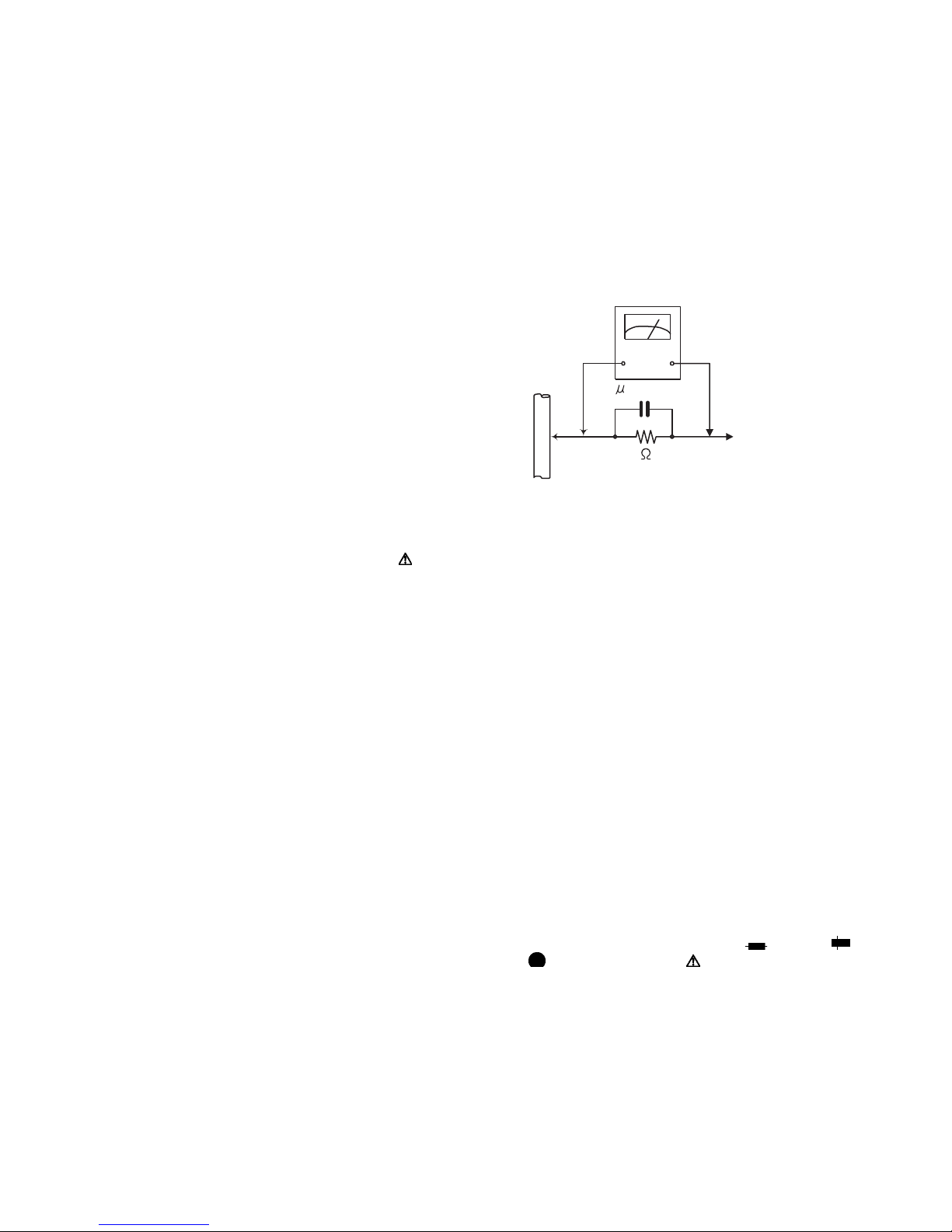
(5) Leakage shock hazard testing
After reassembling the product, always perform an isolation check on the exposed metal parts of the product (antenna terminals, knobs, metal cabinet, screw heads,
headphone jack, control shafts, etc.) to be sure the product
is safe to operate without danger of electrical shock.Do not
use a line isolation transformer during this check.
• Plug the AC line cord directly into the AC outlet. Using a
"Leakage Current Tester", measure the leakage current
from each exposed metal parts of the cabinet, particularly any exposed metal part having a return path to the
chassis, to a known good earth ground. Any leakage current must not exceed 0.5mA AC (r.m.s.).
• Alternate check method
Plug the AC line cord directly into the AC outlet. Use an
AC voltmeter having, 1,000Ω per volt or more sensitivity
in the following manner. Connect a 1,500Ω 10W resistor
paralleled by a 0.15µF AC-type capacitor between an ex-
posed metal part and a known good earth ground.
Measure the AC voltage across the resistor with the AC
voltmeter.
Move the resistor connection to each exposed metal
part, particularly any exposed metal part having a return
path to the chassis, and measure the AC voltage across
the resistor. Now, reverse the plug in the AC outlet and
repeat each measurement. Voltage measured any must
not exceed 0.75 V AC (r.m.s.). This corresponds to 0.5
mA AC (r.m.s.).
AC VOLTMETER
(Having 1000
ohms/volts,
or more sensitivity)
0.15 F AC TYPE
Place this
probe on
1500 10W
Good earth ground
1.2 Warning
(1) This equipment has been designed and manufactured to
meet international safety standards.
(2) It is the legal responsibility of the repairer to ensure that
these safety standards are maintained.
(3) Repairs must be made in accordance with the relevant
safety standards.
(4) It is essential that safety critical components are replaced
by approved parts.
(5) If mains voltage selector is provided, check setting for local
voltage.
1.3 Caution
Burrs formed during molding may be left over on some parts
of the chassis.
Therefore, pay attention to such burrs in the case of preforming repair of this system.
1.4 Critical parts for safety
In regard with component parts appearing on the silk-screen
printed side (parts side) of the PWB diagrams, the parts that are
printed over with black such as the resistor ( ), diode ( )
and ICP ( ) or identified by the " " mark nearby are critical
for safety. When replacing them, be sure to use the parts of the
same type and rating as specified by the manufacturer.
(This regulation dose not Except the J and C version)
each exposed
metal part.
1-4 (No.MB743<Rev.003>)
Page 5
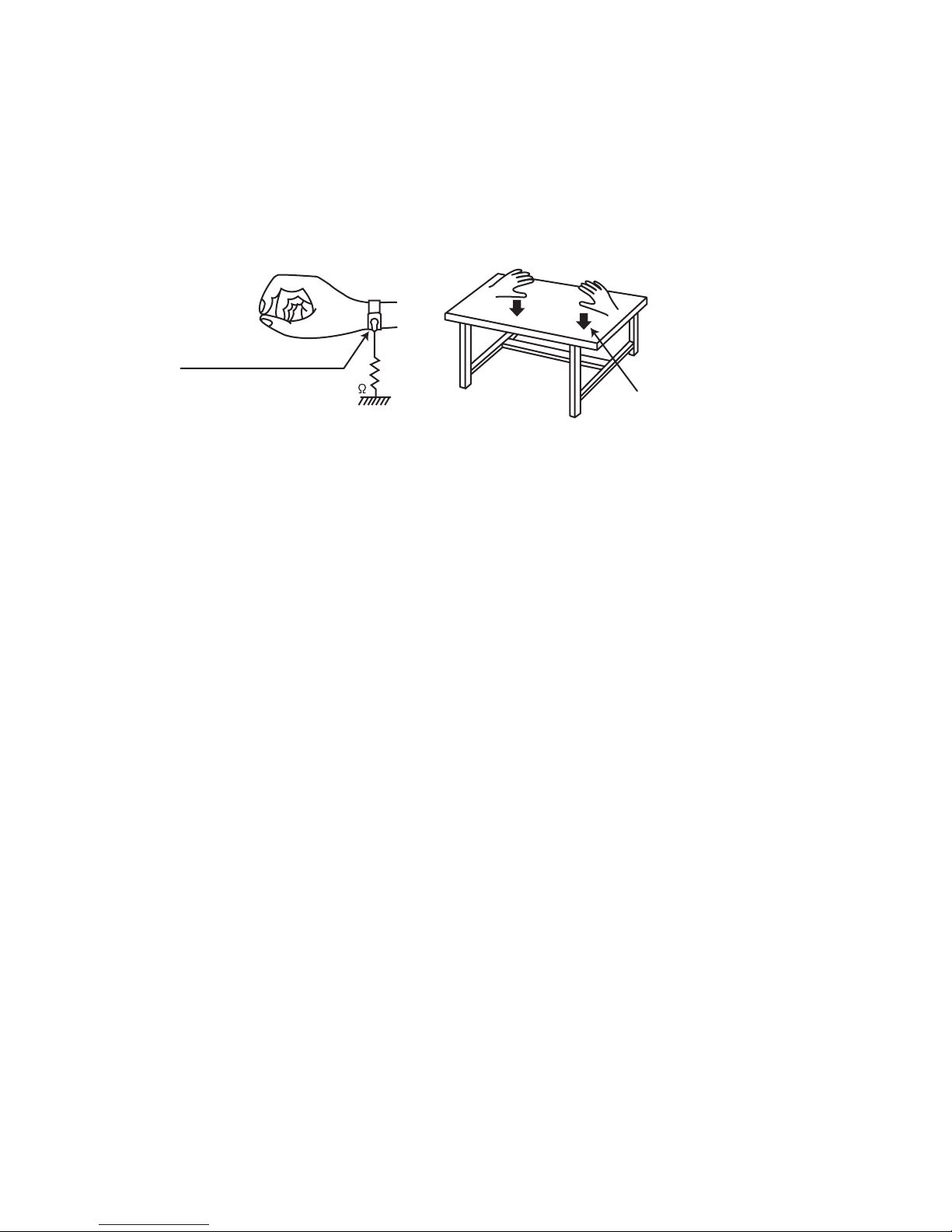
1.5 Preventing static electricity
Electrostatic discharge (ESD), which occurs when static electricity stored in the body, fabric, etc. is discharged, can destroy the laser
diode in the traverse unit (optical pickup). Take care to prevent this when performing repairs.
1.5.1 Grounding to prevent damage by static electricity
Static electricity in the work area can destroy the optical pickup (laser diode) in devices such as laser products.
Be careful to use proper grounding in the area where repairs are being performed.
(1) Ground the workbench
Ground the workbench by laying conductive material (such as a conductive sheet) or an iron plate over it before placing the
traverse unit (optical pickup) on it.
(2) Ground yourself
Use an anti-static wrist strap to release any static electricity built up in your body.
(caption)
Anti-static wrist strap
1M
Conductive material
(conductive sheet) or iron palate
(3) Handling the optical pickup
• In order to maintain quality during transport and before installation, both sides of the laser diode on the replacement optical
pickup are shorted. After replacement, return the shorted parts to their original condition.
(Refer to the text.)
• Do not use a tester to check the condition of the laser diode in the optical pickup. The tester's internal power source can easily
destroy the laser diode.
1.6 Handling the traverse unit (optical pickup)
(1) Do not subject the traverse unit (optical pickup) to strong shocks, as it is a sensitive, complex unit.
(2) Cut off the shorted part of the flexible cable using nippers, etc. after replacing the optical pickup. For specific details, refer to the
replacement procedure in the text. Remove the anti-static pin when replacing the traverse unit. Be careful not to take too long a
time when attaching it to the connector.
(3) Handle the flexible cable carefully as it may break when subjected to strong force.
(4) I t is not possible to adjust the semi-fixed resistor that adjusts the laser power. Do not turn it.
(No.MB743<Rev.003>)1-5
Page 6
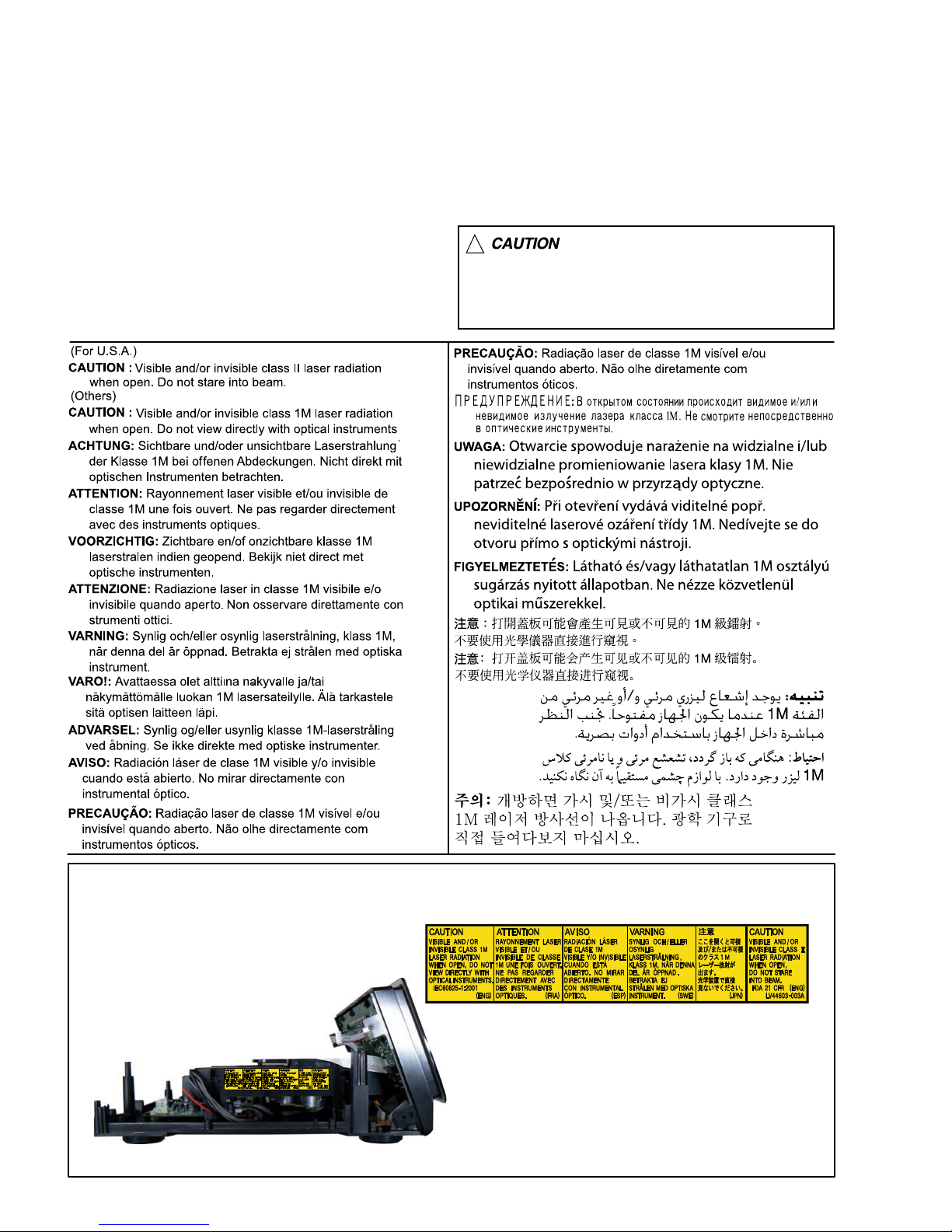
1.7 Important for laser products
1.CLASS 1 LASER PRODUCT
2.CAUTION :
(For U.S.A.) Visible and/or invisible class II laser radiation
when open. Do not stare into beam.
(Others) Visible and/or invisible class 1M laser radiation
when open. Do not view directly with optical instruments.
3.CAUTION : Visible and/or invisible laser radiation when
open and inter lock failed or defeated. Avoid direct
exposure to beam.
4.CAUTION : This laser product uses visible and/or invisible
laser radiation and is equipped with safety switches which
prevent emission of radiation when the drawer is open and
the safety interlocks have failed or are defeated. It is
dangerous to defeat the safety switches.
5.CAUTION : If safety switches malfunction, the laser is able
to function.
6.CAUTION : Use of controls, adjustments or performance of
procedures other than those specified here in may result in
hazardous radiation exposure.
!
Please use enough caution not to
see the beam directly or touch it
in case of an adjustment or operation
check.
REPRODUCTION AND POSITION OF LABELS and PRINT
WARNING LABEL and PRINT
1-6 (No.MB743<Rev.003>)
Page 7
SECTION 2
SPECIFIC SERVICE INSTRUCTIONS
This service manual does not describe SPECIFIC SERVICE INSTRUCTIONS.
SECTION 3
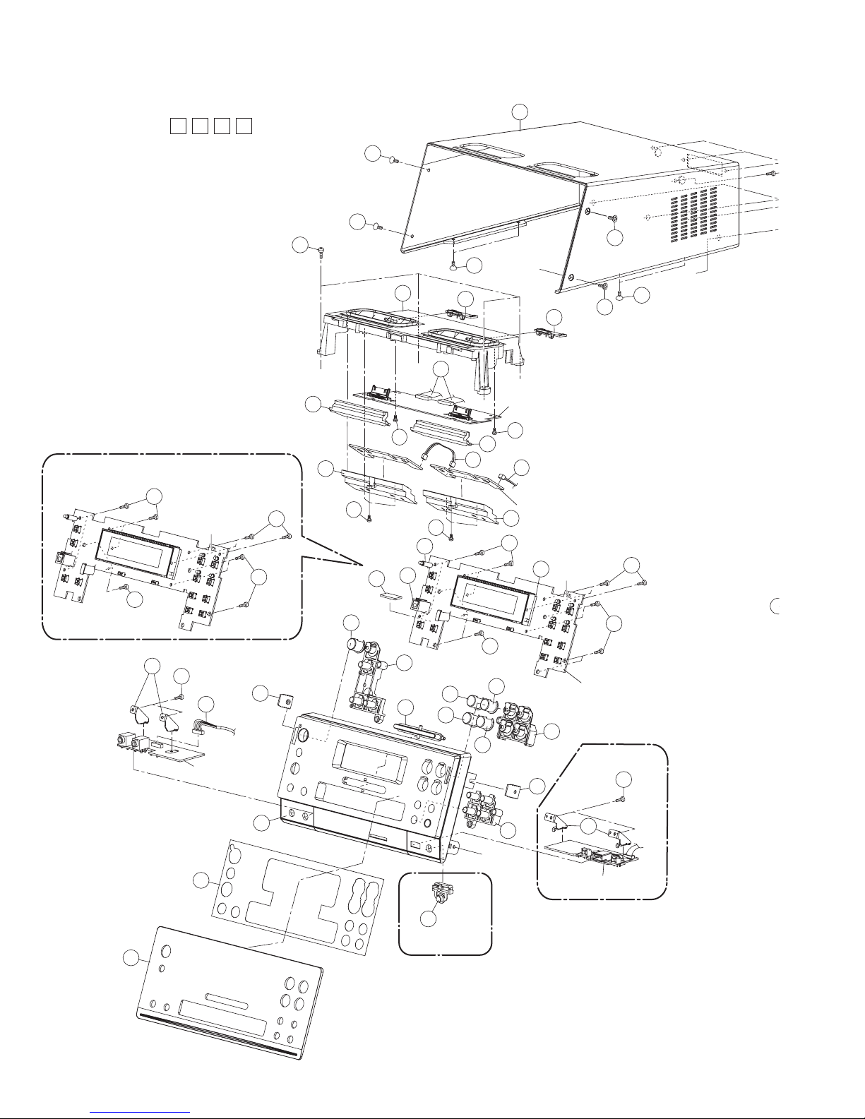
DISASSEMBLY
3.1 Main body (Used model: UX-F3E)
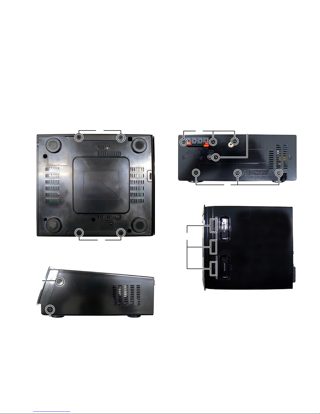
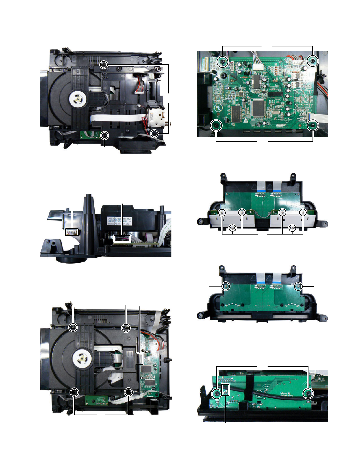
3.1.1 Removing the Top cover (See Fig.1, 2, 3, 4)
(1) Remove the four screws A attaching the Top cover. (See
Fig.1)
(3) Remove the three screws D, three screws E and one screw
F attaching the Top cover. (See Fig.3)
A
A
Fig.1
(2) Remove the two screws B and two screws C attaching the
both side of the Top cover. (See Fig.2)
B
E
F
D
Fig.3
(4) Disengaged three hooks a engaged Top cover. (See Fig.4)
hook
a
C
Fig.2
Fig.4
(No.MB743<Rev.003>)1-7
Page 8

3.1.2 Removing the iPod bracket (See Fig.5, 6)
(1) Disconnect the card wires from iPod board connected to
connectors CN803
Fig.5)
(2) Remove the four screws G attaching the iPod bracket.
(See Fig.5)
and CN804 of the Main board. (See
(10) Remove the five screws H attaching the Main board.
CN604 CN605
CN606
H
CN602
CN601
H
GG
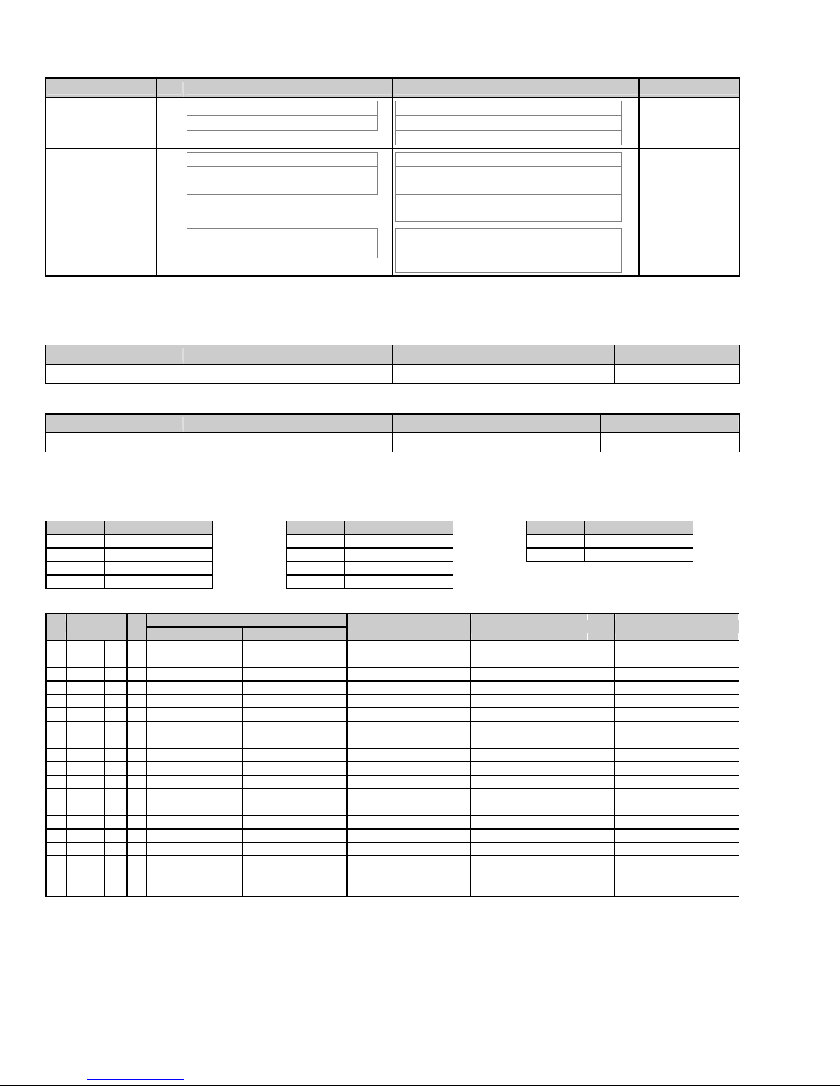
3.1.4 Removing the SMPS board (See Fig.8)
(1) Disconnect the connector wire from Display board connect-
CN803CN804
Fig.5
(3) Turn overt the iPod bracket; disconnect the connector wire
from Display board connected to connector CON202
LED board. (See Fig.6)
CON202
Fig.6
3.1.3 Removing the Main board (See Fig.7)
(1) Disconnect the connector wire from USB board connected
to connector CN606
(2) Disconnect the card wire from Tuner pack connected to
connector CN604 of the Main board.
(3) Disconnect the card wire from Upgrade board connected to
connector CN605
(4) Disconnect he card wire from Display board connected to
connector CN602
(5) Disconnect the connector wire from SMPS board connect-
ed to connector CN601
(6) Disconnect the connector wire from MPEG board connect-
ed to connector CN607
(7) Disconnect the card wire from MPEG board connected to
connector CN609
(8) Disconnect the connector wire from SMPS board connect-
ed to connector CN603
(9) Disconnect the connector wire from FAN connected to con-
nector CN612 of the Main board.
of the Main board.
of the Main board.
of the Main board.
of the Main board.
of the Main board.
of the Main board.
of the Main board.
of the
ed to connector CN902
(2) Remove the three screws J attaching the SMPS board.
J
3.1.5 Removing the Front panel (See Fig.9, 10)
(1) Disconnect the card wire from USB board connected to
connector CN108
(2) Disengaged two hooks b engaged both side of the Front
panel. (See Fig.9)
of the MPEG board. (See Fig.9)
b
(3) Disengage one hook c engaged Front panel. (See Fig.10)
hook
CN603CN612
Fig.7
of the SMPS board.
Fig.8
CN108hook
Fig.9
c
CN607
CN609
H
CN902
1-8 (No.MB743<Rev.003>)
Fig.10
Page 9
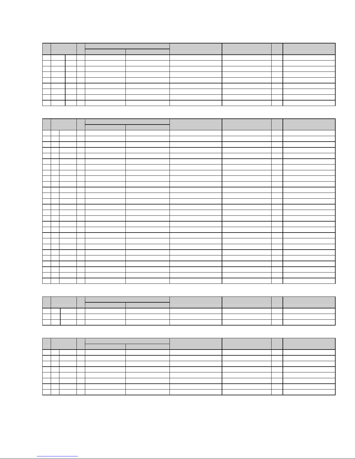
3.1.6 Removing the DVD mechanism (See Fig.11. 12, 13)
(1) Remove the three screws K attaching the Rear cabi brack-
et. (See Fig.11)
K
K
Fig.11
(2) Disconnect the connector wire from MPEG board connect-
ed to connector of the Loading board. (See Fig.12)
(3) Disconnect the connector wire from MPEG board connect-
ed to connector of the Traverse mechanism. (See Fig.12)
Loading board
connector
Traverse mechanism
connector
3.1.7 Removing the MPEG board (See Fig.14)
(1) Remove the four screws M attaching the MPEG board.
M
M
Fig.14
3.1.8 Removing the LED board (See Fig.15)
(1) Remove the six screws N attaching the LED board.
Fig.12
(4) Disconnect the card wire from Pickup connected to con-
nector CN102
(5) Remove the four screws L attaching the DVD mechanism.
(See Fig.13)
of the MPEG board. (See Fig.13)
L
CN102
N
Fig.15
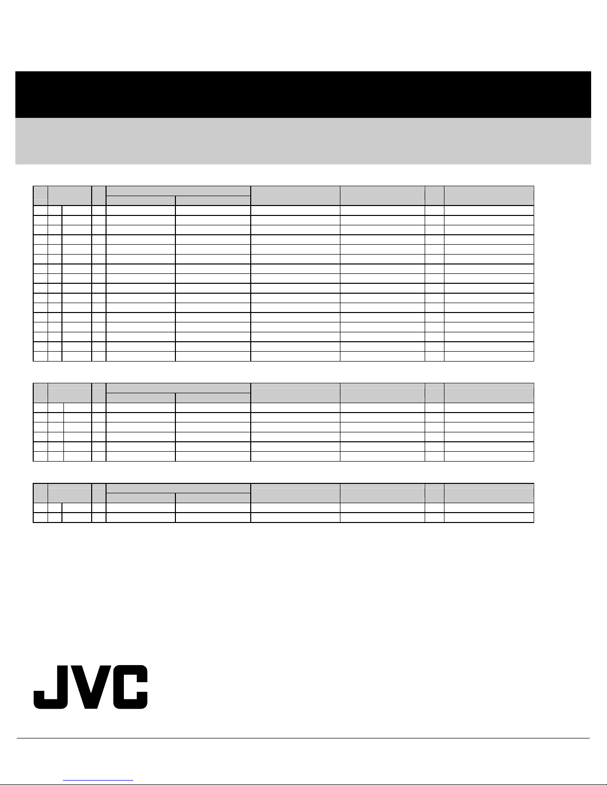
3.1.9 Removing the iPod board (See Fig.16)
(1) Remove the two screws P attaching the iPod board.
P
Fig.16
3.1.10 Removing the USB board (See Fig.17)
(1) Disconnect the connector wire from Display board connect-
ed to connector CN203
(2) Remove the two screws Q attaching the USB board.
of the USB board.
P
Q
L
Fig.13
CN203
Fig.17
(No.MB743<Rev.003>)1-9
Page 10

3.1.11 Removing the Jack board (See Fig.18)
(1) Remove the two screws R attaching the Jack board.
R
Fig.18
3.1.12 Removing the Display board (See Fig.19)
(1) Remove the fifteen screws S attaching the Display board.
S
S
Fig.19
1-10 (No.MB743<Rev.003>)
Page 11

SECTION 4
ADJUSTMENT
This service manual does not describe ADJUSTMENT.
SECTION 5
TROUBLESHOOTING
This service manual does not describe TROUBLESHOOTING.
(No.MB743<Rev.003>)1-11
Page 12

Victor Company of Japan, Limited
Home Entertainment Business Division Personal AV Operation 10-1,1chome,Ohwatari-machi,Maebashi-city,371-8543,Japan
(No.MB743<Rev.003>)
Printed in Japan
VSE
Page 13

REVISION INFORMATION
MICRO COMPONENT SYSTEM
UX-F3BB, UX-F3BC, UX-F3BE, UX-F3BEN,
UX-F3BEV, UX-F3BJ, UX-F3HB, UX-F3HE,
UX-F3HEN, UX-F3HEV
■ OVERVIEW
Add UX-F3BC and UX-F3BJ.
■ DETAILS
COVER SECTION
Title Line No.MB743<Rev.001> No.MB743<Rev.002> Description
Revision Rev.001 Rev.002
Issue Date 2010/05 2010/06
Model No. UX-F3BB, UX-F3BE, UX-F3BEN,
Cover Illustration ILLUSTRATION(mb743_0001.png) ILLUSTRATION(mb743_0001.png)
SPECIFICATION 2
4
7
8
15
25
UX-F3BEV, UX-F3HB, UX-F3HE,
UX-F3HEN, UX-F3HEV
Main unit (CA-UXF3B/CA-UXF3H)
Power source
AC 230 V , 50 Hz
Dimensions (approx.) (W x H x D)
236 mm × 123 mm × 285 mm
(including projecting parts)
Mass (approx.)
2.0 kg
USB
Tweeter
4 cm
UX-F3BB, UX-F3BC, UX-F3BE, UX-F3BEN,
UX-F3BEV, UX-F3BJ, UX-F3HB, UX-F3HE,
UX-F3HEN, UX-F3HEV
Main unit (CA-UXF3B/CA-UXF3H)
For B.E.EN.EV
For J.C
Power source
AC 230 V , 50 Hz
AC 120 V , 60 Hz
Dimensions (approx.) (W x H x D)
236 mm × 123 mm × 285 mm (including
projecting parts)
236 mm × 123 mm × 285 mm (9-5/16"×47/8"×11-1/4")(including projecting parts)
Mass (approx.)
2.0 kg
2.0 kg(4.5 lbs)
USB (Only Europe)
Tweeter
4 cm
4 cm(1-5/8")
COPYRIGHT © 2010 Victor Company of Japan, Limited
MB743-R002
2010/06
Page 14
Title Line No.MB743<Rev.001> No.MB743<Rev.002> Description
26
28
29
Woofer
12 cm
Dimensions (approx.) (W x H x D)
141 mm × 250 mm × 181 mm
(including projecting parts)
Mass (approx.)
1.8 kg each
Woofer
12 cm
12 cm(4-3/4")
Dimensions (approx.) (W x H x D)
141 mm × 250 mm × 181 mm (including
projecting parts)
141 mm × 250 mm × 181 mm (5-9/16"×97/8"×7-3/16")(including projecting parts)
Mass (approx.)
1.8 kg each
1.7 kg (3.8 lbs) each
STANDARD SCHEMATIC DIAGRAMS
Schematic Diagram
Diagram Name No.MB743<Rev.001> No.MB743<Rev.002> Description
Menu USB & SD section USB & SD section (for Except UX-F3BC,BJ)
Printed Circuit Board
Diagram Name No.MB743<Rev.001> No.MB743<Rev.002> Description
Menu USB board USB board (for Except UX-F3BC,BJ)
PARTS LIST
MODEL No. LIST
Model No. No.MB743<Rev.002>
UX-F3BB 01
UX-F3BC 02
UX-F3BE 03
UX-F3BEN 04
Model No. No.MB743<Rev.002>
UX-F3BEV 05
UX-F3BJ 06
UX-F3HB 07
UX-F3HE 08
Model No. No.MB743<Rev.002>
UX-F3HEN 09
UX-F3HEV 0A
General Assembly [M1MM]
Symbol or
!
M1MM 1 ------------ CD5501091400200 DISPLAY LENS (Addition) 1 02,06
M1MM 3 ------------ CD6021226060110 SCREW (Addition) 2 02,06
M1MM 6 ------------ CD5001091400200 FRONT CABINET (Addition) 1 02,06
M1MM 9 ------------ CD5902091400400 POWER BTN (Addition) 1 02,06
M1MM 13 ------------ CD6013226080100 SCREW (Addition) 13 02,06
M1MM 14 ------------ CD5633091800101 REAR CABI BKT (Addition) 1 02,06
M1MM 21 ------------ CD5002091400200 REAR CABINET (Addition) 1 02,06
M1MM 22 ------------ CD5201091400100 CD DOOR (Addition) 1 02,06
M1MM 29 ------------ CD5902091400500 CD PLAY BTN (Addition) 1 02,06
M1MM 30 ------------ CD5902091400800 TUNER BTN (Addition) 1 02,06
M1MM 31 ------------ CD5902091400900 iPod A PLAY BTN (Addition) 1 02,06
M1MM 32 ------------ CD5902091401000 iPod B PLAY BTN (Addition) 1 02,06
M1MM 37 ------------ CD5002091400301 BOTTOM CABINET (Addition) 1 02,06
M1MM 48 ------------ CD6013230060300 SCREW (Addition) 1 02,06
M1MM 51 ------------ CD5631091400300 iPod BRACKET (Addition) 1 02,06
! M1MM 57 ------------ CD2901212508040 AC CORD (Addition) 1 02,06
M1MM 59 ------------ CD7111091400200 RATING LABEL (Addition) 1 02,06
M1MM 73 ------------ CD3002150080930 FFC CABLE (Addition) 2 02,06
M1MM 77 ------------ CD3002100160900 FFC CABLE (Addition) 1 02,06
<Rev.001> <Rev.002>
Part No.
Part Name Description Qty Models
2 (MB743-R002)
Page 15
Packing and Accessories [M3MM]
Symbol or
!
M3MM A1 ------------ CD7202091400500 INST BOOK (Addition) 1 02,06
M3MM A2 ------------ CD7202091401800 INST BOOK (Addition) 1 02
M3MM A6 ------------ CD7201091400400 SAFETY SHEET (Addition) 1 02,06
M3MM A7 ------------ ------------ WARRANTY CARD (Addition) 1 02,06
M3MM A8 ------------ CD7201081100200 REGIS. CARD (Addition) 1 02,06
M3MM A10 ------------ CD1901000012400 REMOCON UNIT (Addition) 1 02,06
M3MM A13 ------------ CD7201081200600 SAFETY INST (Addition) 1 02,06
M3MM P1 ------------ CD7603091400200 CARTON (Addition) 1 02,06
M3MM P10 ------------ CD7215091800200 FLOUR PAPER (Addition) 2 02,06
<Rev.001> <Rev.002>
Part No.
Part Name Description Qty Models
Electrical parts list Main board [01]
Symbol or
!
01 D801 ------------ CD1322058170010 SCHOTTKY DIODE (Addition) 1 02,06
01 C780 ------------ CD1129226044120 C CAPACITOR (Addition) 1 02,06
01 C781 ------------ CD1129226044120 C CAPACITOR (Addition) 1 02,06
01 C796 ------------ CD1221000042050 C RESISTOR (Addition) 1 02,06
01 C797 ------------ CD1221000042050 C RESISTOR (Addition) 1 02,06
01 R780 ------------ CD1221103052020 C RESISTOR (Addition) 1 02,06
01 R782 ------------ CD1221104052020 C RESISTOR (Addition) 1 02,06
01 L824 ------------ CD1221000052020 C RESISTOR (Addition) 1 02,06
01 L825 ------------ CD1221000052020 C RESISTOR (Addition) 1 02,06
01 CF05 ------------ CD1132107053063 E CAPACITOR (Addition) 1 02,06
01 CV04 ------------ CD1132107053063 E CAPACITOR (Addition) 1 02,06
01 CV07 ------------ CD1132107053063 E CAPACITOR (Addition) 1 02,06
01 EC601 ------------ CD1132107053063 E CAPACITOR (Addition) 1 02,06
01 EC602 ------------ CD1132107053063 E CAPACITOR (Addition) 1 02,06
01 EC605 ------------ CD1132227053064 E CAPACITOR (Addition) 1 02,06
01 EC607 ------------ CD1132107053063 E CAPACITOR (Addition) 1 02,06
01 EC608 ------------ CD1132107053063 E CAPACITOR (Addition) 1 02,06
01 EC610 ------------ CD1132227053064 E CAPACITOR (Addition) 1 02,06
01 EC701 ------------ CD1132228073270 E CAPACITOR (Addition) 1 02,06
01 EC703 ------------ CD1132227053064 E CAPACITOR (Addition) 1 02,06
01 EC711 ------------ CD1132227053064 E CAPACITOR (Addition) 1 02,06
01 EC712 ------------ CD1132227053064 E CAPACITOR (Addition) 1 02,06
01 EC713 ------------ CD1132227053064 E CAPACITOR (Addition) 1 02,06
01 EC810 ------------ CD1132227053064 E CAPACITOR (Addition) 1 02,06
01 EC811 ------------ CD1132227053064 E CAPACITOR (Addition) 1 02,06
01 P601 ------------ CD3401000000420 PUSH TERMINAL (Addition) 1 02,06
01 P602 ------------ CD3401000000420 PUSH TERMINAL (Addition) 1 02,06
<Rev.001> <Rev.002>
Part No.
Part Name Description Qty Models
MPEG board [02]
Symbol or
!
02 C139 ------------ CD1121300081020 C CAPACITOR (Addition) 1 02,06
02 C140 ------------ CD1121300081020 C CAPACITOR (Addition) 1 02,06
02 R110 ------------ CD2721601020030 FERRITE BEADS (Addition) 1 02,06
<Rev.001> <Rev.002>
Part No.
Display board [03]
Symbol or
!
03 C306 ------------ CD1121102083020 C CAPACITOR (Addition) 1 02,06
03 C507 ------------ CD1132227053064 E CAPACITOR (Addition) 1 02,06
03 C510 ------------ CD1132107053063 E CAPACITOR (Addition) 1 02,06
03 C513 ------------ CD1132107053063 E CAPACITOR (Addition) 1 02,06
03 R503 ------------ CD1221181022050 C RESISTOR (Addition) 1 02,06
03 R536 ------------ CD1221203062020 C RESISTOR (Addition) 1 02,06
03 R544 ------------ CD1221000042050 C RESISTOR (Addition) 1 02,06
03 ZD506 ------------ CD1323000510050 Z DIODE (Addition) 1 02,06
<Rev.001> <Rev.002>
Part No.
Part Name Description Qty Models
Part Name Description Qty Models
(MB743-R002)3
Page 16
SMPS board [04]
Symbol or
!
04 Q901 ------------ CD1414005600011 TRANSISTOR (Addition) 1 02,06
04 D904 ------------ CD1311001070050 DIODE (Addition) 1 02,06
04 C924 ------------ CD1132108053161 E CAPACITOR (Addition) 1 02,06
04 C925 ------------ CD1132108053161 E CAPACITOR (Addition) 1 02,06
04 C926 ------------ CD1132337063220 E CAPACITOR (Addition) 1 02,06
04 C927 ------------ CD1132337063220 E CAPACITOR (Addition) 1 02,06
04 C928 ------------ CD1132337063220 E CAPACITOR (Addition) 1 02,06
04 C931 ------------ CD1132107053063 E CAPACITOR (Addition) 1 02,06
04 R916 ------------ CD1231039022000 RESISTOR (Addition) 1 02,06
04 R917 ------------ CD1231039022000 RESISTOR (Addition) 1 02,06
04 CN901 ------------ CD3101100221010 HEADER (Addition) 1 02,06
04 PIN3 ------------ CD3401000000420 PUSH TERMINAL (Addition) 1 02,06
04 PIN4 ------------ CD3401000000420 PUSH TERMINAL (Addition) 1 02,06
04 PIN5 ------------ CD3401000000420 PUSH TERMINAL (Addition) 1 02,06
04 ZD901 ------------ CD1323003620010 ZENER DIODE (Addition) 1 02,06
04 ZD902 ------------ CD1323003620010 ZENER DIODE (Addition) 1 02,06
<Rev.001> <Rev.002>
Part No.
Part Name Description Qty Models
iPod board [06]
Symbol or
!
06 C809 ------------ CD1132107053063 E CAPACITOR (Addition) 1 02,06
06 C818 ------------ CD1132107053063 E CAPACITOR (Addition) 1 02,06
06 C833 ------------ CD1132107053063 E CAPACITOR (Addition) 1 02,06
06 C871 ------------ CD1132107053063 E CAPACITOR (Addition) 1 02,06
06 C874 ------------ CD1132107053063 E CAPACITOR (Addition) 1 02,06
06 C884 ------------ CD1132107053063 E CAPACITOR (Addition) 1 02,06
<Rev.001> <Rev.002>
Part No.
Part Name Description Qty Models
LED board [07]
Symbol or
!
07 ZD201 ------------ CD1313055270010 Z DIODE (Addition) 1 02,06
07 ZD202 ------------ CD1313055270010 Z DIODE (Addition) 1 02,06
<Rev.001> <Rev.002>
Part No.
Part Name Description Qty Models
Victor Company of Japan, Limited
Home Entertainment Business Division Personal AV Operation 10-1,1chome,Ohwatari-machi,Maebashi-city,371-8543,Japan
(MB743-R002)
Printed in Japan
No.MB743<Rev.001> VSE
Page 17
REVISION INFORMATION
MICRO COMPONENT SYSTEM
UX-F3BA, UX-F3BB, UX-F3BC, UX-F3BE,
UX-F3BEN, UX-F3BEV, UX-F3BJ, UX-F3BUJ,
UX-F3HB, UX-F3HE, UX-F3HEN, UX-F3HEV
■ OVERVIEW
Add UX-F3BA and UX-F3BUJ.
■ DETAILS
COVER SECTION
Title Line No.MB743<Rev.002> No.MB743<Rev.003> Description
Revision Rev.002 Rev.003
Model No. UX-F3BB, UX-F3BC, UX-F3BE,
UX-F3BEN, UX-F3BEV, UX-F3BJ,
UX-F3HB, UX-F3HE, UX-F3HEN,
UX-F3HEV
Cover Illustration ILLUSTRATION(mb743_0001.png) ILLUSTRATION(mb743_0001.png)
33 -
34 -
35 -
36 -
37 -
38 -
39 -
40 -
UX-F3BA, UX-F3BB, UX-F3BC,
UX-F3BE, UX-F3BEN, UX-F3BEV,
UX-F3BJ, UX-F3BUJ, UX-F3HB,
UX-F3HE, UX-F3HEN, UX-F3HEV
UX-F3BA/UX-F3BUJ
General
Power source
For Australian model
AC 240 V , 50 Hz
For another model
AC 110 V - 127 V / 220 V - 240 V
adjustable with voltage selector, 50/60 Hz
Power consumption (at operation)
40 W
Power consumption (on standby)
1.00 W or less
Dimensions (approx.) (W × H × D)
236 mm × 123 mm ×~ 285 mm (including
projecting parts)
Mass (approx.)
2.0 kg
COPYRIGHT © 2010 Victor Company of Japan, Limited
MB743-R003
2010/06
Page 18

Title Line No.MB743<Rev.002> No.MB743<Rev.003> Description
41 -
42 -
43 -
44 -
45 -
46 -
47 -
48 -
49 -
50 -
51 -
52 -
53 -
54 -
55 -
56 -
57 -
58 -
59 -
60 -
61 -
63 - Design and specifications are subject to
Amplifier
Output Power
60 W (30 W + 30 W) at 6 Ω (10% THD)
Audio Input
AUDIO IN: Stereo mini (Φ 3.5 mm)
Speaker impedance
6 Ω - 16 Ω
Tuner
FM frequency
87.50 MHz - 108.00 MHz
USB
USB specification
Compatible with USB 2.0 Full Speed
Compatible device
Mass storage class
Compatible system
FAT16, FAT32
Output power
DC 5 V 500 mA
iPod
Output power
DC 5 V 500 mA
Video out
Composite
Speaker(SP-UXF3B)
Speaker type
Bass-reflex type
Tweeter
4 cm
Woofer
12 cm
Impedance
6 Ω
Dimensions (approx.) (W × H × D)
141 mm × 250 mm × 181 mm (including
projecting parts)
Mass (approx.)
1.8 kg each
change without notice.
2 (MB743-R003)
Page 19

PARTS LIST
r
MODEL No. LIST
Model No. No.MB743<Rev.003>
UX-F3BA 01
UX-F3BB 02
UX-F3BC 03
UX-F3BE 04
General Assembly [M1MM]
Symbol or
!
M1MM 6 ------------ CD5001091400600 FRONT CABINET (Addition) 1 01
M1MM 6 ------------ CD5001091400500 FRONT CABINET (Addition) 1 08
M1MM 37 ------------ CD5002091800201 BOTTOM CABINET (Addition) 1 01
M1MM 37 ------------ CD5002091800400 BOTTOM CABINET (Addition) 1 08
! M1MM 57 ------------ CD2904225007000 AC CORD (Addition) 1 01
! M1MM 57 or ------------ CD2902125007210 AC CORD (Addition) 1 04,05,06
M1MM 59 ------------ CD7111091400300 RATING LABEL (Addition) 1 01
M1MM 59 ------------ CD7111091400700 RATING LABEL (Addition) 1 08
M1MM 88 ------------ CD3307020200010 VOLTAGE SELECT SW (Addition) 1 08
M1MM 89 ------------ CD6013226080100 SCREW (Addition) 2 08
M1MM 90 ------------ CD3501020083900 CONNECTOR WIRE (Addition) 1 08
<Rev.002> <Rev.003>
Part No.
Packing and Accessories [M3MM]
Symbol or
!
M3MM A1 ------------ CD7202091400600 INST BOOK (Addition) 1 01,08
M3MM A6 ------------ CD7201091900400 SAFETY SHEET (Addition) 1 01,08
M3MM A7 ------------ ------------ WARRANTY CARD (Addition) 1 01
M3MM A14 ------------ ------------ WARRANTY CARD (Addition) 1 01
M3MM A15 ------------ CD3103000000020 CONVERSION PLUG (Addition) 1 08
<Rev.002> <Rev.003>
Part No.
Model No. No.MB743<Rev.003>
UX-F3BEN 05
UX-F3BEV 06
UX-F3BJ 07
UX-F3BUJ 08
Part Name Description Qty Models
Part Name Description Qty Models
Model No. No.MB743<Rev.003>
UX-F3HB 09
UX-F3HE 0A
UX-F3HEN 0B
UX-F3HEV 0C
Electrical parts list Main board [01]
Symbol o
!
01 B701 ------------ CD2721601020030 FERRITE BEADS (Addition) 1 01,02,03,04,05,06,07,08,09,0A,0B,0C
01 B702 ------------ CD1221000052020 C RESISTOR (Addition) 1 01,02,03,04,05,06,07,08,09,0A,0B,0C
01 B703 ------------ CD2721601020030 FERRITE BEADS (Addition) 1 01,02,03,04,05,06,07,08,09,0A,0B,0C
01 B704 ------------ CD2721601020030 FERRITE BEADS (Addition) 1 01,02,03,04,05,06,07,08,09,0A,0B,0C
01 B705 ------------ CD2721601020030 FERRITE BEADS (Addition) 1 01,02,03,04,05,06,07,08,09,0A,0B,0C
01 B706 ------------ CD2721601020030 FERRITE BEADS (Addition) 1 01,02,03,04,05,06,07,08,09,0A,0B,0C
01 B707 ------------ CD2721601020030 FERRITE BEADS (Addition) 1 01,02,03,04,05,06,07,08,09,0A,0B,0C
01 B708 ------------ CD2721601020030 FERRITE BEADS (Addition) 1 01,02,03,04,05,06,07,08,09,0A,0B,0C
01 B709 ------------ CD2721601020030 FERRITE BEADS (Addition) 1 01,02,03,04,05,06,07,08,09,0A,0B,0C
01 B710 ------------ CD2721601020030 FERRITE BEADS (Addition) 1 01,02,03,04,05,06,07,08,09,0A,0B,0C
01 B711 ------------ CD1221000052020 C RESISTOR (Addition) 1 01,02,03,04,05,06,07,08,09,0A,0B,0C
01 B712 ------------ CD2721601020030 FERRITE BEADS (Addition) 1 01,02,03,04,05,06,07,08,09,0A,0B,0C
<Rev.002> <Rev.003>
Part No.
Part Name Description Qty Models
SMPS board [04]
Symbol or
!
04 SW901 ------------ CD3101790221000 CONNECTOR WIRE (Addition) 1 08
<Rev.002> <Rev.003>
Part No.
Part Name Description Qty Models
(MB743-R003) 3
Page 20

Victor Company of Japan, Limited
Home Entertainment Business Division Personal AV Operation 10-1,1chome,Ohwatari-machi,Maebashi-city,371-8543,Japan
(MB743-R003)
Printed in Japan
No.MB743<Rev.002> VSE
Page 21

PARTS LIST
UX-F3BA, UX-F3BB, UX-F3BC, UX-F3BE
UX-F3BEN, UX-F3BEV, UX-F3BJ, UX-F3BUJ
UX-F3HB, UX-F3HE, UX-F3HEN, UX-F3HEV
MODEL MARK
AUX-F3BA
UX-F3BB
UX-F3BE
* All printed circuit boards and its assemblies are not available as service parts.
B
CUX-F3BC
D
MODEL MARK
EUX-F3BEN
UX-F3BEV
UX-F3BUJ
F
GUX-F3BJ
H
MODEL MARK
UX-F3HE
UX-F3HEV
- Contents -
Exploded view of general assembly and parts list (Block No.M1)
Electrical parts list (Block No.01~07)
Packing materials and accessories parts list (Block No.M3)
IUX-F3HB
J
KUX-F3HEN
L
3- 2
3- 6
3-17
MB743PAR<Rev.003>
3-1
Page 22
Exploded view of general assembly and parts list
0
21
13
4
M MM1
w
3
86
Jack board
15
65
19
65
51
G
18
17
13
13
5
r
68
33
9
F
68
10
8
7
20
73
t
u
18
74
68
11
c
13
31
29
30
E
20
H
iPod board
68
85
w
LED board
17
13
12
32
28
5
Block No.
UX-F3BC
UX-F3BJ
c
13
15
65
w
13
Display board
Except BC,BJ
D
65
13
7
3
6
2
1
3-2
25
Except BC,BJ
27
26
e
E
USB board
Page 23

71
61
59
65
66
c
76
b
k
p
h
a
75
58
n
48
j
t
u
d
77
n
Main board
H
r
16
49
50
70
Only B ver.
83
84
SMPS board
57
57
44
j
k
43
70
45
72
UX-F3BUJ
89
88
F
64
14
60
63
22
69
46
90
UX-F3BUJ
35
37
s
56
54
B
72
B
42
41
G
23
s
35
64
63
63
m
b
78
79
80
h
35
m
g
55
Upgrade board
64
d
63
24
87
f
H
e
82
81
62
A
39
38
23
38
a
34
36
47
52
53
67
g
MPEG board
p
40
D
35
A
The parts without symbol number are not service.
3-3
Page 24

General Assembly
Symbol No. Part No. Part Name Description Local
1 CD5501091400100 DISPLAY LENS 5501-091400100 A,B,D,E,F,H,I,J,K,L
1 CD5501091400200 DISPLAY LENS 5501-091400200 C,G
2 CD7902091800101 DOUBLE SIDE PAPER 7902-091800101
3 CD6021226060110 SCREW 6021-226060110(x4) A,B,D,E,F,H,I,J,K,L
3 CD6021226060110 SCREW 6021-226060110(x2) C,G
4 CD6306091800100 BRACKET 6306-091800100(x2)
5 CD6211091800100 PANEL FIX PLATE 6211-091800100(x2)
6 CD5001091400600 FRONT CABINET 5001-091400600 A
6 CD5001091400100 FRONT CABINET 5001-091400100 B,D,E,F
6 CD5001091400200 FRONT CABINET 5001-091400200 C,G
6 CD5001091400500 FRONT CABINET 5001-091400500 H
6 CD5001091400400 FRONT CABINET 5001-091400400 I,J,K,L
7 CD5307091800100 VOLUME BTN 5307-091800100
8 CD5403091800101 BUTTON SET 5403-091800101
9 CD5902091800100 POWER BTN 5902-091800100 A,B,D,E,F,H,I,J,K,L
9 CD5902091400400 POWER BTN 5902-091400400 C,G
10 CD5603091800100 SENSOR BRACKET 5603-091800100
11 CD5601091800100 POWER LED BKT 5601-091800100
12 CD5601091800200 DISPLAY BRACKET 5601-091800200
13 CD6013226080100 SCREW 6013-226080100(x15) A,B,D,E,F,H,I,J,K,L
13 CD6013226080100 SCREW 6013-226080100(x13) C,G
14 CD5633091800101 REAR CABI BKT 5633-091800101 A,C,G
14 CD5633091800100 REAR CABI BKT 5633-091800100 B,D,E,F,H,I,J,K,L
15 CD6024330080100 SCREW 6024-330080100(x2)
16 CD6600091400100 HEAT SINK 6600-091400100
17 CD5631091400200 BRACKET 5631-091400200(x2)
18 CD5502091400100 LIGHT GUIDE 5502-091400100(x2)
19 CD6013230100120 SCREW 6013-230100120(x4)
20 CD5907091400100 INSERT HOOK 5907-091400100(x2)
21 CD5002091400100 REAR CABINET 5002-091400100 A,B,D,E,F,H
21 CD5002091400200 REAR CABINET 5002-091400200 C,G
21 CD5002091400500 REAR CABINET 5002-091400500 I,J,K,L
22 CD5201091800100 CD DOOR 5201-091800100 A,B,D,E,F,H,I,J,K,L
22 CD5201091400100 CD DOOR 5201-091400100 C,G
23 CD5607091800100 BRACKET 5607-091800100(x2)
24 CD8949050900201 CD MECHA LOADER 8949-050900201
25 CD5416091800101 BTN SD/USB REC 5416-091800101 A,B,D,E,F,H
25 CD5416091400100 BTN SD/USB REC 5416-091400100 I,J,K,L
26 CD6306091800200 BRACKET 6306-091800200(x2) A,B,D,E,F,H,I,J,K,L
27 CD5404091800101 FUNCTION BTN 5404-091800101
28 CD5627091800101 FUNC BTN BKT 5627-091800101
29 CD5902091800200 CD PLAY BTN 5902-091800200 A,B,D,E,F,H,I,J,K,L
29 CD5902091400500 CD PLAY BTN 5902-091400500 C,G
30 CD5902091800300 USB PLAY BTN 5902-091800300 A,B,D,E,F,H,I,J,K,L
30 CD5902091400800 TUNER BTN 5902-091400800 C,G
31 CD5902091400100 iPod A PLAY BTN 5902-091400100 A,B,D,E,F,H,I,J,K,L
31 CD5902091400900 iPod A PLAY BTN 5902-091400900 C,G
32 CD5902091400200 iPod B PLAY BTN 5902-091400200 A,B,D,E,F,H,I,J,K,L
32 CD5902091401000 iPod B PLAY BTN 5902-091401000 C,G
33 CD6406081200200 EVA 6406-081200200
34 CD5904091800100 BTM CABI COVER 5904-091800100
35 CD6404081100200 SILICON FOOT 6404-081100200(x4)
36 CD6013230100120 SCREW 6013-230100120
37 CD5002091800201 BOTTOM CABINET 5002-091800201 A
37 CD5002091800200 BOTTOM CABINET 5002-091800200 B,D,E,F,I,J,K,L
37 CD5002091400301 BOTTOM CABINET 5002-091400301 C,G
37 CD5002091800400 BOTTOM CABINET 5002-091800400 H
38 CD6406091300100 EVA 6406-091300100(x2)
39 CD6011220080300 SCREW 6011-220080300(x2)
40 CD8028000001000 FAN 8028-000001000
41 CD8045000000300 SLILCA GEL SHEET 8045-000000300
42 CD6600091800200 HEAT SINK B 6600-091800200
43 CD6600091800100 HEAT SINK A 6600-091800100
44 CD6210091300100 PC SHEET 6210-091300100
45 CD5939080700100 PLASTIC WASHER 5939-080700100
46 CD6306091800300 BRACKET 6306-091800300(x2)
47 CD3801000000350 FM TUNER MODULE 3801-000000350
48 CD6013230060300 SCREW 6013-230060300 A,C,G
48 CD6013226080100 SCREW 6013-226080100 B,D,E,F,H,I,J,K,L
49 CD5939081000100 PLASTIC WASHER 5939-081000100(x2)
50 CD6023230100300 SCREW 6023-230100300(x2)
51 CD5631091400100 iPod BRACKET 5631-091400100 A,B,D,E,F,H
51 CD5631091400300 iPod BRACKET 5631-091400300 C,G
51 CD5631091400400 iPod BRACKET 5631-091400400 I,J,K,L
Block No. [M][1][M][M]
3-4
Page 25

Symbol No. Part No. Part Name Description Local
52 CD6209091300100 COPPER PLATINUM 6209-091300100
53 CD4401120001120 CD MECHANISM 4401-120001120
54 CD2712104030000 FERRITE CORE 2712-104030000
55 CD8024000004600 FIBER WASHER 8024-000004600(x2) B,D,E,F
56 CD6012226100110 SCREW 6012-226100110
57 CD2904225007000 AC CORD 2904-225007000 A
57 CD2905123007000 AC CORD 2905-123007000 B,I
57 or CD2905225007070 AC CORD 2905-225007070 B,I
57 CD2901212508040 AC CORD 2901-212508040 C,G
57 CD2902223007000 AC CORD 2902-223007000 D,E,F,H,J,K,L
57 or CD2902225007060 AC CORD 2902-225007060 D,E,F,H,J,K,L
57 or CD2902125007210 AC CORD 2902-125007210 D,E,F
57 or CD2902123007040 AC CORD 2902-123007040 D,E,F,H,J,K,L
57 or CD2902225007040 AC CORD 2902-225007040 D,E,F,H,J,K,L
58 CD1214103146001 THERMISTOR 1214-103146001
59 CD7111091400300 RATING LABEL 7111-091400300 A
59 CD7111091400100 RATING LABEL 7111-091400100 B,D,E
59 CD7111091400200 RATING LABEL 7111-091400200 C,G
59 CD7111091400600 RATING LABEL 7111-091400600 F
59 CD7111091400700 RATING LABEL 7111-091400700 H
59 CD7111091400500 RATING LABEL 7111-091400500 I,J,K
59 CD7111091400800 RATING LABEL 7111-091400800 L
60 CD7112081000100 CAUTION LABEL 7112-081000100
61 CD6013230100120 SCREW 6013-230100120(x3)
62 CD6013230100120 SCREW 6013-230100120
63 CD6013230100120 SCREW 6013-230100120(x4)
64 CD6013230100120 SCREW 6013-230100120(x3)
65 CD6014230080130 SCREW 6014-230080130(x9)
66 CD6013226080100 SCREW 6013-226080100(x5)
67 CD6013226080100 SCREW 6013-226080100(x4)
68 CD6011220080300 SCREW 6011-220080300(x8)
69 CD6013230120400 SCREW 6013-230120400(x2)
70 CD6033226060200 SCREW 6033-226060200(x2)
71 CD6033226080110 SCREW 6033-226080110
72 CD6013226080100 SCREW 6013-226080100(x2)
73 CD3002150080930 FFC CABLE 3002-150080930(x2) A,C,G
73 CD3002150055900 FFC CABLE 3002-150055900(x2) B,D,E,F,H,I,J,K,L
74 CD3504020052000 HOUSING 3504-020052000
75 CD3002070190900 FFC CABLE 3002-070190900
76 CD3002090210900 FFC CABLE 3002-090210900
77 CD3002100160900 FFC CABLE 3002-100160900 A,C,G
77 CD3002100135900 FFC CABLE 3002-100135900 B,D,E,F,H,I,J,K,L
78 CD3002090095900 FFC CABLE 3002-090095900
79 CD3505080182010 HOUSING 3505-080182010
80 CD3502060152040 HOUSING 3502-060152040
81 CD3505050152010 HOUSING 3505-050152010
82 CD3002140160910 FFC CABLE SHILED 3002-140160910 A,I,J,K,L
82 CD3002140160900 FFC CABLE SHILED 3002-140160900 B,D,E,F
83 CD3505070152010 HOUSING 3505-070152010
84 CD3505060222500 HOUSING 3505-060222500
85 CD3505020102010 HOUSING 3505-020102010
86 CD3505070523000 HOUSING SHILED 3505-070523000
87 CD3002160100910 FFC CABLE 3002-160100910
88 CD3307020200010 VOLTAGE SELECT SW 3307-020200010 H
89 CD6013226080100 SCREW 6013-226080100(x2) H
90 CD3501020083900 CONNECTOR WIRE 3501-020083900 H
3-5
Page 26

Electrical parts list
Main board
Block No. [0][1]
Symbol No.
U601 1506780527010-C IC 1506-780527010
U602 CD1511002402080 IC 1511-002402080
U604 CD1502002314010 IC 1502-002314010
U605 CD1502004453000 IC 1502-004453000
U608 CD1502007492010 IC 1502-007492010
U611 CD1510743257000 IC 1510-743257000
U803 CD1509000200010 IC 1509-000200010
U804 CD1507004052010 IC 1507-004052010
U805 CD1507004052010 IC 1507-004052010
Q601 CD1424023010020 MOS FET 1424-023010020
Q602 CD1422080500050 TRANSISTOR 1422-080500050
Q603 CD1422080500050 TRANSISTOR 1422-080500050
Q604 CD1422080500050 TRANSISTOR 1422-080500050
Q605 CD1422080500050 TRANSISTOR 1422-080500050
Q606 CD1421085500010 TRANSISTOR 1421-085500010
Q607 CD1412080500000 TRANSISTOR 1412-080500000
Q701 CD1421085500010 TRANSISTOR 1421-085500010
Q702 CD1422080500050 TRANSISTOR 1422-080500050
Q703 CD1422080500050 TRANSISTOR 1422-080500050
Q704 CD1412080500000 TRANSISTOR 1412-080500000
Q706 CD1424230180010 MOS FET 1424-230180010
Q707 CD1412080500000 TRANSISTOR 1412-080500000
Q708 CD1422080500050 TRANSISTOR 1422-080500050
Q810 CD1424023010020 MOS FET 1424-023010020
Q811 CD1424023010020 MOS FET 1424-023010020
Q812 CD1422080500050 TRANSISTOR 1422-080500050
Q813 CD1422080500050 TRANSISTOR 1422-080500050
Q814 CD1422080500050 TRANSISTOR 1422-080500050
Q815 CD1422080500050 TRANSISTOR 1422-080500050
D601 CD1321041480050 DIODE 1321-041480050
D602 CD1321041480050 DIODE 1321-041480050
D603 CD1321041480050 DIODE 1321-041480050
D604 CD1321041480050 DIODE 1321-041480050
D605 CD1321041480050 DIODE 1321-041480050
D701 CD1321041480050 DIODE 1321-041480050
D702 CD1321041480050 DIODE 1321-041480050
D703 CD1321041480050 DIODE 1321-041480050
D801 CD1322058170010 SCHOTTKY DIODE 1322-058170010 A,C,G
D801 CD1322020100010 SCHOTTKY DIODE 1322-020100010 B,D,E,
C601 CD1121104082020 C CAPACITOR 1121-104082020
C602 CD1121104082020 C CAPACITOR 1121-104082020
C603 CD1121104082020 C CAPACITOR 1121-104082020
C604 CD1121104082020 C CAPACITOR 1121-104082020
C605 CD1121104082020 C CAPACITOR 1121-104082020
C606 CD1121104082020 C CAPACITOR 1121-104082020
C607 CD1121240081020 C CAPACITOR 1121-240081020
C608 CD1121240081020 C CAPACITOR 1121-240081020
C609 CD1121101081020 C CAPACITOR 1121-101081020
C610 CD1121103082020 C CAPACITOR 1121-103082020
C611 CD1121104082020 C CAPACITOR 1121-104082020
C612 CD1121104082020 C CAPACITOR 1121-104082020
C613 CD1121470081020 C CAPACITOR 1121-470081020
C614 CD1121470081020 C CAPACITOR 1121-470081020
C617 CD1121104082020 C CAPACITOR 1121-104082020
C618 CD1121104082020 C CAPACITOR 1121-104082020
C619 CD1121104082020 C CAPACITOR 1121-104082020
C621 CD1121104082020 C CAPACITOR 1121-104082020
C622 CD1121470081020 C CAPACITOR 1121-470081020
C623 CD1121470081020 C CAPACITOR 1121-470081020
C624 CD1121470081020 C CAPACITOR 1121-470081020
C625 CD1121470081020 C CAPACITOR 1121-470081020
C626 CD1121101081020 C CAPACITOR 1121-101081020
C627 CD1121101081020 C CAPACITOR 1121-101081020
C628 CD1121101081020 C CAPACITOR 1121-101081020
C629 CD1121101081020 C CAPACITOR 1121-101081020
C630 CD1121104082020 C CAPACITOR 1121-104082020
C631 CD1121103082020 C CAPACITOR 1121-103082020
Part No. Part Name Description Local
F,H , I, J
,K,L
Symbol No.
C632 CD1121103082020 C CAPACITOR 1121-103082020
C633 CD1121103082020 C CAPACITOR 1121-103082020
C634 CD1121103082020 C CAPACITOR 1121-103082020
C635 CD1121106052031 C CAPACITOR 1121-106052031
C636 CD1121106052031 C CAPACITOR 1121-106052031
C637 CD1121200081021 C CAPACITOR 1121-200081021
C638 CD1121200081021 C CAPACITOR 1121-200081021
C640 CD1121101081020 C CAPACITOR 1121-101081020
C641 CD1121101081020 C CAPACITOR 1121-101081020
C642 CD1121101081020 C CAPACITOR 1121-101081020
C643 CD1121101081020 C CAPACITOR 1121-101081020
C644 CD1121101081020 C CAPACITOR 1121-101081020
C645 CD1121101081020 C CAPACITOR 1121-101081020
C646 CD1121101081020 C CAPACITOR 1121-101081020
C647 CD1121101081020 C CAPACITOR 1121-101081020
C648 CD1121101081020 C CAPACITOR 1121-101081020
C649 CD1121101081020 C CAPACITOR 1121-101081020
C701 CD1121104082020 C CAPACITOR 1121-104082020
C702 CD1121224084020 C CAPACITOR 1121-224084020
C703 CD1121224084020 C CAPACITOR 1121-224084020
C704 CD1121104082020 C CAPACITOR 1121-104082020
C705 CD1121104082020 C CAPACITOR 1121-104082020
C706 CD1121104082020 C CAPACITOR 1121-104082020
C707 CD1121104082020 C CAPACITOR 1121-104082020
C708 CD1121104082020 C CAPACITOR 1121-104082020
C709 CD1121104082020 C CAPACITOR 1121-104082020
C710 CD1121104082020 C CAPACITOR 1121-104082020
C711 CD1121225052030 C CAPACITOR 1121-225052030
C712 CD1121225052030 C CAPACITOR 1121-225052030
C713 CD1121105052020 C CAPACITOR 1121-105052020
C714 CD1121105052020 C CAPACITOR 1121-105052020
C715 CD1121474064020 C CAPACITOR 1121-474064020 A,C,G,
C715 CD1121474084020 C CAPACITOR 1121-474084020 B,D,E,
C716 CD1121474064020 C CAPACITOR 1121-474064020 A,C,G,
C716 CD1121474084020 C CAPACITOR 1121-474084020 B,D,E,
C717 CD1121474064020 C CAPACITOR 1121-474064020 A,C,G,
C717 CD1121474084020 C CAPACITOR 1121-474084020 B,D,E,
C718 CD1121474064020 C CAPACITOR 1121-474064020 A,C,G,
C718 CD1121474084020 C CAPACITOR 1121-474084020 B,D,E,
C719 CD1121102082021 C CAPACITOR 1121-102082021 A,C,G,
C719 CD1121102082020 C CAPACITOR 1121-102082020 B,D,E,
C720 CD1121102082021 C CAPACITOR 1121-102082021 A,C,G,
C720 CD1121102082020 C CAPACITOR 1121-102082020 B,D,E,
C721 CD1121102082021 C CAPACITOR 1121-102082021 A,C,G,
C721 CD1121102082020 C CAPACITOR 1121-102082020 B,D,E,
C722 CD1121470081020 C CAPACITOR 1121-470081020
C723 CD1121470081020 C CAPACITOR 1121-470081020
C724 CD1121470081020 C CAPACITOR 1121-470081020
C725 CD1121470081020 C CAPACITOR 1121-470081020
C726 CD1121331081020 C CAPACITOR 1121-331081020
C727 CD1121331081020 C CAPACITOR 1121-331081020
C728 CD1138474091210 M CAPACITOR 1138-474091210
C729 CD1138474091210 M CAPACITOR 1138-474091210
C730 CD1121104082020 C CAPACITOR 1121-104082020
C731 CD1121104082020 C CAPACITOR 1121-104082020
C732 CD1121104082020 C CAPACITOR 1121-104082020
C733 CD1121104082020 C CAPACITOR 1121-104082020
Part No. Part Name Description Local
H,I,J,
K,L
F
H,I,J,
K,L
F
H,I,J,
K,L
F
H,I,J,
K,L
F
H,I,J,
K,L
F
H,I,J,
K,L
F
H,I,J,
K,L
F
3-6
Page 27

Symbol No.
Part No. Part Name Description Local
Symbol No.
Part No. Part Name Description Local
C734 CD1121224084020 C CAPACITOR 1121-224084020
C735 CD1121224084020 C CAPACITOR 1121-224084020
C736 CD1121224084020 C CAPACITOR 1121-224084020
C737 CD1121224084020 C CAPACITOR 1121-224084020
C740 CD1121104082020 C CAPACITOR 1121-104082020
C741 CD1121104082020 C CAPACITOR 1121-104082020
C742 CD1138474091210 M CAPACITOR 1138-474091210
C743 CD1121104082020 C CAPACITOR 1121-104082020
C744 CD1121104082020 C CAPACITOR 1121-104082020
C745 CD1121272082020 C CAPACITOR 1121-272082020
C746 CD1121272082020 C CAPACITOR 1121-272082020
C747 CD1121104082020 C CAPACITOR 1121-104082020
C748 CD1121104082020 C CAPACITOR 1121-104082020
C749 CD1138010091000 FILM CAPACITOR 1138-010091000
C750 CD1138010091000 FILM CAPACITOR 1138-010091000
C751 CD1138010091000 FILM CAPACITOR 1138-010091000
C752 CD1138010091000 FILM CAPACITOR 1138-010091000
C753 CD1121475044020 C CAPACITOR 1121-475044020 A,C,G,
C753 CD1121105052020 C CAPACITOR 1121-105052020 B,D,E,
C754 CD1121475044020 C CAPACITOR 1121-475044020 A,C,G,
C754 CD1121105052020 C CAPACITOR 1121-105052020 B,D,E,
C755 CD1121105052020 C CAPACITOR 1121-105052020
C756 CD1121105052020 C CAPACITOR 1121-105052020
C757 CD1121105052020 C CAPACITOR 1121-105052020
C758 CD1121105052020 C CAPACITOR 1121-105052020
C759 CD1121105052020 C CAPACITOR 1121-105052020
C760 CD1121105052020 C CAPACITOR 1121-105052020
C761 CD1121681081021 C CAPACITOR 1121-681081021 A,C,G,
C761 CD1121681081020 C CAPACITOR 1121-681081020 B,D,E,
C762 CD1121681081021 C CAPACITOR 1121-681081021 A,C,G,
C762 CD1121681081020 C CAPACITOR 1121-681081020 B,D,E,
C763 CD1121102082021 C CAPACITOR 1121-102082021 A,C,G,
C763 CD1121102082020 C CAPACITOR 1121-102082020 B,D,E,
C764 CD1121102082021 C CAPACITOR 1121-102082021 A,C,G,
C764 CD1121102082020 C CAPACITOR 1121-102082020 B,D,E,
C765 CD1121102082021 C CAPACITOR 1121-102082021 A,C,G,
C765 CD1121102082020 C CAPACITOR 1121-102082020 B,D,E,
C766 CD1121102082021 C CAPACITOR 1121-102082021 A,C,G,
C766 CD1121102082020 C CAPACITOR 1121-102082020 B,D,E,
C767 CD1121101081020 C CAPACITOR 1121-101081020
C768 CD1121101081020 C CAPACITOR 1121-101081020
C769 CD1121102082021 C CAPACITOR 1121-102082021 A,C,G,
C769 CD1121102082020 C CAPACITOR 1121-102082020 B,D,E,
C770 CD1121102082021 C CAPACITOR 1121-102082021 A,C,G,
C770 CD1121102082020 C CAPACITOR 1121-102082020 B,D,E,
C771 CD1121470081020 C CAPACITOR 1121-470081020
C772 CD1121470081020 C CAPACITOR 1121-470081020
C773 CD1121470081020 C CAPACITOR 1121-470081020
C774 CD1121470081020 C CAPACITOR 1121-470081020
C775 CD1121105052020 C CAPACITOR 1121-105052020
C776 CD1121105052020 C CAPACITOR 1121-105052020
C777 CD1121225052030 C CAPACITOR 1121-225052030
H,I,J,
K,L
F
H,I,J,
K,L
F
H,I,J,
K,L
F
H,I,J,
K,L
F
H,I,J,
K,L
F
H,I,J,
K,L
F
H,I,J,
K,L
F
H,I,J,
K,L
F
H,I,J,
K,L
F
H,I,J,
K,L
F
C778 CD1121225052030 C CAPACITOR 1121-225052030
C779 CD1121225052030 C CAPACITOR 1121-225052030
C780 CD1129226044120 C CAPACITOR 1129-226044120 A,C,G
C780 CD1121106052031 C CAPACITOR 1121-106052031 B,D,E,
C781 CD1129226044120 C CAPACITOR 1129-226044120 A,C,G
C781 CD1121106052031 C CAPACITOR 1121-106052031 B,D,E,
C784 CD1121225052030 C CAPACITOR 1121-225052030
C785 CD1121470081020 C CAPACITOR 1121-470081020
C786 CD1121470081020 C CAPACITOR 1121-470081020
C787 CD1121470081020 C CAPACITOR 1121-470081020
C788 CD1121470081020 C CAPACITOR 1121-470081020
C793 CD1121470081020 C CAPACITOR 1121-470081020
C794 CD1121470081020 C CAPACITOR 1121-470081020
C796 CD1221000042050 C RESISTOR 1221-000042050 A,C,G
C797 CD1221000042050 C RESISTOR 1221-000042050 A,C,G
C822 CD1121470081020 C CAPACITOR 1121-470081020
C823 CD1121470081020 C CAPACITOR 1121-470081020
C824 CD1121470081020 C CAPACITOR 1121-470081020
C825 CD1121470081020 C CAPACITOR 1121-470081020
C841 CD1221000052020 C RESISTOR 1221-000052020 A,C,G,
C841 CD1121105052020 C CAPACITOR 1121-105052020 B,D,E,
C842 CD1221000052020 C RESISTOR 1221-000052020 A,C,G,
C842 CD1121105052020 C CAPACITOR 1121-105052020 B,D,E,
C843 CD1221000052020 C RESISTOR 1221-000052020 A,C,G,
C843 CD1121105052020 C CAPACITOR 1121-105052020 B,D,E,
C844 CD1221000052020 C RESISTOR 1221-000052020 A,C,G,
C844 CD1121105052020 C CAPACITOR 1121-105052020 B,D,E,
C845 CD1121475044020 C CAPACITOR 1121-475044020 A,C,G,
C845 CD1121105052020 C CAPACITOR 1121-105052020 B,D,E,
C846 CD1121475044020 C CAPACITOR 1121-475044020 A,C,G,
C846 CD1121105052020 C CAPACITOR 1121-105052020 B,D,E,
C849 CD1121470081020 C CAPACITOR 1121-470081020
C850 CD1121470081020 C CAPACITOR 1121-470081020
C851 CD1121104082020 C CAPACITOR 1121-104082020
C852 CD1121104082020 C CAPACITOR 1121-104082020
C853 CD1121104082020 C CAPACITOR 1121-104082020
C854 CD1121104082020 C CAPACITOR 1121-104082020
C855 CD1121104082020 C CAPACITOR 1121-104082020
C856 CD1121104082020 C CAPACITOR 1121-104082020
C857 CD1121106052031 C CAPACITOR 1121-106052031
C860 CD1121470081020 C CAPACITOR 1121-470081020
C861 CD1121470081020 C CAPACITOR 1121-470081020
R601 CD1221000052020 C RESISTOR 1221-000052020
R602 CD1221102052020 C RESISTOR 1221-102052020
R603 CD1221102052020 C RESISTOR 1221-102052020
R604 CD1221102052020 C RESISTOR 1221-102052020
R605 CD1221103052020 C RESISTOR 1221-103052020
R606 CD1221000052020 C RESISTOR 1221-000052020
R607 CD1221220052020 C RESISTOR 1221-220052020
R609 CD1221103052020 C RESISTOR 1221-103052020
R611 CD1221102052020 C RESISTOR 1221-102052020
R612 CD1221103052020 C RESISTOR 1221-103052020
R613 CD1221103052020 C RESISTOR 1221-103052020
R614 CD1221103052020 C RESISTOR 1221-103052020
R615 CD1221103052020 C RESISTOR 1221-103052020
R616 CD1221101052020 C RESISTOR 1221-101052020
R617 CD1221102052020 C RESISTOR 1221-102052020
R618 CD1221102052020 C RESISTOR 1221-102052020
F, H, I, J
,K,L
F, H, I, J
,K,L
H,I,J,
K,L
F
H,I,J,
K,L
F
H,I,J,
K,L
F
H,I,J,
K,L
F
H,I,J,
K,L
F
H,I,J,
K,L
F
3-7
Page 28

Symbol No.
Part No. Part Name Description Local
Symbol No.
Part No. Part Name Description Local
R619 CD1221102052020 C RESISTOR 1221-102052020
R620 CD1221102052020 C RESISTOR 1221-102052020
R621 CD1221102052020 C RESISTOR 1221-102052020
R622 CD1221102052020 C RESISTOR 1221-102052020
R623 CD1221102052020 C RESISTOR 1221-102052020
R624 CD1221472052020 C RESISTOR 1221-472052020
R625 CD1221472052020 C RESISTOR 1221-472052020
R626 CD1221472052020 C RESISTOR 1221-472052020
R627 CD1221472052020 C RESISTOR 1221-472052020
R628 CD1221103052020 C RESISTOR 1221-103052020
R629 CD1221103052020 C RESISTOR 1221-103052020
R630 CD1221102052020 C RESISTOR 1221-102052020
R631 CD1221102052020 C RESISTOR 1221-102052020
R632 CD1221220052020 C RESISTOR 1221-220052020
R633 CD1221220052020 C RESISTOR 1221-220052020
R634 CD1221220052020 C RESISTOR 1221-220052020
R635 CD1221220052020 C RESISTOR 1221-220052020
R636 CD1221220052020 C RESISTOR 1221-220052020
R639 CD1221104052020 C RESISTOR 1221-104052020
R640 CD1221102052020 C RESISTOR 1221-102052020
R641 CD1221102052020 C RESISTOR 1221-102052020
R643 CD1221102052020 C RESISTOR 1221-102052020
R644 CD1221102052020 C RESISTOR 1221-102052020
R645 CD1221102052020 C RESISTOR 1221-102052020
R646 CD1221472052020 C RESISTOR 1221-472052020
R647 CD1221472052020 C RESISTOR 1221-472052020
R648 CD1221103052020 C RESISTOR 1221-103052020
R649 CD1221103052020 C RESISTOR 1221-103052020
R650 CD1221103052020 C RESISTOR 1221-103052020
R651 CD1221103052020 C RESISTOR 1221-103052020
R652 CD1221103052020 C RESISTOR 1221-103052020
R653 CD1221103052020 C RESISTOR 1221-103052020
R654 CD1221103052020 C RESISTOR 1221-103052020
R655 CD1221101052020 C RESISTOR 1221-101052020
R657 CD1221472052020 C RESISTOR 1221-472052020
R658 CD1221123052020 C RESISTOR 1221-123052020
R659 CD1221682052020 C RESISTOR 1221-682052020
R660 CD1221472052020 C RESISTOR 1221-472052020
R661 CD1221473052020 C RESISTOR 1221-473052020
R662 CD1221102052020 C RESISTOR 1221-102052020
R663 CD1221472052020 C RESISTOR 1221-472052020
R664 CD1221473052020 C RESISTOR 1221-473052020
R665 CD1221105052020 C RESISTOR 1221-105052020
R666 CD1221000052020 C RESISTOR 1221-000052020
R667 CD2721601020030 FERRITE BEADS 2721-601020030
R668 CD2721601020030 FERRITE BEADS 2721-601020030
R669 CD1221223052020 C RESISTOR 1221-223052020
R670 CD1221472052020 C RESISTOR 1221-472052020
R671 CD1221472052020 C RESISTOR 1221-472052020
R672 CD1221103052020 C RESISTOR 1221-103052020
R673 CD1221222052020 C RESISTOR 1221-222052020
R674 CD1221221052020 C RESISTOR 1221-221052020
R675 CD1221102052020 C RESISTOR 1221-102052020
R676 CD1221102052020 C RESISTOR 1221-102052020
R678 CD1221103052020 C RESISTOR 1221-103052020
R701 CD1221220052020 C RESISTOR 1221-220052020
R702 CD1221000052020 C RESISTOR 1221-000052020
R704 CD1221104052020 C RESISTOR 1221-104052020
R705 CD1221105052020 C RESISTOR 1221-105052020
R706 CD1221105052020 C RESISTOR 1221-105052020
R707 CD1221105052020 C RESISTOR 1221-105052020
R708 CD1221105052020 C RESISTOR 1221-105052020
R709 CD1221393052020 C RESISTOR 1221-393052020
R710 CD1221222052020 C RESISTOR 1221-222052020
R711 CD1221224052020 C RESISTOR 1221-224052020
R712 CD1221333052020 C RESISTOR 1221-333052020
R713 CD1221333052020 C RESISTOR 1221-333052020
R714 CD1221472052020 C RESISTOR 1221-472052020
R715 CD1221472052020 C RESISTOR 1221-472052020
R716 CD1221472052020 C RESISTOR 1221-472052020
R717 CD1221472052020 C RESISTOR 1221-472052020
R718 CD1221222052020 C RESISTOR 1221-222052020
R719 CD1221473052020 C RESISTOR 1221-473052020
R720 CD1221473052020 C RESISTOR 1221-473052020
R721 CD1221473052020 C RESISTOR 1221-473052020
R722 CD1221220052020 C RESISTOR 1221-220052020
R723 CD1221220052020 C RESISTOR 1221-220052020
R724 CD1221222052020 C RESISTOR 1221-222052020
R725 CD1221472052020 C RESISTOR 1221-472052020
R727 CD1221102052020 C RESISTOR 1221-102052020
R728 CD1221102052020 C RESISTOR 1221-102052020
R729 CD1221103052020 C RESISTOR 1221-103052020
R730 CD1221103052020 C RESISTOR 1221-103052020
R740 CD1221471052020 C RESISTOR 1221-471052020
R741 CD1221221052020 C RESISTOR 1221-221052020
R742 CD1221123052020 C RESISTOR 1221-123052020
R743 CD1221123052020 C RESISTOR 1221-123052020
R744 CD1221562052020 C RESISTOR 1221-562052020
R745 CD1221562052020 C RESISTOR 1221-562052020
R746 CD1221242052020 C RESISTOR 1221-242052020
R747 CD1221242052020 C RESISTOR 1221-242052020
R748 CD1221242052020 C RESISTOR 1221-242052020
R749 CD1221242052020 C RESISTOR 1221-242052020
R750 CD1221242052020 C RESISTOR 1221-242052020
R751 CD1221242052020 C RESISTOR 1221-242052020
R752 CD1221242052020 C RESISTOR 1221-242052020
R753 CD1221242052020 C RESISTOR 1221-242052020
R754 CD1221000052020 C RESISTOR 1221-000052020
R755 CD1221000052020 C RESISTOR 1221-000052020
R756 CD1221392052020 C RESISTOR 1221-392052020
R757 CD1221392052020 C RESISTOR 1221-392052020
R758 CD1221682052020 C RESISTOR 1221-682052020
R759 CD1221682052020 C RESISTOR 1221-682052020
R760 CD1221393052020 C RESISTOR 1221-393052020 A,C,G,
R760 CD1221183052020 C RESISTOR 1221-183052020 B,D,E,
R761 CD1221393052020 C RESISTOR 1221-393052020 A,C,G,
R761 CD1221183052020 C RESISTOR 1221-183052020 B,D,E,
R762 CD1221562052020 C RESISTOR 1221-562052020
R763 CD1221562052020 C RESISTOR 1221-562052020
R764 CD1221562052020 C RESISTOR 1221-562052020
R765 CD1221562052020 C RESISTOR 1221-562052020
R766 CD1221101052020 C RESISTOR 1221-101052020
R767 CD1221101052020 C RESISTOR 1221-101052020
R768 CD1221102052020 C RESISTOR 1221-102052020
R769 CD1221102052020 C RESISTOR 1221-102052020
R770 CD1221102052020 C RESISTOR 1221-102052020
R773 CD1221473052020 C RESISTOR 1221-473052020
R774 CD1221473052020 C RESISTOR 1221-473052020
R775 CD1221473052020 C RESISTOR 1221-473052020
R776 CD1221473052020 C RESISTOR 1221-473052020
R779 CD1221103052020 C RESISTOR 1221-103052020
R780 CD1221103052020 C RESISTOR 1221-103052020 A,C,G
R780 CD1221104052020 C RESISTOR 1221-104052020 B,D,E,
R781 CD1221103052020 C RESISTOR 1221-103052020
R782 CD1221104052020 C RESISTOR 1221-104052020 A,C,G
R782 CD1221102052020 C RESISTOR 1221-102052020 B,D,E,
R783 CD1221561052020 C RESISTOR 1221-561052020
R784 CD1221561052020 C RESISTOR 1221-561052020
R785 CD1221000052020 C RESISTOR 1221-000052020
R786 CD1221220052020 C RESISTOR 1221-220052020
R787 CD1221220052020 C RESISTOR 1221-220052020
R851 CD1221472052020 C RESISTOR 1221-472052020
R852 CD1221473052020 C RESISTOR 1221-473052020
R853 CD1221103052020 C RESISTOR 1221-103052020
R854 CD1221105052020 C RESISTOR 1221-105052020
R855 CD1221105052020 C RESISTOR 1221-105052020
R856 CD1221103052020 C RESISTOR 1221-103052020
R857 CD1221473052020 C RESISTOR 1221-473052020
R858 CD1221472052020 C RESISTOR 1221-472052020
R859 CD1221220052020 C RESISTOR 1221-220052020
R863 CD1221221052020 C RESISTOR 1221-221052020
R864 CD1221221052020 C RESISTOR 1221-221052020
R865 CD1221221052020 C RESISTOR 1221-221052020
R866 CD1221103052020 C RESISTOR 1221-103052020
R867 CD1221103052020 C RESISTOR 1221-103052020
R868 CD1221103052020 C RESISTOR 1221-103052020
R869 CD1221103052020 C RESISTOR 1221-103052020
H,I,J,
K,L
F
H,I,J,
K,L
F
F,H , I, J
,K,L
F,H , I, J
,K,L
3-8
Page 29

Symbol No.
Part No. Part Name Description Local
Symbol No.
Part No. Part Name Description Local
R873 CD1221561052020 C RESISTOR 1221-561052020
R874 CD1221000052020 C RESISTOR 1221-000052020
R875 CD1221221052020 C RESISTOR 1221-221052020
R876 CD1221221052020 C RESISTOR 1221-221052020
R877 CD1221000052020 C RESISTOR 1221-000052020
L601 CD1604101350000 COIL 1604-101350000
L602 CD1604101350000 COIL 1604-101350000
L603 CD1604101350000 COIL 1604-101350000
L611 CD2105000000100 EMI FILTER BEAD 2105-000000100
L701 CD1614220001000 CHOKE COIL 1614-220001000
L702 CD1614220001000 CHOKE COIL 1614-220001000
L703 CD1614220001000 CHOKE COIL 1614-220001000
L704 CD1614220001000 CHOKE COIL 1614-220001000
L705 CD1608300025000 TOROIDAL COIL 1608-300025000
L706 CD1608300025000 TOROIDAL COIL 1608-300025000
L707 CD1703030035000 BEAD COIL 1703-030035000
L708 CD1703030035000 BEAD COIL 1703-030035000
L820 CD1606100115000 CHOKE COIL 1606-100115000
L821 CD1606100115000 CHOKE COIL 1606-100115000
L822 CD1606100115000 CHOKE COIL 1606-100115000
L823 CD1606100115000 CHOKE COIL 1606-100115000
L824 CD1221000052020 C RESISTOR 1221-000052020 A,C,G
L825 CD1221000052020 C RESISTOR 1221-000052020 A,C,G
B701 CD2721601020030 FERRITE BEADS 2721-601020030
B702 CD1221000052020 C RESISTOR 1221-000052020
B703 CD2721601020030 FERRITE BEADS 2721-601020030
B704 CD2721601020030 FERRITE BEADS 2721-601020030
B705 CD2721601020030 FERRITE BEADS 2721-601020030
B706 CD2721601020030 FERRITE BEADS 2721-601020030
B707 CD2721601020030 FERRITE BEADS 2721-601020030
B708 CD2721601020030 FERRITE BEADS 2721-601020030
B709 CD2721601020030 FERRITE BEADS 2721-601020030
B710 CD2721601020030 FERRITE BEADS 2721-601020030
B711 CD1221000052020 C RESISTOR 1221-000052020
B712 CD2721601020030 FERRITE BEADS 2721-601020030
CF01 CD1121104082020 C CAPACITOR 1121-104082020
CF02 CD1121105052020 C CAPACITOR 1121-105052020
CF03 CD1121105052020 C CAPACITOR 1121-105052020
CF05 CD1132107053063 E CAPACITOR 1132-107053063 A,C,G
CF05 CD1132107053060 E CAPACITOR 1132-107053060 B,D,E,
CF06 CD1132106083060 E CAPACITOR 1132-106083060
CF07 CD1132106083060 E CAPACITOR 1132-106083060
CF08 CD1132106083060 E CAPACITOR 1132-106083060
CN601 CD3101200721000 HEADER 3101-200721000
CN602 CD3106120921000 FFC CONNECTOR 3106-120921000
CN603 CD3101250621000 HEADER 3101-250621000
CN604 CD3106121011010 FFC CONNECTOR 3106-121011010
CN605 CD3106120721000 FFC CONNECTOR 3106-120721000
CN606 CD3101200721000 HEADER 3101-200721000
CN607 CD3101200821000 HEADER 3101-200821000
CN609 CD3106100921020 FFC CONNECTOR 3106-100921020
CN610 CD3101250221020 CONNECTOR 3101-250221020
CN612 CD3101250221020 CONNECTOR 3101-250221020
CN803 CD3106101521000 FFC CONNECTOR 3106-101521000
CN804 CD3106101521000 FFC CONNECTOR 3106-101521000
CV01 CD1121101081020 C CAPACITOR 1121-101081020
CV02 CD1121101081020 C CAPACITOR 1121-101081020
CV03 CD1121100081020 C CAPACITOR 1121-100081020
CV04 CD1132107053063 E CAPACITOR 1132-107053063 A,C,G
CV04 CD1132107053060 E CAPACITOR 1132-107053060 B,D,E,
CV05 CD1121104082020 C CAPACITOR 1121-104082020
CV06 CD1121104082020 C CAPACITOR 1121-104082020
CV07 CD1132107053063 E CAPACITOR 1132-107053063 A,C,G
CV07 CD1132107053060 E CAPACITOR 1132-107053060 B,D,E,
DF01 CD1321140010010 DIODE 1321-140010010
DF02 CD1321041480050 DIODE 1321-041480050
DF03 CD1321041480050 DIODE 1321-041480050
DV01 CD1323000510050 Z DIODE 1323-000510050
DV02 CD1323000510050 Z DIODE 1323-000510050
EC601 CD1132107053063 E CAPACITOR 1132-107053063 A,C,G
F, H, I, J
,K,L
F, H, I, J
,K,L
F, H, I, J
,K,L
EC601 CD1132107053060 E CAPACITOR 1132-107053060 B,D,E,
EC602 CD1132107053063 E CAPACITOR 1132-107053063 A,C,G
EC602 CD1132107053060 E CAPACITOR 1132-107053060 B,D,E,
EC604 CD1132475083060 E CAPACITOR 1132-475083060
EC605 CD1132227053064 E CAPACITOR 1132-227053064 A,C,G
EC605 CD1132227053060 E CAPACITOR 1132-227053060 B,D,E,
EC607 CD1132107053063 E CAPACITOR 1132-107053063 A,C,G
EC607 CD1132107053060 E CAPACITOR 1132-107053060 B,D,E,
EC608 CD1132107053063 E CAPACITOR 1132-107053063 A,C,G
EC608 CD1132107053060 E CAPACITOR 1132-107053060 B,D,E,
EC610 CD1132227053064 E CAPACITOR 1132-227053064 A,C,G
EC610 CD1132227053060 E CAPACITOR 1132-227053060 B,D,E,
EC701 CD1132228073270 E CAPACITOR 1132-228073270 A,C,G
EC701 CD1132228073271 E CAPACITOR 1132-228073271 B,D,E,
EC703 CD1132227053064 E CAPACITOR 1132-227053064 A,C,G
EC703 CD1132227053060 E CAPACITOR 1132-227053060 B,D,E,
EC704 CD1132226053060 E CAPACITOR 1132-226053060
EC709 CD1132476053060 E CAPACITOR 1132-476053060
EC710 CD1132476053060 E CAPACITOR 1132-476053060
EC711 CD1132227053064 E CAPACITOR 1132-227053064 A,C,G
EC711 CD1132227053060 E CAPACITOR 1132-227053060 B,D,E,
EC712 CD1132227053064 E CAPACITOR 1132-227053064 A,C,G
EC712 CD1132227053060 E CAPACITOR 1132-227053060 B,D,E,
EC713 CD1132227053064 E CAPACITOR 1132-227053064 A,C,G
EC713 CD1132227053060 E CAPACITOR 1132-227053060 B,D,E,
EC810 CD1132227053064 E CAPACITOR 1132-227053064 A,C,G
EC810 CD1132227053060 E CAPACITOR 1132-227053060 B,D,E,
EC811 CD1132227053064 E CAPACITOR 1132-227053064 A,C,G
EC811 CD1132227053060 E CAPACITOR 1132-227053060 B,D,E,
EC813 CD1132476053060 E CAPACITOR 1132-476053060
F801 CD1214033000001 THERMISTOR 1214-033000001
F802 CD1214033000001 THERMISTOR 1214-033000001
FB830 CD2721601020030 FERRITE BEADS 2721-601020030
JK601 CD3401000000100 SPK TERMINAL 3401-000000100
JK603 CD3204010184070 RCA JACK 3204-010184070
LV01 CD1606010040000 INDUCTOR 1606-010040000
P601 CD3401000000420 PUSH TERMINAL 3401-000000420 A,C,G
P601 CD8016000000100 FM ANT CONT PIN 8016-000000100 B,D,E,
P602 CD3401000000420 PUSH TERMINAL 3401-000000420 A,C,G
P602 CD8016000000100 FM ANT CONT PIN 8016-000000100 B,D,E,
QF01 CD1411085500000 TRANSISTOR 1411-085500000
QF03 CD1422080500050 TRANSISTOR 1422-080500050
QV01 CD1411085500000 TRANSISTOR 1411-085500000
RF02 CD1221331052020 C RESISTOR 1221-331052020
RF03 CD1221102052020 C RESISTOR 1221-102052020
RF04 CD1221000052020 C RESISTOR 1221-000052020
RF05 CD1221473052020 C RESISTOR 1221-473052020
RF06 CD1221123052020 C RESISTOR 1221-123052020
RF07 CD1221103052020 C RESISTOR 1221-103052020
RF08 CD1221103052020 C RESISTOR 1221-103052020
RF09 CD1221682052020 C RESISTOR 1221-682052020
RF10 CD1221682052020 C RESISTOR 1221-682052020
F, H, I, J
,K,L
F, H, I, J
,K,L
F, H, I, J
,K,L
F, H, I, J
,K,L
F, H, I, J
,K,L
F, H, I, J
,K,L
F, H, I, J
,K,L
F, H, I, J
,K,L
F, H, I, J
,K,L
F, H, I, J
,K,L
F, H, I, J
,K,L
F, H, I, J
,K,L
F, H, I, J
,K,L
F, H, I, J
,K,L
F, H, I, J
,K,L
3-9
Page 30

Symbol No.
Part No. Part Name Description Local
Symbol No.
Part No. Part Name Description Local
RF13 CD1221000052020 C RESISTOR 1221-000052020
RN01 CD1225102052020 RESISTOR ARRAY 1225-102052020
RN02 CD1225102052020 RESISTOR ARRAY 1225-102052020
RN03 CD1225102052020 RESISTOR ARRAY 1225-102052020
RN04 CD1225102052020 RESISTOR ARRAY 1225-102052020
RN05 CD1225102052020 RESISTOR ARRAY 1225-102052020
RV01 CD1221750052020 C RESISTOR 1221-750052020
RV02 CD1221750052020 C RESISTOR 1221-750052020
RV03 CD1221750052020 C RESISTOR 1221-750052020
RV04 CD1221750052020 C RESISTOR 1221-750052020
RV05 CD1221750052020 C RESISTOR 1221-750052020
RV06 CD2721601020030 FERRITE BEADS 2721-601020030
RV07 CD1221000052020 C RESISTOR 1221-000052020
RV09 CD1221000052020 C RESISTOR 1221-000052020
X601 CD1001000327130 CRYSTAL 1001-000327130
X602 CD1001080000200 CRYSTAL 1001-080000200
ZD601 CD1313055560020 Z DIODE 1313-055560020
ZD701 CD1313055330010 Z DIODE 1313-055330010
ZD702 CD1323000510050 Z DIODE 1323-000510050
ZD703 CD1313055910000 Z DIODE 1313-055910000
ZD704 CD1313055560020 Z DIODE 1313-055560020
ZD810 CD1323001330000 Z DIODE 1323-001330000
MPEG board
Block No. [0][2]
Symbol No.
IC101 CD1512001117130 IC 1512-001117130
IC102 CD1512001117080 IC 1512-001117080
IC103 CD1511981616030 IC 1511-981616030
IC104 CD1513005888020 IC 1513-005888020
IC105 CD1511002540000 IC 1511-002540000
IC106 CD1509008104020 IC 1509-008104020
Q3 CD1422080500050 TRANSISTOR 1422-080500050
Q4 CD1422080500050 TRANSISTOR 1422-080500050
Q100 CD1411085500000 TRANSISTOR 1411-085500000
Q101 CD1422080500050 TRANSISTOR 1422-080500050
Q102 CD1421211320010 TRANSISTOR 1421-211320010
Q103 CD1422080500050 TRANSISTOR 1422-080500050
Q104 CD1422080500050 TRANSISTOR 1422-080500050
Q105 CD1424023010020 MOS FET 1424-023010020
Q106 CD1412080500000 TRANSISTOR 1412-080500000
Q107 CD1412080500000 TRANSISTOR 1412-080500000
Q108 CD1411085500000 TRANSISTOR 1411-085500000
Q109 CD1411085500000 TRANSISTOR 1411-085500000
D2 CD1311140010040 DIODE 1311-140010040
D101 CD1311140010040 DIODE 1311-140010040
D102 CD1321041480050 DIODE 1321-041480050
D103 CD1321041480050 DIODE 1321-041480050
D104 CD1321041480050 DIODE 1321-041480050
D110 CD1321041480050 DIODE 1321-041480050
D111 CD1321041480050 DIODE 1321-041480050
C1 CD1121103082020 C CAPACITOR 1121-103082020
C2 CD1121103082020 C CAPACITOR 1121-103082020
C16 CD1121222082020 C CAPACITOR 1121-222082020
C17 CD1121222082020 C CAPACITOR 1121-222082020
C100 CD1121104082020 C CAPACITOR 1121-104082020
C101 CD1121104082020 C CAPACITOR 1121-104082020
C102 CD1132227043091 E CAPACITOR 1132-227043091
C103 CD1121104082020 C CAPACITOR 1121-104082020
C104 CD1132227043091 E CAPACITOR 1132-227043091
C105 CD1121104082020 C CAPACITOR 1121-104082020
C106 CD1132106044021 E CAPACITOR 1132-106044021
C107 CD1121105052020 C CAPACITOR 1121-105052020
C108 CD1121104082020 C CAPACITOR 1121-104082020
C109 CD1132107043040 E CAPACITOR 1132-107043040
C110 CD1121104082020 C CAPACITOR 1121-104082020
C111 CD1132107043040 E CAPACITOR 1132-107043040
C112 CD1121104082020 C CAPACITOR 1121-104082020 A,B,D,
Part No. Part Name Description Local
E,F,H,
I,J,K,L
C113 CD1121200081020 C CAPACITOR 1121-200081020 A,B,D,
C114 CD1121104082020 C CAPACITOR 1121-104082020
C115 CD1121104082020 C CAPACITOR 1121-104082020
C116 CD1121104082020 C CAPACITOR 1121-104082020
C117 CD1121104082020 C CAPACITOR 1121-104082020
C118 CD1132107043040 E CAPACITOR 1132-107043040
C119 CD1121104082020 C CAPACITOR 1121-104082020 A,B,D,
C120 CD1121104082020 C CAPACITOR 1121-104082020
C121 CD1121104082020 C CAPACITOR 1121-104082020
C122 CD1132106044021 E CAPACITOR 1132-106044021
C123 CD1121104082020 C CAPACITOR 1121-104082020
C124 CD1132107043040 E CAPACITOR 1132-107043040
C125 CD1121240081020 C CAPACITOR 1121-240081020
C126 CD1132476053041 E CAPACITOR 1132-476053041
C127 CD1132227043091 E CAPACITOR 1132-227043091
C129 CD1121105052020 C CAPACITOR 1121-105052020
C131 CD1121104082020 C CAPACITOR 1121-104082020
C132 CD1121104082020 C CAPACITOR 1121-104082020
C133 CD1121104082020 C CAPACITOR 1121-104082020
C134 CD1132107043040 E CAPACITOR 1132-107043040
C135 CD1121102082021 C CAPACITOR 1121-102082021 A,C,G,
C135 CD1121102082020 C CAPACITOR 1121-102082020 B,D,E,
C136 CD1121104082020 C CAPACITOR 1121-104082020
C137 CD1121104082020 C CAPACITOR 1121-104082020
C138 CD1121101081020 C CAPACITOR 1121-101081020
C139 CD1121300081020 C CAPACITOR 1121-300081020 A,C,G
C139 CD1121510081020 C CAPACITOR 1121-510081020 B,D,E,
C139 CD1121510081021 C CAPACITOR 1121-510081021 H,I,J,
C140 CD1121300081020 C CAPACITOR 1121-300081020 A,C,G
C140 CD1121510081020 C CAPACITOR 1121-510081020 B,D,E,
C140 CD1121510081021 C CAPACITOR 1121-510081021 H,I,J,
C141 CD1121104082020 C CAPACITOR 1121-104082020
C146 CD1121104082020 C CAPACITOR 1121-104082020
C147 CD1121104082020 C CAPACITOR 1121-104082020
C148 CD1121105052020 C CAPACITOR 1121-105052020
C149 CD1121104082020 C CAPACITOR 1121-104082020
C150 CD1132476053041 E CAPACITOR 1132-476053041
C151 CD1132476053041 E CAPACITOR 1132-476053041
C152 CD1121104082020 C CAPACITOR 1121-104082020
C155 CD1121103082020 C CAPACITOR 1121-103082020
C156 CD1121103082020 C CAPACITOR 1121-103082020
C157 CD1121103082020 C CAPACITOR 1121-103082020
C158 CD1132107043040 E CAPACITOR 1132-107043040
C159 CD1121104082020 C CAPACITOR 1121-104082020
C160 CD1121104082020 C CAPACITOR 1121-104082020
C161 CD1132107043040 E CAPACITOR 1132-107043040
C162 CD1121104082020 C CAPACITOR 1121-104082020
C163 CD1132476053041 E CAPACITOR 1132-476053041
C164 CD1121104082020 C CAPACITOR 1121-104082020
C165 CD1121152082021 C CAPACITOR 1121-152082021 A,C,G,
C165 CD1121152082020 C CAPACITOR 1121-152082020 B,D,E,
C166 CD1121102082021 C CAPACITOR 1121-102082021 A,C,G,
C166 CD1121102082020 C CAPACITOR 1121-102082020 B,D,E,
C167 CD1121104082020 C CAPACITOR 1121-104082020
C168 CD1132227043091 E CAPACITOR 1132-227043091
C169 CD1121104082020 C CAPACITOR 1121-104082020
C170 CD1121104082020 C CAPACITOR 1121-104082020
C171 CD1121104082020 C CAPACITOR 1121-104082020
C172 CD1132106044021 E CAPACITOR 1132-106044021
C173 CD1121104082020 C CAPACITOR 1121-104082020
C174 CD1121104082020 C CAPACITOR 1121-104082020
C177 CD1132476053041 E CAPACITOR 1132-476053041
C178 CD1132476053041 E CAPACITOR 1132-476053041
E,F,H,
I,J,K,L
E,F,H,
I,J,K,L
H,I,J,
K,L
F
F
K,L
F
K,L
H,I,J,
K,L
F
H,I,J,
K,L
F
3-10
Page 31

Symbol No.
Part No. Part Name Description Local
Symbol No.
Part No. Part Name Description Local
C179 CD1121104082020 C CAPACITOR 1121-104082020
C180 CD1121104082020 C CAPACITOR 1121-104082020
C181 CD1121103082020 C CAPACITOR 1121-103082020
C182 CD1121103082020 C CAPACITOR 1121-103082020
C183 CD1121103082020 C CAPACITOR 1121-103082020
C184 CD1121103082020 C CAPACITOR 1121-103082020
C185 CD1121103082020 C CAPACITOR 1121-103082020
C186 CD1121104082020 C CAPACITOR 1121-104082020
C187 CD1121104082020 C CAPACITOR 1121-104082020
C188 CD1121103082020 C CAPACITOR 1121-103082020
C189 CD1121103082020 C CAPACITOR 1121-103082020
C190 CD1121101081020 C CAPACITOR 1121-101081020
C193 CD1121101081020 C CAPACITOR 1121-101081020
C194 CD1121101081020 C CAPACITOR 1121-101081020
C196 CD1121104082020 C CAPACITOR 1121-104082020
R1 CD1221562052020 C RESISTOR 1221-562052020
R2 CD1221562052020 C RESISTOR 1221-562052020
R3 CD1231047022000 RESISTOR 1231-047022000
R4 CD1221102052020 C RESISTOR 1221-102052020
R5 CD1221101052020 C RESISTOR 1221-101052020
R6 CD1221102052020 C RESISTOR 1221-102052020
R7 CD1221101052020 C RESISTOR 1221-101052020
R8 CD1221101052020 C RESISTOR 1221-101052020
R19 CD1221000052020 C RESISTOR 1221-000052020
R20 CD1221000052020 C RESISTOR 1221-000052020
R32 CD1221101052020 C RESISTOR 1221-101052020
R101 CD1221000052020 C RESISTOR 1221-000052020
R103 CD1221510051020 C RESISTOR 1221-510051020
R104 CD1221121051020 C RESISTOR 1221-121051020
R105 CD1221103052020 C RESISTOR 1221-103052020
R106 CD1221101052020 C RESISTOR 1221-101052020
R107 CD1221220052020 C RESISTOR 1221-220052020
R108 CD1221470052020 C RESISTOR 1221-470052020
R109 CD1221101052020 C RESISTOR 1221-101052020
R110 CD1221101052020 C RESISTOR 1221-101052020 A,B,D,
R110 CD2721601020030 FERRITE BEADS 2721-601020030 C,G
R114 CD1221222052020 C RESISTOR 1221-222052020
R115 CD1221222052020 C RESISTOR 1221-222052020
R118 CD1221000052020 C RESISTOR 1221-000052020
R119 CD1221472052020 C RESISTOR 1221-472052020
R120 CD1221472052020 C RESISTOR 1221-472052020
R122 CD1221102052020 C RESISTOR 1221-102052020
R123 CD1221472052020 C RESISTOR 1221-472052020
R125 CD1221103052020 C RESISTOR 1221-103052020
R126 CD1221000052020 C RESISTOR 1221-000052020
R127 CD1231022022000 RESISTOR 1231-022022000
R128 CD1221222052020 C RESISTOR 1221-222052020
R129 CD1221000052020 C RESISTOR 1221-000052020
R130 CD1221222052020 C RESISTOR 1221-222052020
R132 CD1221101052020 C RESISTOR 1221-101052020
R133 CD1221101052020 C RESISTOR 1221-101052020
R135 CD1221153052020 C RESISTOR 1221-153052020
R141 CD1221473052020 C RESISTOR 1221-473052020
R142 CD1221472052020 C RESISTOR 1221-472052020
R143 CD1221000052020 C RESISTOR 1221-000052020
R144 CD1221051052020 C RESISTOR 1221-051052020
R145 CD1221000052020 C RESISTOR 1221-000052020
R147 CD1221103052020 C RESISTOR 1221-103052020
R148 CD1221393052020 C RESISTOR 1221-393052020
R149 CD1221222052020 C RESISTOR 1221-222052020
R150 CD1221222052020 C RESISTOR 1221-222052020
R153 CD1221153052020 C RESISTOR 1221-153052020
R154 CD1221000052020 C RESISTOR 1221-000052020
R155 CD1221000052020 C RESISTOR 1221-000052020
R156 CD1221103052020 C RESISTOR 1221-103052020
R158 CD1221000052020 C RESISTOR 1221-000052020
R159 CD1221010052020 C RESISTOR 1221-010052020
R163 CD1221103052020 C RESISTOR 1221-103052020
R164 CD1231022012000 RESISTOR 1231-022012000
R165 CD1221473052020 C RESISTOR 1221-473052020
R166 CD1221103052020 C RESISTOR 1221-103052020
R167 CD1221473052020 C RESISTOR 1221-473052020
R168 CD1221681052020 C RESISTOR 1221-681052020
R169 CD1221000052020 C RESISTOR 1221-000052020
R171 CD1221220052020 C RESISTOR 1221-220052020
E,F,H,
I,J,K,L
R172 CD1221220052020 C RESISTOR 1221-220052020
R173 CD1221104052020 C RESISTOR 1221-104052020
R199 CD1221472052020 C RESISTOR 1221-472052020
L101 CD2721272030010 FERRITE BEAD 2721-272030010
L102 CD1606010040000 INDUCTOR 1606-010040000
CN101 CD3106100921020 FFC CONNECTOR 3106-100921020
CN102 CD3106101611010 FFC CONNECTOR 3106-101611010
CN104 CD3101200611010 HEADER 3101-200611010
CN108 CD3106101421010 FFC CONNECTOR 3106-101421010
F101 CD1221000052020 C RESISTOR 1221-000052020
F103 CD2721601020030 FERRITE BEADS 2721-601020030
F106 CD2721272030010 FERRITE BEAD 2721-272030010
F108 CD1221000052020 C RESISTOR 1221-000052020
F109 CD1221000052020 C RESISTOR 1221-000052020
F110 CD1221000052020 C RESISTOR 1221-000052020
F118 CD2721272030010 FERRITE BEAD 2721-272030010
F119 CD2721272030010 FERRITE BEAD 2721-272030010
F120 CD2721272030010 FERRITE BEAD 2721-272030010
F121 CD1221000052020 C RESISTOR 1221-000052020
F122 CD2721272030010 FERRITE BEAD 2721-272030010
F124 CD1221000052020 C RESISTOR 1221-000052020
FB100 CD1221000052020 C RESISTOR 1221-000052020
FB101 CD2721601030020 FERRITE BEADS 2721-601030020
FB102 CD1221330052020 C RESISTOR 1221-330052020
FB103 CD1221330052020 C RESISTOR 1221-330052020
FB104 CD1221330052020 C RESISTOR 1221-330052020
FB105 CD1221330052020 C RESISTOR 1221-330052020
FB107 CD1221330052020 C RESISTOR 1221-330052020
FB108 CD1221330052020 C RESISTOR 1221-330052020
FB109 CD1221330052020 C RESISTOR 1221-330052020
FB112 CD1221000052020 C RESISTOR 1221-000052020
FB113 CD1221000052020 C RESISTOR 1221-000052020
FB114 CD2721601020030 FERRITE BEADS 2721-601020030
FB115 CD2721601020030 FERRITE BEADS 2721-601020030
FB116 CD1221000052020 C RESISTOR 1221-000052020
FB117 CD1221000052020 C RESISTOR 1221-000052020
FB118 CD2721272030010 FERRITE BEAD 2721-272030010
FB120 CD2721272030010 FERRITE BEAD 2721-272030010
FB121 CD2721272030010 FERRITE BEAD 2721-272030010
FB124 CD2721601020030 FERRITE BEADS 2721-601020030
FB125 CD2721601020030 FERRITE BEADS 2721-601020030
FB127 CD1221000052020 C RESISTOR 1221-000052020
FB128 CD1221000052020 C RESISTOR 1221-000052020
RN101 CD1225330062020 RESISTOR ARRAY 1225-330062020
RN102 CD1225330062020 RESISTOR ARRAY 1225-330062020
RN103 CD1225330062020 RESISTOR ARRAY 1225-330062020
RN104 CD1225330062020 RESISTOR ARRAY 1225-330062020
RZ1 CD3601180000000 VARISTOR 3601-180000000
RZ2 CD3601180000000 VARISTOR 3601-180000000
RZ3 CD3601180000000 VARISTOR 3601-180000000
RZ4 CD3601180000000 VARISTOR 3601-180000000
RZ5 CD3601180000000 VARISTOR 3601-180000000
RZ6 CD3601180000000 VARISTOR 3601-180000000
X101 CD1001270000250 CRYSTAL 1001-270000250
Display board
Block No. [0][3]
Symbol No.
U501 CD1513016315010 IC 1513-016315010
Q501 CD1412080500000 TRANSISTOR 1412-080500000
Q502 CD1411085500000 TRANSISTOR 1411-085500000
Q503 CD1422080500050 TRANSISTOR 1422-080500050
Q504 CD1422080500050 TRANSISTOR 1422-080500050 A,B,D,
Q505 CD1421085500010 TRANSISTOR 1421-085500010
Q506 CD1422080500050 TRANSISTOR 1422-080500050
Q507 CD1422080500050 TRANSISTOR 1422-080500050
D501 CD1322005200020 BARRIER DIODE 1322-005200020
Part No. Part Name Description Local
E,F,H,
I,J,K,L
3-11
Page 32

Symbol No.
Part No. Part Name Description Local
Symbol No.
Part No. Part Name Description Local
D502 CD1311040030010 RECTIFIER DIODE 1311-040030010
C301 CD1121102083020 C CAPACITOR 1121-102083020
C302 CD1121102083020 C CAPACITOR 1121-102083020
C303 CD1121101081020 C CAPACITOR 1121-101081020
C304 CD1121101081020 C CAPACITOR 1121-101081020
C306 CD1121102083020 C CAPACITOR 1121-102083020 C,G
C307 CD1121101081020 C CAPACITOR 1121-101081020
C308 CD1121101081020 C CAPACITOR 1121-101081020
C309 CD1121102083020 C CAPACITOR 1121-102083020
C310 CD1121102083020 C CAPACITOR 1121-102083020
C506 CD1121104082020 C CAPACITOR 1121-104082020
C507 CD1132227053064 E CAPACITOR 1132-227053064 A,C,G
C507 CD1132227053060 E CAPACITOR 1132-227053060 B,D,E,
C508 CD1121104082020 C CAPACITOR 1121-104082020
C509 CD1121104082020 C CAPACITOR 1121-104082020
C510 CD1132107053063 E CAPACITOR 1132-107053063 A,C,G
C510 CD1132107053060 E CAPACITOR 1132-107053060 B,D,E,
C511 CD1121102083020 C CAPACITOR 1121-102083020
C512 CD1121102083020 C CAPACITOR 1121-102083020
C513 CD1132107053063 E CAPACITOR 1132-107053063 A,C,G
C513 CD1132107053060 E CAPACITOR 1132-107053060 B,D,E,
C514 CD1121104082020 C CAPACITOR 1121-104082020
C515 CD1121104082020 C CAPACITOR 1121-104082020 A,B,D,
C516 CD1121104082020 C CAPACITOR 1121-104082020 A,B,D,
C517 CD1121221081020 C CAPACITOR 1121-221081020
C518 CD1121221081020 C CAPACITOR 1121-221081020
C519 CD1121221081020 C CAPACITOR 1121-221081020
C521 CD1121104082020 C CAPACITOR 1121-104082020
C522 CD1132106083060 E CAPACITOR 1132-106083060
C524 CD1121104082020 C CAPACITOR 1121-104082020
C525 CD1132106083060 E CAPACITOR 1132-106083060
C526 CD1121474064020 C CAPACITOR 1121-474064020 A,C,G,
C526 CD1121474084020 C CAPACITOR 1121-474084020 B,D,E,
C527 CD1132477043060 E CAPACITOR 1132-477043060
C528 CD1121104082020 C CAPACITOR 1121-104082020
C529 CD1121104082020 C CAPACITOR 1121-104082020
C530 CD1121104082020 C CAPACITOR 1121-104082020 B,D,E,
C531 CD1121104082020 C CAPACITOR 1121-104082020 B,D,E,
C532 CD1121104082020 C CAPACITOR 1121-104082020 B,D,E,
C533 CD1121104082020 C CAPACITOR 1121-104082020 B,D,E,
C534 CD1121330081020 C CAPACITOR 1121-330081020
C535 CD1121330081020 C CAPACITOR 1121-330081020
C536 CD1121330081020 C CAPACITOR 1121-330081020
C537 CD1121474064020 C CAPACITOR 1121-474064020 A,C,G,
C537 CD1121474084020 C CAPACITOR 1121-474084020 B,D,E,
C538 CD1132477043060 E CAPACITOR 1132-477043060
C539 CD1132477043060 E CAPACITOR 1132-477043060
R501 CD1221471052020 C RESISTOR 1221-471052020
R502 CD1221102052020 C RESISTOR 1221-102052020
R503 CD1221181022050 C RESISTOR 1221-181022050 A,C,G
R503 CD1221471022050 C RESISTOR 1221-471022050 B,D,E,
R504 CD1221151052020 C RESISTOR 1221-151052020
R505 CD1221471052020 C RESISTOR 1221-471052020
F,H , I, J
,K,L
F,H , I, J
,K,L
F,H , I, J
,K,L
E,F,H,
I,J,K,L
E,F,H,
I,J,K,L
H,I,J,
K,L
F
F,H , I, J
,K,L
F,H , I, J
,K,L
F,H , I, J
,K,L
F,H , I, J
,K,L
H,I,J,
K,L
F
F,H , I, J
,K,L
R506 CD1221471052020 C RESISTOR 1221-471052020
R507 CD1221681052020 C RESISTOR 1221-681052020
R508 CD1221102052020 C RESISTOR 1221-102052020
R509 CD1221102052020 C RESISTOR 1221-102052020
R510 CD1221152052020 C RESISTOR 1221-152052020
R511 CD1221222052020 C RESISTOR 1221-222052020
R512 CD1221471052020 C RESISTOR 1221-471052020
R513 CD1221681052020 C RESISTOR 1221-681052020
R514 CD1221102052020 C RESISTOR 1221-102052020
R515 CD1221102052020 C RESISTOR 1221-102052020
R516 CD1221152052020 C RESISTOR 1221-152052020
R517 CD1221222052020 C RESISTOR 1221-222052020
R518 CD1221221052020 C RESISTOR 1221-221052020
R520 CD1221472052020 C RESISTOR 1221-472052020
R521 CD1221103052020 C RESISTOR 1221-103052020
R522 CD1221222052020 C RESISTOR 1221-222052020
R523 CD1221472052020 C RESISTOR 1221-472052020 A,B,D,
R524 CD1221103052020 C RESISTOR 1221-103052020 A,B,D,
R525 CD1221681052020 C RESISTOR 1221-681052020 A,B,D,
R526 CD1221681052020 C RESISTOR 1221-681052020 A,B,D,
R527 CD1221101022050 C RESISTOR 1221-101022050
R528 CD1221103052020 C RESISTOR 1221-103052020
R529 CD1221222052020 C RESISTOR 1221-222052020
R530 CD1221103052020 C RESISTOR 1221-103052020
R531 CD1221472052020 C RESISTOR 1221-472052020
R532 CD1221103052020 C RESISTOR 1221-103052020
R533 CD1221221052020 C RESISTOR 1221-221052020
R534 CD1221221052020 C RESISTOR 1221-221052020
R535 CD1221221052020 C RESISTOR 1221-221052020
R536 CD1221203062020 C RESISTOR 1221-203062020 A,C,G
R536 CD1221203052020 C RESISTOR 1221-203052020 B,D,E,
R537 CD1221123052020 C RESISTOR 1221-123052020
R538 CD1221471052020 C RESISTOR 1221-471052020
R539 CD1221471052020 C RESISTOR 1221-471052020
R540 CD1221103052020 C RESISTOR 1221-103052020
R541 CD1221472052020 C RESISTOR 1221-472052020
R542 CD1221000052020 C RESISTOR 1221-000052020
R543 CD1221000052020 C RESISTOR 1221-000052020
R544 CD1221000042050 C RESISTOR 1221-000042050 A,C,G
R544 CD1221047022050 C RESISTOR 1221-047022050 B,D,E,
L303 CD1606100115000 CHOKE COIL 1606-100115000
L304 CD1606100115000 CHOKE COIL 1606-100115000
CON1 CD3106120711000 FFC CONNECTOR 3106-120711000
CON2 CD3101200721000 HEADER 3101-200721000
CON501 CD3106120911000 FFC CONNECTOR 3106-120911000
CON502 CD3501040072000 HOUSING 3501-040072000
CON503 CD3501020072000 HOUSING 3501-020072000 A,B,D,
FB301 CD1221000052020 C RESISTOR 1221-000052020
FB302 CD1221000052020 C RESISTOR 1221-000052020
FB303 CD2721272020000 FERRITE BEADS 2721-272020000
FB304 CD2721272020000 FERRITE BEADS 2721-272020000
FB307 CD1606100115000 CHOKE COIL 1606-100115000
FB308 CD1606100115000 CHOKE COIL 1606-100115000
FB502 CD2721101020000 FERRITE BEAD 2721-101020000
FB503 CD2721101020000 FERRITE BEAD 2721-101020000
FB504 CD2721101020000 FERRITE BEAD 2721-101020000
FB505 CD2721101020000 FERRITE BEAD 2721-101020000
FB506 CD2721101020000 FERRITE BEAD 2721-101020000
FB507 CD2721101020000 FERRITE BEAD 2721-101020000
FB508 CD2721101020000 FERRITE BEAD 2721-101020000
FB509 CD2721101020000 FERRITE BEAD 2721-101020000
FB510 CD2721101020000 FERRITE BEAD 2721-101020000
FB511 CD2721101020000 FERRITE BEAD 2721-101020000
FB512 CD2721101020000 FERRITE BEAD 2721-101020000
E,F,H,
I,J,K,L
E,F,H,
I,J,K,L
E,F,H,
I,J,K,L
E,F,H,
I,J,K,L
F,H , I, J
,K,L
F,H , I, J
,K,L
E,F,H,
I,J,K,L
3-12
Page 33

Symbol No.
Part No. Part Name Description Local
Symbol No.
Part No. Part Name Description Local
IR501 CD1801000000220 SENSOR 1801-000000220
JK301 CD3202070236000 HP JACK 3202-070236000
JK302 CD3202070236000 HP JACK 3202-070236000
LED501 CD1316033470000 LED 1316-033470000
LED502 CD1316030410000 LED 1316-030410000 A,B,D,
LED503 CD1316030410000 LED 1316-030410000 A,B,D,
LED504 CD1316030410000 LED 1316-030410000 A,B,D,
LED505 CD1316030410000 LED 1316-030410000 A,B,D,
SW501 CD3302010152030 TACT SWITCH 3302-010152030
SW502 CD3302010152030 TACT SWITCH 3302-010152030
SW503 CD3302010152030 TACT SWITCH 3302-010152030
SW504 CD3302010152030 TACT SWITCH 3302-010152030
SW505 CD3302010115000 SWITCH TACT 3302-010115000
SW506 CD3302010115000 SWITCH TACT 3302-010115000
SW507 CD3302010152030 TACT SWITCH 3302-010152030
SW508 CD3302010152030 TACT SWITCH 3302-010152030
SW509 CD3302010152030 TACT SWITCH 3302-010152030
SW510 CD3302010152030 TACT SWITCH 3302-010152030
SW511 CD3302010152030 TACT SWITCH 3302-010152030
SW512 CD3302010152030 TACT SWITCH 3302-010152030
SW513 CD3302010152030 TACT SWITCH 3302-010152030
SW514 CD3302010152030 TACT SWITCH 3302-010152030
VFD501 CD2401000000110 FL 2401-000000110
ZD501 CD1313055270000 Z DIODE 1313-055270000
ZD502 CD1313055560020 Z DIODE 1313-055560020
ZD503 CD1313055390000 Z DIODE 1313-055390000
ZD504 CD1313055470010 Z DIODE 1313-055470010
ZD505 CD1313055910000 Z DIODE 1313-055910000
ZD506 CD1323000510050 Z DIODE 1323-000510050 C,G
SMPS board
Block No. [0][4]
Symbol No.
U901 CD1512001216020 IC 1512-001216020
U902 CD1415008170000 PHOTO COUPLER 1415-008170000
U903 CD1512000431020 IC 1512-000431020
U904 CD1508031565000 IC 1508-031565000
U905 CD1415008170000 PHOTO COUPLER 1415-008170000
U906 CD1512000431020 IC 1512-000431020
U907 CD1415008170000 PHOTO COUPLER 1415-008170000
Q901 CD1414005600011 TRANSISTOR 1414-005600011 A,C,G
Q901 CD1414005600010 MOS FET 1414-005600010 B,D,E,
Q902 CD1422080500050 TRANSISTOR 1422-080500050
Q903 CD1412255510010 TRANSISTOR 1412-255510010
Q905 CD1411012750000 TRANSISTOR 1411-012750000
Q906 CD1422080500050 TRANSISTOR 1422-080500050
Q908 CD1422080500050 TRANSISTOR 1422-080500050
Q909 CD1422080500050 TRANSISTOR 1422-080500050
D901 CD1314000100000 RECTIFIER 1314-000100000
D902 CD1321041480050 DIODE 1321-041480050
D903 CD1311001070050 DIODE 1311-001070050
D904 CD1311001040030 DIODE 1311-001040030 A,B,D,
D904 CD1311001070050 DIODE 1311-001070050 C,G
D905 CD1311008200000 DIODE RECTIFIER 1311-008200000
D907 CD1311001070050 DIODE 1311-001070050
D908 CD1311001040030 DIODE 1311-001040030
D909 CD1311001070050 DIODE 1311-001070050
D910 CD1323001200030 Z DIODE 1323-001200030
D911 CD1312158220010 BARRIER DIODE 1312-158220010
D912 CD1312158220010 BARRIER DIODE 1312-158220010
Part No. Part Name Description Local
E,F,H,
I,J,K,L
E,F,H,
I,J,K,L
E,F,H,
I,J,K,L
E,F,H,
I,J,K,L
F, H, I, J
,K,L
E,F,H,
I,J,K,L
D913 CD1312021000000 SCHOTTKY
D915 CD1311001040030 DIODE 1311-001040030
D916 CD1311001040030 DIODE 1311-001040030
D917 CD1312021000000 SCHOTTKY
D918 CD1312158190000 DIODE 1312-158190000
D919 CD1312158190000 DIODE 1312-158190000
D921 CD1323147500000 Z DIODE 1323-147500000
C901 CD1116104132840 M.M.CAPACITOR 1116-104132840
C902 CD1111224243870 CAPACITOR 1111-224243870
C903 CD1111224243870 CAPACITOR 1111-224243870
C905 CD1132227203630 E CAPACITOR 1132-227203630
C906 CD1132227203630 E CAPACITOR 1132-227203630
C907 CD1116103192000 C CAPACITOR 1116-103192000 A,C,G,
C907 CD1111103193000 C CAPACITOR 1111-103193000 B,D,E,
C908 CD1121471101120 C CAPACITOR 1121-471101120
C909 CD1121102102120 C CAPACITOR 1121-102102120
C910 CD1132476083100 E CAPACITOR 1132-476083100
C911 CD1121104082120 C CAPACITOR 1121-104082120
C912 CD1111472193001 C CAPACITOR 1111-472193001
C913 CD1112228073890 E CAPACITOR 1112-228073890
C914 CD1111222143000 C CAPACITOR 1111-222143000
C915 CD1112228073890 E CAPACITOR 1112-228073890
C916 CD1121104082120 C CAPACITOR 1121-104082120
C917 CD1121105082030 C CAPACITOR 1121-105082030
C918 CD1116103192000 C CAPACITOR 1116-103192000 A,C,G,
C918 CD1111103193000 C CAPACITOR 1111-103193000 B,D,E,
C919 CD1123105053050 T CAPACITOR 1123-105053050
C920 CD1121333082030 C CAPACITOR 1121-333082030
C921 CD1132476083100 E CAPACITOR 1132-476083100
C922 CD1132475153220 E CAPACITOR 1132-475153220
C923 CD1121104082120 C CAPACITOR 1121-104082120
C924 CD1132108053161 E CAPACITOR 1132-108053161 A,C,G
C924 CD1112108053160 E CAPACITOR 1112-108053160 B,D,E,
C925 CD1132108053161 E CAPACITOR 1132-108053161 A,C,G
C925 CD1112108053160 E CAPACITOR 1112-108053160 B,D,E,
C926 CD1132337063220 E CAPACITOR 1132-337063220 A,C,G
C926 CD1132337063290 E CAPACITOR 1132-337063290 B,D,E,
C927 CD1132337063220 E CAPACITOR 1132-337063220 A,C,G
C927 CD1132337063290 E CAPACITOR 1132-337063290 B,D,E,
C928 CD1132337063220 E CAPACITOR 1132-337063220 A,C,G
C928 CD1132337063290 E CAPACITOR 1132-337063290 B,D,E,
C929 CD1132226083060 E CAPACITOR 1132-226083060
C930 CD1132476083100 E CAPACITOR 1132-476083100
C931 CD1132107053063 E CAPACITOR 1132-107053063 A,C,G
C931 CD1132107053060 E CAPACITOR 1132-107053060 B,D,E,
C932 CD1132337053220 E CAPACITOR 1132-337053220
C933 CD1121225052030 C CAPACITOR 1121-225052030
C937 CD1111222143000 C CAPACITOR 1111-222143000
C939 CD1121101191120 C CAPACITOR 1121-101191120
C940 CD1121103082030 C CAPACITOR 1121-103082030
R901 CD1221105022050 C RESISTOR 1221-105022050
R902 CD1221105022050 C RESISTOR 1221-105022050
R903 CD1221105022050 C RESISTOR 1221-105022050
R904 CD1221105022050 C RESISTOR 1221-105022050
R905 CD1221102022050 C RESISTOR 1221-102022050
R906 CD1237473082000 RESISTOR 1237-473082000
R907 CD1221103022050 C RESISTOR 1221-103022050
R908 CD1231560022000 RESISTOR 1231-560022000
R909 CD1231330082000 RESISTOR 1231-330082000
BARRIER DIODE
BARRIER DIODE
1312-021000000
1312-021000000
H,I,J,
K,L
F
H,I,J,
K,L
F
F, H, I, J
,K,L
F, H, I, J
,K,L
F, H, I, J
,K,L
F, H, I, J
,K,L
F, H, I, J
,K,L
F, H, I, J
,K,L
3-13
Page 34

Symbol No.
Part No. Part Name Description Local
Symbol No.
Part No. Part Name Description Local
R910 CD1221303041030 C RESISTOR 1221-303041030
R912 CD1221432041030 C RESISTOR 1221-432041030
R913 CD1221103022050 C RESISTOR 1221-103022050
R915 CD1237473082000 RESISTOR 1237-473082000
R916 CD1231020022000 RESISTOR 1231-020022000 A,B,D,
R916 CD1231039022000 RESISTOR 1231-039022000 C,G
R917 CD1231020022000 RESISTOR 1231-020022000 A,B,D,
R917 CD1231039022000 RESISTOR 1231-039022000 C,G
R919 CD1231333022000 RESISTOR 1231-333022000
R921 CD1221203041030 C RESISTOR 1221-203041030
R922 CD1221472042030 C RESISTOR 1221-472042030
R923 CD1221102042030 C RESISTOR 1221-102042030
R924 CD1221471022050 C RESISTOR 1221-471022050
R925 CD1221102022050 C RESISTOR 1221-102022050
R926 CD1221332042030 C RESISTOR 1221-332042030
R927 CD1221753041030 C RESISTOR 1221-753041030
R928 CD1221362041030 C RESISTOR 1221-362041030
R929 CD1221000042030 C RESISTOR 1221-000042030
R930 CD1221332042030 C RESISTOR 1221-332042030
R931 CD1221332042030 C RESISTOR 1221-332042030
R933 CD1221103022050 C RESISTOR 1221-103022050
R934 CD1221102042030 C RESISTOR 1221-102042030
R935 CD1221222042030 C RESISTOR 1221-222042030
R936 CD1221332042030 C RESISTOR 1221-332042030
R937 CD1221103022050 C RESISTOR 1221-103022050
R939 CD1237075082000 RESISTOR 1237-075082000
R940 CD1221000022050 C RESISTOR 1221-000022050
R941 CD1221000022050 C RESISTOR 1221-000022050
R944 CD1221220022050 C RESISTOR 1221-220022050
R945 CD1221333042030 C RESISTOR 1221-333042030
R946 CD1221332042030 C RESISTOR 1221-332042030
L901 CD2104000000320 LINE FILTER 2104-000000320
L902 CD2104000000340 LINE FILTER 2104-000000340 A,C,G,
L902 CD2104000000270 LINE FILTER 2104-000000270 B,D,E,
L904 CD1614100003010 INDUCTOR 1614-100003010
L905 CD2105000000100 EMI FILTER BEAD 2105-000000100
L906 CD1614150000000 INDUCTOR 1614-150000000
L907 CD2105000000100 EMI FILTER BEAD 2105-000000100
L909 CD2105000000100 EMI FILTER BEAD 2105-000000100
L911 CD2105000000100 EMI FILTER BEAD 2105-000000100
T901 CD2302285000020 TRANSFORMER 2302-285000020 A,C,G,
T901 CD2302285000010 TRANSFORMER 2302-285000010 B,D,E,
T902 CD2302225000020 TRANSFORMER 2302-225000020 A,C,G,
T902 CD2302225000010 TRANSFORMER 2302-225000010 B,D,E,
CN901 CD3101100221010 HEADER 3101-100221010 C,G
CN902 CD3101200421010 HEADER 3101-200421010
F901 CD2003250250410 FUSE 2003-250250410 A,C,G,
F901 CD2003250250420 FUSE 2003-250250420 B,D,E,
J901 CD2105000000100 EMI FILTER BEAD 2105-000000100
J903 CD2105000000100 EMI FILTER BEAD 2105-000000100
PIN3 CD3401000000420 PUSH TERMINAL 3401-000000420 A,C,G
PIN3 CD8016000000100 FM ANT CONT PIN 8016-000000100 B,D,E,
PIN4 CD3401000000420 PUSH TERMINAL 3401-000000420 A,C,G
PIN4 CD8016000000100 FM ANT CONT PIN 8016-000000100 B,D,E,
PIN5 CD3401000000420 PUSH TERMINAL 3401-000000420 A,C,G
PIN5 CD8016000000100 FM ANT CONT PIN 8016-000000100 B,D,E,
RT901 CD1214050003010 THERMISTOR NTC 1214-050003010
E,F,H,
I,J,K,L
E,F,H,
I,J,K,L
H,I,J,
K,L
F
H,I,J,
K,L
F
H,I,J,
K,L
F
H,I,J,
K,L
F
F,H , I, J
,K,L
F,H , I, J
,K,L
F,H , I, J
,K,L
SW901 CD3101790221000 CONNECTOR WIRE 3101-790221000 H
ZD901 CD1323003620010 ZENER DIODE 1323-003620010 C,G
ZD902 CD1323003620010 ZENER DIODE 1323-003620010 C,G
USB board
Block No. [0][5]
Symbol No.
C201 CD1121104082020 C CAPACITOR 1121-104082020 A,B,D,
C202 CD1138474091210 M CAPACITOR 1138-474091210 A,H,I,
R201 CD1221392052020 C RESISTOR 1221-392052020 A,B,D,
R202 CD1221752052020 C RESISTOR 1221-752052020 A,B,D,
L201 CD1603000030010 CHOKE COIL 1603-000030010 A,B,D,
CN201 CD3106101421010 FFC CONNECTOR 3106-101421010 A,B,D,
CN203 CD3101200221010 HEADER 3101-200221010 A,B,D,
F201 CD1214033000001 THERMISTOR 1214-033000001 A,B,D,
JK201 CD3209040100050 USB JACK 3209-040100050 A,B,D,
RS1 CD3601180000000 VARISTOR 3601-180000000 A,B,D,
RS2 CD3601180000000 VARISTOR 3601-180000000 A,B,D,
RS3 CD1121080088020 C CAPACITOR 1121-080088020 A,H,I,
RS3 CD1121080081021 C CAPACITOR 1121-080081021 B,D,E,
RS4 CD1121080088020 C CAPACITOR 1121-080088020 A,H,I,
RS4 CD1121080081021 C CAPACITOR 1121-080081021 B,D,E,
RS5 CD1121080088020 C CAPACITOR 1121-080088020 A,H,I,
RS5 CD1121080081021 C CAPACITOR 1121-080081021 B,D,E,
RS6 CD1121080088020 C CAPACITOR 1121-080088020 A,H,I,
RS6 CD1121080081021 C CAPACITOR 1121-080081021 B,D,E,
RS7 CD1121080088020 C CAPACITOR 1121-080088020 A,H,I,
RS7 CD1121080081021 C CAPACITOR 1121-080081021 B,D,E,
RS8 CD1121080088020 C CAPACITOR 1121-080088020 A,H,I,
RS8 CD1121080081021 C CAPACITOR 1121-080081021 B,D,E,
SW202 CD3302010138000 TACT-SWITCH 3302-010138000 A,B,D,
TP1 CD3001010180100 WIRE 3001-010180100 A,B,D,
Part No. Part Name Description Local
E,F,H,
I,J,K,L
J,K,L
E,F,H,
I,J,K,L
E,F,H,
I,J,K,L
E,F,H,
I,J,K,L
E,F,H,
I,J,K,L
E,F,H,
I,J,K,L
E,F,H,
I,J,K,L
E,F,H,
I,J,K,L
E,F,H,
I,J,K,L
E,F,H,
I,J,K,L
J,K,L
F
J,K,L
F
J,K,L
F
J,K,L
F
J,K,L
F
J,K,L
F
E,F,H,
I,J,K,L
E,F,H,
I,J,K,L
3-14
Page 35

iPod board
Block No. [0][6]
Symbol No.
U801 CD1502004558030 IC 1502-004558030
U802 CD1502004558030 IC 1502-004558030
C1 CD1121106052031 C CAPACITOR 1121-106052031 A,C,G,
C2 CD1121106052031 C CAPACITOR 1121-106052031 A,C,G,
C3 CD1121106052031 C CAPACITOR 1121-106052031 A,C,G,
C4 CD1121106052031 C CAPACITOR 1121-106052031 A,C,G,
C801 CD1121470081020 C CAPACITOR 1121-470081020
C802 CD1121470081020 C CAPACITOR 1121-470081020
C803 CD1121470081020 C CAPACITOR 1121-470081020
C804 CD1121470081020 C CAPACITOR 1121-470081020
C805 CD1121470081020 C CAPACITOR 1121-470081020
C806 CD1121470081020 C CAPACITOR 1121-470081020
C807 CD1121104082020 C CAPACITOR 1121-104082020
C808 CD1121470081020 C CAPACITOR 1121-470081020
C809 CD1132107053063 E CAPACITOR 1132-107053063 A,C,G
C809 CD1112107053060 E CAPACITOR 1112-107053060 B,D,E,
C810 CD1121470081020 C CAPACITOR 1121-470081020
C811 CD1121470081020 C CAPACITOR 1121-470081020
C812 CD1121470081020 C CAPACITOR 1121-470081020
C813 CD1121470081020 C CAPACITOR 1121-470081020
C814 CD1121470081020 C CAPACITOR 1121-470081020
C815 CD1121470081020 C CAPACITOR 1121-470081020
C816 CD1121104082020 C CAPACITOR 1121-104082020
C817 CD1121470081020 C CAPACITOR 1121-470081020
C818 CD1132107053063 E CAPACITOR 1132-107053063 A,C,G
C818 CD1112107053060 E CAPACITOR 1112-107053060 B,D,E,
C819 CD1121106052031 C CAPACITOR 1121-106052031 A,C,G,
C819 CD1121225052020 C CAPACITOR 1121-225052020 B,D,E,
C820 CD1121470081020 C CAPACITOR 1121-470081020
C821 CD1121106052031 C CAPACITOR 1121-106052031 A,C,G,
C821 CD1121225052020 C CAPACITOR 1121-225052020 B,D,E,
C826 CD1121470081020 C CAPACITOR 1121-470081020
C827 CD1121470081020 C CAPACITOR 1121-470081020
C828 CD1121106052031 C CAPACITOR 1121-106052031 A,C,G,
C828 CD1121225052020 C CAPACITOR 1121-225052020 B,D,E,
C829 CD1121106052031 C CAPACITOR 1121-106052031 A,C,G,
C829 CD1121225052020 C CAPACITOR 1121-225052020 B,D,E,
C830 CD1121470081020 C CAPACITOR 1121-470081020
C831 CD1121470081020 C CAPACITOR 1121-470081020
C832 CD1121470081020 C CAPACITOR 1121-470081020
C833 CD1132107053063 E CAPACITOR 1132-107053063 A,C,G
C833 CD1112107053060 E CAPACITOR 1112-107053060 B,D,E,
C834 CD1121470081020 C CAPACITOR 1121-470081020
C835 CD1121470081020 C CAPACITOR 1121-470081020
C836 CD1121106052031 C CAPACITOR 1121-106052031 A,C,G,
C836 CD1121225052020 C CAPACITOR 1121-225052020 B,D,E,
Part No. Part Name Description Local
H,I,J,
K,L
H,I,J,
K,L
H,I,J,
K,L
H,I,J,
K,L
F, H, I, J
,K,L
F, H, I, J
,K,L
H,I,J,
K,L
F
H,I,J,
K,L
F
H,I,J,
K,L
F
H,I,J,
K,L
F
F, H, I, J
,K,L
H,I,J,
K,L
F
Symbol No.
C837 CD1121106052031 C CAPACITOR 1121-106052031 A,C,G,
C837 CD1121225052020 C CAPACITOR 1121-225052020 B,D,E,
C838 CD1121470081020 C CAPACITOR 1121-470081020
C839 CD1121106052031 C CAPACITOR 1121-106052031 A,C,G,
C839 CD1121225052020 C CAPACITOR 1121-225052020 B,D,E,
C840 CD1121106052031 C CAPACITOR 1121-106052031 A,C,G,
C840 CD1121225052020 C CAPACITOR 1121-225052020 B,D,E,
C870 CD1121106052031 C CAPACITOR 1121-106052031 A,C,G,
C870 CD1121225052020 C CAPACITOR 1121-225052020 B,D,E,
C871 CD1132107053063 E CAPACITOR 1132-107053063 A,C,G
C871 CD1112107053060 E CAPACITOR 1112-107053060 B,D,E,
C872 CD1121470081020 C CAPACITOR 1121-470081020
C873 CD1121470081020 C CAPACITOR 1121-470081020
C874 CD1132107053063 E CAPACITOR 1132-107053063 A,C,G
C874 CD1112107053060 E CAPACITOR 1112-107053060 B,D,E,
C875 CD1121470081020 C CAPACITOR 1121-470081020
C876 CD1121470081020 C CAPACITOR 1121-470081020
C877 CD1121470081020 C CAPACITOR 1121-470081020
C878 CD1121470081020 C CAPACITOR 1121-470081020
C879 CD1121106052031 C CAPACITOR 1121-106052031 A,C,G,
C879 CD1121225052020 C CAPACITOR 1121-225052020 B,D,E,
C880 CD1121106052031 C CAPACITOR 1121-106052031 A,C,G,
C880 CD1121225052020 C CAPACITOR 1121-225052020 B,D,E,
C881 CD1121470081020 C CAPACITOR 1121-470081020
C882 CD1121470081020 C CAPACITOR 1121-470081020
C883 CD1121470081020 C CAPACITOR 1121-470081020
C884 CD1132107053063 E CAPACITOR 1132-107053063 A,C,G
C884 CD1112107053060 E CAPACITOR 1112-107053060 B,D,E,
C885 CD1121470081020 C CAPACITOR 1121-470081020
C886 CD1121470081020 C CAPACITOR 1121-470081020
C887 CD1121106052031 C CAPACITOR 1121-106052031 A,C,G,
C887 CD1121225052020 C CAPACITOR 1121-225052020 B,D,E,
R801 CD1221000052020 C RESISTOR 1221-000052020
R802 CD1221000052020 C RESISTOR 1221-000052020
R803 CD1221103052020 C RESISTOR 1221-103052020
R804 CD1221103052020 C RESISTOR 1221-103052020
R805 CD1221103052020 C RESISTOR 1221-103052020
R806 CD1221103052020 C RESISTOR 1221-103052020
R807 CD1221103052020 C RESISTOR 1221-103052020
R808 CD1221223052020 C RESISTOR 1221-223052020
R809 CD1221223052020 C RESISTOR 1221-223052020
R810 CD1221103052020 C RESISTOR 1221-103052020
R811 CD1221544051020 C RESISTOR 1221-544051020
R812 CD1221753051020 C RESISTOR 1221-753051020
R813 CD1221753051020 C RESISTOR 1221-753051020
R814 CD1221493051021 C RESISTOR 1221-493051021
R815 CD1221493051021 C RESISTOR 1221-493051021
R819 CD1221103052020 C RESISTOR 1221-103052020
R820 CD1221103052020 C RESISTOR 1221-103052020
R821 CD1221103052020 C RESISTOR 1221-103052020
R822 CD1221561042020 C RESISTOR 1221-561042020
R823 CD1221000052020 C RESISTOR 1221-000052020
R824 CD1221000052020 C RESISTOR 1221-000052020
Part No. Part Name Description Local
H,I,J,
K,L
F
H,I,J,
K,L
F
H,I,J,
K,L
F
H,I,J,
K,L
F
F, H, I, J
,K,L
F, H, I, J
,K,L
H,I,J,
K,L
F
H,I,J,
K,L
F
F, H, I, J
,K,L
H,I,J,
K,L
F
3-15
Page 36

Symbol No.
Part No. Part Name Description Local
Symbol No.
Part No. Part Name Description Local
R825 CD1221103052020 C RESISTOR 1221-103052020
R826 CD1221103052020 C RESISTOR 1221-103052020
R827 CD1221103052020 C RESISTOR 1221-103052020
R828 CD1221103052020 C RESISTOR 1221-103052020
R829 CD1221544051020 C RESISTOR 1221-544051020
R830 CD1221753051020 C RESISTOR 1221-753051020
R831 CD1221753051020 C RESISTOR 1221-753051020
R832 CD1221493051021 C RESISTOR 1221-493051021
R833 CD1221493051021 C RESISTOR 1221-493051021
R837 CD1221000052020 C RESISTOR 1221-000052020
R838 CD1221000052020 C RESISTOR 1221-000052020
R839 CD1221103052020 C RESISTOR 1221-103052020
R840 CD1221103052020 C RESISTOR 1221-103052020
R841 CD1221223052020 C RESISTOR 1221-223052020
R842 CD1221223052020 C RESISTOR 1221-223052020
R843 CD1221103052020 C RESISTOR 1221-103052020
R844 CD1221103052020 C RESISTOR 1221-103052020
R845 CD1221103052020 C RESISTOR 1221-103052020
R846 CD1221561042020 C RESISTOR 1221-561042020
CON801 CD3106101511000 FFC CONNECTOR 3106-101511000
CON802 CD3106101511000 FFC CONNECTOR 3106-101511000
FB801 CD2721701020000 FERRITE BEADS 2721-701020000
FB803 CD2721701020000 FERRITE BEADS 2721-701020000
FB804 CD2721701020000 FERRITE BEADS 2721-701020000
FB805 CD2721701020000 FERRITE BEADS 2721-701020000
FB806 CD2721701020000 FERRITE BEADS 2721-701020000
FB807 CD1221000052020 C RESISTOR 1221-000052020
FB808 CD2721701020000 FERRITE BEADS 2721-701020000
FB810 CD2721701020000 FERRITE BEADS 2721-701020000
FB811 CD2721701020000 FERRITE BEADS 2721-701020000
FB812 CD2721701020000 FERRITE BEADS 2721-701020000
FB813 CD2721701020000 FERRITE BEADS 2721-701020000
FB814 CD1221000052020 C RESISTOR 1221-000052020
IP801 CD3108053025040 iPod HEADER 3108-053025040
IP802 CD3108053025040 iPod HEADER 3108-053025040
C214 CD1121104084021 C CAPACITOR 1121-104084021 A,C,G,
C214 CD1121104084020 C CAPACITOR 1121-104084020 B,D,E,
C215 CD1121104084021 C CAPACITOR 1121-104084021 A,C,G,
C215 CD1121104084020 C CAPACITOR 1121-104084020 B,D,E,
C216 CD1121104084021 C CAPACITOR 1121-104084021 A,C,G,
C216 CD1121104084020 C CAPACITOR 1121-104084020 B,D,E,
R210 CD1221151062020 C RESISTOR 1221-151062020
R211 CD1221151062020 C RESISTOR 1221-151062020
R212 CD1221151062020 C RESISTOR 1221-151062020
R213 CD1221151062020 C RESISTOR 1221-151062020
CON202 CD3101200211010 CONNECTOR 3101-200211010
LED201 CD1316039080000 LED 1316-039080000
LED202 CD1316039080000 LED 1316-039080000
LED203 CD1316039080000 LED 1316-039080000
LED204 CD1316039080000 LED 1316-039080000
LED205 CD1316039080000 LED 1316-039080000
LED206 CD1316039080000 LED 1316-039080000
ZD201 CD1313055270010 Z DIODE 1313-055270010 A,C,G
ZD201 CD1313079270000 Z DIODE 1313-079270000 B,D,E,
ZD202 CD1313055270010 Z DIODE 1313-055270010 A,C,G
ZD202 CD1313079270000 Z DIODE 1313-079270000 B,D,E,
H,I,J,
K,L
F
H,I,J,
K,L
F
H,I,J,
K,L
F
F,H , I, J
,K,L
F,H , I, J
,K,L
LED board
Block No. [0][7]
Symbol No.
C207 CD1121104084021 C CAPACITOR 1121-104084021 A,C,G,
C207 CD1121104084020 C CAPACITOR 1121-104084020 B,D,E,
C208 CD1121104084021 C CAPACITOR 1121-104084021 A,C,G,
C208 CD1121104084020 C CAPACITOR 1121-104084020 B,D,E,
C209 CD1121104084021 C CAPACITOR 1121-104084021 A,C,G,
C209 CD1121104084020 C CAPACITOR 1121-104084020 B,D,E,
C210 CD1121104084021 C CAPACITOR 1121-104084021 A,C,G,
C210 CD1121104084020 C CAPACITOR 1121-104084020 B,D,E,
C211 CD1121104084021 C CAPACITOR 1121-104084021 A,C,G,
C211 CD1121104084020 C CAPACITOR 1121-104084020 B,D,E,
C212 CD1121104084021 C CAPACITOR 1121-104084021 A,C,G,
C212 CD1121104084020 C CAPACITOR 1121-104084020 B,D,E,
C213 CD1121104084021 C CAPACITOR 1121-104084021 A,C,G,
C213 CD1121104084020 C CAPACITOR 1121-104084020 B,D,E,
Part No. Part Name Description Local
H,I,J,
K,L
F
H,I,J,
K,L
F
H,I,J,
K,L
F
H,I,J,
K,L
F
H,I,J,
K,L
F
H,I,J,
K,L
F
H,I,J,
K,L
F
3-16
Page 37

Packing materials and accessories parts list
No additional / supplemental order of WARRANTY CARDs are available.
A10
P3
A12
P7
P8
P5
P9
Block No.
P4
A1,A2,A3,A4
A5,A6,A7,A8,A13,A14
M MM3
P6
P8
P7
P2
A9
BUJ
A11
P10
A15
A11
P10
BA,BC,BJ
P1
The parts without symbol number are not service.
3-17
Page 38

Packing and Accessories
Block No. [M][3][M][M]
Symbol No. Part No. Part Name Description Local
A 1 CD7202091400600 INST BOOK 7202-091400600 (ENG) A,H
A 1 CD7202091401300 INST BOOK 7202-091401300 (ENG) B,I
A 1 CD7202091400500 INST BOOK 7202-091400500 (ENG) C,G
A 1 CD7202091400100 INST BOOK 7202-091400100 (GER) D,J
A 1 CD7202091400800 INST BOOK 7202-091400800 (SPA) E,K
A 1 CD7202091401400 INST BOOK 7202-091401400 (RUS) F,L
A 2 CD7202091401800 INST BOOK 7202-091401800 (FRE) C
A 2 CD7202091400200 INST BOOK 7202-091400200 (FRE) D,J
A 2 CD7202091400900 INST BOOK 7202-091400900 (POR) E,K
A 2 CD7202091401500 INST BOOK 7202-091401500 (POL) F,L
A 3 CD7202091400300 INST BOOK 7202-091400300 (DUT) D,J
A 3 CD7202091401000 INST BOOK 7202-091401000 (SWE) E,K
A 3 CD7202091401600 INST BOOK 7202-091401600 (HUN) F,L
A 4 CD7202091400400 INST BOOK 7202-091400400 (ITA) D,J
A 4 CD7202091401100 INST BOOK 7202-091401100 (FIN) E,K
A 4 CD7202091401700 INST BOOK 7202-091401700 (CZE) F,L
A 5 CD7202091401200 INST BOOK 7202-091401200 (DAN) E,K
A 6 CD7201091900400 SAFETY SHEET 7201-091900400 (ENG) A,H
A 6 CD7201091900100 SAFETY SHEET 7201-091900100 (ENG/GER/FRE/ITA/DUT) B,D,I,J
A 6 CD7201091400400 SAFETY SHEET 7201-091400400 (ENG/FRE) C,G
A 6 CD7201091900200 SAFETY SHEET 7201-091900200 (SPA/DAN/FIN/SWE/POR) E,K
A 6 CD7201091900300 SAFETY SHEET 7201-091900300 (RUS/HUN/CZE/POL) F,L
A 7 ------------ WARRANTY CARD 7201-081200200 A
A 7 ------------ WARRANTY CARD 7201-081000102 B,D,E,F
A 7 ------------ WARRANTY CARD 7201-081100300 C,G
A 7 ------------ WARRANTY CARD 7201-081000103 I,J,K,L
A 8 CD7201081200700 REGIS. CARD 7201-081200700 B,I
A 8 CD7201081100200 REGIS. CARD 7201-081100200 C,G
A 9 CD3009001400100 FM ANTENNA 3009-001400100
A 10 CD1901000012100 REMOCON UNIT 1901-000012100 A,B,D,E,F,H,I,J,K,L
A 10 CD1901000012400 REMOCON UNIT 1901-000012400 C,G
A 11 UXF3-SPBOX SPK WITH BOX 8919-091400100(x2)
A 12 CD5902091400300 iPod COVER 5902-091400300(x2)
A 13 CD7201081200600 SAFETY INST 7201-081200600 (ENG/FRE) C,G
A 14 ------------ WARRANTY CARD 7201-081200300 A
A 15 CD3103000000020 CONVERSION PLUG 3103-000000020 H
P 1 CD7603091400100 CARTON 7603-091400100 A,B,D,E,F,H
P 1 CD7603091400200 CARTON 7603-091400200 C,G
P 1 CD7603091400500 CARTON 7603-091400500 I,J,K,L
P 2 CD7702091800100 PAPER PULP BOTTOM 7702-091800100
P 3 CD7701091800100 PAPER PULP TOP 7701-091800100
P 4 CD7502081000100 POLY BAG 7502-081000100
P 5 CD7502081000400 POLY BAG 7502-081000400
P 6 CD7502092000100 POLY BAG 7502-092000100
P 7 CD7215091800100 CARD 7215-091800100(x2)
P 8 CD7501070900100 EPE SHEET 7501-070900100(x2)
P 9 CD7208092000100 PAPER SHEET 7208-092000100
P 10 CD7215091800200 FLOUR PAPER 7215-091800200(x2) A,C,G
3-18
Page 39

SCHEMATIC DIAGRAMS
MICRO COMPONENT SYSTEM
UX-F3BA, UX-F3BB, UX-F3BC,
UX-F3BE, UX-F3BEN, UX-F3BEV,
UX-F3BJ, UX-F3BUJ, UX-F3HB,
UX-F3HE, UX-F3HEN, UX-F3HEV
SP-UXF3B
Lead free solder used in the board (material : Sn-Ag-Cu, melting point : 219 Centigrade)
Contents
Block diagrams
Standard schematic diagrams
Printed circuit boards
CA-UXF3B
CA-UXF3H
except UX-F3BJ/C
COPYRIGHT 2010 Victor Company of Japan, Limited.
SP-UXF3B
SP-UXF3H
except
UX-F3BJ/C
2-1
2-2
2-14 to 17
No.MB743SCH<Rev.003>
2010/6
Page 40

In regard with component parts appearing on the silk-screen printed side (parts side) of the PWB diagrams, the
parts that are printed over with black such as the resistor ( ), diode ( ) and ICP ( ) or identified by the " "
mark nearby are critical for safety.
Page 41

2-1
Block diagram
CON1
CN103 CN102 CN104
LOADER
TRY SW
M
CD PICKUP
mechanism
CD traverse
mechanism
VIDEO
OUT
IC106
MPEG
IC103
SDRAM
IC105
FLASH
ROM
IC104
MOTOR
DRIVER
LOADER DRIVER
X101
27MHz
IC101
1V8,3V3
CD /RL
CN605
D+/D-
REG
JK603
CVBS
D911,D912
5VD REG
D905
+25V REG
D917
FL+/- REG
D916
5VE REG
D913
+12V REG
D915
-25V REG
T902
POWER TRANS
D901
DIODE
BRIDGE
CN904
CN903
CN612
CON502
CN902
CN610
CN601
CN603
CN604
U901&U904
SW REG.
CONTROL
AC CORD
SW901
110V/230V
TUNER
UNIT
U601
U602
U604
U608
U605
MUTE
MICON
Q601,Q602
A+12V
SWITCH
Q704
+9V REG
CN606
CN602
CON501
X601
Q604
RESET
32.768K
Q605,Q606
Q607,ZD601
+5V REG
CN201
CN108
CN608
CN101
CN607
CN105
JK601
TO
Speake
r
U501
VFD DRIVER
IR501
REMOCON
STANDBY
LED
LED501
VFD1 DISPLAY
LED MATRIX
SW501-SW514
KEY MATRIX
WITH DIM
JK201JK302JK301
HP
AUX IN
USB
D+/D-
+5V_USB
HP L/R
AUX L/R
KEY_1
KEY_2
LED ON
DIM OFF
STB LED OFF
GR1 to 12
SG1 to 16
IR_RX
VFD_CLK
VFD_DATA
VFD_STB
IPOD_LED
AC IN
HP L/R
IN L/R
TUNER L/R
CD R/L
SPI I/O
DVD_ON
TR+
TROPEN
CLOSE
TU_CLK
TU_RST
TU_DET
POWER ON
LED section
JACK section
TACT SW
Blue LED
CON202
CON504
CON503
Twin iPod
HP_MUTE
AUX L/R
X602
8MHz
T901
AMP TRANS
NTC
DC Fan
QF01,QF03
A+12V
SWITCH
5VD
MCU upgrade
USB JACK section
CN203CON301
HP&AUX&MIC
REC Key
U803
IPOD
AUTHENTIC
N_RST
CN803
CN804
CN801
CN802
Twin iPod
U805
UART
SWITCH
U804
Audio
SWITCH
U611
UART
iPod R/L
CVBS SWITCH
HP_DET
Q702,Q703
STBY/MUTE
CON2
U801&U802
Pre-AMP
IC102
docking section
Section
CD servo section
HP AMP
TU_ON
TU_DA
SDA
SCLK
EEPROM
E,VOLUME
System control & Audio Amp section
POWER AMP
TU_ON
DISPLAY section
SMPS section
Page 42
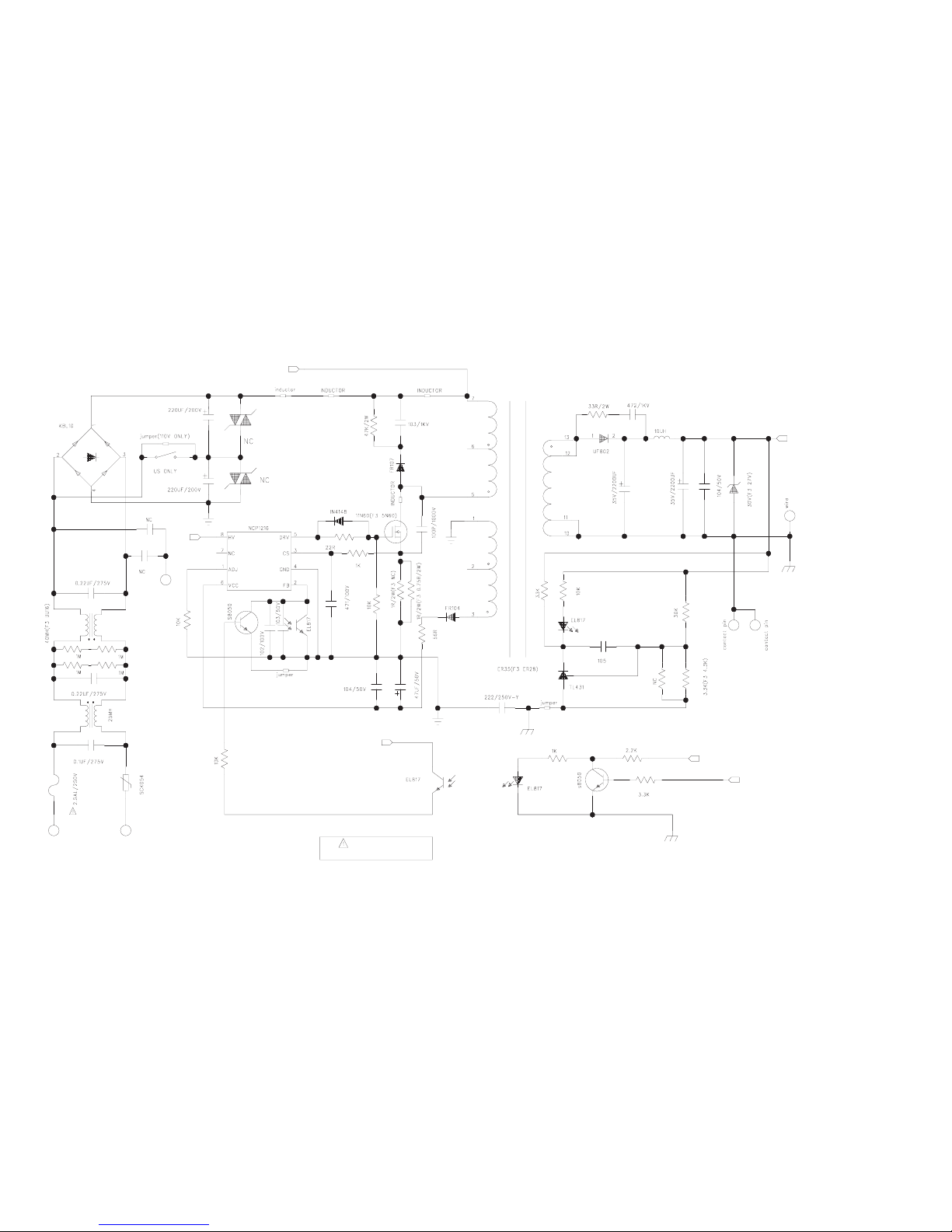
2-2
Standard schematic diagrams
<SMPS section 1>
C939
L909
D903
R906
WIRE1-2
R907
L902
L901
L
N
F901
RT901
R933
Q909
C909
C940
U902-B
C908
R937
R943
R939
R908
C910
Q902
R913
R945
R912
R911
PIN4
PIN5
R910
D905
D921
C916
C915
C913
J909
D902
PRM-GND
C901
C902
R902
R904
R901
R903
C903
C936
C935
RV901
RV902
U901
VCC-H
PRM-GND
C906
U907-A
SEC-GND
STB+5V
ECO
R936
R935
L906
C912
D905
R909
PVCC
SEC-GND
U902-A
C917
J904
T901
C937
U903
R934
SEC-GND
PRM-GND
U907-B
VCC-L
C911
D904
R944
R905
Q901
C907
L907
L905
P+
J901
C905
SW901
J910
D901
With respect to risk of fire or
electrical shock.
Parts that are shaded are critical
NOTE)
Warning
Page 43

2-3
<SMPS section 2>
R928
R926
R927
PIN3
J908
STB+5V
R930
C928
R924
C932
Q906
C930
R921
R922
C927
C926
R925
C925
C924
-27V
R946
WIRE1-1
D910
C923
C921
D922
C919
J911
R917
R916
C938
D907
R915
C918
Q908
J906
R931
CN904
CN903
SEC-GND
-27V
SEC-GND
CN902
C931
D917
J907
D918
R923
Q905
D916
SEC-GND
D913
SEC-GND
D919
L904
D911
D912
D915
C929
SEC-GND
R929
C933
U905-A
U906
SEC-GND
C914
PRM-GND
PRM-GND
D908
R940
D909
T902
C922
VCC-H
R919
Q903
VCC-L
U905-B
C920
U904
R941
L911
J903
P+
To DISPLAY section CN502
To MICOM section CN601
To MICOM section CN603
PVCC
ECO
Page 44

2-4
<MAIN section>
C845
C846
CP25
CP26
U804
R866
Q814
C844
C843
C842
C841
R873
L822
L823
L821
L820
IPOD2_RIN
IPOD1_RIN
UR_TXD
UR_RXD
R874
R875
R876
R877
D801
C856
DVD_DAT
UR_FROM_IPOD1
UR_TO_IPOD1
ST+5V
R869
CD/IPOD_SEL
Q815
U805
R868
CD-DVD_ON
IPOD_SELECT
A+12V
IPOD1_RIN
IPOD1_CVBS_IN
IPOD1_DET
UR_FROM_IPOD1
UR_TO_IPOD1
IPOD1_SLEEP_DET
IPOD1_SET
IPOD2+5V
VGND
C850
C852
EC811
R855
Q813
IPOD2+5V
R858
R857
R856
Q811
F801
D+5V
DGND
VGND
T74
C860
C861
EC813
C855
C823
C822
R867
T104
CN803
T112
IPOD2_RIN
A+12V
IPOD2_DET
UR_FROM_IPOD2
UR_TO_IPOD2
IPOD2_SLEEP_DET
IPOD2_SET
DGND
VGND
CN804
T113
IPOD_IC_NREST
DGND
R863
R864
R865
MCU_SDA
MCU_SCL
C824
C825
IPOD1+5V
C851
C849
DGND
U803
F802
EC810
Q810
D+5V
R853
Q812
R854
R852
R851
C853
C851
R859
FB830
ZD810
C857
To This sheet
To This sheet
To This sheet
To This sheet
To This sheet
To This sheet
To This sheet
IPOD2_CVBS_IN
To This sheet
To This sheet
To iPOD section CON801
To iPOD section CON802
DVD_CLK
To VIDEO section
T60
T57
T58
T59
T61
IPOD1_LIN
To VIDEO section
IPOD1+5V
T73
T65
T64
T63
T62
T32
T34
T35
T36
T68
T37
T38
T39
T40
T41
IPOD2+5V
To VIDEO section
IPOD2_LIN
To MICOM section
To MICOM section
To MICOM section
To MICOM section
IPOD2_LIN
IPOD1_LIN
T33
ST+5V
To VIDEO section
To MICOM section
To MICOM section
T96
CP24
IPOD_R
IPOD_L
IPOD_SELECT_A/B
IPOD2_ON
To MICOM section
IPOD1_ON
+3V6
To MICOM section
To AUDIO section
Page 45

2-5
<AMP section>
RF10
RF09
T101
T100
T66
T99
RF12
T11
T10
T9
T8
CF01
C737
C736
C735
C734
C779
R726
C729
VDDS
R703
R702
C719
C717
R706
C718
R708
C720
R707
R704
VDDS
C728
R722
R723
T2
QA02
CP32
CP27
CP29
C742
T3
T4
T1
T14
ZD701
R718
C724
C725
PGND
UNPLUG_MUTE
+25V
ZD702
Q701
D702
R724
R725
ST+25V
L701
L703
L702
PGND
L704
C792
C733
C791
C732
C790
C731
C789
C730
SPK_L_+
SPK_R_+
L705
L706
C783
C782
MGND
RF13
CN610
PGND
RF01
QF01
RF02
MGND
RF04
RF11
CF05
RF03
QF03
CF06
CF02
RF05
RF06
RF07
DF03
RF08
DF02
CF07
SPK_L_+
CF08
SPK_R_+
DF01
M+12V
C726
C727
C793C794
C703
C702
QA01
LA01
RA15
CA04
U610-B
RA14
QA03
RA13
RA12
RA11
LINE_MUTE
CA07
ST+5V
CA08
RA10
RA09
+12VV
U610-A
RA08
VREF
RA06
AGND
CA02
VREF
RA03
RA02
CA06
+12VV
CA01
RA01
A+12V
U609-B
SUB_L
CP31
RA07
CA03
RA05
+12VV
RA04
U609-A
SUB_R
+25V
PGND
R721
C701
EC701
AMP_MUTE
UNPLUG_MUTE
D701
AMP_STB
Q703
R720
R717
R716
R719
C706
C705
Q702
C711
R701
C710
C722
C704
U608
C714
T12
C713
C708
C723
C709
R705
R709
R710
C712
R712
R713
R715
C707
R714
C716
C715
C721
Q706
R711
A+12V
PRE_R
PRE_L
R727
R728
R729
R730
To MICOM section
To AUDIO section
To MICOM section
To MICOM section
To AUDIO section
To This sheet
To This sheet
To MICOM section
To VIDEO section
AM_HOP
CP30
CP28
CA05
SUB_OUT
PGND
PGND
SVR
CF03
MGND
PGND
PGND
SCREW1
SCREW2
JK601
MGND
CN612
Page 46
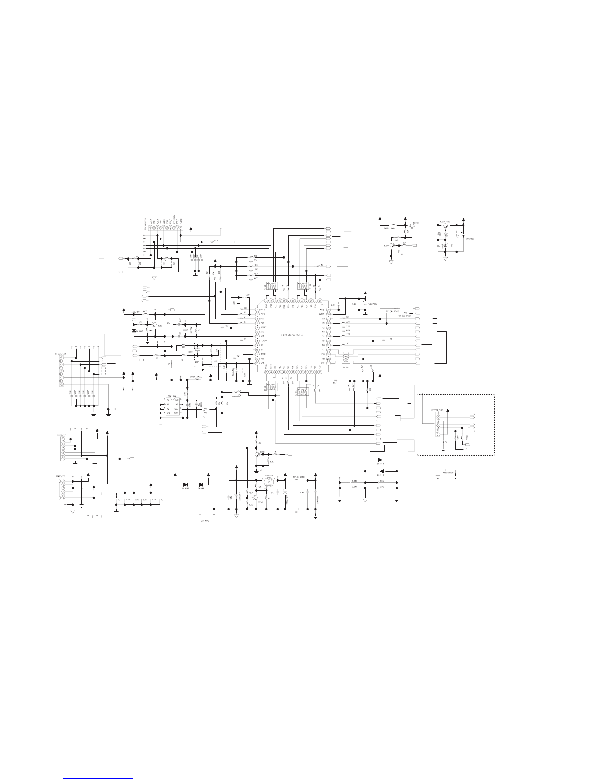
2-6
<MICOM section>
R614
R615
C636
C603
R616
T71
R610
T88
T87
T90
T86
T85
T84
T83
T82
T81
C610
R652
R653
R654
C629
C628
C627
C626
CN604
C625
C624
C623
C622
C645
C644
C643
C642
C641
C640
T26
T25
T24
T23
T28
T27
T29
T47
T46
T21
T20
P601
P602
EC605
C617
T93
EC610
EC607
T98
R668
R667
R666
R640
R641
R645
R644
D601
T92
C608
C607
T97
X601
R656
R639
C602
EC601
C601
R619
R620
R621
R623
R622
R624
R625
R628
R627
R629
C621
ZD601
R674
C635
R673
R669
IPOD1_DET
IPOD2_SET
IPOD2_SLEEP_DET
IPOD2_DET
IPOD_SELECT_A/B
UR_TO_IPOD2
DVD_STB
UR_RXD
DVD_DAT
DGND
L611
CN605
+3V6
R637
R638
EC608
+5V_TUNER
Q607
Q606
R672
R671
Q605
R670
TU+12V
L603
A+12V
ECO_STBY
VFD_CLK
VFD_STB
HP_DET
TUNER_ON
R643
HOP
C605
EC602
+3V6
C604
U601
R636
R635
R634
R633
R632
R631
R630
RN05
R626
R606
R609
C638
R613
R612
R618
R617
C609
CN602
U602
L601
+3V6
C637
R608
X602
R607
R611
T95
T94
UR_FROM_IPOD2
UP_TO_IPOD2
RESET
TXD6
SCLK_UPGRADE
IPOD_IC_NREST
LINE_MUTE
SYNC
TRAY+
TRAY-
OPEN_SW
CLOSE_SW
CD_DVD_ON
IPOD1_SET
PGND
D605
D604
C634
C633
C632
C631
MGND
M+12V
FB601
C619
R660
Q603
R662
ECO_STBY
L602
A+12V
R661
C620
Q601
C618
R665
Q602
R664
R678
R663
+12V
+3V6
D603
D602
ST+5V
+3V6
C616
C614
C611
C612
C613
C615
T91
+12V
PGND
CN603
DGND
+25V
MGND
CN601
ST+5V
D+5V
T89
MGND
KEY_2
VFD_STB
A+12V
ST+5V
SCLK_UPGRADE
HOP
AM_HOP
R605
R604
R603
R602
R601
R646
R647
R648
R649
R650
R651
TUNER_PULSE
MGND
R655
RESET
C606
R659
Q604
T103
R658
R657
TUNER_PULSE
R676
T17
T15
T13
T16
T22
T19
T18
R675
To DISPLAY section CON501
To SMPS section 2 CN904
To This sheet
To This sheet
To This sheet
To This sheet
To This sheet
To This sheet
To This sheet
To SMPS section 2 CN903
To This sheet
To DISPLAY section CON1
To This sheet
TUNER_LIN
To AUDIO section
TUNER_RIN
To AMP section
+3V6
IR_RX
AMP_STB
AMP_MUTE
EC604
To AMP section
FMLD0
VFD_CLK
VFD_DATA
KEY_1
IR_RX
SYSTEM_ON
MCU_SCL
MCU_SDA
MCU_3V3
+5V_TUNER
HP_MUTE
VFD_DATA
KEY_1
KEY_2
RN01
RN02
RN03
RN04
ST+5V
To MAIN section
To AMP section
IPOD1_ON
IPOD1_SLEEP_DET
TUNER_ON
To AUDIO section
DVD_CLK
UR_TXD
UR_FROM_IPOD2
To MAIN section
To VIDEO section
To MAIN section
IPOD2_ON
To MAIN section
To VIDEO section
+3V6
FMLD0
RXD6
+3V6
Page 47
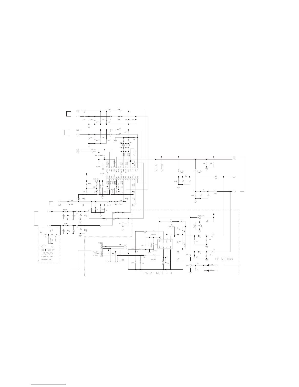
2-7
<AUDIO section>
EC710
ZD704
CP04
C774
C773
C772
C771
C788
C787
C784
EC711
T75
T79
T78
T5
T80
T77
T76
C761
R756
R790
R791
C795
R761
R760
C762
R757
CP19
CP17
EC703
ZD703
B702
C745
C748
C746
B706
C785
C747
C777
B705
B704
B703
B701
B711
B712
B708
B710
C778
C786
B707
B709
C752
C751
C750
C749
C741
C769
R768
C780
SUB_L
SUB_R
CP07
CP06
L707
C781
PRE_R
L708
C770
A+12V
R770
Q707
R773
R774
R775
C775
CP02
C776
R778
CP03
UNPLUG_MUTE
HP_MUTE
D705
D703
R781
Q708
R780
R782
C744
EC713
R786
R784
R783
U605
CP01
EC712
R787
C743
R785
AUX_R
AUX_L
HP_DET
CN606
R750
C757
R751
C758
CP11
CP10
R752
R753
C760
C759
C739
C738
R755
C797
R792
R789
A+12V
AUX_R
AUX_L
EC704
R759
R758
C740
R741
R740
EC704
Q704
A+12V
U604
EC704
C768
C767
R767
R766
MCU_SCL
MCU_SDA
CP08
R765
R764
C756
R749
C755
CP09
R748
C764
R763
C763
R762
IPOD_L
R746
C753
R747
C754
C766
R745
C765
R744
R743
R742
To DISPLAY section CN301
To MAIN section
To MICOM section
IPOD_R
TUNER_RIN
TUNER_LIN
To This sheet
CD/DVD_LIN
To VIDEO section
CD/DVD_RIN
CP16
CP18
CP20
R754
CP21
C796
CP22
CP23
CP14
CP15
CP05
CP13
CP12
To This sheet
R769
R772
R771
R788
EC709
R777
R776
R779
To MICOM section
PRE_L
To AMP section
Page 48

2-8
<VIDEO section>
T115
T114
T109
T110
T111
T116
T106
T108
T107
T105
CVBS_OUT
DVD_CVBS
VGND
T102
LV02
T6
T50
D+5V
A+12V
DVD_DAT
DVD_STB
SYNC
CD-DVD_ON
CLOSE_SW
OPEN_SW
TRAY-
TRAY+
CN607
MGND
DGND
CN608
C630
CD/DVD_LIN
C649
C648
C647
C646
MGND
JK602
SUB_OUT
CV12
JK604
JK605
CV05
JK603
CV13
L827
L826
L825
L824
CVBS_OUT
CV01
CV02
LV01
CV03
RV02
RV01
RV07
D+5V
CV04
RV06
U612
D+5V
RV09
DVD_CVBS
CV07
D+5V
IPOD2_CVBS_IN
IPOD_SELECT
CD/IPOD_SEL
U611
To This sheet
To This sheet
To This sheet
To MPEG section CN105
To MPEG section CN101
CN609
To MAIN section
IPOD1_CVBS_IN
To AUDIO section
CD/DVD_RIN
T42
T31
T30
T43
T44
T45
DVD_CLK
To MICOM section
T49
T51
T52
T53
T54
T55
T56
CV06
To AMP section
MGND
DV02
DV01
CA11
T70
CV11
CV10
RV10
T48
CV08
CV09
T72
RV08
RV03
RV04
RV11
QV01
RV05
T67
Page 49

2-9
<DISPLAY section>
R530
R531
DIM_OFF
+8V_LED
DIM_OFF
JW511
C528
C527
JW521
R536
JW522
JW513
JW509
C536
C535
JW523
JW507
JW524
JW508
R532
R534
C534
JW516
JW513
R535
JW509
JW506
R533
C517
C518
C519
C524
ZD506
C523
GND
VFD501
G1
G3
G2
G5
G4
G6
G8
G7
G10
G9
G12
P16
P15
P8
P10
P9
P11
P14
P13
P1
P3
P2
P5
P4
P7
P6
C526
C525
U501
G3
G2
G1
P14
P15
P13
P10
P11
P1
P3
P2
P5
P4
P7
P6
P9
P8
JW519
F1
F2
R539
JW504
R538
R537
C522
ZD502
1
2
ZD501
C520
C521
0.1U
-25V
R542
D501
FB505
FB504
FB503
FB502
R528
D502
LED+
JW514
Q505
C533
C532
C531
R526
C530
R525
JW515
R524
C515
R523
C516
JW501
C529
LED501
R521
+5V_VFD
R520
Q503
JW503
C512
KEY_2
GND
R543
JW520
FB512
R516
JW518
R517
R514
R515
SW508
R513
SW509
SW511
SW510
SW512
SW514
SW513
VFD_DATA
VFD_CLK
VFD_STB
+5V_VFD
C511
KEY_1
FB511
GND
SW501
R508
R507
SW503
SW502
R509
JW505
SW505
SW504
R511
R510
SW507
SW506
JW517
CON503
R541
CON504
CON301
FB304
FB303
JK301
GND_ESD
FB302
JW301
L304
L303
GND_ESD
FB301
FB308
FB307
JK302
R312
C323
C322
TP31
CON302
L305
R315
JW305
U301
R305
D301
R314
R313
R323
R310
C321
R306
C320
C319
C318
R309
C317
C316
R304
C315
Q301
JW302
R303
C314
R302
JW303
JW304
R307
R308
GND
GND_ESD
JK303
FB305
C305
FB306
R301
CON1
CON2
C514
C513
ZD503
IR501
R519
R518
FB506
+8V_LED
+5V_VFD
ZD505
R501
R502
C507
Q501
JW502
C506
JW512
C508
F2
FILAMENT
F1
FILAMENT
-25V
R544
Q502
JW510
C509
FB509
ZD504
C510
R505
R504
FB508
FB507
R503
C505
C503
C502
ESD
GND
CON501
CON502
+12V_VFD
+5V_VFD
(100mA)
KEY_1
IR_RX
KEY_2
VFD_STB
VFD_CLK
VFD_DATA
To MICOM section CN602
To SMPS section 2 CN902
To USB & SD section
(Except UX-F3BC,BJ)
CN203
To This sheet
To This sheet
To This sheet
To This sheet
To This sheet
To This sheet
To This sheet
To This sheet
To This sheet
To This sheet
To This sheet
To AUDIO section CN606
To MICOM section CN605
To iPOD LED section CON202
LED502
LED505
C501
C504
C313
C307
C308
C301
C302
C306
C309
C310
C311
C303
C304
IR_RX
Q507
LED+
R540
STBLED_ON
LED_ON
LED503
IPOD_LED_ON
R522
P12
P12
P16
G11
R527
LED504
R529
Q504
Q506
R512
IPOD_LED_ON
LED_ON
STBLED_ON
FB510
R506
Page 50

2-10
<USB & SD section (Except UX-F3BC,BJ)>
CN201
R216
R215
R214
R213
R212
R211
R210
FB201
SW202
SW201
R201
R202
L201
F201
R209
R208
R207
R206
R205
R204
R203
C205
CN203
RS2
RS1
JK201
C206
C201
RS8
RS7
RS6
RS5
RS4
RS3
D_GND
JK202
To DISPLAY section CN503
To MPEG section CN108
Page 51

2-11
<MPEG section>
11
1
C179
C180
Q106
Q107
IC106
D+D-_CONNECT
C111
C112
L101
FB100
C139
R123
C140
SDCARD+MD
C128
C126
RZ3
RZ2
R153
C182
R135
C184
C183
VCC_ADAC
C129
C132
R122
C131
C130
C186
TR-_CD
C185
C136
C133
C187
C134
FB120
USB_VCC
USB_DP
USB_DM
C138
L102
PLLVCC3
PLLVCC1.8
HOME
C148
R129
R126
C137
D103
C135
R120
C156
C147
C146
C158
MD8
MD9
MD7
MD6
MD5
MD3
MD2
MD1
MD0
C189
C188
RST
C110
C109
C173
VDD3
R105
C106
C196
C102
C104
C162
Q102
C152
C151
RN102
RN101
MD5
MD6
MD7
MD4
MD1
MD2
MD3
MD0
R141
R4
Q100
R173
CARD_VCC3
C177
TCO
BIAS
MUTE
M+5V
SCO
OR
OR
FB128
FB127
LOAD+
LOAD-
CLK/UR_TO_CD
DAT/UR_FROM_CD
CD_ON
TR+
TR-
AOUT_R
AOUT_L
DGND
DGND
AGND
+12V
F124
CN105
F122
F121
+5V
F108
F109
FB117
FB116
FB121
FB112
FB113
CN101
DGND
CN103
DGND
CN104
DGND
F-
F+
T+
T-
C168
IC104
SLED+
SLED-
C169
R158
R159
F-
SP-
R3
F110
C127
DGND
C170
4.7R
SPDC0
FC0
VCC3
TR+_CD
C163
C150
C149
C155
DGND
R119
D104
C174
C165
C166
TC0
C167
C157
SC0
SPDC0
VCREF
F-
T+
T-
F+
MD
MD
CDE
CDF
DVDA
DVDB
DVDC
CARD_SENSE
D3
D4
D1
+5V
CN108
USB_D-
USB_D+
D+D-_CONNECT
Q2
Q1
C4
C125
DGND
USB_DM
R171
Q201
Q202
R172
USB_DP
AGMD
DGND
VCC3
DGND
FB119
FB115
VCC_VDAC
FB101
AGND
VCC_CARD
CARD_RST
DGND
F119
F120
C141
C123
F118
C124
C122
SD D1 / MMC WP
SD D2 / MMC RST
CARD SENSE
SD CLK / MMC SCK
SD D3 / MMC CS
SD CMD / MMC SO
SD D0 / MMC SI
FB103
FB109
FB102
FB105
FB108
FB107
FB104
MD13
DGND
F106
VCC3
SDRAM
VCC
C118
C181
C120
C119
C121
MD9
C114
RN103
RN104
C113
C116
C115
R110
C117
DGND
DGND
IC103
C7
R21
C6
+12V
R30
R24
C10
+12V
R114
AOUT_R
R28
AOUT_L
C9
IC107
R115
C3
C8
C5
R9
AGND
DGND
DGND
DGND
C194
AGND
C193
R169
Q3
DGND
TR-_CD
D111
R156
ROM_SCK
ROM_DQ1
ROM_VCC
ROM_DQ3
ROM_SCK
ROM_DQ1
IC105
DGND
R163
ROM_CE
ROM_DQ0
ROMDQ2
DGND
DGND
ROM_DQ0
ROM_VCC
VVCC1V8
C105
DGND
D101
R103
C103
CD_ON
DGND
R167
Q104
R166
R168
R165
Q105
IC101
IC102
C101
DGND
R101
C100
R102
VCC3
VCC3
VDD3
FB114
DGND
R106
F103
ROM_VCC
Q101
R107
R109
R108
C108
C107
Q4
D110
R133
Q103
R125
DGND
R127
R132
CD_L
LOAD+
LOAD-
C178
R130
Q109
Q108
R128
DGND
F101
D2
CLK/UR_TO_CD
DAT/UR_FROM_CD
R7
R8
DGND
VVCC1V8
R199
FB118
need?
C1
C2
ROM_DQ1
ROM_DQ0
ROM_CE
R2
R1
R155
R6
R154
R5
DQ1
DQ0
SD_D2/MMC_RST
SD_D3/MMC_CS
SD_CMD/MMC_S0
SD_CLK/MMC_SCK
SD_D0/MMC_SI
SD_D1/MMC_WP
R150
R149
R147
R148
DGND
BIAS
VCREF
RF3.3V
R142
RF3.3V
R143
FB125
VCC3
DVDD
VCREF
CDE
CDF
DVDA
DVDB
DVDC
DVDD
R144
DGND
R145
FB124
CN102
C160
C161
R118
C159
To USB & SD section
(Except UX-F3BC,BJ)
CN201
To This sheet
To This sheet
To This sheet
To This sheet
To This sheet
To This sheet
To This sheet
To This sheet
To This sheet
To This sheet
To This sheet
To This sheet
To This sheet
To VIDEO section CN609
To VIDEO section CN607
+5VV
CD_M
+5VV
OPVIN
ID3
+5VV
R164
R104
C172
C171
R32
ROM_SCK
CLOSE
OPEN
TRAY++
MUTE
C164
FC0
OPVIN
OPVIP
CDLD
X101
TRAY--
VCC1.8V
MD4
MD15
MD14
MD13
MD12
MD11
MD10
TR+
D102
TR-
TR+_CD
TP1
TP3
TP4
CD_R
CD_L
CD_R
CD_L
ID3
CD_R
R27
C12
C13
R26
R25
C11
R31
C21
C20
R11
R10
R22
R23
C16
C18
C19
C15
R29
C17
CD_R
C14
CD_L
MD11
MD10
MD8
MD12
MD14
MD15
RZ1
RZ4
RZ5
RZ6
R20
R19
R13
RZ7
RZ8
R12
R15
R14
R16
R17
R18
Page 52

2-12
<iPOD section>
P65
P64
P63
P62
P61
P59
P54
P57
P58
P55
P56
P52
P53
P50
P51
P46
P47
P44
P45
P43
P41
P40
P39
P38
P37
P36
P35
P34
P33
P32
C1
C2
C3
C4
P28
C871
R809
R807
C870
R808
R806
R805
C826
C873
C872
R822
C833
C832
C831
C830
C881
R846
C883
C882
C884
C877
C876
C875
C874
R842
R840
C840
R841
R839
R827
IP801
R818
P29
C809
C808
C807
R815
R814
R836
C818
C817
C816
R833
IP802
R832
C835
R803
C819
CON801
C821
R804
C820
U801
C829
C828
R820
R819
C827
C834
C836
R821
P16
P15
P14
P13
P12
P11
P10
P9
P8
P7
P6
P5
P30
R826
R825
C837
C838
C839
C878
U802
C880
C879
R844
R843
C887
R845
C886
C885
P31
CON802
P18
P17
P20
P19
P22
P21
P24
P23
P26
P25
P4
P27
P3
P2
P1
R835
R834
Q804
Q803
R831
R830
FB814
R829
R824
R823
R828
C815
C814
C813
C812
FB813
FB812
FB816
R838
C811
C810
FB811
FB810
FB808
R817
R816
Q801
Q802
R813
R812
FB807
R811
R802
R801
R810
C806
C805
C804
C803
FB806
FB805
R837
FB815
C802
C801
FB804
FB803
FB801
To MAIN section CN803
To MAIN section CN804
Page 53

2-13
<iPOD LED section>
CON202
CON204
C216
LED206
C214
ZD202
R213
LED204
LED205
TP33
C209
TP32
C208
ZD201
R211
LED203
C213
LED201
C207
LED202
R210
TP30
TP31
TP37
TP38
TP39
C212
C211
To DISPLAY section CN504
TP36
CON203
R212
C215
C210
Page 54

2-14
Printed circuit boards
<MAIN Board>
(Lead free solder used in the board (material : Sn-Ag-Cu, melting point : 219 Centigrade))
(forward side)
(reverse side)
C768
R763
C793
RF09
RF10
C710
RF13
D703
C624
C723
C737 C736 C735 C734
R724
JK601
C783
L705
C730
Q701
D702
D701 D705
L706
C782
C789
C731
CF07
CF08
EC701
C790
C728
C706
R725
C779
R720
C633
ZD702
L701
L702
R719 R717
R715
R714
Q702
R716
Q703
C726
R722
C705
C703
R784
Q605
R771
C715
EC711
R727
R729
R718
C707
L707
L708
C744
EC710
EC713
EC712
R786
C784
R778
R777
C776
R776
R775
C743
R785
R774
R773
U605
R788
R772
B710
C780
C716
C720
C724
R713
C711
ZD701
R707
C712
R712
R730
C774
C725
R728
R768
C772
C771
C769
C770
C773
C749
R709
R710
R708
C718
R701
C709
EC704
C788
C781
B711
C767
B712
C786
C751
C750
R672
R671
R780
R779
C775
R769
R782
R764
R765
Q708
R770
Q707
ZD704
R781
C739
C738
L603
R761
C778
B707
B708
C787
B709
C758
R760
C752
R751
R750
C757
C756
R749
C763
R762
R674
R759
R758
P602
R783
R787
CN606
P601
C635
EC709
ZD601
Q606
R673
EC608
Q607
C621
C623
R670
R669
R675
C634
C611
R876
R875
C854
R726
R615
C636
RV08
R664
R663
R665
Q602
U612
JK604
JK602
CA11
JK603
RF06
RF08
RF07
DF03
CF02
RF05
CF06
C732
C791
C729
DF02
RF11
CN610
RF12
RF04
DV01
DV02
RF01
RF02
QF03
C733
C792
RF03
QF01
CF03
C794
C727
R723
L703
U608
C702
R721
L704
L602
EC607
CV02
CV01
CF01
CN612
CV03
LV01
C701
CF05
DF01
RV02
RV04
C619
RV05
RV11
CV04
EC610
QV01
RV01
RV03
RV07
RV06
EC605
R859
CN603
C617
C742
FB601
CA01
CA02
ZD810
C603
FB830
Q601
R678
C857
U602
R616
C649
CV06
L826
U611
CV05
RV10
CV07
RV09
LV02
CV09
L827
JK605
CV08
CN608
C647
C646
C648
R638
C795
R869
U805
R868
C618
Q815
C614
R618
R617
R614
R877
CN609
C856
R874
R637
CN607
D801
R645 R651
L601
Q813
EC811
C755
R867
R857
CN803
R620
C632
C631
R755
R754
R608
R653
C746
ZD703
C745
Q706
C721
R711
D605
C719
C717
R705
R706
C714
C713
D604
C704
C722
C741
R766
R767
U604
B703
B702
B701
R704
R702
R703
R863
C853
C708
C638
C637
C607
C608
R619
R613
R612
R624
EC703
Q704
C740
R611
R741 R740
R654
C785
C777
B704
C748
C764
B706
C747
B705
R748
C765
C754
R747
R746
C766
C753
R752
R753
C760
C759
R756
R757
C761
C762
C845
C823
C861
C843
R743
R744
C846
R742
R745
R657
L821
L823
RN01
C609
R604
R864
C825
U803
R621
X602
C824
R865
X601D601
R659
C602
RN03
EC601
RN04
R656
R639
C601
R602
U601
R631
R607
R601
R658
EC604
Q604
R603
C610
R605
R667
C606
CN804
CN605
R610
R606
R666
R668
R609
R652
RN02
R627
C849
C616
R633
R632
C627
C626
C629
R655R676
C622
C625
U804
CN604
C628
C841
C852
C842
C844
R873
C855
EC813
L820
C850
L822
C860
C822
F801
R855
R866
R630
C620
R660
R623
R622
R625
R636
R634
R626
R635
EC602
R629
RN05
C605
D603
C604
D602
C630
L611
CN601
Q603
Q814
R662
R648
R647
R641
R650
R649
R643
R644
R646
R640
R628
R856
R853
R858
R851
CN602
R661
C641
C640
R852
Q812
C643
C642
C644
C645
R854
EC810
F802
C851
Q811 Q810
C612
CP20
U609
CP32
CP17
CV11
CV13
L824
L825
LA01
C797
C796
CP16
R790
R792
RA12
RA13
RA01
CA05
CP27
RA15
RA14
CA04
CA08
C615
C613
QA03
CP30
CA03
CP31
U610
CP05
CP06
RA08
CA06
CP15
CP25
CP10
CP08
CP03
CP02
CP01
CP24
CP04
CP22
CP23
CA07
RA09
RA10
CP19
CP18
RA04
RA05
RA07
RA06
CP29
CP07
CP09
CP12
CP13
CP11
CP26
CP21
CP28
QA02
RA03
RA02
QA01
R789
R791
CP14
RA11
CV12
CV10
Page 55

2-15
R940
R902
R904
R903
R901
C911
C940
C908
C909
R907
R937
R905
U901
C923
R944
D902
C939
C919
C920
C938
D922
D910
R941
Q909
R913
R946
R933
Q902
R934
R925
R935
R930
R936
R926
R929
C933
R927
R928
R911
R945
C917
R912
R910
C916
R921
R922
Q908
R923
R924
Q906
R931
(reverse side)
L201
RS8
RS7
RS5
RS6
C205
C206
RS4
RS3
SW202
C202
CN203
CN201
F201
TP1
JK201
SW201
JK202
TP20
RS1
R202
R201
R214
C201
R216
R212
FB201
R210
R215
R207
R204
R203
R213
R211
R209
R208
R206
R205
(reverse side)
(forward side)
<SMPS Board>
(Lead free solder used in the board (material : Sn-Ag-Cu, melting point : 219 Centigrade))
(Lead free solder used in the board (material : Sn-Ag-Cu, melting point : 219 Centigrade))
<USB board
(Except UX-F3BC,BJ)
>
RS2
J907
D918
PIN4
PIN1
D921
PIN5
CN903
J908
CN904
J906
U903
L906
R909
C914
U902
C913
C915
J904
C912
D905
C928
C925
D919
L904
U906
C924
U907
D911
U905
CN902
D913
D916
D915
PIN3
C927
C932
C926
C929
Q905
C930
C931
D917
D912
WIRE1-1
C937
T902
L902
D904
J909
C910
F901
SW901
L909
Q901
R908
J903
T901
C918
L905
L907
R915
D903
R906
C907
U904
RV902
R939
C906
R943
J910
J901
J
9
1
1
R916
RV901
N
L
C901
C902
RT901
L901
C935
C921
Q903
C922
D907
D908
D909
L911
C905
D901
R917
R919
C903
C936
WIRE1-2
(forward side)
Page 56

2-16
(forward side)
CN101
C21
IC107
C177
C172
R163
C171
R156
IC103
C181
C180
F119
C182
C184
C183
C117
F118
F120
C120
C118
C121
R20
Q202
R172
D1
D3
R17
R18
Q2
C4
R13
RZ7
R19
Q201
Q1
R108
R107
FB114
D4
R16
R14
Q101
C116
R109
C107
C196
R135
R15
R12
R171
D102
R106
F103
R105
C106
FB101
FB109
FB102
FB105
FB103
CN108
Q100
FB108
FB107
FB104
RZ6
C125
RZ2
RZ1
RZ3
FB127
RZ8
C126
R4
CN103
RZ5
R173
RZ4
FB128
C137
RN103
RN102
C187
C138
C185
FB118
IC106
F106
C113
C115
C119
C114
C112
R110
RN104
C132
C123
FB120
C124
C190
C122
C141
FB115
C131
R122
C129
C133
R129
C134
C109
C130
FB100
C139
C140
R123
R126
C136
FB119
L102
X101
C188
C189
F108
FB113
FB112
FB116
F109
C16
C7
R8
R7
FB121
FB117
C194
R115
R21
R27
R114
C13
C17
R133
R125
R132
C146
R6
R32
C108
RN101
C111
C110
R199
C173
R155
R2
R1
IC105
C2
C1
C163
C162
C166
R5
R154
R150
R149
C165
R148
C174
C157
R143
R144
C149
C156
C148
C147
C167
Q102
C164
C160
C152
C151
R159
Q109
Q106
R127
C179
C170
R128
C178
Q107
CN104
C169
IC104
C168
R158
Q103
C103
C158
C150
C104
C161
FB125
C155
R142
L101
CN102
R120
R119
FB124
R145
C159
R118
C19
C20
R11
R10
R9
R31
R30
C6
F124
C5
C3
C8
C18
IC102
R104
R103
R23
R22
C9
C105
IC101
CN105
F122
R169
F110
F101
R3
D104
D2
Q3
D111
D110
D103
R166
R167
Q4
Q104
Q105
R168
F121
R165
C100
D101
R164
C101
C127
C193
C12
C11
R25
R28
R29
C14
C15
(reverse side)
CN101
TP2
C134
C109
C104
C12
C20
C14
C150
C6
C158
C18
C8
C161
C127
D101
R164
C102
CN105
C124
C130
X101
C122
C118
C151
CN102
C168
D2
R3
Q106
CN104
Q107
C111
C172
C106
CN103
Q109
C177
R127
C163
C178
Q108
Q100
C126
CN108
C816
C812
C813
C814
C815
C811
P29
C810
FB808
R838
FB816
FB813
FB812
R823
C817
R824
C818
IP802
R830
FB814
R832
R835
Q803
R834
Q804
C874
C884
UX-F3-01
UX-F3 IPOD PWB
3703-091460130
Pb
VGND
CVBS2
DGND
DGND
IP2_5V
IP2_5V
DET2
ACC2
ADET2
RX2
TX2
A12V
AGND
L2_O
CON802
R846
C807
C804
C805
R802
C809
R801
C801
C871
C833
Q801
Q802
C802
FB801
FB815
FB804
FB803
C808
R814
R811
R810
FB806
FB805
R812
FB807
IP801
R815
R813
TX1
ACC1
ADET1
CON801
R822
R1_O
AGND
L1_O
VGND
CVBS1
DGND
DGND
IP1_5V
DET1
RX1
C830
R821
C835
R809
C872
R819
R807
C2
C829
C828
R820
C827
C870
R805
R803
C880
C879
R844
R843
R840
C840
R808
R806
C1
C819
C873
C878
C4
R841
C837
R842
C875
R826
C876
C3
C877
C838
R839
R827
R825
U801
C834
C836
C881
C821
C831
C832
R804
C820
C826
C886
R845
U802
C887
C885
C839
C883
C882
(reverse side)
(forward side)
C213
C215
R212
C209
C216
R213
C210
C214
C212
C207
R211
C208
C211
R210
(reverse side)
<MPEG board>
(Lead free solder used in the board (material : Sn-Ag-Cu, melting point : 219 Centigrade))
<iPOD board>
(Lead free solder used in the board (material : Sn-Ag-Cu, melting point : 219 Centigrade))
<LED board>
(Lead free solder used in the board (material : Sn-Ag-Cu, melting point : 219 Centigrade))
R141
R153
Q108
R130
C135
R147
R102
R101
C102
C10
R24
R26
FR4V7.0
R2_O
FB810
FB811
R828
R829
R831
R833
R836
C806
C803
IP1_5V
A12V
R817
R818
R816
R837
LED201
LED203
LED202 LED204
CON203
CON204
LED206
LED205
ZD202
ZD201
CON202
(forward side)
Page 57

<DISPLAY board>
(Lead free solder used in the board (material : Sn-Ag-Cu, melting point : 219 Centigrade))
(forward side)
(Display board)
LED503
CON504
LED502
SW514
JW515
D502
VFD501
JW509
JW523
Q502
ZD504
C510
LED501
SW513
JW521
CON502
JW524
JW506
ZD501
JW520
C520
JW514
JW507
SW501
JW522
LED505
JW518
LED504
JW508
JW501
JW516
SW502
JW513
JW511
C527
ZD502
C522
SW511
JW519
C525
JW510
JW504
SW512
JW512
C507
Q501
ZD503
JW526
JW525
ZD505
IR501
SW506
SW505
JW502
SW510
SW509
C317
JW503
C319
JW505
CON503
CON302
SW507
JW305
JW517
JW303
CON301
CON501
C513
JW301
SW508
CON1
Q301
C320
A2
SW504
SW503
C322
D301
JK303
JK302
JW306
CON2
JW302
C318
C313
A1
JK301
(Upgrade board)
(Jack board)
JW304
A3
(reverse side)
(Display board)
C512
(Jack board)
R314
R305
R304
R308
C315
FB305
C309
C311
C314
C306
FB302
R303
R313
FB306
C312
C302
C301
L304
R301
FB308
C308
C307
C310
FB307
FB301
C305
FB304
C303
C304
R323
R306
C316
R315
FB303
R302
R508
C531
C533
R512
R513
R511
R309
R307
C321
U301
R310
R312
C323
L305
FB506
C503
R518
C504
C508
C505
C514
L303
ZD506
C502
R507
R514
R510
FB505
R509
R544
FB502
FB510
C501
R540
C506
R541
Q507
FB504
FB503
FB512
FB511
R535
R532
R534
R533
C517
R519
R542
R502
R501
R543
C519
C518
R528
R529
R515
R531
C523
D501
R537
R524
C515
C521
R538
C524
R526
R530
R527
R536
R503
FB507
R506
C532
R523
U501
R539
R504
R525
C509
FB508
R516
C516
C536
Q505
Q506
Q504
C535
FB509
R505
C537
C526
C528
C534
R521
R517
C511
R520
R522
Q503
C530
R545
C529
2-17
Page 58

Victor Company of Japan, Limited
Home Entertainment Business Division Personal AV Operation
(No.MB743SCH<Rev.003>)
Printed in Japan
VSE
 Loading...