

Page 1
SERVICE MANUAL
MICRO COMPONENT MD SYSTEM
UX-A10DVD
UX-A10DVD
Contents
Safety precaution
Preventing static electricity
Disassembly method
Adjustment method
Maintenance of MD pickup
COPYRIGHT 2003 VICTOR COMPANY OF JAPAN, LTD.
1-2
1-3
1-4
1-39
1-47
Area suffix
UB ----------- Hong Kong
Procedures of changing the
MD pickup
Maintenance of DVD pickup
Procedures of changing the
DVD pickup
Description of major ICs
1-47
1-48
1-48
1-49~88
No.22011
Jan. 2003
Page 2
UX-A10DVD
1. This design of this product contains special hardware and many circuits and components specially for safety
purposes. For continued protection, no changes should be made to the original design unless authorized in
writing by the manufacturer. Replacement parts must be identical to those used in the original circuits. Services
should be performed by qualified personnel only.
2. Alterations of the design or circuitry of the product should not be made. Any design alterations of the product
should not be made. Any design alterations or additions will void the manufacturer`s warranty and will further
relieve the manufacture of responsibility for personal injury or property damage resulting therefrom.
3. Many electrical and mechanical parts in the products have special safety-related characteristics. These
characteristics are often not evident from visual inspection nor can the protection afforded by them necessarily
be obtained by using replacement components rated for higher voltage, wattage, etc. Replacement parts which
have these special safety characteristics are identified in the Parts List of Service Manual. Electrical
components having such features are identified by shading on the schematics and by ( ) on the Parts List in
the Service Manual. The use of a substitute replacement which does not have the same safety characteristics
as the recommended replacement parts shown in the Parts List of Service Manual may create shock, fire, or
other hazards.
4. The leads in the products are routed and dressed with ties, clamps, tubings, barriers and the like to be
separated from live parts, high temperature parts, moving parts and/or sharp edges for the prevention of
electric shock and fire hazard. When service is required, the original lead routing and dress should be
observed, and it should be confirmed that they have been returned to normal, after re-assembling.
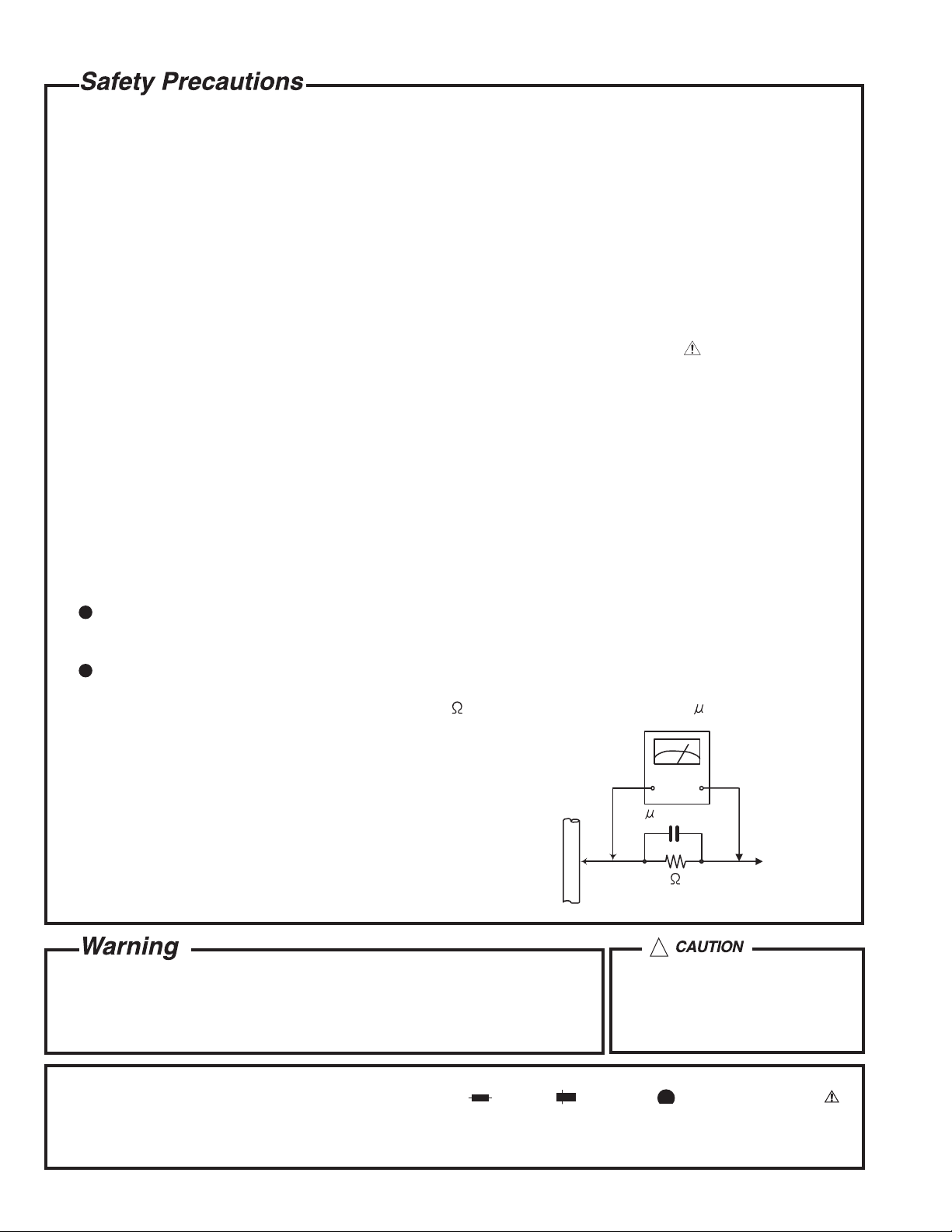
5. Leakage currnet check (Electrical shock hazard testing)
After re-assembling the product, always perform an isolation check on the exposed metal parts of the product
(antenna terminals, knobs, metal cabinet, screw heads, headphone jack, control shafts, etc.) to be sure the
product is safe to operate without danger of electrical shock.
Do not use a line isolation transformer during this check.
Plug the AC line cord directly into the AC outlet. Using a "Leakage Current Tester", measure the leakage
current from each exposed metal parts of the cabinet, particularly any exposed metal part having a return
path to the chassis, to a known good earth ground. Any leakage current must not exceed 0.5mA AC (r.m.s.).
Alternate check method
Plug the AC line cord directly into the AC outlet. Use an AC voltmeter having, 1,000 ohms per volt or more
sensitivity in the following manner. Connect a 1,500 10W resistor paralleled by a 0.15 F AC-type capacitor
between an exposed metal part and a known good earth ground.
Measure the AC voltage across the resistor with the AC
voltmeter.
Move the resistor connection to each exposed metal part,
particularly any exposed metal part having a return path to
the chassis, and meausre the AC voltage across the resistor.
Now, reverse the plug in the AC outlet and repeat each
measurement. Voltage measured any must not exceed 0.75 V
AC (r.m.s.). This corresponds to 0.5 mA AC (r.m.s.).
0.15 F AC TYPE
1500 10W
Good earth ground
AC VOLTMETER
(Having 1000
ohms/volts,
or more sensitivity)
Place this
probe on
each exposed
metal part.
!
1. This equipment has been designed and manufactured to meet international safety standards.
2. It is the legal responsibility of the repairer to ensure that these safety standards are maintained.
3. Repairs must be made in accordance with the relevant safety standards.
4. It is essential that safety critical components are replaced by approved parts.
5. If mains voltage selector is provided, check setting for local voltage.
Burrs formed during molding may
be left over on some parts of the
chassis. Therefore, pay attention to
such burrs in the case of
preforming repair of this system.
In regard with component parts appearing on the silk-screen printed side (parts side) of the PWB diagrams, the
parts that are printed over with black such as the resistor ( ), diode ( ) and ICP ( ) or identified by the " "
mark nearby are critical for safety.
(This regulation does not correspond to J and C version.)
1-2
Page 3
Preventing static electricity
UX-A10DVD
1.Grounding to prevent damage by static electricity
Electrostatic discharge (ESD), which occurs when static electricity stored in the body, fabric, etc. is discharged,
can destroy the laser diode in the traverse unit (optical pickup). Take care to prevent this when performing repairs.
2.About the earth processing for the destruction prevention by static electricity
Static electricity in the work area can destroy the optical pickup (laser diode) in devices such as CD players.
Be careful to use proper grounding in the area where repairs are being performed.
2-1 Ground the workbench
Ground the workbench by laying conductive material (such as a conductive sheet) or an iron plate over
it before placing the traverse unit (optical pickup) on it.
2-2 Ground yourself
Use an anti-static wrist strap to release any static electricity built up in your body.
(caption)
Anti-static wrist strap
Conductive material
(conductive sheet) or iron plate
3. Handling the optical pickup
1. In order to maintain quality during transport and before installation, both sides of the laser diode on the
replacement optical pickup are shorted. After replacement, return the shorted parts to their original condition.
(Refer to the text.)
2. Do not use a tester to check the condition of the laser diode in the optical pickup. The tester's internal power
source can easily destroy the laser diode.
Attention when traverse unit is decomposed
*Please refer to "Disassembly method" in the text for pick-up and how to
detach the substrate.
1.Solder is put up before the card wire is removed from connector on the CD substrate as shown in Figure.
(When the wire is removed without putting up solder, the pick-up assembly might destroy.)
2.Please remove solder after connecting the card wire with
when you install picking up in the substrate.
Sorting round point
CN321
Servo control board
CN101
Flexible wire
CN101
DVD mechanism assembly
MD mechanism assembly
Pickup
Soldering
1-3
Page 4
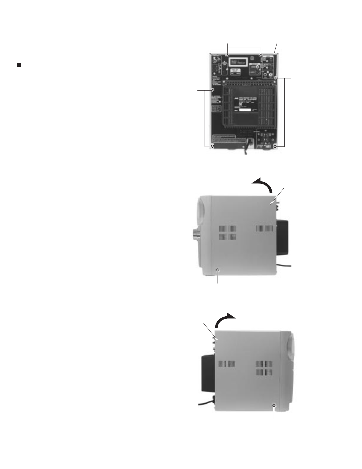
UX-A10DVD
Disassembly method
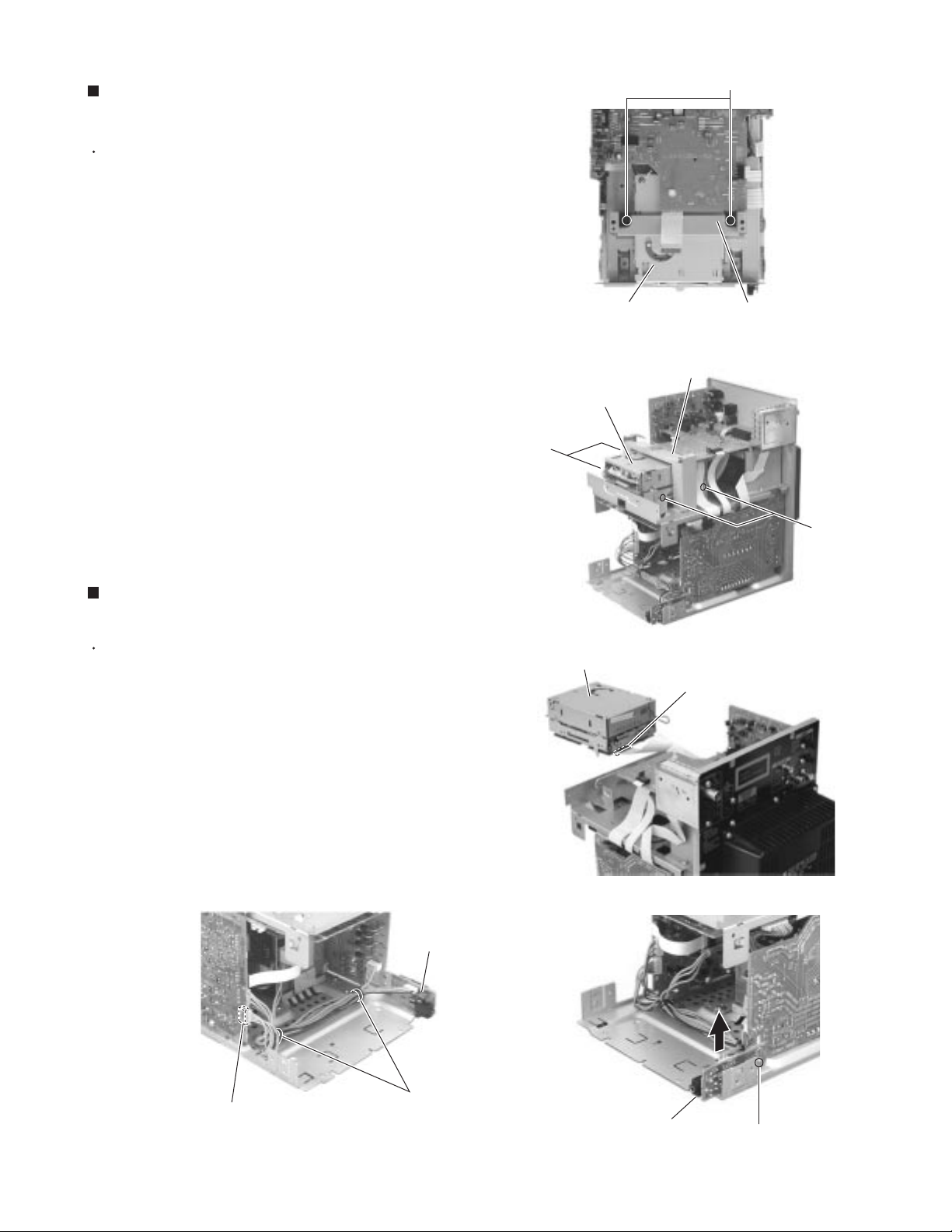
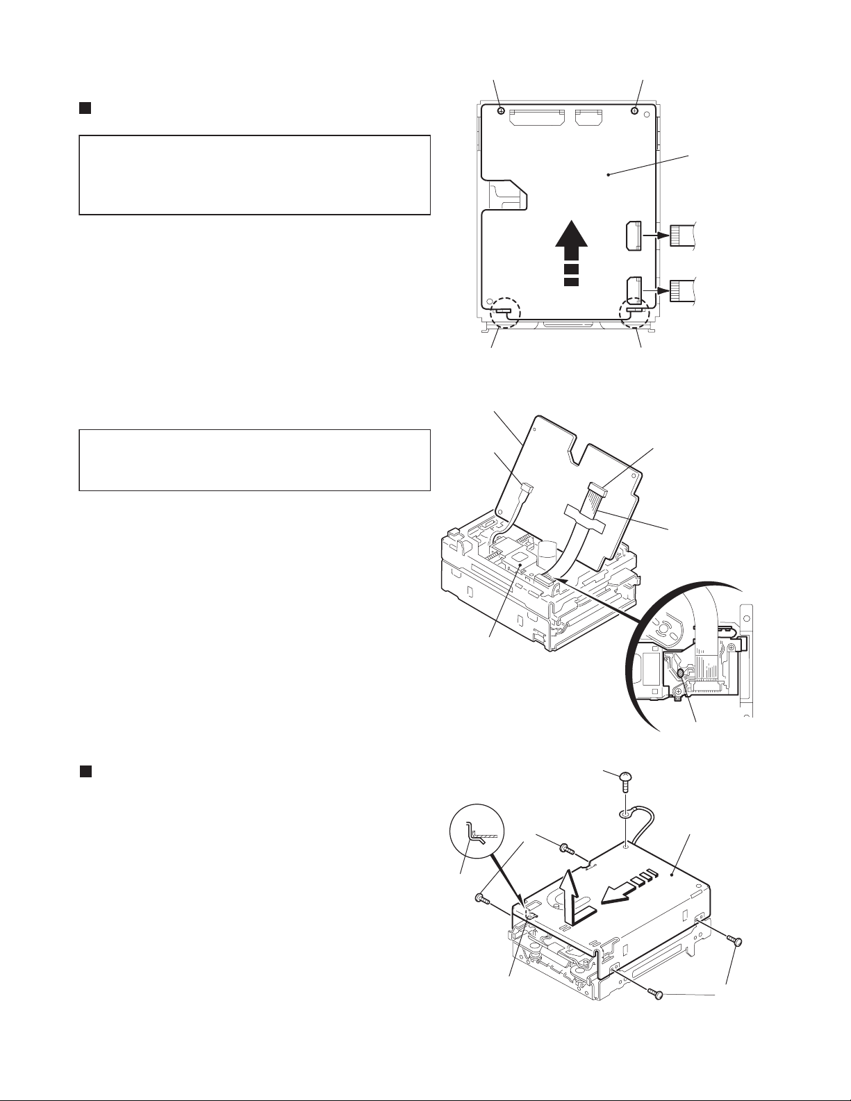
<Main body>
Removing the metal cover (See Fig.1~3)
1.
Remove the six screws A on the back of the body.
2.
Remove the screw B on each side of the body.
3.
Detach the rear side of the metal cover upward while
pulling the lower sides outward.
A
A
Metal cover
A
Fig.1
Metal cover
1-4
B
Fig.2
Metal cover
B
Fig.3
Page 5
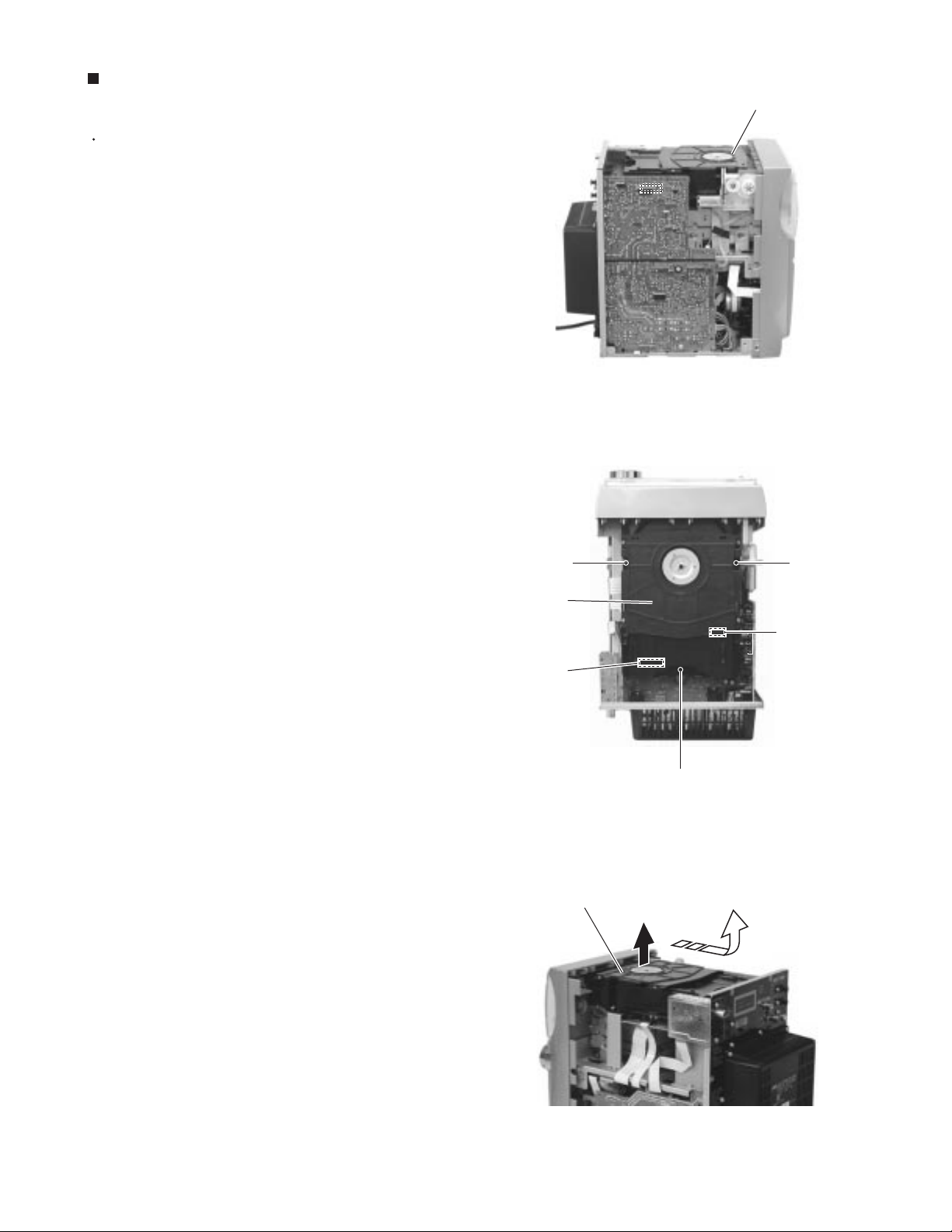
Removing the DVD mechanism assembly
(See Fig.4~6)
Prior to performing the following procedure, remove
the metal cover.
1.
Remove the three screws C attaching the DVD
mechanism assembly on top of the body.
2.
Disconnect connector CN502 and CN503 on the
DVD servo board upward at the bottom of the DVD
mechanism assembly.
Bring up the DVD mechanism assembly and remove
backward.
UX-A10DVD
DVD mechanism assembly
Fig.4
DVD mechanism assembly
CN503
DVD mechanism assembly
C
C
CN502
C
Fig.5
Fig.6
1-5
Page 6
UX-A10DVD
Removing the front panel assembly
(See Fig.7~10)
Prior to performing the following procedure, remove
the metal cover and the DVD mechanism assembly.
1.
Disconnect the card wire from connector CN705 on
the microcomputer board in the center of the right
side of the body.
2.
Disconnect the card wire from connector CN301 on
the main board in the center of the left side of the
body.
3.
Disconnect the card wire from connector CN704,
and the wires from CN703 and CN710 on the
microcomputer board.
Front panel assembly
D
b
Microcomputer board
CN705
Fig.7
ATTENTION:
4.
Disconnect the card wire from connector CN442 on
the FL connection board on top of the body.
5.
Remove the screw D on each side of the body.
6.
Remove the two screws E on the bottom of the
body.
7.
Release the joint a on the bottom and the two joints
b on the right and left sides of the body using a
screwdriver. Remove the front panel assembly
toward the front.
When disconnecting the wires from
CN703 and CN710, remove the
spacer attaching the wires.
FL connection board
CN442
Front panel assembly
Main board
CN301
CN710
E
CN703
Fig.8
Front panel assembly
Spacer
D
Microcomputer board
b
CN704
Front panel assembly
E
1-6
CN710
CN703
Spacer
a
Microcomputer board
CN704
Fig.10Fig.9
Page 7
UX-A10DVD
Removing the rear cover/ rear panel
(See Fig.11~15)
Prior to performing the following procedure, remove
the metal cover and the DVD mechanism assembly.
1.
Remove the two screws F on the back of the body.
2.
Disconnect the wire from connector CN1 on the
tuner pack on the right side of the body.
3.
Remove the thirteen screws G on the back of the
body.
4.
Release the two joints c on the lower right and left
sides of the rear panel.
REFERENCE:
The rear panel with the tuner pack
comes off.
F
Rear cover
Rear panel
F
Fig.11
G
Tuner pack
CN1
Fig.12
Rear panel
G
G
G
G
Rear panel
G
FIg.13
Rear panel
c
Rear panel
Fig.15Fig.14
c
1-7
Page 8
UX-A10DVD
Removing the tuner pack (See Fig.16)
Prior to performing the following procedure, remove
the metal cover.
Tuner pack
1.
Disconnect the card wire from connector CN1 on the
tuner pack on the right side of the body.
2.
Remove the two screws H on the back of the body.
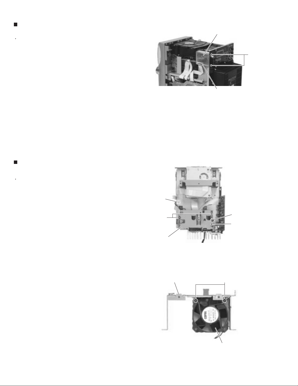
Removing the fan (See Fig.17,18)
Prior to performing the following procedure, remove
the metal cover, the DVD mechanism assembly, the
rear cover/rear panel and the DVD relay board.
1.
Disconnect the wire from connector CN711 on the
microcomputer board on the right side of the body.
2.
Remove the three screws I attaching the fan bracket
on top of the body and release the joint d.
H
CN1
Fig.16
CN711
d
I
I
3.
Remove the two screws J attaching the fan.
1-8
Fan bracket
Fan bracket
Fig.17
Fig.18
J
Fan
Page 9
UX-A10DVD
Removing the MD mechanism assembly
(See Fig.19~21)
Prior to performing the following procedure, remove
the metal cover, the DVD mechanism assembly and
the front panel assembly.
1.
Remove the two screws K attaching the DVD
mechanism attaching bracket.
2.
Remove the two screws L on each side of the MD
mechanism assembly and remove the MD
mechanism assembly toward the front.
3.
Disconnect the card wire from connector CN521 on
the MD mechanism assembly board.
MD mechanism assembly
MD mechanism assembly
L
K
DVD mechanism
Fig.19
DVD mechanism attaching bracket
attaching bracket
Removing the headphone board
(See Fig.22,23)
Prior to performing the following procedure, remove
the metal cover, the DVD mechanism assembly and
the front panel assembly.
1.
Disconnect the wire from connector CN310 on the
main board on the left side of the body.
2.
Release the wires from the two clamps on the
bottom chassis.
3.
Remove the screw M attaching the headphone
board on the right side of the body.
Headphone board
L
Fig.20
MD mechanism assembly
CN521
Fig.21
Main board
CN310
Fig.22
Clamp
Headphone board
Fig.23
M
1-9
Page 10
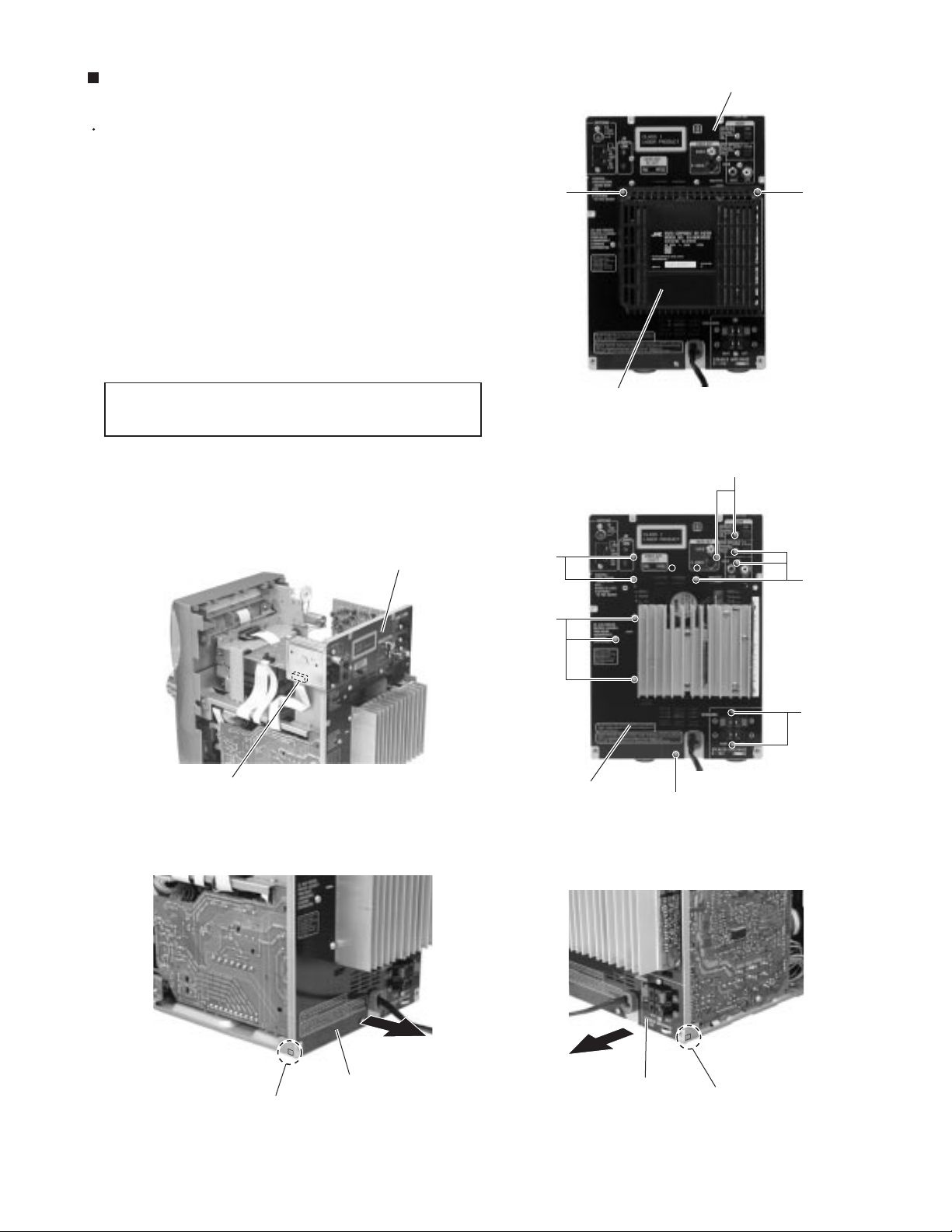
UX-A10DVD
Removing the main board
(See Fig.24,25)
Prior to performing the following procedure, remove
the metal cover, the DVD mechanism assembly, the
front panel assembly and the rear cover/ rear panel.
1.
Remove the two screws N and the three screws O.
Remove the heat sink.
2.
Disconnect the wires from connector CN307 and
CN310, the card wire from CN312 on the main board
on the left side of the body.
3.
Remove the screw P and Q attaching the main
board.
Main board
Heat sink
O
N
4.
Disconnect connector CN303, CN304, CN305 and
CN306 on the main board. Release the two joints e
at the bottom.
5.
Draw out the main board and disconnect the card
wire and the wire from connector CN302 and
CN311.
Removing the DVD relay board
(See Fig.26)
Prior to performing the following procedure, remove
the metal cover, the DVD mechanism assembly and
the rear panel/ rear cover.
1.
Disconnect the card wire from connector CN515 on
the DVD relay board.
Main board
Heat sink
CN302
P
CN311
Main board
Fig.24
CN303 CN304
e
Q
Fig.25
CN512
CN305
CN306
e
CN511
DVD connector board
CN312
CN307
CN310
R
2.
Remove the screw R attaching the DVD relay board
on top of the body.
3.
Disconnect connector CN511 and CN512 on the
DVD relay board.
1-10
CN515
Fig.26
Page 11
Removing the MD base chassis/
microcomputer board (See Fig.27~29)
Prior to performing the following procedure, remove
the metal cover, the DVD mechanism assembly, the
front panel assembly, the rear cover/ rear panel, the
main board and the DVD relay board.
MD mechanism assembly
UX-A10DVD
MD base chassis
REFERENCE:
1.
Disconnect the wire from connector CN701 on the
microcomputer board in the center of the right side of
the body.
2.
Remove the two screws S attaching the MD base
chassis on top of the body.
3.
Disconnect connector CN706 and CN707 on the
microcomputer board from the main board.
REFERENCE:
4.
Remove the two screws T attaching the
microcomputer board and release the two joints f.
It is not necessary to remove the DVD
mechanism assembly.
The MD base chassis with the MD
mechanism assembly comes off.
Microcomputer board
CN701
Fig.27
MD mechanism assembly MD base chassis
CN706
CN707
S
CN706
CN707
Fan bracket
Main board
Fig.28
T
Microcomputer
board
f
Fig.29
1-11
Page 12
UX-A10DVD
Removing the power transformer
assembly (See Fig.30,31)
Prior to performing the following procedure, remove
the metal cover, the DVD mechanism assembly, the
front panel assembly, the rear cover/ rear panel, the
main board and the MD base chassis.
1.
Move the power cord stopper upward on the back of
the body and remove. Disconnect the power cord
from connector CN901 on the power transformer
board.
REFERENCE:
2.
Remove the four screws U on top of the body and
release the wires from the two clamps on the bottom
chassis.
The power cord can be removed alone.
Removing the power amplifier board
(See Fig.32,33)
Power transformer board
CN901
Power cord stopper
Power cord
Fig.30
Clamp
Power amplifier board
Bottom chassis
Prior to performing the following procedure, remove
the metal cover, the DVD mechanism assembly, the
front panel assembly, the rear cover/ rear panel, the
main board and the MD base chassis.
1.
Disconnect the wire from connector CN111 on the
power amplifier board.
2.
Remove the band attaching the wire to the power
amplifier board.
3.
Release the wires from the clamp.
4.
Move the power amplifier board upward to release
the two joints g and remove to the right.
U
Power transformer
assembly
g
U
U
Fig.31
Power amplifier
board
1-12
Band
Power amplifier board
CN111
Fig.32
Band
Clamp
Fig.33
Page 13
UX-A10DVD
<Front panel assembly>
Prior to performing the following procedure, remove
the metal cover, the DVD mechanism assembly and
the front panel assembly.
Removing the cassette mechanism
assembly (See Fig.34,35)
1.
Remove the spring attached to the cassette door on
the back of the front panel.
2.
Remove the four screws V attaching the cassette
mechanism assembly.
Cassette door
Spring
Fig.35
Spring
Cassette mechanism assembly
V
Fig.34
V
Front panel assembly
V
Removing the key board (See Fig.36~38)
Prior to performing the following procedure, remove
the cassette mechanism assembly.
1.
Pull out the volume knob on the front side of the front
panel.
2.
Remove the five screws W attaching the bracket (1)
on the back of the front panel.
3.
Remove the ten screws X attaching the key board.
Bracket(1)
W
W
W
X
Volume knob
Fig.36
Key board
X
Front panel
X
Fig.38Fig.37
X
1-13
Page 14
UX-A10DVD
Removing the FL connection board
(See Fig.39~41)
1.
Remove the two screws Y and the screw Z
attaching the bracket (2) on the back of the front
panel.
2.
Disconnect the card wire from connector CN441 on
the FL connection board.
3.
Push the two joint tabs h downward to release and
pull out the FL connection board.
Removing the Drive motor assembly
(See Fig.39, 40,42)
1.
Remove the two screws Y and the screw Z attaching
the bracket (2) on the back of the front panel.
FL connection board
CN441
Y
Bracket(2)
Bracket(2)
Fig.39
Front panel
Y
Front panel
2.
Remove the screw A' attaching the drive motor
assembly. Release the joint tab i and pull out the
drive motor assembly.
CN441
h
h
Drive motor
Z
Fig.40
A'
Drive motor
1-14
FL connection board
i
Fig.42Fig.41
Page 15
Removing the belt/ drive motor
(See Fig.43)
Prior to performing the following procedure, remove
the drive motor assembly.
1.
Remove the belt from the pulley
2.
Remove the two screws B' attaching the drive
motor.
UX-A10DVD
Belt
Drive motor
B'
Fig.43
Removing the switch board
(See Fig.44,45)
Prior to performing the following procedure, remove
the bracket (2) / drive motor assembly.
1.
Disconnect the card wire from connector CN441 on
the FL connection board(Do not fold down the card
wire).
2.
Release the joint j and k in order on the right and left
sides of the shaft gear.
Remove the screw C' attaching the switch board
and release the joint tab l.
FL connection board
k
Shaft gear
CN441
Fig.44
Switch board
C'
j
Switch board
l
Fig.45
1-15
Page 16
UX-A10DVD
Removing the FL display section
(See Fig.46~51)
1.
Remove the four screws D' attaching the case cover
on the front panel.
2.
Pull out the FL panel from the four joint bosses m on
the FL display cover.
3.
Remove the four screws E' attaching the FL display
cover. Disconnect the card wire from connector
CN451 on the FL relay board and from CN452 on
the LED board.
D'
Case cover
D'
Fig.46
m
FL panel
E'
FL display cover
E'
Fig.47
FL connection board
CN451
Fig.49Fig.48
m
LED board
CN452
FL display cover
1-16
Page 17
4.
Remove the two screws F' attaching the FL display
on the FL display cover.
5.
The FL board and the lens come off from the FL
display section.
FL display section
FL display cover
F' F'
Fig.50
FL display section
UX-A10DVD
Removing the FL relay board(See Fig.52)
Prior to performing the following procedure, remove
the FL display cover.
1.
Disconnect the card wire from connector CN453 on
the FL relay board.
2.
Remove the two screws G' attaching the FL relay
board.
LED board
FL board
Fig.51
CN453
G'
FL connection board
Fig.52
Lens
G'
1-17
Page 18
UX-A10DVD
<DVD loading mechanism section>
Removing the clamper assembly
(See Fig.1)
Remove the four screws A attaching the clamper
1.
assembly.
Move the clamper assembly in the direction of the
2.
arrow to release the joint a on each side, and
remove.
ATTENTION:
Removing the tray (See Fig.2,3)
Prior to performing the following procedure, remove
the clamper assembly.
1.
Push the part b of the slide cam through the slot on
the left side of the loading base.
2.
Draw out the tray toward the front.
ATTENTION:
When reassembling, reattach the
clamper assembly at the two joints a.
When reattaching the tray, move the
part c of the slide cam to the right(See
Fig.3).
a
A
Loading base
a
A
Clamper
assembly
AA
Fig.1
Tray
b
Fig.2
Removing the servo control board
(See Fig.4)
CAUTION:
1.
Solder the
connected to connector CN101 on the servo control
board.
2.
Disconnect the flexible wire from connector CN101
on the servo control board.
3.
Disconnect the card wires from connector CN201
and CN202 on the servo control board.
4.
Release the two joints d.
5.
Move the servo control board in the direction of the
arrow to release the joint e, and remove upward.
CAUTION:
Solder the sorting round point before
disconnecting the flexible wire extending
from the pickup. If you do not follow this
instruction, the pickup may be damaged.
sorting round
Unsolder the sorting round point after
reassembling.
point on the flexible wire
CN201
d
e
Servo control board
c
Slide cam
Fig.3
Sorting round point
CN101
Flexible wire
d
CN202
CN101
Fig.4
1-18
Page 19
Removing the traverse mechanism
assembly (See Fig.5,6)
UX-A10DVD
Prior to performing the following procedure, remove
the clamper assembly, the tray and the servo control
board.
Remove the four screws B attaching the traverse
1.
mechanism assembly.
CAUTION:
When reassembling, get the flexible wire
extending from the spindle motor board
through the slot f of the elevator.
Removing the elevator (See Fig.7 and 8)
Prior to performing the following procedure, remove
the clamper assembly, the tray, the servo control
board and the traverse mechanism assembly.
1.
Pull the two tabs g outward and release the two
shafts of the elevator.
B
Traverse mechanism
assembly
B
B
BB
BB
Fig.5
Traverse mechanism
assembly
B
f
ATTENTION:
Tab g
When reassembling, fit the two shafts
on the front side of the elevator into
the grooves h of the slide cam.
Elevator
Fig.6
Shaft
Elevator
Elevator
Slide cam
Loading base
Elevator
Fig.7 Fig.8
Tab g
h
1-19
Page 20
UX-A10DVD
Removing the motor assembly
(See Fig.9,10)
Prior to performing the following procedure, remove
the clamper assembly, the tray, the servo control
board, the traverse mechanism assembly and the
elevator.
Remove the belt from the pulley.
1.
Remove the screw C attaching the loading motor.
2.
Remove the screw D attaching the motor board on
3.
the back of the loading assembly.
Release the tab i fixing the motor board and remove
4.
the motor assembly.
Belt
C
Loading motor pulley
Fig.9
Ta b i
Motor assembly
Motor board
Fig.10
D
Loading assembly
1-20
Page 21
UX-A10DVD
Pulley gear bracket
Pulley gear
Motor assembly
E
Pulley gear bracket
E
Idle gear
Fig.11
Idle gear
Pulley gear
Pulley gear
k
Middle gear
Tab j
k
Removing the idle gear/ pulley gear/
middle gear/ slide cam (See Fig.11~13)
Prior to performing the following the procedures,
remove the clamper assembly, the tray, the servo
control board, the traverse mechanism assembly,
the elevator and the motor assembly.
Push the two tabs j attaching the idle gear inward
1.
and pull out the idle gear.
Remove the screw E attaching the pulley gear
2.
bracket. Move the pulley gear bracket in the direction
of the arrow and remove upward.
Pull out the pulley gear.
3.
Move the slide cam in the direction of the arrow to
4.
release the two joints k and remove upward.
Remove the middle gear.
5.
Slide cam
Slide cam
Fig.12
Middle gear
Fig.13
Loading base
1-21
Page 22
UX-A10DVD
<DVD traverse mechanism assembly>
Removing the feed motor assembly
(See Fig.14)
Unsolder the two soldering l on the spindle motor
1.
board.
Remove the two screws F attaching the feed motor
2.
assembly.
Removing the feed motor
(See Fig.14~16)
Prior to performing the following procedure, remove
the feed motor assembly.
1.
Remove the screw G and the spring.
CAUTION:
2.
Remove the feed gear M.
When reassembling, attach the spring
correctly to press the feed gear M and
E.
Feed motor assembly
F
F
m
l
Spindle motor board
Pickup
Spindle motor
Fig.14
Feed gear M
Spring
3.
Pull out the feed gear E and the lead screw.
4.
Remove the two screws H and the feed motor.
CAUTION:
When reassembling, set the two wires
extending from the feed motor to the
notch m of the feed holder as shown in
Fig.14.
G
Lead screw
Feed gear E
Fig.15
Feed motor
1-22
Feed motor
Fig.16
H
Page 23
UX-A10DVD
Removing the pickup (See Fig.17,18)
1.
Prior to performing the following procedure, remove
the feed motor assembly.
2.
Remove the screw l, the T spring(S) and the shaft
holder with the plate.
ATTENTION:
3.
Detach the part n of the shaft upward and move the
part o in the direction of the arrow, then remove the
shaft from the spindle base.
4.
Release the joint p in the direction of the arrow.
Pull out the shaft from the pickup.
5.
Remove the two screws J attaching the actuator.
6.
Release the joint of the actuator and the lead spring,
and pull out the lead spring.
When reassembling, reattach the T
spring (s) correctly to press the shaft
I
Plate
T spring(S)
Lead spring
Actuator
p
J
Pickup
n
Fig.17
Spindle base
o
Shaft holder
Actuator
Lead spring
ATTENTION:
When reattaching the pickup, attach
the spring under the shaft(See the
figure below).
Pickup
Spring
Shaft
Removing the shaft holder/ shaft
(SeeFig.19)
Prior to performing the following procedure, remove
the feed motor assembly and the pickup.
Pickup
K
Shaft
Fig.18
Shaft
Shaft holder
1.
Remove the screw K attaching the shaft holder.
2.
Remove the shaft.
Fig.19
1-23
Page 24
UX-A10DVD
Removing the spindle motor assembly
(See Fig.20~22)
Prior to performing the following procedure, remove
the feed motor assembly, the pickup, the shaft and
the shaft holder.
1.
Turn over the mechanism base and remove the
three screws l attaching the spindle motor
assembly.
ATTENTION:
2.
Remove the three screws M and the spindle base.
When reassembling, set the card wire
extending from the spindle motor
board to the notch of the spindle base.
L
Spindle motor assembly
Spindle motor board
Spindle motor
L
Fig.20
Spindle base
Spindle base
L
Fig.21
M
M
Mechanism base
Fig.22
1-24
Page 25
UX-A10DVD
<MD mechanism assembly>
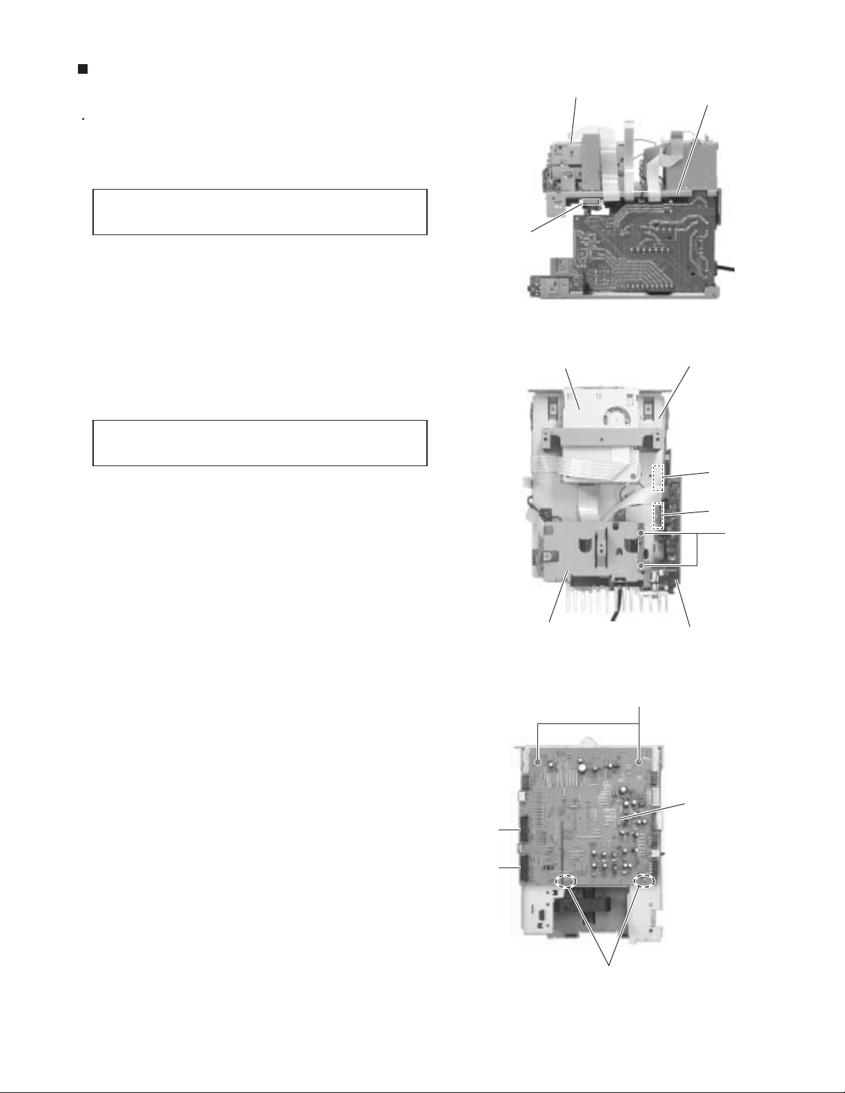
Removing the main board (See Fig.1, 2)
CAUTION:
1.
Turn over the main body and disconnect the card
wire from connector CN408 and the flexible wire
from CN407 on the main board respectively.
2.
Remove the two screws A attaching the main board.
Move the main board in the direction of the arrow to
release the two joints a .
3.
Solder the sorting round point to protect the pickup.
Disconnect the flexible wire from connector CN321
on the back of the main board.
CAUTION:
When replacing the flexible wire connected
to the main board, solder the shorting round
point. Otherwise, the pickup may be
damaged. (see Fig.18)
When reassembling, connect the flexible
wire from the pickup to the main board and
unsolder the shorting round point.
CN408
CN407
Joint a Joint a
Fig.1
Main board
C451
AA
Main board
CN321
Removing the mechanism cover (See Fig.3)
1.
Remove the four screws B on each side of the body.
2.
Remove the one screw C on the upper side of the
body.
3.
Move the mechanism cover toward the front to release
the front hook from the loading assembly (joint b ) , then
remove upward.
Hook
Pickup
Joint b
B
Fig.2
C
Flexible wire
Sorting round
point
Mechanism cover
Joint c
B
Fig.3
1-25
Page 26
UX-A10DVD
Removing the head lifter (See Fig.4~6)
1.
Removing the spring from the hook on the main body.
Remove the spring from the head lifter if necessary.
2.
Turn the head lifter in the direction of the arrow to release
the joint c and d .
Joint c
Head lifter
Fig.4
Spring
Head lifter
Joint d
Fig.5
Head lifter
Removing the head assembly (See Fig.7)
Spring
Fig.6
Prior to performing the following procedure, remove
ޓ
the main board.
1.
Remove the screw D on the upper side of the body.
Remove the head assembly while pulling the flexible
harness from the body.
1-26
Head assembly
D
Fig.7
Page 27
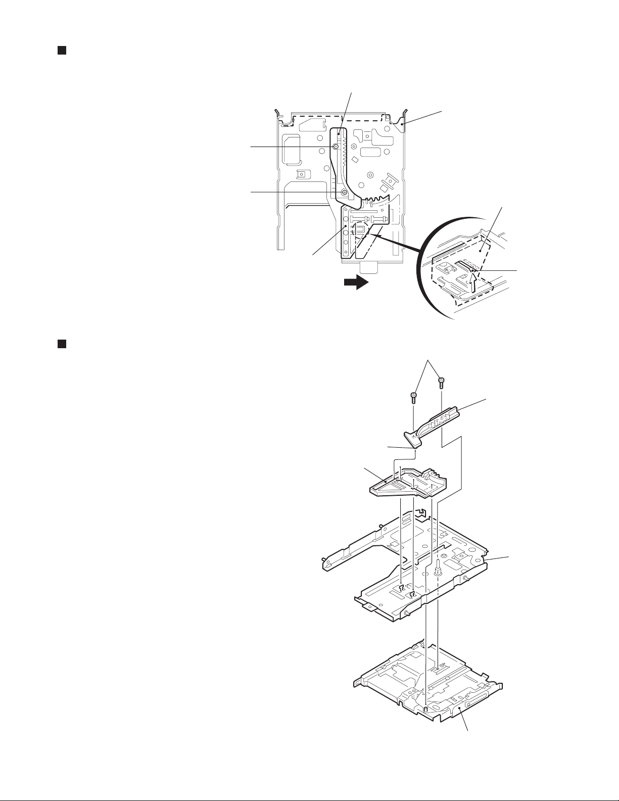
Removing the loading assembly
(See Fig.8, 9)
E
UX-A10DVD
E
REFERENCE:
Prior to performing the following procedure, remove
the main board, the mechanism cover and the head
lifter/head assembly.
1.
Remove the three screws E on the upper side of the
body.
2.
Move the loading assembly toward the front to
release the joint e and remove upward.
3.
Remove the traverse mechanism assembly from the
single flame.
The traverse mechanism assembly and
the single flame can be removed after
removing the loading assembly from the
body.
Loading assembly
Joint e
E
Fig.8
Loading assembly
Traverse mechanism assembly
Single frame
Fig.9
1-27
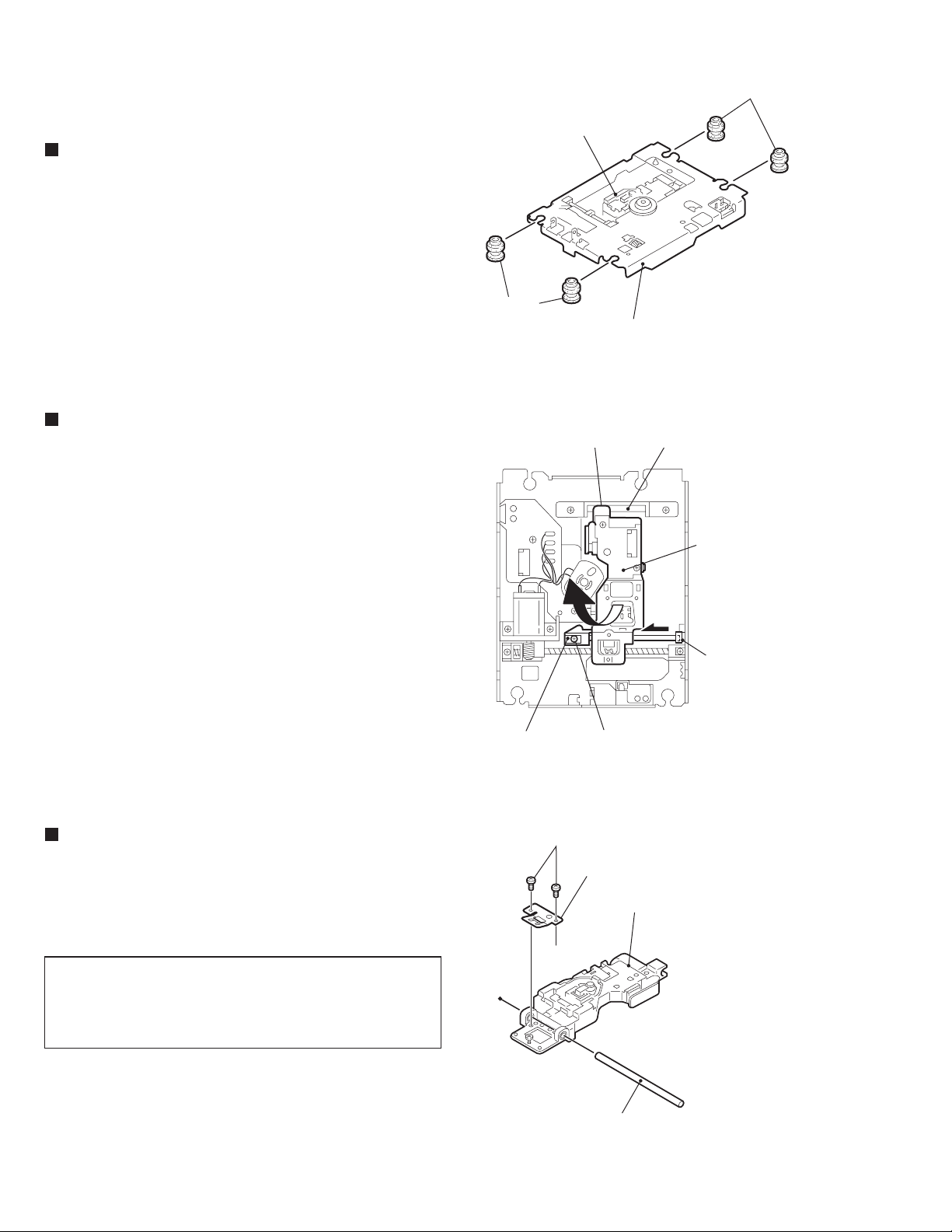
Page 28
UX-A10DVD
<Loading assembly section>
Removing the slide base (L) and (R)
(See Fig.10)
1.
Remove the two screws F on the upper side of the
loading base assembly.
2.
Remove the slide base (L) outward while releasing
the two joints f on the bottom.
3.
Remove the slide base (R) outward.
Removing the loading mechanism assembly
(See Fig.11)
1.
To release the loading mechanism assembly from
the bending g without trouble, first bring up the one
side of the loading mechanism assembly opposite to
the bending g and release the side bosses from the
loading mechanism base. And next, remove another
side.
Slide base(R)
Bending g
Loading mechanism assembly
Joint f
F
Slide base(L)
F
Joint f
Fig.10
Loading mechanism base
Fig.11
Loading mechanism assembly section
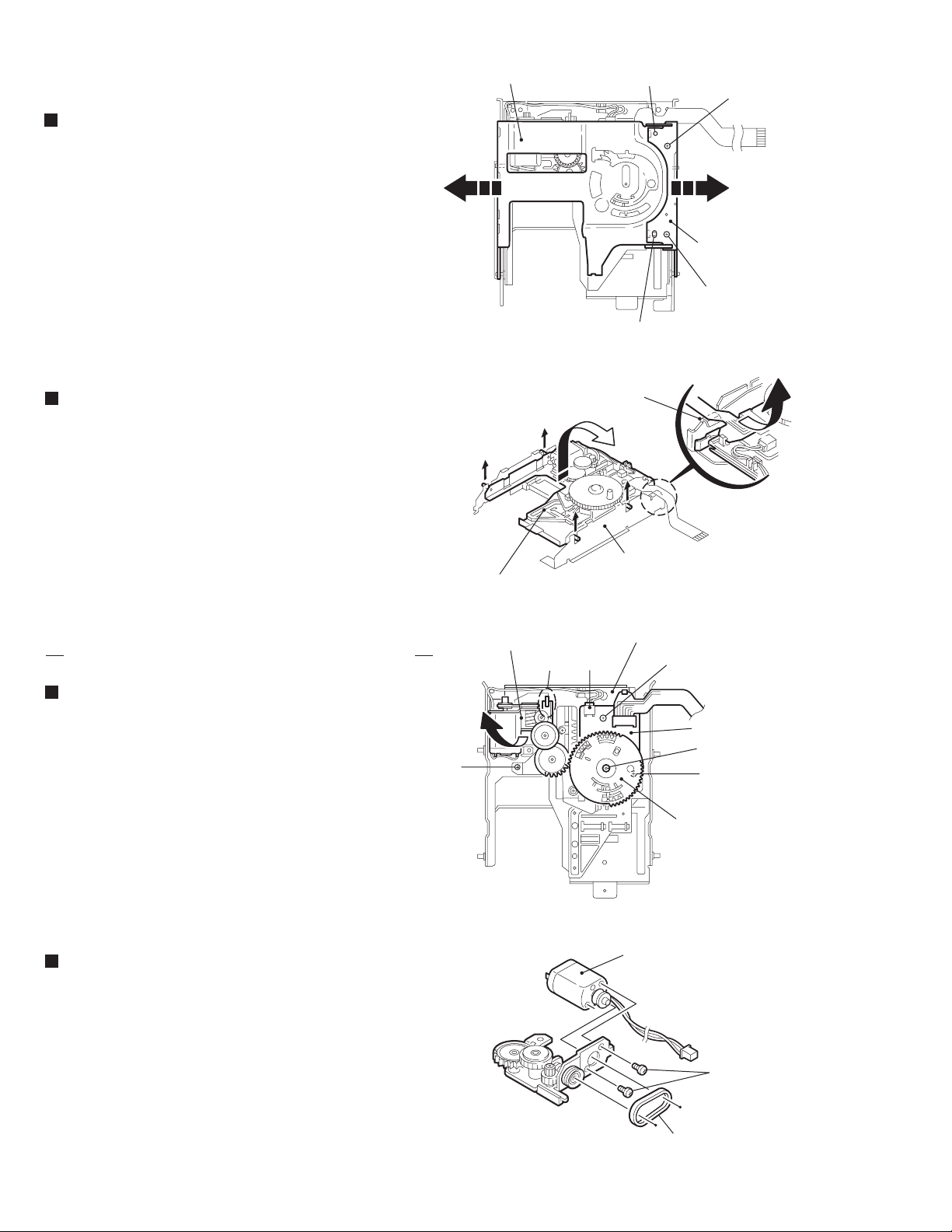
Removing the loading motor
(See Fig.12, 13)
1.
Release the harness from the wire holder on the cam
switch board and disconnect from connector t.
2.
Remove the screw G and release the joint h .
3.
Remove the belt from the loading motor assembly.
4.
Remove the two screws H .
Remove the cam gear and the cam switch
board (See Fig.12)
1.
Remove the slit washer and pull out the cam gear.
2.
Release the harness from the wire holder on the cam
switch board and disconnect from connector CN612.
Loading motor assembly
Joint h
G
CN612
Fig.12
Wire holder
I
Cam switch board
Slit washer
I
Cam gear
Loading motor
H
3.
Remove the two screws I , the clamp and the cam
switch board.
1-28
Belt
Fig.13
Page 29
Remove the cartridge holder assembly
(See Fig.14, 15)
UX-A10DVD
1.
Remove the two screws J on the upper side of the
loading assembly.
J
J
Eject bar
Removing the slide bar/Eject bar
(See Fig.14, 15)
Slide bar
Cartridge holder assembly
Eject bar
Tab i
Fig.14
J
Prior to performing the following procedure, remove
the cartridge holder assembly.
1.
Remove the slide bar upward.
2.
Move the slide bar outward until it stops (See
Fig.14). Push the tab i from below and remove the
eject bar from the chassis section.
Slide bar
boss m
Eject bar
UD base
Cartridge holder assembly
Fig.15
1-29
Page 30
UX-A10DVD
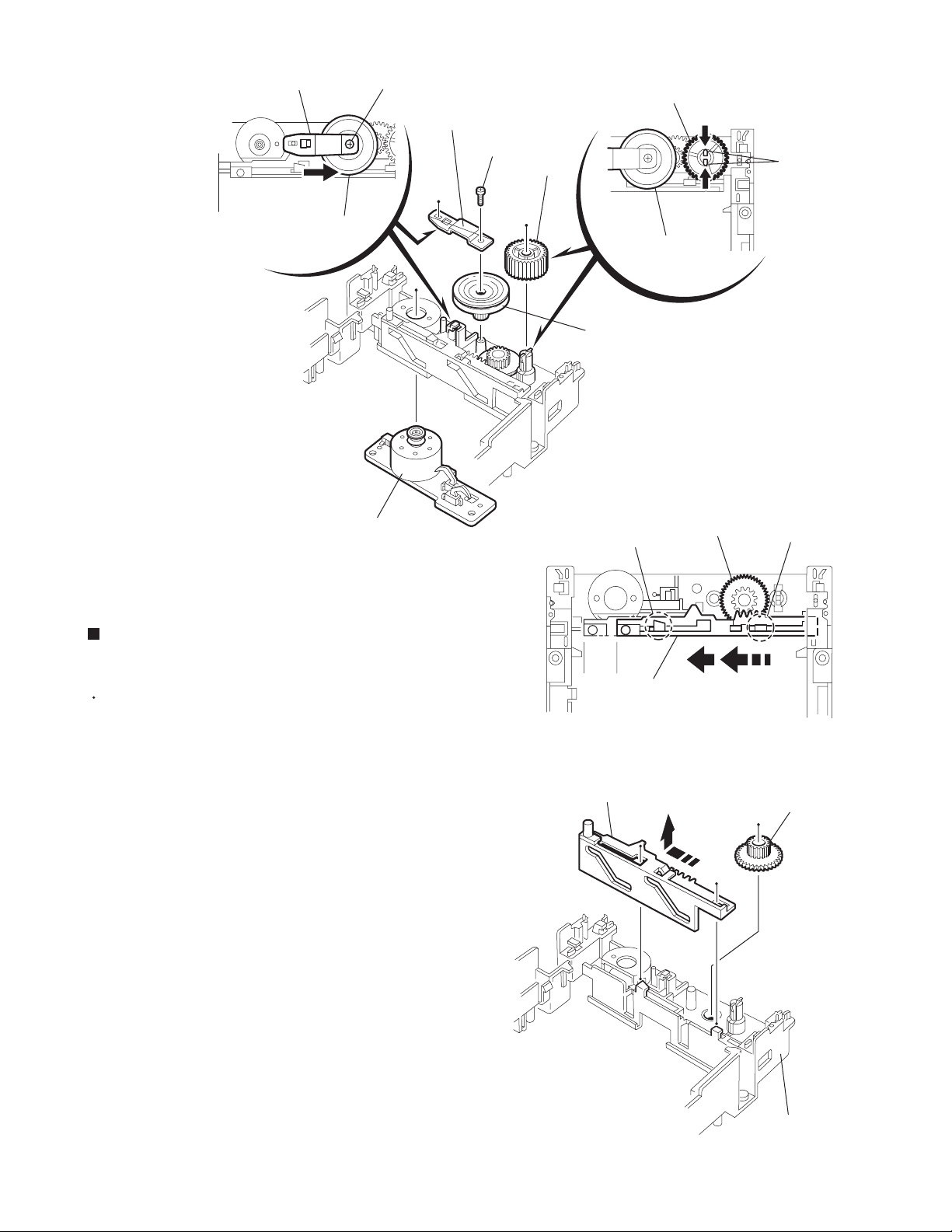
<Traverse mechanism assembly section>
<Traverse mechanism assembly section>
Removing the insulator (See Fig.16)
1.
Removing the insulators from the four notches of the
traverse mechanism chassis.
Removing the pickup unit (See Fig.17)
1.
Remove the screw K attaching the shaft holder (F) on
the back of the traverse mechanism assembly.
2.
Move the shaft inward and release from the shaft holder
(R).
Insulator
Pickup unit
Insulator
Traverse mechanism chassis
Fig.16
Joint j Pickup guide
Pickup unit
3.
Bring up the one side of the pickup unit on the shaft to
release the joint j on the opposite side. Then, remove
the pickup unit with the shaft.
Removing the pickup (See Fig.18)
1.
Pull out the shaft from the pickup.
2.
Remove the two screws L attaching the rack spring
to the pickup.
CAUTION:
Before disconnecting the flexible wire
connected to the pickup, solder the shorting
round point to protect the pickup from static
electricity.
Shaft holder(F)
L
Shaft holder(R)
K
Fig.17
Rack spring
Pickup
1-30
Shaft
Fig.18
Page 31

Removing the feed motor assembly
(See Fig.19,20)
UX-A10DVD
REFERENCE:
For the white and black harnesses extending from
1.
the feed motor assembly, unsolder two soldering k
on the traverse mechanism board.
Remove the two screws M attaching the feed motor
2.
assembly.
Remove the two screws O attaching the feed motor
3.
bracket.
The feed motor assembly can be
performed even if the pickup unit is
attached.
Removing the traverse mechanism
board (See Fig.19)
Prior to performing the following procedure, remove the
feed motor assembly.
1.
For the red and black harnesses extending from the
spindle motor, unsolder two soldering l on the traverse
mechanism board.
2.
Remove the screw N .
Traverse mechanism board Soldering l Pickup
N
Solldering k
Feed motor assembly
M
Rest SW
Fig.19
Feed motor
Feed motor bracket
Screw shaft gear
O
CAUTION:
When reattaching the traverse mechanism
board, make sure the position of the pickup.
If the pickup is on the most inside position,
move it outward by turning the screw shaft
gear not to contact with the rest SW.
Fig.20
1-31
Page 32

UX-A10DVD
<Reattaching the loading
assembly section>
1.
Reattach the eject bar to the UD base (see Fig.15,
21).
2.
Reattach the slide bar to the loading mechanism
chassis while fitting the boss m to the groove of the
eject bar (see Fig.15).
3.
Move the slide bar and eject bar in the direction of
the arrow and reattach the cartridge holder assembly
using the two screw J (Fig.21, 22).
CAUTION:
Make sure that pin n of the eject bar is
correctly fitted in the groove o when
moving the eject bar and the loading
slider as shown in Fig.22.
Wire holder
Cam switch board
p
q
I
Mark
I
Groove o
Slide bar
J
Cam switch boss
J
Groove
UD base
Eject bar
Fig.21
UD base(Bottom)
Cartridge holder assembly
1-32
Loading slider
Eject bar
Pin n
Fig.22
Page 33

4.
Reattach the wire holder to the UD base while fitting
the bending q to the hole of the wire holder (The
boss on the back of the wire holder is fit to the hole
of the UD base)(see Fig.21).
5.
Reattach the cam switch board using the two screws
I .
6.
Turn the cam switch until the boss comes to the
position marked with a triangle (see Fig.23).
Reattach the cam gear while fitting the cam gear slot
to the cam switch boss, and fix them using the slit
washer.
UX-A10DVD
CAUTION:
When reattaching the cam gear with
fitting the slot to the cam switch boss,
make sure that part r of the gear is
aligned with the position marked with a
triangle of the cam gear.
7.
Reattach the loading motor assembly using the
screw G (see Fig.23).
Connect the wire extending from the loading motor to
connector CN612 on the switch board, set on the
bending s of the UD base and fix using the wire
holder.
Bending s
Loading motor assembly
Slide bar CN612 Wire holder
Mark
Boss
Cam switch
Cam switch board
G
Eject bar
Fig.23
Slit washer
Cam gear
part r
Cam gear
(Marked with
a triangle)
Eject bar
1-33
Page 34

UX-A10DVD
8.
Reattach the UD base to the loading mechanism
base while fitting the four bosses to the notches of
the loading mechanism base respectively (see
Fig.24).
First, sit part t of the cartridge holder assembly under
the bending g of the loading mechanism base, then
reattach the UD base.
9.
Reattach the slide base (R) while fitting the two slots
of the slide base (R) to the bosses of the UD base
(see Fig.25, 26).
CAUTION:
Set the bending u of the slide base (R)
to the part v inside of the cam gear rib.
10.
Reattach the slide base (L) on the slide base (R)
while fitting the two bosses of the UD base to the
notches on the side of the slide base (L). Make sure
that the slots of the slide base (L) are fitted to the two
part f and fix the slide base (L) using the two screws
F (see Fig.25, 27).
REFERENCE:
To reattach the slide base (L) and (R)
easily, fit the bosses to the notches with
bringing up the UD base slightly.
Pin
t
Pin
g
t
Loading mechanism base
Fig.24
Slide base(R)
Bending u
F
Pin
Slide base(L)
Pin
v
Fig.25
f
Slide base(L)Slide base(R)
Slide(R)
Cam gear
F
Bending u
v
1-34
Fig.27
f
Fig.26
Page 35

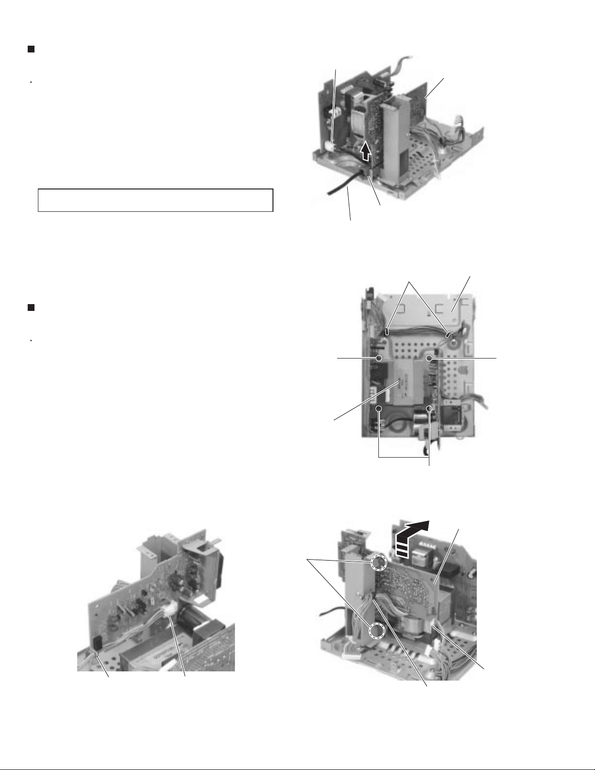
<Cassette mechanism assembly section>
UX-A10DVD
Removing the Play/Record & Clear head
(See Fig.1~3)
1.
While moving the trigger arm on the right side of the
head mount in the direction of the arrow, turn the
flywheel R counterclockwise until the head mount
comes ahead and clicks.
2.
The head turns counterclockwise as you turn the
flywheel R counterclockwise(See Fig.2 and 3).
3.
Disconnect the flexible wire from connector CN31 on
the head amplifier & mecha control board.
4.
Remove the spring from the back of the head.
5.
Loosen the azimuth screw for reversing attaching the
head.
6.
Remove the head on the front side of the head
mount.
Cassette mechanism assembly
Fig.1
Head
Fly wheelR
Trigger armHead mount
Flexible wire
Fly wheel R
Fig.2
Azimuth screw
Head
Head amplifer & mecha control board
Fig.3
for reversing
Spring
CN31
1-35
Page 36

UX-A10DVD
Removing the head amplifier &
mechanism control board (See Fig.4)
1.
Turn over the cassette mechanism assembly and
remove the three screws A attaching the head
amplifier & mechanism control board.
2.
Disconnect the flexible wire from connector CN31 on
the head amplifier & mechanism control board.
3.
Disconnect connector CN32 of the head amplifier &
mechanism control board from connector CN1 on
the reel pulse board.
REFERENCE:
If necessary, unsolder the 4 pin wire
soldered to the main motor.
Removing the main motor (See Fig.4~7)
1.
Remove the two screws B .
2.
Half raise the motor and remove the capstan belt
from the motor pulley.
Head amplifier & mecha control board
CN32
A
CN31
A
Flexible wire
Capstan belt
4pin wire
Fig.4
Main motor assembly
B
Main motor assembly
ATTENTION:
Be careful to keep the capstan belt
from grease. When reassembling,
refer to Fig.6 and 7 for attaching the
capstan belt.
Fig.5
Main motor assembly
Main motor assembly
Fly wheel
Motor pulley
1-36
Capstan belt
Capstan belt
Motor pulley
Fig.7Fig.6
Page 37

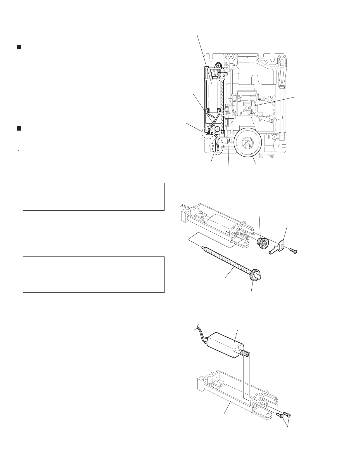
Removing the flywheel (See Fig.8,9)
Prior to performing the following procedure, remove
the head amplifier & mechanism control board and
the main motor assembly.
1.
From the front side of the cassette mechanism,
remove the slit washers attaching the capstan shaft
L and R. Pull out the flywheels backward.
UX-A10DVD
Fly wheel R
Capstan shaft R Capstan shaft L
Removing the reel pulse board and
solenoid (See Fig.10)
Prior to performing the following procedure, remove
the head amplifier & mechanism control board.
1.
Remove the screw C.
Slit washer
Fig.9
Fly wheel R
Fly wheel L
Fly wheel L
Fig.8
2.
Release the tab a, b, c, d and e retaining the reel
pulse board.
3.
Release the tab f and g attaching the solenoid on
the reel pulse board.
4.
The reel pulse board and the solenoid come off.
fg
Solenoid
a
Fig.10
bc
d
Reel pulse board
e
C
1-37
Page 38

UX-A10DVD
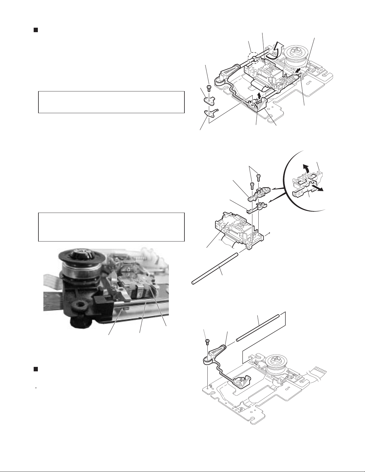
Reattaching the Play/ Record & Clear
head (See Fig.11~13)
1.
Reattaching the head mount assembly.
1)
Change front of the direction cover of the head
mount assembly to the left(Turn the head forward).
2)
Fit the bosses O',P',Q',U' and V' on the head
mount assembly to the holes P and V, the slots
O,U and Q of the mecha sub assembly(See Fig.11
to 13).
CAUTION:
2.
Tighten the azimuth screw for reversing.
To remove the head mount assembly,
turn the direction cover to the left to
disengage the gear. If the gear can not
be disengaged easily, push up the boss
Q' slightly and raise the rear side of the
head mounts slightly to return the
direction lever to the reversing side.
U' Q'
Head mount assembly
Head mount assembly
O'
P'
V'
Direction cover
Fig.11
3.
Reattach the spring from the back of the Play/
Record & Clear head.
4.
Connect the flexible wire to connector CN31 on the
head amplifier & mechanism control board.
Spring
Flexible wire
O
V
Head
P
Direction cover
Q
U
Fig.12
Azimuth screw for reversing
Head mount
1-38
CN31
Head amplifier &
mechanism control board
Fig.13
Page 39

Adjustment method
< MD adjustment (self adjustment) >
UX-A10DVD
(1) Setting of adjustment mode of MD
While pressing both the POWER
key and REC key, turn on the
primary power supply.
FL indication
TEST MODE 1
STOP key of the main body pushed
for stopped MD after power supply
ON with pushed the MD PLAY key.
FL indication
TEST MODE 1
Setup is complete.
(3) Adjustment of the playback laser power
Changes to the adjustment
mode of MD.
Insert the laser power
meter sensor.
(2) Initialization of EEPROM
(The EEPROM can be initialized on the precondition that the
setup of the TEST MODE 1 is complete. After setup of the
TEST MODE 1, proceed to the following operations with the
remote controller*.)
* For EJECT operation, use the EJECT key on the main unit.
changes to the adjustment
mode of MD.
FL indication
TEST MODE 1
Press the PLAY MODE key
on the remote controller.
FL indication
TEST MODE 1
Initialization completion
of EEPROM
Four buttons of remote
control are pushed.
Press the "2" key on
the remote controller.
Set up the playback
laser power.
Increase the laser
power with the F.
SKIP key on the
remote controller.
Adjust the power to be 0.68 mW or
more. If the value exceeds 0.68 mW,
approximate it to 0.68 mW as
accurately as possible.
Press the STOP key
on the main unit.
Setup of the MD laser
power is complete.
Decrease the laser
power with the B.
SKIP key on the
remote controller.
Recording laser power setting
Increase the laser
power with the F.
SKIP key on the
remote controller.
It is adjusted with 6.23mW or less to
a value which is unlimited and close
to 6.23mW.
Press the STOP key
on the main unit.
EJECT does the sensor of the laser
power meter with the EJECT button
of the main body.
Setup of the MD laser
power is complete.
Decrease the laser
power with the B.
SKIP key on the
remote controller.
1-39
Page 40

UX-A10DVD
(4) Adjustment of the disk
Set up the TEST MODE 1.
Insert the
premastered disk.
Reading of TOC ends.
Press the MD PLAY
key on the remote
controller.
FL indication
ON TUNING
Automatic adjustment starts.
Adjustment OK?
FL indication
OK TUNING
Press the STOP key on
the remote controller.
Press the EJECT key
on the main unit.
Insert a recordable
disk.
Press the MD PLAY key
on the remote controller.
FL indication
ON TUNING
YES
NO
FL indication
NG ERR: XX
NG Judgment Code Table
Code
00 Automatic adjustment is incomplete.
01 Rest switch detection
02 Focus-on
03 EF balance, tracking offset adjustment (Pit area)
04 ABCD level (I-V resistance) adjustment (Pit area)
05 Focus servo AGC (Pit area)
06 Tracking servo AGC (Pit area)
07 Focus bias adjustment (Pit area)
08 EF balance, tracking offset adjustment (GRV area)
09 ABCD level (I-V resistance) adjustment (GRV area)
0A Focus servo AGC (GRV area)
0B Tracking servo AGC (GRV area)
0C Focus bias adjustment (GRV area)
0D Room temperature measurement
0E Write in EEPROM
FF Automatic adjustment is complete.
NG item in adjustment
Automatic adjustment starts.
Adjustment OK?
FL indication
ON TUNING
Press the STOP key on
the remote controller.
Press the MD EJECT
key on the main unit.
1-40
YES
NO
Automatic adjustment
ends.
FL indication
NG ERR: XX
Press the POWER key on the
main unit or remote controller.
Cut off the power supply after
cancelling the TEST MODE.
Page 41

UX-A10DVD
<Method of setting DVD test mode>
1.Main body "Stop button " and "DVD eject button " are pushed at the same time, and the power supply
is turned on.
2.The display of the FL display becomes "TEST D", and becomes a test mode.
TEST D R2
3.Comes off the test mode when the power supply is turned off by "STANDBY button ".
4.Use key in test mode
[STOP]+[DVD EJECT]+AC opening:Test mode
[STANDBY]:Test mode release
[ON SCREEN] : Self adjustment command for test
[DVD EJECT] : EJECT command for test
[STOP] : STOP command for test
[DVD PAUSE] : Self adjustment command for test
[DVD PLAY] : Jitter measurement command for test
[ENTER] : EEPROM initialization command
[ ] : Outer tracking OFF command
[ ] : Tracking OFF of surroundings on inside command
[1]~[9] : Servo relation examination command
[MENU] : Display of number of ROM
[TOP MENU] : Display of number of ROM
5.Content of processing
(1) A reproduction and posed inside display the jitter measurement value and the value of the
current of the laser on the FL display in the TEST mode.
FIX4 BYTE7 Value of current of laser (subordinate position)
BYTE8 Value of current of laser (high rank)
BYTE9 Jitter measurement value (subordinate position)
BYTE10 Jitter measurement value (high rank)
FL display
TEXS
X
Value of current of laser Jitter measurement value
T
XX
D
YYRY
2
Y
1-41
Page 42

UX-A10DVD
Value of current of laser
FL display(Example)
0033 0000
Value of current of laser
As for the value of the current of the laser, the figure displayed on the FL display
reaches the current value as it is by the unit of mA.
It is 33mA if displayed as "0033".
<For DVD>
If the value of the current of the laser is 64mA or less, it is possible to judge simply
with about normal.
The deterioration of the laser diode of picking up is thought when there are 65mA or more
value of the current of the laser.
<For CD>
If the value of the current of the laser is 49mA or less, it is possible to judge simply
with about normal.
The deterioration of the laser diode of picking up is thought when there are 50mA or more
value of the current of the laser.
Remote control "4" button Value of current of laser for CD
Remote control "5" button Value of current of laser for DVD
Jitter measurement value
FL display(Example)
0033 20A2
jitter value
<Please adjust when corresponding to the following.>
When you exchange picking up.
When you replace the spindle motor.
When the reading accuracy of the signal is low.
(The screen sometimes stops in outer which with the block noise to the screen on the disk)
(2) EEPROM initialization
When the ENTER key is pushed in the test mode; Done the intialize for EEPROM of system CPU and
unit CPU.
FL display
TESET
The jitter value is displayed by the hex
R2
EPRODM
1-42
(3) Inside and outside surroundings tracking OFF
After searches for the DA disk to first TR and each last TR when " " and the
" " key are pushed in the test mode, tracking OFF is processed.
Page 43

(4) Display of number of ROM
When MENU and the TOP MENU key are pushed in the test mode, the number of ROM of the main
microcomputer, a sub-microcomputer, the unit microcomputer, and microcode is displayed on the FL
display instead of the test display.
Transmission command: C2(ROM VERSION REQUEST)
Data from unit CPU is as follows.
FIX4 BYTE11: Ver subordinate position byte of unit CPU
BYTE12: Ver high-ranking byte of unit CPU (HEX)
BYTE13: Date of microcode(ASCII)
FL display (When you press MENU:five seconds).
Version of unit microcomputer
UX-A10DVD
U
M
FL display (When you press TOP MENU:five seconds).
S
D
(5) Servo relation examination command
The following processing is done to ten keys in the test mode respectively.
[ 1 ] : Start & reproduction of DISC (reproduction from starting position)
[ 2 ] : TNO+1 search of CD
[ 3 ] : TNO-1 search of CD
[ 4 ] : The CD_LD lighting (Turn off with the stop button).
[ 5 ] : The DVD_LD lighting (Turn off with the stop button).
[ 6 ] : DVDx1.4 jitter measurement mode
[ 7 ] : Unused
[ 8 ] : The display (The address is done and -1 is done).
[ 9 ] : The display (The address is done and +1 is done).
( [8] and [9] are the stop button and Back to Top. )
N
C
Y
V
I
:
S
D
T:
120J
Version of the main microcomputer
:
:
Version of sub-microcomputer
Microcode
1
1
0
A
.
.
1
N
0
0
9
00
8
7
1-43
Page 44

UX-A10DVD
<Cassette mechanism section>
Head angle
azimuth screw
(foward)
Mechanism control P.C. board
Motor speed
VR37
BIAS adjustment
VR31
L301
VR37
VR31
R314
C308
B155
R315
R327
Head angle
azimuth screw
(reverse)
MB
PBRAGPBL
RECRAGRECL
MS
SW8V
MG
1
CN34
C307
R313
C310
C314
Q302
C317
C319
C221
B112
C313
C121
L303
C316
R310
R335
C106
Q103
R305
Q305
B198
R353
R303
R122
C103
B163
Q321
Q101
R221
10
B156
C303
R115
R101
B157
R108
C113
R110
R109
R102
C110
C104
R301
R121
1
C108
C107
9
B151
R112
R111
C102
R107
B152
C302
R103
1
C301
C111
B164
C306
R304
C109
B158
8
B106
C101
6
B166
R116
R212
R211
C211
R216
Head angle
azimuth screw
(foward)
CN31
Recording and play head/Erase head
9
9
IC32
C201
B101
B109B108
C209
CN33
R342
C213
R210
R209
C207
B159
16
B102
R341
C208
R207
B200
1
B110
CN31
1
R205
R208
B160
R340
R105
C105
NC
R343
C305
C206
R345
R201
1IC31
TAP
B113
C304
RRE
C202
C210
Q331
C375
C205
C203
B161
R215
R339
C334
R106
R206
5VMGSOL
R204
R203
R222
C204
B168
PHO
R375
B153
R104
R202
C333
C332
PLA
Q201
C331
Q372
Q203
R331
FRE
B167
16
1
70u
CN32
B162
R371
C376
10
Q375
E
R376
D375
Q376
Q371
E
R372
R373
C374
C371
R338
R337
R336
9
IC33
8
Head angle
azimuth screw
(reverse)
B
B
1-44
Page 45

Mechanism section
UX-A10DVD
Item
Mesurement
condition
Mesurement
procedure
Standard
value
Adjustment
position
Confirmation of angle of head Tape speed confirmation
Test tape: VT703L (8kHz)
Measurement output terminal:
Speaker terminal
1.Test tape VT703L (8kHz) is played.
2.It is adjusted that becomes an output
that both are the maximum on a forward
side and a reverse side with the screw
for the azimuth adjustment.
Test tape: VT712 (3kHz)
Measurement output terminal:
Speaker terminal or headphone terminal
Test tape VT712(3kHz) of the forward is
reproduced by finishing rolling , and
adjusted for the display of the frequency
counter to become 2,940-3,090Hz by
VR37.
3.This adjustment is adjusted respectively
with the adjustment screw for the forward
side and the adjustment screw for a
reverse side.
The maximum output
Only when the head is exchanged,
2,940 ~ 3,090Hz
VR37
adjusts.
Reference and standard value of confirmation matter
Item
Mesurement
condition
Mesurement
procedure
Standard
value
Adjustment
position
Forward/reverse tape speed difference Wow & flutter
Test tape: VT712 (3kHz)
Measurement output terminal: Speaker terminal or headphone terminal
Both reverse must forward/reproduce, and
the speed difference must be 6.0Hz or
less as for finish wrapping of test tape
VT712 (3kHz).
6.0Hz or less
Both reverse must forward/reproduce,
and each wow & flutter must be 0.25%
(WRMS) or less as for begin to wrap of
test tape VT712 (3kHz).
0.25% or less (WRMS)
VR31
1-45
Page 46

UX-A10DVD
Electric adjustment
Item
Mesurement
condition
Mesurement
procedure
Standard
value
Adjustment
position
Recording BIAS adjustment
Forward or reverse
Test tape: AC-514 TYPE and
AC-225 TYPE
Measurement output terminal:
Recording and headphone terminal
1.Test tape (AC-514 TYPE ,AC-225
TYPE )is installed, and makes to
recording/pose.
2.Connects in the head for the recording
and to connect 100 with the series and
to measure the current of the bias,
connects with VTVM.
3.The pose is released after sets and the
recording begins. It is adjusted that the
current of the bias reaches the following
value by VR31 for L side at this time and
VR32 for R side.
4.0 (TYPE )and4.20 (TYPE )
AC-225: 4.20
AC-514: 4.0
VR31
Recording reproduction
frequency characteristic
Standard frequency: 1kHz/10kHz
(Srandard: -20dB)
Test tape: AC-514 TYPE
Measurement input terminal: OSC IN
1.Test tape (AC-514 TYPE )is installed,
and makes to recording/pose.
2.Records the recording's releasing the
pose, beginning, and repeating 1kHz
and 10kHz of a standard frequency from
the frequency transmitter.
3.VR31 for L side and VR32 for R side are
adjusted so that the recorded part may
be reproduced and there is a difference
between 1kHz and 10kHz in 1dB }2dB,
and the recording is repeated again.
Output difference
1kHz/10kHz:-1dB 2dB
Electric characteristic confirmation
Item
Mesurement
condition
Mesurement
procedure
Standard
value
Adjustment
position
Forward or reverse
Test tape: AC-514 TYPE
Measurement terminal:
BIAS TP on P.C.board
1. It is confirmed that BIAS1 and 2 are
switched, and the frequency changes.
2.Test tape (AC-514 TYPE ) is installed,
and recording/makes to the pose.
3.It is confirmed that it is BIAS TP on the
substrate and the frequency is 100Hz
6kHz.
100kHz 6kHz
Current of recording bias Deletion current (standard value)
Forward or reverse
State of recording
Test tape: AC-514 TYPE and
AC-225TYPE
Measurement terminal:
Erase head's both ends
1.Test tape (AC-514 TYPE )is installed,
and makes to recording/pose.
2.The pose is released and after sets in
the state of the recording, 1W is
confirmed, and connects with the series,
and the deletion current is confirmed
from erase head's both ends to the
erase head.
TYPE : 120mA
TYPE : 75mA
1-46
Page 47

UX-A10DVD
Maintenance of MD pickup
1. Cleaning of pickup lens
(1) Prior to changing the pickup, clean the pickup lens.
(2) For cleaning the lens, use the following cotton swab after
mearsing it in alcohol.
Product No. JCB-B4; Manufacturer;Nippon Cotton Swab
2. Confirmation of the service life of laser
diode when the service life of the laser
diode has been exhausted, the following
symptoms will appear.
(1) Recording will become impossible.
(2) The RF output (EFM output and eye pattern amplitude)
will become lower.
(3) The drive current required for light emitting of laser diode
will be increased.
Confirm the service life according to the following flow chart:
Procedures of changing
the MD pickup
Change the MD pickup by referring
to "Removing the MD pickup" in the
Disassembly Method.
Set the pickup to [TEST] mode according
to the procedures described in the
Adjustment Method.
Adjust the laser power.
Completion the disc.
Is the recording power
(6.23mV) output with the
laser power under
test mode?
YES
Is the drive current
of laser diode
120mA or less?
YES
OK.
NO
Change the pickup
NO
Change the pickup
3. Method of measuring the drive current of
laser diode
When the voltage measured at both side of R337 of the MD
servo P.C. board have become 120mV or over, the service life
of the laser diode is judged to have been exhausted.
Completion of changing the MD pickup.
Since this system is designed to perform magnetic
recording, the laser power ten times or over of the
conventional MD player will be output. Therefore, be
sure to perform not only adjustment and operation
of this system so carefully as not to directly look at the
laser beam or touch on the body.
4. Semi-solid state resistors on
the APC P.C. board
The semi-solid state resistor on the APC P.C.board
attached to the pickup is used for adjusting the laser
power. Since these resistor should be adjusted in
pair according to the characteristics of the optical
block, be sure not to touch on the resistors.
Since the service life of the laser diode will be
exhausted when the laser power is low, it is
necessary to change the pickup. Meanwhile, do not
pickup. Otherwise, the pickup will be damaged due
to over current.
1-47
Page 48

UX-A10DVD
Maintenance of DVD pickup
1. Cleaning of pickup lens
(1) Prior to changing the pickup, clean the pickup lens.
2. Confirmation of the service life of laser
diode when the service life of the laser
diode has been exhausted, the following
symptoms will appear.
(1) The RF output (EFM output and eye pattern amplitude)
will become lower.
(2) The drive current required for light emitting of laser diode
will be increased.
Confirm the service life according to the following flow chart:
Is the RF output
1.25 0.22VP-P?
NO
Change the pickup
Procedures of changing
the DVD pickup
The power switch is turned off,
and the power code is pulled out from the outlet.
Change the DVD pickup by referring
to "Removing the DVD pickup" in the
Disassembly Method.
The power code is inserted, and the power switch is
turned on. It is confirmed that the laser emits light
for about three seconds at that time, and object lens
moves vertically.
Completion the disc.
YES
OK.
3. Semi-solid state resistors on
the APC P.C. board
The semi-solid state resistor on the APC P.C.board
attached to the pickup is used for adjusting the laser
power. Since these resistor should be adjusted in
pair according to the characteristics of the optical
block, be sure not to touch on the resistors.
Since the service life of the laser diode will be
exhausted when the laser power is low, it is
necessary to change the pickup. Meanwhile, do not
pickup. Otherwise, the pickup will be damaged due
to over current.
It is confirmed to be able to observe the shape of
waves of the eye pattern to TP602.
Completion of changing the DVD pickup.
Therefore, besure to perform not only adjustment and
operation of this system so carefully as not to directly
look at thelaser beam or touch on the body.
1-48
Page 49

Description of major ICs
AK93C65AF-X (IC451) : EEPROM
1.Pin layout
UX-A10DVD
PE
VCC
CS
SK
2.Block diagram
DI
CS
1
2
3
4
8 PIN SOP
INSTRUCTION
REGISTER
8
7
6
5
INSTRUCTION
GENERATION
NC
GND
DO
DI
DECODE,
CONTROL
AND
CLOCK
DATA
REGISTER
ADD.
BUFFERS
16
R/W AMPS
AND
AUTO ERASE
DECODER
DO
16
EEPROM
4096bit
256 x 16
SK
PE
3.Pin function
Pin no. Symbol
1 PE
2 VCC
3 CS
4 SK
5 DI
6 DO
7 GND
8 NC
Function
Program enable (With built-in pull-up resistor)
Power supply
Chip selection
Cereal clock input
Cereal data input
Cereal data output
Ground
No connection
NOTE : The pull-up resistor of the PE pin is about 2.5M (VCC=5V)
VREF
VPP SW
VPP
GENERATOR
1-49
Page 50

UX-A10DVD
74VHC00MTC-X (IC455,503) : NAND gate
1.Pin layout / Block diagram
GND
1
A
0
2
B
0
3
O
0
4
A
1
5
B
1
6
O
1
7
14
V
CC
13
A
2
12
B
2
11
O
2
10
A
3
9
B
3
8
O
3
Truth Table
A
L
L
H
H
B
L
H
L
H
O
H
H
H
L
2.Pin function
Pin Names
A B
n' n
O
n
function
Inputs
Outputs
74VHC74MTC-X (IC454) : Dual D-type Flip-Flop with preset and clear
1.Pin layout / Block diagram
1
CLR
1
2
D
CK
PR
GND
1
1
1
Q
1
Q
1
CK
D
1
PR CLR
O
1O1
D
2
CLR PR
O
2O2
1
15
CK
2
22
3
4
5
6
7
14
V
CC
13
CLR
2
12
D
2
11
CK
2
10
PR
2
9
Q
2
8
Q
2
Truth Table
OutputsInputs
CLR
PR
D
L
H
X
H
L
X
L
L
X
H
H
L
H
H
H
H
H
Note 1: This configurailon is nonstable; that is, it will not persist when preset and clear inputs return to their inactive (HIGH) state.
X
CK
X
X
X
Q
L
H
H(Note 1)
H(Note 1)
L
H
Q
nn
Q
H
L
H
L
Q
Function
Clear
Preset
No Change
2.Pin function
Pin Names
D D
1' 2
CK CK
1' 2
CLR CLR
1' 2
PR PR
1' 2
Q Q Q Q
1' 1' 2 2
function
Data Inputs
Clock Pulse Inputs
Direct Clear Inputs
Direct Preset Inputs
Output
BR93LC66F-X (IC590):EEPROM
1.Terminal layout
1
NC
2
VCC
3
CS
4
SK
8
NC
7
GND
6
DO
5
DI
2.Pin Functions
Symbol
VCC
GND
CS
SK
DI
DO
I/O
-
-
O
Function
Power supply
Connect to GND
I
Chip select input
I
Serial clock input
I
Start bit,OP-code,address,serial data input
Serial data output,
Internal state display output of READY/BUSY
1-50
Page 51

AK4519VF-X (IC480) : A / D.D / A converter
1.Pin layout
1
2
3
4
5
6
7
8
9
10
11
12
24
23
22
21
20
19
18
17
16
15
14
13
UX-A10DVD
2.Block diagram
AINL
VCML
AINR
VCMR
VRAD
ARDV
VCOM
AOUTL
AOUTR
3.Pin Function
Pin
Symbol I/O Function
NO.
1
2
3
4
5
6
7
8
9
10
11
12
13
14
15
16
17
18
19
20
21
22
23
24
VRDA
VRAD
AINR
VCMR
VCML
AINL
PWAD
PWDA
MCLK
LRCK
SCLK
SDTO
DGND
VD
SDTI
CMODE
DEM1
DEM0
AOUTL
AOUTR
VCOM
AGND
VB
VA
Voltage Reference Input Pin for DAC, VA
I
Voltage Reference Input Pin for ADC, VA
I
RCH Analog Input Pin
I
Rch Common Voltage Output Pin, 0.45xVA
O
Lch Common Voltage Output Pin, 0.45xVA
O
Lch Analog Input Pin
I
ADC Power-Down Mode Pin "L":Power Down
I
DAC Power-Down Mode Pin "L":Power Down
I
Master Clock Input Pin
I
Input/Output Channel Clock Pin
I
Audio Serial Data Clock Pin
I
Audio Serial Data Output Pin
O
Digital Ground Pin
Digital Power Supply Pin
Audio Serial Data Input Pin
I
Master Clock Select Pin
I
De-emphasis Frequency Select Pin
I
De-emphasis Frequency Select Pin
I
Lch Analog Output Pin
O
Rch Analog Output Pin
O
Common Voltage Output Pin, 0.45xVA
O
Analog Ground Pin
Substrate Pin
Analog Power Supply Pin
-
VA AGND VB VD DGND
Decimation
Modulator
Filter
Decimation
Modulator
Filter
Common Voltage
LPF
LPF
Modulator
Modulator
PWAD PWDA
8x
Interpolator
8x
Interpolator
Clock
Divider
Serial I/O
Interface
MCLK
CMODE
LRCK
SCLK
SDTO
SDTI
1-51
Page 52

UX-A10DVD
AN8703FH-V (IC101) : Front-end processor for DVD
1.Pin layout
48~33
49~64
2. Block diagram
49
VIN5
50
VIN6
51
VIN7
52
VIN8
VIN9
53
VIN10
54
VIN11
62
VIN12
63
VIN1
57
VIN2
58
VIN3
59
VIN4
60
J-line s-line
A
M
P
JLINE
1~16
RSCL
32~17
ASOUT
FBAL
FEN
FEOUT
RFC
RFOUT
DCRF
VFOSHORT
TESTSG
RFINN
RFINP
20 7 21 22 37 35 38 5 46 48 47 43 42 41 32 25 31 30 19 23
+
-
+
TEOUT
+
-
+
-
LPCO2
ADD
ADD
+
-
EQ
EQ
EQ
EQ
+
-
RFDIFO
FBAL
ADD
ADD
ADD
TBAL
MON
+
-
Differential
Phase
Det.
Mirro
Det.
POFLT
SW
TBAL
TBAL
+
-
+
-
-
+
-
TEN
PEAK
BOTTOM
HOLD
EQ
VGA
FC
Boost
Cont.
Cont.
LPC AMP SIF
LPCO1
LPC2
LPC1
HDTYPE
RFENV
ACC
Cont.
STDI
DCFLT
SCK
+
-
Vol. Adj.
REG
SEN
AGCLVL
DFLTOP
STANBY
+
BDO
Det.
OFLR
Det.
DFLTON
-
IDGT
AGCBAL
Level
Cont.
910111213146412341516 1817682434
DTRD
Level
Cont.
AGCOFST
40
BDO
OFTR
39
AGCO
45
AGCG
44
29
VHALF
27
VREF2
56
VREF1
36
VCC3
28
VCC2
VCC1
55
33
GND3
26
GND2
61
GND1
1-52
3.Pin function (1/2)
Pin No.
1
2
3
4
5
6
7
Symbol
LPC1
LPCO1
LPC2
LPCO2
VFOSHORT
TBAL
FBAL
Function
Laser pin input (DVD head)
Laser drive output (DVD head)
Laser pin input (CD head)
Laser drive output (CD head)
VFOSHORT control
Tracking balance control
Focus balance control
Page 53

UX-A10DVD
3.Pin function (2/2)
Pin No.
8
9
10
11
12
13
14
15
16
17
18
19
20
21
22
23
24
25
26
27
28
29
30
31
32
33
34
35
36
37
38
39
40
41
42
43
44
45
46
47
48
49
50
51
52
53
54
55
56
57
58
59
60
61
62
63
64
Symbol
POFLT
DTRD
IDGT
STANBY
SEN
SCK
STDI
RSCL
JLINE
TEN
TEOUT
AGCBAL
ASOUT
FEN
FEOUT
AGCOFST
MON
AGCLVL
GND2
VREF2
VCC2
VHALF
DFLTON
DFLTOP
DCFLT
GND3
RFDIFO
RFOUT
VCC3
RFC
DCRF
OFTR
BDO
RFENV
BOTTOM
PEAK
AGCG
AGCO
TESTSG
RFINP
RFINN
VIN5
VIN6
VIN7
VIN8
VIN9
VIN10
VCC1
VREF1
VIN1
VIN2
VIN3
VIN4
GND1
VIN11
VIN12
HDTYPE
Function
Tracking detection threshold level
Data slice data read signal input (for RAM)
Data slice address gate signal input (for RAM)
Standby mode control
SEN (serial data input)
SCK (serial data input)
STDI (serial data I/o)
Reference current supply
J-line current setting
Tracking error amplifier inverted input
Tracking error signal output
Offset adjustment for DRC - 1
Full addition signal output
Focus error amplifier inverted input
Focus error signal output
Offset adjustment for DRC - 2
Monitor
Output amplitude adjustment for DRC
Ground 2
VREF2 voltage output
Power supply 2 (5V)
VHALF voltage output
Filter amplifier inverted output
Filter amplifier positive output
Filter output capacitance connection
Ground3
Radial differential output
RF full-addition amplifier output
Power supply 3 (3.3V)
Filter for RF-group delay correction amplifier
DC-cut filter for RF full-addition amplifier
OFTR output
BDO output
RF envelope output
Bottom envelope detection filter
Peak envelope detection filter
AGC amplifier gain control
AGC amplifier level control
TEST signal input
RF signal positive input
RF signal inverted input
Internal four-partition (CD) RF input 1
Internal four-partition (CD) RF input 2
Internal four-partition (CD) RF input 3
Internal four-partition (CD) RF input 4
External two-partition (DVD) RF input 2
External two-partition (DVD) RF input 1
Power supply 1 (5V)
VREF1 voltage output
Internal four-partition (DVD) RF input 1
Internal four-partition (DVD) RF input 2
Internal four-partition (DVD) RF input 3
Internal four-partition (DVD) RF input 4
Ground 1
3-beam sub (CD) input 2
3-beam sub (CD) input 1
HD type selection
1-53
Page 54

UX-A10DVD
BA5983FM-X (IC201) : Driver
1.Pin layout / Block diagram
Vcc
+ -
10k
2428 27 26 25 23 22 21 20 19 18 17 16 15
+ -
10k
20k
-
+
20k
-
+
STAND BY
CH 4
Vcc
10k
- + - + + -+ -
10k
Level
Shift
10k
10k10k
10k
Level
Shift
10k
10k
2.Pin function
1
BIAS IN
2
OPIN1(+)
3
OPIN1(-)
4
OPOUT1
10k
+ -
+
-
10k
51234 67 891011121314
10k
+ -
+
-
10k
FunctionSymbolNo.
Input for Bias-amplifier
Non inverting input for CH1 OP-AMP
Inverting input for CH1 OP-AMP
Output for CH1 OP-AMP
15
16
17
18
STAND BY
CH 1/2/3
VO4(+)
VO4(-)
VO3(+)
VO3(-)
Level
Shift
Level
Shift
10k
10k
Vcc
10k
- + - + + -+ -
FunctionSymbolNo.
Non inverted output of CH4
Inverted output of CH4
Non inverted output of CH3
Inverted output of CH3
10k
10k10k10k10k
10
11
12
13
14
1-54
5
OPIN2(+)
6
OPIN2(-)
7
OPOUT2
8
GND
9
STBY1
PowVcc1
VO2(-)
VO2(+)
VO1(-)
VO1(+)
Non inverting input for CH2 OP-AMP
Inverting input for CH2 OP-AMP
Output for CH2 OP-AMP
Substrate ground
Input for CH1/2/3 stand by control
Vcc for CH1/2 power block
Inverted output of CH2
Non inverted output of CH2
Inverted output of CH1
Non inverted output of CH1
19
PowVcc2
20
STBY2
21
GND
22
OPOUT3
23
OPIN3(-)
24
OPIN3(+)
25
OPOUT4
26
OPIN4(-)
27
OPIN4(+)
28
PreVcc
Vcc for CH3/4 power block
Input for CH4 stand by control
Substrate ground
Output for CH3 OP-AMP
Inverting input for CH3 OP-AMP
Non inverting input for CH3 OP-AMP
Output for CH4 OP-AMP
Inverting input for CH4 OP-AMP
Non inverting input for CH4 OP-AMP
Vcc for pre block
Page 55

BA6664FM-X (IC251) : Motor driver
1. Block diagram
l
t
l
A3
2
A2
4
A1
7
GND
8
H1+
9
H1-
10
H2+
11
H2-
12
H3+
13
H3-
14
TL
HALL AMP
+
-
+
-
+
-
+
-
+
-
+
-
DRIVER
GAIN
CONTROL
DCKQ
CURRENT
SENSE AMP
R
Q
TSD
+
-
TORQUE
SENSE AMP
VCC
SHORT BRAKE
BRAKE MODE
Hall Bias
GAIN
SWITCH
VCC
PS
+
-
VCC
28
27
26
25
24
23
22
21
20
19
18
17
16
15
UX-A10DVD
RNF
VM
GSW
VCC
FG
PS
EC
ECR
FR
FG2
SB
CNF
BR
VH
2.Pin function
Pin No.
Symbol
1
2
3
4
5
6
7
8
9
GND
H1+
10
11
H2+
12
13
H3+
14
15
16
17
CNF
18
NC
A3
NC
A2
NC
NC
A1
H1H2H3-
VH
BR
SB
Function
NC
Output3 for motor
NC
Output2 for motor
NC
NC
Output1 for motor
GND
Positive input for hall input Amp1
Negative input for hall input Amp1
Positive input for hall input Amp2
Negative input for hall input Amp2
Positive input for hall input Amp3
Negative input for hall input Amp3
Hall bias terminal
Brake Mode terminal
Capacitor connection pin for
phase compensation
Short brake terminal
Pin No.
19
20
21
22
23
24
25
26
27
28
FIN
Symbol
FG2
FR
ECR
EC
PS
FG
Vcc
GSW
VM
RNF
FIN
Function
3Phase synthesized FG signal
output terminal
Rotation detect signal output termina
Torque control standard voltage inpu
terminal
Torque control voltage input termina
START/STOP switch
FG signal output terminal
Power supply for signal division
Gain switch
Power supply for driver division
Resistance connection pin for output
current sense
GND
1-55
Page 56

UX-A10DVD
BD7910FV-X (IC450) : M.HEAD driver
1.Block diagram
20 19 18 17 16 15 14 13 12 11
- +
Vregin
1 2 3 4 5 6 7 8 9 10
- +
VG
SVcc
Pre driver
EFM
2.Pin function
Pin
Symbol Symbol
No.
1
Vreg IN
I/O I/O
Regulator input and regulator
I
power supply
2
3
4
5
6
7
8
9
10
Reg GN
NC
VG
SVCC
PDGND
EFM
MUTE
NC
NC
Regulator GND
-
Non connect
-
Voltage input for power MOS drive
I
EFM high level output voltage
O
Pre-driver GND
-
EFM signal input
I
Mute control (Low active)
I
Non conncet
O
Non connect
O
Function Function
Pin
No.
11
12
13
14
15
16
17
18
19
20
Mute
NC
VOD2
VSS
VOD1
VOS1
VDD
VOS2
Reg DRV
Reg OUT
Reg NF
Non connect
O
Sync.output (Lower power MOS,drain)
"H"bridge GND (Lower power MOS,source)
O
Sync.output (Lower power MOS,drain)
O
Source output (Upper power MOS,source)
"H" bridge power supply terminal
(Upper power MOS,source)
O
Source output (Upper power MOS,source)
O
External PNP drive output for regulator
O
Reglator output (Emitter follower output)
Regulator feedbaack terminal
1-56
Page 57

CS5960AT-X (IC571) : MPEG/Audio clock generator with VCXO
1.Pin layout
UX-A10DVD
2.Block diagram
27 XIN
XOUT
VCXO
3.Pin function
1 XIN
2 VDD
3 VCXO
4 VSS
OSC
ADC
8 bit
1
XIN
2
VDD
3
VCXO
4
VSS
5
16.93421053 MHz
6
13.5 MHz
7
27 MHz
8
XOUT
7 bit
8 XOUT
7 27 MHz
6 13.5 MHz
5 16.93421053 MHz
/Q
/P
11bit
OUTPUT
VCO
DIVIDERS
7 bit
PLL
/2
VDD VSS
FunctionSymbolNo.
Reference Crystal Input
Voltage Supply
Input Analog Control for VCXO
Ground
16.93421053-MHz clock output
13.5-MHz clock output
27-MHz clock output
Reference Crystal output
27 MHz
16.93421053 MHz (-3)
13.5 MHz
GM71VS17400CLT5 (IC390) : DRAM
1.Pin layout 3.Pin function
Pin No.
Vcc 1
I/O1 2
I/O2 3
WE 4
RAS 5
A11 6
A10 8
A0 9
A1 10
A2 11
A3 12
Vcc 13
26 Vss
25 I/O4
24 I/O3
23 CAS
22 OE
21 A9
19 A8
18 A7
17 A6
16 A5
15 A4
14 Vss
1
2
3
4
5
6
7
8
9㨪12
13
14
15㨪19
20
21
22
23
24
25
26
Symbol
Vcc
I/O1
I/O2
WE
RAS
A11
-
A10
A0㨪A3
Vcc
Vss
A4㨪A8
-
A9
OE
CAS
I/O3
I/O4
Vss
ޓޓFunction
Power(+3.3V)
Data-Input/Output
Data-Input/Output
Read/Write Enable
Row Address Strobe
Address Input
No Connection
Address Input
Address Input
Power(+3.3V)
Ground
Address Input
No Connection
Address Input
Output Enable
Column Address Strobe
Data-Input/Output
Data-Input/Output
Ground
1-57
Page 58

UX-A10DVD
CXA2523AR (IC310) : MD servo
1.Block diagram
BOTM
ABCD34FE33AUX32ADFG31ADAGC30ADIN29ADFM28SE27CSLED26TE25WBLADJ
36 35
37
PEAK
38
RF
39RFAGC
MORFO
40AGCI
41COMPO
42COMPP
43ADDC
44OPO
45OPN
46RFO
47MORFI
48
AGC, EQ
Comp
USER
USER
OP Amp
RF Amp
1 2
I
2.Pin function 1/2
1
2
3
4
5
6
7
8
9
Symbol
I
J
VC
A
B
C
D
E
F
PD
APC
APCREF
GND
TEMPI
TEMP R
SWDT
SCLK
XLAT
XSTBY
F0CNT
Pin No.
10
11
12
13
14
15
16
17
18
19
20
ADIP Amp TE/SE Amp
MUX FE Amp
Peak, Bottom Detector
CPU
Command I/F
ABCD Amp
3T Detector
I-V Amp APC
3VC4A5B6C7D8E9F10PD11
J
I/O
I-V converted RF signal I input.
I
I-V converted RF signal J input.
I
Vcc/2 voltage output.
O
A current input for main beam servo signal.
I
B current input for main beam servo signal.
I
C current input for main beam servo signal.
I
D current input for main beam servo signal.
I
E current input for side beam servo signal.
I
F current input for side beam servo signal.
I
Reflection light quantity monitor signal input.
I
Laser APC output.
O
Reference voltage input for the laser power intensity setting.
I
Connect to GND.
Connects the temperature sensor.
I
Connects the temperature sensor. outputs the reference voltage.
I
Data input for microcomputer serial interface.
I
Shift clock input for microcomputer serial interface.
I
Latch signal input for microcomputer serial interface.Latched when low.
I
Standby setting pin. Normal operation when high Standby when low.
I
Internal current source setting pin.
I
TEMP Amp
12
APC
APCREF
Function
24
Vcc
23
3TADJ
22 EQADJ
21 VREF
20 F0CNT
19 XSTBY
18 XLAT
17 SCLK
16 SWDT
15 TEMP R
14 TEMP I
13 GND
1-58
Page 59

2.Pin function 2/2
UX-A10DVD
Pin No.
21
22
23
24
25
26
27
28
29
30
31
32
33
34
35
36
37
38
39
40
41
42
43
44
45
46
47
48
Symbol
VREF
EQADJ
3TADJ
Vcc
WBLADJ
TE
CSLED
SE
ADFM
ADIN
ADAGC
ADFG
AUX
FE
ABCD
BOTM
PEAK
RF
RFAGC
AGCI
COMPO
COMPP
ADDC
OPO
OPN
RFO
MORFI
MORFO
I/O
O
I/O
I/O
I/O
O
O
O
O
O
O
O
O
O
O
O
I/O
O
O
O
Function
Reference voltage output.
Equalizer center frequency setting pin.
BPF3T center frequency setting pin.
Power supply.
BPF22 center frequency setting pin.
Tracking error signal output.
Connects the sled error signal LPF capacitor.
Sled error signal output.
ADIP FM signal output.
ADIP signal comparator input.
I
Connects the ADIPAGC capacitor.
ADIP2 binary value signal output.
13 output / temperature signal output. Switched with serial commands.
Focus error signal output.
Reflection light quantity signal output for the main beam servo detector.
RF/ABCD bottom hold signal output.
Peak hold signal output for the RF/ABCD signals.
RF equalizer output.
Connects the RFAGC capacitor.
RFAGC input.
I
User comparator output.
User comparator non-inverted input.
I
Connects the capacitor for ADIP amplifier feedback circuit.
User operational amplifier output.
User operational amplifier inverted input.
I
RF amplifier output. Eye pattern checkpoint.
Input of the groove RF signal with AC coupling.
I
Groove RF signal output.
1-59
Page 60

UX-A10DVD
CXD2662R (IC350) : MD DSP
1.Pin layout
2.Block diagram
59
PCO
60
FILI
61
FILO
62
CLTV
100
EFM
57
RFI
54
ASYI
BIAS
56
COMP
75 ~ 51
76
~~
100
1 ~ 25
PLL
50
26
EFM / ACIRC
ENCODER / DECODER
OSCI
OSCO
XTSL
16 17 18 29
CLOCK
GENERATOR
each block
FS256
LRCK
XBCK
FS4
MDDT1
90 52
27 28
SHOCK RESISTANT
MEMORY CONTROLLER
12
XRAS
46
XCAS
44
XWE
4
4
47
43
14
15
XOE
A00~A11
D0~D3
XINT
TX
ASYO
ADFG
FGIN
SPFD
SPRD
F0CNT
APC
FE
TE
SE
PEAK
BOTM
ABCD
AUX1
DCHG
VC
ADIO
ADRT
ADRB
DTRF
CKRF
XLRF
78
95
94
93
79
77
66
75
74
63
64
65
67
76
68
69
71
72
82
81
80
53
ADIP DECODER
SPINDLE
SERVO
A/D
CONVERTER
ANALOG MUX
AUTO
SEQUENCER
AT RA C / ATR A C3
ENCODER/DECODER
SAMPLING
RATE
CONVERTER
SERVO
DSP
each block each block
CPU I/F
MONITOR
CONTROL
DIGITAL
AUDIO
I/F
SUBCODE
PROCESSOR
PWM
GENERATOR
DADT
26
ADDT
25
XBCKI
4
24
LRCKI
23
DATAI
22
2
DIN~DIN1
DOUT
21
12
DQSY
11
SQSY
LDDR
84
FFDR
88
FRDR
89
TFDR
86
TRDR
85
SFDR
92
SRDR
91
APCREF
83
1-60
10 7
XRST
5689 1 2 34 13
XLAT
SCLK
SWDT
SRDT
SENS
MNT0
MNT1
MNT2
MNT3
RECP
Page 61

3.Pin function 1/3
1
2
3
4
5
6
7
8
9
Symbol
MNT0
MNT1
MNT2
MNT3
SWDT
SCLK
XLAT
SRDT
SENS
XRST
SQSY
DQSY
RECP
XINT
TX
OSCI
OSCO
XTSL
DIN0
DIN1
DOUT
DATA I
LRCKI
XBCKI
ADDT
DADT
LRCK
XBCK
FS256
DVDD
A03
A02
A01
A00
A10
A04
A05
A06
A07
A08
A11
DVSS
XOE
Pin No.
10
11
12
13
14
15
16
17
18
19
20
21
22
23
24
25
26
27
28
29
30
31
32
33
34
35
36
37
38
39
40
41
42
43
I/O
I/O
Monitor output.
O
Monitor output.
O
Monitor output.
O
Monitor output.
I
Data input for microcomputer serial interface.
I
Shift clook input for microcomputer serial interface.
I
Latch input for microcomputer serial interface.Latched at the falling edge.
O
Data output for microcomputer serial interface.
O
Outputs the internal status corresponding to the microcomputer serial
interface address.
I
Reset input. Low : reset
O
Disc subcode Q sync / ADIP sync output.
O
Subcode Q sync output in U-bit CD or MD format when the Digital In
source is CD or MD.
I
Laser power switching input.
High : recording power ; low ; playback power
O
Interruption request output. Low when the interruption status occurs.
I
Enable signal input for recoding data output. High : enabled
I
Crystal oscillation circuit input.
O
Crystal oscillation circuit output. (inverted output of the OSCI pin)
I
OSCI input frequency switching.
XTSL1(command) = low and XTSL = high : 512Fs (22.5792MHz)
XTSL1(command) = low and XTSL = low : 1024Fs (45.1584MHz)
XTSL1(command) = high : 2048Fs (90.3168MHz)
I
Digital audio interface signal input 1.
I
Digital audio interface signal input 2.
O
Digital audio interface signal output.
I
Test pin. Connect to GND.
I
Test pin. Connect to GND.
I
Test pin. Connect to GND.
I
Data input from A / D converter.
O
REC monitor output / decoded audio data output.
O
LA clock (44.1kHz) output to the external audio block.
O
Bit clock (2.8224kHz) output to the external audio block.
O
256Fs output.
-
Digital power supply.
O
External DRAM address output.
O
External DRAM address output.
O
External DRAM address output.
O
External DRAM address output.
O
External DRAM address output.
O
External DRAM address output.
O
External DRAM address output.
O
External DRAM address output.
O
External DRAM address output.
O
External DRAM address output.
O
External DRAM address output.
-
Digital ground.
O
External DRAM output enable.
Function
UX-A10DVD
1-61
Page 62

UX-A10DVD
3.Pin function 2/3
Pin No.
44
45
46
47
48
49
50
51
52
53
54
55
56
57
58
59
60
61
62
63
64
65
66
67
68
69
70
71
72
73
74
75
76
77
78
79
80
81
82
83
84
85
86
87
88
89
90
Symbol
XCAS
A09
XRAS
XWE
D1
D0
D2
D3
MDDTI
ASYO
ASYI
AVDD
BIAS
RFI
AVSS
PCO
FILI
FILO
CLTV
PEAK
BOTM
ABCD
FE
AUXI
VC
ADIO
AVDD
ADRT
ADRB
AVSS
SE
TE
DCHG
APC
ADFG
F0CNT
XLRF
CKRF
DTRF
APCREF
LDDR
TRDR
TFDR
DVDD
FFDR
FRDR
FS4
I/O
O
External DRAM CAS output.
O
External DRAM address output.
O
External DRAM RAS output.
O
External DRAM write enable.
I/O
External DRAM data bus.
I/O
External DRAM data bus.
I/O
External DRAM data bus.
I/O
External DRAM data bus.
I
MD-DATA mode 1 switching input. (Low : normal mode ; high : MD-DATA mode 1)
O
Playback EFM full-swing input. (Low : vss ; high : Vdd)
I
Playback EFM comparator slice voltage input.
-
Analog power supply.
I
Playback EFM comparator bias current input.
I
Playback EFM RE signal input.
-
Analog ground.
O
Phase comparison output for master PLL of playback digital PLL and recording
EFM PLL.
I
Filter input for master PLL of playback digital PLL and recording EFM PLL.
O
Filter output for master PLL of playback digital PLL and recording EFM PLL.
I
Internal VCO control voltage input for master PLL of playback digital EFM PLL and
recording EFM PLL.
I
Peak hold signal input for quantity of light.
I
Bottom hold signal input for quantity of light.
I
Signal input for quantity of light.
I
Focus error signal input.
I
Auxillary input 1.
I
Center voltage input.
I
Monitor output for A / D converter input signal.
-
Analog power supply.
I
Voltage input for the upper limit of the A / D converter operating range.
I
Voltage input for the lower limit of the A / D converter operating range.
-
Analog ground.
I
Sled error signal input.
I
Tracking error signal input.
I
Connect to he low-inpedance power supply.
I
Error signal input for laser digital APC.
I
ADIP binary FM signal (22.05 1kHz) input.
O
CXA2523 current source setting output.
O
CXA2523 control latch output. Latched at the falling edge.
O
CXA2523 control shift clock output.
O
CXA2523 control data output.
O
Reference PWM output for laser APC.
O
PWM output for laser digital APC.
O
Tracking servo drive PWM output. ( )
O
Tracking servo drive PWM output. (+)
-
Digital power supply.
O
Focus servo drive PWM output. (+)
O
Focus servo drive PWM output. ( )
O
4Fs output. (176.4kHz)
Function
1-62
Page 63

3.Pin function 3/3
UX-A10DVD
Pin No.
91
92
93
94
95
96
97
98
99
100
Symbol
SRDR
SFDR
SPRD
SPFD
FGIN
TEST1
TEST2
TEST3
DVSS
EFMO
I/O
O
Sled servo drive PWM output. ( )
O
Sled servo drive PWM output. (+)
O
Spindle servo drive output. (PWM ( ) or polarity)
O
Spindle servo drive output. (PWM (+) or PWM absolute value)
I
Spindle CAV servo FG input.
I
Test pin. Connect to GND.
I
Test pin. Connect to GND.
I
Test pin. Connect to GND.
-
Digital ground.
O
Low when playback ; EFM (encoded data) output when recording.
CD4094BC (IC33) : Buffer
1.Pin layout
STROBE
DATA
CLOCK
Q1
Q2
Q3
Q4
V
SS
1
2
3
4
5
6
7
8
V
16
DD
15
OUTPUT/ENABLE
14
Q5
13
Q6
12
Q7
11
Q8
10
Q'
S
9
Q
S
Function
2.Truth Table
Clock Output Strobe Data Parallel Outputs Serial Outputs
Enable Q1 Q
0
0
1
1
1
1
X
X
0
1
1
1
X
X
X
0
1
1
Hi-Z
Hi-Z
No Change
0
1
No Change
N
Hi-Z
Hi-Z
No Change
N
-1
Q
N
-1
Q
No Change
X=Don't Care
=HIGH-to-LOW
=LOW-to-HIGH
Note 1: At the positive clock edge,information in the 7th shift register stage is
transferred to Q8 and Qs
Q
s
(Note 1)
Q7
No Change
Q7
Q7
Q7
No Change
No Change
No Change
No Change
No Change
Q'
Q7
Q7
3.Block Diagram
DATA
CLOCK
Q1
OUTPUT
ENABLE
STROBE
(2)
CL CL
(3)
(15)
Q1
D
(1)
CL
Q1D1
Q2D2
CL CL
(4)
D
CL
CL CL
Q2
Q2
Q3D3
(5)
D
CL
CL CL
Q3
Q3
Q4D4
(6)
D
CL
CL CL
Q4
Q4
Q5D5
(7)
D
CL
CL CL
Q5
Q5
Q6D6
(14)
D
CL
CL CL
Q6
Q6
Q7D7
(13)
D
CL
CL CL
Q7
Q7
Q8D8
Q8
(12)
CL
CL
(11)
Q8
D
CL
(9)
Q
S
D
(10)
Q'
S
Q
1-63
Page 64

UX-A10DVD
GP1FA550RZ (IC391) : Fiber-optic receiver unit
1.Pin layout 2.Pin function / Block diagram
AMP
1
VCC
AMP AMP
AMP
1 OPIC light detector
321
GP1FA550TZ (IC392) : Fiber-optic transmitter unit
1.Pin layout 2.Pin function
1
Vin
2
Vcc
3
GND
comp &
output circuit
3
2
Vout
GND
321
GP1UM261XK (IC861) : IR detect unit
1. Pin layout
Vout
GND
Vcc
2. Block diagram
B.P.F.LimiterAmp
Demodulator
Integrator
Comparator
1-64
GND Vdd Vout
Page 65

HA12238F (IC32) : Recording / Reproduction Equalizer
1.Block diagram
UX-A10DVD
2.Pin function
PB-NF1(L)
TEST 2
PBIN(L)
REC Return
GND
PBIN(R)
NC
TEST 3
PB-NF1(R)
RIP
31
32
33
34
35
36
37
38
39
40
PB-NF2(L)
Return SW
Return SW
PB-NF2(R)
PB-EQ(L)
EQOUT(L)
PB-EQ(R)
EQOUT(R)
PB OUT(L)
REC IN(L)
TAI (L)
MUTE
MUTE
TAI (R)
NC
NC
REC IN(R)
PB-OUT(R)
ALC(L)
ALC(R)
NC
EQ
EQ
NC
21222324252627282930
ALC
10987654321
REC OUT(L)
TEST
20
(Open for normal use)
Iraf
19
GND
18
ALC DET
17
Vcc
16
15
14
13
TEST 4
12
11
REC OUT(R)
REC MUTE OFF/ON
MUTE ON/OFF
REC RETURN ON/OFF
ALC ON/OFF
Pin No.
1
2
3
4
5
6
7
8
9
10
11
12
13
14
15
16
17
18
19
20
Symbol
PB-NF2(R)
PB-EQ(R)
EQ OUT(R)
TAI(R)
PB OUT(R)
NC
REC IN(R)
ALC(R)
NC
REC OUT(R)
ALC ON/OFF
TEST4
REC Return
ON/OFF
MUTE ON/OFF
REC MUTE
OFF/ON
Vcc
ALC DET
GND
IREF
Test mode
I/O
-
Reproduction equalizer feedback terminal
O
NAB output terminal
O
EQ output terminal
I
Tape input terminal
O
Reproduction output terminal
-
Unused
I
Input terminal
I
ALC(R) Input terminal
-
Unused
O
REC output terminal
I
Mode control input terminal
-
Test terminal
I
Mode control input terminal
I
Mode control input terminal
I
Mode control input terminal
-
Vcc terminal
-
ALC detection terminal
-
Grand terminal
I
Equalizer standard current input terminal
-
Test mode terminal
function
Pin No.
21
22
23
24
25
26
27
28
29
30
31
32
33
34
35
36
37
38
39
40
Symbol
REC OUT(L)
NC
ALC(L)
REC IN(L)
NC
PB OUT(L)
TAI(L)
EQ OUT(L)
PB-EQ(L)
PB-NF2(L)
PB-NF1(L)
TEST2
RIP
PBIN(L)
REC-RETURN
GND
PBIN(R)
NC
TEST3
PB-NF1(R)
I/O
O
REC output terminal
-
Unused
I
ALC(L)input terminal
I
REC-EQ input terminal
-
Unused
O
Reproduction output terminal
I
Tape input terminal
O
EQ output terminal
O
NAB output terminal
-
Reproduction equalizer feedback terminal
-
Reproduction equalizer feedback terminal
-
Test terminal
-
Ripple filter terminal
I
Reproduction input terminal
-
REC return terminal
-
Grand terminal
I
Reproduction input terminal
-
Unused
-
Test terminal
-
Reproduction equalizer feedback terminal
function
1-65
Page 66

UX-A10DVD
K4S641632F-TC75 (IC504) : SDRAM
1.Pin layout
VSS
DQ15
VSSQ
DQ14
DQ13
VDDQ
545352515049484746454443424140393837363534333231302928
DQ12
DQ11
VSSQ
DQ10
DQ9
VDDQ
DQ8
VSS
N.C/RFU
UDQM
CLK
CKE
N.C
A11A9A8A7A6A5A4
VSS
2.Block diagram
Address Register
CLK
ADD
123456789
DQ0
DQ1
VDDQ
DQ2
VSSQ
VDD
Bank Select
Refesh Counter
Row Buffer
LRAS
LCBR
1011121314151617181920212223242526
CS
DQ3
DQ4
DQ5
VDDQ
DQ6
DQ7
VSSQ
VDD
WE
LDQM
CAS
RAS
BA0
Data Input Eegister
Row Decoder
1M x 16
1M x 16
1M x 16
1M x 16
Col.Buffer
Column Decoder
BA1
A0A1A2
A10/AP
A3
27
VDD
I/O Control Output Buffuer
LWE
LDQM
Sense AMP
DQI
1-66
Latency & Burst Length
LCKE
LRAS
LCBR LWE
LCAS
Programming Register
LWCBR
Timing Register
CLK
CKE CS
RAS CAS WE L(U)DQM
*Samsung Electronics reserves the right to change products or specification without notice.
LDQM
Page 67

3.Pin function
1
2
3
4,5
6
7,8
9
10,11
12
13
14
15
16
17
18
19
20,21
22~26
27,28
29~35
36
37
38
39
40
41
42
43
44,45
46
47,48
49
50,51
52
53
54
VDD
DQ0
VDDQ
DQ1,DQ2
VSSQ
DQ3,DQ4
VDDQ
DQ5,DQ6
VSSQ
DQ7
VDD
LDQM
WE
CAS
RAS
CS
BA0,BA1
A10/AP,
A0~A3
VDD,VSS
A4~A9,
A11
N.C
CKE
CLK
UDQM
N.C/RFU
VSS
DQ8
VDDQ
DQ9,DQ10
VSSQ
DQ11,DQ12
VDDQ
DQ13,DQ14
VSSQ
DQ15
VSS
Symbol
UX-A10DVD
K4S641632F-TC75
FunctionPin No.
Power and ground for the input buffers and the core logic.
Data inputs/outputs are muitiplexed on the same plns.
Isolated power supply and ground for the output buffers to provide improved noise
Immunity.
Data inputs/outputs are muitiplexed on the same plns.
Isolated power supply and ground for the output buffers to provide improved noise
Immunity.
Data inputs/outputs are muitiplexed on the same plns.
Isolated power supply and ground for the output buffers to provide improved noise
Immunity.
Data inputs/outputs are muitiplexed on the same plns.
Isolated power supply and ground for the output buffers to provide improved noise
Immunity.
Data inputs/outputs are muitiplexed on the same plns.
Power and ground for the input buffers and the core logic.
Makes data output Hi-Z, tsHZ after the clock and masks the output.
Blocks data input when L(U)DQM active.
Enables wnite operation and row precharge.
Latches data in starting from CAS,WE active.
Latches column addresses on the positlve going edge of the CLK with CAS low.
Enables column access.
Latches row addresses on the positlve going edge of the CLK with RAS low.
Enables row access & precharge.
Disables or enables device oparation by masking or enabling all inputs except
CLK,CKE and L(U)DQM
Selects bank to be activated during row address latch time.
Selects bank for read/write during column address latch time.
Row/column addresses are multiplexed on the same plns.
Row address : RA0~RA11, Column address : CA0~CA7
Power and ground for the input buffers and the core logic.
Row/column addresses are multiplexed on the same plns.
Row address : RA0~RA11, Column address : CA0~CA7
This pin is recommended to be left No Connection on the device.
Masks system clock to freeze operation from the next clock cycle.
CKE should be enabled at least one cycle prior to new command.
Dlsable input buffers for power down in standby.
Active on the positlve going edge to sample all inputs.
Makes data output Hi-Z, tsHZ after the clock and masks the output.
Blocks data input when L(U)DQM active.
This pin is recommended to be left No Connection on the device.
Power and ground for the input buffers and the core logic.
Data inputs/outputs are muitiplexed on the same plns.
Isolated power supply and ground for the output buffers to provide improved noise
Immunity.
Data inputs/outputs are muitiplexed on the same plns.
Isolated power supply and ground for the output buffers to provide improved noise
Immunity.
Data inputs/outputs are muitiplexed on the same plns.
Isolated power supply and ground for the output buffers to provide improved noise
Immunity.
Data inputs/outputs are muitiplexed on the same plns.
Isolated power supply and ground for the output buffers to provide improved noise
Immunity.
Data inputs/outputs are muitiplexed on the same plns.
Power and ground for the input buffers and the core logic.
1-67
Page 68

UX-A10DVD
A
L4909 (IC212) : Regulator
1. Pin layout
1 2 34 56 78 9101112131415
2. Block diagram
EN1
EN2
EN3
OC
TRIG
GND
3. Pin functions
Pin No.
1
2
3
4
5
6
7
8
9
10
11
12
13
14
15
6
7
9
5
4
8
THERMAL
SHUTDOWN
ENABLE
CONTROL
CURRENT
Symbol
FB1
VO1
VINA
TRIG
OC
EN1
EN2
GND
EN3
FB3
VO3
N.C.
VINB
VO2
FB2
REFERENCE
GENERATOR
REG1
REG2
REG3
OVER
CHECK
REF
REF+20%
Function
REG1 feedback voltage input
REG1 output voltage
Input DC supply voltage
Trigger for external SCR (crowbar protection)
Over current warning output
REG1 enable input
REG2 enable input
Analog ground
REG3 enable input
REG3 feedback voltage input
REG3 output voltage
Not connected
Input DC supply voltage
REG2 output voltage
REG2 feedback voltage input
REG1
REG2
REG3
3,13
14
15
11
10
VIN
VINB
2
VO1
1
FB1
VO2
FB2
VO3
FB3
1-68
Page 69

LA73054-X (IC601) : Video Driver
1. Pin layout
36 35 34 33 32 31 30829928102711261225132414231522162117201819
UX-A10DVD
2. Block diagram
VOC2 1
AMP-1.SW
DRIVE-1.SW
SQUEEZE.SW
COMPOSITE.IN
VOC1
12345
GND21
COMPOSITE-OUT
LETTER-BOX-SW
MUTE-1.SW
1
2
3
CLAMP
C_OFFSET
DC_CTL
4
5
6
2Step
Amp2
CHROMA.OUT
CHROMA.IN
67
LPF1
C_DC.OUT
GND11
GND22
Y-1.IN
GND23
Y-1.OUT
YC-MIX.SW
RGB.SW
2Step
Amp1
GND24
Y-2.IN
LPF
VCC22
Y-2.OUT
MUTE-2.SW
LPF.SW
CB.OUT
CB.IN
GND25
CR.OUT
AMP-2.SW
CR.IN
75
DRIVER
75
DRIVER
GND26
GND12
36
35
34
33
32
31
DRIVE-2.SW
REG
10
11
12
13
14
15
16
17
18
7
CLAMP
8
Y / C
MIX
2Step
Amp3
LPF1
75
DRIVER
9
SYNC
SEP
30
29
28
27
PEDESTAL
CLAMP
CLAMP
2Step
Amp4
LPF2
LPF1
75
DRIVER
26
25
24
LPF2
PEDESTAL
CLAMP
2Step
Amp5
LPF1
75
DRIVER
23
22
LPF2
PEDESTAL
CLAMP
VCC
REG
2Step
Amp6
LPF1
75
DRIVER
21
20
19
1-69
Page 70

UX-A10DVD
LC75345M-X (IC311) : Function Vol
1. Pin layout
CL
VDD
ROPOUT
RINM
36 35 34 33 32 31 30 29 28 27 26 25 24 23 22 21 20 19
DI
CE
VSS
LOPOUT
LSELO
LVR IN
2. Block diagram
13
12
RINP
LINM
ROOUT
RSB
LINP
LOUT
LTR E
11
RBASS2
RBASS1
LSB
LBASS2
RTRE
LBASS1
LBASS1
10
RVRIN
RSELOR5R4
LTRE
LVRI N
LBASS2
9
L5
LSELO
LSB
8
R3
L4
LOUT
7
R2
L3
R1
L2
Vref
181716151413121110987654321
L1
L5
L4
L3
L2
L1
Vref
R1
R2
R3
R4
R5
14
15
16
17 18
19
20
21
22 23
24
LVref
RVref
CONTROL
CIRCUIT
LOGIC
CIRCUIT
CONTROL
CIRCUIT
CCB
INTERFACE
6
LINP
5
LINM
LOPOUT
34
VSS
2
CE
1
DI
36
CL
35
VDD
34
ROPOUT
33
RINM
32
RINP
1-70
25
RESLO
26
RVRIN
27
RTRE
28
RBASS1
29
RBASS2
30
RSB
31
ROUT
Page 71

3. Pin function
UX-A10DVD
Pin No.
1
2
3
4
5
6
7
8
9
10
11
12
13
14
15
16
17
18
19
20
21
22
23
24
25
26
27
28
29
30
31
32
33
34
35
36
Symbol
DI
CE
VSS
LOPOUT
LINM
LINP
LOUT
LSB
LBASS2
LBASS1
LTRE
LVRIN
LSELO
L5
L4
L3
L2
L1
Vref
R1
R2
R3
R4
R5
RSELO
RVRIN
RTRE
RBASS1
RBASS2
RSB
ROUT
RINP
RINM
ROPOUT
VDD
CL
Function
Serial data and clock input pin for control.
Chip enable pin.
Ground pin.
Output pin of general-purpose operation amplifier.
Non-inverted input pin of general-purpuse operation amplifier.
Non-inverted input pin of general-purpuse operation amplifier.
ATT + equalizer output pin.
Capacitor and resistor connection pin comprising filters for bass and super-bass band.
Capacitor and resistor connection pin comprising filters for bass and super-bass band.
Capacitor and resistor connection pin comprising filters for bass and super-bass band.
Capacitor and resistor connection pin comprising treble band filter.
Volume input pin.
Input selector output pin.
Input signal pin.
Input signal pin.
Input signal pin.
Input signal pin.
Input signal pin.
0.5 x VDD voltage generation block for analog ground.
Input signal pin.
Input signal pin.
Input signal pin.
Input signal pin.
Input signal pin.
Input selector output pin.
Volume input pin.
Capacitor connection pin comprising treble band filter.
Capacitor and resistor connection pin comprising filter for bass and super-bass band.
Capacitor and resistor connection pin comprising filter for bass and super-bass band.
Capacitor and resistor connection pin comprising filter for bass and super-bass band.
ATT + equalizer output pin.
Non inverted input pin of general-purpose operation amplifier.
Non inverted input pin of general purpose operation amplifier.
Output pin of general-purpose operation amplifier.
Supply pin.
Serial data and clock input pin for control.
1-71
Page 72

UX-A10DVD
LB1641 (IC741) : DC Motor driver
1. Pin layout
1 2 3 4 5 6 7 8 9
GND OUT1 P1
VZ IN1 IN2
VCC1
VCC2 P2
M63008FP-X (IC410) : BTL driver
1.Pin layout
CH3IN
OUT3
IN3-
VBS2
Vm2
IN3+
N.C
VM3-
VM3+
GND
10
OUT2
VM4+
VM4-
VM5+
2. Pin function
Input Output
IN1 IN2 OUT1 OUT2
0 0 0 0
1 0 1 0
0 1 0 1
1 1 0 0
VM5-
OUT5
IN5-
IN5+
IN4+
IN4-
OUT4
Mode
Brake
CLOCKWISE
COUNTER-CLOCKWISE
Brake
2.Block diagram
IN1+
IN1-
OUT1
VM1(+)
VM1(-)
VM2(+)
VM2(-)
OUT2
IN2-I
IN2+
VREFO
VREF
REGB
REG+
IN1-
Vm1
IN1+
VBS1
REG+
REGB
Vm1
5
VBS2
CH1
CH2
VBS1
VREF
X5
X5
E1
E2
VBS1
VBS1
VBS1
VBS1
3
6
7
9
8
12
13
14
15
16
21
20
2
VREG
1
OUT1
VM1-
VM1+
GND
1.25V
19 17
VM2+
R
R
Vrefm1
VM2-
BIAS
IN2-
OUT2
VBS1
Low,Open
MUTE ON
1~4
CH
IN2+
4
Vm1
VBS1
MUTE1
MUTE2
VBS2
18
VREF
SS,GND
39
Vm2
HI :Sleep
5CH
10 113233
VREFO
Vrefm2
VREFO
SLEEP
TSD
Vm2
38
VBS2
R
R
E3
VBS2
CH3
X8
VBS2
CH4
X8
E4
VBS2
CH5
X8
VBS2
E5
40
37
41
42
34
35
31
30
23
24
22
29
28
26
25
27
IN3IN3+
OUT3
CH3 IN
VM3(+)
VM3(-)
VM4(+)
VM4(-)
IN4IN4+
OUT4
VM5(+)
vm5(-)
IN5IN5+
OUT5
MUTE1 MUTE2
SS,GND
GND (4PIN)
1-72
Page 73

MN101C49GKY (IC511) : System Micom
1.Pin layout
P74/A12
P73/A11
P72/A10
P71/A9
P70/A8
P67/A7
P66/A6
P65/A5
75747372717069686766656463626160595857565554535251
P75/A13
P76/A14
P77/A15
P80/LED0,D0
P81/LED1,D1
P82/LED2,D2
P83/LED3,D3
P84/LED4,D4
P85/LED5,D5
P86/LED6,D6
P87/LED7,D7
PD0/SD00
PD1/SD01
PD2/SD02
PD3/SD03
PD4/SD04
PD5/SD05
PD6/SD06
PD7/SD07
DAVSS
PC0/DA0
PC1/DA1
PC2/DA2
PC3/DA3
DAVDD
76
77
78
79
80
81
82
83
84
85
86
87
88
89
90
91
92
93
94
95
96
97
98
99
100
123456789
P64/A4
P63/A3
P62/A2
P61/A1
P60/A0
P54/A17
P53/A16
P52/NCS
P51/NRE
P50/NWE
P47/KEY7
P46/KEY6
P45/KEY5
101112131415161718192021222324
P44/KEY4
P43/KEY3
P42/KEY2
P41/KEY1
50
49
48
47
46
45
44
43
42
41
40
39
38
37
36
35
34
33
32
31
30
29
28
27
26
25
KEYO/P40
NDKDMA/P37
NSTDMA/P36
SBT3/SCL/NLDDMA/P35
SBI3/NBT/P34
SBO3/SDA/NBR/P33
SBT1/P32
SBT1/RXD1/P31
SBO1/TXD1/P30
P17
TM4IO/P16
P15
TM7IO/P14
TM3IO/P13
TM2IO/P12
TM1IO/P11
RMOUT/TM0IO/P10
NRST/P27
P26
IRQ5/P25
IRQ4/P24
IRQ3/P23
IRQ2/P22
ACZ/IRQ1/P21
IRQO/P20
UX-A10DVD
VREF-
AN0/PA0
AN1/PA1
AN2/PA2
MN102L62GMA1 (IC401) : Unit CPU
1.Pin layout
NMI
SBO1,P75
PA0,IRQ0
PA1,IRQ1
PA2,IRQ2
PA3,IRQ3
PA4,IRQ4
PAS,ADSEP
RST
V
P00,D00,AD00
P01,D01,AD01
P02,D02,AD02
P03,D03,AD03
P04,D04,AD04
P05,D05,AD05
P06,D06,AD06
P07,D07,AD07
P10,D08,AD08
P11,D09,AD09
P12,D10,AD10
P13,D11,AD11
P14,D12,AD12
P15,D13,AD13
P16,D14,AD14
P17,D15,AD15
DD
V
SS
75 51
76
100
1 25
AM3/PA3
AM4/PA4
SB11,P74
AM5/PA5
AM6/PA6
AM7/PA7
SBT1,P73
SBO0,P72
SB10,P71
VDD
OSC2
VREF+
SBT0,P70
VDD
AN3,P97
VSS
OSC1
AN2,P96
AN1,P95
AN0,P94
XI
XO
MMOD
1/RXDO/SBIO
POO/TXDO/SBOOPO
VSSTM7IC,P93
TM7IOB,P92
TM7IOA,P91
SBI2/PO4
SBO2/PO3
PO2/SBTO
TM6IC,P90
TM6IOB,P87
TM6IOA,P86
VDDTM5IO,P85
SBT2/PO5
SYSCLK/PO7
NDK/BUZZER/PO6
TM4IO,P84
TM3IO,P83
50
26
TM2IO,P82
TM1IO,P81
TM0IO,P80
A23,WDOUT,AN7,P47
A22,STOP,AN6,P46
A21,AN5,P45
A20,AN4,P44
V
SS
A19,P43
A16,P42
A17,P41
A16,P40
A15,P37
A14,P36
A13,P35
A12,P34
V
DD
A11,P33
A10,P32
A09,P31
A08,P30
A07,P27
A06,P26
A05,P25
A04,P24
P60,WAIT
P61,RE
P62,WEL
P50,CS0
P51,CS1
P63,WEH
P52,CS2
P53,CS3
P54,BREQ
P55,BRACK
VDD
P20,A00
P21,A01
P22,A02
P23,A03
P57,WORD
P56,ALE,ALE,BSTRE
XI
SS
V
SYSCLK
XO
DD
V
OSCI
OSCO
MODE
1-73
Page 74

UX-A10DVD
MN103S28EGA (IC301) : SODC
1.Pin layout
MASTER
176 133
NRESET
VDD3
HDD7
HDD8
HDD6
VSS
VDD3
HDD9
HDD5
HDD10
HDD4
HDD11
VSS
VDD3
HDD3
HDD12
HDD2
HDD13
HDD1
VDD3
VSS
UATASELP0VDD18
HDD14
HDD0
HDD15
DMARQ
NIOWR
NIORD
IORDY
VSS
VDD3
NDMACK
INTRQ
NIOCS15
DA1
NPDJAG
DA0
DA2
NCS1FX
NCS3FX
NDASP
NINTO
NINT1
VDD3
VSS
NINT2
WAITODC
NMRST
DASPST
CPUADR17
CPUADR16
CPUADR15
CPUADR14
CPUADR13
CPUADR12
CPUADR11
CPUADR10
CPUADR9
VDD18
VSS
DRAMVDD18
DRAMVSS
CPUADR8
CPUADR7
CPUADR6
CPUADR5
CPUADR4
CPUADR3
CPUADR2
CPUADR1
CPUADR0
VDD3
VSS
DRAMVDD33
NCS
NWR
NRD
CPUDT7
CPUDT6
CPUDT5
CPUDT4
CPUDT3
CPUDT2
CPUDT1
CPUDT0
1
44
45 88
TX
FG
NRST
MMOD
MSTPOL
CLKOUT1
BOO
OFTR
SDATA
SCLOCK
PWM1
PWM2
PWM3
PWM4
VDD3
VSS
PWM5
PWM6
PWM7
DRAMVSS
DRAMVDD18
TBAL
PWM8
FBAL
TRSDRV
TILT
TILTP
SPDRV
TILTN
DTRD
VSS
VDD3
OSCI1
VDD18
OSCO1
IDGT/TEMUTE
VSS
JLINE
TSTSG
VFOSHORT
AVSS
132
LOUT
ROUT
89
AVD D
NTRYCL
NEJECT
MONI3
MONI2
MONI1
MONI0
VSS
VDD3
TECAPA
AD6/CAPAC1
AD5/CAPAC2
AD4
AD3
AD2
AD1
AD0
AVD D
DAC1
DAC0
AVS S
JITOUT
ARF
NARF
AVD D
DSLF1
DSLF2
VHALF
PLPG
VREFH
RVI
AVS S
PLFLT1
PLFLT2
AVD D
RFDIF
CSLFLT
HPFIN
HPFOUT
AVS S
LPFIN
LPFOUT
CMPIN
TRCRS
VCOF
1-74
Page 75

MN35505-X (IC202) : D/A Converter
1.Pin layout 1.Block diagram
M5
DIN
LRCK
BCK
M3
DVDD2
CKO
DVSS2
M2
M1
OUT1 C
AVDD1
OUT1D
AVSS1
1
2
3
4
5
6
7
8
9
10
11
12
13
14
28
27
26
25
24
23
22
21
20
19
18
17
16
15
M6
M4
M8
M7
DVDD1
VCOF
XIN
XOUT
DVSS1
M9
OUT2C
AVDD2
OUT2D
AVSS2
DIN
LRCK
BCK
M1
M2
M3
MA
MB
MC
RDO
MD
2
3
4
9
20
25
1
5
26
27
IF
BLOCK
MODE
CONTROL
BLOCK
DF BLOCK
DE-EMPHASIS
IIR FILTER BLOCK
8fs OVER SAMPLING
DIGITAL FILTER
1ST ORDER NOISE
SHAPER BLOCK
VANS NOISE
SHAPER BLOCK
OSC
BLOCK
UX-A10DVD
28
23
XIN
22
XOUT
7
CKO
3.Pin function
Pin
Symbol
No.
M5
1
DIN
2
LRCK
3
BCK
4
M3
5
DVDD2
6
CKO
7
DVSS2
8
M2
9
M1
10
OUT1C
11
AVDD1
12
OUT1D
13
AVSS1
14
I/O
Connects with VDD
I
Data input
I
L/RClock input
I
Bit clock input
I
Connects with playground
I
Digital power supply 2
-
NC
I
Digital ground 2
-
Connects with playground
I
Connects with playground
I
1C PEM output
O
Analog power supply 1
-
1d PEM output
O
Analog playground 1
-
Function
OUT1C
OUT1D
10
13
Pin
No.
15
OUT2D
16
AVDD2
17
OUT2C
18
19
DVSS1
20
21
22
23
DVDD1
24
25
26
27
28
BLOCK
Symbol
AVSS2
M9
XOUT
XIN
VCOF
M7
M8
M4
M6
PEM
D/A BLOCK
I/O
Analog playground 2
-
2D PEM output
O
Analog power supply 2
-
2C PEM output
O
NC
I
Digital grand pin 1
-
Crystal oscillator output
O
Crystal oscillator input
I
VCO Filter
I
Digital power supply 1
-
System clock rate selection
I
System clock rate selection
I
Reset signal
I
Connects with VDD
I
PEM
BLOCK
Function
19
16
OUT2C
OUT2D
1-75
Page 76

UX-A10DVD
MR27V1602EUMTPX (IC402) : 16M ROM
1.Pin layout
PP
NC
44
1
NC
2.Block diagram
A0
A1
A2
A3
A4
A5
A6
A7
A8
A9
A10
A11
A12
A13
A14
A15
A16
A17
A18
A19
A19A8A9
43
42
2
3
A18
A17
A10
A11
41
40
39
4
5
6
A7A6A5A4A3A2A1
Address Buffer
A12
A13
A14
A15
38
37
36
35
7
8
9
10
A-1
CE
CE
1,048,576 x 16-Bit or 2,097,152 x 8-Bit
Row Decoder
Column Decoder
D0D1D2D3D4D5D6D7D8D9D10
OE
OE
A16
34
11
A0
VSSD15/A-1D7D14D6D13D5D12D4V
BYTE/V
33
32
31
30
19
18
17
16
12
13
14
15
16
17
18
19
CE
SS
V
OE
D0
D8D1D9
D2
BYTE
Memory Cell Matrix
Multiplexer
Output Buffer
D12
D11
D13
25
20
D10
D14
24
21
D3
CC
23
22
D11
D15
3.Pin Functions
1-76
Pin No,
1
2~11
12
13
14
15~22
23
24~30
31
32
33
34~43
44
Symbol
NC
A18,A17,A7~A0
CE
VSS
OE
D0,D8,D1,D9,D2,
D10,D3,D11
VCC
D4,D12,D5,D13,
D6,D14,D7
D15/A-1
VSS
BYTE/VPP
A16~A8,A19
NC
16When 8- bit is output, these pins
are in the state of high impedance.
The D15 pin functions as A-1.
Function
No connection
Address input
Chip enable
GND
Output enable
Data output
Power supply
Data output
Data output / Address input
GND
Mode Switch
Address input
No connection
Page 77

NJM4580M-X (IC211) : Dual operational amplifier
1.Pin layout
UX-A10DVD
2.Block diagram
V+
-
INPUT
+
A OUT
A -IN
A +IN
1
2
A B
3
4
V-
8
7
6
5
V+
B OUT
B -IN
B +IN
OUTPUT
V-
1-77
Page 78

UX-A10DVD
SG-105F3-BB.C(IC1) : Reel pulse
1.Pin layout / Block diagram
TC74HCU04AF-W (IC393) : Inverter
1.Pin layout 2.
1A 1
1Y 2
2A 3
2Y 4
3A 5
3Y 6
GND 7
14 Vcc
13 6A
12 6Y
11 5A
10 5Y
9 4A
8 4Y
Truth table
A Y
L H
H L
TC7S08F-W (IC340) : APC PWM Buffer
1. Pin layout 2. Block diagram
Vss
1
2
3
5 4VDD
OUT X
A
B
IN B
IN A
Vcc
Y
GND
1-78
Page 79

STK402-050 (IC111) : Power amp.
Pin
layout
1.
1 ~ 15
UX-A10DVD
2.Block diagra
4
R1
1
2
TR3
R2
8
TR7
TR4
C1
TR5
TR2TR1
D1
R3
R4
R5
R6
TR8
TR6
R7
TR9
TR10
R8
TR12
TR13
R9
R13
TR1E
C2
R15R14
R11
R12
R10
TR16
R14
9
SUB
151411106712513
1-79
Page 80

UX-A10DVD
UPD784217AGC174 (IC500) : CPU
1. Pin layout
75 ~ 51
100 ~ 76
1 ~ 25
2. Pin function (1/2)
Pin No. FunctionSymbol I/O
1 5
6
7
8
9
10
11
12
13
14
15
16
17
18
19
20
21
22
23
24
25
26
27
28
29
30
31
32
33
34
35
36
37
38
39
40
41
42
43
44
45
NC
CD-MUTE
CD-REST
ANT REM
VDD
X2
X1
VSS
XT2
XT1
RESET
P.REQ
BUS-INT
PS2
NC
RDS-SCK
RDS-DA
REMOCON
AVDD
AVREF0
SD/ST
MRC DATA
KEY0
KEY1
TEMP
LEVEL
SQ
SM
AVSS
INLOCK
NC
AVREF
BUS-SI
BUS-SO
BUS-SCK
LCD-CE1
LCD-DA
LCD-CL
LCD-CE2
BUZZER
EPDAI
26 ~ 50
Non connect
CD MUTE
O
CD REST
O
Antenna remote output
O
5V connection
Connect to X'tal for main clock
Connect to X'tal for main clock
Connect to GND
Connect to X'tal for sub clock
Connect to X'tal for sub clock
Reset detection terminal
I
Mechanism power supply ON/OFF demand output ("L" on demand)
O
J-BUS signal interrupt input
I
Power save 2
I
Non connect
Clock input for RDS
I
RDS data input
I
Remocon signal input
I
5V connect
I
5V connect
I
Station detector, Stereo signal input
I
MRC data input
I
Key input 0
I
Key input 1
Temperature data input for contrast correction
I
Level meter input
S.quality level input
I
S.meter level input
Connect to GND
Lock detection output
I
Non connect
O
5V connect
I/O
J-BUS data input
I
J-BUS data output
O
J-BUS clock input/output
O
Chip enable 1 out put for LCD driver
O
Data output for LCD driver
O
Clock output to LCD driver
O
Chip enable 2 out put for LCD driver
O
Buzzer output
O
Communication data input 12C
I
1-80
Page 81

UX-A10DVD
2. Pin function (2/2)
Pin No. FunctionSymbol I/O
46
47
48
49
50
51
52
53
54
55
56~61
62
63
64
65
66
67
68
69
70
71
72
73
74
75
76
77
78
79
80
81
82
83
84
85
86
87
88
89
90
91
92
93
94
95
96
97
98
99
100
EP-DAO
EPCLK
BUS-I/O
PM0
PM1
EQ-CLK
EQ-DA
EQ-LA
STAGE
VCR CONT
PNL-SW1~6
NC
NC
NC
FM/AM
PLL-CE
PLL-DO
PLL-CLK
PLL-DI
NC
TELMUTE
VSS
DIM-IN
PS1
POWER
CD-ON
MUTE
W-LPF1
W-LPF2
W-MUTE
VDD
VOL-DA
VOL-CLK
CF SEL
PMKICK
NC
NC
VOL-1
VOL-2
J/U
NC
NC
NC
TEST
NC
NC
NC
NC
DISCSEL
NC
Communication data input of 12C
O
Communication data input of 12C
O
J-BUS I/O switching output
O
Panel close side motor control signal output
O
Panel open side motor control signal output
O
Equalizer clock
O
Equalizer data
O
Equalizer latch
O
H:L: Initialization port
I
VCR control signal output
O
Panel position detection switch 1 to 6 signal input
I
Non connect
Non connect
Non connect
FM / AM select output
O
PLL IC control CE output
O
PLL IC control data output
O
PLL IC control clock output
O
PLL IC control data input
I
Non connect
Telephone mute signal detection input
I
Connect to GND
Dimmer detection input
I
Power save 1
I
Power ON / OFF select output
O
CD power supply control signal output
O
Mute output
O
Sub woofer cut off frequency control output 1
O
Sub woofer cut off frequency control output 2
O
Sub woofer mute output
O
5V connect
O
E. volume IC control data output
O
E. volume IC control clock data output
O
FM band area filter select signal output
O
Panel motor kick signal output
O
Non connect
Non connect
Rotary volume pulse
I
Rotary volume pulse signal input
I
Pull down
I
Non connect
Non connect
Non connect
Connect to GND
I/O
Non connect
Non connect
Non connect
Non connect
H: 8 cm disc non correspondence L: 8 cm disc correspondence
O
Non connect
-
UPD784217AGC174
1-81
Page 82

UX-A10DVD
UPD784217AGF525 (IC701) : System CPU
1.Pin layout
100 81
1
80
30
51
31 50
2.Pin Functions 1/2
Pin No. Symbol I/O Function
1
2
3
4
5
6
7
8
9
10
11
12
13
14
15
16
17
18
19
20
21
22
23
24
25
26
27,28
29
30
31
32
33
34
35
36
37
38
39
40
41
42
43
44
45
46
47
POUTRELAY
POUTFL
MDRESET
NC
FANON
NC
PROTECT
HPMUTE
VDD
PMT0
PMT1
RMSPEED
FDVD
POUTMDAMP
NC
VOLCE
VOLDATA
AHB
POUTPAMP
SMUTE
DVDTRAY
TEST(VPP)
PANEL_SW1
NC
PANEL_SW3
PANEL_SW4
NC
PIN
JOGL
JOGR
LEDCTL(STBY)
VOLCK
BUP
+
BCTL
XKIL
VDD
X2
X1
VSS
XT2
XT1
RESET
REM
RDS_CK
NC
S2MREQ
PHOTO
O
O
O
O
O
I
O
O
O
O
O
O
O
O
O
O
O
O
-
I
-
I
I
-
I
I
I
O
O
I
O
O
-
-
I
-
-
I
I
I
I
-
I
I
Main transformer relay CTL
Power supply control of FL driver
MD Reset
Unused
Fan control
Unused
Speaker output abnormality detection
Headphone mute
Digital power supply
Panel motor control
Panel motor control
Panel motor speed control(always "L" output)
DVD unit power supply control
REG IC MD6V
Unused
CE of volume IC
Data of volume IC
Actively hyper bus
Enable contororl of power amplifier
System mute
Power supply control for DVD tray
Test (power supply)
Panel switch
Unused
Panel switch
Panel switch
Unused
Power key
Jog input
Jog input
Standby LED
Clock of volume IC
Power failure detection
Power supply control
Sub-clock stop control
Digital power supply
Main clock connection
Main clock connection
Digital playground
Sub-clock connection
Sub-clock connection
Reset terminal and L active of this microcomputer
Remote control input
RDS clock input
Unused
BUSY from sub-microcomputer
Reel pulse detection
1-82
Page 83

2.Pin Functions 2/2
Pin No. Symbol I/O Function
48
49
50
51
52
53
54
55
56
57
58
59
60
61
62
63
64
65
66
67
68
69
70
71
72
73
74
75
76
77
78
79
80
81
82
83
84
85
86
87
88
89
90
91
92
93
94
95
96
97
98
99
100
LOCK
NC
RDS_ST
NC
AVDD
AVREF0
SAFETY4
NC
SAFETY3
SAFETY5
KEY1
VERSION
FKEY2
FKEY1
SAFETY1
AVSS
ECHO1
ECHO2
AVREF1
MDSTAT
NC
MDCMD
NC
MICIN
S2MDATA
M2SDATA
M2SCLK
M2SREQ
SMON
NC
FLDATA
FLCLK
STTA
SDATA
SCK
PLAY
SPKRELAY
TUDATA_IN
TUDATA_OUT
TUCLK
TUCE
RDS_DT
NC
FTU
NC
POUTLOG
FLSTB
FLBK
CRED
RGREEN
RBLUE
RRED
LGREEN
LBLUE
LRED
CGREEN
CBLUE
VSS
Abnormal detection of panel
I
Unused
-
RDS *stororb*
O
Unused
-
A/D and D/A digital power supply
-
A/D and D/A converter
I
Abnormal detection of MD6V power supply
I
Unused
-
Abnormal detection of SW10V, DVDM9V, and DVD5V
I
Abnormal detection of DVD3 and 3V power supply
I
Tape relation detection
I
Version (destination) detection
I
Key detection
I
Key detection
I
Abnormality of voltage of solenoid in cassette mechanism SLC detection
I
A/D and D/A digital playground
-
Echo adjustment
O
Echo adjustment
O
A/D and D/A converter
I
Status from MD unit
I
Unused
-
Command to MD unit
O
Unused
-
MIC detection
I
Data from sub-microcomputer to the main microcomputer
I
Data from the main microcomputer to sub-microcomputer
O
Cereal lock of sub-microcomputer and the main microcomputer
O
Data request to sub-microcomputer
O
Sub-microcomputer power supply control
O
Unused
-
FL driver CTL
O
FL driver CTL
O
TAPE module control
O
TAPE module control
O
TAPE module control
O
TAPE module
I
Speaker relay
O
Data from tuner
I
Data to tuner
O
Clock to tuner
O
CE to tuner
O
RDS data
I/O
Unused
-
Tuner power supply
O
Unused
-
Power supply control of logic of FL
O
FL driver CTL
O
FL driver CTL
O
Panel LED
O
Panel LED
O
Panel LED
O
Panel LED
O
Panel LED
O
Panel LED
O
Panel LED
O
Panel LED
O
Panel LED
O
Digital playground
-
UX-A10DVD
1-83
Page 84

UX-A10DVD
ZIVA-4.1-PBO (IC501) : AV decoder
1.Pin layout
VDD_RREF
RREF
VSS_RREF
VDD_VIDEO
VDD_DAC
C/R/V
VSS_VIDEO
VSS_DACNCVDD_VIDEO
VDD_DAC
Y/B/U
VSS_VIDEO
VSS_DACNCVDD_VIDEO
VDD_DAC
CVBS/G/Y
VSS_VIDEO
VSS_DACNCVDD_VIDEO
VDD_DAC
CVBS
VSS_VIDEO
VSS_DACNCVSS
VDD_2.5
DA-IEC
DA-BCK
DA-XCK
VSS
VDD_3.3
DA-LRCK
DA-DATA0
DA-DATA1
DA-DATA2
DA-DATA3
DAI-DATA
VSS
VDD_3.3
DAI-BCK
DAI-LRCK
RESERVED
RESERVED
RESERVEDNCRESERVEDNCNC
RESERVED
A_VSS
SYSCLK
VCLK
A_VDD
DVD-DATA0/CD-DATA
DVD-DATA1/CD-LRCK
DVD-DATA2/CD-BCK
DVD-DATA3/CD-C2P0
DVD-DATA4/CDG-SDATA
DVD-DATA5/CDG-VFSY
DVD-DATA6/CDG-SOS1
DVD-DATA7/CDG-SCLK
VSS
VDD_3.3
VDACK
VREQUEST
VSTROBE
ERROR
VDD_3.3
RESERVED
VDD_3.3
VSS
NC
RESERVED
NC
HADDR0
HADDR1
HADDR2
RESERVED
RESERVED
RESERVED
VSS
VDD_2.5
RESERVED
VSS
VDD_3.3
RESERVED
RESERVED
RESERVED
RESERVED
HDATA7
VSS
HDATA6
HDATA5
HDATA4
HDATA3
HDATA2
VDD_3.3
VSS
HDATA1
HDATA0
CS
157
208
156
MADDR3
105
MADDR2
104
MADDR1
VSS
VDD_3.3
MADDR0
MADDR10
SD-BS
SD-CS1/MADDR11
SD-CS0
SD-RAS
VSS
VDD_3.3
SD-CAS
MWE
MADDR4
VSS
VDD_2.5
MADDR5
MADDR6
MADDR7
VSS
VDD_3.3
MADDR8
MADDR9
CLKSEL
SD-CLK
LDQM
MDATA8
VSS
VDD_3.3
MDATA9
MDATA10
MDATA11
MDATA12
MDATA13
VSS
VDD_2.5
MDATA14
VSS
VDD_3.3
MDATA15
MDATA7
MDATA6
MDATA5
MDATA4
MDATA3
MDATA2
VSS
VDD_3.3
53
MDATA1
1
MDATA0
52
2.Pin function 1/4
Pin No.
1
2
3
4
5
6
7
8
9~12
13
14
15~18
19
20
21~28
29
Symbol
RD
R/W
VDD_3.3
WAIT
RESET
VSS
VDD_3.3
INT
NC
VDD_2.5
VSS
NC
VSS
VDD_3.3
VDATA0~7
VSYNC
RD
R/W
VDD_3.3
O,OD,PU
O,OD,PU
VSS
WAIT
RESET
VDD_3.3
I/O
I
I
Power
I
Ground
Power
O
Power
Ground
O
Ground
Power
O
I/O
INT-
NCNCNC
NC
VSS
VDD_2.5
NC
VSS
VDATA0
VDD_3.3
VDATA1
VDATA2
VDATA3
VDATA4
VDATA5
VDATA6
VSVNC
VDATA7
VSS
HSVNC
VDD_3.3
NCNCNC
VSS
VDD_2.5
NCNCNCNCNC
PIO0
VSS
PIO1
VDD_3.3
PIO2
PIO3
PIO4
PIO5
PIO6
PIO7
NCNCNC
Function
Read strobe in I mode.Must be held HIGH in M mode.
Read/write strobe in M mode. Write strobe in I mode.Host asserts R/WLOW to
select Write and LOW to select Read for M mode only.
3.3-V supply voltage for I/O signals.
Transfer not complete / data acknowledge.Active LOW to indicate host initiated
transfer is not complete.WAIT is asserted after the falling edge of CS and
reasserted when decoder is ready to complete transfer cycle.Open drain
signal,must be pulled-up via 1k to 3.3 volts.Driven high for 10 ns before tristate.
Active Low Reset.Assert for at least 5-milliseconds in the presence of clock to
reset the entire chip
Ground for core logic and I/O signals
3.3-V supply voltage for I/O signals.
Host interrupt.Open drain signal,must be pulled-up via 4.7k to 3.3 volts.
No connect
2.5-V supply voltage for core logic
Ground for core logic and I/O signals
No connect
Ground for core logic and I/O signals
3.3-V supply voltage for I/O signals.
Video data bus.Byteserial CbYCrY data synchronous with VCLK.At power-up,the
decoder does not drive VDATA.During boot-up,the decoder uses configuration
parameters to drive or 3-state VDATA.
Vertical sync.Bi-directional,the decoder outputs the top border of a new field on
the first HSYNC after the falling edge of VSYNC,VSYNC can accept vertical
synchronization or top/bottom field notification from an external source.
(VSYNC HIGH=bottom field.VSYNC LOW=Top field)
1-84
Page 85

2.Pin function 2/4
Pin No.
30
31
32
33~35
36
37
38~42
43
44
45
46~52
53,54
55
56
57~62,63
64
65
66
67
68
69~73
74
75
76
77
78
79
80,81
82
83
84~86
87
88
89
90
91
92
93
94
95
96
97
98,99
100
101
102~104
105
106,107
108
109
110~112
113
114
115
116
117
118,121
122
Symbol
HSYNC
VSS
VDD_3.3
NC
VDD_2.5
VSS
NC
PIO0
VSS
VDD_3.3
PIO1~7
MDATA0,1
VDD_3.3
VSS
MDATA2~7,15
VDD_3.3
VSS
MDATA14
VDD_2.5
VSS
MDATA13~9
VDD_3.3
VSS
MDATA8
LDQM
SD-CLK
CLKSEL
MADDR9,8
VDD_3.3
VSS
MADDR7~5
VDD_2.5
VSS
MADDR4
MWE
SD-CAS
VDD_3.3
VSS
SD-RAS
SD-CSO
SD-CS1
/MADDR11
SD-BS
MADDR10,0
VDD_3.3
VSS
MADDR1~3
RESERVED
NC
RESERVED
NC
RESERVED
DAI-LRCK
DAI-BCK
VDD_3.3
VSS
DAI-DATA
DA-DATA3~0
DA-LRCK
I/O
I/O
Ground
Power
O
Power
Ground
O
I/O
Ground
Power
I/O
I/O
Power
Ground
I/O
Power
Ground
I/O
Power
Ground
I/O
Power
Ground
I/O
O
O
I
O
Power
Ground
O
Power
Ground
O
O
O
Power
Ground
O
O
O
O
O
Power
Ground
O
I
O
I
O
I
I
I
Power
Ground
I
O
O
UX-A10DVD
Function
Horizontal sync.The decoder begins outputting pixel data for a new horizontal
line after the falling(active)edge of HSYNC.
Ground for core logic and I/O signals
3.3-V supply voltage for I/O signals.
No connect
2.5-V supply voltage for core logic
Ground for core logic and I/O signals
No connect
Programmable I/O pins.
Ground for core logic and I/O signals
3.3-V supply voltage for I/O signals.
Programmable I/O pins.
SDRAM Data
3.3-V supply voltage for I/O signals.
Ground for core logic and I/O signals
SDRAM Data
3.3-V supply voltage for I/O signals.
Ground for core logic and I/O signals
SDRAM Data
2.5-V supply voltage for core logic
Ground for core logic and I/O signals
SDRAM Data
3.3-V supply voltage for I/O signals.
Ground for core logic and I/O signals
SDRAM Data
SDRAM Lower or Upper Mask
SDRAM Clock
Selects SYSCLK or VCLK as clock source.Normal operation is to tie HIGH.
SDRAM Address
3.3-V supply voltage for I/O signals.
Ground for core logic and I/O signals
SDRAM Address
2.5-V supply voltage for core logic
Ground for core logic and I/O signals
SDRAM Address
SDRAM Write Enable
Active LOW SDRAM Column Address
3.3-V supply voltage for I/O signals.
Ground for core logic and I/O signals
Active LOW SDRAM Row Address
Active LOW SDRAM Chip Select 0
Active LOW SDRAM Chip Select 1 or use as MADDR11 for larger SDRAM
(64 Mbits).
SDRAM Bank Select
SDRAM Address
3.3-V supply voltage for I/O signals.
Ground for core logic and I/O signals
SDRAM Address
Tie to VSS or VDD_3.3 as specified in Table 1.
No connect
Tie to VSS or VDD_3.3 as specified in Table 1.
No connect
Tie to VSS or VDD_3.3 as specified in Table 1.
PCM left/right clock.
PCM input bit clock.
3.3-V supply voltage for I/O signals.
Ground for core logic and I/O signals
PCM data input.
PCM Data Out.Eight channels.Serial audio samples relative to DA_8CK and
DA_LRCK.
PCM Left Clock.ldentifies the channel for each sample.The polarity is program
mable
1-85
Page 86

UX-A10DVD
2.Pin function 3/4
Pin No.
123
124
125
126
127
128
129
130
131
132
133
134
135
136
137
138
140
141
142
143
144
145
146
147
148
149
150
151
152
153
154
155
156
157
158
159
159
160
161
162
163
164
165
166
167
168
169
170
Symbol
VDD_3.3
VSS
DA-XCK
DA-BCK
DA-IEC
VDD_2.5
VSS
NC
VSS_DAC
VSS_VIDEO
CVBS
VDD_DAC
VDD_VIDEO
NC
VSS_DAC
VSS_VIDEO
VDD_DAC
VDD_VIDEO
NC
VSS_DAC
VSS_VIDEO
Y/B/U
VDD_DAC
VDD_VIDEO
NC
VSS_DAC
VSS_VIDEO
C/R/V
VDD_DAC
VDD_VIDEO
VSS_RREF
RREF
VDD_RREF
A_VSS
SYSCLK
VCLK
VCLK
A_VDD
DVD-DATA0
/CD-DATA
DVD-DATA1
/CD-LRCK
DVD-DATA2
/CD-BCK
DVD-DATA3
/CD-C2P0
DVD-DATA4
/CDG-SDATA
VSS
VDD_3.3
DVD-DATA5
/CDG-VFSY
DVD-DATA6
/CDG-SOS1
DVD-DATA7
/CDG-SCLK
I/O
Power
Ground
I/O
O
O
Power
Ground
O
Ground
Ground
Analog O
Power
Power
O
Ground
Ground
Power
Power
O
Ground
Ground
Analog 0
Power
Power
O
Ground
Ground
Analog 0
Power
Power
Ground
Analog 0
Power
Ground
I
I
I
Power
I
I
I
I
I
Ground
Power
I
I
I
Function
3.3-V supply voltage for I/O signals.
Ground for core logic and I/O signals
Audio External Frequency Clock input or output.DA_8CK and DA_LRCK are
derived from this clock.DA_XCK can be 384 or 256 times the sampling frequency
PCM Bit Clock.Divided by 8 from DA_XCK.DA_BCK can be either 48 or 32 times
the sampling frequency
PCM data out in IEC-958 format or compressed data out in IEC-1937 format.
2.5-V supply voltage for core logic
Ground for core logic and I/O signals
No connect.
Analog Video DAC Ground
Analog Video Ground
DAC video output format:CVBS.Macrovision encoded.
Analog Video DAC Power
3.3-V Analog Video Power
No connect.
Analog Video DAC Ground
Analog Video Ground
Analog Video DAC Power
3.3-V Analog Video Power
No connect.
Analog Video DAC Ground
Analog Video Ground
DAC video output format.Macrovision encoded.
Analog Video DAC Power
3.3-V Analog Video Power
No connect.
Analog Video DAC Ground
Analog Video Ground
DAC video output format.Macrovision encoded.
Analog Video DAC Power
3.3-V Analog Video Power
Video Analog Ground
Reference Resistor.Connecting to pin 154 through a 1.18k+/.1% resistor is
recommended.See on.
3.3V Analog Video Power
Analog PLL Ground
Optional System Clock.Tie to A_VDD through a 1k Ohmresistor
System clock that drives internal PLLs and internal DENC.ZiVA-4.1requires
anexternal 27-MHz TTL oscillator.
Video clock.Clocks out data on input.VDATA(7:0).Clock is typically 27 MHz.
3.3-V Analog PLL Power
Serial CD data.This pin is shared with DVD compressed data DVD-DATA0.
Programmable polarity 16-bit word synchronization to the decoder (right channel
HIGH).This pin is shared with DVD compressed data DVD-DATA1.
CD bit clock.Decoder accept multiple BCK rates.This pin is shared with DVD
compressed data DVD-DATA2.
Asserted HIGH indicates a corrupted byte.Decoder keeps the previous valid
picture on-screen until the next valid picture is decoded.This pin is shared with
DVD compressed data DVD-DATA3.
DVD parallel compressed data from DVD DSP.Or CD+G(Subcode) data
indicating serial subcode data input.
Ground for core logic and I/O signals
3.3-V supply voltage for I/O signals.
DVD parallel compressed data from DVD DSP.Or CD+G(Subcode) Frame Sync
indicating frame-start or composite synchronization input.
DVD parallel compressed data from DVD DSP.Or CD+G(Subcode) Block Sync
indicating block-start synchronization input.
DVD parallel compressed data from DVD DSP.Or CD+G(Subcode) Clock
indicating subcode data clock input or output.
1-86
Page 87

2.Pin function 4/4
Pin No.
171
172
173
174
175
176
177
178
179
180
181
182~184
185~187
188
189
190
191
192
193~196
197
198
199~203
204
205
206~207
208
Symbol
VDACK
VREQUEST
VSTROBE
ERROR
VDD_3.3
RESERVED
VDD_3.3
VSS
NC
RESERVED
NC
HADDR0~2
RESERVED
VSS
VDD_2.5
RESERVED
VSS
VDD_3.3
RESERVED
HDATA7
VSS
HDATA6~2
VDD_3.3
VSS
HDATA1,0
CS
I/O
I
O
I
I
Power
I
Power
Ground
O
I
O
I
I
Ground
Power
I
Ground
Power
I
I/O
Ground
I/O
Power
Ground
I/O
I
UX-A10DVD
Function
In synchronous mode,bitstream data acknowledge.Asserted when DVD data is
valid.Polarity is programmable.
Bitstream request.Decoder asserts VREQUEST to indicate that the bitstream
input buffer has available space.Polarity is programmable.
Bitstream strobe.Programmable dual mode pulse.Asynchronous and
synchronous.In Asynchronous mode,an external source pulses VSTROBE to
indicate data is ready for transfer.In synchronous mode,VSTROBE clocks data.
Error in input data.If ERROR signal is not available from the DSP it must be
grounded.
3.3-V supply voltage for I/O signals.
Tie to VSS or VDD_3.3 as specified in Table 1.
3.3-V supply voltage for I/O signals.
Ground for core logic and I/O signals
No connect.
Tie to VSS or VDD_3.3 as specified in Table 1.
No connect.
Host address bus.3-bit address bus selects one of eight host interface registers.
Tie to VSS or VDD_3.3 as specified in Table 1.
Ground for core logic and I/O signals
2.5-V supply voltage for core logic
Tie to VSS or VDD_3.3 as specified in Table 1.
Ground for core logic and I/O signals
3.3-V supply voltage for I/O signals.
Tie to VSS or VDD_3.3 as specified in Table 1.
HDATA(7~0) is the 8-bit bi-directional host data bus through which the host
writes data to the decoder Code FIFO.MSB of the 32-bit word is written first.
The host also reads and writes the decoder internal registers and local
SDRAM/ROM via HDATA(7~0).
Ground for core logic and I/O signals
HDATA(7~0) is the 8-bit bi-directional host data bus through which the host
writes data to the decoder Code FIFO.MSB of the 32-bit word is written first.
The host also reads and writes the decoder internal registers and local
SDRAM/ROM via HDATA(7~0).
3.3-V supply voltage for I/O signals.
Ground for core logic and I/O signals
HDATA(7~0) is the 8-bit bi-directional host data bus through which the host
writes data to the decoder Code FIFO.MSB of the 32-bit word is written first.
The host also reads and writes the decoder internal registers and local
SDRAM/ROM via HDATA(7~0).
Host chip select Host asserts CS to select the decoder for a read or write
operation.The falling edge of this signal triggers the read or write operation.
1-87
Page 88

UX-A10DVD
TK11140SC-W (IC485) : Regulator
1.Pin layout
on / off control 1
6 Vin
GND 2
Np (Vref) 3
4 Vout
2.Block diagram
VIN
Rin=550k
on / off Ccont.
Bandgap Reference
XC62ER3602M-X (IC400) : Regulator
VOUT
Thermal Sensor
Cnp
GND
1.Pin layout 2.Block diagram
54
V
DD
EXT
1
23
3.Pin function
Pin No. Symbol Function
1
2
3
4
5
SS
V
IN
V
OUT
V
EXT
CE
GND
Power supply input
Regulator output
Base current control terminal
Chip enable
CE
Current
Limit
+
-
Voltage
Reference
V
OUT
V
SS
1-88
Page 89

< MEMO >
UX-A10DVD
1-89
Page 90

UX-A10DVD
VICTOR COMPANY OF JAPAN, LIMITED
AUDIO & COMUNICATION BUSINESS DIVISION
PERSONAL & MOBILE NETWORK BUSINESS UNIT. 10-1,1chome,Ohwatari-machi,Maebashi-city,371-8543,Japan
(No.22011)
Printed in Japan
200301
Page 91

PARTS LIST
[ UX-A10DVD ]
* All printed circuit boards and its assemblies are not available as service parts.
UX-A10DVD
Area suffix
UB ------------------- Hong Kong
- Contents -
Exploded view of general assembly and parts list (Block No.M1)
Speaker assembly and parts list (Block No.M2)
MD mechanism assembly and parts list (Block No. ME)
DVD mechanism assembly and parts list (Block No.MJ)
DVD Loading mechanism assembly and parts list (Block No.MN)
Cassette mechanism assembly and parts list (Block No.MP)
Electrical parts list (Block No.01~07)
Packing materials and accessories parts list (Block No.M3,M5)
3- 3
3- 6
3- 7
3-10
3-12
3-14
3-16
3-32
3-1
Page 92

UX-A10DVD
< MEMO >
3-2
Page 93

C
4
Exploded view of general assembly and parts list
59
M
145
h
a
57
a
129
41
19
18
36
127
41
Block No.
128
128
j
100
DVD board
128
102
A
40
16
64
39
38
63
60
56
c
E
20
129
46
35
37
B1
45
46
45
46
D
1
F
35
G
H
26
6
131
25
5
4
77
131
27
103
139
44
137
62
52
47
8
135
e
7
E
2
44
61
G
53
b
3
1
93
D
9
58
144
M
M
C
138
12
9
Key board
43
F
13
9
24
55
29
42
21
9
10
161
2.7mm
54
UX-A10DVD
104
101
99
103
g
q
k
r
43
+0.3
0
d
136
88
11
9
141
22
23
13
97
15
14
f
84
11
85
98
111
110
c
Main board
J
j
i
p
107
109
109
113
114
M
17
106
L
96
s
C
86
87
94
85
J
I
d
e
p
Micon
board
105
n
143
146
i
88
94
160
85
95
82
91
81
n
92
u
80
79
78
89
92
90
118
112
B2
q
142
75
71
79
115
117
s
125
123
119
B1
Power amplifier
t
Power trans board
75
72
130
124
126
120
126
122
121
122
board
M
108
o
m
66
73
74
t
k
B2
67
o
68
70
69
66
Headphone board
r
76
u
83
I
11
34
140
g
22
83
22
33
b
m
f
79
h
70
69
L
A
22
65
H
30
28
32
31
AB
E F
3-3
Page 94

UX-A10DVD
UX-A10DVD
Parts list (General assembly)
Item
A
1 LV10667-006A
2 LV21252-003A
3 LV33551-001A
4 LV42979-001A VOL RING 1 ABS/PLATING
5 QYSBSF2608Z
6 LV33553-001A
7 E408131-001SM REMOTE LENS 1 ABS
8 LV41550-001A
9 QYSBSF2608Z
10 LV21253-001A
11 QYSBSF2608Z
12 LV33733-001A
13 QYSBSF2608Z
14 LV34034-001A FFC BARRIER 1 FRONT STAY BKT
15 QYSBST2604Z
16 QYSBSF2608Z
17 LV30225-011A
18 LV10668-005A
19 LV33555-003A
20 VKY4180-401
21 --------------- CASSETTE MECHANISM 1
22 QYSBSF3012Z
23 VKL7850-002
24 VKW5258-003
25 GV40220-001A
26 LV43142-001A
27 GV40034-001A
28 GV30268-001A MECHA BRACKET 1
29 QYSBSG3008Z
30 GV40278-001A
31 VKZ4341-205 SPECIAL SCREW 1 S.ARM+M.BKT
32 GV40279-001A
33 LV34035-001A
34 LV30225-0J1A
35 GV40269-001A
36 LV21254-006A
37 LV33734-002A
38 LV33557-002A LED LENS 1 PMMA/EMBOSS
39 LV33558-001A
40 LV33559-001A
41 LV40744-001A
42 LV21255-001A
43 GV40269-001A
44 QYSDSF2006Z
45 QYSDSF2006Z SCREW 2 FL COVER+LENS HOLDER
46 QYSDSF2612Z
47 LV33560-001A
52 QYSBST2604Z
Parts number Parts name Area
FRONT PANEL
MAIN BUTTON
REC BUTTON
T.SCREW
VOL KNOB
INDICATOR
T.SCREW
MD STAY BKT
T.SCREW
FRONT STAY BKT
T.SCREW
T.SCREW
T.SCREW
SPACER
CASS DOOR
CASS LENS
CASSETTE SPRING
SCREW
EJECT SAFTY(R)
TORSION SPRING
LACH
DOOR SPRING
DAMPER ASSY
T.SCREW
SAFTY ARM
ARM SPRING
SHIELD
SPACER
ROLLER
FRONT LENS
FL LENS
LENS HOLDER
FL COVER
SOCKET BOLT
FRONT CASE
ROLLER
SCREW
SCREW
MOTOR BKT ASSY
T.SCREW
Q'ty
1
ABS/SPRAY/PAD3
1
ABS/PAINT/H.STM
1
PS/SPRAY
2
VOL RING+F.PANEL
1
ABS/PLATING
1
PS CLEAR
10
KEY PWB
1
EGC T1.0
5
MD S.BKT+F.PANEL
1
EGC T1.0
2
F.S.BKT+F.PANEL
2
1
F.PANEL+O/C SW
1
O/C & MOTOR WIRE
1
ABS/SPRAY/SILK1
1
PMMA/H.STMP/SIL
2
4
CASS MECHA+F.PANEL
1
1
1
1
1
1
MECHA BKT+CASS MECHA
1
1
1
CASS MECHA
1
SHIELD+CASS MECHA
2
FRONT PANEL
1
PMMA/SILK X1
1
GPPS/SILK/HOT S
1
ABS/WHITE
1
PS/SPRAY
4
F.LENS+F.CASE
1
PS
2
FRONT CASE
2
FRONT CASE+PWB
4
F.CASE+FL COVER
1
1
M.BKT+F.STY BKT
Description
Block No. M1MM
Parts list (General assembly)
Item
A
53 QYSBSF2608Z
54 QAR0219-001
55 LV41341-001A
56 QYSPSPT2020Z MINI SCREW 2 MOTOR+M.BKT ASSY
57 LV42525-001A
58 LV42972-001A
59 LV42491-001A GEAR4 1 POM
60 LV33561-001A
61 WDL163225-0
62 LV42701-001A
63 WDM214540
64 LV33602-001A
65 LV10669-002A
66 LV40301-002A FELT SPACER 2 FOOT(BOTTOM C)
67 QMPN160-200-JD
A
68 QZW0033-001
A
69 VKZ4001-111S
70 QYSBST3006Z
71 QQT0377-002
A
72 QMF51W2-1R25-J8
A
73 QMF51W2-4R0-J8 FUSE
A
74 QMF51W2-2R0-J8
A
75 QYSBST4006Z
76 QYSBST3006Z
77 QYSSST3006Z
78 LV33737-001A
79 QYSBSG3006E
80 VKZ4001-111S WIRE CLAMP 1 AMP-MAIN WIRE
81 QYSBSG3006E
82 LV10697-001A
83 QYSBST3006Z T.SCREW 2 MICON+C.CHASSIS
84 ---------------
85 QYSBST3006Z
86 QYSBST3006Z
87 LV33735-001A
88 QYSBST3006Z
89 LV33736-001A
90 QYSBSG3006E T.SCREW 1 CD BKT(R)+C.CHASSIS
91 QAR0124-001
92 QYSBSG3020Z
93 QYSBSG3010Z
94 VYSH101-009
95 QYSBSG3006E
96 QYSBST3006Z
97 QYSBSG3014E T.SCREW 1 MAIN PWB+B.CHASSIS
98 QZW0036-001
99 QYSBSG3006E
100 QZW0036-003
Parts number Parts name Area
T.SCREW
LOADING MOTOR
MOTOR PULLEY
PULLY WORM
BELT
GEAR A
SLIT WASHER
WASHER
WASHER
ROD GEAR
BOTTOM CHASSIS
POWER CORD
STRAIN RELIEF
WIRE CLAMP
T.SCREW
POWER TRANS
FUSE
FUSE
T.SCREW
T.SCREW
SCREW
C CHASSISS BKT
T.SCREW
T.SCREW
CENTER CHASSIS
MD MECHANISM
T.SCREW
T.SCREW
CD BKT(FRONT)
T.SCREW
CD BKT(REAR)
FAN MOTOR
TAP SCREW
T.SCREW
SPACER
T.SCREW
T.SCREW
PC SUPPORT
T.SCREW
PC SUPPORT
Q'ty
1
M.BKT+F.PANEL
1
1
POM
1
POM
1
1
POM
1
WORM
1
GEAR4
1
GEAR A
1
1
EGC T1.0
1
1
2
HP/TRANS WIRE
2
WIRE C.+B.CHASS
1
MAIN TRANS T9001
1
1.25A/250V F9001
1 4A/250V F9002
1
2A/250V F9003
4
TRANS+B.CHASSIS
1
HP PWB+B.CHASSIS
2
F.PANEL+B.CHASSIS
1
EGC T1.0
3
C.C.BKT+B.CHASSIS
1
W CLAMP+C.C.BKT
1
EGC T1.0
1
4
MD MECHA+C.CHASSIS
1
S5 EARTH WIRE
1
EGC T1.0
2
MD S.BKT+C.CHASSIS
1
EGC T1.0
1
2
FAN+CD BKT(R)
1
PWB+CD BKT(R)
2
FL-MICON FF
2
C.C.BKT+C.CHASSIS
2
CD BKT(F)+C.CHASSIS
1
MAIN PWB PAT
1
MAIN PWB+C.CHASSIS
1
SUB MICON PWB
Block No. M1MM
Description
3-4
Page 95

UX-A10DVD
Parts list (General assembly)
Item
A
101 ---------------
102 LV30225-0G6A
103 QYSBSG3010Z
104 QYSBSG3010Z T.SCREW 1 CD BKT(R)+J1
105 VYSH101-009
106 LV33742-001A
107 QYSBSG3014E T.SCREW 3 IC BKT(REG)+IC
108 LV33743-001A
109 QYSBSG3020Z
110 LV33740-002A
111 LV43100-001A
112 LV21322-002A
113 QYSBSGY3008E
114 QYSBSGY3008E SPECIAL SCREW 1 OPT IN+R.PANEL
115 QYSBSGY3008E
117 QYSBSGY3008E
118 QYSBSGY3008E
119 QYSBSGY3008E
120 QYSBSGY3008E
121 QYSBSGY3008E
122 QYSBSGY3008E SPECIAL SCREW 2 HEAT SINK+R.PANEL
123 QYSBSGY3008E
124 GV10068-003A
125 QYSBSGY3008E
126 QYSBSGY3008E
127 LV21258-005A/S/
128 QYSBSGY3008E
129 QYSDSG3006N T.SCREW 2 M.COVER SIDE
130 LV33744-002A
131 LV40301-001A
135 QUQH12-0912AJ FFC WIRE 1 KEY - MICON
136 WJM0195-004A
137 QUQ110-0908AF
138 QUQH10-1006AJ
139 QUQ610-1910BJ
140 QUQH12-1016AJ
141 QUQH12-0913AJ
142 QUQH12-0810BJ FFC WIRE 1 MAIN - AMP
143 QUQH10-2120BJ
144 QUQH10-1922BJ
145 QUQH12-0812AJ
146 QUQH12-1114BJ
160 QAU0279-002
161 LV41843-002A
Parts number Parts name Area
DVD MECHANISM
SPACER
T.SCREW
SPACER
IC BRACKET
IC BRACKET(PWR)
TAP SCREW
HEAT SINK
MICA SHEET
REAR PANEL
SPECIAL SCREW
SPECIAL SCREW
SPECIAL SCREW
SPECIAL SCREW
SPECIAL SCREW
SPECIAL SCREW
SPECIAL SCREW
SPECIAL SCREW
REAR COVER
SPECIAL SCREW
SPECIAL SCREW
METAL COVER
SPECIAL SCREW
RATING LABEL
FELT SPACER
E-SI C WIRE C-F
FFC WIRE
FFC WIRE
FFC WIRE
FFC WIRE
FFC WIRE
FFC WIRE
FFC WIRE
FFC WIRE
FFC WIRE
TUNER
LASER CAUTION DVD MECHA SIDE
Q'ty
1
1
SUB MICON PA
2
CD BKT(F)+J1
1
TUNER FFC
1
EGC T1.0
1
EGC T1.0
2
IC BKT(PWR)+IC
1
1
HEAT SINK
1
EGC T0.8
1
OPT OUT+R.PANEL
1
V.OUT+R.PANEL
1
COM LINK+R.PANEL
2
SPK+R.PANEL
1
BTM CHASS+R.PANEL
1
AUX+R.PANEL
1
C.CHASS+R.PANEL
2
CD BKT(R)+R.PANEL
1
PS/EMBOSS
2
R.COVER+R.PANEL
2
TUNER+R.PANEL
1
EGC T0.6
6
M.COVER+R.PANEL
1
2
FOOT
1
1
FL - FL JOIN
1
LED - FL JOIN
1
FL JON - MOVE JON
1
SLC - MAIN
1
SLC - MICON
1
MD - MAIN
1
MOVE JON - MICON
1
MD - CD
1
TUNER - MICON
1
UB(J) VER. TU1
1
Block No. M1MM
Description
3-5
Page 96

UX-A10DVD
Speaker assembly and parts list
SP-UXA10DVD
14
6
Block No.
M
M
M
2
13
9
4
5
3
5
2
5
2
Parts list (Speaker)
Item
A
1 Z11ML0201
2 Z11ML0101
3 Z11BK0201
4 Z11LQ0001 ALUMINIUM RING 2
5 SD5-CX0001
6 Z11MB0101
7 Z11FC0001 PIEZO CAP 2
8 Z11TW0001
9 Z11FM0001
10 A10WF0001
11 Z11TZ0001
12 A10JD0001
13 A10HT0101
14 Z11KS0001 PROTECT SHEET 2
Parts number Parts name Area
SCREW
SCREW
GRILLE FRAME
LATCH
FRONT PANEL
TWEETER
PIEZO ELEMENT
WOOFER
WOOFER HOLDER
FOOT MAT
RATING LABEL
7
1
8
12
11
12
10
Block No. M2MM
Q'ty
4
8
2
8
2
2
2
2
2
8
2
Description
3-6
Page 97

MD mechanism assembly and parts list
Block No.
UX-A10DVD
E
M
M
M
Grease
=EM-30L
=CFD-4007ZY2
58
A
17
16
15
2
MD cam switch
board
a
19
b
8
5
20
FMU-S5M-4M
+
-
3.2 0.1mm
28
21
22
26
57
38
10.0 0.2mm
39
53
52
28
37
36
30
35
31
d
21
34
33
42
47
51
58
39
B
c
38
40
37
C
51
e
3
49
51
c
24
25
23
25
22
4
50
27
27
32
55
48
41
54
51
42
61.5 0.1mm
41
26
29
44
43
44
f
46
45
32
56
12
A
1
20
11
10
6
7
59
B
b
20
C
18
9
9
7.0 0.2mm
7
13
f
14
e
a
MD servo control
board
d
60
3-7
Page 98

UX-A10DVD
Parts list (MD mechanism)
Item
A
1 LV20548-019A
2 LV31472-004A
3 QYWDL1230252
4 LV41477-002A MINI TAP SCREW 2 CAM SW PWB
5 LV32168-002A
6 LV31710-002A
7 QAR0144-001 MOTOR 1 MT601
8 WJM0117-003A
9 LV41341-001A
10 QYSPSPT2020M
11 LV41342-001A
12 LV41477-002A
13 LV30225-068A
14 LV30225-085A SPACER 1
15 LV20543-002A
16 LV31483-001A
17 LV41477-002A
18 LV10286-003A
19 LVB40003-001A
20 LV41477-002A
21 LV31709-004A TM.CHASSIS ASSY 1
22 LV20545-001A
23 LE40515-001A
24 LV42825-001A
25 QYSPSPU1720N
26 FF-110PH-08280
27 LV41477-002A
28 LE30470-202A T.TABLE ASSY 1
29 LV41343-001A
30 LV41344-002A
31 VKH5803-001 GUIDE SHAFT 1
32 LV41477-002A
33 LV31484-001A
34 LV41350-001A
35 LV41477-002A
36 LV31485-001A
37 QYSPSPT2025N
38 QAR0144-001 MOTOR 1 MT602
39 LV41345-001A
40 LV41477-002A
41 LV42702-001A
42 LV41347-001A
43 LV31486-001A
44 LV41477-002A
45 KMS-260E MD PICK UNIT 1
46 LVB30007-002A
47 LV41348-001A
48 QYSPSPT1414M
Parts number Parts name Area
LOADING ASSY
CAM GEAR
SLIT WASHER
WIRE HOLDER
L.MOTOR ASSY
E-SI C WIRE C-F
MOTOR PULLEY
MINI SCREW
BELT
MINI TAP SCREW
SPACER
SLIDE BASE R
SLIDE BASE L
MINI TAP SCREW
LOAD.MECHA BASE
FPC CABLE
MINI TAP SCREW
SP.MOTOR BASE
COLLAR
S.R.SPRING
SCREW
SP.MOTOR
MINI TAP SCREW
SHAFT HOLDER R
SHAFT HOLDER F
MINI TAP SCREW
T.SPRING HOLDER
COM.SPRING
MINI TAP SCREW
FEED MOTOR BKT.
MINI SCREW
FEED WORM
MINI TAP SCREW
SCREW SHAFT
S.SHAFT GEAR
PICK UP GUIDE
MINI TAP SCREW
FPC CABLE
RACK SPRING
MINI SCREW
Q'ty
1
1
1
RED(OR BLUE)
1
1
1
1
2
LOAD.MOTOR
1
1
L.MOTOR BKT.
1
1
1
2
SLIDE BASE
1
1
3
L.MECHA BASE
1
1
1
2
SP.MOTOR
1
MT603
2
SP.MOTOR BASE
1
1
2
SHAFT HOLDER
1
1
1
T.SP.HOLDER
1
2
FEED MOTOR
1
2
FEED MOTOR BKT.
1
1
1
2
P-UP GUIDE
1
1
2
RACK SPRING
Block No. MEMM
Description
3-8
Page 99

UX-A10DVD
Parts list (MD mechanism)
Item
A
49 WJT0042-001A
50 LV41477-002A
51 LV40761-003A
52 QAH0039-002 MD HEAD 1 H601
53 QYSPSPT1740N
54 LV31487-003A
55 LV41349-001A H.LIFTER SPRING 1
56 LV10284-002A
57 LV10285-003A
58 LV41477-002A
59 LV30225-096A
60 VKZ4539-024
Parts number Parts name Area
E-CARD WIRE
MINI TAP SCREW
INSULATOR
MINI SCREW
HEAD LIFTER
SINGLE FRAME
MECHA COVER
MINI TAP SCREW
SPACER
MINI SCREW
Q'ty
1
1
4
1
1
1
1
4
1
2
Block No. MEMM
Description
T.MECHA PWB
MD HEAD
MECHA COVER
SERVO PWB
3-9
Page 100

UX-A10DVD
DVD mechanism assembly and parts list
EXL-V73-1YPC
+
12.0mm 0.2mm
5
32
33 13
_
1110
12
6
8
9
7
Block No.
21
19
20
18
M
J
M
M
22
4
23
28
+
65.2mm 0.2mm
_
3
16
24
27
2
26
17
25
14
29
15
3-10
Grease
CFD-4007ZYZ
JVG-31N
PG-641
1401C
1
3130
 Loading...