

Page 1
TRAINING BOOK
FOR DIGITAL AMPLIFIER RECEIVER RX-D… SERIES
By JSCA ENGINEERING DEPARTMENT JUNE 2006
Second Edit November 2006
Page 2

CONTENT
• OVERALL
• POWER SUPPLY
• POWER PROTECTION
• DIGITAL AMPLIFIER
• AUDIO DIGITAL PROCESS
• VIDEO DIGITAL PROCESS & HDMI *
• USB WIRE OR WIRELESS**
*
THESE FEATURES APPLY TO RX-D401//402/701/702 ONLY.
**
WIRELESS APPLIES TO RX-D301/302/701/702 ONLY.
Page 3
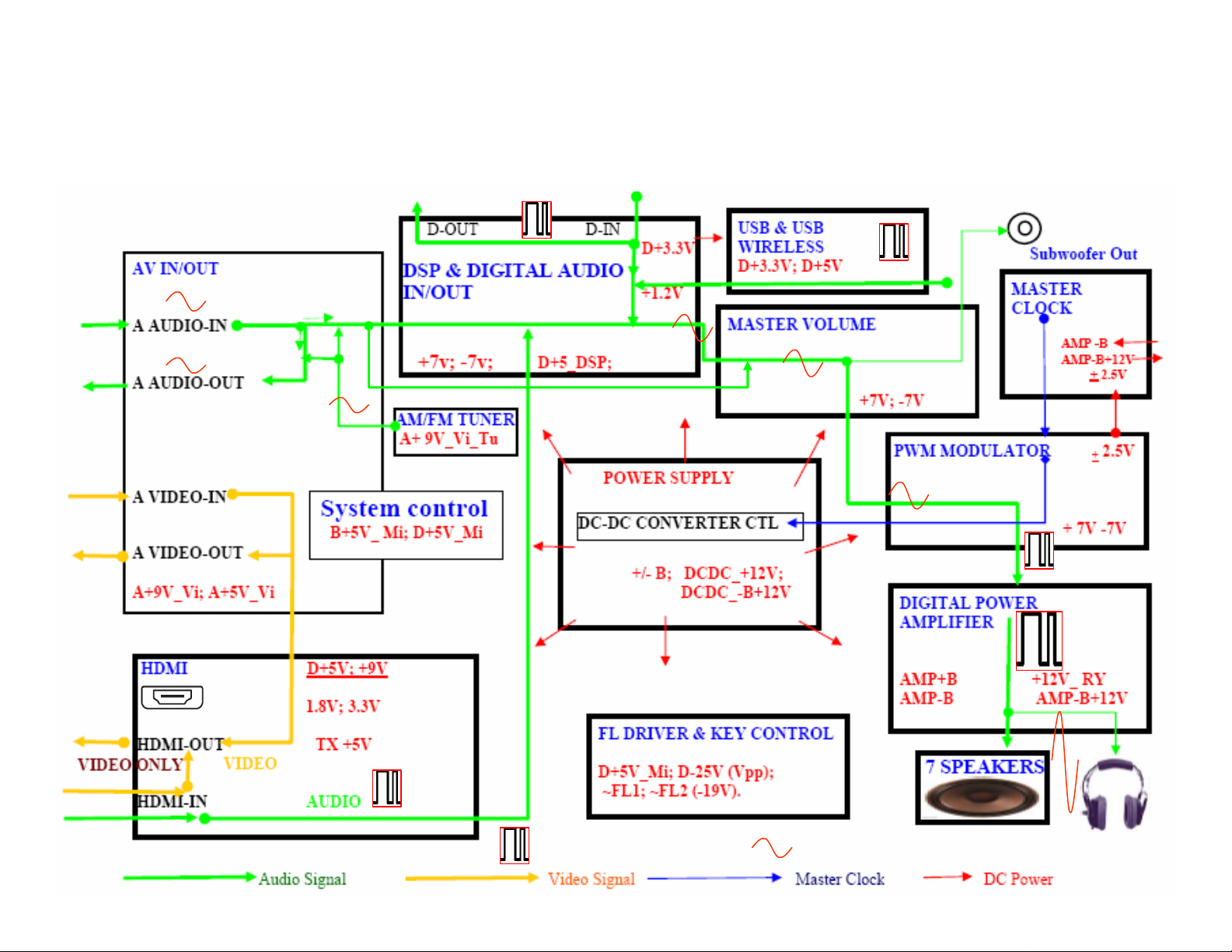
OVERALL BLOCK DIAGRAM
Signal Flow and DC Power Supply
*
DVD A. Multi
IN
=DIGITAL SIGNAL
=ANALOG SIGNAL
Page 4

OVERALL BLOCK DIAGRAM
• A AUDIO means Analog audio, D-OUT means Digital audio output.
• The HDMI outputs video only, even when the HDMI input has both
video & audio data. In the future models, the HDMI will output both A
& V data.
• The digital audio output is not available on models RX-D201/202.
The output format is the same as the digital input signal; other audio
input signals (including HDMI & USB) cannot go through the
DIGITAL OUT.
• The front left & right speaker out audio is applied to headphones.
The CPU will turn off the 7 speaker relays after it detects the
headphone jack is plugged in.
note
• The ‘DVD analog multi channel’ input audio bypasses the DSP
board, and goes into Master Volume Board directly.
• directly.
Page 5
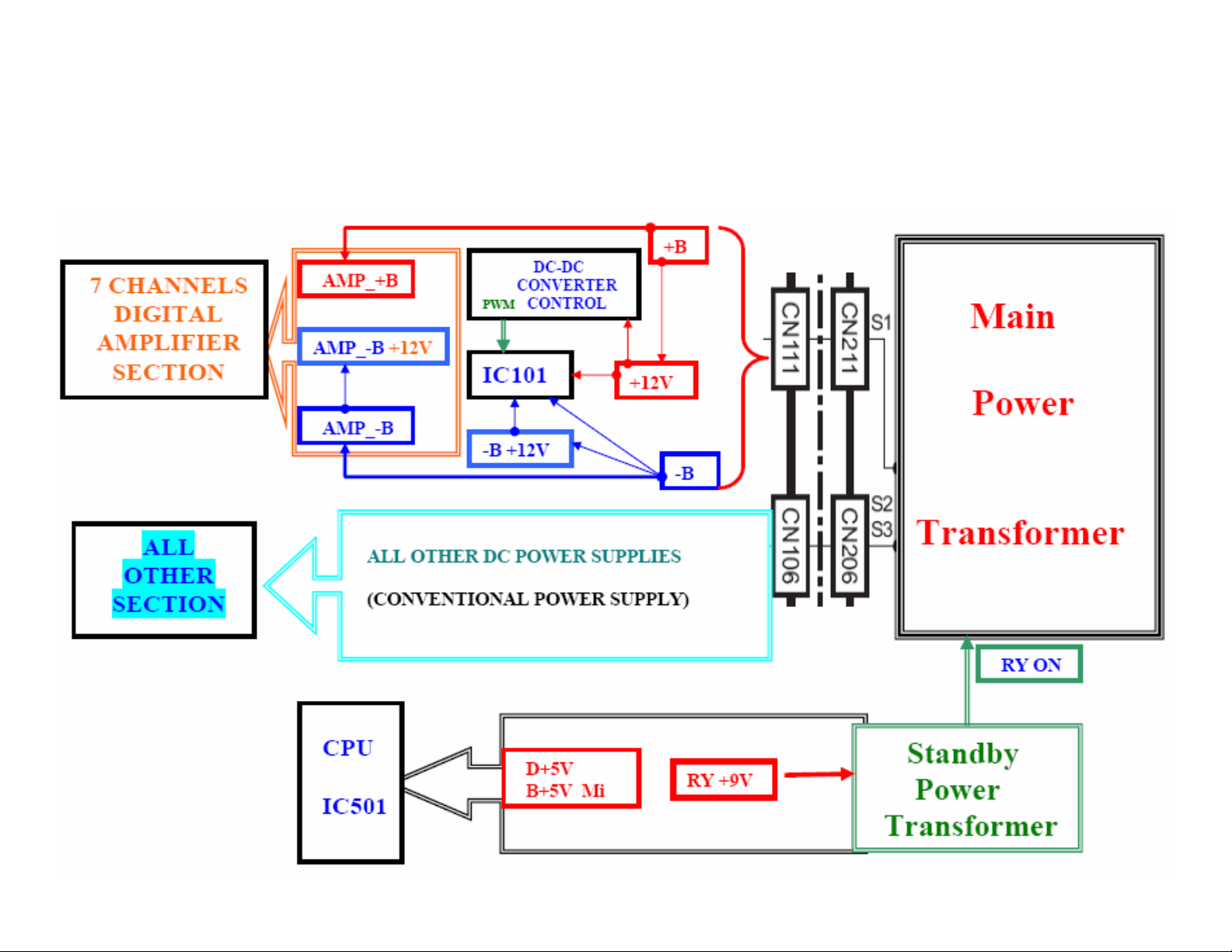
POWER SUPPLY BLOCK DIAGRAM
‘AMP_+/-B’ switch regulator
Page 6
POWER SUPPLY 1/5
Regulate
PCB
Master Clock PCB
IC201/301
IC401/801
PWM PCB
CN114-3
D+5V_DSP
Q171
CN114-4
CN530-5
R152 +12V_RY CN530-7
Page 7

POWER SUPPLY 1/5
• The power supply circuits for 2005 year of RX-D… series are similar. One main
difference is the ‘D+5V_HDMI’ is not in models RX-D201/202/301/302.
• There are two AC power transformers in the unit.
1. T101 for standby power: supplies D+5V and B+5V_Mi DC power for CPU IC501
and RY+9V (power ON/OFF relay circuit).
2. T102 for unit operation after power on: There are more than 15 different DC
voltages provided for unit operation after power is turned on.
• The DC voltages: +B, AMP+B, AMP-B+12V and DCDC_-B+12V all vary (along
with output volume) referenced to ground. The ‘–B’ voltage is -50v~ -62v
referenced to ground. The label ‘DCDC_-B+12V’ DC voltage means this is the
DC voltage supply to the DCDC converter circuit, the +12 DC refers to –B; if
referenced to ground, it is -38v~-50v.
• The +B and AMP+B voltages are higher in models RX-D402/702, because the
output power is higher than RX-D201/202.
note
• The +2.5v, DCDC_+12V, DCDC_-B+12V, AMP-B+12V, D+5V_DSP and
D+5V_HDMI are not produced in the main PCB.
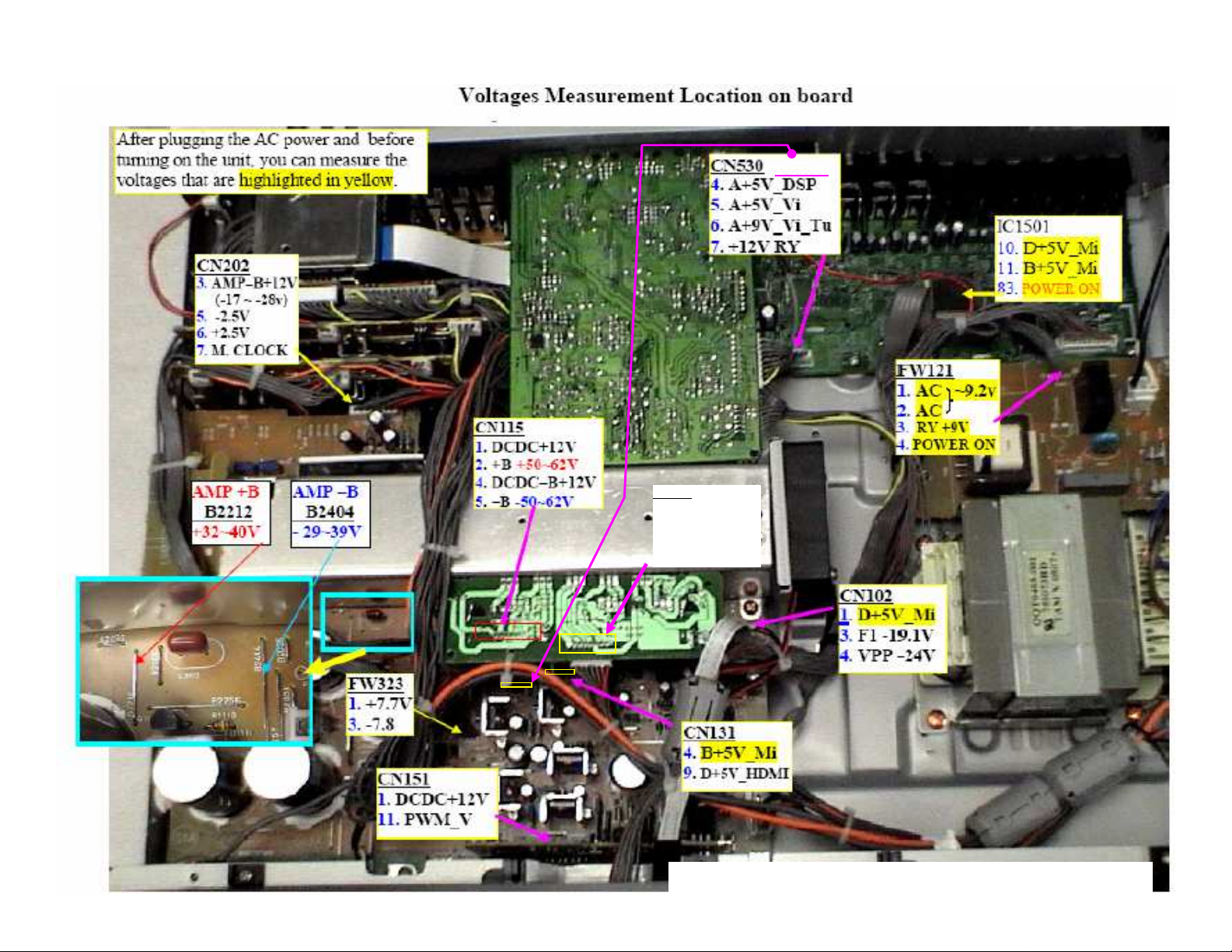
• You could check all of the voltages at the indicated (underlined) locations
without any extension cable, before or after power is turned on. (See the next
page)
• Some additional DC voltages are produced in ‘Regulate PCB’ and ‘Master clock
PCB’.
Page 8
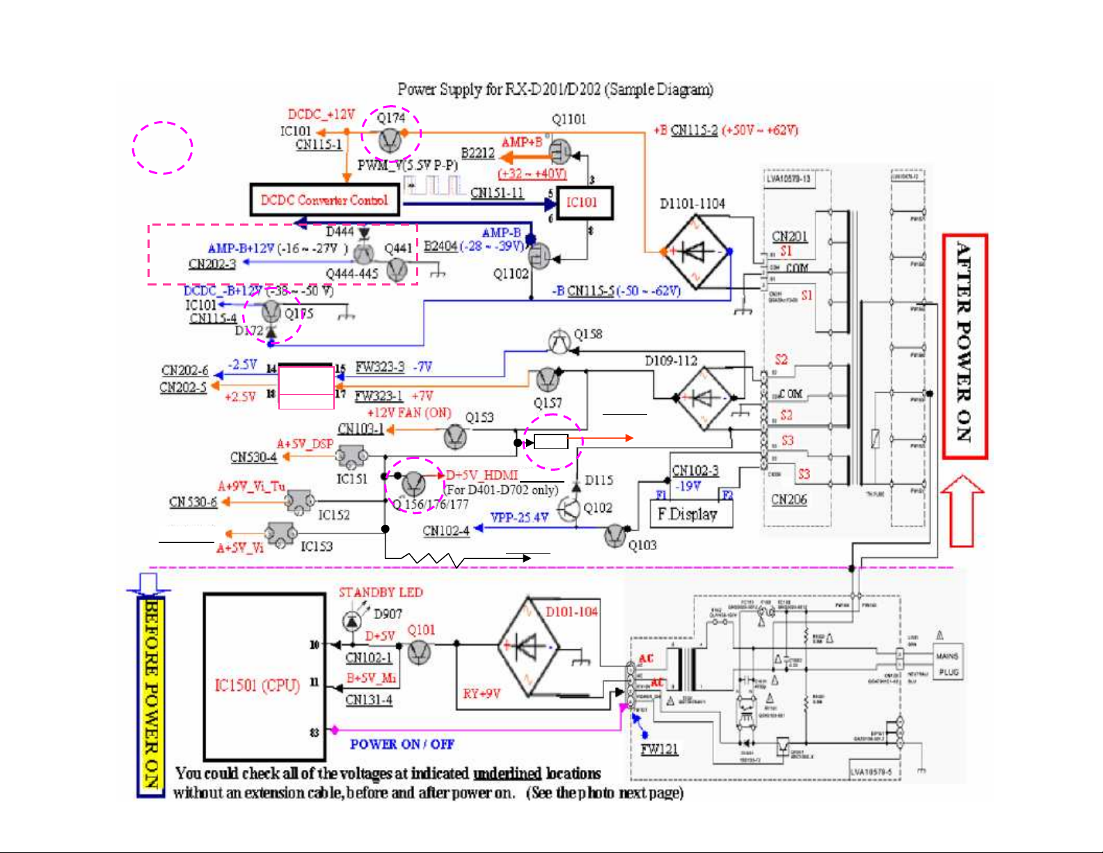
POWER SUPPLY 2/5
(CN130)
CN114
3. D+5V_DSP
4. D+5V_HDMI
*
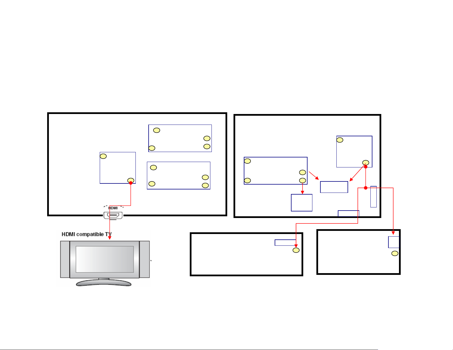
The ’D+5V_HDMI’ for models RX-D401/402/702 only.
*
Page 9
The ‘AMP_+/-B’ switch regulator
composes three sections:
1. MOSFET switch circuit (the important parts are
Q1101/1102, D1107/1108, L1101/1102,
C1117/1118…)
2. Switch driver circuit-IC101.
3. DC-DC Converter Control Board
POWER SUPPLY 3/5
3 2
DC-DC
CONVERTER
CONTROL
AMP_ +/-B
LEVEL
CONTROL
CPU IC501
MOSFET
DRIVE
IC101
SOUND
LEVEL
DETECT
1
MOSFET
SWITCH
Q1101/1102…
7 CHANNEL
POWER
AMP
+
AMP_B
_
Page 10
AMP_+B
‘AMP_ +/-B’ switch regulator-1a
The CEMF current (via D1107/8) loop
after Q1101/1102 switch off.
+B
POWER SUPPLY 3/5
+12V
-B +12V
IC101
V. feedback
AMP_-B
V.out_det.
-B
Page 11
POWER SUPPLY 3/5
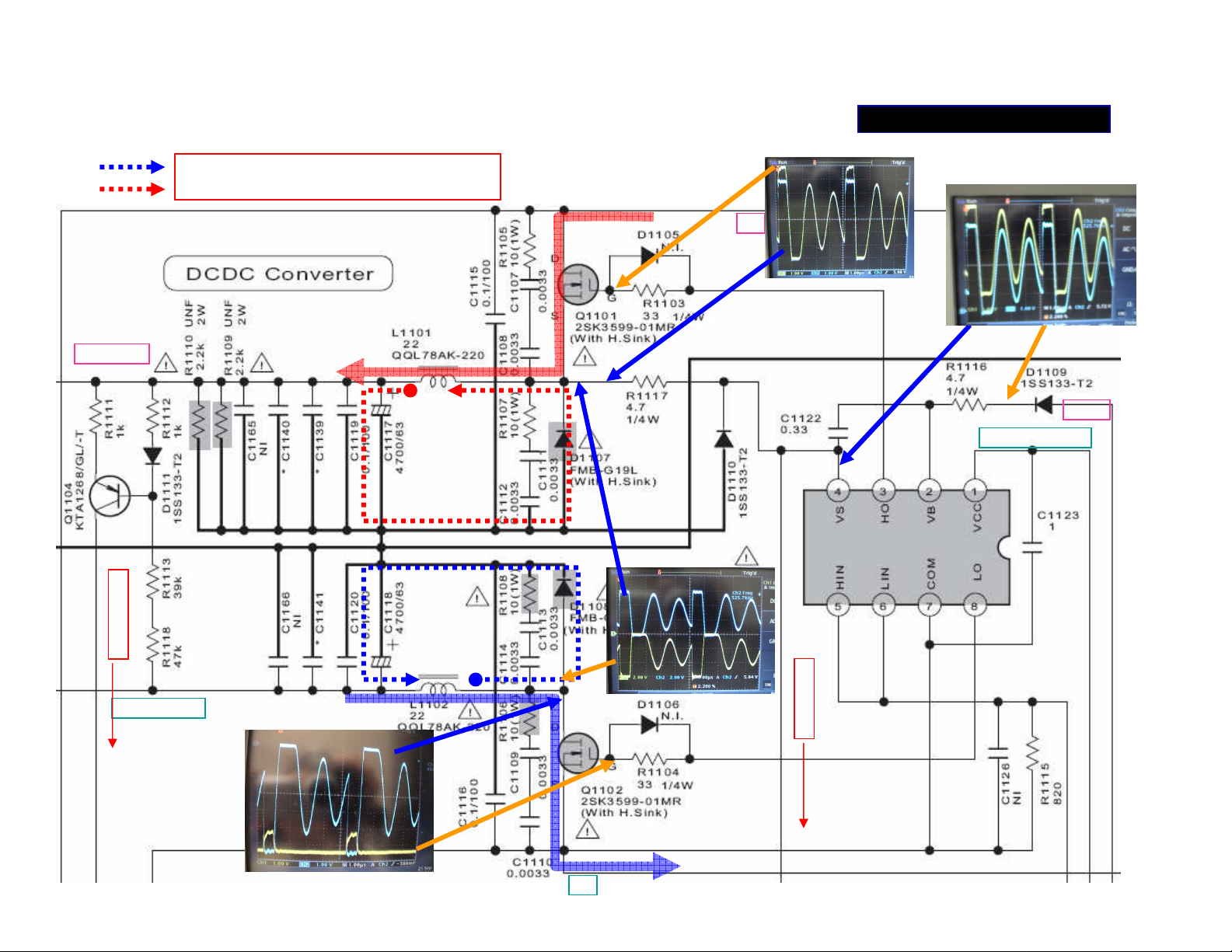
Tip to measure the outputs of Q1101/1102
Page 12
POWER SUPPLY 3/5
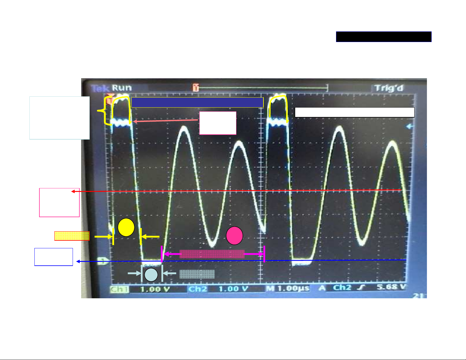
Waveform (1) at ‘AMP_+/-B’ switch regulator
There is 10v At
Gate higher than
Source for
switches Q1101
on.
AMP+B
(+30V.)
Q1101 on
0 V.
Yellow at G of Q1101 –channel 2
Blue at S of Q1101- channel 1
+B
(+60V.)
1
3
Damped oscillation
2
D1107 on
The waveforms at Source and Gate of Q1101. Three periods in one cycle of
oscillation: 1.Q1101 turned on; 2. D1107 turned on by CEMF; 3. Damped LC
oscillation; Q1101 is switched off during period 2 and 3.
Page 13
POWER SUPPLY 3/5
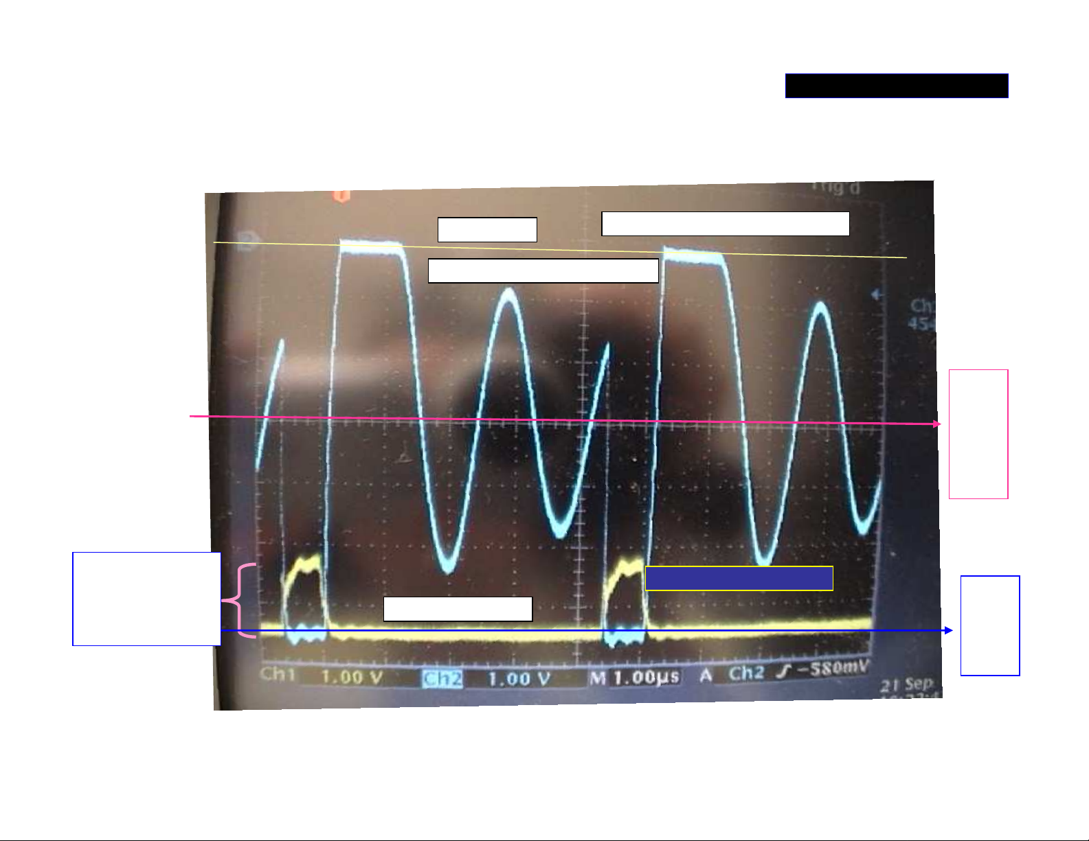
Waveform (2) at ‘AMP_+/-B’ switch regulator
About 10v
pulse at Gate of
Q1102 when
switch on
DC 0v line
Blue at D of Q1102- channel 2
Both channel X 10
Both channels are DC coupling
AMP
-B
About
-30v
Yellow at G of Q1102
-B
About
The waveforms at gate and drain of Q1102 after power is turned on.
-63v
Page 14
POWER SUPPLY 3/5
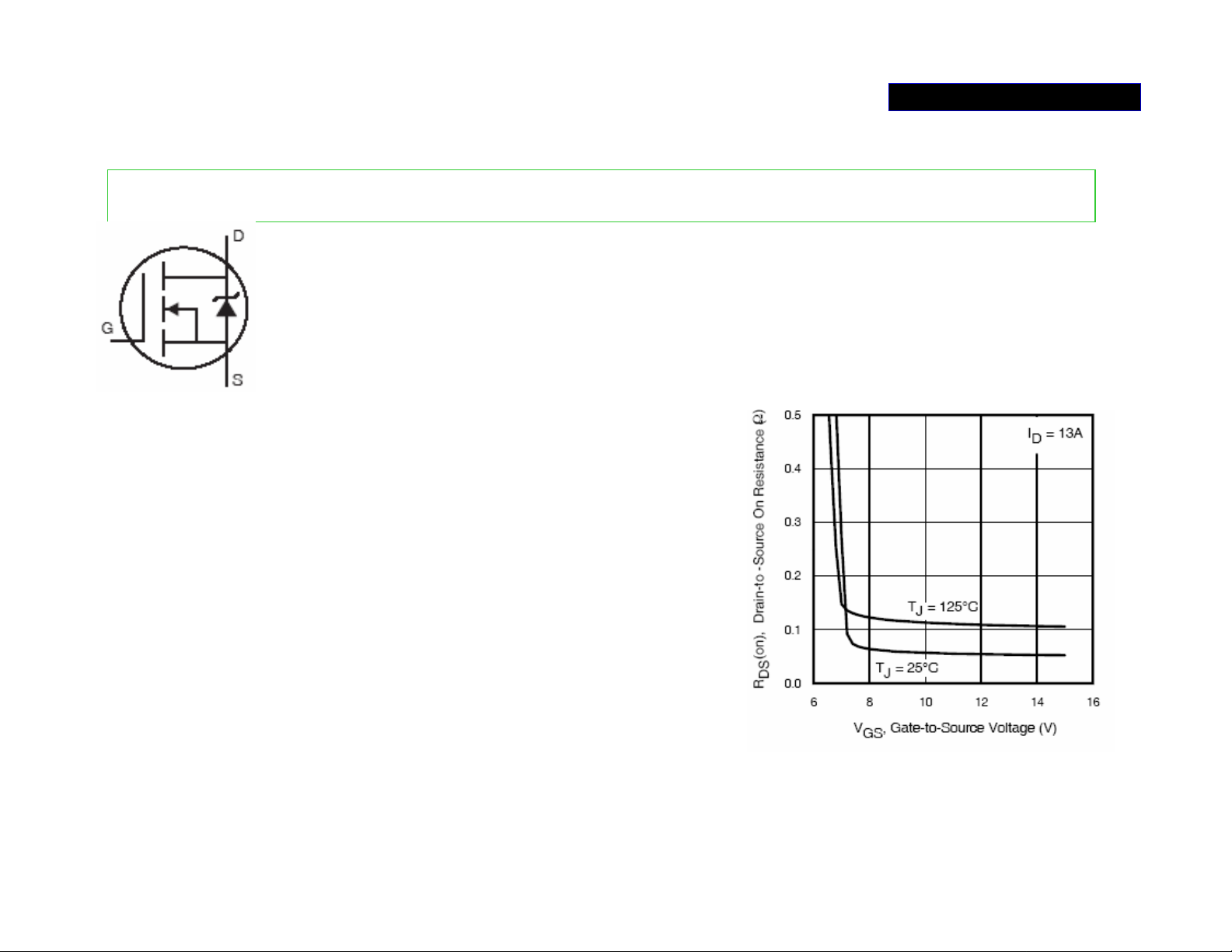
KNOW THE MOSFET
2SK3599-01MR and IRFB4212 are Enhancement-type N-channel MOSFET
+
• Enhancement-type MOSFET is also known as
normally off (when VGS=O, Drain current=o) MOSFET.
• N-channel MOSFET: The more positive the gate
+
voltage (VGS), the greater the drain current.
-
• There is a built in zener diode in these two kinds
of MOSFET, but it does not show in manual’s
diagram.
• The RDS (resistance between Drain and Source)
will increase when VGS drop to below 8v; and it
causes the MOSFET to get very hot and damage.
• MOSFETs have a thin layer of silicon dioxide;
this insulating layer is kept as thin as possible to
give the gate more control over drain current.
Because the insulating layer is so thin, it is easily
destroyed by excessive gate-source voltage.
• The transient voltages by inductive kickback and other effects may exceed the V
(max)
rating; even handling a MOSFET may deposit enough static charge to exceed the
V
GS (max)
rating.
GS
Page 15

POWER SUPPLY 3/5
• If the positive drive pulse at Gate is less than 8 volts
(refer to Source), the MOSFET will get very hot to
damage. If the drive pulse is not sharp or is very noise, it
makes MOSFET very hot also.
• If the drive pulse is low & noisy, the drive IC or
peripheral parts may be defective or the power supply
may not be functioning properly.
• When handling the MOSFET, try not to touch the pins
with your fingers.
• It is preferable to use anti-static iron when soldering the
MOSFET.
• When the pair of MOSFETs are damaged, sometimes the
drive IC becomes defective too. Check the drive circuit
before replacing the MOSFETs, to prevent the power
MOSFET from shorting again.
Page 16
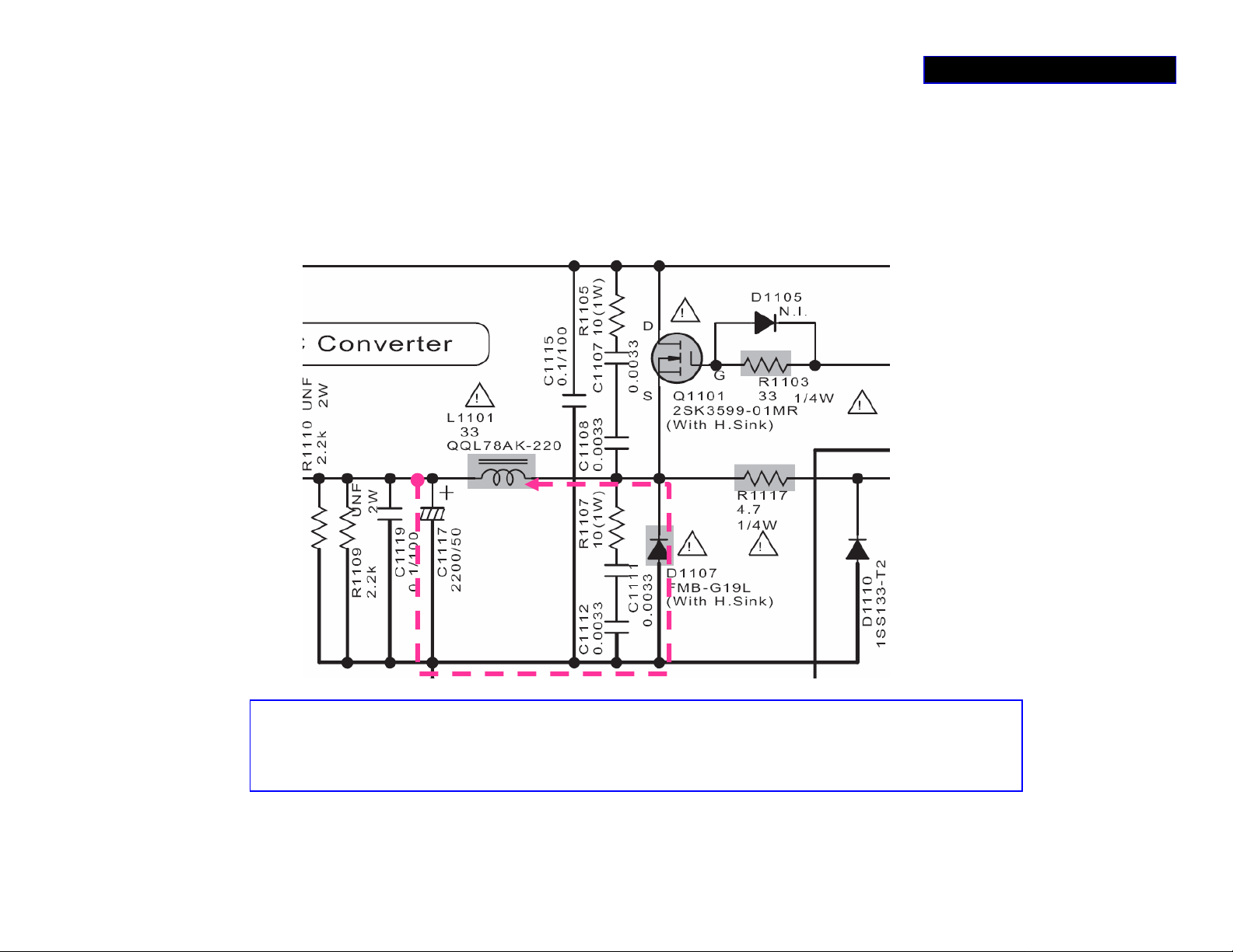
‘AMP_ +/-B’ switch regulator-1b
CEMF charge path
+B 70 V
POWER SUPPLY 3/5
ANP+B 30V
_
(+30 V) *
+
In this circuit it, seems no current through D1107, but D1107 is high power Schottky Diode
with heat sink, If You mean with DC Volt meter but if you use Oscilloscope you can see the
negative peak is clipped. This clipping is by D1107
WHY? *DC METER CHECK
Because there is a large charge current through D1107 that forced by CEMF.
Page 17
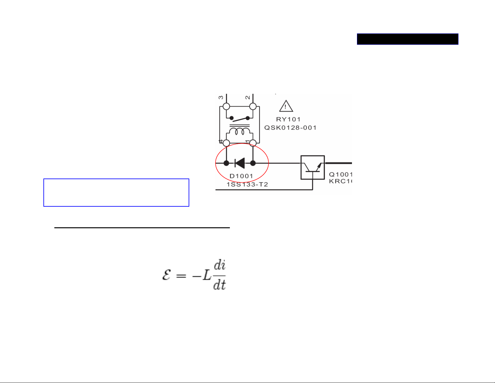
In the relay driver circuit, always has
POWER SUPPLY 3/5
What is CEMF?
a diode parallel with coil,
Counter-Electromotive Force (CEMF) is a voltage developed in an inductor network
by a pulsating current or an alternating current. The voltage's polarity is at every
moment reverse that of the input voltage, therefore opposes the change of main
current flow in the circuit it is called counter-electromotive force (CEMF). The CEMF
is then given by:
Where i is the current, T is time and L is the inductance (L1101) of the circuit. When
the ‘dt’ is very and very small the CEMF (voltage) will become extremely high.
If diode (D1107) is defected it can cause damage to peripheral components
WHY?
(the ‘–’ sign means polarity reverse)
Page 18
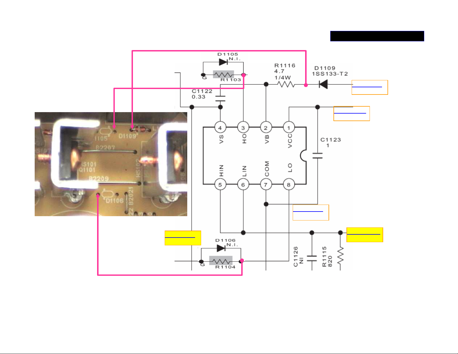
‘AMP_ +/-B’ switch regulator-2
POWER SUPPLY 3/5
IC101-
5
6
Drive IC for Q1101/1102
-B_+12V
DCDC +12V
2
C1122
3
4
1
8
VERAG
DC 42v
+B
AMP+B
AMP-B
-B
7
-B
Audio
CPUPWM
Level
detector
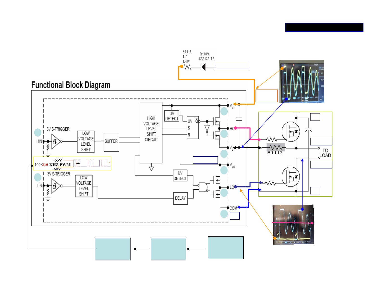
Page 19
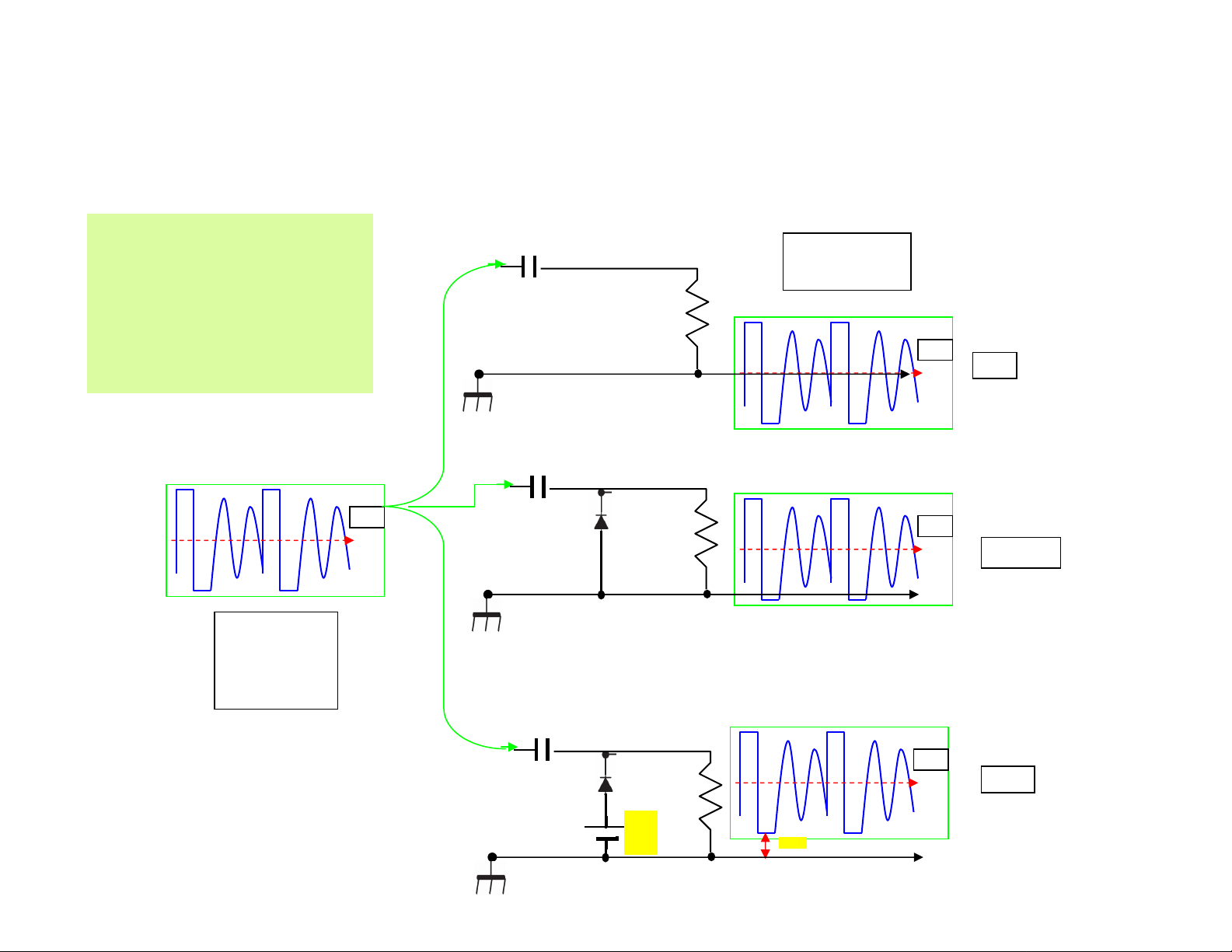
Bootstrap Voltage
1. Capacitor coupling block out the input DC level.
Bootstrap Voltage
The additional
higher positive
USE THE DC CLAMPER
OUTPUT
AVERAGE DC
voltage added to
the low DC voltage
INPUT
AVERAGE
DC 30V
Averag
e
+30v
Averag
e
+0v
0V
2. The DC clamper recovers the DC level at output. *
Averag
e
+30v
29.3V
* In fact it is about +29.3v due to diode forward bias drop.
3. The DC clamper adds DC level to the output.
Averag
e
+42v
42V
+
12v
-
12v
Page 20

POWER SUPPLY 3/5
•
IC101 is high power MOSFET drive with
independent high and low side reference output
channels.
• The power supply for the high channel drive is
floated.
• The bootstrap voltage from VS to VB through
0.33uF capacitor C1122.
• This causes DC level at pin2-VB to be always
approximately 11v higher than pin 4-VS.
• The UV (under voltage) detector is built in the IC, if
the power supply voltage drops below the threshold
level (about 7.5-8.3 v), The IC stops output.
• If IC101 was shorted, sometimes peripheral
resistors are burnt out also.
Page 21
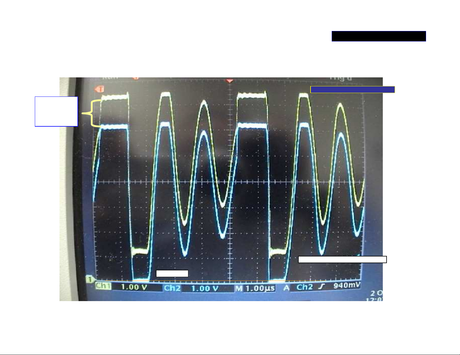
About
11v.
POWER SUPPLY 3/5
Waveform (3) at ‘AMP_+/-B’ switch regulator
Yellow at pin 2 of IC101 (R1110)
Blue at S of Q1101- channel 1
DC 0v line
Always about 11v different between pin 2 and pin4 of IC101.
Page 22
Tip to measure IC101
POWER SUPPLY 3/5
CN115 P-1
DCDC +12V
CN115 PIN4
–B_+12V
CN152 P-4
Vout_DET
CN115 P-5
--B
CN152 P-11
Vout_DET
Page 23
‘AMP_ +/-B’ switch regulator-3
Q1501Buffer
POWER SUPPLY 3/5
This feedback
voltage for
regulate the
AMP. +B
Error amp
And ‘V out’ detector
Page 24
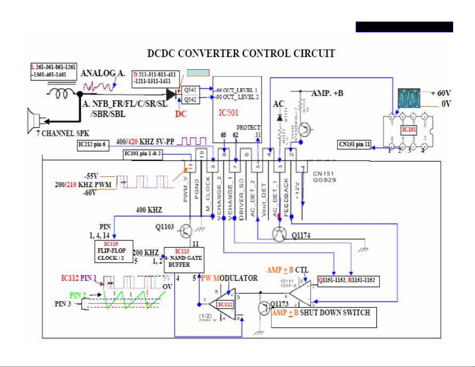
CPU IC501
PIN 62 PIN 65
POWER SUPPLY 3/5
CN151
AMP +/- BPIN 8PIN 7
25VHH
35VHL
42VLL
• The AMP + B voltages vary from about +25v to +42v; depending on the power output of 7
channels at final stage before speaker terminal (The voltages are higher in models
RX-D401/402/702)
• When the audio output level (the analog negative feedback [A NFB] that comes from the
audio final output) is increasing, the DC level at the cathode of diodes D211-D311…
(7 diodes) is increased proportionally.
• This increased DC voltage via buffer Q1501 turns on Q541 first (0.7v), and will turn on
both Q541 and Q542 if the DC level rises higher (2.57v). Then the low state will input to
pins 66 and 90 of IC501 (OUT_LEVEL 1 and OUT_LEVEL 2). This causes IC501 to output
a low state on pins 62 and 65 (V CHANGE_1 and V CHANGE_2) to DCDC CONVERTOR
CONTROL board.
• These low state inputs (through CN151 pin 7 & 8) switch off Q1151, Q1152, and it effects
the DC level at pin 1 of IC111 (error amp). Finally, it changes the PWM pulse’s duty cycle
duration at IC112 pin 1, thus rises the AMP + B voltage to around + 35v ( VCHANG_1
active only) or + 42v (both VCHANGE_ 1 and _2 are active).
• The ‘FEEDBACK‘ from ‘AMP+B’ goes into ERROR AMP IC111 pin 3 through CN151 pin 2,
it is for stabilizing the ‘AMP+B’ regulation.
Page 25
POWER SUPPLY 4/5
+2.5V regulator built-in the IC supply to
digital circuit inside and outside of IC.
+7V
+2.5V
-2.5V
-7V
Use of the built-in ±2.5V regulated supply to the inside and outside digital
circuits, especially for master clock generation circuit, prevents digital
noise interference to analog GND.
Page 26
POWER SUPPLY 5/5
Some Other DC Voltages Not In Main PCB
DC +3.3V, +1.8V, +1.2V and TX5V
HDMI
BOARD
1
IN
9V
IC793
OUT
TX5V
5
OUT PIN 18
IN
5V
5V
IC791
OUT
IC792
OUT
1
2
ADJ---------- 1.8V
IN
1
2
ADJ---------- 1.8V
3.3 V
3.3 V
5
DSP
4
BOARD
7
IN
5V
IC692
1
IN
5V
IC691
OUT
3.3 V
5
4
2
ADJ---------- 1.2V
5
4
OUT
APPLY IN
BOARD
3.3V
1
C661
DSP
CN661-3
CN662-3
USB
wireless
IN -3.3V
BOARD CN11
FRONT INPUT
3
BOARD
CN961
IN-
3.3V
3
Page 27

POWER SUPPLY 5/5 NOTE
• IC791, IC792 and IC691 are same type of regulator IC
and the voltage from ‘output 2’ (pin4 of the IC) can
be adjusted. We see the voltage is 1.2v at pin 4 of
IC691, and others are 1.8v.
• IC793 outputs TX5V to the HDMI out jack, this 5v is
sent to the outside video monitor for HDMI
connection detect; without this 5v, the monitor
cannot accept signals from the HDMI input.
• The +2.5v and -2.5v also are not produced in main
PCB, they are from the PWM PCB; shown on the
previous page.
Page 28
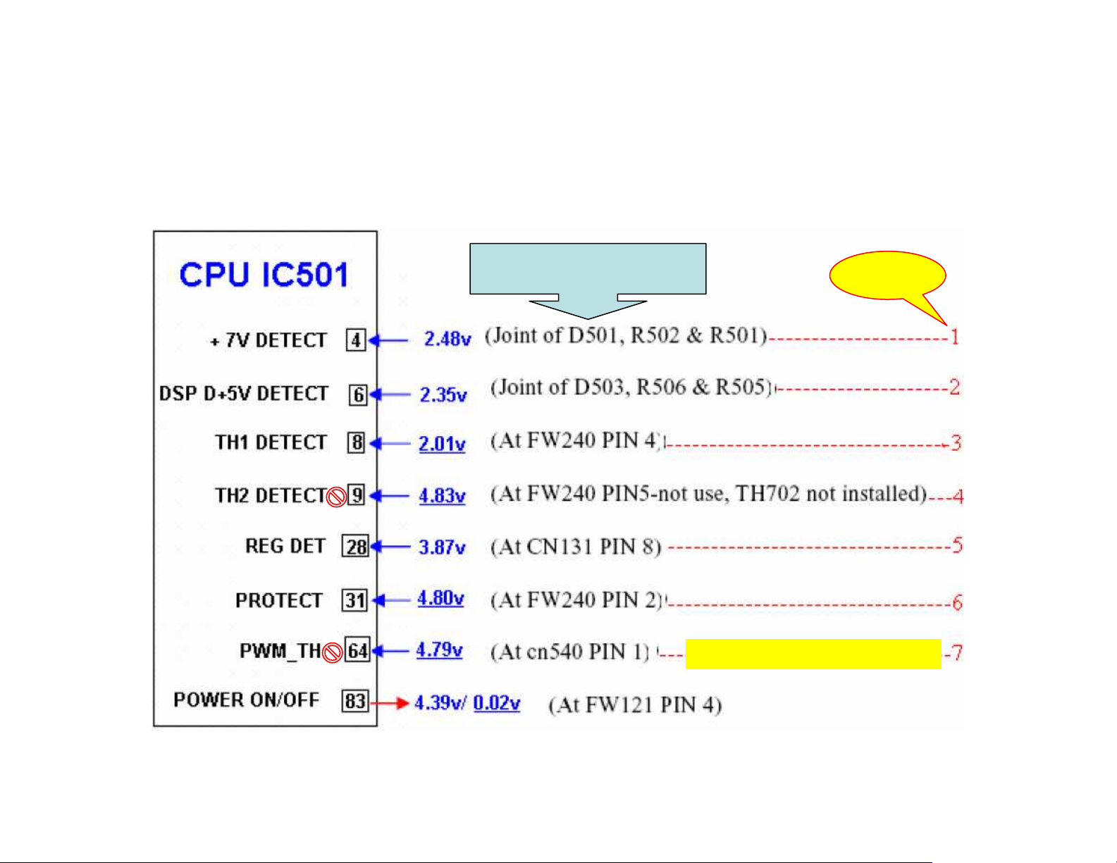
PROTECTION CICUIT 1/8
FOR MODELS: RX-D201/202/301/302
Where to measure
Not use
7 protect
inputs
(Q212/213 R226 NI)
Page 29

PROTECTION CICUIT 1/8
• If the power auto shuts off a few seconds after turn
on, most likely it is caused by the power protection
circuit. We describe the protection circuit on models
RX-D201/202. It is similar to other RX-D… series
models and can be used as a reference for
troubleshooting.
• There are 7 protection input pins (only 5 pins used in
these 4 models) on CPU IC501; any of them could
cause the protection circuit to be triggered and shut
down the power. The marked voltages are +5~10%
NOTE
tolerance.
• The underline marked voltages can be measured in
power standby mode; (e.g. 2.01v, 4.83v …) but have
to be checked again once power is on.
Page 30
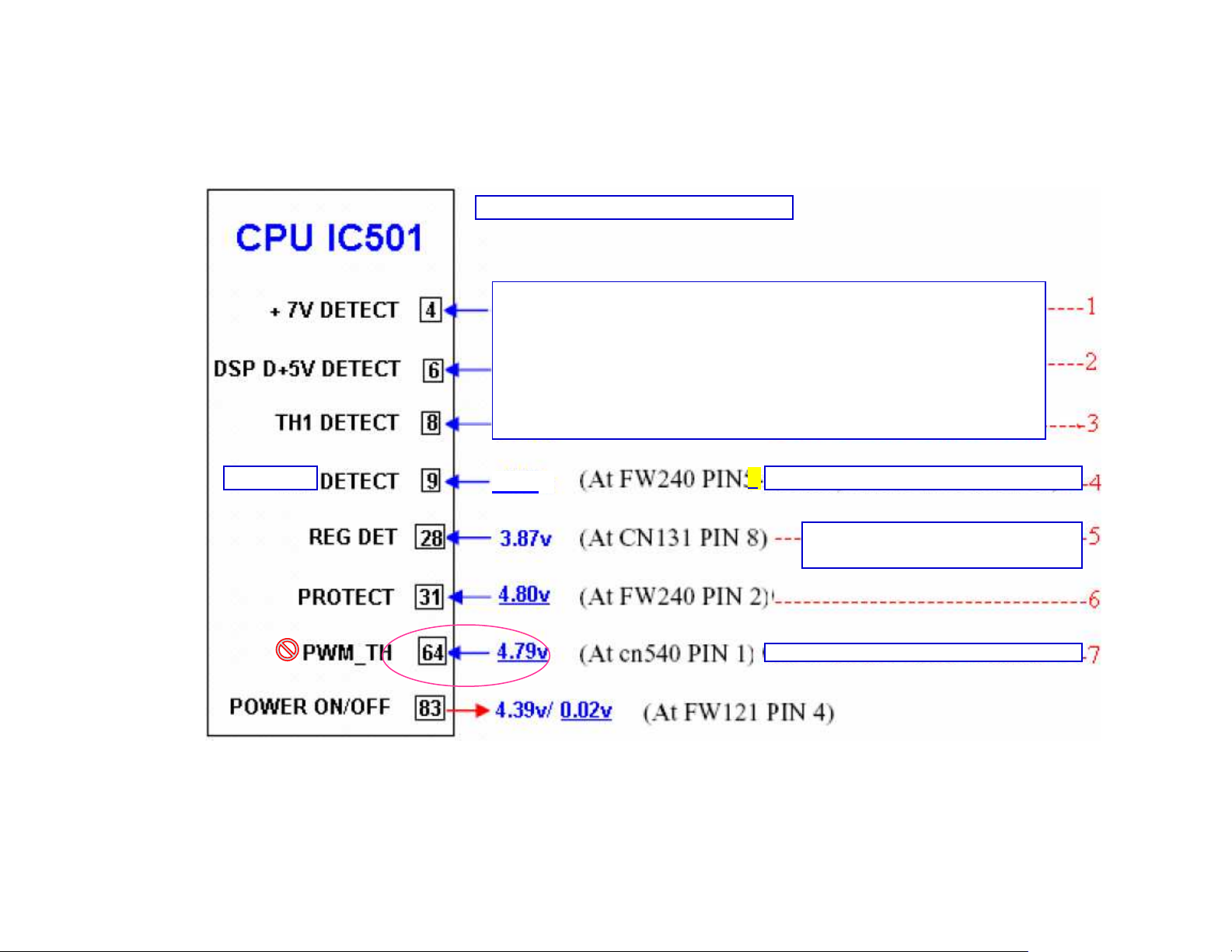
PROTECTION CICUIT-SUP. 1
For models RX-D401/402/701/702
These 3 pins are NOT used for
Where to measure
7 protect
inputs
protection input on models
RX-D401/402/701/702
THERMAL For models RX-D401/203/701/702
2.01v
4
Include +7v, DSP D+5V,
D+5V_HDMI DETECTION.
Not use, because Q212,213 and R220 are NI.
Page 31

PROTECTION CICUIT-SUP. 2
•
The protection circuit on models RX-
D401/402/701/702 has 3 inputs to CPU
IC501. Any of them could cause the
protection circuit to be triggered and shut
down the power. The marked voltages
have tolerance +( 5-10)%
• The underlined voltages could be
measured in power standby mode; (e.g.
2.01v, 4.80v …) but have to confirm them
again once power is ON.
Page 32

PROTECTION CICUIT-SUP. 3
IC501 DIFFERENT
MN101C49KNR1—for models MN101C49GNP— for models
RX-D401/402/701/702 RX-D201/202/301/302
Page 33

PROTECTION CICUIT-SUP. 4
S.S.S.
stands for ‘Smart
Surround Setup’ function
This function is adopted on model
RX-D702B only.
Page 34

PROTECTION CICUIT 2/8
Protection 1 & 2
‘+7V DETECT’ & ‘DSP D+5V DETECT’ inputs:
IC501 pin 4-5 or 6-7 becomes Low (near 0v) when +7v or
D+5v (DSP) is missing
.
7
Page 35

PROTECTION CICUIT 3/8
Protection 3 & 4
TH1 & TH2 DETECT inputs:
The voltage drops at pin 8 of IC501 when
unit gets hot
Page 36

PROTECTION CICUIT 4/8
PROTECTION 5
REG DET input:
This input detects the regulated voltages; A+5V_Vi, A+5V_DSP,
and +9V_Vi_Tu. Any of these three voltages missing can cause
one of three transistors (Q162, Q163 & Q161) to turn off and
give a LOW state input at pin 28 of IC501.
Page 37

PROTECTION CICUIT –SUP. 5
REG DET input for models RX-D401/402/701/702
3.56v
HDMI 5V
DETECTOR
D +5V (DSP)
DETECTOR
+7V DETECTOR
Page 38

PROTECTION CICUIT-SUP. 6
REG DET input:
This input detects the regulated voltages: A+5V_Vi,
A+5V_DSP, +9V_Vi_Tu, +7V, D+5V(DSP), and
d+5v(HDMI). If any of these six voltages are
missing, it may cause one of six transistors
(Q162, Q163, Q161, Q505, Q506 and Q507) to turn
off and to give a LOW state input at pin 28 of IC501.
(for models RX-D401/402/701/702)
Page 39

PROTECTION CICUIT 5/8
Protection 6
PROTECT input:
This protection input including AC DETECT, OUTPUT OVER CURRENT
DETECT & OUTPUT DC (to speaker) DETECT. If any of the three above
condition occurs, it would cause a LOW state inputs to pin 31 of IC501.
R290
D1171
Q282
- 0.6V / + 0.7V
(7 CNANNELS)
AMP-B
R270-370-870-1270-1370-470-1470
Q281
Q286
Q283
R289
Q284
Q285
Page 40

PROTECTION CICUIT 5/8
NOTE
1.
• 2. DC (to speaker) DETECT PROTECTION
• 3. AC DETECT PROTECTION
OVER CURRENT PROTECTION
– There are 7 digital amp ICs (IC 251/351/851/261/361/451/461) for 7 channel audio
amplification. Pin 5 of these ICs outputs a LOW state when the final output over
current is detected. Pin 5 is connected to base of 7 transistors
(Q251/351/851/261/361/451/461) respectively.
– These 7 transistors are PNP type, and are turned on when base voltage goes LOW.
– Any one of these 7 transistors turned on (when over current occurs) would turn off
Q281, then turn on Q286 and Q282. The emitter of Q282 becomes 0 volts, and the
LOW state would be sent to pin 31 of IC501 through R290 triggering the protection.
– There are 7 resistors connected to 7 channel speaker outputs (just after low pass
filter). The other side of these resistors are tied together and connected to the base
of Q284 and Q285.
– If a DC voltage occurs at any audio speaker output line, a (+) will turn on Q285 or a(-)
turns on Q284 and Q283.
– A LOW occurs at collector of Q285 when Q285 or Q283 are turned on. The LOW
state is sent to pin 31 of IC501 through R289 and triggers the protect function.
– The AC power from winding S1 of the power transformer is rectified by D1171,
producing a negative DC voltage which is applied through R1171 and R1172 to base
of Q1174, keeping it cut off, and keeping the collector HIGH (almost +5v).
– When the AC power (S1) disappears, +0.7v is applied to the base of Q1174, turning it
on into saturation. A LOW is sent to IC501 pin 31 through R1178 triggering the
protect function.
Page 41

PROTECTION CICUIT –SUP. 7
Protection 6 detail
The OC & DT/SD functions in the digital amplifier driver IC-IRS20124S-X
Over Current sensor
top-bottom setup levels
PWM in
DC voltage to select
DT mode
Over Current
protect output
PWM out
Over Current
sensor input
Page 42

SUP. 7note
• OC stands for Over Current; DT/SD stands for Dead
Time and Shut Down.
• The DT (dead time) is defined as the time period from the
starting point of turn-off on one side of the switching
stage to the starting point of turn-on on the other side.
• DT/SD pin provides two functions: 1) setting deadtime
and 2) shutdown. There are 4 modes of DT preprogrammed in IC.
• The IRS20124 determines its operation mode based on
the voltage applied to the DT/SD pin. An internal
comparator translates which mode is being used by
comparing internal reference voltages.
• Since IRS20124 has internal dead time generation, if
independent inputs for HO and LO are no longer
provided; shutdown mode is the only way to turn off
both MOSFETs simultaneously to protect them from over
current conditions.
Page 43

PROTECTION CICUIT 6/8
Protection 7 (Not use)
(PWM_TH DETECT) input:
This protection input is not used on 2005
RX-D… series model, because Q212/213 and
R226 are not installed.
LOW V & THERMAL WARNING
NI
NI
Page 44

PROTECTION CICUIT 7/8
• Note:
– Knowing that the power automatically shuts down
within a few seconds, make sure to quickly
measure the protection input voltages before the
unit powers off.
– See the next page for the measuring locations on
the PCB.
– You could check all of protection input voltages at
indicated locations without extension cables. The
voltages that are underlined (#.##V) can be
measured in power standby mode, but have to be
checked again after power on.
Page 45

PROTECTION CICUIT 8/8
4.39V / 0.02V
Page 46

Repair Tip 1
The unit’s power and amplifier circuit can work without
the HDMI and OSD (RX-D701/702) PCBs.
It is easier to
check on the ‘A/V
input & system
control’ section,,
when
troubleshooting
the power and
protection circuit.
Audio/Video
signal input
and system
OSD PCB
(
removed)
HDMI PCB
(
removed)
control section
Page 47

Without any
extension cables
you can turn over
the main PCB and
Repair Tip 2
power on the unit.
Every function
should be working
except the
headphone, front
USB and subwoofer
out functions,
because these 3
connectors are
unplugged only.
(It may need adding
a ground connection
to chasses for stable
ADD GROUND
CONNECTION
operation the unit
when perform the
troubleshooting.)
CN661 CN351 &
CN523 ARE
UNPLUGGED
Page 48

Quick check shorted components 1
Measure points in schematic diagram
AMP+B AMP-B
+Q261 -Q262 6
+Q361 -Q362 4
+Q861 -Q862 2
CN251
PWM IC201
PWM IC801
CN262
CN222 PIN14
on M volume
AMP+B AMP-B
8 +Q1261 -Q1262
6 +Q1361 -Q1362
4 +Q461 -Q462
2 +Q1461 -Q1462
+B
Q1101
Q1102
-B
Page 49

•The high DC voltage on the feedback line (If Q861 or
Q862 shorted) might damage the PWM ICs. (The
picture shows center channel only, the other
channels are similar.)
•When MOSFETs are shorted, there is a high
probability for the driver IC to be damaged also, and
the Gate (47 Ohm) resistor to be burnt out.
•You could quick check the MOSFETs 14 outputs and
2 Amp B+/- and 7 diodes without removing the PCB.
•When checking the 7 diodes, select the DIODE
MODE on multimeter, minus (negative) probe
contacts pin14 of CN222; plus (positive) probe
contact pin 2/4/6/8 of CN251 and CN262 respectively.
Page 50

Without any extension cable, quick measure the Q1101/1102 and 14 power
CN222 PIN14
On the bottom
Quick check shorted components 2
output MOSFETs; also measure the +/- 7V to determine if it is shorted.
CN423
AMP_ +B
+/- 7V
AMP_ -B
CN262
Measure the
resistance, if
less than 100
Ohms it’s NG.
For Example: If
the resistance
between +B (-B)
and AMP_+B
(AMP_-B) is
less than 100
Ohms the
Q1101 (Q1102)
is shorted.
CN251
CN115 PIN 2- +B
----------PIN 5- -B
See next slide
to know the
measure points
on schematic
for all of other
components.
Page 51

•When unit doesn’t power ON and fuse F103 is
blown, it is necessary to find out the shorted
components before replacing the fuse and turning
on the power.
•If F103 is blown it is very likely caused by shorted
MOSFETs at one or more channel’s power output
or may be by shorted on Q1101 and Q1102.
• If -7v was shorted, the master clock will be
missing also.
Page 52

Quick check PWM waveform
After power is turned on, we could measure 7 channels PWM waveform
at four connectors easily. Any abnormal of PWM waveform may be
caused by PWM IC or power output section (MOSFETs & drive ICs).
7 channels
SL----SR
FL----FR
SBL--SBR
PWM at two
end pins on
3connectors
(CN521)analog
audio signal.
RED PIN
C
820 Ohm-
Without AC power the resistance
form ‘AMP_ -B’ to each of 7 CHs.
PWM pin should be 820 Ohms. If
is too low, the drive IC at the next
power amp stage is defective.
‘AMP –B’+4.2V
PWM waveform 4.2V p-p
Master Clock 5V p-pAMP -B
FW323
PIN 4
Page 53

CHECK 7 AMP DRIVE IC’s
820
Ohm
PWM
input
AMP_-B+12V
CN202
PIN 2: AMP_-B
PIN 3: AMP_-B+12V
AMP_-B
800 Ohms
MASTER CLOCK PCB
‘AMP_-B+12V’ is the Vcc for all AMP drive ICs.
Page 54

•Trigger with the MASTER CLOCK signal,
which is at pin 4 of FW323.
•It is recommended to either turn the volume
level to 0 or to not use an audio signal input.
the PWM waveform should normally be at
50% duty cycle.
•Select the FM mode and tune to a station
with good reception. We can measure the
analog audio signal at CN521, even with
CN111 unplugged (no +/-B power).
Page 55

Troubleshooting With Unplugged CN111 2/2
Check analog audio and PWM on all channels
FR channel
CN521
CN683
Pin-Ch
1-FR
3-FL
4-SW
5-SR
6-SL
7-C
8-SBR
9-SBL
Analog audio
0.6-1.2v p-p
(8Channels)
PWM signal
4.2-4.6v p-p
Master clock
FL
FR
On back
PWM BOARD 1
C
SL
SR
PWM BOARD 2
SBL
SBR
Page 56

• Trigger with MASTER CLOCK signal, if the
MASTER CLOCK is missing, most likely -7v is
shorted by defective PWM ICs.
•Un-plug 4 connectors CN311/312/411/412 to
eliminate the bad effect on the PWM signal by power
amp stage.
•It is recommended to select the source on FM mode
and the DAP on ALL CH STEREO mode: Measure all
the 7 channels analog audio at CN521.
•The PWM is 50% duty when no audio input or the
master volume at 0. Increasing the audio level,
causes PWM duty cycle to vary.
•The FR (front right) channel is the only PWM signal
that cannot be measured in the front of PCB, it is at
one end of R317 that close to the IC201 of back side
of the PCB.
Page 57

QUICK CHECK TABLE 1/2
Page 58

QUICK CHECK TABLE 2/2
?
OR
SHORT
OPEN
?
Page 59

Troubleshooting With Disconnected Q1101/1102 (1/2)
Without ‘AMP_+/-B’, we could check IC101 and the DC-DC Converter Control circuit easily and safely
Check the IC101 circuit
Since Q1101 is disconnected there is, no floating voltage at pin 4
of IC101. The power supply for the high channel drive is not
floated.
5
6
200 / 210 KHZ
4.2 - 5V P-P
-B_+12V
DCDC +12V
2
3
4
1
8
OUT AT PIN 3
IN AT PIN 5
200 / 210 KHZ
11V. P-P
+11.3v
+0.8v
200 / 210 KHZ
12V. P-P
-B_+12v
-B
7
OUT AT PIN 8
-B
IN AT PIN 6
Page 60

• Before plug CN111, check IC101 with a multimeter
to ensure that there is no shorting between pins
(except pin 5 & 6); otherwise it may damage the
‘DCDC +12V’ and ‘-B+12v’ power supply.
•Make sure the voltages ‘DCDC +12v’, -B and
‘–B_+12v’ appear at pin 2, 1 and 7; and verify the
input 4.5V p-p PWM signal at pin 5 and 6. If R1115
was opened the PWM signal becomes 13v p-p.
•If there is no out put from HO and LO (pin 3 and 8),
then IC101 is bad.
•If the output PWM level is less than 10V or bed
waveform, IC101 or peripheral components maybe
defective.
•It is possible to measure IC101 from the component
side of the main PCB; (see the next page).
Page 61

Troubleshooting With Disconnected Q1101/1102 (2/2)
CHECK DCDC CONVERTER CONTROL SECTION
Master clock 400/420 KHz 5v p-p
Add 47k
GND
V. Change 1
and 2 (low)
V. feedback
200 / 210 KHZ
Vout_det.
‘V_out’ and AC
detector; ‘AMP +/B’ shut down.
Page 62

•With Q1101/1102 disconnected, the DCDC CONVERTER CONTROL
SECTION can function normally; and it is safe to check the circuit.
•The DC level at pin 3 of IC112 controls the pulse width of the clock at pin1
and it farther controls the DC level of the ‘AMP +/- B’.
•The DC level at pin3 of IC112 is effected by ‘Vout_DET’, ‘VCHANGE_1,
VCHANGE_/2, and ‘FEEDBACK’.
•Until the AMP_+/-B voltages are stabilized, Q1772 and Q1773 are active.
After the mentioned voltages are stabilized, the two transistors turn off. If
the PWM too wide at IC113 pin11, it will be turned on Q1173 and shuts off
the AMP_ +/-B.
•Connect the ‘Vout_DET’ (CN152 pin 4) to ground (or to +12v) through 1K
Ohm resistor. This makes PWM duty cycle change at CN152 pin 11.
Otherwise this board is defective.
•CN152 has 12 pins on models RX-D401/402/702; the 12th pin is for SSS
(Smart Surround Setup) function ON/OFF.
•The purpose to add 47k Ohm resistor is eliminate the noise at the
‘AMP_ +/-B’ when power switch ON/OFF, this noise may cause Q1101 and
Q1102 to become damaged.
•To prevent noise when power is switched ON, do not touch the signal path
that connect to the Gate of the MOSFETs until the power becomes stable.
Page 63

M CLOCK
4.2V P-P
Check Drive IC IRS20124S-X
AMP-B_ +12V (-10.6V)
M CLOCK
1.8 3.84
2.84
70V P-P
M CLOCK
AMP+B
(+32.1V)
40.9 29
34.7 29
30.9 29
10.7
M CLOCK
AMP-B
(-30.9V)
10V P-P
M CLOCK
3.02
1.02
3.03
4.8 0.32
0V (AMP-B)
10V P-P
The voltages marked on IC251 pins are refer to ‘AMP –B’; the blue color is under normal condition, the
red color shows the different when 2 MOSFET are de-soldered. (This is front L/R channels, the DC
level at pin2/4 are different on other 5 channels; on RX-D702, these DC voltages are different too)
Page 64

•Before power on, check any short between pins of drive IC
pins.
•Without the pair of MOSFET in circuit, the OC (over current ) at
pin 5 of IC does not function.
•There are 7 drive ICs- IRS20124S-X- for driving the 7 pair of
MOSFETs at the audio output channels.
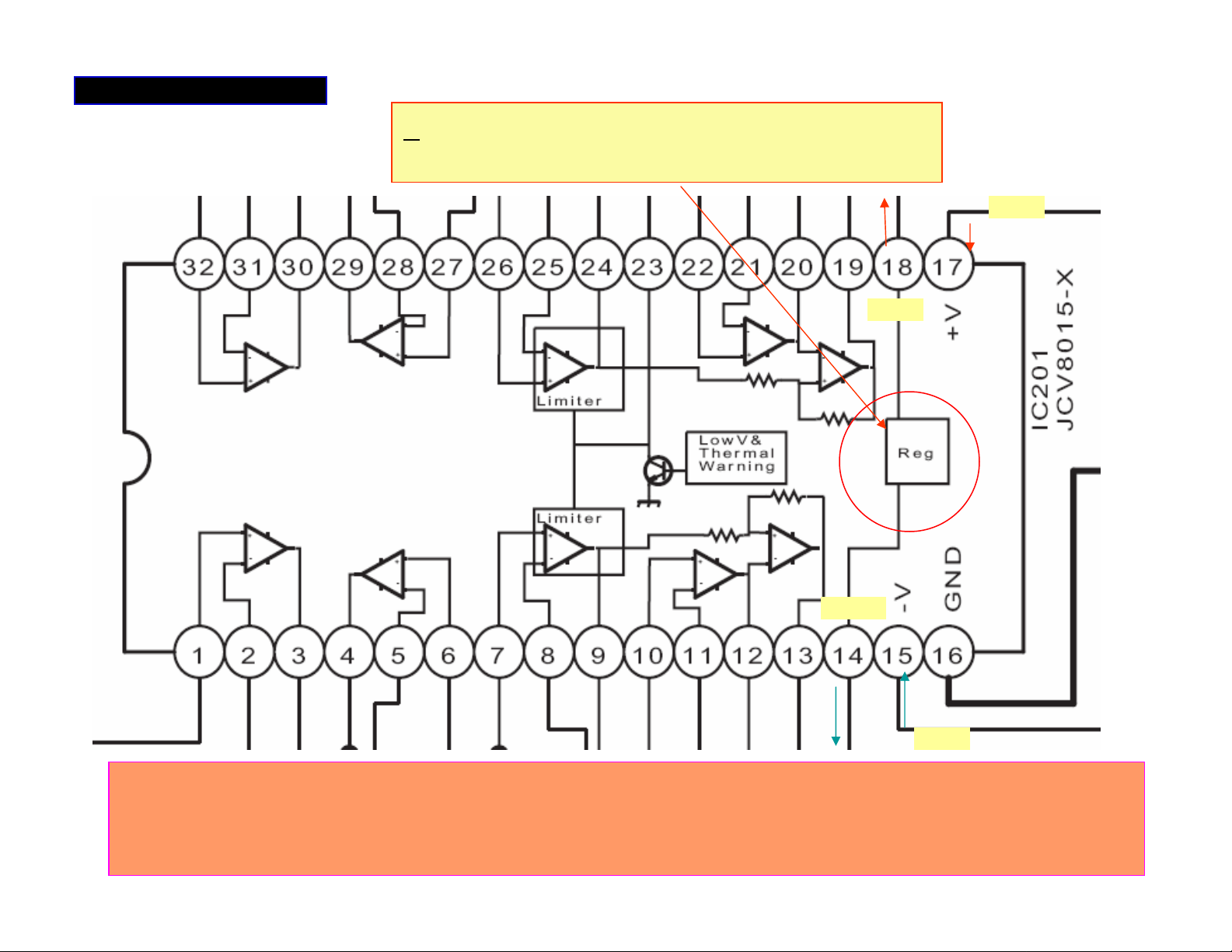
•The ‘AMP +/-B’ voltage varies from +/- 25 to 40V depending on
the models, and output level.
•Since the ‘AMP +/-B’ voltage varies, it is recommended to use
‘AMP –B’ as reference common point to measure DC level at
IC251. When referred to chassis ground, the voltage readings
will be different from the listed values.
•Since the voltage at pin 10, 11 and 12 are floating, the DC level
varies along with ‘AMP_ +/-B’.
Page 65

DIGITAL AMPLIFIER 1/8
Background—What is PWM
• Pulse Width Modulation (PWM) is a method
of digitally encoding analog signal levels.
• In the process, continuously varying value of
input audio signals is detected based on the
reference voltage (Vref) by comparing the
signals with triangular waves (master clock).
+
-
+
-
+
-
+
-
Page 66

DIGITAL AMPLIFIER 2/8
Audio Signal
Master Clock
•“
Digital” is the most advanced technology that creates the best
result.
• It is certain that a Digital Amplifier gives us many benefits,
such as miniaturization, light -weight, and high efficiency.
• However, we hear analog sound from speakers that vibrate
air, instead of digital signals of “0” and “1.” To realize a
hyper digital amplifier, digital signals must be returned to
analog sounds as efficiently and accurately as possible.
Page 67

DIGITAL AMPLIFIER 4/8
Problems of a digital Amplifier
Page 68

DIGITAL AMPLIFIER 5/8
solving the problem 1
D2
D1
A1
A2
Page 69

DIGITAL AMPLIFIER 7/8
solving the problem 2
Hybrid Feedback Digital Amplifier Ver. III
also features low voltage power supply,
which ensures stable signal transfer.
DC-DC
CONVERTER
CONTROL
AMP
AMP
Page 70

DIGITAL AMPLIFIER 8/8
Three features
solving the problem 3
Page 71

DIGITAL AMPLIFIER 8/8
A
solving the problem 3
Feature 1
Page 72

DIGITAL AMPLIFIER 8/8
B
solving the problem 3
Feature 2
Synchronization by an External Clock
Slight gap of frequencies among channels causes specific noise. To prevent this, the JVC amplifier
uses an external clock, which synchronizes the operations of all channels.
Page 73

MASTER CLOCK
TWO FREQENCIES: 400 KHz and 420 KHz
IN AM RADIO MODE
AM TUNNING FREQENCY (KHz)
600 800 1000 1200 1400 1600
I I I I I I
590----610 780------------820 980-------------1020 1180----------1220 1380----------1420 1580------1620
5v
0v ---------------------------------------------------------------------------------------------------------------------------------------------------
IC 501 pin 61-
frenqency control
400
420
SELECTED MASTER CLOCK FREQENCY (KHz)
400400 400400400400
420
420
420
420
420
Page 74

DIGITAL AMPLIFIER 8/8
C
solving the problem 3
Feature 3
Page 75

DIGITAL AMPLIFIER 3/8
Block Diagram for RX-D… Series
Page 76

DIGITAL AMPLIFIER 6/8
PWM PCB
This diagram is for front left channel, other channels are similar.
From Master Volume
Double D/A Feedback Diagram
Power amp
D1
A1
D2
A2
Page 77

DIGITAL AMPLIFIER 6/8
Power Amplifier Diagram
This diagram is for front left channel, the other channels are similar.
From PWM Board
AMP-B+12V (-13/-23/-30V)
AMP+B (+25/+35/+42V)
AMP-B (-25/-35/-42V)
LC LPF
P to P (50/70/84V)
Page 78

MASTER CLOCK VS INPUT AUDIO
INPUT
AUDIO
SIGNAL
(RED
SINE
WAVE)
MASTER
CLOCK
0v
PWM
The PWM duty is 50% when input audio level is zero.
Page 79

MASTER CLOCKVS OUTPUT AUDIO
MASTER CLOCK’S AMPLITUDE AND
DUTY CYCLE (BEFORE LPF)
P-P 50V
OUTPUT AUDIO AMPLITUDE
AFTER LPF
P-P 48V
P-P 80.6V
P-P 84V
The higher amplitude of the same duty cycle PWM, the output audio’s
amplitude is higher, if the pulse width ratio are same.
Page 80

AUDIO DIGITAL PROCESS 1/8
Page 81

AUDIO DIGITAL PROCESS 2/8
The process of playing digital music involves analog/digital conversion and
digital/analog conversion as shown below:
The sound quality of a signal depends on the following two factors when the signal is
converted from analog to digital.
•Quantization word length (bits), which determines resolution or the expression of
music in the amplitude domain.
•Sampling frequency, which determines the frequency response or the expression
of music in the frequency domain.
Page 82

AUDIO DIGITAL PROCESS
PROBLEM 1: An analog signal of a very faint strength cannot be
accurately recreated by A/D and D/A conversion.
Good
3/8
Distortion
Page 83

AUDIO DIGITAL PROCESS
PROBLEM 2: A high-frequency analog signal cannot be accurately
recreated by A/D and D/A conversion.
Good
4/8
Distortion
Page 84

AUDIO DIGITAL PROCESS
5/8
CC Converter (1)- Bit Expansion
Increasing quantization resolution for low
level signals
Page 85

AUDIO DIGITAL PROCESS
CC Converter (2)- Range Expansion
6/8
Page 86

AUDIO DIGITAL PROCESS
JVC exclusive DSP
• ONE CHIP REPLACING TWO.
7/8
• DECODE FORMATS:
Logic IIx, DTS, DTS-ES, DTS 96/24, DTS NEO:6.
• FUNCTIONS:
Equalizer, Dynamic Range Control, Bass management.
DAP 3DPHONIC, 3D Headphone, DSP Digital
Dolby Digital, Dolby Digital EX, Dolby Pro
Page 87

Audio Input-output Path
To
& USB
Page 88

Audio Input-Process Path
RX-D401/402/701/702
IC681
IC661
IC610
IC671
IC686
IC685
IC620
IC630
Page 89

Two Channel
From A/V In
AUDIO DIGITAL PROCESS 8/8
DSP BLOCK DIAGRAM
7.1 channels To Master Volume
27
20-23
13-16
54
Analog signal
Digital signal
USB wireless
FRONT_OPT
HDMI AUDIO DATA
43-49
cc conv.
IC681 FR/FL
USB
Page 90

Master Volume Section
Block Diagram
Analog
Audio
Audio/Video signal input and
system control section
Bypass DSP
From DSP
Go to PWM
RX-D… series
PWM
modulator
section
Page 91

VIDEO PROCESS & HDMI
1/7
What is HDMI ?
• HDMI (High-Definition Multimedia Interface) is the first and only
industry-supported, uncompressed, all-digital audio/video interface.
HDMI provides an interface between any audio/video source, such
as a set-top box, DVD player, or A/V receiver and an audio and/or
video monitor, such as a digital television (DTV), over a single cable.
• HDMI supports standard, enhanced, or high-definition video, plus
multi-channel digital audio on a single cable. It transmits all ATSC
HDTV standards and supports 8-channel digital audio, with
bandwidth to spare to accommodate future enhancements and
requirements.
Page 92

VIDEO PROCESS & HDMI
Video Connection for RX-D401/D402
HDMI AUDIO
HDMI VIDEO
2/7
IC771
IC781
Page 93

VIDEO PROCESS & HDMI
Video Connection for RX-D701/D702
HDMI AUDIO
HDMI VIDEO
3/7
IC771 IC781
Page 94

VIDEO PROCESS & HDMI
HDMI video
HDMI audio
All analog
formats video
Analog video
480p after A/D
Other converted
to 480p by IC781
VCR/DBS IN
YCbCr 4:2:2
4/7
HDMI BLOCK DIAGRAM
Analog video in
DVD/DVR IN
HDMI
OUT
Page 95

Fully HDMI Compliant.
Source Device A/V Receiver Monitor Device
All A/V devices should be fully HDMI compliant to avoid troubles.
Page 96

VIDEO PROCESS & HDMI
5/7
1/16/2006 IY (ver1)
Source (DVD / STB / DVHS) Receiver(RXD401/702) TV (PDP/LCD/HDILA)
Source
If the upstream content is
protected, HDCP
authentication is performed.
Source
+5V
Hot Plug Detect,
EDID (capabilities
of downstream TV)
HDMI Tx
The JVC Receiver accepts the encoded video:
YCbCr (4:2:2) only; if source outputs RGB or
YCbCr(4:4:4) The receiver cannot decode it.
Then receiver ask source send YCbCr (4:2:2),
and by HDMI standard requirement, the source
device has to able to do it.
Aksv
Bksv
Ri’ Rj’
Receiver
Receiver
+5V
Hot Plug Detect,
EDID
HDMI Tx
Bksv
Cksv
TV
Transmits encoded video:
YCbCr (4:2:2) to the TV.
TV
Notes:
*KSV (Key Selection Vector) is a 40-bit
identifier unique to each device. Each
HDCP device also has 40, 56-bit secret
device keys. The KSV specifies which ones
of the 40 secret device keys to use.
Ri’ is read every 2 seconds. If Ri’ does not
match its own internally generate Ri value
then HDCP authentication fails and the
signal is muted.
• If the source device not be able to convert the encoded Video toYCbCr
(4:2:2) as the receiver requests, the source device is not compliant with
HDMI fully. The problem is on the source device.
• Some TV monitor’s HDMI input accepts any kind of encoded video, if
connect this source device to TV directly, it seems no problem at all.
• Some brand Receivers accept more then one video formats through
HDMI input.
Page 97

VIDEO PROCESS & HDMI
6/7
The
renowned, high-performance device. It features a
host of advanced technologies for noise reduction
and reproduction of high-definition pictures,
including:
IC781 is the i/p converter, but also as well as a
Page 98

VIDEO PROCESS & HDMI 7/7
One e.g. for DCDi processes on the picture
3D Deinterlacer-
After DCDi process:
Smooth diagonal
lines.
Before DCDi process:
The jagged edges on
diagonal lines.
Page 99

USB WIRE OR WIRELESS1/5
All of RX-D series equipped wire USB feature
Page 100

USB WIRE OR WIRELESS2/5
band permits transmission
Wireless USB equipped on RX-D301/302/7101/702
(1) The 2Mbpshigh transmission rate using the 2.4GHz
of uncompressed signals for lossless reproduction.
(2) Use of DSSS (Direct Sequence Spread Spectrum) modulation technology
enables transmission of uncompressed signals with superior resistance against
noise, which retains superb sound quality.
(3) Corresponds to 16-bit, 32kHz/44.1kHz/48kHzsampling rates.
 Loading...