

Page 1
21175200302
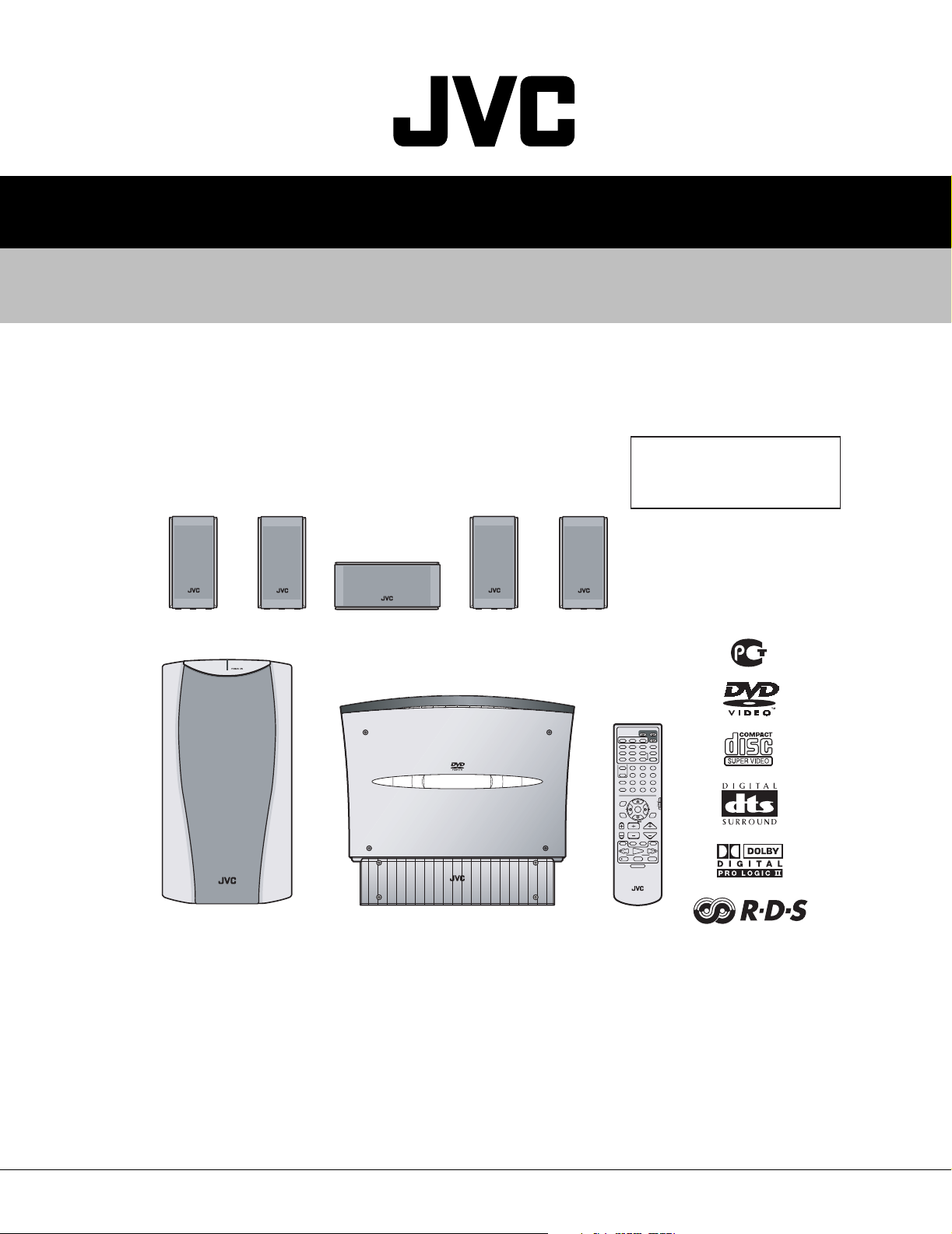
TH-V70R
SERVICE MANUAL
DVD DIGITAL CINEMA SYSTEM
TH-V70R
Area suffix
SP-XSV70 SP-XCV70SP-XSV70 SP-XSV70SP-XSV70
DVD DIGITAL CINEMA
SYSTE
M
TH-
V
70
R
SP-PWV70 XV-THV70R
EE --------- Russian Federation
TV AUDIO
DVD
VCR 1
AUX
FM/AM
VCR
DECODE
AUDIO
ANGLE
SUBTITLE
RETURN DIGEST ZOOM VFP
+
TOP MENU MENU ZOOM
SOUND
Ð
CONTROLÐ SUBWOOFER +EFFECT
VCR
123
Ð
CENTER
+
TEST
TV
456
SLEEP
Ð
REAR-L
+
789
SETTING
REAR-R
+
Ð
+10
10
0
TV RETURN
FM MODE
100+
TA/NEWS/INFO
ON
SCREEN
DVD
RDS
PTY PTY
ENTER
SURROUND
CHOICE
MODE
RDS DISPLAY
PTY SEARCH
CHANNEL VOLUMETV VOL
TV/VIDEO MUTING
/REW
FF/
PLAY
TUNING
DOWN UP
PAUSE
STOP
REC
MEMORY
STROBE
DIMMER
RMÐSTHV70R
DVD CINEMA SYSTEM
TABLE OF CONTENTS
1 Important Safety Precautions . . . . . . . . . . . . . . . . . . . . . . . . . . . . . . . . . . . . . . . . . . . . . . . . . . . . . . . . . . . 1-2
2 Disassembly method . . . . . . . . . . . . . . . . . . . . . . . . . . . . . . . . . . . . . . . . . . . . . . . . . . . . . . . . . . . . . . . . . . 1-6
3 Adjustment method. . . . . . . . . . . . . . . . . . . . . . . . . . . . . . . . . . . . . . . . . . . . . . . . . . . . . . . . . . . . . . . . . . . 1-25
4 Description of major ICs. . . . . . . . . . . . . . . . . . . . . . . . . . . . . . . . . . . . . . . . . . . . . . . . . . . . . . . . . . . . . . . 1-26
COPYRIGHT © 2003 VICTOR COMPANY OF JAPAN, LTD.
No.21175
2003/02
Page 2
TH-V70R
Important Safety Precautions
1.1 Safety Precautions
(1) This design of this product contains special hardware and
many circuits and components specially for safety purposes.
For continued protection, no changes should be made to the
original design unless authorized in writing by the manufacturer. Replacement parts must be identical to those
used in the original circuits. Services should be performed by qualified personnel only.
(2) Alterations of the design or circuitry of the product should
not be made. Any design alterations of the product should
not be made. Any design alterations or additions will void
the manufacturers warranty and will further relieve the
manufacture of responsibility for personal injury or property
damage resulting therefrom.
(3) Many electrical and mechanical parts in the products have
special safety-related characteristics. These characteristics are often not evident from visual inspection nor can the
protection afforded by them necessarily be obtained by using replacement components rated for higher voltage, wattage, etc. Replacement parts which have these special safety
characteristics are identified in the Parts List of Service Manual. Electrical components having such features are identified by shading on the schematics and by ( ) on the
Parts List in the Service Manual. The use of a substitute replacement which does not have the same safety characteristics as the recommended replacement parts shown in the
Parts List of Service Manual may create shock, fire, or other hazards.
(4) The leads in the products are routed and dressed with ties,
clamps, tubings, barriers and the like to be separated from
live parts, high temperature parts, moving parts and/or
sharp edges for the prevention of electric shock and fire
hazard. When service is required, the original lead routing
and dress should be observed, and it should be confirmed
that they have been returned to normal, after reassembling.
(5) Leakage shock hazard testing)
After reassembling the product, always perform an isolation
check on the exposed metal parts of the product (antenna
terminals, knobs, metal cabinet, screw heads, headphone
jack, control shafts, etc.) to be sure the product is safe to
operate without danger of electrical shock.
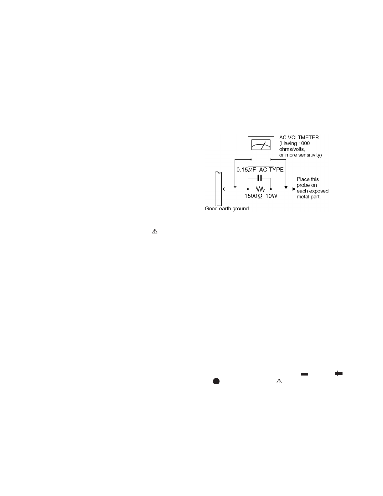
Do not use a line isolation transformer during this check.
• Plug the AC line cord directly into the AC outlet. Using a
"Leakage Current Tester", measure the leakage current
from each exposed metal parts of the cabinet, particularly any exposed metal part having a return path to the
chassis, to a known good earth ground. Any leakage current must not exceed 0.5mA AC (r.m.s.).
• Alternate check method
Plug the AC line cord directly into the AC outlet. Use an AC
voltmeter having, 1,000 ohms per volt or more sensitivity in
the following manner. Connect a 1,500 ohm 10W resistor
paralleled by a 0.15 µF AC-type capacitor between an
SECTION 1
exposed metal part and a known good earth ground.
Measure the AC voltage across the resistor with the AC
voltmeter.
Move the resistor connection to each exposed metal part,
particularly any exposed metal part having a return path to
the chassis, and measure the AC voltage across the resistor.
Now, reverse the plug in the AC outlet and repeat each
measurement. Voltage measured any must not exceed 0.75
V AC (r.m.s.). This corresponds to 0.5 mA AC (r.m.s.).
1.2 Warning
(1) This equipment has been designed and manufactured to
meet international safety standards.
(2) It is the legal responsibility of the repairer to ensure that
these safety standards are maintained.
(3) Repairs must be made in accordance with the relevant
safety standards.
(4) It is essential that safety critical components are replaced
by approved parts.
(5) If mains voltage selector is provided, check setting for local
voltage.
1.3 Caution
Burrs formed during molding may be left over on some parts
of the chassis.
Therefore, pay attention to such burrs in the case of preforming repair of this system.
1.4 Critical parts for safety
In regard with component parts appearing on the silk-screen
printed side (parts side) of the PWB diagrams, the parts that are
printed over with black such as the resistor ( ), diode ( )
and ICP ( ) or identified by the " " mark nearby are critical
for safety.
When replacing them, be sure to use the parts of the same type
and rating as specified by the manufacturer. (Except the JC version)
1-2 (No.21175)
Page 3
1.5 Safety Precautions (U.K only)
(1) This design of this product contains special hardware and many circuits and components specially for safety purposes. For con-
tinued protection, no changes should be made to the original design unless authorized in writing by the manufacturer. Replacement parts must be identical to those used in the original circuits.
(2) Any unauthorised design alterations or additions will void the manufacturer's guarantee; furthermore the manufacturer cannot
accept responsibility for personal injury or property damage resulting therefrom.
(3) Essential safety critical components are identified by ( ) on the Parts List and by shading on the schematics, and must never
be replaced by parts other than those listed in the manual. Please note however that many electrical and mechanical parts in
the product have special safety related characteristics. These characteristics are often not evident from visual inspection. Parts
other than specified by the manufacturer may not have the same safety characteristics as the recommended replacement parts
shown in the Parts List of the Service Manual and may create shock, fire, or other hazards.
(4) The leads in the products are routed and dressed with ties, clamps, tubings, barriers and the like to be separated from live parts,
high temperature parts, moving parts and/or sharp edges for the prevention of electric shock and fire hazard. When service is
required, the original lead routing and dress should be observed, and it should be confirmed that they have been returned to
normal, after re-assembling.
1.5.1 Warning
(1) Service should be performed by qualified personnel only.
(2) This equipment has been designed and manufactured to meet international safety standards.
(3) It is the legal responsibility of the repairer to ensure that these safety standards are maintained.
(4) Repairs must be made in accordance with the relevant safety standards.
(5) It is essential that safety critical components are replaced by approved parts.
(6) If mains voltage selector is provided, check setting for local voltage.
TH-V70R
Burrs formed during molding may be left over on some parts of the chassis. Therefore,
pay attention to such burrs in the case of preforming repair of this system.
(No.21175)1-3
Page 4
TH-V70R
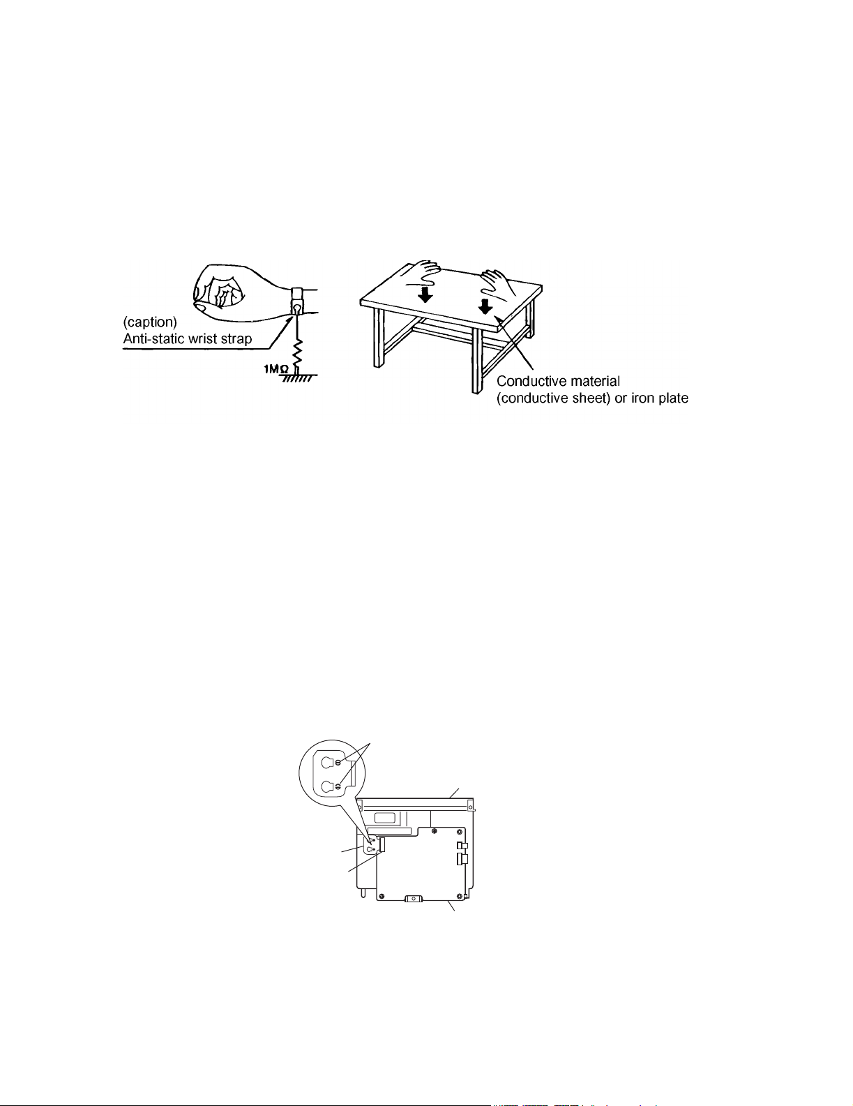
1.6 Preventing static electricity
Electrostatic discharge (ESD), which occurs when static electricity stored in the body, fabric, etc. is discharged,
can destroy the laser diode in the traverse unit (optical pickup). Take care to prevent this when performing repairs.
1.6.1 Grounding to prevent damage by static electricity
Static electricity in the work area can destroy the optical pickup (laser diode) in devices such as DVD players.
Be careful to use proper grounding in the area where repairs are being performed.
(1) Ground the workbench
Ground the workbench by laying conductive material (such as a conductive sheet) or an iron plate over it before placing the
traverse unit (optical pickup) on it.
(2) Ground yourself
Use an anti-static wrist strap to release any static electricity built up in your body.
(3) Handling the optical pickup
• In order to maintain quality during transport and before installation, both sides of the laser diode on the replacement optical
pickup are shorted. After replacement, return the shorted parts to their original condition.
(Refer to the text.)
• Do not use a tester to check the condition of the laser diode in the optical pickup. The tester's internal power source can easily
destroy the laser diode.
1.7 Handling the traverse unit (optical pickup)
(1) Do not subject the traverse unit (optical pickup) to strong shocks, as it is a sensitive, complex unit.
(2) Cut off the shorted part of the flexible cable using nippers, etc. after replacing the optical pickup. For specific details, refer to the replace-
ment procedure in the text. Remove the anti-static pin when replacing the traverse unit. Be careful not to take too long a time
when attaching it to the connector.
(3) Handle the flexible cable carefully as it may break when subjected to strong force.
(4) I t is not possible to adjust the semi-fixed resistor that adjusts the laser power. Do not turn it.
1.8 Attention when traverse unit is decomposed
*Please refer to "Disassembly method" in the text for the DVD pickup unit.
• Apply solder to the short land sections before the flexible wire is disconnected from the connector CN101 on the DVD servo board.
(If the flexible wire is disconnected without applying solder, the DVD pickup may be destroyed by static electricity.)
• In the assembly, be sure to remove solder from the short land sections after connecting the flexible wire.
Short lands
DVD mechanism assembly
1-4 (No.21175)
Flexible wire
Connector
CN202
CN201
DVD servo board
Page 5
1.9 Important for laser products
(1) CLASS 1 LASER PRODUCT
(2) DANGER : Invisible laser radiation when open and inter
lock failed or defeated. Avoid direct exposure to beam.
(3) CAUTION : There are no serviceable parts inside the
Laser Unit. Do not disassemble the Laser Unit. Replace the
complete Laser Unit if it malfunctions.
(4) CAUTION : The compact disc player uses invisible laser
radiation and is equipped with safety switches which
prevent emission of radiation when the drawer is open and
the safety interlocks have failed or are de feated.
It is dangerous to defeat the safety switches.
TH-V70R
(5) CAUTION : If safety switches malfunction, the laser is able
to function.
(6) CAUTION : Use of controls, adjustments or performance of
procedures other than those specified herein may result in
hazardous radiation exposure.
CAUTION
Please use enough caution not to see the beam directly
or touch it in case of anadjustment or operation check.
VARNING
Osynlig laserstrålning är denna del är öppnad och spårren är
urkopplad. Betrakta ej strålen.
VARO
Avattaessa ja suojalukitus ohitettaessa olet alttiina näkymättömälle lasersäteilylle. Älä katso säteeseen.
REPRODUCTION AND POSITION OF LABELS
CLASS 1
LASER PRODUCT
ADVARSEL
Usynlig laserstråling ved åbning, når sikkerhedsafbrydere er
ude af funktion. Undgå udsasttelse for stråling.
ADVARSEL
Usynlig laserstråling ved åpning, når sikkerhetsbryteren er avslott. unngå utsettelse for stråling.
WARNING LABEL
CAUTION: Invisible laser
radiation when open and
interlock failed or defeated.
AVOID DIRECT EXPOSURE
TO BEAM. (e)
ADVARSEL: Usynlig laserstråling ved åbning, når
sikkerhedsafbrydere er ude
af funktion. Undgåudsættelse for stråling. (d)
VARNING: Osynlig laserstrålning när denna del är
öppnad och spärren är
urkopplad. Betrakta ej
strålen. (s)
VARO: Avattaessa ja
suojalukitus ohitettaessa
oleta lttiina näkymättömälle lasersäteilylle.
Älä katso
säteeseen. (f)
CLASS 1
LASER PRODUCT
(No.21175)1-5
Page 6
TH-V70R
SECTION 2
Disassembly method
2.1 Main body section
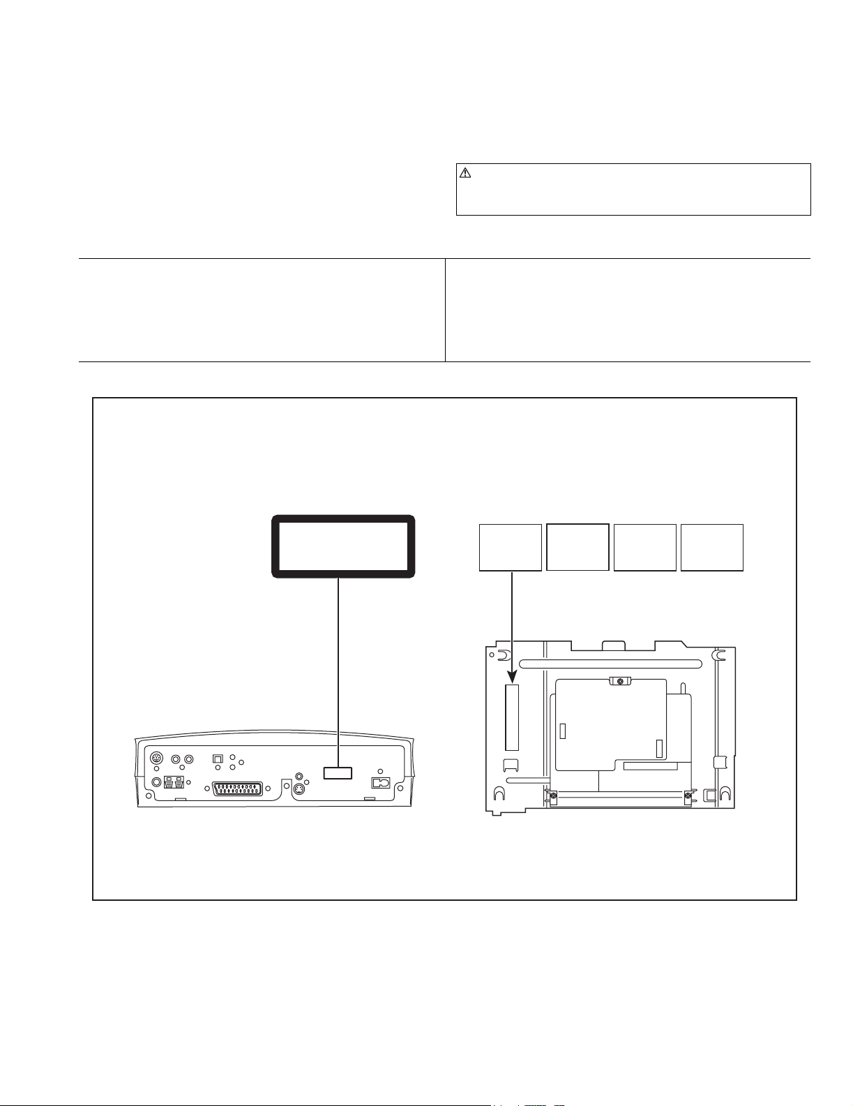
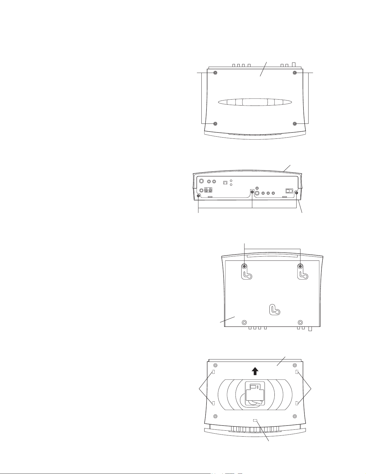
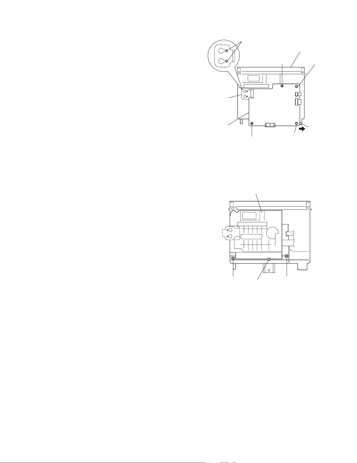
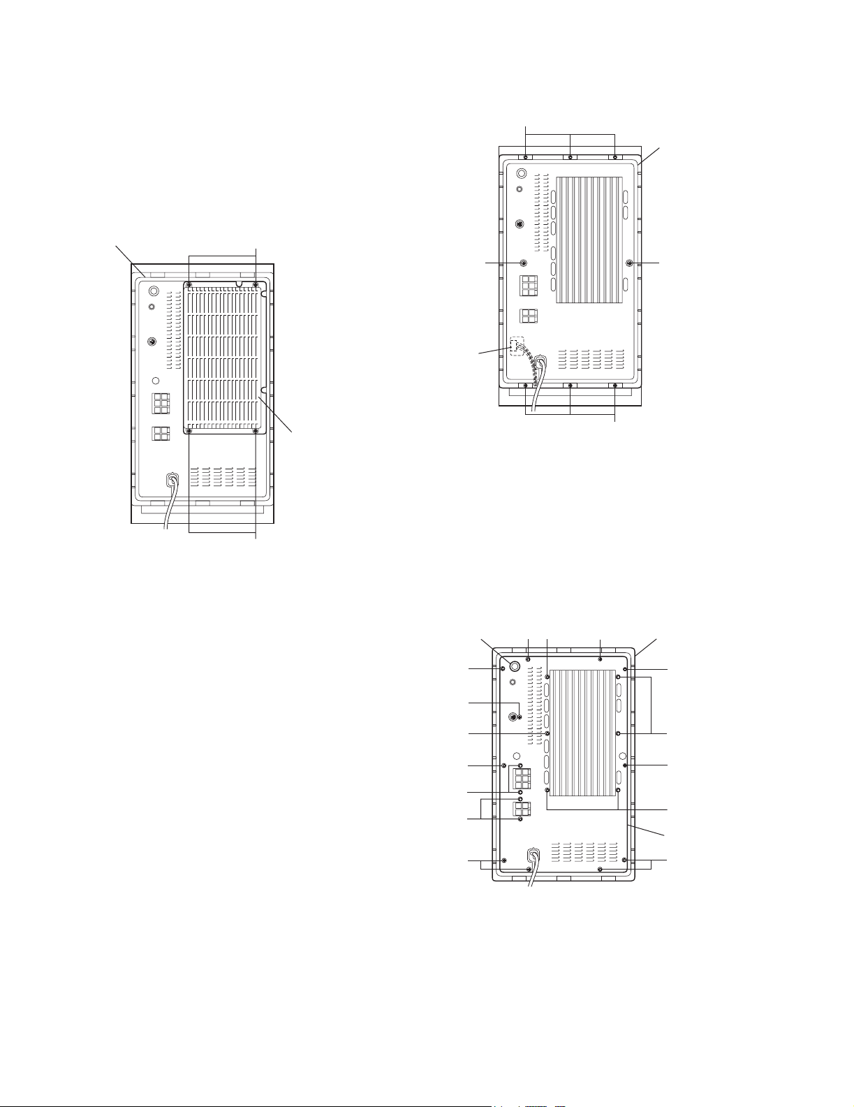
2.1.1 Removing the top plate (See Fig. 1.)
From the top side of the main body, remove the four screws A
attaching the top plate.
2.1.2 Removing the bottom panel (See Figs. 2 and 3.)
(1) From the rear side of the main body, remove the three
screws B attaching the bottom panel.
(2) From the bottom side of the main body, remove the two
screws C attaching the bottom panel.
(3) Remove the bottom panel in an upward direction.
B
Top plate
AA
Fig.1
Top panel
Bottom panel
Fig.2
2.1.3 Removing the top panel (See Fig. 4.)
• Remove the top plate.
• Remove the bottom panel.
(1) Slide the top panel toward the rear (direction of the arrow)
and disengage it from the engagement sections a and b of
the bottom chassis.
(2) Remove the top panel in an upward direction.
C
Bottom panel
Fig.3
Top panel
bb
1-6 (No.21175)
a
Fig.4
Page 7
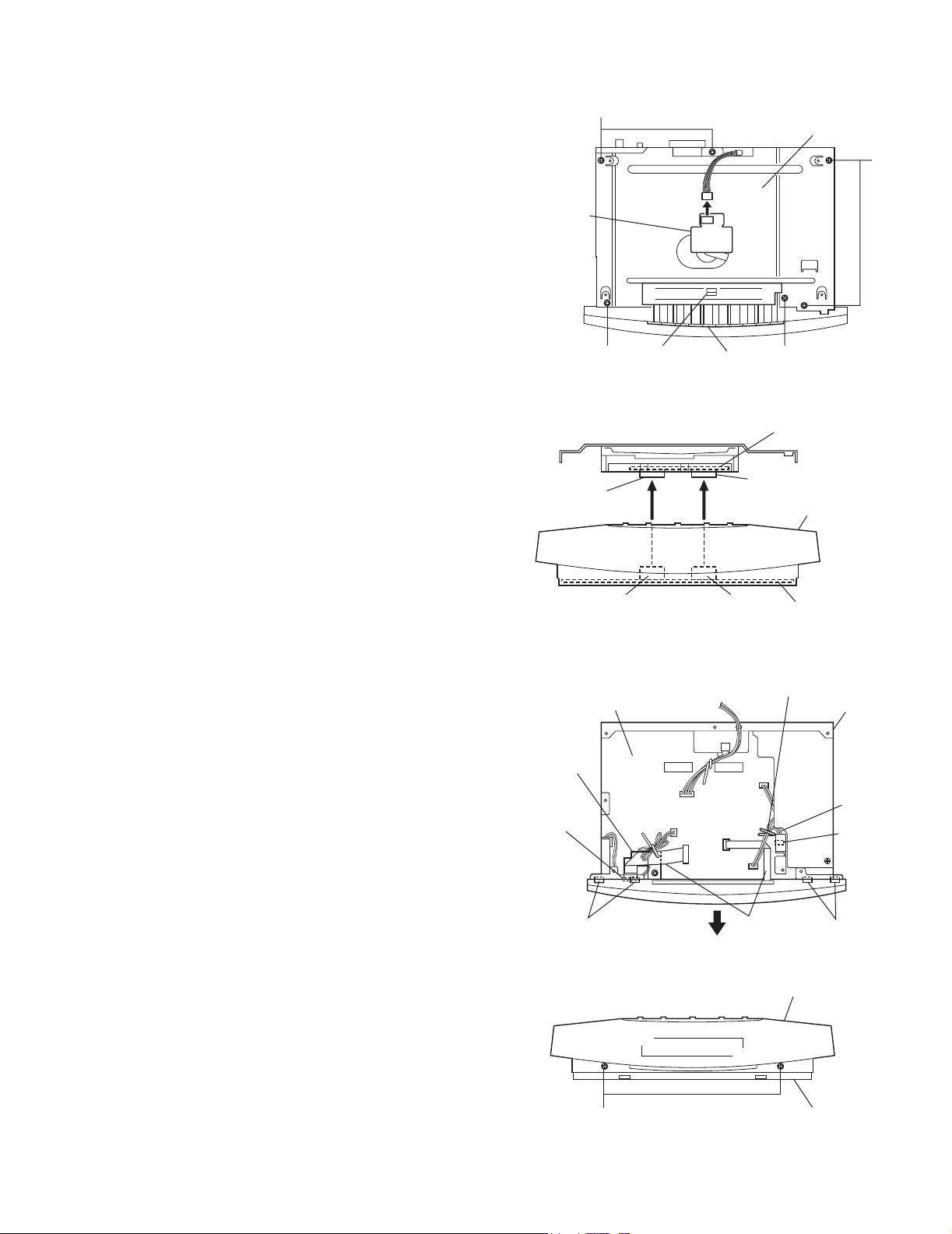
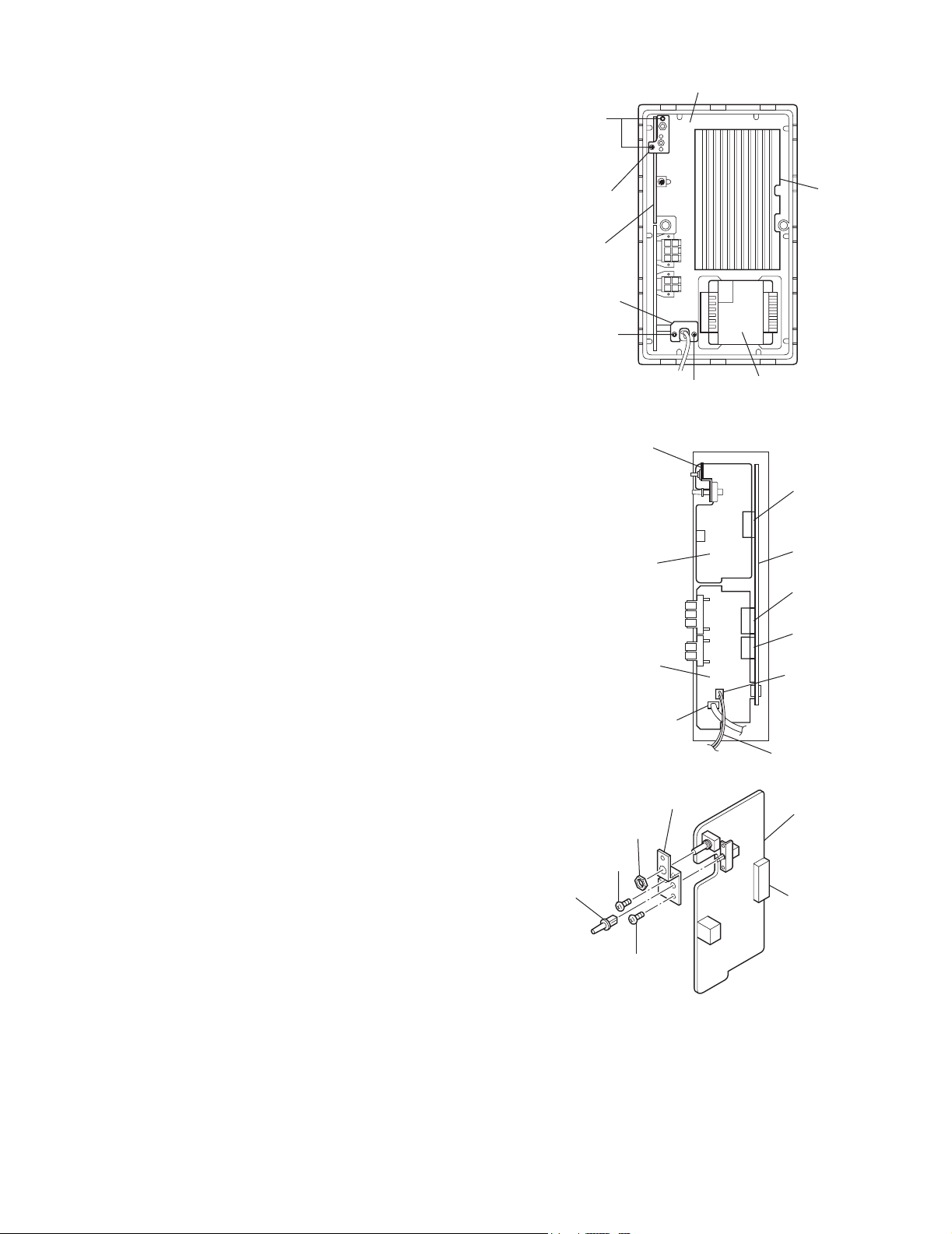
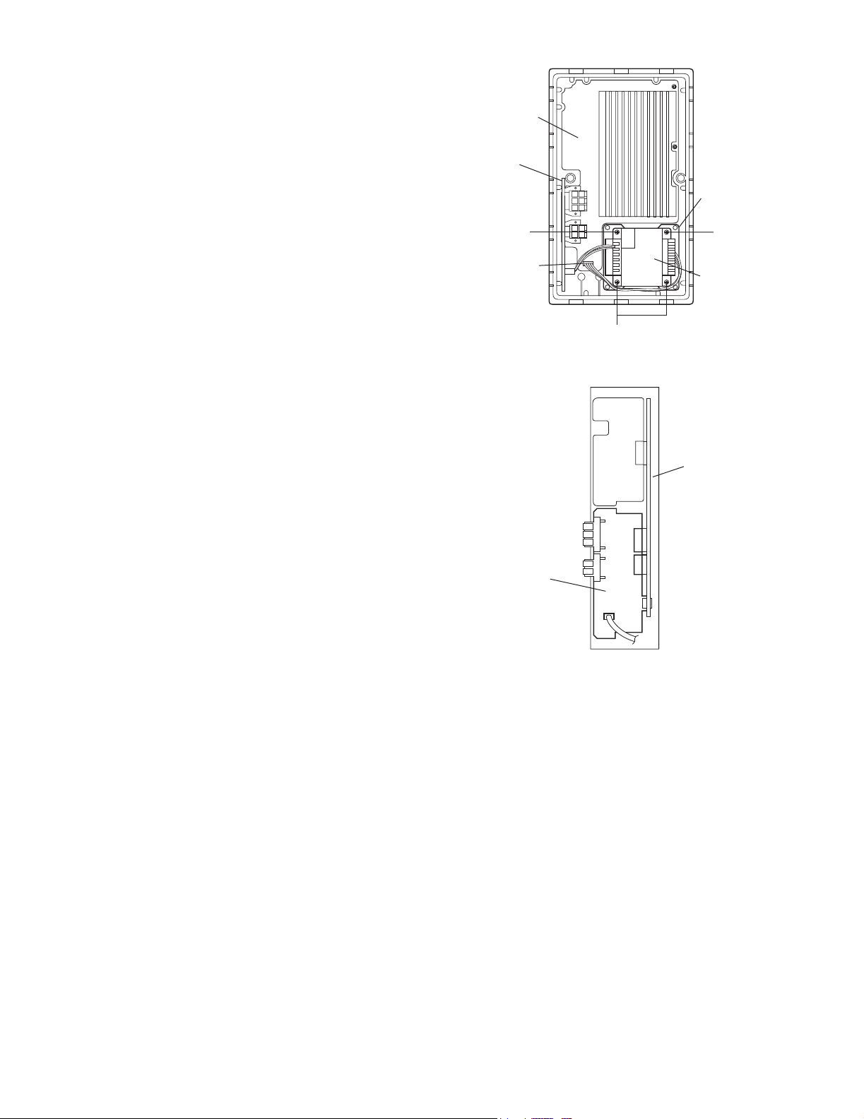
2.1.4 Removing the DVD mechanism assembly (See Figs. 5 and 6.)
• Remove the top plate.
• Remove the bottom panel.
• Remove the top panel.
(1) From the top side of the main body, disengage the claw c
of the DVD mechanism assembly and then remove the
push button.
(2) Remove the five screws D and screw E attaching the DVD
mechanism assembly.
(3) Disconnect the wire from connector CN812 on the LED
board.
(4) Disconnect the connectors CN502 and CN503 on the DVD
servo board from connectors CN801 and CN803 on the
main board while lifting the DVD mechanism assembly in
an upward direction.
LED board
D
TH-V70R
DVD mechanism
assembly
D
CN812
2.1.5 Removing the front panel assembly (See Figs. 7 and 8.)
• Remove the top plate.
• Remove the bottom panel.
• Remove the top panel.
• Remove the DVD mechanism assembly.
(1) Remove the wire clamp bundling the wires of the front pan-
el assembly.
(2) Remove the card wire of the front panel assembly from the
wire holder.
(3) Disconnect the wires from connectors CN106 and CN814
on the main board.
(4) Disconnect the card wires from connectors CN802 and
CN813 on the main board.
(5) From the front side of the main body, remove the two
screws F attaching the front panel assembly.
(6) Disengage the claws d of the front panel assembly from the
bottom chassis and then remove the front panel assembly
in the direction of the arrow.
Reference:
• Before attaching the front panel assembly, pass the
card wire of the front panel assembly through the hole
on the bottom chassis.
• After attaching the front panel assembly, bundle the
wires and card wire of the front panel assembly using
a wire clamp.
Caution:
• In the assembly, arrange the wires and wire clamp so
that they are not touch to the regulator IC(IC953).
CN502
Main board
Wire holder
Bottom
chassis hole
Claws d
Claw c
D
CN803 CN801
Push button
Fig.5
Fig.6
CN814
CN813
CN802
CN106
Fig.7
Card wires
Front panel assembly
F
Fig.8
E
DVD servo board
CN503
Front panel assembly
Main board
Wire clamp
Bottom chassis
Wire
IC953
Claws d
Bottom chassis
(No.21175)1-7
Page 8
TH-V70R
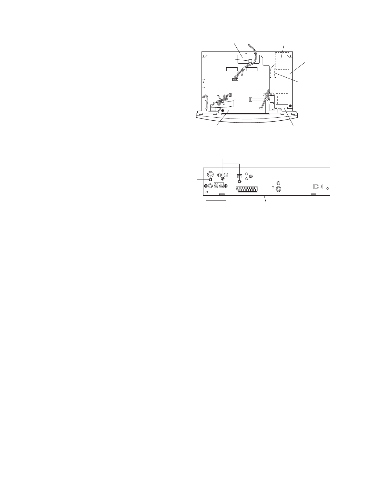
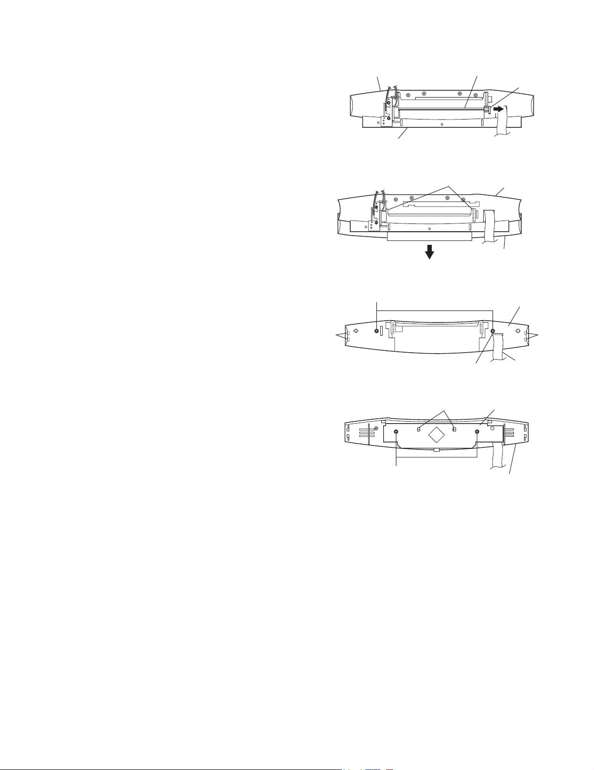
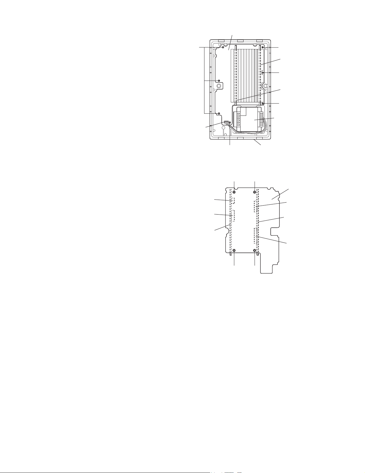
2.1.6 Removing the DSP/Audio board (See Figs. 9 and 10.)
• Remove the top plate.
• Remove the bottom panel.
• Remove the top panel.
• Remove the DVD mechanism assembly.
(1) From the top side of the main body, remove a screw G at-
taching the DSP/Audio board.
(2) From the rear side of the main body, remove the screw H
and two screws J attaching the DSP/Audio board.
(3) Take out the DSP/Audio board from the bottom chassis
and then disconnect the card wire from connector CN806
on the main board.
Reference:
• Before attaching the DSP/Audio board, connect the
card wire to the connector CN806 on the main board.
2.1.7 Removing the compulink board (See Figs. 9 and 10.)
• Remove the top plate.
• Remove the bottom panel.
• Remove the top panel.
• Remove the DVD mechanism assembly.
(1) Disconnect the card wire from connector CN592 on the
compulink board.
(2) From the rear side of the main body, remove the screw K
attaching the compulink board.
(3) Take out the compulink board from the bottom chassis.
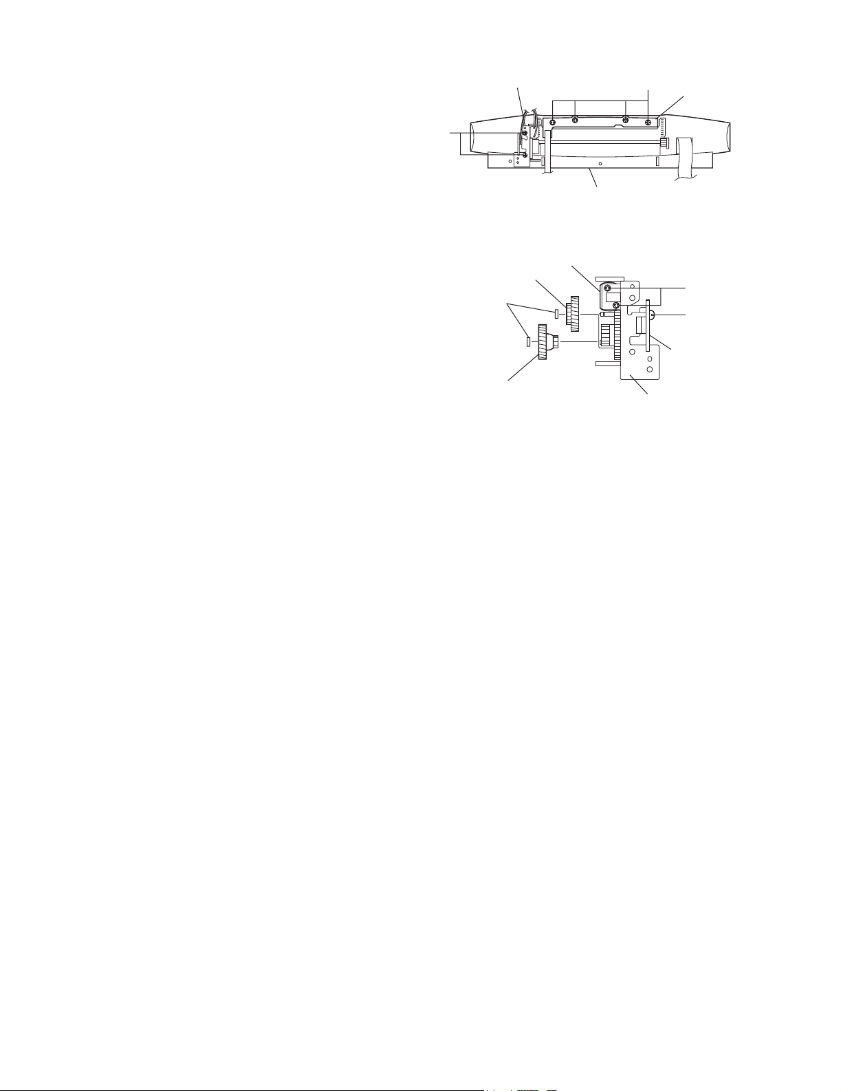
2.1.8 Removing the tuner (See Figs. 9 and 10.)
• Remove the top plate.
• Remove the bottom panel.
• Remove the top panel.
• Remove the DVD mechanism assembly.
(1) Disconnect the card wire from connector CN805 on the
main board.
(2) From the rear side of the main body, remove the two
screws L attaching the tuner.
(3) Take out the tuner from the bottom chassis.
Compulink board
Main board
H
L
CN592
J
Fig.9
K
Rear panel
Fig.10
CN805
CN806
Tuner
DSP/Audio
board
Card wire
G
Card wire
1-8 (No.21175)
Page 9
TH-V70R
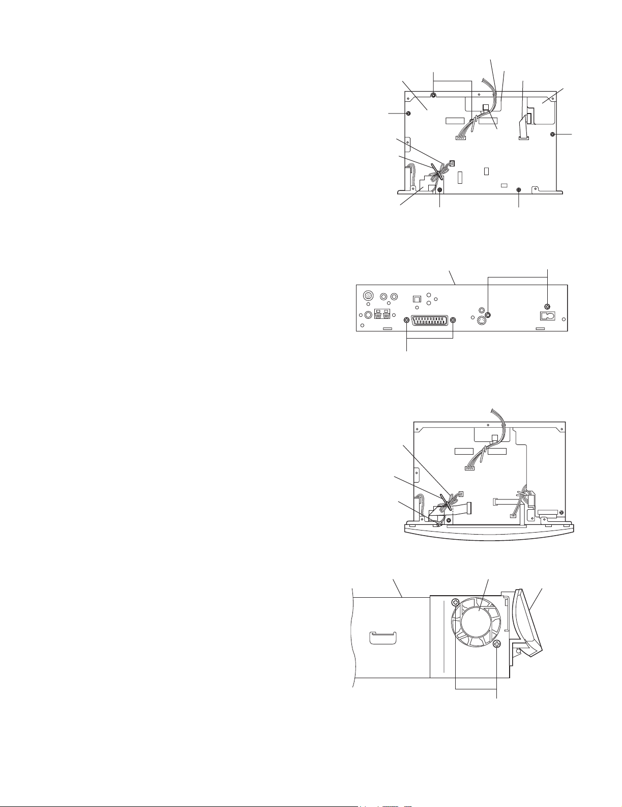
2.1.9 Removing the main board (See Figs. 11 and 12.)
• Remove the top plate.
• Remove the bottom panel.
• Remove the top panel.
• Remove the DVD mechanism assembly.
• Remove the front panel assembly.
• Remove the DSP/Audio board.
(1) Disconnect the card wire from connector CN805 on the
main board.
(2) Remove the wire clamp bundling the fan motor wire and
then disconnect the wire from connector CN972 on the
main board.
(3) Disconnect the card wire from connector CN592 on the
compulink board.
(4) Remove the five screws M and screw M' attaching the main
board.
(5) From the rear side of the main body, remove the four
screws N attaching the main board.
(6) Remove the rear panel with the tuner and compulink board.
(7) Take out the main board from the bottom chassis.
Reference:
Attaching the main board
• When attaching the screw M', attach the wire holder together with it.
• After connecting the wires to the connectors, bundle
them using the wire clamp.
• Insert the DVD mechanism assembly wire into the
notch on the bottom chassis. (See Fig. 11.)
Main board
M
Fan motor wire
Wire clamp
Wire holder
N
Insert this wire into the notch.
M
CN972
M'
Fig.11
Rear panel
Fig.12
Compulink board
CN592
M
Card wire
CN805
N
Tuner
M
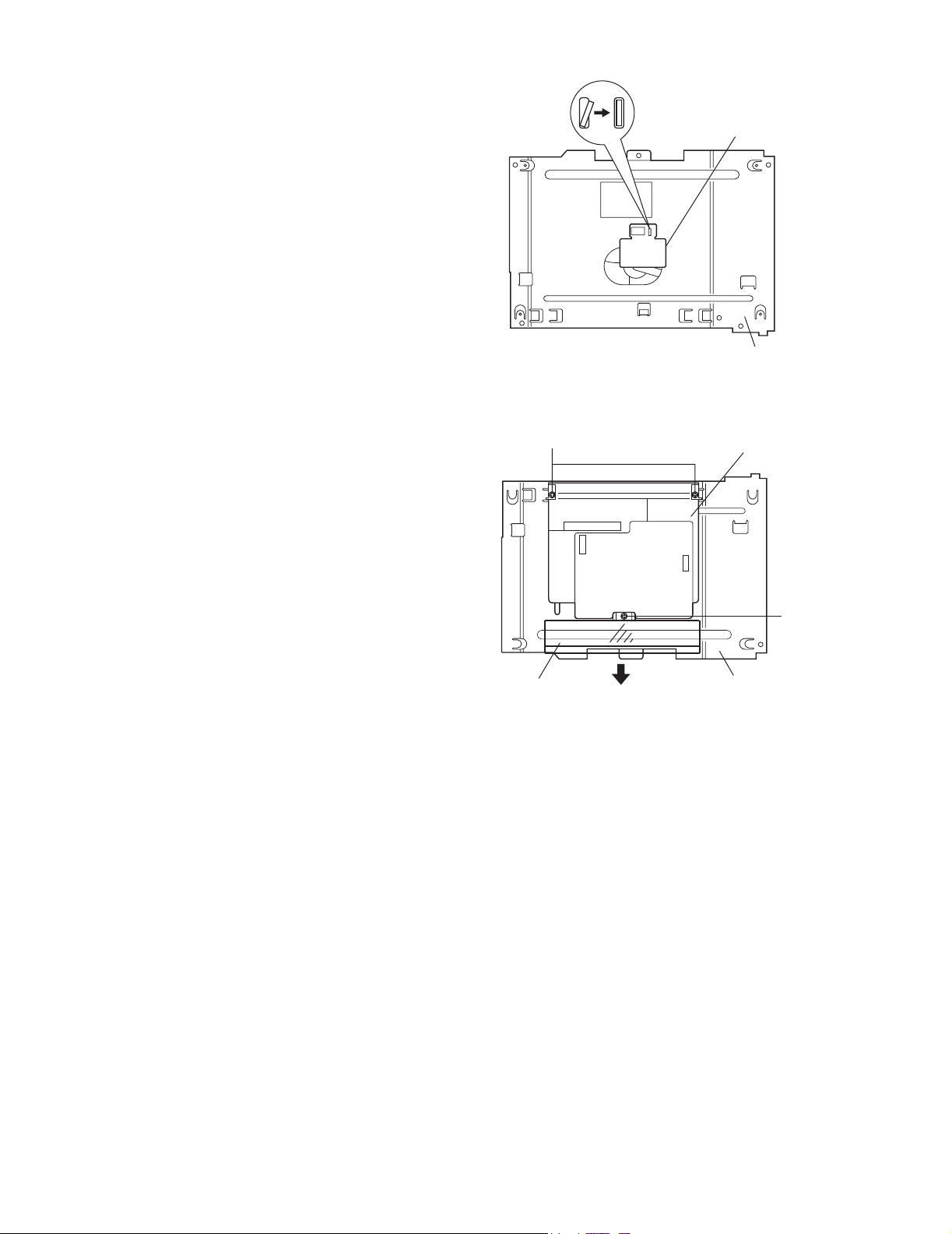
2.1.10 Removing the fan motor (See Figs. 13 and 14.)
• Remove the top plate.
• Remove the bottom panel.
• Remove the top panel.
• Remove the DVD mechanism assembly.
(1) Remove the wire clamp and tie band bundling the fan mo-
tor wire.
(2) Disconnect the wire from connector CN972 on the main
board.
(3) From the left side of the main body, remove the two screws
P attaching the fan motor.
Reference:
• After mounting the fan motor, bundle the fan motor
wire using the wire clamp.
Fan motor wire
Wire clamp
CN972
Tie band
Fig.13
Bottom chassis Fan motor Front panel
assembly
Fig.14
P
(No.21175)1-9
Page 10
TH-V70R
2.2 Front panel assembly section
• Remove the top plate.
• Remove the bottom panel.
• Remove the top panel.
• Remove the DVD mechanism assembly.
• Remove the front panel assembly.
2.2.1 Removing the switch board (See Fig. 15.)
From the back side of the front panel assembly, remove the four
screws Q attaching the switch board.
2.2.2 Removing the open/close board (See Figs. 15 and 16.)
(1) From the back side of the front panel assembly, remove the
two screws R attaching the door motor assembly.
(2) Remove the screw S attaching the open/close board of the
door motor assembly.
2.2.3 Removing the door motor (See Fig. 16.)
• Remove the door motor assembly.
(1) Remove the stop washers attaching the clutch assembly
and gear 2.
(2) Remove the clutch assembly and Gear 2.
(3) Remove the two screws T attaching the door motor.
Door motor assembly
R
Clutch assembly
Stop washer
Gear 2
Front panel assembly
(Back side)
Fig.15
Door motor
Fig.16
Q
Switch board
T
S
Open/close
board
Door motor assembly
1-10 (No.21175)
Page 11
2.2.4 Removing the front board (See Figs. 17 to 20.)
(1) While widening section e of the front base in the direction
of the arrow, remove the rod gear assembly.
(2) Slide the moving panel assembly all the way in the direction
of the arrow.
(3) While slightly widening sections f toward the front, take out
the moving panel assembly in the direction of the arrow.
(4) Remove the two screws U attaching the moving base of the
moving panel assembly.
(5) Disengage the engagement sections g on the inside of the
moving base and at the inside of the moving panel assem-
bly and remove the moving base.
(6) Remove the two screws V attaching the front board.
(7) Disengage the claws h of the moving panel and remove the
front board.
Reference:
• Before attaching the moving base, pass the card wire
of the front board through the hole on the moving base.
(See Fig.19.)
Front panel assembly
(Back side)
Front base
Rod gear assembly
Fig.17
f
Moving panel assembly
Fig.18
TH-V70R
e
Front base
U
V
Fig.19
h
Fig.20
Hole
Front board
Moving panel
Moving base
gg
Card wire
(No.21175)1-11
Page 12
TH-V70R
y
2.3 DVD mechanism assembly section
• Remove the top plate.
• Remove the bottom panel.
• Remove the top panel.
• Remove the DVD mechanism assembly.
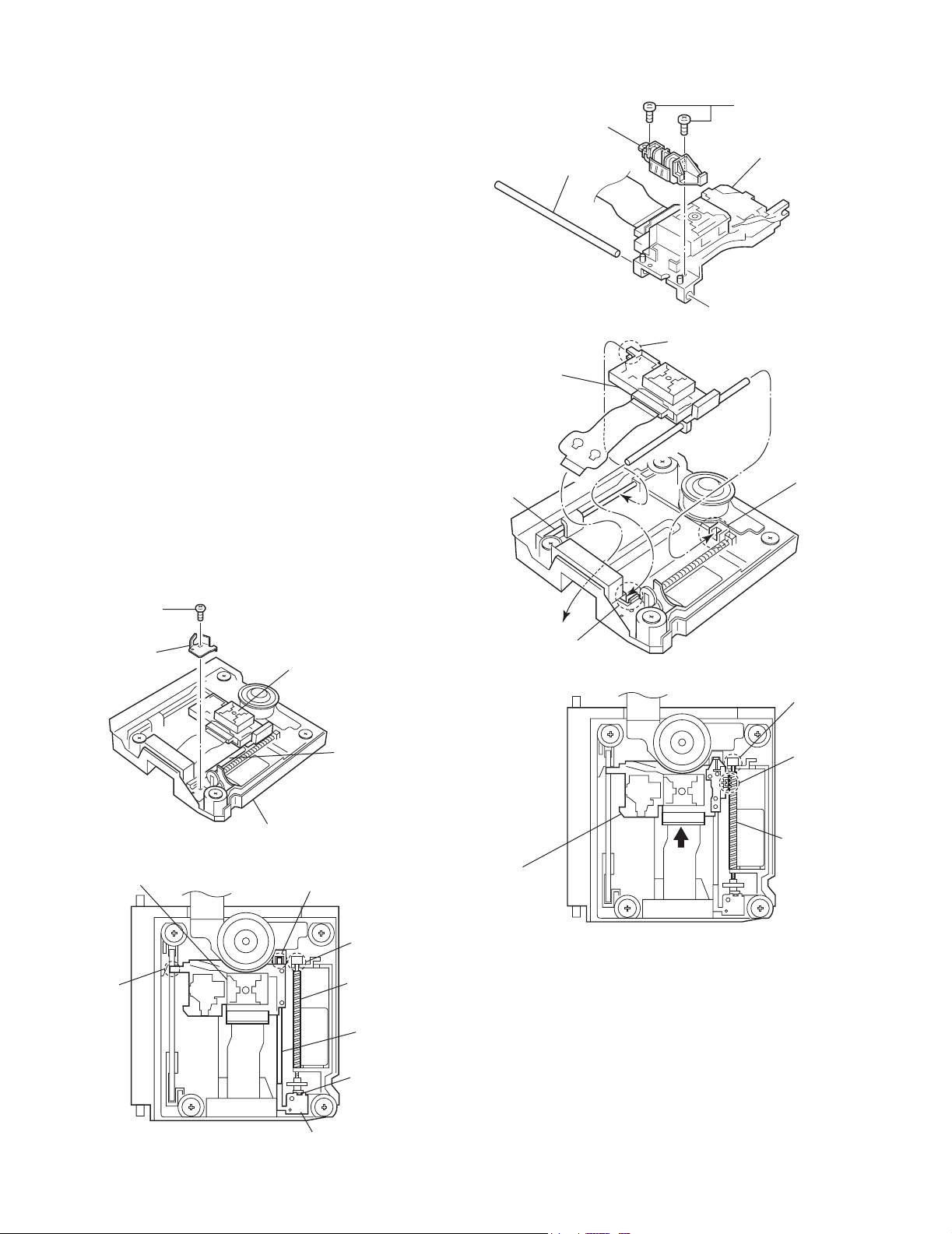
2.3.1 Removing the LED board (See Fig. 1.)
From the top side of the DVD mechanism assembly, disengage
the claw a of the top chassis attaching the LED board and then
remove the LED board.
2.3.2 Removing the DVD mechanism assembly (See Fig. 2.)
(1) Extend the both sides of the protector, and then raise the
protector in the direction of the arrow.
(2) Remove the three screws A attaching the DVD mechanism
assembly on the top chassis.
Claw a
A
LED board
Top chassis
Fig.1
DVD mechanism assembl
A
Protector
Fig.2
Top chassis
1-12 (No.21175)
Page 13
2.3.3 Removing the DVD servo board (See Fig. 3.)
Caution:
• Be sure to solder the short land sections b on the flexible
wire before disconnecting the flexible wire from connector
CN101 on the DVD servo board.
If the flexible wire is disconnected without attaching solder,
the pickup unit may be destroyed by static electricity.
(1) From the back side of the DVD mechanism assembly, at-
tach solder to the short land sections b of the flexible wire
that is connected to the connector CN101 of the DVD servo
board.
(2) Disconnect the flexible wire from connector CN101 on the
DVD servo board.
(3) Disconnect the card wires from connectors CN201 and
CN202 on the DVD servo board.
(4) Remove the two screws B attaching the DVD servo board.
(5) While pushing the claw c of the DVD mechanism assembly
in the direction of the arrow, remove the DVD servo board
from the projections d and e in an upward direction.
Caution:
• In the assembly, be sure to remove solder from the
short land sections b after connecting the flexible wire.
Flexible wire
DVD servo board
Short land sections b
DVD mechanism assembly
B
CN202
CN101
CN201
Projection e
B
Fig.3
TH-V70R
Projection d
Claw c
2.3.4 Removing the DVD traverse mechanism assembly (See Fig. 4.)
• Remove the DVD servo board.
(1) Remove the two screws C attaching the DVD traverse
mechanism assembly.
(2) Disengage the claw f attaching the DVD traverse mecha-
nism assembly and then take out the DVD traverse mechanism assembly.
DVD traverse mechanism assembly
C C
Claw f
Fig.4
(No.21175)1-13
Page 14
TH-V70R
y
w
t
w
2.3.5 Removing the DVD pickup unit (See Figs. 5 to 7.)
• Remove the DVD servo board.
• Remove the DVD traverse mechanism assembly.
(1) From the top side of the DVD traverse mechanism assem-
bly, remove the screw D attaching the bracket.
(2) Remove the claw g attaching the thrust spring and then
take out the torsion spring.
(3) Remove the lead screw from the section h and then re-
move the shaft from the section i.
(4) Disengage the section j of the DVD pickup unit and then re-
move the DVD pickup unit with the shaft.
(5) Pull the shaft out of the DVD pickup unit.
(6) Remove the two screws E attaching the SW. actuator.
SW. actuator
Shaft
E
DVD pickup uni
2.3.6 Attaching the DVD pickup unit (See Figs. 5 to 9.)
Reference:
Refer to the explanation of "Removing the DVD pickup unit" on
the preceding page.
(1) Attach the SW. actuator and shaft to the DVD pickup unit.
(See Fig.7.)
(2) Engage the section j of the DVD pickup unit to the shaft of
the DVD traverse mechanism assembly first, and set the
both ends of the shaft of the DVD pickup unit in the sections
i and i' of the DVD traverse mechanism assembly.
(3) Slide the DVD pickup unit all the way in the direction of the
arrow.
(4) Mesh the lead screw to the section k of DVD pickup unit
and then set the end of the lead screw to the section h.
(5) Attach the thrust spring. (See Fig.6.)
(6) Attach the bracket. (See Fig.5.)
D
Bracket
DVD pickup unit
Shaft
DVD pickup unit
Shaft
Section i'
Fig.7
Fig.8
Section
j
Section i
Section h
Section k
DVD pickup unit
Section j
1-14 (No.21175)
DVD traverse mechanism assembl
Fig.5
Section i
Section h
Lead scre
Claw g
Thrust spring
Fig.6
Lead scre
DVD pickup unit
Fig.9
Shaft
Page 15
2.3.7 Removing the spindle motor board (See Figs. 10 and 11.)
r
r
• Remove the DVD servo board.
• Remove the DVD traverse mechanism assembly.
(1) From the top side of the DVD traverse mechanism assem-
bly, remove the feed motor wire that is soldered to the spindle motor board.
(2) From the back side of the DVD traverse mechanism as-
sembly, remove the three screws F attaching the spindle
motor board.
Spindle motor
board
F
TH-V70R
Remove the solders.
Feed moto
wire
Feed motor
Fig.10
F
Fig.11
Spindle moto
board
(No.21175)1-15
Page 16

TH-V70R
r
2.3.8 Removing the feed motor (See Figs. 12 to 14.)
• Remove the DVD servo board.
• Remove the DVD traverse mechanism assembly.
(1) Remove the four screws G attaching the traverse mecha-
nism assembly.
(2) Take out the traverse mechanism assembly from the
mechanism base.
(3) Remove the screw D attaching the bracket and take out the
bracket.
(4) Disengage the claw g attaching the thrust spring and take
out the thrust spring.
(5) Pull out the lead screw in the direction of the arrow.
(6) Remove the feed gear M.
(7) Remove the feed motor wire that is soldered to the spindle
motor board.
(8) Remove the two screws H attaching the feed motor and
take out the feed motor.
Traverse
mechanism
assembly
G
Bracket
G G
Fig.12
D
Mechanism
base
Feed moto
Spindle motor board
Thrust spring
Remove the solders.
Feed motor wire
Lead screw
Feed motor
Feed gear M
Claw g
Fig.13
1-16 (No.21175)
Traverse
mechanism assembly
Fig.14
H
Page 17
TH-V70R
y
r
y
2.3.9 Removing the switch board (See Fig.15.)
• Remove the DVD mechanism assembly.
(1) From the top side of the CD mechanism assembly, remove
the screw J attaching the switch board.
(2) Lift the switch board slightly and then remove the wire from
connector CN101 on the switch board.
2.3.10 Removing the loading motor assembly (See Figs.3,
15 to 17.)
• Remove the DVD mechanism assembly.
(1) From the back side of the DVD mechanism assembly, dis-
connect the card wire from connector CN202 on the DVD
servo board. (See Fig.3.)
(2) From the top side of the CD mechanism assembly, remove
the two screws K attaching the clamper base assembly.
(3) Disconnect the wire from connector CN101 on the switch
board while lifting the clamper base assembly slightly and
remove the clamper base assembly.
(4) Remove the three screws L attaching the roller holder as-
sembly and take out the roller holder assembly.
(5) Disconnect the wires from connectors CN103 and CN104
on the loading motor assembly.
(6) Remove the belt of the loading motor assembly.
(7) Remove the two screws M attaching the loading motor as-
sembly and take out the loading motor assembly.
CD mechanism assembly Clamper base assembl
J
CN101
K K
Switch board
Fig.15
L
Roller holde
assembly
L
Fig.16
CN103
Roller holder
assembly
M
CN104
Loading motor assembl
M
Belt
Fig.17
(No.21175)1-17
Page 18
TH-V70R
A
r
y
y
2.4 Speaker section
2.4.1 Removing the amplifier assembly (See Figs. 1 and 2.)
(1) From the rear side of the speaker main body, remove the
four screws A attaching the heat sink cover and then remove the heat sink cover.
(2) Remove the eight screws B attaching the amplifier assem-
bly.
(3) Move the amplifier assembly backward and disconnect the
wire from connector CN109 in the lower part of the amplifier
assembly.
B
Amplifier assembl
mplifier assembly
A
Heat sink cove
A
Fig.1
2.4.2 Removing the rear panel (See Fig. 3.)
• Remove the amplifier assembly.
(1) Pull out the knob.
(2) Remove the ten screws C, ten screws D and screw E at-
taching the rear panel.
BB
CN109
B
Fig.2
Amplifier assembl
C
C
Knob
CCD
1-18 (No.21175)
E
DD
C
D
D
C
Fig.3
C
D
Rear panel
C
Page 19
TH-V70R
2.4.3 Removing the pre-amplifier board (See Figs. 4 to 6.)
• Remove the rear panel.
(1) Remove the two screws F attaching the volume bracket.
(2) Disconnect the pre-amplifier board from the connector
CN201 on the mother board and take out the pre-amplifier
board.
(3) Pull out the push button.
(4) Remove the two screws G and nut attaching the volume
bracket.
2.4.4 Removing the power supply & SP terminal board (See
Figs. 4 and 5.)
• Remove the rear panel.
(1) Remove the two screws H attaching the AC bracket.
(2) Disconnect the power supply & SP terminal board from the
connectors CN210 and CN211 on the mother board.
(3) Disconnect the wire from connector CN107 on the power
supply & SP terminal board.
(4) Disconnect the power cord from connector CN108 on the
power supply & SP terminal board.
F
Volume bracket
Pre-amplifier
board
AC bracket
H
Volume bracket
Mother board
H
Fig.4
Power transformer
CN101
Heat sink
CN201
Pre-amplifier board
Power supply & SP
terminal board
Volume bracket
G
Push button
CN107
Nut
G
CN111
CN110
Fig.5
Mother board
CN211
CN210
CN108
Power cord
Pre-amplifier board
CN101
Fig.6
(No.21175)1-19
Page 20
TH-V70R
r
r
2.4.5 Removing the mother board (See Figs. 7 and 8.)
• Remove the rear panel.
• Remove the pre-amplifier board.
• Remove the power supply & SP terminal board.
(1) Disconnect the wire from the connector CN104 on the
mother board.
(2) Remove the seven screws J attaching the mother board.
(3) Take out the mother board with the power amplifier board
(A,B).
(4) From the bottom side of the mother board, remove the two
screws K and two screws L attaching the power amplifier
board (A,B).
(5) Remove the power amplifier board (A,B) from connectors
CN202, CN203, CN205 and CN206 on the mother board.
J
CN104
CN202
Mother board
J
KL
J
Power amplifier
board (A)
J
Power amplifier
board (B)
J
Power transforme
Mold base
Fig.7
Mother board
CN206
CN203
Power amplifier
board (A)
Power amplifie
board (B)
CN205
K L
Fig.8
1-20 (No.21175)
Page 21
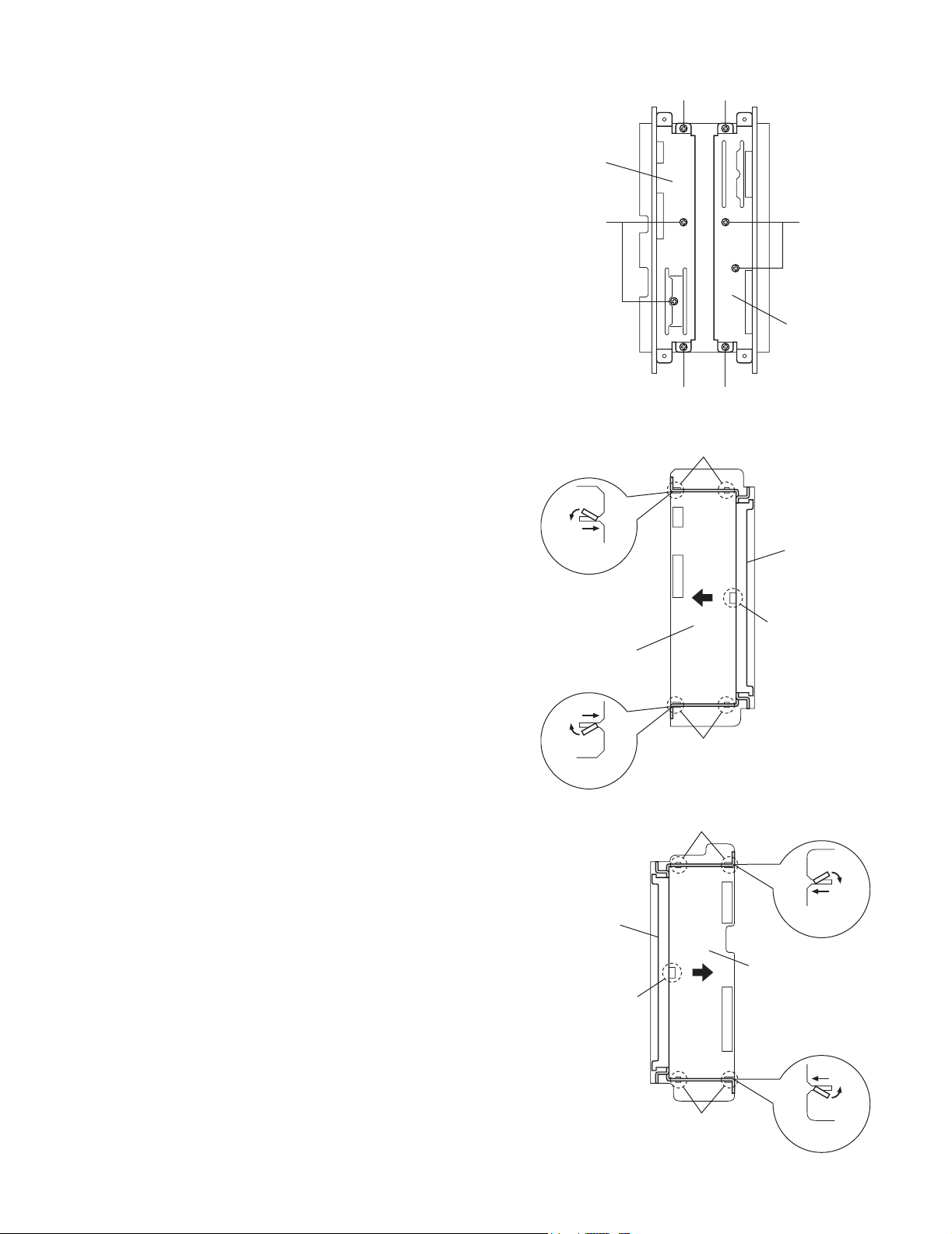
2.4.6 Removing the power amplifier board (A) (See Figs. 9
and 10.)
• Remove the mother board.
(1) Remove the four screws M attaching the heat sink to the
power amplifier board (A).
(2) From the bottom side of the power amplifier board (A), dis-
engage the four engagement sections a.
(3) From the top side of the power amplifier board (A), slide the
P.TR holder (A) in the direction of the arrow to disengage
the engagement section b and remove the power amplifier
board (A) from the P.TR holder (A).
2.4.7 Removing the power amplifier board (B) (See Figs. 9
and 11.)
• Remove the mother board.
(1) Remove the four screws N attaching the heat sink to the
power amplifier board (B). (See Fig.9.)
(2) From the bottom side of the power amplifier board (B), dis-
engage the four engagement sections c.
(3) arrow to disengage the engagement section d and remove
the power amplifier board (B) from the P.TR holder (B).
P.TR holder (A)
M
M N
N
M
Fig.9
a
TH-V70R
N
P.TR holder (B)
1
2
(Bottom side)
Power amplifier
board (A)
2
1
(Bottom side)
P.TR holder (B)
d
CN102
CN103
a
Fig.10
c
CN106
CN105
P.TR holder (A)
b
1
2
(Bottom side)
Power amplifier
board (B)
c
Fig.11
2
1
(Bottom side)
(No.21175)1-21
Page 22
TH-V70R
r
2.4.8 Removing the power transformer (See Figs. 12 and
13.)
• Remove the rear panel.
(1) Remove the wire from the connector CN104 on the mother
board.
(2) Disconnect the wire from the connector CN107 on the pow-
er supply & SP terminal board.
(3) Remove the four screws P attaching the power transformer
and then remove the power transformer from the transformer bracket of the mold base.
Mother board
Power supply & SP
terminal board
Transforme
bracket
PP
CN104
Power supply & SP
terminal board
Power
transformer
P
Fig.12
Mold base
CN107
Fig.13
1-22 (No.21175)
Page 23
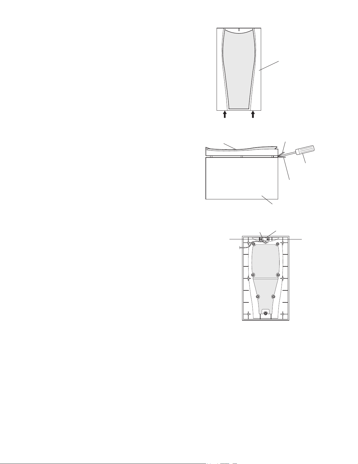
2.4.9 Removing the LED indicator (See Figs. 14 to 16.)
(1) Insert the tip of a flat-bladed screwdriver or a similar tool
into the space between the speaker main body and the ornament panel (the section indicated by the arrows), and lift
the net little by little to remove.
Note:
To prevent damaging the ornament panel and speaker
main body, insert cushioning plates etc. above and below the tip of the flat-bladed screwdriver or a similar tool.
(2) From the back side of the ornament panel, remove the two
screws Q attaching the LED indicator.
(3) Disconnect the wire from connector CN109 on the LED in-
dicator.
TH-V70R
Ornament panel
JVC
Fig.14
Ornament panel
Cushioning plate, etc.
Cushioning plate, etc.
Speaker main body
Fig.15
CN109
LED indicator
Flat-bladed
screwdriver, etc.
QQ
Fig.16
(No.21175)1-23
Page 24
TH-V70R
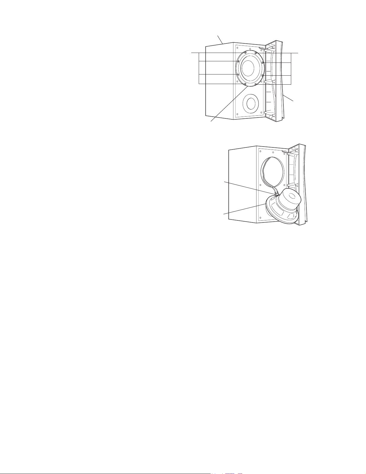
2.4.10 Removing the speaker (See Figs. 17 and 18.)
(1) Remove the eight screws R attaching the speaker.
(2) Take out the speaker.
(3) Disconnect the wires from the terminals of the speaker.
Speaker main body
R
Speaker
Terminal
R
Ornament panel
Fig.17
Speaker
Fig.18
1-24 (No.21175)
Page 25
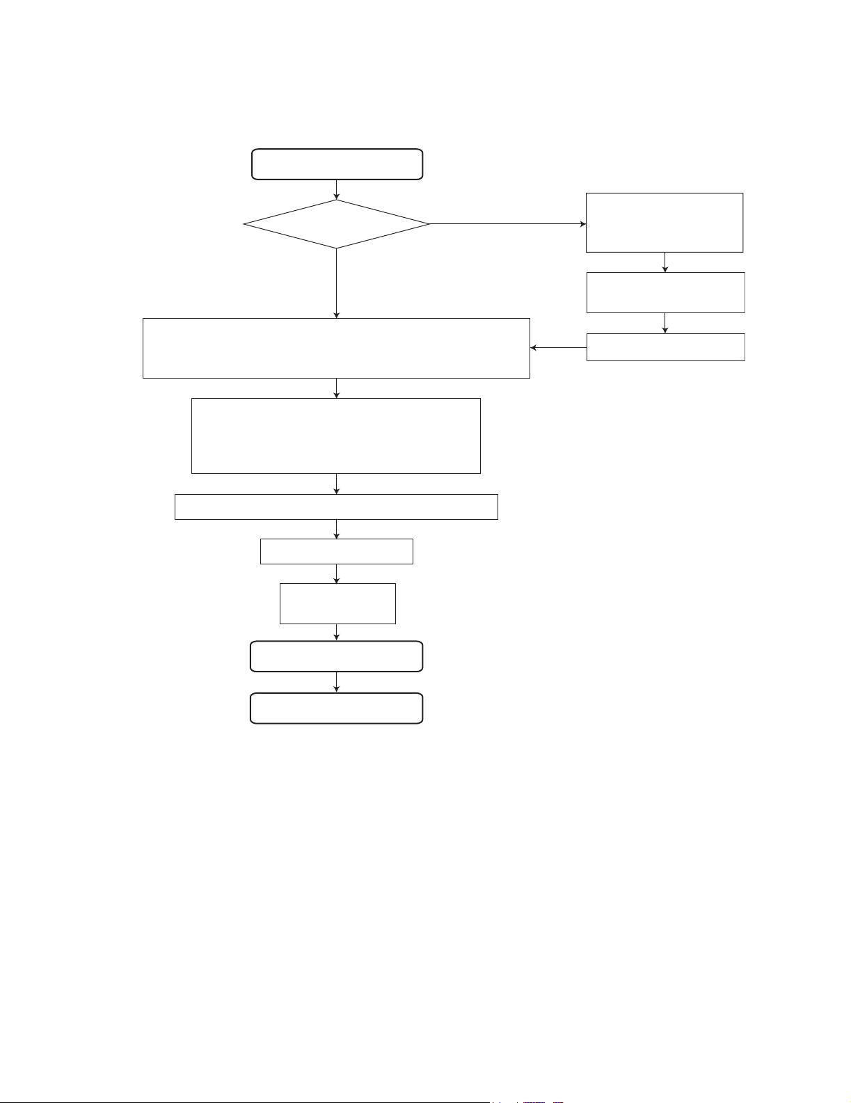
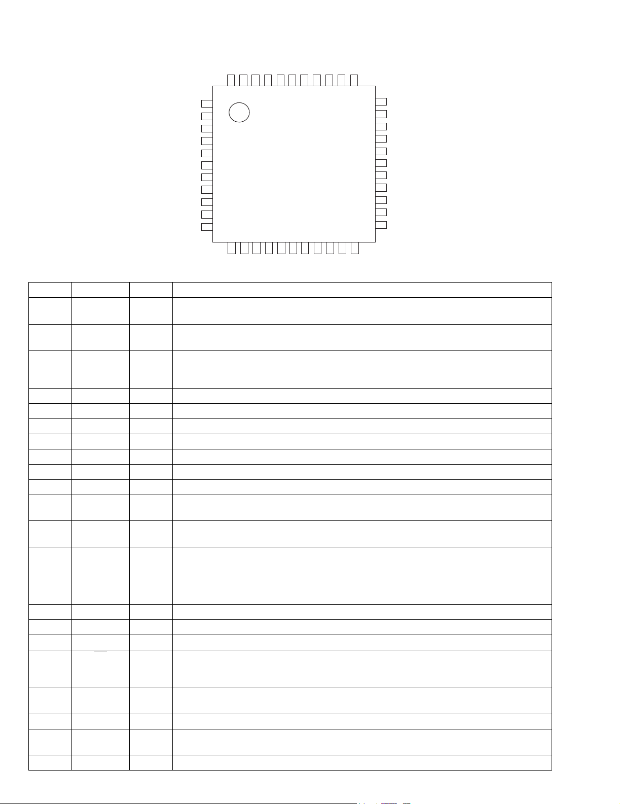
3.1 Initializing in TEST MODE
TH-V70R
SECTION 3
Adjustment method
Initializing in TEST MODE
Moving panel close?
YES
While pressing both the STOP button (fourth button from left)
and EJECT (farthest right button) button on the main unit,
plug in the power.
FL indication
TEST E
Monitor indication (Upper left of the monitor)
E(Europe)
Pressing the PAUSE button (fifth button from right)
Initialization starts
FL indication
"ATT" will appear
NO
Press the power button
on the main unit, and put
it in standby.
Make sure that the panel
has closed.
Pull out the power plug.
Initialization is complete.
Set the power to standby.
(No.21175)1-25
Page 26
TH-V70R
SECTION 4
Description of major ICs
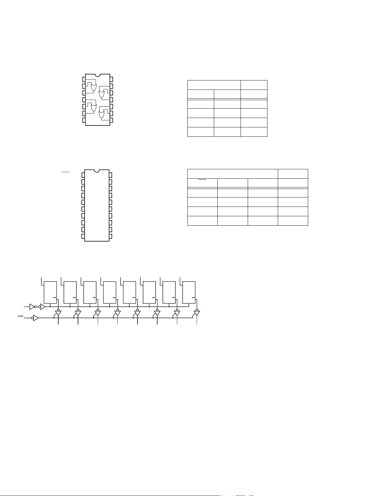
4.1 74LCX32MTC-X (IC522) : Quad 2 input OR gate
• Pin layout & Block diagram
11A
21B
31Y
42A
52B
62Y
7
14
13
12
11
10
9
8GND
V
4B
4A
4Y
3B
3A
3Y
CC
(TOP VIEW)
4.2 74LCX373MTC-X (IC512,IC513) : Octal D-type latch
• Pin layout • Truth table
20
19
18
17
16
15
14D2
13
12
11
VCC
Q7
D7
D6
Q6
Q5
D5
D4
Q4
LE
1OE
2Q0
3D0
4D1
5Q1
6Q2
7
8D3
9Q3
10GND
(TOP VIEW)
• Truth table
INPUTS OUTPUT
ABY
LLL
LHH
HLH
HHH
INPUTS OUTPUT
OE
LE D Y
HXXZ
LLXQn
LHLL
LHHH
X: Don't care
Z: High impedance
Qn: Q outputs are latched at the time when the LE input is tak-
en to a low logic level.
• Block diagram
D0
3
D
Q
L
OE
11
LE
1
2
Q0
D1
4
D2
7
D
Q
L
5
Q1
D3
8
D
Q
L
6
Q2
D4
13
D
Q
L
9
Q3
D5
14
D
Q
L
12
Q4
D6
17
D
Q
L
15
Q5
D7
18
D
D
Q
L
16
Q6
Q
L
19
Q7
1-26 (No.21175)
Page 27
4.3 AK93C65AF-X (IC510) : EEPROM
•Pin layout
TH-V70R
• Block diagram
DI
CS
PE
VCC
CS
SK
1
2
3
4
8 PIN SOP
INSTRUCTION
REGISTER
NC
8
GND
7
DO
6
DI
5
INSTRUCTION
DECODE,
CONTROL
AND
CLOCK
GENERATION
DATA
REGISTER
ADD.
BUFFERS
16
R/W AMPS
AND
AUTO ERASE
DECODER
DO
16
EEPROM
4096bit
256 x 16
SK
PE
• Pin function
Pin no. Symbol Function
1 PE Program enable (With built-in pull-up resistor)
2 VCC Power supply
3 CS Chip selection
4 SK Cereal clock input
5 DI Cereal data input
6 DO Cereal data output
7 GND Ground
8 NC No connection
NOTE :
The pull-up resistor of the PE pin is about 2.5Mohm (VCC=5V)
VREF
VPP SW
VPP
GENERATOR
(No.21175)1-27
Page 28
TH-V70R
4.4 AK4527BVQP (IC401): A/D, D/A converter
• Pin layout
4443424140393837363534
1
2
3
4
5
6
7
8
9
10
11
1213141516171819202122
Top View
• Pin function
No. Symbol I/O Function
1 SDOS I SDTO Source Select Pin (Note 1)
"L" : Internal ADC output "H" : DAUX input
2 OSKS I Control Mode Select Pin
"L" : 3-wire Serial "H" : I2C Bus
3 MIS - Soft Mute Pin (Note 1) Connect to GND
When this pin goes to "H" soft mute cycle is initialized.
When returning to "L" the output mute releases.
4 BICK I Audio Serial Data Clock Pin
5 LRCK I/O Input Channel Clock Pin
6 SDTI1 I DAC1 Audio Serial Data Input Pin
7 SDTI2 I DAC2 Audio Serial Data Input Pin
8 SDTI3 I DAC3 Audio Serial Data Input Pin
9 SDTO O Audio Serial Data Output Pin
10 D,AUX - Sub Audio Serial Data Input Pin Connect to GND
11 DFS - Double Speed Sampling Mode Pin (Note 1)
"L" : Normal Speed "H" : Double Speed
12 DEMI - Connect to GND
No internal bonding.
13 DEMO - Zero Input Detect Enable Pin Connect to GND
"L" : mode 7 (disable) at parallel mode
- zero detect mode is selectable by DZFM2-0 bits at serial mode.
- H : mode 0 (DZF is AND of all six channels)
14 MCKO - Output Buffer Power supply Pin 2.7V~5.5V
15 DVDD I Digital Power Supply Pin 4.5V~5.5V
16 DVSS - De-emphasis Pin 0V
17 PD
I Power-Down & Reset Pin
When "L" the AK4527B is powered-down and the control registers are reset to default state.
If the state of P/S or CAD0-1 changes then the AK4527B must be reset by PDN.
18 XTS - Test Pin Connect to GND
This pin should be connected to DVSS.
19 ICKS - Connect to GND No internal bonding.
20 ADIF - Analog Input Format Select Pin Digital Power Supply
H : Full-differential input "L" : Single-ended input
21 CAD1 - Chip Address 1 Pin Connect to GND
33
32
31
30
29
28
27
26
25
24
23
1-28 (No.21175)
Page 29
No. Symbol I/O Function
22 CAD0 O Chip Address 0 Pin Connect to GND
23 LOUT3 O DAC3 Lch Analog Output Pin
24 ROUT3 O DAC3 Rch Analog Output Pin
25 LOUT2 O DAC2 Lch Analog Output Pin
26 ROUT2 O DAC2 Rch Analog Output Pin
27 LOUT1 O DAC1 Lch Analog Output Pin
28 ROUT1 O DAC1 Rch Analog Output Pin
29 LIN- I Lch Analog Negative Input Pin
30 LIN+ I Lch Analog Positive Input Pin
31 RIN- I Rch Analog Negative Input Pin
32 RIN+ I Rch Analog Positive Input Pin
33 VREFL - Zero Input Detect 2 Pin (Note 2) Non Connect
When the input data of the group 1 follow total 8192LRCK cycles with "0" input data this pin
goes to "H".
OVF O Analog Input Overflow Detect Pin (Note 3)
This pin goes to "H" if the analog input of Lch or Rch is overflows.
34 VCOM O Common Voltage Output PinAVDD/2
Large external capacitor around 2.2uF is used to reduce power-supply noise.
35 VREFH - Positive Voltage Reference Input PinAVDD
36 AVDD - Analog Power Supply Pin4.5V~5.5V
37 AVSS - Analog Ground Pin0V
38 XTI - Zero Input Detect 1 Pin (Note 2) Non connect
When the input data of the group 1 follow total 8192 LRCK cycles with "0" input data this pin
goes to "H".
39 XTO I Master Clock Input Pin
40 P1S - Parallel / Serial Select Pin
"L" : Serial control mode "H" : Parallel control mode
41 CS
CSN I Chip select pin in 3-wire serial control mode
42 DIF1 I Audio Data Interface Format 1 Pin in parallel mode
SCL/CCLK I Control Data Clock Pin in serial control mode
43 LOOP0 I Loopback Mode 0 Pin in parallel control mode
SAD/CDTI I/O Control Data Input Pin in serial control mode
44 CDTD I Loopback Mode 1 Pin (Note 1)
Note:
(1) SDOS, SMUTE, DFS, and LOOP1 pins are ORed with register data if P/S = "L".
(2) The group 1 and 2 can be selected by DZFM2-0 bit if P/S = "L" and DZFME = "L".
(3) This pin becomes OVF pin if OVFE bit is set to "1" at serial control mode.
(4) All input pins should not be left floating.
I Audio Data Interface Format 0 Pin in parallel mode
This pin should be connected to DVDD at I2C bus control mode
I2C = "L" : CCLK(3-wire Serial) I2C = "H" : SCL(I2CBus)
Enables digital loop-back from ADC to 3 DACs.
I2C = "L" : CDTI(3-wire Serial) I2C = "H" : SDA(I2CBus)
Enable all 3 DAC channels to be input from SDTII.
TH-V70R
(No.21175)1-29
Page 30
TH-V70R
4.5 AN8703FH-V (IC101) : Frontend processor for DVD
• Pin layout
64 49
1
16
48
33
17 32
• Pin function
Pin No.
10 IDGT I Data slice part address part gate signal
11 STANDBY I Standby mode control terminal
12 SEN I SEN(Serial data input terminal)
13 SCK I SCK(Serial data input terminal)
14 STDI I STDI(Serial data input terminal)
15 RSCL I Standard electric current terminal
16 JLINE I Electric current setting terminal of JLine
17 TEN I Reversing input terminal of tracking error
18 TEOUT O Tracking error signal output terminal
19 AGCBAL I Offset adjusting terminal 1
20 ASOUT O Full adder signal output terminal
21 FEN I Focus error output amplifier reversing in-
22 FEOUT O Focus error signal output terminal
23 AGCOFST I Offset adjusting terminal 2
24 MON - Non connect
25 AGCLVL O Output amplitude adjustment for DRC
26 GND2 - Connect to GND
27 VREF2 O VREF2 voltage output terminal
28 VCC2 - Power supply terminal 5V
29 VHALF O VHALF voltage output terminal
30 DFLTON O Reversing output terminal of filter AMP.
31 DFLTOP O Filter AMP. output terminal
32 DCFLT I Capacity connection terminal for filter
Symbol I/O Description
1 LPC1 I Laser input terminal (DVD)
2 LPC01 O Laser drive signal output terminal (DVD)
3 LPC2 I Laser input terminal (CD)
4 LPC02 O Laser drive signal output terminal (CD)
5
VFOSHORT
6 TBAL I Tracking balance control terminal
7 FBAL I Focus balance control terminal
8 POFLT O Track detection threshold level terminal
9 DTRD I Data slice part data read signal input ter-
I VFOSHORT control terminal
minal(For RAM)
input terminal( For RAM)
output AMP.
put terminal
output
Pin No.
33 GND3 - Connect to GND
34 RFDIFO - Non connect
35 RFOUT - Connect to TP103
36 VCC3 - Power supply terminal 3.3V
37 RFC O Filter for RF delay correction AMP.
38 DCRF O All addition amplifier capacitor terminal
39 OFTR O OFTR output terminal
40 BDO O BDO output terminal
41 RFENV O RF envelope output terminal
42 BOTTOM O Bottom envelope detection filter terminal
43 PEAK O Peak envelope detection filter terminal
44 AGCG O AGC amplifier gain control terminal
45 AGCO O AGC amplifier level control terminal
46 TESTSG I TEST signal input terminal
47 RFINP I RF signal positive input terminal
48 RFINN I RF signal negative input terminal
49 VIN5 I Internal four-partition (CD) RF input 1
50 VIN6 I Internal four-partition (CD) RF input 2
51 VIN7 - Internal four-partition (CD) RF input 3
52 VIN8 - Internal four-partition (CD) RF input 4
53 VIN9 I External two-partition (DVD) RF input 2
54 VIN10 I External two-partition (DVD) RF input 1
55 VCC1 - Power supply terminal 5V
56 VREF1 O VREF1 voltage output terminal
57 VIN1 I Internal four-partition (DVD) RF input 1
58 VIN2 I Internal four-partition (DVD) RF input 2
59 VIN3 I Internal four-partition (DVD) RF input 3
60 VIN4 I Internal four-partition (DVD) RF input 4
61 GND1 - Connect to GND
62 VIN11 I 3 beam sub input terminal 2 (CD)
63 VIN12 I 3 beam sub input terminal 1 (CD)
64 HDTYPE O HD Type selection
Symbol I/O Description
1-30 (No.21175)
Page 31

4.6 BA15218F-XE (IC510,IC511,IC531,IC561,IC581,IC591) : Dual operational amplifier
•Pin layout
TH-V70R
OUT1 1
-IN1 2
+IN1 3
VEE 4
• Block diagram
Vcc
-IN
+IN
1
2
R1
Q5
Q1
Q2
D1
Q3 Q4
8 Vcc
7 OUT2
6 -IN2
5 +IN2
C2
R5
Q6
Q9
Q8
Q10
Q7
R7
Q11
R6
Q12
R8
Q18Q13
OTHER
CH
Q19
Q17Q16
C1
R3R2
R4
VEE
OUTPUT
4.7 BA15218N (IC103,IC104,IC108,IC109,IC110,IC201,IC202) : Dual Ope. Amp.
• Pin layout / Block diaglam
+
+
1
-
1 2 3 4 5 6 7 8
OUT1 +IN1 +IN1
+IN2 -IN2 OUT2
GND
2
-
Vcc
Q14 Q15Q114
R9
(No.21175)1-31
Page 32

TH-V70R
4.8 BA5983FM-X (IC201) : 4-channel driver
• Block diagram
27
28
Vcc
26
10k
25
20k
23 22 30
24
10k
20k
21
STAND BY
CH4
20
Vcc
19
10k
10k
18
Level Shift
17 16
10k
10k
10k
10k
15
10k
10k
Level Shift
10k
10k
1
2
3
5
4
10k
6
• Pin function
Pin No. Symbol I/O Description
1 BIAS IN I Input for Bias-amplifier
2 OPIN1(+) I Non inverting input for CH1 OP-AMP
3 OPIN1(-) I Inverting input for CH1 OP-AMP
4 OPOUT1 O Output for CH1 OP-AMP
5 OPIN2(+) I Non inverting input for CH2 OP-AMP
6 OPIN2(-) I Inverting input for CH2 OP-AMP
7 OPOUT2 O Output for CH2 OP-AMP
8 GND - Substrate ground
9 STBY1 I Input for CH1/2/3 stand by control
10 PowVcc1 - Vcc for CH1/2 power block
11 VO2(-) O Inverted output of CH2
12 VO2(+) O Non inverted output of CH2
13 VO1(-) O Inverted output of CH1
14 VO1(+) O Non inverted output of CH1
15 VO4(+) O Non inverted output of CH4
Level Shift
10k
10k
Level Shift
10k
10k
10k
10k
10k
10k
10k
STAND BY
CH1/2/3
729 891011121314
Vcc
Pin No. Symbol I/O Description
16 VO4(-) O Inverted output of CH4
17 VO3(+) O Non inverted output of CH3
18 VO3(-) O Inverted output of CH3
19 PowVcc2 - Vcc for CH3/4 power block
20 STBY2 I Input for Ch4 stand by control
21 GND - Substrate ground
22 OPOUT3 O Output for CH3 OP-AMP
23 OPIN3(-) I Inverting input for CH3 OP-AMP
24 OPIN3(+) I Non inverting input for CH3 OP-AMP
25 OPOUT4 O Output for CH4 OP-AMP
26 OPIN4(-) I Inverting input for CH4 OP-AMP
27 OPIN4(+) I Non inverting input for CH4 OP-AMP
28 PreVcc - Vcc for pre block
29 - Connect to ground
30 - Connect to ground
1-32 (No.21175)
Page 33

4.9 BA3121 (IC100,IC101,IC102) : Ground isolation amplifier
• Pin layout • Block diagram
OUT1
VM1
IN1
GND
1
2
3
4
8
7
6
5
VCC
OUT2
VM2
IN2
3IN1
2VM1
5IN2
4.10 GP1FA351RZ (IC409) : Fiber optic receiver
• Pin layout • Block diagram
AMP
AMP
R
R
R
R
AMP
AMP
Comp & Output circuit
TH-V70R
VCC
8
OUT1
1
RR
RR
V
V
CC
OUT
VM2
6
7 OUT2
4 GND
GND
(No.21175)1-33
Page 34

TH-V70R
4.11 BA6664FM-X (IC251) : Motor driver
• Pin layout
1
NC
2
A3
3
NC
4
A2
5
NC
6
NC
7
A1
29 30
8
GND
9
H1+
10
H1-
11
H2+
12
H2-
13
H3+
14
H3-
• Block diagram
RNF
28
VM
27
GSW
26
Vcc
25
FG
24
PS
23
EC
22
ECR
21
FR
20
FG2
19
SB
18
CNF
17
BR
16
VH-
15
A3
A1
GND
H1+
H1-
H2+
H2-
H3+
H3-
R
NF
28
VM
DRIVER
TSD
2
A2
GAIN
CONTROL
4
CURRENT
SENSE AMP
TL
+ -
GAIN
SWITCH
VCC
7
8
9
10
11
12
13
HALL AMP
+
-
+
-
+
-
+
-
+
-
+
-
R
D Q
CK Q
PS
TOROUE
SENSE AMP
+
-
VCC
VCC
SHORT BRAKE
BRAKE MODE
14
Hall Bias
27
26
25
24
23
22
21
20
19
18
17
16
15
GSW
VCC
FG
PS
EC
ECR
FR
FG2
SB
CNF
BR
VH
1-34 (No.21175)
Page 35

• Pin function
Pin No. Symbol I/O Description
1 NC - Non connect
2 A3 O Output 3 for spindle motor
3 NC - Non connect
4 A2 O Output 2 for spindle motor
5 NC - Non connect
6 NC - Non connect
7 A1 O Output 1 for spindle motor
8 GND - Connect to ground
9 H1+ I Positive input for hall input AMP 1
10 H1- I Negative input for hall input AMP 1
11 H2+ I Positive input for hall input AMP 2
12 H2- I Negative input for hall input AMP 2
13 H3+ I Positive input for hall input AMP 3
14 H3- I Negative input for hall input AMP 3
15 VH I Hall bias terminal
16 BR - Non connect
17 CNF - Capacitor connection pin for phase compensation
18 SB I Short brake terminal
19 FG2 - Non connect
20 FR - Non connect
21 ECR I Torque control standard voltage input terminal
22 EC I Torque control voltage input terminal
23 PS O Start/stop switch (power save terminal)
24 FG O FG signal output terminal
25 VCC - Power supply for signal division
26 GSW O Gain switch
27 VM - Power supply for driver division
28 RNF O Resistance connection pin for output current sense
29 - Connect to ground
30 - Connect to ground
TH-V70R
(No.21175)1-35
Page 36

TH-V70R
4.12 BD4740G-W (IC803) : Reset
• Pin layout • Block diagram
54
Vcc Vout
Vcc
5
NC SUB GND
123
4.13 BU4066BCF-X(IC151):Switch
• Pin layout & block diagram
1
I/O1
2
O/I1
3
O/I2
4
I/O2
5
C2
6
C3
7
Vss
14
13
12
11
10
9
8
Vdd
C1
C4
I/O4
O/I4
O/I3
I/O3
• Truth table
Control Switch
HON
LOFF
Vref
3
GND
Vout
4
4.14 CY24203SC-X (IC502) :Clock generator
• Pin layout • Pin function
Pin No. Symbol Description
XIN
VDD
VCXO
VSS
1
2
3
4
8
XOUT
7
27M
6
13.5M
5
16.9344M
1 XIN Reference crystal input
2 VDD Power supply
3 VCXO Input analog control for VCXO
4 VSS Connect to ground
5 16.9344M 16.9344 MHz clock output
6 13.5 13.5 MHz clock output
7 27M 27 MHz clock output
8 XOUT Reference crystal output
1-36 (No.21175)
Page 37

4.15 LA73054-X (IC601) : Video driver
• Pin layout & Block diagram
36 35 34 33 32 31 30 29 28 27 26 25 24 23 22 21 20 19
75
DRIVER
LPF
2Step
Amp1
C_OFFSET
DC_CTL
CLAMP
1 2 3 4 5 6 7 8 9 10 11 12 13 14 15 16 17 18
75
DRIVER
LPF1
2Step
Amp2
Y/C
MIX
75
DRIVER
LPF1
2Step
Amp3
CLAMP
SYNC
SEP
DRIVER
2Step
Amp4
PEDESTAL
CLAMP
75
LPF1LPF2
CLAMP
• Pin function
Pin No. Symbol I/O Function
1 VCC1 - VCC except for 75ohm driver
2 COMPOSITE.IN I Input composite
3 SQUEEZE.SW I Selecting squeeze mode
4 LETTER-BOX.SW I Selecting letter-box mode
5 MUTE-SW-1 I Composite/S signal mute selection
6 C-IN I Input Chroma signal
7 GND11 - Composite/S GND except for 75ohm driver
8 Y-IN-1 I Input Y signal
9 YC-MIX.SW I Selecting of doing Y/C-MIX or not
10 SIGNAL-IN.SW I Selection of a kind of signal
11 Y-IN-2 I Input component Y or baseband signal
12 MUTE-SW-2 I Component signal mute selection
13 LPF.SW I Selection of a kind of component LPF
14 CB.IN I Input component or baseband signal
15 AMP.SW-2 I Selecting amplifier gain for component signal
16 CR.IN I Input component or baseband signal
17 GND12 - Component GND except for 75ohm driver
18 REG O Capacitor terminal for regulator
19 DRIVE.SW-2 I 2drive/1drive select for component signal
20 GND26 - CR-GND for 75ohm driver
21 CR.OUT O 75ohm driver output of pin16 input
22 GND25 - CB-OUT for 75ohm driver
23 CB.OUT O 75ohm driver output of pin14 input
24 VCC22 - Component Vcc for 75ohm driver
25 Y-OUT-2 O 75ohm driver output of pin11 input
26 GND24 - Component Y out for 75ohm driver
27 GND23 - Y out for 75ohm driver
28 Y-OUT-1 O 75ohm driver output of pin8 input
29 GND22 - Chroma out for 75ohm driver
30 C-DC.OUT O DC voltage output for S1,S2
31 C-OUT O 75ohm driver output of pin6 input
32 GND21 - Composite out for 75ohm driver
33 COMPOSITE-OUT O 75ohm driver output of pin2 input
34 VCC21 - Composite/S Vcc for 75ohm driver
35 DRIVE.SW-1 I 2drive/1drive select for composite/S signal
36 AMP.SW-1 I Selecting amplifier gain for composite/S signal
75
DRIVER
LPF1LPF2 LPF1LPF2
2Step
Amp5
PEDESTAL
CLAMP
75
DRIVER
2Step
Amp6
PEDESTAL
CLAMP
VCC
TH-V70R
REG
(No.21175)1-37
Page 38

TH-V70R
A
4.16 K4S643232E-TC60 (IC505) : 512K x 32 bit x 4 banks synchronous DRAM
• Pin layout
86 44
143
• Block diagram
Data Input Register
512K x 32
512K x 32
512K x 32
512K x 32
Column Decoder
Latency & Burst Length
Programming Register
CLK
DD
Address Register
LCKE
Bank Select
Row Buffer
Refresh Counter
LRAS
LCBR
LRAS LCBR LWE
LCAS
Row Decoder
Col. Buffer
LWCBR
Sense AMP
LDQM
LWE
LDQM
I/O Control
DQi
Output Buffer
Timing Register
CLK CKE CS
RAS CAS
WE DQM
• Pin function
Pin No. Symbol Function
1 VDD Power for the input buffers and core logic.
2 DQ0 Data input/output are multiplexed on the same pin.
3 VDDQ Isolated power supply for the output buffers to provide improved noise immunity.
4,5 DQ1,DQ2 Data inputs/outputs are multiplexed on the same pins.
6 VSSQ Isolated ground for the output buffers to provide improved noise immunity.
7,8 DQ3,DQ4 Data inputs/outputs are multiplexed on the same pins.
9 VDDQ Isolated power supply for the output buffers to provide improved noise immunity.
10,11 DQ5,DQ6 Data inputs/outputs are multiplexed on the same pins.
12 VSSQ Isolated ground for the output buffers to provide improved noise immunity.
13 DQ7 Data input/output are multiplexed on the same pin.
14 N.C This pin is recommended to be left no connection on the device.
15 VDD Power for the input buffers and core logic.
16 DQM0 Makes data output Hi-Z, tSHZ after the clock and masks the output.
Blocks data input when DQM active.
17 WE
Enables write operation and row precharge.
Latches data in starting from CAS, WE active.
18 CAS Latches column addresses on the positive going edge of the CLK with CAS low.
Enables column access.
19 RAS
Latches row addresses on the positive going edge of the CLK with RAS low.
Enables row access & precharge.
20 CS
Disables or enables device operation by masking or enabling all inputs except CLK, CKE and DQM.
21 N.C This pin is recommended to be left no connection on the device.
22,23 BA0,BA1 Selects bank to be activated during row address latch time.
Selects bank for read/write during column address latch time.
24,25~27 A10,A0 - A2 Row/column addresses are multiplexed on the same pins.
Row address : RA0 ~ RA10, Column address : CA0 ~ CA7
1-38 (No.21175)
Page 39

Pin No. Symbol Function
28 DQM2 Makes data output Hi-Z, tSHZ after the clock and masks the output.
Blocks data input when DQM active.
29 VDD Power for the input buffers and core logic.
30 N.C This pin is recommended to be left no connection on the device.
31 DQ16 Data input/output are multiplexed on the same pin.
32 VSSQ Isolated ground for the output buffers to provide improved noise immunity.
33,34 DQ17,DQ18 Data inputs/outputs are multiplexed on the same pins.
35 VDDQ Isolated power supply for the output buffers to provide improved noise immunity.
36,37 DQ19,DQ20 Data inputs/outputs are multiplexed on the same pins.
38 VSSQ Isolated ground for the output buffers to provide improved noise immunity.
39,40 DQ21,DQ22 Data inputs/outputs are multiplexed on the same pins.
41 VDDQ Isolated power supply for the output buffers to provide improved noise immunity.
42 DQ23 Data input/output are multiplexed on the same pin.
43 VDD Power for the input buffers and core logic.
44 VSS Ground for the input buffers and core logic.
45 DQ24 Data input/output are multiplexed on the same pin.
46 VSSQ Isolated ground for the output buffers to provide improved noise immunity.
47,48 DQ25,DQ26 Data inputs/outputs are multiplexed on the same pins.
49 VDDQ Isolated power supply for the output buffers to provide improved noise immunity.
50,51 DQ27,DQ28 Data inputs/outputs are multiplexed on the same pins.
52 VSSQ Isolated ground for the output buffers to provide improved noise immunity.
53,54 DQ29,DQ30 Data inputs/outputs are multiplexed on the same pins.
55 VDDQ Isolated power supply for the output buffers to provide improved noise immunity.
56 DQ31 Data input/output are multiplexed on the same pin.
57 N.C This pin is recommended to be left no connection on the device.
58 VSS Ground for the input buffers and core logic.
59 DQM3 Makes data output Hi-Z, tSHZ after the clock and masks the output.
Blocks data input when DQM active.
60~66 A3 - A9 Row/column addresses are multiplexed on the same pins.
Row address : RA0 - RA10, Column address : CA0 - CA7
67 CKE Masks system clock to freeze operation from the next clock cycle.
CKE should be enabled at least one cycle prior to new command.
Disables input buffers for power down mode.
68 CLK Active on the positive going edge to sample all inputs.
69,70 N.C This pin is recommended to be left no connection on the device.
71 DQM1 Makes data output Hi-Z, tSHZ after the clock and masks the output.
Blocks data input when DQM active.
72 VSS Ground for the input buffers and core logic.
73 N.C This pin is recommended to be left no connection on the device.
74 DQ8 Data input/output are multiplexed on the same pin.
75 VDDQ Isolated power supply for the output buffers to provide improved noise immunity.
76,77 DQ9,DQ10 Data inputs/outputs are multiplexed on the same pins.
78 VSSQ Isolated ground for the output buffers to provide improved noise immunity.
79,80 DQ11,DQ12 Data inputs/outputs are multiplexed on the same pins.
81 VDDQ Isolated power supply for the output buffers to provide improved noise immunity.
82,83 DQ13,DQ14 Data inputs/outputs are multiplexed on the same pins.
84 VSSQ Isolated ground for the output buffers to provide improved noise immunity.
85 DQ15 Data input/output are multiplexed on the same pin.
86 VSS Ground for the input buffers and core logic.
TH-V70R
(No.21175)1-39
Page 40

TH-V70R
4.17 M62446AFP-X (IC153): 6 CH Master volume
• Pin layout & Block diagram
OUT4
OUT3
OUT2
OUT1
AVD D
SWin
GNDS
SRin
SLin
GNDC
Cin
GNDR
Rin
GNDL
Lin
BYPASSR
BYPASSL
LTR E
LBASS3
LBASS2
LBASS1
10
11
12
13
14
15
16
17
18
19
20
21
1
2
3
4
5
6
7
8
9
OUTPUT
PORT
tone
volume
volume
volume
volume
volume
volume
MCU
I/F
tone
42
41
40
39
38
37
36
35
34
33
32
31
30
29
28
27
26
25
24
23
22
DVDD
CLK
DATA
LATCH
DGND
AGND
SWout
SRout
SLout
Cout
Rout
Lout
AVS S
CL1
CL2
CR1
CR2
RTRE
RBASS3
RBASS2
RBASS1
1-40 (No.21175)
Page 41

• Pin function
Pin No. Symbol I/O Function
1 OUT4 O PORT output 4
2 OUT3 O PORT output 3
3 OUT2 O PORT output 2
4 OUT1 O PORT output 1
5 AVDD - Analog positive power supply terminal
6 SWin I Volume input
7 GNDS - Ground terminal
8 SRin I Volume input
9 SLin I Volume input
10 GNDC - Ground terminal
11 Cin I Volume input
12 GNDR - Ground terminal
13 Rin I Tone input
14 GNDL - Ground terminal
15 Lin I Tone input
16 BYPASSR I R channel volume input
17 BYPASSL I L channel volume input
18 LTRE I Tone treble frequency adjusting terminal
19 LBASS3 I Tone bass frequency adjusting terminal
20 LBASS2 I Tone bass frequency adjusting terminal
21 LBASS1 I Tone bass frequency adjusting terminal
22 RBASS1 I Tone bass frequency adjusting terminal
23 RBASS2 I Tone bass frequency adjusting terminal
24 RBASS3 I Tone bass frequency adjusting terminal
25 RTRE I Tone treble frequency adjusting terminal
26 CR2 O Tone output terminal
27 CR1 I R channel volume input
28 CL2 O Tone output terminal
29 CL1 I L channel volume input
30 AVSS - Analog negative power supply terminal
31 Lout O L channel output
32 Rout O R channel output
33 Cout O Volume output
34 SLout O Volume output
35 SRout O Volume output
36 SWout O Volume output
37 AGND - Analog ground terminal
38 DGND - Digital ground terminal
39 LATCH I Latch input terminal
40 DATA I Data input terminal
41 CLK I Data transfer clock input terminal
42 DVDD - Digital power supply terminal
TH-V70R
(No.21175)1-41
Page 42

TH-V70R
A
8
4.18 LM1117MP1.8-X (IC511) : Regulator
• Pin layout • Block diagram
Top view
V
IN
INPUT
DJ/GND
OUTPUT
4.19 LP61L1024S-12-X (IC404) : SRAM
• Pin layout • Block diagram
DD
NC
A16
A14
A12
A7
A6
A5
A4
A3
A2
A1
A0
I/O1
I/O2
I/O3
Vss
1
2
3
4
5
6
7
8
9
10
11
12
13
14
15
16
32
31
30
29
28
27
26
25
24
23
22
21
20
19
18
17
V
A15
CS2
WE
A13
A8
A9
A11
OE
A10
CS1
I/O8
I/O7
I/O6
I/O5
I/O4
DD
• Pin function
V
Vss
A0
A16
CS2
CS1
OE
WE
SYMBOL DESCRIPTION
A0 - A16 Address Input
I/O1 - I/O8 Data Input/Output
, CS2 Chip Select Inputs
CS1
WE
OE
VDD Power Supply
Vss Ground
NC No Connection
Thermal
Limit
Current
GND (FIXED OUTPUT)
ADJ.(ADJUSTABLE OUTPUT)
DECODER
CONTROL
Write Enable Input
Output Enable Input
Limit
CORE
ARRAY
DATA I/O
Substrate
I/O1
I/O
V
OUT
1-42 (No.21175)
Page 43

4.20 MM1563DF-X (IC407) : Regulator
•Pin layout
756
(TOP VIEW)
1
234
• Block diagram
V
IN
7
Cont
5
GND
3
• Pin function
Bias
Thermal
shutdown
Driver
Current
limiter
Cn
TH-V70R
Vo
1
Reference
4
Pin No. Symbol Function
1 Vo Output pin
2 NC Not connect
3 GND Ground
4 Cn Noise decrease pin
5 CONT Control pin
CONT
H
L
Output
ON
OFF
6 Sub Substrate pin, The 6pin must be connected to GND.
7 VIN Input pin
(No.21175)1-43
Page 44

TH-V70R
4.21 MM1613DN-X (IC402) : Regulator
• Pin layout • Block diagram
Vin
54
(TOP VIEW)
1
23
Cont
GND
• Pin function
Pin No. Symbol Function
1 Cont ON/OFF Control pin
5
Bias
1
Reference
Thermal
shutdown
2
3
Cn
Driver
Current
limiter
Vout
4
Cont
H
L
Vo
ON
OFF
Cont pin must be connected with VIN pin, if it is not used.
2 GND Ground
3 Cn Noise decrease pin, Connecting 0.01uF capacitor can decrease output noise.
4 Vout If the noise decrease capacitor is not connected, the pin may be influenced by outside noise.
Output pin, The capacitor must be connected with output pin more than 1uF.
5 Vin Input pin
The capacitor is required to connect with input pin more than 1uF.
4.22 MM74HCT32MTC-X (IC521) : Quad 2 input OR gate
• Pin layout & Block diagram • Truth table
11A
21B
31Y
42A
52B
62Y
7
14
13
12
11
10
9
8GND
V
4B
4A
4Y
3B
3A
3Y
CC
INPUTS OUTPUT
ABY
LLL
LHH
HLH
HHH
(TOP VIEW)
1-44 (No.21175)
Page 45

4.23 MN101C35DKB (IC701) : FL driver microcomputer
•Pin layout
100 76
1
75
TH-V70R
25
26 50
51
• Pin function
Pin No. Symbol I/O Function
1 NC - Not connect
2 DATAIN I FL driver communication data input/output
3 CLOCK I FL driver communication clock input
4 NC - Not connect
5 INITIAL I FL driver communication CS(INITIAL)
6,7 NC - Not connect
8 B5V - VDD(B5V)
9 OSC2 O 8MHz main clock output
10 OSC1 I 8MHz main clock input
11,12 GND - Ground
13 NC - Not connect
14 ~ 23 GND - Ground
24 VREF+ - Reference voltage
25 NC - Not connect
26 RESET I FL reset input
27 PLED-HO O POWER LED switching signal
28 KEYLED-HO O KEY LED switching signal
29 PLED.VE O POWER LED switching signal
30 KEYLED_VE O KEY LED switching signal
31 REMOCON_HO O Remote control receiver switching signal
32 NC - Not connect
33 ~ 38 GND - Ground
39 PLED_DIM O POWER LED DIMMER switching signal
40 LED_DIM O KEY LED DIMMER switching signal
41 ~ 46 NC - Not connect
47 G1 O Grid signal outputs
48 ~ 59 G2 - G13 O Grid signal outputs
60 G14 O Grid signal outputs
61 Q15 - Not connect
62 ~ 64 - - Not connect
65 ~ 99 S1 - S35 O Segment signal outputs
100 -VPP - VPP
(No.21175)1-45
Page 46

TH-V70R
4.24 MN101C49GKD1 (IC801) : System micon
• Pin layout
100 76
1
75
25
26
51
50
• Pin function
Pin No. Symbol I/O Function
1 VREF- - Connect to ground
2 NTSEL(RGB--SEL) I NTSC/PAL discrimination(RGB/YC switching discrimination) signal
3 VER/HOR SEL I Vertical/Horizontal setting discrimination signal
4 SW1 I Slide door switch1
5 PHOTOSW I Loading mechanism photo switch
6 LOCK I Slide door lock detection(AD)
7 VERSION I Area discrimination signal
8 KEY1 I Key input1 (AD)
9 KEY2 I Key input2 (AD)
10 VREF+ - Reference power supply
11 VDD - Power supply
12 OSC2 O Oscillator output (8MHz)
13 OSC1 I Oscillator input (8MHz)
14 GND - Ground
15 XI O Not used (Connect to ground)
16 XO I Not used (Not connect)
17 GND - Ground
18 DI-DO O PANECON serial communication data output
19 D.O.MUTE O MP3/JPEG mode: H (for DVD disc)
20 DI-CK O PANECON serial communication clock
21 RXD (DATA OUT) O Serial communication data output for PANTERA
22 TXD (DATA IN) I Serial communication data input for PANTERA
23 SCLK I Serial communication clock for PANTERA
24 CS O Transmit request for PANTERA communication
25 CPU-RESET O Reset signal for PANTERA
26 INTP I Receive request for PANTERA communication (Interruption)
27 REMOCON I Remote control signal input (interruption)
28 GND - Ground
29 RDS ST I RDS communication strobe (interruption)
30 SAFETY1 I Short detecting signal 1
31,32 GND - Ground
33 RESET I Syscon reset input
34 DSP RST O DSP micom reset input
35 DSP RDY O DSP micom ready
36 AVC-OUT O AV compulink output
37 AVC-IN I AV compulink input
38 VIDEO-MUTE1 O Video driver mute 1 control
39 VIDEO-MUTE2 O Video driver mute 2 control
40 VIDEO-Y/C-MIX O Video driver YCMIX control
41 VIDEO-RGB O Video driver RGB control
42 DSP-COM O DSP serial communication data output
43 DSP-STAT I DSP serial communication data input
44 DSP-CLK O DSP serial communication clock
45 VOL-DATA O VOLUME serial communication data output
1-46 (No.21175)
Page 47

Pin No. Symbol I/O Function
46 VOL-STB O VOLUME serial communication strobe
47 VOL-CLK O VOLUME serial communication clock
48 SW2 I Slide door switch2
49 INT/PROG O D terminal LINE2 switching
50 REMO-CTL O Remote controller switching control
51 ~ 55 NC - Ground
56 MT1 O Slide door motor control 0
57 MT1 O Slide door motor control 1
58 MTS O Slide door motor speed control
59 INH I AC switching detection
60 GND - Ground
61 HP I Headphone input detection
62 SYS P.ON O System power supply control
63 GND - Ground
64 DVD P.ON O DVD power supply control
65 TUNER P.ON O TUNER power supply control
66 GND - Ground
67 RDS DATA O RDS communication data
68 RDS CLK O RDS communication clock
69 - - Not used
70 TU-DATA-OUT I IF-DATA and tuner receive detection
71 - - Not used
72 TU-DATA-IN O TUNER serial communication data output
73 TU CLK O TUNER serial communication clock
74 TU CE O TUNER serial communication CE
75 AM-BEAT O AM beat cut switching
76 S MUTE O System mute
77 VS1 O E: Scart connector control, D: S1 OUT control
78 VS3 O Control for scart connector control terminal
79 LED-DIM O Disc LED dimmer control
80 LED BLUE O Disc LED control
81 MECHA-V/H O Indicate of mechanism position to front end
82 DISC-SET O Indicate of read start permission to front end
83 DISC-STOP I Receive of eject permission from front end
84 DVD-SAFETY I Short detecting signal 2
85 SW P.ON O Subwoofer power supply control
86 ~ 88 NC - Not used
89 SELECT2 O DSP signal switching (AUX)
90 SELECT1 O DSP signal switching (TUNER)
91 DI-RST O PANECON reset output
92 DI-CS O PANECON serial communication CS
93 - - Not used
94 TOPEN O Loading mechanism motor control 1
95 DAVSS - Ground
96 TCLOSE O Loading mechanism motor control 2
97 LMMUTE O Loading mechanism motor driver mute
98 SWOPEN I Loading mechanism eject switch
99 SWUPDN I Loading mechanism loading switch
100 DAVDD - Power supply
TH-V70R
(No.21175)1-47
Page 48

TH-V70R
4.25 MN103S26EGA (IC301) : Optical disc controller
• Pin layout
176 133
1
132
44
89
45 88
• Pin function
Pin No. Symbol I/O Function
1 NINT0 O System control interruption 0
2 NINT1 O System control interruption 1
3 VDD3 - Power supply (3.3V)
4 VSS - Ground
5 NINT2 O System control interruption 2
6 WAITODC O System control wait control
7 NMRST - System control reset (Not connect.)
8 DASPST - DASP signal initializing
9~17 CPUADR17 - 9 I System control address
18 VDD18 - Power supply (1.8V)
19 VSS - Ground
20 DRAMVDD18 - Connect to VDD18
21 DRAMVSS - Connect to VSS
22~30 CPUADR8 - 0 I System control address
31 VDD3 - Power supply (3.3V)
32 VSS - Ground
33 DRAMVDD3 - Connect to VDD3
34 NCS I System control chip select
35 NWR I System control write
36 NRD I System control read
37~44 CPUDT7 - 0 I/O System control data
45 CLKOUT1 - Not connect.
46 MMOD I Connect to VSS
47 NRST I System reset
48 MSTPOL I Master terminal polarity switch input (Connect to VSS.)
49 SCLOCK - Not connect.
50 SDATA - Not connect.
51 OFTR I Off track signal input
52 BDO I RF dropout/BCA data of making to binary
53~56 PWM1 - 4 - Not connect.
57 VDD3 - Power supply (3.3V)
58 DRAMVDD18 - Connect to VDD18
59 DRAMVSS - Connect to VSS
60 VSS - Ground
61~64 PWM5 - 8 - Not connect.
65 TBAL O Tracking balance adjustment output
66 FBAL O Focus balance adjustment output
67 TRSDRV O Traverse drive output
68 SPDRV O Spindle drive output
69 FG I Motor FG input
70 TILTP - Not connect.
1-48 (No.21175)
Page 49

Pin No. Symbol I/O Function
71 TILT - Not connect.
72 TILTN - Not connect.
73 TX - Not connect.
74 DTRD - Not connect.
75 IDGT - Not connect.
76 VDD18 - Power supply (1.8V)
77 VSS - Ground
78 VDD3 - Power supply (1.8V)
79 OSCI1 I 16.9MHz clock input
80 OSCO1 - Not connect.
81 VSS - Ground
82 TSTSG O Calibration signal
83 VFOSHORT O VFO short output
84 JLINE O J-line setting output
85 AVSS - Analog ground
86 ROUT - Not connect.
87 LOUT - Not connect.
88 AVDD - Analog power supply
89 VCOF I JFVCO control voltage
90 TRCRS I Input signal for track cross formation
91 CMPIN - Not connect.
92 LPFOUT - Not connect.
93 LPFIN I Pull-up to VHALF
94 AVSS - Analog ground
95 HPFOUT - Not connect.
96 HPFIN I HPF input
97 CSLFLT I Pull-up to VHALF
98 RFOIF - Not connect.
99 AVDD - Analog power supply
100 PLFLT2 I Connect to capacitor 2 for PLL
101 PLFLT1 I Connect to capacitor 1 for PLL
102 AVSS - Analog ground
103 RVI I Connect to resistor for VREF reference current source
104 VREFH I Reference voltage input (2.2V)
105 PLPG - Not connect.
106 VHALF I Reference voltage input (1.65V)
107 DSLF2 I Connect to capacitor 2 for DSL
108 DSLF1 I Connect to capacitor 1 for DSL
109 AVDD - Analog power supply
110 NARF I Equivalence RF111 ARF I Equivalence RF+
112 JITOUT O Output for jitter signal monitor
113 AVSS - Analog ground
114 DAC0 O Tracking drive output
115 DAC1 O Focus drive output
116 AVDD - Analog power supply
117 AD0 I Focus error input
118 AD1 I Phase difference/3 beams tracking error
TH-V70R
(No.21175)1-49
Page 50

TH-V70R
Pin No. Symbol I/O Function
119 AD2 I AS: Full adder signal
120 AD3 I RF envelope input
121 AD4 I DVD laser current control terminal
122 AD5 I Tracking drive IC input offset
123 AD6 I CD laser current control terminal
124 TECAPA - Not connect.
125 VDD3 - Power supply (3.3V)
126 VSS - Ground
127~130 MONI0 - 3 O Internal goods title monitor (Connect to TP306 - TP309)
131 NEJECT I Eject detection
132 NTRYCTL I Tray close detection
133 NDASP I/O ATAPI drive active / Slave connection I/O
134 NCS3FX I ATAPI host chip select (Not connect.)
135 NCS1FX I ATAPI host chip select (Not connect.)
136 DA2 I/O ATAPI host address
137 DA0 I/O ATAPI host address (Not connect.)
138 NPDIAG I/O ATAPI slave master diagnosis input
139 DA1 I/O ATAPI host address (Not connect.)
140 NIOCS16 - ATAPI output of selection of host data bus width (Not connect.)
141 INTRQ O ATAPI host interruption output
142 NDMACK I ATAPI host DMA response (Not connect.)
143 VDD3 - Power supply (3.3V)
144 VSS - Ground
145 IORDI - ATAPI host ready output (Not connect.)
146 NIORD I ATAPI host read (Not connect.)
147 NIOWR I/O ATAPI host write
148 DMARQ - ATAPI host DMA request (Not connect.)
149~151 HDD15,HDD0,HDD14 I/O ATAPI host data 15,0,14
152 VDD18 - Power supply (1.8V)
153 PO - Connect to ground
154 UATASEL I Connect to VSS
155 VSS - Ground
156 VDD3 - Power supply (3.3V)
157~159 HDD1,HDD13,HDD2 I/O ATAPI data 1,13,2
160161 HDD12,HDD3 I/O ATAPI data 12,3
162 VDD3 - Power supply (3.3V)
163 VSS - Ground
164~166 HDD11,HDD4,HDD10 I/O ATAPI data 11,4,10
167168 HDD5,HDD9 I/O ATAPI data 5,9
169 VDD3 - Power supply (3.3V)
170 VSS - Ground
171~173 HDD6,HDD8,HDD7 I/O ATAPI data 6,8,7
174 VDDH - Reference power supply for ATAPI (5.0V)
175 NRESET I ATAPI host reset
176 MASTER I/O ATAPI master / Slave selection
1-50 (No.21175)
Page 51

4.26 MN102L62GLF3 (IC401) : Unit CPU
•Pin layout
100 76
1
75
TH-V70R
25
51
26 50
• Pin function
Pin No. Symbol I/O Function
1 WAIT I Micro computer wait signal input
2 RE O Read enable
3 /SPMUTE O Spindle muting output to IC251
4 WEN O Write enable
5 /LMMUTE - Not connect
6 CS1 O Chip select for ODC
7 CS2 - Chip select for ZIVA
(Not connect.)
8 HDTYPE O HD TYPE selection
9 /DRVMUTE O Driver mute
10 SBRK O SP motor brake control
11 LSIRST O LSI reset
12 WOR0 O Bus selection input
13-16 A0-A3 O Address bus (0-3) for CPU
17 VDD - Power supply
18 SYSCLK - System clock signal output
(Not connect.)
19 VSS - Ground
20 XI - Not use (Connect to VSS)
21 XO - Not connect
22 VDD - Power supply
23 OSCI I Clock signal input (13.5MHz)
24 OSCO O Clock signal output (13.5MHz)
(Not connect.)
25 MODE I CPU mode selection input
26-33 A4-A11 O Address bus (4-11) for CPU
34 VDD - Power supply
35-40 A12-A17 O Address bus (12-17) for CPU
41 A18 - Address bus 18 for CPU
(Not connect.)
42 A19 - Address bus 19 for CPU
(Not connect.)
43 VSS - Ground
44 A20 - Address bus 20 for CPU
( Not connect.)
45 DISCSTP O DISC STOP control
46 HAGUP O H/A gain control
47 TCLOSE - Not connect.
48 WOBBLEFIL - Not connect.
49 /HFMON I HF monitor
50 TRVSW I Detection switch of traverse in-
side
Pin No. Symbol I/O Function
51 SWUPDN - Not connect.
52 MECHA_H/V I Disc detection
53 DISCSET O Serial enable signal for ADSC
54 VDD - Power supply
55 FEPEN O Serial enable signal for FEP
56 SLEEP O Standby signal for FEP
57 BUSY - Not connect.
58 REQ O Communication request
59 - Connect to TP405 (REQ)
60 - Not connect.
61 VSS - Ground
62 EPCS O EEPROM chip select
63 EPSK O EEPROM clock
64 EPDI I EEPROM data input
65 EPDO O EEPROM data output
66 VDD - Power supply
67 SCLKO I Communication clock
68 S2UTD I Communication input data
69 U2SDT O Communication output data
70 CPSCK O Clock for ADSC serial
71 P74/SBI1 - Connect to VSS
72 SDOUT O ADSC serial data output
73 - Not use.
(Pull-up to power supply)
74 - Not use.
(Pull-up to power supply)
75 NMI - Not use.
(Pull-up to power supply)
76 ADSCIRQ I Interrupt input of ADSC
77 ODCIRQ I Interrupt input of ODC
78 DECIRQ I Interrupt input of ZIVA
79 CSSIRQ I Interrupt input of SODC
80 ODCIRQ2 I Interruption of system control
81 ADSEP I Address data selection input
(Pull-up to power supply)
82 RST I Reset input
83 VDD - Power supply
84-91 TEST1-TEST 8 I Test signal (1-8) input
(Not connect.)
92 VSS - Ground
93-100 D0-7 I/O Data bus (0-7) of CPU
(No.21175)1-51
Page 52

TH-V70R
4.27 NDV8601VWA-BE (IC501) : DVD on a chip processor
• Pin layout
240 181
1
180
60
121
61 120
• Block diagram
digital audio
Video I/O port
SDRAM
controller
digital audio
serial
peripherals
DVD data
audio DAC
Serial
port
controller
Audio
output
processor
DVD,A/V
port
+
CSS
Audio
DSP
Demux
engine
MPEG
Video
decoder
SDRAM
• Pin function
Pin No. Symbol Description
1 VDDio - Power supply terminal 3.3V
2,3 MD10,11 I/O SDRAM Data bus terminal
4 VDD - Power supply terminal 1.8V
5 MD12 I/O SDRAM Data bus terminal
6 VSSio - Connect to ground
7~9 MD13~15 I/O SDRAM Data bus terminal
10 VDDio - Power supply terminal 3.3V
11 DQM1 O SDRAM Data byte enable
12,13 MA9,8 O SDRAM Address bus terminal
14 VSSio - Connect to ground
15,16 MA7,6 O SDRAM Address bus terminal
17 VSS - Connect to ground
18 MA5 O SDRAM Address bus terminal
19 VDDio - Power supply terminal 3.3V
20,21 MA4,3 O SDRAM Address bus terminal
22 MCLK O SDRAM Clock output
23 VSSio - Connect to ground
24 CKE O SDRAM Clock enable output
25,26 MA2,1 O SDRAM Address bus terminal
27 VDDio - Power supply terminal 3.3V
Video
output
processor
RISC
uProcessor
+ cache
NTSC
PAL
SCART
encoder
XBUS
controller
Video
XBUS
1-52 (No.21175)
Page 53

Pin No. Symbol Description
28 MA0 O SDRAM Address bus terminal
29 MA10 O SDRAM Address bus terminal
30 MA11 - Non connect
31 VSSio - Connect to ground
32,33 MA12,13 O SDRAM Address bus, reserved for terminal compatibility with 64Mb SDRAM
34 VDD - Power supply terminal 1.8V
35 CS0 O SDRAM Primary bank chip select
36 VDDio - Power supply terminal 3.3V
37 RAS O SDRAM Command bit
38 CAS O SDRAM Command bit
39 WE O SDRAM Command bit
40 VSSio - Connect to ground
41 DQM0 O SDRAM Data byte enable
42 DQM2 O SDRAM Data byte enable
43 MD16 I/O SDRAM Data bus terminal
44 VDDio - Power supply terminal 3.3V
45,46 MD17,18 I/O SDRAM Data bus terminal
47 VSS - Connect to ground
48 MD19 I/O SDRAM Data bus terminal
49 VSSio - Connect to ground
50~52 MD20~22 I/O SDRAM Data bus terminal
53 VDDio - Power supply terminal 3.3V
54~56 MD23~25 I/O SDRAM Data bus terminal
57 VSSio - Connect to ground
58~61 MD26~29 I/O SDRAM Data bus terminal
62 VDDio - Power supply terminal 3.3V
63,64 MD30,31 I/O SDRAM Data bus terminal
65 DQM3 O SDRAM Data byte enable
66 CS1 O SDRAM Extension bank chip select
67 VSSD - Connect to ground
68 SPDIF O S/PDIF Digital audio output terminal
69 VSSio - Connect to ground
70 AIN I Digital audio input for digital micro; can be used as GPIO
71 AOUT3 O Serial audio output data to audio DAC for left and right channels for down-mix
72 AOUT2 O Serial audio output data to audio DAC for surround left and right channels
73 AOUT1 O Serial audio output data to audio DAC for center and LFE channels
74 AOUT0 O Serial audio output data to audio DAC for left and right channels
75 VDDio - Power supply terminal 3.3V
76 PCMCLK O Audio DAC PCM sampling clock frequency, common clock for DACs and ADC
77 VDD - Power supply terminal 1.8V
78 ACLK O Audio interface serial data clock, common clock for DACs and AD converter
79 LRCLK O Left / right channel clock, common clock for DACs and ADC
80 SRST O Active low RESET signal for peripheral reset
81 RSTP I RESET_Power : from system, used to reset frequency synthesizer and rest of chip
82 VSSio - Connect to ground
83 RXD1 I UART1 Serial data input from external serial device, used for IR receiver
TH-V70R
(No.21175)1-53
Page 54

TH-V70R
Pin No. Symbol Description
84 SSPIN1 I/O SSP1 Data in or 16X clock for USART function in UART1
85 VSS - Connect to ground
86 SSPOUT1 I/O SSP1 Data out or UART1 data-terminal-ready signal
87 SSPCLK1 I/O SSP1 Clock or UART1 clear-to -send signal
88 SSPCLK0 I/O SSP0 Clock or request-to-send function in UART1
89 VDD - Power supply terminal 1.8V
90 SSPIN0 I/O SSP0 Data in or 16X clock for USART function in UART0
91 VDDio - Power supply terminal 3.3V
92 SSPOUT0 I/O SSP0 Data out or UART0 data-terminal-ready signal
93 TXD0 I/O UART0 Serial data output to an external serial device
94 RXD0 I UART0 Serial data input from external serial device
95 CTS0 I/O UART0 Clear-to-send signal
96 RTS0 I/O UART0 Request-to-send signal
97 VSSio - Connect to ground
98 CXI I Crystal input terminal for on-chip oscillator or system input clock
99 CXO O Crystal output terminal for on-chip oscillator
100 OSCVSS - Connect to ground for oscillator
101 OSCVDD - Power supply terminal for oscillator 1.8V
102 MVCKVDD - Power supply terminal for main and video clock PLL 3.3V
103 SCEN I Scan chain test enable
104 MVCKVSS - Connect to ground for main and video clock PLL
105 ACLKVSS - Connect to ground for audio clock PLL
106 SCMD I Scan chain test mode
107 ACLKVDD - Power supply terminal for audio clock PLL 3.3V
108 VDDDAK - Power supply terminal for DAC digital 1.8V
109 VSSDAC - Connect to ground for DAC digital
110 Cr/R O Video signal output (Cr output : composite/component Red output)
111 IOM O Cascaded DAC differential output used to dump current into external resistor for power
112 C/Cb/B O Video signal output (Chrominance output for NTSC/PAL S-Video
113 VAA3 - Cb output for component Blue output)
114 Y/G O Power supply terminal for DAC analog 3.3V
115 VSSA - Video signal output (Luminance for S-Video and component Green output)
116 VREF - Connect to ground for DAC analog
117 VAA - Non connect
118 CVBS/C O Video signal output (Composite video Chrominance output for S-Video)
119 RSET O Current setting resistor of output DACs
120 COMP O Compensation capacitor connection
121 VSS - Connect to ground
122 VCLK - Non connect
123 VSYNC - Non connect
124 HSYNC - Non connect
125 VDDio - Power supply terminal 3.3V
126~131 VI07~02 - Non connect
132 VSSio - Connect to ground
133,134 VI01,00 - Non connect
135 VDD - Power supply terminal 1.8V
1-54 (No.21175)
Page 55

Pin No. Symbol Description
136~139 AD31~28 I/O Multiplexed address / data bus terminal
140 VDDio - Power supply terminal
141~144 AD27~24 I/O Multiplexed address / data bus terminal
145 PWE3 I/O Byte write enable for FLASH,EEPROM,SRAM or peripherals terminal
146 AD23 I/O Multiplexed address / data bus terminal
147 VSSio - Connect to ground
148~153 AD22~17 I/O Multiplexed address / data bus terminal
154 VDDio - Power supply terminal 3.3V
155 AD16 I/O Multiplexed address / data bus terminal
156 PWE2 I/O Byte write enable for FLASH,EEPROM,SRAM or peripherals terminal
157,158 AD15,14 I/O Multiplexed address / data bus terminal
159 VDD - Power supply terminal 1.8V
160 SCLK O External bus clock used for programmable host peripherals
161 ACK I/O Programmable WAIT/ACK/RDY control
162 VSSio - Connect to ground
163~168 AD13~8 I/O Multiplexed address / data bus terminal
169 VDDio - Power supply terminal 3.3V
170 PWE1 I/O Byte write enable for FLASH,EEPROM,SRAM or peripherals terminal
171 VSS - Connect to ground
172~176 AD7~3 I/O Multiplexed address / data bus terminal
177 VSSio - Connect to ground
178~180 AD2~0 I/O Multiplexed address / data bus terminal
181 VDDio - Power supply terminal 3.3V
182 PWE0 I/O Byte write enable for FLASH,EEPROM,SRAM or peripherals terminal
183 ALE I/O Address latch enable
184~187 LA0~3 I/O Latched address 0~3
188 VSSio - Connect to ground
189 RD I/O Read terminal
190 LHLDA O Bus hold acknowledge in slave mode
191 LHLD I Bus hold request from external master in slave mode
192 VDD - Power supply terminal 1.8V
193 PCS0 O Peripheral chip select 0, generally used for enabling the program store ROM/FLASH
194,195 XI01,02 I/O Programmable general purpose external input/output
196 VDDio - Power supply terminal 3.3V
197~200 XI03~06 I/O Programmable general purpose external input/output
201 VSS - Connect to ground
202,203 XI07,08 I/O Programmable general purpose external input/output
204 VSSio - Connect to ground
205 XI09 I/O Programmable general purpose external input/output
206~209 XID10~13 I/O Programmable general purpose external input/output
210 VDDio - Power supply terminal 3.3V
211 XID14 I/O Programmable general purpose external input/output
212 VDD - Power supply terminal 1.8V
213 DSYNC I DVD Parallel mode sector sync
214 DREQ O DVD Parallel mode data request
215 DCLK I Data sampling clock
TH-V70R
(No.21175)1-55
Page 56

TH-V70R
Pin No. Symbol Description
216 DSTB I Parallel mode data valid, serial mode left/right clock
217 DVD0 I DVD Drive parallel data port
218 VSSio - Connect to ground
219~223 DVD1~5 I DVD Drive parallel data port
224 VDDio - Power supply terminal 3.3V
225,226 DVD6,7 I DVD Drive parallel data port
227 MD0 I/O SDRAM Data bus terminal
228 VSSio - Connect to ground
229 MD1 I/O SDRAM Data bus terminal
230 VSS - Connect to ground
231,232 MD2,3 I/O SDRAM Data bus terminal
233 VDDio - Power supply terminal 3.3V
234~236 MD4~6 I/O SDRAM Data bus terminal
237 VSSio - Connect to ground
238~240 MD7~9 I/O SDRAM Data bus terminal
1-56 (No.21175)
Page 57

4.28 NC7SZ125P5-X (IC523) : Bus buffer gate with 3-state output
• Pin layout & Block diagram • Truth table
VCC Y
54
INPUTS OUTPUT
OE
LHH
LLL
1
23
OE A GND
HXZ
X: Don't care
Z: High impedance
4.29 NJM4580M-X (IC158,IC159,IC160) : Dual OP amplifier
• Block diagram
V+ B OUT B -IN B +IN
8765
B
TH-V70R
BY
A
1234
V-A +INA -INA OUT
(No.21175)1-57
Page 58

TH-V70R
T
4.30 NJM78M05FA (IC805,IC953) : Regulator
• Terminal layout
1 2 3
• Block diagram
1.INPUT
2.GND
3.OUTPU
INPUT
OUTPUT
GND
1-58 (No.21175)
Page 59

4.31 PQ05RD21 (IC951) : Regulator
• Terminal layout
TH-V70R
• Block diagram
PQ05RD21
Vin
GND
Vout
Vcontrol
4.32 RPM6938-SV4 (IC711,IC871) : Remote control receiver
• Pin diagram
1 2 3
• Block diagram
AMP
I/V
conversion
BPF
AGC
Vinput
Detector
1
Vcc
Comp
3
GND
22k
2
Vcontrol
4
Vcc
Rout
Voutput
PD
magnetic shield
fo
trimming
circuit
GND
(No.21175)1-59
Page 60

TH-V70R
4.33 S-93C66AFJ-X (IC451) : Serial EEPROM
• Pin layout
NC
Vcc
CS
SK
1
2
3
4
Top view
8
7
6
5
• Pin function
Pin No. Symbol Function
1 NC Not connect
2 Vcc Power supply
3 CS Chip select input
4 SK Serial clock input
5 DI Serial data input
6 DO Serial data output
7 GND Ground
8 TEST TEST pin:Open
TEST
GND
DO
DI
• Block diagram
Memory array
Data register
DI
Mode decode
CS
SK
Clock generator
logic
circuit
Address
decoder
VCC
GND
Output buffer
DO
1-60 (No.21175)
Page 61

4.34 SAA6588 (IC191) : RDS Detector (only CA-MXS5RMD)
• Terminal Layout • Pin Function
Pin
Symbol I/O Function
MRO
NC
GND
OSCO
OSCI
1
2
3
4
5
20
19
18
17
16
NC
CIN
SCOUT
Vref
MPX
No.
1 MRO O Multi-path rectifier output
2 NC - Non connect
3 GND I Test control input pin
4 OSCO O Oscillator output
5 OSCI I Oscillator input
6 VSSD - Digital ground (0V)
VSSD
VDDD
DAVN
SDA
SCL
6
7
8
9
10
15
14
13
12
11
VSSA
VDDA
NC
GND
NC
7 VDDD - Digital power supply (5V)
8 DAVN O Data available output (active LOW)
9 SDA I/O IC-bus serial data I/O
10 SCL I IC-bus serial clock input
11 NC - Non connect
12 GND - Connect to ground
13 NC - Non connect
14 VDDA - Analog power supply (5V)
15 VSSA - Connect to ground
16 MPX I Multiplex input signal
17 Vref O Reference voltage output
18 SCOUT O Band-pass filter output
19 CIN O Comparator output
20 NC I Level input
TH-V70R
• Block Diagram
MPX
AFIN
LVIN
VDDA
16
13
20
14
VSSA
SCOUT
57 kHz
8th ORDER
BAND-PASS
PAUSE
DETECTOR
POWER
SUPPLY
AND RESET
15
18
17
Vref
19
CLOCK
COMPARATOR
MULTI-PATH
DETECTOR
TEST
CONTROL
3
TCON
RDS/RDBS
DEMODULATOR
SIGNAL QUALITY
DETECTOR
OSCILLATOR
AND CLOCK
1
MRO
OSCI OSCO
VDDDCIN
7
DAVN
12
MAD
8
11
2
9
10
PSWN
MPTH
SDA
SCL
RDS/RDBS
DECODER
INTERFACE
REGISTER
IC-BUS SLAVE
TRANSCEIVER
5
4
6
VSSD
(No.21175)1-61
Page 62

TH-V70R
4.35 SST39VF160-7CEK (IC509) : 16 Mbit multi-purpose flash memory
• Pin layout
• Block diagram
A15
A14
A13
A12
A11
A10
A9
A8
A19
NC
WE#
NC
NC
NC
NC
A18
A17
A7
A6
A5
A4
A3
A2
A1
1
2
3
4
5
6
7
8
9
10
11
12
13
14
15
16
17
18
19
20
21
22
23
24
Top view
X-Decoder
48
47
46
45
44
43
42
41
40
39
38
37
36
35
34
33
32
31
30
29
28
27
26
25
A16
NC
V
SS
DQ15
DQ7
DQ14
DQ6
DQ13
DQ5
DQ12
DQ4
DD
V
DQ11
DQ3
DQ10
DQ2
DQ9
DQ1
DQ8
DQ0
OE#
SS
V
CE#
A0
Super flash memory
Memory Address
Address buffer & Latches
CE#
OE#
Control Logic
WE#
• Pin function
Pin
No.
Symbol I/O Function
1-9 A15-A8,A19 I Address inputs : To provide memory addresses.
During Sector-Erase A19-A11 address lines will select the sector.
During Block-Erase, A19-A15 address line will select the block.
10 NC - No connection : Unconnected pins
11 WE# I Write Enable : To control the Write operations
12-15 NC - No connection : Unconnected pins
16-25 A18,A17,A7-A0 I Address inputs : To provide memory addresses.
During Sector-Erase A19-A11 address lines will select the sector.
During Block-Erase, A19-A15 address line will select the block.
26 CE# I Chip Enable : To activate the device when CE# is low.
27 VSS - Ground
28 OE# I Output Enable : To gate the data output buffers
29-36 DQ0,DQ8,DQ1
DQ9,DQ2,DQ10
DQ3,DQ11
I/O Data input/output : To output data during Read cycles and receive input data during write cycles.
Data is internally latched during a write cycle.
The outputs are in tri-state when OE# or CE# is high.
37 VDD - Power supply : To provide power supply voltage (2.7-3.6V)
38-45 DQ4,DQ12,DQ5
DQ13,DQ6,DQ14
DQ7,DQ15
I/O Data input/output : To output data during Read cycles and receive input data during write cycles.
Data is internally latched during a write cycle.
The outputs are in tri-state when OE# or CE# is high.
46 VSS - Ground
47 NC - No connection : Unconnected pins
48 A16 I Address input : To provide memory address.
During Sector-Erase A19-A11 address lines will select the sector.
During Block-Erase, A19-A15 address line will select the block.
Y-Decoder
I/O Buffers and Data Latches
DQ15 - DQ0
1-62 (No.21175)
Page 63

4.36 STK402-030 (IC106) : Power amplifier
•Pin layout
115
• Block diagram
4
R1
TR7
TH-V70R
8
TR9
R13
TR4
R6
C1
1
TR1
2
TR3
R2
TR2
R3
R4
D1
SUB
R5
13
TR5
TR6
TR8
R7
1256710
TR10
11
R8
TR12
TR13
R9
TR11
R10
C2
R11
R12
TR14 TR15
TR16
R14
9
14
15
(No.21175)1-63
Page 64

TH-V70R
c
4.37 STK402-230 (IC107) : Power amplifier
• Terminal layout
STK402-230
119
• Block daiagram
PRE+Vcc
PRE–Vcc
CH1IN
CH1NF
BIAS
–Vcc
GND
4
R1
TR4
C1
R3
TR1
TR2
1
2
TR3
R2
12
5
9
13
R4
R5
D1
SUB
TR5
TR6
R6
R7
TR7
TR8
7 6 10 14 15 16 17 19 1811
CH1–VE
CH1+VE
CH2+VE
TR9
TR10
CH2–VE
R8
TR12
R10
TR13
R9
TR11
R11
R12
C2
TR14
TR16
R14
R13 R20
TR15
TR23
CH2IN
CH3IN
CH2NF
TR24
CH3NF
C3
R18
TR22
R19
TR21
R17
R15
TR19
R16R21
TR17
TR18
TR20
8 +Vc
CH3–VE
CH3+VE
4.38 STK404-130 (IC105) : Power amplifier
• Pin layout
113
• Block diagram
TR1 TR2
PT1
IN1 NF GND BIAS +12V
TR3 TR4
SUB
1 2 3 4 5
TR7
R1
TR6
R4
R5
D1
C2
TR8
TR5
R2C1
R3 R6
PRE
-Vcc
C3
NC -VCC +VCC -OUT +OUT
6 7 8 9 10 11 12 13
1-64 (No.21175)
Page 65

4.39 STR-G6651 (IC901) : Switching regulator
• Block diagram
VIN
4
TH-V70R
1
D
START
REG
T.S.D
O.V.P
LATCH
O.S.C
Comp.2
Vth(2)
DRIVE
Comp.1
2
S
Vth(1)
5
O.C.P/F.B
3
GND
• Pin function
Pin No. Symbol Description Function
1 D Drain terminal MOS FET drain
2 S Source terminal MOS FET source
3 GND Ground terminal Ground
4 Vin Power supply terminal Input of power supply for control circuit
5 O.C.P/F.B Over current / Feedback terminal Input of over current detection signal and constant voltage control signal
(No.21175)1-65
Page 66

TH-V70R
4.40 TA8409S (IC108) : Motor driver
• Pin layout
• Pin function
1
IN2
2
VCC
GND
GND
VS
VR
IN1
3
4
5
6
7
8
9
OUT 2
OUT 1
• Pin function
Pin No. Symbol Description
1 IN2 Input terminal
2 Vcc Power supply terminal for logic
3 OUT2 Output terminal
4 NC Non connect
5 GND Connect to ground
6 Vs Power supply terminal for motor driver
7 OUT1 Output terminal
8 Vref Reference voltage terminal for control circuit
9 IN1 Input terminal
INPUT OUTPUT MODE
IN1 IN2 OUT 1 OUT 2 MOTOR
0 0 Infinity Infinity STOP
1 0 H L CW/CCW
0 1 L H CCW/CW
11L L BRAKE
4.41 TC74HC00AF(IC408):Digital I/O selector
• Pin layout & block diagram
Vcc 4B 4A 4Y 3B 3A 3Y
14 13
1
12
11 10 9 8
2
6
543
1A 1B 1Y 2A 2B 2Y GND
7
1-66 (No.21175)
Page 67

4.42 TC9446F-025 (IC403): Digital signal processor for dolby digital (AC-3) / DTS audio decode
• Pin Function
Pin No. Symbol I/O Function
1 RST I Reset signal input terminal (L:reset H: normal operation)
2 MIMD I Microcomputer interface mode selection input terminal (L:serial H:IC bus)
3 MICS I Microcomputer interface chip select input terminal
4 MILP I Microcomputer interface latch pulse input
5 MIDIO I/O Microcomputer interface data I/O terminal
6 MICK I Microcomputer interface clock input terminal
7 MIACK O Microcomputer interface acknowledge output terminal
8~11 FI0~3 I Flag input terminal 0~3
12 IRQ I Interrupt input terminal
13 VSS - Digital ground terminal
14 LRCKA I Audio interface LR clock input terminal A
15 BCKA I Audio interface bit clock input terminal A
16~18 SDO0~2 O Audio interface data output terminal 0
19 SD03 - Non connect
20 LRCKB I Audio interface LR clock input terminal B
21 BCKB I Audio interface bit clock input terminal B
22 SDT0 I Audio interface data input terminal 0
23 SDT1 I Audio interface data input terminal 1
24 VDD - Power supply for digital circuit
25 LRCKOA O Audio interface LR clock output terminal A
26 BCKOA O Audio interface bit clock output terminal A
27, 28 TEST0,1 I Test input terminal 0/1 (L:test H: normal operation)
29~30 LRCKOBBCKOB - Non connect
31 TXO O SPDIF Output
32, 33 TEST2,3 I Test input terminal (L:test H: normal operation)
34 RX I SPDIF input terminal
35 VSS - Ground terminal for digital circuit
36 TSTSUB0 I Test sub input terminal 0 (L:test H: normal operation)
37 FCONT O VCO Frequency control output terminal
38, 39 TSTSUB1TSTSUB2 I Test sub input terminal 12 (L:test H: normal operation)
40 PDO O Phase detect signal output terminal
41 VDDA - Power supply for analog circuit
42 PLON I Clock selection input terminal (L:external clock H:VCO clock)
43 AMPI I amplifier input terminal for LPF
44 AMPO O amplifier output terminal for LPF
45 CKI I External clock input terminal
46 VSSA - Ground terminal for analog circuit
47 CKO O DIR Clock output terminal
48 LOCK O VCO Lock output terminal
49 VSS - Ground terminal for digital circuit
50 WR O External SRAM writing signal output terminal
51 OE O External SRAM output enable signal output terminal
52 CE O External SRAM chip enable signal output terminal
53 VDD - Power supply terminal for digital circuit
54~61 IO7~0 I/O External SRAM data I/O terminal 7~0
62 VSS - Ground terminal for digital circuit
63~70 AD0~7 O External SRAM address output terminal 0~7
71 VDD - Power supply terminal for digital circuit
72~80 AD8~16 O External SRAM address output terminal 8~16
81 VSS - round terminal for digital circuit
82~89 PO0~7 O General purpose output terminal 0~7
90 VDDDL - Power supply terminal for DLL
91 LPFO O LPF output terminal for DLL
92, 93 DLON,DLCKS I Refer to the undermentioned table
94 SCKO - Non connect
95 VSSDL - Ground terminal for DLL
96 SCKI I External system clock input terminal
97 VSSX - Ground terminal for oscillation circuit
98, 99 XO,XI I/O Oscillation I/O terminal
100 VDDX - Power supply terminal for oscillation circuit
TH-V70R
DLCKS terminal DLON terminal DLL clock setting
L L SCKI input (DLL circuit OFF)
L H Four times XI clock
H L Three times XI clock
H H Six times XI clock
(No.21175)1-67
Page 68

TH-V70R
4.43 UPD784215AGC167 (IC406): Digital signal controller
• Pin layout
~
100 76
1
~
25
~
26 50
• Pin function
Pin No. Symbol I/O Function
1~8 - Non connect
9 VDD - Power supply terminal
10 X2 O Connecting the crystal oscillator for system main clock
11 X1 I Connecting the crystal oscillator for system main clock
12 VSS - Connect to GND
13 XT2 O Connecting the crystal oscillator for system sub clock
14 XT1 I Connecting the crystal oscillator for system sub clock
15 RESET I System reset signal input
16 AUTODATA I Output of DSP to general-purpose port
17 LOCK I Output of DSP to general-purpose port
18 DIGITAL0 I Output of DSP to general-purpose port
19 FORMAT I Output of DSP to general-purpose port
20 CHANNEL I Output of DSP to general-purpose port
21 ERR I Output of DSP to general-purpose port
22 REST IN I Reset signal input
23 AVDD - Power supply terminal
24 AVREF0 - Connect to GND
25 - Connect to GND
26 - Connect to GND
27 - Connect to GND
28 - Connect to GND
29 - Connect to GND
30 - Connect to GND
31 - Connect to GND
32 - Connect to GND
33 AVSS - Connect to GND
34,35 - Non connect
36 AV REF1 - Power supply terminal
37 RX - Not use
38 TX - Not use
39 - Non connect
40 DSPCOM I Communication port from IC701
41 DSPSTS O Status communication port to IC701
42 DSPCLK I Clock input from IC701
43 DSPRDY I Ready signal input from IC701
44 - Non connect
75
~
51
1-68 (No.21175)
Page 69

Pin No. Symbol I/O Function
45 MIDIO IN I/O Interface I/O terminal with microcomputer
46 MIDIO OUT I/O Interface I/O terminal with microcomputer
47 MICK O Interface I/O terminal with microcomputer of clock signal
48 MICS O Interface I/O terminal with microcomputer of chip select
49 MILP O Interface I/O terminal with microcomputer
50 MIACK O Interface I/O terminal with microcomputer
51 - Non connect
52 - Non connect
53 DSPRST O Reset signal output of DSP
54~63 - Non connect
64 CODEC OUT I/O Interface I/O terminal with microcomputer
65 CODEC IN I/O Interface I/O terminal with microcomputer
66 CODEC CLK O Interface I/O terminal with microcomputer of clock signal
67 CODEC CS O Interface I/O terminal with microcomputer of chip select
68 CODEC XTS - Non connect
69 - Non connect
70 - Non connect
71 PD O Reset signal output
72 GND - Connect to GND
73 - Non connect
74 - Non connect
75 - Non connect
76 - Non connect
77 - Non connect
78 - Non connect
79 - Non connect
80 - Non connect
81 VDD - Power supply
82 - Non connect
83 - Non connect
84 ANA/T-TONE O Test tone control
85 LEF-MIX O Control at output destination of LFE channel
86 - Non connect
87 D.MUTE O Mute of the digital out terminal is controlled
88 S.MUTE O Mute of the audio signal is controlled
89 O Non connect
90 ASW1 O Selection of digital input selector
91 ASW2 - Selection of digital input selector
92 ASW3 - Selection of digital input selector
93 ASW4 - Selection of digital input selector
94 TEST - Test terminal
95 - Non connect
96 - Non connect
97 - Non connect
98 - Non connect
99 - Non connect
100 - Non connect
TH-V70R
(No.21175)1-69
Page 70

TH-V70R
VICTOR COMPANY OF JAPAN, LIMITED
AV & MULTIMEDIA COMPANY 10-1,1chome,Ohwatari-machi,Maebashi-city,371-8543,Japan
(No.21175)
Printed in Japan
200302WPC
Page 71

SCHEMATIC DIAGRAMS
DVD DIGITAL CINEMA SYSTEM
TH-V70R
CD-ROM No.SML200302
Area suffix
TH-V70R
SP-XSV70 SP-XCV70SP-XSV70 SP-XSV70SP-XSV70
DVD DIGITAL CINEMA
SYSTE
M
TH-
V
70
R
SP-PWV70 XV-THV70R
EE --------- Russian Federation
TV AUDIO
DVD
VCR 1
AUX
FM/AM
VCR
DECODE
AUDIO
ANGLE
SUBTITLE
RETURN DIGEST ZOOM VFP
+
TOP MENU MENU ZOOM
SOUND
Ð
CONTROLÐ SUBWOOFER +EFFECT
VCR
123
Ð
CENTER
+
TEST
TV
456
SLEEP
Ð
REAR-L
+
789
SETTING
Ð
REAR-R
+
+10
10
0
TV RETURN
FM MODE
100+
TA/NEWS/INFO
ON
SCREEN
DVD
RDS
PTY( PTY9
ENTER
SURROUND
CHOICE
MODE
RDS DISPLAY
PTY SEARCH
CHANNEL VOLUMETV VOL
TV/VIDEO1MUTING
Á
/REW
FF/
PLAY
TUNING
DOWN UP
PAUSE
STOP
REC
MEMORY
STROBE
DIMMER
RMÐSTHV70R
DVD CINEMA SYSTEM
Contents
Block diagrams
Standard schematic diagrams
Printed circuit boards
COPYRIGHT 2003 VICTOR COMPANY OF JAPAN, LTD.
2-1
2-5
2-16~20
No.21175SCH
2003/02
Page 72

TH-V70R
In regard with component parts appearing on the silk-screen printed side (parts side) of the PWB diagrams, the
parts that are printed over with black such as the resistor ( ), diode ( ) and ICP ( ) or identified by the " "
mark nearby are critical for safety.
(This regulation does not correspond to J and C version.)
Page 73

Block diagrams
<Main body section>
Overall block diagram
TH-V70R
DVD servo board
5
DVD traverse
mechanism
EXL-V9-1
LVA10311-A1
CN101
IC101
IC451
EEPROM
FRONT END
PROCESSOR
CN201
DVD traverse
mechanism
EXL-V9-1
4
CN202
DVD loader
mechanism
FLM-FD1-1
IC201
DRIVER
IC251
SPINDLE
MOTOR
IC401
UNIT CPU
IC301
SODC
IC505
DRAM
PANTERA-2
DRIVER
FLASH
IC501
IC509
ROM
CN502
CN503
Main board
LVA10308-A1
CN803
IC601
VIDEO
DRIVER
B
G
R/C
J691
SCART
TERMINAL
Y
C
J601
Y
S-VIDEO OUT
J601
COMPOSITE VIDEO OUT
P901
D5V,DVD 5V
AC IN
T901
Trans.
REG.
DOOR M9V
DVD3.3V
P.ON,B5V
+12V,-12V
CN972
3
Fan
Front board
LVA10320-A1
IC711
REMOCON
2
IC701
DISPLAY
MICOM
motor
F1,F2
B5V
-VDISP
CN701
CN802
CN801
IC801
SYSTEM
MICOM
IC191
RDS
B/E/EN
version only
Compulink board
LVA10308-A3
CN815
CN592
FROM/TO
TUNER UNIT
CN805 CN806
DSP/Audio board
LVA10309-A1
J592
AV COMPULINK2
IC404
SDRAM
J1103
IC403
CN401
DI701
FL DISPLAY
IC108
DOOR MOTOR
DRIVER
CN106
DOOR
MOTOR
1
CN814
W802
DOOR
DETECT
SWITCH
LVA10308-A4
W812
CN812
DISC
LED
REMOCON
LVA10308-A5
IC871
CN813
W801
Key
switch
LVA10308-A2
DSP
IC406
DSP
MICOM
IC401
CODEC
IC153
6CH
VOLUME
IC151
INPUT
SELECT
7
68
453
2 1
SYSTEM
CONNECTOR
J1101
AUX IN
L
R
AB CD E F G
2-1
Page 74

LOUT1
ROUT1
LOUT2
ROUT2
LOUT3
ROUT3
MUTE
VOL_STB
VOL_DT
VOL_CK
LIN+
LIN–
RIN+
RIN–
L
R
J1101
AUX
IN
FROM/TO
DSP
IC531
Amp.
Q2521
Mute control
IC153
6CH
VOLUME
IC158
Amp.
J1103
SYSTEM
CONNECTOR
IC159
Amp.
IC160
Amp.
Q1131
Mute control
IC561
Amp.
Q2561
Mute control
IC581
IC591
Amp.
IC510,511
Amp.
Q2581
Mute control
Q1133
Mute control
Q1135
Q1137
Mute control
IC151
INPUT SELECT
Q2501
Q2502
Mute control
Mute control
Q1252
3
AUX
5
SW.P.ON
4
SMUTE
8
OUT_L
6
OUT_R
11
TUNER L
10
TUNER R
2
TUNER
7
453
68
2 1
15
13
9
8
11
6
2
1
4
3
8
9
10
12
6
5
13
11
33
36
34
35
31
32
39 40 41
FROM/TO
CN806 OF
LVA10308-A1
(System control)
CN401
Audio input/output section
A5V
12
A5V
Q1252
Mute control
Mute control
Q1252
Q1251
Mute control
LVA10309-A1
21
23
24
31
30
20
19
18
27
22
34
IC403
DSP
40,42,43
1,3-7
83,85-89
16-18
22
99
41
46-50,53
16,18-20,22
71
17
37,38
94
11
17
21
84
88
27
LOUT1
MUTE
TX
RX
TEST
IC406
DSP MICOM
IC401
CODEC
Q403
X402
OSC
6.14MHZ
28
ROUT1
25
LOUT2
26
ROUT2
23
LOUT3
24
ROUT3
VOL_STB
VOL_DT
30
LIN+
29
LIN-
32
RIN+
31
RIN-
IC404
SDRAM
84
VOL_CK
VOL_STB
VOL_DT
D5V
D5V
DSPCLK
DSPSTATUS
DSPCOMMAND
DSPREADY
IEC958
VOL_CK
LVA10309-A1
FROM/TO
CN806 OF
LVA10308-A1
(System control)
CN401
2
3
5
CN403
71
IC407
D3V
VDD
FROM/TO
Audio
input/output
DSP section
IC408
41-43
6-9
64,66,67
A5V
54
VDDA
IC402
A3V
Q401
Q402
X401
OSC
24.576MHZ
IC409
Digital
input
System control section
CN805
TUR
8
TUL
6
RDS
10
4
TUCK
3
2
TUCE
1
CN801
14
1
16
17
FLINT
18
19
21
23
25
CN106
1
2
CN802
8
9
10
11
12
LVA10308-A5
LVA10308-A4
LVA10308-A2
LVA10308-A1
7
MOTOR
3
DRIVER
IC871
REMOCON
D8721
D8722
DISC LED
LED board
S551
DOOR DETECT
SWITCH
Open/Close board
S501-S510
Key switch
Switch board
FROM/TO
TUNER UNIT
B/E/EN/EE
version
5
4
3
TO
Door motor
TUDTO
TUDTI
FROM/TO
CN503 OF
LVA10311-A1
(DVD servo)
SPDIF
SWPHOTO
DISKSTP
SSPCLK1B
SSPOUT1B
SSPIN1A
FLCS-
CPURST
FROM/TO
CN701 OF
LVA10320-A1
(FL display)
RESET
CLOCK
DATA IN
INITIAL
REMOCON
2
1
RDS DECODER
IC108
IC191
X191
OSC
4.322MHz
70,72-74
5,21-26
83
1,9
56,57
18,20
91,92
1
2
5
2
3
2
3
8,9,1016
27
W812CN812
1
REM +B
2
5
CN814W802
2
3
CN813W801
2
3
29
67,68
76
IC801
SYSTEM MICOM
50
79,80
4,48 59 62,64
Q8712
Q8713
LED
CTL
Q8711
CTL
Q802
Q805
SMUTE
89
85
90
8,9
30
Q804
Q807
SW P.ON
13
33 4
34,35
42-47
36
2
3
BACKUP
SAFETY
DETECT
X801
OSC
8MHz
IC803
RESET
Q816
Q818
Q803
Main board
CN806
TH-V70R
FROM/TO
CN401 OF
LVA10309-A1
(DSP)
TUNER R
22
TUNER L
21
SMUTE
28
IEC958
5
SW P.ON
27
AUX
29
TUNER
30
OUT L
24
OUT R
26
VOL_CK
14
VOL_DT
13
VOL_STB
12
DSPCLK
11
DSPSTATUS
10
DSPCOMMAND
9
DSPREADY
8
DSPRESET
7
D5V
2
D5V
1
Japan version
AUDIO_R
AUDIO_L
AVVLR
RGB/NTB
VER/HOR
D5V
P. O N
DVD-P.ON
B5V
+12V
-12V
TO
Audio I/O
TO
Video output
TO
Power supply
2-2
TH-V70R
HAB C DE FG
Page 75

CN802
T901
TRANSFORMER
Q951
FL SW
71
8
9
13
4
1
12
16
Q953
-VDISP
D956
Q958
D957
Q961
IC953
B5V REG.
1
P. O N
18
A7V
20
A5V19A-7V
FAN MOTOR
2
F2
1
F1
3
-VDISP6D5V
5
B5V15M5V
S5V
25
M9V
14
3
5
L901
IC901
SWITCH
REG.
TO CN701 OF
LVA10320-A1
(FL display)
TO CN503 OF
LVA10311-A1
(DVD servo)
TO CN401 OF
LVA10309-A1
(DSP)
LVA10308-A1
AC IN
31
IC951
D5V REG.
2
4
1
Q954,Q955
DVD5V SW
Q957
Q959
Q960
CN801
CN806
CN972
1
F901
D901
B5V
DOOR M9V
D5V
21
23
DVD-P.ON
Q964
Q965
17
19
S3.3V
D3.3V
CN803
DVD3.3V
2
D5V
D5V
IC805
A5V
Q1181
E.VOL
+7V
Q1182
E.VOL
-7V
A5V
TO CN502 OF
LVA10311-A1
(DVD servo)
Power supply section
15
16
A12V
A-12V
7
-12V
FROM/TO
System
control
P901
Video output section
TH-V70R
5
TO
System
control
4
FROM CN502
OF LVA10311-A1
(DVD servo)
3
VER/HOR
RGB/NTB
AVVLR
CrOUT
CbOUT
COUT
YOUT
LVA10308-A1
CN803
10
12
14
16
B/E/EN/EE version
S802
VER/HOR
S691
RGB/YC
SW
SW
16
14
6
11
8
2
IC601
VIDEO
DRIVER
LVA10308-A3
21
23
31
25
28
33
CN592
42
13
CN815
B
7
G
11
R/C
15
19
COMPOSITE/Y
C
Y
J601
COMPOSITE
VIDEO OUT
J592
AV COMPULINK2
J691
SCART
TERMINAL
J601
S-VIDEO
OUT
2
1
REMOCON
CN701
INITIAL
DATA IN
CLOCK
RESET
-12V
D5V D5V
B5V
-VDISP
F2
F1
FL display section
FROM/TO
CN802 OF
LVA10308-A1
(System control)
LVA10320-A1
12
11
10
9
8
7
6
5
3
2
1
-12V
B5V
IC711
Remocon
receiver
Q709
2,3,5,26
OSC
X701
8MHz
1, 2
61. 62
31
DISPLAY MICOM
100
9,10
FL DISPLAY
IC701
DI701
G1-G14
P1-P35
27
29
39
28
30
40
Q710
Q712
Q721
DIMMER
Q711
Q713
Q722,Q723
DIMMER
D701
POWER LED
HORIZONTAL
D711
POWER LED
VERTICAL
D702-D710
KEY LED
HORIZONTAL
D712-D720
KEY LED
VERTICAL
AB CD E F G
2-3
Page 76

DVD servo section
7 68
4 35
2 1
31
57
IC100
GND.ISO.AMP
Mini Din CONNECTOR
J100
WOIN
FLIN
31
57
IC101
GND.ISO.AMP
FCIN
FRIN
31
57
IC102
GND.ISO.AMP
RLIN
RRIN
21
67
IC103
PHASE REVERSE
AMP
S100
PHASE SW
REVERSE
NORMAL
VR100
WOOFER GAIN
PRESET VOLUME
- 12V
+12V
P.CNT
CN101
LVA10203-A2
31
IC108
HPF
- 12V
31
57
IC109
HPF
31
57
IC110
HPF
CN201
- 12V
+12V
- 12V
+12V
PRTCT
51
IC104
LPF
IC105
WOOFER AMP
3
IN1
12
13
- OUT
+OUT
IC201, IC202
AMP
Q211
THERMAL
PROTECTOR
2
Q205,Q210
POWER
SWITCH
LVA10204-A2
Pre-amplifier board Power amplifier board (A)
LVA10204-A1
Power supply
& SP terminal board
CN109
RY401-RY403
4
3
J101
5
4
J102
6
RROUT
RLOUT
FCOUT
FROUT
FLOUT
IC107
MAIN AMP
16
CH3IN
18
19
CH3+VE
CH3-VE
151011
CH2IN
CH2+VE
CH2-VE
6
7
CH1+VE
CH1-VE
1
CH1IN
IC106
MAIN AMP
15
CH2IN
10
11
CH2+VE
CH2-VE
6
7
CH1+VE
CH1-VE
1
CH1IN
+12V
Q508-Q514
MUTE
CONTROL
LED1
LED2
PRY1
PRY2
Q500-Q505
POWER CONTROL
& PROTECTOR
Q515-Q517
Q522,Q523
PROTECTOR
AC IN
F403
CN108
RY400
CN107
T101
TRANS.
CN104
AC/DC
D511-D514
AC/DC
D515-D518
+40V
+20V - 20V
+12V REG
Q506,Q507
F504
MCONOUT
MCONIN
Q202
PRY2
PRY1
PRY1
PRY2
Q303
Q302
PRTCT
PRTCT
PRT
PRT
PRT
PRT
PRT
PRT
PRT
P.CNT
P.CNT
P.CNT
Q518-Q521
LOW VOLTAGE
DETECTOR
+20V
- 20V
+40V
- 40V
PRTCT
LVA10203-A1
Mother board
Q304
SP-PWV70 powered subwoofer section
121110
98765
1
CN202 CN102
123
CN203 CN103
876
- 40V
+12V - 12V
345
789
CN210 CN110
6
432
1
2
1
1
5
CN211 CN111
9
10
3
6
131110
6
4
CN206 CN106
8
201917
13
11
CN205 CN105
15
Q301
531
Q300
152
4
F505
152
4
1
2
1
2
1
2
<Speaker section>
LVA10204-A3
Power amplifier board (B)
7
FROM/TO
CN803 OF
LVA10308-A1
(System control)
25
CN502
232119
17
161412
TH-V70R
FROM/TO
CN801 OF
LVA10308-A1
(System control)
4
7
10
2
CN503
16
20
15
21
17
19
1
23
TH-V70R
5
D5V
M9V
4
S5V
S3.3V
D3.3V
Y OUT
C OUT
Cr OUT
Cb OUT
S1OUT
7
X571
OSC
27MHz
IC502
CLOCK
GENERATOR
56
79
3
TOPEN
TCLOSE
/LMMUTE
STD0-7
SWOPEN(SW2)
SWUPDN(SW3)
114
118
98
6
47
112
110
IC501
PANTERA-2
IC512
IC513
16M
IC505
D DATA
Latch
SDRAM
DCLK
IC509
DAC0CS,DAC1CS
FLASH
DAC2CS,BCK
LRCLK,AOUT0-3
192K,SPDIF
LRMUTE,SMUTE
IC521-2/4
ROM
IC522-4/4
WAITDEC
LSI RST
DISCSTP
M5V
IC521-4/4
1
11
DISCSET
SSPCLK1B
SSPOUT1B
IC521-3/4
23
FLCS-
SSPIN1A
IC522-3/4
65
IC510
EEPROM
CPURST
FLINT,SWMUTE
SWPHOTO(SW1)
IC521-1/4
IC523
IC522-1/4
IC522-2/4
2
1
LVA10311-A1
TO EXL-V9-1
IC101
FRONT END
49,50
53,54
62,63
57-60
CN101
(DVD traverse
mechanism)
PROCESSOR
LD
11,12
13,14
T+/-
F+/-
IC301
IC201
DRIVER
17,18
SODC
15,16
TO EXL-V9-1
(DVD traverse
CPUD0-7
CPUA0-17
H1+/-
FM+/-
CN201
mechanism)
IC251
SPINDEL
9-14
H2+/-
H3+/-
MOTOR
DRIVER
2,4,7
SM1-3
TRVSW
IC401
UNIT CPU
50
TO FLM-FD1-1
CN202
(Loader
mechanism)
LM+/-
IC451
EEPROM
2-4
HAB C DE FG
Page 77

TH-V70R
Standard schematic diagrams
<Main body section>
System control section
Q1181
!
KTC3203/OY/-T
R1181
10
!
R1182
2.2K
5
To
DVD servo section
CN503
R853
R851
R850
R849
R848
R847
PHOTSW
SCLK
220
CS
220
TXD
220
RXD
220
INTP
220
CPU-RST
220
4
CN801
QGB2027M7-26S
SWUPDN
SWOPEN
LMMUTE
TCLOSE
TOPEN
C613
NI
C603
NI
R606
0
R616
0
R636
0
R626
To
DVD servo section
CN502
C624
0
NI
C633
NI
3
QNZ0136-001Z
EP802
CN803
QGB2027M7-26S
D5V
DOOR-M9V
DVD5V
DVD3.3V
MGND
2
1
P.ON
DVD-P.ON
B5V
-12V
To
Power supply section
F1
F2
-VDSP
DIGND
B5V
D1184
MTZJ7.5C-T2
D1185
MTZJ7.5C-T2
R1183
2.2K
!
R1184
10
1SS133-T2
D802
R858 R855
15K 22K
Q803
KRC102S-X
1SS133-T2
D801
IC805
NJM78M05FA
C815
100/16
DI-CK
DI-RST
1K
R864
R866
To
FL display section
CN701
Q1182
KTA1271/OY/-T
R856R857
DI-DO
DI-CS
REMOCON
1K1K1K
R861
R862
R852R854
12K39K
C1184
47/25
C1185
47/25
12K39K
C816
QGF1016C1-13
CN802
C1186
100/10
C1187
100/10
100/10
D809
1SS133-T2
DSP-STAT
DSP-COM
DSP-RDY
DSP-RST
R834
100K
VER/HOR
R837
R838
R842
R839
10K
10K
10K
10K
R831
R833
R835
R836
PHOTSW
X801
C814
QAX0246-001Z
100/10
C811
0.01
DI-DO
DI-CK
RXD
TXD
SCLK
CS
CPU-RESET
INTP
D807
1SS133-T2
MTZJ4.7B-T2
330
R813
C807
47000/5.5
220/6.3
C806
Digital (Audio) signal
Audio signal
VOL-STB
DSP-CLK
DAN202K-X
To
DSP section
CN401
VOL-CK
VOL-DT
SW1
LOCK
KEY1
KEY2
R859
100K
D821
D812
1K
R895
IC871
D8722
SELU2L10C-T10
680
330
180
MTS
MT1
MT0
C821
R891
Q815
KRC102S-X
0.01/50
RPM6938-SV4
C8728
4.7/10
CN812
QGA2001F1-05
W812
Q8711
KRA102S-X
AVVLR
TU_R
C1351
TU_L
D1352
6.8K
R1302
22K
R823
SMUTE
MA700A-T2
100/16
MTZJ6.8A-T2
150
R1807
R1304
R1303
6.8K
R1301
10/16
C199
Q805
KTA1267/YG/-T
Q1351
KTA1271/OY/-T
D1351
R1353
NI
R1808
LOCK
K1801
1K
1K
SAA6588
IC191
0.1
C194
SMUTE2
R822
22K
Q802
KRC102S-X
KTC3875/YG/-X
Q1352
820
10/16
C1352
IC108
TA8409S
NI
100/16
R1804
C1802
MT1
C193
470K
R192
QAX0263-001Z
0.22/50
C826
R1351
4.7K
10K
R1352
0
B1188
560P
C196
R191
C191
82P
X191
10/16
C1801
C1803
1.5
CN106
QGA2501C1-02
2.2/50
C195
1K
KRC102S-X
MT0
C192
47P
330P
0.047
C197
RDS_ST
Q813
R1802
15K
R1803
24K
RDS_DT
SW-P.ON
R873
R1806
47K
TU-DATA-OUT
TU_CE
TU-DATA-IN
TU_CK
10K
R193
10K
R194
RDS_CK
Q807
KRA102S-X
Q804
KRC102S-X
Q812
KTA1271/OY/-T
47K
R872
3.3K
R871
3.3K
Q811
KRC102S-X
Q1801
KRC103M-T
CN805
QGF1205C1-11
C836
100P
QNZ0136-001Z
!
MTS
4.7
SW-P.ON2
R821
D820
1SS133-T2
C828
100/10
C837
0.01
!
1SS133-T2
D803
L801
220
R3192 R3191
330 330
C3191C3192
47/1647/16
4.7/50
4.7/50
C3101
C3102
100K
R3101
100K
R3102
R3103
R3104
10K
R3107R3108
10K
NJM4580E-W
IC301EP801
C3105
R3111
R3113
33
47K
R3109
47K
R3110
33
R3112
DGND
KEY1
KEY2
SW1
SW2
AVVLR
VER/HOR
VS3
INT/PROG
V5V
VIDEO-MUTE1
VIDEO-MUTE2
VIDEO-Y/C-MIX
VIDEO-RGB
AGND
C3107
C3108
39
39
R3114
L3191
47/16
R3105
18K
180P
C3103
10K
10K
C3104
180P
R3106
18K
47/16
C3106
IC301
NJM4580E-W
L3101L3102
QNS0188-001
J301
To
Video output section
CR
B
G
Y
680
R8722
Q8713
RDS_CK
RDS_DT
BD4740G-W
IC803
0.022/50
C822
2.2/50
680
D811
D8721
1SS133-T2
0.01
C8722
SELU2L10C-T10
680
R8723
R8724
Q8712
KRC102S-X
10K
150
R840
4.7K
470K
R841
R8741
R892
R819
1K
R818
0.001
C823
R817
Q801
KRC107S-X
R8733
22K
100K
C824
0.01
C8721
R8721
DTC114TKA-X
QGF1016C1-31
CN806
TU_R
TU_L
R868
10K
R867
10K
SWOPEN
LMMUTE
TCLOSE
TOPEN
SWUPDN
R816
100K
RDS_ST
R814
10K
10K
R896
Q818
KRC111M-T
AUDIO-L
AUDIO-R
DI-CS
DI-RST
IC801
MN101C49GKD
DSP-RST
DSP-RDY
SMUTE2
SW-P.ON2
R844
2K
SW-P.ON
DSP-COM
VIDEO-MUTE1
VIDEO-MUTE2
VIDEO-Y/C-MIX
VIDEO-RGB
D808 R815
1SS133-T2 220
Q816
KRC102S-X
R843
DSP-CLK
DSP-STAT
1K
VOL-DATA
VOL-STB
10K
R832
SMUTE
VOL-CLK
Y CBGR
Video (Composite) signal
R
Y
Video (Brightness) signal
C
Video (Chrominance) signal
Video (Red) signal
G
Video (Green) signal
B
Video (Blue) signal
QAR0220-001
Parts are safety assurance parts.
When replacing those parts make
sure to use the specified one.
AB CD E F G
2-5
Page 78

Video output section
TH-V70R
TH-V70R
C591
220P
J592
QNS0089-001
J592
QNS0089-001
R505 R504 R503 R502 R501
15k 6.8k 3.9k 3.3k 0
S505 S504 S503 S502 S501
S551
QSW0851-001
R593
100
D591
MTZJ6.2C-T2
R594
100
220P
C592
5
R510 R509 R508 R507 R506
15k 6.8k 3.9k 3.3k 0
S510 S509 S508 S507 S506
W801
CN813
QGF1205C1-04
KEY1
KEY2
4
3
To
DGND
AVVLR
VER/HOR
KEY1
KEY2
SW1
SW2
INT/PROG
AGND
V12V
VS3
VS1
System control section
S802
QSW0454-001
C802
100P
K605
R
C
B
G
NQR0201-018X
C671
C672
470/10
0.1/16
Y
36
R642
VIDEO-MUTE1
VIDEO-MUTE2
VIDEO-Y/C-MIX
2
VIDEO-RGB
C
10K
R673
Q671
KRC102S-X
R641
R671
R672
VIDEO-MUTE1
R604
Y
R643
VIDEO-Y/C-MIX
VIDEO-RGB
R625
G
R624
VIDEO-MUTE2
B
R611
R612
RC
R601
R602
C673
470/10
C641
0
0.1
10K
10K
0.1/16
0
C631
0.1
0
C621
33
0.1
0
C651
0.1
0
C611
36
0.1
0
C601
36
1
IC601
LA73054-X
W802
CN814
QGA2001C1-03
R677
R674
INT/PROG
0
10K
C
Y
G
B
R
CN592
QGF1205F1-04
CN815
QGF1205C1-04
K641
0
K631
0
K621
0
K651
0
K611
0
K601
0
J691
180P
QNZ0516-001
J601
QNN0434-001
Y
J601
QNN0434-001
C661
X
R686
150
R685
150
1K
R696
R697
820
R698
S691
QSW0454-001
0.1/16
R629C629
R639
12K
R635
R615
R694
R605
75
75
75
Q691
KRC107S-X
Q694
KRC102S-X
G
B
Y
R
C635
470/6.3
C615
470/6.3
C694
470/6.3 75
C
C605
470/6.3
C639
10K
100
Q692
KRC107S-X
R682
R681
C803
100P
75470/6.3
75
C
C649
R649
75470/6.3
B
G
C637
C617
R
C607
C
180P
C697
180P
Y
C
C636
C626
180P
180P 180P
C646
180P
Video (Composite) signal
Y
Video (Brightness) signal
C
Video (Chrominance) signal
R
Video (Red) signal
2-6
G
Video (Green) signal
B
Video (Blue) signal
HAB C DE FG
Page 79

TH-V70R
y
Power supply section
T901
!
EP951
QEZ0136-001Z
!
P901
!
5
EP952
QEZ0136-001Z
!
C904
!
C905
0.001/AC250V
!
C902
0.068/AC275V
R921
0.001/AC250V
!
L901
QQR1105-001
!
IC901
STR-G6651
4
!
D901
S1WB/A/60-4101
R905
68K
R911
R910
!
C907
C913
100p/1000V
C908
0.0033
R907
0.47
K902
470p/50
R906
680
R901
68K
D903
ERA18-04-T1
D902
ERA18-04-T1
C914
39/25
D904
ERA18-04-T1
D910
ERA18-04-T1
C909
100p/1000
D908
ERA18-04-T1
R904
2.2k
C910C915
220p/50
R903
27
QQS0097-001
C951
100p/50
D951
ERA18-04-T1
C952
100p/1000
D952
ERA18-04-T1
!
R954
!
CP951
ICP-N10-T
C960 C961
82/10 1.5/25
L951
0.22
39/50
C963
C953
100p/50
D953
FMB-24
!
C965
1000/10
C964
22/50
R980
C994
Q953
KTA1267/YG/-T10
2.7K
0.022/50
L952
C962
MTZJ36C-T2
C966
470/10
R966
Q964
KTA1046/Y/
22/50
22k
R955
IC951
C967
220
0.1/16
Q951
2SC3576-JVC-T
R953
22k
D960
MTZJ3.6B-T2
PQ05RD21
C969
220/10
HS964
R952
10k
C968
0.1/16
C838
F1
F2
-VDISP
D984
1SS133-T2
B5V
D5V
DOOR-M9V
DVD5V
DVD3.3V
stem control section
To
S
D976
1SS133-T2
Q954
SI2305DS-X
22k
R981
Q955
DTC124EKA-X
1.5
C831
1.5
R972
!
ICP-N5-T
1.2k
Q965
KTC3875/YG/-X
R971
4.7k
D970
1SS133-T2
C976
0.1/50
C981
C980
10/50
C970
0.1/16
IC953
NJM78M05FA
1SS133-T2
D975
C973
R977
EP805
100/10
1K
C977
QEZ0136-001Z
0.1/50
C978
100/10
4.7
R993
C990
Q957
KRC117S-X
10/50
CN972
QGA2001C1-02
!
C992
R960
100
R961
680
R969
220
D991
R964
R962
1M
R963
R965
10k
C954
100p/50
D954
EU2YX-LFH6K
C979
820/16
CP952
L955
!
C997
220/16 1.5/25
PC902
PC123Y02
!
Q991
PC901
PC123Y02
C993
100p/50
0.47/50
R908
3
3.3K
C918
0.1/50
D911
ERA18-04-T1
!
C916
0.0033/AC250V
KTC3875/YG/-X
2
L957
C956
100p/50
!
D956
EU2YX-LFH6K
C982
560/25
C987
180/25
!
D957
EU2YX-LFH6K
1
C957
100p/50
L959
R990R989
33K
33K
220/25
KTA1504/YG/-X
C984
100/16
C989
KTA1271/OY/-T
R983
1K
R984
1K
Q960
R988
2.2K
Q958
D958 D950
1SS133-T2
1K
R986
1K
R987
Q961
KTC3203/OY/-T
R985
1K
C985
Q959
KRC101M-T
100/16
C986
100/16
P.ON
B5V
AGND
12V
-12V
To
System control section
Parts are safety assurance parts.
When replacing those parts make
sure to use the specified one.
AB CD E F G
2-7
Page 80

TH-V70R
TH-V70R
DSP section
BCLK
LRCLK
SDTI1
SDTI2
SDTO
SDTI3
220
220
220
220
220
220
IC408
10k
R435
TC74HC00AF-W
OE
CE
I/O8
0.1/16
LRCLK
BCLK
I/O6
I/O7
C427
W24L010AJ-12-X
C408
47/6.3
C407
0.1/16
R438
0
C435
0.01/16
C434
DSP_RST
A16
IC407
MM1563DF-X
100/6.3
AUTODATA
ERR
FORMAT
CHANNEL
DIGITAL0
RST_DET
C450
470p
X401
NAX0385-001X
2.2M
R431
C430
0.047/16
NQR0321-001X
0.01/16
C451
LC401
100/6.3
C452
C429
C432
22p
C431
18p
100/6.3
C455
0.1/16
0.1/16
C456
C433
0.01/16
KRA104S-X
Q401
R430
D401
DAN202K-X
CS
CCLK
CDTI
220
220
220
R441
R443
R444
D405
DAN202K-X
Q402
R451
10k
D403
DAN202K-X
10k
ERR
KRC107S-X
D407
DAN202K-X
TP609
R464
10k
0.01/16
C445
100/6.3
C444
IC406
UPD784215AGC167
0
R463
X402
NAX0275-001X
C443
R462
8.2k
AUTODATA
DIGITAL0
FORMAT
CHANNEL
ERR
RST_DET
LOCK
100p
4.3k
R461
4.7k
SDTI1
SDTI2
SDTI3
SDTO
IC403
TC9446F-025
A0
A1A2A3A4A5A6A7
I/O1
I/O2
I/O3
I/O4
I/O5
IC404
R432
MILP
MIDIO
MICS
MICK
MIACK
A8
A9
A10
A11
A12
A13
A14
A15
C428
0.1/16
A15
WE
A13
A8
A9
A11
OE
A10
CE
I/O8
I/O7
I/O6
I/O5
I/O4
TP604
IC402
MM1613DN-X
R427
10k
C425
0.47/10
K401
NQR0319-001X
C411
C412
R425
1k
4.7k
R428
R429
100
C426
0.01/16
DAP202K-X
C454
DSPREADY
DSPCOMMAND
DSPSTATUS
DSPCLK
TP603
0.1/16
0.1/16
Q404
KRC107S-X
TP608
D406
0.01/1c
R426
C453
220
R421
TP606
100/6.3
R418
100
10k
R419
0.1/16
C413
R420
220
10k
WE
A16
A14
A12
A7
A6
A5
A4
A3
A2
A1
A0
I/O1
I/O2
I/O3
IC409
GP1FA351RZ
5
IC410
GP1FA351TZ
4
C436
47/6.3
C437
0.01/16
C421
C422
R423
R424
C423
C424
100/6.3
0.01/16
1k
15k
100p
120p
3
2
VOL_STB
VOL_DT
VOL_CK
A12V
A-12V
A7V
A-7V
D_OUT_MUTE
CN401
QGF1016F2-31W
A5V
TUNERL
TUNERR
HP_OUT_L
HP_OUT_R
SW.P.ON
S_MUTE
AUX
TUNER
To
System control section
CN801
LOUT3
ROUT3
R408
R407
AK4527BVQP
LOUT2
ROUT2
R445
R446
R447
R448
R449
R450
R406
IC401
LOUT1
R405
ROUT1
R404
LIN-
C401
DSP_RST
220
220
220
220
220
220
R403
8.2k
R455
LIN+
0.001
MIACK
MILP
MICS
MICK
MIDIO
8.2k
R456
CDTI
CCLK
CS
R415
220
C405
0.1/16
C403
47/6.3
C404
47/6.3
C406
RIN-
RIN+
C402
0.001
R452
R453
R454
Q403
KRC107S-X
8.2k
100p
C442
R457
0
R465
10K
R466
0.1/16
4.3k
DSPREADY
4.3k
DSPCLK
4.3k
DSPCOMMAND
DSPSTATUS
R459
1k
R458
10k
1/6.3
C493
TP607
C494
0.01/16
LIN+
LIN-
RIN-
RIN+
LOUT1
ROUT1
LOUT2
ROUT2
LOUT3
ROUT3
MUTE
A5V
A.GND
D5V
D.GND
VOL_STB
VOL_DT
VOL_CK
A12V
A-12V
A7V
A-7V
TUNERL
TUNERR
HP_OUT_L
HP_OUT_R
SW.P.ON
S_MUTE
AUX
TUNER
To
Audio input/output section
1
CN403
2-8
Digital (Audio) signal Audio signal
HAB C DE FG
Page 81

Audio input/output section
TH-V70R
LIN+
LIN-
R467
10k
10k
R468
5
RIN-
RIN+
LOUT1
4
ROUT1
LOUT2
ROUT2
C466
47/16
R471
R472
R473
R474
TP509
TP511
C2553
5600p
C467
0.1/16
TP510
TP512
TP515
C2533
1/50
1k
R2537
100k
R2538
100k
1k
C2534
1/50
TP514
TP517
C2561
1.0/50
1k
1k
TP518
C2562
1.0/50
R2561
100k
R2562
100k
R2519
1k
C2554
5600p
R2520
1k
R2535
56k
R2536
56k
IC561
BA15218F-XE
R2565
3.9k
R2566
3.9k
C2507
R2509
C2555
C2556
0.1/16
R2510
C2508
IC531
BA15218F-XE
C2531
R2533
C2532
R2534
C2563
R2563
R2564
C2564
56p
10k
0.1/16
IC510
BA15218F-XE
C2512
0.47/10
IC510
BA15218F-XE
10k
56p
C2539
0.1/16
C2540
0.1/16
56p
22k
56p
22k
IC531
BA15218F-XE
22p
10k
C2569
0.1/16
C2570
0.1/16
IC561
BA15218F-XE
10k
22p
R2517
1k
R2507
10k
C2518
5600p
R2508
10k
R2518
1k
3
22p
C2583
10k
R2583
C2589
C2584
R2584
0.1/16
C2590
0.1/16
56p
120k
IC581
BA15218F-XE
C2594
0.022
R2592
33k
TP519
C2581
IC581
1.0/50
TP520
C2582
10/16
BA15218F-XE
R2582
100k
R2585R2581
3.9k100k
R2586
12k
LOUT3
ROUT3
C461
47/16
C459
C460
C458
C463
C462
0.01/16
47/16
0.01/16
100/6.3
0.01/16
LIN+
LIN-
RIN-
To
DSP section
RIN+
LOUT1
ROUT1
LOUT2
ROUT2
LOUT3
ROUT3
MUTE
A5V
A.GND
D5V
D.GND
VOL_STB
VOL_DT
VOL_CK
2
R475
R476
1k
1k
C2519
0.1/16
BA15218F-XE
R2594
33k
0.1/16
IC591
C2520
C2516
R2516
R2515
C2515
10K
180p
R2513 R2503
10K 51K
IC511
BA15218F-XE
C2511
0.47/10
IC511
BA15218F-XE
R2514
180p
10K
10K
C2527
4.7/25
R2527
100k
R2528
100k
C2528
4.7/25
C2577
4.7/25
R2577
100k
R2578
100k
C2578
4.7/25
C2599
0.1/16
C2597
4.7/25
C2600
0.1/16
R2597
100k
C2592
0.0047
C2598
4.7/25
IC591
BA15218F-XE
R2590
33k
C2513C2517
1800p5600p
C2514
1800p
R2525
R2526
1k
R2575
1k
R2576
1k
R2595
1k
R2596
1k
C2504
4.7/25
1k
R2598
100k
C2503
4.7/25
R483
C2575
0.001
C2576
0.001
C2595
0.001
C2525C2526
1M
R2501
10K
R2502
10K
0.0010.001
Q2501
KRA104S-X
R2504
51K
IMX9-W
Q2521
Q2561
IMX9-W
Q2581
IMX9-W
10k10k10k10k10k10k
R2529R2530R2567R2568R2587R2588
R482
10k
TP501
TP502
C2541
4.7/25
C2542
4.7/25
C2601
4.7/25
C2602
4.7/25
C2603
4.7/25
C2604
4.7/25
Q2502
KRC107S-X
2.2k
R481
R2531
100k
R2532
100k
R2579
100k
R2580
100k
R2599
100k
R2600
100k
TP503
TP504
TP505
OUT_SL
TP506
OUT_SR
TP507
TP508
OUT_C
OUT_LFE
R1121
10k
R1122
10k
R1123
10k
C1121
0.022/16
C1122
0.0082
C1124
0.33/16
C1123
0.015
C1252
R1252
22k
0.01/16
R1251
22k
IC153
M62446FP-X
C1141 C1142
47/16 47/16
C1251
0.01/16
BU4066BCF-X
IC151
0.022/16
C1127
4.7/25
C1128
4.7/25
C1131
0.015
C1130
0.33/16
C1125
0.022/16
C1126
C1129
0.0082
KRA104S-X
VOL_CK
VOL_DT
VOL_STB
Q1252
KRA104S-X
Q1251
C1213
4.7/25
C1214
4.7/25
C1207
4.7/25
C1208
4.7/25
C1201
4.7/25
C1202
4.7/25
100k100k100k100k100k100k
R1147R1148R1139R1140R1131R1132
R1149
470
R1150
1k
R1141
1k
R1142
R1133
1k
R1134
Q1135
Q1131
IMX9-WIMX9-W
Q1137
2SD2114K/VW/-X
R1143
Q1133
R1135
IMX9-W
R1101
470
C1103
4.7/25
560k560k
R1103R1104
C1104
4.7/25
IC160
NJM4580M-X
C1215
R1153
4.7/25
470
R1145
R1146
R1137
R1138
R1155
R1156
100k
100k
100k
100k
100k
100k
3.3k
R1157
3.3k
R1175
IC159
NJM4580M-X
3.3k3.3k3.3k 3.3k
R1171R1172R1168 R1167
IC158
NJM4580M-X
R1169
R1201
C1221
C1222
R1202
R1170
R1158
100k
R1176
39k
C1225
470p
C1226
47p
R1173
39k
C1223
47p
C1224
47p
R1174
39k
C1180C1179 C1178C1177
C1181
39k
120k
C1176
47p
47p
120k
39k
R1151
4.7k
4.7k
R1154
R1152
3.3k
C1216
4.7/25
C1209
4.7/25
3.3k
C1210
4.7/25
R1144
3.3k1k
C1203
4.7/25
3.3k
C1204
4.7/25
R1136
3.3k1k
0.01/160.01/16 0.01/160.01/16
0.01/16
0.01/16
R1102
470
C1217
4.7/25
4.7/25
C1211
4.7/25
C1212
4.7/25
C1205
4.7/25
C1206
4.7/25
C1218
C495
0.01/16
R1163R1164
C1101
330p
C1102
330p
100k100k
R1165R1166
100k100k
100k100k
R1161R1162
R491
QNN0385-001
J1101
0
J1103
QND0079-001
0
R492
470k
R1197
4.7/25
A12V
A-12V
A7V
A-7V
TUNERL
TUNERR
1
HP_OUT_L
HP_OUT_R
SW.P.ON
S_MUTE
AUX
TUNER
C1183
Audio signal
AB CD E F G
2-9
Page 82

TH-V70R
TH-V70R
DVD servo section 1/4
STD7
R307
R337
R404
C302
47K
MN103S26EGA
27K
FBAL
TBAL
TP401
C402
0.1/16
NININININININI
R403
STD6
AVRTM
0.1/16
C303
0.1/16
0
R308
IC301
27K
R336
TRSDRV
SPDRV
FG
ODCIRQ2
R402
4.7K
DECIRQ
NI
R310
47K
R309
C338
0.1/16
TP305
ODCIRQ
R427
ADSCIRQ
0
R425
NI
R428
4.7K
R422
R311
C337
CK169
R424
4.7K
R421
SSPOUT0
SSPCLK0
SRST
SSPIN0
C407
C406
0.1/16
0.1/16
0
0.1/16
STVALID
NI
TP405
STCLK
NI
NI
NI
NI
R316
R314
R312
R315
47K
47K
R317
R313
NI
R318
47K
R319
TP309
TP308
TP307
TP306
C310
0.1/16
C311
C312
560P
560P
R321
47K
C313
560P
C314
R323
330P
C315
470P
C316
270P
C317
120P
C318
0.1/16
0.001
0.001
C324
C349
0.1/16
C350
0.1/16
C351
C328
0.1/16
R332
1K
C332
1/16
1k
R334
R333
18K
C333
C334
0.1/16
0.1/16
TESTSG
JLINE
R423
4.7K
4.7K
SDOUT
CPSCK
EPDO
EPDI
EPSK
EPCS
REQ
SLEEP
FEPEN
47K
R324
47K
R325
12K
R326
47K
TP301
TP302
C319
C320
0.001
C321
C322
0.0056
R327
1M
0.1/16
C323
0.001
R328
15K
C325
47P
C326
0.018/16
NI
C327
0.001
47K
R329
R330
47K
R331
47K
C329
0.01/16
C330
0.1/16
C331
0.01/16
K401
C401
47/4
DGND
C450
0.1/16
C308
100/4
CDLDCUR
TDOFS
DVDLDCUR
RFENV
AS
TE
FE
FODRV
TRDRV
TP312
11146
ARF+
ARF-
TP313
11146
TE
D3.3V
IC451
S-93C66AFJ-X
EPCS
EPSK
K301
S3.3V
K302
D3.3V
K303
D1.8V
C304
C306
100/4
100/4
DGND
To
DVD servo section 2/4
SGND
EPDO
EPDI
STD5
STD4
STD3
STD2
STD1
STD0
STEN
D5V
TP10
TP11
TP12
TP13
TP15
TP16
TP21
TP22
TP23
TP25
TP27
TP28
TP30
TP29
T2CD
F2CD
5
4
CN101
QGF0523F1-30W
CN201
QGF1016F2-15W
TP9
TP7
TP6
TP45
TP44
TP43
T1CD
F1CD
R114
TB
TC
TD
TA
R115
0
R116
0
F2DVD
F1DVD
RF-
RF+
R117
0
K101
NQR0007-002X
T-
F-
F+
T+
TP5
TP4
TP3
TP2
TP1
TP42
TP41
TP40
TP39
3
TRVSW
TP31
TP32
TP33
TP34
TP35
TP36
TP37
TP38
TP49
TP50
TP46
TP47
TP48
SWOPEN
SWUPDN
LM+
LM-
R225
2
CN202
QGF1016F2-07W
TP51
NI
Q201
NI
NI
R226
R227
NI
R228
0
SWPHOTO
TP52
TP26
C141
0.1/16
0
C142
0.1/16
TP20
TP19
TP18
TP17
TP14
C143
C146
0.1/16
0.1/16
Q101
KTA1001/Y/-X
C102
0.1/16
R201
47
RB521S-30-X
C139
0.1/16
R103
R101
HAGUP
NI
27
R119
R104
22K
C105
47/6.3 47/6.3
33K
DVDLDCUR
C215
0.1/16
2.2
R105
22K
R102
33K
R110
R218
220
1SS355-X
180
R217
C138
D101
VH
H3+
H3-
H2+
H2-
H1+
H1-
SM3
SM2
SM1
FM-
FM+
R229
3.3K
TP24
C103
NI
27
C106
CDLDCUR
D202
Q102
KTA1001/Y/-X
S5V
HDTYPE
R106
27K
TBAL
FBAL
R107
27K
SLEEP
FEPEN
CPSCK
SDOUT
R108 R109
2.2K 1.8K
2.2
R120
JLINE
0.1/16
C109
/HFMON
Q103
DTA144EE-X
M5V
M9V
1
F-F+T+
R202
C201
22/6.3
C203
0.1/16
C213 C214
NI NI
DGND
MGND
LM+
LM-
0.01/16
C145
NI
24K
220P
C110
R111
C205
C204
0.1/16
T-
IC201
BA5983FM-X
C217
0.1/16
FM+
FM-
H2-
H3-
H3+
VH
0.1/16
C257
TB
TA
TC
TD
T2CD
T1CD
10K
R113
R112
8.2K
C144
C111
R130
1.8K
IC101
AN8703FH-V
C124
47P
C125
270P
TP105TP104
AS
FE
TE
R203
0
R204
27K
C206
NI120P
R205
27K
R207R206
47K30K
C207
390P
R219
18K
R220
24K
R221
6.8K
R210
2.2K
R222
10k
R211
2.2K
R213
10K
C211
0.022
H2+
0.1/16
C258
R212
10k
C210
NI
R214
10K
C212
0.01/16
C216
H1-
H1+
SM1
SM2
0.1/16
C259
IC251
BA6664FM-X
F1CD
F2CD
F1DVD
F2DVD
0.1/16
0.1/16
C112
C129
C128
0.0047
0.1/16
0.1/16
C126
C127
ARF-
ARF+
0.1/16
D201
NI
TDOFS
R208
TRDRV
22K
R209
FODRV
22K
NI
C209
C208
390P
/DRVMUTE
R223
9.1k
C218
NI
R216
9.1k
R215
TRSDRV
10K
11146
TP311
NI
SM3
0.1/16
C260
C261
0.1/16
C262
0.1/16
C263
0.1/16
C113
22/6.3
C115
0.1/16
RF-
RF+
R124
NI
C116
TESTSG
0.1/16
RFENV
TP103
TP101
C117
C118
0.047/16
C119
0.027/16
560P
R125
1M
R126
1M
C120
BDO
560P
OFTR
0.1/16
C121
C122
R127
2.2K
12P
C123
0.1/16
S5V
S3.3V
1
1
R128
R129
47/6.3
47/4
C137
C135
SGND
TP102
K304
ODCIRQ2
ODCIRQ
ADSCIRQ
CPUA17
CPUA16
CPUA15
CPUA14
CPUA13
CPUA12
CPUA11
CPUA10
CPUA9
CPUA8
CPUA7
CPUA6
CPUA5
CPUA4
CPUA3
CPUA2
CPUA1
CPUA0
SODCCS
/WR
/RD
CPUD7
CPUD6
CPUD5
CPUD4
CPUD3
CPUD2
CPUD1
CPUD0
WAITDEC
/RD
/WR
SODCCS
CPUA0
CPUA1
CPUA2
CPUA3
CK135
LSIRST
R341
5.6K
C347
0.1/16
C346
0.1/16
C345
0.1/16
C344
0.1/16
C343
0.1/16
HDTYPE
R413
4.7K
R416
C403C404
NI
C348
0.1/16
47K
47K
10K
R302
R301
R340
TP304
TP303
OFTR
BDO
CPUD3
CPUD4
CPUD5
CPUD6
CPUD7
R411R412
4.7KNI
0.1/160.1/16
0.1/16
C301
47K
47K
47K
47K
R303
CPUD1
CPUD2
R306
R305
R304
0.1/16
C341
C342
0.1/16
R338
4.7K
R339
4.7K
C340
0.1/16
C339
0.1/16
CPUD0
NI
R405
R406
R407
R408
R409
R410
IC401
MN102L62GLF1
R256
47
M9V
D5V
0.1/16
1
MGND DGND
R259
10K
C256
SBRK
0
20k
R258
R254
R253
C252
C253
0.1/16
C255
R255
0.015/16
/SPMUTE
10K
TP310
FG
R251
0.47
0
R252
C264
2.2
0.01/16
C251
0.1/1633/10
SPDRV
TOPEN
TCLOSE
/LMMUTE
/SPMUTE
/DRVMUTE
4.7K
NI
R415
R414
CPUA4
SBRK
CPUA11
CPUA5
CPUA6
CPUA7
CPUA8
CPUA9
CPUA10
CPUA12
CPUA17
CPUA13
CPUA14
CPUA15
CPUA16
C405
0.1/16
HAGUP
DISCSTP3V
2-10
/HFMON
TRVSW
R224
10K
To
MECHA_H/V
DISCSET3V
DVD servo section 2/4
Digital data signal
HAB C DE FG
Page 83

TH-V70R
DVD servo section 2/4
D3.3V
5
To
DVD servo section 1/4
K501
NQR0007-002X
C511
IC505
C501
MD0
0.1/16
MD1
MD2
MD3
MD4
MD5
4
3
MD6
MD7
DQM0
WE-
CAS-
RAS-
CS0-
MA12
MA13
MA10
MA0
MA1
MA2
DQM3
MD24
MD25
MD26
MD27
MD28
MD29
MD30
MD31
W986432DH-7
47/4
MD8
MD9
MD10
MD11
MD12
MD13
MD14
MD15
DQM1
CKE
MA9
MA8
MA7
MA6
MA5
MA4
MA3
DQM2
MD16
MD17
MD18
MD19
MD20
MD21
MD22
MD23
MD10
MD11
MD12
MD13
MD14
MD15
DQM1
MA9
MA8
MA7
MA6
MA5
MA4
MA3
CKE
MA2
MA1
MA0
MA10
MA12
MA13
CS0-
RAS-
CAS-
WE-
DQM0
DQM2
MD16
MD17
MD18
MD19
MD20
MD21
MD22
MD23
MD24
MD25
MD26
MD27
MD28
D3.3VD1.8V
K504
NQR0007-002X
C524 C527
47/4 47/4
C512
0.1/16
C514
0.1/16
C515
0.1/16
C516
0.1/16
C517
0.1/16
C518
0.1/16
C519
0.1/16
C520
0.1/16
C523
0.1/16
C529
0.1/16
STD7
STD6
STD5
STD4
STD3
STD2
STD1
C528
0.1/16
MD8
MD7
MD6
MD5
MD4
MD9
MD3
MD2
C533
0.1/16
MD1
MD0
0
STD0
STEN
STCLK
AVRTM
R740
STVALID
TP913
C534
0.1/16
NDV8601VWA-BB
D3.3V
R995
R998
NI
NI
X6
BUSY
NTB
FLINT
SWMUTE
DACDENA
NI
NINI0NINI
NI
0
470
REQ
DECIRQ
0
R542
R543
R544
R545
R546
R997
TP912
R739
R541
TP911
C547
0.1/16
IC501
RCK
RGB
DAC0CS
DAC1CS
DAC2CS
FLCS3V
NI
R996
000
NI
PCS0
LHLD
R552
R551
R550
R547
R548
R549
0
R553
C536
C548
0.1/16
0.1/16
LA0
LA3
LA2
LA1
LHLDA
C539
0.1/16
SRST
CPURST
To
DVD servo section 3/4
ALE
RD-
PWE0
AD0
AD1
AD2
R584
3.3K
AD3
AD4
AD5
AD6
AD7
C993
0.1/16
C994
0.1/16
C995
0.1/16
C996
0.1/16
C997
0.1/16
C998
0.1/16
PWE1
AD8
AD9
AD10
AD11
AD12
AD13
ACK
SCLK
R991
22
AD14
AD15
PWE2
AD16
AD17
AD18
AD19
AD20
AD21
AD22
AD23
PWE3
AD24
AD25
AD26
AD27
AD28
AD29
AD30
AD31
0.1/16
C531
0.1/16
2
To
DVD servo section 1/4
IC511
LM1117MP1.8-X
D3.3V
C550
C549
47/4
DGND
C573
C557
0.1/16
0.1/16
220/4
D1.8V
MD29
MD30
MD31
DQM3
470
R583
SPDIF
1
Digital data signal
Digital (Audio) signal
C532
NININI
NI
NI
NI
TP860
R576
R581
R580
AOUT3
AOUT2
192k
D3.3V
K502
NQR0007-002X
C504
47/4
DGND
R575
R579
R578
TP878
TP862
AOUT1
AOUT0
BCK
LRCLK
SMUTE
SSPOUT1
SSPIN1
47
R501
R504
C505
10k
0.1/16
R503
NI
NI
C506
C507
Y
Video (Brightness) signal
C
Video (Chrominance) signal
AB CD E F G
TP861
SSPCLK0
CK135
SSPCLK1
0
R510
X571
NAX0513-001X
3P
0.1/16
C535
C545
TP865
TP866
0.1/16
TP863
TP864
SSPOUT0
SSPIN0
LRMUTE
CK169
C508
S1OUT
0
R511
R513
33
IC502
CY24203SC-X
10k
R509
0.1/16
C540
0.1/16
C582
47/4
D1.8V
K507
NQR0007-002X
C541
0.1/16
C571
47/4
D3.3V
1.6k
R574
K508
NQR0007-002X
R573
C543
0.1/16
C601
47/4
D3.3V
1.6k
K509
NQR0007-002X
R
G
Y
R C
B
G
CrOUT
YOUT
CbOUT
C544
0.1/16
C602
47/4
L501
10
K510
NQR0007-002X
D1.8V
D3.3V
Video (Red) signal
Video (Green) signal
C542
0.1/16
R565
R566
R567
R568
R569
R570
R571
R572
Y
COUT
C572
C580
C578
C581
K513
NQR0007-002X
D1.8V
R738
1.5K
6.2K
1.3K
NI
NI
NI
10
NI
NI
0.1/16
47/4
0.1/16
220/4
B
Video (Blue) signal
To
DVD servo section 3/4
Video (Composite) signal
2-11
Page 84

TH-V70R
TH-V70R
DVD servo section 3/4
SRST
CPURST
To
5
4
3
2
DVD servo section 2/4
To
DVD servo section 2/4
D5V
D3.3V
CN501
NI
NI
NI
C620
C621
AD30
AD28
AD26
AD24
AD23
AD22
AD21
AD19
AD17
AD16
AD15
AD14
AD13
AD12
AD11
AD10
AD8
AD7
AD6
AD5
AD3
AD1
PWE0
LA0
LA2
RD-
LHLD
DAC0CS
DAC2CS
RGB
FLINT
SWMUTE
NI
R502
NI
SW501
0
R655
PCS0
FCS-
Y C R G B
R523
R522
NI
NI
FLCS3V
DAC1CS
DACDENA
X6
NTB
DGND
MM74HCT32MTC-X
D3.3V
TP907
LADD16
LADD15
LADD14
LADD13
LADD12
LADD11
LADD10
LADD9
LADD8
LADD19
PWE0
AD31
AD29
AD27
AD25
PWE3
AD20
AD18
PWE2
SCLK
ACK
AD9
PWE1
AD4
AD2
AD0
ALE
LA1
LA3
LHLDA
PCS0
D5V
K505
NQR0007-002X
IC521
C618
ACK
LADD18
LADD17
LADD7
LADD6
LADD5
LADD4
LA3
LA2
LA1
LADD16
LADD15
LADD14
LADD13
LADD12
LADD11
LADD10
LADD9
LADD8
LADD19
PWE0
ACK
LADD18
LADD17
LADD7
LADD6
LADD5
LADD4
LA3
LA2
0.1/16
R524
NI
R525
IC509
SST39VF160-9CEK
R604
NI
R601
NI
R602
NI
IC508
NI
R605
NI
R606
NI
IC523
NC7SZ125P5-X
AD15
AD7
AD14
AD6
AD13
AD5
AD12
AD4
AD11
AD3
AD10
AD2
AD9
AD1
AD8
AD0
RD-
FCS-
LA0
C554
0.1/16
R607
NI
AD31
AD23
AD30
AD22
AD29
AD21
AD28
AD20
AD27
AD19
AD26
AD18
AD25
AD17
AD24
AD16
RD-
FCS-
LA0LA1
R608
10K
R536
C555
1K
0.1/16
2SC2412K/RS/-X
DGND
10K
R521
AD6
AD5
AD4
AD16
AD11
AD10
AD9
AD8
R537
NI
Q501
2SB1424/QR/-X
R535 R534 R531
33K 560 5.6K
Q502
LADD6
LADD5
LADD4
LADD16
LADD11
LADD10
LADD9
LADD8
R533
1K
R532
3.9K
IC522
74LCX32MTC-X
IC512
74LCX373MTC-X
LADD19
LADD18
LADD17
LADD7
LADD15
LADD14
LADD13
LADD12
IC513
74LCX373MTC-X
DGND
D3.3V
C558
1/16
D3.3V
AD19
AD18
AD17
AD7
ALE
AD15
AD14
AD13
AD12
ALE
K520
NQR0007-002X
R512
3.3K
NQR0007-002X
C992
C569
C619
0.1/16
IC510
S-93C66AFJ-X
K519
0.1/16
0.1/16
M9V
D5V
S5V
D3.3V
S3.3V
DISCSTP
FLINT
DISCSET
SWMUTE
CPURST
DAC0CS
DAC1CS
DAC2CS
NI
C910
C904
0.1/16
C906
0.1/16
C902
0.1/16
C908
0.1/16
C911
NI
TP914
C912
NI
TP915
C913
C2
NI
TP919
MGNDNISGND DGND
MECHA_H/V
S1OUT
TOPEN
TCLOSE
/LMMUTE
SWOPEN
SWUPDN
SWPHOTO
DDATA
BCK
DCLK
LRCLK
AOUT0
AOUT1
AOUT2
192k
AOUT3
SPDIF
SSPCLK1B
SSPOUT1B
SSPIN1A
LRMUTE
FLCS-
SMUTE
NI
TP916
C914
NI
TP917
M5V
K556
YOUT
NQR0129-002X
K557
COUT
NQR0129-002X
K558
CbOUT
NQR0129-002X
K559
TP853
NI
NI
NI
NI
NI
NQR0129-002X
TP850
TP851
TP852
TP813
TP817
TP828
TP815
C
TP854
TP849
TP842
TP819
TP821
TP823
TP825
TP812
TP837
TP832
CrOUT
K573
K567
K577
K569
K571
TP903
TP904
TP905
TP841
TP906
TP902
TP901
CN502
QGB2027L1-26X
G
Y
B
R
To
System control section
CN803
C1
NI
TP844
TP846
TP847
TP845
TP848
DGND
TP918
TP829
TP816
TP818
TP820
TP822
TP824
TP826
CN503
QGB2027L1-26X
To
System control section
CN801
TP836
TP830
TP831
TP835
TP827
TP833
TP811
TP814
1
FLCS3V
DGND
FLCS-
DISCSTP
DISCSTP3V
SSPCLK1B
SSPOUT1B
BUSY
SSPIN1A
SSPOUT1
SSPCLK1
Digital (Audio) signal
Y
Video (Brightness) signal
SSPIN1
DACDENA
DISCSET3V
DISCSET
DDATA
DCLK
C
Video (Chrominance) signal
R
Video (Red) signal
2-12
RCK
G
Video (Green) signal
B
Video (Blue) signal
Video (Composite) signal
HAB C DE FG
Page 85

TH-V70R
DVD servo section 4/4 (Voltage value)
5
4
3
2
1
AB CD E F G
2-13
Page 86

TH-V70R
TH-V70R
FL display section
QLF0097-001
DI701
G14
P1
P2
P3
P4
P5
P6P7P8
P9
P10
P11
P12
P13
P14
P15
P16
P17
P18
P19
P20
P21
P22
P23
P24
P25
P26
P27
P28
P29
P30
P31
P32
P33
P35
P34
G13
G12
G11
G10G9G8G7G6G5G4G3G2
G1
5
C710
4.7/50
X
R701
XXX
X
XXXXXXXXXXXXXXXXXXXXX
R705
R704
R703
R702
R706
R707
R708
R709
R710
R711
R712
R713
R714
R715
R716
R717
R718
R719
R720
R721
R722
R723
R724
R725
R726
X
R727
P35
P34
P33
P32
P31
P30
P29
P28
P27
P26
P25
P24
XXXXXXX
R742
R743
P20
P21
P22
P23
R744
P19
R745
P18
R746
P17
R747
P16
R748
P15
X
R749
P14
P13
C709
4.7/50
C707
0.01/16
C706
100/6.3
CN701
QGF1016F2-13W
4
X701
NAX0248-001X
R752
R753
R755
1K
1K
C701
0.01/16
DATAIN
CLOCK
1K
INITIAL
IC701
MN101C35DKB
P11
P10
P9
P8
P7
P6
P5
P4
P3
P2
P1
Q707
G14
Q706
RESET
CLOCK
DATAIN
INITIAL
REMOCON
G1
To
System control section
CN802
G13
G12
3
RESET
PLED_HO
PLED.VE
KEYLED_HO
C702
0.01/16
R756
KEYLED_VE
1K
PLED_DIM
LED_DIM
G2G3G4 P12
G11
G10
G9
G8
G7
G6
G5
Q709
IC711
RPM6938-SV4
REMOCON
C733
100/6.3
2
390
R771
R764
1.5K
R765
1.5K
D703D704D705D706D707D708D709D710
R769
1.5K
R770
1.5K
1
D720
D719 D718
D717 D716 D715 D714
D713
R763
D702
R768
D712
1.2K
1.2K
R762R767
1.2K1.2K
Q711
KEYLED_HO
PLED_HO
Q713
KEYLED_VE
PLED_VE
Q710
Q712
D701
D711
R761
R766
220
220
Q721
PLED_DIM
Q723
R772
390
Q722
LED_DIM
2-14
HAB C DE FG
Page 87

<Speaker section>
Powered subwoofer section
TH-V70R
R139C129
C128
470
4.7/50
4.7/50
S100
QSW0834-001
R122
C119
0.01/50
IC100
0.01/50
IC101
IC102
QGB2510K2-12
QGB2510J1-12
C107
0.01/50
0.01/50
CN101
CN201
10
C118
0.01/50
R121
1K
R130
47K
R119
10
22K
R113
10
R138
4.7/50
C109
C108
22/50
R114
10
4.7/50
C112
C111
C110
22/50
R115
10
1/50
C115
C114
22/50
C113
P.CNT
GND
+12V
RR_GIAMP_O
GND
R124
2.2K
22K
22K
22K
R135
R137
R136
FR_GIAMP_O
RL_GIAMP_O
FC_GIAMP_O
22K
R134
FL_GIAMP_O
-12V
WO_GAIN
VR100
10KB
Q205
KRA111M-T
D207
D212
R277
10K
10K
R237
D217
MTZJ6.2B-T2
0.01
C231
MTZJ6.2B-T2
R259
100K
R276
D206
MTZJ6.2B-T2
Q210
2SK373/OY/-T
22K
10K
R238
56K56K 10K 10K
R240R242R244
R239R245 R243 R241
10K10K
0.01
C226
22K
R200
C232
D208
SLR-325MG-T
82K
IC201
BA15218N
R246
82K
D209
SLR-325MG-T
4.7/50
D218 D219
R247
390K
R248
330K
IC202
BA15218N
C202 IC104
1/50 BA15218N
47K
R201
C225
22/100
IC201
BA15218N
R273
D210
220
C229
0.022
BA15218N
R274
D211
220
C230
0.022
2SC2389S/SE/-T
47K
R208
IC202
R250
R260
47K
R230 C223
470 10P
D216
R249
R231
4.7M
R253
10K
R258
10K
4.7M
R209
2.2K 10K 10K
C203
10K
0.1/50
R266
R272
4.7K
R235R236
4.7K47K
R267
R251
C228
0.01
R268
10K
10K
R252
R262 R263
10K 10K
Q209
R261
47K
R210 R211
C204
0.18/50
4.7K
D205
MTZJ15C-T2
10K
10K
D214
MTZJ15C-T2
C205
0.039/50
Q204
2SK2937
2SC2389S/SE/-T
R265
22K
R256
4.7K
2SA1038S/SE/-T
R264
10K
R257
3.3K
!
Q208
2SK2937
C206
0.01
!
!
D204
1N5402M-20
Q206
Q207
D215
1N5402M-20
!
C233
0.1
IC104
BA15218N
R213C207
100.01
R254
R275
R212
10
R214
C208
10K
4.7/50
R215
R255
10
C227
0.01
10
220
QGB2510K2-06
QGB2510J1-06
IC103
IC103
C116
10/50
22K
QQR0621-001Z
QQR0621-001Z
R132
FLIN
WOIN
FRIN
FCIN
RRIN
RLIN
BA15218N
12K
C126
10P
R100
1K
R102
1K
R104
1K
R106 C123
1K 100P
R108
1K
R110
1K
K100
K101
5
R133
J100
QND0079-001
4
BA15218N
R118
47K
R123
1K
R116
47K
C120
BA3121
100P
C121
C101
100P
47/25
C100
4.7/50
C122
100P
BA3121
C103
47/25
C102
4.7/50
C124
100P
R112
BA3121
C125
C105
100P
47/25
C104
1/50
C106
100
0.01/50
IC105
!
STK404-130
220P/50
R375
C301
C300
470P
2SA1038S/SE/-T
R370
1.5K
3.3K
R300
+20V
-20V
2.2K
2.2/50
56K
R301
R308
D300
R309
C302
1.8K
R302
22/50
C303
1K15K
Q300
KTA1267/YG/-T
10K
0.22( 1W) 4.7( 1/2W)
100/25
C304
R304
100( 1/4W)
R303
R305
!!!
!
56K
R307
3.3P
C306
R311
0.1
C307
0.1
C308
8.2
R312
47K
R310
CN105
QGB2510K2-20
CN205
QGB2510J1-20
C210
4.7/50
R217
56K
3.9K
C209R216 C211
470P/501.8K 10/50
-12V
+12V
WO_GAIN
CN102
CN202
!
!
D202
R219
220( 1/4W)
220( 1/4W)
R220
R218C212
4.7K
100/50
C213
R221
4.7K
100/25
C214
47/50
3P
C215
R222
56K
R269
R270
10K
10K
Q211
KRC111M-T
R271
4.7K
GND
CN103
QGB2510K2-14
CN203
QGB2510J1-14
1K
C216
4.7/50
C217
4.7/50
4.7
R227
C218 C219
GND
-40V
0.22/50 0.22/50
+40V
R223
D203
15K
R225
1
L200
WO_AMP_O
R224
R226
4.7( 1/2W)
!
PRT
MR200
0.22/5W
Q202
47K
IC106
! !
STK402-030
0.22( 1W)
R306
1
L300
!!
10/50
0.22( 1W)
0.22( 1W)
C305
100( 1/4W)
R313
10/50
C309
R314
R315
!
R319
56K
C315
3.3P
!!
1
R320
4.7( 1/2W)
L301
0.10.1
C316
C317
8.2
R321
GND
GND
+20V
RR_AMP_O
PRT
-20V
100/25
C311
Q301
RL_AMP_O
1K15K
R323
D301
KTA1267/YG/-T
47K
R324
R322
PRT
220P/50
C312
R376 R377
2.2K 5.6K
56K
1.8K
C313
R317
R371
R316
1.5K
C314
22/50
470P
C310
2.2/50
IC107
STK402-230
220P/50
C320
56K
1.8K
R327
C319
4.7/50
R326
R372
2K
22/50
C350
C318
470P
680
R380
4700P
3.3K
3.3K
R318
R325
PRT
FR_AMP_O
1K15K
C352
R333D302R334
100/25
C321
R328
R332
C323
Q302
KTA1267/YG/-T
10K
R329
100( 1/4W)
56K
3.3P
47K
R335
R330
0.22( 1W)
!
R336
C324
C325
R337
!!!
R331
0.22( 1W)
4.7( 1/2W)
0.1
0.18.2
100/25
C326
C322
1
L302
+20V
100/25
R338
1
L303
GND
!!
R339
0.22( 1W)
R340
100( 1/4W)
!
R344
56K
C332
4.7( 1/2W)
R345
8.2
R346
-20V
FC_AMP_O
C333
C334
0.22( 1W)
0.1
0.1
220P/50
C328
100/25
C327
3.3P
KTA1267/YG/-T
47K
R347
PRT
56K
1.8K
R342
R341
C331
22/50
1K15K
R349
Q303
D303R348
FC_AMP_I
5.6K
R379
220P/50
R381
R350
4.7/50
C329
R374
2K
C335
470P
680
C353
3.3K
FL_AMP_O
C336
4.7/50
R356
D304
4700P
CN106
QGB2510K2-14
CN206
QGB2510J1-14
C337
56K
1.8K
R352
R351
C351
C338
1K
3.3P
Q304
KTA1267/YG/-T
15K
R357
!!
0.22( 1W)
0.22( 1W)
R353
R354
22/50
56K
R355
!!
1
4.7( 1/2W)
L304
R359
47K
R358
0.10.18.2
C339
C340
R360
R378
2.2K
R373
1.5K
C330
470P
3.3K
R343
PRT
C513C512
0.1/500.1/50
R514R513
18K3.9K
C516
C518
R561
100K
KTC3199/GL/-T
2SD2037/EF/-T
100/25
100/25
Q522
0.01/50
47/25
C517
C519
47/25
C514
C515
0.01/50
Q506
!
!
Q507
2SA1359/OY/
C532
10/50
R562
100
R515
10
IC109
BA15218N
R517
R518
D509
MTZJ12C-T2
D510
MTZJ12C-T2
R544
KTA1267/YG/-T
R516
10
R519
R520
R543
10K
100K
Q516
R545
100K
!
10
1K
1K
10
!
Q515
KTC3199/GL/-T
R509
C508
10
R522
1K
D502
MTZJ5.1C-T2
1K
R523
Q509
22K1K
R533R534
C507C506
0.1/500.1/50
R508R507
18K3.9K
C552
4.7/50
C551
0.01/50
Q504
KTC3199/GL/-T
R532
2.2K
R535 D519
220K
0.01/50
D503
KRA102M-T
Q510
R537
10K
R538
10K
IC110
BA15218N
R510
10
C509
0.01/50
D504
Q502
KTA1267/YG/-T
R524
D501
10K
Q503
KRC102M-T
4.7( 1/4W)
R539
22K
KTC3199/GL/-T
Q512
Q511
0.1/50
C510
D505
D506
MTZJ30C-T2
Q505
KRC102M-T
!
R536
R541
Q513
KRC104M-T
KTC3199/GL/-T
D520
4.7/50
R512R511
2.2K
C531
C511
18K3.9K
R525
0.1/50
R565
4.7K
R527
330
!
R542
270( 1W)
D508
R526
MTZJ5.1B-T2
2.2K
D521
C558
22/50
10K
R540
IC109
BA15218N
1.2K
0.01/50
C553
PRTCT
D534
Q523
KRA104M-T
IC110
C505C504
BA15218N
R505
KRA104M-T
Q500
C550
3.3/50
P.CNT
R529
75K
R528
22K
Q514
DTC115ESA-T
0.1/500.1/50
18K
3.9K
R506
100K
R564
D530
R563
1K
D500
R521
100K
Q501
KRC102M-T
D536
R530
KTC3199/GL/-T
100
R531
75K
Q508
220/16
C530
KTC3199/GL/-T
3
2
R546
10K
Q517
47/25
C533
0.01/50
C501C500
0.1/500.1/50
R501R500
18K3.9K
KTC3199/GL/-T
D522
C502
R502
10
C503
0.01/50
R570
4.7K
D535
MTZJ15C-T2
R547
100K
R548
100K
R549
100K
R550
100K
R551
100K
R552
100K
D531 D532 R566
MTZJ30C-T2
IC108
BA15218N
R504
10
C520C521
PRT
10K
R568
KRA111M-T
Q518
4.7K
D527
10K
D523
R554
MTZJ15C-T2
4700/504700/50
C554
!
1N5402M-20
D512
1N5402M-20
0.01/50
0.1/100
C526
!
D528
D533
0.1/100
0.1/100
Q519
MTZJ6.2B-T2
KRA111M-T
10K
R556
!
D514 D513
C525
R567
10K
D524
MTZJ6.2B-T2
1N5402M-20
1N5402M-20
R555R553
10K10K
!
C524
D511
D515
C522C523
6A20G-E4
6800/256800/25
D516
6A20G-E4
R557 R559
100K 100K
Q520
2SK373/OY/-T
C555
0.01/50
!
C529
0.1/100
!
0.1/100
D525
MTZJ6.2B-T2
C527
0.1/100
C528
C556
R558
22K
!
!
0.01/50
6A20G-E4
D517
D518
6A20G-E4
F504
F505
AC2
Q521
2SK373/OY/-T
!
T8AL
!
T8AL
D526
MTZJ15C-T2
!
CN104
QGA3901C1-05
LED1
LED2
PRY1
PRY2
WO_AMP_O
RR_AMP_O
CN210
QGB2510J1-10
QGB2510J1-12
RL_AMP_O
FR_AMP_O
0.01/50
C557
22K
R560
FC_AMP_O
FL_AMP_O
MCONOUT
CN211
CN110
QGB2510K2-10
CN111
QGB2510K2-12
!
CN107
QGA7901C1-02
QSK0109-001
QSK0109-001
QSK0109-001
1SR35-400A-T5
C412
1/50
C400
RY400
QSK0055-001
RY401
RY402
RY403
D401
C404 C405
0.1 0.1
C409C408
C407C406
0.10.1
QGA7901C1-02
CN109
QGA3901F2-04
J101
QNB0065-002
C403C402R400
0.10.18.2
0.10.1
C410C411
0.10.1
CN108
!
J102
D8603
QNB0070-002
0.0047/250
!
!
F403
T2.5AL
!
D400
LC400
QQR0797-002
LC401
QQR0797-002
R401
8.2
R402
8.2
LC402
QQLZ005-R45
R403
8.2
LC403
QQLZ005-R45
R404
8.2
LC404
QQLZ005-R45
1
Audio signal
AB CD E F G
Parts are safety assurance parts.
When replacing those parts make
sure to use the specified one.
2-15
Page 88

(
)
Printed circuit boards
<Main body section>
Main board
5
TH-V70R
TH-V70R
K601
K611
R832
Q816
D809
D812
Q815
C635
B1015
B1006
B1005
R813
C823
R817
K1801
B1198
J691
,C637
CN801
R814
R635
D808
R896
C814
C807
R615
Q818
X801
B1002
R895
IC108
C617
C615
SP801
R835
C806
B1021
B1016
R851
C811
R816
B1007
CN815
R853
R836
R1806
B1008
Q959
R1803
C651
CN813
R1802
R850
C1801
R837
R985
R686
R685
C1805
R849
B1188
Q661
R838
D958
R1804
R848
R1808
R665
R847
R831
B1013
Q960
R1807
B1009
C1802
R986
C833
R839
R833
R852
EP802
R842
R854
R987
C613
PP906
D802
Q662
R834
D821
IC801
R840
R855
R636
B1001
R858
C986
R666
B1025
C633
CN811
R8741
B1014
C603
C985
R988
B1199
Q8713
R867
K604
Q803
R984
R868
R819
R859
Q961
R983
R864
R861
R862
R866
C631
Q693
R660 R661
Q958
R639
C639
C636
R606
CN803
Q8712
W812
J601
R649
C649
R604
C641
B1011
R632
Q8711
CN802
R856
C661
C646
R631
R616
R857
R843
D984
B1019
C990
D976
R642
R641
R643
C826
C626
Q805
D801
R659
R629
C621
R626
CN972
C629
D803
R621
Q957
R953
C656
C624
R993
R624 R625
R952
C659
Q802
Q951
R822
C619
L964
R823
PP903
R619
B1194
B1012
R844
C606 C616
C904
C609
L963
L962
CP952
B1193
B1192
C989
C962
C834
L961
C981
C935
B1191
PP905
D960
R989
Q954
J603
R609
R921
L959
C997
EP803
C987
EP952
C984
R981
R901
Q955
C916
L901
L955
C957
C908
R990
C969
D957
C909
C968
C960
D902 D903
D956
D901
L957
IC951
T901
C956
D954
C954
C902
C907
C913
C982
C979
FC901 FC902
R910 R911
C915
IC901
D904
D908
R904
C914
R903
CP955
C953
C965
C966
C967
L952
C973
D982
D983
D970
C970
R971
7
P90
P
C905
R907
C910
R905
D910
R908
D952
Q964
C918
C952
Q965
HS901
D953
D911
R972
R906
R954
C963
R969
C964
Q953
D951
P901
K902
B9098
Q991
R965
D991
L951
HS964
R955
R962
R980
EP951
PC902
C951
R963
C961
R966
C994
D950
PC901
C993
R961
R960
R964
C992
CP951
R664
CN591
R663
C622
R662
R623
R613
C612
J591
(Compulink board)
CN812
C8727
C8728
D8722
R8723
R8724
IC871
R8721
R8722
C8722
(LED board)
R603
C602
C591
R8733
CN592
C592
D8721
R593
C8721
R594
D591
(Open/Close board)
J592
S501
R509 R510
R503
R506
S507
R502
S504
R504
R508
R505
S510
R501
S502
S503
S505 S506
R507
S508
S509
S691
R681
Q694
S802
C802
Q695
B1026
R682
K631
K605
R676
R3102
J301
C1186
C3191
R191
C1187
C832
C837
R1183
C816
C1185
R3108
C196
C3104
R3106
C191
IC805
R3107
C3192
B1017
D1185
X191
R3105
C3103
R3114
C3108
L3101
C197
R696
IC301
R193
C199
Q1182
C3106
HS805
R3112
R194
CN806
R3110
R697 R698
C195
R1301
R1184
L3102
R1302
R1181
C3107
Q691
C192
R1308
B1151
C815
R3109
R1303
R3191
R3192
C3105
B1024
R3113
R1307
B1150
R1304
Q692
R3111
C671
C672
R815
C836
C1352
R1351
R1352
Q1352
R841
C977
4
R192
C194
IC191
L801
C193
C828
Q812
EP801
R871
R872
3
2
C1184
D1184
Q1181
L3191
Q811
Q813
R3101
C3101
C3102
R873
R821
R1182
R3103
R3104
C803
Q671
D975
EP805
IC953
R671
R672
R673
R677
R1353
R605
CN805
Q1351
K641
B1023
C980
CN814
R977
C607
C1351
D1352
D1351
C976
C605
R612
C978
D820
IC601
C838
C611
R694
C694
B1018
C822
Q807
C824
C821
Q801
R892
C831
Q804
C673
D811
R611
R602
C697
R674
PP904
C1803
K621
D807
R891
C601
B1004
K651
B1020
R818
IC803
CN106
Q1801
R675
R601
B1003
(Main board)
1
2-16
Switch board
HAB C DE FG
Page 89

TH-V70R
Front board
Forward side
Reverse side
IC711
5
CN701
R749
Q709
R747
R723
R743
R725
R727
R724
R745
R721
R726
R748
R746
R744
R742
R722
Q706
Q707
Q711
IC701
Q712
Q713
R764
R765
R762
R763
R767
R768
R769
R770
C710
C706
C709
D701 D702
D720
D719
4
D703
D718
D704
D717
DSP/Audio board
R435
C1212
R1171
C1211
C1205
J1103
R1163
C1206
R1164
C1224
R1174
C1178 C1179
IC159
R1173
C1223
C1176
C413
R436
J1101
IC409
IC410
C1177
C1221
R1146
R1172
R1251
R1169
R1252
R1201
R420
Q1252
Q1251
R1167
R1137
R438
R1140
R1145
R1144
R1131
IC408
R1135
IC158
Q1133
R1143
R1138
R1136
R1168
Q1131
C1209
R1141
R1134
C1207
R1139
R1132
C1222
R1197
C1128
C1183
C1126
C1129
R1202
R1170
C1127
C1204
C1121
C1202
R483
R2579 R2580
C1122
Q2501
C2575 C2576
R2531
C2526
R2532
C2601
C2602
C2541
C2525
C2542
R482
R2575
R2525
R2526
C2577
Q2561
Q2521
Q2502
R2567
R2577
R2578
R2568
R2529
R2527
R2528
R2530
R2576
C2527
C2528
R481
C2563
R2563
IC561
C2578
R2564
C2564
C2531
R2533
C2540
R2534
C2532
Forward side
C2561
C2569 C2570
C2562
C2533
C2539
IC531
C2534
IC402
TP517
TP518
TP515
TP514
C493
R2565
R2562
C437
R2535
R2538
R423
R424
C423
R425
R2561
R2566
R471 R472 R473 R474
R2536 R2537
C436
C402
C401
C406
C405
C407
C426
R429
C421
C435
IC404
R428
R427
C424
C425
R426
D401
IC401
C434
R432
R430
C494
R441
R443
R444
C429
X401
Q401
R451
D403
Q402
D405
CN403
R464
R462
C443
R457
R455
R456
LC401
C442
Q403
C456
X402
C451
C444
R459
C450
R458
C453
IC407
C460
C461
C463
R716
R714
R712
R710
R708
R706
R704
R702
DI701
R720
R719
R718
R715
R713
R717
R711
R709
R707
R705
R703
R701
R753
R751
R752
C701
C707
C702
Q723
R755
R754
R756
R761
Q710
Q722
Q721
R771
R766
R772
K401
CN401
C462
C454
C459
C458
C445
R454
R461
C452
R463
R452
R453
C455
IC406
R465
R466
CN403
C431 C432
TP609
C433
R431
C430
D407
R445
R446
R447 R448
R449
R407
R450
R406
R408
IC403
R404
R403
R405
R415
C427 C428
C403
TP607
Reverse side
C2507
R2519
TP511
R2509
C2553 C2554
C2555 C2556
TP509
IC510 IC511
C2508
R2520
R2510
C466
D406
C467
R468
R467
C422
R2590
R2592
C2584
R2594
R2584
TP520
R2586
IC581
R2582
C408
R475 R476
R2581
R2585
TP519
C2581
R2583
C404
C2583
C2582
TP510
C2512
C2589 C2590
C2597
C2517 C2518
C2598
C2592
C2594
IC591
R2507
R2517
C2519 C2520
R2518
R2508
R2597
R2595
TP512
C2595
C2599 C2600
R2515
C2515
C2516
R2516
C2604
R2588
R2598
Q2581
R2587
C2603
R2596
C2511
TP508
R2599 R2600
R2513
R2514
TP506
TP507
TP503
TP504
C1141
C2513 C2514
TP505
C2503
C2504
R1121
C1123 C1124
R1122
IC153
R1123
C1131
C1142
R2503
R2501 R2502
R2504
C1125
C1130
R1152
R1149
R1154
Q1135
R1151
R1147
Q1137
C1214
C1201
TP501
C1208
R1175
R1148
TP606
TP502
C1213
IC151
R437
C1251
R1142
TP608
R1150
R1133
C1252
R1103
R1104
C1104
C1210
C1215
C1216
C1203
R421
C1103
IC160
R1156
R419
R1153
R1155
C1180
C1218
R418
TP603
Q404
R1102
R1176
C1226
C412
R1101
C1101
C1102
R1166
R1162
R1161
C411
C1225
R1158
C1181
TP604
C495
R491
R1157
J1103
R1165
IC409
IC410
C496
C1217
C497
J1101
R492
D705
D716
3
DI701
X701
D706 D707 D708
D715
D714
2
D713
D709
D712
D710
C733
IC711
D711
1
AB CD E F G
2-17
Page 90

TH-V70R
TH-V70R
DVD servo board DVD loading switch board
Forward side
C904
K302
C144
R310
C338
C917
C303
C306
C906
R215
R255
C902
R130
R112
C908
C308
R116
C112
C302
R129
C111
C304
K301
C117
C119
C918
C341
C301
C342
R125
C118
C915
R336
R339
R338
R337
R309
C348
C345
R124
C340
R128
R106
R308
R341
C344
R107
ARF+
C120
R126
R307
K303
R306
R340
C339
C110
ARF-
R305
C343
R111
C123
R127
C911
C910
R327
C351
R332
C334
C324
C350
C328
C329
C322
C323
C325
C326
C330
C331
R334
R317
C318
R313
C310
R314
R312
R311
C916
R333
C333
C337
5
C311
C312
C313
C314
C315
C316
C317
C319
R321
R323
R324
R325
R326
C320
C321
C349
R328
C327
R329
R330
R331
C332
4
Q102
Q101
R117
C143
R115
C146
R114
C141
C142
K304
C346
R304
C121
R303
R109
C126
C129
C122
R302
R416
C404
C403
R108
R301
C127
C347
C128
R411
IC511
K556
R415
R414
R410
R409
K559
K558
K557
R511
R413
R412
R407
R510
C405
C401
TP405
TP401
K401
IC451
Q502
R532
R531
R535
C558
R424
R405
R504
R423
C450
R403
R509
R425
R534
R533
R537
R422
R408
C406
R427
C505
R406
C407
C402
R513
R404
K501
R402
R997
R545
R546
R996
C548
R655
R224
D201
R428
Q501
R502
R421
R536
R206
R220
R219
C511
R995
R998
K504
C205
C536
R218
R217
C528
C539
C215
C533
C501
C534
C206
C209
R203
R204
C208
R207
R205
C207
R602
C554
R222
C217
R221
R210
C913
R601
C203
IC509
R608
R604
R213
C210 C211
R211
TRSDRV
C218
R214
R212
R581
C212 C216
R216
R580
C253
R223
R579
R578
R605
R606
C555
C620
R254
C255
SPDRV
K571
C264
R253
R258
R256
R575
TP878
C251
R259
K569
IC505
C621
R252
C256
R576
R738
R607
K567
C529
R251
IC508
K513
K505
C618
R523
C531
C532
C252
IC521
IC523
C580
C262
C261
C260
C263
C535
C545 C547
K577
K573
C619
R512
K519
C912
R524
R521
R226
R201
R225
Q201
R228
R229
C992
C569
IC522
IC510
IC513
IC512
R227
CN101
S102
S101
R101
(Switch board)
CN103
CN104
(Loading motor board)
D101
Q101
CN102
C101
(Sensor board)
3
Reverse side
TP824
TP821
R566
C998
C517
C995
TP52
TP50
TP51
TP43 TP44
TP49
TP41 TP42
C213
C214
TP39 TP40
C516
R202
IC201
TP812
TP827
R991
TP916
TP915
R583
TP814
K520
TP816
TP817
TP818
TP819
TP820
TP829
TP828
TP823
R522
TP862
TP863
K507 K508
K509
K510
TP48
TP31
TP32
CN202
TP864
TP33
2
TP832
TP830
TP865
TP866
TP811
TP831
TP833
TP860
C540
CN201
TP826
R525
TP835
TP861
C581
TP37
TP35
TP822
TP47
IC501
L501
TP46
TP813
TP815
TP38
TP36
TP34
CN503
C523
C997
C520
CN501
C996
C519
C518
R565
1
C257
TP917
C914
C258
TP45
C259
IC251
C994
C201
C515
C514
C993
R584
C512
TP825
TP837
TP836
C1
K502
C504
TP911
C524
C204
C527
T+
D202
R542
R544
R548
R550
R552
T-
R541
TP912
C507
R543
R547
R549
R551
R553
R740
R503
TP913
R739
SW501
X571
C508
IC401
IC502
C550
R501
C543
C544
C506
C549
R568
C572
R567
C578
C542
TP852
TP847
TP846
TP845
TP844
TP848
TP854
TP842
TP853
C541
R574
R573
R569
R572
C573
C124
C125
R571
FE
VHALF
R570
TP850
C557
C115
C116
C145
R113
TP851
TE
TD
TP849
IC301
RFOUT
TC
TP914
TP903
CN502
R315
C135
SGND
PIN
VREF
PIN.CD
FG
D101
C138
VREF
K101
GND
T1.CD
LD+.CD
HFM
GND
TA
FE1.CD
T2.CD
TP904
LD+
F2.CD
GND
GAIN
GND
R316
R319
C106
R110
R105
R208 R209
R102
R120
C103
R104
MONI3
MONI2
MONI1
MONI0
FODRV
C105
R101
CN101
TRDRV
TP919
C2
R119
R103
C102
TP841
TP901
TP902
TP905
TP906
TP907
BDO
OFTR
C137
Q103
RF+
RF-
FE1
FE2
C109
IC101
C139
TB
F-
VCC
C113
F+
2-18
HAB C DE FG
Page 91

<Speaker section>
Main board
TH-V70R
J102
B411
5
R304
R301
R375
C301
C302
R317
C320
C312
R329
C318
R327
R316
R376
C319
C314
R331
R302
R305
R306
R313
R314
C313
R318
R371
R330
IC106
4
3
R326
R377
IC107
2
R338
R339
C332
C328
R341
C329
R378
R351
R379
C336
C337
R353
R354
C300
R319
C315
C338
R307
R372
C350
R342
R380
R374
R355
R344
C323
R332
C306
R315
R370
R328
R340
C304
R325
C352
C321
C330
C335
R300
C303
R303
C305
C309
C310
R381
C326
C327
R373
R333
C322
R349
R352
L304
C311
C316
R345
R308
R323
R343
C307
R311
Q301
C333
Q300
R320
D303
R324
Q302
R348
C351
R350
C353
D301
R336
R359
D300
D302
R322
C317
L302
L303
R309
Q303
C334
C331
R334
L300
R310
L301
R356
C308
R321
R335
C339
R347
R346
D304
Q304
R312
CN105
R337
C325
C324
CN106
R360
C340
R357
R358
C412
CN111
CN110
B412
B413
Z400 Z401
CN109
(Power supply & SP terminal board)
D401
D400
B426
B401
B405
RY401 RY402
RY400
RY403
LF400
C400
B403
B417
B404
B402
B420
LC400
LC401
B406
B416
LC402
B418
C405
B423
LC403
C406
C411
LC404
B424
B419
S101
CN108
R400
R402
R401
C403
CN107
C404
C407
R403
C408 C409
B409
R404
C410
C402
B407
B410
B408
J101
CN102
D211
Q201
R275
R268
R274
R252
R254
R203
1
R264
R248
CN103
C228
IC202
R245
R255
R200
C200
R250
R258
R244
D219
D218
C224
R243
C218
C232
C230
C227
R238
C233
R246
D209
R226
C213
Q200
R204
Q203
C226
R224
R201
R212
R205
D206
R242
L200
C219
C202
R202
Q211
R249
MR200
C205
R213
C207
R277
R253
R241
R239
Q202
C229
R240
C214
R230
C206
D208
R227
R208
Q205
R220
R270
IC201
R237
C217
R251
Q206
D204
C215
R269
R271
D207
R247
IC104
R267
D216
C225
R223
D203
R225
R221
C211
C208
D215
D217
R265
R273
R256
C216
C223
Q210
R257
D210
R222
R231
R262
R235
C204
R211
Q207
Q209
R236
C212
R209
R216
R214
D201
R266
R272
C221
C201
R261
D205
R219
C210
R210
D202
C203
R260
R218
C222
D200
R259
C231
D212
R276
D214 R263
R217
C209
R215
Q208
Q204
IC105
R233
(Power amplifier board (A))
(Power amplifier board (B))
AB CD E F G
2-19
Page 92

Sub board
TH-V70R
(Mother board)
TH-V70R
CN201
5
C513
R516
C511
IC109
C515
C510
R512
R511
C514
R507
R515
C506
C507
IC110
R508
R510
C505
C509
C504
R506
R505
C508
R501
R500
IC108
C503
R504
C500
C501
C502
R502
C512
R513
R514
4
CN206
C533
C532
Q516 Q517
Q515
R551
D531
D532
R566
R561
Q522
R562
Q523
R569
R552
C519
D510
R517
R518
D509
C517
R520
R519
R543
R545
D522
R546
R544
3
C516
Q506
Q507
C518
C558
R509
Q505
Q502
R524
C552
R527
Q514
R529
D504
Q503
D503
D530
C550
D505
Q500
D502
C551
R523
D536
R564
Q501
Q508
R528
R530
R525
R521
D500
D501
R563
C530
C531
R522
D506
R565
Q504
R540
Q513
R531
R550
Q512
C521
R539
Q509
R533
R534
R532
CN205
R535
Q511
D519
R538
Q510
R537
R536
D508
C553
R526
R549
R548
C523
C522
CN211
R542
R541
D520
D521
C524
C520
2
CN202
R570
D535
R547
CN203
R560
C557
D526
R559
Q521
R558
C556
D525
R557
Q520
C555
R555
D524
R567
Q519
R556
D533
R568
D528
C554
R553
D523
D527
Q518
R554
1
D513
D511
C528
C527
CN210
R100
K101
D512
C120
D517
D515
D514
R110
J100
R102
K100
C129
C125 R112
C121
R106
VR100
C123
C100
R124
C106
R139
C104
C105
R108
C124
C122
R104
C101
C102
C103
D518
D516
S100
C525
C128
C529
Z500
C115
C112
C110
C109
R121
C113
IC101 IC102
C107
IC100
R123
R118
C526
C117
R116
R130
Z502
C114
R114
R133
C108
R113
R134
IC103
R115
C111
R135
Z501
C119
R136
R137
C127
Z503
R138
C116
C126
R132
CN104
CN101
R119
R122
C118
2-20
(Pre-amplifier board)
HAB C DE FG
Page 93

< MEMO >
TH-V70R
Page 94

TH-V70R
VICTOR COMPANY OF JAPAN, LIMITED
AV & MULTIMEDIA COMPANY 10-1,1Chome,Ohwatari-machi,Maebashi-city,371-8543,Japan
(No.21175SCH)
Printed in Japan
2003/02
Page 95

PARTS LIST
[ TH-V70R ]
* All printed circuit boards and its assemblies are not available as service parts.
TH-V70R
Area suffix
EE --------- Russian Federation
- Contents -
Exploded view of general assembly and parts list (Block No.M1)
Exploded view of general assembly and parts list(SP-THV70) (Block No.M2)
DVD mechanism assembly and parts list (Block No.MJ)
DVD loading base assembly and parts list (Block No.MN)
Electrical parts list (Block No.01~07)
Packing materials and accessories parts list (Block No.M3,M5)
3- 3
3- 5
3- 7
3- 9
3-11
3-26
3-1
Page 96

TH-V70R
< MEMO >
3-2
Page 97

Exploded view of general assembly and parts list
Block No.
M
TH-V70R
M
1
M
44
50
49
h
60
46
60
h
63
60
86
30
37
30
30
84
f
d
30
c
51
61
60
58
30
29
81
n
j
b
k
30
e
68
73
72
64
71
C
67
70
69
66
65
66
62
52
49
54
53
52
78
55
56
35
Main board
35
31
34
Compulink board
32
B
c
27
f
83
j
33
33
43
5
43
40
43
45
60
LED board
A
42
B
43
41
4
41
39
38
48
52
49
53
52
53
A
53
3
55
56
Switch board
12
10
13
26
9
28
2
11
7
2
80
87
11
1
Front board
28
2
3
79
4
n
8
5
1
6
DVD servo board
b
7
2
36
D
57
57
47
D
76
DSP board
e
82
76
22
59
18
22
22
19
24
20
17
16
21
15
Open/Close board
23
14
k
85
16.10 16.20
d
25
74
75
77
75
C
76
75
77
AB CD E F G
3-3
Page 98

TH-V70R
TH-V70R
Parts list (General assembly)
Item
A
1 GV10091-003A
2 GV40269-001A ROLLER 4
3 GV10092-001A
4 GV40334-001A
5 GV40356-001A
6 GV30238-013A
7 QYSBSF2608Z
8 QYSBSF2608Z
9 GV10090-010A FRONT BASE 1 SAME TIMING AS
10 GV30235-002A
11 GV40269-001A
12 GV30308-002A
13 QYSBSF2608Z
14 QYSBSF2608Z
15 GV30237-002A
16 GV40265-001A WORM GEAR 1 MADE IN MALAYSI
17 GV40266-001A
18 GV40267-002A
19 GV40338-001A GEAR 2 1
20 LV30981-005A
21 QYWFL266010-9
22 WDM214540
23 QAR0220-001
24 QYSPSPT2020Z
25 QYSBST2604Z
26 LV10643-001A BOTTOM CHASSIS 1 SECC-P T1.0
27 LV30225-0F7A
28 QYSBSG3008Z
29 LV43075-001A
30 QYSBSG3006Z
31 LV33595-001A
32 QAR0148-001
33 LV30225-0F6A SPACER 2
34 GV40354-002A
35 QYSBSGG3014Z
36 E3400-431
37 QMF51E2-1R6-J1
38 GV10096-004A
39 GV30245-001A
40 LV10644-001A TOP PLATE 1
41 LV33317-002A
42 LV33318-004A
43 LV42860-001A SPECIAL SCREW1 4 TOP PLATE+T.CHA
44 GV10095-002A
45 GV40333-001A
46 GV40330-001A
47 GV30349-002A
48 GV20159-001A
Parts number Parts name Area
MOVING BASE
MOVING PANEL
SHEET
WINE RED SHEET
FRONT LENS
T.SCREW
T.SCREW
FELT
ROLLER
ROD GEAR ASS'Y
T.SCREW
T.SCREW
MOTOR BKT ASSY
ROTOR
GEAR 1
CLUTCH ASS'Y
WASHER
WASHER
DC MOTOR
MINI SCREW
T.SCREW
SPACER
T.SCREW
WIRE HOLDER
T.SCREW
BARRIER
FAN MOTOR
FAN COVER
SCREW
SPACER
FUSE
TOP PANEL
LIGHT LENS
TOP LENS
TOP ORNAMENT
TOP CHASSIS
SPACER
SPACER
SPACER
PUSH BUTTON
Q'ty
1
SAME TIMING AS
1
PS/PAINT
1
1
FOR FL TUBE COL
1
W/STRONG GLUE(3
2
FL PWB
2
M.PANEL+M.BASE
1
NO SCRATCH TO D
2
FRONT BASE
1
ROD + GEAR*2
4
SW PWB
2
M BKT ASY+F.BAS
1
FOR FL
1
1
1
1
CLUTCH
3
GEAR/CLUTCH
1
2
DC MOTOR+M.BKT
1
OPEN/CLOSE PWB
1
2
BOTTOM+F.BASE
1
6
BOTTOM+MAIN PWB
2
PRIMARY&15 WATT
1
WIRE 80->10
1
FOR FAN MOTOR
2
FAN+B.CHASSIS
1
FOR E-CARD WIRE
1
F 901
1
PS/PAINT
1
PMMA
2
PMMA/SILK X1
1
1
SECC-P T0.8
1
1
STICK ON TOP CH
1
STICK ON T.CHAS
1
ABS/PLATING
Description
Block No. M1MM
Parts list (General assembly)
Item
A
49 QYSBSG3008Z
50 --------------------- DVD TRAVERSE ME 1 DVD MECHA
51 ---------------------
52 LV43132-001A
53 LE40860-001A
54 LV21207-006A
55 VKZ4563-006
56 GV40133-001A
57 QYSBSF2006Z SCREW 2 DVD M.PWB + LOA
58 LV41843-002A
59 LV21296-001A
60 QYSSST3006Z
61 QYSBST3006Z
62 LV21195-006A
63 GV40329-001A
64 QAU0278-001 TUNER 1
65 QYSBSP3006M
66 QYSBST3006M
67 QYSBSGY3008M SPECIAL SCREW 1 OPT IN
68 QYSBSG3006Z
69 QYSBSGY3008M
70 QYSBSGY3008M
71 QYSBSGY3008M
72 QYSBSGY3008M
73 QYSBSGY3008M
74 GV10094-010A BOTTOM PANEL 1 PS/PAINT
75 GV40270-001A
76 QYSBSG3008M
77 QYSBSG3008M
78 QUQ410-0707DF
79 QUQ110-1318AJ
80 WJT0081-001A
81 E3400-431 SPACER 1 FOR E-CARD WIRE
82 QUQ110-3110AJ
83 QUQ412-1108CJ
84 QUQ412-0406CJ
85 WJM0133-001A
86 QYSBSE3008Z
87 GV40268-002A
Parts number Parts name Area
T.SCREW
SLOT IN DVD LOA
INSULATOR
S. SCREW
DVD ELEVATOR
O-RING
SPECIAL SCREW
LASER CAUTION
PROTECTOR
SCREW
T.SCREW
REAR PANEL
SPACER
SCREW
T.SCREW
T.SCREW
SPECIAL SCREW
SPECIAL SCREW
SPECIAL SCREW
SPECIAL SCREW
SPECIAL SCREW
FOOT
T.SCREW
T.SCREW
FFC WIRE
FFC WIRE
FFC WIRE
FFC WIRE
FFC WIRE
FFC WIRE
E-SI C WIRE C-F
SCREW
SPACER
Q'ty
3
MECHA+TOP CHASS
1
4
HARDNESS 7 DEGR
4
1
2
FOR DVD ELEVATO
2
1
1
FOR DVD SLOT ME
5
T.CHAS.+M.BKT*1
1
T.CHASSIS+MOTOR
1
SECC-P/SILKX1
1
ROLL MAIN-TOP W
1
SYSTEM
2
FOR TUNER PACK:
1
DSP PWB+BOTT.CH
1
AUX IN
2
AV OUT 21PIN
1
AV COMPULINK
1
S VIDEO
1
AC IN
4
BOTTOM PANEL
3
R.PANEL+B.PANEL
2
B.CHA+B.PANEL
1
M.PCB TO DVD ME
1
CN802 TO CN701(
1
CN813 TO KEY SW
1
CN806 TO CN401(
1
CN805 TO TUNER
1
CN815 TO CN592
1
MOTOR TO CN106
1
FOR IC901+HS901
2
TOTAL THICKNESS
Block No. M1MM
Description
3-4
Page 99

Exploded view of general assembly and parts list
(SP-THV70)
31
20
31
31
20
33
21
31
31
21
22
32
15
8
7
5
24
3
3
4
6
15
15
11
15
25
7
3
24
6
3
2
23
Block No.
7
4
7
17
16
10
24
25
24
25
18
18
17
24
19
12
24
M
25
29
2
27
24
27
24
30
26
29
M
M
28
TH-V70R
29
35
38
37
38
14
13
31
1
36
38
39
38
9
34
3-5
Page 100

TH-V70R
Parts list (SP-THV70 General assembly)
Item
A
1 LV10447-001A
2 LV31723-001A TRANS BRACKET 1
3 QYSBSF4008Z
4 QZW0004-001
5 QQT0297-003
6 E406309-002
7 QYSDSTL4010E
8 LV30225-078A
9 QMF51E2-2R5-J1 FUSE
10 LV42032-001A
11 QMFZ031-8R0-J1
12 QYSBSF3008Z
13 QHS3771-108
14 QMPK190-200-JC
15 QYSBSF3008Z
16 LV31756-001A VOLUME BRACKET 1
17 QYSBSF3008Z
18 QYSBST3006Z
19 E407321-002SM PUSH BUTTON 1
20 QYSBSG3016Z
21 QYSBSG3008E
22 LV20656-002A
23 LV20895-014A
24 QYSDSF3008M
25 QYSBSGY3008E
26 E73562-003 SCREW 1 DIN.REAR
27 QYSBSGY3008E
28 LV20655-001A
29 QYSBSG3008M
30 LV30734-002A
31 QYSDSA4025M
32 LV31722-003A
33 LV31722-002A P.TR HOLDER 1
34 AA000027-02
35 AA000028-02
36 7004690801
37 6600007421
38 7005942502
39 CR200002-01
Parts number Parts name Area
MOLD BASE
SCREW
WIRE CLAMP
P.TRANS
SPACER
SPECIAL SCREW
SPACER
AC BRACKET
FUSE
SCREW
CORD STOPPER
POWER CORD
SCREW
SCREW
T.SCREW
T.SCREW
T.SCREW
HEAT SINK
REAR PANEL
SCREW
SPECIAL SCREW
SPECIAL SCREW
H.S.COVER
T.SCREW
KNOB
T.SCREW
P.TR HOLDER
SPEAKER CABINET
ORNAMENT PANEL
TAPPING SCREW
L.E.D.INDICATOR
SCREW
SPEAKER
Q'ty
Description
1
6
FOR TRANS BKT
2
1
4
4
1
1 F 403
1
2
F 504 F 505
2
1
1
MOTHER TO H.BKT
7
2
FOR BOLUME BKT
2
FOR PUSH SW
8
FOR TRTO H/S
4
MOTHER TO H/SBK
1
1
10
TO MOLD BASE
6
FOR H/S
4
FOR SPK
1
4
1
8
1
1
1
2
1
8
1
Block No. M2MM
3-6
 Loading...