

Page 1
21175200302
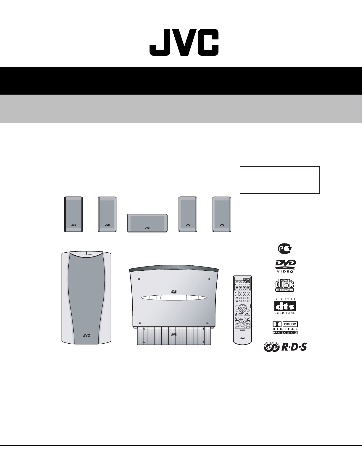
TH-V70R
SERVICE MANUAL
DVD DIGITAL CINEMA SYSTEM
TH-V70R
Area suffix
SP-XSV70 SP-XCV70SP-XSV70 SP-XSV70SP-XSV70
DVD DIGITAL CINEMA
SYSTE
M
TH-
V
70
R
SP-PWV70 XV-THV70R
EE --------- Russian Federation
TV AUDIO
DVD
VCR 1
AUX
FM/AM
VCR
DECODE
AUDIO
ANGLE
SUBTITLE
RETURN DIGEST ZOOM VFP
+
TOP MENU MENU ZOOM
SOUND
Ð
CONTROLÐ SUBWOOFER +EFFECT
VCR
123
Ð
CENTER
+
TEST
TV
456
SLEEP
Ð
REAR-L
+
789
SETTING
REAR-R
+
Ð
+10
10
0
TV RETURN
FM MODE
100+
TA/NEWS/INFO
ON
SCREEN
DVD
RDS
PTY PTY
ENTER
SURROUND
CHOICE
MODE
RDS DISPLAY
PTY SEARCH
CHANNEL VOLUMETV VOL
TV/VIDEO MUTING
/REW
FF/
PLAY
TUNING
DOWN UP
PAUSE
STOP
REC
MEMORY
STROBE
DIMMER
RMÐSTHV70R
DVD CINEMA SYSTEM
TABLE OF CONTENTS
1 Important Safety Precautions . . . . . . . . . . . . . . . . . . . . . . . . . . . . . . . . . . . . . . . . . . . . . . . . . . . . . . . . . . . 1-2
2 Disassembly method . . . . . . . . . . . . . . . . . . . . . . . . . . . . . . . . . . . . . . . . . . . . . . . . . . . . . . . . . . . . . . . . . . 1-6
3 Adjustment method. . . . . . . . . . . . . . . . . . . . . . . . . . . . . . . . . . . . . . . . . . . . . . . . . . . . . . . . . . . . . . . . . . . 1-25
4 Description of major ICs. . . . . . . . . . . . . . . . . . . . . . . . . . . . . . . . . . . . . . . . . . . . . . . . . . . . . . . . . . . . . . . 1-26
COPYRIGHT © 2003 VICTOR COMPANY OF JAPAN, LTD.
No.21175
2003/02
Page 2
TH-V70R
Important Safety Precautions
1.1 Safety Precautions
(1) This design of this product contains special hardware and
many circuits and components specially for safety purposes.
For continued protection, no changes should be made to the
original design unless authorized in writing by the manufacturer. Replacement parts must be identical to those
used in the original circuits. Services should be performed by qualified personnel only.
(2) Alterations of the design or circuitry of the product should
not be made. Any design alterations of the product should
not be made. Any design alterations or additions will void
the manufacturers warranty and will further relieve the
manufacture of responsibility for personal injury or property
damage resulting therefrom.
(3) Many electrical and mechanical parts in the products have
special safety-related characteristics. These characteristics are often not evident from visual inspection nor can the
protection afforded by them necessarily be obtained by using replacement components rated for higher voltage, wattage, etc. Replacement parts which have these special safety
characteristics are identified in the Parts List of Service Manual. Electrical components having such features are identified by shading on the schematics and by ( ) on the
Parts List in the Service Manual. The use of a substitute replacement which does not have the same safety characteristics as the recommended replacement parts shown in the
Parts List of Service Manual may create shock, fire, or other hazards.
(4) The leads in the products are routed and dressed with ties,
clamps, tubings, barriers and the like to be separated from
live parts, high temperature parts, moving parts and/or
sharp edges for the prevention of electric shock and fire
hazard. When service is required, the original lead routing
and dress should be observed, and it should be confirmed
that they have been returned to normal, after reassembling.
(5) Leakage shock hazard testing)
After reassembling the product, always perform an isolation
check on the exposed metal parts of the product (antenna
terminals, knobs, metal cabinet, screw heads, headphone
jack, control shafts, etc.) to be sure the product is safe to
operate without danger of electrical shock.
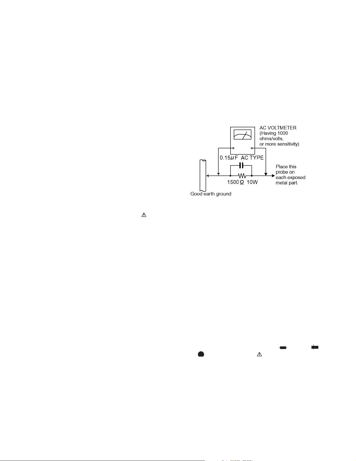
Do not use a line isolation transformer during this check.
• Plug the AC line cord directly into the AC outlet. Using a
"Leakage Current Tester", measure the leakage current
from each exposed metal parts of the cabinet, particularly any exposed metal part having a return path to the
chassis, to a known good earth ground. Any leakage current must not exceed 0.5mA AC (r.m.s.).
• Alternate check method
Plug the AC line cord directly into the AC outlet. Use an AC
voltmeter having, 1,000 ohms per volt or more sensitivity in
the following manner. Connect a 1,500 ohm 10W resistor
paralleled by a 0.15 µF AC-type capacitor between an
SECTION 1
exposed metal part and a known good earth ground.
Measure the AC voltage across the resistor with the AC
voltmeter.
Move the resistor connection to each exposed metal part,
particularly any exposed metal part having a return path to
the chassis, and measure the AC voltage across the resistor.
Now, reverse the plug in the AC outlet and repeat each
measurement. Voltage measured any must not exceed 0.75
V AC (r.m.s.). This corresponds to 0.5 mA AC (r.m.s.).
1.2 Warning
(1) This equipment has been designed and manufactured to
meet international safety standards.
(2) It is the legal responsibility of the repairer to ensure that
these safety standards are maintained.
(3) Repairs must be made in accordance with the relevant
safety standards.
(4) It is essential that safety critical components are replaced
by approved parts.
(5) If mains voltage selector is provided, check setting for local
voltage.
1.3 Caution
Burrs formed during molding may be left over on some parts
of the chassis.
Therefore, pay attention to such burrs in the case of preforming repair of this system.
1.4 Critical parts for safety
In regard with component parts appearing on the silk-screen
printed side (parts side) of the PWB diagrams, the parts that are
printed over with black such as the resistor ( ), diode ( )
and ICP ( ) or identified by the " " mark nearby are critical
for safety.
When replacing them, be sure to use the parts of the same type
and rating as specified by the manufacturer. (Except the JC version)
1-2 (No.21175)
Page 3
1.5 Safety Precautions (U.K only)
(1) This design of this product contains special hardware and many circuits and components specially for safety purposes. For con-
tinued protection, no changes should be made to the original design unless authorized in writing by the manufacturer. Replacement parts must be identical to those used in the original circuits.
(2) Any unauthorised design alterations or additions will void the manufacturer's guarantee; furthermore the manufacturer cannot
accept responsibility for personal injury or property damage resulting therefrom.
(3) Essential safety critical components are identified by ( ) on the Parts List and by shading on the schematics, and must never
be replaced by parts other than those listed in the manual. Please note however that many electrical and mechanical parts in
the product have special safety related characteristics. These characteristics are often not evident from visual inspection. Parts
other than specified by the manufacturer may not have the same safety characteristics as the recommended replacement parts
shown in the Parts List of the Service Manual and may create shock, fire, or other hazards.
(4) The leads in the products are routed and dressed with ties, clamps, tubings, barriers and the like to be separated from live parts,
high temperature parts, moving parts and/or sharp edges for the prevention of electric shock and fire hazard. When service is
required, the original lead routing and dress should be observed, and it should be confirmed that they have been returned to
normal, after re-assembling.
1.5.1 Warning
(1) Service should be performed by qualified personnel only.
(2) This equipment has been designed and manufactured to meet international safety standards.
(3) It is the legal responsibility of the repairer to ensure that these safety standards are maintained.
(4) Repairs must be made in accordance with the relevant safety standards.
(5) It is essential that safety critical components are replaced by approved parts.
(6) If mains voltage selector is provided, check setting for local voltage.
TH-V70R
Burrs formed during molding may be left over on some parts of the chassis. Therefore,
pay attention to such burrs in the case of preforming repair of this system.
(No.21175)1-3
Page 4
TH-V70R
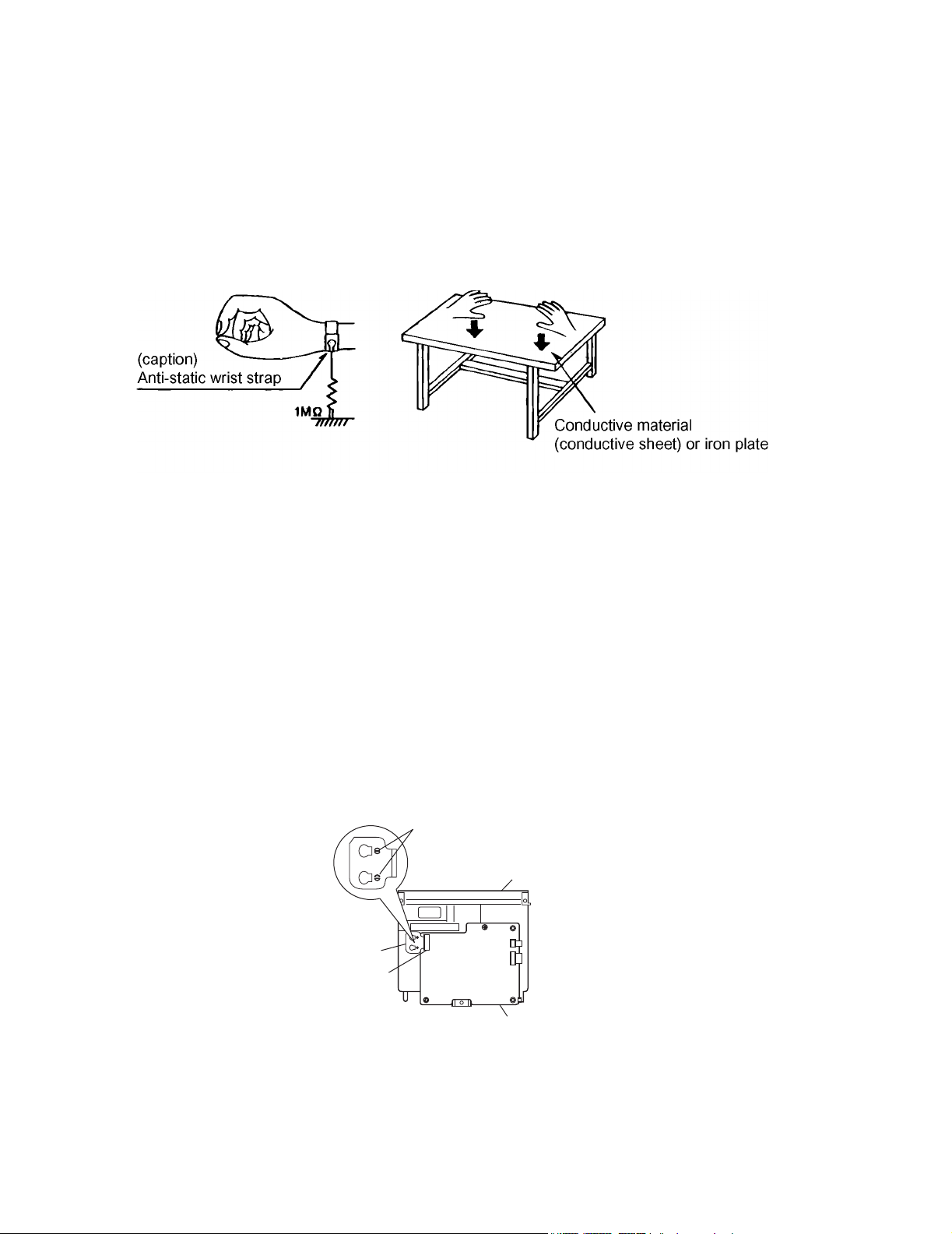
1.6 Preventing static electricity
Electrostatic discharge (ESD), which occurs when static electricity stored in the body, fabric, etc. is discharged,
can destroy the laser diode in the traverse unit (optical pickup). Take care to prevent this when performing repairs.
1.6.1 Grounding to prevent damage by static electricity
Static electricity in the work area can destroy the optical pickup (laser diode) in devices such as DVD players.
Be careful to use proper grounding in the area where repairs are being performed.
(1) Ground the workbench
Ground the workbench by laying conductive material (such as a conductive sheet) or an iron plate over it before placing the
traverse unit (optical pickup) on it.
(2) Ground yourself
Use an anti-static wrist strap to release any static electricity built up in your body.
(3) Handling the optical pickup
• In order to maintain quality during transport and before installation, both sides of the laser diode on the replacement optical
pickup are shorted. After replacement, return the shorted parts to their original condition.
(Refer to the text.)
• Do not use a tester to check the condition of the laser diode in the optical pickup. The tester's internal power source can easily
destroy the laser diode.
1.7 Handling the traverse unit (optical pickup)
(1) Do not subject the traverse unit (optical pickup) to strong shocks, as it is a sensitive, complex unit.
(2) Cut off the shorted part of the flexible cable using nippers, etc. after replacing the optical pickup. For specific details, refer to the replace-
ment procedure in the text. Remove the anti-static pin when replacing the traverse unit. Be careful not to take too long a time
when attaching it to the connector.
(3) Handle the flexible cable carefully as it may break when subjected to strong force.
(4) I t is not possible to adjust the semi-fixed resistor that adjusts the laser power. Do not turn it.
1.8 Attention when traverse unit is decomposed
*Please refer to "Disassembly method" in the text for the DVD pickup unit.
• Apply solder to the short land sections before the flexible wire is disconnected from the connector CN101 on the DVD servo board.
(If the flexible wire is disconnected without applying solder, the DVD pickup may be destroyed by static electricity.)
• In the assembly, be sure to remove solder from the short land sections after connecting the flexible wire.
Short lands
DVD mechanism assembly
1-4 (No.21175)
Flexible wire
Connector
CN202
CN201
DVD servo board
Page 5
1.9 Important for laser products
(1) CLASS 1 LASER PRODUCT
(2) DANGER : Invisible laser radiation when open and inter
lock failed or defeated. Avoid direct exposure to beam.
(3) CAUTION : There are no serviceable parts inside the
Laser Unit. Do not disassemble the Laser Unit. Replace the
complete Laser Unit if it malfunctions.
(4) CAUTION : The compact disc player uses invisible laser
radiation and is equipped with safety switches which
prevent emission of radiation when the drawer is open and
the safety interlocks have failed or are de feated.
It is dangerous to defeat the safety switches.
TH-V70R
(5) CAUTION : If safety switches malfunction, the laser is able
to function.
(6) CAUTION : Use of controls, adjustments or performance of
procedures other than those specified herein may result in
hazardous radiation exposure.
CAUTION
Please use enough caution not to see the beam directly
or touch it in case of anadjustment or operation check.
VARNING
Osynlig laserstrålning är denna del är öppnad och spårren är
urkopplad. Betrakta ej strålen.
VARO
Avattaessa ja suojalukitus ohitettaessa olet alttiina näkymättömälle lasersäteilylle. Älä katso säteeseen.
REPRODUCTION AND POSITION OF LABELS
CLASS 1
LASER PRODUCT
ADVARSEL
Usynlig laserstråling ved åbning, når sikkerhedsafbrydere er
ude af funktion. Undgå udsasttelse for stråling.
ADVARSEL
Usynlig laserstråling ved åpning, når sikkerhetsbryteren er avslott. unngå utsettelse for stråling.
WARNING LABEL
CAUTION: Invisible laser
radiation when open and
interlock failed or defeated.
AVOID DIRECT EXPOSURE
TO BEAM. (e)
ADVARSEL: Usynlig laserstråling ved åbning, når
sikkerhedsafbrydere er ude
af funktion. Undgåudsættelse for stråling. (d)
VARNING: Osynlig laserstrålning när denna del är
öppnad och spärren är
urkopplad. Betrakta ej
strålen. (s)
VARO: Avattaessa ja
suojalukitus ohitettaessa
oleta lttiina näkymättömälle lasersäteilylle.
Älä katso
säteeseen. (f)
CLASS 1
LASER PRODUCT
(No.21175)1-5
Page 6
TH-V70R
SECTION 2
Disassembly method
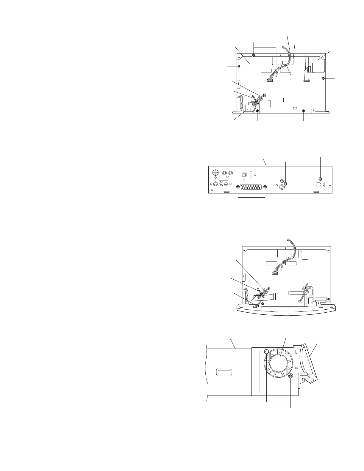
2.1 Main body section
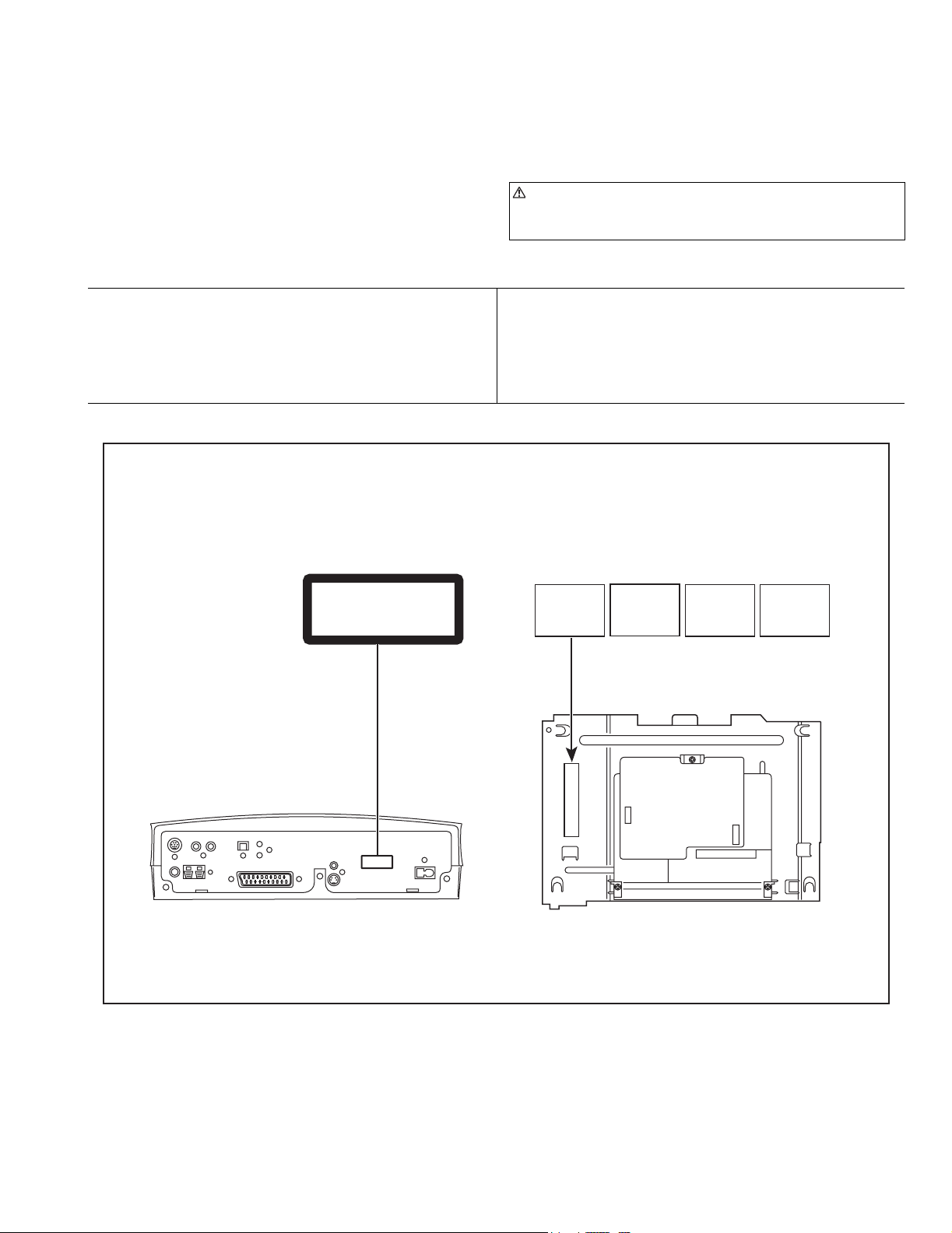
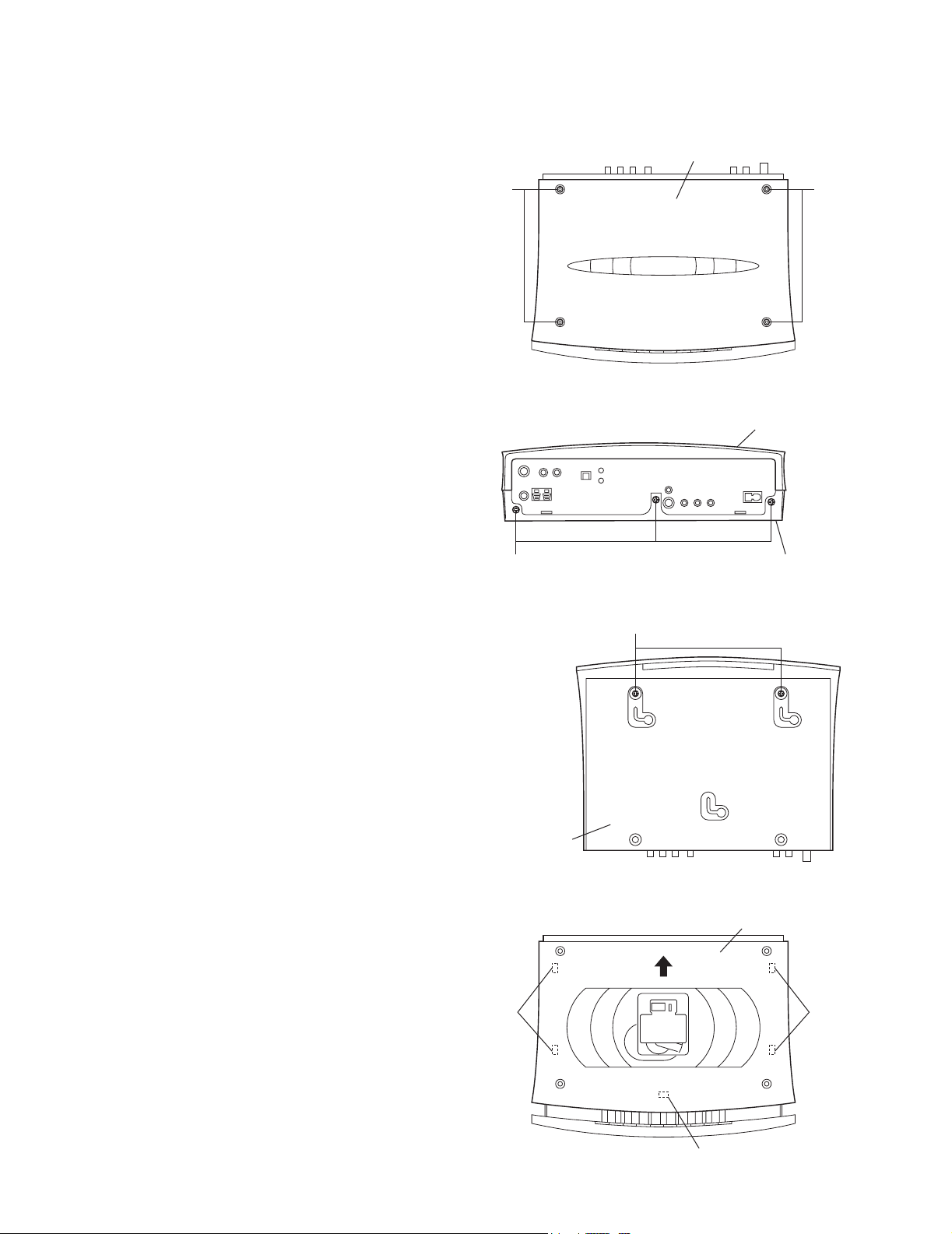
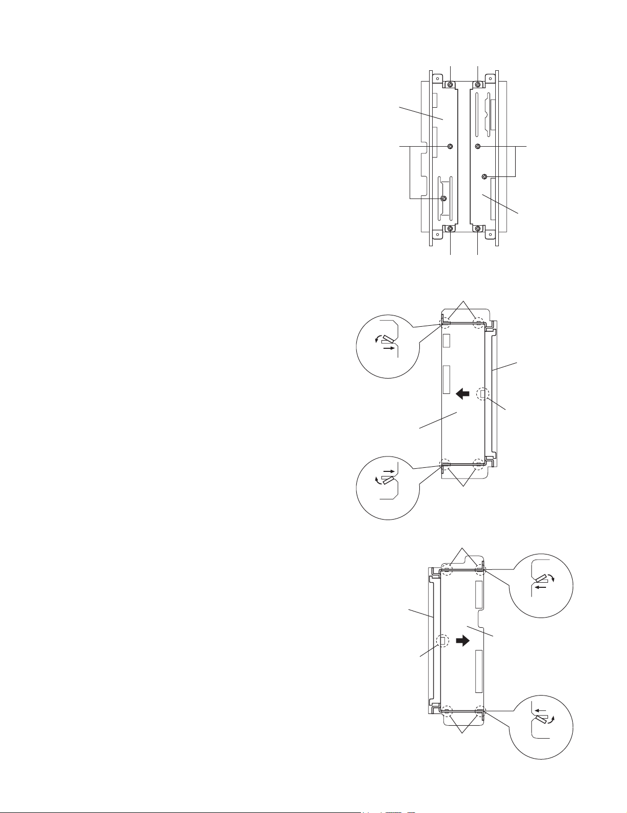
2.1.1 Removing the top plate (See Fig. 1.)
From the top side of the main body, remove the four screws A
attaching the top plate.
2.1.2 Removing the bottom panel (See Figs. 2 and 3.)
(1) From the rear side of the main body, remove the three
screws B attaching the bottom panel.
(2) From the bottom side of the main body, remove the two
screws C attaching the bottom panel.
(3) Remove the bottom panel in an upward direction.
B
Top plate
AA
Fig.1
Top panel
Bottom panel
Fig.2
2.1.3 Removing the top panel (See Fig. 4.)
• Remove the top plate.
• Remove the bottom panel.
(1) Slide the top panel toward the rear (direction of the arrow)
and disengage it from the engagement sections a and b of
the bottom chassis.
(2) Remove the top panel in an upward direction.
C
Bottom panel
Fig.3
Top panel
bb
1-6 (No.21175)
a
Fig.4
Page 7
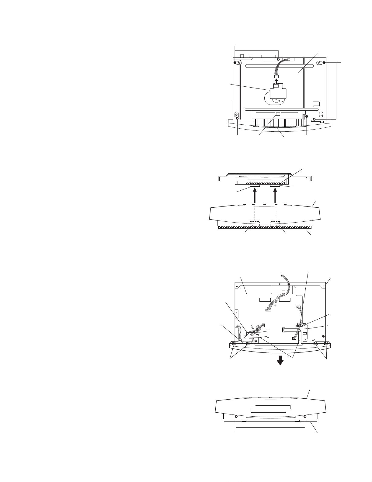
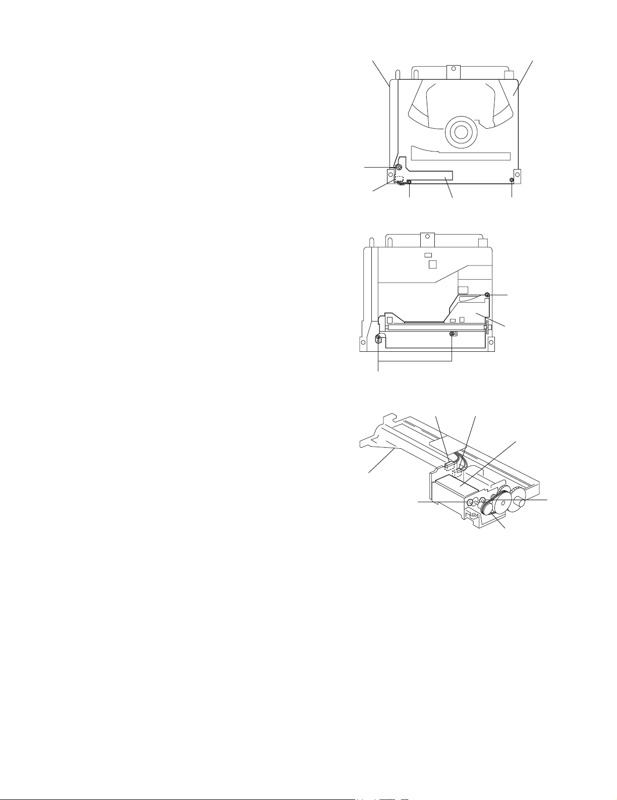
2.1.4 Removing the DVD mechanism assembly (See Figs. 5 and 6.)
• Remove the top plate.
• Remove the bottom panel.
• Remove the top panel.
(1) From the top side of the main body, disengage the claw c
of the DVD mechanism assembly and then remove the
push button.
(2) Remove the five screws D and screw E attaching the DVD
mechanism assembly.
(3) Disconnect the wire from connector CN812 on the LED
board.
(4) Disconnect the connectors CN502 and CN503 on the DVD
servo board from connectors CN801 and CN803 on the
main board while lifting the DVD mechanism assembly in
an upward direction.
LED board
D
TH-V70R
DVD mechanism
assembly
D
CN812
2.1.5 Removing the front panel assembly (See Figs. 7 and 8.)
• Remove the top plate.
• Remove the bottom panel.
• Remove the top panel.
• Remove the DVD mechanism assembly.
(1) Remove the wire clamp bundling the wires of the front pan-
el assembly.
(2) Remove the card wire of the front panel assembly from the
wire holder.
(3) Disconnect the wires from connectors CN106 and CN814
on the main board.
(4) Disconnect the card wires from connectors CN802 and
CN813 on the main board.
(5) From the front side of the main body, remove the two
screws F attaching the front panel assembly.
(6) Disengage the claws d of the front panel assembly from the
bottom chassis and then remove the front panel assembly
in the direction of the arrow.
Reference:
• Before attaching the front panel assembly, pass the
card wire of the front panel assembly through the hole
on the bottom chassis.
• After attaching the front panel assembly, bundle the
wires and card wire of the front panel assembly using
a wire clamp.
Caution:
• In the assembly, arrange the wires and wire clamp so
that they are not touch to the regulator IC(IC953).
CN502
Main board
Wire holder
Bottom
chassis hole
Claws d
Claw c
D
CN803 CN801
Push button
Fig.5
Fig.6
CN814
CN813
CN802
CN106
Fig.7
Card wires
Front panel assembly
F
Fig.8
E
DVD servo board
CN503
Front panel assembly
Main board
Wire clamp
Bottom chassis
Wire
IC953
Claws d
Bottom chassis
(No.21175)1-7
Page 8
TH-V70R
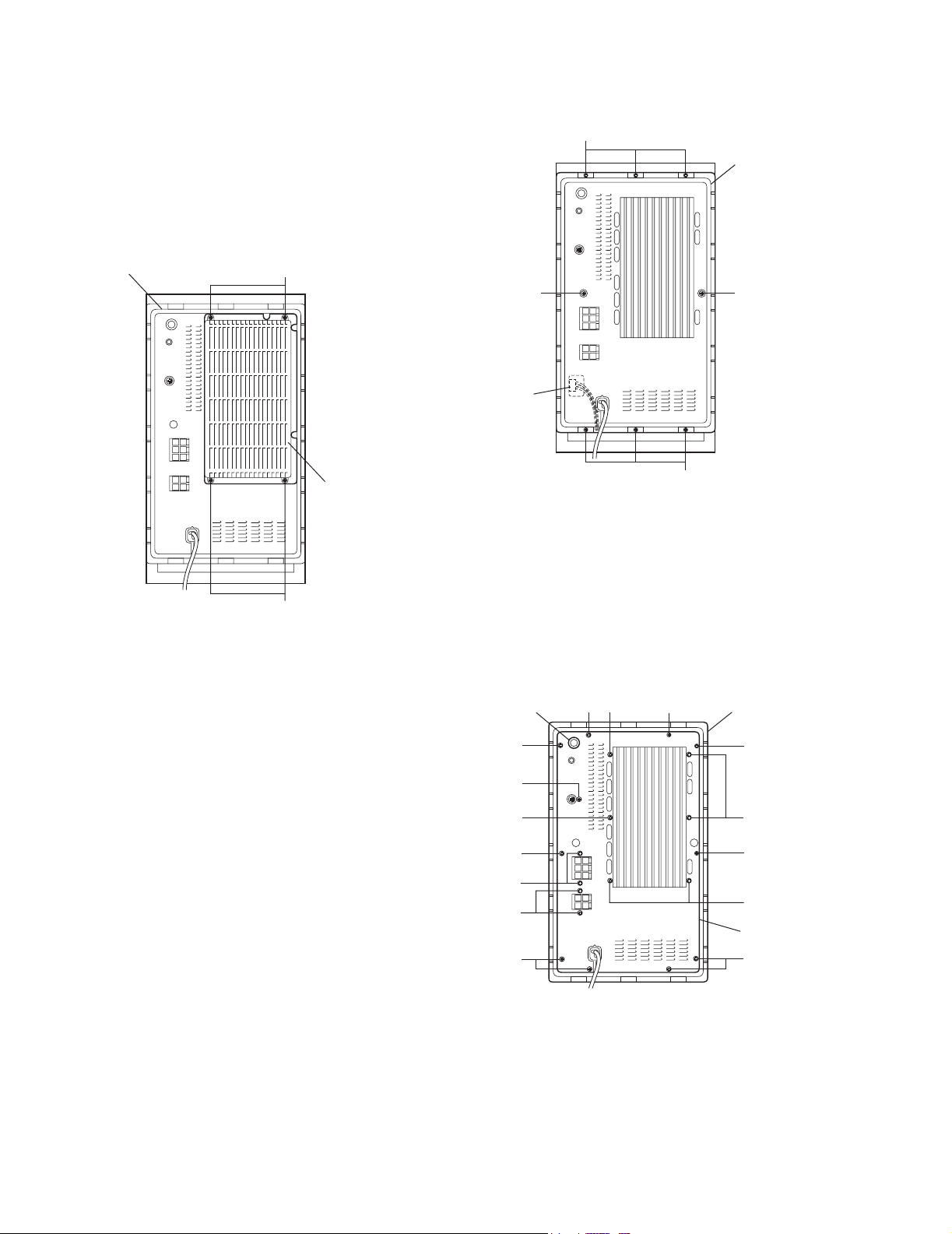
2.1.6 Removing the DSP/Audio board (See Figs. 9 and 10.)
• Remove the top plate.
• Remove the bottom panel.
• Remove the top panel.
• Remove the DVD mechanism assembly.
(1) From the top side of the main body, remove a screw G at-
taching the DSP/Audio board.
(2) From the rear side of the main body, remove the screw H
and two screws J attaching the DSP/Audio board.
(3) Take out the DSP/Audio board from the bottom chassis
and then disconnect the card wire from connector CN806
on the main board.
Reference:
• Before attaching the DSP/Audio board, connect the
card wire to the connector CN806 on the main board.
2.1.7 Removing the compulink board (See Figs. 9 and 10.)
• Remove the top plate.
• Remove the bottom panel.
• Remove the top panel.
• Remove the DVD mechanism assembly.
(1) Disconnect the card wire from connector CN592 on the
compulink board.
(2) From the rear side of the main body, remove the screw K
attaching the compulink board.
(3) Take out the compulink board from the bottom chassis.
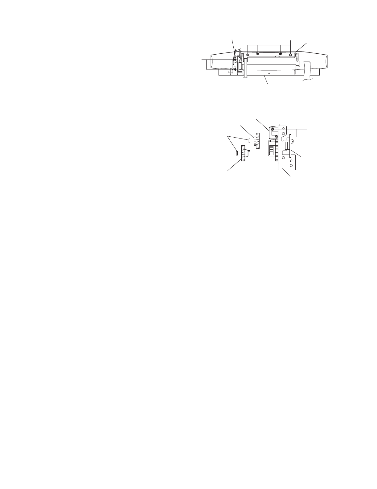
2.1.8 Removing the tuner (See Figs. 9 and 10.)
• Remove the top plate.
• Remove the bottom panel.
• Remove the top panel.
• Remove the DVD mechanism assembly.
(1) Disconnect the card wire from connector CN805 on the
main board.
(2) From the rear side of the main body, remove the two
screws L attaching the tuner.
(3) Take out the tuner from the bottom chassis.
Compulink board
Main board
H
L
CN592
J
Fig.9
K
Rear panel
Fig.10
CN805
CN806
Tuner
DSP/Audio
board
Card wire
G
Card wire
1-8 (No.21175)
Page 9
TH-V70R
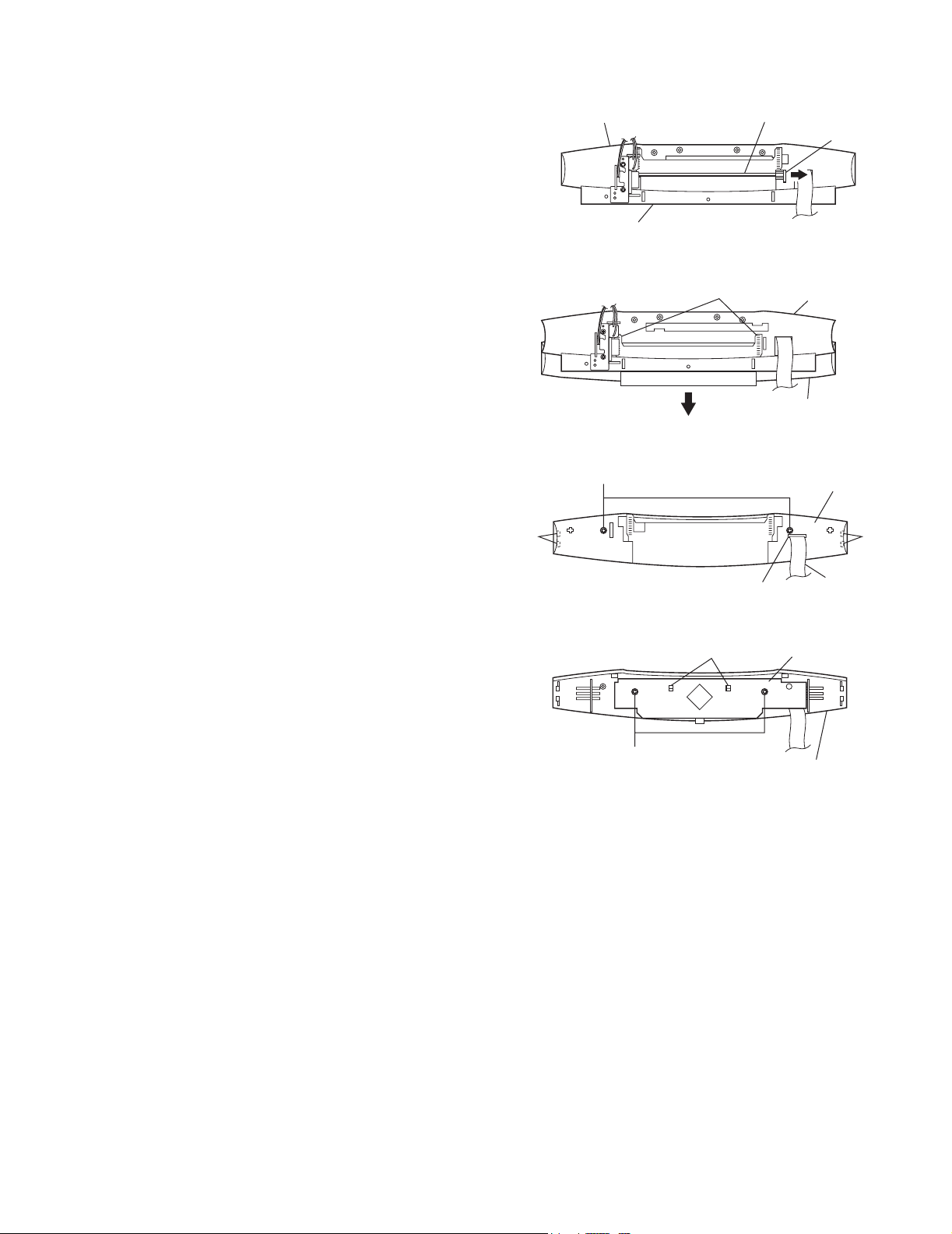
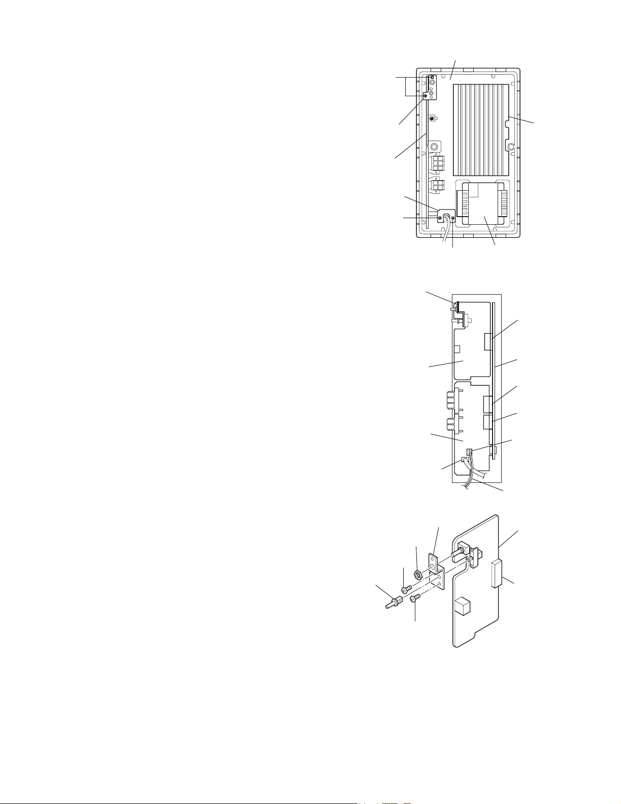
2.1.9 Removing the main board (See Figs. 11 and 12.)
• Remove the top plate.
• Remove the bottom panel.
• Remove the top panel.
• Remove the DVD mechanism assembly.
• Remove the front panel assembly.
• Remove the DSP/Audio board.
(1) Disconnect the card wire from connector CN805 on the
main board.
(2) Remove the wire clamp bundling the fan motor wire and
then disconnect the wire from connector CN972 on the
main board.
(3) Disconnect the card wire from connector CN592 on the
compulink board.
(4) Remove the five screws M and screw M' attaching the main
board.
(5) From the rear side of the main body, remove the four
screws N attaching the main board.
(6) Remove the rear panel with the tuner and compulink board.
(7) Take out the main board from the bottom chassis.
Reference:
Attaching the main board
• When attaching the screw M', attach the wire holder together with it.
• After connecting the wires to the connectors, bundle
them using the wire clamp.
• Insert the DVD mechanism assembly wire into the
notch on the bottom chassis. (See Fig. 11.)
Main board
M
Fan motor wire
Wire clamp
Wire holder
N
Insert this wire into the notch.
M
CN972
M'
Fig.11
Rear panel
Fig.12
Compulink board
CN592
M
Card wire
CN805
N
Tuner
M
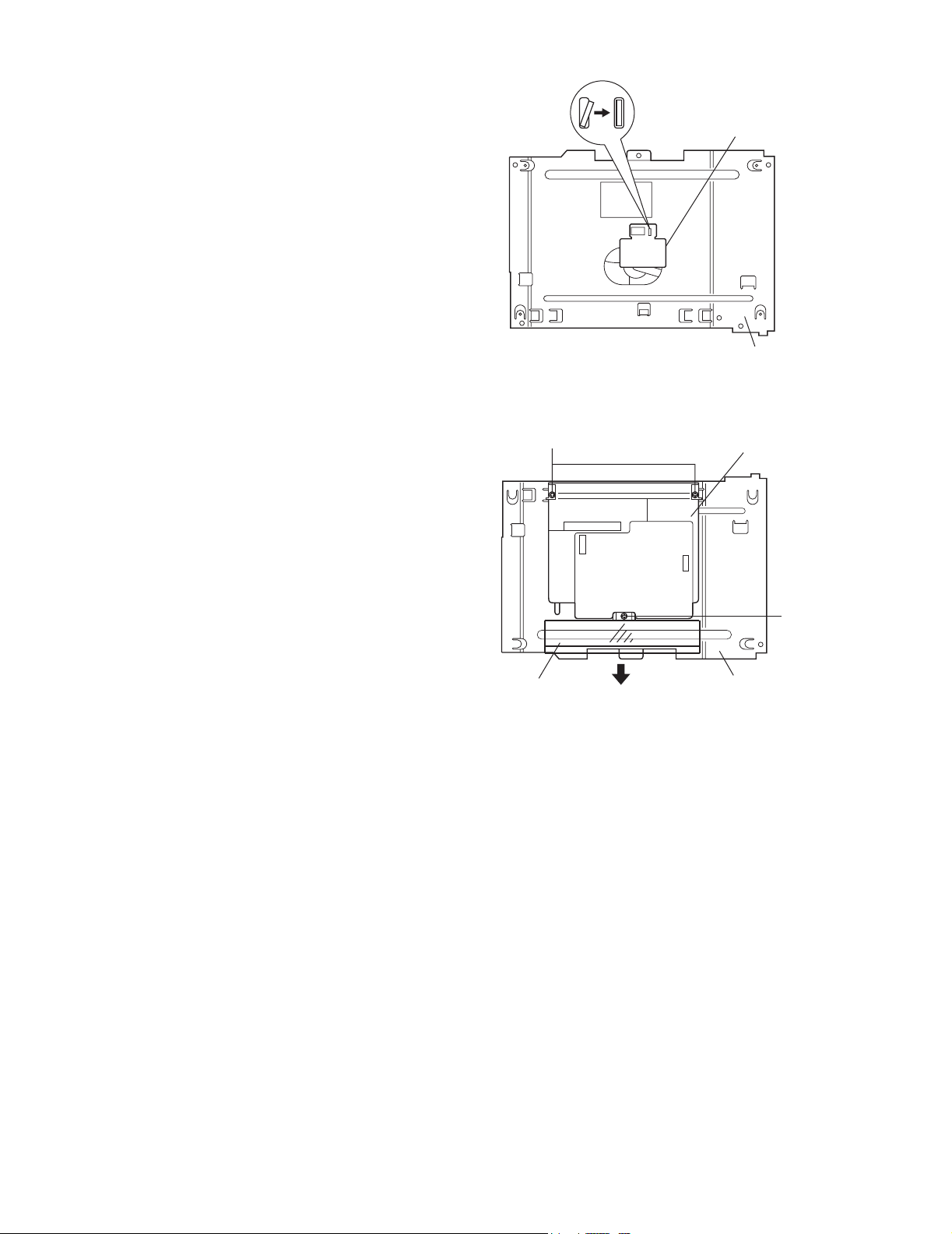
2.1.10 Removing the fan motor (See Figs. 13 and 14.)
• Remove the top plate.
• Remove the bottom panel.
• Remove the top panel.
• Remove the DVD mechanism assembly.
(1) Remove the wire clamp and tie band bundling the fan mo-
tor wire.
(2) Disconnect the wire from connector CN972 on the main
board.
(3) From the left side of the main body, remove the two screws
P attaching the fan motor.
Reference:
• After mounting the fan motor, bundle the fan motor
wire using the wire clamp.
Fan motor wire
Wire clamp
CN972
Tie band
Fig.13
Bottom chassis Fan motor Front panel
assembly
Fig.14
P
(No.21175)1-9
Page 10
TH-V70R
2.2 Front panel assembly section
• Remove the top plate.
• Remove the bottom panel.
• Remove the top panel.
• Remove the DVD mechanism assembly.
• Remove the front panel assembly.
2.2.1 Removing the switch board (See Fig. 15.)
From the back side of the front panel assembly, remove the four
screws Q attaching the switch board.
2.2.2 Removing the open/close board (See Figs. 15 and 16.)
(1) From the back side of the front panel assembly, remove the
two screws R attaching the door motor assembly.
(2) Remove the screw S attaching the open/close board of the
door motor assembly.
2.2.3 Removing the door motor (See Fig. 16.)
• Remove the door motor assembly.
(1) Remove the stop washers attaching the clutch assembly
and gear 2.
(2) Remove the clutch assembly and Gear 2.
(3) Remove the two screws T attaching the door motor.
Door motor assembly
R
Clutch assembly
Stop washer
Gear 2
Front panel assembly
(Back side)
Fig.15
Door motor
Fig.16
Q
Switch board
T
S
Open/close
board
Door motor assembly
1-10 (No.21175)
Page 11
2.2.4 Removing the front board (See Figs. 17 to 20.)
(1) While widening section e of the front base in the direction
of the arrow, remove the rod gear assembly.
(2) Slide the moving panel assembly all the way in the direction
of the arrow.
(3) While slightly widening sections f toward the front, take out
the moving panel assembly in the direction of the arrow.
(4) Remove the two screws U attaching the moving base of the
moving panel assembly.
(5) Disengage the engagement sections g on the inside of the
moving base and at the inside of the moving panel assem-
bly and remove the moving base.
(6) Remove the two screws V attaching the front board.
(7) Disengage the claws h of the moving panel and remove the
front board.
Reference:
• Before attaching the moving base, pass the card wire
of the front board through the hole on the moving base.
(See Fig.19.)
Front panel assembly
(Back side)
Front base
Rod gear assembly
Fig.17
f
Moving panel assembly
Fig.18
TH-V70R
e
Front base
U
V
Fig.19
h
Fig.20
Hole
Front board
Moving panel
Moving base
gg
Card wire
(No.21175)1-11
Page 12
TH-V70R
y
2.3 DVD mechanism assembly section
• Remove the top plate.
• Remove the bottom panel.
• Remove the top panel.
• Remove the DVD mechanism assembly.
2.3.1 Removing the LED board (See Fig. 1.)
From the top side of the DVD mechanism assembly, disengage
the claw a of the top chassis attaching the LED board and then
remove the LED board.
2.3.2 Removing the DVD mechanism assembly (See Fig. 2.)
(1) Extend the both sides of the protector, and then raise the
protector in the direction of the arrow.
(2) Remove the three screws A attaching the DVD mechanism
assembly on the top chassis.
Claw a
A
LED board
Top chassis
Fig.1
DVD mechanism assembl
A
Protector
Fig.2
Top chassis
1-12 (No.21175)
Page 13
2.3.3 Removing the DVD servo board (See Fig. 3.)
Caution:
• Be sure to solder the short land sections b on the flexible
wire before disconnecting the flexible wire from connector
CN101 on the DVD servo board.
If the flexible wire is disconnected without attaching solder,
the pickup unit may be destroyed by static electricity.
(1) From the back side of the DVD mechanism assembly, at-
tach solder to the short land sections b of the flexible wire
that is connected to the connector CN101 of the DVD servo
board.
(2) Disconnect the flexible wire from connector CN101 on the
DVD servo board.
(3) Disconnect the card wires from connectors CN201 and
CN202 on the DVD servo board.
(4) Remove the two screws B attaching the DVD servo board.
(5) While pushing the claw c of the DVD mechanism assembly
in the direction of the arrow, remove the DVD servo board
from the projections d and e in an upward direction.
Caution:
• In the assembly, be sure to remove solder from the
short land sections b after connecting the flexible wire.
Flexible wire
DVD servo board
Short land sections b
DVD mechanism assembly
B
CN202
CN101
CN201
Projection e
B
Fig.3
TH-V70R
Projection d
Claw c
2.3.4 Removing the DVD traverse mechanism assembly (See Fig. 4.)
• Remove the DVD servo board.
(1) Remove the two screws C attaching the DVD traverse
mechanism assembly.
(2) Disengage the claw f attaching the DVD traverse mecha-
nism assembly and then take out the DVD traverse mechanism assembly.
DVD traverse mechanism assembly
C C
Claw f
Fig.4
(No.21175)1-13
Page 14
TH-V70R
y
w
t
w
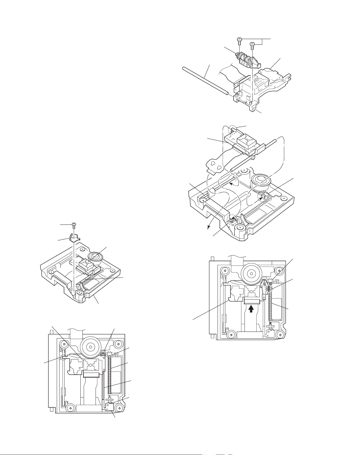
2.3.5 Removing the DVD pickup unit (See Figs. 5 to 7.)
• Remove the DVD servo board.
• Remove the DVD traverse mechanism assembly.
(1) From the top side of the DVD traverse mechanism assem-
bly, remove the screw D attaching the bracket.
(2) Remove the claw g attaching the thrust spring and then
take out the torsion spring.
(3) Remove the lead screw from the section h and then re-
move the shaft from the section i.
(4) Disengage the section j of the DVD pickup unit and then re-
move the DVD pickup unit with the shaft.
(5) Pull the shaft out of the DVD pickup unit.
(6) Remove the two screws E attaching the SW. actuator.
SW. actuator
Shaft
E
DVD pickup uni
2.3.6 Attaching the DVD pickup unit (See Figs. 5 to 9.)
Reference:
Refer to the explanation of "Removing the DVD pickup unit" on
the preceding page.
(1) Attach the SW. actuator and shaft to the DVD pickup unit.
(See Fig.7.)
(2) Engage the section j of the DVD pickup unit to the shaft of
the DVD traverse mechanism assembly first, and set the
both ends of the shaft of the DVD pickup unit in the sections
i and i' of the DVD traverse mechanism assembly.
(3) Slide the DVD pickup unit all the way in the direction of the
arrow.
(4) Mesh the lead screw to the section k of DVD pickup unit
and then set the end of the lead screw to the section h.
(5) Attach the thrust spring. (See Fig.6.)
(6) Attach the bracket. (See Fig.5.)
D
Bracket
DVD pickup unit
Shaft
DVD pickup unit
Shaft
Section i'
Fig.7
Fig.8
Section
j
Section i
Section h
Section k
DVD pickup unit
Section j
1-14 (No.21175)
DVD traverse mechanism assembl
Fig.5
Section i
Section h
Lead scre
Claw g
Thrust spring
Fig.6
Lead scre
DVD pickup unit
Fig.9
Shaft
Page 15
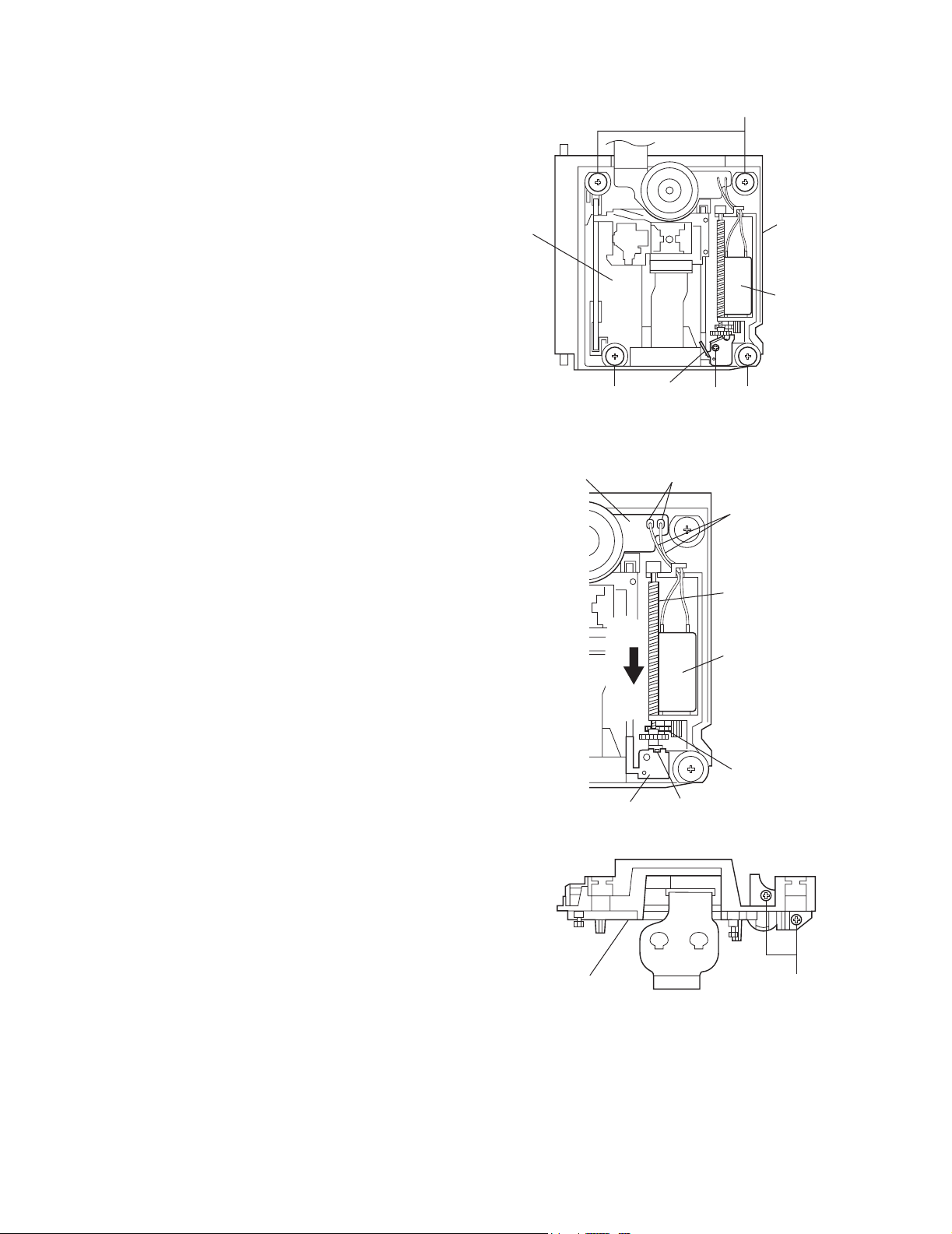
2.3.7 Removing the spindle motor board (See Figs. 10 and 11.)
r
r
• Remove the DVD servo board.
• Remove the DVD traverse mechanism assembly.
(1) From the top side of the DVD traverse mechanism assem-
bly, remove the feed motor wire that is soldered to the spindle motor board.
(2) From the back side of the DVD traverse mechanism as-
sembly, remove the three screws F attaching the spindle
motor board.
Spindle motor
board
F
TH-V70R
Remove the solders.
Feed moto
wire
Feed motor
Fig.10
F
Fig.11
Spindle moto
board
(No.21175)1-15
Page 16
TH-V70R
r
2.3.8 Removing the feed motor (See Figs. 12 to 14.)
• Remove the DVD servo board.
• Remove the DVD traverse mechanism assembly.
(1) Remove the four screws G attaching the traverse mecha-
nism assembly.
(2) Take out the traverse mechanism assembly from the
mechanism base.
(3) Remove the screw D attaching the bracket and take out the
bracket.
(4) Disengage the claw g attaching the thrust spring and take
out the thrust spring.
(5) Pull out the lead screw in the direction of the arrow.
(6) Remove the feed gear M.
(7) Remove the feed motor wire that is soldered to the spindle
motor board.
(8) Remove the two screws H attaching the feed motor and
take out the feed motor.
Traverse
mechanism
assembly
G
Bracket
G G
Fig.12
D
Mechanism
base
Feed moto
Spindle motor board
Thrust spring
Remove the solders.
Feed motor wire
Lead screw
Feed motor
Feed gear M
Claw g
Fig.13
1-16 (No.21175)
Traverse
mechanism assembly
Fig.14
H
Page 17
TH-V70R
y
r
y
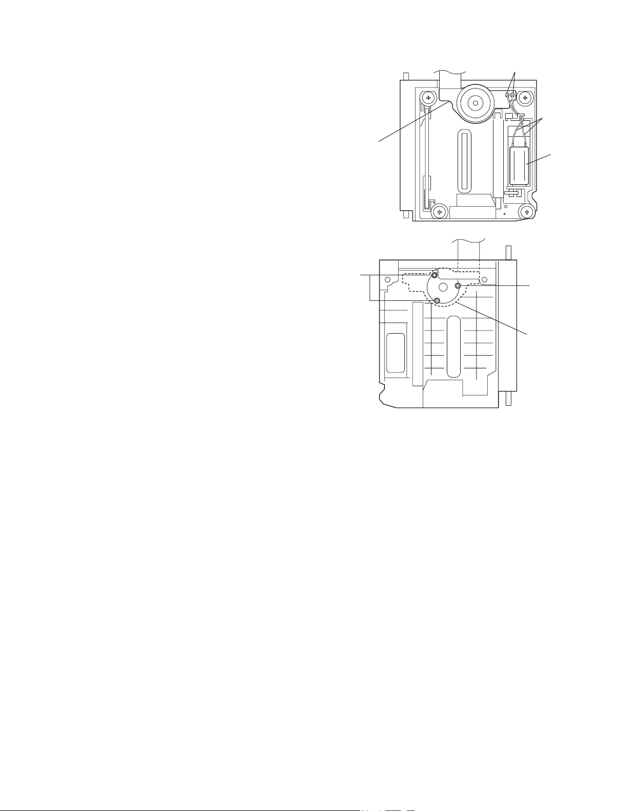
2.3.9 Removing the switch board (See Fig.15.)
• Remove the DVD mechanism assembly.
(1) From the top side of the CD mechanism assembly, remove
the screw J attaching the switch board.
(2) Lift the switch board slightly and then remove the wire from
connector CN101 on the switch board.
2.3.10 Removing the loading motor assembly (See Figs.3,
15 to 17.)
• Remove the DVD mechanism assembly.
(1) From the back side of the DVD mechanism assembly, dis-
connect the card wire from connector CN202 on the DVD
servo board. (See Fig.3.)
(2) From the top side of the CD mechanism assembly, remove
the two screws K attaching the clamper base assembly.
(3) Disconnect the wire from connector CN101 on the switch
board while lifting the clamper base assembly slightly and
remove the clamper base assembly.
(4) Remove the three screws L attaching the roller holder as-
sembly and take out the roller holder assembly.
(5) Disconnect the wires from connectors CN103 and CN104
on the loading motor assembly.
(6) Remove the belt of the loading motor assembly.
(7) Remove the two screws M attaching the loading motor as-
sembly and take out the loading motor assembly.
CD mechanism assembly Clamper base assembl
J
CN101
K K
Switch board
Fig.15
L
Roller holde
assembly
L
Fig.16
CN103
Roller holder
assembly
M
CN104
Loading motor assembl
M
Belt
Fig.17
(No.21175)1-17
Page 18
TH-V70R
A
r
y
y
2.4 Speaker section
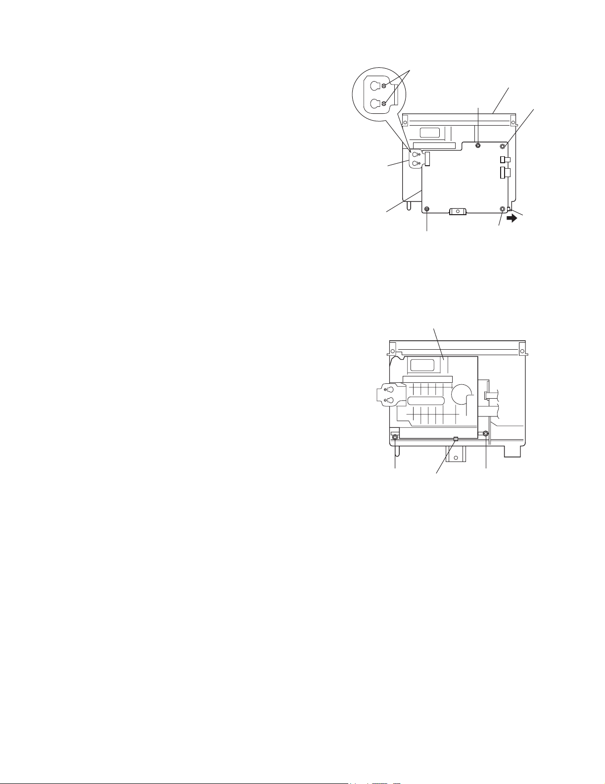
2.4.1 Removing the amplifier assembly (See Figs. 1 and 2.)
(1) From the rear side of the speaker main body, remove the
four screws A attaching the heat sink cover and then remove the heat sink cover.
(2) Remove the eight screws B attaching the amplifier assem-
bly.
(3) Move the amplifier assembly backward and disconnect the
wire from connector CN109 in the lower part of the amplifier
assembly.
B
Amplifier assembl
mplifier assembly
A
Heat sink cove
A
Fig.1
2.4.2 Removing the rear panel (See Fig. 3.)
• Remove the amplifier assembly.
(1) Pull out the knob.
(2) Remove the ten screws C, ten screws D and screw E at-
taching the rear panel.
BB
CN109
B
Fig.2
Amplifier assembl
C
C
Knob
CCD
1-18 (No.21175)
E
DD
C
D
D
C
Fig.3
C
D
Rear panel
C
Page 19
TH-V70R
2.4.3 Removing the pre-amplifier board (See Figs. 4 to 6.)
• Remove the rear panel.
(1) Remove the two screws F attaching the volume bracket.
(2) Disconnect the pre-amplifier board from the connector
CN201 on the mother board and take out the pre-amplifier
board.
(3) Pull out the push button.
(4) Remove the two screws G and nut attaching the volume
bracket.
2.4.4 Removing the power supply & SP terminal board (See
Figs. 4 and 5.)
• Remove the rear panel.
(1) Remove the two screws H attaching the AC bracket.
(2) Disconnect the power supply & SP terminal board from the
connectors CN210 and CN211 on the mother board.
(3) Disconnect the wire from connector CN107 on the power
supply & SP terminal board.
(4) Disconnect the power cord from connector CN108 on the
power supply & SP terminal board.
F
Volume bracket
Pre-amplifier
board
AC bracket
H
Volume bracket
Mother board
H
Fig.4
Power transformer
CN101
Heat sink
CN201
Pre-amplifier board
Power supply & SP
terminal board
Volume bracket
G
Push button
CN107
Nut
G
CN111
CN110
Fig.5
Mother board
CN211
CN210
CN108
Power cord
Pre-amplifier board
CN101
Fig.6
(No.21175)1-19
Page 20
TH-V70R
r
r
2.4.5 Removing the mother board (See Figs. 7 and 8.)
• Remove the rear panel.
• Remove the pre-amplifier board.
• Remove the power supply & SP terminal board.
(1) Disconnect the wire from the connector CN104 on the
mother board.
(2) Remove the seven screws J attaching the mother board.
(3) Take out the mother board with the power amplifier board
(A,B).
(4) From the bottom side of the mother board, remove the two
screws K and two screws L attaching the power amplifier
board (A,B).
(5) Remove the power amplifier board (A,B) from connectors
CN202, CN203, CN205 and CN206 on the mother board.
J
CN104
CN202
Mother board
J
KL
J
Power amplifier
board (A)
J
Power amplifier
board (B)
J
Power transforme
Mold base
Fig.7
Mother board
CN206
CN203
Power amplifier
board (A)
Power amplifie
board (B)
CN205
K L
Fig.8
1-20 (No.21175)
Page 21
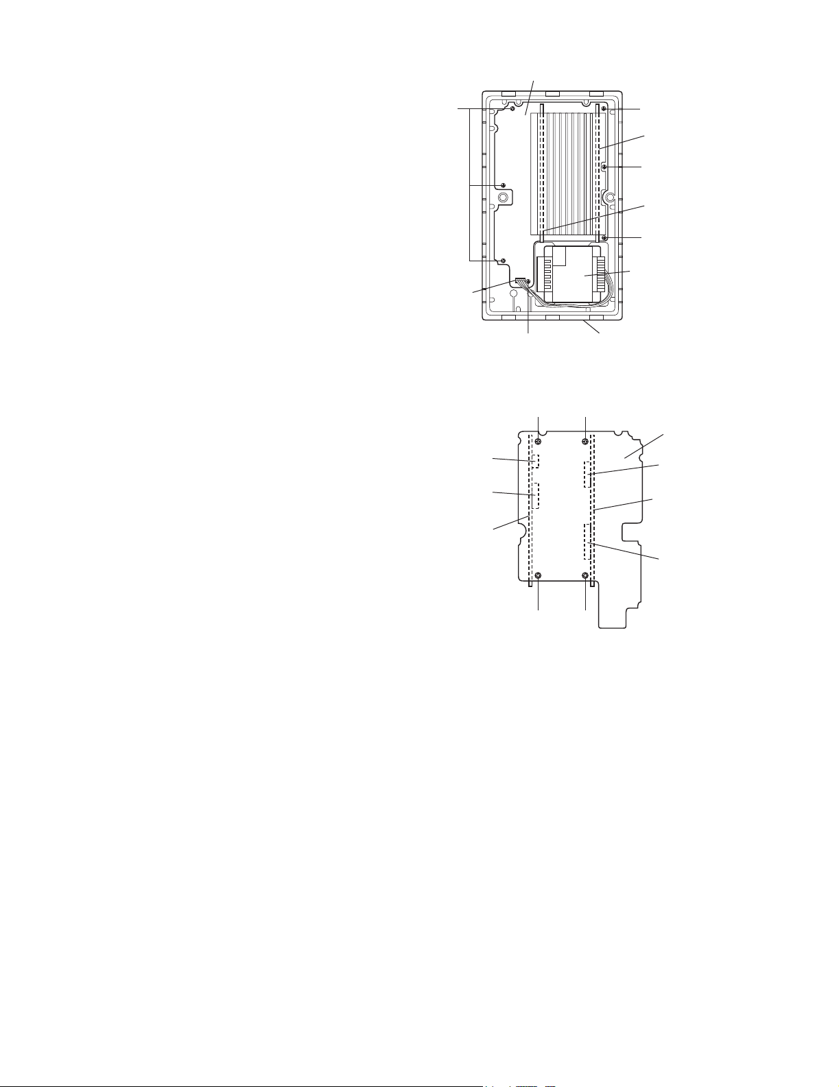
2.4.6 Removing the power amplifier board (A) (See Figs. 9
and 10.)
• Remove the mother board.
(1) Remove the four screws M attaching the heat sink to the
power amplifier board (A).
(2) From the bottom side of the power amplifier board (A), dis-
engage the four engagement sections a.
(3) From the top side of the power amplifier board (A), slide the
P.TR holder (A) in the direction of the arrow to disengage
the engagement section b and remove the power amplifier
board (A) from the P.TR holder (A).
2.4.7 Removing the power amplifier board (B) (See Figs. 9
and 11.)
• Remove the mother board.
(1) Remove the four screws N attaching the heat sink to the
power amplifier board (B). (See Fig.9.)
(2) From the bottom side of the power amplifier board (B), dis-
engage the four engagement sections c.
(3) arrow to disengage the engagement section d and remove
the power amplifier board (B) from the P.TR holder (B).
P.TR holder (A)
M
M N
N
M
Fig.9
a
TH-V70R
N
P.TR holder (B)
1
2
(Bottom side)
Power amplifier
board (A)
2
1
(Bottom side)
P.TR holder (B)
d
CN102
CN103
a
Fig.10
c
CN106
CN105
P.TR holder (A)
b
1
2
(Bottom side)
Power amplifier
board (B)
c
Fig.11
2
1
(Bottom side)
(No.21175)1-21
Page 22

TH-V70R
r
2.4.8 Removing the power transformer (See Figs. 12 and
13.)
• Remove the rear panel.
(1) Remove the wire from the connector CN104 on the mother
board.
(2) Disconnect the wire from the connector CN107 on the pow-
er supply & SP terminal board.
(3) Remove the four screws P attaching the power transformer
and then remove the power transformer from the transformer bracket of the mold base.
Mother board
Power supply & SP
terminal board
Transforme
bracket
PP
CN104
Power supply & SP
terminal board
Power
transformer
P
Fig.12
Mold base
CN107
Fig.13
1-22 (No.21175)
Page 23

2.4.9 Removing the LED indicator (See Figs. 14 to 16.)
(1) Insert the tip of a flat-bladed screwdriver or a similar tool
into the space between the speaker main body and the ornament panel (the section indicated by the arrows), and lift
the net little by little to remove.
Note:
To prevent damaging the ornament panel and speaker
main body, insert cushioning plates etc. above and below the tip of the flat-bladed screwdriver or a similar tool.
(2) From the back side of the ornament panel, remove the two
screws Q attaching the LED indicator.
(3) Disconnect the wire from connector CN109 on the LED in-
dicator.
TH-V70R
Ornament panel
JVC
Fig.14
Ornament panel
Cushioning plate, etc.
Cushioning plate, etc.
Speaker main body
Fig.15
CN109
LED indicator
Flat-bladed
screwdriver, etc.
QQ
Fig.16
(No.21175)1-23
Page 24

TH-V70R
2.4.10 Removing the speaker (See Figs. 17 and 18.)
(1) Remove the eight screws R attaching the speaker.
(2) Take out the speaker.
(3) Disconnect the wires from the terminals of the speaker.
Speaker main body
R
Speaker
Terminal
R
Ornament panel
Fig.17
Speaker
Fig.18
1-24 (No.21175)
Page 25

3.1 Initializing in TEST MODE
TH-V70R
SECTION 3
Adjustment method
Initializing in TEST MODE
Moving panel close?
YES
While pressing both the STOP button (fourth button from left)
and EJECT (farthest right button) button on the main unit,
plug in the power.
FL indication
TEST E
Monitor indication (Upper left of the monitor)
E(Europe)
Pressing the PAUSE button (fifth button from right)
Initialization starts
FL indication
"ATT" will appear
NO
Press the power button
on the main unit, and put
it in standby.
Make sure that the panel
has closed.
Pull out the power plug.
Initialization is complete.
Set the power to standby.
(No.21175)1-25
Page 26

TH-V70R
SECTION 4
Description of major ICs
4.1 74LCX32MTC-X (IC522) : Quad 2 input OR gate
• Pin layout & Block diagram
11A
21B
31Y
42A
52B
62Y
7
14
13
12
11
10
9
8GND
V
4B
4A
4Y
3B
3A
3Y
CC
(TOP VIEW)
4.2 74LCX373MTC-X (IC512,IC513) : Octal D-type latch
• Pin layout • Truth table
20
19
18
17
16
15
14D2
13
12
11
VCC
Q7
D7
D6
Q6
Q5
D5
D4
Q4
LE
1OE
2Q0
3D0
4D1
5Q1
6Q2
7
8D3
9Q3
10GND
(TOP VIEW)
• Truth table
INPUTS OUTPUT
ABY
LLL
LHH
HLH
HHH
INPUTS OUTPUT
OE
LE D Y
HXXZ
LLXQn
LHLL
LHHH
X: Don't care
Z: High impedance
Qn: Q outputs are latched at the time when the LE input is tak-
en to a low logic level.
• Block diagram
D0
3
D
Q
L
OE
11
LE
1
2
Q0
D1
4
D2
7
D
Q
L
5
Q1
D3
8
D
Q
L
6
Q2
D4
13
D
Q
L
9
Q3
D5
14
D
Q
L
12
Q4
D6
17
D
Q
L
15
Q5
D7
18
D
D
Q
L
16
Q6
Q
L
19
Q7
1-26 (No.21175)
Page 27

4.3 AK93C65AF-X (IC510) : EEPROM
•Pin layout
TH-V70R
• Block diagram
DI
CS
PE
VCC
CS
SK
1
2
3
4
8 PIN SOP
INSTRUCTION
REGISTER
NC
8
GND
7
DO
6
DI
5
INSTRUCTION
DECODE,
CONTROL
AND
CLOCK
GENERATION
DATA
REGISTER
ADD.
BUFFERS
16
R/W AMPS
AND
AUTO ERASE
DECODER
DO
16
EEPROM
4096bit
256 x 16
SK
PE
• Pin function
Pin no. Symbol Function
1 PE Program enable (With built-in pull-up resistor)
2 VCC Power supply
3 CS Chip selection
4 SK Cereal clock input
5 DI Cereal data input
6 DO Cereal data output
7 GND Ground
8 NC No connection
NOTE :
The pull-up resistor of the PE pin is about 2.5Mohm (VCC=5V)
VREF
VPP SW
VPP
GENERATOR
(No.21175)1-27
Page 28

TH-V70R
4.4 AK4527BVQP (IC401): A/D, D/A converter
• Pin layout
4443424140393837363534
1
2
3
4
5
6
7
8
9
10
11
1213141516171819202122
Top View
• Pin function
No. Symbol I/O Function
1 SDOS I SDTO Source Select Pin (Note 1)
"L" : Internal ADC output "H" : DAUX input
2 OSKS I Control Mode Select Pin
"L" : 3-wire Serial "H" : I2C Bus
3 MIS - Soft Mute Pin (Note 1) Connect to GND
When this pin goes to "H" soft mute cycle is initialized.
When returning to "L" the output mute releases.
4 BICK I Audio Serial Data Clock Pin
5 LRCK I/O Input Channel Clock Pin
6 SDTI1 I DAC1 Audio Serial Data Input Pin
7 SDTI2 I DAC2 Audio Serial Data Input Pin
8 SDTI3 I DAC3 Audio Serial Data Input Pin
9 SDTO O Audio Serial Data Output Pin
10 D,AUX - Sub Audio Serial Data Input Pin Connect to GND
11 DFS - Double Speed Sampling Mode Pin (Note 1)
"L" : Normal Speed "H" : Double Speed
12 DEMI - Connect to GND
No internal bonding.
13 DEMO - Zero Input Detect Enable Pin Connect to GND
"L" : mode 7 (disable) at parallel mode
- zero detect mode is selectable by DZFM2-0 bits at serial mode.
- H : mode 0 (DZF is AND of all six channels)
14 MCKO - Output Buffer Power supply Pin 2.7V~5.5V
15 DVDD I Digital Power Supply Pin 4.5V~5.5V
16 DVSS - De-emphasis Pin 0V
17 PD
I Power-Down & Reset Pin
When "L" the AK4527B is powered-down and the control registers are reset to default state.
If the state of P/S or CAD0-1 changes then the AK4527B must be reset by PDN.
18 XTS - Test Pin Connect to GND
This pin should be connected to DVSS.
19 ICKS - Connect to GND No internal bonding.
20 ADIF - Analog Input Format Select Pin Digital Power Supply
H : Full-differential input "L" : Single-ended input
21 CAD1 - Chip Address 1 Pin Connect to GND
33
32
31
30
29
28
27
26
25
24
23
1-28 (No.21175)
Page 29

No. Symbol I/O Function
22 CAD0 O Chip Address 0 Pin Connect to GND
23 LOUT3 O DAC3 Lch Analog Output Pin
24 ROUT3 O DAC3 Rch Analog Output Pin
25 LOUT2 O DAC2 Lch Analog Output Pin
26 ROUT2 O DAC2 Rch Analog Output Pin
27 LOUT1 O DAC1 Lch Analog Output Pin
28 ROUT1 O DAC1 Rch Analog Output Pin
29 LIN- I Lch Analog Negative Input Pin
30 LIN+ I Lch Analog Positive Input Pin
31 RIN- I Rch Analog Negative Input Pin
32 RIN+ I Rch Analog Positive Input Pin
33 VREFL - Zero Input Detect 2 Pin (Note 2) Non Connect
When the input data of the group 1 follow total 8192LRCK cycles with "0" input data this pin
goes to "H".
OVF O Analog Input Overflow Detect Pin (Note 3)
This pin goes to "H" if the analog input of Lch or Rch is overflows.
34 VCOM O Common Voltage Output PinAVDD/2
Large external capacitor around 2.2uF is used to reduce power-supply noise.
35 VREFH - Positive Voltage Reference Input PinAVDD
36 AVDD - Analog Power Supply Pin4.5V~5.5V
37 AVSS - Analog Ground Pin0V
38 XTI - Zero Input Detect 1 Pin (Note 2) Non connect
When the input data of the group 1 follow total 8192 LRCK cycles with "0" input data this pin
goes to "H".
39 XTO I Master Clock Input Pin
40 P1S - Parallel / Serial Select Pin
"L" : Serial control mode "H" : Parallel control mode
41 CS
CSN I Chip select pin in 3-wire serial control mode
42 DIF1 I Audio Data Interface Format 1 Pin in parallel mode
SCL/CCLK I Control Data Clock Pin in serial control mode
43 LOOP0 I Loopback Mode 0 Pin in parallel control mode
SAD/CDTI I/O Control Data Input Pin in serial control mode
44 CDTD I Loopback Mode 1 Pin (Note 1)
Note:
(1) SDOS, SMUTE, DFS, and LOOP1 pins are ORed with register data if P/S = "L".
(2) The group 1 and 2 can be selected by DZFM2-0 bit if P/S = "L" and DZFME = "L".
(3) This pin becomes OVF pin if OVFE bit is set to "1" at serial control mode.
(4) All input pins should not be left floating.
I Audio Data Interface Format 0 Pin in parallel mode
This pin should be connected to DVDD at I2C bus control mode
I2C = "L" : CCLK(3-wire Serial) I2C = "H" : SCL(I2CBus)
Enables digital loop-back from ADC to 3 DACs.
I2C = "L" : CDTI(3-wire Serial) I2C = "H" : SDA(I2CBus)
Enable all 3 DAC channels to be input from SDTII.
TH-V70R
(No.21175)1-29
Page 30

TH-V70R
4.5 AN8703FH-V (IC101) : Frontend processor for DVD
• Pin layout
64 49
1
16
48
33
17 32
• Pin function
Pin No.
10 IDGT I Data slice part address part gate signal
11 STANDBY I Standby mode control terminal
12 SEN I SEN(Serial data input terminal)
13 SCK I SCK(Serial data input terminal)
14 STDI I STDI(Serial data input terminal)
15 RSCL I Standard electric current terminal
16 JLINE I Electric current setting terminal of JLine
17 TEN I Reversing input terminal of tracking error
18 TEOUT O Tracking error signal output terminal
19 AGCBAL I Offset adjusting terminal 1
20 ASOUT O Full adder signal output terminal
21 FEN I Focus error output amplifier reversing in-
22 FEOUT O Focus error signal output terminal
23 AGCOFST I Offset adjusting terminal 2
24 MON - Non connect
25 AGCLVL O Output amplitude adjustment for DRC
26 GND2 - Connect to GND
27 VREF2 O VREF2 voltage output terminal
28 VCC2 - Power supply terminal 5V
29 VHALF O VHALF voltage output terminal
30 DFLTON O Reversing output terminal of filter AMP.
31 DFLTOP O Filter AMP. output terminal
32 DCFLT I Capacity connection terminal for filter
Symbol I/O Description
1 LPC1 I Laser input terminal (DVD)
2 LPC01 O Laser drive signal output terminal (DVD)
3 LPC2 I Laser input terminal (CD)
4 LPC02 O Laser drive signal output terminal (CD)
5
VFOSHORT
6 TBAL I Tracking balance control terminal
7 FBAL I Focus balance control terminal
8 POFLT O Track detection threshold level terminal
9 DTRD I Data slice part data read signal input ter-
I VFOSHORT control terminal
minal(For RAM)
input terminal( For RAM)
output AMP.
put terminal
output
Pin No.
33 GND3 - Connect to GND
34 RFDIFO - Non connect
35 RFOUT - Connect to TP103
36 VCC3 - Power supply terminal 3.3V
37 RFC O Filter for RF delay correction AMP.
38 DCRF O All addition amplifier capacitor terminal
39 OFTR O OFTR output terminal
40 BDO O BDO output terminal
41 RFENV O RF envelope output terminal
42 BOTTOM O Bottom envelope detection filter terminal
43 PEAK O Peak envelope detection filter terminal
44 AGCG O AGC amplifier gain control terminal
45 AGCO O AGC amplifier level control terminal
46 TESTSG I TEST signal input terminal
47 RFINP I RF signal positive input terminal
48 RFINN I RF signal negative input terminal
49 VIN5 I Internal four-partition (CD) RF input 1
50 VIN6 I Internal four-partition (CD) RF input 2
51 VIN7 - Internal four-partition (CD) RF input 3
52 VIN8 - Internal four-partition (CD) RF input 4
53 VIN9 I External two-partition (DVD) RF input 2
54 VIN10 I External two-partition (DVD) RF input 1
55 VCC1 - Power supply terminal 5V
56 VREF1 O VREF1 voltage output terminal
57 VIN1 I Internal four-partition (DVD) RF input 1
58 VIN2 I Internal four-partition (DVD) RF input 2
59 VIN3 I Internal four-partition (DVD) RF input 3
60 VIN4 I Internal four-partition (DVD) RF input 4
61 GND1 - Connect to GND
62 VIN11 I 3 beam sub input terminal 2 (CD)
63 VIN12 I 3 beam sub input terminal 1 (CD)
64 HDTYPE O HD Type selection
Symbol I/O Description
1-30 (No.21175)
Page 31

4.6 BA15218F-XE (IC510,IC511,IC531,IC561,IC581,IC591) : Dual operational amplifier
•Pin layout
TH-V70R
OUT1 1
-IN1 2
+IN1 3
VEE 4
• Block diagram
Vcc
-IN
+IN
1
2
R1
Q5
Q1
Q2
D1
Q3 Q4
8 Vcc
7 OUT2
6 -IN2
5 +IN2
C2
R5
Q6
Q9
Q8
Q10
Q7
R7
Q11
R6
Q12
R8
Q18Q13
OTHER
CH
Q19
Q17Q16
C1
R3R2
R4
VEE
OUTPUT
4.7 BA15218N (IC103,IC104,IC108,IC109,IC110,IC201,IC202) : Dual Ope. Amp.
• Pin layout / Block diaglam
+
+
1
-
1 2 3 4 5 6 7 8
OUT1 +IN1 +IN1
+IN2 -IN2 OUT2
GND
2
-
Vcc
Q14 Q15Q114
R9
(No.21175)1-31
Page 32

TH-V70R
4.8 BA5983FM-X (IC201) : 4-channel driver
• Block diagram
27
28
Vcc
26
10k
25
20k
23 22 30
24
10k
20k
21
STAND BY
CH4
20
Vcc
19
10k
10k
18
Level Shift
17 16
10k
10k
10k
10k
15
10k
10k
Level Shift
10k
10k
1
2
3
5
4
10k
6
• Pin function
Pin No. Symbol I/O Description
1 BIAS IN I Input for Bias-amplifier
2 OPIN1(+) I Non inverting input for CH1 OP-AMP
3 OPIN1(-) I Inverting input for CH1 OP-AMP
4 OPOUT1 O Output for CH1 OP-AMP
5 OPIN2(+) I Non inverting input for CH2 OP-AMP
6 OPIN2(-) I Inverting input for CH2 OP-AMP
7 OPOUT2 O Output for CH2 OP-AMP
8 GND - Substrate ground
9 STBY1 I Input for CH1/2/3 stand by control
10 PowVcc1 - Vcc for CH1/2 power block
11 VO2(-) O Inverted output of CH2
12 VO2(+) O Non inverted output of CH2
13 VO1(-) O Inverted output of CH1
14 VO1(+) O Non inverted output of CH1
15 VO4(+) O Non inverted output of CH4
Level Shift
10k
10k
Level Shift
10k
10k
10k
10k
10k
10k
10k
STAND BY
CH1/2/3
729 891011121314
Vcc
Pin No. Symbol I/O Description
16 VO4(-) O Inverted output of CH4
17 VO3(+) O Non inverted output of CH3
18 VO3(-) O Inverted output of CH3
19 PowVcc2 - Vcc for CH3/4 power block
20 STBY2 I Input for Ch4 stand by control
21 GND - Substrate ground
22 OPOUT3 O Output for CH3 OP-AMP
23 OPIN3(-) I Inverting input for CH3 OP-AMP
24 OPIN3(+) I Non inverting input for CH3 OP-AMP
25 OPOUT4 O Output for CH4 OP-AMP
26 OPIN4(-) I Inverting input for CH4 OP-AMP
27 OPIN4(+) I Non inverting input for CH4 OP-AMP
28 PreVcc - Vcc for pre block
29 - Connect to ground
30 - Connect to ground
1-32 (No.21175)
Page 33

4.9 BA3121 (IC100,IC101,IC102) : Ground isolation amplifier
• Pin layout • Block diagram
OUT1
VM1
IN1
GND
1
2
3
4
8
7
6
5
VCC
OUT2
VM2
IN2
3IN1
2VM1
5IN2
4.10 GP1FA351RZ (IC409) : Fiber optic receiver
• Pin layout • Block diagram
AMP
AMP
R
R
R
R
AMP
AMP
Comp & Output circuit
TH-V70R
VCC
8
OUT1
1
RR
RR
V
V
CC
OUT
VM2
6
7 OUT2
4 GND
GND
(No.21175)1-33
Page 34

TH-V70R
4.11 BA6664FM-X (IC251) : Motor driver
• Pin layout
1
NC
2
A3
3
NC
4
A2
5
NC
6
NC
7
A1
29 30
8
GND
9
H1+
10
H1-
11
H2+
12
H2-
13
H3+
14
H3-
• Block diagram
RNF
28
VM
27
GSW
26
Vcc
25
FG
24
PS
23
EC
22
ECR
21
FR
20
FG2
19
SB
18
CNF
17
BR
16
VH-
15
A3
A1
GND
H1+
H1-
H2+
H2-
H3+
H3-
R
NF
28
VM
DRIVER
TSD
2
A2
GAIN
CONTROL
4
CURRENT
SENSE AMP
TL
+ -
GAIN
SWITCH
VCC
7
8
9
10
11
12
13
HALL AMP
+
-
+
-
+
-
+
-
+
-
+
-
R
D Q
CK Q
PS
TOROUE
SENSE AMP
+
-
VCC
VCC
SHORT BRAKE
BRAKE MODE
14
Hall Bias
27
26
25
24
23
22
21
20
19
18
17
16
15
GSW
VCC
FG
PS
EC
ECR
FR
FG2
SB
CNF
BR
VH
1-34 (No.21175)
Page 35

• Pin function
Pin No. Symbol I/O Description
1 NC - Non connect
2 A3 O Output 3 for spindle motor
3 NC - Non connect
4 A2 O Output 2 for spindle motor
5 NC - Non connect
6 NC - Non connect
7 A1 O Output 1 for spindle motor
8 GND - Connect to ground
9 H1+ I Positive input for hall input AMP 1
10 H1- I Negative input for hall input AMP 1
11 H2+ I Positive input for hall input AMP 2
12 H2- I Negative input for hall input AMP 2
13 H3+ I Positive input for hall input AMP 3
14 H3- I Negative input for hall input AMP 3
15 VH I Hall bias terminal
16 BR - Non connect
17 CNF - Capacitor connection pin for phase compensation
18 SB I Short brake terminal
19 FG2 - Non connect
20 FR - Non connect
21 ECR I Torque control standard voltage input terminal
22 EC I Torque control voltage input terminal
23 PS O Start/stop switch (power save terminal)
24 FG O FG signal output terminal
25 VCC - Power supply for signal division
26 GSW O Gain switch
27 VM - Power supply for driver division
28 RNF O Resistance connection pin for output current sense
29 - Connect to ground
30 - Connect to ground
TH-V70R
(No.21175)1-35
Page 36

TH-V70R
4.12 BD4740G-W (IC803) : Reset
• Pin layout • Block diagram
54
Vcc Vout
Vcc
5
NC SUB GND
123
4.13 BU4066BCF-X(IC151):Switch
• Pin layout & block diagram
1
I/O1
2
O/I1
3
O/I2
4
I/O2
5
C2
6
C3
7
Vss
14
13
12
11
10
9
8
Vdd
C1
C4
I/O4
O/I4
O/I3
I/O3
• Truth table
Control Switch
HON
LOFF
Vref
3
GND
Vout
4
4.14 CY24203SC-X (IC502) :Clock generator
• Pin layout • Pin function
Pin No. Symbol Description
XIN
VDD
VCXO
VSS
1
2
3
4
8
XOUT
7
27M
6
13.5M
5
16.9344M
1 XIN Reference crystal input
2 VDD Power supply
3 VCXO Input analog control for VCXO
4 VSS Connect to ground
5 16.9344M 16.9344 MHz clock output
6 13.5 13.5 MHz clock output
7 27M 27 MHz clock output
8 XOUT Reference crystal output
1-36 (No.21175)
Page 37

4.15 LA73054-X (IC601) : Video driver
• Pin layout & Block diagram
36 35 34 33 32 31 30 29 28 27 26 25 24 23 22 21 20 19
75
DRIVER
LPF
2Step
Amp1
C_OFFSET
DC_CTL
CLAMP
1 2 3 4 5 6 7 8 9 10 11 12 13 14 15 16 17 18
75
DRIVER
LPF1
2Step
Amp2
Y/C
MIX
75
DRIVER
LPF1
2Step
Amp3
CLAMP
SYNC
SEP
DRIVER
2Step
Amp4
PEDESTAL
CLAMP
75
LPF1LPF2
CLAMP
• Pin function
Pin No. Symbol I/O Function
1 VCC1 - VCC except for 75ohm driver
2 COMPOSITE.IN I Input composite
3 SQUEEZE.SW I Selecting squeeze mode
4 LETTER-BOX.SW I Selecting letter-box mode
5 MUTE-SW-1 I Composite/S signal mute selection
6 C-IN I Input Chroma signal
7 GND11 - Composite/S GND except for 75ohm driver
8 Y-IN-1 I Input Y signal
9 YC-MIX.SW I Selecting of doing Y/C-MIX or not
10 SIGNAL-IN.SW I Selection of a kind of signal
11 Y-IN-2 I Input component Y or baseband signal
12 MUTE-SW-2 I Component signal mute selection
13 LPF.SW I Selection of a kind of component LPF
14 CB.IN I Input component or baseband signal
15 AMP.SW-2 I Selecting amplifier gain for component signal
16 CR.IN I Input component or baseband signal
17 GND12 - Component GND except for 75ohm driver
18 REG O Capacitor terminal for regulator
19 DRIVE.SW-2 I 2drive/1drive select for component signal
20 GND26 - CR-GND for 75ohm driver
21 CR.OUT O 75ohm driver output of pin16 input
22 GND25 - CB-OUT for 75ohm driver
23 CB.OUT O 75ohm driver output of pin14 input
24 VCC22 - Component Vcc for 75ohm driver
25 Y-OUT-2 O 75ohm driver output of pin11 input
26 GND24 - Component Y out for 75ohm driver
27 GND23 - Y out for 75ohm driver
28 Y-OUT-1 O 75ohm driver output of pin8 input
29 GND22 - Chroma out for 75ohm driver
30 C-DC.OUT O DC voltage output for S1,S2
31 C-OUT O 75ohm driver output of pin6 input
32 GND21 - Composite out for 75ohm driver
33 COMPOSITE-OUT O 75ohm driver output of pin2 input
34 VCC21 - Composite/S Vcc for 75ohm driver
35 DRIVE.SW-1 I 2drive/1drive select for composite/S signal
36 AMP.SW-1 I Selecting amplifier gain for composite/S signal
75
DRIVER
LPF1LPF2 LPF1LPF2
2Step
Amp5
PEDESTAL
CLAMP
75
DRIVER
2Step
Amp6
PEDESTAL
CLAMP
VCC
TH-V70R
REG
(No.21175)1-37
Page 38

TH-V70R
A
4.16 K4S643232E-TC60 (IC505) : 512K x 32 bit x 4 banks synchronous DRAM
• Pin layout
86 44
143
• Block diagram
Data Input Register
512K x 32
512K x 32
512K x 32
512K x 32
Column Decoder
Latency & Burst Length
Programming Register
CLK
DD
Address Register
LCKE
Bank Select
Row Buffer
Refresh Counter
LRAS
LCBR
LRAS LCBR LWE
LCAS
Row Decoder
Col. Buffer
LWCBR
Sense AMP
LDQM
LWE
LDQM
I/O Control
DQi
Output Buffer
Timing Register
CLK CKE CS
RAS CAS
WE DQM
• Pin function
Pin No. Symbol Function
1 VDD Power for the input buffers and core logic.
2 DQ0 Data input/output are multiplexed on the same pin.
3 VDDQ Isolated power supply for the output buffers to provide improved noise immunity.
4,5 DQ1,DQ2 Data inputs/outputs are multiplexed on the same pins.
6 VSSQ Isolated ground for the output buffers to provide improved noise immunity.
7,8 DQ3,DQ4 Data inputs/outputs are multiplexed on the same pins.
9 VDDQ Isolated power supply for the output buffers to provide improved noise immunity.
10,11 DQ5,DQ6 Data inputs/outputs are multiplexed on the same pins.
12 VSSQ Isolated ground for the output buffers to provide improved noise immunity.
13 DQ7 Data input/output are multiplexed on the same pin.
14 N.C This pin is recommended to be left no connection on the device.
15 VDD Power for the input buffers and core logic.
16 DQM0 Makes data output Hi-Z, tSHZ after the clock and masks the output.
Blocks data input when DQM active.
17 WE
Enables write operation and row precharge.
Latches data in starting from CAS, WE active.
18 CAS Latches column addresses on the positive going edge of the CLK with CAS low.
Enables column access.
19 RAS
Latches row addresses on the positive going edge of the CLK with RAS low.
Enables row access & precharge.
20 CS
Disables or enables device operation by masking or enabling all inputs except CLK, CKE and DQM.
21 N.C This pin is recommended to be left no connection on the device.
22,23 BA0,BA1 Selects bank to be activated during row address latch time.
Selects bank for read/write during column address latch time.
24,25~27 A10,A0 - A2 Row/column addresses are multiplexed on the same pins.
Row address : RA0 ~ RA10, Column address : CA0 ~ CA7
1-38 (No.21175)
Page 39

Pin No. Symbol Function
28 DQM2 Makes data output Hi-Z, tSHZ after the clock and masks the output.
Blocks data input when DQM active.
29 VDD Power for the input buffers and core logic.
30 N.C This pin is recommended to be left no connection on the device.
31 DQ16 Data input/output are multiplexed on the same pin.
32 VSSQ Isolated ground for the output buffers to provide improved noise immunity.
33,34 DQ17,DQ18 Data inputs/outputs are multiplexed on the same pins.
35 VDDQ Isolated power supply for the output buffers to provide improved noise immunity.
36,37 DQ19,DQ20 Data inputs/outputs are multiplexed on the same pins.
38 VSSQ Isolated ground for the output buffers to provide improved noise immunity.
39,40 DQ21,DQ22 Data inputs/outputs are multiplexed on the same pins.
41 VDDQ Isolated power supply for the output buffers to provide improved noise immunity.
42 DQ23 Data input/output are multiplexed on the same pin.
43 VDD Power for the input buffers and core logic.
44 VSS Ground for the input buffers and core logic.
45 DQ24 Data input/output are multiplexed on the same pin.
46 VSSQ Isolated ground for the output buffers to provide improved noise immunity.
47,48 DQ25,DQ26 Data inputs/outputs are multiplexed on the same pins.
49 VDDQ Isolated power supply for the output buffers to provide improved noise immunity.
50,51 DQ27,DQ28 Data inputs/outputs are multiplexed on the same pins.
52 VSSQ Isolated ground for the output buffers to provide improved noise immunity.
53,54 DQ29,DQ30 Data inputs/outputs are multiplexed on the same pins.
55 VDDQ Isolated power supply for the output buffers to provide improved noise immunity.
56 DQ31 Data input/output are multiplexed on the same pin.
57 N.C This pin is recommended to be left no connection on the device.
58 VSS Ground for the input buffers and core logic.
59 DQM3 Makes data output Hi-Z, tSHZ after the clock and masks the output.
Blocks data input when DQM active.
60~66 A3 - A9 Row/column addresses are multiplexed on the same pins.
Row address : RA0 - RA10, Column address : CA0 - CA7
67 CKE Masks system clock to freeze operation from the next clock cycle.
CKE should be enabled at least one cycle prior to new command.
Disables input buffers for power down mode.
68 CLK Active on the positive going edge to sample all inputs.
69,70 N.C This pin is recommended to be left no connection on the device.
71 DQM1 Makes data output Hi-Z, tSHZ after the clock and masks the output.
Blocks data input when DQM active.
72 VSS Ground for the input buffers and core logic.
73 N.C This pin is recommended to be left no connection on the device.
74 DQ8 Data input/output are multiplexed on the same pin.
75 VDDQ Isolated power supply for the output buffers to provide improved noise immunity.
76,77 DQ9,DQ10 Data inputs/outputs are multiplexed on the same pins.
78 VSSQ Isolated ground for the output buffers to provide improved noise immunity.
79,80 DQ11,DQ12 Data inputs/outputs are multiplexed on the same pins.
81 VDDQ Isolated power supply for the output buffers to provide improved noise immunity.
82,83 DQ13,DQ14 Data inputs/outputs are multiplexed on the same pins.
84 VSSQ Isolated ground for the output buffers to provide improved noise immunity.
85 DQ15 Data input/output are multiplexed on the same pin.
86 VSS Ground for the input buffers and core logic.
TH-V70R
(No.21175)1-39
Page 40

TH-V70R
4.17 M62446AFP-X (IC153): 6 CH Master volume
• Pin layout & Block diagram
OUT4
OUT3
OUT2
OUT1
AVD D
SWin
GNDS
SRin
SLin
GNDC
Cin
GNDR
Rin
GNDL
Lin
BYPASSR
BYPASSL
LTR E
LBASS3
LBASS2
LBASS1
10
11
12
13
14
15
16
17
18
19
20
21
1
2
3
4
5
6
7
8
9
OUTPUT
PORT
tone
volume
volume
volume
volume
volume
volume
MCU
I/F
tone
42
41
40
39
38
37
36
35
34
33
32
31
30
29
28
27
26
25
24
23
22
DVDD
CLK
DATA
LATCH
DGND
AGND
SWout
SRout
SLout
Cout
Rout
Lout
AVS S
CL1
CL2
CR1
CR2
RTRE
RBASS3
RBASS2
RBASS1
1-40 (No.21175)
Page 41

• Pin function
Pin No. Symbol I/O Function
1 OUT4 O PORT output 4
2 OUT3 O PORT output 3
3 OUT2 O PORT output 2
4 OUT1 O PORT output 1
5 AVDD - Analog positive power supply terminal
6 SWin I Volume input
7 GNDS - Ground terminal
8 SRin I Volume input
9 SLin I Volume input
10 GNDC - Ground terminal
11 Cin I Volume input
12 GNDR - Ground terminal
13 Rin I Tone input
14 GNDL - Ground terminal
15 Lin I Tone input
16 BYPASSR I R channel volume input
17 BYPASSL I L channel volume input
18 LTRE I Tone treble frequency adjusting terminal
19 LBASS3 I Tone bass frequency adjusting terminal
20 LBASS2 I Tone bass frequency adjusting terminal
21 LBASS1 I Tone bass frequency adjusting terminal
22 RBASS1 I Tone bass frequency adjusting terminal
23 RBASS2 I Tone bass frequency adjusting terminal
24 RBASS3 I Tone bass frequency adjusting terminal
25 RTRE I Tone treble frequency adjusting terminal
26 CR2 O Tone output terminal
27 CR1 I R channel volume input
28 CL2 O Tone output terminal
29 CL1 I L channel volume input
30 AVSS - Analog negative power supply terminal
31 Lout O L channel output
32 Rout O R channel output
33 Cout O Volume output
34 SLout O Volume output
35 SRout O Volume output
36 SWout O Volume output
37 AGND - Analog ground terminal
38 DGND - Digital ground terminal
39 LATCH I Latch input terminal
40 DATA I Data input terminal
41 CLK I Data transfer clock input terminal
42 DVDD - Digital power supply terminal
TH-V70R
(No.21175)1-41
Page 42

TH-V70R
A
8
4.18 LM1117MP1.8-X (IC511) : Regulator
• Pin layout • Block diagram
Top view
V
IN
INPUT
DJ/GND
OUTPUT
4.19 LP61L1024S-12-X (IC404) : SRAM
• Pin layout • Block diagram
DD
NC
A16
A14
A12
A7
A6
A5
A4
A3
A2
A1
A0
I/O1
I/O2
I/O3
Vss
1
2
3
4
5
6
7
8
9
10
11
12
13
14
15
16
32
31
30
29
28
27
26
25
24
23
22
21
20
19
18
17
V
A15
CS2
WE
A13
A8
A9
A11
OE
A10
CS1
I/O8
I/O7
I/O6
I/O5
I/O4
DD
• Pin function
V
Vss
A0
A16
CS2
CS1
OE
WE
SYMBOL DESCRIPTION
A0 - A16 Address Input
I/O1 - I/O8 Data Input/Output
, CS2 Chip Select Inputs
CS1
WE
OE
VDD Power Supply
Vss Ground
NC No Connection
Thermal
Limit
Current
GND (FIXED OUTPUT)
ADJ.(ADJUSTABLE OUTPUT)
DECODER
CONTROL
Write Enable Input
Output Enable Input
Limit
CORE
ARRAY
DATA I/O
Substrate
I/O1
I/O
V
OUT
1-42 (No.21175)
Page 43

4.20 MM1563DF-X (IC407) : Regulator
•Pin layout
756
(TOP VIEW)
1
234
• Block diagram
V
IN
7
Cont
5
GND
3
• Pin function
Bias
Thermal
shutdown
Driver
Current
limiter
Cn
TH-V70R
Vo
1
Reference
4
Pin No. Symbol Function
1 Vo Output pin
2 NC Not connect
3 GND Ground
4 Cn Noise decrease pin
5 CONT Control pin
CONT
H
L
Output
ON
OFF
6 Sub Substrate pin, The 6pin must be connected to GND.
7 VIN Input pin
(No.21175)1-43
Page 44

TH-V70R
4.21 MM1613DN-X (IC402) : Regulator
• Pin layout • Block diagram
Vin
54
(TOP VIEW)
1
23
Cont
GND
• Pin function
Pin No. Symbol Function
1 Cont ON/OFF Control pin
5
Bias
1
Reference
Thermal
shutdown
2
3
Cn
Driver
Current
limiter
Vout
4
Cont
H
L
Vo
ON
OFF
Cont pin must be connected with VIN pin, if it is not used.
2 GND Ground
3 Cn Noise decrease pin, Connecting 0.01uF capacitor can decrease output noise.
4 Vout If the noise decrease capacitor is not connected, the pin may be influenced by outside noise.
Output pin, The capacitor must be connected with output pin more than 1uF.
5 Vin Input pin
The capacitor is required to connect with input pin more than 1uF.
4.22 MM74HCT32MTC-X (IC521) : Quad 2 input OR gate
• Pin layout & Block diagram • Truth table
11A
21B
31Y
42A
52B
62Y
7
14
13
12
11
10
9
8GND
V
4B
4A
4Y
3B
3A
3Y
CC
INPUTS OUTPUT
ABY
LLL
LHH
HLH
HHH
(TOP VIEW)
1-44 (No.21175)
Page 45

4.23 MN101C35DKB (IC701) : FL driver microcomputer
•Pin layout
100 76
1
75
TH-V70R
25
26 50
51
• Pin function
Pin No. Symbol I/O Function
1 NC - Not connect
2 DATAIN I FL driver communication data input/output
3 CLOCK I FL driver communication clock input
4 NC - Not connect
5 INITIAL I FL driver communication CS(INITIAL)
6,7 NC - Not connect
8 B5V - VDD(B5V)
9 OSC2 O 8MHz main clock output
10 OSC1 I 8MHz main clock input
11,12 GND - Ground
13 NC - Not connect
14 ~ 23 GND - Ground
24 VREF+ - Reference voltage
25 NC - Not connect
26 RESET I FL reset input
27 PLED-HO O POWER LED switching signal
28 KEYLED-HO O KEY LED switching signal
29 PLED.VE O POWER LED switching signal
30 KEYLED_VE O KEY LED switching signal
31 REMOCON_HO O Remote control receiver switching signal
32 NC - Not connect
33 ~ 38 GND - Ground
39 PLED_DIM O POWER LED DIMMER switching signal
40 LED_DIM O KEY LED DIMMER switching signal
41 ~ 46 NC - Not connect
47 G1 O Grid signal outputs
48 ~ 59 G2 - G13 O Grid signal outputs
60 G14 O Grid signal outputs
61 Q15 - Not connect
62 ~ 64 - - Not connect
65 ~ 99 S1 - S35 O Segment signal outputs
100 -VPP - VPP
(No.21175)1-45
Page 46

TH-V70R
4.24 MN101C49GKD1 (IC801) : System micon
• Pin layout
100 76
1
75
25
26
51
50
• Pin function
Pin No. Symbol I/O Function
1 VREF- - Connect to ground
2 NTSEL(RGB--SEL) I NTSC/PAL discrimination(RGB/YC switching discrimination) signal
3 VER/HOR SEL I Vertical/Horizontal setting discrimination signal
4 SW1 I Slide door switch1
5 PHOTOSW I Loading mechanism photo switch
6 LOCK I Slide door lock detection(AD)
7 VERSION I Area discrimination signal
8 KEY1 I Key input1 (AD)
9 KEY2 I Key input2 (AD)
10 VREF+ - Reference power supply
11 VDD - Power supply
12 OSC2 O Oscillator output (8MHz)
13 OSC1 I Oscillator input (8MHz)
14 GND - Ground
15 XI O Not used (Connect to ground)
16 XO I Not used (Not connect)
17 GND - Ground
18 DI-DO O PANECON serial communication data output
19 D.O.MUTE O MP3/JPEG mode: H (for DVD disc)
20 DI-CK O PANECON serial communication clock
21 RXD (DATA OUT) O Serial communication data output for PANTERA
22 TXD (DATA IN) I Serial communication data input for PANTERA
23 SCLK I Serial communication clock for PANTERA
24 CS O Transmit request for PANTERA communication
25 CPU-RESET O Reset signal for PANTERA
26 INTP I Receive request for PANTERA communication (Interruption)
27 REMOCON I Remote control signal input (interruption)
28 GND - Ground
29 RDS ST I RDS communication strobe (interruption)
30 SAFETY1 I Short detecting signal 1
31,32 GND - Ground
33 RESET I Syscon reset input
34 DSP RST O DSP micom reset input
35 DSP RDY O DSP micom ready
36 AVC-OUT O AV compulink output
37 AVC-IN I AV compulink input
38 VIDEO-MUTE1 O Video driver mute 1 control
39 VIDEO-MUTE2 O Video driver mute 2 control
40 VIDEO-Y/C-MIX O Video driver YCMIX control
41 VIDEO-RGB O Video driver RGB control
42 DSP-COM O DSP serial communication data output
43 DSP-STAT I DSP serial communication data input
44 DSP-CLK O DSP serial communication clock
45 VOL-DATA O VOLUME serial communication data output
1-46 (No.21175)
Page 47

Pin No. Symbol I/O Function
46 VOL-STB O VOLUME serial communication strobe
47 VOL-CLK O VOLUME serial communication clock
48 SW2 I Slide door switch2
49 INT/PROG O D terminal LINE2 switching
50 REMO-CTL O Remote controller switching control
51 ~ 55 NC - Ground
56 MT1 O Slide door motor control 0
57 MT1 O Slide door motor control 1
58 MTS O Slide door motor speed control
59 INH I AC switching detection
60 GND - Ground
61 HP I Headphone input detection
62 SYS P.ON O System power supply control
63 GND - Ground
64 DVD P.ON O DVD power supply control
65 TUNER P.ON O TUNER power supply control
66 GND - Ground
67 RDS DATA O RDS communication data
68 RDS CLK O RDS communication clock
69 - - Not used
70 TU-DATA-OUT I IF-DATA and tuner receive detection
71 - - Not used
72 TU-DATA-IN O TUNER serial communication data output
73 TU CLK O TUNER serial communication clock
74 TU CE O TUNER serial communication CE
75 AM-BEAT O AM beat cut switching
76 S MUTE O System mute
77 VS1 O E: Scart connector control, D: S1 OUT control
78 VS3 O Control for scart connector control terminal
79 LED-DIM O Disc LED dimmer control
80 LED BLUE O Disc LED control
81 MECHA-V/H O Indicate of mechanism position to front end
82 DISC-SET O Indicate of read start permission to front end
83 DISC-STOP I Receive of eject permission from front end
84 DVD-SAFETY I Short detecting signal 2
85 SW P.ON O Subwoofer power supply control
86 ~ 88 NC - Not used
89 SELECT2 O DSP signal switching (AUX)
90 SELECT1 O DSP signal switching (TUNER)
91 DI-RST O PANECON reset output
92 DI-CS O PANECON serial communication CS
93 - - Not used
94 TOPEN O Loading mechanism motor control 1
95 DAVSS - Ground
96 TCLOSE O Loading mechanism motor control 2
97 LMMUTE O Loading mechanism motor driver mute
98 SWOPEN I Loading mechanism eject switch
99 SWUPDN I Loading mechanism loading switch
100 DAVDD - Power supply
TH-V70R
(No.21175)1-47
Page 48

TH-V70R
4.25 MN103S26EGA (IC301) : Optical disc controller
• Pin layout
176 133
1
132
44
89
45 88
• Pin function
Pin No. Symbol I/O Function
1 NINT0 O System control interruption 0
2 NINT1 O System control interruption 1
3 VDD3 - Power supply (3.3V)
4 VSS - Ground
5 NINT2 O System control interruption 2
6 WAITODC O System control wait control
7 NMRST - System control reset (Not connect.)
8 DASPST - DASP signal initializing
9~17 CPUADR17 - 9 I System control address
18 VDD18 - Power supply (1.8V)
19 VSS - Ground
20 DRAMVDD18 - Connect to VDD18
21 DRAMVSS - Connect to VSS
22~30 CPUADR8 - 0 I System control address
31 VDD3 - Power supply (3.3V)
32 VSS - Ground
33 DRAMVDD3 - Connect to VDD3
34 NCS I System control chip select
35 NWR I System control write
36 NRD I System control read
37~44 CPUDT7 - 0 I/O System control data
45 CLKOUT1 - Not connect.
46 MMOD I Connect to VSS
47 NRST I System reset
48 MSTPOL I Master terminal polarity switch input (Connect to VSS.)
49 SCLOCK - Not connect.
50 SDATA - Not connect.
51 OFTR I Off track signal input
52 BDO I RF dropout/BCA data of making to binary
53~56 PWM1 - 4 - Not connect.
57 VDD3 - Power supply (3.3V)
58 DRAMVDD18 - Connect to VDD18
59 DRAMVSS - Connect to VSS
60 VSS - Ground
61~64 PWM5 - 8 - Not connect.
65 TBAL O Tracking balance adjustment output
66 FBAL O Focus balance adjustment output
67 TRSDRV O Traverse drive output
68 SPDRV O Spindle drive output
69 FG I Motor FG input
70 TILTP - Not connect.
1-48 (No.21175)
Page 49

Pin No. Symbol I/O Function
71 TILT - Not connect.
72 TILTN - Not connect.
73 TX - Not connect.
74 DTRD - Not connect.
75 IDGT - Not connect.
76 VDD18 - Power supply (1.8V)
77 VSS - Ground
78 VDD3 - Power supply (1.8V)
79 OSCI1 I 16.9MHz clock input
80 OSCO1 - Not connect.
81 VSS - Ground
82 TSTSG O Calibration signal
83 VFOSHORT O VFO short output
84 JLINE O J-line setting output
85 AVSS - Analog ground
86 ROUT - Not connect.
87 LOUT - Not connect.
88 AVDD - Analog power supply
89 VCOF I JFVCO control voltage
90 TRCRS I Input signal for track cross formation
91 CMPIN - Not connect.
92 LPFOUT - Not connect.
93 LPFIN I Pull-up to VHALF
94 AVSS - Analog ground
95 HPFOUT - Not connect.
96 HPFIN I HPF input
97 CSLFLT I Pull-up to VHALF
98 RFOIF - Not connect.
99 AVDD - Analog power supply
100 PLFLT2 I Connect to capacitor 2 for PLL
101 PLFLT1 I Connect to capacitor 1 for PLL
102 AVSS - Analog ground
103 RVI I Connect to resistor for VREF reference current source
104 VREFH I Reference voltage input (2.2V)
105 PLPG - Not connect.
106 VHALF I Reference voltage input (1.65V)
107 DSLF2 I Connect to capacitor 2 for DSL
108 DSLF1 I Connect to capacitor 1 for DSL
109 AVDD - Analog power supply
110 NARF I Equivalence RF111 ARF I Equivalence RF+
112 JITOUT O Output for jitter signal monitor
113 AVSS - Analog ground
114 DAC0 O Tracking drive output
115 DAC1 O Focus drive output
116 AVDD - Analog power supply
117 AD0 I Focus error input
118 AD1 I Phase difference/3 beams tracking error
TH-V70R
(No.21175)1-49
Page 50

TH-V70R
Pin No. Symbol I/O Function
119 AD2 I AS: Full adder signal
120 AD3 I RF envelope input
121 AD4 I DVD laser current control terminal
122 AD5 I Tracking drive IC input offset
123 AD6 I CD laser current control terminal
124 TECAPA - Not connect.
125 VDD3 - Power supply (3.3V)
126 VSS - Ground
127~130 MONI0 - 3 O Internal goods title monitor (Connect to TP306 - TP309)
131 NEJECT I Eject detection
132 NTRYCTL I Tray close detection
133 NDASP I/O ATAPI drive active / Slave connection I/O
134 NCS3FX I ATAPI host chip select (Not connect.)
135 NCS1FX I ATAPI host chip select (Not connect.)
136 DA2 I/O ATAPI host address
137 DA0 I/O ATAPI host address (Not connect.)
138 NPDIAG I/O ATAPI slave master diagnosis input
139 DA1 I/O ATAPI host address (Not connect.)
140 NIOCS16 - ATAPI output of selection of host data bus width (Not connect.)
141 INTRQ O ATAPI host interruption output
142 NDMACK I ATAPI host DMA response (Not connect.)
143 VDD3 - Power supply (3.3V)
144 VSS - Ground
145 IORDI - ATAPI host ready output (Not connect.)
146 NIORD I ATAPI host read (Not connect.)
147 NIOWR I/O ATAPI host write
148 DMARQ - ATAPI host DMA request (Not connect.)
149~151 HDD15,HDD0,HDD14 I/O ATAPI host data 15,0,14
152 VDD18 - Power supply (1.8V)
153 PO - Connect to ground
154 UATASEL I Connect to VSS
155 VSS - Ground
156 VDD3 - Power supply (3.3V)
157~159 HDD1,HDD13,HDD2 I/O ATAPI data 1,13,2
160161 HDD12,HDD3 I/O ATAPI data 12,3
162 VDD3 - Power supply (3.3V)
163 VSS - Ground
164~166 HDD11,HDD4,HDD10 I/O ATAPI data 11,4,10
167168 HDD5,HDD9 I/O ATAPI data 5,9
169 VDD3 - Power supply (3.3V)
170 VSS - Ground
171~173 HDD6,HDD8,HDD7 I/O ATAPI data 6,8,7
174 VDDH - Reference power supply for ATAPI (5.0V)
175 NRESET I ATAPI host reset
176 MASTER I/O ATAPI master / Slave selection
1-50 (No.21175)
Page 51

4.26 MN102L62GLF3 (IC401) : Unit CPU
•Pin layout
100 76
1
75
TH-V70R
25
51
26 50
• Pin function
Pin No. Symbol I/O Function
1 WAIT I Micro computer wait signal input
2 RE O Read enable
3 /SPMUTE O Spindle muting output to IC251
4 WEN O Write enable
5 /LMMUTE - Not connect
6 CS1 O Chip select for ODC
7 CS2 - Chip select for ZIVA
(Not connect.)
8 HDTYPE O HD TYPE selection
9 /DRVMUTE O Driver mute
10 SBRK O SP motor brake control
11 LSIRST O LSI reset
12 WOR0 O Bus selection input
13-16 A0-A3 O Address bus (0-3) for CPU
17 VDD - Power supply
18 SYSCLK - System clock signal output
(Not connect.)
19 VSS - Ground
20 XI - Not use (Connect to VSS)
21 XO - Not connect
22 VDD - Power supply
23 OSCI I Clock signal input (13.5MHz)
24 OSCO O Clock signal output (13.5MHz)
(Not connect.)
25 MODE I CPU mode selection input
26-33 A4-A11 O Address bus (4-11) for CPU
34 VDD - Power supply
35-40 A12-A17 O Address bus (12-17) for CPU
41 A18 - Address bus 18 for CPU
(Not connect.)
42 A19 - Address bus 19 for CPU
(Not connect.)
43 VSS - Ground
44 A20 - Address bus 20 for CPU
( Not connect.)
45 DISCSTP O DISC STOP control
46 HAGUP O H/A gain control
47 TCLOSE - Not connect.
48 WOBBLEFIL - Not connect.
49 /HFMON I HF monitor
50 TRVSW I Detection switch of traverse in-
side
Pin No. Symbol I/O Function
51 SWUPDN - Not connect.
52 MECHA_H/V I Disc detection
53 DISCSET O Serial enable signal for ADSC
54 VDD - Power supply
55 FEPEN O Serial enable signal for FEP
56 SLEEP O Standby signal for FEP
57 BUSY - Not connect.
58 REQ O Communication request
59 - Connect to TP405 (REQ)
60 - Not connect.
61 VSS - Ground
62 EPCS O EEPROM chip select
63 EPSK O EEPROM clock
64 EPDI I EEPROM data input
65 EPDO O EEPROM data output
66 VDD - Power supply
67 SCLKO I Communication clock
68 S2UTD I Communication input data
69 U2SDT O Communication output data
70 CPSCK O Clock for ADSC serial
71 P74/SBI1 - Connect to VSS
72 SDOUT O ADSC serial data output
73 - Not use.
(Pull-up to power supply)
74 - Not use.
(Pull-up to power supply)
75 NMI - Not use.
(Pull-up to power supply)
76 ADSCIRQ I Interrupt input of ADSC
77 ODCIRQ I Interrupt input of ODC
78 DECIRQ I Interrupt input of ZIVA
79 CSSIRQ I Interrupt input of SODC
80 ODCIRQ2 I Interruption of system control
81 ADSEP I Address data selection input
(Pull-up to power supply)
82 RST I Reset input
83 VDD - Power supply
84-91 TEST1-TEST 8 I Test signal (1-8) input
(Not connect.)
92 VSS - Ground
93-100 D0-7 I/O Data bus (0-7) of CPU
(No.21175)1-51
Page 52

TH-V70R
4.27 NDV8601VWA-BE (IC501) : DVD on a chip processor
• Pin layout
240 181
1
180
60
121
61 120
• Block diagram
digital audio
Video I/O port
SDRAM
controller
digital audio
serial
peripherals
DVD data
audio DAC
Serial
port
controller
Audio
output
processor
DVD,A/V
port
+
CSS
Audio
DSP
Demux
engine
MPEG
Video
decoder
SDRAM
• Pin function
Pin No. Symbol Description
1 VDDio - Power supply terminal 3.3V
2,3 MD10,11 I/O SDRAM Data bus terminal
4 VDD - Power supply terminal 1.8V
5 MD12 I/O SDRAM Data bus terminal
6 VSSio - Connect to ground
7~9 MD13~15 I/O SDRAM Data bus terminal
10 VDDio - Power supply terminal 3.3V
11 DQM1 O SDRAM Data byte enable
12,13 MA9,8 O SDRAM Address bus terminal
14 VSSio - Connect to ground
15,16 MA7,6 O SDRAM Address bus terminal
17 VSS - Connect to ground
18 MA5 O SDRAM Address bus terminal
19 VDDio - Power supply terminal 3.3V
20,21 MA4,3 O SDRAM Address bus terminal
22 MCLK O SDRAM Clock output
23 VSSio - Connect to ground
24 CKE O SDRAM Clock enable output
25,26 MA2,1 O SDRAM Address bus terminal
27 VDDio - Power supply terminal 3.3V
Video
output
processor
RISC
uProcessor
+ cache
NTSC
PAL
SCART
encoder
XBUS
controller
Video
XBUS
1-52 (No.21175)
Page 53

Pin No. Symbol Description
28 MA0 O SDRAM Address bus terminal
29 MA10 O SDRAM Address bus terminal
30 MA11 - Non connect
31 VSSio - Connect to ground
32,33 MA12,13 O SDRAM Address bus, reserved for terminal compatibility with 64Mb SDRAM
34 VDD - Power supply terminal 1.8V
35 CS0 O SDRAM Primary bank chip select
36 VDDio - Power supply terminal 3.3V
37 RAS O SDRAM Command bit
38 CAS O SDRAM Command bit
39 WE O SDRAM Command bit
40 VSSio - Connect to ground
41 DQM0 O SDRAM Data byte enable
42 DQM2 O SDRAM Data byte enable
43 MD16 I/O SDRAM Data bus terminal
44 VDDio - Power supply terminal 3.3V
45,46 MD17,18 I/O SDRAM Data bus terminal
47 VSS - Connect to ground
48 MD19 I/O SDRAM Data bus terminal
49 VSSio - Connect to ground
50~52 MD20~22 I/O SDRAM Data bus terminal
53 VDDio - Power supply terminal 3.3V
54~56 MD23~25 I/O SDRAM Data bus terminal
57 VSSio - Connect to ground
58~61 MD26~29 I/O SDRAM Data bus terminal
62 VDDio - Power supply terminal 3.3V
63,64 MD30,31 I/O SDRAM Data bus terminal
65 DQM3 O SDRAM Data byte enable
66 CS1 O SDRAM Extension bank chip select
67 VSSD - Connect to ground
68 SPDIF O S/PDIF Digital audio output terminal
69 VSSio - Connect to ground
70 AIN I Digital audio input for digital micro; can be used as GPIO
71 AOUT3 O Serial audio output data to audio DAC for left and right channels for down-mix
72 AOUT2 O Serial audio output data to audio DAC for surround left and right channels
73 AOUT1 O Serial audio output data to audio DAC for center and LFE channels
74 AOUT0 O Serial audio output data to audio DAC for left and right channels
75 VDDio - Power supply terminal 3.3V
76 PCMCLK O Audio DAC PCM sampling clock frequency, common clock for DACs and ADC
77 VDD - Power supply terminal 1.8V
78 ACLK O Audio interface serial data clock, common clock for DACs and AD converter
79 LRCLK O Left / right channel clock, common clock for DACs and ADC
80 SRST O Active low RESET signal for peripheral reset
81 RSTP I RESET_Power : from system, used to reset frequency synthesizer and rest of chip
82 VSSio - Connect to ground
83 RXD1 I UART1 Serial data input from external serial device, used for IR receiver
TH-V70R
(No.21175)1-53
Page 54

TH-V70R
Pin No. Symbol Description
84 SSPIN1 I/O SSP1 Data in or 16X clock for USART function in UART1
85 VSS - Connect to ground
86 SSPOUT1 I/O SSP1 Data out or UART1 data-terminal-ready signal
87 SSPCLK1 I/O SSP1 Clock or UART1 clear-to -send signal
88 SSPCLK0 I/O SSP0 Clock or request-to-send function in UART1
89 VDD - Power supply terminal 1.8V
90 SSPIN0 I/O SSP0 Data in or 16X clock for USART function in UART0
91 VDDio - Power supply terminal 3.3V
92 SSPOUT0 I/O SSP0 Data out or UART0 data-terminal-ready signal
93 TXD0 I/O UART0 Serial data output to an external serial device
94 RXD0 I UART0 Serial data input from external serial device
95 CTS0 I/O UART0 Clear-to-send signal
96 RTS0 I/O UART0 Request-to-send signal
97 VSSio - Connect to ground
98 CXI I Crystal input terminal for on-chip oscillator or system input clock
99 CXO O Crystal output terminal for on-chip oscillator
100 OSCVSS - Connect to ground for oscillator
101 OSCVDD - Power supply terminal for oscillator 1.8V
102 MVCKVDD - Power supply terminal for main and video clock PLL 3.3V
103 SCEN I Scan chain test enable
104 MVCKVSS - Connect to ground for main and video clock PLL
105 ACLKVSS - Connect to ground for audio clock PLL
106 SCMD I Scan chain test mode
107 ACLKVDD - Power supply terminal for audio clock PLL 3.3V
108 VDDDAK - Power supply terminal for DAC digital 1.8V
109 VSSDAC - Connect to ground for DAC digital
110 Cr/R O Video signal output (Cr output : composite/component Red output)
111 IOM O Cascaded DAC differential output used to dump current into external resistor for power
112 C/Cb/B O Video signal output (Chrominance output for NTSC/PAL S-Video
113 VAA3 - Cb output for component Blue output)
114 Y/G O Power supply terminal for DAC analog 3.3V
115 VSSA - Video signal output (Luminance for S-Video and component Green output)
116 VREF - Connect to ground for DAC analog
117 VAA - Non connect
118 CVBS/C O Video signal output (Composite video Chrominance output for S-Video)
119 RSET O Current setting resistor of output DACs
120 COMP O Compensation capacitor connection
121 VSS - Connect to ground
122 VCLK - Non connect
123 VSYNC - Non connect
124 HSYNC - Non connect
125 VDDio - Power supply terminal 3.3V
126~131 VI07~02 - Non connect
132 VSSio - Connect to ground
133,134 VI01,00 - Non connect
135 VDD - Power supply terminal 1.8V
1-54 (No.21175)
Page 55

Pin No. Symbol Description
136~139 AD31~28 I/O Multiplexed address / data bus terminal
140 VDDio - Power supply terminal
141~144 AD27~24 I/O Multiplexed address / data bus terminal
145 PWE3 I/O Byte write enable for FLASH,EEPROM,SRAM or peripherals terminal
146 AD23 I/O Multiplexed address / data bus terminal
147 VSSio - Connect to ground
148~153 AD22~17 I/O Multiplexed address / data bus terminal
154 VDDio - Power supply terminal 3.3V
155 AD16 I/O Multiplexed address / data bus terminal
156 PWE2 I/O Byte write enable for FLASH,EEPROM,SRAM or peripherals terminal
157,158 AD15,14 I/O Multiplexed address / data bus terminal
159 VDD - Power supply terminal 1.8V
160 SCLK O External bus clock used for programmable host peripherals
161 ACK I/O Programmable WAIT/ACK/RDY control
162 VSSio - Connect to ground
163~168 AD13~8 I/O Multiplexed address / data bus terminal
169 VDDio - Power supply terminal 3.3V
170 PWE1 I/O Byte write enable for FLASH,EEPROM,SRAM or peripherals terminal
171 VSS - Connect to ground
172~176 AD7~3 I/O Multiplexed address / data bus terminal
177 VSSio - Connect to ground
178~180 AD2~0 I/O Multiplexed address / data bus terminal
181 VDDio - Power supply terminal 3.3V
182 PWE0 I/O Byte write enable for FLASH,EEPROM,SRAM or peripherals terminal
183 ALE I/O Address latch enable
184~187 LA0~3 I/O Latched address 0~3
188 VSSio - Connect to ground
189 RD I/O Read terminal
190 LHLDA O Bus hold acknowledge in slave mode
191 LHLD I Bus hold request from external master in slave mode
192 VDD - Power supply terminal 1.8V
193 PCS0 O Peripheral chip select 0, generally used for enabling the program store ROM/FLASH
194,195 XI01,02 I/O Programmable general purpose external input/output
196 VDDio - Power supply terminal 3.3V
197~200 XI03~06 I/O Programmable general purpose external input/output
201 VSS - Connect to ground
202,203 XI07,08 I/O Programmable general purpose external input/output
204 VSSio - Connect to ground
205 XI09 I/O Programmable general purpose external input/output
206~209 XID10~13 I/O Programmable general purpose external input/output
210 VDDio - Power supply terminal 3.3V
211 XID14 I/O Programmable general purpose external input/output
212 VDD - Power supply terminal 1.8V
213 DSYNC I DVD Parallel mode sector sync
214 DREQ O DVD Parallel mode data request
215 DCLK I Data sampling clock
TH-V70R
(No.21175)1-55
Page 56

TH-V70R
Pin No. Symbol Description
216 DSTB I Parallel mode data valid, serial mode left/right clock
217 DVD0 I DVD Drive parallel data port
218 VSSio - Connect to ground
219~223 DVD1~5 I DVD Drive parallel data port
224 VDDio - Power supply terminal 3.3V
225,226 DVD6,7 I DVD Drive parallel data port
227 MD0 I/O SDRAM Data bus terminal
228 VSSio - Connect to ground
229 MD1 I/O SDRAM Data bus terminal
230 VSS - Connect to ground
231,232 MD2,3 I/O SDRAM Data bus terminal
233 VDDio - Power supply terminal 3.3V
234~236 MD4~6 I/O SDRAM Data bus terminal
237 VSSio - Connect to ground
238~240 MD7~9 I/O SDRAM Data bus terminal
1-56 (No.21175)
Page 57

4.28 NC7SZ125P5-X (IC523) : Bus buffer gate with 3-state output
• Pin layout & Block diagram • Truth table
VCC Y
54
INPUTS OUTPUT
OE
LHH
LLL
1
23
OE A GND
HXZ
X: Don't care
Z: High impedance
4.29 NJM4580M-X (IC158,IC159,IC160) : Dual OP amplifier
• Block diagram
V+ B OUT B -IN B +IN
8765
B
TH-V70R
BY
A
1234
V-A +INA -INA OUT
(No.21175)1-57
Page 58

TH-V70R
T
4.30 NJM78M05FA (IC805,IC953) : Regulator
• Terminal layout
1 2 3
• Block diagram
1.INPUT
2.GND
3.OUTPU
INPUT
OUTPUT
GND
1-58 (No.21175)
Page 59

4.31 PQ05RD21 (IC951) : Regulator
• Terminal layout
TH-V70R
• Block diagram
PQ05RD21
Vin
GND
Vout
Vcontrol
4.32 RPM6938-SV4 (IC711,IC871) : Remote control receiver
• Pin diagram
1 2 3
• Block diagram
AMP
I/V
conversion
BPF
AGC
Vinput
Detector
1
Vcc
Comp
3
GND
22k
2
Vcontrol
4
Vcc
Rout
Voutput
PD
magnetic shield
fo
trimming
circuit
GND
(No.21175)1-59
Page 60

TH-V70R
4.33 S-93C66AFJ-X (IC451) : Serial EEPROM
• Pin layout
NC
Vcc
CS
SK
1
2
3
4
Top view
8
7
6
5
• Pin function
Pin No. Symbol Function
1 NC Not connect
2 Vcc Power supply
3 CS Chip select input
4 SK Serial clock input
5 DI Serial data input
6 DO Serial data output
7 GND Ground
8 TEST TEST pin:Open
TEST
GND
DO
DI
• Block diagram
Memory array
Data register
DI
Mode decode
CS
SK
Clock generator
logic
circuit
Address
decoder
VCC
GND
Output buffer
DO
1-60 (No.21175)
Page 61

4.34 SAA6588 (IC191) : RDS Detector (only CA-MXS5RMD)
• Terminal Layout • Pin Function
Pin
Symbol I/O Function
MRO
NC
GND
OSCO
OSCI
1
2
3
4
5
20
19
18
17
16
NC
CIN
SCOUT
Vref
MPX
No.
1 MRO O Multi-path rectifier output
2 NC - Non connect
3 GND I Test control input pin
4 OSCO O Oscillator output
5 OSCI I Oscillator input
6 VSSD - Digital ground (0V)
VSSD
VDDD
DAVN
SDA
SCL
6
7
8
9
10
15
14
13
12
11
VSSA
VDDA
NC
GND
NC
7 VDDD - Digital power supply (5V)
8 DAVN O Data available output (active LOW)
9 SDA I/O IC-bus serial data I/O
10 SCL I IC-bus serial clock input
11 NC - Non connect
12 GND - Connect to ground
13 NC - Non connect
14 VDDA - Analog power supply (5V)
15 VSSA - Connect to ground
16 MPX I Multiplex input signal
17 Vref O Reference voltage output
18 SCOUT O Band-pass filter output
19 CIN O Comparator output
20 NC I Level input
TH-V70R
• Block Diagram
MPX
AFIN
LVIN
VDDA
16
13
20
14
VSSA
SCOUT
57 kHz
8th ORDER
BAND-PASS
PAUSE
DETECTOR
POWER
SUPPLY
AND RESET
15
18
17
Vref
19
CLOCK
COMPARATOR
MULTI-PATH
DETECTOR
TEST
CONTROL
3
TCON
RDS/RDBS
DEMODULATOR
SIGNAL QUALITY
DETECTOR
OSCILLATOR
AND CLOCK
1
MRO
OSCI OSCO
VDDDCIN
7
DAVN
12
MAD
8
11
2
9
10
PSWN
MPTH
SDA
SCL
RDS/RDBS
DECODER
INTERFACE
REGISTER
IC-BUS SLAVE
TRANSCEIVER
5
4
6
VSSD
(No.21175)1-61
Page 62

TH-V70R
4.35 SST39VF160-7CEK (IC509) : 16 Mbit multi-purpose flash memory
• Pin layout
• Block diagram
A15
A14
A13
A12
A11
A10
A9
A8
A19
NC
WE#
NC
NC
NC
NC
A18
A17
A7
A6
A5
A4
A3
A2
A1
1
2
3
4
5
6
7
8
9
10
11
12
13
14
15
16
17
18
19
20
21
22
23
24
Top view
X-Decoder
48
47
46
45
44
43
42
41
40
39
38
37
36
35
34
33
32
31
30
29
28
27
26
25
A16
NC
V
SS
DQ15
DQ7
DQ14
DQ6
DQ13
DQ5
DQ12
DQ4
DD
V
DQ11
DQ3
DQ10
DQ2
DQ9
DQ1
DQ8
DQ0
OE#
SS
V
CE#
A0
Super flash memory
Memory Address
Address buffer & Latches
CE#
OE#
Control Logic
WE#
• Pin function
Pin
No.
Symbol I/O Function
1-9 A15-A8,A19 I Address inputs : To provide memory addresses.
During Sector-Erase A19-A11 address lines will select the sector.
During Block-Erase, A19-A15 address line will select the block.
10 NC - No connection : Unconnected pins
11 WE# I Write Enable : To control the Write operations
12-15 NC - No connection : Unconnected pins
16-25 A18,A17,A7-A0 I Address inputs : To provide memory addresses.
During Sector-Erase A19-A11 address lines will select the sector.
During Block-Erase, A19-A15 address line will select the block.
26 CE# I Chip Enable : To activate the device when CE# is low.
27 VSS - Ground
28 OE# I Output Enable : To gate the data output buffers
29-36 DQ0,DQ8,DQ1
DQ9,DQ2,DQ10
DQ3,DQ11
I/O Data input/output : To output data during Read cycles and receive input data during write cycles.
Data is internally latched during a write cycle.
The outputs are in tri-state when OE# or CE# is high.
37 VDD - Power supply : To provide power supply voltage (2.7-3.6V)
38-45 DQ4,DQ12,DQ5
DQ13,DQ6,DQ14
DQ7,DQ15
I/O Data input/output : To output data during Read cycles and receive input data during write cycles.
Data is internally latched during a write cycle.
The outputs are in tri-state when OE# or CE# is high.
46 VSS - Ground
47 NC - No connection : Unconnected pins
48 A16 I Address input : To provide memory address.
During Sector-Erase A19-A11 address lines will select the sector.
During Block-Erase, A19-A15 address line will select the block.
Y-Decoder
I/O Buffers and Data Latches
DQ15 - DQ0
1-62 (No.21175)
Page 63

4.36 STK402-030 (IC106) : Power amplifier
•Pin layout
115
• Block diagram
4
R1
TR7
TH-V70R
8
TR9
R13
TR4
R6
C1
1
TR1
2
TR3
R2
TR2
R3
R4
D1
SUB
R5
13
TR5
TR6
TR8
R7
1256710
TR10
11
R8
TR12
TR13
R9
TR11
R10
C2
R11
R12
TR14 TR15
TR16
R14
9
14
15
(No.21175)1-63
Page 64

TH-V70R
c
4.37 STK402-230 (IC107) : Power amplifier
• Terminal layout
STK402-230
119
• Block daiagram
PRE+Vcc
PRE–Vcc
CH1IN
CH1NF
BIAS
–Vcc
GND
4
R1
TR4
C1
R3
TR1
TR2
1
2
TR3
R2
12
5
9
13
R4
R5
D1
SUB
TR5
TR6
R6
R7
TR7
TR8
7 6 10 14 15 16 17 19 1811
CH1–VE
CH1+VE
CH2+VE
TR9
TR10
CH2–VE
R8
TR12
R10
TR13
R9
TR11
R11
R12
C2
TR14
TR16
R14
R13 R20
TR15
TR23
CH2IN
CH3IN
CH2NF
TR24
CH3NF
C3
R18
TR22
R19
TR21
R17
R15
TR19
R16R21
TR17
TR18
TR20
8 +Vc
CH3–VE
CH3+VE
4.38 STK404-130 (IC105) : Power amplifier
• Pin layout
113
• Block diagram
TR1 TR2
PT1
IN1 NF GND BIAS +12V
TR3 TR4
SUB
1 2 3 4 5
TR7
R1
TR6
R4
R5
D1
C2
TR8
TR5
R2C1
R3 R6
PRE
-Vcc
C3
NC -VCC +VCC -OUT +OUT
6 7 8 9 10 11 12 13
1-64 (No.21175)
Page 65

4.39 STR-G6651 (IC901) : Switching regulator
• Block diagram
VIN
4
TH-V70R
1
D
START
REG
T.S.D
O.V.P
LATCH
O.S.C
Comp.2
Vth(2)
DRIVE
Comp.1
2
S
Vth(1)
5
O.C.P/F.B
3
GND
• Pin function
Pin No. Symbol Description Function
1 D Drain terminal MOS FET drain
2 S Source terminal MOS FET source
3 GND Ground terminal Ground
4 Vin Power supply terminal Input of power supply for control circuit
5 O.C.P/F.B Over current / Feedback terminal Input of over current detection signal and constant voltage control signal
(No.21175)1-65
Page 66

TH-V70R
4.40 TA8409S (IC108) : Motor driver
• Pin layout
• Pin function
1
IN2
2
VCC
GND
GND
VS
VR
IN1
3
4
5
6
7
8
9
OUT 2
OUT 1
• Pin function
Pin No. Symbol Description
1 IN2 Input terminal
2 Vcc Power supply terminal for logic
3 OUT2 Output terminal
4 NC Non connect
5 GND Connect to ground
6 Vs Power supply terminal for motor driver
7 OUT1 Output terminal
8 Vref Reference voltage terminal for control circuit
9 IN1 Input terminal
INPUT OUTPUT MODE
IN1 IN2 OUT 1 OUT 2 MOTOR
0 0 Infinity Infinity STOP
1 0 H L CW/CCW
0 1 L H CCW/CW
11L L BRAKE
4.41 TC74HC00AF(IC408):Digital I/O selector
• Pin layout & block diagram
Vcc 4B 4A 4Y 3B 3A 3Y
14 13
1
12
11 10 9 8
2
6
543
1A 1B 1Y 2A 2B 2Y GND
7
1-66 (No.21175)
Page 67

4.42 TC9446F-025 (IC403): Digital signal processor for dolby digital (AC-3) / DTS audio decode
• Pin Function
Pin No. Symbol I/O Function
1 RST I Reset signal input terminal (L:reset H: normal operation)
2 MIMD I Microcomputer interface mode selection input terminal (L:serial H:IC bus)
3 MICS I Microcomputer interface chip select input terminal
4 MILP I Microcomputer interface latch pulse input
5 MIDIO I/O Microcomputer interface data I/O terminal
6 MICK I Microcomputer interface clock input terminal
7 MIACK O Microcomputer interface acknowledge output terminal
8~11 FI0~3 I Flag input terminal 0~3
12 IRQ I Interrupt input terminal
13 VSS - Digital ground terminal
14 LRCKA I Audio interface LR clock input terminal A
15 BCKA I Audio interface bit clock input terminal A
16~18 SDO0~2 O Audio interface data output terminal 0
19 SD03 - Non connect
20 LRCKB I Audio interface LR clock input terminal B
21 BCKB I Audio interface bit clock input terminal B
22 SDT0 I Audio interface data input terminal 0
23 SDT1 I Audio interface data input terminal 1
24 VDD - Power supply for digital circuit
25 LRCKOA O Audio interface LR clock output terminal A
26 BCKOA O Audio interface bit clock output terminal A
27, 28 TEST0,1 I Test input terminal 0/1 (L:test H: normal operation)
29~30 LRCKOBBCKOB - Non connect
31 TXO O SPDIF Output
32, 33 TEST2,3 I Test input terminal (L:test H: normal operation)
34 RX I SPDIF input terminal
35 VSS - Ground terminal for digital circuit
36 TSTSUB0 I Test sub input terminal 0 (L:test H: normal operation)
37 FCONT O VCO Frequency control output terminal
38, 39 TSTSUB1TSTSUB2 I Test sub input terminal 12 (L:test H: normal operation)
40 PDO O Phase detect signal output terminal
41 VDDA - Power supply for analog circuit
42 PLON I Clock selection input terminal (L:external clock H:VCO clock)
43 AMPI I amplifier input terminal for LPF
44 AMPO O amplifier output terminal for LPF
45 CKI I External clock input terminal
46 VSSA - Ground terminal for analog circuit
47 CKO O DIR Clock output terminal
48 LOCK O VCO Lock output terminal
49 VSS - Ground terminal for digital circuit
50 WR O External SRAM writing signal output terminal
51 OE O External SRAM output enable signal output terminal
52 CE O External SRAM chip enable signal output terminal
53 VDD - Power supply terminal for digital circuit
54~61 IO7~0 I/O External SRAM data I/O terminal 7~0
62 VSS - Ground terminal for digital circuit
63~70 AD0~7 O External SRAM address output terminal 0~7
71 VDD - Power supply terminal for digital circuit
72~80 AD8~16 O External SRAM address output terminal 8~16
81 VSS - round terminal for digital circuit
82~89 PO0~7 O General purpose output terminal 0~7
90 VDDDL - Power supply terminal for DLL
91 LPFO O LPF output terminal for DLL
92, 93 DLON,DLCKS I Refer to the undermentioned table
94 SCKO - Non connect
95 VSSDL - Ground terminal for DLL
96 SCKI I External system clock input terminal
97 VSSX - Ground terminal for oscillation circuit
98, 99 XO,XI I/O Oscillation I/O terminal
100 VDDX - Power supply terminal for oscillation circuit
TH-V70R
DLCKS terminal DLON terminal DLL clock setting
L L SCKI input (DLL circuit OFF)
L H Four times XI clock
H L Three times XI clock
H H Six times XI clock
(No.21175)1-67
Page 68

TH-V70R
4.43 UPD784215AGC167 (IC406): Digital signal controller
• Pin layout
~
100 76
1
~
25
~
26 50
• Pin function
Pin No. Symbol I/O Function
1~8 - Non connect
9 VDD - Power supply terminal
10 X2 O Connecting the crystal oscillator for system main clock
11 X1 I Connecting the crystal oscillator for system main clock
12 VSS - Connect to GND
13 XT2 O Connecting the crystal oscillator for system sub clock
14 XT1 I Connecting the crystal oscillator for system sub clock
15 RESET I System reset signal input
16 AUTODATA I Output of DSP to general-purpose port
17 LOCK I Output of DSP to general-purpose port
18 DIGITAL0 I Output of DSP to general-purpose port
19 FORMAT I Output of DSP to general-purpose port
20 CHANNEL I Output of DSP to general-purpose port
21 ERR I Output of DSP to general-purpose port
22 REST IN I Reset signal input
23 AVDD - Power supply terminal
24 AVREF0 - Connect to GND
25 - Connect to GND
26 - Connect to GND
27 - Connect to GND
28 - Connect to GND
29 - Connect to GND
30 - Connect to GND
31 - Connect to GND
32 - Connect to GND
33 AVSS - Connect to GND
34,35 - Non connect
36 AV REF1 - Power supply terminal
37 RX - Not use
38 TX - Not use
39 - Non connect
40 DSPCOM I Communication port from IC701
41 DSPSTS O Status communication port to IC701
42 DSPCLK I Clock input from IC701
43 DSPRDY I Ready signal input from IC701
44 - Non connect
75
~
51
1-68 (No.21175)
Page 69

Pin No. Symbol I/O Function
45 MIDIO IN I/O Interface I/O terminal with microcomputer
46 MIDIO OUT I/O Interface I/O terminal with microcomputer
47 MICK O Interface I/O terminal with microcomputer of clock signal
48 MICS O Interface I/O terminal with microcomputer of chip select
49 MILP O Interface I/O terminal with microcomputer
50 MIACK O Interface I/O terminal with microcomputer
51 - Non connect
52 - Non connect
53 DSPRST O Reset signal output of DSP
54~63 - Non connect
64 CODEC OUT I/O Interface I/O terminal with microcomputer
65 CODEC IN I/O Interface I/O terminal with microcomputer
66 CODEC CLK O Interface I/O terminal with microcomputer of clock signal
67 CODEC CS O Interface I/O terminal with microcomputer of chip select
68 CODEC XTS - Non connect
69 - Non connect
70 - Non connect
71 PD O Reset signal output
72 GND - Connect to GND
73 - Non connect
74 - Non connect
75 - Non connect
76 - Non connect
77 - Non connect
78 - Non connect
79 - Non connect
80 - Non connect
81 VDD - Power supply
82 - Non connect
83 - Non connect
84 ANA/T-TONE O Test tone control
85 LEF-MIX O Control at output destination of LFE channel
86 - Non connect
87 D.MUTE O Mute of the digital out terminal is controlled
88 S.MUTE O Mute of the audio signal is controlled
89 O Non connect
90 ASW1 O Selection of digital input selector
91 ASW2 - Selection of digital input selector
92 ASW3 - Selection of digital input selector
93 ASW4 - Selection of digital input selector
94 TEST - Test terminal
95 - Non connect
96 - Non connect
97 - Non connect
98 - Non connect
99 - Non connect
100 - Non connect
TH-V70R
(No.21175)1-69
Page 70

TH-V70R
VICTOR COMPANY OF JAPAN, LIMITED
AV & MULTIMEDIA COMPANY 10-1,1chome,Ohwatari-machi,Maebashi-city,371-8543,Japan
(No.21175)
Printed in Japan
200302WPC
 Loading...