

Page 1
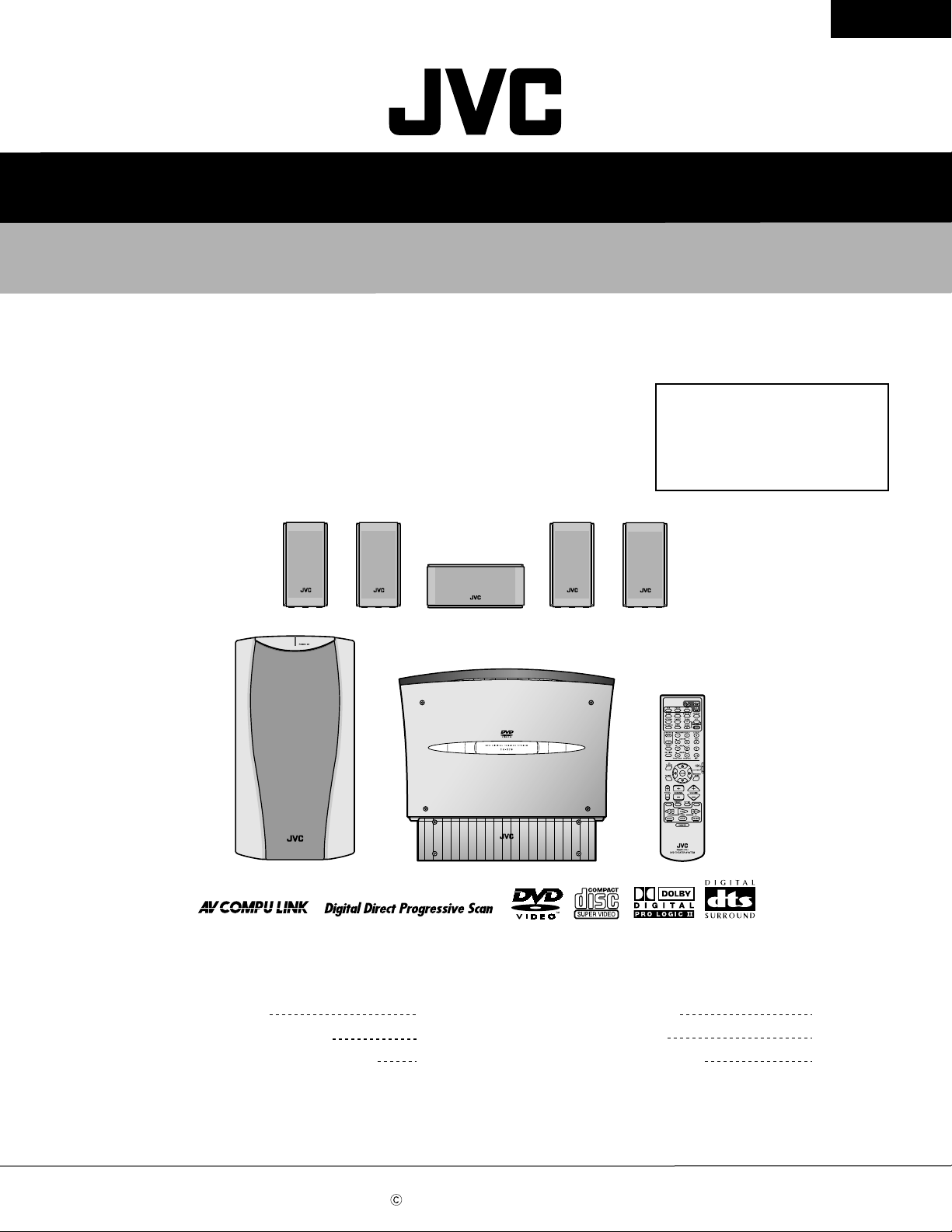
SERVICE MANUAL
DVD DIGITAL THEATER SYSTEM
TH-V70
Area suffix
J ----------------------------- U.S.A.
C -------------------------- Canada
TH-V70
SP-XSV70SP-XSV70
SP-PWV70 XV-THV70
Contents
Safety precautions
Preventing static electricity
Importance administering point
on the safety
SP-XCV70 SP-XSV70SP-XSV70
1-2
1-3
1-4
Disassembly method
Adjustment method
Description of major ICs
1-6
1-21
1-22~54
COPYRIGHT 2002 VICTOR COMPANY OF JAPAN, LTD.
No.21089
Jul. 2002
Page 2
TH-V70
1. This design of this product contains special hardware and many circuits and components specially for safety
purposes. For continued protection, no changes should be made to the original design unless authorized in
writing by the manufacturer. Replacement parts must be identical to those used in the original circuits. Services
should be performed by qualified personnel only.
2. Alterations of the design or circuitry of the product should not be made. Any design alterations of the product
should not be made. Any design alterations or additions will void the manufacturer`s warranty and will further
relieve the manufacture of responsibility for personal injury or property damage resulting therefrom.
3. Many electrical and mechanical parts in the products have special safety-related characteristics. These
characteristics are often not evident from visual inspection nor can the protection afforded by them necessarily
be obtained by using replacement components rated for higher voltage, wattage, etc. Replacement parts which
have these special safety characteristics are identified in the Parts List of Service Manual. Electrical
components having such features are identified by shading on the schematics and by ( ) on the Parts List in
the Service Manual. The use of a substitute replacement which does not have the same safety characteristics
as the recommended replacement parts shown in the Parts List of Service Manual may create shock, fire, or
other hazards.
4. The leads in the products are routed and dressed with ties, clamps, tubings, barriers and the like to be
separated from live parts, high temperature parts, moving parts and/or sharp edges for the prevention of
electric shock and fire hazard. When service is required, the original lead routing and dress should be
observed, and it should be confirmed that they have been returned to normal, after re-assembling.
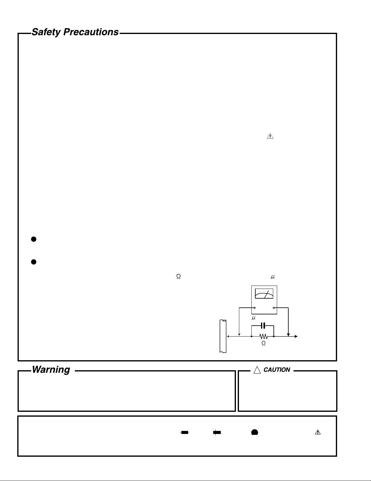
5. Leakage currnet check (Electrical shock hazard testing)
After re-assembling the product, always perform an isolation check on the exposed metal parts of the product
(antenna terminals, knobs, metal cabinet, screw heads, headphone jack, control shafts, etc.) to be sure the
product is safe to operate without danger of electrical shock.
Do not use a line isolation transformer during this check.
Plug the AC line cord directly into the AC outlet. Using a "Leakage Current Tester", measure the leakage
current from each exposed metal parts of the cabinet, particularly any exposed metal part having a return
path to the chassis, to a known good earth ground. Any leakage current must not exceed 0.5mA AC (r.m.s.).
Alternate check method
Plug the AC line cord directly into the AC outlet. Use an AC voltmeter having, 1,000 ohms per volt or more
sensitivity in the following manner. Connect a 1,500 10W resistor paralleled by a 0.15 F AC-type capacitor
between an exposed metal part and a known good earth ground.
Measure the AC voltage across the resistor with the AC
voltmeter.
Move the resistor connection to each exposed metal part,
particularly any exposed metal part having a return path to
the chassis, and meausre the AC voltage across the resistor.
Now, reverse the plug in the AC outlet and repeat each
measurement. Voltage measured any must not exceed 0.75 V
AC (r.m.s.). This corresponds to 0.5 mA AC (r.m.s.).
0.15 F AC TYPE
1500 10W
Good earth ground
AC VOLTMETER
(Having 1000
ohms/volts,
or more sensitivity)
Place this
probe on
each exposed
metal part.
!
1. This equipment has been designed and manufactured to meet international safety standards.
2. It is the legal responsibility of the repairer to ensure that these safety standards are maintained.
3. Repairs must be made in accordance with the relevant safety standards.
4. It is essential that safety critical components are replaced by approved parts.
5. If mains voltage selector is provided, check setting for local voltage.
Burrs formed during molding may
be left over on some parts of the
chassis. Therefore, pay attention to
such burrs in the case of
preforming repair of this system.
In regard with component parts appearing on the silk-screen printed side (parts side) of the PWB diagrams, the
parts that are printed over with black such as the resistor ( ), diode ( ) and ICP ( ) or identified by the " "
mark nearby are critical for safety.
(This regulation does not correspond to J and C version.)
1-2
Page 3
Preventing static electricity
1. Grounding to prevent damage by static electricity
Electrostatic discharge (ESD), which occurs when static electricity stored in the body, fabric, etc. is discharged,
can destroy the laser diode in the traverse unit (optical pickup). Take care to prevent this when performing repairs.
2. About the earth processing for the destruction prevention by static electricity
Static electricity in the work area can destroy the optical pickup (laser diode) in devices such as DVD players.
Be careful to use proper grounding in the area where repairs are being performed.
2-1 Ground the workbench
Ground the workbench by laying conductive material (such as a conductive sheet) or an iron plate over it
before placing the traverse unit (optical pickup) on it.
2-2 Ground yourself
Use an anti-static wrist strap to release any static electricity built up in your body.
(caption)
Anti-static wrist strap
TH-V70
Conductive material
(conductive sheet) or iron plate
3. Handling the optical pickup
In order to maintain quality during transport and before installation, both sides of the laser diode on the
1.
replacement optical pickup are shorted. After replacement, return the shorted parts to their original condition.
(Refer to the text.)
Do not use a tester to check the condition of the laser diode in the optical pickup. The tester's internal power
2.
source can easily destroy the laser diode.
4. Handling the traverse unit (optical pickup)
1.
Do not subject the traverse unit (optical pickup) to strong shocks, as it is a sensitive, complex unit.
2.
Remove solder of the short lands on the flexible wire after replacing the optical pickup. For specific details, refer
to the replacement procedure in the text. Remove the anti-static pin when replacing the traverse unit.
Be careful not to take too long a time when attaching it to the connector.
3.
Handle the flexible wire carefully as it may break when subjected to strong force.
4.
It is not possible to adjust the semi-fixed resistor that adjusts the laser power. Do not turn it.
5. Attention when traverse unit is decomposed
*Please refer to "Disassembly method" in the text for the DVD pickup unit.
Short lands
Apply solder to the short lands before the flexible wire is disconnected
from the connector on the DVD servo board.
(If the flexible wire is disconnected without applying solder, the DVD
pickup may be destroyed by static electricity.)
In the assembly, be sure to remove solder from the short lands after
connecting the flexible wire.
Flexible wire
Connector
DVD mechanism assembly
CN202
CN201
DVD servo board
1-3
Page 4
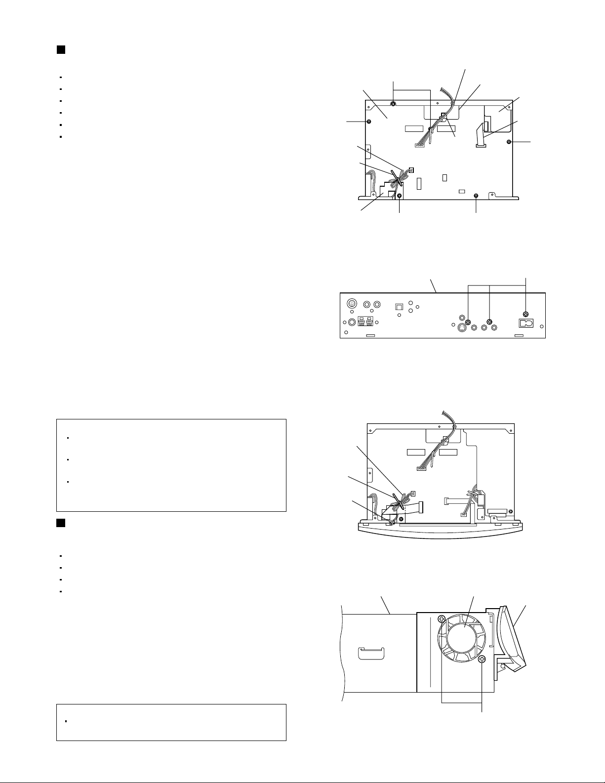
TH-V70
Importance administering point on the safety
<Main body section>
Main board
F901
1-4
Caution: For continued protection against risk of
fire, replace only with same type 1.6A/125V for F901.
This symbol specifies type of fast operating fuse.
Precaution: Pour eviter risques de feux, remplacez
le fusible de surete de F901 comme le meme type
que 1.6A/125V.
Ce sont des fusibles suretes qui functionnes rapide.
Page 5
<Speaker section>
F505
F504
TH-V70
Power supply & SP terminal board
F403
Mother board
Caution: For continued protection against risk of
fire, replace only with same type 4A/125V for F403,
8A/125V for F504, 8A/125V for F505.
This symbol specifies type of fast operating fuse.
Precaution: Pour eviter risques de feux, remplacez
le fusible de surete de F403 comme le meme type
que 4A/125V, F504 comme le meme type que
8A/125, et 8A/125V pour F505.
Ce sont des fusibles suretes qui functionnes rapide.
1-5
Page 6
TH-V70
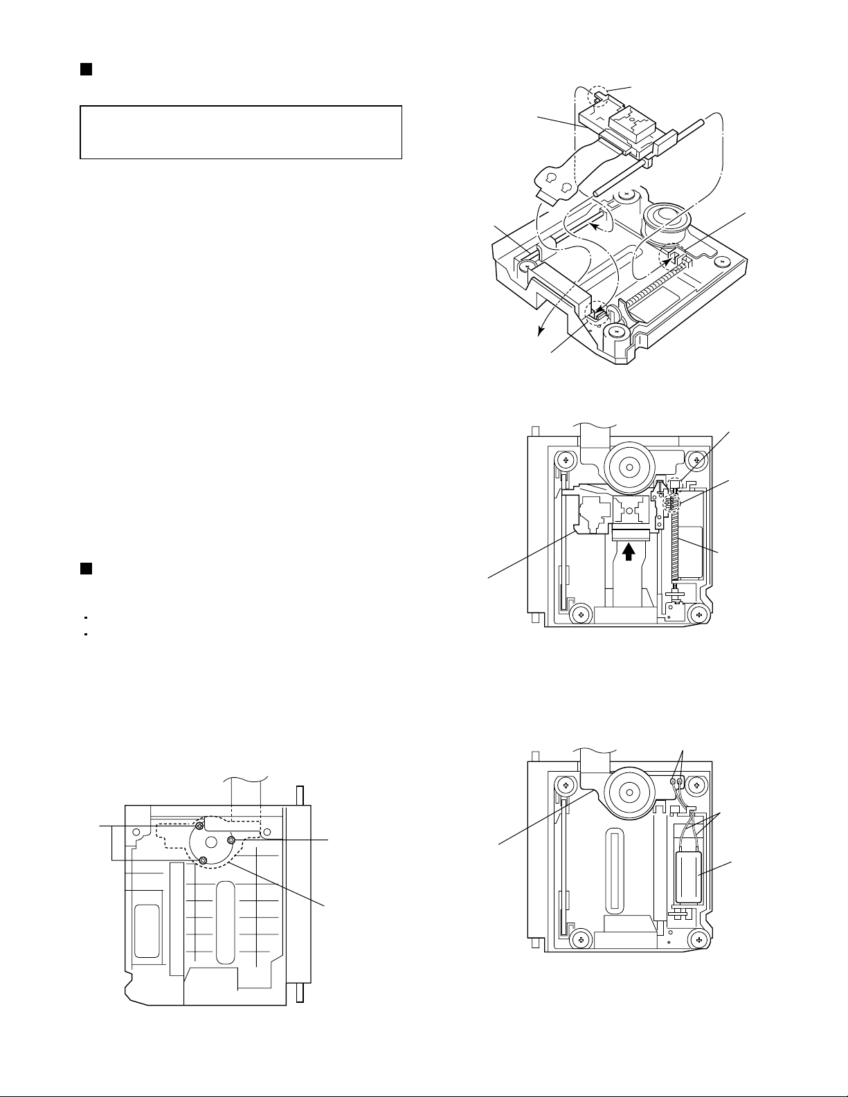
Disassembly method
<Main body section>
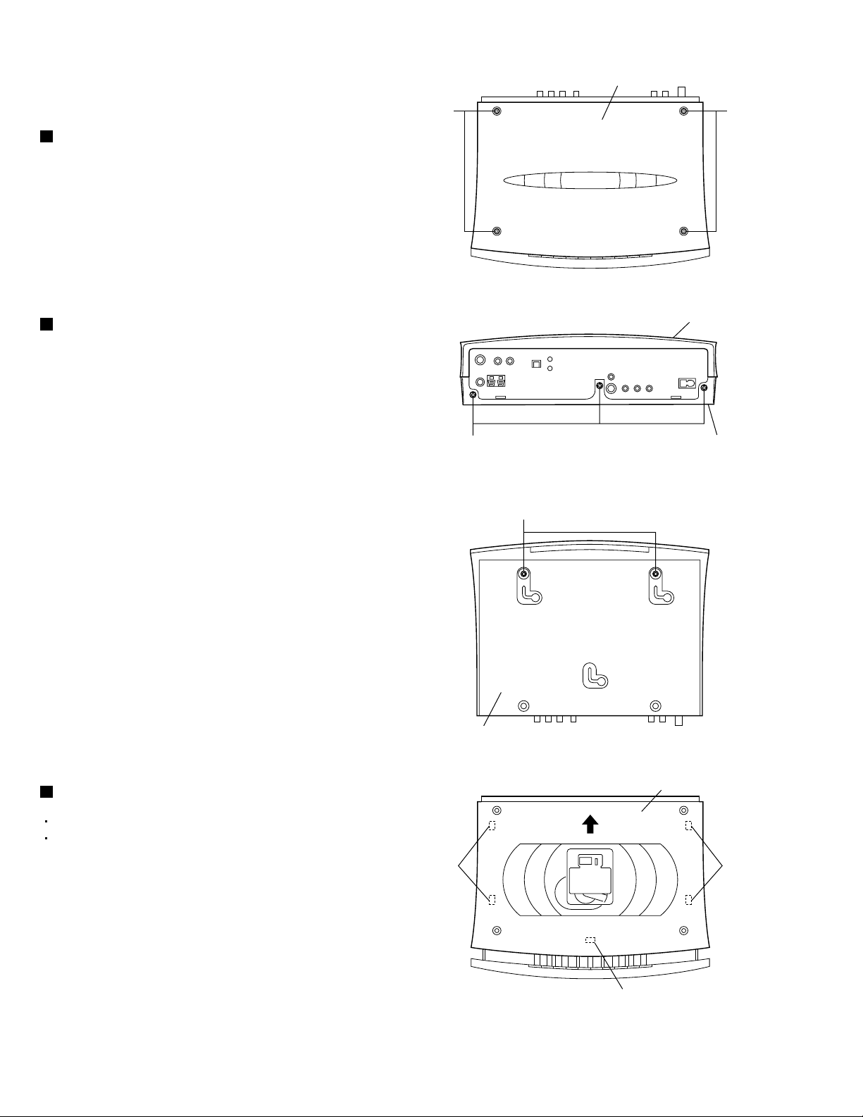
Removing the top plate (See Fig. 1.)
From the top side of the main body, remove the
four screws A attaching the top plate.
Removing the bottom panel
(See Figs. 2 and 3.)
1.
From the rear side of the main body, remove the
three screws B attaching the bottom panel.
2.
From the bottom side of the main body, remove the
two screws C attaching the bottom panel.
3.
Remove the bottom panel in an upward direction.
A
B
Top plate
A
Fig.1
Top panel
Bottom panel
Fig.2
Removing the top panel (See Fig. 4.)
Remove the top plate.
Remove the bottom panel.
1.2.Slide the top panel toward the rear (direction of the
arrow) and disengage it from the engagement
sections a and b of the bottom chassis.
C
Bottom panel
Fig.3
Top panel
bb
Remove the top panel in an upward direction.
1-6
a
Fig.4
Page 7
TH-V70
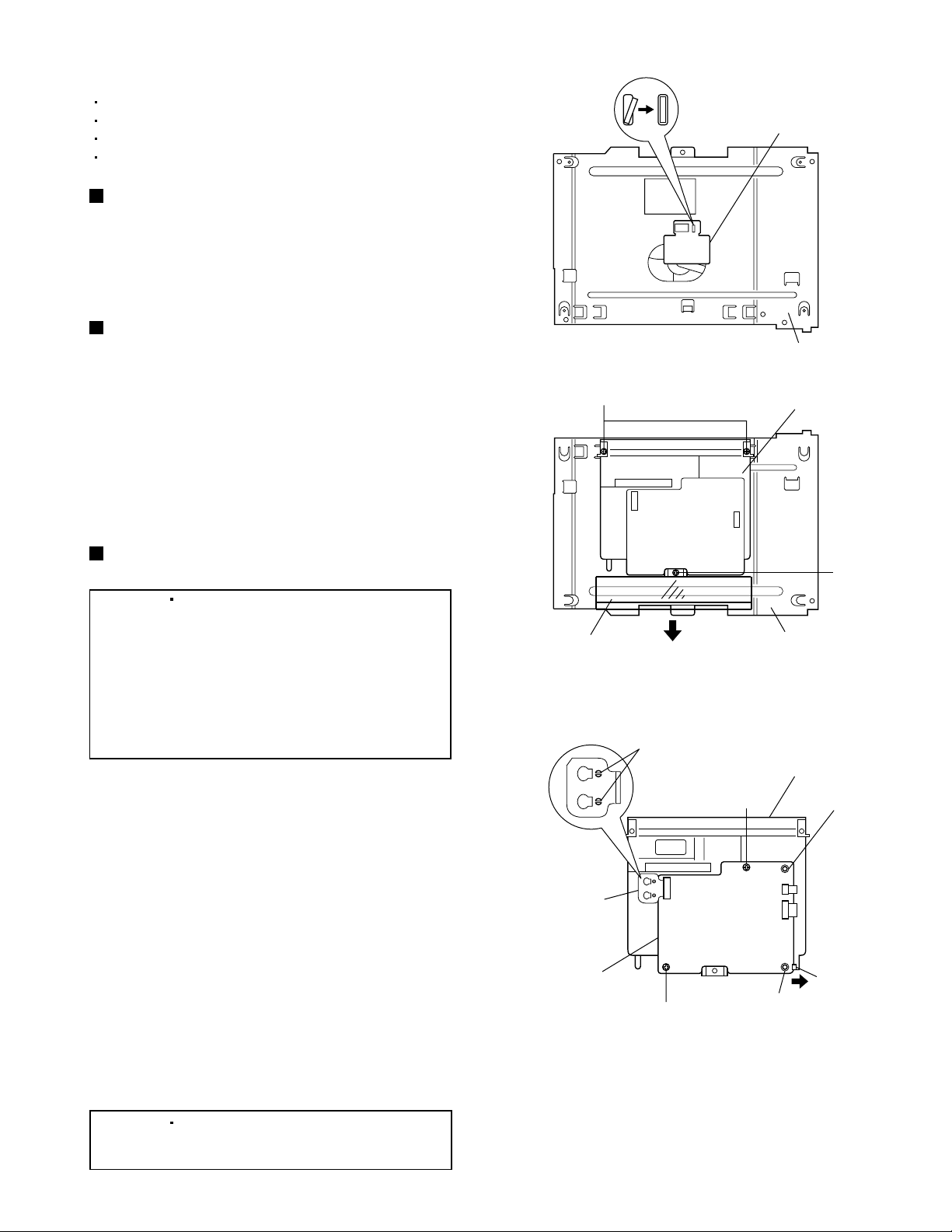
Removing the DVD mechanism
assembly (See Figs. 5 and 6.)
Remove the top plate.
Remove the bottom panel.
Remove the top panel.
1.
From the top side of the main body, disengage the
claw c of the DVD mechanism assembly and then
remove the push button.
2.
Remove the five screws D and screw E attaching
the DVD mechanism assembly.
3.
Disconnect the wire from connector CN812 on the
LED board.
4.
Disconnect the connectors CN502 and CN503 on
the DVD servo board from connectors CN801 and
CN803 on the main board while lifting the DVD
mechanism assembly in an upward direction.
Removing the front panel assembly
(See Figs. 7 and 8.)
LED board
CN502
D
D
Claw c
CN812
Push button
Fig.5
DVD mechanism
assembly
D
E
DVD servo board
CN503
Front panel assembly
Remove the top plate.
Remove the bottom panel.
Remove the top panel.
Remove the DVD mechanism assembly.
1.
Remove the wire clamp bundling the wires of the
front panel assembly.
2.
Remove the card wire of the front panel assembly
from the wire holder.
3.
Disconnect the wires from connectors CN106 and
CN814 on the main board.
4.
Disconnect the card wires from connectors CN802
and CN813 on the main board.
5.
From the front side of the main body, remove the
two screws F attaching the front panel assembly.
6.
Disengage the claws d of the front panel assembly
from the bottom chassis and then remove the front
panel assembly in the direction of arrow.
[Reference]
Before attaching the front panel assembly,
pass the card wire of the front panel assembly
through the hole on the bottom chassis.
After attaching the front panel assembly,
bundle the wires and card wire of the front
panel assembly using a wire clamp.
[Caution]
In the assembly, arrange the wires and wire
clamp so that they are not touch to the
regulator IC(IC953).
Main board
Wire holder
Bottom
chassis hole
Claws d
CN803 CN801
Fig.6
CN814
CN813
CN802
CN106
Card wires
Fig.7
Front panel assembly
F
Fig.8
Main board
Wire clamp
Bottom chassis
Wire
IC953
Claws d
Bottom chassis
1-7
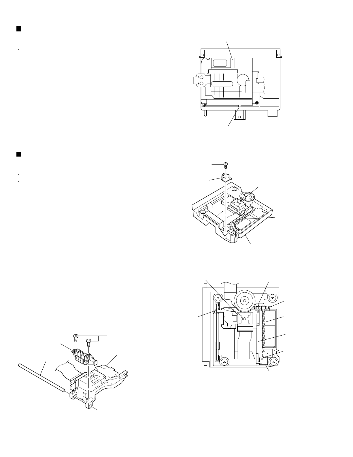
Page 8
TH-V70
Removing the DSP/Audio board
(See Figs. 9 and 10.)
Remove the top plate.
Remove the bottom panel.
Remove the top panel.
Remove the DVD mechanism assembly.
1.
From the top side of the main body, remove a
screw G attaching the DSP/Audio board.
2.
From the rear side of the main body, remove the
screw H and two screws J attaching the DSP/Audio
board.
3.
Take out the DSP/Audio board from the bottom
chassis and then disconnect the card wire from
connector CN806 on the main board.
Compulink board
CN592
CN805
CN806
Tuner
DSP/Audio
board
Card wire
G
Card wire
[Reference]
Before attaching the DSP/Audio board, connect
the card wire to the connector CN806 on the
main board.
Removing the compulink board
(See Figs. 9 and 10.)
Remove the top plate.
Remove the bottom panel.
Remove the top panel.
Remove the DVD mechanism assembly.
1.
Disconnect the card wire from connector CN592 on
the compulink board.
2.
From the rear side of the main body, remove the
screw K attaching the compulink board.
3.
Take out the compulink board from the bottom
chassis.
Removing the tuner
(See Figs. 9 and 10.)
Remove the top plate.
Remove the bottom panel.
Remove the top panel.
Remove the DVD mechanism assembly.
H
L
Fig.9
J
K
Rear panel
Fig.10
1.
Disconnect the card wire from connector CN805 on
the main board.
2.
From the rear side of the main body, remove the
two screws L attaching the tuner.
3.
Take out the tuner from the bottom chassis.
1-8
Page 9
Removing the main board
(See Figs. 11 and 12.)
Remove the top plate.
Remove the bottom panel.
Remove the top panel.
Remove the DVD mechanism assembly.
Remove the front panel assembly.
Remove the DSP/Audio board.
1.
Disconnect the card wire from connector CN805 on
the main board.
2.
Remove the wire clamp bundling the fan motor wire
and then disconnect the wire from connector
CN972 on the main board.
3.
Disconnect the card wire from connector CN592 on
the compulink board.
4.
Remove the five screws M and screw M' attaching
the main board.
Main board
M
Fan motor wire
Wire clamp
Wire holder
Insert this wire into the notch.
M
CN972
M'
Fig.11
Rear panel
Compulink board
CN592
CN805
M
TH-V70
Tuner
Card wire
M
N
5.
From the rear side of the main body, remove the
three screws N attaching the main board.
6.
Remove the rear panel with the tuner and
compulink board.
7.
Take out the main board from the bottom chassis.
[Reference] Attaching the main board
When attaching the screw M', attach the wire
holder together with it.
After connecting the wires to the connectors,
bundle them using the wire clamp.
Insert the DVD mechanism assembly wire
into the notch on the bottom chassis.
(See Fig. 11.)
Removing the fan motor
(See Figs. 13 and 14.)
Remove the top plate.
Remove the bottom panel.
Remove the top panel.
Remove the DVD mechanism assembly.
1.
Remove the wire clamp and tie band bundling the
fan motor wire.
Fig.12
Fan motor wire
Wire clamp
CN972
Tie band
Fig.13
Bottom chassis Fan motor Front panel
assembly
2.
Disconnect the wire from connector CN972 on the
main board.
3.
From the left side of the main body, remove the two
screws P attaching the fan motor.
[Reference]
After mounting the fan motor, bundle the fan
motor wire using the wire clamp.
P
Fig.14
1-9
Page 10
TH-V70
<Front panel assembly section>
Remove the top plate.
Remove the bottom panel.
Remove the top panel.
Remove the DVD mechanism assembly.
Remove the front panel assembly.
Removing the switch board
(See Fig. 15.)
From the back side of the front panel assembly,
remove the four screws Q attaching the switch
board.
Removing the open/close board
(See Figs. 15 and 16.)
1.2.From the back side of the front panel assembly,
remove the two screws R attaching the door motor
assembly.
Remove the screw S attaching the open/close
board of the door motor assembly.
Removing the door motor (See Fig. 16.)
Remove the door motor assembly.
1.
Remove the stop washers attaching the clutch
assembly and gear 2.
2.
Remove the clutch assembly, washer and Gear 2.
Door motor assembly
R
Clutch assembly
Stop washer
Gear 2
Front panel assembly
(Back side)
Front panel assembly
(Back side)
Fig.15
Door motor
Washer
Fig.16
Rod gear assembly
Q
Switch board
T
S
Open/close
board
Door motor assembly
e
3.
Remove the two screws T attaching the door
motor.
Removing the front board
(See Figs. 17 to 20.)
1.
While widening section e of the front base in the
direction of the arrow, remove the rod gear
assembly.
2.
Slide the moving panel assembly all the way in the
direction of the arrow.
3.
While slightly widening sections f toward the front,
take out the moving panel assembly in the direction
of the arrow.
4.
Remove the two screws W attaching the moving
base of the moving panel assembly.
5.
Disengage the engagement sections g on the
inside of the moving base and at the inside of the
moving panel assembly and remove the moving
base.
6.
Remove the two screws X attaching the front
board.
7.
Disengage the claws h of the moving panel and
remove the front board.
[Reference]
Before attaching the moving base, pass the
card wire of the front board through the hole
on the moving base. (See Fig.19.)
Front base
W
X
Fig.17
Fig.18
Fig.19
Fig.20
f
Moving panel assembly
Hole
h
Front base
Moving base
Front board
Moving panel
gg
Card wire
1-10
Page 11
TH-V70
<DVD mechanism assembly section>
Remove the top plate.
Remove the bottom panel.
Remove the top panel.
Remove the DVD mechanism assembly.
Removing the LED board (See Fig. 1.)
From the top side of the DVD mechanism
assembly, disengage the claw a of the top chassis
attaching the LED board and then remove the LED
board.
Removing the DVD mechanism
assembly (See Fig. 2.)
Extend the both sides of the protector, and then
1.
raise the protector in the direction of arrow.
Remove the three screws A attaching the DVD
2.
mechanism assembly on the top chassis.
Claw a
A
LED board
Fig.1
DVD mechanism assembly
Top chassis
Removing the DVD servo board
(See Fig. 3.)
[Caution] Be sure to solder the short land
sections b on the flexible wire before
disconnecting the flexible wire from
connector CN101 on the DVD servo
board.
If the flexible wire is disconnected
without attaching solder, the pickup
unit may be destroyed by static
electricity.
1.
From the back side of the DVD mechanism
assembly, attach solder to the short land sections b
of the flexible wire that is connected to the
connector CN101 of the DVD servo board.
2.
Disconnect the flexible wire from connector CN101
on the DVD servo board.
3.
Disconnect the card wires from connectors CN201
and CN202 on the DVD servo board.
4.
Remove the two screws B attaching the DVD servo
board.
Protector
Flexible wire
DVD servo board
Fig.2
Short land sections b
DVD mechanism assembly
B
CN202
CN101
CN201
Projection e
B
A
Top chassis
Projection d
Claw c
5.
While pushing the claw c of the DVD mechanism
assembly in the direction of the arrow, remove the
DVD servo board from the projections d and e in an
upward direction.
[Caution] In the assembly, be sure to remove
solder from the short land sections
b after connecting the flexible wire.
Fig.3
1-11
Page 12
TH-V70
Removing the DVD traverse
mechanism assembly (See Fig. 4.)
Remove the DVD servo board.
1.
Remove the two screws C attaching the DVD
traverse mechanism assembly.
2.
Disengage the claw f attaching the DVD traverse
mechanism assembly and then take out the DVD
traverse mechanism assembly.
DVD traverse mechanism assembly
Removing the DVD pickup unit
(See Figs. 5 to 7.)
Remove the DVD servo board.
Remove the DVD traverse mechanism assembly.
1.
From the top side of the DVD traverse mechanism
assembly, remove the screw D attaching the
bracket.
2.
Remove the claw g attaching the thrust spring and
then take out the torsion spring.
3.
Remove the lead screw from the section h and
then remove the shaft from the section i.
4.
Disengage the section j of the DVD pickup unit and
then remove the DVD pickup unit with the shaft.
5.
Pull the shaft out of the DVD pickup unit.
C
D
Bracket
DVD traverse mechanism assembly
DVD pickup unit
Claw f
C
Fig.4
DVD pickup unit
Shaft
Fig.5
Section i
6.
Remove the two screws E attaching the SW.
actuator.
SW. actuator
Shaft
Fig.7
1-12
E
DVD pickup unit
Section j
Section h
Lead screw
Shaft
Claw g
Thrust spring
Fig.6
Page 13
Attaching the DVD pickup unit
(See Figs. 5 to 9.)
[Reference]
Refer to the explanation of "Removing the
DVD pickup unit" on the preceding page.
1.
Attach the SW. actuator and shaft to the DVD
pickup unit. (See Fig.7.)
2.
Engage the section j of the DVD pickup unit to the
shaft of the DVD traverse mechanism assembly
first, and set the both ends of the shaft of the DVD
pickup unit in the sections i and i' of the DVD
traverse mechanism assembly.
3.
Slide the DVD pickup unit all the way in the
direction of the arrow.
4.
Mesh the lead screw to the section k of DVD
pickup unit and then set the end of the lead screw
to the section h.
TH-V70
Section j
DVD pickup unit
Section i
Shaft
Section i'
Fig.8
Section h
5.
Attach the thrust spring. (See Fig.6.)
6.
Attach the bracket. (See Fig.5.)
Removing the spindle motor board
(See Figs. 10 and 11.)
Remove the DVD servo board.
Remove the DVD traverse mechanism assembly.
1.
From the top side of the DVD traverse mechanism
assembly, remove the feed motor wire that is
soldered to the spindle motor board.
2.
From the back side of the DVD traverse mechanism
assembly, remove the three screws F attaching the
spindle motor board.
F
F
DVD pickup unit
Spindle motor
board
Section k
Lead screw
Fig.9
Remove the solders.
Feed motor
wire
Feed motor
Fig.11
Spindle motor
board
Fig.10
1-13
Page 14

TH-V70
Removing the feed motor
(See Figs. 12 to 14.)
Remove the DVD servo board.
Remove the DVD traverse mechanism assembly.
1.
Remove the four screws G attaching the traverse
mechanism assembly.
2.
Take out the traverse mechanism assembly from
the mechanism base.
3.
Remove the screw D attaching the bracket and
take out the bracket.
4.
Disengage the claw g attaching the thrust spring
and take out the thrust spring.
5.
Pull out the lead screw in the direction of arrow.
6.
Remove the feed gear M.
7.
Remove the feed motor wire that is soldered to the
spindle motor board.
Traverse
mechanism
assembly
Spindle motor board
G
Bracket
G G
Fig.12
Remove the solders.
D
Mechanism
base
Feed motor
8.
Remove the two screws H attaching the feed motor
and take out the feed motor.
Torsion spring
Fig.13
Feed motor wire
Lead screw
Feed motor
Feed gear M
Claw g
1-14
Traverse
mechanism assembly
H
Fig.14
Page 15
Removing the switch board
(See Fig.15.)
Remove the DVD mechanism assembly.
1.
From the top side of the CD mechanism assembly,
remove the screw J attaching the switch board.
2.
Lift the switch board slightly and then remove the
wire from connector CN101 on the switch board.
Removing the loading motor assembly
(See Figs.3, 15 to 17.)
TH-V70
CD mechanism assembly Clamper base assembly
J
Remove the DVD mechanism assembly.
1.
From the back side of the DVD mechanism
assembly, disconnect the card wire from connector
CN202 on the DVD servo board. (See Fig.3.)
2.
From the top side of the CD mechanism assembly,
remove the two screws K attaching the clamper
base assembly.
3.
Disconnect the wire from connector CN101 on the
switch board while lifting the clamper base
assembly slightly and remove the clamper base
assembly.
4.
Remove the three screws L attaching the roller
holder assembly and take out the roller holder
assembly.
5.
Disconnect the wires from connectors CN103 and
CN104 on the loading motor assembly.
6.
Remove the belt of the loading motor assembly.
7.
Remove the two screws M attaching the loading
motor assembly and take out the loading motor
assembly.
CN101
Roller holder
assembly
L
K
M
Switch board
Fig.15
Fig.16
CN103
K
L
Roller holder
assembly
CN104
Loading motor assembly
M
Fig.17
Belt
1-15
Page 16
TH-V70
<Speaker section>
Removing the amplifier assembly
(See Figs. 1 and 2.)
1.
From the rear side of the speaker main body,
remove the four screws A attaching the heat sink
cover and then remove the heat sink cover.
2.
Remove the eight screws B attaching the amplifier
assembly.
3.
Move the amplifier assembly backward and
disconnect the wire from connector CN109 in the
lower part of the amplifier assembly.
Removing the rear panel (See Fig. 3.)
Remove the amplifier assembly.
1.2.Pull out the knob.
Amplifier assembly
B
Fig.1
A
Heat sink cover
A
Amplifier assembly
Remove the ten screws C, ten screws D and screw
E attaching the rear panel.
BB
CN109
B
Fig.2
Amplifier assembly
C
C
Knob
CCD
E
DD
1-16
C
D
D
C
C
D
Rear panel
C
Fig.3
Page 17
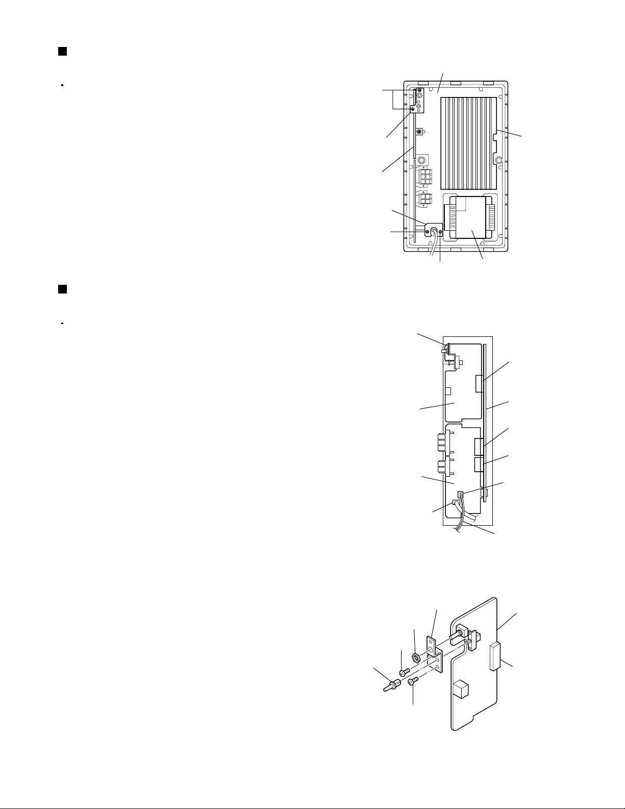
Removing the pre-amplifier board
(See Figs. 4 to 6.)
TH-V70
Mother board
Remove the rear panel.
1.
Remove the two screws F attaching the volume
bracket.
2.
Disconnect the pre-amplifier board from the
connector CN201 on the mother board and take
out the pre-amplifier board.
3.
Pull out the push button.
4.
Remove the two screws G and nut attaching the
volume bracket.
Removing the power supply & SP
terminal board (See Figs. 4 and 5.)
Remove the rear panel.
1.
Remove the two screws H attaching the AC
bracket.
2.
Disconnect the power supply & SP terminal board
from the connectors CN210 and CN211 on the
mother board.
3.
Disconnect the wire from connector CN107 on the
power supply & SP terminal board.
4.
Disconnect the power cord from connector CN108
on the power supply & SP terminal board.
F
Volume bracket
Pre-amplifier
board
AC bracket
H
Volume bracket
Pre-amplifier board
Power supply & SP
terminal board
H
Fig.4
Power transformer
CN101
CN111
CN110
Heat sink
CN201
Mother board
CN211
CN210
CN108
Push button
CN107
Fig.5
Volume bracket
Nut
G
G
Fig.6
Power cord
Pre-amplifier board
CN101
1-17
Page 18

TH-V70
Removing the mother board
(See Figs. 7 and 8.)
Remove the rear panel.
Remove the pre-amplifier board.
Remove the power supply & SP terminal board.
1.
Disconnect the wire from the connector CN104 on
the mother board.
2.
Remove the seven screws J attaching the mother
board.
3.
Take out the mother board with the power amplifier
board (A,B).
4.
From the bottom side of the mother board, remove
the two screws K and two screws L attaching the
power amplifier board (A,B).
5.
Remove the power amplifier board (A,B) from
connectors CN202, CN203, CN205 and CN206 on
the mother board.
Removing the power amplifier
board (A) (See Figs. 9 and 10.)
Remove the mother board.
J
CN104
CN202
CN203
Mother board
J
Fig.7
KL
J
Power amplifier
board (A)
J
Power amplifier
board (B)
J
Power transformer
Mold base
Mother board
CN206
Power amplifier
board (B)
1.
Remove the four screws M attaching the heat sink
to the power amplifier board (A).
2.
From the bottom side of the power amplifier board
(A), disengage the four engagement sections a.
3.
From the top side of the power amplifier board (A),
slide the P.TR holder (A) in the direction of the
arrow to disengage the engagement section b and
remove the power amplifier board (A) from the P.TR
holder (A).
a
1
2
(Bottom side)
Power amplifier
board (A)
CN102
P.TR holder (A)
CN103
b
Power amplifier
board (A)
P.TR holder (A)
M
K
CN205
L
Fig.8
M N
N
P.TR holder (B)
1-18
2
1
(Bottom side)
a
Fig.10
M
Fig.9
N
Page 19

TH-V70
Removing the power amplifier
board (B) (See Figs. 9 and 11.)
Remove the mother board.
1.
Remove the four screws N attaching the heat sink
to the power amplifier board (B). (See Fig.9.)
2.
From the bottom side of the power amplifier board
(B), disengage the four engagement sections c.
3.
From the top side of the power amplifier board (B),
slide the P.TR holder (B) in the direction of the
arrow to disengage the engagement section d and
remove the power amplifier board (B) from the P.TR
holder (B).
Removing the power transformer
(See Figs. 12 and 13.)
Remove the rear panel.
1.
Remove the wire from the connector CN104 on the
mother board.
P.TR holder (B)
Mother board
c
1
CN106
Power amplifier
board (B)
d
CN105
c
2
(Bottom side)
2
1
(Bottom side)
Fig.11
2.
Disconnect the wire from the connector CN107 on
the power supply & SP terminal board.
3.
Remove the four screws P attaching the power
transformer and then remove the power
transformer from the transformer bracket of the
mold base.
Power supply & SP
terminal board
P
CN104
Transformer
bracket
P
Power
transformer
P
Fig.12
Mold base
Power supply & SP
terminal board
CN107
Fig.13
1-19
Page 20
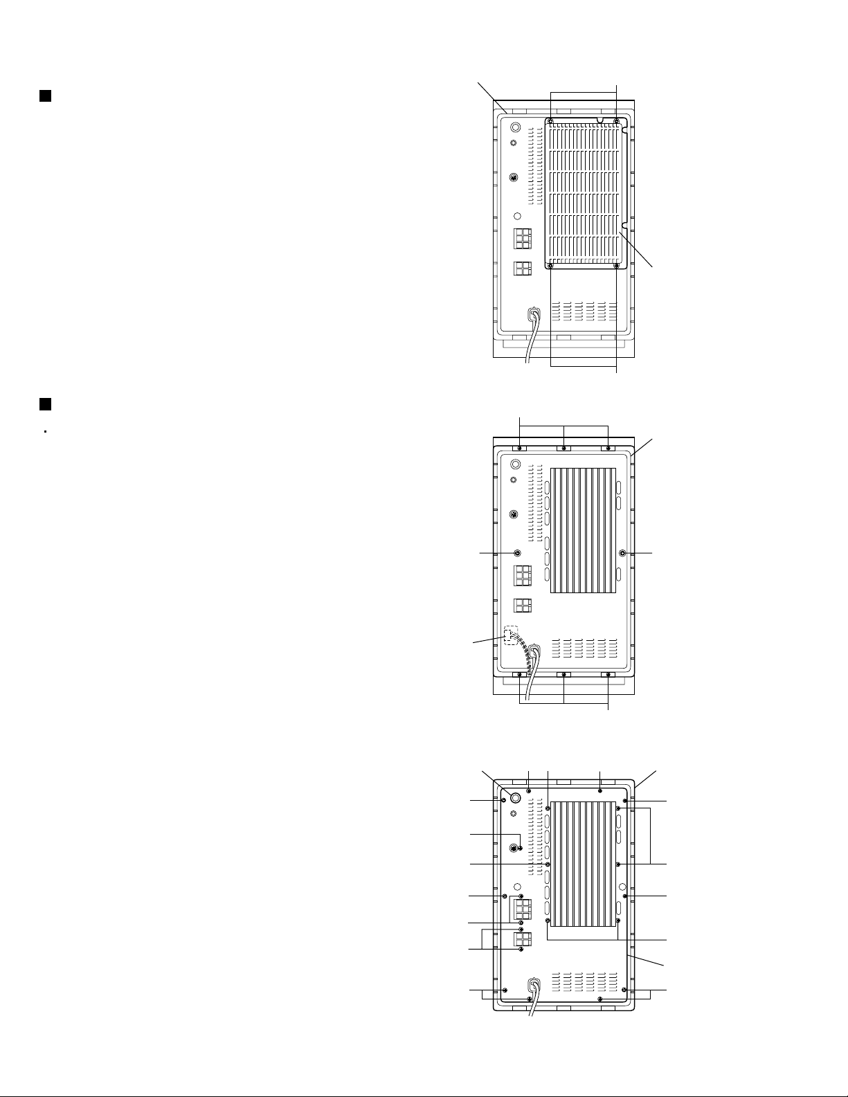
TH-V70
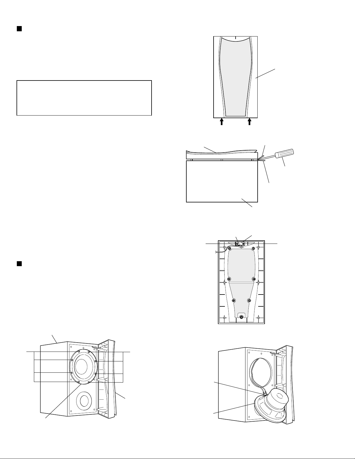
Removing the LED indicator
(See Figs. 14 to 16.)
1.
Insert the tip of a flat-bladed screwdriver or a
similar tool into the space between the speaker
main body and the ornament panel (the section
indicated by the arrows), and lift the net little by little
to remove.
[Note] To prevent damaging the ornament
panel and speaker main body, insert
cushioning plates etc. above and below
the tip of the flat-bladed screwdriver or a
similar tool.
2.3.From the back side of the ornament panel, remove
the two screws Q attaching the LED indicator.
Ornament panel
JVC
Fig.14
Disconnect the wire from connector CN109 on the
LED indicator.
Removing the speaker
(See Figs. 17 and 18.)
1.
Remove the eight screws R attaching the speaker.
2.
Take out the speaker.
Ornament panel
Q
Cushioning plate, etc.
Speaker main body
Fig.15
CN109
LED indicator
Flat-bladed
screwdriver, etc.
Cushioning plate, etc.
Q
3.
Disconnect the wires from the terminals of the
speaker.
Speaker main body
R
Ornament panel
Speaker
Fig.17
1-20
Fig.16
R
Terminal
Speaker
Fig.18
Page 21

Adjustment method
Initializing in TEST MODE
Initializing in TEST MODE
TH-V70
Moving panel close?
YES
While pressing both the STOP button (fourth button from left)
and EJECT (farthest right button) button on the main unit,
plug in the power.
FL indication
TEST E
Monitor indication (Upper left of the monitor)
E(Europe)
Pressing the PAUSE button (fifth button from right)
Initialization starts
FL indication
"ATT" will appear
NO
Press the power button
on the main unit, and put
it in standby.
Make sure that the panel
has closed.
Pull out the power plug.
Initialization is complete.
Set the power to standby.
1-21
Page 22

TH-V70
Description of major ICs
AN8703FH (IC101) : Frontend processor for DVD
1.Terminal layout
HDTYPE
VIN12
VIN11
GND1
VIN4
VIN3
VIN2
VIN1
646362616059585756555453525150
LPC1
1
LPCO1
2
LPC2
3
LPCO2
TBAL
FBAL
POFLT
DTRD
IDGT
SEN
SCK
STDIO
RSCL
JLINE
4
5
6
7
8
9
10
11
12
13
14
15
16
AN8703FH
VFOSHORT
STANDBY
VREF1
VCC1
VIN10
VIN9
VIN8
VIN7
VIN6
VIN5
49
48
47
46
45
44
43
42
41
40
39
38
37
36
35
34
33
RFINN
RFINP
TESTSG
AGCO
AGCG
PEAK
BOTTOM
RFENV
BDO
OFTR
DCRF
RFC
VCC3
RFOUT
RFDIFO
GND3
171819202122232425262728293031
TEN
TEOUT
AGCBAL
FEN
ASOUT
FEOUT
AGCOFST
MON
GND2
AGCLVL
VCC2
VREF2
VHALF
DFLTON
32
DCFLT
DFLTOP
2. Pin function
Pin No. Symbol I/O Function
1
2
3
4
5
6
7
8
9
10
11
12
13
14
15
16
17
18
19
20
21
22
23
24
25
26
27
28
29
30
LPC1
LPCO1
LPC2
LPCO2
VFOSHORT
TBAL
FBAL
POFLT
DTRD
IDGT
STANDBY
SEN
SCK
STDIO
RSCL
JLINE
TEN
TEOUT
AGCBAL
ASOUT
FEN
FEOUT
AGCOFST
MON
AGCLVL
GND2
VREF2
VCC2
VHALF
DFLTON
I
Laser pin input (DVD head)
O
Laser drive output (DVD head)
I
Laser pin input (CD head)
O
Laser drive output (CD head)
I
VFOSHORT control
I
Tracking balance control
I
Focus balance control
O
Track detection threshold level
I
Data slice data read signal input (for RAM)
I
Data slice address gate signal input (for RAM)
I
Standby mode control
I
SEN(Serial data input)
I
SCK(Serial data input)
I/O
STDI(Serial data I/O)
I
Reference current supply
I
J-line current setting
I
Tracking error amplifier inverted input
O
Tracking error signal output
I
Offset adjustment for DRC-1
O
Full addition signal output
I
Focus error amplifier inverted input
O
Focus error signal output
I
Offset adjustment for DRC-2
-
Not use (Monitor)
I
Output amplitude adjustment for DRC
-
Ground 2
O
VREF2 voltage output
-
Power supply 2 (5V)
O
VHALF voltage output
O
Filter amplifier inverted output
1-22
Page 23

Pin No. Symbol I/O Function
31
32
33
34
35
36
37
38
39
40
41
42
43
44
45
46
47
48
49
50
51
52
53
54
55
56
57
58
59
60
61
62
63
64
DFLTOP
DCFLT
GND3
RFDIFO
RFOUT
VCC3
RFC
DCRF
OFTR
BDO
RFENV
BOTTOM
PEAK
AGCG
AGCO
TESTSG
RFINP
RFINN
VIN5
VIN6
VIN7
VIN8
VIN9
VIN10
VCC1
VREF1
VIN1
VIN2
VIN3
VIN4
GND1
VIN11
VIN12
HDTYPE
O
Filter amplifier positive output
O
Filter output capacitance connection
-
Ground 3
-
Radial differential output (Not use)
O
RF full-addition amplifier output
-
Power supply 3 (3.3V)
I
Filter for RF-group delay correction amplifier
O
DC-cut filter for RF full-addition amplifier
O
OFTR output
O
BDO output
O
RF envelope output
O
Bottom envelope detection filter
O
Peak envelope detection filter
O
AGC amplifier gain control
O
AGC amplifier level control
I
TEST signal input
I
RF signal positive input
I
RF signal inverted input
I
Internal four-partition (CD) RF input 1
I
Internal four-partition (CD) RF input 2
I
Internal four-partition (CD) RF input 3
I
Internal four-partition (CD) RF input 4
I
External two-partition (DVD) RF input 2
I
External two-partition (DVD) RF input 1
-
Power supply 1 (5V)
O
VREF1 voltage output
I
Internal four-partition (DVD) RF input 1
I
Internal four-partition (DVD) RF input 2
I
Internal four-partition (DVD) RF input 3
I
Internal four-partition (DVD) RF input 4
-
Ground 1
I
3-beam sub (CD) input 2
I
3-beam sub (CD) input 1
I
HD type selection
TH-V70
MM74HCT32MTC / 74LCX32MTC (IC521 / IC522) : Quad 2 input OR gate
1. Terminal layout & Block diagram 2. Truth table
11A
21B
31Y
42A
52B
62Y
7
(TOP VIEW)
14
13
12
11
10
9
8GND
VCC
4B
4A
4Y
3B
3A
3Y
INPUTS OUTPUT
A
B
L
L
L
H
H
L
H
H
Y
L
H
H
H
1-23
Page 24

TH-V70
MN101C49GKD1 (IC801) : System micon
1.Terminal layout
100 76
1
75
25
26 50
2. Pin function
Pin No.
1
2
3
4
5
6
7
8
9
10
11
12
13
14,17,28,
31,32
15
16
18
19
20
21
22
23
24
25
26
27
29
30
33
34
35
36
37
38
39
40
41
42
51
Symbol Function
VREFNTSEL(RGB--SEL)
VER/HOR SEL
SW1
PHOTOSW
LOCK
VERSION
KEY1
KEY2
VREF+
VDD
OSC2
OSC1
GND
XI
XO
DI-DO
D.O.MUTE
DI-CK
RXD (DATA OUT)
TXD (DATA IN)
SCLK
CS
CPU-RESET
INTP
REMOCON
RDS ST
SAFETY1
RESET
DSP RST
DSP RDY
AVC-OUT
AVC-IN
VIDEO-MUTE1
VIDEO-MUTE2
VIDEO-Y/C-MIX
VIDEO-RGB
DSP-COM
I/O
-
Connect to ground
I
NTSC/PAL discrimination(RGB/YC switching discrimination) signal
I
Vertical/Horizontal setting discrimination signal
I
Slide door switch1
I
Loading mechanism photo switch
I
Slide door lock detection(AD)
I
Area discrimination signal
I
Key input1 (AD)
I
Key input2 (AD)
-
Reference power supply
-
Power supply
O
Oscillator output (8MHz)
I
Oscillator input (8MHz)
-
Ground
O
Not used (Connect to ground)
I
Not used (Not connect)
O
PANECON serial communication data output
O
MP3/JPEG mode: H (for DVD disc)
O
PANECON serial communication clock
O
Serial communication data output for PANTERA
I
Serial communication data input for PANTERA
I
Serial communication clock for PANTERA
O
Transmit request for PANTERA communication
O
Reset signal for PANTERA
I
Receive request for PANTERA communication (Interruption)
I
Remote control signal input (interruption)
I
RDS communication strobe (interruption)
I
Short detecting signal 1
I
Syscon reset input
O
DSP micom reset input
O
DSP micom ready
O
AV compulink output
I
AV compulink input
O
Video driver mute 1 control
O
Video driver mute 2 control
O
Video driver YCMIX control
O
Video driver RGB control
O
DSP serial communication data output
1-24
Page 25

TH-V70
Pin No.
43
44
45
46
47
48
49
50
51 - 55,60
63,66
56
57
58
59
61
62
64
65
67
68
69
70
71
72
73
74
75
76
77
78
79
80
81
82
83
84
85
86 - 88
89
90
91
92
93
94
95
96
97
98
99
100
Symbol FunctionI/O
DSP-STAT
DSP-CLK
VOL-DATA
VOL-STB
VOL-CLK
SW2
INT/PROG
REMO-CTL
NC
MT1
MT1
MTS
INH
HP
SYS P.ON
DVD P.ON
TUNER P.ON
RDS DATA
RDS CLK
TU-DATA-OUT
TU-DATA-IN
TU CLK
TU CE
AM-BEAT
S MUTE
VS1
VS3
LED-DIM
LED BLUE
MECHA-V/H
DISC-SET
DISC-STOP
DVD-SAFETY
SW P.ON
NC
SELECT2
SELECT1
DI-RST
DI-CS
TOPEN
DAVSS
TCLOSE
LMMUTE
SWOPEN
SWUPDN
DAVDD
I
DSP serial communication data input
O
DSP serial communication clock
O
VOLUME serial communication data output
O
VOLUME serial communication strobe
O
VOLUME serial communication clock
I
Slide door switch2
O
D terminal LINE2 switching
O
Remote controller switching control
-
Ground
O
Slide door motor control 0
O
Slide door motor control 1
O
Slide door motor speed control
I
AC switching detection
I
Headphone input detection
O
System power supply control
O
DVD power supply control
O
TUNER power supply control
O
RDS communication data
O
RDS communication clock
-
Not used
I
IF-DATA and tuner receive detection
-
Not used
O
TUNER serial communication data output
O
TUNER serial communication clock
O
TUNER serial communication CE
O
AM beat cut switching
O
System mute
O
E: Scart connector control, D: S1 OUT control
O
Control for scart connector control terminal
O
Disc LED dimmer control
O
Disc LED control
O
Indicate of mechanism position to front end
O
Indicate of read start permission to front end
I
Receive of eject permission from front end
I
Short detecting signal 2
O
Subwoofer power supply control
-
Not used
O
DSP signal switching (AUX)
O
DSP signal switching (TUNER)
O
PANECON reset output
O
PANECON serial communication CS
-
Not used
O
Loading mechanism motor control 1
-
Ground
O
Loading mechanism motor control 2
O
Loading mechanism motor driver mute
I
Loading mechanism eject switch
I
Loading mechanism loading switch
-
Power supply
1-25
Page 26

TH-V70
MN102L62GLF1 (IC401) : Unit CPU
1. Terminal layout
100 76
1
75
25
26 50
2. Pin function
Pin No.
1
WAIT
2
RE
3
/SPMUTE
4
WEN
5
-
6
CS1
7
CS2
8
HDTYPE
9
/DRVMUTE
10
SBRK
11
LSIRST
12
WORD
13 - 16
26 - 33
35 - 40
A0 - A3
17
VDD
18
SYSCLK
19
VSS
20
XI
21
XO
22
VDD
23
OSCI
24
OSCO
25
MODE
A4 - A11
34
VDD
A12 - A17
41
A18
42
A19
43
VSS
44
A20
45
DISCSTP
46
HAGUP
47
-
48
-
49
/HFMON
50
TRVSW
51
SWUPDN
52
MECHA_H/V
53
DISCSET
54
VDD
55
FEPEN
56
SLEEP
51
Symbol Function
I/O
I
Micro computer wait signal input
O
Read enable
O
Spindle muting output to IC251
O
Write enable
-
Not connect
O
Chip select for ODC
-
Chip select for ZIVA (Not connect)
O
HD TYPE selection
O
Driver mute
O
SP motor brake control
O
LSI reset
O
Bus selection input
O
Address bus (0 - 3) for CPU
-
Power supply
-
System clock signal output (Not connect)
-
Ground
-
Not use (Connect to VSS)
-
Not connect
-
Power supply
I
Clock signal input (13.5MHz)
O
Clock signal output (13.5MHz)
I
CPU mode selection input
O
Address bus (4 - 11) for CPU
-
Power supply
O
Address bus (12 - 17) for CPU
-
Address bus 18 for CPU (Not connect)
-
Address bus 19 for CPU (Not connect)
-
Ground
-
Address bus 20 for CPU ( Not connect)
O
DISC STOP control
O
H/A gain control
-
Not connect
-
Not connect
I
HF monitor
I
Detection switch of traverse inside
-
Not connect
I
Disc detection
O
Serial enable signal for ADSC
-
Power supply
O
Serial enable signal for FEP
O
Standby signal for FEP
1-26
Page 27

TH-V70
Pin No.
57
58
59
60
61
62
63
64
65
66
67
68
69
70
71
72
73
74
75
76
77
78
79
80
81
82
83
84 - 91
92
93 - 100
Symbol FunctionI/O
REQ
-
VSS
EPCS
EPSK
EPDI
EPDO
VDD
SCLKO
S2UTD
U2SDT
CPSCK
P74/SBI1
SDOUT
-
NMI
ADSCIRQ
ODCIRQ
DECIRQ
CSSIRQ
ODCIRQ2
ADSEP
RST
VDD
TEST1 - TEST 8
VSS
D0 - 7
-
Not connect
O
Communication request
-
Connect to TP405 (REQ)
-
Not connect
-
Ground
O
EEPROM chip select
O
EEPROM clock
I
EEPROM data input
O
EEPROM data output
-
Power supply
I
Communication clock
I
Communication input data
O
Communication output data
O
Clock for ADSC serial
-
Connect to VSS
O
ADSC serial data output
-
Not use (Connect to ground)
-
Not use (Connect to ground)
-
Not use (Connect to ground)
I
Interrupt input of ADSC
I
Interrupt input of ODC
I
Interrupt input of ZIVA
I
Interrupt input of SODC
I
Interruption of system control
I
Address data selection input
I
Reset input
-
Power supply
I
Test signal (1 - 8) input
-
Ground
I/O
Data bus (0 - 7) of CPU
TC74HC00AF (IC408) : Quad 2 input NAND gate
1. Terminal layout & Block diagram
VCC 4B 4A 4Y 3B 3A 3Y
14 13
1
1A 1B 1Y 2A 2B 2Y GND
12
11 10 9 8
2
6
543
7
1-27
Page 28

TH-V70
MN103S26EGA (IC301) : Optical disc controller
1.Terminal layout
176 133
1
132
2. Pin function
Pin No.
NINT0
1
NINT1
2
VDD3
3
VSS
4
NINT2
5
WAITODC
6
NMRST
7
DASPST
8
9 - 17
18
19
20
21
22 - 30
31
32
33
34
35
36
37 - 44
45
46
47
48
49
50
51
52
53 - 56
57
58
59
60
61 - 64
65
66
67
68
69
70
CPUADR17 - 9
VDD18
VSS
DRAMVDD18
DRAMVSS
CPUADR8 - 0
VDD3
VSS
DRAMVDD3
NCS
NWR
NRD
CPUDT7 - 0
CLKOUT1
MMOD
NRST
MSTPOL
SCLOCK
S DATA
OFTR
BDO
PWM1 - 4
VDD3
DRAMVDD18
DRAMVSS
VSS
PWM5 - 8
TBAL
FBAL
TRSDRV
SPDRV
FG
TILTP
44
45 88
Symbol
89
I/O
O
System control interruption 0
O
System control interruption 1
-
Power supply (3.3V)
-
Ground
O
System control interruption 2
O
System control wait control
-
System control reset (Not connect)
-
DASP signal initializing
I
System control address
-
Power supply (1.8V)
-
Ground
-
Connect to VDD18
-
Connect to VSS
I
System control address
-
Power supply (3.3V)
-
Ground
-
Connect to VDD3
I
System control chip select
I
System control write
I
System control read
I/O
System control data
-
Not connect
I
Connect to VSS
I
System reset
I
Master terminal polarity switch input
-
Not connect
-
Not connect
I
Off track signal input
I
RF dropout/BCA data of making to binary
-
Not connect
-
Power supply (3.3V)
-
Connect to VDD18
-
Connect to VSS
-
Ground
-
Not connect
O
Tracking balance adjustment output
O
Focus balance adjustment output
O
Traverse drive output
O
Spindle drive output
I
Motor FG input
-
Not connect
Function
1-28
Page 29

TH-V70
Pin No.
71
72
73
74
75
76
77
78
79
80
81
82
83
84
85
86
87
88
89
90
91
92
93
94
95
96
97
98
99
100
101
102
103
104
105
106
107
108
109
110
111
112
113
114
115
116
117
118
119
Symbol I/O
TILT
TILTN
TX
DTRD
IDGT
VDD18
VSS
VDD3
OSCI1
OSCO1
VSS
TSTSG
VFOSHORT
JLINE
AVSS
ROUT
LOUT
AVDD
VCOF
TRCRS
CMPIN
LPFOUT
LPFIN
AVSS
HPFOUT
HPFIN
CSLFLT
RFOIF
AVDD
PLFLT2
PLFLT1
AVSS
RVI
VREFH
PLPG
VHALF
DSLF2
DSLF1
AVDD
NARF
ARF
JITOUT
AVSS
DAC0
DAC1
AVDD
AD0
AD1
AD2
Function
-
Not connect
-
Not connect
-
Not connect
-
Not connect
-
Not connect
-
Power supply (1.8V)
-
Ground
-
Power supply (1.8V)
I
16.9MHz clock input
-
Not connect
-
Ground
O
Calibration signal
O
VFO short output
O
J-line setting output
-
Analog ground
-
Not connect
-
Not connect
-
Analog power supply
I
JFVCO control voltage
I
Input signal for track cross formation
-
Not connect
-
Not connect
I
Pull-up to VHALF
-
Analog ground
-
Not connect
I
HPF input
I
Pull-up to VHALF
-
Not connect
-
Analog power supply
I
Connect to capacitor 2 for PLL
I
Connect to capacitor 1 for PLL
-
Analog ground
I
Connect to resistor for VREF reference current source
I
Reference voltage input (2.2V)
-
Not connect
I
Reference voltage input (1.65V)
I
Connect to capacitor 2 for DSL
I
Connect to capacitor 1 for DSL
-
Analog power supply
I
Equivalence RF-
I
Equivalence RF+
O
Output for jitter signal monitor
-
Analog ground
O
Tracking drive output
O
Focus drive output
-
Analog power supply
I
Focus error input
I
Phase difference/3 beams tracking error
I
AS: Full adder signal
1-29
Page 30

TH-V70
Pin No.
120
121
122
123
124
125
126
127 - 130
131
132
133
134
135
136
137
138
139
140
141
142
143
144
145
146
147
148
149 - 151
152
153
154
155
156
157
160,161
162
163
164 - 166
167,168
169
170
171
174
175
176
Symbol I/O
AD3
AD4
AD5
AD6
TECAPA
VDD3
VSS
MONI0 - 3
NEJECT
NTRYCTL
NDASP
NCS3FX
NCS1FX
DA2
DA0
NPDIAG
DA1
NIOCS16
INTRQ
NDMACK
VDD3
VSS
IORDI
NIORD
NIOWR
DMARQ
HDD15,HDD0,HDD14
VDD18
PO
UATASEL
VSS
VDD3
HDD1,HDD13,HDD2
HDD12,HDD3
VDD3
VSS
HDD11,HDD4,HDD10
HDD5,HDD9
VDD3
VSS
HDD6,HDD8,HDD7
VDDH
NRESET
MASTER
Function
I
RF envelope input
I
DVD laser current control terminal
I
Tracking drive IC input offset
I
CD laser current control terminal
-
Not connect
-
Power supply (3.3V)
-
Ground
O
Internal goods title monitor (Connect to TP306 - TP309)
I
Eject detection
I
Tray close detection
I/O
ATAPI drive active / Slave connection I/O
I
ATAPI host chip select
I
ATAPI host chip select
I/O
ATAPI host address
I/O
ATAPI host address
I/O
ATAPI slave master diagnosis input
I/O
ATAPI host address
-
ATAPI output of selection of host data bus width (Not connect)
O
ATAPI host interruption output
I
ATAPI host DMA response
-
Power supply (3.3V)
-
Ground
-
ATAPI host ready output (Not connect)
I
ATAPI host read
I/O
ATAPI host write
-
ATAPI host DMA request (Not connect)
I/O
ATAPI host data 15,0,14
-
Power supply (1.8V)
-
Connect to ground
I
Connect to VSS
-
Ground
-
Power supply (3.3V)
I/O
ATAPI data 1,13,2
I/O
ATAPI data 12,3
-
Power supply (3.3V)
-
Ground
I/O
ATAPI data 11,4,10
I/O
ATAPI data 5,9
-
Power supply (3.3V)
-
Ground
I/O
ATAPI data 6,8,7
-
Reference power supply for ATAPI (5.0V)
I
ATAPI host reset
I/O
ATAPI master / Slave selection
1-30
Page 31

TC9446F-025 (IC403) : DSP
1.Terminal layout
80 51
81
50
TH-V70
100
1 30
2. Pin function
Pin No.
1
RST
2
MIMD
3
MICS
4
MILP
5
MIDIO
6
MICK
7
MIACK
8
F10
9
F11
10
F12
11
F13
12
IRQ
13
VSS
14
LRCKA
15
BCKA
16
SDO0
17
SDO1
18
SDO2
19
SDO3
20
LRCKB
21
BCKB
22
SDI0
23
SDI1
24
VDD
25
LRCKOA
26
BCKOA
27
TEST0
28
TEST1
29
LRCKOB
30
BCKOB
31
TXO
32
TEST2
33
TEST2
34
RX
35
VSS
36
TSTSUB0
37
FCONT
38
TSTSUB1
39
TSTSUB2
40
PDO
41
VDDA
31
Symbol
I/O
I
Reset signal input terminal (L: reset, H: normal operation)
I
Mode select input for MCU interface (L: serial, H: IIC bus)
I
Chip select input for MCU interface
I
Latch pulse input for MCU interface
I/O
Data input and output for MCU interface
I
Clock input for MCU interface
O
Acknowledge output for MCU interface
I
Flag input 0
I
Flag input 1
I
Flag input 2
I
Flag input 3
I
Interruption input
-
Digital ground
I
LR clock input-A for audio interface
I
Bit clock input-A for audio interface
O
Data output-0 for audio interface
O
Data output-1 for audio interface
O
Data output-2 for audio interface
O
Data output-3 for audio interface (Not connect)
I
LR clock input-B for audio interface
I
Bit clock input-B for audio interface
I
Data input-0 for audio interface
I
Data input-1 for audio interface
-
Digital power supply
O
LR clock output-A for audio interface
O
Bit clock output-A for audio interface
I
Test input-0 (L: test, H: normal operation)
I
Test input-1 (L: test, H: normal operation)
O
LR clock output-B for audio interface (Not connect)
O
Bit clock output-B for audio interface (Not connect)
O
SPDIF output
I
Test input-2 (L: test, H: normal operation)
I
Test input-3 (L: test, H: normal operation)
I
SPDIF input
-
Digital ground
I
Test sub input-0 (L: test, H: normal operation)
O
Frequency control output for VCO circuit
I
Test sub input-1 (L: test, H: normal operation)
I
Test sub input-2 (L: test, H: normal operation)
O
Phase detect signal output
-
Analog power supply
Function
1-31
Page 32

TH-V70
Pin No.
42
43
44
45
46
47
48
49
50
51
52
53
54
55
56
57
58
59
60
61
62
63
64
65
66
67
68
69
70
71
72
73
74
75
76
77
78
79
80
81
82
83
84
85
86
87
88
89
90
PLON
AMPI
AMPO
CKI
VSSA
CKO
LOCK
VSS
WR
OE
CE
VDD
IO7
IO6
IO5
IO4
IO3
IO2
IO1
IO0
VSS
AD0
AD1
AD2
AD3
AD4
AD5
AD6
AD7
VDD
AD8
AD9
AD10
AD11
AD12
AD13
AD14
AD15
AD16
VSS
PO0
PO1
PO2
PO3
PO4
PO5
PO6
PO7
VDDDL
FunctionI/OSymbol
I
Clock selection input (L: external clock, H: VCO clock)
I
Amplifier input for low pass filter
O
Amplifier output for low pass filter
I
External clock input
-
Analog ground
O
DIR clock output
O
VCO lock output
-
Digital ground
O
Write signal output for external SRAM
O
Enable signal output for external SRAM
O
Chip enable signal output for external SRAM
-
Digital power supply
I/O
Data I/O-7 for external SRAM
I/O
Data I/O-6 for external SRAM
I/O
Data I/O-5 for external SRAM
I/O
Data I/O-4 for external SRAM
I/O
Data I/O-3 for external SRAM
I/O
Data I/O-2 for external SRAM
I/O
Data I/O-1 for external SRAM
I/O
Data I/O-0 for external SRAM
-
Digital ground
O
Address output-0 for external SRAM
O
Address output-1 for external SRAM
O
Address output-2 for external SRAM
O
Address output-3 for external SRAM
O
Address output-4 for external SRAM
O
Address output-5 for external SRAM
O
Address output-6 for external SRAM
O
Address output-7 for external SRAM
-
Digital power supply
O
Address output-8 for external SRAM
O
Address output-9 for external SRAM
O
Address output-10 for external SRAM
O
Address output-11 for external SRAM
O
Address output-12 for external SRAM
O
Address output-13 for external SRAM
O
Address output-14 for external SRAM
O
Address output-15 for external SRAM
O
Address output-16 for external SRAM
-
Digital ground
O
General output port-0
O
General output port-1
O
General output port-2
O
General output port-3
O
General output port-4
O
General output port-5
O
General output port-6
O
General output port-7
-
Power supply for DLL circuit
1-32
Page 33

TH-V70
Pin No.
91
92
93
LPFO
DLON
DLCKS
O
Low pass filter output for DLL circuit
I
DLCKS pin DLON pin DLL clock setting
I
"L" "L" SCKI input (DLL = off)
"L" "H" 4th times of XI clock
"H" "L" 3rd times of XI clock
"H" "H" 6th times of XI clock
94
95
96
97
98
99
100
SCKO
VSSDL
SCKI
VSSX
XO
XI
VDDX
O
ASP clock output (Not connect)
-
Ground for DLL circuit
I
External system clock input
-
Ground for crystal oscillator
O
Crystal oscillator output
I
Crystal oscillator input
-
Digital power supply
74LCX373MTC (IC512,IC513) : Octal D-type latch
1. Terminal layout 2. Truth table
1OE
2Q0
3D0
4D1
5Q1
6Q2
7
8D3
9Q3
10GND
3. Block diagram
D0
3
D
(TOP VIEW)
D1
4
D
20
VCC
19
Q7
18
D7
17
D6
16
Q6
15
Q5
14D2
D5
13
D4
12
Q4
11
LE
D2
7
D3
8
D
D4
13
D
D
INPUTS OUTPUT
OE
LE
H
X
L
L
L
H
L
H
X: Don't care
Z: High impedance
Qn: Q outputs are latched at the time when the LE input
is taken to a low logic level.
D5
14
D6
17
D
D
FunctionI/OSymbol
D
X
X
L
H
D7
18
D
Y
Z
Qn
L
H
OE
Q
11
LE
1
L
Q
L
2
Q0
Q
L
5
Q1
Q
L
6
Q2
Q
L
9
12
Q3
Q4
Q
L
15
Q5
Q
L
16
Q6
Q
L
19
Q7
1-33
Page 34

TH-V70
NDV8601VWA-BB (IC501) : DVD on a chip processor
1.Terminal layout
240 181
1
180
60
61 120
2. Pin function
Pin No.
1
Vddio
2,3
7 - 9
12,13
15,16
20,21
25,26
28,29
32,33
45,46
50 - 52
4
5
6
10
11
14
17
18
19
22
23
24
27
30
31
34
35
36
37
38
39
40
41
42
43
44
47
48
49
53
MD10,MD11
Vdd
MD12
Vssio
MD13 - MD15
Vddio
DQM1
MA9,MA8
Vssio
MA7,MA6
Vss
MA5
Vddio
MA4,MA3
MCLK
Vssio
CKE
MA2,MA1
Vddio
MA0,MA10
MA11
Vssio
MA12,MA13
Vdd
CS0Vddio
RASCASWEVssio
DQM0
DQM2
MD16
Vddio
MD17,MD18
Vss
MD19
Vssio
MD20 - MD22
Vddio
121
Symbol
FunctionI/O
-
Power supply (3.3V)
I/O
SDRAM data bus
-
Power supply (1.8V)
I/O
SDRAM data bus
-
Ground
I/O
SDRAM data bus
-
Power supply (3.3V)
O
SDRAM data byte enable
O
SDRAM address bus
-
Ground
O
SDRAM address bus
-
Ground
O
SDRAM address bus
-
Power supply (3.3V)
O
SDRAM address bus
O
SDRAM clock
-
Ground
O
SDRAM clock enable
O
SDRAM address bus
-
Power supply (3.3V)
O
SDRAM address bus
-
Not connect (SDRAM address bus)
-
Ground
O
SDRAM address bus, reserved for pin compatibility with 63-Mb SDRAM
-
Power supply (1.8V)
O
SDRAM primary bank chip select
-
Power supply (3.3V)
O
SDRAM command bit
O
SDRAM command bit
O
SDRAM command bit
-
Ground
O
SDRAM data byte enable
O
SDRAM data byte enable
I/O
SDRAM data bus
-
Power supply (3.3V)
I/O
SDRAM data bus
-
Ground
I/O
SDRAM data bus
-
Ground
I/O
SDRAM data bus
-
Power supply (3.3V)
1-34
Page 35

TH-V70
Pin No.
54 - 56
57
58 - 61
62
63,64
65
66
67
68
69
70
71
72
73
74
75
76
77
78
79
80
81
82
83
84
85
86
87
88
89
90
91
92
93
94
95
96
97
98
99
Symbol
MD23 - MD25
Vssio
MD26 - MD29
Vddio
MD30,MD31
DQM3
CS1Vsso
SPDIF
Vssio
AIN
AOUT3
AOUT2
AOUT1
AOUT0
Vddio
PCMCLK
Vdd
ACLK
LRCLK
SRST
RSTP
Vssio
RXD1
SSPIN1
Vss
SSPOUT1
SSPCLK1
SSPCLK0
Vdd
SSPIN0
Vddio
SSPOUT0
TXD0
RXD0
CTS0RTS0Vssio
CXI
CXO
FunctionI/O
I/O
SDRAM data bus
-
Ground
I/O
SDRAM data bus
-
Power supply (3.3V)
I/O
SDRAM data bus
O
SDRAM data byte enable
-
Not connect (SDRAM extension bank chip select)
-
Ground
O
S/PDIF digital audio output
-
Ground
I
Digital audio input for digital micro; can be used as GPIO
O
Serial audio output data to audio DAC for left and right channels for
down-mixed stereo; can be used as GPIO
O
Serial audio output data to audio DAC for surround left and right channels;
can be used as GPIO
O
Serial audio output data to audio DAC for center and LFE channels;
can be used as GPIO
O
Serial audio output data to audio DAC for left and right channels;
can be used as GPIO
-
Power supply (3.3V)
-
Not connect (Audio DAC PCM sampling clock frequency, common clock for
DACs and ADC; can be used as GPIO)
-
Power supply (1.8V)
O
Audio interface serial data clock, common clock for DACs and analog-to digital
converter (ADC)
O
Left/Right channel clock, common clock for DACs and ADC
O
Active low RESET signal for peripheral reset
I
RESET_Power from system, used to reset frequency synthesizer and rest of
chip
-
Ground
I
UART1 serial data input from external serial device, used for IR receive; can
be used as GPIO
I/O
SSP1 data in or 16X clock for USART function in UART1; can be used as
GPIO
-
Ground
I/O
SSP1 data out or UART1 data-terminal-ready signal; can be used as GPIO
I/O
SSP1 clock or UART1 clear-to-send signal; can be used as GPIO
I/O
SSP0 clock or request-to-send function in UART1; can be used as GPIO
-
Power supply (1.8V)
I/O
SSP0 data in or 16X clock for USART function in UART0; can be used as
GPIO
-
Power supply (3.3V)
I/O
SSP0 data out or UART0 data-terminal-ready signal; can be used as GPIO
I/O
UART0 serial data output to an external serial device; can be used as GPIO
I
UART0 serial data input from external serial device; can be used as GPIO
I/O
UART0 clear-to-send signal; can be used as GPIO
I/O
UART0 request-to-send signal; can be used as GPIO
-
Ground
I
Crystal input pin for on-chip oscillator or system input clock
-
Not connect (Crystal output pin for on-chip oscillator)
1-35
Page 36

TH-V70
Pin No.
100
101
102
103
104
105
106
107
108
109
110
111
112
113
114
115
116
117
118
119
120
121
122
123
124
125
126 - 131
132
133,134
135
136 - 139
140
141 - 144
145
146
147
148 - 153
154
155
156
157,158
159
160
161
Symbol
OSCVss
OSCVdd
MVCKVdd
SCEN
MVCKVss
ACLKVss
SCMD
ACLKVdd
Vdddak
Vssdac
Cr/R
IOM
C/Cb/B
Vaa3
Y/G
Vssa
VREF
Vaa
CVBS/C
RSET
COMP
Vss
VCLK
VSYNC
HSYNC
Vddio
VIO7 - VIO2
Vssio
VIO1,VIO0
Vdd
AD31 - AD28
Vddio
AD27 - AD24
PWE3AD23
Vssio
AD22 - AD17
Vddio
AD16
PWE2AD15,AD14
Vdd
SCLK
ACK
FunctionI/O
-
Oscillator ground
-
Oscillator power supply (1.8V)
-
Main and video clock PLL power supply (3.3V)
I
Scan chain test enable
-
Main and video clock PLL ground
-
Audio clock PLL ground
I
Scan chain test mode
-
Audio clock PLL power supply (3.3V)
-
DAC digital power supply (1.8V)
-
DAC digital ground
O
Video DAC3 output (A second composite video; Cr output for composite, Cr
output for component, Red output for SCART
O
Cascaded DAC differential output used to dump current into external resistor
for power
O
Video DAC2 output (Chrominance output for NTSC/PAL S-Video; Cb output
for component, Blue output for SCART
-
DAC analog power supply (3.3V)
O
Video DAC1 output (Luminance for S-Video and component, G output for
SCART)
-
DAC analog ground
-
Not connect (Input voltage reference (1.2V typical) for output DACs)
-
Connect to power supply (1.8V)
O
Video DAC output (Composite video; Chrominance output for S-Video)
O
Current setting resistor of output DACs
O
Compensation capacitor connection
-
Ground
-
Not connect (VCLK input/output for video I/O port function
-
Not connect (Bi-directional HSYNC signal for devices that do not use end
active video/start active video (EAV/SAV) codes; can be used as GPIO)
-
Not connect (Bi-directional VSYNC signal for devices that do not use end
active video/start active video (EAV/SAV) codes; can be used as GPIO)
-
Power supply (3.3V)
-
Not connect (Bi-directional digital video port data bus; can be used as GPIO)
-
Ground
-
Not connect (Bi-directional digital video port data bus; can be used as GPIO)
-
Power supply (1.8V)
I/O
P multiplexed address/data bus
-
Power supply (3.3V)
I/O
P multiplexed address/data bus
I/O
Byte write enable for FLASH, EEPROM, SRAM or peripherals
I/O
P multiplexed address/data bus
-
Ground
I/O
P multiplexed address/data bus
-
Power supply (3.3V)
I/O
P multiplexed address/data bus
I/O
Byte write enable for FLASH, EEPROM,SRAM or peripherals
I/O
P multiplexed address/data bus
-
Power supply (1.8V)
O
External bus clock used for programmable host bus peripherals
I/O
Programmable WAIT-/ACK-/RDY- control
1-36
Page 37

TH-V70
Pin No.
162
163 - 168
169
170
171
172 - 176
177
178 - 180
181
182
183
184 - 187
188
189
190
191
192
193
194,195
197 - 200
202,203
205 - 209
211
196
201
204
210
212
213
214
215
216
217
218
219 - 223
224
225,226
227
228
229
230
231,232
233
234 - 236
237
238 - 240
Symbol
Vssio
AD13 - AD8
Vddio
PWE1Vss
AD7 - AD3
Vssio
AD2 - AD0
Vddio
PWE0ALE
LA0 - LA3
Vssio
RDLHLDA
LHLD
Vdd
PCS0
XIO1,XIO2
XIO3 - XIO6
XIO7,XIO8
XIO9 - XIO13
XIO14
Vddio
Vss
Vssio
Vddio
Vdd
DSYNC
DREQ
DCLK
DSTB
DVD0
Vssio
DVD1 - DVD5
Vddio
DVD6,DVD7
MD0
Vssio
MD1
Vss
MD2,MD3
Vddio
MD4 - MD6
Vssio
MD7 - MD9
FunctionI/O
-
Ground
I/O
P multiplexed address/data bus
-
Power supply (3.3V)
I/O
Byte write enable for FLASH, EEPROM,SRAM or peripherals
-
Ground
I/O
P multiplexed address/data bus
-
Ground
I/O
P multiplexed address/data bus
-
Power supply (3.3V)
I/O
Byte write enable for FLASH, EEPROM,SRAM or peripherals
I/O
Address latch enable
I/O
Latched address [3:0]
-
Ground
I/O
Read
O
Bus hold acknowledge in slave mode
I
Bus hold request from external master in slave mode
-
Power supply (1.8V)
O
Peripheral chip select 0, generally used for enabling the program store
ROM/FLASH
I/O
Programmable general purpose external input/output (XIO) also used as
peripheral chip select, interrupt, Pulse Width Modulator (PWM) output and
other system signals
-
Power supply (3.3V)
-
Ground
-
Ground
-
Power supply (3.3V)
-
Power supply (1.8V)
I
DVD parallel mode Sector Sync
O
DVD parallel mode Data Request
I
Data sampling clock
I
Parallel mode Data Valid, serial mode left/right clock
I
DVD drive parallel data port
-
Ground
I
DVD drive parallel data port
-
Power supply (3.3V)
I
DVD drive parallel data port
I/O
SDRAM data bus
-
Ground
I/O
SDRAM data bus
-
Ground
I/O
SDRAM data bus
-
Power supply (3.3V)
I/O
SDRAM data bus
-
Ground
I/O
SDRAM data bus
1-37
Page 38

TH-V70
1. Terminal layout
UPD784215AGC167 (IC406) : DSP micom
1
25
75
51
100 76
26 50
1 - 8
9
10
11
12
13
14
15
16
17
18
19
20
21
22
23
24
25
26
27 - 32
33
34,35
36
37
38
39
40
41
42
43
44
45
46
47
48
49
50
51,52
53
54 - 63
2. Pin function
-
VDD
X2
X1
VSS
XT2
XT1
RESET
AUTODATA
LOCK
DIGITAL0
DSP FORMAT
DSP CHANNEL
PARITY_ERR
RESET IN
AVDD
AV REF0
-
FILTER SELECT
-
AVSS
-
Rx
Tx
-
I
O
DSP_CLK
DSP_RDY
-
MIDIO_IN
MIDIO_OUT
MICK
MICS
MILP
MIACK
-
DSP_RST
-
-
-
O
I
-
-
I
O
I
I
I
I
I
I
-
-
I
-
-
-
I
O
O
O
O
O
-
I
O
O
O
O
I
-
O
-
Not connect
Power supply
OSC connect pin
OSC connect pin
Ground
Not connect
Not connect
Reset input
Data request signal
VCO lock input
Digital data input
DSP format status signal
DSP channel status signal
Data error output signal
Reset signal input
Analog power supply
Connect to ground
Connect to ground
Filter selection
Connect to ground
Ground
Not connect
Connect to VDD
Digital signal input
Digital signal output
Not connect
DSP control signal
DSP status signal
DSP clock control
DSP ready signal
Not connect
Data input for MCU interface
Data output for MCU interface
Clock output for MCU interface
Chip select output for MCU interface
Latch pulse output for MCU interface
Acknowledge input for MCU interface
Not connect
DSP reset signal
Not connect
Pin No.
Symbol
Function
I/O
1-38
Page 39

TH-V70
Pin No.
64
65
66
67
68
69,70
71
72
73 - 80
81
82
83
84
85
86
87
88
89
90
91
92
93
94
95 - 100
Symbol
CODEC_D-OUT
CODEC_D-IN
CODEC_CLK
CODEC_CS
CODEC_XTS
-
PD
GND
-
VDD
3D-ON
3D-ON
ANA/T.TONE
LFE.MIX
-
D-OUT_MUTE
S.MUTE
ASW1
ASW2
ASW3
ASW4
TEST
-
I/O
O
CO decoder digital data output
I
CO decoder digital data input (Not connect)
O
CO decoder clock signal
O
CO decoder chip select signal
-
Not connect
-
Not connect
O
Power down and Reset in
-
Ground
-
Not connect
-
Power supply
-
Not connect
-
Not connect
O
Analog test tone output
-
Not connect
-
Not connect
O
Digital out mute output
O
System mute output
-
Not connect
O
Optical/Coaxial switching
O
Optical/Coaxial switching
-
Not connect
-
Not connect
I
Test pin
-
Not connect
Function
MM1563DF (IC407) : Regulator
1. Terminal layout
756
(TOP VIEW)
1
234
3. Pin function
Pin No. Symbol Function
Vout
1
2
GND
3
4
Cont
5
Output pin
NC
Not connect
Ground
Cn
Noise decrease pin
Control pin
CONT Output
H ON
L OFF
6
7
Sub
Vin
Substrate pin, The 6pin must be connected to GND.
Input pin
2. Block diagram
GND
Vin
Cont
Vout
7
Bias
5
Thermal
shutdown
3
Driver
Current
limiter
Reference
4
Cn
1
1-39
Page 40

TH-V70
MN101C35DKB (IC701) : FL driver microcomputer
1. Terminal layout
100 76
1
75
25
26 50
51
2. Pin function
Pin No. Symbol I/O Function
1
2
3
4
5
6,7
8
9
10
11,12
13
14 - 23
24
25
26
27
28
29
30
31
32
33 - 38
39
40
41 - 46
47
48 - 59
60
61
62 - 64
65 - 99
100
NC
DATAIN
CLOCK
NC
INITIAL
NC
B5V
OSC2
OSC1
GND
NC
GND
VREF+
NC
RESET
PLED-HO
KEYLED-HO
PLED.VE
KEYLED_VE
REMOCON_HO
NC
GND
PLED_DIM
LED_DIM
NC
G1
G2 - G13
G14
Q15
S1 - S35
-VPP
-
Not connect
I
FL driver communication data input/output
I
FL driver communication clock input
-
Not connect
I
FL driver communication CS(INITIAL)
-
Not connect
-
VDD(B5V)
O
8MHz main clock output
I
8MHz main clock input
-
Ground
-
Not connect
-
Ground
-
Reference voltage
-
Not connect
I
FL reset input
O
POWER LED switching signal
O
KEY LED switching signal
O
POWER LED switching signal
O
KEY LED switching signal
O
Remote control receiver switching signal
-
Not connect
-
Ground
O
POWER LED DIMMER switching signal
O
KEY LED DIMMER switching signal
-
Not connect
O
Grid signal outputs
O
Grid signal outputs
O
Grid signal outputs
-
Not connect
-
Not connect
O
Segment signal outputs
-
VPP
NC7SZ125P5 (IC523) : Bus buffer gate with 3-state output
1. Terminal layout & Block diagram
VCC Y
54
1
23
OE A GND
2. Truth table
INPUTS OUTPUT
OE
X: Don't care
Z: High impedance
B
L
H
L
L
H
X
Y
H
L
Z
1-40
Page 41

AK93C65AF (IC510) : EEPROM
1. Terminal layout
PE
VCC
CS
SK
3. Block diagram
DI
1
2
3
4
8 PIN SOP
INSTRUCTION
REGISTER
8
GND
7
6
5
NC
DO
DI
2. Pin function
Pin No. Symbol Function
1
PE
Not connect,
Program enable (With built-in pull-up resistor)
DATA
VCC
CS
SK
DI
DO
GND
NC
Power supply
Chip selection
Cereal clock input
Cereal data input
Cereal data output
Ground
Not connect
16
R/W AMPS
AND
AUTO ERASE
DO
16
2
3
4
5
6
7
8
NOTE : The pull-up resistor of the PE pin is about 2.5M (VCC=5V)
REGISTER
EEPROM
TH-V70
ADD.
BUFFERS
VREF
CS
SK
PE
INSTRUCTION
DECODE,
CONTROL
AND
CLOCK
GENERATION
W24L010AJ-12/LP61L1024S-12-X (IC404) : SDRAM
1. Terminal layout 2. Pin function
NC
A16
A14
A12
A7
A6
A5
A4
A3
A2
A1
A0
I/O1
I/O2
I/O3
VSS
10
11
12
13
14
15
16
1
2
3
4
5
6
7
8
9
32
31
30
29
28
27
26
25
24
23
22
21
20
19
18
17
VDD
A15
NC(CE2)
WE
A13
A8
A9
A11
OE
A10
CS1
I/O8
I/O7
I/O6
I/O5
I/O4
Symbol Function
A0~A16
I/O1~I/O8
CS1
WE
OE
VDD
VSS
Address inputs
Data inputs/outputs
Chip select inputs
Write enable input
Output enable input
Power supply
Ground
DECODER
VPP SW
GENERATOR
4096bit
256 x 16
VPP
1-41
Page 42

TH-V70
AK4527BVQP (IC401) : A/D,D/A Converter
1.Terminal layout
2.Block diagram
LOOP1
CDTI
CCLK
CSN
P/S
MCLK
DZF1
AVSS
AVDD
VREFH
SDOS
I2C
SMUTE
BICK
LRCK
SDTI1
SDTI2
SDTI3
SDTO
D.AU X
DFS
4443424140393837363534
1
2
3
4
5
6
7
8
9
10
11
1213141516171819202122
NC
DZFE
TVDD
DVDD
DVSS
PDN
TSTNCADIF
VCOM
CAD1
CAD0
33
DZF2
32
RIN+
31
RIN-
30
LIN+
29
LIN-
28
ROUT1
27
LOUT1
26
ROUT2
25
LOUT2
24
ROUT3
23
LOUT3
LIN+
LIN-
RIN+
RIN-
LOUT1
ROUT1
LOUT2
ROUT2
LOUT3
ROUT3
LPF
LPF
LPF
LPF
LPF
LPF
Block Diagram (DIR and AC-3) DSP are external parts)
3. Pin function
Pin No. Symbol I/O Function
1
SDOS
SDTO Source select pin
I
"L" : Internal ADC output, "H" : DAUX input
ORed with serial control register if P/S="L".
2
I2C
MCKO Clock frequency select pin
I
"L" : MCLK, "H" : MCLK/2. ORed with serial control register if P/S= "L".
3
4
5
6
7
8
9
10
11
SMUTE
BICK
LRCK
SDTI1
SDTI2
SDTI3
SDTO
D.AUX
DFS
Connect to GND
I
Audio serial data clock pin
I
Input/Output channel clock pin
I/O
DAC1 Audio serial data input pin
I
DAC2 Audio serial data input pin
I
DAC3 Audio serial data input pin
I
Audio serial data output pin
O
AUX Audio serial data input pin
I
Double speed sampling mode pin
I
"L" : Normal speed, "H" : Double speed, the ADC is powered down.
ORed with serial control register if P/S="L".
12
NC
De-emphasis pin (Not connect)
ORed with serial control register if P/S="L"
13
DZFE
De-emphasis Pin
I
ORed with serial control register if P/S="L"
14
15
16
17
TVDD
DVDD
DVSS
PDN
Master clock output pin
O
Digital power supply pin
Digital ground pin
Power-down & Reset pin
I
When "L", the AK4527 is powered-down and the control registers are reset
to default state. If the state of CAD0-1 changes, then the AK4527
must be reset by PDN.
ADC
ADC
DAC
DAC
DAC
DAC
DAC
DAC
HPF
HPF
DATT
DATT
DATT
DATT
DATT
DATT
Audio
I/F
LRCK
BICK
MCLK
SDOUT
SDIN1
SDIN2
SDIN3
D.AU X
Format
Converter
SDOS
SDTO
SDTI1
SDTI2
SDTI3
1-42
Page 43

Pin No. Symbol I/O Function
18
19
20
21
22
23
24
25
26
27
28
29
30
31
32
33
34
35
36
37
38
39
40
41
42
43
44
TST
NC
ADIF
CAD1
CAD0
LOUT3
ROUT3
LOUT2
ROUT2
LOUT1
ROUT1
LINLIN+
RIN-
RIN+
DZF2
VCOM
VREFH
AVDD
AVSS
DZF1
MCKI
P/S
CSN
CCLK
CDTI
LOOP1
X'tal oscillator Select/Test mode pin
I
"H" : X'tal Oscillator selected
"L" : External clock source selected
Input clock select 1 pin (Not connect)
I
Input clock select 0 pin
I
Chip address pin
I
Used during the serial control mode.
Chip address pin
I
Used during the serial control mode.
Lch #3 analog output pin
O
Rch #3 analog output pin
O
Lch #2 analog output pin
O
Rch #2 analog output pin
O
Lch #2 analog output pin
O
Rch #1 analog output pin
O
Lch analog negative Input Pin
I
Lch analog positive Input Pin
I
Rch analog negative Input Pin
I
Rch analog positive Input Pin
I
Negative voltage reference Input pin, AVSS
I
Common voltage output pin,AVDD/2
O
Large external capacitor around 2.2uF is used to reduce power-supply noise
Positive voltage reference input pin,AVDD
I
Analog power supply pin
Analog ground pin
X'tal input pin (Not connect)
I
External master clock input pin if XTS="L"
I
Parallel/Serial select pin
I
"L" : Serial control mode, "H" : Parallel control mode
Chip select pin in serial mode
I
Control data clock pin in serial mode
I
Control data input pin in serial mode
I
Loop back mode pin in parallel mode
I
Enable all 3 DAC channels to be input from SDTII.
TH-V70
1-43
Page 44

TH-V70
BA15218F (IC510,IC511,IC531,IC561,IC581,IC591) : Dual operational amplifier
1. Terminal layout & Block diagram
OUT1
IN1-
IN1+
VEE
1
2
1
3
4
8
VCC
7
OUT2
6
2
IN2-
5
IN2+
BA15218N (IC103,IC104,IC108,IC109,IC110,IC201,IC202) : Dual operational amplifier
1. Terminal layout & Block diagram
BA15218N
+
12
-
1
2
OUT1
-IN13+IN14VEE5+IN26-IN27OUT28VCC
+
-
BA3121 (IC100,IC101,IC102) : Ground isolation amplifier
1. Terminal layout
1
OUT1
2
VM1
3
IN1
8
7
6
VCC
OUT2
VM2
2. Block diagram
3IN1
2VM1
VCC
8
R
1
6
OUT1
VM2
R
RR
GND
4
5
IN2
BU4066BCF (IC151) : Quad analog witch
1. Terminal layout & Block diagram
I/O 1
O/I 1
O/I 2
I/O 2
C2
C3
VSS
1
2
3
4
5
6
7
14
13
12
11
10
VDD
C1
C4
I/O 4
O/I 4
9
O/I 3
8
I/O 3
5IN2
R
R
RR
7 OUT2
4 GND
1-44
Page 45

BA5983FM (IC201) : 4-channel driver
1. Terminal layout & Block diagram 2. Pin function
1
2
3
10k 10k
4
5
6
7
8
9
Vcc
10
10k
11
12
10k
10k
13
14
10k 10k
10k
10k 10k
10k 20k
STAND BY
CH1/2/3
10k
Level
Shift
10k
10k
Level
Shift
10k
20k
STAND BY
CH4
10k
Level
Shift
10k
10k
Level
Shift
10k
10k
10k
Vcc
Vcc
10k
Pin No. Symbol I/O Function
28
27
26
25
24
23
22
21
20
19
18
17
16
15
1
2
3
4
5
6
7
8
9
10
11
12
13
14
15
16
17
18
19
20
21
22
23
24
25
26
27
28
BIASIN
OPIN1+
OPIN1OPOUT1
OPIN2+
OPIN2OPOUT2
GND
STBY1
POWVCC1
VO2VO2+
VO1VO1+
VO4+
VO4VO3+
VO3POWVCC2
STBY2
GND
OPOUT3
OPIN3OPIN3+
OPOUT4
OPIN4OPIN4+
PREVCC
Input for Bias-amplifier
I
Non inverting input for CH1 OP-AMP
I
Inverting input for CH1 OP-AMP
I
Output for CH1 OP-AMP
O
Non inverting input for CH2 OP-AMP
I
Inverting input for CH2 OP-AMP
I
Output for CH2 OP-AMP
O
Substrate ground
Input for CH1/2/3 stand by control
I
Vcc for CH1/2 power block
Inverted output of CH2
O
Non inverted outpur of CH2
O
Inverted output of CH1
O
Non inverted outpur of CH1
O
Non inverted output of CH4
O
Inverted output of CH4
O
Non inverted output of CH3
O
Inverted output of CH3
O
Vcc for CH3/4 power block
Input for Ch4 stand by control
I
Substrate ground
Output for CH3 OP-AMP
O
Inverting input for CH3 OP-AMP
I
Non inverting input for CH3 OP-AMP
I
Output for CH4 OP-AMP
O
Inverting input for CH4 OP-AMP
I
Non inverting input for CH4 OP-AMP
I
Vcc for pre block
-
TH-V70
BD4740G (IC803) : Reset
1. Terminal layout 2. Block diagram
54
VCC RST
NC SUB GND
123
Vref
TA8409S (IC108) : Motor driver
1. Terminal layout 2. Truth table
INPUT
IN1
IN2
0
0
1
1 234 5678 9
VS
VCC
OUT2
NC
GND
OUT1
VREF
IN2
IN1
0
0
1
1
1
VCC
5
4
3
GND
OUTPUT MODE
OUT1
OUT2
MOTOR
STOP
H
L
L
L
H
L
CW/CCW
CCW/CW
BRAKE
RST
1-45
Page 46

TH-V70
BA6664FM (IC251) : Motor driver
1. Terminal layout & Block diagram
FIN
PS
TORQE
Vcc
L
T
SENSE
AMP.
FIN
DRIVER
1
GAIN
SWITCH
TSD
CURRENT
SENSE AMP.
GAIN
CONTROL
2
34567
2. Pin function
Pin No. Symbol Function
1
2
3
4
5
6
7
8
9
10
11
12
13
14
15
16
17
18
19
20
21
22
23
24
25
26
27
28
29,30
NC
A3
NC
A2
NC
NC
A1
GND
H1+
H1H2+
H2H3+
H3VH
BR
CNF
SB
FG2
FR
ECR
EC
PS
FG
VCC
GSW
VM
RNF
FIN
Not connect
Output terminal
Not connect
Output terminal
Not connect
Not connect
Output terminal
Ground terminal
Hall signal input terminal
Hall signal input terminal
Hall signal input terminal
Hall signal input terminal
Hall signal input terminal
Hall signal input terminal
Hall bias terminal
Brake mode switching terminal (Not connect)
Connecting terminal for phase compensating capacitor
Short brake terminal
FG3-phase synthesizing signal output terminal (Not connect)
Rotation detecting terminal (Not connect)
Reference terminal for output voltage control
Output terminal for output voltage control
Power save terminal
FG signal output terminal
Power supply terminal
Gain switching terminal
Power supply terminal for motor
Connecting terminal for output current detecting resistor
Ground
21 20 19 18 17 16 1528 27 26 25 24 23 22
Vcc
Vcc
HALL
AMP.
8910 11 12 13 14
SHORT
BRAKE
BRAKE
MODE
Q
Q
R
D
CK
HALL
BIAS
1-46
Page 47

CY24203SC (IC502) : Clock generator
1. Terminal layout
1
XIN
2
VDD
3
VCXO
4
VSS
8
XOUT
7
27M
6
13.5M
5
16.9344M
2. Block diagram
XIN
XOUT
VCXO
OSC
ADC
8 bit
GP1FA351RZ (IC409) : Fiber optic receiver
1. Terminal layout
2. Block diagram
AMP
AMP
AMP
LM1117MP1.8 (IC511) : Regulator
1. Terminal layout 2. Block diagram
/Q
7 bit
PLL
AMP
Comp & Output circuit
/P
11bit
VCO
VDD VSS
VCC
Vout
GND
OUTPUT
DIVIDERS
7 bit
/2
TH-V70
27M
16.9344M
13.5M
V
IN
Top view
Thermal
Limit
GND (FIXED OUTPUT)
ADJ.(ADJUSTABLE OUTPUT)
OUTPUT
ADJ/GND
INPUT
S-93C66AFJ (IC451) : Serial EEPROM
1. Terminal layout 3. Block diagram
PE
1
VCC
CS
SK
2
3
4
Top view
2. Pin function
Pin No. Symbol Function
1
2
3
4
5
6
7
8
PE
VCC
CS
SK
DI
DO
GND
NC
NC
8
GND
7
DO
6
DI
5
Not connect
Power supply
Chip select input
Serial clock input
Serial data input
Serial data output
Ground
Not connect
DI
CS
SK
Memory array
Data register
Mode decode
Clock generator
Current
Limit
logic
circuit
Substrate
Address
decoder
V
OUT
Output buffer
VCC
GND
DO
1-47
Page 48

TH-V70
K4S643232E-TC60 (IC505) : 512K x 32 bit x 4 banks synchronous DRAM
1. Terminal layout
1
43
3. Pin function
Pin No. Symbol Function
1,15,29,43
2,4,5,7,8,10,11,
13,74,76,77,79,
80,82,83,85,31,
33,34,36,37,39,
40,42,45,47,48,
50,51,53,54,56
3,9,35,41,49
55,75,81
6,12,32,38,46
52,78,84
14,21,30,57,
69,70,73
16,71,28,59
24,25 - 27,
60 - 66
44,58,72,86
17
18
19
20
22,23
67
68
86
44
VDD
DQ0 - DQ31
VDDQ
VSSQ
N.C
DQM0 - DQM3
WE
CAS
RAS
CS
BA0,BA1
A10,A0 - A2,
A3 - A9
VSS
CKE
CLK
2. Block diagram
LWE
Data Input Register
512K x 32
512K x 32
512K x 32
512K x 32
Column Decoder
Latency & Burst Length
Programming Register
LWCBR
WE DQM
Sense AMP
LDQM
LDQM
I/O Control
DQi
Output Buffer
CLK
ADD
LCKE
Bank Select
Row Buffer
Refresh Counter
Address Register
LRAS
LCBR
LRAS LCBR LWE
CLK CKE CS
Row Decoder
Col. Buffer
LCAS
Timing Register
RAS CAS
Power for the input buffers and core logic.
Data inputs/outputs are multiplexed on the same pins.
Isolated power supply for the output buffers to provide improved
noise immunity.
Isolated ground for the output buffers to provide improved noise immunity.
This pin is recommended to be left no connection on the device.
Makes data output Hi-Z, t
SHZ
after the clock and masks the output.
Blocks data input when DQM active.
Enables write operation and row precharge.
Latches data in starting from CAS, WE active.
Latches column addresses on the positive going edge of the CLK
with CAS low. Enables column access.
Latches row addresses on the positive going edge of the CLK
with RAS low. Enables row access & precharge.
Disables or enables device operation by masking or enabling all
inputs except CLK, CKE and DQM.
Selects bank to be activated during row address latch time.
Selects bank for read/write during column address latch time.
Row/column addresses are multiplexed on the same pins.
Row address : RA0 - RA10, Column address : CA0 - CA
7
Ground for the input buffers and core logic.
Masks system clock to freeze operation from the next cycle.
CKE should be enabled at least one cycle prior to new command.
Disables input buffers for power down mode.
Active on the positive going edge to sample all inputs.
1-48
Page 49

LA73054 (IC601) : Video driver
1. Terminal layout & block diagram
36 35 34 33 32 31 30 29 28 27 26 25 24 23 22 21 20 19
TH-V70
75
DRIVER
LPF
2Step
Amp1
C_OFFSET
DC_CTL
CLAMP
1 2 3 4 5 6 7 8 9 10 11 12 13 14 15 16 17 18
75
DRIVER
LPF1
2Step
Amp2
Y/C
MIX
75
DRIVER
LPF1
2Step
Amp3
CLAMP
SYNC
SEP
DRIVER
2Step
Amp4
PEDESTAL
CLAMP
75
LPF1LPF2
CLAMP
75
DRIVER
LPF1LPF2 LPF1LPF2
2Step
Amp5
PEDESTAL
CLAMP
DRIVER
PEDESTAL
2. Pin function
Pin No.
1,24,34
2
3
4
5
6
7,17,20,22
Symbol Function
VCC
COMPOSITE IN
SQUEEZE SW
LETTER-BOX SW
MUTE1 SW
CHROMA IN
GND
I/O
Power supply
Composite video signal input (Not connect)
I
Selecting squeeze mode
I
Selecting letter box mode
I
Composite/S signal mute selection
I
Chrominance signal input
I
Ground
-
26,27,29,32
8
9
10
11
12
13
14
15
16
18
19
21
23
25
28
30
31
33
35
36
Y-1 IN
YC MIX SW
RGB SW
Y-2 IN
MUTE2 SW
LPF SW
Cb IN
AMP-2 SW
Cr IN
REG
DRIVE-2 SW
Cr OUT
Cb OUT
Y-2 OUT
Y-1 OUT
C-DC OUT
CHROMA OUT
COMPOSITE OUT
DRIVE SW
AMP-1 SW
Brightness signal input
I
Y/C-MIX control
I
Selection of a kind of signal (11pin)
I
Brightness signal input or baseband signal
I
Component signal mute selection
I
Selection of a kind of component LPF
I
Component signal (Cb) input or baseband signal
I
Selecting amplifier gain for component signal
I
Component signal (Cr) input or baseband signal
I
Capacitor terminal for regulator
O
2drive/1drive select for component signal
I
Component signal (Cr) output
O
Component signal (Cb) output
O
Brightness signal output
O
Brightness signal output
O
DC voltage output (Not connect)
O
Chrominance signal output
O
Composite video signal output
O
2drive/1drive select for composite/S signal
I
Selecting amplifier gain for composite/S signal
I
75
2Step
Amp6
CLAMP
VCC
REG
1-49
Page 50

TH-V70
M62446FP (IC153) : 6CH Master volume
1. Terminal layout & Block Diagram
1
-
2
-
AVDD
LFE IN
AGND
RR IN
RL IN
AGND
C IN
AGND
R IN
AGND
L IN
OUTPUT
3
-
-
-
-
-
-
-
-
PORT
4
5
6
7
8
9
10
11
12
13
14
15
16
17
18
19
20
21
tone
volume
volume
volume
volume
volume
volume
tone
MCU
I/F
42
41
40
39
38
37
36
35
34
33
32
31
30
29
28
27
26
25
24
23
22
DVDD
CLK
DATA
STB
DGND
AGND
LFE OUT
RR OUT
RL OUT
C OUT
R OUT
L OUT
AVSS
-
-
-
-
-
-
-
-
2.Pin function
Pin No. Symbol I/O
1
2
3
4
5
6
7
8
9
10
11
12
13
14
15
16,17
18
19~21
22
23,24
25
26
27
28
-
-
-
-
AVDD
LFE IN
AGND
RR IN
RL IN
AGND
C IN
AGND
R IN
AGND
L IN
-
-
-
-
-
-
-
-
-
Function
SURROUND control terminal (Not connect)
BASS BOOST control terminal
Input attenuator control terminal
MUTING control terminal
Analog positive power supply terminal
SUB Woofer volume signal input terminal
I
Analog ground terminal
R ch volume signal input terminal for rear speaker
I
L ch volume signal input terminal for rear speaker
I
Analog ground terminal
Center volume signal input terminal
I
Analog ground terminal
R ch volume signal input terminal
I
Analog ground terminal
L ch volume signal input terminal
I
Not connect
Frequency adjustment terminal tone/treble
Frequency adjustment terminal tone/bass
Tone output terminal
Frequency adjustment terminal tone/bass
Frequency adjustment terminal tone/treble
Frequency adjustment terminal tone/bass
L/R volume input terminal
Tone output terminal
-
1-50
Page 51

TH-V70
Pin No. Symbol I/O
29
30
31
32
33
34
35
36
37
38
39
40
41
42
-
AVSS
L OUT
R OUT
C OUT
RL OUT
RR OUT
LFE OUT
AGND
DGND
STB
DATA
CLK
DVDD
L/R volume input terminal
Analog negative power supply terminal
L ch output
O
R ch output
O
Center volume signal output terminal
O
L ch volume signal output terminal for rear speaker
O
R ch volume signal output terminal for rear speaker
O
SUB Woofer volume signal output terminal
O
Analog ground terminal
Digital ground terminal
Latch input terminal
I
Volume data input terminal
I
Clock input terminal for data transfer
I
Digital power supply terminal
-
MM1613DN (IC402) : Regulator
1. Terminal layout
54
(TOP VIEW)
1
23
2. Block diagram
Vin
5
Cont
1
Bias
Reference
Function
Driver
Current
limiter
Vout
4
Thermal
GND
2
shutdown
3
Cn
3. Pin function
Pin No. Symbol Function
1
Cont
ON/OFF Control pin
Cont Vo
H ON
L OFF
Cont pin must be connected with V
2
GND
3
4
Vout
Ground
Noise decrease pin, Connecting 0.01uF capacitor can decrease output noise.
Cn
If the noise decrease capacitor is not connected, the pin may be influenced by outside noise.
IN
pin, if it is not used.
Output pin, The capacitor must be connected with output pin more than 1uF.
5
Vin
Input pin
The capacitor is required to connect with input pin more than 1uF.
1-51
Page 52

TH-V70
NJM4580M (IC158,IC159,IC160) : Dual operational amplifier
1. Terminal layout & Block diagram
V+ B OUT B -IN B +IN
8765
B
A
1234
V-A +INA -INA OUT
NJM78M05FA (IC805,IC953) : Regulator
1. Terminal layout
1
23
1.INPUT
2.GND
3.OUTPUT
2. Block diagram
PQ05RD21 (IC951) : Regulator
1. Terminal layout
1
423
2. Block diagram
1
Specific IC
3
1.IN
2.OUT
3.GND
4.CTRL
INPUT
OUTPUT
GND
2
4
RPM6938-SV4 (IC711,IC871) : Remote control receiver
1. Block diagram
3
1
2
1-52
I/V
conversion
PD
magnetic shield
AMP
BPF
for
trimming circuit
AGC
Detector
Vcc
Comp
22k
ohm
VDD
OUT
GND
Page 53

SST39VF160-7CEK (IC509) : 16 Mbit multi-purpose flash memory
1. Terminal layout
TH-V70
A15
A14
A13
A12
A11
A10
A9
A8
A19
NC
/WE
*/RST
NC
NC
*R/B
A18
A17
A7
A6
A5
A4
A3
A2
A1
1
2
3
4
5
6
7
8
9
10
11
12
13
14
15
16
17
18
19
20
21
22
23
24
2. Block diagram
Top view
X-Decoder
48
47
46
45
44
43
42
41
40
39
38
37
36
35
34
33
32
31
30
29
28
27
26
25
A16
*/BYTE
VSS
D15
D7
D14
D6
D13
D5
D12
D4
VCC
D11
D3
D10
D2
D9
D1
D8
D0
/OE
VSS
/CE
A0
Super flash memory
Memory Address
3. Pin function
Pin No. Symbol
1 - 9,
16 - 25,48
10,12 - 15,47
11
26
27,46
28
29 - 36, 38 - 45
37
/CE
/OE
/WE
A19 - A0
NC
/WE
/CE
VSS
/OE
D15 - D0
VCC
Address buffer & Latches
Y-Decoder
Control Logic
I/O Buffers and Data Latches
D15 - D0
Function
Address inputs : To provide memory addresses.
During Sector-Erase A19 - A11 address lines will select the sector.
During Block-Erase, A19 - A15 address line will select the block.
No connection : Unconnected pins
Write Enable : To control the Write operations
Chip Enable : To activate the device when CE# is low
Ground
Output Enable : To gate the data output buffers
Data input/output : To output data during Read cycles and receive input data
during write cycles. Data is internally latched during a write cycle. The outputs are
in tri-state when OE# or CE# is high.
Power supply : To provide power supply voltage (2.7 - 3.6V)
1-53
Page 54

TH-V70
STK402-030 (IC106) : Power amplifier
2.Block diagram1.Terminal layout
STK402-030
CH1
CH1
IN
115
NF
123456789101112131415
STK402-230 (IC107) : Power amplifier
1. Terminal layout
STK402-230
119
2.Block diagram
ch. 1 ch. 2
CH1INCH1
NF
12 456789101112131415
PRE
+Vcc
BIAS +VCC
CH1
+VE
CH1
-VE
STK404-130 (IC105) : Power amplifier
2.Block diagram1.Terminal layout
ch. 1 ch. 2
CH1
PRE
-Vcc
+VE
CH1
-VE
SUB
PRE
NC
-VCC GND
BIAS +VCC
+Vcc
CH2
CH2
-VE
+VE
CH2
NF
CH2
-VCC GND
+VE
CH2INCH3INCH3
16 17 18 19
CH2
-VE
ch. 3
NF
PRE
-Vcc
CH3
+VE
CH3
-VE
SUB
CH2NFCH2
IN
STK404-130
TR1 TR2
113
PT1
1 2 3 4 5
TR3 TR4
IN1 NF GND BIAS +12V
STR-G6651 (IC901) : Switching regulator
2.Block diagram1.Terminal layout
VIN
4
STR
O.V.P
LATCH
O.S.C
START
REG
T. S. D
12 3 45
R1
R2C1
SUB
Vth(2)
Comp.2
TR6
R4
R5
C2
TR5
D1
R3 R6
6 7 8 9 10 11 12 13
DRIVE
Vth(1)
Comp.1
TR7
TR8
C3
PRE
-Vcc
NC -VCC +VCC -OUT +OUT
D
1
S
2
OCP/FB
5
GND
3
1-54
Page 55

< MEMO >
TH-V70
1-55
Page 56

TH-V70
VICTOR COMPANY OF JAPAN, LIMITED
AUDIO & COMMUNICATION BUSINESS DIVISION
PERSONAL & MOBILE NETWORK BUSINESS UNIT. 10-1,1Chome,Ohwatari-machi,maebashi-city,371-8543,Japan
No.21089
200207
 Loading...