

Page 1
SERVICE MANUAL
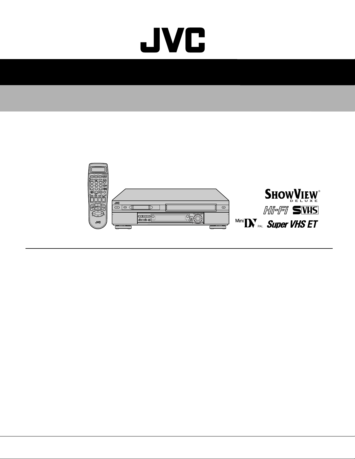
Mini DV/S-VHS VIDEO CASSETTE RECORDER
SR-VS30E/EK
TV
VHSDV
CABLE/SAT
– –:– –
LCD PROG
1
AUDIO
TV/VCR
2
123
3
456
DAILY/QTDN.
VPS/PDC
WEEKLY/HEBDO
4
789
4
0000
AUX
MENU
0
ENTER/ENTREE
OK
1
PROG
30
SEC
3
2
START
STOP
DATE
PR
DEBUT
FIN
EXPRESS
P
V
R
T
+
+
T
V
–
PULL-OPEN
TIRER-OUVRIR
V
T
–
T
R
V
P
DV
DUB
VHS
DV
COPIE
PR / +
PUSH / TURN
VHS
EXPRESS
1
24H
32
PULL-OPEN
TIRER-OUVRIR
625
SPECIFICATIONS
GENERAL
Power requirement : AC 220 V - 240 Vd, 50 Hz/60 Hz
Power consumption
Power on : 31 W
Power off : 6.5 W
Temperature
Operating :
Storage :
Operating position : Horizontal only
Dimensions (WxHxD)
Weight : 5.1 kg
Input/Output : 21-pin SCART connectors:
VHS DECK VIDEO/AUDIO
Signal system : PAL-type colour signal and CCIR
Recording system : DA4 (Double Azimuth) head helical
Format : S-VHS/VHS PAL standard
Signal-to-noise ratio: 45 dB
Horizontal resolution
(SP/LP) : 250 lines (VHS)
Frequency range : 70 Hz to 10,000 Hz (Normal audio)
Maximum recording time
(SP) : 240 min. with E-240 video cassette
(LP) : 480 min. with E-240 video cassette
5°C to 40°C
–20°C to 60°C
: 435 mm x 106 mm x 380 mm
IN/OUT x 1, IN/DECODER x 1
RCA connectors:
VIDEO IN x 1, AUDIO IN x 1,
AUDIO OUT x 1
S-Video connectors:
IN x 1, OUT x 1
DV connector:
IN/OUT x 1 (4-pin, IEEE1394
conformity, digital input/output)
monochrome signal, 625 lines
50 fields
scan system
400 lines (S-VHS)
20 Hz to 20,000 Hz (Hi-Fi audio)
(The specifications shown pertain specifically to the model SR-VS30E.)
DV DECK VIDEO/AUDIO
Signal system : PAL-type colour signal, 625 lines
Recording system : Digital Component Recording
Format : DV format (SD mode)
Cassette : Mini DV Cassette
Maximum recording time
(SP) : 80 min. with M-DV80ME cassette
(LP) : 120 min. with M-DV80ME cassette
Audio recording system
TUNER/TIMER
TV channel storage capacity
Tuning system : Frequency synthesized tuner
Channel coverage : VHF 47 MHz
Memory backup time
ACCESSORIES
Provided accessories
Specifications shown are for SP mode unless otherwise specified.
E.& O.E. Design and specifications subject to change without
notice.
50 fields
: PCM 48 kHz, 16 bit (2 ch)/
32 kHz, 12 bit (4 ch)
: 99 positions (+AUX position)
–
104 MHz
302 MHz
300 MHz/
–
470 MHz
UHF 470 MHz
: Approx. 10 min.
: RF cable,
21-pin SCART/RCA cable,
BNC/RCA adapter x 2,
Satellite Controller,
Infrared remote control unit,
"R6" battery x 2
–
89 MHz/
–
862 MHz
SR-VS30E/EK V14SD1
This service manual is printed on 100% recycled paper.
COPYRIGHT © 2002 VICTOR COMPANY OF JAPAN, LTD
No.82910
March 2002
Page 2

Page 3

TABLE OF CONTENTS
Section Title Page Section Title Page
Important Safety Precautions
INSTRUCTIONS
1. DISASSEMBLY
1.1 HOW TO REMOVE THE MAJOR PARTS ........................................1-1
1.1.1 Introduction ..................................................................................1-1
1.2 HOW TO READ THE DISASSEMBLY AND ASSEMBLY.................. 1-1
1.3 DISCONNECTION OF CONNECTORS (WIRES) ............................1-1
1.4 HOW TO REMOVE THE MAJOR PARTS <COM section> ..............1-2
1.4.1 Disassembly flow chart ................................................................1-2
1.4.2 Disassembly/assembly method <COM section> ......................... 1-2
1.5 HOW TO REMOVE THE MAJOR PARTS <VHS section> ...............1-4
1.5.1 Disassembly flow chart ................................................................1-4
1.5.2 DIsassembly/assembly method <VHS section> ..........................1-4
1.6 HOW TO REMOVE THE MAJOR PARTS <DV section>..................1-6
1.6.1 Disassembly flow chart ................................................................1-6
1.6.2 Disassembly/assembly method <DV section> .............................1-6
1.7 CONNECTION ..................................................................................1-8
1.8 SERVICE POSITIONS.................................................................... 1-10
1.8.1 Requirement PATCH CORDS....................................................1-10
1.8.2 Service position <VHS SIDE>.................................................... 1-10
1.8.3 Service position <DV FOIL SIDE> .............................................1-10
1.8.4 Service position <DV COMPONENT SIDE>.............................. 1-1 1
1.9 Jig RCU mode................................................................................. 1-11
1.9.1 Setting the Jig RCU mode ......................................................... 1-11
1.9.2 Setting the User RCU mode ...................................................... 1-11
1.10 MECHANISM SERVICE MODE ................................................... 1-12
1.10.1 How to set the “MECHANISM SERVICE MODE” .................... 1-12
1.11 EMERGENCY DISPLAY FUNCTION............................................1-13
1.11.1 Displaying the emergency information .....................................1-13
1.11.2 Clearing the emergency history ...............................................1-13
1.11.3 Emergency content description................................................ 1-14
1.11.4 Emergency detail information <1> ...........................................1-15
1.11.5 Emergency detail information <2> ...........................................1-16
2. MECHANISM ADJUSTMENT (VHS)
2.1 BEFORE STARTING REPAIR AND ADJUSTMENT .........................2-1
2.1.1 Precautions .................................................................................. 2-1
2.1.2 Checking for Proper Mechanical Operations ...............................2-1
2.1.3 Manually Removing the Cassette Tape ....................................... 2-1
2.1.4 Jigs and Tools Required for Adjustment.......................................2-2
2.1.5 Maintenance and Inspection ........................................................ 2-3
2.2 REPLACEMENT OF MAJOR PARTS ............................................... 2-6
2.2.1 Before Starting Disassembling
(Phase matching between mechanical parts) ...............................2-6
2.2.2 How to Set the Mechanism Assembling Mode.............................2-6
2.2.3 Cassette Holder Assembly........................................................... 2-6
2.2.4 Pinch Roller Arm Assembly .......................................................... 2-8
2.2.5 Guide Arm Assembly and Press Lever Assembly ........................ 2-8
2.2.6 Audio Control Head...................................................................... 2-8
2.2.7 Loading Motor .............................................................................. 2-8
2.2.8 Capstan Motor .............................................................................2-9
2.2.9 Pole Base Assembly (supply or take-up side)..............................2-9
2.2.10 Rotary Encoder ........................................................................ 2-10
2.2.11 Clutch Unit................................................................................2-10
2.2.12 Change Lever Assembly, Direct Gear, Clutch Gear
and Coupling Gear.................................................................... 2-10
2.2.13 Link Lever ................................................................................ 2-11
2.2.14 Cassette Gear, Control Cam and Worm Gear ......................... 2-11
2.2.15 Control Plate ............................................................................ 2-11
2.2.16 Loading Arm Gear (supply or take-up side)
and Loading Arm Gear Shaft .................................................... 2-12
Take-up Lever, Take-up Head and Control Plate Guide ..................
2.2.17
2.2.18 Capstan Brake Assembly......................................................... 2-13
2.2.19 Sub Brake Assembly (take-up side)......................................... 2-13
2.2.20 Main Brake Assembly (take-up side),
Reel Disk (take-up side)
and Main Brake Assembly (supply side)................................... 2-13
2.2.21 Tension Brake Assembly, Reel Disk (supply side)
and Tension Arm Assembly....................................................... 2-14
2.2.22 Idler Lever, Idler Arm Assembly ...............................................2-14
2.2.23 Stator Assembly .......................................................................2-14
2.2.24 Rotor Assembly........................................................................ 2-14
2.2.25 Upper Drum Assembly .............................................................2-15
2.3 COMPATIBILITY ADJUSTMENT .................................................. 2-16
2.3.1 Checking/Adjustment of FM Waveform Linearity .......................2-16
Checking/Adjustment of the Height and Tilt of the Audio Control Head ....................
2.3.2
Checking/Adjustment of the Audio Control Head Phase (X-Value) ...............
2.3.3
2.3.4 Checking/Adjustment of the Standard Tracking Preset .............2-18
2.3.5 Checking/Adjustment of the Tension Pole Position....................2-18
MECHANISM ADJUSTMENT (DV)
2.4 PREPARATION...............................................................................2-20
2.4.1 Precautions ................................................................................ 2-20
2.4.2 Tools Required for Adjustments .................................................2-20
2.4.3 Disassembly and Assembly Procedures.................................... 2-20
2.4.4 Screws and Washers Used in Disassembly/
Assembly of the Mechanism Assembly......................................2-20
DISASSEMBLY/ASSEMBLY OF THE MECHANISM ASSEMBLY...................
2.5
2.5.1 Introduction ................................................................................2-21
2.5.2 Mechanism Modes .....................................................................2-21
2.6 MECHANISM TIMING CHART ....................................................... 2-23
MECHANISM ASSEMBLY/DISASSEMBLY PROCEDURE TABLE ..................
2.7
2.8 DISASSEMBLY/ASSEMBLY...........................................................2-26
2.9 LIST OF PROCEDURES FOR DISASSEMBLY ............................. 2-34
2.10 MECHANISM PHASE CHECK/ADJUSTMENT ............................ 2-35
2.11 MECHANISM DISASSEMBLY/ASSEMBLY SHEET.....................2-36
2-13
2-17
2-17
2-21
2-24
2.12 POSITIONING THE TENSION POLE........................................... 2-38
COMPATIBILITY AND ERROR RATE ADJUSTMENTS .................
2.13
2.13.1 Preparation ..............................................................................2-39
2.13.2 Adjustment ............................................................................... 2-39
2.13.3 Linearity adjustment .................................................................2-40
2.13.4 PB switching point adjustment ................................................. 2-40
2.13.5 Error rate adjustment ...............................................................2-40
2.13.6 Error rate measuring method ................................................... 2-40
2.14 TAPE EJECTION ..........................................................................2-41
3. ELECTRICAL ADJUSTMENT (VHS)
3.1 PRECAUTION ..................................................................................3-1
3.1.1 Required test equipments ............................................................ 3-1
3.1.2 Required adjustment tools ...........................................................3-1
3.1.3 Color (colour) bar signal,Color (colour) bar pattern ..................... 3-1
3.1.4 Switch settings and standard precautions ...................................3-1
3.1.5 EVR Adjustment........................................................................... 3-1
3.2 SERVO CIRCUIT ..............................................................................3-2
3.2.1 Switching point .............................................................................3-2
3.2.2 Slow tracking preset..................................................................... 3-2
3.3 VIDEO CIRCUIT ...............................................................................3-2
3.3.1 D/A level .......................................................................................3-2
3.3.2 EE Y/PB Y (S-VHS/VHS) level.....................................................3-2
3.3.3 REC color (colour) level ............................................................... 3-3
3.3.5 Video EQ (Frequency response) .................................................3-3
3.3.6 AUTO PICTURE initial setting......................................................3-4
3.3.6 DV EE Y level...............................................................................3-4
3.4 AUDIO CIRCUIT ...............................................................................3-4
3.4.1 Audio REC FM ............................................................................. 3-4
3.5 SYSCON CIRCUIT ...........................................................................3-4
3.5.1 Timer clock................................................................................... 3-4
ELECTRICAL ADJUSTMENT (DV)
3.6 PREPARATION.................................................................................3-5
3.6.1 Precautions .................................................................................. 3-5
3.6.2 Equipment required for adjustment ..............................................3-5
3.6.3 Tools required for adjustments ..................................................... 3-5
3.6.4 Setup............................................................................................ 3-5
4. CHARTS AND DIAGRAMS
NOTES OF SCHEMATIC DIAGRAM..................................................... 4-1
CIRCUIT BOARD NOTES ..................................................................... 4-2
4.1 BOARD INTERCONNECTIONS .......................................................4-3
4.2 SWITCHING REGULATOR SCHEMATIC DIAGRAM.......................4-5
4.3 MAIN (VIDEO/AUDIO) SCHEMATIC DIAGRAM .............................. 4-7
4.4 MAIN (VHS SYSCON) SCHEMATIC DIAGRAM .............................. 4-9
4.5 MAIN (TUNER) SCHEMATIC DIAGRAM ....................................... 4-11
MAIN (VIDEO I/O & SUB EMPHA) SCHEMATIC DIAGRAM ..................
4.6
4.7 MAIN (AUDIO I/O) SCHEMATIC DIAGRAM...................................4-15
4.8 MAIN (CONNECTION) SCHEMATIC DIAGRAM............................4-17
4.9 3D DIGITAL/2M SCHEMATIC DIAGRAM ....................................... 4-19
4.10 TERMINAL (S-SUB) SCHEMATIC DIAGRAM .............................. 4-21
4.11 TERMINAL (I/O) SCHEMATIC DIAGRAM ....................................4-23
4.12 DEMODULATOR SCHEMATIC DIAGRAM...................................4-25
POWER SW, SW/DISPLAY AND JOG SCHEMATIC DIAGRAMS...................
4.13
4.14 DV MSD SCHEMATIC DIAGRAM ................................................ 4-29
4.15 DV MAIN SCHEMATIC DIAGRAM ............................................... 4-31
4.16 DV I/O SCHEMATIC DIAGRAM ...................................................4-33
4.17 DV V OUT SCHEMATIC DIAGRAM ............................................. 4-35
4.18 DV PRE/REC SCHEMATIC DIAGRAM ........................................ 4-37
4.19 DV REG SCHEMATIC DIAGRAM ................................................4-39
4.20 DV AUDIO AD/DA SCHEMATIC DIAGRAM .................................4-40
4.21 MAIN(ON SCREEN) SCHEMATIC DIAGRAM .............................4-41
4.22 REMOTE CONTROL SCHEMATIC DIAGRAM ............................ 4-42
4.23 SWITCHING REGULATOR CIRCUIT BOARD .............................4-43
4.24 MAIN CIRCUIT BOARD................................................................ 4-45
4.25 3D DIGITAL/2M CIRCUIT BOARD ............................................... 4-48
DEMODULATOR POWER SW, SW/DISPLAY AND JOG CIRCUIT BOARDS ...
4.26
4.27 TERMINAL CIRCUIT BOARD.......................................................4-51
4.28 DV MAIN CIRCUIT BOARD.......................................................... 4-53
4.29 WAVEFORMS ............................................................................... 4-55
4.30 VOLTAGE CHARTS......................................................................4-57
FDP GRID ASSIGNMENT AND ANODE CONNECTION .................
4.31
4.32 CPU PIN FUNCTION ....................................................................4-60
4.33 SYSTEM CONTROL BLOCK DIAGRAM (VHS) ........................... 4-61
4.34 VIDEO BLOCK DIAGRAM(VHS) .................................................. 4-63
4.35 AUDIO BLOCK DIAGRAM (VHS) .................................................4-67
4.36 SYSTEM CONTROL BLOCK DIAGRAM (DV) .............................4-69
4.37 VIDEO BLOCK DIAGRAM (DV) ...................................................4-71
5. PARTS LIST
5.1 PACKING AND ACCESSORY ASSEMBLY <M1> ............................ 5-1
5.2 FINAL ASSEMBLY <M2>..................................................................5-2
5.3 MECHANISM ASSEMBLY (VHS) <M3> ...........................................5-4
5.4 MECHANISM ASSEMBLY (DV) <M4>..............................................5-6
5.5 ELECTRICAL PARTS LIST...............................................................5-8
SW REGULATOR BOARD ASSEMBLY <01> ........................................ 5-8
MAIN BOARD ASSEMBLY <03> ............................................................5-9
3D DIGITAL/2M BOARD ASSEMBLY <05>..........................................5-17
TERMINAL BOARD ASSEMBLY <06> ................................................. 5-19
AUDIO CONTROL HEAD BOARD ASSEMBLY <12> ..........................5-20
DEMOD BOARD ASSEMBLY <14>......................................................5-20
POWER SW BOARD ASSEMBLY <27>...............................................5-21
SW/DISPLAY BOARD ASSEMBLY <28> .............................................5-21
DV MAIN BOARD ASSEMBLY <50> ....................................................5-22
LOADING MOTOR BOARD ASSEMBLY <55>.....................................5-27
JOG BOARD ASSEMBLY <85>............................................................5-27
2-39
4-13
4-27
4-49
4-59
The following table lists the differing points between models SR-VS30EK and SR-VS30E.
ITEM
MODEL
SR-VS30EK
SR-VS30E
POWER PLUG 3PIN(CLASS II) CEE(CLASSII)
VIDEO SYSTEM PAL/NTSC ON PAL TV PAL/MESECAM(MANUAL)/NTSC ON PAL TV
BROADCASTING STANDARD I B/G, D/K
STEREO DECODER NICAM NICAM/A2
VCR PLUS+
VIDEO PLUS+ DELUXE
SHOWVIEW DELUXE
LANGUAGE[INITIAL](ON SCREEN DISPLAY) ENGLISH 10 LANGUAGE [E]
Page 4
Important Safety Precautions
cut close to connector
Prior to shipment from the factory, JVC products are strictly inspected to conform with the recognized product safety and electrical codes
of the countries in which they are to be sold. However, in order to maintain such compliance, it is equally important to implement the
following precautions when a set is being serviced.
v
Precautions during Servicing
1. Locations requiring special caution are denoted by labels and
inscriptions on the cabinet, chassis and certain parts of the
product. When performing service, be sure to read and comply with these and other cautionary notices appearing in the
operation and service manuals.
2. Parts identified by the
critical for safety.
Replace only with specified part numbers.
Note: Parts in this category also include those specified to com-
ply with X-ray emission standards for products using
cathode ray tubes and those specified for compliance
with various regulations regarding spurious radiation
emission.
3. Fuse replacement caution notice.
Caution for continued protection against fire hazard.
Replace only with same type and rated fuse(s) as specified.
4. Use specified internal wiring. Note especially:
1) Wires covered with PVC tubing
2) Double insulated wires
3) High voltage leads
5. Use specified insulating materials for hazardous live parts.
Note especially:
1) Insulation Tape 3) Spacers 5) Barrier
2) PVC tubing 4) Insulation sheets for transistors
6. When replacing AC primary side components (transformers,
power cords, noise blocking capacitors, etc.) wrap ends of
wires securely about the terminals before soldering.
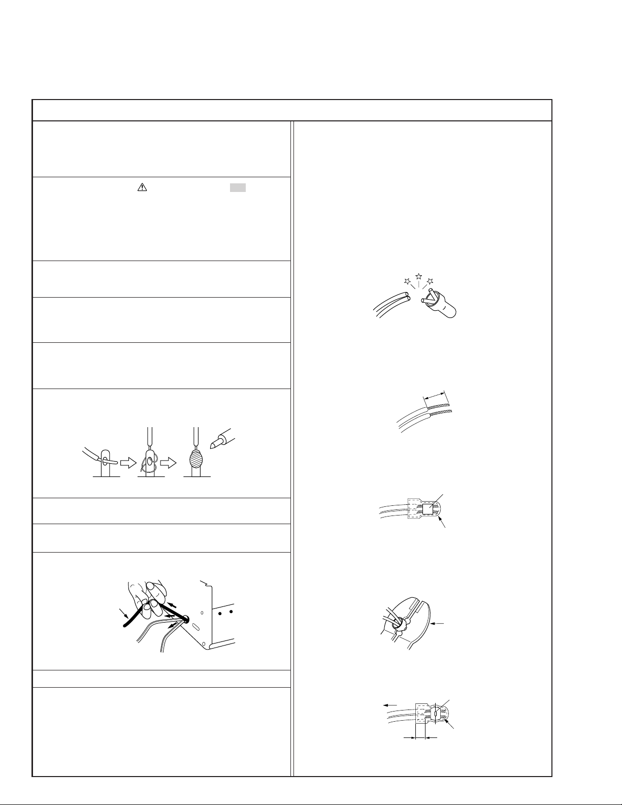
symbol and shaded ( ) parts are
12. Crimp type wire connector
In such cases as when replacing the power transformer in sets
where the connections between the power cord and power
transformer primary lead wires are performed using crimp type
connectors, if replacing the connectors is unavoidable, in order to prevent safety hazards, perform carefully and precisely
according to the following steps.
1) Connector part number : E03830-001
2) Required tool : Connector crimping tool of the proper type
which will not damage insulated parts.
3) Replacement procedure
(1) Remove the old connector by cutting the wires at a point
close to the connector.
Important : Do not reuse a connector (discard it).
Fig.3
(2) Strip about 15 mm of the insulation from the ends of
the wires. If the wires are stranded, twist the strands to
avoid frayed conductors.
15 mm
Fig.1
7. Observe that wires do not contact heat producing parts
(heatsinks, oxide metal film resistors, fusible resistors, etc.)
8. Check that replaced wires do not contact sharp edged or
pointed parts.
9. When a power cord has been replaced, check that 10-15 kg of
force in any direction will not loosen it.
Power cord
Fig.2
10. Also check areas surrounding repaired locations.
11. Products using cathode ray tubes (CRTs)
In regard to such products, the cathode ray tubes themselves,
the high voltage circuits, and related circuits are specified for
compliance with recognized codes pertaining to X-ray emission.
Consequently, when servicing these products, replace the cathode ray tubes and other parts with only the specified parts.
Under no circumstances attempt to modify these circuits.
Unauthorized modification can increase the high voltage value
and cause X-ray emission from the cathode ray tube.
Fig.4
(3) Align the lengths of the wires to be connected. Insert
the wires fully into the connector.
Metal sleeve
Connector
Fig.5
(4) As shown in Fig.6, use the crimping tool to crimp the
metal sleeve at the center position. Be sure to crimp fully
to the complete closure of the tool.
1.25
2.0
5.5
Fig.6
(5) Check the four points noted in Fig.7.
Not easily pulled free
Wire insulation recessed
more than 4 mm
Fig.7
Crimping tool
Crimped at approx. center
of metal sleeve
Conductors extended
1
S40888-01
Page 5
v
d'
d
Chassis
Power cord,
primary wire
Safety Check after Servicing
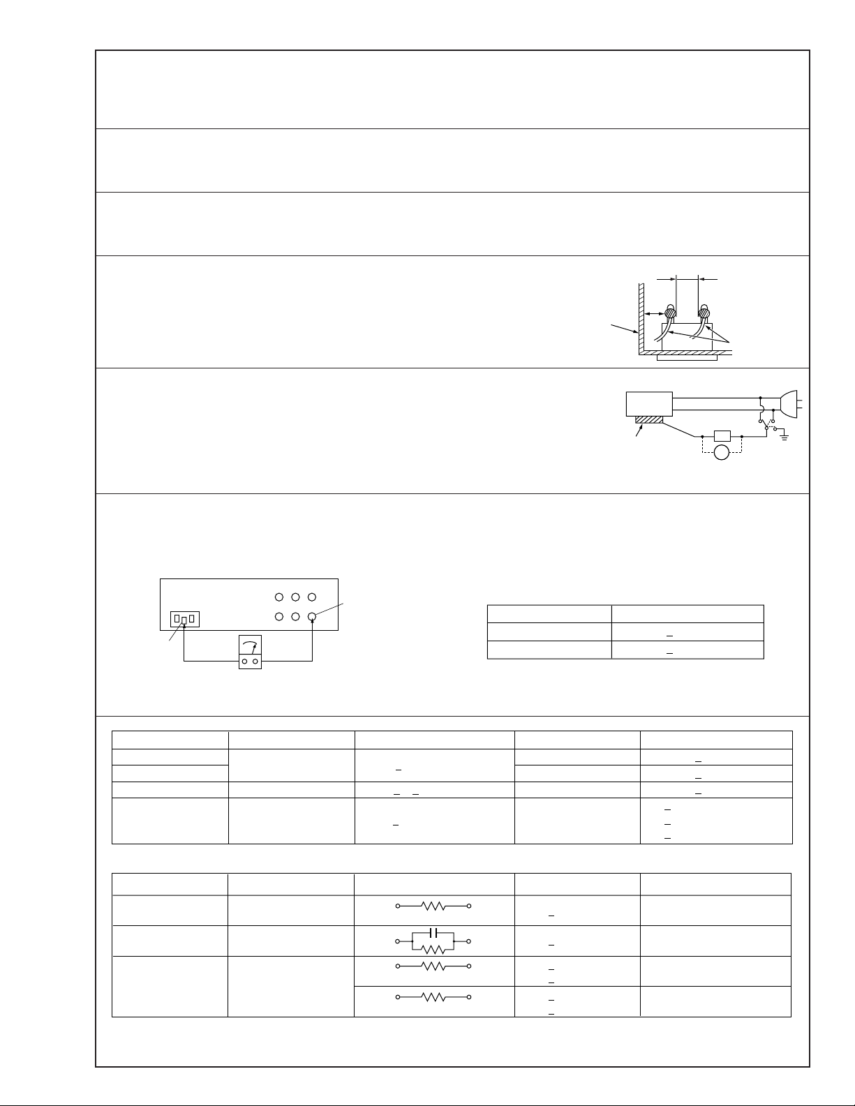
Examine the area surrounding the repaired location for damage or deterioration. Observe that screws, parts and wires have been
returned to original positions, Afterwards, perform the following tests and confirm the specified values in order to verify compliance with safety standards.
1. Insulation resistance test
Confirm the specified insulation resistance or greater between power cord plug prongs and
externally exposed parts of the set (RF terminals, antenna terminals, video and audio input
and output terminals, microphone jacks, earphone jacks, etc.). See table 1 below.
2. Dielectric strength test
Confirm specified dielectric strength or greater between power cord plug prongs and exposed
accessible parts of the set (RF terminals, antenna terminals, video and audio input and output
terminals, microphone jacks, earphone jacks, etc.). See table 1 below.
3. Clearance distance
When replacing primary circuit components, confirm specified clearance distance (d), (d’) between soldered terminals, and between terminals and surrounding metallic parts. See table 1
below.
Fig. 8
4. Leakage current test
Confirm specified or lower leakage current between earth ground/power cord plug prongs
and externally exposed accessible parts (RF terminals, antenna terminals, video and audio
input and output terminals, microphone jacks, earphone jacks, etc.).
Measuring Method : (Power ON)
Insert load Z between earth ground/power cord plug prongs and externally exposed accessible parts. Use an AC voltmeter to measure across both terminals of load Z. See figure 9 and
following table 2.
Externally
exposed
accessible part
Z
V
Fig. 9
ab
c
5. Grounding (Class 1 model only)
Confirm specified or lower grounding impedance between earth pin in AC inlet and externally exposed accessible parts (Video in,
Video out, Audio in, Audio out or Fixing screw etc.).
Measuring Method:
Connect milli ohm meter between earth pin in AC inlet and exposed accessible parts. See figure 10 and grounding specifications.
AC inlet
Earth pin
AC Line Voltage
100 V
100 to 240 V
110 to 130 V
110 to 130 V
200 to 240 V
Exposed accessible part
Milli ohm meter
Fig. 10
Region
Japan
USA & Canada
Europe & Australia R 10 MΩ/500 V DC
Region Load Z
Insulation Resistance (R)
≤
R 1 MΩ/500 V DC
≥≥
1 MΩ R 12 MΩ/500 V DC
≤
Table 1 Specifications for each region
Grounding Specifications
Region
USA & Canada
Europe & Australia
Dielectric Strength
AC 1 kV 1 minute
AC 1.5 kV 1 miute
AC 1 kV 1 minute
AC 3 kV 1 minute
AC 1.5 kV 1 minute
(Class 2)
(Class 1)
Grounding Impedance (Z)
≤
Z 0.1 ohm
≤
Z 0.5 ohm
Clearance Distance (d), (d')
≤
d, d' 3 mm
≤
d, d' 4 mm
≤
d, d' 3.2 mm
≤
d 4 mm
≤
d' 8 mm (Power cord)
≤
d' 6 mm (Primary wire)
a, b, cLeakage Current (i)AC Line Voltage
100 V
110 to 130 V
110 to 130 V
220 to 240 V
Note: These tables are unofficial and for reference only. Be sure to confirm the precise values for your particular country and locality.
Japan
USA & Canada
Europe & Australia
Table 2 Leakage current specifications for each region
1 kΩ
0.15 µF
1.5 kΩ
2 kΩ
50 kΩ
2
≤
i 1 mA rms Exposed accessible parts
≤
i 0.5 mA rms
≤
i 0.7 mA peak
≤
i 2 mA dc
≤
i 0.7 mA peak
≤
i 2 mA dc
Exposed accessible parts
Antenna earth terminals
Other terminals
S40888-01
Page 6

Page 7
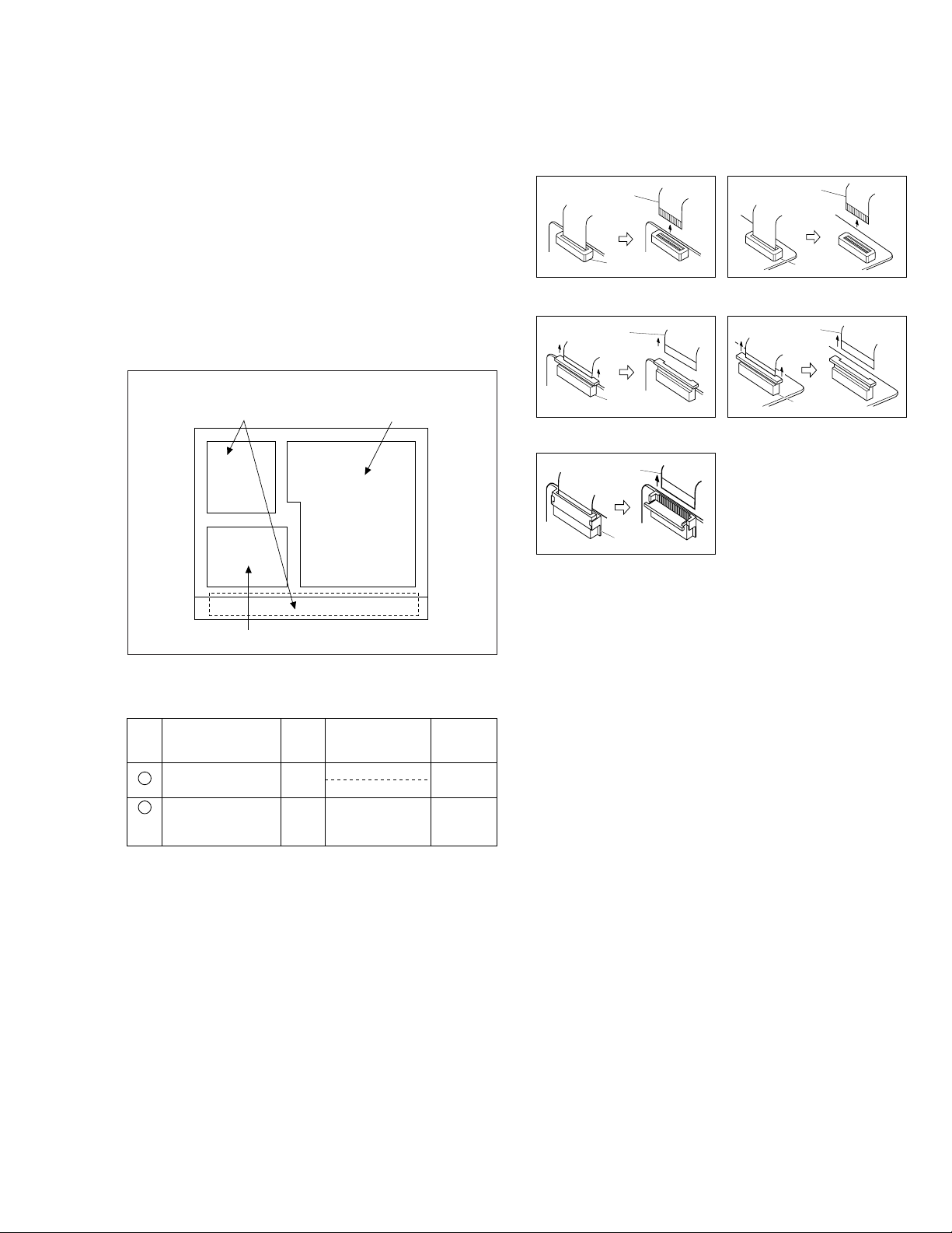
SECTION 1
CONNECTOR
FPC
CONNECTOR
FPC
Fig. 1-3-1 Fig. 1-3-2
Fig. 1-3-3 Fig. 1-3-4
CONNECTOR
FPC
Fig. 1-3-5
CONNECTOR
FPC
CONNECTOR
FPC
DISASSEMBLY
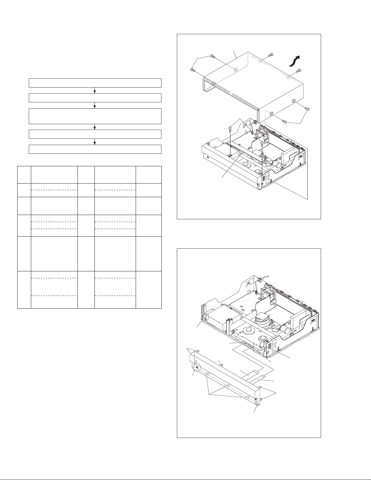
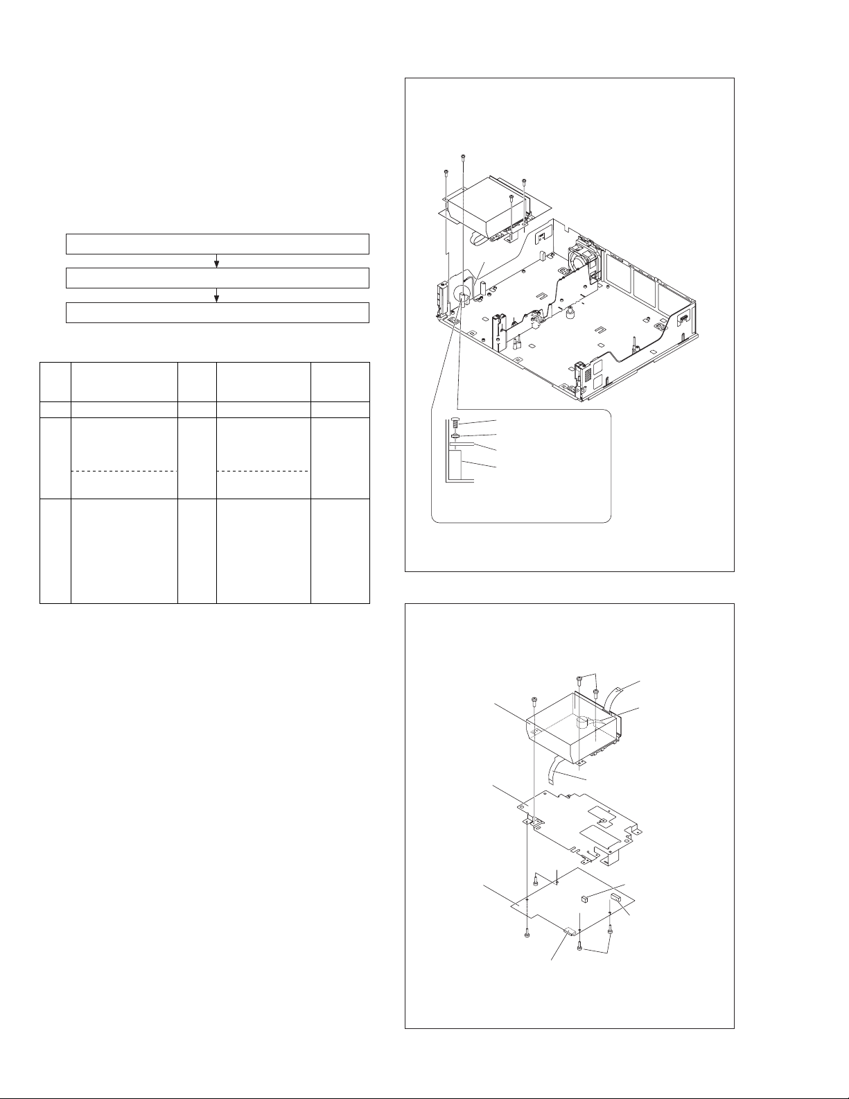
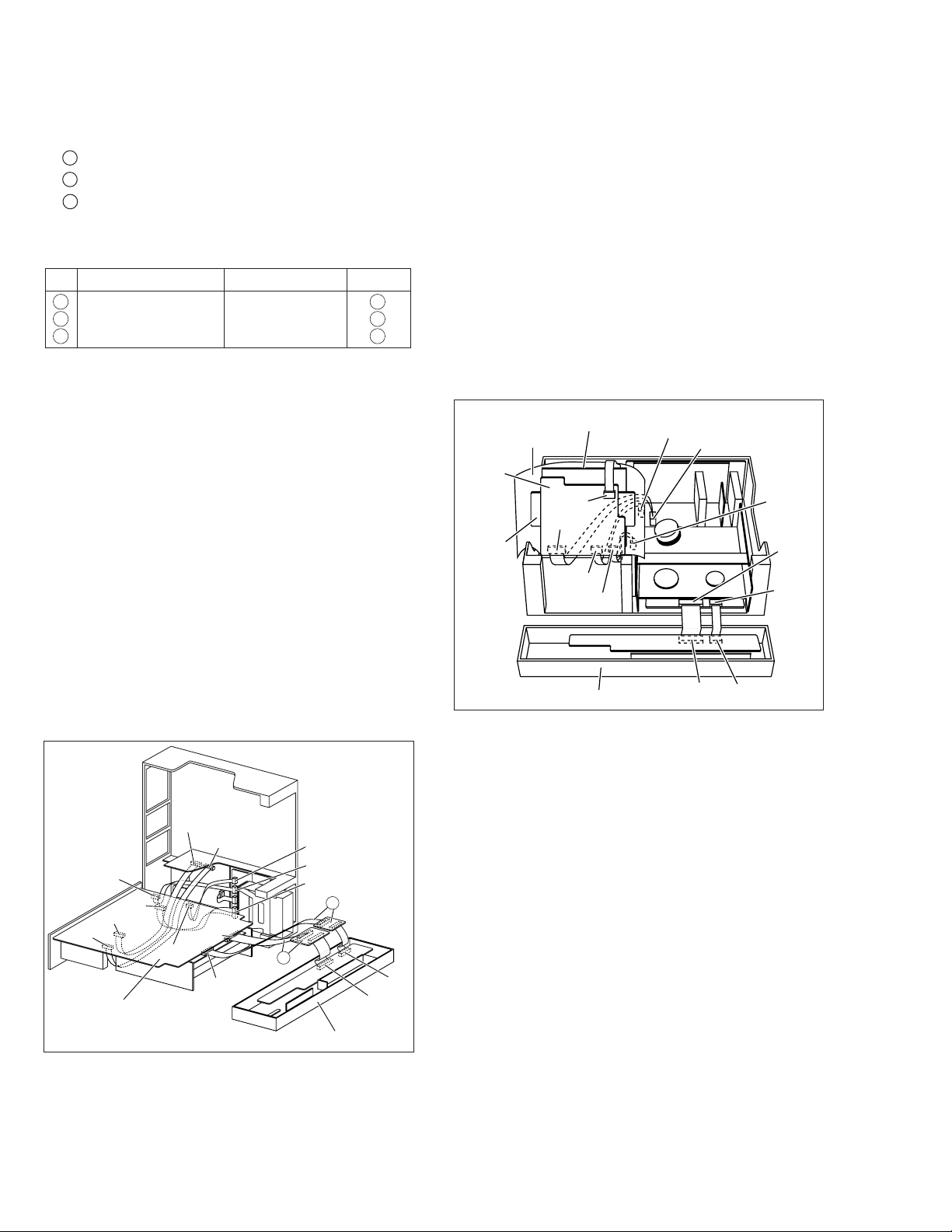
1.1 HOW TO REMOVE THE MAJOR PARTS
1.1.1 Introduction
This set is a double-deck video recorder integrating a Mini DV
deck and a VHS deck. Its internal structure is divided into three
sections that include the power supply, VHS and DV sections.
Therefore, the removal of major parts will also be described
under three separate sections as listed below.
1. COMMON section
2. VHS section
3. DV section
< TOP VIEW >
1. COMMON section
2. VHS section
1.3 DISCONNECTION OF CONNECTORS (WIRES)
3. DV section
Fig. 1-1-1
1.2 HOW TO READ THE DISASSEMBLY AND ASSEMBLY
Step/
Loc No.
1
Top cover, Bracket COM1
Front panel
2
assembly
Fig. No.
COM2 8(L3),
§§ §§ §
(1) (2) (3) (4) (5)
(1) Order of steps in Procedure
When reassembling, perform the step(s) in the reverse order.
These numbers are also used as the identification (location) No.
of parts Figures.
(2) Part name to be removed or installed.
(3) Fig. No. showing procedure or part location.
(4) Identification of part to be removed, unhooked, unlocked,
released, unplugged, unclamped or unsoldered.
P= Spring, W= Washer, S= Screw, L= Locking tab, SD= Solder,
CN**(WR**)= Remove the wire (WR**) from the connector
(CN**).
Note:
• The bracketed ( ) WR of the connector symbol are as-
signed nos. in priority order and do not correspond to
those on the spare parts list.
(5) Adjustment information for installation
Point NotePart name
4(S1), 3(S2), 2(L1), (L2)
2(S3)
CN7507(WR1),
CN3011(WR2)
<Note
1,2,3,4>
—
1-1
Page 8
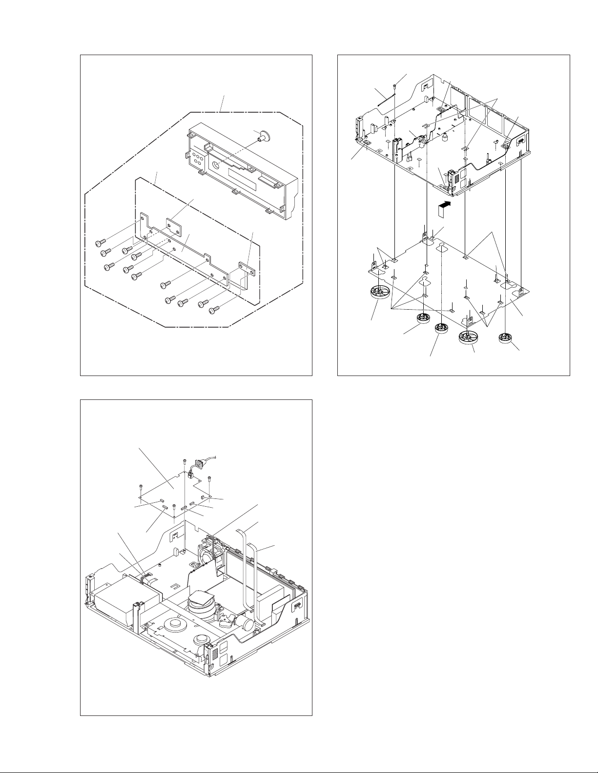
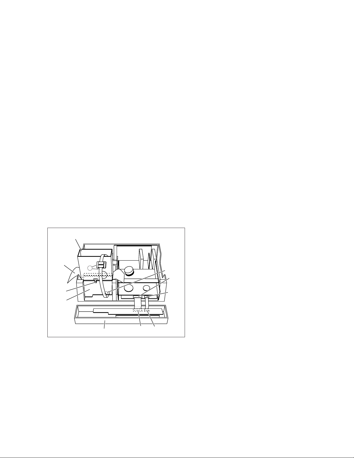
1.4
HOW TO REMOVE THE MAJOR PARTS <COM section>
1.4.1 Disassembly flow chart
This flowchart shows the disassembly procedure for the exterior parts and electrical parts.
Basically, reverse this procedure when assembling them.
[1] Top cover, Bracket
[2] Front panel assembly
(S1a)
[1] Top cover
(S1b)
(S1b)
SW/Display board assembly, Power SW board assembly,
[3]
Jog board assembly
[4] SW REG board assembly
Foot assembly, Foot(center), Foot(rear), Bottom cover
[5]
1.4.2
Disassembly/assembly method <COM section>
Step/
Loc No.
Top cover
[1]
Bracket
Front panel
[2]
assembly
SW/Display board assembly
[3]
Power SW board assembly
Jog board assembly
SW REG board
[4]
assembly
[5]
Foot assembly
Foot(center)
Foot(rear)
Bottom cover
Fig. No.
4(S1a), 2(S1b)
COM1
2(S1c)
COM2 8(L2a),
CN7510(WR2a),
CN3011(WR2b)
COM3 8(S3a)
2(S3b)
2(S3c),Knob(Jog)
COM4 4(S4a),
CN5322(WR4a),
CN5321(WR4b),
CN5325(WR4c),
CN5324(WR4d),
CN5323(WR4e)
(S5a)
COM5Lug wire
5(L5a)
4(L5b), 9(L5c),
2(L5d)
Point NotePart name
—
<Note 2a,
2b, 2c,2d>
—
<Note 2a>
<Note 5a>
<Note 2a>
• When attaching the FPC, be sure to connect it in the correct orientation.
• When attaching the FPC take care that it is not caught.
• When removing or attaching the WIRE/FPC, refer to "1.7
CONNECTION"(page 1-8) at same time.
<Note 2b>
When attaching the Front panel assembly, make sure that
the door openers of both decks (DV, VHS) are in the down
position.
<Note 2c>
When attaching the Front panel assembly, be careful not
to damage the DV terminals.
<Note 2d>
When attaching (WR2a) and (WR2b), insert supporting
long side to connector in the Main board assembly.
<Note 3a>
When attaching Jog board assembly, attach it before SW/
Display board assembly.
<Note 5a>
When removing Bottom cover, remove it after VHS section parts and DV section parts.
<Note 2b>
DV SIDE
(L2a)
DV terminals
<Note 2c>
(L2a)
(S1c)
[1] Bracket
Fig. COM1
CN3011
(L2a)
(WR2b)
<Note 2a, 2b>
[2] Front panel assembly
Fig. COM2
<Note 2b>
CN7510
VHS SIDE
(WR2a)
<Note 2a, 2d>
(L2a)
(S1a)
1-2
Page 9
[2] Front panel assembly
Knob (Jog)
[5] Lug wire
(S5a)
(L5a)
(L5a)
(L5d)
(L5a)
(S3a)
(S3a)
(S3c)
(S3a)
(S3c)
(S3a)
(S3a)
(S3a)
[4] SW.REG board assy
[3]
(S3a)
(S3a)
Fig. COM3
(S4a)
Jog board assembly
<Note 3a>
SW/Display board
assembly
(S3b)
(S3b)
Power SW board
assembly
(L5a)
(L5b)
[5] Foot assy
(L5c)
[5] Foot(center)
[5] Foot(rear)
(L5a)
(L5b)
[5] Foot assy
Fig. COM5
(L5c)
(L5b)
[5] Bottom cover
(L5c)
[5] Foot(rear)
CN5324
(WR4d)
<Note 2a>
(WR4e)
<Note 2a>
(S4a)
CN5323
(S4a)
Fig. COM4
(S4a)
CN5325
CN5322
CN5321
(WR4c)
<Note 2a>
(WR4a)
<Note 2a>
(WR4b)
<Note 2a>
1-3
Page 10
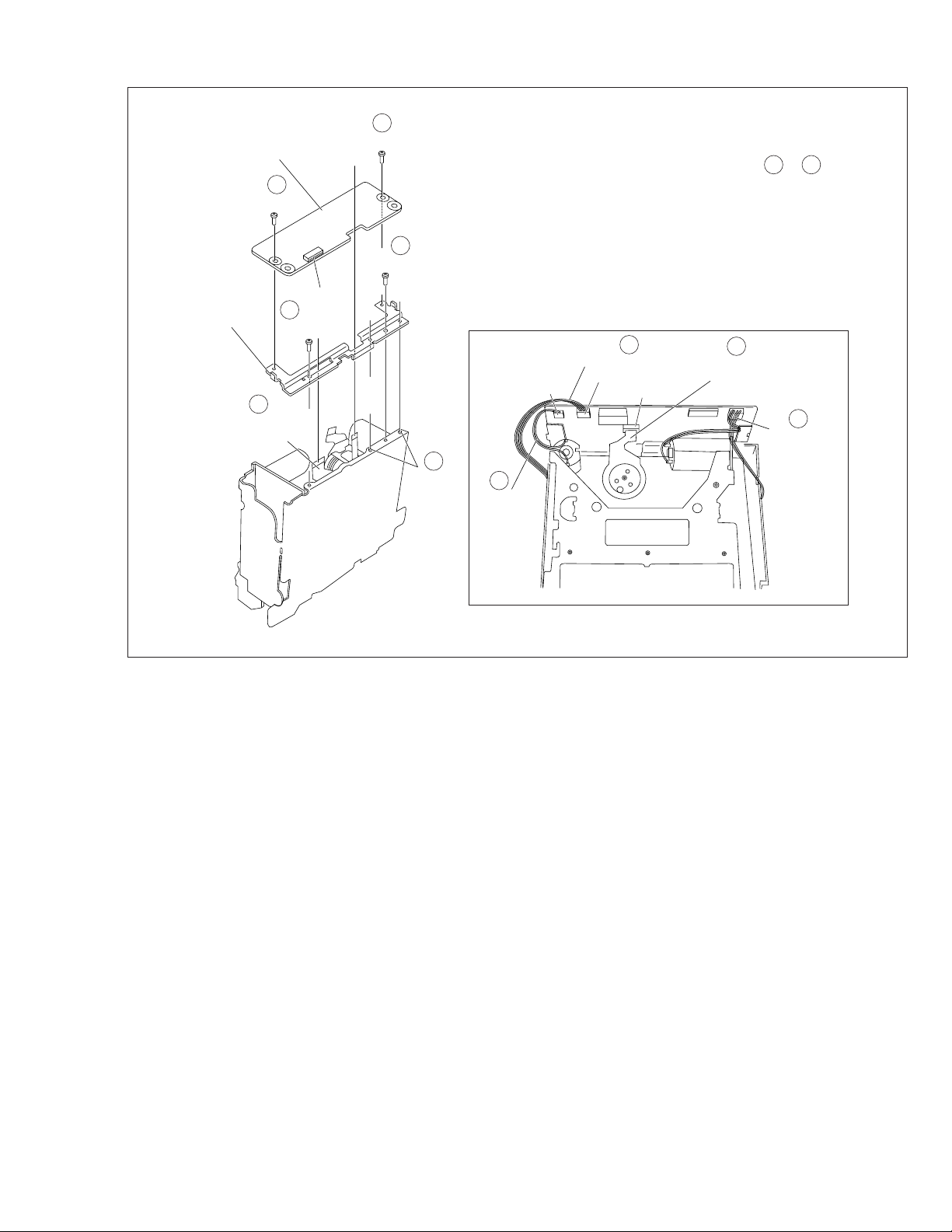
1.5
HOW TO REMOVE THE MAJOR PARTS <VHS section>
1.5.1 Disassembly flow chart
This flowchart shows the disassembly procedure for the exterior parts and electrical parts.
Basically, reverse this procedure when assembling them.
However, it is required to remove the common section parts
as far as [1] “Top cover Bracket” and [2] “Front panel assembly” in advance. (See section 1.4.)
[1] Drum assembly
[2] Mechanism assembly
[3] Main board assembly
1.5.2 DIsassembly/assembly method <VHS section>
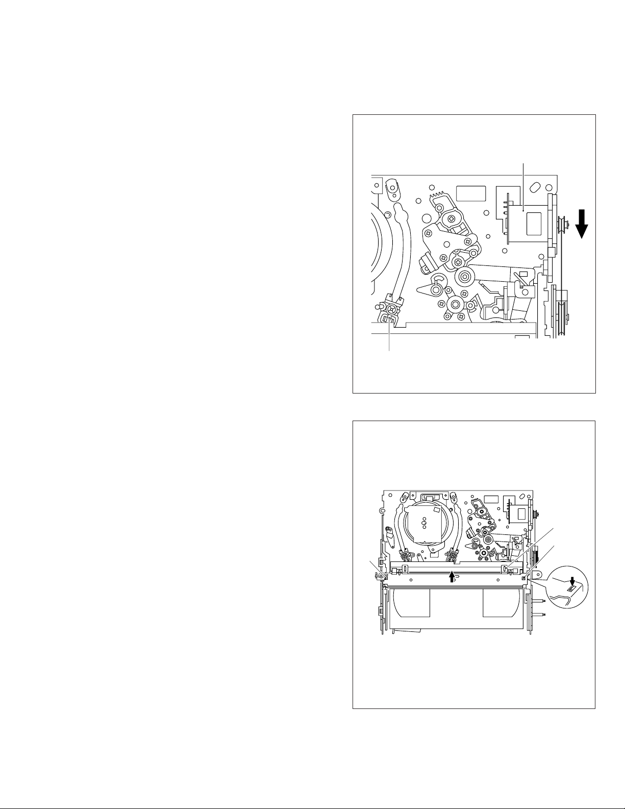
Procedures for Lowering the Cassette holder assembly
As the mechanism of this unit is integrated with the Housing
assembly, the holder must be lowered and the two screws unscrewed when removing the Mechanism assembly.
Fig. 2
Fig. 1
Step/
Loc No.
[1]
Drum assembly
(Inertia plate)
(Roller arm assy)
Mechanism
[2]
assembly
Main board
[3] <Note 1b>
assembly
Fig. No.
V1
V2
V3 (S8a), 6(L8a),
Point NotePart name
CN1(WR6a),
CON1(WR6b),
(S6a), (S6b), (S6c)
4(L6a)
(P6a), (L6b)
(S7a), (S7b), (S7c),
(S7d), 2(L7a),
CN1(WR7a)
CN701(WR8a),
CN2601(WR8b),
CN3014(WR8c)
<Note 1a,1b>
<Note 1b,
2a, 2b, 2c>
<Note 1a>
When attaching or removing the FPC, take care not to disconnect any of the wires.
<Note 1b>
• When attaching the FPC, be sure to connect it in the correct orientation.
• When removing or attaching the WIRE/FPC, refer to "1.7
CONNECTION"(page 1-8) at same time.
<Note 2a>
When it is required to remove the screws ((S7a), (S7b),
(S7c) and (S7d)) retaining the Mechanism assembly , please
refer to the “Procedures for Lowering the Cassette holder
assembly”(See on page 1-4).
<Note 2b>
• When reattaching the Mechanism assembly to the Main
board assembly, take care not to damage the sensors on
the Main board assembly (D3001: LED, Q3002: Start sensor, Q3003: End sensor, S3002: S cassette switch).
• When reattaching the Mechanism assembly to the Main
board assembly, CN2 of LOADING MOTOR BOARD
should not be floated.
Fig. 3
Turn the loading motor pulley in the direction as indicated by
Fig.2. As both A and B levers are lodged twice, push the
levers in the direction as indicated by Fig.3 to release them.
When pushing the levers, do it in the order of A , B , B , A .
When the holder has been lowered, turn the pulley until the
cassette holder is securely in place without allowing any up/
down movement.
Procedures for Lowering the Cassette holder assembly
Note: When installing the Drum assembly, secure the screws
(S6a to S6c) in the order of a, b, c.
Inertia plate
(S6c)
Roller arm
assy
(S6a)
(L6a)
(P6a)
(L6b)
[1]
Drum
assembly
CON1
CN1
(WR6b)
<Note 1b>
(S6b)
(WR6a)
<Note 1a,1b>
Cleaner assy
(L6c)
Not used
<Note 2c>
• When removing the Mechanism assembly only, unhook the
two spacers connecting it with the Main board assembly
with pliers from the back side of the Main board assembly
first, and then remove the Mechanism assembly.
1-4
Fig. V1
Page 11
Note:
(S8a)
(L8a)
(L8a)
CN2601
CN701
CN3014
[3] Main board
assembly
(WR8a)
<Note 1b>
(WR8b)
<Note 1b>
(WR8c)
<Note 1b>
Make a crease on the position where
the dotted line is not exceeded.
A/C head base
(WR7a)
Note:
When installing the
Mechanism assembly,
secure the screws
(S7a to S7b) in the
order of a, b.
[2]
Mechanism
assembly
(S7b)
<Note 2a>
(L7a)
spacer
<Note 2c>
(S7d)
Q3003
Q3003
End sensor
<Note 2b>
D3001
(WR7a)
<Note 1b>
CN2
(S7a)
<Note 2a>
CN1
Q3002
S3002
S3002
S cassette switch
<Note 2b>
CN2
<Note 2b>
(S7c)
D3001
LED
<Note 2b>
<Note 2c>
Q3002
Start sensor
<Note 2b>
(L7a)
spacer
Fig. V3
Fig. V2
1-5
Page 12
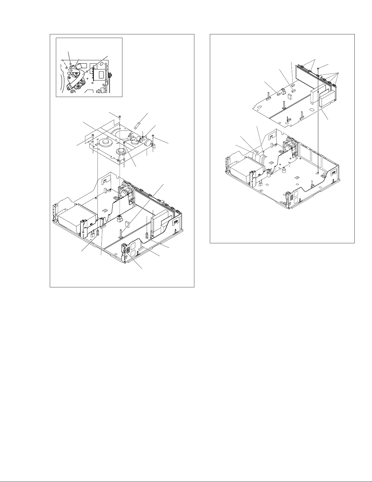
1.6
HOW TO REMOVE THE MAJOR PARTS <DV section>
1.6.1 Disassembly flow chart
This flowchart shows the disassembly procedure for the exterior parts and electrical parts.
Basically, reverse this procedure when assembling them.
However, it is required to remove the common section parts
as far as [1] “Top cover, Bracket” and [2] “Front panel assembly” in advance. (See section 1.5.)
(S9b)
(S9a)
(S9a)
(S9a)
[1] Base(DV)
[2] DV Mechanisam assembly, DV Main board assembly
[3] DV MDA board assembly
1.6.2 Disassembly/assembly method <DV section>
Step/
Loc No.
[1]
[2]
[3]
Base(DV)
DV Mechanism
assembly
DV Main board
assembly
DV MDA board
assembly
Fig. No.
D1 3(S9a), (S9b)
D2 3(S10a),
D3 2(S11a), 2(S11b),
Point NotePart name
CN1502(WR10a),
CN4001(WR10b)
CN1501(WR10c)
4(S10b)
2(L11a),
CN5503(WR11a),
CN5504(WR11b),
CN5502(WR11c),
CN5505(WR11d),
CN5507(WR11e),
Bracket(MDA)
<Note 1a>
<Note 2a,
2b, 2c>
<Note 2c>
<Note 1a>
With due regard to operational considerations, remove the
parts located on the Base(DV) (i.e. DV Mechanism assembly, DV MDA board assembly etc.) together before removing the major parts.
<Note 2a>
Take care not to scratch or damage the drum assembly
by the cleaner assembly when performing work.
<Note 2b>
Take care not to damage the board assembly when detaching parts.
<Note 2c>
• When attaching the FPC, be sure to connect it in the correct orientation.
• When removing or attaching the WIRE/FPC, refer to "1.7
CONNECTION"(page 1-8) at same time.
Lug wire
(S9b)
Lug wire
Base(DV)
Bottom chassis
When reattaching (S9b), attach
in the order of the above figure.
Fig. D1
[2] Mechanism
assembly(DV)
<Note 2a>
[1] Base(DV)
[2] DV Main
board assembly
<Note 2b>
(S10a)
(S10b)
CN1502
(S10a)
(WR10a)
<Note 2c>
CN4001
(WR10c)
<Note 2c>
(WR10b)
<Note 2c>
CN4001
CN1501
1-6
(S10b)
CN1502
(S10b)
Fig. D2
Page 13
[3] DV MDA board assembly
5
(S11a)
CN5504
Bracket(DV)
(WR11b)
<Note 2c>
3
(S11b)
2
5
(S11a)
(S11b)
3
NOTE: When removing, remove in order of a number to .
CN5505
CN5503
1
4
(WR11a)
<Note 2c>
CN5507
3
(L11a)
(WR11d)
<Note 2c>
CN5502
1
(WR11c)
<Note 2c>
1
5
1
(WR11e)
<Note 2c>
Fig. D3
1-7
Page 14
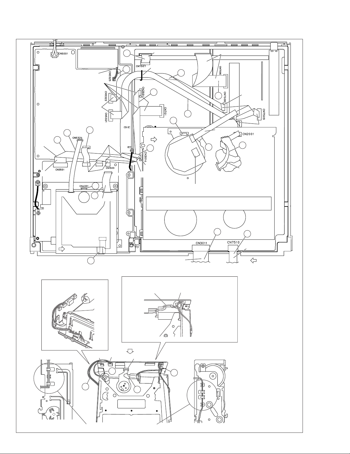
1.7 CONNECTION
Treat the wire so as not to come to fan.
right side
7
CN5323
CN1001
right side
bend
right side
6
11
CN5501
DV DRUM
FAN
bend
CN3701
18
14
bend
CN5506
back side
CN1501
16
right side
TERMINAL PWB
5
Hold wire by stylepin.
3
ST2
12
right side
CN502CN901
right side
15
right side
make a crease
4
8
CN1
right side
CN3001
right side
A
10
right side
A/C HEAD
bend
13
back side
DRUM
Should be confirmed that wire not
touch to IC of STATOR PWB ASS'Y.
9
B
17
NOTE) Wire the wires as
shown in a figure.
21
CN1502
CN5502
NOTE) Wire the wires as shown in a figure.
NOTE) Put the surplus
wire into this space.
"D"
CN5505
22
CN5503
19
CN5507
back side
To SW/Display board
CN7001
NOTE) Twist a wire one time.
20
2
To SW/Display board
CN7191
1
back side
C
1-8
NOTE) Wire the wires as shown in a figure.
Fig. 1-7-1
Page 15
DETAIL"A"
Absorb the looseness of
the wire in the B part.
B
CN1
MAIN PWB
WIRING for MECHA ADJ
DRUM
DETAIL"B"
DV MAIN
PWB
FINAL WIRING
DV MECHA
CN1502
electrode side
Push into the BOTTOM CHASSIS
and treat the wire according
to the following figure.
BOTTOM
CHASSIS
DETAIL"C"
FRONT
PANEL
Absorb the looseness of the wire
according to the following figure.
BOTTOM CHASSIS
CN7510
MAIN PWB
CN3011
DETAIL "D"
DV MDA BOARD ASSEMBLY
CN5504
23
BRACKET(DV)
AC/ HEAD
right side
(WR7a)
AC/ HEAD
right side
After MECHA adjustment,
Treat the wire (WR7a) according
to the following figure.
Make a crease on the position where
the dotted line is not exceeded.
Fig. 1-7-2
Fig
No.
Symbol
Connected point
Connection
Connected point
Pin
No.
Type
(FPC/
WIRE)
1 WR2a MAIN CN7510 SW/DISPLAY CN7191 10 FPC
2 WR2b MAIN CN3011 SW/DISPLAY CN7001 20 FPC
3 WR4a MAIN CN7508 SW/REG CN5322 10 FPC
4 WR4b MAIN CN7509 SW/REG CN5321 12 FPC
5 WR4c SW/REG CN5325 FAN MOTOR - 2 WIRE
6 WR4d SW/REG CN5324 DV MDA CN5501 5 WIRE
7 WR4e SW/REG CN5323 DV MAIN CN1001 8 FPC
8 WR6a MAIN CN1 UPPER DRUM - 13 FPC
9 WR6b DRUM MOTOR CON1 MAIN CN3001 5 FPC
10 WR7a A/C HEAD CN1 MAIN CN2001 7 FPC
11 WR8a MAIN CN701 DV MAIN CN3501 14 FPC
12 WR8b MAIN CN2601 DV MAIN CN3701 8 FPC
13 WR8c MAIN CN3014 DV MAIN CN1503 4 FPC
14 WR10c DV MAIN CN1501 DV MDA CN5506 20 FPC
15 - MAIN CN7506 TERMINAL CN502 15 FPC
16 - MAIN CN7507 TERMINAL CN901 9 FPC
17 WR10a SENSOR(DV) - DV MAIN CN1502 15 FPC
18 WR10b PRE/REC(DRUM)(DV) - DV MAIN CN4001 8 FPC
19 WR11a DRUM MOTOR(DV) - DV MDA CN5503 11 FPC
20 WR11e HOUSING MOTOR(DV) - DV MDA CN5507 4 WIRE
21 WR11d ROTARY ENCODER(DV) - DV MDA CN5505 4 WIRE
22 WR11c LOADING MOTOR(DV) - DV MDA CN5502 2 WIRE
23 WR11b CAPSTAN MOTOR(DV) - DV MDA CN5504 18 FPC
Table 1-7-1
1-9
Page 16
1.8 SERVICE POSITIONS
The servicing locations for use in troubleshooting or servicing of the set are provided separately for the VHS and DV.
I SERVICE POSITIONS <VHS SIDE>
II SERVICE POSITIONS <DV FOIL SIDE>
III SERVICE POSITIONS <DV COMPONENT SIDE>
1.8.1 Requirement PATCH CORDS
The following PATCH CORDS is required.
Board to Board Wire Used
1 PTU94022-10 QUQ212-1040CG I
2 PTU94022-20 QUQ112-2040CG I
3 YTU94074-15 QUQ105-1540AA III
Table 1-8-1
1.8.2 Service position <VHS SIDE>
<Removal>
(1) Remove the top cover and bracket.
(2) Remove the front panel assembly.
(3) Remove the Main board assembly together with the
Mechanism assembly.
< Installation >
(1) Stand up the Bottom chassis assembly so that the DV/
Regulator side is in the lower position.
Note: • Take care to the fall of the Fan.
(2) Connect FPCs and wires accordingly in Fig. 1-8-1.
Point: • Take care that the FPCs and wires are not
subjected to stress in this positioning.
(3) Connect the PATCH CORDS to the two FPCs of the Front
panel assembly, then connect the CORDS to the
CN7510/CN3011.
For the PATCH CORD is required, see Table 1-8-1.
1.8.3 Service position <DV FOIL SIDE>
<Removal>
(1) Remove the top cover and bracket.
(2) Remove the front panel assembly.
(3) Remove the Base(DV) together with DV Mechanism as-
sembly and DV Main board assembly.
Note:
• Take care not to damage the parts during operating.
< Installation >
(1) Place an insulation sheet on the SW/Reg board assem-
bly.
(2) Place a DV section(Base(DV) with DV Mechanism as-
sembly and DV Main board assembly) on the insulation
sheet.(refer to Fig. 1-8-2)
Note:
• Confirm that FPCs and wires are not unconnected from
the connectors.
DV Mechanism
Insulation Sheet
assembly
DV Main board
assembly
CN1502
CN3501
Base(DV)
CN3701
CN1503
Front panel assembly
CN2601
CN701
CN7001
CN3014
CN3011
CN7510
CN7191
Fig. 1-8-2
CN2601
CN7509
Main board assembly
1-10
CN701
CN7508
CN5322
CN3011
CN3014
CN5321
CN7510
Fig. 1-8-1
CN1503
CN3701
CN3501
1
2
CN7191
CN7001
Front panel assembly
Page 17
1.8.4 Service position <DV COMPONENT SIDE>
<Removal>
(1) Remove the top cover and bracket.
(2) Remove the front panel assembly.
(3) Remove the Base(DV) together with DV Mechanism as-
sembly and DV Main board assembly.
(4) Remove the DV Mechanism assembly and DV Main
board assembly from Base(DV).
Note:
• Take care not to damage the parts during operating.
< Installation >
(1) Place a DV Main board assembly on the Bottom chas-
sis.
(2) Place an insulation sheet on the rear side of DV Main
board assembly.
(3) Place a DV Mechanism assembly on the insulation sheet.
Note:
• Confirm that DV Mechanism assembly be getting on on
the insulation sheet completely.
(4) Connect PATCH CORD to the connector(CN1502) and
connect FPC from DV Mechanism assembly.(refer to Fig.
1-8-3)
(5) Connect other FPCs and wires to the connector that cor-
responds each.(refer to "1-7 CONNECTION")
For the PATCH CORD is required, see Table 1-8-1.
Note:
• Confirm that FPCs and wires are not unconnected from
the connectors(especially CN4001).
1.9 Jig RCU mode
This unit uses the following two modes for receiving remote
control codes.
1) User RCU mode : Ordinary mode for use by the user.
2) Jig RCU mode : Mode for use in production and servicing.
When using the Jig RCU, it is required to set the VCR to the Jig
RCU mode (the mode in which codes from the Jig RCU can be
received). As both of the above two modes are stored in the
EEPROM, it is required to set the VCR back to the User RCU
mode each time that an adjustment is made or to check that the
necessary operations have been completed. These modes can be
set by the operations described below.
1.9.1 Setting the Jig RCU mode
(1) Unplug the power cord plug from the power outlet.
(2) Press and hold the “REC” and “PAUSE” buttons on the
VCR simultaneously, while plugging the power cord plug
into the power outlet.
When the VCR is set to the Jig RCU mode, the symbols
( “ : ” ) in the time display of the FDP are turned off.
1.9.2 Setting the User RCU mode
(1) Turn off the power.
(2) Press the “REC” and “PAUSE” buttons of the VCR simul-
taneously. Alternatively, transmit the code “80” from the
Jig RCU.
DV Mechanism
assembly
Insulation Sheet
CN4001
DV Main board
assembly
3
Front panel assembly
Fig. 1-8-3
CN7001
CN1502
CN3011
CN7510
CN7191
1-11
Page 18
1.10 MECHANISM SERVICE MODE
This model has a unique function to enter the mechanism
into every operation mode without loading of any cassette
tape. This function is called the “MECHANISM SERVICE
MODE”.
1.10.1 How to set the "MECHANISM SERVICE MODE"
(1) Disconnect VCR from AC.
(2) Connect TPGND and TP7001 (TEST) on the Display
board assembly with a jump wire.
(3) Connect VCR to AC.
(4) Press the POWER button.
(5) With lock levers A B on the left and right of the Cassette
holder assembly pulled toward the front, slide the holder
in the same direction as the cassette insertion direction.
(For the positions of lock levers A B , refer to the “Procedures for Lowering the Cassette holder assembly” on
page 1-4 of 1.5 HOW TO REMOVE THE MAJOR PARTS
<VHS section>
(6) The cassette holder lowers and, when the loading has
completed, the mechanism enters the desired mode.
bend
right side
DV MAIN BOARD
ASSEMBLY
SW/REG BOARD
ASSEMBLY
CP5321
CN1001
right side
CN5501
DV DRUM
FAN
right side
CP5322
CN5323
CN3701
bend
back side
CP5325
bend
CN5506
CN2001
(JIG CONN.)
CN1501
TERMINAL BOARD ASSEMBLY
right side
TP701
D YV IN
ST2
right side
MAIN BOARD
ASSEMBLY
DRUM
back side
bend
3D DIGITAL/2M BOARD ASSEMBLY
VR701
D YV IN
CN1
CN502CN901
right side
CP3004
right side
VR1401
right side
make a crease
CN3001
right side
A/C HEAD
DEMOD BOARD
ASSEMBLY
right side
CP4001
CP3003
TP111
D.FF
TP4001
CTL. P
TP106
PB. FM
TP2253
A. PB.FM
1-12
DV MDA BOARD
ASSEMBLY
FW7002
DV MECHANISM
ASSEMBLY
POWER SW BOARD
ASSEMBLY
CN1502
FW7001
back side
SW/DISPLAY BOARD ASSEMBLY
<FRONT PANEL ASSEMBLY>
Fig. 1-10-1
VHS MECHANISM ASSEMBLY
JOG BOARD
CN7001
CN7191
back side
ASSEMBLY
TPGND
TP7001
TEST
Page 19
1.11 Emergency display function
This unit has a function for storing the history of the past two
emergencies (EMG) and displaying them on each FDP (or
OSD). With the status of the VCR and mechanism at the moment an emergency occurred can also be confirmed.
FDP display model
[FDP display]
0: 00 : 00
E:**:**
*1: *2 :34
*5: *6 : *7
FDP (7segment LED) display model
[FDP display]
0: 00
E: **
1: **
2: *1
3: *2
4: 34
5: *5
6: *6
7: *7
OSD display model
[OSD display]
Normal display
EMG content display
(E:Latest:Previous)
EMG detail information <1>
EMG detail information <2>
Normal display
EMG content display (Latest)
EMG content display (Previous)
EMG detail information <1>
[Deck operation mode]
EMG detail information <1>
[Mechanism operation mode]
EMG detail information <1>
[Mechanism sensor information and Mechanism mode position]
EMG detail information <2>
[Type of the cassette tape in use <1>]
EMG detail information <2>
[Winding position of the cassette tape in use]
EMG detail information <2>
[Type of the cassette tape in use <2> (Winding area)]
EMG
E:**:**
*1: *2 : 34
*5: *6 : *7
EMG content display
(E:Latest:Previous)
EMG detail information <1>
EMG detail information <2>
Notes:
• The EMG detail information <1><2> show the information
on the latest EMG.
It becomes “ – – : – – : – –” when there is no latest EMG
record.
• When using the Jig RCU, it is required to set the VCR to
the Jig RCU mode (the mode in which codes from the Jig
RCU can be received).
Jig RCU
[Data transmitting method]
Depress the “ ” ( 3 ) button
after the data code is set.
CUSTOM CODE
43: A CODE
DATA CODE
INITIAL MODE
Fig. 1-11a Jig RCU [PTU94023B]
1.11.1 Displaying the EMG information
(1) Transmit the code “59” from the Jig RCU.
The FDP shows the EMG content in the form of “E:**:**”.
<Example 1> E : 01 : 03
Previous EMG
Latest EMG
<Example 2> E : –– : – –
No EMG record
(2) Transmit the code “59” from the Jig RCU again.
The FDP shows the EMG detail information <1> in the form
of “ *1 : *2 : 34 ”.
*1 : Deck operation mode at the moment of EMG
*2 : Mechanism operation mode at the moment of EMG
3– : Mechanism sensor information at the moment of
EMG
–4 : Mechanism mode position at the moment of EMG
(3) Transmit the code “59” from the Jig RCU once again.
The FDP shows the EMG detail information <2> in the form
of “ *5 : *6 : *7 ”.
*5 : Type of the cassette tape in use <1> .
*6 : Winding position of the cassette tape in use
*7 : Type of the cassette tape in use <2> (Winding area)
(4) Transmit the code “59” from the Jig RCU once again to re-
set the display.
Notes:
• For the OSD display model, all EMG information are
showed by transmitting first code from the Jig RCU.
• For the EMG content, see “1.7.3 EMG content description”.
• For the EMG detail information <1> , see “1.7.4 EMG detail information <1> ”.
• For the EMG detail information <2> , see “1.7.5 EMG de-
tail information <2>”.
1.11.2 Clearing the EMG history
(1) Display the EMG history.
(2) Transmit the code “36” from the Jig RCU.
(3) Reset the EMG display.
(EMG-02e)
1-13
Page 20

1.11.3 EMG content description
Note: EMG contents “E08/E09” are for the model with Dynamic Drum (DD).
FDP CONTENT CAUSE
E01:Loading EMG
E02:
Unloading EMG
E03:Take Up Reel
Pulse EMG
E04: Drum FG
EMG
E05:Cassette Eject
EMG
E06:Capstan FG
EMG
E07:SW Power
Short-Circuit
EMG
E08:
DD Initialized
(Absolute
Position
Sensor)
EMG
E09: DD FG EMG
E0A:Supply Reel
Pulse EMG
EC1 or EU1:
Head clog warning
When the mechanism mode cannot be changed to another mode even when the loading motor has rotated
for more than 4 seconds in the loading direction, [E:01]
is identified and the power is turned off.
When the mechanism mode cannot be changed to another mode even when the loading motor has rotated
for more than 4 seconds in the unloading direction, [E:02]
is identified and the power is turned off.
When the take-up reel pulse has not been generated for
more than 4 seconds in the capstan rotating mode, [E:03]
is identified, the pinch rollers are turned off and stopped,
and the power is turned off. However, the reel EMG is
not detected in STILL/SLOW modes.
When the drum FG pulse has not been input for more
than 3 seconds in the drum rotating mode, [E:04] is identified, the pinch rollers are turned off and stopped, and
the power is turned off.
When the eject operation does not complete in 3 seconds after the start, [E:05] is identified, the pinch rollers
are turned off and stopped, and the power is turned off.
When the cassette insertion operation does not complete
in 3 seconds after the start, the cassette is ejected. In
addition, when the operation does not complete within
3 seconds after the start, [E:05] is also identified and the
power is turned off immediately.
When the capstan FG pulse has not been generated for
more than 1 second in the capstan rotating mode, [E:06]
is identified, the pinch rollers are turned off and stopped,
and the power is turned off.However, the capstan EMG
is not detected in STILL/SLOW/FF/REW modes.
When short-circuiting of the SW power supply with GND
has lasted for 0.5 second or more, [E:07] is identified,
all the motors are stopped and the power is turned off.
When DD tilting does not complete in 4 seconds, [E:08]
is identified, the tilt motor is stopped and the power is
turned off.
When the DD FG pulse is not generated within 2.5 seconds, [E:09] is identified, the tilt motor is stopped and
the power is turned off.
When the supply reel pulse has not been generated for
more than 10 seconds in the capstan rotating mode,
[E:0A] is identified and the cassette is ejected (but the
power is not turned off). However, note that the reel EMG
is not detected in the SLOW/STILL mode.
Presupposing the presence of the control pulse output in the PLAY mode, when the value obtained by mixing the two V.FM output
channels (without regard to the A.FM output) has remained below a certain threshold level for more than 10 seconds, [E:C1] or [E:U1]
is identified and recorded in the emergency history. During the period in which a head clog is detected, the FDP and OSD repeat the
“3-second warning display” and “7-second noise picture display” alternately.
EMG code : “E:C1” or “E:U1” / FDP : “U:01” / OSD : “Try cleaning tape.” or “Use cleaning cassette.”
The head clog warning is reset when the above-mentioned threshold has been exceeded for more than 2 seconds or the mode is
changed to another mode than PLAY.
1.
The mechanism is locked in the middle of mode transition.
2
. T he mechanism is locked at the loading end due to the encoder position
reading error during mode transition.
3.
Power is not supplied to the loading MDA.
1.
The mechanism is locked in the middle of mode transition.
2.
The mechanism is locked at the unloading end due to the encoder position reading error during mode transition.
3.
Power is not supplied to the loading MDA.
1.
The take-up reel pulse is not generated in the FWD transport modes (PLAY/
FWD SEARCH/FF, etc.) because;
1) The idler gear is not meshed with the take-up reel gear;
2)
The idler gear is meshed with the take-up reel gear, but incapable of winding due to too large mechanical load (abnormal tension);
3) The take-up reel sensor does not output the FG pulse.
2.
The supply reel pulse is not generated in the REV transport modes (REV
SEARCH/REW, etc.) because;
1) The idler gear is not meshed with the supply reel gear.
2) The idler gear is meshed with the supply reel gear, but incapable of winding due to too large a mechanical load (abnormal tension);
3) The supply reel sensor does not output the FG pulse.
3.
Power is not supplied to the reel sensors.
1.
The drum could not start or the drum rotation has stopped due to too large
a load on the tape, because;
1) The tape tension is abnormally high;
2)
The tape is damaged or a foreign object (grease, etc.) adheres to the tape.
2.
The drum FG pulse did not reach the System controller CPU because;
1) The signal circuit is disconnected in the middle;
2) The FG pulse generator (hall device) of the drum is faulty.
3.
The drum control voltage (DRUM CTL V) is not supplied to the MDA.
4.
Power is not supplied to the drum MDA.
1.
The cassette cannot be ejected due to a failure in the drive mechanism of
the housing.
2.
When the housing load increases during ejection, the loading motor is
stopped because of lack of headroom in its drive torque.
Housing load increasing factors: Temperature environment (low temperature, etc.), mechanism wear or failure.
3.
The sensor/switch for detecting the end of ejection are not functioning normally.
4.
The loading motor drive voltage is lower than specified or power is not supplied to the motor (MDA).
5.
When the user attempted to eject a cassette, a foreign object (or perhaps
the user's hand) was caught in the opening of the housing.
1.
The capstan could not start or the capstan rotation has stopped due to too
large a load on the tape, because;
1) The tape tension is abnormally high (mechanical lock);
2) The tape is damaged or a foreign object (grease, etc.) is adhered to the
tape (occurrence of tape entangling, etc.).
2.
The capstan FG pulse did not reach the System controller CPU because;
1) The signal circuit is disconnected in the middle;
2) The FG pulse generator (MR device) of the capstans is faulty.
3.
The capstan control voltage (CAPSTAN CTL V) is not supplied to the MDA.
4.
Power is not supplied to the capstan MDA.
1.
The SW 5 V power supply circuit is shorted with GND.
2.
The SW 12 V power supply circuit is shorted with GND.
1. The absolute value sensor is defective. (The soldered parts have separated.)
2. The pull-up resistor at the absolute sensor output is defective. (The soldered parts
have separated.)
3. Contact failure or soldering failure of the pins of the connector (board-to-board) to the
absolute value sensor.
4.
The absolute value sensor data is not sent to the System Controller CPU.
1. The FG sensor is defective. (The soldered parts have separated.)
2. The pull-up resistor at the FG sensor output is defective. (The soldered parts have
separated.)
3. Contact failure or soldering failure of the pins of the connector (board-to-board) to the FG sensor.
4. The power to the sensor is not supplied. (Connection failure/soldering failure)
5. The FG pulse is not sent to the System Controller CPU.
6.
The tilt motor is defective. (The soldered parts have separated.)
7. The drive power to the tilt motor is not supplied. (Connection failure/soldering failure)
8. The tilt motor drive MDA - IC is defective.
9. Auto-recovery of the DD tilting cannot take place due to overrun.
1.
The supply reel pulse is not generated in the FWD transport mode (PLAY/
FWD SEARCH/FF, etc.) because;
1) PLAY/FWD or SEARCH/FF is started while the tape in the inserted cas-
sette is cut in the middle;
2) A mechanical factor caused tape slack inside and outside the supply
reel side of the cassette shell. In this case, the supply reel will not rotate
until the tape slack is removed by the FWD transport, so the pulse is not
generated until then;
3) The FG pulse output from the supply reel sensor is absent.
2.
The take-up reel pulse is not generated in the REV transport mode (REV
SEARCH/REW, etc.).
1) REV SEARCH/REW is started when the tape in the inserted cassette
has been cut in the middle;
2) A mechanical factor caused tape slack inside and outside the take-up
reel side of the cassette shell. In this case, the supply reel will not rotate
until the tape slack is removed by the REV transport, so the pulse will
not be generated until that time;
3) The FG pulse output from the take-up reel sensor is absent.
3.
The power to a reel sensor is not supplied.
1-14
Table 1-11-3a
Page 21

1.11.4 EMG detail information <1>
The status (electrical operation mode) of the VCR and the status (mechanism operation mode/sensor information) of the
mechanism in the latest EMG can be confirmed based on the
figure in EMG detail information <1> .
[FDP/OSD display]
*1 : *2 : 34
*1 : Deck operation mode at the moment of EMG
*2 : Mechanism operation mode at the moment of EMG
3– : Mechanism sensor information at the moment of EMG
–4 : Mechanism mode position at the moment of EMG
Note:
• For EMG detailed information <1>, the content of the code
that is shown on the FDP (or OSD) differs depending on
the parts number of the system control microprocessor
(IC3001) of the VCR. The system control microprocessor
parts number starts with two letters, refer these to the corresponding table.
*1 : Deck operation mode
[Common table of MN*, HD* and M3*]
Display
MN*/M3* HD*
00 - Mechanism being initialized
01 00 STOP with pinch roller pressure off (or tape present with P.OFF)
02 01 STOP with pinch roller pressure on
03 - POWER OFF as a result of EMG
04 04 PLAY
0C 0E REC
10 11 Cassette ejected
20 22 FF
21 - Tape fully loaded, START sensor ON, short FF
22 - Cassette identification FWD SEARCH before transition to FF (SP
24 26 FWD SEARCH (variable speed) including x2-speed
2C 2E INSERT REC
40 43 REW
42 - Cassette identification REV SEARCH before transition to REW (SP
44 47 REV SEARCH (variable speed)
4C 4C AUDIO DUB
6C 6E INSERT REC (VIDEO + AUDIO)
84 84 FWD STILL / SLOW
85 85 REV STILL / SLOW
8C 8F REC PAUSE
8D - Back spacing
8E - Forward spacing (FWD transport mode with BEST function)
AC AF INSERT REC PAUSE
AD - INSERT REC back spacing
CC CD AUDIO DUB PAUSE
CD - AUDIO DUB back spacing
EC EF INSERT REC (VIDEO + AUDIO) PAUSE
ED - INSERT REC (VIDEO + AUDIO) back spacing
x7-speed)
x7-speed)
Deck operation mode
*2 : Mechanism operation mode
[Common table of MN* and M3*]
Display
MN* M3*
00 00 Command standby (Status without executing command)
02 02 POWER OFF by EMG occurrence
04 04 Moving to the adjacent position in the LOAD direction
06 06 Moving to the adjacent position in the UNLOAD direction
08 08 Cassette ejection being executed / Cassette housing ejection being
- 0A Mode transition to STOP with cassette ejection end
0A 0C Cassette insertion being executed
0C 0E Tape being loaded
0E 10 Tape being unloaded
10 12 Mode transition to STOP with pinch roller compression ON
12 14 Mode transition to STOP with pinch roller compression OFF
14 16
16 18
18 1A Mode transition to PLAY
1A 1C Mode transition to FWD SEARCH
1C 1E Mode transition to REC
1E 20 Mode transition to FWD STILL / SLOW
20 22 Mode transition to REV STILL / SLOW
22 24 Mode transition to REV SEARCH
24 26 Mode transition from FF / REW to STOP
26 28 Mode transition to FF
28 2A Mode transition to REW
2A 2C 4 sec. of REV as a result of END sensor going ON during loading
2C 2E
2E 30 Mechanism position being corrected due to overrun
80 80 Mechanism in initial position (Dummy command)
executed
Mode transition to STOP with pinch roller compression OFF as a result
of POWER OFF
Mode transition to STOP with pinch roller compression ON as a result
of POWER ON
Short FF / REV as a result of END sensor going ON during unloading
Mechanism operation mode
[Table of HD*]
Display
00 STOP with pinch roller pressure off
01 STOP with pinch roller pressure on
02 U/L STOP (or tape being loaded)
04 PLAY
05 PLAY (x1-speed playback using JOG)
0E REC
11 Cassette ejected
22 FF
26 FWD SEARCH (variable speed) including x2-speed
2E INSERT REC
43 REW
47 REV SEARCH
4C AUDIO DUB
6E INSERT REC (VIDEO + AUDIO)
84 FWD STILL/SLOW
85 REV STILL/SLOW
8F REC PAUSE
AF INSERT REC PAUSE
C7 REV SEARCH (x1-speed reverse playback using JOG)
CD AUDIO DUB PAUSE
EF INSERT REC (VIDEO + AUDIO) PAUSE
F0 Mechanism being initialized
F1 POWER OFF as a result of EMG
F2 Cassette being inserted
F3 Cassette being ejected
F4 Transition from STOP with pinch roller pressure on to STOP with pinch
roller pressure off
F5 Transition from STOP with pinch roller pressure on to PLAY
F6 Transition from STOP with pinch roller pressure on to REC
F7 Cassette type detection SEARCH before FF/REW is being executed
F8 Tape being unloaded
F9 Transition from STOP with pinch roller pressure off to STOP with pinch
roller pressure on
FA Transition from STOP with pinch roller pressure off to FF/REW
FB Transition from STOP with pinch roller pressure off to REC.P (T.REC,etc.)
FC Transition from STOP with pinch roller pressure off to cassette type de-
tection SEARCH
FD Short REV being executed after END sensor on during unloading
FE Tension loosening being executed after tape loading (STOP with pinch
roller pressure on)
Mechanism operation mode
1-15
Page 22
3– : Mechanism sensor information
[Common table of MN*, HD* and M3*]
Display
MN* / HD* M3* REC safety Start End
S-VHS SW CASS SW SW sensor sensor
0- VHS Cassette insertion Tab broken ON ON
1- VHS Cassette insertion Tab broken ON OFF
2- VHS Cassette insertion Tab broken OFF ON
3- VHS Cassette insertion Tab broken OFF OFF
4- VHS Cassette insertion Tab present ON ON
5- VHS Cassette insertion Tab present ON OFF
6- VHS Cassette insertion Tab present OFF ON
7- VHS Cassette insertion Tab present OFF OFF
8- S-VHS Cassette ejection Tab broken ON ON
9- S-VHS Cassette ejection Tab broken ON OFF
A- S-VHS Cassette ejection Tab broken OFF ON
B- S-VHS Cassette ejection Tab broken OFF OFF
C- S-VHS Cassette ejection Tab present ON ON
D- S-VHS Cassette ejection Tab present ON OFF
E- S-VHS Cassette ejection Tab present OFF ON
F- S-VHS Cassette ejection Tab present OFF OFF
Mechanism sensor information
–4 : Mechanism mode position
[Common table of MN*, HD* and M3*]
Display Mechanism mode position
MN* HD* M3*
-0 -7 - Initial value
-1 -0 - EJECT position
- - -0 EJECT position (Cassette housing drive mode)
-2 -7 - Housing operating
- - -1 Between EJECT and U / L STOP
-3 -1 -2 U / L STOP position
- - -3 Guide arm drive position
-4 -7 -4 Tape being loaded / unloaded (When the pole base is
-5 -2 -5 Tape being loaded / unloaded (When the pole base is
-6 -7 -6 Pole base compressed position
-7 -3 -F FF / REW position
-8 -7 -F Between FF / REW and STOP with pinch roller compres-
-9 -4 -F STOP with pinch roller compression OFF
-A -7 -E Between STOP with pinch roller compression OFF and
-B -5 - REV (REV STILL / SLOW) position
- - -D REV position
- - -C Between REV and REV STILL / SLOW
- - -B REV STILL / SLOW position
-C -7 - Between REV and FWD
- - -A Between REV STILL / SLOW and FWD STILL / SLOW
-D -6 - FWD (FWD STILL / SLOW) position
- - -9 FWD STILL / SLOW position
-E -7 - Between FWD and PLAY
- - -8 Between FWD STILL / SLOW and PLAY
-F -6 -7 PLAY position
located on the front side of the position just beside the
drum)
located on the rear side of the position just beside the
drum)
sion ON
REV
Note:
• In the case of the "HD*” microprocessor, as the display is
always "-7” at any intermediate position between modes,
the position of transitory EMG may sometimes not be located.
1.11.5 EMG detail information <2>
The type of the cassette tape and the cassette tape winding position can be confirmed based on the figure in EMG detail information <2> .
[FDP/OSD display]
*5 : *6 : *7
*5 : Type of the cassette tape in use <1>
*6 : Winding position of the cassette tape in use
*7 : Type of th
e cassette tape in use
<2>
(Winding area)
Note:
• EMG detail information <2> is the reference information
stored using the remaining tape detection function of the
cassette tape. As a result, it may not identify cassette correctly when a special cassette tape is used or when the
tape has variable thickness.
*5 : Cassette tape type <1>
Display Cassette tape type <1>
00 Cassette type not identified
16
Large reel/small reel (T-0 to T-15/T-130 to T-210) not classified
82 Small reel, thick tape (T-120) identified/thin tape (T-140) identified
84 Large reel (T-0 to T-60) identified
92
Small reel, thick tape (T-130) identified/thin tape (T-160 to T-210) identified
93
Small reel, thick tape/C cassette (T-0 to T-100/C cassette) not classified
C3
Small reel, thick tape/C cassette (T-0 to T-100/C cassette) being classified
D3
Small reel, thick tape/C cassette (T-0 to T-100/C cassette) being classified
E1 C cassette, thick tape (TC-10 to TC-20) identified
E2 Small reel, thick tape (T-0 to T-100) identified
E9 C cassette, thin tape (TC-30 to TC-40) identified
C cassette, thick tape/thin tape (TC-10 to TC-40) not classified
F1
Notes:
•
Cassette tape type
<1>
is identified a few times during mode
transition and the identification count is variable depending on
the cassette tape type. If an EMG occurs in the middle of identification, the cassette tape type may not be able to be identified.
•
If other value than those listed in the above table is displayed,
the cassette tape type is not identified.
*6 : Cassette tape winding position
The cassette tape winding position at the moment of EMG is
displayed by dividing the entire tape (from the beginning to the
end) in 22 sections using a hex number from “00” to “15”.
“00” : End of winding
“15” : Beginning of winding
“FF or –– ” : Tape position not identified
*7 : Cassette tape type <2> (Winding area)
Display Cassette tape type <2>
00 Cassette type not identified
07 Small reel, thick tape T-5
08 - 0E C cassette, thick tape TC-10
09 - 15 C cassette, thick tape TC-20P
0A - 0B Small reel, thick tape T-20
0A - 16 C cassette, thin tape TC-30
0A - 16 C cassette, thin tape TC-40
0D - 0F Small reel, thick tape T-40
11 - 14 Small reel, thick tape T-60
15 - 18 Small reel, thick tape T-80 / DF-160
17 - 1A Small reel, thick tape T-90 / DF-180
19 - 1D Small reel, thick tape T-100
1D - 21 Small reel, thick tape T-120 / DF-240
1E - 1F Small reel, thin tape T-140
1F - 23 Small reel, thick tape T-130
21 - 23 Small reel, thin tape T-160
21 - 23 Small reel, thin tape T-168
22 - 24 Small reel, thick tape DF-300
22 - 24 Small reel, thin tape T-180 / DF-360
22 - 24 Small reel, thin tape T-210 / DF-420
22 - 23 Large reel T-5
23 - 24 Large reel T-10
25 - 26 Large reel T-20
27 - 29 Large reel T-30
29 - 2B Large reel T-40
2D - 2F Large reel T-60
Note:
• The values of cassette tape type <2> in the above table
are typical values with representative cassette tapes.
1-16
Page 23
SECTION 2
MECHANISM ADJUSTMENT (VHS)
2.1 Before starting repair and adjustment
2.1.1 Precautions
(1) Unplug the power cord plug of the VCR before using your
soldering iron.
(2) Take care not to cause any damage to the conductor
wires when plugging and unplugging the connectors.
(3) Do not randomly handle the parts without identifying
where the trouble is.
(4) Exercise enough care not to damage the lugs, etc. dur-
ing the repair work.
(5) When reattaching the front panel assembly, make sure
that the door opener of the cassette holder assembly is
lowered in position prior to the reinstallation. (See SECTION 1 DISASSEMBLY.)
(6) When using the Jig RCU, it is required to set the VCR to
the Jig RCU mode (the mode in which codes from the
Jig RCU can be received). (See SECTION 1 DISASSEMBLY.)
Loading motor
2.1.2 Checking for proper mechanical operations
Enter the mechanism service mode when you want to operate the mechanism when no cassette is loaded. (See SECTION 1 DISASSEMBLY.)
2.1.3 Manually removing the cassette tape
1. In case of electrical failures
If you cannot remove the cassette tape which is loaded because of any electrical failure, manually remove it by taking
the following steps.
(1) Unplug the power cord plug from the power outlet.
(2) Refer to the disassembly procedure and perform the dis-
assembly of the major parts before removing the drum
assembly.
(3) Unload the pole base assembly by manually turning the
loading motor of the mechanism assembly toward the
front. In doing so, hold the tape by the hand to keep the
slack away from any grease. (See Fig.2-1-3a.)
(4) Bring the pole base assembly to a pause when it reaches
the position where it is hidden behind the cassette tape.
(5) Move the top guide toward the drum while holding down
the lug (A) of the bracket retaining the top guide. Likewise hold part (B) down and remove the top guide.
Section (C) of the top guide is then brought under the
cassette lid. Then remove the top guide by pressing the
whole cassette tape down. (See Fig.2-1-3b.)
(6) Remove the cassette tape by holding both the slackened
tape and the cassette lid.
(7) Take up the slack of the tape into the cassette. This com-
pletes removal of the cassette tape.
Note:
• For the disassembly procedure of the major parts and
details of the precautions to be taken, see “SECTION
1 DISASSEMBLY”.
Pole base assembly
Fig. 2-1-3a
(C)
(A)
(B)
Press
Fig. 2-1-3b
2-1
Page 24
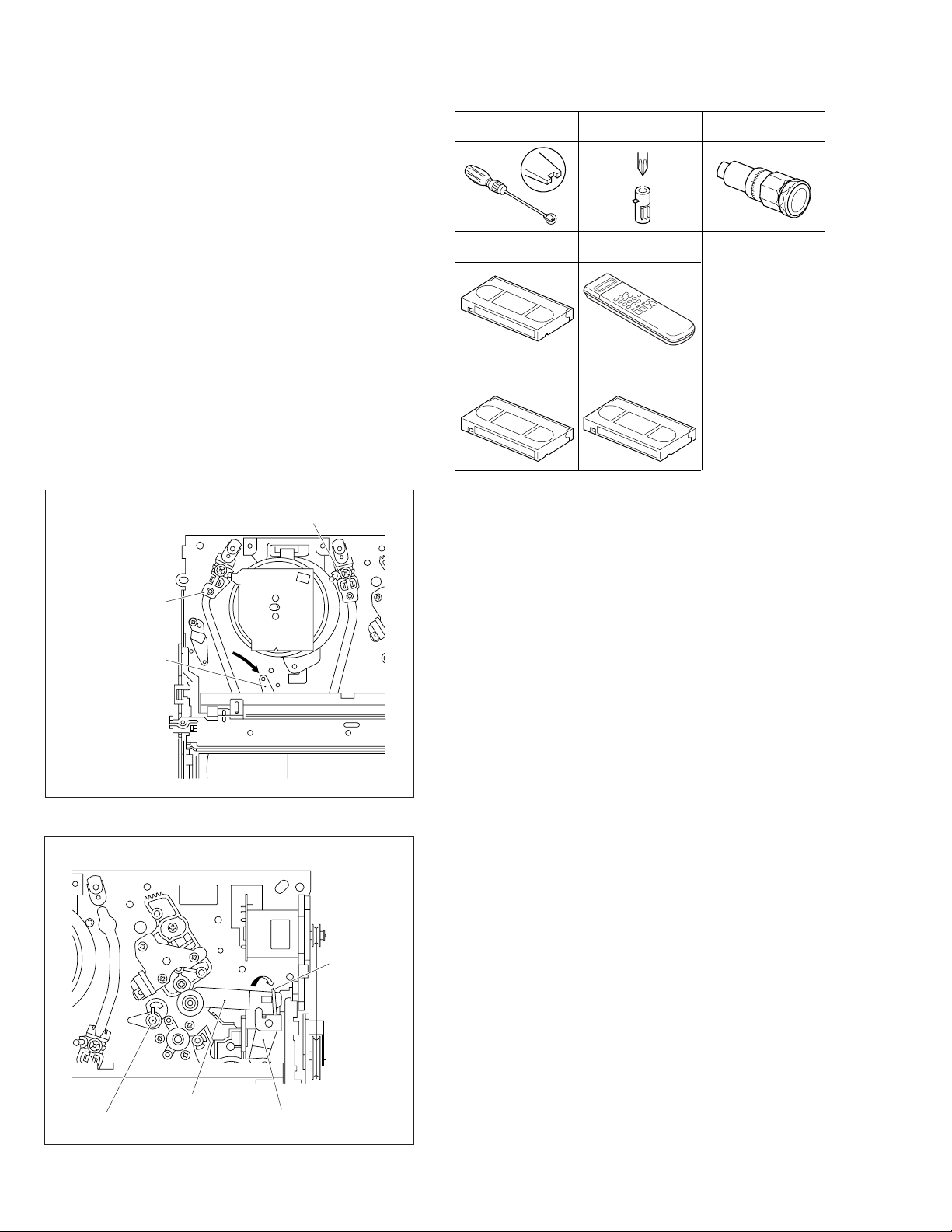
2. In case of mechanical failure
If you cannot remove the cassette tape which is loaded because of any mechanical failure, manually remove it by taking the following steps.
(1) Unplug the power cable and remove the top cover, front
panel assembly and others so that the mechanism assembly is visible. (See SECTION 1 DISASSEMBLY.)
(2) While keeping the tension arm assembly of the mecha-
nism assembly free from tension, pull the tape on the pole
base assembly (supply or take-up side) out of the guide
roller. (See Fig.2-1-3c.)
(3) Take the spring of the pinch roller arm assembly off the
hook of the press lever assembly, and detach it from the
tape. (See Fig.2-1-3d.)
(4) In the same way as in the electrical failure instructions in
2.1.3-1(5), remove the top guide.
(5) Raise the cassette tape cover. By keeping it in that posi-
tion, draw out the cassette tape case from the cassette
holder and take out the tape.
(6) By hanging the pinch roller arm assembly spring back
on the hook, take up the slack of the tape into the cassette.
Pole base assembly (take-up side)
2.1.4 Jigs and tools required for adjustment
Roller driver
PTU94002
Back tension cassette gauge
PUJ48076-2
Alignment tape
(SP, stairstep, PAL)
MHPE
A/C head positioning tool
PTU94010
Jig RCU
PTU94023B
Alignment tape
(LP, stairstep, PAL)
MHPE-L
Torque gauge
PUJ48075-2
Pole base assembly
(supply side)
Tension arm assembly
Fig. 2-1-3c
Take the spring
off the hook, and
detach it from the
tape.
Guide pole guard
2-2
Pinch roller arm assembly
Press lever assembly
Fig. 2-1-3d
Page 25
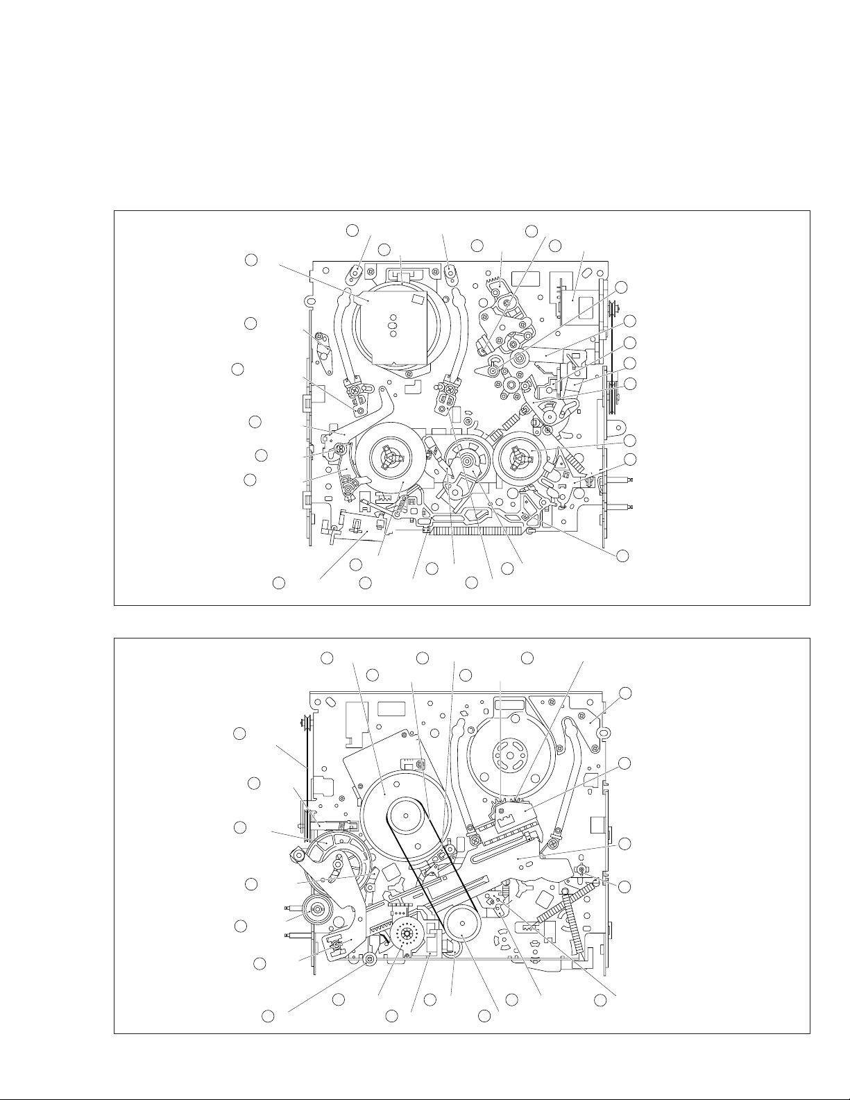
2.1.5 Maintenance and inspection
1. Location of major mechanical parts
In this chapter, the two mechanism speeds are described by comparing the speeds of the standard type and the high-speed
FF/REW type.
It is possible to distinguish between these two types of mechanism by the diameters of their capstan pulleys.
The capstan pulley diameter for the standard type is approx. 32 mm.
The capstan pulley diameter for the high-speed FF/REW type is approx. 43 mm.
For information on the different parts used in the two mechanism types, please refer to the “Replacement of major parts”.
UV catcher2 (supply and take-up side)
Stator assembly
T2
Full erase head
T26
Pole base assembly
T25
(supply side)
Tension arm
T24
assembly
T23
Tension brake
T22
assembly
Adjust pin
T1
T5 T7
T3
Drum assembly
Head base
T6
A/C head
Loading motor
Guide pole guard
T8
Pinch roller arm
T9
assembly
Lid guide
T10
Press lever
T11
assembly
Guide arm
T12
assembly
Reel disk
T13
(take-up side)
Sub brake assembly
T14
(take-up side)
Belt
B22
(loading motor)
B21
Control cam
B20
B19
Cassette gear
B18
Worm gear
Brake lever
Rec safety lever
B1
Reel disk
T20
(supply side)
Main brake assembly
(supply side)
Idler lever
T17T19T21
Idler arm assembly
T16T18
Pole base assembly (take-up side)
Fig. 2-1-5a Mechanism assembly top side
Capstan motor
B2
Capstan brake assembly
B3 B5
Belt (capstan)
Loading arm gear (take-up side)
B4
Loading arm gear (supply side)
Main brake assembly
T15
(take-up side)
Plate
B6
(supply side)
Control
B7
bracket1
Control plate
B8
Tension arm
B9
bearing
Link lever
B17
Rotary encoder guide
B16
Rotary encoder
B15
B14
Direct gear
B13
Change lever assembly
B12
B10
Clutch unit
Take-up head
Fig. 2-1-5b Mechanism assembly bottom side
B11
Take-up lever
2-3
Page 26
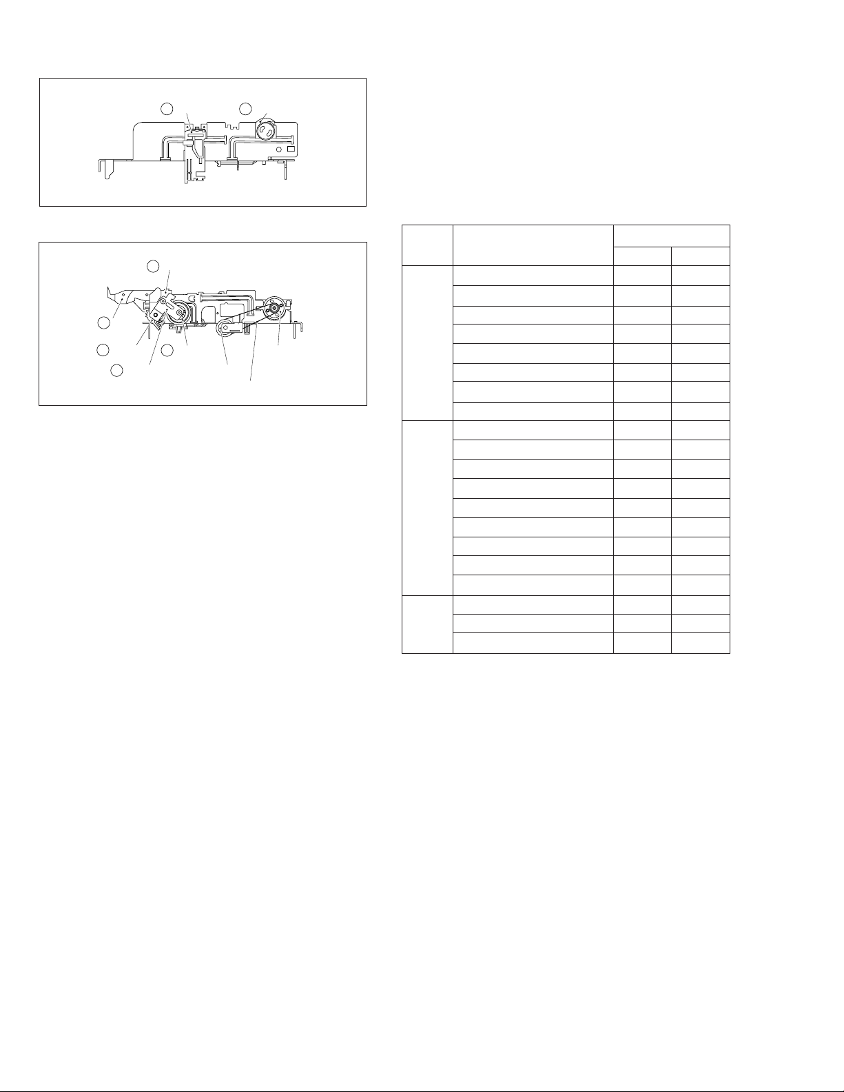
Guide rail Roller cam assembly
L2L1
Fig. 2-1-5c Mechanism assembly left side
R1
Opener guide
Door
R2
opener
Drive gear
R3
Cassette housing bracket
R4
R5
Limit gear
Loading motor
Worm gear
Belt (loading motor)
Fig. 2-1-5d Mechanism assembly right side
2. Cleaning
Regular cleaning of the transport system parts is desirable
but practically impossible. So make it a rule to carry out cleaning of the tape transport system whenever the machine is
serviced.
When the video head, tape guide and/or brush get soiled,
the playback picture may appear inferior or at worst disappear, resulting in possible tape damage.
(1) When cleaning the upper drum (especially the video
head), soak a piece of closely woven cloth or Kimu-wipe
with alcohol and while holding the cloth onto the upper
drum by the fingers, turn the upper drum
counterclockwise.
Note:
• Absolutely avoid sweeping the upper drum vertically
as this will cause damage to the video head.
(2) To clean the parts of the tape transport system other than
the upper drum, use a piece of closely woven cloth or a
cotton swab soaked with alcohol.
(3) After cleaning, make sure that the cleaned parts are com-
pletely dry before using the video tape.
3. Lubrication
With no need for periodical lubrication, you have only to lubricate new parts after replacement. If any oil or grease on
contact parts is soiled, wipe it off and newly lubricate the
parts.
Note:
• See the “mechanism assembly” diagram of the parts
list for the lubricating or greasing spots, and for the
types of oil or grease to be used.
4. Suggested servicing schedule for main components
The following table indicates the suggested period for such
service measures as cleaning,lubrication and replacement.
In practice, the indicated periods will vary widely according
to environmental and usage conditions.However, the indicated components should be inspected when a set is brought
for service and the maintenance work performed if necessary. Also note that rubber parts may deform in time,even if
the set is not used.
System Parts Name
Upper drum assembly
A/C head
Lower drum assembly
Pinch roller arm assembly
Full erase head
Tension arm assembly
Capstan motor (Shaft)
Guide arm assembly
Capstan motor
Capstan brake assembly
Main brake assembly
Belt (Capstan)
Belt (Loading motor)
Loading motor
Clutch unit
Worm gear
Control plate
Brush
Tension brake assembly
Other Drive Tape transport
Rotary encoder
: Cleaning
¤
: Inspection or replacement if necessary
R
Operation Hours
~1000H ~2000H
¤R R
¤R ¤R
¤¤R
¤¤
¤¤
¤¤
¤¤
¤¤
R
R
R
RR
R
R
R
R
R
¤R ¤R
RR
R
Table 2-1-5a
5. Disassembling procedure table
The following table indicates the order in which parts are removed for replacement. To replace parts, remove them in
the order of 1 to 18 as shown in the table. To install them,
reverse the removal sequence.
The symbols and numbers preceding the individual part
names represent the numbers in the “Location of major mechanical parts” table. Also, the “T”, “B”, and “T/B” on the right
of each part name shows that the particular part is removed
from the front, from the back, and from both sides of the
mechanism, respectively.
2-4
Page 27
R4 R1 R3 T9 T12 T11 B15 B12 B14 B13 B17 B21 B7 B8 B5 B4 B11 T14 T15 T13 T22 T24 T18 B19
Symbols and numbers
Removal parts
(Reference items)
Replacement parts
Symbols and numbers
2.2.3 Guide rail T 1
L2
2.2.3 Roller cam assembly T 1
R4
2.2.3 Cassette housing bracket T 1
R1
2.2.3 Opener guide T 2
R2
2.2.3 Door opener T 3
2.2.3 Relay gear T 3
R5
2.2.3 Limit gear T 3
2.2.3 Cassette holder assembly T 6
R3
2.2.3 Drive gear T 4
2.2.3 Drive arm T 8
T9
2.2.4 Pinch roller arm assembly T 1
T12
2.2.5 Guide arm assembly T 1
T11
2.2.5 Press lever assembly T 3
T6
2.2.6 A/C head T 1
T7
2.2.7 Loading motor T 1
B1
2.2.8 Capstan motor T/B 1
T1
2.2.9 UV catcher2 T 1
T17
2.2.9
Pole base assembly (take-up side)
T25
2.2.9
Pole base assembly (supply side)
B15
2.2.10 Rotary encoder B 1
B12
2.2.11 Clutch unit B 1
B14
2.2.12 Change lever assembly B 3
B13
2.2.12 Direct gear B 4
2.2.12 Coupling gear B 5
2.2.12 Clutch gear B 6
B17
2.2.13 Link lever B 1
2.2.14 Cassette gear B 2
B18
B20
2.2.14 Control cam B 2
B21
2.2.14 Worm gear B 1
T10
- Lid guide T/B 5
B7
2.2.15Control bracket1 B 1
2.2.15Control plate B 6
B8
B5
2.2.16Loading arm gear (supply side) B 7
B4
2.2.16
Loading arm gear (take-up side)
2.2.16Loading arm gear shaft B 9
2.2.17Take-up lever T/B 7
B11
B10
2.2.17Take-up head T/B 8
2.2.17Control plate guide T/B 8
B3
2.2.18Capstan brake assembly T/B 7
T14
2.2.19
Sub brake assembly(take-up side)
T15
2.2.20
Main brake assembly(take-up side)
T19
2.2.20
Main brake assembly(supply side)
T13
2.2.20Reel disk (take-up side) T/B 16
T22
2.2.21Tension brake assembly T/B 9
T20
2.2.21Reel disk (supply side) T/B 10
T24
2.2.21Tension arm assembly T/B 10
B9
2.2.21Tension arm bearing T/B 10
T18
2.2.22Idler lever T/B 17
T16
2.2.22Idler arm assembly T/B 18
B19
- Brake lever (
B16
- Rotary encoder guide T/B 19
1
) T/B 18
*
L1L1L2
Number of removal steps
Guide rail
Roller cam assembly
Cassette housing bracket
Opener guide
Front (T)/Back (B) of mechanism
1 2 3 4 5
12
T/B 2
T/B 2
B8
T/B 15
1 2 3 4
T/B 16
1 2 3 4 5 6 7 8
T/B 9
1 2 3 4 5 6 7 8
1 2 3 4 5 6 7 8
1 2 3 4 5 6 7 8
1 2 3 4 5 6 7 8
1 2 3 4 5 6 7 8
1 2 3 4 5 6 7 8
1 2 3 4 5 6 7 8
1 2 3 4 5 6 7 8
1 2 3 4 5 6 7 8
1 2 3 4 5 6 7 8
Relay gear
112
12
12
12 3
3
4 5
5 6
6 7
Cassette holder assembly
Drive gear
7
Table 2-1-5b
Note:
• The parts with marked (
nisms (standard type or high-speed FF/REW type).
1: Uses the standard type mechanism only.
*
2: Uses the high-speed FF/REW type mechanism only.
*
) have different types of mecha-
*
T1
Drive arm
Pinch roller arm assembly
Guide arm assembly
Press lever assembly
UV catcher2
Rotary encoder
Clutch unit
Change lever assembly
Direct gear
1
2
1
1
1
2
12
3
12
3
1 2 3 4 5
12
3 4
1 2 3 4
1 2 3 4 5
1 2 3 4 5 6
1 2 3 4 5 6 7
1 2 3 4 5 6
1 2 3 4 5 6
1 2 3 4 5 6
1 2 3 4 5 6
8
9 10 11 12 13 14
9 10 11 12 13 14 15
9 10 11 12 13 14 15
9 10 11 12 13 14 15 16
9 10 11 12 13 14 15 16 17
9 10 11 12 13 14 15 16 17
9 10 11 12 13 14 15 16 17 18
4
Coupling gear
Link lever
Worm gear
Control bracket1
Control plate
Loading arm gear (supply side)
Loading arm gear (take-up side)
1
1
5
6
7
8
)
1
*
(
Take-up lever
Sub brake assembly (take-up side)
Main brake assembly (take-up side)
Reel disk (take-up side)
Tension brake assembly
Tension arm assembly
Idler lever
Brake lever
7
7
9
9
9
2-5
Page 28
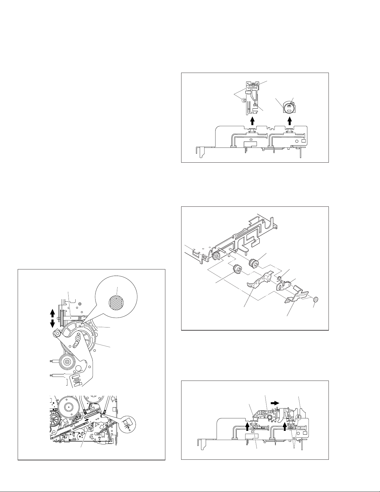
2.2 Replacement of major parts
2.2.1 Before starting disassembling (Phase matching
between mechanical parts)
The mechanism of this unit is closely linked with the rotary
encoder and system controller circuits.
Since the system controller detects the status of mechanical operation in response to phases of the rotary encoder
(internal switch positions), the mechanism may not operate
properly unless such parts as the rotary encoder, control
plate, loading arm gear, control cam, cassette gear, limit gear,
relay gear and drive gear are installed in their correct positions.
Especially, this model is not provided with any cassette housing assembly, so that cassette loading and unloading must
be accomplished by operation of the cassette holder assembly. The latter is in turn driven by such parts as the drive
gear, relay gear and limit gear. Exercise enough care, therefore, to have the phases of all this gear matching one another. (For information on phase matching of the mechanism,
see the instructions on how to install individual parts.)
This unit is provided with a mechanism assembly mode. It is
therefore necessary to enter this mode for assembling and
disassembling procedures.
This mode is usually not in use, manually set it when it is
required.
2.2.3 Cassette holder assembly
1. How to remove
(1) Remove the guide rail and roller cam assembly. (See
Fig.2-2-3a.)
(3 lugs on the guide rail and one lug on the roller cam
assembly)
Guide rail
Lugs
Roller cam
assembly
Lug
Lug
Fig. 2-2-3a
(2) Remove the two slit washers and remove the cassette
housing bracket. (See Fig.2-2-3b.)
(3) Remove the opener guide, spring(A), door opener, relay
gear and limit gear. (See Fig.2-2-3b.)
2.2.2 How to set the “Mechanism assembling mode”
Remove the mechanism assembly and place it bottom side
up. (See SECTION 1 DISASSEMBLY.) Turn the worm gear
toward the front so that the guide hole of the control cam is
brought into alignment with the hole at the mechanism assembly chassis. This position renders the mechanism assembling mode operational. Make sure that the control plate is
located in alignment with the mark E. (See Fig.2-2-2a.)
Worm gear
Chassis hole
Guide hole
Control cam
Limit gear
Spring(A)
Opener guide
Relay gear
Door opener
Cassette housing bracket
Slit washers
Fig. 2-2-3b
(4) While swinging the lock levers (R) and (L) of the cassette
holder assembly toward the front, slide the cassette
holder assembly until its legs come to where the guide
rail and the roller cam assembly have been removed (so
that the drive arm is upright). (See Fig.2-2-3c.)
Lock lever (L)
Cassette holder assembly
Drive arm
(Upright)
2-6
Control plate
Fig. 2-2-2a
Mark E
Leg Legs
Fig. 2-2-3c
Page 29
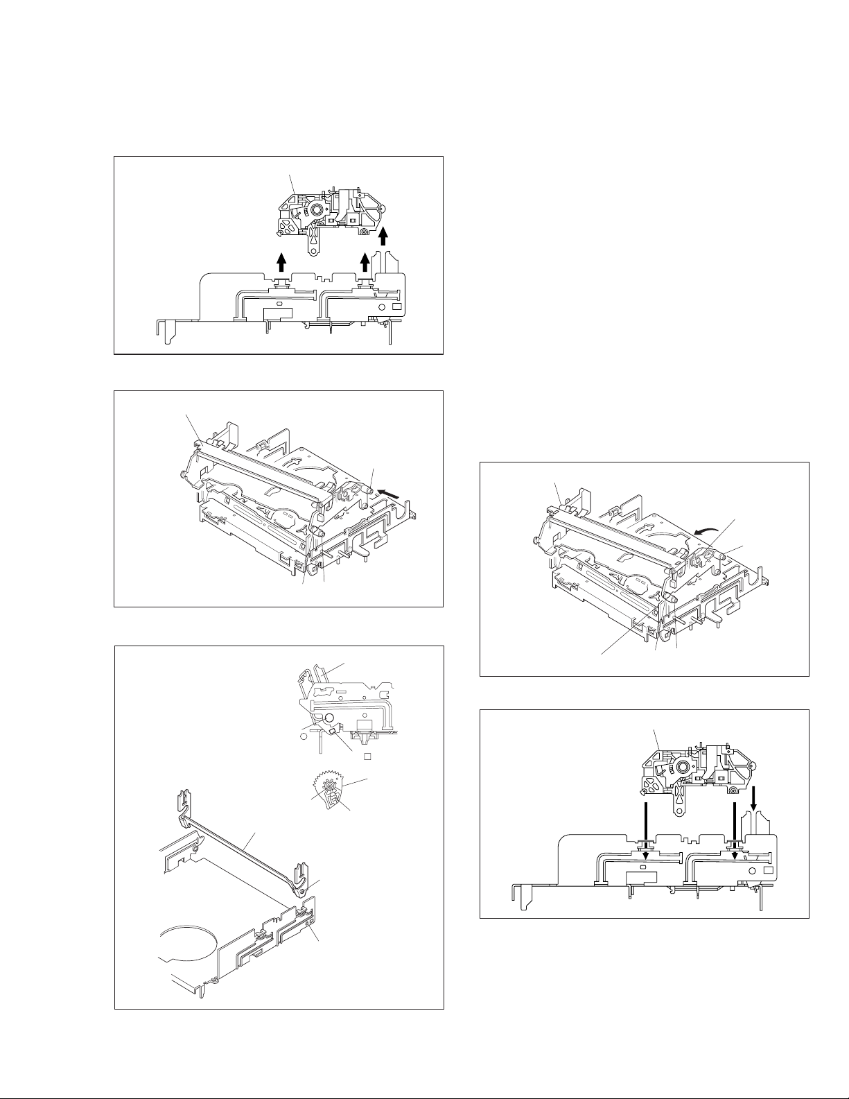
While holding the left side of the cassette holder, lift the
(5)
cassette holder assembly so that the three legs on the
left side are all released. Then pull the legs (A) and (B)
on the right side out of the rail and also pull up the leg(C).
(See Fig.2-2-3d and Fig.2-2-3e.)
(6) Draw out the drive gear, and remove the drive arm.
Cassette holder assembly
Fig. 2-2-3d
Cassette holder assembly
(A)
2. How to install (Phase matching)
(1) Insert the section (A) of the drive arm into the section (B)
of the main deck.
(2) Insert the section (1) of the drive gear into the round hole,
and the section (2) into the square hole on the drive arm.
(See Fig.2-2-3f.)
(3) Hold the drive arm upright and fit the leg (C) on the right
side of the cassette holder assembly into the groove. (See
Fig.2-2-3g.)
(4) While swinging the lock lever (R) of the cassette holder
assembly toward the front, put the legs (A) and (B) into
the rail. (See Fig.2-2-3g.)
(5) Drop the three legs on the left side of the cassette holder
assembly into the groove at one time. (See Fig.2-2-3h.)
(6) Slide the whole cassette holder assembly toward the front
to bring it to the eject end position.
(7) Install the limit gear so that the notch on the outer cir-
cumference of the limit gear is brought into alignment with
the guide hole on the main deck. (See Fig.2-2-3i.)
(8) Install so that the notch on the periphery of the relay gear
is aligned with the notch of the main deck and that hole
A of the relay gear is aligned with the hole A of the limit
gear and that hole B of the relay gear is aligned with the
hole B of the drive gear. (See Fig.2-2-3i.)
(9) Install the door opener, opener guide, spring(A) and cas-
sette housing bracket and fasten the two slit washers.
Cassette holder assembly
Fig. 2-2-3e
Main deck right side
Drive arm
Hole
(C)
Lock lever (R)
(A)
(B)
(B)
Drive arm
Drive arm
(C)
Fig. 2-2-3g
Cassette holder assembly
Hole
Drive gear
(1)
(2)
(A)
Fig. 2-2-3f
(B)
Fig. 2-2-3h
2-7
Page 30
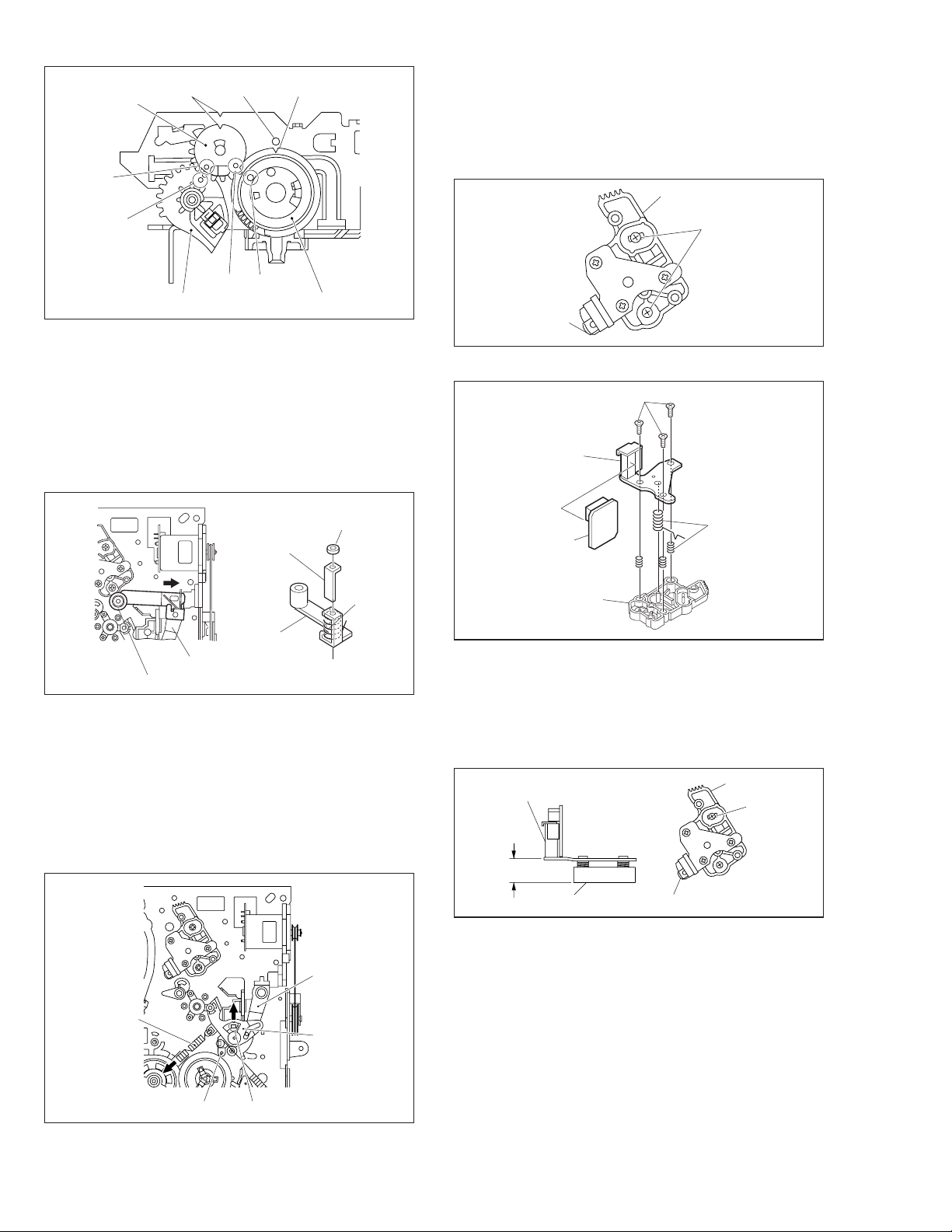
Relay gear
B
Guide holeNotches Notch
2.2.6 A/C head
1. How to remove
(1) Remove the two screws (A) and remove the A/C head
together with the head base.
(2) When replacing only the A/C head, remove the three
screws (B) while controlling the compression spring.
Head base
B
AA
Drive gear Limit gear
Fig. 2-2-3i
2.2.4 Pinch roller arm assembly
1. How to remove
(1) Remove the spring from the hook of the press lever as-
sembly.
(2) Remove the slit washer and remove the pinch roller seat
2. (See Fig.2-2-4a.)
(3) Remove the pinch roller arm assembly by pulling it up.
Slit washer
Pinch roller seat2
Spring
Pinch roller arm
Press lever assembly
Pinch roller arm assembly
assembly
Fig. 2-2-4a
2.2.5 Guide arm assembly and press lever assembly
1. How to remove
(1) Remove the spring and expand the lug of the lid guide in
the arrow-indicated direction. Then remove the guide arm
assembly by pulling it up.
(2) Remove the press lever assembly by pulling it up. (See
Fig.2-2-5a.)
Screws(A)
A/C head
Fig. 2-2-6a
Screws(B)
A/C head
Compression
A/C head board
assembly
Head base
springs
Fig. 2-2-6b
2. How to install
(1) To make the post-installation adjustment easier, set the
temporary level as indicated in Fig.2-2-6c. Also make sure
that the screw center (centre) is brought into alignment
with the center (centre) position of the slot.
A/C head
12.4 mm
Head base
Screw
2-8
Tension
spring
LugLid guide
Fig. 2-2-5a
Press lever
assembly
Guide arm
assembly
Head base
A/C head
Fig. 2-2-6c
2.2.7 Loading motor
1. How to remove
(1) Remove the belt wound around the worm gear.
(2) Open the two lugs of the motor guide and remove the
loading motor, loading motor board assembly and motor
guide altogether by pulling them up.
(3) When replacing the loading motor board assembly, take
care with the orientation of the loading motor. (Install so
that the loading motor label faces upward.)
(4) When the motor pulley has been replaced, choose the
fitting dimension as indicated in Fig.2-2-7a.
Page 31

Loading motor board assembly
Loading motor
Lugs
Motor guide
6.5 ± 0.2 mm
LABEL
Motor pulley
Worm gear
Belt
Fig. 2-2-7a
2.2.8 Capstan motor
1. How to remove
(1) Remove the belt (capstan) on the mechanism assembly
back side.
(2) Remove the three screws (A) and remove the capstan
motor.
Screws(A)
Screw(A)
Capstan motor
Belt
Fig. 2-2-8a
Spacer
Spacer
2. How to install (Centering the mounting position)
When the capstan motor has once been removed and then
reinstalled out of the initial correct position in the rotational
direction, the capstan motor current may be unstable during
operation in high or low temperatures. This may result in
greater Wow & Flutter and occasionally in power breakdown
because of current over - load. Install the capstan motor while
following the procedure given below.
(The capstan motor is centrally located when the unit is
shipped from the factory.)
(1) Provisionally tighten the three screws (A) securing the
capstan motor.
(2) Install the mechanism assembly to which the capstan
motor is provisionally fastened on the bottom chassis
which incorporates the Main board assembly. (No need
to tighten the screws for mounting the mechanism.)
Make sure that all the connectors for the mechanism assembly and the Main board assembly are correctly installed as indicated in Fig. 2-2-8b.
(3) Making sure that the connector for the capstan motor is
correctly mounted, and securely tighten the three screws
(A).
Note:
• When the capstan motor has been replaced with a new
one, perform recording in the EP(or LP) mode for at
least 2 minutes at normal temperatures immediately before starting the FF/REW or SEARCH operations (Aging).
2.2.9 Pole base assembly (supply or take-up side)
1. How to remove
(1) Remove the UV catcher 2 on the removal side by loos-
ening the screw (A).
(2) Remove the pole base assembly on the supply side from
the mechanism assembly by loosening the screw (B) on
the mechanism assembly back side and sliding the pole
base assembly toward the UV catcher 2.
(3) As for the pole base assembly on the take-up side, turn
the pulley of the loading motor to lower the cassette
holder because the screw (B) is hidden under the control plate. (See the “Procedures for Lowering the Cassette
holder assembly” of 1.3 DISASSEMBLY/ASSEMBLY
METHOD.) Further turn the motor pulley to move the cassette holder until the screw (B) is no longer under the control plate (in the half-loading position). Then remove it as
done for the supply side by removing the screw (B).
Note:
• After reinstalling the Pole base assembly and the UV
catcher2, be sure to perform compatibility adjustment.
Fig. 2-2-8b
Connector for
the capstan motor
Screw(A)
UV catcher2
Screw(A)
UV catcher2
Screw(B)
Fig. 2-2-9a
2-9
Page 32

2.2.10 Rotary encoder
1. How to remove
(1) Remove the screw (A) and remove the rotary encoder
by pulling it up. (See Fig. 2-2-10a.)
Rotary encoder (Front side)
Screw(A)
Guide marks
2.2.12 Change lever assembly, direct gear, clutch gear
and coupling gear
1. How to remove
(1) Release the two lugs of the rotary encoder guide in the
arrow-indicated direction and remove the change lever
assembly.
(2) Remove the slit washer retaining the direct gear and re-
move the latter.
Take care so as not to lose the washer and spring. (See
Fig.2-2-12a.)
Rotary encoder (Back side)
Positioning pin of the rotary encoder
Fig. 2-2-10a
Mark E
Shaft of the rotary encoder guide
Control plate
Fig. 2-2-10b
2. How to install (Phase matching)
(1) Make sure that the mark E of the control plate is in align-
ment with the mark
of the loading arm gear shaft and
bring the guide marks on the rotary encoder into alignment as indicated in Fig.2-2-10a. (See Fig. 2-2-10a and
Fig. 2-2-10b.)
(2) Turn over the rotary encoder with its guide marks kept in
alignment and install it by fitting on the shaft of the rotary
encoder guide and the positioning pin.
(3) Tighten the screw (A) to complete the installation.
2.2.11 Clutch unit
(1) Remove the belt wound around the capstan motor and
the clutch unit.
(2) Remove the slit washer and remove the clutch unit.
Change lever
assembly
Spring(B)
Lugs
Note:
• The parts with marked (
speed FF/REW type).
1 : Uses the standard type mechanism only.
*
2:
Uses the high-speed FF/REW type mechanism only.
*
Slit washer
Washer (*1)
Spacer
Direct gear
Spring(A)
Position the projecting
side down.
) have different types of mechanisms (standard type or high-
*
Coupling gear
Spring (C)
Clutch gear
Spacer
Fig. 2-2-12a
2. How to install
(1) Install the clutch gear, spring (A), spring (C), direct gear,
spacer and others to the individual shafts of the main
deck, and finally the slit washer. (See Fig.2-2-12a.)
(2) Let the spring (B) drops into the rotary encoder guide hole
and install the change lever assembly.(Take care not to
mistake a direction of the spring.) The point is to slightly
lift the coupling gear and catch it from the both sides with
the assembly. (See Fig.2-2-12b.)
Rotary encoder guide
Spring(B)
Change lever assembly
Coupling gear
2-10
Belt
Clutch unit
Fig. 2-2-11a
Slit washer
Main deck Main deck
Fig. 2-2-12b
Page 33

2.2.13 Link lever
1. How to remove
(1) Remove the two slit washers.
(2) Remove the link lever by lifting it from the shaft retained
by the slit washers. Then swing the link lever
counterclockwise and remove it from the locking section
of the control plate.
Slit washers
2.2.14 Cassette gear, control cam and worm gear
1. How to remove
(1) Remove the control cam by lifting it.
(2) Open the two lugs of the cassette gear outward and pull
the latter off.
(3) Remove the belt wound around the worm gear and the
loading motor.
(4) Open the lug of the lid guide outward and remove the
worm gear.
Link lever
Locking section of the
control plate
Fig. 2-2-13a
2. How to install (Phase matching)
(1) Slide the control plate so that its mark E is aligned with
the mark
on the loading arm gear shaft. (See Fig.2-2-
13b.)
(2) Rotate the worm gear until the guide hole of the control
cam is aligned exactly with the guide hole of the main
deck. (See Fig.2-2-13c.)
(3) Insert the link lever into the locking section of the control
plate. (See Fig.2-2-13a.)
(4) Rotate the link lever clockwise so that it is installed on
the shafts in the center (centre) and on the left of the control cam.
(5) Fasten the slit washers at these two points.
Loading motor
Belt
Lug
Worm gear
Lugs
Cassette gear
Lid guide
Control cam
Fig. 2-2-14a
2.2.15 Control plate
1. How to remove
(1) Remove the screw (A) retaining the control bracket 1 and
remove the latter.
(2) Slide the control plate as indicated by the arrow and re-
move the control plate. (See Fig.2-2-15a.)
Shaft of the rotary encoder guide
Fig. 2-2-13b
Worm gear
Main deck
guide hole
Control cam
guide hole
Cassette gear
Fig. 2-2-13c
Control plate
Control cam
Mark E
Screw(A)
Control
bracket1
Control
plate
Fig. 2-2-15a
2. How to install (Phase matching)
(1) Adjust the position of the idler arm assembly pin as indi-
cated in Fig.2-2-15b (to the left of center (centre) of the
R section).
(2) Bring the guide hole of the take-up lever into alignment
with the hole at the control plate guide and fix the position by inserting a 1.5 mm hexagonal wrench.
2-11
Page 34

(3) Install the control plate so that the section A of the load-
ing arm gear shaft fits into the hole (A) of the control plate,
the section B of the control plate guide into the hole (B),
and the control plate comes under the section C of the
rotary encoder guide and the section D of the loading arm
gear shaft while press-fit the pole base assmebly (supply side) as indicated by the arrow. It is important that
the tension arm assembly shaft is positioned closer toward you than the control plate. (See Fig.2-2-15c.)
(4) Make sure that the mark E of the control plate is in align-
ment with the mark
of the loading arm gear shaft. (See
Fig.2-2-15c.)
(5) Pull off the hexagonal wrench for positioning.
(3) Turn the loading arm gear (take-up side) clockwise so
that the notch of the loading arm gear (take-up side) is
in alignment with the projection of the loading arm gear
shaft and lift it.
Likewise, turn the loading arm counterclockwise so that
the notch is in alignment with the projection and remove
the loading arm gear (take-up side). (See Fig.2-2-16a and
Fig. 2-2-16b.)
(4) When removing the loading arm gear shaft, be sure of
first removing the screw retaining the drum assembly (on
the back side of the loading arm gear shaft). Then remove the screw (C) and remove the loading arm gear
shaft by sliding it.
Idler arm assembly
pin
R section
Guide hole of the
control plate guide
Section D
1.5mm hexagonal wrench
Fig. 2-2-15b
Section A
Section D
Hole A
Pressfit
Take-up lever
Insert
Pole base assembly
(supply side)
Section A
Hole A
Pole base assembly
(take-up side)
Screw(B)
Torsion arm
Loading arm gear
(take-up side)
Projection B
Guide marks
Projection A
Pole base assembly
(supply side)
Screw(A)
Loading arm gear
(supply side)
Fig. 2-2-16a
Loading arm gear shaft
Loading arm gear (take-up side)
Notch
Screw(C)
Loading arm gear shaft
Section C
Section C
Section B
Hole B
Hole B
Section B
Control plate
Tension arm assembly
shaft
Fig. 2-2-15c
2.2.16 Loading arm gear (supply or take-up side) and
loading arm gear shaft
1. How to remove
(1) Remove the loading arm gear (supply side) by loosen-
ing the screw (A). (See Fig. 2-2-16a.)
(2) Remove the screw (B) and remove the torsion arm from
the pole base assembly (take-up side). (See Fig.2-2-16a.)
2-12
Fig. 2-2-16b
2. How to install
(1) Align the notch of the loading arm gear (take-up side) to
the projection B of the loading arm gear shaft and slip it
over. Then rotate it clockwise for alignment with the projection A and slip it down to the bottom. (See Fig.2-216b.)
(2) Then turn the loading arm gear (take-up side)
counterclockwise. Hang the torsion arm on the pole base
assembly (take-up side) and tighten the screw (B).
(3) Install the loading arm gear (supply side) so that the guide
mark of the loading arm gear (take-up side) is in alignment with the guide mark of the loading arm gear (supply side). Then hang the torsion arm on the pole base
assembly (supply side) and tighten the screw (A). (See
Fig.2-2-16a.)
Page 35

2.2.17 Take-up lever, take-up head and control plate
guide
(1) Remove the spring of the take-up lever from the main
deck.
(2) Remove the lug (A) of the take-up lever from the main
deck and pull out the take-up lever and the take-up head
together.
(3) Remove the screw (A).
(4) Align the idler arm assembly pin in the center (centre) of
the R section of the control plate guide, remove the con-
trol plate guide lugs (B) and (C) from the main deck, and
remove the control plate guide.
Idler arm assembly pin
Lug(C)
Screw(A)
Take-up lever
Take-up head
Lug(A)
Lug(B)
Control plate guide
Fig. 2-2-17a
2.2.18 Capstan brake assembly
1. How to remove
(1) Move the lug (A) of the capstan brake assembly in the
arrow-indicated direction so that it comes into alignment
with the notch of the main deck. (See Fig. 2-2-18a.)
(2) Remove the lug (B) of the capstan brake assembly from
the main deck and remove the capstan brake assembly.
Spring
Sub brake
Lug(A)
Lug(B)
assembly
(take-up side)
Lug(C)
Fig. 2-2-19a
2.2.20 Main brake assembly (take-up side), reel disk
(take-up side) and main brake assembly (supply
side)
1. How to remove
(1) Move the main brake assembly (take-up side) in the ar-
row-indicated direction and remove the reel disk (takeup side).
Remove the spring attached to the main brake assembly.
(2)
(3) Remove the lug (A) of the main brake assembly (take-
up side) and pull out the lug (B) after bringing it into alignment with the main deck notch.
(4) Remove the lugs (C), (D) and (E) of the main brake as-
sembly (supply side) from the main deck and pull them
off. (See Fig.2-2-20a.)
(5) When installing the main brake assembly (take-up side),
slide the brake lever in the direction as indicated by the
arrow to prevent it from hitting the projection of the main
brake assembly (take-up side). (See Fig.2-2-20b.)
Main brake assembly
(supply side)
Reel disk
(take-up side)
Main brake assembly
(take-up side)
Lug(B)
Lug(A)
Capstan brake assembly
Fig. 2-2-18a
2.2.19 Sub brake assembly (take-up side)
1. How to remove
(1) Remove the spring attached to the lid guide and sub
brake assembly (take-up side).
(2) Bring the lug (A) of the sub brake assembly (take-up side)
into alignment with the notch of the main deck.
(3) Remove the lugs (B) and (C) of the sub brake assembly
(take-up side) from the main deck and remove the sub
brake assembly (take-up side).
Lug(B)
Lug(C)
Lug(D)
SpringLug(E)
Lug(A)
Notch
Fig. 2-2-20a
1)
(
*
Brake
lever
Note:
• The parts with marked ( *) have different types of mechanisms (standard type
or high-speed FF/REW type).
1 : Uses the standard type mechanism only.
*
Rotary encoder guide
Projection of the main
brake assembly
(take-up side)
Fig. 2-2-20b
2-13
Page 36

2.2.21 Tension brake assembly, reel disk (supply side)
and tension arm assembly
1. How to remove
(1) Remove the three lugs of the tension brake assembly
from the main deck and pull them off.
(2) Remove the reel disk (supply side) by loosening in the
arrow-indicated direction the main brake assembly (supply side).
(3) Remove the tension spring on the back of the main deck.
Then release the lug of the tension arm bearing in the
arrow-indicated direction and draw out the tension arm
assembly. (See Fig. 2-2-21a.)
Lug of the tension
arm bearing
Tension arm
assembly
Reel disk
(supply side)
2.2.23 Stator assembly
(1) Remove the flat cable.
(2) Remove the two screws (A), (B) and remove the lug wire.
(3) Remove the stator assembly by lifting in the arrow-indi-
cated direction. (Take care that the brush spring does not
jump out.)
Notes:
• Be careful not to lose the brush and spring.
• There are some models that do not use the lug wire.
Refer to the parts list for these models.
• When tightening the screw (B), place the caulked part
of the lug terminal near to the shaft of the drum and
then tighten it.
• After installation, be sure to perform the switching
point adjustment according to the electrical adjustment
procedure.
Tension brake
assembly
Lugs
Tension spring Main brake assembly
(supply side)
Fig. 2-2-21a
2.2.22 Idler lever, idler arm assembly
1. How to remove
(1) Remove the lug of the idler lever from the main deck and
remove the hook fitted in the idler arm assembly hole by
lifting it.
(2) Remove the slit washer and pull out the idler arm assem-
bly.
Lug Idler lever
Hook
Idler arm
assembly
Slit washer
Screw (A)
Stator assembly
Screw (B)
Lug wire
(Note)
Drum
shaft
Flat cable
(Take care not to mix up the
polar faces when installing.)
Lug wire
Screw (A)
Fig. 2-2-23a
2.2.24 Rotor assembly
1. How to remove
(1) Remove the stator assembly.
(2) Remove the two screws (B) and remove the rotor assem-
bly.
2. How to install
(1) Match the phases of the upper drum assembly and the
rotor assembly as indicated in Fig.2-2-24a.
(2) Place the upper drum assembly hole (a) over the rotor
assembly holes (b) (with three holes to be aligned) and
tighten the two screws (B). (See Fig.2-2-24a.)
Screws (B)
Hole(a)
2-14
Fig. 2-2-22a
Screw holes
Upper drum
assembly
Rotor assembly
Fig. 2-2-24a
The hole is not in
line but is offset
toward the right.
Hole(b)
Page 37

2.2.25 Upper drum assembly
Notes:
• To replace the upper drum assembly only may not be
possible with some models. For upper drum assembly replacement, refer to the parts list. (When the parts
number of the upper drum assembly is not listed on
the parts list, then this cannot be replaced.)
• When replacement is required, control the up- down
movement of the brush. Never apply grease.
• When replacing the upper drum assembly, replace it
the together with the washer.
1. How to remove
(1) Remove the stator assembly and rotor assembly.
(2) Loosen the screw of the collar assembly using a 1.5 mm
hexagonal wrench and remove the collar assembly. Also
remove the brush, spring and cap at one time.
(3) Remove the upper drum assembly and remove the
washer using tweezers.
Lower drum assembly
Coil parts
Upper drum assembly
Fig. 2-2-25b
Spring
Brush
Upper drum
assembly
Washer
Collar
assembly
Loosen
Cap
Shaft
1.5 mm
hexagonal wrench
Lower drum assembly
Fig. 2-2-25a
2. How to install
(1) Clean the coil parts of the lower drum assembly and the
newly installed upper drum assembly with an air brush
in advance. (See Fig.2-2-25b.)
(2) Install a new washer and upper drum assembly on the
drum shaft. (See Fig.2-2-25a.)
(3) Install the cap to the upper drum assembly.
(4) Position the collar assembly as indicated in Fig.2-2-25c
while controlling its up- down movement.
(5) Secure the collar assembly in position with a hexagonal
wrench while pressing its top with the fingers.
(6) After installation, gently turn the upper drum assembly
with your hand to make sure that it turns normally. Then
install the brush and the spring.
(7) Install the rotor assembly and stator assembly according
to Fig 2-2-23a and 2-2-24a.
(8) When installation is complete, clean the upper drum as-
sembly and lower drum assembly and carry out the fol-
lowing adjustments.
• PB switching point adjustment
• Slow tracking adjustment
• Compatibility adjustment (Be sure to check for compatibility for the EP (or LP) mode.)
Upper drum
assembly
Collar
assembly
Fig. 2-2-25c
Press
Fig. 2-2-25d
Collar
assembly
Tighten
2-15
Page 38

2.3 Compatibility adjustment Notes:
• Although compatibility adjustment is very important,
it is not necessary to perform this as part of the normal servicing work. It will be required when you have
replaced the A/C head, drum assembly or any part of
the tape transport system.
• To avoid any damage to the alignment tape while performing the compatibility adjustment, get a separate
cassette tape (for recording and play back) ready to
be used for checking the initial tape running behavior.
• Unless otherwise specified, all measuring points and
adjustment parts are located on the Main board.
• When using the Jig RCU, it is required to set the VCR
to the Jig RCU mode (the mode in which codes from
the Jig RCU can be received). (See SECTION 1 DISASSEMBLY.)
Jig RCU
[Data transmitting method]
Depress the “ ” ( 3 ) button
after the data code is set.
pole base assembly (supply or take-up side).
(7) Unload the cassette tape once, play back the alignment
tape (A1) again and confirm the V.PB FM waveform.
(8) After adjustment, confirm that the tape wrinkling does not
occur at the roller upper or lower limits. (See Fig. 2-31d.)
[Perform adjustment step (9) only for the models
equipped with SP mode and EP (or LP) mode.]
(9) Repeat steps (1) to (8) by using the alignment tape (A2).
CUSTOM CODE
43: A CODE
DATA CODE
INITIAL MODE
Fig. 2-3a Jig RCU [PTU94023B]
2.3.1 FM waveform linearity
Signal (A1) •
(A2) •
Mode (B) •PB
Equipment (C) • Oscilloscope
Measuring point (D) • TP106 (PB. FM)
External trigger (E) •TP111 (D.FF)
Adjustment part (F) •Guide roller [Mechanism assembly]
Specified value (G) • Flat V.PB FM waveform
Adjustment tool (H)
Alignment tape(SP, stairstep, PAL) [MHPE]
Alignment tape(LP, stairstep, PAL) [MHPE-L]
• Roller driver [PTU94002]
(1) Play back the alignment tape (A1).
(2) Apply the external trigger signal to D.FF (E), to observe
the V.PB FM waveform at the measuring point (D).
(3) Set the VCR to the manual tracking mode.
(4) Make sure that there is no significant level drop of the
V.PB FM waveform caused by the tracking operation, with
its generally parallel and linear variation ensured. Per-
form the following adjustments when required. (See Fig.
2-3-1a.)
(5) Reduce the V.PB FM waveform by the tracking opera-
tion. If a drop in level is found on the left side, turn the
guide roller of the pole base assembly (supply side) with
the roller driver to make the V.PB FM waveform linear.
If a drop in level is on the right side, likewise turn the guide
roller of the pole base assembly (take-up side) with the
roller driver to make it linear. (See Fig. 2-3-1c.)
(6) Make sure that the V.PB FM waveform varies in parallel
and linearly with the tracking operation again. When re-
quired, perform fine-adjustment of the guide roller of the
Max level
Proper waveform variation
Improper waveform variation
Fig. 2-3-1a
Roller driver
Fig. 2-3-1b
Min level
Guide roller (supply side)
2-16
Page 39

A
B
waveform by turning the screws (1), (2) and (3) little by
little until both waveforms reach maximum. The screw (1)
and (3) are for adjustment of tilt and the screw (2) for azimuth.
(4) Adjust the AUDIO OUT waveform and Control pulse
Level drop at the guide roller (supply side)
C
Level drop at the guide roller (take-up side)
• Proper waveform variation: Always flat
• Improper waveform variation:
Higher Lower
Fig. 2-3-1c
Improper
(a) Guide roller
Head base
A/C head
(2)
(3)
(1)
AUDIO OUT
CTL. P
D
Fig. 2-3-2a
2.3.3 A/C head phase (X-value)
Proper
Signal (A1) •
Mode (B) •PB
Equipment (C) • Oscilloscope
Measuring point (D) •TP106 (PB. FM)
External trigger (E) •TP111 (D.FF)
Adjustment part (F) •
Specified value (G) • Maximum V.PB FM waveform
Adjustment tool (H) • A/C head positioning tool [PTU94010]
Alignment tape(SP, stairstep, PAL) [MHPE]
A/C head base [Mechanism assembly]
(b) Guide pole
Fig. 2-3-1d
2.3.2 Height and tilt of the A/C head
Note:
• Set a temporary level of the height of the A/C head in
advance to make the adjustment easier after the A/C
head has been replaced. (See Fig.2-2-6c.)
Signal (A) •
Mode (B) •PB
Equipment (C) • Oscilloscope
Measuring point (D1)
(D2) •TP4001 (CTL. P)
External trigger (E) •TP111 (D.FF)
Adjustment part (F) •A/C head [Mechanism assembly]
Specified value (G) • Maximum waveform
Alignment tape(SP, stairstep, PAL) [MHPE]
• AUDIO OUT terminal
(1) Play back the alignment tape (A).
(2) Apply the external trigger signal to D.FF (E), to observe
the AUDIO OUT waveform and Control pulse waveform
at the measuring points (D1) and (D2) in the ALT mode.
(3) Set the VCR to the manual tracking mode.
(1) Play back the alignment tape (A1).
(2) Apply the external trigger signal to D.FF (E), to observe
the V.PB FM waveform at the measuring point (D).
(3) Set the VCR to the manual tracking mode.
(4) Loosen the screws (4) and (5), then set the A/C head
positioning tool to the innermost projected part of the A/
C head. (See Fig. 2-3-3a.)
(5) Turn the A/C head positioning tool fully toward the cap-
stan. Then turn it back gradually toward the drum and
stop on the second peak point position of the V.PB FM
waveform output level. Then tighten the screws (4) and
(5).
(6) Perform the tracking operation and make sure that the
V.PB FM waveform is at its maximum.
If it is not at maximum, loosen the screws (4) and (5),
and turn the A/C head positioning tool to bring the A/C
head to a position, around where the waveform reaches
its maximum for the first time. Then tighten the screws
(4) and (5).
2-17
Page 40

[Perform adjustment steps (7) to (10) only for 2 Head
models equipped with LP mode.]
(7) Then play back the alignment tape (A2).
(8) Set the VCR to the manual tracking mode.
(9) Perform the tracking operation and make sure that the
V.PB FM waveform is at its maximum.
(10)
If it is not at maximum, loosen the screws (4) and (5),
and turn the A/C head positioning tool to bring the A/C
head to a position, around where the waveform reaches
its maximum for the first time. Then tighten the screws
(4) and (5).
Note:
• After adjusting, always perform the confirmation and
re-adjustment of the item 2.3.4.
Toward the drum
A/C head positioning tool
To the drum
A/C head
Toward the capstan
Head base
Screw
Screw
To the capstan
(4)
(5)
Fig. 2-3-3a
Alignment tape
[SP, stairstep]
played with the
SP head
Alignment tape
[EP(LP), stairstep]
played with the
EP(LP) head
(4) Set the VCR to the Auto adjust mode by transmitting the
code (F) twice from the Jig RCU. When the VCR enters
the stop mode, the adjustment is completed.
(5) If the VCR enters the eject mode, perform adjustment for
the audio control head phase (X-value) again.
2.3.5 Tension pole position
Signal (A) •Back tension cassette gauge
Mode (B) •PB
Adjustment part (F) •Adjust pin [Mechansim assembly]
Specified value (G)
[PUJ48076-2]
• 25 - 51 gf•cm (2.45 – 5 × 10
-3
Nm]
(1) Play back the back tension cassette gauge (A).
(2) Check that the indicated value on the left side gauge is
within the specified value (G).
(3) If the indicated value is not within the specified value (G),
perform the adjustment in a following procedure.
1) Set the VCR to the mechanism service mode. (See
SECTION 1 DISASSEMBLY.)
2) Set the VCR to the play back mode and adjust by turning adjustment pin to align the tension arm assembly
edge with the main deck hole (A) on the right edge
marker. (See Fig. 2-3-5a)
Tension arm
assembly
Hole (A)
Marker
Edge
Waveform output
X-value adjustment point
Drum side Control head position Capstan side
Maximum
Fig. 2-3-3b
2.3.4 Standard tracking preset
Signal (A) •
Mode (B) •PB ¥ Auto adjust
Equipment (C) • Oscilloscope
Measuring point (D) • TP106 (PB. FM)
External trigger (E) •TP111 (D.FF)
Adjustment part (F) •Jig RCU: Code “50”
Specified value (G)
Adjustment tool (H)
Alignment tape(LP, stairstep, PAL) [MHPE-L]
• STOP mode
(Maximum V.PB FM waveform)
• Jig RCU [PTU94023B]
(1) Play back the alignment tape (A).
(2) Apply the external trigger signal to D.FF (E), to observe
the V.PB FM waveform at the measuring point (D).
(3) Confirm that the automatic tracking operation is com-
pleted.
0.5 mm
Tension arm assembly
Tension brake assembly
Adjust pin
Fig. 2-3-5a
2-18
Page 41

Mechanism Timing Chart
Mechanism mode
Control plate mark
Rotary encoder
Control cam angle
EJECT
END
E U CI
HIGH
C CH
LOW
HIGH
B CH
LOW
HIGH
A CH
LOW
0
CASS-
UP
69 136 370 412.
CASS-INS
FF/REW
FR
230
STOP
ST
264.
REV
R
7
318.
7
SLOW/STILLPPLAY
SL
42
Rotary encoder
angle
Pole base
Pinch roller
Guide arm
Tension arm
Main brake S
Main brake T
Sub brake S
Sub brake T
Capstan brake
Direct gear
Change lever 2
Idler position
Take-up lever
Rec safety switch
Operation mode
HALF PRESS
CONTACT
ON PLAY
ON REV
CONTACT
(C-INS)
HALF REV
HALF FF/REW
CONTACT
CONTACT
IN FF/REW
OUT PLAY
SUPPLY
CENTER
TAKE-UP
READY
RESET
OFF
OFF
OFF
OFF
OFF
OFF
OFF
OFF
OFF
OFF
OFF
20 42.652.
0
ON
ON
ON
ON
ON
ON
ON
ON
ON
ON
6
6
114.
150.4167.8178.
8
Timer REC
(drum at stop)
POWER OFF
(cassette loaded)
207.2218.2240.2251.
standby
STOP
Backspace Slow FOR
Search REW
Slow REW
2
293.2304.2320.4335
REC pause
REC
Search FF
STOP
(
drum
in motion)
2-19
Page 42

MECHANISM ADJUSTMENT (DV)
2.4 PREPARATION
2.4.1 Precautions
(1) Observe the specified screw tightening torque when at-
taching parts. The torque should be 0.04 Nm (0.4 kgfcm)
unless otherwise specified.
(2) Always disconnect the power supply unit before proceed-
ing to solder or attach parts.
(3) When plugging or unplugging a wire, be careful not to
damage the connector.
(4) When replacing a part, be careful not to damage other
parts or to mistakenly attach parts.
2.4.2 Tools Required for Adjustments
TORQUE DRIVER
12
YTU94088
Tool for replacing tip IC
4
PTS40844-2
BIT
YTU94088-003
Table 2-4-1 Tools Required for Adjustments
2.4.3 Disassembly and Assembly Procedures
The following table shows the steps for assembling or disassembling the mechanism parts. Read the following descriptions carefully before actual assembly/disassembly operations.
: Order of disassembly steps. Reverse this order when
(1)
assembling.
: Name of the disassembled/assembled part.
(2)
: Surface where the disassembled/assembled part is
(3)
mounted. T = Top. B: Bottom.
: Number of disassembly drawing.
(4)
Tool for installing slit washer
3
YTU94121A
: Parts to be removed in disassembly/assembly, such as
(5)
screws, washers and springs, and the points.
Symbol Name & Point
S Screw
W Washer
P Spring
*
Connector, lock(L), soldering(SD),
shield, etc.
[Example] • (W1) = Remove the washer W1.
• (P1) = Remove the spring P1.
: Notes for disassembly/assembly.
(6)
: For the phase alignment in disassembly/assembly and
(7)
the parts which require phase adjustments after assembly, see “2.11 MECHANISM PHASE CHECK/ADJUSTMENT”.
2.4.4 Screws and Washers Used in Disassembly/Assembly of the Mechanism Assembly
Table 2-4-1 shows the symbols, designs, part numbers and
colors of the screws and washers used in the mechanism
assembly.
When disassembling or assembling the mechanism assembly, be sure to attach screws and washers correctly by referring to the following table.
Part numberSymbol
(S1)
(S2)
(S3)
Symbol
(W1)
(W2)
(W3)
QYTDSP2004Z
YQ43893
YQ43893-7
Part number
YQ44246
YQ44246-3
YQ43933-2
Table 2-4-2
Step
/Loc Part Name
No.
1 A Cassette housing assembly/ B Mechanism assembly T 1
Fig.
No.
2(S1),(L1) – (L5)
Point Note Discription
1
2 1 Drum assembly T 2 3(S2) 2,3
3 2 Motor bracket assembly T 2 4(S2) 2,4
4 3 Middle catcher assembly T 3 3(S2) —
§§ §§§§§
(1) (2) (3) (4) (5) (6) (7)
2-20
Page 43

2.5 DISASSEMBLY/ASSEMBLY OF THE MECHANISM ASSEMBLY
2.5.1 Introduction
The disassembly and assembly of the mechanism assembly should usually be performed in the ASSEMBLY mode.
(Table 2-5-1)
Note that the mechanism is in the cassette in (C-IN) mode
when the mechanism assembly is taken out of the set and
that the C-IN mode should be switched to the ASSEMBLY
mode in this case.
To set the ASSEMBLY mode, apply 3 V DC to the electrodes
on the upper part of the loading motor as shown in Fig. 2-5-
7.
MODE
PARTS
1
ROTARY
ENCORDER
R. ENC -20
MAIN CAM GEAR 0
2
3
36°
C-IN
ASSEMBLY
17°
S. FF
30.33°
36.33°
0
15
33.33
40
Table 2-5-1
2.5.2 Mechanism Modes
The mechanism has 6 modes as shown in Table 2-6-1. The
current mode can be confirmed by the positioning of the “ ”
marking on the sub-cam gear and the “ ” marking on the
mechanism.
See the following figures (Figs. 2-5-1 to -6) for details.
Note:
•
This mechanism assembly has another ASSEMBLY
mode. However, this mode cannot be identified from the
markings because it corresponds to an intermediate po-
C
sition between the C-IN (
) mode and S-FF ( H ) mode.
This mode can be confirmed by the rotary encoder
phase. See Fig. 2-5-7.
LOADING END
87°
166.66
PLAY REV STOP FF/REW
223.66°
229.66°
226.66
185
140
190.33°
196.33°
169.66°
193.33
160
270.33°
273.33
220
276.33°
303.66°
306.66
245
1. Checking the mechanism mode
C H P
H
Fig. 2-5-1 Fig. 2-5-2 Fig. 2-5-3
R S F
Fig. 2-5-4 Fig. 2-5-5 Fig. 2-5-6
2-21
Page 44

2. Setting/checking the ASSEMBLY mode
Wire (Brown)
Note:
• In this ASSEMBLY mode, only the 2
gear teeth of the rotary encoder are
marked (red coloring).
Marking
Wire (Red)
(Colored red)
DC 3 V
Motor Bracket Assembly (Loading Motor)
Rotary Encoder
< ASSEMBLY >
C
H
Fig. 2-5-7
2-22
Page 45

2.6 MECHANISM TIMING CHART
See following table (Table 2-6-1).
MODE
PARTS
36°
1
ROTARY
ENCODER
2
3
ROTARY ENCODER
MAIN CAM 0
SUB CAM
POLE BASE
CTL PLATE
FF/REW
MAIN BRAKE(SUP)
MAIN BRAKE(TU)
SUB BRAKE
ON(REV MODE PRESS UP)
ON(PLAY MODE)
PINCH ROLLER
EXIT GUIDE ARM
HALF LOADING
TENSION ARM
BAND ARM PLATE
CLUTCH LOCK
SUP CENTRRING
S/REV
PLAY
ON 1
ON 2
ON 1
ON 2
ASSY
OFF 1
OFF 2
OFF 1
OFF 2
OFF
OFF
OFF
OFF
OFF
OFF
OFF
ASSEMBLY
C-IN
17°
-20
0
15
0
ON
ON
ON
ON
ON
S. FF
30.33°
33.33
40
4015
36.33°
87°
LOADING END
169.66°
166.66
140
140
PLAY REV STOP FF/REW
270.33°
276.33°
223.66°
226.66
185
185
229.66°
303.66°
273.33
220
220
306.66
245
245
190.33°
193.33
160
160
196.33°
CENTERRING ARM
S/REV
Table 2-6-1
2-23
Page 46

2.7 MECHANISM ASSEMBLY/DISASSEMBLY PROCEDURE TABLE Step
/Loc Part Name
No.
1 A Cassette housing assembly/ B Mechanism assembly
2 1
Drum assembly T 2-13-2 3(S2) 2,3
3
2 Motor bracket assembly T 2-13-2 4(S2) 2,4
4 3 Middle catcher assembly T 2-13-3 3(S2) —
5 4 Reel cover assembly T 2-13-3 (S2), 2(L6) 5
6 5 Pinch roller arm assembly T 2-13-4 (W1), (L7) 6
7 6 Sub brake assembly T 2-13-4 (P1), (W1), (L8) —
8 7 Band arm plate sub assembly T 2-13-4 (S3), (L9), (P2), (W2) 7,8
9 8 Tension arm sub assembly T 2-13-4 (P3) 8
10 9 EXIT guide arm assembly T 2-13-5 (W1) —
11 10 Swing arm assembly T 2-13-5 — — Position alignment
12 11 Sub deck assembly T 2-13-6 4(S2) 9 Position alignment
13 12 Main brake (Sup) assembly T 2-13-6 (P4), (L10) —
14 13 Main brake (Take up) assembly T 2-13-6 (P5), (L11) —
15 14 Reel disk assembly (Sup) T 2-13-7 — —
16 15 Reel disk assembly (Take up) T 2-13-7 — —
17 16 Prism T 2-13-7 (S2) —
18 17 Control plate T 2-13-7 2(L12) —
19 18 Guide rail (Take up) assembly T 2-13-8 4(S2) 10 Position alignment
20 19 Guide rail (Sup) assembly T 2-13-8 (S2), 2(L13) 10 Position alignment
21 20 Base plate assembly T 2-13-8 (S2), 2(L14) —
22 21 Ent. guide base assembly T 2-13-9 (S2) —
23 22 Worm wheel 2 T 2-13-9 — 11 Phase alignment
24 23 Timing belt T 2-13-9 — —
25 24 Center gear assembly T 2-13-9 — —
26 25 Reel drive pulley assembly T
27 26 Push plate T
28 27 Clutch lock gear(2) T
29 28 Clutch lock gear (1) T
30 29 Tension control arm assembly T
31 30 Brake control arm assembly T
32 31 Charge arm assembly T
33 32 Connect gear 2 T
34 33 Connect gear 2 T
35 34 Rotary encoder assembly T
36 35 Main cam T
37 36 Arm gear 1 assembly T
38 37 Centering arm assembly T
39 38 Sub cam T
40 39 Arm gear 2 assembly T
41 40 Clutch lock lever assembly T
42 41 Capstan motor T
43 42 Drum base deck T
Fig.
No.
T 2-13-1 2(S1),(L1) – (L5) 1
2-13-10
2-13-10
2-13-10
2-13-10
2-13-11
2-13-11
2-13-11
2-13-12
2-13-12
2-13-13
2-13-13
2-13-13
2-13-13
2-13-14
2-13-14
2-13-14
2-13-15
2-13-15
(W1) —
(W1) —
(W3) —
(P6) —
(L15) 12 Position alignment
(W1), (L16) 12 Position alignment
(L17) 13 Position alignment
(S2) — (Phase alignment)
(S2) — (Phase alignment)
2(S2) 14 Phase alignment
(W1) 15 Phase alignment
Collar 15,16 Position alignment
(L18) 15 Position alignment
(S2) 17 Phase alignment
— 17 Position alignment
(L19) 17,18 Position alignment
(P7), Adjust nut — Vertical adjustment
3(S2) —
Point Note Discription
2-24
Table 2-7-1
Page 47

TOP VIEW
21
11
22
8
34
35
14
37
7
29
2 19 42 1 18 41 3
9
23
25
5
15
10
38
39
31
30
17 12 16 36 20 4 32 26
Fig. 2-7-1
6
40
–
33 24 1328
2-25
Page 48

2.8 DISASSEMBLY/ASSEMBLY A Cassette Housing Assembly/ B Mechanism Assembly
1.
1
(S1)
<Note 1a>: If the wires for the cassette housing motor are
connected to the circuit board, remove them before disassembly.
(L3)
A
(L4)
(L1)
Fig. 2-8-1
(L5)
<Note1a>
2
(S1)
(L2)
B
2. 1 Drum assembly / 2 Motor bracket assembly
3
2
<Note2a>
8
(S2)
(S2)
(S2)
6
(S2)
9
7
(S2)
(S2)
<Note2c>
4
<Note2a>
<Note2b>
5
(S2)
1
<Note 2a>: If wires are connected to the circuit board, re-
move them before disassembly.
<Note 2b>: Be careful not to damage the drum assembly
when removing it.
<Note 2c>: The bracket (DV) may come in the way of re-
moval of screw (7). Be sure to remove the
bracket before proceeding to the screw removal.
NOTE: Fasten screw in order
a b
of .
c
c
a
When Handling hold this part.
b
Fig. 2-8-2A
2-26
Fig. 2-8-2
Page 49

Middle Catcher Assembly/
SUB BRAKE(T)
OK NG
SPRING HOOKED
REVERSE-SIDE
3. 3
4
(S2)
13
4 Reel Cover Assembly
b
c
12
<Note3b>
(S2)
<Note3b>
10
(S2)
a
11
(S2)
<Note3b>
Apply grease
<Note 3a>: Once the reel cover assembly has been re-
moved, the parts located below it tend to slip out
easily: Be careful.
<Note 3b>: When attaching these screws, screwing order
a b c .
<Note3a>
3
(L6)
(L6)
Fig. 2-8-3
4.
5 Pinch Roller Arm Assembly/ 6 Sub Brake Assembly/
7 Band Arm Plate Sub Assembly/ 8 Tension Arm Sub
Assembly
<Note 4c>:
How to install the spring
Step 1
Hook a
8
Step 2
Hook b
(P2)
14
(S3)
(P3)
(W2)
7
<Note4b>
NOTE4c
<Note 4a>: When attaching this part, fit it in the boss (L7)
on the charge arm assembly.
<Note 4b>: When attaching or removing this part, take care
of the handling of the band section.
<Note 4c>: After fitting the spring on the shaft, engage it with
hook a first then with hook b .
After attaching it, set it to the positioning shown
in “Step 3” and confirm that band arm plate sub
assembly 7 can be rotated in the direction of
the arrow as shown below.
(L9)
(W1)
6
(P1)
5
<Note4a>
Fig. 2-8-4
(W1)
Step 3
Fig. 2-8-4A
(L7)
(L8)
Fig. 2-8-4B
2-27
Page 50

5.
9 EXIT Guide Arm Assembly/ 10 Swing Arm Assembly
<Note 5a>: EXIT Guide Arm Assembly phase alignment.
EXIT Guide Arm Assembly
10
Fig. 2-8-5
9
<Note5a>
(W1)
This protrusion is
combined to
the dent of CHARGE
ARM ASS'Y.
Charge Arm Assembly
Gear alignment
EXIT Guide Arm
Assembly
Arm Gear 2
Assembly
Fig. 2-8-5A
6.
11 Sub Deck Assembly/ 12 Main Brake (Sup) Assembly/
13 Main Brake (Take up) Assembly
15
(S2)
(P4)
(P5)
13
12
(
L10
16
(S2)
)
(
)
L11
<Note6a>
18
(S2)
17
(S2)
11
<Note 6a>: When attaching the sub deck assembly, make
sure to adjust the phase of the control plate.
MAIN BRAKE(S)
SPRING HOOKED
REVERSE-SIDE
OK NG
Fig. 2-8-6A
MAIN BRAKE(T)
TWISTED SPRING
2-28
Fig. 2-8-6
OK NG
Fig. 2-8-6B
Page 51

7.
14 Reel disk assembly (Sup) / 15 Reel disk assembly
(Take up) / 16 Prism / 17 Control plate
14
15
17
(
L12
(
)
L12
Fig. 2-8-7
8.
18 Guide rail (Take up) assembly / 19 Guide rail (Sup)
assembly / 20 Base plate assembly
19
(S2)
16
)
11
20
(
L14
<Note 8a>: When attaching, set the alignment markings of
the two gears so that the markings face oppo-
(
)
L13
24
<Note8a>
(S2)
19
25
(S2)
)
21
(S2)
20
(S2)
22
(S2)
18
23
(S2)
site to each other.
19
18
Fig. 2-8-8A
Fig. 2-8-8
2-29
Page 52

9.
21
Ent. guide base assembly /
23
Timing belt / 24 Center gear assembly
26
(S2)
21
<Note9a>
22
22
Worm wheel 2 /
23
24
23
<Note 9a>: How to attach the worm wheel 2 22 .
22
34
Align the phase of the rotary encoder assembly 34 ,
then attach it by aligning the phase hole of the mechanism assembly.
Fig. 2-8-9A
Phase alignment
Mark (Red)
Fig. 2-8-9
25
10.
Reel drive pulley assembly / 26
27
Clutch lock gear(2) / 28 Clutch lock gear (1)
DETAIL "A"
<Note10b>
FLANGE
(P6)
28
26
(W1)
<Note10a>
27
(W3)
(P6)
28
"A"
Push plate
<Note 10a>: After attaching (W1), confirm that pushes 26
from the top and hit to MAIN DECK.
If there are a rattling or inclination in 26 , reconfirm the attachment of (P6).
(Take care to the oblique insertion of (P6).)
<Note 10b>: Attach (P6) straight for it which does not get
on on the flange of 28 .
(W1)
25
2-30
Fig. 2-8-10
Page 53

11.
34
30
29
35
Boss
(Phase alignment)
29 Tension control arm assembly/ 30 Brake control
31
arm assembly /
Charge arm assembly
(
)
L16
(W1)
30
(
<Note11a>
(
)
L15
L17
)
<Note11b>
29
<Note 11a>: How to attach the tension control arm assem-
bly 29 / Brake control arm assembly 30 .
31
Align the phase of the main cam 35 , then attach it by
fitting the bosses into the cam slot.
Fig. 2-8-11A
<Note 11b>: How to attach the charge arm assembly 31 .
12.
Fig. 2-8-11
32
Connect gear 2 / 33 Connect gear 2
27
(S2)
32
28
(S2)
33
31
39
38
Phase alignment
Boss
(Phase alignment)
Align the phase of the sub cam 38 , then attach it by
fitting the boss into the cam slot.
Fig. 2-8-11B
Fig. 2-8-12
2-31
Page 54

34 Rotary encoder assembly / 35 Main cam /
13.
36 Arm gear 1 assembly / 37 Centering arm assembly
<Note 13a>:
How to attach the rotary encoder assembly 34 .
COLLAR
<Note13b>
36
<Note13a>
34
(
)
L18
<Note13c>
29
(S2)
37
<Note13b>
Fig. 2-8-13
30
(S2)
(W1)
35
<Note13b>
34
Mark (colored : red)
35
Phase alignment
Align the phase of the main cam 35 , then attach it by
placing the (red) coloured markings (on 2 gear teeth)
within the encircled area.
Fig. 2-8-13A
<Note 13b>: How to attach the main cam 35 .
Boss
Phase alignment
35
Boss
36
Phase alignment
37
Phase alignment
Align the phases of the arm gear 1 assembly 36 and
centering arm assembly 37 , then attach the arm gear 1
assembly 36 /centering arm assembly 37 by fitting the
bosses into the lower cam slot, and fit the slit washer.
Fig. 2-8-13B
<Note 13c>:
How to remove the centering arm assembly 37
The center arm assembly is located behind the
mechanism assembly when the phase is
aligned correctly. The center arm assembly can
be removed by displacing it in the direction of
the arrow.
L18
37
Phase alignment
Fig. 2-8-13C
2-32
Page 55

38 Sub cam / 39
39
38
40
Phase alignment
Phase alignment
Phase alignment
Boss
14.
Arm gear 2 assembly /
40 Clutch lock lever assembly
<Note14a>
40
<Note14b>
(
)
L19
31
(S2)
<Note14a>
38
<Note14a>
39
<Note 14a>: How to attach the sub cam 38 .
Align the phases of the arm gear 2 assembly 39 and
clutch lock lever assembly 40 , then attach them by
fitting the boss into the lower cam slot and tighten the
screws.
Fig. 2-8-14A
15.41
Fig. 2-8-14
Capstan motor / 42
32
(S2)
33
(S2)
42
Drum base deck
34
(S2)
ADJUST NUT
(P7)
41
<Note 14b>:
How to remove the clutch lock lever assembly 40
L19 is located behind the mechanism assembly when the phase is aligned correctly. The
clutch lock lever assembly can be removed by
displacing it in the direction of the arrow.
Phase alignment
40
L19
Fig. 2-8-14B
Fig. 2-8-15
2-33
Page 56

2.9 LIST OF PROCEDURES FOR DISASSEMBLY
24
23
17
29
(S2)
34
(W2)
7
(P3)
12
29
30
(S2)
25
(S2)
20
COLOR
14(S3)
26
(S2)
21
8
13
(W1)
27
28
(S2)
35
37
26
(W3)
(P6)
16
14
(W1)
32
(S2)
30
15
11
33
(S2)
(W1)
22
15
27
(S2)
32
(S2)
ADJ.
NUT
(P7)
28
(S2)
33
19
(S2)
16
34
(S2)
(W1)
6
17
(S2)
(S2)
42
18
(W1)
25
18
41
21
(S2)
31(S2)
38
19
10
20
(S2)
(S2)
23
(S2)
12
(S2)
(S2)
31
4
22
24
9(S2)
8(S2)
5
10
(S2)
4
(S2)
6(S2)
11
(S2)
3
(W1)
13
(S2)
7(S2)
2
3
(S2)
5
(S2)
1
(W1)
9
36
40
Note :
• For the greasing and oiling locations,
see “SECTION 5 PARTS LIST” (Page 5-6).
2-34
B
Fig. 2-9-1
39
Page 57

2.10 MECHANISM PHASE CHECK/ADJUSTMENT
See Fig. 2-10-1.
Worm Wheel 2
22
See Fig. 2-8-9A.
Rotary Encoder Assembly
34
See Figs. 2-8-9A and
2-8-13A.
35
Main Cam
See Figs. 2-8-13A and 2-8-13B.
Arm Gear 1 Assembly
36
See Fig. 2-8-13B.
Centering Arm Assembly
37
See Fig. 2-8-13B.
Arm Gear 2 Assembly
39
See Fig. 2-8-14A.
Sub Cam
38
See Fig. 2-8-14A.
Clutch Lock Lever Assembly
40
See Fig. 2-8-14A.
Fig. 2-10-1
2-35
Page 58

2.11 MECHANISM DISASSEMBLY/ASSEMBLY SHEET
Fig. No.
No.
Type
A 1 2 3 4 7 11
1 18234567891011121314151617
S1
Attachin
Ref. Fig.
Screw Management Table
2-13-1 2-13-2 2-13-3
A Cassette housing assembly
1
(
S1
(L4)
(L1)
(L3)
S2 S2 S2
2-13-4
1 Drum assembly
3
)
4
(S2)
2
(S1)
(S2)
(S2)
S2×3
2 Motor bracket assembly
6
(S2)
7
(S2)
(L5)
(L2)
9
(S2)
8
(S2)
S2×4
3 Middle catcher assembly
10
(S2)
12
(S2)
11
(S2)
4 Reel cover assembly
5
S2, L6×2
5
Pinch roller arm assembly
W1, L7
6 Sub brake assembly
(W1)
2-13-6
(W1)
S2S1 S2 S2 S2 S2 S2 S2 S2 S2 S2 S2 S2 S3
13
(S2)
S1×2, L1-L5
S2×3
P1, W1, L8
17 Control plate 18 Guide rail (Take up) assembly 19 Guide rail (Sup)
assembly
(
)
L13
21
(S2)
20
(S2)
22
(S2)
23
(S2)
L12×2 S2×4 S2, L13×2
24 Center
gear
assembly
25 Reel drive
pulley
assembly
(W1)
26 Push
plate
(W1)
27 Clutch
lock gear
(2)
(W3)
28 Clutch
lock
gear (1)
(P6)
29 Tension control arm
assembly
(
)
L15
30
(
L16
W1 W1 W3 P6 L15 W1, L16
35 Main cam 36 Arm gear 1 assembly
(W1)
Collar
37
Centering arm assembly
(
)
L18
38 Sub cam
31
(S2)
(P1)
24
(S2)
Brake
control arm
assembly
) (W1)
W1 COLLAR L18 S2
Fig. 2-11-1A
2-36
Page 59

16 18 19 20 21 32 33 34 38 42
19 20 21 22 23 24 25 26 27 28 29 30 31 32 33 34
S2 S2 S2 S2 S2 S2 S2 S2 S2
S2 S2 S2 S2 S2 S2 S2
2-13-7 2-13-9
7 Band arm plate sub
assembly
(P2)
14
(S3)
(W2)
11 Sub deck assembly
S3, P2, L9, W2
8 Tension arm sub
assembly
(P3)
P3
9
EXIT guide arm assembly
(W1)
S2×4
10 Swing arm assembly
16
(S2)
18
(S2)
2-13-14
17
(S2)
12
Main
Brake(Sup)
assembly
(P4)
13
Main
Brake(Take up)
assembly
(P5)
2-13-12 2-13-13 2-13-152-13-8
15
(S2)
P4, L10 P5, L11
14
Reel disk
assembly
(Sup)
15
Reel disk
assembly
(Take up)
16 Prism
19
(S2)
W1
20 Base plate assembly
21 Ent. guide base
22 Worm wheel 2 23 Timing belt
S2
assembly
25
(S2)
26
(S2)
S2, L14×2 S2
31 Charge arm assembly 32 Connect gear 2 33 Connect gear 2 34 Rotaly encoder
assembly
33
(S2)
29
(S2)
32
(S2)
(
L17
)
27
(S2)
L17 S2 S2
39 Arm gear 2 assembly 40 Clutch lock lever
41 Capstan motor 42 Drum base deck
assembly
(
)
L19
28
(S2)
S2×2
ADJUST NUT
(P7)
L19 S2×3ADJUST NUT, P7
30
(S2)
34
(S2)
Fig. 2-11-1B
2-37
Page 60

2.12 POSITIONING THE TENSION POLE
See Fig. 2-12-1.
Tension Arm Sub
Assembly
B section
C
D section
Fig. 2-12-1
Adjustment Method
Note:
• Remove the cassette housing assembly in advance.
1. Set the mechanism mode to the PLAY mode. (See pages
2-20 and 21.)
2. Loosen a screw A .
3. Check the location of the tip (section B ) of the tension
arm assembly to make sure that it is within area C .
If it is located outside, turn part D to bring it within the
specified area.
4. Tighten the screw A .
Tightening torque for the screw A : 0.06 N.m (0.6
Note :
kgf.cm)
Screw A
2-38
Page 61

Service Support Software
RS-232C Port
PC Cable
Personal Computer
JVC
MENU
INITIAL MODE
DATA CODE
CUSTOM CODE
43: A CODE
[Data transmitting method]
Depress the “ ” ( 3 ) button
after the data code is set.
Jig RCU
[PTU94023B]
DV MAIN PWB
CN2001
CN1501
CN1503
CN3701
<JLIP>
2.13
COMPATIBILITY AND ERROR RATE ADJUSTMENTS
2.13.1 Preparation
Before disassembly and adjustment, back up the data stored
in the EEPROM (IC1504 on the DV MAIN board) using the
Service Support System Software (SSS software).
Table 2-18-1 shows the important service points for the compatibility and error rate adjustments.
Adjustment Item
Service Point
Drum replacement Required Required Required
Transport part Required Not Check
replacement Note 1
Transport part Required Not Check
(drum) repair Note 1
IC4001
(PRE/REC amp on Not Not Check
DV MAIN board)
replacement
IC2001
(PB. EQ on DV Not Not Required
MAIN board)
replacement
DV MAIN board
replacement Not Required Required
Note 2
Linearity
Adjustment
Note 1
PB Switching
Point Adjustment
Adjustmenmt
Error Rate
Table 2-13-1
Note 1 :
• The linearity adjustment is required only after servicing or
replacing the drum or the take up/supply guide rail.
Note 2 :
After replacing the DV MAIN board, write the original data in
•
the EEPROM of the new board. If write communication is not
possible, mount the original EEPROM on the new board.
When adjustments of more than one item are required, use
the following order for the adjustments.
2.18.3 Linearity Adjustment
∫
2.18.4 PB Switching Point Adjustment
∫
2.18.5 Error Rate Adjustment
2. Procedure
1. Take out the 6 screws, then remove the top cover. (See
Fig. COM1 on page 1-2 of section 1.4.)
2. Connect the jig connector cable to CN2001 on the DV
MAIN board.
Jig Connector Cable
PTU94018B
CN1503
DV MAIN PWB
CN2001
CN1501
CN3701
Fig. 2-13-2
3. Setup for computer adjustment
– Setup by extending the jig connector –
When performing the adjustment by the SSS software, set the VCR
to JIG mode by transmitting the code "menu", "2", "8", and "OK" in
order from the Jig RCU, and set the VCR to external communication
mode by transmitting the code "8C" from the Jig RCU.
2.13.2 Adjustment
The actual adjustment requires the following preparation.
1. Tools required for adjustment
Alignment tape
US : MC-1
PAL : MC-2
SSS software
PTU94016-4
Guide driver
YTU94085
PC cable
US : QAM0099-002
PAL : QAM0099-005
Fig. 2-13-1
Jig connector cable
PTU94018B
Jig RCU
PTU94023B
Fig. 2-13-3
2-39
Page 62

2.13.3 Linearity adjustment
The following flowchart shows the linearity check/adjustment
procedure.
2.13.4 PB switching point adjustment
The following flowchart shows the PB switching point adjustment procedure.
Connect an oscilloscope (CH: + Slope) and, while triggering
it with the HID signal, observe the ENV OUT waveform.
Play the alignment tape, then set “ATF” (Auto Tracking
Find) in “Deck Controller” of the SSS Software to ON.
(Note 3)
Ensure that the ENV OUT waveform is linear and parallel,
without a noticeable drop or variation in the overall level. If
the waveform linearity is poor or there is a noticeable drop
in level, adjust the guide roller by turning it with the roller
driver.
Set “ATF” (Auto Tracking Find) to OFF using “Deck
Controller” of the SSS Software (Note 4). Observe the ENV
OUT waveform to confirm that the overall waveform
balance and linearity levels vary in accordance with the
tracking variation as shown in Fig. 2-18-3.
Repeat above steps
as required.
No
Is the PB ENV waveform ideally
stable and does it vary ideally
according to the tracking variation?
Yes
Load the alignment tape.
The “PB Switching Point” in the Adjustment Utility of
the SSS software is adjusted automatically.
2.13.5 Error rate adjustment
The following flowchart shows the error rate adjustment procedure.
Record for about 5 minutes. (Note 6)
While playing the recorded signal, adjust “
Frequency (ME SP)
“Deck Section” of the Adjustment Utility.
To adjust VCO Center Frequency (ME SP) : Set Viterbi OFF.
To adjust VCO Center Frequency (ME LP) : Set Viterbi ON.
No
” or “
VCO Center Frequency (ME LP)
Is the obtained error rate minimum
(almost the typical value)?
VCO Center
” in
The linearity adjustment is complete if the PB ENV
waveform is ideally stable and varies ideally according to
the tracking variation. To close, play a prerecorded tape and
check the audio and video.
HID waveform
PB ENV
waveform
CH1
CH2
Adjust variation
in the parallelism
Fig. 2-18-4 PB ENV Waveform
Note 3 :
• The VHS section has an A/C head, and the first tracking
position can be locked using the CTL pulse and drum FF
when AT is off. Therefore, the linearity of the VHS section
can usually be adjusted with AT off. However, this adjustment method is not available with the DV section, which
does not have the A/C head. If ATF is turned off, the DV
section performs tracking only of the speed system. Therefore, as time passes, the servo will be lost and the linearity
adjustment will become difficult.
Note 4 :
• Since the speed servo function is active when ATF is off,
there will be no problem even if the DVC ATF function is
off, provided that it is for a few minutes.
Yes
The error rate adjustment is complete when the minimum
error rate which is no higher than the typical value is
obtained. (Note 5)
Note 5 :
• The “typical value” refers to the following:
CH1 or CH2: < 498.; with Viterbi OFF. Inter-channel difference: < 10 times between CH1 and CH2.
Note 6 :
• It is desirable to use a brand-new tape or an unused section of tape. This is to assure the adjustment reliability because using a damaged tape increases the error rate.
2.13.6 Error rate measuring method
It is not necessary to use the error rate jig (YTU93083) or a
frequency counter. The Service Support System Software
displays the error rates of video CH1, CH2 and totals. When
measuring the error rate of a channel, be sure to total the
values of the video and the audio errors.
2-40
Page 63

2.14 TAPE EJECTION
If a loaded cassette tape cannot be ejected due to a failure
in the electrical circuitry, take the cassette tape out using the
following procedure.
However, this method consists of a forced driving of the loading motor. Therefore, the following description assumes that
there is no trouble in the mechanism operations.
1. Unplug the power plug from the power outlet, then remove the top cover.
2. Apply 3 V DC to the electrodes (Red wire: + pole. Brown
wire: - pole) on the upper part of the loading motor to perform the unloading operation so that the pole base assemblies are returned on the inner side of the tape. At
this time, the exit guide arm assembly should return toward the drum assembly and the mechanism should enter the C-IN mode.
As the tape is left without winding, be careful not to damage the tape or leave grease on it.
–
DC 3 V
+
Motor Bracket Assembly (Loading Motor)
Wire (Brown)
3. If the tape is slack, wind it up by turning the shaft on the
topside of the capstan motor in the direction of the arrow
using a pointed tool (chip IC replacement jig).
This operation may be difficult because the shaft is located below the housing motor of the cassette housing
assembly. Be careful not to damage parts during it.
4. After confirming that the tape is fully wound up, take out
the cassette tape by turning the gear of the cassette housing assembly in the direction of the arrow.
Note :
• After ejecting the tape, check that grease or similar for-
eign material is not attached to the wound tape. Also
perform similar checking for the mechanism assembly,
particularly the tape transport system.
Exit Guide Arm Assembly
Cassette Housing Motor
Wire (Red)
Pole Base Assembly (Supply)
Rotary Encoder Assembly
[3] Tape winding [4] Tape ejection
Capstan motor Cassette housing assembly, side view
A B
Chip IC replacement jig
Shaft
A
Pole Base Assembly (Take-Up)
B
Cassette Housing Assembly
Gear
Capstan motor
Ejection direction
Fig. 2-14-1
2-41
Page 64

SECTION 3
ELECTRICAL ADJUSTMENT (VHS)
3.1 Precaution
The following adjustment procedures are not only necessary
after replacement of consumable mechanical parts or board
assemblies, but are also provided as references to be referred to when servicing the electrical circuitry.
In case of trouble with the electrical circuitry, always begin a
service by identifying the defective points by using the measuring instruments as described in the following electrical adjustment procedures. After this, proceed to the repair , replacement and/or adjustment. If the required measuring instruments
are not available in the field, do not change the adjustment
parts (variable resistor, etc.) carelessly.
3.1.1 Required test equipments
• Color (colour) television or monitor
• Oscilloscope:
• Frequency counter
• Audio level meter
• Signal generator: RF / IF sweep / marker
• Signal generator: stairstep, color (colour) bar [PAL]
• Recording tape (VHS/SVHS)
• Digit-key remote controller (provided)
3.1.2 Required adjustment tools
Jig RCU
PTU94023B
LPF
PTU93006
3.1.3
Color (colour) bar signal,Color (colour) bar pattern
Color(colour) bar signal [PAL]•
•
1V
Horizontal sync
White(100%)
White(75%)
0.7 V
0.3 V
3.1.4 Switch settings and standard precautions
The SW settings of the VCR and the standard precautions
for the electrical adjustments are as follows.
•
When using the Jig RCU, it is required to set the VCR to
the Jig RCU mode (the mode in which codes from the Jig
RCU can be received). (See SECTION 1 DISASSEMBLY.)
wide-band, dual-trace, triggered delayed sweep
Alignment tape
(SP, stairstep, PAL)
MHPE
Alignment tape
(S-VHS, SP/LP, color (colour) bar)
MH-2H
Alignment tape
(LP, stairstep, PAL)
Alignment tape
(SP, stairstep, NTSC)
Color(colour) bar pattern [PAL]
(75%)
Yellow
Cyan
Green
Magenta
Red
Burst
VU
V(R-Y)
U(B-Y)
Blue
0.3 V
V
Cyan
White
Yellow
White
U Black
100%
MHPE-L
MHP
Green
Magenta
Red
Blue
•
Set the switches as shown below unless otherwise
specified on the relevant adjustment chart. The switches
that are not listed below can be set as desired.
If the VCR is not equipped with the functions detailed
below, setup is not required.
AUTO PICTURE/VIDEO CALIBRATION/
B.E.S.T./D.S.P.C.
PICTURE CONTROL/SMART PICTURE
VIDEO STABILIZER OFF
TBC ON
Digital 3R ON
VIDEO NAVIGATION/TAPE MANAGER
OFF
NORMAL/NATURAL
OFF
• If there is a reference to a signal input methed in the
signal column of the adjustment chart, “Ext. S-input”
means the Y/C separated video signal and “Ext. input”
means the composite video signal input.
• Unless otherwise specified, all measuring points and
adjustment parts are located on the Main board.
3.1.5 EVR Adjustment
Some of the electrical adjustments require the adjustment
performed by the EVR system. The main unit have EEPROMs
for storing the EVR adjustment data and user setups.
Notes:
• In the EVR adjustment mode, the value is varied with
the channel buttons (+, –). The adjusted data is stored
when the setting mode changes (from PB to STOP,
when the tape speed is changed, etc.). Take care to
identify the current mode of each adjustment item
when making an adjustment.
• When changing the address setting in the EVR adjustment mode, use the Jig RCU or the remote controller
having numeric keypad with which a numeric code can
be directly input.
The remote control code of the Jig RCU corresponds
to each of the digit keys on the remote controller as
follows.
Digit-key 0 1 2 3 4 5 6 7 8 9
Code 20 21 22 23 24 25 26 27 28 29
• As the counter indication and remaining tape indication are not displayed FDP during the EVR adjustment
mode, check them on the TV monitor screen.
• When performing the EVR adjustment, confirm that the
FDP indication is changed to the EVR mode, as shown
below.
FDP
3-1
Jig RCU
[Data transmitting method]
Depress the “ ” ( 3 ) button
after the data code is set.
CUSTOM CODE
43: A CODE
DATA CODE
Fig. 3-1-4a Jig RCU [PTU94023B]
Fig. 3-1-5a EVR mode
INITIAL MODE
Page 65

3.2 Servo circuit
3.2.1 Switching point
Signal (A1) • Stairstep signal
Mode (B) • PB
(A2)
(A3) •
•
Alignment tape(SP, stairstep, PAL) [MHPE]
Alignment tape(SP, stairstep, NTSC) [MHP]
• TBC: OFF
Equipment (C) • Oscilloscope
Measuring point (D1) •
(D2) •TP106 (PB. FM)
External trigger (E) • TP111 (D.FF)/slope : –
Adjustment part (F) • Jig RCU: Code “51” or “52”
Specified value (G) • 8.0 ± 0.5H [MHPE]
VIDEO OUT terminal (75Ø terminated)
• 7.5 ± 0.5H [MHP]
Adjustment tool (H) • Jig RCU [PTU94023B]
(1) Play back the signal (A1) of the alignment tape (A2).
(2) Apply the external trigger signal to D.FF (E) to observe
the VIDEO OUT waveform and V.PB FM waveform at the
measuring points (D1) and (D2).
(3) Set the VCR to the manual tracking mode.
(4) Adjust tracking so that the V.PB FM waveform becomes
maximum.
(5) Transmit the code (F) from the Jig RCU to adjust so that
the trigger point of the VIDEO OUT waveform is changed
from the trailing edge of the V.sync signal becomes the
specified value (G).
(6) Set the VCR to the stop mode or eject mode.
(7) Play back the signal (A1) of the alignment tape (A3).
(8) Repeat steps (2) to (6).
3.3 Video circuit
3.3.1 D/A level
Signal (A1) • Ext. S-input / Ext. input
Mode (B)
• Color (colour) bar signal [PAL]
(A2)
(A3) • S-VHS tape
• S-VHS
• EE
Equipment (C) • Oscilloscope
Measuring point (D) •
Adjustment part (F) • VR1401 (D/A LEVEL ADJ)
Specified value (G)
(Note)
(1) Insert the cassette tape (A3) to enter the mode (B).
(2) Observe the Y OUT waveform at the measuring point (D).
(3) Check the Y level value when the External S-input (Y/C
separated video signal).
Switch the input signal to the External input (composite
(4)
video signal), and adjust the adjustment part (F) so that
the Y level becomes the same value observed in step (3).
Note:
• The specified value (G) is just a reference value to be
obtained when the External S-Video (Y/C separated
video) signal is input. In actual adjustment, set it to
the value observed in step (3).
Y OUT terminal (75Ø terminated)
[3D TBC/2M board]
• 1.00 ± 0.015 Vp-p (reference value)
Trigger point
Switching point
V.sync
V. rate
Fig. 3-2-1a Switching point
3.2.2 Slow tracking preset
Signal (A1) • Ext. input
Mode (B1) • VHS SP
Measuring point (D) • TV-Monitor
Adjustment part (F) • Jig code “71“ or “72”
Specified value (G) • Minimum noise
Adjustment tool (H) • Jig RCU [PTU94023B]
(A2) • Color (colour) bar signal [PAL]
(B2) • VHS LP
(1) Record the signal (A2) in the mode (B1), and play back
the recorded signal.
(2) Set the VCR to the manual tracking mode.
(3) Set the VCR to the FWD slow (+1/6x) mode.
(4) Transmit the code (F) from the Jig RCU to adjust so that
the noise bar becomes the specified value (G) on the TV
monitor in the slow mode.
(5) Set the VCR to the Stop mode.
(6) Confirm that the noise bar is (G) on the TV monitor in
the slow mode.
(7) Repeat steps (3) to (6) in the REV slow (–1/6x) mode.
(8) Repeat steps (1) to (7) in the mode (B2).
Note:
• For FWD slow (+1/6x) playback, transmit the code “08”
from the Jig RCU to enter the slow playback mode, and
transmit the code “D0” for REV slow (–1/6x) mode.
Y level
H. rate
Fig. 3-3-1a D/A level
3.3.2 EE Y/PB Y (S-VHS/VHS) level
Signal (A1) • Ext. input
Mode (B1)
Equipment (C) • Oscilloscope
Measuring point (D) • Y OUT terminal (75Ø terminated)
EVR mode (F1) • Jig code “57”
EVR address (F2)
Specified value (G) • 1.00 ± 0.03 Vp-p
Adjustment tool (H) • Jig RCU [PTU94023B]
(A2) • Color (colour) bar signal [PAL]
• EE
• S-VHS SP
(B2)
(B3) • VHS SP
• A : 11
(F3)
• Jig code “21” twice
(F4) • Jig code “18” or “19” (Channel +/-)
(1) Set the VCR to the mode (B1).
(2) Observe the Y OUT waveform at the measuring point (D).
(3) Set the VCR to the EVR mode by transmitting the code
(F1) from the Jig RCU.
(4) Set the EVR address to (F2) by transmitting the code (F3)
from the Jig RCU.
(5) Transmit the code (F4) from the Jig RCU to adjust so that
the Y level of the Y OUT waveform becomes the specified value (G).
(6) Release the EVR mode of the VCR by transmitting the
code (F1) from the Jig RCU again. (When the EVR mode
is released, the adjusted data is memorized.)
3-2
Page 66

V. rate
Specified
value (G)
(7) Record the signal (A2) in the mode (B2), and play back
the recorded signal.
(8) Set the VCR to the manual tracking mode.
(9) Repeat steps (1) to (5) in the mode (B2).
(10)
Record the signal (A2) in the mode (B3), and play back
the recorded signal.
(11)
Set the VCR to the manual tracking mode.
(12)
Repeat steps (1) to (5) in the mode (B3).
Y level
H. rate
Fig. 3-3-2a EE/PB Y level
3.3.3 REC color (colour) level
Signal (A1) •
(A2) • Ext. input
(A3) • Color (colour) bar signal [PAL]
Mode (B1) • S-VHS SP
(B2) • S-VHS LP
Equipment (C) • Oscilloscope
Measuring point (D1) • TP106 (PB. FM)
(D2) •PB color (colour) output of the LPF
External trigger (E) • TP111 (D.FF)
EVR mode (F1) • Jig code “57”
EVR address (F2)
(F3)
(F4) • Jig code “18” or “19” (Channel +/-)
Specified value (G)
Alignment tape(S-VHS, SP/LP, Color(colour)
bar) [MH-2H]
• A : 02
• Jig code “20” and “22”
• SP: “B” x 125 ± 5%
• LP: “B” x 125 ± 5%
Adjustment tool (H1) • Jig RCU [PTU94023B]
(H2) • LPF [PTU93006] (See Fig. 3-3-3a.)
(11)
Release the EVR mode of the VCR by transmitting the
code (F1) from the Jig RCU again. (When the EVR mode
is released, the adjusted data is memorized.)
(12)
Repeat steps (3) to (11) in the mode (B2).
Note:
• After adjusting, always perform the confirmation and
re-adjustment of the item 3.4.1.
Fig. 3-3-3b REC color (colour) level
3.3.4 Video EQ (Frequency response)
Signal (A1) • Ext. S-input
Mode (B1)
Equipment (C) • Oscilloscope
Measuring point (D1)
Frequency marker(D2) • 3 [MHz]
External trigger (E) • TP111 (D.FF)
EVR mode (F1)
EVR address (F2)
Specified value (G) • SP: 3.6 ± 0.4 div. (–1 ± 1 dB)
(A2) • Video sweep signal
• S-VHS SP
• S-VHS LP
(B2)
• Picture Control / Smart Picture
(B3)
REC : Normal / Natural
PB : Edit / Distinct
• Y OUT terminal (75Ø terminated)
• Jig code “57”
• A : 03
• Jig code “20” and “23”
(F3)
(F4) • Jig code “18” or “19” (Channel +/-)
• LP: 3.2 ± 0.4 div. (–2 ± 1 dB)
Adjustment tool (H)
• Jig RCU [PTU94023B]
PB. FM
1 kØ 39 µH 180 µH
120 pF 180 pF
629 [kHz]
PB COLOR
(PB COLOUR)
Fig. 3-3-3a LPF
(1)
Connect the adjustment tool (H2) to the measuring point (D1).
(2)
Apply the external trigger signal to D.FF (E) to observe the
PB color (colour) waveform at the measuring point (D2).
(3) Play back the signal (A3) in the mode (B1) of the align-
ment tape (A1).
(4) Set the VCR to the manual tracking mode.
(5) Adjust tracking so that the PB color (colour) waveform
becomes maximum. Make a note of the higher PB color
(colour) level as “B” at this time.
(6) Record the signal (A3) in the mode (B1), and play back
the recorded signal.
(7) Set the VCR to the EVR mode by transmitting the code
(F1) from the Jig RCU.
(8) Set the EVR address to (F2) by transmitting the code (F3)
from the Jig RCU.
(9) Transmit the code (F4) from the Jig RCU to adjust so that
the higher level channel becomes the specified value (G)
of the note "B" level as shown in Fig. 3-3-3b. (Adjust be-
fore recording, then confirm it by playing back.)
(10)
After adjustment, record the signal (A3) then playing it
back again. At this time, confirm that there is no invert-
ing phenomenon or noise appearing on the playback
screen.
3-3
(1) Apply the external trigger signal to D.FF (E) to observe
the Y OUT waveform at the measuring point (D1).
(2) Record the signal (A2) in the mode (B1), and play back
the recorded signal.
(3) Set the VCR to the manual tracking mode.
(4) Set the VCR to the EVR mode by transmitting the code
(F1) from the Jig RCU.
(5) Set the EVR address to (F2) by transmitting the code (F3)
from the Jig RCU.
(6) Set the slope of the oscilloscope to the channel having
higher (D2) marker level of the Y OUT waveform [signal
(A2)]. Then set the 100 kHz marker level to the “4” scale
on the oscilloscope. In this condition, transmit the code
(F4) from the Jig RCU to adjust so that the (D2) marker
level reaches the specified value (G).
(7) Release the EVR mode of the VCR by transmitting the
code (F1) from the Jig RCU again. (When the EVR mode
is released, the adjusted data is memorized.)
(8) Repeat steps (2) to (7) in the mode (B2).
Scale 4
(4 div.)
Specified
value (G)
Four scale
100 kHz
1 MHz
2 MHz
Frequency
marker (D2)
5 MHz
V. rate
Fig. 3-3-4a Video EQ (Frequency Response)
Page 67

3.3.5 Auto picture initial setting
V. rate
Specified
value (G1)
Specified
value (G2)
Signal (A1) • Ext. input
Mode (B) •
Adjustment part (F) • Jig code “58”
Specified value (G) • STOP mode
Adjustment tool (H)
• Video: Optional
(A2)
(A3) • VHS tape
EE ¥ Auto adjust (SP/LP REC ¥ PB)
• Jig RCU [PTU94023B]
(1) Insert the cassette tape (A3).
(2) Set the VCR to the Auto adjust mode by transmitting the
code (F) from the Jig RCU. When the VCR enters the
stop mode, the adjustment is completed. When the VCR
enters the eject mode, repeat steps (1) to (2) again.
3.3.6 DV EE Y level
Signal (A1) • Ext. input
Mode (B) • VHS
Equipment (C) • Oscilloscope
Measuring point (D) •
Adjustment part (F) • VR701 (DV AGC)
Specified value (G) • 1.00 ± 0.02 Vp-p
(A2) • Color (colour) bar signal [PAL]
•EE
TP701 (DV AGC)
(1) Observe the VIDEO OUT waveform at the measuring
point (D).
(2) Adjust the adjustment part (F) so that the Y level of the
VIDEO OUT waveform becomes the specified value (G).
Note:
• After adjusting, always perform the confirmation and
re-adjustment of the Electrical adjustment (DV).
(1) Apply the external trigger signal to D.FF (E) to observe
the Audio PB FM waveform at the measuring point (D).
(2) Record the signal (A3) with no audio signal input in the
mode (B), and play back the recorded signal.
(3) Set the VCR to the manual tracking mode.
(4) If the A.PB FM level is not within the specified value (G1),
perform the adjustment in a following procedure.
(5) Set the VCR to the EVR mode by transmitting the code
(F1) from the Jig RCU.
(6) Set the EVR address to (F2) by transmitting the code (F3)
from the Jig RCU.
(7) Transmit the code (F4) from the Jig RCU to adjust so that
the A.PB FM level of the higher channel level becomes
the specified value (G1). (Adjust before recording, then
confirm it by playing back.)
(8) If the specified value (G1) is not obtained, transmit the
code (F4) from the Jig RCU to adjust so that the wave-
form level of the lower channel level becomes the speci-
fied value (G2). (Adjust before recording, then confirm it
by playing back.)
(9) Release the EVR mode of the VCR by transmitting the
code (F1) from the Jig RCU again. (When the EVR mode
is released, the adjusted data is memorized.)
Fig. 3-4-1a Audio REC FM
Specified
value (G)
H. rate
Fig. 3-3-6a DV EE Y level
3.4 Audio circuit Notes:
• This adjustment should be done after the “REC color
(colour) level adjustment” for the video circuit has
been completed.
• GND (Ground) should be taken from the Tuner shield
case.
3.4.1 Audio REC FM
Signal (A1) • Ext. input
Mode (B) • S-VHS LP
Equipment (C) • Oscilloscope
Measuring point (D) • TP2253 (A. PB. FM)
External trigger (E) • TP111 (D.FF)
EVR mode (F1)
EVR address (F2)
Specified value (G1) • 400 ± 100 mVp-p
Adjustment tool (H) • Jig RCU [PTU94023B]
• Audio: No signal
(A2)
(A3) •
Video: Color (colour) bar signal [PAL]
• Jig code “57”
• A : 30
• Jig code “23” and “20”
(F3)
(F4) • Jig code “18” or “19” (Channel +/-)
(G2) • More than 250 mVp-p
3.5 Syscon circuit [SR-VS30E] Note:
• When perform this adjustment, remove the Mechanism
assembly.
3.5.1 Timer clock
Signal (A) • No signal
Mode (B) • EE
Equipment (C) • Frequency counter
Measuring point (D1)
Short point (D2)
Adjustment part (F) • C3025 (TIMER CLOCK)
Specified value (G)
• IC3001 pin 61
• IC3001 pin 24
(D3) • C3026 + and –
• 1024.008 ± 0.001 Hz
(976.5549 ± 0.0010 µsec)
(1) Connect the frequency counter to the measuring point
(D1).
(2) Connect the short wire between the short point (D2) and
Vcc (5V).
(3) Short the leads of capacitor (D3) once in order to reset
the microprocessor of the SYSCON.
(4) Disconnect the short wire between the short point (D2)
and Vcc then connect it again.
(5) Adjust the Adjustment part (F) so that the output fre-
quency becomes the specified value (G).
3-4
Page 68

ELECTRICAL ADJUSTMENT (DV)
3.6 PREPARATION
3.6.1 Precautions
(1) The DV section of this model is based on a special ad-
justment method using a PC. However, ordinary adjustment is required only when the part listed below has been
replaced. In this case, the adjustment should be performed by a service center equipped with the required
facilities.
2
PROM (IC1504 on DV main board)
• E
In case of trouble with the electrical circuitry, First identify the faulty position with a measuring tool as described
below. Proceed to repair , replacement and/or adjustment
only after the troubleshooting.
(2) When observing a chip TP, use an IC clip or similar tool
to protect the chip against stress. When replacing a chip
part (IC, particularly), remove solder completely before
replacing. (This is to prevent separation of the pattern.)
(3) The connectors are fragile. Be careful when plugging or
unplugging a wire.
3.6.2 Equipment required for adjustment
1 Personal computer (Windows compatible)
2 Color monitor
3 Oscilloscope (2-CH, 100 MHz or more)
4 Frequency counter
3.6.3 Tools required for adjustments
Alignment tape
US : MC-1
PAL : MC-2
Jig connector cable
PTU94018B
SSS software
PTU94016-4
3.6.4 Setup
1. Setup for computer adjustment
— Setup by extending the jig connector —
When performing the adjustment by the SSS software, set the VCR
to JIG mode by transmitting the code "menu", "2", "8", and "OK" in
order from the Jig RCU, and set the VCR to external communication
mode by transmitting the code "8C" from the Jig RCU.
Jig RCU
[PTU94023B]
[Data transmitting method]
Depress the “ ” ( 3 ) button
after the data code is set.
CN1503
CN3701
DV MAIN PWB
CN2001
CN1501
INITIAL MODE
DATA CODE
CUSTOM CODE
43: A CODE
<JLIP>
PC Cable
Service Support Software
RS-232C Port
JVC
MENU
Personal Computer
US : QAM0099-002
PAL : QAM0099-005
3-5
PC cable
Jig RCU
PTU94023B
Fig. 3-6-3a
Fig. 3-6-4a Setup for Computer Adjustment
Page 69

Page 70

VICTOR COMPANY OF JAPAN, LIMITED
VIDEO DIVISION
S40894
Printed in Japan
Page 71

SECTION 4
CHARTS AND DIAGRAMS
NOTES OF SCHEMA TIC DIAGRAM
Safety precautions
The Components identified by the symbol are
critical for safety . For continued safety, replace safety
critical components only with manufacturer's recommended parts.
1. Units of components on the schematic diagram
Unless otherwise specified.
1) All resistance values are in ohm, 1/6 W, 1/8 W (refer to
parts list).
Chip resistors are 1/16 W.
K or k: k
2) All capacitance values are in µF, (P: PF).
3) All inductance values are in µH, (m: mH).
4) All diodes are 1SS133, MA165 or 1N4148M (refer to parts
list).
2. Indications of control voltage
AUX : Active at high
AUX or AUX(L) : Active at low
3. Interpreting Connector indications
(1000 ), M: M (1000k )
1
2
Removable connector
3
1
2
Wire soldered directly on board
3
4) Indication on schematic diagram
Voltage Indications for REC and PB mode on the schematic diagram are as shown below.
REC mode
123
2.5
(5.0)
PB mode
1.8
PB and REC modes
(Voltage of PB and REC modes
are the same)
Note: If the voltages are not indicated on the schematic
diagram, refer to the voltage charts.
5. Waveform measurement
1) Video circuits
REC : Colour bar signal in SP mode, normal VHS mode
PB : Alignment tape, colour bar SP mode, normal VHS
mode
2) Audio circuits
REC : 1KHz, –8 dBs sine wave signal in SP mode, normal
VHS mode
PB : REC then playback it
3) Movie Camera circuits
Measured using a correctly illuminated gray scale or colour
bar test chatrs in the E-E mode
4) Indication on schematic diagram
Waveform indications on the schematic diagram are as
shown below.
24
22201816
Measurement point
1
Non-removable Board connector
2
3
1
2
4
Board to Board
3
Connected pattern on board
The arrows indicate signal path
4. Voltage measurement
1) Video circuits
REC : Colour bar signal in SP mode, normal VHS mode
PB : Alignment tape, colour bar SP mode, normal VHS
mode
— : Unmeasurable or unnecessary to measure
2) Audio circuits
REC : 1KHz, –8 dBs sine wave signal in SP mode, Nor-
mal VHS mode
PB : REC then playback it
3) Movie Camera circuits
Measured using a correctly illuminated gray scale or colour
bar test charts in the E-E mode
C329
C330
0.1/50
R344
47K
R343
18K
0.1/50
C331
11/10
R345
10K
5) Waveform indications
Waveform number
WF25
REC/PB 1.2 Vp-p
50 mV/2 msec/DIV
Oscilloscope Volts and Time/Division, Probe 10 : 1
Mode : REC or PB modes
WF25
R346
15K
ALC OUT
Waveform number
Waveform name or
measurement point
Level : 1.2 Vp-p
4-1
Page 72

6. Signal path Symbols
The arrows indicate the signal path as follows.
Playback signal path
Playback and recording signal path
Recording signal path
(including E-E signal path)
Capstan servo path
CIRCUIT BOARD NOTES
1. Foil and Component sides
1) Foil side (B side) :
Parts on the foil side seen from foil face (pattern face)
are indicated.
2) Component side (A side) :
Parts on the component side seen from component face
(parts face) indicated.
Drum servo path
(Example)
R-Y
Playback R-Y signal path
Y
Recording Y signal path
7. Indication of the parts for adjustments
The parts for the adjustments are surrounded with the circle as
shown below.
8. Indication of the parts not mounted on the circuit board
“OPEN” is indicated by the parts not mounted on the circuit
board.
R216
OPEN
2. Parts location guides
Parts location are indicated by guide scale on the circuit board.
REF No. LOCATION
Category: IC
Horizontal “A” zone
Vertical “6” zone
(A : Component side)
(D : Discrete component)
B : Foil side
C : Chip component
IC
IC101 B C 6A
Note:
For general information in service manual, please refer
to the Service Manual of GENERAL INFORMA TION Edition 4 No. 82054D (January 1994).
4-2
Page 73

5
4
3
2
87
85 JOG
5758CAP MDA
55
50 DV MAIN
47
41
28
27
14
1
12
6
5
3
NO NAME
4.1 BOARD INTERCONNECTIONS
LIVE
NEUTRAL
AC220V-240V
50Hz/60Hz
CN5001
0 1 SW REGULATOR
J2001
DV IN/OUT
SENSOR
CN1502
CASSETTE SW
MIC 1
GND
TU REEL LED
TU REEL SENSOR
MIC 2
SUP REEL LED
SUP REEL SENSOR
END SENSOR
MIC 3
LED
GND
START SENSOR
GND
REC SAFETY SW
M
DV
HOUSING MOTOR
CN5501
4.5V(M)
FF/REW_6V
MDA_6V
AL5V(DV)
GND(M)
CN5507
GND
HOUSING SW
S/P CONVERTER
DRUM MOTOR
LOADING MOTOR
LED/SW
U.DRUM
SW/DISPLAY
POWER SW
DEMOD.
A/C HEAD
TERMINAL
3D DIGITAL/2M
MAIN
SW REGULATOR1
DV
ENCORDER
HOUSING MOTOR+
HOUSING MOTOR-
CN5505
R.ENC3
R.ENC2
R.ENC1
GND
5
LD ON
CAP FG
DRUM FG
DRUM PG
GND
CN1501
CN5506
COIL V
COIL V
COIL W
COIL W
COIL U
COIL U
CN5504
MR VCC
DV CAPSTAN MOTOR
M
FAN MOTOR
GND
FAN7V
CN5325
4.5V(M)
FF/REW_6V
MDA_6V
AL5V(DV)
CN5324
0
DV MAIN
(MSD CPU,DV I/O,AUDIO AD/DA,VIDEO OUT,
DV MAIN,REG,PRE/REC,MSD,DV I/O,
CAM SW2
HOUSING IN
HOUSING OUT
HOUSING SW
MR GND
FG2
GND
CAM SW1
CAM SW3
CN5503
GND(M)
COIL COMMON
PG/FG COMMON
MOTOR GND
MDA IN
MDA CLK
MDA OUT
MDA CS
CAP BAK
MDA BOARD ASSEMBLY
is supplied with parts.
HG IN+
HG V+
HG V-
HG U+
HG IN-
HG W-
DRUM REF
HG W+
CAP REF
HG U-
FG1
DV DRUM MOTOR
M
GND(M)
COIL W
COIL W
M
AUDIO)
COIL V
COIL V
COIL U
OPEN
87
CN5323
CN1001
COIL U
S/P CONVERTER
AL12V
AL17V
CN5321
AL_7V[-]
AL_5V
GND
GND
AL_5V
AL_7V[-]
CN4001
DV VIDEO HEAD
FG OUT
PG OUT
AL_3V
AL_3V
GND
GND
GND
GND1F1S
CN5502
M
GND
GND
AL_3V
AL_3V
LOAD.MOTOR+
LOADING
MOTOR
GND
GND
LOAD>MOTOR-
-29V
DC3.5V[-]
MDA_CTL
MDA_CTL
GND
DC3.5V[+]
GND
The Parts Number,value and rated voltage etc. in the Schematic Diagram are for references only.
Note :
When replacing the parts,refer to the Parts List.
CN1601 CN501
GND
P.CTL[H]
P.SAVE[L]
FAN_CTL[H]
CN7509
CN5322
AL5.8V
48V
SW5V
SW5V
AUDIO[-]
SW12V
GND
GND
GND
BT2
CN3501
D_C_IN
GND
D_Y/V_IN
GND
D_C_OUT
GND
D_Y_OUT
GND
D_V_OUT
GND
RF_Y_OUT
GND
BLANK
CHARA
CN3701
GND
DV_A_PB[R]
GND
DV_A_PB[L]
GND
DV_A_REC[R]
GND
DV_A_REC[L]
CN1503
RXD
TXD
DIAL_OFF[H]
DV_H.SW
2F
GND
2S
FAN_CTL[H]
P.SAVE[L]
P.CTL[H]
GND
DC3.5V[+]
-29V
DC3.5V[-]
GND
GND
GND
AL12V
AL17V
CN7508
BT2
GND
GND
GND
SW12V
AUDIO(-)
SW5V
SW5V
48V
AL5.8V
CN2601
GND
DV_A_PB[R]
GND
DV_A_PB[L]
GND
DV_A_REC[R]
GND
DV_A_REC[L]
CN3014
RXD
TXD
DIAL_OFF[H]
DV_H.SW
CN1
CN701
EP CH1
EP CH1
41
CHARA
BLANK
EP CH2
GND
EP CH2
GND
RF_Y_OUT
SP CH1
SP CH1
U.DRUM
D_V_OUT
SP CH2
GND
SP CH2
D_Y_OUT
FMA CH1
COMMON
GND
FMA CH2
GND
D_C_OUT
CN501
FLY. E
D_Y/V_IN
FLY. E
GND
D_C_IN
0
fsc
GND
SW5V
SW5V
TO_PS_C
GND
FROM_PS_C
GND
TO_PS_Y
GND
FROM_PS_Y
SW12V
SW12V
CN503
CN7501
5
3D DIGITAL/2M
C_TO_DIGI
SW5V[2]
Y/V_TO_DIGI
EE[L]
CN3001
58
DRUM MOTOR
R_V_OUT
Y_FROM_DIGI
GND
DRUM_12V
GND
C_FROM_DIGI
GND(M)
M
GND
S_Y_OUT
KILLER_DET
I2C_CLK_A/V
DRUM_CTL_V
D.PG
S_C_OUT
I2C_DATA_A/V
D.FG
GND
V.P.C T L
GND
FRONT_C_IN
D.FF
V.R EF
0
C.BOX/SAT_CTL
V_FROM_AV
EE[L]
CN504
CN7502
1 4 DEMOD.
TRICK[H]
SLOW_PULSE
LDM1
LDM2
CN3002
M
55
LOADING
MOTOR
6 TERMINAL
[I/O,S-SUB]
REC_COLOR
GND
GND
FROM_PS_C
I2C_DATA_A/V
SIF
CN6701
03
LSB
LSC
CN3004
ROTAR Y
ENCODER
I2C_CLK_A/V
SW5V
Fsc
SW5V
GND
COMP
LSA
GND[C]
DEMOD(L)
MAIN
CN505
DEMOD(R)
J905
SAT CTL
V_TO_OSD
CHARA_DATA2
GND
CN7503
I2C DATA
I2C CLK
TU A MUTE
[VIDEO/AUDIO,
AL5V
S.CLK
CN3011
CN7001
J906
J903
AUDIO
OUT
GND
GND
V_FROM_OSD
FROM_PS_Y
Y_FROM_S.E
NC
ON SCREEN,
TUNER,
RC_IN
S.DATA_TOSYS
S.DATA_FRSYS
GND
STB
S-OUT
J904
AUDIO
OUT[L] [R]
GND
GND
Y_TO_S.E
Y_TO_AV
CN506
CN7504
TUNER
[PAL/MS]
VIDEO I/O & SUB EMPHA,
SECAM,
CONNECTION]
B.UP_GND
DC3.5V[-]
DC3.5V[+]
-29V
LED4
LED5
LED6
J902
J901
PB_COLOR
FRONT_Y_IN
SECAM_PB_COLOR
AUDIO I/O,
SHUTTLE[L]/NC
LED7
LED8
MAIN_ALC_DET
Y_TO_SUB
VIDEO OUT
MB(SW5V)
JSB/SHUTTLE_B
GND
AV1
AV2/DECODER
P.MUTE[L]
FRONT_V_IN
GND
AUDIO OUT
SIF OUT
AFT
JSA/SHUTTLE_A
GND
Y_OUT
IF IN
SW1
SW2
2 8 SW/DISPLAY
FW7002
EP CH1
EP CH2
SP CH1
SP CH2
FMA CH1
FMA CH2
FLY. E
27
POWER SW
FW7001
J7194 J7191 J7193J7192 J7195
C_OUT
CN902
CN7505
IF OUT
TU(30V)
LOCK(L)
SYSCON,
CN7510
FRONT_Y_IN
CN7191
S IN
CN901
P50_I/O
SCR[H]
MB(SW5V)
NC
GND
FRONT_C_INNCGND
IN
GND
3.58NTSC[H]/P.ON_P
SDA
A.IN1[L]
TU_VIDEO
FRONT_V_IN
A.IN2[L]
A.IN1[R]
A.IN2[R]
A.OUT[L]
A.OUT[R]
DEC_OUT[L]
DEC_OUT[R]
D_DUB_C_IN
D_DUB_Y_IN
C_TO_DIGI
Y/V_TO_DIGI
Y_FROM_DIGI
C_FROM_DIGI
TO_PS_C
I2C_CLK2
I2C_DATA2
GND
VIDEO IN
RF AGC
NC
GND
PAUSE
FRONT_A[R]
AUDIOAUDIOVIDEO REMOTE
MOD B(AL5V)
MOD SCL
D_DUB_C_IN
D_DUB_Y_IN
C_TO_DIGI
Y/V_TO_DIGI
Y_FROM_DIGI
C_FROM_DIGI
DEC_OUT[L]
DEC_OUT[R]
CAP_CTL_V
CAP_REV[L]
FULL ERASE
CTL HEAD(-)
CTL HEAD(+)
TO_PS_Y
MOD SDA
CN7506
TO_PS_C
TO_PS_Y
CN7507
A.IN1[L]
A.IN1[R]
A.OUT[L]
A.OUT[R]
A.IN2[L]
A.IN2[R]
CN3003
GND[C]
CAP_FG
GND[M]
M12/17V
CN2002
A.ERASE
CH+12V
SW12V
(BT)ASSCL
FRONT_A[L]
[L]IN [R]IN PAUSE
CN502
AUDIO IN
GND
GND
GND
GND
GND
GND
GND
GND
SW5V
GND
CN2001
GND(C)
GND(C)
FW7003
GND
GND
GND
GND
GND
GND
GND
BB(AL5V)
NC
REC
PB
ANT IN
RF OUT
57
CAP MDA
FULL ERASE HEAD
CN1
12
A/C HEAD
FW7004
85
M
F.E
R/P
A.E
CTL
JOG
p10373001a_rev0
4-3 4-4
HGFEDCBA
Page 74

The Parts Number,value and rated voltage etc. in the Schematic Diagram are for references only.
Note :
4.2 SWITCHING REGULATOR SCHEMATIC DIAGRAM
When replacing the parts,refer to the Parts List.
5
##
B5301
CP5325
NMF012-1R0
CP
D5337
11ES2
ERA15-02
1A3G
D5338
11ES2
ERA15-02
1A3G
Q5339
2SD2144S/UV/
R5343
2.2k
R5344
Q5340
DTA114EUA
UN5111
RN2302
PDTA114EU
Q5321
2SC5739/QP/
R5323 R5325
470 10k
Q5322
2SD1819A/RS/
2SC4081/RS/
2PC4081/R/
IC5321
CP
IN OUT GND REF
C5329
0.01
/50
1k
R5337
PQ15RW11
1k
Q5341
DTC114EUA
UN5211
RN1302
PDTC114EU
R5322
220
C5324
0.001
/50
D5325
RD5.1JS/B2/
MA4051N/M/
##
R5346
R5336
4.7k
R5324
1k
D5326
1SS133
1SS270A
Q5329
DTA114EUA
UN5111
RN2302
PDTA114EU
C5321
100
/10
CP
CP5322
NMFZ012-1R0
Q5327
2SD1819A/RS/
2SC4081/RS/
2PC4081/R/
C5330
100
/10
R5330
R5321
470
47k
D5340
##
D5324
AK04
11EQS04
1S4
Q5326
2SD1858/QR/
R5326
220
C5325
0.001
/50
RD5.1JS/B2/
MA4051N/M/
R5327 R5329
470 10k
D5327
1SS133
1SS270A
Q5328
2SD1302/ST/
2SD1450/ST/
C5322
2.2
/50
R5328
1k
D5328
1SS133
1SS270A
##
D5329
MTZJ11C
RD11ES/B3/
R5342R5341
1.2k1k
R5348
27k
C5323
100
/16
C5326
R5349
27k
100
/10
0.15
C5201
T5001
QQS0031-001
R5203
/50
1k
IC5201
MM1431AT
L5431
UTCTL431
R5205
12k
R5206
R5204
3.3k
C5203
R5210
220
1k
/6.3
D5201
AU01Z
10ELS2
D5203
FSQ05A04B
SB640FCT
YG801C04
SF5SC4
FMB-24
##
D5204
YG901C2
FML-12S
FCF06A20
SF5LC20U
ER602FCT
D5209
ERA18-02
AU01Z
1SR153-400
10ELS2
3.3k
PG104RS
C5208
D5210
ERA18-02
AU01Z
1SR153-400
10ELS2
PG104RS
D5206
18
/50
D5205
10ELS2
AU01Z
10ELS2
AU01Z
D5208
ERA18-02
1SR153-400
10ELS2
PG104RS
220
C5207
R5208
C5204 C5209
2700 100
/10 /10
D5202
MTZJ15C
RD15ES/B3/
4.7
/100
1/4W
R5209
330
1/2W
L5203
33µ
L5202
33µ
C5206
180
/25
FR
R5211 R5212
330 330
1/2W 1/2W
R5207
3.3
C5211
L5201
33µ
C5205 C5210
820 100
/16 /16
R5213
47k
D5214
MTZJ7.5A
RD7.5ES/B1/
D5212
1SS133
1SS270A
D5213
MTZJ27C
RD27ES/B3/
CP5321
NMFZ012-1R0
D5323
11ES2
ERA15-02
1A3G
C5331
100
100
/10
SW.REG01
LF5001
VA5001
##
R5001
4.7M
1/2W
F5001
T2AL
/250
##
QAF0026-621
C5001
0.068
##
C5003
100p
/250
CN5001
BRN
LIVE
BLU
NEUTRAL
4
3
PELN1204-01-01
QQR0977-001
C5002B5002
##
0.033
220k
/250
##
B5001
Q5101
2SK2129
2SK2632
G
/250
MY
C5105
0.018
/50
Q5102
2SD2144S/UV/
GROUND POINT FOR
PRIMARY VOL TAGE.
/250
LF5002
MY
D
S
R5110
R5106
0.39
1W
C5004
0.0022
DANGEROUS V OLT A GE
D5002
S1WB/A/60
C5006
82
/400
R5103
68k
K5102
QQR0678-001
QQR0621-001
MY
R5109
680
C5106
270p
/50
C5104
/50
1
R5111
680
R5108
1.5k
PC5101
PC123F2
ON3171/R/
PS2561L1-1/WL/
R5104
68k
2W
R5101
220k
K5101
QQR0678-001
QQR0621-001
R5102
220k
D5101
10ELS4
AU01
D5102
10ELS4
AU01
R5107
330
MY
C5107
/50
0.1
1SS133
1SS270A
D5103
1SS133
1SS270A
R5201
R5202
4.7k
470
GROUND POINT FOR
SECONDARY VOLT AGE
C5101
0.0047
/1k
1/2W
R5112D5105
C5102
100p
/1k
220
2
R5340
82
D5339
1SS133
1SS270A
Q5335
2SA1576A/RS/
R5338
10k
R5331
R5332
10k
1W
1k
R5333
##
R5339
Q5323
2SA1267/YG/
2SA933AS/RS/
1k
Q5331
2SB1068/KU/
1k
Q5332
DTC114EUA
UN5211
RN1302
PDTC114EU
Q5324
DTC114EUA
UN5211
RN1302
PDTC114EU/10
##
Q5338
DTC114EUA
UN5211
RN1302
PDTC114EU
B5302
C5202
0.01
/50
CN5325
FAN12V
GND
TO MAIN (CONNECTION)
CN5321
FAN.CTL[H]
P.SAVE[L]
P.CTL[H]
GND
DC3.5V[+]
-29V
DC3.5V[-]
GND
GND
GND
AL12V
AL17V
TO MAIN (CONNECTION)
CN5322
BT2
GND
GND
GND
SW12V
AUDIO[-]
SW5V
SW5V
48V
AL5.8V
##
CN5326
12V
GND
GND
OPEN
5V
TO DV MAIN
CN5323
NC
OPEN
NC
AL_7V[-]
AL_5V
GND
AL_3V
GND
AL_3V
GND
MDA_CTL
TO MDA
CN5324
4.5V[M]
FF/REW_6V
6V[DV]
AL5V[DV]
GND[M]
## MARK ELEMENTS ARE NOT MOUNTED
1
p20237001a_rev1.1
4-5 4-6
HGFEDCBA
Page 75

The Parts Number,value and rated voltage etc. in the Schematic Diagram are for references only.
Note :
4.3 MAIN (VIDEO/AUDIO) SCHEMATIC DIAGRAM
03
MAIN
When replacing the parts,refer to the Parts List.
(VIDEO/AUDIO)
TO AUDIO I/O
TO DRUM
FMA_CH2
FMA_CH1
SP_CH2
SP_CH1
LP/EP_CH2
LP/EP_CH1
TO
CONNECTION
TO SYSCON
FMA_OUT[L]
FMA_OUT[R]
DEC_OUT[L]
DEC_OUT[R]
AMP_DEMOD[L]
AMP_DEMOD[R]
A.SEL_IN[L]
A.SEL_IN[R]
DV_A.PB[L]
DV_A.PB[R]
TO TUNER
TU_AUDIO
TU_VIDEO
TO SYSCON
A.ENV/ND[L]
A.MUTE[H]
H.REC_ST[H]
EDS_CS/PAL_PB[H]
FLY.E
P/R
A.E
CTL
FE
TO SYSCON
FULL_E.ON[L]
N.REC[L]
N.REC_ST[H]
SEP_PB[H]
TO SECAM
SECAM_DET
SECAM_REC_COLOR
V_TO_OSD
SECAM_PB_COLOR
NC
A_IN1[L]
A_IN1[R]
CN2001
CN2002
C.SYNC
SECAM[H]
GND
SHORT
R2217
R2218
39k
R2219
39k
R2220
D1
DA204
B42
R21 R22
OPEN OPEN
C69
SHORT
SP_SHORT[H]
OPEN
LP_SHORT[H]
C2051
330p
OPEN
R401 R402
220 680
C402
0.022
C401
Q401
0.01
2SA1576A/QR/
2SA1576A/QR/
C403
130p
Q2
Q1
OPEN
OPEN
Q3
OPEN
C70
SHORT
R2051
OPEN
R2053
3.3k
MY
C2052
0.033
R2052
OPEN
C2061
0.033
L15
10µ
##
R67
4.7k
##
R65
##
1k
C78
0.01
##
R68
1.2k
##
0.01
A.FF
#
CN1
GND
SW5V
SW12V
K2003
K2004
CTL[+]
CTL[-]
GND
PB_FM
GND
SW5V
EE[L]
Fsc
NQR0403-003X
SHORT
##
##
D2
OPEN
TO SHEELD
B25
B66
TO SHEELD
C405
OPEN
R404
47k
C406
R403 R405
0.001
560 68k
Q402
C404
47p
C1
0.01
C2
0.01
C3
0.01
Q4
C4
0.01
C2053
R2054
T2051
PELN0860
MY
T2052
PELN0861
##
Q14
C77
FLY_ON[H]
L401
15µ
C407
15p
/25
C2062
R2061
C2064
10
/16
0.0033
15k
R406
39k
Q403
/6.3
Q2051
2SC4081/QRS/
FLY_REC[L]
Q405
2SA1576A/QR/
L402
SHORT
R408
47k
R407
4.7k
C409
OPEN
C2003 C2251 C2252C2004
/6.3 /6.3OPEN
47 47 0.01
L2251
10µ
L2001
SHORT
L1
10µ
C5
47
0.001 0.1
R2057
Q2052
2SA1576A/QR/
R2056
100
R2055
C2054C2055
3.3
0.0110
0.0033
27k
C60
47
/6.3
Q2061
2SC4081/QRS/
C2063
0.01
R2064
47K
R2063
Q2062
150
2SA1576A/QR/
R2062
3.3
C59
0.01
TP106
PB FM
R24
OPEN
L17
OPEN
C93
OPEN
C7 C44C8
Q2054
2SA1576A/QR/
R2065
18k
C71
0.01
C103
OPEN
TP111
R77
22k
D.FF
OPEN
47k
R2058
18k
Q2053
DTC144WUA
R2059
47k
R2060
18k
R25
R27
10k
220
Q7
R26 R28
6.8k 220
C72 L18
47p 22µ
R2011
10k
Q2003
DTA144WUA
R2022
1k
D2001
Q2006
DTC144WUA
Q8
R29
560
R32
470
L19
12µ
C73
12p
Q9
Q6
R31
OPEN
C74
1.5k
OPEN
R2012
OPEN
Q2001
2SC4081/QRS/
R2018
4.7k
R2019
4.7k
Q2002
2SC4081/QRS/
R23
1.8k
Q2251
DTA144WUA
1k
R2251
TP2253
L2252
150µ
C2255
180p
Q2252
DTC114EUA
C2227
0.1
C2253
C2254
R2021
4.7
C2005
R2015
R2020
OPEN
180
C2009
0.0012
R2016
Q2005
39k
R2017
OPEN
15k
R113
0Ω
Q5
SHORT
0.01
K2251
K2252
SHORT
K2253
SHORT
0.01
C6
0.1
OPEN
/50
R2014
220k
R2013
6.8k
C2006
C2007
0.012
/16
22
4.7
C2008
/50
C2016
K2001
33p
C2010
0.0015
C2011
/50
4.7
C65
/50
1
K2001.K2002
NQR0403-003XNQR0403-003X
IC1
JCP8050-MSA
VHS[H]
VHS[H]
39k
12k
12k
15k
R2223
R2224
R2225
/50
/50
/25
C2226
C2225
C2223
10
C2224
4.7
0.47
0.01
FM MON
A.MUTE
ENV DET
A.FF
+
NOR DET
PRE/REC GND
REC/PB MON
CH2
COMMON
CH1
PRE/REC VCC
A.Vcc
BDL GND
COMP
PRE/REC GND
SP2
SP
COMMON
PRE/REC
AMP
SP1
LP/EP2
COMMON
LP/EP1
DET
A.GND
C2013K2002
3p
REC
TANK
DC PB
C2012
/50
4.7
Q16
OPEN
SP[H]
Q17
PRE/REC VCC
LP/EP
PRE/REC
ENV OUT
D.FF
C61
R92
1.5k
C109
0.22
MUTE
VCA
SP
SP
AMP
CARREA
OFFSET
MAIN
EMPHA.
INT
W.C./D.C
D17
CTL
EXT
42PIN[L]
42PIN[L]
0.01
R1
R33
6.8k
15k
±0.5%
L20
SHORT
C10
150p
±2%
R35
OPEN
C84
C139
R2
47p
OPEN
1.5k
±0.5%
R104
6.8k
R93
2.2k
L24
27µ
5
4
3
2
R2003
100
R2206
100
R2208
100
R2209
100
SHORT
R2005
R2006
39k
R2007
39k
R2213
39k
12k
12k
12k
NA EXT IN
SECAM
SECAM
R90
390
C2228
0.1
NA INPUT SEL
LPF
LPF
MOD
S-DET
FBC
ALC
Y
BDL
LPF
0.1
C14
/50
C2218
0.47
INPUT_SEL INPUT_SEL [L][R]
D1*D18
D1*D18
P
ACC
R
HPF
ET
ET
C15
0.01
OPEN
R75
15k
R2009
R2008
R2010
R2215
OPEN
C2230
/25
/25
C2217
C2002
10
10
GND
EVR
REC LEV.
R
TRAP
CTL
P
SECAM SECAM
CTL.P.TRAP
Fh TRAP
COMP
SEP
SUB LPF
DE MOD D.LIM.
R
P
SQPB
EQ
N.L.
ET
LPF
P
YNR
Y-LPF
R
DO DO
&REC
R
P
-10dB
CLAMPCLAMP
Y GND
0.1
0.1
R70
C16
C63
0Ω
B8
R62
OPEN
R2226
12k
12k
R2222
R2227
12k
/50
/50
/25
C2222
C2220
C2219
C2221
0.47
4.7
10
0.01
NR[L]NR[R]
HIFI FM
2M LPF
629TRAP
P
R
CARR./DEV.ADJ
R
P
MAIN
DE EMPH.
L2
68µ
C12
8p
C11
0.1
1.8k
OPEN
C13
R3
Q38
C110
82p
C106
L28
820p
68µ
/50
C2216
0.47
2233441
EVR
INPUT_SEL
C.K.
P
PILOT
BPF
R
ADD
FM AGC
DET
DO DET
D.E.
P.C.
N.C.
SQPB
P
SQPB
R
R
AGC
P
CH4
CH2CH3
-10dB -10dB
C9
C17
3.3 2.2
2.2
/50
/50 /50
R54
OPEN
Q18
OPEN
C82
OPEN
Q28
OPEN
C2214 C2213
10 10
C2229
OPEN
C2215
1
GND
(TU)(TU) (FR)(FR) (L1)(L1)(L2) (L2)
DL
C-LPF
MAIN
CONV.1
RR
PP
LEVEL DET1 LEVEL DET2
BURST
EMPH./DE EMPH.
P EQ
SQPB DL
SQPB SQPB
G EQ
SB GAIN
CLEAR
SYNC
ALC
FBC
AGC DET
PB ALC
CH1
-10dB
C23
0.1
C19
/50
/25 /25
/50
4.7
Vcc/2
BS IN[R]
DEC OUT[R]
DEC OUT[L]
5
OUTPUT SEL
HIFI
C-LPF
MAIN
CONV.2
NT on PAL
C.K.
WHITE
LIM.
Y VCC
C21C20
0.11
C22
47
##
B55
R91
OPEN
C2208 C2001
4.7 4.7
/50 /50
R2207 R2004
R2210
R2211
10k
10k
C2210
BS IN[L]
5
HIFI
P
R
CNV.
SQUELCH
CLAMP
SYNC SEP
0Ω
R4
/6.3
C.SYNC
3.3k 3.3k
C2209
0.1
0.1
C2231
LOG
LOG
LINE OUT[R]
NA PB
NA REC
VCA
C
BDL
CCD LPF
Fh LOCK CTL
MESECAM
DET
1/2
PHASE SW.
DOWN CONV.
C.KILLER
ID DET
APC SW
DISCRI
PULSE
GEN.
4PHASE GEN.
D4
C-SQUELCH
D4
6dB
6dB
D1*D24
0Ω
0.01
R5
C80
C24
0.1
D8
OPEN
OPEN
DATA
LINE OUT[L]
CLK
9V
DET
fsc IN
CR DET
R2228 R2229
10k 56k
BAND_GAP
C2202
BDL VCC
BDL DET
R9
DATA
IIC LOGIC
R8
CLK
LPF2FscVCO
D5 D5
C GND
2Fsc OUT
CR DET
X'tal
VCO/XO
ACC DET
REC AFC
PB APC
C VCC
R
REC APC
P
1/2
2FL VCO
KILLER
6p
DET OUT
D1*D24
R46
330
C64
R111
22p
OPEN
L3
10µ
C25
L27
L13
33µ
33µ
C108
C112
OPEN
68p
Q39
OPEN
B12
OPEN
B13
0.033
0Ω
0Ω
R36
L11
QQR0967-001
C2205
1
C2203
10
C2014
OPEN
I2C_DATA
I2C_CLK
L12
R2201
150
D2202
MTZJ8.2C
C2207
47
/16
/50
C2204
0.001
/25
C2201
0.1
C40
/25
10
C143
OPEN
C45
C39
C38
0.1
0.1
47
/6.3
/50
C37
1.8K
C36
4.7
/50
C32
0.1
OPEN
0.1
C26
#
Q41
B65
1
C51
C35
0.01
#
C114
180p
0.01
X2
R43
OPEN
OPEN
R37
OPEN
X1
QAX0576
QAX0579
R38
QAX0691
1k
QAX0683
C34
R7
C140
OPEN
R117
100K
Q25
Q21
680
R6
27k
C29
0.033
C28
3.3
C27
0.022
C47
OPEN
R48
1k
C56
OPEN
Q26
OPEN
C33
100p
0.1
C31
C30
/50
L5
QQR0521-012
47
MTZJ5.1C
D6
L30C46
SHORT
/50
2.2
/6.3
0.47
L4
10µ
R88
R42
680
R41
3.9k
Q10
R40
2.2k
R39
OPEN
Q11
OPEN
Q40
OPEN
R51
0Ω
1.2k
Q24
B52
OPEN
C142
L31
OPEN
OPEN
TO SYSCON
SECAM_DET
LP_SHORT[H]
SP_SHORT[H]
D.FF
VIDEO_ENV
HEAD_SEL
FLY_ON[H]
FLY_REC[L]
I2C_DATA_A/V
I2C_CLK_A/V
TRICK[H]/M_TRICK[L]
3.58NTSC[H]/P.ON_P
MESECAM[H]
V.PULSE
NORM/MESEC/S
C.SYNC/V.REF
SB_GAIN
ET_PB[H]
VHS[H]
SP[H]
EE[L]
JUST/EDS[H]/SECAM
SLOW_PULSE
V.P.CTL
TO_DIGITAL
CN501
FSC
GND
C_TO_DIGI
SE5V[2]
Y/V_TO_DIGI
EE[L]
Y_FROM_DIGI
GND
C_FROM_DIGI
KILLER_DET
I2C_CLK_A/V
I2C_DATA_A/V
V.P.CTL
V.REF
D.FF
TRICK[H]
SLOW_PULSE
Fsc
TU_VIDEO
V_TO_OSD
V_FROM_AV
1
DIFFERENCE TABLE
SYMBOL
MODEL
EU, EU/EA
EK
MS
C114Q41,
##
NO
YES
NO
NO
YES
YES
SECAM_PB_COLOR
CONNECTION
TO
REC_COLOR
MAIN_ALC_DET
2Fsc
Y_TO_AV
Y_TO_SUB
C_TO_DIGI
PB_COLOR
Y/V_TO_DIGI
Y_FROM_DIGI
C_FROM_DIGI
2SC4081/QRS/ or 2SD1819A/QRS/ or 2PC4081/R/.
2SA1576A/QR/ or 2SB1218A/QR/ or 2PA1576/R/.
DTC144WUA or UN521E or PDTC144WU or RN1309.
DTA144WUA or UN511E or PDTA144WU or RN2309.
#;OPTION
p10399001a_rev0
4-7 4-8
HGFEDCBA
Page 76

4.4 MAIN (VHS SYSCON) SCHEMATIC DIAGRAM
The Parts Number,value and rated voltage etc. in the Schematic Diagram are for references only.
Note :
When replacing the parts,refer to the Parts List.
HEAD_SEL
ET_PB[H]
FLY_REC[L]
VHS[H]
FLY_ON[H]
V.P.C TL
V.PULSE
SB_GAIN
CN3001
GND[M]
D.PG
D.FG
CN3002
LDM1
LDM2
CN3003
GND[C]
SW5V
GND[M]
NC
CN3004
LSB
LSC
LSA
GND[C]
GND[M]
DC3.5[+]
DC3.5[-]
M12/17V
DRUM_12V
SW12V
P.SAVE[L]
P.CTL[H]
V_UP[H]
CN3011
AL5V
S.CLK
RC_IN
DC3.5V[-]
DC3.5V[+]
LED4
LED5
LED6
LED7
LED8
CN3014
CTL[+]
CTL[-]
AL5.8V
GND
-29V
GND
EE[L]
D.FF
SP[H]
AL5V
GND
-29V
M12V
SW5V
GND
48V
STB
GND[M]
COMMON_USE_M12/DRUM12V
0 3 MAIN
B3093
L3011
C3001
0.1
C3004
0.1
CP
CP3003
ICP-N25
##
EDL
C3010
QEZ0244-229
TO
VIDEO/AUDIO
TRICK[H]/M_TRICK[L]
JUST/EDS[H]/SECAM
SECAM_DET
TO
VIDEO/AUDIO
5
CONNECTION
SLOW_PULSE
3.58NTSC[H]/P.ON_P
MESECAM[H]
I2C_CLK_A/V
CONNECTION
I2C_DATA_A/V
SP_SHORT[H]
LP_SHORT[H]
C.SYNC/V.REF
NORM/MESEC/S
VIDEO_ENV
NC
TO
4
DRUM MDA
DRUM_12V
DRUM_CTL_V
LOADING MDATO
TO
CAP MDA
CAP_FG
CAP_CTL_V
CAP_REV[L]
M12/17V
TO
ROTARY ENCODER
3
TO
CONNECTION
FAN_CTL/MESECAM[H]
TO
2
SW/DISPLAY
S.DAT A_T OSYS
S.DAT A_FRSYS
B.UP_GND
SHUTTLE[L]/NC
JSB/SHUTTLE_B
JSA/SHUTTLE_A
TO
DV MSD
RXD/KBUS_I/O
TXD/KBUS_CLK
DIAL_OFF[H]/KBUS_REQ
DV_H.SW/HDD_RESET
(VHS SYSCON)
drum_ctl_v
dpg
dfg
OPEN
B3004
R3201
L3012
OPEN
ICP-N25
CP
CP4001
ICP-N25
470k
R3243
R3616
4.7k
#
10k
CP
CP3002
##
ICP-N15
R3206 R3207
R3205
18k 18k
180
1/4W
Q3002 Q3003
PTZ-NV16 PTZ-NV16
START
SENSOR SENSOR
D3001 R3213
LNB2301L01VI
B3003
OPEN
CP
CP3004
C3042
1000
/6.3
470
[for_EDL]
IC3004
Vref
R3214
10k
R3237
R3251
D3004 D3005
11ES2 11ES2
LDM2
L3001
C3007
10k
R3238
10k
BA6956AN
VCC
LDM1
C3002
SHORT
0.01
C3003
/16
10
R3208 R3210
END
C3008
R3215 R3216
10k 10k
D3003 Q3004
RD39ES/B3
RD33ES/B2
R3218
4.7k
10k
10k
R3239
R3222
4.7k
100
GND
LMC1
LMC2
Q3001
2SD1819A/QRS/
2SC4081/QRS/
2PC4081/R/
R3202
R3203
4.7k
10k
PC3001 PC3002
SG-280
GP3S123
SUPPLY TAKE UP
REEL SENSOR REEL SENSOR
0.001
2SD1819A/QRS/
2SC4081/QRS/
2PC4081/R/
R3219
4.7k
R3220
100k
JSA
JSB
STL[L]
JOG_B
Q3005
2SD1819A/QRS/
2SC4081/QRS/
2PC4081/R/
B4001
OPEN
C3012
/6.3
SG-280
GP3S123
TO CONNECTION
P.MUTE[L]
EE[L]
NC
SP[H]
D_OUT[L]
SP_CONV[H]
P.SAVE[L]
TO
AUDIO I/O
OUTSEL_B
OUTSEL_A
INSEL_B
INSEL_A
12/0V
12/0V
[RMO]
A.MUTE[H]
VHS_DUB[H]
TO OSD
S.CLK
S.DATA_FRSYS
OSD_CS
SYNC_DET[H]
I2C_CLK2
I2C_DATA2
SWD_DATA
JUST/EDS[H]/SECAM
EDS_CS/PAL_PB[H]
P.MUTE[L]
TO
VIDEO/AUDIO
A.MUTE[H]
N.REC_ST[H]
I2C_CLK_A/V
I2C_DATA_A/V
A.FF
H.REC_ST[H]
EDS_CS/PAL_PB[H]
SEP_PB[H]
A.ENV/ND[L]
FULL_E.ON[L]
N.REC[L]
TO
CONNECTION
I2C_CLK2
I2C_DATA2
EE[L]
AL5V
P50_I/O
PAUSE
SCR_ID[H]
C.BOX/SAT_CTL
TO TUNER
I2C_CLK2
I2C_DATA2
TU_V_MUTE[H]
TU_A_MUTE[H]
TU_DATA
TU_CLK
SW_1
JUST_CLK[H]
LOCK[L]
RF_AGC/LED
BS_ANT/AFC
SW_2
BIL_SEL/DEC[H]
TU_SYNC[L]
1SS355
D4001
R4016
10k
OPEN
0
R3091
R3090
OSD_CS
HEAD_SEL
DIAL_OFF[H]
/KBUS_REQ
I2C_CLK_A/V
S.DATA_TOSYS
330
470
R3050
R3051
R3089
470
R3052
R3088
TRICK[H]
/M_TRICK[L]
S.DATA_FRSYS
47000
R3053
R3087
R3086
FLY_ON[H]
H.REC_ST[H]
LP_SHORT[H]
EDS_CS/PAL_PB[H]
VHS_DUB[H]
TU_V_MUTE[H]
TU_A_MUTE[H]
OSC2
JUST/EDS[H]
N.REC_ST[H]
TU_FG
SP_FG
S.CLK
R3054
R3055
C3039
C3038
OPEN
0
TP3910
R3085
Vss
SLOW_
SP_SHORT[H]
PULSE
Vcc
V.P.C TL
EXP_CLK
PAUS E
I2C_DATA2
I2C_CLK2
A.MUTE[H]
MODE
Vcc
[OUT]
Vss
OSC1
RES
NMI
FWE
TU_DATA
TU_CLK
/SECAM
#
0
IC3003
#
AT24C10-10SC-X
C3017
R3056
C3018
C3019
C3020
C3021
R3235
R3236
B3044
#
B3032
#
##
AT24C**-10PC
SLOW_PULSE
0
R3083
R3081
R3080
R3079
R3078
R3077
R3076
R3075
R3074
R3073
R3072
C3050
TP3904
C3037
R3069
100
C3036
1M
R3229
X3002
[IN]
X1
X2
R3256
TP3906
IC3005
QAX0527
C3041
#
TP3905
#
C3025
#
C3024
X3001
#
R3063 B3063
4.7k
##
R3062
TP3903
R3061
R3060
R3059
TP3908
R3058
TP3907
R3057
R3257
#
10k
10k
A1
A2
VSS
OPEN
OPEN
SDA
SCLWPVCC A0
100p
100p
R3223
100p
R3224
3.3k
3.3k
WP
SCL
VSS SDA
C3034
C3035
C3032
0.1
OPEN
OPEN
R3233
10k
1k
D3007
0
0
1SS355
470
470
0
0
0
0.1
R3071
B3070
4.7k
12p
R3066
R3230
18p
10p
4.7k
C3026
30p
B3971
0.01
C3028
10k
OPEN
B3962
C3029
1k
1k
1k
1k
1k
R3260
R3258
R3261
10k
10k
10k
#
Q3901
S3002
C3022
0.1
4.7k
R3225
4.7k
10k
VCC
A0A1A2
10k
C3054
S-80727AN-DQ-X
OPEN
QSW0695-001
S.CASS
C3031
1k
0.1
C3030
T
22
/6.3
R3231
OPEN
IC3002
10
/6.3
T
C3027
B3056
B3966
#
CN3901
#
R3613
1k
R3610
4.7k
R3609
2.2k
10k
R3614
R3615
10k
IC3601
BU2090FS
NC
VCC
V.UP[H]
P.CTL[H]
BIL_SEL
P.SAVE[L]
D_OUT[L]
FF/REW[L]
VIDEO/TU/REG
0.1
C3602
CONTROL
EE[L]
3.58NTSC
VHS[H]
/P.ON_P
CLK
DATA
FLY_REC[L]
VSS
SP_CONV[H]
C3603
OPEN
C3604 C3653
OPEN OPEN
2.2k
R3604
2.2k
R3605
2.2k
R3607
R3608
2.2k
IC3651
BU2090FS
C3652
0.1
C3654
OPEN
R3655
OPEN
VCC
LED4
LED5
LED8
LED6
LED7
CONTROL
VSS
OUTSEL_B
FULL_E_ON[L]
DATA
CLK
N.REC[L]
OUTSEL_A
INSEL_A
INSEL_B
SEP_PB[H]
AUDIO
0.22
0.1
100p
0.056
10k
R4021
10K
R3217
5.6k
R3204
2.2k
LMC3
LMC2
LMC1
R3211R3209
R3212
470k180 180
27k27k
D3002
1SS133
330k
S3001
QSW0602-004
REC_SAFETY
Q3009
DTC144WUA
TP4001
CTL.P
##
C4017
##
R4001
4.7k
C3014
OPEN
#
#
C4016
R4020
47
/6.3
C4001
C4002
0.1
C4003
0.001
DTC114EUA
Q4003
##
T
C4004
22
/6.3
R4005
C4005
Q4001
5.6k
R4007
0.0022
C4010
0.022
R3241
100k
1k
C3015
R3252
0.1
OPEN
#
R3253
4.7k
R3242
#
4.7k
#
R3246
OPEN
#
R3247
OPEN
DTC114EUA
560p
10K
OPEN
R3011
R3012
R3013
R3014
R3015
#
R3016
R3017
R3018
R3019
R3020
R3021
R3022
##
Q4002
DTC114EUA
T
R4006
C4008
C4009
R3025
R3026
R3027
R4008
560
R4003
C4006
/6.3
47
0
C4007
0.001
1
0.056
0
0
0
0
0
6.8k
0
0
0
0
1k
R3234
#
R4019
C4015
0.001
560
R4004
TP3911
C3049
OPEN
R4018
1k
1k
R4017
CTLREF
CTL[+]
SVss
CTL[-]
CTLBIAS
CTLFB
CTLAMPOUT
CTLSMTIN
CFG
SVcc
AVcc
NORM/MESEC/S
SECAM_DET
VIDEO_ENV
START_SENSOR
END_SENSOR
TU_SYNC[H]
S.CASS[H]
SYNC_DET[H]
SCR_ID
BS_ANT/AFC
RF_AGC/LED
A.ENV/ND[L]
AVss
CTL_GAIN
LSA
LSB
LSC
CAP_REV[L]
10k
C3033
1k
R4013
Vss
V.PULSE
LOCK[L]
P50_IN
RC
4.7k
0
4.7k
1k
R3030
R3031
R3029
R3032
D3008
1SS355
#
#
C4014
C4013
Vcc
DFG
DPG
EXP1_DATA
P50_OUT/M.PLUSE
BS_REC_CTL
1k
R3033
R3034
Q3007
DTC144WUA
1k
R3106
P.MUTE[L]
LMC1
R3035
COMPU_OUT
1k
R3105
R3036
SP[H]
LMC2
0
1k
R3104
R3103
SW2
IC3001
LMC3
1.5k04.7k
R3038
C3040
B3045
#
C4012
1SS355
D4002 R4015
SW1
HD6432194SBD26F
SB_GAIN
R3039
0.1
0.1
C4011
0
22k
R4014
1k1k00001k0000
2.2k
2.7k
R4012
R4011
R4010
R4009
R3097
R3096
R3095
R3094
R3093
V.FF
A.FF
C.SYNC
CAPPWM
JSA/STLA
DV_HOUSING_SW/HDD_RESET
Vss
PROTECT
REC_SAFETY
POWER_DET
ANT_CTL[H]/RMO
0
0
R3042
R3040
R3041
R3044
C3016
C3043
OPEN
#
#
R3262
10k
B3047
R3248
#
DTC144WUA
B3046
#
EXP2_DATA
Vcc
TP3901
1k1k1k
0.1
R3046
10k
JSB/STLB
SHTL[L]/JOGA
C3025 Timer clock
RXD/KBUS_IN
TXD/KBUS_OUT
TP3902
R3047
R3048
#
Q3010
DTC144WUA
DRUMPWM
STB/TEST
#
Q3011
#
R3092
ET_PB[H]
FAN_CTL[H]/MESECAM[H]
I2C_DATA_A/V
KBUS_CLK
330
R3049
B3048
#
1
# DIFFERENCE TABLE
X3001
QAX0445-001
EU, EU/EA
QAX0444-001
EK
QAX0444-001
MS
QAX0444-001
U
QAX0444-001
DOM
QAX0444-001
KR
: Used
: Not used
C3024 C3025 C3041
22p
12p
12p
12p
12p
12p
R3234
D3008
Q3007
R3616
R3248
Q3010
Q3011
B3046
B3045
B3262
B3044 CN3901
B3047
B3048
B3032
B3966
Q3901
R3256
R3257
R3253 R3016
##;NOT USED.
p10374001a_rev0
4-9 4-10
HGFEDCBA
Page 77

4.5 MAIN (TUNER) SCHEMATIC DIAGRAM
The Parts Number,value and rated voltage etc. in the Schematic Diagram are for references only.
Note :
When replacing the parts,refer to the Parts List.
0 3 TUNER[MAIN]
#
ANT IN ANT OUT
TU6001
MATSUSHITA
5
MOD B(AL5V)
4
OPEN
3
2
TO
SYSCON
LOCK[L]
TU_DATA
TU_CLK
I2C_CLK2
I2C_DATA2
BS_ANT/AFC
TU_A_MUTE[H]
TU_V_MUTE[H]
BIL_SEL/DEC[H]
RF_AGC/LED
JUST_CLK[H]
SW_1
SW_2
TU_SYNC[L]
PAL/MS
BB(AL5V)
AUDIO IN
MOD SDA
MOD SCL
VIDEO IN
RF AGC
MB(SW5V)
LOCK(L)
TU(30V)
IF OUT
AUDIO OUT
SIF OUT
VIDEO OUT
MB(SW5V)
NTSC
NC(GND)
AUDIO IN
CH SW
MOD B(SW5V)
CONV.CTL(H)
VIDEO IN
NC
NC(GND)
(RF AGC)
(BT)
(BT)
AS
AS
SCL
SCL
SDA
SDA
NC(5V)
NC
MB(SW5V)
LOCK(L)
TU(30V)
IF OUT
IF IN
IF IN
NC
SW 1
NC
SW 2
AUDIO OUT
(SIF OUT)
AFT
AFT
VIDEO OUT
NC(OPEN)
ANT IN ANT OUT
TU6001
#
ALPS/LG
PAL/MS NTSC
BB(AL5V)
MOD SDA CH SW
MOD B(AL5V)
MOD SCL CONV.CTL(H)
VIDEO IN VIDEO IN
TU(30V)
RF AGC (RF AGC)
NC
MB(SW5V)
SW 1
SW 2
AUDIO OUT AUDIO OUT
SIF OUT SIF OUT
AFT AFT
AUDIO INAUDIO IN
MOD B(SW5V)
MB(SW5V)
LOCK(L)LOCK(L)
TU(30V)TU(30V)
IF OUTIF OUT
VIDEO OUTVIDEO OUT
B6001
#
NC
ASAS
SCLSCL
SDASDA
NCNC
TPTP
#
L6002
10µ
#
L6005
Q6551
#
2SC3243/DE
R6551
#
#
R6552
270
100
#
C6554
D6551C6552
##
MTZJ10B
#
R6045
470
R6080
#
#
#
Q6501
DTC143T
#
Q6502
DTC143T
10k
2SB1218A/QR
2SA1576A/QR
2PA1576/R
C6043
0.022
#
B6030
#
Q6030
#
DA204U
#
T6040
PELN0806
0.01
D6040
#
R6030
#
B6511
#
Q6042
DTC114EU
#
C6044
2.2
#
B6510
#
R6046
10k
/50
#
L6501
R6553
#
470
I2C_DATA
B6552
#
LED/RF_AGC
#
R6554
I2C_CLK
470
B6554
#
BIL_SEL
#
C6553
/6.3
330
#
C6551
47
/16
R6508
0
#
C6014
0.01
C6022
#
R6020
1k
C6020
#
R6021
1k
C6021
#
L6001
R6060
#
10k
R6061
#
10k
#
#
C6007
#
C6008
R6023
OPEN
C6023
C6006
#
D6002
0
0.01
#
C6005
10
/50
HZ30-2L
C6027
#
C6028
#
OPEN
R6038
C6024
OPEN
B6034
#
C6037
#
10
/6.3
##
R6040 R6041
470 180k
R6031
#
R6510
0
L6032
0
SHORT
CF6031
OPEN
5.07MHz
R6032
#
R6033
#
1.8k
R6044
#
8.2k
C6040
#
0.1
Q6040
#
2SC4081/RS
C6041
R6043
#
0.01
#
#
R6509
C6519
#
#
C6520
R6511
#
R6034
1M
#
C6033
0.001
B6033
#
#
Q6031
DTC144E
#
B6032
0.047
Q6032
#
DTC144E
C6032
#
#
R6042
2.7k
#
Q6041
2SA1576/RS
#
22k
C6042
470p
TO
CONNECTION
GND
RF5V
SW5V
SW12V
BT2
NC
SW_1
TO AUDIO_IO
DEMOD[L]
DEMOD[R]
TO
VIDEO/AUDIO
GND
NC
TU_AUDIO
CN6701
#
PAL/MS
/ARC/KR
US JPN
NC
NC
JUST
_CLK
I2C
I2C
LED
_DATA
_DATA
I2C
I2C
BIL
_CLK
_CLK
_SEL
TU
TU
TU
_MUTE
_MUTE
_MUTE
DEMOD
DEMOD
DEMOD
_[R]
_[R]
_[R]
DEMOD
DEMOD
DEMOD
_[L]
_[L]
_[L]
SW5V
SW9V
GND
GND
COMP
COMP
SIF
TO
VIDEO/AUDIO
TU_VIDEO
GND
SW9V
GND
COMP
OPEN
NC
C6555
#
# DIFFERENCE TABLE
TUNER UNIT
RF CONVERTER
BB (RF 5V)
FRONT END
RF AGC
AS
SCL
SDA
MB (SW5V)
TU (30V)
IF
SW1
SW2
AUDIO OUT
AFT
VIDEO OUT
AUDIO MUTE
VIDEO MUTE Q6031
DEMOD REG R6551,R6552,
DEMOD OUT R6508,R6510
DEMOD OPTION R6553
DEMOD UNIT CN6701 LPA10094
SYNC DET
: Used
: Not used
EU, EU/EA, EK MS US KOREA JAPAN
ALPS
QAU0208LGQAU0210
L6002,C6014
R6080
C6022
C6020
C6021
L6001
C6007
C6008
L6005 10µ 10µ SHORT SHORT
C6005
C6006
R6060
C6027
R6061
C6028
C6037
B6034
R6032
R6033
C6032
B6001
Q6030
R6030
B6030
Q6032
R6034
C6033
B6032
B6033
D6551,Q6551
C6551,C6552,
C6554
L6501
C6553
C6555
R6509,R6511
C6519,C6520
Q6501,Q6502
B6510,B6511
B6552
R6554
B6554
R6040-R6046,
C6040-C6044,
Q6040-Q6042,
D6040,T6040
10µ 10µ SHORT SHORT SHORT
3.3k
1.5k
0Ω0Ω0Ω
-04*
ALPS MATSUSHITA MATSUSHITA
QAU0207 QAU0238 QAU0224
12k 0Ω
18k
18k
3.3k 3.3k 3.3k1k 1k
0Ω
0Ω 0Ω 0Ω
0Ω 0Ω
0Ω 0Ω
LPA10094 LPA10094
-05* -06*
-* -*
SHORT
PB11087APB11076A
1
p10377001a_rev0
4-11 4-12
HGFEDCBA
Page 78

4.6 MAIN (VIDEO I/O&SUB EMPHA) SCHEMATIC DIAGRAM
The Parts Number,value and rated voltage etc. in the Schematic Diagram are for references only.
Note :
When replacing the parts,refer to the Parts List.
03
MAIN(VIDEO I/O & SUB EMPHA)
5
TP701
L701
10µ
IC701
MM1501XN
Vcc
C702C701
L601
10µ
0.0147
/6.3
TO
CONNECTION
Y/V_TO_OSD
R_V_OUT
S_Y_OUT
S_C_OUT
4
GND
C_OUT
Y_OUT
V_FROM_OSD
V_TO_OSD
C_TO_DIGI
FROM_PS_C
Y/V_TO_DIGI
FROM_PS_Y
D_DUB_Y_IN
D_DUB_C_IN
Y_TO_S.E
Y_FROM_S.E
TO_PS_C
TO_PS_Y
3
GND
IN2
C703 C704
0.01 0.01
IN1
Vcc
C705
0.01
C601 C604C602 C603
4.7 4.72.2 2.2
/50 /50/50 /50
NON LINEAR
PROCESSPR
IN2
SPSP
IC702
MM1503XN
GND
C706 C707
10 10
/16 /16
R
P
IC703
MM1503XN
Vcc
C708
IN1
0.01
IN2
C709 C710
10 1
/16 /50
IC601
VC2076DP
GND
L704
10µ
IN1
/6.3
47
C722
SPSP
0.01
C723
R702
470
Q701
R701
470
Q706
L702
10µ
R709
R710
L703
10µ
IC704
MM1504XN
R703
470
Q703
Vcc
R739
C714
1
1k
IN1
R738
1M
/50
Q709
R714
1k
C712C711
0.0147
/6.3
560
Q707
560
R711
1k
1
C713
GND
IN2
R737
1M
/50
R712
560
R713
560
Q708
Q702
R704
560
R705
C716C715
0.0147
/6.3
1k
L705
10µ
C724
/6.3
C717
0.01
R715
0Ω
47
Q710
OPEN
#
IC705
VccGND
H
H
Q711
OPEN
#
#
VR701
D_Y/V
Q704
R706
B701
OPEN
1k
Q705
B702
C719
OPEN
#
0.01
R707
R708
C725
0.01
1k
R716
3.9k
R717
5.6k
C720
10
/16
#
C718
0.01
IC706
Q712
2SC3938/QR/
R718
1.5k
D_Y/V_IN
VccGND
H
2SC3938/QR/
#
10
R719
270
C721
/16
Q713
H
R720
1.5k
R721
Q714
TO
DV V.OUT
CN701
D_C_IN
GND
D_Y/V_IN
GND
D_C_OUT
GND
D_Y_OUT
GND
D_V_OUT
GND
PF_Y_OUT
GND
BLANK
CHARA
TO
CONNECTION
SP_CONV[H]
EE[L]
SP[H]
CHARA_DATA1
P.MUTE[L]
CHARA_DATA2
D_OUT[L]
OSD_P.CTL[L]
SW5V
1k
R722
470
1k
150
1.6k
R608
100p
C613
R609
1.2k
R610
390
R611
3.9k
C614
300p
±2%CH±2%
R612
3.3k
CH
C615
300p
C726
0.01
B703 B704
OPEN
R723
470
#
Q715
470
R604
2
R602
R601C605 C606
3.3k
3.3k47 0.01
±0.5%
±0.5%/6.3
CH
CH
C608C607
300p300p
±2%
±2%
DIFFERENCE TABLE
SYMBOL
1
MODEL
IC705 IC706 R706
PAL
MM1111XF
MS
NTSC 680
MM1111XF
MM1115XF
MM1118XF
MM1115XF
Q716,
C718,
R724, R725
YESMM1113XF
NO
NO
±0.5%
±2%
±2%
±0.5%
±0.5%
220p
82p
1k
CH
CH
1.5k
R603
C609
C610
R605
C721
B704 R707
YES
NO
YES
R606
R607
±0.5%
±2%
270p
CH CH CH
C611
680
180
180p
C612
330
680
330
#
R724
470
#
R725
470
C727
10
/16
#
Q716
2SC4081/QRS/ or 2SD1819A/QRS/ or 2PC4081/R/.
2SA1576A/QR/ or 2SB1218A/QR/ or 2PA1576/R/.
DTA144WU
DTC144WUA or UN521E or PDTC144WU or RN1309.
DTA144WUA or UN511E or PDTA144WU or RN2309.
Q717
R726
R729
820
R730
1k
R727
330
1k
R728
10k
Q718
Q719 Q720
DTC144WU DTC144WU
D701
DA204U
R731
3.9k
R732
4.7k
Q721
2SC3938/QR/
R733
1.5k
R735
1.5k
R734
270
Q722
2SC3938/QR/
Q723
R736
1k
p20250001a_rev0
4-13 4-14
HGFEDCBA
Page 79

The Parts Number,value and rated voltage etc. in the Schematic Diagram are for references only.
Note :
4.7 MAIN (AUDIO I/O) SCHEMATIC DIAGRAM
03
MAIN (AUDIO I/O)
TUNERTO
5
4
DEMOD[R]
DEMOD[L]
TO
CONNECTION
F.AUDIO[R]
F.AUDIO[L]
A.IN2[R]
A.IN2[L]
A.IN1[R]
A.IN1[L]
GND
LINE_OUT[R]
LINE_OUT[L]
DEC_OUT[R]
DEC_OUT[L]
68k
R2601
68k1M15k
R2602
R2603
15k
R2604
R2605
1M
R2606
C2602
100p
R2608
12k
R2607
12k
C2601
100p
VEE
R2610
1k
R2612
3.3k
R2609
1k
R2611
3.3k
VCC
R2613
100
IC2601 IC2603
BA15218F
BA X
R2614
100
R2615
R2616
SHORT
1k
Y
11 0 10 1
R2619 R2620 R2621
SHORT SHORT SHORT
X2X1X0X3 VDD
R2618R2617
SHORTSHORT
Y0Y2Y3Y1INHVEEVSS
011110
IC2602
BU4052BCF
When replacing the parts,refer to the Parts List.
R2622
R2623
100
BA15218F
100
VEE
C2604
100p
C2603
100p
VCC
C2605
10
C2607
10
C2606
10
C2608
10
/25
/25
TO
/25
/25
VIDEO/AUDIO
A.IN1[R]
A.IN1[L]
AMP_DEMOD[R]
AMP_DEMOD[L]
A.SEL_IN[R]
A.SEL_IN[L]
DV_A.PB[R]
DV_A.PB[L]
GND
FMA_OUT[R]
FMA_OUT[L]
DEC_OUT[R]
DEC_OUT[L]
C2609 C2610
/25 /25
10 10
C2617
10
R2631
Y0Y2Y3Y1INHVEEVSS
011110
10k
R2630
10k
IC2604
BU4052BCF
3
2
TO
CONNECTION
AUDIO[-]
AL12V
AL5.8V
GND
TO
SYSCON
INSEL_B
INSEL_A
OUTSEL_B
OUTSEL_A
A.MUTE[H]
VHS_DUB[H]
R2624
R2625
R2626
220
220
220
R2627
R2628
SHORT
1k 1k
Y
11 0 10 1
R2629
SHORT
X2X1X0X3 VDD
47k
R2635
10 10
47k
R2636
C2611 C2612
/25 /25
47k
47k
R2637
R2638
C2613
/25
10
Q2601 Q2602
DTC114EUA DTC114EUA
BA X
C2616
VEE
C2615
100p
C2614
100p
/25
10
/25
R2634
Y
10 11 1 0
011
110
X2X1X0X3 VDD
Y0Y2Y3Y1INHVEEVSS
IC2606
BU4052BCF
TO
DV AUDIO AD/DA
CN2601
DV_A_REC[L]
GND
DV_A_REC[R]
GND
DV_A_PB[L]
GND
DV_A_PB[R]
GND
VCC
R2633
100
R2632
100
IC2605
BA15218F
BA X
1
p20251001a_rev0
4-15 4-16
HGFEDCBA
Page 80

4.8 MAIN (CONNECTION) SCHEMATIC DIAGRAM
The Parts Number,value and rated voltage etc. in the Schematic Diagram are for references only.
Note :
When replacing the parts,refer to the Parts List.
GND
SW12V
TU_VIDEO
Y_FROM_DIGI
2Fsc
Y/V_TO_OSD
2Fsc
SW5V
GND
V_FROM_OSD
CHARA_DATA1
TO
TO
R5403
220
D5402
MTZJ11C
RD11ES/B3/
#
ERA15-02
R5404
#
B5401
2SD1450/ST/
2SD1302/ST/
C5401
47 100
/16
D5403
11ES2
1A3G
Q5404
2SD2144/UV/
220
C5403 C5404
47 100
/16 /16
ON SCREEN
Q5403
C5402
/16
5
TO
SW REG
CN7509
AL17V
AL12V
GND
GND
GND
DC3.5[-]
-29V
DC3.5[+]
GND
P.CTL[H]
P.SAVE[L]
FAN_CTL[H]
TO SW REG
CN7508
AL5.8V
AUDIO[-]
SW12V
TO
SYSCON
GND[M]
M12/17V
DRUM_12V
DC3.5[+]
DC3.5[-]
AL5.8V
SW5V
SW12V
FAN_CTL/MESECAM[H]
P.SAVE[L]
P.CTL[H]
V_UP[H]
P.MUTE[L]
D_OUT[L]
SP_CONV[H]
C.BOX/SAT_CTL
I2C_CLK_A/V
I2C_DATA_A/V
I2C_DATA2
I2C_CLK2
3.58NTSC[H]/P.ON_P
SCR_ID[H]
P50_I/O
PAUS E
TO TUNER
SW5V
SW12V
TO
FRONT
CN7510
FRONT_Y_IN
FRONT_C_IN
FRONT_V_IN
F.AUDIO[L]
F.AUDIO[R]
PAUS E
SW5V
SW5V
M12V
SP[H]
RF5V
48V
GND
GND
GND
BT2
-29V
48V
AL5V
EE[L]
GND
BT2
GND
GND
GND
GND
GND
4
3
2
B5402
B5403
R7501
#
C7501
#
SHORT
75
R7502
#
75
R7503
#
75
R5401
D5401
11ES2
ERA15-02
1A3G
4.7k
Q5401
2SB1256
R5402
2.2k
Q5402
DTC114TUA
UN5215
RN1311
PDTC114TU
VIDEO/AUDIO
SECAM_PB_COLOR
PB_COLOR
C_FROM_DIGI
V_TO_OSD
MAIN_ALC_DET
Y_TO_SUB
#
L7501
100µ
#
C7502 R7506
Y_TO_AV
C_TO_DIGI
Y/V_TO_DIGI
V_FROM_AV
#
R7505
220
470 4.7k
/6.3
SW5V
REC_COLOR
Fsc
#
B7501
#
TO
AUDIO I/O
#
R7507
10
#
Q7502
2SC1317/RS/
AL5.8V
F.AUDIO[R]
F.AUDIO[L]
AUDIO[-]
AL12V
1/2W
A.IN2[R]
A.IN2[L]
A.IN1[R]
A.IN1[L]
GND
LINE_OUT[R]
LINE_OUT[L]
DEC_OUT[R]
DEC_OUT[L]
CN7507
TO
TERMINAL (I/O)
DEC_OUT[R]
#
A.IN2[L]
A.IN2[R]
DEC_OUT[L]
A.IN1[R]
LINE_OUT[L]
LINE_OUT[R]
GND
A.IN1[L]
R7504
5.6k
Q7501
DTC144WUA
0 3
TO
VIDEO_I/O&S.E
Y/V_TO_OSD
D_DUB_C_IN
D_DUB_Y_IN
GND
EE[L]
OSD_P.CTL[L]
CHARA_DATA1
C_TO_DIGI
Y/V_TO_DIGI
P.MUTE[L]
Y_OUT
C_OUT
V_TO_OSD
CHARA_DATA2
V_FROM_OSD
Y_FROM_S.E
FROM_PS_Y
Y_TO_S.E
FROM_PS_C
SW5V
R_V_OUT
S_Y_OUT
MAIN(CONNECTION)
S_C_OUT
D_OUT[L]
SP_CONV[H]
SP[H]
TO_PS_C
TO_PS_Y
TO
TERMINAL
CN7501
C.BOX/SAT_CTL
GND
FRONT_C_IN
GND
S_C_OUT
GND
S_Y_OUT
GND
R_V_OUT
TO
TERMINAL (S-SUB)
CN7502
Fsc
SW5V
I2C_CLK_A/V
I2C_DATA_A/V
GND
FROM_PS_C
GND
REC_COLOR
EE[L]
V_FROM_AV
TO
TERMINAL (S-SUB)
CN7503
Y_TO_AV
GND
Y_TO_S.E
GND
Y_FROM_S.E
GND
FRM_PS_Y
GND
V_FROM_OSD
GND
CHARA_DATA2
V_TO_OSD
TO
TERMINAL (S-SUB)
CN7504
C_OUT
GND
Y_OUT
GND
FRONT_V_IN
P.MUTE[L]
Y_TO_SUB
MAIN_ALC_DET
SECAM_PB_COLOR
FRONT_Y_IN
PB_COLOR
TO TERMINAL (S-SUB)
CN7506
TO_PS_Y
TO_PS_C
GND
C_FROM_DIGI
GND
Y_FROM_DIGI
GND
Y/V_TO_DIGI
GND
C_TO_DIGI
GND
D_DUB_Y_IN
GND
D_DUB_C_IN
GND
TO
TERMINAL (I/O)
CN7505
#
GND
I2C_DATA2
I2C_CLK2
SW12V
CH+12V
TU_VIDEO
3.58NTSC[H]/P.ON_P
SCR[H]
P50_I/O
: Used
# DIFFERENCE TABLE
EU, EU/EA EK MS U DOM KR
B5401
D5403
B7501
R7505
R7506
R7507
L7501
C7502
Q7502
CN7505
CN7507
(1-9) (1-9) (1-9) (1-5) (1-5) (1-5)
R7501
R7502
R7503
C7501
: Not used
999555
1
p10375001a_rev0
4-17 4-18
HGFEDCBA
Page 81

The Parts Number,value and rated voltage etc. in the Schematic Diagram are for references only.
Note :
4.9 3D DIGITAL/2M SCHEMATIC DIAGRAM
When replacing the parts,refer to the Parts List.
0 5 3D DIGITAL/2M
R1447
1k
5
LC1402
R1448
R1449
R1450
##
R1451
R1452
R1453
4
TO MAIN(VIDEO/AUDIO)
CN501
3
CN1401
SLOW_PULSE
TRICK[H]
V.REF
V.P_CTL
I2C_DATA
I2C_CLK
KILLER_DET
C_FROM_DIGI
Y_FROM_DIGI
V/Y_TO_DIGI
SW5V[2]
C_TO_DIGI
D.FF
GND
EE[L]
GND
Fsc
LC1401
QQR0657-013
2
CH
C1459
OPEN
1k
CH
C1460
OPEN
1k
CH
OPEN
C1461
QQR0657-010
R1446
OPEN
OPEN
OPEN
/6.3
OPEN
OPEN
100p
OPEN
1k
6.8k
R1441
R1442
6.8k
##
B1409
Q1414
Q1401
2SC1317(RS)
R1401
180
R1402
100
C1401 C1402
33
/16
D1401
RD4.3ESB3
0.1
C1433
0.1
C1430
C1432
1
##
C1434
0.1
R1434
15k
VR1401
D/A LEVEL ADJ.
##
B1416
R1435
22k
VR1401
R1436
6.8k
##
D1404
##
D1403
1SS355
C1403
330
/6.3
L1401
10µ
0.01
1SS355
R1404
1.8k
##
R1405
2.2k
C1406
0.01
Q1422
##
DTC124T
C1410
4.7
/25
C1411
0.1
R1459
680
Q1420 Q1421
R1463
100
Q1418
Q1402
C1404
0.1
R1411
1.5k
Q1406
##
R1461 R1462
120 10K
CH
##
R1412
2.2k
CH
C1416
10
/16
R1416
##
100k
Q1417
R1458
680
C1405
0.1
470
R1413
C1415
0.1
Q1408
2SC4081(S)
R1418
CH##CH
R1407
2.7k
Q1403
#
R1408
#
Q1404
R1414
820
Q1407
C1417
0.1
470
C1421
33p
CH
Q1410
L1404
6.8µ
##
R1425
C1422
R1426
68p
560
#
R1410
R1415
220
L1405
100µ
C1429
330
/6.3
C1423
0.1
C1408
33p
CH
L1402
R1406
6.8µ
##
C1409
CH
C1407
39p
68p
C1413
33p
CH
#
L1403
##
CH
6.8µ
C1414
39p
C1412
68p
R1417
100
#
R1421
C1420
1k
CH
C1462
470
470
CH
##
C1464
1k
CH
C1465
Q1419
DTC124T
C1463
33
R1460
27k
C1466
R1454
C1467
1k
C1468
##
C1469
0.1
C1455
TS1
MON3
MON2
DRAMTE
MON1
MON0
VDD33
SLOWP
TRICK
DFFI
VR
VPLS
VSS
SDATA
SCLK
KILLER
VDD25
COMP
AVDD1
COUT
AVSS1
YOUT
IREF
AVDD2
VREF
CLAMP
0.1
10k
C1436
0.1
C1435
C1424
0.01
VDD25
YVIN
VSS
CWE
MCO3
MCO2
MCO1
MCO0
VSS25
IC1401
JCP8026
AVSS2
FSCIN
VRTY
VRTC
VRBY
VRBC
CIN
0.1
0.1
C1438
C1472
0.1
0.1
C1437
C1473
C1439
R1427
33k
R1428
39k
0.1
0.1
C1453
C1454
VSS
MCO7
MCO6
MCO5
MCO4
VDD33
AVDD3
PFSC
0.1
C1440
1
C1425
0.01
TCPOUT
0.1
C1471
RSTW
VDD33
SWRCK
RSTR
MCI7
MCI6
MCI5
MCI4
CRE
MCI3
MCI2
MCI1
MCI0
MINTEST
TCLK
CKMODE
MTO
VDD25
RST
VDD33
VSS
VOUT
VDD33
AVSS3
PVREF
PIREF
PCOMP
RFSC
AVDD4
R1439
1
27k
47k
R1438
C1442
C1445
0.1
C1444
0.1
3.9k
0.1
0.1
C1443
C1441
R1437
##
R1430
2.2k
##
C1427
CH
6p
Q1412
R1429
1.5k
R1431
L1406
33µ
820
CHCH
C1428C1426
22p39p
C1452
0.1
C1451
4.7
/25
C1450
0.1
C1449
0.1
C1448
47
/6.3
R1440
1SS133
47k
D1402
C1447
0.1
C1446
47
/6.3
L1407
100µ
B1412
0Ω
R1432
1.8k
Q1413
R1433
51
#
C1470
#
L1409
1µ
33p
CH
R1455
680
1
## MARK ELEMENTS ARE NOT MOUNTED.
ALL SINGLE DIODE:1SS133 OR 1N4148.
ALL PNP TRANSISTOR:2SA1576A(QR) OR 2SB1218A(QR) OR 2PA1576(R)
ALL NPN TRANSISTOR:2SC4081(QRS) OR 2SD1819A(QRS) OR 2PC4081(R)
ALL NPN DIGITAL TRANSISTOR:DTC144WUA OR UN521E OR RN1309
# DIFFERENCE TABLE
PAL/MS
NTSC
: Used
: Not used
Q1404 R1408 R1410 R1421
R1413
1.2k 390 390
330 33p 1u
470
330240OPEN
C1470 L1409
OPEN OPEN
p10354001a_rev0
4-19 4-20
HGFEDCBA
Page 82

4.10 TERMINAL (S-SUB) SCHEMATIC DIAGRAM
The Parts Number,value and rated voltage etc. in the Schematic Diagram are for references only.
Note :
When replacing the parts,refer to the Parts List.
TERMINAL(S-SUB)06
TO P/S CONV.
5
OPEN
TO MAIN (CONNECTION)
4
TO MAIN (CONNECTION)
3
TO TERMINAL(I/O)
(MS ONLY)
2
(NTSC model ONLY)
#
SW12V
SW12V
FROM_PS_Y
TO_PS_Y
FROM_PS_C
TO_PS_C
SW5V
SW5V
TO_PS_Y
TO_PS_C
C_FROM_DIGI
Y_FROM_DIGI
Y/V_TO_DIGI
C_TO_DIGI
D_DUB_Y_IN
D_DUB_C_IN
CN503
R_V_OUT
GND
S_Y_OUT
GND
S_C_OUT
GND
FRONT_C_IN
GND
C.BOX/SAT_CTL
SW12V
SW5V
REAR1_Y/V_IN
REAR1_C_IN
REAR_V_IN
C.BOX/SAT_CTL
S_C_OUT
S_Y_OUT
R_V_OUT
CN501
GND
GND
GND
CN502
GND
GND
GND
GND
GND
GND
GND
GND
R527
C509
10
/16
BAND GAP
CONV
CONV
PB*CONV
VCA
C3
S1/S2 DET
C564
0.01
PB*D15
C.K.
V4
V3
C572 C573C570 C571
68p 68p68p 68p
C557
1
OPEN
#
C535
0.01
EE/PB SP/EP
BF1
N/S-LPF
PB
CONV
CONV
REC
PB*CONV
N.C.
PB
REC
TRAP
+-
A4
A5
BB
BB
BB
BB
R536
100
/50
C513
C512
0.01
4.7
Pre LPF2
CL2
A7
/50
Pre LPF1
Pre LPF1
CR
ADJ
ATT9
EXT PB Y
CLK DATA
IIC LOGIC
DIGI/PB
EXT PB Y
GND1
PB
DIGI/PB
A9
REC
A8
DIGI
BF2
DIGI
REC REC
L501
10µ 10µ
C514
0.01
C510
47
/6.3
C511
0.01
R501
OPEN
VCC1
Pre LPF2
A6
0.01
C515
#
0.01
C566
0.01
C516
OPEN
C517
0.1
C518
R525
/50
/50
2SC4081/QRS/-X
2PC4081/R/-X
2SD1819A/QRS/-X
#
R554
560
#
R555
560
#
Q553
2SA1576A/QR/-X
2PA1576/R/-X
2SB1218A/QR/-X
1.2M
#
Q554
#
R556
1k
B552
#
2.2
C519
4.7
C520
2SC4081/QRS/-X
2PC4081/R/-X
2SD1819A/QRS/-X
#
Q552
R551
#
560
R552
#
560
#
R553
#
1k
Q551
2SA1576A/QR/-X
2PA1576/R/-X
2SB1218A/QR/-X
D_Y_OUT D_DUB_Y_IN
D_C_OUT
B551
#
CL1 ATT7
IC501
JCP8018
D_DUB_C_IN
EXT PB C
EXT PB C
GCL
COMP IN
REC
AGC
Y/C IN
PB
AGC DET
S.SEP
ATT6
ATT1 ATT2 ATT3
R531 R534 R535
100 100 100
C568
C569
68p
68p
C551
C553 C556 C559
1
0.01 0.01 0.01
/50
PB
REC
V5
V3/V4
Y1
R533R532
100100
C554
1
C1
C2
Y3
Y2
/50
C508
0.47
/50
CL3
PB
REC
ATT4 AT T5
D501
#
/50
C560
1
REC
GND2
1SS133
#
L505
C575
100p
S-VHS
PB
EQ
V MUTEV FBC
C MUTE
Y FBC
Y MUTE
C561
1
#
VHS
A12
A13
A10
A11
A14
ATT8 CL6
D16
/50
REC
VCC2
D7&D8
BIAS
PB
CL4
CL5
A1
A2
A3
OPEN
C576
#
C562
1
C503
C502
/50
L502
R503
C563
OPEN
C504
OPEN
0.1
220
2.2
/50
4.7
/50
C501
2.2
/50
C507
47
/6.3
C506
0.01
L503
R517
R516
0Ω
0Ω
TO MAIN (CONNECTION)
CN504
Fsc
SW5V
I2C_CLK_A/V
I2C_DATA_A/V
GND
FROM_PS_C
GND
REC_COLOR
EE[L]
V_FROM_AV
TO MAIN (CONNECTION)
CN505
Y_TO_AV
GND
Y_TO_S.E
GND
Y_FROM_S.E
GND
FROM_PS_Y
GND
V_FROM_OSD
GND
CHARA_DATA2
V_TO_OSD
TO MAIN (CONNECTION)
CN506
C_OUT
GND
Y_OUT
GND
FRONT_V_IN
P.MUTE[L]
Y_TO_SUB
MAIN_ALC_DET
SECAM_PB_COLOR
FRONT_Y_IN
PB_COLOR
DIFFERENCE TABLE
#
EU,EU/EA
CN501
C562
C564
C566
D501
C575
L505
SHORT
B551
B552
R551
R552
R553
R554
R555
R556
Q551
Q552
Q553
Q554
: Used
: Not used
EK MS U DOM KR
XXXX
X
X
X
X
X
X
X
XXXXXX
SHORT SHORT OPEN OPEN OPEN
XXXXXX
X
X
X
X
X
X
X
X
X
X
X
X
X
X
X
X
X
X
X
X
X
X
X
X
X
X
X
X
X
X
X
X
X
X
X
X
XXX
X
X
X
X
X
X
X
X
X
X
X
X
X
X
X
X
X
X
X
X
X
X
X
X
X
X
X
1
p20225001a_rev0
4-21 4-22
HGFEDCBA
Page 83

The Parts Number,value and rated voltage etc. in the Schematic Diagram are for references only.
Note :
4.11 TERMINAL (I/O) SCHEMATIC DIAGRAM
TERMINAL(I/O)
0
6
1k
R904
5
L901
4.7µ
R905
R901
B901
75
OPEN
Q901
J901
C901 C902
330p 330p
L902
4.7µ
C904 C906
330p 330p
R906
100
100
L905
1µ
Q902
DTC144WU
R910
75
J902
When replacing the parts,refer to the Parts List.
R913
C909 C910
330p 330p
L906
L907
4.7µ
4.7µ
C912 C914
330p 330p
R914
L910
0.22µ
100
100
V.IN V.GND SCRAMBLE
GND GND GND
V.OUT V.GND R/C GND
R902
75
4
3
TO MAIN (CONNECTION)
TO
TERMINAL(S-SUB)
TO MAIN (CONNECTION)
A.IN1[R]
A.OUT[L]
A.OUT[R]
A.IN2[R]
DEC_OUT[L]
DEC_OUT[R]
REAR_V_IN
REAR1_Y/V_IN
REAR1_C_IN
C.BOX/SAT_CTL
S_C_OUT
S_Y_OUT
R_V_OUT
GND
I2C_DATA2
I2C_CLK2
SW12V
CH+12V
TU_VIDEO
3.58NTSC[H]/P.ON_P
SCR[H]
P50_I/O
CN901
GND
A.IN1[L]
A.IN2[L]
GND
SW12V
CN902
2
OPEN
C917
L913
SHORT
100
OPEN
C918
C931
330p
330p
OPEN
OPEN
OPEN
OPEN
C919
C920
C921
C922
C923
C924
R923
R924
0Ω
470
R925
C933
OPEN
470
Q905
L914
OPEN
/16
GND
RAPID SW RAPID SW
AV2/DECODER
R903
75
C934
0.022
DRIVER
CLAMP
6dB 6dB
CLAMP CLAMP CLAMP
R926
100
L915
OPEN
C936
OPEN
0.022
C937
L916
[H]
GB BG
IC901
BH7636S
DRIVER
BUFFER
BUFFER
R927
C939
0.1
100
R928
100
C941
C938
33p
OPEN
L917
1µ
OPEN
A.INA.IN A.GND
[L]
R929
C942
0.01
100
[R]
A.OUT A.OUT
[L]
L904
BUFFER
C943
47
/6.3
[R]
L903
BUFFER
100.0220.022
CURRENT
LIMITER
C944C940C935
/16
470p
C903
4.7µ
4.7µ
BUFFER
EXP1
470p
C905
470p
470p
C907
C908
R907
10µH
R908
10µH
CLK
I2C-BUS
CONTROL
C945
10
/16
R931R930
100100
DATA
EXP2
R932
4.7k
R909
0Ω
Q906
R935R933
5606.8k
D902D901
OPENOPEN
R917
4.7k 33k
Q903
C925
0.01
R934
1k
Q907
R937
0Ω
R911
Q904
Q908
R936
4.7k
C946
47
/6.3
75
R938
2.7k
R939
3.3k
R918
R919
10k
C926
0.01
Q909
GNDV.GNDV.IN FUNC.
P50
AV1 IN/OUT
R912
68
R940
15k
C947
47
/6.3
R941
10k
SW
R942
330
1/2W
Q910
C948
OPEN
L918
OPEN
[L]
GNDGNDGNDR/CV.GNDV.OUTGND
A.INA.IN A.GND
[R]
A.OUT A.OUT
[L]
L909
C949
220
/6.3
Q911
DTC114EU
[R]
C950
0.1
C915
C916
C911
C913
L908
R915
10µH
4.7µ
4.7µ
R916
10µH
L919
SHORT
/16
R943
100
R944
100
C952C951
0.0147
B902
OPEN
Q912
R920
0Ω
C927
OPEN
R921
0Ω
C928 C930
OPEN
R945 R946
390 390
1/2W 1/2W
B903
OPEN
Q913
L911
C929
15µ
0.001
L912
15µ
0.001
R922
100
C953
R947
0.01
68
R948
75
C954
/6.3
220
C955
/6.3
330
J903
A.OUT[L]
J904
A.OUT[R]
J905
SAT_CTL
S_OUT
Y
C
43
21
J906
470p
470p
470p
470p
1
2SC4081/QRS/ or 2SD1819A/QRS/ or 2PC4081/R/.
2SA1576A/QR/ or 2SB1218A/QR/ or 2PA1576/R/.
p20226001a_rev0
4-23 4-24
HGFEDCBA
Page 84

The Parts Number,value and rated voltage etc. in the Schematic Diagram are for references only.
Note :
4.12 DEMODULATOR SCHEMATIC DIAGRAM
When replacing the parts,refer to the Parts List.
5
: Not used
1 4 DEMOD
##
R6713R6715
4
CAPL_M
AHVSS
AGNDC
NC
NC
NC
SC1_IN_L
SC1_IN_R
VREFTOP
MONO_IN
AVSS
K6701
#
600
#
R6716C6718
470.01
#
K6706
600
AHVSUP
AVSUP
K6702
#
#
R6707
NC
ANA_IN1+
600
C6707
#
C6719
R6720
5.6k
/16
10
C6720
10
/16
#
#
A GND
D GND
0.01
C6722
10
C6723
0.01
R6721
5.6k
/16
C6706
#
0.01
3
2
TO MAIN (TUNER)
CN6701
CN6701
I2C_DATA
I2C_CLK
TU_A_MUTE
DEMOD_[R]
DEMOD_[L]
SW5V
GND
COMP
NC
C6703
C6704
C6724
#
2.2600
/50
#
R6718
0.01
K6707
#
#
L6701
C6701
0.01
R6702
6.8k
R6701
3.9k
1µ
Q6701
2SC3936/BC
#
R6703
47
#
C6702
0.0022
R6704
1k
##
L6702
3.3µ
C6705
0.001
###
R6705
R6706
270
150
SIF
SC1_OUT_L
ANA_IN-
CH CHCH
47p
#
VREF1
SC1_OUT_R
IC6701
MSP3417D
TESTEN
XTAL_IN
C6708
#
8p
22k22k
#
C6714C6716 C6715C6717
0.00680.0068 2.22.2
R6712R6714
1k1k
TP
XTAL_OUTTPD_CTR_OUT1
X6701
18.432MHz
#
C6709
1p
DACM_L
R6719
DACM_R
10k
VREF2
D_CTR_OUT0
TP
ADR_SEL
/50/50
TP
RESETQ
DVSUP
I2C_DA
I2C_CL
STANDBYQ
DVSS
R6711
680k
C6713
0.22
TP
TP
TP
TP
TP
TP
D6701
1SS133
1N4148M
#
R6710C6721
#
K6705
600
#
C6712
0.01
#
C6711
100p
K6704
#
#
R6709
600
100
#
R6708
100
K6703
#
600
CH CH
C6710
#
100p
# DIFFERENCE TABLE
DEMOD PWB ASSY
R6703PRE AMP
R6705
R6706
C6702
C6703
C6705
L6701
L6702
MONO IN K6707
C6724
R6718
I2C-BUS R6708,R6709
K6703,K6704
C6710,C6711
ANALOG
R6707
Vcc
K6701
C6706
DIGITAL
R6710
Vcc
K6705
C6712
DAC Vcc R6716
K6706
C6718
C6708
X'TAL
C6709
DAC OUT R6713,R6715
C6714,C6716 0.0068 0.0068 0.0068 0.00680.0022 0.0022 0.0022 0.0022
VREF C6722
C6723 0.01 0.01 0.01 0.01 0.01 0.01 0.010.001
: Used
V13 V14
FRANCE
EU/EK ARC
MS
LPA10094 LPA10094 LPA10094 LPA10094 LPA10094 LPA10094 LPA10094
-01* -02* -03* -04* -05* -06* -07* -08*
47 47 47 47000
270 270 270 270 270 270 270100
150 150 100
0.0022 0.0022 0.0022
0.001 0.001 0.001
1µ 1µ 1µ
3.3µ 3.3µ 3.3µ 3.3µ
FE 600 FE 600
0.22/50 0.22/50
100 100 100
FE 600 FE 600 FE 600
22 47 47 FE 600 FE 600 FE 600 FE 600 FE 600
FE 600 FE 600 FE 600 33 33 33 33 33
10
12 12
FE 600 FE 600 FE 600
47 47 47
FE 600 FE 600 FE 600
8p 8p 8p 7p 7p 7p 7p 7p
1p 1p 1p 3p 3p 3p 3p 3p
EU, EU/EA, EK
220p 220p 180p
FRANCE
MS
47
100
0.001
SHORT SHORT SHORT SHORT SHORT
3.3µ 3.3µ 3.3µ
FE 600 FE 600 FE 600 FE 600 FE 600
1K 1K 1K 1K 1K
FE 600 FE 600 FE 600 FE 600 FE 600
10 10 10 10 10
FE 600 FE 600 FE 600 FE 600 FE 600
47 47 47 47 47
KOREA
ARC ARC
4SYSTEM
3SYSTEM
LPA10094
1
p20162001a_rev3
4-25 4-26
HGFEDCBA
Page 85

The Parts Number,value and rated voltage etc. in the Schematic Diagram are for references only.
Note :
4.13 POWER SW, SW/DISPLAY AND JOG SCHEMATIC DIAGRAMS
When replacing the parts,refer to the Parts List.
5
#
#
D7016
R7058
#
DI7001
QLF0031-002
QLF0033-002
F+
F+
NP
NC
P1
P2
P3
P4
P5
P6
P7
P8
P9
P10
P11
4
NC
NC
NC
NC
NC
P12
P13
P14
P15
P16
1G
2G
3G
4G
5G
6G
NC
NP
FF-
(FRONT)SW/DISPLAY28
D7002
RD9.1ES/B2/
MTZJ9.1B
UZ9.1BSB
R7013
10k
G5
G4
G3
G2
G1
S1
S2
S3
S4
S5
S6
G6
LED4
S7S8S9
D7006
D7005
D7004
LED1
LED2
LED3
S11
S10
VEE
S12
VEE
S13
1SS133
1SS133
1SS133
##
C7020
0.1
SCLK
##
S14
SLR-342VC3F
SLR-342MC3F
SLR-342DC3F
Sout
C7021
0.1
S15
Sin
RESET
S16
D7011 R7053
VHS-REC
D7010
R7052
VHS-PLAY
R7051
D7009
VHS
IC7001
M35500BFP
M35500BGP
M35500AGP
CS
AN0
AN1
AN2
AN3
AN4
AN5
C7010
0.1
Xin
VSS
Xout
C7009
15p
VDD
VDD
C7008
##
0.022
R7001
R7002
R7003
R7004
330
330
330
470
470
470
470
/50
0.1
10
C7001
C7023
#
10k
10k
10k
R7020
R7030
R7006
R7040
OPEN
C7015
OPEN
OPEN
C7013
C7014
L7001
10k
10k
10k
R7007
R7008
/6.3
C7007
C7019
47
0.022
3
SLR-342MC3F
#
D7015
SLR-342MC3F
D7014
SLR-342VC3F
D7013
SLR-342MC3F
D7012
SLR-342DC3F
1
1µ
#
L7002
SHORT
0Ω
R7014
0Ω
R7015
C7011
/6.3
220
VCC
GND
V.OUT
IC7002
GP1U281X
PNA4652M00XB
DV<VHS
#
DV>VHS
DV/HDD-REC
DV/HDD-PLAY
DV/HDD
R7057
R7056
R7055
R7054
330
330
330
330
330
B7001
TO MAIN (VHS SYSCON)
#
CN7001
JSA/SHUTTLE_A
JSB/SHUTTLE_B
GND
SHUTTLE[L]/NC
LED8
LED7
LED6
LED5
LED4
-29V
DC3.5V[+]
DC3.5V[-]
B.UP_GND
GND
RC_IN
STB
S.DATA_FRSYS
S.DATA_TOSYS
S.CLK
AL5V
#
FW7003
#
FW7005
J7194
S IN
#
FW7004
#
FW7006
J7191
VIDEO IN AUDIO[L] IN AUDIO[R] IN
#
S7061
POWER
#
JOG
#
R7062
#
Q7061
DTC114E
J7193
85
D7061
SELU5E20C
#
90
#
D7062
100
#
C7061
100kΩ
LED
0.01
J7195
REMOTE
PAUSE
OPEN
A
C
B
#
UN7001
UN7001
UN7001
UN7001
UN7001
UN7001UN7001
ADV.JOG
QSW0905-001
#
R7061
10k
J7192
#
D7199
R7024 R7025 R7026
R7023
2.2k
2.7k 4.7k 6.8k
S7007
PAUSE
STOP START
2
#
POWER SW27
# DIFFERENCE TABLE
EU, EU/EA
EK
MS
DV+VHS
U
DOM
KR
EU
EK
MS
HDD+VHS
##;NOT USED
U
DOM
KR
1
#
#
S7001
S7014
DV_EJECT
POWER
: Used
: Not used
2
79
S7001 ,S7014
FW7001-FW7002
5
8
UN7001
FW7003-FW7004
0
S7061
R7061,R7062
Q7061,C7061
D7061,D7062
FW7005-FW7006
#
FW7002
S7012S7005
EXPRESS
TIMER
/MENU
S7003
R7043
S7024
R7044
S7025
R7045
R7046
S7026
R7047
S7027
S7028
R7028R7022R7021
R7027
15k
39k1.8k1.2k
S7013
S7010
VHS REC R.A.EDIT
DV/HDD
#
FW7001
S7023
CN7001
D7015
D7016
R7057
R7058
D7191
D7192
L7193
L7194
C7192
C7194
1-20
1-20
1-20
1-20
1-20
1-20
1-15
1-15
1-15
1-15
1-15
1-15
#
S7003
S7011
NAVI.
VHS
_EJECT
S7021 S7028S7026S7023 S7027
DV>VHS
/REW
D7199 L7191 L7092
100ohm
100ohm
100ohm
100ohm
100ohm
100ohm
100ohm
100ohm
100ohm
100ohm
100ohm
100ohm
100ohm
100ohm
100ohm
100ohm
100ohm
100ohm
100ohm
100ohm
100ohm
100ohm
100ohm 100ohm
R7033
R7032R7031
S7004 S7015
S7022
/FF
L7001
L7002
R7034 R7035 R7036
2.2k 2.7k 4.7k 6.8k1.8k1.2k
PLAY
/SUMBNAIL
#####
R7043
R7044 R7045 R7046R7042R7041
2.2k 2.7k 4.7k 6.8k1.8k1.2k
#
S7024
OK
S7008
IN-OUT
/REC
_SPEED
#
S7025
R7037
15k
S7009S7006
S7016 S7017
INSERT
/CANCEL
/REC
_LINK
#
R7047
15k
LEFT
TP7001
R7038
39k
TEST
TPGND
A.DUB
####
RIGHTUPDUB DOWNDV<VHS
RD6.2ES/B1
R7194
75
C7196
0.01
R7193
75
##
D7191
#
#
D7192
C7191
R7192
R7191
0Ω
75
1SS133
1SS133
OPEN
#
L7193
#
SHORT
C7192
680p
#
C7194
680p
##
C7193
OPEN
#
L7194
SHORT
L7192L7191
100µ100µ
C7195
OPEN
TO MAIN (CONNECTION)
CN7191
PAUSE
GND
F.AUDIO[R]
F.AUDIO[L]
GND
FRONT_V_IN
GND
FRONT_C_IN
GND
FRONT_Y_IN
4-27 4-28
p10370001a_rev0
HGFEDCBA
Page 86

The Parts Number,value and rated voltage etc. in the Schematic Diagram are for references only.
Note :
4.14 DV MSD SCHEMATIC DIAGRAM
DVREG
TO
AL_3V
REG_5V
AL_5V
GND
TO
DV AUDIO
CMODE
ADC_PWD1
ADC_PWD0
ADC_DEM1
ADC_DEM0
TO
V OUT
AGC_RST
ASPECT1
DV MAIN/ PRE/ REC
TO
TO
TO
QGF1211F1-04W
TO
HOUSING_OUT
ASPECT2
PWR_CTL
HID1
DV MAIN
PWM27O
TSR
FRP
SRV_TRK
SRV_FRP
JLIP_RX
JLIP_TX
VHS MAIN
CN1503
DV_H.SW
DIAL_OFF[H]
TXD
RXD
DV MDA
CN1501
QGF0503C1-20X
CAM_SW3
CAM_SW2
CAM_SW1
GND
HOUSING_SW
HOUSING_IN
CAP_REF
DRUM_REF
MOTOR_GND
REG_5V
MDA_IN
MDA_CLK
MDA_CS
CAP_BRK
LD_ON
CAP_FG
DRUM_FG
DRUM_PG
GND
SPA
ZP151-20
ZP151-19
ZP151-18
ZP151-17
ZP151-16
ZP151-15
ZP151-14
ZP151-13
ZP151-12
ZP151-11
ZP151-10
ZP151-9
ZP151-8
ZP151-7
ZP151-6
ZP151-5
ZP151-4
ZP151-3
ZP151-2
ZP151-1
5
4
3
TO
DV I/O
TBC_RST
TBC_VD
TBC_CLK
TBC_SDI
TBC_SDO
TBC_CS
DAC_CLK
DAC_DATA
DAC_CS
FRG
V OUT
IND
OSD_VD
OSD_HD
2
EXT_IN_L
CLK27A
ZP153-1
ZP153-2
ZP153-3
ZP153-4
R1581
47K
D1502
SB007W03Q-X
R1532 R1531
R1621
TC7W04FU-X
10k
3.3k 3.3k
IC1503
R1535
4.7k
R1536
100K
C1521
R1537
R1551
R1552
R1553
R1554
R1555
R1556
R1557
R1558
C1515
0.022
0.1
OPEN
R1534 R1533
C1520
0.1
3.3k 3.3k
R1541
R1542
R1543
D1501
SB007W03Q-X
C1517C1518 C1516
0.0220.022 0.022
10K
10K
10K
R1544
OPEN
D1503
SB007W03Q-X
2SC4617/RS/-X
Q1502
R1585
R1582
10k
18p33p0.1
4.7k
R1584R1583
CS
VCC
SO
HOLD
WP
SCK
VSS
IC1505
UPD6461GS-921-X
SBT2
CS
DATA
PCL
VDD
CKO
OSCO
OSCI
TEST
VSS
OPEN
10k4.7k
SI
IC1504
25LC040-I/SN-X
HD
VD
VC2
BLK2
VC1
BLK1
R1545
0Ω
R1561
100K
OPEN
2SC4617/RS/-X
Q1501
4.7K
R1586
R1571
OPEN
NQL024J-390X
R1572
OPEN
C1531
0.1
L1505
39µ
C1534 C1535C1533C1532
5
0 DV MSD
L1501
10µ
NQL144K-100X
TL1639
DRUM_REF
AS
TL1519
TL1638
PWM27O
TL1520
C1523
TL1637
TL1636
TL1635
TL1634
TL1633
HID1
VDDH
IC1501
VSS
TL1521
TL1522
TL1523
TL1524
TL1525
TL1632
TL1526
TL1631
TL1527
TL1630
TL1528
TL1629
ASPECT1
ASPECT2
TL1529
TL1628
ADC_DEM0
VDDB
TL1530
TL1627
ADC_DEM1
ADM15
TL1531
TL1626
TL1532
TL1625
VSS
ADM14
TL1533
TL1624
TL1623
ADC_PWD0
ADC_PWD1
ADM12
ADM13
TL1534
TL1535
TL1622
CMODE
ADM11
TL1536
ADM10
TL1621
TL1537
1k
R1521
0.1
0.01
0.01
0.01
TL1620
TL1619
TL1618
TL1617
TL1616
TL1615
TL1614
TL1613
TL1612
TL1611
TL1610
TL1609
TL1608
TL1607
TL1606
TL1605
VDD
AGC_RST
DRUM_FG
DRUM_PG
(TRIG_OUT)
DV_ENABLE
ADM4
ADM5
ADM6
ADM7
ADM8
ADM9
VSS
TL1539
TL1540
TL1541
TL1542
TL1543
TL1538
C1501
TL1544
START_SENS
END_SENS
TUNER_DET
VSS
NMIRQ
AVDD
VREFH
MMOD0
MMOD1
PVSS
PVDD
WE0
WE1
ADM2
ADM3
TL1545
TL1546
0.1
BCID1
BCID2
BCID3
S_DC_IN
DEW
KEY_1
KEY_2
KEY_3
KEY_4
KEY_5
AVSS
CAM0
CAM1
CAM2
VDDH
REC_SAFE
REEL_LED
PB_H
REC_H
HID3
VSS
MONI_CHG
CLK27SEL
DV_RST
(DRUM_GAIN)
FFREW_H
VDD
DV_CS
(164SEL)
VDDH
OSCO
OSCI
EXMOD0
EXMOD1
VSS
FRQS
RESET
VDDB
REDKADM0
ADM1
TL1547
TL1548
TL1549
TL1550
TL1551
TL1552
R1505
4.7k
C1508
C1506
C1507
C1505
3.3k
2k
TL1604
TL1603
TL1602
TL1601
TL1600
TL1599
TL1598
TL1597
TL1596
TL1595
TL1594
TL1593
TL1592
TL1591
TL1590
TL1589
TL1588
TL1587
TL1586
TL1585
TL1584
TL1583
TL1582
TL1581
TL1580
TL1579
TL1578
TL1577
TL1576
TL1575
TL1574
TL1573
TL1572
TL1571
TL1570
TL1569
TL1568
TL1567
TL1566
TL1565
TL1564
TL1563
TL1562
TL1561
TL1560
TL1559
TL1558
TL1557
TL1556
TL1555
TL1554
TL1553
RA1505
RA1506
RA1507
RA1508
R1516
R1517
1k
1K
1K
1K
R1508
2.2k
R1507
2.2k
R1506
1k
C1502
0.1
C1522
0.1 0.1
1K
R1522
TL1655
TL1654
TL1653
TL1652
TL1651
TL1650
TL1649
TL1648
TL1647
TL1646
TL1645
TL1644
TL1643
TL1642
TL1641
TL1656
TAPE_LED
VDD
VSS
TBC_VD
NTSC_L
VDDH
TBC_CLK
TBC_IN
TBC_OUT
TBC_CS
VPP
EEP_CS
VSS
EEP_CLK
EEP_OUT
EEP_IN
MDA_CLK
MDA_IN
VDD
MDA_CS
DAC_CLK
DAC_DATA
DAC_CS
NC
VSS
TXD
RXD
OSD_CLK
OSD_DATA
OSD_CS
MIC_SCL
VDDH
0Ω
TL1501
TL1502
TSR
TL1503
TL1657
TL1658
TL1659
TL1660
TL1661
TL1662
TL1663
TL1664
TL1665
TL1666
TL1667
TL1668
TL1669
TL1670
TL1671
TL1672
TL1673
TL1674
TL1675
TL1676
TL1677
TL1678
TL1679
TL1680
TL1681
TL1682
TL1683
TL1684
TL1685
TL1686
TL1687
TL1688
TL1689
TL1690
TL1691
TL1692
TL1693
1k
TL1694
1k
TL1695
1k
TL1696
TL1697
TL1698
1K
TL1699
1K
TL1700
OPEN
TL1701
OPEN
TL1702
OPEN
TL1703
TL1704
TL1705
TL1706
TL1707
TL1708
R1501
TL1504
T_REEL
TL1505
VDD
S_REEL
D.FG
DRUM_FG
VSS
MIC_SDA
MIC_CTL
VSS
TL1506
TL1507
HID_IN
SRV_FRP
C.FG
POWER_CTL
TL1508
TL1509
REMOTE
CAP_BRK
TL1510
FRP
LD_ON
HOUSING_OUT
TL1511
R1622
TL1640
VD
SPA
TSR
VSS
SRV_TRK
CAP_REF
MN103004KFF(PAL)
MN1030F04KHFFF(PAL)
TBC_RST
EXT_IN_L
VDDH
HOUSING_IN
HOUSING_SW
CASETTE_SW
RWSEL
TL1512
TL1513
TL1514
TL1515
TL1516
TL1517
TL1518
1k
R1502
10k
When replacing the parts,refer to the Parts List.
IC1502
TC7W14FK-X
TAPE_LED
Q1513
UMC3N-W
REEL_LED
Q1512
UMC3N-W
C1510
/6.3
47
R1611
R1512
OPEN
330
OPEN
R1602
R1601
NRZ0040-102X
NRZ0040-102X
NRZ0040-102X
NRZ0040-102X
L1502
10µ
RA1510
NQL144K-100X
47K
NRZ0040-473X
3.3k
3.3k
3.3k
C1509
R1518
R1519
R1520
/6.3
47
Q1511
DTA114EE-X
RA1509
1k
NRZ0040-102X
C1504
0.1
R1510
OPEN
0Ω
R1509
R1511
OPEN
68k
R1614
OPEN
R1612
100
OPEN
IC1601
TC4W53FU-X
47K
R1603
R1617
1k
R1616
1k
ZP155-1
ZP155-2
ZP155-3
ZP155-4
ZP155-5
ZP155-6
ZP155-7
ZP155-8
68k
R1615
33
R1613
ZP152-1
ZP152-2
ZP152-3
ZP152-4
ZP152-5
ZP152-6
ZP152-7
ZP152-8
ZP152-9
ZP152-10
ZP152-11
ZP152-12
ZP152-13
ZP152-14
ZP152-15
330
330
R1605
R1604
FRONT
TO
CN1505
REMOTE
S_DC_IN
DEW
KEY_1
KEY_2
KEY_3
KEY_4
KEY_5
OPEN
TO
DV MECHA
CN1502
QGF0505F2-15X
REC_SAFTY_SW
GND
START_SENSOR
GND
LED
MIC_3
E_SENSOR
SUP_REEL_SENSOR
SUP_REEL_LED
MIC_2
TU_REEL_SENSOR
TU_REEL_LED
GND
MIC_1
CASETTE_SW
TO
DV MAIN/DV REG
FFREW_H
RESET
TO
DV PRE/REC
PB_H
REC_H
HID3
MONI_CHG
TO
DV MAIN
CLK27SEL
DV_RST
DV_CS
DV_WAIT
DWE
DALE
DRWSEL
DRE
ADDT00
ADDT01
ADDT02
ADDT03
ADDT04
ADDT05
ADDT06
ADDT07
ADDT08
ADDT09
ADDT10
ADDT11
ADDT12
ADDT13
ADDT14
ADDT15
JIG_SPT
JIG_SCK
JIG_MOD
1
LAST NO VACANT NO
R
C
D
Q
L
p10395001a_rev0
4-29 4-30
HGFEDCBA
Page 87

4.15 DV MAIN SCHEMATIC DIAGRAM
The Parts Number,value and rated voltage etc. in the Schematic Diagram are for references only.
Note :
When replacing the parts,refer to the Parts List.
0.1
TTST
EXDATAI1
PBI
N.C
EXDATAI0
PBCLKO
R2150
2.2k
C2114
0.011M0.1
N.C
PBCLKI
N.C
VSSP
C2115
C2032
N.C
N.C
N.C
N.C
VSS
EXTDATA5
EXTDATA6
EXTDATA7
VCO D/AA/D A/DD/A
VCI4185
VDDP
DAAOUT0
DAVRO0
DAVREF0
DAAVS0
DAAVD0
DAAOUT1
0Ω
150
150
0.1
3K
R2140
C2003
R2011
R2013
R2012
C2105
/10
10
T
R2141
R2142
VSS
VDDE
EXTDATA2
EXTDATA1
EXTDATA3
EXTDATA4
JCY0176
[DVMAIN]
DAVRO1
DAVREF1
DAAVS1
DAAVD1
SBE
HID
0.1
0.1
3K
C2005
C2006
R2014
IC2002
JCY0136-X
C2101
0.1
1K
1K
C2102
C2119
OPEN
VSS
EXTFRP
EXTREQ
EXTDATA0
EXTACCESS
IC2001
HSP
RECDATA
RECCLK
RECCTL
SPA
X2001
41.85M
NAX0141-001X
R2144
VCC
NORI1
NORI2
TRICSW
AMP+
AMP-
AMPO
GND
R2145
150P
560
ADRS10
VSS
0Ω
12P
ADRS8
ADRS9
OSC4185I
OSC4185O
C2009
OPEN
3.9K
R2146
C2104
0.047
ADRS7
DISCRI
5.6k
R2018
ADRS6
REFCLK
R2148
VSS
ADRS5
BUSCLK
ADVIN1
ADAVD1
ADAVS1
0.1
C2010
2.2k
R2019
K2002
NQR0129-002X
C2116
0.1
R2149
0Ω
VDDI
VDDE
ADVRH1
ADVRL1
0.1
C2011
R2022
OPEN
VSS
VDDI
VSS
VDDE
0.1
C2007
R2016
R2017
C2008
12P
C2103
OPEN
5TO0
5
TO
DV MSD
HID1
JLIP_RX
JLIP_TX
DAC_DATA
DAC_CLK
RESET
JIG_MOD
JIG_SPT
JIG_SCK
JIG
TO
CN2001
QGB0801L1-26X
JIG_SCK
JIG_SPT
JIG_MOD
4
D_REG_3V
JLIP_TX
AL_3VSYS
JLIP_RX
MAIN_VCO
PB_VCO
ENV_OUT
REC_MON
FS_PLL
CHG_STOP
UNREG
3
DV PRE/REC
TO
MONI_CHG
PB_ENV
D_REG_3V
VREF_1.1
VRB_ATF
VRB_AGC
2
AGC_OUT
REC_DATA
REC_CLK
REC_CTL
ATF_IN
REF_CLK
TO
DV REG
REG_2.9V
A_REG_3V
D_REG_3V
REG_2.5V
REG_1.8V
DV REG
TO
1
AL_3V
ZP201-1
ZP201-14
NC
ZP201-2
ZP201-15
ZP201-3
GND
ZP201-16
SBE
ZP201-4
NC
ZP201-17
RST
ZP201-5
SBD
ZP201-18
SBT
ZP201-6
ZP201-19
ZP201-7
ZP201-20
ZP201-8
GND
ZP201-21
ZP201-9
ZP201-22
ZP201-10
ATFI
ZP201-23
ZP201-11
HID
ZP201-24
SPA
ZP201-12
ZP201-25
GND
ZP201-13
ZP201-26
L2007
NQL144K-100X
GND
DV MAIN
R2162
OPEN
R2161
0Ω
10µ
C2063
C2064
/6.3
22
0.1
L2001
NQL144K-100X
L2002
NQL144K-100X
C2051
1M
R2087
IC2001
TDI
N.C
TCK
VSS
TRST
DCTEST1
ADVRH0
ADVRL0
EXDATAI7
EXDATAI6
0.1
C2002
IC2007
TLC2940IPW-X
VCO
DCTEST0
EXDATAI5
VPD
TBST
EXDATAI4
EXDATAI3
EXDATAI2
TMS
TDO
N.C
N.C
MON0
0.1
C2036
C2037
0.1
0.1
C2038
C2039
0.1
C2040
0.1
C2041
R2090
R2092
R2093
R2094
C2042
C2043
C2044
10µ
10µ
/6.3
22
C2054
22
/6.3
C2052
C2053
1
0.1
L2003
L2004
NQL144K-100X
NQL144K-100X
10µ
10µ
C2056
C2055
0.1
/6.3
22
0.1
1K
R2091
1K
1K
1K
1K
0.1
0.1
0.1
10µ
L2005
NQL144K-100X
L2006
10µ
NQL144K-100X
C2059
22
/6.3
C2058
/6.3
22
C2057
1
MON1
VDDE
VDDI
MON2
MON3
MON4
MON5
VSS
MON6
MON7
MON8
MON9
MON10
MON11
MON12
VDDE
VDDI
MON13
MON14
MON15
MON16
MON17
MON18
MON19
VSS
MON20
MON21
MON22
MON23
VDDE
MON24
MON25
MON26
MON27
VDDE
N.C
VDDP
VSSP
VDDA
VSS
N.C
N.C
VDDE
VSS
VSS
VDDE
VDDI
VSS
VDDE
VDDE
VDDI
VSS
VSS
MTEST
PHYAVD2
BUSRST
PHYAVS2
PMODE
PWR3
PWR1
PWR2
VDDI
PHYAVS1
PHYAVD3
PHYAVD1
VSS
VDDE
VDDI
VSS
ADVIN0
ADAVD0
ADAVS0
0.1
C2001
K2001
NQR0129-002X
C2113
0.1
C2061
C2062
22
/6.3
0.1
1
C2060
ADRS3
ADRS4
VSS
PWM27O
C2014
39P
10k
C2020
R2023
IC2006
JCY0164
0.1
C2031
AD0
AD1
AD2
AD3
AD4
AD5
AD6
AD7
AD8
AD15
CLK135O
DVSS
AVSS
AD9
AD10
AD11
AD12
AD13
AD14
VDDI
FRRES
FRREF
TRKREF
SERVOFRREF
SERVOTRKREF
0.1
C2016
1K
R2021
CPUBUSTYPE
CPUDSLOGIC
CPUWAITLOGIC
CPUWAIT
XINT
XCPUCS
XCPURW
XCPUDSTB1
XCPUDSTB0
CPUALE
INV
INH
OUTV
OUTH
BRSI3
BRSI2
BRSI1
BRSI0
YSI3
YSI2
YSI1
YSI0
BRSO3
BRSO2
BRSO1
BRSO0
YSO3
YSO2
YSO1
YSO0
AODAT0
AODAT1
VSS
AOBCK
AOLRCK
DODAT
VDDI
DOBCK
DOLRCK
AIDAT0
AIDAT1
AIMCK
AIBCK
AILRCK
DIDAT
DIMCK
DIBCK
DILRCK
OSC11O
OSC11I
OSC24O
OSC24I
VCXO12O
VCXO12I
VCXO11O
VCXO11I
VDDP
VCIAUD
VCO
VSSP
VDDE
PWMAUDIO
VSS
VDDE
N.C
LPFIN
LPFOUT
VDDE
PHYAVS3
PHYVSR
PHYVSA
PHYVDR
PHYVDA
PHYTPB
PHYTPBIAS
1
C2017
PHYXTPA
PHYXTPB
PHYRO
2.4k
R2033
PHYFIL
PHYRF
PHYFIL
XRESET
C2021
OPEN
R2035
3.9k
3.9k
R2034
56
C2018
R2038
R2036
R2037
4700p
PHYTPA
R2071 R2073
R2072
R2032
565656
5.1k
270p
R2039
R2040
C2019
R2043
1M
NAX0206-001X
R2042
10K
5.6k 560
R2074
OPEN
R2031
0Ω
R2052
C2025
6p
R2044
0Ω
C2024
24.576M
6p
X2003
C2023
0.1
C2022
C2048
C2047
C2046
OPEN
OPEN
10K
R2041
R2051
OPEN
0Ω
R2053
OPEN
0.1
0.01
0.1
0.1
R2046
OPEN
L2011
NQL024J-120X
C2026
1000P
D2003
EC2C01C-X EC2C01C-X
R2050
2.2K
12µ
NQL024J-100X
C2027
39P
C2028
R2047
1000P
220K 220K
D2004
R2098
L2015
NQR0276-001X
L2010
10µ
C2029
56p
R2048
0Ω
ZP200-4
ZP200-3
ZP200-2
ZP200-1
ZP200-5
OPEN
VSS
512FS
XI
XO
VSS
VSS
VDDI
VDDE
ADRS0
ADRS1
ADRS2
VDDE
OSC27I
OSC27O
CLK27I
CLK27O
CLK27SEL
VSS
2.2K
R2020
L2009
2.2µ
NQL024J-2R2X
C2015
1000P
R2027
220K
D2002
EC2C01C-X
0.1
10K
C2118
0.1
VSS
VSSVDD2
DVDD
CLK41MVSS2
AVDD
VSS
VSS VSS
C2117
0.1
TO
ADDT15
ADDT14
ADDT13
ADDT12
ADDT11
ADDT10
ADDT09
ADDT08
ADDT07
ADDT06
ADDT05
ADDT04
ADDT03
ADDT02
ADDT01
ADDT00
DV_WAIT
DV_CS
DRWSEL
DRE
DWE
DALE
TO
DV I/O
INV
INH
OUTV
OUTH
DCO3
DCO2
DCO1
DCO0
DYO3
DYO2
DYO1
DYO0
DCI3
DCI2
DCI1
DCI0
DYI3
DYI2
DYI1
DYI0
FSPLLCTL
CLK27A
M_VCOCTL
TO
DV AUDIO
AODAT
AIDAT
AIMCK
AIBCK
AILRCK
J2001
QNZ0097-001
TPA+
TPATPB+
TPB-
DV_MSD
SRV_TRK
SRV_FRP
TSR
FRP
SPA
PWM27O
FFREW_H
DV_RST
CLK27SEL
DVMSD
4-31 4-32
LAST NO VACANT NO
R
C
D
Q
L
p10396001a_rev0
HGFEDCBA
Page 88

The Parts Number,value and rated voltage etc. in the Schematic Diagram are for references only.
Note :
4.16 DV I/O SCHEMATIC DIAGRAM
TO
DV V OUT
Y_GCTL
C_GCTL
DV_Y
DV_C
Y/V_IN
5
C_IN
L3022
NQL144K-100X
10µ
L3151
NQL144K-100X
C3012
C3011
22
/6.3
10µ
0.1
22
C3131
C3132
/6.3
When replacing the parts,refer to the Parts List.
AO4
AO5
AO6
AO7
AO8
AO9
AO10AO11
VrefUVcc
AO12DOLD
0.1
CLK
VrefL
IC3151
M62366GP-X
GND
AO1
AO2 AO3
DI
TO
PRE/REC
AGC_GAIN
DUMP_CTL
ATF_GAIN
RECCADJ
Q3101
NQL024J-150X
L3112
15µ
C3116
22p
R3165
100
0.1
R3102
1k
CH
NQL024J-150X
L3132
15µ
C3126
OPEN
IC3101
TC7SH04F-X
C3117
CH
R3118
R3117
R3105
1k
Q3102
2SA1576A/RS/-X
R3103
330
R3120
680
C3118
OPEN
R3122
HN1B04FU/YG/-X
R3138
R3139
R3121
47k
39k
*
CH
820
820
R3140
C3128
Q3112
680
OPEN
47k
4.7
R3119
2.2k
56k
C3127
0.1
R3137
2.2k
R3123
270
*
CH
R3142
1.2K
R3141
820
R3161
1M
NAX0229-001X
R3162
100
C3142
12P
R3106
270
2SC4081/RS/-XHN1B04FU/YG/-X
Q3113
C3119
4.7
R3124
470k
Q3132
R3143
270
X3101
27MHz
2SC4081/S/-X
Q3114
R3125
330
2SC4081/RS/-X
Q3133
C3129
0.1
L3103
NQL144K-100X
IC3102
TC7SH04F-X
C3144
C3143
12P
10µ
C3101
0.1
C3120
0.1
0.1
C3130
0.1
C3106
22
R3079
R3008
C3001
R3003
R3004
R3005
C3002
C3003
C3004
C3005
C3006
C3007
C3008
L3001
10µ
NQL144K-100X
L3104
10µ
NQL144K-100X
/6.3
C3107
0.1
R3164
100
R3163
2.7k
1.5k
R3073
0.1
820
270
100
0.1
0.1
0.1
0.1
0.1
0.1
0.1
C3018
/6.3
22
C3109
0.1
C3108
/6.3
22
1M
2.7k
1.5k
R3078
AVSS(D/A)
AVDD(D/A)
IREF1
YCOUT
ABAR1
COMP1
YSOUT
VREF1
AVSS(D/A)
AVDD(D/A)
CLPY
VYIN
AVSS(A/D)
AVDD(A/D)
VRM
VRL
VRH
CIN
AVSS(A/D)
SCANMODE
0.1
C3017
COUT
SCANEN
820
100
0.1
220
220
R3074
R3076
C3016
R3081
R3075
VREF2
ABAR2
CBOUT
CROUT
COMP2
JCP8029
VSS
VDD(CORE)
OUTH
OUTV
CSO0
0.1
C3009
50
0.1
C3015
VB
BLK1
BLK2
VBLK
AVSS
AVDD
IREF2
IC3001
CSO1
CSO2
CSO3
VSS
VDD(I/O)
YSO0
YSO1
0.1
C3010
C3014
0.1
VR
VG
VC1
VC2
VSS
VDD(I/O)
VDD(CORE)
ADDATEST
RAMTEST
YSO2
YSO3
INH
INV
CSI0
CSI1
DV I/O
CLKOSD
VDOUT
HDOUT
CSYNC
AMUTE
SDOUT
CSI2
ZCNT
SCLK
SDIN
YSI3
YSI2
YSI1
YSI0
CSI3
TO
DV_MSD
EXT_IN_L
DAC_DATA
TO
DV MSD, DV MAIN
DAC_CLK
R3060
OPEN
R3059
OPEN
R3049
OPEN
RST
CLK
VSS
CS
C3013
R3048
0.1
R3050
OPEN
0Ω
0Ω
R3054
DAC_CS
OSD_VD
OSD_HD
TBC_VD
TBC_RST
TBC_CS
TBC_CLK
TBC_SDI
TBC_SDO
TO
DV MAIN/DV MSD
CLK27A
TO
DV MAIN
DYI3
DYI2
DYI1
DYI0
DCI3
DCI2
DCI1
DCI0
OUTV
OUTH
DYO3
DYO2
DYO1
DYO0
DCO3
FSPLLCTL
M_VCOCTL
DCO2
DCO1
DCO0
INV
INH
L3021
10µ
NQL144K-100X
C3021
47
/6.3
C3022
0.1
4
2SA1576A/RS/-X
NQL024J-150X
C3113
R3114
R3111
C3112
C3111
47
0.1
/6.3
56k
R3113
R3112
680
Q3111
2SA1576A/RS/-X
22
47k
3
R3131
R3134
56k
R3133
R3132
47k
22
680
Q3131
2SA1576A/RS/-X
TO
DV REG
REG_3V
A_REG_5V
A_REG_5V
D_REG_3V
AL_3V
L3101
NQL144K-100X
10µ
C3102
47
C3121
0.1
C3103
0.1
/6.3
R3115
820
R3116
10K
C3114 C3115
Q3115
DTC144EE-X
R3135
C3124 C3125
Q3135
DTC144EE-X
22p
L3111
CH CH
8p 22p
NQL024J-150X
820
R3136
18k
8p
CH
15µ
C3123
12p
CH
L3131
15µ
CH CH
OPEN
2
K3101LC3101
NQR0129-002X
C3141
0.1
C3140
TO
DV REG
GND
PELN0969-04Y
1
LAST NO VACANT NO
R
C
D
Q
L
p20247001a_rev0.1
4-33 4-34
HGFEDCBA
Page 89

The Parts Number,value and rated voltage etc. in the Schematic Diagram are for references only.
Note :
4.17 DV V OUT SCHEMATIC DIAGRAM
L3521
10µ
REG
5
TO
A_REG_5V
REG_3V
NQL144K-100X
C3521
100
/6.3
L3522
10µ
NQL144K-100X
When replacing the parts,refer to the Parts List.
5
0 V OUT
GND
C3523
22
/6.3
R3512
10k
Ω
Ω
C3506
22
R3503
10k
/6.3
C3516
22
R3510
120
R3507
OPEN
R3506
R3504
120
R3509
OPEN
/6.3
R3508
68
R3505
68
OPEN
C3509
22p
R3551
OPEN
Q3512
2SA1576A/RS/-X
Q3511
2SC4081/RS/-X
R3553
OPEN
R3552
OPEN
R3556
0
Ω
C3507
C3508
22p
22p
R3554
OPEN
ZP351-2
R3541
R3542
ZP351-3
R3543
ZP351-4
ZP351-6
ZP351-8
ZP351-10
ZP351-12
R3544
Q3513
2SC4081/RS/-X
R3555
OPEN
ZP351-1
68
68
68
68
R3545
68
ZP351-14
TO
MAIN (VIDEO I/O)
CN3501
QGF1211F1-14X
CHARA
BLANK
GND
PF_Y_OUT
GND
D_V_OUT
GND
D_Y_OUT
GND
D_C_OUT
GND
D_Y/V_IN
GND
D_C_IN
TO DV I/O
C_IN
Y/V_IN
68
R3515
Ω
+12dB
OPEN
R3513
10k
R3534
6dB
GND
/6.3
C3517
100
R3511
OPEN
220k Ω
C3505
/6.3
100
75
Buf.
+18dB
-6dB
+12dB
75
Buf.
C3515
/6.3
22
4
C3537
15p
CH
R3527
4.7k
R3526
680
3
TO DV I/O
DV_C
DV_Y
C_GCTL
R3521
620
L3533
12µ
NQL024J-120X
C3532
15p
CH
R3522
4.7k
L3531
12µ
NQL024J-120X
Y_GCTL
DV MSD
TO
IND
2
FRG
ASPECT1
C3538C3536
47p12p
C3533C3531
47p12p
[POST FILTER]
[POST FILTER]
NQL024J-270X
L3534
27µ
CHCH
C3539
39p
[POST FILTER]
[POST FILTER]
NQL024J-270X
L3532
27µ
CHCH
C3534
39p
R3529
Q3503
2SA1576A/RS/-X
CH
R3528
3.3k
R3524
2SA1576A/RS/-X
Q3502
CH
R3523
3.3k
IC3501
1k
C3540
0.1
1k
C3535
0.1
OPEN
R3531
OPEN
R3532
NJM2538V-X
[VIDEO_AMP]
C3501
0.1
C3513
0.1
Ref.
-12dB
ATT
BPF
LPF
-12dB
0.1
C3514
PWR
SAVE
ATTATT
6 3dB
-12dB
GCA
Ω
0
R3516
ATT
GCA
CLAMP
-12dB
6 3dB
CLAMP
LOGIC
0.1
C3511
CHA BLK
C3510
R3514
VCC1VCC2CLAMP
R3533
0.1
OPEN
75
Buf.
Comp.
20k
ASPECT2
AGC_RST
Q3501
DTC144EE-X
R3502
10k
C3502
0.1
0.1
C3503
R3501
2.2M
C3504
22
/6.3
1
LAST NO VACANT NO
R
C
D
Q
L
p20248001a_rev0
4-35 4-36
HGFEDCBA
Page 90

The Parts Number,value and rated voltage etc. in the Schematic Diagram are for references only.
Note :
4.18 DV PRE/REC SCHEMATIC DIAGRAM
10µ
L4005
NQL144K-100X
C4013
TO
5
DV MSD
HID3
PB_H
REC_H
HID1
0.1
C4014
0.1
C4015
22
/6.3
C4030 C4029 C4028
0.047 0.047 0.047
PB_MONI
DCS_C3
DCS_C2
DCS_C1
R_CTL
VCC5
REC_H
PB_H
HID1
HID2
C4027
HID3
C4026
0.1
0.1
VDD3
22K
R4010
DUMP
R4009
4.7K
PBIN_R
R4008
22k
HEAD_GND
50
HEAD_GND
When replacing the parts,refer to the Parts List.
PRE/REC
C4031
C4032
220p
4
TO
DV MAIN
REC_CTL
PB_ENV
VREF_1.1
AGC_OUT
VRB_AGC
VRB_ATF
ATF_IN
D_REG_3V
REF_CLK
REC_CLK
REC_DATA
TO
DV I/O
3
ATF_GAIN
AGC_GAIN
DUMP_CTL
RECCADJ
C4041
C4046
0.1
C4036
C4038
0.1
4.7
C4039
0.1
K4001
4.7
NQR0129-002X
C4047
0.1
0.1
C4033
0.1
C4034
1000p
C4035
0.1
C4040
0.1
R4021
PB_OUT
AGC_IN
AGC_CTL
AGC_DET
PB_GND
AGC_OUT
AGC_BUFF_IN
REG_1.1V
AGC_BUFF_OUT
VRB_AGC
MAIN_GND
ATF_GAIN
VCA_OUT
ATF_IN
VRB_ATF
ATF_OUT
0Ω
ATF_GNDTCPB_GND
MUSIN_EVR
C4021
0.1
C4022 R4001
0.047
IC4001
JCY0132
REF_CLK
ADREF
REC_DATA
REC_GND
0.1
C4023
470
C4025
REC_CLK
0.1
REC_GAIN
VCC3
MONI_CHG
HEAD_VCC
1k
R4003
REC_R
HEAD_GND
HEAD_GND
HEAD_GND
HEAD_GND
HEAD_GND
HEAD_GND
DX3
X3
Y3
DY3
R4007
240
DX2
TO
X2
Y2
R4006
DY2
DX1
DY1
240
R4005
240
X1
Y1
R4004
240
ZP401-8
ZP401-7
ZP401-6
ZP401-5
ZP401-4
ZP401-3
ZP401-2
ZP401-1
DRUM
CN4001
QGF0503C1-08X
GND
2S
2F
GND
GND
1S
1F
GND
C4024
2
TO
DV MAIN/DV MSD
MONI_CHG
TO
DV REG
REG_5V
A_REG_3V
REG_2.5V
GND
C4001 C4007 C4010 C4011C4006C4003C4002 C4009
IC4002
TC7SH00FU-X
10µ
L4001
NQL144K-100X
0.1 22 0.1 220.1220.1 0.1
1
0.022
R4002
NQL144K-100X
L4003
L4002
NQL144K-100X
C4005
0.1
100K
10µ
10µ
/6.3 /6.3/6.3
LAST NO VACANT NO
R
C
D
Q
L
p20249001a_rev0
4-37 4-38
HGFEDCBA
Page 91

4.19 DV REG SCHEMATIC DIAGRAM 4.20 DV AUDIO AD/DA SCHEMATIC DIAGRAM
The Parts Number,value and rated voltage etc. in the Schematic Diagram are for references only.
Note :
When replacing the parts,refer to the Parts List.
TO V OUT, DV I/O
TO PRE/REC,
DV MSD
A_REG_5V
Q1007
Q1005
2SB1302/ST/-X
PELN1148-223X
LC1003
LC1004
39µ
NQL17CM-390X
NQL17CM-390X
L1003
ZP101-4
GND
GND
AL_3V
DV MSD
REG_5V
10k
R1007
2SB1302/ST/-X
C1008
10k
R1005
10K
R1009
IC1005
S-80823ANNP-W
Q1003
2SB1302/ST/-X
Q1001
2SB1302/ST/-X
0.1
C1002
PELN1148-223X
39µ
NQL17CM-390X
L1004
ZP101-7
ZP101-5
GND
AL_3V
MDA_CTL
C1009
R1008
1
R1006
C1010
10k
R1003
10k
R1001
ZP101-8
ZP101-6
1
270
VDD OUT
0.1
270
Q1008
DTC144EE-X
Q1006
VSSNC
C1007
R1004
C1012
R1002
C1005 C1003 C1001C1006 C1004
DTC144EE-X
C1011
1k
Q1004
DTC144EE-X
11100 100 1000.1 0.1
1k
Q1002
DTC144EE-X
/6.3 /6.3
/6.3
TO
V OUT
DV I/O
AUDIO D/A
PRE/REC
DV MSD
DV MAIN
TO V OUT,
GND
0.1
TO DV MAIN,
PRE/REC
TO DV MAIN
REG_1.8V
REG_3V
REG_2.5V
REG_2.9V
TO DV MAIN
DV I/O
IC1004
IC1003
IC1002
IC1001
Vo
Vo
Vo
NC
Vin
C1015
Cont
1
C1029
MM1572KNRE
MM1573ANRE
MM1572FNRE
MM1561JF
1
T T T
C1030
C1024 C1025
C1020 C1021
/10
10
110
110
5
0.01
C1028
C1026
C1022
C1018
C1017
C1016
1
1
1
0.01
2.2
C1023
C1019
0.01
C1027
0.01
4
0.01
3
RCDQL
LAST NO VACANT NO
Cont Noise
GND
Vin
/10
Cont Noise
GND
Vin
/10
Cont Noise
GND
Vin
Noise
GND
NC
Vout
T
/10
10
C1014
TO REG
10µ
L3702
A_REG_3V
AL_5V
AL_5V[-]
10µ
NQL144K-100X
L3701
NQL144K-100X
GND
C3730
C3731
/16
10
C3711
10
R3709
/16
47
0.1
2
AUDIO AD/DA
REG
50
50
K1001
NQR0129-002X
1
TO
FFREW_H
DV MSD
RESET
PWR_CTL
TO DV I/O, DV MAIN,
AUDIO D/A,
PRE/REC
TO DV I/O, DV MAIN
TO AUDIO D/A
AL_3V
D_REG_3V
A_REG_3V
AL_5V[-]
TO AUDIO D/A,
AL_5V
TO DV I/O, DV MAIN,
DV MSD
5
4
3
2
PELN1148-223X
LC1002
39µ
10µ
NQL144K-100X
L1001
L1002
ZP101-3
ZP101-2
ZP101-1
1
TO
CN1001
SW REG
QGF1211F1-08W
AL_5V
AL_7V[-]
The Parts Number,value and rated voltage etc. in the Schematic Diagram are for references only.
Note :
When replacing the parts,refer to the Parts List.
C3712
/16
10
C3733
C3713
0.0033
0.1
10k
R3717
C3734
R3726
0.0068
1k
TO
/16
10
C3714
/16
10
C3717
R3727
2.7k
ZP371-1
CN3701
QGF1016F2-08W
MAIN (AUDIO/IO)
0.1
C3710
/16
10
C3718
1k
R3719
1k
R3720
R3711
C3736C3737 C3735
OPENOPEN OPEN
R3728
ZP371-2
ZP371-3
GND
DV_A_REC[L]
0.1
C3716
C3715
VCC
3k
VCC
220
ZP371-4
ZP371-5
GND
DV_A_REC[R]
0.1
BA15218F-XE BA15218F-XE
IC3703 IC3702
ZP371-7
ZP371-6
GND
DV_A_PB[L]
DV_A_PB[R]
VD
VB
VA
R3740
ZP371-8
GND
SDTI
DEM1
DEM0
AGND
220
DGND
CMODE
AOUTL
AOUTR
VCOM
VEE
VEE
DV_MSD
ADC_DEM0
TO
AK4518-VF-X
IC3701
1k
R3714
1k
R3713
3k
R3712
C3723
C3722
220
R3721
ADC_DEM1
ADC_PWD0
CMODE
OPEN
C3724
OPENOPEN
R3722
ADC_PWD1
SDTO
SCLK
LRCK
MCLK
PWDA
PWAD
AINL
VCML
VCMR
AINR
VRAD
VRDA
C3726 R3716
0.0068 10k
2.7k
C3703
C3725
0.1
0.0033
R3723
DV_MAIN
AODAT
AIDAT
AIMCK
AILRCK
AIBCK
TO
/16
10
C3709
0.1 0.1
C3706 C3707
C3705 C3708
150p 150p
/16
1
1
C3701
15k
/16
C3729
R3701
47
0.1
C3728
1k
C3702
15k
R3702
C3704
10
8.2k 8.2k
R3703 R3704
RCDQL
LAST NO VACANT NO
p30096001a_rev0
DCBA
4-39 4-40
p30095001a_rev0
DCBA
Page 92

4.21 MAIN (ON SCREEN) SCHEMATIC DIAGRAM 4.22 REMOTE CONTROLLER SCHEMATIC DIAGRAM
The Parts Number,value and rated voltage etc. in the Schematic Diagram are for references only.
Note :
When replacing the parts,refer to the Parts List.
5
L204L201
#
10µ1µ
NC
NC
NC
C208
#
4
3
2
(ON SCREEN)
68p
VSS2
CV_IN
Q202
OPEN
2SA1576A/QR/
R207 L202
#
R204
56p
C206
C204
330 4.7µ
100
/50
1
#
R206
B204
#
10K
1
C202
R205
100
2SC4081/QRS/
Q201
C207
0.47
#
B205
#
B203
#
#
B202
R209
0Ω
#
10k
R208
#
10k
#
R202
#
R203
VDD1
CDLR
CS2
CPDT
RST
VDD1
-24 -23 -22 -21 -20 -19 -18 -17 -16 -15 -14 -13
1k
22µ
L203
#
OPEN
C205
R211
0Ω10k
R210
#
C203
#
0.01
C201
0.01
B201
R201
470
(VCO_R)
(VDD3)
CVOUT
(CVCR)
(VDD1)
SYN_IN
(SYN_IN)
(BEP_C)
SEP_IN
(BEP_IN)
(CDLR)
#
##
#
SEO_OUT
(SEP_OUT)
C210
C209
C222
C221
C219 C220
R221
330
220
OPEN
0.22 0.22
5.6K
OPEN
/6.3
/6.3
(VSS3)
NC
(VCO_IN1)
NC
(CR_OUT)
NC
VDD2
SDATA
SCLK
CS1
SYNC_DET
OSC_OUT
OSC_IN
LN21
CHABLK
MUTE
XTAL_IN
VSS1
10k
10k
10k
10k
IC201
#
R215
R214
R213
R212
KEY NAMEKEY No.
)
LP20873-006#
(
4.70.1
C218C217
/50
#
1.8k
R220
#
5.1k
#
R219
R218
2.2k
22µ
L206
R217
1k
C211L205
#
#
0Ω
R216
#
#
#
D201
B206
B207
#
#
#
D202
#
D203
#
D204
#
#
##
100p100p33p33p
C216C215C214C213C212
OPEN
10p
10p
10p
0.01
0.01
0.01
uuu
333333
B208
OPEN
: Used
L205 C211
C207
D203
D202
D201
,B203
R202
B208
,C218
,C222
,R221
B206
R214
R213
: Not used
IC201
# DIFFERENCE TABLE
D204
,B205
R203
R208
,C215
,R219
,C206
B207
R215
R206
,C203
R209
C208
,C216
,R220
,C219
L203
B202
0.47
0.47
0.47
100
100
100
1.5k
1.5k
1.5k
OPEN
OPEN
OPEN
R210
,C217
,C220
L204
B204
LC74775-9750
LC74775-9750
LC74775-9750
EU, EU/EAEKMSUDOM
SHORT
SHORT
SHORT
OPEN
OPEN
0.22
1SS133
1SS133
1SS133
1SS133
1SS133
1SS133
OPEN
1SS133
1SS133
LC74785N-9762
LC74785N-9762
LC74789N-9774
KR
0 3 MAIN
2Fsc
GND
SW5V
Y/V_TO_OSD
V_FROM_OSD
CHARA_DATA1
CONNECTION
TO
1
SYSCON
TO
SWD_DATA
P.MUTE[L]
EDS_CS/PAL_PB[H]
I2C_CLK2
I2C_DATA2
S.CLK
OSD_CS
SYNC_DET[H]
S.DATA_FRSYS
JUST/EDS[H]/SECAM
TV/CABLE/SAT
1
DV
2
VDD
VHS
3
)
/
POWER
- - : - -
(
/
LCD PROG
AUDIO/
45678
C4
R5
R10
R2
)
3V
(
VCC
)
TRANS
123
TV/VCR
RE-VIEW45
9
1011121314151617181920212223242526272829303132333435363738404142434445
p40
p60
p61
p62
p63
p71
46 4 8 20 28
p70
S0
S1
S2
S3
S4
S5
S6
S7
S8
S9
S11
S10
80 79 78 77 76 75 74 73 72 71 70 69 68 67 66 65 64 63 62 61
(
6
8/DAILY
7/VPS/PDC
p41
p42
p43
p50
36 3 112432
43 33 6 18 19 29
44 35 7 12 16 31
2
X1
1
3
60595857565554535251504948474645444342
X2
X1
S13
S14
S15
XT2NCXT1
S16
5
P60/KR0
P61/KR1
P62/KR2
P63/KR3
P70/KR4
P71/KR5
RESET
S12
12364
42 39 2 10 23 27
9/WEEKLY
S17
)
TIMER
(
p51
C2
C3
VDD
S18
7
)
CANCEL
(
X/0000
p52
45 34 13 14 15 30
X2
R4
P33
S19
8119
)
SP/LP/EP
(
/
0/AUX
p53
41 38 5 17 22 26
P32
U1
S20
MENU
40 37 1 9 21 25
)
3V
(
D1
VCC
P31/SYNC
P30/LCDCL
S22
S21
10
)
PROG CHECK
(
?
PROG
30 SEC
Q1
R3
P23/BCZ
P22/PCL/PT02
S23
S24
1213141615
OK
START
R1
VDD
P21/PT01
P20/PT00
S26
S25
STOP
P13/T10
P12/INT2
S28
S27
17
DATE
START
PR
P11/INT1
P10/INT0
S30
S29
182019
DATE
STOP
41
P03/SI/SB1
S31
)
REW
(
PR
P02/SO/SB0
P01/SCR
P00/INT4
P53
P52
P51
P50
VSS
P43
P42
P41
P40
VCL2
VCL1
VCL0
BIAS
COM3
COM2
COM1
COM0
21 22 23 24 25 26 27 28 29 30 31 32 33 34 35 36 37 38 39 40
)
PLAY
(
)
)
)
)
FF
(
REC
(
39
VDD
STOP
(
VDDVDD
PAUSE
(
/TV PROG
R8R6
/TV
-
C1
J1 J6J5J3J4J2
R7
/TV
+
/TV PROG
46
REC PAUSE
REC START
DOUBLE KEYS
40 + 38
40 + 42
p30097001a_rev0.1
DCBA
4-41 4-42
LCD
1122
354
687
S0S1S2S3S4S5S6S7S8
91011
13
141615
171918
20
S9
S10
S11
S12
21222324252627
S13
S14
S15
S16
S17
S18
S19
COM0
COM1
COM2
28
COM3
Page 93

4.23 SWITCHING REGULATOR CIRCUIT BOARD
L
<01> SW.REG
LPB10153-001B
D5331
R5336
R5346
C5328
IC5321
4
B5302
D5336
D5335
D5332
R5256
C5330
9
1
D5334
R5255
R5345
10
2
D5333
R5254
1
3
ST1
1
R5335
1
R5327
R5337
CN5323
4
CN5326
C5255
L5251
D5252
IC5251
2
1
R5347
D5330
C5329
R5333
B
5
C5251
R5252
R5251
E
C5257
C5326
1
CN5324
C5260
C5254
D5255
D5256
V1
Q5333
Q5324
R5332
D5323
C5331
L5252
R5261
R5253
PC5151
3
R5158
R5334
Q5323
E
B5252
D5153
4
C5327
Q5334
B
R5329
D5328
E
Q5326
C5259
B5251
R5161
C5156
CP5324
UNHZ202
D5321
R5328
E
7
R5162
C5157
Q5152
B
E
C5325
B
L5253
CP5321
UNHZ202
D5253
R5157
R5159
C5155
C5154
D5338
R5326
Q5327
D5327
B
Q5342
C5256
D5155
D5337
5
R5160
CP5325
UNHZ202
UNHZ202
CP5322
D5257
K5152
T5051
C5152
D5152
Q5151
R5156
R5151
C5322
Q5329
R5153
R5152
1
2
C5202
C5323
R5321
R5213
D5151
E
Q5328
C5207
CN5321
D5340
R5206
14
1
K5151
C5151
C5210
D5329
C5206
D5208
R5204
C5004
D5103
Q5102
1
3
Q5332
D5209
IC5201
R5205
R5108
B
E
R5341
R5330
L5201
D5202
C5106
C5107
CP5321
CP5322
11
UNHZ202
UNHZ202
CP5325 UNHZ202
CP5324
1
R5349
C5205
D5206
7
PC5101
R5109
C5105
R5154
2
Q5335
R5325
R5348
D5204
D5205
R5201
5
R5107
R5112
D5105
R5110
R5102
SOLDERED
SIDE
12
R5342
C5201
R5203
R5202
R5111
C5104
UNHZ202
9
CN5322
10
C5321
R5323
L5202
C5209
C5204
L5203
T5001
D5102
K5102
C5102
Q5101
R5106
R5103
R5101
LPB10153 -001B
SW.REG PWB
R5324
D5203
K5101
D5101
R5322
E
D5326
Q5321
C5211
14
R5104
C5101
COMPONENT PARTS LOCATION GUIDE <SW.REG> LPB10153-001B
REF.NO . LOCATION REF.NO. LOCATION REF.NO . LOCATION REF.NO. LOCATION REF.NO. LOCATION REF.NO. LOCATION REF.NO. LOCATION REF.NO .
CAPASISTOR
C5001 A D 11C
C5002 A D 9D
C5003 A D 12B
C5004 A D 5D
C5006 A D 9A
C5101 A D 8A
C5102 A D 7C
C5104 A D 6B
C5105 A D 6B
C5106 A D 6C
C5107 A D 6C
C5151 A D 5A
R5340
D5339
D5325
C5324
Q5322
B
D5213
D5212
D5210
C5203
1
D5002
C5006
R5331
C5208
Q5340
R5210
D5201
C5002
1
CN5325
E
R5338
R5208
LF5001
Q5331
D5214
R5211
R5209
R5344
D5001
2
R5212
B
R5207
B5001
B5002
SW.REG PWB ASS'YLPA10153
B
Q5338
R5339
Q5341
Q5339
R5210
R5343
E
LF5002
B5301
FC5002
FC5001
F5001
C5001
CN5001
C5003
VA5001
NEUTRAL
BLU
LIVE
BRN
R5001
DANGEROUS V OL T A GE
C5152 A D 4B
C5154 A D 3A
C5155 A D 3A
C5156 A D 3A
C5157 A D 3B
C5201 A D 6E
C5202 B C 5I
C5203 A D 9F
C5204 A D 7G
C5205 A D 6G
C5206 A D 5G
C5207 A D 5F
C5208 A D 9G
C5209 A D 7H
C5210 A D 5G
C5211 A D 8G
C5251 A D 2B
C5254 A D 2D
C5255 A D 1D
C5256 A D 4F
C5257 A D 2H
C5259 A D 3F
C5260 A D 2E
C5321 A D 7H
C5322 A D 5G
C5323 A D 4H
C5324 B C 8H
C5325 B C 3H
C5326 A D 3H
C5327 B C 2I
C5328 A D 1I
C5329 B C 2H
C5330 A D 1H
C5331 A D 2F
CONNECTOR
CN5001 A D 12C
CN5321 A D 5I
CN5322 A D 7I
CN5323 A D 1F
CN5324 A D 2F
CN5325 A D 9I
CN5326 A D 2E
CP5321 B C 3G
CP5322 B C 3G
CP5324 B C 3I
CP5325 B C 4I
DIODE
D5001 A D 8C
D5002 B C 9B
D5101 A D 8C
D5102 A D 7C
D5103 A D 6C
D5105 A D 6C
D5151 A D 5B
D5152 A D 4B
D5153 A D 3A
D5155 A D 3B
D5201 A D 9F
D5202 A D 6G
D5203 A D 8F
D5204 A D 7F
D5205 A D 6F
D5206 A D 6F
D5208 A D 6F
D5209 A D 6F
D5210 A D 9G
D5212 A D 8G
D5213 A D 9H
D5214 A D 10H
D5252 A D 2C
D5253 A D 4E
D5255 A D 3D
D5256 A D 3D
D5257 A D 4E
D5321 A D 3I
D5323 A D 3G
D5325 A D 8H
D5326 A D 8H
D5327 A D 3H
D5328 A D 3H
D5329 A D 6G
D5330 A D 2I
D5331 A D 1I
D5332 A D 1D
D5333 A D 1C
D5334 A D 1D
D5335 A D 1D
D5336 A D 1E
D5337 A D 4I
D5338 A D 4I
D5339 A D 9I
D5340 A D 5H
FUSE
F5001 A D 11A
IC
IC5201 A D 5E
IC5251 A D 1B
IC5321 A D 1H
COIL
L5201 A D 6G
L5202 A D 8G
L5203 A D 8G
L5251 A D 2C
L5252 A D 2F
L5253 A D 4F
LF5001 A D 10D
LF5002 A D 10C
PC5101 A D 6D
PC5151 A D 2A
TRANSISTOR
Q5101 A D 7C
Q5102 A D 6B
Q5151 A D 4B
Q5152 A D 3A
Q5321 A D 8H
Q5322 B C 8H
Q5323 A D 2G
Q5324 B C 2G
Q5326 A D 3G
Q5327 B C 3H
Q5328 A D 5G
Q5329 B C 5G
Q5331 A D 9I
Q5332 B C 6I
Q5333 A D 2I
Q5334 B C 2I
Q5335 B C 6H
Q5338 B C 9H
Q5339 A D 10F
Q5340 B C 9F
Q5341 B C 10G
Q5342 A D 3H
RESISTOR
R5001 A D 12B
R5101 A D 7A
R5102 A D 7B
R5103 A D 7B
R5104 A D 8D
R5106 A D 7B
R5107 A D 6C
R5108 B C 6C
R5109 A D 6B
R5110 B C 7B
R5111 B C 6D
R5112 B C 7C
R5151 A D 4A
R5152 A D 4A
R5153 A D 4A
R5154 A D 7A
R5156 A D 4A
R5157 A D 3B
R5158 B C 2A
R5159 A D 3A
R5160 B C 4B
R5161 B C 3B
R5162 B C 3C
R5201 B C 6E
R5202 B C 6E
R5203 B C 6E
R5204 B C 5F
R5205 B C 6E
R5206 B C 5F
R5207 A D 10F
R5208 A D 9G
R5209 A D 9G
R5210 B C 9F
R5211 A D 9G
R5212 A D 10H
R5213 B C 5F
R5251 B C 2A
R5252 B C 2B
R5253 B C 2B
R5254 B C 1B
R5255 B C 1B
R5256 B C 1B
R5261 B C 2B
R5321 B C 5G
R5322 B C 8I
R5323 B C 8H
R5324 B C 8I
R5325 B C 8H
R5326 B C 3H
R5327 B C 2H
R5328 B C 3H
R5329 B C 2H
R5330 B C 5G
R5331 B C 9I
R5332 B C 2G
R5333 B C 2G
R5334 B C 3I
R5335 B C 2I
R5336 B C 1H
R5337 B C 1H
R5338 B C 9H
R5339 B C 10I
R5340 A D 9I
R5341 B C 6H
R5342 B C 6H
R5343 B C 10F
R5344 B C 9G
R5345 B C 1I
R5346 B C 1H
R5347 B C 2I
R5348 B C 6H
R5349 A D 6H
OTHER
FC5001 A D 11A
FC5002 A D 11C
K5101 A D 8B
K5102 A D7C
K5151 A D 5B
K5152 A D 4B
T5001 A D 8D
T5051 A D 5C
VA5001 A D 12D
4-43 4-44
Page 94

4.24 MAIN CIRCUIT BOARD
<03> MAIN LPB10149-001B
R3046
R3047
R3235
R3236
R3225
R3251
R3260
R3261
ZZ1
CN7510
10
9
R7503
R7501
2
1
R7502
C7501
19
20
IC3601
16
C3602
CN3011
2
1
IC3651
B3003
R3238
R3237
R3239
L7501
E
V1
R3073
D3007
R3233
R3215
R3216
R3214
R3614
R3615
9
1
8
916
C7502
Q7502
B7501
C3604
R3241
1
2
C3603
C3654
C3042
S3001
R3608
8
C3653
1
C3010
R7506
B
R7507
R3613
R3607
R7505
Q3009
R3056
R3057
B3966
R3072
R3609
C3652
R3256
C3027
R3243
R3074
R3605
R3209
R3048
R3257
IC3002
R3231
R3610
R3655
ZZ7
R3220
R3059
PC3001
3
S3002
2
R3258
2
R3207
R3248
R3616
R3206
ZZ4
C3018
C3028
R3066
B3063
R3230
1
4
3
B3044
R3262
TP3908
R3058
C3029
C3026
C3054
C3031
B3070
R3604
1
C3017
4
1
R3055
B3962
R3063
C3030
R3071
B3971
CN3004
4
R3208
R3044
R3049
R3050
C3019
R3061
Q3901
Q3011
R3039
R3060
C3025
Q3010
R3213
C3020
TP3907
R3062
C3036
R3079
C3043
TP3902
R3051
C3021
R3052
R3053R3054
C3024
C3041
C3037
X3002
R3210
R3211
IC301
C301
B3045
6
D3008
R3217
R3042
TP3906
TP3903
2
C77
B66
1
R312
C3040
R3040
R3041
TP3901
TP3905
R3069
1
L15
C60
C78
C319
28
R301
B3047
5
CN3901
R3234
56
57
R65
C320
R313
Q3007
R3038
R3229
C3050
R3080
R3081
R23
R32
C59
Q302
R321
Q312
3
PC
R316
C318
R3036
X3001
4
3002
R113
Q14
C306
R302
B301
2
C3035
C3034
R67
R68
R314
C321
1
R3030
R3031
B3032
R3032
R3035
C3016
R3075
Q5
C103
R315
R329
C303
C302
Q311
R3034
R3076
R3083
W6
R327
R326
C304
R3033
29
84
R3205
L19
C305
C323
B3048
TP3911
C3049
C3032
R3077
Q8
R25
R24
R311
L303
C316
C322
C308
R3029
R3078
C3039
Q9
C73
R29
R27
C71
C317
R306
R303
L301
R3027
C3038
R31
C74
R310
C307
R4008
28
R3085
Q7
L17
C315
C309
R304
R305
B3046
R3026
85
C61
R328
C311
R317
R3247
R3086
14
C314
C310
L302
B302
R3246
R3025
R3019
TP3910
R3091
R3087
R3088
L18
C313
R308
Q303
R3020
D4002
R4012
D3001
B52
Q6
C72
B25
Q301
R2065
R3022
R3018
C3014
C3015
C4002
112
IC3001
R3090
R3089
R39
Q24
R26
R2064
C3007
R3021
R3017
R3092 R3093
R4011
R4010
Q11
Q40
R28
C93
C312
R309
R307
R318
C324
Q2062
1
R3104
R3103
R4009
R3094
R51
Q3003
C3033
R3095
L4
D6
L304
Q3002
R3242
R3253
R3013
C4001
C4014
R4014
R3096
R91
L5
R88
R2201
R2063
C2063
R3016
R3012
R3011
C4013
R3106
R3105
D4001
R3097
D8
C31
C37
D2202
R2003
R2206
R2208
R2209
R2217
R3015
R4003
R4004
R4017
R4018
C4011
B12
B55
R2218
R3014
C4009
C4007
R4021
R4015
C4012
R4016
R117
Q10
C140
R8
C45
R2219
R2220
C2064
R2061
C2062
C3008
R4007
C35
R9
C143
C40
C2205
R3252
C4008
C4015
R4019
B13
C56
R40
R2004
R2226
Q4001
C4003
R4006
B65
C34
R42
C51
C36
R36
C2203
R2207
R2210
R2211
C4010
C4006
R4001R4005
C29
C38
C2002
T2052
Q2061
Q4003
C4005
C4004
Q25
R41
L30
W5
C2207
C2215
C2213
Q2251
C4017
R4013
Q26
C2014
C2204
C2201
C2210
C2214
C2217
R2062
Q4002
C4016
B3093
Q39
C112
R7
C46
R43
R38
X2
C2202
R2229
R2228
C2231
C2001
C2208
C2229
R2008
R2009 R2010
R2005
R2222
R2251
C2061
D3005
R37
R2006
C2219
C2255
2
D3004
60
C2209
C2216
R2215
R2007
R2223
C2230
Q2252
C
Q41
C30
R6
61
L2252
N
D3002
C108
X1
R2213
R2224
2002
C64
C27
C3004
8
4
R3212
C114
L13
C28
C32
C39
C2228
R2227
R2225
1
R4020
L27
Q21
R48
C26
L12
C2218
C2222
C47
C33
C25
C2225
C2221
C2220
1
2
1
R3223
R3224
9
5
R2060
D2001
R46
C80
31
90
C2224
CN3014
L3001
C3002
Q2053
R2059
R111
R5
L11
IC1
C2223
C2226
R22
3
4
IC3005
CN3003
1
Q2052
C44
C70
C3003
Q3004
C3012
Q2054
R2056
R2057
ZZ5
L3
C22
91
C2227
C2251
R3201
R2058
L24
R4
C24
C20
C23
30
58
R3219
Q3005
C2055
R70
C2003
C69
4
R3204
T2051
C2054
C106
C19
C17
C21
C2252
C2004
R21
Q405
4
R3202
L3011
R2054
Q38
C110
C9
ZZ8
IC3003
5
R3203
Q3001
C3001
C2053
C6
L2251
L402
1
L3012
R3222
C2052
Q2051
R93
R104
120
C5
1
8
IC3004
2
R2055
R90
L28
Q18
R54
R75
C16
1
C409
R408
R407
B4001
CN3002
R2053
R2052
Q16
R92
C109
Q28
R62
C4
C3
L2001
C3022
R2051
C139
C82
B8
R1
Q4
Q2
K2253
C401
C2051
L20
R2
C10
C2012
C65
C1
L1
R406
Q403
1
R35
C15
C13
C63
C11
C2011
R2013
Q3
C2
Q1
R403
7
C84
Q17
C2013
K2252
R404
R405
L401
ZZ2
1
R3
C14
R2011
Q2003
R2018
Q2001
R2017
K2002
12
C2254
6
2
R33
R2022
Q2002
K2001
C2010
R2014
C2006
R2021
2
C2253
K2251
C406
TP2253
A.PB FM
CP3003
ICP-N25
M12V/M17V
CP4001
ICP-N25
DRUM12V
CN2001
K2004
K2003
C12
L2
Q2006
R2019
R2012
C2007
C2016
C2005
1
CN1
13
C403
Q401
Q402
C407
B5403
Q2005
R2016
C2009
R2020
C2008
R2015
C405
PB FM
B5402
4
5
W4
R402
R5402
Q5402
M12V
CN3001
D2
CP3004
ICP-N25
AL5.8V
C7
C8
B42
D1
C402
R401
TP106
B
ICP-N15
CP3002
2
R77
C404
R2625
R2624
CTL.P
R5401
1
TP4001
Q5401
12
11
D5401
B3004
D3003
C2605
C2610
D.FF
TP111
E
CN7509
D201
14
C2606
C2607
L702
13
B6033
ZZ3
B6032
R6046
C6044
Q6042
D6040
2
C6043
Q6041
1
T6040
R3218
R717
C2612
CN7508
9
R203
C209
R7504
C2613
C2609
C2608
10
Q717
R716
R721
C711
Q701
CN701
R202
R727 R728
Q7501
Q713
R2626
2
1
R216
L205
L206
C211
1
R206
C202
C210
30 16
L201
R208
R209
C201
C203
R726
Q714
R702
R715
Q719
R718
R732
R739
R737
C2611
C724
R730
R731
R736
C712
R701
Q718
Q723
2
1
W7
R729
Q721
R734
Q710
Q711
Q720
1
C713
IC704
R2602
R210
D701
L705
Q712
R719
R720
R6045
1
B202
C725
R733
R735
6
R2635
49
25
CF6031
L6032
R6044
R217
C212
B203
C205
C204
Q722
R2615
R2616
IC2602
R2636
R6042
C6041
Q6040
C213
B204
C222
L704
C722
R6031
Q6031
R6034
C6042
R218
IC201
C214
C714
R2617
C6024
R212
C215
B205
R211
C723
R738
R2618
B6001
C6033
C6040
R213
C216
C206
C208
C207
L203
R711
Q706
R2601
8
9
8
7
R6032
C6037
R6030
R6041
R6043
L31
C218
R219
C219
C221
R709
R2608
CN2601
R6061
R6038
Q6030
D6551
C6552
C6551
R220
C220
R207
R710
R2609
R2610
R2619
C6028
B6034
C142
D203
Q202
R205
Q707
R712
R2607
R2620
R6060
44
C6027
L6005
B6030
R6040
L6501
D202
R204
R714
Q709
Q708
2
19
10
B
CN501
D204
C217
15
R221
L202
1
R6552
R6551
Q6551
15
R214
R215
R201
B201
Q201
C2602
5
1
8
16
R2621
14
R722
L204
IC705
R713
L703
9
43
R6033
C6032
L6001
C6554
IC601
R723
C2601
R2612
R2614
C6023
18
C6005
Q6032
C6555
C6553
E
B703
4
5
C718
R2634
IC2606
R6509
C6519
Q6501
CN7506
1
18
Q715
C726
L701
IC2601
R2613
1
8
5
C2604
R2623
C6006
B6510
R609
C715
R2611
1
16
R6023
R6508
C6520
C615
R607
R705
1
C704
C2603
D6002
R6510
B6511
R6511
C604
R612
R704
Q703
C717
8
C716
1
1
Q2602
Q2601
C6008
R611
R608
Q702
R703
R725
IC701
R2622
R2627
8
CN6701
Q6502
17
2
C603
C614
C612
Q716
B704
4
IC2603
4
58
C2615
R2637
R6021
C6021
R606
C613
B702
B701
C727
C703
C701
C2614
R2638
R6020
C6020
1
R610
R724
C721
C702
R2628
IC2604
1
R5404
ZZ6
C602
C611
C710
R706
5
C707
ZZ9
16
C6022
C607
D Y/V
R707
4
IC702
1
B
VR701
C719
6
1
1
R2632
8
IC2605
23
D5403
Q5404
C601
R601
1
IC703
B
R2633
R2629
R2604
8
R6080
C6007
R6554
B6554
C610
Q705
1
8
IC706
4
3
46
C2616
C2617
B6552
C606
R605
Q704
3
R5403
R6553
E
C605
9
R604
C705
C709
Q5403
R2631
B3056
C608
R603
R708
C5401
R2630
R2606
7
C5404
L601
R602
C609
C720
C706
E
C5403
W9
W8
TP701
D YV IN
C708
D5402
R2603
2
8
TU6001
L6002
1
CN7507
9
C5402
R2605
B206
B208
B207
B5401
2622
1
C6014
10
CN7502
1
12
CN7503 CN7504
1
11
1
CN7501
19
9
CN7505
1
4-45 4-46
Page 95

L
COMPONENT PARTS LOCATION GUIDE <MAIN> LPB10149-001B
REF.NO. LOCATION REF.NO. LOCATION REF.NO. LOCATION REF.NO. LOCATION REF.NO. LOCATION REF.NO. LOCATION REF.NO. LOCATION REF.NO. LOCATION REF.NO. LOCATION REF.NO. LOCATION REF.NO.
CAPASITOR
C1 B C 13E
C2 B C 13F
C3 B C 12F
C4 B C 12F
C5 A D 12F
C6 B C 12F
C7 B C 14F
C8 B C 14E
C9 A D 12J
C10 B C 13H
C11 B C 13H
C12 B C 13K
C13 B C 13I
C14 B C 13J
C15 B C 13J
C16 B C 12H
C17 A D 12I
C19 A D 12J
C20 A D 12I
C21 B C 12H
C22 A D 11I
C23 B C 12H
C24 B C 11J
C25 B C 11H
C26 B C 10I
C27 B C 10J
C28 A D 10J
C29 B C 10J
C30 B C 10J
C31 A D 8I
C32 B C 10H
C33 A D 10I
C34 B C 9J
C35 B C 9J
C36 A D 9I
C37 A D 8H
C38 A D 9H
C39 B C 10H
C40 A D 8G
C44 B C 11D
C45 B C 8H
C46 B C 9I
C47 A D 10J
C51 B C 9I
C56 B C 9J
C59 B C 6F
C60 A D 6G
C61 B C 7G
C63 B C 13I
C64 B C 10K
C65 A D13G
C69 B C 11D
C70 B C 11D
C71 B C 6E
C72 B C 7F
C73 B C 6F
C74 B C 7F
C77 B C 5F
C78 B C 5E
C80 B C 11I
C82 B C 13J
C84 B C 13K
C93 B C 7F
C103 B C 6F
C106 B C 12K
C108 B C 10K
C109 B C 12K
C110 B C 12J
C112 B C 10J
C114 B C 10K
C139 B C 13K
C140 B C 8I
C142 B C 18K
C143 B C 8G
C201 B C 16G
C202 B C 16H
C203 B C 16G
C204 A D 17G
C205 B C 17G
C206 B C 17G
C207 B C 17G
C208 B C 18G
C209 A D 16H
C210 B C 16H
C211 B C 16I
C212 B C 17H
C213 B C 17H
C214 B C 17H
C215 B C 17H
C216 B C 17H
C217 B C 18I
C218 A D 18I
C219 B C 18H
C220 B C 18H
C221 A D 18G
C222 A D 17F
C301 B C 5C
C302 B C 6C
C303 B C 6D
C304 B C 6D
C305 B C 6D
C306 B C 6C
C307 B C 7C
C308 B C 6D
C309 B C 7D
C310 B C 7C
C311 B C 7D
C312 B C 7D
C313 B C 7D
C314 B C 7D
C315 B C 7D
C316 B C 6D
C317 B C 6E
C318 B C 6D
C319 B C 5D
C320 B C 5E
C321 B C 6D
C322 B C 6D
C323 A D 6C
C324 B C 7C
C401 B C 13D
C402 B C 13D
C403 B C 14E
C404 B C 13D
C405 B C 13D
C406 B C 13D
C407 B C 13D
C409 A D 12D
C601 A D 20I
C602 A D 20I
C603 A D 20I
C604 A D 19I
C605 A D 21I
C606 B C 21H
C607 B C 20H
C608 B C 21H
C609 B C 21H
C610 B C 20H
C611 B C 20H
C612 B C 19H
C613 B C 20H
C614 B C 19H
C615 B C 19H
C701 A D 20E
C702 B C 20E
C703 B C 20E
C704 B C 19E
C705 B C 21E
C706 A D 21E
C707 A D 20E
C708 B C 21D
C709 A D 21D
C710 A D 20D
C711 A D 16D
C712 B C 16D
C713 A D 16D
C714 A D 17D
C715 A D 19E
C716 B C 19E
C717 B C 19F
C718 B C 19E
C719 B C 20E
C720 A D 21F
C721 A D 20E
C722 A D 17F
C723 B C 17F
C724 A D 16G
C725 B C 17F
C726 B C 19F
C727 A D 20F
C2001 A D 9G
C2002 A D 9E
C2003 A D12E
C2004 B C12E
C2005 A D14G
C2006 B C13G
C2007 A D14G
C2008 A D13H
C2009 B C13H
C2010 B C13G
C2011 A D13G
C2012 A D13H
C2013 B C13G
C2014 B C 9H
C2016 B C13G
C2051 B C 13L
C2052 A D 12L
C2053 B C 12L
C2054 B C 12L
C2055 A D 11L
C2061 A D 9B
C2062 B C 8A
C2063 B C 8B
C2064 A D 8B
C2201 B C 9G
C2202 B C10H
C2203 A D 9G
C2204 B C 9G
C2205 A D 9G
C2207 A D 9G
C2208 A D 9F
C2209 B C10G
C2210 B C 9F
C2213 A D 9F
C2214 A D 9E
C2215 A D 9F
C2216 A D 10F
C2217 A D10E
C2218 A D 10F
C2219 A D10D
C2220 A D10D
C2221 B C11D
C2222 A D10D
C2223 A D11E
C2224 B C11E
C2225 A D11E
C2226 A D11D
C2227 B C11E
C2228 B C10E
C2229 B C 10F
C2230 B C10E
C2231 B C 9G
C2251 A D12E
C2252 B C12E
C2253 B C13E
C2254 B C13E
C2255 B C10D
C2601 B C19D
C2602 B C18C
C2603 B C19C
C2604 B C19C
C2605 A D15B
C2606 A D15A
C2607 A D15A
C2608 A D16A
C2609 A D16A
C2610 A D15A
C2611 A D16B
C2612 A D15B
C2613 A D16B
C2614 B C20C
C2615 B C20B
C2616 A D21B
C2617 A D21B
C3001 B C12M
C3002 B C11N
C3003 A D11N
C3004 B C10N
C3007 B C 7P
C3008 B C 8A
C3010 A D 3E
C3012 A D12M
C3014 A D 8N
C3015 B C 7N
C3016 B C 6N
C3017 B C 4O
C3018 B C 4O
C3019 B C 4N
C3020 B C 5N
C3021 B C 5N
C3022 B C12P
C3024 B C 5M
C3025 A D 5M
C3026 B C 4M
C3027 A D 3M
C3028 B C 4M
C3029 B C 4M
C3030 A D 4L
C3031 B C 4L
C3032 B C 6L
C3033 B C 8M
C3034 B C 6L
C3035 B C 6L
C3036 B C 5L
C3037 B C 5L
C3038 B C 7K
C3039 B C 7L
C3040 B C 5O
C3041 B C 5M
C3042 A D 2E
C3043 B C 5O
C3049 B C 6O
C3050 B C 6M
C3054 B C 4L
C3602 B C 2H
C3603 B C 2H
C3604 B C 2H
C3652 B C 3F
C3653 B C 2G
C3654 B C 2G
C4001 A D 8N
C4002 B C 7N
C4003 B C 9O
C4004 A D 9N
C4005 B C 9O
C4006 A D 9N
C4007 B C 8N
C4008 B C 9N
C4009 B C 8N
C4010 B C 9O
C4011 B C 8L
C4012 B C 8L
C4013 B C 8M
C4014 B C 8M
C4015 B C 9N
C4016 B C 9N
C4017 B C 9O
C5401 A D21C
C5402 A D21C
C5403 A D21N
C5404 A D21N
C6005 A D19O
C6006 B C19P
C6007 A D20O
C6008 B C19P
C6014 B C22P
C6020 B C20P
C6021 B C20P
C6022 B C20P
C6023 B C19P
C6024 B C17P
C6027 B C18P
C6028 B C18P
C6032 B C19O
C6033 B C17O
C6037 A D18O
C6040 B C17N
C6041 B C17N
C6042 B C17N
C6043 B C16N
C6044 A D17O
C6519 B C19N
C6520 B C19N
C6551 A D18M
C6552 B C18M
C6553 A D19N
C6554 B C18N
C6555 B C19N
C7501 B C 1J
C7502 A D 2D
CONNECTOR
CN1 A D 13F
CN501 A D 17K
CN701 A D16C
CN2001 A D 13L
CN2002 A D 10B
CN2601 A D 18A
CN3001 A D 15L
CN3002 A D 13M
CN3003 A D 11M
CN3004 A D 4L
CN3011 A D 1G
CN3014 A D 11A
CN3901 A D 6A
CN6701 A D 20N
CN7501 A D 22F
CN7502 A D 22M
CN7503 A D 22J
CN7504 A D 22G
CN7505 A D 22C
CN7506 A D 20J
CN7507 A D 21B
CN7508 A D 16J
CN7509 A D 16N
CN7510 A D 1K
DIODE
D1 B C 14E
D2 B C 14K
D6 A D 8G
D8 B C 8J
D201 A D 15G
D202 A D 18I
D203 A D 18I
D204 A D 18I
D701 B C 17F
D2001 A D11K
D2202 A D 8G
D3001 A D 7H
D3002 A D10N
D3003 A D 15J
D3004 A D 10L
D3005 A D 10L
D3007 B C 2L
D3008 B C 6P
D4001 B C 8L
D4002 B C 8L
D5401 A D15M
D5402 A D21C
D5403 A D20N
D6002 A D20O
D6040 B C17N
D6551 A D18N
IC
IC1 B C11G
IC201 A D 16H
IC301 A D 5D
IC601 A D 19I
IC701 B C 19E
IC702 B C 20E
IC703 B C 20D
IC704 B C 17D
IC705 B C 19F
IC706 B C 20F
IC2601 B C19C
IC2602 B C18B
IC2603 B C19C
IC2604 B C20B
IC2605 B C20C
IC2606 B C19B
IC3001 B C 6M
IC3002 B C 4M
IC3003 B C12P
IC3004 A D12N
IC3005 A D11P
IC3601 B C 2H
IC3651 B C 2F
COIL
L1 A D12D
L2 A D 13K
L3 A D 11I
L4 A D 8H
L5 A D 8G
L11 A D 11H
L12 A D 11I
L13 A D 10J
L15 A D 5G
L17 A D 7E
L18 A D 7F
L19 A D 6G
L20 A D 13K
L24 A D 12K
L27 A D 10K
L28 A D 12J
L30 A D 9I
L31 A D 18K
L201 A D16G
L202 A D 18H
L203 A D17G
L204 A D 18F
L205 A D 17I
L206 A D 17I
L301 A D 6C
L302 A D 7C
L303 A D 7D
L304 A D 8C
L401 A D 13D
L402 A D 12D
L601 A D 21J
L701 A D 19E
L702 A D 15D
L703 A D 18E
L704 A D 17F
L705 A D16G
L2001 A D12D
L2251 A D12D
L2252 A D10D
L3001 A D11O
L3011 A D12M
L3012 A D12M
L6001 A D18O
L6002 A D21O
L6005 A D18O
L6032 A D17O
L6501 A D18N
L7501 A D 2D
TRANSISTOR
Q1 B C13E
Q2 B C13E
Q3 B C 13F
Q4 B C 13F
Q5 B C 6G
Q6 B C 7F
Q7 B C 7F
Q8 B C 6F
Q9 B C 6G
Q10 B C 8I
Q11 B C 7H
Q14 B C 6F
Q16 B C 13K
Q17 B C 13J
Q18 B C 12J
Q21 B C 11J
Q24 B C 8G
Q25 B C 9J
Q26 B C 9J
Q28 B C 12J
Q38 B C 12K
Q39 B C 10J
Q40 B C 7H
Q41 B C 10K
Q201 B C18G
Q202 B C18G
Q301 B C 7C
Q302 B C 6E
Q303 B C 7C
Q311 B C 6C
Q312 B C 6C
Q401 B C 13D
Q402 B C 13D
Q403 B C 13D
Q405 B C 12C
Q701 B C 16D
Q702 B C19G
Q703 B C 19F
Q704 B C20G
Q705 B C 20F
Q706 B C 17E
Q707 B C 18F
Q708 B C 18E
Q709 B C 18F
Q710 B C 16F
Q711 B C 17F
Q712 B C 16F
Q713 B C 16E
Q714 B C 16E
Q715 B C19G
Q716 B C 20F
Q717 B C 16F
Q718 B C 16F
Q719 B C 16F
Q720 B C 17F
Q721 B C 16E
Q722 B C 17E
Q723 B C 16E
Q2001 B C 13H
Q2002 B C 13H
Q2003 B C 13I
Q2005 B C 14H
Q2006 B C 13J
Q2051 B C 12L
Q2052 B C 11K
Q2053 B C 11L
Q2054 B C 11L
Q2061 B C 9A
Q2062 B C 8B
Q2251 B C 9C
Q2252 B C 10C
Q2601 B C 19B
Q2602 B C 19B
Q3001 B C 12N
Q3002 A D 8P
Q3003 A D 8A
Q3004 B C11M
Q3005 B C12M
Q3007 B C 6O
Q3009 B C 3N
Q3010 B C 5A
Q3011 B C 4A
Q3901 B C 5L
Q4001 B C 9O
Q4002 B C 9O
Q4003 B C 9O
Q5401 A D 15O
Q5402 B C 14N
Q5403 A D 21C
Q5404 A D 21N
Q6030 B C 18O
Q6031 B C 17O
Q6032 B C 18N
Q6040 B C 17N
Q6041 B C 17N
Q6042 B C 17N
Q6501 B C19M
Q6502 B C 19N
Q6551 A D18M
Q7501 B C 16F
Q7502 A D 2D
RESISTOR
R1 B C13H
R2 B C 13I
R3 B C 13K
R4 B C 11J
R5 B C 11J
R6 B C 10J
R7 B C 10I
R8 B C 8H
R9 B C 8H
R21 B C 11D
R22 B C 11C
R23 B C 6G
R24 B C 6E
R25 B C 6F
R26 B C 7F
R27 B C 7F
R28 B C 7F
R29 B C 7F
R31 B C 7G
R32 B C 6F
R33 B C 13J
R35 B C 13K
R36 B C 9H
R37 B C 10H
R38 B C 10I
R39 B C 7H
R40 B C 9I
R41 B C 9I
R42 B C 9J
R43 B C 9H
R46 B C 11K
R48 B C 10J
R51 B C 7G
R54 B C 12I
R62 B C 12J
R65 B C 6E
R67 B C 6F
R68 B C 6F
R70 B C 12J
R75 B C 12I
R77 B C 14F
R88 B C 8G
R90 B C 12J
R91 B C 8J
R92 B C 12K
R93 B C 12K
R104 B C 12K
R111 B C 11J
R113 B C 6G
R117 B C 9J
R201 B C 18G
R202 B C 16H
R203 B C 16H
R204 B C 18G
R205 B C 18G
R206 B C 16H
R207 B C 18G
R208 B C 16G
R209 B C 17G
R210 B C 17G
R211 B C 17G
R212 B C 17J
R213 B C 17J
R214 B C 18J
R215 B C 18I
R216 B C 17I
R217 B C 17I
R218 B C 17J
R219 B C 18I
R220 B C 18I
R221 B C 18H
R301 B C 5C
R302 B C 6C
R303 B C 6C
R304 B C 7C
R305 B C 7C
R306 B C 6D
R307 B C 7C
R308 B C 7D
R309 B C 7D
R310 B C 6D
R311 B C 6E
R312 B C 5D
R313 B C 5D
R314 B C 6D
R315 B C 6E
R316 B C 6D
R317 B C 7C
R318 B C 7C
R321 B C 5C
R326 B C 6D
R327 B C 6E
R328 B C 7E
R329 B C 6D
R401 B C 13D
R402 B C 13D
R403 B C 13D
R404 B C 13D
R405 B C 13D
R406 B C 13D
R407 B C 12C
R408 B C 12C
R601 B C 20H
R602 B C 21H
R603 B C 20H
R604 B C 20H
R605 B C 20H
R606 B C 20H
R607 B C 19H
R608 B C 19H
R609 B C 19H
R610 B C 20H
R611 B C 19H
R612 B C 19H
R701 B C 16D
R702 B C 16D
R703 B C 19G
R704 B C 19G
R705 B C 19G
R706 B C 20F
R707 B C 20G
R708 B C 21G
R709 B C 18F
R710 B C 18E
R711 B C 17F
R712 B C 18E
R713 B C 18E
R714 B C 18F
R715 B C 16F
R716 B C 16F
R717 B C 16E
R718 B C 16E
R719 B C 16E
R720 B C 16E
R721 B C 16E
R722 B C 19G
R723 B C 19G
R724 B C 20F
R725 B C 19F
R726 B C 16F
R727 B C 16F
R728 B C 16F
R729 B C 17F
R730 B C 16F
R731 B C 16E
R732 B C 16E
R733 B C 17E
R734 B C 17E
R735 B C 17E
R736 B C 16E
R737 B C 16D
R738 B C 17D
R739 B C 16E
R2003 B C 8F
R2004 B C 9F
R2005 B C 9E
R2006 B C10E
R2007 B C10E
R2008 B C 10F
R2009 B C 10F
R2010 B C 10F
R2011 B C 13J
R2012 B C 14I
R2013 B C13G
R2014 B C13G
R2015 B C14G
R2016 B C13H
R2017 B C13H
R2018 B C13H
R2019 B C 13I
R2020 B C14H
R2021 B C13G
R2022 B C 13J
R2051 B C 13L
R2052 B C 13L
R2053 B C 12L
R2054 B C 12L
R2055 B C12K
R2056 B C 11L
R2057 B C11K
R2058 B C11K
R2059 B C 11L
R2060 B C 11L
R2061 B C 8B
R2062 B C 9A
R2063 B C 8B
R2064 B C 7B
R2065 B C 7B
R2201 A D 8E
R2206 B C 8F
R2207 B C 9F
R2208 B C 8F
R2209 B C 8E
R2210 B C 9F
R2211 B C 9E
R2213 B C10E
R2215 B C 10F
R2217 B C 9D
R2218 B C10D
R2219 B C10D
R2220 B C10D
R2222 B C10E
R2223 B C10E
R2224 B C10E
R2225 B C10E
R2226 B C10D
R2227 B C10E
R2228 B C 9G
R2229 B C 9H
R2251 B C 9D
R2601 B C18C
R2602 B C16B
R2603 B C21B
R2604 B C20A
R2605 B C21A
R2606 B C21A
R2607 B C18D
R2608 B C18C
R2609 B C18D
R2610 B C18C
R2611 B C19D
R2612 B C19C
R2613 B C19D
R2614 B C19C
R2615 B C18C
R2616 B C18C
R2617 B C18C
R2618 B C18C
R2619 B C18B
R2620 B C18B
R2621 B C18B
R2622 B C19C
R2623 B C19C
R2624 B C15B
R2625 B C15B
R2626 B C16B
R2627 B C20B
R2628 B C20B
R2629 B C20A
R2630 B C21B
R2631 B C21B
R2632 B C20C
R2633 B C20C
R2634 B C19B
R2635 B C17B
R2636 B C17B
R2637 B C19A
R2638 B C20A
R3011 B C 8O
R3012 B C 8O
R3013 B C 8O
R3014 B C 8O
R3015 B C 8O
R3016 B C 8O
R3017 B C 8O
R3018 B C 8O
R3019 B C 7O
R3020 B C 7P
R3021 B C 7P
R3022 B C 7O
R3025 B C 7O
R3026 B C 7O
R3027 B C 7O
R3029 B C 6O
R3030 B C 6P
R3031 B C 6P
R3032 B C 6O
R3033 B C 6O
R3034 B C 6O
R3035 B C 6O
R3036 B C 6O
R3038 B C 6O
R3039 B C 5O
R3040 B C 5O
R3041 B C 5O
R3042 B C 5O
R3044 B C 5O
R3046 B C 4O
R3047 B C 4O
R3048 B C 4O
R3049 B C 5O
R3050 B C 5N
R3051 B C 5N
R3052 B C 5N
R3053 B C 5N
R3054 B C 4N
R3055 B C 4N
R3056 B C 3N
R3057 B C 3M
R3058 B C 4M
R3059 B C 4M
R3060 B C 5M
R3061 B C 4M
R3062 B C 5M
R3063 B C 4M
R3066 B C 4M
R3069 B C 5M
R3071 B C 5L
R3072 B C 3L
R3073 B C 3L
R3074 B C 3L
R3075 B C 6L
R3076 B C 6L
R3077 B C 6K
R3078 B C 6L
R3079 B C 5K
R3080 B C 6K
R3081 B C 6K
R3083 B C 6K
R3085 B C 7L
R3086 B C 7L
R3087 B C 7K
R3088 B C 7K
R3089 B C 7K
R3090 B C 7K
R3091 B C 7L
R3092 B C 7L
R3093 B C 7K
R3094 B C 8K
R3095 B C 8K
R3096 B C 8K
R3097 B C 8K
R3103 B C 8L
R3104 B C 8M
R3105 B C 8M
R3106 B C 8M
R3201 B C11O
R3202 B C12O
R3203 B C12O
R3204 B C12O
R3205 A D 6I
R3206 B C 4P
R3207 B C 4A
R3208 B C 4D
R3209 B C 3D
R3210 B C 5L
R3211 B C 5K
R3212 B C 10L
R3213 B C 5O
R3214 B C 3K
R3215 B C 3L
R3216 B C 3K
R3217 B C 5O
R3218 B C15K
R3219 B C12M
R3220 B C 4O
R3222 B C12M
R3223 B C11P
R3224 B C11P
R3225 B C 2N
R3229 B C 5M
R3230 B C 4L
R3231 B C 3L
R3233 B C 3L
R3234 B C 6P
R3235 B C 2N
R3236 B C 2N
R3237 B C 1E
R3238 B C 1F
R3239 B C 1E
R3241 B C 2C
R3242 B C 8O
R3243 B C 3M
R3246 B C 7P
R3247 B C 7P
R3248 B C 4A
R3251 B C 2N
R3252 B C 8O
R3253 B C 8O
R3256 B C 3N
R3257 B C 4M
R3258 B C 4M
R3260 B C 2N
R3261 B C 2N
R3262 B C 4O
R3604 B C 4G
R3605 B C 3F
R3607 B C 3H
R3608 B C 3H
R3609 B C 3H
R3610 B C 3H
R3613 B C 3I
R3614 B C 2I
R3615 B C 2I
R3616 B C 4A
R3655 B C 4G
R4001 B C 9L
R4003 B C 8N
R4004 B C 8N
R4005 B C 9N
R4006 B C 9N
R4007 B C 8N
R4008 B C 7O
R4009 B C 8L
R4010 B C 8L
R4011 B C 8L
R4012 B C 8L
R4013 B C 9M
R4014 B C 8L
R4015 B C 8L
R4016 B C 8L
R4017 B C 8M
R4018 B C 8M
R4019 B C 8M
R4020 B C10N
R4021 B C 8M
R5401 B C15O
R5402 B C14N
R5403 B C21C
R5404 B C20N
R6020 B C20P
R6021 B C20P
R6023 B C19P
R6030 B C18O
R6031 B C17P
R6032 B C18O
R6033 B C19O
R6034 B C17N
R6038 B C18P
R6040 B C18N
R6041 B C17N
R6042 B C17N
R6043 B C17N
R6044 B C17N
R6045 B C17N
R6046 B C16O
R6060 B C18P
R6061 B C18P
R6080 B C20P
R6508 B C19N
R6509 B C19N
R6510 B C19N
R6511 B C19N
R6551 B C18N
R6552 B C18N
R6553 B C20O
R6554 B C19O
R7501 B C 1K
R7502 B C 1K
R7503 B C 1K
R7504 B C 16F
R7505 B C 2D
R7506 B C 2D
R7507 A D 2C
SWITCH
S3001 A D 2B
S3002 A D 4N
TESTPOINT
TP106 A D14P
TP111 A D15P
TP701 A D 21F
TP2253 A D 14P
TP3901 B C 5N
TP3902 B C 5N
TP3903 B C 5M
TP3904 B C 6L
TP3905 B C 5M
TP3906 B C 5N
TP3907 B C 5N
TP3908 B C 5N
TP3910 B C 7M
TP3911 B C 6O
TP4001 A D 15P
OTHER
CF6031 A D17O
CP3002 A D14N
CP3003 A D14N
CP3004 A D 15K
CP4001 A D 15L
K2001 B C13G
K2002 B C13G
K2003 B C 13K
K2004 B C 14K
K2251 B C 13E
K2252 B C 13E
K2253 B C 13E
T2051 A D 12L
PC3001 A D 4D
PC3002 A D 5L
T2052 A D 9A
T6040 A D 17N
TU6001 A D 22P
VR701 A D20G
X1 A D 10H
X2 A D 9H
X3001 A D 5M
X3002 A D 5L
4.25 3D DIGTAL/2M CIRCUIT BOARD
<05> 3D DIGITAL/2M
LPB10105-001B
Q1422
C1430
1
40
C1445
R1438
R1437
R1439
C1443
C1417
R1417
Q1408
R1463
Q1418
R1441
R1454
R1442
C1468
CN1401
DIODE
D1401 A D 6B
D1402 A D 5D
D1403 A C 1C
IC
IC1401 B C 3D
IC1402 A C 4D
COIL
L1401 A D 4B
L1402 A D 1B
L1403 A D 2B
L1404 A D 4C
L1405 A D 4B
L1406 A D 5B
L1407 A D 6B
L1408 A D 6C
L1409 A D 5A
TRANSISTOR
Q1401 A D 5B
Q1402 B C 2B
Q1403 A C 2C
Q1404 A C 2C
Q1406 A C 2B
80
41
C1449
C1450
R1459
C1455
C1446
L1405
R1446
LPB10105
C1454
61
60
C1452
C1447
L1404
C1421
C1420
Q1420
L1407
Q1421
R1461
R1462
E
R1401
R1402
B
C1469
C1402
R1455
Q1401
LC1401
1
Q1407 B C 2C
Q1408 A C 3B
Q1410 B C 4B
Q1412 A C 5B
Q1413 A C 5C
Q1414 A C 3A
Q1415 B C 5D
Q1416 A C 4D
Q1417 A C 4B
Q1418 B C 4A
Q1419 A C 2B
Q1420 A C 4A
Q1421 A C 4B
Q1422 A C 1C
RESISTOR
R1401 B C 5B
R1402 B C 5A
R1404 B C 2B
R1405 B C 2B
R1406 B C 1B
R1407 A C 2C
R1408 A C 2C
R1410 A C 2C
R1411 A C 2B
-001B
3D DIGI/2M PWB
C1453
C1451
C1448
R1440
R1425
R1426
Q1410
C1422
R1458
C1403
R1421
Q1417
D1401
C1470
D1402
C1423
L1401
C1401
L1409
R1412 A C 2B
R1413 A C 2C
R1414 A C 2C
R1415 B C 2C
R1416 B C 3B
R1417 B C 3B
R1418 A C 3B
R1421 A C 4B
R1425 A C 4B
R1426 B C 3C
R1427 B C 3B
R1428 A C 3B
R1429 A C 4B
R1430 A C 5B
R1431 B C 5C
R1432 A C 5C
R1433 A C 5C
R1434 B C 2B
R1435 B C 1E
R1436 B C 1E
R1437 B C 4C
R1438 A C 3C
R1439 A C 4C
R1440 B C 5C
R1441 A C 3A
R1442 A C 3A
R1446 A C 2A
R1447 B C 1A
R1448 B C 1A
R1449 B C 2A
R1450 B C 2A
R1451 B C 3A
R1452 B C 3A
R1453 B C 3A
R1454 B C 4A
R1455 B C 5A
R1456 B C 5C
R1457 A C 4C
R1458 A C 4B
R1459 A C 4B
R1460 A C 2B
R1461 A C 3B
R1462 A C 3B
R1463 A C 4A
VR1401 A D 1E
OTHER
LC1401 A D 4A
LC1402 A D 2A
R1408
R1429
C1412C1413
05
C1425
Q1412
C1426
R1410
C1428
Q1413
R1412
C1462
D1404
B1416
C1424
R1428
R1430
R1433
R1411
R1450
LPA10105
3D DIGI/2M
R1427
W1402
C1427
R1431
Q1406
C1463
R1460
Q1419
C1432
C1471
R1432
C1440
C1441
C1411
D1403
R1451
R1415
C1435
C1472
C1444
C1464
C1465
R1452
C1433
R1434
C1436
C1437
C1473
C1438
W1401
C1406
C1466
R1453
PWB Ass'Y
IC1401
C1434
20
21
C1429
C1439
B1412
C1442
R1418
C1467
Q1414
B1409
C1416
C1410
R1416
R1436
L1402
Q1407
LC1402
VR1401
LEVEL
ADJ
Q1404
C1405
R1406
R1407
C1407 C1408
Q1402
R1405
R1404
C1404
R1413
R1414
C1415
L1403
C1459
C1460
R1447
R1448
D/A
Q1403
C1414
C1461
R1449
R1435
C1409
L1406
17
COMPONENT PARTS LOCATION GUIDE <3D DIGITAL/2M>
REF.NO. LOCATION REF.NO. LOCATION REF.NO. LOCATION REF.NO. LOCATION REF.NO. LOCATION REF.NO. LOCATION REF.NO. LOCATION
CAPACITOR
C1401 A D 5A
C1402 B C 5A
C1403 A D 5B
C1404 B C 2B
C1405 A C 1C
C1406 B C 3A
C1407 B C 2B
C1408 B C 1B
C1409 B C 1B
C1410 A D 2B
C1411 A C 1B
C1412 B C 2B
C1413 A C 2B
C1414 A C 2C
C1415 B C 1C
C1416 A D 3B
C1417 A C 3B
C1420 A C 4B
C1421 A C 4B
C1422 A C 4B
C1423 B C 4B
C1424 B C 3B
C1425 A C 4C
C1426 B C 5B
C1427 B C 5B
C1428 A C 5C
C1429 A D 3B
C1430 A C 2D
C1431 A C 2D
C1432 B C 2C
C1433 A C 3C
C1434 B C 3B
C1435 B C 1E
C1436 B C 2E
C1437 A C 3C
C1438 B C 3C
C1439 A C 5A
C1440 B C 3C
C1441 A C 3C
C1442 B C 4C
C1443 B C 4C
C1444 A C 4C
C1445 A C 4C
C1446 A D 5C
C1447 B C 5B
C1448 A D 5C
C1449 A C 4D
C1450 A C 3D
C1451 A D 5D
C1452 A C 3D
C1453 A C 3D
C1454 A C 2D
C1455 B C 2D
C1456 A D 5D
C1457 A C 5E
C1458 A C 5D
C1459 A C 1A
C1460 A C 1B
C1461 A C 1B
C1462 A C 2A
C1463 A D 1D
C1464 A C 3A
C1465 A C 3A
C1466 A C 3A
C1467 B C 3A
C1468 B C 4A
C1469 B C 4A
C1470 B C 6A
C1471 B C 5B
C1472 A C 3C
C1473 A C 3C
CONNECTOR
CN1401 A D 5A
4-47 4-48
Page 96

4.26 DEMODULATOR POWER SW, SW/DISPLAY AND JOG CIRCUIT BOARDS
<27> POWER SW, <28> SW/DISPLAY, <85> JOG
LPB10150-001A
S7011
VHS
EJECT
C7196
D7199
J7192
L!
C7192
L7191
J7191
VIDEO
R7191
L7193
J7194
S IN
R7193
J7193
R!
C7195
R7194
D7191
L7192
C7194
<14> DEMODULATOR
LPB10094-001C
LPA10094
R6704
R6707
K6707
W6701
R6718
C6701
C6724
L6702
C6703
L6701
R6701
Q6701
41
C6722
K6701
IC6701
C6704
R6703
10
C6705
C6702
R6702
C6706
R6706
R6705
C6723
K6702
44
C6707
R6721
C6721
1
C6708
CN6701
C6720
34
11
C6709
R6720
X6701
R6719
K6706
R6708
12
K6703
C7193
C6719
C6718
33
R6712
R7192
D7192
C7191
J7195
REMOTE
PAUSE
L7194
DEMOD PWB ASS'Y
C6716
R6715
C6717
C6715
R6714
R6716
C6714
R6713
23
22
K6705
C6712
R6710
R6709
K6704
C6710
C6711
1
R7038
C6713
D6701
R6711
DEMOD PWB
S7009
START/
CANCEL
R7035
R7036
S7017
A.DUB
LPB10094 -001B
-01A3
S7026
R7047
1
UP
21
4
JOG PWB
ASS'Y
UN7001
ADV.JOG
JOG PWB
8 5
LPB10150
3
R7033
5
R7043
R7044
S7024
OK
S7027
DOWN
FW7003
41
R7046
FW7004
-001A
R7028
R7025
R7045
R7034
R7037
R.A.EDIT
S7015
SUMBNAIL
S7008
IN-OUT/
REC-SPEED
S7016
INSERT/
REC-LINK
TEST
TP7001
TPGND
10
9
LPA10150
CN7191
S7028
RIHGT
2
COMPONENT PARTS LOCATION GUIDE
<DEMODULATOR>
REF.NO. LOCATION REF.NO. LOCATION REF.NO. LOCATION
CAPACITOR
C1501 A D 4C
C1502 A D 3D
C1503 A D 4D
C1504 A D 4C
C1505 A D 3D
C1506 A D 3C
C1507 A D 2C
C1508 A D 1D
C1509 A D 2C
C1510 A D 1B
C1511 A D 1A
C1512 A D 2A
C1513 A D 2B
C1514 A D 2A
C1515 A D 3B
C1516 A D 3C
C1517 A D 3B
C1518 A D 3A
C1519 A D 3B
C1520 A D 3A
C1521 A D 2C
CONNECTOR
CN1501 A D 3A
IC
IC1501 B C 2C
TRANSISTOR
Q1501 A D 3B
Q1502 A D 3B
RESISTOR
R1501 A D 4C
R1502 A D 2C
R1503 A D 2C
R1504 A D 2B
R1505 A D 2B
R1506 A D 2B
R1507 A D 2B
R1508 A D 3B
R1509 A D 3B
R1510 A D 4B
R1511 A D 3A
R1514 A D 2B
R1515 A D 2C
R1517 A D 2C
1
R7026
S7025
LEFT
S7012
19
D7061
HD
D7062
C7061
LPB10150 -001A
R7027
FRONT PWB
NAVI.
S7003
R7053
MENU
20
LPA10150 -01A4
LPB10150 -001A FRONT PWB
D7009
R7051
VHS
D7011
VHS
VHS-REC
PLAY
CN7001
S7013
VHS
D7010
LED PWB ASS'Y
R7052
2
1
D7004
D7005D7006
3435
4
Q7061
9 0
E
R7062
82
C7023
R7004
R7001
R7002
R7003
32
30
FW7006
B
1
LPA10150
SW/DISP PWB ASS'Y
IC7001
C7001
22
C7020
23
25
S7061
POWER
4
FW7005
L7001
R7061
DV
EJECT
R7057
R7041
LPB10150 -001A
FRONT PWB
2 7
PAUSE
S7006
R7032
R7024
D7016
VHSDV
R7042
S7022
DV VHS
1
POWER SW PWB ASS'YLPA10150 -01A2
PLAY
FW7002
S7023
DUB
C7013
C7014
R7020
5
1
D7012
DV/HDD
R7014
DV/
R7056
1
R7054
S7010
DV/HDD
HDD-REC
D7014
L7002
D7013
DV/HDD-PLAY
R7055
IC7002
D7002
4
R7013
12
C7011
3
R7015
R7021
B7001
REC
S7005
R7022
R7058
R7031
S7004
C7008
C7009
C7010
11
12
1
44
33
21
34
15
R7008
R7006
R7007
C7021
C7007
10
R7030
R7040
C7019
C7015
R7023
3
S7007
S7021
S7001S7014
POWER
STOP
3
D7015
FW7001
VHS
DV
1
4-49 4-50
Page 97

4.27 TERMINAL CIRCUIT BOARD
1
2
14
AV2
AV1
AOUT R!
1
2
8
9
1
2
15
11
10
1012
1
111
9
1
9
1
SAT CTL
1
28
15
14
29
42
43
56
1
12
13
24
A.OUT L!
S OUT
LPB10151 -001A
TERMINAL PWB
1
D501
R947
R948
J904
J903
B902
B903
C502
C503
C504
C506
C507
C508
C510
C514
C515
C518
C553
C560
C562
C563
C566
C573
C576
C901
C902
C903 C905
C906
C909
C910
C911
C912
C913
C914
C915
C918
C931
W32
C933
C937
C939
C940
C942
C943
C944
C945
C947
C949
C951
CN501
CN502
CN503
CN504
CN505
CN506
CN901
CN902
D901
D902
IC501
IC901
J901
J902
J905
J906
L501
L502
L503
L901
L902
L904
L905
L907
L909
L910
L912
L913
L917
L918
L919
Q901
Q904
Q905
Q906
Q907
Q908
Q909
Q910
Q911
Q912
Q913
R503
R525
R531
R534
R535
R902
R903
R904
R905
R909
R911
R912
R914
R915
R916
R922
R923
R925
R926
R927
R928
R929
R930
R931
R932
R945
R946
W29
W30
W26
W27
W23
W2
W10
W5W6
W3
W31
W25
W22
W21
W24
W15
W12
R551
R552
R553
R554
R555R556
W17
W1
W13
W19
W4
W16
B901
C501
C509
C511
C512
C513
C516
C517
C519
C520
C535
C551
C556
C557
C559
C561
C564
C568
C569
C570
C571
C572
C575
C904
C907
C908
C916
C917
C919
C920
C921
C922
C923
C924
C925
C926
C927
C928
C929
C930
C934
C935
C936
C941
C946
C948
C950
C952
C953
C954
C955
L505
L903
L906
L908
L911
L914
L915
L916
Q902
Q903
R501
R516
R517
R527
R532
R533
R536
R901
R906
R907
R908
R910
R913
R917
R918
R919
R920
R921
R924
R933
R934
R935
R936
R937
R938
R939
R940
R941
R942
R943
R944
W20
W14
W7
W18
Q552
Q553
Q554
Q551
W8
W11
W28
W9
B551
B552
<06> TERMINAL LPB10151-001A
C554
C938
N
COMPONENT PARTS LOCATION GUIDE
<TERMINAL> LPB10151-001A
REF.NO. LOCATION REF.NO. LOCATION REF.NO. LOCATION REF.NO. LOCATION REF.
CAPASISTOR
C501 A D 14B
C502 A D 14A
C503 A D 14B
C504 B C 15B
C506 B C 15C
C507 A D 15C
C508 A D 15D
C509 A D 15D
C510 A D 13D
C511 B C 13D
C512 B C 16B
C513 A D 14D
C514 B C 14D
C515 B C 12D
C516 B C 13D
C517 B C 13D
C518 B C 13D
C519 A D 12D
C520 A D 12C
C535 B C 15D
C551 A D 12C
C553 B C 12C
C554 A D 12B
C556 B C 12B
C557 A D 12B
C559 B C 13B
C560 A D 13B
C561 A D 13B
C562 A D 16C
C563 B C 16C
C564 B C 15D
C566 B C 12D
C568 B C 13C
C569 B C 13C
C570 B C 13B
C571 B C 13B
C572 B C 13B
C573 B C 13B
C575 B C 15D
C576 B C 14B
C901 B C 9B
C902 B C 10B
C903 B C 10B
C904 B C 9A
C905 B C 10B
C906 B C 9A
C907 B C 9A
C908 B C 8A
C909 B C 9C
C910 B C 10C
C911 B C 10D
C912 B C 9C
C913 B C 10C
C914 B C 9C
C915 B C 10D
C916 B C 9D
C917 B C 2E
C918 B C 2E
C919 B C 2D
C920 B C 3E
C921 B C 3D
C922 B C 3E
C923 B C 3D
C924 B C 3E
C925 B C 1D
C926 B C 2D
C927 B C 3C
C928 B C 3B
C929 B C 3C
C930 B C 2B
C931 A D 5C
C933 B C 3C
C934 B C 3C
C935 B C 4D
C936 B C 3D
C937 B C 3D
C938 B C 4D
C939 B C 4D
C940 B C 5D
C941 B C 4E
C942 B C 4C
C943 A D 4D
C944 A D 5D
C945 A D 5E
C946 A D 2C
C947 A D 1B
C948 B C 1B
C949 A D 2B
C950 B C 2B
C951 A D 7E
C952 B C 7E
C953 B C 8E
C954 A D 8E
C955 A D 9E
CONNECTOR
CN501 A D 15E
CN502 A D 9E
CN503 A D 7A
CN504 A D 15A
CN505 A D 12A
CN506 A D 9A
CN901 A D 2E
CN902 A D 4A
DIODE
D501 A D 14B
D901 A D 8B
D902 A D 8D
IC
IC501 B C 14C
IC901 A D 3D
COIL
L501 A D 14E
L502 A D 14B
L503 A D 15C
L505 A D 15C
L901 A D 8A
L902 A D 9A
L903 A D 10B
L904 A D 9B
L905 A D 9B
L906 A D 9C
L907 A D 10C
L908 A D 10D
L909 A D 9D
L910 A D 9D
L911 A D 2C
L912 A D 3A
L913 A D 4B
L914 A D 3D
L915 A D 3D
L916 A D 4E
L917 A D 5B
L918 A D 1A
L919 A D 8D
TRANSISTOR
Q551 B C 10C
Q552 B C 11C
Q553 B C 11B
Q554 B C 11B
Q901 B C 5E
Q902 B C 7C
Q903 B C 1D
Q904 B C 2D
Q905 B C 4C
Q906 B C 1C
Q907 B C 1C
Q908 B C 2C
Q909 B C 1B
Q910 B C 2B
Q911 B C 2B
Q912 B C 7E
Q913 B C 8E
RESISTOR
R501 B C 13D
R503 B C 14B
R516 B C 15A
R517 B C 16B
R525 A D 13E
R527 B C 15D
R531 B C 12C
R532 B C 12C
R533 B C 13B
R534 B C 12B
R535 B C 12B
R536 B C 13B
R551 B C 11C
R552 B C 10C
R553 B C 10C
R554 B C 11B
R555 B C 11B
R556 B C 10B
R901 B C 7B
R902 B C 7B
R903 B C 8B
R904 B C 5D
R905 B C 8A
R906 B C 8A
R907 A D 8A
R908 A D 7A
R909 B C 4D
R910 B C 8C
R911 B C 7D
R912 B C 8D
R913 B C 9C
R914 B C 9C
R915 A D 10D
R916 A D 8D
R917 B C 2D
R918 B C 2D
R919 B C 2D
R920 B C 2C
R921 B C 3B
R922 B C 4B
R923 B C 4C
R924 B C 3C
R925 B C 3C
R926 B C 3D
R927 B C 4D
R928 B C 4E
R929 B C 4C
R930 B C 5D
R931 B C 5E
R932 B C 5D
R933 B C 1C
R934 B C 1C
R935 B C 1C
R936 B C 1C
R937 B C 2C
R938 B C 2C
R939 B C 2C
R940 B C 1B
R941 B C 1B
R942 A D 1B
R943 B C 8D
R944 B C 7E
R945 A D 7E
R946 A D 7E
R947 B C 9D
R948 B C 9E
OTHER
J901 A D 8B
J902 A D 8C
J903 A D 3C
J904 A D 3B
J905 A D 4B
J906 A D 13D
4-51
Page 98

N
COMPONENT PARTS LOCATION GUIDE <DV MAIN> LPB10165-001B
REF.NO. LOCATION REF.NO. LOCATION REF.NO. LOCATION REF.NO. LOCATION REF.NO. LOCATION REF.NO. LOCATION REF.NO. LOCATIO
CAPASISTOR
C1001 A C 1C
C1002 B C 1C
C1003 A C 2E
C1004 A C 2E
C1005 A C 1F
C1006 B C 1F
C1007 B C 2F
C1008 B C 2D
C1009 B C 2C
C1010 B C 1E
C1011 B C 1E
C1012 B C 2F
C1014 B C 2F
C1015 B C 1F
C1016 B C 2F
C1017 B C 2F
C1018 B C 2E
C1019 A C 1E
C1020 B C 2E
C1021 B C 2F
C1022 A C 2C
C1023 B C 2C
C1024 B C 1C
C1025 B C 2C
C1026 A C 2C
C1027 B C 2C
C1028 A C 2B
C1029 B C 2C
C1030 B C 2B
C1501 A C 5D
C1502 A C 5D
C1504 B C 6E
C1505 B C 7D
C1506 B C 7D
C1507 B C 7D
C1508 B C 7D
C1509 A C 8D
C1510 A C 8D
C1515 B C 8C
C1516 B C 8C
C1517 B C 8C
C1518 B C 8C
C1520 A C 6B
C1521 B C 7B
C1522 A C 8B
C1523 A C 8C
C1531 B C 6A
C1532 A C 6B
C1533 A C 6A
C1534 A C 6A
C1535 A C 6A
C2001 A C 7F
C2002 A C 8F
C2003 B C 6G
C2005 A C 8F
C2006 B C 7G
C2007 B C 7G
C2008 B C 8G
C2009 B C 8G
C2010 A C 7F
C2011 A C 8F
C2014 B C 8H
C2015 B C 8H
C2016 B C 6G
C2017 B C 7F
C2018 B C 6E
C2019 B C 7E
C2020 B C 8H
C2021 B C 6E
C2022 B C 7H
C2023 A C 7G
C2024 B C 7H
C2025 B C 7G
C2026 B C 6H
C2027 B C 6H
C2028 B C 7H
C2029 B C 7H
C2031 B C 6G
C2032 B C 6F
C2036 A C 7F
C2037 A C 7G
C2038 A C 6G
C2039 A C 7F
C2040 B C 6F
C2041 A C 7F
C2042 B C 7G
C2043 A C 7F
C2044 A C 7F
C2046 A C 8F
C2047 A C 8F
C2048 A C 8F
C2051 A C 5F
C2052 B C 5F
C2053 A C 8G
C2054 A C 8H
C2055 A C 5F
C2056 B C 5F
C2057 B C 5F
C2058 A C 5F
C2059 A C 5F
C2060 B C 5F
C2061 B C 5F
C2062 A C 5F
C2063 A C 8F
C2064 A C 8F
C2101 B C 9F
C2102 B C 8F
C2103 B C 9F
C2104 B C 9F
C2105 B C 9F
C2113 B C 9F
C2114 B C 9F
C2115 B C 8F
C2116 B C 8G
C2117 B C 8G
C2118 A C 9G
C2119 B C 8F
C3001 A C 5H
C3002 B C 4H
C3003 B C 4H
C3004 A C 5G
C3005 A C 5G
C3006 B C 4G
C3007 B C 4G
C3008 B C 4G
C3009 A C 5G
C3010 A C 5G
C3011 A C 4H
C3012 A C 5H
C3013 A C 5G
C3014 A C 6H
C3015 B C 5H
C3016 B C 5H
C3017 B C 5H
C3018 A C 4G
C3021 A C 3G
C3022 A C 3G
C3101 A C 3G
C3102 A C 2H
C3103 A C 2H
C3106 A C 5H
C3107 A C 5H
C3108 A C 5G
C3109 A C 5G
C3111 B C 1H
C3112 A C 1H
C3113 B C 3H
C3114 B C 3H
C3115 B C 3H
C3116 B C 3H
C3117 B C 3H
C3118 B C 4H
C3119 B C 4H
C3120 B C 4H
C3121 B C 1H
C3123 B C 2H
C3124 B C 3H
C3125 B C 3H
C3126 B C 3H
C3127 B C 3G
C3128 B C 4G
C3129 B C 4G
C3130 B C 4G
C3131 A C 3C
C3132 A C 3C
C3140 A C 9E
C3141 A C 9D
C3142 A C 9D
C3143 A C 9E
C3144 A C 8E
C3501 B C 2G
C3502 B C 2G
C3503 B C 2G
C3504 A C 2F
C3505 A C 2F
C3506 A C 2F
C3507 A C 1G
C3508 A C 1G
C3509 A C 1G
C3510 B C 2G
C3511 B C 2G
C3513 B C 2G
C3514 B C 2G
C3515 A C 2G
C3516 A C 1H
C3517 A C 2H
C3521 A C 2H
C3523 A C 3H
C3531 B C 3G
C3532 B C 3F
C3533 B C 3G
C3534 B C 2G
C3535 B C 2G
C3536 B C 3G
C3537 B C 3G
C3538 B C 3G
C3539 B C 2G
C3540 B C 2G
C3701 A C 3B
C3702 A C 3B
C3703 B C 4B
C3704 A C 3A
C3705 A C 4B
C3706 A C 4A
C3707 A C 4A
C3708 A C 4B
C3709 A C 4A
C3710 A C 4B
C3711 A C 4B
C3712 A C 4B
C3713 A C 4B
C3714 A C 3B
C3715 B C 3B
C3716 B C 4B
C3717 A C 4B
C3718 A C 4B
C3722 A C 4C
C3723 A C 4C
C3724 A C 4C
C3725 A C 4C
C3726 A C 4C
C3728 B C 3C
C3729 A C 3C
C3730 A C 3B
C3731 B C 3B
C3733 A C 4B
C3734 A C 4B
C3735 A C 4B
C3736 A C 4B
C3737 A C 4B
C4001 A C 3F
C4002 A C 3F
C4003 A C 3F
C4005 A C 4F
C4006 A C 4F
C4007 A C 3F
C4009 A C 4F
C4010 A C 4F
C4011 A C 4F
C4013 A C 3C
C4014 B C 4C
C4015 A C 4C
C4021 A C 3E
C4022 A C 3E
C4023 A C 3E
C4024 A C 3E
C4025 A C 4E
C4026 A C 4D
C4027 A C 4D
C4028 A C 3D
C4029 A C 3D
C4030 A C 3D
C4031 A C 3D
C4032 A C 3D
C4033 A C 3D
C4034 A C 3D
C4035 A C 3D
C4036 A C 3D
C4038 A C 3D
C4039 A C 3E
C4040 A C 3E
C4041 A C 3E
C4046 A C 2E
C4047 A C 3E
CONNCTOR
CN1001 A C 1D
CN1501 A C 3B
CN1502 B C 9B
CN1503 A C 1B
CN1505 B C 9C
CN2001 A C 2A
CN3501 A C 1G
CN3701 A C 1C
CN4001 A C 4D
DIODE
D1501 A C 7B
D1502 B C 8C
D1503 B C 6B
D2002 B C 8H
D2003 B C 6H
D2004 B C 7H
IC
IC1001 A C 2F
IC1002 A C 2E
IC1003 A C 2C
IC1004 A C 2C
IC1005 A C 1E
IC1501 A C 7C
IC1502 B C 8B
IC1503 A C 5B
IC1504 A C 7A
IC1505 A C 6A
IC1601 A C 6E
IC2001 B C 7F
IC2002 A C 9F
IC2006 A C 8G
IC2007 A C 9F
IC3001 B C 5G
IC3101 A C 9E
IC3102 A C 9E
IC3151 B C 3C
IC3501 A C 2G
IC3701 B C 4B
IC3702 A C 4C
IC3703 A C 4C
IC4001 A C 3D
IC4002 A C 3E
COIL
L1001 A C 1C
L1002 A C 1D
L1003 A C 1D
L1004 A C 1E
L1501 A C 7A
L1502 A C 8D
L1505 A C 6A
L2001 A C 8H
L2002 B C 5F
L2003 B C 5F
L2004 B C 5F
L2005 B C 5F
L2006 B C 5F
L2007 A C 8E
L2009 B C 8H
L2010 B C 7G
L2011 B C 6G
L2015 A C 9G
L3001 A C 4G
L3021 A C 3G
L3022 A C 4H
L3101 A C 2H
L3103 A C 5H
L3104 A C 5G
L3111 B C 3H
L3112 B C 3H
L3131 B C 3H
L3132 B C 3G
L3151 A C 3C
L3521 B C 2G
L3522 B C 3G
L3531 B C 3G
L3532 B C 3G
L3533 B C 3G
L3534 B C 3G
L3701 B C 3B
L3702 B C 3B
L4001 A C 3F
L4002 A C 3F
L4003 A C 4F
L4005 A C 3C
TRANSISTOR
Q1001 A C 2F
Q1002 B C 2F
Q1003 A C 3F
Q1004 B C 3F
Q1005 A C 2C
Q1006 B C 2C
Q1007 A C 2C
Q1008 B C 2C
Q1501 B C 5B
Q1502 B C 6B
Q1511 A C 7E
Q1512 A C 8B
Q1513 A C 8B
Q3101 B C 3G
Q3102 B C 3G
Q3111 B C 2H
Q3112 B C 4H
Q3113 B C 4H
Q3114 B C 4H
Q3115 B C 2H
Q3131 B C 2H
Q3132 B C 4G
Q3133 B C 4G
Q3135 B C 2H
Q3501 B C 2F
Q3502 B C 2G
Q3503 B C 2G
Q3511 B C 2G
Q3512 B C 1G
Q3513 B C 1F
RESISTOR
R1001 B C 2F
R1002 B C 2F
R1003 B C 3F
R1004 B C 3F
R1005 B C 2C
R1006 B C 2C
R1007 B C 2C
R1008 B C 2C
R1009 B C 1E
R1501 B C 5B
R1502 A C 5B
R1505 A C 5D
R1506 A C 6D
R1507 A C 6D
R1508 A C 6D
R1509 A C 6D
R1510 A C 6D
R1511 A C 6D
R1512 A C 6D
R1516 A C 8E
R1517 A C 8E
R1518 A C 7E
R1519 A C 7E
R1520 A C 7E
R1521 B C 8C
R1522 B C 8B
R1531 B C 8C
R1532 B C 8C
R1533 B C 8C
R1534 B C 8C
R1535 B C 6B
R1536 B C 7B
R1537 B C 7B
R1541 A C 7B
R1542 A C 7B
R1543 B C 8B
R1544 B C 7B
R1545 B C 7B
R1551 A C 6B
R1552 A C 6B
R1553 A C 6B
R1554 A C 6B
R1555 A C 6B
R1556 A C 6B
R1557 A C 6B
R1558 A C 6B
R1561 A C 7A
R1571 A C 6A
R1572 A C 6A
R1581 B C 9C
R1582 B C 5B
R1583 B C 5B
R1584 A C 6B
R1585 A C 6B
R1586 A C 2B
R1601 B C 6E
R1602 A C 6E
R1603 B C 6E
R1604 B C 6E
R1605 A C 5D
R1611 A C 8B
R1612 A C 8B
R1613 A C 8B
R1614 B C 8B
R1615 B C 8B
R1616 B C 8B
R1617 B C 8B
R1621 A C 5B
R1622 A C 5B
R1625 B C 7A
R2011 B C 8F
R2012 B C 8F
R2013 B C 8F
R2014 B C 8F
R2016 B C 8G
R2017 B C 8G
R2018 A C 8G
R2019 A C 8G
R2020 A C 8G
R2021 B C 7H
R2022 B C 7H
R2023 B C 7H
R2027 B C 8H
R2031 B C 7H
R2032 B C 7H
R2033 B C 7E
R2034 B C 6E
R2035 B C 6E
R2036 B C 7F
R2037 B C 7F
R2038 B C 7F
R2039 B C 7E
R2040 B C 7E
R2041 B C 6H
R2042 B C 7H
R2043 B C 7H
R2044 B C 7G
R2046 B C 7H
R2047 B C 6H
R2048 B C 7H
R2050 B C 8G
R2051 B C 6H
R2052 B C 6G
R2053 B C 6G
R2071 A C 8F
R2072 A C 7F
R2073 A C 8F
R2074 A C 8F
R2087 B C 6G
R2090 B C 7F
R2091 A C 7F
R2092 B C 7F
R2093 B C 7F
R2094 B C 7F
R2098 B C 10H
R2140 A C 8F
R2141 A C 8F
R2142 A C 8F
R2144 B C 8G
R2145 B C 9F
R2146 B C 9F
R2148 B C 9F
R2149 B C 9F
R2150 B C 9F
R2161 B C 1B
R2162 B C 1B
R2165 B C 8H
R3003 B C 4H
R3004 B C 4H
R3005 B C 4H
R3008 B C 4G
R3048 A C 6G
R3049 B C 6H
R3050 B C 6G
R3054 B C 6G
R3059 B C 6H
R3060 B C 6H
R3073 B C 4G
R3074 B C 5H
R3075 B C 5H
R3076 B C 5H
R3078 B C 5H
R3079 B C 5H
R3081 B C 5H
R3102 B C 3G
R3103 B C 3G
R3105 B C 3F
R3106 B C 3G
R3111 B C 1H
R3112 B C 2H
R3113 B C 2H
R3114 B C 2H
R3115 B C 2H
R3116 B C 2H
R3117 B C 3H
R3118 B C 3H
R3119 B C 3H
R3120 B C 4H
R3121 B C 4H
R3122 B C 4H
R3123 B C 4H
R3124 B C 4H
R3125 B C 4H
R3131 B C 1H
R3132 B C 2H
R3133 B C 2H
R3134 B C 2H
R3135 B C 2H
R3136 B C 2H
R3137 B C 3H
R3138 B C 3G
R3139 B C 3H
R3140 B C 4G
R3141 B C 4G
R3142 B C 4G
R3143 B C 4G
R3161 A C 9E
R3162 A C 9D
R3163 A C 9E
R3164 A C 8E
R3165 A C 9E
R3501 B C 2G
R3502 B C 2G
R3503 B C 2F
R3504 A C 2G
R3505 B C 2F
R3506 A C 2G
R3507 A C 2G
R3508 B C 2G
R3509 B C 1G
R3510 B C 1H
R3511 B C 2H
R3512 B C 1G
R3513 B C 2G
R3514 B C 2G
R3515 B C 2G
R3516 B C 2G
R3521 B C 3G
R3522 B C 3F
R3523 B C 2G
R3524 B C 2G
R3526 B C 3G
R3527 B C 3G
R3528 B C 2G
R3529 B C 2G
R3531 B C 2G
R3532 B C 2G
R3533 B C 2G
R3534 B C 2G
R3541 A C 1F
R3542 A C 1F
R3543 A C 1G
R3544 B C 1H
R3545 B C 1H
R3551 B C 1G
R3552 B C 2F
R3553 B C 2G
R3554 B C 1G
R3555 B C 1F
R3556 A C 1G
R3701 A C 3B
R3702 A C 3B
R3703 A C 3B
R3704 A C 3B
R3709 A C 4B
R3711 A C 4B
R3712 A C 4C
R3713 A C 4C
R3714 A C 4C
R3716 A C 4C
R3717 A C 4B
R3719 A C 4B
R3720 A C 4B
R3721 A C 3C
R3722 A C 4C
R3723 A C 4C
R3726 A C 4B
R3727 A C 4B
R3728 A C 3B
R3740 B C 3C
R4001 A C 3E
R4002 A C 3E
R4003 A C 4E
R4004 A C 4E
R4005 A C 4E
R4006 A C 4D
R4007 A C 4D
R4008 A C 4D
R4009 A C 4D
R4010 A C 4D
R4021 A C 3E
RA1505 A C 7D
RA1506 A C 7D
RA1507 A C 7D
RA1508 A C 7D
RA1509 A C 7D
RA1510 A C 7E
OTHER
K1001 B C 1D
K2001 A C 8F
K2002 A C 8G
K3101 A C 9D
LC1002 A C 1C
LC1003 A C 1E
LC1004 A C 1E
LC3101 A C 9D
PC0973 A C 1H
PC0974 A C 9A
PC0980 A C 9B
PC0984 A C 1H
K4001 A C 3E
X2001 B C 8G
X2003 B C 7H
X3101 A C 8D
4-52
Page 99

4.28 DV MAIN CIRCUIT BOARD
<50> DV MAIN
LPB10165-001B -FOIL SIDE(B)-
I
Q3111
Q3131
R3511
C1020
R1009
C1018
R3113
C1014
C1008
C3513
R1005
R1006
Q1006
C3540
R3516
Q3115
R3116
R3114
Q3135
R3136
R3134 R3135
L3521
C3535
R3529
Q3501
C1016
C1012
Q1002
C1017
R1002
R1001
R1007
C1009
R1008
Q1008
C1029
C1030
C3113
R3115
C3123
C3514
C3539
R3528
Q3503
C3534
R3523
Q3502
R1003
C1007
IC3151
10 1
C1027
R1004
UL MARK
2011
L3702
Q1004
C3715
R3740
L3522
C3538
C3533
L3701
R3527
L3533
L3532 L3534
C3728
L3531
R3522
C3532
C3731
R3140
C3703
1
L3131
12
Q3112
L3111
C4014
C3114
C3536
C3531
L3112
C3125
L3132
C3537
C3118
Q3133
C3115
C3126
R3526
R3521
C3716
R3122
C3116
R3137
C3130
R3117
R3139
Q3101Q3102
R3102
R3106
R3105
IC3701
R3121
R3119
C3117
R3103
R3124
R3143
R3118
R3138
C3127
C3120
Q3114
13
C3129
R3125
C3008
C3007
C3006
24
R3079
R3003
R3004
R3005
C3002
C3003
R3008
R3073
L2003
L2004
R3120
Q3113
Q3132
C3128
DV MAIN PWB ASS'Y
0
5
R3078
1
20
L2006
C2057
C2056
R3123
R3142
LPA10165
C3017
C3119
R3141
R3081
80
21
C3016
TL10 TL20 TL30 TL40
L2002
R3076
R3075
Q1501
R3074
C3015
C2060
L2005
C2061
C2052
TL49
TL1
TL50
R1501
IC3001
Q1502
R1582
40
R1601
R1583
R3111
R3112
R3513
Q3512
R3554
Q3513
R3555
R3534
R3514
R3551
C3502
R3533
C3121
R3515
Q3511
R3503
R3501
R3532
C3510
C3511
C3503
R3531
R3131
R3545
R3553
R3132
R3544
C3124
R3552
R3502
R3508
R3505
C3501
R3133
R3512
C1006
R3524
C3111
R3509
C1011
R3510
C1015
K1001
C1021
C1010
H
G
F
E
D
C
C1025
C1023
C1002
C1024
R2161R2162
B
A
1 2 3 4 5 6 7 8 910
61
R1603
R3060
R3059
C2032
C2040
TL52
TL4
-COMPONENT SIDE(A)-
I
R2031
R2041
R2046
C2022
R2047
D2003 D2004
C2027 C2029
R2051
R2052
R2053
TL53TL56
TL208
C1531
R3050
R1604
R3054
C2016
C2031
TL60
R3049
C1504
TL200
D1503
R2035
R2087
R1535
L2011
43
TL190
64
C2003
C2018
C2026
C2021
TL70
L2010
R2039
R2034
TL80
R1545
R2033
R2040
TL180
60
41
TL205
C2019
R2037R2038
C2017
R1625
R2093
TL170
C2024
R2043
C2025
R2042R2048
C2028
R2044
TL90
TL160
R2032
C1521
R2036
C1505
TL100
R1544
R1537
R2023
R2022
X2003
R2092
C1506
TL104
TL140
R1536
C2020
R2027
R2021
R2090
C1507
TL157
C2015
22
C1508
C2042
1
TL156
C2007
IC2001
R2094
TL101
C2006
TL108
D2002
R2050
R2144
C2119
R1543
L2009
R2145
C2014
TL153
C2116
R2014
R2013
R2011
TL105
TL110
TL120
TL130
R1531
R1533
C1517
TL150
IC1502
R1615
R1614
5
R2165
R2017
C2009
R2012
R1522
R2016
C2102
D1502
C1515
X2001
R2150
C2104
CN1505
R1521
C1516
C1518
14
R1617
R1616
1
C2117
C2008
8
R1532
R1534
1
R1581
15
CN1502
R2146
C2103
R2148
C2115
C2114
R2149
C2113
C2105
C2101
42
6
J2001
R2098
IC4002
L3021
C3714
19
L4001
1
5
C3131
L3151
1
C3523
C3504
C4040
C4039
C4036
C4035
C4034
C3132
Q1003
C4041
C4038
C4033
C3515
C4028
C4029
C1028
CN1501
C1026
C3521
R3507
R3506
C4030
2
20
C3103
C4031
R3702
R3704
R3703
R3701
C3505
R4021
C4032
IC1004
C4026
R1586
1
4
Q1001
C4047
R4009
IC3501
IC1002
K4001
R4010
C4046
Q1005Q1007
1
C4027
54
C1022
IC1003
13
C3506
C1003
C1004
LC1003
L1002L1003
L3101
1120
1
1
CN2001
C3102
C3516
14 1
C3508
C3517
C3507
C3509
R3556
R3504
R3543
R3542
R3541
C1019
IC1001
C1005
IC1005
L1004
81
L1001
LC1002
8
11
5
C1001
1
CN3701
26 14
R3721
R3728
C3705 C3708
14
CN1503
C3701C3702
CN1001
C3112
CN3501
LC1004
H
G
F
E
D
C
B
A
J2001
24
C3106
C3109
L3103
C3108
C3009C3010
IC1601
14
R1507
R1508
R1510
R1509
R1505
52
R3720
C1501
C3735 C3736
C3734
IC1501
R1622
R1502
R1621
1
IC1503
5
C3712
C3713
14
8
20 11
IC1505
R1552
R1553
R1554
R1555
6
5
8
L2015
4
1
IC2006
IC2002 IC2007
5
8
5
8
IC3102
IC3101
C3142
R3165
5
C3140
1
K3101
1
C3141
LC3101
LPB10165 -001B
K2002
C2053
8
916
C2118
R2019
4
1
4
1
K2001
R3163
R3164
4
4
3
C3143
R3161
R3162
C1510
DV MAIN PWB
R1611 R1612
R1613
C2063
C3144
L2001
1
C2005
R2142
R2141
X3101
L2007
R2020
C2054
Q1512 Q1513
C2002
C1509
R2018
R2140
C2064
C1522C1523
C2046
L1502
C2023
C2001
C2011
C2036
R2073
C2039
C2048
R2091
C2047
C2043
C2044
R1516
R1517
R1518
R1519
R1520
Q1511
RA1505 RA1506 RA1507
105
156
157
R1541
R1542
5
8
R1561
L1501
R2074
C2041
RA1508
IC1504
R2071
D1501
C2010
R2072
C1535
4
1
C1534
RA1510
RA1509
C2038
C1532
R1571
R1572
C1533
C2037
R1551
R1512
R1511
L1505
R1602
C1520
101
R3048
85
C3014
C3107
C2059
C2062
C2051
C3013
53
R1506
C2058
R1605
R3717
C3718
C3717
R1556
L3104
C2055
C1502
C3733
R1557
C3001 C3004
R3711
R3726
R3714
R3716
R1558
C3725
R3719
C3710
C3012
C3005
R3713
IC3702
R1584
CN4001
C3726
C3724
R1585
1
C3723
C3018
7
C3737
R3727
4
C3011
C4009
C4010
R3723
R3712
L3001
R3709
C3711
C3709
2
8
C4015
C3707
L3022
R4004
R4005
R4006
R4007
R4008
C4011
32
4
IC3703
C3022
C3101
L4003
C3021
L4002
C4005
C4001
C4006
C4002
C4003C4007
C4023
C4024
R4002
C4025
R4003
C4022
17
33
C3706
R4001
C4021
1
49
48
IC4001
R3722
C4013
L4005
C3729
C3722
C3730
8
C3704
12345678910
4-53 4-54
Page 100

4.29 WAVEFORMS
< SYSCON >
WF1
REC/PB 2.7 Vp-p
50 mV/0.5 msec/DIV
CN3003-2
CAP_FG
< VIDEO >
WF1
PB 2.1 Vp-p
50 mV/20 µsec/DIV
WF7-1
REC 0.52 Vp-p
20 mV/20 µsec/DIV
WF12
IC201-19
CVOUT
IC1-27
IC1-14
WF2
REC/PB 4.5 Vp-p
0.1 V/10 msec/DIV
WF2
20 mV/20 µsec/DIV
WF7-2
20 mV/20 µsec/DIV
WF13
CN3001-4
PB 0.6 Vp-p
PB 0.5 Vp-p
CN7503-12
D.PG
IC1-30
IC1-14
WF3
REC/PB 4.5 Vp-p
0.1 V/10 msec/DIV
WF3
20 mV/5 msec/DIV
WF8
REC/PB 0.5 Vp-p
20 mV/20 µsec/DIV
WF14
CN3001-5
PB 0.3 Vp-p
CN7502-1
D.FG
IC1-1
IC1-13
WF4
PB 2.2 Vp-p
0.1 V/10 msec/DIV
WF4
PB 0.3 Vp-p
20 mV/5 msec/DIV
WF9
REC/PB 0.7 Vp-p
20 mV/20 µsec/DIV
WF15
CN7502-3
TP4001
CTL.P
TP106
PB.FM
IC1-11
WF5
REC 3.5 Vp-p
0.1 V/10 msec/DIV
WF5
REC/PB 4 Vp-p
0.1 V/10 msec/DIV
WF10
REC 0.6 Vp-p
20 mV/20 µsec/DIV
WF16
IC3001-1
CN7506-10
CTL(+)
TP111
D.FF
IC1-16
WF6
REC/PB 4.5 Vp-p
0.1 V/20 µsec/DIV
WF6
0.1 V/1 msec/DIV
WF11
REC/PB 2.2 Vp-p
50 mV/20 µsec/DIV
WF17-1
IC3001-98
REC 2 Vp-p
IC201-21
CN7506-8
C.SYNC
IC1-105
CV_IN
< AUDIO >
WF1
REC 0.2 Vp-p
5 mV/0.5 msec/DIV
WF7
50 mV/5 msec/DIV
A.PB.FM
PB 0.5 Vp-p
IC1-80
TP2253
WF2
REC/PB 0.9 Vp-p
20 mV/0.5 msec/DIV
IC1-62
WF3
REC 0.11 Vp-p
2 mV/0.5 msec/DIV
IC1-52
WF4
PB 0.58 Vp-p
10 mV/0.5 msec/DIV
IC1-48
WF5
REC 0.7 Vp-p
20 mV/0.5 msec/DIV
IC1-119
WF6
REC 1.5 Vp-p
0.1 V/5 msec/DIV
IC1-97
REC/PB 2.2 Vp-p
50 mV/20 µsec/DIV
WF17-2
50 mV/20 µsec/DIV
WF21
50 mV/20 µsec/DIV
CN7506-8
PB 1.7 Vp-p
CN7504-5
PB 2.2 Vp-p
REC/PB 0.52 Vp-p
20 mV/20 µsec/DIV
WF18-1
REC 0.76 Vp-p
20 mV/20 µsec/DIV
WF22
REC/PB 2.2 Vp-p
50 mV/20 µsec/DIV
CN7506-6
CN7503-1
PB 0.5 Vp-p
20 mV/20 µsec/DIV
WF18-2
20 mV/20 µsec/DIV
WF23-1
REC 1.6 Vp-p
50 mV/20 µsec/DIV
CN7506-6
PB 0.6 Vp-p
CN7504-11
REC 0.6 Vp-p
20 mV/20 µsec/DIV
WF19-1
REC 0.5 Vp-p
20 mV/20 µsec/DIV
WF23-2
50 mV/20 µsec/DIV
CN7506-4
CN7504-11
PB 1.2 Vp-p
PB 1.3 Vp-p
50 mV/20 µsec/DIV
WF19-2
20 mV/20 µsec/DIV
WF24-1
50 mV/20 µsec/DIV
CN7506-4
PB 0.7 Vp-p
CN7504-9
REC 2 Vp-p
REC 1.7 Vp-p
50 mV/20 µsec/DIV
WF20
20 mV/20 µsec/DIV
WF24-2
50 mV/20 µsec/DIV
CN7504-1
PB 0.6 Vp-p
CN7504-9
PB 2.2 Vp-p
4-55 4-56
 Loading...