

Page 1
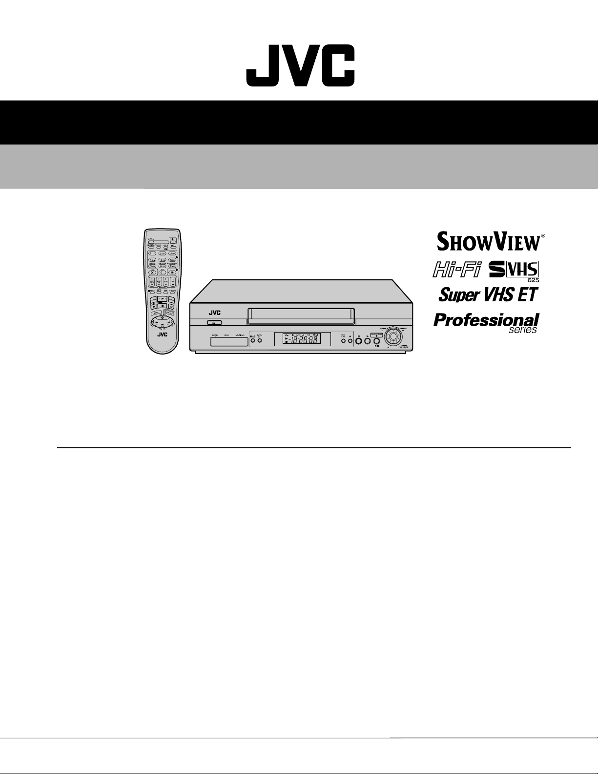
SERVICE MANUAL
VIDEO CASSETTE RECORDER
SR-V10E,
SR-V10EK
Note:
Most of the schematic diagrams for this model are the same as for the HR-S7950EU model. The schematic
diagram and circuit boards that are different in the case of the HR-S7950EU model are described below.
.
MAIN(SYSCON) SCHEMATIC DIAGRAM page 4-57
.
MAIN(MAIN TERMINAL) SCHEMATIC DIAGRAM page 4-53
.
MAIN CIRCUIT BOARD page 4-55
SPECIFICATIONS
GENERAL
Power requirement : AC 220 V – 240 Vd, 50 Hz/60 Hz
Power consumption
Power on : 18 W
Power off : 3.6 W
Temperature
Operating : 5°C to 40°C
Storage : –20°C to 60°C
Operating position : Horizontal only
Dimensions (WxHxD)
Weight : 3.4 kg
Format : S-VHS/VHS PAL standard
Maximum recording time
(SP) : 240 min. with E-240 video cassette
(LP) : 480 min. with E-240 video cassette
(EP) : 720 min. with E-240 video cassette
VIDEO/AUDIO
Signal system : PAL-type colour signal and CCIR
Recording system : DA4 (Double Azimuth) head helical
Signal-to-noise ratio: 45 dB
Horizontal resolution
(SP/LP) : 250 lines (VHS)
(EP) : 220 lines (VHS)
Frequency range : 70 Hz to 10,000 Hz (Normal audio)
Input/Output : RCA connectors:
(The specifications shown pertain specifically to the model SR-V10E.)
: 400 mm x 94 mm x 270 mm
monochrome signal, 625 lines
50 fields
scan system
400 lines (S-VHS)
350 lines (S-VHS)
20 Hz to 20,000 Hz (Hi-Fi audio)
VIDEO IN x 2, VIDEO OUT x 1,
AUDIO IN x 2, AUDIO OUT x 1
S-Video connectors:
IN x 2, OUT x 1
TUNER/TIMER
TV channel storage capacity
Tuning system : Frequency synthesized tuner
Channel coverage : VHF 47 MHz – 89 MHz/
Aerial output : UHF channels 22 – 69 (Adjustable)
Memory backup time
ACCESSORIES
Provided accessories
Specifications shown are for SP mode unless otherwise
specified.
E.& O.E. Design and specifications subject to change without
notice.
This service manual is printed on 100% recycled paper.
COPYRIGHT © 2002 VICTOR COMPANY OF JAPAN, LTD
: 99 positions (+AUX position)
104 MHz – 300 MHz/
302 MHz – 470 MHz
UHF 470 MHz – 862 MHz
: Approx. 6 months
Estimated figure based on provided
fresh battery; actual performance
may differ.
: RF cable,
S-video cable,
Audio/video cable,
Infrared remote control unit,
“R6” battery x 2,
Lithium battery CR2025,
BNC/RCA adapter x 2
SR-V10E, SR-V10EK V15S2
No.82945
October 2002
Page 2

TABLE OF CONTENTS
Section Title Page Section Title Page
DIFFERENCE LIST
Important Safety Precautions
INSTRUCTIONS
1. DISASSEMBLY
1.1 Manually removing the cassette tape ........................................ 1-1
1.2 Removing the major parts .......................................................... 1-2
1.2.1 How to read the procedure table .......................................... 1-2
1.2.2 Disassembly procedure ....................................................... 1-2
1.3 Emergency display function ....................................................... 1-4
1.3.1 Displaying the EMG information .......................................... 1-4
1.3.2 Clearing the EMG history ..................................................... 1-4
1.3.3
Details of the OSD display in the EMG display mode
1.3.4 EMG content description ...................................................... 1-6
1.3.5 EMG detail information<1> .................................................. 1-7
1.3.6 EMG detail information<2> .................................................. 1-8
1.3.7 EMG detail information<3> .................................................. 1-8
1.4 Service position .......................................................................... 1-9
1.4.1 How to set the "Service position" ......................................... 1-9
1.5 Jig RCU mode ............................................................................ 1-9
1.5.1 Setting the Jig RCU mode ................................................... 1-9
1.5.2 Setting the User RCU mode ................................................ 1-9
1.6 Mechanism service mode .......................................................... 1-9
1.6.1 How to set the "Mechanism service mode" .......................... 1-9
1.6.2 How to exit from the "Mechanism service mode" ................. 1-9
1.7 Maintenance and inspection .................................................... 1-10
1.7.1 Cleaning ............................................................................. 1-10
1.7.2 Lubrication ......................................................................... 1-10
1.7.3
Suggested servicing schedule for main components
1.8 Sevicing items related to video navigation ............................... 1-10
2. MECHANISM
2.1. Before disassembling/assembling ............................................ 2-1
2.1.1 Notes .................................................................................... 2-1
2.1.2 Mechanism operation check ................................................ 2-1
2.1.3 Setting the mechanism assembling mode ........................... 2-1
2.1.4 Layout of the main mechanism parts ................................... 2-2
2.1.5 Disassembling procedure table ............................................ 2-3
2.2. Replacement of the main mechanism parts .............................. 2-4
2.2.1 Cassette holder .................................................................... 2-4
2.2.2 A/C head .............................................................................. 2-5
2.2.3 Guide arm, pinch roller arm ................................................. 2-6
2.2.4 Idler arm, idler gear 1/2 ........................................................ 2-6
2.2.5
Main brake(T), brake lever, tension arm,reel disk(S/T), Rec safety lever
2.2.6
Press lever, control cam, capstan brake assembly,loading motor assembly
2.2.7 Capstan motor, load gear, control plate ............................... 2-8
2.2.8 Clutch unit assembly, direct gear ......................................... 2-9
2.3. Mechanism timing chart .......................................................... 2-10
3. ADJUSTMENT
3.1 Before adjustment ...................................................................... 3-1
3.1.1 Precaution ............................................................................. 3-1
3.1.2 Required test equipments .................................................... 3-1
3.1.3 Required adjustment tools ................................................... 3-1
3.1.4 Color(colour) bar signal, color(colour) bar pattern ............... 3-1
3.1.5 Switch settings ..................................................................... 3-1
3.1.6
Manual tracking mode (Auto tracking ON/OFF) setting .................
3.1.7
EVR sdjustment .............................................................................
3.2 Mechanism compatibility adjustment ......................................... 3-2
3.2.1 Tension pole position............................................................ 3-3
3.2.2 FM waveform linearity .......................................................... 3-3
3.2.3 Height and tilt of the A/C head ............................................. 3-3
3.2.4 A/C head phase(X-value) ..................................................... 3-4
3.3 Electrical Adjustment.................................................................. 3-4
.................. 1-5
................. 1-10
.............. 2-6
.............. 2-7
3.3.1 Servo circuit ......................................................................... 3-4
3.3.1.1 Switching point ................................................................ 3-4
3.3.1.2 Slow tracking preset ........................................................ 3-5
3.3.2 Video circuit.......................................................................... 3-5
3.3.2.1 EE Y/PB Y(S-VHS/VHS)level.......................................... 3-5
3.3.3 Audio circuit.......................................................................... 3-5
3.3.3.1 Audio REC FM ................................................................ 3-5
3.3.4 Syscon circuit(EU/EK MODEL) ............................................ 3-6
3.3.4.1 Timer clock ...................................................................... 3-6
3.3.5 PAL/SECAM converter circuit(MS MODEL) ......................... 3-6
3.3.5.1 Colour difference level .................................................... 3-6
3.3.5.2 SECAM burst position ..................................................... 3-6
4. CHARTS AND DIAGRAMS
4.1 BOARD INTERCONNECTIONS ................................................ 4-3
4.2 MAIN(VIDEO/N.AUDIO) SCHEMATIC DIAGRAM..................... 4-5
4.3 MAIN(ON SCREEN) SCHEMATIC DIAGRAM........................... 4-7
4.4
MAIN(SECAM) SCHEMATIC DIAGRAM [HR-S6950MS/S7955MS] ...........
4.5 MAIN(FMA) SCHEMATIC DIAGRAM ........................................ 4-9
4.6 MAIN(SYSCON) SCHEMATIC DIAGRAM................................ 4-11
4.7 MAIN(SW.REG) SCHEMATIC DIAGRAM................................ 4-13
4.8 MAIN(TUNER) SCHEMATIC DIAGRAM.................................. 4-15
4.9 MAIN(FRONT) ,MINI FRONT, S-JACK AND ADV.JOG SCHEMATIC DIAGRAM
4.10
MAIN(MAIN TERMINAL) SCHEMATIC DIAGRAM
4.11
2D DIGITAL SCHEMATIC DIAGRAM [HR-S6950EU/S6955MS/S7955MS] ............
4.12
3D/TBC (2M) SCHEMATIC DIAGRAM [HR-S7950EU/S7955EK]
4.13
TERMINAL(S-SUB) SCHEMATIC DIAGRAM
4.14
TERMINAL(I/O) SCHEMATIC DIAGRAM ....................................
4.15
DEMODULATOR SCHEMATIC DIAGRAM ................................
4.16
S-P CONVERTER SCHEMATIC DIAGRAM [HR-S6955MS/S7955MS] .........
4.17 MAIN CIRCUIT BOARD ......................................................... 4-33
4.18 2D DIGITAL AND 3D DIGITAL/2M CIRCUIT BOARDS ......... 4-36
4.19 DEMODULATOR CIRCUIT BOARD ...................................... 4-37
4.20
S-P CONVERTER CIRCUIT BOARD[HR-S6955MS/S7955MS] ......
4.21
TERMINAL CIRCUIT BOARD ...........................................................
4.22
WAVEFORMS ...................................................................................
4.23
VOLTAGE CHARTS ..........................................................................
4.24
REMOTE CONTROLLER
4.25
FDP GRID ASSIGNMENT AND ANODE CONNECTION
4.26
CPU PIN FUNCTION
4.27
SYSTEM CONTROL BLOCK DIAGRAM
4.28
VIDEO BLOCK DIAGRAM
4.29
AUDIO BLOCK DIAGRAM
4.30
MAIN(MAIN TERMINAL) SCHEMATIC DIAGRAM [SR-V10E, SR-V10EK] .
4.31 MAIN CIRCUIT BOARD [SR-V10E, SR-V10EK] ................... 4-55
4.32
MAIN(SYSCON) SCHEMATIC DIAGRAM [SR-V10E, SR-V10EK]..
5. PARTS LIST
5.1 PACKING AND ACCESSORY ASSEMBLY<M1> ...................... 5-1
5.2 FINAL ASSEMBLY<M2> ............................................................ 5-2
5.3 MECHANISM ASSEMBLY<M4> ................................................ 5-4
5.4 ELECTRICAL PARTS LIST ........................................................ 5-6
3-1
MAIN BOARD ASSEMBLY<03> .................................................... 5-6
3-2
3D D/2M BOARD ASSEMBLY<05> ............................................. 5-12
TERMINAL BOARD ASSEMBLY<06> ......................................... 5-13
A/C HEAD BOARD ASSEMBLY<12> .......................................... 5-15
DEMOD BOARD ASSEMBLY<14> .............................................. 5-15
S.JACK BOARD ASSEMBLY<36>............................................... 5-15
ADV.JOG BOARD ASSEMBLY<38> ............................................ 5-15
LOADING MOTOR BOARD ASSEMBLY<55>............................. 5-15
SCHEMATIC DIAGRAM .................. 4-43
................................................................ 4-44
..................................... 4-45
......................................................... 4-47
......................................................... 4-51
.................... 4-23
........................... 4-25
................... 4-19
............... 4-43
...
4-8
4-17
4-21
4-27
4-29
4-31
4-37
4-38
4-39
4-41
4-53
4-57
Page 3
The following table indicates main different points between models HR-S7950EU, SR-V10E and SR-V10EK.
ITEM
POWER PLUG CEE 3 PIN
BODY COLOR PURE SILVER DARK GRAY
REPEAT TIMES 100 NO LIMIT
MESECAM USED NOT USED
16:9 USED NOT USED
REAR L-1 INPUT USED(SCART) USED(S,V,LR)
REAR L-2 INPUT USED NOT USED
AV OUT S,LR S,V,LR
SATELLITE CONTROLLER TERMINAL
REMOTE PAUSE TERMINAL USED NOT USED
REMOTE TERMINAL NOT USED USED
BROADCASTING STANDARD B/G,D/K I
STEREO DECODER NICAM/A2 NICAM
LITHIUM BATTERY BACKUP NOT USED USED
VCR PLUS SHOVIEW DELUXE SHOWVIEW VCRplus
INSTANT REC MAX TIME 6H NO
REC LINK USED(L-2) USED(L-1)
VPS USED NOT USED
OSD LANGUAGE 13 LANGUAGES ENGLISH
PRESET DOWNLOAD USED NOT USED
DIRECT REC USED NOT USED
TV AUTO POWER ON USED NOT USED
NEXTVIEW LINK USED NOT USED
REPEAT REC, PLAY NOT USED USED
SELECT RETURN POINT (PLAYBACK)
SERIES REC, PLAY NOT USED USED
MODE LOCK NOT USED USED
DAY, TIME INSERT NOT USED USED
REC SAFETY ON/OFF NOT USED USED
LAST FUNCTION MEMORY NOT USED USED
OSD OFF(REC, PLAY) NOT USED USED
WIRED RCU NOT USED USED
DAILY TIMER RECORD NOT USED USED
Note: Mark is same as left.
Mark — is not used.
MODEL
HR-S7950EU
USED NOT USED
NOT USED USED
SR-V10E
SR-V10EK
1
Page 4
Important Safety Precautions
Connector
Metal sleeve
Prior to shipment from the factory, JVC products are strictly inspected to conform with the recognized product safety and electrical codes
of the countries in which they are to be sold. However, in order to maintain such compliance, it is equally important to implement the
following precautions when a set is being serviced.
v
Precautions during Servicing
1. Locations requiring special caution are denoted by labels and
inscriptions on the cabinet, chassis and certain parts of the
product. When performing service, be sure to read and comply with these and other cautionary notices appearing in the
operation and service manuals.
2. Parts identified by the symbol and shaded ( ) parts are
critical for safety.
Replace only with specified part numbers.
Note: Parts in this category also include those specified to com-
ply with X-ray emission standards for products using
cathode ray tubes and those specified for compliance
with various regulations regarding spurious radiation
emission.
3. Fuse replacement caution notice.
Caution for continued protection against fire hazard.
Replace only with same type and rated fuse(s) as specified.
4. Use specified internal wiring. Note especially:
1) Wires covered with PVC tubing
2) Double insulated wires
3) High voltage leads
5. Use specified insulating materials for hazardous live parts.
Note especially:
1) Insulation Tape 3) Spacers 5) Barrier
2) PVC tubing 4) Insulation sheets for transistors
6. When replacing AC primary side components (transformers,
power cords, noise blocking capacitors, etc.) wrap ends of
wires securely about the terminals before soldering.
12. Crimp type wire connector
In such cases as when replacing the power transformer in sets
where the connections between the power cord and power
transformer primary lead wires are performed using crimp type
connectors, if replacing the connectors is unavoidable, in order to prevent safety hazards, perform carefully and precisely
according to the following steps.
1) Connector part number : E03830-001
2) Required tool : Connector crimping tool of the proper type
which will not damage insulated parts.
3) Replacement procedure
(1) Remove the old connector by cutting the wires at a point
close to the connector.
Important : Do not reuse a connector (discard it).
cut close to connector
Fig.3
(2) Strip about 15 mm of the insulation from the ends of
the wires. If the wires are stranded, twist the strands to
avoid frayed conductors.
15 mm
Fig.1
7. Observe that wires do not contact heat producing parts
(heatsinks, oxide metal film resistors, fusible resistors, etc.)
8. Check that replaced wires do not contact sharp edged or
pointed parts.
9. When a power cord has been replaced, check that 10-15 kg of
force in any direction will not loosen it.
Power cord
Fig.2
10. Also check areas surrounding repaired locations.
11. Products using cathode ray tubes (CRTs)
In regard to such products, the cathode ray tubes themselves,
the high voltage circuits, and related circuits are specified for
compliance with recognized codes pertaining to X-ray emission.
Consequently, when servicing these products, replace the cathode ray tubes and other parts with only the specified parts.
Under no circumstances attempt to modify these circuits.
Unauthorized modification can increase the high voltage value
and cause X-ray emission from the cathode ray tube.
Fig.4
(3) Align the lengths of the wires to be connected. Insert
the wires fully into the connector.
Fig.5
(4) As shown in Fig.6, use the crimping tool to crimp the
metal sleeve at the center position. Be sure to crimp fully
to the complete closure of the tool.
1.25
2.0
5.5
Fig.6
(5) Check the four points noted in Fig.7.
Not easily pulled free
Wire insulation recessed
more than 4 mm
Fig.7
Crimping tool
Crimped at approx. center
of metal sleeve
Conductors extended
1
S40888-01
Page 5
v
d'
d
Chassis
Power cord,
primary wire
Safety Check after Servicing
Examine the area surrounding the repaired location for damage or deterioration. Observe that screws, parts and wires have been
returned to original positions, Afterwards, perform the following tests and confirm the specified values in order to verify compliance with safety standards.
1. Insulation resistance test
Confirm the specified insulation resistance or greater between power cord plug prongs and
externally exposed parts of the set (RF terminals, antenna terminals, video and audio input
and output terminals, microphone jacks, earphone jacks, etc.). See table 1 below.
2. Dielectric strength test
Confirm specified dielectric strength or greater between power cord plug prongs and exposed
accessible parts of the set (RF terminals, antenna terminals, video and audio input and output
terminals, microphone jacks, earphone jacks, etc.). See table 1 below.
3. Clearance distance
When replacing primary circuit components, confirm specified clearance distance (d), (d’) between soldered terminals, and between terminals and surrounding metallic parts. See table 1
below.
Fig. 8
4. Leakage current test
Confirm specified or lower leakage current between earth ground/power cord plug prongs
and externally exposed accessible parts (RF terminals, antenna terminals, video and audio
input and output terminals, microphone jacks, earphone jacks, etc.).
Measuring Method : (Power ON)
Insert load Z between earth ground/power cord plug prongs and externally exposed accessible parts. Use an AC voltmeter to measure across both terminals of load Z. See figure 9 and
following table 2.
Externally
exposed
accessible part
Z
V
Fig. 9
ab
c
5. Grounding (Class 1 model only)
Confirm specified or lower grounding impedance between earth pin in AC inlet and externally exposed accessible parts (Video in,
Video out, Audio in, Audio out or Fixing screw etc.).
Measuring Method:
Connect milli ohm meter between earth pin in AC inlet and exposed accessible parts. See figure 10 and grounding specifications.
AC inlet
Earth pin
AC Line Voltage
100 V
100 to 240 V
110 to 130 V
110 to 130 V
200 to 240 V
Exposed accessible part
Milli ohm meter
Fig. 10
Region
Japan
USA & Canada
Europe & Australia R 10 MΩ/500 V DC
Region Load Z
Insulation Resistance (R)
≤
R 1 MΩ/500 V DC
≥≥
1 MΩ R 12 MΩ/500 V DC
≤
Table 1 Specifications for each region
Grounding Specifications
Region
USA & Canada
Europe & Australia
Dielectric Strength
AC 1 kV 1 minute
AC 1.5 kV 1 miute
AC 1 kV 1 minute
AC 3 kV 1 minute
AC 1.5 kV 1 minute
(Class 2)
(Class 1)
Grounding Impedance (Z)
≤
Z 0.1 ohm
≤
Z 0.5 ohm
Clearance Distance (d), (d')
≤
d, d' 3 mm
≤
d, d' 4 mm
≤
d, d' 3.2 mm
≤
d 4 mm
≤
d' 8 mm (Power cord)
≤
d' 6 mm (Primary wire)
a, b, cLeakage Current (i)AC Line Voltage
100 V
110 to 130 V
110 to 130 V
220 to 240 V
Note: These tables are unofficial and for reference only. Be sure to confirm the precise values for your particular country and locality.
Japan
USA & Canada
Europe & Australia
Table 2 Leakage current specifications for each region
1 kΩ
0.15 µF
1.5 kΩ
2 kΩ
50 kΩ
2
≤
i 1 mA rms Exposed accessible parts
≤
i 0.5 mA rms
≤
i 0.7 mA peak
≤
i 2 mA dc
≤
i 0.7 mA peak
≤
i 2 mA dc
Exposed accessible parts
Antenna earth terminals
Other terminals
S40888-01
Page 6
SECTION 1
DISASSEMBLY
1.1 Manually removing the cassette tape
If you cannot remove the cassette tape which is loaded because of any electrical or mechanical failures, manually remove
it by taking the following steps.
(1) Unplug the power cord plug from the power outlet.
(2) Refer to the disassembly procedure of the VCR and perform
the disassembly of the major parts before removing the
mechanism assembly. (See Fig. 1-1a)
Fig. 1-1a
Tension arm assembly
Pole base assembly
Pinch roller arm assembly
(3) Unload the pole base assembly by manually turning the gear
of the loading motor until the pole base assembly is hidden
behind the cassette lid. In doing so, hold the tape by the hand
to keep the slack away from any grease. (See Fig. 1-1b.)
In case of mechanical failures, while keeping the tension arm
assembly free from tension, pull out the tape on the pole
base assembly. Take the spring(a) of the pinch roller arm
assembly off the hook, and detach it from the tape.
(4) Remove the screw (a) of the side frame (L/R).
(5) Hold the slack tape and cassette cover together, lift the
cassette tape, top frame, cassette holder and side frames
(L, R) together from the rear and remove them by dis-
engaging the hooks (a) and (b).
Screw(a)
Cassette tape
Hook(a)
Side frame(L)
Cassette holder
Top frame
Side frame(R)
Screw(a)
Hook(b)
Spring(a)
Fig. 1-1c
(6) Take up the slack of the tape into the cassette. This com-
pletes removal of the cassette tape.
Direction of unloading
Fig. 1-1b
1-1
Page 7
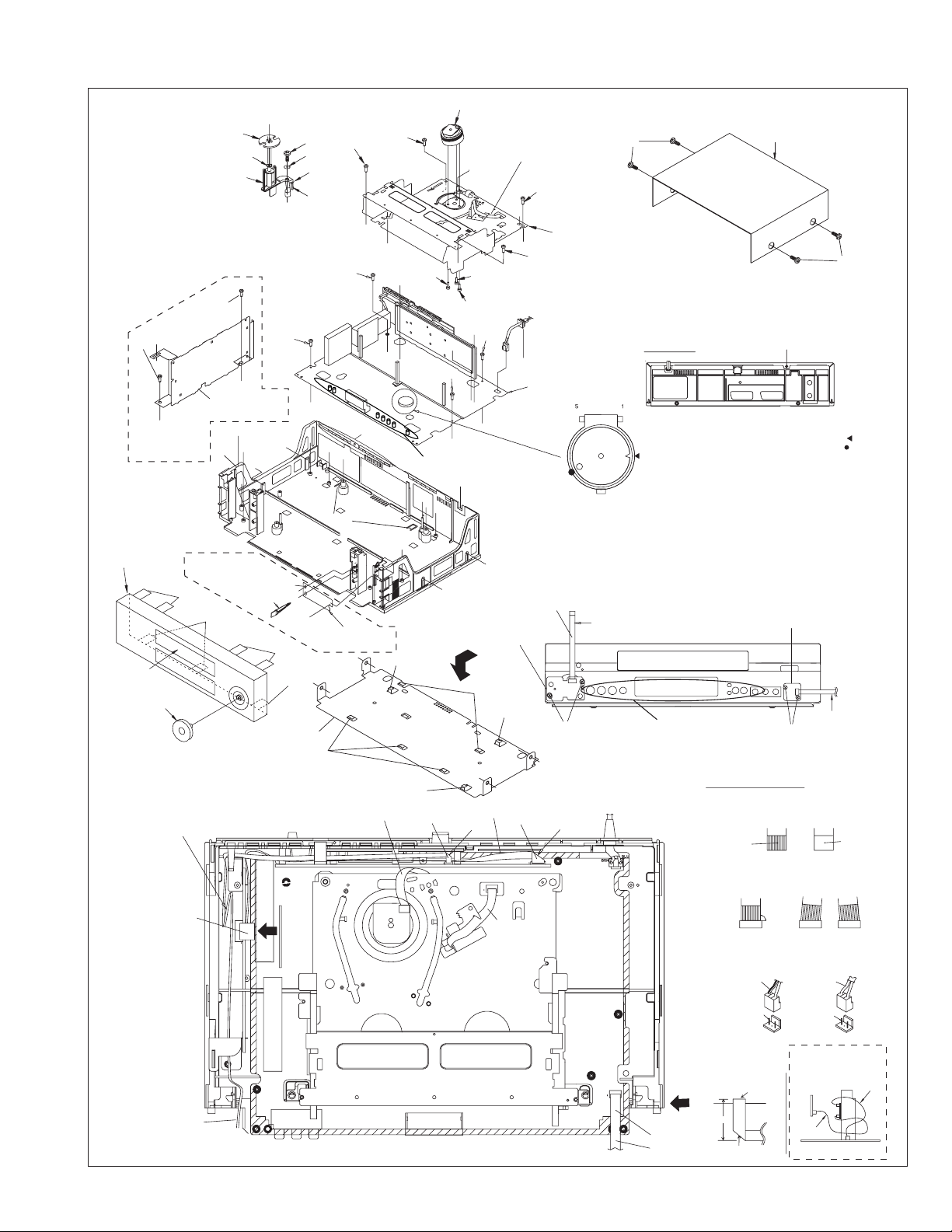
1.2 Removing the major parts
1.2.1 How to read the procedure table
This table shows the steps for disassembly of the externally
furnished parts and board assemblies. Reverse these steps
when re-assembling them.
<Example>
Step/
Loc No.
Part Name
[1] Top cover, 1-3a
Bracket 2(S1c)
(1) (2) (3) (4) (5)
Fig.
No.
Point Note
4(S1a),(S1b),3(L1a), <Note 1a>
2(SD1a),(P1a),(W1a),
CN1(WR1a),
----------------------------------------
(1) Order of steps in Procedure
When reassembling, perform the step(s) in the reverse order.
These numbers are also used as the identification (location) No. of
parts Figures.
(2) Part name to be removed or installed.
(3) Fig. No. showing procedure or part location.
(4) Identification of part to be removed, unhooked, unlocked,
released, unplugged, unclamped or unsoldered.
P= Spring, W= Washer, S= Screw, L= Locking tab, SD= Solder,
CN**(WR**)= Remove the wire (WR**) from the connector (CN**).
Note:
•
The bracketed ( ) WR of the connector symbol are assigned nos. in priority order and do not correspond to
those on the spare parts list.
(5) Adjustment information for installation
1.2.2
Disassembly procedure
Step/
Loc No.
Part Name
[1] Top cover
[2] Front panel
assembly CN7005(WR2a) <
--------------------------------------------------------------------------
[HR-S7955MS] CN7001(WR2c)
Mini front board assembly
--------------------------------------------------------------------------
(
ADV. Jog board assembly)2(S2b), Knob assembly
--------------------------------------------------------------------------
(Front S jack board assembly)
[3] Mechanism
assembly (S3a), (S3b) <
(Drum assembly) CN1(WR3b),
(Inertia plate) 4(L3b)
(Roller arm assembly) (S3g), (W3a), (P3a),
[4]
[HR-S6955MS, S7955MS]
S/P Converter board assembly
[5]
Main board assembly
[6] Bottom cover
Fig.
No.
1-2-2d
1-2-2d
--------------------------
Point Note
4(S1a), (S1b)
[HR-S7955MS] <
[HR-S6950EU, S6950MS
HR-S7950EU, S7955EK]
CN7001(WR2a),
--------------------------
CN916(WR2b),
2(S2a), 4(L2a), 3(L2b)
(L2c), (L2d),
PC Support
2(S2c)
1-2-2d
CN2001(WR3a), <
--------------------------
(S3c), (S3d), (S3e)
--------------------------
--------------------------
(L3c)
1-2-2d
CN511(WR4a)
2(S4a), (L4a)
1-2-2d
(S5a), 3(S5b), (L5a)
1-2-2d
3(L6a), 5(L6b), 2(L6c)
Note 2a
Note 2b
Note 2a
Note 3a
<
Note 3b
<
Note 3c
<Note 2a>
• Be careful not to damage the connector and wire etc. during
connection and disconnection.
• When connecting the flat wire to the connector, be careful with
the flat wire direction.
<Note 2b>
• When reattaching the Front panel assembly , make sure that
the door opener of the Side frame (R) is lowered in position
prior to the reinstallation.
• When reattaching the Front panel assembly, pay careful attention to the switch lever of the Front panel assembly not to make
it touch the switch knob of the Main board assembly from the
side.
• When reattaching the Front panel assembly , lift the Cassette
door slightly.
Door
opener
Switch
knob
Switch
lever
<Note 3a>
Side
frame(R)
Fig. 1-2-2a
• When reattaching the Mechanism assembly, secure the screws
(S3a to S3b) in the order of a, b.
<Note 3b>
• When reattaching the Mechanism assembly , be sure to align
the phase of the Rotary encoder on the Main board assembly.
• When reattaching the Mechanism assembly, set the “Mechanism assembling mode”. (See “section 2 mechanism”.)
• When reattaching the Mechanism assembly to the Main board
assembly, take care not to damage the sensors and switch on
the Main board assembly.
(S3c)
(S3d)
Mechanism
>
assembly
(S3e)
(S3d)
>
Drum
assembly
<Note 3c>
<Note 3c>
<NOTE>
Attach the Drum assembly appropriately,
since the installation state of the Drum assembly
influences the FM WAVEFORM LINEARITY
greatly.
Fig. 1-2-2b
(S3c)
(S3e)
HOOK
• When reattaching the Drum assembly, secure the screws (S3c
to S3e) in the order of c, d, e.
• When handling the drum assembly alone, hold it by the motor
or shaft. Be careful not to touch other parts, especially the video
>
>
>
>
heads. Also take care not to damage the connectors.
Shaft
Motor
Video heads
Fig. 1-2-2c
1-2
Page 8
NOTE) INERTIA PLATE should be attached so as to ser small
Roller arm assembly
(S4a)
k
h
ONLY USED FOR
HR-S6955MS,
HR-S7955MS
[2] Front panel
assembly
<Note 2b>
Cassette door
<Note 2b>
Knob assembly
The excessive length portion
of wire should be reat as figure.
diameter of central round hole above.
Inertia plate
(L3b)
(S3g)
(W3a)
(P3a)
<Note 3e>
NOTE) When attaching ROLLER ARM ASS'Y,
attach the hook(L3c) before the spring(P3a).
NOTE) After attached ROLLER ARM ASS'Y,
tighten screw(S3g) with slit washer(W3a).
(L3c)
g
(S4a)
(S5a)
h
[4] S/P conveter board
assembly
k
a
(L4a)
f
h
a
h
f
"Z"
ONLY USED
FOR HR-S7955MS
(L2a)
(L2b)
(L2c)
PC Support
(L2d)
[2]Mini front board
(L2a)
(L2b)
[6] Bottom cover
(L6b)
right side
CN1601
A
(S2a)
(S5b)
b
c'
(L6c)
assembly
f
<Note 2a>
<Note 3a>
Q3003
(L5a)
(WR3b)
(S3a)
e
b
f
DRUM
<Note 3c>
c
JS3001
(L6a)
Drum assembly
d
(S3c)
c'
(S5b)
D3001
Q3002
Switch knob
<Note 2b>
d'
c'
b
b
f
(L6a)
back side
CN916
g
a
<Note 3c>
(S3d)
<Note 3c>
c
d
d'
c'
b
e
Make a crease
A/C HEAD
(WR3a)
<Note 2a>
(S3b)
<Note 3a>
[3] Mechanism assembly
<Note 3b>
d
(S2a)
(S3e)
C
N5001
e
[5]Main board
Insert the bushing of POWER CORD
so as not to twist the cord.
assembly
REAR SIDE
(S5b)
JS3001
b
For the prevention of the DRUM FPC damage.
When you attach the Mechanism assembly on Bottom chassis.
Attach the Mechanism assembly after the positioning boss "z" of the
Bottom chassis is matched to the positioning hole of the Mehcanism assembly.
NOTE) INSERT FFC WIRE TO THE CONNECTOR BEFORE
f
ATTACHING JOG/SW PWB TO F.PANEL.
NOTE)INSERT FFC WIRE TO THE CONNECTOR
BEFORE ATTACHING JOG/SW PWB TO F.PANEL.
Back side
CN7003
(WR2a)
<Note 2a>
ADV. Jog board
assembly
(L6b)
(L6a)
(S2b)
f
f
<Note 2a>
(WR4a)
back side
Make a crease
(WR3a)
<Note 2a>
CN511
CN2001
<Phase alignment>
Accord the position of V gap on R. Encoder and PWB silk " ".
Accord the position of Boss on R. Encoder and PWB silk " ".
NOTE) WHEN YOU FIX FRONT S Jack PWB WITH THE SCREW.
PUT JIG UNDER FRONT PANEL ASS'Y.
Front panel assembly back side
Switch lever
<Note 2b>
CN5001
(S1a)
[1] Top cover
(S1a)
(S1b)
Front S Jack board assembly
CN7108
(WR2b)
<Note 2a>
(S2c)
NOTE
1. Insert direction of FFC WIRE as follows.
Right side Back side
electrode side
2. FFC WIRE and DRUM FPC WIRE should
be insert as follows.
OK
90°
CN
3. Insert direction of POWER CORD.
U/U(C)/JPN
WHITE LINE
supporting side
NG
CN CN
Except U/U(C)/JPN
BLUE
(WR2b)
<Note 2a>
To Front S Jack board assembly
Fig. 1-2-2d
CN7001
To Adv. Jog board assembly
right side
(WR2a)
<Note 2a>
B
DETAIL "A"
About 5cm
Make a crease
NEUTRAL
Make a crease
P/S CONV PWB
NEUTRAL
CN5001
ONLY USED
FOR HR-S7955MS
DETAIL "B"
FRONT PANEL
CN7002
CN7005
(WR2a)
Push the FFC wire from the FRONT PANEL
to rear side.
CN5001
(WR2c)
CN7001
1-3
Page 9
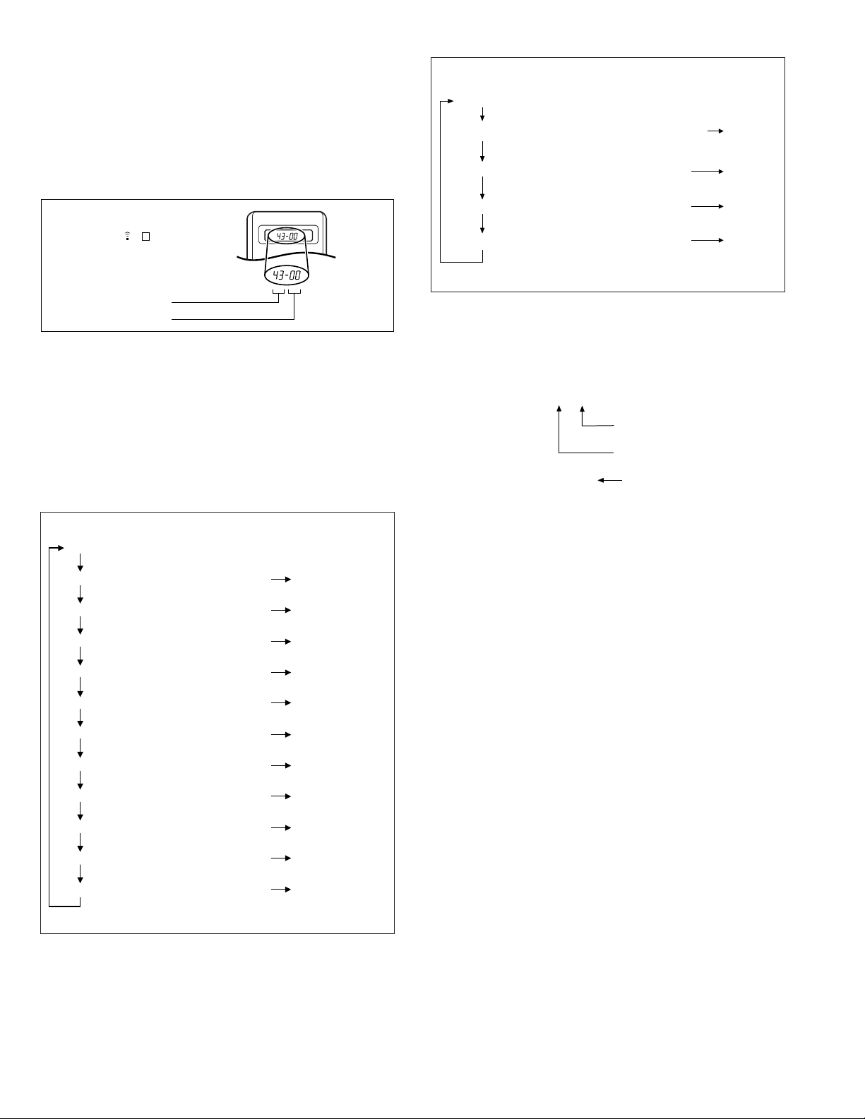
1.3 Emergency display function
This unit saves details of the last two emergencies as the EMG
history and allows the status of the VCR and the mechanism
of each emergency to be shown both on the display and as
OSD information.
When using the emergency function, it is required to set the
VCR to the Jig RCU mode (the mode in which codes from the
Jig RCU can be received).
Jig RCU
[Data transmitting method]
Depress the “ ” ( 3 ) button
after the data code is set.
CUSTOM CODE
43: A CODE
DATA CODE
INITIAL MODE
0 : 00 : 00
E:**:**
*1 : *2 : 34
*5: *6 : *7
*8: *9 : *10
Normal display (Counter or clock)
EMG content display (E:Latest:Previous) See 1.3.4.
[EMG code display mode]
EMG detail information <1> display See 1.3.5.
[Deck and other mode display mode]
EMG detail information <2> display See 1.3.6.
[Cassette display mode]
EMG detail information <3> display See 1.3.7.
[Deck mode history dispaly mode]
Fig. 1-3-1b EMG display of FDP display model
Fig. 1-3a Jig RCU [PTU94023B]
1.3.1 Displaying the EMG information
The EMG detail of information can be displayed by transmitting the code "59" from the Jig RCU.
Note:
•
The EMG detail information <1><2> show the information on
the latest EMG.
It becomes “ – – : – – : – –” when there is no latest EMG
record.
0: 00
E: **
1E: **
1: *1
2: *2
3: 34
4: *5
5: *6
6: *7
7: *8
8: *9
9: *10
Normal display
EMG content display (Latest) See 1.3.4.
EMG content display (Previous) See 1.3.4.
EMG detail information <1> See 1.3.5.
[Deck operation mode]
EMG detail information <1> See 1.3.5.
[Mechanism operation mode]
EMG detail information <1> See 1.3.5.
[Mechanism sensor information and Mechanism mode position]
EMG detail information <2> See 1.3.6.
[Type of the cassette tape in use <1>]
EMG detail information <2> See 1.3.6.
[Winding position of the cassette tape in use]
EMG detail information <2> See 1.3.6.
[Type of the cassette tape in use <2> (Winding area)]
EMG detail information <3> See 1.3.7.
[Previous deck operation mode]
EMG detail information <3> See 1.3.7.
[The deck operation mode of the one before the last]
EMG detail information <3> See 1.3.7.
[The deck operation mode of the one prior to one above]
Fig. 1-3-1a EMG display of 7segment LED display model
<Reference> EMG display of FDP display mode
(1) Transmit the code “59” from the Jig RCU.
The FDP shows the EMG content in the form of “E:**:**”.
<Example 1> E : 01 : 03
Previous EMG
Latest EMG
<Example 2> E : – – : – –
No EMG record
(2) Transmit the code “59” from the Jig RCU again.
The FDP shows the EMG detail information <1> in the form
of “ * 1 : * 2 : 34 ”.
* 1 : Deck operation mode at the moment of EMG
* 2 : Mechanism operation mode at the moment of EMG
3– : Mechanism sensor information at the moment of
EMG
–4 : Mechanism mode position at the moment of EMG
(3) Transmit the code “59” from the Jig RCU once again.
The FDP shows the EMG detail information <2> in the form
of “ * 5 : * 6 : * 7 ”.
* 5 : Type of the cassette tape in use <1> .
* 6 : Winding position of the cassette tape in use
* 7 : Type of the cassette tape in use <2> (Winding area)
(4) Transmit the code “59” from the Jig RCU once again.
The FDP shows the EMG detail information <3> in the form
of “*8 : *9 : *10”.
* 8 : Previous deck operation mode at the moment of
EMG
* 9 : The deck operation mode of the one before the last
at the moment of EMG
* 10 : The deck operation mode of the one prior to one
above at the moment of EMG
(5) Transmit the code “59” from the Jig RCU once again to re-
set the display.
1.3.2 Clearing the EMG history
(1) Display the EMG history.
(2) Transmit the code “36” from the Jig RCU.
(3) Reset the EMG display.
1-4
Page 10
1.3.3 Details of the OSD display in the EMG display mode
During the EMG display, the OSD shows the data on the deck
mode, etc. The details of the display contents are as follows.
Notes:
•
The display is variable depending on the part No. of the
System Control microcomputer (IC3001) built into the
VCR. In the following, refer to the figure carrying the same
two characters as the top two characters of the part
number of your IC.
•
The sensor information in the OSD display contents is par-
tially different from the mechanism sensor information in
EMG detail information <1>.
[For *HD only]
AA BB CC
DD EE FF
GGGG HHHH
I I JJJJ
KKKK LLLL MMMM
ROM No.
[For MN* only]
AA BB CC DD EE
FF GG HH I I J J
KK LL MM NN OO
PP QQ RR SS T T
UU VV WW XX YY
A A : Deck operation mode (See EMG detail information <1>.)
BB :
Mechanism operation mode (See EMG detail of information <1>.)
C C : Mechanism transition flag
D D : Capstan motor control status
E E : Loading motor control status
F F : Sensor information (See sensor information details.)
GG : Capstan motor speed
HH : Key code (JVC code)
I I : Supply reel winding diameter data, higher 8 bits.
J J : Supply reel winding diameter data, lower 8 bits.
KK : Mechanism sensor information & mechanism mode position
(See EMG detail of information <1>.)
L L : Tape speed data, higher 8 bits.
MM : Tape speed data, lower 8 bits.
N N : Cassette tape type <2>, higher 8 bits.
(See EMG detail of information <2>.)
OO : Cassette tape type <2>, lower 8 bits.
(See EMG detail of information <2>.)
P P : General data display area
Y Y : General data display area
*FF: Sensor information details
<Display>
** h
********
Encoder data
(See Mechanism mode sequence.)
Cassette tab present = 1
Cassette tab broken = 0
Cassette absent = 1
Cassette present = 0
Start sensor
End sensor
A A : Key code (JVC code)
B B : Deck operation mode (See EMG detail information <1>.)
Mechanism operation mode (See EMG detail information <1>.)
CC :
D D : Sensor information (See sensor information details.)
E E : Capstan motor speed (Search, double speed)
F F : Tracking value
GGGG: Cassette tape type <2>, 16 bits.
(See EMG detail information <2>.)
HHHH : Supply reel winding diameter data
I I : Capstan motor speed (FF/REW, double speed)
JJJJ: Tape speed data, lower 8 bits.
KKKK : General data display area
LLLL : General data display area
MMMM : General data display area
*DD: Sensor information details
<Display>
** h
********
Encoder data
(See Mechanism mode sequence.)
Remote pause
End sensor
Start sensor
Cassette tab present = 1
Cassette tab broken = 0
[For both MN*/HD*]
Mechanism mode sequence
Mechanism mode - Encoder data
LSA
LSB
LSC
LSD
No. Position Encoder data
21
Encoder output = Low
or
Trerminal - GND = SHORT
1
2
3
4
5
6
7
8
9
10
11
12
EJECT 0 h = 0000
EJECT1 1 h = 0001
EJECT2 2 h = 0010
ULSTOP 3 h = 0011
UPPER 4 h = 0100
ONSTOP(PLAY) 5 h = 0101
FWD/SS 6 h = 0110
REV/SS 7 h = 0111
OFFSTOP 8 h = 1000
FFREW-BRAKE 9 h = 1001
FFREW A h = 1010
MIDDLE F h = 1111
543
Encoder output = High
or
Trerminal - GND = OPEN
LSD
9876
LSC
LSB
LSA
12345
1110
GND
1-5
Page 11

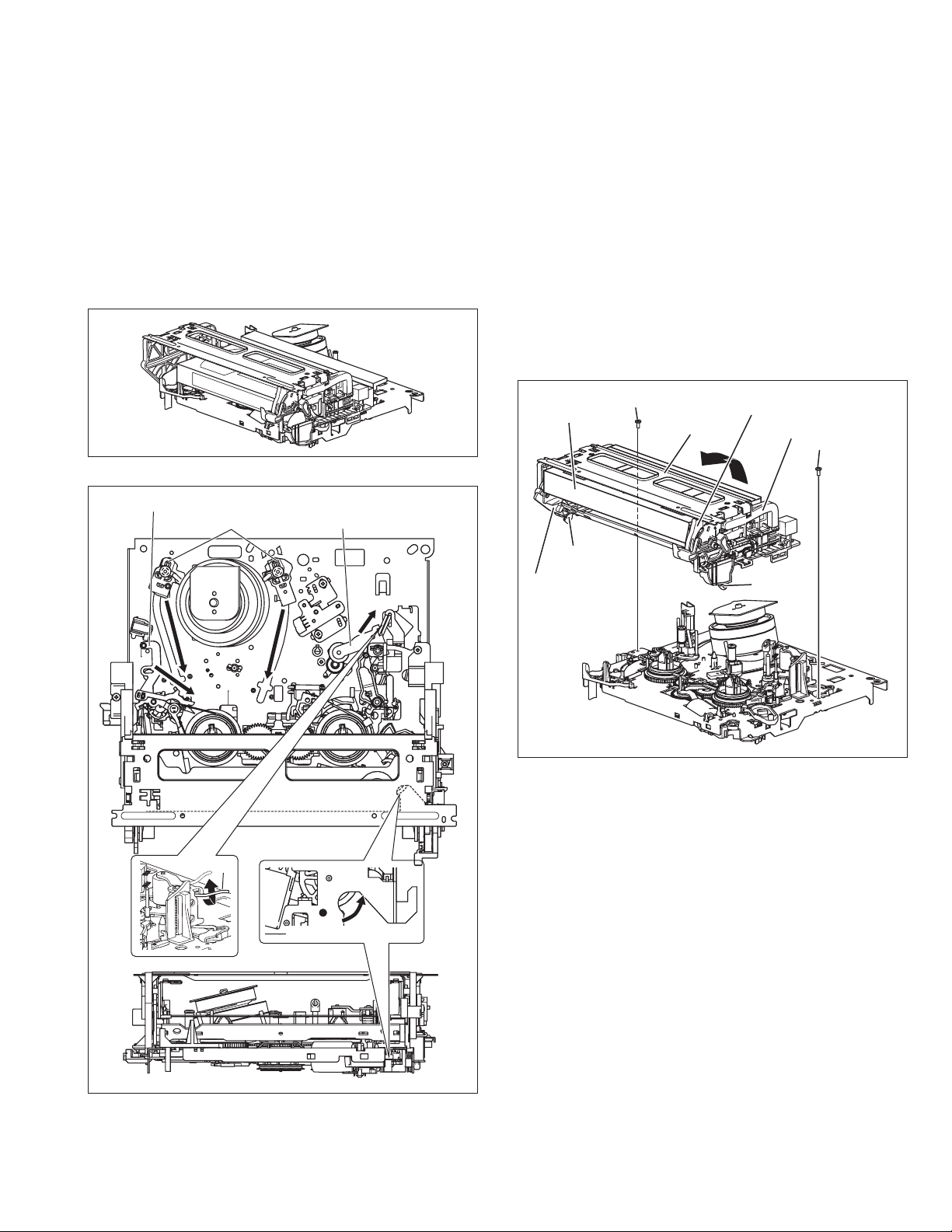
1.3.4 EMG content description
EMG contents “E08/E09” are for the model with Dynamic Drum (DD).
Note:
FDP CONTENT CAUSE
E01: Loading EMG
E02:
Unloading EMG
E03: Take Up Reel
Pulse EMG
E04: Drum FG EMG
E05: Cassette Eject
EMG
E06: Capstan FG
EMG
E07: SW Power
Short-Circuit
EMG
E08:
DD Initialized
(Absolute
Position
Sensor) EMG
E09: DD FG EMG
E0A: Supply Reel
Pulse EMG
EU1:
Head clog warning
history
1-6
If the mechanism mode does not change to the next mode within 4 seconds after the loading motor starts rotating in the loading direction, while
the mechanism is in the after-loading position (with the tape up against
the pole base), [E:01] is identified and the power is switched OFF.
However, if the tape loading is not completed within 4 seconds after
the loading motor starts rotating in the loading direction, the tape is
simply unloaded and ejected. No EMG data is recorded in this case.
When the mechanism mode cannot be changed to another mode
even when the loading motor has rotated for more than 4 seconds in the unloading direction, [E:02] is identified and the power
is turned off.
When the falling edje of the take-up reel pulse has not been generated for more than 4 seconds in the capstan rotating mode,
[E:03] is identified, the pinch rollers are turned off and stopped,
and the power is turned off. In this case, however, the mechanism should be in position after tape loading. Note that the reel
EMG is not detected during Slow/Frame advance operations.
When the drum FG pulse has not been input for more than 3 seconds in the drum rotating mode, [E:04] is identified, the pinch rollers are turned off and stopped, and the power is turned off.
If the cassette does not reach the eject position within about 0.7
seconds after the cassette housing has started the cassette ejection operation, [E:05] is identified, the drive direction is reversed
to load the tape, the mode is switched to STOP mode with the
pinch roller OFF, and the power is switched OFF.
During the cassette insertion process, the drive direction is reversed
and the cassette is ejected if the tape is not up against the pole
base within about 3 seconds after the start of the cassette pullingin operation. If the cassette does not reach the eject position within
about 0.7 seconds after the drive mode reversal operation, [E:05]
is identified and the power is switched OFF immediately.
When the capstan FG pulse has not been generated for more
than 1 second in the capstan rotating mode, [E:06] is identified,
the pinch rollers are turned off and stopped, and the power is
turned off.However, the capstan EMG is not detected in SLOW/
STILL modes.
Note that, if the part number of the System Control IC begins with
“MN” or “M3”, the capstan EMG is not detected even during the
FF/REW operation.
When short-circuiting of the SW power supply with GND has lasted
for 0.5 second or more, [E:07] is identified, all the motors are
stopped and the power is turned off.
When DD tilting does not complete in 4 seconds, [E:08] is identified, the tilt motor is stopped and the power is turned off.
When the DD FG pulse is not generated within 2.5 seconds, [E:09]
is identified, the tilt motor is stopped and the power is turned off.
When the falling edge of the supply reel pulse has not been generated for more than 10 seconds in the capstan rotating mode,
[E:0A] is identified and the cassette is ejected (but the power is
not turned off). In this case, however, the mechanism should be
in the position after tape loading (with the tape up against the pole
base). Also note that the reel EMG is not detected during Slow/
Frame advance operations.
Presupposing the presence of the control pulse output in the PLAY mode, when the value obtained by mixing the two V.FM output channels (without regard
to the A.FM output) has remained below a certain threshold level for more than 10 seconds, [E:U1] is identified and recorded in the emergency history.
During the period in which the head clog is detected, the FDP shows "U:01" and the OSD repeats the “3 seconds of warning display” and the “7 seconds of
noise picture display” alternately.
EMG code : “E:C1” or “E:U1” / FDP : “U:01” / OSD : “Try cleaning tape.” or “Use cleaning cassette.”
The head clog warning is reset when the above-mentioned threshold has been exceeded for more than 2 seconds or the mode is changed to another mode
than PLAY.
1. The mechanism is locked in the middle of the mode transition during a tape loading operation.
2.
The mechanism overruns during the tape loading operation because the SYSCON cannot recognize
the mechanism mode normally. This problem is due to a cause such as a rotary encoder failure.
3.
Power is not supplied to the loading MDA. (M12V/Vcc/Vref/ICP are disconnected in
the middle.)
1.
The mechanism is locked in the middle of mode transition.
2.
Without an eject signal being sent from the SYSCON, unloading is attempted (i.e. Ejection is attempted while the tape is still inside the mechanism.) because the SYSCON
cannot recognize the mechanism mode normally. This is due to a cause such as a
rotary encoder failure. (Mechanism position: UPPER)
3.
Power is not supplied to the loading MDA. (M12V/Vcc/Vref/ICP are disconnected in the middle.)
1.
The take-up reel pulse is not generated in the FWD transport modes (PLAY/FWD
SEARCH/FF, etc.) because;
1)The idler gear is not meshed with the take-up reel gear because the mechanism malfunctions for some reason.
2)
The idler gear is meshed with the take-up reel gear, but incapable of winding due to
too large mechanical load (abnormal tension);
3)The reel is rotating normally but an FG pulse is not generated due to the take-up reel
sensor failure.
2.
The supply reel pulse is not generated in the REV transport modes (REV SEARCH/
REW, etc.) because;
1) The idler gear is not meshed with the supply reel gear because the mechanism mal-
functions for some reason.
2) The idler gear is meshed with the supply reel gear, but incapable of winding due to
too large a mechanical load (abnormal tension);
3) The reel rotates normally but the FG pulse is not generated due to a supply reel
sensor failure.
3.
Power(SW5V) is not supplied to the reel sensor on the tape winding side.
1.
The drum could not start or the drum rotation has stopped due to too large a load on
the tape, because;
1) The tape tension is abnormally high;
2)
The tape is damaged or a foreign object (grease, etc.) adheres to the tape.
2.
The drum FG pulse did not reach the System controller CPU because;
1) The signal circuit is disconnected in the middle;
2) The FG pulse generator (hall device) of the drum is faulty.
3.
The drum control voltage (DRUM CTL V) is not supplied to the MDA.
4.
Power (M12V) is not supplied to the drum MDA.
1.
The cassette cannot be ejected due to a failure in the drive mechanism of the housing.
2.
When the housing load increases during ejection, the loading motor is stopped because
of lack of headroom in its drive torque.
Housing load increasing factors: Temperature environment (low temperature, etc.),
mechanism wear or failure.
3.
The sensor/switch for detecting the end of ejection are not functioning normally.
4.
The loading motor drive voltage is lower than specified or power (M12V) is not supplied to the motor (MDA).
5.
When the user attempted to eject a cassette, a foreign object (or perhaps the user's
hand) was caught in the opening of the housing.
1.
The capstan could not start or the capstan rotation has stopped due to too large a load
on the tape, because;
1) The tape tension is abnormally high (mechanical lock);
2) The tape is damaged or a foreign object (grease, etc.) is adhered to the tape (occur-
rence of tape entangling, etc.).
2.
The capstan FG pulse did not reach the System controller CPU because;
1) The signal circuit is disconnected in the middle;
2) The FG pulse generator (MR device) of the capstans is faulty.
3.
The capstan control voltage (CAPSTAN CTL V) is not supplied to the MDA.
4.
Power (M12V, SW5V) are not supplied to the capstan MDA.
1.
The SW 5 V power supply circuit is shorted with GND.
2.
The SW 12 V power supply circuit is shorted with GND.
1. The absolute value sensor is defective. (The soldered parts have separated.)
2. The pull-up resistor at the absolute sensor output is defective. (The soldered parts have separated.)
3. Contact failure or soldering failure of the pins of the connector (board-to-board) to the absolute value
sensor.
4.
The absolute value sensor data is not sent to the System Controller CPU.
1. The FG sensor is defective. (The soldered parts have separated.)
2. The pull-up resistor at the FG sensor output is defective. (The soldered parts have separated.)
3. Contact failure or soldering failure of the pins of the connector (board-to-board) to the FG sensor.
4. The power (5V) to the sensor is not supplied. (Connection failure/soldering failure)
5. The FG pulse is not sent to the System Controller CPU.
6.
The tilt motor is defective. (The soldered parts have separated.)
7. The drive power to the tilt motor is not supplied. (Connection failure/soldering failure)
8. The tilt motor drive MDA - IC is defective.
9. Auto-recovery of the DD tilting cannot take place due to overrun.
1.
The supply reel pulse is not generated in the FWD transport mode (PLAY/FWD
SEARCH/FF, etc.) because;
1) PLAY/FWD or SEARCH/FF is started while the tape in the inserted cassette is cut in
the middle;
2) A mechanical factor caused tape slack inside and outside the supply reel side of the
cassette shell. In this case, the supply reel will not rotate until the tape slack is removed by the FWD transport, so the pulse is not generated until then;
3) The reel is rotating normally but the FG pulse is not generated due to a supply reel
sensor failure.
2.
The take-up reel pulse is not generated in the REV transport mode (REV SEARCH/
REW, etc.).
1) REV SEARCH/REW is started when the tape in the inserted cassette has been cut
in the middle;
2) A mechanical factor caused tape slack inside and outside the take-up reel side of
the cassette shell. In this case, the take-up reel will not rotate until the tape slack is
removed by the REV transport, so the pulse will not be generated until that time;
3) The reel is rotating normally but the FG pulse is not generated due to a take-up reel
sensor failure.
3.
The power (SW 5V) to a reel sensor is not supplied.
Table 1-3-4a
Page 12
1.3.5 EMG detail information <1>
The status (electrical operation mode) of the VCR and the status
(mechanism operation mode/sensor information) of the mechanism
in the latest EMG can be confirmed based on the figure in EMG
detail information <1> .
[FDP/OSD display]
* 1 : * 2 : 34
* 1 : Deck operation mode at the moment of EMG
* 2 : Mechanism operation mode at the moment of EMG
3– : Mechanism sensor information at the moment of EMG
–4 : Mechanism mod
e position at the moment of EMG
Note:
•
For EMG detailed information <1>, the content of the code
that is shown on the display (or OSD) differs depending on
the parts number of the system control microprocessor
(IC3001) of the VCR. The system control microprocessor parts
number starts with two letters, refer these to the corresponding table.
*2 : Mechanism operation mode
[Table of MN*]
Display
00 Command standby (No command to be executed)
01 Immediate Power OFF after EMG occurrence
02 Loading from an intermediate position during mechanism initialization
03 Unloading due to EMG occurrence during mechanism initialization
04 Ejecting cassette (ULSTOP to EJECT)
05 Inserting cassette (EJECT to ULSTOP)
06 Loading tape (ULSTOP to PLAY)
07 Unloading tape (PLAY to ULSTOP)
08 Transition from pinch roller ON to STOP
09 Transition from pinch roller OFF to STOP (PLAY to OFFSTOP)
0A Transition from pinch roller OFF to STOP at power OFF
0B Transition from pinch roller ON to STOP at power ON
0C Transition to PLAY
0D Transition to Search FF
0E Transition to REC
0F Transition to FWD STILL/SLOW
10 Transition to REV STILL/SLOW
11 Transition to Search REV
12 Transition from FF/REW to STOP
13 Transition to FF
14 Transition to REW
15 Tape end detection processing during loading
16 Short FWD/REV at tape sensor ON during unloading
17 Transition to FF/REW brake mode
Mechanism operation mode
*1 : Deck operation mode
[Common table of MN* and HD]
Display
MN* HD*
00 - Mechanism being initialized
01 00 STOP with pinch roller pressure off (or tape present with P.OFF)
02 01 STOP with pinch roller pressure on
03 - POWER OFF as a result of EMG
04 04 PLAY (Normal playback)
0C 0E REC
10 11 Cassette ejected
20 22 FF
21 - Tape fully loaded, START sensor ON, short FF
22 - Cassette identification FWD SEARCH before transition to FF (SP
24 26 FWD SEARCH (variable speed) including x2-speed
2C 2E INSERT REC
40 43 REW
42 - Cassette identification REV SEARCH before transition to REW (SP
44 47 REV SEARCH (variable speed)
4C 4C AUDIO DUB
6C 6E INSERT REC (VIDEO + AUDIO)
84 84 FWD STILL / SLOW
85 85 REV STILL / SLOW
8C 8F REC PAUSE
8D - Back spacing
8E - Forward spacing (FWD transport mode with BEST function)
AC AF INSERT REC PAUSE
AD - INSERT REC back spacing
CC CD AUDIO DUB PAUSE
CD - AUDIO DUB back spacing
EC EF INSERT REC (VIDEO + AUDIO) PAUSE
ED - INSERT REC (VIDEO + AUDIO) back spacing
x7-speed)
x7-speed)
Deck operation mode
[Table of HD*]
Display
00 STOP with pinch roller pressure off
01 STOP with pinch roller pressure on
02 U/L STOP (or tape being loaded)
04 PLAY (Normal playback)
05 PLAY (x1-speed playback using JOG)
0E REC
11 Cassette ejected
22 FF
26 FWD SEARCH (variable speed) including x2-speed
2E INSERT REC
43 REW
47 REV SEARCH
4C AUDIO DUB
6E INSERT REC (VIDEO + AUDIO)
84 FWD STILL/SLOW
85 REV STILL/SLOW
8F REC PAUSE
AF INSERT REC PAUSE
C7 REV SEARCH (x1-speed reverse playback using JOG)
CD AUDIO DUB PAUSE
EF INSERT REC (VIDEO + AUDIO) PAUSE
F0 Mechanism being initialized
F1 POWER OFF as a result of EMG
F2 Cassette being inserted
F3 Cassette being ejected
F4 Transition from STOP with pinch roller pressure on to STOP with pinch roller
pressure off
F5 Transition from STOP with pinch roller pressure on to PLAY
F6 Transition from STOP with pinch roller pressure on to REC
F7 Cassette type detection SEARCH before FF/REW is being executed
F8 Tape being unloaded
F9 Transition from STOP with pinch roller pressure off to STOP with pinch roller
pressure on
FA Transition from STOP with pinch roller pressure off to FF/REW
FB Transition from STOP with pinch roller pressure off to REC.P (T.REC,etc.)
FC Transition from STOP with pinch roller pressure off to cassette type detec-
tion SEARCH
FD Short REV being executed after END sensor on during unloading
FE Tension loosening being executed after tape loading (STOP with pinch roller
pressure on)
FF Tape being unloaded
Mechanism operation mode
1-7
Page 13
3– : Mechanism sensor information
[Common table of MN* and HD*]
Display
0- Tab broken ON ON ON
1- Tab broken ON
2- Tab broken ON
3- Tab broken ON OFF
4- Tab present ON
5- Tab present
6- Tab present OFF
7- Tab present OFF
8- Tab broken ON ON
9- Tab broken ON
A- Tab broken
B- Tab broken OFF
C- Tab present ON
D- Tab present
E- Tab present OFF
F- Tab present OFF
REC safety SW
Tab broken = 0 Sensor ON = 0 Sensor ON = 0
Tab present = 1 sensor OFF = 1 Sensor OFF = 1
Mechanism sensor information
Start sensor End sensor
ON
OFF
OFF
OFF
ON
ON
OFF
OFF
ON
OFF
OFF
ON
OFF
ON
OFF
OFF OFF
Mechansim
position sensor
OFF
ON
OFF
ON
OFF
ON
OFF
ON
OFF
ON
OFF
ON
OFF
ON
*5 : Cassette tape type <1>
Display Cassette tape type <1>
00 Cassette type not identified
16
Large reel/small reel (T-0 to T-15/T-130 to T-210) not classified
82 Small reel, thick tape (T-120) identified/thin tape (T-140) identified
84 Large reel (T-0 to T-60) identified
92
Small reel, thick tape (T-130) identified/thin tape (T-160 to T-210) identified
93
Small reel, thick tape/C cassette (T-0 to T-100/C cassette) not classified
C3
Small reel, thick tape/C cassette (T-0 to T-100/C cassette) being classified
D3
Small reel, thick tape/C cassette (T-0 to T-100/C cassette) being classified
E1 C cassette, thick tape (TC-10 to TC-20) identified
E2 Small reel, thick tape (T-0 to T-100) identified
E9 C cassette, thin tape (TC-30 to TC-40) identified
F1
C cassette, thick tape/thin tape (TC-10 to TC-40) not classified
Notes:
•
Cassette tape type
<1>
is identified a few times during mode transition and the identification count is variable depending on the cassette tape type. If an EMG occurs in the middle of identification, the
cassette tape type may not be able to be identified.
•
If other value than those listed in the above table is displayed,
the cassette tape type is not identified.
–4 : Mechanism mode position
[Common table of MN* and HD*]
Mechanism
sensor
information
Dis-
play
Deck operation mode
-0 Not established
-1 EJECT EJECT position
-2 EJECT-EJECT1 Intermodal position
-3 EJECT1 EJECT1 position
-4 EJECT1-EJECT2 Intermodal position
-5 EJECT2 EJECT2 position
-6 EJECT2-ULSTOP Intermodal position
Even number
(0, 2, 4, 6, 8,
A, C, E)
-7 ULSTOP ULSTOP position
-8 ULSTOP-UPPER Intermodal position
-9 UPPER Loading (unloading) tape
-A UPPER-ONSTOP Intermodal position
-B ONSTOP PLAY position
-C PLAY-FWD/SS Intermodal position
-D FWD/SS
FWD (FWD Still/Slow) position
-E FWD/SS-REV Intermodal position
-F REV
REV (REV Still/Slow) position
-0 REV-OFFSTOP Intermodal position
-1 OFFSTOP Pinch roller OFF position
Odd number
(1, 3, 5, 7, 9,
B, D, F)
-2
OFFSTOP-FFREWB
Intermodal position
-3 FFREWB FF/REW Brake position
-4 FFREWB-FFREW Intermodal position
-5 FFREW FF/REW position
1.3.6 EMG detail information <2>
The type of the cassette tape and the cassette tape winding position can be confirmed based on the figure in EMG detail information <2> .
[FDP/OSD display]
*5 : *6 : *7
* 5 : Type of the cassette tape in use <1>
* 6 : Winding position of the cassette tape in use
* 7 : Type of th
e cassette tape in use
<2>
(Winding area)
Note:
•
EMG detail information <2> is the reference information
stored using the remaining tape detection function of the cassette tape. As a result, it may not identify cassette correctly
when a special cassette tape is used or when the tape has
variable thickness.
*6 : Cassette tape winding position
The cassette tape winding position at the moment of EMG is displayed by dividing the entire tape (from the beginning to the end) in
21 sections using a hex number from “00” to “14”.
“00” : End of winding
“14” : Beginning of winding
“FF” : Tape position not identified
*7 : Cassette tape type <2> (Winding area)
Display
00
04 - 08
05 - 06
05 - 0C
06 - 0C
06 - 0C
07 - 08
09 - 0B
0C - 0D
0D - 0F
0E - 10
10 - 12
10 - 13
11 - 14
12 - 14
13 - 14
13 - 14
13 - 14
13 - 14
15 - 16
16 - 17
17 - 18
19 - 1B
Cassette tape type <2>
Cassette type not identified
C cassette, thick tape TC-10
Small reel, thick tape T-20
C cassette, thick tape TC-20P
C cassette, thin tape TC-40
C cassette, thin tape TC-30
Small reel, thick tape T-40
Small reel, thick tape T-60
Small reel, thick tape T-80(DF-160)
Small reel, thick tape T-90(DF-180)
Small reel, thick tape T-100
Small reel, thin tape T-140
Small reel, thick tape T-120(DF-240)
Small reel, thick tape T-130
Small reel, thin tape T-160
Small reel, thin tape T-210(DF-420)
Small reel, thin tape T-180(DF-360)
Small reel, thin tape T-168
Small reel, thick tape DF-300
Large reel T-20
Large reel T-30
Large reel T-40
Large reel T-60
(Reference) Word data
(Beginning) (End)
(0497 - 0506) (0732 - 0858)
(05A9 - 0661)
(0599 - 05FF) (0AA1 - 0C07)
(0623 - 063D) (0C41 - 0CC3)
(0611 - 0638) (0C0C - 0CB2)
(07CC - 08E5)
(09FD - 0B78)
(0C20 - 0DFC)
(0D31 - 0F3E)
(0E43 - 107F)
(10E1 - 120C)
(1073 - 1313)
(1185 - 1429)
(12D3 - 141F)
(1373 - 14C3)
(1357 - 14C0)
(1395 - 14EE)
(13A8 - 14CE)
(1536 - 1618)
(1647 - 175A)
(1759 - 189C)
(1989 - 1B2F)
Note:
•
The values of cassette tape type <2> in the above table are
typical values with representative cassette tapes.
1.3.7 EMG detail information <3>
Three deck operation modes preceding the deck operation
mode in which the EMG occurs may be confirmed based on
the figures in the EMG information detail <3>. For the contents
of the displayed information, see the table "Deck operation
mode" in section "1.3.5 EMG detail information <1>".
1-8
Page 14
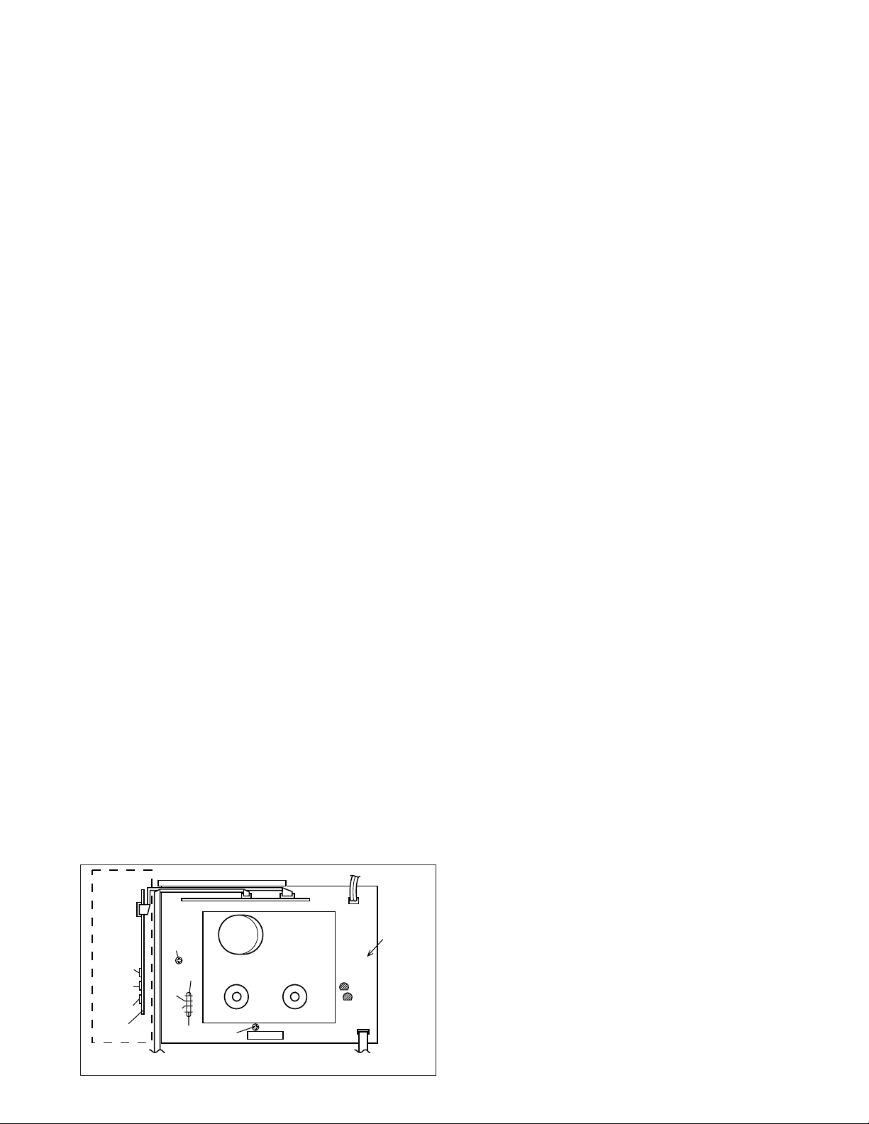
1.4 Service position
This unit has been designed so that the Mechanism and Main
board assemblies can be removed together from the chassis
assembly. Before diagnosing or servicing the circuit boards,
take out the major parts from the chassis assembly.
1.4.1 How to set the “Service position”
(1) Refer to the disassembly procedure and perform the dis-
assembly of the major parts before removing the Mechanism assembly.
(2) Remove the screws that fix the Mechanism assembly to the
Chassis assembly. If any other screws are used to fix the
boards, remove them also.
(3) Remove the combined Mechanism and Main board assem-
blies.
(4) If any other major parts are used, remove them also.
(5) Connect the wires and connectors of the major parts that
have been removed in steps (1) to (4). (Refer to Fig. 1-2-2d.)
(6) Place the combined Mechanism, Main board and other
board assemblies upside down.
(7) Insert the power cord plug into the power outlet and then
proceed with the diagnostics and servicing of the board as-
sembly.
Notes:
•
Before inserting the power cord plug into the power outlet, make sure that none of the electrical parts are able to
short-circuit between the workbench and the board assembly.
•
For the disassembly procedure of the major parts and details of the precautions to be taken, see “1.2 Removing
the major parts”.
•
If there are wire connections from the Main board and
Mechanism assemblies to the other major parts, be sure
to remove them (including wires connected to the major
parts) first before performing step (2).
•
When carrying out diagnosis and repair of the Main board
assembly in the “Service position”, be sure to ground both
the Main board and Mechanism assemblies. If they are improperly grounded, there may be noise on the playback
picture or FDP counter display may move even when the
mechanism is kept in an inoperative status.
•
In order to diagnose the playback or recording of the cassette tape, set the Mechanism assembly to the required
mode before placing it upside down. If the mechanism
mode is changed (including ejection) while it is in an upside down position the tape inside may be damaged.
•
For some models, the mechanism and board assemblies
are attached by connectors only. When carrying out a diagnosis or repair of the boards in the “Service position”,
make sure that the connectors are not disconnected.
ONLY USED FOR
HR-S6955MS,
HR-S7955MS
CN1601
CN916
CN511
1.5 Jig RCU mode
This unit uses the following two modes for receiving remote
control codes.
1) User RCU mode : Ordinary mode for use by the user.
2) Jig RCU mode : Mode for use in production and servicing.
When using the Jig RCU, it is required to set the VCR to the
Jig RCU mode (the mode in which codes from the Jig RCU
can be received). As both of the above two modes are stored
in the EEPROM, it is required to set the VCR back to the User
RCU mode each time that an adjustment is made or to check
that the necessary operations have been completed. These
modes can be set by the operations described below.
1.5.1 Setting the Jig RCU mode
(1) Unplug the power cord plug from the power outlet.
(2) Press and hold the “REC” and “PAUSE” buttons on the VCR
simultaneously, while plugging the power cord plug into the
power outlet.
When the VCR is set to the Jig RCU mode, the symbols
( “ : ” ) in the time display of the FDP are turned off.
1.5.2 Setting the User RCU mode
(1) Turn off the power.
(2) Press the “REC” and “PAUSE” buttons of the VCR simulta-
neously. Alternatively, transmit the code “80” from the Jig
RCU.
1.6 Mechanism service mode
This model has a unique function to enter the mechanism into
every operation mode without loading of any cassette tape. This
function is called the “Mechanism service mode”.
1.6.1 How to set the “Mechanism service mode”
(1) Set the VCR to the Jig RCU mode (the mode in which codes
from the Jig RCU can be received).
(2) Transmit the code “E5” from the Jig RCU.
(3) Release the lug of the Cassette holder and then slide the
Cassette holder toward the direction where the Cassette
holder is loaded by manually.
(4) The cassette holder lowers and, when the loading has com-
pleted, the mechanism enters the desired mode.
When the VCR is set to the Mechanism service mode, the
symbols (“Timer”) in the FDP (LED) are blinked.
1.6.2 How to exit from the "Mechanism service mode"
(1) Unplug the power cord plug from the power outlet.
VR1603
BURST
VR1601
R-Y
VR1602
B-Y
S/P converter
board assembly
VR2251
REC AGC ADJ
TP111
D.FF
TP4001
CTL.P
TP106
PB.FM
TP2253
A.PB.FM
C3025
Timer clock
Fig. 1-4-1a
Main board
assembly
CP3001
CP4001
CN7001
To Adv. jog board assemblyTo Front S jack board assembly
1-9
Page 15
1.7 Maintenance and inspection
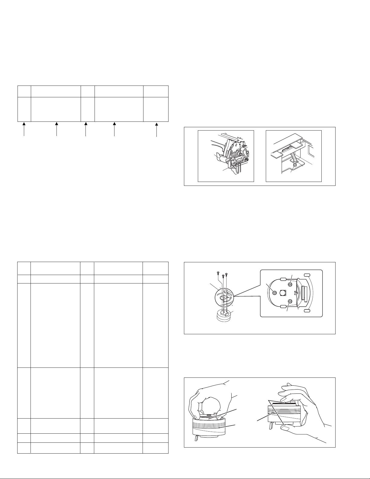
1.7.1 Cleaning
Regular cleaning of the transport system parts is desirable but
practically impossible. So make it a rule to carry out cleaning
of the tape transport system whenever the machine is serviced.
When the video head, tape guide and/or brush get soiled, the
playback picture may appear inferior or at worst disappear, resulting in possible tape damage.
Note:
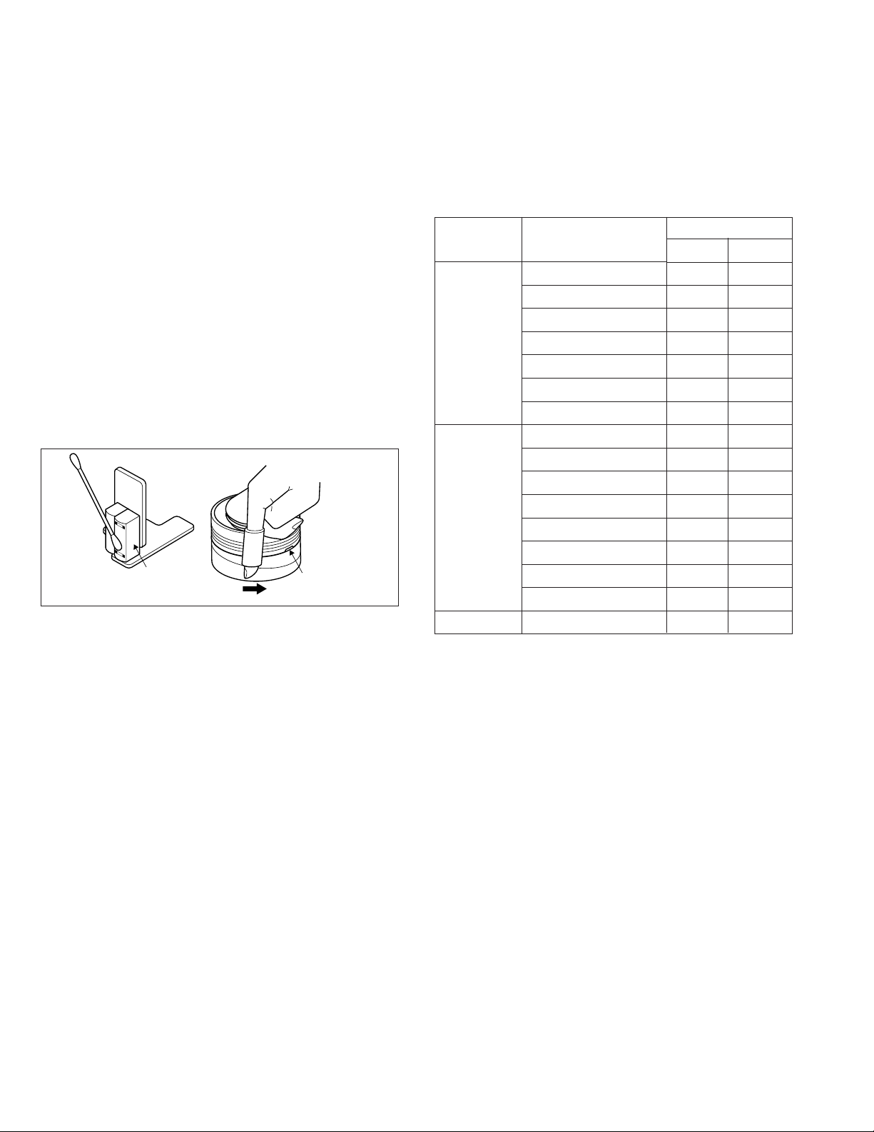
Absolutely avoid sweeping the upper drum vertically as
•
this will cause damage to the video head.
(1) When cleaning the upper drum (especially the video head),
soak a piece of closely woven cloth with alcohol and while
holding the cloth onto the upper drum by the fingers, turn
the upper drum counterclockwise.
(2) To clean the parts of the tape transport system other than
the upper drum, use a piece of closely woven cloth or a
cotton swab soaked with alcohol.
(3) After cleaning, make sure that the cleaned parts are com-
pletely dry before using the cassette tape.
A/C head
Video heads
Fig. 1-7-1a
1.7.2 Lubrication
With no need for periodical lubrication, you have only to lubricate new parts after replacement. If any oil or grease on contact parts is soiled, wipe it off and newly lubricate the parts.
Note:
•
See the “mechanism assembly” diagram of the “parts list”
for the lubricating or greasing spots, and for the types of
oil or grease to be used.
1.7.3 Suggested servicing schedule for main components
The following table indicates the suggested period for such
service measures as cleaning, lubrication and replacement. In
practice, the indicated periods will vary widely according to environmental and usage conditions. However, the indicated components should be inspected when a set is brought for service
and the maintenance work performed if necessary. Also note
that rubber parts may deform in time, even if the set is not used.
System Parts name
Drum assembly
A/C head
Pinch roller arm assembly
Tape transport
Drive
Other
Full erase head
Tension arm assembly
Capstan motor (Shaft)
Guide arm assembly
Capstan motor
Capstan brake assembly
Main brake assembly
Belt (Capstan)
Loading motor
Clutch unit
Worm gear
Control plate
Rotary encoder
Operation hours
1000H
C,X
C,X
C
C
C
C
C
X
2000H
X
C,X
C
C
C
C
C
X
X
X
X
X
X
X
X
X
C : Cleaning
X : Inspection or Replacement if necessary
1.8 Servicing items related to video navigation
The video navigation function built into this unit works by storing the video navigation data in the internal EEPROM and writing data in the cassette tape simultaneously.
The video navigation data stored in the EEPROM cannot be copied to another EEPROM. Therefore, when the circuit board mounting the EEPROM is replaced, the original EEPROM should be
mounted on the new board. This will make the user’s video navigation data usable with the new circuit board after replacement.
However, the user’s data cannot be restored if the EEPROM on
the original circuit board is damaged.
Note:
• If the circuit board mounting the EEPROM or the EEPROM
alone has been replaced, it is required to perform confirmation/re-adjustment on all of the adjustment items using the EVR as well as those which are adjusted by transmitting adjustment codes from the Jig RCU.
1-10
Page 16
SECTION 2
MECHANISM
2.1 Before disassembling
2.1.1 Notes
This model’s mechanism relates closely to the rotary encoder
and system control circuit (the rotary encoder is meshed with
the control cam).
The system control circuit detects the mechanism condition
using the rotary encoder’s phase (internal switch phase).
Therefore, the parts such as the rotary encoder, control plate,
loading gear and control cam need to be installed correctly in
order for the mechanism to operate properly. (For the mechanism phase adjustment, refer to the installation of each part.)
• For the disassembly procedure of the major parts of the main
unit and notes, refer to the “section 1 disassembly”.
• Before using a soldering iron, be sure to disconnect the
power plug from the AC outlet.
• Do not touch any of the adjustment points until a defect position is specified.
• When plugging or unplugging the connector, be sure not to
damage the wire.
• Be sure the springs are hooked all the way around and in
the correct direction.
• When performing repairs, take care not to damage a catch,
etc.
2.1.3 Setting the mechanism assembling mode
The mechanism-assembling mode is provided with this mechanism. When disassembling and assembling, it is required to
engage this mode.
Set the mode by adopting the following procedures.
(1) Remove the mechanism assembly using the disassembling
procedure.
(2) Turn gear (a) of the loading motor manually to set the mecha-
nism assembly to the eject end mode. Make sure that the
main deck is connected to the guide hole (a) of the drive
lever and the seal (a) of the main deck is connected to the
mark “E” of the control plate. This condition is called the
mechanism-assembling mode.
Seal (a)
“E” mark
CONTROL PLATE
Guide hole (a)
DRIVE LEVER
<Example>
OK NG
not hooked all the
()
way around
Fig. 2-1-1a
2.1.2 Mechanism operation check
When the mechanism is operated without a cassette loaded,
operate the mechanism in the mechanism service mode. (Refer to the "section 1 disassembly".)
LOADING MOTOR
Loading
Gear (a)
Unloading
Fig. 2-1-3a
2-1
Page 17
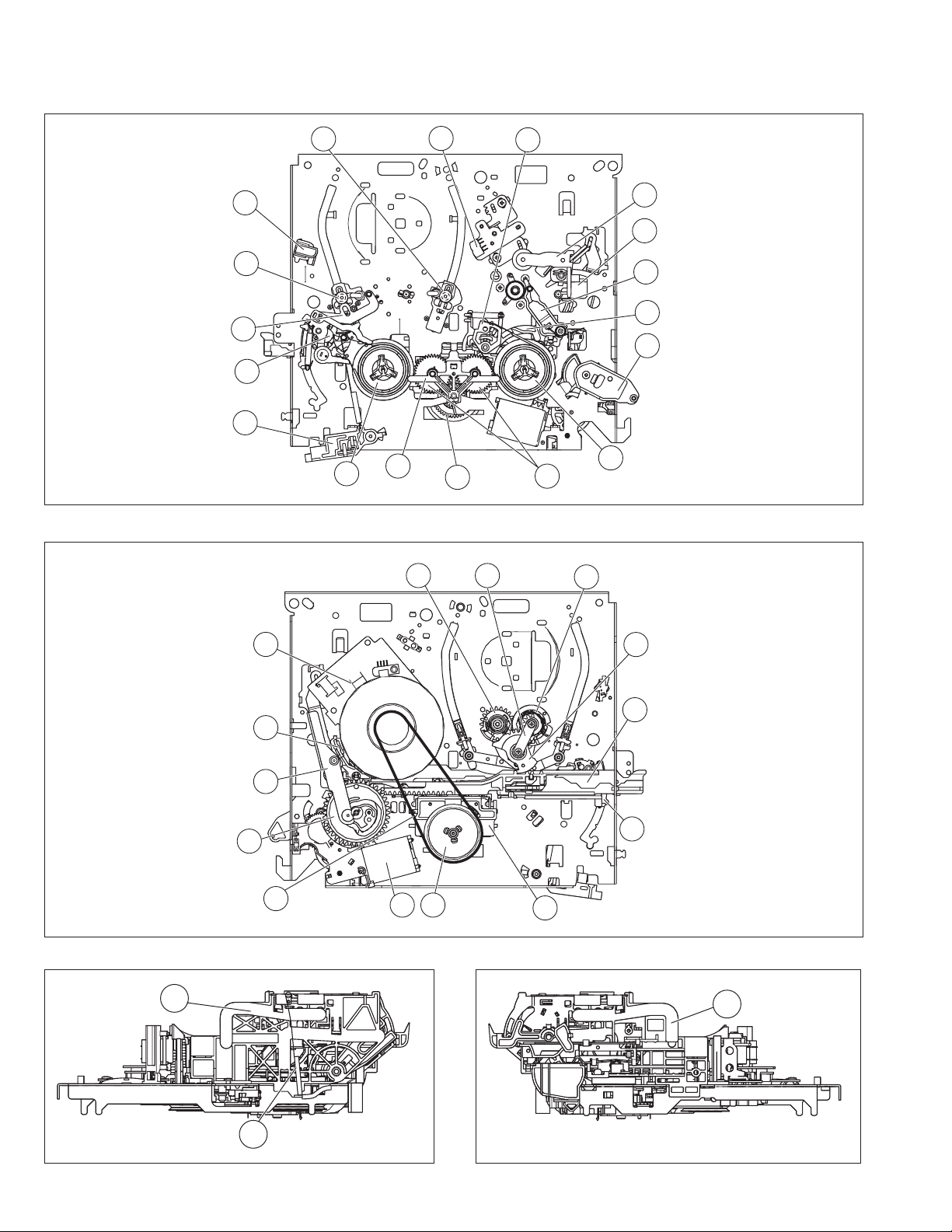
2.1.4 Layout of the main mechanism parts
Full erase head
Pole base assy
(supply side)
Tension arm assy
Tension arm base
Rec safety lever
T17
T1
T16
T15
T14
T2
Reel disk
(supply side)
Pole base assy
(take-up Side)
T13
Load gear assy
(take-up side)
T12
Idler arm
T3
A/C head
B15
Fig. 2-1-4a
B1
Direct gear
Fixing plate
B2
Main brake assy
T4
(take-up side)
T11
Ider gear 1/2
T10
Load gear assy
B3
(supply side)
T5
Pinch roller arm assy
T6
Lid guide
Guide arm assy
T7
T8
Brake lever
T9
Drive lever
Reel disk
(take-up side)
Side frame(L)
Capstan motor
Capstan brake
Press lever
Control cam
L2
B11
Belt
B14
B13
B12
B10
Loading motor assy
B8
B9
Fig. 2-1-4b
Clutch unit assy
B7
Change lever
B4
Load gear
B5
Control plate
B6
Tension arm lever
Side frame(R)
R1
2-2
Earth spring(1)
Fig. 2-1-4c
L1
Fig. 2-1-4d
Page 18
2.1.5 Disassembling procedure table
Front(T)/Back(B) of mechanism
Number of removal steps
Earth spring (1)
Top frame
Cassette holder
Side frame (L)
Drive arm
Side frame (R)
Lid guide
Idler arm
Idler gear 1/2
Main brake (T)
Reel disk (T)
Tension arm
Tension arm base
Press lever
Control cam
Capstan brake assy
Loading motor assy
Belt
Fixing plate
Load gear
Loading gear assy (S)
Loading gear assy (T)
Control plate
Clutch unit
Direct gear
Removal parts
Symbols and numbers
Symbols and numbers
(Reference items)
Replacement parts
2.1 Earth spring (1) T 1
2.1 Top frame T 2 1
2.1 Cassette holder T 3 1 2
2.1 Side frame (L) T 3 1 2
2.1Drive arm T51234
2.1 Side frame (R) T 3 1 2
2.2 A/C head T 1
- FE head T/B 1
2.3 Guide arm assy T 1
2.3 Lid guide T 1
2.3
Pinch roller arm assy
T2 1
2.4 Idler arm T 4123
2.4 Idler gear 1/2 T 5123 4
2.5 Main brake assy (T) T 6123 45
2.5 Reel disk (T) T 7123 456
2.5 Tension arm T 6123 45
2.5 Reel disk (S) T 7123 45
2.5 Tension arm base T 7123 45
-T-up head T 8123 45
-T-up lever T 8123 45
2.5Brake lever T8123
456
2.5 Rec safety le ver T 7 1 2 3456
2.6 Press lever B 1
2.6 Control cam B 2
2.6 Capstan brake assy B 3
2.6 Loading motor assy B 4
2.7 Belt B 1
2.7 Capstan motor T/B 2
- Wire holder T/B 1
2.7 Fixing plate B 1
2.7 Load gear B 2
2.7
Loading gear assy(S)
B3
2.7
Loading gear assy(T)
B4
- Pole base assy(S) T/B 4
- Pole base assy(T) T/B 5
- Load gear base B 5
2.7 Control plate B 6
-Drive lever T/B10123456
2.8 Clutch unit B 2
2.8 Direct gear B 3
- Change lever T/B 6 1 2
- Tension arm lever T/B 14 1 2 3 4 5
6
6
67
67
7
1
12
123
1
1
12
123
123
1234
1234
12 345
78 9
1
12
345
6789 101112 13
L1 - - L2 - R1 T6 T12 T11 T4 T10 T16 T15B12B11B13 B9 B10 B2 B4 B3 B1 B5 B8 B15
L1
-
-
L2
R1
T3
T17
T7
T6
T5
T12
T11
T4
T10
T16
T13
T15
-
T8
T14
B12
B11
B13
B9
B10
B14
B2
B4
B3
B1
T1
T2
B5
T9
B8
B15
B7
B6
This table shows the order of parts removal when replacing each part. For replacement, remove the parts in the order of 1 to 13
shown in the table and install the parts in the reverse order.
The symbol number before each part name shows the number in the figure “Layout of the main mechanism parts”. T and B on the
right of each part name show the side from which the part should be removed (T: From the front of the mechanism, B: From the
rear of the mechanism, T/B: From both sides).
2-3
Page 19
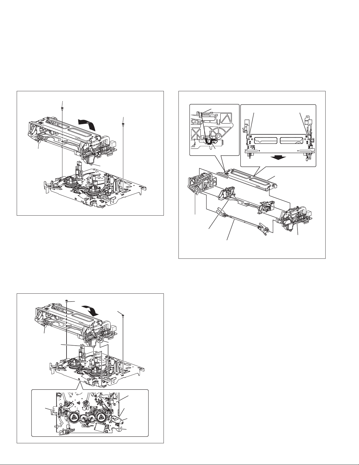
2.2 Replacement of the main mechanism parts
2.2.1 Cassette holder
2.2.1.1 Removal
(1) Remove the screws (a) and (b).
(2) Hold up the top frame, cassette holder assembly, drive arm
assembly and side frames (L/R) all together and remove
them by releasing the hooks (a) and (b).
Screw (a)
Screw (b)
2.2.1.3 Disassembling
(1) Release hook (a) to remove the earth spring (1) from the
top frame.
(2) Release the catches (a) and (b) and pull the top frame in
the direction shown by the arrow (a) to remove it.
(3) Pull out the side frame (R).
(4) Pull out the cassette holder assembly and drive arm assem-
bly from the side frame (L).
Hook (a)
Catch (a)
Catch (b)
Hook (a)
Hook (b)
Fig. 2-2-1a
2.2.1.2 Installation (phase adjustment)
(1) Turn gear (a) of the loading motor assembly so that the main
deck connects to the guide hole (a) of the drive lever.
(2) Hook the main deck to hooks (a) and (b).
(3) Place the projection of the drive lever to section (a) of the
side frame (R) and install the cassette holder to the main
deck. Make sure that the bosses of the side frame (L/R) con-
nect with the holes (a) and (b) of the main deck.
(4) Secure screws (a) and (b).
Screw (a)
Screw (b)
Hook (a)
Hook (b)
Hole
(a)
Section
(a)
Hole (b)
Guide hole (a)
DRIVE
LEVER
EARTH SPRING(1)
Arrow (a)
TOP FRAME
SIDE
FRAME(L)
CASSETTE HOLDER
Assembly
DRIVE ARM Assembly
SIDE FRAME(R)
Fig. 2-2-1c
2.2.1.4 Assembling (installation and phase adjustment)
(1) Turn gear (a) of the loading motor assembly so that the main
deck connects to the guide hole (a) of the drive lever.
(2) Place the projection of the drive lever on section (a) of the
side frame (R) and install the side frame (R) to the main deck.
(3) Secure screw (b).
(4) Place section (b) of the drive arm on the gear of the side
frame (R). Make sure that the pin of the door opener con-
nects with section (c) of the drive arm.
(5) Place the drive arm on section (d) of the side frame (L) and
install the side frame (L) on the main deck. Be sure to con-
nect the earth spring (1) to the side frame (L).
(6) Secure screw (a).
(7) Turn gear (a) of the loading motor assembly until the drive
arm is vertical.
(8) Place the slit of the side frame (L/R) at the foot of the cas-
sette holder assembly and install the cassette holder.
(9) Place the top frame on the position guide (a) of the side
frame (L/R) and push it in the direction shown by the arrow
(a) for installation.
(10) Hook the earth spring (1) to the hook (a) of the top frame.
2-4
Gear (a)
Fig. 2-2-1b
Page 20
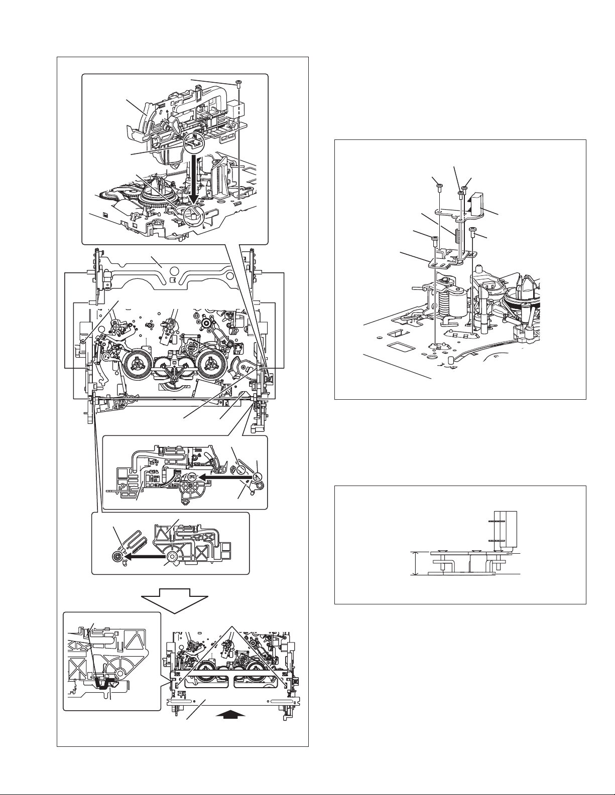
SIDE FRAME(R)
(Temporary height)
11mm
HEAD BASE
A/C HEAD
Screw (b)
2.2.2 A/C head
2.2.2.1 Removal
(1) Remove screws (a) and (b).
(2) Remove the A/C head together with the head base.
(3) Remove the screws (c), (d) and (e) to remove the spring (a)
and the A/C head from the Head base.
Section (a)
DRIVE LEVER
Cassette Holder Assembly
Screw (a)
Guide hole (a)
Gear (a)
Section (c)
Section
(b)
Screw (e)
Screw (c)
Spring (a)
Screw (a)
HEAD BASE
Screw (d)
A/C HEAD
Screw (b)
Fig. 2-2-2a
2.2.2.2 Installation (initial setting)
To install the A/C head to the head base, secure the screws in
the order of (c), (d) and (e). To make the adjustment easy, temporarily elevate the A/C head.
SIDE FRAME(R)
DRIVE ARM(L)
Section (d)
Hook (a)
EARTH SPRING(1)
SIDE FRAME(L)
TOP FRAME
Fig. 2-2-1d
DRIVE ARM(R)
Position guide (a)
Arrow (a)
Fig. 2-2-2b
2-5
Page 21
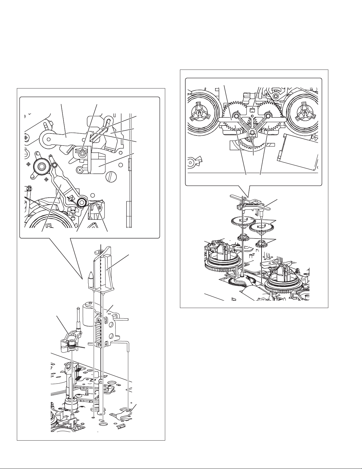
2.2.3 Guide arm, pinch roller arm
2.2.3.1 Removal
(1) Remove the spring (a) from the hook (a) and detach the
guide arm assembly.
(2) Release the catch (a) to remove the lid guide.
(3) Remove the spring (b) from the hook (b) and detach the
pinch roller arm assembly.
2.2.4 Idler arm, idler gear 1/2
2.2.4.1 Removal
(1) Release the catches (a) and (b) to detach the idler arm.
(2) Detach the idler gear 1/2.
IDLER ARM
Catch (b)
Pinch roller arm assembly
Hook (a)Guide arm assembly Spring (a)
Catch (a)
Spring (b)
PRESS
LEVER
Hook (b)
LID GUIDE
Catch
(a)
IDLER GEAR 1/2
IDLER ARM
IDLER GEAR 2
IDLER GEAR 1
LID GUIDE
Guide arm assembly
2-6
Fig. 2-2-3a
Pinch roller arm
assembly
PRESS
LEVER
Fig. 2-2-4a
2.2.5 Main brake (T), brake lever, tension arm,
reel disk (S/T), Rec safety lever
2.2.5.1 Removal
(1) Remove the spring (a). (Detach section (b) of the spring (a).)
(2) Release the catch (a) to detach the main brake (T).
(3) Release the catch (b) to detach the reel disk (T) and the
spacer.
(4)
Lift up and turn section (b) of the brake lever counterclockwise
to remove the brake lever.
(5) Remove the spring (b) from the hook (a).
(6) Release the catch (c) to detach the tension arm.
(7) Release the catch (d) to detach the reel disk (S) and the
spacer.
(8) Remove the spring (c) from the hook (b).
(9) Turn the tension arm base in the direction shown by arrow
(a) to release catch (e). Place the projections of the tension
arm base to the holes (a) to detach the tension arm base.
(10) While releasing the catch (f), turn the Rec safety lever
counterclockwise to remove it.
Page 22
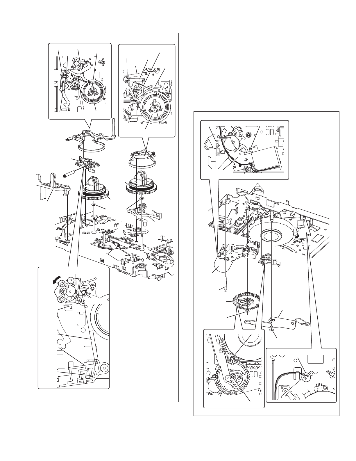
Tension arm assembly
Catch (d)
Catch (c)
Screw (a)
Screw (a)
Loading motor
assembly
Solder (a)
Slit washer (a)
Slit washer
(b)
Catch (b)
Capstan brake assembly
CONTROL CAM
Slit washer (b)
PRESS LEVER
Capstan
brake assembly
CONTROL
CAM
Loading
motor
assembly
Spring (b)
Catch (c)
Hook (a)
Catch (d)
REEL DISK(S)
Main brake (T) assembly
Section (b)
Spring (a)
Spring (a)
BRAKE
LEVER
2.2.6 Press lever, control cam, capstan brake assembly,
loading motor assembly
2.2.6.1 Removal
(1) Remove the slit washer (a) to detach the press lever.
(2) Release the slit washer (b) to detach the control cam.
(3) Release the catch (b) to detach the capstan brake assem-
bly.
(4) Remove the solder (a).
(5) Remove the screw (a).
(6) Release the catches (c) and (d) to detach the loading motor
assembly.
Tension arm base
assembly
REC SAFETY
LEVER
Tension arm base assembly
Arrow (a)
Hole (a)
Catch (e)
Hole (a)
Hook (b)
Catch (a)
Tension arm
assembly
Main brake (T)
assembly
REEL DISK(T)
REEL DISK(S)
SPACER
REEL DISK(T)
Catch (b)
BRAKE
LEVER
Spring (c)
REC
SAFETY
LEVER
Catch (f)
Fig. 2-2-5a
Fig. 2-2-6a
2-7
Page 23
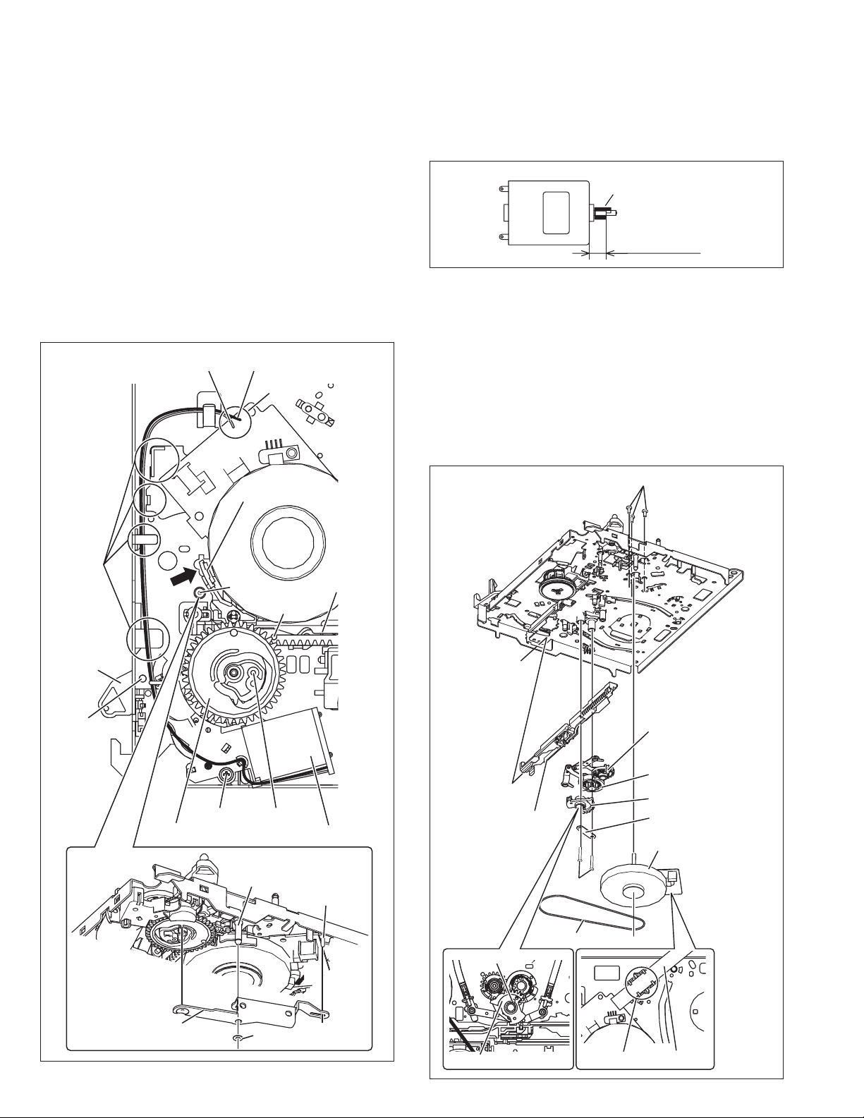
2.2.6.2 Installation (phase adjustment)
(1) Attach the loading motor assembly to the main deck.
(2) Secure the screw (a).
(3) Solder the wire to section (a).
(4) Arrange the wire along with the position guide (b).
(5) Attach the capstan brake assembly to the main deck.
(6) Place the main deck on the guide hole (a) of the control plate.
(7) Place the main deck on the guide hole (b) of the drive lever.
(8) Place the main deck no guide hole (c) of the control cam to
install the control cam.
(9) Move the capstan brake in the direction shown by the arrow
(a) to attach the press lever to the shaft (a). Make sure that
the boss of the press lever fits in the control cam, and that
the shaft (b) of the pinch roller arm assembly connects with
the hole of the press lever.
(10) Attach slit washer (a) to shaft (a).
Wire (black)Wire (red)
Section (a)
Capstan brake assembly
Note:
• When replacing the worm bearing of the loading motor as-
sembly, attach it according to the following specification.
If worm bearing is not attached correctly, a mechanism
noise may occur. (See Fig. 2-2-6c)
LOADING MOTOR
WORM BEARING
6.8 ± 0.2 mm
Fig. 2-2-6c
2.2.7 Capstan motor, load gear, control plate
2.2.7.1 Removal
(1) Detach the belt.
(2) Check that the FFC connector on the drum is disconnected.
(3) Release the catch (a) to remove the FFC wire.
(4) Remove the screws (a) to detach the capstan motor.
(5) Remove the screws (b) to detach the fixing plate.
(6) Release the catch (b) to detach the load gear.
(7) Turn the load gear (S/T) in the loading direction to detach it.
(8) Remove the control plate.
Screws (a)
Position
guide (b)
DRIVE
LEVER
Guide hole (b)
Arrow (a)
Screw (a)
CONTROL CAM
Shaft (a)
Guide hole (a)
Guide hole (c)
Loading motor assembly
Shaft (a)
Shaft (b)
CONTROL
PLATE
CONTROL
PLATE
Catch (b)
Load gear (T) assembly
Load gear (S) assembly
LOAD GEAR
FIXING PLATE
Capstan motor assembly
Screws (b)
BELT
2-8
PRESS LEVER
Fig. 2-2-6b
Slit washer (a)
LOAD GEAR
Catch (a)
Fig. 2-2-7a
FFC
Page 24
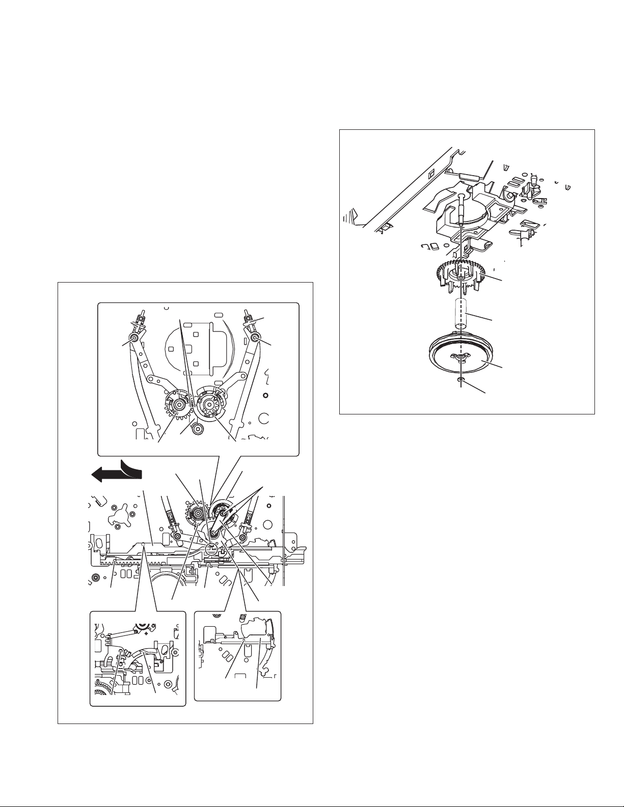
2.2.7.2 Installation (phase adjustment)
(1) Place the main deck on the guide hole (a) of the tension arm
lever.
(2) Place the main deck on the guide hole (b) of the brake le-
ver.
(3) Attach the control plate to align with the position guide (a).
(4) Place the hole (c) of the load arm (T) on the pole base (T)
and the load gear (T) on the load gear base.
(5) Place the hole (d) of the load arm (S) on the pole base (S)
and the load gear (S) on the load gear base. Be sure to align
the guide mark (e) of the load gear (T) to that of the load
gear (S).
(6) Turn the load gear (S/T) in the unloading direction to place
the main deck on the guide hole (f) of the load gear (T).
(7) Place the main deck on the guide hole (g) of the control plate.
(8) Attach the load gear on the load gear base so that the con-
trol plate is placed on the edge (h) of the load gear.
(9) Place the fixing plate on the shaft of the load gear base and
secure the screws (b).
2.2.8 Clutch unit assembly, direct gear
2.2.8.1 Removal
(1) Remove the slit washer (a) to detach the clutch unit assem-
bly.
(2) Remove the spring (a) and the direct gear.
DIRECT GEAR
POLE
BASE(T)
Hole (c)
Load gear (T) assembly
Insertion direction
CONTROL PLATE
Guide hole (g)
Guide marks (e)
Load gear (T)
assembly
(From the top)
LOAD GEAR BASE
Edge (h)
Position guide (a)
Guide hole (f)
POLE
BASE(S)
Hole (d)
Load gear (S) assembly
Load gear (S)
assembly
Screws (b)
FIXING
PLATE
LOAD GEAR
Spring (a)
CLUTCH UNIT
Slit washer (a)
Fig. 2-2-8a
Guide hole (b)
BRAKE LEVER
Fig. 2-2-7b
Guide hole (a)
TENSION ARM LEVER
2-9
Page 25

2.3 Mechanism timing chart
MECHANISM MODE
CONTROL PLATE
MARK
POLE BASE
REEL LOCK
TENSION ARM
TENSION
ARM LEVER
ON
OFF
LOCK
FREE
ON
OFF
PLAY
STOP
FF/REW
REV
OFF
REV
SERCH
/SLOW
/STILL
STOP
REEL
BRAKE
EJECT
PLAY
FOR
SLOW
/STILL
E P SL R ST B FR
FF
/REW
(STOP MODE PRESS UP)
ON
BRAKE
LEVER
GUIDE ARM
PINCH
ROLLER
CONTACT
CAPSTAN BRAKE
TU LEVER
DIRECT GEAR
Movements of a
CONTROL PLATE
ON
OFF
ON
OFF
ON
OFF
ON
OFF
OFF2
OFF1
ON
OFF
DIRECT
CLUTCH
(m/m)
0 5 15 20 25 30 35 40 45 50 5510
2-10
Page 26

SECTION 3
0.3 Vp-p
0.7 Vp-p
R-Y
B-Y
R-Y
B-Y
Cyan
Carrier(4.250 MHz)
Horizontal sync
Blue
Red
Magenta
Green
White
(100%)
Yellow
White
(100%)
Carrier(4.406 MHz)
B-Y colour BAR
R-Y colour BAR
White
Yellow
Cyan
Green
Magenta
Red
Blue
B–Y Black
White
100%
R–Y
s
Colour bar signal [SECAM]s Colour bar pattern [SECAM]
ADJUSTMENT
3.1 Before adjustment
3.1.1 Precaution
• The adjustments of this unit include the mechanism
compatibility and electrical adjustments. During the
performance of this work, be sure to observe the precautions for each type of adjustment.
• If there is a reference to a signal input method in the
signal column of the adjustment chart, “Ext. S-input”
means the Y/C separated video signal and “Ext. input”
means the composite video signal input.
• Unless otherwise specified, all measuring points and
adjustment parts are located on the Main board.
3.1.2 Required test equipments
• Color (colour) television or monitor
• Oscilloscope:
• Signal generator: RF / IF sweep / marker
•
Signal generator: stairstep, color (colour) bar [PAL/SECAM]
• Recording tape
• Digit-key remote controller(provided)
wide-band, dual-trace, triggered delayed sweep
3.1.5 Switch settings
When adjusting this unit, set the VCR mode and switches
as described below.
• When using the Jig RCU, it is required to set the VCR
to the Jig RCU mode (the mode in which codes from
the Jig RCU can be received). (See SECTION 1 DISASSEMBLY.)
Jig RCU
[Data transmitting method]
Depress the “ ” ( 3 ) button
after the data code is set.
3.1.3 Required adjustment tools
Machanism
compatibility
Roller driver
Jig RCU
Back tension cassette gauge
Alignment tape(MHPE)
Alignment tape(MHPE-L)
(LP, stairstep, PAL)
Burst
Blue
Jig RCU
PTU94023B
Alignment tape
MHPE-L
Color(colour) bar pattern [PAL]
•
(75%)
White
0.3 V
V
Roller driver
PTU94002
Alignment tape
(SP, stairstep, PAL)
MHPE
Color (colour) bar signal, color (colour) bar pattern
3.1.4
Color(colour) bar signal [PAL]
•
1V
Horizontal sync
White(75%)
0.7 V
0.3 V
White(100%)
Yellow
VU
Cyan
Green
Magenta
Red
V(R-Y)
U(B-Y)
: Used : Not used
Electrical
adjustment
Back tension cassette gauge
Yellow
U Black
adjustment
PUJ48076-2
Alignment tape
(EP, stairstep, NTSC)
MHP-L
Cyan
Green
Magenta
White
100%
Red
Blue
CUSTOM CODE
43: A CODE
DATA CODE
INITIAL MODE
Fig. 3-1-4a Jig RCU [PTU94023B]
•
Set the switches as shown below unless otherwise
specified on the relevant adjustment chart. The switches
that are not listed below can be set as desired.
If the VCR is not equipped with the functions detailed
below, setup is not required.
AUTO PICTURE/VIDEO CALIBRATION/
B.E.S.T./D.S.P.C.
PICTURE CONTROL/SMART PICTURE
VIDEO STABILIZER OFF
TBC ON
Digital 3R ON
VIDEO NAVIGATION/TAPE MANAGER
BLUE BACK OFF
3.1.6
Manual tracking mode (Auto tracking ON/OFF) setting
OFF
NORMAL/NATURAL
OFF
(1) In order to set to the manual tracking mode during tape
playback, press the "SP/EP(LP)" button on the remote
control unit.
• Each press of the button switches the auto tracking ON
or OFF.
• When the auto tracking is OFF, the monitor screen displays “AT: OFF”.
• When the manual tracking mode is set, the tracking is
placed at the center position.
(2) Press "channel +/-" to adjust the tracking manually.
3-1
Page 27

3.1.7 EVR adjustment
Some of the adjustments require the adjustment performed
by the EVR system. The main unit have EEPROMs for storing the EVR adjustment data and user setups.
Notes:
• In the EVR adjustment mode, the value is varied with
the channel buttons (+, –). The adjusted data is stored
when the setting mode changes (from PB to STOP,
when the tape speed is changed, etc.). Take care to
identify the current mode of each adjustment item
when making an adjustment.
• When changing the address setting in the EVR adjustment mode, use the Jig RCU or the remote controller
having numeric keypad with which a numeric code can
be directly input.
The remote control code of the Jig RCU corresponds
to each of the digit keys on the remote controller as
follows.
Digit-key 0 1 2 3 4 5 6 7 8 9
Code 20 21 22 23 24 25 26 27 28 29
• As the counter indication and remaining tape indication are not displayed FDP during the EVR adjustment
mode, check them on the TV monitor screen.
• When performing the EVR adjustment, confirm that the
FDP indication is changed to the EVR mode, as shown
below.
FDP
Fig. 3-1-7a EVR mode
3.2 Mechanism compatibility adjustment
Notes:
• Although compatibility adjustment is very important, it is not
necessary to perform this as part of the normal servicing
work. It will be required when you have replaced the A/C head,
drum assembly or any part of the tape transport system.
• To prevent damaging the alignment tape in the compatibility
adjustment, prepare a cassette tape (for self-recording/playback), perform a test on it by transporting it and making sure
that the tape is not bent by the tape transport mechanisms
such as in the guide rollers.(See Fig.3-2-2a)
3.2.1 Tension pole position
Notes:
•
This adjustment must be performed every time the tension
band is replaced.
Signal (A) • Back tension cassette gauge
Mode (B1) • Play back position
(B2) • Eject end
Adjustment part (F) • Adjust pin [Mechansim assembly]
Specified value (G) • 25 - 51 gf•cm (2.45 – 5 × 10
[PUJ48076-2]
-3
Nm]
(1) Play back the back tension cassette gauge (A).
(2) Check that the indicated value on the left side gauge is
within the specified value (G).
(3) If the indicated value is not within the specified value (G),
perform the adjustment in a following procedure.(See
Fig.3-2-1a.)
1) Remove the top frame, cassette holder and side
frames (L/R) all together. (See “section 2 mechanism”.)
2) Rotate the loading motor gear to move the control plate
so that the triangular stamping to the left of the “P”
stamping is aligned with the stamping (a) on the main
deck. This positioning is mode (B1).
3) Adjust by turning the adjustment pin so that the tip of
the tension arm is aligned with the stamping (b) on
the main deck.
4) Rotate the reel disk (S) by about one turn clockwise
and make sure that the round hole of the adjustment
pin is located in the “OK” range.
If it is outside this range, restart the adjustment from
the beginning.
After completion of the adjustment, rotate the loading gear
motor to return it to the mode (B2) position.
TENSION ARM
3-2
Stamping(b)
OK
ADJUST PIN
CONTROL PLATE
Stamping(a)
NG
Fig. 3-2-1a
Page 28

Head base
A/C head
AUDIO OUT
CTL. P
(1)
(2)
(3)
3.2.2 FM waveform linearity
Signal (A1) •
(A2) •
Mode (B) • PB
Equipment (C) • Oscilloscope
Measuring point (D) • TP106 (PB. FM)
External trigger (E) • TP111 (D.FF)
Adjustment part (F) • Guide roller [Mechanism assembly]
Specified value (G) • Flat V.PB FM waveform
Adjustment tool (H) • Roller driver [PTU94002]
Alignment tape(SP, stairstep, PAL) [MHPE]
Alignment tape(LP, stairstep, PAL) [MHPE-L]
(1) Play back the alignment tape (A1).
(2) Apply the external trigger signal to D.FF (E), to observe
the V.PB FM waveform at the measuring point (D).
(3) Set the VCR to the manual tracking mode.
(4)
Make sure that there is no significant level drop of the V.PB
FM waveform caused by the tracking operation, with its
generally parallel and linear variation ensured. Perform the
following adjustments when required. (See Fig. 3-2-2b.)
(5) Reduce the V.PB FM waveform by the tracking opera-
tion. If a drop in level is found on the left side, turn the
guide roller of the pole base assembly (supply side) with
the roller driver to make the V.PB FM waveform linear.
If a drop in level is on the right side, likewise turn the guide
roller of the pole base assembly (take-up side) with the
roller driver to make it linear. (See Fig. 3-2-2b.)
(6) Make sure that the V.PB FM waveform varies in parallel
and linearly with the tracking operation again. When re-
quired, perform fine-adjustment of the guide roller of the
pole base assembly (supply or take-up side).
(7) Unload the cassette tape once, play back the alignment
tape (A1) again and confirm the V.PB FM waveform.
(8)
After adjustment, confirm that the tape wrinkling does not
occur at the roller upper or lower limits. (See Fig. 3-2-2a.)
[Perform adjustment step (9) only for the models
equipped with SP mode and EP (or LP) mode.]
(9) Repeat steps (1) to (8) by using the alignment tape (A2).
Improper
(a) GUIDE ROLLER
(b) GUIDE POLE
Proper
Fig. 3-2-2a
• Proper waveform variation
• Improper waveform variation
A
C
Up Down
B
D
Roller driver
Guide roller
(supply side)
Fig. 3-2-2b
3.2.3 Height and tilt of the A/C head
Note:
• Set a temporary level of the height of the A/C head in
advance to make the adjustment easier after the A/C
head has been replaced. (See “section 2 mechanism”.)
Signal (A) •
Mode (B) • PB
Equipment (C) • Oscilloscope
Measuring point (D1) • AUDIO OUT terminal
External trigger (E) • TP111 (D.FF)
Adjustment part (F) • A/C head [Mechanism assembly]
Specified value (G) • Maximum waveform
Alignment tape(SP, stairstep, PAL) [MHPE]
(D2) • TP4001 (CTL. P)
(1) Play back the alignment tape (A).
(2) Apply the external trigger signal to D.FF (E), to observe
the AUDIO OUT waveform and Control pulse waveform
at the measuring points (D1) and (D2) in the ALT mode.
(3) Set the VCR to the manual tracking mode.
(4) Adjust the AUDIO OUT waveform and Control pulse
waveform by turning the screws (1), (2) and (3) little by
little until both waveforms reach maximum. The screw (1)
and (3) are for adjustment of tilt and the screw (2) for azi-
muth.
Fig. 3-2-3a
3-3
Page 29

3.2.4 A/C head phase (X-value)
Signal (A1) •
(A2) •
Mode (B) • PB
Equipment (C) • Oscilloscope
Measuring point (D) • TP106 (PB. FM)
External trigger (E) • TP111 (D.FF)
Adjustment part (F) •
Specified value (G) • Maximum V.PB FM waveform
Adjustment tool (H) • Roller driver [PTU94002]
Alignment tape(SP, stairstep, PAL) [MHPE]
Alignment tape(LP, stairstep, PAL) [MHPE-L]
A/C head base [Mechanism assembly]
(1) Play back the alignment tape (A1).
(2) Apply the external trigger signal to D.FF (E), to observe
the V.PB FM waveform at the measuring point (D).
(3) Set the VCR to the manual tracking mode.
(4) Loosen the screws (4) and (5), then set the Roller driver
to the innermost projected part of the A/C head. (See Fig.
3-2-4a.)
(5) Rotate the roller driver so that the A/C head comes clos-
est to the capstan. From there, move the A/C head back
gradually toward the drum until the point where the FM
waveform is maximized for the second time, and then
tighten the screws (4) and (5) temporarily.
(6) Play an alignment tape (A2) and set to the manual-track-
ing mode.
(7) Fine-adjust A/C head base position to maximize the FM
waveform, and then tighten the screws (4) and (5) firmly.
(8) Play alignment tapes (A1) and (A2) and confirm that the
FM waveforms are maximized when the tracking is at the
center position.
To the drum
Toward the capstan
Toward the drum
A/C head
Screw (5)
Roller driver
Screw (4)
Head base
To the capstan
Fig. 3-2-4a
Alignment tape
[SP, stairstep]
played with the
SP head
Waveform output
X-value adjustment point
Drum side Control head position Capstan side
Alignment tape
[EP(LP), stairstep]
played with the
EP(LP) head
3.3 Electrical adjustment
Note:
The following adjustment procedures are not only necessary
after replacement of consumable mechanical parts or board
assemblies, but are also provided as references to be referred to when servicing the electrical circuitry.
In case of trouble with the electrical circuitry, always begin a
service by identifying the defective points by using the measuring instruments as described in the following electrical adjustment procedures. After this, proceed to the repair, replacement and/or adjustment. If the required measuring instruments are not available in the field, do not change the
adjustment parts (variable resistor, etc.) carelessly.
3.3.1 Servo circuit
3.3.1.1 Switching point
Signal (A1) • Stairstep signal
(A2) •
(A3) •
Mode (B) • PB
Equipment (C) • Oscilloscope
Measuring point (D1) •
(D2) • TP106 (PB. FM)
External trigger (E) • TP111 (D.FF)
Adjustment part (F) • Jig RCU: Code “5A”
(F1) • Jig RCU: Code “51” or “52”
Specified value (G) • 7.5 ±0.5 H
(G) • 8.0 ±0.5 H (PAL)
Adjustment tool (H) • Jig RCU [PTU94023B]
Alignment tape (LP, stairstep, PAL) [MHPE-L]
Alignment tape (EP, stairstep, NTSC) [MHP-L]
• TBC:OFF
VIDEO OUT terminal (75Ø terminated)
• 7.5 ±0.5 H (NTSC)
[For the model without TBC function]
(1) Play back the signal (A1) of the alignment tape (A2).
(2) Apply the external trigger signal to D. FF (E) to observe the
VIDEO OUT waveform and V. PB FM waveform at the meas-
uring points (D1) and (D2).
(3) Set the VCR to the manual tracking mode.
(4) Adjust tracking so that the V . PB FM waveform becomes
maximum.
(5) Set the VCR to the Auto adjust mode by transmitting the code
(F) from the Jig RCU. When the VCR enters the stop mode,
the adjustment is completed.
(6) If the VCR enters the eject mode, repeat steps (1) to (5) again.
(7) Play back the alignment tape (A2) again, confirm that the
switching point is the specified value (G).
[For the model equipped with TBC function]
Steps (1) to (4) are the same as previous steps (1) to (4).
(5) Transmit the code (F1) from the Jig RCU to adjust so that the
trigger point of the VIDEO OUT waveform is changed from
the trailing edge of the V. sync signal becomes the specified
value (G1).
(6) Set the VCR to the stop mode or eject mode.
(7) Play back the signal (A1) of the alignment tape (A3).
(8) Repeat steps (2) to (6).
Trigger point
Switching point
V.sync
3-4
Fig. 3-2-4b
Maximum
V. rate
Fig. 3-3-1-1a Switching point
Page 30

3.3.1.2Slow tracking preset
H. rate
Y level
Signal (A1) • Ext. input
Mode (B1) • VHS SP
Measuring point (D) • TV-Monitor
Adjustment part (F) • Jig RCU: Code “71“ or “72”
Specified value (G) • minimum noise
Adjustment tool (H) • Jig RCU [PTU94023B]
(A2) • Color (colour) bar signal [PAL]
(B2) • VHS LP
(1) Record the signal (A2) in the mode (B1), and play back
the recorded signal.
(2) Set the VCR to the manual tracking mode.
(3) Set the VCR to the FWD slow (+1/6x) mode.
(4) Transmit the code (F) from the Jig RCU to adjust so that
the noise bar becomes the specified value (G) on the TV
monitor in the slow mode.
(5) Set the VCR to the Stop mode.
(6) Confirm that the noise bar is (G) on the TV monitor in
the slow mode.
(7) Repeat steps (3) to (6) in the REV slow (–1/6x) mode.
(8) Repeat steps (1) to (7) in the mode (B2).
Note:
For FWD slow (+1/6x) playback, transmit the code “08”
•
from the Jig RCU to enter the slow playback mode, and
transmit the code “D0” for REV slow (–1/6x) mode.
3.3.2 Video circuit
3.3.2.1 EE Y/PB Y (S-VHS/VHS) level
Signal (A1) • Ext. S-input
Mode (B1) • EE SP
Equipment (C) • Oscilloscope
Measuring point (D) • Y OUT terminal (75Ø terminated)
EVR mode (F1) • Jig code “57”
EVR address (F2) • A : 11
Specified value (G) • 1.00 ± 0.05 Vp-p
Adjustment tool (H) • Jig RCU [PTU94023B]
(A2) • Ext. input
(A3) • Color (colour) bar signal [PAL]
(B2) • S-VHS SP
(B3) • VHS SP
(F3) • Jig code “21” twice
(F4) • Jig code “18” or “19” (Channel +/-)
(1) Input the signal (A3) from the input point (A1).
(2) Set the VCR to the mode (B1).
(3) Observe the Y OUT waveform at the measuring point (D).
(4) Set the VCR to the EVR mode by transmitting the code
(F1) from the Jig RCU.
(5) Set the EVR address to (F2) by transmitting the code (F3)
from the Jig RCU.
(6) Transmit the code (F4) from the Jig RCU to adjust so that
the Y level of the Y OUT waveform becomes the specified value (G).
(7) Release the EVR mode of the VCR by transmitting the
code (F1) from the Jig RCU again. (When the EVR mode
is released, the adjusted data is memorized.)
(8) Input the signal (A3) from the input point (A2).
(9) Repeat steps (3) to (7) in the mode (B1).
(10) Record the signal (A3) in the mode (B2), and play back
the recorded signal.
(11) Set the VCR to the manual tracking mode.
(12) Repeat steps (3) to (7) in the mode (B2).
(13) Record the signal (A3) in the mode (B3), and play back
the recorded signal.
(14) Set the VCR to the manual tracking mode.
(15) Repeat steps (3) to (7) in the mode (B3).
Fig. 3-3-2-1a EE/PB Y level
3.3.3 Audio circuit
Notes:
• GND (Ground) should be taken from the Tuner shield
case.
3.3.3.1 Audio REC FM
Signal (A1) • Ext. input
Mode (B) • S-VHS LP
Equipment (C) • Oscilloscope
Measuring point (D) • TP2253 (A. PB. FM)
External trigger (E) • TP111 (D.FF)
Adjustment part (F) • VR2251
Specified value (G1) • 600 ± 100 mVp-p
(A2) • Audio: No signal
(A3) •
(G2) • More than 400 mVp-p
Video: Color (colour) bar signal [PAL]
(1) Apply the external trigger signal to D.FF (E) to observe
the Audio PB FM waveform at the measuring point (D).
(2) Record the signal (A3) with no audio signal input in the
mode (B), and play back the recorded signal.
(3) Set the VCR to the manual tracking mode.
(4) If the A.PB FM level is not within the specified value (G1),
perform the adjustment in a following procedure.
(5) Adjust the Adjustment part (F) so that the A. PB FM level
of the higher channel level becomes the specified value
(G1). (Adjust before recording, then confirm it by playing
back.)
(6) If the specified value (G1) is not obtained, adjust the Ad-
justment part (F) so that the waveform level of the lower
channel level becomes the specified value (G2). (Adjust
before recording, then confirm it by playing back.)
Specified
value (G2)
V. rate
Specified
value (G1)
Fig. 3-3-3-1a Audio REC FM
3-5
Page 31

3.3.4 Syscon circuit [EU/EK MODEL]
Note:
•
When perform this adjustment, remove the Mechanism
assembly.
3.3.4.1 Timer clock
Signal (A) • No signal
Mode (B) • EE
Equipment (C) • Frequency counter
Measuring point (D1) • IC3001 pin 61
Short point (D2) • IC3001 pin 24
(D3) • C3026 + and –
Adjustment part (F) • C3025 (TIMER CLOCK)
Specified value (G) • 1024.008 ± 0.001 Hz
(976.5549 ± 0.0010 µsec)
(1) Connect the frequency counter to the measuring point
(D1).
(2) Connect the short wire between the short point (D2) and
Vcc (5V).
(3) Short the leads of capacitor (D3) once in order to reset
the microprocessor of the SYSCON.
(4) Disconnect the short wire between the short point (D2)
and Vcc then connect it again.
(5) Adjust the Adjustment part (F) so that the output fre-
quency becomes the specified value (G).
3.3.5
PAL/SECAM converter circuit [MS MODEL]
Note:
• Unless otherwise specified in this P/S Converter circuit adjustments, all measuring points and adjustment
parts are located on the S-P Converter board.
3.3.5.2 SECAM burst position
Signal (A1) • Ext. input
Mode (B) • EE
Equipment (C) • Oscilloscope
Measuring point (D1) • CN1601 Pin 7
Adjustment part (F) • VR1603
Specified value (G) • Tr = 5.6 ± 0.1 µsec
(A2) • Color (colour) bar signal [SECAM]
(D2) • CN1601 Pin 3
(1) Observe the waveforms appeared at the measuring
points (D1) and (D2).
(2) Adjust the adjustment part (F) so that the waveforms tim-
ing width between the H-SYNC and the colour burst signal becomes the specified value (G).
Colour burst signal
C
(Converted colour)
Y
H-SYNC
Specified value (G)
H.rate
Fig. 3-5-2a PAL burst position
3.3.5.1 Colour difference level
Signal (A1) • Color (colour) bar signal [SECAM]
Mode (B) • EE
Equipment (C) • Oscilloscope
Measuring point (D) • CN1601 Pin 7
Adjustment part (F1) • VR1602 (B-Y ADJ)
(F2) • VR1601 (R-Y ADJ)
Specified value (G1) • 460 ± 20 mVp-p (B-Y)
(G2) • 620 ± 20 mVp-p (R-Y)
(1) Observe the C (converted colour) waveform at the meas-
uring point (D).
(2) Adjust the adjustment part (F1) so that the higher level
of the Yellow and Blue of the C waveform becomes the
specified value (G1).
(3) Adjust the adjustment part (F2) so that the higher level
of the Green and Magenta of the C waveform becomes
the specified value (G2).
GREEN
Specified
value (G2)
Specified
value (G1)
BLUE
YELLOW
MAGENTA
H.rate
3-6
Fig. 3-5-1a Colour difference level
Page 32

VICTOR COMPANY OF JAPAN, LIMITED
12,3-chome,Moriya-cho,Kanagawa-ku,Yokohama,Kanagawa-prefecture,221-8528,JapanHOME AV NETWORK BUSINESS UNIT.
Printed in Japan
0210 VP
Page 33

SECTION 4
12 3
2.5
(5.0)
1.8
PB and REC modes
(Voltage of PB and REC modes
are the same)
PB mode
REC mode
CHARTS AND DIAGRAMS
NOTES OF SCHEMA TIC DIAGRAM
Safety precautions
The Components identified by the symbol are
critical for safety . For continued safety, replace safety
critical components only with manufacturer's recommended parts.
1. Units of components on the schematic diagram
Unless otherwise specified.
1) All resistance values are in ohm, 1/6 W , 1/8 W (refer to
parts list).
Chip resistors are 1/16 W.
K: KØ (1000Ø), M: MØ (1000KØ)
2) All capacitance values are in µF, (P: PF).
3) All inductance values are in µH, (m: mH).
4) All diodes are 1SS133, MA165 or 1N4148M (refer to parts
list).
2. Indications of control voltage
AUX : Active at high
AUX or AUX(L) : Active at low
3. Interpreting Connector indications
1
2
Removable connector
3
1
2
Wire soldered directly on board
3
4) Indication on schematic diagram
Voltage Indications for REC and PB mode on the schematic diagram are as shown below.
Note: If the voltages are not indicated on the schematic
diagram, refer to the voltage charts.
5. Waveform measurement
1) Video circuits
REC : Colour bar signal in SP mode, normal VHS mode
PB : Alignment tape, colour bar SP mode, normal VHS
mode
2) Audio circuits
REC : 1KHz, –8 dBs sine wave signal in SP mode, normal
VHS mode
PB : REC then playback it
3) Movie Camera circuits
Measured using a correctly illuminated gray scale or colour
bar test chatrs in the E-E mode
4) Indication on schematic diagram
Waveform indications on the schematic diagram are as
shown below.
24
22201816
Measurement point
1
Non-removable Board connector
2
3
1
2
4
Board to Board
3
Connected pattern on board
The arrows indicate signal path
4. Voltage measurement
1) Video circuits
REC : Colour bar signal in SP mode, normal VHS mode
PB : Alignment tape, colour bar SP mode, normal VHS
mode
— : Unmeasurable or unnecessary to measure
2) Audio circuits
REC : 1KHz, –8 dBs sine wave signal in SP mode, Nor-
mal VHS mode
PB : REC then playback it
3) Movie Camera circuits
Measured using a correctly illuminated gray scale or colour
S40884-03
bar test charts in the E-E mode
C329
C330
0.1/50
R344
47K
R343
18K
0.1/50
C331
11/10
R345
10K
5) Waveform indications
Waveform number
WF25
REC/PB 1.2 Vp-p
50 mV/2 msec/DIV
Oscilloscope Volts and Time/Division, Probe 10 : 1
Mode : REC or PB modes
WF25
R346
15K
ALC OUT
Waveform number
Waveform name or
measurement point
Level : 1.2 Vp-p
4-1
Page 34

6. Signal path Symbols
The arrows indicate the signal path as follows.
Playback signal path
Playback and recording signal path
Recording signal path
(including E-E signal path)
Capstan servo path
CIRCUIT BOARD NOTES
1. Foil and Component sides
1) Foil side (B side) :
Parts on the foil side seen from foil face (pattern face)
are indicated.
2) Component side (A side) :
Parts on the component side seen from component face
(parts face) indicated.
Drum servo path
(Example)
R-Y
Playback R-Y signal path
Y
Recording Y signal path
7. Indication of the parts for adjustments
The parts for the adjustments are surrounded with the circle as
shown below.
8. Indication of the parts not mounted on the circuit board
“OPEN” is indicated by the parts not mounted on the circuit
board.
R216
2. Parts location guides
Parts location are indicated by guide scale on the circuit board.
REF No. LOCATION
Category: IC
Horizontal “A” zone
Vertical “6” zone
(A : Component side)
(D : Discrete component)
B : Foil side
C : Chip component
IC
IC101 B C 6A
Note:
For general information in service manual, please refer
to the Service Manual of GENERAL INFORMA TION Edition 4 No. 82054D (January 1994).
OPEN
4-2
S40884-03
Page 35

BOARD INTERCONNECTIONS4.1
J922
J911
J912
J913
J914
J903
J904
S-IN
GND
A.IN1[L]
OPEN
A.IN1[R]
S-OUT
ONLY USED FOR
HR-S7955MS/
S7950EU/
S7955EK
A.IN2[L]
A.IN2[R]
A.OUT[L]
A.OUT[R]
DEC.OUT[L]
CN903 CN913
DEC.OUT[R]
J901
0
GND
C_TO_DIGI
Y/V_TO_DIGI
3D/TBC(2M)
(Page 4-23)
6
J902
AV2/DECODER
TERMINAL
(S-SUB Page 4-25)
(I/O Page 4-27)
CN914CN904
R.PAUSE
SAT_CTL_OUT
ONLY USED FOR HR-S6955MS/S7955MS
#
87
S-P CONVERTER
(Page 4-31)
CN1601
5
RF OUT RF IN
TU/MD/IF
(Page 4-15)
26
BB(AL5V)
27
AUDIO IN
28
MOD SDA
29
MOD B(AL5V)
30
MOD SCL
31
VIDEO IN
TU(30V)
32
33
RF AGC
NC
34
35
AS
36
SCL
37
4
38
39
40
41
42
43
44
45
46
47
48
49
SDA
NC
MB(SW5V)
NC
TU(30V)
TP
IF OUT
SW 1
SW 2
AUDIO OUT
SIF OUT
AFT
VIDEO OUT
CN511
SW5V
SW5V
TO_PS_C
GND
FROM_PS_C
GND
TO_PS_Y
GND
FROM_PS_Y
SW12V
SW12V
CN905 CN915
AV1 IN/OUT
Fsc
GND
GND
GND
Y_FROM_DIGI
C_FROM_DIGI
#
ONLY USED FOR HR-S7955MS
#
MINI FRONT2
8
(FOR 400HA2)
(Page 4-18)
3
CN7003
#
#
(FOR 400HA2)
b5/KEY OUT
JSB
GND
(FOR 400HA)
CN7002
CN7005
JSA
CN7003
#
#
b5/KEY OUT
JSA
GND
JSB
#
CN7001
#
(FOR 400HA2)
b6
b7
JSA
GND
JSB
b5/KEY OUT
#
CN7001
#
(FOR 400HA)
05
CN1401CN501
Fsc
GND
C TO DIGI
SW5V(2)
V/Y TO DIGI
EE(L)
Y FROM DIGI
GND
C FROM DIGI
KILLER DET
I2C CLK A/V
I2C DATA A/V
V.P CTL
V.REF
D.FF
TRIC(H)
SLOW PULSE
ONLY USED FOR
HR-S7950EU/S7955EK
V.IN
A.IN(L)
A.IN(R)
TU_VIDEO
CH+12V(OPEN)
SW12V
GND
I2C CLK2
I2C DATA2
P50_I/O
SCR[H]
LI_5V(OPEN)
3.58NTSC[H]/P.ON_P
03
(VIDEO/N.AUDIO
(ON SCREEN
(SECAM
(FMA
(SYSCON
(SW.REG
(TUNER
(FRONT
(MAIN TERMINAL
#
2D DIGITAL
05
(Page 4-21)
CN1201
CN501
Fsc
GND
C TO DIGI
SW5V(2)
V/Y TO DIGI
EE(L)
Y FROM DIGI
GND
C FROM DIGI
KILLER DET
I2C CLK A/V
I2C DATA A/V
CNR(H)/VPCTL
V.REF
D.FF
FH625(L)/TRICK(H)
3.58NTSC(L)/SLOW PULSE
ONLY USED FOR
HR-S6950EU/S6955MS/S7955MS
OPEN
CN902 CN912
V.OUT
OPEN
PB_COLOR
FRONT_Y_IN(ADJ)
SECAM_PB_COLOR
MAIN
J915
A.OUT(L)
P.MUTE[L]
Y_TO_SUB
FRONT_V_IN
MAIN_ALC_DET
GND
V_TO_OSD
J916
A.OUT(R)
GND
CHARA_DATA
V_FROM_OSD
Page 4-5)
Page 4-7)
Page 4-8)
Page 4-9)
Page 4-11)
Page 4-13)
Page 4-15)
Page 4-17)
Page 4-19)
J921
SAT. C TL
CN901 CN911
I2C CLK
CN6701
R.PAUSE
ONLY USED FOR
HR-S7955MS/
S7950EU/
S7955EK
GND
GND
EE[L]
Y_TO_AV
I2C DATA
F_FROM_AV
14
CN1501
NC
I2C
DATA
I2C
CLK
TU A
MUTE
DEMOD
(R)
DEMOD
(L)
SW5V
GND
COMP
SIF
CN916
GND
FRONT C
GND
FRONT Y
GND
SW5V
REC_COLOR
DEMODU
(Page 4-29)
CN7108
3
S JACK
6
[FOR_FRONT-S-IN]
(Page 4-18)
J7102
S IN
AC INPUT
LIVE
CN5001
NEUTRAL
QGA7901C1-02
J7105
FRONT
VIDEO
IN
IN(L)
FRONT
AUDIO
IN(R)
96
93
92
91
2
87 S-P CONVERTER
76
58
57
55
36
28 MINI FRONT
14
1
9
5 2D/3D DIGITAL
3 MAIN
NO NAME
DRUM MOTOR
3in1 MDA/CAP MOTOR
LOADING MOTOR
JOG39
ADV.JOG38
S JACK
DEMOD
A/C HEAD12
38
CN7004
#
#
(for 400EA)
b5/KEY OUT
#
ADV.JOG
(Page 4-18)
FULL ERASE
QGF1207C1-07
QGF1209C1-07
QGF1201C1-07
QGF1208C1-07
RECPBGND
AUDIO ERASE
CTL HEAD(-)
CN2001
CTL HEAD(+)
OPEN
JSA
GND
JSB
QGF1208F1-07
12
CTLR/P55A.E
#DIFFERENCE_TABLE
FRONT
400H
400HA
400HA2
GND
QGB2532J1-02
CN2002
A/C HEAD
F.E
: Used
: Not used
38 28
ADV_JOG MINI_FRONT
TYPE
XX
O
[TO_MAIN]
OO
[TO
MINI-FRONT]
QGF1201C2-09
CN1
LP/EP CH1
LP/EP
CH1
FULL ERASE HEAD
X
COMMON
LP/EP
CH2
LP/EP CH2
COMMON#SP CH1
SP CH2
SP SP
CH1 CH2
EU/EK
FRANCE-MS/EE
ASIA
COMMON
FMA CH1
FMA CH2
FLY. E
FMA
FMA
FLY. E
#
#
CH1 CH2
FLY.E MODELS
S-P_CONVERTER
[SECAM->PAL_CONVERTER]
FLY. E
87
CAP.M_FG
CAP.M_Vcc
Vcc5V
CAP.M_F/R
LM_VCTL
M_GND
S_GND
Vcc12V
CAP.M_VCTL
LM_F/R/S
DRUM_PG/FG
JS3001
GND
LSA
LSB
LSC
LSD
CN3001
QGB2032M4-12
DRUM_VCTL
ROTARY ENCODER
JP
D_PG+
D_PG-
M_GND
D_COM
8
5
DRUM MOTOR LOADING MOTOR
D_W OUT
D_V OUT
D_U OUT
57
3 in 1 MDA/
CAP MOTOR
MM
X
O
X
L1
L2
BLK
RED
M
p10437001a_rev0
4-44-3
EDCBA
HGF
Page 36

MAIN (VIDEO/N.AUDIO) SCHEMATIC DIAGRAM4.2
The Parts Number,value and rated voltage etc. in the Schematic Diagram are for references only.
Note :
When replacing the parts,refer to the Parts List.
0
3
TO FMA
2Fsc
RF_AUDIO
NA_PB
NA_REC
A.IN1[R]
A.IN1[L]
F.AUDIO[R]
F.AUDIO[L]
LINE_OUT[R]
LINE_OUT[L]
GND
DEC_OUT[L]
FLY.E
FMA_CH2
FMA_CH1
SP_CH2
SP_CH1
LP/EP_CH2
LP/EP_CH1
TO FULL ERASE HEAD
SECAM_REC_COLOR
DEC_OUT[R]
A.IN2[L]
A.IN2[R]
TO
MAIN TERMINAL
A.IN2[R]
A.IN2[L]
DEC_OUT[R]
DEC_OUT[L]
LINE_OUT[L]
LINE_OUT[R]
F.AUDIO[L]
F.AUDIO[R]
A.IN1[L]
A.IN1[R]
TO TUNER
RF_AUDIO
TU_AUDIO
TO SW.REG
SW12V
TO U.DRUM
TO FMA
FMA_CH1
FMA_COM
FMA_CH2
TO A/C HEAD
CN2001
AUDIO ERASE
GND(AUDIO)
TO SYSCON
CTL[+]
CN2002
FE
TO SYSCON
FULL_E.ON[H]
N.REC[H]
N.REC_ST[H]
VHS[H]
TO SECAM
SECAM_DET
PB_FM
C.SYNC
SECAM[H]
V_TO_OSD
SECAM_PB_COLOR
GND
GND
SW5V
GND
#
CN1
REC
PB
CTL[-]
CTL[+]
CTL[-]
EE[L]
Fsc
GND
SW5V
5
4
3
2
MAIN(VIDEO/N.AUDIO)
##
D2
K2003
NQR0403-003X
R2041
K2004
0µ
0Ω
#
B2051
EE[L]
B2001
B2002
SHORT
TO SHEELD
15k
R2005
OPEN
R2006
18k
L2001
SHORT
C2003
C2004
47
/6.3 OPEN
R84
180
C44
0.01
4.7
/50
C2007
22
Q2004
DTC144WUA
PDTC144WU
UN521E
RN1309
#
Q19
DTC144WUA
PDTC144WUA
UN521E
RN1309
10k
Q50
DTC144WUA
PDTC144WU
UN521E
RN1309
BDL GND
COMP
PRE/REC GND
SP2
SP
COMMON
##
C125
0.01
C2018
OPEN
OPEN
C2012
Q16
DTC144WUA
PDTC144WUA
UN521E
RN1309
SP1
LP/EP2
COMMON
LP/EP1
A.GND
IC1
JCP8051-MSA
4.7
/50
PRE/REC VCC
D.FF
DET
REC
TANK
DC PB
ENV OUT
C61
PRE/REC
LP/EP
PRE/REC
B10
AMP
AMP
C6
0.01
R2014
220k
R2013
6.8k
K2002
NQL103K-R10X
K2001
NQL103K-R10X
C2010
C2011R2017
4.718k
/50
1
C65
K2006
OPEN
#
C2013
15p
K2005
0.0015
/50
0.01
C43
##
Q17
##
DTA144WUADTA144WUA
B60
PDTA144WUAPDTA144WUA
UN511EUN511E
RN2309RN2309
##
R34
10k
#
Q18
DTC144WUA
PDTC144WUA
UN521E
RN1309
C2006
0.012
/16
#
C2016
220p
C2008
4.7
/50
C2017
0.0068
#
R30
10K
##
R401
C405
R402
220
680
D1
R22
#
1k
R21
#
1k
#
#
C70
C69
0.01
0.01
C2051
#
C2061
MY
10µ
L15
C60
47
/6.3
C402
#
0.22
C401
#
0.01
330p
#
PELN0861
QQR1083-001
###
C403
130p
R2051
T2052
#
R2053
3.9k
#
C2052
0.033
R2052
OPEN
OPEN
#
#
Q401
R403 R405
560 68k
C404
47p
#
Q1
2SC4081/S
Q4
#
2SC4081/S
#
Q3
2SC4081/S
OPEN
#
MY
#
C2062
#
R2061
#
C2064
10
/25
TP106
PB FM
C59
0.01
##
R404
47k
#
C406
#
0.001
#
L401
#
15µ
Q402
#
C407
15p
C1
#
#
Q2
2SC4081/S
C2
#
C3
#
#
C4
T2051
#
C2053
#
R2054
10
0.0033
27k
#
C2063
0.01
R85
##
1.8k
##
Q5
2SA1576A/QR/
2PA1576/R
2SB1218A/QR
R406
39k
#
Q403
0.01
0.01
0.01
0.01
/25
#
Q2061
2SC4081/QRS
2SD1819A/QRS/
2PC4081/R/
#
R2063
150
#
R2062
3.3
B5
C103
Q2051
2SC4081/QRS/
2SD1819A/QRS/
2PC4081/R/
#
C2054C2055
0.01
L402
#
#
Q405
SHORT
#
R408
47k
#
R407
4.7k
#
C409
#
OPEN
Q404
L1
10µ
C5
47
/6.3
0.001
0.1
C7
C8
R2057
47k
R2058
18k
Q2052
2SA1576A/QR/
2SB1218A/QR/
2PA1576/R/
R2059
47k
#
R2056
R2060
18k
Q2054
2SA1576A/QR/
R2055
2SB1218A/QR/
3.3
2PA1576/R/
#
R2064
#
47k
R2065
18k
#
Q2063
DTC144WUA
UN521E
#
Q2062
RN1309
2SA1576A/QR/
PDTC144WU
2SB1218A/QR/
2PA1576/R/
R27
10k
R26
6.8k
220
R28
220
Q7
2SC4081/QRS/
2SD1819A/QRS/
2PC4081/R/
C72 L18
47p 22
R29
560
µ
L19
12µ
C74
R31
1.5k
OPEN
Q8R25
2SC4081/QRS/
2SD1819A/QRS
2PC4081/R/
Q2053
DTC144WUA
UN521E
RN1309
PDTC144WU
Q2055
DTC144WUA
UN521E
RN1309
PDTC144WU
R32
470
C73
12p
TP111
D.FF
2SA1576A/QR/
2SB1218A/QR/
Q9
2SA1576A/QR/
2SB1218A/QR/
2PA1576/R
2PA1576/
R77
Q2003
DTA144WUA
UN511E
RN2309
PDTA144WU
#
Q14
22k
#
R68
1k
R2020
4.7k
2SC4081/QRS/
2SD1819A/QRS/
2PC4081/R/
R2018
4.7k
R2019
4.7k
2SC4081/QRS/
2SD1819A/QRS/
2PC4081/R/
#
C78
0.01
#
R76
10k
C2005
R2015
C2009
0.001
R2016
39k
Q2001
Q2002
#
R23
1.8k
#
R65
1k
OPEN
C75
R10
10k
A.Vcc
A.MUTE
MONO-DET
VCA
MUTE
SP
SP
CARREA
OFFSET
MAIN
EMPHA.
INT
W.C./D.C
P
D17
CTL
EXT
42PIN[L]
42PIN[L]
0.01
R1
6.2k
L20
SHORT
C10
150p
C84
15k
R35
47p
C11
0.1
R33
OPEN
R2
1.5k
/50
1
C51
##
R2007
R2009
R2008
R2010
10k
12k
OPEN
B75
##
OPEN
R71
Comb ctl
SECAM
D1∗D18
LPF
SECAM
D1∗D18
2M LPF
P
R
HPF
629TRAP
P
R
LPF
MOD
CARR./DEV.ADJ
S-DET
ET
FBC
ALC
ET
Y
BDL
R
MAIN
LPF
DE EMPH.
## ##
C136 C62
0.01
120µ
L2
C12
8p
OPEN
C14
C13
0.1
1.8k
R3
C2002
1
/50
INPUT_SEL
REC LEV.
R
CTL
TRAP
P
SECAM
SECAM
C.K.
CTL.P.TRAP
ACC
Fh TRAP
COMP
SEP
SUB LPF
N.L.
ET
LPF
YNR
DO DO
&REC
R
P
CLAMPCLAMP
Y GND
##
D5
C15
C16
C63
0.10.1
OPEN
R75
##
R104
6.8k
R93
2.2k
P
R
DE MOD D.LIM.
R
P
SQPB
SQPB
EQ
SQPB
P
Y-LPF
R
-10dB
C17
3.3
/50
C87
##
Q38
2SC4081/QRS/
2SD1819A/QRS/
2PC4081/R/
L24 L28
27µ 68µ
C106
820p
BPF
D.E.
N.C.
FM AGC
DET
DO DET
R
P
CH4
-10dB -10dB
C18
##
C88
C110
82p
PILOT
ADD
P.C .
AGC
C9
/50
1
R90
390
LEVEL DET1 LEVEL DET2
SQPB DL
SB GAIN
P
R
CH1
CH2CH3
##
/50
2.2
R2004
R2002
GND
HIFI
DL
C-LPF
C-LPF
MAIN
MAIN
CONV.2
CONV.1
PP
RR
BURST
EMPH./DE EMPH.
P EQ
SQPB SQPB
G EQ
NT on PAL
CNV.
C.K.
WHITE
LIM.
CLEAR
SYNC
ALC
FBC
AGC DET
PB ALC
SQUELCH
CLAMP
-10dB
SYNC SEP
Y VCC
D4
C23
0.01
C92
33p
1µ
L22
C21C20
C22
C19
/50
0.11
/6.3
/50
47
2.2
OPEN
OPEN
R2003
R2001
100
OPEN
C2001
4.7
/50
NC
BAND_GAP
HIFI
P
R
CCD LPF
C.KILLER
ID DET
APC SW
DISCRI
PULSE
GEN.
4PHASE GEN.
D4
D4
L3
10µ
BDL VCC
BDL DET
VCA
C
BDL
DATA
IIC LOGIC
CLK
LPF2FscVCO
D5
D5
C GND
Fh LOCK CTL
MESECAM
2Fsc OUT
DET
CR DET
X'tal
VCO/XO
1/2
PHASE SW.
DOWN CONV.
ACC DET
REC AFC
PB APC
C VCC
R
REC APC
P
1/2
2FL VCO
KILLER
DET OUT
C-SQUELCH
6dB
6dB
D1∗D24
D1∗D24
0.01
##
C81
0.01
C24
0.1
R5
SHORT
R49
OPEN
Q22
OPEN
#
R46
C80
L13
33µ
OPEN
R66
Q32
OPEN
Q23
OPEN
R50
OPEN
C2014
OPEN
R118
SHORT
##
C99
##
0.01
C97
##
0.01
C36
4.7
/25
C32
0.01
C25
6p
#
L12
QQR0967-001
R48
1k
B17
##
L27
33µ
C108
C64
22p
68p
R79
C35
0.01
C26
0.01
Q21
2SA1576A/QRS
C41
OPEN
C114
180p
Q41
DTC144WUA
PDTC144WU
UN521E
RN1309
10
C40
/16
C45
0.1
C39
0.1
##
/6.3
47
C38
C42
OPEN
#
X2
0.01µF
X1
QAX0576
QAX0579
#
R117
100K
#
Q25
C37
1
C120
OPEN
R38
R7
R6
DTC144WUA
PDTC144WU
UN521E
RN1309
QQR0657-019
L5
/50
1.8k
R36
Q24
R88
SHORT
2SA1576A/QR/
2SB1218A/QR/
2PA1576/R/
R39
OPEN
3.9K
680
27k
C29
C28
C27
R51
1.2k
100p
C53
0.1
C34
2.2
C33
/50
C31
47
/6.3
C30
0.47
0.033
/50
3.3
0.022
L4
10µ
#
B12
#
B13
R9
OPEN
R8
OPEN
TO
ON SCREEN
2Fsc
V_TO_OSD(NC)
CHARA_DATA
#
Q11
DTC144WUA
PDTC144WUA
UN521E
RN1309
#
R43
1k
#
Q40
DTC144WUA
RN1309
PDTC144WUA
UN521E
R41
R42
100K
680
Q10
R40
2SA1576A/QR/
47K
2SB1218A/QR/
2PA1576/R/
LH
#
C90
#
TC4W53F
IC2
#
B65
SP_SHORT[H]/FLY_ON[H]
C142L31
OPENOPEN
LP_SHORT[H]
/FLY_REC[H]
R52
NQR0360-003X
TO SYSCON
SEP[H]
ET_REC[H]
TRICK[H]
CTL2
CTL1
D.FF
VIDEO_ENV
SECAM_DET
A.MUTE[H]
I2C_DATA_A/V
I2C_CLK_A/V
V.PULSE
SB_GAIN
NORM/MESEC/S
SECAM[H]
MESECAM[H]/AGC_CTL
GND
C.SYNC/V.REF
SW5V
V.P.CTL
SLOW_PULSE
TO 2D DIGITAL
CN1201
CN501
FSC
GND
C_TO_DIGI
SE5V[2]
V/Y_TO_DIGI
EE[L]
Y_FROM_DIGI
GND
C_FROM_DIGI
KILLER_DET
I2C_CLK_A/V
I2C_DATA_A/V
V.P CTL
V.REF
D.FF
TRICK[H]
SLOW_PULSE
TO 3D/TBC(2M)
CN1401
EE[L]
Fsc
GND
EE[L]
(S-SUB)
FRONT_V_IN
1
#DEFFERENCE TABLE
V15 SP LINEUP
S6950EU(S1)
"S7950EU,S7955EK(S2)"
S7955MS(S15)
S6955MS(S1)
S8955EE(S25)
FLY.ERASE
Q1-Q4
R401-R408
CN1
1-9
1-9
1-11
1-9
1-11
Q401-Q405
C401-C407
"L401,L402"
C409
"C69,C70"
"R21,R22"
PRE.IN
C1-C4
PAL_EP TRICKH.SHORT
C TRAP
R46
R43 R117
Q11
Q25
Q40
0.01
0.01
0.1
0.01
0.1
220
470
220
220
470
3D
for_MS
"Q14,Q18,Q19"
B12
X2
B13
"R23,R30R65"
0.01uF
"R66,R75,C78"
Function
T2051
PELN0832
PELN0832
PELN0860
PELN0832
PELN0860
AUDIO.DUBBING
R2053
B2051 R2054 R2056
12k
3.9k
12k
3.9k
15k
3.9k
12k
3.9k
15k
3.9k
82
82
100
82
100
C2053 C2054
0.0047
0.0047
0.0033
0.047
0.0033
TO MAIN TERMINAL
Q2061-Q2063
C2061
T2052
C2052
R2061-R2065
C2062-C2064
0.022
0.082
0.022
0.082
0.01
0.033
0.022
0.082
0.01
0.033
TO
TU_VIDEO
TU_VIDEO
TO TUNER
ABCD EFGH
Y_TO_AV
MAIN_ALC_DET
V_FROM_AV
CONNECTION
REC_COLOR/REAR_V_IN
## MARKS ARE NOT MOUNTED ALL MODELS
TITLE REC
: Used
: Not used
Y_TO_SUB
C_TO_DIGI
V_TO_OSD
PB_COLOR
Y/V_TO_DIGI
Y_FROM_DIGI
C_FROM_DIGI
SECAM_PB_COLOR
MY
B65 IC2
YES
NO
C90
2SC4081/QRS/ or 2SD1819A/QRS/ or 2PC4081/R/
2SA1576A/QR/ or 2SB1218A/QR/ or 2PA1576/R/
DTC144WUA or UN521E or RN1309 or PDTC144WU
DTA144WUA or UN511E or RN2309 or PDTA144WU
p10439001a_rev1
4-64-5
Page 37

MAIN (ON SCREEN) SCHEMATIC DIAGRAM4.3
Note :
The Parts Number,value and rated voltage etc. in the Schematic Diagram are for references only.
When replacing the parts,refer to the Parts List.
MAIN (SECAM) SCHEMATIC DIAGRAM [HR-S6955MS/S7955MS]4.4
Note :
The Parts Number,value and rated voltage etc. in the Schematic Diagram are for references only.
When replacing the parts,refer to the Parts List.
TO MAIN TERMINAL
TO
5
VIDEO/N.AUDIO
CHARA_DATA
2Fsc
S.DATA_FRSYS
S.CLK
OSD_CS
SYNC_DET[H]
I2C_DATA2
I2C_CLK2
TO SYSCON
P.MUTE[L]
GND
SW5V
TO SW.REG
CHARA_DATA
V_FROM_OSD
V_TO_OSD
TO TUNER
RF_VIDEO
GND
0 3 MAIN
5
## MARKS ARE NOT MOUNTED ON EE MODELS
EE MODEL
MS MODEL
# DIFFERENCE TABLE
0 3 MAIN
C301
R304
C324
TO VIDEO/N.AUDIO
#
##
##
OPEN
Q312
100µ
2PA1576/R/
L304
##
OPEN
B301
R301
27k
120k
R302
C305
0.01
47
C323
/6.3
R305
47k
##
2SA1576A/QR/
2SB1218A/QR/
Q301
OPEN
Q303
##
##
OPENSHORT
R317B302
L301
10µ
p30087001a_rev1
(SECAM)
DTA144WUA
UN511E
RN2309
R316
MODE
CTL
TO
PB MUTE
REC MUTE
B
BGP
GEN
DET SENSE
CONTROL
GND
IREF
B
4.2V
REG
AGC
AMP DET
AGC
TO PHASE DET
TO
FILT.
FILT.
ADJ
1.1MHZ
OSC
MUTE
P
PB
HOLD
R
PDTA144WU
4.43MHZ
VCO
LIMITER
ADJ.
CA
VA
BPF
P
GATE
F0
1.1M
1/4
R
SYNC
Q302
LA7358
IC301
AFC
LOGIC
X2
2.2M
BPF
X2
4.3M
BPF
P
OPEN
Q311
OPEN
R321
GEN./V-SEP
SYNC GAIE
TO MUTE
SECAM
DET
FROM LIM
PHASE
DET
4.3MHZ
ADJ.
OSC
F0
R
CA
P
VA
IREF
R
MUTE
PB
B
LIM
4.3MHZ
BPF
R/P
SYNC
GATE
R
P
SECAM[H]
C306
1
VCC
C307
150p
C310
0.01
SECAM_REC_COLOR
GND
Fsc
PB_FM
C302
C303
C304
6.8µ
2.2k
SECAM_PB_COLOR
V_TO_OSD
L302
2.2k
R307
R308
SW5V
1
0.0068
0.0068
27k
0.1
820
EE[L]
#
R303
0.01
R306
C309
R318
##
C311
0.01
SECAM_DET
C.SYNC
150p
6.8k
C308
39p
R327
V14
D203
100
D202
100
D201
1.5k
B203
B204
SHORT
SHORT
SHORT
B214
V15
R303 C313
6.8k 0.01
27k 0.47
27k OPEN
(ON SCREEN)
R202
10k
R203
#
R209
R204
OPEN
OPEN
C201
/6.3
#
IC201
R226
1k
L203
22µ
2.2k
R208
OPEN
VSS1
XTAL_IN
MUTE
CHABLK
LN21
OSC_IN
OSC_OUT
SYNC_DET
CS
SCLK
SD ATA
VDD2
CR_OUT
VCO_IN1
VSS3
5.6K
0.22 0.22
OPEN
220
/10
220
C202
VDD1
RST
CDLR
I2C_DATA
SEP_OUT
SEP_C
SYNC_IN
VDD1
CVCR
CV_IN
VSS2
CVOUT
VDD3
NC
VCO_R
C214 C215
C216R211
C225
L201
1µ
Q208
2SC4081/QRS/
R224
100
2SA1576A/QR/
R212
100
Q207
C222
1
R216
10K
R220
OPEN
1
C218
0Ω
/50
C217
56p
R213
L206
22µ
0.47
C209
L204
10µ
OPEN
R225
470
B206
4
MY
3
2
4
OTHER
EE
LC74775-9750
LC74776-9791
5.1k
6.8k
# DIFFERENCE TABLE
IC201
R209
R201
0Ω
SHORT
L202
C204
0.01
3
OPEN
C211C210C208C207C206
100p100p33p33p
R210
1.8k
C213C212
/25
4.70.1
2
OPEN
±0.5%
R314
R315
0
680p
27µ 4.7k
R329
C317
L303 R311
24k
R312
2.7k
##
## ##
22k
C315
1
OPEN
C314R310
C313
560k
120k
R328
OPEN
##
R309
##
0Ω
#
##
C312
0.001
R326
OPEN
C322
0.47
±2%
C321
300p
R313
22k
C319
1
0.0220.01
C318C320
##
C316
0.01
p30088001a_rev0
1
ABCD
4-7 4-8
1
ABCD
Page 38

MAIN (FMA) SCHEMATIC DIAGRAM4.5
The Parts Number,value and rated voltage etc. in the Schematic Diagram are for references only.
Note :
When replacing the parts,refer to the Parts List.
MAIN[FMA]0
3
C2222
0.01
5
TO SW.REG
TO SYSCON
4
TO VIDEO/N.AUDIO
3
SW5V
SW12V
GND
AL5V
2Fsc
LINE_OUT[R]
LINE_OUT[L]
DEC_OUT[R]
DEC_OUT[L]
RF_AUDIO
NA_REC
NA_PB
GND
A.IN1[R]
A.IN1[L]
F.AUDIO[R]
F.AUDIO[L]
A.IN2[R]
A.IN2[L]
B2222B2221
OPENSHORT
Q2201
DTA144WUA
Q2203
2SC4081/QRS/
R2211
2.7k
R2212
2.7k
Q2204
2SC4081/QRS/
R2215
180
C2216 C2217
47
/16 OPEN
R2218
R2235
R2237
R2236
R2238
R2209
680
R2210
4.7k
R2213
4.7k
R2214
680
OPEN
R2220
1k
3.3k
680
680
2.7k
2.7k
Q2202
DTC144WUA
D2201
OPEN
#
R2216
1.2k
R2217
#
4.7k
R2234C2228
100
R2219
1.2k
C2229
OPEN
C2232C2233
OPENOPEN
/6.3
C2211
33
27k
4.7k
0.047
C2224
R2225
510
R2224
R2255
MUTE_CTL
REC_AGC_ADJ
NR_DET2[L] NR_REF(L)
IN_REF(L)
TV_IN[L]
/50
4.7
C2203
/16
10
C2210
NR_DET2[R]
NR_DET1[R]
EXT1_IN(L)
EXT2_IN(L)
R2222
4.7k
C2209
/16
10
VR2251
QVP0039-103Z
AUDIO REC FM
NR
REF(R)
CCA_OUT(R)
NOISE_DET
PB_FM_IN
PRE_OUT
ENV
AFF
REC(-)DCF
Vcc(P/R)
CH2
GND(P/R)
CH1
COM
REC(+)DCF
CCA_OUT(L)
NR_DET1[L]
R2223
510
C2223
0.047
C2204
33
/6.3
CLK
IN_REF(R)
/6.3
47
OPEN
C2213
Vcc(1)
GND(LOGIC)
TV_IN[R]
EXT1_IN(R)
C2212
SHORT
L2201
PE
EXT2_IN(R)
GND1(R)
GND1(L)
OPEN
OPEN
C2227
/16
10
R2239
R2240
DATA
fsc_IN
OPEN
OPEN
OPEN
BS_IN(L)
C2226
/50
1
EXT3_IN(L)
B2201
LOGIC_REG
HiFi AGC DET
VREF
OPEN
/25
10
C2201
/50
4.7
C2202
LOG_OUT[R]
LOG_OUT[L]
EXT4_IN[R]
EXT4_IN[L]
/25
10
C2214
10
C2215
#
10
C2218
#
22
C2219
10
C2220
0.022
C2221
C2230
/25
10
C2231
/25
10
/25
/25
/16
/25
IC2201
AN3651FBP
R2230
R2232
47K
47K
LINE_OUT(R)
LOG_IN[R]
GND2
LOG_IN[L]
LINE_OUT(L)
Vcc2(12V)
RFC_OUT
RFC_AGC_DET
NORMAL_OUT
NORMAL_IN
DEC_OUT[R]
DEC_OUT[L]
C2225
/50
1
R2231
6.8K
BS_IN(R)
EXT3_IN(R)
R2233
6.8K
R2252
220
C2208
R2257
C2259
C2257
C2256
C2251
C2207
C2206
C2205
R2256
2.2K
C2261
100p
C2262
100p
Q2254
0.015
OPEN
0.33
0.01
0.01
C2254C2255
470.01
0.01
0.015
10
10
Q2253
DTC144WUA DTC144WUA DTC144WUADTC114EUA
TP2253
A.PB.FM
R2253
100
/50
R2251
4.7k
L2251
10µ
/6.3
K2251
NQR0007-001X
K2252
NQR0007-001X
/25
/25
L2252
150µ
C2258
180p
Q2252
D2251
1SS133
C2253
C2252
0.01
0.01
NQR0007-001X
R2254
10k
Q2251
Q2255
DTC114EUA
K2253
TP2254
A.REC_FM
TO SYSCON
S.CASS[H]
ET_REC[H]
I2C_DATA_A/V
I2C_CLK_A/V
A.MUTE[H]
H.REC_ST[H]
PAL_PB[H]
A.ENV/ND[L]
A.FF
TO
VIDEO/N.AUDIO
FMA_CH2
FMA_CH1
FMA_COM
2
R2208R2206R2204R2202
6.8k6.8k6.8k6.8k
TO TUNER
DEMOD[R]
DEMOD[L]
R2226
R2228
R2229R2227
39k39k
27k
27k
R2201
R2203
47k
47k
R2205
R2207
47k
47k
: Used
1#DIFFERENCE TABLE
: Not used
C2218 C2219 R2216 R2217
1
RF OUT
YES
NO
MY
p20281001a_rev0
ABCD EFGH
4-104-9
Page 39

MAIN (SYSCON) SCHEMATIC DIAGRAM4.6
The Parts Number,value and rated voltage etc. in the Schematic Diagram are for references only.
Note :
When replacing the parts,refer to the Parts List.
D_G
D_F
D_E
D_D
D_C
D_B
TO FRONT
D_A
CP
C3071
33
/16
0
C4032
OPEN
C4031
/16
33
L4001
SHORT
CP
QMFZ050-1R5X-E
CP4001
R3252
CP
CP4002
TO
VIDEO/N.AUDIO
I2C_DATA_A/V
I2C_CLK_A/V
5
4
(NC)3.58NTSC[H]/P.ON_P
A.MUTE[H]
V.P.C T L
VHS[H]
SECAM[H]
SLOW_PULSE
TRICK[H]
C.SYNC/V.REF
ET_REC[H]
V.PULSE
CTL[+]
CTL[-]
MESECAM[H]/AGC_CTL
NORM/MESEC/S
SECAM_DET
VIDEO_ENV
SB_GAIN
TO
CAP MOTOR
CN3001
CAP.M_FG
CAP.M_Vcc
Vcc5V
CAP.M_F/R
LM_VCTL
M_GND
S_GND
Vcc12
CAP.M_VCTL
LM_F/R/S
DRUM_PG/FG
DRUM_VCTL
CTL1
CTL2
D.FF
GND
SP_SHORT[H]/FLY_ON[H]
LP/EP_SHORT[H]/FLY_REC[H]
CP3002
SHORT
CP
QMFZ050-1R5X-E
CP3001
C3004
0.047
3
TO
ROTARY ENCODER
JS3001
GND
LSA
LSB
LSC
LSD
TO
SW.REG
GND[M]
GND
M12V
SW12V
SW5V
48V
GND
P.CTL[H]
AL5.8V
2
TO
FRONT
DIG1
DIG2
DIG3
DIG4
DIG5
DIG6
DIG7
KEY1
KEY2
AL5V
JSA
JSB
RC
GND
D3004
D3005
11ES2
11ES2
MAIN (SYSCON)
3
R3253
15k
10k
R3254
OPEN
R3255
OPEN
OPEN
R3205
R3206 R3207
12k 18k
180
1/4W
Q3002 Q3003
PTZ-NV16A PTZ-NV16A
START
END
SENSOR SENSOR
R3215 R3216
10k
10k 10k
Q3004
2SD1819A/QRS/
2SC4081/QRS/
2PC4081/R/
D3003
RD39ES/B3
R3219
4.7k
R3237 R3238
10k 10k
/6.3
C3007
OPEN
Q3005
2SC4081/QRS/
2SD1819A/QRS/
2PC4081/R/
B4001
OPEN
C3008
R3217
10k
C3011
3300
/6.3
LNB2301L01VI
R3222
4.7k
D3001
R3218
4.7k
R3214
C3012
47
R3208 R3210
PC3001 PC3002
RPI-304 RPI-304
SUPPLY TAKE UP
REEL SENSOR REEL SENSOR
0.001
R3220
100k
JSA
JSB
D4001
SHORT
OPEN
1k
R3090
N.REC_ST[H]
I2C_CLK
DIG6
R3051
R3089
TRICK[H]
470
R3052
R3088
R3087
SEP[H]
H.REC_ST[H]
TU_V_MUTE[H]
SYNC_DET[H]
SP_FG
S.CLK
4701k1k
R3053
R3054
C3039
OPEN
R3086
R3085
SLOW_P
VHS[H]
SP_SHORT/FLY.ON[H]
LP_SHORT/FLY.REC[H]
V.P.C T L
PAL_PB[H]
P.ON_PULSE
SECAM[H]
I2C_DATA2
I2C_CLK2
A.MUTE[H]
MODE
VCC/VCL
OSC2
OSC1
REC_SAFTY
JSA
TU_FG
1k
C3017
R3055
R3056
C3018
C3020
C3021
R3236
R3235
FULL_E.ON[H]
C3038
OPEN
C3035
C3034
OPEN
1M
#
#
100
X3002
C3041
#
C3025
C3024
0
0
1k
1k
C3022
0.1
470
470
0
C3025
#
TIMER CLOCK
0
1k
C3037
12p
C3036
QAX0527
DTC144W
S3002
QSW0602-003
S.CASS
4.7k
4.7k
OPEN
C3032
0.1
C3031
0.1
C3030
47
/6.3
R3071
10k
R3231
1k
R3230
4.7k
OPEN
B3971
C3054
##
18p
R3066
RST
B3966
##
IC3002
S3001
REC_SAFETY
QSW0602-003
VCC
VSS
IC-PST3427U
C3027
10
GND
RESET
FWE
AL5V
SIO
SII
/25
10k1k
R3062R3061
OPEN
CN3901
##
4.7k
C3026
30p
0.01
B3962
Q3901
10k
R3225
##
10k
##
R3241
Vss
R3083
#
Vcc
[OUT]
Vss
[IN]
RES
X1
X2
NMI
FWE
DIG7
SW2
SW1
JSB
TP3906
1k
0
R3081
R3080
#
1k
R3079
0
0
R3078
0
R3077
R3076
R3075
R3074
R3073
R3072
TP3904
B3070
OPEN
R3069
C3050
0.1
R3229
TP3905
#
X3001
0
R3063
R3060
R3059
R3058
R3057
TP3903
TP3908
TP3907
IC3003
OPEN
OPEN
100p
100p
3.3k
3.3k
A1
A2
VSS
SDA
SCLWPVCC A0
R3223
R3224
ET_REC[H]
A.MUTE[H]
I2C_CLK_A/V
I2C_DATA_A/V
N.REC[H]
A.FF
TO FMA
N.REC_ST[H]
H.REC_ST[H]
SEP[H]
TO VIDEO/N.AUDIO
PAL_PB[H]
A.ENV/ND[L]
S.CASS[H]
P.MUTE[L]
I2C_DATA2
I2C_CLK2
S.CLK
S.DATA_FRSYS
SYNC_DET[H]
OSD_CS
TO TUNER
TU_V_MUTE[H]
I2C_CLK2
I2C_DATA2
SW2
SW1
AFC
RF_AGC
SCR[H]
3.58NTSC[H]/P.ON_P
I2C_CLK2
I2C_DATA2
AL5V
SAT_CTL
P50_I/O
R.PAUSE
TO VIDEO/N.AUDIO
TO FMA
TO FMA,
MAIN TERMINAL
TO VIDEO/N.AUDIO
TO VIDEO/N.AUDIO
TO FMA
TO FMA
TO ON SCREEN,
MAIN TERMINAL
TO
ON SCREEN
TO
MAIN TERMINAL
TO FMA,
MAIN TERMINAL
TO
MAIN TERMINAL
10k
R4016
OPEN
1
0.1
C4012
C4014
DFG
P50_OUT
0
R3033
D3008
C4011
100p
5.6K
0
0
0
0
2.7k
2.2k
SHORT
#
R3105
R4012
R4011
R3106
R3104
D4002 R4015
R3103
V.FF
N.REC[H]
CAPPWM
ET_REC[H]
P.MUTE[L]
DRUMPWM
HI_S_FF_REW
FULL_E_ON[H]
IC3001
HD6432194SBD30F
[HR-S6950EU/S7950EU/S7955EK]
HD6432194SAD32F
[HR-S6955MS/S7955MS]
LM_F/R/S
LSD
DIG3
DIG2
POWER_DET
SB_GAIN[PWM]
DIG4
P.CTL[H]
0
R3035
4.7k
R3036
1k
R3037
1.5k1k4.7k
R3038
R3039
C3040
0.01
Q3007
DTC144WU
R3040
0
R3041
1k
R3034
1SS355
0
10k1k00000000000
R4010
R4009
R3097
R3096
R3095
R3094
R3092
R3091
R3093
Df
Dc
Dg
Db
Da
De
Dd
A.FF
C.SYNC
Vss
Vcc
I2C_DATA
S.CASS[H]
OSD_CSRCS.DATA_FRSYS
SAT_CTL
0
R3044
C3016
TP3901
1k
R3046
0.1
TP3902
1k
R3047
0
R3048
MESECAM[H]/AGC_CTL
001k
R3049
R3050
DIG5
1k
R3042
1k
CTL[+]
SVss
CTL[-]
CTLBIAS
CTLFB
CTLAMPOUT
CTLSMTIN
CFG
SVcc
AVcc
NORM/MESEC/S
SECAM_DET
VIDEO_ENV
START_SENSOR
END_SENSOR
KEY1
PROTECT
SCR_ID/
KEY2
AFC
RFAGC
A.ENV/ND[L]
AVss
CTL_GAIN
LSA
LSB
LSC
CAP.M_F/R
R3029
1k
10k
10k
CTLREF
1k
R3030
0.1
C3033
0
R4013
Vcc
Vss
V.PULSE
DIG1
P50_IN
R.PAUSE
1k
1k
R3031
R3032
#
10K
OPEN
R4021
Q4002
DTC144W
C4006
47
/6.3
C4007
C4008
C4009
SHORT
R3011
R3012
R3013
R3014
R3015
R3016
R3017
R3019
R3020
R3021
R3022
R3025
R3026
R3027
R4008
R4017
C4016
680p
OPEN
C4015
0.001
560
R4003
R4004
560
R4006
OPEN
0.001
1
0.056
1k
1k
1k
1k
1k
1k
1k
1k
1k
1k
1k
4.7k
4.7k
4.7k
1k
C3049
OPEN
#
R3233
R3234
R4001
4.7k
OPEN
/6.3
C3014
47
OPEN
/6.3
C4001
47
DTC144W
OPEN
DTC114EU
C4002
C4003
R3251
C4004
R4005
R4007
C3015
OPEN
R3018
R3242
R3246
R3247
OPEN
0.1
0.001
22
5.6k
0.1
6.8k
4.7K
OPEN
OPEN
TP4001
CTL.P
Q4003
C4017
C4005
0.0022
C4010
0.022
R3211R3209
R3212
D3002
470k120 120
18k18k
R3213
330k
1SS133
Q4001
OPEN
10K
R4020
/10
OPEN
1k
1
## DIFFERENCE_TABLE#
S1EU
S2EU/EK
S1MS
S15MS
S25EE
R3032
R3233
X
X
R3012 R3080
R3083
XXX
X
X
R3104
##:FOR FLASH WRITE
X
X
X
: Used
: Not used
MY
4-124-11
EDCBA
p10438001a_rev0
HGF
Page 40

MAIN (SW.REG) SCHEMAITC DIAGRAM4.7
The Parts Number,value and rated voltage etc. in the Schematic Diagram are for references only.
Note :
When replacing the parts,refer to the Parts List.
48V
BT2
TO SYSCON
TO TUNER
3
0
5
CN5001
BRN
LIVE
T2AL
F5001
MAIN[SW.REG]
B5002
SHORT
C5001
0.047
/250
/250
LF5002
QQR0978-001
QQR0608-001
QQR0609-001
QQR0610-001
D5001
S1WB/A/60-4102
S1WB/A/60-X
S1WB(A)60F4072X
T5001
QQS0083-001
QQS0084-001
QQS0093-001
R5302
1k
R5303
1.2k
BLU
NEUTRAL
VA5003
##
QAF0026-621
4
MY
##
LF5001
PELN1204-01-01
QQR0977-001
B5001
SHORT
MY
D
S
Q5101
2SK2632
2SK2129
C5006
/400
K5101
QQR0678-001
QQR0621-001
R5110
220k
##
C5002
0.033
/250
R5101
220k
68
R5102
220k
R5103
68k
C5104
/50
1
G
C5107
0.1
/50
MY
R5104 C5101
68k 0.0047
2W /1k
K5102
SHORT
D5101
AU01
1SR153-400
ERA18-04
10ELS4
D5102
AU01
1SR153-400
ERA18-04
10ELS4
R5112D5105
220
1SS133
1SS270A
R5107
330
1/2W
C5102
33p
/1k
D5210
AU01Z
1SR153-400
ERA18-02
10ELS2
PG104RS
C5204
4.7
/100
D5209
AK04
11EQS04
1S4
SBO40
D5207
AK04
11EQS04
1S4
SBO40
##
D5208
RK14
21DQ04
SB240
##
D5206
RK14
21DQ04
SB240
##
D5205
FMB-24
FSQ05A04B
YG801C04
SF5SC4
SB640FCT
L5202
33µ
C5203
2200
AL5.8V
TO SYSCON
Q5321
##
2SD1858/QR/
R5306
Q5303
2SC5739/QP/
C5206
/10
47
/10
180
##
R5305
220
D5305
MTZJ5.6C
RD5.6ES/B3/
C5301
100
/16
R5319
220
Q5307
2SD2144S/UV/
C5307
47
C5308
100
/16
/16
TO
SW5V
VIDEO/N.AUDIO,
ON SCREEN, FMA, SYSCON,
TUNER, MAIN TERMINAL
TO TUNER
RF5V
P.CTL[H]
D5203
AU01Z
10ELS2
R5111
R5109
560
390
C5106
270p
/50
##
C5103
MY
R5108
1.5k
D5103
1SS133
1SS270A
PC5101
PS2561L1-1/L/
PC123F2
ON3171/R/
R5304
470
D5204
AU01Z
10ELS2
D5301
MTZJ15C
RD15ES/B3/
2SC1740S/RS/-T
2SC3199/YG/-T
Q5301
3
GROUND POINT FOR
PRIMARY VOLTAGE
##
C5003
100p
/250
GROUND POINT FOR
SECONDARY VOLTAGE
C5004
0.0022
/250
R5106
0.39
1W
DANGEROUS VOLTAGE
MY
C5105
0.015
/50
Q5102
2SD2144S/UV/
2
C5202
680
/16
L5201
33µ
R5310
10k
Q5304
R5332
R5333
##
D5303
MTZJ5.6A
RD5.6ES/B1
390
2W
Q5306
DTC114EUA
R5313
1k
UN5211
RN1302
PDTC114EU
Q5305
DTA114EUA
UN5111
RN2302
PDTA114EU
D5302
MTZJ11C
RD11ES/B3/
390
2W
C5207
100
/16
C5305
0.1
MY
/50
R5312
1k
2SD2144S/UV/
##
C5302
/50
2.2
C5303
100
/16
TO SYSCON
M12V
TO
SW12V
VIDEO/N.AUDIO,
FMA, SYSCON,
TUNER, MAIN TERMINAL
GND
TO
VIDEO/N.AUDIO,
ON SCREEN, FMA, SYSCON,
TUNER, MAIN TERMINAL
## MARK ELEMENTS ARE NOT MOUNTED
1
MY
p20236001a_rev0
ABCD EFGH
4-144-13
Page 41

MAIN (TUNER) SCHEMATIC DIAGRAM4.8
The Parts Number,value and rated voltage etc. in the Schematic Diagram are for references only.
Note :
When replacing the parts,refer to the Parts List.
0 3 MAIN (TUNER)
L6001
C6007
C6008
C6012
C6013
C6016
C6005
C6006
R6051
C6053
R6052
C6052
R6056
C6056
R6050
C6055
C6020
C6021
C6027
C6028
R6032
R6033
C6032
Q6032
C6501
C6502
: Used
: Not used
FRANCE
EU/EK
MS
ALPS LG
QAU0261 QAU0266
10µ 10µ 10µ
0.01 0.01
0.01 0.01 0.01
100
100
100 100
4.7k
18k
1.8k
18k
10µ 10µ
0.01 0.01 0.01
ALPS
QAU0261
4.7k
1.8k
EE
100
100
10µ
ANT IN ANT OUT
#
TU6001
MATSUSHITA
KOREA
5
NC(GND)
AUDIO IN
MOD B(SW5V)
CONV_CTL
VIDEO IN
NC(GND)
(RF AGC)
MB(SW5V)
4
AUDIO OUT
VIDEO OUT
NC(OPEN)
3
2
TO
SYSCON
I2C_CLK2
I2C_DATA2
AFC
TU_V_MUTE[H]
SW1
SW2
RF_AGC
CH SW
TU(30V)
IF OUT
SIF OUT
PAL
BB(AL5V)
AUDIO IN
MOD SDA
MOD B(AL5V)
MOD SCL
VIDEO IN
NC
RF AGC
(BT)
BT
MB(SW5V)
TU(30V)
IF OUT
AUDIO OUT
SIF OUT
VIDEO OUT
MB(SW5V)
OPEN
AS
SCL
SDA
NC
NC
ANT IN ANT OUT
#
TU6001
IF IN
SW 1
SW 2
AFT
ALPS
BB(AL5V)
AUDIO IN
MOD SDA
MOD B(AL5V)
MOD SCL
VIDEO IN
TU(30V)
RF AGC
MB(SW5V)
TU(30V)
IF OUT
AUDIO OUT
SIF OUT
VIDEO OUT
NC
AS
SCL
SDA
NC
NC
TP
SW 1
SW 2
AFT
AS
SCL
SDA
NC
NC
IF IN
NC
NC
AFT
R6056
#
L6002
C6013
#
0.01
C6056
#
47p
R6051
#
R6052
#
#
C6016
#
#
R6080
1k
R6050
C6055
#
R6020
1k
C6020
#
R6021
1k
C6021
L6001
#
#
C6007
#
C6008
#
C6006
0.01
#
C6005
#
10
HZ30-2L
D6002
C6027
220p
#
C6028
220p
#
C6052
100
22p
/50
100p
C6053
#
C6012
#
100p
L6501
3.3µ
B6510
#
B6511
#
C6501
#
R6030
1k
R6031
270
R6032
#
C6037
10
R6033
#
Q6031
#
DTC144E
/50
0.047
C6032
#
DTC144E
#
C6038
Q6032
Q6030
2SB1218A/RS
TO
SW.REG
GND
RF5V
SW5V
SW12V
BT2
DEMOD[L]
TO FMA
PAL
/MS
TO
VIDEO/N.AUDIO
TO FMA
TO
VIDEO/N.AUDIO
TO
VIDEO/N.AUDIO
TO
ON SCREEN
TO
VIDEO/N.AUDIO
ON SCREEN
GND
DEMOD[R]
TU_AUDIO
RF_AUDIO
TO DEMOD
CN6701
CN6701
#
NC
I2C_DATA
I2C_CLK
TU_A_MUTE
DEMOD_[R]
DEMOD_[L]
C6502
#
SW5V
GND
COMP
SIF
TU_VIDEO
RF_VIDEO
GND
# DIFFERENCE TABLE
TUNER TU6001
ATS+ R6080 1kΩ 1kΩ
SW5V
RF5V
RF
CONV.
BT2
TUNER
RF
I2C
CONV.
AUDIO
IN
VIDEO
IN
TUNER I2C
SYSTEM SW
AUDIO OUT
VIDEO OUT Q6031
DEMOD
PASS CON
1
MY
4-164-15
EDCBA
p10436001a_rev0
HGF
Page 42

MAIN (FRONT), MINI FRONT, S-JACK AND ADV.JOG SCHEMATIC DIAGRAMS4.9
The Parts Number,value and rated voltage etc. in the Schematic Diagram are for references only.
Note :
When replacing the parts,refer to the Parts List.
5
Q7001
DI7001
DI7001
#
D1
D2
D3
D4
D5
Da/D6
NC/D7
4
NC/Da
Db
Dc
Dd
De
Df
Dg
(FRONT)MAIN03
Q7002
#
R7001
150
R7002
150
R7003
150
R7004
150
R7005
150
R7006
150
150
R7007
#
#
R7010
R7009
330
330
##
D7001 D7002
#
R7008
330
Q7014
Q7003
Q7013
Q7004
Q7012
Q7005
#
Q7011
Q7006
#
Q7010
Q7015
Q7009
#
Q7007
Q7008
0.0033
C7012
1SS133
D7003
###
IC7002
#
GP1U291Q
#
R7015
V.OUT
C7011
200
VCC
R7030
10k
#
C7014
C7013
0.01
/6.3
GND
10k
R7020
0.01
#
3
#
B7002
#
R7023 R7035
R7022R7021
1.8k1.2k
R7024
#
R7025
4.7k2.7k 2.7k2.2k 4.7k
#
B7001
R7033
R7032R7031
2.2k
1.8k1.2k
#
R7034
#
#
R7036
6.8k
TO
SYSCON
AL5V
DIG1
DIG2
DIG3
DIG4
DIG5
DIG6
DIG7
D_A
D_B
D_C
D_D
D_E
D_F
D_G
GND
RC
JSB
JSA
KEY1
KEY2
TO MINI FRONT
CN7002
TO ADV.JOG
CN7003
#
CN7001
b6
b7
JSA
GND
JSB
b5/KEY OUT
TO ADV.JOG
CN7003
CN7005
JSA
GND
JSB
b5/KEY OUT
TO MAIN (FRONT)
CN7001
CN7002
JSA
GND
JSB
b5/KEY OUT
TO MAIN (FRONT)
CN7001
TO MINI FRONT
CN7005
(for 400HA)
#
CN7003
OPEN
B.UP
JSA
GND
JSB
b5/KEY OUT
2 8 MINI FRONT
b6
b7
ADV.JOG
38
A
C
B
S7029
#
#
INSERTA.DUB
S7028
ONLY USED FOR HR-S7955MS
#
UN7001UN7001
UN7001UN7001UN7001UN7001UN7001
(for 400HA)
(for 400EA)
#
b5/KEY OUT
OPEN
CN7004
B.UP
JSA
GND
JSB
A
C
B
#
UN7002UN7002UN7002UN7002UN7002UN7002UN7002
(for 400EA)
POWER
DI7001
789
NC NC Da
Da D7 D6
S7016
R7001
Q7007
2
7seg LED
V14TYPE
V15NEW
#
S7008
LED
R7008Q7006
D7001
D7002
#
S7012
(ONLY USED BY V14TYPE 7segLED)
USED
NOT USED
USED
NOT USED
PAUSE
##
##
S7013 S7006S7002
S7015S7001 S7004
-
-
Q7007 Q7015
-
-
-
-
: Used
: Not used
400HA2
OTHERS
R7009 R7010
-
-
REW
## #
S7011S7010
S7014
# IC7042 /C7041 /C7042 /D7043 /R7046 USED BY 360H/K
CN7001TOOL
1-6
3-6
C7914 R7924
OPEN OPEN
#
6
3
R7925
OPEN
D7901
OPEN
S-JACK
S IN
J7102
TO TERMINAL(I/O)
CN916
CN7108
FRONT Y
GND
FRONT C
GND
1
MY
p20280001a_rev0
ABCD EFGH
4-184-17
Page 43

MAIN (MAIN TERMINAL) SCHEMATIC DIAGRAM4.10
The Parts Number,value and rated voltage etc. in the Schematic Diagram are for references only.
Note :
When replacing the parts,refer to the Parts List.
5
SCR[H]
TO TERMINAL (I/O)
CN913
CN903
P50_I/O
A.OUT[L]
A.OUT[R]
A.IN2[L]
A.IN2[R]
DEC.OUT[L]
GND
A.IN1[L]
A.IN1[R]
SAT_CTL_OUT
R.PAUSE
TO TERMINAL (I/O)
CN914
CN904
TO
VIDEO/N.AUDIO
A.IN1[L]
A.IN1[R]
LINE_OUT[L]
LINE_OUT[R]
A.IN2[L]
A.IN2[R]
DEC_OUT[L]
DEC_OUT[R]
F.AUDIO[L]
4
REC_COLOR/REAR_V_IN
TO VIDEO/N.AUDIO,
ON SCREEN
3
TO
ON SCREEN
F.AUDIO[R]
TU_VIDEO
C_FROM_DIGI
Y_FROM_DIGI
Y/V_TO_DIGI
C_TO_DIGI
PB_COLOR
SECAM_PB_COLOR
MAIN_ALC_DET
Y_TO_SUB
EE[L]
Y_TO_AV
V_FROM_AV
FRONT_V_IN
V_TO_OSD
CHARA_DATA
V_FROM_OSD
Fsc
DEC.OUT[R]
OPEN
3.58NTSC[H]/P.ON_P
SW12V
TU_VIDEO
OPEN
I2C_CLK2
I2C_DATA2
GND
TO TERMINAL (S-SUB)
CN915
Fsc
CN905
GND
GND
C_FROM_DIGI
Y_FROM_DIGI
GND
Y/V_TO_DIGI
GND
C_TO_DIGI
TO TERMINAL (S-SUB)
CN912
PB_COLOR
CN902
FRONT_Y_IN(ADJ)
SECAM_PB_COLOR
MAIN_ALC_DET
Y_TO_SUB
P.MUTE[L]
FRONT_V_IN
GND
V_TO_OSD
CHARA_DATA
GND
V_FROM_OSD
TO TERMINAL (S-SUB)
CN911
CN901
I2C_CLK
I2C_DATA
EE[L]
GND
GND
V_FROM_AV
Y_TO_AV
GND
SW5V
REC_COLOR
TO SW.REG
TO SYSCON
TO SW.REG
2
SW12V
SW5V
AL5V
GND
TO SYSCON
R.PAUSE
P50_I/O
SCR[H]
3.58NTSC[H]/P.ON_P
I2C_CLK2
I2C_DATA2
P.MUTE[L]
I2C_CLK_A/V
I2C_DATA_A/V
SAT_CTL
#
Q7201
2SC1317/RS/
R7202
#
220
#
R7203
4.7k
#
L7201
10µ
#
10
R7204
1/2W
#
C7202
470
R7160
100
#
C7165
C7160
#
OPEN
R7162
#
C7166
OPEN
/6.3
680p
R7161
100
100
#
C7167
680p
R7163
75
J7105
0 3 MAIN (MAIN TERMINAL)
# DIFFERENCE TABLE
Q7201
R7202
R7203
R7204
1
SAT CTL
C7202
L7201
YES YES
MY
NO NO
: Used
: Not used
CE
C7160
C7165
C7166
C7167
p30104001a_rev0
4-204-19
EDCBA
HGF
Page 44

2D DIGITAL SCHEMATIC DIAGRAM [HR-S6950EU/S6955MS/S7955MS]4.11
The Parts Number,value and rated voltage etc. in the Schematic Diagram are for references only.
Note :
When replacing the parts,refer to the Parts List.
0 5 2D DIGITAL
C1211
47
/6.3
5
4
R1210 R1211VR1201
39k 15k
0.5% 0.5%
L1204
220µ
LC1201
100µ
3
C1246
47
/6.3
TO MAIN (VIDEO/N.AUDIO)
CN501
2
CN1201
I2C_DATA
I2C_CLK
KILLER_DET
C_FROM_DIGI
GND
Y_FROM_DIGI
EE[L]
V/Y_TO_DIGI
SW5V[2]
C_TO_DIGI
GND
Fsc
C1203
OPEN
R1206
560
C1204
OPEN
R1203
R1204
R1205
C1208
C1209
C1201
47
Q1201
2SC1317/RS/
R1201 R1202
120 100
/6.3
D1201
RD4.3ES/B3/
220
220
1k
100p
OPEN
C1243
C1244
4.7
C1220
47
/6.3
R1212
0.01
/25
1k
R1215
1k
Q1203
L1202
180Ω
L1203
330µ
D/A LEVEL ADJ
SHORT
R1223
OPEN
R1214
120
L1205
6.8µ
C1223
C1222R1213Q1202
82p330
L1206
6.8µ
C1226
C1225
R1216
82p
330
27p
27p
R1221
OPEN
C1215
47
/6.3
C1217
0.1
C1219
C1218
1
0.1
IC1201
JCP8036
R1217
100
0.5%
R1207
5.6k
IIC_DATA
IIC_CLK
RESET
CMUTE
VSS
VDD
VREF
COUT
IOB
COMP
YOUT
R1218
0.5%
300
R1220
560
C1248
OPEN
C1212
0.001
R1208
12k
SIMLD
IREF
R1225
OPEN
R1226
OPEN
PO
AVSS
C1228
4.7
C1227
/25
0.1
C1213
R1228
OPEN
0.1
R
AVDD
VCNT
CLP
Q1205
2SC4081/S/
R1227
OPEN
Q1206
OPEN
C1214R1209
118
C1216
0.1
AVSS
YVIN
AVDD
AVSS
R1224
560
C1245
15p
0.1
C1230
L1208
C1238
NC(TEST)
AVDD
C1229
0.01
15µ
18p
C1239
56p
NC(TEST)
VRL
0.1
C1231
0.1
C1232
NC(TEST)
VRH
Q1204
NC(TEST)
CIN
0.01
C1233
R1222
470
NC(TEST)
NC(TEST)
NC(TEST)
NC(TEST)
FSC_IN
NC(TEST)
NC(TEST)
NC(TEST)
NC(TEST)
AVDD
AVSS
VDD
VSS
C1237
0.1
C1234
0.1
C1236
0.1
L1207
220µ
C1235
47
/6.3
L1201 C1210
1µ 33p
1
ALL NPN TYPE TRANSISTORS ARE 2SC4081/QRS/.
ALL PNP TYPE TRANSISTORS ARE 2SA1576A/QR/.
MY
p20282001a_rev0
ABCD EFGH
4-224-21
Page 45

3D/TBC (2M) SCHEMATIC DIAGRAM [HR-S7950EU/S7955EK]4.12
The Parts Number,value and rated voltage etc. in the Schematic Diagram are for references only.
Note :
When replacing the parts,refer to the Parts List.
0 5 3D/TBC(2M)
1k
R1447
R1448
5
R1449
LC1402
R1450
R1451
R1452
R1453
4
TO MAIN (VIDEO/N.AUDIO)
CN501
CN1401
SLOW_PULSE
TRICK[H]
D.FF
V.R E F
V.P_CTL
I2C_DATA_A/V
I2C_CLK_A/V
KILLER_DET
C_FROM_DIGI
GND
Y_FROM_DIGI
EE[L]
V/Y_TO_DIGI
SW5V[2]
C_TO_DIGI
GND
Fsc
R1454
3
LC1401
100µ
2
1k
1k
QQR0521-006Z
1k
OPEN
470
1k
OPEN
C1459
C1460
C1461
C1462
C1464
C1465
C1467
C1466
C1468
C1469
CH
OPEN
CH
OPEN
CH
OPEN
CH
OPEN
CH
OPEN
CH
OPEN
Q1419
DTC124TUA
C1463
/6.3
33
R1460
27k
OPEN
OPEN
100p
OPEN
R1446
1k
R1441
OPEN
R1442
OPEN
B1409
OPEN
Q1414
Q1401
2SC1317/RS/
R1401
120
R1402
100
C1401 C1402
33
/16
D1401
RD4.3ES/B3
OPEN
L1401
OPEN
SHORT
C1403
0.1
MCO0
VRBY
R1427
R1428
39k
0.1
C1473
33k
MCO1
VRTC
0.1
C1438
MCO2
VRBC
MCO3
IC1401
JCP8026
CIN
VSS
AVSS2
C1439
CWE
FSCIN
0.01
0.1
C1454
0.1
C1440
C1471
VDD33
AVDD3
0.1
MCO4
PFSC
MCO5
TCPOUT
C1425
0.01
MCO6
AVSS3
MCO7
RFSC
R1430
2.2k
R1429
1.8k
Q1412
0.1
C1441
C1453
VSS
RSTW
VDD33
RSTR
SWRCK
MCI7
MCI6
MCI5
MCI4
CRE
MCI3
MCI2
MCI1
MCI0
MINTEST
TCLK
CKMODE
MTO
VDD25
RST
VDD33
VSS
VOUT
VDD33
PVREF
PIREF
PCOMP
AVDD4
R1439
1
27k
D1402
C1445
0.1
C1444
0.1
B1412
0Ω
C1427
OPEN
CH
L1406
R1431
820
33µ
CHCH
C1428C1426
22p39p
C1442
OPEN
C1443
R1438
47k
3.9k
R1437
R1440
47k
R1433
51
C1452
C1451
C1450
C1449
C1447
0.1
4.7
/50
0.1
0.1
C1448
47
/6.3
0.1
C1446
/6.3
47
L1407
10µ
OPEN
C1455
TS1
MON3
VSS25
VDD25
MON2
DRAMTE
MON1
0.1
C1430
MON0
VDD33
SLOWP
TRICK
R1404
2.7k
R1411
1.5k
C1404
Q1402
0.1
Q1418
Q1406
R1459
CH
C1407
68p
R1405
OPEN
R1412
OPEN
CH
680
C1416
10
/25
R1416
100k
C1406
0.01
C1410
4.7
/50
C1411
0.1
330
/6.3
C1412
68p
C1405
C1408
0.1
CH
33p
220
R1406
L1402
6.8µ
C1409
CH
OPEN
C1413
33p
CH
L1403
6.8µ
R1421
220
R1413
CH
C1414
OPEN
C1415
0.1
Q1408
2SC4081/S/
R1417
100
R1418
470
C1421
33p
CH
L1404
6.8µ
330
CH
CH
C1420
OPEN
C1422
68p
Q1410
C1417
R1425
OPEN
0.1
R1426
560
Q1404
OPEN
R1408
OPEN
C1423
0.1
R1410
240
L1405
10µ
C1429
C1432
C1433
0.1
OPEN
C1434
R1415
220
±0.5%
R1434
15k
±0.5%
VR1401
D/A LEVEL ADJ.
330
/6.3
DFFI
VR
VPLS
VSS
SDATA
SCLK
KILLER
VDD25
COMP
1
AVDD1
COUT
AVSS1
YOUT
IREF
AVDD2
VREF
CLAMP
YVIN
VRTY
B1416
OPEN
R1435
±0.5%
R1436
±0.5%
47k
SHORT
VR1401
R1444
39k
R1445
27k
±0.5%
0.1
0.1
C1472
OPEN
C1436
0.1
0.1
C1437
C1435
C1424
0.01
CH
C1470
L1409
OPEN
OPEN
R1455
680
1
ALL DIODES ARE 1SS133 OR 1N4148.
MY
2SA1576A/QR/. OR 2PA1576/R/.
2SC4081/QRS/. OR 2PC4081/R/.
4-244-23
p10440001a_rev1
EDCBA
HGF
Page 46

TERMINAL (S-SUB) SCHEMATIC DIAGRAM4.13
The Parts Number,value and rated voltage etc. in the Schematic Diagram are for references only.
Note :
When replacing the parts,refer to the Parts List.
TO
S-P CONVERTER
#
CN511
5
SW12V
SW12V
FROM_PS_Y
TO_PS_Y
FROM_PS_C
TO_PS_C
SW5V
SW5V
GND
GND
GND
4
3
TO I/O
SW12V
GND
REAR1_Y_IN
REAR1_C_IN
2
REAR2_Y_IN
REAR2_C_IN
FRONT_Y_IN
FRONT_C_IN
REAR_V_IN
Y_OUT
C_OUT
V_FROM_OSD
0 6 TERMINAL(S-SUB)
L501
10µ
C513
R525
1.2M
C516
C517
C518
C519
C520
C514
0.01
C515
0.01
R501
OPEN
C566
#
C512
4.7
0.01
/50
CR
ADJ
Pre LPF2
CL2
A7
Pre LPF1
Pre LPF1
ATT9
EXT PB Y
VCC1
A6
Pre LPF2
EXT PB C
EXT PB C
0.01
0.01
CL1 ATT7
OPEN
0.1
2.2
/50
4.7
/50
IC501
JCP8018
GCL
COMP IN
REC
AGC
Y/C IN
PB
AGC DET
S.SEP
ATT6
ATT1 ATT2 ATT3 ATT4 ATT5
R531 R534 R535
100 100 100
C569
C568
68p
68p
C553 C556 C559
C551
1
0.01 0.01 0.01
/50
CLK DATA
IIC LOGIC
DIGI/PB
EXT PB Y
V5
V3/V4
/6.3
47
0.01
C511
C510
GND1
PB
DIGI/PB
A9
REC
DIGI
A8
REC
DIGI
PB
REC
C1
Y1
Y3
Y2
R533R532
100100
C554 C557
/50 /50
11
C509
10
/16
BAND GAP
CONV
BF2
PB*CONV
C3
C2
S1/S2 DET
C564
0.01
#
C524
C525
±2
300p
CH
±2
300p
CH
1.2k
1.6k
±2
270p
R516
R517
±0.5
1k
±2
±0.5
300p
±2
CH
300p
±2
CH
TO MAIN(MAIN TERMINAL)
CN901
CN911
SW5V
REC_COLOR
GND
V_FROM_AV
GND
Y_TO_AV
GND
EE[L]
0Ω
I2C_DATA
0Ω
I2C_CLK
TO MAIN(MAIN TERMINAL)
CN902
CN912
V_FROM_OSD
GND
CHARA_DATA
V_TO_OSD
GND
FRONT_V_IN
P.MUTE[L]
Y_TO_SUB
MAIN_ALC_DET
SECAM_PB_COLOR
FRONT_Y_IN(ADJ)
PB_COLOR
TO MAIN(MAIN TERMINAL)
CN905
CN915
C_TO_DIGI
GND
Y/V_TO_DIGI
GND
Y_FROM_DIGI
GND
C_FROM_DIGI
GND
Fsc
#
R527 C535
3.3K 0.01
C508
L505
SHORT
0.47
/50
C575
100p
EE/PB SP/EP
BF1
CONV
VCA
PB*D15
C.K.
V4
V3
N/S-LPF
PB
CONV
CONV
REC
PB*CONV
N.C.
PB
REC
TRAP
+-
A4
A5
BB
BB
BB
BB
VHS
CL3
S-VHS
REC
PB
EQ
V MUTEV FBC
C MUTE
Y MUTE
Y FBC
REC
A12
PB
A13
CL4
A10
A11
VCC2
A14
CL5
ATT8
CL6
A1
D7&D8
BIAS
A2
D16
A3
PB
REC
REC
#
C562
/50
1
C521
4.7
/50
C505
/50
4.7
C563
#
OPEN
L502
R503
C503
C502
220
OPEN
C504
0.1
/50
2.2
/50
4.7
C501
2.2
L503
10µ
/50
C523
C522
L504
10µ
IC502
VC2076DP
R
/50
2.2
2.2
/50
PP
NON LINEAR
PROCESS
R
C533
0.01
C534
47
R504
3.3k
R505
3.9k
R506
SP
SP
SP SP
/6.3
390
R508
150
R510
±0.5
1k
R
R511
±0.5
470
R515
3.3k
C529
3.3k
±0.5
R514
C526
C527
C530
R513
R507
100p
CH
R509
180p
CH
C528
CH
±2
82p
CH
R512
220p
CH
1.5k
±0.5
C531
C532
GND2
R536
100
C572 C573C570 C571
68p 68p68p 68p
C560 C561
/50 /50
11
C576
OPEN
C507
C506
47
/6.3
0.01
1
# DIFFERENCE TABLE
CN511
C562
C564
C566
C563
R527
: Used
: Not used
MS
OTHERS
p20213001a_rev0
ABCD EFGH
4-264-25
Page 47

TERMINAL (I/O) SCHEMATIC DIAGRAM4.14
The Parts Number,value and rated voltage etc. in the Schematic Diagram are for references only.
Note :
When replacing the parts,refer to the Parts List.
5
R916
1k
#
Q905
#
DTC144WU
MTZJ12C-T2
Q901
#
UN5211
DTC114EUA
RN1302
PDTC114EU
#
Q906
##
CE/V-OUT DRIVER
OPEN
OPEN
#
R901
75
D902
#
#
R903
68
OPEN
#
R902
75
#
B904
OPEN
R945
#
47
/16
#
#
Q907
#
Q908
R943
R946R947
Ω
5606.8k
C931
10/25
10/25
J901
#
PEMC1177
PEMC1019
PU59592
GNDV.GNDV.IN FUNC.SWP50
RAPID SW
AV1 IN/OUT
###
R942
4.7k01k
C927
R951
#
C949
#
Q912
DTC114TUA
#
Q911
DTC144WUA
BACK UP
R966
BT901
3.3k
#
R941
3.3k
#
R944
2.7k
OPEN
OPEN
100
R912
4.7µ
#
L917
CLAMP
DRIVER
6dB
##
C905 C906
330p 330p
[L]
#
C918
0.022
#
C922
#
#
4.7µ
L918
C938 C937
#
330p 330p
A.INA.IN A.GND
[R]
470p
A.OUT A.OUT
#
R934
100
#
C924
0.01
[L]
470p
[R]
C907
C908
#
#
#
L919
4.7µ
#
L920
4.7µ
R915
#
BUFFER
BUFFER
BUFFER
CURRENT
LIMITER
EXP1YEXP2
#
#
C923
C945
47
10
/25
/16
#
R938
#
R937
100
C915 C943 C928 C948
0.01
0.01
OPEN OPEN 0.01 47/16
R913
#
#
470p
470p
C939
C940
#
#
#
R914
10µH
CLK
I2C-BUS
CONTROL
#
C946
/25
10
#
100
SW12VDECUP
100/16
100/16
100
L902
#
1µ
10µH
#
R940
10k
DATA
R939
100
0Ω
R908
#
AV1_YCIN[H]
C929 L912
OPEN
0.01
0.01
OPEN
OPEN
OPEN
5.6k SHORT 220/6.3 220/6.3
#
Q902
RAPID SW
OPEN
C925
#
0.022
#
REAR IN/OUT
J911-J914
R927,R928
R961-R963
L921,L922
C960-C963
B903
OPEN
PEMC1177
PEMC1019
PU59592
GND
AV2/DECODER
#
R911
75
A.IN[L]
A.IN[R]
LINE_OUT[L]
LINE_OUT[R]
A.IN2[L]
A.IN2[R]
DEC_OUT[L]
DEC_OUT[R]
#
DRIVER
CLAMP
6dB
CLAMP CLAMP
R936
100
#
L910
1µ
J902
#
[H]
GB
IC901
BH7636S
BUFFER
BUFFER
#
C917
0.022
#
C921
33p
#
L911
OPEN
SAT CTL R.PAUSE
J921 J922
R964 R965
R909
#
75
2SB1218A/QR/
#
2SA1576A/QR/
2PA1576/R/
V.IN V.GND SCRAMBLE
GND GND GND
V.OUT V.GND R/C GND
D901
#
R966
#
MTZJ12C-T2
1K
#
R910
OPEN
C952
R931
#
Q909
#
R935
100
#
L909
OPEN
#
C915
0.01
J903
R925,R926
75
#
#
R932
100
510
#
#
C926
R933
OPEN
470
#
L908
OPEN
#
C916
0.022
#
C920
OPEN
S-IN
BT901
#
QVZ0032-001
TO MAIN(MAIN TERMINAL)
4
3
2
1
CN904
CN914
SAT_CTL_OUT
R.PAUSE
A.IN1[L]
A.IN1[R]
A.OUT[L]
A.OUT[R]
A.IN2[L]
A.IN2[R]
DEC.OUT[L]
DEC.OUT[R]
TO S-SUB
REAR2_Y_IN
REAR2_C_IN
REAR1_Y_IN
REAR1_C_IN
REAR_V_IN
C_OUT
Y_OUT
V_FROM_OSD
SW12V
FRONT_Y_IN
FRONT_C_IN
TO S-JACK
CN7108
CN916
FRONT_C
FRONT_Y
TO MAIN(MAIN TERMINAL)
CN903
CN913
I2C_DATA2
I2C_CLK2
SW12V
CH+12V
TU_VIDEO
3.58NTSC[H]/P.ON_P
LI_5V
SCR[H]
P50_I/O
# DIFFERENCE TABLE
EURO MODELS
OPEN
OPEN
OPEN
OPEN
OPEN
OPEN
OPEN
GND
GND
R929
WITHOUT
REAR S-OUT
WITH
REAR S-OUT
75
R930
75
: Used
: Not used
R901-R908,
R909-R916,
R931-R947,
R951,R953
L901,L902
L908-L911,
L913-L916,
L917-L920,
IC901
B903,B904
D901,D902
J901,J902
CH+
C901-C904,
C905-C908,
C916-C918,
C920-C927,
C933-C936,
C937-C940,
C945,C946
Q902
Q901,Q905
Q906-Q909,
Q911,Q912
GND
GND
GND
C959
C957
C958
L907
SHORT
REAR S-OUT
J904
R919-R924
C913,C914
C941,C942
C950
Q903,Q904
L906
C956
C955
C954
C953
2SB1218A/QR/
2SA1576A/QR/
2PA1576/R/
#
C943
100
/16
ARC MODELS
R953
5.6k
C951
47
/16
R952
5.6k
[L]
BG
##
C901 C902
330p 330p
A.OUT A.OUT
GNDGNDGNDR/CV.GNDV.OUTGND
[L]
R949
330
1/2W
#
C929
#
L912
L913
#
#
L914
A.INA.IN A.GND
#
[R]
[R]
L916
#
Q910
4.7µ
4.7µ
C934 C933
#
330p 330p
470p
C903
#
L915
#
4.7µ
4.7µ
C949
#
C931
R904
100
#
R905
100
#
#
#
L901
0.22µ
470p
470p
470p
C904
C936
C935
#
#
#
#
R906
10µH
R907
#
10µH
#
L906
SHORT
#
R919
100
#
C913 C942
#
#
C928
C948
0.01 47
#
R920
100
0
##
R921 R922
390 390
1/2W 1/2W
#
#
C941
220
/16
#
Q903
#
C950
220
2SB1218A/QR/
2SA1576A/QR/
2PA1576/R/
ALL NPN TYPE TRANSISTORS ARE 2SC4081/QRS/ or 2SD1819A/QRS/ or 2PC4081/R/.
ALL PNP TYPE TRANSISTORS ARE 2SA1576A/QR/ or 2SB1218A/QR/ or 2PA1576/R/.
TERMINAL(I/O)
6
Ω
R962
0
L922
#
#
SHORT
C962
#
OPEN
#
R961
0
#
Ω
L921
SHORT
C960
#
OPEN
C961
#
OPEN
R928
#
R918
0Ω
L904
15µ
C911
OPEN
R917
0Ω
L903
C909
15µ
OPEN
R964
#
100
#
R965
100
R925
#
75
#
#
R923
C914
0.01
#
#
Q904
/6.3
/6.3
R924
#
R927
75
#
C963
OPEN
#
R963
0
Ω
75
C912
0.001
C910
0.001
ONLY USED FOR
HR-S7955MS/S7950EU/
S7955EK
R926
#
75
#
75
Y
75
ONLY USED FOR
HR-S7955MS/S7950EU/
S7955EK
OPEN
J911
#
V.IN
J912
#
A.IN[L]
J913
#
A.IN[R]
#
J914
V.OUT
J915
A.OUT[L]
J916
A.OUT[R]
J921
#
SAT.CTL
PU60659
J922
#
R.PAUSE
PU60659
OPEN
C
43
21
J903
S-IN
C
3
4
2
1
J904
#
S-OUT
p20212001a_rev0
4-284-27
EDCBA
HGF
Page 48

DEMODULATOR SCHEMATIC DIAGRAM
4.15
The Parts Number, value and rated voltage etc. in the Schematic Diagram are for references only.
5
Note :
When replacing the parts, refer to the Parts List.
14
4
TO MAIN (TUNER)
3
2
CN6701
CN6701
I2C_DATA
I2C_CLK
TU_A_MUTE
DEMOD_[R]
DEMOD_[L]
SW5V
GND
COMP
NC
SIF
C6732
0.01
R6722
4.7K
L6702
R6721
3.9k
C6733
0.0022
1µ
Q6701
2SC3354
R6723
47
DEMOD
#
R6726L6703
3.3µ
#
C6734
0.01
R6724
220
#
R6725
100
#
C6740
220p
R6719
3.3
#
R6720
10
C6728
C6729
CH
/50
EXTIR
TEST2
0.0012
C6714
#
MONOIN
ref
I
8.2k
R6711
0.01
K6707
600
#
R6712
2.7k
#
C6715
0.0047
P1
ADDR2
SSD4V
SSA2
V
C6730
/16
47
C6731
B6702
#
SSA3V
PCLK
R6709
0.01
P2
DDA3V
tune
ADDR1
V
#
R6708
10k
39k
L6701
#
###
0.0330.33
C6701
2.2
6800p
C6702
R6702
#
6800p
C6704
R6704
#
R6705
10
R6706
10
R6707
#
3.3
C6703
2.2
/50 /50
R6701
R6703
K6701
C6706
0.47
K6702
#
600
C6707
#
0.47
1k
1k
OUTL
OUTR
V
DDA1
V
SSA1
C6705
0.47
V
C6708
0.47
SSD1
V
DDD1
V
SSD2
V
DDD2
TP2
NICAM
TP1
#
C6709
0.047
600
#
2.2
ref2V
EXTIL
IC6701
#
XTALI
XTALO
CH
#
C6712
27p
X6701
24.576
MHz
27p
3.3µ
39k
R6710
#
C6713
#
#
B6701
D6701C6711C6710
1SV214/50
DDD4V
DDA2
V
C6716
0.47
#
R6713
10
#
C6727
SYSCLK
CRESET
TEST1
0.47
# DIFFERENCE TABLE
V12 EK/ARC
IC6701
TDA9874H TDA9874AH
R6707
SCK
WS
SDO
SDA
SCL
V
DDD3
SSD3V
SIF1
ref1
V
SIF2
#
C6726
0.47
#
C6725
0.47
R6718
3.3k
#
100p
C6724
100
R6717
100p
C6723
K6706
600
K6705
600
K6703
600
#
C6717
0.22
R6714
#
4.7k
R6716
#
CH
C6721
#
C6720
C6719
0.01
C6718
0.22
100
0.22
1
/50
C6722
0.47
R6715K6704
10600
#
R6727
1k
R6708
R6709
R6710
R6713
R6720
R6725
R6726 1k
C6707
C6710
C6711
C6712
C6713
C6714
C6734
C6740
L6701
D6701
K6702
R6702,R6704,
R6712,R6714,
R6717,R6718,
C6708,C6709,
C6715,C6717,
C6721,C6725,
C6726,C6727,
B6701
V12 EU/MS
10
10k 0Ω
39k
39k
10
10
100
NOT USED
2.2k
0.47
0.33/50
0.033
27p
27p
0.0012
0.01
NOT USED
NOT USED
NOT USED
220p
3.3µ
1SV214
600
V13/V14
NOT USED
NOT USED
NOT USED
NOT USED
NOT USED
100
1k
NOT USED
NOT USED
NOT USED
NOT USED
0Ω
NOT USED
0.01
NOT USED
NOT USED
NOT USED
NOT USED
1
p20130001a_rev1
ABCD EFGH
4-304-29
Page 49

4.16
S-P CONVERTER SCHEMATIC DIAGRAM [HR-S6955MS/S7955MS]
The Parts Number,value and rated voltage etc. in the Schematic Diagram are for references only.
Note :
When replacing the parts,refer to the Parts List.
8 7 S-P CONVERTER
5
4
L1601
10µ
TO TERMINAL (S-SUB)
CN511
CN1601
FROM_PS_Y
FROM_PS_C
OPEN
##
SW12V
SW12V
TO_PS_Y
TO_PS_C
SW5V
SW5V
CN1602
##
SW12V
SW12V
CN1603
#
FROM/TO
MAIN
GND
GND
GND
GND
GND
GND
GND
R1631
560
R1632
3.3k
3
TO MAIN(CONNECTION)
CN6102
2
C1601
47
/16
2SC1740S(QR)
Q1606
C1602
L1605
#
10µ
C1660
#
GND
C1659
#
470
#
Q1603
#
R1606
680
TEST
n.c.
n.c.
GND
CLOCHEref
PLLref
OUT
XOUT
#
R1607
330
B1601
Ω
0
IC1605
TDA8395
0.01
R1662
#
10k
#
Q1618
C1664
#
0.01
C1663
#
R1663
470
#
10k
#
C1661
470
R1609
Q1604
1k
R1612
10k
R1608
2.2k
CVBSfref
SSC
n.c.Vp
n.c.
n.c.
n.c.
-(B-Y)
-(R-Y)
R1664
#
FL1601 FL1602
QQR1187-001EQQQR1187-001
EQ
C1637
0.01
C1638
47
/6.3
1.2k
C.SYNC
H.SYNC(-)
L1604
10µ
C1639
0.01
R1610
L1602
10µ
R1620
3.3k
IC1601
V.SEPA
H.OSC
SYNC
PHASE
SEPA
COMP
C1609
C1607
C1608
47
2200p
0.01
C1610
/50
1
/6.3
R1635
1.2k
Q1607
R1637
680
R1636
R-Y LEVEL
1k
ADJ.
R-Y_IND_VCC
B-Y_IND_GND
B-Y_OUT
R-Y_OUT
A_GND
A_VCC
R1615 C1605
330
C1606
1000p
NC.
NC.
C1640
/6.3
47
BA7046F
C1642
0.01
C1643
0.01
C1641
1
/50
R1616
470k
0.01
R1611
2.7k
Q1605
1k
NC.
IC.
SSC_IN
NC.
IC.
IC.
IC1606
TDA4665T
R1617
470k
C1611 R1619
100p 130k
R1618
10k
R1638
100
Q1608
Q1609
VR1601
470
R1639
C1612
0.1
R1640
1.2k
Q1610
R1641
1k
330
R1642
680
B-Y LEVEL
ADJ.
74HC132D
SSC
R1643
100
Q1611
Q1612
VR1602
470
H.SYNC(+)
IC1602
R1621
R1644
C1613
0.1
470p
R1623
12k
D1601
1SS133
R1622
10K
10K
R1658
1k
Q1615
Q1616
R1656
R1657
2.2k
560
C1656
330
0.01
R1659
R1645
1.5k
680
C/R1
RE1
A1
B1
Q1
Q1
GND
IC1603
74HC4538D
C1644
0.01
Q1613
2SC4083/NP/
C/R2
GND
RE2
R1646
C1615
470p
R1624
120k
A2
B2
Q2
Q2
WIDE_V.SYNC(-)
R1647
1.5k
100k
Q1617
R1660
R1661
C1616
0.1
C1645
1
/50
C1646
1
/50
R1648
1k
27k
Q1614
33k
VCC
GND
C1614
1CLR
1D
1CK
1PR
1Q
1Q
GND
IC1604
74HC74D
R1649
#
R1650
#
C1647
0.22
/6.3
C1650
0.22
VCC
2CLR
2D
2CK
2PR
2Q
2Q
fH/2
-(R-Y)
MCONTROL
-(B-Y)
H/2
Y
U_OFFSET
RED
VCC
GND
C1649C1648
0.0147
V_OFFSET VREF
GREEN
BLUE
IC1607
TDA8501T/N1-X
SYNC_IN
OSC
Y+SYNC_OUT
BURST_ADJ
Y+SYNC_IN
Y+SYNC_OUT
NOTCH
PAL/NTSC
CVBS
C_OUT
FLT
C1654 C1655
0.01 47
C1651
0.022
X1601
QAX0345-001Z
R1653
180k 100k
R1654
560
/6.3
POSITION
C1653
0.22
R1651
12k
VR1603
SECAM
BURST
R1652
C1652
C1662
R1655
1k
12p
1p
1.2k
#
IC1608
BA4432G
#
/6.3
#
R1603
#
R1602
56k
C1603
22
47k
C1634
/16
100p
#
R1634
Vcc
XIN
X1602
#
QAX0576-001Z
#
R1604
1.2k
Q1602
#
#
R1605
680
B1604
#
OPEN
B1602
B1603
B1605
#
OPEN
C1635
0.1
C1636
0.22
Ω
0
0
Ω
D1602
L1603
10µ
R1601
3.3k
Q1601
#
C1658
47
R1633
22k
C1632 C1633
47 0.01
/16
#
C1657
0.01
0.01
C1631
47
/16
#
MTZJ7.5A
# MARKED ELEMENTS ARE NOT MOUNTED.
1
ABOUT ## MARKED ELEMENTS
MODELS
HR-S6955MS
HR-S7955MS
VR1200/39
ELEMENTS
CN1601 CN1602
1pin-11pin
3pin-11pin
NOT USED
3pin-6pin
p20219001a_rev0
4-324-31
EDCBA
HGF
Page 50

MAIN CIRCUIT BOARD4.17
<03> MAIN
LPB10170-001C
CN5001
12
NEUTRAL/BLU
K5102
C5206
Q5321
E
C5301
B7001
5
V2
R5104
C5004
14
6
R5106
1
LIVE/BRN
D5101
C5102
BE
CN7001
D5205
B
Q5303
B7002
C5101
R5306
2
1
R7025
FC5001
D5001
D5102
D5206
C5203
W15
D5305
R5305
R5319
S7014S7015
D5208
D5209
REWFF
C5001
K5101
D5207
L5202
VA5003
C5002
C5006
C5202
C5307
S7013
PAUSE
F5001
Q5101
B
S7012
D5301
C5207
Q5307
24H
EXP
R5107
C5308
R5110
D5105
D5203
Q5304
B5001
C5105
5
B
C5107
L5201
E
E
FC5002
R5103
R5109
R5112
D5204
R3222
R7035
C5204
D5303
C5302
D5302
R5332
Q3005
C3012
R7036
LF5001
E
7
R5310
C5303
CP4001
R5333
B4001
R5111
T5001
D5210
R5102
B
C5103
R5108
D5103
Q5102
C5106
R5312
Q5305
D3005
S7011
LF5002
4
3
R5313
CP4002
REC
C5003
B5002
R5101
C5104
PC5101
R5304
C5305
B
D3004
CP3002
Q3002
E
R7033
C3007
Q5306
R3241
Q5301
R5302
2
1
1
2
S7010
PLAY
R5303
S3002
ZZ1
ZZ4
ZZ7
R7024
R7032
DANGEROUS V OL T A GE
CN901 CN902 CN903
110
R2062
C2062
Q2061
T2052
W54
C319
R3218
R314
R315
R316
Q312
R3206
R3213
L301
R301
D3003
R3212
S7008
PAUSE
Q302
R321
R3219
C323
28
CP3001
D3002
C3011
W52
C320
R312
1
C318
R313
B301
Q311
C302
C306
C301
L4001
C4032
C4031
R3252
C3004
C3071
Q3004
REC SAT
C321
R302
C317
R329
C303
C305
12
R3253
R3254
R3255
R3220
L303
C322
C304
R317
W47
R327
S7004S7006
C2054
R2055
C2063
R2061
B2051
R311
2
C2055
C2053
Q2051
R2054
C2064
R2051
R2063
C315
C2052
C313
R328
C314
R326
C316
C308
R303
C307
11
14
R310
C309
R306
R305
R318
Q301
R304
CN3001
L304
B302
1
R3217
R3216
15
JS3001
R4020
R7023
R7034
R7022
T2051
L302
15
R308
W19
R3214
R3215
IC7002
W50
IC301
R309
C312
C310
Q303
R2053
W45
R2056
Q2062
C4016
6
R2064
R307
13
C311
C324
R2052
W60
Q2063
W62
C2051
R2065
B12
Q4002
K2004
K2003
W55
W26
PC3002
W4
R4015
R4021
Q4003
R3011
15
R4017
C4005
R4007
C4003
R3251
C7011
D7003
CN2001
R3210
R3012
3
R3211
R4001
R3013
W61
C90
B13
W63
4
C4014
C4017
R3014
R7015
112
W58
5
IC2
C4012
R3015
Q22
R50
4
D4001
D4002
R4005
C4008
C4009
R3016
W59
W31
R49
2
1
R3017
C7012
Q23
B65
Q32
W25
1
R4016
R4009
ZZ8
R3018
W46
8
Q7001
W66
W64
C92
L13
C108
C4007
R3242
R5
C64
C4011
R4012
R4006
Q7002
L15
C20
C114
R3019
Q18
C75
C18
C80
C81
Q21
B17
R3205
R4011
R3105
14
Q19
C33
L4
Q41
R4010
R3103
R3020
W65
R23
C63
C51
B10
R66
L22
L3
C28
R7
C29
W30
R46
R3094
C4015
C4004
C4006
C4001
R3247
Q7003
L27
W24
R2041
R34
R42
R3097
R3106
R3021
DI7001
Q16
W35
C35
R3096
R4013
Q7004
C60
C120
Q25
R48
R4004
R4003
R3022
R30
C21
C34
R41
C4010
Q7005
C78
C31
R117
Q10
R3090R3092
R3095
10
R68
R65
C59
R75
C9
C24
W29
R51
R3093
C3033
Q7006
R35
R33
W49
C19
R43
1
R32
R76
D4
C26
R38
R3091
R3104
112
C4002
C3014
R7008
Q14
B60
Q17
C88
L12
C30
Q24
R88
R3088
L28
R3
C23
X1
X2
C53
W17
R3089
R3026
Q7007
L24
C12
D5
R6
D3001
R3087
C3015
R3025
Q7008
Q8
C73
C3038
C3039
R3086
Q9
C106
C110
C84
C25
W36
C27
R39
R40
R8
R3085
Q7009
R7001
L19
L2
C17
C22
30
C42
Q11
Q38
C87
31
Q40
R3083
C3032
Q4001
R3027
7
C14
C15
C32
R79
R3081
W8
85
28
R31
R90
C41
C3049
Q7010
R7002
R104
C62
W48
R36
R3029
R4008
C36
C74
C136
L20
R9
W68
C16
R118
C2014
L5
R3080
R3079
R93
50
C37
84
R7003
C38
R3078
R3077
IC3001
29
R3030
R7004
C13
C10
R1
C125
C99
R3034
R28
C43
C3034
Q7011
C61
C45
C3035
R3076
R3036
R2020
R2058
R2
C11
W51
R3075
R27
1
C40
R2001
R3074
R3037
R7005
R7006
R2059
Q2053
51
R2003
W28
ZZ5
R3073
C3050
C3016
R7007
R2057
R2002
R2004
C39
W18
R3072
B3971
R3071
W3
R3039
1
W21
R29
Q7
Q2004
Q2054
Q2052
C2012
C2001
C97
B3070
X3001
R3047
R2060
Q2055
100
C2002
R2009
R2008
R3229
57
56
R3046
R3042
R3041
Q7014
C2017
R2005
C3030
C3031
C3036
Q7013
L18
Q2002
Q2003
C65
IC1
W10
R3063
Q7012
R2016
Q2001
R2019
R71
R2006
C7160
R3069
C3024
R3040
C72
C2018
81
80
R2010
R3053
R3052
R3038
R25
R2017
R2018
K2005
C6
B75
W33
Q50
R2007
W9
C3054
R3230
C3037
R3231
X3002
R3055
110
R26
C2009
C2011
K2006
C44
C2004
L2252
C2257
R3066
C3041
R3044
C3040
C5
R10
D2251
B3966
C3026
R3050
R3049
C103
C2003
R3062
C3025
R3057
R3056
C3021
ZZ2
Q5
W56
C2010
C2005
L2251
L2001
R84
W6
R3059
C3020
R85
K2001
W44
R3035
C2013
C2
W39
C2259
Q2255
R3209
IC3002
R3238
R3054
C3018
R3236
R3031
B5
C2016
K2002
L1
C3
W34
R2257
Q2252
C3027
C2006
R77
R2253
Q3901
B3962
R3060
R3058
R3237
C3017
R3235
R3032
C2007C2008
Q4
Q2254
C7
R2251
C2258
W43
R3234
R2013
C8
Q2
C2254
C2208
IC2201
Q2251
3
R3061
R3051
D3008
W67
W53
C403
Q1
C2256
R2252
C2209
R2224
C2224
R2256
R3233
R2015
Q3
C1
W38
C2255
32
33
Q2253
4
R2014
R401
C402
Q401
R22
C2261
R2225
D7001
Q403
C69
C4
10
W37
R2255
R2254
PC3001
1
R3048
CN904
11
D1
D2
C401
L401
C409
R402
R403
C407
C405
R404
Q402
R406
R405
C2206
C406
Q404
R21
C2210
C2232
L2201
2
R3208
Q3007
W1
C2223
R2223
C2251
C70
C2207
CN1
K2253
1
C2205
R2207
C2252
K2252
K2251
C2253
W40
11
C2262
17
48
C2233
C2227
C2213
R2239
C2211
R2240
R225
Q208
C216
C225
L204
C213
R202
R3033
CN3901
2
6
51
W2
S-ET/SAT
R7009
Q7015
D7002
C404
R407
R2222
R224
B206
D202
16
49
C2212
C2222
B214
16
R211
C212
D203
S7016
R7010
L402
Q405
R2205
R2206R2208
15
R203
R408
C2204
C2201
C2202
R2228
C2220
C2217
W23
D2201
L206
Q207
R2204
R2202
Q2202
R213
R204
R7021
R2229
64
C2215
C2216
R2220
B204
W12
C215
R209
R7031
C7014
W22
1
W69
C214
R210
R2203
1
C217
12
D201
C7013
R2201
C2203
R2231
C2218
Q2204
B2222
C218
R212
C211
R2233
R2230
C2230
R208
R7030
R2226
R2227
B2201
C2214
Q2201
C210
R2232
R2237
R2209
C208
S7002
ST/EJ
B2002
W42
R2235
R2212
L201
S3001
R2238
R2234
R2211
R2213
C207
C2231
W32
C222
R220
C2229
R2219
R2215
C206
5
R7160
R7020
C2226
C2225
C2221
R2218
R2217
R216
C7165
R2210
C3022
R7204
R2236
C2228
R2216
R2214
B2001
Q2203
L203
C201
C202
C204
1
R3225
R3223
R3224
IC3003
C2061
C2219
Q3003
30
1
6
CN905
19
1
26
R6052
R6050
32
R6080
R6020
R6032
R3246
2
R6056
TU6001
17 1
S7001
POWER
D7051
33
44
49
W13
W11 W7
43
CN501
C6016
19
C6007
C6013
C6056
C6052
C6055
8
C6008
C6027
C6028
C6053
C6020
C6021
C6006
18
D6002
25
ZZ3
C6032
R6033
REC-AGC
TP111
D.FF
TP4001
CTL.P
TP106
PB FM
TP2253
A.PB FM
TP2254
A.REC FM
3
10
CN6701
1
VR2251
5
L6501
R6051
C6502
B6510
B6511
R6030
Q6030
ZZ9
C6012
W57
C6501
C6038
Q6031
C6037
W27
R52
R7163
L6002
C6005
R6021
W41
Q6032
R6031
L6001
W16
W14
C142
L31
1
R7203
E
R7202
Q7201
L7201
B
C7202
1
CN2002
2
W20
R3207
C3008
ZZ6
C209
IC201
R201
W5
L202
R226
B203
58
4
7
C7166
J7105
4
8
R7162
C7167
R7161
4-344-33
Page 51

COMPONENT PARTS LOCATION GUIDE <MAIN> LPB10170-001C
REF.NO. LOCATION REF.NO. LOCATION REF.NO. LOCATION REF.NO. LOCATION REF.NO. LOCATION REF.NO. LOCATION REF.NO. LOCATION REF.NO. LOCATION REF.NO. LOCATION
CAPACITOR
C1 B C 15L
C2 B C 15M
C3 B C 15M
C4 B C 16M
C5 A D 14M
C6 A D 14M
C7 B C 15N
C8 B C 15N
C9 A D 11M
C10 B C 13N
C11 B C 13N
C12 B C 12N
C13 B C 13N
C14 B C 12N
C15 B C 12N
C16 B C 12N
C17 A D 12M
C18 A D 11N
C19 A D 11M
C20 A D 11M
C21 B C 11M
C22 A D 12M
C23 B C 12M
C24 A D 11L
C25 B C 12L
C26 B C 11L
C27 B C 12L
C28 A D 11L
C29 B C 11K
C30 B C 12L
C31 A D 11L
C32 B C 12L
C33 A D 11L
C34 B C 11K
C35 B C 11K
C36 A D 12K
C37 A D 12K
C38 A D 13K
C39 B C 13J
C40 A D 13K
C41 B C 12K
C42 B C 12K
C43 B C 13J
C44 B C 14M
C45 B C 13K
C51 A D 11N
C53 B C 12K
C59 B C 11P
C60 A D 11P
C61 B C 13N
C62 B C 12M
C63 B C 11N
C64 B C 10J
C65 A D 14N
C69 B C 16M
C70 B C 16M
C72 B C 14P
C73 B C 12P
C74 B C 12O
C75 B C 11P
C78 B C 11P
C80 B C 10K
C81 B C 10K
C84 B C 12N
C87 B C 12M
C88 B C 11M
C90 B C 9J
C92 B C 11M
C97 B C 13J
C99 B C 13J
C103 B C 14P
C106 B C 12O
C108 B C 10J
C110 B C 12N
C114 B C 10J
C120 A D 11K
C125 B C 13K
C136 B C 12N
C142 B C 21F
C201 A D 18F
C202 B C 19F
C204 B C 19E
C206 B C 18F
C207 B C 18F
C208 B C 18F
C209 B C 19F
C210 B C 18F
C211 B C 17F
C212 B C 17F
C213 A D 17E
C214 B C 17F
C215 B C 17F
C216 A D 16F
C217 B C 17G
C218 A D 17G
C222 A D 18G
C225 A D 16F
C301 B C 6L
C302 B C 6L
C303 B C 6M
C304 B C 7M
C305 B C 6L
C306 B C 6L
C307 B C 7L
C308 B C 7M
C309 B C 7M
C310 B C 8M
C311 B C 8L
C312 B C 8M
C313 B C 7N
C314 B C 7M
C315 B C 7N
C316 B C 7M
C317 B C 6N
C318 B C 6M
C319 B C 6N
C320 B C 6N
C321 B C 6M
C322 B C 7M
C323 A D 6N
C324 B C 8L
C401 B C 16O
C402 B C 16N
C403 B C 15N
C404 B C 17N
C405 B C 16N
C406 B C 16N
C407 B C 16N
C409 A D 16O
C2001 A D 13K
C2002 A D 14L
C2003 A D 14L
C2004 B C 14L
C2005 A D 15N
C2006 B C 15O
C2007 A D 15O
C2008 A D 15O
C2009 B C 14O
C2010 B C 15N
C2011 A D 14N
C2012 A D 13N
C2013 B C 15N
C2014 B C 12K
C2016 B C 15O
C2017 B C 14O
C2018 B C 14N
C2051 B C 8N
C2052 A D 7N
C2053 B C 7O
C2054 B C 7P
C2055 A D 8O
C2061 A D 19K
C2062 B C 7O
C2063 B C 7P
C2064 A D 7O
C2201 A D 17M
C2202 A D 17M
C2203 A D 17L
C2204 A D 17M
C2205 A D 16M
C2206 A D 16M
C2207 B C 16M
C2208 B C 15K
C2209 A D 15K
C2210 A D 16K
C2211 A D 16I
C2212 A D 16J
C2213 B C 16J
C2214 A D 18J
C2215 A D 17J
C2216 A D 17J
C2217 B C 17J
C2218 A D 18J
C2219 A D 18K
C2220 A D 18J
C2221 B C 18K
C2222 B C 17I
C2223 B C 16M
C2224 B C 15J
C2225 A D 18L
C2226 A D 18L
C2227 A D 16J
C2228 B C 18K
C2229 B C 18K
C2230 A D 18K
C2231 A D 18K
C2232 B C 16J
C2233 B C 16J
C2251 B C 16M
C2252 B C 16M
C2253 B C 16L
C2254 A D 15L
C2255 B C 15L
C2256 B C 15L
C2257 B C 15K
C2258 B C 15K
C2259 A D 15K
C2261 B C 16L
C2262 B C 16L
C3004 B C 6K
C3007 B C 4I
C3008 B C 19I
C3011 A D 6C
C3012 A D 3E
C3014 A D 11C
C3015 B C 11C
C3016 B C 13D
C3017 B C 15D
C3018 B C 15D
C3020 B C 15D
C3021 B C 14D
C3022 B C 18C
C3024 B C 14E
C3025 A D 15E
C3026 B C 14E
C3027 A D 14F
C3030 A D 14F
C3031 B C 14F
C3032 B C 12F
C3033 B C 11E
C3034 B C 13F
C3035 B C 13F
C3036 B C 14E
C3037 B C 14F
C3038 B C 12F
C3039 B C 12F
C3040 B C 14C
C3041 B C 14E
C3049 B C 12C
C3050 B C 13E
C3054 B C 14F
C3071 A D 6K
C4001 A D 10C
C4002 B C 11D
C4003 B C 9C
C4004 A D 11D
C4005 B C 9D
C4006 A D 11C
C4007 B C 10D
C4008 B C 10D
C4009 B C 10D
C4010 B C 11C
C4011 B C 10F
C4012 A D 9E
C4014 B C 9E
C4015 B C 11D
C4016 A D 8E
C4017 B C 9D
C4031 A D 6L
C4032 B C 6L
C5001 A D 2P
C5002 A D 2N
C5003 A D 4P
C5004 A D 1J
C5006 A D 2M
C5101 A D 2M
C5102 A D 1K
C5103 B C 3L
C5104 A D 4M
C5105 A D 3L
C5106 A D 3J
C5107 A D 3L
C5202 A D 2G
C5203 A D 2H
C5204 A D 3H
C5206 A D 1F
C5207 A D 3F
C5301 A D 1E
C5302 A D 3G
C5303 A D 3G
C5305 A D 4H
C5307 A D 2E
C5308 A D 3E
C6005 A D 21N
C6006 B C 22M
C6007 A D 21J
C6008 B C 22M
C6012 A D 21O
C6013 B C 22P
C6016 B C 22O
C6020 B C 22N
C6021 B C 22N
C6027 B C 22L
C6028 B C 22L
C6032 B C 20K
C6037 A D 21K
C6038 B C 21L
C6052 B C 22O
C6053 B C 22P
C6055 B C 22O
C6056 B C 22P
C6501 A D 21M
C6502 B C 21M
C7011 A D 9A
C7012 B C 10A
C7013 B C 17A
C7014 B C 17A
C7160 B C 14K
C7165 B C 18A
C7166 B C 19A
C7167 B C 20A
C7202 A D 19O
CONNECTOR
CN1 A D 16M
CN501 A D 21F
CN901 A D 6P
CN902 A D 10P
CN903 A D 14P
CN904 A D 17P
CN905 A D 20P
CN2001 A D 9O
CN2002 A D 19L
CN3001 A D 7L
CN3901 A D 16B
CN5001 A D 1P
CN6701 A D 20L
CN7001 A D 2C
DIODE
D1 A D 16P
D2 A D 16P
D4 A D 11M
D5 A D 12N
D201 A D 17E
D202 A D 17E
D203 A D 17E
D2201 A D 17I
D2251 A D 15J
D3001 A D 12H
D3002 A D 5E
D3003 A D 5C
D3004 A D 4E
D3005 A D 3E
D3008 B C 15C
D4001 A D 10F
D4002 A D 10E
D5001 B C 2M
D5101 A D 1M
D5102 A D 2K
D5103 A D 3K
D5105 A D 3K
D5203 A D 3I
D5204 A D 3I
D5205 A D 1H
D5206 A D 2H
D5207 A D 2I
D5208 A D 2I
D5209 A D 2H
D5210 A D 3I
D5301 A D 2H
D5302 A D 4G
D5303 A D 4G
D5305 A D 2F
D6002 A D 22N
D7001 A D 16A
D7002 A D 16A
D7003 A D 9A
D7051 A D 22B
IC
IC1 B C 13L
IC2 B C 10J
IC201 A D 19E
IC301 A D 6M
IC2201 B C 16K
IC3001 B C 12D
IC3002 B C 14F
IC3003 B C 19B
IC7002 A D 8A
JACK
J7105 A D 20A
COIL
L1 A D 15M
L2 A D 12N
L3 A D 10M
L4 A D 11L
L5 A D 13J
L12 A D 12L
L13 A D 10J
L15 A D 11P
L18 A D 14P
L19 A D 12P
L20 A D 12N
L22 A D 11M
L24 A D 12O
L27 A D 10J
L28 A D 12N
L31 A D 21F
L201 A D 18G
L202 A D 19E
L203 A D 19E
L204 A D 17E
L206 A D 17G
L301 A D 6M
L302 A D 7M
L303 A D 7N
L304 A D 8L
L401 A D 16N
L402 A D 17O
L2001 A D 14K
L2201 A D 16J
L2251 A D 14L
L2252 A D 15K
L4001 A D 6L
L5201 A D 3H
L5202 A D 2G
L6001 A D 21J
L6002 A D 21O
L6501 A D 21N
L7201 A D 20O
TRANSISTOR
Q1 B C 15M
Q2 B C 15M
Q3 B C 15M
Q4 B C 15M
Q5 B C 15P
Q7 B C 13P
Q8 B C 12P
Q9 B C 12O
Q10 B C 11K
Q11 B C 12J
Q14 B C 12O
Q16 B C 11O
Q17 B C 12N
Q18 B C 10P
Q19 B C 11P
Q21 B C 10J
Q22 B C 10J
Q23 B C 10J
Q24 B C 12K
Q25 B C 11K
Q32 B C 10M
Q38 B C 12O
Q40 B C 12J
Q41 B C 10J
Q50 B C 14L
Q207 B C 17G
Q208 B C 16G
Q301 B C 7L
Q302 B C 6M
Q303 B C 8L
Q311 B C 6M
Q312 B C 5L
Q401 B C 16N
Q402 B C 16N
Q403 B C 16N
Q404 B C 16N
Q405 B C 17N
Q2001 B C 14O
Q2002 B C 14O
Q2003 B C 14N
Q2004 B C 13O
Q2051 B C 7O
Q2052 B C 14N
Q2053 B C 13N
Q2054 B C 13O
Q2055 B C 14N
Q2061 B C 7O
Q2062 B C 8N
Q2063 B C 8N
Q2201 B C 18I
Q2202 B C 17I
Q2203 B C 18J
Q2204 B C 18J
Q2251 B C 15I
Q2252 B C 15J
Q2253 B C 15J
Q2254 B C 15J
Q2255 B C 15J
Q3002 A D 5I
Q3003 A D 19I
Q3004 B C 6C
Q3005 B C 3E
Q3007 B C 16C
Q3901 B C 15E
Q4001 B C 12C
Q4002 B C 9E
Q4003 B C 9D
Q5101 A D 2L
Q5102 A D 3M
Q5301 A D 4G
Q5303 A D 1F
Q5304 A D 3G
Q5305 B C 4G
Q5306 B C 4G
Q5307 A D 3E
Q5321 A D 1F
Q6030 B C 21K
Q6031 B C 21L
Q6032 B C 21L
Q7001 B C 10A
Q7002 B C 10A
Q7003 B C 11A
Q7004 B C 11A
Q7005 B C 11A
Q7006 B C 11A
Q7007 B C 12A
Q7008 B C 12A
Q7009 B C 12A
Q7010 B C 12A
Q7011 B C 13A
Q7012 B C 14B
Q7013 B C 14A
Q7014 B C 14A
Q7015 B C 16A
Q7201 A D 19P
RESISTOR
R1 B C 13M
R2 B C 13N
R3 B C 12N
R5 B C 10K
R6 B C 12L
R7 B C 11K
R8 B C 12J
R9 B C 12J
R10 A D 14K
R21 B C 16M
R22 B C 15M
R23 B C 11P
R25 B C 14P
R26 B C 14P
R27 B C 13P
R28 B C 13P
R29 B C 13P
R30 B C 11P
R31 B C 12O
R32 B C 11P
R33 B C 11N
R34 B C 11N
R35 B C 11N
R36 B C 12K
R38 B C 11K
R39 B C 12K
R40 B C 12K
R41 B C 11J
R42 B C 11J
R43 B C 11J
R46 B C 10K
R48 B C 11J
R49 B C 10K
R50 B C 10J
R51 B C 11J
R52 B C 21G
R65 B C 11P
R66 B C 11M
R68 B C 11P
R71 B C 14L
R75 B C 11N
R76 B C 11P
R77 B C 15N
R79 B C 12K
R84 B C 14J
R85 B C 15P
R88 B C 12J
R90 B C 12N
R93 B C 12O
R104 B C 12O
R117 B C 11K
R118 B C 13K
R201 B C 19F
R202 B C 17E
R203 B C 17E
R204 B C 17E
R208 B C 18E
R209 B C 17F
R210 B C 17E
R211 B C 17F
R212 B C 17F
R213 B C 17G
R216 B C 18F
R220 B C 18F
R224 B C 17G
R225 B C 16G
R226 B C 19E
R301 B C 6L
R302 B C 6L
R303 B C 7L
R304 B C 7L
R305 B C 8L
R306 B C 7M
R307 B C 8L
R308 B C 8L
R309 B C 8M
R310 B C 7M
R311 B C 7N
R312 B C 6N
R313 B C 6M
R314 B C 5M
R315 B C 5M
R316 B C 6M
R317 B C 7L
R318 B C 8L
R321 B C 6L
R326 B C 7M
R327 B C 7M
R328 B C 7N
R329 B C 6M
R401 B C 16O
R402 B C 16N
R403 B C 16N
R404 B C 16N
R405 B C 16N
R406 B C 16N
R407 B C 17N
R408 B C 17N
R2001 B C 13K
R2002 B C 13K
R2003 B C 13K
R2004 B C 13K
R2005 B C 14K
R2006 B C 14K
R2007 B C 14K
R2008 B C 14K
R2009 B C 14K
R2010 B C 14K
R2013 B C 15N
R2014 B C 15O
R2015 B C 15O
R2016 B C 14O
R2017 B C 14O
R2018 B C 14N
R2019 B C 14N
R2020 B C 13O
R2041 A D 11O
R2051 B C 8N
R2052 B C 8N
R2053 B C 8N
R2054 B C 7O
R2055 B C 7P
R2056 A D 8O
R2057 B C 13N
R2058 B C 13N
R2059 B C 13O
R2060 B C 14O
R2061 B C 7O
R2062 B C 7P
R2063 A D 7O
R2064 B C 8N
R2065 B C 8N
R2201 B C 17L
R2202 B C 17L
R2203 B C 17L
R2204 B C 17L
R2205 B C 17M
R2206 B C 17L
R2207 B C 17M
R2208 B C 17L
R2209 B C 18J
R2210 B C 18I
R2211 B C 18J
R2212 B C 18J
R2213 B C 18I
R2214 B C 18J
R2215 B C 18J
R2216 B C 18J
R2217 B C 18J
R2218 B C 18K
R2219 B C 18K
R2220 B C 17I
R2222 B C 17M
R2223 B C 16M
R2224 B C 15J
R2225 B C 15J
R2226 B C 18L
R2227 B C 18L
R2228 B C 17M
R2229 B C 17L
R2230 B C 18L
R2231 B C 17L
R2232 B C 18L
R2233 B C 17L
R2234 B C 18J
R2235 B C 18K
R2236 B C 18L
R2237 B C 18K
R2238 B C 18L
R2239 B C 16J
R2240 B C 17I
R2251 B C 15K
R2252 B C 15L
R2253 B C 15K
R2254 A D 16I
R2255 B C 16J
R2256 B C 15J
R2257 B C 15K
R3011 B C 9C
R3012 B C 9C
R3013 B C 9C
R3014 B C 9C
R3015 B C 9C
R3016 B C 10C
R3017 B C 10C
R3018 B C 10C
R3019 B C 10C
R3020 B C 10C
R3021 B C 11C
R3022 B C 11C
R3025 B C 12C
R3026 B C 12B
R3027 B C 12B
R3029 B C 12C
R3030 B C 13C
R3031 B C 15C
R3032 B C 15C
R3033 B C 16C
R3034 B C 13C
R3035 B C 14C
R3036 B C 13C
R3037 B C 13C
R3038 B C 14C
R3039 B C 13C
R3040 B C 14C
R3041 B C 14C
R3042 B C 14C
R3044 B C 14C
R3046 B C 14D
R3047 B C 14D
R3048 B C 15D
R3049 B C 14D
R3050 B C 14D
R3051 B C 15D
R3052 B C 14D
R3053 B C 14D
R3054 B C 15D
R3055 B C 14D
R3056 B C 14D
R3057 B C 14D
R3058 B C 15E
R3059 B C 15E
R3060 B C 15E
R3061 B C 15E
R3062 B C 15E
R3063 B C 14E
R3066 B C 14E
R3069 B C 14E
R3071 B C 13F
R3072 B C 13F
R3073 B C 13F
R3074 B C 13F
R3075 B C 13F
R3076 B C 13F
R3077 B C 13F
R3078 B C 13F
R3079 B C 13F
R3080 B C 13F
R3081 B C 12F
R3083 B C 12F
R3085 B C 12F
R3086 B C 12F
R3087 B C 12F
R3088 B C 12F
R3089 B C 11F
R3090 B C 11F
R3091 B C 11F
R3092 B C 11F
R3093 B C 11F
R3094 B C 11F
R3095 B C 11F
R3096 B C 11F
R3097 B C 11F
R3103 B C 11E
R3104 B C 11E
R3105 B C 11E
R3106 B C 11E
R3205 A D 10H
R3206 B C 5I
R3207 B C 19J
R3208 B C 16E
R3209 B C 15F
R3210 B C 9F
R3211 B C 9F
R3212 B C 5E
R3213 B C 5E
R3214 B C 7G
R3215 B C 7G
R3216 B C 7G
R3217 B C 7H
R3218 B C 5C
R3219 B C 6C
R3220 B C 6C
R3222 B C 3E
R3223 B C 19C
R3224 B C 19C
R3225 B C 18D
R3229 B C 14E
R3230 B C 14F
R3231 B C 14F
R3233 B C 15C
R3234 B C 15C
R3235 B C 15D
R3236 B C 15D
R3237 B C 15D
R3238 B C 15D
R3241 B C 4E
R3242 B C 10C
R3246 B C 21K
R3247 B C 11B
R3251 B C 9C
R3252 B C 6K
R3253 B C 6L
R3254 B C 6K
R3255 B C 6J
R4001 B C 9E
R4003 B C 11D
R4004 B C 11D
R4005 B C 10D
R4006 B C 10D
R4007 B C 9D
R4008 B C 12B
R4009 B C 10F
R4010 B C 11F
R4011 B C 10F
R4012 B C 10E
R4013 B C 11E
R4015 B C 9E
R4016 B C 10F
R4017 B C 9E
R4020 B C 7D
R4021 B C 9E
R5101 A D 4M
R5102 A D 4M
R5103 A D 3M
R5104 A D 1L
R5106 A D 2L
R5107 A D 3K
R5108 B C 3L
R5109 A D 3M
R5110 B C 3L
R5111 B C 3K
R5112 B C 3K
R5302 B C 4F
R5303 B C 4F
R5304 B C 4I
R5305 B C 2F
R5306 B C 1F
R5310 B C 3H
R5312 B C 4H
R5313 B C 4G
R5319 B C 2E
R5332 A D 3F
R5333 A D 3F
R6020 B C 21N
R6021 B C 21N
R6030 B C 21K
R6031 B C 21K
R6032 B C 21L
R6033 B C 20K
R6050 B C 21O
R6051 A D 21P
R6052 B C 21O
R6056 B C 21P
R6080 B C 21N
R7001 B C 12A
R7002 B C 12A
R7003 B C 13A
R7004 B C 13A
R7005 B C 13B
R7006 B C 13A
R7007 B C 13A
R7008 B C 12A
R7009 B C 16A
R7010 B C 17A
R7015 B C 9A
R7020 B C 18A
R7021 B C 17B
R7022 B C 7A
R7023 B C 7B
R7024 B C 5B
R7025 B C 1B
R7030 B C 17B
R7031 B C 17B
R7032 B C 5B
R7033 B C 4B
R7034 B C 7B
R7035 B C 3A
R7036 B C 3A
R7160 B C 18B
R7161 B C 19A
R7162 B C 19B
R7163 B C 21B
R7202 B C 20O
R7203 B C 19P
R7204 A D 19P
SWITCH
S3001 A D 18C
S3002 A D 4E
S7001 A D 22B
S7002 A D 18B
S7004 A D 7B
S7006 A D 6B
S7008 A D 5B
S7010 A D 4B
S7011 A D 4B
S7012 A D 3B
S7013 A D 2B
S7014 A D 2B
S7015 A D 1B
S7016 A D 17B
TESTPOINT
TP106 A D 19E
TP111 A D 19F
TP2253 A D 19E
TP2254 A D 19E
TP3901 B C 14D
TP3902 B C 13D
TP3903 B C 15E
TP3904 B C 13E
TP3905 B C 14E
TP3906 B C 14D
TP3907 B C 14D
TP3908 B C 15E
TP4001 A D 20F
OTHER
CP3001 A D 6K
CP3002 B C 6K
CP4001 A D 3G
CP4002 B C 4G
DI7001 A D 12A
F5001 A D 2P
FC5001 A D 2P
FC5002 A D 3P
JS3001 A D 8G
K2001 B C 15O
K2002 B C 15O
K2003 B C 9N
K2004 B C 9O
K2005 B C 14N
K2006 B C 14N
K2251 B C 16L
K2252 B C 16M
K2253 B C 16M
K5101 A D 2K
K5102 A D 1N
LF5001 A D 4P
LF5002 A D 3N
PC3001 A D 15F
PC3002 A D 9F
PC5101 A D 4K
T2051 A D 7O
T2052 A D 6O
T5001 A D 1K
TU6001 A D 22P
VA5003 A D 2O
VR2251 A D 20H
X1 A D 12K
X2 A D 12K
X3001 A D 14E
X3002 A D 14E
4-35
Page 52

2D DIGITAL AND 3D DIGITAL/2M CIRCUIT BOARDS4.18
<05> 2D DIGITAL
LPB10162-001C
L1202
C1215
W1206
R1445
VR1201
W1214
W1205
R1204
R1205
R1203
R1436
C1407 C1408
R1413
LC1402
R1223
R1405
C1404
C1415
L1205
LEVEL
Q1402
C1414
LPB10162
W1203
C1223
R1213
C1243
R1212
C1204
R1444
D/A
ADJ
Q1404
C1405
L1402
R1404
L1403
C1459
R1447
R1209
C1214 C1216
C1213
34
C1217
W1251
R1211
R1221
C1222
Q1203
R1215
C1203
VR1401
R1408
R1406
C1409
L1406
C1412C1413
C1460
C1461
R1448
R1449
17
-001C
R1208
R1214
W1202
W1210
L1206
C1226
R1435
R1429
Q1412
C1425
33
W1212
C1428
C1426
R1430
C1212
44
C1218
R1217
12
05
R1410
R1412
C1462
C1219
Q1202
R1216
CN1201
B1416
3D DIGI/2M
C1424
R1428
C1427
R1431
R1433
R1411
Q1406
R1450
Q1419
C1220
R1210
LPA10105
R1427
W1402
C1463
D/A LEVEL ADJ
05
C1211
R1207
LPA10162-
<05> 3D DIGITAL/2M
LPB10105-002B
COMPONENT PARTS LOCATION GUIDE <2D DIGITAL>
LPB10162-001C
REF.NO. LOCATION REF.NO. LOCATION REF.NO. LOCATION REF.NO. LOCATION
CAPACITOR
C1201 A D 4C
C1203 B C 2A
C1204 B C 1A
C1208 B C 3A
C1209 B C 4A
C1210 B C 5A
C1211 A D 1D
C1212 B C 2D
C1213 B C 2D
C1214 B C 2D
C1215 A D 1C
C1216 B C 2D
C1217 B C 2C
C1218 B C 2C
C1219 B C 2C
C1220 A D 3B
C1222 B C 2B
C1223 B C 1B
C1225 B C 2A
C1226 B C 2A
C1227 B C 3C
C1228 A D 3B
C1229 B C 4C
C1230 B C 3C
C1231 B C 3C
C1232 B C 4C
C1233 A D 4C
C1234 B C 4D
C1235 A D 4D
C1236 B C 3D
C1237 B C 3D
C1238 B C 3B
C1239 B C 4B
C1243 B C 2B
C1244 A D 3A
C1245 B C 4B
C1246 A D 4B
C1248 B C 4A
CONNECTOR
CN1201 A D 4A
DIODE
D1201 A D 4C
IC
IC1201 B C 3D
COIL
L1201 A D 4B
L1202 A D 1D
L1203 A D 4D
L1204 A D 3B
L1205 A D 1B
L1206 A D 2A
L1207 A D 4D
L1208 A D 3B
TRANSISTOR
Q1201 A D 4C
Q1202 B C 2B
Q1203 B C 3A
Q1204 B C 3B
Q1205 B C 3C
Q1206 B C 3B
RESISTOR
R1201 B C 4C
R1202 B C 4B
R1203 B C 1B
R1204 B C 1B
R1205 B C 1B
R1206 B C 4A
R1207 B C 1D
R1208 B C 2D
R1209 B C 2D
R1210 B C 2B
23
C1227
C1208
C1225
C1244
IC1201
C1238
2D DIGITAL PWB
22
1
W1208
C1228
Q1206
L1204
C1236
C1230
R1224
R1218
Q1204
R1227
C1237
W1215
Q1205
L1208
12
11
C1234
W1211
C1231
C1229
W1216
C1232
LC1201
L1203
L1207
D1201
C1233
EB
C1246
R1225
R1226
C1209
R1220
C1248
R1206
1
W1213
C1235
R1201
Q1201
W1209
W1204
W1207
C1201
R1202
R1222
C1239
C1245
R1228
L1201
C1210
W1201
2D DIGITAL PWB ASS'Y
- FOIL SIDE (B) - - COMPONENT SIDE (A) -
C1432
C1471
C1440
C1411
R1460
R1451
C1441
C1464
C1435
C1472
C1444
R1452
R1415
C1436
C1437
C1473
C1438
C1465
R1453
C1433
PWB Ass'Y
R1434
B1412
W1401
C1406
C1466
C1434
C1439
R1418
C1467
IC1401
20
21
C1429
C1442
C1410
Q1414
B1409
R1416
C1430
C1417
Q1408
C1455
1
80
41
40
C1445
C1449
R1438
C1450
R1437
R1439
C1443
R1417
R1459
C1416
Q1418
R1441
R1454
R1442
C1468
C1469 C1470
CN1401
C1446
L1405
C1454
R1446
C1402
C1447
L1404
LC1401
E
B
R1455
1
C1452
C1421
R1402
LPB10105
-002B
3D DIGI/2M PWB
61
60
C1420
L1407
Q1401
R1401
B1401
R1456
C1453
C1448
R1425
D1401
Q1410
C1422
R1421
Q1415
C1451
R1440
R1426
C1403
D1402
C1423
L1401
L1409
C1401
C1403
C1401
C1451
C1446
L1401
L1409
D1402
L1404
D1401
C1448
L1405
L1407
Q1401
LC1401
BE
1
L1406
C1429
C1410
C1416
CN1401
R1211 B C 2C
R1212 B C 2B
R1213 B C 2B
R1214 B C 2C
R1215 B C 3A
R1216 B C 2A
R1217 B C 2C
R1218 B C 3C
R1220 B C 3A
R1221 B C 2C
R1222 B C 4B
R1223 B C 1C
R1224 B C 3C
R1225 B C 3A
R1226 B C 4B
R1227 B C 3A
R1228 B C 4B
OTHER
LC1201 A D 4A
VR1201 A D 1E
D/A LEVEL ADJ
VR1401
L1402
L1403
C1463
LC1402
17
4-36
COMPONENT PARTS LOCATION GUIDE <3D DIGITAL/2M> LPB10105-002B
REF.NO. LOCATION REF.NO. LOCATION REF.NO. LOCATION REF.NO. LOCATION REF.NO. LOCATION REF.NO. LOCATION REF.NO. LOCATION
CAPACITOR
C1401 A D 6A
C1402 B C 5A
C1403 A D 6B
C1404 B C 1C
C1405 B C 1D
C1406 B C 3B
C1407 B C 1C
C1408 B C 2C
C1409 B C 2C
C1410 A D 3B
C1411 B C 3B
C1412 B C 2B
C1413 B C 2B
C1414 B C 2B
C1415 B C 1B
C1416 A D 4A
C1417 B C 4B
C1420 B C 5B
C1421 B C 5C
C1422 B C 5B
C1423 B C 6B
C1424 B C 2D
C1425 B C 2C
C1426 B C 2C
C1427 B C 2C
C1428 B C 2C
C1429 A D 3C
C1430 B C 4E
C1432 B C 3D
C1433 B C 3D
C1434 B C 3D
C1435 B C 3D
C1436 B C 3C
C1437 B C 3C
C1438 B C 3C
C1439 B C 3C
C1440 B C 3C
C1441 B C 3B
C1442 B C 4B
C1443 B C 4B
C1444 B C 3B
C1445 B C 4C
C1446 A D 5C
C1447 B C 5C
C1448 A D 5C
C1449 B C 4C
C1450 B C 4C
C1451 A D 6D
C1452 B C 5C
C1453 B C 5D
C1454 B C 5D
C1455 B C 4E
C1459 B C 1B
C1460 B C 2B
C1461 B C 2B
C1462 B C 2A
C1463 A D 2B
C1464 B C 3B
C1465 B C 3B
C1466 B C 3A
C1467 B C 3B
C1468 B C 4A
C1469 B C 4A
C1470 B C 6A
C1471 B C 3D
C1472 B C 3C
C1473 B C 3C
CONNECTOR
CN1401 A D 5A
DIODE
D1401 A D 6A
D1402 A D 6C
IC
IC1401 B C 4D
COIL
L1401 A D 5B
L1402 A D 2C
L1403 A D 2B
L1404 A D 5C
L1405 A D 4B
L1406 A D 2C
L1407 A D 5B
L1409 A D 5A
LC1401 A D 4A
LC1402 A D 2A
TRANSISTOR
Q1401 A D 5B
Q1402 B C 1C
Q1404 B C 1D
Q1406 B C 2B
Q1408 B C 4B
Q1410 B C 5C
Q1412 B C 2C
Q1414 B C 3B
Q1415 B C 5A
Q1418 B C 4B
Q1419 B C 2A
RESISTOR
R1401 B C 5A
R1402 B C 5A
R1404 B C 2C
R1405 B C 1D
R1406 B C 2D
R1408 B C 2D
R1410 B C 2D
R1411 B C 2B
R1412 B C 2B
R1413 B C 2B
R1415 B C 3D
R1416 B C 3B
R1417 B C 4B
R1418 B C 3B
R1421 B C 5B
R1425 B C 5C
R1426 B C 6C
R1427 B C 2D
R1428 B C 2D
R1429 B C 2D
R1430 B C 2C
R1431 B C 2C
R1433 B C 2C
R1434 B C 3D
R1435 B C 2E
R1436 B C 1E
R1437 B C 4B
R1438 B C 4C
R1439 B C 4B
R1440 B C 5C
R1441 B C 4A
R1442 B C 4A
R1444 B C 2E
R1445 B C 1E
R1446 B C 4B
R1447 B C 1A
R1448 B C 2A
R1449 B C 2A
R1450 B C 2A
R1451 B C 3A
R1452 B C 3A
R1453 B C 3A
R1454 B C 4A
R1455 B C 5A
R1456 B C 5A
R1459 B C 4B
R1460 B C 2A
OTHER
VR1401 A D 2E
Page 53

<14> DEMODULATOR
LPB10094-001C
COMPONENT PARTS LOCATION GUIDE
<DEMODULATOR> LPB10094-001C
REF.NO. LOCATION REF.NO. LOCATION REF.NO. LOCATION
R1509 A D 3B
R1510 A D 4B
R1511 A D 3A
R1514 A D 2B
R1515 A D 2C
R1517 A D 2C
R6704
R6707
K6707
W6701
C6701
R6718
L6701
C6724
L6702
C6703
R6701
C6722
Q6701
41
IC6701
K6701
C6704
R6703
10
C6705
C6702
R6702
C6723
C6706
R6706
R6705
44
K6702
LPA10094
R6721
C6721
1
C6707
C6708
CN6701
34
11
C6709
R6720
C6720
X6701
R6719
K6706
R6708
12
K6703
C6719
C6718
33
DEMOD PWB ASS'Y
C6716
R6715
C6715
R6714
R6712
R6713
23
22
K6705
C6712
R6710
R6709
1
C6717
K6704
R6716
C6714
C6710
C6711
C6713
D6701
R6711
DEMOD PWB
LPB10094 -001B
CAPACITOR
C1501 A D 4C
C1502 A D 3D
C1503 A D 4D
C1504 A D 4C
C1505 A D 3D
C1506 A D 3C
C1507 A D 2C
C1508 A D 1D
C1509 A D 2C
C1510 A D 1B
C1511 A D 1A
C1512 A D 2A
C1513 A D 2B
C1514 A D 2A
C1515 A D 3B
C1516 A D 3C
C1517 A D 3B
C1518 A D 3A
C1519 A D 3B
C1520 A D 3A
C1521 A D 2C
CONNECTOR
CN1501 A D 3A
IC
IC1501 B C 2C
TRANSISTOR
Q1501 A D 3B
Q1502 A D 3B
RESISTOR
R1501 A D 4C
R1502 A D 2C
R1503 A D 2C
R1504 A D 2B
R1505 A D 2B
R1506 A D 2B
R1507 A D 2B
R1508 A D 3B
S-P CONVERTER CIRCUIT BOARD [HR-S6955MS/S7955MS]4.20
<87> S-P CONVERTER
LPB10144-001B
LPB10144 -001B S-P CONVERTER PWB
R1633
C1634
1
C1637
16 9
Q1612
R1642
C1643
C1642
16
IC1606
1
C1639
W3
B-Y
Q1610
C1638
CN1603
C1636
R1634
IC1605
VR1602 VR1603
R1644
R1640
R1643
L1604
C1635
R1637
Q1607
9
8
Q1609
R1636
Q1608Q1611
R1635
C1641
R1649
C1640
R1632
1
8
C1631
C1633
R1652
R-Y
VR1601
R1653
R1639R1641
R1638
X1601
IC1607
24
C1645C1646
1
R1650
8 7
S-P CONV. PWB AY
2
C1632
BURST
C1651
Q1606
C1652
B
E
C1662
C1647
R1651
C1653
R1631
L1603
R1661
R1645
C1650
D1602
15
2
CN1602
C1644
R1647
R1646
Q1617
R1660
R1658
Q1613
Q1615
R1657
Q1616
C1656
R1659
R1655
R1654
Q1614
R1648
C1654
C1655
13
12
C1648
C1649
LPA10144 -
6
R1656
IC1602
14
1
COMPONENT PARTS LOCATION GUIDE <S-P CONVERTER> LPB10144-001B
REF.NO. LOCATION REF.NO. LOCATION REF.NO. LOCATION REF.NO. LOCATION REF.NO. LOCATION REF.NO. LOCATION REF.NO. LOCATION REF.NO. LOCATION
CAPACITOR
C1601 A D 7E
C1602 B C 8E
C1603 A D 8D
C1605 A D 9C
C1606 B C 9C
C1607 B C 9C
C1608 A D 9B
C1609 B C 10C
C1610 A D 10C
C1611 B C 9D
C1612 B C 6B
C1613 B C 7B
C1614 B C 7C
C1615 B C 7B
C1616 B C 8B
C1631 A D 4E
C1632 A D 4E
C1633 B C 4E
C1634 B C 2E
C1635 B C 3E
C1636 B C 3E
C1637 B C 2E
C1638 A D 2B
C1639 B C 2B
C1640 A D 3B
C1641 B C 3C
C1642 B C 2C
C1643 B C 2C
C1644 B C 6D
C1645 A D 4B
C1646 A D 4C
C1647 B C 4B
C1648 A D 5B
C1649 B C 5B
C1650 B C 5B
C1651 B C 4D
C1652 B C 4C
C1653 B C 5C
C1654 B C 5C
C1655 A D 5C
C1656 B C 5D
C1657 B C 9B
C1658 A D 9B
C1659 B C 9B
C1660 B C 9B
C1661 B C 9B
C1662 B C 5D
C1663 B C 8B
C1664 B C 8B
CONNECTOR
CN1601 A D 7F
CN1602 A D 5F
CN1603 A D 4F
DIODE
D1601 A D 7C
D1602 A D 4E
IC
IC1601 B C 9C
IC1602 B C 6C
IC1603 B C 7B
IC1604 B C 8C
IC1605 A D 2E
IC1606 B C 3C
IC1607 B C 4C
IC1608 B C 9B
COIL
L1601 A D 7E
L1602 A D 8A
L1603 A D 5E
L1604 A D 3B
L1605 A D 10B
TRANSISTOR
Q1601 B C 8E
Q1602 B C 8D
Q1603 B C 9E
Q1604 B C 9D
Q1605 B C 9E
Q1606 A D 4E
Q1607 B C 3C
Q1608 B C 3C
Q1609 B C 3D
Q1610 B C 2C
Q1611 B C 3C
Q1612 B C 2D
Q1613 B C 5D
Q1614 B C 5C
Q1615 B C 5D
Q1616 B C 5C
Q1617 B C 5D
Q1618 B C 8B
RESISTOR
R1601 B C 8D
R1602 B C 8E
R1603 B C 8D
R1604 B C 8D
R1605 B C 9E
R1606 B C 8D
R1622
C1612
IC1603
B1603
CN1601
1
2
B1602
C1601
L1601
C1603
W2
D1601
R1621
8
R1623
8
7
R1624
C1615
9
C1613
R1607 B C 9D
R1608 B C 9E
R1609 B C 9D
R1610 B C 9D
R1611 B C 10D
R1612 B C 9D
R1615 B C 9C
R1616 B C 9C
R1617 B C 10C
R1618 B C 10C
R1619 B C 10D
R1620 B C 9C
R1621 A D 7C
R1622 A D 7C
R1623 B C 7C
R1624 B C 7B
R1631 B C 4E
R1632 B C 4E
R1633 B C 3E
R1634 B C 3E
C1614
1
16
L1602
Q1601
C1602
R1601
14
C1664
R1603
1
C1616
IC1604
R1664
Q1618
R1602
R1604
10
R1663
11
Q1602
B1601
C1663
R1662
R1606
8
W1
7
C1605
C1660
R1605
Q1604
R1607
R1615
C1606
X1602
4
R1635 B C 3C
R1636 B C 3D
R1637 B C 3D
R1638 B C 3C
R1639 B C 4C
R1640 B C 3C
R1641 B C 2D
R1642 B C 2D
R1643 B C 3C
R1644 B C 3D
R1645 B C 5C
R1646 B C 5D
R1647 B C 5D
R1648 B C 5C
R1649 B C 4B
R1650 B C 4B
R1651 B C 5D
R1652 B C 4D
R1653 B C 4D
R1654 B C 5C
Q1603
C1608
IC1608
FL1601
R1608
R1609
R1620
R1616
C1661
5
C1659
R1612
IC1601
4
5
C1658
L1605
FL1602
Q1605
R1610
C1611
1
8
C1607
R1611
R1617
C1657
R1619
C1610
R1618
C1609
R1655 B C 5C
R1656 B C 6D
R1657 B C 5C
R1658 B C 5D
R1659 B C 5C
R1660 B C 5D
R1661 B C 5D
R1662 B C 8A
R1663 B C 8B
R1664 B C 8B
VR1601 A D 3D
VR1602 A D 3D
VR1603 A D 4D
OTHER
FL1601 A D 9D
FL1602 A D 10E
X1601 A D 4C
X1602 A D 9B
TERMINAL CIRCUIT BOARD4.21DEMODULATOR CIRCUIT BOARD4.19
<06> TERMINAL
LPB10138-001B
C563
C562
10
11
R527
W15
R501
3
1
R930
R941
C927
R951
R949
LPB10138 -001B
TERMINAL PWB
R525
L906
R921
C951
C948
2
W13
W14
2
R944
C928
C931
C949
W11
C535
W12
C510
C515
4
C941
C950
Q907
R942
Q908
C929
R953
C933
C508
C509
C513
R922
Q912
R904
R928
L505
C516
C566
C519
C942
R952
Q901
L901
J914
J911
C514
R903
C934
V.OUT
V.IN
W9
C511
C517
C913
L913
L914
R905
IC501
42
43
C520
6
R945
L912
1
C564
L501
R947
R946
R943
CN511
1
C512
W10
R929
CN916
TERMINAL PWB ASS'Y
L503
C506
29
C575
56
C518
W8
C568
R531
C551
Q903
Q904
C914
R923
2
4
3
1
5
Q906
S-IN
4
2
R925
3
6
1
Q910Q911
R901
20
15
AV1
10
J901
C901
5
2
C902
C904
1
2
R927
2
C553
S-OUT
R924
J903
R926
5
21
C903
SAT.CTL
A.OUT[L]
1
C962
R962
06
C521
C504
C570
J904
B903
1
C936
L922
C507
28
1
C569
D902
R906
J921
1
C505
L502
R532
W7
L916
C935
R919
B904
R937
R902
C938
L915
1
2
J915
LPA10138-
C522
1
R509
18
C501
R503
15
14
C573
C571
R533
C554
R935
R916
R908
Q902
BT901
L902
C937
C906
R907
R912
R964
2
C911
C912
L904
C963
2
J912
A.IN[L]
C523
R508
C576
R920
C945
C920
3
R918
3
IC502
R510
C527
C503
C526
W6
W5
R536
R534
C556
W3
C923
C922
L909
R909
C905
L917
C908
R913
R.PAUSE
A.OUT[R]
1
R963
L504
R506
C561
C572
Q905
2
J922
R507
C525
C559
R938
C946
C916
L910
L918
1
C532
C528
W2
W4
C560
R535
C557
R939
C918
L911
1
20
15
10
J902
AV2
1
1
R917
J916
C961
J913
A.IN[R]
12
C533
R504
W1
R934
R940
C915
21
R965
2
C910
2
C960
R505
D901
C939
5
C940
C958
3
2
C921
R915
L919
C534
R517
R515
R512
C529
C524
C502
C943
C924
C917
L908
R936
R911
C907
3
C909
R516
R511
13
24
C953
L920
9
C531
R514
R513
R931
Q909
R933
R932
C925
C926
R910
R966
C952
C954
C955
C957
R914
C959
L903
R961
L921
10
L907
IC901
CN915
10
CN911
1
12
CN912
10
CN913
1
11
C956
CN914
1
9
1
C530
1
COMPONENT PARTS LOCATION GUIDE
<TERMINAL> LPB10138-001B
REF.NO . LOCA TION REF.NO. LOCA TION REF.NO. LOCA TION
CAPA CITOR
C501 A D 14B
C502 A D 14A
C503 A D 14B
C504 B C 15C
C505 A D 15C
C506 B C 15C
C507 A D 15C
C508 A D 15D
C509 A D 14E
C510 A D 13D
C511 B C 13D
C512 B C 14E
C513 A D 14D
C514 B C 13D
C515 B C 12D
C516 B C 13D
C517 B C 12D
C518 B C 13D
C519 A D 12D
C520 A D 13D
C521 A D 16C
C522 A D 16C
C523 A D 16B
C524 B C 14A
C525 B C 14A
C526 B C 15B
C527 B C 15B
C528 B C 15B
C529 B C 14A
C530 B C 15A
C531 B C 15A
C532 B C 15B
C533 B C 16B
C534 A D 16A
C535 B C 14D
C551 A D 12C
C553 A D 12C
C554 A D 12C
C556 A D 12B
C557 A D 12B
C559 B C 13B
C560 A D 13B
C561 A D 13B
C562 A D 16D
C563 B C 16D
C564 B C 14E
C566 B C 12D
C568 B C 12C
C569 B C 12C
C570 B C 13C
C571 B C 13B
C572 B C 13B
C573 B C 13B
C575 B C 14D
C576 B C 13B
C901 B C 5D
C902 B C 5D
C903 B C 5C
C904 B C 5C
C905 B C 6B
C906 B C 5B
C907 B C 5A
C908 B C 5B
C909 B C 3A
C910 B C 3B
C911 B C 2B
C912 B C 2C
C913 B C 11D
C914 B C 11D
C915 B C 9A
C916 B C 9B
C917 B C 9A
C918 A D 9B
C920 B C 8B
C921 B C 9A
C922 B C 9B
C923 A D 9B
C924 B C 10A
C925 B C 9A
C926 B C 9A
C927 A D 9E
C928 B C 8D
C929 B C 9D
C931 A D 7E
C933 B C 5D
C934 B C 5D
C935 B C 5C
C936 B C 5C
C937 B C 5B
C938 B C 5B
C939 B C 6A
C940 B C 5A
C941 A D 11D
C942 A D 11D
C943 A D 11A
C945 A D 10B
C946 A D 10B
C948 A D 8E
C949 A D 6E
C950 A D 10D
C951 A D 9E
C952 B C 6A
C953 B C 6A
C954 B C 6A
C955 B C 5A
C956 B C 5A
C957 B C 5A
C958 B C 4A
C959 B C 4A
C960 B C 2B
C961 B C 1B
C962 B C 1C
C963 B C 1C
CONNECTOR
CN511 A D 15E
CN911 A D 15A
CN912 A D 12A
CN913 A D 7A
CN914 A D 4A
CN915 A D 1A
CN916 A D 10E
DIODE
D901 A D 8A
D902 A D 7C
IC
IC501 B C 14C
IC502 A D 15B
IC901 A D 9B
JACK
J901 A D 6C
J902 A D 6B
J903 A D 9D
J904 A D 10D
J911 A D 2D
J912 A D 2C
J913 A D 2B
J914 A D 3D
J915 A D 3C
J916 A D 3B
J921 A D 4C
J922 A D 4B
COIL
L501 A D 14E
L502 A D 14C
L503 A D 15D
L504 A D 16B
L505 A D 15D
L901 A D 5D
L902 A D 5C
L903 A D 3A
L904 A D 2B
L906 A D 12E
L907 A D 10A
L908 A D 8A
L909 A D 8B
L910 A D 8A
L911 A D 9B
L912 A D 8D
L913 A D 6D
L914 A D 5D
L915 A D 5C
L916 A D 5C
L917 A D 6B
L918 A D 5B
L919 A D 5B
L920 A D 5A
L921 A D 2A
L922 A D 1C
TRANSISTOR
Q901 B C 7D
Q902 B C 7C
Q903 B C 11D
Q904 B C 11D
Q905 B C 7B
Q906 B C 10D
Q907 B C 10D
Q908 B C 9E
Q909 B C 10A
Q910 B C 8D
Q911 B C 8D
Q912 B C 8D
RESISTOR
R501 B C 13D
R503 B C 14C
R504 B C 14A
R505 B C 15B
R506 B C 14B
R507 B C 15B
R508 B C 15B
R509 B C 15C
R510 B C 15B
R511 B C 15A
R512 B C 15A
R513 B C 15A
R514 B C 15A
R515 B C 15A
R516 A D 16A
R517 A D 16A
R525 A D 13E
R527 B C 15E
R531 B C 12C
R532 B C 12C
R533 B C 12C
R534 B C 12B
R535 B C 13B
R536 B C 13B
R901 B C 8D
R902 B C 7C
R903 A D 7D
R904 B C 4D
R905 B C 4D
R906 A D 4C
R907 A D 4C
R908 B C 7B
R909 B C 7B
R910 B C 7A
R911 B C 7A
R912 B C 4B
R913 B C 4B
R914 A D 5A
R915 A D 6A
R916 B C 7C
R917 B C 3B
R918 B C 3B
R919 A D 11B
R920 A D 11B
R921 A D 11E
R922 A D 11D
R923 B C 11D
R924 B C 10C
R925 B C 9D
R926 B C 9C
R927 B C 2D
R928 A D 2D
R929 B C 11E
R930 B C 10E
R931 B C 10A
R932 B C 9A
R933 B C 9A
R934 A D 11B
R935 A D 9B
R936 A D 8A
R937 A D 9B
R938 A D 11B
R939 A D 11B
R940 B C 10B
R941 B C 9E
R942 B C 9D
R943 B C 9E
R944 B C 10E
R945 B C 9D
R946 B C 10E
R947 B C 10E
R949 A D 8E
R951 B C 8E
R952 B C 9D
R953 B C 8D
R961 B C 2A
R962 B C 1C
R963 B C 1B
R964 B C 4C
R965 B C 4B
R966 A D 7A
OTHER
BT901 A D 6B
4-384-37
Page 54

WAVEFORMS4.22
< SYSCON >
WF1
CN3001-1
CAP.M_FG
WF2
CN3001-11
DRUM_PG/FG
WF3
TP4001
CTL.P
WF4
IC3001-1
CTL(+)
WF5
IC3001-98
C.SYNC
WF21
CN902-1
WF22
CN902-5
WF23-1
CN902-9
WF23-2
CN902-9
WF24
IC301-15
WF25
IC30-17
REC/PB 4.6 Vp-p
0.1 V/0.5 msec/DIV
< S-P CONVERTER >
WF1-1
SECAM REC 0.46 Vp-p
10 mV/20 µsec/DIV
CN1601-9
< VIDEO >
WF1
PB 2.1 Vp-p
50 mV/20 µsec/DIV
WF7
PB 0.5 Vp-p
20 mV/20 µsec/DIV
WF11-2
IC1-27
IC1-14
IC201-21
CV_IN
REC/PB 5 Vp-p
0.1 V/5 msec/DIV
WF1-2
SECAM PB 0.4 Vp-p
10 mV/20 µsec/DIV
WF2
PAL PB 0.68 Vp-p
20 mV/20 µsec/DIV
WF8
REC/PB 0.5 Vp-p
20 mV/20 µsec/DIV
WF12-1
CN1601-9
IC1-30
IC1-13
IC201-19
CVOUT
PB 2.7 Vp-p
50 mV/5 msec/DIV
WF2-1
SECAM REC 0.52 Vp-p
10 mV/20 µsec/DIV
WF3
20 mV/5 msec/DIV
WF9
REC/PB 0.5 Vp-p
20 mV/20 µsec/DIV
WF12-2
CN1601-7
PB 0.3 Vp-p
IC201-19
IC1-1
IC1-11
CVOUT
REC 4.2 Vp-p
0.1 V/5 msec/DIV
WF2-2
SECAM PB 0.68 Vp-p
10 mV/20 µsec/DIV
WF4
20 mV/5 msec/DIV
WF10-1
PAL REC 0.58 Vp-p
20 mV/20 µsec/DIV
WF13
CN1601-7
PB 0.5 Vp-p
CN901-5
TP106
PB.FM
IC1-16
REC/PB 2.2 Vp-p
0.1 V/20 µsec/DIV
WF3
SECAM REC/PB 1.0 Vp-p
20 mV/20 µsec/DIV
WF5
REC/PB 3.4 Vp-p
0.1 V/10 msec/DIV
WF10-2
SECAM REC 0.46 Vp-p
10 mV/20 µsec/DIV
WF14
CN1601-5
TP111
D.FF
IC1-16
CN901-7
WF4
SECAM REC/PB 1.5 Vp-p
10 mV/20 µsec/DIV
WF6
0.1 V/1 msec/DIV
WF11-1
PAL REC/PB 2.2 Vp-p
50 mV/20 µsec/DIV
WF15-1
CN1601-3
IC1-185
REC 1.8 Vp-p
CN903-1
CN901-9
PAL PB 0.6 Vp-p
20 mV/20 µsec/DIV
WF26
SECAM REC 0.44 Vp-p
10 mV/20 µsec/DIV
IC301-11
< AUDIO >
WF1
REC 0.2 Vp-p
5 mV/0.5 msec/DIV
WF7
REC 0.7 Vp-p
20 mV/0.5 msec/DIV
IC2201-9
IC1-99
PB 2.2 Vp-p
50 mV/20 µsec/DIV
WF27
SECAM PB 0.36 Vp-p
20 mV/1 msec/DIV
WF2
REC/PB 0.9 Vp-p
20 mV/0.5 msec/DIV
IC301-13
IC2201-53
PAL REC/PB 2.2 Vp-p
50 mV/20 µsec/DIV
WF3
0.1 V/5 msec/DIV
IC2201-21
REC 1.1 Vp-p
SECAM REC/PB 2.4 Vp-p
50 mV/20 µsec/DIV
WF4
PB 0.5 Vp-p
50 mV/5 msec/DIV
TP2253
A.PB.FM
SECAM REC/PB 2.4 Vp-p
50 mV/20 µsec/DIV
WF5
PB 0.58 Vp-p
10 mV/0.5 msec/DIV
IC1-53
SECAM PB 0.44 Vp-p
20 mV/20 µsec/DIV
WF6
REC 0.11 Vp-p
2 mV/0.5 msec/DIV
IC1-63
SECAM REC/PB 2.3 Vp-p
50 mV/20 µsec/DIV
WF15-2
SECAM REC 0.46 Vp-p
10 mV/20 µsec/DIV
WF18
REC/PB 0.76 Vp-p
20 mV/20 µsec/DIV
CN901-9
CN905-5
PAL REC/PB 2.2 Vp-p
50 mV/20 µsec/DIV
WF16-1
PAL PB 1.3 Vp-p
50 mV/20 µsec/DIV
WF19-1
PAL REC 0.48 Vp-p
20 mV/20 µsec/DIV
CN905-9
CN905-3
SECAM REC/PB 2.3 Vp-p
50 mV/20 µsec/DIV
WF16-2
SECAM PB 0.9 Vp-p
50 mV/20 µsec/DIV
WF19-2
PAL PB 0.7 Vp-p
20 mV/20 µsec/DIV
CN905-9
CN905-3
REC/PB 0.52 Vp-p
20 mV/20 µsec/DIV
WF17-1
PAL REC 1.7 Vp-p
50 mV/20 µsec/DIV
WF19-3
SECAM REC 0.36 Vp-p
10 mV/20 µsec/DIV
CN905-7
CN905-3
PB 0.5 Vp-p
20 mV/20 µsec/DIV
WF17-2
SECAM REC 1.8 Vp-p
50 mV/20 µsec/DIV
WF19-4
SECAM PB 0.46 Vp-p
10 mV/20 µsec/DIV
CN905-7
CN905-3
PAL REC 0.6 Vp-p
20 mV/20 µsec/DIV
WF17-4
REC/PB 1.7 Vp-p
50 mV/20 µsec/DIV
WF20
SECAM PB 0.38 Vp-p
10 mV/20 µsec/DIV
CN905-7
CN902-3
4-404-39
Page 55

4.23 VOLTAGE CHARTS
MODE
PIN NO.
IC1
1 1.5 2.3
2 2.8 2.8
3 2.6 2.6
4 1.9 1.5
5 1.9 1.5
6 2.4 2.1
7 1.4 0.8
800
9 2.6 3.1
10 2.3 2.3
11 3.1 3.1
12 2.8 2.8
13 3.1 3.1
14 2.3 2.3
15 0 0
16 2.8 2.8
17 1.4 1.4
18 2.8 2.8
19 2.8 2.8
20 2.8 2.8
21 2.0 2.0
22 2.8 2.8
23 2.8 2.8
24 5.0 5.0
25 0.4 0.4
26 0 0
27 2.3 2.3
28 2.3 2.3
29 1.9 1.9
30 2.1 2.1
31 0 0
32 2.5 2.5
33 5.0 5.0
34 2.7 2.3
35 5.0 5.0
36 2.5 0
37 2.3 2.3
38 - 39 1.2 1.2
40 - 41 2.5 2.5
42 - 43 0 0
44 2.2 2.2
45 4.6 4.6
46 4.9 4.6
47 2.9 2.9
48 2.6 2.6
49 5.0 5.0
50 2.5 2.5
51 2.8 2.8
52 0 0
53 2.6 2.6
54 0 0
55 0 0
56 0 0
57 0 0
58 0 0
59 0 0
60 0 0
61 0 0
62 0 0
63 0 0
64 0 0
65 2 2
66 0 0
67 0 0
68 0 0
69 0 0
70 0 0
71 0 0
72 0 0
73 3.1 3.1
74 0 0
75 0 0
76 0 0
77 0 0
78 0 0
79 5.0 5.0
80 5.0 5.0
81 0 0
82 0 0
83 0 0
84 2.2 2.2
85 2.4 2.4
86 2.2 2.2
87 5.0 5.0
88 0 0
89 0 0
REC PLAY
MODE
PIN NO.
90 0 0
91 0 4.0
92 2.6 2.6
93 0.8 0.5
94 0 0
95 2.5 2.5
96 2.5 2.5
97 2.5 2.5
98 0 0
99 2.5 2.5
100 0 0
IC201
100
2 2.5 2.5
3 4.9 4.9
400
5 4.4 4.4
6 2.4 2.4
7 2.4 2.4
8 4.9 4.9
9 3.3 3.3
10 4.2 4.2
11 1.6 1.6
12 4.9 4.9
13 2.7 2.7
14 2.7 2.7
15 0 0
16 1.2 1.2
17 0 0
18 4.9 4.9
19 2.3 2.3
20 0 0
21 2.3 2.3
22 0.5 0.5
23 4.9 4.9
24 2.9 2.9
25 2.5 2.5
26 4.9 4.9
27 4.6 4.6
28 3.5 3.5
29 4.9 4.9
30 4.9 4.9
IC301[HR-S6955MS/S7955MS
1 0.2 0.2
2 1.9 1.9
3 3.8 3.8
4 0.4 0.4
500
6 3.1 3.1
700
8 2.4 2.4
9 2.4 2.4
10 2.2 2.2
11 2.4 0
12 4.4 4.4
13 2.4 2.4
14 3 1.9
15 2.7 2.7
16 0.3 4.9
17 0.2 2.5
18 2.2 2.2
19 2.3 2.3
20 2.4 2.4
21 2.4 2.4
22 4.8 4.8
23 3.1 3.1
24 3.1 3.1
25 2.7 2.7
26 0 0
27 0.4 0.4
28 0.3 0.3
IC2201
1 2.3 2.3
200
3 2.3 2.3
400
500
6 2.4 2.4
7 2.0 2.0
800
900
10 0 0
11 0 0
12 2.0 2.0
13 0 0
14 0 0
15 0 0
16 2.4 2.4
17 0.5 0.5
18 2.4 2.4
REC PLAY
]
MODE
PIN NO.
19 2.4 2.4
20 2.4 2.4
21 2.4 0
22 2.5 0.7
23 0 0
24 2.5 0.7
25 4.8 4.8
26 2.5 0
27 0 28 4.1 2.8
29 4.3 1.7
30 4.4 1.6
31 1.1 1.8
32 2.4 2.4
33 2.4 2.4
34 0.8 0.8
35 2.4 2.4
36 0 0.2
37 1.6 1.6
38 0 0
39 0 0
40 4.8 4.8
41 0 0
42 4.8 0
43 4.7 4.7
44 3.3 3.3
45 0 0
46 4.7 4.7
47 2.4 2.4
48 2.4 2.4
49 0.4 0.4
50 0.2 0.2
51 0 0
52 0 0
53 4.3 4.3
54 0 0
55 0 0
56 0 0
57 4.4 4.4
58 9.6 9.6
59 4.4 0
60 0.8 0.8
61 2.4 2.4
62 2.4 2.4
63 4.2 4.2
64 4.3 4.3
IC3001
1 2.5 2.5
200
3 2.5 2.5
4 2.4 2.4
5 0 1.5
6 2.4 2.6
7 2.4 2.4
8 2.4 2.4
9 4.8 4.8
10 4.8 4.8
11 0 0
12 0 0.2
13 0 2.0
14 4.4 4.6
15 4.9 4.6
16 0.6 0.6
17 4.0 4.0
18 0 0
19 3.1 3.1
20 4.5 4.5
21 3.8 3.8
22 0.2 1.9
23 0 0
24 4.8 4.8
25 0 0
26 4.9 4.9
27 4.9 4.9
28 4.9 4.9
29 4.9 4.9
30 0 0
31 4.9 4.9
32 4.9 4.9
33 0 0
34 4.9 4.9
35 0 0
36 0 0
37 0 0
38 0 4.9
39 4.0 4.0
40 0 0
41 4.8 4.8
42 4.8 4.8
43 0 0
REC PLAY
MODE
PIN NO.
44 0 0
45 4.9 4.9
46 0 0
47 2.8 2.8
48 0 0
49 4.1 4.1
50 4.6 4.6
51 1.3 1.3
52 1.3 1.3
53 4.2 4.2
54 5.0 5.0
55 5.0 5.0
56 4.9 4.9
57 0 0
58 4.9 4.9
59 0 0
60 4.9 4.9
61 4.9 4.9
62 0 0
63 0 0
64 - 65 - 66 - 67 - 68 0 0
69 - 70 3.3 3.3
71 4.9 4.9
72 4.9 4.9
73 4.9 4.9
74 0 0
75 4.4 4.4
76 4.4 4.4
77 4.9 0
78 0 0
79 0 0
80 0 0
81 4.9 4.9
82 4.9 4.9
83 2.4 2.4
84 0 0
85 0 0
86 4.9 4.9
87 4.9 0
88 4.9 4.9
89 0 0
90 0 0
91 0 0
92 4.9 4.9
93 0 0
94 0 0
95 4.9 4.9
96 0 0
97 4.9 0
98 0.8 0.8
99 0 2.2
100 2.4 2.4
101 2.4 2.4
102 1.4 1.4
103 4.9 4.9
104 4.9 0
105 4.9 0
106 0 0
107 0 0
108 1.2 1.2
109 4.9 4.9
110 0 0
111 0 0
112 2.4 2.4
IC3002
1 4.9 4.9
2 4.9 4.9
300
400
IC3003
100
200
300
400
5 4.5 4.5
6 4.5 4.5
700
8 4.9 4.9
IC7002
1 4.9 4.9
2 4.9 4.9
300
REC PLAY
MODE
PIN NO.
CN1 [Except HR-S7955MS]
CN1 [HR-S7955MS]
CN501
CN901
CN902
CN903
CN904
CN905
REC PLAY
100
200
300
4 2.3 2.3
5 2.3 2.3
6 2.3 2.3
7 2.6 2.3
8 2.6 2.3
9 2.6 2.3
100
200
300
4 2.3 2.3
5 2.3 2.3
6 2.3 2.3
7 2.6 2.3
8 2.6 2.3
9 2.6 2.3
10 0 0
11 0 0
1 2.4 2.4
200
3 2.3 2.3
4 4.9 4.9
5 2.1 2.1
6 0.3 4.5
7 3.3 3.3
800
9 2.8 2.8
10 0 0
11 4.6 4.6
12 4.1 4.1
13 0 0
14 0 0
15 2.5 2.5
16 0 0
17 0 0
1 4.6 4.6
2 4.1 4.1
3 0.3 0.3
400
5 2.5 2.3
600
7 3.5 2.4
800
9 2.8 2.8
10 4.9 4.9
1 2.8 2.8
200
300
4 2.4 2.1
5 1.3 2.3
6 4.9 4.9
700
800
9 2.3 2.3
10 0 0
11 0 0
12 2.4 2.1
1 4.7 4.7
200
300
400
5 0.8 0.8
6 10.1 10.1
7 10.1 10.1
8 4.5 4.5
9 4.5 4.5
10 0 0
100
2 4.9 4.9
300
4 0.2 0.2
5 0 0.2
600
700
800
900
10 0 0
11 0 0
1 2.4 2.4
200
MODE
PIN NO.
3 2.8 2.8
400
5 3.3 3.3
600
7 2.1 2.1
800
9 2.3 2.3
CN2001
100
200
300
400
5 2.3 2.3
6 2.2 2.2
CN2002
100
200
CN3001
1 2.6 2.7
2 13.5 13.5
3 6.0 6.0
400
5 0 8.0
600
700
8 13.3 13.3
9 3.0 3.1
10 3.0 3.0
11 1.5 1.5
12 3.0 3.1
CN6701
100
2 4.6 4.6
3 4.5 4.5
4 4.8 4.8
5 0.3 0.3
6 0.3 0.3
7 5.0 5.0
800
900
10 0.1 0
CN7001
1-2-3 5.6 5.6
400
5 5.8 0
6 5.8 5.8
<2D DIGITAL>
[HR-S6950EU,HR-S6955MS,
HR-S7955MS]
MODE
PIN NO.
IC1201 - CN1201
1 2.4 2.4
200
3 2.3 2.3
4 4.9 4.9
5 2.1 2.1
6 0.3 4.5
7 3.3 3.3
800
9 2.8 2.8
10 0 0
11 4.6 4.6
12 4.1 4.1
<3D/TBC (2M)>
[HR-S7950EU,HR-S7955EK]
MODE
PIN NO.
IC1401 - CN1401
1 2.4 2.4
200
3 2.3 2.3
4 4.9 4.9
5 2.1 2.1
6 0.3 4.5
7 3.3 3.3
800
9 2.8 2.8
10 0 0
11 4.6 4.6
12 4.1 4.1
13 0 0
REC PLAY
REC PLAY
REC PLAY
MODE
PIN NO.
14 0.8 0.8
15 2.5 2.5
16 0 0
17 2.5 2.5
<TERMINAL>
MODE
PIN NO.
IC501 - IC502
1 2.0 2.0
2 0.1 4.9
3 3.3 3.3
4 3.4 3.4
5 4.9 4.9
6 2.2 2.2
7 2.0 2.0
8 4.9 0
9 1.4 0
10 2.9 2.9
11 2.9 2.9
12 2.9 2.9
13 0 0
14 2.8 2.8
15 2.8 2.8
16 1.9 1.9
17 2.0 2.0
18 1.9 1.9
IC901 - CN511
1 4.9 4.9
2 4.9 4.9
3 2.8 2.8
400
5 1.8 1.8
600
7 2.8 2.8
800
9 2.1 2.1
10 12.0 12.0
11 12.0 12.0
CN911
1 4.6 4.6
2 4.1 4.1
3 0.3 0.3
400
5 2.5 2.3
600
7 3.5 2.4
800
9 2.8 2.8
10 4.9 4.9
CN912
1 2.8 2.8
200
300
4 2.4 2.1
5 1.3 2.3
6 4.9 4.9
700
800
9 2.3 2.3
10 0 0
11 0 0
12 2.4 2.1
CN913
1 4.7 4.7
200
300
400
5 0.8 0.8
6 10.1 10.1
7 10.1 10.1
8 4.5 4.5
9 4.5 4.5
10 0 0
CN914
100
2 4.9 4.9
300
4 0.2 0.2
5 0 0.2
600
700
800
900
10 0 0
11 0 0
REC PLAY
REC PLAY
MODE
PIN NO.
CN915
1 2.4 2.4
200
3 2.8 2.8
400
5 3.3 3.3
600
7 2.1 2.1
800
9 2.3 2.3
CN916
100
200
300
400
<DEMOD>
MODE
PIN NO.
IC6701
1 4.3 4.3
2 1.5 1.5
3 1.5 0
400
5 2.0 2.0
6 1.9 1.9
7 0.2 0.2
800
900
10 3.6 3.6
11 3.6 3.6
12 4.5 4.5
13 4.5 4.5
14 2.2 2.2
15 2.1 2.2
16 0 0
17 0.3 0.3
18 0.3 0.3
19 4.5 4.5
20 0 0
21 0.3 0.3
22 4.7 4.7
23 0 0
24 0 0
25 0 0
26 0 0
27 0 0
28 0 0
29 0 0
30 2.4 2.4
31 2.4 2.4
32 0 0
33 4.7 4.7
34 3.8 3.8
35 0 0
36 2.4 2.4
37 0 0
38 0 0
39 0 0
40 0 0
41 0 0
42 2.5 2.5
43 2.4 2.4
44 0 0
CN6701
100
2 4.6 4.6
3 4.5 4.5
4 4.8 4.8
5 0.3 0.3
6 0.3 0.3
7 5.0 5.0
800
900
10 0.1 0
<MINI FRONT>[HR-S7955MS]
MODE
PIN NO.
CN7002
1 5.8 5.8
2 5.8 0
300
4 5.6 5.6
5-6--
REC PLAY
REC PLAY
REC PLAY
MODE
PIN NO.
CN7005
1 5.6 5.6
200
3 5.8 0
4 5.8 5.8
<S-JACK>
MODE
PIN NO.
CN7108
100
200
300
400
<ADV.JOG>
MODE
PIN NO.
CN7003
1 5.8 5.8
2 5.8 0
300
4 5.6 5.6
<S-P CONVERTER>
MODE
PIN NO.
IC1601
1 2.0 2.0
2 4.4 4.4
3 0 0.9
4 4.8 4.1
500
6 2.1 4.9
7 4.9 4.9
8 2.2 2.2
IC1602
1 4.9 4.9
2 4.4 4.4
3 0.4 0.4
4 0.4 0.4
5 0.4 0.4
6 4.4 4.4
700
8 0.5 0.5
9 4.4 4.4
10 0 4.7
11 0 4.4
12 0 4.7
13 0.4 0.4
14 4.9 4.9
IC1603
100
2 4.6 4.6
3 4.9 4.9
400
5 0.4 0.4
6 0.3 0.3
7 4.5 4.5
800
9 1.5 1.5
10 3.3 3.3
11 4.9 4.9
12 0 0.9
13 4.9 4.9
14 2.3 2.3
15 0 0
16 4.9 4.9
IC1604
1 4.9 4.9
2 3.3 3.3
3 0.9 0.9
4 4.9 4.9
5 0.1 0.1
6 4.7 4.7
700
8 2.4 2.4
9 2.4 2.4
10 4.9 4.9
11 0 4.4
12 2.4 2.4
13 4.9 4.9
14 4.9 4.9
REC PLAY
REC PLAY
REC PLAY
REC PLAY
MODE
PIN NO.
IC1605
1 8 8.1
2 1.1 1.1
3 8.1 8.1
400
500
600
7 3.2 3.2
8 4.2 4.1
9 2.8 2.8
10 2.9 2.8
11 0 0
12 0 0
13 0 0
14 0 0
15 0.5 0.5
16 0 0
IC1606
1 4.8 4.8
200
300
4 0.1 0.4
5 0.5 0.5
600
7 0.1 0.4
800
9 4.8 4.8
10 0 0
11 3.0 3.0
12 3.0 3.0
13 0.5 0
14 1.5 1.4
15 0.6 0
16 1.5 1.4
IC1607
1 2.5 2.5
200
3 2.5 2.5
4 2.4 2.4
5 2.1 2.1
6 2.0 2.0
7 2.3 2.2
8 4.8 4.8
9 2.3 2.2
10 0 0
11 2.3 2.2
12 2.0 2.0
13 2.5 2.5
14 0 1.7
15 0 0.8
16 0.6 0.6
17 0 0
18 0 0
19 0 0
20 0 0.1
21 2.5 2.5
22 0 1.9
23 1.2 1.2
24 0 2.1
CN1601
1 12.0 12.0
2 12.0 12.0
3 2.1 2.1
400
5 2.8 2.8
600
7 1.8 1.8
800
9 2.8 2.8
10 4.9 4.9
11 4.9 4.9
REC PLAY
4-41 4-42
Page 56

REMOTE CONTROLLER SCHEMATIC DIAGRAM4.24 CPU PIN FUNCTION4.26
(LP20878-016#)
R2
X1
VSS
XI
XO
P00
P01
P02
P03
P10
P11
P33
IC1
VDD
KI/04
TST
P21
P22
P23
P24
P30
P31
P32
46
48
R1
1
9
18
26
34
42
27
35
43
44
45
47
28
36
29
37
30
38
31
32
40
10
2
19
11
3
12
20
21
22
23
24
4
13
5
14
6
15
7
16
8
9+27
9+32
1+30
1+36
1+26
1+37
1+38
1+40
1+23
1+22
FDP GRID ASSIGNMENT AND ANODE CONNECTION4.25
GRID ASSIGNMENT ANODE CONNECTION
J4 J5 J6 J7 H1 H2
J3
S-VHS
J2
H8
J1
H3
DIG1 DIG2 DIG3 DIG4 DIG5
H4,H5 H6 H7
No. CONNECTION
1
2
3
4
5
6
7
8
9
10
11
12
13
14
CATHODE G, J7, H8
CATHODE F, J6, H7
CATHODE E, J5, H6
CATHODE D, J4, H4, H5
CATHODE C, J3, H3
CATHODE B, J2, H2
CATHODE A, J1, H1
COMMON ANODE H1-H8
COMMON ANODE J1-J7
COMMON ANODE (DIGIT 5)
COMMON ANODE (DIGIT 4)
COMMON ANODE (DIGIT 3)
COMMON ANODE (DIGIT 2)
COMMON ANODE (DIGIT 1)
TV
PROG
?(PROG CHECK
ENTER/ENTREE
30 SEC
PR
DATE
--:- (
REC
PR
START/DEBUT
STOP/FIN
DATE
START/DEBUT
STOP/FIN
MENU
0/AUX
8 / DAILY/QTDN.
4
+
AUDIO/
(
PLAY
X/0000(CANCEL
7 / VSP/PDC
/
5
(
PAUSE
2
6
TV/VCR
/
-
42
3
43
(
44
STOP
45
RE-VIEW
1
46
9 / WEEKLY/HEBDO
47
48
OK
REC START
REC PAUSE
POWER
TV/VCR
MUTE
MAIN/SUB
TV
TV PR
TV
TV PR
)
(
POWER
(
SP/LP
(
)
(FF)
)
REW
/
)
)
)
(
MUTE
)
<SYSCON IC3001>
PIN NO. LABEL IN/OUT FUNCTION
1 CTL(+) IN/OUT CTL(+) SIGNAL
2 SVSS - GND
3 CTL(-) IN/OUT CTL(-) SIGNAL
4 CTLBIAS - CTL BIAS VOLTAGE
)
5 CTLFB IN CTL PULSE FEEDBACK
6 CTLAMPOUT OUT CTL PULSE OUTPUT
7 CTLSMTIN IN CTL PULSE INPUT
8 CFG IN CAPSTAN FG PULSE INPUT
9 SVCC - SYSTEM POWER
10 AVCC - SYSTEM POWER FOR ANALOG CIRCUIT
11 NORM/MESEC/S IN (NORM MODE: L/MESECAM MODE: M/SVHS MODE:H)
12 SECAM_DET IN SECAM COLOR DETECT (SECAM:H)
13 VIDEO_ENV IN
AUTO TRACKING DETECT/INPUT THE AVERAGE OF PLAYBACK VIDEO SIGNAL
14 START_SENSOR IN START SENSOR
15 END_SENSOR ININEND SENSOR
16 KEY1 OPERATION CONTROL SIGNAL
)
)
17 PROTECT IN DETECTION SIGNAL FOR SW POWER SUPPLY
18 SCR_ID/ IN SCRAMBLE CONTROL INPUT (SCRAMBLE:H)
19 KEY2
OPERATION CONTROL SIGNAL
IN
20 AFC IN TUNING CHECK
21 RF AGC IN
CHANGES IN ATS+IC OUTPUT AS CAUSED BY CHANGES IN RECEIVER SENSITIVITY
WHEN THE SAME CHANNEL IS RECEIVED MORE THAN ONCE ARE INPUT.
22 A.ENV/ND(L) IN AUDIO PB FM ENV.INPUT/NON HiFi MODE:L
23 AVSS - GND FOR ANALOG CIRCUIT
24 CTL_GAIN OUT
CONTROL AMP OUT FREQUENCY RESPONSE SWITCHING
25 LSA IN MECHANISM MODE DETECT(A)
26 LSB IN MECHANISM MODE DETECT(B)
27 LSC IN MECHANISM MODE DETECT(C)
28 CAP.M F/R
CAPSTAN MOTOR FORWARD/REVERSE CONTROL
OUT
29 RC IN REMOTE CONTROL DATA INPUT
30 DIG1 OUT LED DRIVE
31 P50_IN
ININCONTROL SIGNAL FOR TV LINK
32 R.PAUSE REMOTE PAUSE CONTROL
33 P50_OUT OUT CONTROL SIGNAL FOR TV LINK
34 DIG2 OUT LED DRIVE
35 LM_F/R/S OUT LOADING MOTOR DRIVE
36 LSD OUT MECHANISM MODE DETECT (D)
37 DIG3 OUT LED DRIVE
38 SB_GAIN(PWM) OUT
VOLTAGE CONTROL SIGNAL FOR VIDEO FREQUENCY RESPONSE
39 DIG4 OUT LED DRIVE
40 POWER_DET IN DETECTION SIGNAL FOR POWER DOWN OF AC POWER SUPPLY
41 P.CTL(H) OUT CONTROL SIGNAL FOR SWITCHING POWER SUPPLY
42 DIG5 OUT LED DRIVE
43 VSS - GND
44 SAT_CTL CONTROL SIGNAL FOR SATELLITE RECEIVER
OUT
45 VCC - SYSTEM POWER
46 S.CASS(H) IN DETECTION SIGNAL FOR SVHS CASSETTE (SVHS:H)
47 OSD_CS OUT
48 MESECAM(H)/AGC_CTL MESECAM: H/AGC CONTROL INPUT
CHIP SELECT FOR THE ON-SCREEN IC
OUT
49 I2C_DATA IN/OUT SERIAL DATA TRANSFER OUTPUT FOR THE VIDEO/AUDIO IC
50 I2C_CLK OUT
51 DIG6
52 S.DATA_FRSYS OUT
53 S.CLK OUT
SERIAL DATA TRANSFER CLOCK FOR THE VIDEO/AUDIO IC
OUT
LED DRIVE
SERIAL DATA TRANSFER OUTPUT FROM THE FDP DRIVER TO THE ON-SCREEN IC
SERIAL DATA TRANSMISSION CLOCK FROM THE FDP DRIVER TO THE ON-SCREEN IC
54 SP_FG IN DETECTION SIGNAL FOR SUPPLY REEL ROTATION/TAPE REMAIN
55 TU_FG IN
DETECTION SIGNAL FOR TAKE-UP REEL ROTATION/TAPE REMAIN
56 JSA IN INPUT FOR THE JOG SHUTTLE
PIN NO. LABEL IN/OUT FUNCTIONPIN NO. LABEL IN/OUT FUNCTION
57 JSB IN INPUT FOR THE JOG SHUTTLE
58 REC_SAFETY IN REC SAFETY SWITCH DETECT (SW ON:L)
59 SW1 OUT TUNER SYSTEM MODE:H
60 SW2 OUT TUNER SYSTEM MODE:L
61 DIG7 OUT LED DRIVE
62 FWE
OUT
FLASH WRITE ENABLE
63 NMI(L) - CONNECT TO GND
64 X2 - TIMER CLOCK (32.768KHz)
65 X1 - TIMER CLOCK (32.768KHz)
66 RES - RESET TERMINAL (RESET ON:L)
67 OSC1(IN) - MAIN SYSTEM CLOCK(10MHz)
68 VSS - GND
69 OSC2(OUT) - MAIN SYSTEM CLOCK(10MHz)
70 VCC/VCL - SYSTEM POWER
71 MODE IN
FWE MODE
72 SYNC DET(H) IN DETECTION OF VIDEO SYNC SIGNAL(DETECTED:H)
73 TU_V_MUTE(H) OUT TUNER VIDEO CONTROL (MUTE:H)
74 A.MUTE(H) OUT AUDIO MUTE CONTROL (MUTE:H)
75 I2C_CLK2 OUT
SERIAL DATA TRANSFER CLOCK FOR MEMORY IC
76 I2C_DATA2 IN/OUT SERIAL DATA TRANSFER OUTPUT FOR MEMORY IC
77 SECAM(H) SECAM MODE:H
78 P.ON_PULSE OUT
79 PAL PB(H) PAL FM(PB ON:H)
80 V.P.CTL
81 VHS(H) OUT
OUT
P.ON_PULSE(H)
OUT
OUT
V.PULSE CONTROL, V COMPENSATION DURING SPECIAL PLAYBACK
VHS MODE(H)
82 VCC - SYSTEM POWER
83 SLOW_P MEMORY TIMING CONTROL IN THE SLOW MODE
OUT
84 VSS - GND
85 SP_SHORT(H)/FLY.ON(H) OUT MODE SELECT/FLYING ERASE ON:H
86 LP_SHORT(H)/FLY.REC(H) OUT MODE SELECT/FLY REC START:H
87 SEP(H)
88 H.REC_ST(H) OUT
89 TRICK(H) SPECIAL PLAYBACK:H
90 N.REC_ST(H) NORMAL AUDIO SOUND RECORDING START
91 Da OUT
92 Db LED DRIVE
93 Dc OUT
94 Dd LED DRIVE
OUT SEP PB:H
HIFI AUDIO SOUND RECORDING START
OUT
OUT
LED DRIVE
OUT
LED DRIVE
OUT
95 De OUT LED DRIVE
96 Df OUT
LED DRIVE
97 Dg OUT LED DRIVE
98 C.SYNC IN COMPOSITE SYNC
99 A.FF OUT AUDIO FF OUTPUT
100 V.FF OUT
ROTATION DETECTION SIGNAL FOR DRUM MOTOR/TIMING CONTROL SIGNAL FOR REC
101 CAPPWM OUT CAPSTAN MOTOR CONTROL
102 DRUMPWM OUT DRUM MOTOR CONTROL
103 P.MUTE(L) OUT
104 FULL_E_ON(H) FULL ERASE ON:H
PICTURE MUTE CONTROL(MUTE:L)
OUT
105 N.REC(H) OUT NORMAL AUDIO REC MODE CONTROL SIGNAL (REC:H)
106 ET_REC(H) OUT
107 HI_S_FF_REW HIGH SPEED FF/REW CONTROL
ET REC MODE:H
OUT
108 DFG IN DRUM FG PULSE INPUT
109 VCC - SYSTEM POWER
110 V.PULSE OUT V.PULSE ADDITION TIMING CONTROL
111 VSS - GND
112 CTLREF - CTL REFERENCE VOLTAGE
4-444-43
Page 57

SYSTEM CONTROL BLOCK DIAGRAM4.27
5
4
3
HEADA/C
2
CTL
1
DRUM MOTOR
58
M
D PG+
12
57
3in1MDA
CAP MOTOR
M
L1
LOADING MOTOR
55
M
2
1
HEADA/C
D PG-
21
4
10
11
12
L2
ROTARY
ENCODER
CN1
2
1
TO
VIDEO/N. AUDIO
CAP.M_FG
1
CAP.M_F/R
CAP.M_VCTL
9
LM_F/R/S
DRUM_PG/FG
DRUM_VCTL
LSA
LSB
LSC
LSD
CN2001
(-)HEADCTL
(+)HEADCTL
D.FF
VIDEO_ENV
C.SYNC
SECAM_DET
SECAM(H)
)
28
101
35
108
102
4
10
12
CN3001
1
9
11
MAIN(SYSCON, MAIN TERMINAL
30
WF1
WF2
3
5
JS3001
2
4
5
6
PC3001
PHOTO
SENSOR
PC3002
PHOTO
SENSOR
WF3
TP4001
CTL. P
54
55
25
26
27
36
WF4
100
110
WF5
Note : For the waveforms in this block diagram, refer to page 4-39.
IC3001
(
SYSTEM CONTROL MICRO PROCESSOR
OSC2(OUT)
OSC1(IN)
8
CFG
CAP.M F/R
CAPPWM
LM_F/R/S
DFG
DRUMPWM
SP FG
TU FG
LSA
LSB
LSC
LSD
6
CTLAMPOUT
3
CTL(-)
1
CTL(+)
11
NORM/MESEC/SNORM/MESEC/S
V.FF
V. PULSEV. PULSE
13
VIDEO_ENV
98
C.SYNC
SECAM_DET
12
SECAM(H)
77
REC_SAFETY
S.CASS(H)
START_SENSOR
END_SENSOR
PAL_PB(H
H.REC_ST(H
I2C_DATA
I2C_CLK
A.MUTE(H
N.REC ST(H
N.REC(H
FULL_E_ON(H) FULL_E_ON(H
I2C_DATA2
I2C_CLK2
SYNC_DET(H)
SAT_CTL
R. PAUSE
X1
X2
JSA
JSB
)
69
67
65
64
58
46
14
15
79
)
88
)
49
50
74
)
90
)
105
)
104
76
75
72
56
57
44
32
+5V
Q7201
BUF
START
SENSOR
SENSOR
X3002
MAIN SYSTEM
CLOCK
(10MHz)
X3001
TIMER CLOCK
(
)
32kHz
Q3002
END
Q3003
IC3003
(
SERIAL MEMORY
6
SCL
5
SDA
CN7001
3
5
CN9042CN914
1
C3025
TIMER CLOCK
REC SAFETY SWS3001
S.CASS SWS3002
)
CN7005
1
3
TERMINAL(I/O)
60
ONLY USED FOR
HR-S6950EU/S7950EU/S7955EK
CN7002
4
2
MINI FRONT
82
ONLY USED FOR
HR-S7955MS
3
2
1
3
2
1
ONLY USED FOR
J921
SAT.CTL
J922
R.PAUSE
CN7003
4
2
ADV. JOG
83
4
6
UN7001
I2C_DATA_A/V
I2C_CLK_A/V
A.MUTE(H
PAL_PB(H)
H.REC_ST(H)
I2C_DATA_A/V
I2C_CLK_A/V
A.MUTE(H
N.REC_ST(H)
N.REC(H
I2C_DATA2
I2C_CLK2
TO TERMINAL(S-SUB)
CN901
CN911
2
I2C_DATA
1
I2C_CLK
I2C_DATA2
I2C_CLK2
SYNC_DET(H)
)
)
)
TO
FMA
TO
VIDEO/N. AUDIO
)
TO
TUNER
TO
ON SCREEN
HR-S7955MS/S7950EU/S7955EK
4-464-45
EDCBA
HGF
Page 58

VIDEO BLOCK DIAGRAM
4.28
(
IC1401
FSCIN
29
REC
CIN
Q1410
Y/C SEP & MIX
com/CNRPS
YVIN
24
87
S-P CONVERTER
VR1601
R-Y LEVEL
ADJ
1
3
VR1602
B-Y LEVEL
ADJ
IC1601IC1604
SYNC
SEP.
Q1607Q1609
AMP
AMP
Q1610Q1612
IC1606
11
R-Y
R-Y
12
B-Y
B-Y
DL
Q1604
BUF
IC1605
16
9
R-Y
16
14
CVBS
10
B-Y
MULTI
COLOR
DECODER
C
Q1601
C
Y
BUF
Q1605
Y
BUFEQ
CN1601
9
7
5
3
WF1
WF2
TO_PS_C
FROM_PS_C
TO_PS_Y
FROM_PS_Y
WF3
31
WF4
IC1607
R-Y
14
BUF
C OUT
PAL
ENCODER
24
B-Y
Q1614
5
BUF
CN511
3
9
5
7
TERMINAL(S-SUB)06
4
C
Y
C
Y
C
Y
Y
3
C
Y
C
C
C
2
Y
Y
PRE LPF
43
CLAMP
45
47
48
49
50
51
CLAMP
52
53
REC
54
PB
ATT
56
IC501
(
Y/C
SWITCH
)
C
42
PRE LPF
PRE LPF
PRE LPF
ATT
GCL
AGC
AGC DET
S.SEP
ATT
1
Y
NOT
USED
+
41
CR
ADJ
EXT PB C
EXT PB C
2
CLK40DATA
ATT
DIGI/PB
EXT PB Y
EXT PB Y
C
COMP IN
Y/C IN
Y
34
C
39
IIC LOGIC
V5
V3/V4
Y1
38
PB
DIGI/PB
REC
DIGI
PB
Y
REC
DIGI
C
REC
C
C1
Y3
Y2
ATT
6
5
NOT
USED
36
CONV
CONV
PB*CONV
C3
C2
S1/S2 DET
7
NOT
USED
VCA
PB*D15
C.K.
V4
V3
8
Y
C
34 33
CONV
REC
REC
ATT
9
N.C.
PB
NOT
USED
CONV
PB*CONV
EE/PB
N/S-LPF
PB
TRAP
BB
BB
BB
10 11
32
CLAMP
PB
REC
REC
V FBC
BB
C
Y
31 30 29
SP/EP(LP
REC
ATT
12
VHS
S-VHS
PB
EQ
V MUTE
C MUTE
Y FBC
Y MUTE
)
ATT
D16
USED
NOT
C
Y
C
REC
28
PB
27
CLAMP
25
CLAMP
24
23
FILTERFILTER
21
CLAMP
20
19
D7&D8
18
BIAS
ATT
14
NOT
USED
17
15
1
(Only used for HR-S7950EU/S7955EK) (Only used for HR-S6950EU/S6955MS/S7955MS)
COMB3L
Y COMB
PB
BPF
REC
)
DFFI
SD ATA
SCLK
COUT
PB
REC
YOUT
PB
VREF
VR
LPF
7
8
11
12
17
19
21
AVDD
05
Q1419
ES
3D/TBC(2M)
BPF
Q1402
Q1406
LPF
Q1418
BUF
BUF
BUF
(
Y/C
IC1201
PS
com/CNR
COMB
C
Y
C
CN1401
15
14
12
11
9
7
Y
5
3
1
D.FF
V.REF
I2C_DATA
I2C_CLK
C_FROM_DIGI
Y_FROM_DIGI
V/Y_TO_DIGI
C_TO_DIGI
Fsc
1
2
3
4
5
6
7
8
9
FSC_IN
10
19
3L
Y
REC
CIN
COMB
PB
YVIN
5
Q1204
C
&SEP MIX
REC
PB
BUF
REC
PB
)
IIC_DATA
IIC_CLK
COUT
YOUT
VREF
34
35
41
44
AVDD
40
Y
HR-S6955MS/S7955MS
EE(L
IC502
&
SVHS-ETS-VHS
)
REC
NON LINEAR
PROCESSOR
PB
REC
PB
(
1
2
5
6
C
Y
SWITCH
SP
SP
SP
SP
)
18
EQ
17
EQ
16
12
11
EQ
10
EQ
BPF
05
BPF
LPF
Q1205
BUF
Y
Y
C
C
Y
Q1202
C
C
BUF
BUF
Q1203
DIGITAL2D
C
CN1201
I2C_DATA_A/V
12
Y
Y
CN911
Y
C
CN915
C
Y
CN912
C
Y
C
Y
11
9
7
5
3
1
3
2
1
5
7
9
1
9
7
5
3
SECAM_PB_COLOR
3
V_FROM_OSD
12
1
MAIN_ALC_DET
4
5
6
7
9
10
V_FROM_OSD
I2C_CLK_A/V
C_FROM_DIGI
Y_FROM_DIGI
V/Y_TO_DIGI
C_TO_DIGI
Fsc
EE(L)
I2C_DATA
I2C_CLK
Y_TO_AV
V_FROM_AV
REC_COLOR
Fsc
C_TO_DIGI
Y/V_TO_DIGI
Y_FROM_DIGI
C_FROM_DIGI
PB_COLOR
Y_TO_SUB
P.MUTE(L
FRONT_V_IN
V_TO_OSD
CHARA_DATA
FRONT_Y_IN
FRONT_C_IN
C_OUT
Y_OUT
REAR2_C_IN
REAR2_Y_IN
REAR1_C_IN
REAR1_Y_IN
3
4
5
6
7
8
9
10
11
12
13
14
15
16
17
18
19
20
21
22
23
24
25
)
26
27
28
29
30
31
32
33
34
35
36
37
38
Note : For the waveforms in this block diagram, refer to page 4-39.
4-47 4-48
HGFEDCBA
Page 59

5
4
3
2
1
J7102
FRONT_S_IN
Y
C
P
5
J902
Phase
COMP
SQPB
DL
Q903
BUF
C
Q11, Q40
X2
42 40
PB/REC
Discri
1/2
2FL VCO
629
AGC
TRAP
Main Emph
Offset
.C/D.CW
ES
X-tal
VCO/OSC
REC
MUTE
FM
fo/Dev
2Fsc
Q24
BUF
44
LPF
Det.
CR
2fsc
R
REC
REC
AFC
APC
1/2
DOWN
Conv.
SW.
4Phase
Gen.
P
ACC
2M LPF
R
HPF
L-SECAM
LPF
L-SECAM
.SEP
P
FM
EQ
DET
Carrier
HR-S6950EU/S6955MS/S7955MS
Q10
P
R
REC
Filter
S-DET
BUF
X1
38
SP
EP
(LP)
YCA
MOD
Adj
Head
Head
Fsc
SW1
D.FF
SW2
HPF
ME
SECAM
DET
DET
DET
SP2
CH2
CH1
SP1
LP2
CH2
CH1
LP1
D.FF
+
-
-
+
+
-
-
+
DETENV
TANC
Comp
C.SYNC
WF5
TP111
D.FF
92
CTL
91
100
81
84
SP2
85
SP1
WF6
86
88
LP2
89
LP1
90
SECAM SECTION
SECAM_PB_COLOR
27
SYNC GATE
C
Fsc
EE(L)
V_TO_OSD
IC301
GEN
/V-SEP
R/P
16
CN1
X2
IC301
6
5
4
3
2
1
MUTE
SYNC
GEN
MUTE
2.2MHz
VCA
REC
MUTE
C
C
WF25
PB
VCA
X2
BPF
1.1MHz
BPF
AGC
DET
14
AGC
FILTER
WF27
WF26
HR-S6955MS/S7955MS
WF24
4.3MHz
4.3MHz
17
BPF
REC
PB
BPF
REC
PB
AGC
AMP
13
LIM
SYNC
1/4
GATE
REC/PB
MUTE
MODE
CTL
1
VIDEO
HEAD
SP CH2
SP CH1
LP/EP CH2
LP/EP CH1
26112
SYNC
GATE
SECAM
15
REC
PB
DET
SECAM_DET
SECAM(H)
D.FF
VIDEO_ENV
TO
SYSCON
IC1
(
VIDEO
8
3
21
19
27
5
SIGNAL
(
ON
DISPLA
SYNC_DET
MUTE
CV_IN
CVOUT
I2C_DATA
LN21
BUF
Q207, Q208
8
P. MUTE(L)
J904
REAR
S-OUT
7
SWQ16
1
3
Y
4
2
C
HR-S7955MS
HR-S7950EU
HR-S7955EK
BUF
Q904
WF11
WF12
V_TO_OSD
IC201
SCREEN
Y
CHABLK
SD ATA
XTAL_
AUDIO&
PROCESSOR
)
4
9
CS
10
SCLK
11
2
IN
2Fsc
)
NORM/MESEC/S
SYNC_DET(H
)
VHS(H
I2C_DATA2
I2C_CLK2
OSD_CS
S.CLK
S.DATA_FRSYS
)
TO
SYSCON
2
C
Y
BDL
BDL
10
Y
WF2
BDL
LPF
C
PILOT
ADD
REC
AGC Det
D.E.
N.C.
YNR
Clamp
LPF
11
FILTER
Q906-Q908
AV1_YCIN(H
Q14
BUF
1
LEVEL
Det1
LEVEL
Det2
CLPF
Main
Conv2
P
R
BPF
ALCPB
Y
DO
R
612
AMP
MAIN(VIDEO, ON SCREEN, SECAM, MAIN TERMINAL)
WF22
CN501
CN901
CN905
CN902
CN916
Y
)
15
14
12
11
9
7
5
3
1
3
2
1
5
7
9
1
9
7
5
3
3
12
1
4
5
6
7
9
10
1
3
03
HR-S7950EU
HR-S7955EK
Y
Y
C
C
Y
WF20
C
Y
WF23
2
1
06
Y
C
B13
D.FF
C
C
Y
EE(L)
Y
Fsc
Y
C
SECAM_PB_COLOR
TERMINAL(I/O)
Y
C
Clamp
AMP6dB
C.SQUELCH
SQUELCH
CLEAR
SYNC
WF1
6dBAMP
Sync.Sep.
Y
WHITE
LIMITER
L-SECAM
Q21
BUF
30
C.K
PN
B.E
B.D
C
EXT
INT
C.K
L-SECAM
MIX
LEVEL
ADJ
B12
C
C
Y
Y
HR-S6950EU
HR-S6955MS
HR-S7955MS
C.SYNC
26 29 27
25
21
P
APT
22
ATT
)(
-10dB
20
NOT
USED
NOT
USED
Y
C
WF10
ATT
)
(
-10dB
18
ATT
))(
-10dB
16
ATT
(
-10dB
I2C
LOGIC
46
DATA
45
CLK
CTL
R
Video
AGC
C
P. MUTE(L)
Y
Y
Y
IC901
Q909
24
Q910
Q911,Q912
BUF
NOT
USED
C
USED
AV1
_YCIN(H
NOT
23
22
21
20
18
17
16
15
13
)
14
6dB&
BUF
BUF
BUF
BUF
6dB&
BUF
BUF
BUF
BUF
BUF
DATA
CTLI2C BUS
CLK
1
CLAMP
3
CLAMP
5
CLAMP
7
9
11
12
EXP2EXP1
C
C
SW
I2C_DATA_A/V
TO
SYSCON
1
2
3
4
5
6
7
8
9
10
11
12
13
14
15
16
17
18
19
20
21
22
23
24
25
26
27
28
29
SECAM_PB_COLOR
I2C_CLK_A/V
C.SYNC/V.REF
TO
TUNER
HR-S7950EU
HR-S7955EK
D.FF
V.REF
I2C_DATA_A/V
I2C_CLK_A/V
C_FROM_DIGI
Y_FROM_DIGI
V/Y_TO_DIGI
C_TO_DIGI
Fsc
WF14
EE(L)
I2C_DATA
I2C_CLK
Y_TO_AV
V_FROM_AV
REC_COLOR
WF16
WF17
Fsc
C_TO_DIGI
Y/V_TO_DIGI
Y_FROM_DIGI
C_FROM_DIGI
WF18
V_FROM_OSD
PB_COLOR
MAIN_ALC_DET
Y_TO_SUB
)
P.MUTE(L
FRONT_V_IN
V_TO_OSD
CHARA_DATA
P.MUTE(L
V.PULSE
TU_VIDEO
WF13
WF15
WF19
WF21
J7105
FRONT
VIDEO IN
63
S-JACK
1
3
4
2
30
31
32
33
34
35
36
37
38
CN7108
4
2
FRONT_Y_IN
FRONT_C_IN
V_FROM_OSD
C_OUT
Y_OUT
REAR2_C_IN
REAR2_Y_IN
REAR1_C_IN
REAR1_Y_IN
FRONT_Y
FRONT_C
BDL
Y
DO
/REC
Y
)
C
C
R
P
SQPB
EQ
WF3
VCA
R
P
R
SQPB
RP
WF9
SECAM_REC_COLOR
TP106
PB.FM
BUF
EQ&
P
CLPF
RP
Main
Conv1
P
R
C
N.L.
N.L.
De.Emph
Emph
SQPB
ET
FBC/ALC
Y
P
Clamp
13
Y
Y
Y
Y
HR-S7950EU/S7955EK
WF4
PB_FM
34
2fsc VCO
LOCKfH CTL
PB
Killer
Color
APC
ID Det.
Delay
C
ET
LPF
ET
Y
14
20
Y/V.IN
20
Y/V.IN
TRAP
DO
Det
WF8
V.OUT
V.OUT
APC
SW
Pulse
Gen.
G
EQ
DLIM
DeMOD
Main
De.Emph
R
Y LPF
PR
WF7
CN903
CN913
C
18
V.GND
19
18
V.GND
19
Det
ACC
TRAP
CTL
HPF
fH
P
R
SQPB
SQPB
LPFSub
P
9
8
AV2 IN/DECODER
C/R
11
15
J901
AV1 IN/OUT
C/R
11
15
BG
7
BG
7
Note : For the waveforms in this block diagram, refer to page 4-39.
ABCD EFGH
4-49 4-50
Page 60

AUDIO BLOCK DIAGRAM4.29
J7105
FRONT
AUDIO IN(R
5
AUDIO IN(L
ANT IN
ANT OUT
4
TO DEMODULATOR
CN6701
3
2
REAR OUT
AUDIO(R
AUDIO(L
1
)
)
TU6001
AUDIO IN
SIF OUT
AUDIO OUT
COMP
DEMOD (L)
DEMOD (R)
J916
)
J915
)
SIF
27
47
46
9
5
8
7
6
5
4
3
CN6701
10
6
2
1
2
1
30
MAIN(VIDEO/N. AUDIO,FMA, MAIN TERMINAL, TUNER
IC2201
8
R
A.IN(L)
A.GND
A.IN(R)
A.IN(L)
A.GND
A.IN(R)
L
6
4
2
6
4
2
10
EXT2_IN(R)
15
EXT2_IN(L)
59
RFC_OUT
13
TV_IN(L)
8
TV_IN(R)
63
DEC_OUT(R)
64
DEC_OUT(L)
53
LINE_OUT(R)
57
LINE_OUT(L)
14
EXT1_IN(L)
9
EXT1_IN(R)
4
EXT3_IN(L)
2
EXT3_IN(R)
PB_FM_IN
MUTE_CTL
NORMAL_OUT
NORMAL_IN
53 6364 62 61 78 44
CN904
11
CN914
R
L
60
TERMINAL(I/O
CONTROL
(Q2201 Q2204)
1067
R
L
WF1
MUTE
(AV2 IN/DECODER)
)
WF2
549
J901
(AV1 IN/OUT)
A.OUT(L)
L
3
A.OUT(R)
R
1
J902
A.OUT(L)
3
A.OUT(R)
1
CH1
COM
CH2
PRE_OUT
CLK
DATA
fsc_IN
WF5
)
22
21
24
WF3
TP2253
A.PB.FM
30
29
42
43
45
36
61
62
R
P
NOT
USED
A.MUTE
SP ON
PRE AMP
REC ON
EP(LP)ON
X1
WF6
NOT
USED
40 38
DET
VCA
REC
EQ
IC1
(
VIDEO/N.AUDIO SIGNAL PROCESSOR
WF4
-
+
BUF
)
Q24
CN1
7
8
9
AUDIO HEAD
FMA CH1
FMA CH2
Q2255
SW
TO
SYSCON
PAL_PB(H)
H.REC_ST(H)
I2C_CLK_A/V
I2C_DATA_A/V
A.MUTE(H)
N.REC_ST(H)
N.REC(H)
FULL_E_ON(H)
ONLY USED FOR
Q2062
Q2063
Q2061
6
4
HR-S7955MS
CN2002
CN2001
FULL ERASE HEAD
2
1
CN1
3
4
2
1
21
A/C HEAD
5
4
6
7
F. ERASE
A. ERASE
REC/PB
POWER
SW
POWER
SW
Q2052-Q2055
OSC
TRANS
OSC
TRANS
T2051
Q2051
5
T2052
B2051
6
ONLY USED FOR
HR-S6950EU/S6955MS
95
FILTER
96
97
+
HR-S7950EU/S7955EK
98
99
FILTER
WF7
Note : For the waveforms in this block diagram, refer to page 4-40.
ABCD EFGH
4-524-51
E. & O. E. No. 82923 (VP)
-V15S1/S2/S15
Page 61

4.30 MAIN(MAIN TERMINAL) SCHEMATIC DIAGRAM [SR-V10E, SR-V10EK]
The Parts Number,value and rated voltage etc. in the Schematic Diagram are for references only.
Note :
When replacing the parts,refer to the Parts List.
5
TO VIDEO/N.AUDIO
SW12V
TO SW.REG
ONSCREEN
TO ONSCREEN
TO
ON SCREEN
V_FROM_OSD
CHARA_DATA
V_TO_OSD
REC_COLOR/REAR_V_IN
FRONT_V_IN
V_FROM_AV
Y_TO_AV
EE[L]
SECAM_PB_COLOR
MAIN_ALC_DET
Y_TO_SUB
PB_COLOR
C_TO_DIGI
Y/V_TO_DIGI
C_FROM_DIGI
Y_FROM_DIGI
Fsc
F.AUDIO[R]
TU_VIDEO
DEC_OUT[R]
F.AUDIO[L]
DEC_OUT[L]
A.IN2[R]
A.IN2[L]
LINE_OUT[R]
LINE_OUT[L]
A.IN1[R]
A.IN1[L]
VIDEO/AUDIO
TO
TO TERMINAL(I/O) CN914
CN904
REMOTE_OUT
REMOTE_IN
GND
A.IN1[L]
A.IN1[R]
A.OUT[L]
A.OUT[R]
A.IN2[L]
A.IN2[R]
DEC.OUT[L]
DEC.OUT[R]
TO TERMINAL(I/O) CN913
CN903
P50_I/O
SCR[H][NC]
LI_5V
3.58NTSC[H]/P.ON_P
TU_VIDEO
OPEN
SW12V
I2C_CLK2
I2C_DATA2
GND
MY
TO SYSCON
TO SW.REG
TO SYSCON
GND
TO SW.REG
SW5V
AL5V
4
REMOTE_OUT
2SC1317/RS/
Q7201
R7202
220
R7203
2.2k
L7201
10
10^
R7204
1/2W
470
C7202
/6.3
3.58NTSC[H]/P.ON_P
I2C_CLK2
LI_5V
P50_I/O
REMOTE_IN
I2C_DATA2
P.MUTE[L]
I2C_DATA
I2C_CLK
3
TO TERMINAL(S-SUB) CN915
CN905
Fsc
GND
C_FROM_DIGI
GND
Y_FROM_DIGI
GND
Y/V_TO_DIGI
GND
C_TO_DIGI
TO TERMINAL(S-SUB) CN912
CN902
PB_COLOR
FRONT_Y_IN(ADJ)
0 3 MAIN TERMINAL
2
C7160
C7166
OPEN
OPEN
680p
C7167
75
R7163
R7162
100
R7160
100
C7165
680p
100
R7161
J7105
SECAM_PB_COLOR
MAIN_ALC_DET
Y_TO_SUB
P.MUTE[L]
FRONT_V_IN
GND
V_TO_OSD
CHARA_DATA
GND
V_FROM_OSD
TO TERMINAL(S-SUB) CN911
CN901
I2C_CLK
I2C_DATA
EE[L]
GND
Y_TO_AV
GND
V_FROM_AV
GND
REC_COLOR/REAR_V_IN
SW5V
1
p30106001a_rev0
DCBA
4-53
4-53
Page 62

COMPONENT PARTS LOCATION GUIDE <MAIN> LPB10170-002A
REF.NO. LOCATION REF.NO. LOCATION REF.NO. LOCATION REF.NO. LOCATION REF.NO. LOCATION REF.NO. LOCATION REF.NO. LOCATION REF.NO. LOCATION REF.NO. LOCATION REF.NO.
CAPACITOR
C1 B C 15L
C2 B C 15M
C3 B C 15M
C4 B C 16M
C5 A D 14M
C6 A D 14M
C7 B C 15N
C8 B C 15N
C9 A D 11M
C10 B C 13N
C11 B C 13N
C12 B C 12N
C13 B C 13N
C14 B C 12N
C15 B C 12N
C16 B C 12N
C17 A D 12M
C18 A D 11N
C19 A D 11M
C20 A D 11M
C21 B C 11M
C22 A D 12M
C23 B C 12M
C24 A D 11L
C25 B C 12L
C26 B C 11L
C27 B C 12L
C28 A D 11L
C29 B C 11K
C30 B C 12L
C31 A D 11L
C32 B C 12L
C33 A D 11L
C34 B C 11K
C35 B C 11K
C36 A D 12K
C37 A D 12K
C38 A D 13K
C39 B C 13J
C40 A D 13K
C41 B C 12K
C42 B C 12K
C43 B C 13J
C44 B C 14M
C45 B C 13K
C51 A D 11N
C53 B C 12K
C59 B C 11P
C60 A D 11P
C61 B C 13N
C62 B C 12M
C63 B C 11N
C64 B C 10J
C65 A D 14N
C69 B C 16M
C70 B C 16M
C72 B C 14P
C73 B C 12P
C74 B C 12O
C75 B C 11P
C78 B C 11P
C80 B C 10K
C81 B C 10K
C84 B C 12N
C87 B C 12M
C88 B C 11M
C90 B C 9J
C92 B C 11M
C97 B C 13J
C99 B C 13J
C103 B C 14P
C106 B C 12O
C108 B C 10J
C110 B C 12N
C114 B C 10J
C120 A D 11K
C125 B C 13K
C136 B C 12N
C142 B C 21F
C201 A D 18F
C202 B C 19F
C204 B C 19E
C206 B C 18F
C207 B C 18F
C208 B C 18F
C209 B C 19F
C210 B C 18F
C211 B C 17F
C212 B C 17F
C213 A D 17E
C214 B C 17F
C215 B C 17F
C216 A D 16F
C217 B C 17G
C218 A D 17G
C222 A D 18G
C225 A D 16F
C301 B C 6L
C302 B C 6L
C303 B C 6M
C304 B C 7M
C305 B C 6L
C306 B C 6L
C307 B C 7L
C308 B C 7M
C309 B C 7M
C310 B C 8M
C311 B C 8L
C312 B C 8M
C313 B C 7N
C314 B C 7M
C315 B C 7N
C316 B C 7M
C317 B C 6N
C318 B C 6M
C319 B C 6N
C320 B C 6N
C321 B C 6M
C322 B C 7M
C323 A D 6N
C324 B C 8L
C401 B C 16O
C402 B C 16N
C403 B C 15N
C404 B C 17N
C405 B C 16N
C406 B C 16N
C407 B C 16N
C409 A D 16O
C2001 A D 13K
C2002 A D 14L
C2003 A D 14L
C2004 B C 14L
C2005 A D 15N
C2006 B C 15O
C2007 A D 15O
C2008 A D 15O
C2009 B C 14O
C2010 B C 15N
C2011 A D 14N
C2012 A D 13N
C2013 B C 15N
C2014 B C 12K
C2016 B C 15O
C2017 B C 14O
C2018 B C 14N
C2051 B C 8N
C2052 A D 7N
C2053 B C 7O
C2054 B C 7P
C2055 A D 8O
C2061 A D 19K
C2062 B C 7O
C2063 B C 7P
C2064 A D 7O
C2201 A D 17M
C2202 A D 17M
C2203 A D 17L
C2204 A D 17M
C2205 A D 16M
C2206 A D 16M
C2207 B C 16M
C2208 B C 15K
C2209 A D 15K
C2210 A D 16K
C2211 A D 16I
C2212 A D 16J
C2213 B C 16J
C2214 A D 18J
C2215 A D 17J
C2216 A D 17J
C2217 B C 17J
C2218 A D 18J
C2219 A D 18K
C2220 A D 18J
C2221 B C 18K
C2222 B C 17I
C2223 B C 16M
C2224 B C 15J
C2225 A D 18L
C2226 A D 18L
C2227 A D 16J
C2228 B C 18K
C2229 B C 18K
C2230 A D 18K
C2231 A D 18K
C2232 B C 16J
C2233 B C 16J
C2251 B C 16M
C2252 B C 16M
C2253 B C 16L
C2254 A D 15L
C2255 B C 15L
C2256 B C 15L
C2257 B C 15K
C2258 B C 15K
C2259 A D 15K
C2261 B C 16L
C2262 B C 16L
C3004 B C 6K
C3007 B C 4I
C3008 B C 19I
C3011 A D 6C
C3012 A D 3E
C3014 A D 11C
C3015 B C 11C
C3016 B C 13D
C3017 B C 15D
C3018 B C 15D
C3020 B C 15D
C3021 B C 14D
C3022 B C 18C
C3024 B C 14E
C3025 A D 15E
C3026 B C 14E
C3027 A D 14F
C3030 A D 14F
C3031 B C 14F
C3032 B C 12F
C3033 B C 11E
C3034 B C 13F
C3035 B C 13F
C3036 B C 14E
C3037 B C 14F
C3038 B C 12F
C3039 B C 12F
C3040 B C 14C
C3041 B C 14E
C3049 B C 12C
C3050 B C 13E
C3054 B C 14F
C3071 A D 6K
C4001 A D 10C
C4002 B C 11D
C4003 B C 9C
C4004 A D 11D
C4005 B C 9D
C4006 A D 11C
C4007 B C 10D
C4008 B C 10D
C4009 B C 10D
C4010 B C 11C
C4011 B C 10F
C4012 A D 9E
C4014 B C 9E
C4015 B C 11D
C4016 A D 8E
C4017 B C 9D
C4031 A D 6L
C4032 B C 6L
C5001 A D 2P
C5002 A D 2N
C5003 A D 4P
C5004 A D 1J
C5006 A D 2M
C5101 A D 2M
C5102 A D 1K
C5103 B C 3L
C5104 A D 4M
C5105 A D 3L
C5106 A D 3J
C5107 A D 3L
C5202 A D 2G
C5203 A D 2H
C5204 A D 3H
C5206 A D 1F
C5207 A D 3F
C5301 A D 1E
C5302 A D 3G
C5303 A D 3G
C5305 A D 4H
C5307 A D 2E
C5308 A D 3E
C6005 A D 21N
C6006 B C 22M
C6007 A D 21J
C6008 B C 22M
C6012 A D 21O
C6013 B C 22P
C6016 B C 22O
C6020 B C 22N
C6021 B C 22N
C6027 B C 22L
C6028 B C 22L
C6032 B C 20K
C6037 A D 21K
C6038 B C 21L
C6052 B C 22O
C6053 B C 22P
C6055 B C 22O
C6056 B C 22P
C6501 A D 21M
C6502 B C 21M
C7011 A D 9A
C7012 B C 10A
C7013 B C 17A
C7014 B C 17A
C7160 B C 14K
C7165 B C 18A
C7166 B C 19A
C7167 B C 20A
C7202 A D 19O
CONNECTOR
CN1 A D 16M
CN501 A D 21F
CN901 A D 6P
CN902 A D 10P
CN903 A D 14P
CN904 A D 17P
CN905 A D 20P
CN2001 A D 9O
CN2002 A D 19L
CN3001 A D 7L
CN3901 A D 16B
CN5001 A D 1P
CN6701 A D 20L
CN7001 A D 2C
DIODE
D1 A D 16P
D2 A D 16P
D4 A D 11M
D5 A D 12N
D201 A D 17E
D202 A D 17E
D203 A D 17E
D2201 A D 17I
D2251 A D 15J
D3001 A D 12H
D3002 A D 5E
D3003 A D 5C
D3004 A D 4E
D3005 A D 3E
D3006 A D 7H
D3008 B C 15C
D4001 A D 10F
D4002 A D 10E
D5001 B C 2M
D5101 A D 1M
D5102 A D 2K
D5103 A D 3K
D5105 A D 3K
D5203 A D 3I
D5204 A D 3I
D5205 A D 1H
D5206 A D 2H
D5207 A D 2I
D5208 A D 2I
D5209 A D 2H
D5210 A D 3I
D5301 A D 2H
D5302 A D 4G
D5303 A D 4G
D5305 A D 2F
D6002 A D 22N
D7001 A D 16A
D7002 A D 16A
D7003 A D 9A
D7051 A D 22B
FUSE
F5001 A D 2P
IC
IC1 B C 13L
IC2 B C 10J
IC201 A D 19E
IC301 A D 6M
IC2201 B C 16K
IC3001 B C 12D
IC3002 B C 14F
IC3003 B C 19B
IC7002 A D 8A
COIL
L1 A D 15M
L2 A D 12N
L3 A D 10M
L4 A D 11L
L5 A D 13J
L12 A D 12L
L13 A D 10J
L15 A D 11P
L18 A D 14P
L19 A D 12P
L20 A D 12N
L22 A D 11M
L24 A D 12O
L27 A D 10J
L28 A D 12N
L31 A D 21F
L201 A D 18G
L202 A D 19E
L203 A D 19E
L204 A D 17E
L206 A D 17G
L301 A D 6M
L302 A D 7M
L303 A D 7N
L304 A D 8L
L401 A D 16N
L402 A D 17O
L2001 A D 14K
L2201 A D 16J
L2251 A D 14L
L2252 A D 15K
L4001 A D 6L
L5201 A D 3H
L5202 A D 2G
L6001 A D 21J
L6002 A D 21O
L6501 A D 21N
L7201 A D 20O
TRANSISTOR
Q1 B C 15M
Q2 B C 15M
Q3 B C 15M
Q4 B C 15M
Q5 B C 15P
Q7 B C 13P
Q8 B C 12P
Q9 B C 12O
Q10 B C 11K
Q11 B C 12J
Q14 B C 12O
Q16 B C 11O
Q17 B C 12N
Q18 B C 10P
Q19 B C 11P
Q21 B C 10J
Q22 B C 10J
Q23 B C 10J
Q24 B C 12K
Q25 B C 11K
Q32 B C 10M
Q38 B C 12O
Q40 B C 12J
Q41 B C 10J
Q50 B C 14L
Q207 B C 17G
Q208 B C 16G
Q301 B C 7L
Q302 B C 6M
Q303 B C 8L
Q311 B C 6M
Q312 B C 5L
Q401 B C 16N
Q402 B C 16N
Q403 B C 16N
Q404 B C 16N
Q405 B C 17N
Q2001 B C 14O
Q2002 B C 14O
Q2003 B C 14N
Q2004 B C 13O
Q2051 B C 7O
Q2052 B C 14N
Q2053 B C 13N
Q2054 B C 13O
Q2055 B C 14N
Q2061 B C 7O
Q2062 B C 8N
Q2063 B C 8N
Q2201 B C 18I
Q2202 B C 17I
Q2203 B C 18J
Q2204 B C 18J
Q2251 B C 15I
Q2252 B C 15J
Q2253 B C 15J
Q2254 B C 15J
Q2255 B C 15J
Q3002 A D 5I
Q3003 A D 19I
Q3004 B C 6C
Q3005 B C 3E
Q3007 B C 16C
Q3901 B C 15E
Q4001 B C 12C
Q4002 B C 9E
Q4003 B C 9D
Q5101 A D 2L
Q5102 A D 3M
Q5301 A D 4G
Q5303 A D 1F
Q5304 A D 3G
Q5305 B C 4G
Q5306 B C 4G
Q5307 A D 3E
Q5321 A D 1F
Q6030 B C 21K
Q6031 B C 21L
Q6032 B C 21L
Q7001 B C 10A
Q7002 B C 10A
Q7003 B C 11A
Q7004 B C 11A
Q7005 B C 11A
Q7006 B C 11A
Q7007 B C 12A
Q7008 B C 12A
Q7009 B C 12A
Q7010 B C 12A
Q7011 B C 13A
Q7012 B C 14B
Q7013 B C 14A
Q7014 B C 14A
Q7015 B C 16A
Q7201 A D 19P
RESISTOR
R1 B C 13M
R2 B C 13N
R3 B C 12N
R5 B C 10K
R6 B C 12L
R7 B C 11K
R8 B C 12J
R9 B C 12J
R10 A D 14K
R21 B C 16M
R22 B C 15M
R23 B C 11P
R25 B C 14P
R26 B C 14P
R27 B C 13P
R28 B C 13P
R29 B C 13P
R30 B C 11P
R31 B C 12O
R32 B C 11P
R33 B C 11N
R34 B C 11N
R35 B C 11N
R36 B C 12K
R38 B C 11K
R39 B C 12K
R40 B C 12K
R41 B C 11J
R42 B C 11J
R43 B C 11J
R46 B C 10K
R48 B C 11J
R49 B C 10K
R50 B C 10J
R51 B C 11J
R52 B C 21G
R65 B C 11P
R66 B C 11M
R68 B C 11P
R71 B C 14L
R75 B C 11N
R76 B C 11P
R77 B C 15N
R79 B C 12K
R84 B C 14J
R85 B C 15P
R88 B C 12J
R90 B C 12N
R93 B C 12O
R104 B C 12O
R117 B C 11K
R118 B C 13K
R201 B C 19F
R202 B C 17E
R203 B C 17E
R204 B C 17E
R208 B C 18E
R209 B C 17F
R210 B C 17E
R211 B C 17F
R212 B C 17F
R213 B C 17G
R216 B C 18F
R220 B C 18F
R224 B C 17G
R225 B C 16G
R226 B C 19E
R301 B C 6L
R302 B C 6L
R303 B C 7L
R304 B C 7L
R305 B C 8L
R306 B C 7M
R307 B C 8L
R308 B C 8L
R309 B C 8M
R310 B C 7M
R311 B C 7N
R312 B C 6N
R313 B C 6M
R314 B C 5M
R315 B C 5M
R316 B C 6M
R317 B C 7L
R318 B C 8L
R321 B C 6L
R326 B C 7M
R327 B C 7M
R328 B C 7N
R329 B C 6M
R401 B C 16O
R402 B C 16N
R403 B C 16N
R404 B C 16N
R405 B C 16N
R406 B C 16N
R407 B C 17N
R408 B C 17N
R2001 B C 13K
R2002 B C 13K
R2003 B C 13K
R2004 B C 13K
R2005 B C 14K
R2006 B C 14K
R2007 B C 14K
R2008 B C 14K
R2009 B C 14K
R2010 B C 14K
R2013 B C 15N
R2014 B C 15O
R2015 B C 15O
R2016 B C 14O
R2017 B C 14O
R2018 B C 14N
R2019 B C 14N
R2020 B C 13O
R2041 A D 11O
R2051 B C 8N
R2052 B C 8N
R2053 B C 8N
R2054 B C 7O
R2055 B C 7P
R2056 A D 8O
R2057 B C 13N
R2058 B C 13N
R2059 B C 13O
R2060 B C 14O
R2061 B C 7O
R2062 B C 7P
R2063 A D 7O
R2064 B C 8N
R2065 B C 8N
R2201 B C 17L
R2202 B C 17L
R2203 B C 17L
R2204 B C 17L
R2205 B C 17M
R2206 B C 17L
R2207 B C 17M
R2208 B C 17L
R2209 B C 18J
R2210 B C 18I
R2211 B C 18J
R2212 B C 18J
R2213 B C 18I
R2214 B C 18J
R2215 B C 18J
R2216 B C 18J
R2217 B C 18J
R2218 B C 18K
R2219 B C 18K
R2220 B C 17I
R2222 B C 17M
R2223 B C 16M
R2224 B C 15J
R2225 B C 15J
R2226 B C 18L
R2227 B C 18L
R2228 B C 17M
R2229 B C 17L
R2230 B C 18L
R2231 B C 17L
R2232 B C 18L
R2233 B C 17L
R2234 B C 18J
R2235 B C 18K
R2236 B C 18L
R2237 B C 18K
R2238 B C 18L
R2239 B C 16J
R2240 B C 17I
R2251 B C 15K
R2252 B C 15L
R2253 B C 15K
R2254 A D 16I
R2255 B C 16J
R2256 B C 15J
R2257 B C 15K
R3011 B C 9C
R3012 B C 9C
R3013 B C 9C
R3014 B C 9C
R3015 B C 9C
R3016 B C 10C
R3017 B C 10C
R3018 B C 10C
R3019 B C 10C
R3020 B C 10C
R3021 B C 11C
R3022 B C 11C
R3025 B C 12C
R3026 B C 12B
R3027 B C 12B
R3029 B C 12C
R3030 B C 13C
R3031 B C 15C
R3032 B C 15C
R3033 B C 16C
R3034 B C 13C
R3035 B C 14C
R3036 B C 13C
R3037 B C 13C
R3038 B C 14C
R3039 B C 13C
R3040 B C 14C
R3041 B C 14C
R3042 B C 14C
R3044 B C 14C
R3046 B C 14D
R3047 B C 14D
R3048 B C 15D
R3049 B C 14D
R3050 B C 14D
R3051 B C 15D
R3052 B C 14D
R3053 B C 14D
R3054 B C 15D
R3055 B C 14D
R3056 B C 14D
R3057 B C 14D
R3058 B C 15E
R3059 B C 15E
R3060 B C 15E
R3061 B C 15E
R3062 B C 15E
R3063 B C 14E
R3066 B C 14E
R3069 B C 14E
R3071 B C 13F
R3072 B C 13F
R3073 B C 13F
R3074 B C 13F
R3075 B C 13F
R3076 B C 13F
R3077 B C 13F
R3078 B C 13F
R3079 B C 13F
R3080 B C 13F
R3081 B C 12F
R3083 B C 12F
R3085 B C 12F
R3086 B C 12F
R3087 B C 12F
R3088 B C 12F
R3089 B C 11F
R3090 B C 11F
R3091 B C 11F
R3092 B C 11F
R3093 B C 11F
R3094 B C 11F
R3095 B C 11F
R3096 B C 11F
R3097 B C 11F
R3103 B C 11E
R3104 B C 11E
R3105 B C 11E
R3106 B C 11E
R3205 A D 10H
R3206 B C 5I
R3207 B C 19J
R3208 B C 16E
R3209 B C 15F
R3210 B C 9F
R3211 B C 9F
R3212 B C 5E
R3213 B C 5E
R3214 B C 7G
R3215 B C 7G
R3216 B C 7G
R3217 B C 7H
R3218 B C 5C
R3219 B C 6C
R3220 B C 6C
R3222 B C 3E
R3223 B C 19C
R3224 B C 19C
R3225 B C 18D
R3229 B C 14E
R3230 B C 14F
R3231 B C 14F
R3233 B C 15C
R3234 B C 15C
R3235 B C 15D
R3236 B C 15D
R3237 B C 15D
R3238 B C 15D
R3241 B C 4E
R3242 B C 10C
R3246 B C 21K
R3247 B C 11B
R3251 B C 9C
R3252 B C 6K
R3253 B C 6L
R3254 B C 6K
R3255 B C 6J
R4001 B C 9E
R4003 B C 11D
R4004 B C 11D
R4005 B C 10D
R4006 B C 10D
R4007 B C 9D
R4008 B C 12B
R4009 B C 10F
R4010 B C 11F
R4011 B C 10F
R4012 B C 10E
R4013 B C 11E
R4015 B C 9E
R4016 B C 10F
R4017 B C 9E
R4020 B C 7D
R4021 B C 9E
R5101 A D 4M
R5102 A D 4M
R5103 A D 3M
R5104 A D 1L
R5106 A D 2L
R5107 A D 3K
R5108 B C 3L
R5109 A D 3M
R5110 B C 3L
R5111 B C 3K
R5112 B C 3K
R5302 B C 4F
R5303 B C 4F
R5304 B C 4I
R5305 B C 2F
R5306 B C 1F
R5310 B C 3H
R5312 B C 4H
R5313 B C 4G
R5319 B C 2E
R5332 A D 3F
R5333 A D 3F
R6020 B C 21N
R6021 B C 21N
R6030 B C 21K
R6031 B C 21K
R6032 B C 21L
R6033 B C 20K
R6050 B C 21O
R6051 A D 21P
R6052 B C 21O
R6056 B C 21P
R6080 B C 21N
R7001 B C 12A
R7002 B C 12A
R7003 B C 13A
R7004 B C 13A
R7005 B C 13B
R7006 B C 13A
R7007 B C 13A
R7008 B C 12A
R7009 B C 16A
R7010 B C 17A
R7015 B C 9A
R7020 B C 18A
R7021 B C 17B
R7022 B C 7A
R7023 B C 7B
R7024 B C 5B
R7025 B C 1B
R7030 B C 17B
R7031 B C 17B
R7032 B C 5B
R7033 B C 4B
R7034 B C 7B
R7035 B C 3A
R7036 B C 3A
R7160 B C 18B
R7161 B C 19A
R7162 B C 19B
R7163 B C 21B
R7202 B C 20O
R7203 B C 19P
R7204 A D 19P
SWITCH
S3001 A D 18C
S3002 A D 4E
S7001 A D 22B
S7002 A D 18B
S7004 A D 7B
S7006 A D 6B
S7008 A D 5B
S7010 A D 4B
S7011 A D 4B
S7012 A D 3B
S7013 A D 2B
S7014 A D 2B
S7015 A D 1B
S7016 A D 17B
TEST POINT
TP106 A D 19E
TP111 A D 19F
TP2253 A D 19E
TP2254 A D 19E
TP3901 B C 14D
TP3902 B C 13D
TP3903 B C 15E
TP3904 B C 13E
TP3905 B C 14E
TP3906 B C 14D
TP3907 B C 14D
TP3908 B C 15E
TP4001 A D 20F
OTHER
B5 B C 15P
B10 B C 11N
B12 B C 9G
B17 B C 10J
B60 B C 11O
B65 B C 10J
B75 B C 14L
B203 A D 19D
B204 A D 17H
B206 B C 17G
B214 B C 17G
B301 B C 6M
B302 B C 8L
B2001 B C 18J
B2002 B C 18M
B2051 A D 7N
B2201 B C 18L
B2221 A D 19I
B2222 B C 17I
B3070 B C 13F
B3962 B C 15E
B3966 A D 14G
B3971 B C 13F
B4001 B C 3E
B5001 A D 3P
B5002 A D 4P
B6510 B C 21L
B6511 B C 21L
B7001 B C 1C
B7002 B C 1C
CP3001 A D 6K
CP3002 B C 6K
CP4001 A D 3G
CP4002 B C 4G
DI7001 A D 12A
FC5001 A D 2P
FC5002 A D 3P
J7105 A D 20A
JS3001 A D 8G
K2001 B C 15O
K2002 B C 15O
K2003 B C 9N
K2004 B C 9O
K2005 B C 14N
K2006 B C 14N
K2251 B C 16L
K2252 B C 16M
K2253 B C 16M
K5101 A D 2K
K5102 A D 1N
LF5001 A D 4P
LF5002 A D 3N
PC3001 A D 15F
PC3002 A D 9F
PC5101 A D 4K
T2051 A D 7O
T2052 A D 6O
T5001 A D 1K
TU6001 A D 22P
VA5003 A D 2O
VR2251 A D 20H
X1 A D 12K
X2 A D 12K
X3001 A D 14E
X3002 A D 14E
4-54
Page 63

4.31 MAIN CIRCUIT BOARD [SR-V10E, SR-V10EK]
<03> MAIN
LPB10170-002A
CN5001
12
NEUTRAL/BLU
K5102
C5004
14
C5206
Q5321
E
C5301
B7001
5
V1
R5104
R5106
6
1
LIVE/BRN
D5101
C5102
BE
CN7001
B
Q5303
D5205
R5306
2
B7002
R7025
FC5001
D5001
C5101
D5102
D5206
C5203
W15
D5305
R5319
1
D5209
R5305
S7014S7015
REWFF
C5001
K5101
D5208
D5207
L5202
VA5003
C5002
C5006
S7013
PAUSE
C5202
B
C5307
S7012
F5001
Q5101
D5301
C5207
24H
EXP
R5107
Q5307
R5110
D5105
C5308
DANGEROUS V OL T A GE
5
D5203
B
Q5304
B5001
C5105
L5201
E
FC5002
R5103
R5109
C5107
R5112
D5204
D5303
E
R5332
R3222
C3012
R7035
LF5001
E
C5204
C5302
D5302
R5333
Q3005
R7036
B
D5103
R5111
T5001
7
D5210
R5310
C5303
CP4001
B4001
R5102
C5103
R5108
C5106
LF5002
Q5102
4
3
R5312
Q5305
D3005
S7011
REC
C5003
PC5101
R5313
CP4002
D3004
R5101
C5104
C5305
B
B5002
Q3002
R5304
E
R7033
CP3002
C3007
Q5301
Q5306
R5302
R3241
1
2
1
2
S7010
PLAY
R5303
S3002
ZZ1
ZZ4
ZZ7
R7024
R7032
R3218
R23
C63
B10
R66
L3
C28
R7
C29
R3094
C4004
C4006
C4001
R2041
L22
W30
R46
L27
W24
R3097
C4015
Q16
R34
R42
R3106
R4013
R3021
DI7001
Q7004
W35
C120
C35
Q25
R3096
R4004
R4003
R3022
R30
C60
C21
C34
R48
C78
C31
R41
R3090R3092
R3095
C4010
Q7005
R117
Q10
10
R65
R75
W29
R51
R3093
C3033
Q7006
R68
Q8
C73
R76
C59
Q14
B60
R35
R33
C9
W49
C19
D4
C24
C26
C30
R38
R43
R3091
R3104
112
1
C4002
C3014
R7008
Q17
R3
C88
C23
L12
X1
X2
C53
Q24
R88
W17
R3088
R3089
R3026
Q7007
L28
D5
R3087
C3015
R3025
Q7008
L24
C12
R6
D3001
C3038
C3039
R3086
Q9
C106
C110
C84
C25
C27
R40
R8
R3085
Q7009
R7001
C22
30
W36
R39
L19
L2
C17
C42
Q11
Q38
C87
31
Q40
R3083
C3032
Q4001
R3027
85
7
R31
C14
C15
R90
C32
R79
C41
R3081
W8
28
R7002
R104
C62
W48
R36
R3029
C3049
R4008
Q7010
C74
C36
Q23
B65
W46
Q32
W25
1
8
R4016
R4009
ZZ8
R3018
W66
W64
C92
L13
C108
C4007
R3242
Q7001
L15
C20
R5
C64
C114
C4011
R4012
R4006
Q7002
Q18
C75
C18
C80
C81
R4011
R3105
R3019
14
Q19
C33
Q21
B17
Q41
R3205
R4010
R3103
R3020
W65
C51
L4
R3247
Q7003
W26
15
R4017
C4005
R4007
C4003
R3251
C7011
D7003
CN2001
R3210
R3211
R3012
3
R4001
R3013
W61
C90
B13
W63
4
C4014
C4017
R3014
R7015
W58
5
IC2
C4012
112
Q22
R50
4
D4001
D4002
R3015
R4005
C4008
C4009
R3016
W59
W31
R49
2
1
R3017
C7012
CN901 CN902 CN903
R314
R315
R316
Q312
R3206
R3213
L301
R301
D3003
R3212
S7008
PAUSE
C323
Q302
R321
CP3001
D3002
R3219
Q2061
T2052
C319
W52
C320
R312
1
C318
R313
B301
Q311
28
C302
C306
C301
L4001
C4032
C4031
R3252
C3004
C3071
Q3004
C3011
REC SAT
C321
W54
R302
110
C317
R329
C303
C305
12
R3253
R3254
R3255
R3220
L303
C322
C304
R317
R2062
C2054
R2055
C2063
C2062
R2061
C2053
Q2051
R2054
C2064
R2063
C315
B2051
R311
R328
C314
W47
C316
R310
R326
C309
R306
C308
R327
R303
C307
Q301
11
R304
CN3001
L304
1
2
D3006
15
W71
R7023
S7004S7006
R7022
C313
R4020
C2055
R2051
R318
B302
JS3001
R7034
C2052
14
R305
R3217
R3216
L302
15
W19
R3214
R3215
W70
IC7002
T2051
R308
Q303
W50
IC301
R309
C312
C310
W45
R2056
R2053
Q2062
6
R307
C4016
13
R2064
C311
C324
R2052
W60
Q2063
W62
C2051
R2065
B12
Q4002
K2004
K2003
W55
PC3002
W4
R4015
R4021
Q4003
R3011
R32
C136
L20
C2014
L5
R9
W68
C16
R118
R93
50
C37
R3080
R3079
84
R7003
C38
R3078
R3077
IC3001
29
R3030
R7004
C13
C10
R1
C99
R3034
R28
C125
C43
C3034
R3076
Q7011
C61
C3035
R2020
R2
C11
C45
R3075
R3036
R27
R2058
W51
1
C40
R2001
R7006
R2059
51
W28
ZZ5
R3074
R3073
C3050
C3016
R3037
R7005
R2057
Q2053
R2003
R2004
R3072
B3971
R3071
R3039
1
R7007
Q2054
Q2052
R2002
C97
C39
W18
B3070
W3
R3047
W21
R29
Q7
Q2004
C2012
C2001
R3229
X3001
R2060
Q2055
100
C2002
R2009
R2008
C3036
57
56
R3046
R3042
R3041
Q7014
C2017
Q2002
C65
IC1
R2005
C3030
C3031
Q7013
L18
Q2003
C7160
W10
C3024
R3063
Q7012
R2016
Q2001
R2019
C2018
R71
R2010
R2006
R3069
R3052
R3040
C72
C6
81
80
R2007
C3037
X3002
R3055
R3053
R3038
R25
R2017
R2018
K2005
B75
W33
Q50
W9
C3054
R3230
R3231
110
R26
C2009
C2011
K2006
C44
C2004
L2252
C2257
R3066
C3026
C3041
R3044
C3040
C5
R10
D2251
B3966
R3057
C3021
R3050
R3049
C103
C2003
R84
W6
R3062
C3025
R3059
R3056
ZZ2
Q5
W56
C2010
C2005
L2251
L2001
C3020
R85
K2001
W44
R3035
C2016
K2002
C2013
C3
C2
W39
C2259
Q2255
R3209
IC3002
R3238
R3054
C3018
R3236
R3031
B5
L1
W34
R2257
Q2252
C3027
B3962
R3058
C3017
R3235
R3032
C2007C2008
C2006
R77
R2253
Q2254
Q3901
R3060
R3237
Q4
R2251
C2258
W43
R3234
R2013
C7
Q2
C2254
C2208
IC2201
3
R3061
R3051
C8
C403
R2252
C2209
R2224
Q2251
R3233
D3008
R2015
W67
W53
Q3
Q1
C1
W38
C2256
C2224
R2256
R2014
R401
C402
Q401
R22
C2255
32
33
R2225
Q2253
4
Q403
C69
C4
10
W37
C2261
R2255
R2254
PC3001
R3048
D7001
1
R406
R405
Q404
R21
C2210
L2201
R3208
W1
11
R402
C2232
2
Q3007
CN904
D1
D2
C401
L401
C409
R403
C407
C405
C70
1
C2262
C2213
R3033
6
R7009
C404
R404
Q402
C2206
C406
R407
C2223
R2222
R2223
C2251
C2207
CN1
K2253
C2205
R2207
C2252
K2252
K2251
C2253
16
W40
11
17
48
49
C2233
C2227
C2212
R2239
C2222
C2211
R2240
R225
B214
R224
Q208
B206
C216
16
R211
C225
C212
L204
15
C213
R202
D203
D202
CN3901
2
51
S7016
W2
S-ET/SAT
Q7015
R7010
D7002
L402
Q405
R2205
R2206R2208
Q207
R203
R408
C2204
C2201
C2202
R2228
C2220
C2217
W23
D2201
L206
R2204
R2202
Q2202
R213
R204
R7021
R2229
C2215
B204
W12
C215
R209
1
W69
1
64
C2216
W22
R2220
C214
R210
R7031
C7014
R2203
Q2204
C217
12
D201
C7013
R2201
C2203
R2231
C2218
B2222
C218
R212
C211
R208
R2227
B2201
R2233
R2230
C2230
C2214
Q2201
C210
R7030
R2226
R2232
R2237
R2209
S7002
ST/EJ
B2002
W42
R2212
C208
S3001
R2238
R2235
R2234
R2211
R2213
L201
C207
C2231
W32
C222
R220
C2229
R2215
C206
R7020
C2226
R2219
C2221
R216
5
R7160
C7165
C2225
R2218
R2217
R2210
C3022
R7204
R2236
C2228
R2216
R2214
B2001
Q2203
L203
1
C201
C202
C204
R3225
Q3003
1
R3223
R3224
IC3003
C2061
C2219
30
6
CN905
19
1
26
R6052
R6050
32
TU6001
R6080
R6020
R6032
R3246
2
R6056
17
1
S7001
POWER
D7051
33
44
49
W13
W11
W7
43
CN501
C6016
19
C6007
C6013
C6056
C6053
C6052
C6055
8
C6020
C6021
C6008
C6006
C6027
C6028
D6002
18
25
ZZ3
C6032
R6033
REC-AGC
TP111
D.FF
TP4001
CTL.P
TP106
PB FM
TP2253
A.PB FM
TP2254
A.REC FM
3
10
CN6701
1
VR2251
5
L6501
R6051
C6502
B6510
B6511
R6030
ZZ9
C6501
Q6030
W27
C142
C6012
W57
C6038
Q6031
C6037
R7163
L6002
C6005
R6021
W41
Q6032
R6031
L6001
W16
W14
R52
L31
1
R7203
E
R7202
Q7201
L7201
B
C7202
1
CN2002
2
W20
R3207
C3008
ZZ6
C209
IC201
R201
W5
L202
R226
B203
58
4
7
C7166
J7105
4
8
R7162
C7167
R7161
4-55 4-56
Page 64

The Parts Number,value and rated voltage etc. in the Schematic Diagram are for references only.
4.32 MAIN(SYSCON) SCHEMATIC DIAGRAM [SR-V10E, SR-V10EK]
TO FRONT
D_G
D_E
D_D
D_F
Note :
When replacing the parts,refer to the Parts List.
D_C
D_B
D_A
0 3 MAIN[SYSCON]
TO VIDEO/N.AUDIO
I2C_DATA
I2C_CLK
5
4
3
2
3.58NTSC[H]/P.ON_P
A.MUTE[H]
V.P.CTL
VHS[H]
SECAM[H]
SLOW_PULSE
CTL1
CTL2
TRICK[H]
D.FF
C.SYNC/V.REF
ET_REC[H]
V.PULSE
CTL[+]
CTL[-]
GND
MESECAM[H]/AGC_CTL
NORM/MESEC/S
SECAM_DET
VIDEO_ENV
SB_GAIN
TO
CAPSTAN MDA
CN3001
CAP.M_FG
CAP.M_Vcc
Vcc5V
CAP.M_F/R
LM_VCTL
M_GND
S_GND
Vcc12
CAP.M_VCTL
LM_F/R/S
DRUM_PG/FG
DRUM_VCTL
TO
ROTARY ENCODER
JS3001
GND
LSA
LSB
LSC
LSD
TO
SW.REG
GND
M12V
SW12V
SW5V
GND
P.CTL[H]
AL5.8V
TO
FRONT
DIG1
DIG2
DIG3
DIG4
DIG5
DIG6
DIG7
KEY1
KEY2
AL5V
GND
SP_SHORT[H]/FLY_ON[H]
LP/EP_SHORT[H]/FLY_REC[H]
!
GND[M]
48V
JSA
JSB
RC
CP3002
SHORT
CP
QMFZ050-1R5X-E
CP3001
C3004
0.047
D4001
SHORT
OPEN
1k
0
0
R3089
R3090
R3088
TRICK[H]
N.REC_ST[H]
DIG6
S.DATA_FRSYS
1k
470
470
R3051
R3052
R3053
0
0
R3087
R3086
SEP[H]
LP_SHORT
H.REC_ST[H]
P.ON_PULSE
TU_V_MUTE[H]
SYNC_DET[H]
REC_SAFTY
SP_FG
TU_FG
S.CLK
1k
1k
R3054
R3055
C3039
OPEN
0
R3085
SP_SHORT
SLOW_P
VHS[H]
V.P.CTL
PAL_PB[H]
SECAM[H]
I2C_DATA2
I2C_CLK2
A.MUTE[H]
MODE
VCC/VCL
OSC2
OSC1
JSA
1k
C3017
R3056
C3018
C3020
C3021
R3236
R3235
Vss
Vcc
[OUT]
Vss
[IN]
RES
NMI
FWE
DIG7
SW2
SW1
JSB
C3038
OPEN
X1
X2
TP3906
TO FMA
FULL_E.ON[H]
ET_REC[H]
A.MUTE[H]
I2C_CLK
I2C_DATA
N.REC[H]
A.FF
N.REC_ST[H]
H.REC_ST[H]
SEP[H]
PAL_PB[H]
A.ENV/ND[L]
S.CASS[H]
C3035
C3034
OPEN
100
#
C3041
#
C3025
#
C3024
0
0
1k
1k
0
0
1k
X3002
C3022
0.1
QSW0602-003
4.7k
4.7k
470
470
C3037
12p
C3036
QAX0527
18p
30p
DTC144W
S3002
S.CASS
##
R3241
Q3901
10k
R3071
OPEN
C3032
0.1
C3031
0.1
C3030
/6.3
47
10k
R3231
1k
R3230
4.7k
OPEN
B3971
C3054
##
R3066
RST
B3966
##
IC3002
S3001
REC_SAFETY
QSW0602-003
VCC
VSS
C3027
IC-PST3427U
10
GND
RESET
FWE
AL5V
SIO
SII
/25
10k1k
R3062R3061
CN3901
##
C3026
0.01
R3225
4.7k
B3962
##
10k
TO OSD
P.MUTE[L]
I2C_DATA2
I2C_CLK2
S.CLK
S.DATA_FRSYS
SYNC_DET[H]
OSD_CS
TO TUNER
TU_V_MUTE[H]
I2C_CLK2
I2C_DATA2
SW2
SW1
AFC
RF_AGC
TO TERMINAL
3.58NTSC[H]/P.ON_P
I2C_CLK2
I2C_DATA2
AL5V
REMOTE_OUT
P50_I/O
REMOTE_IN
LI_5V
R3083
1k
R3081
0
R3080
1k
R3079
0
0
R3078
0
R3077
R3076
R3075
R3074
R3073
R3072
TP3904
B3070
OPEN
R3069
C3050
0.1
1M
R3229
TP3905
0
X3001
R3063
#
R3060
R3059
R3058
R3057
TP3903
TP3908
TP3907
IC3003
OPEN
OPEN
100p
100p
3.3k
3.3k
A2
A1
VSS
SDA
SCL
WP
VCC A0
R3223
R3224
TO VIDEO/N.AUDIO
TO FMA
TO FMA,
MAIN TERMINAL
TO VIDEO/N.AUDIO
TO FMA
TO VIDEO/N.AUDIO
TO FMA
TO VIDEO/N.AUDIO
TO FMA
TO ON SCREEN,
MAIN TERMINAL
TO
ON SCREEN
TO
MAIN TERMINAL
TO FMA,
MAIN TERMINAL
TO
MAIN TERMINAL
10k
R4016
OPEN
100p
0
R3106
DFG
HI_S_FF_REW
DIG2
P50_OUT
0
1k
R3035
R3034
1SS355
0
R3105
N.REC[H]
ET_REC[H]
LM_F/R/S
LSD
4.7k
R3036
1
C4012
R4015
OPEN
0
0
SHORT
D4002
R3103
R3104
P.MUTE[L]
FULL_E_ON[H]
IC3001
HD6432194SB***F
HD64F2194CF***
DIG3
SB_GAIN[PWM]
1k
1k
1.5k
R3037
R3038
R3039
C3040
0.01
Q3007
DTC144WU
C4011
5.6K
2.2k
R4012
CAPPWM
DRUMPWM
DIG4
POWER_DET
4.7k
R3040
0.1
2.7k
R4011
0
R3041
10k
R4010
V.FF
P.CTL[H]
1k
R3042
0
1k
0
0
0
0
0
0
R3092
R3093
R3096
Dg
REMOTE_OUT
C3016
R3095
Df
Vcc
TP3901
1k
R3046
0.1
R3094
Dd
De
S.CASS[H]
OSD_CS
TP3902
1k
R3047
0
R3048
Dc
MESECAM[H]/AGC_CTL
0
R3049
Db
I2C_DATA
R3091
Da
I2C_CLK
0
R3050
R4009
R3097
A.FF
C.SYNC
Vss
DIG5
0
R3044
1k
CTL[+]
SVss
CTL[-]
CTLBIAS
CTLFB
CTLAMPOUT
CTLSMTIN
CFG
SVcc
AVcc
NORM/MESEC/S
SECAM_DET
VIDEO_ENV
START_SENSOR
END_SENSOR
KEY1
PROTECT
SCR_ID/
KEY2
AFC
RFAGC
A.ENV/ND[L]
AVss
CTL_GAIN
LSA
LSB
LSC
CAP.M_F/R
R3029
1k
10k
10k
CTLREF
RC
1k
R3030
0.1
C3033
C4014
0
R4013
Vss
Vcc
V.PULSE
DIG1
P50_IN
REMOTE_IN
1k
0
1k
R3033
R3032
R3031
D3008
10K
OPEN
R4021
OPEN
Q4002
DTC144W
47
C4008
C4009
SHORT
R3011
R3012
R3013
R3014
R3015
R3016
R3017
R3019
R3020
R3021
R3022
R3025
R3026
R3027
R4008
C4006
/6.3
C4007
R4017
C4016
680p
OPEN
C4015
0.001
560
R4003
R4004
560
R4006
OPEN
0.001
1
0.056
1k
1k
1k
1k
1k
1k
1k
1k
1k
1k
1k
4.7k
4.7k
4.7k
1k
C3049
OPEN
R3233
R3234
C3071
33
/16
R3253
15k
R3252
10k
R3254
OPEN
R3255
OPEN
C4032
OPEN
C4031
/16
33
L4001
SHORT
CP
QMFZ050-1R5X-E
CP4001
!
D3004
D3005
11ES2
11ES2
CP
OPEN
CP4002
R3211R3209
R3212
D3002
470k120 120
18k18k
R3213
330k
1SS133
C3011
3300
/6.3
LNB2301L01VI
R3222
4.7k
D3001
R3218
4.7k
R3205
180
1/4W
R3206 R3207
12k 18k
Q3002 Q3003
PTZ-NV16A PTZ-NV16A
START
SENSOR SENSOR
R3215 R3216
R3214
10k
10k 10k
Q3004
2SD1819A/QRS/
2SC4081/QRS/
2PC4081/R/
D3003
RD39ES/B3
R3219
4.7k
R3237 R3238
10k 10k
C3012
47
/6.3
END
C3007
OPEN
Q3005
2SC4081/QRS/
2SD1819A/QRS/
2PC4081/R/
B4001
OPEN
C3008
R3208 R3210
PC3001 PC3002
RPI-304 RPI-304
SUPPLY TAKE UP
REEL SENSOR REEL SENSOR
0.001
R3217
10k
R3220
100k
JSA
JSB
!
D3006
RB721Q-40
CP
TP4001
CTL.P
C4017
C4010
0.022
C4005
Q4001
0.0022
Q4003
DTC144W
OPEN
R4001
C3014
C4001
C4002
C4003
DTC114EU
R3251
R4005
C4004
R4007
C3015
OPEN
R3018
R3242
R3246
R3247
4.7k
OPEN
/6.3
47
OPEN
/6.3
47
0.1
0.001
22
OPEN
10K
OPEN
R4020
/10
OPEN
5.6k
1k
0.1
OPEN
OPEN
OPEN
1
##:FOR FLASH WRITE
4-57 4-58
MY
E. & O. E. No. 82945 (VP)
p10455001a_rev0.1
-V15S2
HGFEDCBA
Page 65

SECTION 5
PARTS LIST
SAFETY PRECAUTION
Parts identified by the symbol are critical for safety. Replace only with specified part numbers.
5.1 PACKING AND ACCESSOR Y ASSEMBLY <M1>
The instruction manual to be provided with this product will differ according to the destination.
309
302
306
306A
FINAL ASSY <M2>
ADHESIVE TAPE
308
303
311
307
312
313
320
314
310
302
301
# REF No. PART No. PART NAME, DESCRIPTION # REF No. PART No. PART NAME, DESCRIPTION
--------------- ----------------------- ----------------------------------------------------- ---------------- ----------------------- ------------------------------------------------------
******************************
P ACKING AND ACCESSOR Y ASSEMBLY <M1>
301 LP30855-005A PACKING CASE,V10E
LP30855-006A PACKING CASE,V10EK
302 LP30909-001C CUSHION ASSY
303 PQM30021-93 POLY BAG
306 LP20878-016A REMOTE CONTROLLER
306A LP40610-003A COVER(BATTERY)
307 — BATTERY,X2
308 QPC02202230P POLY BAG
SPEC OF BARCODE
!
309 PECA0903 LI BATTERY
!
310 LPT0720-001A INST.BOOK(EN),V10E
!
!
!
!
!
LPT0720-002A INST.BOOK(GE),V10E
LPT0720-003A INST.BOOK(FR),V10E
LPT0720-004A INST.BOOK(SP),V10E
LPT0720-005A INST.BOOK(IT),V10E
LPT0721-001A INST.BOOK(EN),V10EK
311 QPC02503530P POLY BAG
312 PEAC0300-02 RF CABLE
313 QAM0310-005 A/V CABLE
314 QAM0246-001 S CABLE
320 QAM0259-001 ADAPTOR PLUG,X2
5-1
Page 66

5.2 FINAL ASSEMBLY <M2>
520
522
521
BEWARE OF BOGUS PARTS
Parts that do not meet specifications may cause trouble in regard to safety
and performance. We recommend that genuine JVC parts be used.
515
505
519A
519
g
NOTE) AFTER ATTACHED ROLLER ARM ASS'Y,
TIGHTEN SCREW WITH SLIT WASHER.
3D D/2M BOARD ASSY<05>
k
a
f
f
h
"Z"
501
501A
501B
516
532
511
h
e
DEMOD BOARD
ASSY<14>
a
b
c'
f
510
Q3003
f
d
a
510
533
c
b
c'
D3001
JS3001
MAIN BOARD
ASSY<03>
d'
c'
b
g
525
MECHANISM ASSY<M4>
d
516
510
TERMINAL BOARD ASSY<06>
517
c
533
d
533
Q3002
d'
b
NOTE)CP3001 must stand vertically
at the Mechanism Assembly installation.
e
b
f
e
CN5001
c'
b
For the prevention of the DRUM FPC damage.
When you attach the Mechanism assembly on Bottom chassis.
Attach the Mechanism assembly after the positioning boss "z" of the
Bottom chassis is matched to the positioning hole of the Mehcanism assembly.
f
ADV. JOG BOARD
ASSY<38>
503
REAR SIDE
Insert the bushing of POWER CORD
so as not to twist the cord.
JS3001
<Phase alignment>
Accord the position of V gap on R. Encoder and PWB silk " ".
Accord the position of Boss on R. Encoder and PWB silk " ".
NOTE) INSERT FFC WIRE TO THE CONNECTOR BEFORE
ATTACHING JOG/SW PWB TO F.PANEL.
NOTE)INSERT FFC WIRE TO THE CONNECTOR
BEFORE ATTACHING JOG/SW PWB TO F.PANEL.
Back side
NOTE) WHEN YOU FIX FRONT S Jack PWB WITH THE SCREW.
WR4
PUT JIG UNDER FRONT PANEL ASS'Y.
Front panel assembly back side
CN7003
502
504
540
S JACK BOARD ASSY<36>
CN7108
503
534
The excessive length portion
of wire should be reat as figure.
5-2
529
CN1601
WR5
To Front S Jack board assembly
512
DRUM
back side
CN916
Make a crease
A/C HEAD
f
f
530
531
WR5
NOTE
1. Insert direction of FFC WIRE as follows.
CN2001
CN511
CN5001
2. FFC WIRE and DRUM FPC WIRE should
3. Insert direction of POWER CORD.
CN7001
right side
To Adv. Jog board assembly
WR4
Right side Back side
electrode side
be insert as follows.
OK
90°
CN
U/U(C)/JPN
WHITE LINE
NEUTRAL
CN CN
Except U/U(C)/JPN
NEUTRAL
CN5001
supporting side
NG
BLUE
CN5001
Page 67

# REF No. PART No. PART NAME, DESCRIPTION # REF No. PART No. PART NAME, DESCRIPTION
--------------- ----------------------- ----------------------------------------------------- ---------------- ----------------------- ------------------------------------------------------
******************************
FINAL ASSEMBLY <M2>
!
501 LP10427-028A FRONT PANEL ASSY,V10E
!
501A LP20961-030A CASSETTE DOOR
501B PQ46448 TOR.SPRING
!
502 LP10013-063B TOP COVER
503 QYTDSF3010R TAP SCREW,X4,TOP COVER(SIDE)
504 QYTDSF3010M TAP SCREW,TOP COVER(REAR)
505 PDV2544A DRUM FINAL ASSY
510 QYSPSPD3008Z SCREW,X3,DRUM
!
511 LP10108-016G BOTTOM CHASSIS
!
512 LP10014-002C BOTTOM COVER
515 QYTDSF4012Z TAP SCREW,MECHA
516 QYSPSFG3010Z TAP SCREW,X2,MECHA
!
517 QMP4A10-170 POWER CORD,V10E
!
519 LP40370-001F ROLLER ARM ASSY
519A PDM4311A-1 ROLLER ASS’Y
520 PQ45160 INERTIA PLATE
521 PQM30017-51 SLIT WASHER
522 QYSLSF2060D TAP SCREW
525 LP40700-001A SPECIAL SCREW,MECHA
529 LP31019-007A KNOB ASSY
530 QYTPSFG2608Z TAP SCREW,X2,ADV.JOG
531 QYTDSF2608Z TAP SCREW,X2,S JACK
532 QYTDSF3010Z TAP SCREW,MAIN
533 DPSF3010Z SCREW,X3,MAIN
534 LP30871-006A CAP(JACK)
540 LP30336-001A CAP
WR4 QUQ212-0414CG FFC WIRE,ADV.JOG CN7003
WR5 QUQ212-0456CG FFC WIRE,S JACK CN7103
LP10427-029A FRONT PANEL ASSY,V10EK
QMP51K0-170-K POWER CORD,V10EK
5-3
Page 68

5.3 MECHANISM ASSEMBLY <M4>
112
AA
124
127
128
138
126
5-4
AA
110
AA
118
77
76
AA
134
AA
69
70
Classification drawing
AA
122
130
121
74
BB
90
72
71
73
75
37
AA
36
78
AA
89
38
AA
107
AA
102
Part No.
88
BB
4
105
BB
BB
AA
95
96
93
94
Symbol in
90
89
21
AA
BB
15
AA
18B
18A
22
KYODO-SH-P
Grease
or
AA
KYODO-SH-JB
137
138
123
125
131
126
119
120
79
82
31
30
AA
19
20
LOADING MOTOR
BOARD ASSY <55>
16
111
115
WR3
AA
52
58
3
AA
67
62
59
55
53
91
1
39
68
AA
61
60
63
66
AA
80
105
23B
117
26
86
AA
40
AA
AA
64
65
23A
23
83
81
107
24
18
NOTE:The section marked in AA and BB
indicate lubrication and greasing areas.
151
113
112
116
114
A/C HEAD
BOARD ASSY <12>
WR2
57
58
42
84
48
50
44
49
WR1
51
85
87
AA
AA
46
47
Oil COSMO-HV56 BB
Page 69

# REF No. PART No. PART NAME, DESCRIPTION # REF No. PART No. PART NAME, DESCRIPTION
--------------- ----------------------- ----------------------------------------------------- ---------------- ----------------------- ------------------------------------------------------
******************************
1 LP21039-001R MAIN DECK ASSY
3 LP40097-002D GUIDE POLE CAP
4 QAH0082-001 FULL ERASE HEAD
15 LP30958-001B LOAD.GEAR BASE
16 QYTPST2620Z SCREW,X2
18 LP40798-001A LOAD.GEAR(SUPPLY)ASSY
18A LP21040-001A LOAD.GEAR(SUPPLY)
18B LP40799-001A LOAD.ARM(SUPPLY)ASSY
19 LP40837-001A TORSION SPRING(SUPPLY)
20 LP40903-001A FIXING PLATE
21 LP40806-001D POLE BASE ASSY(SUPPLY)
22 LP30959-002A LOAD GEAR
23 LP40802-001B LOAD.GEAR(TAKE UP)ASSY
23A LP21041-001B LOAD.GEAR(TAKE UP)
23B LP40803-001A LOAD.ARM(TAKE UP)ASSY
24 LP40838-001A TORSION SPRING(TAKE UP)
26 LP40808-001E POLE BASE ASSY(TAKE UP)
30 LP31020-004A ARM BASE
31 QYTDST2606Z SCREW
36 LP21055-001E TU LEVER
37 LP40943-001A TENSION SPRING
38 LP40859-001D T-UP HEAD
39 LP30961-001C LID GUIDE
40 LP30002-0B7A SPACER
42 LP40810-001A PINCH ROLLER ARM ASSY
44 LP40840-001D TORSION SPRING
46 LP30963-001B PRESS LEVER
47 PQM30017-24 SLIT WASHER
48 LP40930-002E S-SWITCH
49 LP40813-001D GUIDE ARM ASSY
50 LP40841-001A TORSION SPRING
51 LP30002-090A SPACER
52 QAH0081-001 AC HEAD
53 LP30965-001A HEAD BASE
55 LP40842-001A COMPRESSION SPRING
57 QYTSST2010Z SCREW,X3
58 QYTDST2606Z SCREW,X2
59 QAR0023-001 LOADING MOTOR
60 QYTPSP3003Z SCREW,X2
61 LP21056-002G MOTOR BRACKET
62 QYTPST2620Z SCREW
63 LP40814-001B WORM BEARING
64 LP21044-001D CONTROL CAM
65 PQM30017-24 SLIT WASHER
66 LP40815-001A WORM GEAR
67 LP40816-001B HELICAL GEAR
68 LP40817-001A CONNECT GEAR
69 LP10400-001H CONTROL PLATE
70 LP40843-001A TORSION SPRING
71 LP40818-001B TENSION ARM ASSY
72 LP40844-001D TENSION SPRING
73 LP21045-001D TENSION ARM BASE
74 LP40821-001A TENSION BAND ASSY
75 LP30967-001B BAND HOLDER-1
76 LP30968-001C BAND HOLDER-2
77 LP40822-002B ADJUST PIN
78 LP31000-005E TENSION ARM LEVER
79 LP21046-001C MAIN BRAKE(TAKE UP)
MECHANISM ASSEMBLY <M4>
80 LP40824-001A BAND BRAKE ASSY
81 LP30969-002A BRAKE LEVER
82 LP30003-033B TENSION SPRING
83 LP30003-035B TENSION SPRING
84 LP40825-001B CAPSTNAN BRAKE ASSY
!
85 QAR0224-001 CAPSTAN MOTOR
86 QYTDSF2606M SCREW,X3
87 LP30005-010A BELT,CAPSTAN MOTOR
88 LP30970-001A IDLER ARM
89 LP40828-004A IDLER GEAR 1,X2
90 LP40829-001B IDLER GEAR 2,X2
91 LP31014-001A WIRE HOLDER
93 LP40934-001B CLUTCH UNIT
94 PQM30017-47 SLIT WASHER
95 LP30973-001A DIRECT GEAR
96 LP40939-001A COMP. SPRING
102 LP30974-001B CHANGE LEVER
105 LP21049-001A REEL DISK,X2
107 LP30017-004A SPACER,X2
110 LP10401-001F SIDE FRAME(L)
111 LP10402-001G SIDE FRAME(R)
112 QYTDST2606Z SCREW,X2
113 LP40917-001D TORSION SPRING
114 LP30976-001E SIDE PLATE
115 LP30977-002D LIMIT PLATE
116 LP40846-001C LIMIT SPRING
117 LP31100-001B DRIVE LEVER
118 LP30978-001B DRIVE ARM(L)
119 LP30979-001H DRIVE ARM(R)
120 LP40847-001B TORSION SPRING
121 LP30980-001B CONNECT PLATE
122 LP10403-001C SIDE HOLDER(L)
123 LP10404-001E SIDE HOLDER(R)
124 LP30983-001A LOCK LEVER(L)
125 LP30984-001A LOCK LEVER(R)
126 LP40924-001D TENSION SPRING,X2
127 LP40856-001B EARTH SPRING(1)
128 LP40857-001B EARTH SPRING(2)
130 LP30981-001F CASETTE HOLDER ASSY
131 LP31135-001A C.H STOPPER
134 LP21051-002C REC.SAFETY LEVER
137 LP21052-001H TOP FRAME
138 LP30002-0A7A SPACER,X2
151 LP30985-001G DOOR OPENER
WR1 WJT0059-001D E-CARD WIRE,DRUM
WR2 WJT0067-001B E-CARD WIRE,A/C HEAD CN2001
WR3 WJS0022-001A E-FL/RB WIRE,LOADING MOTOR
5-5
Page 70

5.4 ELECTRICAL PARTS LIST
# REF No. PART No. PART NAME, DESCRIPTION # REF No. PART No. PART NAME, DESCRIPTION
--------------- ----------------------- ----------------------------------------------------- ---------------- ----------------------- ------------------------------------------------------
or 2PC4081/R/-X TRANSISTOR
******************************
MAIN BOARD ASSEMBLY <03>
PW1 MAIN BOARD ASS’Y<03> includes the parts shown in the following.
PW1 3D D/2M BOARD ASS’Y<05>
PW1 TERMINAL BOARD ASS’Y<06>
PW1 DEMOD BOARD ASS’Y<14>
PW1 LPA10170-06A MAIN BOARD ASSY
IC1 JCP8051-MSA IC
IC2 TC4W53F-X CHIP IC
IC201 LC74775-9750 IC
IC2201 AN3651FBP IC
IC3001 HD6432194SAD34F IC(MCU)
or HD64F2194CFD34 IC(MCU)
IC3002 IC-PST3427U-X IC
IC3003 *(
IC7002 GP1U291Q IR DETECT UNIT
Q1 2SC4081/QRS/-X TRANSISTOR
Q2 2SC4081/QRS/-X TRANSISTOR
Q3 2SC4081/QRS/-X TRANSISTOR
Q4 2SC4081/QRS/-X TRANSISTOR
Q7 2SC4081/QRS/-X TRANSISTOR
Q8 2SC4081/QRS/-X TRANSISTOR
Q9 2SA1576A/QR/-X TRANSISTOR
Q10 2SA1576A/QR/-X TRANSISTOR
Q16 DTC144WUA-X DIGI TRANSISTOR
Q21 2SA1576A/QR/-X TRANSISTOR
Q24 2SA1576A/QR/-X TRANSISTOR
Q25 DTC144WUA-X DIGI TRANSISTOR
Q38 2SC4081/QRS/-X TRANSISTOR
Q41 DTC144WUA-X DIGI TRANSISTOR
Q50 DTC144WUA-X DIGI TRANSISTOR
Q207 2SA1576A/QR/-X TRANSISTOR
Q208 2SC4081/QRS/-X TRANSISTOR
* SR-V10E : LPN0771-002A-03 The VCR goes to jig RCU mode after replacing the EEPROM and the VCR does not accept some RCU command.
SR-V10EK : LPN0772-002A-02 Therefore please set the VCR to the user RCU mode after replacing the EEPROM.
5-6
REFER TO BELOW)
or PNA4652M00YC IR DETECT UNIT
or GP1UA291QK IR DETECT UNIT
or 2PC4081/R/-X TRANSISTOR
or 2PC4081/R/-X TRANSISTOR
or 2PC4081/R/-X TRANSISTOR
or 2PC4081/R/-X TRANSISTOR
or 2PC4081/R/-X TRANSISTOR
or 2PC4081/R/-X TRANSISTOR
or 2PA1576/R/-X TRANSISTOR
or 2PA1576/R/-X TRANSISTOR
or UN521E-X DIGI TRANSISTOR
or RN1309-X DIGI TRANSISTOR
or PDTC144WU-X DIGI TRANSISTOR
or 2PA1576/R/-X TRANSISTOR
or 2PA1576/R/-X TRANSISTOR
or UN521E-X DIGI TRANSISTOR
or RN1309-X DIGI TRANSISTOR
or PDTC144WU-X DIGI TRANSISTOR
or 2PC4081/R/-X TRANSISTOR
or UN521E-X DIGI TRANSISTOR
or RN1309-X DIGI TRANSISTOR
or PDTC144WU-X DIGI TRANSISTOR
or UN521E-X DIGI TRANSISTOR
or RN1309-X DIGI TRANSISTOR
or PDTC144WU-X DIGI TRANSISTOR
or 2PA1576/R/-X TRANSISTOR
IC(EEPROM)
The method of setting the VCR to the user RCU mode is written on the service manual.
Q2001 2SC4081/QRS/-X TRANSISTOR
or 2SD1819A/QRS/-X TRANSISTOR
or 2PC4081/R/-X TRANSISTOR
Q2002 2SC4081/QRS/-X TRANSISTOR
or 2SD1819A/QRS/-X TRANSISTOR
or 2PC4081/R/-X TRANSISTOR
Q2003 DTA144WUA-X DIGI TRANSISTOR
or UN511E-X DIGI TRANSISTOR
or RN2309-X DIGI TRANSISTOR
or PDTA144WU-X DIGI TRANSISTOR
Q2004 DTC144WUA-X DIGI TRANSISTOR
or PDTC144WU-X DIGI TRANSISTOR
or UN521E-X DIGI TRANSISTOR
or RN1309-X DIGI TRANSISTOR
Q2051 2SC4081/QRS/-X TRANSISTOR
or 2SD1819A/QRS/-X TRANSISTOR
or 2PC4081/R/-X TRANSISTOR
Q2052 2SA1576A/QR/-X TRANSISTOR
or 2SB1218A/QR/-X TRANSISTOR
or 2PA1576/R/-X TRANSISTOR
Q2053 DTC144WUA-X DIGI TRANSISTOR
or UN521E-X DIGI TRANSISTOR
or RN1309-X DIGI TRANSISTOR
or PDTC144WU-X DIGI TRANSISTOR
Q2054 2SA1576A/QR/-X TRANSISTOR
or 2SB1218A/QR/-X TRANSISTOR
or 2PA1576/R/-X TRANSISTOR
Q2055 DTC144WUA-X DIGI TRANSISTOR
or UN521E-X DIGI TRANSISTOR
or RN1309-X DIGI TRANSISTOR
or PDTC144WU-X DIGI TRANSISTOR
Q2201 DTA144WUA-X DIGI TRANSISTOR
or PDTA144WU-X DIGI TRANSISTOR
or UN511E-X DIGI TRANSISTOR
or RN2309-X DIGI TRANSISTOR
Q2202 DTC144WUA-X DIGI TRANSISTOR
or PDTC144WU-X DIGI TRANSISTOR
or UN521E-X DIGI TRANSISTOR
or RN1309-X DIGI TRANSISTOR
Q2203 2SC4081/QRS/-X TRANSISTOR
or 2PC4081/R/-X TRANSISTOR
or 2SD1819A/QRS/-X TRANSISTOR
Q2204 2SC4081/QRS/-X TRANSISTOR
or 2PC4081/R/-X TRANSISTOR
or 2SD1819A/QRS/-X TRANSISTOR
Q2251 DTC144WUA-X DIGI TRANSISTOR
or PDTC144WU-X DIGI TRANSISTOR
or UN521E-X DIGI TRANSISTOR
or RN1309-X DIGI TRANSISTOR
Q2252 DTC144WUA-X DIGI TRANSISTOR
or PDTC144WU-X DIGI TRANSISTOR
or UN521E-X DIGI TRANSISTOR
or RN1309-X DIGI TRANSISTOR
Q2253 DTC144WUA-X DIGI TRANSISTOR
or PDTC144WU-X DIGI TRANSISTOR
or UN521E-X DIGI TRANSISTOR
or RN1309-X DIGI TRANSISTOR
Q2254 DTC114EUA-X DIGI TRANSISTOR
or PDTC114EU-X DIGI TRANSISTOR
or UN5211-X DIGI TRANSISTOR
Page 71

# REF No. PART No. PART NAME, DESCRIPTION # REF No. PART No. PART NAME, DESCRIPTION
--------------- ----------------------- ----------------------------------------------------- ---------------- ----------------------- ------------------------------------------------------
or RN1302-X DIGI TRANSISTOR
Q2255 DTC114EUA-X DIGI TRANSISTOR
or PDTC114EU-X DIGI TRANSISTOR
or UN5211-X DIGI TRANSISTOR
or RN1302-X DIGI TRANSISTOR
Q3002 PTZ-NV16A IC(PHOTO SENSOR)
Q3003 PTZ-NV16A IC(PHOTO SENSOR)
Q3004 2SD1819A/QRS/-X TRANSISTOR
or 2SC4081/QRS/-X TRANSISTOR
or 2PC4081/R/-X TRANSISTOR
Q3005 2SD1819A/QRS/-X TRANSISTOR
or 2SC4081/QRS/-X TRANSISTOR
or 2PC4081/R/-X TRANSISTOR
Q4001 UN5211-X DIGI TRANSISTOR
or DTC114EUA-X DIGI TRANSISTOR
or RN1302-X DIGI TRANSISTOR
or PDTC114EU-X DIGI TRANSISTOR
Q5101 2SK2632-CB14 POWER MOS FET
or 2SK2129-LT POWER MOS FET
or 2SK2632 POWER MOS FET
or 2SK2129 POWER MOS FET
Q5102 2SD2144S/UV/-T TRANSISTOR
Q5301 2SC1740S/RS/-T TRANSISTOR
or 2SC3199/YG/-T TRANSISTOR
Q5303 2SC5739/QP/ TRANSISTOR
Q5304 2SD2144S/UV/-T TRANSISTOR
Q5305 DTA114EUA-X DIGI TRANSISTOR
or UN5111-X DIGI TRANSISTOR
or RN2302-X DIGI TRANSISTOR
or PDTA114EU-X DIGI TRANSISTOR
Q5306 DTC114EUA-X DIGI TRANSISTOR
or UN5211-X DIGI TRANSISTOR
or RN1302-X DIGI TRANSISTOR
or PDTC114EU-X DIGI TRANSISTOR
Q5307 2SD2144S/UV/-T TRANSISTOR
Q6030 2SB1218A/QR/-X TRANSISTOR
or 2SA1576A/QR/-X TRANSISTOR
or 2PA1576/R/-X TRANSISTOR
Q6031 DTC114EUA-X DIGI TRANSISTOR
or UN5211-X DIGI TRANSISTOR
or RN1302-X DIGI TRANSISTOR
or PDTC114EU-X DIGI TRANSISTOR
Q6032 DTC114EUA-X DIGI TRANSISTOR
or UN5211-X DIGI TRANSISTOR
or RN1302-X DIGI TRANSISTOR
or PDTC114EU-X DIGI TRANSISTOR
Q7001 2SB1218A/QR/-X TRANSISTOR
or 2SA1576A/QR/-X TRANSISTOR
or 2PA1576/R/-X TRANSISTOR
Q7002 2SB1218A/QR/-X TRANSISTOR
or 2SA1576A/QR/-X TRANSISTOR
or 2PA1576/R/-X TRANSISTOR
Q7003 2SB1218A/QR/-X TRANSISTOR
or 2SA1576A/QR/-X TRANSISTOR
or 2PA1576/R/-X TRANSISTOR
Q7004 2SB1218A/QR/-X TRANSISTOR
or 2SA1576A/QR/-X TRANSISTOR
or 2PA1576/R/-X TRANSISTOR
Q7005 2SB1218A/QR/-X TRANSISTOR
or 2SA1576A/QR/-X TRANSISTOR
or 2PA1576/R/-X TRANSISTOR
Q7006 2SB1218A/QR/-X TRANSISTOR
or 2SA1576A/QR/-X TRANSISTOR
or 2PA1576/R/-X TRANSISTOR
Q7007 2SB1218A/QR/-X TRANSISTOR
or 2SA1576A/QR/-X TRANSISTOR
or 2PA1576/R/-X TRANSISTOR
Q7008 DTC143TUA-X DIGI TRANSISTOR
or UN5216-X DIGI TRANSISTOR
Q7009 DTC143TUA-X DIGI TRANSISTOR
or UN5216-X DIGI TRANSISTOR
Q7010 DTC143TUA-X DIGI TRANSISTOR
or UN5216-X DIGI TRANSISTOR
Q7011 DTC143TUA-X DIGI TRANSISTOR
or UN5216-X DIGI TRANSISTOR
Q7012 DTC143TUA-X DIGI TRANSISTOR
or UN5216-X DIGI TRANSISTOR
Q7013 DTC143TUA-X DIGI TRANSISTOR
or UN5216-X DIGI TRANSISTOR
Q7014 DTC143TUA-X DIGI TRANSISTOR
or UN5216-X DIGI TRANSISTOR
Q7201 2SC1317/RS/-T TRANSISTOR
D1 QUY153-050Y IM BUS WIRE
D201 QRE141J-152Y RESISTOR 1.5kØ,1/4W
D202 QRE141J-101Y RESISTOR 100Ø,1/4W
D203 QRE141J-101Y RESISTOR 100Ø,1/4W
D2251 1SS133-T2 DIODE
D3001 LNB2301L01VI LED
D3002 1SS133-T2 DIODE
D3003 RD39ES/B3/-T2 ZENER DIODE
D3004 11ES2-T2 DIODE
D3005 11ES2-T2 DIODE
!
D3006 RB721Q-40-T2 SB DIODE
D4001 QUY153-050Y IM BUS WIRE
D4002 QUY153-050Y IM BUS WIRE
D5001 S1WB/A/60-4102 BRIDGE DIODE
D5101 AU01-T2 DIODE
D5102 AU01-T2 DIODE
D5103 1SS133-T2 DIODE
D5105 1SS133-T2 DIODE
D5203 AU01Z-T2 FR DIODE
D5204 AU01Z-T2 FR DIODE
D5207 AK04-T2 SB DIODE
D5209 AK04-T2 SB DIODE
D5210 AU01Z-T2 FR DIODE
D5301 MTZJ15C-T2 ZENER DIODE
D5302 MTZJ11C-T2 ZENER DIODE
D5303 MTZJ5.6A-T2 ZENER DIODE
D5305 MTZJ5.6C-T2 ZENER DIODE
D6002 HZ30-2L-T2 ZENER DIODE
D7051 1SS133-T2 DIODE
R1 NRSA02J-622X MG RESISTOR 6.2kØ,1/10W
R2 NRSA02J-152X MG RESISTOR 1.5kØ,1/10W
R3 NRSA02J-182X MG RESISTOR 1.8kØ,1/10W
R5 NRSA02J-0R0X MG RESISTOR 0Ø,1/10W
R6 NRSA02J-273X MG RESISTOR 27kØ,1/10W
R7 NRSA02J-681X MG RESISTOR 680Ø,1/10W
R10 QRE141J-103Y RESISTOR 10kØ,1/4W
R21 NRSA02J-102X MG RESISTOR 1kØ,1/10W
R22 NRSA02J-102X MG RESISTOR 1kØ,1/10W
R25 NRSA02J-103X MG RESISTOR 10kØ,1/10W
R26 NRSA02J-682X MG RESISTOR 6.8kØ,1/10W
5-7
Page 72

# REF No. PART No. PART NAME, DESCRIPTION # REF No. PART No. PART NAME, DESCRIPTION
--------------- ----------------------- ----------------------------------------------------- ---------------- ----------------------- ------------------------------------------------------
R27 NRSA02J-221X MG RESISTOR 220Ø,1/10W
R28 NRSA02J-221X MG RESISTOR 220Ø,1/10W
R29 NRSA02J-561X MG RESISTOR 560Ø,1/10W
R31 NRSA02J-152X MG RESISTOR 1.5kØ,1/10W
R32 NRSA02J-471X MG RESISTOR 470Ø,1/10W
R35 NDC21HJ-470X CAPACITOR 47pF,50V
R36 NRSA02J-182X MG RESISTOR 1.8kØ,1/10W
R38 NRSA02J-392X MG RESISTOR 3.9kØ,1/10W
R40 NRSA02J-473X MG RESISTOR 47kØ,1/10W
R41 NRSA02J-104X MG RESISTOR 100kØ,1/10W
R42 NRSA02J-681X MG RESISTOR 680Ø,1/10W
R46 NRSA02J-471X MG RESISTOR 470Ø,1/10W
R48 NRSA02J-102X MG RESISTOR 1kØ,1/10W
R51 NRSA02J-122X MG RESISTOR 1.2kØ,1/10W
R52 NRSA02J-101X MG RESISTOR 100Ø,1/10W
R77 NRSA02J-223X MG RESISTOR 22kØ,1/10W
R84 NRSA02J-103X MG RESISTOR 10kØ,1/10W
R88 NRSA02J-0R0X MG RESISTOR 0Ø,1/10W
R90 NRSA02J-391X MG RESISTOR 390Ø,1/10W
R93 NRSA02J-222X MG RESISTOR 2.2kØ,1/10W
R104 NRSA02J-682X MG RESISTOR 6.8kØ,1/10W
R117 NRSA02J-104X MG RESISTOR 100kØ,1/10W
R118 NRSA02J-0R0X MG RESISTOR 0Ø,1/10W
R201 NRSA02J-0R0X MG RESISTOR 0Ø,1/10W
R202 NRSA02J-103X MG RESISTOR 10kØ,1/10W
R208 NRSA02J-222X MG RESISTOR 2.2kØ,1/10W
R209 NRSA02J-512X MG RESISTOR 5.1kØ,1/10W
R210 NRSA02J-182X MG RESISTOR 1.8kØ,1/10W
R211 NRSA02J-562X MG RESISTOR 5.6kØ,1/10W
R212 NRSA02J-101X MG RESISTOR 100Ø,1/10W
R213 NRSA02J-0R0X MG RESISTOR 0Ø,1/10W
R216 NRSA02J-103X MG RESISTOR 10kØ,1/10W
R224 NRSA02J-101X MG RESISTOR 100Ø,1/10W
R225 NRSA02J-471X MG RESISTOR 470Ø,1/10W
R226 NRSA02J-102X MG RESISTOR 1kØ,1/10W
R2003 NRSA02J-101X MG RESISTOR 100Ø,1/10W
R2005 NRSA02J-153X MG RESISTOR 15kØ,1/10W
R2007 NRSA02J-183X MG RESISTOR 18kØ,1/10W
R2008 NRSA02J-103X MG RESISTOR 10kØ,1/10W
R2010 NRSA02J-123X MG RESISTOR 12kØ,1/10W
R2013 NRSA02J-682X MG RESISTOR 6.8kØ,1/10W
R2014 NRSA02J-224X MG RESISTOR 220kØ,1/10W
R2015 NRSA02J-181X MG RESISTOR 180Ø,1/10W
R2016 NRSA02J-393X MG RESISTOR 39kØ,1/10W
R2017 NRSA02J-183X MG RESISTOR 18kØ,1/10W
R2018 NRSA02J-472X MG RESISTOR 4.7kØ,1/10W
R2019 NRSA02J-472X MG RESISTOR 4.7kØ,1/10W
R2020 NRSA02J-472X MG RESISTOR 4.7kØ,1/10W
R2041 QRE141J-0R0 RESISTOR 0Ø,1/4W
R2053 NRSA02J-392X MG RESISTOR 3.9kØ,1/10W
R2054 NRSA02J-123X MG RESISTOR 12kØ,1/10W
R2055 NRSA02J-3R3X MG RESISTOR 3.3Ø,1/10W
R2056 QRE141J-820Y RESISTOR 82Ø,1/4W
R2057 NRSA02J-473X MG RESISTOR 47kØ,1/10W
R2058 NRSA02J-183X MG RESISTOR 18kØ,1/10W
R2059 NRSA02J-473X MG RESISTOR 47kØ,1/10W
R2060 NRSA02J-183X MG RESISTOR 18kØ,1/10W
R2201 NRSA02J-473X MG RESISTOR 47kØ,1/10W
R2202 NRSA02J-682X MG RESISTOR 6.8kØ,1/10W
R2203 NRSA02J-473X MG RESISTOR 47kØ,1/10W
R2204 NRSA02J-682X MG RESISTOR 6.8kØ,1/10W
R2205 NRSA02J-473X MG RESISTOR 47kØ,1/10W
R2206 NRSA02J-682X MG RESISTOR 6.8kØ,1/10W
R2207 NRSA02J-473X MG RESISTOR 47kØ,1/10W
R2208 NRSA02J-682X MG RESISTOR 6.8kØ,1/10W
R2209 NRSA02J-681X MG RESISTOR 680Ø,1/10W
R2210 NRSA02J-472X MG RESISTOR 4.7kØ,1/10W
R2211 NRSA02J-272X MG RESISTOR 2.7kØ,1/10W
R2212 NRSA02J-272X MG RESISTOR 2.7kØ,1/10W
R2213 NRSA02J-472X MG RESISTOR 4.7kØ,1/10W
R2214 NRSA02J-681X MG RESISTOR 680Ø,1/10W
R2215 NRSA02J-181X MG RESISTOR 180Ø,1/10W
R2216 NRSA02J-122X MG RESISTOR 1.2kØ,1/10W
R2217 NRSA02J-472X MG RESISTOR 4.7kØ,1/10W
R2218 NRSA02J-332X MG RESISTOR 3.3kØ,1/10W
R2219 NRSA02J-122X MG RESISTOR 1.2kØ,1/10W
R2220 NRSA02J-102X MG RESISTOR 1kØ,1/10W
R2222 NRSA02J-472X MG RESISTOR 4.7kØ,1/10W
R2223 NRSA02J-511X MG RESISTOR 510Ø,1/10W
R2224 NRSA02J-511X MG RESISTOR 510Ø,1/10W
R2225 NRSA02J-472X MG RESISTOR 4.7kØ,1/10W
R2226 NRSA02J-273X MG RESISTOR 27kØ,1/10W
R2227 NRSA02J-393X MG RESISTOR 39kØ,1/10W
R2228 NRSA02J-273X MG RESISTOR 27kØ,1/10W
R2229 NRSA02J-393X MG RESISTOR 39kØ,1/10W
R2230 NRSA02J-473X MG RESISTOR 47kØ,1/10W
R2231 NRSA02J-682X MG RESISTOR 6.8kØ,1/10W
R2232 NRSA02J-473X MG RESISTOR 47kØ,1/10W
R2233 NRSA02J-682X MG RESISTOR 6.8kØ,1/10W
R2234 NRSA02J-101X MG RESISTOR 100Ø,1/10W
R2235 NRSA02J-681X MG RESISTOR 680Ø,1/10W
R2236 NRSA02J-272X MG RESISTOR 2.7kØ,1/10W
R2237 NRSA02J-681X MG RESISTOR 680Ø,1/10W
R2238 NRSA02J-272X MG RESISTOR 2.7kØ,1/10W
R2251 NRSA02J-472X MG RESISTOR 4.7kØ,1/10W
R2252 NRSA02J-221X MG RESISTOR 220Ø,1/10W
R2253 NRSA02J-101X MG RESISTOR 100Ø,1/10W
R2254 QRE141J-103Y RESISTOR 10kØ,1/4W
R2255 NRSA02J-273X MG RESISTOR 27kØ,1/10W
R2256 NRSA02J-222X MG RESISTOR 2.2kØ,1/10W
R3011 NRSA02J-102X MG RESISTOR 1kØ,1/10W
R3013 NRSA02J-102X MG RESISTOR 1kØ,1/10W
R3014 NRSA02J-102X MG RESISTOR 1kØ,1/10W
R3015 NRSA02J-102X MG RESISTOR 1kØ,1/10W
R3016 NRSA02J-102X MG RESISTOR 1kØ,1/10W
R3017 NRSA02J-102X MG RESISTOR 1kØ,1/10W
R3019 NRSA02J-102X MG RESISTOR 1kØ,1/10W
R3020 NRSA02J-102X MG RESISTOR 1kØ,1/10W
R3021 NRSA02J-102X MG RESISTOR 1kØ,1/10W
R3022 NRSA02J-102X MG RESISTOR 1kØ,1/10W
R3025 NRSA02J-472X MG RESISTOR 4.7kØ,1/10W
R3026 NRSA02J-472X MG RESISTOR 4.7kØ,1/10W
R3027 NRSA02J-472X MG RESISTOR 4.7kØ,1/10W
R3029 NRSA02J-102X MG RESISTOR 1kØ,1/10W
R3030 NRSA02J-102X MG RESISTOR 1kØ,1/10W
R3032 NRSA02J-102X MG RESISTOR 1kØ,1/10W
R3034 NRSA02J-102X MG RESISTOR 1kØ,1/10W
R3035 NRSA02J-0R0X MG RESISTOR 0Ø,1/10W
R3036 NRSA02J-472X MG RESISTOR 4.7kØ,1/10W
R3037 NRSA02J-102X MG RESISTOR 1kØ,1/10W
R3038 NRSA02J-152X MG RESISTOR 1.5kØ,1/10W
R3039 NRSA02J-102X MG RESISTOR 1kØ,1/10W
5-8
Page 73

# REF No. PART No. PART NAME, DESCRIPTION # REF No. PART No. PART NAME, DESCRIPTION
--------------- ----------------------- ----------------------------------------------------- ---------------- ----------------------- ------------------------------------------------------
R3040 NRSA02J-472X MG RESISTOR 4.7kØ,1/10W
R3041 NRSA02J-0R0X MG RESISTOR 0Ø,1/10W
R3042 NRSA02J-102X MG RESISTOR 1kØ,1/10W
R3044 NRSA02J-0R0X MG RESISTOR 0Ø,1/10W
R3046 NRSA02J-102X MG RESISTOR 1kØ,1/10W
R3047 NRSA02J-102X MG RESISTOR 1kØ,1/10W
R3048 NRSA02J-0R0X MG RESISTOR 0Ø,1/10W
R3049 NRSA02J-0R0X MG RESISTOR 0Ø,1/10W
R3050 NRSA02J-0R0X MG RESISTOR 0Ø,1/10W
R3051 NRSA02J-102X MG RESISTOR 1kØ,1/10W
R3052 NRSA02J-471X MG RESISTOR 470Ø,1/10W
R3053 NRSA02J-471X MG RESISTOR 470Ø,1/10W
R3054 NRSA02J-102X MG RESISTOR 1kØ,1/10W
R3055 NRSA02J-102X MG RESISTOR 1kØ,1/10W
R3056 NRSA02J-102X MG RESISTOR 1kØ,1/10W
R3057 NRSA02J-102X MG RESISTOR 1kØ,1/10W
R3058 NRSA02J-102X MG RESISTOR 1kØ,1/10W
R3059 NRSA02J-0R0X MG RESISTOR 0Ø,1/10W
R3060 NRSA02J-0R0X MG RESISTOR 0Ø,1/10W
R3061 NRSA02J-102X MG RESISTOR 1kØ,1/10W
R3062 NRSA02J-103X MG RESISTOR 10kØ,1/10W
R3063 NRSA02J-0R0X MG RESISTOR 0Ø,1/10W
R3066 NRSA02J-472X MG RESISTOR 4.7kØ,1/10W
R3069 NRSA02J-101X MG RESISTOR 100Ø,1/10W
R3071 NRSA02J-103X MG RESISTOR 10kØ,1/10W
R3072 NRSA02J-102X MG RESISTOR 1kØ,1/10W
R3073 NRSA02J-0R0X MG RESISTOR 0Ø,1/10W
R3074 NRSA02J-0R0X MG RESISTOR 0Ø,1/10W
R3075 NRSA02J-471X MG RESISTOR 470Ø,1/10W
R3076 NRSA02J-471X MG RESISTOR 470Ø,1/10W
R3077 NRSA02J-0R0X MG RESISTOR 0Ø,1/10W
R3079 NRSA02J-0R0X MG RESISTOR 0Ø,1/10W
R3080 NRSA02J-101X MG RESISTOR 100Ø,1/10W
R3081 NRSA02J-0R0X MG RESISTOR 0Ø,1/10W
R3083 NRSA02J-0R0X MG RESISTOR 0Ø,1/10W
R3085 NRSA02J-0R0X MG RESISTOR 0Ø,1/10W
R3086 NRSA02J-0R0X MG RESISTOR 0Ø,1/10W
R3087 NRSA02J-0R0X MG RESISTOR 0Ø,1/10W
R3088 NRSA02J-0R0X MG RESISTOR 0Ø,1/10W
R3089 NRSA02J-0R0X MG RESISTOR 0Ø,1/10W
R3090 NRSA02J-0R0X MG RESISTOR 0Ø,1/10W
R3091 NRSA02J-0R0X MG RESISTOR 0Ø,1/10W
R3092 NRSA02J-0R0X MG RESISTOR 0Ø,1/10W
R3093 NRSA02J-0R0X MG RESISTOR 0Ø,1/10W
R3094 NRSA02J-0R0X MG RESISTOR 0Ø,1/10W
R3095 NRSA02J-0R0X MG RESISTOR 0Ø,1/10W
R3096 NRSA02J-0R0X MG RESISTOR 0Ø,1/10W
R3097 NRSA02J-0R0X MG RESISTOR 0Ø,1/10W
R3103 NRSA02J-0R0X MG RESISTOR 0Ø,1/10W
R3105 NRSA02J-0R0X MG RESISTOR 0Ø,1/10W
R3106 NRSA02J-0R0X MG RESISTOR 0Ø,1/10W
R3205 QRE141J-181Y RESISTOR 180Ø,1/4W
R3206 NRSA02J-123X MG RESISTOR 12kØ,1/10W
R3207 NRSA02J-183X MG RESISTOR 18kØ,1/10W
R3208 NRSA02J-121X MG RESISTOR 120Ø,1/10W
R3209 NRSA02J-183X MG RESISTOR 18kØ,1/10W
R3210 NRSA02J-121X MG RESISTOR 120Ø,1/10W
R3211 NRSA02J-183X MG RESISTOR 18kØ,1/10W
R3212 NRSA02J-474X MG RESISTOR 470kØ,1/10W
R3213 NRSA02J-334X MG RESISTOR 330kØ,1/10W
R3214 NRSA02J-103X MG RESISTOR 10kØ,1/10W
R3215 NRSA02J-103X MG RESISTOR 10kØ,1/10W
R3216 NRSA02J-103X MG RESISTOR 10kØ,1/10W
R3217 NRSA02J-103X MG RESISTOR 10kØ,1/10W
R3218 NRSA02J-472X MG RESISTOR 4.7kØ,1/10W
R3219 NRSA02J-472X MG RESISTOR 4.7kØ,1/10W
R3220 NRSA02J-104X MG RESISTOR 100kØ,1/10W
R3222 NRSA02J-472X MG RESISTOR 4.7kØ,1/10W
R3223 NRSA02J-472X MG RESISTOR 4.7kØ,1/10W
R3224 NRSA02J-472X MG RESISTOR 4.7kØ,1/10W
R3225 NRSA02J-103X MG RESISTOR 10kØ,1/10W
R3229 NRSA02J-105X MG RESISTOR 1MØ,1/10W
R3230 NRSA02J-472X MG RESISTOR 4.7kØ,1/10W
R3231 NRSA02J-102X MG RESISTOR 1kØ,1/10W
R3233 NRSA02J-103X MG RESISTOR 10kØ,1/10W
R3235 NRSA02J-332X MG RESISTOR 3.3kØ,1/10W
R3236 NRSA02J-332X MG RESISTOR 3.3kØ,1/10W
R3237 NRSA02J-103X MG RESISTOR 10kØ,1/10W
R3238 NRSA02J-103X MG RESISTOR 10kØ,1/10W
R3241 NRSA02J-103X MG RESISTOR 10kØ,1/10W
R3242 NRSA02J-472X MG RESISTOR 4.7kØ,1/10W
R3252 NRSA02J-153X MG RESISTOR 15kØ,1/10W
R3253 NRSA02J-103X MG RESISTOR 10kØ,1/10W
R4003 NRSA02J-561X MG RESISTOR 560Ø,1/10W
R4004 NRSA02J-561X MG RESISTOR 560Ø,1/10W
R4005 NRSA02J-562X MG RESISTOR 5.6kØ,1/10W
R4007 NRSA02J-102X MG RESISTOR 1kØ,1/10W
R4008 NRSA02J-102X MG RESISTOR 1kØ,1/10W
R4009 NRSA02J-102X MG RESISTOR 1kØ,1/10W
R4010 NRSA02J-103X MG RESISTOR 10kØ,1/10W
R4011 NRSA02J-272X MG RESISTOR 2.7kØ,1/10W
R4012 NRSA02J-222X MG RESISTOR 2.2kØ,1/10W
R4013 NRSA02J-0R0X MG RESISTOR 0Ø,1/10W
R4015 NRSA02J-562X MG RESISTOR 5.6kØ,1/10W
R4017 NRSA02J-102X MG RESISTOR 1kØ,1/10W
R5101 QRE141J-224Y RESISTOR 220kØ,1/4W
R5102 QRE141J-224Y RESISTOR 220kØ,1/4W
R5103 QRE141J-683Y RESISTOR 68kØ,1/4W
R5104 QRG02GJ-683 OMF RESISTOR 68kØ,2W
R5106 QRT01DJ-R39X MF RESISTOR 0.39Ø,1W
R5107 QRE121J-331Y RESISTOR 330Ø,1/2W
R5108 NRSA02J-152X MG RESISTOR 1.5kØ,1/10W
R5109 QRE141J-561Y RESISTOR 560Ø,1/4W
R5110 NRSA02J-224X MG RESISTOR 220kØ,1/10W
R5111 NRSA02J-391X MG RESISTOR 390Ø,1/10W
R5112 NRSA02J-221X MG RESISTOR 220Ø,1/10W
R5302 NRSA02J-102X MG RESISTOR 1kØ,1/10W
R5303 NRSA02J-122X MG RESISTOR 1.2kØ,1/10W
R5304 NRSA02J-471X MG RESISTOR 470Ø,1/10W
R5306 NRSA02J-181X MG RESISTOR 180Ø,1/10W
R5310 NRSA02J-103X MG RESISTOR 10kØ,1/10W
R5312 NRSA02J-102X MG RESISTOR 1kØ,1/10W
R5313 NRSA02J-102X MG RESISTOR 1kØ,1/10W
R5319 NRSA02J-221X MG RESISTOR 220Ø,1/10W
R5332 QRL02DJ-391X OMF RESISTOR 390Ø,2W
R6020 NRSA02J-102X MG RESISTOR 1kØ,1/10W
R6021 NRSA02J-102X MG RESISTOR 1kØ,1/10W
R6030 NRSA02J-102X MG RESISTOR 1kØ,1/10W
R6031 NRSA02J-271X MG RESISTOR 270Ø,1/10W
R6032 NRSA02J-472X MG RESISTOR 4.7kØ,1/10W
R6033 NRSA02J-182X MG RESISTOR 1.8kØ,1/10W
R6050 NRSA02J-101X MG RESISTOR 100Ø,1/10W
5-9
Page 74

# REF No. PART No. PART NAME, DESCRIPTION # REF No. PART No. PART NAME, DESCRIPTION
--------------- ----------------------- ----------------------------------------------------- ---------------- ----------------------- ------------------------------------------------------
R6051 QRE141J-101Y RESISTOR 100Ø,1/4W
R6052 NRSA02J-101X MG RESISTOR 100Ø,1/10W
R6056 NRSA02J-101X MG RESISTOR 100Ø,1/10W
R6080 NRSA02J-102X MG RESISTOR 1kØ,1/10W
R7001 NRSA02J-151X MG RESISTOR 150Ø,1/10W
R7002 NRSA02J-151X MG RESISTOR 150Ø,1/10W
R7003 NRSA02J-151X MG RESISTOR 150Ø,1/10W
R7004 NRSA02J-151X MG RESISTOR 150Ø,1/10W
R7005 NRSA02J-151X MG RESISTOR 150Ø,1/10W
R7006 NRSA02J-151X MG RESISTOR 150Ø,1/10W
R7007 NRSA02J-151X MG RESISTOR 150Ø,1/10W
R7015 NRSA02J-0R0X MG RESISTOR 0Ø,1/10W
R7020 NRSA02J-103X MG RESISTOR 10kØ,1/10W
R7021 NRSA02J-122X MG RESISTOR 1.2kØ,1/10W
R7022 NRSA02J-182X MG RESISTOR 1.8kØ,1/10W
R7023 NRSA02J-222X MG RESISTOR 2.2kØ,1/10W
R7024 NRSA02J-272X MG RESISTOR 2.7kØ,1/10W
R7030 NRSA02J-103X MG RESISTOR 10kØ,1/10W
R7031 NRSA02J-122X MG RESISTOR 1.2kØ,1/10W
R7032 NRSA02J-182X MG RESISTOR 1.8kØ,1/10W
R7033 NRSA02J-222X MG RESISTOR 2.2kØ,1/10W
R7034 NRSA02J-272X MG RESISTOR 2.7kØ,1/10W
R7160 NRSA02J-101X MG RESISTOR 100Ø,1/10W
R7161 NRSA02J-101X MG RESISTOR 100Ø,1/10W
R7162 NRSA02J-101X MG RESISTOR 100Ø,1/10W
R7163 NRSA02J-750X MG RESISTOR 75Ø,1/10W
R7202 NRSA02J-221X MG RESISTOR 220Ø,1/10W
R7203 NRSA02J-222X MG RESISTOR 2.2kØ,1/10W
R7204 QRE121J-100Y RESISTOR 10Ø,1/2W
VR2251 QVP0039-223Z TRIM RESISTOR,AUDIO REC FM 22kØ
B5 NRSA02J-0R0X MG RESISTOR 0Ø,1/10W
B10 NRSA02J-0R0X MG RESISTOR 0Ø,1/10W
B13 QUY160-180Y IM BUS WIRE
B203 QUY160-100Y IM BUS WIRE
B204 QUY160-080Y IM BUS WIRE
B214 NRSA02J-0R0X MG RESISTOR 0Ø,1/10W
B2051 QUY160-060Y IM BUS WIRE
B2221 QUY160-140Y IM BUS WIRE
B5001 QUY160-100Y IM BUS WIRE
B5002 QUY160-100Y IM BUS WIRE
B7001 NRSA02J-0R0X MG RESISTOR 0Ø,1/10W
C1 NCB21HK-103X CAPACITOR 0.01µF,50V
C2 NCB21HK-103X CAPACITOR 0.01µF,50V
C3 NCB21HK-103X CAPACITOR 0.01µF,50V
C4 NCB21HK-103X CAPACITOR 0.01µF,50V
C5 QEKC0JM-476Z E CAPACITOR 47µF,6.3V
C6 QDYB1CM-103Y CAPACITOR 0.01µF,16V
C7 NCB21HK-102X CAPACITOR 0.001µF,50V
C8 NCB21EK-104X CAPACITOR 0.1µF,25V
C9 QEKJ1HM-225Z E CAPACITOR 2.2µF,50V
C10 NDC21HJ-151X CAPACITOR 150pF,50V
C11 NCB21EK-104X CAPACITOR 0.1µF,25V
C12 NDC21HJ-8R0X CAPACITOR 8pF,50V
C14 NCB21EK-104X CAPACITOR 0.1µF,25V
C15 NCB21HK-103X CAPACITOR 0.01µF,50V
C16 NCB21EK-104X CAPACITOR 0.1µF,25V
C17 QEKJ1HM-335Z E CAPACITOR 3.3µF,50V
C19 QEKJ1HM-225Z E CAPACITOR 2.2µF,50V
C20 QEPF1HM-105Z NP E CAPACITOR 1µF,50V
C21 NCB21EK-104X CAPACITOR 0.1µF,25V
C22 QEKJ0JM-476Z E CAPACITOR 47µF,6.3V
C23 NCB21HK-103X CAPACITOR 0.01µF,50V
C24 QCBB1HK-104Y CAPACITOR 0.1µF,50V
C25 NDC21HJ-6R0X CAPACITOR 6pF,50V
C26 NCB21HK-103X CAPACITOR 0.01µF,50V
C27 NCB21HK-223X CAPACITOR 0.022µF,50V
C28 QEKJ1HM-335Z E CAPACITOR 3.3µF,50V
C29 NCB21EK-333X CAPACITOR 0.033µF,25V
C30 NCB21CK-474X CAPACITOR 0.47µF,16V
C31 QEKJ0JM-476Z E CAPACITOR 47µF,6.3V
C32 NCB21HK-103X CAPACITOR 0.01µF,50V
C33 QEKJ1HM-225Z E CAPACITOR 2.2µF,50V
C34 NCB21EK-104X CAPACITOR 0.1µF,25V
C35 NCB21HK-103X CAPACITOR 0.01µF,50V
C36 QEKJ1HM-475Z E CAPACITOR 4.7µF,50V
C37 QEKJ1HM-105Z E CAPACITOR 1µF,50V
C38 QEKJ0JM-476Z E CAPACITOR 47µF,6.3V
C40 QEKJ1EM-106Z E CAPACITOR 10µF,25V
C44 NCB21HK-103X CAPACITOR 0.01µF,50V
C45 NCB21HK-103X CAPACITOR 0.01µF,50V
C53 NDC21HJ-101X CAPACITOR 100pF,50V
C59 NCB21HK-103X CAPACITOR 0.01µF,50V
C61 NCB21HK-103X CAPACITOR 0.01µF,50V
C63 NCB21EK-104X CAPACITOR 0.1µF,25V
C64 NDC21HJ-220X CAPACITOR 22pF,50V
C65 QEKJ1HM-105Z E CAPACITOR 1µF,50V
C69 NCB21HK-103X CAPACITOR 0.01µF,50V
C70 NCB21HK-103X CAPACITOR 0.01µF,50V
C72 NDC21HJ-470X CAPACITOR 47pF,50V
C73 NDC21HJ-120X CAPACITOR 12pF,50V
C80 NCB21HK-103X CAPACITOR 0.01µF,50V
C84 NRSA02J-153X MG RESISTOR 15kØ,1/10W
C92 NDC21HJ-330X CAPACITOR 33pF,50V
C103 NCB21HK-103X CAPACITOR 0.01µF,50V
C106 NCB21HK-821X CAPACITOR 820pF,50V
C108 NDC21HJ-680X CAPACITOR 68pF,50V
C110 NDC21HJ-820X CAPACITOR 82pF,50V
C114 NDC21HJ-181X CAPACITOR 180pF,50V
C201 QEKJ0JM-227Z E CAPACITOR 220µF,6.3V
C204 NCB21HK-103X CAPACITOR 0.01µF,50V
C206 NDC21HJ-330X CAPACITOR 33pF,50V
C207 NDC21HJ-330X CAPACITOR 33pF,50V
C209 NCB21CK-474X CAPACITOR 0.47µF,16V
C210 NDC21HJ-101X CAPACITOR 100pF,50V
C211 NDC21HJ-101X CAPACITOR 100pF,50V
C212 NCB21EK-104X CAPACITOR 0.1µF,25V
C213 QERF1EM-475Z E CAPACITOR 4.7µF,25V
C214 NCB21CK-224X CAPACITOR 0.22µF,16V
C215 NCB21CK-224X CAPACITOR 0.22µF,16V
C217 NDC21HJ-560X CAPACITOR 56pF,50V
C218 QEKJ1HM-105Z E CAPACITOR 1µF,50V
C222 QEKJ1HM-105Z E CAPACITOR 1µF,50V
C225 QERF1AM-227Z E CAPACITOR 220µF,10V
C2001 QEKJ1HM-475Z E CAPACITOR 4.7µF,50V
C2002 QEKJ1HM-105Z E CAPACITOR 1µF,50V
C2003 QEKJ0JM-476Z E CAPACITOR 47µF,6.3V
C2005 QEKJ1HM-475Z E CAPACITOR 4.7µF,50V
C2006 NCB21HK-123X CAPACITOR 0.012µF,50V
C2007 QEKJ1CM-226Z E CAPACITOR 22µF,16V
C2008 QEKJ1HM-475Z E CAPACITOR 4.7µF,50V
C2009 NCB21HK-102X CAPACITOR 0.001µF,50V
C2010 NCB21HK-152X CAPACITOR 0.0015µF,50V
5-10
Page 75

# REF No. PART No. PART NAME, DESCRIPTION # REF No. PART No. PART NAME, DESCRIPTION
--------------- ----------------------- ----------------------------------------------------- ---------------- ----------------------- ------------------------------------------------------
C2011 QEKJ1HM-475Z E CAPACITOR 4.7µF,50V
C2012 QEKC1HM-475Z E CAPACITOR 4.7µF,50V
C2013 NCB21HK-331X CAPACITOR 330pF,50V
C2017 NCB21HK-682X CAPACITOR 0.0068µF,50V
C2051 NCB21HK-331X CAPACITOR 330pF,50V
C2053 NCB21HK-472X CAPACITOR 0.0047µF,50V
C2054 NCB21EK-223X CAPACITOR 0.022µF,25V
C2055 QEKJ1EM-106Z E CAPACITOR 10µF,25V
C2061 QFV91HJ-823Z F CAPACITOR 0.082µF,50V
C2201 QEKJ1EM-106Z E CAPACITOR 10µF,25V
C2202 QEKJ1HM-475Z E CAPACITOR 4.7µF,50V
C2203 QEKJ1HM-475Z E CAPACITOR 4.7µF,50V
C2204 QEKJ0JM-336Z E CAPACITOR 33µF,6.3V
C2205 QEKJ1EM-106Z E CAPACITOR 10µF,25V
C2206 QEKJ1EM-106Z E CAPACITOR 10µF,25V
C2207 NCB21HK-153X CAPACITOR 0.015µF,50V
C2208 NCB21HK-153X CAPACITOR 0.015µF,50V
C2209 QERF1CM-106Z E CAPACITOR 10µF,16V
C2210 QERF1CM-106Z E CAPACITOR 10µF,16V
C2211 QEKJ0JM-336Z E CAPACITOR 33µF,6.3V
C2212 QERF0JM-476Z E CAPACITOR 47µF,6.3V
C2214 QEKJ1EM-106Z E CAPACITOR 10µF,25V
C2215 QEKJ1EM-106Z E CAPACITOR 10µF,25V
C2216 QEKJ1CM-476Z E CAPACITOR 47µF,16V
C2218 QEKJ1EM-106Z E CAPACITOR 10µF,25V
C2219 QEKJ1CM-226Z E CAPACITOR 22µF,16V
C2220 QEKJ1EM-106Z E CAPACITOR 10µF,25V
C2221 NCB21EK-223X CAPACITOR 0.022µF,25V
C2222 NCB21HK-103X CAPACITOR 0.01µF,50V
C2223 NCB21EK-473X CAPACITOR 0.047µF,25V
C2224 NCB21EK-473X CAPACITOR 0.047µF,25V
C2225 QEKJ1HM-105Z E CAPACITOR 1µF,50V
C2226 QEKJ1HM-105Z E CAPACITOR 1µF,50V
C2227 QERF1CM-106Z E CAPACITOR 10µF,16V
C2230 QEKJ1EM-106Z E CAPACITOR 10µF,25V
C2231 QEKJ1EM-106Z E CAPACITOR 10µF,25V
C2251 NCB21HK-103X CAPACITOR 0.01µF,50V
C2252 NCB21HK-103X CAPACITOR 0.01µF,50V
C2253 NCB21HK-103X CAPACITOR 0.01µF,50V
C2254 QEKJ0JM-476Z E CAPACITOR 47µF,6.3V
C2255 NCB21HK-103X CAPACITOR 0.01µF,50V
C2256 NCB21HK-103X CAPACITOR 0.01µF,50V
C2257 NCB21HK-103X CAPACITOR 0.01µF,50V
C2258 NDC21HJ-181X CAPACITOR 180pF,50V
C2259 QEKJ1HM-334Z E CAPACITOR 0.33µF,50V
C2261 NDC21HJ-101X CAPACITOR 100pF,50V
C2262 NDC21HJ-101X CAPACITOR 100pF,50V
C3008 NDC21HJ-101X CAPACITOR 100pF,50V
C3011 QETL0JM-338 E CAPACITOR 3300µF,6.3V
C3012 QEKJ0JM-476Z E CAPACITOR 47µF,6.3V
C3014 QERF0JM-476Z E CAPACITOR 47µF,6.3V
C3015 NCB21EK-104X CAPACITOR 0.1µF,25V
C3016 NCB21EK-473X CAPACITOR 0.047µF,25V
C3020 NDC21HJ-101X CAPACITOR 100pF,50V
C3021 NDC21HJ-101X CAPACITOR 100pF,50V
C3022 NCB21EK-104X CAPACITOR 0.1µF,25V
C3024 NDC21HJ-220X CAPACITOR 22pF,50V
C3025 QAT3725-300Z TRIM CAPACITOR,TIMER CLOCK
C3026 NCB21HK-103X CAPACITOR 0.01µF,50V
C3027 QEKJ1EM-106Z E CAPACITOR 10µF,25V
C3030 QEKJ0JM-476Z E CAPACITOR 47µF,6.3V
C3031 NCB21EK-473X CAPACITOR 0.047µF,25V
C3033 NCB21EK-473X CAPACITOR 0.047µF,25V
C3036 NDC21HJ-180X CAPACITOR 18pF,50V
C3037 NDC21HJ-120X CAPACITOR 12pF,50V
C3040 NCB21HK-103X CAPACITOR 0.01µF,50V
C3050 NCF21EZ-104X CAPACITOR 0.1µF,25V
C3071 QEKJ1CM-336Z E CAPACITOR 33µF,16V
C4002 NCB21EK-104X CAPACITOR 0.1µF,25V
C4004 QEKJ1AM-226Z E CAPACITOR 22µF,10V
C4005 NCB21HK-222X CAPACITOR 0.0022µF,50V
C4006 QEKJ0JM-476Z E CAPACITOR 47µF,6.3V
C4008 NCB21AK-105X CAPACITOR 1µF,10V
C4009 NRSA02J-0R0X MG RESISTOR 0.0Ø,1/10W
C4010 NCB21EK-223X CAPACITOR 0.022µF,25V
C4011 NCB21EK-104X CAPACITOR 0.1µF,25V
C4012 QERF1HM-105Z E CAPACITOR 1µF,50V
C4014 NDC21HJ-101X CAPACITOR 100pF,50V
C4015 NCB21HK-102X CAPACITOR 0.001µF,50V
C4031 QEKJ1CM-336Z E CAPACITOR 33µF,16V
!
C5001 QFZ9072-473 F CAPACITOR 0.047µF,250V
!
C5004 QCZ9071-222 CAPACITOR 0.0022µF,400V
C5006 QEZ0375-686 E CAPACITOR 68µF,400V
C5101 QCZ0212-472 CAPACITOR 0.0047µF
C5102 QCZ0302-330Z CAPACITOR 33pF
C5104 QEKJ1HM-105Z E CAPACITOR 1µF,50V
C5105 QFN31HJ-153Z M CAP. 0.015µF,50V
C5106 QCBB1HJ-271Y CAPACITOR 270pF,50V
C5107 QFV91HJ-104Z F CAPACITOR 0.1µF,50V
C5202 QETN1CM-108Z E CAPACITOR 1000µF,16V
C5203 QEMT1AM-128 E CAPACITOR 1200µF,10V
C5204 QETJ2AM-475Z E CAPACITOR 4.7µF,100V
C5206 QEKJ1CM-476Z E CAPACITOR 47µF,16V
C5207 QEKJ1CM-107Z E CAPACITOR 100µF,16V
C5301 QEKJ1CM-107Z E CAPACITOR 100µF,16V
C5303 QEKJ1CM-107Z E CAPACITOR 100µF,16V
C5305 QFVF1HJ-274Z F CAPACITOR 0.27µF,50V
C5307 QEKJ1CM-476Z E CAPACITOR 47µF,16V
C5308 QEKJ1CM-107Z E CAPACITOR 100µF,16V
C6013 NCB21HK-103X CAPACITOR 0.01µF,50V
C6032 NCB21EK-473X CAPACITOR 0.047µF,25V
C6037 QEKJ1EM-106Z E CAPACITOR 10µF,25V
C6055 NDC21HJ-220X CAPACITOR 22pF,50V
C6056 NDC21HJ-470X CAPACITOR 47pF,50V
C6501 QEKJ1EM-106Z E CAPACITOR 10µF,25V
C6502 NCB21HK-103X CAPACITOR 0.01µF,50V
C7011 QEKJ0JM-476Z E CAPACITOR 47µF,6.3V
C7165 NCB21HK-681X CAPACITOR 680pF,50V
C7167 NCB21HK-681X CAPACITOR 680pF,50V
C7202 QETJ0JM-477Z E CAPACITOR 470µF,6.3V
L1 QQL29BJ-100Z COIL 10µF
L2 QQL071J-121Y COIL 120µF
L3 QQL29BJ-100Z COIL 10µF
L4 QQL29BJ-100Z COIL 10µF
L5 QQR0521-012Z NOISE FILTER
L12 QQR0967-001 CHOKE COIL
L13 QQL071J-330Y COIL 33µF
L15 QQL29BJ-100Z COIL 10µF
L18 QQL071J-220Y COIL 22µF
L19 QQL071J-120Y COIL 12µF
L20 QUY153-050Y IM BUS WIRE
L22 QQL231J-1R0Y COIL 1.0µF
5-11
Page 76

# REF No. PART No. PART NAME, DESCRIPTION # REF No. PART No. PART NAME, DESCRIPTION
--------------- ----------------------- ----------------------------------------------------- ---------------- ----------------------- ------------------------------------------------------
L24 QQL071J-270Y COIL 27µF
L27 QQL071J-330Y COIL 33µF
L28 QQL071J-680Y COIL 68µF
L201 QQL29BK-1R0Z COIL 1.0µF
L202 QUY153-050Y IM BUS WIRE
L203 QQL29BJ-220Z COIL 22µF
L204 QQL29BJ-100Z COIL 10µF
L206 QQL071J-220Y COIL 22µF
L2001 QUY153-050Y IM BUS WIRE
L2201 QUY153-050Y IM BUS WIRE
L2251 QQL29BJ-100Z COIL 10µF
L2252 QQL29BJ-151Z COIL 150µF
L4001 QUY153-050Y IM BUS WIRE
L5201 PELN1184 CHOKE COIL 33µH
L5202 PELN1184 CHOKE COIL 33µH
L6001 QQL29BJ-100Z COIL 10µF
L6002 QQL29BJ-100Z COIL 10µF
L6501 QUY153-050Y IM BUS WIRE
L7201 QQL29BJ-100Z COIL 10µF
T2051 PELN0832 OSC TRANS
!
T5001 QQS0083-001 SW TRANSF
CN1 QGF1201C2-09 FPC CONNECTOR,(1-9)DRUM
CN901 QGB2024K1-10S CONNECTOR,(1-9)TERMINAL
CN902 QGB2024K1-12S CONNECTOR,(1-12)TERMINAL
CN903 QGB2024K1-10S CONNECTOR,(1-10)TERMINAL
CN904 QGB2024K1-11S CONNECTOR(,(1-11)TERMINAL
CN905 QGB2024K1-09S CONNECTOR,(1-9)TERMINAL
CN2001 QGF1207C1-06 FPC CONNECTOR,(1-6)A/C HEAD
CN2002 QGB2532J1-02 CONNECTOR,(1-2)FE HEAD
CN3001 QGB2032M4-12 CONNECTOR,(1-12)CAPSTAN MOTOR
!
CN5001 QGA7901C3-02 CONNECTOR,(1-2)AC IN
CN7001 QGF1207C1-04 FPC CONNECTOR,(3-6)ADV.JOG
S3001 QSW0602-004 PUSH SWITCH,REC SAFETY
S3002 QSW0602-004 PUSH SWITCH,S CASS
S7001 QSW0456-002Z TACT SWITCH,STAND-BY
S7002 QSW0456-002Z TACT SWITCH,STOP/EJECT
S7004 QSW0456-002Z TACT SWITCH,SAT
S7006 QSW0456-002Z TACT SWITCH,REC
S7008 QSW0456-002Z TACT SWITCH,PAUSE
S7010 QSW0456-002Z TACT SWITCH,PLAY
S7012 QSW0456-002Z TACT SWITCH,24H EXP.
S7016 QSW0456-002Z TACT SWITCH,S-ET
!
CP3001 QMFZ050-1R5X-E FUSE T1.5A
!
CP4001 QMFZ050-1R5X-E FUSE T1.5A
DI7001 LTG-0126M-03J LED
ET1 PQ21623-2-5 EARTH PLATE(RF)
!
F5001 QMF51E2-2R0J1 FUSE T2.0A,AC250V
FC5001 QNG0006-001Z FUSE CLIP
FC5002 QNG0006-001Z FUSE CLIP
HS1 LP40090-001A HEAT SINK,Q5101
J7105 QNN0381-002 PIN JACK
JS3001 QSW0954-002 ROTARY ENCODER
K2001 NRSA02J-0R0X MG RESISTOR 0Ø,1/10W
K2002 NRSA02J-0R0X MG RESISTOR 0Ø,1/10W
K2003 NRSA02J-0R0X MG RESISTOR 0Ø,1/10W
K2004 NRSA02J-0R0X MG RESISTOR 0Ø,1/10W
K2251 NRSA02J-0R0X MG RESISTOR 0Ø,1/10W
K2252 NRSA02J-0R0X MG RESISTOR 0Ø,1/10W
K2253 NQR0007-001X FERRITE BEAD
K5101 QQR0678-001Z FERRITE BEAD
K5102 QUY153-050Y IM BUS WIRE
!
LF5002 QQR0978-001 LINE FILTER
OT1 QYTDSF3010Z TAP SCREW,X2,TERMINAL
OT2 PU59915-110 #500SPACER0.014
OT3 QYTDST3006Z TAP SCREW,Q5101
PC3001 RPI-304J IC(PHOTO SENSOR)
PC3002 RPI-304J IC(PHOTO SENSOR)
!
PC5101 PS2561L1-1/L/ IC(PHOTO COUPLER)
SD1 LP21105-001A SHIELD CASE
TP106 QUY160-100Y IM BUS WIRE,PB FM
TP111 QUY160-100Y IM BUS WIRE,D.FF
TP2253 QUY160-100Y IM BUS WIRE,A.PB.FM
TP2254 QUY160-100Y IM BUS WIRE,A.REC.FM
TP4001 QUY160-100Y IM BUS WIRE,CTL.P
TU6001 QAU0261-002 TUNER
X1 QAX0576-001Z CRYSTAL
X2 QCBB1HK-103Y CAPACITOR 0.01µF,50V
X3001 QAX0445-001 CRYSTAL
X3002 QAX0527-001 CRYSTAL
******************************
3D D/2M BOARD ASSEMBLY <05>
PW1 LPA10105-07A 3D D/2M BOARD ASSY
IC1401 JCP8026 IC
!
Q1401 2SC1317/RS/-T TRANSISTOR
Q1402 2SA1576A/QR/-X TRANSISTOR
or 2PA1576/R/-X TRANSISTOR
Q1406 2SA1576A/QR/-X TRANSISTOR
or 2PA1576/R/-X TRANSISTOR
Q1408 2SC4081/S/-X TRANSISTOR
Q1410 2SC4081/QRS/-X TRANSISTOR
or 2PC4081/R/-X TRANSISTOR
Q1412 2SA1576A/QR/-X TRANSISTOR
or 2PA1576/R/-X TRANSISTOR
Q1418 2SA1576A/QR/-X TRANSISTOR
or 2PA1576/R/-X TRANSISTOR
Q1419 DTC124TUA-X DIGI TRANSISTOR
D1401 RD4.3ES/B3/-T2 ZENER DIODE
or MTZJ4.3B-T2 ZENER DIODE
D1402 1SS133-T2 DIODE
R1401 NRSA02J-121X MG RESISTOR 120Ø,1/10W
R1402 NRSA02J-101X MG RESISTOR 100Ø,1/10W
R1404 NRSA02J-272X MG RESISTOR 2.7kØ,1/10W
R1406 NRSA02J-221X MG RESISTOR 220Ø,1/10W
R1410 NRSA02J-391X MG RESISTOR 390Ø,1/10W
R1411 NRSA02J-152X MG RESISTOR 1.5kØ,1/10W
R1413 NRSA02J-221X MG RESISTOR 220Ø,1/10W
R1415 NRVA02D-221X CMF RESISTOR 220Ø,1/10W
R1416 NRSA02J-104X MG RESISTOR 100kØ,1/10W
R1417 NRSA02J-101X MG RESISTOR 100Ø,1/10W
R1418 NRSA02J-471X MG RESISTOR 470Ø,1/10W
R1421 NRSA02J-331X MG RESISTOR 330Ø,1/10W
R1426 NRSA02J-561X MG RESISTOR 560Ø,1/10W
R1427 NRSA02J-333X MG RESISTOR 33kØ,1/10W
R1428 NRSA02J-393X MG RESISTOR 39kØ,1/10W
R1429 NRSA02J-182X MG RESISTOR 1.8kØ,1/10W
R1430 NRSA02J-222X MG RESISTOR 2.2kØ,1/10W
R1431 NRSA02J-821X MG RESISTOR 820Ø,1/10W
5-12
Page 77

# REF No. PART No. PART NAME, DESCRIPTION # REF No. PART No. PART NAME, DESCRIPTION
--------------- ----------------------- ----------------------------------------------------- ---------------- ----------------------- ------------------------------------------------------
R1433 NRSA02J-510X MG RESISTOR 51Ø,1/10W
R1434 NRVA02D-153X CMF RESISTOR 15kØ,1/10W
R1435 NRVA02D-473X CMF RESISTOR 47kØ,1/10W
R1436 NRVA02D-393X CMF RESISTOR 39kØ,1/10W
R1437 NRSA02J-392X MG RESISTOR 3.9kØ,1/10W
R1438 NRSA02J-473X MG RESISTOR 47kØ,1/10W
R1439 NRSA02J-273X MG RESISTOR 27kØ,1/10W
R1440 NRSA02J-473X MG RESISTOR 47kØ,1/10W
R1445 NRVA02D-393X CMF RESISTOR 39kØ,1/10W
R1446 NRSA02J-102X MG RESISTOR 1kØ,1/10W
R1447 NRSA02J-102X MG RESISTOR 1kØ,1/10W
R1448 NRSA02J-102X MG RESISTOR 1kØ,1/10W
R1449 NRSA02J-102X MG RESISTOR 1kØ,1/10W
R1450 NRSA02J-102X MG RESISTOR 1kØ,1/10W
R1452 NRSA02J-471X MG RESISTOR 470Ø,1/10W
R1453 NRSA02J-102X MG RESISTOR 1kØ,1/10W
R1455 NRSA02J-681X MG RESISTOR 680Ø,1/10W
R1459 NRSA02J-681X MG RESISTOR 680Ø,1/10W
R1460 NRSA02J-273X MG RESISTOR 27kØ,1/10W
VR1401 QUY153-050Y IM BUS WIRE
B1401 NRSA02J-0R0X MG RESISTOR 0Ø,1/10W
B1412 NRSA02J-0R0X MG RESISTOR 0Ø,1/10W
C1401 QEKJ1CM-336Z E CAPACITOR 33µF,16V
C1403 QEKJ0JM-337Z E CAPACITOR 330µF,6.3V
C1404 NCF21EZ-104X CAPACITOR 0.1µF,25V
C1405 NCF21EZ-104X CAPACITOR 0.1µF,25V
C1406 NCB21HK-103X CAPACITOR 0.01µF,50V
C1407 NDC21HJ-680X CAPACITOR 68pF,50V
C1408 NDC21HJ-330X CAPACITOR 33pF,50V
C1410 QEKJ1HM-475Z E CAPACITOR 4.7µF,50V
C1411 NCF21EZ-104X CAPACITOR 0.1µF,25V
C1412 NDC21HJ-680X CAPACITOR 68pF,50V
C1413 NDC21HJ-330X CAPACITOR 33pF,50V
C1415 NCF21EZ-104X CAPACITOR 0.1µF,25V
C1416 QEKJ1EM-106Z E CAPACITOR 10µF,25V
C1417 NCF21EZ-104X CAPACITOR 0.1µF,25V
C1421 NDC21HJ-330X CAPACITOR 33pF,50V
C1422 NDC21HJ-680X CAPACITOR 68pF,50V
C1423 NCF21EZ-104X CAPACITOR 0.1µF,25V
C1424 NCB21HK-103X CAPACITOR 0.01µF,50V
C1425 NCB21HK-103X CAPACITOR 0.01µF,50V
C1426 NDC21HJ-390X CAPACITOR 39pF,50V
C1428 NDC21HJ-220X CAPACITOR 22pF,50V
C1429 QEKJ0JM-337Z E CAPACITOR 330µF,6.3V
C1430 NCF21EZ-104X CAPACITOR 0.1µF,25V
C1432 NCF21CZ-105X CAPACITOR 1µF,16V
C1433 NCF21EZ-104X CAPACITOR 0.1µF,25V
C1435 NCF21EZ-104X CAPACITOR 0.1µF,25V
C1436 NCF21EZ-104X CAPACITOR 0.1µF,25V
C1437 NCF21EZ-104X CAPACITOR 0.1µF,25V
C1438 NCF21EZ-104X CAPACITOR 0.1µF,25V
C1439 NCB21HK-103X CAPACITOR 0.01µF,50V
C1440 NCF21EZ-104X CAPACITOR 0.1µF,25V
C1441 NCF21EZ-104X CAPACITOR 0.1µF,25V
C1442 NCF21CZ-105X CAPACITOR 1µF,16V
C1444 NCF21EZ-104X CAPACITOR 0.1µF,25V
C1445 NCF21EZ-104X CAPACITOR 0.1µF,25V
C1446 QEKJ0JM-476Z E CAPACITOR 47µF,6.3V
C1447 NCF21EZ-104X CAPACITOR 0.1µF,25V
C1448 QEKJ0JM-476Z E CAPACITOR 47µF,6.3V
C1449 NCF21EZ-104X CAPACITOR 0.1µF,25V
C1450 NCF21EZ-104X CAPACITOR 0.1µF,25V
C1451 QEKJ1HM-475Z E CAPACITOR 4.7µF,50V
C1452 NCF21EZ-104X CAPACITOR 0.1µF,25V
C1453 NCF21EZ-104X CAPACITOR 0.1µF,25V
C1454 NCF21EZ-104X CAPACITOR 0.1µF,25V
C1463 QEKJ0JM-336Z E CAPACITOR 33µF,6.3V
C1468 NDC21HJ-101X CAPACITOR 100pF,50V
C1470 NDC21HJ-330X CAPACITOR 33pF,50V
C1471 NCF21EZ-104X CAPACITOR 0.1µF,25V
C1472 NCF21EZ-104X CAPACITOR 0.1µF,25V
C1473 NCF21EZ-104X CAPACITOR 0.1µF,25V
L1401 QUY153-050Y IM BUS WIRE
L1402 QQL071J-6R8Y COIL 6.8µF
L1403 QQL071J-6R8Y COIL 6.8µF
L1404 QQL071J-6R8Y COIL 6.8µF
L1405 QQL29BJ-100Z COIL 10µF
L1406 QQL071J-330Y COIL 33µF
L1407 QQL29BJ-100Z COIL 10µF
L1409 QQL071J-1R0Y COIL 1.0µF
CN1401 QGG2502K1-17 HEADER PIN,(1-17)MAIN
!
LC1401 QQL29BJ-101Z COIL 100µF
LC1402 QQR0521-006Z NOISE FILTER
SD1 LP30706-001C S.FRAME(S-VHS)
SD2 LP30684-001A S.CASE(S-VHS)
******************************
TERMINAL BOARD ASSEMBLY <06>
PW1 LPA10138-12A TERMINAL BOARD ASSY
IC501 JCP8018 IC
or JCP8028 IC
or JCP8028-01 IC
or JCP8038 IC
IC502 VC2076DP IC
Q903 2SB1218A/QR/-X TRANSISTOR
or 2SA1576A/QR/-X TRANSISTOR
or 2PA1576/R/-X TRANSISTOR
Q904 2SB1218A/QR/-X TRANSISTOR
or 2SA1576A/QR/-X TRANSISTOR
or 2PA1576/R/-X TRANSISTOR
Q910 2SB1218A/QR/-X TRANSISTOR
or 2SA1576A/QR/-X TRANSISTOR
or 2PA1576/R/-X TRANSISTOR
R503 NRSA02J-221X MG RESISTOR 220Ø,1/10W
R504 NRSA02J-332X MG RESISTOR 3.3kØ,1/10W
R505 NRSA02J-392X MG RESISTOR 3.9kØ,1/10W
R506 NRSA02J-391X MG RESISTOR 390Ø,1/10W
R507 NRSA02J-122X MG RESISTOR 1.2kØ,1/10W
R508 NRSA02J-151X MG RESISTOR 150Ø,1/10W
R509 NRSA02J-162X MG RESISTOR 1.6kØ,1/10W
R510 NRVA02D-102X CMF RESISTOR 1kØ,1/10W
R511 NRVA02D-471X CMF RESISTOR 470Ø,1/10W
R512 NRVA02D-102X CMF RESISTOR 1kØ,1/10W
R513 NRVA02D-152X CMF RESISTOR 1.5kØ,1/10W
R514 NRVA02D-332X CMF RESISTOR 3.3kØ,1/10W
R515 NRVA02D-332X CMF RESISTOR 3.3kØ,1/10W
R516 QUY160-100Y IM BUS WIRE
R517 QUY160-100Y IM BUS WIRE
R525 QRE141J-125Y RESISTOR 1.2MØ,1/4W
5-13
Page 78

# REF No. PART No. PART NAME, DESCRIPTION # REF No. PART No. PART NAME, DESCRIPTION
--------------- ----------------------- ----------------------------------------------------- ---------------- ----------------------- ------------------------------------------------------
R527 NRSA02J-332X MG RESISTOR 3.3kØ,1/10W
R533 NRSA02J-101X MG RESISTOR 100Ø,1/10W
R534 NRSA02J-101X MG RESISTOR 100Ø,1/10W
R535 NRSA02J-101X MG RESISTOR 100Ø,1/10W
R536 NRSA02J-101X MG RESISTOR 100Ø,1/10W
R917 NRSA02J-101X MG RESISTOR 100Ø,1/10W
R918 NRSA02J-101X MG RESISTOR 100Ø,1/10W
R919 QRE141J-101Y RESISTOR 100Ø,1/4W
R920 QRE141J-101Y RESISTOR 100Ø,1/4W
R921 QRE121J-331Y RESISTOR 330Ø,1/2W
R922 QRE121J-331Y RESISTOR 330Ø,1/2W
R923 NRSA02J-750X MG RESISTOR 75Ø,1/10W
R924 NRSA02J-750X MG RESISTOR 75Ø,1/10W
R925 NRSA02J-750X MG RESISTOR 75Ø,1/10W
R926 NRSA02J-750X MG RESISTOR 75Ø,1/10W
R927 NRSA02J-750X MG RESISTOR 75Ø,1/10W
R928 QRE141J-750Y RESISTOR 75Ø,1/4W
R929 NRSA02J-820X MG RESISTOR 82Ø,1/10W
R930 NRSA02J-750X MG RESISTOR 75Ø,1/10W
R949 QRE121J-331Y RESISTOR 330Ø,1/2W
R952 NRSA02J-562X MG RESISTOR 5.6kØ,1/10W
R961 NRSA02J-101X MG RESISTOR 100Ø,1/10W
R962 NRSA02J-101X MG RESISTOR 100Ø,1/10W
R963 NRSA02J-101X MG RESISTOR 100Ø,1/10W
R964 NRSA02J-101X MG RESISTOR 100Ø,1/10W
R965 NRSA02J-101X MG RESISTOR 100Ø,1/10W
!
R966 QRE141J-102Y RESISTOR 1kØ,1/4W
B904 QUY160-100Y IM BUS WIRE
C501 QEKJ1HM-225Z E CAPACITOR 2.2µF,50V
C502 QEKJ1HM-475Z E CAPACITOR 4.7µF,50V
C503 QEKJ1HM-225Z E CAPACITOR 2.2µF,50V
C504 NCB21EK-104X CAPACITOR 0.1µF,25V
C505 QEKJ1HM-475Z E CAPACITOR 4.7µF,50V
C506 NCB21HK-103X CAPACITOR 0.01µF,50V
C507 QEKJ0JM-476Z E CAPACITOR 47µF,6.3V
C508 QEKJ1HM-474Z E CAPACITOR 0.47µF,50V
C509 QEKJ1CM-106Z E CAPACITOR 10µF,16V
C510 QEKJ0JM-476Z E CAPACITOR 47µF,6.3V
C511 NCB21HK-103X CAPACITOR 0.01µF,50V
C512 NCB21HK-103X CAPACITOR 0.01µF,50V
C513 QEKJ1HM-475Z E CAPACITOR 4.7µF,50V
C514 NCB21HK-103X CAPACITOR 0.01µF,50V
C515 NCB21HK-103X CAPACITOR 0.01µF,50V
C516 NCB21HK-103X CAPACITOR 0.01µF,50V
C518 NCB21EK-104X CAPACITOR 0.1µF,25V
C519 QEKJ1HM-225Z E CAPACITOR 2.2µF,50V
C520 QEKJ1HM-475Z E CAPACITOR 4.7µF,50V
C521 QEKJ1HM-475Z E CAPACITOR 4.7µF,50V
C522 QEKJ1HM-225Z E CAPACITOR 2.2µF,50V
C523 QEKJ1HM-225Z E CAPACITOR 2.2µF,50V
C524 NDC21HG-301X CAPACITOR 300pF,50V
C525 NDC21HG-301X CAPACITOR 300pF,50V
C526 NDC21HJ-101X CAPACITOR 100pF,50V
C527 NDC21HJ-181X CAPACITOR 180pF,50V
C528 NDC21HG-271X CAPACITOR 270pF,50V
C529 NDC21HG-820X CAPACITOR 82pF,50V
C530 NDC21HG-221X CAPACITOR 220pF,50V
C531 NDC21HG-301X CAPACITOR 300pF,50V
C532 NDC21HG-301X CAPACITOR 300pF,50V
C533 NCB21HK-103X CAPACITOR 0.01µF,50V
C535 NCB21HK-103X CAPACITOR 0.01µF,50V
C554 QEKJ1HM-105Z E CAPACITOR 1µF,50V
C556 QCBB1HK-103Y CAPACITOR 0.01µF,50V
C557 QEKJ1HM-105Z E CAPACITOR 1µF,50V
C559 NCB21HK-103X CAPACITOR 0.01µF,50V
C560 QEKJ1HM-105Z E CAPACITOR 1µF,50V
C561 QEKJ1HM-105Z E CAPACITOR 1µF,50V
C563 NCB21HK-103X CAPACITOR 0.01µF,50V
C570 NDC21HJ-680X CAPACITOR 68pF,50V
C571 NDC21HJ-680X CAPACITOR 68pF,50V
C572 NDC21HJ-680X CAPACITOR 68pF,50V
C573 NDC21HJ-680X CAPACITOR 68pF,50V
C575 NDC21HJ-101X CAPACITOR 100pF,50V
C910 NCB21HK-102X CAPACITOR 0.001µF,50V
C912 NCB21HK-102X CAPACITOR 0.001µF,50V
C913 NCB21HK-103X CAPACITOR 0.01µF,50V
C914 NCB21HK-103X CAPACITOR 0.01µF,50V
C928 NCB21HK-103X CAPACITOR 0.01µF,50V
C929 NRSA02J-562X MG RESISTOR 5.6kØ,1/10W
C931 QEKJ0JM-227Z E CAPACITOR 220µF,6.3V
C941 QEKJ0JM-227Z E CAPACITOR 220µF,6.3V
C942 QEKJ1CM-476Z E CAPACITOR 47µF,16V
C948 QEKJ1CM-476Z E CAPACITOR 47µF,16V
C949 QEKJ0JM-227Z E CAPACITOR 220µF,6.3V
C950 QEKJ0JM-227Z E CAPACITOR 220µF,6.3V
C951 QEKC1CM-476Z E CAPACITOR 47µF,16V
C961 NCB21HK-681X CAPACITOR 680pF,50V
C963 NCB21HK-681X CAPACITOR 680pF,50V
L501 QQL29BJ-100Z COIL 10µF
L503 QQL29BJ-100Z COIL 10µF
L504 QQL29BJ-100Z COIL 10µF
L505 QUY153-050Y IM BUS WIRE
L903 QQL071J-150Y COIL 15µF
L904 QQL071J-150Y COIL 15µF
L906 QUY153-050Y IM BUS WIRE
L907 QUY153-050Y IM BUS WIRE
L912 QUY153-050Y IM BUS WIRE
L921 QUY153-050Y IM BUS WIRE
L922 QUY153-050Y IM BUS WIRE
CN911 QGB2024J1-10S CONNECTOR,(1-10)MAIN
CN912 QGB2024J1-12S CONNECTOR,(1-12)MAIN
CN913 QGB2024J1-10S CONNECTOR,(1-10)MAIN
CN914 QGB2024J1-11S CONNECTOR,(1-11)MAIN
CN915 QGB2024J1-09S CONNECTOR,(1-9)MAIN
CN916 QGF1208F1-04 FPC CONNECTOR,(1-4)FRONT S IN
J903 QND0084-001 S JACK,S IN
J904 QND0084-001 S JACK,S OUT
J911 QNN0418-004 PIN JACK,V.IN
J912 QNN0418-003 PIN JACK,A.IN(L)
J913 QNN0419-002 PIN JACK,A.IN(R)
J914 QNN0418-004 PIN JACK,V.OUT
J915 QNN0418-003 PIN JACK,A.OUT(L)
J916 QNN0418-002 PIN JACK,A.OUT(R)
J921 PU60659 MINI JACK,SAT.CTL
J922 PU60659 MINI JACK,PAUSE,RAE
BT901 QNZ0032-001 BATTERY HOLDER
ET1 LP30918-001A EARTH PLATE
ET2 LP30915-001A EARTH PLATE
OT1 QYTDSF3008Z TAP SCREW,X2
!
TB1 LP21028-004A TERMINAL BOARD
C534 QEKJ0JM-476Z E CAPACITOR 47µF,6.3V
5-14
Page 79

# REF No. PART No. PART NAME, DESCRIPTION # REF No. PART No. PART NAME, DESCRIPTION
--------------- ----------------------- ----------------------------------------------------- ---------------- ----------------------- ------------------------------------------------------
******************************
A/C HEAD BOARD ASSEMBLY <12>
PW1 LPA10158-01A1 A/C HEAD BOARD ASSY
******************************
DEMOD BOARD ASSEMBLY <14>
PW1 LPA10094-09A DEMOD BOARD ASSY
IC6701 MSP3417D-X IC
or MSP3417DG3-X IC
or MSP3417G-X IC
Q6701 2SC3936/BC/-X TRANSISTOR
D6701 1SS133-T2 DIODE
R6701 NRSA02J-392X MG RESISTOR 3.9kØ,1/10W
R6702 NRSA02J-682X MG RESISTOR 6.8kØ,1/10W
R6703 NRSA02J-0R0X MG RESISTOR 0Ø,1/10W
R6704 NRSA02J-102X MG RESISTOR 1kØ,1/10W
R6705 NRSA02J-271X MG RESISTOR 270Ø,1/10W
R6707 NQR0200-003X FERRITE BEAD
R6708 NQR0200-003X FERRITE BEAD
R6709 NQR0200-003X FERRITE BEAD
R6710 NQR0200-003X FERRITE BEAD
R6711 NRSA02J-474X MG RESISTOR 470kØ,1/10W
R6712 NRSA02J-102X MG RESISTOR 1kØ,1/10W
R6713 NRSA02J-123X MG RESISTOR 12kØ,1/10W
R6714 NRSA02J-102X MG RESISTOR 1kØ,1/10W
R6715 NRSA02J-123X MG RESISTOR 12kØ,1/10W
R6716 NQR0200-003X FERRITE BEAD
R6719 QRE141J-103Y RESISTOR 10kØ,1/4W
R6720 NRSA02J-562X MG RESISTOR 5.6kØ,1/10W
R6721 NRSA02J-562X MG RESISTOR 5.6kØ,1/10W
C6701 NCB21HK-103X CAPACITOR 0.01µF,50V
C6704 NCB21HK-103X CAPACITOR 0.01µF,50V
C6707 NDC21HJ-470X CAPACITOR 47pF,50V
C6708 NDC21HJ-7R0X CAPACITOR 7pF,50V
C6709 NDC21HJ-3R0X CAPACITOR 3pF,50V
C6713 NCF21CZ-224X CAPACITOR 0.22µF,16V
C6714 NCB21HK-222X CAPACITOR 0.0022µF,50V
C6715 QEKJ1HM-225Z E CAPACITOR 2.2µF,50V
C6716 NCB21HK-222X CAPACITOR 0.0022µF,50V
C6717 QEKJ1HM-225Z E CAPACITOR 2.2µF,50V
C6719 QEKJ1EM-106Z E CAPACITOR 10µF,25V
C6720 QEKJ1EM-106Z E CAPACITOR 10µF,25V
C6721 NCB21HK-103X CAPACITOR 0.01µF,50V
C6723 NCB21HK-103X CAPACITOR 0.01µF,50V
L6701 QUY153-050Y IM BUS WIRE
CN6701 QGG2502K1-10 HEADER PIN,(1-10)MAIN
K6701 NRSA02J-330X MG RESISTOR 33Ø,1/10W
K6702 NQR0200-003X FERRITE BEAD
K6703 NRSA02J-103X MG RESISTOR 10kØ,1/10W
K6704 NRSA02J-0R0X MG RESISTOR 0Ø,1/10W
K6705 NRSA02J-0R0X MG RESISTOR 0Ø,1/10W
K6706 NRSA02J-470X MG RESISTOR 47Ø,1/10W
BK1 LP40425-001A BRACKET(PWB)
X6701 QAX0443-001 CRYSTAL
******************************
S JACK BOARD ASSEMBLY <36>
PW1 LPA20009-02B S JACK BOARD ASSY
CN7108 QGF1209F1-04 FPC CONNECTOR,(1-4)TERMINAL
J7102 QND0084-001 S JACK
******************************
ADV .JOG BOARD ASSEMBLY <38>
PW1 LPA20013-05A ADV.JOG BOARD ASSY
CN7003 QGF1209F1-04 FPC CONNECTOR,(1-4)MAIN
UN7001 QSW0905-001 ROTARY ENCODER
******************************
LOADING MOTOR BOARD ASSEMBLY <55>
PW2 LPA10158-01A2 LODING MOTOR BOARD ASSY
E. & O.E. No.82945 (VP)-V15S2
5-15
 Loading...