

Page 1
SERVICE MANUAL
AUDIO/VIDEO CONTROL RECEIVER
MB44820059
RX-D402B, RX-D401S
Area suffix
J ---------------------------- U.S.A.
Lead free solder used in the board (material : Sn-Ag-Cu, melting point : 219 Centigrade)
TABLE OF CONTENTS
1 PRECAUTION. . . . . . . . . . . . . . . . . . . . . . . . . . . . . . . . . . . . . . . . . . . . . . . . . . . . . . . . . . . . . . . . . . . . . . . . . 1-3
2 SPECIFIC SERVICE INSTRUCTIONS . . . . . . . . . . . . . . . . . . . . . . . . . . . . . . . . . . . . . . . . . . . . . . . . . . . . . . 1-6
3 DISASSEMBLY . . . . . . . . . . . . . . . . . . . . . . . . . . . . . . . . . . . . . . . . . . . . . . . . . . . . . . . . . . . . . . . . . . . . . . . 1-7
4 ADJUSTMENT . . . . . . . . . . . . . . . . . . . . . . . . . . . . . . . . . . . . . . . . . . . . . . . . . . . . . . . . . . . . . . . . . . . . . . . 1-19
5 TROUBLESHOOTING . . . . . . . . . . . . . . . . . . . . . . . . . . . . . . . . . . . . . . . . . . . . . . . . . . . . . . . . . . . . . . . . . 1-19
COPYRIGHT © 2005 Victor Company of Japan, Limited
No.MB448
2005/9
Page 2
SPECIFICATION
Amplifier Output Power At stereo operation Front channels 110 W per channel, min. RMS, driven into 6
Ω at 20 Hz to 20 kHz with no more than 0.8%
total harmonic distortion.
At surround operation Front channels 110 W per channel, min. RMS, driven into 6
Center channel 110 W, min. RMS, driven into 6
Surround channels 110 W per channel, min. RMS, driven into 6
Surround back channels 110 W per channel, min. RMS, driven into 6
Audio Audio Input Sensitivity/
Video Video Input Sensitivity/
HDMI HDMI Input (Ver. 1.1) VCR (DBS), DVR/DVD
FM tuner (IHF) Tuning Range 87.5 MHz to 108.0 MHz
Usable Sensitivity Monaural 12.8 dBf (1.2
50 dB Quieting Sensitivity Monaural 16.0 dBf (1.7
Stereo Separation at REC OUT 35 dB at 1 kHz
AM tuner Tuning Range 530 kHz to 1 710 kHz
General Power Requirements AC 120 V , 60 Hz
Power Consumption 150 W/200 VA (at operation)
Dimensions (W
Mass 7.1 kg (15.7 lbs)
Impedance
Audio Input
(DIGITAL IN)*
Audio Output Level DVR, VCR 270 mV
Signal-to-Noise Ratio ('66 IHF/'78 IHF) 80 dB/62 dB
Frequency Response (6
Bass Boost +4 dB ±1 dB at 100 Hz
Equalization
(at DSP operation)
Impedance
Video Output Level/
Impedance
× H × D) 435 mm × 91.5 mm × 371 mm (17 3/16 inch-
DVR/DVD, VCR, DBS, TV 270 mV/47 k
Coaxial DIGITAL IN 1(DVR/DVD): 0.5 V(p-p)/75 Ω
Optical DIGITAL IN 2(DBS), 3(VCR): -21 dBm to -15
USB USB
Ω) 20 Hz to 20 kHz (±1 dB)
Center frequency 63 Hz, 250 Hz, 1 kHz, 4 kHz, 16 kHz
Control range ±8 dB
Composite video:DVR/DVD, VCR, DBS 1 V(p-p)/75
S-video:DVR/DVD, VCR, DBS Y (luminance): 1 V(p-p)/75 Ω
Component:DVR/DVD, VCR (DBS) Y (luminance): 1 V(p-p)/75 Ω
Composite video: DVR, VCR, MONITOR OUT 1 V(p-p)/75 Ω
S-video: DVR, VCR, MONITOR OUT Y (luminance): 1 V(p-p)/75 Ω
Component: MONITOR OUT Y (luminance): 1 V(p-p)/75 Ω
Synchronization Negative
HDMI Output (Ver. 1.0) MONITOR OUT
Stereo 37.5 dBf (20.5
Ω at 1 kHz with no more than 0.8% total har-
monic distortion.
Ω at 1
kHz,with no more than 0.8% total harmonic
distortion.
Ω at 1 kHz, with no more than 0.8% total har-
monic distortion.
Ω at 1 kHz, with no more than 0.8% total har-
monic distortion.
Ω
dBm (660 nm ±30 nm)
Ω
C (chrominance, burst):0.286 V(p-p)/75 Ω
PB, PR: 0.7 V(p-p)/75 Ω
C (chrominance, burst): 0.286 V(p-p)/75 Ω
PB, PR: 0.7 V(p-p)/75 Ω
µV/75 Ω)
µV/75 Ω)
µV/75 Ω)
0.9 W (in standby mode)
es
× 3 5/8 inches × 14 5/8 inches)
*Corresponding to Linear PCM, Dolby Digital, and DTS (with sampling frequency -32 kHz, 44.1 kHz, 48 kHz).
Designs and specifications are subject to change without notice.
1-2 (No.MB448)
Page 3
SECTION 1
PRECAUTION
1.1 Safety Precautions
(1) This design of this product contains special hardware and
many circuits and components specially for safety purposes. For continued protection, no changes should be made
to the original design unless authorized in writing by the
manufacturer. Replacement parts must be identical to
those used in the original circuits. Services should be performed by qualified personnel only.
(2) Alterations of the design or circuitry of the product should
not be made. Any design alterations of the product should
not be made. Any design alterations or additions will void
the manufacturers warranty and will further relieve the
manufacture of responsibility for personal injury or property
damage resulting therefrom.
(3) Many electrical and mechanical parts in the products have
special safety-related characteristics. These characteristics are often not evident from visual inspection nor can the
protection afforded by them necessarily be obtained by using replacement components rated for higher voltage, wattage, etc. Replacement parts which have these special
safety characteristics are identified in the Parts List of Service Manual. Electrical components having such features
are identified by shading on the schematics and by ( ) on
the Parts List in the Service Manual. The use of a substitute
replacement which does not have the same safety characteristics as the recommended replacement parts shown in
the Parts List of Service Manual may create shock, fire, or
other hazards.
(4) The leads in the products are routed and dressed with ties,
clamps, tubings, barriers and the like to be separated from
live parts, high temperature parts, moving parts and/or
sharp edges for the prevention of electric shock and fire
hazard. When service is required, the original lead routing
and dress should be observed, and it should be confirmed
that they have been returned to normal, after reassembling.
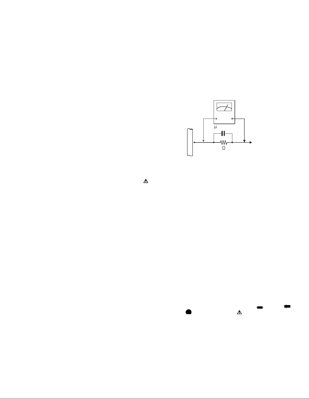
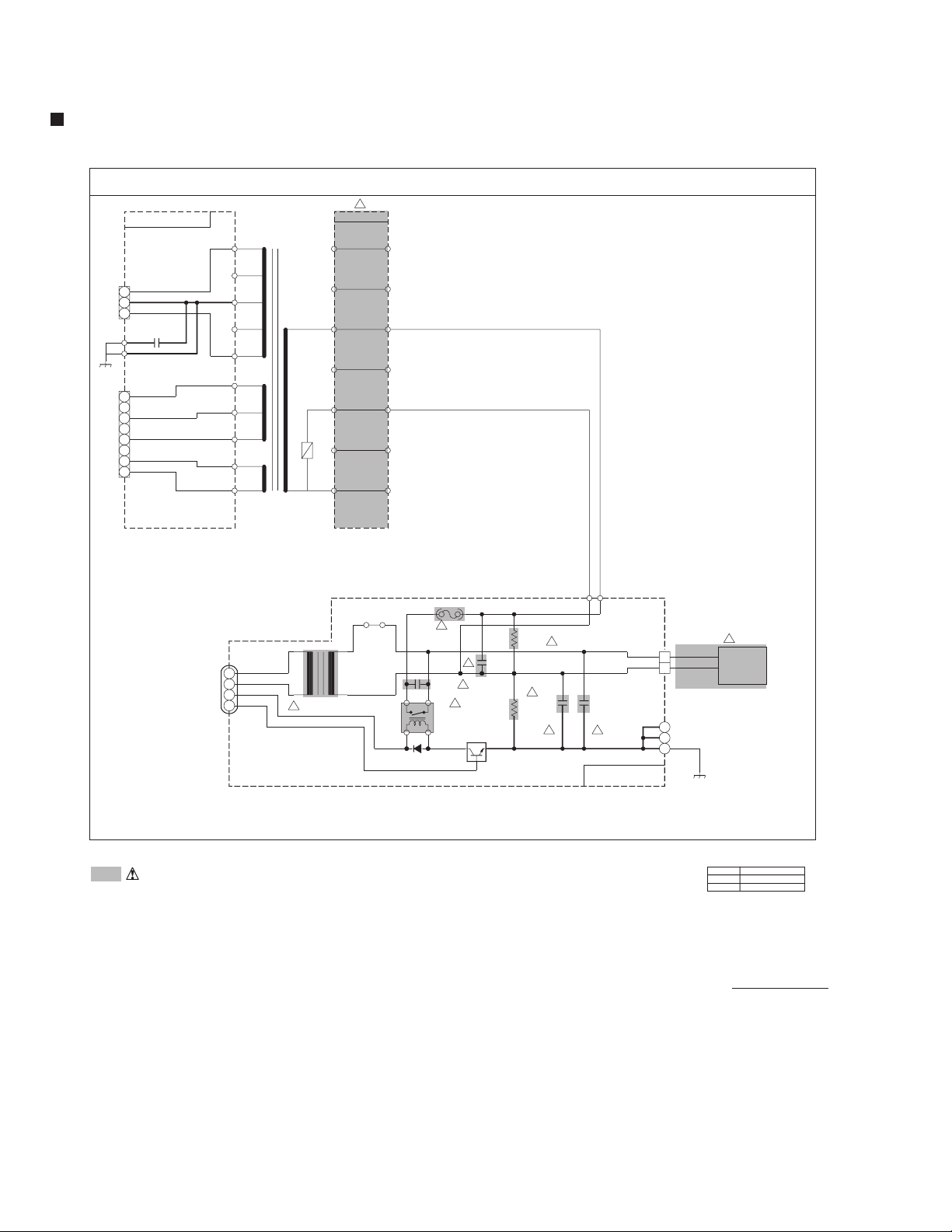
(5) Leakage shock hazard testing
After reassembling the product, always perform an isolation check on the exposed metal parts of the product (antenna terminals, knobs, metal cabinet, screw heads,
headphone jack, control shafts, etc.) to be sure the product
is safe to operate without danger of electrical shock.Do not
use a line isolation transformer during this check.
• Plug the AC line cord directly into the AC outlet. Using a
"Leakage Current Tester", measure the leakage current
from each exposed metal parts of the cabinet, particularly any exposed metal part having a return path to the
chassis, to a known good earth ground. Any leakage current must not exceed 0.5mA AC (r.m.s.).
• Alternate check method
Plug the AC line cord directly into the AC outlet. Use an
AC voltmeter having, 1,000Ω per volt or more sensitivity
in the following manner. Connect a 1,500Ω 10W resistor
paralleled by a 0.15µF AC-type capacitor between an ex-
posed metal part and a known good earth ground.
Measure the AC voltage across the resistor with the AC
voltmeter.
Move the resistor connection to each exposed metal
part, particularly any exposed metal part having a return
path to the chassis, and measure the AC voltage across
the resistor. Now, reverse the plug in the AC outlet and
repeat each measurement. Voltage measured any must
not exceed 0.75 V AC (r.m.s.). This corresponds to 0.5
mA AC (r.m.s.).
AC VOLTMETER
(Having 1000
ohms/volts,
or more sensitivity)
0.15 F AC TYPE
Place this
probe on
1500 10W
Good earth ground
1.2 Warning
(1) This equipment has been designed and manufactured to
meet international safety standards.
(2) It is the legal responsibility of the repairer to ensure that
these safety standards are maintained.
(3) Repairs must be made in accordance with the relevant
safety standards.
(4) It is essential that safety critical components are replaced
by approved parts.
(5) If mains voltage selector is provided, check setting for local
voltage.
1.3 Caution
Burrs formed during molding may be left over on some parts
of the chassis.
Therefore, pay attention to such burrs in the case of preforming repair of this system.
1.4 Critical parts for safety
In regard with component parts appearing on the silk-screen
printed side (parts side) of the PWB diagrams, the parts that are
printed over with black such as the resistor ( ), diode ( )
and ICP ( ) or identified by the " " mark nearby are critical
for safety. When replacing them, be sure to use the parts of the
same type and rating as specified by the manufacturer.
(This regulation dose not Except the J and C version)
each exposed
metal part.
(No.MB448)1-3
Page 4
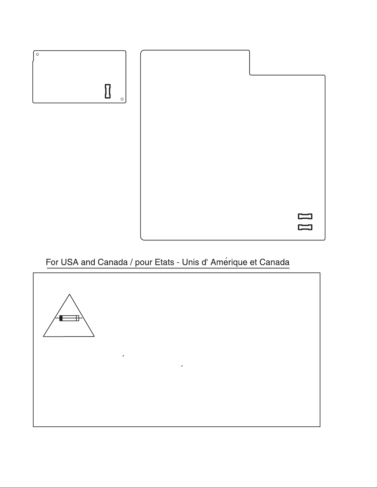
1.5 Importance administering point on the safety
Primary board (Forward side)
F103
Main amplifier board (Forward side)
F102
F101
Caution: For continued protection against risk of
fire, replace only with same type 4 A/125 V for
F101, 4 A/125 V for F102, 6.3 A/125 V for F103.
This symbol specifies type of fast operating fuse.
Precaution: Pour eviter risques de feux, remplacez
le fusible de surete de F101 comme le meme type
que 4 A/125 V, 4 A/125 V pour F102, et 6,3 A/125V
pour F103.
Ce sont des fusibles suretes qui functionnes rapide.
^
1-4 (No.MB448)
Page 5
1.6 Caution after repairs
There are two power supply as the second power supply of the transformer.
One is a power supply for power IC(3pin), and another is a power supply for the control(5pin).
+B for power IC
(3pins)
There are two power supply as the second power supply of the transformer.
One is a power supply for power IC(3pin), and another is a power supply for the control(8pin).
Please connect first of all and confirm the power supply for the control when you do the energizing examination after it completes of
the repair.
+B for control section
(8pins)
For power IC(3pins)
Please never do the energizing examination in a power supply of power IC alone.
Moreover, when the control system breaks down, power IC is occasionally damaged.
(No.MB448)1-5
Page 6

SECTION 2
SPECIFIC SERVICE INSTRUCTIONS
This service manual does not describe SPECIFIC SERVICE INSTRUCTIONS.
1-6 (No.MB448)
Page 7
SECTION 3
DISASSEMBLY
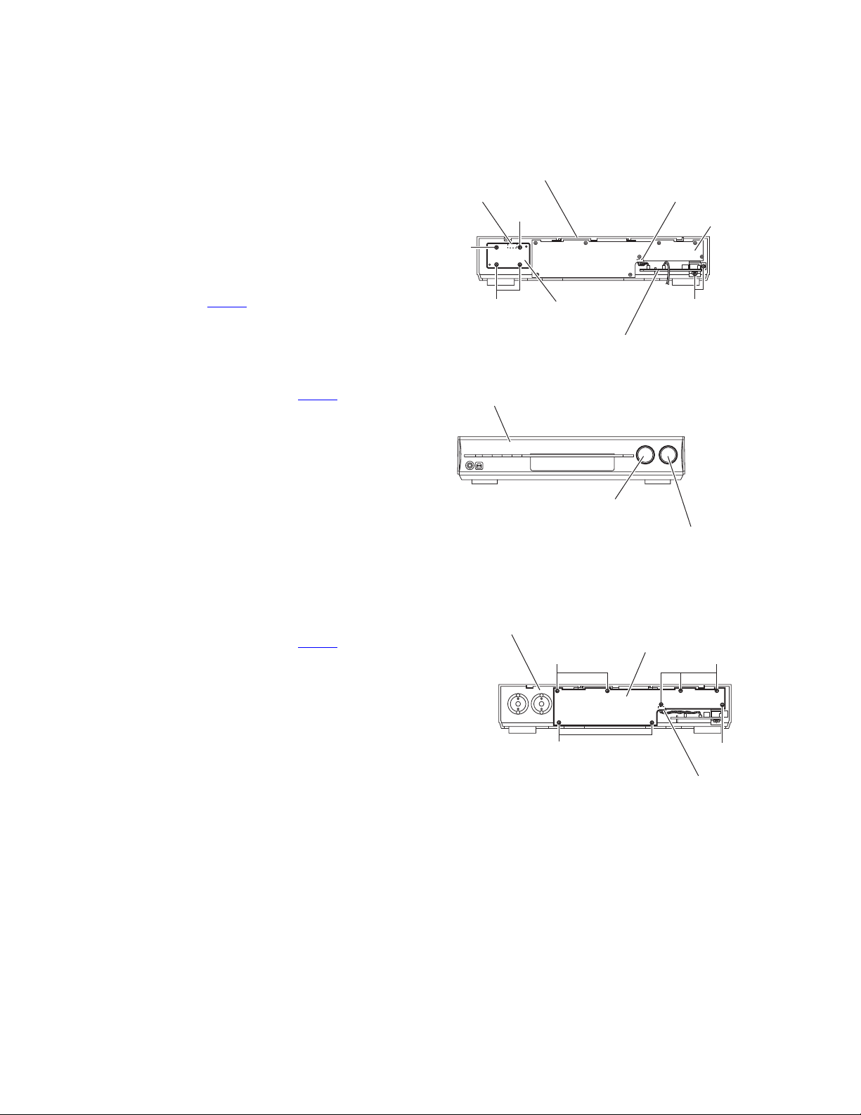
3.1 Main body section
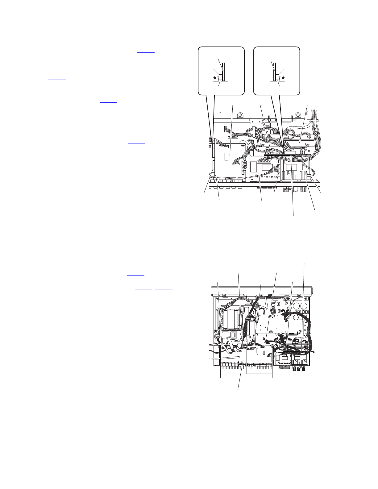
3.1.1 Removing the top cover
(See Figs.1 and 2)
(1) From the both sides of the main body, remove the four
screws A attaching the top cover. (See Fig.1)
(2) From the back side of the main body, remove the five
screws B and screw C attaching the top cover. (See Fig.2)
(3) Remove the top cover in the direction of the arrow. (See
Fig.1.)
Top cover
A
Fig.1
3.1.2 Removing the HDMI board
(See Fig.3)
• Remove the top cover.
(1) From the back side of the main body, remove the three
screws D attaching the HDMI board to the rear panel.
(2) From the top side of the main body, remove the screw E at-
taching the HDMI board to the support bracket.
(3) Disconnect the card wires from the connectors (CN731
, CN762) on the HDMI board.
CN732
(4) Take out the HDMI board from the main body and discon-
nect the parallel wires from the connectors (CN771,
) on the reverse side of the HDMI board.
CN772
Reference:
Remove the shield from the HDMI board as required.
B
C
Top cover
B B
Fig.2
CN732
CN731
,
Support bracket
E
Shield
CN771
CN762
CN772 HDMI board
D
Rear panel
Fig.3
(No.MB448)1-7
Page 8
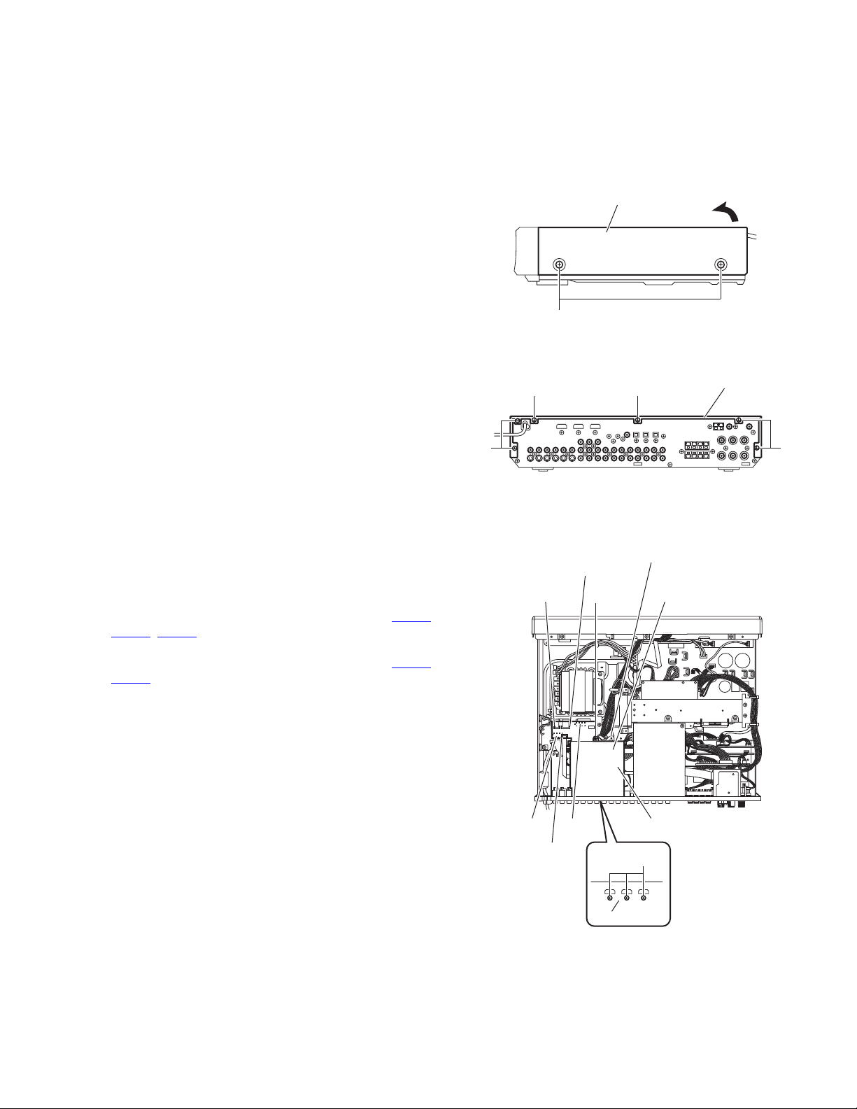
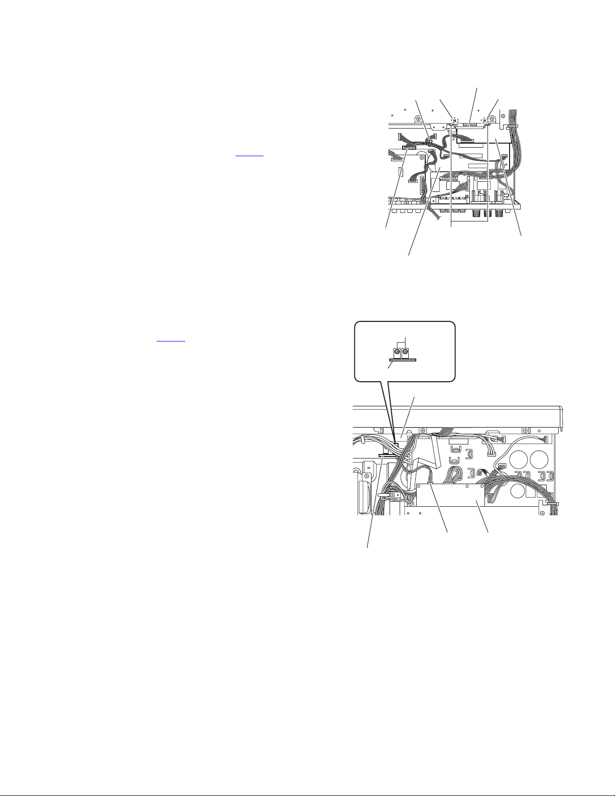
3.1.3 Removing the front panel assembly
(See Figs.4 and 5)
• Remove the top cover and HDMI board.
(1) From the top side of the main body, remove the tie band
bundling the wires. (See Fig.4.)
Reference:
After reassembling, bundle the wires with a new tie band
as before. (See Fig.4.)
(2) Release the wire holders bundling the wires. (See Fig.4)
(3) Disconnect the card wire from the connector CN102
main amplifier board. (See Fig.4)
(4) Disconnect the wire from the connector CN351
amplifier board. (See Fig.4)
(5) Disconnect the wire from the connector CN552
board. (See Fig.4)
(6) Disconnect the wire from the connector CN661
board. (See Fig.4)
(7) Remove the three screws F attaching the front panel as-
sembly. (See Fig.4)
(8) Remove the screw F attaching the OSD connect 2 board.
(See Fig.4)
(9) From the bottom side of the main body, remove the four
screws F attaching the front panel assembly. (See Fig.5)
(10) Release the joints a and remove the front panel assembly
in the direction of the arrow. (See Fig.5)
on the
on the main
on the input
on the DSP
CN102
Wire holders
F
CN552
Input board
Main amplifier board
Wire holder
Wire holder
F
CN661
DSP board
Tie band
F
F
CN351
OSD connect 2 board
Front panel assembly
F
Fig.4
F
a
Fig.5
1-8 (No.MB448)
Page 9
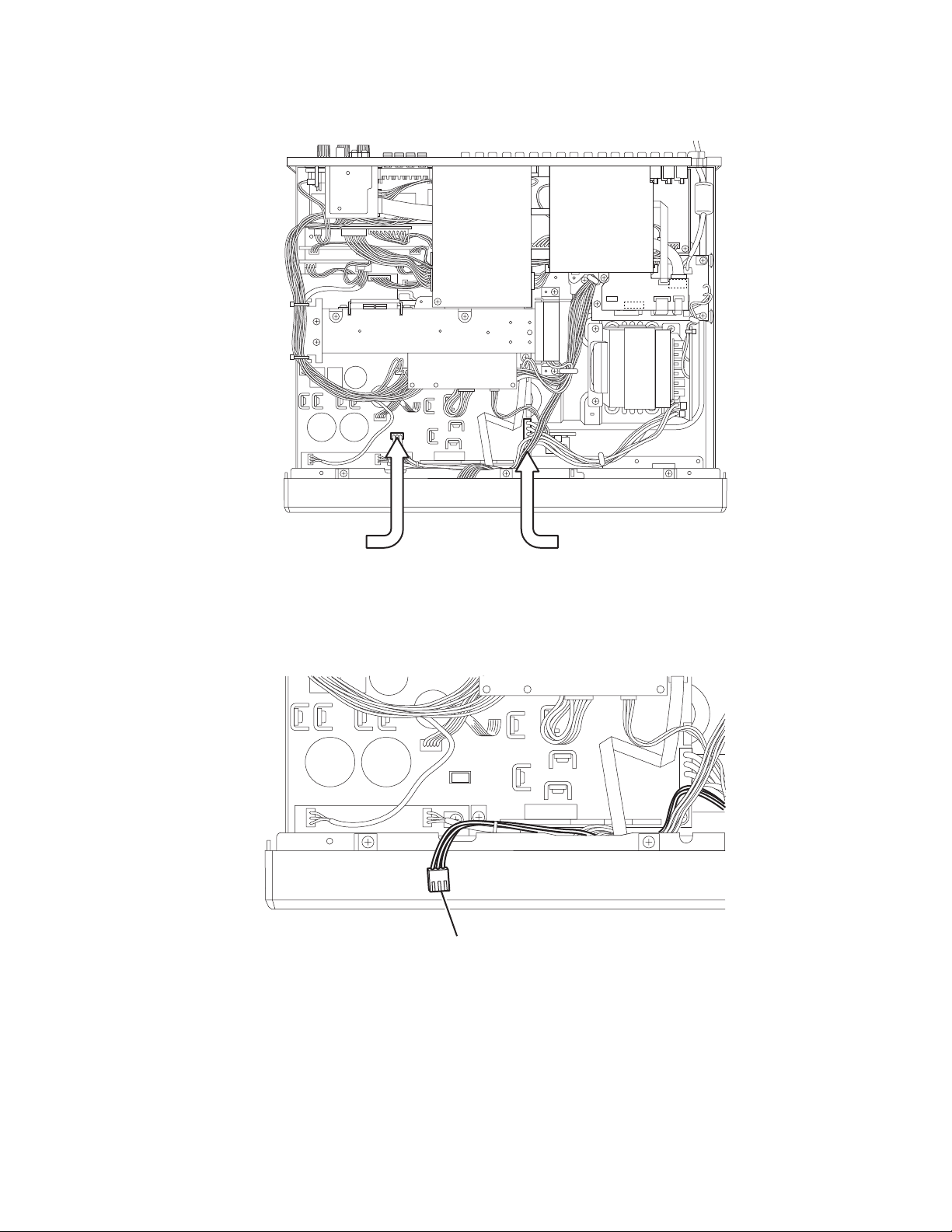
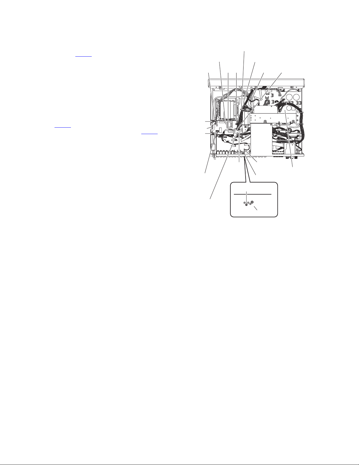
3.1.4 Removing the rear panel
(See Fig.6)
• Remove the top cover.
(1) From the back side of the main body, remove the strain re-
lief from the rear panel in the direction of the arrow and remove the power cord.
(2) Remove the three screws G and twenty-seven screws H
attaching the rear panel.
3.1.5 Removing the tuner
(See Fig.7)
• Remove the top cover.
(1) From the top side of the main body, disconnect the card
wire from the connector CN1
(2) From the back side of the main body, remove the two
screws J attaching the tuner to the rear panel and take out
the tuner.
3.1.6 Removing the subwoofer board
(See Fig.7)
• Remove the top cover.
(1) From the top side of the main body, disconnect the wire
from the connector CN524
(2) From the back side of the main body, remove the screw K
attaching the subwoofer board to the rear panel and take
out the subwoofer board.
on the tuner.
on the subwoofer board.
Power cord
H
Strain relief
G HHG H
DSP board
CN661CN652
Fig.6
Rear panel
CN683
N
CN682
3.1.7 Removing the DSP board
(See Fig.7)
• Remove the top cover.
(1) From the back side of the main body, remove the five
screws M attaching the DSP board to the rear panel.
(2) Remove the screw N attaching the DSP board.
(3) Disconnect the DSP board from the DSP connect board
while releasing the claw b of the connector CN681
DSP board.
Note:
When releasing the claw b, take care not to break it.
(4) Take out the DSP board and disconnect the wires from the
connectors (CN661
the DSP board.
(5) Disconnect the card wires from the connectors (CN651
) on the forward side of the DSP board.
CN652
, CN682, CN683) on the forward side of
on the
CN651 Tuner
DSP board
CN681
b
DSP connect board
,
M
Rear panel Rear panel
Fig.7
CN1 CN524
KJ
Subwoofer board
(No.MB448)1-9
Page 10
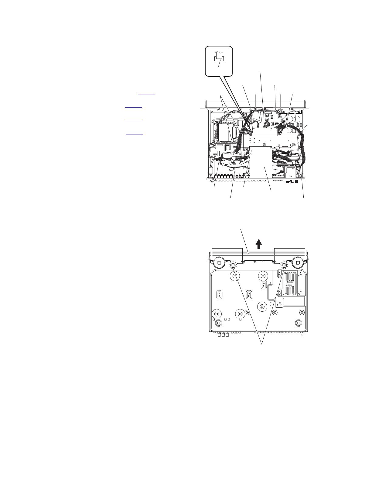
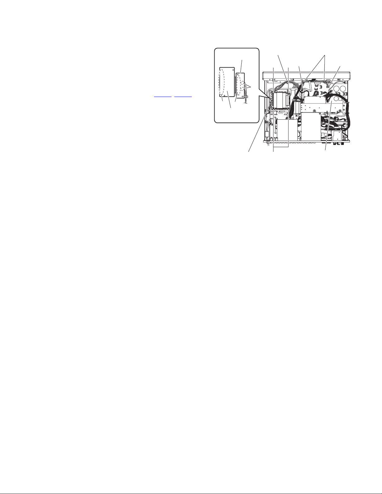
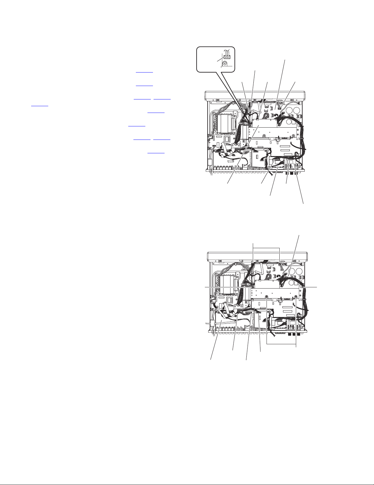
3.1.8 Removing the compulink board
(See Fig.8)
• Remove the top cover and HDMI board.
(1) From the top side of the main body, disconnect the wire
from the connector CN565 on the compulink board.
(2) From the back side of the main body, remove the screw P
attaching the compulink board to the rear panel and take
out the compulink board.
3.1.9 Removing the primary board
(See Fig.8)
• Remove the top cover and HDMI board.
(1) From the top side of the main body, remove the screw Q
attaching the support bracket on the chassis base.
(2) Release the wire holders and disconnect the wire from the
connector CN101
(3) Disconnect the power cord from the connector CN120 on
the primary board.
(4) Remove the two screws R and two screws R' attaching the
primary board.
Reference:
When attaching the screws R', attach the wire holders
with them as before.
(5) Take out the primary board from the main body and remove
the wires from the soldered sections c on the reverse side
of the primary board.
on the main amplifier board.
Primary board
Wire holder
R'
c
R
CN120
Wire holder
R' R
Q
Chassis base
Wire holderCN101
CN565
Main amplifier board
Compulink board
P
Support bracket
Rear panel
Fig.8
1-10 (No.MB448)
Page 11
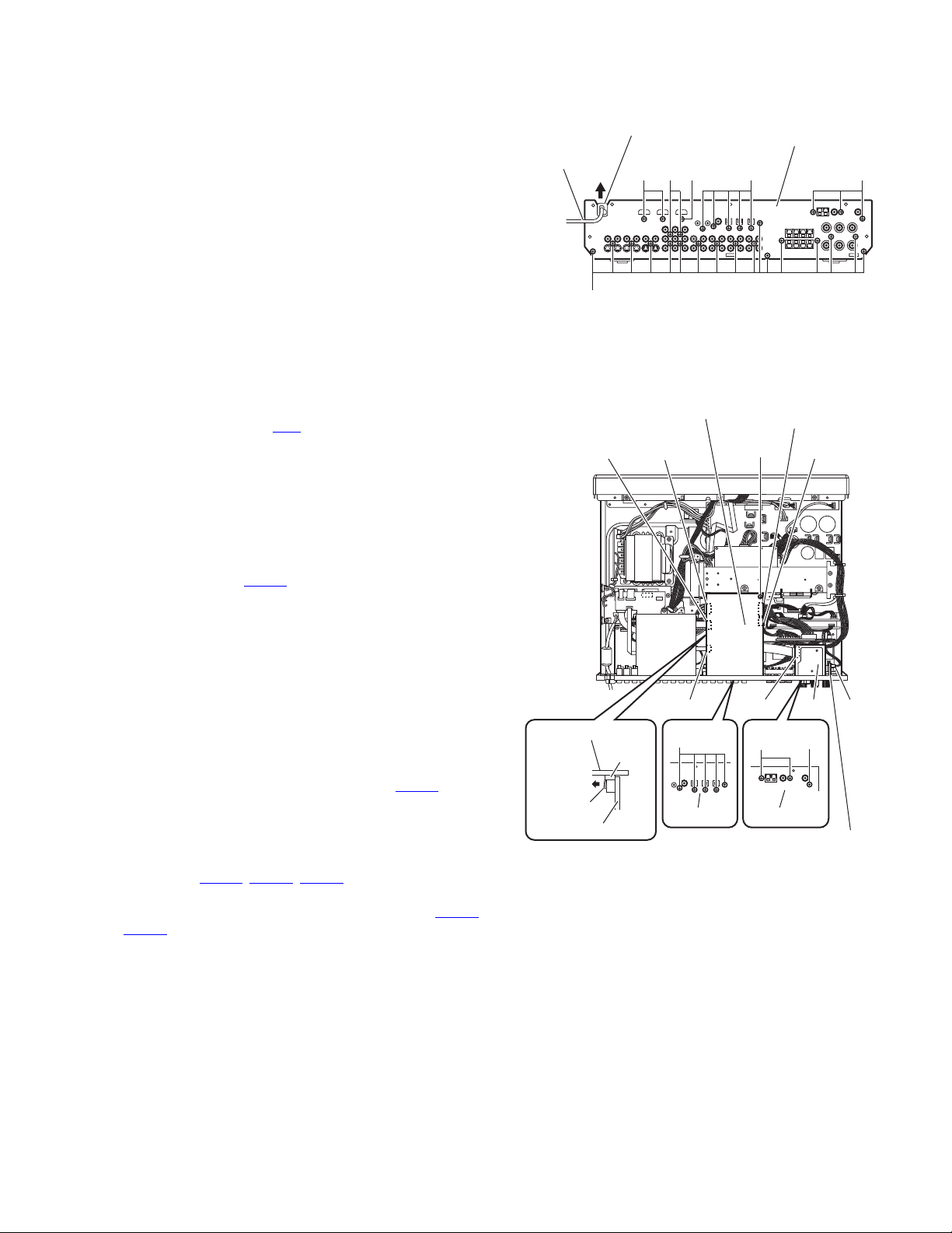
3.1.10 Removing the power transformer
(See Fig.9)
• Remove the top cover.
(1) From the top side of the main body, remove the tie band
bundling the wires.
Reference:
After reassembling, bundle the wires with a new tie band
as before.
(2) Release the wire holders to remove the wires.
(3) Disconnect the wires from the connectors (CN106
on the main amplifier board.
(4) Remove the soldered sections d and remove the wires.
(5) Remove the four screws S and take out the power trans-
former from the main body.
3.1.11 Removing the trans primary board
(See Fig.9)
• Remove the top cover.
(1) From the top side of the main body, remove the tie band
bundling the wires.
Reference:
After reassembling, bundle the wires with a new tie band
as before.
(2) Remove the wires from the soldered sections d and re-
move the wires.
(3) Remove the solders from the soldered sections e and re-
move the trans primary board.
, CN111)
Trans primary
board
d
e
f
Trans secondary
board
Tie band
Wire holder
S
S
S
Fig.9
Wire holders
CN106 C N111
Main amplifier board
3.1.12 Removing the trans secondary board
(See Fig.9)
• Remove the top cover.
Reference:
Take out the power transformer from the main body as re-
quired.
From the side of the power transformer, remove the solders from
the soldered sections f and remove the trans secondary board.
(No.MB448)1-11
Page 12
3.1.13 Removing the DCDC control board
(See Fig.10)
• Remove the top cover.
From the top side of the main body, disconnect the DCDC control
board from the main amplifier board in an upward direction while
releasing the claw g of the connector CN152
fier board.
Note:
When releasing the claw g, take care not to break it.
on the main ampli-
DCDC control board
g
CN152
Main amplifier board
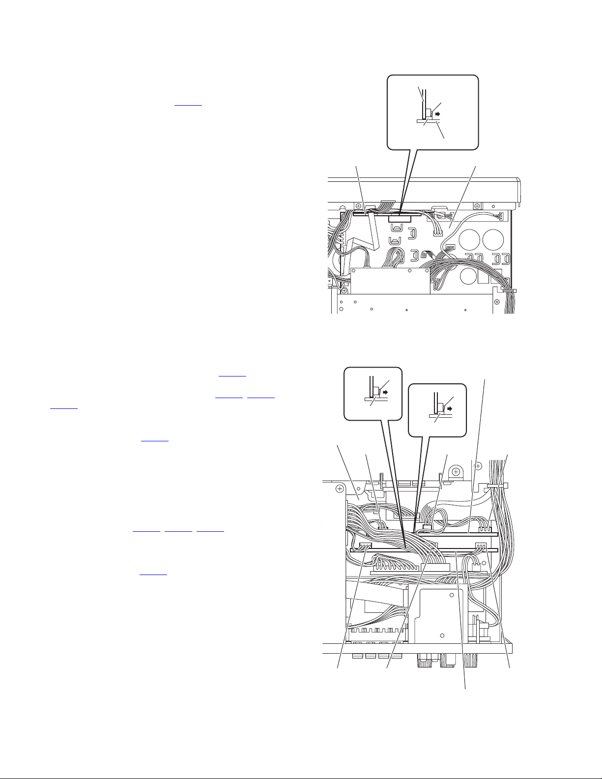
3.1.14 Removing the PWM modulation 1 board
(See Fig.11)
• Remove the top cover.
(1) Disconnect the wire from the connector CN413
PWM modulation 2 board.
(2) Disconnect the wires from the connectors (CN311
CN313) on the PWM modulation 1 board.
(3) Disconnect the PWM modulation 1 board from the main
amplifier board in an upward direction while releasing the
claw h of the connector CN302
Note:
When releasing the claw h, take care not to break it.
on the main amplifier board.
on the
, CN312,
DCDC control board
CN402
Main amplifier
board
CN312
j
Main amplifier board
Fig.10
PWM modulation 1 board
h
CN302
CN313 CN311
3.1.15 Removing the PWM modulation 2 board
(See Fig.11)
• Remove the top cover.
(1) From the top side of the main body, disconnect the wires
from the connectors (CN411
modulation 2 board.
(2) Disconnect the PWM modulation 2 board from the main
amplifier board in an upward direction while releasing the
claw j of the connector CN402
Note:
When releasing the claw j, take care not to break it.
1-12 (No.MB448)
, CN412, CN413) on the PWM
on the main amplifier board.
CN411CN413CN412
PWM modulation 2 board
Fig.11
Page 13
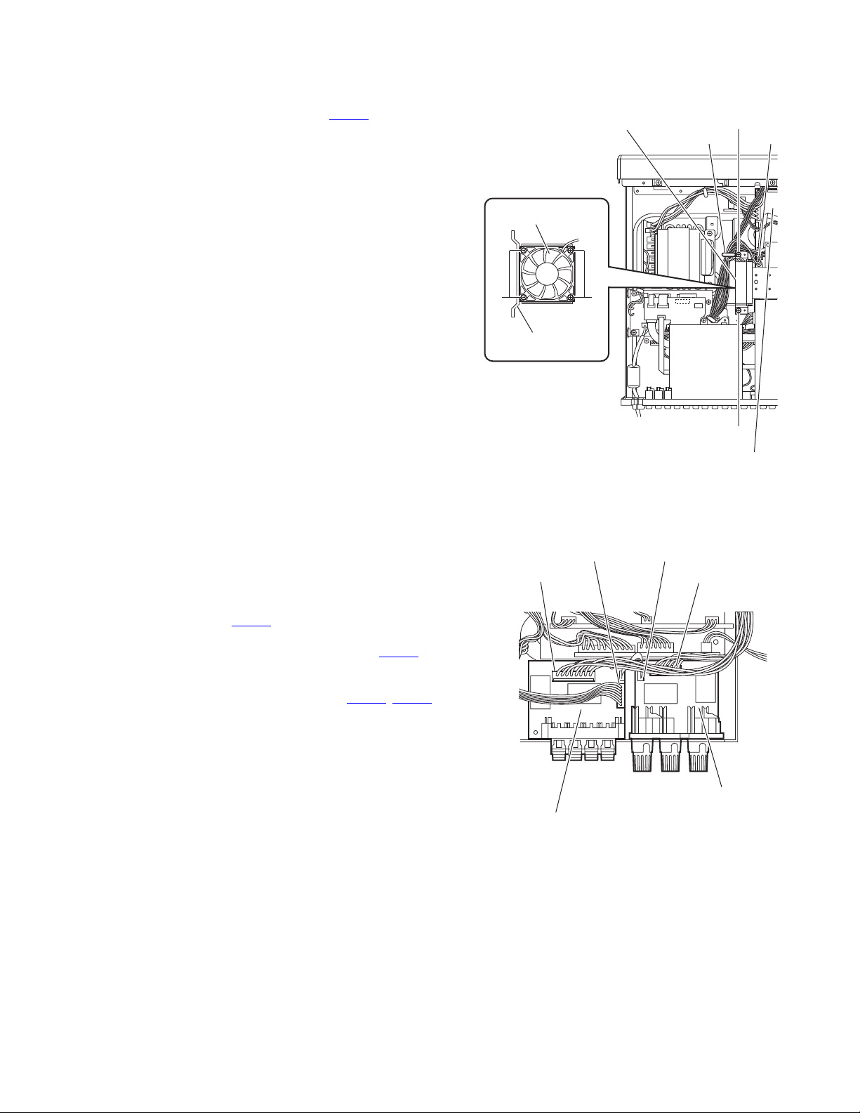
3.1.16 Removing the cooling fan
(See Fig.12.)
• Remove the top cover.
(1) Disconnect the wire from the connector CN103
amplifier board.
(2) Remove the screw T and screw T'.
Reference:
When attaching the screw T', attach the wire holder with
it.
(3) Take out the cooling fan assembly.
(4) Remove the four screws U attaching the cooling fan to the
fan bracket.
on the main
Cooling fan assembly
Cooling fan
Wire holder
T'
CN103
U
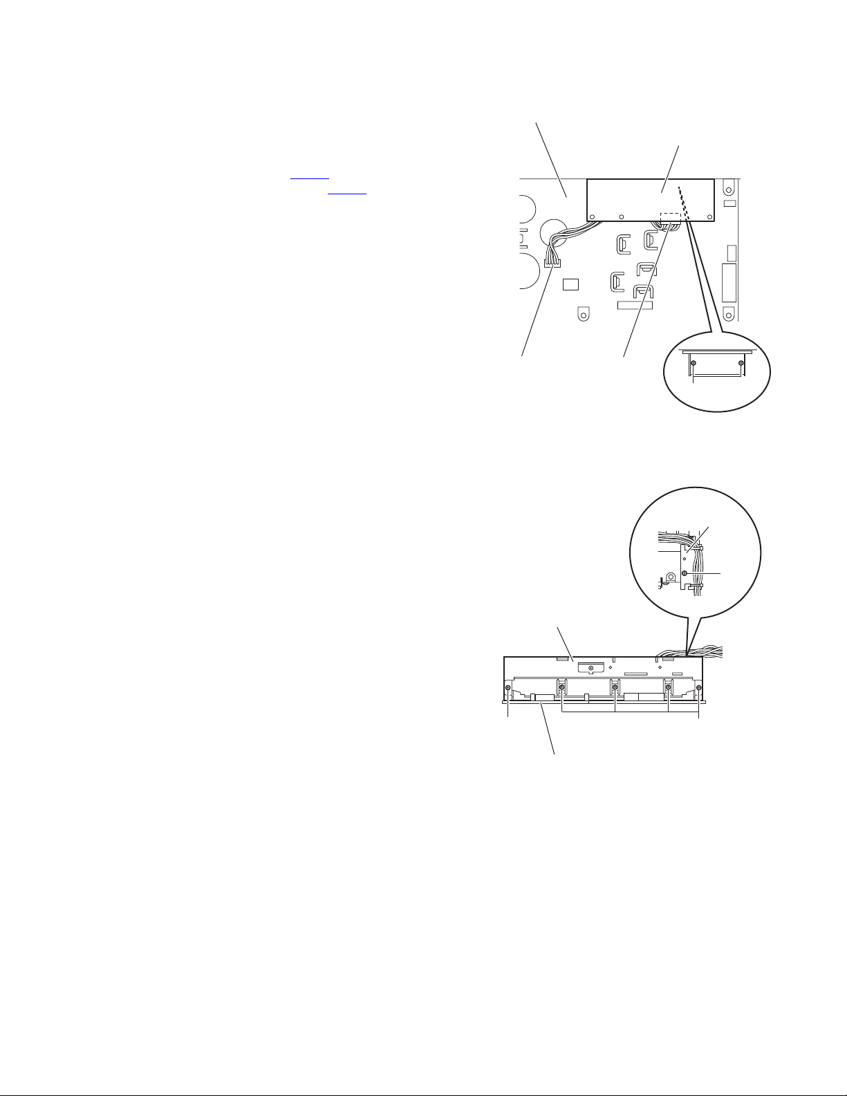
3.1.17 Removing the speaker terminal 1 and speaker terminal 2 boards
(See Fig. 13)
• Remove the top cover and rear panel.
Reference:
Remove the tuner, subwoofer board and DSP board as required.
(1) From the top side of the main body, disconnect the wire
from the connector CN265
board.
(2) Disconnect the parallel wire from the connector CN465
the speaker terminal 1 board.
(3) Take out the speaker terminal 1 board from the main body.
(4) Disconnect the wires from the connectors (CN209
on the speaker terminal 2 board.
(5) Take out the speaker terminal 2 board from the main body.
on the speaker terminal 1
on
, CN262)
Fan bracket
CN262
U
T
Main amplifier board
Fig.12
CN465CN209
CN265
Speaker terminal 2 board
Fig.13
Speaker terminal 1 board
(No.MB448)1-13
Page 14
3.1.18 Removing the DSP connect board
(See Fig.14)
• Remove the top cover, tuner and DSP board.
(1) Disconnect the wire from the connector CN209 on the
speaker terminal 2 board.
(2) Disconnect the DSP connect board from the input board in
an upward direction while releasing the claw k of the connector CN502
Note:
When releasing the claw k, take care not to break it.
(3) Disconnect the connector CN516
board from the input board.
3.1.19 Removing the OSD connect 1 board
(See Fig.14)
• Remove the top cover, tuner and DSP board.
(1) Disconnect the wire from the connector CN524
woofer board.
(2) Disconnect the wire from the connector CN513
connect 1 board.
(3) Disconnect the OSD connect 1 board from the main ampli-
fier board in an upward direction while releasing the claw m
of the connector CN222
Note:
When releasing the claw m, take care not to break it.
on the input board.
on the DSP connect
on the sub-
on the OSD
on the main amplifier board.
DSP connect
board
k
CN502
Input board CN513
CN516
DSP connect board
OSD connect 1
board
m
CN222
Main amplifier board
CN209 CN524
Speaker terminal
2 board
OSD connect 1 board
Subwoofer
board
3.1.20 Removing the input board
(See Fig. 15)
• Remove the top cover, HDMI board, rear panel, tuner, sub-
woofer board, DSP board, compulink board and DSP connect
board.
(1) Disconnect the wire from the connector CN513
connect 1 board.
(2) Disconnect the wires from the connectors (CN530
CN552) on the input board.
(3) Disconnect the parallel wire from the connector CN540 on
the input board.
(4) Remove the three screws V and take out the input board
from the main body.
on the OSD
, CN531,
CN540
CN552
CN530
V V
Input board
Fig.14
OSD connect 1 board
CN531
CN513
Fig.15
1-14 (No.MB448)
Page 15
3.1.21 Removing the master clock board
(See Fig.16)
• Remove the top cover, tuner, DSP board, PWM modulation 1
board, PWM modulation 2 board and OSD connect 1 board.
(1) From the top side of the main body, remove the tie band
bundling the wires.
Reference:
After reassembling, bundle the wires with a new tie band
as before.
(2) Disconnect the wire from the connector CN201
amplifier board.
(3) Remove the two screws W with a short driver and remove
the transistor hold from the joints n of the heat sink.
(4) Take out the master clock board from the main body.
on the main
Tie band
Transistor hold
n
n
3.1.22 Removing the HDMI-Regulator board
(See Fig.17)
• Remove the top cover.
(1) From the top side of the main body, disconnect the wire
from the connector CN117
lator board.
(2) Remove the two screws X attaching the HDMI-Regulator
board on the chassis base.
(3) Take out the HDMI-Regulator board from the main body.
on the forward side of the regu-
CN201
Main amplifier board
X
HDMI-Regulator board
Chassis base
W
Master clock board
Fig.16
HDMI-Regulator board
CN117
Fig.17
Regulator board
(No.MB448)1-15
Page 16
3.1.23 Removing the main amplifier board
Y
(See Figs.18 and 19)
• Remove the top cover, HDMI board, front panel assembly, tun-
er, DSP board, DCD control board, PWM modulation 1 board,
PWM modulation 2 board, OSD connect 1 board and master
clock board.
(1) Disconnect the wire from the connector CN265
speaker terminal 1 board. (See Fig.18.)
(2) Disconnect the wire from the connector CN262
speaker terminal 2 board. (See Fig.18.)
(3) Disconnect the wires from the connectors (CN103
) on the main amplifier board. (See Fig.18.)
CN111
(4) Disconnect the parallel wire from the connector CN101
the main amplifier board. (See Fig.18.)
(5) Disconnect the wire from the connector CN117
ward side of the regulator board. (See Fig.18.)
(6) Disconnect the wires from the connectors (CN530
on the input board. (See Fig.19.)
(7) Disconnect the parallel wire from the connector CN540
the input board. (See Fig.19.)
(8) Remove the four screws Y and two screws Z. (See Fig.19.)
(9) Take out the main amplifier board with the regulator board
from the main body. (See Fig.19.)
on the
on the
, CN106,
on
on the for-
, CN531)
on
CN103
Main amplifier board
CN106
CN101 CN117
CN262Regulator board
Speaker terminal 2 board
CN265
Speaker terminal 1 board
CN111
Y
Input board
CN540
CN530
Fig.18
Z
CN531
Fig.19
Main amplifier board
Y
1-16 (No.MB448)
Page 17
3.1.24 Removing the regulator board
(See Fig.20)
• Remove the top cover, HDMI board, front panel assembly, tun-
er, DSP board, DCD control board, PWM modulation 1 board,
PWM modulation 2 board, OSD connect 1 board, master clock
board and main amplifier board.
(1) From the forward side of the main amplifier board, discon-
nect the wire from the connector CN105
(2) Disconnect the wire from the connector CN114
ulator board.
(3) Remove the two screws AA attaching the regulator board.
.
on the reg-
Main amplifier board
Regulator board
3.1.25 Removing the heat sink
(See Fig.21)
• Remove the top cover, HDMI board, front panel assembly, tun-
er, DSP board, DCD control board, PWM modulation 1 board,
PWM modulation 2 board, OSD connect 1 board, master clock
board and main amplifier board.
(1) From the forward side of the main amplifier board, remove
the screw AB and remove the wire holder board with the
wires.
(2) Remove the five screws AC to remove the heat sink.
CN105
Heat sink
AC
Main amplifier board
CN114
AA
Fig.20
Wire holder board
AB
AC
Fig.21
(No.MB448)1-17
Page 18
3.2 Front panel assembly section
• Remove the front panel assembly.
(See "3.1.3 Removing the front panel assembly".)
3.2.1 Removing the JOG board
(See Figs. 1 and 2)
(1) From the inside of the front panel assembly, remove the
four screws A attaching the JOG board. (See Fig.1.)
(2) Take out the JOG board while lifting it from the front panel
assembly little by little.
Reference:
The MASTER VOLUME knob and SOURCE SELECTOR knob are removed from the front side simultaneously. (See Fig.2.)
(3) From the forward side of the JOG board, disconnect the
wire from the connector CN913
3.2.2 Removing the OSD connect 2 board
(See Fig. 1)
(1) From the inside of the front panel assembly, remove the
two screws A attaching the OSD connect 2 board.
(2) Disconnect the wire from the connector CN914
board.
. (See Fig.1)
on the FL
Front panel assembly
CN913
A
A
JOG board
A
Front panel assembly
CN914
FL board
A
OSD connect 2 board
Fig.1
3.2.3 Removing the FL board
(See Fig. 3)
• Remove the JOG board.
(1) Remove the eight screws A and take out the FL board.
(2) Disconnect the wire from the connector CN914
board.
on the FL
SOURCE SELECTOR knob
Front panel assembly
A
A
MASTER VOLUME knob
Fig.2
FL board
CN914
Fig.3
A
A
1-18 (No.MB448)
Page 19

SECTION 4
ADJUSTMENT
This service manual does not describe ADJUSTMENT.
SECTION 5
TROUBLESHOOTING
This service manual does not describe TROUBLESHOOTING.
(No.MB448)1-19
Page 20

Victor Company of Japan, Limited
AV & MULTIMEDIA COMPANY AUDIO/VIDEO SYSTEMS CATEGORY 10-1,1chome,Ohwatari-machi,Maebashi-city,371-8543,Japan
(No.MB448)
Printed in Japan
VPT
Page 21
SCHEMATIC DIAGRAMS
AUDIO / VIDEO CONTROL RECEIVER
RX-D402B,RX-D401S
CD-ROM No.SML200509
Area suffix
J ---------------------------- U.S.A.
Lead free solder used in the board (material : Sn-Ag-Cu, melting point : 219 Centigrade)
Contents
Block diagram
Standard schematic diagrams
Printed circuit boards
COPYRIGHT 2005 Victor Company of Japan, Limited.
2-1
2-3
2-25 to 36
No.MB448SCH
2005/9
Page 22

In regard with component parts appearing on the silk-screen printed side (parts side) of the PWB diagrams, the
parts that are printed over with black such as the resistor ( ), diode ( ) and ICP ( ) or identified by the " "
mark nearby are critical for safety.
Page 23

< MEMO >
Page 24
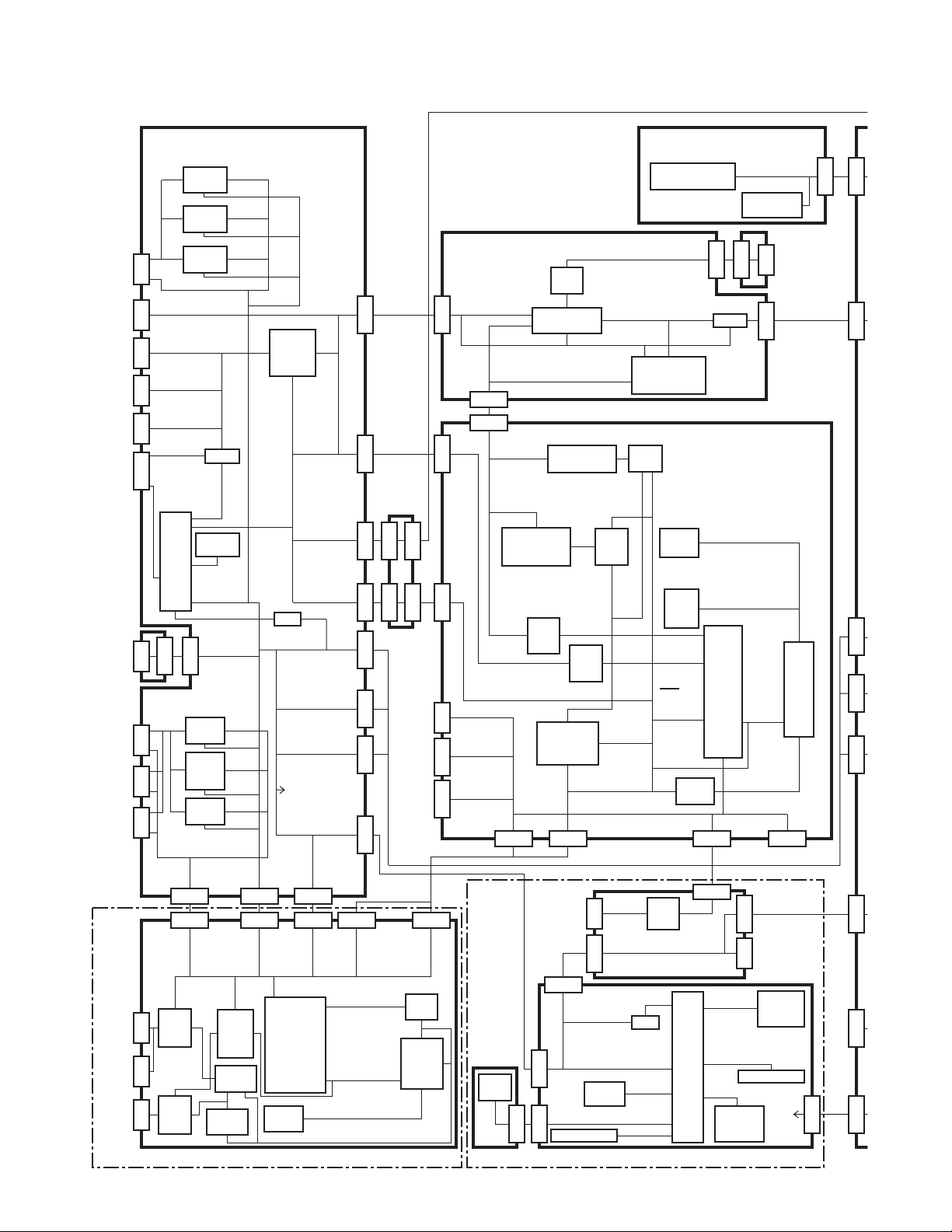
Block diagram
F
S
S
_
R
R
R
R
R
o
o
Audio/Video signal input and system
control section
Y OUT
IC530
Y
Y SEL.
PB OUT
IC531
PB
PB SEL.
VCR IN
DVR/DVD IN
MONITOR OUT
DVD C/SW
DVD SURR
DVR OUT
DVR/DVD IN
VCR
IN/OUT
TV
DBS
TO
TUNER
AV
COMPULINK
DBS
VCR OUT
VCR IN
DVR OUT
DVR/DVD IN
MONITOR
HDMI
PORT0
HDMI
PORT1
J4503
PR
J6504
DVD_C,DVD_SW
DVD_SL/SR
DVRREC_L/R
J6503
DVR_L/R
VCRREC_L/R
J6502
VCR_L/R
TV_L/R
J6501
DBS_L/R
TU_L/R
CN505
TU_DATAI
TU_DATAO
TU_CLK,TU_CE
IC501
CPU
CN565
J505
J6511
J6512
J6513
Y,C,CVBS
J711
IC731
HDMI
RX
CSDA,CSCL
J721
TX_RST
TX_HPD
TX_INT
J751
IC751
HDMI
TX
Y
C
CV
SD0 to 2,LRCK
BCK,RX_SPDIF
RX_MUTE
IC532
PR SEL.
MUTE
T_MUTE
IC507
EEPROM
RC_SDA
RC_SCL
RC_WP
HP_RELAY
CN555
AVCLINK
IC522
SY SEL.
IC524
IC525
SC SEL.
IC527
CV SEL.
HDMI_SY
HDMY_SC,CV
MICON
BUS SW
IC743
BUS SW
PR OUT
VIDEO1
VIDEO4
HDMI_Y
HDMI_PB
HDMI_PR
Y OUT
C OUT
CV OUT
FW781FW782
CN771CN772
Y,Pb,Pr
IC761
HDMI
SUB
IC741
SOURCE
VIDEO1
VIDEO11
HDMI_Y
HDMI_PB
HDMI_PR
HDMI_Y
HDMI_PB
HDMI_PR
HDMI_CLK
HDMI_STS
HDMI_COM
HDMI_RDY
HDMI_RST
SDTV/HDTV
DECODER
GRAPHICS
DIGITIZER
IC782
SDRAM
VIDEO1
VIDEO11
IC502
L,R
6CH
SEL.
BD3813/3842 DA
BD3813/3842 CL
DA,CL
S_MUTE
L,R
SBWR_MUTE
FR_RELAY
C_RELAY
SURR_RELAY
SBK_RELAY
DSP_STATUS
DSP_READY
DSP_COMMAND
DSP_CLOCK
DSP_RESET
HP_RY
Q524
BCHANGE1
BCHANGE2
FAN_ON/OFF
FAN_ L
PROTECT
FREQ_CTRL
D+5V,B+5V
+/-7V,+9V
A+5V(DSP)
D+5V(DSP)
+5V(VIDEO)
+12V(RELAY)
HDMI_CLK
HDMI_STS
HDMI_COM
HDMI_READY
HDMI_RESET
CN504
CN762
RX_SPDIF
DSP_SPDF
Y,C,CVBS
Y,Pb,Pr
IC771
AD_OUT_Y0 to Y7
AD_OUT_CBCR0 to 7
VIDEO
&
RGB
AD_SDA,AD_SCL
AD_RST,IP_RST
DATA0 to 31,ADDR0 to 10
SDRAM_CLK,BA0,BA1,DQM
BUF_OUT_Y0 to Y7,Y0 to 7
BUFF_OUT_CBCR0 to 7,CBCR0 to 7
HDMI RX,TX,micom,HDMI ADC and i/p converter section
CN503
CN501
CN516
CN602
CN509
CN672
CN506
CN502
CN530
CN531
DIGITAL
CN540
DIGITAL
DIGITAL
CN552
AUDIO_SEL1 to 4
SD0 to 2,LRCK
RX_MUTE,BCK
IC772
BUFF.
IC781
DIGITAL
VIDEO
CONV.
Master volume section
L,R
DVD_SW
CN513
DVD_SL/SR
DVD_C
DSP_L/R
DSP_C,DSP_SW
DSP_SL/SR
CN521
CN683
CN682
CN681
J681 UN682
IN1
DSP.L
DSP.R
DSP.LS/RS
DSP.C
DSP.SW
DSP.SBL
DSP.SBR
DSP_IN_L
DSP_IN_R
DSPSTATUS,DSPREADY
DSPCLK,DSPRESET
DSPCOMMAND
RX0
RX1
IN2
UN683
RX2
IN3
CN651 CN652
CN732CN731
JS901
JS902
User control keys, system control and FL display section
IC504
IC503
6CH VOLUME
IC611 to IC614
IC621,IC622
IC632 to IC634
AMP.
IC651
IC652
AMP.
IC685,IC686
DATA S E L
& MPX
SD0 to 2
LRCK,BCK
RX6,TX
USB
TERMINAL
CN914
CN952
CN913
CN903
VOL1,VOL2,JOG1,JOG2
S901 to S906
Master clock section
M_CLOCK
CN523
FREQ_CTRL
-B, -B+12V
Q444,Q445
-B+12V REG
CN524
J504
SUBWOOFER
OUT
IC211 to IC214
Master clock GEN.
SUBWFR
AMP
CN522
MUTE
DA,CL
DSP_SBL/SBR
DA,CL
S_MUTE
SBWR_MUTE
IC508
AUDIO SOUND
PROCESSOR
DSP and digital signal input terminal section
IC610
AMP.
P_SL/SR
P_C/LFE
P_BCK
P_LRCK
A4+/B4+/-
IC601
IC602
AMP.
AUDIO_SEL1 to 4
HDMI_MUTE
AV COMPULINK
M_COMMAND,M_STATUS
M_CLK,M_RESET,M_BUSY
M_CS
IR DET.
D/A
IC903
AVC_IN/OUT
DAC_fs1
DAC_fs2
PD_DD
RST_DD
FL/FR,SL/SR
C/LFE,C_BCK
C_LRCK
D/A
DAC_fs3
DAC_fs4
PD_DD
RST_DD
IC620
IC630
D/A
FL/FR,SL/SR
C/LFE,C_BCK
C_LRCK
RX0,RX1,RX2,RX6,TX
J903
D+/-,VBUS
CN904
HEADPHONE_DET
Q910
REMOCON
IC902
KEY_IN1 to 3
DSP_A2 to A15,DSP_D0 to D15
DSP_CE0,DSP_ARE,DSP_AWE
DSP_AOE,DSP_BE0,DSP_BE1
SDRAM_CLK
IC664
SDRAM
DSP_A2 to A21
DSP_D0 to D15
ROM
IC671
DSP_CE1,DSP_AWE
DSP_AOE
IC697
8CH
CODEC
CPU
RX4
IC663
FLASH
LIN+/RIN+/-
CDIN
CDOUT
CCLK
D_CS
D_RST
CN661
CN961
USB_IN
HP_L
HP_R
SEG1 to 35
GRID1 to 15
FMAM_LED
USB_LED,TV_LED
IC901
DBS_LED,DVD_LED
VCR_LED,HDMI_LED
CPU
&
FL
DRV.
STANDBY_IND
STANDBY
C_LRCK
S_LRCK
C_BCK
S_BCK
FL/FR
SL/SR
C/LFE
SBL/SBR
SCK,MOSI
MISO
HD3,HD4
READY
CSDSP
DIGITAL OUT
CN905
J901
HEADPHONE
DISPLAY
D917 to D923
D907
LED
UN686
DI901
FL
F1,F1
-VPP
D+5V
IC661
DSP
TX
CN202
CN902
TO
FAN
CN201
M
F
P
CN222
F
P
L
R
FW240
CN351
CN102CN130 CN131 CN103
2-1
Page 25
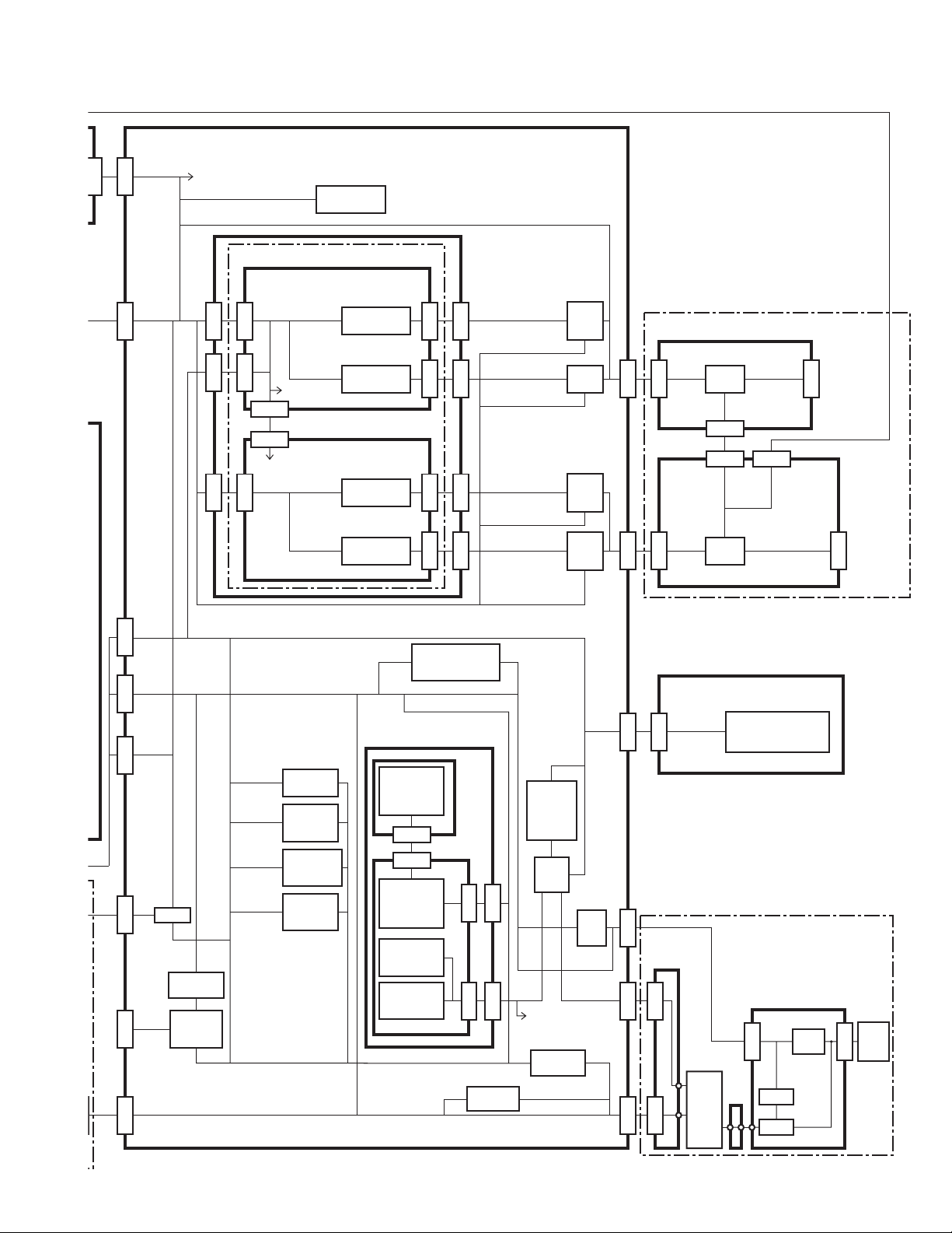
Regulator, DC-DC converter and digital power amplifier section
CN202
CN201
M_CLOCK
FREQ_CTRL
PROTECT
AMP_-B
AMP_-B+12V
PROTECT
Q281 to Q286
PROTECTOR
Lout_HP
Rout_HP
FER
TO
FAN
FL,FR,C
CN222
SL,SR
SBL,SBR
FREQ_CTRL
PROTECT
Lout_HP
Rout_HP
CN130
CN131
FW240
Lout_HP
Rout_HP
CN351
RY300
HP_RY
+12V_RY
FAN_ON/OFF
FAN_LOW
Q151,Q152
CN103
FAN
+12V_FAN
CN102
D+5V_Mi,FL1,FL2,VPP
M_CLOCK
+/-7V
Q154
Q153
REG
PWM modulator section
FL,FR
A.NFB_FL
CN302
CN301
FW323
CN313
CN402
CN401
VCHANGE_1,VCHANGE_2,M_CLOCK
+/-7V
A+5V_Vi
A+9V_Vi_Tu
A+5V_DSP
+12V_RY
D.NFB_FL
A.NFB_FR
D.NFB_FR
C
A.NFB_C
D.NFB_C
+/-7V
CN423
CN413
SL,SR
A.NFB_SL
+/-7V
D.NFB_SL
A.NFB_SR
D.NFB_SR
SBL,SBR
A.NFB_SBL
D.NFB_SBL
A.NFB_SBR
D.NFB_SBR
D+5V_Mi,D+5V_DSP
B+5V_Mi,POWER_ON
Q157,Q158
+/-7V REG
IC153
A+5V_Vi
REG
IC152
A+9V_Vi_Tu
REG
IC151
A+5V_DSP
REG
IC201
MODULATOR
IC801
MODULATOR
IC301
MODULATOR
IC401
MODULATOR
D+5V_Mi
B+5V_Mi
D+5V_Mi
Q156,Q176
D+5V_HDMI
Q155,Q171
D+5V_DSP
DCDC_+12
DCDC_-B+12
CN312CN311 CN412CN411
Q101
D+5V_Mi,B+5V_Mi
REG
D+5V_DSP
Q177
REG
CN107
CN117
Q172
REG
Q174
REG
Q175
REG
VPP
CN321
CN322
CN421
CN422
FRONT_L
FRONT_R
A.NFB_FL,D.NFB_FL
A.NFB_FR,D.NFB_FR
CENTER
SURROUND_L
SURROUND_R
A.NFB_SL,D.NFB_SL
A.NFB_SR,D.NFB_SR
SURRBACK_L
SURRBACK_R
A.NFB_SBL,D.NFB_SBL
A.NFB_SBR,D.NFB_SBR
POWER_ON
CN104 CN105
CN114 CN115
Q102
VPP REG.
A.NFB_C
D.NFB_C
PWM_V
Vout_DET
Q1101
Q1102
IC101
DCDC
converter
D1101
to
D1104
+B
-B
+12V
-B+12V
D111 ,D11 2
D119,D120
IC251
IC351
AMP
IC851
AMP
IC261
IC361
AMP
IC451
IC461
AMP
AC_DET_1
D101
to
D104
POWER_ON
S2
S2
S3
Speaker terminal section
Lout
CN251
CN265
Rout
Cout
RY295
RY895
FRONT_RY
CENTER_RY
CN465
FRONT_RY
CENTER_RY
CN252
CN106C N111CN101CN152
SLout
SRout
CN262
SBLout
SBRout
PWM_V,Vout_DET
M_CLOCK
AC_DET_1
CN151
VCHANGE_1
VCHANGE_2
S1
CN206CN211
S2
S3
Power
trans.
RY391
RY491
SURR_RY
SURRBACK_RY
IC111 to IC113, IC115
CN209FW451
FRONT_RY
CENTER_RY
SURR_RY
SURRBACK_RY
DCDC converter
control
Primary section
FW121
AC
T102
Trans.
POWER_ON
Q1001
RY101
ST295
FRONT
&
CENTER
ST292
SURROUND
&
SURRBACK
CN120
Main
plug
2-2
Page 26
Standard schematic diagrams
Primary section
!
TH.FUSE
LVA10579-12
PW157
PW156
PW155
PW154
PW153
PW152
PW151
LVA10579-13
S1
1
COM
2
S1
3
(SHEET 2)
CN211
QJK012-034003-E
TO CN111 OF LVA10578-1
PW11 C121
0.1
PW13
S2
1
2
COM
3
4
S2
5
6
(SHEET 2)
S3
7
S3
8
CN206
TO CN106 OF LVA10578-1
WJK0208-002A-E
J
54
AC
1
AC
of LVA10578-1to CN101
(SHEET 2)
2
3
4
RY+9V
POWER_ON
FW121
9
!
T102
QQT0478-001
Parts are safety assurance parts.
When replacing those parts make
sure to use the specified one.
1
B142
QUY158-150Y
FC113
QNG0020-001Z
43
D1001
1SS133-T2
C1001
4700p
21
F103
!
!
RY101
QSK0128-001
FC103
QNG0020-001Z
!
!
C1002
0.22
Q1001
KRC105S-X
R1002
3.3M
R1001
3.3M
PW103
PW104
!
MAINS
PLUG
CN120
LIVE/
BRN
2
1
NEUTRAL/
BLU
123
!
C1004
0.001
!
QNZ0136-001Z
QGA7901C1-02
EP151
!
C1003
0.001
!
LVA10579-5
J
F103
QMF51U1-6R3-J8
F104
-
VERSION CODES
J ;U.S.A.
C ;CANADA
2-3
Page 27
VOLTAGE MEASUREMENT CONDITION
POWER ON
SOURCE FM(NO SIGNAL)
SURROUND OFF
VOLUME 0
SHEET
NUMBER
1
2
3
4
5
6
7
8
9
10
11 HDMI ADC / i/p CONVERTER
CIRCUIT DISCRIPTION
PRIMARY
REGULATOR / DC-DC CONVERTER
PWM MODULATOR / MASTER CLOCK
DIGITAL POWER AMP / SPKEAKER TERMINAL
AUDIO,VIDEO SIGNAL INPUT / SYSTEM CONTROL LSI
COMPONENT VIDEO IN/OUT
MASTER VOLUME IC
USER CONTROL KEYS / SYSTEM CONTROL IC / FL DISPLAY
DSP IC / DIGITAL SIGNAL INPUT TERMINAL
HDMI RX / TX / MICOM
SHEET 1
2-4
Page 28

F
E
Regulator and DC-DC converter section
LVA10578-1
D+5V_Mi
1
DGND
2
FL1
3
VPP
4
FL2
5
TO CN902
(SHEET 8)
CN102
QGF1205C1-05
+12V
+B
PGND
-B+12V
-B
C114
1/50
MTZJ8.2C-T2
to CN104
of LVA10578-1
CN114
QGA2001F1-07
CN115
to CN105
of LVA10578-1
Q103
KTC3200/GL/-T
D117
D161 1A3G-T1
D162
1A3G-T1
(SHEET 3)
7
6
5
4
3
2
1
1
2
3
4
5
1
2
3
4
7
6
5
4
3
2
1
1
2
3
4
5
R109
22k
FW323
to CN313
of LVA10578-2
CN104
CN105
QGA2001C1-05
*MARK LIST
US,UP,A,UF J,C,B,E,EN,EV
220/63 1000/25
C102
USE NONE
R101
USE NONE
R102
USE NONE
R104
R105
USE NONE
D105
B2017
USE
Q173
USE
C172
F101
QMF51U1-4R0-J8
F102
QMF51U1-4R0-J8
470/16
LVA10578-6
BLK_REG2
J/C
C169
LVA10578-4
D+5V_DSP
470/16
BLK_REG
USENONE
USENONE
NONE
NONE
Q176
2SD2394/EF/
Q177
2SD2394/EF/
C166
R177
100
R178
100
D+5V_HDMI
Q171
2SD2394/EF/
DCDC_-B+12
2SC1740S/RS/-T
C168
100/16
PRI_RY+9V
Q172
2SD2394/EF/
R171
100
DCDC_+12
Q156
R172
100
TO CN530
(SHEET 5)
TO CN531
(SHEET 5)
TO
FAN
D159
MTZJ6.2C-T2
2SD2394/EF/
Q155
2SC1740S/RS/-T
C165
100/16
(SHEET 4)
10
11
C167
0.0022
*
Q173
2SD2394/EF/
C174
10/50
MTZJ13B-T2
2SD2394/EF/
C176
10/50
MTZJ13B-T2
CN130
1
2
3
4
5
6
7
8
9
1
2
3
4
5
6
7
8
9
1
2
R168
2.2k
QGA2001F1-03
Q174
D171
Q175
D172
+12V_RY
HP_RY
+7V
-7V
AGND
A+5V_DSP
A+5V_Vi
A+9V_Vi_Tu
+12V_RY
AC_DET_2
VCHANGE_1
VCHANGE_2
HP_RY
DGND
D+5V_DSP
D+5V_Mi
B+5V_Mi
FAN_ON/OFF
FAN_LOW
POWER_ON
REG_DET
D+5V_HDMI
CN131
CN103
QGA2501C1-02
R167
0.22
UNF
(1/4W)
CN117
D158
MTZJ7.5A-T2
R174
10k
R110
100k
FAN
FANGND
R186
NI
R187
NI
R188
NI
UNF
(1W)
CN107
123
123
*
C172
0.0047
R165
UNF
0.22
(1W)
C164
2200p
R166
UNF
2.2k
(1/4W)
R173
UNF
(1/2W)
4.7
UNF
(1/2W)
C173
1/50
R175
UNF
(1/2W)
4.7
R176
UNF
(1/2W)
10k
C175
1/50
TO CN206
(SHEET 1)
8
1/4W
R107
5.6 UNF
MY
C108
C109
0.047
0.047
Q102
KTA1046/Y/
R108
3.3k
C113
UNF
22/50
(1/4W)
C112
22/50
D116
MTZJ36C-T2
+7V
AGND
-7V
R181
100
KRC111S-X
+7V
-7V
M_CLOCK
MY
S2S3S3
FC102
F102
FC112
C111
100/63
Q163
Q161
Q162
COM
QNG0020-001Z
QNG0020-001Z
D115
1A3G-T1
KRC111S-X
KRC111S-X
470/16
S2
FC101
F101
D114
1A3G-T1
R183
R184
47k
A+9V_Vi_Tu
R154
R182
NI
+12V_FAN
Q154
KRC102S-X
A+5V_Vi
C161
C163
470/16
1234567
CN106
QGA3901C1-08
QNG0020-001Z
FC111
QNG0020-001Z
C110
220/50
D113
1A3G-T1
A+5V_DSP
2k
10k
R155
11k
D154
MTZJ9.1C-T2
2k
R159
R160
47k
2SD2394/EF/
(With H.Sink)
**
Q101
6800/25
3300/25
KTD863/Y/-T
UNF
(1/4W)
C103
R106
D106
MTZJ6.2B-T2
820
4700p
D107
D108
1A3G-T1
1A3G-T1
C104
470/16
C151
C152
C106
0.1/100
D119
UF304G-F82
D109
NI
C105
0.1/100
NI
D111
D110
D120
10DDA20-FD
UF304G-F82
C107
0.1/100
IC151
KIA7805API
IC152
KIA7809API
(With H.Sink)
D152
1SS133-T2
C157
10/50
IC153
KTA1046/Y/
(With H.Sink)
(With H.Sink)
123
(With H.Sink)
KRA102S-X
(With H.Sink)
D157
MTZJ8.2C-T2
Q158
R152 4.7
123
Q151
123
D156
MTZJ8.2C-T2
10DDA20-FD
C153
0.01
C155
0.01
Q152
KRC102S-X
C158
0.01
D112
R15122UNF
UNF
R15310UNF
R156
10
R157
560
R158
4.7
R161
4.7
R162
2.2k
R164
2.2k
R16310UNF
1W
(1/4W)
1W
UNF
(1/4W)
UNF
(1/4W)
UNF
1W
UNF
(1/4W)
UNF
(1/4W)
UNF
(1/4W)
(1/4W)
TH101
4.7
C154
100/16
C156
100/25
Q153
2SD2394/EF/
D153
MTZJ13B-T2
KIA7805API
C159
100/16
Q157
C160
100/16
C162
100/16
TO
(SH
4
RY+9V
POWER_ON
R105
R104
10
10
UNF
UNF
(1/4W)
(1/4W)
*
B2017
R103
UNF
6.8
(1/4W)
UNF
(1/4W)
UNF
R102
3.3k
(1W)
*
R101
15k
*
C102
*
D105
*
MTZJ12C-T2
2-5
Page 29

*
TO FW121
(SHEET 1)
123
4
CN101
QGA2001C1-04
AC
AC
RY+9V
POWER_ON
*
R105
10
UNF
(1/4W)
17
03
UNF
(1/4W)
UNF
(1/4W)
UNF
R102
3.3k
(1W)
R101
15k
*
D105
*
MTZJ12C-T2
D101
1A3G-T1
D102
1A3G-T1
D103
C101
1A3G-T1
0.0047/100
C102
*
D104
1A3G-T1
TH_COM
(SHEET 3)
(SHEET 4)
NI
R272
(SHEET 4)
(SHEET 4)
PGND
AMP_+B
AMP_-B
DCDC Converter
2W
2W
UNF
UNF
2.2k
R1109
2.2k
R1110
R1111
1k
R1112
1k
NI
NI
C1139
C1140
NI
TH272
Q1104
KTA1268/GL/-T
D1111
R1113
R1118
1SS133-T2
39k
47k
C1165
NI
NI
C1141
C1166
C1119
C1120
0.1/100
0.22/100
L1101
33
QQL78AK-220
C1117
2200/50
C1118
2200/50
L1102
33
QQL78AK-220
C1115
0.1/100
C1116
0.1/100
D1105
(1W)(1W)(1W) (1W)
R1105
10
C1107
C1108
0.0033
R1107
10
C1112
0.0033
R1108
10
C1114
0.0033
R1106
10
C1109
C1110
0.0033
D
0.0033
S
C1111
0.0033
C1113
0.0033
D
S
0.0033
Q1101
2SK3599-01MR
(With H.Sink)
D1107
FMB-G19L
(With H.Sink)
D1108
FMB-G19L
(With H.Sink)
Q1102
2SK3599-01MR
(With H.Sink)
N.I.
G
R1103
33
1/4W
R1116
D1109
4.7
1SS133-T2
1/4W
R1117
4.7
1/4W
D1106
G
R1104
33
N.I.
1/4W
IRS2011S-X
D1110
IC101
1SS133-T2
C1122
0.33
1234
C1123
VB
HO
VS
HIN
LIN
1
VCCLO
COM
8765
C1126
NI
R1115
820
NI
NI
R1101
C1143
0.22/100
C1142
0.22/100
C1161
C1162
100k
EP101
QNZ0136-001Z
R1102
100k
NI
NI
C1144
0.22/100
C1145
0.22/100
C1163
C1164
C1171
4.7/50
DRIVER_SD
(SHEET 4)
C1106
6800/71
C1105
R1171
3.3k
UNF
1/4W
30PRA20-FC
30PRA20-FC
6800/71
1
30PRA20-FC
D1101
D1103
C1124
0.1/250
C1146
0.1/250
C1150
NI
C1149
NI
C1147
0.1/250
C1125
0.1/250
D1102
D1104
30PRA20-FC
D1171
1SS133-T2
C1104
0.22
C1137
0.1/250
C1138
0.1/250
C1148
C1136
0.1/250
C1135
0.1/250
C1103
0.22
C1101
0.22/100
C1133
0.22/100
C1134
0.22/100
3
2
CN111
1
QGA3901C1-03
TO CN211 (SHEET 1)
C1102
0.22/100
C1131
0.22/100
C1132
0.22/100
NI
LVA10579-12
D1154
UDZS2.7B-X
R11701kR1169
BLK_DCCTRL
3.3k
VCC
1CLR1D1CLK
(SHEET 4)
EP102
QNZ0136-001Z
DCDC Converter_Control
Q1103
KTA1268/GL/-T
R1114
820
IC115
SN74HC74ANS-X
891011121314
D1155
1SS133-T2
2PRE
2CLK
1PRE1Q1Q
2Q
GND 2Q
7654321
2D
2CLR
C1157
0.1
VCC
C1158
0.1
R1166
470
C1156
100p
1SS133-T2
D1153
SN74HC00ANS-X
R1165
3.3k
SSS_ON/OFF
891011121314
1k
R1162
1
GND
7654321
C1155
IC112
NJM2403M-X
SSS_ON/OFF
R1161
1M
1
(1/2)
7
IC112
NJM2403M-X
PWM_V
PWM_V
8
VCHANGE_1
VCHANGE_2
M_CLOCK
PGND
101112
101112
PGND
M_CLOCK
VCHANGE_1
VCHANGE_2
R1164
+
3
-
2
4
C1154
100p
+
5
-
6
(2/2)
DRIVER_SD
DRIVER_SD
47k
1SS133-T2IC113
D1152
AC_DET_2
AC_DET_2
Vout_DET
Vout_DET
AC_DET_1
AC_DET_1
R1159
10k
R1160
1k
330
R1163
FEEDBACK
FEEDBACK
Q1173
+12V
CN152
QGB2510J1-12
123456789
123456789
CN151
QGB2510K1-12
+12V
D1151
1SS133-T2
R1180
13k
KTA1504/YG/-X
C1174
100/16
KIA7805API
R1158
390
R1176
47k
IC121
C1182
100/16
D1174
1SS133-T2
Q1172
KRC102S-X
C1153
1
NJM2125F-X
R1156
120k
R1157
10k
C1159
820p
C1173
0.01
R1175
2.2k
123
C1181
0.01
R1155
5
C1152
1
1SS133-T2
Q1171
+
1
C1151
47/16
-
3
R1179
3.3k
Q1177
NI
C1172
KTC3875/YG/-X
1000p
22k
D1172
1SS133-T2
R1154
3.3k
R1173
10k
R1172
3.3k
KTC3875/YG/-X
R1153
2.2k
R1152
6.8k
R1151
3.6k
Q1151
Q1152
KRC102S-X
KRC102S-X
R1178
100
Q1176
NI
Q1174
Q1175
NI
IC111
4
2
18k
R1174
D1173
Parts are safety assurance parts.
When replacing those parts make
sure to use the specified one.
SHEET 2
2-6
Page 30

D NFB SR
D NFB SBL
C1322
C1422
PWM modulator and master clock section
R333
C332
4.7k
QGB2510J1-17
FR
F.GND
FL
A.NFB_FL
D.NFB_FL
LIMITTER
+B_DET
PWM_TH
D.NFB_C
A.NFB_C
C
C.GND
CN302
FRONT_R
R3011kC301
10/50
C302
C202
C201
R201
10/50
1k
FRONT_L
CENTER
R8011kC801
10/50
C802
470p
FR
FL
F.GND
D.NFB_FR
D.NFB_FL
A.NFB_FL
A.NFB_FR
123456789
123456789
D.NFB_FR
A.NFB_FR
A.NFB_FL
D.NFB_FL
(SHEET 4)
(SHEET 4)
C331
100/16
C304
2200p
R306
3.3k
R305
1K
1.5M
R304
C312
470p
R303
1K
32 31 30 29 28 27 26 25 24 23 22 21 20 19 18 17
R302
22k
470p
470p
-
+
+
-
R202
22k
C211
100p
R203
C212
1K
470p
1K
R204
R206
C204
2200p
100/16
R224
15k
R225
15k
C831
100/16
C804
2200p
R806
C812
R804
2k
470p
R803
1k
32 31 30 29 28 27 26 25 24 23 22 21 20 19 18 17
R802
22k
-
+
+
-
C
+2.5V
-2.5V
C.GND
PWM_TH
+B_DET
M_CLOCK
LIMITTER
A.NFB_C
10111213141516
10111213141516
PWM_TH
(SHEET 4)
C829
100/10
C821
100/10
R331
1k
C305
R307
C303
10/50
C311
100p
-
+
+
-
C203
10/50
R205
1.5M
R207
3.3k
C205
R2311kC231
KTC3875/YG/-X
R831
1k
C805
R807
3.3k
R805
1.5M
C803
10/50
C811
100p
-
+
+
-
D.NFB_C
17
17
A.NFB_C
2200p
18k
R308
R208
100k
18k
2200p
Q211
C832
33p
2200p
18k
R808
CN301
QGB2510K1-17
D.NFB_C
33p
R334
1k
R335
10k
100k
R309
10k
-
+
Limiter
Limiter
+
-
10k
R209
R210
1M
R235 10k
R234 1k
R232 100k
C232
33p
R223
1k
R834 1k
R835 10k
100k
R809
10k
-
+
Limiter
Limiter
+
-
(SHEET 4)
R310
1M
R311
2.2k
R211
2.2k
R811
2.2k
1SS133-T2
AMP_+B
R332
100k
C307
0.0022
-
+
LowV&
Thermal
Warning
+
-
C207
0.0022
D221
C227
100/16
R832
100k
C807
0.0022
R810
1M
-
+
LowV&
Warning
+
-
to CN302
of LVA10578-1
+
-
+
-
(SHEET 2)
C308
-
+
C208
R233
4.7k
R833
4.7k
C808
-
+
Q214
KRC102M-T
D222
MTZJ16B-T2
D.NFB_FR
A.NFB_FR
1
C310
NI
R315
8.2k
C309
100p
1
C322
1
R314
100k
C323
Q301
KTA1268/GL/-T
1
+V
C224
C226
0.1
IC201
JCV8015-X
100/16
Reg
-V
GND
16151413121110987654321
C223
C225
0.1
100/16
R214
100k
C222
1
C209
100p
1
NI
R215
8.2k
R230 R330R830
1
C210
R221
68k
R226
NI
R222
22k
Q212
Q213
NI
1
C810
NI
R815
8.2k
C809
100p
1
C822
1
R814
100k
+V
RegThermal
-V
GND
16151413121110987654321
IC801
JCV8015-X
C824
C827
C823
C825
0.1
100/16
C826
0.1
100/16
C830
1
D211
1SS133-T2
D311
1SS133-T2
D811
1SS133-T2
KTA1268/GL/-T
NI
Q801
KTA1268/GL/-T
1
+2.5V
-2.5V
LVA10578-2
R1333
C1332
4.7k
100/16
C1304
2200p
3.3k
SURROUND_R
of LVA10478-1
to CN321
R317
(SHEET 4)
820
CN311
QGA2001F1-03
M_CLOCK
+7V
-7V
CN313
QGA2001C1-04
to FW323
+7V
-7V
CN423
of LVA10578-3
to CN413
CN312
QGA2501F1-02
to CN322
1
2
3
(SHEET 2)
1
2
3
4
1
2
(SHEET 3)
(SHEET 4)
of LVA10478-1 of LVA10578-1
1
2
VEE
4321
8765
VCC
C324
0.1
IC202
SN74LVC3G04T-X
R217
820
Q201
R318
10
UNF
1/4W
R319
10
UNF
1/4W
R817
820
SR
S.GND
SL
A.NFB_SL
D.NFB_SL
LIMITTER
A.NFB_SBR
SBR
SB.GND
SBL
D.NFB_SBR
R1301
C1301
1k
10/50
C1302
470p
C1202
C1201
R1201
10/50
1k
SURROUND_L
SURRBACK_R
R1401
C1401
1k
10/50
C1402
470p
C402
470p
C401
R401
10/50
1k
R1302
22k
R1202
22k
470p
R1402
22k
R402
22k
SURRBACK_L
R1306
R1305
1.5M
R1304
NI
C1312
NI
R1303
0
32 31 30 29 28 27 26 25 24 23 22 21 20 19 18 17
-
+
+
-
R1203
0
C1212
10/50
NI
R1205
NI
1.5M
R1204
R1206
3.3k
C1204
2200p
R1231
C1231
100/16
R1431
C1431
1k
100/16
C1404
2200p
R1406
3.3k
R1405
1.5M
R1404
NI
C1412
NI
R1403
0
32 31 30 29 28 27 26 25 24 23 22 21 20 19 18 17
-
+
+
-
R403
0
C412
NI
R405
1.5M
NI
R404
R406
3.3k
C404
2200p
R431
C431
1k
100/16
M_CLOCK
SL
QGB2510J1-14
CN222
D1211
1SS133-T2
D1311
1SS133-T2
D411
1SS133-T2
D1411
1SS133-T2
123456789
TO CN522 (SHEET 7)
1011121314
D.NFB_SL
123456789
BLK_PWM2BLK_PWM1
123456789
D.NFB_SL
(SHEET 4)
A.NFB_SL
A.NFB_SL
SR
S.GND
(SHEET 4)
(SHEET 4)
A.NFB_SR
A.NFB_SR
D.NFB_SR
D.NFB_SR
M_CLOCK
LIMITTER
D.NFB_SBL
10111213141516
10111213141516
D.NFB_SBL
(SHEET 4)
A.NFB_SBL
A.NFB_SBL
SBL
SBR
SB.GND
D.NFB_SBR
A.NFB_SBR
CN401
QGB2510K1-16
CN402
QGB2510J1-16
D.NFB_SBR
A.NFB_SBR
(SHEET 4)
(SHEET 4)
R1332
100k
R1334
1k
R1335
100k
R1309
Limiter
Limiter
R1209
100k
100k
R1409
Limiter
Limiter
R409
100k
10k
-
+
+
-
10k
C1432
10k
-
+
+
-
10k
0.0022
R1310
1M
R1311
2.2k
R1211
2.2k
C1207
C1232
33p
33p
R1434 1k
R1435 10k
R1410
1M
R1411
2.2k
R411
2.2k
C407
C432
33p
C1307
0.0022
-
+
LowV&
Warning
+
-
+
-
R1210
1M
0.0022
R1235 10k
R1234 1k
R1232
100k
R1233
4.7k
R1433
4.7k
R1432
100k
C1407
0.0022
-
+
LowV&
Warning
+
-
+
-
R410
1M
R435 10k
R434 1k
R432
100k
R433
4.7k
10k
-
+
-
+
C1305
2200p
18k
R1307
R1308
C1303
10/50
C1311
100p
-
+
+
-
C1211
100p
C1203
R1208
R1207
18k
C1205
2200p
1k
C1405
2200p
R1407
18k
R1408
C1403
10/50
C1411
100p
-
+
+
-
C411
100p
C403
10/50
R408
R407
18k
C405
2200p
33p
R1331
C1331
1k
A.NFB_SR
1
C1310
R1315
8.2k
C1309
100p
1
C1308
R1314
100k
+V
C1224
IC301
JCV8015-X
RegThermal
100/16
-V
GND
16151413121110987654321
C1223
100/16
R1214
100k
1
C1208
C1209
100p
NI NI
R1215
8.2k
R1230 R1330
C1210
1
1
C1410
NI
8.2k
R1430
R1415
C1409
100p
1
C1408
R1414
100k
+V
C424
100/16
IC401
JCV8015-X
RegThermal
-V
GND
16151413121110987654321
C423
100/16
R414
100k
C409
100p
1
C408
NI
R430
R415
8.2k
1
C410
A.NFB_SBL
2-7
Page 31

C1310
V
V
LVA10578-3
A.NFB_SR
D.NFB_SRD.NFB_SBL
5
1
R1315
8.2k
C1309
100p
C1322
1C1222
R1314
100k
817
+V
Reg
-
GND
165
R1214
100k
C1209
100p
R1215
8.2k
C1210
1
0k
k
IC301
JCV8015-X
NI NI
R1230 R1330
1
C1323
C1224
C1226
0.1
100/16
C1223
C1225
0.1
100/16
1
Q1301
R1317
820
KTA1268/GL/-T
8765
C1324
VCC
0.1
IC302
SN74LVC3G04T-X
R1217
820
Q1201
KTA1268/GL/-T
R1318
10
UNF
R1319
10
UNF
to CN421
(SHEET 4)
1SS133-T2
C241
0.1
C246
0.1
C248
100p
R247
D242
2.2k
VEE
1/4W
1/4W
2
4321
1
to CN423
of LVA10578-2 of LVA10478-1
(SHEET 3)
CN413
QGA2501F1-02
+7V
1
-7V
2
3
CN411
QGA2501F1-03
MasterClock Block
VCC
R241
1M
R242
5.6k
C242
C243
470p
X241
VCC
IC212
SN74HC00ANS-X
C244
470p
R246
2.2k
470p
QAX0734-001
400kHz 420kHz
IC211
SN74HCU04ANS-X
R243
1M
X242
QAX0735-001
C245
470p
R244
R245
100
C247
100p
D241
1SS133-T2
891011121314
VSS
7654321
5.6k
891011121314
VSSVSS
7654321
LVA10579-7
2CLK
1PRE1Q1Q
UNF
UNF
MTZJ20C-T2
CN202
to CN201
of LVA10578-1
CN201
QGA2501C1-07
891011121314
7654321
891011121314
2Q
2PRE
VSS 2Q
7654321
R441
Q441
4.7
2SD2394/EF/
1/2W
R442
3.6k
1/2W
D442
C443
100/35
D441
MTZJ24B-T2
-B+12V
R443
680
R444
1.8k
UNF
KTA1046/Y/
2SC2812N/6/-X
1/4W
Q444
Q445
C442
100/25
C441
D444
100/25
MTZJ11C-T2
Parts are safety assurance parts.
VCC
C249
0.1
1
C1410
NI
8.2k
R1430
R1415
C1409
100p
C1422
1C422
R1414
100k
817
+V
Reg
-
GND
165
R414
100k
C409
100p
R415
8.2k
1
C410
IC401
JCV8015-X
NI
R430
C424
100/16
C423
100/16
A.NFB_SBL
1
C1423
C426
0.1
C425
0.1
1
Q1401
KTA1268/GL/-T
R1417
820
R417
820
Q401
KTA1268/GL/-T
M_CLOCK
to CN422
of LVA10478-1
CN412
(SHEET 4)
QGA2501F1-04
4
3
2
1
BLK_CLOCK
SN74HC74ANS-X
IC214
VCC
1CLR1D1CLK
-2.5V
M_CLOCK
+2.5V
IC213
SN74HC08NS-X
C341
0.1
2CLR
R341
1k
R342
2.2k
D341
UDZS2.7B-X
-B+12V-BPGND
FREQ_CTRL
2D
1234567
1234567
When replacing those parts make
sure to use the specified one.
AMP_-B+12V
AMP_-B
PGND
FREQ_CTRL
(SHEET 4)
LVA10578-1
SHEET 3
2-8
Page 32

N
Digital power amplifier and speaker terminal section
LVA10478-1
TO CN311
(SHEET 3)
TO CN312
(SHEET 3)
A.NFB_FL
D.NFB_FL
(SHEET 3)
3
2
1
CN321
D.NFB_FR
A.NFB_FR
(SHEET 3)
FRONT_L
Q251
KTA1504/YG/-X
R216
820
C254
100p
C250
N.I.
C354
100p
R251
100
C251
0.01
Q351
KTA1504/YG/-X
R316
820
R351
100
C351
0.01
R254
IC251
220
IRS20124S-X
R255
7.5k
IN
R256
R252
8.2k
R253
3.3k
R355
R356
R352
8.2k
R353
3.3k
ISET1
3.3k
ISET2
OCNCVS
COM
7654321
LO VCC
R257
470
R354
IC351
220
IRS20124S-X
7.5k
IN
ISET1
DT/SD
3.3k
ISET2
OC
COM
R357
470
7654321
LO
FRONT_R
A.NFB_C
D.NFB_C
(SHEET 3)
1
2
CN322
CENTER
Q851
KTA1504/YG/-X
R851
R816
820
C854
C850
N.I.
100p
100
C851
0.01
R854
IC851
220
IRS20124S-X
R855
9.1k
ISET1
R852
8.2k
R856
R853
3.3k
DT/SD
2.2k
ISET2
OC
COM
7654321
LO
R857
1.2k
D251
1SS133-T2
R258
D261
4.7
NI
(1/4W)
NC
141312111098
C253
NC
0.33
VBDT/SD
HO
C252
1
C276
47/25
D351
1SS133-T2
R358
4.7
(1/4W)
NC
141312111098
C353
NC
0.33
VB
HO
VS
NC
VCC
C352
1
D851
1SS133-T2
R858
4.7
(1/4W)
NCIN
141312111098
C853
NC
0.33
VB
HO
VS
NC
VCC
C852
1
C876
47/25
Q261
IRFB4212
D
G
R261
47
1/4W
D262
NI R265
R262
47
1/4W
D361
NI
R361
47
1/4W
D362
NI
R362
47
1/4W
D861
NI
R861
47
1/4W
D862
NI
R862
47
1/4W
IRFB4212
IRFB4212
IRFB4212
C263
0.1/100
S
D
C275
10/100
G
Q262
S
D
G
S
Q361
C363
0.1/100
IRFB4212
D
C375
10/100
G
Q362
S
Q861
IRFB4212
D
G
C863
0.1/100
S
D
C875
10/100
G
S
Q862
R269
4.7k
C273
220/50
R268
6.8k
C270
0.001
QQL77AK-220
L261
22
C268
1.5
L361
22
QQL77AK-220
C368
1.5
C370
0.001
R368
6.8k
R868
6.8k
C870
0.001
QQL77AK-220
L861
22
C868
C271
0.1/100
(1W)(1W)
R266
22
C269
0.1
C274
C272
220/50
0.1/100
C371
0.1/100
R366
C369
0.1/100
1.5
C869
0.1
0.1/100
0.1
0.1/100
C373
220/50
22
C372
C374
220/50
C873
220/50
C871
(1W)
R866
22
C874
220/50
C872
R282
10k
R283
0
R264
22
1W
C264
0.001
R267
10k
C266
1/2W
0.001
22
1/2W
C265
0.001
C267
0.001
R364
22
1W
C364
0.001
C366
0.001
R365
22
1/2W
R367
10k
1/2W
C365
0.001
C367
0.001
R369
4.7k
R869
4.7k
R864
22
1W
C864
0.001
R867
10k
1/2W
C866
0.001
R865
22
1/2W
C865
0.001
C867
0.001
R290
100
R284
100k
R281
10k
Q286
KRC102M-T
Q281
KRC109M-T
1
C284
C281
0.1
R270
100k
R370
100k
21
D300
MA111-X
65
TO CN411
(SHEET 3)
TO CN412
(SHEET 3)
1
2
3
CN421
CN422
1
2
3
4
(SHEET 2)
R1269
A.NFB_SL
SURROUND_L
D.NFB_SL
(SHEET 3)
C1254
100p
C1250
N.I.
D.NFB_SR
A.NFB_SR
(SHEET 3)
Q1251
KTA1504/YG/-X
R1251
R1216
C1354
100p
100
820
C1251
0.01
Q1351
KTA1504/YG/-X
R1316
820
R1351
100
C1351
0.01
R1254
IC261
220
IRS20124S-X
R1255
9.1k
ISET1
R1256
R1252
8.2k
R1253
3.3k
R1355
R1356
R1352
8.2k
R1353
3.3k
DT/SD
2.2k
ISET2
OC
COM
7654321
LO
R1257
1.2k
R1354
IC361
220
IRS20124S-X
9.1k
IN
ISET1
DT/SD
2.2k
ISET2
OC
COM
7654321
LO
R1357
1.2k
SURROUND_R
A.NFB_SBL
SURRBACK_L
D.NFB_SBL
(SHEET 3)
C454
100p
AMP_-B
AMP_-B+12V
C450
N.I.
Q451
KTA1504/YG/-X
R416
820
R451
100
C451
0.01
(SHEET 3)
D.NFB_SBR
A.NFB_SBR
(SHEET 3)
DRIVER_SD
Q400
NI
R400
NI
C400
NI
Q1451
KTA1504/YG/-X
C1454
R1416
820
100p
R1451
100
C1451
0.01
R454
IC451
220
IRS20124S-X
R455
9.1k
ISET1
R456
R452
8.2k
R453
3.3k
R1455
R1456
R1452
8.2k
R1453
3.3k
DT/SD
2.2k
ISET2
OC
COM
7654321
LO
R457
1.2k
R1454
IC461
220
IRS20124S-X
9.1k
IN
ISET1
DT/SD
2.2k
ISET2
OC
COM
7654321
LO
R1457
1.2k
SURRBACK_R
D1251
1SS133-T2
D1261
R1258
NI
4.7
(1/4W)
NCIN
141312111098
NC
C1253
0.33
VB
HO
VS
NC
VCC
C1252
1
D1351
1SS133-T2
R1358
4.7
(1/4W)
NC
141312111098
NC
0.33
VB
HO
VS
NC
VCC
C1352
1
D451
1SS133-T2
R458
4.7
NCIN
(1/4W)
141312111098
NC
C453
0.33
VB
HO
VS
NC
VCC
C452
1
C476
47/25
D1451
1SS133-T2
R1458
4.7
(1/4W)
NC
141312111098
NC
0.33
VB
HO
VS
NC
VCC
C1452
1 C1474
Q1261
IRFB4212
D
G
R1261
S
47
1/4W
D1262
NI
D
G
R1262
Q1262
S
47
IRFB4212
1/4W
D1361
NI
D
G
R1361
SC1353
47
1/4W
Q1361
IRFB4212
D1362
NI
D
G
R1362
Q1362
S
47
IRFB4212
1/4W
D461
NI
Q461
IRFB4212
D
G
R461
S
47
1/4W
D462
NI
D
G
R462
Q462
S
47
IRFB4212
1/4W
D1461
NI
D
G
R1461
47
SC1453
1/4W
Q1461
IRFB4212
D1462
NI
D
G
R1462
Q1462
S
47
IRFB4212
1/4W
4.7k
C1271
0.1/100
R1268
R1264
6.8k
22
1W
C1264
0.001
C1263
0.1/100
C1266
0.001
R1265
22
1/2W
C1275
10/100
C1265
0.001
C1267
0.001
R1364
22
1W
C1364
0.001
C1363
0.1/100
C1366
0.001
R1365
22
1/2W
C1375
10/100
C1365
0.001
C1367
0.001
R464
22
1W
C464
0.001
C463
0.1/100
C466
0.001
R465
22
1/2W
C475
10/100
C465
0.001
C467
0.001
R1464
22
1W
C1464
0.001
C1463
0.1/100
C1466
0.001
R1465
22
C1475
10/100
1/2W
C1465
0.001
C1467
0.001
C1270
R1267
0.001
10k
1/2W
QQL77AK-220
L1261
22
C1268
L1361
22
QQL77AK-220
C1368
1.5
R1367
10k
1/2W
C1370
0.001
R1368
6.8k
R1369
4.7k
R469
4.7k
R468
6.8k
C470
R467
0.001
10k
1/2W
QQL77AK-220
L461
22
C468
1.5
L1461
22
QQL77AK-220
C1468
1.5
R1467
10k
1/2W
C1470
0.001
R1468
6.8k
R1469
4.7k
C1273
220/50
(1W)(1W)(1W)(1W)
22
R1266
1.5
C1269
0.1
C1272
C1274
0.1/100
220/50
C1371
0.1/100
0.1/100
C1373
220/50
R1366
22
C1369
0.1
C1374
C1372
220/50
0.1/100
C471
C473
220/50
R466
22
C469
0.1
C472
C474
0.1/100
220/50
C1471
C1473
0.1/100
220/50
R1466
22
C1469
0.1
C1472
220/50
0.1/100
(SHEET 3)
PWM_TH
FREQ_CTRL
R271
TH271
QAD0146-10
PGND
2-9
Page 33

R281
R290
100
10k1R284
100k
Q286
KRC102M-T
Q281
KRC109M-T
1
C284
R270
100k
R370
100k
D300
MA111-X
65 4
Q282
KRA102M-T
R870
R286
100k
100k
321
Q284
KTA1268/GL/-T
R1270
100k
RY300
QSK0127-001
C283
10/50
R285
47k
Q283
KTC3200/GL/-T
R287
3.9k
R289
100
D281
R288
220k
C282
47/16
Q285
KTC3199/GL/-T
R470
100k
R1370
100k
R1470
100k
R291
470
UNF
R391
470
UNF
1SS133-T2
EP201
QNZ0136-001Z
EP202
QNZ0136-001Z
(2W)
Lout_HP
GND
Rout_HP
CN351
QGA2501C1-03
(2W)
1
2
3
123
123
TO CN905
(SHEET 8)
LVA10579-9
QSK0127-001
ST295
C296
C295
220p
654
321
R129547UNF
D295
1SS133-T2
(1/4W)
C395
220p
RY295
L
220p
FRONT
C297
0.022
C397
0.022
C396
R
220p
QNB0078-002
R271 NI
QAD0146-103
R30047UNF
(1/4W)
6
5
4
3
2
1
8
7
6
5
4
3
2
1
1
2
3
4
5
6
TO CN540
(SHEET 5)
6
5
4
3
2
1
BLK_SPK1
8
7
6
5
4
3
2
1
CN265
QGA3901C1-06
Lout
GND
Rout
GND
Cout
GND
CN262
QGA3901C1-08
SLout
GND
SRout
GND
SBLout
GND
SBRout
GND
C1494
C298 NI
C398 NI
C898 NI
C1294 NI
C1394 NI
C494 NI
NI
CN251
C277
220p
C377
220p
C877
220p
CN252
C1277
220p
C1377
220p
C477
220p
C1477
220p
FW240
PWM_TH
PROTECT
FREQ_CTRL
TH1
SSS_ON/OFF
TH271
TH_COM
QSK0127-001
QSK0127-001
RY895
QSK0127-001
UNFR895
654
(1/4W)
47
D895
1SS133-T2
321
654
R1391
47
(1/4W)
321
321
Q1491
KTC3875/YG/-X
654
Q1291
KTC3875/YG/-X
UNF
D391
1SS133-T2
D491
R1491
47
(1/4W)
1SS133-T2
UNF
Q891
KTC3875/YG/-X
RY391
RY491
Q291
KTC3875/YG/-X
C895
220p
CN465
QGA2001C1-03
123
123
FW451
C1291
220p
C1391
220p
C491
220p
C1491
220p
C896
220p
C1292
220p
C1392
220p
C492
220p
C1492
220p
CENTER
C897
0.022
L
C1293
0.022
SURROUND
C1393
0.022
R
L
C493
0.022
SURRBACK
C1493
0.022
R
ST292
QNB0256-001
CN209
QGA2501C1-06
TH_COM
AMP_+B
AMP_-B
PGND
HP_RY
+12V_RY
BLK_SPK2
3)
SSS_ON/OFF
(SHEET 2)
TO CN509 (SHEET 7)
Parts are safety assurance parts.
When replacing those parts make
sure to use the specified one.
CENTER_RY
SURR_RY
SURRBACK_RY
6
FRONT_RY
RY12V
DGND
12345
LVA10579-8
SHEET 4
2-10
Page 34

Audio/Video signal input and system control section
TO TUNER
CN505
LVA10599-1
QGF1205C1-11
1234567891011
QGB2510J1-07
TO CN602 OF LVA10599-6
(SHEET 7)
1234567
CN502
TO CN682 OF LVA10602-1
(SHEET 9)
123456
CN501
QJK016-061401-E
TO CN513 OF LVA10599-3
(SHEET 7)
1234567891011121314
CN503
QJK002-
17
1717
TV
DBS
VCR OUT
VCR IN
DVR OUT
DVR/DVD IN
DVD C/SW
DVD SURR
DBS
VCR OUT
VCR IN
DVR OUT
DVR/DVD IN
MONITOR
AUDIO IN/OUT
R6513
47k
TV_L TV_R
R6501
470
R6503
47k
DBS_L DBS_R
J6501 QNN0476-001
J6502 QNN0476-001
J6503 QNN0476-001
J6504 QNN0690-001
J6511 QNN0570-001
J6512 QNN0570-001
J6513QNN0570-001
R6505
470
R6507
100
R6509
47k
VCR_L VCR_R
R6511
470
DVRREC_L DVRREC_R
R6515
100
R6517
47k
DVR_L DVR_R
R6519
470
R6581
13k
DVD_C
R6521
6.2k
R6583
47k
DVD_SL
R6585
470
7
8
12
3456
15
16
10
9
11 12
7
8
12
34
56
15
16
C6523 N.I.
C6525 N.I.
910
11 12
7
8
6
12
34
5
15
16
910
11 12
C6502
C6501
2
330p
330p
3
C6506
5
C6505
330p
330p
6
C6509
C6510
330p
330p
C6507
C6508
2
330p
330p
3
5
C6511
C6512
330p
330p
6
C6503
C6504
330p
330p
C6513
2
C6514
330p
330p
3
5
C6516
C6515
330p
330p
6
C6518
2
C6517
330p
330p
3
5
C6519
C6520
330p
330p
6
C6543
4.7/50
R6548
75
C6541
0.047
R6544
75
C6542
4.7/50
R6545
75
R6536
62
C6536
N.I.
C6537
470/6.3
Q6522
KTA1267/YG
R6534
62
C6533
0.047
N.I.C6532
N.I.C6534
R6535
C6535
62
470/6.3
C6540
4.7/50
R6542
75
C6538
0.047
R6538
75
C6557
R6539
0.1
75
C6539
4.7/50
R6527
62
C6528
470/6.3
C6527
N.I.
C6524
R6525
0.047
62
R6526
C6526
62
470/6.3
R6533
75
C6531
4.7/50
C6529
0.047
R6529
75
C6530
4.7/50
R6530
75
C6549
C6548
470/6.3
N.I.
R6551
62
R6549
62
C6545
0.047
N.I.C6544
N.I.C6546
C6547
470/6.3
R6550
62
1
4
1
4
1
4
1
4
R6577
C6556
R6568
R6559
Q6516
KTA1267/YG
300
R6514
47k
R6502
470
R6504
47k
R6506
470
R6508
100
R6510
47k
R6512
470
R6516
100
R6518
47k
R6520
470
R6582
3.3k
R6522
6.2k
R6584
47k
R6586
470
0.1
300
Q6518
KTA1267/YG/-T
300
Q6512
Q6528
KTA1267/YG/-T
R6562
KTA1267/YG
Q6520
R6552
KTA1267/YG
C6558
0.1
R6571
270
270
270
Q6514
VCRREC_RVCRREC_L
DVD_SW
DVD_SR
R6565
R6556
KTA1267/YG
300
300
Q6511
Q6521
KRA121S-X
Q6517
KRA121S-X
Q6515
KRA121S-X
R6574
300
Q6524
KTA1267/YG/-T
KTA1267/YG/-T
Q6519
KRA121S-X
KRA121S-X
Q6513
KRA121S-X
C6591
R6572
Q6526
C6555 N.I.
C6553 N.I.
R6563
C6552 N.I.
R6560 1k
C6550 N.I.
R6554 1k
N.I.
1k
C6593
R6575
KRA121S-X
1kR6569
1k
Q6527
KRA121S-X
C6554 N.I.
KRA121S-X
Q6531
KRA121S-X
C6551 N.I.
N.I.
1k
Q6523
R6570
10k
Q6525
KRA121S-X
R6564
10k
R6567 10k
R6566
1k
Q6529
KRA121S-X
R6561
10k
Q6530
R6555
10k
R6558 10k
R6557
1k
L
R
R564
510
8765
R6523
+7V
A+5V(DSP)
2SC3576-JVC-T
C6582
0
GND
-7V
R569
240
Q501
R571
10k
C6561
0.1/16
39p
+9V
TU_CE
TU_CLK
TU_DATAI
TU_DATAO
R594
1k
1k
R593
FL502
QQR1372-001
2SC3576-JVC-T
46
C564
0.0056
R596
6.8k
R1544
Q522
TV_L
TV_R
VCR_L
VCR_R
DBS_L
DBS_R
DVR_R
123
10k
2SC3576-JVC-T
123
46
C563
R595
Q523
6.8k
KRA104S-X
10k
R1543
Q521
IC502
BD3843FS-X
TV_L
TV_R
VCR_L
VCR_R
DBS_L
DBS_R
DVR_L
DVR_R
TU_L
TU_R
VIDEO_L
VIDEO_R
121110987654321
FL501
QQR1372-001
0.0056
R1545
1k
0V0V
C581
0V
10/16
C522
560p
R565
D.GND
242322212019181716151413
1k
CL
DA
VEE
C577 0.1
A.GND
C578 0.1
VCC
DVRREC_LDVR_L
REC1L
DVRREC_R
REC1R
VCRREC_L
REC2L
VCRREC_R
REC2R
L_OUT
R_OUT
SOURCE SELECTOR
SY
R6540
10k
Q6535
KRC102S-X
Q6536
KRC102S-X
R6541
Q6537
10k
KRC102S-X
Q6538
KRC102S-X
Q6543
KTA1267/YG/-T
R6547
0
C6592
N.I.
R6573
1k
R6599
0
R6546
1k
R6588
0
DSP_CLOCK
DSP_STATUS
T_MUTE
R566
1k
C6581
39p
DSP_READY
DSP_RESET
DSP_COMMAND
R567
510
R568
510
C6580
R6532
0
D+5V(DSP)
C523
47/16
510
R563
39p
IN1
SW1
IN2
SW2 IN3
4321
MM1118XF-X
Q6542
KTA1267/YG/-T
D.GND
C524
47/16
GND
OUT
VCC
IC522
R6580
0
R6531
1k
HDMI_SC
Q6541
R570
240
Q502
2SC3576-JVC-T
R6589
R6524
1k
KTA1267/YG/-T
0
(SHEET 6)
R572
10k
KRA104S-X
DA
Q503
CL
+7V
-7VLGND
4.7/50
INP_LEVEL
C525
SC
S_MUTE
R
SBWR_MUTE
R6597
0
DVD_C
DVD_SW
DVD_SR
DVD_SL
R573
1k
C6564 0.1/16
IC524
SW
IN1
123
OUT
GND
VCC
IN2
456
MM1501XN-X
C6566 0.047
IN1
SW
123
GND
OUT
IN2
VCC
IC525
MM1502XN-X
456
R6578
0
C6567
0.1/16
2-11
VIDEO IN/OUT
(SHEET 6)
CVHDMI_SY
(SHEET 6)
Page 35

3
12 13 14
DVD_SR
DVD_SL
C6564 0.1/16
IC524
SW
123
OUT
VCC
MM1501XN-X
C6566 0.047
SW
123
OUT
VCC
7
IC525
MM1502XN-X
DVD_C
R6578
CN503
QJK002-141804-E
IN1
GND
IN2
456
IN1
GND
IN2
456
0
C1552
0.001
INP_LEVEL
R1571
20k
R1572
7.5k
R1556
1k
R1557
27k
VIDEO SWITCH
SYSTEM CONTROL
TP3
R6576
10k
R521
10k
R1592 1k
FR_RELAY
R1593 1k
C_RELAY
R1594
S_MUTE
SBWR_MUTE
DSP_READY
DSP_CLOCK
DSP_STATUS
DSP_COMMAND
LC_SCLK
LC_CS
LC_SIN
T_MUTE
DSP_RESET
TU_CE
TU_CLK
TU_DATAI
TU_DATAO
PROTECT
REG_DTCT
SYNCDET
M_BUSY
R1541
10k
R1599
R1542
REGDET
N.I.
0
Q505
KRC111S-X
Q506
KRC111S-X
Q507
KRC111S-X
SURR_RELAY
SBK_RELAY
RC_SDA
RC_SCL
RC_WP
BCHANGE1
BCHANGE2
R507
2.2k
TP1
TP2
C529
REG_DTCT
SSS_ON/OFF
HEADPHONE_DET
58
60
S.S.S. ON/OFF
CARRIER F CONT
2200/6.3
C527
100/6.3
C6575
470/16
VIDEO1
VIDEO11
VIDEO11
HDMI_COM
VIDEO4
VIDEO10
52
55
56
57
VIDEO SW10
VIDEO SW1159HP. DETECT
BD3813/3842 DA
BD3813/3842 CL
HDMI MICOM STATUS20HDMI MICOM CLK21MICOM COMMAND22MICOM STATUS23MICOM CLK24MICOM RESET25MICOM CS
19
M_CLOCK
M_RESET
HDMI_CLK
M_STATUS
HDMI_STS
M_COMMAND
C526
R585
330
L6502
10u
L6501
10u
VIDEO1
(SHEET 6)
VIDEO11
(SHEET 6)
51
VIDEO
SW1
VIDEO SW253VIDEO SW354VIDEO SW4
SOURCE MUTE
M_CS
R502
47K
R504
47k
(SHEET 5)
HDMI5V
R505
2k
R506
47k
50
49SUBWFR MUTE
48DSP READY
47DSP CLK
46DSP STATUS
45DSP COMMAND
44LC74761 SCLK
43LC74761 CS/TEST RX
42LC74761 SIN/TEST TX
41VPP(FRASH)
40TUNER MUTE
39DSP RESET
38RDS SDA
37TUNER CE
36TUNER CLK
35TUNER DATA I
34TUNER DATA O
33RESET
32VDD2(FRASH)
31D.A. PROTECTOR
30INH
29RDS SCL
28REG. DETECT
27SYNCDET
MICON
26
BUSY
R501
22K
R503
2k
R1580
15k
R1573
10k
Q542
R1558
10k
Q541
KTC3199/GL/-T
KTC3199/GL/-T
RC_SDA
POWER_ON
BLUE_LED
LED_DIM1
LED_DIM2
HDMI_RESET
HDMI_READY
FAN_ON/OFF
INP_LEVEL1
VIDEO9
TA/TC_SCL
TA/TC_SDA
VIDEO5
VIDEO7
VIDEO8
C6586
39p
FAN_L
RC_WP
RC_SCL
SURR_RELAY
72
73
74
75
ROM CR
INPUT ATT
76
SDA
SLOW SW
ROM CORRE WP
77
M OUT
ROM CORRE SCL
78 SLOW SW L OUT
79 SCAR DVR H IN
80 SCART DVR M IN
81 SCART VCR H IN
82 SCART VCR M IN
83 POWER ON
84 BLUE LED
85 LED DIMMAER 1
86 LED DIMMAER 2
87 HDMI MICOM RESET
88 HDMI MICOM READY
89 FAN ON/OFF
90 INPUT LEVEL 1
91 FAN L
92 VIDEO SW9
93 TA1270/TC90A49 SCL
94 TA1270/TC90A49 SDA
95 GND
96 VIDEO SW5
97 VIDEO SW6
98 VIDEO SW7
99 VIDEO SW8
100
DAVDD
VREF-2S.S.S. L3S.S.S. R4S.S.S. C5S.S.S. SL6S.S.S. SR7S.S.S. SBL8S.S.S. SBR9THERMAL DETECT10VREF+11VDD12OSC213OSC114VSS15XI(GND)16XO(OPEN)17MMOD(GND)18HDMI MICOM COMMAND
1
R511 0
R512 0
R513 0
CV
C6585
39p
GND
IN1
8765
OUT
SW1
VCC
IN2
SW2
IN3
4321
IC527
MM1118XF-X
R6590
0
C_RELAY
FR_RELAY
70
71
C RELAY
SURR RELAY
R514 0
R515 0
C6587
HP_RELAY
SBK_RELAY
68
FRONT RELAY
R516 0
R517 0
39p
67
SB RELAY69HP RELAY
C6569
0.1/16
BCHANGE2
INP_LEVEL2
65
66
D.AMP CONT2
CB TEST MODE
INPUT LEVEL 2
IC501
MN101C49KNR
R1590 1k
63
64
PWM DETECT
QAX0246-001Z
C6574
47/16
VIDEO4
VIDEO1
VIDEO2
62
GND
X501
C528
1.5
FREQ_CTRL
61
D.AMP CONT1
321
PWM_DET
BCHANGE1
VIDEO1
VIDEO2
1k
R1595 1k
D505
MA111-X
VCC
A0
A1
WP
A2
SCL
SDA
4321
GND
IC507
BR24L01AF-W-X
R1566 N.I.
(FRASH)
(MASK)
R1565
0
C531
0.022
Q510
KRC102S-X
D509
MA111-X
22k
R587
C530
2.2/50
IC506
IC-PST9139-T
3
1
R586
2
4.7k
0.022
D508
D506
D507
MA111-X
MA111-X
MA111-X
8765
R598
10k
C597
0.1
(SHEET 6)
HP_RELAY
1k
R1596
D510
MA111-X
Q524
KRC120S-X
R1550 N.I.
R1549 N.I.
R1548 N.I.
R1567 10k
R522
0
(D401)
SYNCDET
HDMI5V
QGB1224J1-15
+12V(RELAY)
FR_RELAY
C_RELAY
SURR_RELAY
SBK_RELAY
(SHEET 6)
DGND
R1501
2.2
R1502
2.2
A+5V(DSP)
+5V(VIDEO)
+12V(RELAY)
BCHANGE1
BCHANGE2
QGA2001C1-11
D+5V(DSP)
FAN_ON/OFF
POWER_ON
D+5V(HDMI)
QGA2001C1-09
QGA2001C1-12
HEADPHONE_DET
AV COMPULINK
M_COMMAND
M_STATUS
FREQ_CTRL
SSS_ON/OFF
CN506
AC.DET.2
HP_RY
CN530
D.GND
FAN_L
REGDET
CN531
CN552
M_CLOCK
M_RESET
M_BUSY
RESET
S2UDT
S2SDT
PWM_DET
PROTECT
TH_COM
+7V
-7V
A.GND
+9V
D+5V
B+5V
M_CS
GND
VDD
SCLK
CN551
N.I.
TH
CN540
1
2
3
4
5
6
7
8
9
10
(SHEET 7)
11
12
TO CN516 OF LVA10599-6
13
14
15
1
2
3
4
5
6
7
8
(SHEET 2)
9
10
FROM CN130 OF LVA10578-1
11
1
2
3
4
5
6
(SHEET 2)(SHEET 8)
7
8
9
FROM CN131 OF LVA10578-1FROM CN952 OF LVA10579-1TO FW240
1
2
3
4
5
6
7
8
9
10
11
12
1
2
3
4
FOR FLASH
5
6
1
2
3
4
5
(SHEET 4)
OF LVA10478-1
6
QGA2001C1-06
VIDEO_GND
(SHEET 6)
VIDEO5V
HDMI_COM
HDMI_STS
HDMI_CLK
HDMI_READY
HDMI_RESET
CN504
QGF1036C1-05
TO CN762
OF LVA10561-1
(SHEET 10)
12
CN565
QGA2501C1-02
C6577
D512
UDZS6.2B-X
LVA10579-4
9V
220p
R6595
C6578
220
1.5
AV COMPU LINK
J505
QNS0089-001
2
1
3
AVCLINK
GND
CN555
12
12345
QJK002-022002-E
Parts are safety assurance parts.
When replacing those parts make
sure to use the specified one.
SHEET 5
2-12
Page 36

Component video input section
LVA10599-1
YPBPR
VIDEO1
VCR IN
DVR/DVD IN
MONITOR OUT
J4503 QNN0681-001
4
R4541
3
75
C4580
4.7/50
8
R4544
7
75
C4583
4.7/50
12
C4577
N.I.
11
R4547
68
C4586
470/6.3
R4542
75
12
C4581
10/50
R4545
75
56
C4584
10/50
C4578
N.I.
910
R4548
75
C4587
470/6.3
R4549
R4543
C4582
10/50
R4546
C4585
10/50
C4579
75
C4588
470/6.3
75
75
N.I.
KTA1267/YG/-T
Q4501
R4502
470
C4500
R4501
N.I.
47
R4507
C4501
0.1/16
SW
123
OUT
VCC
IC530
MM1504XN-X
C4502
0.1/16
C4507
39p
IN1
GND
IN2
456
C4508
39p
R4508
123
OUTSWGND
VCC
IC531
MM1506XN-X
IN1
IN2
456
R4509
R4521
1.5k
R4522
1.5k
YPB
2-13
Page 37

VIDEO1
(SHEET 5)
D-CON_5V
VIDEO11
VIDEO5V
9V
VIDEO_GND
R4521
R4522
C4503
0.1/16
SW
123
OUT
VCC
MM1506XN-X
IC532
PR
IN1
GND
IN2
456
Q4503
KRA120S-X
Q4502
KTA1267/YG/-T
R4504
1k
(SHEET 5)
HDMI_SY
Q4508
HDMI_SC
R4533
1.5k
R4534
1.5k
2SA1037AK/RS/-X
Q4509
R4536
1.5k
R4537
1.5k
CV
R4509
R4530
1.5k
R4531
1.5k
R4532
560
Q4507
R4535
R4538
2SA1037AK/RS/-X
560
2SA1037AK/RS/-X
560
R4529
C4511
0.1
C4513
560
Q4506
2SA1037AK/RS/-X
0.1
C4512
0.1
R4524
R4526
560
Q4504
1.5k
R4525
1.5k
Q4505
2SA1037AK/RS/-X
R4527
680
R4528
680
R4523
560
1.5k
2SA1037AK/RS/-X
1.5k
(SHEET 5)
HDMI5V
DGND
HDMI_Y
HDMI_PB
HDMI_PR
TO CN771 OF LVA10561-1
(SHEET 11)
FW781
12345678
123456
TO CN772 OF LVA10561-1
FW782
(SHEET 11)
SHEET 6
2-14
Page 38

S
S
S
S
S
X
C
C
Master volume section
LVA10599-3
CN513
QGA2501F1-14
1
2
3
4
5
6
7
8
9
(SHEET 5)
10
11
FROM CN503 OF LVA10599-1
12
13
14
9
8
7
6
5
4
(SHEET 9)
3
2
1
FROM CN683 OF LVA10602-1
CN521
QJK016-091804-E
INP_LEVEL
S_MUTE
SBWR_MUTE
DVD_SW
DVD_SR
DVD_SL
DSP_SW
DSP_SR
DSP_SL
DSP_SBR
DSP_SBL
DVD_C
DSP_R
DSP_L
DSP_C
DA
CL
R
L
R
L
DVD_SW
DVD_SR
DVD_SL
DVD_C
DSP_R
DSP_L
DSP_SW
DSP_SR
DSP_SL
DSP_C
CL
DA
0V
43
44
0V
45
0V
46
0V
47
0V
48
49
0V
50
0V
51
0V
52
0V
53
0V
54
0V
55
56
4.7k
R580
4.7k
R579
C538
C537
10/50
10/50
0V
0V
0V
0V
0V
0V
1234567891011121314
C542
C540
10/50
10/50
0.1
0.1C546
0.1C547
C545
0.1
C548
0V
0V
0V
BD3813KS
0V
0V
C539
10/50
0V
0V
0V
0V
0V
0V
R OUT
IC503
0V
0V
0V
0V
0V
D.GND
-6.2V
-6.2V
47k
47kR574
C541
10/50
R575
0V
A.GND
0V
DA
1kR576
0V
2930313233343536373839404142
L OUT
A.GND
SBWFR OUT
A.GND
SR OUT
A.GND
SL OUT
A.GND
C OUT
A.GND
A.GND
0V
CL
1k
R577
C551
10/50
R1503
1k
C561
R1529
680p
DSP_SBL
DSP_SBR
IC508
BD3812F
0V
1
0V
2
3
0V
C1502
4
0.1
-7.0V
5
0V
6
0V
28
0V0V
27
0V
26
0V
25
0V
24
0V
23
0V
22
0V
21
0V
20
0V
19
7.0V
18
VCC
0V
17
-7.0V
16
VEE
15
-7.0V
C532
560p
0.1C533
47/16C534
0.1C535
C536
47/16
C1503
6.9V
0.1
A.GND
SBL
IN
A.GND
SBR
IN
VEE
A.GND
4.7/50
0V
SBL
14
OUT
SBR
13
OUT
1211
0V
D.GND
109
0V
0V
8
R562
R1520
1k
NJM4565M-WE
C1504
1k
1k
R561
R1521
13k
-7.0V
6
4
0V
-
5
+
8
0V
6.9V
IC504
DA
CL7VCC
R1519
100k
C557
100k
R1530
C562
100k
680p
R1504
C552
1k
10/50
C555
4.7/50
R1513
4.7/50
100k
C1581
4.7/50
R1581
100k
R1582
100k
C1582
4.7/50
R1514
100k
C556
560p
7
0V
R1584
R1515
R1583
0V0V
0V
2S
0V0V
0V
2S
1k
0V
2
1k
2
0V
1k
2
MASTER VOLUME
S_MUTE
SBWR_MUTE
C553
4.7/50
4.7/50
R1508
C554
C549
C550
47/16
47/16
R1509
0V
1k
R1507
100k
100k
R1510
1k
R1527
1k
0V
0V
2
3
C558
10/16
9
-
+
10
IC504
NJM4565M-WE
Q511
KRA104S-
1
0V
2
0V
0V
2
33.0V
2-15
Page 39

TO CN209 OF LVA10579-8
(SHEET 4)
123456
CN509
LVA10599-6
CN516
QGB1224K1-15
1
2
R1505
10k
0.6V
Q513
0V0V 0V0V
2SC3576-JVC-T
R1506
0V0V
10k
0.6V
Q514
2SC3576-JVC-T
15
R1517
0V
10k
0.6V FL
Q517
2SC3576-JVC-T
83
R1585
10k
Q525
2SC3576-JVC-T
R1586
10k
0.6V
Q526
0V
2SC3576-JVC-T
84
F.GND
C.GND
S.GND
SB.GND
LEVEL_DET
QGB2510K1-14
CN522
1
FR
3
C
5
SL
7
SR
9
SBL
11
SBR
13
2
4
6
8
(SHEET 3)
10
TO CN222 OF LVA10578-1
12
14
3
4
5
6
7
8
9
(SHEET 5)
10
11
FRONT_RELAY
12
14
2
4
(SHEET 5)
6
FROM CN502 OF LVA10599-1 FROM CN506 OF LVA10599-1
13
15
CN602
QGB2510K1-07
DSP_CLOCK
1
DSP_STATUS
DSP_COMMAND
3
DSP_READY
DSP_RESET
5
D+5V
D.GND
7
C_RELAY
SURR_RELAY
SB_RELAY
220/6.3
C5401
QJK002-062001-E
SURR_RELAY
C_RELAY
FRONT_RELAY
SB_RELAY
09
10
3.0V
C558
10/16
-
+
10
NJM4565M-WE
KRA104S-X
9
IC504
0V
0V 0V
Q511
1
0V
R1511
0.6V
Q515
2SC3576-JVC-T
R1512
0.6V
Q516
2SC3576-JVC-T
3.0V
R1524
10k
0.6V
Q518
0V
R1523
2SC3576-JVC-T
R1526
4.7k
1k
22/16
INP_LEVEL
C559
R1522
1k
10k
10k
0V
2SC3576-JVC-T
KRA104S-X
3.0V
0.6V
Q519
Q512
2SC2412K/RS
C1551
100/16
R1525
10k
SUBWFR
1
GND
2
CN523
QJK002-021002-E
CN672
QGB2510K1-07
1
2
DSP_RESET
3
DSP_READY
4
DSP_COMMAND
5
DSP_STATUS
6
(SHEET 9)
DSP_CLOCK
7
TO CN681 OF LVA10602-1
LVA10579-3
J504
QNN0545-002
SUBWFR
1
GND
2
3.0V
Q1501
R1553
R1551
20k
R1552
5.1k
10k
CN524
QGA2501C1-02
C1583
1
R1575
2
0
C575
0.1
SHEET 7
2-16
Page 40

0.01
M
M
L
O
L
C
T
D
R
R
U
V
D
User control keys, system control and FL display section
C911
4.7/50
RA903
N.I.
FL DISPLAY
RA902
N.I.
RA901
N.I.
LVA10599-4
J901
QNS0247-001
USB TERMINAL
J903
QNZ0783-002
FROM CN351 OF LVA10478-1
HEADPHONE
1234
VBUS
D-
D+
GND
5
4
2
3
7
8
1
C959
0.01
R964
1.5k
(SHEET 4)
CN905
QJP001-032601-E
123
GND
HP_L
IC904
SN74AHC1G08V-X
OUT
45
VDD
HP_R
C962
IN-A
IN-B
R965 27
R966 27
L901
10
SEG14
SEG10
SEG11
SEG8
SEG9
DI901
QLF0157-001
SEG12
SEG11
-20.5V
-27.2V
SEG12
JOG IN1
12345678910111213141516171819202122232425
5.0V
5.0V
10kR954
10kR953
JOG1
JOG2
SEG12
SEG10
-20.5V
SEG11
JOG IN2
5.0V
SEG13
SEG9
SEG8
-28.8V
-27.2V
SEG10
SEG9
LED(STANDBY)
5.0V
STANDBY_IND
SEG17
SEG15
SEG16
SEG5
SEG7
SEG6
-18.9V
-25.5V
-20.5V
SEG8
SEG6
SEG5
SEG7
NC
VDD
NC
NC
0V
4.9V
5.0V
SEG19
SEG18
SEG4
SEG3
-18.8V
-18.9V
SEG4
SEG3
OSC1
OSC2
2.3V
2.4V
X901
QAX0246-001
8MHz
SEG21
SEG20
SEG2
SEG1
-20.5V
-18.8V
SEG1
SEG2
IC901
MN101C35DMF
VSS
GND
0V
0V
321
SEG22
GRID1
-27.3V
SEG24
SEG27
SEG26
SEG23
SEG28
SEG25
SEG29
GRID6
GRID3
GRID2
-27.2V
GRID1
NC
0V
0.01C901
GRID8
GRID4
GRID5
GRID7
-27.2V
-27.2V
-27.2V
-27.3V
-27.2V
-27.3V
GRID5
GRID3
GRID6
GRID4
GRID7
KEY IN4
GND GRID2
KEY IN2
KEY IN1
GND
KEY IN3
0V
5.0V
5.0V
5.0V
5.0V
5.0V
10kR931
10kR932
KEY_IN1
KEY_IN3
KEY_IN2
0.01C902
GRID8
KEY IN5
SEG30
GRID9
-27.3V
5.0V
10kR933
GRID9
KEY IN6
SEG31
GRID10
-27.3V
GRID10
CS1
1.2V
SEG33
SEG32
GRID12
GRID11
-27.3V
-27.3V
GRID11
LED(DVD MU
MICOM COM
MICOM S
CS2
1.2V
5.0V
GRID12
REMOC
MICOM
VREF+
SEG34
GRID13
-27.3V
51525354555657585960616263646566676869707172737475
LED(
LED(
LED(
MICO
MIC
LED(
5.0V
DRID13
NC
SEG35
567891011121314151617181920212223242526272829303132333435363738394041424344454647484950515253545556575859606162
G
G
LED
AV
VO
VO
AV
LED
LED
R
C903
SEG13
SEG14
SEG15
SEG16
SEG17
SEG18
SEG19
SEG20
SEG21
SEG22
SEG23
SEG24
SEG25
SEG26
SEG27
SEG28
SEG29
SEG30
SEG31
SEG32
SEG33
SEG34
SEG35
SEG2
SEG6
SEG4
SEG5
SEG1
SEG7
SEG3
-25.5V
76
SEG13
-23.8V
77
SEG14
-23.9V
78
SEG15
-23.7V
79
SEG16
-25.5V
80
SEG17
-20.6V
81
SEG18
-23.9V
82
SEG19
-23.8V
83
SEG20
-22.2V
84
SEG21
-25.5V
85
SEG22
-27.2V
86
SEG23
-27.2V
87
SEG24
-20.7V
88
SEG25
-20.6V
89
SEG26
-24.0V
90
SEG27
-25.6V
91
SEG28
-27.3V
92
SEG29
-22.3V
93
SEG30
-25.6V
94
SEG31
-20.8V
95
SEG32
-22.5V
96
SEG33
-24.1V
97
SEG34
-27.3V
98
SEG35
99
NC
-28.7V
100
VPP
GRID10
GRID13
GRID14
GRID12
GRID15
GRID11
GND
EP902
0.1
C960
330P
C961
330P
1M
SSPND
TEST1
AGNDR
VOUTR
C942
22p
XTI
2827262524232221201918171615
R968
1.5k
R969 1.5k
HOST
VCCP
PGND
VCOM
VCCR
R970 1.5k
C946
1
C947
10/50
C948
1
R971
R972
N.I.
1.5k
R973
C950
100
N.I.
WJP0074-001A-E
CN904
QJK021-030803-E
C964
N.I.
HEADPHONE_DET
VIDEO_S/C
C963
R991
N.I.
N.I.
C941
X905
22p
QAX0320-001Z
R961
IC903
1
1
R967
N.I.
PCM2704DB-X
XTO
CK
DT TEST0
PSEL
HID2/MD
DOUT
HID1/MC
DGND
HID0/MS
VDD
D-
D+
VBUS
ZGND
AGNDL
VCCL
VOUTL
1413121110987654321
G
123
C944
0.01
C949
R974
1
10M
R962 1.5k
R963 1.5k
C943
C945
USB_IN
D+3.3V
OPT_IN
CN961
GRID8
GRID9
DGND
DGND
GND
GRID4
GRID7
GRID2
GRID3
GRID5
GRID6
5
4
3
2
(SHEET 9)
1
TO CN661 OF LVA10602-1
CN914
QGA2001F1-03
1
1
2
2
3
3
GRID1
2-17
STANDBY_IND
D907
R930
220
STANDBY LED
R901
KEY_IN1
10k
R902
1k
S901
12
DIMMER
R903
1k
S902
12
POWER
KEY_IN2
R905
1k
R906
1k
R907
1.2k
R904
10k
S903
12
ADJUST
S904
12
SETTING
S905
12
SURROUND
R908
KEY_IN3
10k
R909
1k
R910
1k
S906
12
SET/TUNER PRESET
IR DETECTOR
IC902
GP1UM281XKVF
C908
100/6.3
12345
R934
N.I.
Page 41

SEG30
GRID9
10kR933
27
3V
5
0V
SEG32
SEG31
GRID11
GRID10
.
-
-27.3V
-27.3V
GRID9
GRID11
GRID10
LED(DVD MULTI)
MICOM COMMAND
CS2
KEY IN6
CS1
21 22 23 24 25
.
1.2V
1.2V
SEG33
SEG35
SEG34
GRID13
GRID12
-27.3V
-27.3V
5152535455
DRID13
GRID12
GRID14
GRID15
LED(DVD)
LED(VCR)
LED(DBS)
LED(TV)
MICOM CLK
MICOM STATUS
AVC IN
VOL IN2
VOL IN1
REMOCON IN
MICOM CS
MICOM BUSY
AVC OUT
LED(USB)
LED(FM)
LED(AM)
NC
VREF+
5.0V
5.0V
RESET
LVA10579-2
C910
4.7/50
CN913
Q910
AVC_OUT
QJK021-070802-E
D910
1N4448WS-X
QGA2001F1-07
CN903
AVC_IN
R935
10k
5.0V
JOG1JOG1
10kR950
10kR949
10kR948
10kR947
2345678910
1
GRID15
GRID14
-27.3V
50
4.8V
49
NC
4.8V
48
NC
-27.3V
47
0.9V
46
5.0V
45
5.0V
44
5.0V
43
5.0V
42
4.9V
41
4.8V
40
4.7V
39
0.4V
38
0V
37
GND
5.0V
36
5.0V
35
5.0V
34
4.0V
33
0.5V
32
0V
31
0V
30
NC
5.0V
29
5.0V
28
5.0V
27
5.0V
26
HDMI_LED
DVD_LED
VCR_LED
DBS_LED
TV_LED
M_CLK
M_COMMAND
M_STATUS
AVC_IN
VOL2
10kR956
10kR955
VOL1
REMOCON
M_CS
M_BUSY
AVC_OUT
USB_LED
FMAM_LED
M_RESET
C929
0.01
KRC107S-X
JS901
QSW1129-001
132
C912
0.1
1234567
5.0V
5.0V
0V
0V
1234567
GND
VOL2VOL2
JOG2JOG2
VOL1VOL1
C931 0.1
C932 0.1
C933 0.1
C934 0.1
R936
220
JS902
QSW1129-001
132
C913
0.1
C914
0.1
C915
0.1
HEADPHONE_DET
AV COMPULINK
M_COMMAND
M_STATUS
M_CLK
M_RESET
M_CS
M_BUSY
C921
0.001
QJK021-124402-E
220R940
220R941
220R939
220R944
220R942
220R943
CN952
1
2
3
4.3V
4
4.2V
5
4.4V
6
4.5V
7
3.5V
8
(SHEET 5)
0.5V
9
0V
10
TO CN552 OF LVA10599-1
0V
11
0V
12
0.01
C903
C906
1.5
0.01
C904
0.01
C905
OR
VF
1
R934
N.I.
C907
100/6.3
REMOCON
C918
0.1
R919
10k
R920
1k
B908
D401
R921
N.I.
D
E
A
B909
D701
N.I.
R922
N.I.
B910
F31
N.I.
R923
N.I.
B911
D301
N.I.
R924
N.I.
B912
N.I.
R925
N.I.
B913
N.I.
R926
N.I.
B914
N.I.
C909
4.7/50
LVA10579-1
TV_LED
DBS_LED
VCR_LED
DVD_LED
D923
SLR-343VC-T
D917
SLR-343VC-T
D918
SLR-343VC-T
D919
SLR-343VC-T
D920
SLR-343VC-T
D921
SLR-343VC-T
D922
SLR-343VC-T
Q926
KRA107S-X
HDMI_LED
USB_LED
Q925
KRA107S-X
FMAM_LED
KRA107S-X
R937
220
R911
10k
R912
1k
B901
J,C
R913
N.I.
R938
220
Q924
B902
R914
N.I.
B903
R915
N.I.
B904
R916
N.I.
B905
U1
R917
N.I.
B906
U2
R918
N.I.
B907
U3
CN902
QGF1205F1-05
D.GND
-VPP
D+5V
5.0V
1
0V
2
F1
-19.1V
3
-25.4V
4
F2
(SHEET 2)
-19.1V
5
FROM CN102 OF LVA10578-1
SHEET 8
2-18
Page 42

5
8
R2988
B681
1
0
0
47
0
P LRCK
DSP and digital signal input terminal section
R2007
DSP.L
R2101
10k
Q2101
2SD2114K/VW/-X
R2102
10k
Q2102
2SD2114K/VW/-X
DSP.R
DSP.LS
R2201
10k
Q2201
2SD2114K/VW/-X
R2202
10k
Q2202
2SD2114K/VW/-X
DSP.RS
DSP.C
R2301
10k
Q2301
2SD2114K/VW/-X
R2401
10k
Q2401 R2409
2SD2114K/VW/-X
DSP.SW
DSP.SBL
R2501
10k
Q2501
2SD2114K/VW/-X
R2502
10k
Q2502
2SD2114K/VW/-X
DSP.SBR
R2773
1M
DSP.SBR
DSP.SBL
TO CN521
(SHEET 7)
DSP_IN_L
DSP_IN_R
TP_13
TP_14
TP_15
TP_16
TP_17
TP_18
TP_19
DSP.C
DSP.LS
TP_11
R2001
100k
R2002
100k
TP_12
R2103
1k
0.0010.001
C2101C2102
R2104
1k
C2110
4.7/50
R2203
1k
C2201
0.0039
C2202
0.0039
R2204
1k
R2303
1k
C2301
0.0012
C2401
560p
R2403
C2409
1k
4.7/25
R2503
1k
C2501
0.0018
C2502 R2510
0.0018 100k
R2504
1k
TP_20
DSP.L
DSP.SW
DSP.RS
C2109
4.7/50
100k
R2109
100k
R2110
C2309
2.2/50
R2309
100k
100k
DSP.R
C2001
4.7/25
C2002 R2004
4.7/25 22k
R2122 R2121
C2209
2.2/50
R2209
100k
R2210
100k
C2210
2.2/50
2SD2114K/VW/-X
2.2/50
R2509
100k
CN683
QGA2001F6-09X
22k
C2009
0.1
22k
C2003
X
C2004
X
0.1
C2112
0.1
IC611
NJM4565M-WE
100k
C2114
330p
UN2214-X
C2005
B601
33p
0
IC601
NJM4565M-WE
C2010
0.1
IC601
NJM4565M-WE
B602
0
R2008
22k
R2111
1k
R2113
1k
IC611
NJM4565M-WE
R2114
1k
R2112
1k
R2225
5.1k
Q2223
2SD2114K/VW/-X
R2227
R2228
Q2224
2SD2114K/VW/-X
R2226
5.1k
R2426
2.2k
R2427
3.3k
R2412
47k
IC631
NJM2120M-X
Q2708
UN2114-X
Q2710
C2006
R2115
1k
C2115
0.0027
C2116
0.0027
R2116
1k
R2221
5.1k
Q2221
2SD2114K/VW/-X
3.3k
Q2222
2SD2114K/VW/-X
3.3k
R2222
5.1k
R2423
1.1k
R2421
Q2421
2SD2114K/VW/-X
C2771
47/6.3
33p
C2131
0.1
0.1
C2132
IC612
NJM4565M-WE
C2229
1/50
R2223
R2224
C2230
1/50
10
4.7/50
C2429
R2422
3.3k
R2433
10
R2771
1k
C2134
3.3k
3.3k
C2421
0.1
C2422
C2412
0.1
B604 R2012
C2133
33p
R2131
33k
R2132
33k
33p
0.1
IC632
NJM4565M-WE
R2003
C2113
330p
C2111
33k 33k
R2123
C2129
4.7/50
Q2422
C2411
0.1
47k
R2411
C2509
C2510
2.2/50
R2011
B603
22k
0
IC602
NJM4565M-WE
C2007
X
C2008
IC602
X
NJM4565M-WE
022k
R2137
12k
R2135
36k
R2133
33k
IC612
NJM4565M-WE
100k
R2129
100k
R2134
R2130
33k
R2136
36k
R2138
12k
C2243
0.0047
C2241
0.1
C2242
0.1
R2279
4.3k
C2247
0.0018
R2280
4.3k
C2248
0.0018
IC621
NJM4565M-WE
C2244
0.0047
C2423
0.082
R2424
IC632
10k
NJM4565M-WE
C2425
0.033
C2433
10k
0.082
R2435
R2434
12k
C2013
33p
R2013
22k
100k
R2128
IC621
NJM4565M-WE
R2277
R2278
R2425
10k
R2772
R2014
C2014
10k10k
1M
C2139
4.7/25
R2139
100k
R2140
100k
C2140
4.7/25
UN2114-X
C2019
0.1
C2020
0.1
C2018
47/6.3
22k
33p
33p
C2143
33k
R2141
IC613
0.1
NJM4565M-WE
C2141
X
22k22k
R2145R2146
R2143
C2142
0.1
Q2142 Q2141
X
R2144
IC613
NJM4565M-WE
2SD601A/RS/-X 2SD601A/RS/-X
R2142
33k
C2144
33p
R2241
R2243
1k
1k
C2245
0.0012
Q2706
R2249
UN2114-X
100k
R2763
1M
C2246
0.0012
R2242
Q2709
1k
C2343
R2341
C2341
IC633
NJM4565M-WE
C2342
R2244
0.1
C2323
0.0056
1k
33p
47k
0.1
IC633
NJM4565M-WE
R2250
100k
R2343
X
C2544
0.0056
C2581
0.1
C2582
0.1
C2584
330p
R2582
10k
R2163
820
IC614
NJM4565M-WE
0.068
0.068
IC614
NJM4565M-WE
R2263
1.6k
IC622
R2271
IC622
R2363
1.6k
IC634
IC634
NJM4565M-WE
2.2/50
LIN-
LIN+
RIN+
RIN-
R2165
18k
R2167
18k
R2173
R2169
5.6k
R2171
C2168 C2167
2k 2k
R2172
0.0018 0.0018
R2170
5.6k
R2164
R2168
R2174
18k
820
R2166
18k
R2265
16k
R2267
16k
R2273
24k
R2269
3.6k
0.0018
1.8k
R2272
1.8k
C2268 C2267
0.0018
C2252
R2270
3.6k
24k
R2274
R2268
R2264
1.6k
16k
R2266
16k
R2365
16k
R2367
16k
R2373
24k
R2369
3.6k
R2371
1.8k
C2367
0.0018
R2471
C2467
1.8k
0.0018
R2469
3.6k
24k
R2473
R2467
R2463
16k
1.6k
R2465
16k
C2543
0.0056
C2541
0.1
C2542
0.1
C2583
330p
R2022
330
R2021
330
R2018
4.7k
R2017
4.7k
R2023
330
R2024
330
R2161
10k
C2163
180p
C2161
0.1
C2149
4.7/25
R2177
1
C2162
R2147
10k
1M
R2761
R2148
10k
47k
R2345
C2325
0.0018
R2321
1k
C2586
330p
0.1
C2165
C2166
100k 100k
R2150 R2149
4.7/25
C2150
R2178
1
C2164
180p
Q2704
UN2114-X
R2162
10k
R2261
16k
C2249
2.2/50
C2250
2.2/50
Q2341
2SD601A/RS/-X
10k
1M
R2762 R2347
1k
R2323
R2542
IC652
NJM4565M-WE
C2263
180p
C2261
0.1
NJM4565M-WE
C2262
0.1
C2265C2266
0.0680.068
NJM4565M-WE
C2264
180p
R2262
16k
R2361
16k
C2363
180p
C2361
0.1
R2377
NJM4565M-WE
C2349
2.2/50
C2362
R2349
0.1
100k
C2365C2465
0.0680.068
R2449
100k
11
R2477
C2449
C2463
4.7/25
180p
R2461
16k
C2550
R2544
1k
1k
IC652
NJM4565M-WE
R2550
C2546
100k
0.0018
R2588
R2590
10k
R2592
180
5.6k
C2588
0.0039
R2584
R2586
180
5.6k
24k
R2175
100/10
C2151
C2152
100/10
24k
R2176
R2275
24k
C2251
100/10
100/10
R2276
24k
24k
R2375
C2351C2352
100/10100/10
24k
R2475
C2585
R2581
K2102
24k
1.5
C2156
R2153
24k
100
1.5
C2157
R2154
R2253
C2256
1.5
C2257
1.5
R2254
1.5
R2353R2354
C2356
1.5
C2357
R2541
IC651
NJM4565M-WE
C2545
0.0018
330p
R2587
IC651
NJM4565M-WE
R2583
180
10k
DSP_IN_R
TO CN501
(SHEET 5)
NQR0007-003X
100
K2103
K2202
NQR0007-003X
100100
K2203
NQR0007-003X
K2302
NQR0007-003X
100100
K2303
NQR0007-003X
1k
180
DSP_IN_L
X
B680
C2154
IC610
MN35505-X
C2158
0.01
C2159
0.22
C2153
10/16
C2160
NQR0007-003X
1.5
C2255
1.5
C2254
IC620
MN35505-X
C2258
0.01
C2259
0.22
C2253
10/16
C2260
1.5
C2355
1.5
C2354
IC630
MN35505-X
C2358
0.01
C2359
0.22
C2353
10/16
C2360
1.5
R2543
R2591
1.0
C2155
1.5
1.0
R2252
R2352
1.0
10k
C2587
0.0039
CN682
QGA2001F6-06X
R2152
100
R2256
100
R2356
1k
R2589
5.6k
R2585
5.6k
100
K2101
R2155
100
R2156
100
K2201
NQR0007-003X
R2255
3.3k
K2204
100
K2301
NQR0007-003X
R2355
3.3k
C2549
R2549
100k
C2901
10/16
NQR0007-003X
3.3k
NQR0007-003X
K2104
560
R2259
NQR0007-003X
R2359
K2304
NQR0007-003X
2.2/50
560
R2151
PD_DD
RST_DD
DAC_fs1
DAC_fs2
560
R2159
R2251
560
P_BCK
P_LRCK
P_SL/SR
PD_DD
RST_DD
DAC_fs3
DAC_fs4
P_BCK
P_LRCK
P_C/LFE
560
R2351
PD_DD
RST_DD
DAC_fs3
DAC_fs4
560
B4+
B4-
C2902
10/16 47/6.3
C2903
DVD_AUD_SEL
A4+
A4-
Q2705
UN2114-X
TO CN732 (S
CN652
QGF1038F1-11X
TP_10
AUDIO_SEL3
AUDIO_SEL2
C/LFE
P_LRCK
RIN+
C2976
R2836
P_C/LFE
RIN-
TP_80
TP_81
Q2703
X
R2839
R2838
100
100
SL/SR
R2837
P_SL/SR
P_BCK
R2973
D_RST
INT
D_CS
CDIN
220p
IC697
CS42518-CQZ-D-W
0.0022
TP_82
TP_83
C2984
C2751
0.1
IC672
SN74AHCT1G32K-X
220
220
220
R2701
R2702
R2703
CC_DATA
CC_CLK
NAX0275-001X
100
CDOUT
X671
100
CC_CS
R2802
R2803
10k
0.1
C2985
TP_58
220
R2704
IC686
CCLK
0.01
C2988
TP_57
CC_RST
QGB2510J
AUDIO_SEL1
SN74LV157APW-X
P_BCK
22
10
IC685
SN74LV157APW-X
R2801
100
0.1
C2974
RX4
RX6
RX5
TP_55
TP_56
C2703
100p
R270
8.2k
C2702
1
CN6
HDMI_MUTE
C2834
0.1
R2835
100
100
R2834
C2833
0.1
R2833
100
LIN+
LIN-
220p
C2977
C2978
C2981
C2979
C2980
4.7/25
0.1
0.1
100/6.3
B4-
B4+
A4+
A4-
C2982
0.1
TP_71
TP_72
TP_73
TP_74
TP_75
TP_76
TP_77
R2971
2.4k
C2971
R2972
X
10/16
C2983
0.047
TP_78
TP_79
R2751
1k
R2752
10k
AUDIO_SEL1
AUDIO_SEL2
AUDIO_SEL3
AUDIO_SEL4
INT
C2951
1
C2952
1
C2953
1
C2954
1
C2955
1
2-19
Page 43

p
D
RST
O CN732 (SHEET 10)
AUDIO_SEL3
AUDIO_SEL2
AUDIO_SEL1
AUDIO_SEL4C_LRCK
R2839
100
R2838
100
IC686
SN74LV157APW-X
C_BCK
C_LRCK
100
SL/SR
R2837
P_BCK
P_LRCK
P_SL/SR
220
R2802
P_BCK
100
R2803
IC685
SN74LV157APW-X
R2801
100
000
B683
B682
B681
10k
R2973
_
INT
D_CS
CDIN
CCLK
47
0.1
CDOUT
C2974
R2988
IC697
CS42518-CQZ-D-W
0.0022
TP_82
TP_83
C2984
C2751
0.1
IC672
SN74AHCT1G32K-X
03
220
220
220
R2701
R2702
R2703
CC_DATA
CC_CLK
NAX0275-001X
0.1
C2985
TP_58
220
R2704
CC_CS
X671
QGB2510J1-07
0.01
C2988
TP_57
CC_RST
RX6
RX5
RX4
RX3
TP_55
TP_56
C2703
100p
R2705
8.2k
C2702
1
CN681
C_BCK
FL/FR
47
R2987
RX2
RX1
CCLK
CDIN
CDOUT
220
220
220
R2745
R2743
R2744
IC671
UPD784215AGC244
B671
0
B691
C2975
0.1
R2706
0
0
B692
C2801
TX
RX0
0.01
0.01
C2990
C2991
RST_DD
PD_DD
DVD_AUD_SEL
220
220
220
R2746
R2741
R2742
INT
4.3k
DSPRESET
DSPRESET
10/16
C2973
10/16
R2986
R2985
R2984
R2983
R2982
R2981
X
C2989
DAC_fs4
DAC_fs3
220
220
R2740
R2748
DSPCOMMAND
0.1
C2802
DAC_fs2
D_RST
220
220
R2739
R2747
HDMI_MUTE
DSPCLK
MCK
IC681
JCV8009-W
CC_CS
CC_DATA
CC_CLK
CC_RST
FL/FR
C_BCK
C_LRCK
SL/SR
C/LFE
SBL/SBR
S_BCK
220
S_LRCK
220
10k
10k
MCK
100
DATA
220
C2987
0.1
C2986
0.1
LC697
C2972
NQR0450-001X
10/16
DAC_fs1
D_CS
220
220
R2737
R2738
10k
R2722
Q2701
UN2214-X
R2711
R2712
DSPSTATUS
R2784
R2783
R2736
R2735
R2734
R2733
R2732
R2731
R2782
R2724
8.2k
R2781
TP_54
10k
10k
R2716
10k
10k
R2723
DSPREADY
0.1
C2933
Q2702
UN2214-X
XTAL
C2681
100p
1k
1k
220
220
220
220
220
220
1k
R2727
R2725
1k
TP_53
10k
10k
R2715
R2714
R2681
C2683
IC662
SN74LVC1GU04K-X
R2682
X661
NAX0435-001X
HD13
DSP_RST
CSDSP
READY
SCK
MOSI
MISO
HD4
4.3k
4.3k
R2726
HD3
TP_51
TP_52
10k
R2713
CN671
QGF1016F2-06W
0.1
C2932
C2931
X
B686
220
0.1
1M
DSPREADY
DSPCLK
DSPSTATUS
DSPCOMMAND
C2934
100/6.3
R2831
8.2k
X
B672
10k
R2721
IC692
MM1563DF-X
470p
C2831
X
IC683
X
X
LC664
LC663
NQR0450-001X
C2610
IC663
SA16M90TFIR1
DSP_A17
DSP_A16
DSP_A15
DSP_A14
DSP_A13
DSP_A12
DSP_A11
DSP_A10
DSP_A21
DSP_AWE
0
B663
DSP_A20
DSP_A19
DSP_A9
DSP_A8
DSP_A7
DSP_A6
DSP_A5
DSP_A4
DSP_A3
C2642
0.01
C2643
0.01
DSP_BE1
DSP_A21
DSP_BE0
DSP_D13
DSP_D15
DSP_D14
C2644
0.01
C2682
100p
DSP_D11
DSP_D12
DSP_D9
DSP_D10
DSP_D6
DSP_D7
DSP_D8
DSP_D4
DSP_D5
DSP_D3
DSP_D2
DSP_D1
DSP_D0
TP_30
TP_31
TP_32
TP_33
S_LRCK
S_BCK
FL/FR
C/LFE
SL/SR
SBL/SBR
C_BCK
HD3
C_LRCK
HD4
C2604
C2602
B695
AUDIO_SEL1
AUDIO_SEL2
AUDIO_SEL3
AUDIO_SEL4
HDMI_MUTE
0.1
0.1
0
C2645
0.01
C2646
0.01
C2648
0.01
R2626
R2627
R2628
R2629
C2650
0.01
LC662
LC661
10k
R2601
IC691
BA3259HFP-W
R2922R2921
0.1
C2925
C2647
0.01
C2649
0.01
220
220
220
220
NQR0450-001X
X
10k
10k1k10k
R2602
R2603
1.1k2.2k
C2603
100/6.3
C2601
100/6.3
10k
R2605
R2604
0.1
C2922
C2921
100/6.3
0.01
DSP_A18
10k
R2653
DSP_D15
DSP_D7
DSP_D14
DSP_D6
DSP_D13
DSP_D5
DSP_D12
DSP_D4
DSP_D11
DSP_D3
DSP_D10
DSP_D2
DSP_D9
DSP_D1
10k
DSP_D8
R2651
DSP_D0
DSP_AOE
DSP_CE1
DSP_A2
DSP_A12
DSP_A11
DSP_A15
DSP_A20
DSP_CE0
DSP_A17
DSP_A19
DSP_CE1
0.01
C2641
0.01
C2651
R2631
C2652
TP_46
TP_47
TP_48
TP_49
TP_50
0.1
C2924
C2923
100/6.3
DSP_A14
DSP_A13
DSP_A16
DSP_A18
C2638
0.01
0.01
C2639
0.01
C2640
1k1k1k
R2632
R2633
TP_34
0.01
0.01
C2637
1k
1k
0.01
0.01
C2654
C2653
R2634
R2637
R2635
1k
R2636
HD13
TP_35
DSP_RST
DSP_D0
DSP_D1
DSP_D2
DSP_D3
DSP_D4
DSP_D5
DSP_D6
DSP_D7
DSP_BE0
DSP_AWE
DSP_ARE
DSP_AOE
DSP_CE0
DSP_A14
DSP_A15
DSP_A12
DSP_A2
DSP_A3
DSP_A4
DSP_A5
C2636
C2655
TP_29
DSP_AWE
0.01
D601A002BPYP225
0.01
470p
C2656
K4S641632H-UC75
X
C2634
DSP_ARE
C2635
0.01
IC661
470p
C2657
IC664
K2603
R2621
0.01
C2658
DSP_A10
SDRAM_CLK
220
TP_36
TP_37
DSP_AOE
NQR0269-013X
NQR0450-001X
C2608C2609
C2607
0.0110/16
10/16
DSP_D15
DSP_D14
DSP_D13
DSP_D12
DSP_D11
DSP_D10
DSP_D9
DSP_D8
0
B662
DSP_BE1
SDRAM_CLK
R2652
1k
DSP_A13
DSP_A11
DSP_A10
DSP_A9
DSP_A8
DSP_A7
DSP_A6
TP_28
DSP_A4
DSP_A6
DSP_A8
DSP_A5
DSP_A7
DSP_A9
0.01
C2633
C2660
TP_38
TP_39
0.01
C2659
DSP_A2
DSP_A3
C2632
0.01
0.01
C2630
0.01
C2631
0.01
C2662
0.01
TP_44
TP_40
TP_45
TP_41
TP_42
TP_43
C2664
0.01
0.01
C2661
C2663
0.1
K2601
K2602
NQR0229-001X
NQR0229-001X
TP_1
K2861
R2861
NQR0269-004X
220
RX0
C2881
0.01
C2871
120p
TP_2
C2882
0.01
RX1
R2872
1k
TP_3
C2883
0.01
RX2
R2873
1k
TP_4
RX3
C2884
0.01
TP_5
R2874
1k
C2885
0.01
RX4
R2875
TP_7
C2887
0.01
RX5
R2877
TP_8
C2888
0.01
RX6
R2878
TP_6
R2866
220
TX
R2876
X
X
3.3k
B684
B685
B694
0
TP_26
TP_27
C2627
0.01
0.01
0.01
C2628
C2629
R2614
R2613
R2612
R2611
1k
R2640
0
B661
XTAL
C2605
0.1
10/16
0.01
C2606
C2666
0.01
C2665
J681
QNN0481-001
75
C2861
27p
R2871
UN682
TORX177
C2862
0.1
R2862
3.9k
UN683
TORX177
C2863
0.1
R2863
3.9k
R2864
3.9k
R2865
3.9k
1k
C2865
1
R2867
3.9k
C2890C2889
1k
11
R2868
3.9k
R2879
1k
X
TOTX177
C2866
0.1
X
1.0
C2957
C2956
0.01
C2626
0.01
C2625
C2624
0.01
C2623
0.01
C2622
0.01
C2621
0.01
TP_25
C2620
0.01
MOSI
C2619
R2615
0.01
SCK
MISO
CSDSP
C2618
0.01
C2617
0.01
47
C2616
0.01
47
47
47
C2615
0.01
READY
C2614
0.01
C2613
0.01
TP_24
TP_23
C2612
0.01
C2611
0.01
TP_22
TP_21
LC665
NQR0345-001X
UN686
EP681
E409182-001SM
X
DATA
S_LRCK
S_LRCK
S_BCK
S_BCK
TO CN961
CN661CN651
(SHEET 8)
QGA2001F6-05XQGF1038F1-06X
CN662
QGA2001F6-05X
TO CN731
(SHEET 10)
(SHEET 7)
SHEET 9
2-20
Page 44

F
R3645 10k
C
HDMI RX, TX and micom section
P0_HP
8765
R3152
UN2214-X
1k
R3251
*1
D3212
R3365
0
R3367
0
R3368xR3366
UN2214-X
20k
Q3101
20k
R3252
UN2214-X
32
1
8765
ED0_WP
10k
R3111
Q3102
R3122
32
32
*1
*1
D3112
D3111
1
1
1
*1
D3102
3
1
*1
D3101
32
*1
D3201
1
3
*1
D3202
1
Q3201
P1_HP
R3241
47k
Q3211
2SD601A/RS/-X
32
*1
D3211
1
10k
10k
R3222
R3211
Q3202
UN2214-X
RX_SPDIF
x
AUDIO_SEL4
AUDIO_SEL3
AUDIO_SEL2
AUDIO_SEL1
BCK
TP306
LRCK
TP305
SD0
TP304
SD1
TP303
SD2
TP302
RX_MUTE
TP307
2-21
HDMI PORT0
HDMI PORT1
TO CN651
(SHEET 9)
FOR DSP
J711
NNZ0117-001
Shield
Shield
Shield
Shield
P0_HPD
P0_5V
GND
P0_SDA
P0_SCL
Reserved
CEC
P0_RXC-
P0_RXCGND
P0_RXC+
P0_RX0-
P0_RX0GND
P0_RX0+
P0_RX1-
P0_RX1GND
P0_RX1+
P0_RX2-
P0_RX2GND
P0_RX2+
J721
NNZ0117-001
Shield
Shield
Shield
Shield
P1_HPD
P1_5V
GND
P1_SDA
P1_SCL
Reserved
CEC
P1_RXC-
P1_RXCGND
P1_RXC+
P1_RX0-
P1_RX0GND
P1_RX0+
P1_RX1-
P1_RX1GND
P1_RX1+
P1_RX2-
P1_RX2GND
P1_RX2+
CN731
QGF1038F1-06X
DGND
DSP_SPDIF
DGND
MCLK
DGND
RX_SPDIF
TO CN652
(SHEET 9)
CN732
QGF1038F1-11X
AUDIO_SEL4
AUDIO_SEL3
AUDIO_SEL2
AUDIO_SEL1
BCK
DGND
LRCK
SD0
SD1
SD2
RX_MUTE
C3111
0.1
IC711
BR24L04F-W-X
VCC
A0
WP
A1
SCL
A2
GND
SDA
4321
R3112
x
1k
R3151
23
22
21
20
19
18
17
16
15
14
13
12
11
10
9
8
7
6
5
4
3
2
1
23
22
21
20
19
18
17
16
15
14
13
12
11
10
9
8
7
6
5
4
3
2
1
C3211
0.1
IC721
BR24L04F-W-X
VCC
A0
WP
A1
SCLA2
SDAGND
4321
R3212
x
TP331
TP332
TP333
1
2
3
4
5
6
1
2
3
4
5
6
7
8
9
10
11
10k
1
*1
D3103
32
322
*1
D3203
1
ED1_WP
BUS_SW1
RX_MCLK
TX_MCLK
RX_SPDIF
TX_SPDIF
ED0_SDA
*1
D3104
*1
D3204
ED1_SDA
ED0_SCL
1
32
32
1
ED1_SCL
ED0_SW
SN74CBT3257PW-X
87654321
1
*1
D3105
32
32
*1
D3205
1
ED1_SW
SN74CBT3257PW-X
87654321
IC712
VCC
SEL
OE
1B1
4B1
1B2
4B2
1A
4A
2B1
3B1
2B2
3B2
2A
GND 3A
1
*1
D3106
32
*1
D3107
*1
D3207
32
*1
D3206
1
IC722
SEL
VCC
1B1
OE
1B2
4B1
1A
4B2
4A
2B1
2B2
3B1
2A
3B2
GND
3A
IC733
SN74CBTLV3257PX
SEL
1B1
1B2
1A
2B1
2B2
2A
87654321
GND
161514131211109
R3121
10k
*1
D3108
322
1
32
332
1
32
*1
D3208
161514131211109
R3221
10k
VCC
161514131211109
OE
4B1
4B2
4A
3B1
3B2
3A
*1
*2
*3
Q3112
2SD601A/RS/-X
R3142
47k
Q3111
2SD601A/RS/-X
47k
0.1
R3141
C3121
R3134 4.7k
R3233 4.7k
R3231 47k
IC713
SN74CB3T3306U-X
1234
1OE
1A
1B
GND
is PartNameMark
is PartNameMark
is PartNameMark
R3132 x
IC723
SN74CB3T3306U-X
8765
1234
VCC
VCC
2OE
2B
2A
R3371 10
R3372 10
R3373 10
R3374 10
R3375 10
R3376 10
R3377 10
R3378 10
R3381 10
R3382 10
R3383 10
R3384 10
R3385 10
R3386 10
R3387 10
R3388 10
1OE
0.1
C3131
K3311
x
C3306
2.2
C3307
2.2
C3308
2.2
NAF0013-001X
BAV99L-X
NQR0489-001X
2OE
1A
1B
2B
GND
2A
C3323
0.1
C4011
0.1
*3*3*3
K3304
R31334.7k
R313147k
1
2
1
R3242
47k
Q3212
2SD601A/RS/-X
C3221
0.1
C3362
R3364
0.1
10k
8765
VCC
C3361
0.1
IC732
1A1B2Y
1234
SN74AHC2G08T-X
x
R3234 4.7k
R3232
8765
0.1
C3231
37
PVCC0
38
AVCC
39
R0XC-
C3324 0.1
40
R0XC+
41
AGND
42
AVCC
43
R0X0-
C3325 0.1
44
R0X0+
45
AGND
46
AVCC
47
R0X1-
C3326 0.1
48
R0X1+
49
AGND
50
AVCC
51
R0X2-
C3327 0.1
52
R0X2+
53
AGND
54
TMDSPGND
C3328 0.1
55
PVCC1
56
RSVD_A
57
AVCC
58
R1XC-
C3329 0.1
59
R1XC+
60
AGND
61
AVCC
62
R1X0-
C3330 0.1
63
R1X0+
64
AGND
65
AVCC
66
R1X1-
C3331 0.1
67
R1X1+
68
AGND
69
AVCC
70
R1X2-
C3332 0.1
71
R1X2+
72
AGND
K3306
K3305
CSCL
CSDA
R3361 4.7k
R3362 4.7k
2B
1Y
GND 2A
R3363 10k
TP318
TP317
TP319
0.01
C3316
C3322 0.1
DGND
DSCL0
DSDA0
DSCL1
DVCC18
R0PWR5V
R1PWR5V
C3319 0.1
C3320 0.1
C3321 0.1
CSCL
CSDA
CGND
DSDA1
IOVCC
IOGND
CVCC18
DACDGND
DACDVCC18
SII9031CTU
DGND
DVCC18
IOGND
IOVCC
MUTEOUT
SPDIF
CVCC
CGND
SD3
SD2
SD1
SD0WSSCK
MCLKIN
73 74 75 76 77 78 79 80 81 82 83 84 85 86 87 88 89 90 91 92 93 94 95 96 97 98 99
C3335 0.1
C3334 0.1
C3333 0.1
R3312 22
R3311 220
RX_MUTE
RX_SPDIF
MCLKOUT
R3319 22
R3320 22
R3318 22
R3317 22
R3316 22
R3315 22
R3314 22
R3313 22
TP301
RX_MCLK
SD2
SD1
SD0
LRCK
BCK
IC731
C3315 0.1
C3317 0.1
C3318 0.1
AnGY
AnBPb
AnRPr
DACVCCB
DACGNDB
DACVCCG
DACGNDG
DACVCCR
HDMI RX
IOVCC
IOGND
CGND
CVCC18NCAUDPVCC18
AUDPGND
XTALOUT
C3336 0.1
C3337 0.1
C3338 0.1
C3309
2.2
C3339
18p
R3322
R3321 1M
X731
NAX0805-001X
28.322MHz
IC761 PARTS NAME LIST
1st
MB90F488BPFV1A
2st
MB90F488BPFV929(MAKER PROGRAMED)
(PROGRAMED IN JEIN)
0.01
R3303 180
C3314
COMP
RSET
VREF
DACGNDR
XTALIN
XTALVCC
REGVCCNCRSVDL
100 101 102 103 104 105 106 107 108
0.1
C3341
0.01
C3342
0.1
C3343
*3
*3
K3308
K3307
C3340
0
18p
DACAGND
HD_VS
HD_HS
K3303
C3311 0.1
R3302 22
R3301 22
123456789101112131415161718192021222324252627282930313233343536
DE
IOVCC
IOGND
VSYNC
HSYNC
DACAVCC
DACOVCC
RESET#
SCDT
R33234.7k
RX_RST
RX_SCDT
144
Q0
143
Q1
142
Q2
141
Q3
140
Q4
139
CVCC18
138
CGND
137
Q5
136
Q6
135
IOGND
134
IOVCC
133
Q7
132
Q8
131
Q9
130
Q10
129
Q11
128
CVCC18
127
CGND
126
Q12
125
Q13
124
Q14
123
Q15
122
IOVCC
121
ODCK
120
IOGND
119
Q16
118
Q17
117
Q18
116
Q19
115
CGND
114
CVCC18
113
Q20
112
Q21
111
Q22
110
Q23
109
IOVCC
INT
CVCC18
CGND
CLK48B
IOGND
TP308
C3344 0.1
C4012
0.1
C3310
2.2
RX_INT
CN761
QGF1038F1-07X
MD2
MD0
RESET
3.3Vor5V
GND
UART_IN
UART_OUT
C3350 0.1
C3349 0.1
C3348 0.1
C3347 0.1
C3346 0.1
0.1
C3345
C3303
2.2
*3
K3301
K3302
C3302
47/6.3
C3301
47/6.3
MD2
1
MD0
2
HDMI_RST
3
4
5
6
7
TP690 TP624
EXT3.3V
R3672
x
MICON5V
R3671
0
D5V
TP638
TP639
MD0
TP640
TP641
MD2
TP642
TX_HPD
TP643
TP316
TP315
TP314
TP313
TP312
TP311
TP310
TP309
RA731 22
1
8
2
7
3
6
4
5
RA732 22
1
8
2
7
3
6
4
5
R332433
RA733 22
1
8
2
7
3
6
4
5
RA734 22
1
8
2
7
3
6
4
5
2.2
C3304
*3
TP691
EXT3.3V
R3611 10k
26
27
TP625
28
TP626
29
TP627
30
TP628
31
TP629
32
33
34
C3612
0.1
35
C3613
TP630
36
0.1
TP631
37
TP632
38
TP633
39
40
TP634
41
TP635
42
TP636
43
TP637
44
45
46
47
48
49
50
R3617 220
R3614 10k
R3615 10k
R3616 10k
R3612 10k
R3613 10k
TP692
HDMI_RST
HDMI_CLK
HDMI_STS
HDMI_COM
HDMI_RDY
4.3k
R3631
12345
CN762
QGF1038
TO
(SH
HDMI_RESET
HDMI_CLOCK
HDMI_READY
HDMI_STATUS
HDMI_COMMAND
FOR SYSTEM MICON
Page 45

R3615 10k
5
HDMI
CLOCK
(SHEET 11)
(SHEET 11)
FROM FLI2310
(SHEET 11)
FROM BUFFER
CBCR6
CBCR5
CBCR4
CBCR3
CBCR2
CBCR1
CBCR0
HSVSCLK
CBCR6
CBCR5
CBCR4
CBCR3
CBCR2
CBCR1
CBCR0
CLKHSVS
TP522
TP518
TP521
TP513
TP516
TP520
TP519
TP517
TP514
TP515
Y7
Y6
C3520 0.1
D14
CGND
CVCC18
HSYNC
VSYNC
CGND
1234567891011121314151617181920
VS
HS
VS
TP501
TP502
C4026
C4027
0.1
0.1
CBCR7
CBCR6
CBCR5
CBCR4
CBCR3
CBCR2
CBCR1
CBCR0
C3519 0.1
C3518 0.1
D23
D22
D21
D20
D19
D18
D17
D16
D15
CVCC18
SPDIF
MCLK
SD3
C3511 0.1
TP505
TX_MCLK
TX_SPDIF
TP503
TP504
C4028
C4029
0.1
0.1
SII9030CTU
SD2
TP506
R3641 0
IC751
SD1
TP507
HDMI TX
SD0WSSCK
TP508
TP509
(SHEET 11)
MICON3.3V
CGND
IOGND
IOVCC
IOVCC
IOGND
CGND
C3513 0.1
C3512 0.1
TP510
C4009
C4010
0.1
IP_RST
ED0_SW
R3602 220
IP_RST
EDID0_SW
AUDIO_SEL4
AUDIO_SEL3
AUDIO_SEL2
AUDIO_SEL1
TP602
P0_HP
R3601 220
12345678910111213141516171819202122232425
CHIP_SEL4
CHIP_SEL3
CHIP_SEL2
CHIP_SEL1
RESET
TP601
EDID0_HP
BUS_SW3
BUS_SW2
BUS_SW1
AD_SDA
AD_SCL
IP_RST
AD_RST
VCC3.3
D5V
REG1_3.3V
TP531
R3655 10k
R3657 10k
R3637 4.7k
R3636 4.7k
R3649 4.7k
R3659 10k
R3661 10k
10MHz
NAX0663-001X
123
R351110k
R351210k
R351310k
R351410k
R351510k
R351610k
R351710k
R351810k
R351910k
X761
Y5
Y4
Y3
Y2
Y1
CLK
Y0
MICON5V
AUDIO_SEL4
AUDIO_SEL3
AUDIO_SEL2
AUDIO_SEL1
R3662 x
R3660 x
R3658 x
R3656 x
BUS_SW3
BUS_SW2
BUS_SW1
AD_SDA
AD_SCL
IP_RST
AD_RST
C3614
0.1
TP523
TP524
TP525
TP526
TP527
TP528
TP529
TP530
TP532
TP533
TP534
TP535
TP536
TP537
TP538
D5V
C3602
C3604
2.2
47/6.3
K3602
*3
TP689
100
TP688
99
R3666 220
98
R3665 220
97
R3664 220
96
R3663 220
95
94
93
92
91
R3640 220
90
R3639 220
89
R3638 220
88
TP676
87
R3635 220
86
R3634 220
85
R3633 220
84
R3632 220
83
82
81
X1
80
X0
79
GND
TP671
78
X0A
TP670
77
X1A
TP669
76
61
D13
62
D12
63
D11
64
D10
65
D9
66
IDCK
67
D8
68
D7
69
D6
70
D5
71
IOVCC
C3521 0.1
72
IOGND
73
CGND
C3522 0.1
74
CVCC18
75
D4
76
D3
77
D2
78
D1
79
D0
80
DE
C3503
2.2
*3
K3501
C3501
47/6.3
TP687
TP686
TP685
TP684
TP683
TP682
TP681
TP680
TP679
TP678
TP677
TP675
TP674
TP673
TP672
K3601
*3
C3603
2.2
C3601
47/6.3
DGND
IC741
SN74CBTLV16210X
NC
1OE
1A1
1A2
1A3
1A4
1A5
1A6
GND
1A7
1A8
1A9
1A10
2A1
2A2
VCC
2A3
GND
2A4
2A5
2A6
2A7
2A8
2A9
2A10 2B10
242322212019181716151413121110987654321
*3
K3411
TP618
HDMI_CLK
HDMI_RDY
TP619
TP620
R3653 220
R3654 220
0.1
C3611
VCC5
HDMI_RDY
VSYNC
RX_MUTE
PC_COM
PC_SYS
2OE
1B1
1B2
1B3
1B4
1B5
GND
1B6
1B7
1B8
1B9
1B10
2B1
2B2
2B3
GND
2B4
2B5
2B6
2B7
2B8
2B9
R3411
10k
TP615
TP616
TP617
HDMI_COM
HDMI_STS
R3643 10k
R3651 220
R3652 220
HDMI_COM
HDMI_SYS
HDMI_CLK
MB90F488BPFV1A
PC_CLK
PC_RDY
484746454443424140393837363534333231302928272625
ED1_SDA
TP614
R3610 220
TP612
TP613
ED1_WP
ED1_SCL
R3608 220
R3609 220
EDID1_SCL
EDID1_SDA
IC761
HDMI SUBMICON
TP611
ED1_SW
R3607 220
EDID1_WP
HD_VS
22
8
7
6
5
22
8
7
6
5
33
22
8
7
6
5
22
8
7
6
5
R3611 10k
24
25
26
27
28
29
C3612
0.1
30
31
32
33
34
35
36
37
R3616 10k
HD_HS
C3411
0.1
TP621
TP622
TP623
UART_IN
26
UART_OUT
27
28
29
30
31
32
33
VCC3.3
34
VCC3.3
35
GND
C3613
36
0.1
37
38
39
40
GND
41
42
43
44
45
P0
46
P1
47
MD0
48
MD1
49
MD2
TX_HPD
50
R3617 220
RX_SCDT
RX_INT
TX_INT
51 52 53 54 55 56 57 58 59 60 61 62 63 64 65 66 67 68 69 70 71 72 73 74 75
TP610
P1_HP
R3606 220
EDID1_SW
EDID1_HP
RA73522
1
2
3
4
RA73622
1
2
3
4
1
2
3
4
RA73722
RA73822
1
2
3
4
1
2
3
4
RA73922
TP609
AD_SDA
AD_SCL
AD_RST
BUS_SW2
AD_SDA
AD_SCL
AD_RST
BUS_SW2
VS
8
HS
7
CLK
6
Y0
5
Y1
8
Y2
7
Y3
6
Y4
5
Y5
8
Y6
7
Y7
6
CBCR0
5
CBCR1
8
CBCR2
7
CBCR3
6
CBCR4
5
CBCR5
8
CBCR6
7
CBCR7
6
5
BUS_SW1
TP604
TP603
TP605
ED0_WP
ED0_SCL
ED0_SDARX_RST
R3642 10k
TP607
TP606
TP608
R3603 220
R3604 220
R3605 220
GND
EDID0_WP
EDID0_SCL
EDID0_SDA
SiI_SCL
SiI_SDA
9030_RST
9031_RST
Y7Y6Y5Y4Y3Y2Y1Y0CBCR7
Y7Y6Y5Y4Y3Y2Y1Y0CBCR7
CSCL
CSDA
TX_RST
R3508 0
R3507 0
R3506 4.7k
TP512
TP511
4142434445464748495051525354555657585960
CSCL
CSDA
CI2CA
RESET#
CVCC18
PGND2
PVCC2
AGND
TX2+
TX2-
AVCC
TX1+
TX1-
AGND
TX0+
TX0-
AVCC
TXC+
TXC-
AGND
EXT_SWING
PVCC1
PGND1
RSVDL
CVCC18
INT
HPD
DSDA
DSCL
R35024.7k
R35014.7k
C3504
2.2
TX_INT
TX_HPD
C4007
C4008
0.1
0.1
0.1
C3506
2.2
40
NC
C3517
0.1
39
38
*3
K3504
37
36
C3516 0.1
35
34
33
32
31
30
C3515 0.1
29
28
27
26
25
R3505 470
24
23
C3514 0.1
22
21
R35044.7k
C3507
2.2
C3505
2.2
*3
*3
K3503
K3505
K3502
*3
C3502
47/6.3
REGULATOR 1
RX/TX1.8V,3.3V
IC791
BA3259HFP-W
Vin
ADJ
GND
Vout2
Vout1
12345
2.2k
0.1
R3912
1.8k
R3911
C3914
C3915
0.1
C4032
C4033
C4034
C4006
0.1
0.1
0.1
0.1
BUF_OUT_Y5
BUF_OUT_Y6
BUF_OUT_Y7
K3431
*3
24 23 22 21 20 19 18 17 16 15 14 13 12 11 10 9 8 7 6 5 4 3 2 1
2A7
2A8
2A9
2A102B10
2B9
2B8
2B7
R3431
10k
123
4
876
5
RA74522
TP551
IC752
SN74CB3T3306U-X
1OE
VCC
8765
1234
1A
2OE
1B
2B
GND
2A
TP554
0.1
47/6.3
47/6.3
C3912
C3913
C3911
C4035
C4036
0.1
0.1
BUF_OUT_Y3
BUF_OUT_Y4
2A5
2A6
2B6
2B5
4
5
C3531
0.1
0.1
C4016
C3901
100/6.3
TP552
C4015
BUF_OUT_Y2
GND
2A4
2B4
GND
123
876
0.1
C4014
BUF_OUT_Y1
C3431
2A3
2B3
RA74422
R3531 1.8k
R3532 1.8k
0.1
0.1
RA74322
*1
D3501
0.1
C4013
VCC
2B2
4
5
CBCR7Y0Y1Y2Y3Y4Y5Y6Y7
R3568 10
R3567 10
R3566 10
R3565 10
R3564 10
R3563 10
R3562 10
R3561 10
1
3
BUF_OUT_Y0
2A2
2B1
CBCR6
BUF_OUT_CBCR6
BUF_OUT_CBCR7
1A9
2A1
1A10
1B10
1B9
1B8
123
4
876
5
CBCR4
CBCR5
*1
D3502
23
TP555
C3532
0.1
R3533
10k
R3534
10k
Q3503
2SB709A/RS/-X
R3548 4.7k
BUF_OUT_CBCR2
BUF_OUT_CBCR3
BUF_OUT_CBCR4
BUF_OUT_CBCR5
1A6
GND
1A7
1A8
1B7
1B6
GND
1B5
123
876
RA74222
CBCR1
CBCR2
CBCR3
L3504
NQR0597-001X
1234
L3502
NQR0597-001X
1234
1
2
3
2
1
D3503
*2
8765
VCC
1234
C3533
0.1
R3543 22k
Q3502
R3546 47k
C3541 1
BUF_OUT_CBCR1
1A5
1B4
4
5
CBCR0
C3933
47/6.3
TP553
R3542 4.7k
2SD601A/RS/-X
BUF_OUT_CLK
BUF_OUT_CBCR0
1A3
1A4
1B3
1B2
HSVSCLK
L3503
NQR0597-001X
1234
L3501
NQR0597-001X
1234
GND
R3541 4.7k
R35441k
BUF_OUT_VS
BUF_OUT_HS
1A1
1A2
1B1
2OE
484746454443424140393837363534333231302928272625
123
876
RA74122
C3932
SN74LVC2G08T-X
Q3501
2SD601A/RS/-X
SN74CBTLV16210X
NC
1OE
BUS_SW3
For TX5V
OUT
IN
123
1
C3934
1
IC753
R35471k
R3545 10k
IC743
IC793
LD2981ABM50-X
45
NC
GND
INH
C3931
22/16
+9V
(SHEET 11)
+9V
J751
NNZ0117-001
1
TX2+
2
TX2GND
3
TX2-
4
TX1+
5
TX1GND
6
TX1-
7
TX0+
8
TX0GND
9
TX0-
10
TXC+
11
TXCGND
12
TXC-
13
CEC
14
Reserved
15
TX_SCL
16
TX_SDA
17
GND
18
TX_5V
19
TX_HPD
20
Shield
21
Shield
22
Shield
23
Shield
R3618 220
R3619 220
R3620 220
R3623 220
R3624 220
R3625 220
R3645 10k
HDMI_COM
4
HDMI_STATUS
HDMI_COMMAND
HDMI_RDY
HDMI_READY
HDMI_RST
R3631
123
HDMI_RESET
TP692
4.3k
QGF1038F1-05X
R3644 10k
CN762
TO CN504
(SHEET 5)
HDMI_STS
_
SYSTEM MICON
R3626 220
R3621 220
R3622 220
RX_SCDT
TX_INT
RX_INT
VS
RX_MUTE
TP644
TP645
TP646
TP647
TP648
TP652
TP651
TP650
TP649
R3627 220
TP653
TP654
TP655
TP656
TP657
TP658
TP659
TP660
CSCL
R3648 8.2k
R3647 10k
R3646 10k
R3630 220
R3629 220
R3628 220
TP665
TP666
TP667
CSDA
TX_RST
HDMI_RST
TP661
TP662
TP663
TP664
TP668
LVA10561
SHEET 10
2-22
Page 46

0
7
01
K3801
1
HDMI ADC and i/p converter section
REGULATOR 2
MICON3.3V
(SHEET 10)
(SHEET 10)
TO FW781
(SHEET 6)
TO FW782
(SHEET 6)
FROM ANALOG VIDEO
D5V
DGND
QGA2001F6-08X
QGA2001F6-06X
D401
ONLY
TP904
TP902
TP905
TP903
+9V
C4000
0.1
C4001
0.1
C4002
0.1
C4003
0.1
C4004
0.1
C4005
0.1
CN771
Y
1
AGND
2
3
Pb
AGND
4
Pr
5
+9V
6
DGND
7
D+5V
8
CN772
1
CVBS
2
AGND
3
Y
4
AGND
5
C
6
NC
AD/IP/MICON 1.8V,3.3V
IC792
R3731 0
R3732 0
R3733 0
BA3259HFP-W
VIN
ADJ
GND
VOUT2
VOUT1
12345
2.2k
R3922
C3925
0.1
1.8k
R3921
C3924
C3923
0.1
47/6.3
*1
K3704
C3706
2.2
C4025
0.1
C3722
C3721
10/16
C3723
0.1
0.1
C3724 0.1
C3725
0.1
C3726
10/16
C3727
C3728
10/16
R3714
2.7k
R3715
2.7k
C3729
C3731
0.1
C3730
0.1
R3901
0
C3741
C3742
C3743
0.1
10/16
C3737
C3732
C3738
C3733
C3739
R3734 10k
x
R3735 10k
x
R3736 10k
x
C4024
C4023
C3921
47/6.3
C3922
0.1
C3702
47/6.3
C3705
2.2
FB
51525354555657585960616263646566676869707172737475
SOG
AIN7
AIN1
AIN8
AIN2
AIN9
AIN3
TEST1
AGND
CAPY1
CAPY2
AVDD
REFOUT
CML
AGND
BIAS
CAPC1
CAPC2
TEST0
0.1
AIN10
0.1
AIN4
0.1
AIN11
0.1
AIN5
0.1
AIN12
TP711
TP718
C4030
0.1
0.1
0.1
C3715
24p
*1
K3703
C3718
0.082
0.01
C3717
C3719 0.1
30k
C3720 0.1
R3706
R3705 1.8k
P0
P20
ELPF
PVDD
PVDD
AGND
AGND
ADV7401BSTZ-80
AIN6
SOY
RESET
DE_IN
ALSB
SDA
SCLK
7677787980818283848586878889909192939495969798
C3734 0.1
C3735 0.001
P40
R3722 100
R3723 100
R3719 100
R3721 10k
TP901
TP712
TP713
C4031
0.1
P39
X771
NAX0663-001X
28.63636MHz
R3704 x
0.1
C3716
P3P2P1
DGND
IC771
VS_IN
HS_IN
*
C4022
C4021
C4020
C4019
C4018
P25
P35
0.1
P26
P34
R3726 22
0.1
26272829303132333435363738394041424344454647484950
P5
P4
P6
SFL/SYNC_OUT
FIELD/DEVSP33
99
100
R3727 22
DVDDIO
DVDDIO
C4017
0.1
AD_OUT_CLK
RA771 22
AD_OUT_CBCR0
8
1
AD_OUT_CBCR1
7
2
AD_OUT_CBCR2
6
3
AD_OUT_CBCR3
5
4
*1
*1
K3702
K3701
C3704
2.2
C3703
2.2
RA772 22
AD_OUT_CBCR4
1
P7
P27
P8
P9
P10
P11
SDA2
C3713
0.1
DGND
SCLK2
P28
P29
C3712
0.1
DVDD
DGND
P12
P13
P14
P15
C3711
0.1
DGND
CS/HS
R3728
P30
22
P31
P32
12345678910111213141516171819202122232425
2
3
4
RA773 22
1
2
3
4
RA774 22
1
2
3
4
8
AD_OUT_CBCR5
7
AD_OUT_CBCR6
6
AD_OUT_CBCR7
5
AD_OUT_Y0
8
AD_OUT_Y1
7
AD_OUT_Y2
6
AD_OUT_Y3
5
AD_OUT_HS
AD_OUT_VS
AD_OUT_Y4
8
AD_OUT_Y5
7
AD_OUT_Y6
6
AD_OUT_Y7
5
BUF_OUT_HS
BUF_OUT_VS
BUF_OUT_CLK
BUF_OUT_CBCR0
BUF_OUT_CBCR1
BUF_OUT_CBCR2
BUF_OUT_CBCR3
BUF_OUT_CBCR4
BUF_OUT_CBCR5
BUF_OUT_CBCR6
BUF_OUT_CBCR7
BUF_OUT_Y0
BUF_OUT_Y1
BUF_OUT_Y2
BUF_OUT_Y3
BUF_OUT_Y4
BUF_OUT_Y5
BUF_OUT_Y6
BUF_OUT_Y7
DATA0
DATA1
DATA2
0.1
0.1
0.1
C3701
47/6.3
C3714
24p
R3703 0
R3702 22
P24
P23
P22
P21
LLC1
XTAL
DVDD
XTAL1
DCLK_IN
P38
P37
DGND
DVDD
P19
P18
P17
P16
P36
C3736
0.1
2-23
REG1_3.3V
(SHEET 10)
AD_SCL
AD_RST
IP_RST
TP714
TP715
TP716
TP717
AD_OUT_HS
C3761
2.2
K3761
*1
AD_OUT_Y7
0.1
C3754
1A8
GND
1A7
1A6
1A5
VCC
1A4
1A3
GND
1A2
1A1
1OE21OE1
1Y1
1Y2
GND
1Y3
1Y4
VCC
1Y5
1Y6
1Y7
GND
1Y8
0.1
C3751
BUF_OUT_Y0
BUF_OUT_Y1
BUF_OUT_Y2
BUF_OUT_Y3
BUF_OUT_Y4
BUF_OUT_Y5
BUF_OUT_Y6
BUF_OUT_Y7
*1 NQR0489-001X
is PartNameMark
AD_OUT_CBCR6
AD_OUT_CBCR7
2A1
1A9
1A10
1Y9
2Y1
1Y10
BUF_OUT_CBCR6
BUF_OUT_CBCR7
AD_OUT_CBCR4
AD_OUT_CBCR5
2A3
2A2
2Y2
2Y3
BUF_OUT_CBCR4
BUF_OUT_CBCR5
AD_OUT_CBCR3
2A4
GND
GND
2Y4
BUF_OUT_CBCR3
AD_OUT_Y0
AD_OUT_Y1
AD_OUT_Y2
AD_OUT_Y3
AD_OUT_Y4
AD_OUT_Y5
AD_OUT_Y6
AD_OUT_CBCR1
AD_OUT_CBCR2
2A6
2A5
2Y5
2Y6
BUF_OUT_CBCR1
BUF_OUT_CBCR2
AD_OUT_CLK
AD_OUT_CBCR0
0.1
C3753
2A8
2A7
VCC
VCC
2Y7
2Y8
0.1
C3752
BUF_OUT_CLK
BUF_OUT_CBCR0
AD_OUT_VS
2A9
GND
GND
2Y9
BUF_OUT_VS
29303132333435363738394041424344454647484950515253545556
2A10
2Y10
28272625242322212019181716151413121110987654321
BUF_OUT_HS
2OE2
2OE1
IC772
SN74ALVCH62827-X
C3851
47/6.3
AD_SDA
from MICON
(SHEET 10)
IC782
K4S643232H-UC60
32bit2M SRDAM
(HY57V643220DTP7
COMPATIBLE)
*1
K3811
K3812
*1
DATA15
DATA14
DATA13
DATA12
DATA11
DATA10
0.1
C3871
7
VSS
DQ15
VDD
DQ0
C3852
C3853
2.2
2.2
DATA0
787980818283848586
VSSQ
DQ11
DQ12
VDDQ
DQ13
DQ14
VSSQ
VDQ0
DQ1
DQ2
VSSQ
DQ3
DQ4
VDDQ
DQ5 DQ10
987654321
1
0.1
C3861
C3862
DATA1
DATA2
DATA3
DATA4
DATA5
Page 47

0
1
13.5MHz
C3841
33p
R3828
C3801
*1
K3801
C3803
2.2
C3802
*1
47/6.3
47/6.3
K3802
C3804
2.2
470k
X781
C3842
NAX0394-001X
33p
C3836
C3837
0.1
0.1
*1
K3803
C3834
C3835
0.1
R3827 1k
0.1
C3805
2.2
C3833
C3832
C3831
0.1
0.1
0.1
*1
K3804
C3806
C3829
2.2
0.1
C3830
0.1
C3827
C3828
0.1
*1
K3805
C3826
C3807
0.1
0.1
2.2
OUT_HS
OUT_VS
OUT_CLK
OUT_CBCR0
OUT_CBCR1
OUT_CBCR2
OUT_CBCR3
OUT_CBCR4
OUT_CBCR5
OUT_CBCR6
OUT_CBCR7
OUT_Y0
OUT_Y1
OUT_Y2
OUT_Y3
OUT_Y4
OUT_Y5
OUT_Y6
OUT_Y7
R3826 0
191
192
193
194
195
196
197
198
199
200
201
202
203
204
205
206
207
208
VSSio
XTALIN
XTALOUT
D1_IN_0
VSScore
D1_IN_1
D1_IN_2
D1_IN_3
D1_IN_4
D1_IN_5
D1_IN_6
D1_IN_7
VS_PORT2
HS_PORT2
FID_PORT2
12345678910111213141516171819202122232425262728293031323334353637383940414243444546474849505152
HSYNC1_PORT1
VSYNC1_PORT1
FIELDID1_PORT1
IN_CLK1_PORT1
HSYNC2_PORT1
VSYNC2_PORT1
R3813 10k
R3814 10k
R3815 10k
R3816 100
R3817 100
R3818 100
FIELDID2_PORT1
VDD1(3.3)
VSSio
IN_CLK2_PORT1
B/Cb/D1_0
B/Cb/D1_1
B/Cb/D1_2
B/Cb/D1_3
B/Cb/D1_4
VDDcore1(1.8)
VSScore
B/Cb/D1_5
B/Cb/D1_6
B/Cb/D1_7
R/Cr/CbCr_0
R/Cr/CbCr_1
R/Cr/CbCr_2
R/Cr/CbCr_3
R/Cr/CbCr_4
R/Cr/CbCr_5
R/Cr/CbCr_6
R/Cr/CbCr_7
G/Y/Y_0
VDD2(3.3)
VSSio
G/Y/Y_1
G/Y/Y_2
G/Y/Y_3
G/Y/Y_4
VDDcore2(1.8)
VSScore
G/Y/Y_5
G/Y/Y_6
G/Y/Y_7
IN_SEL
TEST
DEV_ADDR1
DEV_ADDR0
SCLK
SDATA
RESET_N
VDD3(3.3)
VSSio
SDRAMD0
SDRAMD1
SDRAMD2
SDRAMD3
SDRAMD4
SDRAMD5
SDRAMD6
SDRAMD7
SDRAMD8
SDRAMD9
SDRAMD10
5354555657585960616263646566676869707172737475767778798081828384858687888990919293949596979899
DATA3
DATA4
DATA5
SDRAMD11
DATA6
DATA7
DATA8
DATA9
DATA10
DATA11
C3811
0.1
C3812
0.1
C3813
0.1
C3814
0.1
TP801
DATA0
C3815
0.1
DATA1
DATA2
VDD4(3.3)
VDDcore8(1.8)
VSSio
SDRAMD12
C3816
DATA12
0.1
DATA13
IN_CLK_PORT2
SDRAMD13
SDRAMD14
DATA14
DATA15
VDD9(3.3)
SDRAMD15
VDDcore3(1.8)
VSScore
SDRAMD16
0.1
C3817
DATA16
DATA17
189
190
TEST1
TEST2
SDRAMD17
SDRAMD18
DATA18
187
188
TEST0
RVDD(3.3)
FLI2310-LF-CF
SDRAMD19
SDRAMD20
DATA19
DATA20
DATA21
185
186
RVSS
RVDD(3.3)
SDRAMD21
SDRAMD22
DATA22
184
RVSS
IC781
SDRAMD23
DATA23
DATA24
182
183
RVSS
RVDD(3.3)
SDRAMD24
SDRAMD25
DATA25
180
181
VDDcore4(1.8)
VSScore
C3818
DATA26
178
179
NCNCNC
RVSS
SDRAMD26
SDRAMD27
0.1
DATA27
DATA28
176
177
NC
RVDD(3.3)
SDRAMD28
SDRAMD29
DATA29
DATA30
174
175
RVSS
RVDD(3.3)
SDRAMD30
SDRAMD31
DATA31
173
NC
VDD5(3.3)
171
172
RVSS
RVDD(3.3)
VSSio
TESTIN
0.1
C3819
ADDR10
168
169
170
NC
RVSS
RVDD(1.8)
SDRAMADDR10
SDRAMADDR9
SDRAMADDR8
ADDR9
ADDR8
167
RVSS
SDRAMADDR7
ADDR7
ADDR6
164
165
166
AVSS_PLL_FE
AVDD_PLL_FE(1.8)
AVDD_PLL_SD1(1.8)
SDRAMADDR6
VDDcore5(1.8)
VSScore
C3820
ADDR5
161
162
163
AVSS_PLL_BE2
AVSS_PLL_SD1
AVDD_PLL_BE2(1.8)
SDRAMADDR5
SDRAMADDR4
SDRAMADDR3
100
0.1
ADDR4
ADDR3
158
159
160
G/Y/Y_OUT_7
G/Y/Y_OUT_6
AVDD_PLL_BE1(1.8)
G/Y/Y_OUT_5
G/Y/Y_OUT_4
G/Y/Y_OUT_3
G/Y/Y_OUT_2
PLL_PVSS
G/Y/Y_OUT_1
AVSS_PLL_BE1
G/Y/Y_OUT_0
PLL_PVDD(1.8)
R/Y/Pr_OUT_7
R/Y/Pr_OUT_6
R/Y/Pr_OUT_5
R/Y/Pr_OUT_4
R/Y/Pr_OUT_3
R/Y/Pr_OUT_2
VDDcore7(1.8)
R/Y/Pr_OUT_1
R/Y/Pr_OUT_0
B/U/Pb_OUT_7
B/U/Pb_OUT_6
B/U/Pb_OUT_5
B/U/Pb_OUT_4
B/U/Pb_OUT_3
B/U/Pb_OUT_2
B/U/Pb_OUT_1
B/U/Pb_OUT_0
VDDcore6(1.8)
SDRAMCLKIN
SDRAMCLKOUT
SDRAMADDR2
SDRAMADDR1
SDRAMADDR0
101
102
103
ADDR2
ADDR1
ADDR0
157
VSSio
VDD8(3.3)
VSScore
VSSio
VDD7(3.3)
CLKOUT
VSScore
CTLOUT4
CTLOUT3
CTLOUT2
CTLOUT1
CTLOUT0
TESTOUT1
TESTOUT0
TEST3
VSSio
VDD6(3.3)
SDRAMDQM
SDRAMCSN
SDRAMBA0
SDRAMBA1
SDRAMCASN
SDRAMRASN
SDRAMWE
104
WE
x
R3825 4.7k
R3824
OE
R3823 33
C3822
R3822 22
R3821 22
R3820 22
TP803
TP802
R3819
100
105 106 107 108 109 110 111 112 113 114 115 116 117 118 119 120 121 122 123 124 125 126 127 128 129 130 131 132 133 134 135 136 137 138 139 140 141 142 143 144 145 146 1 47 148 149 150 151 152 153 154 155 156
RA781 22
1
8
2
7
3
6
4
5
1
8
2
7
3
6
4
TP806
TP805
TP804
SDRAM_CLK
DQM
BA0
BA1
CAS
RAS
RA782 22
RA783 22
RA784 22
CS
5
8
1
7
2
6
3
5
4
1
8
2
7
3
6
4
5
C3825
0.1
C3824
0.1
C3823
0.1
0.1
C3821
0.1
BUF_OUT_Y7
BUF_OUT_Y6
BUF_OUT_Y5
BUF_OUT_Y4
BUF_OUT_Y3
BUF_OUT_Y2
BUF_OUT_Y1
BUF_OUT_Y0
BUF_OUT_CBCR7
BUF_OUT_CBCR6
BUF_OUT_CBCR5
BUF_OUT_CBCR4
BUF_OUT_CBCR3
BUF_OUT_CBCR2
BUF_OUT_CBCR1
BUF_OUT_CBCR0
BUF_OUT_CLK
BUF_OUT_VS
BUF_OUT_HS
BUS_SW2
(SHEET 10)
Y7
Y6
Y5
Y4
Y3
Y2
Y1
Y0
CBCR7
CBCR6
CBCR5
CBCR4
CBCR3
CBCR2
CBCR1
CBCR0
CLK
VS
HS
to HDMI_TX
BUF_OUT_Y7
BUF_OUT_Y6
BUF_OUT_Y5
BUF_OUT_Y4
BUF_OUT_Y3
BUF_OUT_Y2
BUF_OUT_Y1
BUF_OUT_Y0
BUF_OUT_CBCR7
BUF_OUT_CBCR6
BUF_OUT_CBCR5
BUF_OUT_CBCR4
BUF_OUT_CBCR3
BUF_OUT_CBCR2
BUF_OUT_CBCR1
BUF_OUT_CBCR0
BUF_OUT_CLK
BUF_OUT_VS
BUF_OUT_HS
to HDMI_TX
(SHEET 10)
(SHEET 10)
DQM
717273747576777879808182
VSSNCDQ8
DQM
NC
DQM1
DQM0WECAS
0.1
C3863
WE
SDRAM_CLK
NC
CAS
RASCSBA0
R3861 470
CKE
CLK
RASCSNC
ADDR9
DATA9
DATA12
DATA3
DATA8
DATA11
DATA10
0.1
0.1
C3871
C3870
DQ9
VDDQ
DQ10
VSSQ
DQ11
DQ12
DQ3
DQ4
VDDQ
DQ5
DQ6
VSSQ
DQ7NCVDD
0.1
C3862
DATA4
DATA5
DATA6
DATA7
DATA13
VDDQ
DQ13
DQ2
VSSQ
.
DATA2
ADDR8
ADDR7
BA0
BA1
ADDR6
ADDR5
ADDR4
BA1
A10/APA0A1A2DQM2
ADDR10
ADDR0
ADDR1
ADDR3
ADDR2
A3A4A5A6A7A8A9
DQM
DQM3
DQM
DATA31
NC
VSS
VDDNCDQ16
0.1
C3864
DATA16
DQ31
DATA30
DATA29
DATA28
0.1
C3869
DQ28
VSSQ
DQ29
DQ30
VDDQ
VSSQ
DQ17
DQ18
VDDQ
DQ19
33 34 35 36 37 38 39 40
323130292827262524232221201918171615141312111098765
0.1
C3865
DATA17
DATA18
DATA19
DATA27
DATA20
DATA26
DATA25
DATA24
0.1
C3868
474849505152535455565758596061626364656667686970
444546
DQ24
VSSQ
DQ25
DQ26
VDDQ
DQ27
DQ20
VSSQ
DQ21
DQ22
VDDQ
DQ23
VDD VSS
41 42 43
0.1
0.1
C3866
C3867
DATA21
DATA22
DATA23
LVA10561
SHEET 11
2-24
Page 48

C936
P
Printed circuit boards
Front board
Lead free solder used in the board (material : Sn-Ag-Cu, melting point : 219 Centigrade)
C1156
IC115
R1166
CN206
R1165
PW13
D1153
IC113
(DCDC control board) (
D1172
D1155
R1169
CN211
R1163
R1175
C1158
R1114
C1157
Q1177
D1154 R1170
D1152
D1151
R1159
R1162
Q1173
CN151
R1160
R1164
C1154
R1176
R1158
Q1103
R1161
D1174
Q1152
R1154
IC112
C1174
R1179
C1155
Q1172
R1157
C1159
Q1151
Q1171
C1173
D1173
R1174
C1152
C1172
R1173
R1156
R1172
IC111
C1182
C1153
C121
Q1174
R1151
R1152
R1153
R1155
C1151
R1178
C1181
IC121
PW11
PW12
Q1175
Q1176
(Trans secondary board)
Q1001
FW121
C1004
C1003
FC1
RY101
D1001
CN120
D912
C964
R986
R985
(Master clock board)
D341
R342
IC214
R341
C341
R246
D241
S902
R903
C912
X242
IC213
D242
R247
R244
C245
C247
C248
D907
JS901
R243
C913
C244
C249
C243
D911
R930
IC211
CN913
C242
C963
R983
R987
R989
C966
R990R984
X241
R242
R241
C241
S901
R902
R901
PW903
C914
D914
PW904
PW912
IC212
C246
R443
S904
R906
R245
Q444
Q445
JS902
C915
C441
D444
R444
C442
CN202
R988
C965
D913
Q441
D442
R905
(JOG board)
(Compulink board)
C443
R441
R442
D441
S903
R904
C6578
CN565
R907
D512
J505
C6577
S905
R6595
C919
C920
D910
R935
Q910
CN914
R946
C916
R927
D908
C921
EP151
(FL board)
BK902
RA903
D923
C911
R937
R
D922
Q926
2-25
R936
R940
C925
C926
R941
R939
C927
R944
R942
R943
C928
CN952
Page 49

(Primary board)
FC114
RY101
CN120
R1001
PW104
FC113
T102
C1001
R1002
FC104
PW103
C1002
FC103
(Subwoofer board)
J504
C1583
C575
R1575
CN524
PW154 PW153 PW152 PW151PW155PW156
PW157
(Speaker terminal 2 board)(Trans primary board)
CN209
ST292
Q1291Q1491
C1293
C1291
C1292
RY391
C1392
C1393
C1391
C492
C493
C491
C1492
C1491
C1493
C297
C296
C295
RY295
C395
C897
C396
C397
C895
RY895
C896
ST295
(Speaker terminal 1 board)
D895
Q891
R1391
D391
RY491
Q291
C1294
C1394
C494
C1494
C298
C398
C898
FW451
CN465
R895
R1491
CN262
D491
R1295
D295
CN265
rd)
R937
Q926
CN952
D922
C936
C935
PW901
C929
R956
R955
D920D921
CN902
D919
RA902
Q925
IC901
D918
R954
R953
DI901
R991
R947
C934
C933
R926
R925
R924
R923
R922
R921
R920
R919
R910
R908
R909
PW911
R949
R948
S906
C932
R950
C931
CN903
Q922Q921
Q920
R992
BK901
C909
C910
R918
R917
R916
R915
R914
R913
R912
R911
IC902
R928
C917
R951
Q911Q903
R934
D909
R957
R929
C908
Q901
C905
X901
C904
R933
R932
R931
C907
D917
C918
C906
RA901
Q924
C902
R938
Q923
C903
C901
PW902
D916
2-26
Page 50

6
R
Amplifier board
Lead free solder used in the board (material : Sn-Ag-Cu, melting point : 219 Centigrade)
2-27
R1314
C1309
R1415
R173
R174
CN115
C176
C173
R175
R176
C175
C166
CN114
CN117
C165
C164
Q155
R165
D158
R166
(Regulator board)
(PWM modulation 2 board)
R1233
Q1201
D171
C1209
CN411
IC302
C1310
CN413
R415
C410
Q401
C1410
D172
R172
C409
CN412
C174
C172
Q171
R430
Q174
Q175
Q173
Q172
R1214
R1430
R1215
C1210
Q1301
C1324
C1222
C1226
R1317
R1315
R1330
C1308
C1323
C408
R414
C425
C1409
R1417
R417
C1422
Q1401
CN311
Q301
IC202
C310
R315
R330
R314
C309
CN423
R171
CN312
R1230
R1318
R1414
R215
R230
C308
C809
R1217
C1223
C1224
C424
R814
R817
R1319
C324
C1208
C1225
C423
C426
Q201
R1234
C1207
R1210
IC301
R1235
R1304
R1303
C1322
C1311
R1305
R1335
R1310
C1332
C1305
R1333
R1334
R1311
C1307
R1309
R433
C432
R432
C411
C422
C1408
C1423
R1433
C210
C209
R217
C225
C223
C222
C226
C224
R317
R310
R335
R311
R334
C307
R333
C323
R319
CN313
C826
C824
C823
C822
Q801
C808
C827
C810
R830
R815
(PWM modulation 1 board)
R1306
IC401
R1409
R214
R318
R1209
R1332
R1308
R431
R403
C208
C322
C825
C832
C403
R226
C1304
C412
C332
D221
C830
R832
C1411
R224
R810
R1307
R332
IC801
C804
R1206
R225
R807
R1406
C807
IC201
Q211
R833
R809
C1211
C1202
R1331
C402
C1402
C1405
R305
C304
R309
R835
C1303
R409
C405
R405
R307
R306
R1208
C1312
C1331
R406
C404
C431
R404
R308
R834
(HDMI-Regulator board)
C1203
R1231
R1203
C1231
C1205
R1204
C1212
C1204
R1207
R1211
C1232
R1232
R1205
R1202
C1301
C1201
R1302
C1302
R1301
R1201
R1458
D1461
R1461
Q101
R1455
C1470
CN101
EP102
D106
EP202
R1416
C1454
R1454
Q1451
C1471
R1469
C1473
CN103
CN102
C104
R106
R104
C101
D101
D103
CN106
R408
R407
R434
R411
R435
C407
R410
C305
Q212
R811
CN401
R401
R1401
R402
C401
C1401
R1402
R1405
R1435
R1410
R1411
R1434
R1432
C1432
C1404
R1407
C1407
C1412
R1403
R1431
R1408
C211
C311
R331
C303
R221
R223
R805
C805
R806
R209
R304
C1403
C227
Q213
C1431
R1404
R206
R208
R204
C203
C231
R231
R203
C212
R233
C205
R211
R234
R210
C207
C204
R207
C232
R232
R205
R202
C202
R303
C811
R235
C201
C301
C302
R302
C312
R301
R201
C331
CN301
R222
R801
C802
R802
C812
C801
R803
R831
R804
C831
C803
R808
C1453
IC461
Q1461
Q1462
C1466
C1464
R1464
C1475
R1465
R1467
R1468
L1461
C1468
D162
D107
D108
C103
R101
R103
D105
R102
R105
C102
D102
D104
R107
C109
C108
FC101 FC111
WC102
R1456
R1452
R1451
C1467
R1462
C113
C152
C1463
C1472
C1465
C111
C110
TH101
D1451
C1452
R109
FC112FC102
R1457
R1453
C1451
D115
D1462
C470
C1474
D161
Q103
Q461
C471
C473
CN201
D461
R461
CN422
R455
R454
C450
Q451
C464
R464
R469
R467
R468
D117
R110
Q102
C114
C112
Q154
D116
R108
D113
D114
D111
C107
D159
Q176
R178
R177
R458
C454
R416
C453
IC451
Q462
C466
C475
C463
C472
C467
R465
L461
C468
HS253
R156
Q153
D152
C157
D153
Q152
D154
Q151
R157
C151
C105
C106
D109
D112
D119
CN107
R168
C169
C167
Q156 C168
R167
R187
R186
R188
Q177
R1356
R1
R1352
R1
R1351
C1
C1354
Q1361
C1370
Q162
HS158
R1316
TH271
C158
R1354
R1367
C153
CN152
C1371
C1469
R1369
R1368
CN252
Q161
Q158
C1364
HS153
C162
R151
R1358
R1466
C1353
IC361
D1351
C1366
R1364
C1375
R1365
C1365
C1367
L1361
C1368
R4
C469
C1477
R182
R181
Q163
R158
D157
C163
R161
R162
C160
R152
C476
D451
D1361
R1361
C452
R1355
D462
R462
Q1351
R456
R457
R452
R453
C451
R451
C1373
C465
R271
C474
CN104
CN131
R184
IC153
R183
R163
R164
C154
D110
IC151
HS151
D120
Page 51

C169
R188
ard)
D1211
D1311
D411
(Main amplifier board)
CN222
R1356
R1352
R1351
R1358
C1353
IC361
C1366
R1364
C1375
R1365
C1365
C1367
L1361
C1368
R1466 R466
C469
R182
R181
Q163
D157
R161
R162
R1357
R1353
C1351
C163
R152
R158
R153
D1351
C160
FW240
R159
C159
D156
C1372
C156
R160
C1352
R1362
C161
Q1362
C1363
D1362
C1271
C1369
R1470
R155
Q157
HS157
Q1261
D1261
C1250
CN421
Q1251
C1270
C1377C477C1477
C1374
C155
C1171
R1366
R154
C1273
C1254
R1254
C1266
C1264
C1277
R1216
R1255
R1269
R1268
R470
R1261
R1171
WC101
CN130
IC152
R1258
R1264
C1269
R1370
HS152
D1171
C1138
R1267
R1270
C1137
L1261
FW323
R1256
R1252
C1275
C1268
R870
R1251
C877
R1266
C1253
R1265
D1104
IC261
C1263
C1104
R1257
Q282
R1253
C1251
C869
R289
C1148
R281
R282
R290
D1251
Q1262
C1272
D1102
R1262
R370
C1132
EP101
D1411
C821
C829
D811
R858
R861
C853
R867
L861
R1113
R1118
R865
D1111
C1118
C1136
C1135
D851
D361
IC851
R361
C876
C852
R316
C354
D862
R355
R354
R862
Q862
C875
C865
C867
C369
R1112
R1109
CN105
C872
C1141
C1120
Q1104
C1166
C863
C1124
C1146
C370
R1111
PW101
C1103
C874
D1103
C371
C364
R369
C373
R1110
R1106
R1108
C1113
D861
C850
C1252
CN322
R816
C854
R855
R854
D1262
Q851
Q861
R288
C1147
R869
C1149
R868
C283
Q284
C1150
C866
C864
R864
C868
C277
R285
R286
C284
D1101
C1101
C1133
C1134
C871
R856
R857
R852
R853
R851
C851
C870
C1265
C873
C1267
C1274
R866
PW102
C377
CN251
R270
R287
Q283
R283
C281
Q281
Q286
R284
Q285
C282
C1125
D281
C1131
C1102
CN111
R367
C1114
R368
R272
D311
R364
C1109
R366
C1110
C1163
C1164
CN402
CN302
CN321
C374
D211
D261
R261
C250
R255
R254
Q251Q351
R357
R353
C351
C271
C270
C273
D300
RY300
L1102
R1116
D1109
R1115
C1126
HS102
R358
C353
IC351
D351
C352
R362
D362
Q361
C366
C1117
TH272
L361
C1165
Q362
C375
R365
C1140
D1108
R356
R352
R351
C363
C372
C367
C365
C368
R300
C1139
Q1102
C1116
HS108
R1102
C1145
C1144
D222
Q214
Q261
R267
L261
R1103
IC101
D1106
D251
R258
C253
C266
R264
C268
R291
L1101
D1110
R1117
C1108
C1123
R1101
HS101
C400
Q400
C276
R400
C252
IC251
R262
R256
R257
D262
R252
R253
R251
C1107
D1107
HS107
R1105
C251
C272
C267
C274
C269
EP201
CN351
R1107
C1111
C1112
C1115
Q262
C263
C275
R265
C265
R266
R391
Q1101
C1143
C1142
R216
C254
C264
R269
R268
C1119
D1105
C1122
R1104
C1161
C1162
C1105C1106
2-28
Page 52

C4582
Input board
Lead free solder used in the board (material : Sn-Ag-Cu, melting point : 219 Centigrade)
C5301
R5303
C5311
R5021
CN672
C5001
R5003
C5002
R5022
(DSP connect board)
CN218
C5302
R5304
C5312
R5321
R5222
R5221
C5011
R5322
R5121
C5012
R5004
R5301
C5303
C5304
R5302
C5003
R5305
C5401
C5202
R5204
C5212
C5201
R5203
C5211
C5101
R5103
C5111
R5001
R5306
C5322
R5307
C5204
R5202
R5201
C5203
C5103
R5101
R5006
IC594
R5105
C5022
R5308
C5222
R5008
R5002
C5004
IC592
R5011
R5007
D5302
D5301
C5005
C5122
C5021
D5101
C5121
R5207
R5005
IC591
C5221
R5107
D5001
C5032
R5012
C5006
D5002
C5205
R5111
C5105
CN602
C5031
C5306
R5312
R5311
C5305
D5202
C5206
R5212
R5211
R5208
CN516
R5206
R5205
IC593
CN509
C5321
D5201
CN522
C558
(OSD connect 1 board)
R1521
Q513
R1527
C540
R574
R575
Q514
Q517
Q516
Q525
Q526
R576
C532
Q515
R1586
R577
C535
IC504
C549
R1505
R1506
R1517
R1511
R1512
R1585
Q511
C533
C536
C550
C542
C539
C541
C551
C1582
C1551
C555
C1581
C552
C553
C554
C556
IC508
IC503
R579
C534
C547
C557
C1504
C545
C1502
C548
R580
C1503
C537
C538
Q518
CN513
C546
R1524
R561
R562
Q512
Q519
C559
CN521
Forward side
CN523
R1525
R1526
CN905
J901
J903
CN503
C525
R573
C581
Q503
J6504
R571
R572
CN501
CN571
Q501
Q502
Q522
Q521
IC502
FL502
FL501
C522
C523
CN531
J6503
CN505
R566
R565
C524
R1502
C528
C527
R1501
R502
J6502
C526
R506 R507
Q507
R505
R504
C6509
CN506
R6507
X501
CN502
C6510
R512
C6575
R511
IC501
R6508
R523
R1599
CN583
R6505
R6503
L6502
R6504
R6506
L6501
R6513
C530
C6574
CN530
R6501
R1594
R1593
R1592
R1595
R6514
J6501
R6502
C4587
C4588
D507
D505
R521
R1571
R1556
R6576
R1557
C1552
IC506
(Input board)
Q541
Q542
R1572
C4586
Q4501
R4502
C4500
R4501
R4523
IC534
R4508
R4527
R4528
Q4506
R4526
C4584
R4529
R4524
Q4505
C4513
R4525
C4593
Q4502
C4585
C4583
C4505
C4590
IC535
C4511
CN540
C4581
C4591
FW781
J4503
R4509
CN504
Q45
2-29
Page 53

J903
(OSD connect 2 board)
C945
IC903
R967
IC904
C959
R965
R966
R964
J902
R971
C947
C948
C943
R962
R963
C946
C944
R972
R970
R969
R968
X905
CN961
EP902
EP901
CN904
C973
CN971
C972
C4590
IC535
C4511
CN540
C4581
C4591
FW781
J4503
R4509
CN504
Q4504
C4582
R4522
Q6526
C4580
C6547
R4521
C4506
C4594
C4507
C4509
Q6528
C4592
C4510
IC533
R4507
R6577
R4530
R4532
C4512
CN581
C6549
C4508
C4504
R6571
CN585
Q4507
R4533
C4589
Q6524
Q6531
C6558
R4534
J6513
Q4508
R4535
C6530
R4537
C6531
IC531
R4538
Q6514
R6558
C4502
FW782
Q4509
R4536
Q6513
IC532
C4501
C4503
C6526
IC530
J6512
Q6529
Q6543
R6541
Q6538
R6556
R6561
Q6536
Q6537
R6552 C6538
R6559R6574
C6528
Q6516
Q6530
Q6515
Q6541
Q6535
R6540
CN551
C6557
Q6542
IC529
C6573
R6555
Q6511
C6571
IC528
C6539
Q6512
R6597
C6595
R6524
CN555
C6584
Q6527
C6583
C6540
C6588C6589C6590
C6572
C6535
C6596
R6567
Q6519
IC526
R6565
Q6520
C6594
C6560
C6568
Q6523
C6576
C6579
R6568
R6570
Q6521
C6563
C6556
Q6522
C6570
IC521
C6561
C6562
IC523
C6537
R6580
C6569
C6565
R6562
R6590
C6564
Q6525
C6587
C6567
IC522
C6582
IC527
Q6518
IC524
IC525
C6542
R6564
CN552
J6511
C6541
C6543
Q6517
C6581
C6580
C6586
C6585
C6566
CN572
2-30
Page 54

Q518
1
C597
1
R
Input board
Lead free solder used in the board (material : Sn-Ag-Cu, melting point : 219 Centigrade)
Reverse side
CN523
Q519
J901
CN905
C559
R
R1523
(OSD connect 2 board)
L901
C949
R974
J902
C951
C947
R975
R976
C952
R978
C954
R961
X905
C953
R973
R977
C942
C941
CN961
C950
C955
R980
R979
EP901
EP902
R981
C956
C964
C972
R991
C957
C963
C958
CN904
C973
R982
CN521
CN971
C971
J903
C962
C960C961
R6548
R6544
Q6518
C6553
CN572
C6543
R6589
R6545
C6532
C6533
C6542
R6563
CN552
C6536
C6537
R6569
J6511
R6534
C6570
Q6522
C6555
R6536
C6562
C6594
CN555
C6596
C6535
R6566
R6535
Q6520
C6534
C6572
C6540
C6554
R6523
R6578
R6538
Q6542
R6542
Q6512
R6539
C6539
R6554
R1549
R1548
R6598
R6531
C6523
R6599
FW782
CN551
C6524
Q6516
C6550
Q6541
C6528
C6552
R6547
R1550
R6525
J6512
C6527
R1580
R6560
Q6543
R6527
R6532
R6526
Q6514
R6546
C6525
C6526
C6551
C6529
R6557
R6588
R4531
CN585
R6529
Q6524
R6587
J6513
R6533
C6531
C6592
R6573
CN581
R6530
C6530
C6591
C4589
C6544
C6545
C6549
R6572
R6549
R6551
R6575
C6548
Q6528
C6547
C4592
R6550
C6593
C6546
C4594
Q6526
C4580
C4591
R4543
R4541
CN504
R4542
C4582
FW781
CN540
C4581
Q4503
Q4502
R4504
C4590
C4593
R4544
C4583
R1567
R4546
C4585
R4545
C4577
C4584
J4503
C4579
C4578
R4549
C4586
R4547
C4588
Q4501
(Input board)
Q541
D508
R4548
Q542
C6502
C4587
R1596
J6501
IC506
CN583
C6574
C6506
C6501
IC507
R1558
D509
Q524
R1573
C530
R586
R1541
R598
Q5
R1565
R1566
L6501
D506
TP3
TP1TP2
D510
2-31
Page 55

(OSD connect 1 board)
Q519
R1514
Q518
C556
R1522
3
559
CN513
C551
C552
C553
R1507
C554
R1508
C557
C555
R1513
C537
C538
R1581
C534
R1504
R1515
C1581
C1582
R1582
C1551
R1503
R1530
C562
R1510
R1583
C536
R1553
R1509
R1519
R1584
R1520
C549
R1529
C561
Q513
Q514
Q517
Q515
Q516
Q525
Q526
C539
C541
C540
C542
C550
R1552
C558
Q1501
R1551
CN522
(DSP connect board)
CN509
C5032
C5031
CN516
C5306
C5305
C5206
C5205
C5105
CN602
Q5001
R5009
R5010
Q5002
R5209
R5310
R5210
C5203
R5109
C5006
R5309
CN218
C5204
C5005
Q5101
C5103
C5401
C5003
C5004
Q5302
C5301
C5202
C5101
Q5201
C5201
C5001
C5002
Q5202
C5302
C5304
Q5301
C5303
CN672
J6502
C6505
C6506
IC507
C597
R598
R1573
8
Q510
C530
R1565
R586
R1566
R522
R1541
L6501
4
R1590
C531
R587
L6502
C529
CN530
C6575
R513
R514
C6507
R515
R516
R517
X501
CN502
C6512
R1542
R6512
CN506
C6511
R6510
R585
Q506
C527
R6509
C528
R1501
R503
R6511
C524
C526
R501
Q505
J6503
C6514
R6516
C523
C6504
R1502
C6513
C6503
C578
C577
CN531
R6515
CN505
R6518
C6516
R594
R593
R6520
R564
C6515
R6519
R6517
R567
R568
FL502
FL501
R563
R569
R6522
R570
J6504
C6518
C564
C563
CN571
Q522
Q521
R6582
Q502
C6517
R1544
R1543
R6581
R596
R6521
CN501
R595
Q501
C581
C6520
R6586
R6584
C525
R1545
C6519C6508
R6585
R6583
CN503
Q523
2-32
Page 56

HDMI board
C3933
C3931
C3932
C4000
C4008
C3541
R3546
TP680
R3543
Q3501
IC782
TP682
TP683
TP688
C4003
C3502
R3542
Q3502
C4001
Q3503
R3544
IC793
R3548
TP679
TP689
R3665
R3541
IC791
TP681
C3504
R3534
TP677
R3664
C3533
C3934
C3912
C3915
TP676
R3603
R3607
R3634
R3635
R3608
Lead free solder used in the board (material : Sn-Ag-Cu, melting point : 219 Centigrade)
Forward side
IC712
K3505
C3867
R3632
TP678
R3604
R3609
C3507
C3512
K3502
R3649
R3663
R3610
K3503
C3505
C3511
C3914
R3911
C3864
R3651
R3912
R3648
R3639
R3601
R3602
R3652
TP554
C3514
R3631
X761
R3505
C3513
C3521
C3913
R3646
67
C3614
R3633
C3815
R3638
R3640
020304
01
C3515
66
C3820
C3816
R3666
C4007
C3911
TP664
C3819
C3516
R3647
65
06
05
C3517
C3519
TP663
C4020
R3630
R3605
07
R3642
C3506
TP529
C3821
R3606
08
C3518
62
61
IC761
09
K3504
R3506
TP528
60
59
C3822
C3814
10
R3121
C3121
R3131
57 58
R3629
R3653
C3813
11
R3643
R3122
C3520
56
C3823
R3628
R3627
12
R3151
IC711
C4011
C3231
R3232
IC713
R3133
C4021
535455
C3824
TP650
TP649
14
13
TP619
R3234
R3364
TP647
K3601
C3603
51
C3811
R3654
TP620
R3233
C3301
52
TP621
C3611
IC723
C3601
C3825
TP641
TP636
C3612
24
R3626
C3613
C3602
R3625
29
28
26
R3611
TP905
C3302
R3624
R3152
C4013
K3301
R3623
R3622
R3644
TP646
C3836
32
31
30
27
25
Q3101
C3303
C4012
R3620
R3619
R3621
35
34
TP622
D3112
K3302
R3616
33
C3752
C3604
K3304
C3318
C3317
C3315
K3602
CN761
C3304
C3316
R3645
TP648
R3613
R3612
C3751
C3306
R3618
R3617
C4023
TP645
TP644
R3672
R3221
D3111
C3323
C3321
K3303
C3311
TP643
R3615
C3801
C3324
C3349
C3350
R3614
C3901
C3921
C4006
C3325
C4022
C4030
C3221
K3311
C3328
RA745
RA744
TP639
TP637
TP638
IC772
IC721
C3327
C3326
K3308
C3348
RA743
RA742
RA741
C4024
C4034
R3222
C3329
R3431
RA772
RA771
R3702
R3703
C3307
C3347
RA773
R3728
C4029
C4018
Q3201
K3305
R3324
IC771
C3714
C3923
IC722
C3331
C3330
C3346
R3727
R3704
IC743
R3722
R3723
C3715
C4028
R3368 R3366
C4031
R3252
C3332
C3334
C3345
R3726
R3251
RA774
R3367
C4026
C3344
C3736
R3365
D3211
K3306
C4016
R3733
C3337
C3338
R3323
X771
C3333
C3335
C3431
R3721
C3742C3743
R3735R3736
D3212
C4014
K3307
C3310
K3431
C3411
R3732
C3342
C3336
C3341
C3309 C3308
C3343
K3411
R3719
C3735
C3741
R3734
R3901
C4015
R3311
R3312
C3739
C3734
C3737
R3715
R3714
C3720
C3717
C3718
C3732
C3733
R3705
R3731
C3738
R3706
CN762
CN732
C4035
CN731
2-33
Page 57

Reverse side
TP901
TP903
TP331
TP332
TP713
TP333
TP712
TP711
CN771
TP307
TP684
TP692
TP618
TP685
TP615
TP617
TP616
TP686
TP687
CN772
02
03
04
05
06
R3315
R3316
R3317
R3318
TP714
D3208
R3388
01
C3729
C3731
C3723
C3721
X731
D3206
R3387
R3386
C3730
C3722
C3705
K3703
TP904
J721
R3211
D3205
R3212
D3202
D3207
D3204
R3385
R3384
R3313
R3314
R3320
R3319
C3340
TP308
RA732
RA733
TP716
RA731
RA734
C3727
C3724
C3725
C3726 C3728
C3706
C3716C3719
TP717
IC741
C4019
C3339
R3321
R3322
C3701 C3702
TP718
TP715
RA735
RA736
RA737
RA738
RA739
C3711
K3701
C3704
D3203
C3761
C3713
C3703
R3641
C4027
Q3202
C3712
R3671
R3922
K3761
R3921
R3241
R3383
C3805
C3754
K3704
C4025
C3922
C3924
D3108
R3411
C3841
K3702
C3925
Q3211
Q3212
C3211
C3753
D3201
09
K3803
C3842
C3804
D3106
D3107
K3804
C3806
X781
C3833
C3834
C3835
R3826
R3828
R3827
C3837
R3242
C4017
C4033
TP690
K3802
C4005
D3105
D3104
R3825
R3824
K3805
C3807
C3826
C3827
C3828
C3829
C3830
C3831
C3832
TP623
16151413121110
TP691
IC792
J711
IC731
R3301
TP902
TP668
D3102
C3322
C3319
TP521
TP523
TP640
R3361
R3362
C3320
TP642
D3103
R3302
D3101
IC732
RA781
R3231
C3362
R3303
C3314
RA782
C3812
R3363
IC733
R3111
R3112
Q3102
TP517
R3507
R3508
TP504
TP519
R3141
R3382
R3381
C3361
C3111
R3378
R3134
15
R3813
C4032
Q3111
Q3112
R3377
18
20
22
24
R3815
R3814
R3376
R3375
TP318
TP317
TP319
R3374
C3131
1413
16
25
R3816
11
12
R3817
TP801
R3142
R3373
R3372
R3371
R3132
27
26
30313233343536
C3802
06
05
020304
R3818
IC751
C4004
C3803
TP675
R3504
37
38
TP674
C3522
R3660
J751
D3501
K3801
IC781
C3817 C3818
R3662
TP671
TP670
TP669
TP673
TP672
R3659
R3501
R3502
07
05
C3852
C4010
D3502
09
K3811
R3636
R3637
R3656
02
01
C3866
C3865
L3504
L3503
IC752
C3531
10
08
06
03
C3863
L3502
K3812
RA783
R3861
C3861
C4009
R3655
L3501
TP553
C3532
C3851
C3853
RA784
R3661
R3658
TP551
D3503
R3512
R3511
C3503
C3501
R3657
R3567
R3568
R3531
TP555
R3513
K3501
R3822
R3823
C3862
R3566
R3533
IC753
R3514
R3821
R3565
C4036
R3545
R3515
R3820
R3563
R3564
R3532
TP552
R3547
R3516
C3868
C3869
R3819
C3870
C3871
R3562
R3517
R3561
R3518
R3519
C4002
2-34
Page 58

DSP board
CN683
CN682
R2549
C2541
R2543
C2583
C2549
R2773
Q2708
C2664
C2606
C2605
C2955
LC665
C2612C2613
C2615
C2614
C2616
C2617
C2618
C2619
C2621
C2622
C2624
C2623
C2625
C2626
C2609
IC663
CN662
Lead free solder used in the board (material : Sn-Ag-Cu, melting point : 219 Centigrade)
Forward side
R2367
R2167
R2163R2164
R2141
R2626
C2143
IC613
C2144
R2142
R2145
C2654
R2744
R2743
UN686
R2467
R2165
C2167
R2171
C2165
R2166
R2168
R2761
C2653
R2732
R2733
R2731
R2735
R2734
R2736
R2784
R2465
C2162
R2147
R2631
C2652
R2745
R2783
R2746
UN683
R2148
C2651
R2373
C2247
R2279
IC634
C2362
C2467
C2357 C2360
R2473
R2173
C2155
C2154
C2156
IC610
C2157
R2174
C2168
C2971
TP_72
R2143
C2161
TP_74
C2142
R2144
R2146
R2737
R2738
R2747
IC621
R2227
C2608
C2607
R2277
R2243
R2241
TP_75
TP_77
R2739
R2278
R2280
C2248
R2228
C2603
LC664
R2273
C2115
C2112
C2982
TP_78
R2748
R2223
K2101
R2115
R2116
C2116 C2131
R2740
R2224
C2984
C2983
R2741
R2261
C2263
R2274
C2257
IC612
R2742
C2245
C2242
C2601
R2131
C2133
C2134
R2132
C2751
IC622
C2261
C2264
R2262
R2726
C2160
C2985
R2751
R2727
UN682
R2263
C2974
IC672
R2725
C2256
R2152
R2133
R2137
R2138
R2134
R2264
R2352
R2972
C2355C2356
C2354
R2971
Q2703
C2703
R2705
R2351
Q2702
R2712
IC697
R2724
C2921
IC630
R2151
IC681
R2681
IC662
R2701
K2301
R2356
C2802
C2987
R2702
R2706
C2931
Q2701
R2836
R2839
R2838
R2837
C2951
C2260
C2952
R2803
B695
R2703
C2934
R2252
B681
R2682
R2704
R2711
C2923
C2343
R2341 R2343
R2359
K2304
R2251
C2831
R2722
R2723
IC683
B686
C2702
IC620
TP_10
R2604
R2603
R2602
R2601
C2801
X661
R2831
J681
C2255
C2254
IC692
R2349
R2833
R2835
C2681 C2682
R2752
C2932
B684
B685
CN651
C2933
C2543
R2581
C2662C2663
C2661
C2666
C2620
R2541
R2583
C2611
R2503
Q2102
C2102
C2114
R2112
C2665
R2877
R2867
R2501
R2101
C2660
C2627
C2628
C2887
Q2501
R2309
R2411
R2102
C2771
C2659
C2889
C2890
R2502
IC631
C2412
R2412
Q2101
R2114
K2601
LC663
C2501
C2101
IC651
C2629
R2365
R2449
R2129
C2132
R2544
C2546
C2582
R2763
EP681
C2341
C2422
Q2223
Q2221
R2130
R2542
R2550
C2586
Q2141
C2638
R2323
R2226
Q2224
C2141
Q2706
IC633
R2225
C2323
C2639
R2361
C2363
R2321
C2325
R2222
Q2704
C2640
R2221
C2244
R2161
C2163
IC614
C2164
R2162
Q2142
C2954
C2649
C2648
C2647
C2646
C2645
C2644
C2643
C2641
C2361
C2342
C2241
Q2222
R2629
C2650
R2363
R2628
C2642
C2367
C2365
R2371
R2627
C2433 C2463
R2434 R2435
R2433
R2111
C2113
C2111
TP_7
R2303
IC611
Q2502
C2630
R2591
R2587
R2589
R2585
C2587
B694
C2581
C2631
R2113
C2545
R2771
R2017
C2632
R2423
C2502
C2542
C2585
C2633
C2584
R2582
C2411
C2544
R2018
C2656
C2657
C2421
R2424
C2423
C2658
IC661
C2588
R2586
IC632
C2018
C2635
R2651
R2584
C2636
IC664
R2588
C2425
IC652
Q2705
C2655
C2637
R2592
R2590
C2550
R2633
R2632
R2461
K2201
R2267
R2265
C2267
R2271
C2265
R2266
R2268
IC691
CN661
C2262
B691
R2463
C2268
CN652
CN681
B692
2-35
Page 59

TP_5
C2888
R2868
R2878
R2875
C2885
C2884
C2881
R2864
R2713
R2714
R2715
R2716
B672
R2721
R2865
TP_8
R2605
B671
C2865
R2874
IC685
CN681
R2879
TP_51
C2925
R2921
C2924
C2922
C2683
R2922
K2861
IC686
K2204
R2256
R2255
C2259
C2833
C2953
C2834
R2259
R2834
R2802
B682
R2985
R2982
X671
R2987
R2986
R2984
R2988
R2983
C2986
TP_53
C2258
R2254
IC671
TP_54
R2355
C2359
K2202
R2155
C2159
TP_50
K2303
R2253
C2253
K2203
B683
TP_52
C2972
C2990
R2801
C2989
CN671
B680
C2358
R2159
TP_3
K2302
K2104
R2156
C2973
C2353
K2103
LC697
TP_6
TP_2
K2102
C2975
C2991
R2153
C2153
C2158
C2988
C2604
C2602
R2354
C2977
C2976
LC662
LC661
R2353
R2981
C2251C2252
R2154
C2978
TP_83
C2351
R2276
C2151
TP_82
TP_71
TP_58
TP_73
TP_56
R2862
C2883
R2873
R2863
C2979
TP_57
Reverse side
C2201 C2202
R2209 R2210
R2203
R2369
R2375
C2465
R2471
C2352
R2469
C2243
R2475
C2229
C2230
R2169
R2175
C2166
R2176
R2172
C2152
R2170
C2980
R2973
C2981
TP_76
TP_35
TP_37
TP_36
TP_55
R2272
R2876
R2866
R2270
R2782
R2781
R2872
C2882
C2149
R2177
C2150
TP_39
TP_38
TP_41
TP_40
R2377
C2449
C2209
C2210
TP_43
TP_42
R2275
C2266
R2250
R2244
R2652
B662
R2204
TP_45
TP_44
R2269
C2349
TP_30
C2249
C2250
R2178
R2022
R2021
R2023
R2024
Q2709
TP_34
R2249
R2149
TP_32
C2246
R2242
R2345
Q2201
C2139
R2150
R2634
TP_31
R2477
R2635
Q2421 Q2422
R2422
R2421
Q2341
R2762
R2347
R2128
R2202
Q2202
R2772
R2636
TP_33
R2201
R2653
C2429
R2426
R2427
R2123
R2637
K2603
C2129
TP_29
C2634
C2956
K2602
R2640
R2621
R2409
R2425
R2122
Q2710
C2610
C2957
C2309
C2409
R2121
C2901
R2613
R2614
C2109
R2615
R2013
C2013
C2008
C2019
R2014
R2403
C2140
R2011
Q2301
R2301
R2135
R2139
TP_22
TP_23
R2140
B661
TP_28
C2020
C2014
R2012
Q2401
R2136
C2510
C2007
B603
R2007
C2005
C2009
B604
C2301
R2401
R2103
C2110
R2504
TP_27
IC601IC602
C2006
R2008
C2401
C2902
R2510
TP_26
R2109R2110
R2104
R2509
TP_21
TP_24
R2611
R2612
TP_25
TP_16
C2509
B601
TP_17
TP_15
TP_18
TP_13
TP_14
TP_11
R2003
C2003
C2002
C2010
C2004
R2004
B602
TP_20
C2001
B663
TP_19
TP_12
C2903
R2001R2002
J681
R2861
C2871
C2861
R2871
UN682
C2862
UN683
C2863
UN686
C2866
EP681
2-36
Page 60

Victor Company of Japan, Limited
AV & MULTIMEDIA COMPANY AUDIO/VIDEO SYSTEMS CATEGORY 10-1,1chome,Ohwatari-machi,Maebashi-city,371-8543,Japan
(No.MB448SCH)
Printed in Japan
VPT
Page 61

PARTS LIST
[ RX-D401S ] [ RX-D402B ]
* All printed circuit boards and its assemblies are not available as service parts.
Area suffix
J ----------------------------- U.S.A.
No.MB448
- Contents -
Exploded view of general assembly and parts list (Block No.M1)
Electrical parts list (Block No.01~05)
Packing materials and accessories parts list (Block No.M3)
3- 2
3- 6
3-26
3-1
Page 62

Exploded view of general assembly and parts list
M
d
d
1
100
64
Block No.
Master clock board
63
M
M
1
M
m
51
46
45
D
100
98
105
99
Wire holder board
58
58
50
58
34
33
98
C
97
100
B
54
100
98
ff
55
ee
44
Regulator board
nn
53
54
110
aa
PWM
moudulation 1
board
58
k
23
36
e
PW
mou
boar
23
e
ee
59
aa
bb
26
FL board
15
15
x
76
65
65
25
1
OSD connect 2 board
z
11
25
F
10
79
9
11
z
4
14
13
12
Main amplifier board
f
15
15
15
ff
c
109
103
59
DCDC control board
s
43
3-2
2
3
24
25
E
9
8
101
24
7
24
3
24
6
5
6
16
JOG board
16
27
22
F
2
19
20
Page 63

g
108
94
45
34
33
58
M
udulation 1
rd
k
3
36
e
s
F
19
20
52
49
45
PWM
moudulation 2
board
e
n
23
ee
C
21
18
OSC connect 1
board
j
k
f
j
n
A
b
m
q
r
109
t
u
w
56
28
104
28
E
49
61
47
h
115
h
y
57
jj
48
66
57
27
dd
y
73
56
30
27
Speaker
terminal 1
board
D
DSP board
u
67
57
A
114
Subwoofer
board
q
74
89
112
p
DSP
connect
111
bb
board
88
70
g
t
73
Input board
68
37
69
J
56
82
G
B
17
29
nn
HDMI-Regulator board
84
a
cc
Speaker
terminal 2 board
kk
60
dd
a
s
35
71
30
106
107
72
102
31
81
60
32
b
62
96
75
cc
G
78
c
v
pp
85
qq
86
93
86
r
K
v
Compulink
board
38
HDMI board
x
mm
113
qq
62
gg
w
83 83
jj
77
95
80
90
gg
90
85
92
H
104
mm
p
H
60
40
kk
39
J
62
hh
Primary board
d
Trans primary board
d
hh
Trans secondary board
pp
87
41
91
87
85
K
3-3
Page 64

General Assembly
Symbol No. Part No. Part Name Description Local
1 LV11052-014A FRONT PANEL D401SJ
1 LV11052-015A FRONT PANEL D402BJ
2 LV43338-002A JVC MARK
3 LV43622-002A FOOT (x2)
4 LV35714-001A SOURCE INDICATO
5 LV21918-003A LIGHT LENS
6 LV30225-0P9A SPACER (x2)
7 LV36119-001A FRONT LENS D401SJ
7 LV36119-002A FRONT LENS D402BJ
8 LV30225-0Z9A SPACER
9 LV21919-008A PUSH BUTTON
10 LV43381-004A FILTER D701
11 LV21920-001A LED HOLDER
12 LV30225-0L9A SPACER (x2)
13 LV30227-001A SPACER
14 LV30225-0F4A SPACER
15 QYSBSF2608ZA TAP SCREW M2.6 x 8mm(x8)
16 QYSBSF2608ZA TAP SCREW M2.6 x 8mm(x4)
17 LV11051-003A CHASSIS BASE
18 LV11055-002A FRONT BRACKET
19 LV30225-0M7A SPACER
20 LV30225-0F4A SPACER
21 LV30227-026A SPACER
22 LV30225-071A SPACER
23 LV30225-0F4A SPACER (x2)
24 QYSBSG3006ZA TAP SCREW M3 x 6mm(x4)
25 QYSBSG3006ZA TAP SCREW M3 x 6mm(x3)
26 QYSBSG3006ZA TAP SCREW M3 x 6mm
27 QYSBSG3006ZA TAP SCREW M3 x 6mm(x6)
28 QYSBST3005EA TAP SCREW M3 x 5mm(x2)
29 QYSBST3006ZA TAP SCREW M3 x 6mm(x2)
30 LV43622-002A FOOT (x2)
31 LV34679-001A PWB BRACKET
32 QYSBST3005EA TAP SCREW M3 x 5mm
33 LV34682-001A C.B BRACKET
34 QYSBSG3006ZA TAP SCREW M3 x 6mm
35 LV35719-001A SUPPORT BRACKET
36 LV30225-0F4A SPACER
37 QYSBST3005EA TAP SCREW M3 x 5mm
38 LV22143-001A SHIELD CASE(U)
39 LV22144-001A SHIELD CASE(L)
40 QYSBSG3006ZA TAP SCREW M3 x 6mm
41 LV30225-0F9A SPACER
43 LV30225-0N9A SPACER
44 LV21923-001A HEAT SINK
45 LV43915-003A COOLING RUBBER (x3)
46 LV43915-004A COOLING RUBBER
47 LV35721-001A FET BRACKET
48 QYSDSG3005EA TAP SCREW M3 x 5mm(x3)
49 QYSDSG3005EA TAP SCREW M3 x 5mm(x2)
50 LV30225-0D4A SPACER
51 LV35043-002A TRANSISTOR HOLD
52 QYSBSG3010ZA TAP SCREW M3 x 10mm(x2)
53 LV35735-001A TR BRACKET
54 LV30225-0F4A SPACER (x2)
55 QYSBSG3010ZA TAP SCREW M3 x 10mm(x2)
56 E68587-223SM CB BKT (x3)
57 QYSBST3005EA TAP SCREW M3 x 5mm(x3)
58 QYSBSGY3008EA TAP SCREW M3 x 8mm(x4)
59 QYSBSG3006ZA TAP SCREW M3 x 6mm(x2)
60 QYSBSG3006ZA TAP SCREW M3 x 6mm(x3)
61 QYSBSG3006ZA TAP SCREW M3 x 6mm
62 QYSBSG3006ZA TAP SCREW M3 x 6mm(x4)
63 QYSBSG3010ZA TAP SCREW M3 x 10mm
64 LV44156-001A H/P BRACKET
65 QYSBSF2608ZA TAP SCREW M2.6 x 8mm(x2)
66 LV35724-001A FAN BRACKET
67 LV30227-025A SPACER
68 LV36668-001A BRACKET
69 LV30225-0F4A SPACER
70 QAR0379-001 COOLING FAN
71 LV30225-0F4A SPACER
72 QYSBSG3030ZA TAP SCREW M3 x 30mm(x4)
73 QYSBST3005EA TAP SCREW M3 x 5mm(x2)
Block No. [M]1][M][M]
3-4
Page 65

Symbol No. Part No. Part Name Description Local
74 QQR0491-001 FERRITE CORE TDK (GRAY)
75 QQR0491-001 FERRITE CORE TDK (GRAY)
76 QQR0491-001 FERRITE CORE TDK (GRAY)
77 QQR0491-001 FERRITE CORE TDK (GRAY)
78 QQR0491-001 FERRITE CORE TDK (GRAY)
79 QQR0491-001 FERRITE CORE TDK (GRAY)
80 QQR0491-001 FERRITE CORE TDK (GRAY)
81 QQT0494-001 POWER TRANSF
82 E406309-002 SPACER (x4)
83 QYSDSTL4008EA TAP SCREW M4 x 8mm(x4)
84 LV21924-069A REAR PANEL D401SJ
84 LV21924-070A REAR PANEL D402BJ
85 QYSBSGY3008EA TAP SCREW M3 x 8mm(x3)
86 QYSBSGY3008EA TAP SCREW M3 x 8mm(x4)
87 QYSBSGY3008EA TAP SCREW M3 x 8mm(x11)
88 LV30225-0F4A SPACER
89 QYSBST3006ZA TAP SCREW M3 x 6mm
90 QYSBSGY3008EA TAP SCREW M3 x 8mm(x5)
91 QYSBST3006EA TAP SCREW M3 x 6mm(x3)
92 QYSBSGY3008EA TAP SCREW M3 x 8mm
93 QYSBSGY3008EA TAP SCREW M3 x 8mm(x2)
94 QMPD380-200-JN POWER CORD(US/CA) 2m BLACK
95 QZW0033-001 STRAIN RELIEF
96 QYSBSGY3008EA TAP SCREW M3 x 8mm
97 LV21925-001A TOP COVER D401SJ
97 LV21925-002A TOP COVER D402BJ
98 QYSBSGY3008EA TAP SCREW M3 x 8mm(x5)
99 LV44339-001A SPECIAL SCREW
100 QYSDSG3008NA TAP SCREW M3 x 8mm(x4) D401SJ
100 QYSDSG3008MA TAP SCREW M3 x 8mm(x4) D402BJ
101 LV44151-003A ROTARY KNOB ASS (x2) D401SJ
101 LV44151-004A ROTARY KNOB ASS (x2) D402BJ
102 QMF51U1-6R3-J8 FUSE F103 6.3A AC125V
103 QMF51U1-4R0-J8 FUSE F101 F102 4A AC125V(x2)
104 LV43517-001A FUSE CAUTION (x2)
105 E409394-001 CAUTION LABEL
106 LV43550-004A LABEL
107 LV43835-001A EMC LABEL
108 QAU0346-001 TUNER TU 1
109 QYSBSG3008EA TAP SCREW M3 x 8mm(x5)
110 QYSBSG3008EA TAP SCREW M3 x 8mm(x4)
111 QUQ110-1126BJ-E FFC WIRE 11pin 26cm
112 QUQ110-0626BJ-E FFC WIRE 6pin 26cm
113 QUQ110-0516AJ-E FFC WIRE 5pin 16cm
114 QUQ412-1120CJ-E FFC WIRE 11pin 20cm
115 QUQ412-0520CJ-E FFC WIRE 5pin 20cm
3-5
Page 66

Electrical parts list
Front board
Block No. [0][1]
Symbol No.
PW11 QUB220-14DMHP-E SNAPIN-RINGWIRE
PW13 QUB220-14DMHP-E SNAPIN-RINGWIRE
PW153 QUB116-15PPPP-E SIN TWIST WIRE
PW155 QUB111-15PPPP-E SIN TWIST WIRE
PW902 QUB220-15DMHP-E SIN TWIST WIRE
PW903 QUB220-15DMHP-E SIN TWIST WIRE
IC111 NJM2125F-X IC
IC112 NJM2403M-X IC
IC113 SN74HC00ANS-X IC
IC115 SN74HC74ANS-X IC
IC121 KIA7805API IC
IC211 SN74HCU04ANS-X IC
IC212 SN74HC00ANS-X IC
IC213 SN74HC08NS-X IC
IC214 SN74HC74ANS-X IC
IC901 MN101C35DMF IC
IC902 GP1UM281XKVF IR DETECT UNIT
Q291 KTC3875/YG/-X SI TRANSISTOR
Q441 2SD2394/EF/ TRANSISTOR
Q444 KTA1046/Y/ TRANSISTOR
Q445 2SC2812N/6/-X TRANSISTOR
Q891 KTC3875/YG/-X SI TRANSISTOR
Q910 KRC107S-X DIGI TRANSISTOR
Q924 KRA107S-X DIGI TRANSISTOR
Q925 KRA107S-X DIGI TRANSISTOR
Q926 KRA107S-X DIGI TRANSISTOR
Q1001 KRC105S-X DIGI TRANSISTOR
Q1103 KTA1268/GL/-T TRANSISTOR
Q1151 KRC102S-X DIGI TRANSISTOR
Q1152 KRC102S-X DIGI TRANSISTOR
Q1171 KTC3875/YG/-X SI TRANSISTOR
Q1172 KRC102S-X DIGI TRANSISTOR
Q1173 KTA1504/YG/-X SI TRANSISTOR
Q1174 KTC3875/YG/-X SI TRANSISTOR
Q1291 KTC3875/YG/-X SI TRANSISTOR
Q1491 KTC3875/YG/-X SI TRANSISTOR
D241 1SS133-T2 SI DIODE
D242 1SS133-T2 SI DIODE
D295 1SS133-T2 SI DIODE
D341 UDZS2.7B-X Z DIODE
D391 1SS133-T2 SI DIODE
D441 MTZJ20C-T2 Z DIODE
D442 MTZJ24B-T2 Z DIODE
D444 MTZJ11C-T2 Z DIODE
D491 1SS133-T2 SI DIODE
D512 UDZS6.2B-X Z DIODE
D895 1SS133-T2 SI DIODE
D907 SLR-343VC-T LED
D910 1N4448WS-X SI DIODE
D917 SLR-343VC-T LED
D918 SLR-343VC-T LED
D919 SLR-343VC-T LED
D920 SLR-343VC-T LED
D921 SLR-343VC-T LED
D922 SLR-343VC-T LED
D923 SLR-343VC-T LED
D1001 1SS133-T2 SI DIODE
D1151 1SS133-T2 SI DIODE
D1152 1SS133-T2 SI DIODE
D1153 1SS133-T2 SI DIODE
D1154 UDZS2.7B-X Z DIODE
D1155 1SS133-T2 SI DIODE
D1172 1SS133-T2 SI DIODE
D1173 1SS133-T2 SI DIODE
D1174 1SS133-T2 SI DIODE
C121 QCFB1HZ-104Y C CAPACITOR 0.1uF 50V Z
C241 NCB31CK-104X C CAPACITOR 0.1uF 16V K
C242 NDC31HJ-471X C CAPACITOR 470pF 50V J
Part No. Part Name Description Local
Symbol No.
C243 NDC31HJ-471X C CAPACITOR 470pF 50V J
C244 NDC31HJ-471X C CAPACITOR 470pF 50V J
C245 NDC31HJ-471X C CAPACITOR 470pF 50V J
C246 NCB31CK-104X C CAPACITOR 0.1uF 16V K
C247 NDC31HJ-101X C CAPACITOR 100pF 50V J
C248 NDC31HJ-101X C CAPACITOR 100pF 50V J
C249 NCB31CK-104X C CAPACITOR 0.1uF 16V K
C295 QCBB1HK-221Y C CAPACITOR 220pF 50V K
C296 QCBB1HK-221Y C CAPACITOR 220pF 50V K
C297 QDVB1EZ-223Y C CAPACITOR 0.022uF 25V Z
C341 NCB31CK-104X C CAPACITOR 0.1uF 16V K
C395 QCBB1HK-221Y C CAPACITOR 220pF 50V K
C396 QCBB1HK-221Y C CAPACITOR 220pF 50V K
C397 QDVB1EZ-223Y C CAPACITOR 0.022uF 25V Z
C441 QETN1EM-107Z E CAPACITOR 100uF 25V M
C442 QETN1EM-107Z E CAPACITOR 100uF 25V M
C443 QETN1VM-107Z E CAPACITOR 100uF 35V M
C491 QCBB1HK-221Y C CAPACITOR 220pF 50V K
C492 QCBB1HK-221Y C CAPACITOR 220pF 50V K
C493 QDVB1EZ-223Y C CAPACITOR 0.022uF 25V Z
C895 QCBB1HK-221Y C CAPACITOR 220pF 50V K
C896 QCBB1HK-221Y C CAPACITOR 220pF 50V K
C897 QDVB1EZ-223Y C CAPACITOR 0.022uF 25V Z
C901 NCB31HK-103X C CAPACITOR 0.01uF 50V K
C902 NCB31HK-103X C CAPACITOR 0.01uF 50V K
C903 NCB31HK-103X C CAPACITOR 0.01uF 50V K
C904 NCB31HK-103X C CAPACITOR 0.01uF 50V K
C905 NCB31HK-103X C CAPACITOR 0.01uF 50V K
C906 QCZ0202-155Z C CAPACITOR 1.5uF 25V Z
C907 QEKC0JM-107Z E CAPACITOR 100uF 6.3V M
C908 QEKC0JM-107Z E CAPACITOR 100uF 6.3V M
C909 QEKC1HM-475Z E CAPACITOR 4.7uF 50V M
C910 QER61HM-475Z E CAPACITOR 4.7uF 50V M
C911 QEKC1HM-475Z E CAPACITOR 4.7uF 50V M
C912 NCF31CZ-104X C CAPACITOR 0.1uF 16V Z
C913 NCF31CZ-104X C CAPACITOR 0.1uF 16V Z
C914 NCF31CZ-104X C CAPACITOR 0.1uF 16V Z
C915 NCF31CZ-104X C CAPACITOR 0.1uF 16V Z
C918 NCB31CK-104X C CAPACITOR 0.1uF 16V K
C921 NCB31HK-102X C CAPACITOR 1000pF 50V K
C929 NCB31HK-103X C CAPACITOR 0.01uF 50V K
C931 NCB31EK-104X C CAPACITOR 0.1uF 25V K
C932 NCB31EK-104X C CAPACITOR 0.1uF 25V K
C933 NCB31EK-104X C CAPACITOR 0.1uF 25V K
C934 NCB31EK-104X C CAPACITOR 0.1uF 25V K
C1001 QCZ9104-472 C CAPACITOR 4700pF
C1002 QFZ9075-224 MPP CAPACITOR 0.22uF AC275V M
C1003 QCZ9079-102 C CAPACITOR 1000pF AC250V M
C1004 QCZ9079-102 C CAPACITOR 1000pF AC250V M
C1151 QETN1CM-476Z E CAPACITOR 47uF 16V M
C1152 NCB31CK-105X C CAPACITOR 1uF 16V K
C1153 NCB31CK-105X C CAPACITOR 1uF 16V K
C1154 NDC31HJ-101X C CAPACITOR 100pF 50V J
C1155 NCB31CK-105X C CAPACITOR 1uF 16V K
C1156 NDC31HJ-101X C CAPACITOR 100pF 50V J
C1157 NCB31CK-104X C CAPACITOR 0.1uF 16V K
C1158 NCB31CK-104X C CAPACITOR 0.1uF 16V K
C1159 NCB31HK-821X C CAPACITOR 820pF 50V K
C1172 NCB31HK-102X C CAPACITOR 1000pF 50V K
C1173 NCB31HK-103X C CAPACITOR 0.01uF 50V K
C1174 QETN1CM-107Z E CAPACITOR 100uF 16V M
C1181 NCB31HK-103X C CAPACITOR 0.01uF 50V K
C1182 QETN1CM-107Z E CAPACITOR 100uF 16V M
C1291 QCBB1HK-221Y C CAPACITOR 220pF 50V K
C1292 QCBB1HK-221Y C CAPACITOR 220pF 50V K
C1293 QDVB1EZ-223Y C CAPACITOR 0.022uF 25V Z
C1391 QCBB1HK-221Y C CAPACITOR 220pF 50V K
C1392 QCBB1HK-221Y C CAPACITOR 220pF 50V K
C1393 QDVB1EZ-223Y C CAPACITOR 0.022uF 25V Z
C1491 QCBB1HK-221Y C CAPACITOR 220pF 50V K
C1492 QCBB1HK-221Y C CAPACITOR 220pF 50V K
C1493 QDVB1EZ-223Y C CAPACITOR 0.022uF 25V Z
C6577 NCB31HK-221X C CAPACITOR 220pF 50V K
C6578 QCZ0202-155Z C CAPACITOR 1.5uF 25V Z
R241 NRSA63J-105X MG RESISTOR 1MΩ 1/16W J
Part No. Part Name Description Local
3-6
Page 67

Symbol No.
Part No. Part Name Description Local
Symbol No.
Part No. Part Name Description Local
R242 NRSA63J-562X MG RESISTOR 5.6kΩ 1/16W J
R243 NRSA63J-105X MG RESISTOR 1MΩ 1/16W J
R244 NRSA63J-562X MG RESISTOR 5.6kΩ 1/16W J
R245 NRSA63J-101X MG RESISTOR 100Ω 1/16W J
R246 NRSA63J-222X MG RESISTOR 2.2kΩ 1/16W J
R247 NRSA63J-222X MG RESISTOR 2.2k
R341 NRSA63J-102X MG RESISTOR 1k
R342 NRSA63J-222X MG RESISTOR 2.2kΩ 1/16W J
R441 QRK126J-4R7X UNF C RESISTOR 4.7Ω 1/2W J
R442 QRK126J-362X UNF C RESISTOR 3.6kΩ 1/2W J
R443 NRSA63J-681X MG RESISTOR 680Ω 1/16W J
R444 QRJ146J-182X UNF C RESISTOR 1.8kΩ 1/4W J
R895 QRJ146J-470X UNF C RESISTOR 47Ω 1/4W J
R901 NRSA63J-103X MG RESISTOR 10kΩ 1/16W J
R902 NRSA63J-102X MG RESISTOR 1kΩ 1/16W J
R903 NRSA63J-102X MG RESISTOR 1kΩ 1/16W J
R904 NRSA63J-103X MG RESISTOR 10kΩ 1/16W J
R905 NRSA63J-102X MG RESISTOR 1kΩ 1/16W J
R906 NRSA63J-102X MG RESISTOR 1kΩ 1/16W J
R907 NRSA63J-122X MG RESISTOR 1.2kΩ 1/16W J
R908 NRSA63J-103X MG RESISTOR 10k
R909 NRSA63J-102X MG RESISTOR 1k
R910 NRSA63J-102X MG RESISTOR 1kΩ 1/16W J
R911 NRSA63J-103X MG RESISTOR 10kΩ 1/16W J
R912 NRSA63J-102X MG RESISTOR 1kΩ 1/16W J
R919 NRSA63J-103X MG RESISTOR 10kΩ 1/16W J
R920 NRSA63J-102X MG RESISTOR 1kΩ 1/16W J
R930 NRSA63J-221X MG RESISTOR 220Ω 1/16W J
R931 NRSA63J-103X MG RESISTOR 10kΩ 1/16W J
R932 NRSA63J-103X MG RESISTOR 10kΩ 1/16W J
R933 NRSA63J-103X MG RESISTOR 10kΩ 1/16W J
R935 NRSA63J-103X MG RESISTOR 10kΩ 1/16W J
R936 NRSA63J-221X MG RESISTOR 220Ω 1/16W J
R937 NRSA63J-221X MG RESISTOR 220Ω 1/16W J
R938 NRSA63J-221X MG RESISTOR 220Ω 1/16W J
R939 NRSA63J-221X MG RESISTOR 220Ω 1/16W J
R940 NRSA63J-221X MG RESISTOR 220Ω 1/16W J
R941 NRSA63J-221X MG RESISTOR 220Ω 1/16W J
R942 NRSA63J-221X MG RESISTOR 220Ω 1/16W J
R943 NRSA63J-221X MG RESISTOR 220Ω 1/16W J
R944 NRSA63J-221X MG RESISTOR 220Ω 1/16W J
R947 NRSA63J-103X MG RESISTOR 10kΩ 1/16W J
R948 NRSA63J-103X MG RESISTOR 10kΩ 1/16W J
R949 NRSA63J-103X MG RESISTOR 10kΩ 1/16W J
R950 NRSA63J-103X MG RESISTOR 10kΩ 1/16W J
R953 NRSA63J-103X MG RESISTOR 10kΩ 1/16W J
R954 NRSA63J-103X MG RESISTOR 10kΩ 1/16W J
R955 NRSA63J-103X MG RESISTOR 10kΩ 1/16W J
R956 NRSA63J-103X MG RESISTOR 10kΩ 1/16W J
R1001 QRZ9037-335 COMP RESISTOR 3.3MΩ 1/2W K
R1002 QRZ9037-335 COMP RESISTOR 3.3MΩ 1/2W K
R1114 NRSA63J-821X MG RESISTOR 820
R1151 NRSA63J-362X MG RESISTOR 3.6k
R1152 NRSA63J-682X MG RESISTOR 6.8kΩ 1/16W J
R1153 NRSA63F-222X MG RESISTOR 2.2k
R1154 NRSA63F-332X MG RESISTOR 3.3k
R1155 NRSA63J-223X MG RESISTOR 22kΩ 1/16W J
R1156 NRSA63J-124X MG RESISTOR 120k
R1157 NRSA63J-103X MG RESISTOR 10kΩ 1/16W J
R1158 NRSA63J-391X MG RESISTOR 390
R1159 NRSA63J-103X MG RESISTOR 10k
R1160 NRSA63J-102X MG RESISTOR 1kΩ 1/16W J
R1161 NRSA63J-105X MG RESISTOR 1M
R1162 NRSA63J-102X MG RESISTOR 1k
R1163 NRSA63J-331X MG RESISTOR 330Ω 1/16W J
R1164 NRSA63J-473X MG RESISTOR 47k
R1165 NRSA63J-332X MG RESISTOR 3.3k
R1166 NRSA63J-471X MG RESISTOR 470
R1169 NRSA63J-332X MG RESISTOR 3.3k
R1170 NRSA63J-102X MG RESISTOR 1kΩ 1/16W J
R1172 NRSA02J-332X MG RESISTOR 3.3k
R1173 NRSA63J-103X MG RESISTOR 10k
R1174 NRSA63J-183X MG RESISTOR 18kΩ 1/16W J
R1175 NRSA63J-222X MG RESISTOR 2.2k
R1176 NRSA63J-473X MG RESISTOR 47k
R1178 NRSA63J-101X MG RESISTOR 100Ω 1/16W J
R1179 NRSA63F-332X MG RESISTOR 3.3k
R1180 NRSA63J-133X MG RESISTOR 13k
Ω
1/16W J
Ω
1/16W J
Ω
1/16W J
Ω
1/16W J
Ω
1/16W J
Ω
1/16W J
Ω
1/16W F
Ω
1/16W F
Ω
1/16W J
Ω
1/16W J
Ω
1/16W J
Ω
1/16W J
Ω
1/16W J
Ω
1/16W J
Ω
1/16W J
Ω
1/16W J
Ω
1/16W J
Ω
1/10W J
Ω
1/16W J
Ω
1/16W J
Ω
1/16W J
Ω
1/16W F
Ω
1/16W J
R1295 QRJ146J-470X UNF C RESISTOR 47Ω 1/4W J
R1391 QRJ146J-470X UNF C RESISTOR 47Ω 1/4W J
R1491 QRJ146J-470X UNF C RESISTOR 47Ω 1/4W J
R1575 NRSA63J-0R0X MG RESISTOR 0Ω 1/16W J
R6595 NRSA63J-221X MG RESISTOR 220Ω 1/16W J
T102 QQT0478-001 POWER TRANSF
BK901 LV34673-001A FL HOLDER(L)
BK902 LV34687-001A FL HOLDER(R)
CN120 QGA7901C1-02 CONNECTOR W-B (1-2)
CN151 QGB2510K1-12 CONNECTOR B-B (1-12)
CN202 QJK002-071802-E SIN CR C-B WIRE
CN206 WJK0208-002A-E E-SI C WIRE C-B
CN209 QGA2501C1-06 CONNECTOR W-B (1-6)
CN211 QJK012-034003-E SIN CR C-B WIRE
CN262 QGA3901C1-08 CONNECTOR W-B (1-8)
CN265 QGA3901C1-06 CONNECTOR W-B (1-6)
CN465 QGA2001C1-03 CONNECTOR W-B (1-3)
CN524 QGA2501C1-02 CONNECTOR W-B (1-2)
CN565 QGA2501C1-02 CONNECTOR W-B (1-2)
CN902 QGF1205F1-05 CONNECTOR FFC/FPC (1-5)
CN903 QJK021-070802-E SIN CR C-B
CN913 QGA2001F1-07 CONNECTOR W-B (1-7)
CN914 QGA2001F1-03 CONNECTOR W-B (1-3)
CN952 QJK021-124402-E SIN CR C-B WIRE
DI901 QLF0157-001 FL TUBE
EP151 QNZ0136-001Z EARTH PLATE
FC103 QNG0020-001Z FUSE CLIP
FC113 QNG0020-001Z FUSE CLIP
FS900 VYSH101-009 SPACER
FS901 VYSH101-009 SPACER
FW121 WJS0042-001A-E E-FL/RB WIRE
FW451 WJS0046-003A-E E-FL/RB WIRE
J504 QNN0480-001 PIN JACK
J505 QNS0089-001 3.5 JACK
JS901 QSW1129-001 ROTARY ENCODER
JS902 QSW1129-001 ROTARY ENCODER
RY101 QSK0128-001 RELAY
RY295 QSK0127-001 RELAY
RY391 QSK0127-001 RELAY
RY491 QSK0127-001 RELAY
RY895 QSK0127-001 RELAY
S901 QSW0683-001Z PUSH SW
S902 QSW0683-001Z PUSH SW
S903 QSW0683-001Z PUSH SW
S904 QSW0683-001Z PUSH SW
S905 QSW0683-001Z PUSH SW
S906 QSW0683-001Z PUSH SW
ST292 QNB0256-001 SPK TERMINAL
ST295 QNB0078-002 SPK TERMINAL
X241 QAX0734-001 C RESONATOR 400.00kHz
X242 QAX0735-001 C RESONATOR 420.00kHz
X901 QAX0246-001Z C RESONATOR 8.00MHz
Amplifier board
Block No. [0][2]
Symbol No.
IC101 IRS2011S-X IC
IC151 KIA7805API IC
IC152 KIA7809API IC
IC153 KIA7805API IC
IC201 JCV8015-X IC
IC202 SN74LVC3G04T-X IC
IC251 IRS20124S-X IC
IC261 IRS20124S-X IC
IC301 JCV8015-X IC
IC302 SN74LVC3G04T-X IC
IC351 IRS20124S-X IC
IC361 IRS20124S-X IC
IC401 JCV8015-X IC
IC451 IRS20124S-X IC
Part No. Part Name Description Local
3-7
Page 68

Symbol No.
IC461 IRS20124S-X IC
IC801 JCV8015-X IC
IC851 IRS20124S-X IC
Q101 KTD863/Y/-T TRANSISTOR
Q102 KTA1046/Y/ TRANSISTOR
Q103 KTC3200/GL/-T TRANSISTOR
Q151 KRA102S-X DIGI TRANSISTOR
Q152 KRC102S-X DIGI TRANSISTOR
Q153 2SD2394/EF/ TRANSISTOR
Q154 KRC102S-X DIGI TRANSISTOR
Q155 2SC1740S/RS/-T TRANSISTOR
Q156 2SC1740S/RS/-T TRANSISTOR
Q157 2SD2394/EF/ TRANSISTOR
Q158 KTA1046/Y/ TRANSISTOR
Q161 KRC111S-X TRANSISTOR
Q162 KRC111S-X TRANSISTOR
Q163 KRC111S-X TRANSISTOR
Q171 2SD2394/EF/ TRANSISTOR
Q172 2SD2394/EF/ TRANSISTOR
Q174 2SD2394/EF/ TRANSISTOR
Q175 2SD2394/EF/ TRANSISTOR
Q176 2SD2394/EF/ TRANSISTOR
Q177 2SD2394/EF/ TRANSISTOR
Q201 KTA1268/GL/-T TRANSISTOR
Q211 KTC3875/YG/-X SI TRANSISTOR
Q214 KRC102M-T DIGI TRANSISTOR
Q251 KTA1504/YG/-X SI TRANSISTOR
Q261 IRFB4212 FET
Q262 IRFB4212 FET
Q281 KRC109M-T DIGI TRANSISTOR
Q282 KRA102M-T DIGI TRANSISTOR
Q283 KTC3200/GL/-T TRANSISTOR
Q284 KTA1268/GL/-T TRANSISTOR
Q285 KTC3199/GL/-T TRANSISTOR
Q286 KRC102M-T DIGI TRANSISTOR
Q301 KTA1268/GL/-T TRANSISTOR
Q351 KTA1504/YG/-X SI TRANSISTOR
Q361 IRFB4212 FET
Q362 IRFB4212 FET
Q401 KTA1268/GL/-T TRANSISTOR
Q451 KTA1504/YG/-X SI TRANSISTOR
Q461 IRFB4212 FET
Q462 IRFB4212 FET
Q801 KTA1268/GL/-T TRANSISTOR
Q851 KTA1504/YG/-X SI TRANSISTOR
Q861 IRFB4212 FET
Q862 IRFB4212 FET
Q1101 2SK3599-01MR POWER MOS FET
Q1102 2SK3599-01MR POWER MOS FET
Q1104 KTA1268/GL/-T TRANSISTOR
Q1201 KTA1268/GL/-T TRANSISTOR
Q1251 KTA1504/YG/-X SI TRANSISTOR
Q1261 IRFB4212 FET
Q1262 IRFB4212 FET
Q1301 KTA1268/GL/-T TRANSISTOR
Q1351 KTA1504/YG/-X SI TRANSISTOR
Q1361 IRFB4212 FET
Q1362 IRFB4212 FET
Q1401 KTA1268/GL/-T TRANSISTOR
Q1451 KTA1504/YG/-X SI TRANSISTOR
Q1461 IRFB4212 FET
Q1462 IRFB4212 FET
D101 1A3G-T1 SI DIODE
D102 1A3G-T1 SI DIODE
D103 1A3G-T1 SI DIODE
D104 1A3G-T1 SI DIODE
D106 MTZJ6.2B-T2 Z DIODE
D107 1A3G-T1 SI DIODE
D108 1A3G-T1 SI DIODE
D111 10DDA20-FD DIODE
D112 10DDA20-FD DIODE
D113 1A3G-T1 SI DIODE
D114 1A3G-T1 SI DIODE
D115 1A3G-T1 SI DIODE
D116 MTZJ36C-T2 Z DIODE
D117 MTZJ8.2C-T2 Z DIODE
Part No. Part Name Description Local
Symbol No.
D119 UF304G-F82 FR DIOAE
D120 UF304G-F82 FR DIOAE
D152 1SS133-T2 SI DIODE
D153 MTZJ13B-T2 Z DIODE
D154 MTZJ7.5A-T2 Z DIODE
D156 MTZJ8.2C-T2 Z DIODE
D157 MTZJ8.2C-T2 Z DIODE
D158 MTZJ7.5A-T2 Z DIODE
D159 MTZJ6.2C-T2 Z DIODE
D161 1A3G-T1 SI DIODE
D162 1A3G-T1 SI DIODE
D171 MTZJ13B-T2 Z DIODE
D172 MTZJ13B-T2 Z DIODE
D211 1SS133-T2 SI DIODE
D221 1SS133-T2 SI DIODE
D222 MTZJ16B-T2 Z DIODE
D251 1SS133-T2 SI DIODE
D281 1SS133-T2 SI DIODE
D300 MA111-X SI DIODE
D311 1SS133-T2 SI DIODE
D351 1SS133-T2 SI DIODE
D411 1SS133-T2 SI DIODE
D451 1SS133-T2 SI DIODE
D811 1SS133-T2 SI DIODE
D851 1SS133-T2 SI DIODE
D1101 30PRA20-FC SI DIODE
D1102 30PRA20-FC SI DIODE
D1103 30PRA20-FC SI DIODE
D1104 30PRA20-FC SI DIODE
D1107 FMB-G19L SB DIODE
D1108 FMB-G19L SB DIODE
D1109 1SS133-T2 SI DIODE
D1110 1SS133-T2 SI DIODE
D1111 1SS133-T2 SI DIODE
D1171 1SS133-T2 SI DIODE
D1211 1SS133-T2 SI DIODE
D1251 1SS133-T2 SI DIODE
D1311 1SS133-T2 SI DIODE
D1351 1SS133-T2 SI DIODE
D1411 1SS133-T2 SI DIODE
D1451 1SS133-T2 SI DIODE
C101 QFLC2AJ-472Z M CAPACITOR 4700pF 100V J
C102 QETM1EM-108 E CAPACITOR 1000uF 25V M
C103 NCB31HK-472X C CAPACITOR 4700pF 50V K
C104 QETN1CM-477Z E CAPACITOR 470uF 16V M
C105 NCZ1061-104X C CAPACITOR 0.1uF
C106 NCZ1061-104X C CAPACITOR 0.1uF
C107 NCZ1061-104X C CAPACITOR 0.1uF
C108 QFLC1HJ-473Z M CAPACITOR 0.047uF 50V J
C109 QFLC1HJ-473Z M CAPACITOR 0.047uF 50V J
C110 QETN1HM-227Z E CAPACITOR 220uF 50V M
C111 QETN1JM-107Z E CAPACITOR 100uF 63V M
C112 QETN1HM-226Z E CAPACITOR 22uF 50V M
C113 QETN1HM-226Z E CAPACITOR 22uF 50V M
C114 QETN1HM-105Z E CAPACITOR 1uF 50V M
C151 QEZ0774-688 E CAPACITOR 6800uF
C152 QETM1EM-338 E CAPACITOR 3300uF 25V M
C153 NCB31HK-103X C CAPACITOR 0.01uF 50V K
C154 QETN1CM-107Z E CAPACITOR 100uF 16V M
C155 NCB31HK-103X C CAPACITOR 0.01uF 50V K
C156 QETN1EM-107Z E CAPACITOR 100uF 25V M
C157 QETN1HM-106Z E CAPACITOR 10uF 50V M
C158 NCB31HK-103X C CAPACITOR 0.01uF 50V K
C159 QETN1CM-107Z E CAPACITOR 100uF 16V M
C160 QETN1CM-107Z E CAPACITOR 100uF 16V M
C161 QETN1CM-477Z E CAPACITOR 470uF 16V M
C162 QETN1CM-107Z E CAPACITOR 100uF 16V M
C163 QETN1CM-477Z E CAPACITOR 470uF 16V M
C164 NCB31HK-222X C CAPACITOR 2200pF 50V K
C165 QETN1CM-107Z E CAPACITOR 100uF 16V M
C166 QETN1CM-477Z E CAPACITOR 470uF 16V M
C167 NCB31HK-222X C CAPACITOR 2200pF 50V K
C168 QETN1CM-107Z E CAPACITOR 100uF 16V M
C169 QETN1CM-477Z E CAPACITOR 470uF 16V M
C173 QETN1HM-105Z E CAPACITOR 1uF 50V M
C174 QETN1HM-106Z E CAPACITOR 10uF 50V M
C175 QETN1HM-105Z E CAPACITOR 1uF 50V M
Part No. Part Name Description Local
3-8
Page 69

Symbol No.
Part No. Part Name Description Local
Symbol No.
Part No. Part Name Description Local
C176 QETN1HM-106Z E CAPACITOR 10uF 50V M
C201 QEKC1HM-106Z E CAPACITOR 10uF 50V M
C202 NCB31HK-471X C CAPACITOR 470pF 50V K
C203 QEKC1HM-106Z E CAPACITOR 10uF 50V M
C204 NCB31HK-222X C CAPACITOR 2200pF 50V K
C205 NCB31HK-222X C CAPACITOR 2200pF 50V K
C207 NCB31HK-222X C CAPACITOR 2200pF 50V K
C208 NCB31AK-105X C CAPACITOR 1uF 10V K
C209 NDC31HG-101X C CAPACITOR 100pF 50V G
C210 NCB31CK-105X C CAPACITOR 1uF 16V K
C211 NDC31HJ-101X C CAPACITOR 100pF 50V J
C212 NCB31HK-471X C CAPACITOR 470pF 50V K
C222 NCB31CK-105X C CAPACITOR 1uF 16V K
C223 QEKC1CM-107Z E CAPACITOR 100uF 16V M
C224 QEKC1CM-107Z E CAPACITOR 100uF 16V M
C225 NCB31CK-104X C CAPACITOR 0.1uF 16V K
C226 NCB31CK-104X C CAPACITOR 0.1uF 16V K
C227 QEKC1CM-107Z E CAPACITOR 100uF 16V M
C231 QEKC1CM-107Z E CAPACITOR 100uF 16V M
C232 NDC31HJ-330X C CAPACITOR 33pF 50V J
C251 NCB31HK-102X C CAPACITOR 1000pF 50V K
C252 NCB31CK-105X C CAPACITOR 1uF 16V K
C253 NCB21EK-334X C CAPACITOR 0.33uF 25V K
C254 NDC31HJ-101X C CAPACITOR 100pF 50V J
C263 NCZ1061-104X C CAPACITOR 0.1uF
C264 NCB31HK-102X C CAPACITOR 1000pF 50V K
C265 NCB31HK-102X C CAPACITOR 1000pF 50V K
C266 NCB31HK-102X C CAPACITOR 1000pF 50V K
C267 NCB31HK-102X C CAPACITOR 1000pF 50V K
C268 QFKC2AJ-155Z MM CAPACITOR 1.5uF 100V J
C269 QFVM2AJ-104Z MF CAPACITOR 0.1uF 100V J
C270 NCB31HK-102X C CAPACITOR 1000pF 50V K
C271 NCZ1061-104X C CAPACITOR 0.1uF
C272 NCZ1061-104X C CAPACITOR 0.1uF
C273 QETN1HM-227Z E CAPACITOR 220uF 50V M
C274 QETN1HM-227Z E CAPACITOR 220uF 50V M
C275 QETN2AM-106Z E CAPACITOR 10uF 100V M
C276 QETN1EM-476Z E CAPACITOR 47uF 25V M
C277 NCB31HK-102X C CAPACITOR 1000pF 50V K
C281 NCB31CK-103X C CAPACITOR 0.01uF 16V K
C282 QETN1CM-476Z E CAPACITOR 47uF 16V M
C283 QETN1HM-106Z E CAPACITOR 10uF 50V M
C284 NCF31CZ-474X C CAPACITOR 0.47uF 16V Z
C285 QETN1CM-106Z E CAPACITOR 10uF 16V M
C301 QEKC1HM-106Z E CAPACITOR 10uF 50V M
C302 NCB31HK-471X C CAPACITOR 470pF 50V K
C303 QEKC1HM-106Z E CAPACITOR 10uF 50V M
C304 NCB31HK-222X C CAPACITOR 2200pF 50V K
C305 NCB31HK-222X C CAPACITOR 2200pF 50V K
C307 NCB31HK-222X C CAPACITOR 2200pF 50V K
C308 NCB31AK-105X C CAPACITOR 1uF 10V K
C309 NDC31HG-101X C CAPACITOR 100pF 50V G
C310 NCB31CK-105X C CAPACITOR 1uF 16V K
C311 NDC31HJ-101X C CAPACITOR 100pF 50V J
C312 NCB31HK-471X C CAPACITOR 470pF 50V K
C322 NCB31CK-105X C CAPACITOR 1uF 16V K
C323 NCB31CK-105X C CAPACITOR 1uF 16V K
C324 NCB31CK-104X C CAPACITOR 0.1uF 16V K
C331 QEKC1CM-107Z E CAPACITOR 100uF 16V M
C332 NDC31HJ-330X C CAPACITOR 33pF 50V J
C351 NCB31HK-102X C CAPACITOR 1000pF 50V K
C352 NCB31CK-105X C CAPACITOR 1uF 16V K
C353 NCB21EK-334X C CAPACITOR 0.33uF 25V K
C354 NDC31HJ-101X C CAPACITOR 100pF 50V J
C363 NCZ1061-104X C CAPACITOR 0.1uF
C364 NCB31HK-102X C CAPACITOR 1000pF 50V K
C365 NCB31HK-102X C CAPACITOR 1000pF 50V K
C366 NCB31HK-102X C CAPACITOR 1000pF 50V K
C367 NCB31HK-102X C CAPACITOR 1000pF 50V K
C368 QFKC2AJ-155Z MM CAPACITOR 1.5uF 100V J
C369 QFVM2AJ-104Z MF CAPACITOR 0.1uF 100V J
C370 NCB31HK-102X C CAPACITOR 1000pF 50V K
C371 NCZ1061-104X C CAPACITOR 0.1uF
C372 NCZ1061-104X C CAPACITOR 0.1uF
C373 QETN1HM-227Z E CAPACITOR 220uF 50V M
C374 QETN1HM-227Z E CAPACITOR 220uF 50V M
C375 QETN2AM-106Z E CAPACITOR 10uF 100V M
C377 NCB31HK-102X C CAPACITOR 1000pF 50V K
C401 QEKC1HM-106Z E CAPACITOR 10uF 50V M
C402 NCB31HK-471X C CAPACITOR 470pF 50V K
C403 QEKC1HM-106Z E CAPACITOR 10uF 50V M
C404 NCB31HK-222X C CAPACITOR 2200pF 50V K
C405 NCB31HK-222X C CAPACITOR 2200pF 50V K
C407 NCB31HK-222X C CAPACITOR 2200pF 50V K
C408 NCB31AK-105X C CAPACITOR 1uF 10V K
C409 NDC31HG-101X C CAPACITOR 100pF 50V G
C410 NCB31CK-105X C CAPACITOR 1uF 16V K
C411 NDC31HJ-101X C CAPACITOR 100pF 50V J
C422 NCB31CK-105X C CAPACITOR 1uF 16V K
C423 QEKC1CM-107Z E CAPACITOR 100uF 16V M
C424 QEKC1CM-107Z E CAPACITOR 100uF 16V M
C425 NCB31CK-104X C CAPACITOR 0.1uF 16V K
C426 NCB31CK-104X C CAPACITOR 0.1uF 16V K
C431 QEKC1CM-107Z E CAPACITOR 100uF 16V M
C432 NDC31HJ-330X C CAPACITOR 33pF 50V J
C451 NCB31HK-102X C CAPACITOR 1000pF 50V K
C452 NCB31CK-105X C CAPACITOR 1uF 16V K
C453 NCB21EK-334X C CAPACITOR 0.33uF 25V K
C454 NDC31HJ-101X C CAPACITOR 100pF 50V J
C463 NCZ1061-104X C CAPACITOR 0.1uF
C464 NCB31HK-102X C CAPACITOR 1000pF 50V K
C465 NCB31HK-102X C CAPACITOR 1000pF 50V K
C466 NCB31HK-102X C CAPACITOR 1000pF 50V K
C467 NCB31HK-102X C CAPACITOR 1000pF 50V K
C468 QFKC2AJ-155Z MM CAPACITOR 1.5uF 100V J
C469 QFVM2AJ-104Z MF CAPACITOR 0.1uF 100V J
C470 NCB31HK-102X C CAPACITOR 1000pF 50V K
C471 NCZ1061-104X C CAPACITOR 0.1uF
C472 NCZ1061-104X C CAPACITOR 0.1uF
C473 QETN1HM-227Z E CAPACITOR 220uF 50V M
C474 QETN1HM-227Z E CAPACITOR 220uF 50V M
C475 QETN2AM-106Z E CAPACITOR 10uF 100V M
C476 QETN1EM-476Z E CAPACITOR 47uF 25V M
C477 NCB31HK-102X C CAPACITOR 1000pF 50V K
C801 QEKC1HM-106Z E CAPACITOR 10uF 50V M
C802 NCB31HK-471X C CAPACITOR 470pF 50V K
C803 QEKC1HM-106Z E CAPACITOR 10uF 50V M
C804 NCB31HK-222X C CAPACITOR 2200pF 50V K
C805 NCB31HK-222X C CAPACITOR 2200pF 50V K
C807 NCB31HK-222X C CAPACITOR 2200pF 50V K
C808 NCB31AK-105X C CAPACITOR 1uF 10V K
C809 NDC31HG-101X C CAPACITOR 100pF 50V G
C810 NCB31CK-105X C CAPACITOR 1uF 16V K
C811 NDC31HJ-101X C CAPACITOR 100pF 50V J
C812 NCB31HK-471X C CAPACITOR 470pF 50V K
C821 QEKC1CM-107Z E CAPACITOR 100uF 16V M
C822 NCB31CK-105X C CAPACITOR 1uF 16V K
C823 QEKC1CM-107Z E CAPACITOR 100uF 16V M
C824 QEKC1CM-107Z E CAPACITOR 100uF 16V M
C825 NCB31CK-104X C CAPACITOR 0.1uF 16V K
C826 NCB31CK-104X C CAPACITOR 0.1uF 16V K
C827 NCB31CK-105X C CAPACITOR 1uF 16V K
C829 QEKC1CM-107Z E CAPACITOR 100uF 16V M
C830 NCB31CK-105X C CAPACITOR 1uF 16V K
C831 QEKC1CM-107Z E CAPACITOR 100uF 16V M
C832 NDC31HJ-330X C CAPACITOR 33pF 50V J
C851 NCB31HK-102X C CAPACITOR 1000pF 50V K
C852 NCB31CK-105X C CAPACITOR 1uF 16V K
C853 NCB21EK-334X C CAPACITOR 0.33uF 25V K
C854 NDC31HJ-101X C CAPACITOR 100pF 50V J
C863 NCZ1061-104X C CAPACITOR 0.1uF
C864 NCB31HK-102X C CAPACITOR 1000pF 50V K
C865 NCB31HK-102X C CAPACITOR 1000pF 50V K
C866 NCB31HK-102X C CAPACITOR 1000pF 50V K
C867 NCB31HK-102X C CAPACITOR 1000pF 50V K
C868 QFKC2AJ-155Z MM CAPACITOR 1.5uF 100V J
C869 QFVM2AJ-104Z MF CAPACITOR 0.1uF 100V J
C870 NCB31HK-102X C CAPACITOR 1000pF 50V K
C871 NCZ1061-104X C CAPACITOR 0.1uF
C872 NCZ1061-104X C CAPACITOR 0.1uF
C873 QETN1HM-227Z E CAPACITOR 220uF 50V M
C874 QETN1HM-227Z E CAPACITOR 220uF 50V M
C875 QETN2AM-106Z E CAPACITOR 10uF 100V M
C876 QETN1EM-476Z E CAPACITOR 47uF 25V M
C877 NCB31HK-102X C CAPACITOR 1000pF 50V K
C1101 QFKC2AJ-224Z MM CAPACITOR 0.22uF 100V J
3-9
Page 70

Symbol No.
Part No. Part Name Description Local
Symbol No.
Part No. Part Name Description Local
C1102 QFKC2AJ-224Z MM CAPACITOR 0.22uF 100V J
C1103 QFKC2AJ-224Z MM CAPACITOR 0.22uF 100V J
C1104 QFKC2AJ-224Z MM CAPACITOR 0.22uF 100V J
C1105 QEZ0742-688 E CAPACITOR 6800uF
C1106 QEZ0742-688 E CAPACITOR 6800uF
C1107 NCB31HK-332X C CAPACITOR 3300pF 50V K
C1108 NCB31HK-332X C CAPACITOR 3300pF 50V K
C1109 NCB31HK-332X C CAPACITOR 3300pF 50V K
C1110 NCB31HK-332X C CAPACITOR 3300pF 50V K
C1111 NCB3 1HK- 332X C CAPACITOR 3300pF 50V K
C1112 NCB31HK-332X C CAPACITOR 3300pF 50V K
C1113 NCB31HK-332X C CAPACITOR 3300pF 50V K
C1114 NCB31HK-332X C CAPACITOR 3300pF 50V K
C1115 NCZ1061-104X C CAPACITOR 0.1uF
C1116 NCZ1061-104X C CAPACITOR 0.1uF
C1117 QEZ0570-228 E CAPACITOR 2200uF
C1118 QEZ0570-228 E CAPACITOR 2200uF
C1119 NCZ1061-104X C CAPACITOR 0.1uF
C1120 NCZ1061-104X C CAPACITOR 0.1uF
C1122 NCB21EK-334X C CAPACITOR 0.33uF 25V K
C1123 NCB31CK-105X C CAPACITOR 1uF 16V K
C1124 NCZ1008-104X C CAPACITOR 0.1uF 250V K
C1125 NCZ1008-104X C CAPACITOR 0.1uF 250V K
C1131 NCZ1069-224X C CAPACITOR 0.22uF
C1132 NCZ1069-224X C CAPACITOR 0.22uF
C1133 NCZ1069-224X C CAPACITOR 0.22uF
C1134 NCZ1069-224X C CAPACITOR 0.22uF
C1135 NCZ1008-104X C CAPACITOR 0.1uF 250V K
C1136 NCZ1008-104X C CAPACITOR 0.1uF 250V K
C1137 NCZ1008-104X C CAPACITOR 0.1uF 250V K
C1138 NCZ1008-104X C CAPACITOR 0.1uF 250V K
C1142 NCZ1069-224X C CAPACITOR 0.22uF
C1143 NCZ1069-224X C CAPACITOR 0.22uF
C1144 NCZ1069-224X C CAPACITOR 0.22uF
C1145 NCZ1069-224X C CAPACITOR 0.22uF
C1146 NCZ1008-104X C CAPACITOR 0.1uF 250V K
C1147 NCZ1008-104X C CAPACITOR 0.1uF 250V K
C1171 QETN1HM-475Z E CAPACITOR 4.7uF 50V M
C1201 QEKC1HM-106Z E CAPACITOR 10uF 50V M
C1202 NCB31HK-471X C CAPACITOR 470pF 50V K
C1203 QEKC1HM-106Z E CAPACITOR 10uF 50V M
C1204 NCB31HK-222X C CAPACITOR 2200pF 50V K
C1205 NCB31HK-222X C CAPACITOR 2200pF 50V K
C1207 NCB31HK-222X C CAPACITOR 2200pF 50V K
C1208 NCB31AK-105X C CAPACITOR 1uF 10V K
C1209 NDC31HG-101X C CAPACITOR 100pF 50V G
C1210 NCB31CK-105X C CAPACITOR 1uF 16V K
C1211 NDC31HJ-101X C CAPACITOR 100pF 50V J
C1222 NCB31CK-105X C CAPACITOR 1uF 16V K
C1223 QEKC1CM-107Z E CAPACITOR 100uF 16V M
C1224 QEKC1CM-107Z E CAPACITOR 100uF 16V M
C1225 NCB31CK-104X C CAPACITOR 0.1uF 16V K
C1226 NCB31CK-104X C CAPACITOR 0.1uF 16V K
C1231 QEKC1CM-107Z E CAPACITOR 100uF 16V M
C1232 NDC31HJ-330X C CAPACITOR 33pF 50V J
C1251 NCB31HK-102X C CAPACITOR 1000pF 50V K
C1252 NCB31CK-105X C CAPACITOR 1uF 16V K
C1253 NCB21EK-334X C CAPACITOR 0.33uF 25V K
C1254 NDC31HJ-101X C CAPACITOR 100pF 50V J
C1263 NCZ1061-104X C CAPACITOR 0.1uF
C1264 NCB31HK-102X C CAPACITOR 1000pF 50V K
C1265 NCB31HK-102X C CAPACITOR 1000pF 50V K
C1266 NCB31HK-102X C CAPACITOR 1000pF 50V K
C1267 NCB31HK-102X C CAPACITOR 1000pF 50V K
C1268 QFKC2AJ-155Z MM CAPACITOR 1.5uF 100V J
C1269 QFVM2AJ-104Z MF CAPACITOR 0.1uF 100V J
C1270 NCB31HK-102X C CAPACITOR 1000pF 50V K
C1271 NCZ1061-104X C CAPACITOR 0.1uF
C1272 NCZ1061-104X C CAPACITOR 0.1uF
C1273 QETN1HM-227Z E CAPACITOR 220uF 50V M
C1274 QETN1HM-227Z E CAPACITOR 220uF 50V M
C1275 QETN2AM-106Z E CAPACITOR 10uF 100V M
C1277 NCB31HK-102X C CAPACITOR 1000pF 50V K
C1301 QEKC1HM-106Z E CAPACITOR 10uF 50V M
C1302 NCB31HK-471X C CAPACITOR 470pF 50V K
C1303 QEKC1HM-106Z E CAPACITOR 10uF 50V M
C1304 NCB31HK-222X C CAPACITOR 2200pF 50V K
C1305 NCB31HK-222X C CAPACITOR 2200pF 50V K
C1307 NCB31HK-222X C CAPACITOR 2200pF 50V K
C1308 NCB31AK-105X C CAPACITOR 1uF 10V K
C1309 NDC31HG-101X C CAPACITOR 100pF 50V G
C1310 NCB31CK-105X C CAPACITOR 1uF 16V K
C1311 NDC31HJ-101X C CAPACITOR 100pF 50V J
C1322 NCB31CK-105X C CAPACITOR 1uF 16V K
C1323 NCB31CK-105X C CAPACITOR 1uF 16V K
C1324 NCB31CK-104X C CAPACITOR 0.1uF 16V K
C1331 QEKC1CM-107Z E CAPACITOR 100uF 16V M
C1332 NDC31HJ-330X C CAPACITOR 33pF 50V J
C1351 NCB31HK-102X C CAPACITOR 1000pF 50V K
C1352 NCB31CK-105X C CAPACITOR 1uF 16V K
C1353 NCB21EK-334X C CAPACITOR 0.33uF 25V K
C1354 NDC31HJ-101X C CAPACITOR 100pF 50V J
C1363 NCZ1061-104X C CAPACITOR 0.1uF
C1364 NCB31HK-102X C CAPACITOR 1000pF 50V K
C1365 NCB31HK-102X C CAPACITOR 1000pF 50V K
C1366 NCB31HK-102X C CAPACITOR 1000pF 50V K
C1367 NCB31HK-102X C CAPACITOR 1000pF 50V K
C1368 QFKC2AJ-155Z MM CAPACITOR 1.5uF 100V J
C1369 QFVM2AJ-104Z MF CAPACITOR 0.1uF 100V J
C1370 NCB31HK-102X C CAPACITOR 1000pF 50V K
C1371 NCZ1061-104X C CAPACITOR 0.1uF
C1372 NCZ1061-104X C CAPACITOR 0.1uF
C1373 QETN1HM-227Z E CAPACITOR 220uF 50V M
C1374 QETN1HM-227Z E CAPACITOR 220uF 50V M
C1375 QETN2AM-106Z E CAPACITOR 10uF 100V M
C1377 NCB31HK-102X C CAPACITOR 1000pF 50V K
C1401 QEKC1HM-106Z E CAPACITOR 10uF 50V M
C1402 NCB31HK-471X C CAPACITOR 470pF 50V K
C1403 QEKC1HM-106Z E CAPACITOR 10uF 50V M
C1404 NCB31HK-222X C CAPACITOR 2200pF 50V K
C1405 NCB31HK-222X C CAPACITOR 2200pF 50V K
C1407 NCB31HK-222X C CAPACITOR 2200pF 50V K
C1408 NCB31AK-105X C CAPACITOR 1uF 10V K
C1409 NDC31HG-101X C CAPACITOR 100pF 50V G
C1410 NCB31CK-105X C CAPACITOR 1uF 16V K
C1411 NDC31HJ-101X C CAPACITOR 100pF 50V J
C1422 NCB31CK-105X C CAPACITOR 1uF 16V K
C1423 NCB31CK-105X C CAPACITOR 1uF 16V K
C1431 QEKC1CM-107Z E CAPACITOR 100uF 16V M
C1432 NDC31HJ-330X C CAPACITOR 33pF 50V J
C1451 NCB31HK-102X C CAPACITOR 1000pF 50V K
C1452 NCB31CK-105X C CAPACITOR 1uF 16V K
C1453 NCB21EK-334X C CAPACITOR 0.33uF 25V K
C1454 NDC31HJ-101X C CAPACITOR 100pF 50V J
C1463 NCZ1061-104X C CAPACITOR 0.1uF
C1464 NCB31HK-102X C CAPACITOR 1000pF 50V K
C1465 NCB31HK-102X C CAPACITOR 1000pF 50V K
C1466 NCB31HK-102X C CAPACITOR 1000pF 50V K
C1467 NCB31HK-102X C CAPACITOR 1000pF 50V K
C1468 QFKC2AJ-155Z MM CAPACITOR 1.5uF 100V J
C1469 QFVM2AJ-104Z MF CAPACITOR 0.1uF 100V J
C1470 NCB31HK-102X C CAPACITOR 1000pF 50V K
C1471 NCZ1061-104X C CAPACITOR 0.1uF
C1472 NCZ1061-104X C CAPACITOR 0.1uF
C1473 QETN1HM-227Z E CAPACITOR 220uF 50V M
C1474 QETN1HM-227Z E CAPACITOR 220uF 50V M
C1475 QETN2AM-106Z E CAPACITOR 10uF 100V M
C1477 NCB31HK-102X C CAPACITOR 1000pF 50V K
R103 QRJ146J-6R8X UNF C RESISTOR 6.8Ω 1/4W J
R105 QRJ146J-100X UNF C RESISTOR 10Ω 1/4W J
R106 QRJ146J-821X UNF C RESISTOR 820Ω 1/4W J
R107 QRJ146J-5R6X UNF C RESISTOR 5.6Ω 1/4W J
R108 QRJ146J-332X UNF C RESISTOR 3.3kΩ 1/4W J
R109 QRE141J-223Y C RESISTOR 22k
R110 QRE141J-104Y C RESISTOR 100k
R151 QRL01DJ-220X OMF RESISTOR 22Ω 1W J
R152 QRJ146J-4R7X UNF C RESISTOR 4.7Ω 1/4W J
R153 QRL01DJ-100X OMF RESISTOR 10Ω 1W J
R154 NRSA63J-103X MG RESISTOR 10k
R155 NRSA63J-113X MG RESISTOR 11kΩ 1/16W J
R156 QRJ146J-100X UNF C RESISTOR 10Ω 1/4W J
R157 QRJ146J-561X UNF C RESISTOR 560Ω 1/4W J
R158 QRT01DJ-4R7X MF RESISTOR 4.7Ω 1W J
R159 NRSA63J-202X MG RESISTOR 2k
R160 NRSA63J-473X MG RESISTOR 47k
Ω
1/4W J
Ω
1/4W J
Ω
1/16W J
Ω
1/16W J
Ω
1/16W J
3-10
Page 71

Symbol No.
R161 QRJ146J-4R7X UNF C RESISTOR 4.7Ω 1/4W J
R162 QRJ146J-222X UNF C RESISTOR 2.2kΩ 1/4W J
R163 QRJ146J-100X UNF C RESISTOR 10Ω 1/4W J
R164 QRJ146J-222X UNF C RESISTOR 2.2kΩ 1/4W J
R165 QRT01DJ-R22X MF RESISTOR 0.22Ω 1W J
R166 QRJ146J-222X UNF C RESISTOR 2.2kΩ 1/4W J
R167 QRT01DJ-R22X MF RESISTOR 0.22Ω 1W J
R168 QRJ146J-222X UNF C RESISTOR 2.2kΩ 1/4W J
R171 QRE141J-101Y C RESISTOR 100Ω 1/4W J
R172 QRE141J-101Y C RESISTOR 100Ω 1/4W J
R173 QRK126J-4R7X UNF C RESISTOR 4.7Ω 1/2W J
R174 QRK126J-103X UNF C RESISTOR 10kΩ 1/2W J
R175 QRK126J-4R7X UNF C RESISTOR 4.7Ω 1/2W J
R176 QRK126J-103X UNF C RESISTOR 10kΩ 1/2W J
R177 QRE141J-101Y C RESISTOR 100Ω 1/4W J
R178 QRE141J-101Y C RESISTOR 100Ω 1/4W J
R181 NRSA63J-101X MG RESISTOR 100Ω 1/16W J
R183 NRSA63J-202X MG RESISTOR 2kΩ 1/16W J
R184 NRSA63J-473X MG RESISTOR 47kΩ 1/16W J
R201 NRSA63J-102X MG RESISTOR 1kΩ 1/16W J
R202 NRSA63J-223X MG RESISTOR 22k
R203 NRSA63J-102X MG RESISTOR 1k
R204 NRSA63J-102X MG RESISTOR 1kΩ 1/16W J
R205 NRSA63J-155X MG RESISTOR 1.5MΩ 1/16W J
R206 NRSA63J-332X MG RESISTOR 3.3kΩ 1/16W J
R207 NRSA63J-183X MG RESISTOR 18kΩ 1/16W J
R208 NRSA63J-104X MG RESISTOR 100kΩ 1/16W J
R209 NRSA63J-103X MG RESISTOR 10kΩ 1/16W J
R210 NRSA63J-105X MG RESISTOR 1MΩ 1/16W J
R211 NRSA63J-222X MG RESISTOR 2.2kΩ 1/16W J
R214 NRSA63J-104X MG RESISTOR 100kΩ 1/16W J
R215 NRSA63F-822X MG RESISTOR 8.2kΩ 1/16W F
R216 NRSA63J-821X MG RESISTOR 820Ω 1/16W J
R217 NRSA63J-821X MG RESISTOR 820Ω 1/16W J
R221 NRSA63J-683X MG RESISTOR 68kΩ 1/16W J
R222 NRSA63J-223X MG RESISTOR 22kΩ 1/16W J
R223 NRSA63J-102X MG RESISTOR 1kΩ 1/16W J
R224 NRSA63J-153X MG RESISTOR 15kΩ 1/16W J
R225 NRSA63J-153X MG RESISTOR 15kΩ 1/16W J
R231 NRSA63J-102X MG RESISTOR 1kΩ 1/16W J
R232 NRSA63J-104X MG RESISTOR 100kΩ 1/16W J
R233 NRSA63J-472X MG RESISTOR 4.7kΩ 1/16W J
R234 NRSA63J-102X MG RESISTOR 1kΩ 1/16W J
R235 NRSA63J-103X MG RESISTOR 10kΩ 1/16W J
R251 NRSA63J-101X MG RESISTOR 100Ω 1/16W J
R252 NRSA63J-822X MG RESISTOR 8.2kΩ 1/16W J
R253 NRSA63J-332X MG RESISTOR 3.3kΩ 1/16W J
R254 NRSA63J-221X MG RESISTOR 220Ω 1/16W J
R255 NRSA63J-752X MG RESISTOR 7.5kΩ 1/16W J
R256 NRSA63J-332X MG RESISTOR 3.3k
R257 NRSA63J-471X MG RESISTOR 470Ω 1/16W J
R258 NRS144J-4R7X MG RESISTOR 4.7
R261 NRS144J-470X MG RESISTOR 47
R262 NRS144J-470X MG RESISTOR 47Ω 1/4W J
R264 QRL01DJ-220X OMF RESISTOR 22Ω 1W J
R265 NRS125J-220X MG RESISTOR 22
R266 QRL01DJ-220X OMF RESISTOR 22Ω 1W J
R267 NRS125J-103X MG RESISTOR 10k
R268 NRSA63J-682X MG RESISTOR 6.8kΩ 1/16W J
R269 NRSA63J-472X MG RESISTOR 4.7k
R270 NRSA63J-104X MG RESISTOR 100k
R281 NRSA63J-103X MG RESISTOR 10kΩ 1/16W J
R282 NRSA63J-103X MG RESISTOR 10k
R283 NRSA63J-0R0X MG RESISTOR 0
R284 NRSA63J-104X MG RESISTOR 100kΩ 1/16W J
R285 NRSA63J-473X MG RESISTOR 47k
R286 NRSA63J-104X MG RESISTOR 100k
R287 NRSA02J-392X MG RESISTOR 3.9k
R288 NRSA63J-224X MG RESISTOR 220k
R289 NRSA63J-101X MG RESISTOR 100Ω 1/16W J
R290 NRSA63J-101X MG RESISTOR 100
R291 QRL027J-471 OMF RESISTOR 470Ω 2W J
R300 QRJ146J-470X UNF C RESISTOR 47Ω 1/4W J
R301 NRSA63J-102X MG RESISTOR 1k
R302 NRSA63J-223X MG RESISTOR 22k
R303 NRSA63J-102X MG RESISTOR 1kΩ 1/16W J
R304 NRSA63J-102X MG RESISTOR 1k
R305 NRSA63J-155X MG RESISTOR 1.5M
Part No. Part Name Description Local
Ω
1/16W J
Ω
1/16W J
Ω
1/16W J
Ω
1/4W J
Ω
1/4W J
Ω
1/2W J
Ω
1/2W J
Ω
1/16W J
Ω
1/16W J
Ω
1/16W J
Ω
1/16W J
Ω
1/16W J
Ω
1/16W J
Ω
1/10W J
Ω
1/16W J
Ω
1/16W J
Ω
1/16W J
Ω
1/16W J
Ω
1/16W J
Ω
1/16W J
Symbol No.
R306 NRSA63J-332X MG RESISTOR 3.3kΩ 1/16W J
R307 NRSA63J-183X MG RESISTOR 18kΩ 1/16W J
R308 NRSA63J-104X MG RESISTOR 100kΩ 1/16W J
R309 NRSA63J-103X MG RESISTOR 10kΩ 1/16W J
R310 NRSA63J-105X MG RESISTOR 1MΩ 1/16W J
R311 NRSA63J-222X MG RESISTOR 2.2k
R314 NRSA63J-104X MG RESISTOR 100k
R315 NRSA63F-822X MG RESISTOR 8.2kΩ 1/16W F
R316 NRSA63J-821X MG RESISTOR 820Ω 1/16W J
R317 NRSA63J-821X MG RESISTOR 820Ω 1/16W J
R318 QRJ146J-100X UNF C RESISTOR 10Ω 1/4W J
R319 QRJ146J-100X UNF C RESISTOR 10Ω 1/4W J
R331 NRSA63J-102X MG RESISTOR 1kΩ 1/16W J
R332 NRSA63J-104X MG RESISTOR 100kΩ 1/16W J
R333 NRSA63J-472X MG RESISTOR 4.7kΩ 1/16W J
R334 NRSA63J-102X MG RESISTOR 1kΩ 1/16W J
R335 NRSA63J-103X MG RESISTOR 10kΩ 1/16W J
R351 NRSA63J-101X MG RESISTOR 100Ω 1/16W J
R352 NRSA63J-822X MG RESISTOR 8.2kΩ 1/16W J
R353 NRSA63J-332X MG RESISTOR 3.3kΩ 1/16W J
R354 NRSA63J-221X MG RESISTOR 220
R355 NRSA63J-752X MG RESISTOR 7.5k
R356 NRSA63J-332X MG RESISTOR 3.3kΩ 1/16W J
R357 NRSA63J-471X MG RESISTOR 470Ω 1/16W J
R358 NRS144J-4R7X MG RESISTOR 4.7Ω 1/4W J
R361 NRS144J-470X MG RESISTOR 47Ω 1/4W J
R362 NRS144J-470X MG RESISTOR 47Ω 1/4W J
R364 QRL01DJ-220X OMF RESISTOR 22Ω 1W J
R365 NRS125J-220X MG RESISTOR 22Ω 1/2W J
R366 QRL01DJ-220X OMF RESISTOR 22Ω 1W J
R367 NRS125J-103X MG RESISTOR 10kΩ 1/2W J
R368 NRSA63J-682X MG RESISTOR 6.8kΩ 1/16W J
R369 NRSA63J-472X MG RESISTOR 4.7kΩ 1/16W J
R370 NRSA63J-104X MG RESISTOR 100kΩ 1/16W J
R391 QRL027J-471 OMF RESISTOR 470Ω 2W J
R401 NRSA63J-102X MG RESISTOR 1kΩ 1/16W J
R402 NRSA63J-223X MG RESISTOR 22kΩ 1/16W J
R403 NRSA63J-0R0X MG RESISTOR 0Ω 1/16W J
R405 NRSA63J-155X MG RESISTOR 1.5MΩ 1/16W J
R406 NRSA63J-332X MG RESISTOR 3.3kΩ 1/16W J
R407 NRSA63J-183X MG RESISTOR 18kΩ 1/16W J
R408 NRSA63J-104X MG RESISTOR 100kΩ 1/16W J
R409 NRSA63J-103X MG RESISTOR 10kΩ 1/16W J
R410 NRSA63J-105X MG RESISTOR 1MΩ 1/16W J
R411 NRSA63J-222X MG RESISTOR 2.2kΩ 1/16W J
R414 NRSA63J-104X MG RESISTOR 100kΩ 1/16W J
R415 NRSA63F-682X MG RESISTOR 6.8kΩ 1/16W F
R416 NRSA63J-821X MG RESISTOR 820Ω 1/16W J
R417 NRSA63J-821X MG RESISTOR 820Ω 1/16W J
R431 NRSA63J-102X MG RESISTOR 1k
R432 NRSA63J-104X MG RESISTOR 100kΩ 1/16W J
R433 NRSA63J-472X MG RESISTOR 4.7k
R434 NRSA63J-102X MG RESISTOR 1k
R435 NRSA63J-103X MG RESISTOR 10kΩ 1/16W J
R451 NRSA63J-101X MG RESISTOR 100
R452 NRSA63J-822X MG RESISTOR 8.2k
R453 NRSA63J-332X MG RESISTOR 3.3kΩ 1/16W J
R454 NRSA63J-331X MG RESISTOR 330
R455 NRSA63J-752X MG RESISTOR 7.5kΩ 1/16W J
R456 NRSA63J-152X MG RESISTOR 1.5k
R457 NRSA63J-152X MG RESISTOR 1.5k
R458 NRS144J-4R7X MG RESISTOR 4.7Ω 1/4W J
R461 NRS144J-470X MG RESISTOR 47
R462 NRS144J-470X MG RESISTOR 47
R464 QRL01DJ-220X OMF RESISTOR 22Ω 1W J
R465 NRS125J-220X MG RESISTOR 22
R466 QRL01DJ-220X OMF RESISTOR 22Ω 1W J
R467 NRS125J-103X MG RESISTOR 10k
R468 NRSA63J-682X MG RESISTOR 6.8k
R469 NRSA63J-472X MG RESISTOR 4.7kΩ 1/16W J
R470 NRSA63J-104X MG RESISTOR 100k
R801 NRSA63J-102X MG RESISTOR 1k
R802 NRSA63J-223X MG RESISTOR 22kΩ 1/16W J
R803 NRSA63J-102X MG RESISTOR 1k
R804 NRSA63J-202X MG RESISTOR 2k
R805 NRSA63J-155X MG RESISTOR 1.5MΩ 1/16W J
R806 NRSA63J-332X MG RESISTOR 3.3k
R807 NRSA63J-183X MG RESISTOR 18k
Part No. Part Name Description Local
Ω
1/16W J
Ω
1/16W J
Ω
1/16W J
Ω
1/16W J
Ω
1/16W J
Ω
1/16W J
Ω
1/16W J
Ω
1/16W J
Ω
1/16W J
Ω
1/16W J
Ω
1/16W J
Ω
1/16W J
Ω
1/4W J
Ω
1/4W J
Ω
1/2W J
Ω
1/2W J
Ω
1/16W J
Ω
1/16W J
Ω
1/16W J
Ω
1/16W J
Ω
1/16W J
Ω
1/16W J
Ω
1/16W J
3-11
Page 72

Symbol No.
Part No. Part Name Description Local
Symbol No.
Part No. Part Name Description Local
R808 NRSA63J-104X MG RESISTOR 100kΩ 1/16W J
R809 NRSA63J-103X MG RESISTOR 10kΩ 1/16W J
R810 NRSA63J-105X MG RESISTOR 1MΩ 1/16W J
R811 NRSA63J-222X MG RESISTOR 2.2kΩ 1/16W J
R814 NRSA63J-104X MG RESISTOR 100kΩ 1/16W J
R815 NRSA63F-682X MG RESISTOR 6.8k
R816 NRSA63J-821X MG RESISTOR 820
R817 NRSA63J-821X MG RESISTOR 820Ω 1/16W J
R831 NRSA63J-102X MG RESISTOR 1kΩ 1/16W J
R832 NRSA63J-104X MG RESISTOR 100kΩ 1/16W J
R833 NRSA63J-472X MG RESISTOR 4.7kΩ 1/16W J
R834 NRSA63J-102X MG RESISTOR 1kΩ 1/16W J
R835 NRSA63J-103X MG RESISTOR 10kΩ 1/16W J
R851 NRSA63J-101X MG RESISTOR 100Ω 1/16W J
R852 NRSA63J-822X MG RESISTOR 8.2kΩ 1/16W J
R853 NRSA63J-332X MG RESISTOR 3.3kΩ 1/16W J
R854 NRSA63J-331X MG RESISTOR 330Ω 1/16W J
R855 NRSA63J-752X MG RESISTOR 7.5kΩ 1/16W J
R856 NRSA63J-152X MG RESISTOR 1.5kΩ 1/16W J
R857 NRSA63J-152X MG RESISTOR 1.5kΩ 1/16W J
R858 NRS144J-4R7X MG RESISTOR 4.7
R861 NRS144J-470X MG RESISTOR 47
R862 NRS144J-470X MG RESISTOR 47Ω 1/4W J
R864 QRL01DJ-220X OMF RESISTOR 22Ω 1W J
R865 NRS125J-220X MG RESISTOR 22Ω 1/2W J
R866 QRL01DJ-220X OMF RESISTOR 22Ω 1W J
R867 NRS125J-103X MG RESISTOR 10kΩ 1/2W J
R868 NRSA63J-682X MG RESISTOR 6.8kΩ 1/16W J
R869 NRSA63J-472X MG RESISTOR 4.7kΩ 1/16W J
R870 NRSA63J-104X MG RESISTOR 100kΩ 1/16W J
R1101 NRS144J-104X MG RESISTOR 100kΩ 1/4W J
R1102 NRS144J-104X MG RESISTOR 100kΩ 1/4W J
R1103 NRS144J-330X MG RESISTOR 33Ω 1/4W J
R1104 NRS144J-330X MG RESISTOR 33Ω 1/4W J
R1105 NRS016J-100X MG RESISTOR 10Ω 1W J
R1106 QRL01DJ-100X OMF RESISTOR 10Ω 1W J
R1107 NRS016J-100X MG RESISTOR 10Ω 1W J
R1108 QRL01DJ-100X OMF RESISTOR 10Ω 1W J
R1109 QRL027J-222 OMF RESISTOR 2.2kΩ 2W J
R1110 QRL027J-222 OMF RESISTOR 2.2kΩ 2W J
R1111 NRSA 63F-102X MG RESISTOR 1kΩ 1/16W F
R1112 NRSA63F-102X MG RESISTOR 1kΩ 1/16W F
R1113 NRSA63F-393X MG RESISTOR 39kΩ 1/16W F
R1115 NRSA63J-821X MG RESISTOR 820Ω 1/16W J
R1116 NRS144J-4R7X MG RESISTOR 4.7Ω 1/4W J
R1117 NRS144J-4R7X MG RESISTOR 4.7Ω 1/4W J
R1118 NRSA63F-473X MG RESISTOR 47kΩ 1/16W F
R1171 QRJ146J-332X UNF C RESISTOR 3.3kΩ 1/4W J
R1201 NRSA63J-102X MG RESISTOR 1kΩ 1/16W J
R1202 NRSA63J-223X MG RESISTOR 22k
R1203 NRSA63J-0R0X MG RESISTOR 0Ω 1/16W J
R1205 NRSA63J-155X MG RESISTOR 1.5M
R1206 NRSA63J-332X MG RESISTOR 3.3k
R1207 NRSA63J-183X MG RESISTOR 18kΩ 1/16W J
R1208 NRSA63J-104X MG RESISTOR 100k
R1209 NRSA63J-103X MG RESISTOR 10k
R1210 NRSA63J-105X MG RESISTOR 1MΩ 1/16W J
R1211 NRSA63J-222X MG RESISTOR 2.2k
R1214 NRSA63J-104X MG RESISTOR 100kΩ 1/16W J
R1215 NRSA63F-682X MG RESISTOR 6.8k
R1216 NRSA63J-821X MG RESISTOR 820
R1217 NRSA63J-821X MG RESISTOR 820Ω 1/16W J
R1231 NRSA63J-102X MG RESISTOR 1k
R1232 NRSA63J-104X MG RESISTOR 100k
R1233 NRSA63J-472X MG RESISTOR 4.7kΩ 1/16W J
R1234 NRSA63J-102X MG RESISTOR 1k
R1235 NRSA63J-103X MG RESISTOR 10k
R1251 NRSA63J-101X MG RESISTOR 100
R1252 NRSA63J-822X MG RESISTOR 8.2k
R1253 NRSA63J-332X MG RESISTOR 3.3kΩ 1/16W J
R1254 NRSA63J-331X MG RESISTOR 330
R1255 NRSA63J-752X MG RESISTOR 7.5k
R1256 NRSA63J-152X MG RESISTOR 1.5kΩ 1/16W J
R1257 NRSA63J-152X MG RESISTOR 1.5k
R1258 NRS144J-4R7X MG RESISTOR 4.7
R1261 NRS144J-470X MG RESISTOR 47Ω 1/4W J
R1262 NRS144J-470X MG RESISTOR 47
R1264 QRL01DJ-220X OMF RESISTOR 22Ω 1W J
Ω
1/16W F
Ω
1/16W J
Ω
1/4W J
Ω
1/4W J
Ω
1/16W J
Ω
1/16W J
Ω
1/16W J
Ω
1/16W J
Ω
1/16W J
Ω
1/16W J
Ω
1/16W F
Ω
1/16W J
Ω
1/16W J
Ω
1/16W J
Ω
1/16W J
Ω
1/16W J
Ω
1/16W J
Ω
1/16W J
Ω
1/16W J
Ω
1/16W J
Ω
1/16W J
Ω
1/4W J
Ω
1/4W J
R1265 NRS125J-220X MG RESISTOR 22Ω 1/2W J
R1266 QRL01DJ-220X OMF RESISTOR 22Ω 1W J
R1267 NRS125J-103X MG RESISTOR 10kΩ 1/2W J
R1268 NRSA63J-682X MG RESISTOR 6.8kΩ 1/16W J
R1269 NRSA63J-472X MG RESISTOR 4.7kΩ 1/16W J
R1270 NRSA63J-104X MG RESISTOR 100k
R1301 NRSA63J-102X MG RESISTOR 1k
R1302 NRSA63J-223X MG RESISTOR 22kΩ 1/16W J
R1303 NRSA63J-0R0X MG RESISTOR 0Ω 1/16W J
R1305 NRSA63J-155X MG RESISTOR 1.5MΩ 1/16W J
R1306 NRSA63J-332X MG RESISTOR 3.3kΩ 1/16W J
R1307 NRSA63J-183X MG RESISTOR 18kΩ 1/16W J
R1308 NRSA63J-104X MG RESISTOR 100kΩ 1/16W J
R1309 NRSA63J-103X MG RESISTOR 10kΩ 1/16W J
R1310 NRSA63J-105X MG RESISTOR 1MΩ 1/16W J
R1311 NRSA63J-222X MG RESISTOR 2.2kΩ 1/16W J
R1314 NRSA63J-104X MG RESISTOR 100kΩ 1/16W J
R1315 NRSA63F-682X MG RESISTOR 6.8kΩ 1/16W F
R1316 NRSA63J-821X MG RESISTOR 820Ω 1/16W J
R1317 NRSA63J-821X MG RESISTOR 820Ω 1/16W J
R1318 QRJ146J-100X UNF C RESISTOR 10Ω 1/4W J
R1319 QRJ146J-100X UNF C RESISTOR 10Ω 1/4W J
R1331 NRSA63J-102X MG RESISTOR 1kΩ 1/16W J
R1332 NRSA63J-104X MG RESISTOR 100kΩ 1/16W J
R1333 NRSA63J-472X MG RESISTOR 4.7kΩ 1/16W J
R1334 NRSA63J-102X MG RESISTOR 1kΩ 1/16W J
R1335 NRSA63J-103X MG RESISTOR 10kΩ 1/16W J
R1351 NRSA63J-101X MG RESISTOR 100Ω 1/16W J
R1352 NRSA63J-822X MG RESISTOR 8.2kΩ 1/16W J
R1353 NRSA63J-332X MG RESISTOR 3.3kΩ 1/16W J
R1354 NRSA63J-331X MG RESISTOR 330Ω 1/16W J
R1355 NRSA63J-752X MG RESISTOR 7.5kΩ 1/16W J
R1356 NRSA63J-152X MG RESISTOR 1.5kΩ 1/16W J
R1357 NRSA63J-152X MG RESISTOR 1.5kΩ 1/16W J
R1358 NRS144J-4R7X MG RESISTOR 4.7Ω 1/4W J
R1361 NRS144J-470X MG RESISTOR 47Ω 1/4W J
R1362 NRS144J-470X MG RESISTOR 47Ω 1/4W J
R1364 QRL01DJ-220X OMF RESISTOR 22Ω 1W J
R1365 NRS125J-220X MG RESISTOR 22Ω 1/2W J
R1366 QRL01DJ-220X OMF RESISTOR 22Ω 1W J
R1367 NRS125J-103X MG RESISTOR 10kΩ 1/2W J
R1368 NRSA63J-682X MG RESISTOR 6.8kΩ 1/16W J
R1369 NRSA63J-472X MG RESISTOR 4.7kΩ 1/16W J
R1370 NRSA63J-104X MG RESISTOR 100kΩ 1/16W J
R1401 NRSA63J-102X MG RESISTOR 1kΩ 1/16W J
R1402 NRSA63J-223X MG RESISTOR 22kΩ 1/16W J
R1403 NRSA63J-0R0X MG RESISTOR 0Ω 1/16W J
R1405 NRSA63J-155X MG RESISTOR 1.5MΩ 1/16W J
R1406 NRSA63J-332X MG RESISTOR 3.3kΩ 1/16W J
R1407 NRSA63J-183X MG RESISTOR 18k
R1408 NRSA63J-104X MG RESISTOR 100kΩ 1/16W J
R1409 NRSA63J-103X MG RESISTOR 10k
R1410 NRSA63J-105X MG RESISTOR 1M
R1411 NRSA63J-222X MG RESISTOR 2.2kΩ 1/16W J
R1414 NRSA63J-104X MG RESISTOR 100k
R1415 NRSA63F-682X MG RESISTOR 6.8k
R1416 NRSA63J-821X MG RESISTOR 820Ω 1/16W J
R1417 NRSA63J-821X MG RESISTOR 820
R1431 NRSA63J-102X MG RESISTOR 1kΩ 1/16W J
R1432 NRSA63J-104X MG RESISTOR 100k
R1433 NRSA63J-472X MG RESISTOR 4.7k
R1434 NRSA63J-102X MG RESISTOR 1kΩ 1/16W J
R1435 NRSA63J-103X MG RESISTOR 10k
R1451 NRSA63J-101X MG RESISTOR 100
R1452 NRSA63J-822X MG RESISTOR 8.2kΩ 1/16W J
R1453 NRSA63J-332X MG RESISTOR 3.3k
R1454 NRSA63J-331X MG RESISTOR 330
R1455 NRSA63J-752X MG RESISTOR 7.5k
R1456 NRSA63J-152X MG RESISTOR 1.5k
R1457 NRSA63J-152X MG RESISTOR 1.5kΩ 1/16W J
R1458 NRS144J-4R7X MG RESISTOR 4.7
R1461 NRS144J-470X MG RESISTOR 47
R1462 NRS144J-470X MG RESISTOR 47Ω 1/4W J
R1464 QRL01DJ-220X OMF RESISTOR 22Ω 1W J
R1465 NRS125J-220X MG RESISTOR 22
R1466 QRL01DJ-220X OMF RESISTOR 22Ω 1W J
R1467 NRS125J-103X MG RESISTOR 10k
R1468 NRSA63J-682X MG RESISTOR 6.8k
Ω
1/16W J
Ω
1/16W J
Ω
1/16W J
Ω
1/16W J
Ω
1/16W J
Ω
1/16W J
Ω
1/16W F
Ω
1/16W J
Ω
1/16W J
Ω
1/16W J
Ω
1/16W J
Ω
1/16W J
Ω
1/16W J
Ω
1/16W J
Ω
1/16W J
Ω
1/16W J
Ω
1/4W J
Ω
1/4W J
Ω
1/2W J
Ω
1/2W J
Ω
1/16W J
3-12
Page 73

Symbol No.
R1469 NRSA63J-472X MG RESISTOR 4.7kΩ 1/16W J
R1470 NRSA63J-104X MG RESISTOR 100kΩ 1/16W J
L261 QQL77AK-220 COIL 22uH K
L361 QQL77AK-220 COIL 22uH K
L461 QQL77AK-220 COIL 22uH K
L861 QQL77AK-220 COIL 22uH K
L1101 QQL78AK-220 COIL 22uH K
L1102 QQL78AK-220 COIL 22uH K
L1261 QQL77AK-220 COIL 22uH K
L1361 QQL77AK-220 COIL 22uH K
L1461 QQL77AK-220 COIL 22uH K
CN101 QGA2001C1-04 CONNECTOR W-B (1-4)
CN102 QGF1205C1-05 CONNECTOR FFC/FPC (1-5)
CN103 QGA2501C1-02 CONNECTOR W-B (1-2)
CN104 QJK016-071002-E SIN CR C-B WIRE
CN105 QGA2001C1-05 CONNECTOR W-B (1-5)
CN106 QGA3901C1-08 CONNECTOR W-B (1-8)
CN107 QJK016-031403-E SIN CR C-B WIRE
CN111 QGA3901C1-03 CONNECTOR W-B (1-3)
CN114 QGA2001F1-07 CONNECTOR W-B (1-7)
CN115 QJK016-051100-E SIN CR C-B WIRE
CN117 QGA2001F1-03 CONNECTOR W-B (1-3)
CN130 QJK016-113601-E SIN CR C-B WIRE
CN131 QJK016-094004-E SIN CR C-B WIRE
CN152 QGB2510J1-12 CONNECTOR B-B (1-12)
CN201 QGA2501C1-07 CONNECTOR W-B (1-7)
CN222 QGB2510J1-14 CONNECTOR B-B (1-14)
CN251 QJK015-063601-E SIN CR C-B WIRE
CN252 QJK015-083403-E SIN CR C-B WIRE
CN301 QGB2510K1-17 CONNECTOR B-B (1-17)
CN302 QGB2510J1-17 CONNECTOR B-B (1-17)
CN311 QGA2001F1-03 CONNECTOR W-B (1-3)
CN312 QGA2501F1-02 CONNECTOR W-B (1-2)
CN313 QGA2001C1-04 CONNECTOR W-B (1-4)
CN321 QJK016-030903-E SIN CR C-B WIRE
CN322 QJK002-021002-E SIN CR C-B WIRE
CN351 QGA2501C1-03 CONNECTOR W-B (1-3)
CN401 QGB2510K1-16 CONNECTOR B-B (1-16)
CN402 QGB2510J1-16 CONNECTOR B-B (1-16)
CN411 QGA2501F1-03 CONNECTOR W-B (1-3)
CN412 QGA2501F1-04 CONNECTOR W-B (1-4)
CN413 QGA2501F1-02 CONNECTOR W-B (1-2)
CN421 QJK002-031803-E SIN CR C-B WIRE
CN422 QJK002-041404-E SIN TWIST WIRE
CN423 QJK002-021002-E SIN CR C-B WIRE
EP101 QNZ0136-001Z EARTH PLATE
EP102 QNZ0136-001Z EARTH PLATE
EP201 QNZ0136-001Z EARTH PLATE
FC101 QNG0020-001Z FUSE CLIP
FC102 QNG0020-001Z FUSE CLIP
FC111 QNG0020-001Z FUSE CLIP
FC112 QNG0020-001Z FUSE CLIP
FS285 VYSH101-009 SPACER
FW240 WJS0048-004A-E E-FL/RBWIRE*C-F
FW323 WJS0047-002A-E E-FL/RB WIRE
HS101 E70306-001 HEAT SINK HS 951
HS102 E70306-001 HEAT SINK HS 951
HS107 E70306-001 HEAT SINK HS 951
HS108 E70306-001 HEAT SINK HS 951
HS151 E70306-001 HEAT SINK HS 951
HS152 E70306-001 HEAT SINK HS 951
HS153 E70945-H40B HEAT SINK HS 921
HS157 E70306-001 HEAT SINK HS 951
HS158 E70306-001 HEAT SINK HS 951
RY300 QSK0127-001 RELAY
TH101 QAD0095-4R7Z P THERMISTOR 4.7Ω M
TH271 QAD0146-103 N THERMISTOR 10k
Part No. Part Name Description Local
Ω
Input board
Symbol No.
IC501 MN101C49KNR IC
IC502 BD3843FS-X IC
IC503 BD3813KS IC
IC504 NJM4565M-WE IC
IC506 IC-PST9139-T IC
IC507 BR24L01AF-W-X IC
IC508 BD3812F-X IC
IC522 MM1118XF-X IC
IC524 MM1501XN-X IC
IC525 MM1502XN-X IC
IC527 MM1118XF-X IC
IC530 MM1504XN-X IC
IC531 MM1506XN-X IC
IC532 MM1506XN-X IC
IC903 PCM2704DB-X IC
IC904 SN74AHC1G08V-X IC
Q501 2SC3576-JVC-T TRANSISTOR
Q502 2SC3576-JVC-T TRANSISTOR
Q503 KRA104S-X DIGI TRANSISTOR
Q505 KRC111S-X TRANSISTOR
Q506 KRC111S-X TRANSISTOR
Q507 KRC111S-X TRANSISTOR
Q510 KRC102S-X DIGI TRANSISTOR
Q511 KRA104S-X DIGI TRANSISTOR
Q512 KRA104S-X DIGI TRANSISTOR
Q513 2SC3576-JVC-T TRANSISTOR
Q514 2SC3576-JVC-T TRANSISTOR
Q515 2SC3576-JVC-T TRANSISTOR
Q516 2SC3576-JVC-T TRANSISTOR
Q517 2SC3576-JVC-T TRANSISTOR
Q518 2SC3576-JVC-T TRANSISTOR
Q519 2SC3576-JVC-T TRANSISTOR
Q521 2SC3576-JVC-T TRANSISTOR
Q522 2SC3576-JVC-T TRANSISTOR
Q523 KRA104S-X DIGI TRANSISTOR
Q524 KRC120S-X TRANSISTOR
Q525 2SC3576-JVC-T TRANSISTOR
Q526 2SC3576-JVC-T TRANSISTOR
Q541 KTC3199/GL/-T TRANSISTOR
Q542 KTC3199/GL/-T TRANSISTOR
Q1501 2SC2412K/RS/-X TRANSISTOR
Q4501 KTA1267/YG/-T TRANSISTOR
Q4502 KTA1267/YG/-T TRANSISTOR
Q4503 KRA120S-X TRANSISTOR
Q4504 2SA1037AK/RS/-X TRANSISTOR
Q4505 2SA1037AK/RS/-X TRANSISTOR
Q4506 2SA1037AK/RS/-X TRANSISTOR
Q4507 2SA1037AK/RS/-X TRANSISTOR
Q4508 2SA1037AK/RS/-X TRANSISTOR
Q4509 2SA1037AK/RS/-X TRANSISTOR
Q6511 KRA121S-X DIGI TRANSISTOR
Q6512 KTA1267/YG/-T TRANSISTOR
Q6513 KRA121S-X DIGI TRANSISTOR
Q6514 KTA1267/YG/-T TRANSISTOR
Q6515 KRA121S-X DIGI TRANSISTOR
Q6516 KTA1267/YG/-T TRANSISTOR
Q6517 KRA121S-X DIGI TRANSISTOR
Q6518 KTA1267/YG/-T TRANSISTOR
Q6519 KRA121S-X DIGI TRANSISTOR
Q6520 KTA1267/YG/-T TRANSISTOR
Q6521 KRA121S-X DIGI TRANSISTOR
Q6522 KTA1267/YG/-T TRANSISTOR
Q6523 KRA121S-X DIGI TRANSISTOR
Q6524 KTA1267/YG/-T TRANSISTOR
Q6525 KRA121S-X DIGI TRANSISTOR
Q6526 KTA1267/YG/-T TRANSISTOR
Q6527 KRA121S-X DIGI TRANSISTOR
Q6528 KTA1267/YG/-T TRANSISTOR
Q6529 KRA121S-X DIGI TRANSISTOR
Q6530 KRA121S-X DIGI TRANSISTOR
Q6531 KRA121S-X DIGI TRANSISTOR
Q6535 KRC102S-X DIGI TRANSISTOR
Q6536 KRC102S-X DIGI TRANSISTOR
Part No. Part Name Description Local
Block No. [0][3]
3-13
Page 74

Symbol No.
Part No. Part Name Description Local
Symbol No.
Part No. Part Name Description Local
Q6537 KRC102S-X DIGI TRANSISTOR
Q6538 KRC102S-X DIGI TRANSISTOR
Q6541 KTA1267/YG/-T TRANSISTOR
Q6542 KTA1267/YG/-T TRANSISTOR
Q6543 KTA1267/YG/-T TRANSISTOR
D505 MA111-X SI DIODE
D506 MA111-X SI DIODE
D507 MA111-X SI DIODE
D508 MA111-X SI DIODE
D509 MA111-X SI DIODE
D510 MA111-X SI DIODE
C522 NCB31HK-561X C CAPACITOR 560pF 50V K
C523 QEKC1CM-476Z E CAPACITOR 47uF 16V M
C524 QEKC1CM-476Z E CAPACITOR 47uF 16V M
C525 QETN1HM-475Z E CAPACITOR 4.7uF 50V M
C526 QETN0JM-228Z E CAPACITOR 2200uF 6.3V M
C527 QEKC0JM-107Z E CAPACITOR 100uF 6.3V M
C528 QCZ0202-155Z C CAPACITOR 1.5uF 25V Z
C529 NCB31CK-223X C CAPACITOR 0.022uF 16V K
C530 QEKC1HM-225Z E CAPACITOR 2.2uF 50V M
C531 NCB31CK-223X C CAPACITOR 0.022uF 16V K
C532 NCB31HK-561X C CAPACITOR 560pF 50V K
C533 NCF31CZ-104X C CAPACITOR 0.1uF 16V Z
C534 QEKC1CM-476Z E CAPACITOR 47uF 16V M
C535 NCF31CZ-104X C CAPACITOR 0.1uF 16V Z
C536 QEKC1CM-476Z E CAPACITOR 47uF 16V M
C537 QEKC1HM-106Z E CAPACITOR 10uF 50V M
C538 QEKC1HM-106Z E CAPACITOR 10uF 50V M
C539 QEKC1HM-106Z E CAPACITOR 10uF 50V M
C540 QEKC1HM-106Z E CAPACITOR 10uF 50V M
C541 QEKC1HM-106Z E CAPACITOR 10uF 50V M
C542 QEKC1HM-106Z E CAPACITOR 10uF 50V M
C545 NCB31CK-104X C CAPACITOR 0.1uF 16V K
C546 NCB31CK-104X C CAPACITOR 0.1uF 16V K
C547 NCB31CK-104X C CAPACITOR 0.1uF 16V K
C548 NCB31CK-104X C CAPACITOR 0.1uF 16V K
C549 QEKC1CM-476Z E CAPACITOR 47uF 16V M
C550 QEKC1CM-476Z E CAPACITOR 47uF 16V M
C551 QEKC1HM-106Z E CAPACITOR 10uF 50V M
C552 QEKC1HM-106Z E CAPACITOR 10uF 50V M
C553 QEKC1HM-475Z E CAPACITOR 4.7uF 50V M
C554 QEKC1HM-475Z E CAPACITOR 4.7uF 50V M
C555 QEKC1HM-475Z E CAPACITOR 4.7uF 50V M
C556 QEKC1HM-475Z E CAPACITOR 4.7uF 50V M
C557 QEKC1HM-475Z E CAPACITOR 4.7uF 50V M
C558 QEKC1CM-106Z E CAPACITOR 10uF 16V M
C559 QEKC1CM-226Z E CAPACITOR 22uF 16V M
C561 NCB31HK-681X C CAPACITOR 680pF 50V K
C562 NCB31HK-681X C CAPACITOR 680pF 50V K
C563 NCB31HK-562X C CAPACITOR 5600pF 50V K
C564 NCB31HK-562X C CAPACITOR 5600pF 50V K
C577 NCF31CZ-104X C CAPACITOR 0.1uF 16V Z
C578 NCF31CZ-104X C CAPACITOR 0.1uF 16V Z
C581 QEKC1CM-106Z E CAPACITOR 10uF 16V M
C597 NCB31EK-104X C CAPACITOR 0.1uF 25V K
C941 NDC31HJ-220X C CAPACITOR 22pF 50V J
C942 NDC31HJ-220X C CAPACITOR 22pF 50V J
C943 NCF31AZ-105X C CAPACITOR 1uF 10V Z
C944 NCB31HK-103X C CAPACITOR 0.01uF 50V K
C945 NCF31AZ-105X C CAPACITOR 1uF 10V Z
C946 NCF31AZ-105X C CAPACITOR 1uF 10V Z
C947 QETN1HM-106Z E CAPACITOR 10uF 50V M
C948 NCF31AZ-105X C CAPACITOR 1uF 10V Z
C949 NCF31AZ-105X C CAPACITOR 1uF 10V Z
C959 NCB31HK-103X C CAPACITOR 0.01uF 50V K
C960 NDC31HJ-331X C CAPACITOR 330pF 50V J
C961 NDC31HJ-331X C CAPACITOR 330pF 50V J
C962 NCF31CZ-104X C CAPACITOR 0.1uF 16V Z
C1502 NCF31CZ-104X C CAPACITOR 0.1uF 16V Z
C1503 NCF31CZ-104X C CAPACITOR 0.1uF 16V Z
C1504 NCB31HK-561X C CAPACITOR 560pF 50V K
C1551 QEKC1CM-107Z E CAPACITOR 100uF 16V M
C1552 NCB31HK-102X C CAPACITOR 1000pF 50V K
C1581 QEKC1HM-475Z E CAPACITOR 4.7uF 50V M
C1582 QEKC1HM-475Z E CAPACITOR 4.7uF 50V M
C4501 NCF31CZ-104X C CAPACITOR 0.1uF 16V Z
C4502 NCF31CZ-104X C CAPACITOR 0.1uF 16V Z
C4503 NCF31CZ-104X C CAPACITOR 0.1uF 16V Z
C4511 NCF31CZ-104X C CAPACITOR 0.1uF 16V Z
C4512 NCF31CZ-104X C CAPACITOR 0.1uF 16V Z
C4513 NCF31CZ-104X C CAPACITOR 0.1uF 16V Z
C4580 QEKC1HM-475Z E CAPACITOR 4.7uF 50V M
C4581 QETN1HM-106Z E CAPACITOR 10uF 50V M
C4582 QETN1HM-106Z E CAPACITOR 10uF 50V M
C4583 QEKC1HM-475Z E CAPACITOR 4.7uF 50V M
C4584 QETN1HM-106Z E CAPACITOR 10uF 50V M
C4585 QETN1HM-106Z E CAPACITOR 10uF 50V M
C4586 QETN0JM-477Z E CAPACITOR 470uF 6.3V M
C4587 QETN0JM-477Z E CAPACITOR 470uF 6.3V M
C4588 QETN0JM-477Z E CAPACITOR 470uF 6.3V M
C5401 QETN0JM-227Z E CAPACITOR 220uF 6.3V M
C6501 NDC31HJ-331X C CAPACITOR 330pF 50V J
C6502 NDC31HJ-331X C CAPACITOR 330pF 50V J
C6503 NDC31HJ-331X C CAPACITOR 330pF 50V J
C6504 NDC31HJ-331X C CAPACITOR 330pF 50V J
C6505 NDC31HJ-331X C CAPACITOR 330pF 50V J
C6506 NDC31HJ-331X C CAPACITOR 330pF 50V J
C6507 NDC31HJ-331X C CAPACITOR 330pF 50V J
C6508 NDC31HJ-331X C CAPACITOR 330pF 50V J
C6509 NDC31HJ-331X C CAPACITOR 330pF 50V J
C6510 NDC31HJ-331X C CAPACITOR 330pF 50V J
C6511 NDC31HJ-331X C CAPACITOR 330pF 50V J
C6512 NDC31HJ-331X C CAPACITOR 330pF 50V J
C6513 NDC31HJ-331X C CAPACITOR 330pF 50V J
C6514 NDC31HJ-331X C CAPACITOR 330pF 50V J
C6515 NDC31HJ-331X C CAPACITOR 330pF 50V J
C6516 NDC31HJ-331X C CAPACITOR 330pF 50V J
C6517 NDC31HJ-331X C CAPACITOR 330pF 50V J
C6518 NDC31HJ-331X C CAPACITOR 330pF 50V J
C6519 NDC31HJ-331X C CAPACITOR 330pF 50V J
C6520 NDC31HJ-331X C CAPACITOR 330pF 50V J
C6524 NCB31EK-473X C CAPACITOR 0.047uF 25V K
C6526 QETN0JM-477Z E CAPACITOR 470uF 6.3V M
C6528 QETN0JM-477Z E CAPACITOR 470uF 6.3V M
C6529 NCB31EK-473X C CAPACITOR 0.047uF 25V K
C6530 QEKC1HM-475Z E CAPACITOR 4.7uF 50V M
C6531 QEKC1HM-475Z E CAPACITOR 4.7uF 50V M
C6533 NCB31EK-473X C CAPACITOR 0.047uF 25V K
C6535 QETN0JM-477Z E CAPACITOR 470uF 6.3V M
C6537 QETN0JM-477Z E CAPACITOR 470uF 6.3V M
C6538 NCB31EK-473X C CAPACITOR 0.047uF 25V K
C6539 QEKC1HM-475Z E CAPACITOR 4.7uF 50V M
C6540 QEKC1HM-475Z E CAPACITOR 4.7uF 50V M
C6541 NCB31EK-473X C CAPACITOR 0.047uF 25V K
C6542 QEKC1HM-475Z E CAPACITOR 4.7uF 50V M
C6543 QEKC1HM-475Z E CAPACITOR 4.7uF 50V M
C6545 NCB31EK-473X C CAPACITOR 0.047uF 25V K
C6547 QETN0JM-477Z E CAPACITOR 470uF 6.3V M
C6549 QETN0JM-477Z E CAPACITOR 470uF 6.3V M
C6556 NCF31CZ-104X C CAPACITOR 0.1uF 16V Z
C6557 NCF31CZ-104X C CAPACITOR 0.1uF 16V Z
C6558 NCF31CZ-104X C CAPACITOR 0.1uF 16V Z
C6561 NCF31CZ-104X C CAPACITOR 0.1uF 16V Z
C6564 NCF31CZ-104X C CAPACITOR 0.1uF 16V Z
C6566 NCB31EK-473X C CAPACITOR 0.047uF 25V K
C6567 NCF31CZ-104X C CAPACITOR 0.1uF 16V Z
C6569 NCF31CZ-104X C CAPACITOR 0.1uF 16V Z
C6574 QETN1CM-476Z E CAPACITOR 47uF 16V M
C6575 QETN1CM-477Z E CAPACITOR 470uF 16V M
R501 NRSA63J-223X MG RESISTOR 22kΩ 1/16W J
R502 NRSA63J-473X MG RESISTOR 47k
R503 NRSA63J-202X MG RESISTOR 2k
R504 NRSA63J-473X MG RESISTOR 47k
R505 NRSA63J-202X MG RESISTOR 2k
R506 NRSA63J-473X MG RESISTOR 47kΩ 1/16W J
R507 NRSA63J-222X MG RESISTOR 2.2k
R511 NRSA63J-0R0X MG RESISTOR 0
R512 NRSA63J-0R0X MG RESISTOR 0Ω 1/16W J
R513 NRSA63J-0R0X MG RESISTOR 0
R514 NRSA63J-0R0X MG RESISTOR 0
R515 NRSA63J-0R0X MG RESISTOR 0Ω 1/16W J
R516 NRSA63J-0R0X MG RESISTOR 0
R517 NRSA63J-0R0X MG RESISTOR 0
Ω
1/16W J
Ω
1/16W J
Ω
1/16W J
Ω
1/16W J
Ω
1/16W J
Ω
1/16W J
Ω
1/16W J
Ω
1/16W J
Ω
1/16W J
Ω
1/16W J
3-14
Page 75

Symbol No.
Part No. Part Name Description Local
Symbol No.
Part No. Part Name Description Local
R521 NRSA63J-103X MG RESISTOR 10kΩ 1/16W J
R522 NRSA63J-0R0X MG RESISTOR 0Ω 1/16W J
R561 NRSA63J-102X MG RESISTOR 1kΩ 1/16W J
R562 NRSA63J-102X MG RESISTOR 1kΩ 1/16W J
R563 NRSA63J-511X MG RESISTOR 510Ω 1/16W J
R564 NRSA63J-511X MG RESISTOR 510
R565 NRSA63J-102X MG RESISTOR 1k
R566 NRSA63J-102X MG RESISTOR 1kΩ 1/16W J
R567 NRSA63J-511X MG RESISTOR 510Ω 1/16W J
R568 NRSA63J-511X MG RESISTOR 510Ω 1/16W J
R569 NRSA63J-241X MG RESISTOR 240Ω 1/16W J
R570 NRSA63J-241X MG RESISTOR 240Ω 1/16W J
R571 NRSA63J-103X MG RESISTOR 10kΩ 1/16W J
R572 NRSA63J-103X MG RESISTOR 10kΩ 1/16W J
R573 NRSA63J-102X MG RESISTOR 1kΩ 1/16W J
R574 NRSA63J-473X MG RESISTOR 47kΩ 1/16W J
R575 NRSA63J-473X MG RESISTOR 47kΩ 1/16W J
R576 NRSA63J-102X MG RESISTOR 1kΩ 1/16W J
R577 NRSA63J-102X MG RESISTOR 1kΩ 1/16W J
R579 NRSA63J-472X MG RESISTOR 4.7kΩ 1/16W J
R580 NRSA63J-472X MG RESISTOR 4.7k
R585 NRSA63J-331X MG RESISTOR 330
R586 NRSA63J-472X MG RESISTOR 4.7kΩ 1/16W J
R587 NRSA63J-223X MG RESISTOR 22kΩ 1/16W J
R593 NRSA63J-102X MG RESISTOR 1kΩ 1/16W J
R594 NRSA63J-102X MG RESISTOR 1kΩ 1/16W J
R595 NRSA63J-682X MG RESISTOR 6.8kΩ 1/16W J
R596 NRSA63J-682X MG RESISTOR 6.8kΩ 1/16W J
R598 NRSA63J-103X MG RESISTOR 10kΩ 1/16W J
R961 NRSA63J-105X MG RESISTOR 1MΩ 1/16W J
R962 NRSA63J-152X MG RESISTOR 1.5kΩ 1/16W J
R963 NRSA63J-152X MG RESISTOR 1.5kΩ 1/16W J
R964 NRSA63J-152X MG RESISTOR 1.5kΩ 1/16W J
R965 NRSA63J-270X MG RESISTOR 27Ω 1/16W J
R966 NRSA63J-270X MG RESISTOR 27Ω 1/16W J
R968 NRSA63J-152X MG RESISTOR 1.5kΩ 1/16W J
R969 NRSA63J-152X MG RESISTOR 1.5kΩ 1/16W J
R970 NRSA63J-152X MG RESISTOR 1.5kΩ 1/16W J
R972 NRSA63J-152X MG RESISTOR 1.5kΩ 1/16W J
R973 NRSA63J-101X MG RESISTOR 100Ω 1/16W J
R974 NRSA63J-106X MG RESISTOR 10MΩ 1/16W J
R1501 QRZ9015-2R2X FUSI RESISTOR 2.2
R1502 QRZ9015-2R2X FUSI RESISTOR 2.2
R1503 NRSA63J-102X MG RESISTOR 1kΩ 1/16W J
R1504 NRSA63J-102X MG RESISTOR 1kΩ 1/16W J
R1505 NRSA63J-103X MG RESISTOR 10kΩ 1/16W J
R1506 NRSA63J-103X MG RESISTOR 10kΩ 1/16W J
R1507 NRSA63J-104X MG RESISTOR 100kΩ 1/16W J
R1508 NRSA63J-104X MG RESISTOR 100kΩ 1/16W J
R1509 NRSA63J-102X MG RESISTOR 1k
R1510 NRSA63J-102X MG RESISTOR 1kΩ 1/16W J
R1511 NRSA63J-103X MG RESISTOR 10k
R1512 NRSA63J-103X MG RESISTOR 10k
R1513 NRSA63J-104X MG RESISTOR 100kΩ 1/16W J
R1514 NRSA63J-104X MG RESISTOR 100k
R1515 NRSA63J-102X MG RESISTOR 1k
R1517 NRSA63J-103X MG RESISTOR 10kΩ 1/16W J
R1519 NRSA63J-104X MG RESISTOR 100k
R1520 NRSA63J-102X MG RESISTOR 1kΩ 1/16W J
R1521 NRSA63J-133X MG RESISTOR 13k
R1522 NRSA63J-102X MG RESISTOR 1k
R1523 NRSA63J-102X MG RESISTOR 1kΩ 1/16W J
R1524 NRSA63J-103X MG RESISTOR 10k
R1525 NRSA63J-103X MG RESISTOR 10k
R1526 NRSA63J-472X MG RESISTOR 4.7kΩ 1/16W J
R1527 NRSA63J-102X MG RESISTOR 1k
R1529 NRSA63J-104X MG RESISTOR 100k
R1530 NRSA63J-104X MG RESISTOR 100k
R1541 NRSA63J-0R0X MG RESISTOR 0
R1543 NRSA63J-103X MG RESISTOR 10kΩ 1/16W J
R1544 NRSA63J-103X MG RESISTOR 10k
R1545 NRSA63J-102X MG RESISTOR 1k
R1551 NRSA63J-203X MG RESISTOR 20kΩ 1/16W J
R1552 NRSA63J-512X MG RESISTOR 5.1k
R1553 NRSA63J-103X MG RESISTOR 10k
R1556 NRSA63J-102X MG RESISTOR 1kΩ 1/16W J
R1557 NRSA63J-273X MG RESISTOR 27k
R1558 NRSA63J-103X MG RESISTOR 10k
Ω
1/16W J
Ω
1/16W J
Ω
1/16W J
Ω
1/16W J
Ω
Ω
Ω
1/16W J
Ω
1/16W J
Ω
1/16W J
Ω
1/16W J
Ω
1/16W J
Ω
1/16W J
Ω
1/16W J
Ω
1/16W J
Ω
1/16W J
Ω
1/16W J
Ω
1/16W J
Ω
1/16W J
Ω
1/16W J
Ω
1/16W J
Ω
1/16W J
Ω
1/16W J
Ω
1/16W J
Ω
1/16W J
Ω
1/16W J
Ω
1/16W J
R1565 NRSA63J-0R0X MG RESISTOR 0Ω 1/16W J
R1567 NRSA63J-103X MG RESISTOR 10kΩ 1/16W J
R1571 NRSA63J-203X MG RESISTOR 20kΩ 1/16W J
R1572 NRSA63J-752X MG RESISTOR 7.5kΩ 1/16W J
R1573 NRSA63J-103X MG RESISTOR 10kΩ 1/16W J
R1580 NRSA63J-153X MG RESISTOR 15k
R1581 NRSA63J-104X MG RESISTOR 100k
R1582 NRSA63J-104X MG RESISTOR 100kΩ 1/16W J
R1583 NRSA63J-102X MG RESISTOR 1kΩ 1/16W J
R1584 NRSA63J-102X MG RESISTOR 1kΩ 1/16W J
R1585 NRSA63J-103X MG RESISTOR 10kΩ 1/16W J
R1586 NRSA63J-103X MG RESISTOR 10kΩ 1/16W J
R1590 NRSA63J-102X MG RESISTOR 1kΩ 1/16W J
R1592 NRSA63J-102X MG RESISTOR 1kΩ 1/16W J
R1593 NRSA63J-102X MG RESISTOR 1kΩ 1/16W J
R1594 NRSA63J-102X MG RESISTOR 1kΩ 1/16W J
R1595 NRSA63J-102X MG RESISTOR 1kΩ 1/16W J
R1596 NRSA63J-102X MG RESISTOR 1kΩ 1/16W J
R1599 NRSA63J-103X MG RESISTOR 10kΩ 1/16W J
R4501 NRSA63J-470X MG RESISTOR 47Ω 1/16W J
R4502 NRS144J-471X MG RESISTOR 470
R4504 NRSA63J-102X MG RESISTOR 1k
R4507 NRSA63J-0R0X MG RESISTOR 0Ω 1/16W J
R4508 NRSA63J-0R0X MG RESISTOR 0Ω 1/16W J
R4509 NRSA63J-0R0X MG RESISTOR 0Ω 1/16W J
R4521 NRSA63J-152X MG RESISTOR 1.5kΩ 1/16W J
R4522 NRSA63J-152X MG RESISTOR 1.5kΩ 1/16W J
R4523 NRSA63J-561X MG RESISTOR 560Ω 1/16W J
R4524 NRSA63J-152X MG RESISTOR 1.5kΩ 1/16W J
R4525 NRSA63J-152X MG RESISTOR 1.5kΩ 1/16W J
R4526 NRSA63J-561X MG RESISTOR 560Ω 1/16W J
R4527 NRSA63J-681X MG RESISTOR 680Ω 1/16W J
R4528 NRSA63J-681X MG RESISTOR 680Ω 1/16W J
R4529 NRSA63J-561X MG RESISTOR 560Ω 1/16W J
R4530 NRSA63J-152X MG RESISTOR 1.5kΩ 1/16W J
R4531 NRSA63J-152X MG RESISTOR 1.5kΩ 1/16W J
R4532 NRSA63J-561X MG RESISTOR 560Ω 1/16W J
R4533 NRSA63J-152X MG RESISTOR 1.5kΩ 1/16W J
R4534 NRSA63J-152X MG RESISTOR 1.5kΩ 1/16W J
R4535 NRSA63J-561X MG RESISTOR 560Ω 1/16W J
R4536 NRSA63J-152X MG RESISTOR 1.5kΩ 1/16W J
R4537 NRSA63J-152X MG RESISTOR 1.5kΩ 1/16W J
R4538 NRSA63J-561X MG RESISTOR 560Ω 1/16W J
R4541 NRSA63J-750X MG RESISTOR 75Ω 1/16W J
R4542 NRSA63J-750X MG RESISTOR 75Ω 1/16W J
R4543 NRSA63J-750X MG RESISTOR 75Ω 1/16W J
R4544 NRSA63J-750X MG RESISTOR 75Ω 1/16W J
R4545 NRSA63J-750X MG RESISTOR 75Ω 1/16W J
R4546 NRSA63J-750X MG RESISTOR 75Ω 1/16W J
R4547 NRSA63J-680X MG RESISTOR 68
R4548 NRSA63J-750X MG RESISTOR 75Ω 1/16W J
R4549 NRSA63J-750X MG RESISTOR 75
R6501 NRSA63J-471X MG RESISTOR 470
R6502 NRSA63J-471X MG RESISTOR 470Ω 1/16W J
R6503 NRSA63J-473X MG RESISTOR 47k
R6504 NRSA63J-473X MG RESISTOR 47k
R6505 NRSA63J-471X MG RESISTOR 470Ω 1/16W J
R6506 NRSA63J-471X MG RESISTOR 470
R6507 NRSA63J-101X MG RESISTOR 100Ω 1/16W J
R6508 NRSA63J-101X MG RESISTOR 100
R6509 NRSA63J-473X MG RESISTOR 47k
R6510 NRSA63J-473X MG RESISTOR 47kΩ 1/16W J
R6511 NRSA63J-471X MG RESISTOR 470
R6512 NRSA63J-471X MG RESISTOR 470
R6513 NRSA63J-473X MG RESISTOR 47kΩ 1/16W J
R6514 NRSA63J-473X MG RESISTOR 47k
R6515 NRSA63J-101X MG RESISTOR 100
R6516 NRSA63J-101X MG RESISTOR 100
R6517 NRSA63J-473X MG RESISTOR 47k
R6518 NRSA63J-473X MG RESISTOR 47kΩ 1/16W J
R6519 NRSA63J-471X MG RESISTOR 470
R6520 NRSA63J-471X MG RESISTOR 470
R6521 NRSA63J-622X MG RESISTOR 6.2kΩ 1/16W J
R6522 NRSA63J-622X MG RESISTOR 6.2k
R6523 NRSA63J-0R0X MG RESISTOR 0
R6524 NRSA63J-102X MG RESISTOR 1kΩ 1/16W J
R6525 NRSA63J-620X MG RESISTOR 62
R6526 NRSA63J-620X MG RESISTOR 62
Ω
1/16W J
Ω
1/16W J
Ω
1/4W J
Ω
1/16W J
Ω
1/16W J
Ω
1/16W J
Ω
1/16W J
Ω
1/16W J
Ω
1/16W J
Ω
1/16W J
Ω
1/16W J
Ω
1/16W J
Ω
1/16W J
Ω
1/16W J
Ω
1/16W J
Ω
1/16W J
Ω
1/16W J
Ω
1/16W J
Ω
1/16W J
Ω
1/16W J
Ω
1/16W J
Ω
1/16W J
Ω
1/16W J
Ω
1/16W J
3-15
Page 76

Symbol No.
Part No. Part Name Description Local
Symbol No.
Part No. Part Name Description Local
R6527 NRSA63J-620X MG RESISTOR 62Ω 1/16W J
R6529 NRSA63J-750X MG RESISTOR 75Ω 1/16W J
R6530 NRSA63J-750X MG RESISTOR 75Ω 1/16W J
R6531 NRSA63J-102X MG RESISTOR 1kΩ 1/16W J
R6532 NRSA63J-0R0X MG RESISTOR 0Ω 1/16W J
R6533 NRSA63J-750X MG RESISTOR 75
R6534 NRSA63J-620X MG RESISTOR 62
R6535 NRSA63J-620X MG RESISTOR 62Ω 1/16W J
R6536 NRSA63J-620X MG RESISTOR 62Ω 1/16W J
R6538 NRSA63J-750X MG RESISTOR 75Ω 1/16W J
R6539 NRSA63J-750X MG RESISTOR 75Ω 1/16W J
R6540 NRSA63J-103X MG RESISTOR 10kΩ 1/16W J
R6541 NRSA63J-103X MG RESISTOR 10kΩ 1/16W J
R6542 NRSA63J-750X MG RESISTOR 75Ω 1/16W J
R6544 NRSA63J-750X MG RESISTOR 75Ω 1/16W J
R6545 NRSA63J-750X MG RESISTOR 75Ω 1/16W J
R6546 NRSA63J-102X MG RESISTOR 1kΩ 1/16W J
R6547 NRSA63J-0R0X MG RESISTOR 0Ω 1/16W J
R6548 NRSA63J-750X MG RESISTOR 75Ω 1/16W J
R6549 NRSA63J-620X MG RESISTOR 62Ω 1/16W J
R6550 NRSA63J-620X MG RESISTOR 62
R6551 NRSA63J-620X MG RESISTOR 62
R6552 NRS144J-271X MG RESISTOR 270Ω 1/4W J
R6554 NRSA63J-102X MG RESISTOR 1kΩ 1/16W J
R6555 NRSA63J-103X MG RESISTOR 10kΩ 1/16W J
R6556 NRS144J-301X MG RESISTOR 300Ω 1/4W J
R6557 NRSA63J-102X MG RESISTOR 1kΩ 1/16W J
R6558 NRSA63J-103X MG RESISTOR 10kΩ 1/16W J
R6559 NRS144J-301X MG RESISTOR 300Ω 1/4W J
R6560 NRSA63J-102X MG RESISTOR 1kΩ 1/16W J
R6561 NRSA63J-103X MG RESISTOR 10kΩ 1/16W J
R6562 NRS144J-271X MG RESISTOR 270Ω 1/4W J
R6563 NRSA63J-102X MG RESISTOR 1kΩ 1/16W J
R6564 NRSA63J-103X MG RESISTOR 10kΩ 1/16W J
R6565 NRS144J-301X MG RESISTOR 300Ω 1/4W J
R6566 NRSA63J-102X MG RESISTOR 1kΩ 1/16W J
R6567 NRSA63J-103X MG RESISTOR 10kΩ 1/16W J
R6568 NRS144J-301X MG RESISTOR 300Ω 1/4W J
R6569 NRSA63J-102X MG RESISTOR 1kΩ 1/16W J
R6570 NRSA63J-103X MG RESISTOR 10kΩ 1/16W J
R6571 NRS144J-271X MG RESISTOR 270Ω 1/4W J
R6572 NRSA63J-102X MG RESISTOR 1kΩ 1/16W J
R6573 NRSA63J-102X MG RESISTOR 1kΩ 1/16W J
R6574 NRS144J-301X MG RESISTOR 300Ω 1/4W J
R6575 NRSA63J-102X MG RESISTOR 1kΩ 1/16W J
R6576 NRSA63J-103X MG RESISTOR 10kΩ 1/16W J
R6577 NRS144J-301X MG RESISTOR 300Ω 1/4W J
R6578 NRSA63J-0R0X MG RESISTOR 0Ω 1/16W J
R6580 NRSA63J-0R0X MG RESISTOR 0Ω 1/16W J
R6581 NRSA63J-133X MG RESISTOR 13k
R6582 NRSA63J-332X MG RESISTOR 3.3kΩ 1/16W J
R6583 NRSA63J-473X MG RESISTOR 47k
R6584 NRSA63J-473X MG RESISTOR 47k
R6585 NRSA63J-471X MG RESISTOR 470Ω 1/16W J
R6586 NRSA63J-471X MG RESISTOR 470
R6588 NRSA63J-0R0X MG RESISTOR 0
R6589 NRSA63J-0R0X MG RESISTOR 0Ω 1/16W J
R6590 NRSA63J-0R0X MG RESISTOR 0
R6597 NRSA63J-0R0X MG RESISTOR 0Ω 1/16W J
R6599 NRSA63J-0R0X MG RESISTOR 0
L901 NQL085J-100X COIL 10uH J
L6501 QQL244K-100Z COIL 10uH K
L6502 QQL244K-100Z COIL 10uH K
CN501 QJK016-061401-E SIN CR C-B WIRE
CN502 QGB2510J1-07 CONNECTOR B-B (1-7)
CN503 QJK002-141804-E SIN CR C-B WIRE
CN504 QGF1036C1-05 CONNECTOR FFC/FPC (1-5)
CN505 QGF1205C1-11 CONNECTOR FFC/FPC (1-11)
CN506 QGB1224J1-15 CONNECTOR B-B (1-15)
CN509 QJK002-062001-E E-SH C WIRE C-B
CN513 QGA2501F1-14 CONNECTOR W-B (1-14)
CN516 QGB1224K1-15 CONNECTOR B-B (1-15)
CN521 QJK016-091804-E SIN CR C-B WIRE
CN522 QGB2510K1-14 CONNECTOR B-B (1-14)
CN523 QJK002-021002-E SIN CR C-B WIRE
CN530 QGA2001C1-11 CONNECTOR W-B (1-11)
Ω
1/16W J
Ω
1/16W J
Ω
1/16W J
Ω
1/16W J
Ω
1/16W J
Ω
1/16W J
Ω
1/16W J
Ω
1/16W J
Ω
1/16W J
Ω
1/16W J
Ω
1/16W J
CN531 QGA2001C1-09 CONNECTOR W-B (1-9)
CN540 QGA2001C1-06 CONNECTOR W-B (1-6)
CN552 QGA2001C1-12 CONNECTOR W-B (1-12)
CN555 QJK002-022002-E SIN CR C-B WIRE
CN602 QGB2510K1-07 CONNECTOR B-B (1-7)
CN672 QGB2510K1-07 CONNECTOR B-B (1-7)
CN904 QJK021-030803-E WIRE
CN905 QJP001-032601-E SHI CR C-B WIRE
CN961 WJP0074-001A-E E-SH C WIRE C-B
EP902 QNZ0136-001Z EARTH PLATE
FL501 QQR1372-001 LPF
FL502 QQR1372-001 LPF
FW781 WJS0074-002A-E E-FL/RB WIRE
FW782 WJS0048-003A-E E-FL/RB WIRE
J901 QNS0247-001 JACK
J903 QNZ0783-002 USB CONNECTOR
J4503 QNN0681-001 PIN JACK
J6501 QNN0476-001 PIN JACK
J6502 QNN0476-001 PIN JACK
J6503 QNN0476-001 PIN JACK
J6504 QNN0690-001 PIN JACK
J6511 QNN0570-001 PIN JACK
J6512 QNN0570-001 PIN JACK
J6513 QNN0570-001 PIN JACK
X501 QAX0246-001Z C RESONATOR 8.00MHz
X905 QAX0320-001Z CRYSTAL 12.000MHz
HDMI board
Block No. [0][4]
Symbol No.
IC711 BR24L02F-W-X IC
IC712 SN74CBT3257PW-X IC
IC713 SN74CB3T3306U-X IC
IC721 BR24L02F-W-X IC
IC722 SN74CBT3257PW-X IC
IC723 SN74CB3T3306U-X IC
IC731 SII9031CTU IC
IC732 SN74AHC2G08T-X IC
IC733 SN74LV157APW-X IC
IC741 SN74CBTLV16210X IC
IC743 SN74CBTLV16210X IC
IC751 SII9030CTU IC
IC752 SN74CB3T3306U-X IC
IC761 MB90F488BPFV2A IC(PROGRAMED)
IC771 ADV7401BSTZ-80 IC(DIGITAL)
IC772 SN74ALCH62827-X IC
IC781 FLI2310-LF-CF IC
IC782 HY57V643220DTP7 IC
IC791 BA3259HFP-W IC
IC792 BA3259HFP-W IC
IC793 LD2981ABM50-X IC
Q3101 UN2214-X TRANSISTOR
Q3102 UN2214-X TRANSISTOR
Q3111 2SD601A/RS/-X TRANSISTOR
Q3112 2SD601A/RS/-X TRANSISTOR
Q3201 UN2214-X TRANSISTOR
Q3202 UN2214-X TRANSISTOR
Q3211 2SD601A/RS/-X TRANSISTOR
Q3212 2SD601A/RS/-X TRANSISTOR
Q3501 2SD601A/RS/-X TRANSISTOR
Q3502 2SD601A/RS/-X TRANSISTOR
Q3503 2SB709A/RS/-X TRANSISTOR
C3111 NCB31CK-104X C CAPACITOR 0.1uF 16V K
C3121 NCB31CK-104X C CAPACITOR 0.1uF 16V K
C3131 NCB31CK-104X C CAPACITOR 0.1uF 16V K
C3211 NCB31CK-104X C CAPACITOR 0.1uF 16V K
C3221 NCB31CK-104X C CAPACITOR 0.1uF 16V K
C3231 NCB31CK-104X C CAPACITOR 0.1uF 16V K
C3301 NEAF0JM-476X E CAPACITOR 47uF 6.3V M
C3302 NEAF0JM-476X E CAPACITOR 47uF 6.3V M
Part No. Part Name Description Local
3-16
Page 77

Symbol No.
Part No. Part Name Description Local
Symbol No.
Part No. Part Name Description Local
C3303 NCB21AK-225X C CAPACITOR 2.2uF 10V K
C3304 NCB21AK-225X C CAPACITOR 2.2uF 10V K
C3306 NCB21AK-225X C CAPACITOR 2.2uF 10V K
C3307 NCB21AK-225X C CAPACITOR 2.2uF 10V K
C3308 NCB21AK-225X C CAPACITOR 2.2uF 10V K
C3309 NCB21AK-225X C CAPACITOR 2.2uF 10V K
C3310 NCB21AK-225X C CAPACITOR 2.2uF 10V K
C3311 NCB31CK-104X C CAPACITOR 0.1uF 16V K
C3314 NCB31CK-103X C CAPACITOR 0.01uF 16V K
C3315 NCB31CK-104X C CAPACITOR 0.1uF 16V K
C3316 NCB31CK-103X C CAPACITOR 0.01uF 16V K
C3317 NCB31CK-104X C CAPACITOR 0.1uF 16V K
C3318 NCB31CK-104X C CAPACITOR 0.1uF 16V K
C3319 NCB31CK-104X C CAPACITOR 0.1uF 16V K
C3320 NCB31CK-104X C CAPACITOR 0.1uF 16V K
C3321 NCB31CK-104X C CAPACITOR 0.1uF 16V K
C3322 NCB31CK-104X C CAPACITOR 0.1uF 16V K
C3323 NCB31CK-104X C CAPACITOR 0.1uF 16V K
C3324 NCB31CK-104X C CAPACITOR 0.1uF 16V K
C3325 NCB31CK-104X C CAPACITOR 0.1uF 16V K
C3326 NCB31CK-104X C CAPACITOR 0.1uF 16V K
C3327 NCB31CK-104X C CAPACITOR 0.1uF 16V K
C3328 NCB31CK-104X C CAPACITOR 0.1uF 16V K
C3329 NCB31CK-104X C CAPACITOR 0.1uF 16V K
C3330 NCB31CK-104X C CAPACITOR 0.1uF 16V K
C3331 NCB31CK-104X C CAPACITOR 0.1uF 16V K
C3332 NCB31CK-104X C CAPACITOR 0.1uF 16V K
C3333 NCB31CK-104X C CAPACITOR 0.1uF 16V K
C3334 NCB31CK-104X C CAPACITOR 0.1uF 16V K
C3335 NCB31CK-104X C CAPACITOR 0.1uF 16V K
C3336 NCB31CK-104X C CAPACITOR 0.1uF 16V K
C3337 NCB31CK-104X C CAPACITOR 0.1uF 16V K
C3338 NCB31CK-104X C CAPACITOR 0.1uF 16V K
C3339 NDC31HJ-180X C CAPACITOR 18pF 50V J
C3340 NDC31HJ-180X C CAPACITOR 18pF 50V J
C3341 NCB31CK-104X C CAPACITOR 0.1uF 16V K
C3342 NCB31CK-103X C CAPACITOR 0.01uF 16V K
C3343 NCB31CK-104X C CAPACITOR 0.1uF 16V K
C3344 NCB31CK-104X C CAPACITOR 0.1uF 16V K
C3345 NCB31CK-104X C CAPACITOR 0.1uF 16V K
C3346 NCB31CK-104X C CAPACITOR 0.1uF 16V K
C3347 NCB31CK-104X C CAPACITOR 0.1uF 16V K
C3348 NCB31CK-104X C CAPACITOR 0.1uF 16V K
C3349 NCB31CK-104X C CAPACITOR 0.1uF 16V K
C3350 NCB31CK-104X C CAPACITOR 0.1uF 16V K
C3361 NCB31CK-104X C CAPACITOR 0.1uF 16V K
C3362 NCB31CK-104X C CAPACITOR 0.1uF 16V K
C3411 NCB31CK-104X C CAPACITOR 0.1uF 16V K
C3431 NCB31CK-104X C CAPACITOR 0.1uF 16V K
C3501 NEAF0JM-476X E CAPACITOR 47uF 6.3V M
C3502 NEAF0JM-476X E CAPACITOR 47uF 6.3V M
C3503 NCB21AK-225X C CAPACITOR 2.2uF 10V K
C3504 NCB21AK-225X C CAPACITOR 2.2uF 10V K
C3505 NCB21AK-225X C CAPACITOR 2.2uF 10V K
C3506 NCB21AK-225X C CAPACITOR 2.2uF 10V K
C3507 NCB21AK-225X C CAPACITOR 2.2uF 10V K
C3511 NCB31CK-104X C CAPACITOR 0.1uF 16V K
C3512 NCB31CK-104X C CAPACITOR 0.1uF 16V K
C3513 NCB31CK-104X C CAPACITOR 0.1uF 16V K
C3514 NCB31CK-104X C CAPACITOR 0.1uF 16V K
C3515 NCB31CK-104X C CAPACITOR 0.1uF 16V K
C3516 NCB31CK-104X C CAPACITOR 0.1uF 16V K
C3517 NCB31CK-104X C CAPACITOR 0.1uF 16V K
C3518 NCB31CK-104X C CAPACITOR 0.1uF 16V K
C3519 NCB31CK-104X C CAPACITOR 0.1uF 16V K
C3520 NCB31CK-104X C CAPACITOR 0.1uF 16V K
C3521 NCB31CK-104X C CAPACITOR 0.1uF 16V K
C3522 NCB31CK-104X C CAPACITOR 0.1uF 16V K
C3531 NCB31CK-104X C CAPACITOR 0.1uF 16V K
C3532 NCB31CK-104X C CAPACITOR 0.1uF 16V K
C3541 NCB30JK-105X C CAPACITOR 1uF 6.3V K
C3601 NEAF0JM-476X E CAPACITOR 47uF 6.3V M
C3602 NEAF0JM-476X E CAPACITOR 47uF 6.3V M
C3603 NCB21AK-225X C CAPACITOR 2.2uF 10V K
C3604 NCB21AK-225X C CAPACITOR 2.2uF 10V K
C3611 NCB31CK-104X C CAPACITOR 0.1uF 16V K
C3612 NCB31CK-104X C CAPACITOR 0.1uF 16V K
C3613 NCB31CK-104X C CAPACITOR 0.1uF 16V K
C3614 NCB31CK-104X C CAPACITOR 0.1uF 16V K
C3701 NEAF0JM-476X E CAPACITOR 47uF 6.3V M
C3702 NEAF0JM-476X E CAPACITOR 47uF 6.3V M
C3703 NCB21AK-225X C CAPACITOR 2.2uF 10V K
C3704 NCB21AK-225X C CAPACITOR 2.2uF 10V K
C3705 NCB21AK-225X C CAPACITOR 2.2uF 10V K
C3706 NCB21AK-225X C CAPACITOR 2.2uF 10V K
C3711 NCB31CK-104X C CAPACITOR 0.1uF 16V K
C3712 NCB31CK-104X C CAPACITOR 0.1uF 16V K
C3713 NCB31CK-104X C CAPACITOR 0.1uF 16V K
C3714 NDC31HJ-240X C CAPACITOR 24pF 50V J
C3715 NDC31HJ-240X C CAPACITOR 24pF 50V J
C3716 NCB31CK-104X C CAPACITOR 0.1uF 16V K
C3717 NCB31CK-103X C CAPACITOR 0.01uF 16V K
C3718 NCB31CK-823X C CAPACITOR 0.082uF 16V K
C3719 NCB31CK-104X C CAPACITOR 0.1uF 16V K
C3720 NCB31CK-104X C CAPACITOR 0.1uF 16V K
C3721 NCB31CK-104X C CAPACITOR 0.1uF 16V K
C3722 NEAF1CM-106X E CAPACITOR 10uF 16V M
C3723 NCB31CK-104X C CAPACITOR 0.1uF 16V K
C3724 NCB31CK-104X C CAPACITOR 0.1uF 16V K
C3725 NCB31CK-104X C CAPACITOR 0.1uF 16V K
C3726 NEAF1CM-106X E CAPACITOR 10uF 16V M
C3727 NCB31CK-104X C CAPACITOR 0.1uF 16V K
C3728 NEAF1CM-106X E CAPACITOR 10uF 16V M
C3729 NCB31CK-104X C CAPACITOR 0.1uF 16V K
C3730 NEAF1CM-106X E CAPACITOR 10uF 16V M
C3731 NCB31CK-104X C CAPACITOR 0.1uF 16V K
C3732 NCB31CK-104X C CAPACITOR 0.1uF 16V K
C3733 NCB31CK-104X C CAPACITOR 0.1uF 16V K
C3734 NCB31CK-104X C CAPACITOR 0.1uF 16V K
C3735 NDC31HJ-102X C CAPACITOR 1000pF 50V J
C3736 NCB31CK-104X C CAPACITOR 0.1uF 16V K
C3737 NCB31CK-104X C CAPACITOR 0.1uF 16V K
C3738 NCB31CK-104X C CAPACITOR 0.1uF 16V K
C3739 NCB31CK-104X C CAPACITOR 0.1uF 16V K
C3751 NCB31CK-104X C CAPACITOR 0.1uF 16V K
C3752 NCB31CK-104X C CAPACITOR 0.1uF 16V K
C3753 NCB31CK-104X C CAPACITOR 0.1uF 16V K
C3754 NCB31CK-104X C CAPACITOR 0.1uF 16V K
C3761 NCB21AK-225X C CAPACITOR 2.2uF 10V K
C3801 NEAF0JM-476X E CAPACITOR 47uF 6.3V M
C3802 NEAF0JM-476X E CAPACITOR 47uF 6.3V M
C3803 NCB21AK-225X C CAPACITOR 2.2uF 10V K
C3804 NCB21AK-225X C CAPACITOR 2.2uF 10V K
C3805 NCB21AK-225X C CAPACITOR 2.2uF 10V K
C3806 NCB21AK-225X C CAPACITOR 2.2uF 10V K
C3807 NCB21AK-225X C CAPACITOR 2.2uF 10V K
C3811 NCB31CK-104X C CAPACITOR 0.1uF 16V K
C3812 NCB31CK-104X C CAPACITOR 0.1uF 16V K
C3813 NCB31CK-104X C CAPACITOR 0.1uF 16V K
C3814 NCB31CK-104X C CAPACITOR 0.1uF 16V K
C3815 NCB31CK-104X C CAPACITOR 0.1uF 16V K
C3816 NCB31CK-104X C CAPACITOR 0.1uF 16V K
C3817 NCB31CK-104X C CAPACITOR 0.1uF 16V K
C3818 NCB31CK-104X C CAPACITOR 0.1uF 16V K
C3819 NCB31CK-104X C CAPACITOR 0.1uF 16V K
C3820 NCB31CK-104X C CAPACITOR 0.1uF 16V K
C3821 NCB31CK-104X C CAPACITOR 0.1uF 16V K
C3822 NCB31CK-104X C CAPACITOR 0.1uF 16V K
C3823 NCB31CK-104X C CAPACITOR 0.1uF 16V K
C3824 NCB31CK-104X C CAPACITOR 0.1uF 16V K
C3825 NCB31CK-104X C CAPACITOR 0.1uF 16V K
C3826 NCB31CK-104X C CAPACITOR 0.1uF 16V K
C3827 NCB31CK-104X C CAPACITOR 0.1uF 16V K
C3828 NCB31CK-104X C CAPACITOR 0.1uF 16V K
C3829 NCB31CK-104X C CAPACITOR 0.1uF 16V K
C3830 NCB31CK-104X C CAPACITOR 0.1uF 16V K
C3831 NCB31CK-104X C CAPACITOR 0.1uF 16V K
C3832 NCB31CK-104X C CAPACITOR 0.1uF 16V K
C3833 NCB31CK-104X C CAPACITOR 0.1uF 16V K
C3834 NCB31CK-104X C CAPACITOR 0.1uF 16V K
C3835 NCB31CK-104X C CAPACITOR 0.1uF 16V K
C3836 NCB31CK-104X C CAPACITOR 0.1uF 16V K
C3837 NCB31CK-104X C CAPACITOR 0.1uF 16V K
C3841 NDC31HJ-330X C CAPACITOR 33pF 50V J
C3842 NDC31HJ-330X C CAPACITOR 33pF 50V J
C3851 NEAF0JM-476X E CAPACITOR 47uF 6.3V M
3-17
Page 78

Symbol No.
Part No. Part Name Description Local
Symbol No.
Part No. Part Name Description Local
C3852 NCB21AK-225X C CAPACITOR 2.2uF 10V K
C3853 NCB21AK-225X C CAPACITOR 2.2uF 10V K
C3861 NCB31CK-104X C CAPACITOR 0.1uF 16V K
C3862 NCB31CK-104X C CAPACITOR 0.1uF 16V K
C3863 NCB31CK-104X C CAPACITOR 0.1uF 16V K
C3864 NCB31CK-104X C CAPACITOR 0.1uF 16V K
C3865 NCB31CK-104X C CAPACITOR 0.1uF 16V K
C3866 NCB31CK-104X C CAPACITOR 0.1uF 16V K
C3867 NCB31CK-104X C CAPACITOR 0.1uF 16V K
C3868 NCB31CK-104X C CAPACITOR 0.1uF 16V K
C3869 NCB31CK-104X C CAPACITOR 0.1uF 16V K
C3870 NCB31CK-104X C CAPACITOR 0.1uF 16V K
C3871 NCB31CK-104X C CAPACITOR 0.1uF 16V K
C3901 NEAF0JM-107X E CAPACITOR 100uF 6.3V M
C3911 NEAF0JM-476X E CAPACITOR 47uF 6.3V M
C3912 NCB31CK-104X C CAPACITOR 0.1uF 16V K
C3913 NEAF0JM-476X E CAPACITOR 47uF 6.3V M
C3914 NCB31CK-104X C CAPACITOR 0.1uF 16V K
C3915 NCB31CK-104X C CAPACITOR 0.1uF 16V K
C3921 NEAF0JM-476X E CAPACITOR 47uF 6.3V M
C3922 NCB31CK-104X C CAPACITOR 0.1uF 16V K
C3923 NEAF0JM-476X E CAPACITOR 47uF 6.3V M
C3924 NCB31CK-104X C CAPACITOR 0.1uF 16V K
C3925 NCB31CK-104X C CAPACITOR 0.1uF 16V K
C3931 NEAF1CM-226X E CAPACITOR 22uF 16V M
C3932 NCB31CK-105X C CAPACITOR 1uF 16V K
C3933 NEAF0JM-476X E CAPACITOR 47uF 6.3V M
C3934 NCB31CK-105X C CAPACITOR 1uF 16V K
C4000 NCB31CK-104X C CAPACITOR 0.1uF 16V K
C4001 NCB31CK-104X C CAPACITOR 0.1uF 16V K
C4002 NCB31CK-104X C CAPACITOR 0.1uF 16V K
C4003 NCB31CK-104X C CAPACITOR 0.1uF 16V K
C4004 NCB31CK-104X C CAPACITOR 0.1uF 16V K
C4005 NCB31CK-104X C CAPACITOR 0.1uF 16V K
C4006 NCB31CK-104X C CAPACITOR 0.1uF 16V K
C4007 NCB31CK-104X C CAPACITOR 0.1uF 16V K
C4008 NCB31CK-104X C CAPACITOR 0.1uF 16V K
C4009 NCB31CK-104X C CAPACITOR 0.1uF 16V K
C4010 NCB31CK-104X C CAPACITOR 0.1uF 16V K
C4011 NCB31CK-104X C CAPACITOR 0.1uF 16V K
C4012 NCB31CK-104X C CAPACITOR 0.1uF 16V K
C4013 NCB31CK-104X C CAPACITOR 0.1uF 16V K
C4014 NCB31CK-104X C CAPACITOR 0.1uF 16V K
C4015 NCB31CK-104X C CAPACITOR 0.1uF 16V K
C4016 NCB31CK-104X C CAPACITOR 0.1uF 16V K
C4017 NCB31CK-104X C CAPACITOR 0.1uF 16V K
C4018 NCB31CK-104X C CAPACITOR 0.1uF 16V K
C4019 NCB31CK-104X C CAPACITOR 0.1uF 16V K
C4020 NCB31CK-104X C CAPACITOR 0.1uF 16V K
C4021 NCB31CK-104X C CAPACITOR 0.1uF 16V K
C4022 NCB31CK-104X C CAPACITOR 0.1uF 16V K
C4023 NCB31CK-104X C CAPACITOR 0.1uF 16V K
C4024 NCB31CK-104X C CAPACITOR 0.1uF 16V K
C4025 NCB31CK-104X C CAPACITOR 0.1uF 16V K
C4026 NCB31CK-104X C CAPACITOR 0.1uF 16V K
C4027 NCB31CK-104X C CAPACITOR 0.1uF 16V K
C4028 NCB31CK-104X C CAPACITOR 0.1uF 16V K
C4029 NCB31CK-104X C CAPACITOR 0.1uF 16V K
C4030 NCB31CK-104X C CAPACITOR 0.1uF 16V K
C4031 NCB31CK-104X C CAPACITOR 0.1uF 16V K
C4032 NCB31CK-104X C CAPACITOR 0.1uF 16V K
C4033 NCB31CK-104X C CAPACITOR 0.1uF 16V K
C4034 NCB31CK-104X C CAPACITOR 0.1uF 16V K
C4035 NCB31CK-104X C CAPACITOR 0.1uF 16V K
C4036 NCB31CK-104X C CAPACITOR 0.1uF 16V K
R3111 NRSA63J-103X MG RESISTOR 10kΩ 1/16W J
R3121 NRSA63J-103X MG RESISTOR 10k
R3122 NRSA63J-103X MG RESISTOR 10k
R3131 NRSA63J-473X MG RESISTOR 47kΩ 1/16W J
R3133 NRSA63J-472X MG RESISTOR 4.7k
R3134 NRSA63J-472X MG RESISTOR 4.7k
R3141 NRSA63J-473X MG RESISTOR 47kΩ 1/16W J
R3142 NRSA63J-473X MG RESISTOR 47k
R3151 NRSA63J-102X MG RESISTOR 1k
R3152 NRSA63J-203X MG RESISTOR 20kΩ 1/16W J
R3211 NRSA63J-103X MG RESISTOR 10k
R3221 NRSA63J-103X MG RESISTOR 10k
Ω
1/16W J
Ω
1/16W J
Ω
1/16W J
Ω
1/16W J
Ω
1/16W J
Ω
1/16W J
Ω
1/16W J
Ω
1/16W J
R3222 NRSA63J-103X MG RESISTOR 10kΩ 1/16W J
R3231 NRSA63J-473X MG RESISTOR 47kΩ 1/16W J
R3233 NRSA63J-472X MG RESISTOR 4.7kΩ 1/16W J
R3234 NRSA63J-472X MG RESISTOR 4.7kΩ 1/16W J
R3241 NRSA63J-473X MG RESISTOR 47kΩ 1/16W J
R3242 NRSA63J-473X MG RESISTOR 47k
R3251 NRSA63J-102X MG RESISTOR 1k
R3252 NRSA63J-203X MG RESISTOR 20kΩ 1/16W J
R3301 NRSA63J-220X MG RESISTOR 22Ω 1/16W J
R3302 NRSA63J-220X MG RESISTOR 22Ω 1/16W J
R3303 NRSA63J-181X MG RESISTOR 180Ω 1/16W J
R3311 NRSA63J-221X MG RESISTOR 220Ω 1/16W J
R3312 NRSA63J-220X MG RESISTOR 22Ω 1/16W J
R3313 NRSA63J-220X MG RESISTOR 22Ω 1/16W J
R3314 NRSA63J-220X MG RESISTOR 22Ω 1/16W J
R3315 NRSA63J-220X MG RESISTOR 22Ω 1/16W J
R3316 NRSA63J-220X MG RESISTOR 22Ω 1/16W J
R3317 NRSA63J-220X MG RESISTOR 22Ω 1/16W J
R3318 NRSA63J-220X MG RESISTOR 22Ω 1/16W J
R3319 NRSA63J-220X MG RESISTOR 22Ω 1/16W J
R3320 NRSA63J-220X MG RESISTOR 22
R3321 NRSA63J-105X MG RESISTOR 1M
R3322 NRSA63J-0R0X MG RESISTOR 0Ω 1/16W J
R3323 NRSA63J-472X MG RESISTOR 4.7kΩ 1/16W J
R3324 NRSA63J-330X MG RESISTOR 33Ω 1/16W J
R3361 NRSA63J-472X MG RESISTOR 4.7kΩ 1/16W J
R3362 NRSA63J-472X MG RESISTOR 4.7kΩ 1/16W J
R3363 NRSA63J-103X MG RESISTOR 10kΩ 1/16W J
R3364 NRSA63J-103X MG RESISTOR 10kΩ 1/16W J
R3366 NRSA63J-103X MG RESISTOR 10kΩ 1/16W J
R3368 NRSA63J-103X MG RESISTOR 10kΩ 1/16W J
R3371 NRSA63J-100X MG RESISTOR 10Ω 1/16W J
R3372 NRSA63J-100X MG RESISTOR 10Ω 1/16W J
R3373 NRSA63J-100X MG RESISTOR 10Ω 1/16W J
R3374 NRSA63J-100X MG RESISTOR 10Ω 1/16W J
R3375 NRSA63J-100X MG RESISTOR 10Ω 1/16W J
R3376 NRSA63J-100X MG RESISTOR 10Ω 1/16W J
R3377 NRSA63J-100X MG RESISTOR 10Ω 1/16W J
R3378 NRSA63J-100X MG RESISTOR 10Ω 1/16W J
R3381 NRSA63J-100X MG RESISTOR 10Ω 1/16W J
R3382 NRSA63J-100X MG RESISTOR 10Ω 1/16W J
R3383 NRSA63J-100X MG RESISTOR 10Ω 1/16W J
R3384 NRSA63J-100X MG RESISTOR 10Ω 1/16W J
R3385 NRSA63J-100X MG RESISTOR 10Ω 1/16W J
R3386 NRSA63J-100X MG RESISTOR 10Ω 1/16W J
R3387 NRSA63J-100X MG RESISTOR 10Ω 1/16W J
R3388 NRSA63J-100X MG RESISTOR 10Ω 1/16W J
R3411 NRSA63J-103X MG RESISTOR 10kΩ 1/16W J
R3431 NRSA63J-103X MG RESISTOR 10kΩ 1/16W J
R3501 NRSA63J-472X MG RESISTOR 4.7k
R3502 NRSA63J-472X MG RESISTOR 4.7kΩ 1/16W J
R3504 NRSA63J-472X MG RESISTOR 4.7k
R3505 NRSA63J-471X MG RESISTOR 470
R3506 NRSA63J-472X MG RESISTOR 4.7kΩ 1/16W J
R3507 NRSA63J-0R0X MG RESISTOR 0
R3508 NRSA63J-0R0X MG RESISTOR 0
R3511 NRSA63J-103X MG RESISTOR 10kΩ 1/16W J
R3512 NRSA63J-103X MG RESISTOR 10k
R3513 NRSA63J-103X MG RESISTOR 10kΩ 1/16W J
R3514 NRSA63J-103X MG RESISTOR 10k
R3515 NRSA63J-103X MG RESISTOR 10k
R3516 NRSA63J-103X MG RESISTOR 10kΩ 1/16W J
R3517 NRSA63J-103X MG RESISTOR 10k
R3518 NRSA63J-103X MG RESISTOR 10k
R3519 NRSA63J-103X MG RESISTOR 10kΩ 1/16W J
R3531 NRSA63J-182X MG RESISTOR 1.8k
R3532 NRSA63J-182X MG RESISTOR 1.8k
R3533 NRSA63J-103X MG RESISTOR 10k
R3534 NRSA63J-103X MG RESISTOR 10k
R3541 NRSA63J-472X MG RESISTOR 4.7kΩ 1/16W J
R3542 NRSA63J-472X MG RESISTOR 4.7k
R3543 NRSA63J-223X MG RESISTOR 22k
R3544 NRSA63J-102X MG RESISTOR 1kΩ 1/16W J
R3545 NRSA63J-103X MG RESISTOR 10k
R3546 NRSA63J-473X MG RESISTOR 47k
R3547 NRSA63J-222X MG RESISTOR 2.2kΩ 1/16W J
R3548 NRSA63J-472X MG RESISTOR 4.7k
R3561 NRSA63J-100X MG RESISTOR 10
Ω
1/16W J
Ω
1/16W J
Ω
1/16W J
Ω
1/16W J
Ω
1/16W J
Ω
1/16W J
Ω
1/16W J
Ω
1/16W J
Ω
1/16W J
Ω
1/16W J
Ω
1/16W J
Ω
1/16W J
Ω
1/16W J
Ω
1/16W J
Ω
1/16W J
Ω
1/16W J
Ω
1/16W J
Ω
1/16W J
Ω
1/16W J
Ω
1/16W J
Ω
1/16W J
Ω
1/16W J
Ω
1/16W J
Ω
1/16W J
3-18
Page 79

Symbol No.
Part No. Part Name Description Local
Symbol No.
Part No. Part Name Description Local
R3562 NRSA63J-100X MG RESISTOR 10Ω 1/16W J
R3563 NRSA63J-100X MG RESISTOR 10Ω 1/16W J
R3564 NRSA63J-100X MG RESISTOR 10Ω 1/16W J
R3565 NRSA63J-100X MG RESISTOR 10Ω 1/16W J
R3566 NRSA63J-100X MG RESISTOR 10Ω 1/16W J
R3567 NRSA63J-100X MG RESISTOR 10
R3568 NRSA63J-100X MG RESISTOR 10
R3601 NRSA63J-221X MG RESISTOR 220Ω 1/16W J
R3602 NRSA63J-221X MG RESISTOR 220Ω 1/16W J
R3603 NRSA63J-221X MG RESISTOR 220Ω 1/16W J
R3604 NRSA63J-221X MG RESISTOR 220Ω 1/16W J
R3605 NRSA63J-221X MG RESISTOR 220Ω 1/16W J
R3606 NRSA63J-221X MG RESISTOR 220Ω 1/16W J
R3607 NRSA63J-221X MG RESISTOR 220Ω 1/16W J
R3608 NRSA63J-221X MG RESISTOR 220Ω 1/16W J
R3609 NRSA63J-221X MG RESISTOR 220Ω 1/16W J
R3610 NRSA63J-221X MG RESISTOR 220Ω 1/16W J
R3611 NRSA63J-103X MG RESISTOR 10kΩ 1/16W J
R3612 NRSA63J-103X MG RESISTOR 10kΩ 1/16W J
R3613 NRSA63J-103X MG RESISTOR 10kΩ 1/16W J
R3614 NRSA63J-103X MG RESISTOR 10k
R3615 NRSA63J-103X MG RESISTOR 10k
R3616 NRSA63J-103X MG RESISTOR 10kΩ 1/16W J
R3617 NRSA63J-221X MG RESISTOR 220Ω 1/16W J
R3618 NRSA63J-221X MG RESISTOR 220Ω 1/16W J
R3619 NRSA63J-221X MG RESISTOR 220Ω 1/16W J
R3620 NRSA63J-221X MG RESISTOR 220Ω 1/16W J
R3621 NRSA63J-221X MG RESISTOR 220Ω 1/16W J
R3622 NRSA63J-221X MG RESISTOR 220Ω 1/16W J
R3623 NRSA63J-221X MG RESISTOR 220Ω 1/16W J
R3624 NRSA63J-221X MG RESISTOR 220Ω 1/16W J
R3625 NRSA63J-221X MG RESISTOR 220Ω 1/16W J
R3626 NRSA63J-221X MG RESISTOR 220Ω 1/16W J
R3627 NRSA63J-221X MG RESISTOR 220Ω 1/16W J
R3628 NRSA63J-221X MG RESISTOR 220Ω 1/16W J
R3629 NRSA63J-221X MG RESISTOR 220Ω 1/16W J
R3630 NRSA63J-221X MG RESISTOR 220Ω 1/16W J
R3631 NRSA63J-432X MG RESISTOR 4.3kΩ 1/16W J
R3632 NRSA63J-221X MG RESISTOR 220Ω 1/16W J
R3633 NRSA63J-221X MG RESISTOR 220Ω 1/16W J
R3634 NRSA63J-221X MG RESISTOR 220Ω 1/16W J
R3635 NRSA63J-221X MG RESISTOR 220Ω 1/16W J
R3636 NRSA63J-472X MG RESISTOR 4.7kΩ 1/16W J
R3637 NRSA63J-472X MG RESISTOR 4.7kΩ 1/16W J
R3638 NRSA63J-221X MG RESISTOR 220Ω 1/16W J
R3639 NRSA63J-221X MG RESISTOR 220Ω 1/16W J
R3640 NRSA63J-221X MG RESISTOR 220Ω 1/16W J
R3641 NRSA63J-0R0X MG RESISTOR 0Ω 1/16W J
R3642 NRSA63J-103X MG RESISTOR 10kΩ 1/16W J
R3643 NRSA63J-103X MG RESISTOR 10k
R3644 NRSA63J-103X MG RESISTOR 10kΩ 1/16W J
R3645 NRSA63J-103X MG RESISTOR 10k
R3646 NRSA63J-103X MG RESISTOR 10k
R3647 NRSA63J-103X MG RESISTOR 10kΩ 1/16W J
R3648 NRSA63J-822X MG RESISTOR 8.2k
R3649 NRSA63J-472X MG RESISTOR 4.7k
R3651 NRSA63J-221X MG RESISTOR 220Ω 1/16W J
R3652 NRSA63J-221X MG RESISTOR 220
R3653 NRSA63J-221X MG RESISTOR 220Ω 1/16W J
R3654 NRSA63J-221X MG RESISTOR 220
R3655 NRSA63J-103X MG RESISTOR 10k
R3657 NRSA63J-103X MG RESISTOR 10kΩ 1/16W J
R3659 NRSA63J-103X MG RESISTOR 10k
R3661 NRSA63J-103X MG RESISTOR 10k
R3663 NRSA63J-221X MG RESISTOR 220Ω 1/16W J
R3664 NRSA63J-221X MG RESISTOR 220
R3665 NRSA63J-221X MG RESISTOR 220
R3666 NRSA63J-221X MG RESISTOR 220
R3671 NRSA63J-0R0X MG RESISTOR 0
R3702 NRSA63J-220X MG RESISTOR 22Ω 1/16W J
R3703 NRSA63J-0R0X MG RESISTOR 0
R3705 NRSA63J-182X MG RESISTOR 1.8k
R3706 NRSA63J-303X MG RESISTOR 30kΩ 1/16W J
R3714 NRSA63J-272X MG RESISTOR 2.7k
R3715 NRSA63J-272X MG RESISTOR 2.7k
R3719 NRSA63J-101X MG RESISTOR 100Ω 1/16W J
R3721 NRSA63J-103X MG RESISTOR 10k
R3722 NRSA63J-101X MG RESISTOR 100
Ω
1/16W J
Ω
1/16W J
Ω
1/16W J
Ω
1/16W J
Ω
1/16W J
Ω
1/16W J
Ω
1/16W J
Ω
1/16W J
Ω
1/16W J
Ω
1/16W J
Ω
1/16W J
Ω
1/16W J
Ω
1/16W J
Ω
1/16W J
Ω
1/16W J
Ω
1/16W J
Ω
1/16W J
Ω
1/16W J
Ω
1/16W J
Ω
1/16W J
Ω
1/16W J
Ω
1/16W J
Ω
1/16W J
Ω
1/16W J
R3723 NRSA63J-101X MG RESISTOR 100Ω 1/16W J
R3726 NRSA63J-220X MG RESISTOR 22Ω 1/16W J
R3727 NRSA63J-220X MG RESISTOR 22Ω 1/16W J
R3728 NRSA63J-220X MG RESISTOR 22Ω 1/16W J
R3731 NRSA63J-0R0X MG RESISTOR 0Ω 1/16W J
R3732 NRSA63J-0R0X MG RESISTOR 0
R3733 NRSA63J-0R0X MG RESISTOR 0
R3734 NRSA63J-103X MG RESISTOR 10kΩ 1/16W J
R3735 NRSA63J-103X MG RESISTOR 10kΩ 1/16W J
R3736 NRSA63J-103X MG RESISTOR 10kΩ 1/16W J
R3813 NRSA63J-103X MG RESISTOR 10kΩ 1/16W J
R3814 NRSA63J-103X MG RESISTOR 10kΩ 1/16W J
R3815 NRSA63J-103X MG RESISTOR 10kΩ 1/16W J
R3816 NRSA63J-101X MG RESISTOR 100Ω 1/16W J
R3817 NRSA63J-101X MG RESISTOR 100Ω 1/16W J
R3818 NRSA63J-101X MG RESISTOR 100Ω 1/16W J
R3819 NRSA63J-101X MG RESISTOR 100Ω 1/16W J
R3820 NRSA63J-220X MG RESISTOR 22Ω 1/16W J
R3821 NRSA63J-220X MG RESISTOR 22Ω 1/16W J
R3822 NRSA63J-220X MG RESISTOR 22Ω 1/16W J
R3823 NRSA63J-330X MG RESISTOR 33
R3825 NRSA63J-472X MG RESISTOR 4.7k
R3826 NRSA63J-0R0X MG RESISTOR 0Ω 1/16W J
R3827 NRSA63J-102X MG RESISTOR 1kΩ 1/16W J
R3828 NRSA63J-474X MG RESISTOR 470kΩ 1/16W J
R3861 NRSA63J-471X MG RESISTOR 470Ω 1/16W J
R3901 NRSA02J-0R0X MG RESISTOR 0Ω 1/10W J
R3911 NRSA63J-182X MG RESISTOR 1.8kΩ 1/16W J
R3912 NRSA63J-222X MG RESISTOR 2.2kΩ 1/16W J
R3921 NRSA63J-182X MG RESISTOR 1.8kΩ 1/16W J
R3922 NRSA63J-222X MG RESISTOR 2.2kΩ 1/16W J
RA731 NRZ0034-220W NET RESISTOR 22Ω 1/32W J x4
RA732 NRZ0034-220W NET RESISTOR 22Ω 1/32W J x4
RA733 NRZ0034-220W NET RESISTOR 22Ω 1/32W J x4
RA734 NRZ0034-220W NET RESISTOR 22Ω 1/32W J x4
RA735 NRZ0034-220W NET RESISTOR 22Ω 1/32W J x4
RA736 NRZ0034-220W NET RESISTOR 22Ω 1/32W J x4
RA737 NRZ0034-220W NET RESISTOR 22Ω 1/32W J x4
RA738 NRZ0034-220W NET RESISTOR 22Ω 1/32W J x4
RA739 NRZ0034-220W NET RESISTOR 22Ω 1/32W J x4
RA741 NRZ0034-220W NET RESISTOR 22Ω 1/32W J x4
RA742 NRZ0034-220W NET RESISTOR 22Ω 1/32W J x4
RA743 NRZ0034-220W NET RESISTOR 22Ω 1/32W J x4
RA744 NRZ0034-220W NET RESISTOR 22Ω 1/32W J x4
RA745 NRZ0034-220W NET RESISTOR 22Ω 1/32W J x4
RA771 NRZ0034-220W NET RESISTOR 22Ω 1/32W J x4
RA772 NRZ0034-220W NET RESISTOR 22Ω 1/32W J x4
RA773 NRZ0034-220W NET RESISTOR 22Ω 1/32W J x4
RA774 NRZ0034-220W NET RESISTOR 22Ω 1/32W J x4
RA781 NRZ0034-220W NET RESISTOR 22
RA782 NRZ0034-220W NET RESISTOR 22Ω 1/32W J x4
RA783 NRZ0034-220W NET RESISTOR 22
RA784 NRZ0034-220W NET RESISTOR 22
L3501 NQR0597-001X EMI FILTER
L3502 NQR0597-001X EMI FILTER
L3503 NQR0597-001X EMI FILTER
L3504 NQR0597-001X EMI FILTER
CN731 QGF1038F1-06X CONNECTOR FFC/FPC (1-6)
CN732 QGF1038F1-11X CONNECTOR FFC/FPC (1-11)
CN761 QGF1038F1-07X CONNECTOR FFC/FPC (1-7)
CN762 QGF1038F1-05X CONNECTOR FFC/FPC (1-5)
CN771 QGA2001F6-08X CONNECTOR W-B (1-8)
CN772 QGA2001F6-06X CONNECTOR W-B (1-6)
J711 NNZ0117-001 CONNECTOR
J721 NNZ0117-001 CONNECTOR
J751 NNZ0117-001 CONNECTOR
K3301 NQR0489-001X FERRITE BEADS
K3302 NQR0489-001X FERRITE BEADS
K3303 NQR0489-001X FERRITE BEADS
K3304 NQR0489-001X FERRITE BEADS
K3305 NQR0489-001X FERRITE BEADS
K3306 NQR0489-001X FERRITE BEADS
K3307 NQR0489-001X FERRITE BEADS
K3308 NQR0489-001X FERRITE BEADS
K3411 NQR0489-001X FERRITE BEADS
K3431 NQR0489-001X FERRITE BEADS
Ω
1/16W J
Ω
1/16W J
Ω
1/16W J
Ω
1/16W J
Ω
1/32W J x4
Ω
1/32W J x4
Ω
1/32W J x4
3-19
Page 80

Symbol No.
Part No. Part Name Description Local
Symbol No.
Part No. Part Name Description Local
K3501 NQR0489-001X FERRITE BEADS
K3502 NQR0489-001X FERRITE BEADS
K3503 NQR0489-001X FERRITE BEADS
K3504 NQR0489-001X FERRITE BEADS
K3505 NQR0489-001X FERRITE BEADS
K3601 NQR0489-001X FERRITE BEADS
K3602 NQR0489-001X FERRITE BEADS
K3701 NQR0489-001X FERRITE BEADS
K3702 NQR0489-001X FERRITE BEADS
K3703 NQR0489-001X FERRITE BEADS
K3704 NQR0489-001X FERRITE BEADS
K3761 NQR0489-001X FERRITE BEADS
K3801 NQR0489-001X FERRITE BEADS
K3802 NQR0489-001X FERRITE BEADS
K3803 NQR0489-001X FERRITE BEADS
K3804 NQR0489-001X FERRITE BEADS
K3805 NQR0489-001X FERRITE BEADS
K3811 NQR0489-001X FERRITE BEADS
K3812 NQR0489-001X FERRITE BEADS
X731 NAX0805-001X CRYSTAL
X761 NAX0663-001X C RESONATOR
X771 NAX0633-001X CRISTAL
X781 NAX0394-001X CRISTAL
DSP board
Symbol No.
IC601 NJM4565M-WE IC
IC602 NJM4565M-WE IC
IC610 MN35505-X IC
IC611 NJM4565M-WE IC
IC612 NJM4565M-WE IC
IC613 NJM4565M-WE IC
IC614 NJM4565M-WE IC
IC620 MN35505-X IC
IC621 NJM4565M-WE IC
IC622 NJM4565M-WE IC
IC630 MN35505-X IC
IC631 NJM2120M-X IC
IC632 NJM4565M-WE IC
IC633 NJM4565M-WE IC
IC634 NJM4565M-WE IC
IC651 NJM4565M-WE IC
IC652 NJM4565M-WE IC
IC661 D601A002BPYP225 IC
IC662 SN74LVC1GU04K-X IC
IC663 ------------ IC
IC663 SA16M90TFIR12B IC(PROGRAMED)
IC664 K4S641632H-UC75 IC
IC671 UPD784215AGC291 IC
IC672 SN74AHCT1G32K-X IC
IC685 SN74LV157APW-X IC
IC686 SN74LV157APW-X IC
IC691 BA3259HFP-W IC
IC692 MM1563DF-X IC
IC697 CS42518-CQZ-D-W IC
Q2101 2SD2114K/VW/-X TRANSISTOR
Q2102 2SD2114K/VW/-X TRANSISTOR
Q2141 2SD601A/RS/-X TRANSISTOR
Q2142 2SD601A/RS/-X TRANSISTOR
Q2201 2SD2114K/VW/-X TRANSISTOR
Q2202 2SD2114K/VW/-X TRANSISTOR
Q2221 2SD2114K/VW/-X TRANSISTOR
Q2222 2SD2114K/VW/-X TRANSISTOR
Q2223 2SD2114K/VW/-X TRANSISTOR
Q2224 2SD2114K/VW/-X TRANSISTOR
Q2301 2SD2114K/VW/-X TRANSISTOR
Q2341 2SD601A/RS/-X TRANSISTOR
Q2401 2SD2114K/VW/-X TRANSISTOR
Q2421 2SD2114K/VW/-X TRANSISTOR
Q2422 2SD2114K/VW/-X TRANSISTOR
Part No. Part Name Description Local
Block No. [0][5]
Q2501 2SD2114K/VW/-X TRANSISTOR
Q2502 2SD2114K/VW/-X TRANSISTOR
Q2701 UN2214-X TRANSISTOR
Q2702 UN2214-X TRANSISTOR
Q2704 UN2114-X TRANSISTOR
Q2705 UN2114-X TRANSISTOR
Q2706 UN2114-X TRANSISTOR
Q2708 UN2114-X TRANSISTOR
Q2709 UN2114-X TRANSISTOR
Q2710 UN2214-X TRANSISTOR
C2001 NEAF1EM-475X E CAPACITOR 4.7uF 25V M
C2002 NEAF1EM-475X E CAPACITOR 4.7uF 25V M
C2005 NDC31HJ-330X C CAPACITOR 33pF 50V J
C2006 NDC31HJ-330X C CAPACITOR 33pF 50V J
C2009 NCF31CZ-104X C CAPACITOR 0.1uF 16V Z
C2010 NCF31CZ-104X C CAPACITOR 0.1uF 16V Z
C2013 NDC31HJ-330X C CAPACITOR 33pF 50V J
C2014 NDC31HJ-330X C CAPACITOR 33pF 50V J
C2018 NEAF0JM-476X E CAPACITOR 47uF 6.3V M
C2019 NCF31CZ-104X C CAPACITOR 0.1uF 16V Z
C2020 NCF31CZ-104X C CAPACITOR 0.1uF 16V Z
C2101 NCB31HK-102X C CAPACITOR 1000pF 50V K
C2102 NCB31HK-102X C CAPACITOR 1000pF 50V K
C2109 NEAF1HM-475X E CAPACITOR 4.7uF 50V M
C2110 NEAF1HM-475X E CAPACITOR 4.7uF 50V M
C2111 NCF31CZ-104X C CAPACITOR 0.1uF 16V Z
C2112 NCF31CZ-104X C CAPACITOR 0.1uF 16V Z
C2113 NCB31HK-331X C CAPACITOR 330pF 50V K
C2114 NCB31HK-331X C CAPACITOR 330pF 50V K
C2115 NCB31HK-272X C CAPACITOR 2700pF 50V K
C2116 NCB31HK-272X C CAPACITOR 2700pF 50V K
C2129 NEAF1HM-475X E CAPACITOR 4.7uF 50V M
C2131 NCF31CZ-104X C CAPACITOR 0.1uF 16V Z
C2132 NCF31CZ-104X C CAPACITOR 0.1uF 16V Z
C2133 NDC31HJ-330X C CAPACITOR 33pF 50V J
C2134 NDC31HJ-330X C CAPACITOR 33pF 50V J
C2139 NEAF1EM-475X E CAPACITOR 4.7uF 25V M
C2140 NEAF1EM-475X E CAPACITOR 4.7uF 25V M
C2141 NCF31CZ-104X C CAPACITOR 0.1uF 16V Z
C2142 NCF31CZ-104X C CAPACITOR 0.1uF 16V Z
C2143 NDC31HJ-330X C CAPACITOR 33pF 50V J
C2144 NDC31HJ-330X C CAPACITOR 33pF 50V J
C2149 NEAF1EM-475X E CAPACITOR 4.7uF 25V M
C2150 NEAF1EM-475X E CAPACITOR 4.7uF 25V M
C2151 NEAF1AM-107X E CAPACITOR 100uF 10V M
C2152 NEAF1AM-107X E CAPACITOR 100uF 10V M
C2153 NEAF1CM-106X E CAPACITOR 10uF 16V M
C2154 NCF21CZ-155X C CAPACITOR 1.5uF 16V Z
C2155 NCB30JK-105X C CAPACITOR 1uF 6.3V K
C2156 NCF21CZ-155X C CAPACITOR 1.5uF 16V Z
C2157 NCF21CZ-155X C CAPACITOR 1.5uF 16V Z
C2158 NCB31HK-103X C CAPACITOR 0.01uF 50V K
C2159 NCB31AK-224X C CAPACITOR 0.22uF 10V K
C2160 NCF21CZ-155X C CAPACITOR 1.5uF 16V Z
C2161 NCF31CZ-104X C CAPACITOR 0.1uF 16V Z
C2162 NCF31CZ-104X C CAPACITOR 0.1uF 16V Z
C2163 NDC31HJ-181X C CAPACITOR 180pF 50V J
C2164 NDC31HJ-181X C CAPACITOR 180pF 50V J
C2165 NCB31CK-683X C CAPACITOR 0.068uF 16V K
C2166 NCB31CK-683X C CAPACITOR 0.068uF 16V K
C2167 NCB31HK-182X C CAPACITOR 1800pF 50V K
C2168 NCB31HK-182X C CAPACITOR 1800pF 50V K
C2201 NCB31HK-392X C CAPACITOR 3900pF 50V K
C2202 NCB31HK-392X C CAPACITOR 3900pF 50V K
C2209 NEAF1HM-225X E CAPACITOR 2.2uF 50V M
C2210 NEAF1HM-225X E CAPACITOR 2.2uF 50V M
C2229 NEAF1HM-105X E CAPACITOR 1uF 50V M
C2230 NEAF1HM-105X E CAPACITOR 1uF 50V M
C2241 NCF31CZ-104X C CAPACITOR 0.1uF 16V Z
C2242 NCF31CZ-104X C CAPACITOR 0.1uF 16V Z
C2243 NCB31HK-472X C CAPACITOR 4700pF 50V K
C2244 NCB31HK-472X C CAPACITOR 4700pF 50V K
C2245 NFV41HJ-122X MPPS CAPACITOR 1200pF 50V J
C2246 NFV41HJ-122X MPPS CAPACITOR 1200pF 50V J
C2247 NCB31HK-182X C CAPACITOR 1800pF 50V K
C2248 NCB31HK-182X C CAPACITOR 1800pF 50V K
C2249 NEAF1HM-225X E CAPACITOR 2.2uF 50V M
3-20
Page 81

Symbol No.
Part No. Part Name Description Local
Symbol No.
Part No. Part Name Description Local
C2250 NEAF1HM-225X E CAPACITOR 2.2uF 50V M
C2251 NEAF1AM-107X E CAPACITOR 100uF 10V M
C2252 NEAF1AM-107X E CAPACITOR 100uF 10V M
C2253 NEAF1CM-106X E CAPACITOR 10uF 16V M
C2254 NCF21CZ-155X C CAPACITOR 1.5uF 16V Z
C2255 NCB30JK-105X C CAPACITOR 1uF 6.3V K
C2256 NCF21CZ-155X C CAPACITOR 1.5uF 16V Z
C2257 NCF21CZ-155X C CAPACITOR 1.5uF 16V Z
C2258 NCB31HK-103X C CAPACITOR 0.01uF 50V K
C2259 NCB31AK-224X C CAPACITOR 0.22uF 10V K
C2260 NCF21CZ-155X C CAPACITOR 1.5uF 16V Z
C2261 NCF31CZ-104X C CAPACITOR 0.1uF 16V Z
C2262 NCF31CZ-104X C CAPACITOR 0.1uF 16V Z
C2263 NDC31HJ-181X C CAPACITOR 180pF 50V J
C2264 NDC31HJ-181X C CAPACITOR 180pF 50V J
C2265 NCB31CK-683X C CAPACITOR 0.068uF 16V K
C2266 NCB31CK-683X C CAPACITOR 0.068uF 16V K
C2267 NCB31HK-182X C CAPACITOR 1800pF 50V K
C2268 NCB31HK-182X C CAPACITOR 1800pF 50V K
C2301 NCB31HK-122X C CAPACITOR 1200pF 50V K
C2309 NEAF1HM-225X E CAPACITOR 2.2uF 50V M
C2323 NCB31HK-562X C CAPACITOR 5600pF 50V K
C2325 NFV41HJ-182X MPPS CAPACITOR 1800pF 50V J
C2341 NCF31CZ-104X C CAPACITOR 0.1uF 16V Z
C2342 NCF31CZ-104X C CAPACITOR 0.1uF 16V Z
C2343 NDC31HJ-330X C CAPACITOR 33pF 50V J
C2349 NEAF1HM-225X E CAPACITOR 2.2uF 50V M
C2351 NEAF1AM-107X E CAPACITOR 100uF 10V M
C2352 NEAF1AM-107X E CAPACITOR 100uF 10V M
C2353 NEAF1CM-106X E CAPACITOR 10uF 16V M
C2354 NCF21CZ-155X C CAPACITOR 1.5uF 16V Z
C2355 NCB30JK-105X C CAPACITOR 1uF 6.3V K
C2356 NCF21CZ-155X C CAPACITOR 1.5uF 16V Z
C2357 NCF21CZ-155X C CAPACITOR 1.5uF 16V Z
C2358 NCB31HK-103X C CAPACITOR 0.01uF 50V K
C2359 NCB31AK-224X C CAPACITOR 0.22uF 10V K
C2360 NCF21CZ-155X C CAPACITOR 1.5uF 16V Z
C2361 NCF31CZ-104X C CAPACITOR 0.1uF 16V Z
C2362 NCF31CZ-104X C CAPACITOR 0.1uF 16V Z
C2363 NDC31HJ-181X C CAPACITOR 180pF 50V J
C2365 NCB31CK-683X C CAPACITOR 0.068uF 16V K
C2367 NCB31HK-182X C CAPACITOR 1800pF 50V K
C2401 NCB31HK-561X C CAPACITOR 560pF 50V K
C2409 NEAF1EM-475X E CAPACITOR 4.7uF 25V M
C2411 NCF31CZ-104X C CAPACITOR 0.1uF 16V Z
C2412 NCF31CZ-104X C CAPACITOR 0.1uF 16V Z
C2421 NCF31CZ-104X C CAPACITOR 0.1uF 16V Z
C2422 NCF31CZ-104X C CAPACITOR 0.1uF 16V Z
C2423 NCB31CK-823X C CAPACITOR 0.082uF 16V K
C2425 NFV41HJ-333X MPPS CAPACITOR 0.033uF 50V J
C2429 NEAF1HM-475X E CAPACITOR 4.7uF 50V M
C2433 NCB31CK-823X C CAPACITOR 0.082uF 16V K
C2449 NEAF1EM-475X E CAPACITOR 4.7uF 25V M
C2463 NDC31HJ-181X C CAPACITOR 180pF 50V J
C2465 NCB31CK-683X C CAPACITOR 0.068uF 16V K
C2467 NCB31HK-182X C CAPACITOR 1800pF 50V K
C2501 NCB31HK-182X C CAPACITOR 1800pF 50V K
C2502 NCB31HK-182X C CAPACITOR 1800pF 50V K
C2509 NEAF1HM-225X E CAPACITOR 2.2uF 50V M
C2510 NEAF1HM-225X E CAPACITOR 2.2uF 50V M
C2541 NCF31CZ-104X C CAPACITOR 0.1uF 16V Z
C2542 NCF31CZ-104X C CAPACITOR 0.1uF 16V Z
C2543 NCB31HK-562X C CAPACITOR 5600pF 50V K
C2544 NCB31HK-562X C CAPACITOR 5600pF 50V K
C2545 NFV41HJ-182X MPPS CAPACITOR 1800pF 50V J
C2546 NCB31HK-182X C CAPACITOR 1800pF 50V K
C2549 NEAF1HM-225X E CAPACITOR 2.2uF 50V M
C2550 NEAF1HM-225X E CAPACITOR 2.2uF 50V M
C2581 NCF31CZ-104X C CAPACITOR 0.1uF 16V Z
C2582 NCF31CZ-104X C CAPACITOR 0.1uF 16V Z
C2583 NCB31HK-331X C CAPACITOR 330pF 50V K
C2584 NCB31HK-331X C CAPACITOR 330pF 50V K
C2585 NCB31HK-331X C CAPACITOR 330pF 50V K
C2586 NCB31HK-331X C CAPACITOR 330pF 50V K
C2587 NCB31HK-392X C CAPACITOR 3900pF 50V K
C2588 NCB31HK-392X C CAPACITOR 3900pF 50V K
C2601 NEAF0JM-107X E CAPACITOR 100uF 6.3V M
C2602 NCF31CZ-104X C CAPACITOR 0.1uF 16V Z
C2603 NEAF0JM-107X E CAPACITOR 100uF 6.3V M
C2604 NCF31CZ-104X C CAPACITOR 0.1uF 16V Z
C2605 NEAF1CM-106X E CAPACITOR 10uF 16V M
C2606 NCF31CZ-104X C CAPACITOR 0.1uF 16V Z
C2607 NEAF1CM-106X E CAPACITOR 10uF 16V M
C2608 NCB31CK-103X C CAPACITOR 0.01uF 16V K
C2609 NEAF1CM-106X E CAPACITOR 10uF 16V M
C2610 NCB31CK-103X C CAPACITOR 0.01uF 16V K
C2611 NCB31CK-103X C CAPACITOR 0.01uF 16V K
C2612 NCB31CK-103X C CAPACITOR 0.01uF 16V K
C2613 NCB31CK-103X C CAPACITOR 0.01uF 16V K
C2614 NCB31CK-103X C CAPACITOR 0.01uF 16V K
C2615 NCB31CK-103X C CAPACITOR 0.01uF 16V K
C2616 NCB31CK-103X C CAPACITOR 0.01uF 16V K
C2617 NCB31CK-103X C CAPACITOR 0.01uF 16V K
C2618 NCB31CK-103X C CAPACITOR 0.01uF 16V K
C2619 NCB31CK-103X C CAPACITOR 0.01uF 16V K
C2620 NCB31CK-103X C CAPACITOR 0.01uF 16V K
C2621 NCB31CK-103X C CAPACITOR 0.01uF 16V K
C2622 NCB31CK-103X C CAPACITOR 0.01uF 16V K
C2623 NCB31CK-103X C CAPACITOR 0.01uF 16V K
C2624 NCB31CK-103X C CAPACITOR 0.01uF 16V K
C2625 NCB31CK-103X C CAPACITOR 0.01uF 16V K
C2626 NCB31CK-103X C CAPACITOR 0.01uF 16V K
C2627 NCB31CK-103X C CAPACITOR 0.01uF 16V K
C2628 NCB31CK-103X C CAPACITOR 0.01uF 16V K
C2629 NCB31CK-103X C CAPACITOR 0.01uF 16V K
C2630 NCB31CK-103X C CAPACITOR 0.01uF 16V K
C2631 NCB31CK-103X C CAPACITOR 0.01uF 16V K
C2632 NCB31CK-103X C CAPACITOR 0.01uF 16V K
C2633 NCB31CK-103X C CAPACITOR 0.01uF 16V K
C2634 NDC31HJ-100X C CAPACITOR 10pF 50V J
C2635 NCB31CK-103X C CAPACITOR 0.01uF 16V K
C2636 NCB31CK-103X C CAPACITOR 0.01uF 16V K
C2637 NCB31CK-103X C CAPACITOR 0.01uF 16V K
C2638 NCB31CK-103X C CAPACITOR 0.01uF 16V K
C2639 NCB31CK-103X C CAPACITOR 0.01uF 16V K
C2640 NCB31CK-103X C CAPACITOR 0.01uF 16V K
C2641 NCB31CK-103X C CAPACITOR 0.01uF 16V K
C2642 NCB31CK-103X C CAPACITOR 0.01uF 16V K
C2643 NCB31CK-103X C CAPACITOR 0.01uF 16V K
C2644 NCB31CK-103X C CAPACITOR 0.01uF 16V K
C2645 NCB31CK-103X C CAPACITOR 0.01uF 16V K
C2646 NCB31CK-103X C CAPACITOR 0.01uF 16V K
C2647 NCB31CK-103X C CAPACITOR 0.01uF 16V K
C2648 NCB31CK-103X C CAPACITOR 0.01uF 16V K
C2649 NCB31CK-103X C CAPACITOR 0.01uF 16V K
C2650 NCB31CK-103X C CAPACITOR 0.01uF 16V K
C2651 NCB31CK-103X C CAPACITOR 0.01uF 16V K
C2652 NCB31CK-103X C CAPACITOR 0.01uF 16V K
C2653 NCB31CK-103X C CAPACITOR 0.01uF 16V K
C2654 NCB31CK-103X C CAPACITOR 0.01uF 16V K
C2655 NCB31CK-103X C CAPACITOR 0.01uF 16V K
C2656 NCB31HK-471X C CAPACITOR 470pF 50V K
C2657 NCB31HK-471X C CAPACITOR 470pF 50V K
C2658 NCB31CK-103X C CAPACITOR 0.01uF 16V K
C2659 NCB31CK-103X C CAPACITOR 0.01uF 16V K
C2660 NCB31CK-103X C CAPACITOR 0.01uF 16V K
C2661 NCB31CK-103X C CAPACITOR 0.01uF 16V K
C2662 NCB31CK-103X C CAPACITOR 0.01uF 16V K
C2663 NCF31CZ-104X C CAPACITOR 0.1uF 16V Z
C2664 NCB31CK-103X C CAPACITOR 0.01uF 16V K
C2665 NCB31CK-103X C CAPACITOR 0.01uF 16V K
C2666 NCB31CK-103X C CAPACITOR 0.01uF 16V K
C2681 NDC31HJ-101X C CAPACITOR 100pF 50V J
C2682 NDC31HJ-101X C CAPACITOR 100pF 50V J
C2683 NCF31CZ-104X C CAPACITOR 0.1uF 16V Z
C2702 NCF31AZ-105X C CAPACITOR 1uF 10V Z
C2703 NDC31HJ-101X C CAPACITOR 100pF 50V J
C2751 NCF31CZ-104X C CAPACITOR 0.1uF 16V Z
C2771 NEAF0JM-476X E CAPACITOR 47uF 6.3V M
C2833 NCF31CZ-104X C CAPACITOR 0.1uF 16V Z
C2834 NCF31CZ-104X C CAPACITOR 0.1uF 16V Z
C2861 NDC31HJ-270X C CAPACITOR 27pF 50V J
C2862 NCF31CZ-104X C CAPACITOR 0.1uF 16V Z
C2863 NCF31CZ-104X C CAPACITOR 0.1uF 16V Z
C2865 NCB31AK-105X C CAPACITOR 1uF 10V K
C2866 NCF31CZ-104X C CAPACITOR 0.1uF 16V Z
3-21
Page 82

Symbol No.
Part No. Part Name Description Local
Symbol No.
Part No. Part Name Description Local
C2871 NDC31HJ-121X C CAPACITOR 120pF 50V J
C2881 NCB31CK-103X C CAPACITOR 0.01uF 16V K
C2882 NCB31CK-103X C CAPACITOR 0.01uF 16V K
C2883 NCB31CK-103X C CAPACITOR 0.01uF 16V K
C2885 NCB31CK-103X C CAPACITOR 0.01uF 16V K
C2888 NCB31CK-103X C CAPACITOR 0.01uF 16V K
C2901 NEAF1CM-106X E CAPACITOR 10uF 16V M
C2902 NEAF1CM-106X E CAPACITOR 10uF 16V M
C2903 NEAF0JM-476X E CAPACITOR 47uF 6.3V M
C2921 NEAF0JM-107X E CAPACITOR 100uF 6.3V M
C2922 NCF31CZ-104X C CAPACITOR 0.1uF 16V Z
C2923 NEAF0JM-107X E CAPACITOR 100uF 6.3V M
C2924 NCF31CZ-104X C CAPACITOR 0.1uF 16V Z
C2925 NCF31CZ-104X C CAPACITOR 0.1uF 16V Z
C2931 NEAF0JM-107X E CAPACITOR 100uF 6.3V M
C2932 NCF31CZ-104X C CAPACITOR 0.1uF 16V Z
C2933 NCF31CZ-104X C CAPACITOR 0.1uF 16V Z
C2934 NCB31HK-471X C CAPACITOR 470pF 50V K
C2951 NCF31AZ-105X C CAPACITOR 1uF 10V Z
C2952 NCF31AZ-105X C CAPACITOR 1uF 10V Z
C2953 NCF31AZ-105X C CAPACITOR 1uF 10V Z
C2954 NCF31AZ-105X C CAPACITOR 1uF 10V Z
C2955 NCF31AZ-105X C CAPACITOR 1uF 10V Z
C2956 NCF31AZ-105X C CAPACITOR 1uF 10V Z
C2971 NEAF1CM-106X E CAPACITOR 10uF 16V M
C2972 NEAF1CM-106X E CAPACITOR 10uF 16V M
C2973 NEAF1CM-106X E CAPACITOR 10uF 16V M
C2974 NCF31CZ-104X C CAPACITOR 0.1uF 16V Z
C2975 NCF31CZ-104X C CAPACITOR 0.1uF 16V Z
C2976 NCB31HK-221X C CAPACITOR 220pF 50V K
C2977 NCB31HK-221X C CAPACITOR 220pF 50V K
C2978 NEAF1EM-475X E CAPACITOR 4.7uF 25V M
C2979 NCF31CZ-104X C CAPACITOR 0.1uF 16V Z
C2980 NEAF0JM-107X E CAPACITOR 100uF 6.3V M
C2981 NCF31CZ-104X C CAPACITOR 0.1uF 16V Z
C2982 NCF31CZ-104X C CAPACITOR 0.1uF 16V Z
C2983 NCB31CK-473X C CAPACITOR 0.047uF 16V K
C2984 NCB31HK-222X C CAPACITOR 2200pF 50V K
C2985 NCF31CZ-104X C CAPACITOR 0.1uF 16V Z
C2986 NCF31CZ-104X C CAPACITOR 0.1uF 16V Z
C2987 NCF31CZ-104X C CAPACITOR 0.1uF 16V Z
C2988 NCB31CK-103X C CAPACITOR 0.01uF 16V K
C2990 NCB31CK-103X C CAPACITOR 0.01uF 16V K
C2991 NCB31CK-103X C CAPACITOR 0.01uF 16V K
R2001 NRSA63J-104X MG RESISTOR 100kΩ 1/16W J
R2002 NRSA63J-104X MG RESISTOR 100kΩ 1/16W J
R2003 NRSA63J-223X MG RESISTOR 22kΩ 1/16W J
R2004 NRSA63J-223X MG RESISTOR 22kΩ 1/16W J
R2007 NRSA63J-223X MG RESISTOR 22k
R2008 NRSA63J-223X MG RESISTOR 22kΩ 1/16W J
R2011 NRSA63J-223X MG RESISTOR 22k
R2012 NRSA63J-223X MG RESISTOR 22k
R2013 NRSA63J-223X MG RESISTOR 22kΩ 1/16W J
R2014 NRSA63J-223X MG RESISTOR 22k
R2017 NRSA63J-472X MG RESISTOR 4.7k
R2018 NRSA63J-472X MG RESISTOR 4.7kΩ 1/16W J
R2021 NRSA63J-331X MG RESISTOR 330
R2022 NRSA63J-331X MG RESISTOR 330Ω 1/16W J
R2023 NRSA63J-331X MG RESISTOR 330
R2024 NRSA63J-331X MG RESISTOR 330
R2101 NRSA63J-103X MG RESISTOR 10kΩ 1/16W J
R2102 NRSA63J-103X MG RESISTOR 10k
R2103 NRSA63J-102X MG RESISTOR 1k
R2104 NRSA63J-102X MG RESISTOR 1kΩ 1/16W J
R2109 NRSA63J-104X MG RESISTOR 100k
R2110 NRSA63J-104X MG RESISTOR 100k
R2111 NRSA63J-102X MG RESISTOR 1k
R2112 NRSA63J-102X MG RESISTOR 1k
R2113 NRSA63J-102X MG RESISTOR 1kΩ 1/16W J
R2114 NRSA63J-102X MG RESISTOR 1k
R2115 NRSA63J-102X MG RESISTOR 1k
R2116 NRSA63J-102X MG RESISTOR 1kΩ 1/16W J
R2121 NRSA63J-333X MG RESISTOR 33k
R2122 NRSA63J-333X MG RESISTOR 33k
R2123 NRSA63J-104X MG RESISTOR 100kΩ 1/16W J
R2128 NRSA63J-104X MG RESISTOR 100k
R2129 NRSA63J-104X MG RESISTOR 100k
Ω
1/16W J
Ω
1/16W J
Ω
1/16W J
Ω
1/16W J
Ω
1/16W J
Ω
1/16W J
Ω
1/16W J
Ω
1/16W J
Ω
1/16W J
Ω
1/16W J
Ω
1/16W J
Ω
1/16W J
Ω
1/16W J
Ω
1/16W J
Ω
1/16W J
Ω
1/16W J
Ω
1/16W J
Ω
1/16W J
Ω
1/16W J
Ω
1/16W J
R2130 NRSA63J-104X MG RESISTOR 100kΩ 1/16W J
R2131 NRSA63J-333X MG RESISTOR 33kΩ 1/16W J
R2132 NRSA63J-333X MG RESISTOR 33kΩ 1/16W J
R2133 NRSA63J-333X MG RESISTOR 33kΩ 1/16W J
R2134 NRSA63J-333X MG RESISTOR 33kΩ 1/16W J
R2135 NRSA63J-363X MG RESISTOR 36k
R2136 NRSA63J-363X MG RESISTOR 36k
R2137 NRSA63J-123X MG RESISTOR 12kΩ 1/16W J
R2138 NRSA63J-123X MG RESISTOR 12kΩ 1/16W J
R2139 NRSA63J-104X MG RESISTOR 100kΩ 1/16W J
R2140 NRSA63J-104X MG RESISTOR 100kΩ 1/16W J
R2141 NRSA63J-333X MG RESISTOR 33kΩ 1/16W J
R2142 NRSA63J-333X MG RESISTOR 33kΩ 1/16W J
R2145 NRSA63J-223X MG RESISTOR 22kΩ 1/16W J
R2146 NRSA63J-223X MG RESISTOR 22kΩ 1/16W J
R2147 NRSA63J-103X MG RESISTOR 10kΩ 1/16W J
R2148 NRSA63J-103X MG RESISTOR 10kΩ 1/16W J
R2149 NRSA63J-104X MG RESISTOR 100kΩ 1/16W J
R2150 NRSA63J-104X MG RESISTOR 100kΩ 1/16W J
R2151 NRSA63J-561X MG RESISTOR 560Ω 1/16W J
R2152 NRSA63J-101X MG RESISTOR 100
R2153 NRSA63J-101X MG RESISTOR 100
R2154 NRSA63J-101X MG RESISTOR 100Ω 1/16W J
R2155 NRSA63J-332X MG RESISTOR 3.3kΩ 1/16W J
R2156 NRSA63J-101X MG RESISTOR 100Ω 1/16W J
R2159 NRSA63J-561X MG RESISTOR 560Ω 1/16W J
R2161 NRSA63J-103X MG RESISTOR 10kΩ 1/16W J
R2162 NRSA63J-103X MG RESISTOR 10kΩ 1/16W J
R2163 NRSA63J-821X MG RESISTOR 820Ω 1/16W J
R2164 NRSA63J-821X MG RESISTOR 820Ω 1/16W J
R2165 NRSA63J-183X MG RESISTOR 18kΩ 1/16W J
R2166 NRSA63J-183X MG RESISTOR 18kΩ 1/16W J
R2167 NRSA63J-183X MG RESISTOR 18kΩ 1/16W J
R2168 NRSA63J-183X MG RESISTOR 18kΩ 1/16W J
R2169 NRSA63J-562X MG RESISTOR 5.6kΩ 1/16W J
R2170 NRSA63J-562X MG RESISTOR 5.6kΩ 1/16W J
R2171 NRSA63J-202X MG RESISTOR 2kΩ 1/16W J
R2172 NRSA63J-202X MG RESISTOR 2kΩ 1/16W J
R2173 NRSA63J-243X MG RESISTOR 24kΩ 1/16W J
R2174 NRSA63J-243X MG RESISTOR 24kΩ 1/16W J
R2175 NRSA63J-243X MG RESISTOR 24kΩ 1/16W J
R2176 NRSA63J-243X MG RESISTOR 24kΩ 1/16W J
R2177 NRSA63J-1R0X MG RESISTOR 1Ω 1/16W J
R2178 NRSA63J-1R0X MG RESISTOR 1Ω 1/16W J
R2201 NRSA63J-103X MG RESISTOR 10kΩ 1/16W J
R2202 NRSA63J-103X MG RESISTOR 10kΩ 1/16W J
R2203 NRSA63J-102X MG RESISTOR 1kΩ 1/16W J
R2204 NRSA63J-102X MG RESISTOR 1kΩ 1/16W J
R2209 NRSA63J-104X MG RESISTOR 100kΩ 1/16W J
R2210 NRSA63J-104X MG RESISTOR 100k
R2221 NRSA63J-512X MG RESISTOR 5.1kΩ 1/16W J
R2222 NRSA63J-512X MG RESISTOR 5.1k
R2223 NRSA63J-332X MG RESISTOR 3.3k
R2224 NRSA63J-332X MG RESISTOR 3.3kΩ 1/16W J
R2225 NRSA63J-512X MG RESISTOR 5.1k
R2226 NRSA63J-512X MG RESISTOR 5.1k
R2227 NRSA63J-332X MG RESISTOR 3.3kΩ 1/16W J
R2228 NRSA63J-332X MG RESISTOR 3.3k
R2241 NRSA63J-102X MG RESISTOR 1kΩ 1/16W J
R2242 NRSA63J-102X MG RESISTOR 1k
R2243 NRSA63J-102X MG RESISTOR 1k
R2244 NRSA63J-102X MG RESISTOR 1kΩ 1/16W J
R2249 NRSA63J-104X MG RESISTOR 100k
R2250 NRSA63J-104X MG RESISTOR 100k
R2251 NRSA63J-561X MG RESISTOR 560Ω 1/16W J
R2252 NRSA63J-101X MG RESISTOR 100
R2253 NRSA63J-101X MG RESISTOR 100
R2254 NRSA63J-101X MG RESISTOR 100
R2255 NRSA63J-332X MG RESISTOR 3.3k
R2256 NRSA63J-101X MG RESISTOR 100Ω 1/16W J
R2259 NRSA63J-561X MG RESISTOR 560
R2261 NRSA63J-163X MG RESISTOR 16k
R2262 NRSA63J-163X MG RESISTOR 16kΩ 1/16W J
R2263 NRSA63J-162X MG RESISTOR 1.6k
R2264 NRSA63J-162X MG RESISTOR 1.6k
R2265 NRSA63J-163X MG RESISTOR 16kΩ 1/16W J
R2266 NRSA63J-163X MG RESISTOR 16k
R2267 NRSA63J-163X MG RESISTOR 16k
Ω
1/16W J
Ω
1/16W J
Ω
1/16W J
Ω
1/16W J
Ω
1/16W J
Ω
1/16W J
Ω
1/16W J
Ω
1/16W J
Ω
1/16W J
Ω
1/16W J
Ω
1/16W J
Ω
1/16W J
Ω
1/16W J
Ω
1/16W J
Ω
1/16W J
Ω
1/16W J
Ω
1/16W J
Ω
1/16W J
Ω
1/16W J
Ω
1/16W J
Ω
1/16W J
Ω
1/16W J
Ω
1/16W J
Ω
1/16W J
3-22
Page 83

Symbol No.
Part No. Part Name Description Local
Symbol No.
Part No. Part Name Description Local
R2268 NRSA63J-163X MG RESISTOR 16kΩ 1/16W J
R2269 NRSA63J-362X MG RESISTOR 3.6kΩ 1/16W J
R2270 NRSA63J-362X MG RESISTOR 3.6kΩ 1/16W J
R2271 NRSA63J-182X MG RESISTOR 1.8kΩ 1/16W J
R2272 NRSA63J-182X MG RESISTOR 1.8kΩ 1/16W J
R2273 NRSA63J-243X MG RESISTOR 24k
R2274 NRSA63J-243X MG RESISTOR 24k
R2275 NRSA63J-243X MG RESISTOR 24kΩ 1/16W J
R2276 NRSA63J-243X MG RESISTOR 24kΩ 1/16W J
R2277 NRSA63J-103X MG RESISTOR 10kΩ 1/16W J
R2278 NRSA63J-103X MG RESISTOR 10kΩ 1/16W J
R2279 NRSA63J-432X MG RESISTOR 4.3kΩ 1/16W J
R2280 NRSA63J-432X MG RESISTOR 4.3kΩ 1/16W J
R2301 NRSA63J-103X MG RESISTOR 10kΩ 1/16W J
R2303 NRSA63J-102X MG RESISTOR 1kΩ 1/16W J
R2309 NRSA63J-104X MG RESISTOR 100kΩ 1/16W J
R2321 NRSA63J-102X MG RESISTOR 1kΩ 1/16W J
R2323 NRSA63J-102X MG RESISTOR 1kΩ 1/16W J
R2341 NRSA63J-473X MG RESISTOR 47kΩ 1/16W J
R2345 NRSA63J-473X MG RESISTOR 47kΩ 1/16W J
R2347 NRSA63J-103X MG RESISTOR 10k
R2349 NRSA63J-104X MG RESISTOR 100k
R2351 NRSA63J-561X MG RESISTOR 560Ω 1/16W J
R2352 NRSA63J-101X MG RESISTOR 100Ω 1/16W J
R2353 NRSA63J-101X MG RESISTOR 100Ω 1/16W J
R2354 NRSA63J-101X MG RESISTOR 100Ω 1/16W J
R2355 NRSA63J-332X MG RESISTOR 3.3kΩ 1/16W J
R2356 NRSA63J-101X MG RESISTOR 100Ω 1/16W J
R2359 NRSA63J-561X MG RESISTOR 560Ω 1/16W J
R2361 NRSA63J-163X MG RESISTOR 16kΩ 1/16W J
R2363 NRSA63J-162X MG RESISTOR 1.6kΩ 1/16W J
R2365 NRSA63J-163X MG RESISTOR 16kΩ 1/16W J
R2367 NRSA63J-163X MG RESISTOR 16kΩ 1/16W J
R2369 NRSA63J-362X MG RESISTOR 3.6kΩ 1/16W J
R2371 NRSA63J-182X MG RESISTOR 1.8kΩ 1/16W J
R2373 NRSA63J-243X MG RESISTOR 24kΩ 1/16W J
R2375 NRSA63J-243X MG RESISTOR 24kΩ 1/16W J
R2377 NRSA63J-1R0X MG RESISTOR 1Ω 1/16W J
R2401 NRSA63J-103X MG RESISTOR 10kΩ 1/16W J
R2403 NRSA63J-102X MG RESISTOR 1kΩ 1/16W J
R2409 NRSA63J-104X MG RESISTOR 100kΩ 1/16W J
R2411 NRSA63J-473X MG RESISTOR 47kΩ 1/16W J
R2412 NRSA63J-473X MG RESISTOR 47kΩ 1/16W J
R2421 NRSA63J-112X MG RESISTOR 1.1kΩ 1/16W J
R2422 NRSA63J-332X MG RESISTOR 3.3kΩ 1/16W J
R2423 NRSA63J-100X MG RESISTOR 10Ω 1/16W J
R2424 NRSA63J-103X MG RESISTOR 10kΩ 1/16W J
R2425 NRSA63J-103X MG RESISTOR 10kΩ 1/16W J
R2426 NRSA63J-222X MG RESISTOR 2.2kΩ 1/16W J
R2427 NRSA63J-332X MG RESISTOR 3.3k
R2433 NRSA63J-100X MG RESISTOR 10Ω 1/16W J
R2434 NRSA63J-123X MG RESISTOR 12k
R2435 NRSA63J-103X MG RESISTOR 10k
R2449 NRSA63J-104X MG RESISTOR 100kΩ 1/16W J
R2461 NRSA63J-163X MG RESISTOR 16k
R2463 NRSA63J-162X MG RESISTOR 1.6k
R2465 NRSA63J-163X MG RESISTOR 16kΩ 1/16W J
R2467 NRSA63J-163X MG RESISTOR 16k
R2469 NRSA63J-362X MG RESISTOR 3.6kΩ 1/16W J
R2471 NRSA63J-182X MG RESISTOR 1.8k
R2473 NRSA63J-243X MG RESISTOR 24k
R2475 NRSA63J-243X MG RESISTOR 24kΩ 1/16W J
R2477 NRSA63J-1R0X MG RESISTOR 1
R2501 NRSA63J-103X MG RESISTOR 10k
R2502 NRSA63J-103X MG RESISTOR 10kΩ 1/16W J
R2503 NRSA63J-102X MG RESISTOR 1k
R2504 NRSA63J-102X MG RESISTOR 1k
R2509 NRSA63J-104X MG RESISTOR 100k
R2510 NRSA63J-104X MG RESISTOR 100k
R2541 NRSA63J-102X MG RESISTOR 1kΩ 1/16W J
R2542 NRSA63J-102X MG RESISTOR 1k
R2543 NRSA63J-102X MG RESISTOR 1k
R2544 NRSA63J-102X MG RESISTOR 1kΩ 1/16W J
R2549 NRSA63J-104X MG RESISTOR 100k
R2550 NRSA63J-104X MG RESISTOR 100k
R2581 NRSA63J-103X MG RESISTOR 10kΩ 1/16W J
R2582 NRSA63J-103X MG RESISTOR 10k
R2583 NRSA63J-181X MG RESISTOR 180
Ω
1/16W J
Ω
1/16W J
Ω
1/16W J
Ω
1/16W J
Ω
1/16W J
Ω
1/16W J
Ω
1/16W J
Ω
1/16W J
Ω
1/16W J
Ω
1/16W J
Ω
1/16W J
Ω
1/16W J
Ω
1/16W J
Ω
1/16W J
Ω
1/16W J
Ω
1/16W J
Ω
1/16W J
Ω
1/16W J
Ω
1/16W J
Ω
1/16W J
Ω
1/16W J
Ω
1/16W J
Ω
1/16W J
Ω
1/16W J
R2584 NRSA63J-181X MG RESISTOR 180Ω 1/16W J
R2585 NRSA63J-562X MG RESISTOR 5.6kΩ 1/16W J
R2586 NRSA63J-562X MG RESISTOR 5.6kΩ 1/16W J
R2587 NRSA63J-181X MG RESISTOR 180Ω 1/16W J
R2588 NRSA63J-181X MG RESISTOR 180Ω 1/16W J
R2589 NRSA63J-562X MG RESISTOR 5.6k
R2590 NRSA63J-562X MG RESISTOR 5.6k
R2591 NRSA63J-103X MG RESISTOR 10kΩ 1/16W J
R2592 NRSA63J-103X MG RESISTOR 10kΩ 1/16W J
R2601 NRSA63J-103X MG RESISTOR 10kΩ 1/16W J
R2602 NRSA63J-103X MG RESISTOR 10kΩ 1/16W J
R2603 NRSA63J-103X MG RESISTOR 10kΩ 1/16W J
R2604 NRSA63J-103X MG RESISTOR 10kΩ 1/16W J
R2605 NRSA63J-103X MG RESISTOR 10kΩ 1/16W J
R2611 NRSA63J-470X MG RESISTOR 47Ω 1/16W J
R2612 NRSA63J-470X MG RESISTOR 47Ω 1/16W J
R2613 NRSA63J-470X MG RESISTOR 47Ω 1/16W J
R2614 NRSA63J-470X MG RESISTOR 47Ω 1/16W J
R2621 NRSA63J-221X MG RESISTOR 220Ω 1/16W J
R2626 NRSA63J-221X MG RESISTOR 220Ω 1/16W J
R2627 NRSA63J-221X MG RESISTOR 220
R2628 NRSA63J-221X MG RESISTOR 220
R2629 NRSA63J-221X MG RESISTOR 220Ω 1/16W J
R2631 NRSA63J-102X MG RESISTOR 1kΩ 1/16W J
R2632 NRSA63J-102X MG RESISTOR 1kΩ 1/16W J
R2633 NRSA63J-102X MG RESISTOR 1kΩ 1/16W J
R2634 NRSA63J-102X MG RESISTOR 1kΩ 1/16W J
R2635 NRSA63J-102X MG RESISTOR 1kΩ 1/16W J
R2636 NRSA63J-102X MG RESISTOR 1kΩ 1/16W J
R2637 NRSA63J-102X MG RESISTOR 1kΩ 1/16W J
R2640 NRSA63J-102X MG RESISTOR 1kΩ 1/16W J
R2651 NRSA63J-103X MG RESISTOR 10kΩ 1/16W J
R2652 NRSA63J-102X MG RESISTOR 1kΩ 1/16W J
R2653 NRSA63J-103X MG RESISTOR 10kΩ 1/16W J
R2681 NRSA63J-221X MG RESISTOR 220Ω 1/16W J
R2682 NRSA63J-105X MG RESISTOR 1MΩ 1/16W J
R2705 NRSA63J-822X MG RESISTOR 8.2kΩ 1/16W J
R2706 NRSA63J-432X MG RESISTOR 4.3kΩ 1/16W J
R2711 NRSA63J-103X MG RESISTOR 10kΩ 1/16W J
R2713 NRSA63J-103X MG RESISTOR 10kΩ 1/16W J
R2714 NRSA63J-103X MG RESISTOR 10kΩ 1/16W J
R2715 NRSA63J-103X MG RESISTOR 10kΩ 1/16W J
R2716 NRSA63J-103X MG RESISTOR 10kΩ 1/16W J
R2721 NRSA63J-103X MG RESISTOR 10kΩ 1/16W J
R2722 NRSA63J-103X MG RESISTOR 10kΩ 1/16W J
R2723 NRSA63J-103X MG RESISTOR 10kΩ 1/16W J
R2724 NRSA63J-822X MG RESISTOR 8.2kΩ 1/16W J
R2725 NRSA63J-432X MG RESISTOR 4.3kΩ 1/16W J
R2726 NRSA63J-822X MG RESISTOR 8.2kΩ 1/16W J
R2727 NRSA63J-432X MG RESISTOR 4.3k
R2731 NRSA63J-221X MG RESISTOR 220Ω 1/16W J
R2732 NRSA63J-221X MG RESISTOR 220
R2733 NRSA63J-221X MG RESISTOR 220
R2734 NRSA63J-221X MG RESISTOR 220Ω 1/16W J
R2735 NRSA63J-221X MG RESISTOR 220
R2736 NRSA63J-221X MG RESISTOR 220
R2737 NRSA63J-221X MG RESISTOR 220Ω 1/16W J
R2738 NRSA63J-221X MG RESISTOR 220
R2739 NRSA63J-221X MG RESISTOR 220Ω 1/16W J
R2740 NRSA63J-221X MG RESISTOR 220
R2741 NRSA63J-221X MG RESISTOR 220
R2742 NRSA63J-221X MG RESISTOR 220Ω 1/16W J
R2743 NRSA63J-221X MG RESISTOR 220
R2744 NRSA63J-221X MG RESISTOR 220
R2745 NRSA63J-221X MG RESISTOR 220Ω 1/16W J
R2746 NRSA63J-221X MG RESISTOR 220
R2747 NRSA63J-221X MG RESISTOR 220
R2748 NRSA63J-221X MG RESISTOR 220
R2751 NRSA63J-102X MG RESISTOR 1k
R2752 NRSA63J-103X MG RESISTOR 10kΩ 1/16W J
R2761 NRSA63J-105X MG RESISTOR 1M
R2762 NRSA63J-105X MG RESISTOR 1M
R2763 NRSA63J-105X MG RESISTOR 1MΩ 1/16W J
R2771 NRSA63J-102X MG RESISTOR 1k
R2772 NRSA63J-105X MG RESISTOR 1M
R2773 NRSA63J-105X MG RESISTOR 1MΩ 1/16W J
R2781 NRSA63J-102X MG RESISTOR 1k
R2782 NRSA63J-102X MG RESISTOR 1k
Ω
1/16W J
Ω
1/16W J
Ω
1/16W J
Ω
1/16W J
Ω
1/16W J
Ω
1/16W J
Ω
1/16W J
Ω
1/16W J
Ω
1/16W J
Ω
1/16W J
Ω
1/16W J
Ω
1/16W J
Ω
1/16W J
Ω
1/16W J
Ω
1/16W J
Ω
1/16W J
Ω
1/16W J
Ω
1/16W J
Ω
1/16W J
Ω
1/16W J
Ω
1/16W J
Ω
1/16W J
Ω
1/16W J
Ω
1/16W J
3-23
Page 84

Symbol No.
R2783 NRSA63J-102X MG RESISTOR 1kΩ 1/16W J
R2784 NRSA63J-102X MG RESISTOR 1kΩ 1/16W J
R2801 NRSA63J-101X MG RESISTOR 100Ω 1/16W J
R2802 NRSA63J-221X MG RESISTOR 220Ω 1/16W J
R2803 NRSA63J-101X MG RESISTOR 100Ω 1/16W J
R2833 NRSA63J-101X MG RESISTOR 100
R2834 NRSA63J-101X MG RESISTOR 100
R2835 NRSA63J-101X MG RESISTOR 100Ω 1/16W J
R2836 NRSA63J-101X MG RESISTOR 100Ω 1/16W J
R2837 NRSA63J-101X MG RESISTOR 100Ω 1/16W J
R2838 NRSA63J-101X MG RESISTOR 100Ω 1/16W J
R2839 NRSA63J-101X MG RESISTOR 100Ω 1/16W J
R2861 NRSA63J-221X MG RESISTOR 220Ω 1/16W J
R2862 NRSA63J-392X MG RESISTOR 3.9kΩ 1/16W J
R2863 NRSA63J-392X MG RESISTOR 3.9kΩ 1/16W J
R2865 NRSA63J-392X MG RESISTOR 3.9kΩ 1/16W J
R2866 NRSA63J-221X MG RESISTOR 220Ω 1/16W J
R2868 NRSA63J-392X MG RESISTOR 3.9kΩ 1/16W J
R2871 NRSA63J-750X MG RESISTOR 75Ω 1/16W J
R2872 NRSA63J-102X MG RESISTOR 1kΩ 1/16W J
R2873 NRSA63J-102X MG RESISTOR 1k
R2875 NRSA63J-102X MG RESISTOR 1k
R2878 NRSA63J-102X MG RESISTOR 1kΩ 1/16W J
R2921 NRSA63J-222X MG RESISTOR 2.2kΩ 1/16W J
R2922 NRSA63J-112X MG RESISTOR 1.1kΩ 1/16W J
R2971 NRSA63J-242X MG RESISTOR 2.4kΩ 1/16W J
R2973 NRSA63J-103X MG RESISTOR 10kΩ 1/16W J
R2981 NRSA63J-221X MG RESISTOR 220Ω 1/16W J
R2982 NRSA63J-101X MG RESISTOR 100Ω 1/16W J
R2983 NRSA63J-103X MG RESISTOR 10kΩ 1/16W J
R2984 NRSA63J-103X MG RESISTOR 10kΩ 1/16W J
R2985 NRSA63J-221X MG RESISTOR 220Ω 1/16W J
R2986 NRSA63J-221X MG RESISTOR 220Ω 1/16W J
R2987 NRSA63J-470X MG RESISTOR 47Ω 1/16W J
R2988 NRSA63J-470X MG RESISTOR 47Ω 1/16W J
CN651 QGF1038F1-06X CONNECTOR FFC/FPC (1-6)
CN652 QGF1038F1-11X CONNECTOR FFC/FPC (1-11)
CN661 QGA2001F6-05X CONNECTOR W-B (1-5)
CN671 QGF1016F2-06W CONNECTOR FFC/FPC (1-6)
CN681 QGB2510J1-07 CONNECTOR B-B (1-7)
CN682 QGA2001F6-06X CONNECTOR W-B (1-6)
CN683 QGA2001F6-09X CONNECTOR W-B (1-9)
EP681 E409182-001SM GRAND TERMINAL
J681 QNN0481-001 SURROUND JACK
K2101 NQR0007-003X FERRITE BEADS
K2102 NQR0007-003X FERRITE BEADS
K2103 NQR0007-003X FERRITE BEADS
K2104 NQR0007-003X FERRITE BEADS
K2201 NQR0007-003X FERRITE BEADS
K2202 NQR0007-003X FERRITE BEADS
K2203 NQR0007-003X FERRITE BEADS
K2204 NQR0007-003X FERRITE BEADS
K2301 NQR0007-003X FERRITE BEADS
K2302 NQR0007-003X FERRITE BEADS
K2303 NQR0007-003X FERRITE BEADS
K2304 NQR0007-003X FERRITE BEADS
K2601 NQR0229-001X FERRITE BEADS
K2602 NQR0229-001X FERRITE BEADS
K2603 NQR0269-013X FERRITE BEADS
K2861 NQR0269-004X FERRITE BEADS
LC662 NQR0450-001X EMI FILTER 0.022uF 50V M
LC663 NQR0450-001X EMI FILTER 0.022uF 50V M
LC664 NQR0450-001X EMI FILTER 0.022uF 50V M
LC665 NQR0345-001X FERRITE BEADS
LC697 NQR0450-001X EMI FILTER 0.022uF 50V M
UN682 TORX177 OPT RECEIVER
UN683 TORX177 OPT RECEIVER
UN686 TOTX177 OPT RECEIVER
X661 NAX0435-001X CRYSTAL 24.576MHz
X671 NAX0275-001X C OSCILLATOR 6.144MHz
Part No. Part Name Description Local
Ω
1/16W J
Ω
1/16W J
Ω
1/16W J
Ω
1/16W J
3-24
Page 85

< MEMO >
3-25
Page 86

Packing materials and accessories parts list
P8
A1,A2, A3,A4,
A5,A6, A9
P5
A8,
Block No.
A7
M
3
M
M
P2
2/2
P7
P6
2/2
P3
P2
1/2
P4
1/2
P7
P3
3-26
P1
Page 87

Packing and Accessories
Symbol No. Part No. Part Name Description Local
A 1 LVT1436-001A INST BOOK ENG
A 2 LVT1487-001A INST BOOK ENG
A 3 QAL0457-001 ANT.WIRE
A 4 QAL0476-002 AM LOOP ANT
A 5 BT-51034-2 REGISTRATION CARD
A 6 YU20333 SAFETY INST.
A 7 RM-SRXD401J REMOCON
A 8 --------------- BATTERY (x2)
A 9 LVT1490-001A NOTICE SHEET
P 1 LV22192-001A CARTON BOX D401SJ
P 1 LV22192-002A CARTON BOX D402BJ
P 2 LV21926-001A CUSHION(FRONT)
P 3 LV21927-001A CUSHION(REAR)
P 4 QPC06507015P POLY BAG 65cm x 70cm
P 5 LV36576-001A CUSHION
P 6 LV36577-001A SHEET
P 7 LV32034-017A SHEET (x2)
P 8 QPA02503505P POLY BAG 25cm x 35cm
Block No. [M][3][M][M]
3-27
 Loading...