

Page 1
MB479200510
SERVICE MANUAL
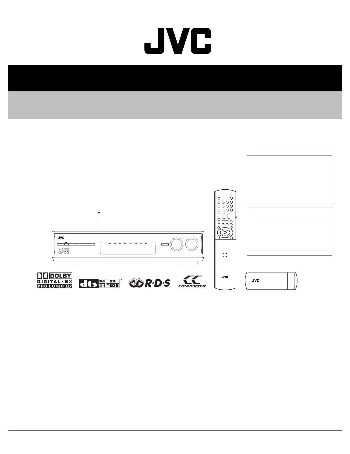
AUDIO/VIDEO CONTROL RECEIVER
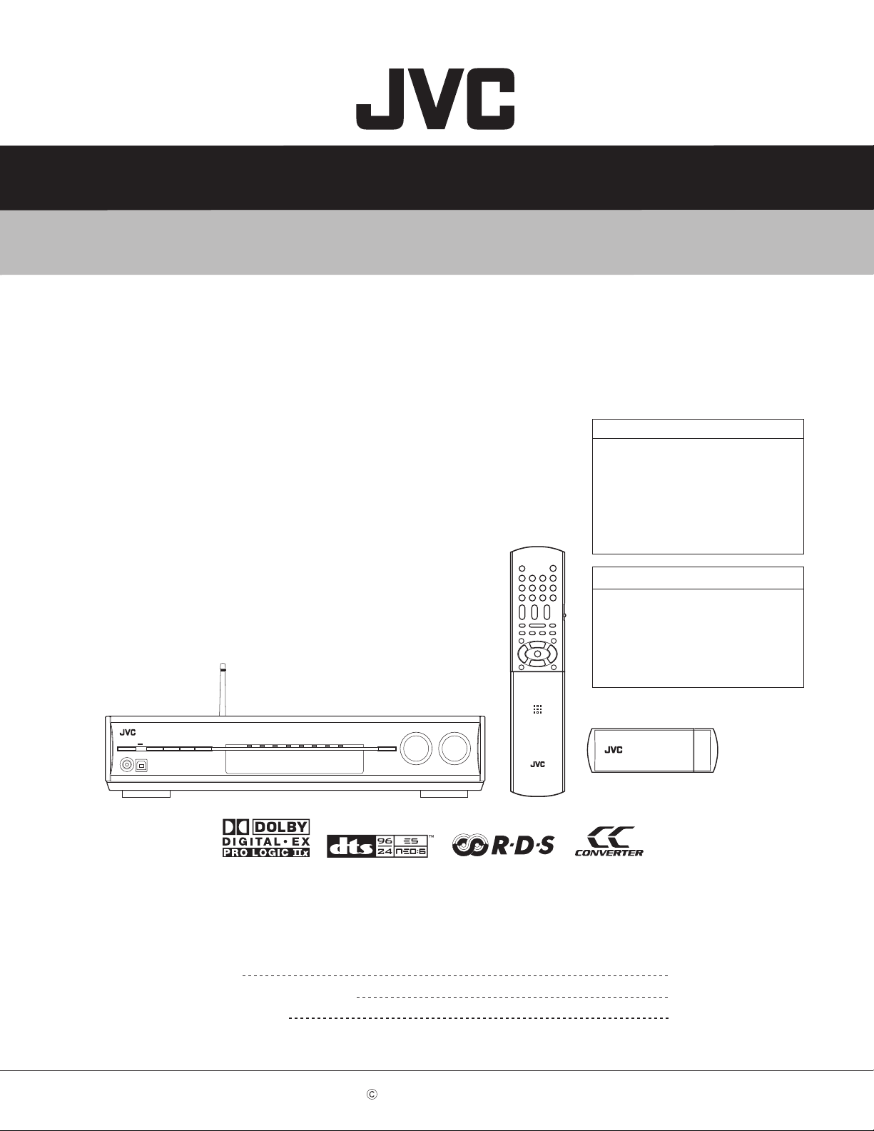
RX-D301S, RX-D302B
RX-D301S
Area suffix
A ------------------------ Australia
B ------------------------------ U.K.
E ---------- Continental Europe
EN ----------- Northern Europe
RX-D302B
Area suffix
B ------------------------------ U.K.
E ---------- Continental Europe
EN ----------- Northern Europe
Lead free solder used in the board (material : Sn-Ag-Cu, melting point : 219 Centigrade)
TABLE OF CONTENTS
1 PRECAUTIONS . . . . . . . . . . . . . . . . . . . . . . . . . . . . . . . . . . . . . . . . . . . . . . . . . . . . . . . . . . . . . . . . . . . . . . . 1-3
2 SPECIFIC SERVICE INSTRUCTIONS . . . . . . . . . . . . . . . . . . . . . . . . . . . . . . . . . . . . . . . . . . . . . . . . . . . . . . 1-6
3 DISASSEMBLY . . . . . . . . . . . . . . . . . . . . . . . . . . . . . . . . . . . . . . . . . . . . . . . . . . . . . . . . . . . . . . . . . . . . . . . 1-7
4 ADJUSTMENT . . . . . . . . . . . . . . . . . . . . . . . . . . . . . . . . . . . . . . . . . . . . . . . . . . . . . . . . . . . . . . . . . . . . . . . 1-20
5 TROUBLESHOOTING . . . . . . . . . . . . . . . . . . . . . . . . . . . . . . . . . . . . . . . . . . . . . . . . . . . . . . . . . . . . . . . . . 1-21
COPYRIGHT © 2005 Victor Company of Japan, Limited
No.MB479
2005/10
Page 2
SPECIFICATION
Amplifier
Output Power At stereo operation Front channels 110 W per channel, min. RMS, driven into 6
1 kHz with no more than 0.8% total harmonic distortion.
At surround operation Front channels 110 W per channel, min. RMS, driven into 6
Center channel 110 W, min. RMS, driven into 6
Surround channels 110 W per channel, min. RMS, driven into 6
Surround back channels 110 W per channel, min. RMS, driven into 6
Audio Audio Input Sensitivity/Impedance DVR/DVD (DVD MULTI), VCR, DBS, TV 270 mV/47 k
Audio Input (DIGITAL IN)*1 Coaxial: DIGITAL IN 1(DVR/DVD) 0.5 V(p-p)/75 Ω
Optical: DIGITAL IN 2(DBS), 3(VCR) -21 dBm to -15 dBm (660 nm ±30 nm)
USB: USB WIRELESS USB TERMINAL
Audio Output Level DVR, VCR 270 mV
Signal-to-Noise Ratio ('66 IHF/'78 IHF) 80 dB/62 dB
Frequency Response (6
Bass Boost +4 dB ±1 dB at 100 Hz
Equalization (at DSP operation) Center frequency 63 Hz, 250 Hz, 1 kHz, 4 kHz, 16 kHz
Video Video Input Sensitivity/Impedance Composite video: DVR/DVD, VCR, DBS 1 V(p-p)/75
Video Output Level/Impedance Composite video: DVR, VCR, MONITOR OUT 1 V(p-p)/75 Ω
Synchronization Negative
Tuning Range 87.50 MHz to 108.00 MHz
Usable Sensitivity Monaural 12.8 dBf (1.2 µV/75 Ω) for A version
50 dB Quieting Sensitivity Monaural 16.0 dBf (1.7 µV/75 Ω) for A version
Stereo Separation at REC OUT 35 dB at 1 kHz
Tuning Range 531 kHz to 1 710 kHz (at 9 kHz intervals)
Power Requirements AC 240 V ,50 Hz for A version
Power Consumption 180 W (at operation)
Dimensions (W
Mass 6.8 kg
USB WIRELESS SYSTEM The USB wireless transmitter supplied with this re-
× H × D) 435 mm × 91.5 mm × 371 mm
Ω) 20 Hz to 20 kHz (±1 dB)
Control range ±8 dB
S-video: DVR/DVD, VCR, DBS Y (luminance): 1 V(p-p)/75 Ω
Component: DVR/DVD, VCR (DBS) Y (luminance): 1 V(p-p)/75 Ω
S-video: DVR, VCR, MONITOR OUT Y (luminance): 1 V(p-p)/75 Ω
Component: MONITOR OUT Y (luminance): 1 V(p-p)/75 Ω
FM tuner (IHF)
Stereo 37.5 dBf (20.5 µV/75 Ω) for A version
AM tuner
General
1 kHz with no more than 0.8% total harmonic distortion.
Ω at 1 kHz, with
no more than 0.8% total harmonic distortion.
1 kHz with no more than 0.8% total harmonic distortion.
1 kHz with no more than 0.8% total harmonic distortion.
Ω
Ω
C (chrominance, burst): 0.3 V(p-p)/75 Ω
PB, PR: 0.7 V(p-p)/75 Ω
C (chrominance, burst): 0.3 V(p-p)/75 Ω
PB, PR: 0.7 V(p-p)/75 Ω
17.0 dBf (1.9 µV/75 Ω) for Europe version
21.3 dBf (3.2 µV/75 Ω) for Europe version
41.3 dBf (31.8 µV/75 Ω) for Europe version
522 kHz to 1 629 kHz (at 10 kHz intervals)
AC 230 V , 50 Hz for Europe version
5.8 W (in standby mode) for A version
0.9 W (in standby mode) for Europe version
ceiver supports Direct Sequence Spreading Spectrum (DSSS) using 2.4 GHz frequency band.
*2: Corresponding to Linear PCM, Dolby Digital, and DTS (with sampling frequency -32 kHz, 44.1 kHz, 48 kHz).
Designs and specifications are subject to change without notice.
1-2 (No.MB479)
Ω at
Ω at
Ω at
Ω at
Page 3
SECTION 1
PRECAUTIONS
1.1 Safety Precautions
(1) This design of this product contains special hardware and
many circuits and components specially for safety purposes. For continued protection, no changes should be made
to the original design unless authorized in writing by the
manufacturer. Replacement parts must be identical to
those used in the original circuits. Services should be performed by qualified personnel only.
(2) Alterations of the design or circuitry of the product should
not be made. Any design alterations of the product should
not be made. Any design alterations or additions will void
the manufacturers warranty and will further relieve the
manufacture of responsibility for personal injury or property
damage resulting therefrom.
(3) Many electrical and mechanical parts in the products have
special safety-related characteristics. These characteristics are often not evident from visual inspection nor can the
protection afforded by them necessarily be obtained by using replacement components rated for higher voltage, wattage, etc. Replacement parts which have these special
safety characteristics are identified in the Parts List of Service Manual. Electrical components having such features
are identified by shading on the schematics and by ( ) on
the Parts List in the Service Manual. The use of a substitute
replacement which does not have the same safety characteristics as the recommended replacement parts shown in
the Parts List of Service Manual may create shock, fire, or
other hazards.
(4) The leads in the products are routed and dressed with ties,
clamps, tubings, barriers and the like to be separated from
live parts, high temperature parts, moving parts and/or
sharp edges for the prevention of electric shock and fire
hazard. When service is required, the original lead routing
and dress should be observed, and it should be confirmed
that they have been returned to normal, after reassembling.
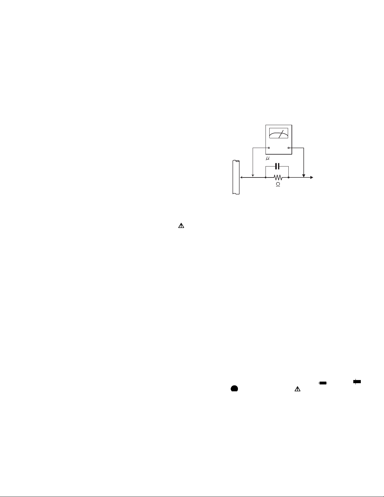
(5) Leakage shock hazard testing
After reassembling the product, always perform an isolation check on the exposed metal parts of the product (antenna terminals, knobs, metal cabinet, screw heads,
headphone jack, control shafts, etc.) to be sure the product
is safe to operate without danger of electrical shock.Do not
use a line isolation transformer during this check.
• Plug the AC line cord directly into the AC outlet. Using a
"Leakage Current Tester", measure the leakage current
from each exposed metal parts of the cabinet, particularly any exposed metal part having a return path to the
chassis, to a known good earth ground. Any leakage current must not exceed 0.5mA AC (r.m.s.).
• Alternate check method
Plug the AC line cord directly into the AC outlet. Use an
AC voltmeter having, 1,000Ω per volt or more sensitivity
in the following manner. Connect a 1,500Ω 10W resistor
paralleled by a 0.15µF AC-type capacitor between an ex-
posed metal part and a known good earth ground.
Measure the AC voltage across the resistor with the AC
voltmeter.
Move the resistor connection to each exposed metal
part, particularly any exposed metal part having a return
path to the chassis, and measure the AC voltage across
the resistor. Now, reverse the plug in the AC outlet and
repeat each measurement. Voltage measured any must
not exceed 0.75 V AC (r.m.s.). This corresponds to 0.5
mA AC (r.m.s.).
AC VOLTMETER
(Having 1000
ohms/volts,
or more sensitivity)
0.15 F AC TYPE
Place this
probe on
1500 10W
Good earth ground
1.2 Warning
(1) This equipment has been designed and manufactured to
meet international safety standards.
(2) It is the legal responsibility of the repairer to ensure that
these safety standards are maintained.
(3) Repairs must be made in accordance with the relevant
safety standards.
(4) It is essential that safety critical components are replaced
by approved parts.
(5) If mains voltage selector is provided, check setting for local
voltage.
1.3 Caution
Burrs formed during molding may be left over on some parts
of the chassis.
Therefore, pay attention to such burrs in the case of preforming repair of this system.
1.4 Critical parts for safety
In regard with component parts appearing on the silk-screen
printed side (parts side) of the PWB diagrams, the parts that are
printed over with black such as the resistor ( ), diode ( )
and ICP ( ) or identified by the " " mark nearby are critical
for safety. When replacing them, be sure to use the parts of the
same type and rating as specified by the manufacturer.
(This regulation dose not Except the J and C version)
each exposed
metal part.
(No.MB479)1-3
Page 4
1.5 Safety Precautions (U.K only)
(1) This design of this product contains special hardware and many circuits and components specially for safety purposes. For con-
tinued protection, no changes should be made to the original design unless authorized in writing by the manufacturer. Replacement parts must be identical to those used in the original circuits.
(2) Any unauthorised design alterations or additions will void the manufacturer's guarantee; furthermore the manufacturer cannot
accept responsibility for personal injury or property damage resulting therefrom.
(3) Essential safety critical components are identified by ( ) on the Parts List and by shading on the schematics, and must never
be replaced by parts other than those listed in the manual. Please note however that many electrical and mechanical parts in
the product have special safety related characteristics. These characteristics are often not evident from visual inspection. Parts
other than specified by the manufacturer may not have the same safety characteristics as the recommended replacement parts
shown in the Parts List of the Service Manual and may create shock, fire, or other hazards.
(4) The leads in the products are routed and dressed with ties, clamps, tubings, barriers and the like to be separated from live parts,
high temperature parts, moving parts and/or sharp edges for the prevention of electric shock and fire hazard. When service is
required, the original lead routing and dress should be observed, and it should be confirmed that they have been returned to
normal, after re-assembling.
1.5.1 Warning
(1) Service should be performed by qualified personnel only.
(2) This equipment has been designed and manufactured to meet international safety standards.
(3) It is the legal responsibility of the repairer to ensure that these safety standards are maintained.
(4) Repairs must be made in accordance with the relevant safety standards.
(5) It is essential that safety critical components are replaced by approved parts.
(6) If mains voltage selector is provided, check setting for local voltage.
Burrs formed during molding may be left over on some parts of the chassis. Therefore,
pay attention to such burrs in the case of preforming repair of this system.
1-4 (No.MB479)
Page 5
1.6 Caution after repairs
There are two power supply as the second power supply of the transformer.
One is a power supply for power IC(3pin), and another is a power supply for the control(8pin).
+B for power IC
(3pins)
There are two power supply as the second power supply of the transformer.
One is a power supply for power IC(3pin), and another is a power supply for the control(8pin).
Please connect first of all and confirm the power supply for the control when you do the energizing examination after it completes of
the repair.
+B for control section
(8pins)
For power IC(3pins)
Please never do the energizing examination in a power supply of power IC alone.
Moreover, when the control system breaks down, power IC is occasionally damaged.
(No.MB479)1-5
Page 6

SECTION 2
SPECIFIC SERVICE INSTRUCTIONS
This service manual does not describe SPECIFIC SERVICE INSTRUCTIONS.
1-6 (No.MB479)
Page 7
SECTION 3
DISASSEMBLY
3.1 Main body section
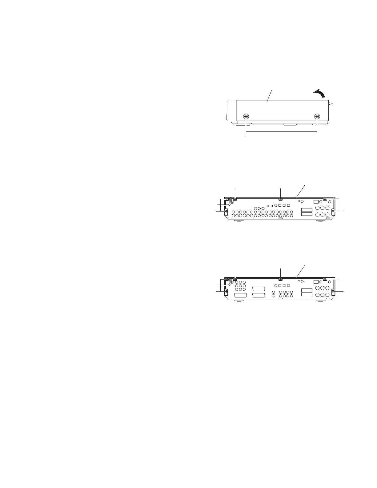
3.1.1 Removing the top cover
(See Figs.1 and 2)
(1) From the both sides of the main body, remove the four
screws A attaching the top cover. (See Fig.1)
(2) From the back side of the main body, remove the five
screws B and screw C attaching the top cover. (See Fig.2)
Reference:
When removing the screw C, use a screwdriver to show
as follows.
TORX Driver: size T10
Parts number: DR-L70
(3) Remove the top cover in the direction of the arrow. (See
Fig.1.)
Top cover
A
Fig.1
[For Australia]
B
C
Top cover
B B
[For Europe]
B
C
Top cover
B B
Fig.2
(No.MB479)1-7
Page 8
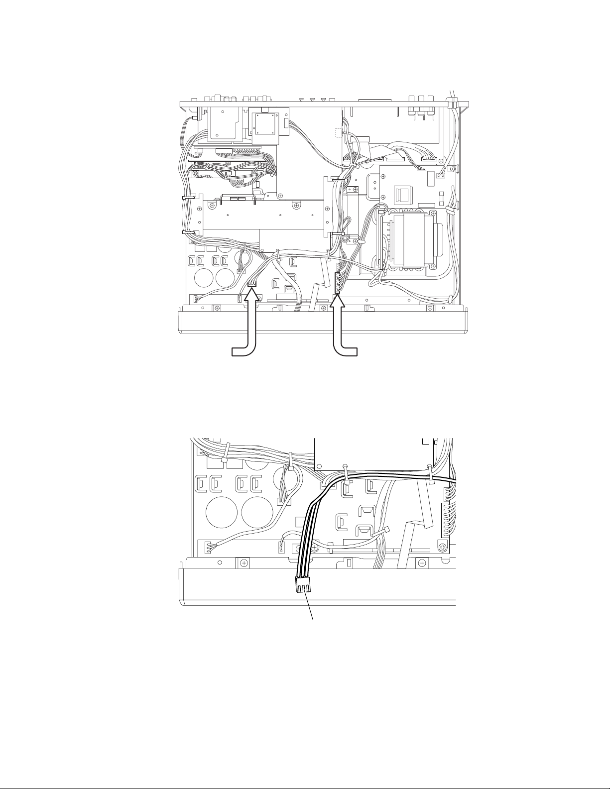
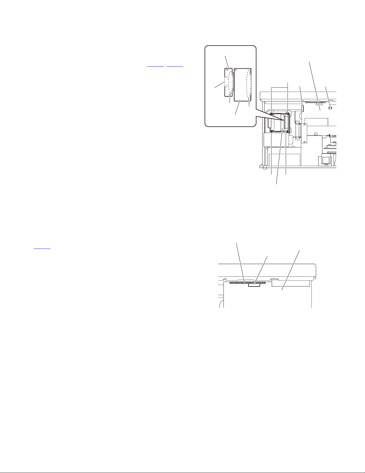
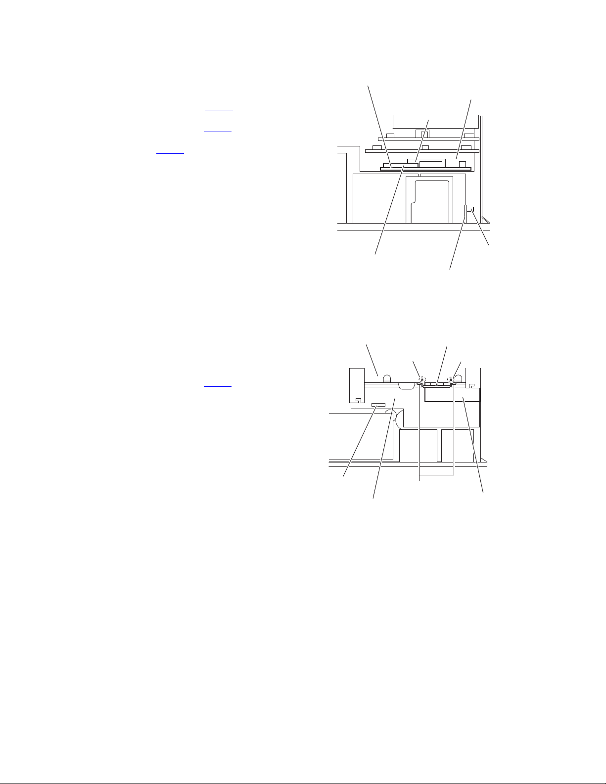
3.1.2 Removing the front panel assembly
(See Figs.3 and 4)
• Remove the top cover.
Reference:
Remove the tie bands and wire holder bundling the wires.
(1) Disconnect the card wire from the connector CN102
main amplifier board. (See Fig.3)
(2) Disconnect the wire from the connector CN351
amplifier board. (See Fig.3)
(3) Disconnect the wire from the connector CN552
board. (See Fig.3)
(4) Disconnect the wire from the connector CN661
ume board. (See Fig.3)
(5) Remove the three screws D attaching the front panel as-
sembly. (See Fig.3)
(6) Remove the screw D attaching the OSD connect 2 board.
(See Fig.3)
(7) From the bottom side of the main body, remove the four
screws E attaching the front panel assembly. (See Fig.4)
(8) Release the joints a and remove the front panel assembly
in the direction of the arrow. (See Fig.4)
on the
on the main
on the input
on the vol-
[For Australia]
Front panel assembly
CN102
D
CN552
Input board
[For Europe]
Front panel assembly
CN102
OSD connect 2 board
D
CN661
Volume board
OSD connect 2 board
D
Main amplifier board
D
CN351
Main amplifier board
D
D
CN552
Input board
E
a
CN351
CN661
Volume board
Fig.3
Front panel assembly
E
a
1-8 (No.MB479)
Fig.4
Page 9
3.1.3 Removing the rear panel
(See Fig.5)
• Remove the top cover.
(1) From the back side of the main body, remove the strain re-
lief from the rear panel in the direction of the arrow and remove the power cord.
(2) Remove the twenty-nine screws F attaching the rear panel.
[For Australia]
(3) Remove the thirty screws F attaching the rear panel. [For
Europe]
(4) Remove the nut and washer attaching the coaxial connec-
tor to the rear panel.
[For Australia]
Strain relief
Power cord
F
Rear panel
F
F
[For Europe]
Power cord
F
Strain relief
Rear panel
Coaxial connector
Nut and washer
Rear panel
F
Rear panel
F
F
F
Coaxial connector
Nut and washer
Fig.5
(No.MB479)1-9
Page 10

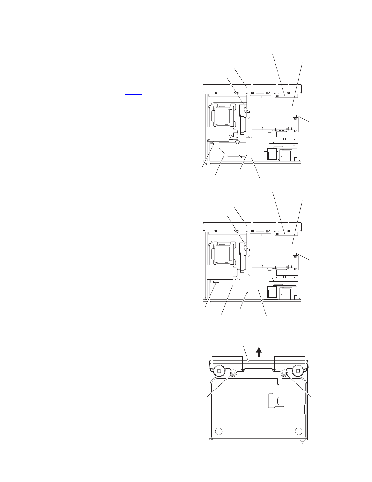
3.1.4 Removing the tuner
(See Fig.6)
• Remove the top cover.
(1) Disconnect the card wire from the connector CN1 on the
tuner.
(2) From the back side of the main body, remove the two
screws G attaching the tuner to the rear panel and take out
the tuner.
3.1.5 Removing the subwoofer board
(See Fig.6)
• Remove the top cover.
(1) Disconnect the wire from the connector CN524
woofer board.
(2) From the back side of the main body, remove the screw H
attaching the subwoofer board to the rear panel and take
out the subwoofer board.
3.1.6 Removing the front video board
(See Fig.6)
• Remove the top cover.
Reference:
Remove the tie band bundling the wires.
(1) Disconnect the wire from the connector CN662
ume board
(2) From the back side of the main body, remove the two
screws J.
(3) Remove the nut and washer attaching the coaxial connec-
tor to the rear panel.
(4) Take out the front video board from the main body.
on the sub-
on the vol-
[For Australia]
Volume board
Front video board
Compulink board
K
Rear panel
Tuner
Subwoofer board
CN662
CN565
Rear panel
Coaxial connector
Nut and washer
CN524
CN1
GJ H
3.1.7 Removing the compulink board
(See Fig.6) [For Australia]
• Remove the top cover.
(1) Disconnect the wire from the connector CN565
pulink board.
(2) From the back side of the main body, remove the screw K
and take out the compulink board from the main body.
on the com-
[For Europe]
Volume board
Tuner
Front video board
CN662
Rear panel
Subwoofer board
CN524
CN1
GJ H
1-10 (No.MB479)
Coaxial connector
Nut and washer
Fig.6
Page 11
3.1.8 Removing the power transformer
(See Fig.7)
• ReReference:zmove the top cover.
Reference:
Remove the tie bands bundling the wires.
(1) Disconnect the wires from the connectors (CN106
on the main amplifier board.
(2) Remove the soldered sections b and remove the wires.
(3) Remove the four screws M and take out the power trans-
former from the main body.
, CN111)
Trans primary board
b
Main amplifier board
M
CN106
CN 111
3.1.9 Removing the trans primary board
(See Fig.7)
• Remove the top cover.
Reference:
Remove the tie band bundling the wires.
(1) Remove the wires from the soldered sections b and re-
move the wires.
(2) Remove the solders from the soldered sections c and re-
move the trans primary board.
3.1.10 Removing the trans secondary board
(See Fig.7)
• Remove the top cover and power transformer.
From the side of the power transformer, remove the solders from
the soldered sections d and remove the trans secondary board.
3.1.11 Removing the DCDC control board
(See Fig.8)
• Remove the top cover.
From the top side of the main body, disconnect the connector
on the DCDC control board from the main amplifier board
CN152
in an upward direction.
Note:
When removing the DCDC control board, take care not to
break the claw of the connector on the main amplifier board.
c
d
Trans secondary
board
DCDC control board
M
M
Power transformer
Fig.7
Main amplifier board
CN152
Fig.8
(No.MB479)1-11
Page 12
3.1.12 Removing the PWM modulation 1 board
(See Fig.9)
• Remove the top cover.
Reference:
Remove the tie band bundling the wires.
(1) Disconnect the wire from the connector CN413
PWM modulation 2 board.
(2) Disconnect the wires from the connectors (CN311
CN313) on the PWM modulation 1 board.
(3) Disconnect the connector CN301
1 board from the main amplifier board in an upward direction.
Note:
When removing the PWM modulation 1 board, take care not to
break the claw of the connector on the main amplifier board.
3.1.13 Removing the PWM modulation 2 board
(See Fig.9)
• Remove the top cover.
(1) From the top side of the main body, disconnect the wires
from the connectors (CN411
modulation 2 board.
(2) Disconnect the connector CN401
2 board from the main amplifier board in an upward direction.
Note:
When removing the PWM modulation 2 board, take care not to
break the claw of the connector on the main amplifier board.
on the PWM modulation
, CN412, CN413) on the PWM
on the PWM modulation
on the
, CN312,
Main amplifier board
CN401
CN312
CN412
CN413
PWM modulation 1 board
CN301
CN311
CN313
CN411
PWM modulation 2 board
Fig.9
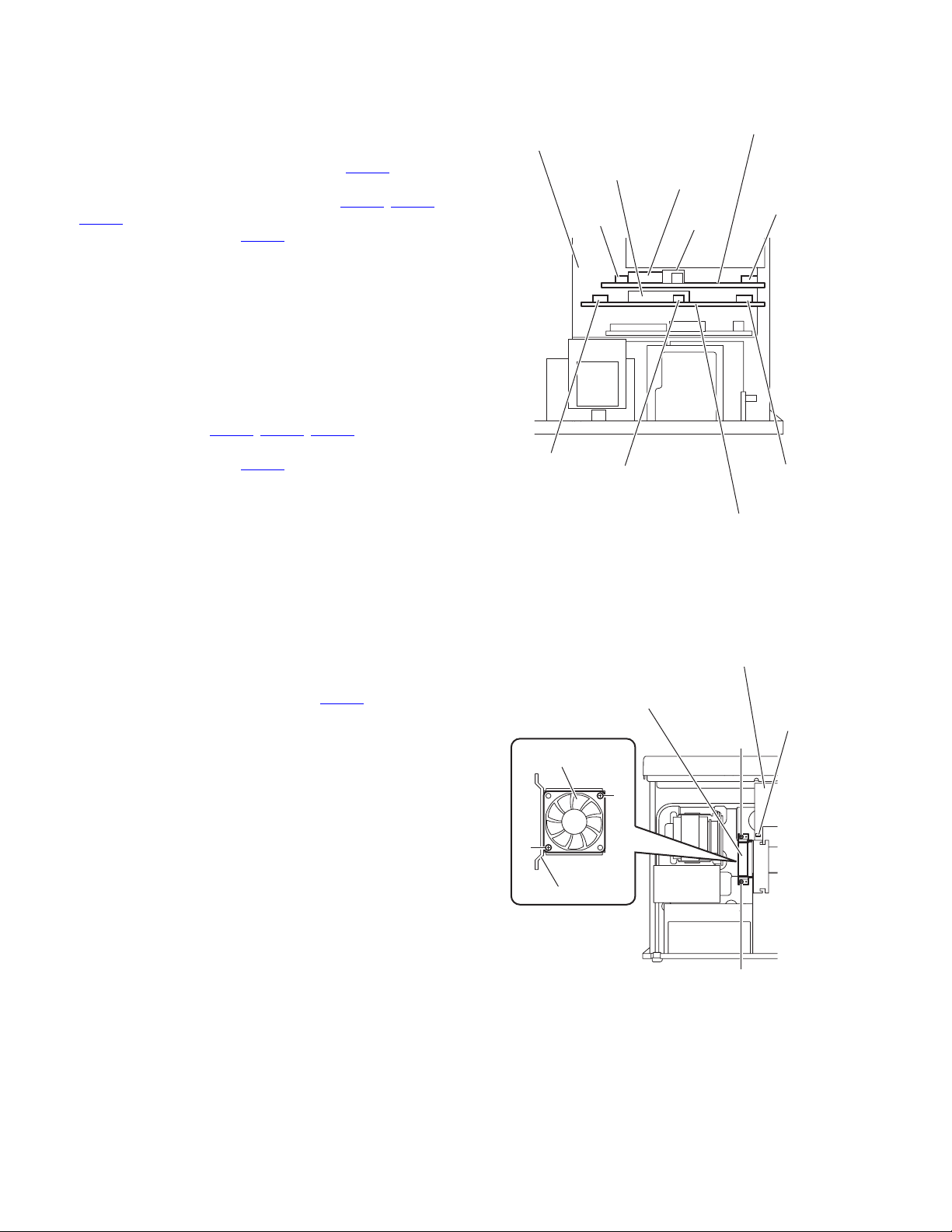
3.1.14 Removing the fan motor
(See Fig.10.)
• Remove the top cover.
Reference:
Remove the tie band bundling the wires.
(1) Disconnect the wire from the connector CN103
amplifier board.
(2) Remove the two screws N and take out the fan motor as-
sembly.
(3) Remove the two screws P attaching the fan motor to the
fan bracket.
on the main
Main amplifier board
Fan motor assembly
CN103
N
Fan motor
P
P
Fan bracket
N
Fig.10
1-12 (No.MB479)
Page 13
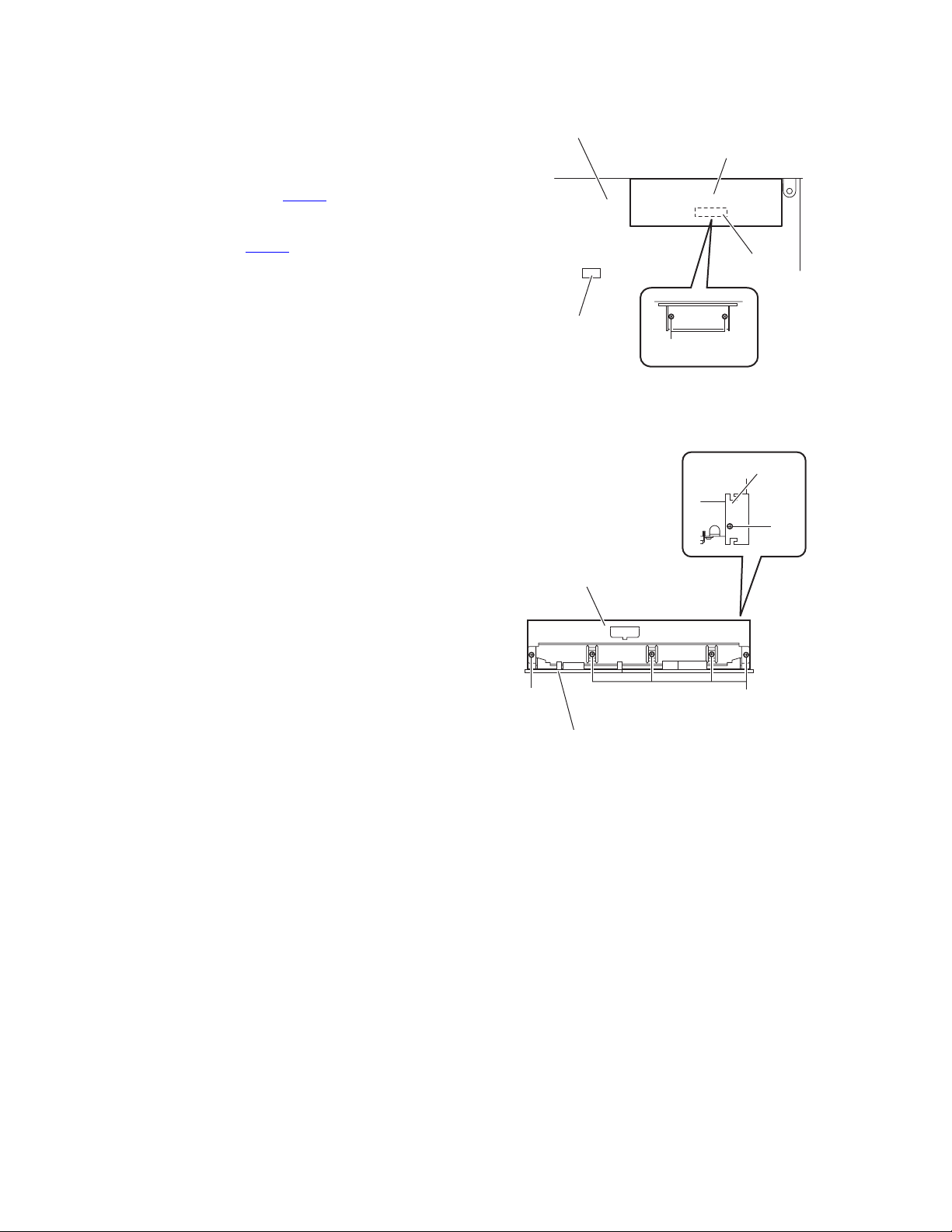
3.1.15 Removing the volume board
r
(See Fig.11)
• Remove the top cover and front video board.
(1) From the back side of the main body, remove the five
screws Q attaching the volume board to the rear panel.
(2) Remove the screw R attaching the volume board.
(3) From the top side of the main body, remove the screw S at-
taching the wire holder board and move the wire holder
board with the wires in the direction of the arrow.
(4) Disconnect the connector CN681
from the DSP connect board.
Note:
When removing the volume board, take care not to break
the claw of the connector on it.
(5) Take out the volume board and disconnect the wires from
the connectors (CN661
side of the volume board.
, CN682, CN683) on the forward
on the volume board
Wire holder board
Volume board
S
CN682
3.1.16 Removing the OSD board
(See Fig.12) [For Australia]
• Remove the top cover, front video board and volume board.
(1) Remove the solder from the section e to remove the earth
wire.
(2) Remove the screw T attaching the support bracket on the
chassis base.
(3) Disconnect the connectors (CN582
board in an upward direction.
Note:
When removing the OSD board, take care not to break
the claws of the connectors on it.
(4) Remove the screw U to remove the support bracket from
the OSD board.
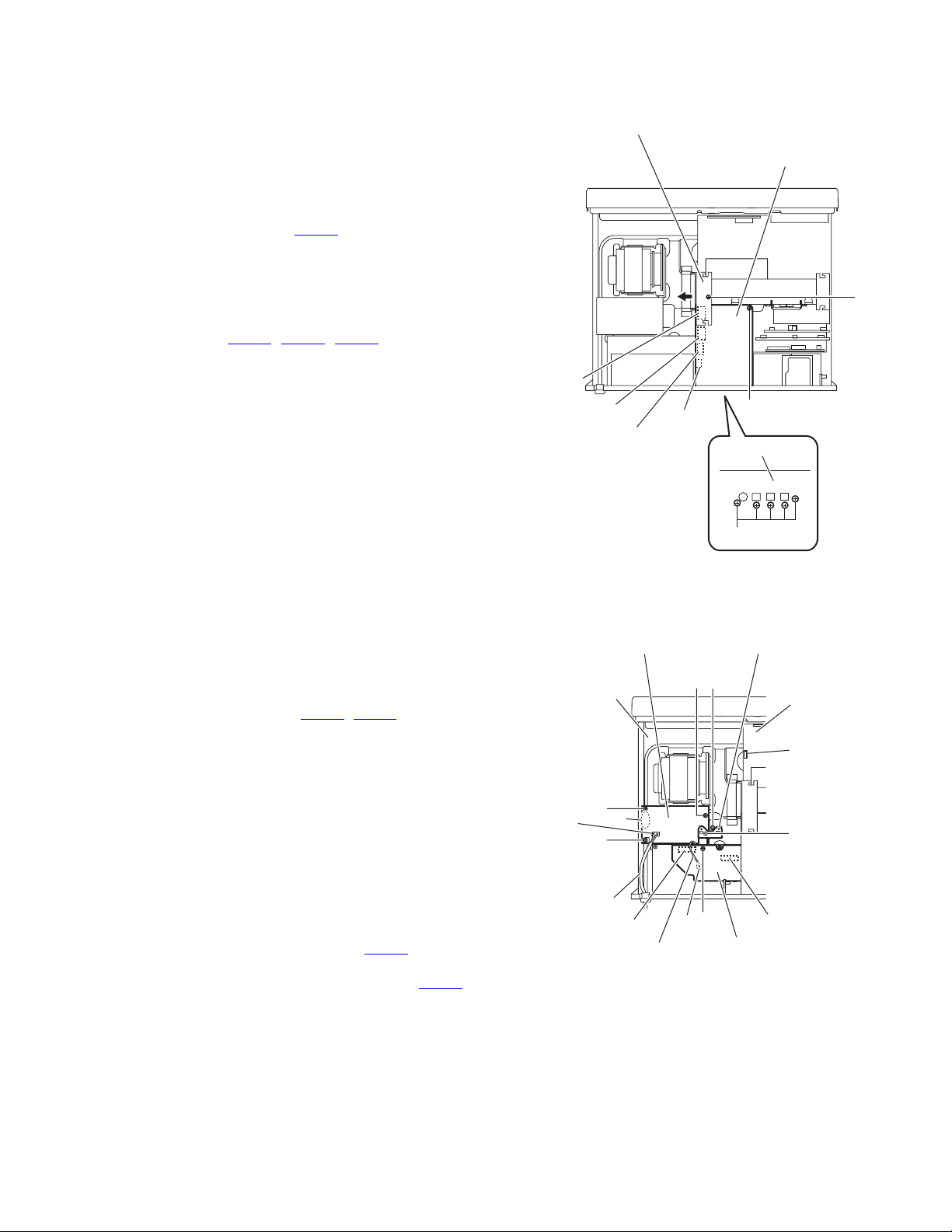
3.1.17 Removing the primary board
(See Fig.12)
• Remove the top cover.
Reference:
Remove the tie bands bundling the wires.
(1) Disconnect the wire from the connector CN101
amplifier board.
(2) Disconnect the power cord from the connector CN120
the primary board.
(3) Remove the four screws V attaching the primary board.
(4) Take out the primary board from the main body and remove
the wires from the soldered sections f on the reverse side
of the primary board.
, CN584) on the OSD
on the main
on
CN683
Chassis base
CN120
V
V
Power cord
CN661
CN681
R
Rear panel
Q
Fig.11
Primary board Support bracket
VT
Main amplifie
board
CN101
f
V
CN582
Earth wire
e
U
Fig.12
CN584
OSD board
(No.MB479)1-13
Page 14

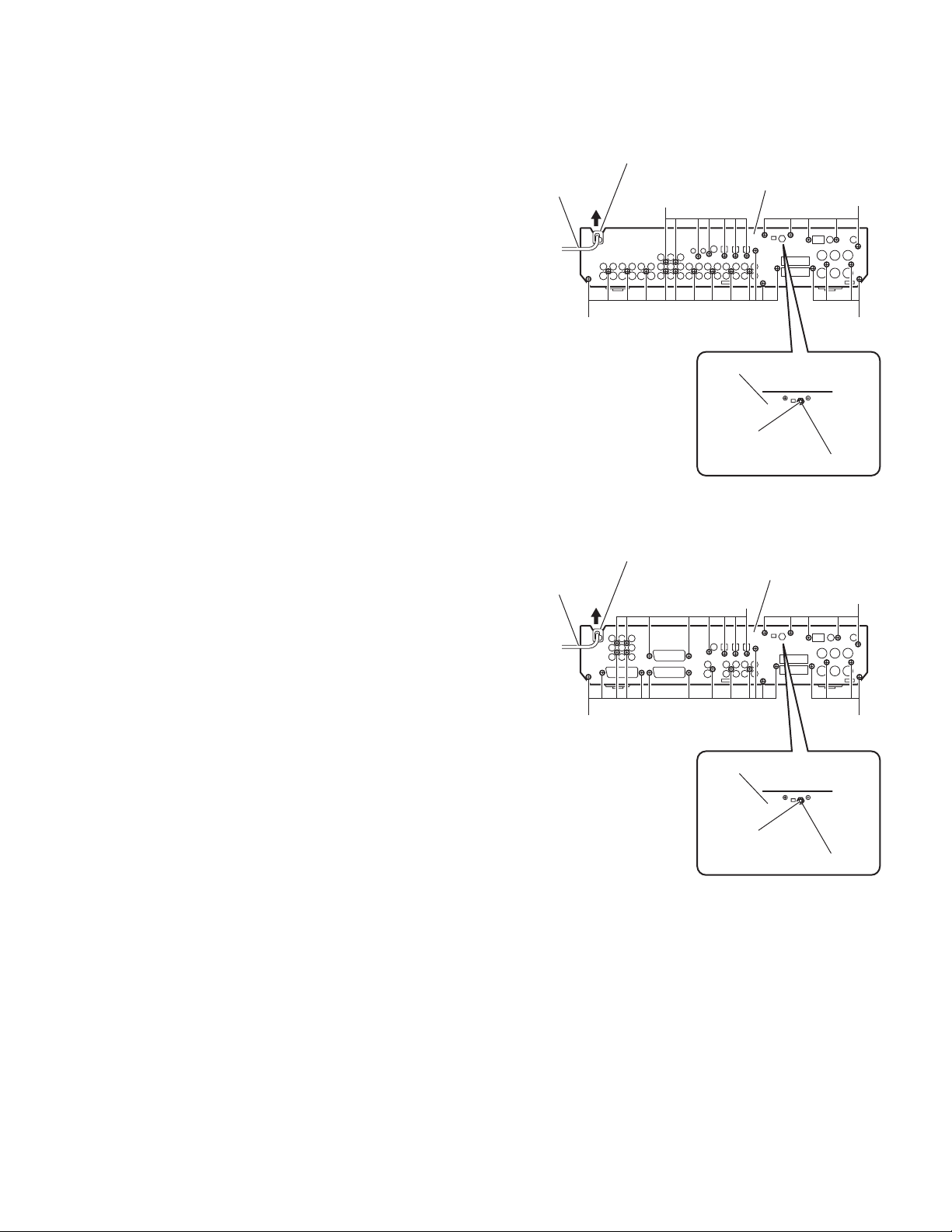
3.1.18 Removing the scart board
(See Fig.13) [For Europe]
• Remove the top cover.
(1) From the back side of the main body, remove the six
screws W attaching the scart board to the rear panel.
(2) Disconnect the card wire from the connector CN537
scart board.
(3) Take out the scart board from the main body.
on the
Scart board
W
W
CN537
Rear panel
3.1.19 Removing the speaker terminal 1 and speaker terminal 2 boards
(See Fig. 14)
• Remove the top cover and rear panel.
Reference:
Remove the tuner and subwoofer board as required.
(1) From the top side of the main body, disconnect the wires
from the connectors (CN265
minal 1 board.
(2) Take out the speaker terminal 1 board from the main body.
(3) Disconnect the wires from the connectors (CN209
on the speaker terminal 2 board.
(4) Take out the speaker terminal 2 board from the main body.
, CN465) on the speaker ter-
, CN262)
Speaker terminal 2 board Speaker terminal 1 board
CN262
Fig.13
CN465CN209
CN265
Fig.14
1-14 (No.MB479)
Page 15
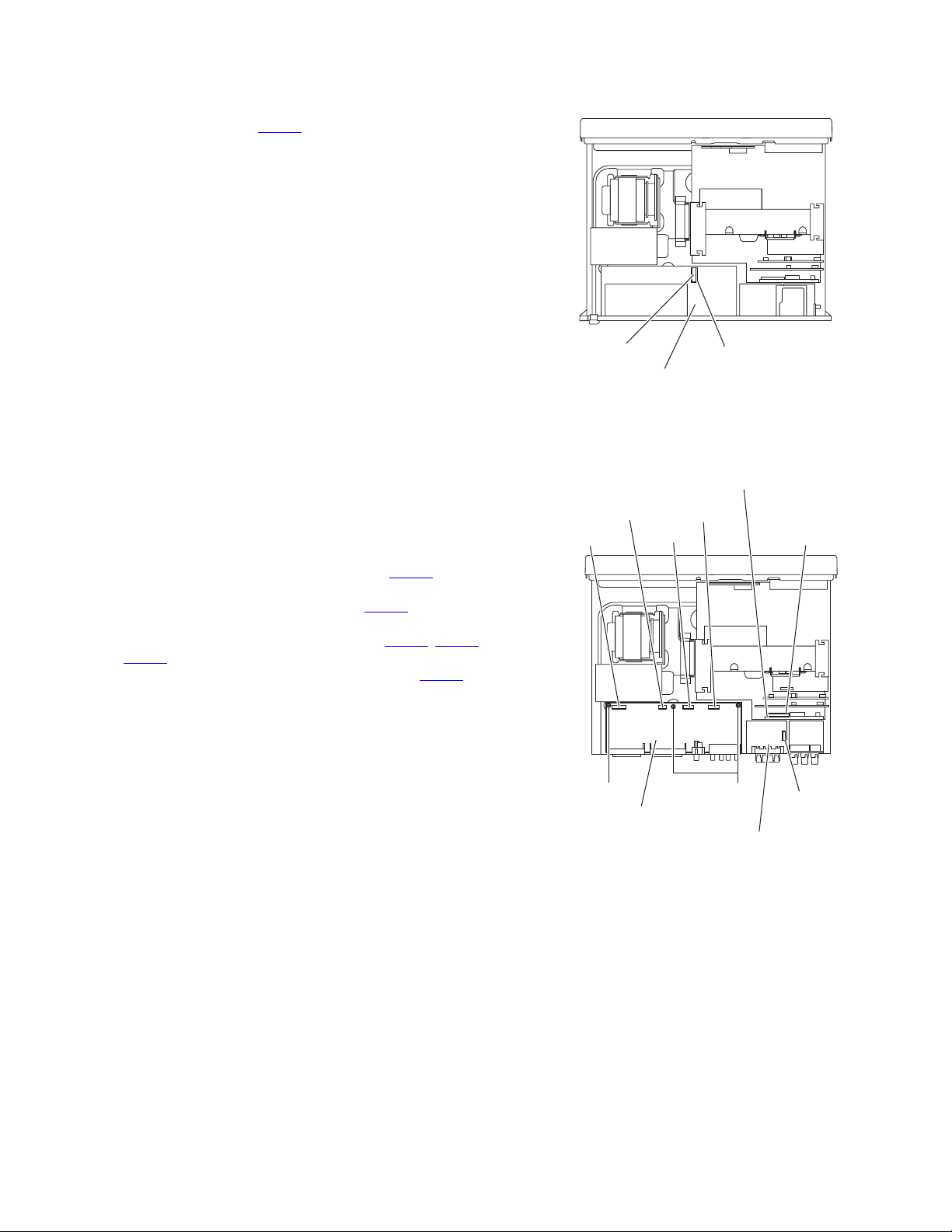
3.1.20 Removing the DSP connect board
(See Fig.15)
• Remove the top cover, front video board and volume board.
Disconnect the connector CN602
from the input board in an upward direction.
Note:
When removing the DSP connect board, take care not to break
the claw of the connector on the input board.
on the DSP connect board
3.1.21 Removing the input board
(See Fig. 16)
• Remove the top cover, rear panel, tuner, subwoofer board,
front video board, compulink board [For Australia], volume
board, OSD board [For Australia], scart board [For Europe]
and DSP connect board.
Reference:
Remove the tie band bundling the wires.
(1) Disconnect the wire from the connector CN209
speaker terminal 2 board.
(2) Disconnect the wire from the connector CN513
connect 1 board.
(3) Disconnect the wires from the connectors (CN530, CN531,
) on the input board.
CN552
(4) Disconnect the parallel wire from the connector CN540 on
the input board.
(5) Remove the three screws X and take out the input board
from the main body.
on the
on the OSD
CN602
CN552
Input board
CN540
X
Input board
DSP connect board
Fig.15
OSD connect 1 board
CN531
CN530
X
Speaker terminal 2 board
CN513
CN209
Fig.16
(No.MB479)1-15
Page 16
3.1.22 Removing the OSD connect 1 board
(See Fig.17)
• Remove the top cover, front video board and volume board.
Reference:
Remove the tie band bundling the wires.
(1) Disconnect the wire from the connector CN524
woofer board.
(2) Disconnect the wire from the connector CN513
connect 1 board.
(3) Disconnect the connector CN522
board from the main amplifier board in an upward direction.
Note:
When removing the OSD connect 1 board, take care not to
break the claw of the connector on the main amplifier board.
on the OSD connect 1
on the sub-
on the OSD
OSD connect 1 board
Main amplifier board
CN522
3.1.23 Removing the master clock board
(See Fig.18)
• Remove the top cover, tuner, front video board, PWM modula-
tion 1 board, PWM modulation 2 board, volume board and
OSD connect 1 board.
(1) Remove the two screws Y with a short driver and remove
the transistor hold from the joints g of the heat sink.
(2) Disconnect the wire from the connector CN201
amplifier board.
(3) Take out the master clock board from the main body.
on the main
CN513
Heat sink
CN201
Main amplifier board
Subwoofer board
Fig.17
Transistor hold
g
g
Y
Master clock board
Fig.18
CN524
1-16 (No.MB479)
Page 17
3.1.24 Removing the main amplifier board
(See Figs.19 and 20)
• Remove the top cover, tuner, front video board, DCDC control
board, PWM modulation 1 board, PWM modulation 2 board,
volume board, OSD connect 1 board and master clock board.
(1) Disconnect the wire from the connector CN265
speaker terminal 1 board. (See Fig.19.)
(2) Disconnect the wire from the connector CN262
speaker terminal 2 board. (See Fig.19.)
Reference:
Remove the tie bands bundling the wires.
(3) Disconnect the wires from the connectors (CN101
, CN111, CN351) on the main amplifier board. (See
CN106
Fig.19.)
(4) Disconnect the card wire from the connector CN102
main amplifier board. (See Fig.19.)
(5) Disconnect the wires from the connectors (CN530
on the input board. (See Fig.20.)
(6) Disconnect the parallel wire from the connector CN540
the input board. (See Fig.20.)
(7) Remove the four screws Z and two screws AA. (See
Fig.20.)
(8) Take out the main amplifier board with the regulator board
from the main body. (See Fig.20.)
on the
on the
, CN103,
on the
, CN531)
on
CN103
CN106
CN101
Speaker terminal 2 board
Main amplifier board
CN102
CN262
Speaker terminal 1 board
Fig.19
CN 111
CN265
CN351
Regulator board
Z
CN540
Input board
CN530
AA
CN531
Fig.20
Main amplifier board
Z
Z
(No.MB479)1-17
Page 18
3.1.25 Removing the regulator board
(See Fig.21)
• Remove the top cover, tuner, front video board, DCDC control
board, PWM modulation 1 board, PWM modulation 2 board,
volume board, OSD connect 1 board, master clock board and
main amplifier board.
(1) From the forward side of the main amplifier board, discon-
nect the wire from the connector CN105
(2) Remove the two screws AB attaching the regulator board.
(3) Remove the regulator board and disconnect the parallel
wire from the connector CN104
board.
3.1.26 Removing the heat sink
(See Fig.22)
• Remove the top cover, tuner, front video board, DCDC control
board, PWM modulation 1 board, PWM modulation 2 board,
volume board, OSD connect 1 board, master clock board,
main amplifier board and regulator board.
(1) From the forward side of the main amplifier board, remove
the screw AC and remove the wire holder board with the
wires.
(2) Remove the five screws AD to remove the heat sink.
.
on the main amplifier
Main amplifier board
Regulator board
CN104
CN105
AB
Fig.21
Wire holder board
AC
Heat sink
AD
Main amplifier board
AD
Fig.22
1-18 (No.MB479)
Page 19
3.2 Front panel assembly section
• Remove the front panel assembly.
(See "3.1.2 Removing the front panel assembly".)
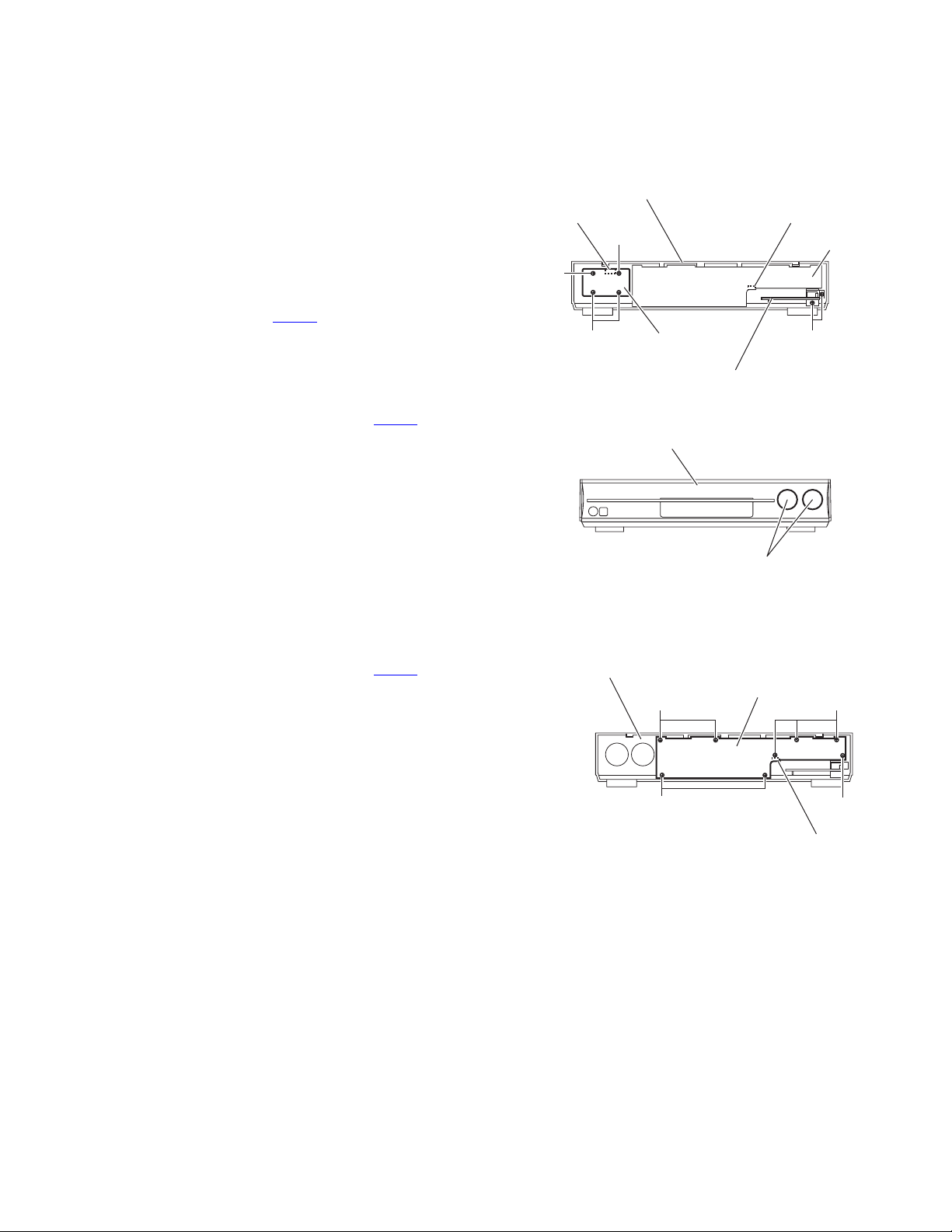
3.2.1 Removing the JOG board
(See Figs. 1 and 2)
(1) From the inside of the front panel assembly, remove the
four screws A attaching the JOG board. (See Fig.1.)
(2) Take out the JOG board while lifting it from the front panel
assembly little by little.
Reference:
The rotary knob assemblies are removed from the front
side simultaneously. (See Fig.2.)
(3) From the forward side of the JOG board, disconnect the
wire from the connector CN913
3.2.2 Removing the OSD connect 2 board
(See Fig. 1)
(1) From the inside of the front panel assembly, remove the
two screws A attaching the OSD connect 2 board.
(2) Disconnect the wire from the connector CN914
board.
. (See Fig.1)
on the FL
Front panel assembly
CN913
A
A
JOG board
A
Front panel assembly
CN914
FL board
A
OSD connect 2 board
Fig.1
3.2.3 Removing the FL board
(See Fig. 3)
• Remove the JOG board.
(1) Disconnect the wire from the connector CN914
board.
(2) Remove the eight screws A and take out the FL board.
on the FL
Rotary knob assemblies
Front panel assembly
A
A
Fig.2
Fig.3
FL board
A
A
CN914
(No.MB479)1-19
Page 20

SECTION 4
ADJUSTMENT
This service manual does not describe ADJUSTMENT.
1-20 (No.MB479)
Page 21

SECTION 5
TROUBLESHOOTING
This service manual does not describe TROUBLESHOOTING.
(No.MB479)1-21
Page 22

Victor Company of Japan, Limited
AV & MULTIMEDIA COMPANY AUDIO/VIDEO SYSTEMS CATEGORY 10-1,1chome,Ohwatari-machi,Maebashi-city,371-8543,Japan
(No.MB479)
Printed in Japan
VPT
Page 23
SCHEMATIC DIAGRAMS
AUDIO / VIDEO CONTROL RECEIVER
RX-D301S,RX-D302B
CD-ROM No.SML200510
RX-D301S
Area suffix
A ------------------------ Australia
B ------------------------------ U.K.
E ---------- Continental Europe
EN ----------- Northern Europe
RX-D302B
Area suffix
Lead free solder used in the board (material : Sn-Ag-Cu, melting point : 219 Centigrade)
Contents
Block diagrams
Standard schematic diagrams
Printed circuit boards
B ------------------------------ U.K.
E ---------- Continental Europe
EN ----------- Northern Europe
2-1
2-3
2-17 to 22
COPYRIGHT 2005 Victor Company of Japan, Limited.
No.MB479SCH
2005/10
Page 24

In regard with component parts appearing on the silk-screen printed side (parts side) of the PWB diagrams, the
parts that are printed over with black such as the resistor ( ), diode ( ) and ICP ( ) or identified by the " "
mark nearby are critical for safety.
Page 25

Block diagrams
Main
plug
CN120
T102
Trans.
FW121
RY101
Q1001
POWER_ON
Primary section
Power
trans.
CN206CN211
S1
S2
S3
AC
CN106C N111CN101CN152
CN151
IC111 to IC113, IC115
DCDC converter
control
PWM_V,Vout_DET
M_CLOCK
AC_DET_1
VCHANGE_1
VCHANGE_2
D1101
to
D1104
Q1101
Q1102
IC101
DCDC
converter
PWM_V
Vout_DET
AC_DET_1
D101
to
D104
D+5V_Mi
B+5V_Mi
D109 to D112
S2
S3
S2
Q102
VPP REG.
VPP
CN102
IC151
A+5V_DSP
REG
CN130
A+5V_DSP
+12V_RY
CN131
IC152
A+9V_Vi_Tu
REG
A+9V_Vi_Tu
CN103
TO
FAN
IC153
A+5V_Vi
REG
A+5V_Vi
Q157,Q158
+/-7V REG
+/-7V
VCHANGE_1,VCHANGE_2,M_CLOCK
Q153
+12V_FAN
REG
FAN
Q151,Q152
Q154
FAN_ON/OFF
FAN_LOW
Q101
D+5V_Mi,B+5V_Mi
REG
CN104 CN105
CN114 CN115
Q174
DCDC_+12
REG
Q175
DCDC_-B+12
REG
Q171
D+5V_DSP
REG
CN252
CN262
RY391
RY491
ST292
SURROUND
&
SURRBACK
SLout
SRout
SBLout
SBRout
CN209FW451
SURR_RY
SURRBACK_RY
CN465
CN251
CN265
RY295
RY895
ST295
FRONT
&
CENTER
Lout
Rout
Cout
FRONT_RY
CENTER_RY
Speaker terminal section
IC851
AMP
CN322
IC451
IC461
AMP
CN422
IC261
IC361
AMP
CN421
IC251
IC351
AMP
CN321
CN312CN311 CN412CN411
IC201
MODULATER
FRONT_L
FRONT_R
CENTER
SURROUND_L
SURROUND_R
SURRBACK_L
SURRBACK_R
IC801
MODULATER
IC301
MODULATER
IC401
MODULATER
CN302
CN301
CN413
CN423
PWM modulator section
FW323
CN313
FL,FR
A.NFB_FL
D.NFB_FL
A.NFB_FR
D.NFB_FR
C
A.NFB_C
D.NFB_C
M_CLOCK
+/-7V
+/-7V
+/-7V
CN402
CN401
SL,SR
A.NFB_SL
D.NFB_SL
A.NFB_SR
D.NFB_SR
SBL,SBR
A.NFB_SBL
D.NFB_SBL
A.NFB_SBR
D.NFB_SBR
CN202
IC211 to IC214
Master clock GEN.
Q444,Q445
-B+12V REG
Master clock section
CN201
M_CLOCK
FREQ_CTRL
-B, -B+12V
FL,FR,C
SL,SR
SBL,SBR
A.NFB_SBL,D.NFB_SBL
A.NFB_SBR,D.NFB_SBR
A.NFB_FL,D.NFB_FL
A.NFB_FR,D.NFB_FR
A.NFB_C
D.NFB_C
A.NFB_SL,D.NFB_SL
A.NFB_SR,D.NFB_SR
J6501
TV
DBS
J6502
VCR
IN/OUT
J6503
DVR OUT
DVR/DVD IN
J6504
DVD C/SW
DVD SURR
IC502
6CH
SW
TV_L/R
DBS_L/R
VCRREC_L/R
VCR_L/R
DVRREC_L/R
DVR_L/R
DVD_C,DVD_SW,DVD_SL/SR
L,R
CN503
BD DA
BD CL
FW501
L,R
J6511
DBS
VCR OUT
J6512
VCR IN
DVR OUT
J6513
DVR/DVD IN
MONITOR
IC522
SY SEL.
IC524
IC525
SC SEL.
IC527
CV SEL.
Y
C
CV
VIDEO1
VIDEO4
VIDEO7
TA/TC_SDA
TA/TC_SCL
IC501
CPU
Y OUT
C OUT
CV OUT
CN505
TO
TUNER
TU_L/R
TU_DATAIN
TU_DATAOUT
TU_CLK,TU_CE
CN531
DSP_STATUS
DSP_READY
DSP_COMMAND
DSP_CLOCK
DSP_RESET
CN502
CN602
CN672
DA,CL
S_MUTE
SBWR_MUTE
CN530
D+5V,B+5V
+/-7V,+9V
A+5V(DSP)
D+5V(DSP)
+5V(VIDEO)
+12V(RELAY)
BCHANGE1
BCHANGE2
FAN_ON/OFF
FAN_L
POWER_ON
Q524
HP_RELAY
HP_RY
J505
AV
COMPULINK
CN565
CN555
AVCLINK
M_COMMAND,M_STATUS
M_CLK,M_RESET,M_BUSY
M_CS
FW240
CN540
PROTECT
FREQ_CTRL
CN222
M_CLOCK
FREQ_CTRL
PROTECT
J4503
VCR IN
DVR/DVD IN
MONITOR
IC531
PB SEL.
PB OUT
PB
IC530
Y SEL.
Y OUT
Y
IC532
PR SEL.
PR OUT
PR
VIDEO1
VIDEO10
VIDEO11
Audio/Video signal input and system control section Regulator, DC-DC converter and digital power amplifier section
CN513
IC503
6CH VOLUME
L,R
DVD_SW
DVD_SL/SR
DVD_C
IC508
AUDIO SOUND
PROCESSOR
MUTE
DSP_L/R
DSP_C,DSP_SW
DSP_SL/SR
S_MUTE
IC504
AMP
CN522
CN523
SUBWFR
CN524
J504
DA,CL
DA,CL
CN521
CN681
CN682
SUBWOOFER
OUT
CN683
IC667
8CH
CODEC
DSP_IN_L
DSP_IN_R
IC671
CPU
DSPSTATUS,DSPREADY
DSPCLK,DSPRESET
DSPCOMMAND
MOSI
MISO
SS,HREQ
DSP_RST
IC673
INV
SCK
MICK
IC661
DSP
IC601
IC602
AMP.
LIN+/RIN+/-
IC621,IC622
IC632 to IC634
IC651,IC652
AMP.
C_LRCK
S_LRCK
C_BCK
S_BCK
D/A0 to D/A3
DATA,XTAL
A2+/- to A4+/B2+/- to B4+/-
Volume section
DSP and digital signal input terminal section
IC901
CPU
&
FL
DRV.
DI901
FL
DISPLAY
SEG1 to 35
GRID1 to 15
CN913
CN903
JS901
JS902
VOL1,VOL2,JOG1,JOG2
J901
HEADPHONE
CN904
CN914
J903
USB
TERMINAL
IC903
D/A
CN961
D+/-,VBUS
USB_IN
CN905
HP_L
HP_R
CN661
RX4
J681 UN682
RX1
RX0
DIGITAL
IN1
DIGITAL
IN2
CN351
CN902
F1,F1
-VPP
D+5V
CN952
CN552
AV COMPULINK
Q910
AVC_IN/OUT
D916 to D923
AM_LED
FM_LED,USB_LED
TV_LED,DBS_LED
DVD_LED,VCR_LED
DVD_MULTI_LED
S901 to S906
KEY_IN1 to 3
D907
STANDBY
LED
STANDBY_LED
IC902
IR DET.
REMOCON
Use control keys, system control and FL display section
MUTE
T_MUTE
DSP_SBL/SBR
HEADPHONE_DET
AMP_-B
AMP_-B+12V
FREQ_CTRL
PROTECT
Lout_HP
Rout_HP
Q281 to Q286
PROTECTOR
PROTECT
Lout_HP
Rout_HP
Lout_HP
Rout_HP
RY300
HP_RY
+12V_RY
D+5V_Mi
D+5V_Mi,D+5V_DSP
B+5V_Mi,POWER_ON
POWER_ON
POWER_ON
RY+9V
+12V
-B+12V
D+5V_DSP
IC611 to IC614
AMP.
CDIN
CDOUT
CCLK,D_CS
D_RST
IC681
DIGITAL AUDIO & DSP
IC682
D/A
DSP_L
DSP_R
CC_DATA,CC_CS
CC_CLK,CC_RST
D/A0,C_LRCK
C_BCK
GPIO1
GPIO2
GPIO3
GPIO4
PD_DD
RST_DD
96K/48K
182K/96K
UN683
RX2
DIGITAL
IN3
CN662
RX5
CN11
IC11
DIGITAL AUDIO
TRANSMITTER
CN12
CN13
FRONT_RY
CENTER_RY
CN509
CN583
VIDEO7
CN581
TA/TC_SDA
TA/TC_SCL
SY_OUT
SC_OUT
SY_IN,SC_IN
CV_IN
CN593CN591
CN594CN592
CN584CN582
IC536
IC537
SW &
AMP
IC551
DIGITAL
Y/C
SEPA.
SY_OUT,SC_OUT
CV_OSD
SY_OSD
SC_OSD
YOUT,COUT
IC559
CLOCK
GEN.
CV_OUT
CKIN
Y/C separate section
IC507
EEPROM
RC_SDA
RC_SCL
RC_WP
LAN MODULE
USB wireless
module section
UN686
TX
DIGITAL OUT
D908,D909
BLUE_LED
D+5V_Mi,FL1,FL2,VPP
FRONT_RY
CENTER_RY
SURR_RY
SURRBACK_RY
Q173
PRI_RY+9V
REG
RY+9V
MUTE
SBWR_MUTE
+B
-B
A version
2-1
Page 26

Main
plug
CN120
T102
Trans.
FW121
RY101
Q1001
POWER_ON
Primary section
Power
trans.
CN206CN211
S1
S2
S3
AC
CN106C N111CN101CN152
CN151
IC111 to IC113, IC115
DCDC converter
control
PWM_V,Vout_DET
M_CLOCK,AC_DET_1
VCHANGE_1
VCHANGE_2
D1101
to
D1104
Q1101
Q1102
IC101
DCDC
converter
PWM_V
Vout_DET
AC_DET_1
M_CLOCK
VCHANGE_1
VCHANGE_2
D101
to
D104
D+5V_Mi
B+5V_Mi
D109 to D112
S2
S3
S2
Q102
VPP REG.
VPP
CN102
IC151
A+5V_DSP
REG
CN130
A+5V_DSP
+12V_RY
CN131
IC152
A+9V_Vi_Tu
REG
A+9V_Vi_Tu
CN103
TO
FAN
IC153
A+5V_Vi
REG
A+5V_Vi
Q157,Q158
+/-7V REG
+/-7V
Q153
+12V_FAN
REG
FAN
Q151,Q152
Q154
FAN_ON/OFF
FAN_LOW
Q101
D+5V_Mi,B+5V_Mi
REG
CN104 CN105
CN114 CN115
Q174
DCDC_+12
REG
Q175
DCDC_-B+12
REG
Q171
D+5V_DSP
REG
CN252
CN262
RY391
RY491
ST292
SURROUND
&
SURRBACK
SLout
SRout
SBLout
SBRout
CN209FW451
SURR_RY
SURRBACK_RY
CN465
CN251
CN265
RY295
RY895
ST295
FRONT
&
CENTER
Lout
Rout
Cout
FRONT_RY
CENTER_RY
Speaker terminal section
IC851
AMP
CN322
IC451
IC461
AMP
CN422
IC261
IC361
AMP
CN421
IC251
IC351
AMP
CN321
CN312CN311 CN412CN411
IC201
MODULATOR
FRONT_L
FRONT_R
CENTER
SURROUND_L
SURROUND_R
SURRBACK_L
SURRBACK_R
IC801
MODULATOR
IC301
MODULATOR
IC401
MODULATOR
CN302
CN301
CN413
CN423
PWM modulator section
FW323
CN313
FL,FR
A.NFB_FL
D.NFB_FL
A.NFB_FR
D.NFB_FR
C
A.NFB_C
D.NFB_C
M_CLOCK
+/-7V
+/-7V
+/-7V
CN402
CN401
SL,SR
A.NFB_SL
D.NFB_SL
A.NFB_SR
D.NFB_SR
SBL,SBR
A.NFB_SBL
D.NFB_SBL
A.NFB_SBR
D.NFB_SBR
CN202
IC211 to IC214
Master clock GEN.
Q444,Q445
-B+12V REG
Master clock section
CN201
M_CLOCK
FREQ_CTRL
-B, -B+12V
FL,FR,C
SL,SR
SBL,SBR
A.NFB_SBL,D.NFB_SBL
A.NFB_SBR,D.NFB_SBR
A.NFB_FL,D.NFB_FL
A.NFB_FR,D.NFB_FR
A.NFB_C
D.NFB_C
A.NFB_SL,D.NFB_SL
A.NFB_SR,D.NFB_SR
CN602
CN672
M_COMMAND,M_STATUS
M_CLK,M_RESET,M_BUSY
M_CS
FW240CN222
M_CLOCK
FREQ_CTRL
PROTECT
Regulator, DC-DC converter and digital power amplifier section
CN513
IC503
6CH VOLUME
L,R
DVD_SW
DVD_SL/SR
DVD_C
IC508
AUDIO SOUND
PROCESSOR
MUTE
DSP_L/R
DSP_C,DSP_SW
DSP_SL/SR
S_MUTE
IC504
AMP
CN522
CN523
SUBWFR
CN524
J504
DA,CL
DA,CL
CN521
CN681
CN682
SUBWOOFER
OUT
CN683
IC667
8CH
CODEC
DSP_IN_L
DSP_IN_R
IC671
CPU
DSPSTATUS,DSPREADY
DSPCLK,DSPRESET
DSPCOMMAND
MOSI
MISO
SS,HREQ
DSP_RST
IC673
INV
SCK
MICK
IC661
DSP
IC601
IC602
AMP.
LIN+/RIN+/-
IC621,IC622
IC632 to IC634
IC651,IC652
AMP.
C_LRCK
S_LRCK
C_BCK
S_BCK
D/A0 to D/A3
DATA,XTAL
A2+/- to A4+/B2+/- to B4+/-
Volume section
DSP and digital signal input terminal section
IC901
CPU
&
FL
DRV.
DI901
FL
DISPLAY
SEG1 to 35
GRID1 to 15
CN913
CN903
JS901
JS902
VOL1,VOL2
JOG1,JOG2
J901
HEADPHONE
CN904
CN914
J903
USB
TERMINAL
IC903
D/A
CN961
D+/-,VBUS
USB_IN
CN905
HP_L
HP_R
CN661
RX4
J681 UN682
RX1
RX0
DIGITAL
IN1
DIGITAL
IN2
CN351
CN902
F1,F1
-VPP
D+5V
CN952
D916 to D923
AM_LED,FM_LED,USB_LED
TV_LED,DBS_LED,DVD_LED
VCR_LED,DVD_MULTI_LED
S901 to S906
KEY_IN1
KEY_IN2
KEY_IN3
D907
STANDBY
LED
STANDBY_LED
IC902
IR DET.
REMOCON
User control keys, system control and FL display section
DSP_SBL/SBR
HEADPHONE_DET
AMP_-B
AMP_-B+12V
FREQ_CTRL
PROTECT
Lout_HP
Rout_HP
Q281 to Q286
PROTECTOR
PROTECT
Lout_HP
Rout_HP
Lout_HP
Rout_HP
RY300
HP_RY
+12V_RY
D+5V_Mi
D+5V_Mi,D+5V_DSP
B+5V_Mi,POWER_ON
POWER_ON
POWER_ON
+12V
-B+12V
D+5V_DSP
IC611 to IC614
AMP.
CDIN
CDOUT
CCLK,D_CS
D_RST
IC681
DIGITAL AUDIO & DSP
IC682
D/A
DSP_L
DSP_R
CC_DATA,CC_CS
CC_CLK,CC_RST
D/A0,C_LRCK
C_BCK
GPIO1
GPIO2
GPIO3
GPIO4
PD_DD
RST_DD
96K/48K
182K/96K
UN683
RX2
DIGITAL
IN3
CN662
RX5
CN11
IC11
DIGITAL AUDIO
TRANSMITTER
CN12
CN13
FRONT_RY
CENTER_RY
LAN MODULE
USB wireless
module section
UN686
TX
DIGITAL OUT
IC502
6CH
SW
L,R
CN503
BD DA
BD CL
FW501
IC501
CPU
CN505
TU_L/R
TU_DATAIN
TU_DATAOUT
TU_CLK,TU_CE
T_MUTE
CN531
DSP_COMMAND
DSP_STATUS
DSP_READY
DSP_CLOCK
DSP_RESET
CN502
DA,CL,S_MUTE
SBWR_MUTE
CN530
D+5V,B+5V,+/-7V,+9V
A+5V(DSP),D+5V(DSP)
+5V(VIDEO),+12V(RELAY)
BCHANGE1
BCHANGE2
FAN_ON/OFF
FAN_ L
POWER_ON
Q524
HP_RELAY
HP_RY
CN540
PROTECT
FREQ_CTRL
CN509
J4503
VIDEO IN
DVR/DVD IN
MONITOR
IC531
PB SEL.
PB OUT
PB
IC530
Y SEL.
Y OUT
Y
IC532
PR SEL.
PR OUT
PR
VIDEO1
Component and scart TV section
CN552
MUTE
T_MUTE
Audio/Video signal input and
system control section
J9511
TV
CN537
CN527
TV_VOUT
TV_VY
TV_L/R
TV_G,TV_B
TV_R/C
TV_SLOW_OUT
J6503
VIDEO
DVR/DVD
VID_L/R
DVR_L/R
J8511
VCR
VCR_B
IC571
AMP
& SEL
IC573
BUFF
IC572
AMP
& SEL
J8512
DVR/DVD
VCR_R/C
VCR_G
DVD_B
DVD_G
IC576
SEL
V/SY IN
VCR_VY
IC577
AMP
& SEL
IC574
SEL
IC575
SEL
R/SC
B
G
V/SY OUT
J8513
VIDEO
C
DVD_R/C
DVD_VY
IC581
SEL
CV
Y
Q8524
Q8525
SLOW_L
SLOW_M
VCROUT_L/R
DVROUT_L/R
VCROUT_L/R
DVROUT_L/R
VCR_L/R
DVR_L/R
TU_L/R
VIDEO2
VIDEO2
VIDEO1
VIDEO2
VIDEO4
VIDEO1
VIDEO2
VIDEO1
VID_S/C
TV_L/R
TO
TUNER
B,G,R/SC
V/SY IN
V/SY OUT
SLOW
L,R
IC505
RDS
RDSDA
RDSCL
IC507
EEPROM
RC_SDA
RC_SCL
RC_WP
M_COMMAND
M_STATUS
M_CLOCK
M_RESET
M_BUSY
M_CS
FRONT_RY
CENTER_RY
SURR_RY
SURRBACK_RY
VIDEO1
VIDEO1
IC551
DIGITAL
Y/C SEPA.
IC536
IC537
AMP
& SEL
Y_OUT
C_OUT
V/SY_OUT
IC583
AMP
& SEL
R/SC
R/SC
TV_VOUT
TV_R/C
IC559
CLOCK
GEN.
CKIN
J6504
DVD C/SW
DVD SURR
DVD_C,DVD_SW
DVD_SL/SR
SLOW
D908,D909
BLUE_LED
+B
-B
MUTE
SBWR_MUTE
B/E/EN version
2-2
Page 27

Parts are safety assurance parts.
When replacing those parts make
sure to use the specified one.
FC103
QNG0020-001Z
PW151
FC104
QNG0020-001Z
!
!
D1001
1SS133-T2
Q1001
KRC105S-X
PW104
C1001
4700p
!
PW151
PW152
FC113
QNG0020-001Z
!
C1002
0.22
!
PW155
R1002
3.3M
!
PW154
CN120
QGA7901C1-02
1
2
FC103
QNG0020-001Z
PW155
PW104
C1001
4700p
!
FW121
1
2
3
4
PW153
FC114
QNG0020-001Z
EP151
QNZ0136-001Z
123
D1001
1SS133-T2
CN206
1
2
3
4
5
6
7
8
CN120
QGA7901C1-02
1
2
Q1001
KRC105S-X
CN206
1
2
3
4
5
6
7
8
PW157
CN211
QGA3901F2-03
1
2
3
EP151
QNZ0136-001Z
123
PW156
FC113
QNG0020-001Z
!
FW121
1
2
3
4
PW103
C1002
0.22
!
QQT0281-006
T102
!
9
54
1
FC114
QNG0020-001Z
RY101
!
QSK0142-001
21
43
R1002
3.3M
!
PW153
RY101
!
QSK0142-001
21
43
PW157
PW103
PW154
QQT0281-006
T102
!
9
54
1
FC104
QNG0020-001Z
!
CN211
QGA3901F2-03
1
2
3
PW152
PW156
C121
0.1
PW12
C121
0.1
PW12
C1003
1000p
C1004
1000p
C1003
1000p
C1004
1000p
COM
17V
!
S2
LIVE/
RY+9V
0V
COM
127V
NEUTRAL/
COM
S2
S1
0V
LVA10579-12
TH.FUSE
LVA10579-13
127V
S2
17V
S3
RY+9V
COM
S1
S3
BRN
TH.FUSE
S3
LIVE/
S1
BLU
127V
!
POWER_ON
BLU
AC
0V
POWER_ON
BRN
S1
AC
110V
AC
127V
LVA10579-5 LVA10579-5
NEUTRAL/
0V
S2
LVA10579-13
S3
LVA10579-12
AC
110V
F103
F104
F103
F104
TO CN111 OF LVA10578-1
TO CN106 OF LVA10578-1
(SHEET 3)(SHEET 3)
TO CN106 OF LVA10578-1 TO CN111 OF LVA10578-1
to CN101 of LVA10578-1
(SHEET 3)
of LVA10578-1to CN101
MAINS
PLUG
UP/UF
MAINS
A
PLUG
Standard schematic diagrams
Primary section (For A version)
SHEET 1
2-3
Page 28

Parts are safety assurance parts.
When replacing those parts make
sure to use the specified one.
PW157
PW156
PW155
PW154
PW153
PW152
PW151
CN211
QGA3901F2-03
1
2
3
CN206
1
2
3
4
5
6
7
8
PW151
CN211
QGA3901F2-03
1
2
3
CN206
1
2
3
4
5
6
7
8
PW157
PW156
PW155
PW154
PW153
PW152
PW113
PW57
PW56
PW55
PW54
VS101
QSW0812-001
!
8
1
746
3
5
2
PW53
PW52
FC115
QNG0020-001Z
FC105
QNG0020-001Z
PW151
CN211
QGA3901F2-03
1
2
3
CN206
1
2
3
4
5
6
7
8
PW157
PW156
PW155
PW154
PW153
PW152
C1001
4700p
!
B142
QUY158-150Y
Q1001
KRC105S-X
FW121
1
2
3
4
QQT0478-001
T102
!
9
54
1
PW103
RY101
!
QSK0128-001
21
43
FC103
QNG0020-001Z
D1001
1SS133-T2
FC113
QNG0020-001Z
!
CN120
QGA7901C1-02
1
2
EP151
QNZ0136-001Z
123
C1002
0.22
!
R1002
3.3M
!
R1001
3.3M
PW104
C1001
4700p
!
Q1001
KRC105S-X
FW121
1
2
3
4
QQT0478-002
T102
!
!
9
54
1
PW103
RY101
!
QSK0128-001
21
43
FC103
QNG0020-001Z
D1001
1SS133-T2
FC113
QNG0020-001Z
!
CN120
QGA7901C1-02
1
2
FC114
QNG0020-001Z
EP151
QNZ0136-001Z
123
C1002
0.22
!
R1002
3.3M
!
FC104
QNG0020-001Z
!
PW104
C1001
4700p
!
Q1001
KRC105S-X
FW121
1
2
3
4
QQT0281-006
T102
!
9
54
1
PW103
RY101
!
QSK0142-001
21
43
FC103
QNG0020-001Z
D1001
1SS133-T2
FC113
QNG0020-001Z
!
CN120
QGA7901C1-02
1
2
FC114
QNG0020-001Z
EP151
QNZ0136-001Z
123
C1002
0.22
!
R1002
3.3M
!
FC104
QNG0020-001Z
!
PW104
8
1
746
3
5
2
8
1
746
3
528
1
746
3
528
1
746
3
5
2
C121
0.1
PW12
C121
0.1
PW12
C1003
1000p
C1004
1000p
C1003
1000p
C1004
1000p
TH.FUSE
S2
COM
S2
S3
S3
S1
COM
S1
LVA10579-12
LVA10579-13
S2
LVA10579-13
TH.FUSE
LVA10579-12
S1
S3
COM
COM
S2
S3
S1
LVA10579-6
127V
0V
110V
127V
0V
17V
S2
LVA10579-13
TH.FUSE
LVA10579-12
S1
S3
COM
COM
S2
S3
S1
POWER_ON
RY+9V
BRN
!
AC
NEUTRAL/
LIVE/
BLU
AC
of LVA10578-1to CN101
LVA10579-5
POWER_ON
RY+9V
BRN
!
AC
NEUTRAL/
LIVE/
BLU
AC
LVA10579-5
POWER_ON
RY+9V
BRN
!
AC
NEUTRAL/
LIVE/
BLU
AC
LVA10579-5
220V 230-240V127V110V
VOLTAGE SELECTOR LOCATION
SOURCE FM(NO SIGNAL)
VOLTAGE MEASUREMENT CONDITION
POWER ON
VOLUME 0
SURROUND OFF
VERSION CODES
J ;U.S.A.
C ;CANADA
B ;U.K.
E ;CONTINENTAL EUROPE
EN:NORDIC COUNTRIES
EV;EAST EUROPEAN COUNTRIES
US;SINGAPORE
UJ;U.S. ARMY
A ;AUSTRARIA
UP;KOREA
UF;CHINA
UN;INDONESIA
UT;TAIWAN
F103 F103
F104
F103
F104
F103
F104
J/C B/E/EN/EV US/UJ/UN/UT A UP/UF
QMF51U1-6R3-J8 -QMF51W2-2R5-J8
QMF5AE2-R10-J1
QMF51W2-5R0-J8
QMF5AE2-R10-J1
QMF51W2-5R0-J8 QMF51W2-5R0-J8
QMF5AE2-R10-J1 QMF5AE2-R10-J1
TO CN111 OF LVA10478-1TO CN106 OF LVA10478-1
TO CN111 OF LVA10478-1TO CN106 OF LVA10478-1
to CN101 of LVA10578-1
TO CN111 OF LVA10578-1
(SHEET 3)(SHEET 3)
TO CN106 OF LVA10578-1
to CN101 of LVA10578-1
(SHEET 3)
J/C US/UJ/UN/UT
B/E/EN/EV
PLUG
MAINS
PLUG
MAINS
PLUG
MAINS
Primary section (For B/E/EN version)
SHEET 2
2-4
Page 29

Parts are safety assurance parts.
When replacing those parts make
sure to use the specified one.
+
-
+
-
+
-
IC112
NJM2403M-X
2
3
1
8
4
R1156
120k
C1174
100/16
R1151
3.6k
C1154
100p
R1160
1k
R1172
3.3k
D1152
1SS133-T2IC113
SN74HC00ANS-X
891011121314
7654321
C1157
0.1
R1163
330
R1159
10k
C1155
1
R1152
6.8k
C1182
100/16
R1162
1k
Q1173
KTA1504/YG/-X
C1152
1
C1153
1
R1157
10k
IC111
NJM2125F-X
3
1
4
5
2
R1166
470
D1174
1SS133-T2
R1165
3.3k
Q1171
KTC3875/YG/-X
C1181
0.01
R1174
18k
R1164
47k
R1175
2.2k
R1161
1M
C1173
0.01
C1151
47/16
D1153
1SS133-T2
R1176
47k
C1156
100p
D1173
1SS133-T2
Q1172
KRC102S-X
D1172
1SS133-T2
R1158
820
R1154
3.3k
IC121
KIA7805API
123
R1153
2.2k
D1151
1SS133-T2
R1173
10k
IC112
NJM2403M-X
6
5
7
R1155
22k
Q1151
KRC102S-X
Q1152
KRC102S-X
C1172
1000p
IC115
SN74HC74ANS-X
891011121314
7654321
C1158
0.1
D1154
UDZS2.7B-X
R11701kR1169
3.3k
Q1174
KTC3875/YG/-X
R1178
100
Q1103
KTA1268/GL/-T
R1114
820
D1155
1SS133-T2
R1180
13k
R1179
3.3k
C1159
820p
CN151
QGB2510K1-11
123456789
10
11
Q1176
KRA102S-X
Q1175
KTC3875/YG/-X
FEEDBACK
VCC
GND
+12V
Vout_DET
VCHANGE_1
VCHANGE_2
M_CLOCK
PGND
PWM_V
(1/2)
(2/2)
1CLR1D1CLK
1PRE1Q1Q
GND 2Q
2Q
2PRE
2CLK
2D
2CLR
VCC
DCDC Converter_Control
LVA10579-11
AC_DET_2
AC_DET_1
DRIVER_SD
C164
2200p
D158
MTZJ6.2C-T2
C165
100/16
B2553
C166
470/16
R165
0.22
UNF
(1W)
!
R166
2.2k
UNF
(1/4W)
!
Q171
2SD2394/EF/
!
B2554
Q173
2SD2394/EF/
!
C172
4700p
C174
10/50
C173
1/50
Q174
2SD2394/EF/
!
D171
MTZJ13B-T2
C176
10/50
C175
1/50
Q175
2SD2394/EF/
!
D172
MTZJ13B-T2
R173
4.7
UNF
!
R174
10k
UNF
!
R175
4.7
UNF
!
R176
10k
UNF
!
CN115
1
2
3
4
5
CN114
QGA2001F1-07
1
2
3
4
5
6
7
D+5V_DSP
PRI_RY+9V
+12V
+B
PGND
-B+12V
-B
(1/2W)
(1/2W)
(1/2W)
(1/2W)
DCDC_+12
LVA10578-4
to CN104
of LVA10578-1
to CN104
of LVA10578-1
*
*
C1122
0.33
D1103
30PRA20-FC
!
D1104
30PRA20-FC
!
D1105
C1103
L1102
QQL78AK-220
33
!
R1103
33
1/4W
!
IC101
IRS2011S-X
8765
1234
Q1102
2SK3599-01MR
!
D
G
S
C1104
C1118
2200/50
R1111
1k
D1106
C1117
2200/50
R1112
1k
L1101
QQL78AK-220
33
!
R1105
10
C1113
0.0033
R1108
10
D1102
30PRA20-FC
!
D1171
1SS133-T2
C1171
4.7/50
C1101
0.22/100
C1120
0.1/100
C1109
0.0033
C1116
0.1/100
R1106
10
D1108
FMB-G19L
!
C1105 6800/71
C1106
6800/71
D1107
FMB-G19L
!
R1113
39k
R1115 820
C1102
0.22/100
D1109
1SS133-T2
C1119
0.1/100
C1111
0.0033
C1107
0.0033
C1123
1
R1107
10
C1115
0.1/100
Q1101
2SK3599-01MR
!
D
G
S
R1104
33
1/4W
!
D1101
30PRA20-FC
!
D111
10DDA20-FD
!
D110
10DDA20-FD
!
D109
10DDA20-FD
!
D112
10DDA20-FD
!
C152
3300/25
TH101
4.7
!
C110
220/50
D113
1A3G-T1
!
D114
1A3G-T1
!
D115
1A3G-T1
!
C112
22/50
Q102
KTA1046/Y/
!
D116
MTZJ36C-T2
C113
22/50
R109
22k
Q103
KTC3200/GL/-T
D117
MTZJ8.2C-T2
C114
1/50
R110
100k
IC151
KIA7805API
!
123
IC153
KIA7805API
!
123
IC152
KIA7809API
!
123
C153
0.01
C158
0.01
C155
0.01
C154
100/16
C159
100/16
C156
100/25
Q157
2SD2394/EF/
!
C160
100/16
D156
MTZJ8.2C-T2
D157
MTZJ8.2C-T2
C162
100/16
D103
1A3G-T1
!
D104
1A3G-T1
!
D101
1A3G-T1
!
D102
1A3G-T1
!
C101
0.0047/100
C102
C103
4700p
Q101
KTD863/Y/-T
!
D106
MTZJ6.2B-T2
C104
470/16
Q158
KTA1046/Y/
!
CN101
QGA2001C1-04
123
4
D107
1A3G-T1
D108
1A3G-T1
CN102
QGF1205C1-05
1
2
3
4
5
Q153
2SD2394/EF/
!
Q151
KRA102S-X
Q152
KRC102S-X
D152
1SS133-T2
C157
10/50
D153
MTZJ13B-T2
D154
MTZJ9.1C-T2
Q154
KRC102S-X
D161 1A3G-T1
D162
1A3G-T1
R154
10k
R155
11k
R159
2k
R160
47k
C161
470/16
C163
470/16
CN103
QGA2501C1-02
1
2
R1101
100k
R1102 100k
B2017
D105
MTZJ12C-T2
C111
100/63
R101
15k
UNF
R102
3.3k
UNF
R103
6.8
UNF
!
!
!
R104
10
UNF
R106
820
UNF
R107
UNF
(1/4W)
!
R108
3.3k
UNF
!
R157
560
UNF
!
R158
4.7
UNF
!
R162
2.2k
UNF
!
R164
2.2k
UNF
!
R1109
2.2k
UNF
2W
R1110
2.2k
UNF
2W
R1171
3.3k
UNF
CN131
1
2
3
4
5
6
7
8
9
R151
10
UNF
!
R153
4.7
UNF
!
CN105
QGA2001C1-05
1
2
3
4
5
R272
NI
TH272
QAD0146-103
!
AMP_+B
PGND
AMP_-B
HP_RY
TH_COM
TH2
+12V_RY
R105
10
UNF
C106
0.1/100
MY
C107
0.1/100
MY
C105
0.1/100
MY
C109
0.047
MY
C108
0.047
MY
R152 4.7
UNF
!
R161
4.7
UNF
!
R16310UNF
!
R156
10
UNF
!
BLK_DCCTRL
C1108
0.0033
C1110
0.0033
C1112
0.0033
C1114
0.0033
FC101
QNG0020-001Z
!
FC111
QNG0020-001Z
FC112
QNG0020-001Z
FC102
QNG0020-001Z
!
R1116
4.7
1/4W
CN104
7
6
5
4
3
2
1
CN130
1
2
3
4
5
6
7
8
9
10
11
CN106
QGA3901C1-08
1234567
8
CN111
QGA3901C1-03
1
2
3
BLK_REG
R183
2k
R184
47k
Q161
KRC111S-X
Q163
KRC111S-X
Q162
KRC111S-X
R181
100
R182
2.2k
C1126
NI
R1117
4.7
1/4W
!
D1110
1SS133-T2
DRIVER_SD
CN152
QGB2510J1-11
123456789
10
11
Q1104
KTA1268/GL/-T
D1111
1SS133-T2
R1118
47k
FW323
1
2
3
4
EP102
QNZ0136-001Z
EP101
QNZ0136-001Z
C151
4700/25
C1124
0.1/250
C1125
0.1/250
C1164
C1163
C1145 0.22/100
C1144 0.22/100
C1162
C1161
C1143 0.22/100
C1142 0.22/100
C1147
0.1/250
C1149
C1150
C1146
0.1/250
C1135
0.1/250
C1136
0.1/250
C1137
0.1/250
C1138
0.1/250
C1148
C1134 0.22/100
C1133 0.22/100
C1132 0.22/100
C1131 0.22/100
HIN
VCCLO
COM
LIN
VB
HO
VS
D+5V_Mi
DGND
FL1
VPP
FL2
+7V
-7V
AGND
A+5V_DSP
A+5V_Vi
A+9V_Vi_Tu
+12V_RY
D+5V_Mi
B+5V_Mi
D+5V_DSP
DGND
FAN_ON/OFF
FAN_LOW
POWER_ON
REG_DET
D+5V_HDMI
AC
AC
RY+9V
POWER_ON
S2
COM
S2S3S3
FAN
FANGND
+12V
FEEDBACK
AC_DET_1
Vout_DET
VCHANGE_2
M_CLOCK
PGND
PWM_V
A+5V_DSP
A+9V_Vi_Tu
+12V_FAN
A+5V_Vi
+7V
-7V
(1/4W)
(1W)
(1/4W)
(1/4W)
(1/4W)
(1/4W)
(1/2W)
(1/4W)
(1/2W)
(1/4W)
(1/4W)
(1/2W)
(1/4W)
(1/4W)
(1/4W)
(1/4W)
(1W)(1W)(1W) (1W)
(1/4W)
(With H.Sink)
(With H.Sink)
(With H.Sink)
(With H.Sink)
(With H.Sink)
(With H.Sink)
(With H.Sink)
(With H.Sink)
(With H.Sink)
(With H.Sink)
DCDC Converter
VCHANGE_1
VCHANGE_2
HP_RY
(1/4W)
VCHANGE_1
AC_DET_2
AC_DET_2
M_CLOCK
+7V
-7V
AGND
N.I.
N.I.
DRIVER_SD
to CN313
of LVA10578-2
*
**
*
*
*
*
*MARK LIST
C102
R101
R102
R104
R105
D105
B2017
Q173
C172
US,UP,A,UF,
UN,UT,UJ
J,C,B,E,EN,EV
220/63 1000/25
USE NONE
USE NONE
USE NONE
USENONE
USE NONE
USENONE
USE
USE
NONE
NONE
LVA10578-1
F102
F101
FROM CN206 OF LVA10579-13
(SHEET 1) or (SHEET 2)
(SHEET 1) or (SHEET 2)
FROM FW121 OF LVA10579-5
FROM CN211 OF LVA10579-13
(SHEET 1) or (SHEET 2)
(SHEET 4)
TO CN531 OF LVA10577-1
TO CN531 OF LVA10584-1
TO CN530 OF LVA10577-1
TO CN530 OF LVA10584-1
(SHEET 7) or (SHEET 10)
(SHEET 7) or (SHEET 10)
TO CN902 OF LVA10579-1
(SHEET 14)
(SHEET 5)
*
R107
J,C B,E,EN,EV
US,UP,A,UF,
UN,UT,UJ
5.6 5.6 6.2
N.I.
N.I.
*
**
*
N.I.
N.I.
*
N.I.
N.I.
*
*
N.I.
*
*
*
*
*
J,C
B,E,EN,EV,US,
UP,A,UF,UN,UT,UJ
N.I.
N.I.
C1142
C1143
C1144
C1145
C1135
C1138
C1146
C1147
C1131
C1132
C1133
C1134
NONE USE
NONE
NONE
NONE
NONE
NONE
NONE
NONE
NONE
NONE
NONE
NONE
USE
USE
USE
USE
USE
USE
USE
USE
USE
USE
USE
*MARK LIST
DCDC_-B+12
!
TO
FAN
(SHEET 5)
(SHEET 4)
(SHEET 5)
(SHEET 5)
Regulator and DC-DC converter section (Common)
SHEET 3
2-5
Page 30

Parts are safety assurance parts.
When replacing those parts make
sure to use the specified one.
IC211
SN74HCU04ANS-X
891011121314
7654321
R241
1M
C242
470p
C243
470p
R242
5.6k
X241
QAX0734-001
C241
0.1
R243
1M
C244
470p
C245
470p
R244
5.6k
X242
QAX0735-001
IC212
SN74HC00ANS-X
891011121314
7654321
IC213
SN74HC08NS-X
891011121314
7654321
C247
100p
C248
100p
D242
1SS133-T2
D241
1SS133-T2
R247
2.2k
R246
2.2k
C249
0.1
IC214
SN74HC74ANS-X
891011121314
7654321
C246
0.1
C341
0.1
R341
1k
R245
100
R342
2.2k
D341
UDZS2.7B-X
CN202
1234567
Q441
2SD2394/EF/
D441
MTZJ20C-T2
Q445
2SC2812N/6/-X
D442
MTZJ24B-T2
R443
680
C442
100/25
C441
100/25
D444
MTZJ11C-T2
R441
4.7
UNF
1/2W
R442
3.6k
UNF
1/2W
Q444
KTA1046/Y/
R444
1.8k
UNF
1/4W
C443
100/35
VCC
VSS
VCC
VCC
VSSVSS
1CLR1D1CLK
1PRE1Q1Q
VSS 2Q
2Q
2PRE
2CLK
2D
2CLR
VCC
MasterClock Block
400kHz 420kHz
-B+12V-BPGND
FREQ_CTRL
+2.5V
-2.5V
M_CLOCK
-B+12V
LVA10579-7
to CN201
of LVA10578-1
+
-
+
-
+
-
+
-
+
-
+
+
-
+
-
+
-
+
-
+
-
+
-
+
-
+
-
+
-
+
+
-
+
-
+
-
+
-
SBR
SBL
D.NFB_SL
A.NFB_SR
A.NFB_SL
D.NFB_SR
SL
SR
S.GND
SL
SR
A.NFB_SR
D.NFB_SR
D.NFB_SBL
LIMITTER
D.NFB_SBR
A.NFB_SBR
SBR
SB.GND
M_CLOCK
SBL
A.NFB_SBL
A.NFB_SBL
S.GND
D.NFB_SBL
LIMITTER
D.NFB_SL
SB.GND
A.NFB_SL
D.NFB_SBR
A.NFB_SBR
M_CLOCK
Q1301
KTA1268/GL/-T
R1205
1.5M
R1332
100k
C1302
470p
R1215
R1304
NI
R1234 1k
R1310
1M
R1209
10k
C1202
470p
C1210
1
R1305
1.5M
R1309
10k
C1201
10/50
C1209
100p
R1232
100k
C1308
1
R1201
1k
C1224
100/16
R1317
820
C1310
1
R1210
1M
R1202
22k
C1223
100/16
R1217
820
C1309
100p
R1214
100k
IC301
JCV8015-X
32 31 30 29 28 27 26 25 24 23 22 21 20 19 18 17
16151413121110987654321
R1307
18k
C1225
0.1
R1311
2.2k
R1233
4.7k
R1314
100k
C1204
2200p
R1207
18k
C1226
0.1
R1334
1k
R1211
2.2k
C1332
33p
R1315
C1205
2200p
R1331
1k
R1333
4.7k
R1303
0
C1232
33p
R1231
1k
C1322
1
R1203
0
C1331
100/16
R1302
22k
R1306
3.3k
C1231
100/16
C1222
1
C1307
0.0022
R1204
NI
C1207
0.0022
Q1201
KTA1268/GL/-T
C1305
2200p
R1301
1k
R1206
3.3k
C1208
1
C1301
10/50
C1304
2200p
Q1401
KTA1268/GL/-T
R405
1.5M
R1432
100k
C1402
470p
R415
R1404
NI
R434 1k
R1410
1M
R409
10k
C402
470p
C410
1
R1405
1.5M
R1409
10k
C401
10/50
C409
100p
R432
100k
C1408
1
R401
1k
C424
100/16
R1417
820
C1410
1
R410
1M
R402
22k
C423
100/16
R417
820
C1409
100p
R414
100k
IC401
JCV8015-X
32 31 30 29 28 27 26 25 24 23 22 21 20 19 18 17
16151413121110987654321
R1407
18k
C425
0.1
R1411
2.2k
R433
4.7k
R1414
100k
C404
2200p
R407
18k
C426
0.1
R1434 1k
R411
2.2k
C1432
33p
R1415
C405
2200p
R1431
1k
R1433
4.7k
R1403
0
C432
33p
R431
1k
C1422
1
R403
0
C1431
100/16
R1402
22k
R1406
3.3k
C431
100/16
C422
1
C1407
0.0022
R404
NI
C407
0.0022
Q401
KTA1268/GL/-T
C1405
2200p
R1401
1k
R406
3.3k
C408
1
C1401
10/50
C1404
2200p
IC302
SN74LVC3G04T-X
8765
4321
C1324
0.1
C1323
1
C1423
1
C1403
10/50
R1408
100k
C403
10/50
R408
100k
C1203
10/50
R1208
100k
C1303
10/50
R1308
100k
R1319
10
UNF
1/4W
R1318
10
UNF
1/4W
CN401
QGB2510K1-16
123456789
10111213141516
CN411
QGA2501F1-03
3
2
1
R1335
10k
R1235 10k
R1435 10k
C1411
100p
C1211
100p
C1311
100p
C411
100p
R435 10k
CN413
QGA2501F1-02
1
2
C1312
NI
C1212
NI
C1412
NI
C412
NI
CN412
QGA2501F1-04
1
2
3
4
RegThermal
Warning
Limiter
+V
Limiter
LowV&
-V
GND
RegThermal
Warning
Limiter
+V
Limiter
LowV&
-V
GND
VCC
VEE
SURROUND_L
SURROUND_R
SURRBACK_L
SURRBACK_R
LVA10578-3
+7V
-7V
to CN422
of LVA10478-1
to CN423
of LVA10578-2
of LVA10478-1
to CN421
(SHEET 5)
(SHEET 4)
(SHEET 5)
*
*
**
+
-
+
-
+
-
+
-
+
-
+
+
-
+
-
+
-
+
-
+
-
+
-
+
-
+
-
+
-
+
+
-
+
-
+
-
+
-
D.NFB_C
D.NFB_FL
A.NFB_FR
LIMITTER
FL
A.NFB_FL
C
FR
FL
FR
A.NFB_FR
A.NFB_FL
PWM_TH
A.NFB_C
D.NFB_FR
F.GND
D.NFB_FR
M_CLOCK
M_CLOCK
+B_DET
LIMITTER
F.GND
PWM_TH
+B_DET
+2.5V
-2.5V
C.GND
C
D.NFB_C
D.NFB_FL
+2.5V
-2.5V
A.NFB_C
C.GND
R302
22k
R3011kC301
10/50
C302
470p
C202
470p
C201
10/50
R201
1k
R202
22k
R303
1K
R306
3.3k
C305
2200p
C304
2200p
R304
1K
R305
1.5M
C307
0.0022
R310
1M
R309
10k
C308
1
C310
1
C309
100p
R314
100k
R315
R203
1K
R204
1K
R206
3.3k
R205
1.5M
R209
10k
R210
1M
R214
100k
C204
2200p
C205
2200p
C207
0.0022
C208
1
R215C210
1
C209
100p
C224
100/16
C223
100/16
C225
0.1
C226
0.1
R307
18k
R207
18k
R331
1k
C331
100/16
R311
2.2k
R211
2.2k
R231
1k
C231
100/16
R221
68k
R222
22k
C227
100/16
D221
1SS133-T2
C222
1
C322
1
R334
1k
R332
100k
C332
33p
R333
4.7k
R234 1k
R232 100k
C232
33p
R233
4.7k
R217
820
Q301
KTA1268/GL/-T
Q201
KTA1268/GL/-T
R317
820
Q801
KTA1268/GL/-T
R832
100k
C802
470p
R804
2k
R810
1M
R805
1.5M
R809
10k
C808
1
C823
100/16
R817
820
C810
1
C824
100/16
C809
100p
IC801
JCV8015-X
32 31 30 29 28 27 26 25 24 23 22 21 20 19 18 17
16151413121110987654321
R807
18k
C826
0.1
R811
2.2k
R814
100k
C825
0.1
R834 1k
C832
33p
R815
R831
1k
R833
4.7k
R803
1k
C822
1
C831
100/16
R802
22k
R806
3.3k
C830
1
C807
0.0022
C805
2200p
R8011kC801
10/50
C804
2200p
IC202
SN74LVC3G04T-X
8765
4321
C324
0.1
C323
1
C827
1
C303
10/50
R308
100k
C203
10/50
R208
100k
C803
10/50
R808
100k
R223
1k
Q211
KTC3875/YG/-X
Q212
NI
R318
10
UNF
1/4W
R319
10
UNF
1/4W
IC201
JCV8015-X
32 31 30 29 28 27 26 25 24 23 22 21 20 19 18 17
16151413121110987654321
CN311
QGA2001F1-03
1
2
3
CN312
QGA2501F1-02
1
2
CN313
QGA2001C1-04
1
2
3
4
CN423
1
2
C311
100p
R335
10k
C211
100p
R235 10k
R835 10k
R224
15k
R225
15k
R226
NI
Q213
NI
C811
100p
C312
470p
C212
470p
C812
470p
CN301
QGB2510K1-17
123456789
10111213141516
17
Limiter
Reg
LowV&
Thermal
Warning
Limiter
+V
-V
GND
RegThermal
Warning
Limiter
+V
Limiter
LowV&
-V
GND
FRONT_R
FRONT_L
VCC
VEE
CENTER
LVA10578-2
M_CLOCK
-7V
+7V
+7V
-7V
to CN302
of LVA10578-1
to CN322
of LVA10478-1 of LVA10578-1
of LVA10478-1
of LVA10578-3
to CN413
FROM FW323
to CN321
(SHEET 5)
(SHEET 3)(SHEET 4)(SHEET 5)
*
**
CN201
QGA2501C1-07
1234567
AMP_-B+12V
AMP_-B
PGND
FREQ_CTRL
BLK_CLOCK
CN402
QGB2510J1-16
123456789
10111213141516
D.NFB_SBR
A.NFB_SBR
D.NFB_SR
A.NFB_SBL
D.NFB_SBL
A.NFB_SR
A.NFB_SL
D.NFB_SL
D.NFB_C
A.NFB_C
D.NFB_FR
A.NFB_FR
A.NFB_FL
D.NFB_FL
C821
100/16
C829
100/16
PWM_TH
BLK_PWM2BLK_PWM1
Q214
KRC102M-T
D222
MTZJ16B-T2
AMP_+B
CN302
QGB2510J1-17
123456789
10111213141516
17
D211
1SS133-T2
D311
1SS133-T2
D811
1SS133-T2
CN222
QGB2510J1-14
123456789
1011121314
D1211
1SS133-T2
D1311
1SS133-T2
D411
1SS133-T2
D1411
1SS133-T2
LVA10578-1
FROM CN522 OF LVA10577-3
FROM CN522 OF LVA10584-3
(SHEET 12)
*MARK LIST
R215,R315,R815,
R1315,R1215,R1415,R415
J,C
B,E,EN,EV,US,A,
UT,UP,UN,UJ,UF
8.2k 6.8k
(SHEET 5)
(SHEET 5)
(SHEET 3)
(SHEET 5)
(SHEET 5)
(SHEET 5)
(SHEET 5)
(SHEET 5)
(SHEET 5)
(SHEET 5)
(SHEET 5)
(SHEET 5)
(SHEET 3)
PWM modulator and master clock section (Common)
2-6
SHEET 4
Page 31

Parts are safety assurance parts.
When replacing those parts make
sure to use the specified one.
ST291
QNB0016-001
C292
220p
C892
220p
C392
220p
RY291
QSK0127-001
321
654
RY891
QSK0127-001
321
654
D291
1SS133-T2
D891
1SS133-T2
C293
0.022
C393
0.022
C893
0.022
C291
220p
C391
220p
C891
220p
R129147UNF
CN461
QGA2001C1-03
123
UNFR891
47
CN261
QGA3901C1-06
6
5
4
3
2
1
C294 NI
C394 NI
C894 NI
FRONT
L
R
CENTER
GND
Lout
Rout
GND
Cout
GND
(1/4W)
(1/4W)
LVA10579-10
RX-D201,D202 ONLY
ST292
QNB0256-001
C1292
220p
C1392
220p
C492
220p
C1492
220p
RY391
QSK0127-001
321
654
RY491
QSK0127-001
321
654
D391
1SS133-T2
D491
1SS133-T2
C1293
0.022
C1393
0.022
C493
0.022
C1493
0.022
C1291
220p
C1391
220p
C491
220p
C1491
220p
CN209
QGA2501C1-06
12345
6
UNF
R1391
47
UNF
R1491
47
CN262
QGA3901C1-08
8
7
6
5
4
3
2
1
C1294 NI
C1394 NI
C494 NI
C1494
NI
FW451
123
Q1491
KTC3875/YG/-X
Q1291
KTC3875/YG/-X
Q891
KTC3875/YG/-X
Q291
KTC3875/YG/-X
RY12V
FRONT_RY
CENTER_RY
SURR_RY
SURRBACK_RY
SURROUND
SURRBACK
L
L
R
R
DGND
SLout
GND
SRout
GND
SBLout
GND
SBRout
GND
(1/4W)
(1/4W)
LVA10579-8
(SHEET 7) or (SHEET 10)
FROM CN509 OF LVA10577-1
FROM CN509 OF LVA10584-1
R367
10k
1/2W
R262
47
1/4W
C265
0.001
R267
10k
1/2W
D361
NI
C365
0.001
D261
NI
R264
22
1W
D362
NI
R366
22
C370
0.001
D262
NI R265
22
1W
C352
1
L261
QQL77AK-220
22
D251
1SS133-T2
C268
1.5
Q261
IRFB4212
D
G
S
R355
C269
0.1
R356
D351
1SS133-T2
R365
22
1W
R256
Q262
IRFB4212
D
G
S
C253
0.33
R266
22
R357
C353
0.33
C374
220/50
R257
C252
1
C271
0.1/100
R353
C364
0.001
L361
QQL77AK-220
22
Q361
IRFB4212
D
G
S
R253
C272
0.1/100
R352
C363
0.1/100
R364
22
1W
R252
C273
220/50
Q362
IRFB4212
D
G
S
C373
220/50
C371
0.1/100
IC251
IRS20124S-X
141312111098
7654321
C263
0.1/100
C274
220/50
IC351
IRS20124S-X
141312111098
7654321
R361
47
1/4W
C372
0.1/100
C369
0.1
R261
47
1/4W
C264
0.001
C270
0.001
R362
47
1/4W
C368
1.5
C873
220/50
C869
0.1
R853
R862
47
1/4W
D861
NI
L861
QQL77AK-220
22
C865
0.001
R864
22
1W
R867
10k
1/2W
C863
0.1/100
D851
1SS133-T2
C872
0.1/100
C874
220/50
R861
47
1/4W
R857
R856
C864
0.001
C852
1
Q862
IRFB4212
D
G
S
C870
0.001
C871
0.1/100
C868
1.5
R855
IC851
IRS20124S-X
141312111098
7654321
C853
0.33
Q861
IRFB4212
D
G
S
R866
22
D862
NI
R852
R865
22
1W
C1352
1
C1374
220/50
R1367
10k
1/2W
C1273
220/50
C1269
0.1
C1365
0.001
R1253
R1361
47
1/4W
R1262
47
1/4W
R1355
D1261
NI
L1261
QQL77AK-220
22
C1265
0.001
Q1362
IRFB4212
D
G
S
R1356
R1264
22
1W
C1372
0.1/100
R1267
10k
1/2W
C1263
0.1/100
D1362
NI
D1361
NI
D1251
1SS133-T2
D1351
1SS133-T2
R1366
22
C1272
0.1/100
C1369
0.1
C1274
220/50
C1370
0.001
R1365
22
1W
R1261
47
1/4W
IC361
IRS20124S-X
141312111098
7654321
R1257
C1373
220/50
R1256
C1264
0.001
C1252
1
C1371
0.1/100
Q1262
IRFB4212
D
G
S
C1270
0.001
C1271
0.1/100
C1268
1.5
R1352
R1255
R1362
47
1/4W
R1353
IC261
IRS20124S-X
141312111098
7654321
C1253
0.33
Q1261
IRFB4212
D
G
S
C1363
0.1/100
C1368
1.5
C1364
0.001
R1266
22
R1364
22
1W
L1361
QQL77AK-220
22
D1262
NI
R1357
R1252
R1265
22
1W
Q1361
IRFB4212
D
G
SC1353
0.33
C1452
1 C1474
220/50
R1467
10k
1/2W
C473
220/50
C469
0.1
C1465
0.001
R453
R1461
47
1/4W
R462
47
1/4W
R1455
D461
NI
L461
QQL77AK-220
22
C465
0.001
Q1462
IRFB4212
D
G
S
R1456
R464
22
1W
C1472
0.1/100
R467
10k
1/2W
C463
0.1/100
D1462
NI
D1461
NI
D451
1SS133-T2
D1451
1SS133-T2
R1466
22
C472
0.1/100
C1469
0.1
C474
220/50
C1470
0.001
R1465
22
1W
R461
47
1/4W
IC461
IRS20124S-X
141312111098
7654321
R457
C1473
220/50
R456
C464
0.001
C452
1
C1471
0.1/100
Q462
IRFB4212
D
G
S
C470
0.001
C471
0.1/100
C468
1.5
R1452
R455
R1462
47
1/4W
R1453
IC451
IRS20124S-X
141312111098
7654321
C453
0.33
Q461
IRFB4212
D
G
S
C1463
0.1/100
C1468
1.5
C1464
0.001
R466
22
R1464
22
1W
L1461
QQL77AK-220
22
D462
NI
R1457
R452
R465
22
1W
Q1461
IRFB4212
D
G
SC1453
0.33
C251
C351
C851
C1251
C1351
C451
C1451
R251
100
R351
100
R851
100
R1251
100
R1351
100
R451
100
R1451
100
R270
100k
R370
100k
R870
100k
R1270
100k
R1370
100k
R470
100k
R1470
100k
Q284
KTA1268/GL/-T
R288
220k
C282
47/16
Q285
KTC3199/GL/-T
Q283
KTC3200/GL/-T
R286
100k
R287
3.9k
R285
47k
C283
10/50
D281
1SS133-T2
R281
10k
R282
10k
R283
0
C281
R284
100k
R255
RY300
QSK0127-001
321
65 4
D300
MA111-X
R289
100
R290
100
C266
0.001
C267
0.001
C366
0.001
C367
0.001
C866
0.001
C867
0.001
C1266
0.001
C1267
0.001
C1366
0.001
C1367
0.001
C466
0.001
C467
0.001
C1466
0.001
C1467
0.001
CN351
QGA2501C1-03
1
2
3
R30047UNF
TH271
QAD0146-103
R271 NI
AMP_+B
PGND
AMP_-B
TH2
+12V_RY
HP_RY
TH_COM
A.NFB_FL
D.NFB_FL
D.NFB_FR
A.NFB_FR
D.NFB_C
A.NFB_C
D.NFB_SL
A.NFB_SL
D.NFB_SR
A.NFB_SR
D.NFB_SBL
A.NFB_SBL
D.NFB_SBR
A.NFB_SBR
PWM_TH
FREQ_CTRL
AMP_-B+12V
AMP_-B
PGND
R291
470
UNF
R391
470
UNF
R254
R354
R854
R1254
R1354
R454
R1454
BLK_SPK1
BLK_SPK2
R258
4.7
R358
4.7
R858
4.7
R1258
4.7
R1358
4.7
R458
4.7
R1458
4.7
CN321
1
2
3
C250
CN322
1
2
C850
CN421
3
2
1
R216
820
R316
820
R816
820
R1216
820
R1316
820
C1250
R416
820
R1416
820
C450
R268
6.8k
R368
6.8k
R868
6.8k
R1268
6.8k
R1368
6.8k
R468
6.8k
R1468
6.8k
FW240
1
2
3
4
5
6
C254
100p
C354
100p
C854
100p
C1254
100p
C1354
100p
C454
100p
C1454
100p
CN251
6
5
4
3
2
1
CN252
8
7
6
5
4
3
2
1
C275
10/100
C1475
10/100
C475
10/100
C1375
10/100
C1275
10/100
C875
10/100
C375
10/100
R269
4.7k
R369
4.7k
R869
4.7k
R1269
4.7k
R1369
4.7k
R469
4.7k
R1469
4.7k
Q400
NI
R400
NI
DRIVER_SD
C400
NI
Q282
KRA102M-T
Q286
KRC102M-T
Q281
KRC109M-T
Q251
KTA1504/YG/-X
Q351
KTA1504/YG/-X
Q851
KTA1504/YG/-X
Q1251
KTA1504/YG/-X
Q1351
KTA1504/YG/-X
Q451
KTA1504/YG/-X
Q1451
KTA1504/YG/-X
C476
47/25
C876
47/25
C276
47/25
C277
0.001
C377
0.001
C877
0.001
C1277
0.001
C1377
0.001
C477
0.001
C1477
0.001
CN422
1
2
3
4
EP201
QNZ0136-001Z
EP202
QNZ0136-001Z
C284
C285
10/16
ISET1
VCC
NC
COM
LO VCC
VS
HO
VB
LO
IN
IN
ISET1
VBDT/SD
NC
NC
NC
DT/SD
ISET2
ISET2
OCNCVS
HO
NC
OC
COM
HO
ISET1
VCC
NCIN
NC
VS
LO
VB
COM
DT/SD
ISET2
NC
OC
ISET2
NC
IN
ISET1
HO
NC
OC
VCC
ISET1
VCC
VB
HO
NC
NCIN
NC
VS
COM
LO
VB
LO
VS
COM
DT/SD
ISET2
NC
OC
DT/SD
ISET2
NC
IN
ISET1
HO
NC
OC
VCC
ISET1
VCC
VB
HO
NC
NCIN
NC
VS
COM
LO
VB
LO
VS
COM
DT/SD
ISET2
NC
OC
DT/SD
(1W)(1W)
(1W)
(1W)(1W)(1W)(1W)
Lout_HP
Rout_HP
GND
(1/4W)
FRONT_L
FRONT_R
CENTER
SURROUND_L
SURROUND_R
SURRBACK_L
SURRBACK_R
TH_COM
TH2
TH1
FREQ_CTRL
PROTECT
PWM_TH
(2W)
(2W)
(1/4W)
(1/4W)
(1/4W)
(1/4W)
(1/4W)
(1/4W)
(1/4W)
N.I.
N.I.
N.I.
N.I.
LVA10478-1
FROM CN311 OF LVA10578-2
(SHEET 4)
FROM CN312 OF LVA10578-2
(SHEET 4)
FROM CN411 OF LVA10578-3
(SHEET 4)
FROM CN412 OF LVA10578-3
(SHEET 4)
(SHEET 4)
FROM CN540 OF LVA10577-1
FROM CN540 OF LVA10584-1
(SHEET 7) or (SHEET 10)
TO CN905 OF LVA10577-4
(SHEET 14)
TO CN905 OF LVA10584-4
(SHEET 6)
TO CN265 OF LVA10579-9
*
**
*
*
*
*
*
*
**
*
*
*
*
**
*
*
*
*
*
**
*
*
*
*
*
**
*
*
*
*
*
**
*
*
*
*
*
**
*
*
*
*
*MARK LIST
R254,R354,R854,R1254,
R1354,R454,R1454
R255,R355
R1455
R256,R356
R855,R1255,R1355,R455,
R856,R1256,R1356,R456,
R1456
R257,R357
R857,R1257,R1357,R457,
R1457
R252,R352,R852,R1252,
R1352,R452,R1452
R253,R353,R853,R1253,
R1353,R453,R1453
J,C
B,E,EN,EV,
US,A,UF,UN,UP,UT,UJ
C251,C351,C851,C1251,
C1351,C451,C1451
220
7.5k
9.1k
3.3k
2.2k
470
1.2k
8.2k
3.3k
0.01
330
7.5k
7.5k
1.5k
1.5k
1.5k
1.5k
10k
3.9k
1000p
*
*
*
C281
C284
C285
0.1 0.01
1 0.47
NONE USE
(SHEET 3)
(SHEET 3)
(SHEET 4)
(SHEET 3)
(SHEET 4)
(SHEET 4)
(SHEET 4) (SHEET 4)
(SHEET 4) (SHEET 4)
FROM CN465 OF
LVA10579-9
(SHEET 6)
Digital power amplifier and speaker terminal section (Common)
SHEET 5
2-7
Page 32

Parts are safety assurance parts.
When replacing those parts make
sure to use the specified one.
C895
220p
RY295
QSK0127-001
321
654
R129547UNF
RY895
QSK0127-001
321
654
D295
1SS133-T2
C896
220p
D895
1SS133-T2
C396
220p
C297
0.022
CN465
QGA2001C1-03
123
C397
0.022
C897
0.022
C296
220p
UNFR895
47
ST295
C295
220p
C395
220p
CN265
QGA3901C1-06
6
5
4
3
2
1
C298 NI
C398 NI
C898 NI
Cout
GND
(1/4W)
GND
Lout
L
CENTER
FRONT
R
Rout
GND
LVA10579-9
(1/4W)
RX-D301,D302 ONLY
FROM CN251 OF LVA10478-1
(SHEET 5)
FROM FW451 OF LVA10579-8
(SHEET 5)
*
*MARK LIST
ST295
J,C
B,E,EN,EV,
US,UP,A,UF,UJ
QNB0078-001 QNB0079-001
R9017
NI
R9001
NI
R9004
15k
R9025
220
R9018
NI
R9012 15k
EP12
E409182-001SM
12
SW11
QSW0454-001
654
123
R9024
220
R9007
15k
CN11
12345
R9022
220
R9021
100
EP11
E409182-001SM
12
R9026
15k
R9005
1M
R9014
220
D9001
C9002
0.1
R9003
15k
R9013
15k
R9006
15k
R9011 15k
R9002
15k
R9015
15k
CN13
QGG1201M1-24X
1
2
3
4
5
6
7
8
9
10
11
12
13
14
15
16
17
18
19
20
21
22
23
24
R9008
15k
R9023
220
R9016
15k
C9001
0.1
CN12
QGG1201M1-24X
1
2
3
4
5
6
7
8
9
10
11
12
13
14
15
16
17
18
19
20
21
22
23
24
R9009
15k
R9010 15k
IC11
DIT4096IPW-X
2827262524232221201918171615
1413121110987654321
45
MODE
46
U
47
BLS
48
EMPH
BLSM
3.3V
LVA10577-6
AUDIO
MONO
LVA10584-6
MDAT
VDD
TX+
TX-
DGND
M/S
SDATA
SYNC(LRCK)
SCLK(BCK)
FMT0
FMT1
V
DGND
Vio
MCLK
CLK0
CLK1
34
CSS
33
35
36
COPY/C
32
L
31
30
29
28
37
27
26
25
38
39
40
pin25-pin48 of module
pin1-pin24 of module
RST
41
RST42D+5V43DGND44DITout
TO CN662 OF LVA10577-5
(SHEET 13)
RX-D301,D302 ONLY
TO CN662 OF LVA10584-5
USB wireless module connection and speaker terminal section (Common)
SHEET 6
2-8
Page 33

Parts are safety assurance parts.
When replacing those parts make
sure to use the specified one.
CN591
123456789
CN592
123456789
LVA10579-16
*
*
CN602
QGB2510K1-07
1234567
CN672
QGB2510K1-07
1234567
LVA10578-5
R6595
220
D512
UDZS6.2B-X
J505
QNS0089-001
2
1
3
C6577
220p
C6578
1.5
CN565
QGA2501C1-02
1
2
LVA10579-4
CN594
QGB2510K1-11
123456789
10
11
CN593
QGB2510K1-11
123456789
10
11
LVA10579-17
*
*
DBS_R
TV_L
VCR_R
VCR_L
TV_R
DVD_SL
VCR_R
DVD_SW
DVRREC_R
VCRREC_L
VCRREC_R
DVD_SR
TV_L
DVR_L
VCRREC_R
DBS_R
DVR_R
DBS_L
DVRREC_LDVR_L
DVRREC_R
DBS_L
DVRREC_L
VCRREC_L
DVR_R
DVD_C
VCR_L
TV_R
DVD_SW
DVD_SR
DVD_SL
DVD_C
INPUT_ATT
TU_DATAOUT
TU_CLK
TU_DATAIN
TU_CE
TU_DATAIN
TU_DATAOUT
TU_CLK
TU_CE
VIDEO1
VIDEO2
VIDEO3
VIDEO4
VIDEO10
VIDEO7
VIDEO5
VIDEO4
VIDEO9
VIDEO11
OUT_LEVEL
S_MUTE
SBWR_MUTE
S_MUTE
SBWR_MUTE
DSP_CLOCK
DSP_STATUS
DSP_COMMAND
DSP_READY
DSP_RESET
DSP_COMMAND
DSP_STATUS
DSP_CLOCK
DSP_READY
DSP_RESET
POWER_ON
FAN_L
FAN_ON/OFF
HDMI_COM
HDMI_STS
HDMI_CLK
M_COMMAND
M_STATUS
M_CLOCK
M_RESET
M_CS
M_BUSY
VIDEO_S/C
HEADPHONE_DET
M_RESET
M_CS
M_BUSY
SYNCDET
REGDET
PROTECT
FREQ_CTRL
T_MUTE
T_MUTE
LC_SIN
LC_CS
LC_SCLK
FREQ_CTRL
BCHANGE1
BCHANGE2
SBK_RELAY
FR_RELAY
C_RELAY
SURR_RELAY
RC_WP
RC_SCL
RC_WP
RC_SCL
RC_SDA
DBS_S/CIN
VCR_S/CIN
DVR_S/CIN
TA/TC_SDA
TA/TC_SCL
HDMI_READY
HDMI_RESET
BLUE_LED
LED_DIM1
LED_DIM2
BLUE_LED
LED_DIM1
LED_DIM2
HP_RELAY
VIDEO8
FR_RELAY
C_RELAY
SURR_RELAY
SBK_RELAY
OUT_LEVEL1
FAN_ON/OFF
FAN_L
POWER_ON
REGDET
OUT_LEVEL2
DBS_S/CIN
VCR_S/CIN
DVR_S/CIN
OUT_LEVEL
RC_SDA
VIDEO_S/C
SY_IN
SC_OUT
VIDEO5
VIDEO7
VIDEO11
HP_RELAY
TA/TC_SDA
HEADPHONE_DET
VIDEO1
VIDEO2
VIDEO1
BCHANGE1
BCHANGE2
PROTECT
VIDEO10
TA/TC_SCL
PWM_TH
CV_IN
SC_IN
SY_OUT
SY_OUT
SC_OUT
PWM_TH
M_COMMAND
M_STATUS
M_CLOCK
SY_IN
SC_IN
CV_IN
R6551
68
16
15
4
C6515
330p
C6545
0.047
C6575
470/16
560p
C522
C6569
0.1/16
IC501
MN101C49GNP
1 2 3 4 5 6 7 8 910111213141516171819202122232425
26
27
28
29
30
31
32
33
34
35
36
37
38
39
40
41
42
43
44
45
46
47
48
49
50
51525354555657585960616263646566676869707172737475
76
77
78
79
80
81
82
83
84
85
86
87
88
89
90
91
92
93
94
95
96
97
98
99
100
13k
R6581
C6566
0.047
Q6511
KRA121S-X
68
R6525
75
R6538
R1599
22k
1k
R566
R6555 10k
4.7/50
C6540
R1590 1k
C6552
SY_OUT
C6509
330p
Q6516
KTA1267/YG/-T
1k
R1556
IC524
MM1501XN-X
123
456
100
R6508
470
R6520
4.7/50
C6531
D509
MA111-X
QQR1372-001
FL501
123
46
R6598
0
C597
0.1
R6599
0
75
R6544
3
1
J6511
QNN0570-001
8
7
C6564 0.1/16
R6539
75
R6588
0
C6546
47k
R6517
CN531
QGA2001C1-09
1
2
3
4
5
6
7
8
9
R1596
15k
R6597
0
R1565
0
6
5
4.7k
R6521
R564
510
IC502
BD3843FS-X
242322212019181716151413
121110987654321
470
R6519
R6560
1k
4.7/50
C6543
3
2
470
R6512
68
R6526
270
R6571
R6570 10k
QQR1372-001
FL502
123
46
Q6521
KRA121S-X
C6523
75
R6545
300
R6577
510
R568
1kR6563
QAX0246-001
X501
QAX0246-001Z
321
47k
R6503
100
R6516
R6513
47k
330p
C6506
R1592 15k
R563
510
D508
C6549
470/6.3
Q6517
KRA121S-X
470/6.3
C6535
R6593
10k
R6589
0
0.047
C6541
Q542
KTC3199/GL/-T
Q6519
KRA121S-X
6
4
C6574
47/16
Q6530
KRA121S-X
470
R6511
C6525
0.0056
C563
0.047
C6524
CN540
1
2
3
4
5
6
7.5k
R1572
100/6.3C527
0.022
C531
510
R567
1.5
C528
Q6518
KTA1267/YG/-T
R6514
47k
Q510
KRC102S-X
0.047
C6533
R573
1k
D505
J6513
QNN0570-001
8
7
J6501
QNN0476-001
3
2
R506 5.6k
Q6514
KTA1267/YG/-T
C6503
330p
VIDEOGND
100
R6507
R1502
2.2
27k
R1557
C6510
330p
C6504
330p
330p
C6501
16
15
470/6.3
C6528
330p
C6517
R6554 1k
0.0056
C564
R6556
300
75
R6533
240
R569
C6536
12
1
Q6512
KTA1267/YG/-T
R6561 10k
Q521
2SC3576-JVC-T
TA/TC_SCL
4.7/50
C6542
1k
R6566
910
11 12
D503 MA111-X
IC522
8765
4321
C6551
75
R6529
470
R6505
330
R585
Q6526
KTA1267/YG/-T
330p
C6513
Q541
KTC3199/GL/-T
3.3k
R6582
4.7k
R6522
330p
C6507
1k
R593
4.7k
R586
C6527
240
R570
0.047
C6529
IC506
IC-PST9139-T
3
2
1
R6550
68
R6573
1.0
68
R6536
R1501 2.2
75
R6530
R1589 1k
Q6520
KTA1267/YG/-T
6.8k
R595
Q522
2SC3576-JVC-T
D506
Q6522
KTA1267/YG/-T
C1552
0.001
C6502
330p
CN502
QGB2510J1-07
1234567
Q6531
KRA121S-X
470
R6501
47k
R6504
47/16
C524
16
15
330p
C6514
300
R6568
2.2/50
C530
6
4
330p
C6519
6
4
330p
C6508
R6559
300
10k
R1558
1k
R594
C6554
R6591 10k
Q501
2SC3576-JVC-T
300
R6574
R505 5.6k
470/6.3
C6537
VIDEO5V
20k
R1571
C6534
10k
R1573
D507
9
10
11
12
D501 MA111-X
R1566
C6548
10k
R1543
R502 5.6k
R598
10k
R6558 10k
Q6515
KRA121S-X
2200/6.3
C526
47k
R6509
R1595 15k
470
R6502
VIDEO11
IC525
123
456
330p
C6520
IC507
BR24L01AF-W-X
8765
4321
R6567 10k
47k
R6510
330p
C6511
SC_OUT
Q523
KRA104S-X
R6552
270
0.047
C6538
C6544
Q502
2SC3576-JVC-T
12345
NC
6
330p
C6505
CN509
1
2
3
4
5
6
Q6524
KTA1267/YG/-T
68
R6534
C6550
CN552
QGA2001C1-12
1
2
3
4
5
6
7
8
9
10
11
12
100
R6515
Q503
KRA104S-X
TA/TC_SDA
10k
R1544
R6590
0
R501 11k
R6594 10k
330p
C6516
R6549
68
C6555
C6532
Q6523
KRA121S-X
470
R6585
Q6525
KRA121S-X
R1593 15k
330p
C6512
R1580
15k
10k
R571
4.7/50
C6530
910
11 12
1k
R1545
270
R6562
Q6529
KRA121S-X
Q6513
KRA121S-X
22k
R587
68
R6535
4.7/50
C525
6.8k
R596
C6567
0.1/16
R6587
0
47k
R6583
R6557 1k
IC527
MM1118XF-X
8765
4321
4.7/50
C6539
3
1
R6564 10k
J6503
QNN0476-001
6
5
J6512
QNN0570-001
8
7
470
R6586
R6596
0
330p
C6518
0.022
C529
10k
R572
3
2
C6553
Q6527
KRA121S-X
1kR6569
12
34
5
NC
6
300
R6565
470/6.3
C6547
10/16
C581
D510
MA111-X
R1594
15k
R6580
0
470/6.3
C6526
47/16
C523
12
34
5NC6
68
R6527
CN503
123456789
1011121314
47k
R6584
C6561
0.1/16
J6502
QNN0476-001
6
5
R6592
10k
9V
1k
R565
R6572
2.2
R1579
15k
J6504
9
2
Q6528
KTA1267/YG/-T
47k
R6518
470
R6506
75
R6542
3
1
75
R6548
CN505
QGF1205C1-11
123456789
10
11
R6576 10k
Q6536
KRC102S-X
Q6535
KRC102S-X
R6540
10k
R6541
10k
Q6538
KRC102S-X
Q6537
KRC102S-X
VIDEO10
VIDEO1
CN530
QGA2001C1-11
1
2
3
4
5
6
7
8
9
10
11
CN555
1
2
C6580
39p
C6581
39p
C6582
39p
C6585
39p
C6586
39p
C6587
39p
C577 0.1
C578 0.1
C6556 1.0
C6557
1.0
C6558
1.0
CN583
QGB2510J1-11
123456789
10
11
R1567
10k
FW501
12345
6
CN581
123456789
C6599
150p
Q524
KTC3875/YG/-X
R6531
0
Q6541
2SA1037AK/RS
R6532
1k
R6537
0
Q6542
2SA1037AK/RS
R6546
1k
R6547
0
Q6543
2SA1037AK/RS
R6553
1k
TV
DBS
VCR OUT
VCR IN
DVR OUT
DVR/DVD IN
DVD C/SW
DVD SURR
TV_L
TV_R
VCR_L
VCR_R
DBS_L
DBS_R
DVR_L
DVR_R
TU_L
TU_R
VIDEO_L
VIDEO_R
D.GND
CL
DA
VEE
A.GND
VCC
REC1L
REC1R
REC2L
REC2R
L_OUT
R_OUT
0V
0V0V
DBS
VCR OUT
VCR IN
DVR OUT
DVR/DVD IN
MONITOR
IN1
SW1
IN2
SW2 IN3
VCC
OUT
GND
VCC
OUT
GND
SW2
SW1
IN1
IN3
IN2
SY SC CV
DACL+7V
-7V
L
GND
R
L
GND
R
+7V
-7V
+12V(RELAY)
+9V
+5V(VIDEO)
A+5V(DSP)
B+5V
A.GND
D+5V
D.GND
OUT
SW
VCC
IN1
IN2
GND
IN2
IN1
GND
VCC
SW
OUT
D+5V(HDMI)
TUNER DATA OUT
TUNER DATA IN
+9V
+7V DETECT
DSP D+5V DETECT
TH1 THERMAL DETECT
TH2 THERMAL DETECT
VREF-
VREF+
VDD
OSC2
OSC1
VSS
D+5V(DSP)
D+5V(DSP)
D.GND
A+5V(DSP)
+7V
-7V
BD DA
BD CL
VDD2(FLASH)
VPP(FLASH)
INH
RESET
D.GND
+12V(RELAY)
A0
A1
A2
GND
VCC
WP
SCL
SDA
N.I.
FR_RELAY
C_RELAY
SURR_RELAY
SBK_RELAY
N.I.
N.I.
N.I.
N.I.
N.I.
N.I.
*
*
*
*
*
*
AV COMPULINK
AVCLINK
GND
TH1
TH2
TH_COM
5V
GND
BCHANGE1
BCHANGE2
HP_RY
LVA10577-1
AC.DET.2
N.I.
N.I.
N.I.
N.I.
N.I.
N.I.
N.I.
N.I.
N.I.
*MARK LIST
IC522
D201,D202 D301,D302
MM1118XF-X MM1117XF-XE
IC525 MM1502XN-X MM1501XN-X
R6587
R6588
R6598
R6599
USE
USE
USE
USE
NONE
NONE
NONE
NONE
*
*
*
*
*
*
UP
J,C,UJ,US
A,UF,UN,UT
C6580
C6581
C6582
C6585
C6586
C6587
USE
USE
USE
USE
USE
USE
NONE
NONE
NONE
NONE
NONE
NONE
*
CN581
CN583
CN591
CN592
CN593
CN594
NONE USE
NONE
NONE
NONE
NONE
NONE
USE
USE
USE
USE
USE
**
*** *
**
*** *
*
R6581
R6582
R6521
R6522
R6583
R6584
R6585
R6586
C6517
C6518
C6519
C6520
J6504
NONE USE
USENONE
NONE USE
USENONE
USE
USE
NONE
NONE
USE
NONE
USE
NONE
USENONE
GND
GND
*
0
0
0
0
13k
3.3k
47k
47k
TO CN681 OF LVA10577-5
(SHEET 13)
TO CN682 OF LVA10577-5
(SHEET 13)
TO CN513 OF LVA10577-3
(SHEET 12)
TO CN209 OF LVA10579-8
(SHEET 5)
FROM CN130 OF LVA10578-1
(SHEET 3)
FROM CN131 OF LVA10578-1
(SHEET 3)
TO CN952 OF LVA 10579-1
(SHEET 14)
TO FW240 OF LVA10478-1
(SHEET 5)
TO CN584 OF LVA10577-2
(SHEET 9)
TO CN582 OF LVA10577-2
(SHEET 9)
*
*
*
*
D505,D506,D507,
D508
J,C
US,A,UP,UT,
UN,UF,UJ
1N4448WS-X MA111-X
*MARK LIST
J,C,US,UP,UF,UJ,A,UN,UT
TO TUNER
(SHEET 8)
(SHEET 8)
(SHEET 8)
(SHEET 8)
(SHEET 8)
(SHEET 8)
!
!
!
Audio/video signal input and system control section (For A version)
SHEET 7
2-9
Page 34

J4503
QNN0681-001
R4541
75
R4542
75
R4543
75
C4580
4.7/50
C4581
10/50
C4582
10/50
R4544
75
R4545
75
R4546
75
C4583
4.7/50
C4584
10/50
C4585
10/50
C4577 C4578 C4579
R4547
68
R4548
75
R4549
75
C4586
470/6.3
C4587
470/6.3
C4588
470/6.3
IC530
123
456
IC531
123
456
IC532
123
456
IC533
MM1504XN-X
123
456
IC534
MM1506XN-X
123
456
IC535
MM1506XN-X
123
456
C4589
4.7/50
C4590
10/50
C4591
10/50
C4592
0.47/50
C4593
10/50
C4594
10/50
R5506
100
X5502
QAX0880-001Z
R5502
360
C5518
0.1
R5501
3k
C5548
100/16
C5550
2.2/50
C5509
12p
C5536
0.01
C5525
0.1
C5521
0.1
C5558
100/10
C5517
0.01
C5503
0.022
C5553
0.22/50
X5504
QAX0687-001
C5530
0.01
R5510
100
R5529
3.3k
IC561
TA1270BFG
1234567891011121314
151617181920212223
24
25 26 27 28 29 30 31 32 33 34 35 36 37 38
394041424344454647
48
C5510
0.1
R5528
6.8k
C5502
0.1
C5578
39p
C5579
39p
C5549
2.2/50
R5504 30k
C5505
0.0022
C5513
12p
C5512
0.1
C5582
39p
C5581 39p
C5506 0.1
C5514
0.1
C5580 39p
R5570
1k
R5569
2.2k
R5568
2.2k
R5567
1k
R5565
2.2k
R5566
2.2k
Q4501
KTA1267/YG/-T
R4502
300
R4501
47
R4507
0
R4508
0
R4509
0
C4504 0.1/16 C4505 0.1/16
C4506 0.1/16
C4501
0.1/16
C4502
0.1/16
C4503
0.1/16
Q4502
KTA1267/YG/-T
R4504
1k
Q4503
KRA120S-X
C4500
SC_OUT
SY_OUT
TA/TC_SDA
TA/TC_SCL
VIDEO11
9V
VIDEO5V
VIDEOGND
C5515
12p
VIDEO1
VIDEO10
C4507
39p
C4508
39p
C4510
39p
C4509
39p
Q5522
KTC3199/GL
Q5521
KTC3199/GL
MONITOR
DVR/DVD IN
VCR IN
YPBPR
GND
IN2
OUT
SW
VCC
IN1
IN2
OUTSWGND
VCC
IN1
PRYPB
IN1
GND
VCC
OUT
SW
IN2
IN2
OUTSWGND
VCC
IN1 SW
GND
VCC
IN1
IN2
OUT
IN1
OUT
SW
IN2
GND
VCC
SDA
CP/HP
Y1IN
D.GND
GND
VCC SW
GND
APC
UV/CbCr SW
DAC2
DAC1SW GND
VCO R-Y2IN
Y IN
DACVCC
ADRS SW
SECAM
C IN
B-Y1IN
R-Y/R OUT
VDO
R-Y/Cr
3.58MHzX'tal
Y IN
HDO
Y/G OUT
SCPO
R-Y1IN
CVCC
V-SEP
Y OUT
Y GND
FscOUT
AFC
Y2IN
Y OUT
Ys
B-Y2IN
B-Y/B OUT
B-Y/Cb
VCC SYNK
C GND
1HDL
M-X'tal
SCL
4.43MHzX'tal
N.I. N.I. N.I.
***
*
**
*
*
*
N.I.
LVA10577-1
*
*
*
*
*MARK LIST
D301,D302
MM1506XN-X
USE
USE
NONE
USE
USE
NONE
MM1503XN-X
IC531
NONE
MM1504XN-X
D201,D202
NONE
USE
USE
IC530
J,C,UJ,US
UP A,UF
C4507
C4508
C4509
C4510
USE
NONE
NONE
NONE
MM1501XN-X
IC532
IC533
IC534
IC535
MM1506XN-X MM1501XN-X
*
*
*
*
*
*
*
*
*
C4504
C4505
C4506
C4589
C4590
C4591
C4592
C4593
C4594
NONE USE
NONE USE
USENONE
NONE USE
NONE USE
NONE USE
USENONE
NONE USE
USENONE
R4507
R4508
R4509
USE NONE
USE
USE
NONE
NONE
*
*
*
*
*
C5578
C5579
C5580
C5581
C5582
USE
USE
USE
USE
USE
NONE
NONE
NONE
NONE
NONE
J,C
NONE
NONE
NONE
NONE
NONE
NONE
NONE
NONE
NONE
USE
USE
USE
MM1506XN-X
NONE
MM1504XN-X
NONE
NONE
MM1506XN-X
D301,D302
US,A,UF,UJ
RX-D301,D302 J,C ONLY
J,C,US,UP,UF,UJ,A
(SHEET 7)
(SHEET 7)
(SHEET 7)
(SHEET 7)
Audio/video signal input section (For A version)
2-10
SHEET 8
Page 35

C5543
0.01
C5540
IC537
MM1504XN-X
123
456
C4558
180p
R4580
1k
C4567
C4566
R5536
390
C5563
4.7/50
C5541
0.01
L4507
6.8u
C4596
4.7/50
IC536
MM1502XN-X
123
456
C4544
47p
C4559
0.01
R4589
R4587
390
C4557
0.0012
C4543
10p
C4554
100/10
C4598
0.01
C5544
C5538
0.01
R4596
0
C4552 0.01
C4562
0.01
C4549
0.01
C4550
100/10
C4555
0.01
C4595
4.7/50
C5577
0.1
R5583
560
R4590
560
R4592
13k
L4505
10u
L4506
6.8u
R4585
100
R4506
NRSA63J-0R0X
0
C4570
0.1
C4568
82p
R5539
10k
C5576
0.1
L4502
10u
C5545
390p
C4571
0.1
R5537
220k
C4564
R4593
1.8k
R5542
15k
R4579
560
C4548
0.01
C4597
0.01
R5540
IC551
TC90A49P
20191817161514131211
10987654321
R4591
390
C5560
10/50
R4581
360
C5542
X5505
R5585
2.2k
L4501
22u
R5581
2.2k
C4547
0.01
R4583
1.8k
R5584
2.2k
C4563
100/10
R4584
100
IC559
MM1093NF-X
161514131211109
87654321
C5592
C4546
100/10
C5562
2.2/50
C4553
0.01
R5541
1k
C4560
0.01
R4597
0
C5539
560p
L4504
10u
C4565
82p
L4503
10u
R4505
NRSA63J-0R0X
0
R4582
1.1k
R5538
10k
C4561
0.01
Q4522
2SC2412K/RS/-X
C4556
10p
C4545
12p
R5582
2.2k
R5586
560
C5561
4.7/50
R4586
820
Q4521
2SA1037AK/RS/-X
C4573
39p
C4572
39p
R5587
1.5k
Q4523
2SA1037AK/RS/-X
Q4524
2SC2412K/RS/-X
Q4525
2SA1037AK/RS/-X
Q4526
2SC2412K/RS/-X
CN584
QGB2510J1-11
1
2
3
4
5
6
7
8
9
10
11
C4551
0.47
R4557
1.5k
R4556
1.5k
R4559
2.2k
C4574
0.01
R4561
10k
Q4530
2SC2412K/RS/-X
R4560
680
Q4529
2SA1037AK/RS/
R4562
1k
Q4528
2SA1037AK/RS/
R4558
1k
R4553 0
R4554
0
K4501
0
CN582
QGB2510J1-09
1
2
3
4
5
6
7
8
9
R4563
100
R4564
100
Q5531
2SC2412K/RS
DAVRB
CKIN
KILLER
SCL
VSS1
VDD2
COUT
VRT
FIL
YOUT
VDD3
VRB
VDD4
DAVRT
TEST
SDA
VSS2
BIAS
VDD1
AIN
GND
IN2
OUT
SW
VCC
IN1
IN2
OUT
SW
VCC
IN1
GND
GND
5V
TA/TC_SDA
TA/TC_SCL
VIDEO7
SC_OUT
SY_OUT
CV_OUT
SC_OSD
SY_OSD
CV_OSD
LVA10577-2
N.I.
N.I.
N.I.
N.I.
N.I.
*MARK LIST
J,C,UJ,UP A,UF,US
C5542
R5540
C5540
C5592
7p
6.2k
8p
5p
6p
4.3k
12p
NONE
*
*
*
*
FROM CN594 OF LVA10579-17
(SHEET 7)
FROM CN592 OF LVA10579-16
(SHEET 7)
RX-D301,D302 ONLY
*
X5505
QAX0880-001Z QAX0879-001Z
*
*
C4572
C4573
J,C,UJ,UP,A,UF UP
NONE USE
NONE
USE
J,C,US,UP,UF,UJ,A
Y/C separate section (For A version)
SHEET 9
2-11
Page 36

Audio/video signal input and system control section (For B/E/EN version)
TO CN681 OF LVA10584-5
(SHEET 13)
1234567
CN672
QGB2510K1-07
LVA10584-1
VIDEO
DVR/DVD
DVD C/SW
DVD SURR
VCR
DVR/DVD
9
VIDEO
J8513
B,E,EN,EV
C6589 330p C6590 330p
R6503
47k
VID_L
DVR_L
J6503
DVD_C
DVD_SL DVD_SR
J6504
*
J8511
1
2
3
4
5
6
7
8
R8521
9
10
11
R8522
12
13
R8523
14
15
R8524
16
17
18
19
20
R8526
21
J8512
1
2
3
4
5
6
7
8
R8527
9
10
11
R8528
12
13
R8529
14
15
R8530
16
17
18
C8527
19
N.I.
20
R8532
21
75
QNN0557-002
7
R8548
75
8
R8544
6
R8545
12
34
5NC
C6505
2
470R6505
330p
3
C6591 330p
R6517
100k
5
470R6519
C6515
330p
6
C6593 330p
**
R6581
2
***
4.7kR6521
C6517
330p
3
C6595 330p
*
R6583
5
*****
R6585
C6519
6
470
330p
C8510
330p
R8508
100
R8507
100
C8507
330p
C8509
330p
C8508
75
75
75
75
75
R8525
75
330p
C8514
75
75
75
75
75
C8512
330p
C8511
330p
C8517 4.7/50
C8518 4.7/50
C8521
N.I.
68
4.7/50
C8516
330p
C8515
330p
C8523
R8531
68
C8528
4.7/50
C8543
4.7/50
C8541
0.047
C8542
4.7/50
330p
R8512
470
R8510
47k
R8511
R8509
470
47k
VCR_B
VCR_SLOW
VCR_G
C8519
4.7/50
VCR_R/C
VCR_YS
C8520
470/10
VCR_VOUT
VCR_VY
C8522
C8504
330p
R8516
100
R8515
100
C8503
C8513
330p
R8520
330p
470
R8518
100k
R8519
R8517
470
100k
DVD_B
4.7/50
DVD_SLOW
C8524
4.7/50
DVD_G
C8573
1.0
C8525
4.7/50
DVD_YS
300
C8526
R8559
470/10
DVD_VOUT
Q8516
KTA1267/YG/-T
10k
R8533
C6520
C8587
330p
Q8515
DVD_VY
C6506
330p
C6516
330p
C6518
330p
330p
C8586
330p
C8585
330p
1.0
DVROUT_R
DVROUT_L
C8588
330p
DVD_R/C
KRA121S-X
C8572
DVR_R
DVR_L
C8552
1
4
14
Q8529
KRA121S-X
R8561
R8560 1k
C8564 0.1
IC581
SW
123
OUT
VCC
MM1503XN-X
R6506
C6592
*
C6596
R8568Q8522
N.I.
R6504
47k
R6518
100k
R6582
R6584
R6586
470
300
KTA1267/YG/-T
10k
IN1
GND
IN2
470
330p
470R6520
330p
4.7kR6522
VCROUT_R
VCROUT_L
KRA121S-X
456
CN602
1234567
QGB2510K1-07
TO TUNER
+9V
1k
TU_DATAOUT
R593
R595
6.8k
10k
R1543
Q521
2SC3576-JVC-T
TV_L
TV_R
VCR_L
VCR_R
DBS_L
DBS_R
DVR_L
DVR_R
TU_L
TU_R
VIDEO_L
VIDEO_R
121110987654321
QUAL
RDATA
VREF
MUX
VDD1
VSS1
FSS3
CMP
87654321
C8530
IC572
0.1
SW IN1
123
OUT GND
VCC
MM1502XN-X
270
C8558
R8581
470/10
Q8518
KTA1267/YG/
TU_CLK
46
IC505
BU1924F-X
N.I.
C8557
Q8517
KTA1267/YG/
TU_DATAIN
C563
KRA104S-X
IC502
BD3843FS-X
RCLK
VDD2
VSS2
IN2
123456789
QGF1205C1-11
TU_CE
123
0.0056
Q523
0V
D.GND
A.GND
REC1L
REC1R
REC2L
REC2R
L_OUT
R_OUT
X0
X1
T1
T2
456
R858047
CN505
1234567
CN502
DSP_CLOCK
DSP_STATUS
DSP_COMMAND
QGB2510J1-07
T_MUTE
FL501
QQR1372-001
R1545
1k
0V0V
C581
10/16
C522
560p
R565
242322212019181716151413
1k
CL
R566
DA
1k
VEE
C577 0.1
C578 0.1
VCC
DVROUT_L
DVROUT_R
VCROUT_L
VCROUT_R
R588
1k
R589
161514131211109
270
R8579
C567
1k
33p
C568
33p
X502
QAX0263-001Z
47/16
R8537
C574
0.1
C573
R8536
C8531
C8589
N.I.
IC573
IN1
SW1
IN2
SW2
4321
MM1113XF-X
C8556
470/10
10
11
1k
R594
123
FL502
46
VID_R
DVR_R
DVD_SW
VCR_R
VCR_L
Q8523
Q8521
KRA121S-X
10k
R8570
1k
R8569
C8582
39p
C8583
39p
QQR1372-001
C564
0.0056
R596
6.8k
10k
R1544
Q522
2SC3576-JVC-T
TV_L
TV_R
VCR_L
VCR_R
VID_L
VID_R
DVR_L
DVR_R
A.GND
C572
2.2/50
C571 270p
C570
560p
N.I.
C8555
C8529
BG
IC571
0.1
SW
IN1
123
GND
OUT
IN2
VCC
456
MM1502XN-X
R8534
10k
Q8502
Q8501
KRC102S-X
KRC102S-X
R8535
10k
Q8503
Q8504
KRC102S-X
KRC102S-X
C8559
N.I.
R8582
47
DSP_READY
RDSDA
RDSCL
47k
22k
0.1
R567
510
R568
510
GND
OUT
IN3
D+5V(DSP)
DSP_RESET
C523
R563
R8538
R8539
C8553
1000p
LVA10578-5
TO CN682 OF LVA10584-5
(SHEET 13)
12345
6
FW501
+7V
-7V
L
GND
510
27k
R8541
A+5V(DSP)
2SC3576-JVC-T
10k
R8542
R569
240
Q501
R571
10k
10k
R8543
C8532 0.1
SW IN1
123
OUT GND
MM1501XN-X
C8534 4.7/50
SW IN1
123
OUT GND
MM1501XN-X
C8535 4.7/50
R8578
NRSA63J-0R0X
R
VCR_IN
Q8506
KTC3199/GL/-T
IC574
N
*
IC575
0
22k
R8549
IN2VCCVCC
IN2VCC
R570
240
Q502
2SC3576-JVC-T
R8550
47k
456
456
D.GND
47/16
C524
47/16
R564
510
Q8505
KTC3199/GL/-T
68k
47k
15k
R8540
R/SC
8765
C8533
0.1
R572
10k
Q503
KRA104S-X
R8551
KTC3199/GL/-T
68k
R8552
47k
C8554
1000p
R8553
C8590
N.I.
TO CN513 OF LVA10584-3
(SHEET 12)
123456789
DACL+7V
-7VLGND
S_MUTE
OUT_LEVEL
R573
1k
C525
4.7/50
10k
R8555
Q8507
10k
R8556
27k
15k
R8554
C8568
39p
IC576
IN1
SW1
IN2 VCC
SW2
4321
MM1117XF-XE
C8569
C8540
4.7/50
SBWR_MUTE
Q8508
KTC3199/GL/-T
C8536
0.1
GND
OUT
IN3
R
DVR_IN
39p
1011121314
CV/SY
8765
DVD_SW
C8570
CN503
DVD_SR
DVD_SL
DVD_C
C1552
0.001
R1573
10k
OUT_LEVEL
R1571
20k
Q542
RC_SDA
R1572
KTC3199/GL/-T
7.5k
R1558
10k
R1556
1k
R1557
KTC3199/GL/-T
27k
Q541
VIDEO4
VIDEO3
VIDEO1
C8565
0.1
C8538
0.1
IC577
C8571
39p
39p
IN1
GND
8765
SW1
IN2 VCC
SW2
4321
MM1118XF-X
C8537
4.7/50
2SA1037AK/RS
OUT
IN3
39p
C8584
0
R8590
R8589
1k
Q8530
VIDEO2
VIDEO1
VIDEO4
VID_S/C
TV_L
TV_R
A.GND
VIDEO11
IC582
CD74HC4053NS-X
10k
R8565
R8566
47k
Q8509
R8567
KTC3199/GL/-T
10k
10k
R8574
R8575
1k
R8576
300
R8577
390
Q8511
KTC3199/GL/-T
SLOW_M
SLOW_L
VID_S/C
POWER_ON
BLUE_LED
LED_DIM1
LED_DIM2
HDMI_RESET
HDMI_READY
FAN_ON/OFF
OUT_LEVEL1
VIDEO9
TA/TC_SCL
TA/TC_SDA
VIDEO5
VIDEO6
VIDEO7
VIDEO8
DVR_IN
VCR_IN
D8501
D8502
MA111-X
16 15 14 13 12 11 10 9
B
A
VCC
BYBXCYCCX
Q8510
KTC3199/GL/-T
FAN_L
100
D501 MA111-X
R502 5.6k
D503 MA111-X
R506 5.6k
MA111-X
R8562 220
AY
AX
76
77
78
79
80
81
82
83
84
85
86
87
88
89
90
91
92
93
94
95
96
97
98
99
R8563
ABC
INH
220
VEE
GND
87654321
FR_RELAY
C_RELAY
SURR_RELAY
RC_WP
RC_SCL
INPUT ATT
SCART DVR IN
SCART VCR IN
+7V DETECT
DSP D+5V DETECT
VREF-
1 2 3 4 5 6 7 8 910111213141516171819202122232425
R501 11k
R505 5.6k
R8564 220
R8587
100k
KRC102S-X
SBK_RELAY
HP_RELAY
TH1 THERMAL DETECT
TH2 THERMAL DETECT
R1590 1k
R1589 1k
1k
R8585
1k
R8586
Q8525
Q8526
KTA1267/YG/-T
BCHANGE2
OUT_LEVEL2
IC501
MN101C49GNP
VREF+
VDD
KTC3203/OY/-T
C8566
47/25
Q8524
KRC102S-X
R8588
1k
Q8527
KRA120S-X
R6594 10k
PWM_TH
OSC2
QAX0246-001
Q8519
R6576 10k
FREQ_CTRL
BCHANGE1
OSC1
VSS
321
X501
C528
1.5
R8584
D8503
UDZS11B-X
C527
C8574
47/16
1k
VIDEO_S/C
VIDEO11
HEADPHONE_DET
HDMI_STS
HDMI_COM
QAX0246-001Z
C526
R585
100/6.3
330
C8575
470/16
FR
R8583 10
BD CL
BD DA
HDMI_CLK
2200/6.3
R8572
FR
VIDEO10
M_COMMAND
R8573
1
2.2
VIDEO3
VIDEO4
TUNER DATA IN
TUNER DATA OUT
M_CLOCK
M_STATUS
VIDEO2
51525354555657585960616263646566676869707172737475
VPP(FLASH)
VDD2(FLASH)
M_RESET
VIDEO1
M_CS
CN509
+12V(RELAY)
1
D.GND
R1592 15k
FR_RELAY
R1593 15k
C_RELAY
R1594
SURR_RELAY
SBK_RELAY
RC_SDA
RC_SCL
S_MUTE
SBWR_MUTE
DSP_READY
DSP_CLOCK
DSP_STATUS
DSP_COMMAND
LC_SCLK
LC_CS
LC_SIN
T_MUTE
DSP_RESET
RDSDA
TU_CE
TU_CLK
TU_DATAOUT
TU_DATAIN
PROTECT
RDSCL
REGDET
SYNCDET
M_BUSY
22k
R1599
RC_WP
BCHANGE1
BCHANGE2
FAN_L
REGDET
SLOW_L
C529
SLOW_M
50
49
48
47
46
45
44
43
42
41
40
39
38
37
36
35
34
33
RESET
32
31
30
INH
29
28
27
26MICON BUSY
R1579
15k
R1580
15k
15k
R1595 15k
D505
MA111-X
D506
D507
MA111-X
MA111-X
IC507
BR24L01AF-W-X
VCC
8765
A0
A1
WP
A2
SCL
SDA
4321
GND
R1566
N.I.
R1565
0
C531
0.022
Q510
KRC102S-X
D509
MA111-X
22k
R587
C530
2.2/50
IC-PST9139-T
R586
4.7k
0.022
IC506
R1501
Q524
321
2.2
FR
FR
R1502
2.2
R1596
D510
MA111-X
KTC3875/YG/-X
R1567
10k
HP_RELAY
R598
10k
C597
0.1
15k
SURR_RELAY
MA111-X
D508
QGA2001C1-12
HEADPHONE_DET
AV COMPULINK
M_COMMAND
QGA2001C1-06
D8504
C8576
GND
AVCLINK
2
FR_RELAY
C_RELAY
SBK_RELAY
QGA2001C1-11
A+5V(DSP)
+5V(VIDEO)
+12V(RELAY)
AC.DET.2
BCHANGE1
BCHANGE2
D+5V(DSP)
FAN_ON/OFF
POWER_ON
QGA2001C1-09
CN552
VIDEO_S/C
M_STATUS
M_CLOCK
M_RESET
M_BUSY
BLUE_LED
LED_DIM1
LED_DIM2
PWM_TH
PROTECT
FREQ_CTRL
TH_COM
N.I.
N.I.
CN555
N.I.
1
CN530
+7V
-7V
A.GND
+9V
HP_RY
D.GND
D+5V
B+5V
CN531
M_CS
CN540
TH1
TH2
2
3
4
5
(SHEET 5)
6
TO CN209 OF LVA10579-8
1
2
3
4
5
6
7
8
9
10
11
FROM CN130 OF LVA10578-1FROM CN131 OF LVA10578-1
1
2
3
4
5
6
7
8
(SHEET 3) (SHEET 3)(SHEET 14)
9
1
2
3
4
5
6
7
8
9
10
TO CN952 OF LVA 10579-1TO FW240 OF LVA10578-1
11
12
1
2
3
4
5
6
(SHEET 5)
*MARK LIST
R6581
R6582
R6521
R6522
R6583
R6584
R6585
R6586
C6517
C6518
C6519
C6520
J6504
D201 D301
0
0
NONE
NONE
0
0
NONE
NONE
NONE
NONE
NONE
NONE
13k
3.3k
USE
USE
47k
47k
USE
USE
USE
USE
USE
USE
USENONE
Parts are safety assurance parts.
When replacing those parts make
sure to use the specified one.
2-12
VIDEO1
VIDEO6
TV_L
GND
TV_R
SLOW
CN527
TO CN537 OF LVA10584-2
(SHEET 11)
TVLIMKYSV/SY OUT
GND
V/SY IN
987654321
R/SC
B
9V
G
5V
COMPONENT 5V
TA/TC_SDA
TA/TC_SCL
VIDEO7
2019181716151413121110
QGF1205C1-20
SHEET 10
Page 37

J4503
QNN0681-001
4
3
8
7
12
11
R4541
75
R4542
75
R4543
75
C4580
4.7/50
C4581
10/50
C4582
10/50
R4544
75
R4545
75
R4546
75
C4583
4.7/50
C4584
10/50
C4585
10/50
C4577 C4578 C4579
R4547
68
R4548
75
R4549
75
C4586
470/6.3
C4587
470/6.3
C4588
470/6.3
IC530
MM1504XN-X
123
456
IC531
MM1506XN-X
123
456
IC532
MM1506XN-X
123
456
Q4501
KTA1267/YG/-T
R4502
300
R4501
47
C4501
0.1/16
C4502
0.1/16
C4503
0.1/16
C4500
330p/50
C9501
68
R9509
47k
R9503
68
R9506
C9507
75
R9510
C9508
330p/50
C9502
C9503
470
R9501
68
R9507
J9511
QNZ0625-001
1
2
3
4
5
6
7
8
9
10
11
12
13
14
15
16
17
18
19
20
21
68R9505
C9504
470/10
C9506
4.7/50
C9510
47k
R9504
75
R9508
470/10
C9509
470
R9502
IC583
MM1502XN-X
123
456
C9512
4.7/50
C9511 0.1
R9513
NRSA63J-0R0X
0
Q9501
KTA1267/YG/-T
R9511
270
Q9502
KTA1267/YG/-T
R9514
NRSA63J-0R0X
0
Q4521
2SA1037AK/RS/-X
C4546
100/10
L4504
10u
C4552 0.01
C4555
0.01
R4585
100
C4553
0.01
L4502
10u
C4554
100/10
C4562
0.01
C4545
12p
C4550
100/10
C4558
180p
R4586
820
C4547
0.01
R4583
1.8k
C4559
0.01
R4584
100
Q4522
2SC2412K/RS/-X
C4557
0.0012
R4581
360
L4505
10u
R4580
1k
L4503
10u
L4501
22u
C4548
0.01
R4579
560
C4563
100/10
C4549
0.01
IC551
TC90A49AP
20191817161514131211
10987654321
C4556
10p
C4561
0.01
C4544
47p
C4560
0.01
C4543
10p
R4582
1.1k
IC536
MM1501XN-X
123
456
C4598
0.01
C4597
0.01
C9513
0.01
IC537
MM1504XN-X
123
456
C4596
4.7/50
C4571 0.1
C4570 0.1
R5537
220k
R5541
1k
C5539
560p
C5538
0.01
C5541
0.01
C5577
0.1
C5562
2.2/50
C5561
4.7/50
R5582
C5544
X5505
QAX0879-001Z
C5543
0.01
R5584
2.2k
Q5532
2SA1037AK/RS/-X
R5542
15k
R5581
0
IC559
MM1093NF-X
161514131211109
87654321
C5576
0.1
C5545 390p
R5586
560
R5585
2.2k
C5563
4.7/50
C5592
C5540
12p
Q5531
2SA1037AK/RS/-X
R5540
4.3k
R5538
10k
C5542
6p
R5539
10k
R5536
390
C5560
10/50
R5583
560
R9512
300
C45510.47/16
C4508 39p
C4507 39p
C4572
39p
C4573
39p
R4550
2.2k
R4551
2.2k
Q4523
2SA1037AK/RS/-X
R4587
390
L4506
6.8u
C4564
C4565
82p
Q4524
2SC2412K/RS/-X
R4590
560
Q4525
2SA1037AK/RS/-X
R4591
390
L4507
6.8u
C4566
C4568
82p
Q4526
2SC2412K/RS/-X
R4593
1.8k
Q4530
2SC2412K/RS/-X
R4560
680
CN537
QGF1205F1-14
123456789
1011121314151617181920
R4557
1.5k
R4556
1.5k
C4574
0.01
R4592
13k
R4561
10k
R4559
2.2k
Q4527
2SC2412K/RS
R4552
560
K4501
0
C4595
0.47/50
C9505
R4589
1
2
5
6
9
10
C9516
330p
C9515
330p
C4599
MONITOR
DVR/DVD IN
VIDEO IN
YPBPR
GND
IN2
OUT
SW
VCC
IN1
IN2
OUTSWGND
VCC
IN1
PRYPB
IN1
GND
VCC
OUT
SW
IN2
N.I. N.I. N.I.
***
N.I.
TV_R
TV_L
TV_B
TV_SLOW_OUT
TV_LINK
TV_G
TV_R/C
YS_OUT
TV_VOUT
TV_VY
VCC
GND
IN1
IN2
SW
OUT
TV_L
GND
TV_R
SLOW
TV_LINK
YS
V/SY_IN
V/SY_OUT
R/SC
G
B
GND
9V
5V
SCL
VRT
SDA
VDD1
DAVRT
DAVRB
COUT
VDD4
FIL
TEST
VSS1
YOUT
BIAS
AIN
VDD3
VRB
VDD2
KILLER
CKIN
VSS2
VCC
IN1
OUT GND
SW
IN2
GND
VCC IN2
IN1
OUT
SW
VIDEO7
VIDEO6
TA/TC_SCL
TA/TC_SDA
COMPONENT 5V
VIDEO1
N.I.
N.I.
N.I.
N.I.
N.I.
N.I.
N.I.
N.I.
*
*
*
*
*
IC583
C9511
C9512
R9513
R9514
USE
USE
USE
USE
*MARK LIST
USE
D201,D202
NONE
D301,D302
NONE
NONE
NONE
NONE
N.I.
LVA10584-2
FROM CN527 OF LVA10584-1
(SHEET 10)
T V
N.I.
N.I.
N.I.
B,E,EN,EV
RX-D301,D302 ONLY
Component and scart TV section (For B/E/EN version)
SHEET 11
2-13
Page 38

+
-
+
-
J504
QNN0545-002
2
1
CN524
QGA2501C1-02
1
2
R1575
0
C1583
C575
0.1
LVA10579-3
GND
SUBWFR
DVD_SW
DVD_SL
DVD_C
DSP_R
DSP_L
DSP_SW
DSP_SR
DSP_SL
DSP_C
DA
CL
OUT_LEVEL
S_MUTE
SBWR_MUTE
R
L
DVD_SW
DVD_SR
DVD_SL
DVD_C
R
L
DVD_SR
DSP_R
DSP_L
DSP_SW
DSP_SR
DSP_SL
DSP_C
DSP_SBR
DSP_SBL
CL
DA
DSP_SBL
DSP_SBR
SBWR_MUTE
S_MUTE
OUT_LEVEL
10k
R1505
100k
R1508
4.7/50
C554
0.1C533
R1583
1k
CN513
QGA2501F1-14
1
2
3
4
5
6
7
8
9
10
11
12
13
14
1k
R1523
CN521
1
2
3
4
5
6
7
8
9
1k
R1509
C1503
0.1
Q519
2SC3576-JVC-T
100k
R1513
1k
R1510
10/50
C537
100k
R1507
1k
R1527
C1504
560p
1k
R1504
10/50
C538
10/50
C539
4.7k
R580
IC508
BD3812F
14
SBL
OUT
13
SBR
OUT
1211
D.GND
109
DA
8
CL
7
VCC
6
A.GND
5
VEE
4
A.GND
3
SBR
IN
2
A.GND
1
SBL
IN
47/16C534
10/50
C541
NJM4565M
IC504
NJM4565M-WE
2
3
1
10
9
R1582
100k
100k
R1530
0.1
C545
13k
R1521
100k
R1519
C1502
0.1
0.1C535
100k
R1529
47kR574
R1584
1k
4.7k
R579
1k
R1503
0.1C547
10/50
C552
47/16
C550
Q512
KRA104S-X
10/50
C542
10k
R1506
10k
R1517
Q525
2SC3576-JVC-T
10k
R1512
1kR576
100k
R1514
4.7/50
C555
Q511
KRA104S-X
680p
C561
1k
R1520
1k
R1515
560p
C532
10k
R1511
1k
R577
IC504
NJM4565M-WE
6
5
7
8
4
Q518
2SC3576-JVC-T
R1586
10k
Q514
2SC3576-JVC-T
0.1C546
10k
R1524
1k
R1522
4.7/50
C557
47/16
C549
Q515
2SC3576-JVC-T
Q526
2SC3576-JVC-T
Q516
2SC3576-JVC-T
10/50
C540
0.1
C548
10/16
C558
BD3813KS
IC503
BD3813KS
1234567891011121314
15
16
17
18
19
20
21
22
23
24
25
26
27
28
2930313233343536373839404142
43
44
45
46
47
48
49
50
51
52
53
54
55
56
10k
R1525
10/50
C551
4.7/50
C556
R1581
100k
680p
C562
R562
1k
Q517
2SC3576-JVC-T
47/16
C559
C1582
4.7/50
4.7k
R1526
4.7/50
C553
C1581
4.7/50
CN523
1
2
R1585
10k
R561
1k
Q513
2SC3576-JVC-T
47/16
C536
47k
R575
CN522
1
2
3
4
5
6
7
8
9
10
11
12
13
14
R1551
20k
R1552
5.1k
Q1501
2SC2412K/RS
R1553
10k
C1551
100/16
VCC
VEE
CL
DA
L OUT
R OUT
SBWFR OUT
SR OUT
SL OUT
C OUT
A.GND
A.GND
A.GND
A.GND
A.GND
A.GND
D.GND
0V
0V
0V
0V
0V
0V
0V
0V
0V
0V
0V
0V
0V
0V
0V
0V
0V
0V
0V
0V
0V
0V
7.0V
-7.0V
-7.0V
0V0V0V0V0V0V0V0V0V0V-6.2V
-6.2V
0V
0V
0V0V0V0V0V0V0V0V0V0V0V
FL
F.GND
FR
SL
SR
C.GND
S.GND
0V0V0V
A.GND
0V
6.9V
-7.0V
0V
0V
0V
0V
0V
0V
0V
0V
0.6V
0.6V
0V0V 0V0V0V 0V
0.6V
0V
0.6V 0.6V
0V
0V
0V
-7.0V
0V
3.0V
0V 0V
0.6V
0V
0.6V
0V
3.0V
3.0V3.0V
6.9V
0V
0V
0V
C
0V
0.6V
SB.GND
SBR
SUBWFR
GND
LVA10577-3
SBL
LEVEL_DET
FROM CN683 OF LVA10577-5
(SHEET 13)
FROM CN503 OF LVA10577-1
FROM CN503 OF LVA10584-1
(SHEET 7) or (SHEET 10)
FROM CN683 OF LVA10584-5
TO CN222 OF LVA10578-1
(SHEET 4)
LVA10584-3
Volume section (Common)
2-14
SHEET 12
Page 39

+
-
+
-
+
-
+
-
+
-
+
-
+
-
+
-
+
-
+
-
+
+
-
+
-
+
-
+
-
+
-
+
-
+
-
+
-
+
-
+
-
+
-
+
-
+
-
+
-
+
-
+
-
+
-
DSP_IN_L
DSP_IN_R
DSPSTATUS
DSPCLK
DSPREADY
DSPCOMMAND
RIN-
RIN+
DSPRESET
A2+
LIN+
LIN-
CC_CS
D/A0
DSPREADY
DSPCOMMAND
DSPSTATUS
DSPCLK
DSP_RST
SS
D_CS
D/A0
HREQ
96K/48K
CC_RST
MOSI
B3-
MISO
RX0
INT
D_CS
CDIN
CDIN
CDOUT
CCLK
RX0
C_LRCK
C_BCK
A2+
B2+
B2-
A3-
A3+
TX
CCLK
DSP_R
CDOUT
D/A0
D/A1
D/A2
D/A3
DATA
S_BCK
96K/48K
DATA
MCK
XTAL
A2-
S_LRCK
D/A1
D/A2
D/A3
C_BCK
RX1
RX2
192K/96K
DSP_SR
DSP_SW
C_LRCK
B3+
B2+
B2-
A3-
DSP_SBL
DSP_C
DSP_SL
A3+
B3+
DSP_L
LIN-
DSP_L
DSP_R
DSP_C
DSP_SW
LIN+
B3-
DSP_SR
PD_DD
A4-
A4+
A4-
A4+
SCK
CC_CLK
MCK
GPIO1
GPIO2
GPIO3
GPIO4
CC_DATA
CC_DATA
RST_DD
192K/96K
INT
CC_CLK
CC_CS
CC_RST
RIN+
RIN-
RST_DD
PD_DD
INT
MOSI
MISO
SCK
SS
HREQ
XTAL
DSP_RST
GPIO1
C_LRCK
S_LRCK
C_BCK
S_BCK
GPIO4
GPIO3
GPIO2
RX1
A2-
RX4
DSP_IN_L
DSP_IN_R
DSP_SBL
DSP_SBR
DSP_SL
B4+
B4-
B4+
B4-
DSP_SBR
RX2
A1-
A1+
B1+
B1-
A1-
A1+
B1+
B1-
RX5
MCK
MCK
D_RST
TX
RX5
DSPRESET
D_RST
RX4
IC661
DSPC56371AF180
1234567891011121314151617181920
21222324252627282930313233343536373839
40
41 42 43 44 45 46 47 48 49 50 51 52 53 54 55 56 57 58 59 60
61626364656667686970717273747576777879
80
10k
R2684
10kR2683
X
R2672
0.033
C2425
0.033
C2435
220R2681
4.7/25
C2678
IC621
NJM4565M-WE
2
3
1
8
4
0.1
C2681
0.1
C2679
100/6.3C2680
IC621
NJM4565M-WE
6
5
7
1MR2626
10kR2621
0.1C2611
0.1
C2613
0.1C2631
0.1C2633
0.1C2606
0.1C2608
0.1
C2607
0.1
C2623
0.1
C2621
0.1
C2612
0.1C2632
220R2682
0.1
C2674
0.1C2685
0.1
C2682
10/16
C2671
0.1
C2687
0.01C2691
22k
R2922
33k
R2921
220
R2688
220
R2687
X
R2938
XR2939
1k
R2873
1k
R2872
1kR2628
1kR2613
IC691
BD7800FP-X
12345
0.1
C2643
1kR2614
XR2944
0R2943
XR2934
XR2935
0.0018
C2545
0.0018
C2325
0.0018
C2245
0.0018
C2246
10k
R2281
330p
C2283
IC622
NJM4565M-WE
2
3
1
4
8
180
R2283
180
R2287
5.6k
R2285
5.6k
R2289
0.0039
C2287
330p
C2285
100p
C2641
100p
C2642
10/16
C2801
330p
C2286
10k
R2291
10k
R2292
0.0039
C2288
180
R2288
180
R2284
5.6k
R2290
5.6k
R2286
IC622
NJM4565M-WE
6
5
7
10k
R2282
330p
C2284
1
C2953
X661
QAX0722-001Z
0R2945
0R2946
0.1
C2281
10/16
C2901
1kR2244
X
C2871
0.1
C2282
220/6.3
C2911
6.8k
R2381
10/16
C2902
47/25
C2903
470p
C2383
0.1
C2925
X671
QAX0719-001Z
123
1k
R2723
0.1
C2922
100/6.3
C2921
IC634
NJM4565M-WE
2
3
1
4
8
180
R2383
180
R2387
5.6k
R2385
5.6k
R2389
4.3k
R2706
4.3k
R2727
4.3k
R2725
1k
R2722
8.2k
R2705
10k
R2647
8.2kR2726
8.2kR2724
0
R2930
33p
C2005
X
C2004
10/16
C2672
0.0033
C2387
470p
C2385
0
R2931
1kR2243
0.01
C2702
220
R2743
220
R2744
220
R2745
10/16
C2673
IC671
UPD78F4217AGC331
12345678910111213141516171819202122232425
26
27
28
29
30
31
32
33
34
35
36
37
38
39
40
41
42
43
44
45
46
47
48
49
50
51525354555657585960616263646566676869707172737475
76
77
78
79
80
81
82
83
84
85
86
87
88
89
90
91
92
93
94
95
96
97
98
99
100
22k
R2013
47/10
C2018
1k
R2751
Q2703
KRC107S-X
10k
R2752
IC683
SN74AHC2G74T-X
8765
4321
Q2701
KRC107S-X
100p
C2703
33k
R2122
0.1
C2751
33k
R2121
36k
R2135
12k
R2137
33k
R2132
33k
R2134
36k
R2136
12k
R2138
Q2142
2SC3928A/RS/-X
2.2/50
C2209
Q2221
2SD2114K/VW/-X
Q2222
2SD2114K/VW/-X
IC631
NJM2120M-X
8765
4321
1/50
C2229
1/50
C2230
4.7k
R2017
4.7k
R2018X
C2003
IC632
NJM4565M-WE
2
3
1
8
4
IC632
NJM4565M-WE
6
5
7
0.1
C2421
0.1
C2009
0.1
C2010
33p
C2013
0.1
C2422
470p
C2485
0.1C2019
220P
C2677
0.1C2020
X
C2007
X
C2008
Q2710
KRC107S-X
33pC2006
10k
R2435
10k
R2434
470
R2833
6.8k
R2391
12k
R2491
0.082
C2433
10
R2433
IC611
NJM4565M-WE
6
5
7
4
8
33pC2014
22k
R2007
0
R2932
0.001
C2101
0.001
C2102
100k
R2110
33k
R2131
100k
R2129
IC612
NJM4565M-WE
6
5
7
4
8
IC612
NJM4565M-WE
2
3
1
0.1
C2131
0.1
C2132
33p
C2133
33p
C2134
33k
R2133
100k
R2128
100k
R2130
560pC2201560pC2202
1K
R2203
100k
R2209
IC633
NJM4565M-WE
6
5
7
220R2740
1kR2543
0.0056C2543
0.1C2542
5.1k
R2221
5.1k
R2222
0.1C2541
0.0033
C2487
1kR2541
10kR2224
4.7/50
C2429
0.0056C2243
0.1C2242
0.1C2241
10kR2223
1kR2241
100k
R2249
100k
R2549
100k
R2250
2.2/50
C2249
2.2/50
C2250
180
R2487
560p
C2301
1k
R2303
47k
R2411
10k
R2301
220R2741
Q2704
KRA107S-X
180
R2483
4.7k
R2489
2.2/50
C2549
4.7k
R2485
UN682
TORX177
321
UN683
TORX177
321
J681
QNN0481-001
2
1
0.1
C2862
0.1
C2863
100p
C2861
220R2742
0.1
C2411
220P
C2676
75R2871
220
R2861
2.2k
R2866
0.001C2684
2.2/50
C2509
560p
C2501
0.1
C2412
1k
R2503
100k
R2509
IC634
NJM4565M-WE
6
5
7
12k
R2481
560p
C2401
IC673
SN74LVC1G04K-X
123
45
IC633
NJM4565M-WE
2
3
1
8
4
47k
R2412
470p
C2483
0.082
C2423
0.1
C2731
0.1C2341
0.0056
C2323
0.1
C2381
1.1k
R2421
10
R2423
10k
R2424
0.01
C2883
0.1
C2382
10k
R2501
0.1
C2342
Q2421
2SD2114K/VW/-X
100k
R2139
100k
R2140
IC613
NJM4565M-WE
6
5
7
8
4
IC611
NJM4565M-WE
2
3
1
0.1
C2111
180
R2587
IC613
NJM4565M-WE
2
3
1
33p
C2143
0.1
C2141
0.1
C2142
33p
C2144
33k
R2141
0.1
C2112
R2143
IC681
JCV8009-W
24 23 22 21 20 19 18 17 16 15 14 13
121110987654321
10k
R2147
22k
R2145
22k
R2146
10k
R2148
IC682
MN35505-X
2827262524232221201918171615
14 13 12 11 10 9 8 7 6 5 4 3 2 1
R2144
33k
R2142
330p
C2113
4.7/25
C2139
4.7/25
C2140
IC614
NJM4565M-WE
2
3
1
0.1
C2162
Q2101
2SD2114K/VW/-X
Q2102
2SD2114K/VW/-X
1k
R2103
100k
R2109
Q2201
2SD2114K/VW/-X
Q2202
2SD2114K/VW/-X
100k
R2210
1k
R2204
Q2401
2SD2114K/VW/-X
100k
R2409
1k
R2403
220
R2701
100k
R2349
Q2705
KRA107S-X
1M
R2772
180
R2583
1k
R2321
1k
R2111
1k
R2112
330p
C2114
4.7/50
C2109
1k
R2104
Q2706
KRA107S-X
2.2/50
C2349
2.2/50
C2210
2.2/50
C2309
4.7/25
C2409
10k
R2401
100k
R2309
10k
R2202
10k
R2201
10k
R2102
10k
R2101
33pC2343
47k
R2341
1k
R2323
100k
R2449
47/10
C2771
1k
R2771
5.6k
R2589
1MR2761
47k
R2345
10k
R2422
10k
R2425
Q2709
KRA107S-X
4.7/25
C2449
R2343
4.7/50
C2129
1kR2242
0.0056C2244
220
R2702
0.022
C2683
5.6k
R2585
0.0039
C2587
Q2341
2SC3928A/RS/-X
1k
R2115
1M
R2762
10k
R2347
1MR2763
Q2708
KRA107S-X
1k
R2113
1k
R2114
1M
R2773
4.7/50
C2110
1k
R2116
0.068
C2165
0.068
C2166
330p
C2585
2k
R2172
2k
R2171
K2861
NQR0269-004X
820
R2163
10k
R2161
220
R2738
TP54
220R2685
820
R2164
220R2739
220R2736
220R2735
220R2734
220R2733
220R2732
220R2731
10k
R2591
EP681
E409182-001SM
Q2702
KRC107S-X
100/6.3
C2601
220R2737
10k
R2162
180p
C2164
180pC2163
CN681
QGB2510J1-07
7654321
TP11
TP53
TP13
0.0018
C2168
0.0018
C2167
18k
R2165
18k
R2167
5.6k
R2169
5.6k
R2170
18k
R2168
0.0027
C2115
0.0027
C2116
100k
R2123
TP15
TP17
220
R2703
220
R2704
TP19
TP18
TP52
TP16
TP14
TP12
TP51
1
C2954
1
C2955
1
C2952
1
C2951
220R2686
3.3k
R2671
0.001
C2614
10k
R2712
100/6.3
C2701
10kR2716
220R2601
10kR2715
10kR2714
10kR2713
0
R2937
TP57
TP56
TP55
TP58
22k
R2011
22k
R2003
220R2602
220R2603
220R2604
10kR2611
TP21
4.7/25
C2149
4.7/25
C2150
100k
R2150
100k
R2149
0R2940
0R2941
0
R2942
0.1
C2924
TP22
TP23
TP24
0.1
C2622
10kR2625
10kR2624
10kR2623
10kR2622
TP26
TP27
TP28
TP29
10kR2631
10kR2632
10kR2633
10kR2634
10kR2635
10kR2636
10k
R2721
10kR2637
10kR2638
10kR2639
10kR2640
TP4
18k
R2166
24k
R2173
24k
R2175
24k
R2174
10k
R2641
10k
R2642
0R2643
24k
R2176
220R2801
220R2803
220R2802
0R2644
100/6.3
C2923
0.1
C2802
0.1
C2831
0.1
C2686
0.1
C2675
TP61
IC684
SN74LVC2G241T-X
8765
4321
0.1
C2832
47
R2831
IC614
NJM4565M-WE
6
5
7
4
8
100k
R2001
0.1C2161
100k
R2002
22kR2008
0
R2933
22k
R2012
22kR2014
4.7/25
C2001
4.7/25
C2002
22k
R2004
330R2022
330R2021
330R2023
330R2024
220
R2832
560R2819
R2876
3.3k
R2815
1kR2607
1kR2608
1kR2606
1kR2605
0.01
C2818
0.22
C2819
560
R2811
100/10
C2811
100/10
C2812
1.5
C2817
1.5
C2816
1.5
C2814
1.5
C2820
10/16
C2813
K2802
NQR0007-003X
K2803
NQR0007-003X
K2804
NQR0007-003X
K2801
NQR0007-003X
100
R2813100
R2814
100
R2816
1.0
C2815
100
R2812
220
R2728
X
R2612
10K
R2673
0.01C2688
0.01C2690
TP31
TP32
220R2627
X
L2601
220
R2707
0
R2936
0.01
C2882
0.01
C2881
3.9k
R2863
3.9k
R2862
TP1
TP2
TP3
TP6
UN686
TOTX177
321
0.1
C2866
Q2422
2SD2114K/VW/-X
10k
R2426
2.2k
R2427
Q2223
2SD2114K/VW/-X
Q2224
2SD2114K/VW/-X
R2227
10k
R2228
10k
R2225
5.1k
R2226
5.1k
0.01
C2884
1k
R28742kR2864
2k
R28651kR2875
0.01
C2885
TP5
CN682
QGA2001F1-06
65432
1
CN683
QGA2501F1-09
123456789
330p
C2583
10kR2581
IC652
NJM4565M-WE
2
3
1
4
8
0.1
C2547
0.1
C2548
IC652
NJM4565M-WE
6
5
7
180
R2588
5.6k
R2590
180
R2584
5.6k
R2586
0.0039
C2588
10k
R2592
330p
C2586
2.2/50
C2550
330pC2584
10kR2582
IC651
NJM4565M-WE
6
5
7
1kR25441k
R2542
100k
R2550
0.0018
C2546
2.2/50
C2510
0.0056
C2544
100k
R2510
1k
R2504
560p
C2502
Q2502
2SD2114K/VW/-X
10k
R2502
IC601
NJM4565M-WE
6
5
7
4
8
IC602
NJM4565M-WE
2
3
1
IC601
NJM4565M-WE
2
3
1
IC602
NJM4565M-WE
6
5
7
4
8
IC662
SN74AHC2GU04T-X
8765
4321
R2629
100
IC672
SN74AHCT1G32K-X
123
45
IC667
CS42518-CQZ-C-W
12345678910111213141516
17
18
19
20
21
22
23
24
25
26
27
28
29
30
31
32
33 34 35 36 37 38 39 40 41 42 43 44 45 46 47 48
49
50
51
52
53
54
55
56
57
58
59
60
61
62
63
64
IC651
NJM4565M-WE
2
3
1
8
4
Q2141
2SC3928A/RS/-X
Q2501
2SD2114K/VW/-X
Q2301
2SD2114K/VW/-X
C2693 0.01
C2692 0.01
R2947
0
180
R2784
0.001
C2783
5.6k
R2786
0.0056
C2788
3.9k
R2792
5.6k
R2789
3.9k
R2791
0.001
C2786
3.9kR2781
0.001
C2785
IC615
NJM4565M-WE
2
3
1
4
8
0.001C2784
IC615
NJM4565M-WE
6
5
7
0.1
C2781
180
R2783
3.9kR2782
180
R2788
5.6k
R2785
0.1
C2782
5.6k
R2790
0.0056
C2787
180
R2787
R2717
10k
IC692
MM1563DF-X
1234
567
C2926
470p
R2181
0
R2183
0
R2182
0
R2184
0
R2185
0
CN661
QGA2501F1-03
1
2
3
R2948
0
R2949
0
C2867
1
C28681C2869
1
CN662
QGA2501F1-05
1
2
3
4
5
EP682
QNZ0136-001Z
123
C2694
12p
R2950
0
PW601
VQ
FILT+
REFGND
(1/2)
(1/2)
++
(1/2)
(2/2)
B4-
B4+
(1/2)
(2/2)
--
(1/2)
(2/2)
(1/2)
(2/2)
2.5V
2.5V
2.5V
2.5V
2.5V
2.5V
EQ
CTR_TONE
3D
LFE_CONT
(1/2)
(2/2)
(1/2)
A4+
A4-
VA
AGND
B3-
B3+
A3+
A3-
B2-
B2+
A2+
A2-
B1-
B1+
A1+
A1-
MUTEC
LPFLT
AGND
VARX
RXP7
RXP6
RXP5
RXP4
RXP3
RXP2
RXP1
RXP0
TXP
VD
DGND
VLS
S_OUT
RMCK
C_OUT
ADCIN2
ADCIN1
OMCK
S_LRCK
S_BCK
C_IN4
C_IN3
C_IN2
C_IN1
C_BCK
C_LRCK
VD
DGND
VLC
CCLK
CDOUT
CDIN
CS
INT
RST
AINR-
AINR+
AINL+
AINL-
SDO4
GNDIO
VDDIO
SDO3
SDO2
SDO1
SDO0
VDDCO
AMO
PF6
PF7
GNDCO
PF2
M6
PF3
PF4
PF5
VDDIO
PF1
PF0
GNDPL
PF9
SCAN
INT
PF10
GNDIO
VDDIO
TIO0
TIO1
GNDCO
VDDCO
TDO
TDI
TCK
TMS
MOSI
MISO
SCKSSHREQ
VDDPL
GNDPL
VDDPL
GNDPL
GNDPL
VDDPL
EXTAL
PINIT
RESET
MODD
MODC
MODB
MODA
VDDCO
GNDCO
SDO0
SDO1
SDO2
SDO3
SDO4
SDO5
FSTE
FSRE
SCKTE
SCKRE
VDDIO
GNDIO
HCKTE
HCKRE
GNDCO
ADO
ACI
VDDCO
HCKRC
HCKTC
GNDIO
VDDIO
SCKRC
SCKTC
FSRC
FSTC
SDO5
96/24DETECT
Vin
GND
32K
ADJ
GND
CTL
VCC
Vout
2.5V
(1/2)
GND
VDD
(1/2)
(2/2)
(1/2)
(2/2)
TX
CC_DATA
CC_CLK
CC_CS
CC_RST
2OE
1Y2A2Y
1A
1OE
VSS
VDD
X2
XT2
XT1
MICK
MIDIO_IN
MIDIO_OUT
DSP_RDY
DSP_CLK
DSP_COM
DSP_STS
96K/48K
CS0
DIGITALOUT
DIRCO_DOUT
DIRCO_DIN
DIRCO_CLK
S.MUTE
LFE.MIX
ANA/T.TONE
(2/2)
AVDD
AV REF0
AVSS
VDD
2.5V
DIRCO_CS
VSS
XI
GND
VDD
DIGITAL
RESET
DIGITAL
USB IN
DIGITAL IN1
IN2
IN3
TEST
HREQ
SS
DSP_RST
DIRCO_RST
AV REF1
12.9V
-12.8V
0V
0V
192K/96K
RST_DD
-11.8V
PD_DD
12.9V
(2/2)
-12.8V
(2/2)
12.9V
-12.8V
-11.8V
-11.8V
0V
0V
0V
0V
0V
0V
0V
-8.7V
-8.7V
12.9V
-12.8V
0V
0V
0V
0V
0.6V
0.6V
0V
0V
0V
0V
-11.8V
-11.8V
-11.8V
-11.8V
0V
0V
0V
0V
GND
VDD
0V
0V
3D
-8.7V
AG
5.1V
VCC
VCC
GND
GND
OUT
OUT
D+5V 5.0V
4.5V
3.4V
4.5V
1.6V
4.4V
0V
2.5V
2.5V
2.5V
3.3V
0V
3.3V
0V
GND
VCC
0.1V
0V
RESET
CS1
2.6V
2.6V
5.1V
5.0V
0V
3.3V
0V
0V
0V
3.3V
3.3V
3.3V
3.3V
0V
0V
0V0V0V0V3.3V
CS2
CS3
CS4
24.576MHz
DEBUG2
DEBUG3
DEBUG4
DEBUG1
6.14MHz
2.5V
RX
0V
0V
3.2V
3.3V
3.3V
3.2V
0V
0V
1.8V
1.4V
2.9V
3.3V0V0V
0V
0V
3.3V
3.3V
2.3V
2.9V
2.2V
2.9V
3.3V
3.3V
0V
0V
IN
0V
0V
3.3V
2.9V
3.3V
3.3V
1.6V
3.3V
0V
12.9V
-12.8V
-12.8V
0V
0V
0V
0V
DGND
MODE
PDN
0V
0V
0V
0V
3.3V
0V0V0V
M8
M7
DVDD1
VCOF
0V
0V
0.6V
12.9V
0V
0V
0V
-12.8V
10.3V
0V
0V
XIN
XOUT
DVSS1
M9
OUT2C
AVDD2
OUT2D
AVSS2
3.3V
ADSS1
OUT1D
AVDD1
OUT1C
M1
M2
DVSS2
CK0
DVDD2
M3
BCK
LRCK
DIN
M5
+5V
A+7
A-7V
VDD
VSSVSS
BCK
DIN
LRCK
CAD1
CAD0
RESET
CCLK
CDAT
CS
MCK
LRCKO2
BCKO2
DOUT2
LRCKO1
BCKO1
DOUT1
(2/2)
(1/2)
CLK
D
Q
GND Q
CLR
PR
VCC
DFR1
WSA
CKSLN
0V
0V
0V
0V
0V
0V
0V
0V
0V
0V
0V
0V
0V
0V
0V
0V
0V
0V
0V
0V
0V0V0V
0V
0V
0V
0V
0V
0V
0V
0V0V
0V
0V
0V
0V
0V
0V
0V
0V
0V
4.8V
1.3V
1.7V
1.6V0V4.2V
0V
0V
0V
0V
0V
0V
2.3V
2.3V
2.3V
2.3V
4.7V
4.7V
2.5V
4.2V
3.3V
4.8V
3.3V
4.8V
0V
0V
0V
0V
0V
0V
0V
0V
0V
0V
0V
1.7V
1.7V
1.7V
1.6V
1.6V
1.3V
1.3V
3.3V
3.3V
3.3V
1.6V
3.3V
3.3V
3.3V
0V
0V
0V
3.3V
0V
0V
0V
0V
1.4V
0V
1.8V
3.3V
3.3V
0V
0V
GND
AG
(1/2)
(2/2)
(2/2)
WIRELESS USB IN
N.I.
(1/2)
(2/2)
Vin
Sub
CTLCn
GNDNCVout
3.3V
5V
RST
3.3V
N.I.N.I.
N.I.
TO CN521 OF LVA10577-3
TO CN521 OF LVA10584-3
(SHEET 12)
FROM FW501 OF LVA10577-1
FROM FW501 OF LVA10584-1
(SHEET 7) or (SHEET 10)
FROM CN672 OF LVA10578-5
FROM CN672 OF LVA10584-1
(SHEET 7) or (SHEET 10)
FROM CN961
OF LVA10577-4
FROM CN961
OF LVA10584-4
(SHEET 14)
FROM CN11
OF LVA10577-6
FROM CN11
OF LVA10584-6
(SHEET 6)
RX-D201,D202 ONLY
RX-D301,D302 ONLY
RX-D301,D302 ONLY
*
*
*
*
*
*
RX-D301,D302 ONLY
RX-D301,D302 ONLY
*MARK LIST
D201,D202 D301,D302
R2181
R2182
R2183
R2184
C2692
C2693
NONE USE
NONE USE
USE
USE
NONE
NONE
USE
USE
NONE
NONE
RX-D301,D302 ONLY
PW601
D301,D302 J,C OTHER
USE NONE
LVA10577-5
LVA10584-5
DSP and digital signal input terminal section (Common)
SHEET 13
2-15
Page 40

SEG22
GRID2
SEG21
M_RESET
SEG31
SEG5
SEG6
AVC_IN
SEG20
SEG19
SEG4
SEG7
M_BUSY
SEG33
SEG18
SEG25
FM_LED
KEY_IN1
SEG29
SEG32
SEG4
SEG13
SEG12
SEG9
SEG27
SEG3
DVD_MULTI_LED
GRID9
SEG2
SEG17
SEG10
AVC_OUT
GRID4
GRID8
SEG17
AM_LED
SEG11
SEG24
GRID5
SEG15
SEG27
USB_LED
SEG3
JOG2JOG2
SEG2
SEG34
GRID10
DVD_LED
SEG8
GRID11
SEG13
JOG1JOG1
SEG18
M_CS
VCR_LED
SEG23
SEG11
M_STATUS
STANDBY_IND
KEY_IN2
SEG32
SEG9
M_CLK
SEG23
SEG15
SEG1
M_STATUS
KEY_IN3
M_COMMAND
SEG14
SEG28
SEG25
SEG22
SEG35
SEG33
GRID3
SEG16
SEG34
SEG16
GRID12
M_BUSY
SEG6
SEG12
SEG29
AVC_OUT
DBS_LED
REMOCON
KEY_IN2
SEG30
SEG20
SEG5
TV_LED
GRID7
SEG28
SEG19
GRID1
SEG31
SEG30
JOG2
SEG14
SEG7
SEG10
SEG35
SEG8
GRID6
SEG26
SEG24
M_CS
SEG21
M_CLK
GRID13
GRID14
GRID15
F1
DVD_LED
DBS_LED
VCR_LED
TV_LED
STANDBY_LED
KEY_IN1
LED_DIM1
LED_DIM2
BLUE_LED
SEG26
KEY_IN3
REMOCON
SEG1
VOL2VOL2
AVC_IN
M_RESET
M_COMMAND
VOL1VOL1
-VPP
JOG1
BLUE_LED
LED_DIM1
LED_DIM2
F2
GRID15
GRID9
GRID8
GRID7
GRID6
GRID5
GRID4
GRID3
GRID2
GRID1
GRID14
GRID13
GRID12
GRID11
GRID10
AM_LED
FM_LED
USB_LED
VOL1
VOL2
DVD_MULTI_LED
10k
R904
1.5k
R923
2.2k
R916
QAX0246-001
X901
321
D907
10k
R919
D908
10kR932
10kR931
3.9k
R918
240
R927
220R956
C928
330p
1.5
C906
100/6.3
C908
C918
0.1
4.7/50
C911
0.01
C903
Q901
KRC107S-X
220R940
S903
10kR949
Q910
KRC107S-X
1.2k
R914
B904
10kR947
220R942
B907
1.2k
R922
220R939
C927
330p
C932 0.1
10k
R908
10k
R911
220R941
C925
330p
1k
R913
4.7/50
C910
R946
220R953
1k
R903
1.5k
R915
10kR933
D910
MA111-X
240
R928
R934
10k
R935
B903
B908
1k
R902
B901
IC902
GP1UM271XKVF
3
2
1
S904
1k
R909
10kR950
220
R936
0.01C901
0.01
C905
1k
R920
D909
S902
1k
R906
B909
1k
R910
B911
C934 0.1
220R943
S905
10k
R901
C931 0.1
220R955
C917
1k
R905
C926
330p
MN101C35DMF
IC901
1 2 3 4 5 6 7 8 9 10 11 12 13 14 15 16 17 18 19 20 21 22 23 24 25
26
27
28
29
30
31
32
33
34
35
36
37
38
39
40
41
42
43
44
45
46
47
48
49
50
51525354555657585960616263646566676869707172737475
76
77
78
79
80
81
82
83
84
85
86
87
88
89
90
91
92
93
94
95
96
97
98
99
100
RA901
220R944
B902
B910
220R954
1k
R921
B906
0.01C902
C933 0.1
0.01
C904
S906
2.7k
R917
100/6.3
C907
S901
C929
0.01
10kR948
220
R930
B905
1.2k
R907
0.001
C921
4.7/50
C909
1k
R912
C916
RA903
D922
D916
D917
D920
D921
D918
D919
D923
220
R938
680
R957
Q911
KRA114S-X
Q903
KRA114S-X
330
R929
RA902
CN952
1
2
3
4
5
6
7
8
9
10
11
12
CN914
1
2
3
CN903
1234567
DI901
1
234567891011121314151617181920212223242526272829303132333435363738394041424344454647484950515253545556575859606162
Q925
KRA107S-X
Q924
KRA107S-X
Q923
KRA107S-X
R951
CN902
1
2
3
4
5
C935
C936
C960
330P
C961
330P
C942
22p
IC904
SN74AHC1G08V-X
123
45
C948
1
R971
16
N.I.
R968
1.5k
C941
22p
X905
QAX0320-001Z
IC903
PCM2704DB-X
2827262524232221201918171615
14 13 12 11 10 9 8 7 6 5 4 3 2 1
R967
16
N.I.
R962 1.5k
R964
1.5k
R961
1M
J903
QNZ0522-001
1234
R970
1.5k
R966 27
L901
NQL085J-100X
10
R974
10M
C945
1
R965 27
C946
1
C943
1
C949
1
R963
1.5k
R972
1.5k
C959
0.01
R969 1.5k
C944
0.01
CN904
1
2
3
R973
100
C950
N.I.
C962
0.1
C947
10
EP901
J901
QNS0247-001
5
4
2
3
7
8
1
CN905
123
0.1
C914
0.1
C915
0.1
C913
JS901
132
0.1
C912
JS902
132
CN913
1234567
CN961
123
PW903
Q926
KRA107S-X
R937
220
C967
C968
C969
C970
PW911
C971
-22.3V
5.0V
GRID5
0V
NC
REMOCON IN
GRID6
KEY IN6
-27.3V
GRID4
CS1
SEG32
0V
GRID3
-27.3V
FL DISPLAY
SEG10
-27.2V
5.0V
SEG34
5.0V
-20.8V
0V
SEG26
0V
NC
-19.1V
SEG35
-25.5V
SEG29
VDD
-27.3V
*MARK:USE ONLY B,E,EN,EV,EE,UP
-27.3V
-27.3V
-22.5V
GND
-23.8V
SEG31
SEG30
RESET
-19.1V
-25.4V
SEG16
-27.2V
SEG15
0.4V
SEG14
5.0V
SEG13
-27.2V
SEG7
SEG6
SEG5
5.0V
GRID10
0V
SEG4
SEG3
-23.7V
SEG2
STANDBY LED
-23.9V
SEG1
4.0V
-27.3V
BLUE LED
SEG25
0V
-22.2V
SEG24
U1
SEG12
5.0V
SEG23
SEG21
*
0V
-27.3V
-27.2V
4.8V
U2
SEG11
5.0V
4.8V
8MHz
DRID13
SEG22
-25.6V
VOL IN2
GRID2
SEG20
KEY IN2
0V
5.0V
KEY IN3
D701
SEG19
SEG9
F31
SEG8
-27.3V
KEY IN1
NC
SEG18
(D201)DIMMER
POWER
SEG17
5.0V
-18.9V
5.0V
MICOM COMMAND
-28.8V
5.0V
MICOM CLK
ADJUST
GRID1
-27.2V
AV COMPULINK
2.4V
GRID12
4.8V
SET/TUNER PRESET
GRID11
5.0V
-20.7V
-28.7V
5.0V
GRID9
-24.1V
GRID8
5.1V
-18.9V
0V
5.0V
-20.6V
SEG33
0V
OSC2
4.9V
J,C
IR DETECTOR
2.3V
0V
4.4V
GRID7
KEY IN5
VREF+
-25.5V
NC
1.2V
0V
5.0V
-23.9V
0V
-20.5V
-27.2V
4.3V
4.7V
-20.5V
4.2V
-27.3V
LED(USB)
3.5V
JOG IN1
JOG IN2
MICOM BUSY
SEG28
5.0V
-25.6V
0.5V
LED(VCR)
SEG27
LED(DVD)
D201
0V
-27.2V
-25.5V
SURROUND
D.GND
-27.3V
VPP
KEY IN4
LED(STANDBY)
5.0V
NC
-20.6V
-25.5V
5.0V
0V
5.0V
*
NC
5.0V
*
GND
5.0V
-27.2V
GND
-27.2V
5.0V
-24.0V
OSC1
D301
0V
SETTING
VSS
MICOM CS
GND
5.0V
0.9V
D
*
0.5V
4.5V
5.0V
5.0V
E
CS2
-27.3V
LED(AM)
5.0V
5.0V
LED(DVD MULTI)
LED(FM)
1.2V
-23.8V
5.0V
4.9V
VOL IN1
-20.5V
-20.5V
-18.8V
-18.8V
5.0V
U4
5.0V
-27.3V
(D301)CCC
NC
AVC OUT
AVC IN
MICOM STATUS
LED(TV)
LED(DBS)
GRID15
NC
NC
GRID14
U3
5.0
0V
5.00V5.05.0
D+5V
HEADPHONE_DET
VIDEO_S/C
LVA10579-1
GND
N.I.
N.I.
N.I.
N.I.
D-
XTO
VCCL
IN-A
GND
VBUS
D-
D+
CK
PSEL
DT
D+
VBUS
G
ZGND
PGND
HID0/MS
VOUTL
IN-B
AGNDL
TEST0
TEST1
XTI
OUT
SSPND
DOUT HID2/MD
DGND HID1/MC
HOST
VCCP
VCOM
AGNDR
VCCR
VOUTR
VDD
VDD
D+3.3V
DGND
USB_IN
HEADPHONE_DET
GND
USB TERMINAL
HEADPHONE
HP_L
HP_R
GND
LVA10577-4
LVA10579-2
**
**
*
*
*
*
*
*MARK LIST
RX-D201 RX-D301
R929
R957
R927
R928
Q903
Q911
Q901
NONE USE
NONE
NONE
NONE
NONE
NONE
NONE
USE
USE
USE
USE
USE
USE
*
*
*
*
*
*
*
*
*
*
*
*
*
*
*
*
*
*
*
*
B901
B902
B903
B904
B905
B906
B907
J,C B,E,EN,EV US,A,UF UP,UJ
USE NONE NONE NONE
USE
USE
USE
NONE NONE NONE NONE
NONE NONE NONE
NONE NONE NONE NONE
NONE NONE NONE
NONE NONE NONE NONE
NONE NONE NONE
R913
R914
R915
R916
R917
R918
NONE
NONE
NONE
NONE
NONE
NONE
USE
USE
NONE
NONE
NONE
NONE
USE
USE
USE
USE
NONE
NONE
USE
USE
USE
USE
USE
USE
RX-D301RX-D201
B909
B910
B911
B908
R923
R921
R922
USE
NONE
NONE
NONE
NONE
NONE
NONE
USE
NONE
NONE
NONE
USE
USE
USE
*MARK LIST
C925
C926
C927
C928
B,E,EN,EV,UPJ,C,UJ,US,
A,UF
USE
USE
USE
USE
NONE
NONE
NONE
NONE
FROM CN552 OF LVA10577-1
FROM CN552 OF LVA10584-1
(SHEET 7) or (SHEET 10)
FROM CN102 OF LVA10578-1
(SHEET 3)
TO CN661 OF LVA10577-5
TO CN661 OF LVA10584-5
(SHEET 13)
FROM CN351 OF LVA10478-1
(SHEET 5)
LVA10584-4
*
PW903
D202 D302
D202 D302
RX-D301,D302 J,C OTHER
USE NONE
N.I.
*
*
D916
D923
NONE USE
NONE USE
*
*
*
B,E,EN,EV J,C,US,A,UF,
UP,UJ
Q910
D910
R936
NONE
NONE
NONE
USE
USE
USE
N.I.
N.I.
N.I.
N.I.
LVA10577-4
LVA10584-4
N.I.
LVA10584-4 ONLY
User control keys, system control and FL display section (Common)
SHEET 14
2-16
Page 41

R904
R923
R916
X901
D907
R919
D908
R932
R931
R918
R927
CN902
R956
C928
C906
C908
C918
C911
C903
Q901
R940
S903
R949
Q910
R914
R947
R942
R922
R939
C927
C932
R908
R911
R941
C925
R913
R926
C910
R946
R953
R903
R915
R933
D910
R928
R934
R935
R902
IC902
S904
R909
R950
R936
C901
C905
R920
D909
S902
R906
R910
C934
R943
S905
R901
C931
R955
C917
R905
C926
IC901
RA901
R944
R954
R921
C902
R925
C933
C904
S906
R917
C907
S901
C929
R948
R924
R930
R907
C921
C909
R912
C916
RA903
D922
D916
D917
D920D921
D918
D919
D923
R938
R957
Q911Q903
R929
RA902
CN952
CN914
CN903
Q920
R992
Q922Q921
Q925
Q924
Q923
R951
R991
BK901
BK902
DI901
PW902
C936
C935
Q926
R937
C920
C919
PW912
PW911
D996
D997
R996
R997
PW913
PW914
PW901
R995
D998
D913
R989
C966
C963
D914
R983
D911
C914
R990R984
C965
R987
R985
C915
C913
D912
JS901
C964
C912
JS902
R986
CN913
R988
PW903
PW904
J504
CN524
C575
C1583
R1575
CN565
R6595
D512
J505
C6577
C6578
R1001
T102
EP151
D1001
RY101
Q1001
R1002
C1004
PW104
PW103
FW121
FC113
FC103
FC114
FC104
C1001
C1002
CN120
C1003
IC211
R241
C242
C243
R242
X241
C241
R243
C244
C245
R244
X242
IC212
IC213
C247
C248
D242
D241
R247
R246
C249
IC214
C246
C341
R341
R245
R342
D341
CN202
Q441
D441
Q445
D442
R443
C442
C441
D444
R441
R442
Q444
R444
C443
ST292
C1292
C1392
C492
C1492
RY391
RY491
D391
D491
C1293
C1393
C493
C1493
C1291
C1391
C491
C1491
Q291
Q891
Q1291Q1491
CN209
C1294
FW451
R1391
R1491
CN262
C1394
C494
C1494
IC112
R1156
D1155
C1174
R1151
C1154
R1160
R1172
D1152
IC113
C1157
R1163
R1159
C1155
R1152
C1182
R1162
R1179
Q1173
C1152
C1153
R1157
IC111
R1166
D1174
R1165
Q1171
C1181
R1174
R1164
R1180
R1175
R1161
C1173
C1151
D1153
R1176
C1156
D1173
Q1172
D1172
R1158
R1154
IC121
R1153
D1151
R1173
R1155
Q1151
Q1152
C1172
IC115
C1158
D1154 R1170
R1169
Q1175
Q1176
C1159
CN151
Q1177
Q1103
R1114
R1178
Q1174
PW154 PW153 PW152 PW151PW155PW156
PW157
PW11
PW12
C121
PW13
CN211
CN206
C895
RY295
ST295
R1295
RY895
D295
C298
C896
D895
C396
C297
CN465
C397
C897
C296
R895
C295
C395
CN265
C398
C898
CN591
CN592
CN594
CN593
(DCDC control board) (Primary board)
(Speaker terminal 1 board)
(Speaker terminal 2 board)(Trans primary board)
(Trans secondary board)
(JOG board)
(Master clock board)
(Subwoofer board)
(FL board)
(Compulink board)
(Connect 1 board) (Connect 2 board)
Printed circuit boards
Front board (Common)
Lead free solder used in the board (material : Sn-Ag-Cu, melting point : 219 Centigrade)
2-17
Page 42

Q171
Q172
R172
R171
Q173
C172
C174
C173
Q174
D171
C176
C175
Q175
D172
CN115
R173
R174
R175
R176
C166
Q155
CN117
C165
C164
R165
R166
D158
CN114
FW240
R268
R368
R868
R1268
R1368
R468
R1468
EP202
EP201
C1126
Q214
D222
C276
PW101
D1110
R1117
C254
C354
C854
C1254
C1354
C454
C1454
C275
C375
C875
R216
C1275
R316
C1375
C475
C1475
R269
R369
R869
R1269
R1369
R469
R1469
R816
C400
CN302
Q400
R400
C821
PW102
CN104
D1111
Q1104
R1118
C829
CN422
CN251
CN252
HS153
C876
C476
D211
D311
D811
D411
D1411
D1311
D1211
CN222
C277
R1316
C377
C877
C1277
C1377C477C1477
Q286
Q251Q351
Q851
Q1251
Q1351
Q451
Q1451
R1216
C1124
C1125
C284
CN111
CN106
WC101
WC102
CN152
C1133
C1134
C1132
C1131
C1135
C1136
C1146
C1147
C1143
C1142
C1145
C1144
C1141
C1139
C1140
C1138
C1137
C1161
C1162
C1163
C1164
C1165
C1166
C1148
C1149
C1150
C105
C106
D109
D110
R1416
C1103
C1104
C285
C1167
C1168
R1475
R1275
R275
R375
R875
R1375
R475
R416
CN201
C1250
C450
C850
C250
R367
R262
C265
R267
D361
C365
D261
R264
D362
R366
C370
D262
R265
C352
L261
D251
C268
Q261
R355
C269
R356
D351
R365
R256
Q262
C253
R266
R357
C353
C374
R257
C252
C271
R353
C364
L361
Q361
R253
C272
R352
C363
R364
R252
C273
Q362
C373
C371
IC251
C263
C274
IC351
R361
C372
C369
R261
C264
C270
R362
C368
C873
C869
R853
R862
D861
L861
C865
R864
R867
C863
D851
C872
C874
R861
R857
R856
C864
C852
Q862
C870
C871
C868
R855
IC851
C853
Q861
R866
D862
R852
R865
C1352
C1374
R1367
C1273
C1269
C1365
R1253
R1361
R1262
R1355
D1261
L1261
C1265
Q1362
R1356
R1264
C1372
R1267
C1263
D1362
D1361
D1251
D1351
R1366
C1272
C1369
C1274
C1370
R1365
R1261
IC361
R1257
C1373
R1256
C1264
C1252
C1371
Q1262
C1270
C1271
C1268
R1352
R1255
R1362
R1353
IC261
C1253
Q1261
C1363
C1368
C1364
R1266
R1364
L1361
D1262
R1357
R1252
R1265
Q1361
C1353
C1452
C1474
R1467
C473
C469
C1465
R453
R1461
R462
R1455
D461
L461
C465
Q1462
R1456
R464
C1472
R467
C463
D1462
D1461
D451
D1451
R1466
C472
C1469
C474
C1470
R1465
R461
IC461
R457
C1473
R456
C464
C452
C1471
Q462
C470
C471
C468
R1452
R455
R1462
R1453
IC451
C453
Q461
C1463
C1468
C1464
R466
R1464
L1461
D462
R1457
R452
R465
Q1461
C1453
C251
C351
C851
C1251
C1351
C451
C1451
R251
R351
R851
R1251
R1351
R451
R1451
R270
R370
R870
R1270
R1370
R470
R1470
Q284
R288
C282
Q285
Q283
R286
R287
R285
C283
D281
R281
R282
R283
C281
Q281
R284
R255
RY300
D300
R289
R290
C266
C267
C366
C367
C866
C867
C1266
C1267
C1366
C1367
C466
C467
C1466
C1467
Q282
CN351
R300
TH271
R271
R291
R391
R258
R358
R858
R1258
R1358
R458
R1458
R254
R354
R854
R1254
R1354
R454
R1454
C1122
D1103
D1104
D1105
L1102
R1103
IC101
Q1102
C1118
R1111
D1106
C1117
R1112
L1101
R1105
C1113
R1108
D1102
D1171
C1171
C1101
C1120
C1109
C1116
R1106
D1108
C1105
C1106
D1107
R1113
R1115
C1102
D1109
C1119
C1111
C1107
C1123
R1107
C1115
Q1101
R1104
D1101
D111
D120
D119
D112
C151
C152
TH101
C110
D113
D114
D115
C112
Q102
D116
C113
R109
Q103
D117
C114
R110
IC151
IC153
IC152
C153
C158
C155
C154
C159
C156
Q157
C160
D156
D157
C162
D103
D104
D101
D102
C101
C102
C103
Q101
D106
C104
Q158
CN101
D107
D108
CN102
Q153
Q151
Q152
D152
C157
D153
D154
Q154
D161
D162
R154
R155
R159
R160
C161
C163
EP102
CN103
EP101
R1101
R1102
D105
C111
R101
R102
R103
R104
R106
R107
R108
R157
R158
R162
R164
R1109
R1110
R1116
R1171
CN131
R151
R153
CN105
R272
TH272
R105
C107
C109
C108
R152
R161
R163
R156
C1108
C1110
C1112
C1114
FC101 FC111
FC112FC102
HS101
HS102
HS107
HS108
HS253
HS152
HS158
HS157
HS151
CN321
CN130
Q163
CN322
CN421
CN402
FW323
Q161
Q162
R183
R184
R182
R181
R235
CN301
D221
C227
Q211
Q212
R221
R222
R223
C211
CN313
R226
Q213
CN423
CN312
C311
C811
R335
R835
R330
R230
R224
R225
R830
C212
C312
C812
CN311
C213
C313
C813
B217
B218
B219
B802
B803
B804
R205
R332
C302
R215
R304
R234
R310
R209
C202
C210
R305
R309
C201
C209
R232
C308
R201
C224
R317
C310
R210
R202
C223
R217
C309
R214
IC201
R307
C225
R311
R233
R314
C204
R207
C226
R334
R211
C332
R315
C205
R331
R333
R303
C232
R231
C322
R203
C331
R302
R306
C231
C222
C307
R204
C207
C305
R301
R206
C208
C301
C304
Q801
R832
C802
R804
R810
R805
R809
C808
C823
R817
C810
C824
C809
IC801
R807
C826
R811
R814
C825
R834
C832
R815
R831
R833
R803
C822
C831
R802
R806
C830
C807
C805
R801
C801
C804
IC202
C324
C323
C827
C803
R808
C203
R208
C303
R308
R319
R318
Q201
Q301
C1212
R1435
C1312
C412
C1412
CN411
R1335
C1211
C1311
C411
C1411
CN413
R1235
R435
CN412
R1230
R1330
R430
R1430
C1213
C1313
C413
C1413
B1215
B1216
B1217
B1401
B1402
B1403
R1205
R1332
C1302
R1215
R1304
R1234
R1310
R1209
C1202
C1210
R1305
R1309
C1201
C1209
R1232
C1308
R1201
C1224
R1317
C1310
R1210
R1202
C1223
R1217
C1309
R1214
IC301
R1307
C1225
R1311
R1233
R1314
C1204
R1207
C1226
R1334
R1211
C1332
R1315
C1205
R1331
R1333
R1303
C1232
R1231
C1322
R1203
C1331
R1302
R1306
C1231
C1222
C1307
R1204
C1207
C1305
R1301
R1206
C1208
C1301
C1304
Q1401
R405
R1432
C1402
R415
R1404
R434
R1410
R409
C402
C410
R1405
R1409
C401
C409
R432
C1408
R401
C424
R1417
C1410
R410
R402
C423
R417
C1409
R414
IC401
R1407
C425
R1411
R433
R1414
C404
R407
C426
R1434
R411
C1432
R1415
C405
R1431
R1433
R1403
C432
R431
C1422
R403
C1431
R1402
R1406
C431
C422
C1407
R404
C407
Q401
C1405
R1401
R406
C408
C1401
C1404
IC302
C1324
C1323
C1423
C1403
R1408
C403
R408
C1203R1208
C1303
R1308
R1319
R1318
Q1201
Q1301
CN401
CN602
CN672
(DSP connect board)
(PWM modulation 2 board) (Main amplifier board)
(PWM modulation 1 board)
(Regulator board)
Amplifier board (Common)
Lead free solder used in the board (material : Sn-Ag-Cu, melting point : 219 Centigrade)
2-18
Page 43

J6511
C6545
C6575
C522
C6569
IC501
C6568
C6566
Q6511
R6525
R1599
R566
C6560
R6555
C6540
R1590
C6552
C6509
Q6516
R1556
IC524
R6508
C6531
D509
FL501
CN504
C6564
CN531
R1596
R6597
R1565
J6504
IC502
R6560
C6543
J6502
R6570
FL502
Q6521
R6576
CN530
IC528
R6563
X501
R6503
IC529
R6513
R1592
D508
C6549
C6587
Q6517
C6535
R6593
R6589
C6541
Q542
Q6519
IC523
C6574
Q6530
CN583
C6524
CN540
C6570
C527
C531
C528
Q6518
R6514
Q510
C6533
R573
D505
J6513
C6571
J6501
R506
Q6514
R6507
R1502
R1557
C6510
J6512
C6528
R6554
Q6512
R6561
C6565
Q521
C6542
R6566
D503
IC522
C6551
R6505
Q6526
Q541
C6529
C6572
IC506
R6573
R1501
R1589
C6563
Q6520
Q522
D506
Q6522
C1552
CN502
Q6531
R6501
R6504
C524
IC526
C530
C6554
CN555
R6591
Q501
R505
C6537
CN571
R1573
D507
C6584
D501
CN551
R1566
R502
R598
R6558
Q6515
C526
R1595
R6502
IC525
R6567
C6538
Q502
CN509
Q6524
R6534
C6550
CN552
Q503
R6590
R501
R6594
R6549
C6555
Q6523
Q6525
R1593
R1580
R571
C6530
Q6529
Q6513
R587
C525
C6567
Q524
IC521
R6557
IC527
C6588
C6539
C6562
R6564
J6503
C6573
R6596
C529
R572
C6553
Q6527
R6569
C6547
C581
D510
R1594
R6580
C6526
C523
CN503
C6561
R6592
R565
C6589
R6572
R1579
Q6528
R6506
CN572
CN505
J4503
C4580C4581 C4582C4583
C4584
C4585
C4586
C4587
C4588
C4589
C4590
C4591
C4592
C4593
C4594
R5506
X5502
R5502
C5518
R5501
C5548
C5550
C5536
C5525
C5521
C5558
C5517
C5503
C5553
X5504
C5530
R5510
R5529
IC561
C5510
R5528
C5502
C5578
C5549
C5515
R5504
C5513
C5582
C5581
C5580
Q5522
R5570
R5569
Q5521
R5566
Q4501
R4502
R4501
R4507
R4508
R4509
C4504
C4505
C4506
C4501
C4502
C4503
Q4502
R4504
Q4503
C4500
CN595
IC530
IC531
IC532
IC533
IC534
IC535
Q6535Q6536
Q6537
Q6538
R6540
R6541
C6590
C6582
C6580
C6581
C6576
C6579
C4507
C4510
C4509
R1567
FW501
Q6542
R6537
R6546
Q6543
R6547
R6553
CN581
IC661
R2684
R2683
R2672
C2425
C2435
R2681
C2678
IC621
C2681
C2679
C2680
C2611
C2613
C2631
C2633
C2606
C2608
C2607
C2623C2621
C2612
C2632
R2682
C2685
C2671
C2691
R2922
R2921
R2688
R2687
R2939
R2613
C2643
R2614
R2943
IC622
R2287
R2285
R2289
C2287
C2801
X661
C2901
C2911
C2902
C2903
C2925
X671
C2922
C2921
IC634
CN671
R2647
C2672
R2743
R2744 R2745
C2673
IC671
C2018
Q2703
IC683
R2132
Q2142
C2209
Q2221
Q2222
IC631
C2229
C2230
IC632
C2020
C2007
Q2710
C2006
R2833
IC611
R2131
IC612
C2131 C2132
C2133
C2134
R2203
R2209
IC633
R2740
C2429
C2249
C2250
C2301
R2303
R2301
R2741
Q2704
C2549
UN682 UN683
J681
R2742
C2684
C2509
C2401
IC673
R2501
Q2421
IC613
C2111
R2587
C2112
IC681
IC682
C2113
C2139
C2140
IC614
Q2101
Q2102
Q2201
Q2202
Q2401
R2409
R2403
R2701
Q2705
R2772
R2111
C2109
Q2706
C2349
C2210
C2309
C2409
R2401
R2309
R2202
R2201
R2102
R2101
C2771
R2589
R2761
Q2709
C2449
C2129
R2702
C2683
R2585
C2587
Q2341
R2115
R2762
R2763
Q2708
R2113
R2773
C2110
R2116
C2165
C2166
C2585
R2172
R2171
R2163
R2161
R2738
R2685
R2164
R2739
R2736
R2591
EP681
C2601
R2737
R2162
C2164
C2163
CN681
C2168
C2167
R2165
R2167
R2169
R2170
R2168
C2115
C2116
R2703
R2704
C2955
C2952
R2686
R2671
C2614
R2712
C2701
R2716
R2715
R2714
R2713
R2937
R2011
R2611
C2149
C2150
C2924
C2622
R2166
R2173
R2175
R2174
R2641
R2642
R2643
R2176
R2801
R2803
R2802
R2644
C2923
C2802
IC684
R2831
R2008
C2001
C2002
R2832
R2815
C2818
C2819
R2811
C2811
C2812
C2817
C2816
C2814
C2813
K2802
K2801
R2813
C2815
R2812
R2673
C2688
C2690
R2627
L2601
R2707
R2936
UN686
Q2422
R2426
PW601
CN683
IC652
R2588
R2590
R2584
R2586
C2588
R2592
C2586
C2550
C2584
R2582
IC651
C2510
Q2502
R2502
CN662
IC601
IC602
IC662
IC672
IC667
Q2141
Q2501
Q2301
C2692
C2693
IC691
IC692
CN661
EP682
R2717
R2185
R2181
R2182
C2694
CN682
R1505
C554
C533
CN513
CN521
C1503
Q519
C537
R1527
C1504
C538
C539
R580
IC508
C534
C541
IC504
C545
R1521
C1502
C535
R574
R579
C547
C552
C550
Q512
C542
R1506
R1517
Q525
R1512
R576
C1551
C555
Q511
C532
R1511
R577
Q518
R1586
Q514
C546
R1524
C557
C549
Q515
Q526
Q516
C540
C548
C558
IC503
R1525
C551
C556
R562
Q517
C559
C1582
R1526
C553
C1581
CN523
R1585
R561
Q513
C536
R575
CN522
IC904
C948
R971
R968
X905
IC903
R967
R962
R964
J903
R970
R966
C945
R965
C946
C943
R963
R972
C959
R969
C944
CN904
C947
EP901
CN961
J901
CN905
IC11
R9025
R9022
R9023
R9024
C9001
C9002
R9007
R9026
R9012
R9009
R9010
R9011
R9006
R9005
CN13
CN12
R9001
SW11
CN11
EP11
EP12
D9001
IC537
C5563
L4507
L5502
C4596
IC536
C5552
C4554
Q4526
C5568
C5559
IC538
C4550
IC539
IC540
C4595
IC541
C5547
L4505
Q4525
L4506
Q5505
C5554
Q5510
Q4521
Q4524
Q4523
L4502
Q5531
L5503
C4551
D5501
IC551
C5560
L5505
X5505
C5556
L4501
C4563
IC559
C4546
C5555
C5562
Q5504
IC560
L5504
L4504
L4503
C5575
Q5501
C5546
Q4522
Q5532
C5557
C5551
C5564
C5561
L5501
X5503
Q5502
CN584
Q4530
Q4528
Q4529
CN582
Forward side
(DSP board) (OSD connect 2 board)(OSD connect 1 board)
(Input board)
(OSD board)
(Wireless USB board)
Input board (For A version)
Lead free solder used in the board (material : Sn-Ag-Cu, melting point : 219 Centigrade)
2-19
Page 44

R6551
J6511
C6515
C6575
R6581
R6538
C6540
Q6516
R6520
C6531
FL501
R6598
C597
CN504
R6599
R6544
R6539
R6588
C6546
R6517
CN531
J6504
R6521
R564
R6519
R1548
C6543
J6502
R6512
R6526
R6571
FL502
C6523
R1550
CN530
R6545
R6577
R568
X501
R6516
C6506
R563
C6549
C6535
Q542
C6574
R6511
C6525
CN583
C563
CN540
C6570
R1572
C527
R567
C528
Q6518
J6513
J6501
Q6514
C6503
R1502
C6504
C6501
J6512
C6528
C6517
C564
R6556
R6533
R569
C6536
Q6512
R1549
Q521
C6542
Q6541
R6529
R585
Q6526
C6513
Q541
R6582
R6522
C6507
R593
R586
C6527
R570
C6572
IC506
R6550
R6573
R6536
R1501
R6530
Q6520
R595
Q522
Q6522
C6502
CN502
C524
C6514
R6568
C530
C6519C6508
R6559
R1558
R594
CN555
Q501
R6574
C6585
C6537
R1571
C6534
CN571
C6586
CN551
C6548
R1543
C526
R6509
C6520
IC507
R6510
C6511
Q523
R6552
C6544
Q502
C6505
CN509
Q6524
CN552
R6515
R1544
C6516
C6532
R6585
C6512
C6530
R1545
R6562
C6583
R6535
C525
R596
R6587
R6583
C6539
C6562
J6503
R6586
C6518
R6565
C6547
C581
C6526
C523
R6527
CN503
R6584
R6572
Q6528
R6518
CN572
R6542
R6548
CN505
J4503
R4541
R4542
R4543
C4580
C4581
C4582
R4544
R4545
R4546
C4583
C4584
C4585
C4577
C4578
C4579
R4547
R4548
R4549
C4586
C4587
C4588
C4589
C4590
C4591
C4592
C4593
C4594
X5502
C5548
C5550
C5509
C5558
C5553
X5504
C5579
C5549
C5505
C5512
C5506
C5514
Q5522
R5568
Q5521
R5567
R5565
Q4501
Q4502
CN595
C577
C578
C6556
C6557
C6558
C4508
FW501
R6531
R6532
C6599
CN581
C2425
C2435
C2678
C2680
R2626
C2674
C2682
C2671
C2687
R2873
R2872
R2944
C2641
C2642
C2801
C2953
X661
R2945
R2946
C2281
C2901
C2871
C2282
C2911
C2902
C2903
X671
R2723
C2921
R2706
R2727
R2725
R2722
R2705
R2726
R2724
C2672
C2702
C2673
C2018
R2751
Q2701
C2703
R2122
R2121
R2135
R2134
R2136
C2209
C2229
C2230
R2017
R2018
C2421
C2422
C2677
R2932
C2101
C2102
R2110
R2133
R2128
C2542
C2541
C2429
C2242
C2241
C2249
C2250
R2411
C2549
UN682
UN683
J681
C2862
C2863
C2861
C2411
C2676
R2871
R2861
R2866
C2509
C2412
R2412
C2341
C2381
R2421
C2883
C2382
C2342
R2139
R2140
C2141
C2142
R2147
R2148
C2139
C2140
C2162
R2103
R2109
C2109
R2104
C2349
C2210
C2309
C2409
R2323
R2449
C2771
C2449
C2129
C2110
K2861
EP681
Q2702
C2601
CN681
TP13
R2123
TP15
TP17
TP19
TP18
TP16
TP14
TP12
C2954
C2951
C2701
R2601
R2602
R2603
R2604
C2149
C2150
R2940
R2941
R2942
R2625
R2623
TP27
TP29
TP4
C2923
C2831
C2686
C2675
C2832
R2001
C2161
R2002
R2933
C2001
C2002
R2022
R2024
R2819
R2876
R2607
R2608
R2606
R2605
C2811
C2812
C2820
C2813
K2803
K2804
R2814
R2816
R2612
C2882
C2881
R2863
R2862
TP1
TP2
TP3
TP6
UN686
C2866
R2427
Q2223
Q2224
R2227
R2228
C2884
R2874
R2864
R2865
R2875
C2885
TP5
PW601
CN683
C2547
C2548
C2550
C2510
CN662
R2629
R2947
CN661
EP682
R2183
R2184
R2781
R2782
R2783
R2784
R2785
R2786
R2787
R2788
R2789
R2790
R2791
R2792
C2781
C2782
C2783
C2784
C2785
C2786
C2787
C2788
IC615
CN682
R2950
C2868C2867
R2948
R2949
C2869
R1508
C554
R1583
CN513
R1523
CN521
R1509
Q519
R1513
R1510
C537
R1507
R1504
C538
C539
C534
C541
R1582
R1530
R1519
R1529
R1584
Q1501
R1503
C552
C550
C542
Q525
C1551
R1514
C555
C561
R1520
R1515
Q518
Q514
R1522
C557
C549
Q515
R1551
Q526
Q516
C540
C558
C551
C556
R1581
C562
Q517
C559
R1552
C1582
C553
C1581
CN523
Q513
C536
R1553
CN522
C960
C961
C942 C941
X905
R961
J903
L901
R974
C949
CN904
R973
C950
C962
C947
EP901
CN961
J901
CN905
C968
C969
C967
R9021
R9008
R9013
R9003
R9004
R9002
SW11
CN11
EP11
EP12
R9014
R9015
R9016
R9017
R9018
C5540
C4558
C5563
C4596
R5503
K4501
C4559
C5552
C4557
C4554
R5516
C5568
C4552
C4562
C4549
C5527
C5559
C4550
C4555
C4595
C5547
C5594
R4585
C5554
Q5510
R5539
C5511
R5513
C5519
C4548
C5504
IC551
C5593
C5560
X5505
C5556
C4547
C5520
C5526
C5523
C4563
R4584
C5592
C4546
C5555
C5562
C4553
C4560
C5522
C5575
Q5501
C5546
R5538
C4561
C5557
C4556
C5551
C5564
R5512
C5561
R4586
X5503
C5516
Q5502
R4554
R4553
C4573
C5586
R5587
CN584
CN582
Reverse side
(DSP board)(OSD connect 2 board) (OSD connect 1 board)
(Input board)
(OSD board)
(Wireless USB board)
Input board (For A version)
Lead free solder used in the board (material : Sn-Ag-Cu, melting point : 219 Centigrade)
2-20
Page 45

R1505
C554
C533
CN513
CN521
C1503
Q519
C537
R1527
C1504
C538
C539
R580
IC508
C534
C541
IC504
C545
R1521
C1502
C535
R574
R579
C547
C552
C550
Q512
C542
R1506
R1517
Q525
R1512
R576
C1551
C555
Q511
C532
R1511
R577
Q518
R1586
Q514
C546
R1524
C557
C549
Q515
Q526
Q516
C540
C548
C558
IC503
R1525
C551
C556
R562
Q517
C559
C1582
R1526
C553
C1581
CN523
R1585
R561
Q513
C536
R575
CN522
IC661
R2684
R2683
R2672
C2425
C2435
R2681
C2678
IC621
C2681
C2679
C2680
C2611
C2613
C2631
C2633
C2606
C2608
C2607
C2623C2621
C2612
C2632
R2682
C2685
C2671
C2691
R2922
R2921
R2688
R2687
R2939
R2613
C2643
R2614
R2943
IC622
R2287
R2285
R2289
C2287
C2801
X661
C2901
C2911
C2902
C2903
C2925
X671
C2922
C2921
IC634
CN671
R2647
C2672
R2743
R2744 R2745
C2673
IC671
C2018
Q2703
IC683
R2132
Q2142
C2209
Q2221
Q2222
IC631
C2229
C2230
IC632
C2020
C2007
Q2710
C2006
R2833
IC611
R2131
IC612
C2131 C2132
C2133
C2134
R2203
R2209
IC633
R2740
C2429
C2249
C2250
C2301
R2303
R2301
R2741
Q2704
C2549
UN682 UN683
J681
R2742
C2684
C2509
C2401
IC673
R2501
Q2421
IC613
C2111
R2587
C2112
IC681
IC682
C2113
C2139
C2140
IC614
Q2101
Q2102
Q2201
Q2202
Q2401
R2409
R2403
R2701
Q2705
R2772
R2111
C2109
Q2706
C2349
C2210
C2309
C2409
R2401
R2309
R2202
R2201
R2102
R2101
C2771
R2589
R2761
Q2709
C2449
C2129
R2702
C2683
R2585
C2587
Q2341
R2115
R2762
R2763
Q2708
R2113
R2773
C2110
R2116
C2165
C2166
C2585
R2172
R2171
R2163
R2161
R2738
R2685
R2164
R2739
R2736
R2591
EP681
C2601
R2737
R2162
C2164
C2163
CN681
C2168
C2167
R2165
R2167
R2169
R2170
R2168
C2115
C2116
R2703
R2704
C2955
C2952
R2686
R2671
C2614
R2712
C2701
R2716
R2715
R2714
R2713
R2937
R2011
R2611
C2149
C2150
C2924
C2622
R2166
R2173
R2175
R2174
R2641
R2642
R2643
R2176
R2801
R2803
R2802
R2644
C2923
C2802
IC684
R2831
R2008
C2001
C2002
R2832
R2815
C2818
C2819
R2811
C2811
C2812
C2817
C2816
C2814
C2813
K2802
K2801
R2813
C2815
R2812
R2673
C2688
C2690
R2627
L2601
R2707
R2936
UN686
Q2422
R2426
PW601
CN683
IC652
R2588
R2590
R2584
R2586
C2588
R2592
C2586
C2550
C2584
R2582
IC651
C2510
Q2502
R2502
CN662
IC601
IC602
IC662
IC672
IC667
Q2141
Q2501
Q2301
C2692
C2693
IC691
IC692
CN661
EP682
R2717
R2185
R2181
R2182
C2694
CN682
IC904
C948
R971
R968
X905
IC903
R967
R962
R964
J903
R970
R966
C945
R965
C946
C943
R963
R972
C959
R969
C944
CN904
C947
EP901
CN961
J901
CN905
PW911
C975
C974
C973
J4503
C4580
C4581
C4582
C4583
C4584
C4585
C4586
C4587
C4588
IC530
IC531
IC532
Q4501
C4501
C4502
C4503
J9511
C9506
C9510
C9509
IC583
C9512
C9511
Q9501
Q9502
R4592
Q4521
C4566
R4593
C4546
C4565
L4506
Q4523
Q4524
C4554
C4545
R4590
C4550
R4591
R4583
C4564
Q4522
C4574
R4589
L4507
Q4525
C4568
R4581
CN537
Q4530
R4580
L4501
R4579
C4563
R4587
IC551
C4544
C4543
Q4526
R4582
IC536
C4598
C4597
C9513
IC537
C4596
C4571
C4570
C4595
R5537
R5541
C5539
C5538
C5541
C5577
C5562
C5561
R5582
C5544
X5505
C5543
R5584
Q5532
R5542
R5581
IC559
C5576
C5545
R5586
R5585
C5563
Q5531
R5540
R5538
C5542
R5539
R5536
C5560
R5583
C4508
C4507
C4572
C4573
R4550
R4551
Q4527
R4552
R4556
R4557
R4559
R4560
R4561
C8575
C522
IC501
R1599
R566
R1590
D509
FL501
CN504
J8513
R1596
R1565
J6504
IC502
FL502
X501
R1592
D508
Q542
C8574
CN540
C527
C531
C528
Q510
R573
D505
R506
Q521
D503
Q541
IC506
R1589
Q522
D506
CN502
C524
C530
R1558
CN555
Q501
R505
CN571
R1573
D507
D501
CN551
R1566
R502
R598
C526
R1595
Q502
CN509
CN552
Q503
R501
R6594
R1593
R1580
R571
J6503
R587
C525
Q524
C529
R572C581
D510
R1594
C523
CN503
R565
R1579
CN505
R6576
J8511J8512
R8516
R8515
C8514 C8513
C8503
C8504
IC505
C571
R589
C572
C570
X502
C574
C573
C8517 C8518 C8519
C8520
R8568
Q8522
R8569
C8555
R8570
Q8523
Q8521
C8522
C8523 C8524 C8525
C8526
R8559
Q8516
C8528
Q8515
Q8529
R8561
C8543
C8542
IC581
C8564
IC571
IC572
IC574
IC573
CN572
IC580
Q8505
Q8506
R8537
R8538
R8542
C8553
R8539
R8540
R8541
R8536
R8543
R8553
R8556
R8550
R8552
R8549
R8551
R8554
C8554
Q8507
Q8508
R8555
IC575
IC576
IC577
C8535
C8534
Q8501
Q8502
R8534
C8529
C8530
C8531
C8532
C8533
C8536
C8538
Q8503
Q8504
R8535
C8539
C8537
C8540
IC579
IC578
C8544
C8546
C8547
C8545
R8578
R8560
C8552
R8582
C8559
Q8518
R8581
C8558
Q8517
C8556
R8579
R8580
C8557
C8563
C8549
C8548
IC582
C8565
R8565
R8566
Q8509
Q8510
Q8511
R8562
R8563
R8564
D8502
D8501
Q8519
R8584
C8566
R8583
R8572
R8573
R1502
R1501
R8585
R8586
R8587 Q8525
Q8524
Q8526
R8588
Q8527
C8567
C8568
C8569
C8571
C8570
C8572
C8573
C8577
C8578
C8579
CN530
CN531
CN527
CN529
C8582
C8583
C8584
C8580
C8581
R1567
FW501
C8589
C8585
C8586
IC11
R9025
R9022
R9023
R9024
C9001
C9002
R9007
R9026
R9012
R9009
R9010
R9011
R9006
R9005
CN13
CN12
R9001
SW11
CN11
EP11
EP12
D9001
Forward side
(DSP board)(OSD connect 2 board)(OSD connect 1 board)
(Input board)
(Video board)
(Wireless USB board)
Input board (For B/E/EN version)
Lead free solder used in the board (material : Sn-Ag-Cu, melting point : 219 Centigrade)
2-21
Page 46
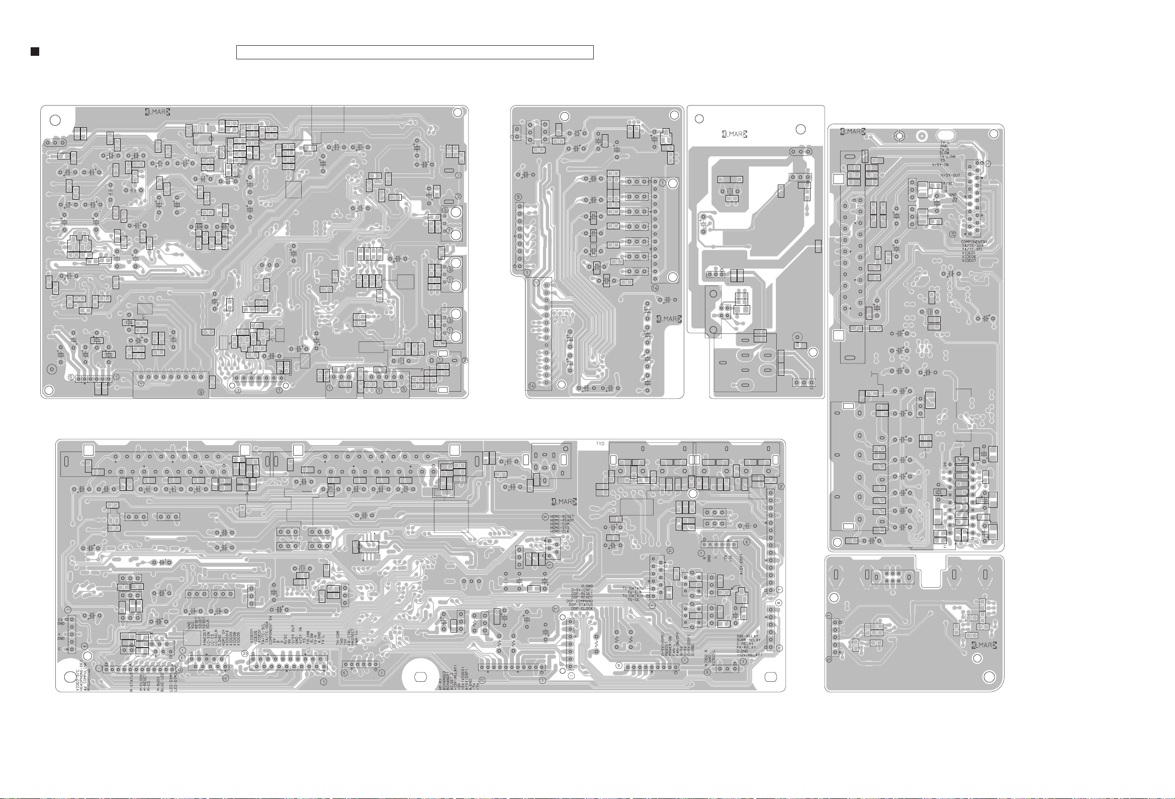
R1508
C554
R1583
CN513
R1523
CN521
R1509
Q519
R1513
R1510
C537
R1507
R1504
C538
C539
C534
C541
R1582
R1530
R1519
R1529
R1584
Q1501
R1503
C552
C550
C542
Q525
C1551
R1514
C555
C561
R1520
R1515
Q518
Q514
R1522
C557
C549
Q515
R1551
Q526
Q516
C540
C558
C551
C556
R1581
C562
Q517
C559
R1552
C1582
C553
C1581
CN523
Q513
C536
R1553
CN522
C2425
C2435
C2678
C2680
R2626
C2674
C2682
C2671
C2687
R2873
R2872
R2944
C2641
C2642
C2801
C2953
X661
R2945
R2946
C2281
C2901
C2871
C2282
C2911
C2902
C2903
X671
R2723
C2921
R2706
R2727
R2725
R2722
R2705
R2726
R2724
C2672
C2702
C2673
C2018
R2751
Q2701
C2703
R2122
R2121
R2135
R2134
R2136
C2209
C2229
C2230
R2017
R2018
C2421
C2422
C2677
R2932
C2101
C2102
R2110
R2133
R2128
C2542
C2541
C2429
C2242
C2241
C2249
C2250
R2411
C2549
UN682
UN683
J681
C2862
C2863
C2861
C2411
C2676
R2871
R2861
R2866
C2509
C2412
R2412
C2341
C2381
R2421
C2883
C2382
C2342
R2139
R2140
C2141
C2142
R2147
R2148
C2139
C2140
C2162
R2103
R2109
C2109
R2104
C2349
C2210
C2309
C2409
R2323
R2449
C2771
C2449
C2129
C2110
K2861
EP681
Q2702
C2601
CN681
TP13
R2123
TP15
TP17
TP19
TP18
TP16
TP14
TP12
C2954
C2951
C2701
R2601
R2602
R2603
R2604
C2149
C2150
R2940
R2941
R2942
R2625
R2623
TP27
TP29
TP4
C2923
C2831
C2686
C2675
C2832
R2001
C2161
R2002
R2933
C2001
C2002
R2022
R2024
R2819
R2876
R2607
R2608
R2606
R2605
C2811
C2812
C2820
C2813
K2803
K2804
R2814
R2816
R2612
C2882
C2881
R2863
R2862
TP1
TP2
TP3
TP6
UN686
C2866
R2427
Q2223
Q2224
R2227
R2228
C2884
R2874
R2864
R2865
R2875
C2885
TP5
PW601
CN683
C2547
C2548
C2550
C2510
CN662
R2629
R2947
CN661
EP682
R2183
R2184
R2781
R2782
R2783
R2784
R2785
R2786
R2787
R2788
R2789
R2790
R2791
R2792
C2781
C2782
C2783
C2784
C2785
C2786
C2787
C2788
IC615
CN682
R2950
C2868C2867
R2948
R2949
C2869
C960
C961
C942 C941
X905
R961
J903
L901
R974
C949
CN904
R973
C950
C962
C947
EP901
CN961
J901
CN905
C968
C969
C967
C970
PW911
C971
C972
J4503
R4541
R4542
R4543
C4580
C4581
C4582
R4544
R4545
R4546
C4583
C4584
C4585
C4577
C4578
C4579
R4547
R4548
R4549
C4586
C4587
C4588
Q4501
R4502
R4501
C4500
C9501
J9511
R9509
R9503
R9506
C9507
R9510
C9508
C9502
C9503
R9501
C9505
R9507
R9505
C9504
C9506
C9510
R9504
R9508
C9509
R9502
C9512
R9513
Q9501
R9511
Q9502
R9514
C4546
L4504
C4552
C4555
R4585
C4553
L4502
C4554
C4562
C4550
C4558
R4586
C4547
C4559
R4584
C4557
L4505
CN537
L4503
K4501
C4548
C4563
C4549
IC551
C4556
C4561
C4560
C4599
C4596
C4595
C5562
C5561
X5505
C5563
C5592
C5540
C5560
R9512
C4551
C9515
C9516
C6515
C8575
R6581
R1556
R6520
FL501
C597
CN504
J8513
R6517
J6504
R6521
R564
R6519
R1548
FL502
R1550
R568
X501
R6503
C6506
R563
Q542
C8574
C563
CN540
R1572
C527
R567
C528
R1557
C6517
C564
R569
R1549
Q521
R6505
R585
Q541
R6582
R6522
R593
R586
R570
IC506
R595
Q522
C1552
CN502
R6504
C524
C530
C6519
R594
CN555
Q501
R1571
CN571
CN551
R1543
C526
C6520
IC507
Q523
Q502
C6505
CN509
CN552
R1544
C6516
R6585
R1545
J6503
C525
R596
R6583
R6586
C6518
C581
C523
CN503
R6584
R6518
R6506
CN505
J8511
J8512
C8508
C8507
R8508
R8507
C8512
C8511
R8512
R8511
R8510
R8509
C8510
C8509
R8520
R8519
C8516
C8515
R588
C572
X502
C567
C568
C574
R8521
C8517
R8522R8523
C8518C8519
R8524
C8521
R8525
C8520
Q8522
R8526
C8522
R8527
C8523
R8528
C8524
R8529
C8525
R8530
C8527
R8531
C8526
Q8516
R8532
C8528
R8548
R8544
R8545
C8543
C8542
C8541
R8533
CN572
R590
Q8505
Q8506
Q8507
Q8508
C8535
C8534
C8539
C8537
C8540
C8544
C8546
C8547
Q8518
C8558
Q8517
C8556
Q8509
R8567 R8574
Q8510
R8575
R8576
Q8511
R8577
Q8519
D8503
R8584
C8566
R8583
R8572
R8573
R1502
R1501
R8518
R8517
Q8526
C577
C578
D8504
C8576
CN530
CN531
CN527
CN529
R8590
R8589
Q8530
FW501
C8590
C8587
C8588
C6589
C6590
C6591
C6592
C6593
C6595
C6596
R9021
R9008
R9013
R9003
R9004
R9002
SW11
CN11
EP11
EP12
R9014
R9015
R9016
R9017
R9018
Reverse side
(DSP board) (OSD connect 2 board) (OSD connect 1 board)
(Input board)
(Video board)
(Wireless USB board)
Input board (For B/E/EN version)
Lead free solder used in the board (material : Sn-Ag-Cu, melting point : 219 Centigrade)
2-22
Page 47

< MEMO >
Page 48

Victor Company of Japan, Limited
AV & MULTIMEDIA COMPANY AUDIO/VIDEO SYSTEMS CATEGORY 10-1,1chome,Ohwatari-machi,Maebashi-city,371-8543,Japan
(No.MB479SCH)
Printed in Japan
VPT
Page 49

PARTS LIST
[ RX-D301S ] [ RX-D302B ]
* All printed circuit boards and its assemblies are not available as service parts.
RX-D301S
Area suffix
A ------------------------- Australia
B ------------------------------- U.K.
E ----------- Continental Europe
EN ------------ Northern Europe
Area suffix
B ------------------------------- U.K.
E ----------- Continental Europe
EN ------------ Northern Europe
RX-D302B
- Contents -
Exploded view of general assembly and parts list (Block No.M1)
Electrical parts list (Block No.01~04)
Packing materials and accessories parts list (Block No.M3)
3- 2
3- 6
3-30
No.MB479
3-1
Page 50
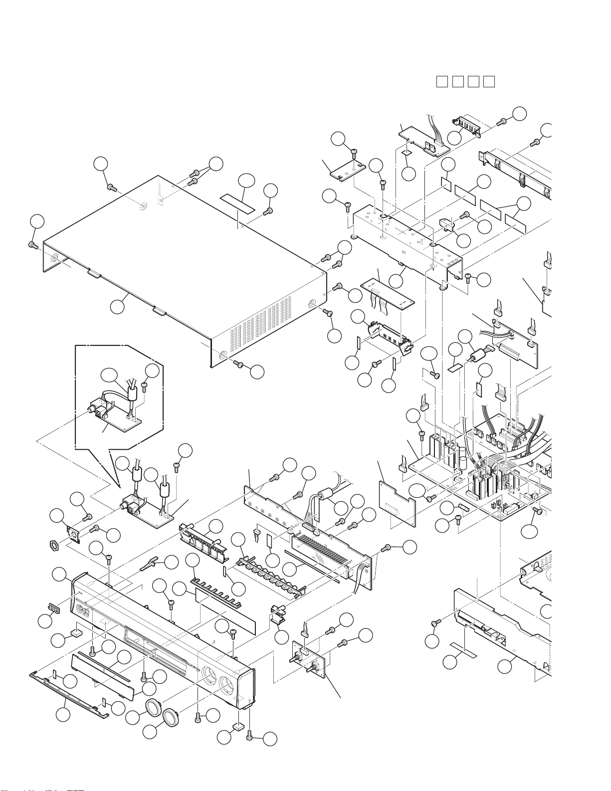
Exploded view of general assembly and parts list
O
0
2
94
C
56
55
1
94
91
Only A ver.
aa
118
z
OSD connect 2
board
65
56
25
bb
aa
92
103
Wire holder board
93
Master clock board
54
49
Block No.
49
M
m
41
37
42
D
M
1
M
43
4
36
36
32
31
49
PWM
moudulation 1
board
k
64
45
45
e
PWM
moudulation 2
board
e
ee
26
92
Regulator
board
35
92
ff
44
ee
B
94
106
59
94
46
59
aa
50
Main amplifier board
s
b
C
F
66
z
26
bb
OSD connect 2
board
FL board
15
15
DCDC control
board
x
f
15
71
15
9
11
z
4
4
25
F
10
12
14
13
ff
c
106
97
50
15
116
j
n
j
n
q
u
A
3-2
2
3
24
25
E
9
8
95
7
95
24
24
3
24
6
5
6
16
JOG board
16
27
23
21
2
Page 51

W
85
86
72
43
40
36
OSC connect 1
board
j
M
oudulation 2
ard
n
e
b
f
j
n
q
r
u
w
A
116
C
22
1
k
m
106
t
47
27
105
mm
39
18
a
Front video
g
board
69
Speaker
terminal 1
board
81
q
80
38
h
p
34
D
Volume board
17
61
qq
dd
57
89
Subwoofer
board
g
cc
p
t
61
kk
cc
bb
kk
51
dd
a
s
58
48
h
48
47
48
u
33
A
47
110
J
108
60
109
N
G
62
qq
112
29
22
jj
B
28
73
r
gg
76
63
Speaker
terminal 2 board
DSP
connect
board
nn
N
Input board
53
99
96
30
G
mm
90
19
x
53
gg
w
Primary board
75 75
87
K
Scart board
77
nn
v
H
Only A ver.
53
hh
d
78
88
83
78
100
Only A ver.
82
Compulink
board
J
Connect 2
board
Input board
d
Trans primary board
hh
82
77
82
M
111
v
79
82
H
115
114
K
OSD board
Connect 1
board
x
79
84
K
101
117
79
77
114
114
77
51
M
70
27
28
20
E
52
104
c
b
68
jj
Trans secondary board
67
3-3
Page 52

General Assembly
Block No. [M][1][M][M]
Symbol No. Part No. Part Name Description Local
1 LV11052-026A FRONT PANEL D301SA
1 LV11052-022A FRONT PANEL D301SB,D301SE,D301SEN
1 LV11052-023A FRONT PANEL D302BB,D302BE,D302BEN
2 LV43338-002A JVC MARK
3 LV43622-002A FOOT (x2)
4 LV35714-001A SOURCE INDICATO
5 LV21918-003A LIGHT LENS
6 LV30225-0P9A SPACER (x2)
7 LV36119-001A FRONT LENS D301SA,D301SB,D301SE,D301SEN
7 LV36119-002A FRONT LENS D302BB,D302BE,D302BEN
8 LV30225-0Z9A SPACER
9 LV21919-008A PUSH BUTTON
10 LV43381-004A FILTER D701
11 LV21920-001A LED HOLDER
12 LV30225-0L9A SPACER (x2)
13 LV30227-001A SPACER
14 LV30225-0F4A SPACER
15 QYSBSF2608ZA TAP SCREW M2.6 x 8mm(x8)
16 QYSBSF2608ZA TAP SCREW M2.6 x 8mm(x4)
17 QUQ412-0519CJ-E FFC WIRE 5pin 19cm
18 QUQ412-1117CJ-E FFC WIRE 11pin 17cm
19 QUQ412-2010CJ-E FFC WIRE 20pin 10cm
20 LV11051-002A CHASSIS BASE
21 LV11055-002A FRONT BRACKET
22 QYSBST3005EA TAP SCREW M3 x 5mm(x2)
23 LV30225-071A SPACER
24 QYSBSG3006ZA TAP SCREW M3 x 6mm(x4)
25 QYSBSG3006ZA TAP SCREW M3 x 6mm(x3)
26 QYSBSG3006ZA TAP SCREW M3 x 6mm
27 QYSBSG3006ZA TAP SCREW M3 x 6mm(x3)
28 LV43622-002A FOOT (x2)
29 LV34679-001A PWB BRACKET
30 QYSBST3005EA TAP SCREW M3 x 5mm
31 LV34682-001A C.B BRACKET
32 QYSBSG3006ZA TAP SCREW M3 x 6mm
33 LV30225-0F4A SPACER
34 LV30225-0D4A SPACER
35 LV21923-001A HEAT SINK
36 LV43915-003A COOLING RUBBER (x3)
37 LV43915-004A COOLING RUBBER
38 LV35721-001A FET BRACKET
39 QYSDSG3005EA TAP SCREW M3 x 5mm(x3)
40 QYSDSG3005EA TAP SCREW M3 x 5mm(x2)
41 LV30225-0D4A SPACER
42 LV35043-002A TRANSISTOR HOLD
43 QYSBSG3010ZA TAP SCREW M3 x 10mm(x2)
44 LV35735-001A TR BRACKET
45 LV30225-0F4A SPACER (x2)
46 QYSBSG3010ZA TAP SCREW M3 x 10mm(x2)
47 E68587-223SM CB BKT (x3)
48 QYSBST3005EA TAP SCREW M3 x 5mm(x3)
49 QYSBSGY3008EA TAP SCREW M3 x 8mm(x4)
50 QYSBSG3006ZA TAP SCREW M3 x 6mm(x2)
51 QYSBSG3006ZA TAP SCREW M3 x 6mm(x3)
52 QYSBSG3006ZA TAP SCREW M3 x 6mm
53 QYSBSG3006ZA TAP SCREW M3 x 6mm(x4)
54 QYSBSG3010ZA TAP SCREW M3 x 10mm
55 LV44156-001A H/P BRACKET
56 QYSBSF2608ZA TAP SCREW M2.6 x 8mm(x2)
57 LV35723-001A FAN BRACKET
58 QAR0312-001 FAN MOTOR
59 LV30225-0F4A SPACER (x2)
60 QYSBSG3020ZA TAP SCREW M3 x 20mm(x2)
61 QYSBST3005EA TAP SCREW M3 x 5mm(x2)
62 QYSBST3005EA TAP SCREW M3 x 5mm
63 QQR0491-001 FERRITE CORE TDK (GRAY)
64 QQR0491-001 FERRITE CORE TDK (GRAY)
65 QQR0491-001 FERRITE CORE TDK (GRAY)
66 QQR0491-001 FERRITE CORE TDK (GRAY)
67 QQR0491-001 FERRITE CORE TDK (GRAY)
D301SB,D301SE,D301SEN,
D302BB,D302BE,D302BEN
D301SB,D301SE,D301SEN,
D302BB,D302BE,D302BEN
D301SB,D301SE,D301SEN,
D302BB,D302BE,D302BEN
D301SB,D301SE,D301SEN,
D302BB,D302BE,D302BEN
D301SB,D301SE,D301SEN,
D302BB,D302BE,D302BEN
3-4
Page 53

Symbol No. Part No. Part Name Description Local
68 QQR0491-001 FERRITE CORE TDK (GRAY)
69 QQR0491-001 FERRITE CORE TDK (GRAY)
70 QQT0485-003 POWER TRANSF D301SA
70 QQT0485-002 POWER TRANSF
71 QQR0491-001 FERRITE CORE TDK (GRAY)
72 QQR0491-001 FERRITE CORE TDK (GRAY)
73 QQR0491-001 FERRITE CORE TDK (GRAY)
75 QYSDSTL4006EA TAP SCREW M4 x 6mm(x4)
76 LV21924-062A REAR PANEL D301SA
76 LV21924-071A REAR PANEL D301SB,D301SE,D301SEN
76 LV21924-073A REAR PANEL D302BB,D302BE,D302BEN
77 QYSBSGY3008EA TAP SCREW M3 x 8mm(x3)
78 QYSBSGY3008EA TAP SCREW M3 x 8mm(x4)
79 QYSBSGY3008EA TAP SCREW M3 x 8mm(x7)
80 LV30225-0X7A SPACER
81 QYSBST3006ZA TAP SCREW M3 x 6mm
82 QYSBSGY3008EA TAP SCREW M3 x 8mm(x5)
83 QYSBSGY3008EA TAP SCREW M3 x 8mm(x2)
84 QYSBSGY3008EA TAP SCREW M3 x 8mm(x6)
85 QMPG150-244-JC POWER CORD(EU) 2.44m BLACK D301SA
85 QMPN160-200-JD POWER CORD(EU) 2m BLACK D301SB,D302BB
85 QMPK210-205-JN POWER CORD(EU) 2.05m BLACK D301SE,D301SEN,D302BE,D302BEN
86 QZW0033-001 STRAIN RELIEF
87 QYSBSGY3008EA TAP SCREW M3 x 8mm
88 QYSBSGY3008EA TAP SCREW M3 x 8mm(x2)
89 QAL0705-001 LAN MODULE
90 QAM0732-001 COAXIAL CABLE
91 LV21925-001A TOP COVER D301SA,D301SB,D301SE,D301SEN
91 LV21925-002A TOP COVER D302BB,D302BE,D302BEN
92 QYSBSGY3008EA TAP SCREW M3 x 8mm(x5)
93 LV44339-001A SPECIAL SCREW
94 QYSDSG3008NA TAP SCREW M3 x 8mm(x4) D301SA,D301SB,D301SE,D301SEN
94 QYSDSG3008MA TAP SCREW M3 x 8mm(x4) D302BB,D302BE,D302BEN
95 LV44151-003A ROTARY KNOB ASS (x2) D301SA,D301SB,D301SE,D301SEN
95 LV44151-010A ROTARY KNOB ASS (x2) D302BB,D302BE,D302BEN
96 QMF51W2-2R5-J8 FUSE F103 2.5A AC250V
97 QMF51W2-2R0-J8 FUSE F101 F102 2A AC250V(x2)
99 QMF5AE2-R10-J1 FUSE F104 0.1A AC250V
100 LV44315-001A LABEL
101 LV44385-001A RECYCLE LABEL D301SB,D301SE,D301SEN
103 E409396-003 CAUTION LABEL
104 LV43550-004A LABEL
105 QAU0346-001 TUNER TU 1 D301SA
105 QAU0347-001 TUNER
106 QYSBSG3008EA TAP SCREW M3 x 8mm(x9)
108 LV35719-001A SUPPORT BRACKET D301SA
109 LV30225-0F4A SPACER D301SA
110 QYSBST3005EA TAP SCREW M3 x 5mm D301SA
111 QYSBSG3006ZA TAP SCREW M3 x 6mm D301SA
112 LV30227-028A SPACER D301SA
114 QYSBSGY3008EA TAP SCREW M3 x 8mm(x11) D301SA
115 QYSBSGY3008EA TAP SCREW M3 x 8mm D301SA
116 QYSBSG3008EA TAP SCREW M3 x 8mm D301SA
117 LV44385-001A LABEL D302BB,D302BE,D302BEN
118 QQR0491-001 FERRITE CORE TDK (GRAY) D301SA
D301SB,D301SE,D301SEN,
D302BB,D302BE,D302BEN
D301SB,D301SE,D301SEN,
D302BB,D302BE,D302BEN
D301SB,D301SE,D301SEN,
D302BB,D302BE,D302BEN
D301SB,D301SE,D301SEN,
D302BB,D302BE,D302BEN
D301SB,D301SE,D301SEN,
D302BB,D302BE,D302BEN
3-5
Page 54

Electrical parts list
Front board
Symbol No.
PW12 QUB111-15DMPP-E SIN CR C-B WIRE
PW13 QUB220-14DMHP-E SNAPIN-RINGWIRE
PW151 QUB111-13PPPP-E SIN TWIST WIRE
PW153 QUB116-15PPPP-E SIN TWIST WIRE
PW155 QUB111-15PPPP-E SIN TWIST WIRE
PW156 QUB112-15PPPP-E SIN TWIST WORE
PW902 QUB220-15DMHP-E SIN TWIST WIRE
PW904 QUB111-10DMPP-E SIN TWIST WIRE
PW911 QUB220-15DMHP-E SIN TWIST WIRE
IC111 NJM2125F-X IC
IC112 NJM2403M-X IC
IC113 SN74HC00ANS-X IC
IC115 SN74HC74ANS-X IC
IC121 KIA7805API IC
IC211 SN74HCU04ANS-X IC
IC212 SN74HC00ANS-X IC
IC213 SN74HC08NS-X IC
IC214 SN74HC74ANS-X IC
IC901 MN101C35DMF IC
IC902 GP1UM281XKVF IR DETECT UNIT
Q291 KTC3875/YG/-X SI TRANSISTOR
Q441 2SD2394/EF/ TRANSISTOR
Q444 KTA1046/Y/ TRANSISTOR
Q445 2SC2812N/6/-X TRANSISTOR
Q891 KTC3875/YG/-X SI TRANSISTOR
Q901 KRC107S-X DIGI TRANSISTOR
Q903 KRA114S-X TRANSISTOR
Q910 KRC107S-X DIGI TRANSISTOR
Q911 KRA114S-X TRANSISTOR
Q923 KRA107S-X DIGI TRANSISTOR
Q924 KRA107S-X DIGI TRANSISTOR
Q925 KRA107S-X DIGI TRANSISTOR
Q926 KRA107S-X DIGI TRANSISTOR
Q1001 KRC105S-X DIGI TRANSISTOR
Q1103 KTA1268/GL/-T TRANSISTOR
Q1151 KRC102S-X DIGI TRANSISTOR
Q1152 KRC102S-X DIGI TRANSISTOR
Q1171 KTC3875/YG/-X SI TRANSISTOR
Q1172 KRC102S-X DIGI TRANSISTOR
Q1173 KTA1504/YG/-X SI TRANSISTOR
Q1174 KTC3875/YG/-X SI TRANSISTOR
Q1291 KTC3875/YG/-X SI TRANSISTOR
Q1491 KTC3875/YG/-X SI TRANSISTOR
D241 1SS133-T2 SI DIODE
D242 1SS133-T2 SI DIODE
D295 1SS133-T2 SI DIODE
D341 UDZS2.7B-X Z DIODE
D391 1SS133-T2 SI DIODE
D441 MTZJ20C-T2 Z DIODE
D442 MTZJ24B-T2 Z DIODE
D444 MTZJ11C-T2 Z DIODE
D491 1SS133-T2 SI DIODE
D512 UDZS6.2B-X Z DIODE
D895 1SS133-T2 SI DIODE
D907 SLR-343VC-T LED
D908 SELU2E10C-P LED
D909 SELU2E10C-P LED
D910 MA111-X SI DIODE
D916 SLR-343VC-T LED
D917 SLR-343VC-T LED
D918 SLR-343VC-T LED
D919 SLR-343VC-T LED
D920 SLR-343VC-T LED
D921 SLR-343VC-T LED
D922 SLR-343VC-T LED
Part No. Part Name Description Local
Block No. [0][1]
D301SB,D301SE,
D301SEN,D302BB,
D302BE,D302BEN
D301SA
D301SB,D301SE,
D301SEN,D302BB,
D302BE,D302BEN
D301SA
D301SA
Symbol No.
D923 SLR-343VC-T LED
D1001 1SS133-T2 SI DIODE
D1151 1SS133-T2 SI DIODE
D1152 1SS133-T2 SI DIODE
D1153 1SS133-T2 SI DIODE
D1154 UDZS2.7B-X Z DIODE
D1155 1SS133-T2 SI DIODE
D1172 1SS133-T2 SI DIODE
D1173 1SS133-T2 SI DIODE
D1174 1SS133-T2 SI DIODE
C121 QCFB1HZ-104Y C CAPACITOR 0.1uF 50V Z
C121 QCFB1HZ-474Y C CAPACITOR 0.47uF 50V Z
C241 NCB31CK-104X C CAPACITOR 0.1uF 16V K
C242 NDC31HJ-471X C CAPACITOR 470pF 50V J
C243 NDC31HJ-471X C CAPACITOR 470pF 50V J
C244 NDC31HJ-471X C CAPACITOR 470pF 50V J
C245 NDC31HJ-471X C CAPACITOR 470pF 50V J
C246 NCB31CK-104X C CAPACITOR 0.1uF 16V K
C247 NDC31HJ-101X C CAPACITOR 100pF 50V J
C248 NDC31HJ-101X C CAPACITOR 100pF 50V J
C249 NCB31CK-104X C CAPACITOR 0.1uF 16V K
C295 QCBB1HK-221Y C CAPACITOR 220pF 50V K
C296 QCBB1HK-221Y C CAPACITOR 220pF 50V K
C296 QCBB1HK-471Y C CAPACITOR 470pF 50V K
C297 QDVB1EZ-223Y C CAPACITOR 0.022uF 25V Z
C297 QCBB1HK-471Y C CAPACITOR 470pF 50V K
C341 NCB31CK-104X C CAPACITOR 0.1uF 16V K
C395 QCBB1HK-221Y C CAPACITOR 220pF 50V K
C396 QCBB1HK-221Y C CAPACITOR 220pF 50V K
C396 QCBB1HK-471Y C CAPACITOR 470pF 50V K
C397 QDVB1EZ-223Y C CAPACITOR 0.022uF 25V Z
C397 QCBB1HK-471Y C CAPACITOR 470pF 50V K
C441 QETN1EM-107Z E CAPACITOR 100uF 25V M
C442 QETN1EM-107Z E CAPACITOR 100uF 25V M
C443 QETN1VM-107Z E CAPACITOR 100uF 35V M
C491 QCBB1HK-221Y C CAPACITOR 220pF 50V K
C492 QCBB1HK-221Y C CAPACITOR 220pF 50V K
C492 QCBB1HK-471Y C CAPACITOR 470pF 50V K
C493 QDVB1EZ-223Y C CAPACITOR 0.022uF 25V Z
C493 QCBB1HK-471Y C CAPACITOR 470pF 50V K
C895 QCBB1HK-221Y C CAPACITOR 220pF 50V K
C896 QCBB1HK-221Y C CAPACITOR 220pF 50V K
C896 QCBB1HK-471Y C CAPACITOR 470pF 50V K
C897 QDVB1EZ-223Y C CAPACITOR 0.022uF 25V Z
C897 QCBB1HK-471Y C CAPACITOR 470pF 50V K
C901 NCB31HK-103X C CAPACITOR 0.01uF 50V K
C902 NCB31HK-103X C CAPACITOR 0.01uF 50V K
C903 NCB31HK-103X C CAPACITOR 0.01uF 50V K
C904 NCB31HK-103X C CAPACITOR 0.01uF 50V K
C905 NCB31HK-103X C CAPACITOR 0.01uF 50V K
C906 QCZ0202-155Z C CAPACITOR 1.5uF 25V Z
C907 QEKC0JM-107Z E CAPACITOR 100uF 6.3V M
C908 QEKC0JM-107Z E CAPACITOR 100uF 6.3V M
C909 QEKC1HM-475Z E CAPACITOR 4.7uF 50V M
C910 QER61HM-475Z E CAPACITOR 4.7uF 50V M
C911 QEKC1HM-475Z E CAPACITOR 4.7uF 50V M
C912 NCF31CZ-104X C CAPACITOR 0.1uF 16V Z
C913 NCF31CZ-104X C CAPACITOR 0.1uF 16V Z
C914 NCF31CZ-104X C CAPACITOR 0.1uF 16V Z
Part No. Part Name Description Local
D301SA
D301SB,D301SE,
D301SEN,D302BB,
D302BE,D302BEN
D301SA
D301SB,D301SE,
D301SEN,D302BB,
D302BE,D302BEN
D301SA
D301SB,D301SE,
D301SEN,D302BB,
D302BE,D302BEN
D301SA
D301SB,D301SE,
D301SEN,D302BB,
D302BE,D302BEN
D301SA
D301SB,D301SE,
D301SEN,D302BB,
D302BE,D302BEN
D301SA
D301SB,D301SE,
D301SEN,D302BB,
D302BE,D302BEN
D301SA
D301SB,D301SE,
D301SEN,D302BB,
D302BE,D302BEN
D301SA
D301SB,D301SE,
D301SEN,D302BB,
D302BE,D302BEN
D301SA
D301SB,D301SE,
D301SEN,D302BB,
D302BE,D302BEN
3-6
Page 55

Symbol No.
Part No. Part Name Description Local
Symbol No.
Part No. Part Name Description Local
C915 NCF31CZ-104X C CAPACITOR 0.1uF 16V Z
C918 NCB31CK-104X C CAPACITOR 0.1uF 16V K
C921 NCB31HK-102X C CAPACITOR 1000pF 50V K
C925 NDC31HJ-331X C CAPACITOR 330pF 50V J
C926 NDC31HJ-331X C CAPACITOR 330pF 50V J
C927 NDC31HJ-331X C CAPACITOR 330pF 50V J
C928 NDC31HJ-331X C CAPACITOR 330pF 50V J
C929 NCB31HK-103X C CAPACITOR 0.01uF 50V K
C931 NCB31EK-104X C CAPACITOR 0.1uF 25V K
C932 NCB31EK-104X C CAPACITOR 0.1uF 25V K
C933 NCB31EK-104X C CAPACITOR 0.1uF 25V K
C934 NCB31EK-104X C CAPACITOR 0.1uF 25V K
C935 NCB31HK-103X C CAPACITOR 0.01uF 50V K
C936 NCB31HK-103X C CAPACITOR 0.01uF 50V K
C1001 QCZ9104-472 C CAPACITOR 4700pF
C1002 QFZ9075-224 MPP CAPACITOR
C1003 QCZ9079-102 C CAPACITOR
C1004 QCZ9079-102 C CAPACITOR
C1151 QETN1CM-476Z E CAPACITOR 47uF 16V M
C1152 NCB31CK-105X C CAPACITOR 1uF 16V K
C1153 NCB31CK-105X C CAPACITOR 1uF 16V K
C1154 NDC31HJ-101X C CAPACITOR 100pF 50V J
C1155 NCB31CK-105X C CAPACITOR 1uF 16V K
C1156 NDC31HJ-101X C CAPACITOR 100pF 50V J
C1157 NCB31CK-104X C CAPACITOR 0.1uF 16V K
C1158 NCB31CK-104X C CAPACITOR 0.1uF 16V K
C1159 NCB31HK-821X C CAPACITOR 820pF 50V K
C1172 NCB31HK-102X C CAPACITOR 1000pF 50V K
C1173 NCB31HK-103X C CAPACITOR 0.01uF 50V K
C1174 QETN1CM-107Z E CAPACITOR 100uF 16V M
C1181 NCB31HK-103X C CAPACITOR 0.01uF 50V K
C1182 QETN1CM-107Z E CAPACITOR 100uF 16V M
C1291 QCBB1HK-221Y C CAPACITOR 220pF 50V K
C1292 QCBB1HK-221Y C CAPACITOR 220pF 50V K
C1292 QCBB1HK-471Y C CAPACITOR 470pF 50V K
C1293 QDVB1EZ-223Y C CAPACITOR 0.022uF 25V Z
C1293 QCBB1HK-471Y C CAPACITOR 470pF 50V K
C1391 QCBB1HK-221Y C CAPACITOR 220pF 50V K
C1392 QCBB1HK-221Y C CAPACITOR 220pF 50V K
C1392 QCBB1HK-471Y C CAPACITOR 470pF 50V K
C1393 QDVB1EZ-223Y C CAPACITOR 0.022uF 25V Z
C1393 QCBB1HK-471Y C CAPACITOR 470pF 50V K
C1491 QCBB1HK-221Y C CAPACITOR 220pF 50V K
C1492 QCBB1HK-221Y C CAPACITOR 220pF 50V K
C1492 QCBB1HK-471Y C CAPACITOR 470pF 50V K
C1493 QDVB1EZ-223Y C CAPACITOR 0.022uF 25V Z
C1493 QCBB1HK-471Y C CAPACITOR 470pF 50V K
C1583 NCB31HK-222X C CAPACITOR 2200pF 50V K
C6577 NCB31HK-221X C CAPACITOR 220pF 50V K
C6578 QCZ0202-155Z C CAPACITOR 1.5uF 25V Z
R241 NRSA63J-105X MG RESISTOR 1MΩ 1/16W J
R242 NRSA63J-562X MG RESISTOR 5.6k
R243 NRSA63J-105X MG RESISTOR 1M
0.22uF
AC275V M
1000pF
AC250V M
1000pF
AC250V M
Ω
1/16W J
Ω
1/16W J
D301SB,D301SE,
D301SEN,D302BB,
D302BE,D302BEN
D301SB,D301SE,
D301SEN,D302BB,
D302BE,D302BEN
D301SB,D301SE,
D301SEN,D302BB,
D302BE,D302BEN
D301SB,D301SE,
D301SEN,D302BB,
D302BE,D302BEN
D301SB,D301SE,
D301SEN,D302BB,
D302BE,D302BEN
D301SB,D301SE,
D301SEN,D302BB,
D302BE,D302BEN
D301SA
D301SB,D301SE,
D301SEN,D302BB,
D302BE,D302BEN
D301SA
D301SB,D301SE,
D301SEN,D302BB,
D302BE,D302BEN
D301SA
D301SB,D301SE,
D301SEN,D302BB,
D302BE,D302BEN
D301SA
D301SB,D301SE,
D301SEN,D302BB,
D302BE,D302BEN
D301SA
D301SB,D301SE,
D301SEN,D302BB,
D302BE,D302BEN
D301SA
D301SB,D301SE,
D301SEN,D302BB,
D302BE,D302BEN
D301SA
D301SA
R244 NRSA63J-562X MG RESISTOR 5.6kΩ 1/16W J
R245 NRSA63J-101X MG RESISTOR 100Ω 1/16W J
R246 NRSA63J-222X MG RESISTOR 2.2kΩ 1/16W J
R247 NRSA63J-222X MG RESISTOR 2.2kΩ 1/16W J
R341 NRSA63J-102X MG RESISTOR 1kΩ 1/16W J
R342 NRSA63J-222X MG RESISTOR 2.2k
R441 QRK126J-4R7X UNF C RESISTOR 4.7Ω 1/2W J
R442 QRK126J-362X UNF C RESISTOR 3.6kΩ 1/2W J
R443 NRSA63J-681X MG RESISTOR 680Ω 1/16W J
R444 QRJ146J-182X UNF C RESISTOR 1.8kΩ 1/4W J
R895 QRJ146J-470X UNF C RESISTOR 47Ω 1/4W J
R901 NRSA63J-103X MG RESISTOR 10kΩ 1/16W J
R902 NRSA63J-102X MG RESISTOR 1kΩ 1/16W J
R903 NRSA63J-102X MG RESISTOR 1kΩ 1/16W J
R904 NRSA63J-103X MG RESISTOR 10kΩ 1/16W J
R905 NRSA63J-102X MG RESISTOR 1kΩ 1/16W J
R906 NRSA63J-102X MG RESISTOR 1kΩ 1/16W J
R907 NRSA63J-122X MG RESISTOR 1.2kΩ 1/16W J
R908 NRSA63J-103X MG RESISTOR 10kΩ 1/16W J
R909 NRSA63J-102X MG RESISTOR 1kΩ 1/16W J
R910 NRSA63J-102X MG RESISTOR 1k
R911 NRSA63J-103X MG RESISTOR 10k
R912 NRSA63J-102X MG RESISTOR 1kΩ 1/16W J
R913 NRSA63J-102X MG RESISTOR 1kΩ 1/16W J
R914 NRSA63J-122X MG RESISTOR 1.2kΩ 1/16W J
R915 NRSA63J-152X MG RESISTOR 1.5kΩ 1/16W J
R916 NRSA63J-222X MG RESISTOR 2.2kΩ 1/16W J
R919 NRSA63J-103X MG RESISTOR 10kΩ 1/16W J
R920 NRSA63J-102X MG RESISTOR 1kΩ 1/16W J
R921 NRSA63J-102X MG RESISTOR 1kΩ 1/16W J
R922 NRSA63J-122X MG RESISTOR 1.2kΩ 1/16W J
R923 NRSA63J-152X MG RESISTOR 1.5kΩ 1/16W J
R927 NRSA63J-241X MG RESISTOR 240Ω 1/16W J
R928 NRSA63J-241X MG RESISTOR 240Ω 1/16W J
R929 NRSA63J-331X MG RESISTOR 330Ω 1/16W J
R930 NRSA63J-221X MG RESISTOR 220Ω 1/16W J
R931 NRSA63J-103X MG RESISTOR 10kΩ 1/16W J
R932 NRSA63J-103X MG RESISTOR 10kΩ 1/16W J
R933 NRSA63J-103X MG RESISTOR 10kΩ 1/16W J
R935 NRSA63J-103X MG RESISTOR 10kΩ 1/16W J
R936 NRSA63J-221X MG RESISTOR 220Ω 1/16W J
R937 NRSA63J-221X MG RESISTOR 220Ω 1/16W J
R938 NRSA63J-221X MG RESISTOR 220Ω 1/16W J
R939 NRSA63J-221X MG RESISTOR 220Ω 1/16W J
R940 NRSA63J-221X MG RESISTOR 220Ω 1/16W J
R941 NRSA63J-221X MG RESISTOR 220Ω 1/16W J
R942 NRSA63J-221X MG RESISTOR 220Ω 1/16W J
R943 NRSA63J-221X MG RESISTOR 220Ω 1/16W J
R944 NRSA63J-221X MG RESISTOR 220Ω 1/16W J
R947 NRSA63J-103X MG RESISTOR 10k
R948 NRSA63J-103X MG RESISTOR 10kΩ 1/16W J
R949 NRSA63J-103X MG RESISTOR 10k
R950 NRSA63J-103X MG RESISTOR 10k
R953 NRSA63J-103X MG RESISTOR 10kΩ 1/16W J
R954 NRSA63J-103X MG RESISTOR 10k
R955 NRSA63J-103X MG RESISTOR 10k
R956 NRSA63J-103X MG RESISTOR 10kΩ 1/16W J
R957 NRSA63J-681X MG RESISTOR 680
R957 NRSA63J-331X MG RESISTOR 330Ω 1/16W J
R995 NRSA63J-0R0X MG RESISTOR 0Ω 1/16W J
R996 NRSA63J-0R0X MG RESISTOR 0
R997 NRSA63J-0R0X MG RESISTOR 0Ω 1/16W J
R1002 QRZ9037-335 COMP RESISTOR 3.3MΩ 1/2W K
R1114 NRSA63J-821X MG RESISTOR 820
R1151 NRSA63J-362X MG RESISTOR 3.6kΩ 1/16W J
R1152 NRSA63J-682X MG RESISTOR 6.8kΩ 1/16W J
R1153 NRSA63F-222X MG RESISTOR 2.2kΩ 1/16W F
R1154 NRSA63F-332X MG RESISTOR 3.3k
R1155 NRSA63J-223X MG RESISTOR 22k
R1156 NRSA63J-124X MG RESISTOR 120kΩ 1/16W J
R1157 NRSA63J-103X MG RESISTOR 10k
R1158 NRSA63J-821X MG RESISTOR 820
R1159 NRSA63J-103X MG RESISTOR 10kΩ 1/16W J
R1160 NRSA63J-102X MG RESISTOR 1k
R1161 NRSA63J-105X MG RESISTOR 1M
R1162 NRSA63J-102X MG RESISTOR 1kΩ 1/16W J
Ω
1/16W J
Ω
1/16W J
Ω
1/16W J
Ω
1/16W J
Ω
1/16W J
Ω
1/16W J
Ω
1/16W J
Ω
1/16W J
Ω
1/16W J
Ω
1/16W J
Ω
1/16W J
Ω
1/16W F
Ω
1/16W J
Ω
1/16W J
Ω
1/16W J
Ω
1/16W J
Ω
1/16W J
D301SA
D301SA
D301SA
D301SB,D301SE,
D301SEN,D302BB,
D302BE,D302BEN
3-7
Page 56

Symbol No.
Part No. Part Name Description Local
Symbol No.
Part No. Part Name Description Local
R1163 NRSA63J-331X MG RESISTOR 330Ω 1/16W J
R1164 NRSA63J-473X MG RESISTOR 47kΩ 1/16W J
R1165 NRSA63J-332X MG RESISTOR 3.3kΩ 1/16W J
R1166 NRSA63J-471X MG RESISTOR 470Ω 1/16W J
R1169 NRSA63J-332X MG RESISTOR 3.3kΩ 1/16W J
R1170 NRSA63J-102X MG RESISTOR 1k
R1172 NRSA02J-332X MG RESISTOR 3.3k
R1173 NRSA63J-103X MG RESISTOR 10kΩ 1/16W J
R1174 NRSA63J-123X MG RESISTOR 12kΩ 1/16W J
R1175 NRSA63J-222X MG RESISTOR 2.2kΩ 1/16W J
R1176 NRSA63J-473X MG RESISTOR 47kΩ 1/16W J
R1178 NRSA63J-101X MG RESISTOR 100Ω 1/16W J
R1179 NRSA63F-332X MG RESISTOR 3.3kΩ 1/16W F
R1180 NRSA63J-133X MG RESISTOR 13kΩ 1/16W J
R1181 QRE141J-473Y C RESISTOR 47kΩ 1/4W J
R1295 QRJ146J-470X UNF C RESISTOR 47Ω 1/4W J
R1391 QRJ146J-470X UNF C RESISTOR 47Ω 1/4W J
R1491 QRJ146J-470X UNF C RESISTOR 47Ω 1/4W J
R6595 NRSA63J-221X MG RESISTOR 220Ω 1/16W J
T102 QQT0281-006 POWER TRANSF
T102 QQT0478-002 POWER TRANSF
BK901 LV34673-001A FL HOLDER(L)
BK902 LV34687-001A FL HOLDER(R)
CN120 QGA7901C1-02 CONNECTOR W-B (1-2)
CN151 QGB2510K1-12 CONNECTOR B-B (1-12)
CN202 QJK002-071802-E SIN CR C-B WIRE
CN206 WJK0208-002A-E E-SI C WIRE C-B
CN209 QGA2501C1-06 CONNECTOR W-B (1-6)
CN211 QJK012-033803-E SIN CR C-B WIRE
CN262 QGA3901C1-08 CONNECTOR W-B (1-8)
CN265 QGA3901C1-06 CONNECTOR W-B (1-6)
CN465 QGA2001C1-03 CONNECTOR W-B (1-3)
CN524 QGA2501C1-02 CONNECTOR W-B (1-2)
CN565 QGA2501C1-02 CONNECTOR W-B (1-2)
CN591 QGB2510K1-09 CONNECTOR B-B (1-9)
CN592 QGB2510K1-09 CONNECTOR B-B (1-9)
CN593 QGB2510K1-11 CONNECTOR B-B (1-11)
CN594 QGB2510K1-11 CONNECTOR B-B (1-11)
CN902 QGF1205F1-05 CONNECTOR FFC/FPC (1-5)
CN903 QJK021-070802-E SIN CR C-B
CN913 QGA2001F1-07 CONNECTOR W-B (1-7)
CN914 QGA2001F1-03 CONNECTOR W-B (1-3)
CN952 QJK021-124402-E SIN CR C-B WIRE
DI901 QLF0157-001 FL TUBE
EP151 QNZ0136-001Z EARTH PLATE
FC103 QNG0020-001Z FUSE CLIP
FC104 QNG0020-001Z FUSE CLIP
FC113 QNG0020-001Z FUSE CLIP
FC114 QNG0020-001Z FUSE CLIP
FS181 VYSH101-009 SPACER
FS900 VYSH101-009 SPACER
FS901 VYSH101-009 SPACER
FW121 WJS0047-002A-E E-FL/RB WIRE
FW451 WJS0046-003A-E E-FL/RB WIRE
J504 QNN0480-001 PIN JACK
J505 QNS0089-001 3.5 JACK
JS901 QSW1129-001
JS902 QSW1129-001
RY101 QSK0142-001 RELAY
RY101 QSK0128-001 RELAY
RY295 QSK0127-001 RELAY
RY391 QSK0127-001 RELAY
RY491 QSK0127-001 RELAY
RY895 QSK0127-001 RELAY
S901 QSW0683-001Z PUSH SW
S902 QSW0683-001Z PUSH SW
S903 QSW0683-001Z PUSH SW
S904 QSW0683-001Z PUSH SW
S905 QSW0683-001Z PUSH SW
S906 QSW0683-001Z PUSH SW
ST292 QNB0256-001 IC
ROTARY
ENCODER
ROTARY
ENCODER
Ω
1/16W J
Ω
1/10W J
D301SA
D301SA
D301SB,D301SE,
D301SEN,D302BB,
D302BE,D302BEN
D301SA
D301SA
D301SA
D301SA
D301SA
D301SA
D301SA
D301SB,D301SE,
D301SEN,D302BB,
D302BE,D302BEN
ST295 QNB0079-001 SPK TERMINAL
X241 QAX0734-001 C RESONATOR 400.00kHz
X242 QAX0735-001 C RESONATOR 420.00kHz
X901 QAX0246-001Z C RESONATOR 8.00MHz
Amplifier board
Symbol No.
IC101 IRS2011S-X IC
IC151 KIA7805API IC
IC152 KIA7809API IC
IC153 KIA7805API IC
IC201 JCV8015-X IC
IC202 SN74LVC3G04T-X IC
IC251 IRS20124S-X IC
IC261 IRS20124S-X IC
IC301 JCV8015-X IC
IC302 SN74LVC3G04T-X IC
IC351 IRS20124S-X IC
IC361 IRS20124S-X IC
IC401 JCV8015-X IC
IC451 IRS20124S-X IC
IC461 IRS20124S-X IC
IC801 JCV8015-X IC
IC851 IRS20124S-X IC
Q101 KTD863/Y/-T TRANSISTOR
Q102 KTA1046/Y/ TRANSISTOR
Q103 KTC3200/GL/-T TRANSISTOR
Q151 KRA102S-X DIGI TRANSISTOR
Q152 KRC102S-X DIGI TRANSISTOR
Q153 2SD2394/EF/ TRANSISTOR
Q154 KRC102S-X DIGI TRANSISTOR
Q157 2SD2394/EF/ TRANSISTOR
Q158 KTA1046/Y/ TRANSISTOR
Q161 KRC111S-X TRANSISTOR
Q162 KRC111S-X TRANSISTOR
Q163 KRC111S-X TRANSISTOR
Q171 2SD2394/EF/ TRANSISTOR
Q173 2SD2394/EF/ TRANSISTOR
Q174 2SD2394/EF/ TRANSISTOR
Q175 2SD2394/EF/ TRANSISTOR
Q201 KTA1268/GL/-T TRANSISTOR
Q211 KTC3875/YG/-X SI TRANSISTOR
Q214 KRC102M-T DIGI TRANSISTOR
Q251 KTA1504/YG/-X SI TRANSISTOR
Q261 IRFB4212 FET
Q262 IRFB4212 FET
Q281 KRC109M-T DIGI TRANSISTOR
Q282 KRA102M-T DIGI TRANSISTOR
Q283 KTC3200/GL/-T TRANSISTOR
Q284 KTA1268/GL/-T TRANSISTOR
Q285 KTC3199/GL/-T TRANSISTOR
Q286 KRC102M-T DIGI TRANSISTOR
Q301 KTA1268/GL/-T TRANSISTOR
Q351 KTA1504/YG/-X SI TRANSISTOR
Q361 IRFB4212 FET
Q362 IRFB4212 FET
Q401 KTA1268/GL/-T TRANSISTOR
Q451 KTA1504/YG/-X SI TRANSISTOR
Q461 IRFB4212 FET
Q462 IRFB4212 FET
Q801 KTA1268/GL/-T TRANSISTOR
Q851 KTA1504/YG/-X SI TRANSISTOR
Q861 IRFB4212 FET
Q862 IRFB4212 FET
Q1101 2SK3599-01MR POWER MOS FET
Q1102 2SK3599-01MR POWER MOS FET
Q1104 KTA1268/GL/-T TRANSISTOR
Q1201 KTA1268/GL/-T TRANSISTOR
Q1251 KTA1504/YG/-X SI TRANSISTOR
Q1261 IRFB4212 FET
Part No. Part Name Description Local
Block No. [0][2]
D301SA
3-8
Page 57

Symbol No.
Part No. Part Name Description Local
Symbol No.
Part No. Part Name Description Local
Q1262 IRFB4212 FET
Q1301 KTA1268/GL/-T TRANSISTOR
Q1351 KTA1504/YG/-X SI TRANSISTOR
Q1361 IRFB4212 FET
Q1362 IRFB4212 FET
Q1401 KTA1268/GL/-T TRANSISTOR
Q1451 KTA1504/YG/-X SI TRANSISTOR
Q1461 IRFB4212 FET
Q1462 IRFB4212 FET
D101 1A3G-T1 SI DIODE
D102 1A3G-T1 SI DIODE
D103 1A3G-T1 SI DIODE
D104 1A3G-T1 SI DIODE
D105 MTZJ12C-T2 Z DIODE
D106 MTZJ6.2B-T2 Z DIODE
D107 1A3G-T1 SI DIODE
D108 1A3G-T1 SI DIODE
D109 10DDA20-FD DIODE
D110 10DDA20-FD DIODE
D111 10DDA20-FD DIODE
D112 10DDA20-FD DIODE
D113 1A3G-T1 SI DIODE
D114 1A3G-T1 SI DIODE
D115 1A3G-T1 SI DIODE
D116 MTZJ36C-T2 Z DIODE
D117 MTZJ8.2C-T2 Z DIODE
D152 1SS133-T2 SI DIODE
D153 MTZJ13B-T2 Z DIODE
D153 MTZJ15A-T2 Z DIODE
D154 MTZJ9.1C-T2 Z DIODE
D156 MTZJ8.2C-T2 Z DIODE
D157 MTZJ8.2C-T2 Z DIODE
D158 MTZJ6.2C-T2 Z DIODE
D161 1A3G-T1 SI DIODE
D162 1A3G-T1 SI DIODE
D171 MTZJ13B-T2 Z DIODE
D172 MTZJ13B-T2 Z DIODE
D211 1SS133-T2 SI DIODE
D221 1SS133-T2 SI DIODE
D222 MTZJ16B-T2 Z DIODE
D251 1SS133-T2 SI DIODE
D281 1SS133-T2 SI DIODE
D300 MA111-X SI DIODE
D311 1SS133-T2 SI DIODE
D351 1SS133-T2 SI DIODE
D411 1SS133-T2 SI DIODE
D451 1SS133-T2 SI DIODE
D811 1SS133-T2 SI DIODE
D851 1SS133-T2 SI DIODE
D1101 30PRA20-FC SI DIODE
D1102 30PRA20-FC SI DIODE
D1103 30PRA20-FC SI DIODE
D1104 30PRA20-FC SI DIODE
D1107 FMB-G19L SB DIODE
D1108 FMB-G19L SB DIODE
D1109 1SS133-T2 SI DIODE
D1110 1SS133-T2 SI DIODE
D1111 1SS133-T2 SI DIODE
D1171 1SS133-T2 SI DIODE
D1211 1SS133-T2 SI DIODE
D1251 1SS133-T2 SI DIODE
D1311 1SS133-T2 SI DIODE
D1351 1SS133-T2 SI DIODE
D1411 1SS133-T2 SI DIODE
D1451 1SS133-T2 SI DIODE
C101 QFLC2AJ-472Z M CAPACITOR 4700pF 100V J
C102 QETM1JM-227 E CAPACITOR 220uF 63V M
C102 QETM1EM-108 E CAPACITOR 1000uF 25V M
C103 NCB31HK-472X C CAPACITOR 4700pF 50V K
C104 QETN1CM-477Z E CAPACITOR 470uF 16V M
C105 NCZ1061-104X C CAPACITOR 0.1uF
C106 NCZ1061-104X C CAPACITOR 0.1uF
C107 NCZ1061-104X C CAPACITOR 0.1uF
D301SA
D301SA
D301SB,D301SE,
D301SEN,D302BB,
D302BE,D302BEN
D301SA
D301SB,D301SE,
D301SEN,D302BB,
D302BE,D302BEN
C108 QFLC1HJ-473Z M CAPACITOR 0.047uF 50V J
C109 QFLC1HJ-473Z M CAPACITOR 0.047uF 50V J
C110 QETN1HM-227Z E CAPACITOR 220uF 50V M
C111 QETN1JM-107Z E CAPACITOR 100uF 63V M
C112 QETN1HM-226Z E CAPACITOR 22uF 50V M
C113 QETN1HM-226Z E CAPACITOR 22uF 50V M
C114 QETN1HM-105Z E CAPACITOR 1uF 50V M
C151 QETM1EM-478 E CAPACITOR 4700uF 25V M
C152 QETM1EM-338 E CAPACITOR 3300uF 25V M
C153 NCB31HK-103X C CAPACITOR 0.01uF 50V K
C154 QETN1CM-107Z E CAPACITOR 100uF 16V M
C155 NCB31HK-103X C CAPACITOR 0.01uF 50V K
C156 QETN1EM-107Z E CAPACITOR 100uF 25V M
C157 QETN1HM-106Z E CAPACITOR 10uF 50V M
C158 NCB31HK-103X C CAPACITOR 0.01uF 50V K
C159 QETN1CM-107Z E CAPACITOR 100uF 16V M
C160 QETN1CM-107Z E CAPACITOR 100uF 16V M
C161 QETN1CM-477Z E CAPACITOR 470uF 16V M
C162 QETN1CM-107Z E CAPACITOR 100uF 16V M
C163 QETN1CM-477Z E CAPACITOR 470uF 16V M
C164 NCB31HK-222X C CAPACITOR 2200pF 50V K
C165 QETN1CM-107Z E CAPACITOR 100uF 16V M
C166 QETN1CM-477Z E CAPACITOR 470uF 16V M
C172 NCB31HK-472X C CAPACITOR 4700pF 50V K
C173 QETN1HM-105Z E CAPACITOR 1uF 50V M
C174 QETN1HM-106Z E CAPACITOR 10uF 50V M
C175 QETN1HM-105Z E CAPACITOR 1uF 50V M
C176 QETN1HM-106Z E CAPACITOR 10uF 50V M
C201 QEKC1HM-106Z E CAPACITOR 10uF 50V M
C202 NCB31HK-471X C CAPACITOR 470pF 50V K
C203 QEKC1HM-106Z E CAPACITOR 10uF 50V M
C204 NCB31HK-222X C CAPACITOR 2200pF 50V K
C205 NCB31HK-222X C CAPACITOR 2200pF 50V K
C207 NCB31HK-222X C CAPACITOR 2200pF 50V K
C208 NCB31AK-105X C CAPACITOR 1uF 10V K
C209 NDC31HG-101X C CAPACITOR 100pF 50V G
C210 NCB31CK-105X C CAPACITOR 1uF 16V K
C211 NDC31HJ-101X C CAPACITOR 100pF 50V J
C212 NCB31HK-471X C CAPACITOR 470pF 50V K
C213 NDC31HJ-101X C CAPACITOR 100pF 50V J
C222 NCB31CK-105X C CAPACITOR 1uF 16V K
C223 QEKC1CM-107Z E CAPACITOR 100uF 16V M
C224 QEKC1CM-107Z E CAPACITOR 100uF 16V M
C225 NCB31CK-104X C CAPACITOR 0.1uF 16V K
C226 NCB31CK-104X C CAPACITOR 0.1uF 16V K
C227 QEKC1CM-107Z E CAPACITOR 100uF 16V M
C231 QEKC1CM-107Z E CAPACITOR 100uF 16V M
C232 NDC31HJ-330X C CAPACITOR 33pF 50V J
C251 NCB31HK-102X C CAPACITOR 1000pF 50V K
C252 NCB31CK-105X C CAPACITOR 1uF 16V K
C253 NCB21EK-334X C CAPACITOR 0.33uF 25V K
C254 NDC31HJ-101X C CAPACITOR 100pF 50V J
C263 NCZ1061-104X C CAPACITOR 0.1uF
C264 NCB31HK-102X C CAPACITOR 1000pF 50V K
C265 NCB31HK-102X C CAPACITOR 1000pF 50V K
C266 NCB31HK-102X C CAPACITOR 1000pF 50V K
C267 NCB31HK-102X C CAPACITOR 1000pF 50V K
C268 QFKC2AJ-155Z MM CAPACITOR 1.5uF 100V J
C269 QFVM2AJ-104Z MF CAPACITOR 0.1uF 100V J
C270 NCB31HK-102X C CAPACITOR 1000pF 50V K
C271 NCZ1061-104X C CAPACITOR 0.1uF
C272 NCZ1061-104X C CAPACITOR 0.1uF
C273 QETN1HM-227Z E CAPACITOR 220uF 50V M
C274 QETN1HM-227Z E CAPACITOR 220uF 50V M
C275 QETN2AM-106Z E CAPACITOR 10uF 100V M
C276 QETN1EM-476Z E CAPACITOR 47uF 25V M
C277 NCB31HK-102X C CAPACITOR 1000pF 50V K
C281 NCB31CK-103X C CAPACITOR 0.01uF 16V K
C282 QETN1CM-476Z E CAPACITOR 47uF 16V M
C283 QETN1HM-106Z E CAPACITOR 10uF 50V M
C284 NCF31CZ-474X C CAPACITOR 0.47uF 16V Z
C285 QETN1CM-106Z E CAPACITOR 10uF 16V M
C301 QEKC1HM-106Z E CAPACITOR 10uF 50V M
C302 NCB31HK-471X C CAPACITOR 470pF 50V K
C303 QEKC1HM-106Z E CAPACITOR 10uF 50V M
C304 NCB31HK-222X C CAPACITOR 2200pF 50V K
D301SA
D301SB,D301SE,
D301SEN,D302BB,
D302BE,D302BEN
3-9
Page 58

Symbol No.
Part No. Part Name Description Local
Symbol No.
Part No. Part Name Description Local
C305 NCB31HK-222X C CAPACITOR 2200pF 50V K
C307 NCB31HK-222X C CAPACITOR 2200pF 50V K
C308 NCB31AK-105X C CAPACITOR 1uF 10V K
C309 NDC31HG-101X C CAPACITOR 100pF 50V G
C310 NCB31CK-105X C CAPACITOR 1uF 16V K
C311 NDC31HJ-101X C CAPACITOR 100pF 50V J
C312 NCB31HK-471X C CAPACITOR 470pF 50V K
C313 NDC31HJ-101X C CAPACITOR 100pF 50V J
C322 NCB31CK-105X C CAPACITOR 1uF 16V K
C323 NCB31CK-105X C CAPACITOR 1uF 16V K
C324 NCB31CK-104X C CAPACITOR 0.1uF 16V K
C331 QEKC1CM-107Z E CAPACITOR 100uF 16V M
C332 NDC31HJ-330X C CAPACITOR 33pF 50V J
C351 NCB31HK-102X C CAPACITOR 1000pF 50V K
C352 NCB31CK-105X C CAPACITOR 1uF 16V K
C353 NCB21EK-334X C CAPACITOR 0.33uF 25V K
C354 NDC31HJ-101X C CAPACITOR 100pF 50V J
C363 NCZ1061-104X C CAPACITOR 0.1uF
C364 NCB31HK-102X C CAPACITOR 1000pF 50V K
C365 NCB31HK-102X C CAPACITOR 1000pF 50V K
C366 NCB31HK-102X C CAPACITOR 1000pF 50V K
C367 NCB31HK-102X C CAPACITOR 1000pF 50V K
C368 QFKC2AJ-155Z MM CAPACITOR 1.5uF 100V J
C369 QFVM2AJ-104Z MF CAPACITOR 0.1uF 100V J
C370 NCB31HK-102X C CAPACITOR 1000pF 50V K
C371 NCZ1061-104X C CAPACITOR 0.1uF
C372 NCZ1061-104X C CAPACITOR 0.1uF
C373 QETN1HM-227Z E CAPACITOR 220uF 50V M
C374 QETN1HM-227Z E CAPACITOR 220uF 50V M
C375 QETN2AM-106Z E CAPACITOR 10uF 100V M
C377 NCB31HK-102X C CAPACITOR 1000pF 50V K
C401 QEKC1HM-106Z E CAPACITOR 10uF 50V M
C402 NCB31HK-471X C CAPACITOR 470pF 50V K
C403 QEKC1HM-106Z E CAPACITOR 10uF 50V M
C404 NCB31HK-222X C CAPACITOR 2200pF 50V K
C405 NCB31HK-222X C CAPACITOR 2200pF 50V K
C407 NCB31HK-222X C CAPACITOR 2200pF 50V K
C408 NCB31AK-105X C CAPACITOR 1uF 10V K
C409 NDC31HG-101X C CAPACITOR 100pF 50V G
C410 NCB31CK-105X C CAPACITOR 1uF 16V K
C411 NDC31HJ-101X C CAPACITOR 100pF 50V J
C413 NDC31HJ-101X C CAPACITOR 100pF 50V J
C422 NCB31CK-105X C CAPACITOR 1uF 16V K
C423 QEKC1CM-107Z E CAPACITOR 100uF 16V M
C424 QEKC1CM-107Z E CAPACITOR 100uF 16V M
C425 NCB31CK-104X C CAPACITOR 0.1uF 16V K
C426 NCB31CK-104X C CAPACITOR 0.1uF 16V K
C431 QEKC1CM-107Z E CAPACITOR 100uF 16V M
C432 NDC31HJ-330X C CAPACITOR 33pF 50V J
C451 NCB31HK-102X C CAPACITOR 1000pF 50V K
C452 NCB31CK-105X C CAPACITOR 1uF 16V K
C453 NCB21EK-334X C CAPACITOR 0.33uF 25V K
C454 NDC31HJ-101X C CAPACITOR 100pF 50V J
C463 NCZ1061-104X C CAPACITOR 0.1uF
C464 NCB31HK-102X C CAPACITOR 1000pF 50V K
C465 NCB31HK-102X C CAPACITOR 1000pF 50V K
C466 NCB31HK-102X C CAPACITOR 1000pF 50V K
C467 NCB31HK-102X C CAPACITOR 1000pF 50V K
C468 QFKC2AJ-155Z MM CAPACITOR 1.5uF 100V J
C469 QFVM2AJ-104Z MF CAPACITOR 0.1uF 100V J
C470 NCB31HK-102X C CAPACITOR 1000pF 50V K
C471 NCZ1061-104X C CAPACITOR 0.1uF
C472 NCZ1061-104X C CAPACITOR 0.1uF
C473 QETN1HM-227Z E CAPACITOR 220uF 50V M
C474 QETN1HM-227Z E CAPACITOR 220uF 50V M
C475 QETN2AM-106Z E CAPACITOR 10uF 100V M
C476 QETN1EM-476Z E CAPACITOR 47uF 25V M
C477 NCB31HK-102X C CAPACITOR 1000pF 50V K
C801 QEKC1HM-106Z E CAPACITOR 10uF 50V M
C802 NCB31HK-471X C CAPACITOR 470pF 50V K
C803 QEKC1HM-106Z E CAPACITOR 10uF 50V M
C804 NCB31HK-222X C CAPACITOR 2200pF 50V K
C805 NCB31HK-222X C CAPACITOR 2200pF 50V K
C807 NCB31HK-222X C CAPACITOR 2200pF 50V K
C808 NCB31AK-105X C CAPACITOR 1uF 10V K
D301SB,D301SE,
D301SEN,D302BB,
D302BE,D302BEN
D301SB,D301SE,
D301SEN,D302BB,
D302BE,D302BEN
C809 NDC31HG-101X C CAPACITOR 100pF 50V G
C810 NCB31CK-105X C CAPACITOR 1uF 16V K
C811 NDC31HJ-101X C CAPACITOR 100pF 50V J
C812 NCB31HK-471X C CAPACITOR 470pF 50V K
C813 NDC31HJ-101X C CAPACITOR 100pF 50V J
C821 QEKC1CM-107Z E CAPACITOR 100uF 16V M
C822 NCB31CK-105X C CAPACITOR 1uF 16V K
C823 QEKC1CM-107Z E CAPACITOR 100uF 16V M
C824 QEKC1CM-107Z E CAPACITOR 100uF 16V M
C825 NCB31CK-104X C CAPACITOR 0.1uF 16V K
C826 NCB31CK-104X C CAPACITOR 0.1uF 16V K
C827 NCB31CK-105X C CAPACITOR 1uF 16V K
C829 QEKC1CM-107Z E CAPACITOR 100uF 16V M
C830 NCB31CK-105X C CAPACITOR 1uF 16V K
C831 QEKC1CM-107Z E CAPACITOR 100uF 16V M
C832 NDC31HJ-330X C CAPACITOR 33pF 50V J
C851 NCB31HK-102X C CAPACITOR 1000pF 50V K
C852 NCB31CK-105X C CAPACITOR 1uF 16V K
C853 NCB21EK-334X C CAPACITOR 0.33uF 25V K
C854 NDC31HJ-101X C CAPACITOR 100pF 50V J
C863 NCZ1061-104X C CAPACITOR 0.1uF
C864 NCB31HK-102X C CAPACITOR 1000pF 50V K
C865 NCB31HK-102X C CAPACITOR 1000pF 50V K
C866 NCB31HK-102X C CAPACITOR 1000pF 50V K
C867 NCB31HK-102X C CAPACITOR 1000pF 50V K
C868 QFKC2AJ-155Z MM CAPACITOR 1.5uF 100V J
C869 QFVM2AJ-104Z MF CAPACITOR 0.1uF 100V J
C870 NCB31HK-102X C CAPACITOR 1000pF 50V K
C871 NCZ1061-104X C CAPACITOR 0.1uF
C872 NCZ1061-104X C CAPACITOR 0.1uF
C873 QETN1HM-227Z E CAPACITOR 220uF 50V M
C874 QETN1HM-227Z E CAPACITOR 220uF 50V M
C875 QETN2AM-106Z E CAPACITOR 10uF 100V M
C876 QETN1EM-476Z E CAPACITOR 47uF 25V M
C877 NCB31HK-102X C CAPACITOR 1000pF 50V K
C1101 QFKC2AJ-224Z MM CAPACITOR 0.22uF 100V J
C1102 QFKC2AJ-224Z MM CAPACITOR 0.22uF 100V J
C1103 QFKC2AJ-224Z MM CAPACITOR 0.22uF 100V J
C1104 QFKC2AJ-224Z MM CAPACITOR 0.22uF 100V J
C1105 QEZ0742-688 E CAPACITOR 6800uF
C1106 QEZ0742-688 E CAPACITOR 6800uF
C1107 NCB31HK-332X C CAPACITOR 3300pF 50V K
C1108 NCB31HK-332X C CAPACITOR 3300pF 50V K
C1109 NCB31HK-332X C CAPACITOR 3300pF 50V K
C1110 NCB31HK-332X C CAPACITOR 3300pF 50V K
C1111 NCB31HK-332X C CAPACITOR 3300pF 50V K
C1112 NCB31HK-332X C CAPACITOR 3300pF 50V K
C1113 NCB31HK-332X C CAPACITOR 3300pF 50V K
C1114 NCB31HK-332X C CAPACITOR 3300pF 50V K
C1115 NCZ1061-104X C CAPACITOR 0.1uF
C1116 NCZ1061-104X C CAPACITOR 0.1uF
C1117 QEZ0570-228 E CAPACITOR 2200uF
C1118 QEZ0570-228 E CAPACITOR 2200uF
C1119 NCZ1061-104X C CAPACITOR 0.1uF
C1120 NCZ1061-104X C CAPACITOR 0.1uF
C1122 NCB21EK-334X C CAPACITOR 0.33uF 25V K
C1123 NCB31CK-105X C CAPACITOR 1uF 16V K
C1124 NCZ1008-104X C CAPACITOR 0.1uF 250V K
C1125 NCZ1008-104X C CAPACITOR 0.1uF 250V K
C1131 NCZ1069-224X C CAPACITOR 0.22uF
C1132 NCZ1069-224X C CAPACITOR 0.22uF
C1133 NCZ1069-224X C CAPACITOR 0.22uF
C1134 NCZ1069-224X C CAPACITOR 0.22uF
C1135 NCZ1008-104X C CAPACITOR 0.1uF 250V K
C1136 NCZ1008-104X C CAPACITOR 0.1uF 250V K
C1137 NCZ1008-104X C CAPACITOR 0.1uF 250V K
C1138 NCZ1008-104X C CAPACITOR 0.1uF 250V K
C1139 NCZ1069-224X C CAPACITOR 0.22uF
C1140 NCZ1069-224X C CAPACITOR 0.22uF
C1141 NCZ1069-224X C CAPACITOR 0.22uF
C1142 NCZ1069-224X C CAPACITOR 0.22uF
C1143 NCZ1069-224X C CAPACITOR 0.22uF
C1144 NCZ1069-224X C CAPACITOR 0.22uF
D301SB,D301SE,
D301SEN,D302BB,
D302BE,D302BEN
D301SB,D301SE,
D301SEN,D302BB,
D302BE,D302BEN
D301SB,D301SE,
D301SEN,D302BB,
D302BE,D302BEN
3-10
Page 59

Symbol No.
Part No. Part Name Description Local
Symbol No.
Part No. Part Name Description Local
C1145 NCZ1069-224X C CAPACITOR 0.22uF
C1146 NCZ1008-104X C CAPACITOR 0.1uF 250V K
C1147 NCZ1008-104X C CAPACITOR 0.1uF 250V K
C1149 NCZ1008-104X C CAPACITOR 0.1uF 250V K
C1150 NCZ1008-104X C CAPACITOR 0.1uF 250V K
C1167 NCZ1008-104X C CAPACITOR 0.1uF 250V K
C1168 NCZ1008-104X C CAPACITOR 0.1uF 250V K
C1171 QETN1HM-475Z E CAPACITOR 4.7uF 50V M
C1201 QEKC1HM-106Z E CAPACITOR 10uF 50V M
C1202 NCB31HK-471X C CAPACITOR 470pF 50V K
C1203 QEKC1HM-106Z E CAPACITOR 10uF 50V M
C1204 NCB31HK-222X C CAPACITOR 2200pF 50V K
C1205 NCB31HK-222X C CAPACITOR 2200pF 50V K
C1207 NCB31HK-222X C CAPACITOR 2200pF 50V K
C1208 NCB31AK-105X C CAPACITOR 1uF 10V K
C1209 NDC31HG-101X C CAPACITOR 100pF 50V G
C1210 NCB31CK-105X C CAPACITOR 1uF 16V K
C1211 NDC31HJ-101X C CAPACITOR 100pF 50V J
C1213 NDC31HJ-101X C CAPACITOR 100pF 50V J
C1222 NCB31CK-105X C CAPACITOR 1uF 16V K
C1223 QEKC1CM-107Z E CAPACITOR 100uF 16V M
C1224 QEKC1CM-107Z E CAPACITOR 100uF 16V M
C1225 NCB31CK-104X C CAPACITOR 0.1uF 16V K
C1226 NCB31CK-104X C CAPACITOR 0.1uF 16V K
C1231 QEKC1CM-107Z E CAPACITOR 100uF 16V M
C1232 NDC31HJ-330X C CAPACITOR 33pF 50V J
C1251 NCB31HK-102X C CAPACITOR 1000pF 50V K
C1252 NCB31CK-105X C CAPACITOR 1uF 16V K
C1253 NCB21EK-334X C CAPACITOR 0.33uF 25V K
C1254 NDC31HJ-101X C CAPACITOR 100pF 50V J
C1263 NCZ1061-104X C CAPACITOR 0.1uF
C1264 NCB31HK-102X C CAPACITOR 1000pF 50V K
C1265 NCB31HK-102X C CAPACITOR 1000pF 50V K
C1266 NCB31HK-102X C CAPACITOR 1000pF 50V K
C1267 NCB31HK-102X C CAPACITOR 1000pF 50V K
C1268 QFKC2AJ-155Z MM CAPACITOR 1.5uF 100V J
C1269 QFVM2AJ-104Z MF CAPACITOR 0.1uF 100V J
C1270 NCB31HK-102X C CAPACITOR 1000pF 50V K
C1271 NCZ1061-104X C CAPACITOR 0.1uF
C1272 NCZ1061-104X C CAPACITOR 0.1uF
C1273 QETN1HM-227Z E CAPACITOR 220uF 50V M
C1274 QETN1HM-227Z E CAPACITOR 220uF 50V M
C1275 QETN2AM-106Z E CAPACITOR 10uF 100V M
C1277 NCB31HK-102X C CAPACITOR 1000pF 50V K
C1301 QEKC1HM-106Z E CAPACITOR 10uF 50V M
C1302 NCB31HK-471X C CAPACITOR 470pF 50V K
C1303 QEKC1HM-106Z E CAPACITOR 10uF 50V M
C1304 NCB31HK-222X C CAPACITOR 2200pF 50V K
C1305 NCB31HK-222X C CAPACITOR 2200pF 50V K
C1307 NCB31HK-222X C CAPACITOR 2200pF 50V K
C1308 NCB31AK-105X C CAPACITOR 1uF 10V K
C1309 NDC31HG-101X C CAPACITOR 100pF 50V G
C1310 NCB31CK-105X C CAPACITOR 1uF 16V K
C1311 NDC31HJ-101X C CAPACITOR 100pF 50V J
C1313 NDC31HJ-101X C CAPACITOR 100pF 50V J
C1322 NCB31CK-105X C CAPACITOR 1uF 16V K
C1323 NCB31CK-105X C CAPACITOR 1uF 16V K
C1324 NCB31CK-104X C CAPACITOR 0.1uF 16V K
C1331 QEKC1CM-107Z E CAPACITOR 100uF 16V M
C1332 NDC31HJ-330X C CAPACITOR 33pF 50V J
C1351 NCB31HK-102X C CAPACITOR 1000pF 50V K
C1352 NCB31CK-105X C CAPACITOR 1uF 16V K
C1353 NCB21EK-334X C CAPACITOR 0.33uF 25V K
C1354 NDC31HJ-101X C CAPACITOR 100pF 50V J
C1363 NCZ1061-104X C CAPACITOR 0.1uF
C1364 NCB31HK-102X C CAPACITOR 1000pF 50V K
C1365 NCB31HK-102X C CAPACITOR 1000pF 50V K
C1366 NCB31HK-102X C CAPACITOR 1000pF 50V K
D301SB,D301SE,
D301SEN,D302BB,
D302BE,D302BEN
D301SB,D301SE,
D301SEN,D302BB,
D302BE,D302BEN
D301SB,D301SE,
D301SEN,D302BB,
D302BE,D302BEN
D301SB,D301SE,
D301SEN,D302BB,
D302BE,D302BEN
D301SB,D301SE,
D301SEN,D302BB,
D302BE,D302BEN
D301SB,D301SE,
D301SEN,D302BB,
D302BE,D302BEN
C1367 NCB31HK-102X C CAPACITOR 1000pF 50V K
C1368 QFKC2AJ-155Z MM CAPACITOR 1.5uF 100V J
C1369 QFVM2AJ-104Z MF CAPACITOR 0.1uF 100V J
C1370 NCB31HK-102X C CAPACITOR 1000pF 50V K
C1371 NCZ1061-104X C CAPACITOR 0.1uF
C1372 NCZ1061-104X C CAPACITOR 0.1uF
C1373 QETN1HM-227Z E CAPACITOR 220uF 50V M
C1374 QETN1HM-227Z E CAPACITOR 220uF 50V M
C1375 QETN2AM-106Z E CAPACITOR 10uF 100V M
C1377 NCB31HK-102X C CAPACITOR 1000pF 50V K
C1401 QEKC1HM-106Z E CAPACITOR 10uF 50V M
C1402 NCB31HK-471X C CAPACITOR 470pF 50V K
C1403 QEKC1HM-106Z E CAPACITOR 10uF 50V M
C1404 NCB31HK-222X C CAPACITOR 2200pF 50V K
C1405 NCB31HK-222X C CAPACITOR 2200pF 50V K
C1407 NCB31HK-222X C CAPACITOR 2200pF 50V K
C1408 NCB31AK-105X C CAPACITOR 1uF 10V K
C1409 NDC31HG-101X C CAPACITOR 100pF 50V G
C1410 NCB31CK-105X C CAPACITOR 1uF 16V K
C1411 NDC31HJ-101X C CAPACITOR 100pF 50V J
C1413 NDC31HJ-101X C CAPACITOR 100pF 50V J
C1422 NCB31CK-105X C CAPACITOR 1uF 16V K
C1423 NCB31CK-105X C CAPACITOR 1uF 16V K
C1431 QEKC1CM-107Z E CAPACITOR 100uF 16V M
C1432 NDC31HJ-330X C CAPACITOR 33pF 50V J
C1451 NCB31HK-102X C CAPACITOR 1000pF 50V K
C1452 NCB31CK-105X C CAPACITOR 1uF 16V K
C1453 NCB21EK-334X C CAPACITOR 0.33uF 25V K
C1454 NDC31HJ-101X C CAPACITOR 100pF 50V J
C1463 NCZ1061-104X C CAPACITOR 0.1uF
C1464 NCB31HK-102X C CAPACITOR 1000pF 50V K
C1465 NCB31HK-102X C CAPACITOR 1000pF 50V K
C1466 NCB31HK-102X C CAPACITOR 1000pF 50V K
C1467 NCB31HK-102X C CAPACITOR 1000pF 50V K
C1468 QFKC2AJ-155Z MM CAPACITOR 1.5uF 100V J
C1469 QFVM2AJ-104Z MF CAPACITOR 0.1uF 100V J
C1470 NCB31HK-102X C CAPACITOR 1000pF 50V K
C1471 NCZ1061-104X C CAPACITOR 0.1uF
C1472 NCZ1061-104X C CAPACITOR 0.1uF
C1473 QETN1HM-227Z E CAPACITOR 220uF 50V M
C1474 QETN1HM-227Z E CAPACITOR 220uF 50V M
C1475 QETN2AM-106Z E CAPACITOR 10uF 100V M
C1477 NCB31HK-102X C CAPACITOR 1000pF 50V K
R101 QRJ146J-153X UNF C RESISTOR 15kΩ 1/4W J
R102 QRL017J-332 OMF RESISTOR 3.3kΩ 1W J
R103 QRJ146J-6R8X UNF C RESISTOR 6.8Ω 1/4W J
R104 QRJ146J-100X UNF C RESISTOR 10Ω 1/4W J
R105 QRJ146J-100X UNF C RESISTOR 10Ω 1/4W J
R106 QRJ146J-821X UNF C RESISTOR 820Ω 1/4W J
R107 QRJ146J-6R2X UNF C RESISTOR 6.2Ω 1/4W J
R107 QRJ146J-5R6X UNF C RESISTOR 5.6Ω 1/4W J
R108 QRJ146J-332X UNF C RESISTOR 3.3kΩ 1/4W J
R109 QRE141J-223Y C RESISTOR 22k
R110 QRE141J-104Y C RESISTOR 100k
R151 QRL01DJ-220X OMF RESISTOR 22Ω 1W J
R152 QRJ146J-4R7X UNF C RESISTOR 4.7Ω 1/4W J
R153 QRL01DJ-100X OMF RESISTOR 10Ω 1W J
R154 NRSA63J-103X MG RESISTOR 10kΩ 1/16W J
R155 NRSA63J-113X MG RESISTOR 11k
R156 QRJ146J-100X UNF C RESISTOR 10Ω 1/4W J
R157 QRJ146J-561X UNF C RESISTOR 560Ω 1/4W J
R158 QRT01DJ-4R7X MF RESISTOR 4.7Ω 1W J
R159 NRSA63J-202X MG RESISTOR 2kΩ 1/16W J
R160 NRSA63J-473X MG RESISTOR 47k
R161 QRJ146J-4R7X UNF C RESISTOR 4.7Ω 1/4W J
R162 QRJ146J-222X UNF C RESISTOR 2.2kΩ 1/4W J
R163 QRJ146J-100X UNF C RESISTOR 10Ω 1/4W J
R164 QRJ146J-222X UNF C RESISTOR 2.2kΩ 1/4W J
R165 QRT01DJ-R22X MF RESISTOR 0.22Ω 1W J
R166 QRJ146J-222X UNF C RESISTOR 2.2kΩ 1/4W J
R173 QRK126J-4R7X UNF C RESISTOR 4.7Ω 1/2W J
R174 QRK126J-103X UNF C RESISTOR 10kΩ 1/2W J
Ω
1/4W J
Ω
1/4W J
Ω
1/16W J
Ω
1/16W J
D301SB,D301SE,
D301SEN,D302BB,
D302BE,D302BEN
D301SA
D301SA
D301SA
D301SB,D301SE,
D301SEN,D302BB,
D302BE,D302BEN
D301SA
D301SB,D301SE,
D301SEN,D302BB,
D302BE,D302BEN
3-11
Page 60

Symbol No.
R175 QRK126J-4R7X UNF C RESISTOR 4.7Ω 1/2W J
R176 QRK126J-103X UNF C RESISTOR 10kΩ 1/2W J
R181 NRSA63J-101X MG RESISTOR 100Ω 1/16W J
R182 NRSA63J-222X MG RESISTOR 2.2kΩ 1/16W J
R183 NRSA63J-202X MG RESISTOR 2kΩ 1/16W J
R184 NRSA63J-473X MG RESISTOR 47k
R201 NRSA63J-102X MG RESISTOR 1k
R202 NRSA63J-223X MG RESISTOR 22kΩ 1/16W J
R203 NRSA63J-102X MG RESISTOR 1kΩ 1/16W J
R204 NRSA63J-102X MG RESISTOR 1kΩ 1/16W J
R205 NRSA63J-155X MG RESISTOR 1.5MΩ 1/16W J
R206 NRSA63J-332X MG RESISTOR 3.3kΩ 1/16W J
R207 NRSA63J-183X MG RESISTOR 18kΩ 1/16W J
R208 NRSA63J-104X MG RESISTOR 100kΩ 1/16W J
R209 NRSA63J-103X MG RESISTOR 10kΩ 1/16W J
R210 NRSA63J-105X MG RESISTOR 1MΩ 1/16W J
R211 NRSA63J-222X MG RESISTOR 2.2kΩ 1/16W J
R214 NRSA63J-104X MG RESISTOR 100kΩ 1/16W J
R215 NRSA63F-682X MG RESISTOR 6.8kΩ 1/16W F
R216 NRSA63J-821X MG RESISTOR 820Ω 1/16W J
R217 NRSA63J-821X MG RESISTOR 820
R221 NRSA63J-683X MG RESISTOR 68k
R222 NRSA63J-223X MG RESISTOR 22kΩ 1/16W J
R223 NRSA63J-102X MG RESISTOR 1kΩ 1/16W J
R224 NRSA63J-153X MG RESISTOR 15kΩ 1/16W J
R225 NRSA63J-153X MG RESISTOR 15kΩ 1/16W J
R231 NRSA63J-102X MG RESISTOR 1kΩ 1/16W J
R232 NRSA63J-104X MG RESISTOR 100kΩ 1/16W J
R233 NRSA63J-472X MG RESISTOR 4.7kΩ 1/16W J
R234 NRSA63J-102X MG RESISTOR 1kΩ 1/16W J
R235 NRSA63J-103X MG RESISTOR 10kΩ 1/16W J
R251 NRSA63J-101X MG RESISTOR 100Ω 1/16W J
R252 NRSA63J-103X MG RESISTOR 10kΩ 1/16W J
R253 NRSA63J-392X MG RESISTOR 3.9kΩ 1/16W J
R254 NRSA63J-331X MG RESISTOR 330Ω 1/16W J
R255 NRSA63J-752X MG RESISTOR 7.5kΩ 1/16W J
R256 NRSA63J-152X MG RESISTOR 1.5kΩ 1/16W J
R257 NRSA63J-152X MG RESISTOR 1.5kΩ 1/16W J
R258 NRS144J-4R7X MG RESISTOR 4.7Ω 1/4W J
R261 NRS144J-470X MG RESISTOR 47Ω 1/4W J
R262 NRS144J-470X MG RESISTOR 47Ω 1/4W J
R264 QRL01DJ-220X OMF RESISTOR 22Ω 1W J
R265 NRS125J-220X MG RESISTOR 22Ω 1/2W J
R266 QRL01DJ-220X OMF RESISTOR 22Ω 1W J
R267 NRS125J-103X MG RESISTOR 10kΩ 1/2W J
R268 NRSA63J-682X MG RESISTOR 6.8kΩ 1/16W J
R269 NRSA63J-472X MG RESISTOR 4.7kΩ 1/16W J
R270 NRSA63J-104X MG RESISTOR 100kΩ 1/16W J
R281 NRSA63J-103X MG RESISTOR 10kΩ 1/16W J
R282 NRSA63J-103X MG RESISTOR 10k
R283 NRSA63J-0R0X MG RESISTOR 0Ω 1/16W J
R284 NRSA63J-104X MG RESISTOR 100k
R285 NRSA63J-473X MG RESISTOR 47k
R286 NRSA63J-104X MG RESISTOR 100kΩ 1/16W J
R287 NRSA02J-392X MG RESISTOR 3.9k
R288 NRSA63J-224X MG RESISTOR 220k
R289 NRSA63J-101X MG RESISTOR 100Ω 1/16W J
R290 NRSA63J-101X MG RESISTOR 100
R291 QRL027J-471 OMF RESISTOR 470Ω 2W J
R300 QRJ146J-470X UNF C RESISTOR 47Ω 1/4W J
R301 NRSA63J-102X MG RESISTOR 1k
R302 NRSA63J-223X MG RESISTOR 22kΩ 1/16W J
R303 NRSA63J-102X MG RESISTOR 1k
R304 NRSA63J-102X MG RESISTOR 1k
R305 NRSA63J-155X MG RESISTOR 1.5MΩ 1/16W J
R306 NRSA63J-332X MG RESISTOR 3.3k
R307 NRSA63J-183X MG RESISTOR 18k
R308 NRSA63J-104X MG RESISTOR 100k
R309 NRSA63J-103X MG RESISTOR 10k
R310 NRSA63J-105X MG RESISTOR 1MΩ 1/16W J
R311 NRSA63J-222X MG RESISTOR 2.2k
R314 NRSA63J-104X MG RESISTOR 100k
R315 NRSA63F-682X MG RESISTOR 6.8kΩ 1/16W F
R316 NRSA63J-821X MG RESISTOR 820
R317 NRSA63J-821X MG RESISTOR 820
R318 QRJ146J-100X UNF C RESISTOR 10Ω 1/4W J
R319 QRJ146J-100X UNF C RESISTOR 10
R331 NRSA63J-102X MG RESISTOR 1k
Part No. Part Name Description Local
Ω
1/16W J
Ω
1/16W J
Ω
1/16W J
Ω
1/16W J
Ω
1/16W J
Ω
1/16W J
Ω
1/16W J
Ω
1/10W J
Ω
1/16W J
Ω
1/16W J
Ω
1/16W J
Ω
1/16W J
Ω
1/16W J
Ω
1/16W J
Ω
1/16W J
Ω
1/16W J
Ω
1/16W J
Ω
1/16W J
Ω
1/16W J
Ω
1/16W J
Ω
1/16W J
Ω
1/4W J
Ω
1/16W J
Symbol No.
R332 NRSA63J-104X MG RESISTOR 100kΩ 1/16W J
R333 NRSA63J-472X MG RESISTOR 4.7kΩ 1/16W J
R334 NRSA63J-102X MG RESISTOR 1kΩ 1/16W J
R335 NRSA63J-103X MG RESISTOR 10kΩ 1/16W J
R351 NRSA63J-101X MG RESISTOR 100Ω 1/16W J
R352 NRSA63J-103X MG RESISTOR 10k
R353 NRSA63J-392X MG RESISTOR 3.9k
R354 NRSA63J-331X MG RESISTOR 330Ω 1/16W J
R355 NRSA63J-752X MG RESISTOR 7.5kΩ 1/16W J
R356 NRSA63J-152X MG RESISTOR 1.5kΩ 1/16W J
R357 NRSA63J-152X MG RESISTOR 1.5kΩ 1/16W J
R358 NRS144J-4R7X MG RESISTOR 4.7Ω 1/4W J
R361 NRS144J-470X MG RESISTOR 47Ω 1/4W J
R362 NRS144J-470X MG RESISTOR 47Ω 1/4W J
R364 QRL01DJ-220X OMF RESISTOR 22Ω 1W J
R365 NRS125J-220X MG RESISTOR 22Ω 1/2W J
R366 QRL01DJ-220X OMF RESISTOR 22Ω 1W J
R367 NRS125J-103X MG RESISTOR 10kΩ 1/2W J
R368 NRSA63J-682X MG RESISTOR 6.8kΩ 1/16W J
R369 NRSA63J-472X MG RESISTOR 4.7kΩ 1/16W J
R370 NRSA63J-104X MG RESISTOR 100k
R391 QRL027J-471 OMF RESISTOR 470
R401 NRSA63J-102X MG RESISTOR 1kΩ 1/16W J
R402 NRSA63J-223X MG RESISTOR 22kΩ 1/16W J
R403 NRSA63J-0R0X MG RESISTOR 0Ω 1/16W J
R405 NRSA63J-155X MG RESISTOR 1.5MΩ 1/16W J
R406 NRSA63J-332X MG RESISTOR 3.3kΩ 1/16W J
R407 NRSA63J-183X MG RESISTOR 18kΩ 1/16W J
R408 NRSA63J-104X MG RESISTOR 100kΩ 1/16W J
R409 NRSA63J-103X MG RESISTOR 10kΩ 1/16W J
R410 NRSA63J-105X MG RESISTOR 1MΩ 1/16W J
R411 NRSA63J-222X MG RESISTOR 2.2kΩ 1/16W J
R414 NRSA63J-104X MG RESISTOR 100kΩ 1/16W J
R415 NRSA63F-682X MG RESISTOR 6.8kΩ 1/16W F
R416 NRSA63J-821X MG RESISTOR 820Ω 1/16W J
R417 NRSA63J-821X MG RESISTOR 820Ω 1/16W J
R431 NRSA63J-102X MG RESISTOR 1kΩ 1/16W J
R432 NRSA63J-104X MG RESISTOR 100kΩ 1/16W J
R433 NRSA63J-472X MG RESISTOR 4.7kΩ 1/16W J
R434 NRSA63J-102X MG RESISTOR 1kΩ 1/16W J
R435 NRSA63J-103X MG RESISTOR 10kΩ 1/16W J
R451 NRSA63J-101X MG RESISTOR 100Ω 1/16W J
R452 NRSA63J-103X MG RESISTOR 10kΩ 1/16W J
R453 NRSA63J-392X MG RESISTOR 3.9kΩ 1/16W J
R454 NRSA63J-331X MG RESISTOR 330Ω 1/16W J
R455 NRSA63J-752X MG RESISTOR 7.5kΩ 1/16W J
R456 NRSA63J-152X MG RESISTOR 1.5kΩ 1/16W J
R457 NRSA63J-152X MG RESISTOR 1.5kΩ 1/16W J
R458 NRS144J-4R7X MG RESISTOR 4.7Ω 1/4W J
R461 NRS144J-470X MG RESISTOR 47
R462 NRS144J-470X MG RESISTOR 47Ω 1/4W J
R464 QRL01DJ-220X OMF RESISTOR 22
R465 NRS125J-220X MG RESISTOR 22
R466 QRL01DJ-220X OMF RESISTOR 22Ω 1W J
R467 NRS125J-103X MG RESISTOR 10k
R468 NRSA63J-682X MG RESISTOR 6.8k
R469 NRSA63J-472X MG RESISTOR 4.7kΩ 1/16W J
R470 NRSA63J-104X MG RESISTOR 100k
R801 NRSA63J-102X MG RESISTOR 1kΩ 1/16W J
R802 NRSA63J-223X MG RESISTOR 22k
R803 NRSA63J-102X MG RESISTOR 1k
R804 NRSA63J-202X MG RESISTOR 2kΩ 1/16W J
R805 NRSA63J-155X MG RESISTOR 1.5M
R806 NRSA63J-332X MG RESISTOR 3.3k
R807 NRSA63J-183X MG RESISTOR 18kΩ 1/16W J
R808 NRSA63J-104X MG RESISTOR 100k
R809 NRSA63J-103X MG RESISTOR 10k
R810 NRSA63J-105X MG RESISTOR 1M
R811 NRSA63J-222X MG RESISTOR 2.2k
R814 NRSA63J-104X MG RESISTOR 100kΩ 1/16W J
R815 NRSA63F-682X MG RESISTOR 6.8k
R816 NRSA63J-821X MG RESISTOR 820
R817 NRSA63J-821X MG RESISTOR 820Ω 1/16W J
R831 NRSA63J-102X MG RESISTOR 1k
R832 NRSA63J-104X MG RESISTOR 100k
R833 NRSA63J-472X MG RESISTOR 4.7kΩ 1/16W J
R834 NRSA63J-102X MG RESISTOR 1k
R835 NRSA63J-103X MG RESISTOR 10k
Part No. Part Name Description Local
Ω
1/16W J
Ω
1/16W J
Ω
1/16W J
Ω
2W J
Ω
1/4W J
Ω
1W J
Ω
1/2W J
Ω
1/2W J
Ω
1/16W J
Ω
1/16W J
Ω
1/16W J
Ω
1/16W J
Ω
1/16W J
Ω
1/16W J
Ω
1/16W J
Ω
1/16W J
Ω
1/16W J
Ω
1/16W J
Ω
1/16W F
Ω
1/16W J
Ω
1/16W J
Ω
1/16W J
Ω
1/16W J
Ω
1/16W J
3-12
Page 61

Symbol No.
Part No. Part Name Description Local
Symbol No.
Part No. Part Name Description Local
R851 NRSA63J-101X MG RESISTOR 100Ω 1/16W J
R852 NRSA63J-103X MG RESISTOR 10kΩ 1/16W J
R853 NRSA63J-392X MG RESISTOR 3.9kΩ 1/16W J
R854 NRSA63J-331X MG RESISTOR 330Ω 1/16W J
R855 NRSA63J-752X MG RESISTOR 7.5kΩ 1/16W J
R856 NRSA63J-152X MG RESISTOR 1.5k
R857 NRSA63J-152X MG RESISTOR 1.5k
R858 NRS144J-4R7X MG RESISTOR 4.7Ω 1/4W J
R861 NRS144J-470X MG RESISTOR 47Ω 1/4W J
R862 NRS144J-470X MG RESISTOR 47Ω 1/4W J
R864 QRL01DJ-220X OMF RESISTOR 22Ω 1W J
R865 NRS125J-220X MG RESISTOR 22Ω 1/2W J
R866 QRL01DJ-220X OMF RESISTOR 22Ω 1W J
R867 NRS125J-103X MG RESISTOR 10kΩ 1/2W J
R868 NRSA63J-682X MG RESISTOR 6.8kΩ 1/16W J
R869 NRSA63J-472X MG RESISTOR 4.7kΩ 1/16W J
R870 NRSA63J-104X MG RESISTOR 100kΩ 1/16W J
R1101 NRS144J-104X MG RESISTOR 100kΩ 1/4W J
R1102 NRS144J-104X MG RESISTOR 100kΩ 1/4W J
R1103 NRS144J-330X MG RESISTOR 33Ω 1/4W J
R1104 NRS144J-330X MG RESISTOR 33Ω 1/4W J
R1105 NRS016J-100X MG RESISTOR 10
R1106 QRL01DJ-100X OMF RESISTOR 10Ω 1W J
R1107 NRS016J-100X MG RESISTOR 10Ω 1W J
R1108 QRL01DJ-100X OMF RESISTOR 10Ω 1W J
R1109 QRL027J-222 OMF RESISTOR 2.2kΩ 2W J
R1110 QRL027J-222 OMF RESISTOR 2.2kΩ 2W J
R1111 NRSA63F-102X MG RESISTOR 1kΩ 1/16W F
R1112 NRSA63F-102X MG RESISTOR 1kΩ 1/16W F
R1113 NRSA63F-393X MG RESISTOR 39kΩ 1/16W F
R1115 NRSA63J-821X MG RESISTOR 820Ω 1/16W J
R1116 NRS144J-4R7X MG RESISTOR 4.7Ω 1/4W J
R1117 NRS144J-4R7X MG RESISTOR 4.7Ω 1/4W J
R1118 NRSA63F-473X MG RESISTOR 47kΩ 1/16W F
R1171 QRJ146J-332X UNF C RESISTOR 3.3kΩ 1/4W J
R1201 NRSA63J-102X MG RESISTOR 1kΩ 1/16W J
R1202 NRSA63J-223X MG RESISTOR 22kΩ 1/16W J
R1203 NRSA63J-0R0X MG RESISTOR 0Ω 1/16W J
R1205 NRSA63J-155X MG RESISTOR 1.5MΩ 1/16W J
R1206 NRSA63J-332X MG RESISTOR 3.3kΩ 1/16W J
R1207 NRSA63J-183X MG RESISTOR 18kΩ 1/16W J
R1208 NRSA63J-104X MG RESISTOR 100kΩ 1/16W J
R1209 NRSA63J-103X MG RESISTOR 10kΩ 1/16W J
R1210 NRSA63J-105X MG RESISTOR 1MΩ 1/16W J
R1211 NRSA63J-222X MG RESISTOR 2.2kΩ 1/16W J
R1214 NRSA63J-104X MG RESISTOR 100kΩ 1/16W J
R1215 NRSA63F-682X MG RESISTOR 6.8kΩ 1/16W F
R1216 NRSA63J-821X MG RESISTOR 820Ω 1/16W J
R1217 NRSA63J-821X MG RESISTOR 820Ω 1/16W J
R1231 NRSA63J-102X MG RESISTOR 1k
R1232 NRSA63J-104X MG RESISTOR 100kΩ 1/16W J
R1233 NRSA63J-472X MG RESISTOR 4.7k
R1234 NRSA63J-102X MG RESISTOR 1k
R1235 NRSA63J-103X MG RESISTOR 10kΩ 1/16W J
R1251 NRSA63J-101X MG RESISTOR 100
R1252 NRSA63J-103X MG RESISTOR 10k
R1253 NRSA63J-392X MG RESISTOR 3.9kΩ 1/16W J
R1254 NRSA63J-331X MG RESISTOR 330
R1255 NRSA63J-752X MG RESISTOR 7.5kΩ 1/16W J
R1256 NRSA63J-152X MG RESISTOR 1.5k
R1257 NRSA63J-152X MG RESISTOR 1.5k
R1258 NRS144J-4R7X MG RESISTOR 4.7Ω 1/4W J
R1261 NRS144J-470X MG RESISTOR 47
R1262 NRS144J-470X MG RESISTOR 47
R1264 QRL01DJ-220X OMF RESISTOR 22Ω 1W J
R1265 NRS125J-220X MG RESISTOR 22
R1266 QRL01DJ-220X OMF RESISTOR 22
R1267 NRS125J-103X MG RESISTOR 10k
R1268 NRSA63J-682X MG RESISTOR 6.8k
R1269 NRSA63J-472X MG RESISTOR 4.7kΩ 1/16W J
R1270 NRSA63J-104X MG RESISTOR 100k
R1301 NRSA63J-102X MG RESISTOR 1k
R1302 NRSA63J-223X MG RESISTOR 22kΩ 1/16W J
R1303 NRSA63J-0R0X MG RESISTOR 0
R1305 NRSA63J-155X MG RESISTOR 1.5M
R1306 NRSA63J-332X MG RESISTOR 3.3kΩ 1/16W J
R1307 NRSA63J-183X MG RESISTOR 18k
R1308 NRSA63J-104X MG RESISTOR 100k
Ω
1/16W J
Ω
1/16W J
Ω
1W J
Ω
1/16W J
Ω
1/16W J
Ω
1/16W J
Ω
1/16W J
Ω
1/16W J
Ω
1/16W J
Ω
1/16W J
Ω
1/16W J
Ω
1/4W J
Ω
1/4W J
Ω
1/2W J
Ω
1W J
Ω
1/2W J
Ω
1/16W J
Ω
Ω
1/16W J
Ω
1/16W J
Ω
Ω
1/16W J
Ω
1/16W J
1/16W J
1/16W J
R1309 NRSA63J-103X MG RESISTOR 10kΩ 1/16W J
R1310 NRSA63J-105X MG RESISTOR 1MΩ 1/16W J
R1311 NRSA63J-222X MG RESISTOR 2.2kΩ 1/16W J
R1314 NRSA63J-104X MG RESISTOR 100kΩ 1/16W J
R1315 NRSA63F-682X MG RESISTOR 6.8kΩ 1/16W F
R1316 NRSA63J-821X MG RESISTOR 820
R1317 NRSA63J-821X MG RESISTOR 820
R1318 QRJ146J-100X UNF C RESISTOR 10Ω 1/4W J
R1319 QRJ146J-100X UNF C RESISTOR 10Ω 1/4W J
R1331 NRSA63J-102X MG RESISTOR 1kΩ 1/16W J
R1332 NRSA63J-104X MG RESISTOR 100kΩ 1/16W J
R1333 NRSA63J-472X MG RESISTOR 4.7kΩ 1/16W J
R1334 NRSA63J-102X MG RESISTOR 1kΩ 1/16W J
R1335 NRSA63J-103X MG RESISTOR 10kΩ 1/16W J
R1351 NRSA63J-101X MG RESISTOR 100Ω 1/16W J
R1352 NRSA63J-103X MG RESISTOR 10kΩ 1/16W J
R1353 NRSA63J-392X MG RESISTOR 3.9kΩ 1/16W J
R1354 NRSA63J-331X MG RESISTOR 330Ω 1/16W J
R1355 NRSA63J-752X MG RESISTOR 7.5kΩ 1/16W J
R1356 NRSA63J-152X MG RESISTOR 1.5kΩ 1/16W J
R1357 NRSA63J-152X MG RESISTOR 1.5k
R1358 NRS144J-4R7X MG RESISTOR 4.7
R1361 NRS144J-470X MG RESISTOR 47Ω 1/4W J
R1362 NRS144J-470X MG RESISTOR 47Ω 1/4W J
R1364 QRL01DJ-220X OMF RESISTOR 22Ω 1W J
R1365 NRS125J-220X MG RESISTOR 22Ω 1/2W J
R1366 QRL01DJ-220X OMF RESISTOR 22Ω 1W J
R1367 NRS125J-103X MG RESISTOR 10kΩ 1/2W J
R1368 NRSA63J-682X MG RESISTOR 6.8kΩ 1/16W J
R1369 NRSA63J-472X MG RESISTOR 4.7kΩ 1/16W J
R1370 NRSA63J-104X MG RESISTOR 100kΩ 1/16W J
R1401 NRSA63J-102X MG RESISTOR 1kΩ 1/16W J
R1402 NRSA63J-223X MG RESISTOR 22kΩ 1/16W J
R1403 NRSA63J-0R0X MG RESISTOR 0Ω 1/16W J
R1405 NRSA63J-155X MG RESISTOR 1.5MΩ 1/16W J
R1406 NRSA63J-332X MG RESISTOR 3.3kΩ 1/16W J
R1407 NRSA63J-183X MG RESISTOR 18kΩ 1/16W J
R1408 NRSA63J-104X MG RESISTOR 100kΩ 1/16W J
R1409 NRSA63J-103X MG RESISTOR 10kΩ 1/16W J
R1410 NRSA63J-105X MG RESISTOR 1MΩ 1/16W J
R1411 NRSA63J-222X MG RESISTOR 2.2kΩ 1/16W J
R1414 NRSA63J-104X MG RESISTOR 100kΩ 1/16W J
R1415 NRSA63F-682X MG RESISTOR 6.8kΩ 1/16W F
R1416 NRSA63J-821X MG RESISTOR 820Ω 1/16W J
R1417 NRSA63J-821X MG RESISTOR 820Ω 1/16W J
R1431 NRSA63J-102X MG RESISTOR 1kΩ 1/16W J
R1432 NRSA63J-104X MG RESISTOR 100kΩ 1/16W J
R1433 NRSA63J-472X MG RESISTOR 4.7kΩ 1/16W J
R1434 NRSA63J-102X MG RESISTOR 1kΩ 1/16W J
R1435 NRSA63J-103X MG RESISTOR 10k
R1451 NRSA63J-101X MG RESISTOR 100Ω 1/16W J
R1452 NRSA63J-103X MG RESISTOR 10k
R1453 NRSA63J-392X MG RESISTOR 3.9k
R1454 NRSA63J-331X MG RESISTOR 330Ω 1/16W J
R1455 NRSA63J-752X MG RESISTOR 7.5k
R1456 NRSA63J-152X MG RESISTOR 1.5k
R1457 NRSA63J-152X MG RESISTOR 1.5kΩ 1/16W J
R1458 NRS144J-4R7X MG RESISTOR 4.7
R1461 NRS144J-470X MG RESISTOR 47Ω 1/4W J
R1462 NRS144J-470X MG RESISTOR 47
R1464 QRL01DJ-220X OMF RESISTOR 22
R1465 NRS125J-220X MG RESISTOR 22Ω 1/2W J
R1466 QRL01DJ-220X OMF RESISTOR 22
R1467 NRS125J-103X MG RESISTOR 10k
R1468 NRSA63J-682X MG RESISTOR 6.8kΩ 1/16W J
R1469 NRSA63J-472X MG RESISTOR 4.7k
R1470 NRSA63J-104X MG RESISTOR 100k
L261 QQL77AK-220 COIL 22uH K
L361 QQL77AK-220 COIL 22uH K
L461 QQL77AK-220 COIL 22uH K
L861 QQL77AK-220 COIL 22uH K
L1101 QQL78AK-220 COIL 22uH K
L1102 QQL78AK-220 COIL 22uH K
L1261 QQL77AK-220 COIL 22uH K
L1361 QQL77AK-220 COIL 22uH K
L1461 QQL77AK-220 COIL 22uH K
Ω
1/16W J
Ω
1/16W J
Ω
1/16W J
Ω
1/4W J
Ω
1/16W J
Ω
1/16W J
Ω
1/16W J
Ω
1/16W J
Ω
1/16W J
Ω
1/4W J
Ω
1/4W J
Ω
1W J
Ω
1W J
Ω
1/2W J
Ω
1/16W J
Ω
1/16W J
3-13
Page 62

Symbol No.
CN101 QGA2001C1-04 CONNECTOR W-B (1-4)
CN102 QGF1205C1-05 CONNECTOR FFC/FPC (1-5)
CN103 QGA2501C1-02 CONNECTOR W-B (1-2)
CN104 QJK016-071002-E SIN CR C-B WIRE
CN105 QGA2001C1-05 CONNECTOR W-B (1-5)
CN106 QGA3901C1-08 CONNECTOR W-B (1-8)
CN111 QGA3901C1-03 CONNECTOR W-B (1-3)
CN114 QGA2001F1-07 CONNECTOR W-B (1-7)
CN115 QJK016-051000-E SIN CR C-B WIRE
CN130 QJK016-113401-E SIN CR C-B WIRE
CN131 QJK016-093604-E SIN CR C-B WIRE
CN152 QGB2510J1-12 CONNECTOR B-B (1-12)
CN201 QGA2501C1-07 CONNECTOR W-B (1-7)
CN222 QGB2510J1-14 CONNECTOR B-B (1-14)
CN251 QJK015-063601-E SIN CR C-B WIRE
CN252 QJK015-084203-E SIN CR C-B WIRE
CN301 QGB2510K1-17 CONNECTOR B-B (1-17)
CN302 QGB2510J1-17 CONNECTOR B-B (1-17)
CN311 QGA2001F1-03 CONNECTOR W-B (1-3)
CN312 QGA2501F1-02 CONNECTOR W-B (1-2)
CN313 QGA2001C1-04 CONNECTOR W-B (1-4)
CN321 QJK016-030903-E SIN CR C-B WIRE
CN322 QJK002-021002-E SIN CR C-B WIRE
CN351 QGA2501C1-03 CONNECTOR W-B (1-3)
CN401 QGB2510K1-16 CONNECTOR B-B (1-16)
CN402 QGB2510J1-16 CONNECTOR B-B (1-16)
CN411 QGA2501F1-03 CONNECTOR W-B (1-3)
CN412 QGA2501F1-04 CONNECTOR W-B (1-4)
CN413 QGA2501F1-02 CONNECTOR W-B (1-2)
CN421 QJK002-031803-E SIN CR C-B WIRE
CN422 QJK002-041404-E SIN TWIST WIRE
CN423 QJK002-021002-E SIN CR C-B WIRE
CN602 QGB2510K1-07 CONNECTOR B-B (1-7)
CN672 QGB2510K1-07 CONNECTOR B-B (1-7)
EP101 QNZ0136-001Z EARTH PLATE
EP102 QNZ0136-001Z EARTH PLATE
EP201 QNZ0136-001Z EARTH PLATE
EP202 QNZ0136-001Z EARTH PLATE
FC101 QNG0020-001Z FUSE CLIP
FC102 QNG0020-001Z FUSE CLIP
FC111 QNG0020-001Z FUSE CLIP
FC112 QNG0020-001Z FUSE CLIP
FW240 WJS0048-002A-E E-FL/RBWIRE*C-F
FW323 WJS0047-002A-E E-FL/RB WIRE
HS101 E70306-005 HEAT SINK
HS101 E70306-001 HEAT SINK HS 951
HS102 E70306-005 HEAT SINK
HS102 E70306-001 HEAT SINK HS 951
HS107 E70306-005 HEAT SINK
HS107 E70306-001 HEAT SINK HS 951
HS108 E70306-005 HEAT SINK
HS108 E70306-001 HEAT SINK HS 951
HS151 E70306-005 HEAT SINK
HS151 E70306-001 HEAT SINK HS 951
HS152 E70306-005 HEAT SINK
HS152 E70306-001 HEAT SINK HS 951
HS153 E70945-H40B HEAT SINK HS 921
HS157 E70306-005 HEAT SINK
HS157 E70306-001 HEAT SINK HS 951
HS158 E70306-005 HEAT SINK
HS253 E70306-001 HEAT SINK HS 951
RY300 QSK0127-001 RELAY
TH101 QAD0095-4R7Z P THERMISTOR 4.7Ω M
TH271 QAD0146-103 N THERMISTOR 10k
Part No. Part Name Description Local
Ω
D301SA
D301SB,D301SE,
D301SEN,D302BB,
D302BE,D302BEN
D301SA
D301SB,D301SE,
D301SEN,D302BB,
D302BE,D302BEN
D301SA
D301SB,D301SE,
D301SEN,D302BB,
D302BE,D302BEN
D301SA
D301SB,D301SE,
D301SEN,D302BB,
D302BE,D302BEN
D301SA
D301SB,D301SE,
D301SEN,D302BB,
D302BE,D302BEN
D301SA
D301SB,D301SE,
D301SEN,D302BB,
D302BE,D302BEN
D301SA
D301SB,D301SE,
D301SEN,D302BB,
D302BE,D302BEN
D301SA
Input board (B,E,EN ver.)
Symbol No.
PW601 QUB220-08DMHP-E SIN TWIST WIRE
IC11 DIT4096IPW-X IC(DIGITAL)
IC501 MN101C49GNP IC(MCU)
IC502 BD3843FS-X IC
IC503 BD3813KS IC
IC504 NJM4565M-WE IC
IC505 BU1924F-X IC
IC506 IC-PST9139-T IC
IC507 BR24L01AF-W-X IC
IC508 BD3812F-X IC
IC530 MM1504XN-X IC
IC531 MM1506XN-X IC
IC532 MM1506XN-X IC
IC536 MM1501XN-X IC
IC537 MM1504XN-X IC
IC551 TC90A49AP IC
IC559 MM1093NF-X IC
IC571 MM1502XN-X IC
IC572 MM1502XN-X IC
IC573 MM1113XF-X IC
IC574 MM1501XN-X IC
IC575 MM1501XN-X IC
IC576 MM1117XF-XE IC
IC577 MM1118XF-X IC
IC581 MM1503XN-X IC
IC582 CD74HC4053NS-X IC
IC583 MM1502XN-X IC
IC601 NJM4565M-WE IC
IC602 NJM4565M-WE IC
IC611 NJM4565M-WE IC
IC612 NJM4565M-WE IC
IC613 NJM4565M-WE IC
IC614 NJM4565M-WE IC
IC621 NJM4565M-WE IC
IC622 NJM4565M-WE IC
IC631 NJM2120M-X IC
IC632 NJM4565M-WE IC
IC633 NJM4565M-WE IC
IC634 NJM4565M-WE IC
IC651 NJM4565M-WE IC
IC652 NJM4565M-WE IC
IC661 DSPC56371AF180 IC
IC662 SN74AHC2GU04T-X IC
IC667 CS42518-CQZ-C-W IC
IC671 UPD784215AGC284 IC(MICRO C ROM)
IC672 SN74AHCT1G32K-X IC
IC673 SN74LVC1G04K-X IC
IC681 JCV8009-W IC
IC682 MN35505-X IC
IC683 SN74AHC2G74T-X IC
IC684 SN74LVC2G241T-X IC
IC691 BD7800FP-X IC
IC692 MM1563DF-X IC
IC903 PCM2704DB-X IC
IC904 SN74AHC1G08V-X IC
Q501 2SC3576-JVC-T TRANSISTOR
Q502 2SC3576-JVC-T TRANSISTOR
Q503 KRA104S-X DIGI TRANSISTOR
Q510 KRC102S-X DIGI TRANSISTOR
Q511 KRA104S-X DIGI TRANSISTOR
Q512 KRA104S-X DIGI TRANSISTOR
Q513 2SC3576-JVC-T TRANSISTOR
Q514 2SC3576-JVC-T TRANSISTOR
Q515 2SC3576-JVC-T TRANSISTOR
Q516 2SC3576-JVC-T TRANSISTOR
Q517 2SC3576-JVC-T TRANSISTOR
Q518 2SC3576-JVC-T TRANSISTOR
Q519 2SC3576-JVC-T TRANSISTOR
Q521 2SC3576-JVC-T TRANSISTOR
Q522 2SC3576-JVC-T TRANSISTOR
Q523 KRA104S-X DIGI TRANSISTOR
Q524 KTC3875/YG/-X SI TRANSISTOR
Part No. Part Name Description Local
Block No. [0][3]
3-14
Page 63

Symbol No.
Part No. Part Name Description Local
Symbol No.
Part No. Part Name Description Local
Q525 2SC3576-JVC-T TRANSISTOR
Q526 2SC3576-JVC-T TRANSISTOR
Q541 KTC3199/GL/-T TRANSISTOR
Q542 KTC3199/GL/-T TRANSISTOR
Q1501 2SC2412K/RS/-X TRANSISTOR
Q2101 2SD2114K/VW/-X TRANSISTOR
Q2102 2SD2114K/VW/-X TRANSISTOR
Q2141 2SC3928A/RS/-X TRANSISTOR
Q2142 2SC3928A/RS/-X TRANSISTOR
Q2201 2SD2114K/VW/-X TRANSISTOR
Q2202 2SD2114K/VW/-X TRANSISTOR
Q2221 2SD2114K/VW/-X TRANSISTOR
Q2222 2SD2114K/VW/-X TRANSISTOR
Q2223 2SD2114K/VW/-X TRANSISTOR
Q2224 2SD2114K/VW/-X TRANSISTOR
Q2301 2SD2114K/VW/-X TRANSISTOR
Q2341 2SC3928A/RS/-X TRANSISTOR
Q2401 2SD2114K/VW/-X TRANSISTOR
Q2421 2SD2114K/VW/-X TRANSISTOR
Q2422 2SD2114K/VW/-X TRANSISTOR
Q2501 2SD2114K/VW/-X TRANSISTOR
Q2502 2SD2114K/VW/-X TRANSISTOR
Q2701 KRC107S-X DIGI TRANSISTOR
Q2702 KRC107S-X DIGI TRANSISTOR
Q2703 KRC107S-X DIGI TRANSISTOR
Q2704 KRA107S-X DIGI TRANSISTOR
Q2705 KRA107S-X DIGI TRANSISTOR
Q2706 KRA107S-X DIGI TRANSISTOR
Q2708 KRA107S-X DIGI TRANSISTOR
Q2709 KRA107S-X DIGI TRANSISTOR
Q2710 KRC107S-X DIGI TRANSISTOR
Q4501 KTA1267/YG/-T TRANSISTOR
Q4521 2SA1037AK/RS/-X TRANSISTOR
Q4522 2SC2412K/RS/-X TRANSISTOR
Q4523 2SA1037AK/RS/-X TRANSISTOR
Q4524 2SC2412K/RS/-X TRANSISTOR
Q4525 2SA1037AK/RS/-X TRANSISTOR
Q4526 2SC2412K/RS/-X TRANSISTOR
Q4527 2SC2412K/RS/-X TRANSISTOR
Q4530 2SC2412K/RS/-X TRANSISTOR
Q5531 2SA1037AK/RS/-X TRANSISTOR
Q5532 2SA1037AK/RS/-X TRANSISTOR
Q8501 KRC102S-X DIGI TRANSISTOR
Q8502 KRC102S-X DIGI TRANSISTOR
Q8503 KRC102S-X DIGI TRANSISTOR
Q8504 KRC102S-X DIGI TRANSISTOR
Q8505 KTC3199/GL/-T TRANSISTOR
Q8506 KTC3199/GL/-T TRANSISTOR
Q8507 KTC3199/GL/-T TRANSISTOR
Q8508 KTC3199/GL/-T TRANSISTOR
Q8509 KTC3199/GL/-T TRANSISTOR
Q8510 KTC3199/GL/-T TRANSISTOR
Q8511 KTC3199/GL/-T TRANSISTOR
Q8515 KRA121S-X DIGI TRANSISTOR
Q8516 KTA1267/YG/-T TRANSISTOR
Q8517 KTA1267/YG/-T TRANSISTOR
Q8518 KTA1267/YG/-T TRANSISTOR
Q8519 KTC3203/OY/-T TRANSISTOR
Q8521 KRA121S-X DIGI TRANSISTOR
Q8522 KTA1267/YG/-T TRANSISTOR
Q8523 KRA121S-X DIGI TRANSISTOR
Q8524 KRC102S-X DIGI TRANSISTOR
Q8525 KRC102S-X DIGI TRANSISTOR
Q8526 KTA1267/YG/-T TRANSISTOR
Q8527 KRA120S-X TRANSISTOR
Q8529 KRA121S-X DIGI TRANSISTOR
Q8530 2SA1037AK/RS/-X TRANSISTOR
Q9501 KTA1267/YG/-T TRANSISTOR
Q9502 KTA1267/YG/-T TRANSISTOR
D501 MA111-X SI DIODE
D503 MA111-X SI DIODE
D505 RB521S-30-X SB DIODE
D506 RB521S-30-X SB DIODE
D507 RB521S-30-X SB DIODE
D508 RB521S-30-X SB DIODE
D509 MA111-X SI DIODE
D510 MA111-X SI DIODE
D8501 MA111-X SI DIODE
D8502 MA111-X SI DIODE
D8503 UDZS11B-X Z DIODE
D8504 UDZS6.2B-X Z DIODE
D9001 SML-310PT/KL/-X LED
C522 NCB31HK-561X C CAPACITOR 560pF 50V K
C523 QEKC1CM-476Z E CAPACITOR 47uF 16V M
C524 QEKC1CM-476Z E CAPACITOR 47uF 16V M
C525 QETN1HM-475Z E CAPACITOR 4.7uF 50V M
C526 QETN0JM-228Z E CAPACITOR 2200uF 6.3V M
C527 QEKC0JM-107Z E CAPACITOR 100uF 6.3V M
C528 QCZ0202-155Z C CAPACITOR 1.5uF 25V Z
C529 NCB31CK-223X C CAPACITOR 0.022uF 16V K
C530 QEKC1HM-225Z E CAPACITOR 2.2uF 50V M
C531 NCB31CK-223X C CAPACITOR 0.022uF 16V K
C532 NCB31HK-561X C CAPACITOR 560pF 50V K
C533 NCF31CZ-104X C CAPACITOR 0.1uF 16V Z
C534 QEKC1CM-476Z E CAPACITOR 47uF 16V M
C535 NCF31CZ-104X C CAPACITOR 0.1uF 16V Z
C536 QEKC1CM-476Z E CAPACITOR 47uF 16V M
C537 QEKC1HM-106Z E CAPACITOR 10uF 50V M
C538 QEKC1HM-106Z E CAPACITOR 10uF 50V M
C539 QEKC1HM-106Z E CAPACITOR 10uF 50V M
C540 QEKC1HM-106Z E CAPACITOR 10uF 50V M
C541 QEKC1HM-106Z E CAPACITOR 10uF 50V M
C542 QEKC1HM-106Z E CAPACITOR 10uF 50V M
C545 NCB31CK-104X C CAPACITOR 0.1uF 16V K
C546 NCB31CK-104X C CAPACITOR 0.1uF 16V K
C547 NCB31CK-104X C CAPACITOR 0.1uF 16V K
C548 NCB31CK-104X C CAPACITOR 0.1uF 16V K
C549 QEKC1CM-476Z E CAPACITOR 47uF 16V M
C550 QEKC1CM-476Z E CAPACITOR 47uF 16V M
C551 QEKC1HM-106Z E CAPACITOR 10uF 50V M
C552 QEKC1HM-106Z E CAPACITOR 10uF 50V M
C553 QEKC1HM-475Z E CAPACITOR 4.7uF 50V M
C554 QEKC1HM-475Z E CAPACITOR 4.7uF 50V M
C555 QEKC1HM-475Z E CAPACITOR 4.7uF 50V M
C556 QEKC1HM-475Z E CAPACITOR 4.7uF 50V M
C557 QEKC1HM-475Z E CAPACITOR 4.7uF 50V M
C558 QEKC1CM-106Z E CAPACITOR 10uF 16V M
C559 QEKC1CM-476Z E CAPACITOR 47uF 16V M
C561 NCB31HK-681X C CAPACITOR 680pF 50V K
C562 NCB31HK-681X C CAPACITOR 680pF 50V K
C563 NCB31HK-562X C CAPACITOR 5600pF 50V K
C564 NCB31HK-562X C CAPACITOR 5600pF 50V K
C567 NDC31HJ-330X C CAPACITOR 33pF 50V J
C568 NDC31HJ-330X C CAPACITOR 33pF 50V J
C570 NCB31HK-561X C CAPACITOR 560pF 50V K
C571 NDC31HJ-271X C CAPACITOR 270pF 50V J
C572 QEKC1HM-225Z E CAPACITOR 2.2uF 50V M
C573 NCF31CZ-104X C CAPACITOR 0.1uF 16V Z
C574 QEKC1CM-476Z E CAPACITOR 47uF 16V M
C577 NCF31CZ-104X C CAPACITOR 0.1uF 16V Z
C578 NCF31CZ-104X C CAPACITOR 0.1uF 16V Z
C581 QEKC1CM-106Z E CAPACITOR 10uF 16V M
C597 NCB31EK-104X C CAPACITOR 0.1uF 25V K
C941 NDC31HJ-220X C CAPACITOR 22pF 50V J
C942 NDC31HJ-220X C CAPACITOR 22pF 50V J
C943 NCF31AZ-105X C CAPACITOR 1uF 10V Z
C944 NCB31HK-103X C CAPACITOR 0.01uF 50V K
C945 NCF31AZ-105X C CAPACITOR 1uF 10V Z
C946 NCF31AZ-105X C CAPACITOR 1uF 10V Z
C947 QETN1HM-106Z E CAPACITOR 10uF 50V M
C948 NCF31AZ-105X C CAPACITOR 1uF 10V Z
C949 NCF31AZ-105X C CAPACITOR 1uF 10V Z
C959 NCB31HK-103X C CAPACITOR 0.01uF 50V K
C960 NDC31HJ-331X C CAPACITOR 330pF 50V J
C961 NDC31HJ-331X C CAPACITOR 330pF 50V J
C968 NCF31CZ-104X C CAPACITOR 0.1uF 16V Z
C970 NDC31HJ-471X C CAPACITOR 470pF 50V J
C972 NCB31CK-105X C CAPACITOR 1uF 16V K
C1502 NCF31CZ-104X C CAPACITOR 0.1uF 16V Z
C1503 NCF31CZ-104X C CAPACITOR 0.1uF 16V Z
C1504 NCB31HK-561X C CAPACITOR 560pF 50V K
C1551 QEKC1CM-107Z E CAPACITOR 100uF 16V M
C1552 NCB31HK-102X C CAPACITOR 1000pF 50V K
C1581 QEKC1HM-475Z E CAPACITOR 4.7uF 50V M
3-15
Page 64

Symbol No.
Part No. Part Name Description Local
Symbol No.
Part No. Part Name Description Local
C1582 QEKC1HM-475Z E CAPACITOR 4.7uF 50V M
C2001 QETN1EM-475Z E CAPACITOR 4.7uF 25V M
C2002 QETN1EM-475Z E CAPACITOR 4.7uF 25V M
C2005 NDC31HJ-330X C CAPACITOR 33pF 50V J
C2006 NDC31HJ-330X C CAPACITOR 33pF 50V J
C2009 NCF31CZ-104X C CAPACITOR 0.1uF 16V Z
C2010 NCF31CZ-104X C CAPACITOR 0.1uF 16V Z
C2013 NDC31HJ-330X C CAPACITOR 33pF 50V J
C2014 NDC31HJ-330X C CAPACITOR 33pF 50V J
C2018 QETN1AM-476Z E CAPACITOR 47uF 10V M
C2019 NCF31CZ-104X C CAPACITOR 0.1uF 16V Z
C2020 NCF31CZ-104X C CAPACITOR 0.1uF 16V Z
C2101 NCB31HK-102X C CAPACITOR 1000pF 50V K
C2102 NCB31HK-102X C CAPACITOR 1000pF 50V K
C2109 QETN1HM-475Z E CAPACITOR 4.7uF 50V M
C2110 QETN1HM-475Z E CAPACITOR 4.7uF 50V M
C2111 NCF31CZ-104X C CAPACITOR 0.1uF 16V Z
C2112 NCF31CZ-104X C CAPACITOR 0.1uF 16V Z
C2113 NCB31HK-331X C CAPACITOR 330pF 50V K
C2114 NCB31HK-331X C CAPACITOR 330pF 50V K
C2115 NCB31HK-272X C CAPACITOR 2700pF 50V K
C2116 NCB31HK-272X C CAPACITOR 2700pF 50V K
C2129 QETN1HM-475Z E CAPACITOR 4.7uF 50V M
C2131 NCF31CZ-104X C CAPACITOR 0.1uF 16V Z
C2132 NCF31CZ-104X C CAPACITOR 0.1uF 16V Z
C2133 NDC31HJ-330X C CAPACITOR 33pF 50V J
C2134 NDC31HJ-330X C CAPACITOR 33pF 50V J
C2139 QETN1EM-475Z E CAPACITOR 4.7uF 25V M
C2140 QETN1EM-475Z E CAPACITOR 4.7uF 25V M
C2141 NCF31CZ-104X C CAPACITOR 0.1uF 16V Z
C2142 NCF31CZ-104X C CAPACITOR 0.1uF 16V Z
C2143 NDC31HJ-330X C CAPACITOR 33pF 50V J
C2144 NDC31HJ-330X C CAPACITOR 33pF 50V J
C2149 QETN1EM-475Z E CAPACITOR 4.7uF 25V M
C2150 QETN1EM-475Z E CAPACITOR 4.7uF 25V M
C2161 NCF31CZ-104X C CAPACITOR 0.1uF 16V Z
C2162 NCF31CZ-104X C CAPACITOR 0.1uF 16V Z
C2163 NDC31HJ-181X C CAPACITOR 180pF 50V J
C2164 NDC31HJ-181X C CAPACITOR 180pF 50V J
C2165 NCB31CK-683X C CAPACITOR 0.068uF 16V K
C2166 NCB31CK-683X C CAPACITOR 0.068uF 16V K
C2167 NCB31HK-182X C CAPACITOR 1800pF 50V K
C2168 NCB31HK-182X C CAPACITOR 1800pF 50V K
C2201 NCB31HK-561X C CAPACITOR 560pF 50V K
C2202 NCB31HK-561X C CAPACITOR 560pF 50V K
C2209 QETN1HM-225Z E CAPACITOR 2.2uF 50V M
C2210 QETN1HM-225Z E CAPACITOR 2.2uF 50V M
C2229 QETN1HM-105Z E CAPACITOR 1uF 50V M
C2230 QETN1HM-105Z E CAPACITOR 1uF 50V M
C2241 NCF31CZ-104X C CAPACITOR 0.1uF 16V Z
C2242 NCF31CZ-104X C CAPACITOR 0.1uF 16V Z
C2243 NCB31HK-562X C CAPACITOR 5600pF 50V K
C2244 NCB31HK-562X C CAPACITOR 5600pF 50V K
C2245 NCB31HK-182X C CAPACITOR 1800pF 50V K
C2246 NCB31HK-182X C CAPACITOR 1800pF 50V K
C2249 QETN1HM-225Z E CAPACITOR 2.2uF 50V M
C2250 QETN1HM-225Z E CAPACITOR 2.2uF 50V M
C2281 NCF31CZ-104X C CAPACITOR 0.1uF 16V Z
C2282 NCF31CZ-104X C CAPACITOR 0.1uF 16V Z
C2283 NCB31HK-331X C CAPACITOR 330pF 50V K
C2284 NCB31HK-331X C CAPACITOR 330pF 50V K
C2285 NCB31HK-331X C CAPACITOR 330pF 50V K
C2286 NCB31HK-331X C CAPACITOR 330pF 50V K
C2287 NCB31HK-392X C CAPACITOR 3900pF 50V K
C2288 NCB31HK-392X C CAPACITOR 3900pF 50V K
C2301 NCB31HK-561X C CAPACITOR 560pF 50V K
C2309 QETN1HM-225Z E CAPACITOR 2.2uF 50V M
C2323 NCB31HK-562X C CAPACITOR 5600pF 50V K
C2325 NCB31HK-182X C CAPACITOR 1800pF 50V K
C2341 NCF31CZ-104X C CAPACITOR 0.1uF 16V Z
C2342 NCF31CZ-104X C CAPACITOR 0.1uF 16V Z
C2343 NDC31HJ-330X C CAPACITOR 33pF 50V J
C2349 QETN1HM-225Z E CAPACITOR 2.2uF 50V M
C2381 NCF31CZ-104X C CAPACITOR 0.1uF 16V Z
C2382 NCF31CZ-104X C CAPACITOR 0.1uF 16V Z
C2383 NCB31HK-471X C CAPACITOR 470pF 50V K
C2385 NCB31HK-471X C CAPACITOR 470pF 50V K
C2387 NCB31HK-332X C CAPACITOR 3300pF 50V K
C2401 NCB31HK-561X C CAPACITOR 560pF 50V K
C2409 QETN1EM-475Z E CAPACITOR 4.7uF 25V M
C2411 NCF31CZ-104X C CAPACITOR 0.1uF 16V Z
C2412 NCF31CZ-104X C CAPACITOR 0.1uF 16V Z
C2421 NCF31CZ-104X C CAPACITOR 0.1uF 16V Z
C2422 NCF31CZ-104X C CAPACITOR 0.1uF 16V Z
C2423 NCB31CK-823X C CAPACITOR 0.082uF 16V K
C2425 QFN31HJ-333Z M CAPACITOR 0.033uF 50V J
C2429 QETN1HM-475Z E CAPACITOR 4.7uF 50V M
C2433 NCB31CK-823X C CAPACITOR 0.082uF 16V K
C2435 QFN31HJ-333Z M CAPACITOR 0.033uF 50V J
C2449 QETN1EM-475Z E CAPACITOR 4.7uF 25V M
C2483 NCB31HK-471X C CAPACITOR 470pF 50V K
C2485 NCB31HK-471X C CAPACITOR 470pF 50V K
C2487 NCB31HK-332X C CAPACITOR 3300pF 50V K
C2501 NCB31HK-561X C CAPACITOR 560pF 50V K
C2502 NCB31HK-561X C CAPACITOR 560pF 50V K
C2509 QETN1HM-225Z E CAPACITOR 2.2uF 50V M
C2510 QETN1HM-225Z E CAPACITOR 2.2uF 50V M
C2541 NCF31CZ-104X C CAPACITOR 0.1uF 16V Z
C2542 NCF31CZ-104X C CAPACITOR 0.1uF 16V Z
C2543 NCB31HK-562X C CAPACITOR 5600pF 50V K
C2544 NCB31HK-562X C CAPACITOR 5600pF 50V K
C2545 NCB31HK-182X C CAPACITOR 1800pF 50V K
C2546 NCB31HK-182X C CAPACITOR 1800pF 50V K
C2547 NCF31CZ-104X C CAPACITOR 0.1uF 16V Z
C2548 NCF31CZ-104X C CAPACITOR 0.1uF 16V Z
C2549 QETN1HM-225Z E CAPACITOR 2.2uF 50V M
C2550 QETN1HM-225Z E CAPACITOR 2.2uF 50V M
C2583 NCB31HK-331X C CAPACITOR 330pF 50V K
C2584 NCB31HK-331X C CAPACITOR 330pF 50V K
C2585 NCB31HK-331X C CAPACITOR 330pF 50V K
C2586 NCB31HK-331X C CAPACITOR 330pF 50V K
C2587 NCB31HK-392X C CAPACITOR 3900pF 50V K
C2588 NCB31HK-392X C CAPACITOR 3900pF 50V K
C2601 QETN0JM-107Z E CAPACITOR 100uF 6.3V M
C2606 NCF31CZ-104X C CAPACITOR 0.1uF 16V Z
C2607 NCF31CZ-104X C CAPACITOR 0.1uF 16V Z
C2608 NCF31CZ-104X C CAPACITOR 0.1uF 16V Z
C2611 NCF31CZ-104X C CAPACITOR 0.1uF 16V Z
C2612 NCF31CZ-104X C CAPACITOR 0.1uF 16V Z
C2613 NCF31CZ-104X C CAPACITOR 0.1uF 16V Z
C2614 NCB31HK-102X C CAPACITOR 1000pF 50V K
C2621 NCF31CZ-104X C CAPACITOR 0.1uF 16V Z
C2622 NCF31CZ-104X C CAPACITOR 0.1uF 16V Z
C2623 NCF31CZ-104X C CAPACITOR 0.1uF 16V Z
C2631 NCF31CZ-104X C CAPACITOR 0.1uF 16V Z
C2632 NCF31CZ-104X C CAPACITOR 0.1uF 16V Z
C2633 NCF31CZ-104X C CAPACITOR 0.1uF 16V Z
C2641 NDC31HJ-101X C CAPACITOR 100pF 50V J
C2642 NDC31HJ-101X C CAPACITOR 100pF 50V J
C2643 NCF31CZ-104X C CAPACITOR 0.1uF 16V Z
C2671 QETN1CM-106Z E CAPACITOR 10uF 16V M
C2672 QETN1CM-106Z E CAPACITOR 10uF 16V M
C2673 QETN1CM-106Z E CAPACITOR 10uF 16V M
C2674 NCF31CZ-104X C CAPACITOR 0.1uF 16V Z
C2675 NCF31CZ-104X C CAPACITOR 0.1uF 16V Z
C2676 NCB31HK-221X C CAPACITOR 220pF 50V K
C2677 NCB31HK-221X C CAPACITOR 220pF 50V K
C2678 QETN1EM-475Z E CAPACITOR 4.7uF 25V M
C2679 NCF31CZ-104X C CAPACITOR 0.1uF 16V Z
C2680 QETN0JM-107Z E CAPACITOR 100uF 6.3V M
C2681 NCF31CZ-104X C CAPACITOR 0.1uF 16V Z
C2682 NCF31CZ-104X C CAPACITOR 0.1uF 16V Z
C2683 NCB31CK-223X C CAPACITOR 0.022uF 16V K
C2684 NCB31HK-102X C CAPACITOR 1000pF 50V K
C2685 NCF31CZ-104X C CAPACITOR 0.1uF 16V Z
C2686 NCF31CZ-104X C CAPACITOR 0.1uF 16V Z
C2687 NCF31CZ-104X C CAPACITOR 0.1uF 16V Z
C2688 NCB31HK-103X C CAPACITOR 0.01uF 50V K
C2690 NCB31HK-103X C CAPACITOR 0.01uF 50V K
C2691 NCB31HK-103X C CAPACITOR 0.01uF 50V K
C2694 NDC31HJ-120X C CAPACITOR 12pF 50V J
C2701 QETN0JM-107Z E CAPACITOR 100uF 6.3V M
C2702 NCB31HK-103X C CAPACITOR 0.01uF 50V K
C2703 NDC31HJ-101X C CAPACITOR 100pF 50V J
C2731 NCF31CZ-104X C CAPACITOR 0.1uF 16V Z
C2751 NCF31CZ-104X C CAPACITOR 0.1uF 16V Z
3-16
Page 65

Symbol No.
Part No. Part Name Description Local
Symbol No.
Part No. Part Name Description Local
C2771 QETN1AM-476Z E CAPACITOR 47uF 10V M
C2801 QETN1CM-106Z E CAPACITOR 10uF 16V M
C2802 NCF31CZ-104X C CAPACITOR 0.1uF 16V Z
C2811 QETN1AM-107Z E CAPACITOR 100uF 10V M
C2812 QETN1AM-107Z E CAPACITOR 100uF 10V M
C2813 QETN1CM-106Z E CAPACITOR 10uF 16V M
C2814 NCF21CZ-155X C CAPACITOR 1.5uF 16V Z
C2815 NCB30JK-105X C CAPACITOR 1uF 6.3V K
C2816 NCF21CZ-155X C CAPACITOR 1.5uF 16V Z
C2817 NCF21CZ-155X C CAPACITOR 1.5uF 16V Z
C2818 NCB31HK-103X C CAPACITOR 0.01uF 50V K
C2819 NCB31AK-224X C CAPACITOR 0.22uF 10V K
C2820 NCF21CZ-155X C CAPACITOR 1.5uF 16V Z
C2831 NCF31CZ-104X C CAPACITOR 0.1uF 16V Z
C2832 NCF31CZ-104X C CAPACITOR 0.1uF 16V Z
C2861 NDC31HJ-101X C CAPACITOR 100pF 50V J
C2862 NCF31CZ-104X C CAPACITOR 0.1uF 16V Z
C2863 NCF31CZ-104X C CAPACITOR 0.1uF 16V Z
C2866 NCF31CZ-104X C CAPACITOR 0.1uF 16V Z
C2867 NCB31AK-105X C CAPACITOR 1uF 10V K
C2868 NCB31AK-105X C CAPACITOR 1uF 10V K
C2869 NCB31AK-105X C CAPACITOR 1uF 10V K
C2881 NCB31HK-103X C CAPACITOR 0.01uF 50V K
C2882 NCB31HK-103X C CAPACITOR 0.01uF 50V K
C2883 NCB31HK-103X C CAPACITOR 0.01uF 50V K
C2884 NCB31HK-103X C CAPACITOR 0.01uF 50V K
C2885 NCB31HK-103X C CAPACITOR 0.01uF 50V K
C2901 QETN1CM-106Z E CAPACITOR 10uF 16V M
C2902 QETN1CM-106Z E CAPACITOR 10uF 16V M
C2903 QETN1EM-476Z E CAPACITOR 47uF 25V M
C2911 QETN0JM-227Z E CAPACITOR 220uF 6.3V M
C2921 QETN0JM-107Z E CAPACITOR 100uF 6.3V M
C2922 NCF31CZ-104X C CAPACITOR 0.1uF 16V Z
C2923 QETN0JM-107Z E CAPACITOR 100uF 6.3V M
C2924 NCF31CZ-104X C CAPACITOR 0.1uF 16V Z
C2925 NCF31CZ-104X C CAPACITOR 0.1uF 16V Z
C2926 NCB31HK-471X C CAPACITOR 470pF 50V K
C2951 NCF31AZ-105X C CAPACITOR 1uF 10V Z
C2952 NCF31AZ-105X C CAPACITOR 1uF 10V Z
C2953 NCF31AZ-105X C CAPACITOR 1uF 10V Z
C2954 NCF31AZ-105X C CAPACITOR 1uF 10V Z
C2955 NCF31AZ-105X C CAPACITOR 1uF 10V Z
C4501 NCF31CZ-104X C CAPACITOR 0.1uF 16V Z
C4502 NCF31CZ-104X C CAPACITOR 0.1uF 16V Z
C4503 NCF31CZ-104X C CAPACITOR 0.1uF 16V Z
C4507 NDC31HJ-390X C CAPACITOR 39pF 50V J
C4508 NDC31HJ-390X C CAPACITOR 39pF 50V J
C4543 NDC31HJ-100X C CAPACITOR 10pF 50V J
C4544 NDC31HJ-470X C CAPACITOR 47pF 50V J
C4545 NDC31HJ-120X C CAPACITOR 12pF 50V J
C4546 QETN1AM-107Z E CAPACITOR 100uF 10V M
C4547 NCB31HK-103X C CAPACITOR 0.01uF 50V K
C4548 NCB31HK-103X C CAPACITOR 0.01uF 50V K
C4549 NCB31HK-103X C CAPACITOR 0.01uF 50V K
C4550 QETN1AM-107Z E CAPACITOR 100uF 10V M
C4551 NCF31CZ-474X C CAPACITOR 0.47uF 16V Z
C4552 NCB31HK-103X C CAPACITOR 0.01uF 50V K
C4553 NCB31HK-103X C CAPACITOR 0.01uF 50V K
C4554 QETN1AM-107Z E CAPACITOR 100uF 10V M
C4555 NCB31HK-103X C CAPACITOR 0.01uF 50V K
C4556 NDC31HJ-100X C CAPACITOR 10pF 50V J
C4557 NCB31HK-122X C CAPACITOR 1200pF 50V K
C4558 NDC31HJ-181X C CAPACITOR 180pF 50V J
C4559 NCB31HK-103X C CAPACITOR 0.01uF 50V K
C4560 NCB31HK-103X C CAPACITOR 0.01uF 50V K
C4561 NCB31HK-103X C CAPACITOR 0.01uF 50V K
C4562 NCB31HK-103X C CAPACITOR 0.01uF 50V K
C4563 QETN1AM-107Z E CAPACITOR 100uF 10V M
C4565 NDC31HJ-820X C CAPACITOR 82pF 50V J
C4568 NDC31HJ-820X C CAPACITOR 82pF 50V J
C4570 NCF31CZ-104X C CAPACITOR 0.1uF 16V Z
C4571 NCF31CZ-104X C CAPACITOR 0.1uF 16V Z
C4572 NDC31HJ-390X C CAPACITOR 39pF 50V J
C4573 NDC31HJ-390X C CAPACITOR 39pF 50V J
C4574 NCB31HK-103X C CAPACITOR 0.01uF 50V K
C4580 QEKC1HM-475Z E CAPACITOR 4.7uF 50V M
C4581 QETN1HM-106Z E CAPACITOR 10uF 50V M
C4582 QETN1HM-106Z E CAPACITOR 10uF 50V M
C4583 QEKC1HM-475Z E CAPACITOR 4.7uF 50V M
C4584 QETN1HM-106Z E CAPACITOR 10uF 50V M
C4585 QETN1HM-106Z E CAPACITOR 10uF 50V M
C4586 QETN0JM-477Z E CAPACITOR 470uF 6.3V M
C4587 QETN0JM-477Z E CAPACITOR 470uF 6.3V M
C4588 QETN0JM-477Z E CAPACITOR 470uF 6.3V M
C4595 QEKC1HM-474Z E CAPACITOR 0.47uF 50V M
C4596 QEKC1HM-475Z E CAPACITOR 4.7uF 50V M
C4597 NCB31HK-103X C CAPACITOR 0.01uF 50V K
C4598 NCB31HK-103X C CAPACITOR 0.01uF 50V K
C5538 NCB31HK-103X C CAPACITOR 0.01uF 50V K
C5539 NDC31HJ-561X C CAPACITOR 560pF 50V J
C5540 NDC31HJ-120X C CAPACITOR 12pF 50V J
C5541 NCB31HK-103X C CAPACITOR 0.01uF 50V K
C5542 NDC31HJ-6R0X C CAPACITOR 6pF 50V J
C5543 NCB31HK-103X C CAPACITOR 0.01uF 50V K
C5545 NDC31HJ-391X C CAPACITOR 390pF 50V J
C5560 QETN1HM-106Z E CAPACITOR 10uF 50V M
C5561 QEKC1HM-475Z E CAPACITOR 4.7uF 50V M
C5562 QEKC1HM-225Z E CAPACITOR 2.2uF 50V M
C5563 QEKC1HM-475Z E CAPACITOR 4.7uF 50V M
C5576 NCF31CZ-104X C CAPACITOR 0.1uF 16V Z
C5577 NCF31CZ-104X C CAPACITOR 0.1uF 16V Z
C6505 NDC31HJ-681X C CAPACITOR 680pF 50V J
C6506 NDC31HJ-681X C CAPACITOR 680pF 50V J
C6515 NDC31HJ-681X C CAPACITOR 680pF 50V J
C6516 NDC31HJ-681X C CAPACITOR 680pF 50V J
C6517 NDC31HJ-681X C CAPACITOR 680pF 50V J
C6518 NDC31HJ-331X C CAPACITOR 330pF 50V J
C6519 NDC31HJ-681X C CAPACITOR 680pF 50V J
C6520 NDC31HJ-681X C CAPACITOR 680pF 50V J
C6589 NDC31HJ-331X C CAPACITOR 330pF 50V J
C6590 NDC31HJ-331X C CAPACITOR 330pF 50V J
C6591 NDC31HJ-331X C CAPACITOR 330pF 50V J
C6592 NDC31HJ-331X C CAPACITOR 330pF 50V J
C6593 NDC31HJ-331X C CAPACITOR 330pF 50V J
C6595 NDC31HJ-331X C CAPACITOR 330pF 50V J
C6596 NDC31HJ-331X C CAPACITOR 330pF 50V J
C8503 NDC31HJ-331X C CAPACITOR 330pF 50V J
C8504 NDC31HJ-331X C CAPACITOR 330pF 50V J
C8507 NDC31HJ-331X C CAPACITOR 330pF 50V J
C8508 NDC31HJ-331X C CAPACITOR 330pF 50V J
C8509 NDC31HJ-331X C CAPACITOR 330pF 50V J
C8510 NDC31HJ-331X C CAPACITOR 330pF 50V J
C8511 NDC31HJ-681X C CAPACITOR 680pF 50V J
C8512 NDC31HJ-681X C CAPACITOR 680pF 50V J
C8513 NDC31HJ-331X C CAPACITOR 330pF 50V J
C8514 NDC31HJ-331X C CAPACITOR 330pF 50V J
C8515 NDC31HJ-681X C CAPACITOR 680pF 50V J
C8516 NDC31HJ-681X C CAPACITOR 680pF 50V J
C8517 QEKC1HM-475Z E CAPACITOR 4.7uF 50V M
C8518 QEKC1HM-475Z E CAPACITOR 4.7uF 50V M
C8519 QEKC1HM-475Z E CAPACITOR 4.7uF 50V M
C8520 QETN1AM-477Z E CAPACITOR 470uF 10V M
C8522 QEKC1HM-475Z E CAPACITOR 4.7uF 50V M
C8523 QEKC1HM-475Z E CAPACITOR 4.7uF 50V M
C8524 QEKC1HM-475Z E CAPACITOR 4.7uF 50V M
C8525 QEKC1HM-475Z E CAPACITOR 4.7uF 50V M
C8526 QETN1AM-477Z E CAPACITOR 470uF 10V M
C8528 QEKC1HM-475Z E CAPACITOR 4.7uF 50V M
C8529 NCF31CZ-104X C CAPACITOR 0.1uF 16V Z
C8530 NCF31CZ-104X C CAPACITOR 0.1uF 16V Z
C8531 NCF31CZ-104X C CAPACITOR 0.1uF 16V Z
C8532 NCF31CZ-104X C CAPACITOR 0.1uF 16V Z
C8533 NCF31CZ-104X C CAPACITOR 0.1uF 16V Z
C8534 QEKC1HM-475Z E CAPACITOR 4.7uF 50V M
C8535 QEKC1HM-475Z E CAPACITOR 4.7uF 50V M
C8536 NCF31CZ-104X C CAPACITOR 0.1uF 16V Z
C8537 QEKC1HM-475Z E CAPACITOR 4.7uF 50V M
C8538 NCF31CZ-104X C CAPACITOR 0.1uF 16V Z
C8540 QEKC1HM-475Z E CAPACITOR 4.7uF 50V M
C8541 NCB31EK-473X C CAPACITOR 0.047uF 25V K
C8542 QEKC1HM-475Z E CAPACITOR 4.7uF 50V M
C8543 QEKC1HM-475Z E CAPACITOR 4.7uF 50V M
C8553 NCB31HK-102X C CAPACITOR 1000pF 50V K
C8554 NCB31HK-102X C CAPACITOR 1000pF 50V K
C8556 QETN1AM-477Z E CAPACITOR 470uF 10V M
C8558 QETN1AM-477Z E CAPACITOR 470uF 10V M
3-17
Page 66

Symbol No.
Part No. Part Name Description Local
Symbol No.
Part No. Part Name Description Local
C8564 NCF31CZ-104X C CAPACITOR 0.1uF 16V Z
C8565 NCF31CZ-104X C CAPACITOR 0.1uF 16V Z
C8566 QETN1EM-476Z E CAPACITOR 47uF 25V M
C8568 NDC31HJ-390X C CAPACITOR 39pF 50V J
C8569 NDC31HJ-390X C CAPACITOR 39pF 50V J
C8570 NDC31HJ-390X C CAPACITOR 39pF 50V J
C8571 NDC31HJ-390X C CAPACITOR 39pF 50V J
C8572 NCB31CK-105X C CAPACITOR 1uF 16V K
C8573 NCB31CK-105X C CAPACITOR 1uF 16V K
C8574 QETN1CM-476Z E CAPACITOR 47uF 16V M
C8575 QETN1CM-477Z E CAPACITOR 470uF 16V M
C8576 NCB31HK-221X C CAPACITOR 220pF 50V K
C8582 NDC31HJ-390X C CAPACITOR 39pF 50V J
C8583 NDC31HJ-390X C CAPACITOR 39pF 50V J
C8584 NDC31HJ-390X C CAPACITOR 39pF 50V J
C8585 NDC31HJ-331X C CAPACITOR 330pF 50V J
C8586 NDC31HJ-331X C CAPACITOR 330pF 50V J
C8587 NDC31HJ-331X C CAPACITOR 330pF 50V J
C8588 NDC31HJ-331X C CAPACITOR 330pF 50V J
C9001 NCF31CZ-104X C CAPACITOR 0.1uF 16V Z
C9002 NCF31CZ-104X C CAPACITOR 0.1uF 16V Z
C9501 NDC31HJ-681X C CAPACITOR 680pF 50V J
C9502 NDC31HJ-681X C CAPACITOR 680pF 50V J
C9506 QETN1AM-477Z E CAPACITOR 470uF 10V M
C9509 QETN1AM-477Z E CAPACITOR 470uF 10V M
C9510 QEKC1HM-475Z E CAPACITOR 4.7uF 50V M
C9511 NCF31CZ-104X C CAPACITOR 0.1uF 16V Z
C9512 QEKC1HM-475Z E CAPACITOR 4.7uF 50V M
C9513 NCB31HK-103X C CAPACITOR 0.01uF 50V K
C9515 NDC31HJ-331X C CAPACITOR 330pF 50V J
C9516 NDC31HJ-331X C CAPACITOR 330pF 50V J
R501 NRSA63J-113X MG RESISTOR 11kΩ 1/16W J
R502 NRSA63J-562X MG RESISTOR 5.6kΩ 1/16W J
R505 NRSA63J-562X MG RESISTOR 5.6kΩ 1/16W J
R506 NRSA63J-562X MG RESISTOR 5.6kΩ 1/16W J
R561 NRSA63J-102X MG RESISTOR 1kΩ 1/16W J
R562 NRSA63J-102X MG RESISTOR 1kΩ 1/16W J
R563 NRSA63J-511X MG RESISTOR 510Ω 1/16W J
R564 NRSA63J-511X MG RESISTOR 510Ω 1/16W J
R565 NRSA63J-102X MG RESISTOR 1kΩ 1/16W J
R566 NRSA63J-102X MG RESISTOR 1kΩ 1/16W J
R567 NRSA63J-511X MG RESISTOR 510Ω 1/16W J
R568 NRSA63J-511X MG RESISTOR 510Ω 1/16W J
R569 NRSA63J-241X MG RESISTOR 240Ω 1/16W J
R570 NRSA63J-241X MG RESISTOR 240Ω 1/16W J
R571 NRSA63J-103X MG RESISTOR 10kΩ 1/16W J
R572 NRSA63J-103X MG RESISTOR 10kΩ 1/16W J
R573 NRSA63J-102X MG RESISTOR 1kΩ 1/16W J
R574 NRSA63J-473X MG RESISTOR 47k
R575 NRSA63J-473X MG RESISTOR 47kΩ 1/16W J
R576 NRSA63J-102X MG RESISTOR 1k
R577 NRSA63J-102X MG RESISTOR 1k
R579 NRSA63J-472X MG RESISTOR 4.7kΩ 1/16W J
R580 NRSA63J-472X MG RESISTOR 4.7k
R585 NRSA63J-331X MG RESISTOR 330
R586 NRSA63J-472X MG RESISTOR 4.7kΩ 1/16W J
R587 NRSA63J-223X MG RESISTOR 22k
R588 NRSA63J-102X MG RESISTOR 1kΩ 1/16W J
R589 NRSA63J-102X MG RESISTOR 1k
R593 NRSA63J-102X MG RESISTOR 1k
R594 NRSA63J-102X MG RESISTOR 1kΩ 1/16W J
R595 NRSA63J-682X MG RESISTOR 6.8k
R596 NRSA63J-682X MG RESISTOR 6.8k
R598 NRSA63J-103X MG RESISTOR 10kΩ 1/16W J
R961 NRSA63J-105X MG RESISTOR 1M
R962 NRSA63J-152X MG RESISTOR 1.5k
R963 NRSA63J-152X MG RESISTOR 1.5k
R964 NRSA63J-152X MG RESISTOR 1.5k
R965 NRSA63J-270X MG RESISTOR 27Ω 1/16W J
R966 NRSA63J-270X MG RESISTOR 27
R968 NRSA63J-152X MG RESISTOR 1.5k
R969 NRSA63J-152X MG RESISTOR 1.5kΩ 1/16W J
R970 NRSA63J-152X MG RESISTOR 1.5k
R972 NRSA63J-152X MG RESISTOR 1.5k
R973 NRSA63J-101X MG RESISTOR 100Ω 1/16W J
R974 NRSA63J-106X MG RESISTOR 10M
R1501 QRZ9015-2R2X FUSI RESISTOR 2.2
Ω
1/16W J
Ω
1/16W J
Ω
1/16W J
Ω
1/16W J
Ω
1/16W J
Ω
1/16W J
Ω
1/16W J
Ω
1/16W J
Ω
1/16W J
Ω
1/16W J
Ω
1/16W J
Ω
1/16W J
Ω
1/16W J
Ω
1/16W J
Ω
1/16W J
Ω
1/16W J
Ω
1/16W J
Ω
1/16W J
Ω
1/16W J
Ω
R1502 QRZ9015-2R2X FUSI RESISTOR 2.2
R1503 NRSA63J-102X MG RESISTOR 1kΩ 1/16W J
R1504 NRSA63J-102X MG RESISTOR 1kΩ 1/16W J
R1505 NRSA63J-103X MG RESISTOR 10kΩ 1/16W J
R1506 NRSA63J-103X MG RESISTOR 10kΩ 1/16W J
R1507 NRSA63J-104X MG RESISTOR 100k
R1508 NRSA63J-104X MG RESISTOR 100k
R1509 NRSA63J-102X MG RESISTOR 1kΩ 1/16W J
R1510 NRSA63J-102X MG RESISTOR 1kΩ 1/16W J
R1511 NRSA63J-103X MG RESISTOR 10kΩ 1/16W J
R1512 NRSA63J-103X MG RESISTOR 10kΩ 1/16W J
R1513 NRSA63J-104X MG RESISTOR 100kΩ 1/16W J
R1514 NRSA63J-104X MG RESISTOR 100kΩ 1/16W J
R1515 NRSA63J-102X MG RESISTOR 1kΩ 1/16W J
R1517 NRSA63J-103X MG RESISTOR 10kΩ 1/16W J
R1519 NRSA63J-104X MG RESISTOR 100kΩ 1/16W J
R1520 NRSA63J-102X MG RESISTOR 1kΩ 1/16W J
R1521 NRSA63J-133X MG RESISTOR 13kΩ 1/16W J
R1522 NRSA63J-102X MG RESISTOR 1kΩ 1/16W J
R1523 NRSA63J-102X MG RESISTOR 1kΩ 1/16W J
R1524 NRSA63J-103X MG RESISTOR 10k
R1525 NRSA63J-103X MG RESISTOR 10k
R1526 NRSA63J-472X MG RESISTOR 4.7kΩ 1/16W J
R1527 NRSA63J-102X MG RESISTOR 1kΩ 1/16W J
R1529 NRSA63J-104X MG RESISTOR 100kΩ 1/16W J
R1530 NRSA63J-104X MG RESISTOR 100kΩ 1/16W J
R1543 NRSA63J-103X MG RESISTOR 10kΩ 1/16W J
R1544 NRSA63J-103X MG RESISTOR 10kΩ 1/16W J
R1545 NRSA63J-102X MG RESISTOR 1kΩ 1/16W J
R1551 NRSA63J-203X MG RESISTOR 20kΩ 1/16W J
R1552 NRSA63J-512X MG RESISTOR 5.1kΩ 1/16W J
R1553 NRSA63J-103X MG RESISTOR 10kΩ 1/16W J
R1556 NRSA63J-102X MG RESISTOR 1kΩ 1/16W J
R1557 NRSA63J-273X MG RESISTOR 27kΩ 1/16W J
R1558 NRSA63J-103X MG RESISTOR 10kΩ 1/16W J
R1565 NRSA63J-0R0X MG RESISTOR 0Ω 1/16W J
R1567 NRSA63J-103X MG RESISTOR 10kΩ 1/16W J
R1571 NRSA63J-203X MG RESISTOR 20kΩ 1/16W J
R1572 NRSA63J-752X MG RESISTOR 7.5kΩ 1/16W J
R1573 NRSA63J-103X MG RESISTOR 10kΩ 1/16W J
R1579 NRSA63J-153X MG RESISTOR 15kΩ 1/16W J
R1580 NRSA63J-153X MG RESISTOR 15kΩ 1/16W J
R1581 NRSA63J-104X MG RESISTOR 100kΩ 1/16W J
R1582 NRSA63J-104X MG RESISTOR 100kΩ 1/16W J
R1583 NRSA63J-102X MG RESISTOR 1kΩ 1/16W J
R1584 NRSA63J-102X MG RESISTOR 1kΩ 1/16W J
R1585 NRSA63J-103X MG RESISTOR 10kΩ 1/16W J
R1586 NRSA63J-103X MG RESISTOR 10kΩ 1/16W J
R1589 NRSA63J-102X MG RESISTOR 1kΩ 1/16W J
R1590 NRSA63J-102X MG RESISTOR 1k
R1592 NRSA63J-153X MG RESISTOR 15kΩ 1/16W J
R1593 NRSA63J-153X MG RESISTOR 15k
R1594 NRSA63J-153X MG RESISTOR 15k
R1595 NRSA63J-153X MG RESISTOR 15kΩ 1/16W J
R1596 NRSA63J-153X MG RESISTOR 15k
R1599 NRSA63J-223X MG RESISTOR 22k
R2001 NRSA63J-104X MG RESISTOR 100kΩ 1/16W J
R2002 NRSA63J-104X MG RESISTOR 100k
R2003 NRSA63J-223X MG RESISTOR 22kΩ 1/16W J
R2004 NRSA63J-223X MG RESISTOR 22k
R2007 NRSA63J-223X MG RESISTOR 22k
R2008 NRSA63J-223X MG RESISTOR 22kΩ 1/16W J
R2011 NRSA63J-223X MG RESISTOR 22k
R2012 NRSA63J-223X MG RESISTOR 22k
R2013 NRSA63J-223X MG RESISTOR 22kΩ 1/16W J
R2014 NRSA63J-223X MG RESISTOR 22k
R2017 NRSA63J-472X MG RESISTOR 4.7k
R2018 NRSA63J-472X MG RESISTOR 4.7k
R2021 NRSA63J-331X MG RESISTOR 330
R2022 NRSA63J-331X MG RESISTOR 330Ω 1/16W J
R2023 NRSA63J-331X MG RESISTOR 330
R2024 NRSA63J-331X MG RESISTOR 330
R2101 NRSA63J-103X MG RESISTOR 10kΩ 1/16W J
R2102 NRSA63J-103X MG RESISTOR 10k
R2103 NRSA63J-102X MG RESISTOR 1k
R2104 NRSA63J-102X MG RESISTOR 1kΩ 1/16W J
R2109 NRSA63J-104X MG RESISTOR 100k
R2110 NRSA63J-104X MG RESISTOR 100k
Ω
Ω
1/16W J
Ω
1/16W J
Ω
1/16W J
Ω
1/16W J
Ω
1/16W J
Ω
1/16W J
Ω
1/16W J
Ω
1/16W J
Ω
1/16W J
Ω
1/16W J
Ω
1/16W J
Ω
1/16W J
Ω
1/16W J
Ω
1/16W J
Ω
1/16W J
Ω
1/16W J
Ω
1/16W J
Ω
1/16W J
Ω
1/16W J
Ω
1/16W J
Ω
1/16W J
Ω
1/16W J
Ω
1/16W J
Ω
1/16W J
3-18
Page 67

Symbol No.
Part No. Part Name Description Local
Symbol No.
Part No. Part Name Description Local
R2111 NRSA63J-102X MG RESISTOR 1kΩ 1/16W J
R2112 NRSA63J-102X MG RESISTOR 1kΩ 1/16W J
R2113 NRSA63J-102X MG RESISTOR 1kΩ 1/16W J
R2114 NRSA63J-102X MG RESISTOR 1kΩ 1/16W J
R2115 NRSA63J-102X MG RESISTOR 1kΩ 1/16W J
R2116 NRSA63J-102X MG RESISTOR 1k
R2121 NRSA63J-333X MG RESISTOR 33k
R2122 NRSA63J-333X MG RESISTOR 33kΩ 1/16W J
R2123 NRSA63J-104X MG RESISTOR 100kΩ 1/16W J
R2128 NRSA63J-104X MG RESISTOR 100kΩ 1/16W J
R2129 NRSA63J-104X MG RESISTOR 100kΩ 1/16W J
R2130 NRSA63J-104X MG RESISTOR 100kΩ 1/16W J
R2131 NRSA63J-333X MG RESISTOR 33kΩ 1/16W J
R2132 NRSA63J-333X MG RESISTOR 33kΩ 1/16W J
R2133 NRSA63J-333X MG RESISTOR 33kΩ 1/16W J
R2134 NRSA63J-333X MG RESISTOR 33kΩ 1/16W J
R2135 NRSA63J-363X MG RESISTOR 36kΩ 1/16W J
R2136 NRSA63J-363X MG RESISTOR 36kΩ 1/16W J
R2137 NRSA63J-123X MG RESISTOR 12kΩ 1/16W J
R2138 NRSA63J-123X MG RESISTOR 12kΩ 1/16W J
R2139 NRSA63J-104X MG RESISTOR 100k
R2140 NRSA63J-104X MG RESISTOR 100k
R2141 NRSA63J-333X MG RESISTOR 33kΩ 1/16W J
R2142 NRSA63J-333X MG RESISTOR 33kΩ 1/16W J
R2145 NRSA63J-223X MG RESISTOR 22kΩ 1/16W J
R2146 NRSA63J-223X MG RESISTOR 22kΩ 1/16W J
R2147 NRSA63J-103X MG RESISTOR 10kΩ 1/16W J
R2148 NRSA63J-103X MG RESISTOR 10kΩ 1/16W J
R2149 NRSA63J-104X MG RESISTOR 100kΩ 1/16W J
R2150 NRSA63J-104X MG RESISTOR 100kΩ 1/16W J
R2161 NRSA63J-103X MG RESISTOR 10kΩ 1/16W J
R2162 NRSA63J-103X MG RESISTOR 10kΩ 1/16W J
R2163 NRSA63J-821X MG RESISTOR 820Ω 1/16W J
R2164 NRSA63J-821X MG RESISTOR 820Ω 1/16W J
R2165 NRSA63J-183X MG RESISTOR 18kΩ 1/16W J
R2166 NRSA63J-183X MG RESISTOR 18kΩ 1/16W J
R2167 NRSA63J-183X MG RESISTOR 18kΩ 1/16W J
R2168 NRSA63J-183X MG RESISTOR 18kΩ 1/16W J
R2169 NRSA63J-562X MG RESISTOR 5.6kΩ 1/16W J
R2170 NRSA63J-562X MG RESISTOR 5.6kΩ 1/16W J
R2171 NRSA63J-202X MG RESISTOR 2kΩ 1/16W J
R2172 NRSA63J-202X MG RESISTOR 2kΩ 1/16W J
R2173 NRSA63J-243X MG RESISTOR 24kΩ 1/16W J
R2174 NRSA63J-243X MG RESISTOR 24kΩ 1/16W J
R2175 NRSA63J-243X MG RESISTOR 24kΩ 1/16W J
R2176 NRSA63J-243X MG RESISTOR 24kΩ 1/16W J
R2181 NRSA63J-0R0X MG RESISTOR 0Ω 1/16W J
R2182 NRSA63J-0R0X MG RESISTOR 0Ω 1/16W J
R2201 NRSA63J-103X MG RESISTOR 10kΩ 1/16W J
R2202 NRSA63J-103X MG RESISTOR 10k
R2203 NRSA63J-102X MG RESISTOR 1kΩ 1/16W J
R2204 NRSA63J-102X MG RESISTOR 1k
R2209 NRSA63J-104X MG RESISTOR 100k
R2210 NRSA63J-104X MG RESISTOR 100kΩ 1/16W J
R2221 NRSA63J-512X MG RESISTOR 5.1k
R2222 NRSA63J-512X MG RESISTOR 5.1k
R2223 NRSA63J-103X MG RESISTOR 10kΩ 1/16W J
R2224 NRSA63J-103X MG RESISTOR 10k
R2225 NRSA63J-512X MG RESISTOR 5.1kΩ 1/16W J
R2226 NRSA63J-512X MG RESISTOR 5.1k
R2227 NRSA63J-103X MG RESISTOR 10k
R2228 NRSA63J-103X MG RESISTOR 10kΩ 1/16W J
R2241 NRSA63J-102X MG RESISTOR 1k
R2242 NRSA63J-102X MG RESISTOR 1k
R2243 NRSA63J-102X MG RESISTOR 1kΩ 1/16W J
R2244 NRSA63J-102X MG RESISTOR 1k
R2249 NRSA63J-104X MG RESISTOR 100k
R2250 NRSA63J-104X MG RESISTOR 100k
R2281 NRSA63J-103X MG RESISTOR 10k
R2282 NRSA63J-103X MG RESISTOR 10kΩ 1/16W J
R2283 NRSA63J-181X MG RESISTOR 180
R2284 NRSA63J-181X MG RESISTOR 180
R2285 NRSA63J-562X MG RESISTOR 5.6kΩ 1/16W J
R2286 NRSA63J-562X MG RESISTOR 5.6k
R2287 NRSA63J-181X MG RESISTOR 180
R2288 NRSA63J-181X MG RESISTOR 180Ω 1/16W J
R2289 NRSA63J-562X MG RESISTOR 5.6k
R2290 NRSA63J-562X MG RESISTOR 5.6k
Ω
1/16W J
Ω
1/16W J
Ω
1/16W J
Ω
1/16W J
Ω
1/16W J
Ω
1/16W J
Ω
1/16W J
Ω
1/16W J
Ω
1/16W J
Ω
1/16W J
Ω
1/16W J
Ω
1/16W J
Ω
1/16W J
Ω
1/16W J
Ω
1/16W J
Ω
1/16W J
Ω
1/16W J
Ω
1/16W J
Ω
1/16W J
Ω
1/16W J
Ω
1/16W J
Ω
1/16W J
Ω
1/16W J
Ω
1/16W J
R2291 NRSA63J-103X MG RESISTOR 10kΩ 1/16W J
R2292 NRSA63J-103X MG RESISTOR 10kΩ 1/16W J
R2301 NRSA63J-103X MG RESISTOR 10kΩ 1/16W J
R2303 NRSA63J-102X MG RESISTOR 1kΩ 1/16W J
R2309 NRSA63J-104X MG RESISTOR 100kΩ 1/16W J
R2321 NRSA63J-102X MG RESISTOR 1k
R2323 NRSA63J-102X MG RESISTOR 1k
R2341 NRSA63J-473X MG RESISTOR 47kΩ 1/16W J
R2345 NRSA63J-473X MG RESISTOR 47kΩ 1/16W J
R2347 NRSA63J-103X MG RESISTOR 10kΩ 1/16W J
R2349 NRSA63J-104X MG RESISTOR 100kΩ 1/16W J
R2381 NRSA63J-682X MG RESISTOR 6.8kΩ 1/16W J
R2383 NRSA63J-181X MG RESISTOR 180Ω 1/16W J
R2385 NRSA63J-562X MG RESISTOR 5.6kΩ 1/16W J
R2387 NRSA63J-181X MG RESISTOR 180Ω 1/16W J
R2389 NRSA63J-562X MG RESISTOR 5.6kΩ 1/16W J
R2391 NRSA63J-682X MG RESISTOR 6.8kΩ 1/16W J
R2401 NRSA63J-103X MG RESISTOR 10kΩ 1/16W J
R2403 NRSA63J-102X MG RESISTOR 1kΩ 1/16W J
R2409 NRSA63J-104X MG RESISTOR 100kΩ 1/16W J
R2411 NRSA63J-473X MG RESISTOR 47k
R2412 NRSA63J-473X MG RESISTOR 47k
R2421 NRSA63J-112X MG RESISTOR 1.1kΩ 1/16W J
R2422 NRSA63J-103X MG RESISTOR 10kΩ 1/16W J
R2423 NRSA63J-100X MG RESISTOR 10Ω 1/16W J
R2424 NRSA63J-103X MG RESISTOR 10kΩ 1/16W J
R2425 NRSA63J-103X MG RESISTOR 10kΩ 1/16W J
R2426 NRSA63J-103X MG RESISTOR 10kΩ 1/16W J
R2427 NRSA63J-222X MG RESISTOR 2.2kΩ 1/16W J
R2433 NRSA63J-100X MG RESISTOR 10Ω 1/16W J
R2434 NRSA63J-103X MG RESISTOR 10kΩ 1/16W J
R2435 NRSA63J-103X MG RESISTOR 10kΩ 1/16W J
R2449 NRSA63J-104X MG RESISTOR 100kΩ 1/16W J
R2481 NRSA63J-123X MG RESISTOR 12kΩ 1/16W J
R2483 NRSA63J-181X MG RESISTOR 180Ω 1/16W J
R2485 NRSA63J-472X MG RESISTOR 4.7kΩ 1/16W J
R2487 NRSA63J-181X MG RESISTOR 180Ω 1/16W J
R2489 NRSA63J-472X MG RESISTOR 4.7kΩ 1/16W J
R2491 NRSA63J-123X MG RESISTOR 12kΩ 1/16W J
R2501 NRSA63J-103X MG RESISTOR 10kΩ 1/16W J
R2502 NRSA63J-103X MG RESISTOR 10kΩ 1/16W J
R2503 NRSA63J-102X MG RESISTOR 1kΩ 1/16W J
R2504 NRSA63J-102X MG RESISTOR 1kΩ 1/16W J
R2509 NRSA63J-104X MG RESISTOR 100kΩ 1/16W J
R2510 NRSA63J-104X MG RESISTOR 100kΩ 1/16W J
R2541 NRSA63J-102X MG RESISTOR 1kΩ 1/16W J
R2542 NRSA63J-102X MG RESISTOR 1kΩ 1/16W J
R2543 NRSA63J-102X MG RESISTOR 1kΩ 1/16W J
R2544 NRSA63J-102X MG RESISTOR 1kΩ 1/16W J
R2549 NRSA63J-104X MG RESISTOR 100k
R2550 NRSA63J-104X MG RESISTOR 100kΩ 1/16W J
R2581 NRSA63J-103X MG RESISTOR 10k
R2582 NRSA63J-103X MG RESISTOR 10k
R2583 NRSA63J-181X MG RESISTOR 180Ω 1/16W J
R2584 NRSA63J-181X MG RESISTOR 180
R2585 NRSA63J-562X MG RESISTOR 5.6k
R2586 NRSA63J-562X MG RESISTOR 5.6kΩ 1/16W J
R2587 NRSA63J-181X MG RESISTOR 180
R2588 NRSA63J-181X MG RESISTOR 180Ω 1/16W J
R2589 NRSA63J-562X MG RESISTOR 5.6k
R2590 NRSA63J-562X MG RESISTOR 5.6k
R2591 NRSA63J-103X MG RESISTOR 10kΩ 1/16W J
R2592 NRSA63J-103X MG RESISTOR 10k
R2601 NRSA63J-221X MG RESISTOR 220
R2602 NRSA63J-221X MG RESISTOR 220Ω 1/16W J
R2603 NRSA63J-221X MG RESISTOR 220
R2604 NRSA63J-221X MG RESISTOR 220
R2605 NRSA63J-102X MG RESISTOR 1k
R2606 NRSA63J-102X MG RESISTOR 1k
R2607 NRSA63J-102X MG RESISTOR 1kΩ 1/16W J
R2608 NRSA63J-102X MG RESISTOR 1k
R2611 NRSA63J-103X MG RESISTOR 10k
R2613 NRSA63J-102X MG RESISTOR 1kΩ 1/16W J
R2614 NRSA63J-102X MG RESISTOR 1k
R2621 NRSA63J-103X MG RESISTOR 10k
R2622 NRSA63J-103X MG RESISTOR 10kΩ 1/16W J
R2623 NRSA63J-103X MG RESISTOR 10k
R2624 NRSA63J-103X MG RESISTOR 10k
Ω
1/16W J
Ω
1/16W J
Ω
1/16W J
Ω
1/16W J
Ω
1/16W J
Ω
1/16W J
Ω
1/16W J
Ω
1/16W J
Ω
1/16W J
Ω
1/16W J
Ω
1/16W J
Ω
1/16W J
Ω
1/16W J
Ω
1/16W J
Ω
1/16W J
Ω
1/16W J
Ω
1/16W J
Ω
1/16W J
Ω
1/16W J
Ω
1/16W J
Ω
1/16W J
Ω
1/16W J
Ω
1/16W J
Ω
1/16W J
3-19
Page 68

Symbol No.
Part No. Part Name Description Local
Symbol No.
Part No. Part Name Description Local
R2625 NRSA63J-103X MG RESISTOR 10kΩ 1/16W J
R2626 NRSA63J-105X MG RESISTOR 1MΩ 1/16W J
R2627 NRSA63J-221X MG RESISTOR 220Ω 1/16W J
R2628 NRSA63J-102X MG RESISTOR 1kΩ 1/16W J
R2629 NRSA63J-101X MG RESISTOR 100Ω 1/16W J
R2631 NRSA63J-103X MG RESISTOR 10k
R2632 NRSA63J-103X MG RESISTOR 10k
R2633 NRSA63J-103X MG RESISTOR 10kΩ 1/16W J
R2634 NRSA63J-103X MG RESISTOR 10kΩ 1/16W J
R2635 NRSA63J-103X MG RESISTOR 10kΩ 1/16W J
R2636 NRSA63J-103X MG RESISTOR 10kΩ 1/16W J
R2637 NRSA63J-103X MG RESISTOR 10kΩ 1/16W J
R2638 NRSA63J-103X MG RESISTOR 10kΩ 1/16W J
R2639 NRSA63J-103X MG RESISTOR 10kΩ 1/16W J
R2640 NRSA63J-103X MG RESISTOR 10kΩ 1/16W J
R2641 NRSA63J-103X MG RESISTOR 10kΩ 1/16W J
R2642 NRSA63J-103X MG RESISTOR 10kΩ 1/16W J
R2643 NRSA63J-0R0X MG RESISTOR 0Ω 1/16W J
R2644 NRSA63J-0R0X MG RESISTOR 0Ω 1/16W J
R2647 NRSA63J-103X MG RESISTOR 10kΩ 1/16W J
R2671 NRSA63J-332X MG RESISTOR 3.3k
R2673 NRSA63J-103X MG RESISTOR 10k
R2681 NRSA63J-221X MG RESISTOR 220Ω 1/16W J
R2682 NRSA63J-221X MG RESISTOR 220Ω 1/16W J
R2683 NRSA63J-103X MG RESISTOR 10kΩ 1/16W J
R2684 NRSA63J-103X MG RESISTOR 10kΩ 1/16W J
R2685 NRSA63J-221X MG RESISTOR 220Ω 1/16W J
R2686 NRSA63J-221X MG RESISTOR 220Ω 1/16W J
R2687 NRSA63J-221X MG RESISTOR 220Ω 1/16W J
R2688 NRSA63J-221X MG RESISTOR 220Ω 1/16W J
R2701 NRSA63J-221X MG RESISTOR 220Ω 1/16W J
R2702 NRSA63J-221X MG RESISTOR 220Ω 1/16W J
R2703 NRSA63J-221X MG RESISTOR 220Ω 1/16W J
R2704 NRSA63J-221X MG RESISTOR 220Ω 1/16W J
R2705 NRSA63J-822X MG RESISTOR 8.2kΩ 1/16W J
R2706 NRSA63J-432X MG RESISTOR 4.3kΩ 1/16W J
R2707 NRSA63J-221X MG RESISTOR 220Ω 1/16W J
R2712 NRSA63J-103X MG RESISTOR 10kΩ 1/16W J
R2713 NRSA63J-103X MG RESISTOR 10kΩ 1/16W J
R2714 NRSA63J-103X MG RESISTOR 10kΩ 1/16W J
R2715 NRSA63J-103X MG RESISTOR 10kΩ 1/16W J
R2716 NRSA63J-103X MG RESISTOR 10kΩ 1/16W J
R2721 NRSA63J-103X MG RESISTOR 10kΩ 1/16W J
R2722 NRSA63J-102X MG RESISTOR 1kΩ 1/16W J
R2723 NRSA63J-102X MG RESISTOR 1kΩ 1/16W J
R2724 NRSA63J-822X MG RESISTOR 8.2kΩ 1/16W J
R2725 NRSA63J-432X MG RESISTOR 4.3kΩ 1/16W J
R2726 NRSA63J-822X MG RESISTOR 8.2kΩ 1/16W J
R2727 NRSA63J-432X MG RESISTOR 4.3kΩ 1/16W J
R2728 NRSA63J-221X MG RESISTOR 220
R2731 NRSA63J-221X MG RESISTOR 220Ω 1/16W J
R2732 NRSA63J-221X MG RESISTOR 220
R2733 NRSA63J-221X MG RESISTOR 220
R2734 NRSA63J-221X MG RESISTOR 220Ω 1/16W J
R2735 NRSA63J-221X MG RESISTOR 220
R2736 NRSA63J-221X MG RESISTOR 220
R2737 NRSA63J-221X MG RESISTOR 220Ω 1/16W J
R2738 NRSA63J-221X MG RESISTOR 220
R2739 NRSA63J-221X MG RESISTOR 220Ω 1/16W J
R2740 NRSA63J-221X MG RESISTOR 220
R2741 NRSA63J-221X MG RESISTOR 220
R2742 NRSA63J-221X MG RESISTOR 220Ω 1/16W J
R2743 NRSA63J-221X MG RESISTOR 220
R2744 NRSA63J-221X MG RESISTOR 220
R2745 NRSA63J-221X MG RESISTOR 220Ω 1/16W J
R2751 NRSA63J-102X MG RESISTOR 1k
R2752 NRSA63J-103X MG RESISTOR 10k
R2761 NRSA63J-105X MG RESISTOR 1M
R2762 NRSA63J-105X MG RESISTOR 1M
R2763 NRSA63J-105X MG RESISTOR 1MΩ 1/16W J
R2771 NRSA63J-102X MG RESISTOR 1k
R2772 NRSA63J-105X MG RESISTOR 1M
R2773 NRSA63J-105X MG RESISTOR 1MΩ 1/16W J
R2801 NRSA63J-221X MG RESISTOR 220
R2802 NRSA63J-221X MG RESISTOR 220
R2803 NRSA63J-221X MG RESISTOR 220Ω 1/16W J
R2811 NRSA63J-561X MG RESISTOR 560
R2812 NRSA63J-101X MG RESISTOR 100
Ω
1/16W J
Ω
1/16W J
Ω
1/16W J
Ω
1/16W J
Ω
1/16W J
Ω
1/16W J
Ω
1/16W J
Ω
1/16W J
Ω
1/16W J
Ω
1/16W J
Ω
1/16W J
Ω
1/16W J
Ω
1/16W J
Ω
1/16W J
Ω
1/16W J
Ω
1/16W J
Ω
1/16W J
Ω
1/16W J
Ω
1/16W J
Ω
1/16W J
Ω
1/16W J
Ω
1/16W J
Ω
1/16W J
Ω
1/16W J
R2813 NRSA63J-101X MG RESISTOR 100Ω 1/16W J
R2814 NRSA63J-101X MG RESISTOR 100Ω 1/16W J
R2815 NRSA63J-332X MG RESISTOR 3.3kΩ 1/16W J
R2816 NRSA63J-101X MG RESISTOR 100Ω 1/16W J
R2819 NRSA63J-561X MG RESISTOR 560Ω 1/16W J
R2831 NRSA63J-470X MG RESISTOR 47
R2832 NRSA63J-221X MG RESISTOR 220
R2833 NRSA63J-471X MG RESISTOR 470Ω 1/16W J
R2861 NRSA63J-221X MG RESISTOR 220Ω 1/16W J
R2862 NRSA63J-392X MG RESISTOR 3.9kΩ 1/16W J
R2863 NRSA63J-392X MG RESISTOR 3.9kΩ 1/16W J
R2864 NRSA63J-202X MG RESISTOR 2kΩ 1/16W J
R2865 NRSA63J-202X MG RESISTOR 2kΩ 1/16W J
R2866 NRSA63J-222X MG RESISTOR 2.2kΩ 1/16W J
R2871 NRSA63J-750X MG RESISTOR 75Ω 1/16W J
R2872 NRSA63J-102X MG RESISTOR 1kΩ 1/16W J
R2873 NRSA63J-102X MG RESISTOR 1kΩ 1/16W J
R2874 NRSA63J-102X MG RESISTOR 1kΩ 1/16W J
R2875 NRSA63J-102X MG RESISTOR 1kΩ 1/16W J
R2921 NRSA63J-333X MG RESISTOR 33kΩ 1/16W J
R2922 NRSA63J-223X MG RESISTOR 22k
R2930 NRSA63J-0R0X MG RESISTOR 0
R2931 NRSA63J-0R0X MG RESISTOR 0Ω 1/16W J
R2932 NRSA63J-0R0X MG RESISTOR 0Ω 1/16W J
R2933 NRSA63J-0R0X MG RESISTOR 0Ω 1/16W J
R2936 NRSA63J-0R0X MG RESISTOR 0Ω 1/16W J
R2937 NRSA63J-0R0X MG RESISTOR 0Ω 1/16W J
R2940 NRSA63J-0R0X MG RESISTOR 0Ω 1/16W J
R2941 NRSA63J-0R0X MG RESISTOR 0Ω 1/16W J
R2942 NRSA63J-0R0X MG RESISTOR 0Ω 1/16W J
R2943 NRSA63J-0R0X MG RESISTOR 0Ω 1/16W J
R2945 NRSA63J-0R0X MG RESISTOR 0Ω 1/16W J
R2946 NRSA63J-0R0X MG RESISTOR 0Ω 1/16W J
R2947 NRSA63J-0R0X MG RESISTOR 0Ω 1/16W J
R2948 NRSA63J-0R0X MG RESISTOR 0Ω 1/16W J
R2949 NRSA63J-0R0X MG RESISTOR 0Ω 1/16W J
R2950 NRSA63J-0R0X MG RESISTOR 0Ω 1/16W J
R4501 NRSA63J-470X MG RESISTOR 47Ω 1/16W J
R4502 NRS144J-301X MG RESISTOR 300Ω 1/4W J
R4541 NRSA63J-750X MG RESISTOR 75Ω 1/16W J
R4542 NRSA63J-750X MG RESISTOR 75Ω 1/16W J
R4543 NRSA63J-750X MG RESISTOR 75Ω 1/16W J
R4544 NRSA63J-750X MG RESISTOR 75Ω 1/16W J
R4545 NRSA63J-750X MG RESISTOR 75Ω 1/16W J
R4546 NRSA63J-750X MG RESISTOR 75Ω 1/16W J
R4547 NRSA63J-680X MG RESISTOR 68Ω 1/16W J
R4548 NRSA63J-750X MG RESISTOR 75Ω 1/16W J
R4549 NRSA63J-750X MG RESISTOR 75Ω 1/16W J
R4550 NRSA63J-222X MG RESISTOR 2.2kΩ 1/16W J
R4551 NRSA63J-222X MG RESISTOR 2.2k
R4552 NRSA63J-561X MG RESISTOR 560Ω 1/16W J
R4556 NRSA63J-152X MG RESISTOR 1.5k
R4557 NRSA63J-152X MG RESISTOR 1.5k
R4559 NRSA63J-222X MG RESISTOR 2.2kΩ 1/16W J
R4560 NRSA63J-681X MG RESISTOR 680
R4561 NRSA63J-103X MG RESISTOR 10k
R4579 NRSA63J-561X MG RESISTOR 560Ω 1/16W J
R4580 NRSA63J-102X MG RESISTOR 1k
R4581 NRSA63J-361X MG RESISTOR 360Ω 1/16W J
R4582 NRSA63J-112X MG RESISTOR 1.1k
R4583 NRSA63J-182X MG RESISTOR 1.8k
R4584 NRSA63J-101X MG RESISTOR 100Ω 1/16W J
R4585 NRSA63J-101X MG RESISTOR 100
R4586 NRSA63J-821X MG RESISTOR 820
R4587 NRSA63J-391X MG RESISTOR 390Ω 1/16W J
R4590 NRSA63J-561X MG RESISTOR 560
R4591 NRSA63J-391X MG RESISTOR 390
R4592 NRSA63J-132X MG RESISTOR 1.3k
R4593 NRSA63J-182X MG RESISTOR 1.8k
R5536 NRSA63J-391X MG RESISTOR 390Ω 1/16W J
R5537 NRSA63J-224X MG RESISTOR 220k
R5538 NRSA63J-103X MG RESISTOR 10k
R5539 NRSA63J-103X MG RESISTOR 10kΩ 1/16W J
R5540 NRSA63J-432X MG RESISTOR 4.3k
R5541 NRSA63J-102X MG RESISTOR 1k
R5542 NRSA63J-153X MG RESISTOR 15kΩ 1/16W J
R5581 NRSA63J-0R0X MG RESISTOR 0
R5583 NRSA63J-561X MG RESISTOR 560
Ω
1/16W J
Ω
1/16W J
Ω
1/16W J
Ω
1/16W J
Ω
1/16W J
Ω
1/16W J
Ω
1/16W J
Ω
1/16W J
Ω
1/16W J
Ω
1/16W J
Ω
1/16W J
Ω
1/16W J
Ω
1/16W J
Ω
1/16W J
Ω
1/16W J
Ω
1/16W J
Ω
1/16W J
Ω
1/16W J
Ω
1/16W J
Ω
1/16W J
Ω
1/16W J
Ω
1/16W J
Ω
1/16W J
Ω
1/16W J
3-20
Page 69

Symbol No.
Part No. Part Name Description Local
Symbol No.
Part No. Part Name Description Local
R5584 NRSA63J-222X MG RESISTOR 2.2kΩ 1/16W J
R5585 NRSA63J-222X MG RESISTOR 2.2kΩ 1/16W J
R5586 NRSA63J-561X MG RESISTOR 560Ω 1/16W J
R6503 NRSA63J-473X MG RESISTOR 47kΩ 1/16W J
R6504 NRSA63J-473X MG RESISTOR 47kΩ 1/16W J
R6505 NRSA63J-681X MG RESISTOR 680
R6506 NRSA63J-681X MG RESISTOR 680
R6517 NRSA63J-104X MG RESISTOR 100kΩ 1/16W J
R6518 NRSA63J-104X MG RESISTOR 100kΩ 1/16W J
R6519 NRSA63J-681X MG RESISTOR 680Ω 1/16W J
R6520 NRSA63J-681X MG RESISTOR 680Ω 1/16W J
R6521 NRSA63J-472X MG RESISTOR 4.7kΩ 1/16W J
R6522 NRSA63J-472X MG RESISTOR 4.7kΩ 1/16W J
R6576 NRSA63J-103X MG RESISTOR 10kΩ 1/16W J
R6581 NRSA63J-133X MG RESISTOR 13kΩ 1/16W J
R6582 NRSA63J-332X MG RESISTOR 3.3kΩ 1/16W J
R6583 NRSA63J-473X MG RESISTOR 47kΩ 1/16W J
R6584 NRSA63J-473X MG RESISTOR 47kΩ 1/16W J
R6585 NRSA63J-681X MG RESISTOR 680Ω 1/16W J
R6586 NRSA63J-681X MG RESISTOR 680Ω 1/16W J
R6594 NRSA63J-103X MG RESISTOR 10k
R8507 NRSA63J-101X MG RESISTOR 100
R8508 NRSA63J-101X MG RESISTOR 100Ω 1/16W J
R8509 NRSA63J-473X MG RESISTOR 47kΩ 1/16W J
R8510 NRSA63J-473X MG RESISTOR 47kΩ 1/16W J
R8511 NRSA63J-681X MG RESISTOR 680Ω 1/16W J
R8512 NRSA63J-681X MG RESISTOR 680Ω 1/16W J
R8515 NRSA63J-101X MG RESISTOR 100Ω 1/16W J
R8516 NRSA63J-101X MG RESISTOR 100Ω 1/16W J
R8517 NRSA63J-104X MG RESISTOR 100kΩ 1/16W J
R8518 NRSA63J-104X MG RESISTOR 100kΩ 1/16W J
R8519 NRSA63J-681X MG RESISTOR 680Ω 1/16W J
R8520 NRSA63J-681X MG RESISTOR 680Ω 1/16W J
R8521 NRSA63J-750X MG RESISTOR 75Ω 1/16W J
R8522 NRSA63J-750X MG RESISTOR 75Ω 1/16W J
R8523 NRSA63J-750X MG RESISTOR 75Ω 1/16W J
R8524 NRSA63J-750X MG RESISTOR 75Ω 1/16W J
R8525 NRSA63J-680X MG RESISTOR 68Ω 1/16W J
R8526 NRSA63J-750X MG RESISTOR 75Ω 1/16W J
R8527 NRSA63J-750X MG RESISTOR 75Ω 1/16W J
R8528 NRSA63J-750X MG RESISTOR 75Ω 1/16W J
R8529 NRSA63J-750X MG RESISTOR 75Ω 1/16W J
R8530 NRSA63J-750X MG RESISTOR 75Ω 1/16W J
R8531 NRSA63J-680X MG RESISTOR 68Ω 1/16W J
R8532 NRSA63J-750X MG RESISTOR 75Ω 1/16W J
R8533 NRSA63J-103X MG RESISTOR 10kΩ 1/16W J
R8534 NRSA63J-103X MG RESISTOR 10kΩ 1/16W J
R8535 NRSA63J-103X MG RESISTOR 10kΩ 1/16W J
R8536 NRSA63J-223X MG RESISTOR 22kΩ 1/16W J
R8537 NRSA63J-473X MG RESISTOR 47k
R8538 NRSA63J-683X MG RESISTOR 68kΩ 1/16W J
R8539 NRSA63J-473X MG RESISTOR 47k
R8540 NRSA63J-153X MG RESISTOR 15k
R8541 NRSA63J-273X MG RESISTOR 27kΩ 1/16W J
R8542 NRSA63J-103X MG RESISTOR 10k
R8543 NRSA63J-103X MG RESISTOR 10k
R8544 NRSA63J-750X MG RESISTOR 75Ω 1/16W J
R8545 NRSA63J-750X MG RESISTOR 75
R8548 NRSA63J-750X MG RESISTOR 75Ω 1/16W J
R8549 NRSA63J-223X MG RESISTOR 22k
R8550 NRSA63J-473X MG RESISTOR 47k
R8551 NRSA63J-683X MG RESISTOR 68kΩ 1/16W J
R8552 NRSA63J-473X MG RESISTOR 47k
R8553 NRSA63J-153X MG RESISTOR 15k
R8554 NRSA63J-273X MG RESISTOR 27kΩ 1/16W J
R8555 NRSA63J-103X MG RESISTOR 10k
R8556 NRSA63J-103X MG RESISTOR 10k
R8559 NRS144J-301X MG RESISTOR 300
R8560 NRSA63J-102X MG RESISTOR 1k
R8561 NRSA63J-103X MG RESISTOR 10kΩ 1/16W J
R8562 NRSA63J-221X MG RESISTOR 220
R8563 NRSA63J-221X MG RESISTOR 220
R8564 NRSA63J-221X MG RESISTOR 220Ω 1/16W J
R8565 NRSA63J-103X MG RESISTOR 10k
R8566 NRSA63J-473X MG RESISTOR 47k
R8567 NRSA63J-103X MG RESISTOR 10kΩ 1/16W J
R8568 NRS144J-301X MG RESISTOR 300
R8569 NRSA63J-102X MG RESISTOR 1k
Ω
1/16W J
Ω
1/16W J
Ω
1/16W J
Ω
1/16W J
Ω
1/16W J
Ω
1/16W J
Ω
1/16W J
Ω
1/16W J
Ω
1/16W J
Ω
1/16W J
Ω
1/16W J
Ω
1/16W J
Ω
1/16W J
Ω
1/16W J
Ω
1/16W J
Ω
1/16W J
Ω
1/4W J
Ω
1/16W J
Ω
1/16W J
Ω
1/16W J
Ω
1/16W J
Ω
1/16W J
Ω
1/4W J
Ω
1/16W J
R8570 NRSA63J-103X MG RESISTOR 10kΩ 1/16W J
R8572 QRZ9015-2R2X FUSI RESISTOR 2.2
R8573 QRJ146J-1R0X UNF C RESISTOR 1Ω 1/4W J
R8574 NRSA63J-103X MG RESISTOR 10kΩ 1/16W J
R8575 NRSA63J-102X MG RESISTOR 1kΩ 1/16W J
R8576 NRSA63J-301X MG RESISTOR 300
R8577 NRSA63J-391X MG RESISTOR 390
R8578 NRSA63J-0R0X MG RESISTOR 0Ω 1/16W J
R8579 NRS144J-271X MG RESISTOR 270Ω 1/4W J
R8580 NRSA63J-470X MG RESISTOR 47Ω 1/16W J
R8581 NRS144J-271X MG RESISTOR 270Ω 1/4W J
R8582 NRSA63J-470X MG RESISTOR 47Ω 1/16W J
R8583 QRZ9015-100X FUSI RESISTOR 10
R8584 QRJ146J-102X UNF C RESISTOR 1kΩ 1/4W J
R8585 NRSA63J-102X MG RESISTOR 1kΩ 1/16W J
R8586 NRSA63J-102X MG RESISTOR 1kΩ 1/16W J
R8587 NRSA63J-104X MG RESISTOR 100kΩ 1/16W J
R8588 NRSA63J-102X MG RESISTOR 1kΩ 1/16W J
R8589 NRSA63J-102X MG RESISTOR 1kΩ 1/16W J
R8590 NRSA63J-0R0X MG RESISTOR 0Ω 1/16W J
R9002 NRSA63J-153X MG RESISTOR 15k
R9003 NRSA63J-153X MG RESISTOR 15k
R9004 NRSA63J-153X MG RESISTOR 15kΩ 1/16W J
R9005 NRSA63J-105X MG RESISTOR 1MΩ 1/16W J
R9006 NRSA63J-153X MG RESISTOR 15kΩ 1/16W J
R9007 NRSA63J-153X MG RESISTOR 15kΩ 1/16W J
R9008 NRSA63J-153X MG RESISTOR 15kΩ 1/16W J
R9009 NRSA63J-153X MG RESISTOR 15kΩ 1/16W J
R9010 NRSA63J-153X MG RESISTOR 15kΩ 1/16W J
R9011 NRSA63J-153X MG RESISTOR 15kΩ 1/16W J
R9012 NRSA63J-153X MG RESISTOR 15kΩ 1/16W J
R9013 NRSA63J-153X MG RESISTOR 15kΩ 1/16W J
R9014 NRSA63J-221X MG RESISTOR 220Ω 1/16W J
R9015 NRSA63J-153X MG RESISTOR 15kΩ 1/16W J
R9016 NRSA63J-153X MG RESISTOR 15kΩ 1/16W J
R9021 NRSA63J-101X MG RESISTOR 100Ω 1/16W J
R9022 NRSA63J-221X MG RESISTOR 220Ω 1/16W J
R9023 NRSA63J-221X MG RESISTOR 220Ω 1/16W J
R9024 NRSA63J-221X MG RESISTOR 220Ω 1/16W J
R9025 NRSA63J-221X MG RESISTOR 220Ω 1/16W J
R9026 NRSA63J-153X MG RESISTOR 15kΩ 1/16W J
R9501 NRSA63J-681X MG RESISTOR 680Ω 1/16W J
R9502 NRSA63J-681X MG RESISTOR 680Ω 1/16W J
R9503 NRSA63J-473X MG RESISTOR 47kΩ 1/16W J
R9504 NRSA63J-473X MG RESISTOR 47kΩ 1/16W J
R9505 NRSA63J-680X MG RESISTOR 68Ω 1/16W J
R9506 NRSA63J-680X MG RESISTOR 68Ω 1/16W J
R9507 NRSA63J-680X MG RESISTOR 68Ω 1/16W J
R9508 NRSA63J-750X MG RESISTOR 75Ω 1/16W J
R9509 NRSA63J-680X MG RESISTOR 68
R9510 NRSA63J-750X MG RESISTOR 75Ω 1/16W J
R9511 NRS144J-271X MG RESISTOR 270
R9512 NRS144J-301X MG RESISTOR 300
L901 NQL085J-100X COIL 10uH J
L4501 NQL085J-220X COIL 22uH J
L4502 NQL085J-100X COIL 10uH J
L4503 NQL085J-100X COIL 10uH J
L4504 NQL085J-100X COIL 10uH J
L4505 NQL085J-100X COIL 10uH J
L4506 NQL085J-6R8X COIL 6.8uH J
L4507 NQL085J-6R8X COIL 6.8uH J
CN11 WJP0072-001A-E E-SH C WIRE C-B
CN12 QGG1201M1-24X CONNECTOR (1-24)
CN13 QGG1201M1-24X CONNECTOR (1-24)
CN502 QGB2510J1-07 CONNECTOR B-B (1-7)
CN503 QJK002-141804-E SIN CR C-B WIRE
CN505 QGF1205C1-11 CONNECTOR FFC/FPC (1-11)
CN509 QJK002-061401-E SIN CR C-B WIRE
CN513 QGA2501F1-14 CONNECTOR W-B (1-14)
CN521 QJK002-092804-E SIN CR C-B WIRE
CN522 QGB2510K1-14 CONNECTOR B-B (1-14)
CN523 QJK002-021002-E SIN CR C-B WIRE
CN527 QGF1205C1-20 CONNECTOR FFC/FPC (1-20)
CN530 QGA2001C1-11 CONNECTOR W-B (1-11)
CN531 QGA2001C1-09 CONNECTOR W-B (1-9)
CN537 QGF1205F1-20 CONNECTOR FFC/FPC (1-20)
Ω
Ω
1/16W J
Ω
1/16W J
Ω
Ω
1/16W J
Ω
1/16W J
Ω
1/16W J
Ω
1/4W J
Ω
1/4W J
3-21
Page 70

Symbol No.
Part No. Part Name Description Local
Symbol No.
Part No. Part Name Description Local
CN540 QGA2001C1-06 CONNECTOR W-B (1-6)
CN552 QGA2001C1-12 CONNECTOR W-B (1-12)
CN555 QGA2501C1-02 CONNECTOR W-B (1-2)
CN661 QGA2501F1-03 CONNECTOR W-B (1-3)
CN662 QGA2501F1-05 CONNECTOR W-B (1-5)
CN681 QGB2510J1-07 CONNECTOR B-B (1-7)
CN682 QGA2001F1-06 CONNECTOR W-B (1-6)
CN683 QGA2501F1-09 CONNECTOR W-B (1-9)
CN904 QJK021-031203-E WIRE
CN905 QJP001-032603-E WIRE
CN961 QJP001-034203-E WIRE
EP11 E409182-001SM GRAND TERMINAL
EP12 E409182-001SM GRAND TERMINAL
EP681 E409182-001SM GRAND TERMINAL
EP682 QNZ0136-001Z EARTH PLATE
EP901 QNZ0136-001Z EARTH PLATE
FL501 QQR1372-001 LPF
FL502 QQR1372-001 LPF
FW501 WJS0048-003A-E E-FL/RB WIRE
J681 QNN0481-001 SURROUND JACK
J901 QNS0247-001 JACK
J903 QNZ0783-002 USB CONNECTOR
J4503 QNN0681-001 PIN JACK
J6503 QNN0476-001 PIN JACK
J6504 QNN0690-001 PIN JACK
J8511 QNZ0625-001 RGB CONNECTOR
J8512 QNZ0625-001 RGB CONNECTOR
J8513 QNN0557-002 PIN JACK
J9511 QNZ0625-001 RGB CONNECTOR
K2801 NQR0007-003X FERRITE BEADS
K2802 NQR0007-003X FERRITE BEADS
K2803 NQR0007-003X FERRITE BEADS
K2804 NQR0007-003X FERRITE BEADS
K2861 NQR0269-004X FERRITE BEADS
K4501 NRSA63J-0R0X MG RESISTOR 0Ω 1/16W J
SW11 QSW0454-001 SW
UN682 TORX177 OPT RECEIVER
UN683 TORX177 OPT RECEIVER
UN686 TOTX177 OPT RECEIVER
X501 QAX0246-001Z C RESONATOR 8.00MHz
X502 QAX0263-001Z CRYSTAL 4.332MHz
X661 QAX0722-001Z CRYSTAL 24.576MHz
X671 QAX0719-001Z C RESONATOR 6.144MHz
X905 QAX0320-001Z CRYSTAL 12.000MHz
X5505 QAX0879-001Z CRYSTAL
Input board (A ver.)
Block No. [0][4]
Symbol No.
IC11 DIT4096IPW-X IC(DIGITAL)
IC501 MN101C49GNP IC(MCU)‹›¿ð—106
IC502 BD3843FS-X IC
IC503 BD3813KS IC
IC504 NJM4565M-WE IC
IC506 IC-PST9139-T IC
IC507 BR24L01AF-W-X IC
IC508 BD3812F-X IC
IC522 MM1117XF-XE IC
IC524 MM1501XN-X IC
IC525 MM1501XN-X IC
IC527 MM1118XF-X IC
IC530 MM1504XN-X IC
IC531 MM1506XN-X IC
IC532 MM1506XN-X IC
IC536 MM1502XN-X IC
IC537 MM1504XN-X IC
IC551 TC90A49AP IC
IC559 MM1093NF-X IC
IC601 NJM4565M-WE IC
IC602 NJM4565M-WE IC
IC611 NJM4565M-WE IC
IC612 NJM4565M-WE IC
Part No. Part Name Description Local
IC613 NJM4565M-WE IC
IC614 NJM4565M-WE IC
IC621 NJM4565M-WE IC
IC622 NJM4565M-WE IC
IC631 NJM2120M-X IC
IC632 NJM4565M-WE IC
IC633 NJM4565M-WE IC
IC634 NJM4565M-WE IC
IC651 NJM4565M-WE IC
IC652 NJM4565M-WE IC
IC661 DSPC56371AF180 IC
IC662 SN74AHC2GU04T-X IC
IC667 CS42518-CQZ-C-W IC
IC671 UPD784215AGC284 IC
IC672 SN74AHCT1G32K-X IC
IC673 SN74LVC1G04K-X IC
IC681 JCV8009-W IC
IC682 MN35505-X IC
IC683 SN74AHC2G74T-X IC
IC684 SN74LVC2G241T-X IC
IC691 BD7800FP-X IC
IC692 MM1563DF-X IC
IC903 PCM2704DB-X IC
IC904 SN74AHC1G08V-X IC
Q501 2SC3576-JVC-T TRANSISTOR
Q502 2SC3576-JVC-T TRANSISTOR
Q503 KRA104S-X DIGI TRANSISTOR
Q510 KRC102S-X DIGI TRANSISTOR
Q511 KRA104S-X DIGI TRANSISTOR
Q512 KRA104S-X DIGI TRANSISTOR
Q513 2SC3576-JVC-T TRANSISTOR
Q514 2SC3576-JVC-T TRANSISTOR
Q515 2SC3576-JVC-T TRANSISTOR
Q516 2SC3576-JVC-T TRANSISTOR
Q517 2SC3576-JVC-T TRANSISTOR
Q518 2SC3576-JVC-T TRANSISTOR
Q519 2SC3576-JVC-T TRANSISTOR
Q521 2SC3576-JVC-T TRANSISTOR
Q522 2SC3576-JVC-T TRANSISTOR
Q523 KRA104S-X DIGI TRANSISTOR
Q524 KTC3875/YG/-X SI TRANSISTOR
Q525 2SC3576-JVC-T TRANSISTOR
Q526 2SC3576-JVC-T TRANSISTOR
Q541 KTC3199/GL/-T TRANSISTOR
Q542 KTC3199/GL/-T TRANSISTOR
Q1501 2SC2412K/RS/-X TRANSISTOR
Q2101 2SD2114K/VW/-X TRANSISTOR
Q2102 2SD2114K/VW/-X TRANSISTOR
Q2141 2SC3928A/RS/-X TRANSISTOR
Q2142 2SC3928A/RS/-X TRANSISTOR
Q2201 2SD2114K/VW/-X TRANSISTOR
Q2202 2SD2114K/VW/-X TRANSISTOR
Q2221 2SD2114K/VW/-X TRANSISTOR
Q2222 2SD2114K/VW/-X TRANSISTOR
Q2223 2SD2114K/VW/-X TRANSISTOR
Q2224 2SD2114K/VW/-X TRANSISTOR
Q2301 2SD2114K/VW/-X TRANSISTOR
Q2341 2SC3928A/RS/-X TRANSISTOR
Q2401 2SD2114K/VW/-X TRANSISTOR
Q2421 2SD2114K/VW/-X TRANSISTOR
Q2422 2SD2114K/VW/-X TRANSISTOR
Q2501 2SD2114K/VW/-X TRANSISTOR
Q2502 2SD2114K/VW/-X TRANSISTOR
Q2701 KRC107S-X DIGI TRANSISTOR
Q2702 KRC107S-X DIGI TRANSISTOR
Q2703 KRC107S-X DIGI TRANSISTOR
Q2704 KRA107S-X DIGI TRANSISTOR
Q2705 KRA107S-X DIGI TRANSISTOR
Q2706 KRA107S-X DIGI TRANSISTOR
Q2708 KRA107S-X DIGI TRANSISTOR
Q2709 KRA107S-X DIGI TRANSISTOR
Q2710 KRC107S-X DIGI TRANSISTOR
Q4501 KTA1267/YG/-T TRANSISTOR
Q4502 KTA1267/YG/-T TRANSISTOR
Q4503 KRA120S-X TRANSISTOR
Q4521 2SA1037AK/RS/-X TRANSISTOR
Q4522 2SC2412K/RS/-X TRANSISTOR
3-22
Page 71

Symbol No.
Part No. Part Name Description Local
Symbol No.
Part No. Part Name Description Local
Q4523 2SA1037AK/RS/-X TRANSISTOR
Q4524 2SC2412K/RS/-X TRANSISTOR
Q4525 2SA1037AK/RS/-X TRANSISTOR
Q4526 2SC2412K/RS/-X TRANSISTOR
Q4528 2SA1037AK/RS/-X TRANSISTOR
Q4529 2SA1037AK/RS/-X TRANSISTOR
Q4530 2SC2412K/RS/-X TRANSISTOR
Q5531 2SC2412K/RS/-X TRANSISTOR
Q5532 2SC2412K/RS/-X TRANSISTOR
Q6511 KRA121S-X DIGI TRANSISTOR
Q6512 KTA1267/YG/-T TRANSISTOR
Q6513 KRA121S-X DIGI TRANSISTOR
Q6514 KTA1267/YG/-T TRANSISTOR
Q6515 KRA121S-X DIGI TRANSISTOR
Q6516 KTA1267/YG/-T TRANSISTOR
Q6517 KRA121S-X DIGI TRANSISTOR
Q6518 KTA1267/YG/-T TRANSISTOR
Q6519 KRA121S-X DIGI TRANSISTOR
Q6520 KTA1267/YG/-T TRANSISTOR
Q6521 KRA121S-X DIGI TRANSISTOR
Q6522 KTA1267/YG/-T TRANSISTOR
Q6523 KRA121S-X DIGI TRANSISTOR
Q6524 KTA1267/YG/-T TRANSISTOR
Q6525 KRA121S-X DIGI TRANSISTOR
Q6526 KTA1267/YG/-T TRANSISTOR
Q6527 KRA121S-X DIGI TRANSISTOR
Q6528 KTA1267/YG/-T TRANSISTOR
Q6529 KRA121S-X DIGI TRANSISTOR
Q6530 KRA121S-X DIGI TRANSISTOR
Q6531 KRA121S-X DIGI TRANSISTOR
Q6535 KRC102S-X DIGI TRANSISTOR
Q6536 KRC102S-X DIGI TRANSISTOR
Q6537 KRC102S-X DIGI TRANSISTOR
Q6538 KRC102S-X DIGI TRANSISTOR
Q6541 2SA1037AK/RS/-X TRANSISTOR
Q6542 2SA1037AK/RS/-X TRANSISTOR
Q6543 2SA1037AK/RS/-X TRANSISTOR
D501 MA111-X SI DIODE
D503 MA111-X SI DIODE
D505 RB751V-40-X DIODE C.M
D506 RB751V-40-X DIODE C.M
D507 RB751V-40-X DIODE C.M
D508 RB751V-40-X DIODE C.M
D509 MA111-X SI DIODE
D510 MA111-X SI DIODE
D9001 SML-310PT/KL/-X LED
C522 NCB31HK-561X C CAPACITOR 560pF 50V K
C523 QEKC1CM-476Z E CAPACITOR 47uF 16V M
C524 QEKC1CM-476Z E CAPACITOR 47uF 16V M
C525 QETN1HM-475Z E CAPACITOR 4.7uF 50V M
C526 QETN0JM-228Z E CAPACITOR 2200uF 6.3V M
C527 QEKC0JM-107Z E CAPACITOR 100uF 6.3V M
C528 QCZ0202-155Z C CAPACITOR 1.5uF 25V Z
C529 NCB31CK-223X C CAPACITOR 0.022uF 16V K
C530 QEKC1HM-225Z E CAPACITOR 2.2uF 50V M
C531 NCB31CK-223X C CAPACITOR 0.022uF 16V K
C532 NCB31HK-561X C CAPACITOR 560pF 50V K
C533 NCF31CZ-104X C CAPACITOR 0.1uF 16V Z
C534 QEKC1CM-476Z E CAPACITOR 47uF 16V M
C535 NCF31CZ-104X C CAPACITOR 0.1uF 16V Z
C536 QEKC1CM-476Z E CAPACITOR 47uF 16V M
C537 QEKC1HM-106Z E CAPACITOR 10uF 50V M
C538 QEKC1HM-106Z E CAPACITOR 10uF 50V M
C539 QEKC1HM-106Z E CAPACITOR 10uF 50V M
C540 QEKC1HM-106Z E CAPACITOR 10uF 50V M
C541 QEKC1HM-106Z E CAPACITOR 10uF 50V M
C542 QEKC1HM-106Z E CAPACITOR 10uF 50V M
C545 NCB31CK-104X C CAPACITOR 0.1uF 16V K
C546 NCB31CK-104X C CAPACITOR 0.1uF 16V K
C547 NCB31CK-104X C CAPACITOR 0.1uF 16V K
C548 NCB31CK-104X C CAPACITOR 0.1uF 16V K
C549 QEKC1CM-476Z E CAPACITOR 47uF 16V M
C550 QEKC1CM-476Z E CAPACITOR 47uF 16V M
C551 QEKC1HM-106Z E CAPACITOR 10uF 50V M
C552 QEKC1HM-106Z E CAPACITOR 10uF 50V M
C553 QEKC1HM-475Z E CAPACITOR 4.7uF 50V M
C554 QEKC1HM-475Z E CAPACITOR 4.7uF 50V M
C555 QEKC1HM-475Z E CAPACITOR 4.7uF 50V M
C556 QEKC1HM-475Z E CAPACITOR 4.7uF 50V M
C557 QEKC1HM-475Z E CAPACITOR 4.7uF 50V M
C558 QEKC1CM-106Z E CAPACITOR 10uF 16V M
C559 QEKC1CM-476Z E CAPACITOR 47uF 16V M
C561 NCB31HK-681X C CAPACITOR 680pF 50V K
C562 NCB31HK-681X C CAPACITOR 680pF 50V K
C563 NCB31HK-562X C CAPACITOR 5600pF 50V K
C564 NCB31HK-562X C CAPACITOR 5600pF 50V K
C577 NCF31CZ-104X C CAPACITOR 0.1uF 16V Z
C578 NCF31CZ-104X C CAPACITOR 0.1uF 16V Z
C581 QEKC1CM-106Z E CAPACITOR 10uF 16V M
C597 NCB31EK-104X C CAPACITOR 0.1uF 25V K
C941 NDC31HJ-220X C CAPACITOR 22pF 50V J
C942 NDC31HJ-220X C CAPACITOR 22pF 50V J
C943 NCF31AZ-105X C CAPACITOR 1uF 10V Z
C944 NCB31HK-103X C CAPACITOR 0.01uF 50V K
C945 NCF31AZ-105X C CAPACITOR 1uF 10V Z
C946 NCF31AZ-105X C CAPACITOR 1uF 10V Z
C947 QETN1HM-106Z E CAPACITOR 10uF 50V M
C948 NCF31AZ-105X C CAPACITOR 1uF 10V Z
C949 NCF31AZ-105X C CAPACITOR 1uF 10V Z
C959 NCB31HK-103X C CAPACITOR 0.01uF 50V K
C960 NDC31HJ-331X C CAPACITOR 330pF 50V J
C961 NDC31HJ-331X C CAPACITOR 330pF 50V J
C962 NCF31CZ-104X C CAPACITOR 0.1uF 16V Z
C1502 NCF31CZ-104X C CAPACITOR 0.1uF 16V Z
C1503 NCF31CZ-104X C CAPACITOR 0.1uF 16V Z
C1504 NCB31HK-561X C CAPACITOR 560pF 50V K
C1551 QEKC1CM-107Z E CAPACITOR 100uF 16V M
C1552 NCB31HK-102X C CAPACITOR 1000pF 50V K
C1581 QEKC1HM-475Z E CAPACITOR 4.7uF 50V M
C1582 QEKC1HM-475Z E CAPACITOR 4.7uF 50V M
C2001 QETN1EM-475Z E CAPACITOR 4.7uF 25V M
C2002 QETN1EM-475Z E CAPACITOR 4.7uF 25V M
C2005 NDC31HJ-330X C CAPACITOR 33pF 50V J
C2006 NDC31HJ-330X C CAPACITOR 33pF 50V J
C2009 NCF31CZ-104X C CAPACITOR 0.1uF 16V Z
C2010 NCF31CZ-104X C CAPACITOR 0.1uF 16V Z
C2013 NDC31HJ-330X C CAPACITOR 33pF 50V J
C2014 NDC31HJ-330X C CAPACITOR 33pF 50V J
C2018 QETN1AM-476Z E CAPACITOR 47uF 10V M
C2019 NCF31CZ-104X C CAPACITOR 0.1uF 16V Z
C2020 NCF31CZ-104X C CAPACITOR 0.1uF 16V Z
C2101 NCB31HK-102X C CAPACITOR 1000pF 50V K
C2102 NCB31HK-102X C CAPACITOR 1000pF 50V K
C2109 QETN1HM-475Z E CAPACITOR 4.7uF 50V M
C2110 QETN1HM-475Z E CAPACITOR 4.7uF 50V M
C2111 NCF31CZ-104X C CAPACITOR 0.1uF 16V Z
C2112 NCF31CZ-104X C CAPACITOR 0.1uF 16V Z
C2113 NCB31HK-331X C CAPACITOR 330pF 50V K
C2114 NCB31HK-331X C CAPACITOR 330pF 50V K
C2115 NCB31HK-272X C CAPACITOR 2700pF 50V K
C2116 NCB31HK-272X C CAPACITOR 2700pF 50V K
C2129 QETN1HM-475Z E CAPACITOR 4.7uF 50V M
C2131 NCF31CZ-104X C CAPACITOR 0.1uF 16V Z
C2132 NCF31CZ-104X C CAPACITOR 0.1uF 16V Z
C2133 NDC31HJ-330X C CAPACITOR 33pF 50V J
C2134 NDC31HJ-330X C CAPACITOR 33pF 50V J
C2139 QETN1EM-475Z E CAPACITOR 4.7uF 25V M
C2140 QETN1EM-475Z E CAPACITOR 4.7uF 25V M
C2141 NCF31CZ-104X C CAPACITOR 0.1uF 16V Z
C2142 NCF31CZ-104X C CAPACITOR 0.1uF 16V Z
C2143 NDC31HJ-330X C CAPACITOR 33pF 50V J
C2144 NDC31HJ-330X C CAPACITOR 33pF 50V J
C2149 QETN1EM-475Z E CAPACITOR 4.7uF 25V M
C2150 QETN1EM-475Z E CAPACITOR 4.7uF 25V M
C2161 NCF31CZ-104X C CAPACITOR 0.1uF 16V Z
C2162 NCF31CZ-104X C CAPACITOR 0.1uF 16V Z
C2163 NDC31HJ-181X C CAPACITOR 180pF 50V J
C2164 NDC31HJ-181X C CAPACITOR 180pF 50V J
C2165 NCB31CK-683X C CAPACITOR 0.068uF 16V K
C2166 NCB31CK-683X C CAPACITOR 0.068uF 16V K
C2167 NCB31HK-182X C CAPACITOR 1800pF 50V K
C2168 NCB31HK-182X C CAPACITOR 1800pF 50V K
C2201 NCB31HK-561X C CAPACITOR 560pF 50V K
C2202 NCB31HK-561X C CAPACITOR 560pF 50V K
3-23
Page 72

Symbol No.
Part No. Part Name Description Local
Symbol No.
Part No. Part Name Description Local
C2209 QETN1HM-225Z E CAPACITOR 2.2uF 50V M
C2210 QETN1HM-225Z E CAPACITOR 2.2uF 50V M
C2229 QETN1HM-105Z E CAPACITOR 1uF 50V M
C2230 QETN1HM-105Z E CAPACITOR 1uF 50V M
C2241 NCF31CZ-104X C CAPACITOR 0.1uF 16V Z
C2242 NCF31CZ-104X C CAPACITOR 0.1uF 16V Z
C2243 NCB31HK-562X C CAPACITOR 5600pF 50V K
C2244 NCB31HK-562X C CAPACITOR 5600pF 50V K
C2245 NCB31HK-182X C CAPACITOR 1800pF 50V K
C2246 NCB31HK-182X C CAPACITOR 1800pF 50V K
C2249 QETN1HM-225Z E CAPACITOR 2.2uF 50V M
C2250 QETN1HM-225Z E CAPACITOR 2.2uF 50V M
C2281 NCF31CZ-104X C CAPACITOR 0.1uF 16V Z
C2282 NCF31CZ-104X C CAPACITOR 0.1uF 16V Z
C2283 NCB31HK-331X C CAPACITOR 330pF 50V K
C2284 NCB31HK-331X C CAPACITOR 330pF 50V K
C2285 NCB31HK-331X C CAPACITOR 330pF 50V K
C2286 NCB31HK-331X C CAPACITOR 330pF 50V K
C2287 NCB31HK-392X C CAPACITOR 3900pF 50V K
C2288 NCB31HK-392X C CAPACITOR 3900pF 50V K
C2301 NCB31HK-561X C CAPACITOR 560pF 50V K
C2309 QETN1HM-225Z E CAPACITOR 2.2uF 50V M
C2323 NCB31HK-562X C CAPACITOR 5600pF 50V K
C2325 NCB31HK-182X C CAPACITOR 1800pF 50V K
C2341 NCF31CZ-104X C CAPACITOR 0.1uF 16V Z
C2342 NCF31CZ-104X C CAPACITOR 0.1uF 16V Z
C2343 NDC31HJ-330X C CAPACITOR 33pF 50V J
C2349 QETN1HM-225Z E CAPACITOR 2.2uF 50V M
C2381 NCF31CZ-104X C CAPACITOR 0.1uF 16V Z
C2382 NCF31CZ-104X C CAPACITOR 0.1uF 16V Z
C2383 NCB31HK-471X C CAPACITOR 470pF 50V K
C2385 NCB31HK-471X C CAPACITOR 470pF 50V K
C2387 NCB31HK-332X C CAPACITOR 3300pF 50V K
C2401 NCB31HK-561X C CAPACITOR 560pF 50V K
C2409 QETN1EM-475Z E CAPACITOR 4.7uF 25V M
C2411 NCF31CZ-104X C CAPACITOR 0.1uF 16V Z
C2412 NCF31CZ-104X C CAPACITOR 0.1uF 16V Z
C2421 NCF31CZ-104X C CAPACITOR 0.1uF 16V Z
C2422 NCF31CZ-104X C CAPACITOR 0.1uF 16V Z
C2423 NCB31CK-823X C CAPACITOR 0.082uF 16V K
C2425 QFN31HJ-333Z M CAPACITOR 0.033uF 50V J
C2429 QETN1HM-475Z E CAPACITOR 4.7uF 50V M
C2433 NCB31CK-823X C CAPACITOR 0.082uF 16V K
C2435 QFN31HJ-333Z M CAPACITOR 0.033uF 50V J
C2449 QETN1EM-475Z E CAPACITOR 4.7uF 25V M
C2483 NCB31HK-471X C CAPACITOR 470pF 50V K
C2485 NCB31HK-471X C CAPACITOR 470pF 50V K
C2487 NCB31HK-332X C CAPACITOR 3300pF 50V K
C2501 NCB31HK-561X C CAPACITOR 560pF 50V K
C2502 NCB31HK-561X C CAPACITOR 560pF 50V K
C2509 QETN1HM-225Z E CAPACITOR 2.2uF 50V M
C2510 QETN1HM-225Z E CAPACITOR 2.2uF 50V M
C2541 NCF31CZ-104X C CAPACITOR 0.1uF 16V Z
C2542 NCF31CZ-104X C CAPACITOR 0.1uF 16V Z
C2543 NCB31HK-562X C CAPACITOR 5600pF 50V K
C2544 NCB31HK-562X C CAPACITOR 5600pF 50V K
C2545 NCB31HK-182X C CAPACITOR 1800pF 50V K
C2546 NCB31HK-182X C CAPACITOR 1800pF 50V K
C2547 NCF31CZ-104X C CAPACITOR 0.1uF 16V Z
C2548 NCF31CZ-104X C CAPACITOR 0.1uF 16V Z
C2549 QETN1HM-225Z E CAPACITOR 2.2uF 50V M
C2550 QETN1HM-225Z E CAPACITOR 2.2uF 50V M
C2583 NCB31HK-331X C CAPACITOR 330pF 50V K
C2584 NCB31HK-331X C CAPACITOR 330pF 50V K
C2585 NCB31HK-331X C CAPACITOR 330pF 50V K
C2586 NCB31HK-331X C CAPACITOR 330pF 50V K
C2587 NCB31HK-392X C CAPACITOR 3900pF 50V K
C2588 NCB31HK-392X C CAPACITOR 3900pF 50V K
C2601 QETN0JM-107Z E CAPACITOR 100uF 6.3V M
C2606 NCF31CZ-104X C CAPACITOR 0.1uF 16V Z
C2607 NCF31CZ-104X C CAPACITOR 0.1uF 16V Z
C2608 NCF31CZ-104X C CAPACITOR 0.1uF 16V Z
C2611 NCF31CZ-104X C CAPACITOR 0.1uF 16V Z
C2612 NCF31CZ-104X C CAPACITOR 0.1uF 16V Z
C2613 NCF31CZ-104X C CAPACITOR 0.1uF 16V Z
C2614 NCB31HK-102X C CAPACITOR 1000pF 50V K
C2621 NCF31CZ-104X C CAPACITOR 0.1uF 16V Z
C2622 NCF31CZ-104X C CAPACITOR 0.1uF 16V Z
C2623 NCF31CZ-104X C CAPACITOR 0.1uF 16V Z
C2631 NCF31CZ-104X C CAPACITOR 0.1uF 16V Z
C2632 NCF31CZ-104X C CAPACITOR 0.1uF 16V Z
C2633 NCF31CZ-104X C CAPACITOR 0.1uF 16V Z
C2641 NDC31HJ-101X C CAPACITOR 100pF 50V J
C2642 NDC31HJ-101X C CAPACITOR 100pF 50V J
C2643 NCF31CZ-104X C CAPACITOR 0.1uF 16V Z
C2671 QETN1CM-106Z E CAPACITOR 10uF 16V M
C2672 QETN1CM-106Z E CAPACITOR 10uF 16V M
C2673 QETN1CM-106Z E CAPACITOR 10uF 16V M
C2674 NCF31CZ-104X C CAPACITOR 0.1uF 16V Z
C2675 NCF31CZ-104X C CAPACITOR 0.1uF 16V Z
C2676 NCB31HK-221X C CAPACITOR 220pF 50V K
C2677 NCB31HK-221X C CAPACITOR 220pF 50V K
C2678 QETN1EM-475Z E CAPACITOR 4.7uF 25V M
C2679 NCF31CZ-104X C CAPACITOR 0.1uF 16V Z
C2680 QETN0JM-107Z E CAPACITOR 100uF 6.3V M
C2681 NCF31CZ-104X C CAPACITOR 0.1uF 16V Z
C2682 NCF31CZ-104X C CAPACITOR 0.1uF 16V Z
C2683 NCB31CK-223X C CAPACITOR 0.022uF 16V K
C2684 NCB31HK-102X C CAPACITOR 1000pF 50V K
C2685 NCF31CZ-104X C CAPACITOR 0.1uF 16V Z
C2686 NCF31CZ-104X C CAPACITOR 0.1uF 16V Z
C2687 NCF31CZ-104X C CAPACITOR 0.1uF 16V Z
C2688 NCB31HK-103X C CAPACITOR 0.01uF 50V K
C2690 NCB31HK-103X C CAPACITOR 0.01uF 50V K
C2691 NCB31HK-103X C CAPACITOR 0.01uF 50V K
C2694 NDC31HJ-120X C CAPACITOR 12pF 50V J
C2701 QETN0JM-107Z E CAPACITOR 100uF 6.3V M
C2702 NCB31HK-103X C CAPACITOR 0.01uF 50V K
C2703 NDC31HJ-101X C CAPACITOR 100pF 50V J
C2731 NCF31CZ-104X C CAPACITOR 0.1uF 16V Z
C2751 NCF31CZ-104X C CAPACITOR 0.1uF 16V Z
C2771 QETN1AM-476Z E CAPACITOR 47uF 10V M
C2801 QETN1CM-106Z E CAPACITOR 10uF 16V M
C2802 NCF31CZ-104X C CAPACITOR 0.1uF 16V Z
C2811 QETN1AM-107Z E CAPACITOR 100uF 10V M
C2812 QETN1AM-107Z E CAPACITOR 100uF 10V M
C2813 QETN1CM-106Z E CAPACITOR 10uF 16V M
C2814 NCF21CZ-155X C CAPACITOR 1.5uF 16V Z
C2815 NCB30JK-105X C CAPACITOR 1uF 6.3V K
C2816 NCF21CZ-155X C CAPACITOR 1.5uF 16V Z
C2817 NCF21CZ-155X C CAPACITOR 1.5uF 16V Z
C2818 NCB31HK-103X C CAPACITOR 0.01uF 50V K
C2819 NCB31AK-224X C CAPACITOR 0.22uF 10V K
C2820 NCF21CZ-155X C CAPACITOR 1.5uF 16V Z
C2831 NCF31CZ-104X C CAPACITOR 0.1uF 16V Z
C2832 NCF31CZ-104X C CAPACITOR 0.1uF 16V Z
C2861 NDC31HJ-101X C CAPACITOR 100pF 50V J
C2862 NCF31CZ-104X C CAPACITOR 0.1uF 16V Z
C2863 NCF31CZ-104X C CAPACITOR 0.1uF 16V Z
C2866 NCF31CZ-104X C CAPACITOR 0.1uF 16V Z
C2867 NCB31AK-105X C CAPACITOR 1uF 10V K
C2868 NCB31AK-105X C CAPACITOR 1uF 10V K
C2869 NCB31AK-105X C CAPACITOR 1uF 10V K
C2881 NCB31HK-103X C CAPACITOR 0.01uF 50V K
C2882 NCB31HK-103X C CAPACITOR 0.01uF 50V K
C2883 NCB31HK-103X C CAPACITOR 0.01uF 50V K
C2884 NCB31HK-103X C CAPACITOR 0.01uF 50V K
C2885 NCB31HK-103X C CAPACITOR 0.01uF 50V K
C2901 QETN1CM-106Z E CAPACITOR 10uF 16V M
C2902 QETN1CM-106Z E CAPACITOR 10uF 16V M
C2903 QETN1EM-476Z E CAPACITOR 47uF 25V M
C2911 QETN0JM-227Z E CAPACITOR 220uF 6.3V M
C2921 QETN0JM-107Z E CAPACITOR 100uF 6.3V M
C2922 NCF31CZ-104X C CAPACITOR 0.1uF 16V Z
C2923 QETN0JM-107Z E CAPACITOR 100uF 6.3V M
C2924 NCF31CZ-104X C CAPACITOR 0.1uF 16V Z
C2925 NCF31CZ-104X C CAPACITOR 0.1uF 16V Z
C2926 NCB31HK-471X C CAPACITOR 470pF 50V K
C2951 NCF31AZ-105X C CAPACITOR 1uF 10V Z
C2952 NCF31AZ-105X C CAPACITOR 1uF 10V Z
C2953 NCF31AZ-105X C CAPACITOR 1uF 10V Z
C2954 NCF31AZ-105X C CAPACITOR 1uF 10V Z
C2955 NCF31AZ-105X C CAPACITOR 1uF 10V Z
C4501 NCF31CZ-104X C CAPACITOR 0.1uF 16V Z
C4502 NCF31CZ-104X C CAPACITOR 0.1uF 16V Z
C4503 NCF31CZ-104X C CAPACITOR 0.1uF 16V Z
3-24
Page 73

Symbol No.
Part No. Part Name Description Local
Symbol No.
Part No. Part Name Description Local
C4543 NDC31HJ-100X C CAPACITOR 10pF 50V J
C4544 NDC31HJ-470X C CAPACITOR 47pF 50V J
C4545 NDC31HJ-120X C CAPACITOR 12pF 50V J
C4546 QETN1AM-107Z E CAPACITOR 100uF 10V M
C4547 NCB31HK-103X C CAPACITOR 0.01uF 50V K
C4548 NCB31HK-103X C CAPACITOR 0.01uF 50V K
C4549 NCB31HK-103X C CAPACITOR 0.01uF 50V K
C4550 QETN1AM-107Z E CAPACITOR 100uF 10V M
C4551 NCF31CZ-474X C CAPACITOR 0.47uF 16V Z
C4552 NCB31HK-103X C CAPACITOR 0.01uF 50V K
C4553 NCB31HK-103X C CAPACITOR 0.01uF 50V K
C4554 QETN1AM-107Z E CAPACITOR 100uF 10V M
C4555 NCB31HK-103X C CAPACITOR 0.01uF 50V K
C4556 NDC31HJ-100X C CAPACITOR 10pF 50V J
C4557 NCB31HK-122X C CAPACITOR 1200pF 50V K
C4558 NDC31HJ-181X C CAPACITOR 180pF 50V J
C4559 NCB31HK-103X C CAPACITOR 0.01uF 50V K
C4560 NCB31HK-103X C CAPACITOR 0.01uF 50V K
C4561 NCB31HK-103X C CAPACITOR 0.01uF 50V K
C4562 NCB31HK-103X C CAPACITOR 0.01uF 50V K
C4563 QETN1AM-107Z E CAPACITOR 100uF 10V M
C4565 NDC31HJ-820X C CAPACITOR 82pF 50V J
C4568 NDC31HJ-820X C CAPACITOR 82pF 50V J
C4570 NCF31CZ-104X C CAPACITOR 0.1uF 16V Z
C4571 NCF31CZ-104X C CAPACITOR 0.1uF 16V Z
C4574 NCB31HK-103X C CAPACITOR 0.01uF 50V K
C4580 QEKC1HM-475Z E CAPACITOR 4.7uF 50V M
C4581 QETN1HM-106Z E CAPACITOR 10uF 50V M
C4582 QETN1HM-106Z E CAPACITOR 10uF 50V M
C4583 QEKC1HM-475Z E CAPACITOR 4.7uF 50V M
C4584 QETN1HM-106Z E CAPACITOR 10uF 50V M
C4585 QETN1HM-106Z E CAPACITOR 10uF 50V M
C4586 QETN0JM-477Z E CAPACITOR 470uF 6.3V M
C4587 QETN0JM-477Z E CAPACITOR 470uF 6.3V M
C4588 QETN0JM-477Z E CAPACITOR 470uF 6.3V M
C4595 QEKC1HM-474Z E CAPACITOR 0.47uF 50V M
C4596 QEKC1HM-475Z E CAPACITOR 4.7uF 50V M
C4597 NCB31HK-103X C CAPACITOR 0.01uF 50V K
C4598 NCB31HK-103X C CAPACITOR 0.01uF 50V K
C5538 NCB31HK-103X C CAPACITOR 0.01uF 50V K
C5539 NDC31HJ-561X C CAPACITOR 560pF 50V J
C5540 NDC31HJ-120X C CAPACITOR 12pF 50V J
C5541 NCB31HK-103X C CAPACITOR 0.01uF 50V K
C5542 NDC31HJ-6R0X C CAPACITOR 6pF 50V J
C5543 NCB31HK-103X C CAPACITOR 0.01uF 50V K
C5545 NDC31HJ-391X C CAPACITOR 390pF 50V J
C5560 QETN1HM-106Z E CAPACITOR 10uF 50V M
C5561 QEKC1HM-475Z E CAPACITOR 4.7uF 50V M
C5562 QEKC1HM-225Z E CAPACITOR 2.2uF 50V M
C5563 QEKC1HM-475Z E CAPACITOR 4.7uF 50V M
C5576 NCF31CZ-104X C CAPACITOR 0.1uF 16V Z
C5577 NCF31CZ-104X C CAPACITOR 0.1uF 16V Z
C6501 NDC31HJ-331X C CAPACITOR 330pF 50V J
C6502 NDC31HJ-331X C CAPACITOR 330pF 50V J
C6503 NDC31HJ-331X C CAPACITOR 330pF 50V J
C6504 NDC31HJ-331X C CAPACITOR 330pF 50V J
C6505 NDC31HJ-331X C CAPACITOR 330pF 50V J
C6506 NDC31HJ-331X C CAPACITOR 330pF 50V J
C6507 NDC31HJ-331X C CAPACITOR 330pF 50V J
C6508 NDC31HJ-331X C CAPACITOR 330pF 50V J
C6509 NDC31HJ-331X C CAPACITOR 330pF 50V J
C6510 NDC31HJ-331X C CAPACITOR 330pF 50V J
C6511 NDC31HJ-331X C CAPACITOR 330pF 50V J
C6512 NDC31HJ-331X C CAPACITOR 330pF 50V J
C6513 NDC31HJ-331X C CAPACITOR 330pF 50V J
C6514 NDC31HJ-331X C CAPACITOR 330pF 50V J
C6515 NDC31HJ-331X C CAPACITOR 330pF 50V J
C6516 NDC31HJ-331X C CAPACITOR 330pF 50V J
C6517 NDC31HJ-331X C CAPACITOR 330pF 50V J
C6518 NDC31HJ-331X C CAPACITOR 330pF 50V J
C6519 NDC31HJ-331X C CAPACITOR 330pF 50V J
C6520 NDC31HJ-331X C CAPACITOR 330pF 50V J
C6524 NCB31EK-473X C CAPACITOR 0.047uF 25V K
C6526 QETN0JM-477Z E CAPACITOR 470uF 6.3V M
C6528 QETN0JM-477Z E CAPACITOR 470uF 6.3V M
C6529 NCB31EK-473X C CAPACITOR 0.047uF 25V K
C6530 QEKC1HM-475Z E CAPACITOR 4.7uF 50V M
C6531 QEKC1HM-475Z E CAPACITOR 4.7uF 50V M
C6533 NCB31EK-473X C CAPACITOR 0.047uF 25V K
C6535 QETN0JM-477Z E CAPACITOR 470uF 6.3V M
C6537 QETN0JM-477Z E CAPACITOR 470uF 6.3V M
C6538 NCB31EK-473X C CAPACITOR 0.047uF 25V K
C6539 QEKC1HM-475Z E CAPACITOR 4.7uF 50V M
C6540 QEKC1HM-475Z E CAPACITOR 4.7uF 50V M
C6541 NCB31EK-473X C CAPACITOR 0.047uF 25V K
C6542 QEKC1HM-475Z E CAPACITOR 4.7uF 50V M
C6543 QEKC1HM-475Z E CAPACITOR 4.7uF 50V M
C6545 NCB31EK-473X C CAPACITOR 0.047uF 25V K
C6547 QETN0JM-477Z E CAPACITOR 470uF 6.3V M
C6549 QETN0JM-477Z E CAPACITOR 470uF 6.3V M
C6556 NCB31CK-105X C CAPACITOR 1uF 16V K
C6557 NCB31CK-105X C CAPACITOR 1uF 16V K
C6558 NCB31CK-105X C CAPACITOR 1uF 16V K
C6561 NCF31CZ-104X C CAPACITOR 0.1uF 16V Z
C6564 NCF31CZ-104X C CAPACITOR 0.1uF 16V Z
C6566 NCB31EK-473X C CAPACITOR 0.047uF 25V K
C6567 NCF31CZ-104X C CAPACITOR 0.1uF 16V Z
C6569 NCF31CZ-104X C CAPACITOR 0.1uF 16V Z
C6574 QETN1CM-476Z E CAPACITOR 47uF 16V M
C6575 QETN1CM-477Z E CAPACITOR 470uF 16V M
C6599 NDC31HJ-151X C CAPACITOR 150pF 50V J
C9001 NCF31CZ-104X C CAPACITOR 0.1uF 16V Z
C9002 NCF31CZ-104X C CAPACITOR 0.1uF 16V Z
R501 NRSA63J-113X MG RESISTOR 11kΩ 1/16W J
R502 NRSA63J-562X MG RESISTOR 5.6kΩ 1/16W J
R505 NRSA63J-562X MG RESISTOR 5.6kΩ 1/16W J
R506 NRSA63J-562X MG RESISTOR 5.6kΩ 1/16W J
R561 NRSA63J-102X MG RESISTOR 1kΩ 1/16W J
R562 NRSA63J-102X MG RESISTOR 1kΩ 1/16W J
R563 NRSA63J-511X MG RESISTOR 510Ω 1/16W J
R564 NRSA63J-511X MG RESISTOR 510Ω 1/16W J
R565 NRSA63J-102X MG RESISTOR 1kΩ 1/16W J
R566 NRSA63J-102X MG RESISTOR 1kΩ 1/16W J
R567 NRSA63J-511X MG RESISTOR 510Ω 1/16W J
R568 NRSA63J-511X MG RESISTOR 510Ω 1/16W J
R569 NRSA63J-241X MG RESISTOR 240Ω 1/16W J
R570 NRSA63J-241X MG RESISTOR 240Ω 1/16W J
R571 NRSA63J-103X MG RESISTOR 10kΩ 1/16W J
R572 NRSA63J-103X MG RESISTOR 10kΩ 1/16W J
R573 NRSA63J-102X MG RESISTOR 1kΩ 1/16W J
R574 NRSA63J-473X MG RESISTOR 47kΩ 1/16W J
R575 NRSA63J-473X MG RESISTOR 47kΩ 1/16W J
R576 NRSA63J-102X MG RESISTOR 1kΩ 1/16W J
R577 NRSA63J-102X MG RESISTOR 1kΩ 1/16W J
R579 NRSA63J-472X MG RESISTOR 4.7kΩ 1/16W J
R580 NRSA63J-472X MG RESISTOR 4.7kΩ 1/16W J
R585 NRSA63J-331X MG RESISTOR 330
R586 NRSA63J-472X MG RESISTOR 4.7kΩ 1/16W J
R587 NRSA63J-223X MG RESISTOR 22k
R593 NRSA63J-102X MG RESISTOR 1k
R594 NRSA63J-102X MG RESISTOR 1kΩ 1/16W J
R595 NRSA63J-682X MG RESISTOR 6.8k
R596 NRSA63J-682X MG RESISTOR 6.8k
R598 NRSA63J-103X MG RESISTOR 10kΩ 1/16W J
R961 NRSA63J-105X MG RESISTOR 1M
R962 NRSA63J-152X MG RESISTOR 1.5kΩ 1/16W J
R963 NRSA63J-152X MG RESISTOR 1.5k
R964 NRSA63J-152X MG RESISTOR 1.5k
R965 NRSA63J-270X MG RESISTOR 27Ω 1/16W J
R966 NRSA63J-270X MG RESISTOR 27
R968 NRSA63J-152X MG RESISTOR 1.5k
R969 NRSA63J-152X MG RESISTOR 1.5kΩ 1/16W J
R970 NRSA63J-152X MG RESISTOR 1.5k
R972 NRSA63J-152X MG RESISTOR 1.5k
R973 NRSA63J-101X MG RESISTOR 100
R974 NRSA63J-106X MG RESISTOR 10M
R1501 QRZ9015-2R2X FUSI RESISTOR 2.2
R1502 QRZ9015-2R2X FUSI RESISTOR 2.2
R1503 NRSA63J-102X MG RESISTOR 1kΩ 1/16W J
R1504 NRSA63J-102X MG RESISTOR 1kΩ 1/16W J
R1505 NRSA63J-103X MG RESISTOR 10k
R1506 NRSA63J-103X MG RESISTOR 10k
R1507 NRSA63J-104X MG RESISTOR 100kΩ 1/16W J
R1508 NRSA63J-104X MG RESISTOR 100k
R1509 NRSA63J-102X MG RESISTOR 1k
Ω
1/16W J
Ω
1/16W J
Ω
1/16W J
Ω
1/16W J
Ω
1/16W J
Ω
1/16W J
Ω
1/16W J
Ω
1/16W J
Ω
1/16W J
Ω
1/16W J
Ω
1/16W J
Ω
1/16W J
Ω
1/16W J
Ω
1/16W J
Ω
Ω
Ω
1/16W J
Ω
1/16W J
Ω
1/16W J
Ω
1/16W J
3-25
Page 74

Symbol No.
Part No. Part Name Description Local
Symbol No.
Part No. Part Name Description Local
R1510 NRSA63J-102X MG RESISTOR 1kΩ 1/16W J
R1511 NRSA63J-103X MG RESISTOR 10kΩ 1/16W J
R1512 NRSA63J-103X MG RESISTOR 10kΩ 1/16W J
R1513 NRSA63J-104X MG RESISTOR 100kΩ 1/16W J
R1514 NRSA63J-104X MG RESISTOR 100kΩ 1/16W J
R1515 NRSA63J-102X MG RESISTOR 1k
R1517 NRSA63J-103X MG RESISTOR 10k
R1519 NRSA63J-104X MG RESISTOR 100kΩ 1/16W J
R1520 NRSA63J-102X MG RESISTOR 1kΩ 1/16W J
R1521 NRSA63J-133X MG RESISTOR 13kΩ 1/16W J
R1522 NRSA63J-102X MG RESISTOR 1kΩ 1/16W J
R1523 NRSA63J-102X MG RESISTOR 1kΩ 1/16W J
R1524 NRSA63J-103X MG RESISTOR 10kΩ 1/16W J
R1525 NRSA63J-103X MG RESISTOR 10kΩ 1/16W J
R1526 NRSA63J-472X MG RESISTOR 4.7kΩ 1/16W J
R1527 NRSA63J-102X MG RESISTOR 1kΩ 1/16W J
R1529 NRSA63J-104X MG RESISTOR 100kΩ 1/16W J
R1530 NRSA63J-104X MG RESISTOR 100kΩ 1/16W J
R1543 NRSA63J-103X MG RESISTOR 10kΩ 1/16W J
R1544 NRSA63J-103X MG RESISTOR 10kΩ 1/16W J
R1545 NRSA63J-102X MG RESISTOR 1k
R1551 NRSA63J-203X MG RESISTOR 20k
R1552 NRSA63J-512X MG RESISTOR 5.1kΩ 1/16W J
R1553 NRSA63J-103X MG RESISTOR 10kΩ 1/16W J
R1556 NRSA63J-102X MG RESISTOR 1kΩ 1/16W J
R1557 NRSA63J-273X MG RESISTOR 27kΩ 1/16W J
R1558 NRSA63J-103X MG RESISTOR 10kΩ 1/16W J
R1565 NRSA63J-0R0X MG RESISTOR 0Ω 1/16W J
R1567 NRSA63J-103X MG RESISTOR 10kΩ 1/16W J
R1571 NRSA63J-203X MG RESISTOR 20kΩ 1/16W J
R1572 NRSA63J-752X MG RESISTOR 7.5kΩ 1/16W J
R1573 NRSA63J-103X MG RESISTOR 10kΩ 1/16W J
R1579 NRSA63J-153X MG RESISTOR 15kΩ 1/16W J
R1580 NRSA63J-153X MG RESISTOR 15kΩ 1/16W J
R1581 NRSA63J-104X MG RESISTOR 100kΩ 1/16W J
R1582 NRSA63J-104X MG RESISTOR 100kΩ 1/16W J
R1583 NRSA63J-102X MG RESISTOR 1kΩ 1/16W J
R1584 NRSA63J-102X MG RESISTOR 1kΩ 1/16W J
R1585 NRSA63J-103X MG RESISTOR 10kΩ 1/16W J
R1586 NRSA63J-103X MG RESISTOR 10kΩ 1/16W J
R1589 NRSA63J-102X MG RESISTOR 1kΩ 1/16W J
R1590 NRSA63J-102X MG RESISTOR 1kΩ 1/16W J
R1592 NRSA63J-153X MG RESISTOR 15kΩ 1/16W J
R1593 NRSA63J-153X MG RESISTOR 15kΩ 1/16W J
R1594 NRSA63J-153X MG RESISTOR 15kΩ 1/16W J
R1595 NRSA63J-153X MG RESISTOR 15kΩ 1/16W J
R1596 NRSA63J-153X MG RESISTOR 15kΩ 1/16W J
R1599 NRSA63J-223X MG RESISTOR 22kΩ 1/16W J
R2001 NRSA63J-104X MG RESISTOR 100kΩ 1/16W J
R2002 NRSA63J-104X MG RESISTOR 100k
R2003 NRSA63J-223X MG RESISTOR 22kΩ 1/16W J
R2004 NRSA63J-223X MG RESISTOR 22k
R2007 NRSA63J-223X MG RESISTOR 22k
R2008 NRSA63J-223X MG RESISTOR 22kΩ 1/16W J
R2011 NRSA63J-223X MG RESISTOR 22k
R2012 NRSA63J-223X MG RESISTOR 22k
R2013 NRSA63J-223X MG RESISTOR 22kΩ 1/16W J
R2014 NRSA63J-223X MG RESISTOR 22k
R2017 NRSA63J-472X MG RESISTOR 4.7kΩ 1/16W J
R2018 NRSA63J-472X MG RESISTOR 4.7k
R2021 NRSA63J-331X MG RESISTOR 330
R2022 NRSA63J-331X MG RESISTOR 330Ω 1/16W J
R2023 NRSA63J-331X MG RESISTOR 330
R2024 NRSA63J-331X MG RESISTOR 330
R2101 NRSA63J-103X MG RESISTOR 10kΩ 1/16W J
R2102 NRSA63J-103X MG RESISTOR 10k
R2103 NRSA63J-102X MG RESISTOR 1k
R2104 NRSA63J-102X MG RESISTOR 1k
R2109 NRSA63J-104X MG RESISTOR 100k
R2110 NRSA63J-104X MG RESISTOR 100kΩ 1/16W J
R2111 NRSA63J-102X MG RESISTOR 1k
R2112 NRSA63J-102X MG RESISTOR 1k
R2113 NRSA63J-102X MG RESISTOR 1kΩ 1/16W J
R2114 NRSA63J-102X MG RESISTOR 1k
R2115 NRSA63J-102X MG RESISTOR 1k
R2116 NRSA63J-102X MG RESISTOR 1kΩ 1/16W J
R2121 NRSA63J-333X MG RESISTOR 33k
R2122 NRSA63J-333X MG RESISTOR 33k
Ω
1/16W J
Ω
1/16W J
Ω
1/16W J
Ω
1/16W J
Ω
1/16W J
Ω
1/16W J
Ω
1/16W J
Ω
1/16W J
Ω
1/16W J
Ω
1/16W J
Ω
1/16W J
Ω
1/16W J
Ω
1/16W J
Ω
1/16W J
Ω
1/16W J
Ω
1/16W J
Ω
1/16W J
Ω
1/16W J
Ω
1/16W J
Ω
1/16W J
Ω
1/16W J
Ω
1/16W J
Ω
1/16W J
Ω
1/16W J
R2123 NRSA63J-104X MG RESISTOR 100kΩ 1/16W J
R2128 NRSA63J-104X MG RESISTOR 100kΩ 1/16W J
R2129 NRSA63J-104X MG RESISTOR 100kΩ 1/16W J
R2130 NRSA63J-104X MG RESISTOR 100kΩ 1/16W J
R2131 NRSA63J-333X MG RESISTOR 33kΩ 1/16W J
R2132 NRSA63J-333X MG RESISTOR 33k
R2133 NRSA63J-333X MG RESISTOR 33k
R2134 NRSA63J-333X MG RESISTOR 33kΩ 1/16W J
R2135 NRSA63J-363X MG RESISTOR 36kΩ 1/16W J
R2136 NRSA63J-363X MG RESISTOR 36kΩ 1/16W J
R2137 NRSA63J-123X MG RESISTOR 12kΩ 1/16W J
R2138 NRSA63J-123X MG RESISTOR 12kΩ 1/16W J
R2139 NRSA63J-104X MG RESISTOR 100kΩ 1/16W J
R2140 NRSA63J-104X MG RESISTOR 100kΩ 1/16W J
R2141 NRSA63J-333X MG RESISTOR 33kΩ 1/16W J
R2142 NRSA63J-333X MG RESISTOR 33kΩ 1/16W J
R2145 NRSA63J-223X MG RESISTOR 22kΩ 1/16W J
R2146 NRSA63J-223X MG RESISTOR 22kΩ 1/16W J
R2147 NRSA63J-103X MG RESISTOR 10kΩ 1/16W J
R2148 NRSA63J-103X MG RESISTOR 10kΩ 1/16W J
R2149 NRSA63J-104X MG RESISTOR 100k
R2150 NRSA63J-104X MG RESISTOR 100k
R2161 NRSA63J-103X MG RESISTOR 10kΩ 1/16W J
R2162 NRSA63J-103X MG RESISTOR 10kΩ 1/16W J
R2163 NRSA63J-821X MG RESISTOR 820Ω 1/16W J
R2164 NRSA63J-821X MG RESISTOR 820Ω 1/16W J
R2165 NRSA63J-183X MG RESISTOR 18kΩ 1/16W J
R2166 NRSA63J-183X MG RESISTOR 18kΩ 1/16W J
R2167 NRSA63J-183X MG RESISTOR 18kΩ 1/16W J
R2168 NRSA63J-183X MG RESISTOR 18kΩ 1/16W J
R2169 NRSA63J-562X MG RESISTOR 5.6kΩ 1/16W J
R2170 NRSA63J-562X MG RESISTOR 5.6kΩ 1/16W J
R2171 NRSA63J-202X MG RESISTOR 2kΩ 1/16W J
R2172 NRSA63J-202X MG RESISTOR 2kΩ 1/16W J
R2173 NRSA63J-243X MG RESISTOR 24kΩ 1/16W J
R2174 NRSA63J-243X MG RESISTOR 24kΩ 1/16W J
R2175 NRSA63J-243X MG RESISTOR 24kΩ 1/16W J
R2176 NRSA63J-243X MG RESISTOR 24kΩ 1/16W J
R2181 NRSA63J-0R0X MG RESISTOR 0Ω 1/16W J
R2182 NRSA63J-0R0X MG RESISTOR 0Ω 1/16W J
R2201 NRSA63J-103X MG RESISTOR 10kΩ 1/16W J
R2202 NRSA63J-103X MG RESISTOR 10kΩ 1/16W J
R2203 NRSA63J-102X MG RESISTOR 1kΩ 1/16W J
R2204 NRSA63J-102X MG RESISTOR 1kΩ 1/16W J
R2209 NRSA63J-104X MG RESISTOR 100kΩ 1/16W J
R2210 NRSA63J-104X MG RESISTOR 100kΩ 1/16W J
R2221 NRSA63J-512X MG RESISTOR 5.1kΩ 1/16W J
R2222 NRSA63J-512X MG RESISTOR 5.1kΩ 1/16W J
R2223 NRSA63J-103X MG RESISTOR 10kΩ 1/16W J
R2224 NRSA63J-103X MG RESISTOR 10k
R2225 NRSA63J-512X MG RESISTOR 5.1kΩ 1/16W J
R2226 NRSA63J-512X MG RESISTOR 5.1k
R2227 NRSA63J-103X MG RESISTOR 10k
R2228 NRSA63J-103X MG RESISTOR 10kΩ 1/16W J
R2241 NRSA63J-102X MG RESISTOR 1k
R2242 NRSA63J-102X MG RESISTOR 1k
R2243 NRSA63J-102X MG RESISTOR 1kΩ 1/16W J
R2244 NRSA63J-102X MG RESISTOR 1k
R2249 NRSA63J-104X MG RESISTOR 100kΩ 1/16W J
R2250 NRSA63J-104X MG RESISTOR 100k
R2281 NRSA63J-103X MG RESISTOR 10k
R2282 NRSA63J-103X MG RESISTOR 10kΩ 1/16W J
R2283 NRSA63J-181X MG RESISTOR 180
R2284 NRSA63J-181X MG RESISTOR 180
R2285 NRSA63J-562X MG RESISTOR 5.6kΩ 1/16W J
R2286 NRSA63J-562X MG RESISTOR 5.6k
R2287 NRSA63J-181X MG RESISTOR 180
R2288 NRSA63J-181X MG RESISTOR 180
R2289 NRSA63J-562X MG RESISTOR 5.6k
R2290 NRSA63J-562X MG RESISTOR 5.6kΩ 1/16W J
R2291 NRSA63J-103X MG RESISTOR 10k
R2292 NRSA63J-103X MG RESISTOR 10k
R2301 NRSA63J-103X MG RESISTOR 10kΩ 1/16W J
R2303 NRSA63J-102X MG RESISTOR 1k
R2309 NRSA63J-104X MG RESISTOR 100k
R2321 NRSA63J-102X MG RESISTOR 1kΩ 1/16W J
R2323 NRSA63J-102X MG RESISTOR 1k
R2341 NRSA63J-473X MG RESISTOR 47k
Ω
1/16W J
Ω
1/16W J
Ω
1/16W J
Ω
1/16W J
Ω
1/16W J
Ω
1/16W J
Ω
1/16W J
Ω
1/16W J
Ω
1/16W J
Ω
1/16W J
Ω
1/16W J
Ω
1/16W J
Ω
1/16W J
Ω
1/16W J
Ω
1/16W J
Ω
1/16W J
Ω
1/16W J
Ω
1/16W J
Ω
1/16W J
Ω
1/16W J
Ω
1/16W J
Ω
1/16W J
Ω
1/16W J
Ω
1/16W J
3-26
Page 75

Symbol No.
Part No. Part Name Description Local
Symbol No.
Part No. Part Name Description Local
R2345 NRSA63J-473X MG RESISTOR 47kΩ 1/16W J
R2347 NRSA63J-103X MG RESISTOR 10kΩ 1/16W J
R2349 NRSA63J-104X MG RESISTOR 100kΩ 1/16W J
R2381 NRSA63J-682X MG RESISTOR 6.8kΩ 1/16W J
R2383 NRSA63J-181X MG RESISTOR 180Ω 1/16W J
R2385 NRSA63J-562X MG RESISTOR 5.6k
R2387 NRSA63J-181X MG RESISTOR 180
R2389 NRSA63J-562X MG RESISTOR 5.6kΩ 1/16W J
R2391 NRSA63J-682X MG RESISTOR 6.8kΩ 1/16W J
R2401 NRSA63J-103X MG RESISTOR 10kΩ 1/16W J
R2403 NRSA63J-102X MG RESISTOR 1kΩ 1/16W J
R2409 NRSA63J-104X MG RESISTOR 100kΩ 1/16W J
R2411 NRSA63J-473X MG RESISTOR 47kΩ 1/16W J
R2412 NRSA63J-473X MG RESISTOR 47kΩ 1/16W J
R2421 NRSA63J-112X MG RESISTOR 1.1kΩ 1/16W J
R2422 NRSA63J-103X MG RESISTOR 10kΩ 1/16W J
R2423 NRSA63J-100X MG RESISTOR 10Ω 1/16W J
R2424 NRSA63J-103X MG RESISTOR 10kΩ 1/16W J
R2425 NRSA63J-103X MG RESISTOR 10kΩ 1/16W J
R2426 NRSA63J-103X MG RESISTOR 10kΩ 1/16W J
R2427 NRSA63J-222X MG RESISTOR 2.2k
R2433 NRSA63J-100X MG RESISTOR 10
R2434 NRSA63J-103X MG RESISTOR 10kΩ 1/16W J
R2435 NRSA63J-103X MG RESISTOR 10kΩ 1/16W J
R2449 NRSA63J-104X MG RESISTOR 100kΩ 1/16W J
R2481 NRSA63J-123X MG RESISTOR 12kΩ 1/16W J
R2483 NRSA63J-181X MG RESISTOR 180Ω 1/16W J
R2485 NRSA63J-472X MG RESISTOR 4.7kΩ 1/16W J
R2487 NRSA63J-181X MG RESISTOR 180Ω 1/16W J
R2489 NRSA63J-472X MG RESISTOR 4.7kΩ 1/16W J
R2491 NRSA63J-123X MG RESISTOR 12kΩ 1/16W J
R2501 NRSA63J-103X MG RESISTOR 10kΩ 1/16W J
R2502 NRSA63J-103X MG RESISTOR 10kΩ 1/16W J
R2503 NRSA63J-102X MG RESISTOR 1kΩ 1/16W J
R2504 NRSA63J-102X MG RESISTOR 1kΩ 1/16W J
R2509 NRSA63J-104X MG RESISTOR 100kΩ 1/16W J
R2510 NRSA63J-104X MG RESISTOR 100kΩ 1/16W J
R2541 NRSA63J-102X MG RESISTOR 1kΩ 1/16W J
R2542 NRSA63J-102X MG RESISTOR 1kΩ 1/16W J
R2543 NRSA63J-102X MG RESISTOR 1kΩ 1/16W J
R2544 NRSA63J-102X MG RESISTOR 1kΩ 1/16W J
R2549 NRSA63J-104X MG RESISTOR 100kΩ 1/16W J
R2550 NRSA63J-104X MG RESISTOR 100kΩ 1/16W J
R2581 NRSA63J-103X MG RESISTOR 10kΩ 1/16W J
R2582 NRSA63J-103X MG RESISTOR 10kΩ 1/16W J
R2583 NRSA63J-181X MG RESISTOR 180Ω 1/16W J
R2584 NRSA63J-181X MG RESISTOR 180Ω 1/16W J
R2585 NRSA63J-562X MG RESISTOR 5.6kΩ 1/16W J
R2586 NRSA63J-562X MG RESISTOR 5.6kΩ 1/16W J
R2587 NRSA63J-181X MG RESISTOR 180
R2588 NRSA63J-181X MG RESISTOR 180Ω 1/16W J
R2589 NRSA63J-562X MG RESISTOR 5.6k
R2590 NRSA63J-562X MG RESISTOR 5.6k
R2591 NRSA63J-103X MG RESISTOR 10kΩ 1/16W J
R2592 NRSA63J-103X MG RESISTOR 10k
R2601 NRSA63J-221X MG RESISTOR 220
R2602 NRSA63J-221X MG RESISTOR 220Ω 1/16W J
R2603 NRSA63J-221X MG RESISTOR 220
R2604 NRSA63J-221X MG RESISTOR 220Ω 1/16W J
R2605 NRSA63J-102X MG RESISTOR 1k
R2606 NRSA63J-102X MG RESISTOR 1k
R2607 NRSA63J-102X MG RESISTOR 1kΩ 1/16W J
R2608 NRSA63J-102X MG RESISTOR 1k
R2611 NRSA63J-103X MG RESISTOR 10k
R2613 NRSA63J-102X MG RESISTOR 1kΩ 1/16W J
R2614 NRSA63J-102X MG RESISTOR 1k
R2621 NRSA63J-103X MG RESISTOR 10k
R2622 NRSA63J-103X MG RESISTOR 10k
R2623 NRSA63J-103X MG RESISTOR 10k
R2624 NRSA63J-103X MG RESISTOR 10kΩ 1/16W J
R2625 NRSA63J-103X MG RESISTOR 10k
R2626 NRSA63J-105X MG RESISTOR 1M
R2627 NRSA63J-221X MG RESISTOR 220Ω 1/16W J
R2628 NRSA63J-102X MG RESISTOR 1k
R2629 NRSA63J-101X MG RESISTOR 100
R2631 NRSA63J-103X MG RESISTOR 10kΩ 1/16W J
R2632 NRSA63J-103X MG RESISTOR 10k
R2633 NRSA63J-103X MG RESISTOR 10k
Ω
1/16W J
Ω
1/16W J
Ω
1/16W J
Ω
1/16W J
Ω
1/16W J
Ω
1/16W J
Ω
1/16W J
Ω
1/16W J
Ω
1/16W J
Ω
1/16W J
Ω
1/16W J
Ω
1/16W J
Ω
1/16W J
Ω
1/16W J
Ω
1/16W J
Ω
1/16W J
Ω
1/16W J
Ω
1/16W J
Ω
1/16W J
Ω
1/16W J
Ω
1/16W J
Ω
1/16W J
Ω
1/16W J
Ω
1/16W J
R2634 NRSA63J-103X MG RESISTOR 10kΩ 1/16W J
R2635 NRSA63J-103X MG RESISTOR 10kΩ 1/16W J
R2636 NRSA63J-103X MG RESISTOR 10kΩ 1/16W J
R2637 NRSA63J-103X MG RESISTOR 10kΩ 1/16W J
R2638 NRSA63J-103X MG RESISTOR 10kΩ 1/16W J
R2639 NRSA63J-103X MG RESISTOR 10k
R2640 NRSA63J-103X MG RESISTOR 10k
R2641 NRSA63J-103X MG RESISTOR 10kΩ 1/16W J
R2642 NRSA63J-103X MG RESISTOR 10kΩ 1/16W J
R2643 NRSA63J-0R0X MG RESISTOR 0Ω 1/16W J
R2644 NRSA63J-0R0X MG RESISTOR 0Ω 1/16W J
R2647 NRSA63J-103X MG RESISTOR 10kΩ 1/16W J
R2671 NRSA63J-332X MG RESISTOR 3.3kΩ 1/16W J
R2673 NRSA63J-103X MG RESISTOR 10kΩ 1/16W J
R2681 NRSA63J-221X MG RESISTOR 220Ω 1/16W J
R2682 NRSA63J-221X MG RESISTOR 220Ω 1/16W J
R2683 NRSA63J-103X MG RESISTOR 10kΩ 1/16W J
R2684 NRSA63J-103X MG RESISTOR 10kΩ 1/16W J
R2685 NRSA63J-221X MG RESISTOR 220Ω 1/16W J
R2686 NRSA63J-221X MG RESISTOR 220Ω 1/16W J
R2687 NRSA63J-221X MG RESISTOR 220
R2688 NRSA63J-221X MG RESISTOR 220
R2701 NRSA63J-221X MG RESISTOR 220Ω 1/16W J
R2702 NRSA63J-221X MG RESISTOR 220Ω 1/16W J
R2703 NRSA63J-221X MG RESISTOR 220Ω 1/16W J
R2704 NRSA63J-221X MG RESISTOR 220Ω 1/16W J
R2705 NRSA63J-822X MG RESISTOR 8.2kΩ 1/16W J
R2706 NRSA63J-432X MG RESISTOR 4.3kΩ 1/16W J
R2707 NRSA63J-221X MG RESISTOR 220Ω 1/16W J
R2712 NRSA63J-103X MG RESISTOR 10kΩ 1/16W J
R2713 NRSA63J-103X MG RESISTOR 10kΩ 1/16W J
R2714 NRSA63J-103X MG RESISTOR 10kΩ 1/16W J
R2715 NRSA63J-103X MG RESISTOR 10kΩ 1/16W J
R2716 NRSA63J-103X MG RESISTOR 10kΩ 1/16W J
R2721 NRSA63J-103X MG RESISTOR 10kΩ 1/16W J
R2722 NRSA63J-102X MG RESISTOR 1kΩ 1/16W J
R2723 NRSA63J-102X MG RESISTOR 1kΩ 1/16W J
R2724 NRSA63J-822X MG RESISTOR 8.2kΩ 1/16W J
R2725 NRSA63J-432X MG RESISTOR 4.3kΩ 1/16W J
R2726 NRSA63J-822X MG RESISTOR 8.2kΩ 1/16W J
R2727 NRSA63J-432X MG RESISTOR 4.3kΩ 1/16W J
R2728 NRSA63J-221X MG RESISTOR 220Ω 1/16W J
R2731 NRSA63J-221X MG RESISTOR 220Ω 1/16W J
R2732 NRSA63J-221X MG RESISTOR 220Ω 1/16W J
R2733 NRSA63J-221X MG RESISTOR 220Ω 1/16W J
R2734 NRSA63J-221X MG RESISTOR 220Ω 1/16W J
R2735 NRSA63J-221X MG RESISTOR 220Ω 1/16W J
R2736 NRSA63J-221X MG RESISTOR 220Ω 1/16W J
R2737 NRSA63J-221X MG RESISTOR 220Ω 1/16W J
R2738 NRSA63J-221X MG RESISTOR 220
R2739 NRSA63J-221X MG RESISTOR 220Ω 1/16W J
R2740 NRSA63J-221X MG RESISTOR 220
R2741 NRSA63J-221X MG RESISTOR 220
R2742 NRSA63J-221X MG RESISTOR 220Ω 1/16W J
R2743 NRSA63J-221X MG RESISTOR 220
R2744 NRSA63J-221X MG RESISTOR 220
R2745 NRSA63J-221X MG RESISTOR 220Ω 1/16W J
R2751 NRSA63J-102X MG RESISTOR 1k
R2752 NRSA63J-103X MG RESISTOR 10kΩ 1/16W J
R2761 NRSA63J-105X MG RESISTOR 1M
R2762 NRSA63J-105X MG RESISTOR 1M
R2763 NRSA63J-105X MG RESISTOR 1MΩ 1/16W J
R2771 NRSA63J-102X MG RESISTOR 1k
R2772 NRSA63J-105X MG RESISTOR 1M
R2773 NRSA63J-105X MG RESISTOR 1MΩ 1/16W J
R2801 NRSA63J-221X MG RESISTOR 220
R2802 NRSA63J-221X MG RESISTOR 220
R2803 NRSA63J-221X MG RESISTOR 220
R2811 NRSA63J-561X MG RESISTOR 560
R2812 NRSA63J-101X MG RESISTOR 100Ω 1/16W J
R2813 NRSA63J-101X MG RESISTOR 100
R2814 NRSA63J-101X MG RESISTOR 100
R2815 NRSA63J-332X MG RESISTOR 3.3kΩ 1/16W J
R2816 NRSA63J-101X MG RESISTOR 100
R2819 NRSA63J-561X MG RESISTOR 560
R2831 NRSA63J-470X MG RESISTOR 47Ω 1/16W J
R2832 NRSA63J-221X MG RESISTOR 220
R2833 NRSA63J-471X MG RESISTOR 470
Ω
1/16W J
Ω
1/16W J
Ω
1/16W J
Ω
1/16W J
Ω
1/16W J
Ω
1/16W J
Ω
1/16W J
Ω
1/16W J
Ω
1/16W J
Ω
1/16W J
Ω
1/16W J
Ω
1/16W J
Ω
1/16W J
Ω
1/16W J
Ω
1/16W J
Ω
1/16W J
Ω
1/16W J
Ω
1/16W J
Ω
1/16W J
Ω
1/16W J
Ω
1/16W J
Ω
1/16W J
Ω
1/16W J
Ω
1/16W J
3-27
Page 76

Symbol No.
Part No. Part Name Description Local
Symbol No.
Part No. Part Name Description Local
R2861 NRSA63J-221X MG RESISTOR 220Ω 1/16W J
R2862 NRSA63J-392X MG RESISTOR 3.9kΩ 1/16W J
R2863 NRSA63J-392X MG RESISTOR 3.9kΩ 1/16W J
R2864 NRSA63J-202X MG RESISTOR 2kΩ 1/16W J
R2865 NRSA63J-202X MG RESISTOR 2kΩ 1/16W J
R2866 NRSA63J-222X MG RESISTOR 2.2k
R2871 NRSA63J-750X MG RESISTOR 75
R2872 NRSA63J-102X MG RESISTOR 1kΩ 1/16W J
R2873 NRSA63J-102X MG RESISTOR 1kΩ 1/16W J
R2874 NRSA63J-102X MG RESISTOR 1kΩ 1/16W J
R2875 NRSA63J-102X MG RESISTOR 1kΩ 1/16W J
R2921 NRSA63J-333X MG RESISTOR 33kΩ 1/16W J
R2922 NRSA63J-223X MG RESISTOR 22kΩ 1/16W J
R2930 NRSA63J-0R0X MG RESISTOR 0Ω 1/16W J
R2931 NRSA63J-0R0X MG RESISTOR 0Ω 1/16W J
R2932 NRSA63J-0R0X MG RESISTOR 0Ω 1/16W J
R2933 NRSA63J-0R0X MG RESISTOR 0Ω 1/16W J
R2936 NRSA63J-0R0X MG RESISTOR 0Ω 1/16W J
R2937 NRSA63J-0R0X MG RESISTOR 0Ω 1/16W J
R2940 NRSA63J-0R0X MG RESISTOR 0Ω 1/16W J
R2941 NRSA63J-0R0X MG RESISTOR 0
R2942 NRSA63J-0R0X MG RESISTOR 0
R2943 NRSA63J-0R0X MG RESISTOR 0Ω 1/16W J
R2945 NRSA63J-0R0X MG RESISTOR 0Ω 1/16W J
R2946 NRSA63J-0R0X MG RESISTOR 0Ω 1/16W J
R2947 NRSA63J-0R0X MG RESISTOR 0Ω 1/16W J
R2948 NRSA63J-0R0X MG RESISTOR 0Ω 1/16W J
R2949 NRSA63J-0R0X MG RESISTOR 0Ω 1/16W J
R2950 NRSA63J-0R0X MG RESISTOR 0Ω 1/16W J
R4501 NRSA63J-470X MG RESISTOR 47Ω 1/16W J
R4502 NRS144J-301X MG RESISTOR 300Ω 1/4W J
R4504 NRSA63J-102X MG RESISTOR 1kΩ 1/16W J
R4505 NRSA63J-0R0X MG RESISTOR 0Ω 1/16W J
R4506 NRSA63J-0R0X MG RESISTOR 0Ω 1/16W J
R4507 NRSA63J-0R0X MG RESISTOR 0Ω 1/16W J
R4508 NRSA63J-0R0X MG RESISTOR 0Ω 1/16W J
R4509 NRSA63J-0R0X MG RESISTOR 0Ω 1/16W J
R4541 NRSA63J-750X MG RESISTOR 75Ω 1/16W J
R4542 NRSA63J-750X MG RESISTOR 75Ω 1/16W J
R4543 NRSA63J-750X MG RESISTOR 75Ω 1/16W J
R4544 NRSA63J-750X MG RESISTOR 75Ω 1/16W J
R4545 NRSA63J-750X MG RESISTOR 75Ω 1/16W J
R4546 NRSA63J-750X MG RESISTOR 75Ω 1/16W J
R4547 NRSA63J-680X MG RESISTOR 68Ω 1/16W J
R4548 NRSA63J-750X MG RESISTOR 75Ω 1/16W J
R4549 NRSA63J-750X MG RESISTOR 75Ω 1/16W J
R4553 NRSA63J-0R0X MG RESISTOR 0Ω 1/16W J
R4554 NRSA63J-0R0X MG RESISTOR 0Ω 1/16W J
R4556 NRSA63J-152X MG RESISTOR 1.5kΩ 1/16W J
R4557 NRSA63J-152X MG RESISTOR 1.5k
R4558 NRSA63J-102X MG RESISTOR 1kΩ 1/16W J
R4559 NRSA63J-222X MG RESISTOR 2.2k
R4560 NRSA63J-681X MG RESISTOR 680
R4561 NRSA63J-103X MG RESISTOR 10kΩ 1/16W J
R4562 NRSA63J-102X MG RESISTOR 1k
R4563 NRSA63J-101X MG RESISTOR 100
R4564 NRSA63J-101X MG RESISTOR 100Ω 1/16W J
R4579 NRSA63J-561X MG RESISTOR 560
R4580 NRSA63J-102X MG RESISTOR 1kΩ 1/16W J
R4581 NRSA63J-361X MG RESISTOR 360
R4582 NRSA63J-112X MG RESISTOR 1.1k
R4583 NRSA63J-182X MG RESISTOR 1.8kΩ 1/16W J
R4584 NRSA63J-101X MG RESISTOR 100
R4585 NRSA63J-101X MG RESISTOR 100
R4586 NRSA63J-821X MG RESISTOR 820Ω 1/16W J
R4587 NRSA63J-391X MG RESISTOR 390
R4590 NRSA63J-561X MG RESISTOR 560
R4591 NRSA63J-391X MG RESISTOR 390
R4592 NRSA63J-133X MG RESISTOR 13k
R4593 NRSA63J-182X MG RESISTOR 1.8kΩ 1/16W J
R4596 NRSA63J-0R0X MG RESISTOR 0
R4597 NRSA63J-0R0X MG RESISTOR 0
R5536 NRSA63J-391X MG RESISTOR 390Ω 1/16W J
R5537 NRSA63J-224X MG RESISTOR 220k
R5538 NRSA63J-103X MG RESISTOR 10k
R5539 NRSA63J-103X MG RESISTOR 10kΩ 1/16W J
R5540 NRSA63J-432X MG RESISTOR 4.3k
R5541 NRSA63J-102X MG RESISTOR 1k
Ω
1/16W J
Ω
1/16W J
Ω
1/16W J
Ω
1/16W J
Ω
1/16W J
Ω
1/16W J
Ω
1/16W J
Ω
1/16W J
Ω
1/16W J
Ω
1/16W J
Ω
1/16W J
Ω
1/16W J
Ω
1/16W J
Ω
1/16W J
Ω
1/16W J
Ω
1/16W J
Ω
1/16W J
Ω
1/16W J
Ω
1/16W J
Ω
1/16W J
Ω
1/16W J
Ω
1/16W J
Ω
1/16W J
Ω
1/16W J
R5542 NRSA63J-153X MG RESISTOR 15kΩ 1/16W J
R5581 NRSA63J-222X MG RESISTOR 2.2kΩ 1/16W J
R5582 NRSA63J-222X MG RESISTOR 2.2kΩ 1/16W J
R5583 NRSA63J-561X MG RESISTOR 560Ω 1/16W J
R5584 NRSA63J-222X MG RESISTOR 2.2kΩ 1/16W J
R5585 NRSA63J-222X MG RESISTOR 2.2k
R5586 NRSA63J-561X MG RESISTOR 560
R5587 NRSA63J-152X MG RESISTOR 1.5kΩ 1/16W J
R6501 NRSA63J-471X MG RESISTOR 470Ω 1/16W J
R6502 NRSA63J-471X MG RESISTOR 470Ω 1/16W J
R6503 NRSA63J-473X MG RESISTOR 47kΩ 1/16W J
R6504 NRSA63J-473X MG RESISTOR 47kΩ 1/16W J
R6505 NRSA63J-471X MG RESISTOR 470Ω 1/16W J
R6506 NRSA63J-471X MG RESISTOR 470Ω 1/16W J
R6507 NRSA63J-101X MG RESISTOR 100Ω 1/16W J
R6508 NRSA63J-101X MG RESISTOR 100Ω 1/16W J
R6509 NRSA63J-473X MG RESISTOR 47kΩ 1/16W J
R6510 NRSA63J-473X MG RESISTOR 47kΩ 1/16W J
R6511 NRSA63J-471X MG RESISTOR 470Ω 1/16W J
R6512 NRSA63J-471X MG RESISTOR 470Ω 1/16W J
R6513 NRSA63J-473X MG RESISTOR 47k
R6514 NRSA63J-473X MG RESISTOR 47k
R6515 NRSA63J-101X MG RESISTOR 100Ω 1/16W J
R6516 NRSA63J-101X MG RESISTOR 100Ω 1/16W J
R6517 NRSA63J-473X MG RESISTOR 47kΩ 1/16W J
R6518 NRSA63J-473X MG RESISTOR 47kΩ 1/16W J
R6519 NRSA63J-471X MG RESISTOR 470Ω 1/16W J
R6520 NRSA63J-471X MG RESISTOR 470Ω 1/16W J
R6521 NRSA63J-472X MG RESISTOR 4.7kΩ 1/16W J
R6522 NRSA63J-472X MG RESISTOR 4.7kΩ 1/16W J
R6525 NRSA63J-680X MG RESISTOR 68Ω 1/16W J
R6526 NRSA63J-680X MG RESISTOR 68Ω 1/16W J
R6527 NRSA63J-680X MG RESISTOR 68Ω 1/16W J
R6529 NRSA63J-750X MG RESISTOR 75Ω 1/16W J
R6530 NRSA63J-750X MG RESISTOR 75Ω 1/16W J
R6531 NRSA63J-0R0X MG RESISTOR 0Ω 1/16W J
R6532 NRSA63J-102X MG RESISTOR 1kΩ 1/16W J
R6533 NRSA63J-750X MG RESISTOR 75Ω 1/16W J
R6534 NRSA63J-680X MG RESISTOR 68Ω 1/16W J
R6535 NRSA63J-680X MG RESISTOR 68Ω 1/16W J
R6536 NRSA63J-680X MG RESISTOR 68Ω 1/16W J
R6537 NRSA63J-0R0X MG RESISTOR 0Ω 1/16W J
R6538 NRSA63J-750X MG RESISTOR 75Ω 1/16W J
R6539 NRSA63J-750X MG RESISTOR 75Ω 1/16W J
R6540 NRSA63J-103X MG RESISTOR 10kΩ 1/16W J
R6541 NRSA63J-103X MG RESISTOR 10kΩ 1/16W J
R6542 NRSA63J-750X MG RESISTOR 75Ω 1/16W J
R6544 NRSA63J-750X MG RESISTOR 75Ω 1/16W J
R6545 NRSA63J-750X MG RESISTOR 75Ω 1/16W J
R6546 NRSA63J-102X MG RESISTOR 1k
R6547 NRSA63J-0R0X MG RESISTOR 0Ω 1/16W J
R6548 NRSA63J-750X MG RESISTOR 75
R6549 NRSA63J-680X MG RESISTOR 68
R6550 NRSA63J-680X MG RESISTOR 68Ω 1/16W J
R6551 NRSA63J-680X MG RESISTOR 68
R6552 NRS144J-271X MG RESISTOR 270
R6553 NRSA63J-102X MG RESISTOR 1kΩ 1/16W J
R6554 NRSA63J-102X MG RESISTOR 1k
R6555 NRSA63J-103X MG RESISTOR 10kΩ 1/16W J
R6556 NRS144J-301X MG RESISTOR 300
R6557 NRSA63J-102X MG RESISTOR 1k
R6558 NRSA63J-103X MG RESISTOR 10kΩ 1/16W J
R6559 NRS144J-301X MG RESISTOR 300
R6560 NRSA63J-102X MG RESISTOR 1k
R6561 NRSA63J-103X MG RESISTOR 10kΩ 1/16W J
R6562 NRS144J-271X MG RESISTOR 270
R6563 NRSA63J-102X MG RESISTOR 1k
R6564 NRSA63J-103X MG RESISTOR 10k
R6565 NRS144J-301X MG RESISTOR 300
R6566 NRSA63J-102X MG RESISTOR 1kΩ 1/16W J
R6567 NRSA63J-103X MG RESISTOR 10k
R6568 NRS144J-301X MG RESISTOR 300
R6569 NRSA63J-102X MG RESISTOR 1kΩ 1/16W J
R6570 NRSA63J-103X MG RESISTOR 10k
R6571 NRS144J-271X MG RESISTOR 270
R6572 QRZ9015-2R2X FUSI RESISTOR 2.2
R6573 QRJ146J-1R0X UNF C RESISTOR 1Ω 1/4W J
R6574 NRS144J-301X MG RESISTOR 300Ω 1/4W J
Ω
1/16W J
Ω
1/16W J
Ω
1/16W J
Ω
1/16W J
Ω
1/16W J
Ω
1/16W J
Ω
1/16W J
Ω
1/16W J
Ω
1/4W J
Ω
1/16W J
Ω
1/4W J
Ω
1/16W J
Ω
1/4W J
Ω
1/16W J
Ω
1/4W J
Ω
1/16W J
Ω
1/16W J
Ω
1/4W J
Ω
1/16W J
Ω
1/4W J
Ω
1/16W J
Ω
1/4W J
Ω
3-28
Page 77

Symbol No.
R6576 NRSA63J-103X MG RESISTOR 10kΩ 1/16W J
R6577 NRS144J-301X MG RESISTOR 300Ω 1/4W J
R6580 NRSA63J-0R0X MG RESISTOR 0Ω 1/16W J
R6581 NRSA63J-133X MG RESISTOR 13kΩ 1/16W J
R6582 NRSA63J-332X MG RESISTOR 3.3kΩ 1/16W J
R6583 NRSA63J-473X MG RESISTOR 47k
R6584 NRSA63J-473X MG RESISTOR 47k
R6585 NRSA63J-471X MG RESISTOR 470Ω 1/16W J
R6586 NRSA63J-471X MG RESISTOR 470Ω 1/16W J
R6589 NRSA63J-0R0X MG RESISTOR 0Ω 1/16W J
R6590 NRSA63J-0R0X MG RESISTOR 0Ω 1/16W J
R6591 NRSA63J-103X MG RESISTOR 10kΩ 1/16W J
R6592 NRSA63J-103X MG RESISTOR 10kΩ 1/16W J
R6593 NRSA63J-103X MG RESISTOR 10kΩ 1/16W J
R6594 NRSA63J-103X MG RESISTOR 10kΩ 1/16W J
R6596 NRSA63J-0R0X MG RESISTOR 0Ω 1/16W J
R6597 NRSA63J-0R0X MG RESISTOR 0Ω 1/16W J
R9002 NRSA63J-153X MG RESISTOR 15kΩ 1/16W J
R9003 NRSA63J-153X MG RESISTOR 15kΩ 1/16W J
R9004 NRSA63J-153X MG RESISTOR 15kΩ 1/16W J
R9005 NRSA63J-105X MG RESISTOR 1M
R9006 NRSA63J-153X MG RESISTOR 15k
R9007 NRSA63J-153X MG RESISTOR 15kΩ 1/16W J
R9008 NRSA63J-153X MG RESISTOR 15kΩ 1/16W J
R9009 NRSA63J-153X MG RESISTOR 15kΩ 1/16W J
R9010 NRSA63J-153X MG RESISTOR 15kΩ 1/16W J
R9011 NRSA63J-153X MG RESISTOR 15kΩ 1/16W J
R9012 NRSA63J-153X MG RESISTOR 15kΩ 1/16W J
R9013 NRSA63J-153X MG RESISTOR 15kΩ 1/16W J
R9014 NRSA63J-221X MG RESISTOR 220Ω 1/16W J
R9015 NRSA63J-153X MG RESISTOR 15kΩ 1/16W J
R9016 NRSA63J-153X MG RESISTOR 15kΩ 1/16W J
R9021 NRSA63J-101X MG RESISTOR 100Ω 1/16W J
R9022 NRSA63J-221X MG RESISTOR 220Ω 1/16W J
R9023 NRSA63J-221X MG RESISTOR 220Ω 1/16W J
R9024 NRSA63J-221X MG RESISTOR 220Ω 1/16W J
R9025 NRSA63J-221X MG RESISTOR 220Ω 1/16W J
R9026 NRSA63J-153X MG RESISTOR 15kΩ 1/16W J
L901 NQL085J-100X COIL 10uH J
L4501 NQL085J-220X COIL 22uH J
L4502 NQL085J-100X COIL 10uH J
L4503 NQL085J-100X COIL 10uH J
L4504 NQL085J-100X COIL 10uH J
L4505 NQL085J-100X COIL 10uH J
L4506 NQL085J-6R8X COIL 6.8uH J
L4507 NQL085J-6R8X COIL 6.8uH J
CN11 WJP0072-001A-E E-SH C WIRE C-B
CN12 QGG1201M1-24X CONNECTOR (1-24)
CN13 QGG1201M1-24X CONNECTOR (1-24)
CN502 QGB2510J1-07 CONNECTOR B-B (1-7)
CN503 QJK002-141804-E SIN CR C-B WIRE
CN505 QGF1205C1-11 CONNECTOR FFC/FPC (1-11)
CN509 QJK002-061401-E SIN CR C-B WIRE
CN513 QGA2501F1-14 CONNECTOR W-B (1-14)
CN521 QJK002-092804-E SIN CR C-B WIRE
CN522 QGB2510K1-14 CONNECTOR B-B (1-14)
CN523 QJK002-021002-E SIN CR C-B WIRE
CN530 QGA2001C1-11 CONNECTOR W-B (1-11)
CN531 QGA2001C1-09 CONNECTOR W-B (1-9)
CN540 QGA2001C1-06 CONNECTOR W-B (1-6)
CN552 QGA2001C1-12 CONNECTOR W-B (1-12)
CN555 QJK002-022402-E SIN CR C-B WIRE
CN581 QGB2510J1-09 CONNECTOR B-B (1-9)
CN582 QGB2510J1-09 CONNECTOR B-B (1-9)
CN583 QGB2510J1-11 CONNECTOR B-B (1-11)
CN584 QGB2510J1-11 CONNECTOR B-B (1-11)
CN661 QGA2501F1-03 CONNECTOR W-B (1-3)
CN662 QGA2501F1-05 CONNECTOR W-B (1-5)
CN681 QGB2510J1-07 CONNECTOR B-B (1-7)
CN682 QGA2001F1-06 CONNECTOR W-B (1-6)
CN683 QGA2501F1-09 CONNECTOR W-B (1-9)
CN904 QJK021-031203-E WIRE
CN905 QJP001-032601-E SHI CR C-B WIRE
CN961 QJP001-034201-E SHI CR C-B WIRE
EP11 E409182-001SM GRAND TERMINAL
EP12 E409182-001SM GRAND TERMINAL
Part No. Part Name Description Local
Ω
1/16W J
Ω
1/16W J
Ω
1/16W J
Ω
1/16W J
Symbol No.
EP681 E409182-001SM GRAND TERMINAL
EP682 QNZ0136-001Z EARTH PLATE
EP901 QNZ0136-001Z EARTH PLATE
FL501 QQR1372-001 LPF
FL502 QQR1372-001 LPF
FW501 WJS0048-003A-E E-FL/RB WIRE
J681 QNN0481-001 SURROUND JACK
J901 QNS0247-001 JACK
J903 QNZ0783-002 USB CONNECTOR
J4503 QNN0681-001 PIN JACK
J6501 QNN0476-001 PIN JACK
J6502 QNN0476-001 PIN JACK
J6503 QNN0476-001 PIN JACK
J6504 QNN0690-001 PIN JACK
J6511 QNN0570-001 PIN JACK
J6512 QNN0570-001 PIN JACK
J6513 QNN0570-001 PIN JACK
K2801 NQR0007-003X FERRITE BEADS
K2802 NQR0007-003X FERRITE BEADS
K2803 NQR0007-003X FERRITE BEADS
K2804 NQR0007-003X FERRITE BEADS
K2861 NQR0269-004X FERRITE BEADS
K4501 NRSA63J-0R0X MG RESISTOR 0Ω 1/16W J
SW11 QSW0454-001 SW
UN682 TORX177 OPT RECEIVER
UN683 TORX177 OPT RECEIVER
UN686 TOTX177 OPT RECEIVER
X501 QAX0246-001Z C RESONATOR 8.00MHz
X661 QAX0722-001Z CRYSTAL 24.576MHz
X671 QAX0719-001Z C RESONATOR 6.144MHz
X905 QAX0320-001Z CRYSTAL 12.000MHz
X5505 QAX0879-001Z CRYSTAL
Part No. Part Name Description Local
3-29
Page 78

Packing materials and accessories parts list
No additional / supplemental order of WARRANTY CARDs are available
Block No.
M
3
M
M
P2
2/2
P6
A6
P2
1/2
A22
A13
A1
A2
A20
A3
A5
A4
A18
A19
A11
A21
A15
A9
A16
A8
A14A12
A10
A7
P5
P5
A17
2/2
P3
P4
P1
P7
1/2
P3
3-30
Page 79

Packing and Accessories
Block No. [M][3][M][M]
Symbol No. Part No. Part Name Description Local
A 1 LVT1321-011A INST BOOK ENG D301SA
A 1 LVT1321-008A INST BOOK ENG D301SB,D302BB
A 1 LVT1321-003A INST BOOK GER FRE D301SE,D301SEN,D302BE,D302BEN
A 2 LVT1496-001A CAUTION SHEET
A 3 LVT1321-004A INST BOOK DUT D301SE,D302BE
A 3 LVT1321-005A INST BOOK SWE FIN DAN D301SEN,D302BEN
A 4 LVT1434-001A SHEET(WEEE)-J D301SB,D301SE,D302BB,D302BE
A 4 LVT1434-002A SHEET(WEEE)-K D301SEN,D302BEN
A 5 LVT1511-001A ECDOC SHEET
A 6 RM-SRXD301RW1 REMOCON D301SE,D301SEN,D302BB
A 6 RM-SRXD301R REMOCON D301SB,D302BE,D302BEN
A 7 QAL0708-002 LAN MODULE
A 8 LV36452-002A SERIAL LABEL D301SA
A 8 LV36452-001A SERIAL LABEL
A 9 QZW0165-001 COVER
A 10 QZW0166-001 COVER
A 11 QAL0706-001 ANTENNA
A 12 QAM0733-001 USB CABLE
A 13 --------------- WARRANTY CARD BT-54027-1
A 14 --------------- BATTERY (x2)
A 15 QAL0457-001 ANT.WIRE
A 16 QAL0476-002 AM LOOP ANT
A 17 LV44438-001A LABEL
A 18 --------------- WARRANTY CARD BT-56012-1 D301SA
A 19 VNA3000-204 REGISTER CARD D301SB,D302BB
A 20 LVT1321-006A INST BOOK SPA ITA D301SEN,D302BEN
A 21 QQR0491-001 FERRITE CORE TDK (GRAY)
A 22 RM-SRXD301J REMOCON D301SA
P 1 LV22030-004A CARTON BOX D301SA
P 1 LV22030-002A CARTON BOX D301SB,D301SE,D301SEN
P 1 LV22030-007A CARTON BOX D302BB,D302BE,D302BEN
P 2 LV22004-001A CUCHION(FRONT)
P 3 LV22005-001A CUCHION(REAR)
P 4 QPC06507015P POLY BAG 65cm x 70cm
P 5 LV32034-018A SHEET (x2)
P 6 QPA02503505P POLY BAG 25cm x 35cm
P 7 LV30256-015A SHEET
D301SB,D301SE,D301SEN,
D302BB,D302BE,D302BEN
D301SB,D301SE,D301SEN,
D302BB,D302BE,D302BEN
D301SB,D301SE,D301SEN,
D302BB,D302BE,D302BEN
D301SB,D301SE,D301SEN,
D302BB,D302BE,D302BEN
D301SB,D301SE,D301SEN,
D302BB,D302BE,D302BEN
D301SB,D301SE,D301SEN,
D302BB,D302BE,D302BEN
3-31
 Loading...