

Page 1
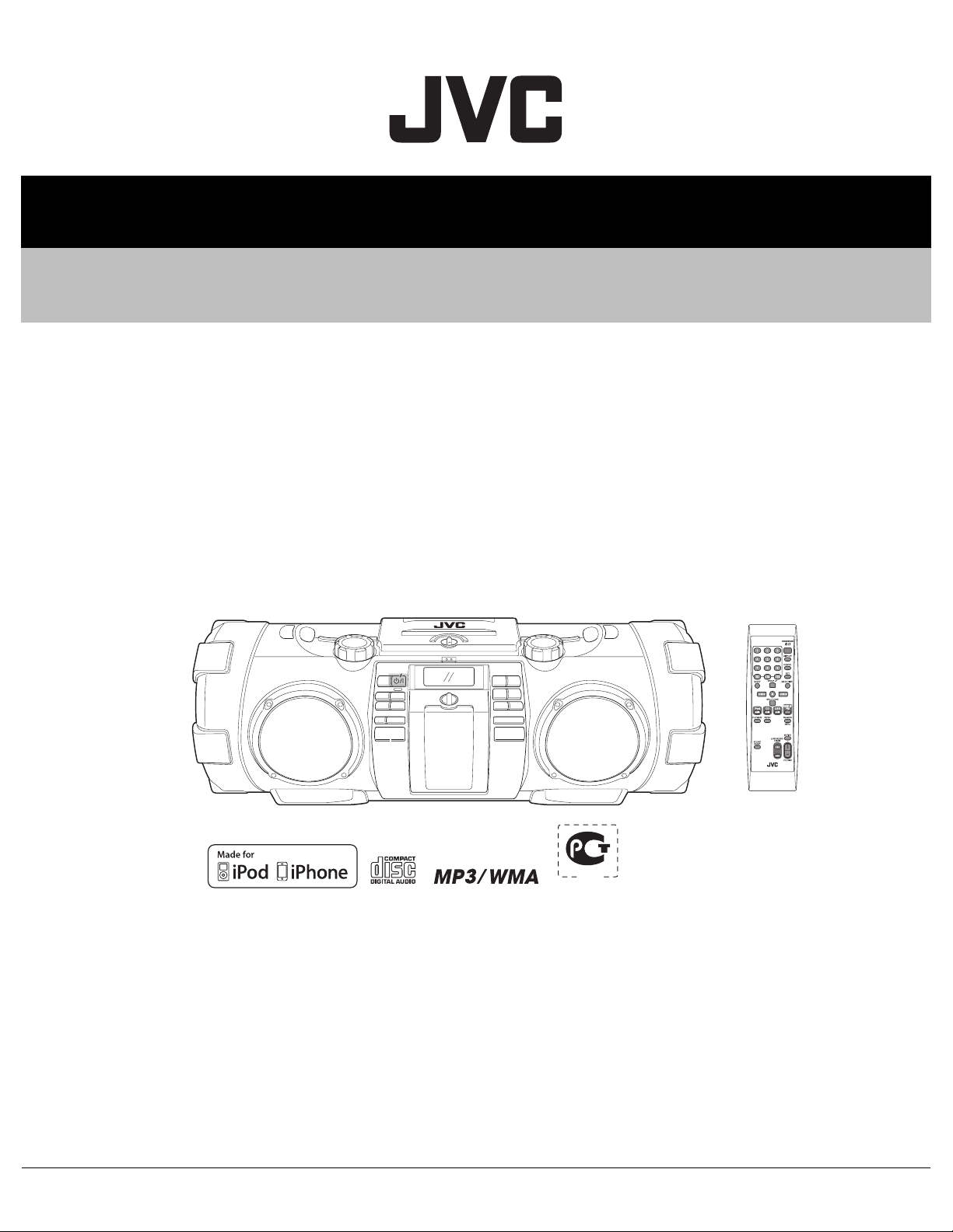
SERVICE MANUAL
MB749<Rev.002>20114SERVICE MANUAL
RV-NB70BA, RV-NB70BE,
RV-NB70BEY, RV-NB70BJ,
RV-NB70SE, RV-NB70SEY,
POWERED WOOFER CD SYSTEM
RV-NB70SJ
For
COPYRIGHT © 2011 Victor Company of Japan, Limited
Lead free solder used in the board (material : Sn-Ag-Cu, melting point : 219 Centigrade)
TABLE OF CONTENTS
1 PRECAUTION. . . . . . . . . . . . . . . . . . . . . . . . . . . . . . . . . . . . . . . . . . . . . . . . . . . . . . . . . . . . . . . . . . . . . . . . . 1-3
2 SPECIFIC SERVICE INSTRUCTIONS . . . . . . . . . . . . . . . . . . . . . . . . . . . . . . . . . . . . . . . . . . . . . . . . . . . . . . 1-5
3 DISASSEMBLY . . . . . . . . . . . . . . . . . . . . . . . . . . . . . . . . . . . . . . . . . . . . . . . . . . . . . . . . . . . . . . . . . . . . . . . 1-6
4 ADJUSTMENT . . . . . . . . . . . . . . . . . . . . . . . . . . . . . . . . . . . . . . . . . . . . . . . . . . . . . . . . . . . . . . . . . . . . . . . 1-11
5 TROUBLESHOOTING . . . . . . . . . . . . . . . . . . . . . . . . . . . . . . . . . . . . . . . . . . . . . . . . . . . . . . . . . . . . . . . . . 1-11
COPYRIGHT © 2011 Victor Company of Japan, Limited
Russia
No.MB749<Rev.002>
2011/4
Page 2
SPECIFICATION
Disc player
CD capacity 1CD
Signal-to-noise ratio 85 dB
Dynamic range 90 dB
Tuner
FM tuning range 87.50 MHz - 108.00 MHz
Antenna FM telescopic antenna
General
Speakers Full range 8 cm (3 3/16”) conex 2
Speaker impedance 16 Ω
Super woofer 13 cm (5 1/8”) conex 2
Speaker impedance 7 Ω
Output power 40 W
Input terminal USB MEMORY Playable files MP3, WMA Compatible device Mass storage class
Compatible system FAT16, FAT32
Output power DC 5 V 500 mA
Dock for iPod DC 5 V 1 A
AUDIO IN Ø3.5
Input Sensitivity /
Impedance (1 kHz)
Output terminal PHONES Ø3.5
Power supply AC For European model AC 230 V , 50 Hz
Power consumption When using an AC outlet 28 W (at operation)
Dimensions: 666 mm (26 1/4”) x 231mm (9 1/8”) x 240 mm (91/2”)(W/H/D)
Mass: Approx. 6.8 kg (15.0 lbs)(without batteries stored in the battery compartment)
• *Not provided for North American model.
• Design and specifi cations are subject to change without notice.
LEVEL 1: 500 mV /47 kΩ
LEVEL 2: 250 mV /47 kΩ
LEVEL 3: 125 mV /47 kΩ
MIC/GUITAR Switchable MIC 200 Ω - 2 kΩ(Ø6.3)
GUITAR 100 kΩ - 1MΩ (Ø6.3)
DC IN DC 12 V, 2 A
32 Ω - 1 kΩ
15 mW / ch output into
32 Ω
VIDEO OUT(For iPod) Composite
DC DC 15 V (R20 (SUM-1)/D
(13D)-size batteries x 10)
External DC 12 V
Less than 1.00 W (on standby)
When using DC IN 2 A (power on mode)
1-2 (No.MB749<Rev.002>)
Page 3
SECTION 1
PRECAUTION
1.1 Safety Precautions
(1) This design of this product contains special hardware and
many circuits and components specially for safety purposes. For continued protection, no changes should be made
to the original design unless authorized in writing by the
manufacturer. Replacement parts must be identical to
those used in the original circuits. Services should be performed by qualified personnel only.
(2) Alterations of the design or circuitry of the product should
not be made. Any design alterations of the product should
not be made. Any design alterations or additions will void
the manufacturers warranty and will further relieve the
manufacture of responsibility for personal injury or property
damage resulting therefrom.
(3) Many electrical and mechanical parts in the products have
special safety-related characteristics. These characteristics are often not evident from visual inspection nor can the
protection afforded by them necessarily be obtained by using replacement components rated for higher voltage, wattage, etc. Replacement parts which have these special
safety characteristics are identified in the Parts List of Service Manual. Electrical components having such features
are identified by shading on the schematics and by ( ) on
the Parts List in the Service Manual. The use of a substitute
replacement which does not have the same safety characteristics as the recommended replacement parts shown in
the Parts List of Service Manual may create shock, fire, or
other hazards.
(4) The leads in the products are routed and dressed with ties,
clamps, tubings, barriers and the like to be separated from
live parts, high temperature parts, moving parts and/or
sharp edges for the prevention of electric shock and fire
hazard. When service is required, the original lead routing
and dress should be observed, and it should be confirmed
that they have been returned to normal, after reassembling.
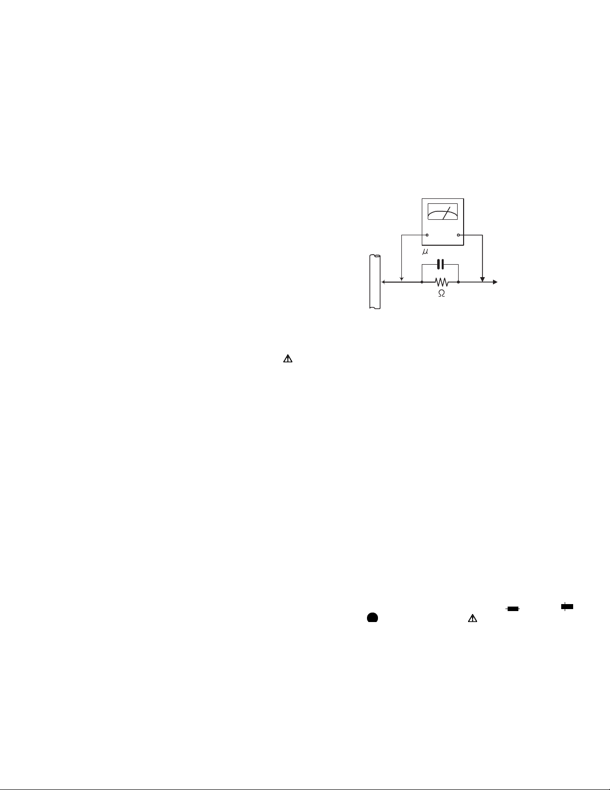
(5) Leakage shock hazard testing
After reassembling the product, always perform an isolation check on the exposed metal parts of the product (antenna terminals, knobs, metal cabinet, screw heads,
headphone jack, control shafts, etc.) to be sure the product
is safe to operate without danger of electrical shock.Do not
use a line isolation transformer during this check.
• Plug the AC line cord directly into the AC outlet. Using a
"Leakage Current Tester", measure the leakage current
from each exposed metal parts of the cabinet, particularly any exposed metal part having a return path to the
chassis, to a known good earth ground. Any leakage current must not exceed 0.5mA AC (r.m.s.).
• Alternate check method
Plug the AC line cord directly into the AC outlet. Use an
AC voltmeter having, 1,000Ω per volt or more sensitivity
in the following manner. Connect a 1,500Ω 10W resistor
paralleled by a 0.15µF AC-type capacitor between an exposed metal part and a known good earth ground.
Measure the AC voltage across the resistor with the AC
voltmeter.
Move the resistor connection to each exposed metal
part, particularly any exposed metal part having a return
path to the chassis, and measure the AC voltage across
the resistor. Now, reverse the plug in the AC outlet and
repeat each measurement. Voltage measured any must
not exceed 0.75 V AC (r.m.s.). This corresponds to 0.5
mA AC (r.m.s.).
AC VOLTMETER
(Having 1000
ohms/volts,
or more sensitivity)
0.15 F AC TYPE
Place this
probe on
1500 10W
Good earth ground
1.2 Warning
(1) This equipment has been designed and manufactured to
meet international safety standards.
(2) It is the legal responsibility of the repairer to ensure that
these safety standards are maintained.
(3) Repairs must be made in accordance with the relevant
safety standards.
(4) It is essential that safety critical components are replaced
by approved parts.
(5) If mains voltage selector is provided, check setting for local
voltage.
1.3 Caution
Burrs formed during molding may be left over on some parts
of the chassis.
Therefore, pay attention to such burrs in the case of preforming repair of this system.
1.4 Critical parts for safety
In regard with component parts appearing on the silk-screen
printed side (parts side) of the PWB diagrams, the parts that are
printed over with black such as the resistor ( ), diode ( )
and ICP ( ) or identified by the " " mark nearby are critical
for safety. When replacing them, be sure to use the parts of the
same type and rating as specified by the manufacturer.
(This regulation dose not Except the J and C version)
each exposed
metal part.
(No.MB749<Rev.002>)1-3
Page 4
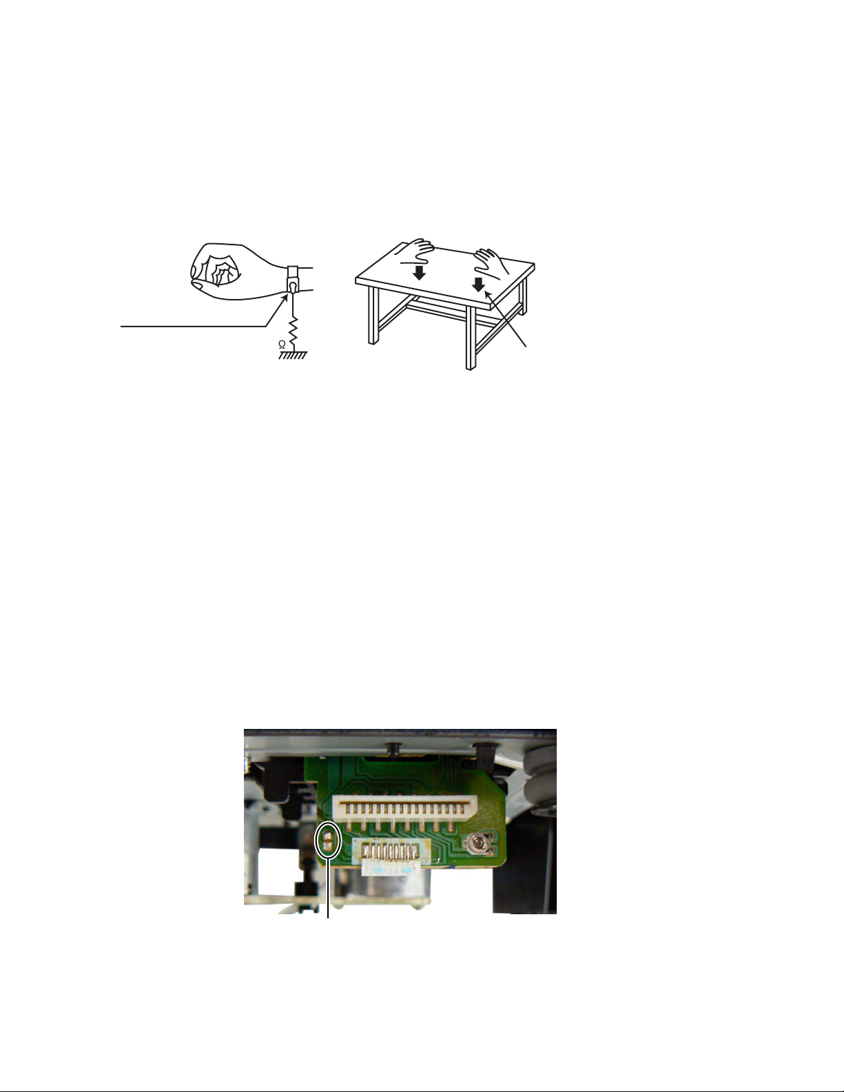
1.5 Preventing static electricity
Electrostatic discharge (ESD), which occurs when static electricity stored in the body, fabric, etc. is discharged, can destroy the laser
diode in the traverse unit (optical pickup). Take care to prevent this when performing repairs.
1.5.1 Grounding to prevent damage by static electricity
Static electricity in the work area can destroy the optical pickup (laser diode) in devices such as laser products.
Be careful to use proper grounding in the area where repairs are being performed.
(1) Ground the workbench
Ground the workbench by laying conductive material (such as a conductive sheet) or an iron plate over it before placing the
traverse unit (optical pickup) on it.
(2) Ground yourself
Use an anti-static wrist strap to release any static electricity built up in your body.
(caption)
Anti-static wrist strap
1M
Conductive material
(conductive sheet) or iron palate
(3) Handling the optical pickup
• In order to maintain quality during transport and before installation, both sides of the laser diode on the replacement optical
pickup are shorted. After replacement, return the shorted parts to their original condition.
(Refer to the text.)
• Do not use a tester to check the condition of the laser diode in the optical pickup. The tester's internal power source can easily
destroy the laser diode.
1.6 Handling the traverse unit (optical pickup)
(1) Do not subject the traverse unit (optical pickup) to strong shocks, as it is a sensitive, complex unit.
(2) Cut off the shorted part of the flexible cable using nippers, etc. after replacing the optical pickup. For specific details, refer to the
replacement procedure in the text. Remove the anti-static pin when replacing the traverse unit. Be careful not to take too long a
time when attaching it to the connector.
(3) Handle the flexible cable carefully as it may break when subjected to strong force.
(4) I t is not possible to adjust the semi-fixed resistor that adjusts the laser power. Do not turn it.
1.7 Attention when traverse unit is decomposed
*Please refer to "Disassembly method" in the text for the pickup unit.
• Apply solder to the short land sections before the card wire is disconnected from the connector on the servo board. (If the card wire
is disconnected without applying solder, the pickup may be destroyed by static electricity.)
• In the assembly, be sure to remove solder from the short land sections after connecting the card wire.
1-4 (No.MB749<Rev.002>)
Short land
Page 5
SECTION 2
SPECIFIC SERVICE INSTRUCTIONS
Playable discs/files
Discs CDs with one of the marks below on the surface.
Files Files in audio CD format, MP3/WMA files on a finalized CD-R or CD-RW.
MP3/WMA files in a USB device can also be played.
Compatible iPod
Made for Audio Video
iPod nano (6th generation) O O*1
iPod nano (5th generation) O O
iPod nano (4th generation) O O
iPod nano (3rd generation) O O
iPod nano (2nd generation) O -
iPod nano O -
iPod touch (4th generation) O O
iPod touch (3rd generation) O O
iPod touch (2nd generation) O O
iPod touch O O
iPod classic O O
iPod video (5th generation) O O
iPod photo (4th generation) O O*1, *2
iPod (4th generation) O -
iPod mini (2nd generation) O -
iPod mini O -
iPhone 4 O O
iPhone 3GS O O
iPhone 3G O O
*1 Only for still picture
*2 Viewable only on the screen of iPod
(No.MB749<Rev.002>)1-5
Page 6
SECTION 3
DISASSEMBLY
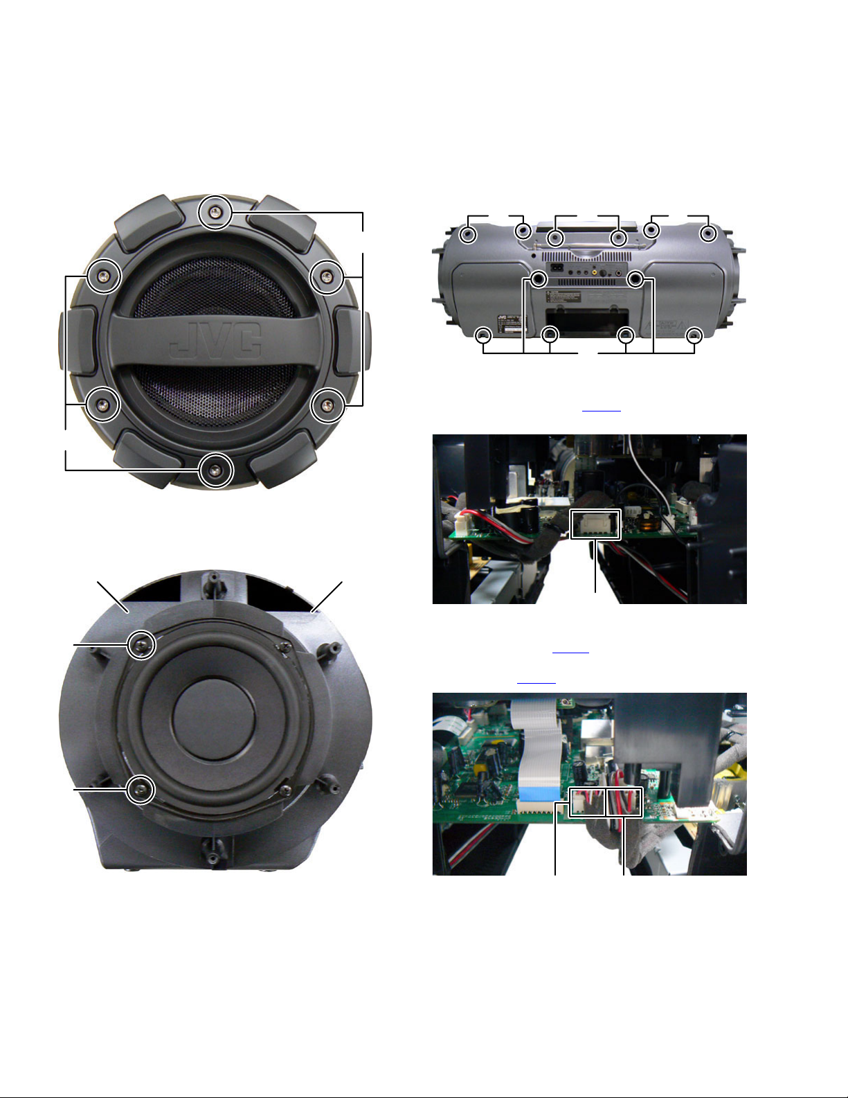
3.1 Main body (Used model: RV-NB70BE)
3.1.1 Removing the Punching panel (See Fig.1)
(1) Remove the six screws A attaching the Punching panel.
(2) Similarly, remove the other side.
A
Fig.1
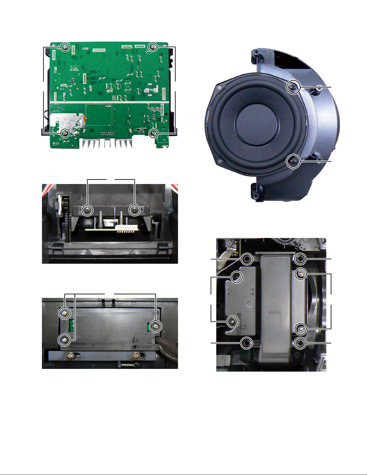
3.1.2 Removing the Rear cabinet (See Fig.2, 3, 4, 5)
(1) Remove the two screws B attaching the subwoofer. (See
Fig.2)
Front cabinetRear cabinet
A
(2) Similarly, remove the other side.
(3) Remove the battery cover.
(4) Remove the ten screws C attaching the Rear cabinet. (See Fig.
(5) Remove the two screws D attaching the CD mechanism.
(See Fig.3)
CC
D
C
Fig.3
(6) Disconnect the connector wire from Power supply board
connected to connector CN101
Fig.4)
on the Main board. (See
3)
B
B
Fig.2
CN101
Fig.4
(7) Disconnect the connector wire from Power supply board con-
nected to connector CN030
(8) Disconnect the connector wire from Mic board connected
to connector CN060 on the Main board. (see Fig.5)
CN030 CN060
on the Main board. (See Fig.
Fig.5
5)
1-6 (No.MB749<Rev.002>)
Page 7
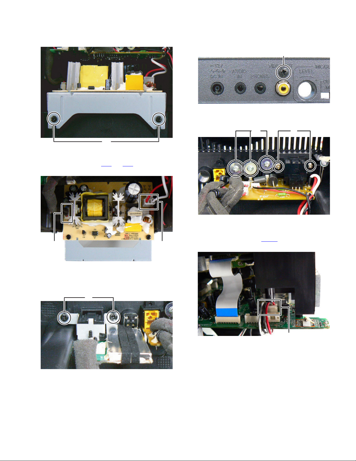
3.1.3 Removing the SMPS board (See Fig.6, 7)
(1) Remove the two screws E attaching the SMPS board. (See
Fig.6)
E
Fig.6
(2) Disconnect the connector wires from Power supply board
connected to connector CN1
(See Fig.7)
and CN2 on the SMPS board.
3.1.5 Removing the Power supply board (See Fig.9, 10)
(1) Remove the one screw G attaching the Video jack. (See
Fig.9)
G
Fig.9
(2) Remove the three screws H and two screws J attaching the
Power supply board. (See Fig.10)
HJ
Fig.7
3.1.4 Removing the Mic board (See Fig.8)
(1) Remove the Mic volume knob.
(2) Remove the two screws F attaching the Mic board.
F
Fig.8
Fig.10
3.1.6 Removing the CD mechanism (See Fig.11, 12, 13, 14)
(1) Disconnect the connector wire from right side subwoofer
CN1CN2
connected to connector CN103
Fig.11)
Fig.11
on the Main board. (see
CN103
(No.MB749<Rev.002>)1-7
Page 8
(2) Disconnect the connector wire from left side subwoofer con-
nected to connector CN102
(3) Disconnect the card wire from Main board connected to
connector CN450 on the iPod board. (See Fig.12)
on the Main board. (See Fig.
12)
CN450 CN102
Fig.12
(4) Disconnect the earth wire from USB board connected to
post pin P2
on the Pain board. (See Fig.13)
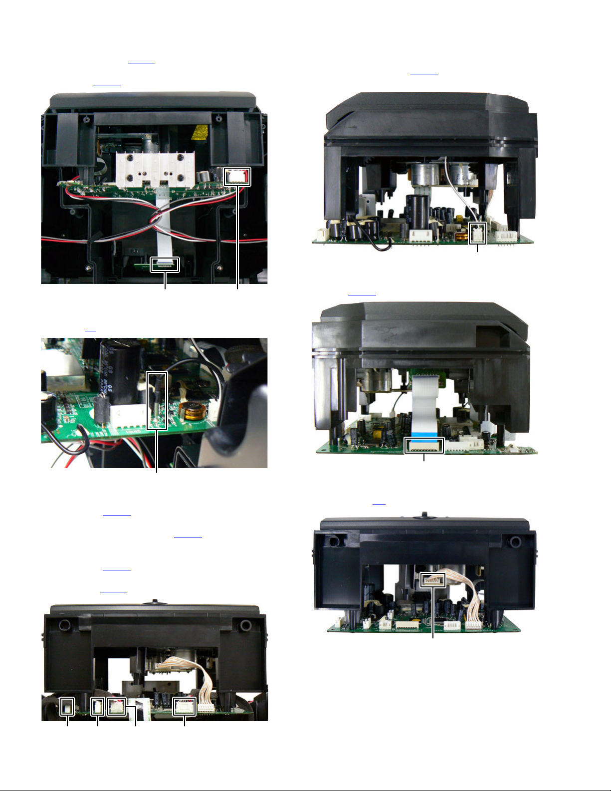
3.1.7 Removing the Main board (See Fig.15, 16, 17, 18)
(1) Disconnect the connector wire from Door switch board con-
nected to connector CN305
Fig.15)
on the Main board. (See
CN305
Fig.15
(2) Disconnect the card wire from Pickup connected to con-
nector CN701
on the Main board. (See Fig.16)
P2
Fig.13
(5) Disconnect the connector wire from LCD board connected
to connector CN304
(6) Disconnect the connector wire from Subwoofer volume
board connected to connector CN301 on the Main board.
(See Fig.14)
(7) Disconnect the connector wire from USB board connected
to connector CN201
(8) Disconnect the connector wire from Volume board connected
to connector CN303
on the Main board. (See Fig.14)
on the Main board. (See Fig.14)
on the Main board. (see Fig.
14)
CN304 CN301 CN201 CN303
Fig.
14
CN701
Fig.16
(3) Disconnect the connector wire from Main board connected
to connector CN on the CD board. (See Fig.17)
CN
Fig.17
1-8 (No.MB749<Rev.002>)
Page 9
(4) Remove the four screws K attaching the Main board. (See
Fig.18)
3.1.10 Removing the Speaker (See Fig.21, 22, 23)
(1) Remove the two screws N attaching the Subwoofer. (See
Fig.21)
KK
Fig.18
3.1.8 Removing the iPod board (see Fig.19)
(1) Remove the two screws L attaching the iPod board.
L
Fig.21
(2) Remove the four screws P attaching the Speaker duct.
(See Fig.22)
(3) Remove the four screws Q attaching the Speaker cover.
(See Fig.22)
P
Fig.19
3.1.9 Removing the LCD board (See Fig.20)
(1) Remove the three screws M attaching the LCD board.
N
N
P
M
Fig.20
QQ
P
Fig.22
(No.MB749<Rev.002>)1-9
P
Page 10
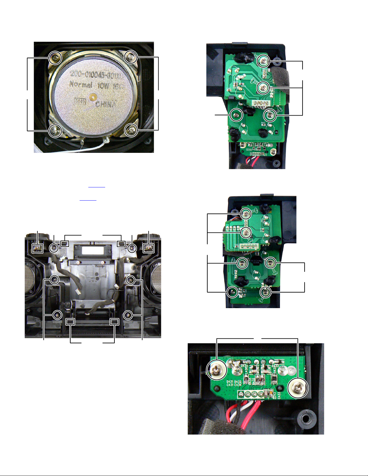
(4) Remove the four screws R attaching the speaker. (See
Fig.23)
3.1.12 Removing the Left button board (See Fig.25)
(1) Remove the four screws T attaching the Left button board.
RR
T
Fig.23
(5) Similarly, remove the other side.
3.1.11 Removing the Front panel (See Fig.24)
(1) Disconnect the connector wire from Right button board
connected to connector CN407
(2) Disconnect the connector wire from Left button board con-
nected to connector CN408
(3) Remove the six screws S attaching the Front panel.
(4) Disengage four hooks a engaged Front panel.
(5) Open the iPod door, and then remove the Front panel.
CN407 CN408
SS
hook
on the Volume board.
on the Woofer volume board.
a
3.1.13 Removing the Right button board (See Fig.26)
(1) Remove the six screws U attaching the Right button board.
Fig.25
T
U
3.1.14 Removing the USB board (See Fig.27)
(1) Remove the two screws V attaching the USB board.
hook
SS
a
Fig.24
U
Fig.26
V
1-10 (No.MB749<Rev.002>)
Fig.27
Page 11
3.1.15 Removing the Volume (See Fig.28)
(1) Remove the Volume knob.
(2) Remove the nut from Volume shaft.
(3) Similarly, remove the other side.
Fig.28
Nut
SECTION 4
ADJUSTMENT
This service manual does not describe ADJUSTMENT.
SECTION 5
TROUBLESHOOTING
This service manual does not describe TROUBLESHOOTING.
(No.MB749<Rev.002>)1-11
Page 12

Victor Company of Japan, Limited
Personal AV Operation 10-1,1chome,Ohwatari-machi,Maebashi-city,371-8543,Japan
(No.MB749<Rev.002>)
Printed in Japan
VSE
Page 13

SCHEMATIC DIAGRAMS
31
POWERED WOOFER CD SYSTEM
RV-NB70BA RV-NB70BE RV-NB70BEY
RV-NB70BJ RV-NB70SE RV-NB70SEY
RV-NB70SJ
(No.MB749<Rev.002>)1/
Page 14
■ PRECAUTIONS ON SCHEMATIC DIAGRAMS
z Due to the improvement in performance, some part numbers shown in the circuit diagrams
may not agree with those indicated in the Parts List.
z The parts numbers, values and rated voltage etc. in the Schematic Diagrams are for
reference only.
z Since the circuit diagrams are standard ones, the circuits and circuit constants may be
subject to change for improvement without any notice.
■ PRECAUTIONS ON PARTS LIST
z
The parts identified by the symbol are critical for safety. Whenever replacing these parts, be sure to
use specified ones to secure the safety.
z
The parts not indicated in this Parts List and those which are filled with lines --- in the Parts No.
columns will not be supplied.
z
P.W. BOARD Ass'y will not be supplied, but those which are filled with the Parts No. in the Parts No.
columns will be supplied.
z
When ordering chips, screws etc., place bulk orders (unit of tens) whenever possible to improve
shipping efficiency.
z
There are cases where the actual implemented parts in the sets and the service parts are different.
When ordering parts, make sure to refer to the Parts List.
■
PRECAUTIONS ON SERVICE
Certain parts of the power circuits and the GNDs differ according to the models. Care must be
taken for the following points as the differences are indicated separately in the LIVE GND ( ) and
the ISOLATED (NEUTRAL) GND ( ).
1. Do not touch the LIVE GND, or do not touch the LIVE GND and the ISOLATED (NEUTRAL)
GND at the same time. It may cause an electric shock.
Before pulling out the chassis or other parts, make sure to pull out the power cord from the
wall outlet first.
2. Do not short circuit between the LIVE GND and ISOLATED (NEUTRAL) GND, or never
measure the LIVE GND and ISOLATED (NEUTRAL) GND at the same time using measuring
instruments (oscilloscope, etc.). It may blow fuses or damage other parts.
■ DEVIATION TOLERANCE RANGE
DEVIATION TOLERANCE RANGE
F G J K M N R H Z P
± 1% ± 2% ± 5% ±10% ±20% ±30%
+30%
-10%
+50%
-10%
+80%
-20%
+100%
-0%
31
(No.MB749<Rev.002>)2/
Page 15
Q702
Q207
Q204
Q111
Q110
Q109
Q105
Q102
Q001
FLASH
IC707
IC705
USB Driver
IC703
Motor driver
IC702
CD/USB RF DSP
IC701
Remocon
IC401
EEPROM
IC304
RESET
IC303
MICON
SYSTEM
IC302
IC301
VIDEO SWITCH
IC204
FUNCTION
IC203
Buffer
IC202
DC/DC 5V
IC201
HPF & LPF
IC107
IC106
COMP AMP
PHASE AMP
INPUT AMP
IC104
WOOFER AMP
IC102
MAIN AMP
IC101
MIC Buffer
IC060
TUNER Section
IC001
CN602
~
~
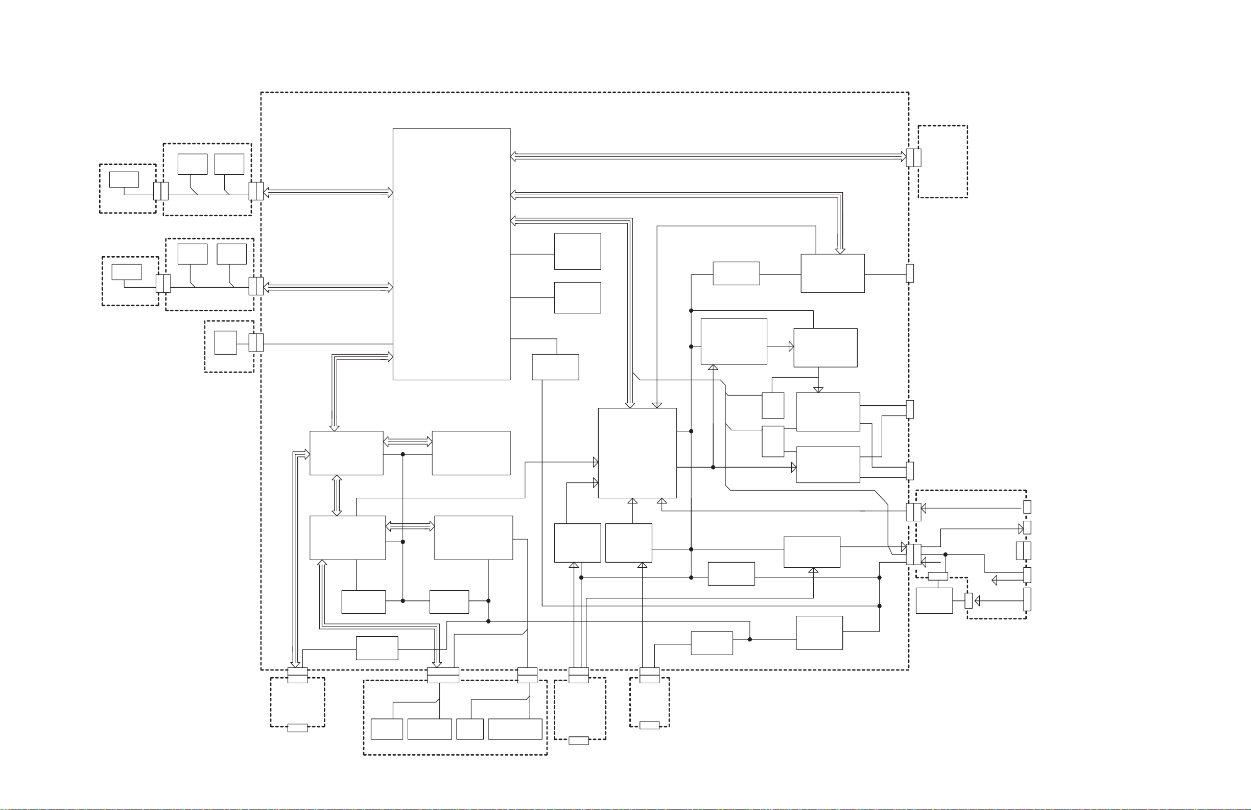
Block diagram
CN403
CN304
B+
AC IN
JK602
DC IN
JK601
IN
BATTERY
CN603
OUTPUT
VIDEO
JK603
Audio IN
JK604
14V/4A
SPS PCB
CN606
AC DET
CN604
VCC
CN601
CN101
CN605
CN030
5V OUT
CN102
W R+/-
M R+/-
TO R WOOFER SPEAKER
TO R MAIN SPEAKER
CN103
W L+/-
M L+/-
TO L WOOFER SPEAKER
TO L MAIN SPEAKER
TO iPod
NJM4580
IC501
MIC AMP
NJM4580
IC502
MIC ALC
INPUT
MIC & GUITAR
JK450
JK501
CN450
CN202
CN501
CN060
TO FM ANT
LCD
iPod L/R
iPod 5V SW
9V OUT
iPod L/R
AUX IN
L / R
MUTE
WVOL3
WVOL2
WVOL1
to
OUT
3.3V
TUNER L/R
Fleed motor
Spindle &
SW
RESET
Focus Coil
Tracking &
PICK UP
CD
CN702
CN701
JK430
CN430
CN201
5V
3.3V
3.3V
USB CD L/R
TO USB
USB 5V SW
1.5V
CD DOOR SWITCH
SWITCH
CD DOOR
LED
CN408
LED
CN409
KEY2
Standby
D401
Switch
S406
Operation
S401
W VOLUME
VR402
CN305
CN301
CN401
CN303
CN402
CN406
RMC
CN407
KEY1
Switch
S411
Operation
S407
M VOLUME
VR401
created date:2011-04-18No.MB749
31
(No.MB749<Rev.002>)3/
Page 16
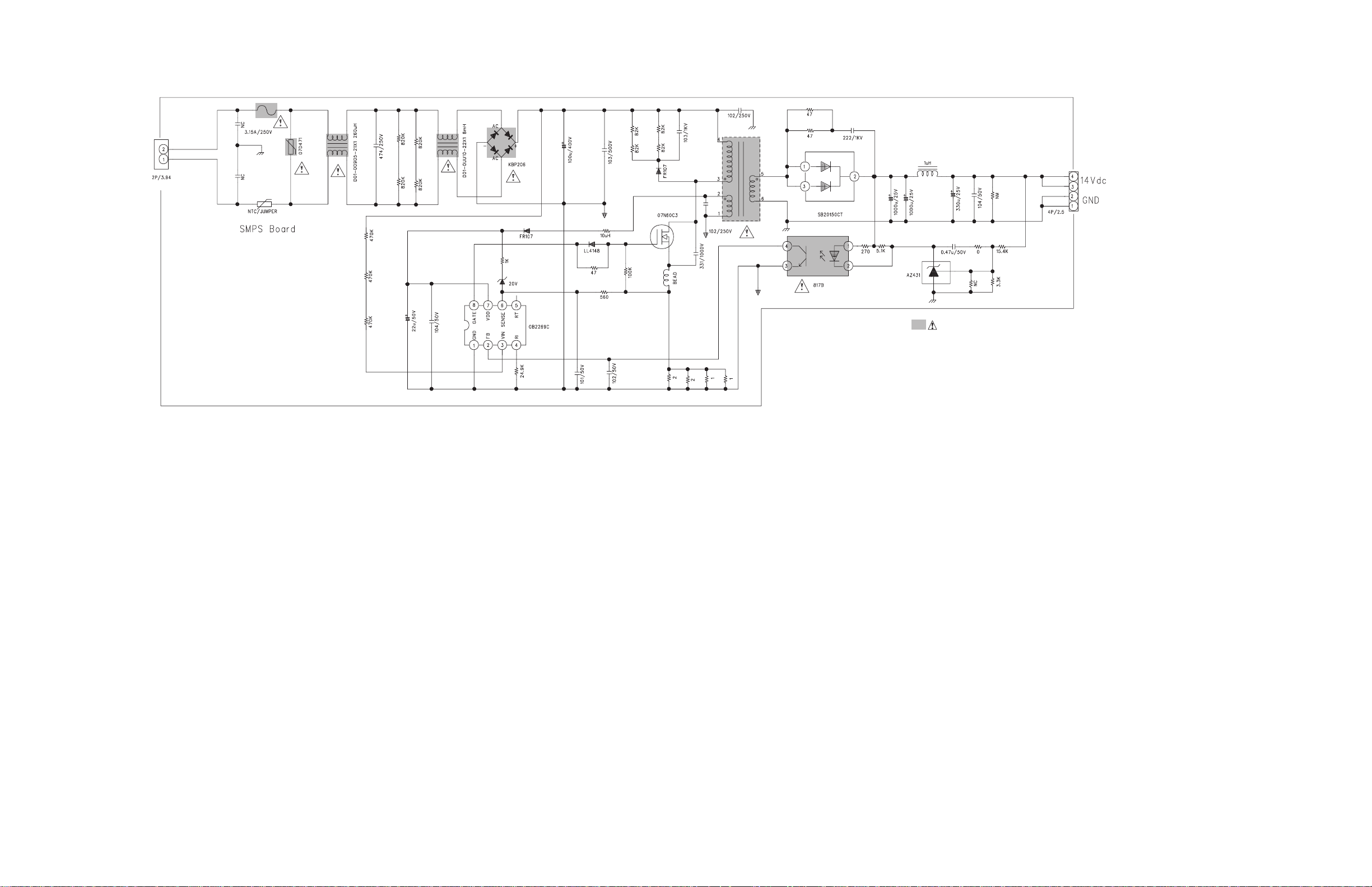
ZD1
T3
RN
R2A
R24
R23
R21
R20A
R20
R1A
R19
R18
R17A
R17
R16C
R16B
R16A
R16
R12
R11
R10C
R10B
R10A
R10
R9
R8
R7
R6
R5
R4
R3
R2
R1
Q1
MOV
LF2
LF1
L2
IC4
IC2
IC1
F1
D4
D3
D2
D1
CY3
CY2
CY1
CX1
CN2
CN1
C52
C18
C17
C14
C13
C12
C11
C10
C9
C8
C7
C6
C5
C4
C1
BD1
BC1
<SMPS section>
To Jack section
CN604
To Jack section
CN606
!
Parts are safety assurance parts.
When replacing those parts make
sure to use the specified one.
created date:2011-04-18No.MB749
31
(No.MB749<Rev.002>)4/
Page 17
X302 X301
R399
R398 R397
R394
R393
R392
R391
R390
R389
R388
R387
R386
R385
R384
R383
R382
R381
R380
R379
R378
R377
R376
R375
R374
R373
R372
R371
R370
R369
R368
R367
R366
R365
R364
R363
R362
R361
R360
R359
R358
R357
R356
R355
R354
R353
R352
R351
R350
R349
R348
R347
R346
R345
R344
R343
R342
R341
R340
R339
R338
R337
R336
R335
R334
R333
R332
R331
R330
R329
R328
R327
R326
R325
R324
R323
R322
R321
R319
R318
R317
R316
R315
R314
R313
R312
R311
R310
R309
R308
R307
R306
R305
R304
R303
R301
R300
R299
R298
R297
R296
R295
R294
R293
R292
R291
R290
R289
R286
R285
R284
R282
R279
R227
R175
R22
Q315
Q314
Q313
Q312
Q310
Q308
Q307
Q306
Q305
Q304
Q303
Q301
L301
JR304
JR303
JR302
JR39
JR38
JR37
JR32
JR31
JR031
JR30
JR29
JR27
JR26
JR25
JR3
JR1
IC305
IC304
IC303
IC302
IC301
D319
D318
D317
D316
D315
D314
D313
D307
D305
D303
D302
D301
CN305
CN304
CN303
CN302
CN301
C356
C332
C331
C330
C325
C324
C323
C322
C321
C320
C314
C313
C312
C311
C310
C309
C308
C307
C306
C305
C304
C303
C302
C301
C294
C28
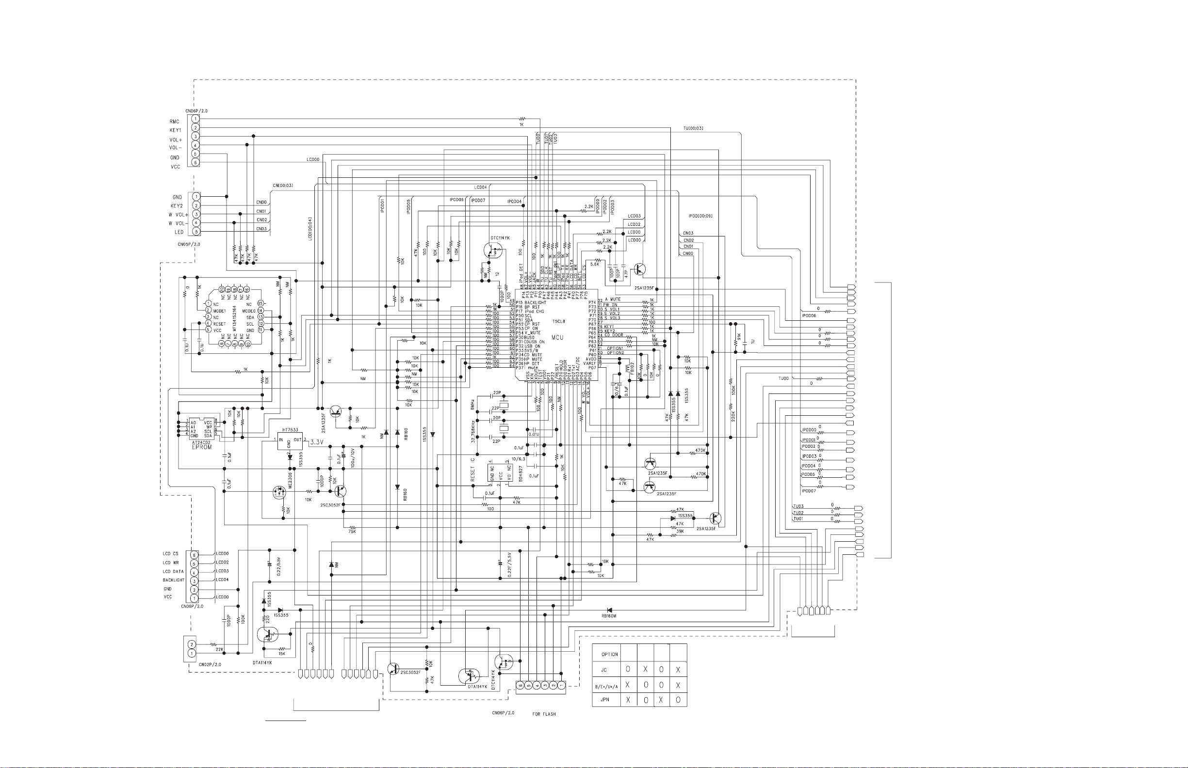
<Micom section>
R347R346R345R344
MGND
CDM5V
CD_R
AGND
CD_L
RESET
VOLSCA
VOLSCL
IPOD_CDG
5VS/W
AMUTE
HP_DET
SUB_VOL3
POWER_ON
SUB_VOL1
SUB_VOL2
DC9V
D_GND
CDM5V
HP_MUTE
AC/DC
JACK
CD_L
3.3V
CD_R
AGND
IPHONE_DET
VCC15V
IPOD_TX
IPOD_RST
I_MUTE
V_MUTE
IPOD_DET
IPOD_RX
MGND
USBD-
USBD+
D_GND
USBON
TUSDO
TUSCLK
TURST
USBD-
USBD+
USB_RST
USB_TXD
USB_RXD
USB_UPD
GND
TxD
RxD
RESET
VDD
TEST
AMUTE_1
AMI
BOOTOUT
DGND
CD_MUTE
JCDUSBON
To Key section
CN402
To Key section
CN401
To LCD section
CN403
To Door switch section
CN404
To Function section
To CD/USB section
To CD/USB section
created date:2011-04-18No.MB749
31
(No.MB749<Rev.002>)5/
Page 18
R816 R815
R814
R813
R812
R811
R810
R809
R808
R807
R806
R805
R803
R802
R238
R237
R236
R187
R169
R168
R167
R166
R165
R164
R163
R162
R161
R160
R159
R158
R157
R156
R155
R154
R153
R152
R151
R150
R149
R148
R147
R146
R145
R144
R143
R142
R141
R140
R139
R138
R137
R136
R135
R134
R133
R132
R131
R130
R129
R128
R127
R126
R125
R124
R123
R122
R121
R120
R119
R118
R117
R116
R115
R114
R113
R112
R111
R110R109
R108
R107
R106
R105
R104
R103
R102
R101
Q112
Q111
Q110
Q109
Q108
Q107
Q106
Q105
Q104
Q103
Q102
L801
L106
L105
L104
L103
L102
L101
JR104
JR103
JR102
JR40
JR36
JR35
JR34
JR28
JR24
JR23
JR22
JR21
JR20
JR19
JR18
JR17
IC801
IC204
IC107
IC106
IC105
IC104
IC102
IC101
FB102
D110
D109
D107
D106
D105
D104
D103
D102
D101
CN103
CN102
CN101
C824
C823
C822
C821
C820
C819
C818
C817
C816
C815
C814
C813
C812
C811
C808
C807
C806
C805
C804
C803
C802
C801
C452
C451
C450
C299
C287
C285
C270
C200
C199
C198
C197
C196
C195
C194
C193
C192
C191
C190
C189
C188
C187
C186
C185
C184
C183
C182
C181
C180
C179
C178
C177
C176
C175
C174
C173
C172
C171
C170
C169
C168
C167
C166
C165
C164
C163
C162
C161
C160
C159
C158
C157
C156
C155
C154
C153
C152
C151
C150
C149
C148
C147
C146
C145
C144
C143
C142
C141
C140
C139
C138
C137
C136
C135
C134
C133
C132
C131
C130
C129
C128
C127
C126
C125
C124
C123
C122
C121
C120
C119
C118
C117
C116
C115
C114
C113
C112 C111
C110 C109
C108
C107
C106 C105
C104 C103
C102
C101
C100
C095
C094
C093
C092
C091
C090
C29
C27
C18
C17
C16
C12
C11
C9
C3
C2
C1
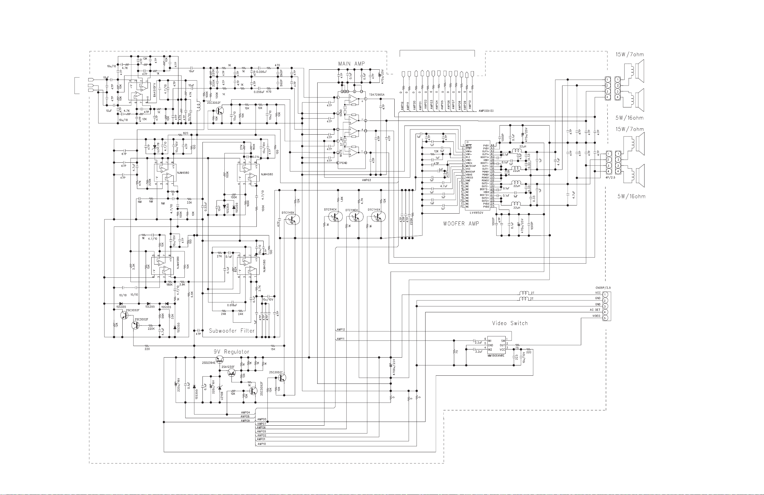
<Amp section>
To Jack section
CN601
To Function section
To Function
section
MGND
DC9V
D_GND
SUB_VOL1
SUB_VOL2
SUB_VOL3
POWER_ON
AMUTE
VCC15V
C_GND
AC/DC
VIDEO
V_MUTE
R
AGND
L
created date:2011-04-18No.MB749
31
(No.MB749<Rev.002>)6/
Page 19
X001
R288
R287
R281
R280
R278
R271
R270
R269
R268
R267
R266
R265
R263
R262
R261
R260
R258
R257
R256
R255
R254
R253
R252
R251
R250
R249
R248
R247
R246
R245
R244
R241
R240
R239
R235
R234
R233
R232
R231
R230
R229
R228
R227
R226
R225
R224
R223
R222
R221
R220
R219
R218
R217
R216
R215
R214
R213
R212
R211
R208
R207
R206
R205
R204
R203
R202
R201
R071
R070
R069
R068
R067
R066
R065
R064R064
R063
R062
R061
R060
R045
R044
R043
R042
R041
R040
R039
R038
R037
R036
R035
R034
R033
R032
R031
R030
R029
R015
R014
R013
R012
R011
R010
R009
R008
R007
R006
R005
R004
R003
R2
R002
R001
Q210
Q209
Q208
Q207
Q206
Q205
Q204
Q203
Q201
Q033
Q031
Q030
Q001
L206
L205
L204
L203
L202
L201
L061
L060
L030
L003
L002
L001
JR053
JR052
JR051
JR050
JR049
JR048
JR047
JR046
JR045
JR030
JR028
JR027
JR026
JR025
JR024
JR023
JR022
JR021
JR020
JR019
JR018
JR017
JR002
IC203
IC202
IC201
IC060
IC030
IC001
D211
D209
D205
D202
D201
D004
D003
D002
D001
CN202
CN201
CN060
CN030
C298
C297
C296
C295
C293
C292
C291
C290
C289
C288
C286
C284
C283
C282
C281
C280
C279
C278
C277
C276
C275
C274
C273
C272
C271
C269
C268
C267
C266
C265
C264
C263
C262
C261
C260
C259
C258
C257
C256
C255
C254
C253
C252
C251
C250
C249
C248
C247
C246
C245
C244
C243
C242
C241
C240
C239
C238
C237
C236
C235
C234
C233
C232
C231
C230
C229
C228
C227
C226
C226
C225
C224
C223
C222
C221
C220
C219
C219
C218
C217
C216
C215
C214
C213
C212
C211
C210
C209
C208
C207
C206
C205
C204
C203
C202
C201
C085
C083
C082
C081
C080
C079
C078
C077
C076
C075
C074
C073
C072
C071
C070
C069
C068
C067
C066
C065
C064
C063
C062
C061
C060
C055
C054
C053
C052
C051
C050
C049
C048
C047
C046
C045
C044
C043
C042
C041
C040
C039
C038
C037
C036
C035
C034
C033
C032
C031
C030
C026
C025
C024
C023
C022
C021
C020
C019
C018
C017
C016
C015
C014
C013
C012
C011
C010
C009
C008
C007
C006
C005
C004
C003
C002
C001
ANT1
<Function section>
To USB jack section
CN430
R
AGND
L
C7
C10
MGND
DC9V
D_GND
SUB_VOL2
SUB_VOL3
POWER_ON
SUB_VOL1
AMUTE
C_GND
AC/DC
VIDEO
VCC15V
V_MUTE
VOLSCL
AMUTE
HP_DET
5VS/W
IPOD_CHG
VOLSDA
D_GND
SUB_VOL1
SUB_VOL3
SUB_VOL2
POWER_ON
AC/DC
JACK
HP_MUTE
CDM5V
DC9V
VCC15V
CD_R
CD_L
AGND
3.3V
IPOD_DET
IPOD_RX
IPOD_RST
IPOD_TX
IPHONE_DET
TUSDO
TUSCLK
I_MUTE
TURST
V_MUTE
MGND
USBD-
USBON
USBD+
D_GND
To iPod section
CN450
To Mic section
CN501
To Jack section
CN605
To Amp section
To Amp section
To CD/USB
section
created date:2011-04-18No.MB749
31
(No.MB749<Rev.002>)7/
Page 20

R433
R432
L431
L430
JK430
D434
D433
D432
D431
CN430
C434
C433
C432
C431
<USB Jack section>
To USB
To Function section
CN201
created date:2011-04-18No.MB749
31
(No.MB749<Rev.002>)8/
Page 21

R424
R423
R422
R421
R420
LCD401
D402
CN403
C414
C413
C412
C411
C410
CN304
To Micom section
<LCD section>
created date:2011-04-18No.MB749
31
(No.MB749<Rev.002>)9/
Page 22

S412
S411
S410
S409
S408
S407
S406
S405
S404
S403
S402
S401
R413
R412 R411 R410 R409 R408
R407 R406 R405 R404 R403
R402
R401
IC401
D401
CN409
CN406
CN402
CN401
C409
C403
C402
C401
To Volume section
CN407
To Woofer vol section
CN408
<Key section>
To Micom section
CN301
To Micom section
CN303
created date:2011-04-18No.MB749
31
(No.MB749<Rev.002>)10/
Page 23

R606
R605
R604
R603
R602
R601
L607
L605
L604
L603
L602
L601
L580
JK605
JK604
JK603
JK602
JK601
F602
F601
D606
D605
D604
D603
D602
D601
CN606
CN605
CN604
CN603
CN602
CN601
C606
C605
C604
C603
C602
C601
CN1
CN2
To SMPS section
To SMPS section
!
sure to use the specified one.
When replacing those parts make
Parts are safety assurance parts.
JACK BOARD
CN101
To Amp section
CN030
To Function section
<Jack section>
created date:2011-04-18No.MB749
31
(No.MB749<Rev.002>)11/
Page 24

VR401
CN407
C406
C405
CN406
To Key section
<Volume section>
created date:2011-04-18No.MB749
31
(No.MB749<Rev.002>)12/
Page 25

VR402
CN408
C408
C407
CN409
To Key section
<Woofer vol section>
created date:2011-04-18No.MB749
31
(No.MB749<Rev.002>)13/
Page 26

SW801
BN802
CN305
To Micom section
<Door switch section>
created date:2011-04-18No.MB749
31
(No.MB749<Rev.002>)14/
Page 27

VR501
SW501-A
SW501-B
R537
R536
R535
R534
R533
R532
R531
R530
R529
R528
R527
R526
R525
R524
R523
R522
R521
R520
R519
R518
R517
R516
R515
R514
R513
R512
R511
R510
R509
R508
R507
R506
R505
R504
R503
R502
R501
Q510
Q509
Q508
Q507
Q506
Q505
Q504
Q503
Q502
Q501
PJ603
L501
JK501
IC502
IC501
D509
D508
D507
D506
D505
D504
D503
D502
D501
CN501
C536
C535
C532
C531
C530
C529
C528
C527
C526
C525
C524
C523
C522
C521
C520
C519
C518
C517
C516
C515
C514
C513
C512
C511
C510
C509
C508
C507
C506
C505
C504
C503
C502
C501
<Mic section>
To Function section
CN060
created date:2011-04-18No.MB749
31
(No.MB749<Rev.002>)15/
Page 28

R456
R455
R454
R453
R452
R451
R450
Q450
JK450
CN450
<iPod section>
To Function section
CN202
created date:2011-04-18No.MB749
31
(No.MB749<Rev.002>)16/
Page 29

X702
X701
RN713
RN712
RN711
RN710
RN709
RN708
RN707
RN706
RN705
RN704
RN703
RN702
RN701
R798
R795
R794
R793
R792
R790
R789
R788
R787
R786
R785
R784
R783
R782
R781
R780
R779
R778
R777
R776
R775
R774
R773
R772
R771
R770
R769
R768
R767
R766
R765
R764
R763
R762
R761
R760
R759
R758
R757
R756
R755
R754
R753
R752
R751
R750
R749
R748
R747
R746
R745
R744
R743
R742
R741
R740
R739
R738
R737
R736
R735
R734
R733
R732
R725
R724
R723
R722
R721
R720
R719
R718
R717
R716
R715
R714
R713
R712
R711
R710
R709
R708
R707
R706
R705
R704
R703
R702
R701
Q709
Q708
Q707
Q706
Q705
Q704
Q703
Q702
Q701
L712
L711
L710
L709
L708
L707
L706
L705
L704
L703
L702
L701
JR707
JR706
JR705
JR703
JR701
JR33
JR16
JR15
JR14
JR13
JR12
JR11
JR10
JR9
JR8
JR7
JR6
JR5
JR4
JR0
IC707
IC705
IC703
IC702
IC701
D703
D702
D701
CN702
CN701
C791
C788
C787
C785
C784
C783
C782
C781
C780
C779
C778
C777
C776
C775
C774
C773
C772
C771
C770
C769
C768
C767
C766
C765
C764
C763
C762
C761
C760
C759
C758
C757
C756
C755
C754
C752
C751
C750
C749
C748
C747
C746
C745
C744
C743
C742
C741
C740
C739
C738
C737
C736
C735
C734
C733
C732
C731
C730
C729
C728
C727
C726
C725
C724
C723
C722
C721
C720
C719
C718
C717
C716
C715
C714
C713
C712
C711
C710
C709
C708
C707
C706
C705
C704
C703
C702
C701
C6
<CD/USB section>
To Micom section
To Micom section
SCL
SDA
MGND
CDM5V
CD_R
AGND
CD_L
RESET
A3.3V
TP1
TP2
TP3
USBD-
USBD+
USB_RST
USB_TXD
USB_RXD
USB_UPD
CD_RESET
AMUTE_1
AMI
BOOTOUT
DGND
CD_MUTE
CDUSBON
created date:2011-04-18No.MB749
31
(No.MB749<Rev.002>)17/
Page 30

X702
X701
X302
X301
X001
TP15
TP14
TP13
TP12
TP11
RN713
RN712
RN711
RN710
RN709
RN708
RN707
RN706
RN705
RN704
RN703
RN702
RN701
R816
R815
R814
R813
R812
R811
R810
R809
R808
R807
R806
R805
R803
R802
R798
R795
R794
R793
R792
R790
R789
R788
R787
R786
R785
R784
R783
R782
R781
R780
R779
R778
R777
R776
R775
R774
R773
R772
R771
R770
R769
R768
R767
R766
R765
R764
R763
R762
R761
R760
R759
R758
R757
R756
R755
R754
R753
R752
R751
R750
R749
R748
R747
R746
R745
R744
R743
R742
R741
R740
R739
R738
R737
R736
R735
R734
R733
R732
R725
R724
R723
R722
R721
R720
R719
R718
R717
R716
R715
R714
R713
R712
R711
R710
R709
R708
R707
R706
R705
R704
R703
R702
R701
R399
R398
R397
R394
R393
R392
R391
R390
R389
R388
R387
R386
R385
R384
R383
R382
R381
R380
R379
R378
R377
R376
R375
R374
R373
R372
R371
R370
R369
R368
R367
R366
R365
R364
R363
R362
R361
R360
R359
R358
R357
R356
R355
R354
R353
R352
R351
R350
R349
R348
R347
R346
R345
R344
R343
R342
R341
R340
R339
R338
R337
R336
R335
R334
R333
R332
R331
R330
R329
R328
R327
R326
R325
R324
R323
R322
R321
R320
R319
R318
R317
R316
R315
R314
R313
R312
R311
R310
R309
R308
R307
R306
R305
R304
R303
R301
R300
R299
R298
R296
R295
R294
R292
R291
R290
R289
R288
R287
R286
R285
R284
R282
R281
R280
R279
R278
R277
R271
R270
R269
R268 R267
R266 R265
R263
R262
R261
R260
R258
R257
R254
R253
R252
R251
R250
R249
R248
R247
R246
R245
R244
R241
R240
R239
R238
R237
R236
R235
R234
R233
R232
R231
R230
R229
R228
R227
R226
R225
R224
R223
R222
R221
R220
R219
R218
R217
R216
R215
R214
R213
R212
R211
R208
R207
R206
R205
R204
R203
R202
R201
R187
R169
R168
R167
R166
R165
R164
R163
R162
R161
R160
R159
R158
R157
R156
R155
R154
R153
R152
R151
R150
R149
R148
R147
R146
R145
R144
R143
R142
R141
R140
R139
R138
R137
R136
R135
R134
R133
R132
R131
R130
R129
R128
R127
R126
R125
R124
R123
R122
R121
R120
R119
R118
R117
R116
R115
R114
R113
R112
R111
R110
R109
R108
R107
R106
R105
R104
R103
R102
R101
R071
R070
R069
R068
R067
R066
R065
R064
R063
R062
R061
R060
R045
R044
R041
R040
R039
R038
R037
R036
R035
R034
R033
R032
R015
R014
R013
R012
R011
R010
R009
R008
R007
R006
R005
R004
R003
R2
R1
Q709
Q708
Q707
Q706
Q704
Q703
Q702
Q701
Q315
Q314
Q313
Q312
Q310
Q308
Q307
Q306
Q305
Q304
Q303
Q301
Q210
Q209
Q208
Q207
Q206
Q205
Q204
Q203
Q201
Q112
Q111
Q110
Q109
Q108
Q107
Q106
Q105
Q104
Q103
Q102
Q101
Q033
Q001
P4
P3
P2
P1
L801
L712
L711
L710
L709
L708
L707
L706
L705
L704
L703
L702
L701
L301
L206
L205
L204
L203
L202
L201
L106
L105
L104
L103
L102
L101
L061
L060
L030
L003
L002
L001
JW2
JW1
JR304
JR303
JR302
JR301
JR1
IC801
IC707
IC705
IC703
IC702
IC701
IC305
IC304
IC303
IC302
IC301
IC204
IC203
IC202
IC201
IC107
IC106
IC105
IC104
IC102
IC101
IC060
IC030
IC001
D703
D702
D701
D319
D318
D317
D316
D315
D314
D313
D307
D305
D303
D302
D301
D211
D209
D205
D202
D201
D110
D109
D107
D106
D105
D104
D103
D102
D101
D004
D003
D002
D001
COVER2
COVER1
CN702
CN701
CN305
CN304
CN303
CN302
CN301
CN202
CN201
CN103
CN102
CN101
CN060CN060
CN030
C824
C823
C822
C821
C820
C819
C818
C817
C816
C815
C814
C813
C812
C811
C808
C807
C806
C805
C804
C803
C802
C801
C794
C793
C791
C788
C787
C785
C784
C783
C782
C781
C780
C779
C778
C777
C776
C775
C774
C773
C772
C771
C770
C769
C768
C767
C766
C765
C764
C763
C762
C761
C760
C759
C758
C757
C756
C755
C754
C752
C751
C750
C749
C748
C747
C746
C745
C744
C743
C742
C741
C740
C739
C738
C737
C736
C735
C734
C733
C732
C731
C730
C729
C728
C727
C726
C725
C724
C723
C722
C721
C720
C719
C718
C717
C716
C715
C714
C713
C712
C711
C710
C709
C708
C707
C706
C705
C704
C703
C702
C701
C452
C451
C450
C356
C332
C331
C330
C325
C324
C323
C322
C321
C320
C314
C313
C312
C311
C310
C309
C308
C307
C306
C305
C304
C303
C302
C301
C298
C297
C296
C295
C294
C293
C292
C291
C290
C289
C288
C287
C286
C284
C283
C282
C281
C280
C279
C278
C277
C276
C275
C274 C273
C272 C271
C267
C266
C265
C264
C263
C262
C261
C260
C259
C258
C257
C256
C255
C254
C253
C252
C251
C250
C249
C248
C247
C246
C245
C244
C243
C242
C241
C240
C239
C238C237
C236 C235
C234
C233
C232
C231
C230 C229
C228
C227
C226
C225
C224
C223
C222
C221
C220
C219
C218
C217
C216
C215
C214
C213
C212
C211
C210
C209
C208
C207
C206
C205
C204
C203
C202
C201
C199
C198
C197
C196
C195
C194
C193
C192
C191
C190
C189
C188
C187
C186
C185
C184
C183
C182
C181
C180
C179
C178
C177
C176
C175
C174
C173
C172
C171
C170
C169
C168
C167
C166
C165
C164
C163
C162
C161
C160
C159
C158
C157
C156
C155
C154
C153
C152
C151
C150
C149
C148
C147
C146
C145
C144
C143
C142
C141
C140
C139
C138
C137
C136
C135
C134
C133
C132
C131
C130
C129
C128
C127
C126
C125
C124
C123
C122
C121
C120
C119
C118
C117
C116
C115
C114
C113
C112
C111
C110
C109
C108
C107
C106
C105
C104
C103
C102
C101
C100
C095
C094
C093
C091
C090
C083
C082
C081
C080
C079
C078
C077
C076
C075
C074
C073
C072
C071
C070
C069
C068
C067
C066
C065
C064
C063
C062
C061
C060
C055
C054
C053
C052
C051
C050
C045
C044
C043
C042
C041
C040
C039
C038
C037
C036
C035
C034
C033
C032
C031
C030
C29
C28
C27
C26
C25
C24
C23
C22
C21
C20
C19
C18
C17
C16
C015
C014
C013
C12
C11
C10
C9
C008
C7
C6
C005
C004
C3
C2
C1
C018
C020
C016
C021
C026
C025
C009
C022
C017
C024
C011
C012
C006
C007
C023
C019
C001
C010
R001
C002
C003
<Main board (foward side)>
(Lead free solder used in the board (material : Sn-Ag-Cu, melting point : 219 Centigrade))
created date:2011-04-18No.MB749
31
(No.MB749<Rev.002>)18/
Page 31

R256
R255
R043
R042
R031
R030
Q705
Q031
Q030
C299
C285
C270
C269
C268
C085
C049
C048
C047
C046
<Main board (reverse side)>
(Lead free solder used in the board (material : Sn-Ag-Cu, melting point : 219 Centigrade))
created date:2011-04-18No.MB749
31
(No.MB749<Rev.002>)19/
Page 32

R433
R432
P14
P13
L431
L430
JK430
D434
D433
D432
D431
CN430
C434
C433
C432
C431
(reverse side)
<USB board>
(foward side)
(Lead free solder used in the board (material : Sn-Ag-Cu, melting point : 219 Centigrade))
created date:2011-04-18No.MB749
31
(No.MB749<Rev.002>)20/
Page 33

R425
R424
R423
R422
R421
R420
LCD401
JR404
JR403
JR402
JR401
CN403
C414
C413
C412
C411
C410
(reverse side)
(foward side)
<LCD board>
(Lead free solder used in the board (material : Sn-Ag-Cu, melting point : 219 Centigrade))
created date:2011-04-18No.MB749
31
(No.MB749<Rev.002>)21/
Page 34

S411
S410
S409
S408
S407
R411
R410
R409
R408
R402
R401
JW15
JW14
JW11
JW8
JW5
JW4
JW3
JW2
JW1
IC401
CN406
CN402
C402
C401
(Remote board)
(reverse side)
(Key board)(Key board)
(foward side)
(Remote board)
<Key board 1>
(Lead free solder used in the board (material : Sn-Ag-Cu, melting point : 219 Centigrade))
created date:2011-04-18No.MB749
31
(No.MB749<Rev.002>)22/
Page 35

S406
S405
S404
S403
S402
S401
R413
R407
R406
R405
R404
R403
JW16
JW7
JW6
D401
CN409
CN401
C403
(reverse side)
(foward side)
<Key board 2>
(Lead free solder used in the board (material : Sn-Ag-Cu, melting point : 219 Centigrade))
created date:2011-04-18No.MB749
31
(No.MB749<Rev.002>)23/
Page 36

R606
R605
R604
R603
R602
R601
P5
P4
P3
L607
L605
L604
L603
L602
L601
JW13
JW12
JK605
JK604
JK603
JK602
JK601
F602
F601
D606
D605
D604
D603
D602
D601
CN606
CN605
CN604
CN602
CN601
C606
C605
C604
C603
C602
C601
(reverse side)
(foward side)
<Jack board>
(Lead free solder used in the board (material : Sn-Ag-Cu, melting point : 219 Centigrade))
created date:2011-04-18No.MB749
31
(No.MB749<Rev.002>)24/
Page 37

VR401
CN407
C406
C405
(reverse side)
(foward side)
<Volume board>
(Lead free solder used in the board (material : Sn-Ag-Cu, melting point : 219 Centigrade))
created date:2011-04-18No.MB749
31
(No.MB749<Rev.002>)25/
Page 38

VR402
CN408
C408
C407
(reverse side)
(foward side)
<Woofer vol board>
(Lead free solder used in the board (material : Sn-Ag-Cu, melting point : 219 Centigrade))
created date:2011-04-18No.MB749
31
(No.MB749<Rev.002>)26/
Page 39

SW801
BN802
(reverse side)
(foward side)
<Door switch board>
(Lead free solder used in the board (material : Sn-Ag-Cu, melting point : 219 Centigrade))
created date:2011-04-18No.MB749
31
(No.MB749<Rev.002>)27/
Page 40

VR501
SW501
R537
R536
R535
R534
R533
R532
R531
R530
R529
R528
R527
R526
R525
R524
R523
R522
R521
R520
R519
R518
R517
R516
R515
R514
R513
R512
R511
R510
R509
R508
R507
R506
R505
R504
R503
R502
R501
Q510
Q509
Q508
Q507
Q506
Q505
Q504
Q503
Q502
Q501
L501
JK501
IC502
IC501
D509
D508
D507
D506
D505
D504
D503
D502
D501
CN501
C536
C535
C532
C531
C530
C529
C528
C527
C526
C525
C524
C523
C522
C521
C520
C519
C518
C517
C516
C515
C514
C513
C512
C511
C510
C509
C508
C507
C506
C505
C504
C503
C502
C501
(reverse side)
<Mic board>
(foward side)
(Lead free solder used in the board (material : Sn-Ag-Cu, melting point : 219 Centigrade))
created date:2011-04-18No.MB749
31
(No.MB749<Rev.002>)28/
Page 41

R459
R458
R456
R455
R454
R453
R452
R451
R450
Q450
JK450
CN450
(reverse side)
<iPod board>
(foward side)
(Lead free solder used in the board (material : Sn-Ag-Cu, melting point : 219 Centigrade))
created date:2011-04-18No.MB749
31
(No.MB749<Rev.002>)29/
Page 42

JW18
JW17
(reverse side)
(foward side)
<Battery board L>
(Lead free solder used in the board (material : Sn-Ag-Cu, melting point : 219 Centigrade))
created date:2011-04-18No.MB749
31
(No.MB749<Rev.002>)30/
Page 43

P2
P1
JW10
JW9
(reverse side)
(foward side)
<Battery board R>
(Lead free solder used in the board (material : Sn-Ag-Cu, melting point : 219 Centigrade))
created date:2011-04-18No.MB749
31
(No.MB749<Rev.002>)31/
Page 44

PARTS LIST
20
POWERED WOOFER CD SYSTEM
RV-NB70BA RV-NB70BE RV-NB70BEY
RV-NB70BJ RV-NB70SE RV-NB70SEY
RV-NB70SJ
(No.MB749<Rev.002>)1/
Page 45

■ PRECAUTIONS ON SCHEMATIC DIAGRAMS
z Due to the improvement in performance, some part numbers shown in the circuit diagrams
may not agree with those indicated in the Parts List.
z The parts numbers, values and rated voltage etc. in the Schematic Diagrams are for
reference only.
z Since the circuit diagrams are standard ones, the circuits and circuit constants may be
subject to change for improvement without any notice.
■ PRECAUTIONS ON PARTS LIST
z
The parts identified by the symbol are critical for safety. Whenever replacing these parts, be sure to
use specified ones to secure the safety.
z
The parts not indicated in this Parts List and those which are filled with lines --- in the Parts No.
columns will not be supplied.
z
P.W. BOARD Ass'y will not be supplied, but those which are filled with the Parts No. in the Parts No.
columns will be supplied.
z
When ordering chips, screws etc., place bulk orders (unit of tens) whenever possible to improve
shipping efficiency.
z
There are cases where the actual implemented parts in the sets and the service parts are different.
When ordering parts, make sure to refer to the Parts List.
■
PRECAUTIONS ON SERVICE
Certain parts of the power circuits and the GNDs differ according to the models. Care must be
taken for the following points as the differences are indicated separately in the LIVE GND ( ) and
the ISOLATED (NEUTRAL) GND ( ).
1. Do not touch the LIVE GND, or do not touch the LIVE GND and the ISOLATED (NEUTRAL)
GND at the same time. It may cause an electric shock.
Before pulling out the chassis or other parts, make sure to pull out the power cord from the
wall outlet first.
2. Do not short circuit between the LIVE GND and ISOLATED (NEUTRAL) GND, or never
measure the LIVE GND and ISOLATED (NEUTRAL) GND at the same time using measuring
instruments (oscilloscope, etc.). It may blow fuses or damage other parts.
■ DEVIATION TOLERANCE RANGE
DEVIATION TOLERANCE RANGE
F G J K M N R H Z P
± 1% ± 2% ± 5% ±10% ±20% ±30%
+30%
-10%
+50%
-10%
+80%
-20%
+100%
-0%
20
(No.MB749<Rev.002>)2/
Page 46

94
93
92
91
91
90
90
89
88
88
87
86
86
85
84
83
82
81
80
80
79
78
77
76
75
74
73
72
71
70
69
68
67
66
65
64
63
62
62
61
60
59
58
57
56
55
54
53
52
51
50
49
48
48
47
46
45
44
43
42
41
40
39
38
37
36
35
35
34
34
33
32
31
30
30
30
29
28
28
27
26
25
24
23
23
23
23
22
21
21
20
19
19
19
18
18
18
18
18
18
18
18
18
18
18
18
18
18
18
17
16
15
15
14
13
12
11
11
11
11
10
9
8
8
8
8
8
8
8
8
8
7
6
5
4
3
3
2
1
Jack board
Mic board
SMPS board
board L
Battery
Battery board R
Volume board
Woofer vol board
board
Door switch
Main board
LCD board
USB board
c
d
d
c
A
A
iPod board
b
a
b
a
Key board
Key board
Remote board
The parts without symbol number are not service.
Block No.M1MM
Exploded view of general assembly
created date:2011-04-18No.MB749
20
(No.MB749<Rev.002>)3/
Page 47

MODEL MARK MODEL MARK MODEL MARK MODEL MARK
20
RV-NB70BA A RV-NB70BE B RV-NB70BEY C RV-NB70BJ D
RV-NB70SE E RV-NB70SEY F RV-NB70SJ G
Safe Symbol No. Parts No. Parts Name Description QTY Local
General assembly <M1MM>
1 BI300N00596702 iPod DOOR 1 A,B,C,D
1 BI300N00596802 iPod DOOR 1 E,F,G
2 BI300N00654001 LOCK KNOB HOLDER 1
3 BI372U20060YTN SPECIAL SCREW 2
4 BI2036940101X1 DOOR SPRING R 1
5 BI300N00589000 iPod WINDOW 1
6 BI300N00656202 FRONT PANEL 1 A,B,C,D
6 BI300N00656002 FRONT PANEL 1 E,F,G
7 BI300N00650100 REMOTE LENS 1 A,B,C,D
7 BI300N00650000 REMOTE LENS 1 E,F,G
8 BI372B20060NTN SCREW 2x6mm 18
9 BI300N00605101 BUTTON R(DOWN) 1 A,B,C,D
9 BI300N00605001 BUTTON R(DOWN) 1 E,F,G
10 BI300N00607101 BUTTON R(UP) 1 A,B,C,D
10 BI300N00607001 BUTTON R(UP) 1 E,F,G
11 BI3033060101X1 FOOT 4
12 BI300N00593000 iPod HOLDER 1
13 BI1002490101X1 LATCH BRACKET 1
14 BI372W20060BTN WASHER SCREW 2x6mm 2
15 BI372B26080BTN TAP SCREW 2.6x8mm 4
16 G31-NB70AA-02B FRONT CABINET 1 A,B,C,E,F
16 G31-NB70AA-05B FRONT CABINET 1 D,G
17 BI3009240101X0 DAMPER 1
18 BI372B30100NTN TAP SCREW 3x10mm 36
19 BI377P26100BTN TAP SCREW 2.6x10mm 4
20 BI300N00595001 SPEAKER COVER R 1
21 BI372B40120BTN TAP SCREW 4x12mm 8
22 BIG31NB52AR02B SIDE PANEL R 1 A,B,C
22 BIG31NB52AR05B SIDE PANEL R 1 D
22 BIG31NB50AR02B SIDE PANEL R 1 E,F
22 BIG31NB50AR05B SIDE PANEL R 1 G
23 BI377S40350BTN SPECIAL SCREW 4x35mm 12 A,B,C,D
23 BI377S40350NTN SPECIAL SCREW 4x35mm 12 E,F,G
24 BI2036860101X1 PCB HOLDER 1
25 BI300N00649000 BATTERY COVER R 1
26 BI377P30080YTN WASHER SCREW 3x8mm 1
27 BI2036960101X1 ANTENNA SPRING 1
28 BI2036920101X1 BATTERY SPRING(-) 2
29 BI300N00582702 REAR CABINET 1 A,B,C,E,F
29 BI300S00059702 REAR CABINET 1 D,G
30 BI372B30350BTH TAP SCREW 3x35mm 10
31 BI300N00608000 BELT STOPPER 2 A,B,C,D
31 BI300N00608100 BELT STOPPER 2 E,F,G
32 BI300N00587700 BATT. COVER(CABINET) 1
33 BI375B30080BMN SCREW 3x8mm 1
34 BI372B30100BTN TAP SCREW 3x10mm 2
35 BI3033050101X1 VOLUME SHEET 2
36 BI300N00584100 VOLUME KNOB 1 A,B,C,D
36 BI300N00584000 VOLUME KNOB 1 E,F,G
37 BI2036890101X1 CD DOOR SPRING 1
38 BI2034630101X1 MAGNET PLATE 1
39 BI2035520101X1 CD DOOR MAGNET 1
40 BI300N00591000 CHUCK PLATE 1
41 BI300N00590001 CD COVER 1
42 BI300N00648000 BATTERY COVER L 1
43 BI377W30080YTN WASHER SCREW 3x8mm 3
44 BI2036070101X1 HEAT SINK B 1
45 BI2036060102X1 HEAT SINK A 1
46 BI375B30080NMN SCREW 3x8mm 2
47 BI3033080101X1 RUBBER 2
48 BI3033070101X1 RUBBER 2
49 BI300N00588001 LCD HOLDER 1
50 BI300N00681001 iPod LOCK HOLDER 1
51 BI377P26080NTN WASHER SCREW 2.6x8mm 2
52 BI2036870101X1 HOLDER SPRING 1
53 BI300N00602002 CD CHASSIS 1 A,B,C,E,F
53 BI300S00062002 CD CHASSIS 1 D,G
54 BI300N00167000 DAMPER 1
55 BI2036910102X1 HOLDER SPRING 1
56 BI2036900102X1 LOCK LEVER SPRING 1
57 BI377W20060BTN WASHER SCREW 2x6mm 3
58 BI2036840101X1 CD LOCK HOLDER 1
59 BI300N00600001 KNOB HOLDER 1
60 BI300N00601000 CD LOCK LEVER 1
61 BI300N00599701 CD DOOR 1 A,B,C,D
61 BI300N00599801 CD DOOR 1 E,F,G
62 BI300N00585100 LOCK KNOB 2 A,B,C,D
62 BI300N00585000 LOCK KNOB 2 E,F,G
63 BI300N00592100 VOLUME
63 BI300N00592000 VOLUME
KNOB(WOOFER)
KNOB(WOOFER)
1 A,B,C,D
1 E,F,G
64 BIG31NB52AL02B SIDE PANEL L 1 A,B,C,E,F
64 BIG31NB52AL05B SIDE PANEL L 1 D
64 BIG31NB50AL02B SIDE PANEL L 1 E,F
64 BIG31NB50AL05B SIDE PANEL L 1 G
65 BI300N00594001 SPEAKER COVER L 1
66 BI300N00606101 BUTTON L(UP) 1 A,B,C,D
66 BI300N00606001 BUTTON L(UP) 1 E,F,G
67 BI300N00651000 POWER LENS 1
(No.MB749<Rev.002>)4/
Page 48

MODEL MARK MODEL MARK MODEL MARK MODEL MARK
20
RV-NB70BA A RV-NB70BE B RV-NB70BEY C RV-NB70BJ D
RV-NB70SE E RV-NB70SEY F RV-NB70SJ G
Safe Symbol No. Parts No. Parts Name Description QTY Local
68 BI300N00604701 BUTTON L(DOWN) 1 A,B,C,D
68 BI300N00604801 BUTTON L(DOWN) 1 E,F,G
69 BI300N00691000 JVC BADGE 1
70 BI300N00657100 USB COVER 1 A,B,C,D
70 BI300N00657000 USB COVER 1 E,F,G
71 BI300N00583100 WINDOW DISPLAY 1
72 BI377W20060BTN WASHER SCREW 2x6mm 2
73 BI300N00655001 iPod LOCK LEVER 1
74 BI2036930101X1 DOOR SPRING L 1
75 BI2036880102X1 LOCK LEVER SPRING 1
76 BI300N00978000 MIC KNOB 1
77 BI300N01106000 PIPE R 1
78 BI300N01107000 PIPE L 1
79 BI2037630101X1 MIC HOLDER 1
80 BI372B30120BTN TAP SCREW 3x12mm 3
81 BI375B30060NTN TAP SCREW 1
82 BI3036230101X1 SHEET COVER 1
83 BI3036250101X1 EVA B 1
84 BI3036240101X1 EVA A 1
85 BI2038190101X1 MIC PCB SHIELD 1
86 BI372B30080BTD TAP SCREW 3x8mm 4
87 BI1205181Y FFC WIRE 16P 95mm 1
88 BI152040440NM6 CONNE WIRE 4P A=400mm B=440mm 2
89 BI155S16130NM2 FFC WIRE 16P 130mm 1
90 BI200010045301 SPEAKER 2
91 BI200010057501 SUBWOOFER 2
! 92 BI215131007002 POWER SWITCH AC:100-240V 50/60Hz
! 93 BI251011026000 CD MECHANISM 1
94 BIAN01571X FM ROD ANTENNA 1
DC:14V/4A
1
Electrical parts list Main board <01>
IC001 BI100S14702000 IC SI4702-C19-GM 1
IC030 BI118801V IC NJM4580M 1
IC060 BI118801V IC NJM4580M 1
IC101 BI100TDA726000 IC TDA7266SA 1
IC102 BI100LV4915000 IC LV49152V 1
IC104 BI118801V IC NJM4580M 1
IC105 BI118801V IC NJM4580M 1
IC106 BI118801V IC NJM4580M 1
IC107 BI118801V IC NJM4580M 1
IC201 BI100MP1482000 IC MP1482 1
IC202 BI100BA4510000 IC BA4510FV 1
IC203 BI126361V IC BD3490FV 1
IC204 BI100MM1506000 IC MM1506XNRE 1
IC301 BI100HT7533000 IC HT7533-1 1
IC302 BI673NB7020200 IC T5CL8 1
IC303 BI126421V IC BD4827G-TR 1
IC304 BI100L24C02000 IC L24C02 1
IC305 BI100MF1341200 IC MFI341S2164 1
IC701 BI100TC94A9000 IC TC94A92FG 1
IC702 BI126401V IC BA5826HFP-E2 1
IC703 BI100T5CJ3000X IC T5CJ3-7D13 1
IC705 BI116761X IC BH15FB1WG-TR 1
IC707 BI673NB5010200 IC SST39VF400A 1
IC801 BI100BA4510000 IC BA4510FV 1
Q001 BI2SC3052FA013 TRANSISTOR 2SC3052 1
Q030 BI2DTC323TKA01 TRANSISTOR DTC323TK 1
Q031 BI2DTC323TKA01 TRANSISTOR DTC323TK 1
Q033 BI2SC3052FA013 TRANSISTOR 2SC3052 1
Q102 BI2SC3052FA013 TRANSISTOR 2SC3052 1
Q103 BI2SC3052FA013 TRANSISTOR 2SC3052 1
Q104 BI2SC3052FA013 TRANSISTOR 2SC3052 1
Q105 BI22SD2394E7X TRANSISTOR 2SD2394E 1
Q106 BI2SA1235FA012 TRANSISTOR 2SA1235F 1
Q107 BI2SC3052FA013 TRANSISTOR 2SC3052 1
Q108 BI2DTC114EKA01 TRANSISTOR DTC114EKA 1
Q109 BI2DTC114EKA01 TRANSISTOR DTC114EKA 1
Q110 BI2DTC114EKA01 TRANSISTOR DTC114EKA 1
Q111 BI2DTC114EKA01 TRANSISTOR DTC114EKA 1
Q112 BI2SC3052FA013 TRANSISTOR 2SC3052 1
Q201 BI2SA1235FA012 TRANSISTOR 2SA1235F 1
Q203 BI2SC3052FA013 TRANSISTOR 2SC3052 1
Q204 BI2ME2307A019X TRANSISTOR ME2307 1
Q205 BI2DTC323TKA01 TRANSISTOR DTC323TK 1
Q206 BI2DTC323TKA01 TRANSISTOR DTC323TK 1
Q207 BI2KTA1273YP00 TRANSISTOR KTA1273Y 1
Q208 BI2SC3052FA013 TRANSISTOR 2SC3052 1
Q209 BI2DTA114YKA01 TRANSISTOR DTA114YK 1
Q210 BI2DTC114TKA01 TRANSISTOR DTC114TK 1
Q301 BI2ME2306DA019 TRANSISTOR ME2306D 1
Q303 BI2SC3052FA013 TRANSISTOR 2SC3052 1
Q304 BI2SA1235FA012 TRANSISTOR 2SA1235F 1
Q305 BI2DTC114YKA01 TRANSISTOR DTC114YK 1
Q306 BI2SA1235FA012 TRANSISTOR 2SA1235F 1
Q307 BI2SA1235FA012 TRANSISTOR 2SA1235F 1
Q308 BI2SA1235FA012 TRANSISTOR 2SA1235F 1
Q310 BI2SA1235FA012 TRANSISTOR 2SA1235F 1
Q312 BI2SC3052FA013 TRANSISTOR 2SC3052 1
Q313 BI2DTA114YKA01 TRANSISTOR DTA114YK 1
Q314 BI2DTC114YKA01 TRANSISTOR DTC114YK 1
Q315 BI2DTA114YKA01 TRANSISTOR DTA114YK 1
(No.MB749<Rev.002>)5/
Page 49

MODEL MARK MODEL MARK MODEL MARK MODEL MARK
20
RV-NB70BA A RV-NB70BE B RV-NB70BEY C RV-NB70BJ D
RV-NB70SE E RV-NB70SEY F RV-NB70SJ G
Safe Symbol No. Parts No. Parts Name Description QTY Local
Q701 BI2SA1576ATA00 TRANSISTOR 2SA1576AT106 1
Q702 BI2KTC3203YP00 TRANSISTOR KTC3203Y 1
Q703 BI2SA1235FA012 TRANSISTOR 2SA1235F 1
Q704 BI2SC3052FA013 TRANSISTOR 2SC3052 1
Q705 BI3SC3052FA013 TRANSISTOR 2SC3052 1
Q706 BI2DTC323TKA01 TRANSISTOR DTC323TK 1
Q707 BI2DTC323TKA01 TRANSISTOR DTC323TK 1
Q708 BI2DTA114YKA01 TRANSISTOR DTA114YK 1
Q709 BI2DTC114TKA01 TRANSISTOR DTC114TK 1
D001 BI3UZ39BSBM000 Z DIODE UZ3.9BSB 1
D002 BI31SS355A000X DIODE L1SS355T1G 1
D003 BI31SS355A000X DIODE L1SS355T1G 1
D004 BI3ESDA09A005X DIODE ESD 1
D101 BI3MTZJ47BM000 Z DIODE 4.7B 1
D102 BI31SS355A000X DIODE L1SS355T1G 1
D103 BI31SS355A000X DIODE L1SS355T1G 1
D104 BI31SS355A000X DIODE L1SS355T1G 1
D105 BI31SS355A000X DIODE L1SS355T1G 1
D106 BI31SS355A000X DIODE L1SS355T1G 1
D107 BI31SS355A000X DIODE L1SS355T1G 1
D109 BI31SS355A000X DIODE L1SS355T1G 1
D110 BI3MTZJ10BM000 Z DIODE 10B 1
D201 BI3RB081L20A02 DIODE RB081L-20 1
D202 BI31SS355A000X DIODE L1SS355T1G 1
D205 BI31SS355A000X DIODE L1SS355T1G 1
D209 BI31SS355A000X DIODE L1SS355T1G 1
D211 BI31SS355A000X DIODE L1SS355T1G 1
D301 BI31SS355A000X DIODE L1SS355T1G 1
D302 BI31SS355A000X DIODE L1SS355T1G 1
D303 BI3RB160MA003X DIODE RB160M-30 1
D305 BI31SS355A000X DIODE L1SS355T1G 1
D313 BI31SS355A000X DIODE L1SS355T1G 1
D314 BI31SS355A000X DIODE L1SS355T1G 1
D316 BI31SS355A000X DIODE L1SS355T1G 1
D317 BI3RB160MA003X DIODE RB160M-30 1
D318 BI3RB160MA003X DIODE RB160M-30 1
D319 BI31SS355A000X DIODE L1SS355T1G 1
D431 BI3ESDA09A005X DIODE ESD 1
D432 BI3ESDA09A005X DIODE ESD 1
D433 BI3ESDA09A005X DIODE ESD 1
D434 BI3ESDA09A005X DIODE ESD 1
D701 BI31SS355A000X DIODE L1SS355T1G 1
D702 BI3UZ39BSBM000 Z DIODE UZ3.9BSB 1
D703 BI31SS355A000X DIODE L1SS355T1G 1
C1 BICC102500KA04 C CAPACITOR 1000pF 50V 1
C2 BICC102500KA04 C CAPACITOR 1000pF 50V 1
C3 BICC105250ZA04 C CAPACITOR 1uF 1
C6 BICC104500KA04 C CAPACITOR 0.1uF 50V 1
C7 BICC101500JA04 C CAPACITOR 100pF 50V 1
C9 BICC470500JA04 C CAPACITOR 47pF 50V 1
C10 BICC102500KA04 C CAPACITOR 1000pF 50V 1
C11 BICC470500JA04 C CAPACITOR 47pF 50V 1
C12 BICC470500JA04 C CAPACITOR 47pF 50V 1
C16 BICC470500JA04 C CAPACITOR 47pF 50V 1
C17 BICC470500JA04 C CAPACITOR 47pF 50V 1
C18 BICC470500JA04 C CAPACITOR 47pF 50V 1
C19 BICC470500JA04 C CAPACITOR 47pF 50V 1
C20 BICC470500JA04 C CAPACITOR 47pF 50V 1
C21 BICC470500JA04 C CAPACITOR 47pF 50V 1
C22 BICC470500JA04 C CAPACITOR 47pF 50V 1
C23 BICC470500JA04 C CAPACITOR 47pF 50V 1
C24 BICC470500JA04 C CAPACITOR 47pF 50V 1
C25 BICC470500JA04 C CAPACITOR 47pF 50V 1
C26 BICC470500JA04 C CAPACITOR 47pF 50V 1
C27 BICC470500JA04 C CAPACITOR 47pF 50V 1
C28 BICC470500JA04 C CAPACITOR 47pF 50V 1
C29 BICC101500JA04 C CAPACITOR 100pF 50V 1
C001 BICC104500KA04 C CAPACITOR 0.1uF 50V 1
C002 BICC106063MA04 C CAPACITOR 10uF 6.3V 1
C003 BICC106063MA04 C CAPACITOR 10uF 6.3V 1
C004 BICC470500JA04 C CAPACITOR 47pF 50V 1
C005 BICC470500JA04 C CAPACITOR 47pF 50V 1
C006 BICC470500JA04 C CAPACITOR 47pF 50V 1
C007 BICC470500JA04 C CAPACITOR 47pF 50V 1
C008 BICC470500JA04 C CAPACITOR 47pF 50V 1
C009 BICC470500JA04 C CAPACITOR 47pF 50V 1
C010 BICC220500JA04 C CAPACITOR 22pF 50V 1
C011 BICC106100ZA02 C CAPACITOR 10uF 1
C012 BICC470500JA04 C CAPACITOR 47pF 50V 1
C013 BICC470500JA04 C CAPACITOR 47pF 50V 1
C014 BICC470500JA04 C CAPACITOR 47pF 50V 1
C015 BICC470500JA04 C CAPACITOR 47pF 50V 1
C016 BICC220500JA04 C CAPACITOR 22pF 50V 1
C017 BICC102500KA04 C CAPACITOR 1000pF 50V 1
C018 BICC470500JA04 C CAPACITOR 47pF 50V 1
C019 BICC470500JA04 C CAPACITOR 47pF 50V 1
C020 BICC220500JA04 C CAPACITOR 22pF 50V 1
C021 BICC102500KA04 C CAPACITOR 1000pF 50V 1
C022 BICC220500JA04 C CAPACITOR 22pF 50V 1
C023 BICC220500JA04 C CAPACITOR 22pF 50V 1
C024 BICC220500JA04 C CAPACITOR 22pF 50V 1
C025 BICC470500JA04 C CAPACITOR 47pF 50V 1
(No.MB749<Rev.002>)6/
Page 50

MODEL MARK MODEL MARK MODEL MARK MODEL MARK
20
RV-NB70BA A RV-NB70BE B RV-NB70BEY C RV-NB70BJ D
RV-NB70SE E RV-NB70SEY F RV-NB70SJ G
Safe Symbol No. Parts No. Parts Name Description QTY Local
C026 BICC470500JA04 C CAPACITOR 47pF 50V 1
C030 BICC105250ZA04 C CAPACITOR 1uF 1
C031 BICC470500JA04 C CAPACITOR 47pF 50V 1
C032 BICC106100ZA02 C CAPACITOR 10uF 1
C033 BICC105250ZA04 C CAPACITOR 1uF 1
C034 BICC470500JA04 C CAPACITOR 47pF 50V 1
C035 BICC106100ZA02 C CAPACITOR 10uF 1
C036 BICC820500JA04 C CAPACITOR 820pF 1
C037 BICC820500JA04 C CAPACITOR 820pF 1
C038 BICC470500JA04 C CAPACITOR 47pF 50V 1
C039 BICC475100ZA02 C CAPACITOR 4.7uF 10V 1
C040 BICC470500JA04 C CAPACITOR 47pF 50V 1
C041 BICC475100ZA02 C CAPACITOR 4.7uF 10V 1
C042 BICC470500JA04 C CAPACITOR 47pF 50V 1
C043 BICC470500JA04 C CAPACITOR 47pF 50V 1
C044 BICE107160MP11 E CAPACITOR 100uF 16V 1
C045 BICE107160MP11 E CAPACITOR 100uF 16V 1
C046 BICC393250KA04 C CAPACITOR 0.039uF 1
C047 BICC393250KA04 C CAPACITOR 0.039uF 1
C048 BICC470500JA04 C CAPACITOR 47pF 50V 1
C049 BICC470500JA04 C CAPACITOR 47pF 50V 1
C050 BICC470500JA04 C CAPACITOR 47pF 50V 1
C051 BICC470500JA04 C CAPACITOR 47pF 50V 1
C052 BICE107160MP11 E CAPACITOR 100uF 16V 1
C053 BICE227160MP01 E CAPACITOR 220uF 16V 1
C054 BICC470500JA04 C CAPACITOR 47pF 50V 1
C055 BICC470500JA04 C CAPACITOR 47pF 50V 1
C060 BICC470500JA04 C CAPACITOR 47pF 50V 1
C061 BICC470500JA04 C CAPACITOR 47pF 50V 1
C062 BICC106100ZA02 C CAPACITOR 10uF 1
C063 BICC106100ZA02 C CAPACITOR 10uF 1
C064 BICC470500JA04 C CAPACITOR 47pF 50V 1
C065 BICC470500JA04 C CAPACITOR 47pF 50V 1
C066 BICC820500JA04 C CAPACITOR 820pF 1
C067 BICC475100ZA02 C CAPACITOR 4.7uF 10V 1
C068 BICC470500JA04 C CAPACITOR 47pF 50V 1
C069 BICC820500JA04 C CAPACITOR 820pF 1
C070 BICC106100ZA02 C CAPACITOR 10uF 1
C071 BICC106100ZA02 C CAPACITOR 10uF 1
C072 BICC470500JA04 C CAPACITOR 47pF 50V 1
C073 BICC475100ZA02 C CAPACITOR 4.7uF 10V 1
C074 BICC105250ZA04 C CAPACITOR 1uF 1
C075 BICC470500JA04 C CAPACITOR 47pF 50V 1
C076 BICC470500JA04 C CAPACITOR 47pF 50V 1
C077 BICC470500JA04 C CAPACITOR 47pF 50V 1
C078 BICC470500JA04 C CAPACITOR 47pF 50V 1
C079 BICC105250ZA04 C CAPACITOR 1uF 1
C080 BICC470500JA04 C CAPACITOR 47pF 50V 1
C081 BICC470500JA04 C CAPACITOR 47pF 50V 1
C082 BICC470500JA04 C CAPACITOR 47pF 50V 1
C083 BICC470500JA04 C CAPACITOR 47pF 50V 1
C085 BICC106100ZA02 C CAPACITOR 10uF 1
C090 BICE475500MP31 E CAPACITOR 4.7uF 50V 1
C091 BICE475500MP31 E CAPACITOR 4.7uF 50V 1
C093 BICC470500JA04 C CAPACITOR 47pF 50V 1
C094 BICC470500JA04 C CAPACITOR 47pF 50V 1
C095 BICC470500JA04 C CAPACITOR 47pF 50V 1
C100 BICC470500JA04 C CAPACITOR 47pF 50V 1
C101 BICC470500JA04 C CAPACITOR 47pF 50V 1
C102 BICC470500JA04 C CAPACITOR 47pF 50V 1
C103 BICC470500JA04 C CAPACITOR 47pF 50V 1
C104 BICC470500JA04 C CAPACITOR 47pF 50V 1
C105 BICC470500JA04 C CAPACITOR 47pF 50V 1
C106 BICC470500JA04 C CAPACITOR 47pF 50V 1
C107 BICC563250KA04 C CAPACITOR 0.056uF 1
C108 BICC563250KA04 C CAPACITOR 0.056uF 1
C109 BICC561500KA04 C CAPACITOR 560pF 1
C110 BICC561500KA04 C CAPACITOR 560pF 1
C111 BICC470500JA04 C CAPACITOR 47pF 50V 1
C112 BICC470500JA04 C CAPACITOR 47pF 50V 1
C113 BICC106100ZA02 C CAPACITOR 10uF 1
C114 BICC106100ZA02 C CAPACITOR 10uF 1
C115 BICC470500JA04 C CAPACITOR 47pF 50V 1
C116 BICC104250ZA04 C CAPACITOR 0.1uF 25V 1
C117 BICC470500JA04 C CAPACITOR 47pF 50V 1
C118 BICC104250ZA04 C CAPACITOR 0.1uF 25V 1
C119 BICE477250MP11 E CAPACITOR 470uF 25V 1
C120 BICC475100KA04 C CAPACITOR 4.7uF 1
C121 BICC470500JA04 C CAPACITOR 47pF 50V 1
C122 BICC475100ZA02 C CAPACITOR 4.7uF 10V 1
C123 BICC106100ZA02 C CAPACITOR 10uF 1
C124 BICC470500JA04 C CAPACITOR 47pF 50V 1
C127 BICC475100ZA02 C CAPACITOR 4.7uF 10V 1
C128 BICC224160ZA04 C CAPACITOR 0.22uF 1
C129 BICC470500JA04 C CAPACITOR 47pF 50V 1
C130 BICC106100ZA02 C CAPACITOR 10uF 1
C131 BICC103500KA04 C CAPACITOR 0.01uF 50V 1
C132 BICC153500KA04 C CAPACITOR 0.015uF 1
C133 BICC475100ZA02 C CAPACITOR 4.7uF 10V 1
C134 BICC475100ZA02 C CAPACITOR 4.7uF 10V 1
(No.MB749<Rev.002>)7/
Page 51

MODEL MARK MODEL MARK MODEL MARK MODEL MARK
20
RV-NB70BA A RV-NB70BE B RV-NB70BEY C RV-NB70BJ D
RV-NB70SE E RV-NB70SEY F RV-NB70SJ G
Safe Symbol No. Parts No. Parts Name Description QTY Local
C135 BICC106100ZA02 C CAPACITOR 10uF 1
C136 BICC470500JA04 C CAPACITOR 47pF 50V 1
C137 BICT475250KA00 T CAPACITOR 4.7uF 1
C138 BICC475100ZA02 C CAPACITOR 4.7uF 10V 1
C139 BICC475100KA04 C CAPACITOR 4.7uF 1
C140 BICC104500KA04 C CAPACITOR 0.1uF 50V 1
C141 BICC106100ZA02 C CAPACITOR 10uF 1
C142 BICC470500JA04 C CAPACITOR 47pF 50V 1
C143 BICC104500KA04 C CAPACITOR 0.1uF 50V 1
C144 BICC104500KA04 C CAPACITOR 0.1uF 50V 1
C145 BICC106100ZA02 C CAPACITOR 10uF 1
C146 BICC183500KA04 C CAPACITOR 0.018uF 1
C147 BICC105250ZA04 C CAPACITOR 1uF 1
C148 BICC470500JA04 C CAPACITOR 47pF 50V 1
C149 BICC470500JA04 C CAPACITOR 47pF 50V 1
C150 BICC105250ZA04 C CAPACITOR 1uF 1
C151 BICC105250ZA04 C CAPACITOR 1uF 1
C152 BICC105250ZA04 C CAPACITOR 1uF 1
C153 BICC105250ZA04 C CAPACITOR 1uF 1
C154 BICC475100KA04 C CAPACITOR 4.7uF 1
C155 BICC105250ZA04 C CAPACITOR 1uF 1
C156 BICC105250ZA04 C CAPACITOR 1uF 1
C157 BICC105250ZA04 C CAPACITOR 1uF 1
C158 BICC105250ZA04 C CAPACITOR 1uF 1
C159 BICC104500KA04 C CAPACITOR 0.1uF 50V 1
C160 BICC104500KA04 C CAPACITOR 0.1uF 50V 1
C161 BICC105250ZA04 C CAPACITOR 1uF 1
C162 BICC104500KA04 C CAPACITOR 0.1uF 50V 1
C163 BICC334160ZA04 C CAPACITOR 0.33uF 1
C164 BICC105250ZA04 C CAPACITOR 1uF 1
C165 BICC334160ZA04 C CAPACITOR 0.33uF 1
C166 BICC104500KA04 C CAPACITOR 0.1uF 50V 1
C167 BICC104500KA04 C CAPACITOR 0.1uF 50V 1
C168 BICC105250ZA04 C CAPACITOR 1uF 1
C169 BICC334160ZA04 C CAPACITOR 0.33uF 1
C170 BICC334160ZA04 C CAPACITOR 0.33uF 1
C171 BICC105250ZA04 C CAPACITOR 1uF 1
C172 BICC104500KA04 C CAPACITOR 0.1uF 50V 1
C173 BICE477250MP11 E CAPACITOR 470uF 25V 1
C174 BICC470500JA04 C CAPACITOR 47pF 50V 1
C175 BICC470500JA04 C CAPACITOR 47pF 50V 1
C176 BICC470500JA04 C CAPACITOR 47pF 50V 1
C177 BICC470500JA04 C CAPACITOR 47pF 50V 1
C178 BICC102500KA04 C CAPACITOR 1000pF 50V 1
C179 BICC102500KA04 C CAPACITOR 1000pF 50V 1
C180 BICC102500KA04 C CAPACITOR 1000pF 50V 1
C181 BICC102500KA04 C CAPACITOR 1000pF 50V 1
C182 BICE47825M6Y4 E CAPACITOR 4700uF 25V 1
C183 BICE227160MP01 E CAPACITOR 220uF 16V 1
C184 BICC104500KA04 C CAPACITOR 0.1uF 50V 1
C185 BICC104500KA04 C CAPACITOR 0.1uF 50V 1
C186 BICE227160MP01 E CAPACITOR 220uF 16V 1
C187 BICC470500JA04 C CAPACITOR 47pF 50V 1
C188 BICC470500JA04 C CAPACITOR 47pF 50V 1
C189 BICC470500JA04 C CAPACITOR 47pF 50V 1
C190 BICC470500JA04 C CAPACITOR 47pF 50V 1
C191 BICC470500JA04 C CAPACITOR 47pF 50V 1
C192 BICE477250MP11 E CAPACITOR 470uF 25V 1
C193 BICC470500JA04 C CAPACITOR 47pF 50V 1
C194 BICC470500JA04 C CAPACITOR 47pF 50V 1
C195 BICC470500JA04 C CAPACITOR 47pF 50V 1
C196 BICC470500JA04 C CAPACITOR 47pF 50V 1
C197 BICC470500JA04 C CAPACITOR 47pF 50V 1
C198 BICC470500JA04 C CAPACITOR 47pF 50V 1
C199 BICC470500JA04 C CAPACITOR 47pF 50V 1
C201 BICE476350MP61 E CAPACITOR 47uF 35V 1
C202 BICC104500KA04 C CAPACITOR 0.1uF 50V 1
C203 BICC103500KA04 C CAPACITOR 0.01uF 50V 1
C204 BICC104500KA04 C CAPACITOR 0.1uF 50V 1
C205 BICC222500KA04 C CAPACITOR 2200pF 1
C206 BICC222500KA04 C CAPACITOR 2200pF 1
C207 BICE477100MP61 E CAPACITOR 470uF 10V 1
C208 BICC104500KA04 C CAPACITOR 0.1uF 50V 1
C209 BICC102500KA04 C CAPACITOR 1000pF 50V 1
C210 BICC225160KA04 C CAPACITOR 2.2uF 16V 1
C211 BICC225160KA04 C CAPACITOR 2.2uF 16V 1
C212 BICC225160KA04 C CAPACITOR 2.2uF 16V 1
C213 BICC102500KA04 C CAPACITOR 1000pF 50V 1
C214 BICC225160KA04 C CAPACITOR 2.2uF 16V 1
C215 BICC470500JA04 C CAPACITOR 47pF 50V 1
C216 BICC470500JA04 C CAPACITOR 47pF 50V 1
C217 BICC470500JA04 C CAPACITOR 47pF 50V 1
C218 BICC470500JA04 C CAPACITOR 47pF 50V 1
C219 BICC470500JA04 C CAPACITOR 47pF 50V 1
C220 BICC470500JA04 C CAPACITOR 47pF 50V 1
C221 BICC106100ZA02 C CAPACITOR 10uF 1
C222 BICC475100ZA02 C CAPACITOR 4.7uF 10V 1
C223 BICC470500JA04 C CAPACITOR 47pF 50V 1
C224 BICC470500JA04 C CAPACITOR 47pF 50V 1
C225 BICC470500JA04 C CAPACITOR 47pF 50V 1
C226 BICC470500JA04 C CAPACITOR 47pF 50V 1
C227 BICC470500JA04 C CAPACITOR 47pF 50V 1
(No.MB749<Rev.002>)8/
Page 52

MODEL MARK MODEL MARK MODEL MARK MODEL MARK
20
RV-NB70BA A RV-NB70BE B RV-NB70BEY C RV-NB70BJ D
RV-NB70SE E RV-NB70SEY F RV-NB70SJ G
Safe Symbol No. Parts No. Parts Name Description QTY Local
C228 BICC470500JA04 C CAPACITOR 47pF 50V 1
C229 BICC470500JA04 C CAPACITOR 47pF 50V 1
C230 BICC470500JA04 C CAPACITOR 47pF 50V 1
C231 BICC470500JA04 C CAPACITOR 47pF 50V 1
C232 BICC470500JA04 C CAPACITOR 47pF 50V 1
C233 BICC470500JA04 C CAPACITOR 47pF 50V 1
C234 BICC470500JA04 C CAPACITOR 47pF 50V 1
C235 BICC470500JA04 C CAPACITOR 47pF 50V 1
C236 BICC470500JA04 C CAPACITOR 47pF 50V 1
C237 BICC470500JA04 C CAPACITOR 47pF 50V 1
C238 BICC470500JA04 C CAPACITOR 47pF 50V 1
C239 BICC470500JA04 C CAPACITOR 47pF 50V 1
C240 BICC470500JA04 C CAPACITOR 47pF 50V 1
C241 BICC106063MA04 C CAPACITOR 10uF 6.3V 1
C242 BICC106063MA04 C CAPACITOR 10uF 6.3V 1
C243 BICC470500JA04 C CAPACITOR 47pF 50V 1
C244 BICC470500JA04 C CAPACITOR 47pF 50V 1
C245 BICC225160KA04 C CAPACITOR 2.2uF 16V 1
C246 BICC225160KA04 C CAPACITOR 2.2uF 16V 1
C247 BICC470500JA04 C CAPACITOR 47pF 50V 1
C248 BICC470500JA04 C CAPACITOR 47pF 50V 1
C249 BICC225160KA04 C CAPACITOR 2.2uF 16V 1
C250 BICC225160KA04 C CAPACITOR 2.2uF 16V 1
C251 BICC106063MA04 C CAPACITOR 10uF 6.3V 1
C252 BICC106063MA04 C CAPACITOR 10uF 6.3V 1
C253 BICC225160KA04 C CAPACITOR 2.2uF 16V 1
C254 BICC225160KA04 C CAPACITOR 2.2uF 16V 1
C255 BICC332500KA04 C CAPACITOR 3300pF 1
C256 BICC332500KA04 C CAPACITOR 3300pF 1
C257 BICC475100ZA02 C CAPACITOR 4.7uF 10V 1
C258 BICC475100ZA02 C CAPACITOR 4.7uF 10V 1
C259 BICC470500JA04 C CAPACITOR 47pF 50V 1
C260 BICC470500JA04 C CAPACITOR 47pF 50V 1
C261 BICC475100ZA02 C CAPACITOR 4.7uF 10V 1
C262 BICC470500JA04 C CAPACITOR 47pF 50V 1
C263 BICC106063MA04 C CAPACITOR 10uF 6.3V 1
C264 BICC472500KA04 C CAPACITOR 4700pF 50V 1
C265 BICC106063MA04 C CAPACITOR 10uF 6.3V 1
C266 BICC470500JA04 C CAPACITOR 47pF 50V 1
C267 BICC470500JA04 C CAPACITOR 47pF 50V 1
C268 BICC470500JA04 C CAPACITOR 47pF 50V 1
C269 BICC470500JA04 C CAPACITOR 47pF 50V 1
C270 BICC106100ZA02 C CAPACITOR 10uF 1
C271 BICC470500JA04 C CAPACITOR 47pF 50V 1
C272 BICC470500JA04 C CAPACITOR 47pF 50V 1
C273 BICC470500JA04 C CAPACITOR 47pF 50V 1
C274 BICC470500JA04 C CAPACITOR 47pF 50V 1
C275 BICC102500KA04 C CAPACITOR 1000pF 50V 1
C276 BICC102500KA04 C CAPACITOR 1000pF 50V 1
C277 BICC470500JA04 C CAPACITOR 47pF 50V 1
C278 BICC225160KA04 C CAPACITOR 2.2uF 16V 1
C279 BICC225160KA04 C CAPACITOR 2.2uF 16V 1
C280 BICC224063KA04 C CAPACITOR 220nF 1
C281 BICC224063KA04 C CAPACITOR 220nF 1
C282 BICC224063KA04 C CAPACITOR 220nF 1
C283 BICC224063KA04 C CAPACITOR 220nF 1
C284 BICC103500KA04 C CAPACITOR 0.01uF 50V 1
C285 BICC223500KA04 C CAPACITOR 0.022uF 50V 1
C287 BICC225160KA04 C CAPACITOR 2.2uF 16V 1
C288 BICC105250ZA04 C CAPACITOR 1uF 1
C289 BICC105250ZA04 C CAPACITOR 1uF 1
C290 BICC102500KA04 C CAPACITOR 1000pF 50V 1
C292 BICC470500JA04 C CAPACITOR 47pF 50V 1
C293 BICC470500JA04 C CAPACITOR 47pF 50V 1
C294 BICC102500KA04 C CAPACITOR 1000pF 50V 1
C295 BICC103500KA04 C CAPACITOR 0.01uF 50V 1
C296 BICC102500KA04 C CAPACITOR 1000pF 50V 1
C299 BICC225160KA04 C CAPACITOR 2.2uF 16V 1
C301 BICE22A055ZYF E CAPACITOR 0.22F 5.5V 1
C302 BICE107100MP01 E CAPACITOR 100uF 10V 1
C303 BICC104500KA04 C CAPACITOR 0.1uF 50V 1
C304 BICC104500KA04 C CAPACITOR 0.1uF 50V 1
C305 BICC104250ZA04 C CAPACITOR 0.1uF 25V 1
C306 BICC104250ZA04 C CAPACITOR 0.1uF 25V 1
C307 BICC104250ZA04 C CAPACITOR 0.1uF 25V 1
C308 BICC104500KA04 C CAPACITOR 0.1uF 50V 1
C309 BICC106063MA04 C CAPACITOR 10uF 6.3V 1
C310 BICC220500JA04 C CAPACITOR 22pF 50V 1
C311 BICC200500JA04 C CAPACITOR 20pF 50V 1
C312 BICC220500JA04 C CAPACITOR 22pF 50V 1
C313 BICC220500JA04 C CAPACITOR 22pF 50V 1
C314 BICC104250ZA04 C CAPACITOR 0.1uF 25V 1
C320 BICC106063MA04 C CAPACITOR 10uF 6.3V 1
C321 BICC104500KA04 C CAPACITOR 0.1uF 50V 1
C322 BICC102500KA04 C CAPACITOR 1000pF 50V 1
C323 BICC470500JA04 C CAPACITOR 47pF 50V 1
C324 BICC101500JA04 C CAPACITOR 100pF 50V 1
C325 BICC101500JA04 C CAPACITOR 100pF 50V 1
C330 BICC103500KA04 C CAPACITOR 0.01uF 50V 1
C331 BICC104500KA04 C CAPACITOR 0.1uF 50V 1
(No.MB749<Rev.002>)9/
Page 53

MODEL MARK MODEL MARK MODEL MARK MODEL MARK
20
RV-NB70BA A RV-NB70BE B RV-NB70BEY C RV-NB70BJ D
RV-NB70SE E RV-NB70SEY F RV-NB70SJ G
Safe Symbol No. Parts No. Parts Name Description QTY Local
C332 BICC102500KA04 C CAPACITOR 1000pF 50V 1
C356 BICC105063KA04 C CAPACITOR 1uF 1
C431 BICC470500JA04 C CAPACITOR 47pF 50V 1
C432 BICC101500JA04 C CAPACITOR 100pF 50V 1
C433 BICC106063MA04 C CAPACITOR 10uF 6.3V 1
C434 BICC470500JA04 C CAPACITOR 47pF 50V 1
C450 BICC470500JA04 C CAPACITOR 47pF 50V 1
C451 BICC470500JA04 C CAPACITOR 47pF 50V 1
C452 BICC470500JA04 C CAPACITOR 47pF 50V 1
C701 BICC104500KA04 C CAPACITOR 0.1uF 50V 1
C702 BICC104500KA04 C CAPACITOR 0.1uF 50V 1
C703 BICE107100MP01 E CAPACITOR 100uF 10V 1
C704 BICE107100MP01 E CAPACITOR 100uF 10V 1
C705 BICC104500KA04 C CAPACITOR 0.1uF 50V 1
C706 BICC104500KA04 C CAPACITOR 0.1uF 50V 1
C707 BICC222500KA04 C CAPACITOR 2200pF 1
C708 BICC103500KA04 C CAPACITOR 0.01uF 50V 1
C709 BICC472500KA04 C CAPACITOR 4700pF 50V 1
C710 BICC104500KA04 C CAPACITOR 0.1uF 50V 1
C711 BICC153500KA04 C CAPACITOR 0.015uF 1
C713 BICC104500KA04 C CAPACITOR 0.1uF 50V 1
C714 BICC104500KA04 C CAPACITOR 0.1uF 50V 1
C715 BICC103500KA04 C CAPACITOR 0.01uF 50V 1
C716 BICC104500KA04 C CAPACITOR 0.1uF 50V 1
C717 BICC470500JA04 C CAPACITOR 47pF 50V 1
C718 BICC153500KA04 C CAPACITOR 0.015uF 1
C719 BICC104500KA04 C CAPACITOR 0.1uF 50V 1
C720 BICC106063MA04 C CAPACITOR 10uF 6.3V 1
C721 BICC104500KA04 C CAPACITOR 0.1uF 50V 1
C722 BICE107100MP01 E CAPACITOR 100uF 10V 1
C723 BICC104500KA04 C CAPACITOR 0.1uF 50V 1
C724 BICC104250ZA04 C CAPACITOR 0.1uF 25V 1
C725 BICC106063MA04 C CAPACITOR 10uF 6.3V 1
C728 BICC104250ZA04 C CAPACITOR 0.1uF 25V 1
C729 BICC475100ZA02 C CAPACITOR 4.7uF 10V 1
C730 BICE107100MP01 E CAPACITOR 100uF 10V 1
C731 BICC104500KA04 C CAPACITOR 0.1uF 50V 1
C732 BICE107100MP01 E CAPACITOR 100uF 10V 1
C733 BICC104500KA04 C CAPACITOR 0.1uF 50V 1
C734 BICC681500KA04 C CAPACITOR 680pF 1
C735 BICC681500KA04 C CAPACITOR 680pF 1
C736 BICC475100ZA02 C CAPACITOR 4.7uF 10V 1
C737 BICC562500KA04 C CAPACITOR 5600pF 1
C738 BICC104500KA04 C CAPACITOR 0.1uF 50V 1
C739 BICE476100MP01 E CAPACITOR 47uF 10V 1
C740 BICC104500KA04 C CAPACITOR 0.1uF 50V 1
C741 BICC106063MA04 C CAPACITOR 10uF 6.3V 1
C742 BICC333500KA04 C CAPACITOR 0.033uF 1
C743 BICC473500KA04 C CAPACITOR 0.047uF 1
C744 BICC473500KA04 C CAPACITOR 0.047uF 1
C745 BICC471500KA04 C CAPACITOR 470pF 1
C746 BICC471500KA04 C CAPACITOR 470pF 1
C747 BICE108100MP01 E CAPACITOR 1000uF 10V 1
C748 BICC104500KA04 C CAPACITOR 0.1uF 50V 1
C749 BICC222500KA04 C CAPACITOR 2200pF 1
C750 BICC222500KA04 C CAPACITOR 2200pF 1
C751 BICC104500KA04 C CAPACITOR 0.1uF 50V 1
C752 BICC104500KA04 C CAPACITOR 0.1uF 50V 1
C754 BICE477100MP01 E CAPACITOR 470uF 10V 1
C755 BICC106063MA04 C CAPACITOR 10uF 6.3V 1
C756 BICC104500KA04 C CAPACITOR 0.1uF 50V 1
C757 BICC104500KA04 C CAPACITOR 0.1uF 50V 1
C758 BICE477100MP01 E CAPACITOR 470uF 10V 1
C759 BICE477100MP01 E CAPACITOR 470uF 10V 1
C760 BICE477100MP01 E CAPACITOR 470uF 10V 1
C761 BICC104500KA04 C CAPACITOR 0.1uF 50V 1
C762 BICE477100MP01 E CAPACITOR 470uF 10V 1
C763 BICC220500JA04 C CAPACITOR 22pF 50V 1
C764 BICC220500JA04 C CAPACITOR 22pF 50V 1
C765 BICC104500KA04 C CAPACITOR 0.1uF 50V 1
C766 BICE107100MP01 E CAPACITOR 100uF 10V 1
C767 BICE107100MP01 E CAPACITOR 100uF 10V 1
C768 BICC104500KA04 C CAPACITOR 0.1uF 50V 1
C769 BICE107100MP01 E CAPACITOR 100uF 10V 1
C770 BICC104500KA04 C CAPACITOR 0.1uF 50V 1
C771 BICC104500KA04 C CAPACITOR 0.1uF 50V 1
C772 BICC104500KA04 C CAPACITOR 0.1uF 50V 1
C773 BICC106063MA04 C CAPACITOR 10uF 6.3V 1
C774 BICC104500KA04 C CAPACITOR 0.1uF 50V 1
C775 BICC104500KA04 C CAPACITOR 0.1uF 50V 1
C776 BICC106063MA04 C CAPACITOR 10uF 6.3V 1
C777 BICC104500KA04 C CAPACITOR 0.1uF 50V 1
C778 BICC106063MA04 C CAPACITOR 10uF 6.3V 1
C779 BICC106063MA04 C CAPACITOR 10uF 6.3V 1
C780 BICC106063MA04 C CAPACITOR 10uF 6.3V 1
C781 BICC104500KA04 C CAPACITOR 0.1uF 50V 1
C782 BICE107100MP01 E CAPACITOR 100uF 10V 1
C783 BICC104500KA04 C CAPACITOR 0.1uF 50V 1
C784 BICC104500KA04 C CAPACITOR 0.1uF 50V 1
C785 BICC106063MA04 C CAPACITOR 10uF 6.3V 1
C787 BICC103500KA04 C CAPACITOR 0.01uF 50V 1
C788 BICC104500KA04 C CAPACITOR 0.1uF 50V 1
(No.MB749<Rev.002>)10/
Page 54

MODEL MARK MODEL MARK MODEL MARK MODEL MARK
20
RV-NB70BA A RV-NB70BE B RV-NB70BEY C RV-NB70BJ D
RV-NB70SE E RV-NB70SEY F RV-NB70SJ G
Safe Symbol No. Parts No. Parts Name Description QTY Local
C791 BICC104500KA04 C CAPACITOR 0.1uF 50V 1
C801 BICC106063MA04 C CAPACITOR 10uF 6.3V 1
C802 BICC106063MA04 C CAPACITOR 10uF 6.3V 1
C803 BICC470500JA04 C CAPACITOR 47pF 50V 1
C804 BICC106100ZA02 C CAPACITOR 10uF 1
C805 BICC470500JA04 C CAPACITOR 47pF 50V 1
C806 BICC470500JA04 C CAPACITOR 47pF 50V 1
C807 BICC470500JA04 C CAPACITOR 47pF 50V 1
C808 BICC475100ZA02 C CAPACITOR 4.7uF 10V 1
C811 BICC470500JA04 C CAPACITOR 47pF 50V 1
C812 BICC470500JA04 C CAPACITOR 47pF 50V 1
C813 BICC470500JA04 C CAPACITOR 47pF 50V 1
C814 BICC470500JA04 C CAPACITOR 47pF 50V 1
C815 BICC470500JA04 C CAPACITOR 47pF 50V 1
C816 BICC106100ZA02 C CAPACITOR 10uF 1
C817 BICC106063MA04 C CAPACITOR 10uF 6.3V 1
C818 BICC106063MA04 C CAPACITOR 10uF 6.3V 1
C819 BICC470500JA04 C CAPACITOR 47pF 50V 1
C820 BICC106100ZA02 C CAPACITOR 10uF 1
C821 BICC470500JA04 C CAPACITOR 47pF 50V 1
C822 BICC470500JA04 C CAPACITOR 47pF 50V 1
C823 BICC470500JA04 C CAPACITOR 47pF 50V 1
C824 BICC470500JA04 C CAPACITOR 47pF 50V 1
R1 BIRC0000105A00 C RESISTOR 0Ω 1/10W 1
R2 BIRC0000105A00 C RESISTOR 0Ω 1/10W 1
R001 BIRC0000105A00 C RESISTOR 0Ω 1/10W 1
R003 BIRC1520105A00 C RESISTOR 1.5kΩ 1/10W 1
R004 BIRC1030165A00 C RESISTOR 10kΩ 1/16W 1
R005 BIRC1030165A00 C RESISTOR 10kΩ 1/16W 1
R007 BIRC1020105A00 C RESISTOR 1kΩ 1/10W 1
R008 BIRC1020105A00 C RESISTOR 1kΩ 1/10W 1
R009 BIRC2200161A00 C RESISTOR 22Ω 1
R010 BIRC1030045A00 C RESISTOR 10kΩ 1
R011 BIRC1020105A00 C RESISTOR 1kΩ 1/10W 1
R012 BIRC1020105A00 C RESISTOR 1kΩ 1/10W 1
R013 BIRC1020105A00 C RESISTOR 1kΩ 1/10W 1
R014 BIRC1020105A00 C RESISTOR 1kΩ 1/10W 1
R032 BIRC1030165A00 C RESISTOR 10kΩ 1/16W 1
R033 BIRC1030165A00 C RESISTOR 10kΩ 1/16W 1
R034 BIRC5620165A00 C RESISTOR 5.6kΩ 1/16W 1
R035 BIRC1030165A00 C RESISTOR 10kΩ 1/16W 1
R036 BIRC5620165A00 C RESISTOR 5.6kΩ 1/16W 1
R037 BIRC1030165A00 C RESISTOR 10kΩ 1/16W 1
R038 BIRC4730165A00 C RESISTOR 47kΩ 1/16W 1
R039 BIRC4730165A00 C RESISTOR 47kΩ 1/16W 1
R040 BIRC1000105A00 C RESISTOR 10Ω 1/10W 1
R041 BIRC1000105A00 C RESISTOR 10Ω 1/10W 1
R042 BIRC1020105A00 C RESISTOR 1kΩ 1/10W 1
R043 BIRC1020105A00 C RESISTOR 1kΩ 1/10W 1
R044 BIRC2030105A00 C RESISTOR 20kΩ 1
R045 BIRC4720165A00 C RESISTOR 4.7kΩ 1/16W 1
R060 BIRC1000105A00 C RESISTOR 10Ω 1/10W 1
R061 BIRC1000105A00 C RESISTOR 10Ω 1/10W 1
R062 BIRC1030165A00 C RESISTOR 10kΩ 1/16W 1
R063 BIRC1030165A00 C RESISTOR 10kΩ 1/16W 1
R064 BIRC1030165A00 C RESISTOR 10kΩ 1/16W 1
R065 BIRC1030165A00 C RESISTOR 10kΩ 1/16W 1
R066 BIRC4730101A00 C RESISTOR 47kΩ 1
R067 BIRC4730101A00 C RESISTOR 47kΩ 1
R068 BIRC1030165A00 C RESISTOR 10kΩ 1/16W 1
R069 BIRC1030165A00 C RESISTOR 10kΩ 1/16W 1
R070 BIRC1020105A00 C RESISTOR 1kΩ 1/10W 1
R071 BIRC1020105A00 C RESISTOR 1kΩ 1/10W 1
R101 BIRC1020165A00 C RESISTOR 1kΩ 1/16W 1
R102 BIRC1020165A00 C RESISTOR 1kΩ 1/16W 1
R103 BIRC1020165A00 C RESISTOR 1kΩ 1/16W 1
R104 BIRC1020165A00 C RESISTOR 1kΩ 1/16W 1
R105 BIRC4710165A00 C RESISTOR 470kΩ 1/16W 1
R106 BIRC4710165A00 C RESISTOR 470kΩ 1/16W 1
R107 BIRC1030105A00 C RESISTOR 10kΩ 1/10W 1
R108 BIRC1030105A00 C RESISTOR 10kΩ 1/10W 1
R109 BIRC1030105A00 C RESISTOR 10kΩ 1/10W 1
R110 BIRC1030105A00 C RESISTOR 10kΩ 1/10W 1
R111 BIRC1030105A00 C RESISTOR 10kΩ 1/10W 1
R112 BIRC1040165A00 C RESISTOR 100kΩ 1/16W 1
R113 BIRC1040165A00 C RESISTOR 100kΩ 1/16W 1
R114 BIRC4730165A00 C RESISTOR 47kΩ 1/16W 1
R115 BIRC1010105A00 C RESISTOR 100Ω 1/10W 1
R116 BIRC2240105A00 C RESISTOR 220kΩ 1
R118 BIRC0000105A00 C RESISTOR 0Ω 1/10W 1
R119 BIRC3330105A00 C RESISTOR 33kΩ 1
R120 BIRC1040105A00 C RESISTOR 100kΩ 1/10W 1
R121 BIRC1030105A00 C RESISTOR 10kΩ 1/10W 1
R122 BIRC2730105A00 C RESISTOR 27kΩ 1/10W 1
R123 BIRC1840105A00 C RESISTOR 180kΩ 1
R124 BIRC1010105A00 C RESISTOR 100Ω 1/10W 1
R125 BIRC1040105A00 C RESISTOR 100kΩ 1/10W 1
R126 BIRC1040105A00 C RESISTOR 100kΩ 1/10W 1
R127 BIRC1040105A00 C RESISTOR 100kΩ 1/10W 1
R128 BIRC1040105A00 C RESISTOR 100kΩ 1/10W 1
(No.MB749<Rev.002>)11/
Page 55

MODEL MARK MODEL MARK MODEL MARK MODEL MARK
20
RV-NB70BA A RV-NB70BE B RV-NB70BEY C RV-NB70BJ D
RV-NB70SE E RV-NB70SEY F RV-NB70SJ G
Safe Symbol No. Parts No. Parts Name Description QTY Local
R129 BIRC1020165A00 C RESISTOR 1kΩ 1/16W 1
R130 BIRC1030165A00 C RESISTOR 10kΩ 1/16W 1
R131 BIRC1010105A00 C RESISTOR 100Ω 1/10W 1
R132 BIRC3320105A00 C RESISTOR 3.3kΩ 1
R133 BIRC1530105A00 C RESISTOR 15kΩ 1/10W 1
R134 BIRC1030165A00 C RESISTOR 10kΩ 1/16W 1
R135 BIRC1840105A00 C RESISTOR 180kΩ 1
R136 BIRC3920105A00 C RESISTOR 3.9kΩ 1
R137 BIRC5620105A00 C RESISTOR 5.6kΩ 1/10W 1
R138 BIRC1020105A00 C RESISTOR 1kΩ 1/10W 1
R139 BIRC1230105A00 C RESISTOR 12kΩ 1/10W 1
R140 BIRC2240105A00 C RESISTOR 220kΩ 1
R141 BIRC5630105A00 C RESISTOR 56kΩ 1
R142 BIRC3330105A00 C RESISTOR 33kΩ 1
R143 BIRC2210105A00 C RESISTOR 220Ω 1/10W 1
R144 BIRC2730105A00 C RESISTOR 27kΩ 1/10W 1
R145 BIRC8230105A00 C RESISTOR 82kΩ 1
R146 BIRC1010105A00 C RESISTOR 100Ω 1/10W 1
R147 BIRC2720105A00 C RESISTOR 2.7kΩ 1
R148 BIRC2430105A00 C RESISTOR 24kΩ 1
R149 BIRC2430105A00 C RESISTOR 24kΩ 1
R150 BIRC1230105A00 C RESISTOR 12kΩ 1/10W 1
R151 BIRC1020165A00 C RESISTOR 1kΩ 1/16W 1
R152 BIRC1820105A00 C RESISTOR 1.8kΩ 1/10W 1
R153 BIRC1020165A00 C RESISTOR 1kΩ 1/16W 1
R154 BIRC4720105A00 C RESISTOR 4.7kΩ 1/10W 1
R155 BIRC1020165A00 C RESISTOR 1kΩ 1/16W 1
R156 BIRC1230105A00 C RESISTOR 12kΩ 1/10W 1
R157 BIRC1020105A00 C RESISTOR 1kΩ 1/10W 1
R158 BIRC1020105A00 C RESISTOR 1kΩ 1/10W 1
R159 BIRC1020105A00 C RESISTOR 1kΩ 1/10W 1
R160 BIRC1020105A00 C RESISTOR 1kΩ 1/10W 1
R161 BIRC1030105A00 C RESISTOR 10kΩ 1/10W 1
R162 BIRC1030105A00 C RESISTOR 10kΩ 1/10W 1
R163 BIRC1030105A00 C RESISTOR 10kΩ 1/10W 1
R164 BIRC1020105A00 C RESISTOR 1kΩ 1/10W 1
R165 BIRC1030165A00 C RESISTOR 10kΩ 1/16W 1
R166 BIRC1030165A00 C RESISTOR 10kΩ 1/16W 1
R167 BIRC1530105A00 C RESISTOR 15kΩ 1/10W 1
R168 BIRC8210105A00 C RESISTOR 820Ω 1/10W 1
R169 BIRC2240105A00 C RESISTOR 220kΩ 1
R187 BIRC1230105A00 C RESISTOR 12kΩ 1/10W 1
R201 BIRC4730165A00 C RESISTOR 47kΩ 1/16W 1
R202 BIRC1030101A00 C RESISTOR 10kΩ 1/10W 1
R203 BIRC1030165A00 C RESISTOR 10kΩ 1/16W 1
R204 BIRC4730101A00 C RESISTOR 47kΩ 1
R205 BIRC4730165A00 C RESISTOR 47kΩ 1/16W 1
R206 BIRC1020165A00 C RESISTOR 1kΩ 1/16W 1
R207 BIRC4720105A00 C RESISTOR 4.7kΩ 1/10W 1
R208 BIRC1030105A00 C RESISTOR 10kΩ 1/10W 1
R211 BIRC1020105A00 C RESISTOR 1kΩ 1/10W 1
R212 BIRC1030105A00 C RESISTOR 10kΩ 1/10W 1
R213 BIRC1030165A00 C RESISTOR 10kΩ 1/16W 1
R214 BIRC1030105A00 C RESISTOR 10kΩ 1/10W 1
R215 BIRC1030105A00 C RESISTOR 10kΩ 1/10W 1
R216 BIRC1030105A00 C RESISTOR 10kΩ 1/10W 1
R217 BIRC1030165A00 C RESISTOR 10kΩ 1/16W 1
R218 BIRC1030105A00 C RESISTOR 10kΩ 1/10W 1
R219 BIRC1030165A00 C RESISTOR 10kΩ 1/16W 1
R220 BIRC1030165A00 C RESISTOR 10kΩ 1/16W 1
R221 BIRC1030165A00 C RESISTOR 10kΩ 1/16W 1
R222 BIRC1020165A00 C RESISTOR 1kΩ 1/16W 1
R223 BIRC1030165A00 C RESISTOR 10kΩ 1/16W 1
R224 BIRC1010105A00 C RESISTOR 100Ω 1/10W 1
R225 BIRC4730165A00 C RESISTOR 47kΩ 1/16W 1
R226 BIRC1030165A00 C RESISTOR 10kΩ 1/16W 1
R227 BIRC1020165A00 C RESISTOR 1kΩ 1/16W 1
R228 BIRC1030165A00 C RESISTOR 10kΩ 1/16W 1
R229 BIRC1030105A00 C RESISTOR 10kΩ 1/10W 1
R230 BIRC4730165A00 C RESISTOR 47kΩ 1/16W 1
R231 BIRC0000105A00 C RESISTOR 0Ω 1/10W 1
R232 BIRC7510105A00 C RESISTOR 750Ω 1
R233 BIRC1030165A00 C RESISTOR 10kΩ 1/16W 1
R234 BIRC1030165A00 C RESISTOR 10kΩ 1/16W 1
R235 BIRC1030165A00 C RESISTOR 10kΩ 1/16W 1
R236 BIRC2210105A00 C RESISTOR 220Ω 1/10W 1
R237 BIRC7500105A00 C RESISTOR 75Ω 1/10W 1
R238 BIRC7500105A00 C RESISTOR 75Ω 1/10W 1
R239 BIRC1030165A00 C RESISTOR 10kΩ 1/16W 1
R240 BIRC1020105A00 C RESISTOR 1kΩ 1/10W 1
R241 BIRC1020105A00 C RESISTOR 1kΩ 1/10W 1
R244 BIRC1020105A00 C RESISTOR 1kΩ 1/10W 1
R245 BIRC1020105A00 C RESISTOR 1kΩ 1/10W 1
R246 BIRC1020105A00 C RESISTOR 1kΩ 1/10W 1
R247 BIRC1020105A00 C RESISTOR 1kΩ 1/10W 1
R248 BIRC1020105A00 C RESISTOR 1kΩ 1/10W 1
R249 BIRC1020105A00 C RESISTOR 1kΩ 1/10W 1
R250 BIRC0000105A00 C RESISTOR 0Ω 1/10W 1
R251 BIRC2230165A00 C RESISTOR 22kΩ 1/16W 1
R252 BIRC0000105A00 C RESISTOR 0Ω 1/10W 1
R253 BIRC4720165A00 C RESISTOR 4.7kΩ 1/16W 1
R254 BIRC4720165A00 C RESISTOR 4.7kΩ 1/16W 1
(No.MB749<Rev.002>)12/
Page 56

MODEL MARK MODEL MARK MODEL MARK MODEL MARK
20
RV-NB70BA A RV-NB70BE B RV-NB70BEY C RV-NB70BJ D
RV-NB70SE E RV-NB70SEY F RV-NB70SJ G
Safe Symbol No. Parts No. Parts Name Description QTY Local
R255 BIRC1030105A00 C RESISTOR 10kΩ 1/10W 1
R256 BIRC1030105A00 C RESISTOR 10kΩ 1/10W 1
R257 BIRC1030165A00 C RESISTOR 10kΩ 1/16W 1
R258 BIRC1030165A00 C RESISTOR 10kΩ 1/16W 1
R260 BIRC1020105A00 C RESISTOR 1kΩ 1/10W 1
R261 BIRC1020105A00 C RESISTOR 1kΩ 1/10W 1
R262 BIRC1030165A00 C RESISTOR 10kΩ 1/16W 1
R263 BIRC1030165A00 C RESISTOR 10kΩ 1/16W 1
R265 BIRC5620165A00 C RESISTOR 5.6kΩ 1/16W 1
R266 BIRC5620165A00 C RESISTOR 5.6kΩ 1/16W 1
R267 BIRC5620165A00 C RESISTOR 5.6kΩ 1/16W 1
R268 BIRC5620165A00 C RESISTOR 5.6kΩ 1/16W 1
R269 BIRC2250105A00 C RESISTOR 2.2MΩ 1
R270 BIRC6820165A00 C RESISTOR 6.8kΩ 1/16W 1
R271 BIRC6820165A00 C RESISTOR 6.8kΩ 1/16W 1
R277 BIRC1030165A00 C RESISTOR 10kΩ 1/16W 1
R278 BIRC4740165A00 C RESISTOR 470kΩ 1/16W 1
R279 BIRC1030105A00 C RESISTOR 10kΩ 1/10W 1
R280 BIRC1030105A00 C RESISTOR 10kΩ 1/10W 1
R281 BIRC5610105A00 C RESISTOR 560Ω 1/10W 1
R282 BIRC1030165A00 C RESISTOR 10kΩ 1/16W 1
R284 BIRC1030165A00 C RESISTOR 10kΩ 1/16W 1
R285 BIRC1040165A00 C RESISTOR 100kΩ 1/16W 1
R286 BIRC1040165A00 C RESISTOR 100kΩ 1/16W 1
R287 BIRC1530161A00 C RESISTOR 15kΩ 1
R288 BIRC1530161A00 C RESISTOR 15kΩ 1
R289 BIRC2240165A00 C RESISTOR 220kΩ 1
R290 BIRC1030165A00 C RESISTOR 10kΩ 1/16W 1
R291 BIRC1030165A00 C RESISTOR 10kΩ 1/16W 1
R292 BIRC1030165A00 C RESISTOR 10kΩ 1/16W 1
R294 BIRC1030165A00 C RESISTOR 10kΩ 1/16W 1
R295 BIRC1030165A00 C RESISTOR 10kΩ 1/16W 1
R296 BIRC1030165A00 C RESISTOR 10kΩ 1/16W 1
R298 BIRC1030105A00 C RESISTOR 10kΩ 1/10W 1
R299 BIRC1030105A00 C RESISTOR 10kΩ 1/10W 1
R300 BIRC1530161A00 C RESISTOR 15kΩ 1
R301 BIRC2210105A00 C RESISTOR 220Ω 1/10W 1
R303 BIRC1030105A00 C RESISTOR 10kΩ 1/10W 1
R304 BIRC1030105A00 C RESISTOR 10kΩ 1/10W 1
R305 BIRC4730165A00 C RESISTOR 47kΩ 1/16W 1
R306 BIRC1030165A00 C RESISTOR 10kΩ 1/16W 1
R307 BIRC1030165A00 C RESISTOR 10kΩ 1/16W 1
R308 BIRC7530165A00 C RESISTOR 75kΩ 1
R309 BIRC1030105A00 C RESISTOR 10kΩ 1/10W 1
R310 BIRC1030105A00 C RESISTOR 10kΩ 1/10W 1
R311 BIRC1020105A00 C RESISTOR 1kΩ 1/10W 1
R312 BIRC1030165A00 C RESISTOR 10kΩ 1/16W 1
R313 BIRC1020165A00 C RESISTOR 1kΩ 1/16W 1
R314 BIRC1020165A00 C RESISTOR 1kΩ 1/16W 1
R315 BIRC1020165A00 C RESISTOR 1kΩ 1/16W 1
R318 BIRC1020165A00 C RESISTOR 1kΩ 1/16W 1
R319 BIRC0000165A00 C RESISTOR 0Ω 1/16W 1
R320 BIRC1030165A00 C RESISTOR 10kΩ 1/16W 1
R321 BIRC1030165A00 C RESISTOR 10kΩ 1/16W 1
R322 BIRC1010165A00 C RESISTOR 100Ω 1/16W 1
R323 BIRC1020165A00 C RESISTOR 1kΩ 1/16W 1
R324 BIRC1020165A00 C RESISTOR 1kΩ 1/16W 1
R325 BIRC1010165A00 C RESISTOR 100Ω 1/16W 1
R326 BIRC1010165A00 C RESISTOR 100Ω 1/16W 1
R327 BIRC1010165A00 C RESISTOR 100Ω 1/16W 1
R328 BIRC1010165A00 C RESISTOR 100Ω 1/16W 1
R329 BIRC1010165A00 C RESISTOR 100Ω 1/16W 1
R330 BIRC1010165A00 C RESISTOR 100Ω 1/16W 1
R331 BIRC1010165A00 C RESISTOR 100Ω 1/16W 1
R332 BIRC1010165A00 C RESISTOR 100Ω 1/16W 1
R333 BIRC1010165A00 C RESISTOR 100Ω 1/16W 1
R334 BIRC1010165A00 C RESISTOR 100Ω 1/16W 1
R335 BIRC1020165A00 C RESISTOR 1kΩ 1/16W 1
R336 BIRC1010165A00 C RESISTOR 100Ω 1/16W 1
R337 BIRC1010165A00 C RESISTOR 100Ω 1/16W 1
R338 BIRC1010165A00 C RESISTOR 100Ω 1/16W 1
R339 BIRC1010165A00 C RESISTOR 100Ω 1/16W 1
R340 BIRC1020165A00 C RESISTOR 1kΩ 1/16W 1
R342 BIRC1010165A00 C RESISTOR 100Ω 1/16W 1
R343 BIRC1010165A00 C RESISTOR 100Ω 1/16W 1
R344 BIRC0000165A00 C RESISTOR 0Ω 1/16W 1 D,G
R345 BIRC0000165A00 C RESISTOR 0Ω 1/16W 1 A,B,C,E,F
R346 BIRC1030165A00 C RESISTOR 10kΩ 1/16W 1
R348 BIRC1030165A00 C RESISTOR 10kΩ 1/16W 1
R349 BIRC1020165A00 C RESISTOR 1kΩ 1/16W 1
R350 BIRC1010165A00 C RESISTOR 100Ω 1/16W 1
R351 BIRC1020165A00 C RESISTOR 1kΩ 1/16W 1
R352 BIRC1020165A00 C RESISTOR 1kΩ 1/16W 1
R353 BIRC1020165A00 C RESISTOR 1kΩ 1/16W 1
R354 BIRC1020165A00 C RESISTOR 1kΩ 1/16W 1
R355 BIRC1020165A00 C RESISTOR 1kΩ 1/16W 1
R357 BIRC1020165A00 C RESISTOR 1kΩ 1/16W 1
R358 BIRC4730105A00 C RESISTOR 47kΩ 1/10W 1
R359 BIRC4730105A00 C RESISTOR 47kΩ 1/10W 1
R360 BIRC4730165A00 C RESISTOR 47kΩ 1/16W 1
(No.MB749<Rev.002>)13/
Page 57

MODEL MARK MODEL MARK MODEL MARK MODEL MARK
20
RV-NB70BA A RV-NB70BE B RV-NB70BEY C RV-NB70BJ D
RV-NB70SE E RV-NB70SEY F RV-NB70SJ G
Safe Symbol No. Parts No. Parts Name Description QTY Local
R361 BIRC4730165A00 C RESISTOR 47kΩ 1/16W 1
R362 BIRC4730165A00 C RESISTOR 47kΩ 1/16W 1
R363 BIRC1010165A00 C RESISTOR 100Ω 1/16W 1
R364 BIRC1010165A00 C RESISTOR 100Ω 1/16W 1
R365 BIRC1010165A00 C RESISTOR 100Ω 1/16W 1
R366 BIRC1020165A00 C RESISTOR 1kΩ 1/16W 1
R367 BIRC1020165A00 C RESISTOR 1kΩ 1/16W 1
R368 BIRC1020165A00 C RESISTOR 1kΩ 1/16W 1
R369 BIRC1020165A00 C RESISTOR 1kΩ 1/16W 1
R370 BIRC1020165A00 C RESISTOR 1kΩ 1/16W 1
R371 BIRC2220165A00 C RESISTOR 2.2kΩ 1/16W 1
R373 BIRC1200105A00 C RESISTOR 12Ω 1
R374 BIRC1020165A00 C RESISTOR 1kΩ 1/16W 1
R375 BIRC2220165A00 C RESISTOR 2.2kΩ 1/16W 1
R376 BIRC2220165A00 C RESISTOR 2.2kΩ 1/16W 1
R377 BIRC5620165A00 C RESISTOR 5.6kΩ 1/16W 1
R378 BIRC2220165A00 C RESISTOR 2.2kΩ 1/16W 1
R379 BIRC4740165A00 C RESISTOR 470kΩ 1/16W 1
R380 BIRC4740165A00 C RESISTOR 470kΩ 1/16W 1
R381 BIRC4730165A00 C RESISTOR 47kΩ 1/16W 1
R382 BIRC3930165A00 C RESISTOR 37kΩ 1/16W 1
R383 BIRC4730165A00 C RESISTOR 47kΩ 1/16W 1
R384 BIRC1010165A00 C RESISTOR 100Ω 1/16W 1
R385 BIRC4730165A00 C RESISTOR 47kΩ 1/16W 1
R386 BIRC4730165A00 C RESISTOR 47kΩ 1/16W 1
R387 BIRC1030165A00 C RESISTOR 10kΩ 1/16W 1
R388 BIRC1030165A00 C RESISTOR 10kΩ 1/16W 1
R389 BIRC4730165A00 C RESISTOR 47kΩ 1/16W 1
R390 BIRC1040165A00 C RESISTOR 100kΩ 1/16W 1
R391 BIRC2230105A00 C RESISTOR 22kΩ 1/10W 1
R392 BIRC4730165A00 C RESISTOR 47kΩ 1/16W 1
R393 BIRC1030165A00 C RESISTOR 10kΩ 1/16W 1
R394 BIRC1010165A00 C RESISTOR 100Ω 1/16W 1
R397 BIRC1030165A00 C RESISTOR 10kΩ 1/16W 1
R398 BIRC4730165A00 C RESISTOR 47kΩ 1/16W 1
R399 BIRC1020165A00 C RESISTOR 1kΩ 1/16W 1
R432 BIRC2700105A00 C RESISTOR 27Ω 1
R433 BIRC2700105A00 C RESISTOR 27Ω 1
R701 BIRC0470105A00 C RESISTOR 4.7Ω 1
R702 BIRC1040105A00 C RESISTOR 100kΩ 1/10W 1
R703 BIRC0000105A00 C RESISTOR 0Ω 1/10W 1
R704 BIRC2210105A00 C RESISTOR 220Ω 1/10W 1
R705 BIRC4730105A00 C RESISTOR 47kΩ 1/10W 1
R706 BIRC1530105A00 C RESISTOR 15kΩ 1/10W 1
R707 BIRC3340101A00 C RESISTOR 330kΩ 1
R708 BIRC1030105A00 C RESISTOR 10kΩ 1/10W 1
R709 BIRC1030165A00 C RESISTOR 10kΩ 1/16W 1
R710 BIRC1010165A00 C RESISTOR 100Ω 1/16W 1
R711 BIRC1010165A00 C RESISTOR 100Ω 1/16W 1
R712 BIRC1030105A00 C RESISTOR 10kΩ 1/10W 1
R713 BIRC1030105A00 C RESISTOR 10kΩ 1/10W 1
R714 BIRC1030105A00 C RESISTOR 10kΩ 1/10W 1
R715 BIRC1810105A00 C RESISTOR 180Ω 1
R716 BIRC1030165A00 C RESISTOR 10kΩ 1/16W 1
R717 BIRC1010165A00 C RESISTOR 100Ω 1/16W 1
R718 BIRC1010105A00 C RESISTOR 100Ω 1/10W 1
R719 BIRC1010105A00 C RESISTOR 100Ω 1/10W 1
R720 BIRC1030165A00 C RESISTOR 10kΩ 1/16W 1
R721 BIRC1030165A00 C RESISTOR 10kΩ 1/16W 1
R722 BIRC1030165A00 C RESISTOR 10kΩ 1/16W 1
R723 BIRC1030165A00 C RESISTOR 10kΩ 1/16W 1
R724 BIRC1030165A00 C RESISTOR 10kΩ 1/16W 1
R725 BIRC1030165A00 C RESISTOR 10kΩ 1/16W 1
R732 BIRC1010165A00 C RESISTOR 100Ω 1/16W 1
R733 BIRC1010165A00 C RESISTOR 100Ω 1/16W 1
R734 BIRC1050165A00 C RESISTOR 1MΩ 1/16W 1
R735 BIRC2200105A00 C RESISTOR 22Ω 1/10W 1
R736 BIRC2200105A00 C RESISTOR 22Ω 1/10W 1
R737 BIRC1030105A00 C RESISTOR 10kΩ 1/10W 1
R738 BIRC1030105A00 C RESISTOR 10kΩ 1/10W 1
R739 BIRC1030165A00 C RESISTOR 10kΩ 1/16W 1
R740 BIRC1030165A00 C RESISTOR 10kΩ 1/16W 1
R741 BIRC1030165A00 C RESISTOR 10kΩ 1/16W 1
R742 BIRC1030165A00 C RESISTOR 10kΩ 1/16W 1
R743 BIRC1030165A00 C RESISTOR 10kΩ 1/16W 1
R744 BIRC1030165A00 C RESISTOR 10kΩ 1/16W 1
R745 BIRC1030165A00 C RESISTOR 10kΩ 1/16W 1
R746 BIRC0000105A00 C RESISTOR 0Ω 1/10W 1
R747 BIRC0000105A00 C RESISTOR 0Ω 1/10W 1
R748 BIRC0000105A00 C RESISTOR 0Ω 1/10W 1
R749 BIRC0000105A00 C RESISTOR 0Ω 1/10W 1
R750 BIRC2220105A00 C RESISTOR 2.2kΩ 1/10W 1
R751 BIRC2220105A00 C RESISTOR 2.2kΩ 1/10W 1
R752 BIRC2220105A00 C RESISTOR 2.2kΩ 1/10W 1
R753 BIRC4730105A00 C RESISTOR 47kΩ 1/10W 1
R754 BIRC2220105A00 C RESISTOR 2.2kΩ 1/10W 1
R755 BIRC1030105A00 C RESISTOR 10kΩ 1/10W 1
R756 BIRC1030165A00 C RESISTOR 10kΩ 1/16W 1
R757 BIRC1010105A00 C RESISTOR 100Ω 1/10W 1
R758 BIRC1010165A00 C RESISTOR 100Ω 1/16W 1
R759 BIRC1010165A00 C RESISTOR 100Ω 1/16W 1
R760 BIRC1010165A00 C RESISTOR 100Ω 1/16W 1
(No.MB749<Rev.002>)14/
Page 58

MODEL MARK MODEL MARK MODEL MARK MODEL MARK
20
RV-NB70BA A RV-NB70BE B RV-NB70BEY C RV-NB70BJ D
RV-NB70SE E RV-NB70SEY F RV-NB70SJ G
Safe Symbol No. Parts No. Parts Name Description QTY Local
R761 BIRC1010165A00 C RESISTOR 100Ω 1/16W 1
R762 BIRC1010165A00 C RESISTOR 100Ω 1/16W 1
R763 BIRC1030165A00 C RESISTOR 10kΩ 1/16W 1
R764 BIRC1030165A00 C RESISTOR 10kΩ 1/16W 1
R765 BIRC0000165A00 C RESISTOR 0Ω 1/16W 1
R766 BIRC5610165A00 C RESISTOR 560Ω 1
R767 BIRC5610165A00 C RESISTOR 560Ω 1
R768 BIRC1030165A00 C RESISTOR 10kΩ 1/16W 1
R769 BIRC1030165A00 C RESISTOR 10kΩ 1/16W 1
R771 BIRC1030165A00 C RESISTOR 10kΩ 1/16W 1
R772 BIRC2210105A00 C RESISTOR 220Ω 1/10W 1
R773 BIRC1050105A00 C RESISTOR 1MΩ 1
R774 BIRC1020105A00 C RESISTOR 1kΩ 1/10W 1
R775 BIRC1020105A00 C RESISTOR 1kΩ 1/10W 1
R776 BIRC1030105A00 C RESISTOR 10kΩ 1/10W 1
R777 BIRC1030105A00 C RESISTOR 10kΩ 1/10W 1
R778 BIRC1010165A00 C RESISTOR 100Ω 1/16W 1
R779 BIRC0000105A00 C RESISTOR 0Ω 1/10W 1
R780 BIRC0000105A00 C RESISTOR 0Ω 1/10W 1
R781 BIRC1030165A00 C RESISTOR 10kΩ 1/16W 1
R782 BIRC1020105A00 C RESISTOR 1kΩ 1/10W 1
R783 BIRC1030165A00 C RESISTOR 10kΩ 1/16W 1
R784 BIRC1030165A00 C RESISTOR 10kΩ 1/16W 1
R785 BIRC1030165A00 C RESISTOR 10kΩ 1/16W 1
R786 BIRC1030165A00 C RESISTOR 10kΩ 1/16W 1
R787 BIRC2220165A00 C RESISTOR 2.2kΩ 1/16W 1
R788 BIRC1030165A00 C RESISTOR 10kΩ 1/16W 1
R789 BIRC1520161A00 C RESISTOR 1.5kΩ 1
R790 BIRC2220165A00 C RESISTOR 2.2kΩ 1/16W 1
R792 BIRC1010165A00 C RESISTOR 100Ω 1/16W 1
R793 BIRC1010165A00 C RESISTOR 100Ω 1/16W 1
R794 BIRC1520161A00 C RESISTOR 1.5kΩ 1
R795 BIRC1230161A00 C RESISTOR 12kΩ 1
R798 BIRC1010165A00 C RESISTOR 100Ω 1/16W 1
R802 BIRC1030165A00 C RESISTOR 10kΩ 1/16W 1
R803 BIRC1030165A00 C RESISTOR 10kΩ 1/16W 1
R805 BIRC4720165A00 C RESISTOR 4.7kΩ 1/16W 1
R806 BIRC1330161A00 C RESISTOR 13kΩ 1
R807 BIRC1020165A00 C RESISTOR 1kΩ 1/16W 1
R808 BIRC1030165A00 C RESISTOR 10kΩ 1/16W 1
R809 BIRC4720165A00 C RESISTOR 4.7kΩ 1/16W 1
R810 BIRC1330161A00 C RESISTOR 13kΩ 1
R811 BIRC1020165A00 C RESISTOR 1kΩ 1/16W 1
R812 BIRC1030165A00 C RESISTOR 10kΩ 1/16W 1
R813 BIRC4730165A00 C RESISTOR 47kΩ 1/16W 1
R814 BIRC4730165A00 C RESISTOR 47kΩ 1/16W 1
R815 BIRC2240165A00 C RESISTOR 220kΩ 1
R816 BIRC2240165A00 C RESISTOR 220kΩ 1
L001 BI18CBW1608A00 FERRITE BEAD CBW160808U102T 1
L002 BI2633C0002A00 INDUCTOR 33nH 1
L003 BI2627BO15KA01 INDUCTOR 0.27uH 1
L030 BI18CBW1608A00 FERRITE BEAD CBW160808U102T 1
L060 BI18CBW1608A00 FERRITE BEAD CBW160808U102T 1
L061 BIRC0000105A00 C RESISTOR 0Ω 1/10W 1
L101 BI2601571X INDUCTOR 22uH 1
L102 BI2601571X INDUCTOR 22uH 1
L103 BI2601571X INDUCTOR 22uH 1
L104 BI2601571X INDUCTOR 22uH 1
L105 BI26A00213X CHOKE COIL 1
L201 BI2601571X INDUCTOR 22uH 1
L202 BI18CBW1608A00 FERRITE BEAD CBW160808U102T 1
L203 BI18APZ1608A00 FERRITE BEAD 600Ω 1.2A 1
L204 BI18APZ1608A00 FERRITE BEAD 600Ω 1.2A 1
L205 BI18APZ1608A00 FERRITE BEAD 600Ω 1.2A 1
L206 BI18APZ1608A00 FERRITE BEAD 600Ω 1.2A 1
L301 BI18CBW1608A00 FERRITE BEAD CBW160808U102T 1
L430 BIRC0000105A00 C RESISTOR 0Ω 1/10W 1
L431 BI18A601TRA002 FERRITE BEAD A601TR 1
L701 BI18CBW1608A00 FERRITE BEAD CBW160808U102T 1
L702 BI18CBW1608A00 FERRITE BEAD CBW160808U102T 1
L703 BI18CBW1608A00 FERRITE BEAD CBW160808U102T 1
L704 BI18CBW1608A00 FERRITE BEAD CBW160808U102T 1
L705 BI18CBW1608A00 FERRITE BEAD CBW160808U102T 1
L706 BI18CBW1608A00 FERRITE BEAD CBW160808U102T 1
L707 BI18CBW1608A00 FERRITE BEAD CBW160808U102T 1
L708 BI18CBW1608A00 FERRITE BEAD CBW160808U102T 1
L709 BI18CBW1608A00 FERRITE BEAD CBW160808U102T 1
L710 BI18CBW1608A00 FERRITE BEAD CBW160808U102T 1
L711 BI18CBW1608A00 FERRITE BEAD CBW160808U102T 1
L712 BI18CBW1608A00 FERRITE BEAD CBW160808U102T 1
L801 BI18CBW1608A00 FERRITE BEAD CBW160808U102T 1
CN030 BI12S70043X CONNECTOR 7P 1
CN060 BI12S40091X CONNECTOR 4P 1
CN101 BI240V05250M02 CONNECTOR 5P 1
CN102 BI240V04250M01 CONNECTOR 4P 1
CN103 BI240V04250M01 CONNECTOR 4P 1
CN201 BI12S40026X CONNECTOR 4P 1
CN202 BI12S160031V CONNECTOR 16P 1
CN301 BI12S50013X CONNECTOR 5P 1
CN302 BI12S60127X CONNECTOR 6P 1
(No.MB749<Rev.002>)15/
Page 59

MODEL MARK MODEL MARK MODEL MARK MODEL MARK
20
RV-NB70BA A RV-NB70BE B RV-NB70BEY C RV-NB70BJ D
RV-NB70SE E RV-NB70SEY F RV-NB70SJ G
Safe Symbol No. Parts No. Parts Name Description QTY Local
CN303 BI12S60127X CONNECTOR 6P 1
CN304 BI12S60127X CONNECTOR 6P 1
CN305 BI12S200161X CONNECTOR 2P 1
CN430 BI151040180NM1 CONNE WIRE 4P 180mm 1
CN701 BI12S160031V CONNECTOR 16P 1
CN702 BI152060075NM5 CONNE WIRE 6P 75mm 1
JK430 BI23B2631V1 USB CONNECTOR 4P 1
JR1 BIRC0000105A00 C RESISTOR 0Ω 1/10W 1
JR301 BIRC0000105A00 C RESISTOR 0Ω 1/10W 1
JR302 BIRC0000165A00 C RESISTOR 0Ω 1/16W 1
JR303 BIRC0000165A00 C RESISTOR 0Ω 1/16W 1
JR304 BIRC0000165A00 C RESISTOR 0Ω 1/16W 1
P1 BI11A050M0Y WIRE 1P 50mm 1
P2 BI2004770102X1 TERMINAL 1
P3 BI11A050M0Y WIRE 1P 50mm 1
P13 BI15301L200NM0 WIRE 1P 200mm 1
RN701 BIRN1010165A40 C RESISTOR 100Ω 1
RN702 BIRN1010165A40 C RESISTOR 100Ω 1
RN703 BIRN1010165A40 C RESISTOR 100Ω 1
RN704 BIRN1010165A40 C RESISTOR 100Ω 1
RN705 BIRN1010165A40 C RESISTOR 100Ω 1
RN706 BIRN1010165A40 C RESISTOR 100Ω 1
RN707 BIRN1010165A40 C RESISTOR 100Ω 1
RN708 BIRN1010165A40 C RESISTOR 100Ω 1
RN709 BIRN1010165A40 C RESISTOR 100Ω 1
RN710 BIRN1010165A40 C RESISTOR 100Ω 1
RN711 BIRN1010165A40 C RESISTOR 100Ω 1
RN712 BIRN1010165A40 C RESISTOR 100Ω 1
RN713 BIRN1010165A40 C RESISTOR 100Ω 1
X001 BI2102591V CRYSTAL 32.768kHz 1
X301 BI2103451X CRYSTAL 8.000MH 1
X302 BI2101012X CRYSTAL 32.768kHz 1
X701 BI2103501X CRYSTAL 9.000MHz 1
X702 BI29ZTT169P000 C RESONATOR 16.93MHz 1
Key board <02>
IC401 BI100HM338S000 IC HM338-S3 1
D401 BI281L034XVP01 LED RED 1
D601 BI36A11X DIODE 6A1 1
D602 BI31SS355A000X DIODE L1SS355T1G 1
D603 BI3RB081L20A02 DIODE RB081L-20 1
D604 BI3ESDA09A005X DIODE ESD 1
D605 BI3ESDA09A005X DIODE ESD 1
D606 BI3ESDA09A005X DIODE ESD 1
C401 BICC104500KA04 C CAPACITOR 0.1uF 50V 1
C402 BICC104500KA04 C CAPACITOR 0.1uF 50V 1
C403 BICC104500KA04 C CAPACITOR 0.1uF 50V 1
C405 BICC103500KA04 C CAPACITOR 0.01uF 50V 1
C406 BICC103500KA04 C CAPACITOR 0.01uF 50V 1
C407 BICC103500KA04 C CAPACITOR 0.01uF 50V 1
C408 BICC103500KA04 C CAPACITOR 0.01uF 50V 1
C410 BICC104500KA04 C CAPACITOR 0.1uF 50V 1
C411 BICC470500JA04 C CAPACITOR 47pF 50V 1
C412 BICC103500KA04 C CAPACITOR 0.01uF 50V 1
C413 BICC101500JA04 C CAPACITOR 100pF 50V 1
C414 BICC101500JA04 C CAPACITOR 100pF 50V 1
C601 BICC393250KA04 C CAPACITOR 0.039uF 1
C602 BICC393250KA04 C CAPACITOR 0.039uF 1
C603 BICC102500KA04 C CAPACITOR 1000pF 50V 1
C604 BICC102500KA04 C CAPACITOR 1000pF 50V 1
C605 BICE477100MP11 E CAPACITOR 470uF 10V 1
C606 BICC101500JA04 C CAPACITOR 100pF 50V 1
R401 BIRC1020105A00 C RESISTOR 1kΩ 1/10W 1
R402 BIRC2200105A00 C RESISTOR 22Ω 1/10W 1
R403 BIRC2020105A00 C RESISTOR 2kΩ 1/10W 1
R404 BIRC2220105A00 C RESISTOR 2.2kΩ 1/10W 1
R405 BIRC2720105A00 C RESISTOR 2.7kΩ 1
R406 BIRC3920105A00 C RESISTOR 3.9kΩ 1
R407 BIRC6820105A00 C RESISTOR 6.8kΩ 1/10W 1
R408 BIRC2020105A00 C RESISTOR 2kΩ 1/10W 1
R409 BIRC2220105A00 C RESISTOR 2.2kΩ 1/10W 1
R410 BIRC2720105A00 C RESISTOR 2.7kΩ 1
R411 BIRC3920105A00 C RESISTOR 3.9kΩ 1
R413 BIRC7510105A00 C RESISTOR 750Ω 1
R420 BIRC2240105A00 C RESISTOR 220kΩ 1
R421 BIRC2240105A00 C RESISTOR 220kΩ 1
R422 BIRC2240105A00 C RESISTOR 220kΩ 1
R423 BIRC0000105A00 C RESISTOR 0Ω 1/10W 1
R424 BIRC2240105A00 C RESISTOR 220kΩ 1
R425 BIRC2240105A00 C RESISTOR 220kΩ 1
R601 BIRC1040105A00 C RESISTOR 100kΩ 1/10W 1
R602 BIRC6830105A00 C RESISTOR 68kΩ 1/10W 1
R603 BIRC3930105A00 C RESISTOR 39kΩ 1
R604 BIRC3930105A00 C RESISTOR 39kΩ 1
R605 BIRC8220105A00 C RESISTOR 8.2kΩ 1
R606 BIRC8220105A00 C RESISTOR 8.2kΩ 1
VR401 BI806011X ENCODER 1
VR402 BI806011X ENCODER 1
L601 BI18APZ1608A00 FERRITE BEAD 600Ω 1.2A 1
L602 BI18APZ1608A00 FERRITE BEAD 600Ω 1.2A 1
L603 BI18APZ1608A00 FERRITE BEAD 600Ω 1.2A 1
L604 BI18APZ1608A00 FERRITE BEAD 600Ω 1.2A 1
(No.MB749<Rev.002>)16/
Page 60

MODEL MARK MODEL MARK MODEL MARK MODEL MARK
20
RV-NB70BA A RV-NB70BE B RV-NB70BEY C RV-NB70BJ D
RV-NB70SE E RV-NB70SEY F RV-NB70SJ G
Safe Symbol No. Parts No. Parts Name Description QTY Local
L605 BI26A00213X CHOKE COIL 1
L607 BIRC0000105A00 C RESISTOR 0Ω 1/10W 1
AK BI167060021001 BACK LIGHT 1
BN802 BI152020090NM5 CONNE WIRE 2P 90mm 1
CN401 BI152050150NM5 CONNE WIRE 5P 150mm 1
CN402 BI152060140NM5 CONNE WIRE 6P 140mm 1
CN403 BI152060145NM5 CONNE WIRE 6P 145mm 1
CN406 BI152030150NM5 CONNE WIRE 3P 150mm 1
CN407 BI12S30081X CONNECTOR 3P 1
CN408 BI12S30081X CONNECTOR 3P 1
CN409 BI152030130NM5 CONNE WIRE 3P 130mm 1
CN601 BI152050210NM6 CONNE WIRE 5P 210mm 1
CN602 BI152020350NM5 CONNE WIRE 2P 350mm 1
CN604 BI152040090NM6 CONNE WIRE 4P 90mm 1
CN605 BI152070220NM5 CONNE WIRE 7P 220mm 1
! CN606 BI152020120NM7 CONNE WIRE 2P 120mm 1
! F601 BI44001125N001 FUSE 0251004.NAT1L 1
! F602 BI44001125N001 FUSE 0251004.NAT1L 1
! JK601 BI23A0901X JACK KM02022ABMP 1
! JK602 BI23C0411X SOCKET 1 A,B,C,E,F
! JK602 BI23C0381X SOCKET HJC-020A-P 1 D,G
JK603 BI23F0671V RCA JACK RCA-112AK-04 1
JK604 BI23B2451V JACK CKX-3.5-31ABW 1
JK605 BI23B2451V JACK CKX-3.5-31ABW 1
JR401 BIRC0000085A00 C RESISTOR 0Ω 1/8W 1
JR402 BIRC0000085A00 C RESISTOR 0Ω 1/8W 1
JR403 BIRC0000105A00 C RESISTOR 0Ω 1/10W 1
JR404 BIRC0000085A00 C RESISTOR 0Ω 1/8W 1
LCD401 BI2703101X LCD 1
P3 BI11A050M0Y WIRE 1P 50mm 1
P4 BI11A050M0Y WIRE 1P 50mm 1
P5 BI11A050M0Y WIRE 1P 50mm 1
S401 BI8SKRGAED0P01 TACT SWITCH 1
S402 BI8SKRGAED0P01 TACT SWITCH 1
S403 BI8SKRGAED0P01 TACT SWITCH 1
S404 BI8SKRGAED0P01 TACT SWITCH 1
S405 BI8SKRGAED0P01 TACT SWITCH 1
S406 BI8SKRGAED0P01 TACT SWITCH 1
S407 BI8SKRGAED0P01 TACT SWITCH 1
S408 BI8SKRGAED0P01 TACT SWITCH 1
S409 BI8SKRGAED0P01 TACT SWITCH 1
S410 BI8SKRGAED0P01 TACT SWITCH 1
S411 BI8SKRGAED0P01 TACT SWITCH 1
SW801 BI805821V SWITCH SPPB512300 1
Mic board <03>
IC501 BI118801V IC NJM4580M 1
IC502 BI118801V IC NJM4580M 1
Q501 BI2SC3052FA013 TRANSISTOR 2SC3052 1
Q502 BI2SC3052FA013 TRANSISTOR 2SC3052 1
Q503 BI2DTC323TKA01 TRANSISTOR DTC323TK 1
Q504 BI2SA1235FA012 TRANSISTOR 2SA1235F 1
Q505 BI2SC3052FA013 TRANSISTOR 2SC3052 1
Q506 BI2DTA124EKA00 TRANSISTOR DTA124EK 1
Q507 BI2DTA124EKA00 TRANSISTOR DTA124EK 1
Q508 BI2DTC124EKA01 TRANSISTOR DTC124EKA 1
Q509 BI2SC3052FA013 TRANSISTOR 2SC3052 1
Q510 BI2SC3052FA013 TRANSISTOR 2SC3052 1
D501 BI31SS355A000X DIODE L1SS355T1G 1
D502 BI31SS355A000X DIODE L1SS355T1G 1
D503 BI31SS355A000X DIODE L1SS355T1G 1
D504 BI31SS355A000X DIODE L1SS355T1G 1
D505 BI31SS355A000X DIODE L1SS355T1G 1
D506 BI31SS355A000X DIODE L1SS355T1G 1
D507 BI31SS355A000X DIODE L1SS355T1G 1
D508 BI31SS355A000X DIODE L1SS355T1G 1
D509 BI31SS355A000X DIODE L1SS355T1G 1
C501 BICC221500JA04 C CAPACITOR 220pF 1
C502 BICC102500JA04 C CAPACITOR 1000oF 50V 1
C503 BICT105160MA20 T CAPACITOR 1uF 1
C504 BICC331500JA04 C CAPACITOR 330pF 1
C505 BICT105160MA20 T CAPACITOR 1uF 1
C506 BICC331500JA04 C CAPACITOR 330pF 1
C507 BICT105160MA20 T CAPACITOR 1uF 1
C508 BICT226160MA00 T CAPACITOR 22uF 16V 1
C509 BICC470500JA04 C CAPACITOR 47pF 50V 1
C510 BICT105160MA20 T CAPACITOR 1uF 1
C511 BICT226160MA00 T CAPACITOR 22uF 16V 1
C512 BICC680500JA04 C CAPACITOR 68pF 1
C513 BICT226160MA00 T CAPACITOR 22uF 16V 1
C514 BICC470500JA04 C CAPACITOR 47pF 50V 1
C515 BICC105250ZA04 C CAPACITOR 1uF 1
C516 BICT475250KA00 T CAPACITOR 4.7uF 1
C517 BICT105160MA20 T CAPACITOR 1uF 1
C518 BICT475250KA00 T CAPACITOR 4.7uF 1
C519 BICC470500JA04 C CAPACITOR 47pF 50V 1
C520 BICT226160MA00 T CAPACITOR 22uF 16V 1
C521 BICC470500JA04 C CAPACITOR 47pF 50V 1
C522 BICT105160MA20 T CAPACITOR 1uF 1
C523 BICC470500JA04 C CAPACITOR 47pF 50V 1
C524 BICC470500JA04 C CAPACITOR 47pF 50V 1
C525 BICC470500JA04 C CAPACITOR 47pF 50V 1
(No.MB749<Rev.002>)17/
Page 61

MODEL MARK MODEL MARK MODEL MARK MODEL MARK
20
RV-NB70BA A RV-NB70BE B RV-NB70BEY C RV-NB70BJ D
RV-NB70SE E RV-NB70SEY F RV-NB70SJ G
Safe Symbol No. Parts No. Parts Name Description QTY Local
C526 BICC470500JA04 C CAPACITOR 47pF 50V 1
C527 BICC470500JA04 C CAPACITOR 47pF 50V 1
C528 BICC470500JA04 C CAPACITOR 47pF 50V 1
C529 BICC470500JA04 C CAPACITOR 47pF 50V 1
C530 BICC470500JA04 C CAPACITOR 47pF 50V 1
C531 BICC104500KA04 C CAPACITOR 0.1uF 50V 1
C532 BICC683250KA04 C CAPACITOR 0.068uF 1
R501 BIRC1020105A00 C RESISTOR 1kΩ 1/10W 1
R502 BIRC1530105A00 C RESISTOR 15kΩ 1/10W 1
R503 BIRC2730105A00 C RESISTOR 27kΩ 1/10W 1
R504 BIRC8230105A00 C RESISTOR 82kΩ 1
R505 BIRC5630105A00 C RESISTOR 56kΩ 1
R506 BIRC3930105A00 C RESISTOR 39kΩ 1
R507 BIRC1010105A00 C RESISTOR 100Ω 1/10W 1
R508 BIRC2230105A00 C RESISTOR 22kΩ 1/10W 1
R509 BIRC1030105A00 C RESISTOR 10kΩ 1/10W 1
R510 BIRC2240105A00 C RESISTOR 220kΩ 1
R511 BIRC1820105A00 C RESISTOR 1.8kΩ 1/10W 1
R512 BIRC1030105A00 C RESISTOR 10kΩ 1/10W 1
R513 BIRC1010105A00 C RESISTOR 100Ω 1/10W 1
R514 BIRC1030105A00 C RESISTOR 10kΩ 1/10W 1
R515 BIRC4740105A00 C RESISTOR 470kΩ 1
R516 BIRC2220105A00 C RESISTOR 2.2kΩ 1/10W 1
R517 BIRC2220105A00 C RESISTOR 2.2kΩ 1/10W 1
R518 BIRC5630105A00 C RESISTOR 56kΩ 1
R519 BIRC2220105A00 C RESISTOR 2.2kΩ 1/10W 1
R520 BIRC4730105A00 C RESISTOR 47kΩ 1/10W 1
R521 BIRC3330105A00 C RESISTOR 33kΩ 1
R522 BIRC1840105A00 C RESISTOR 180kΩ 1
R523 BIRC2220105A00 C RESISTOR 2.2kΩ 1/10W 1
R524 BIRC1010105A00 C RESISTOR 100Ω 1/10W 1
R525 BIRC3930105A00 C RESISTOR 39kΩ 1
R526 BIRC4730105A00 C RESISTOR 47kΩ 1/10W 1
R527 BIRC4730105A00 C RESISTOR 47kΩ 1/10W 1
R528 BIRC1030105A00 C RESISTOR 10kΩ 1/10W 1
R529 BIRC1030105A00 C RESISTOR 10kΩ 1/10W 1
R530 BIRC4720105A00 C RESISTOR 4.7kΩ 1/10W 1
R531 BIRC1220105A00 C RESISTOR 1.2k 1/10W 1
R532 BIRC1030105A00 C RESISTOR 10kΩ 1/10W 1
R533 BIRC1030105A00 C RESISTOR 10kΩ 1/10W 1
R534 BIRC1040105A00 C RESISTOR 100kΩ 1/10W 1
R535 BIRC0000105A00 C RESISTOR 0Ω 1/10W 1
R537 BIRC1030105A00 C RESISTOR 10kΩ 1/10W 1
VR501 BI1502201X ROTARY POTENT. 20kΩ 1
L501 BI18APZ1608A00 FERRITE BEAD 600Ω 1.2A 1
CN501 BI152040300NM5 CONNE WIRE 4P 300mm 1
JK501 BI23B2871X PHONE JACK 6.3mm 1
SW501 BI806041X SLIDE SWITCH SD2202-03G 1
iPod board <04>
Q450 BI2ME2306DA019 TRANSISTOR ME2306D 1
R450 BIRC4939101A00 C RESISTOR 49.9kΩ 1/10W 1
R451 BIRC4939101A00 C RESISTOR 49.9kΩ 1/10W 1
R452 BIRC7530105A00 C RESISTOR 75kΩ 1/10W 1
R453 BIRC4332101A00 C RESISTOR 43.2kΩ 1
R454 BIRC5449101A00 C RESISTOR 549kΩ 1/10W 1
R455 BIRC4730105A00 C RESISTOR 47kΩ 1/10W 1
R456 BIRC1030105A00 C RESISTOR 10kΩ 1/10W 1
R458 BIRC0000105A00 C RESISTOR 0Ω 1/10W 1
R459 BIRC0000105A00 C RESISTOR 0Ω 1/10W 1
CN450 BI12S160043V FFC CONNECTOR 16P 1
JK450 BI240V30050A13 iPod CONNECTOR 30P 1
(No.MB749<Rev.002>)18/
Page 62

P9
P8
P7
P6
P5
P4
P3
P2
P1
A25
A24
A23
A22
A21
A20
A19
A18
A17A16A15A14
A13
A12A11
A10A9
A8
A7
A6
A5A4
A3A2A1
,
,,
,
,
,
,,
,,
,
,
,
,
,
,
Packing materials and accessories
,
,
,,
The parts without symbol number are not service.
No additional / supplemental order of WARRANTY CARDs are available.
Block No.M3MM
created date:2011-04-18No.MB749
20
(No.MB749<Rev.002>)19/
Page 63

MODEL MARK MODEL MARK MODEL MARK MODEL MARK
20
RV-NB70BA A RV-NB70BE B RV-NB70BEY C RV-NB70BJ D
RV-NB70SE E RV-NB70SEY F RV-NB70SJ G
Safe Symbol No. Parts No. Parts Name Description QTY Local
Packing and accessories <M3MM>
A1 LVT2225-001A INST BOOK BI440002370000 ENG 1
A2 LVT2225-002A INST BOOK BI440002369000 FRE 1 B,C,D,E,F,G
A3 LVT2225-003A INST BOOK BI440002368000 GER 1 B,C,E,F
A4 LVT2225-004A INST BOOK BI440002367000 DUT 1 B,C,E,F
A5 LVT2225-005A INST BOOK BI440002424000 ITA 1 B,C,E,F
A6 LVT2225-006A INST BOOK BI440002425000 SWE 1 B,C,E,F
A7 LVT2225-007A INST BOOK BI440002426000 FIN 1 B,C,E,F
A8 LVT2225-008A INST BOOK BI440002427000 DAN 1 B,C,E,F
A9 LVT2225-009A INST BOOK BI440002420000 RUS 1 C,F
A10 LVT2225-010A INST BOOK BI440002421000 POL 1 C,F
A11 LVT2225-011A INST BOOK BI440002422000 HUN 1 C,F
A12 LVT2225-012A INST BOOK BI440002423000 CZE 1 C,F
A13 ------------ WARRANTY CARD BT-56016-1 BI400013525000 1 A
A13 ------------ WARRANTY CARD BT-54043-1 BI400013534007 1 B,C,E,F
A13 ------------ WARRANTY CARD BT-52008-1 BI400013282004 1 D,G
A14 ------------ WARRANTY CARD BT-56017-1 BI400013526000 1 A
A15 LVT2231-001A CAUTION CARD BI400023566000 1 C,F
A16 LVT2120-009A SAFETY SHEET BI400023572000 1 A
A16 LVT2039-002A SAFETY SHEET BI400023569000 1 B,C,E,F
A16 LVT2131-004A SAFETY SHEET BI400023561001 1 D,G
A17 LVT2108-001A SAFETY SHEET BI400023570000 1 B,C,E,F
A18 LVT2108-002A SAFETY SHEET BI400023571000 1 C,F
! A19 BI1402131X POWER CORD 1 A
! A19 BI1402152X POWER CORD 1800mm 1 B,C,E,F
! A19 BI150022001000 POWER CORD 1 D,G
A20 BI482000021001 SHOULDER BELT(B) 1 A,B,C,D
A20 BI482000022001 SHOULDER BELT(S) 1 E,F,G
A21 BI600NB7008S REMOCON UNIT 1 A
A21 BI600NB7002S REMOCON UNIT 1 B,C,E,F
A21 BI600NB7005S REMOCON UNIT 1 D,G
! A22 ------------ BATTERY 2 A,B,C,E,F
A23 BT-51044-1 REGISTRATION CARD BI400053503001 1 D,G
A24 LVT1701-001A SAFETY GUIDE CARD BI400023523001 1 D,G
A25 LVT2151-028A RUSSIA SHEET BI400083605000 1 C,F
P1 BI430002795000 CARTON(B) 1 A
P1 BI430002730000 CARTON(B) 1 B,C
P1 BI430002745000 CARTON(B) 1 D
P1 BI430002789000 CARTON(S) 1 E,F
P1 BI430002794000 CARTON(S) 1 G
P2 BI450012181000 CUSHION(BTM L) 1
P3 BI450012182000 CUSHION(BTM R) 1
P4 BI450012183000 CUSHION(TOP L) 1
P5 BI450012184000 CUSHION(TOP R) 1
P6 BI450032025000 EPE FOAM SHEET 1
P7 BI470011057005 POLY BAG 1
P8 BI420011361000 ACCESSORY BOX 1
P9 BI470011926000 POLY BAG 1
(No.MB749<Rev.002>)20/
 Loading...