

Page 1
Preliminary
SERVICE MANUAL
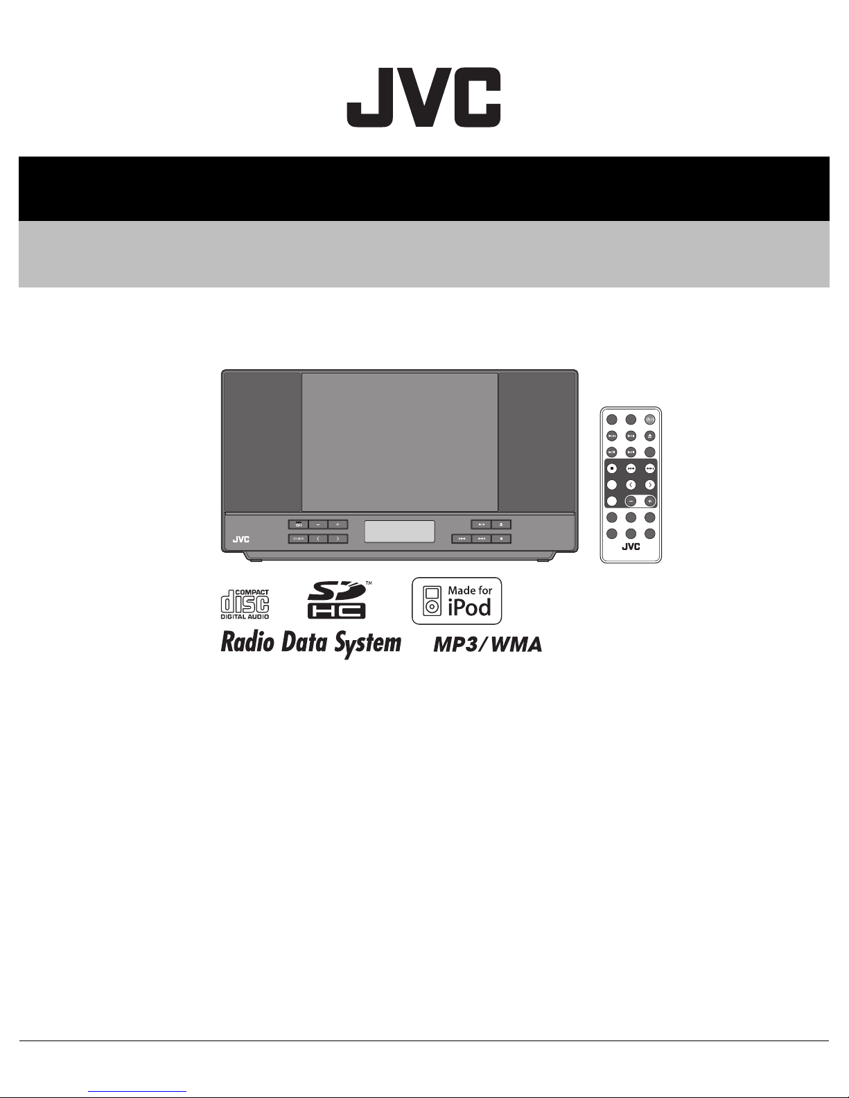
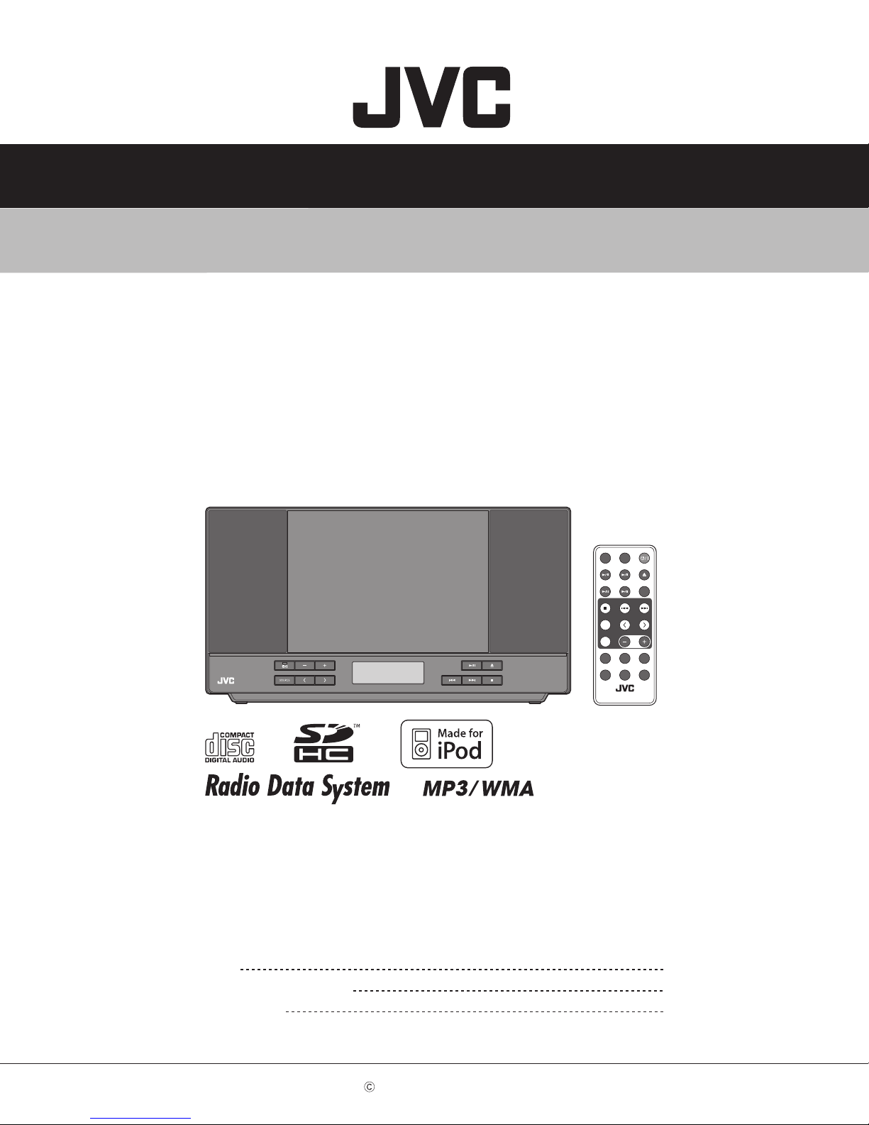
CD PORTABLE SYSTEM
MB730<Rev.001>201010SERVICE MANUAL
NX-PB10B, NX-PB10E, NX-PB10EY
COPYRIGHT © 2010 Victor Company of Japan, Limited
Lead free solder used in the board (material : Sn-Ag-Cu, melting point : 219 Centigrade)
1 PRECAUTION. . . . . . . . . . . . . . . . . . . . . . . . . . . . . . . . . . . . . . . . . . . . . . . . . . . . . . . . . . . . . . . . . . . . . . . . . 1-3
2 SPECIFIC SERVICE INSTRUCTIONS . . . . . . . . . . . . . . . . . . . . . . . . . . . . . . . . . . . . . . . . . . . . . . . . . . . . . . 1-6
3 DISASSEMBLY . . . . . . . . . . . . . . . . . . . . . . . . . . . . . . . . . . . . . . . . . . . . . . . . . . . . . . . . . . . . . . . . . . . . . . . 1-6
4 ADJUSTMENT . . . . . . . . . . . . . . . . . . . . . . . . . . . . . . . . . . . . . . . . . . . . . . . . . . . . . . . . . . . . . . . . . . . . . . . . 1-8
5 TROUBLESHOOTING . . . . . . . . . . . . . . . . . . . . . . . . . . . . . . . . . . . . . . . . . . . . . . . . . . . . . . . . . . . . . . . . . . 1-8
COPYRIGHT © 2010 Victor Company of Japan, Limited
TABLE OF CONTENTS
No.MB730<Rev.001>
2010/10
Page 2
SPECIFICATION
Amplifier section
Output Power 4 W (2 W + 2 W) at 16 Ω (10% THD)
Audio Input AUDIO IN: Stereo mini (
250 mV/47 kΩ
Digital input USB terminal
Tuner
FM tuning range 87.50 MHz - 108.00 MHz
Disc player
Dynamic range 80 dB
Wow and flutter Immeasurable
USB
USB specification Compatible with USB 2.0 Full Speed
Compatible device Mass storage class
Compatible system FAT16, FAT32
Output power DC 5 V 500 mA
SD
Compatible device SD, SDHC
Compatible system FAT16, FAT32
iPod
Output power DC 5 V 500 mA
General
Speaker type Bass-Reflex type
Speaker unit 8 cm x 2
Speaker impedance 16 Ω
Power requirements AC 230 V / 50 Hz
Power consumption 25 W (at operation)
1.00 W or less (on standby)
Dimensions (approx.) 400 mm × 215 mm × 91 mm (W × H × D)
Mass (approx.) 2.3 kg
ø 3.5 mm)
Design and specifications are subject to change without notice.
1-2 (No.MB730<Rev.001>)
Page 3

SECTION 1
PRECAUTION
1.1 Safety Precautions
(1) This design of this product contains special hardware and
many circuits and components specially for safety purposes. For continued protection, no changes should be made
to the original design unless authorized in writing by the
manufacturer. Replacement parts must be identical to
those used in the original circuits. Services should be performed by qualified personnel only.
(2) Alterations of the design or circuitry of the product should
not be made. Any design alterations of the product should
not be made. Any design alterations or additions will void
the manufacturers warranty and will further relieve the
manufacture of responsibility for personal injury or property
damage resulting therefrom.
(3) Many electrical and mechanical parts in the products have
special safety-related characteristics. These characteristics are often not evident from visual inspection nor can the
protection afforded by them necessarily be obtained by using replacement components rated for higher voltage, wattage, etc. Replacement parts which have these special
safety characteristics are identified in the Parts List of Service Manual. Electrical components having such features
are identified by shading on the schematics and by ( ) on
the Parts List in the Service Manual. The use of a substitute
replacement which does not have the same safety characteristics as the recommended replacement parts shown in
the Parts List of Service Manual may create shock, fire, or
other hazards.
(4) The leads in the products are routed and dressed with ties,
clamps, tubings, barriers and the like to be separated from
live parts, high temperature parts, moving parts and/or
sharp edges for the prevention of electric shock and fire
hazard. When service is required, the original lead routing
and dress should be observed, and it should be confirmed
that they have been returned to normal, after reassembling.
(5) Leakage shock hazard testing
After reassembling the product, always perform an isolation check on the exposed metal parts of the product (antenna terminals, knobs, metal cabinet, screw heads,
headphone jack, control shafts, etc.) to be sure the product
is safe to operate without danger of electrical shock.Do not
use a line isolation transformer during this check.
• Plug the AC line cord directly into the AC outlet. Using a
"Leakage Current Tester", measure the leakage current
from each exposed metal parts of the cabinet, particularly any exposed metal part having a return path to the
chassis, to a known good earth ground. Any leakage current must not exceed 0.5mA AC (r.m.s.).
• Alternate check method
Plug the AC line cord directly into the AC outlet. Use an
AC voltmeter having, 1,000Ω per volt or more sensitivity
in the following manner. Connect a 1,500Ω 10W resistor
paralleled by a 0.15µF AC-type capacitor between an ex-
posed metal part and a known good earth ground.
Measure the AC voltage across the resistor with the AC
voltmeter.
Move the resistor connection to each exposed metal
part, particularly any exposed metal part having a return
path to the chassis, and measure the AC voltage across
the resistor. Now, reverse the plug in the AC outlet and
repeat each measurement. Voltage measured any must
not exceed 0.75 V AC (r.m.s.). This corresponds to 0.5
mA AC (r.m.s.).
AC VOLTMETER
(Having 1000
ohms/volts,
or more sensitivity)
0.15 F AC TYPE
Place this
probe on
1500 10W
Good earth ground
1.2 Warning
(1) This equipment has been designed and manufactured to
meet international safety standards.
(2) It is the legal responsibility of the repairer to ensure that
these safety standards are maintained.
(3) Repairs must be made in accordance with the relevant
safety standards.
(4) It is essential that safety critical components are replaced
by approved parts.
(5) If mains voltage selector is provided, check setting for local
voltage.
1.3 Caution
Burrs formed during molding may be left over on some parts
of the chassis.
Therefore, pay attention to such burrs in the case of preforming repair of this system.
1.4 Critical parts for safety
In regard with component parts appearing on the silk-screen
printed side (parts side) of the PWB diagrams, the parts that are
printed over with black such as the resistor ( ), diode ( )
and ICP ( ) or identified by the " " mark nearby are critical
for safety. When replacing them, be sure to use the parts of the
same type and rating as specified by the manufacturer.
(This regulation dose not Except the J and C version)
each exposed
metal part.
(No.MB730<Rev.001>)1-3
Page 4

1.5 Preventing static electricity
Electrostatic discharge (ESD), which occurs when static electricity stored in the body, fabric, etc. is discharged, can destroy the laser
diode in the traverse unit (optical pickup). Take care to prevent this when performing repairs.
1.5.1 Grounding to prevent damage by static electricity
Static electricity in the work area can destroy the optical pickup (laser diode) in devices such as laser products.
Be careful to use proper grounding in the area where repairs are being performed.
(1) Ground the workbench
Ground the workbench by laying conductive material (such as a conductive sheet) or an iron plate over it before placing the
traverse unit (optical pickup) on it.
(2) Ground yourself
Use an anti-static wrist strap to release any static electricity built up in your body.
(caption)
Anti-static wrist strap
1M
Conductive material
(conductive sheet) or iron palate
(3) Handling the optical pickup
• In order to maintain quality during transport and before installation, both sides of the laser diode on the replacement optical
pickup are shorted. After replacement, return the shorted parts to their original condition.
(Refer to the text.)
• Do not use a tester to check the condition of the laser diode in the optical pickup. The tester's internal power source can easily
destroy the laser diode.
1.6 Handling the traverse unit (optical pickup)
(1) Do not subject the traverse unit (optical pickup) to strong shocks, as it is a sensitive, complex unit.
(2) Cut off the shorted part of the flexible cable using nippers, etc. after replacing the optical pickup. For specific details, refer to the
replacement procedure in the text. Remove the anti-static pin when replacing the traverse unit. Be careful not to take too long a
time when attaching it to the connector.
(3) Handle the flexible cable carefully as it may break when subjected to strong force.
(4) I t is not possible to adjust the semi-fixed resistor that adjusts the laser power. Do not turn it.
1.7 Attention when traverse unit is decomposed
*Please refer to "Disassembly method" in the text for the pickup unit.
• Apply solder to the short land sections before the card wire is disconnected from the connector on the servo board. (If the card wire
is disconnected without applying solder, the pickup may be destroyed by static electricity.)
• In the assembly, be sure to remove solder from the short land sections after connecting the card wire.
1-4 (No.MB730<Rev.001>)
solder short
Page 5

1.8 Important for laser products
1.CLASS 1 LASER PRODUCT
2.CAUTION :
(For U.S.A.) Visible and/or invisible class II laser radiation
when open. Do not stare into beam.
(Others) Visible and/or invisible class 1M laser radiation
when open. Do not view directly with optical instruments.
3.CAUTION : Visible and/or invisible laser radiation when
open and inter lock failed or defeated. Avoid direct
exposure to beam.
4.CAUTION : This laser product uses visible and/or invisible
laser radiation and is equipped with safety switches which
prevent emission of radiation when the drawer is open and
the safety interlocks have failed or are defeated. It is
dangerous to defeat the safety switches.
5.CAUTION : If safety switches malfunction, the laser is able
to function.
6.CAUTION : Use of controls, adjustments or performance of
procedures other than those specified here in may result in
hazardous radiation exposure.
!
Please use enough caution not to
see the beam directly or touch it
in case of an adjustment or operation
check.
REPRODUCTION AND POSITION OF LABELS and PRINT
WARNING LABEL and PRINT
(No.MB730<Rev.001>)1-5
Page 6

SECTION 2
SPECIFIC SERVICE INSTRUCTIONS
This service manual does not describe SPECIFIC SERVICE INSTRUCTIONS.
SECTION 3
DISASSEMBLY
3.1 Main body (Used model: NX-PB10E)
3.1.1 Removing the Rear cover (See Fig.1, 2, 3)
(1) Remove the three screws A, three screws B and two
screws C attaching the Rear cabinet. (See Fig.1)
BC CA
AABB
Fig.1
(2) Disconnect the antenna wire from post pin FM1
board. (See Fig.2)
FM1
of the Main
3.1.2 Removing the Main board (See Fig.4)
(1) Disconnect the card wire from iPod board connected to
connector CN103 of the Main board.
(2) Disconnect the card wire from Key board connected to con-
nector CN701
(3) Disconnect the connector wire from Left speaker connect-
ed to connector J2
(4) Disconnect the connector wire from Right speaker con-
nected to connector J3 of the Main board.
(5) Disconnect the connector wire from Door switch board con-
nected to connector CN405 of the Main board.
(6) Disconnect the connector wires from USB board connect-
ed to connectors J13
board.
(7) Disconnect the card wire from USB board connected to
connector CN607
(8) Disconnect the connector wire from Door motor connected
to connector CN404 of the Main board.
(9) Disconnect the connector wire from CD mechanism con-
nected to connector CN902 of the Main board.
(10) Disconnect the flexible wire from CD pickup connected to
connector CN901
(11) Remove the six screws D attaching the Main board.
CN405 J2 J3
of the Main board.
of the Main board.
, CN603 and CN306 off the Main
of the Main board.
of the Main board.
CN306 CN902 CN103
DD
CN404
D
Fig.2
(3) Disconnect the connector wire from Trans board connect-
ed to connector CN402
1-6 (No.MB730<Rev.001>)
of the Main board. (See Fig.3)
CN402
Fig.3
J13 CN607
CN701CN603 CN901
DD D
Fig.4
Page 7

3.1.3 Removing the Key board (See Fig.5)
(1) Remove the nine screws E attaching the Key board.
E
Fig.5
3.1.4 Removing the USB board (See Fig.6)
(1) Remove the three screws F attaching the USB board.
(2) Remove the two screws G and one screw H attaching the
Door switches.
G
3.1.6 Removing the Door motor (See Fig.8)
(1) Remove the three screws K attaching the Door motor.
K
Fig.8
3.1.7 Removing the CD mechanism (See Fig.9)
(1) Remove the three screws L attaching the CD mechanism.
F
H
Fig.6
3.1.5 Removing the iPod boar (See Fig.7)
(1) Remove the two screws J attaching the holder.
(2) Disengage the shaft of iPod bracket from Front cabinet.
J
Fig.7
shaft
L
Fig.9
3.1.8 Removing the Trans board (See Fig.10)
(1) Disconnect the power cord from connector CN1103
Trans board.
(2) Disconnect the connector wires from Power transformer
connected to connector CN1101
board.
(3) Remove the three screws M attaching the Trans board.
and CN1104 of the Trans
M
of the
CN1103 CN1104 CN1101
Fig.10
(No.MB730<Rev.001>)1-7
M
Page 8

SECTION 4
ADJUSTMENT
This service manual does not describe ADJUSTMENT.
SECTION 5
TROUBLESHOOTING
This service manual does not describe TROUBLESHOOTING.
1-8 (No.MB730<Rev.001>)
Page 9

<MEMO>
1-9 (No.MB730<Rev.001>)
Page 10

Victor Company of Japan, Limited
Personal AV Operation 10-1,1chome,Ohwatari-machi,Maebashi-city,371-8543,Japan
(No.MB730<Rev.001>)
Printed in Japan
VSE
Page 11
SCHEMATIC DIAGRAMS
CD PORTABLE SYSTEM
NX-PB10B, NX-PB10E,
NX-PB10EY
Lead free solder used in the board (material : Sn-Ag-Cu, melting point : 219 Centigrade)
Contents
Block diagrams
Standard schematic diagrams
Printed circuit boards
COPYRIGHT 2010 Victor Company of Japan, Limited.
2-1
2-2
2-10 to 12
No.MB730SCH<Rev.001>
2010/12
Page 12

In regard with component parts appearing on the silk-screen printed side (parts side) of the PWB diagrams, the
parts that are printed over with black such as the resistor ( ), diode ( ) and ICP ( ) or identified by the " "
mark nearby are critical for safety.
Page 13

2-1
Block diagram
IC705
U1
LCD
KEY
REMOTE
SENSOR
IC304
IC702
MOTO
OPEN/CLOSE SW
DISC
PICKUP
IC901
SPINDLE
MOTOR
M
SLED
MOTOR
M
IC905
MOTOR/ACTUATOR
DRIVER
IC902
3.3V
IC404
USB
IPOD
USB+5V
IPOD+5V
IC406
IC405
VOL IC
3.3V
IC403
CD-L
CD-R
IPOD-L
IPOD-R
IC401
SIGNAL SELECT SW.
VOL CONTROL
L-CH
R-CH
IC302
POWER AMP
U201
RECTIFIER
AMP
AC INPUT
TRANSFORMER
Q1101
Q1102
TRANSFORMER
RECTIFIER
CD+8V
IC412
+5V
IC413
SD
MAINPOWER
3.3V
+9V
TU-L
TU-R
TU+VCC
FM MODULE
FM ANT.
RELAY
JK402
HEADPHONE
L.SPK OUTPUT
R.SPK OUTPUT
VCC
AUX-L
AUX-R
AUX IN
Page 14

2-2
Q1102
R1108
Q1101
FS1102
CN1103
CN1101
CN1104
RY1101
R1104
R1102
R1101
R1103
DGND
C1110
D1107
C1112
C1113
D1105
C1108
D1109
C1111
D1108
D1106
C1109
C1102
D1102
C1104
D1104
R1105
R1106
C1115
C1101
D1101
C1103
D1103
FS1101
C1114
C1107
PT1101
L1101
CN1102
Parts are safety assurance parts.
When replacing those parts make
sure to use the specified one.
To Main section 3
CN402
Standard schematic diagrams
<Rectifier section>
Page 15

2-3
VC25
PH-MUTE
LOV-TADA
VOL-CLK
CD_RX
CD_TX
CLOSE-DET
R725
R783
R782
GND
R739
R29
R767
R766
C708
C6
U1
GND
IO
IRQ
RDS-DAT
IIC-SCL
IIC-SDA
ST-BY
PLL_RST
IIC-SCL
IIC-SDA
EQ-SCL
EQ-SDA
CLOSE-DET
R759
R750
R763 R762
D407
D408
IC705
Q409
Q912
R484
R483
C336
D705
ZD304
R309
R308
C386
C339
C397
L304
C455
P_CON
C318
KEY1
KEY1
IR
IRQ
R302
VCC3.3V
KEY2
KEY2
LCD-DAT
LCD-DAT
LCD-WR
LCD-WR
LCD-WR
LCD-CS
LCD-CS
LCD-CS
LED+5V
VCC+12V
RX
TX
VC25
R716
R720
R722
R724
R726
R728
R771
R707
LB1641
R715
R713
R718
R761
R111
R708
R706
R709
SW901
R717
R703
Q1
TC703
R710
TC702
C702
D409
R719
R721
R723
U702
R310
C302
CN701
CN405
CN404
R764
C333
DET13
VCC3.3V
VCC3.3V
PH-DET
P-CD
MCU-MUTE
IR
LCD-DAT
TC705
C701
R705
C731
C730
C732
GND
R737
IC304
DET30
VCC+12V
LED+5V
ZD402
C530
C529
R996
R995
R769
R770
R755
R751
R117
VCC3.3V
VCC3.3V
VCC3.3V
To Front section
CN712
To Main section 3
To MOTOR
To Leaf SW section
CN704
To Main section 3
To Main section 2
To Main section 3
To Main section 3
To Main section 3
<Main section 1>
Page 16

2-4
CN901
3V3SD
M33V
L309
C972
C934
C970
R935
L913
Q903
SEV_3V3
C967
C911
C969
C927
C912
C928
C971
C920
C918
C914
C917
R934
C931
R936
X901
C925
C929
M33V_LDO
M33V_CKG
AUD_3V3
V18_CORE
DAC_R
AGND
DAC_L
C13
C14
R205
R206
C222
R67
C974
C977
L916
C957
C976
C975
C916
C221
R439
L505
L504
L931
L932
USB+5V
P-USB
M33V
USB-DET
M33V
R446
R423
R938
R414
R437
C408
C450
IC406
C441
C412
C442
C559
C413
R930
R931
R956
C973
C968
C965
C964
C915
C962
L506
L507
C913
L936
L934
L935
L933
L921
L922
IC902
R929
L912
L917
L906
L905
L918
L919
M33V_PAD
3V3SD
M33V
C932
SEV_3V3
AUD_3V3
3V3SD_IC
M33V_PAD
M33V_CKG
M33V_LDO
M33V
C956
C930
C496
R928
C495
C954
C959
C933
C955
IC404
C923
D406
C5
D410
CD+8V
CD_TX
CD_RX
C3
R23
MUTE1
M33V
3V3SD
CLOSE-DET
C1
IC905
CD-GND
CD+8V
L901
C944
R945
C945
R944
R927
R941
R595
R575
R574
R573
R572
C909
R933
C980
R913
R987
D903
Q901
R984
R985
R986
C979
D904
R947
D901
Q904
R966
R989
R988
Q902
R991
R990
AGND
C958
R943
R916
R917
R918
C919
SEV_3V3
3V3SD_IC
USB-DET
V18_CORE
M33V_PAD
P-USB
L915
C924
C922
C921
AGND
CN603
R937
R946
L902
L900
R3
R2
GND
GND
L1
C961
CN607
IC901
R912
R919
R922
R920
R911
R914
D706
R24
L8
L7
L6
L5
L4
L2
L3
C948
R925
R28
JP60
C946
C947
R942
C949
C938
CN902
To Main section 3
To USB section
CN604
To PICK UP
To Main section 1
To USB section
CN708
To CD TRAMECH
A
To This sheet
To This sheet
To This sheet
To This sheet
To This sheet
To This sheet
To This sheet
To This sheet
To This sheet
<Main section 2>
Page 17

2-5
EQ-SDA
EQ-SCL
L15
L30
DAC_L
DAC_R
C160
C159
C165
R51
C166
R55
R407
R408
R409
C431
C433
C432
R410
R135
R121
C440
R215
Q202
Q201
R216
R31
R212
R485
Q404
Q408
R459
C563
C113
C116
R458
L108
R120
ES113
C120
C101
R115
L112
R742
L116
L115
R103
C103
TU+3.3V
+8V
C168
CE203
CE204
CN306
C20
C403
C524
C511
C411
C525
C526
R201
C534
C540
R454
C10
C11
R18
R17
C533
R82
CN312
C527
C505
C422
C125
DET13
I0
DET30
RX
TX
C115
R103
C104
R105
X101
C105
CE201
BC206
R104
IC101
C119
R125
C202
R124
FB300
H0-L
R113
FB402
C452
C436
C448
R4
C437
C446
C434
R1
C451
IC401
C435
C404
R512
C429
AGND
R209
C407
R517
C453
C430
R208
BC201
R202
U201
C201
R213
ZD201
R101
C103
R110
C107
C105
C104
C108
C106
R109
C102
C101
R102
C109
IC704
C167
C460
R482
C158
EC7
CFC11
C142
C150
C153
C162
C161
C170
C515
C426
R425
C456
C541
C463
R9
C469
R136
C169
R132
C163
C140
R26
C410
C148
U11
R12
R27
C154
R37
R36
TC8
EC8
FC6
C152
TC6
R144
R141
R107
C171
C173
C174
R119
R145
C172
R469
R443
CN103
R420
C723
C414
R452
C510
R191
C538
R438
R518
C9
R15
R83
Q6
R19
Q5
C176
R225
R33
IC302
C535
C521
C143
D405
D402
C89
IC412
C978
L402
C963
D413
IC405
C416
C458
R428
R435
R434
R429
C461
C445
R472
D401
D905
IC413
C459
R413
C1105
CN402
VCC1
R426
C421
C420
C402
J2
J3
R21
C177
R7
R14
C7
C8
R424
L401
D412
C419
C12
R451
R189
D403
R204
IN4148
D404
R442
R519
C522
C2
Q405
C405
Q406
+8V
CD+8V
P-CD
ST-BY
VCC+12V
CD-MUTE
R192
C542
R453
R174
MCU-MUTE
H0-L
H0-R
USB+5V
VCC+12V
VCC3.3V
P_CN
R10
R147
TC5
C151
R11
C141
C155
R151
C156
C157
R104
C427
R422
C509
R13
C523
C528
R427
R421
C514
VOL-CLK
LOV-TADA
IC403
C518
C516
ZD502
R239
R210
R133
C470
R131
USB+5V
TU-R
+8V
TU-L
H0-R
H0-L
IPOD-L
IPOD-R
C175
C147
R20
C149
BC2
EC22
C19
C204
R214
C203
R203
C428
FB401
FB300
R116
R406
R405
C468
C438
C467
R401
C401
C443
C439
BC207
BC204
R207
CE202
BC202
FB202
FB300
FB201
R211
FB204
TU-R
TU-L
IPOD-R
IPOD-L
PH-MUTE
TU+3.3V
H0-R
+8V
PH-DET
RDS-DAT
ANT-FM
PLL_RST
IIC-SDA
IIC-SCL
To Main section 1
To USB section
CN305
To USB section
CN305
To Main section 1
To Main section 1
To Main section 1
To Main section 1
To Main section 2
To This sheet
To This sheet
To Main section 1
To This sheet
To Rectifier section
CN1102
To iPod section
CN201
To Main section 1
To This sheet
To This sheet
To This sheet
To This sheet
To This sheet
To This sheet
To This sheet
To This sheet
To This sheet
<Main section 3>
Page 18

2-6
KEY1
SW702
R732 R755
R761 R756 R733 R753
KEY2
KEY1
IR
IRQ
VCC3.3V
VCC3.3V
KEY2
LCD-DAT
LCD-WR
LCD-CS
LED+5V
LED+5V
R752
C737
R713
LED702
R757
C742
Q702
C748
R716
R715
SW708
SW711
SW709
SW712
C710
C709
R735
R777
R738
R714
LCD-CS
LCD-RW
LCD-DAT
VCC3.3V
IRQ
X701
C726
C706
C705
SW705
SW706
SW704
C724
SW701
C725
C718
C746
R701
VCC3.3V
IR
C717
SW710
C716
C707
CN712
SW703
Q704
R758
R789
R754
R763
R765
R770
R762
LCD701
IC701
R741
C703
C704
SM338A
REM701
C747
R734
LED701
To Main section 1
CN706
<Front section>
Page 19

2-7
C605
C602
C603
JK602
CN708
D603
D604
C604
L609
D601
D602
JK601
C601
R505
R506
L503
C504
C536
R504
R503
L502
L501
C554
C556
CE608
CE609
CN305
C606
CN604
JK302
L302
L303
C607
JK301
L301
L601
L602
ES602
ES601
To Main section 3
CN312
CN306
To Main section 2
CN603
To Main section 2
CN607
<USB section>
Page 20

2-8
L99
L97
L96
CN201
R350
R356
R352
R349
R347
R353
D38
R355
R344
R348
R346
R345
Q53
Q54
D201
Q52
JK201
To Main section 3
CN103
<iPod section>
Page 21

2-9
SW2
R103
C103
C104
R105
X101
C105
R104
IC101
R101
C102
C101
R102
To Main section 1
CN405
To Main section 3
To Main section 3
To Main section 3
<Leaf SW section>
<Tuner section>
Page 22

2-10
C101
ES113
C120
R102
L108
C107
C103
R110
C105
C460
R482
C108
C104
R109
C106
L115
L116
L112
R767
R212
R717
R703
C701
C702
R783
C530
R782
R996
R995
C336
R309
R308
C333
R484
R483
R144
BC2
C19
C157
C152
R912
R919
R920
R922
R984
C979
R985
R943
C447
C944
C947
R945
C946
C948
L906
R935
R928
R929
C973
C968
C965
C964
C915
R25
C421
R426
R424
R401
C134
R406
R405
C976
R936
L916
Q406
C418
D412
C416
R434
R435
D402
D406
D410
C461
R429
R428
C923
L402
D405
C10
C11
IC302
C541
J3
C2
C963
C920
C954
L912
C912
R18
R17
C956
C916
C958
R916
R917
R918
C918
R927
R944
R942
C949
R987
R925
R5
R966
D904
C980
R761
D706
R938
R446
R947
R28
R914
Q902
R991
R990
R989
R988
Q904
C933
D903
R141
R107
R119
R145
C443
R404
R403
C449
C161
C162
C470
R133
R136
C169
R132
C140
C163
C154
C141
R11
C155
C151
C156
C170
C468
R131
C435
C422
C423
C424
C425
C174
C173
C171
C172
C175
C340
C436
C446
C438
C467
C437
C448
C452
C434
R408
R409
C431
R410
C432
R1R4R120
IC401
C430
R438
R82
C427
C426
C417
C439
C469
C451
C457
C401
C433
C411
C453
C407
ZD201
R203
C203
R207
R31
R215
R202
BC201
R213
R204
R210
R209
R201
R459
Q408
R427
R421
C463
R9
R13
R451
C535
C18
R7
R14
C7
C8
R117
C160
C165
C125
FB401
FB402
C115
R103
R742
C116
R115
C113
R721
R719
R111
R708
R704
U702
R116
C708
R766
C16
C4
C119
R113
R762
R764
R763
R751
C707
R755
C412
C450
C408
R414
R437
L30
L15
R55
R125
R51
R124
X101
C559
R723
R725
R29
R724
R722
R720
R709
R737
R771
D701
R713
R705
R770
R769
FM1
IC102
C168
IC704
CN405
CN306
C167
C109
IC705
R759
R750
C6
C159
C166
C441
U1
IC406
TC703
Q702
R706
R710
C413
R911
L3
L2
L4
L5
L12
L9
L10
L11
L6
L7
L8
R23
C3
L505
L504
CN902
R739
R728
R726
R718
R707
TC705
TC702
TC1
R30
R716
R715
L201
D409
R485
CN404
D705
C529
C302
ZD402
Q912
IC304
ZD304
C386
R310
C339
L304
C455
D407
D408
D404
C509
C515
C518
C514
IC403
C176
C538
Q201
Q6
C20
R21
Q202
J2
Q5
Q404
R458
BC206
BC207
FB201
FB202
BC202
R214
R216
BC203
C201
C202
R518
C533
R452
C540
R453
R454
C459
IC413
R443
R469
Q405
L901
L917
C1105
C925
C929
C971
C977
C5
C934
C961
C914
L915
C924
C930
L918
L919
C931
C927
C911
C972
R934
C967
C983
C945
C913
L933
X901
C922
C917
C974
IC901
L309
L905
C955
C975
C957
C921
C932
C13
C919
C221
R205
R16
R206
C14
C222
R420
R67
C405
IC902
C420
L936
L934
L935
C496
L922
L1
L921
R2
R3
R986
EC7
FC6
C138
R37
R36
R12
R27
C147
CN104
EC22
R407
R425
C153
R20
C149
C428
C429
EC8
C419
R486
R422
C158
FC11
C150
R147
C142
C148
R26
U11
R151
TC8
TC6
TC5
R10
R104
CN103
R967
R423
C962
IC412
Q901
R913
L932
L931
R937
C970
Q903
C1
IC905
CN701
R941
R946
C410
C959
C969
IC404
C928
CN901
R442
C1106
CN402
D413
C402
C89
R413
C414
L401
C978
D905
C143
C534
R519
C522
D401
C318
C458
IC405
C723
C17
R192
C542
R174
C516
R239
ZD502
C456
C521
R33
R225
R19
R6
R8
C510
R191
R189
C177
U201
CE202
CE201
R208
CE204
R211
FB204
C204
C9
C404
C403
C12
C454
R83
R15
R121
C440
Q409
D403
R302
R24
R22
R573
R572
R575
R574
R595
R933
CN607
C15
CN603
C442
C1115
R1106
R1105
R1104
R1103
R1102
R1101
JMP1101
JMP1102
Q1101
Q1102
R1108
C1112
CN1102
CN1103CN1104
C1114
CN1101
D1109
RY1101
FS1101
C1113
J1101
C1107
D1104
D1101
D1103
C1102
C1104
C1101
C1103
L1101
FS1102
PT1101
C1109
D1106
C1108
D1105
C1110
D1107
C1111
D1108
J1102
D1102
C103
R103
R104
R105
C104
C105
IC101
R101
R102
C101
C102
Printed circuit boards
<Main board (forward side)>
(Lead free solder used in the board (material : Sn-Ag-Cu, melting point : 219 Centigrade))
<Rectifier board>
(forward side) (reverse side)
(Lead free solder used in the board (material : Sn-Ag-Cu, melting point : 219 Centigrade))
(reverse side)
<Tuner board>
(forward side)
(Lead free solder used in the board (material : Sn-Ag-Cu, melting point : 219 Centigrade))
Page 23

2-11
SW901
D601
D602
C601
CN604
L602
L601
L607
L608
L609
C605
C603
C536
R505
R503
C504
L303
R504
C554
C556
JK301
ES602
JK602
C607
CE609
L302
C602
L301
L305
CE608
D603
D604
C604
JK601
ES601
CN708
C606
L503
CN305
R506
L502
L501
JK302
GND
SW2
<Main board (reverse side)>
(Lead free solder used in the board (material : Sn-Ag-Cu, melting point : 219 Centigrade))
<USB board>
(forward side)
(reverse side)
<Leaf SW board>
(forward side)
(reverse side)
(Lead free solder used in the board (material : Sn-Ag-Cu, melting point : 219 Centigrade))
(Lead free solder used in the board (material : Sn-Ag-Cu, melting point : 219 Centigrade))
Page 24

2-12
C717
C710
C746
C747
R734
R735
IC701
JP1
JP4
JP10
JP3
JP11
JP6
JP7
JP5
C730
R738
JP88
JP81
JP82
C724
Q704
C726
C748
R715
Q702
C707
C706
R761
R756
C725
R752
R751
R758
R789
JP8
R777
R741
C704
C732
C703
C708
R714
C718
R754
R770
R765
C716
R763
R762
C709
JP2
C727
R701
JP89
JP9
JP38
JP12
C712
C737
R753
R732
C742
R757
R713
C768
R716
C705
R733
R755
LED702
SW702
SW701
SW703
SW704
SW705
SW706
LED701
CN712
LCD701
X701
REM701
SW708
SW709
SW710
SW711
SW712
CN202
CN201
L96
L97
Q53
R355
Q52
D38
R353
R352
Q54
R346
R356
R345
D201
R347
R349
R350
L99
R348
R344
JK201
L100
C250
<Front board>
(Lead free solder used in the board (material : Sn-Ag-Cu, melting point : 219 Centigrade))
(forward side)
(reverse side)
<iPod board>
(Lead free solder used in the board (material : Sn-Ag-Cu, melting point : 219 Centigrade))
(forward side)
(reverse side)
Page 25

< MEMO >
Page 26

Victor Company of Japan, Limited
Personal AV Operation
(No.MB730SCH<Rev.001>)
Printed in Japan
VSE
Page 27

PARTS LIST
Preliminary
NX-PB10E,NX-PB10B,NX-PB10EY
MODEL MARK
ANX-PB10B
BNX-PB10E
CNX-PB10EY
* All printed circuit boards and its assemblies are not available as service parts.
- Contents -
Exploded view of general assembly and parts list (Block No.M1)
Electrical parts list (Block No.01~07)
Packing materials and accessories parts list (Block No.M3)
MB730PAR<Rev.001>
3- 2
3- 5
3-12
3-1
Page 28

Exploded view of general assembly and parts list
P
Block No.
M MM1
35
c
h
p
b
58
n
7
56
47
16
r
18
17
Main board
58
F
n
54
54
18
54
18
p
Switch board
33
c
71
14
61/2
11
16
A
16
47
34
A
F
61
q
24
19
58
62
d
58
61
a
a
20
d
70
14
D
5
2
1
4
B
3
1
E
13
42
55
t
16
12
25
47
i
8
26
3-2
Page 29

39
57
58
q
d
a
58
69
t
f
s
e
r
16
12
25
1
24
19
14
47
58
62
61
a
70
8
26
20
21
d
76
iPod board
6 2/2
48
53
27
32
23
53
22
Rectifier board
51
66
64
29
30
28
52
b
77
10
j
52
D
48
B
q
h
k
m
51
48
Front board
k
65
79
66
e
78
48
72
50
80
36
60
67
60
81
60
59
m
60
75
38
B
s
73
49
68
j
f
74
E
63
37
USB board
The parts without symbol number are not service.
3-3
Page 30

General Assembly
Symbol No. Part No. Part Name Description Local
1 467-BL0147-000 SPEAKER NET (x2)
2 5P1-040000-001 SPK PANEL L
3 5P1-040000-002 SPK PANEL R
4 5P1-0450000-000 DISPLAY PANEL
5 5P1-001000-000 FRONT CABINET
6 5P1-051000-000 FUNCTION BTN
7 5P1-021200-001 GEAR COVER
8 5P1-065000-000 RECEIVER LENS
10 5P1-026800-000 REMOTE LENS BKT
11 5P1-032000-000 LED LENS
12 5P1-026500-000 LED BKT
13 586-531100-000 LCD COVER
14 154-361620-508 SPEAKER 16
16 459-155165-060 SPK BRACKET (x4)
17 356-230000-095 CD MECHANISM
18 458-101000-020 RUBBER FOOT (x3)
19 466-260013-013 BELT
20 5P1-024300-000 SLIP GEAR
21 5P1-024000-002 COMPOUND GEAR
22 5P1-021200-000 GEAR BRACKET
23 5P1-024900-000 MOTOR PULLEY
24 5P1-024000-001 BIG GEAR
25 220-000810-026 LCD MODULE 26P 3.3V
26 5B6-580500-000 LCD LENS
27 5B6-531000-000 LCD CASE
28 5P1-022050-000 iPod PCB BKT (x2)
29 5P1-076000-000 iPod BRACKET
30 5P1-039000-000 iPod PLATE
32 360-055133-015 MOTOR
33 5P1-049000-000 DOOR PANEL
34 5P1-029010-001 DOOR PLATE 2
35 5P1-029010-000 DOOR PLATE
36 5P1-002000-000 REAR CABINET
37 530-026200-000 STRAIN RELIEF
38 152-102369-215 POWER TRANS
39 408-PB1000-000 HEAT SINK
42 217-200035-050 LEAF SWITCH
47 238-130080-632 SCREW 3x8mm(x4)
48 238-120080-602 SCREW 2x8mm(x9)
49 238-126080-602 SCREW 2.6x8mm(x3)
50 238-130200-632 SCREW 3x20mm(x2)
51 238-126080-602 SCREW 2.6x8mm(x2)
52 238-120060-602 SCREW 2x6mm(x4)
53 238-130080-602 SCREW 3x8mm(x3)
54 238-170507-631 SCREW 1.7x5mm(x3)
55 238-120060-602 SCREW 2x6mm
56 238-126080-602 SCREW 2.6x8mm(x2)
57 238-130060-202A SCREW 3x6mm(x2)
58 238-126080-602 SCREW 2.6x8mm(x6)
59 238-130100-602 SCREW 3x10mm(x2)
60 238-130180-602 SCREW 3x18mm(x6)
61 238-120060-602 SCREW 2x6mm(x2)
62 238-117040-203 SCREW 1.7x4mm(x2)
63 151-240000-302 POWER CORD A
63 151-230000-200 POWER CORD B,C
64 231-901630-253 FUSE 630mA 250V
65 231-902315-253 FUSE 3.15A 250V
66 406-050090-000 FUSE HOLDER (x4)
67 234-261500-022 HSG WIRE 1P 1500mm
68 222-290190-155 CORD STOPPER
69 234-A04265-170 HSG WIRE 4P
70 234-A02265-150 CONNECTOR WIRE 2P 150mm
71 234-A02245-300 CONNECTOR WIRE 2P 300mm
72 222-160120-080 FERRITE BEAD
73 222-160120-080 FERRITE BEAD
74 222-160120-080 FERRITE BEAD
75 222-160120-080 FERRITE BEAD
76 235-110170-110 FFC WIRE 11P 170mm
77 235-100070-110 FFC WIRE 10P 70mm
78 235-110150-110 FFC WIRE 10P 150mm
79 419-085034-050 SHIELD PLATE
80 LVT44803-003A LASER CAUTION
81 898-PB1000-010 RATING LABEL A,B
81 898-PB1000-020 RATING LABEL C
Ω
2W(x2)
Block No. [M][1][M][M]
3-4
Page 31

Electrical parts list
Main board
Block No. [0][1]
Symbol No.
IC302 210-007266-000 IC TDA7266
IC304 210-001641-000 IC LB1641
IC401 310-007314-100 IC SC7314
IC403 310-062429-036 IC M62429P
IC404 310-001117-104 IC AZ1117 TO-252-2(1)
IC405 310-001117-104 IC AZ1117 TO-252-2(1)
IC406 310-001526-100 IC AIC1526
IC412 310-001007-024 IC TG1007
IC413 310-001007-024 IC TG1007
IC704 310-001117-133 IC APL1117
IC705 310-002161-217 IC iPhone IC 2161
IC901 310-005673-128 IC M5673Z1 128P
IC902 310-002520-008 IC EN25F20
IC905 310-009258-128 IC SA9258PH (3V3)
U1 310-002402-102 IC AM24LC02
U11 310-004558-100 IC
U201 310-004800-115 IC ETK4800
U702 310-006812-132 IC CA6812
Q5 307-008050-030 TRANSISTOR 8050C/D
Q6 307-008050-030 TRANSISTOR 8050C/D
Q201 307-009014-030 TRANSISTOR 9014C
Q202 307-009014-030 TRANSISTOR 9014C
Q404 307-009014-030 TRANSISTOR 9014C
Q405 207-000772-250 TRANSISTOR B772Y
Q406 307-009014-030 TRANSISTOR 9014C
Q408 307-008550-020 TRANSISTOR 8550B/C
Q702 307-008050-030 TRANSISTOR 8050C/D
Q901 307-008050-030 TRANSISTOR 8050C/D
Q902 307-008050-030 TRANSISTOR 8050C/D
Q903 207-008550-020 TRANSISTOR 8550B/C
Q904 307-008550-020 TRANSISTOR 8550B/C
Q912 307-008050-030 TRANSISTOR 8050C/D
D401 206-304001-000 RECTIFIER IN-4001
D402 206-304001-000 RECTIFIER IN-4001
D404 306-104148-000 DIODE 1N4148
D405 206-304001-000 RECTIFIER IN-4001
D406 206-304001-000 RECTIFIER IN-4001
D407 301-100005-014 RESISTOR 0
D408 301-100005-014 RESISTOR 0
D409 306-104148-000 DIODE 1N4148
D410 206-304001-000 RECTIFIER IN-4001
D412 206-305822-000 RECTIFIER DIODE 1N5822
D413 206-305822-000 RECTIFIER DIODE 1N5822
D705 306-104148-000 DIODE 1N4148
D706 206-104148-000 DIODE IN-4148
D903 206-104148-000 DIODE IN-4148
D904 206-104148-000 DIODE IN-4148
D905 206-304001-000 RECTIFIER IN-4001
C1 004-074772-216 E CAPACITOR 470uF/16V
C5 004-072272-210 E CAPACITOR 220uF/10V
C9 303-161062-210 T CAPACITOR 10UF 10V
C12 004-064762-216 E CAPACITOR 47uF/16V
C13 302-311015-550 C CAPACITOR 100pF/50V
C14 302-311015-550 C CAPACITOR 100pF/50V
C17 302-304705-550 C CAPACITOR 47pF/50V
C18 302-304705-550 C CAPACITOR 47pF/50V
C19 302-304705-550 C CAPACITOR 47pF/50V
C20 004-071072-216 E CAPACITOR 100uF/16V
C89 004-081082-225 E CAPACITOR 1000uF/25V
C101 302-303005-550 C CAPACITOR 30pF/50V
C103 302-351055-550 C CAPACITOR 1uF/50V
C104 302-351055-550 C CAPACITOR 1uF/50V
C105 302-331835-550 C CAPACITOR 0.018uF/50V
C106 302-331835-550 C CAPACITOR 0.018uF/50V
C107 302-331035-550 C CAPACITOR 0.01uF/50V
C108 302-331035-550 C CAPACITOR 0.01uF/50V
C113 302-321025-550 C CAPACITOR 0.001uF/50V
C120 302-304705-550 C CAPACITOR 47pF/50V
C134 302-304705-550 C CAPACITOR 47pF/50V
Part No. Part Name Description Local
Ω
1/4W
Ω
1/4W
Symbol No.
C140 302-352255-550 C CAPACITOR 2.2uF/50V
C142 302-304705-550 C CAPACITOR 47pF/50V
C147 302-304705-550 C CAPACITOR 47pF/50V
C148 302-311015-550 C CAPACITOR 100pF/50V
C149 302-311015-550 C CAPACITOR 100pF/50V
C150 302-304705-550 C CAPACITOR 47pF/50V
C151 302-318215-550 C CAPACITOR 820pF/50V
C152 302-318215-550 C CAPACITOR 820pF/50V
C153 302-304705-550 C CAPACITOR 47pF/50V
C154 302-304705-550 C CAPACITOR 47pF/50V
C156 302-321025-550 C CAPACITOR 0.001uF/50V
C157 302-321025-550 C CAPACITOR 0.001uF/50V
C158 302-304705-550 C CAPACITOR 47pF/50V
C159 302-304705-550 C CAPACITOR 47pF/50V
C160 302-304705-550 C CAPACITOR 47pF/50V
C161 302-352255-550 C CAPACITOR 2.2uF/50V
C162 302-304705-550 C CAPACITOR 47pF/50V
C163 302-304705-550 C CAPACITOR 47pF/50V
C165 302-304705-550 C CAPACITOR 47pF/50V
C166 302-304705-550 C CAPACITOR 47pF/50V
C167 004-071072-216 E CAPACITOR 100uF/16V
C168 004-071072-216 E CAPACITOR 100uF/16V
C169 302-304705-550 C CAPACITOR 47pF/50V
C170 302-304705-550 C CAPACITOR 47pF/50V
C171 302-304705-550 C CAPACITOR 47pF/50V
C172 302-304705-550 C CAPACITOR 47pF/50V
C173 302-304705-550 C CAPACITOR 47pF/50V
C174 302-304705-550 C CAPACITOR 47pF/50V
C175 302-304705-550 C CAPACITOR 47pF/50V
C201 302-352255-550 C CAPACITOR 2.2uF/50V
C202 302-311015-550 C CAPACITOR 100pF/50V
C203 302-311015-550 C CAPACITOR 100pF/50V
C204 302-352255-550 C CAPACITOR 2.2uF/50V
C221 302-352255-550 C CAPACITOR 2.2uF/50V
C222 302-352255-550 C CAPACITOR 2.2uF/50V
C318 004-071072-216 E CAPACITOR 100uF/16V
C333 302-331035-550 C CAPACITOR 0.01uF/50V
C336 302-341045-550 C CAPACITOR 0.1uF/50V
C339 302-341045-550 C CAPACITOR 0.1uF/50V
C386 004-072272-225 E CAPACITOR 220uF/25V
C401 302-341045-550 C CAPACITOR 0.1uF/50V
C402 302-341045-550 C CAPACITOR 0.1uF/50V
C403 004-074772-216 E CAPACITOR 470uF/16V
C404 302-322725-550 C CAPACITOR 0.027uF/50V
C405 302-311015-550 C CAPACITOR 100pF/50V
C407 302-322725-550 C CAPACITOR 0.027uF/50V
C408 302-311015-550 C CAPACITOR 100pF/50V
C410 004-071072-216 E CAPACITOR 100uF/16V
C411 302-341045-550 C CAPACITOR 0.1uF/50V
C412 302-341045-550 C CAPACITOR 0.1uF/50V
C413 004-071072-216 E CAPACITOR 100uF/16V
C414 004-072272-210 E CAPACITOR 220uF/10V
C416 302-341045-550 C CAPACITOR 0.1uF/50V
C417 302-341045-550 C CAPACITOR 0.1uF/50V
C418 302-341045-550 C CAPACITOR 0.1uF/50V
C419 004-074772-216 E CAPACITOR 470uF/16V
C420 004-074772-225 E CAPACITOR 470uF/25V
C421 302-341045-550 C CAPACITOR 0.1uF/50V
C422 302-341045-550 C CAPACITOR 0.1uF/50V
C423 302-341045-550 C CAPACITOR 0.1uF/50V
C424 302-341045-550 C CAPACITOR 0.1uF/50V
C425 302-341045-550 C CAPACITOR 0.1uF/50V
C426 302-311015-550 C CAPACITOR 100pF/50V
C427 302-311015-550 C CAPACITOR 100pF/50V
C428 302-311015-550 C CAPACITOR 100pF/50V
C429 302-311015-550 C CAPACITOR 100pF/50V
C430 302-352255-550 C CAPACITOR 2.2uF/50V
C431 302-311015-550 C CAPACITOR 100pF/50V
C432 302-311015-550 C CAPACITOR 100pF/50V
C433 302-311015-550 C CAPACITOR 100pF/50V
C434 302-311015-550 C CAPACITOR 100pF/50V
C435 302-352255-550 C CAPACITOR 2.2uF/50V
C436 302-352255-550 C CAPACITOR 2.2uF/50V
C437 302-352255-550 C CAPACITOR 2.2uF/50V
C438 302-352255-550 C CAPACITOR 2.2uF/50V
C439 302-311015-550 C CAPACITOR 100pF/50V
Part No. Part Name Description Local
3-5
Page 32

Symbol No.
Part No. Part Name Description Local
Symbol No.
Part No. Part Name Description Local
C440 302-311015-550 C CAPACITOR 100pF/50V
C441 004-071072-216 E CAPACITOR 100uF/16V
C442 302-341045-550 C CAPACITOR 0.1uF/50V
C443 302-352255-550 C CAPACITOR 2.2uF/50V
C446 302-352255-550 C CAPACITOR 2.2uF/50V
C448 302-352255-550 C CAPACITOR 2.2uF/50V
C450 302-341045-550 C CAPACITOR 0.1uF/50V
C451 302-311015-550 C CAPACITOR 100pF/50V
C452 302-311015-550 C CAPACITOR 100pF/50V
C453 302-311015-550 C CAPACITOR 100pF/50V
C454 004-061062-250 E CAPACITOR 10uF/50V
C455 302-341045-550 C CAPACITOR 0.1uF/50V
C456 302-341045-550 C CAPACITOR 0.1uF/50V
C457 302-341045-550 C CAPACITOR 0.1uF/50V
C458 004-074772-225 E CAPACITOR 470uF/25V
C459 004-074772-225 E CAPACITOR 470uF/25V
C460 302-341045-550 C CAPACITOR 0.1uF/50V
C463 004-064762-216 E CAPACITOR 47uF/16V
C467 302-352255-550 C CAPACITOR 2.2uF/50V
C468 302-352255-550 C CAPACITOR 2.2uF/50V
C469 302-311015-550 C CAPACITOR 100pF/50V
C470 302-311015-550 C CAPACITOR 100pF/50V
C496 302-341045-550 C CAPACITOR 0.1uF/50V
C509 302-311015-550 C CAPACITOR 100pF/50V
C510 302-351055-550 C CAPACITOR 1uF/50V
C514 302-351055-550 C CAPACITOR 1uF/50V
C515 302-311015-550 C CAPACITOR 100pF/50V
C516 302-351055-550 C CAPACITOR 1uF/50V
C518 302-351055-550 C CAPACITOR 1uF/50V
C521 302-352255-550 C CAPACITOR 2.2uF/50V
C522 302-352255-550 C CAPACITOR 2.2uF/50V
C529 004-072272-210 E CAPACITOR 220uF/10V
C530 302-341045-550 C CAPACITOR 0.1uF/50V
C535 302-311015-550 C CAPACITOR 100pF/50V
C538 302-322725-550 C CAPACITOR 0.027uF/50V
C540 302-311015-550 C CAPACITOR 100pF/50V
C541 302-304705-550 C CAPACITOR 47pF/50V
C542 302-322725-550 C CAPACITOR 0.027uF/50V
C559 302-341045-550 C CAPACITOR 0.1uF/50V
C708 302-321025-550 C CAPACITOR 0.001uF/50V
C911 302-341045-550 C CAPACITOR 0.1uF/50V
C912 302-341045-550 C CAPACITOR 0.1uF/50V
C913 302-341045-550 C CAPACITOR 0.1uF/50V
C914 302-341045-550 C CAPACITOR 0.1uF/50V
C915 302-341045-550 C CAPACITOR 0.1uF/50V
C916 302-341045-550 C CAPACITOR 0.1uF/50V
C917 302-351055-550 C CAPACITOR 1uF/50V
C918 302-341045-550 C CAPACITOR 0.1uF/50V
C919 302-341045-550 C CAPACITOR 0.1uF/50V
C920 302-341045-550 C CAPACITOR 0.1uF/50V
C921 302-338231-150 C CAPACITOR 0.082uF/50V
C922 302-338231-150 C CAPACITOR 0.082uF/50V
C923 302-341045-550 C CAPACITOR 0.1uF/50V
C924 302-341045-550 C CAPACITOR 0.1uF/50V
C925 302-303005-550 C CAPACITOR 30pF/50V
C927 302-341045-550 C CAPACITOR 0.1uF/50V
C928 302-341045-550 C CAPACITOR 0.1uF/50V
C929 302-303005-550 C CAPACITOR 30pF/50V
C930 302-341045-550 C CAPACITOR 0.1uF/50V
C931 302-341045-550 C CAPACITOR 0.1uF/50V
C932 302-341045-550 C CAPACITOR 0.1uF/50V
C933 302-341045-550 C CAPACITOR 0.1uF/50V
C934 302-341045-550 C CAPACITOR 0.1uF/50V
C944 302-341045-550 C CAPACITOR 0.1uF/50V
C945 302-344742-250 C CAPACITOR 0.47uF/50V
C946 302-331035-550 C CAPACITOR 0.01uF/50V
C947 302-331035-550 C CAPACITOR 0.01uF/50V
C948 302-334735-550 C CAPACITOR 0.047uF/50V
C949 302-341045-550 C CAPACITOR 0.1uF/50V
C954 302-341045-550 C CAPACITOR 0.1uF/50V
C955 302-341045-550 C CAPACITOR 0.1uF/50V
C956 302-341045-550 C CAPACITOR 0.1uF/50V
C957 302-341045-550 C CAPACITOR 0.1uF/50V
C958 302-341045-550 C CAPACITOR 0.1uF/50V
C959 302-341045-550 C CAPACITOR 0.1uF/50V
C961 004-072272-210 E CAPACITOR 220uF/10V
C962 004-061062-250 E CAPACITOR 10uF/50V
C963 302-341045-550 C CAPACITOR 0.1uF/50V
C964 302-351055-550 C CAPACITOR 1uF/50V
C965 302-351055-550 C CAPACITOR 1uF/50V
C967 004-071072-216 E CAPACITOR 100uF/16V
C968 302-351055-550 C CAPACITOR 1uF/50V
C969 303-161062-210 T CAPACITOR 10UF 10V
C970 004-064762-216 E CAPACITOR 47uF/16V
C971 303-161062-210 T CAPACITOR 10UF 10V
C972 004-072272-210 E CAPACITOR 220uF/10V
C973 302-351055-550 C CAPACITOR 1uF/50V
C974 004-054752-250 E CAPACITOR 4.7uF/50V
C975 004-054752-250 E CAPACITOR 4.7uF/50V
C976 004-072272-210 E CAPACITOR 220uF/10V
C977 303-464762-206 T CAPACITOR 47uF 6.3V
C978 004-074772-216 E CAPACITOR 470uF/16V
C979 302-351055-550 C CAPACITOR 1uF/50V
C980 302-351055-550 C CAPACITOR 1uF/50V
C983 004-061062-250 E CAPACITOR 10uF/50V
C1105 004-082282-225 E CAPACITOR 2200uF/25V
C1106 302-341045-550 C CAPACITOR 0.1uF/50V
TC1 004-054752-250 E CAPACITOR 4.7uF/50V
TC5 004-061062-250 E CAPACITOR 10uF/50V
TC6 004-061062-250 E CAPACITOR 10uF/50V
TC8 004-061062-250 E CAPACITOR 10uF/50V
TC702 004-054752-250 E CAPACITOR 4.7uF/50V
TC705 004-054752-250 E CAPACITOR 4.7uF/50V
Ω
R1 301-332235-016 RESISTOR 22k
R2 301-331035-016 RESISTOR 10k
R3 301-331035-016 RESISTOR 10k
R4 301-332235-016 RESISTOR 22k
R5 322-134000-221 FERRITE BEAD
R6 301-300005-016 RESISTOR 0
R7 301-300475-016 RESISTOR 4.7
R8 301-300005-016 RESISTOR 0Ω 1/16W
R9 301-334735-016 RESISTOR 47k
R10 301-311015-016 RESISTOR 100
R11 301-331035-016 RESISTOR 10k
R12 301-331035-016 RESISTOR 10k
R13 301-334735-016 RESISTOR 47k
R14 301-300475-016 RESISTOR 4.7
R15 301-331035-016 RESISTOR 10kΩ 1/16W
R16 301-322025-016 RESISTOR 2k
R17 301-300475-016 RESISTOR 4.7
R18 301-300475-016 RESISTOR 4.7
R19 301-341045-016 RESISTOR 100kΩ 1/16W
R20 301-331035-016 RESISTOR 10k
R21 301-341045-016 RESISTOR 100k
R22 301-341045-016 RESISTOR 100k
R23 301-331035-016 RESISTOR 10k
R24 322-134000-220 FERRITE BEAD
R25 301-342245-016 RESISTOR 220k
R26 301-331035-016 RESISTOR 10k
R27 301-331035-016 RESISTOR 10k
R28 301-322025-016 RESISTOR 2k
R29 301-313315-016 RESISTOR 330
R30 301-331035-016 RESISTOR 10k
R31 301-334735-016 RESISTOR 47k
R33 301-321025-016 RESISTOR 1k
R36 301-332235-016 RESISTOR 22k
R37 301-332235-016 RESISTOR 22k
R51 301-321025-016 RESISTOR 1k
R55 301-321025-016 RESISTOR 1k
R67 301-322025-016 RESISTOR 2k
R82 301-325625-016 RESISTOR 5.6k
R83 301-331035-016 RESISTOR 10k
R102 301-321025-016 RESISTOR 1k
R103 301-313315-016 RESISTOR 330
R104 301-311015-016 RESISTOR 100
R107 301-311015-016 RESISTOR 100
R109 301-325625-016 RESISTOR 5.6k
R110 301-325625-016 RESISTOR 5.6k
R111 301-321025-016 RESISTOR 1k
R113 301-335635-016 RESISTOR 56k
R115 301-321025-016 RESISTOR 1k
R116 301-335635-016 RESISTOR 56k
R117 301-331035-016 RESISTOR 10k
R119 301-311015-016 RESISTOR 100
R120 301-332235-016 RESISTOR 22k
Ω
Ω
Ω
Ω
1/16W
Ω
Ω
Ω
Ω
Ω
Ω
Ω
Ω
1/16W
Ω
Ω
Ω
Ω
Ω
Ω
Ω
1/16W
Ω
Ω
Ω
Ω
1/16W
Ω
Ω
Ω
1/16W
Ω
1/16W
Ω
1/16W
Ω
Ω
Ω
1/16W
Ω
Ω
Ω
Ω
Ω
Ω
1/16W
Ω
Ω
1/16W
Ω
Ω
Ω
Ω
1/16W
1/16W
1/16W
1/16W
1/16W
1/16W
1/16W
1/16W
1/16W
1/16W
Ω
1/16W
Ω
1/16W
1/16W
Ω
1/16W
1/16W
1/16W
1/16W
1/16W
1/16W
1/16W
1/16W
1/16W
1/16W
1/16W
1/16W
1/16W
1/16W
1/16W
1/16W
1/16W
1/16W
1/16W
1/16W
3-6
Page 33

Symbol No.
Part No. Part Name Description Local
Symbol No.
Part No. Part Name Description Local
R121 301-332235-016 RESISTOR 22kΩ 1/16W
R124 301-322725-016 RESISTOR 2.7k
R125 301-322725-016 RESISTOR 2.7k
R131 301-321025-016 RESISTOR 1k
R132 301-321025-016 RESISTOR 1k
R133 301-321025-016 RESISTOR 1k
R136 301-321025-016 RESISTOR 1k
R141 301-311015-016 RESISTOR 100
R144 301-311015-016 RESISTOR 100
R145 301-311015-016 RESISTOR 100
R147 301-331235-016 RESISTOR 12k
R151 301-331235-016 RESISTOR 12k
R174 301-300005-016 RESISTOR 0
R189 301-300005-016 RESISTOR 0
R191 301-331035-016 RESISTOR 10k
R192 301-331035-016 RESISTOR 10k
R201 301-338235-016 RESISTOR 82k
R202 301-336835-016 RESISTOR 68k
R203 301-336835-016 RESISTOR 68k
R204 301-338235-016 RESISTOR 82k
R205 301-331035-016 RESISTOR 10kΩ 1/16W
R206 301-331035-016 RESISTOR 10k
R207 301-331035-016 RESISTOR 10k
R208 301-331035-016 RESISTOR 10k
R211 301-304705-016 RESISTOR 47
R212 301-331035-016 RESISTOR 10k
R213 301-322225-016 RESISTOR 2.2k
R214 301-322225-016 RESISTOR 2.2k
R215 301-324725-016 RESISTOR 4.7k
R216 301-324725-016 RESISTOR 4.7k
R225 301-321025-016 RESISTOR 1k
R239 301-314715-016 RESISTOR 470
R302 201-000220-125 RESISTOR 2.2
R308 301-331035-016 RESISTOR 10k
R309 301-331035-016 RESISTOR 10k
R401 301-304705-016 RESISTOR 47
R403 301-325625-016 RESISTOR 5.6k
R404 301-325625-016 RESISTOR 5.6k
R405 301-321025-016 RESISTOR 1k
R406 301-321025-016 RESISTOR 1k
R407 301-331035-016 RESISTOR 10k
R408 301-331035-016 RESISTOR 10k
R409 301-324725-016 RESISTOR 4.7k
R410 301-324725-016 RESISTOR 4.7k
R413 201-005600-145 RESISTOR 56
R414 301-324725-016 RESISTOR 4.7k
R420 301-322725-016 RESISTOR 2.7k
R421 301-321025-016 RESISTOR 1k
R422 301-321025-016 RESISTOR 1k
R423 301-331035-016 RESISTOR 10k
R424 301-325625-016 RESISTOR 5.6k
R425 301-321025-016 RESISTOR 1k
R426 301-321825-016 RESISTOR 1.8k
R427 301-321025-016 RESISTOR 1k
R428 301-321225-016 RESISTOR 1.2k
R429 301-312215-016 RESISTOR 220
R434 301-311815-016 RESISTOR 180
R435 301-311815-016 RESISTOR 180
R438 301-324725-016 RESISTOR 4.7kΩ 1/16W
R442 301-324725-016 RESISTOR 4.7k
R443 301-322025-016 RESISTOR 2k
R446 301-341045-016 RESISTOR 100k
R451 301-300005-016 RESISTOR 0
R453 301-300005-016 RESISTOR 0
R454 301-331035-016 RESISTOR 10k
R458 301-332235-016 RESISTOR 22k
R459 301-321025-016 RESISTOR 1k
R469 301-322025-016 RESISTOR 2k
R482 301-301005-016 RESISTOR 10
R483 301-301005-016 RESISTOR 10
R484 301-314715-016 RESISTOR 470
R485 301-324725-016 RESISTOR 4.7k
R486 301-338235-016 RESISTOR 82k
R518 301-341045-016 RESISTOR 100kΩ 1/16W
R519 301-341045-016 RESISTOR 100k
R572 301-331035-016 RESISTOR 10k
R573 301-331035-016 RESISTOR 10k
R574 301-331035-016 RESISTOR 10k
Ω
Ω
Ω
Ω
Ω
Ω
Ω
Ω
Ω
Ω
1/16W
Ω
1/16W
Ω
Ω
Ω
Ω
Ω
Ω
Ω
Ω
Ω
Ω
Ω
Ω
Ω
Ω
Ω
Ω
Ω
Ω
Ω
Ω
Ω
Ω
Ω
Ω
Ω
Ω
Ω
Ω
Ω
Ω
Ω
Ω
1/16W
Ω
1/16W
Ω
Ω
Ω
Ω
Ω
Ω
Ω
Ω
Ω
Ω
Ω
Ω
1/16W
Ω
1/16W
1/16W
1/16W
1/16W
1/16W
1/16W
1/16W
1/16W
1/16W
1/16W
1/16W
1/16W
1/16W
1/16W
1/16W
1/16W
1/16W
Ω
1/16W
Ω
1/16W
Ω
1/16W
Ω
1/16W
1/16W
1/16W
1/2W
1/16W
1/16W
1/16W
Ω
1/16W
Ω
1/16W
1/16W
1/16W
1/16W
1/16W
Ω
1/16W
Ω
1/16W
1/4W
Ω
1/16W
Ω
1/16W
1/16W
1/16W
1/16W
Ω
1/16W
1/16W
Ω
1/16W
1/16W
Ω
1/16W
1/16W
Ω
1/16W
1/16W
Ω
1/16W
1/16W
1/16W
1/16W
1/16W
1/16W
1/16W
1/16W
Ω
1/16W
Ω
1/16W
1/16W
1/16W
1/16W
R575 301-331035-016 RESISTOR 10kΩ 1/16W
R595 301-322225-016 RESISTOR 2.2k
R703 301-331035-016 RESISTOR 10k
R705 301-331035-016 RESISTOR 10k
R706 301-321025-016 RESISTOR 1k
R707 301-321025-016 RESISTOR 1k
R708 301-321025-016 RESISTOR 1k
R709 301-321025-016 RESISTOR 1k
R710 301-341045-016 RESISTOR 100k
R713 301-331035-016 RESISTOR 10k
R715 301-331035-016 RESISTOR 10k
R716 301-331035-016 RESISTOR 10k
R717 301-328225-016 RESISTOR 8.2k
R718 301-321025-016 RESISTOR 1k
R719 301-321025-016 RESISTOR 1k
R720 301-313315-016 RESISTOR 330
R721 301-321025-016 RESISTOR 1k
R722 301-313315-016 RESISTOR 330
R723 301-313315-016 RESISTOR 330
R724 301-313315-016 RESISTOR 330
R725 301-313315-016 RESISTOR 330
R726 301-313315-016 RESISTOR 330
R728 301-313315-016 RESISTOR 330
R737 301-321025-016 RESISTOR 1k
R739 301-321025-016 RESISTOR 1k
R742 301-313315-016 RESISTOR 330
R750 301-313315-016 RESISTOR 330
R751 301-323025-016 RESISTOR 3k
R755 301-323025-016 RESISTOR 3k
R759 301-313315-016 RESISTOR 330
R761 301-324725-016 RESISTOR 4.7k
R762 301-331035-016 RESISTOR 10k
R763 301-331035-016 RESISTOR 10k
R764 301-331035-016 RESISTOR 10k
R766 301-300005-016 RESISTOR 0
R767 301-321025-016 RESISTOR 1k
R769 301-313315-016 RESISTOR 330
R770 301-313315-016 RESISTOR 330
R771 301-321025-016 RESISTOR 1k
R782 301-321025-016 RESISTOR 1k
R783 301-321025-016 RESISTOR 1k
R911 301-313315-016 RESISTOR 330
R912 301-331035-016 RESISTOR 10k
R913 301-331035-016 RESISTOR 10k
R914 301-331035-016 RESISTOR 10k
R916 301-331035-016 RESISTOR 10k
R917 301-331035-016 RESISTOR 10k
R918 301-331035-016 RESISTOR 10k
R919 301-331035-016 RESISTOR 10k
R922 301-331035-016 RESISTOR 10k
R925 322-134000-221 FERRITE BEAD
R927 301-321025-016 RESISTOR 1k
R928 301-341045-016 RESISTOR 100k
R929 301-341045-016 RESISTOR 100k
R933 301-351055-016 RESISTOR 1M
R934 301-315615-016 RESISTOR 560
R935 301-301005-016 RESISTOR 10
R936 301-335635-016 RESISTOR 56k
R937 301-333335-016 RESISTOR 33k
R938 301-331035-016 RESISTOR 10kΩ 1/16W
R941 301-324725-016 RESISTOR 4.7k
R942 301-300005-016 RESISTOR 0
R943 301-341045-016 RESISTOR 100k
R944 301-325125-016 RESISTOR 5.1k
R945 301-300005-016 RESISTOR 0
R946 301-333335-016 RESISTOR 33k
R947 301-341045-016 RESISTOR 100kΩ 1/16W
R966 301-325625-016 RESISTOR 5.6k
R967 301-300005-016 RESISTOR 0
R984 301-324725-016 RESISTOR 4.7k
R985 301-314715-016 RESISTOR 470
R986 301-332235-016 RESISTOR 22k
R987 301-331035-016 RESISTOR 10k
R988 301-321025-016 RESISTOR 1k
R989 301-331035-016 RESISTOR 10k
R990 301-331035-016 RESISTOR 10k
R991 301-331035-016 RESISTOR 10k
R995 301-331035-016 RESISTOR 10k
Ω
Ω
Ω
Ω
Ω
Ω
Ω
Ω
Ω
Ω
Ω
Ω
Ω
Ω
Ω
Ω
Ω
Ω
Ω
Ω
Ω
Ω
Ω
Ω
Ω
Ω
Ω
Ω
Ω
Ω
1/16W
Ω
Ω
Ω
Ω
Ω
Ω
Ω
Ω
Ω
Ω
Ω
Ω
Ω
Ω
Ω
Ω
Ω
Ω
Ω
Ω
Ω
Ω
1/16W
Ω
1/16W
Ω
Ω
1/16W
Ω
Ω
Ω
Ω
Ω
Ω
Ω
Ω
Ω
1/16W
1/16W
1/16W
1/16W
1/16W
1/16W
1/16W
Ω
1/16W
1/16W
1/16W
1/16W
Ω
1/16W
1/16W
1/16W
1/16W
1/16W
1/16W
1/16W
1/16W
1/16W
1/16W
1/16W
1/16W
1/16W
1/16W
1/16W
1/16W
1/16W
1/16W
Ω
1/16W
1/16W
1/16W
1/16W
1/16W
1/16W
1/16W
1/16W
1/16W
1/16W
1/16W
1/16W
1/16W
1/16W
1/16W
1/16W
1/16W
1/16W
1/16W
1/16W
Ω
1/16W
Ω
1/16W
1/16W
1/16W
1/16W
1/16W
Ω
1/16W
Ω
1/16W
Ω
1/16W
Ω
1/16W
Ω
1/16W
1/16W
1/16W
1/16W
1/16W
1/16W
1/16W
1/16W
1/16W
3-7
Page 34

Symbol No.
Part No. Part Name Description Local
Symbol No.
Part No. Part Name Description Local
R996 301-331035-016 RESISTOR 10kΩ 1/16W
L1 322-134000-220 FERRITE BEAD
L2 322-134000-221 FERRITE BEAD
L3 322-134000-221 FERRITE BEAD
L4 322-134000-221 FERRITE BEAD
L5 322-134000-221 FERRITE BEAD
L6 322-134000-221 FERRITE BEAD
L7 322-134000-221 FERRITE BEAD
L8 322-134000-221 FERRITE BEAD
L9 322-134000-220 FERRITE BEAD
L10 322-134000-220 FERRITE BEAD
L11 322-134000-220 FERRITE BEAD
L12 322-134000-220 FERRITE BEAD
L15 322-134000-220 FERRITE BEAD
L30 322-134000-220 FERRITE BEAD
L108 322-134000-221 FERRITE BEAD
L112 322-134000-221 FERRITE BEAD
L115 322-134000-221 FERRITE BEAD
L116 322-134000-221 FERRITE BEAD
L201 322-134000-221 FERRITE BEAD
L304 226-001000-012 CHOKE COIL 10uH 2A
L309 322-134000-220 FERRITE BEAD
L401 226-003300-108 CHOKE COIL 33uH
L402 226-003300-108 CHOKE COIL 33uH
L504 326-230000-202 COIL
L505 326-230000-202 COIL
L901 226-002600-000 CHOKE COIL
L905 322-134000-220 FERRITE BEAD
L906 322-134000-220 FERRITE BEAD
L912 322-134000-220 FERRITE BEAD
L915 322-134000-220 FERRITE BEAD
L916 322-134000-220 FERRITE BEAD
L917 301-302205-016 RESISTOR 22
L918 322-134000-220 FERRITE BEAD
L919 322-134000-220 FERRITE BEAD
L921 301-321025-016 RESISTOR 1k
L922 301-321025-016 RESISTOR 1k
L931 301-300005-016 RESISTOR 0
L932 301-300005-016 RESISTOR 0
L933 301-318215-016 RESISTOR 820
L934 301-318215-016 RESISTOR 820
L935 301-318215-016 RESISTOR 820
L936 301-318215-016 RESISTOR 820
BC202 302-304705-550 C CAPACITOR 47pF/50V
BC206 302-304705-550 C CAPACITOR 47pF/50V
BC207 302-304705-550 C CAPACITOR 47pF/50V
CE201 303-471072-206 T CAPACITOR 100UF 6.3V
CE202 303-471072-206 T CAPACITOR 100UF 6.3V
CE203 303-471072-206 T CAPACITOR 100UF 6.3V
CE204 004-072272-210 E CAPACITOR 220uF/10V
CN103 232-110130-310 FFC CONNECTOR 11P
CN104 233-020200-020 CONNECTOR 2 PINS 2.0mm
CN306 233-070200-020 CONNECTOR 7P
CN402 233-050200-025 CONNECTOR 5PINS
CN404 233-020200-020 CONNECTOR 2 PINS 2.0mm
CN405 233-040200-025 CONNECTOR 4P
CN603 233-041200-020 CONNECTOR 4PINS
CN607 232-100100-313 FFC CONNECTOR 10P
CN701 232-100135-110 FFC CONNECTOR 10P
CN901 232-160190-213 FFC CONNECTOR 16P
CN902 233-060200-015 CONNECTOR 6P
EC7 004-064762-216 E CAPACITOR 47uF/16V
EC8 004-062262-250 E CAPACITOR 22uF/50V
EC22 004-072272-225 E CAPACITOR 220uF/25V
ES113 326-230000-202 COIL
FB201 301-312015-016 RESISTOR 200
FB202 301-312015-016 RESISTOR 200
FB204 322-134000-221 FERRITE BEAD
FB401 322-134000-220 FERRITE BEAD
FB402 322-134000-220 FERRITE BEAD
FM1 410-100000-001 CONTACT PIN
J2 233-020200-025 CONNECTOR 2PINS
J3 233-020200-025 CONNECTOR 2PINS
SW901 218-085032-120 MICRO SWITCH DS-21
X101 229-327680-200 CRYSTAL 32.768KHz
X901 229-169344-002 CRYSTAL 16.9344 MHz
Ω
1/16W
Ω
1/16W
Ω
1/16W
Ω
1/16W
Ω
1/16W
Ω
Ω
Ω
Ω
Ω
Ω
1/16W
1/16W
1/16W
1/16W
ZD201 306-200056-102 Z DIODE 5.6V 1/2W
ZD304 206-200056-102 Z DIODE 5.6V 1/2W
ZD402 206-200056-102 Z DIODE 5.6V 1/2W
ZD502 306-200062-102 Z DIODE 6.2V 1/2W DS811
Rectifier board
Block No. [0][2]
Symbol No.
Q1101 307-008550-020 TRANSISTOR 8550B/C
Q1102 307-009014-030 TRANSISTOR 9014C
D1101 206-305401-000 RECTIFIER IN5401
D1102 206-305401-000 RECTIFIER IN5401
D1103 206-305401-000 RECTIFIER IN5401
D1104 206-305401-000 RECTIFIER IN5401
D1105 206-304001-000 RECTIFIER IN-4001
D1106 206-304001-000 RECTIFIER IN-4001
D1107 206-304001-000 RECTIFIER IN-4001
D1108 206-304001-000 RECTIFIER IN-4001
D1109 206-104148-000 DIODE IN-4148
C1101 002-034728-250 C CAPACITOR 0.047uF/50V
C1102 002-034728-250 C CAPACITOR 0.047uF/50V
C1103 002-034728-250 C CAPACITOR 0.047uF/50V
C1104 002-034728-250 C CAPACITOR 0.047uF/50V
C1107 004-083382-225 E CAPACITOR 3300uF/25V
C1108 002-034728-250 C CAPACITOR 0.047uF/50V
C1109 002-034728-250 C CAPACITOR 0.047uF/50V
C1110 002-034728-250 C CAPACITOR 0.047uF/50V
C1111 002-034728-250 C CAPACITOR 0.047uF/50V
C1112 302-341045-550 C CAPACITOR 0.1uF/50V
C1113 004-081082-225 E CAPACITOR 1000uF/25V
C1114 003-031038-251 C CAPACITOR 0.01uF/500V
C1115 302-341045-550 C CAPACITOR 0.1uF/50V
R1101 301-311815-016 RESISTOR 180
R1102 301-311815-016 RESISTOR 180
R1103 301-311815-016 RESISTOR 180
R1104 301-311815-016 RESISTOR 180
R1105 301-322025-016 RESISTOR 2kΩ 1/16W
R1106 301-322025-016 RESISTOR 2k
R1108 301-324725-016 RESISTOR 4.7k
L1101 221-130075-070 FERRITE BEAD
CN1101 233-023961-040 CONNECTOR 2P
CN1102 244-C05225-150 HSG 5P 2.5mm
CN1103 233-020150-080 CONNECTOR 2PINS 8.0mm
CN1104 233-020150-080 CONNECTOR 2PINS 8.0mm
JMP1101 301-100005-014 RESISTOR 0
JMP1102 301-100005-014 RESISTOR 0
PT1101 152-004023-028 POWER I.F XL-4023-28 AC-230
RY1101 280-700600-120 RELAY
Part No. Part Name Description Local
Ω
Ω
Ω
Ω
Ω
1/16W
Ω
1/16W
Ω
1/4W
Ω
1/4W
Switch board
Block No. [0][3]
Symbol No.
IC701 310-006803-123 IC CA6803
Q702 307-008050-030 TRANSISTOR 8050C/D
Q704 307-009014-030 TRANSISTOR 9014C
C703 302-301005-550 C CAPACITOR 10pF/50V
C704 302-301005-550 C CAPACITOR 10pF/50V
C705 302-324725-550 C CAPACITOR 0.047F/50V
C706 302-324725-550 C CAPACITOR 0.047F/50V
Part No. Part Name Description Local
3-8
Page 35

Symbol No.
Part No. Part Name Description Local
Symbol No.
Part No. Part Name Description Local
C707 302-324725-550 C CAPACITOR 0.047F/50V
C708 302-341045-550 C CAPACITOR 0.1uF/50V
C709 302-324725-550 C CAPACITOR 0.047F/50V
C710 302-324725-550 C CAPACITOR 0.047F/50V
C712 302-341045-550 C CAPACITOR 0.1uF/50V
C716 302-324725-550 C CAPACITOR 0.047F/50V
C717 302-324725-550 C CAPACITOR 0.047F/50V
C718 302-324725-550 C CAPACITOR 0.047F/50V
C724 302-324725-550 C CAPACITOR 0.047F/50V
C725 302-324725-550 C CAPACITOR 0.047F/50V
C726 302-324725-550 C CAPACITOR 0.047F/50V
C727 302-311015-550 C CAPACITOR 100pF/50V
C730 302-311015-550 C CAPACITOR 100pF/50V
C732 302-311015-550 C CAPACITOR 100pF/50V
C737 302-341045-550 C CAPACITOR 0.1uF/50V
C742 302-341045-550 C CAPACITOR 0.1uF/50V
C746 302-161061-116 C CAPACITOR 10uF/16V
C747 302-341045-550 C CAPACITOR 0.1uF/50V
C748 302-311015-550 C CAPACITOR 100pF/50V
C768 302-161061-116 C CAPACITOR 10uF/16V
Ω
Ω
Ω
Ω
Ω
1/4W
Ω
1/4W
Ω
1/4W
Ω
1/4W
Ω
1/4W
Ω
1/4W
Ω
1/4W
Ω
1/4W
Ω
1/4W
Ω
1/4W
Ω
1/4W
Ω
1/4W
Ω
1/4W
Ω
1/4W
Ω
1/4W
Ω
1/4W
Ω
1/4W
1/16W
Ω
1/16W
Ω
1/16W
Ω
1/16W
Ω
1/16W
Ω
1/16W
Ω
1/16W
1/16W
Ω
1/16W
Ω
1/16W
Ω
1/16W
Ω
1/16W
Ω
1/16W
1/16W
Ω
1/16W
1/16W
Ω
1/16W
Ω
1/16W
Ω
1/16W
Ω
1/16W
Ω
1/16W
Ω
1/16W
Ω
1/16W
Ω
1/16W
Ω
1/16W
R701 301-334735-016 RESISTOR 47k
R713 301-324725-016 RESISTOR 4.7k
R714 301-322225-016 RESISTOR 2.2k
R715 301-331035-016 RESISTOR 10k
R716 301-325625-016 RESISTOR 5.6k
R732 301-331535-016 RESISTOR 15k
R733 301-325625-016 RESISTOR 5.6k
R734 301-304705-016 RESISTOR 47
R735 301-331035-016 RESISTOR 10k
R738 301-331035-016 RESISTOR 10k
R741 301-313315-016 RESISTOR 330
R752 301-312715-016 RESISTOR 270
R753 301-331035-016 RESISTOR 10k
R754 301-321025-016 RESISTOR 1k
R755 301-332235-016 RESISTOR 22k
R756 301-321025-016 RESISTOR 1k
R757 301-324725-016 RESISTOR 4.7k
R758 301-331035-016 RESISTOR 10k
R761 301-332735-016 RESISTOR 27k
R762 301-331035-016 RESISTOR 10k
R763 301-331535-016 RESISTOR 15k
R765 301-323325-016 RESISTOR 3.3k
R770 301-332235-016 RESISTOR 22k
R777 301-331035-016 RESISTOR 10k
R789 301-324725-016 RESISTOR 4.7k
CN712 232-100135-110 FFC CONNECTOR 10P
JP1 301-100005-014 RESISTOR 0
JP2 301-100005-014 RESISTOR 0
JP3 301-100005-014 RESISTOR 0
JP4 301-100005-014 RESISTOR 0
JP5 301-100005-014 RESISTOR 0
JP6 301-100005-014 RESISTOR 0
JP7 301-100005-014 RESISTOR 0
JP8 301-100005-014 RESISTOR 0
JP9 301-100005-014 RESISTOR 0
JP10 301-100005-014 RESISTOR 0
JP11 301-100005-014 RESISTOR 0
JP12 301-100005-014 RESISTOR 0
JP38 301-100005-014 RESISTOR 0
JP81 301-100005-014 RESISTOR 0
JP82 301-100005-014 RESISTOR 0
JP88 301-100005-014 RESISTOR 0
JP89 301-100005-014 RESISTOR 0
LED701 227-080500-021 LED BLUE
LED702 227-090507-800 LED RED
REM701 206-100338-112 DIODE 3.3V
SW701 217-060650-500 TACT SWITCH
SW702 217-060650-500 TACT SWITCH
SW703 217-060650-500 TACT SWITCH
SW704 217-060650-500 TACT SWITCH
SW705 217-060650-500 TACT SWITCH
SW706 217-060650-500 TACT SWITCH
SW708 217-060650-500 TACT SWITCH
SW709 217-060650-500 TACT SWITCH
SW710 217-060650-500 TACT SWITCH
SW711 217-060650-500 TACT SWITCH
SW712 217-060650-500 TACT SWITCH
X701 229-327680-200 CRYSTAL 32.768KHz
USB board
Block No. [0][4]
Symbol No.
D601 206-104148-000 DIODE IN-4148
D602 206-104148-000 DIODE IN-4148
D603 206-104148-000 DIODE IN-4148
D604 206-104148-000 DIODE IN-4148
C504 302-351055-550 C CAPACITOR 1uF/50V
C536 302-351055-550 C CAPACITOR 1uF/50V
C554 302-331035-550 C CAPACITOR 0.01uF/50V
C556 302-331035-550 C CAPACITOR 0.01uF/50V
C601 302-331035-550 C CAPACITOR 0.01uF/50V
C602 004-161062-216 E CAPACITOR 10uF/16V
C603 302-341045-550 C CAPACITOR 0.1uF/50V
C604 302-341045-550 C CAPACITOR 0.1uF/50V
C605 302-303005-550 C CAPACITOR 30pF/50V
C606 302-331035-550 C CAPACITOR 0.01uF/50V
C607 302-341045-550 C CAPACITOR 0.1uF/50V
R503 301-323925-016 RESISTOR 3.9k
R504 301-323925-016 RESISTOR 3.9k
R505 301-334735-016 RESISTOR 47k
R506 301-334735-016 RESISTOR 47k
L301 221-045030-014 FERRITE BEAD
L302 221-045030-014 FERRITE BEAD
L303 221-045030-014 FERRITE BEAD
L305 221-045030-014 FERRITE BEAD
L501 221-045030-014 FERRITE BEAD
L502 221-045030-014 FERRITE BEAD
L503 221-045030-014 FERRITE BEAD
L601 322-134000-220 FERRITE BEAD
L602 322-134000-220 FERRITE BEAD
L609 326-230000-202 COIL
CE608 302-332035-550 C CAPACITOR 0.02uF/50V
CE609 302-332035-550 C CAPACITOR 0.02uF/50V
CN305 244-A07780-260 CONNECTOR WIRE 7P 260mm
CN604 244-A04300-300 WIRE 4PINS 300mm
CN708 232-100135-110 FFC CONNECTOR 10P
ES601 326-230000-202 COIL
ES602 326-230000-202 COIL
JK301 240-000350-912 PHONE JACK 3.5 BK
JK302 240-000350-305 PHONE JACK 3.5 YE
JK601 253-040145-120 USB CONNECTOR 4PIN 2.0mm
JK602 354-292826-140 SD CARD SOCKET
Part No. Part Name Description Local
Ω
1/16W
Ω
1/16W
Ω
1/16W
Ω
1/16W
iPod board
Block No. [0][5]
Symbol No.
Q52 307-003018-000 TRANSISTOR 2SK3018
Q53 307-008050-030 TRANSISTOR 8050C/D
Q54 307-008050-030 TRANSISTOR 8050C/D
D38 306-104148-000 DIODE 1N4148
D201 306-104148-000 DIODE 1N4148
C250 302-341045-550 C CAPACITOR 0.1uF/50V
R344 301-337531-016 RESISTOR 75k
R345 301-334931-016 RESISTOR 49.9k
R346 301-337531-016 RESISTOR 75k
Part No. Part Name Description Local
Ω
1/16W
Ω
Ω
1/16W
1/16W
3-9
Page 36

Symbol No.
Part No. Part Name Description Local
R347 301-321025-016 RESISTOR 1kΩ 1/16W
R348 301-334931-016 RESISTOR 49.9k
R349 301-341045-016 RESISTOR 100k
R350 301-341045-016 RESISTOR 100k
R352 301-331025-016 RESISTOR 10k
R353 301-345441-016 RESISTOR 549k
R355 301-334735-016 RESISTOR 47k
R356 301-334735-016 RESISTOR 47k
L96 326-230600-121 SMT INC
L97 326-230600-121 SMT INC
L99 326-230600-121 SMT INC
L100 326-230600-121 SMT INC
CN201 232-110130-110 FFC CONNECTOR 11P
CN202 244-A02260-150 HSG WIRE 2P 150mm
JK201 232-300200-305 FFC CONNECTOR 30P
Tuner board
Block No. [0][6]
Symbol No.
IC101 310-004705-120 IC
C101 302-402205-550 C CAPACITOR 22pF/50V
C102 302-441041-150 C CAPACITOR 0.1uF/50V
C103 302-441041-150 C CAPACITOR 0.1uF/50V
C104 302-402205-550 C CAPACITOR 22pF/50V
C105 302-402205-550 C CAPACITOR 22pF/50V
Part No. Part Name Description Local
Ω
Ω
Ω
Ω
1/16W
Ω
Ω
1/16W
Ω
1/16W
1/16W
1/16W
1/16W
1/16W
R101 301-300005-016 RESISTOR 0
R102 301-301005-016 RESISTOR 10
R103 301-434735-016 RESISTOR 47k
R104 301-431035-016 RESISTOR 10k
R105 301-431035-016 RESISTOR 10k
Leaf SW board
Symbol No.
SW2 218-085032-120 MICRO SWITCH DS-21
Part No. Part Name Description Local
Ω
1/16W
Ω
1/16W
Ω
Ω
Ω
Block No. [0][7]
3-10
Page 37

<MEMO>
3-11
Page 38

Packing materials and accessories parts list
No additional / supplemental order of WARRANTY CARDs are available.
A7
P4 A1,A2,A3,A4,A5,A6
B
P2
1/2
Block No.
M MM3
P3
P2
2/2
P1
3-12
The parts without symbol number are not service.
Page 39

Packing and Accessories
Symbol No. Part No. Part Name Description Local
A 1 LVT2190-002A INST BOOK 601-PB1000-020 ENG A
A 1 LVT2190-003A INST BOOK 601-PB1000-030 GER FRE DUT ITA B
A 1 LVT2190-005A INST BOOK 601-PB1000-050 RUS POL HUN CZE C
A 2 LVT2190-004A INST BOOK 601-PB1000-040 B
A 3 ------------ WARRANTY CARD BT-54043-1
A 4 LVT2039-002A SAFETY SHEET 639-080067-000 A,B
A 4 LVT2108-002A SAFETY SHEET 639-080069-000 C
A 5 LVT2108-001A SAFETY SHEET 639-080068-000 B
A 6 LVT2151-024A RUSSIA SHEET 602-700679-000 C
A 7 RM-SNXPB10R REMOCON UNIT
P 1 891-PB1012-011 CARTON
P 2 874-PB1000-020 CUSHION
P 3 678-255175-040 POLY BAG
P 4 676-070100-040 POLY BAG
Block No. [M][3][M][M]
3-13
 Loading...