

Page 1
NX-MD1R/NX-MD1
SERVICE MANUAL
COMPACT COMPONENT MD SYSTEM
NX-MD1R / NX-MD1
Contents
Area suffix [NX-MD1R]
B ------------------------------ U.K.
E ---------- Continental Europe
EN ----------- Northern Europe
Area suffix [NX-MD1]
A ------------------------ Australia
US -------------------- Singapore
UB ------------------- Hong Kong
UP -------------------------- Korea
CA-NXMD1R/CA-NXMD1 SP-NXMD1SP-NXMD1
Safety precautions
Preventing static electricity
Important for laser products
Disassembly method
Adjustment method
(CD/MD section)
Flow of functional operation until
TOC read (CD)
COPYRIGHT 2001 VICTOR COMPANY OF JAPAN, LTD.
1-2
1-3
1-5
1-6
1-32
1-37
Flow of functional operation until
TOC read (MD)
Maintenance of laser pickup (CD)
Replacement of laser pickup (CD)
Maintenance of laser pickup(MD)
Replacement of laser pickup(MD)
Description of major ICs
1-38
1-39
1-39
1-40
1-40
1-41~68
No.21041
Oct. 2001
Page 2
NX-MD1R/NX-MD1
1. This design of this product contains special hardware and many circuits and components specially for safety
purposes. For continued protection, no changes should be made to the original design unless authorized in
writing by the manufacturer. Replacement parts must be identical to those used in the original circuits. Services
should be performed by qualified personnel only.
2. Alterations of the design or circuitry of the product should not be made. Any design alterations of the product
should not be made. Any design alterations or additions will void the manufacturer`s warranty and will further
relieve the manufacture of responsibility for personal injury or property damage resulting therefrom.
3. Many electrical and mechanical parts in the products have special safety-related characteristics. These
characteristics are often not evident from visual inspection nor can the protection afforded by them necessarily
be obtained by using replacement components rated for higher voltage, wattage, etc. Replacement parts which
have these special safety characteristics are identified in the Parts List of Service Manual. Electrical
components having such features are identified by shading on the schematics and by ( ) on the Parts List in
the Service Manual. The use of a substitute replacement which does not have the same safety characteristics
as the recommended replacement parts shown in the Parts List of Service Manual may create shock, fire, or
other hazards.
4. The leads in the products are routed and dressed with ties, clamps, tubings, barriers and the like to be
separated from live parts, high temperature parts, moving parts and/or sharp edges for the prevention of
electric shock and fire hazard. When service is required, the original lead routing and dress should be
observed, and it should be confirmed that they have been returned to normal, after re-assembling.
5. Leakage currnet check (Electrical shock hazard testing)
After re-assembling the product, always perform an isolation check on the exposed metal parts of the product
(antenna terminals, knobs, metal cabinet, screw heads, headphone jack, control shafts, etc.) to be sure the
product is safe to operate without danger of electrical shock.
Do not use a line isolation transformer during this check.
Plug the AC line cord directly into the AC outlet. Using a "Leakage Current Tester", measure the leakage
current from each exposed metal parts of the cabinet, particularly any exposed metal part having a return
path to the chassis, to a known good earth ground. Any leakage current must not exceed 0.5mA AC (r.m.s.).
Alternate check method
Plug the AC line cord directly into the AC outlet. Use an AC voltmeter having, 1,000 ohms per volt or more
sensitivity in the following manner. Connect a 1,500 10W resistor paralleled by a 0.15 F AC-type capacitor
between an exposed metal part and a known good earth ground.
Measure the AC voltage across the resistor with the AC
voltmeter.
Move the resistor connection to each exposed metal part,
particularly any exposed metal part having a return path to
the chassis, and meausre the AC voltage across the resistor.
Now, reverse the plug in the AC outlet and repeat each
measurement. Voltage measured any must not exceed 0.75 V
AC (r.m.s.). This corresponds to 0.5 mA AC (r.m.s.).
0.15 F AC TYPE
1500 10W
Good earth ground
AC VOLTMETER
(Having 1000
ohms/volts,
or more sensitivity)
Place this
probe on
each exposed
metal part.
!
1. This equipment has been designed and manufactured to meet international safety standards.
2. It is the legal responsibility of the repairer to ensure that these safety standards are maintained.
3. Repairs must be made in accordance with the relevant safety standards.
4. It is essential that safety critical components are replaced by approved parts.
5. If mains voltage selector is provided, check setting for local voltage.
Burrs formed during molding may
be left over on some parts of the
chassis. Therefore, pay attention to
such burrs in the case of
preforming repair of this system.
In regard with component parts appearing on the silk-screen printed side (parts side) of the PWB diagrams, the
parts that are printed over with black such as the resistor ( ), diode ( ) and ICP ( ) or identified by the " "
mark nearby are critical for safety.
When replacing them, be sure to use the parts of the same type and rating as specified by the manufacturer.
(Except the J and C version)
1-2
Page 3
NX-MD1R/NX-MD1
Preventing static electricity
1. Grounding to prevent damage by static electricity
Electrostatic discharge (ESD), which occurs when static electricity stored in the body, fabric, etc. is discharged,
can destroy the laser diode in the traverse unit (optical pickup). Take care to prevent this when performing repairs.
2. About the earth processing for the destruction prevention by static electricity
Static electricity in the work area can destroy the optical pickup (laser diode) in devices such as CD players.
Be careful to use proper grounding in the area where repairs are being performed.
2-1 Ground the workbench
Ground the workbench by laying conductive material (such as a conductive sheet) or an iron plate over
it before placing the traverse unit (optical pickup) on it.
2-2 Ground yourself
Use an anti-static wrist strap to release any static electricity built up in your body.
(caption)
Anti-static wrist strap
Conductive material
(conductive sheet) or iron plate
3. Handling the optical pickup
1. In order to maintain quality during transport and before installation, both sides of the laser diode on the
replacement optical pickup are shorted. After replacement, return the shorted parts to their original condition.
(Refer to the text.)
2. Do not use a tester to check the condition of the laser diode in the optical pickup. The tester's internal power
source can easily destroy the laser diode.
4. Handling the traverse unit (optical pickup)
1. Do not subject the traverse unit (optical pickup) to strong shocks, as it is a sensitive, complex unit.
2. Remove solder of the shorting round on the flexible wire after replacing the optical pickup. For specific
details, refer to the replacement procedure in the text. Remove the anti-static pin when replacing the traverse
unit. Be careful not to take too long a time when attaching it to the connector.
3. Handle the flexible wire carefully as it may break when subjected to strong force.
4. It is not possible to adjust the semi-fixed resistor that adjusts the laser power. Do not turn it
1-3
Page 4
NX-MD1R/NX-MD1
5. Attention when MD traverse unit is decomposed
*Please refer to "Disassembly method" in the text for pick-up and how to detach the substrate.
*Please refer to "Disassembly method" in the text for pick-up and how to detach the substrate.
1.Short the shorting round before the flexible wire is removed from connector CN321 on the MD servo board
as shown in Figure.
(When the wire is removed without putting up solder, the MD pick-up assembly might destroy.)
2.Please remove solder after connecting the flexible wire with when you install picking up in the substrate.
MD servo control board
CN321
Pickup
Shorting round
6. Attention when CD traverse unit is decomposed
*Please refer to "Disassembly method" in the text for pick-up and how to detach the substrate. *Please refer to "Disassembly method" in the text for pick-up and how to detach the substrate.
1.Short the s
as shown in Figure.
(When the wire is removed without putting up solder, the CD pick-up assembly might destroy.)
2.Please remove solder after connecting the flexible wire with when you install picking up in the substrate.
horting round
before the flexible wire is removed from connector CN601 on the CD servo board
CD servo board
1-4
Shorting round
CN601
Page 5
Important for laser products
NX-MD1R/NX-MD1
1.CLASS 1 LASER PRODUCT
2.DANGER : Invisible laser radiation when open and inter
lock failed or defeated. Avoid direct exposure to beam.
3.CAUTION : There are no serviceable parts inside the
Laser Unit. Do not disassemble the Laser Unit. Replace
the complete Laser Unit if it malfunctions.
4.CAUTION : The compact disc player uses invisible
laserradiation and is equipped with safety switches
whichprevent emission of radiation when the drawer is
open and the safety interlocks have failed or are de
feated. It is dangerous to defeat the safety switches.
VARNING : Osynlig laserstrålning är denna del är öppnad
och spårren är urkopplad. Betrakta ej strålen.
VARO : Avattaessa ja suojalukitus ohitettaessa olet
alttiina näkymättömälle lasersäteilylle.Älä katso
säteeseen.
5.CAUTION : If safety switches malfunction, the laser is able
to function.
6.CAUTION : Use of controls, adjustments or performance of
procedures other than those specified herein may result in
hazardous radiation exposure.
CAUTION
!
Please use enough caution not to
see the beam directly or touch it
in case of an adjustment or operation
check.
ADVARSEL : Usynlig laserstråling ved åbning , når
sikkerhedsafbrydere er ude af funktion. Undgå
udsættelse for stråling.
ADVARSEL : Usynlig laserstråling ved åpning,når
sikkerhetsbryteren er avslott. unngå utsettelse
for stråling.
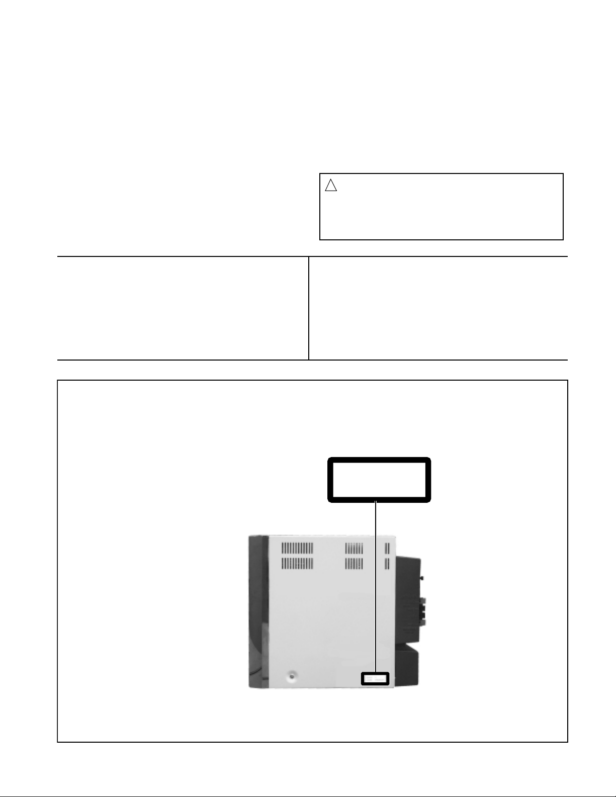
REPRODUCTION AND POSITION OF LABELS
WARNING LABEL
CLASS 1
LASER PRODUCT
CLASS 1
LASER PRODUCT
1-5
Page 6
NX-MD1R/NX-MD1
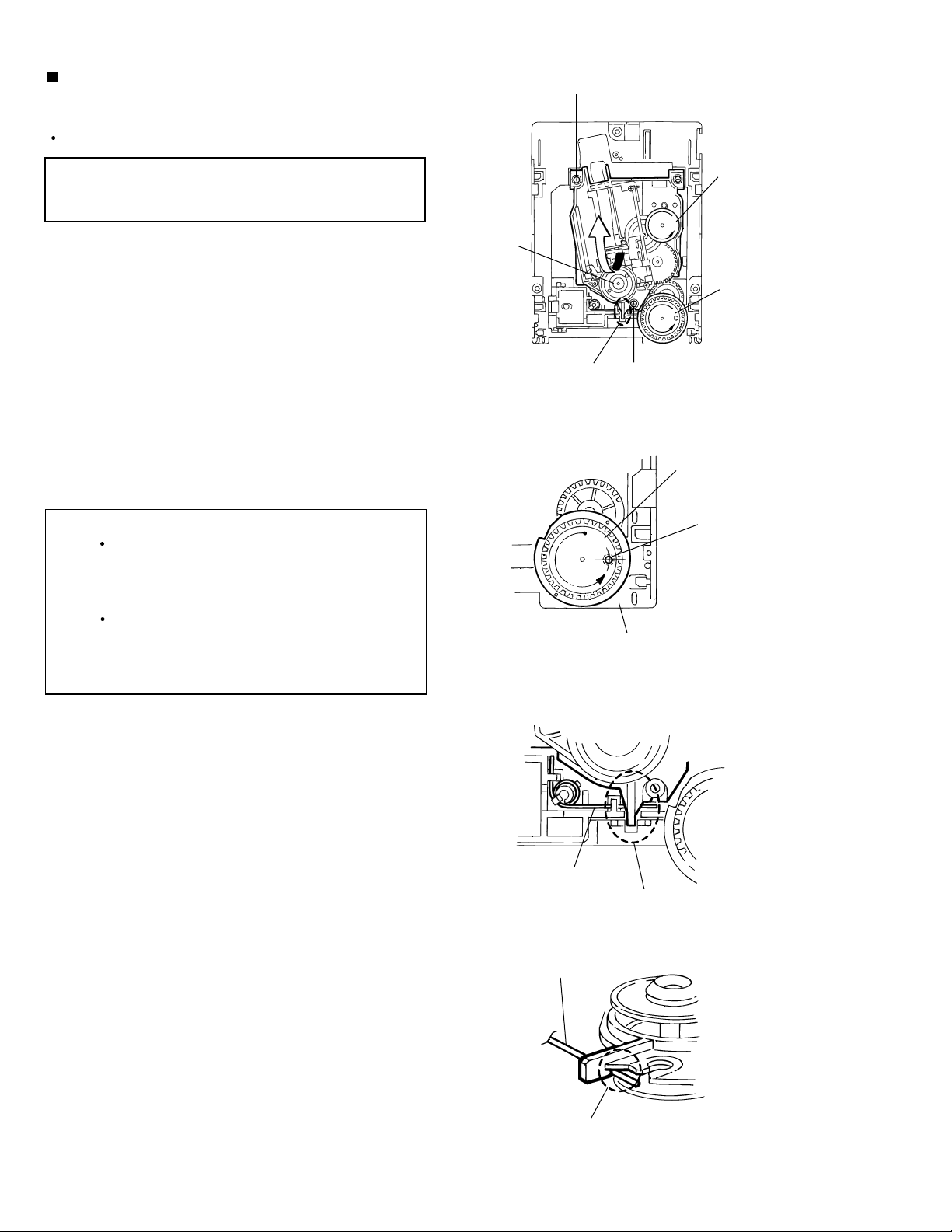
Disassembly method
<Main body section>
Removing the top cover
(See Fig.1 and 2)
1.
Remove the four screws A attaching the top cover
from the back side of the main body.
2.
Remove the two screws B attaching the top cover
from the both sides of the main body.
3.
Remove the top cover from the main body while
lifting up the back side of the top cover.
Removing the rear cover (See Fig.3)
Prior to performing the following procedure, remove
the top cover.
Fig.1
A
Top cover
A
Top cover
1.
Remove the nine screws C attaching the rear cover
from the back side of the main body.
2.
Set the speaker and antenna terminals to the
locked condition.
3.
Disengage the claws a of the rear cover from the
chassis and remove the cover toward the rear.
C
B
Fig.2
Antenna terminal
Rear cover
C
1-6
Claw a
Claw a
Speaker terminal
Fig.3
Page 7
NX-MD1R/NX-MD1
Removing the system control board
(See Fig.4)
Prior to performing the following procedure, remove
the top cover.
Prior to performing the following procedure, remove
the rear cover.
1.
Remove the screw D attaching the card wire
support board, then remove the card wire support
board.
2.
Disconnect the card wires from connectors CN602
and CN605 on the system control board.
3.
Remove the two screws E and screw F attaching
the system control board.
4.
Disconnect connectors CN603 and CN604 on the
system control board from the connector CN693 on
the regulator board and the CN694 on the repeater
board respectively.
5.
Disconnect the wire from connector CN601 on the
system control board.
Card wire support board
CN603
System control board
CN695
E
Fig.4
CN511
CN602
D
CN661
CN605
F
CN601
CN604
E
Protector
CN904
Removing the main amplifier board
(See Fig.5 and 6)
Prior to performing the following procedure, remove
the top cover.
Prior to performing the following procedure, remove
the rear cover.
1.
Disconnect the card wires from connectors CN661,
CN695 and CN511 on the main amplifier board.
2.
Remove the protector, then remove the screws G
attaching the main amplifier board.
3.
Remove the screw H and screw I attaching the
main amplifier board.
4.
Remove the screw J attaching the heat sink from
the back side.
5.
Disengage claw b on the heat sink and disconnect
the connectors CN901 and CN904 on the main
amplifier board, from connector CN991 on the
repeater board and connector CN994 on the
regulator board respectively.
CN901
CN301
Regulator board
HI
Fig.5
Main
amplifier
board
G
Claw b
6.
Disconnect the wire from connector CN301 on the
main amplifier board.
J
Fig.6
1-7
Page 8

NX-MD1R/NX-MD1
k
Removing the regulator board
(See Fig.7)
Prior to performing the following procedure, remove
the top cover.
Prior to performing the following procedure, remove
the rear cover.
Prior to performing the following procedure, remove
the system control board.
Prior to performing the following procedure, remove
the main amplifier board.
1.
Remove the two screws K and two screws L
attaching the regulator board.
2.
Disconnect the wires from connectors CN903 and
CN995 on the regulator board.
CN903
Regulator
board
K
CN995
L
Removing the AC jack board
(See Fig.8)
Prior to performing the following procedure, remove
the top cover.
Prior to performing the following procedure, remove
the rear cover.
Prior to performing the following procedure, remove
the system control board.
Prior to performing the following procedure, remove
the main amplifier board.
Prior to performing the following procedure, remove
the regulator board.
1.
Remove the screw M attaching the AC jack board.
2.
Disconnect the wire from connector CN921 on the
AC jack board.
CN921
Voltage
Selector
LF901
Fig.7
M
AC jac
board
F9001
1-8
Fig.8
Page 9
NX-MD1R/NX-MD1
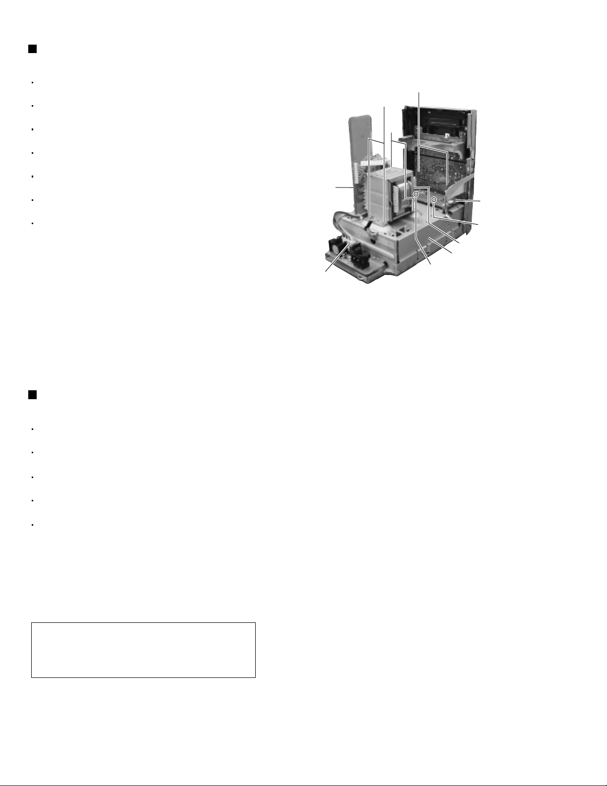
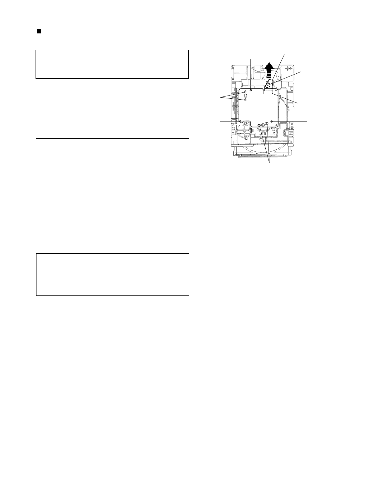
Removing the MD mechanism
assembly (See Fig.9)
Prior to performing the following procedure, remove
the top cover.
Prior to performing the following procedure, remove
the rear cover.
Prior to performing the following procedure, remove
the system control board.
Prior to performing the following procedure, remove
the main amplifier board.
1.
Remove the two screws N and two screws P
attaching the MD mechanism assembly.
(Caution) When assembling, attach the screws N at
the point c so that it also fixes the earth wire.
2.
Disconnect the card wire from connector CN512 on
the repeater board.
3.
Disengage the hook d from the MD mechanism
assembly and lift the rear of the assembly to
remove it.
CN512
P
Fan motor
assembly
N
Q
Fig.9
Q
Q
Earth wire
Point c
MD mechanism
assembly
Hook d
Q
Removing the fan motor assembly and
fan motor (See Fig.10 and 11)
Prior to performing the following procedure, remove
the top cover.
Prior to performing the following procedure, remove
the rear cover.
Prior to performing the following procedure, remove
the system control board.
Prior to performing the following procedure, remove
the main amplifier board.
Prior to performing the following procedure, remove
the regulator board.
Prior to performing the following procedure, remove
the MD mechanism assembly.
1.
Remove the four screws Q attaching the fan motor
assembly from the both sides of the sub chassis.
2.
Remove the fan motor assembly to the top side.
3.
Remove the two screws R attaching the fan motor,
then remove the fan motor.
(Caution)When assembling, attach the screws R
so that they also fix the shield together
with the fan motor assembly.
Sub chassis
Shieid
Fig.10
R
Fan motor
Fig.11
1-9
Page 10
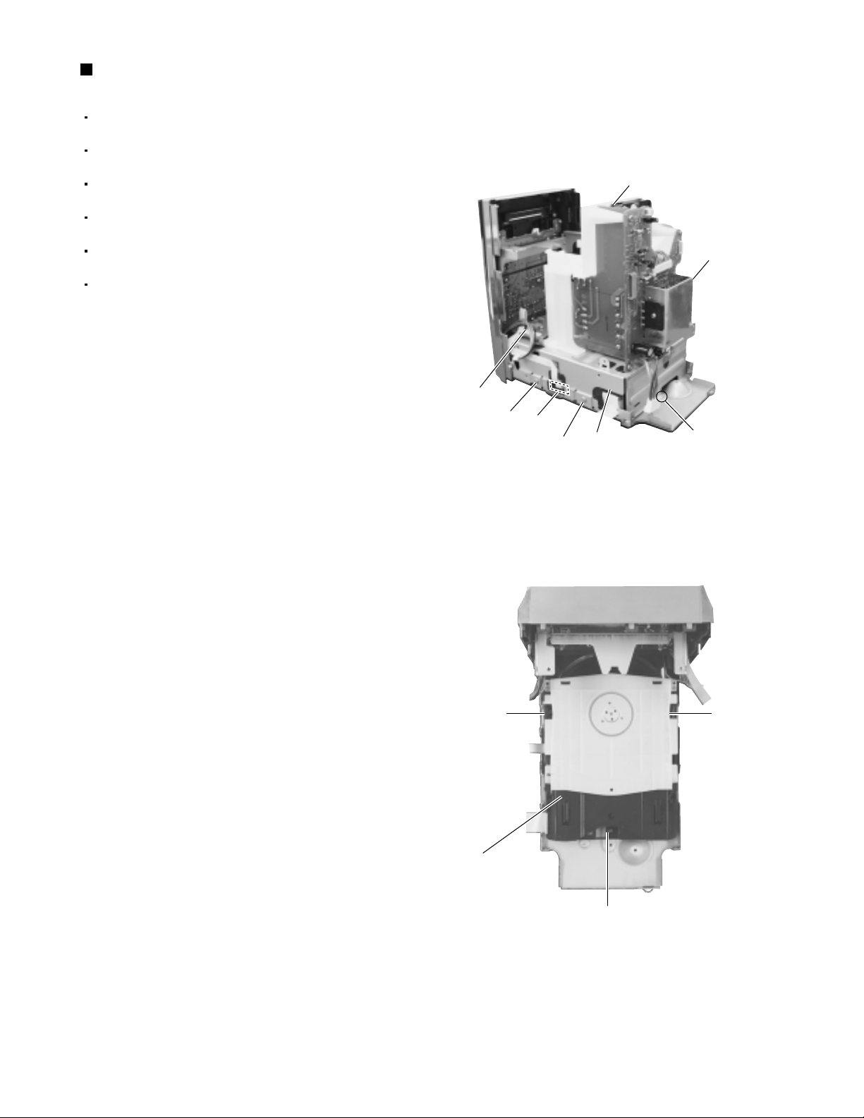
NX-MD1R/NX-MD1
Removing the power board
(See Fig.12)
Prior to performing the following procedure, remove
the top cover.
Prior to performing the following procedure, remove
the rear cover.
Prior to performing the following procedure, remove
the system control board.
Prior to performing the following procedure, remove
the main amplifier board.
Prior to performing the following procedure, remove
the regulator board.
Prior to performing the following procedure, remove
the MD mechanism assembly.
Prior to performing the following procedure, remove
the fan motor assembly.
1.
Remove the four screws S attaching the power
board from the left and right side of the sub
chassis.
2.
Disconnect the wire from connector CN921 on the
AC jack board.
3.
Remove the power board in an upward direction.
T
S
S
Power board
Repeater
board
Clow e
CN691
Sub chassis
Claw e
CN921
Fig.12
Removing the repeater board
(See Fig.12)
Prior to performing the following procedure, remove
the top cover.
Prior to performing the following procedure, remove
the rear cover.
Prior to performing the following procedure, remove
the system control board.
Prior to performing the following procedure, remove
the main amplifier board.
Prior to performing the following procedure, remove
the MD mechanism assembly.
1.
Remove the two screws T attaching the repeater
board.
2.
Disconnect the card wire from connector CN691 on
the repeater board.
(Caution) When assembling, fit the two claws of
the sub chassis into the two rectangular
holes e of the repeater board, before
attaching it.
1-10
Page 11
Removing the CD mechanism
assembly (See Fig.13 and 14)
Prior to performing the following procedure, remove
the top cover.
Prior to performing the following procedure, remove
the rear cover.
Prior to performing the following procedure, remove
the system control board.
Prior to performing the following procedure, remove
the main amplifier board.
Prior to performing the following procedure, remove
the AC jack board.
Prior to performing the following procedure, remove
the MD mechanism assembly.
1.
Remove the four screws U attaching the sub
chassis from the left and right side of the bottom
chassis.
Remove the screw V attaching the sub chassis.
2.
Disconnect the card wire from connector CN691 on
the repeater board.
CN691
U
CN606
Sub chassis
U
NX-MD1R/NX-MD1
Fun motor assembly
Regulator
board
V
3.
Remove sub chassis cover with regulator board
and fan motor assembly in the direction of the
arrow.
4.
Remove the three screws W attaching the CD
mechanism assembly.
5.
Disconnect the card wire from connector CN606 on
the CD servo board.
6.
Remove the CD mechanism assembly while lifting
the rear part of it.
Fig.13
WW
CD mechanism
assembly
W
Fig.14
1-11
Page 12
NX-MD1R/NX-MD1
Removing the front panel assembly
(See Fig.15)
Prior to performing the following procedure, remove
the top cover.
Prior to performing the following procedure, remove
the rear cover.
Prior to performing the following procedure, remove
the system control board.
Prior to performing the following procedure, remove
the main amplifier board.
Prior to performing the following procedure, remove
the MD mechanism assembly.
1.
Remove the two screws X attaching the front panel
assembly from bottom side of the bottom chassis.
2.
Release the three claws f on the bottom side of the
main body using screwdriver, and detach the front
panel assembly toward the front.
Front panel assembly
X
Claw f
Fig.15
Bottom chassis
1-12
Page 13
<Front panel assembly section>
NX-MD1R/NX-MD1
Prior to performing the following procedure, remove
the front panel assembly.
Removing the front board (See Fig.16)
1.
Remove the two screws Y attaching the MD
bracket.
2.
Remove the MD bracket.
(Caution) When assembling, fit the rib of the front
panel into the location hole g on the MD
bracket before attaching it.
3.
Remove the eight screws Z attaching the front
board.
4.
Remove the front board.
(Caution) When assembling, fit the rib of the front
panel into the location hole h on the
front board before attaching it.
MD bracket
Location hole g
Y
Location hole h
Z
Z
Z
Location hole g
Front board
Location hole h
Wire holder i
Wire holder i
AA
Head phone & USB board
Removing head phone & USB board
(See Fig.16)
1.
Remove the wire from two wire holders i.
2.
Remove the two screws AA attaching the head
phone & USB board.
3.
Remove the head phone & USB board.
Fig.16
1-13
Page 14
NX-MD1R/NX-MD1
<MD mechanism assembly section>
Prior to performing the following procedure, remove
the top cover.
Prior to performing the following procedure, remove
the rear cover.
Prior to performing the following procedure, remove
the MD mechanism assembly.
Removing the MD mechanism
assembly (See Fig.17)
1.
Remove the screw AB attaching the earth plate
board.
2.
Remove the card wire on the MD mechanism
assembly.
3.
Disconnect the card wire from connector CN522 on
the MD servo board, then remove it.
4.
Remove the four screws AC attaching the MD
bracket from left and right side of the MD
mechanism assembly.
Card wire
CN522
Earth plate board
ACACAB
Card wire
MD bracket
Fig.17
5.
Remove the MD bracket to the bottom side.
1-14
Page 15
NX-MD1R/NX-MD1
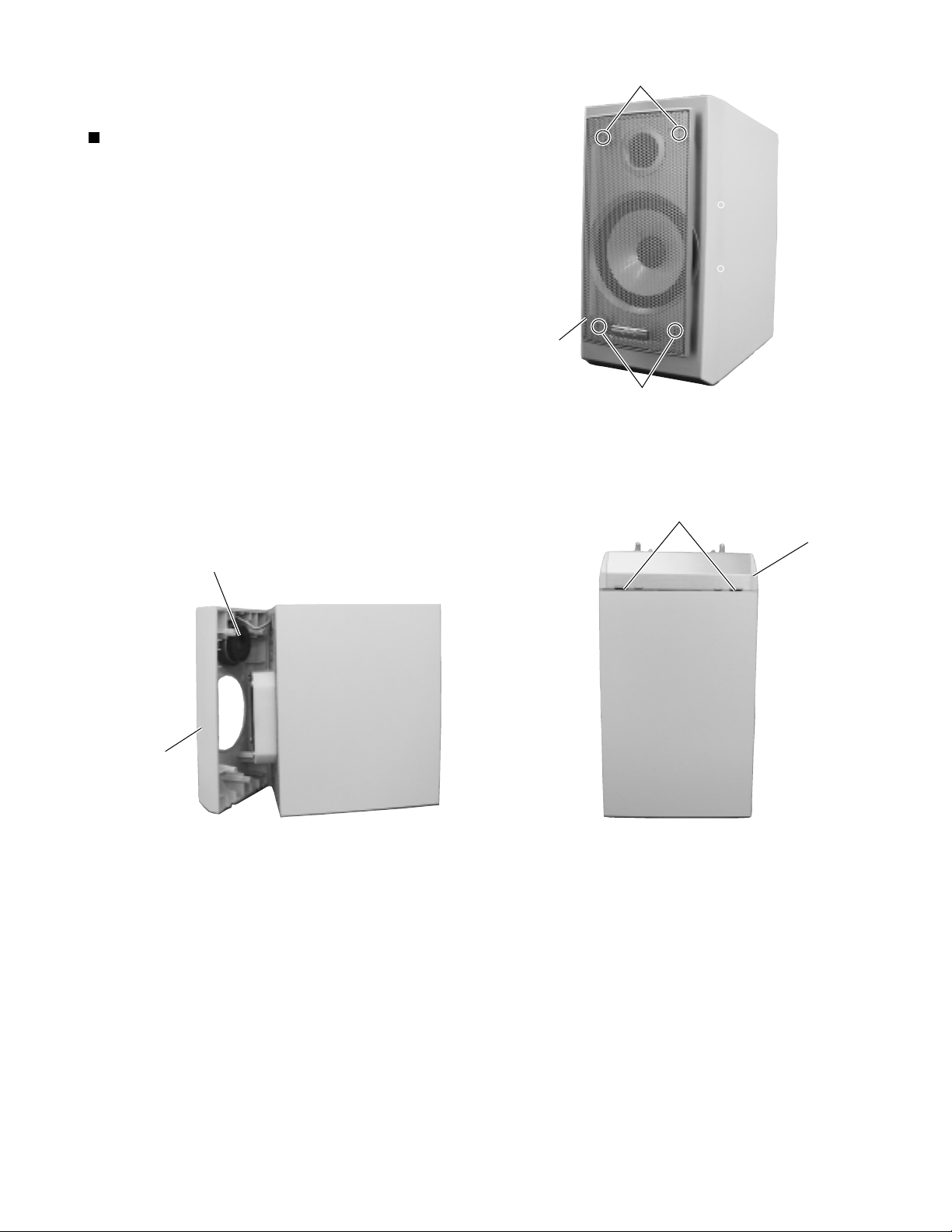
<Speaker section>
Note : Avoid replacing individual parts.
Removing the front cover (See Fig.1 to 3)
1.
Pull out the saran net toward the front while
disengaging the four joints a.
2.
Insert the tip of a flat-bladed screwdriver or a similar
tool into the joints b between the main body and the
front cover from the bottom of the main body.
3.
Lift the front cover little by little to remove.
4.
Remove the front cover toward the front and
disconnect the yellow and black wires from the two
tweeter speaker terminals.
Joints a
Saran net
Joints a
Fig.1
Joints b
Front cover
Tweeter speaker
Front cover
Fig.3
Fig.2
1-15
Page 16
NX-MD1R/NX-MD1
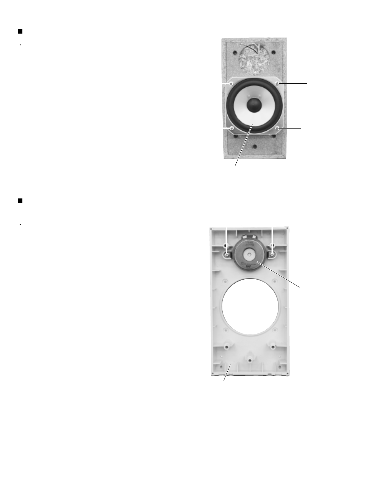
Removing the woofer speaker (See Fig.4)
Prior to performing the following procedure, remove
the front cover.
1.
Remove the four screws A on the front of the body.
2.
Pull out the woofer speaker toward the front and
disconnect the wire (yellow and black,blue and
black) from the two speaker terminals.
A
Woofer speaker
A
Fig.4
Removing the tweeter speaker
(See Fig.5)
Prior to performing the following procedure, remove
the front cover.
1.
Remove the two screws B attaching the tweeter
speaker on the back of the front cover.
B
Tweeter speaker
1-16
Front cover
Fig.5
Page 17
NX-MD1R/NX-MD1
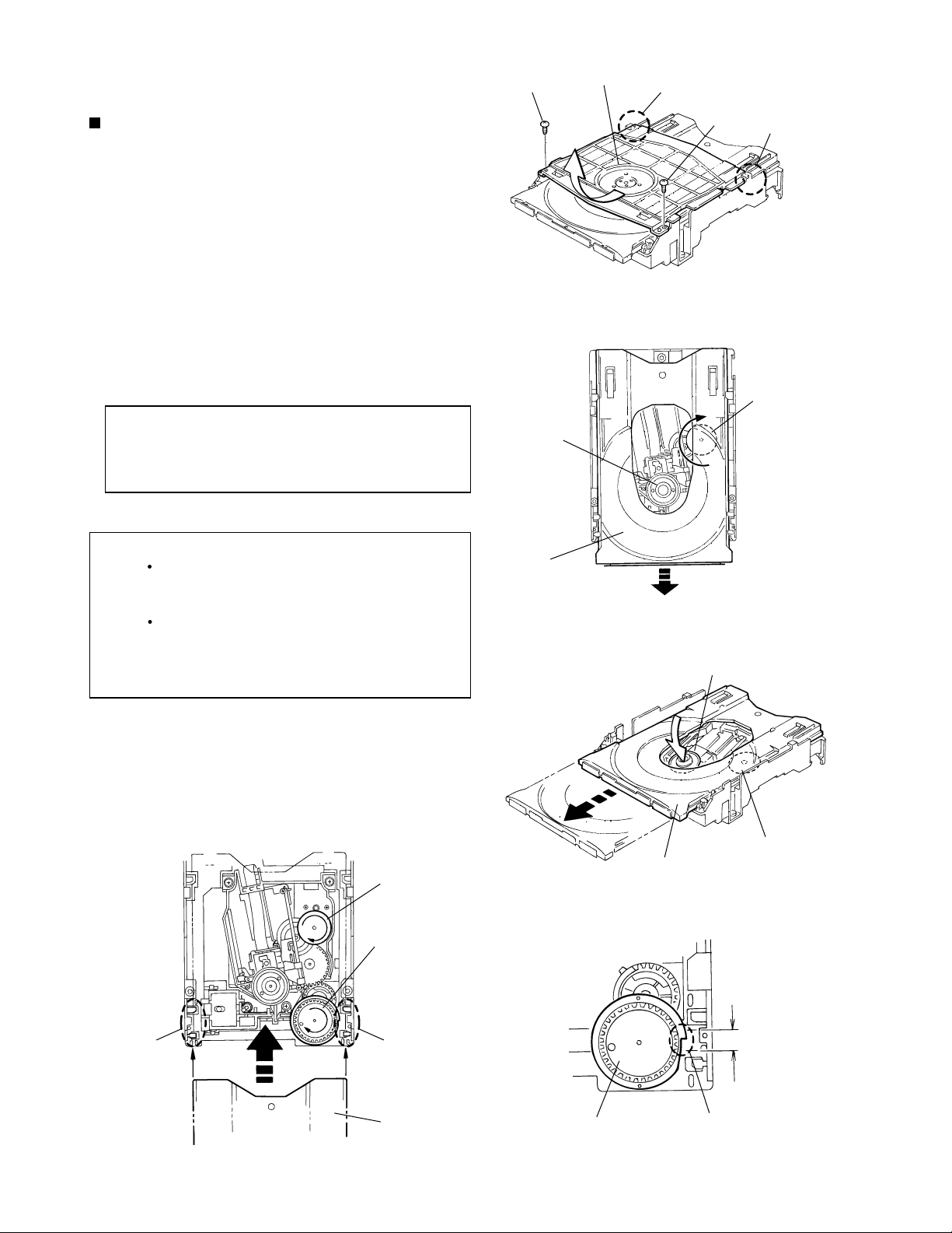
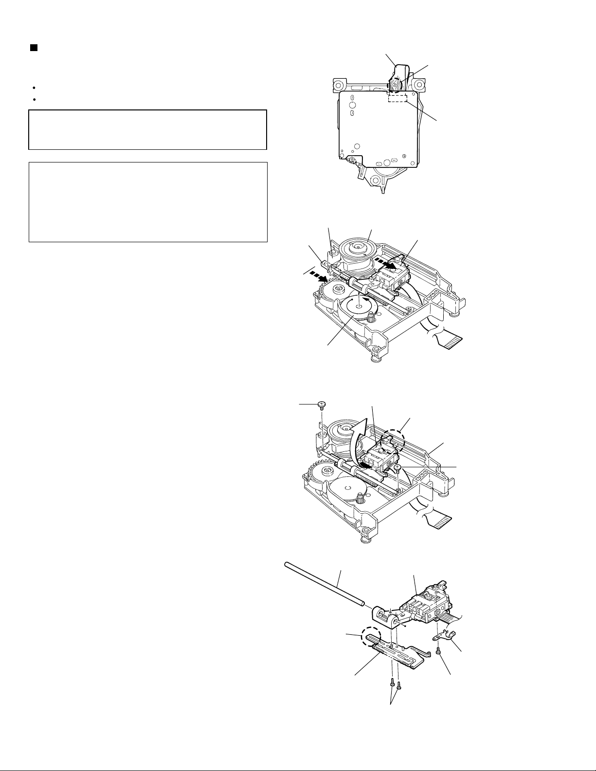
<CD Mechanism Assembly>
Removing the CL. Base Assembly and
Tray (Refer to Figs. 1 to 5.)
1. Remove the two screws A fastening the CL. base
assembly from the top of the CD mechanism
assembly.
2. Move the CL. base assembly diagonally upwards
as indicated by the arrow to release it from the two
hooks a.
3. Turn the idle gear in the arrow-marked direction
from the upper side of the CD mechanism
assembly. Accordingly, the TRAMECHA assembly
moves downwards.
Note: When drawing out the tray, shift down the
TRAMECHA assembly to the position where
the tray does not contact the T-T assembly
of the TRAMECHA assembly.
4. Draw out the tray frontwards for removing it.
CL. base assembly
A
TRAMECHA
assembly
Hook a
Fig. 1
A
Hook a
Idle gear
Note: When reinstalling the tray:
Turn the idle gear so that the part b of the
tray gear is positioned in the part c shown in
Fig. 4. (Eject position)
Engage the right and left hooks d and e of
the tray with the right and left grooves of the
TRAMECHA assembly respectively for
retaining the tray.
Idle gear
Tray gear
Tray
Fig. 2
TRAMECHA assembly
Idle gear
Tray
Fig. 3
Hook d
Hook e
Tray
Tray gear
Part c
Part b
Fig. 4Fig. 5
1-17
Page 18
NX-MD1R/NX-MD1
Removing the TRAMECHA Assembly
(Refer to Figs. 6 to 9.)
Remove the CL. base assembly and tray.
Reference: The TRAMECHA assembly can be
removed without removal of the
mechanism P.C. board.
1. If the TRAMECHA assembly is lowered and it is
located out of the PLAY position, turn the idle gear
in the arrow-marked direction so that the hole in the
part f of the tray gear meets the hole on the CL.
base assembly. (Set the TRAMECHA assembly at
the PLAY position.)
2. Remove the three screws B fastening the
TRAMECHA assembly and then remove the
TRAMECHA assembly upwards from the front side.
3. At the same time, remove the spring from the
groove of the CH. base assembly in the part g of the
TRAMECHA assembly.
Note: When reinstalling the TRAMECHA assembly:
Check to see if the spring is properly
engaged with groove of the CH. base
assembly in the part g of the TRAMECHA
assembly.
After making sure that the three insulators of
the TRAMECHA assembly are properly set
on the bosses of the L. base assembly's
guide, fasten them with the screws.
TRAMECHA
assembly
B
Part g
L. base assembly
B
Fig. 6
Fig. 7
B
Idle gear
Tray gear
Tray gear
Part f
1-18
Spring
Part g
Fig. 8
Spring
Groove of CH. base assembly
Fig. 9
Page 19
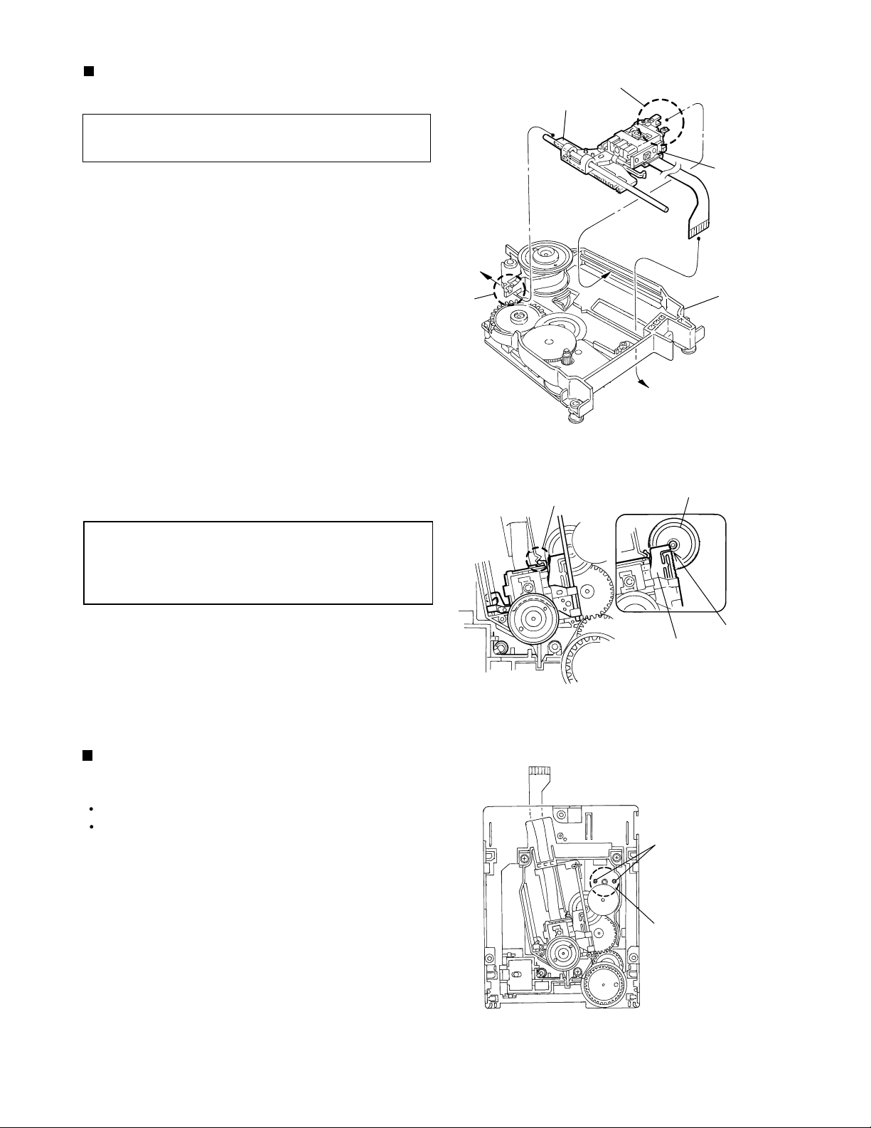
Removing the Mechanism P.C. Board
(Refer to Fig 10.)
Reference:The mechanism P.C. board can be
removed without removal of the
TRAMECHA assembly.
NX-MD1R/NX-MD1
Flexible wire
C
Shorting round
Note: Before disconnecting the flexible wire coming
from the pickup from the connector, be sure to
solder its shorting round.
If the flexible wire is connected without
soldering, it may cause breakdown of the
pickup.
1. Solder the shorting round of the flexible wire
connected with the mechanism P.C. board from the
back of the mechanism assembly.
2. Disconnect the flexible wire from the connector
CN601 on the mechanism P.C. board.
3. Remove the three screws C fastening the
mechanism P.C. board.
4. Unsolder the two points of the part h and one point
of the part i of the mechanism P.C. board. Then,
remove the mechanism P.C. board upwards.
Note: When reinstalling the mechanism P.C. board,
connect the flexible wire coming from the
pickup to the connector first and then remove
the solder from the shorting round of the
flexible cable.
Soldered
part h
C
CN601 on
mechanism
P.C. board
C
Soldered part i
Fig. 10
1-19
Page 20
NX-MD1R/NX-MD1
Removing the Pickup
(Refer to Figs. 11 to 14.)
Remove the CL. base assembly and tray.
Remove the TRAMECHA assembly.
Reference: The pickup can be removed without
removal of the mechanism P.C. board.
Note: Before disconnecting the flexible wire coming
from the pickup from the connector, be sure to
solder its shorting round.
If the flexible wire is connected without
soldering, it may cause breakdown of the
pickup.
1. Solder the shorting round of the flexible wire
connected with the mechanism P.C. board from the
back of the TRAMECHA assembly.
2. Disconnect the flexible wire from the connector
CN601 on the mechanism P.C. board.
CH. base
assembly
Part j of
rack plate
Flexible wire
Shorting round
CN601 on
mechanism
P.C. board
Fig. 11
T-T assembly
Pickup assembly
3. Turn the idle gear in the arrow-marked direction from
the top of the TRAMECHA assembly so that the
pickup assembly is shifted to the reverse side of the
T-T assembly.
Move the pickup assembly until the part j of the rack
plate in the lower part of the pickup assembly comes
out of the CH. base assembly.
4. Remove the two screws D retaining the shaft of the
pickup assembly. Next, disengage the hook k from
the CH. base assembly and then remove the pickup
assembly together with the shaft.
5. Pull the shaft out of the pickup.
6. Remove the two screws E fastening the rack plate
from the pickup.
7. Remove the screw F retaining the P.S. spring from
the pickup.
D
Idle gear
Shaft
Fig. 12
Pickup assembly
Part k
CH. base
assembly
D
Fig. 13
Pickup
1-20
Part j
Rack plate
P.S. spring
F
E
Fig. 14
Page 21
NX-MD1R/NX-MD1
Reinstalling the Pickup Assembly
(Refer to Figs. 15 and 16.)
Reference: Refer to the explanation of "Removing
the Pickup" on the preceding page.
1. Fit the P.S. spring and rack plate to the pickup.
2. Insert the shaft into the pickup.
3. Engage the hook k of the pickup assembly with the
CH. base assembly first, and set the part j of the
rack plate in the opening I next. Then, reinstall the
pickup assembly while shifting it to the T-T side
(inward) so that the part m of the rack plate is
positioned as shown in Fig. 16.
4. Move the pickup assembly to the center position
and fasten the shaft with the two screws D. (Make
sure that the part n of the rack plate is correctly
engaged with the middle gear.)
5. After passing the flexible wire coming from the
pickup through the opening of the CH. base
assembly, connect it to the connector CN601.
Part I
Part j
Part m
Part k
Pickup
assembly
CH. base
assembly
Fig. 15
Middle gear
Note: When reinstalling the pickup assembly,
remove the solder from the shorting round
after connecting the flexible wire coming from
the pick to the connector CN601.
Removing the Feed Motor Assembly
(Refer to Fig. 17.)
Remove the CL. base assembly and tray.
Remove the mechanism P.C. board.
Remove the two screws G fastening the feed motor
assembly from the top of the mechanism assembly.
Rack plate
Part n
Fig. 16
G
Feed motor assembly
Fig. 17
1-21
Page 22

NX-MD1R/NX-MD1
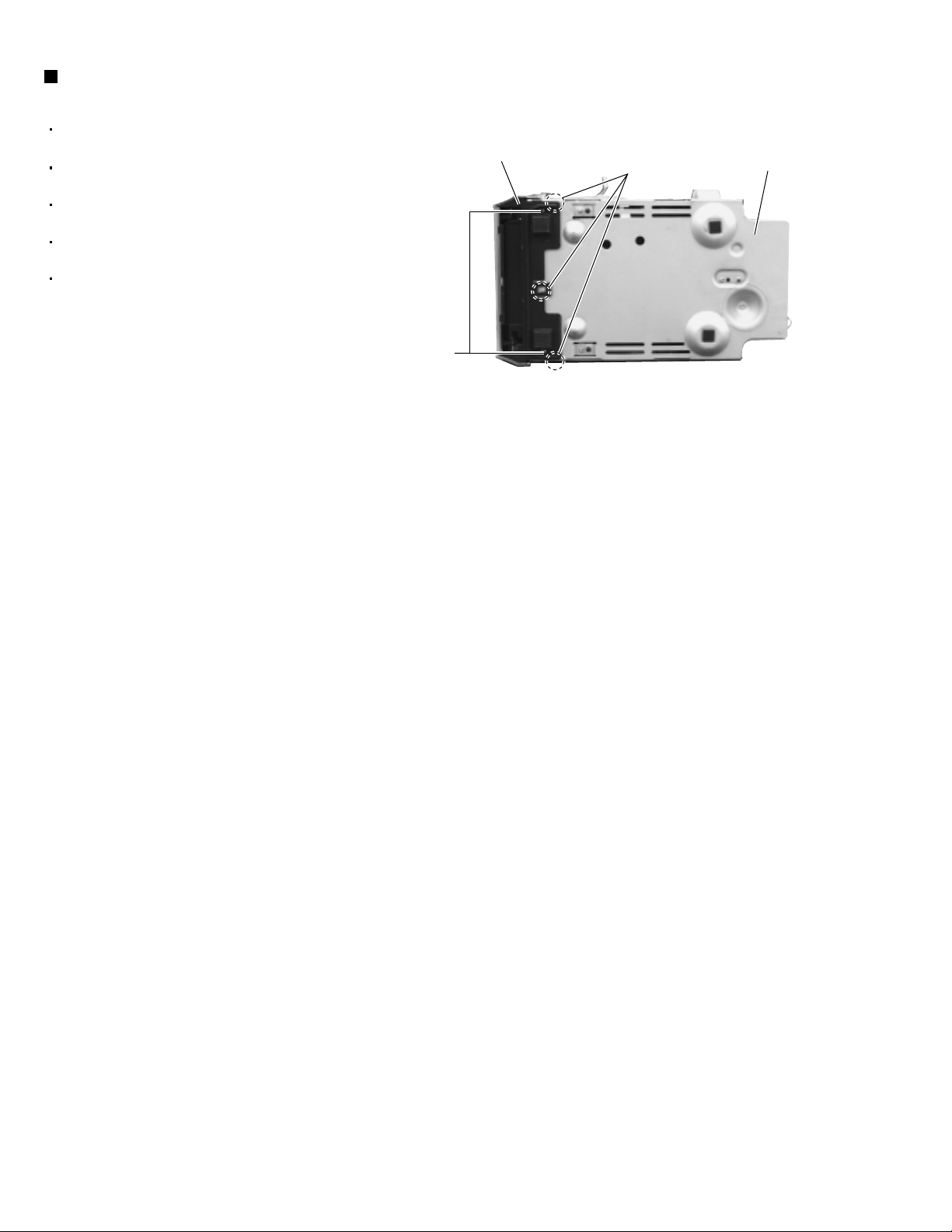
<MD mechanism section>
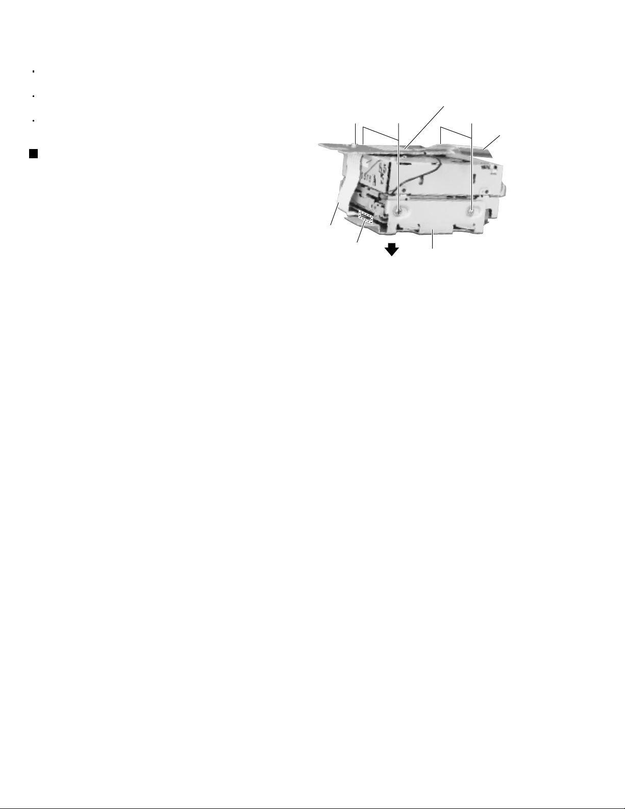
Removing the MD servo board
(See Fig.1 and 2)
1.
Turn over the body and disconnect the card wires
from connectors CN408, CN521 and the flexible wire
from CN407 on the MD servo board.
2.
Remove the two screws A attaching the main board.
Slide the MD servo board in the direction of the
arrow to release the two joints a with the single
flame.
3.
Shorting round b on the pickup in the body.
Disconnect the flexible harness from connector
CN321 and CN451 on the underside of the MD servo
board. Then remove the MD servo board.
CN521
(Bottom side)
Joint a Joint a
Fig.1
CN451
AA
MD servo board
CN408
CN407
MD servo board
CN321
Removing the mechanism cover
(See Fig.3)
1.
Remove the four screws B on both sides of the
mechanism cover.
2.
Remove the screw B' on the earth wire of the
mechanism cover.
3.
Move the mechanism cover toward the front to
disengage the front hook of the mechanism cover
from the internal loading assembly (Joint c). Then
remove the mechanism cover upward.
1-22
Joint c
Hook
Joint c
B
Pickup
Fig.2
Fig.3
Shorting round b
B'
Earth wire
Mechanism cover
B
Page 23

Removing the head lifter (See Fig.4 to 6)
1.
Move the head lifter on top of the body in the
direction of the arrow and turn around.
2.
Detach the spring from the hook of the body.
Remove the head lifter with the spring.
3.
If necessary, remove the spring from the head lifter.
Head lifter
Fig.5
NX-MD1R/NX-MD1
Head lifter
Fig.4
Spring
Removing the head assembly (See Fig.7)
1.
Remove the screw C on the upper side of the body.
Remove the head assembly while pulling the flexible
harness from the body.
Head lifter
Spring
Fig.6
Head assembly
Fig.7
C
1-23
Page 24

NX-MD1R/NX-MD1
Removing the Loading assembly
(See Fig.8 and 9)
Ref:
The loading assembly, the traverse mechanism
assembly and the single flame will be
removable after removing the loading assembly
from the body.
Prior to performing the following procedure, remove
the MD servo board, the mechanism cover, the head
lifter and the head assembly.
1.
Remove the two screws D and screw D' on the
upper side of the body.
2.
Move the loading assembly forward to disengage it
from the traverse mechanism assembly (Joint d).
Then remove it upward.
D
D
Loading assembly
3.
Remove the traverse mechanism assembly from the
single flame.
Joint d
Earth wire
D'
Fig.8
Loading assembly
Traverse mechanism
assembly
1-24
Single flame
Fig.9
Page 25

NX-MD1R/NX-MD1
<Loading assembly section>
Removing the slide base (L) / (R)
(See Fig.10)
1.
Remove the two screws E on the top side of the
loading assembly.
2.
Remove the slide base (L) outward. (Release it from
the joint bosses e'.)
3.
Remove the slide base (R) outward.
Removing the loading mechanism
assembly (See Fig.11)
1.
Detach the loading mechanism assembly upward to
release the four pins on both sides from the loading
motor, paying attention to the part e of the loading
mechanism base.
Slide base (R)
Boss e'
E
Slide base (L)
E
Boss e'
Fig.10
Part e
Loading motor assembly
<Loading mechanism assembly section>
Removing the loading motor
(See Fig.12 and 13)
1.
Disconnect the harnesses from the wire holder and
from connector CN612 on the cam switch board.
2.
Remove the screw F attaching the loading motor
and release the joint f.
3.
Remove the belt from the loading motor assembly.
4.
Remove the slit washer to the cam gear.
5.
Remove the two screws G attaching the loading
motor.
Removing the cam gear and the cam
switch board (See Fig.12)
F
Loading mechanism
assembly
Joint f
CN612
Loading mechanism base
Fig.11
Wire holder
H
Cam switch board
Slit washer
H
Cam gear
Fig.12
Loading motor
1.
Remove the slit washer attaching the cam gear and
pull out the cam gear.
2.
Disconnect the harness from the wire holder and
from connector CN612 on the cam switch board.
3.
Remove the two screws H and the clamp. Remove
the cam switch board.
G
Belt
Fig.13
1-25
Page 26

NX-MD1R/NX-MD1
Removing the cartridge holder assembly
(See Fig.14 and 15)
1.
Remove the two screws J on the top side of the
loading assembly.
J
J
Removing the slide bar and the eject bar
(See Fig.14 and 15)
Prior to performing the following procedure, remove
the cartridge holder assembly.
Slide bar
Cartridge holder assembly
Eject bar
Eject bar
Part g
Fig.14
J
1.
Remove the slide bar upward.
2.
Move the eject bar outward until it stops as shown in
Fig.14. Push the convex part g on the bottom of the
body and remove the eject bar from the chassis.
Slide bar
Boss k
Eject bar
UD base
1-26
Cartridge holder assembly
Fig.15
Page 27

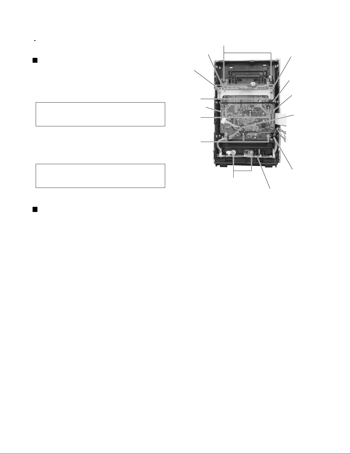
<Traverse mechanism assembly section>
NX-MD1R/NX-MD1
Removing the Insulators (See Fig.16)
1.
Disengage the four insulators from the notches of the
traverse mechanism chassis.
Removing the pickup unit (See Fig.17)
1.
Turn over the traverse mechanism assembly and
remove the screw K attaching the shaft holder (F).
2.
Move the shaft inward and remove it from the shaft
holder (R).
Pickup unit
Insulators
Insulators
Traverse machanism chassis
Fig.16
Joint h
Pickup guide
Pickup unit
3.
Detach the shaft side of the pickup unit upward and
release the joint h with the pickup guide. Then
remove the pickup unit with the shaft.
Removing the pickup (See Fig.18)
1.
Draw out the shaft from the pickup.
2.
Remove the two screws L attaching the rack spring.
Shaft holder (F)
Rack spring
Shaft holder (R)
K
Fig.17
L
Pickup
Fig.18
Shaft
1-27
Page 28

NX-MD1R/NX-MD1
Removing the feed motor assembly
(See Fig.19, 20)
It is not necessary to remove the pickup unit.
1.
For the white and black harnesses extending from
the feed motor assembly, unsolder the soldering i
on the traverse mechanism board.
Traberse mechanism board Soldering j
N
2.
Remove the two screws M attaching the feed motor
assembly.
3.
Remove the two screws P attaching the feed motor
bracket.
Removing the traverse mechanism
board (See Fig.19)
Prior to performing procedure, remove the feed
motor assembly.
1.
For the red and black harnesses extending from the
spindle motor, unsolder the soldering j on the
traverse mechanism board.
Soldering i
Feed motor assembly
M
Fig.19
Feed motor
Feed motor bracket
P
2.
Remove the screw N attaching the traverse
mechanism board.
Fig.20
1-28
Page 29

<Reattaching the loading assembly>
1.
Reattach the eject bar to the UD base.
(Fig.15 and 21)
2.
Reattach the slide bar to the loading mechanism
chassis while fitting the boss marked k to the eject
bar ditch k'. (Fig.21)
3.
Slide the slide bar and the eject bar in the direction
of the arrow in Fig.21 and reattach the cartridge
holder assembly using the two screws J.
(Fig.21 and 22)
NX-MD1R/NX-MD1
ATTENTION:
Make sure the pin of the eject lever
marked m is fitted to the slot of the
eject bar marked n at the bottom of the
loading mechanism chassis after
moving the eject lever and the loading
slider of the cartridge holder assembly
in the direction of the arrow.
(Refer to Fig.22)
Slide bar
J
J
Ditch k'
Eject bar
Cam switch board
q
r
Cam switch boss
Boss k
UD base
Fig.21
H
Point marked
H
Ditch n
UD base (Bottom)
Cartridge holder assembly
Loading slider
Eject lever
m
Fig.22
1-29
Page 30

NX-MD1R/NX-MD1
4.
Reattach the wire holder to the UD base while
engaging the UD base hook marked r to the wire
holder slot marked q (At the same time, the boss on
the reverse side of the wire holder is fitted to the UD
base round hole).
5.
Reattach the cam switch board using the two screws
H. (Fig.23)
6.
Turn the cam switch to bring the boss to the point
marked on the cam switch board. Reattach the
cam gear using a slit washer while fitting the cam
gear slot to the cam switch boss. (Fig.23)
ATTENTION:
When reattaching the cam gear, the
cam switch boss should be fitted to the
cam gear slot, and the triangle mark of
the cam gear should be aligned to the
hole(part p) of the eject lever as shown
in Fig.23.
7.
Reattach the loading motor assembly, using the
screw F. Connect the harness extending from the
loading motor to connector CN612 on the switch
board and fix it with the wire holder. (Fig.23)
Slide bar CN612
Loading motor assembly
Point marked
Wire holder
Boss
Cam switch
Cam switch board
1-30
F
Eject lever
Fig.23
Cam gear
p
Cam gear
(Triangle mark)
Eject lever
Page 31

NX-MD1R/NX-MD1
8.
Reattach the UD base while engaging the four pins
on both sides of the UD base to the notches of the
loading mechanism base and placing the edge
(marked e") of the cartridge holder assembly under
the hook e of the loading mechanism base. (Fig.24)
9.
Reattach the slide base (R) while fitting the two pins
on another side of the UD base to the slots of the
slide base (R). (Fig.25)
ATTENTION:
Fit the part s of the slide base (R) to
the part t on the inward side of the
cam gear rib. (Fig.26)
10.
Reattach the slide base (L) on the slide base (R)
while fitting the two pins on another side of the UD
base to the slots of the slide base (L) (Fig.26). Make
sure the two slots of the slide base (L) are fitted to
the two bosses marked e' and tighten the two
screws E. (Fig.27)
Ref:
To expedite the work, bring up the UD base
slightly when fitting each pin to the appropriate
notch.
Hook e
Hook e"
Hook e"
Pin
Loading mechanism base
Fig.24
Slide base (R)
Part s
E
Pin
Boss e'
Pin
Slide base (L)
Pin
Part t
Fig.25
Slide base (L)Slide base (R)
Slide base (R)
Cam gear
E
Part s
Part t
Boss e'
Fig.26Fig.27
1-31
Page 32

NX-MD1R/NX-MD1
Adjustment Method (CD/MD section)
1. Jigs and test instruments
Laser power meter
Laser power meter sensor (or disk sensor)
Premastered disk (MRG-1018 or TGYS1)
Recordable disk (MDW-74/AU1)
2. CD check method
Remove the four screws retaining the top cover from the rear panel and the two screws retaining it from
1.
the left and right side panels.
Remove the two screws retaining the front cover from the rear side and the two screws retaining it from
2.
the bottom panel.
Remove the eight screws retaining the rear cover.
3.
Remove the four screws retaining the sub chassis from the left and right sides.
4.
(Caution)
3.
USB input check method
Connect the PC to the USB port and ensure that audio is output from the speakers.
(Compatible with Windows 98, Windows 2000 and Windows Me)
For details of the removal, see the previous
section "Disassembly method".
CD mechanism assembly
System control board
1-32
Connect to the USB port
of the PC.
USB audio terminal
Page 33

4. Adjustment and check items
1) CD section
(1) Indication of the C1 error
(2) Cancel of the C1 error indication
2) MD section
(1) Setup of the TEST MODE 1
(2) Initialization of the EEPROM
(3) Adjustment of the laser power
(4) Adjustment of the disk
(5) Setup of the TEST MODE 2
(6) Indication of variation in the pickup adjustment value
(7) Indication of the C1 error
(8) Cancel of the TEST MODE
5. Adjustment and check method
1) CD section
(1) Indication of the C1 error
While pressing both the STOP key
and CD PLAY key on the main
unit,turn on the primary power supply.
NX-MD1R/NX-MD1
Press the STANDBY/ON key
on the main unit
FL indication
CD TEST
Press the CD OPEN/CLOSE key
and insert the test disk.
Press key 1, 2 or 4 of the remote control
unit to start measurement. The number of
error corrections will be displayed every 10
seconds.
Key 1: Normal-speed playback
Key 2: 2x-speed playback
Key 4: 4x-speed playback
FL indication
∗∗ ∗∗
∗∗∗Times
200 Hz or less
(2) Cancel of the C1 error indication
To cancel the C1 error indication, cut off the power supply.
1-33
Page 34

NX-MD1R/NX-MD1
2) MD section
(1) Setup of the TEST MODE 1
While pressing both the STOP key
and MD PLAY key, turn on the
primary power supply.
Press the STANDBY/ON key on
the main unit
FL indication
MD TEST MODE 1
Setup is complete.
(3) Adjustment of the playback laser power
Insert the laser power
meter sensor.
(2) Initialization of the EEPROM
(The EEPROM can be initialized on the precondition that the
setup of the TEST MODE 1 is complete. After setup of the
TEST MODE 1, proceed to the following operations with the
remote controller*.)
* For EJECT operation, use the EJECT key on the main unit.
Initialization of the EEPROM
Press the REC SPEED key
on the remote controller.
FL indication
DATA INITI.
Setup is complete.
Press the "2" key on
the remote controller.
FL indication
L.POW PLAY
Set up the playback
laser power.
Increase the laser
power with the
F.SKIP key on the
remote controller.
Adjust the power to be 0.68 mW or
more. If the value exceeds 0.68 mW,
approximate it to 0.68 mW as
accurately as possible.
Press the STOP key on
the remote controller.
Decrease the laser
power with the
B.SKIP key on the
remote controller.
Press the "4" key on
the remote controller.
FL indication
L.POW REC
Set up the recording
laser power.
Increase the laser
power with the
F.SKIP key on the
remote controller.
Adjust the power to be 6.23 mW or
more. If the value exceeds 6.23 mW,
approximate it to 0.68 mW as
accurately as possible.
Press the STOP key on
the remote controller.
Decrease the laser
power with the
B.SKIP key on the
remote controller.
1-34
MD playback laser power
adjustment is complete.
Press the MD EJECT
key on the main unit.
Setup of the MD laser
power is complete.
Page 35

(4) Adjustment of the disk
Insert the
premastered disk.
Reading of TOC ends.
Press the MD PLAY
key on the
remote controller.
FL indication
ON TUNING
Automatic adjustment starts.
NX-MD1R/NX-MD1
Adjustment OK?
YES
FL indication
OK TUNING
Press the STOP key
on the remote controller.
Press the MD EJECT
key on the main unit.
Insert a recordable
disk.
Press the MD PLAY
key on the
remote controller.
FL indication
ON TUNING
Automatic adjustment starts.
Adjustment OK?
NO
FL indication
NG ERR: xXX!
NO
XX: Refer to the NG judgment code table.
NG Judgment Code Table
Code
00 Automatic adjustment is incomplete.
01 Rest switch detection
02 Focus-on
03 EF balance, tracking offset adjustment (Pit area)
04 ABCD level (I-V resistance) adjustment (Pit area)
05 Focus servo AGC (Pit area)
06 Tracking servo AGC (Pit area)
07 Focus bias adjustment (Pit area)
08 EF balance, tracking offset adjustment (GRV area)
09 ABCD level (I-V resistance) adjustment (GRV area)
0A Focus servo AGC (GRV area)
0B Tracking servo AGC (GRV area)
0C Focus bias adjustment (GRV area)
0D Room temperature measurement
0E Write in EEPROM
FF Automatic adjustment is complete.
NG item in adjustment
YES
FL indication
ON TUNING
Press the STOP key
on the remote controller.
Press the MD EJECT
key on the main unit.
FL indication
NG ERR: xXX!
Refer to the NG judgment code table.
Automatic adjustment
ends.
Press the STANDBY/ON key on the
main unit or remote controller.
Cut off the power supply after
cancelling the TEST MODE.
1-35
Page 36

NX-MD1R/NX-MD1
For investigating the mode in which an error
occurred during the disk adjustment, freeze the
set in the mode by pressing the proper key
(refer to the table on the right) on the remote
controller before cancelling the TEST MODE 1.
(5) Setup of the TEST MODE 2
While pressing both the STOP key and
MD PLAY key on the main unit,turn
on the primary power supply.
FL indication
MD TEST MODE 1
Press the STANDBY/ON key
on the main unit
While pressing the STOP key on the main
unit, press the MD EJECT key on the
main unit double.
The TEST MODE 2 is set up.
Key to press Mode
SLEEP key (Remote controller)
"6" key (Remote controller)
"7" key (Remote controller)
"8" key (Remote controller)
"9" key (Remote controller)
STOP key (Remote controller)
EJECT key (Main unit)
FOCUS SEARCH
PIT ROUGH SERVO
GROOVE ROUGH SERVO
TRACKING ON
TRACKING OFF
STOP
EJECT
FL indication
MD TEST MODE 1
Setup is complete.
(6) Indication of variation in the pickup adjustment value
Set up the TEST MODE 2.
Press the "6" key on the
remote controller.
FL indication*
XXXXX - XXXX
Press the "8" key on the remote controller. Counting of
number of C1 errors starts and it continues until it
counts up the maximum number of C1 errors with
indication (maximum number of error indication is 432).
ASG
TRG
TRB
FOB
FGR
FEXP
FGC
FG
TGR
TEXP
TGC
TG
Each time the "6" key on the remote controller is
*
-1
-2
:
-128
127
126
:
1
0
pressed, the indication changes from ASG to TRG,
from TRG to TRB, and so on as shown in the figure.
(7) Indication of the C1 error
Set up the TEST MODE 2.
Press the MD EJECT key
and insert the MD test disk.
FL indication*
200 Hz or less
X X Y Y Z Z
(8) Cancel of the TEST MODE
(The cancel operation is common to the TEST
MODE 1 and 2.)
Press the STANDBY/ON key
Cut off the primary power supply
after cancelling the TEST MODE
1-36
Page 37

Flow of functional operation until TOC read (CD)
Check Point
Power ON
Play Key
Slider turns REST
SW ON.
Automatic tuning
of TE offset
Laser ON
Detection of disc
Automatic tuning of
Focus offset
Confirm that the voltage at the pin32
of IC251 is "H"\"L"\"H".
NX-MD1R/NX-MD1
Tracking error waveform at TOC reading
Approx.3sec
Tracking
servo
off states
Automatic measurement
of TE amplitude and
automatic tuning of
TE balance
VREF
pin 20 of
IC601(TE)
Approx
1.8V
Disc states
to rotate
Tracking
servo
on states
Disc to be
braked to stop
TOC reading
finishes
500mv/div
2ms/div
Fig.1
Automatic measurement of
Focus S-curve amplitude
Disc is rotated
Focus servo ON
(Tracking servo ON)
Automatic measurement of
Tracking error amplitude
Automatic tuning of
Tracking error balance
Automatic tuning of
Focus error balance
Automatic tuning of
Focus error gain
Confirm that the Focus error
S-cuve signal at the pin28 of
IC651 is approx.2Vp-p
Confirm that the signal from
pin24 IC651(R808) is 0V as
a accelerated pulse during
approx.400ms.
Confirm the waveform of
the Tracking error signal.
at the pin 20 of IC601 (R604)
(See fig-1)
Automatic tuning of
Tracking error gain
TOC reading
Play a disc
Confirm the eys-pattern
at the lead of TP1
1-37
Page 38

NX-MD1R/NX-MD1
Flow of functional operation until TOC read (MD)
Power ON
MD play key
Check Point
Slider turns REST
Switch ON.
Confirm that the voltage
at the pin 9 of CN408 are 0V
Mechanism Operation ON
Laser ON
Detection of Disc
Automatic tuning of
Focus S-curve amplitude
Disc is rotated
Focus servo ON
(Tracking servo ON)
Automatic tuning of
Focus error gain
Confirm that the voltage
at the pin 79 of IC500 are 4V
Confirm that the Focus error
S-cuve signal at the pin34 of
IC310 is approx.2Vpp
It is confirmed that pin2 of CN408
become 0V from VREF as an acceleration
pulse between about 400ms.
1-38
Automatic tuning of
Tracking error gain
TOC reading
Play a disc
Confirm that the eye-pattern
at the pin38 of IC310
Page 39

NX-MD1R/NX-MD1
Maintenance of laser pickup (CD)
(1) Cleaning the pick up lens
Before you replace the pick up, please try to
clean the lens with a alcohol soaked cotton
swab.
(2) Life of the laser diode
When the life of the laser diode has expired,
the following symptoms will appear.
1. The level of RF output (EFM output:ampli
tude of eye pattern) will below.
Is the level of
RFOUT under
1.25V 0.22Vp-p?
YES
O.K
NO
Replace it.
Replacement of laser pickup (CD)
Turn off the power switch and,disconnect the
power cord from the AC OUTLET.
Replace the pickup with a normal one.(Refer
to "Pickup Removal" on the previous page)
Plug the power cord in,and turn the power on.
At this time,check that the laser emits for
about 3seconds and the objective lens moves
up and down.
Note: Do not observe the laser beam directly.
Play a disc.
Check the eye-pattern at TP1.
Finish.
(3) Semi-fixed resistor on the APC board
The semi-fixed resistor on the APC board which is attached to the pickup is used to adjust the laser power.
Since this adjustment should be performed to match the characteristics of the whole optical block, do not touch
the semi-fixed resistor.
If the laser power is lower than the specified value,the laser diode is almost worn out, and the laser pickup should
be replaced.
If the semi-fixed resistor would be adjusted when the pickup operates normally,the laser pickup may be damaged
due to excessive current.
1-39
Page 40

NX-MD1R/NX-MD1
Maintenance of laser pickup (MD)
1. Cleaning of pickup lens
Prior to changing the pickup, clean the pickup lens.
2. Confirmation of the service life of laser
diode when the service life of the laser
diode has been exhausted, the following
symptoms will appear.
(1) Recording will become impossible.
(2) The RF output (EFM output and eye pattern amplitude)
will become lower.
(3) The drive current required for light emitting of laser diode
will be increased.
Confirm the service life according to the following flow chart:
Replacement of laser pickup (MD)
Change the MD pickup by referring
to "Removing the MD pickup" in the
Disassembly Method.
Set the pickup to [TEST] mode according
to the procedures described in the
Adjustment Method.
Adjust the laser power.
Completion the disc.
Is the recording power
(6.23mV) output with the
laser power under
test mode?
YES
Is the drive current
of laser diode
120mA or less?
YES
NO
Change the pickup
NO
Change the pickup
OK.
3. Method of measuring the drive current of
laser diode
When the voltage measured at R337(both end) of the MD servo
board (ENX-0223) have become 120mV or over, the service life
of the laser diode is judged to have been exhausted.
Completion of changing the MD pickup.
Since this system is designed to perform magnetic
recording, the laser power ten times or over of the
conventional MD player will be output. Therefore, be
sure to perform not only adjustment and operation
of this system so carefully as not to directly look at the
laser beam or touch on the body.
4. Semi-solid state resistors on
the APC board
The semi-solid state resistor on the APC board
attached to the pickup is used for adjusting the laser
power. Since these resistor should be adjusted in
pair according to the characteristics of the optical
block, be sure not to touch on the resistors.
[Caution] When both R337 have been shorted on such an occasion,
then the laser diode will be broken.
Therefore, take utmost care in handling the MD pickup.
1-40
Since the service life of the laser diode will be
exhausted when the laser power is low, it is
necessary to change the pickup. Meanwhile, do not
pickup. Otherwise, the pickup will be damaged due
to over current.
Page 41

Description of major ICs
AK4519VF (IC480) : A/D, D/A converter
1.Terminal layout
1
2
3
4
5
6
7
8
9
10
11
12
24
23
22
21
20
19
18
17
16
15
14
13
NX-MD1R/NX-MD1
2.Block diagram
AINL
VCML
AINR
VCMR
VRAD
ARDV
VCOM
AOUTL
AOUTR
3.Pin Function
Pin
Symbol I/O Function
NO.
10
11
12
13
14
15
16
17
18
19
20
21
22
23
24
1
2
3
4
5
6
7
8
9
VRDA
VRAD
AINR
VCMR
VCML
AINL
PWAD
PWDA
MCLK
LRCK
SCLK
SDTO
DGND
VD
SDTI
CMODE
DEM1
DEM0
AOUTL
AOUTR
VCOM
AGND
VB
VA
Voltage Reference Input Pin for DAC, VA
I
Voltage Reference Input Pin for ADC, VA
I
RCH Analog Input Pin
I
Rch Common Voltage Output Pin, 0.45xVA
O
Lch Common Voltage Output Pin, 0.45xVA
O
Lch Analog Input Pin
I
ADC Power-Down Mode Pin "L":Power Down
I
DAC Power-Down Mode Pin "L":Power Down
I
Master Clock Input Pin
I
Input/Output Channel Clock Pin
I
Audio Serial Data Clock Pin
I
Audio Serial Data Output Pin
O
Digital Ground Pin
Digital Power Supply Pin
Audio Serial Data Input Pin
I
Master Clock Select Pin
I
De-emphasis Frequency Select Pin
I
De-emphasis Frequency Select Pin
I
Lch Analog Output Pin
O
Rch Analog Output Pin
O
Common Voltage Output Pin, 0.45xVA
O
Analog Ground Pin
Substrate Pin
Analog Power Supply Pin
-
VA AGND VB VD DGND
Decimation
Modulator
Filter
Decimation
Modulator
Filter
Common Voltage
LPF
LPF
Modulator
Modulator
PWAD PWDA
8x
Interpolator
8x
Interpolator
Clock
Divider
Serial I/O
Interface
MCLK
CMODE
LRCK
SCLK
SDTO
SDTI
1-41
Page 42

NX-MD1R/NX-MD1
AN22000A(IC601):RF & SERVO AMP
1. Terminal layout
32 17
116
2. Block diagram
3. Pin function
VREF
ARF
RF IN
RF OUT
RFN
RF_EQ AGC BDO
NRFDET
32
A
31
C
30
B
29
D
27
E
28
F
17
AMP
AMP
AMP
AMP
GCA
GCA
GCA
GCA
CBDO
C.AGC
8
7654
BCA
BCA
BCA
BCA
26 25 16 3
24
GCTL TBAL FBAL
SUBT
SUBT
BDO
OFTR
COFTR
14131211
OFTR
3TENV
VDET
CDDG VCC
9
10
15
22
23
21
20
19
18
2
1
CEA
3TOUT
NRFDET
FEN
FEOUT
TEN
TEOUT
TEBPF
VDET
LD
PD
Pin
No.
1
2
3
4
5
6
7
8
9
10
11
12
13
14
15
1-42
Symbol Function
PD
LD
VCC
RFN
RF OUT
RF IN
C.AGC
APC Amp. Input terminal
APC Amp.Output terminal
Power supply terminal
RF addition Amp.Reversing input terminal
RF addition Amp.Output terminal
AGC input terminal
Terminal of connection of capacity of AGC loop
filter.
ARF
CEA
3TOUT
CBDO
AGC output terminal
Capacity connection terminal for HPF-Amp.
3TENV output terminal
Capacity connection terminal for RF shade side
envelope detection
BDO
COFTR
BDO output terminal
Capacity connection terminal for RF discernment
side envelope detection
OFTR
NRFDET
OFTR output terminal
NRFDET output terminal
Pin
Symbol Function
No.
16
17
18
19
20
21
22
23
24
25
26
27
28
29
30
31
32
CDDG
VREF
VDET
TEBPF
TEOUT
TEN
FEN
FEOUT
GCTL
FBAL
TBAL
E
F
D
B
C
A
Earth terminal
VREF output terminal
VDET output terminal
VDET input terminal
TE Amp. output terminal
TE Amp. reversing input terminal
FE Amp. reversing input terminal
FE Amp. output terminal
Terminal GCTL & APC
FBAL control terminal
TBAL control terminal
Tracking signal input terminal 1
Tracking signal input terminal 2
Focus signal input terminal 4
Focus signal input terminal 2
Focus signal input terminal 3
Focus signal input terminal 1
Page 43

BD7910FV (IC450) : Pre driver
1.Block diagram
20 19 18 17 16 15 14 13 12 11
NX-MD1R/NX-MD1
- +
Vregin
1 2 3 4 5 6 7 8 9 10
- +
VG
SVcc
Pre driver
EFM
2.Pin function
Pin
Symbol Symbol
No.
1
Vreg IN
I/O I/O
Regulator input and regulator
I
power supply
2
3
4
5
6
7
8
9
10
Reg GN
NC
VG
SVCC
PDGND
EFM
MUTE
NC
NC
Regulator GND
-
Non connect
-
Voltage input for power MOS drive
I
EFM high level output voltage
O
Pre-driver GND
-
EFM signal input
I
Mute control (Low active)
I
Non conncet
O
Non connect
O
Function Function
Pin
No.
11
12
13
14
15
16
17
18
19
20
Mute
NC
VOD2
VSS
VOD1
VOS1
VDD
VOS2
Reg DRV
Reg OUT
Reg NF
Non connect
O
Sync.output (Lower power MOS,drain)
"H"bridge GND (Lower power MOS,source)
O
Sync.output (Lower power MOS,drain)
O
Source output (Upper power MOS,source)
"H" bridge power supply terminal
(Upper power MOS,source)
O
Source output (Upper power MOS,source)
O
External PNP drive output for regulator
O
Reglator output (Emitter follower output)
Regulator feedbaack terminal
1-43
Page 44

NX-MD1R/NX-MD1
BR93LC66F (IC590) : 256 x 16 bit serial EEPROM
1. Terminal layout
PE
1
VCC
2
3
CS
4
SK
2. Block diagram
CS
SK
DI
DO
Command code
Control
Clock generation
NC
8
GND
7
6
DO
5
DI
Command
register
Dummy bits
Address
buffer
Data
register
Write disable
8bits
16bits
Power supply
voltage detector
High voltage
generator
Address
decoder
R / W
amplifier
8bits
4096bits
EEPROM array
16bits
3. Pin function
1-44
Pin
No.
Symbol
1
2
3
4
5
6
7
8
PE
VCC
CS
SK
DI
DO
GND
NC
I/O
-
Not use
-
Power supply
I
Chip select input
I
Serial clock input
I
Serial data input
O
Serial data output
-
Ground
-
No connect
Function
Page 45

GP1U271X (IC721) : Receiver for remote
1. Block diagram
+
–
Amp.
Limiter
B.P.F
TC7S08F (IC340) : Buffer
Demodulator
Integrator
GND
Comparator
VCC
NX-MD1R/NX-MD1
DATA
1. Terminal layout 2. Block diagram
Vss
1
54VDD
A
2
3
OUT X
B
IN B
IN A
TK11140SC (IC485) : Regulator
1.Terminal layout
Co
GND
1
2
54VI
Vcc
Y
GND
2.Block diagram
NB
3
VI
5
Bandgap
reference
550kΩ
12
Co
VO
GND
Thermal
sensor
-
+
VO
4
+
3
NB
1-45
Page 46

NX-MD1R/NX-MD1
CXA2523AR (IC310) : MD servo
1.Block diagram
BOTM
ABCD34FE33AUX32ADFG31ADAGC30ADIN29ADFM28SE27CSLED26TE25WBLADJ
36 35
PEAK
37
38
RF
39RFAGC
40AGCI
41COMPO
42COMPP
43ADDC
44OPO
45OPN
46RFO
47MORFI
MORFO
48
2.Pin function
Pin No.
Symbol
1
2
3
4
5
6
7
8
9
10
11
12
APCREF
13
14
15
16
17
18
19
20
GND
TEMPI
TEMP R
SWDT
SCLK
XLAT
XSTBY
F0CNT
I
J
VC
A
B
C
D
E
F
PD
APC
AGC, EQ
Comp
USER
USER
OP Amp
RF Amp
1 2
I
I/O
ADIP Amp TE/SE Amp
MUX FE Amp
Peak, Bottom Detector
ABCD Amp
3T Detector
I-V Amp APC
3VC4A5B6C7D8E9F10PD11
J
CPU
Command I/F
TEMP Amp
12
APC
APCREF
Vcc
24
23
3TADJ
22 EQADJ
21 VREF
20 F0CNT
19 XSTBY
18 XLAT
17 SCLK
16 SWDT
15 TEMP R
14 TEMP I
13 GND
Function
I-V converted RF signal I input.
I
I-V converted RF signal J input.
I
Vcc/2 voltage output.
O
A current input for main beam servo signal.
I
B current input for main beam servo signal.
I
C current input for main beam servo signal.
I
D current input for main beam servo signal.
I
E current input for side beam servo signal.
I
F current input for side beam servo signal.
I
Reflection light quantity monitor signal input.
I
Laser APC output.
O
Reference voltage input for the laser power intensity setting.
I
Connect to GND.
Connects the temperature sensor.
I
Connects the temperature sensor. outputs the reference voltage.
I
Data input for microcomputer serial interface.
I
Shift clock input for microcomputer serial interface.
I
Latch signal input for microcomputer serial interface.Latched when low.
I
Standby setting pin. Normal operation when high Standby when low.
I
Internal current source setting pin.
I
1-46
Page 47

NX-MD1R/NX-MD1
Pin No.
21
22
23
24
25
26
27
28
29
30
31
32
33
34
35
36
37
38
39
40
41
42
43
44
45
46
47
48
Symbol
VREF
EQADJ
3TADJ
Vcc
WBLADJ
TE
CSLED
SE
ADFM
ADIN
ADAGC
ADFG
AUX
FE
ABCD
BOTM
PEAK
RF
RFAGC
AGCI
COMPO
COMPP
ADDC
OPO
OPN
RFO
MORFI
MORFO
I/O
O
I/O
I/O
-
I/O
O
O
O
O
O
O
O
O
O
O
-
O
I/O
O
O
O
Function
Reference voltage output.
Equalizer center frequency setting pin.
BPF3T center frequency setting pin.
Power supply.
BPF22 center frequency setting pin.
Tracking error signal output.
Connects the sled error signal LPF capacitor.
Sled error signal output.
ADIP FM signal output.
ADIP signal comparator input.
I
Connects the ADIPAGC capacitor.
ADIP2 binary value signal output.
13 output / temperature signal output. Switched with serial commands.
Focus error signal output.
Reflection light quantity signal output for the main beam servo detector.
RF/ABCD bottom hold signal output.
Peak hold signal output for the RF/ABCD signals.
RF equalizer output.
Connects the RFAGC capacitor.
RFAGC input.
I
User comparator output.
User comparator non-inverted input.
I
Connects the capacitor for ADIP amplifier feedback circuit.
User operational amplifier output.
User operational amplifier inverted input.
I
RF amplifier output. Eye pattern checkpoint.
Input of the groove RF signal with AC coupling.
I
Groove RF signal output.
1-47
Page 48

NX-MD1R/NX-MD1
CXD2662R (IC350) : DSP
1.Terminal layout
2.Block diagram
59
PCO
60
FILI
61
FILO
62
CLTV
100
EFM
57
RFI
54
ASYI
BIAS
56
COMP
75 ~ 51
76
~~
100
1 ~ 25
PLL
50
26
EFM / ACIRC
ENCODER / DECODER
OSCI
OSCO
XTSL
16 17 18 29
CLOCK
GENERATOR
each block
FS256
LRCK
XBCK
FS4
MDDT1
90 52
27 28
SHOCK RESISTANT
MEMORY CONTROLLER
12
XRAS
46
XCAS
44
XWE
4
4
47
43
14
15
XOE
A00~A11
D0~D3
XINT
TX
ASYO
ADFG
FGIN
SPFD
SPRD
F0CNT
APC
FE
TE
SE
PEAK
BOTM
ABCD
AUX1
DCHG
VC
ADIO
ADRT
ADRB
DTRF
CKRF
XLRF
53
78
95
94
93
79
77
66
75
74
63
64
65
67
76
68
69
71
72
82
81
80
ADIP DECODER
SPINDLE
SERVO
A/D
CONVERTER
ANALOG MUX
AUTO
SEQUENCER
ATRAC/ATRAC3
ENCODER/DECODER
SAMPLING
RATE
CONVERTER
SERVO
DSP
each block each block
CPU I/F
MONITOR
CONTROL
DIGITAL
AUDIO
I/F
SUBCODE
PROCESSOR
PWM
GENERATOR
DADT
26
ADDT
25
XBCKI
4
24
LRCKI
23
DATA I
22
2
DIN~DIN1
DOUT
21
12
DQSY
11
SQSY
LDDR
84
FFDR
88
FRDR
89
TFDR
86
TRDR
85
SFDR
92
SRDR
91
APCREF
83
1-48
10 7
XRST
5689 1234 13
XLAT
SCLK
SWDT
SRDT
SENS
MNT0
MNT1
MNT2
MNT3
RECP
Page 49

3.Pin function
NX-MD1R/NX-MD1
Pin No.
1
2
3
4
5
6
7
8
9
10
11
12
13
14
15
16
17
18
19
20
21
22
23
24
25
26
27
28
29
30
31
32
33
34
35
36
37
38
39
40
41
42
43
Symbol
MNT0
MNT1
MNT2
MNT3
SWDT
SCLK
XLAT
SRDT
SENS
XRST
SQSY
DQSY
RECP
XINT
TX
OSCI
OSCO
XTSL
DIN0
DIN1
DOUT
DATA I
LRCKI
XBCKI
ADDT
DADT
LRCK
XBCK
FS256
DVDD
A03
A02
A01
A00
A10
A04
A05
A06
A07
A08
A11
DVSS
XOE
I/O
I/O
Monitor output.
O
Monitor output.
O
Monitor output.
O
Monitor output.
I
Data input for microcomputer serial interface.
I
Shift clook input for microcomputer serial interface.
I
Latch input for microcomputer serial interface.Latched at the falling edge.
O
Data output for microcomputer serial interface.
O
Outputs the internal status corresponding to the microcomputer serial
Function
interface address.
I
Reset input. Low : reset
O
Disc subcode Q sync / ADIP sync output.
O
Subcode Q sync output in U-bit CD or MD format when the Digital In
source is CD or MD.
I
Laser power switching input.
High : recording power ; low ; playback power
O
Interruption request output. Low when the interruption status occurs.
I
Enable signal input for recoding data output. High : enabled
I
Crystal oscillation circuit input.
O
Crystal oscillation circuit output. (inverted output of the OSCI pin)
I
OSCI input frequency switching.
XTSL1(command) = low and XTSL = high : 512Fs (22.5792MHz)
XTSL1(command) = low and XTSL = low : 1024Fs (45.1584MHz)
XTSL1(command) = high : 2048Fs (90.3168MHz)
I
Digital audio interface signal input 1.
I
Digital audio interface signal input 2.
O
Digital audio interface signal output.
I
Test pin. Connect to GND.
I
Test pin. Connect to GND.
I
Test pin. Connect to GND.
I
Data input from A / D converter.
O
REC monitor output / decoded audio data output.
O
LA clock (44.1kHz) output to the external audio block.
O
Bit clock (2.8224kHz) output to the external audio block.
O
256Fs output.
-
Digital power supply.
O
External DRAM address output.
O
External DRAM address output.
O
External DRAM address output.
O
External DRAM address output.
O
External DRAM address output.
O
External DRAM address output.
O
External DRAM address output.
O
External DRAM address output.
O
External DRAM address output.
O
External DRAM address output.
O
External DRAM address output.
-
Digital ground.
O
External DRAM output enable.
1-49
Page 50

NX-MD1R/NX-MD1
Pin No.
44
45
46
47
48
49
50
51
52
53
54
55
56
57
58
59
60
61
62
63
64
65
66
67
68
69
70
71
72
73
74
75
76
77
78
79
80
81
82
83
84
85
86
87
88
89
90
Symbol
XCAS
A09
XRAS
XWE
D1
D0
D2
D3
MDDTI
ASYO
ASYI
AVDD
BIAS
RFI
AVSS
PCO
FILI
FILO
CLTV
PEAK
BOTM
ABCD
FE
AUXI
VC
ADIO
AVDD
ADRT
ADRB
AVSS
SE
TE
DCHG
APC
ADFG
F0CNT
XLRF
CKRF
DTRF
APCREF
LDDR
TRDR
TFDR
DVDD
FFDR
FRDR
FS4
I/O
O
External DRAM CAS output.
O
External DRAM address output.
O
External DRAM RAS output.
O
External DRAM write enable.
I/O
External DRAM data bus.
I/O
External DRAM data bus.
I/O
External DRAM data bus.
I/O
External DRAM data bus.
I
MD-DATA mode 1 switching input. (Low : normal mode ; high : MD-DATA mode 1)
O
Playback EFM full-swing input. (Low : vss ; high : Vdd)
I
Playback EFM comparator slice voltage input.
-
Analog power supply.
I
Playback EFM comparator bias current input.
I
Playback EFM RE signal input.
-
Analog ground.
O
Phase comparison output for master PLL of playback digital PLL and recording
Function
EFM PLL.
I
Filter input for master PLL of playback digital PLL and recording EFM PLL.
O
Filter output for master PLL of playback digital PLL and recording EFM PLL.
I
Internal VCO control voltage input for master PLL of playback digital EFM PLL and
recording EFM PLL.
I
Peak hold signal input for quantity of light.
I
Bottom hold signal input for quantity of light.
I
Signal input for quantity of light.
I
Focus error signal input.
I
Auxillary input 1.
I
Center voltage input.
I
Monitor output for A / D converter input signal.
-
Analog power supply.
I
Voltage input for the upper limit of the A / D converter operating range.
I
Voltage input for the lower limit of the A / D converter operating range.
-
Analog ground.
I
Sled error signal input.
I
Tracking error signal input.
I
Connect to he low-inpedance power supply.
I
Error signal input for laser digital APC.
I
ADIP binary FM signal (22.05 1kHz) input.
O
CXA2523 current source setting output.
O
CXA2523 control latch output. Latched at the falling edge.
O
CXA2523 control shift clock output.
O
CXA2523 control data output.
O
Reference PWM output for laser APC.
O
PWM output for laser digital APC.
O
Tracking servo drive PWM output. ( )
O
Tracking servo drive PWM output. (+)
-
Digital power supply.
O
Focus servo drive PWM output. (+)
O
Focus servo drive PWM output. ( )
O
4Fs output. (176.4kHz)
1-50
Page 51

NX-MD1R/NX-MD1
Pin No.
91
92
93
94
95
96
97
98
99
100
Symbol
SRDR
SFDR
SPRD
SPFD
FGIN
TEST1
TEST2
TEST3
DVSS
EFMO
I/O
O
Sled servo drive PWM output. ( )
O
Sled servo drive PWM output. (+)
O
Spindle servo drive output. (PWM ( ) or polarity)
O
Spindle servo drive output. (PWM (+) or PWM absolute value)
I
Spindle CAV servo FG input.
I
Test pin. Connect to GND.
I
Test pin. Connect to GND.
I
Test pin. Connect to GND.
-
Digital ground.
O
Low when playback ; EFM (encoded data) output when recording.
Function
1-51
Page 52

NX-MD1R/NX-MD1
LA1838 (IC1): FM AM IF AMP&detector, FM MPX decoder
1. Block Diagram
30
ALC
BUFF
FM
S-METER
FM IF
1
2. Pin Function
Pin
Symbol
No.
FM IN
1
AM MIX
2
3
FM IF
AM IF
4
GND
5
6
TUNED
STEREO
7
8
VCC
9
FM DET
10
AM SD
FM VSM
11
AM VSM
12
13
MUTE
14
FM/AM
MONO/ST O
15
29
28
REG
AM
MIX
OSC
SD
COMP
S-CLRVE
PM
DET
2
I/O
I
This is an input terminal of FM IF
AM
AM/FM
IF-BUFF
3
27
FM
RF.AMP
AM IF
4
26
AGC
AM
S-METER
GND
Function
DET
5
signal.
This is an out put terminal for AM
O
mixer.
I
Bypass of FM IF
Input of AM IF Signal.
I
I
This is the device ground terminal.
When the set is tuning, this terminal
O
becomes "L".
O
Stereo indicator output. Stereo "L",
Mono: "H"
III
This is the power supply terminal.
I
FM detect transformer.
I
This is a terminal of AM ceramic filter.
O
Adjust FM SD sensitivity.
O
Adjust AM SD sensitivity.
I/O
When the signal of IF REQ of IC121(
LC72131) appear, the signal of FM/AM
IF output. //Muting control input.
Change over the FM/AM input.
I
"H" :FM, "L" : AM
Stereo : "H", Mono: "L"
25
TUNING
DRIVE
6
24
STEREO
DRIVE
7
22
23
P-DET
VCC
89
Pin
Symbol
No.
16
17
18
19
20
21
22
23
FM OUT
24
AM DET
25
AM AGC
26
27
28
AM OSC
29
30
OSC BUFFER
L OUT
R OUT
L IN
R IN
RO
LO
IF IN
AFC
AM RF
REG
21
DECODER
ANIT-BIRDIE
VCO
384KHz
10
20
STEREO
5N
SW
FF
38k
11
I/O
O
Left channel signal output.
O
Right channel signal output.
Input terminal of the left channel post
I
18
19
MUTE
FF
/
19k
2
12 13
FF
19k
/
LS
Function
17 16
PILOT
DET
14
AMP.
Input terminal of the right channel
I
post AMP.
Mpx Right channel signal output.
O
O
Mpx Left channel signal output.
I
Mpx input terminal
FM detection output.
O
AM detection output.
O
This is an AGC voltage input terminal
I
for AM
I
This is an output terminal of voltage
for FM-AFC.
AM RF signal input.
I
Register value between pin 26 and pin28
O
desides the frequency width of the
input signal.
I
This is a terminal of AM Local
oscillation circuit.
AM Local oscillation Signal output.
O
15
1-52
Page 53

LA4628 (IC301) : 2ch BTL AF power amplifier
1. Terminal layout
114
2. Block diagram
NX-MD1R/NX-MD1
INR
SG
STB
INL
IN1
1
3
4
IN2
6
RF
2
Ripple
fillter
+
IN
--
Bias
circuit
Stand by
switch
+
IN
--
Pop noise
prevention circuit
Pre driver
Pre driver
Pre driver
Pre driver
Power
Load short
protector
Power
Over voltage
/Surge protector
Thermal
shut down
Power
Load short
protector
Power
V
CC
VCC
14
VCC short protector
output pin
POWER
GND short protector
output pin
GND short protector
output pin
POWER
VCC short protector
output pin
GND1
GND2
13
12
11
9
10
8
-OUTR
GND
+OUTR
-OUTL
GND
+OUTL
5
7
PP POP
1-53
Page 54

NX-MD1R/NX-MD1
LA6541 (IC801) : Servo driver
1. Terminal Layout & block diagram
Vcc Vref Vin4 Vg4 Vo8 Vo7
24 23
11k
ohm
22
21
20
19
Vcc
Gnd
Vo6 Vo5 Vg3 Vin3 Cd Res
18
17 16
- +
- +
Level
shift
Level
shift
11k
ohm
1
2
3456
Vcc Mute Vin1 Vg1 Vo1 Vo2 Vo3 Vo4 Vg2 Vin2 Reg
B T L
driver
B T L
driver
Gnd
B T L
driver
B T L
driver
7 8 9101112
Level
shift
Level
shift
2. Pin function
Pin
Symbol Function
No.
1
10
11
12
13
14
15
16
17
18
19
20
21
22
23
24
2
3
4
5
6
7
8
9
Vcc
Mute
Vin1
Vg1
Vo1
Vo2
Vo3
Vo4
Vg2
Vin2
Reg Out
Reg In
Res
Cd
Vin3
Vg3
Vo5
Vo6
Vo7
Vo8
Vg4
Vin4
Vref
Vcc
Power supply (Shorted to pin 24)
All BTL amplifier outputs ON/OFF
BTL AMP 1 input pin
BTL AMP 1 input pin (For gain adjustment)
BTL AMP 1 input pin (Non inverting side)
BTL AMP 1 input pin (Inverting side)
BTL AMP 2 input pin (Inverting side)
BTL AMP 2 input pin (Non inverting side)
BTL AMP 2 input pin (For gain adjustment)
BTL AMP 2 input pin
External transistor collector (PNP) connection. 5V power supply output
External transistor (PNP) base connection
Reset output
Reset output delay time setting (Capacitor connected externally)
BTL AMP 3 input pin
BTL AMP 3 input pin (For gain adjustment)
BTL AMP 3 output pin (Non inverting side)
BTL AMP 3 output pin (Inverting side)
BTL AMP 4 output pin (Inverting side)
BTL AMP 4 output pin (Non inverting side)
BTL AMP 4 output pin (For gain adjustment)
BTL AMP 4 output pin
Level shift circuit's reference voltage application
Power supply (Shorted to pin 1)
15
11k
ohm
14
13
RESET
Regulator
11k
ohm
out
Reg
In
1-54
Page 55

LC72136N (IC2) : PLL frequency synthesizer
1. Terminal layout
1
XT
CE
DI
DO
2
3
4
5
6
7
8
FM/AM
CLOCK
FM/ST/VCO
AM/FM
9
10
11
SDIN
2. Block diagram
22
21
20
19
18
17
16
15
14
13
12
XT
GND
LPFOUT
LPFIN
PD
VCC
FMIN
AMIN
IFCONT
IFIN
NX-MD1R/NX-MD1
1
22
16
15
3
4
5
6
17
21
3. Pin function
Pin
Symbol
No.
1
2
3
4
5
6
7
8
9
10
11
XT
FM/AM
CE
DI
CLOCK
DO
FM/ST/VCO
AM/FM
LW
MW
SDIN
Reference
Driver
Swallow Counter
1/2
C
2
B
I/F
Powe r
on
Reset
Function
I/O
X'tal oscillator connect (75kHz)
I
LOW:FM mode
O
When data output/input for 4pin(input) and
I
Swallow Counter
1/16,1/17 4bit
1/16,1/17 4bit
12bit
Programmable
DriverS
Data Shift Register & Latch
7821113
6pin(output): H
Input for receive the serial data from
I
controller
Sync signal input use
I
Data output for Controller
O
Output port
"Low": MW mode
O
Open state after the power on reset
O
Input/output port
I/O
Input/output port
I/O
Data input/output
I/O
Phase
Detector
Charge Pump
Unlock
Detector
Universal
Counter
Pin
No.
12
IFCONT
13
14
15
16
17
18
19
LPFOUT
20
21
22
Symbol
IFIN
AMIN
FMIN
VCC
PD
LPFIN
GND
XT
18
19
20
12
I/O
Function
IF counter signal input
I
IF signal output
O
Not use
-
AM Local OSC signal output
I
FM Local OSC signal input
I
Power suplly(VDD=4.5-5.5V)
-
When power ON:Reset circuit move
PLL charge pump output(H: Local OSC
O
frequency Height than Reference frequency.
L: Low Agreement: Height impedance)
Input for active lowpassfilter of PLL
I
Output for active lowpassfilter of PLL
O
Connected to GND
-
X'tal oscillator(75KHz)
I
1-55
Page 56

NX-MD1R/NX-MD1
LC75345M (IC302) : Electric volume
1. Terminal layout
VOLDI
VOLCE
Vss
LOPOUT
LINM
LINP
LOUT
LSB
LBASS2
LBASS1
LTRE
LVRIN
LSELO
TUL
USBL
CDL
MDL
AUXL
1
2
3
4
5
6
7
8
9
10
11
12
13
14
15
16
17
18
36
35
34
33
32
31
30
29
28
27
26
25
24
23
22
21
20
19
VOLCL
VDD
ROPOUT
RINM
RINP
ROUT
RSB
RBASS2
RBASS1
RTRE
RVRIN
RSELO
TUR
USBR
CDR
MDR
AUXR
Vref
2. Pin functin
Pin No.
1
2
3
4
5
6
7
8
9
10
11
12
13
14~18
19
20~24
25
26
27
28
29
30
31
32
33
34
35
36
Symbol
VOLDI
VOLCE
Vss
LOPOUT
LINM
LINP
LOUT
LSB
LBASS2
LBASS1
LTRE
LVRIN
LSEL0
AUXL,CDL,
MDL,TUL,USBL
Serial data pins and clock input pin for control
Chip enable
Connect to GND
General-purpose op-amp output pin (Lch)
Inverted input pins of general-purpose op-amp (Lch)
Non-inverted input pins of general-purpose op-amp (Lch)
ATT + equalizer output pin / Capacitor connection pins
used to configure super bass filter (Lch)
Capacitor and resistor connection pins for
configuring filter, used for bass band (Lch)
Capacitor connection pins for configuring treble
band filter (Lch)
Volume input pins (Lch)
Input selector output pin (Lch)
Input signal pins (Lch)
Connect a capacitor of few tens of µF between Vreg
Vref
and Avss (VSS) as a analog ground 0.5 X VDD voltage
generator,current ripple cuntermeasures
AUXR,CDR,MDR,TUR,USBR
RSELO
RVRIN
RTRE
RBASS1
RBASS2
RSB
ROUT
RINP
RINM
ROPOUT
VDD
VOLCL
Input signal pins (Rch)
Input selector output pin (Lch)
Volume input pins (Rch)
Capacitor connection pins for configuring treble
band filter (Rch)
Capacitor and resistor connection pins for
configuring filter, used for bass band (Rch)
ATT + equalizer output pin / Capacitor connection
pins used to configure super bass filter (Rch)
Non-inverted input pins of general-purpose op-amp (Rch)
Inverted input pins of general-purpose op-amp (Lch)
General-purpose op-amp output pin (Rch)
Power supply
Serial data pins and clock input pin for control
Function
3. Block diagram
TUL
USBL
CDL
MDL
AUXL
Vref
AUXR
MDR
CDR
USBR
TUR
1-56
LSEL0
LVRIN
LTRE
14
15
RVRIN
LVref
RVref
RTRE
16
17
18
19
20
21
22
23
24
RSEL0
Control
circuit
Logic
circuit
Control
circuit
LBASS1
RBASS1
LBASS2
interface
RBASS2
LSB
CCB
RSB
78910111213
31302928272625
LOUT
ROUT
6
5
4
3
2
1
36
35
34
33
32
LINP
LINM
LOPOUT
Vss
CE
VOLDI
VOLCL
VDD
ROPOUT
RINM
RINP
Page 57

MIIL1644SA-50T (IC390) : DRAM
NX-MD1R/NX-MD1
1. Terminal layout
VDD
D0
D1
WE
RAS
A11
A10
A0
A1
A2
A3
VDD
3. Block diagram
1
2
3
4
5
6
8
9
10
11
12
13
26
25
24
23
22
21
19
18
17
16
15
14
VSS
D3
D2
CAS
OE
A9
A8
A7
A6
A5
A4
VSS
2. Pin function
Pin No.
1.13
2.3.24.25
4
5
6.8~12.
15~19.21
8~12.
15~19.21
14.26
22
23
DO D1 D2 D3
Symbol
VDD
DO~D3
WE
RAS
AO~A11
AO~A10
VSS
OE
CAS
Function
Power supply(3.3V)
Data I/O
Write enable
load adress strobe
Adress input
(4K Refresh Product)
Adress input
(2K Refresh Product)
Ground
Output enable
Colum adress strobe
WE
CAS
A0
A1
A2
A3
A4
A5
A6
A7
A8
A9
A10
(A11)
CAS clock
generator
Colum pre
decoder(11/10)
Reflesh
controller
Reflesh
counter
Low pre decoder
(11/12)
(11/12)
4
Data input
buffer
(11/10)
Low
decoder
Data output
buffer
D0~3D0~3
Colum decoder
Sense amp
I/O gate
Memory arry
4,194,304 x 4
4
OE
RAS
RAS clock
generator
X16 parallel
test
Sub straight generator
VDD
VSS
1-57
Page 58

NX-MD1R/NX-MD1
M63008FP (IC410) : 5ch Actuator driver
1.Terminal layout
CH3IN
OUT3
IN3-
VBS2
Vm2
IN3+
N.C
VM3-
VM3+
GND
VM4+
VM4-
VM5+
VM5-
OUT5
IN5-
IN5+
IN4+
IN4-
OUT4
2.Block diagram
IN1+
IN1-
OUT1
VM1(+)
VM1(-)
VM2(+)
VM2(-)
OUT2
IN2-I
IN2+
VREFO
VREF
REGB
REG+
IN1-
Vm1
IN1+
VBS1
REG+
REGB
Vm1
5
VBS2
CH1
CH2
VBS1
VREF
X5
X5
E1
E2
VBS1
VBS1
VBS1
VBS1
3
6
7
9
8
12
13
14
15
16
21
20
2
VREG
1
OUT1
VM1-
VM1+
GND
1.25V
19 17
VM2+
R
R
Vrefm1
VM2-
BIAS
IN2-
OUT2
VBS1
Low,Open
MUTE ON
1~4
CH
IN2+
4
Vm1
VBS1
MUTE1
MUTE2
VBS2
18
VREF
SS,GND
39
Vm2
HI :Sleep
5CH
10 113233
VREFO
Vrefm2
VREFO
SLEEP
TSD
Vm2
38
VBS2
R
R
E3
VBS2
CH3
X8
VBS2
CH4
X8
E4
VBS2
CH5
X8
VBS2
E5
40
37
41
42
34
35
31
30
23
24
22
29
28
26
25
27
IN3IN3+
OUT3
CH3 IN
VM3(+)
VM3(-)
VM4(+)
VM4(-)
IN4IN4+
OUT4
VM5(+)
vm5(-)
IN5IN5+
OUT5
MUTE1 MUTE2
SS,GND
GND (4PIN)
1-58
Page 59

PCM2702E (IC431) : D/A converter
1. Terminal layout
P
L
CC
XTC
282726252423222120
1
XTI
2. Block diagram
D+
D–
V
BUS
DGNDU
V
2
C
DD
V
AGNDP
3
DGNDC
PLYBCK
USB
I/F
mclk
CC
V
4
DD
V
SSPND
USB
Packet
Data
wrclk
AGNDL
5
DGND
OUTL
6
D+
CCVCOM
V
7
D–
FIFO
8
V
BUS
Audio
Data
AGND
9
DGNDU
rdclk
OUTR
1918171615
1011121314
PLYBCK
Over sampling
Digital Filter
R
CC
AGNDR
V
ZERO
SSPND
ZERO
8x
System Clock
TEST0
TEST3
TEST1
TEST2
MultiLevel
DeltaSigma
Modulator
L
CC
V
DAC
DAC
AGNDL
R
CC
V
AGNDR
Low-Pass
Filter
Low-Pass
Filter
OUTL
V
COM
OUTR
NX-MD1R/NX-MD1
VDDC
DGNDC
USB
Clock
Genelator
OSC
SpAct™
Audio
Clock
Genelator
Power supply
VDDP DGNDPXTI XTC VCCAGND VDDDGND
3. Pin function
Pin
Symbol I/O Function
No.
1
2
3
4
5
6
7
8
9
10
11
12
13
14
15
16
17
18
19
20
21
22
23
24
25
26
27
28
XTI
DD
C
V
DGNDC
DD
V
DGND
I
I
D
I
D
BUS
V
DGNDU
PLYBCK
SSPND
ZERO
TEST3
TEST2
TEST1
TEST0
CC
R
V
AGNDR
OUT
R
V
AGND
COM
V
V
CC
V
OUT
L
AGNDL
CC
L
V
AGNDP
CC
P
V
XTO
Crystal oscillator input
I
Digital power supply for clock generator,+3.3V
Digital ground for clock generator
Digital power supply ,+3.3V
Digital ground
USB differential input/output plus
I/O
USB differential input/output minus
I/O
USB bus power
I
Digital ground for USB transceiver
Playback flag (L:playback H:idol)
O
Suspend flag (L:suspend H:operational)
O
Zero flag (L:normal H:zero)
O
Test pin 3. Connect to digital ground
I
Test pin 2. Connect to digital ground
I
Test pin 1. Connect to digital ground
I
Test pin 0. Connect to digital ground
I
Analog supply forR-channel ,+5v
Analog ground for R-channel
Analog output for R-channel
O
Analog ground
DC common-mode voltage for DAC
Analog supply ,+5v
Analog output for L-channel
O
Analog ground for L-channel
Analog supply for L-channel, +5v
Analog ground for PLL
Analog supply for PLL, +5v
Crystal oscillator output
O
1-59
Page 60

NX-MD1R/NX-MD1
MN101C49GJJ (IC801) : System micon
1. Terminal layout
100 ~ 76
1
25
2. Pin function
Pin No. Symbol
1
2
3
4,5
6
7
8
9
10
11
12
13
14
15
16
17
18
19,20
21
22
23
24
25
26
27
28
29
30
31
32
33
34
35
36
37
38
39
40
~
26 ~ 50
A/D GND
KEY1
KEY2
6V/5.6V SAFETY DETECT
SW+9V SAFETY DETECT
SW+8V SAFETY DETECT
AD POWER
Vdd
8.00(MHz)out
8.00(MHz)in
GND
32kHz
32kHz
MNOD
BEAT CUT
KCMND
MSTAT
CD CLOCK
CD RESET
USBON/OFF
RM IN
READY
SUB CODE
CD REQUEST
RDS CLOCK IN
HARD RESET
MD RESET
RDS DATA IN
CONTRAST ADJUST1
CONTRAST ADJUST2
CONTRAST ADJUST3
FAN MOTOR ON/OFF
75
~
51
I/O Function
I
I
I
-
-
O
I
-
O
I
O
O
I
O
I
I
-
I
O
O
O
GND for A/D
Front control switch input 1
Front control switch input 2I
Not use-
6V/5.6V safety detect input
SW+9V safety detect inputI
Not useSW+8V safety detect input
AD power supply
Power supply
Main clock output (8MHz)
Main clock input (8MHz)
Connect to GND
Sub clock output (32MHz)
Sub clock input (32MHz)
Connect to GNDBeat cut input
Not use
Serial data output
Status input for CD control
Command clock output for CD controlO
Reset output for CD control
USB ON/OFF control outputO
Remote control signal input
Not useNot use
CD request input
Not useNot use
Connect to GND
System reset input
MD reset output
Not useNot useLCD contrast control signal output1
LCD contrast control signal output2O
LCD contrast control signal output3O
FAN MOTOR ON/OFF control output
1-60
Page 61

Pin No. Symbol I/O Function
41
42
43
44
45
46
47
48
49
50
51
52
53
54~58
59
60
61
62~64
65
66
67
68
69
70
71~77
78
79
80
81
82
83
84
85
86
87~94
95
96~98
99
100
FUNCTION CD
MD TX
MD RX
LCD SDA
LCD CS
LCD SCL
LCD RS
LCD RESET
TUNER DATA IN/OUT
TUNER CLOCK
TUNER STROBE
TUNER MPX
AMP SOURCE MUTE
AMP LINE OUT MUTE
AMP STANDBY
AHB ON/OFF
CHIP ENABLE
CLOCK
DATA OUT
AMP POWER
AMP TR SWITCH
SPK PRT
VOL KEY LED
AMP INH
MD REC IND
AMP BAND-0(CS)
AMP BAND-1(CS)
STANDBY IND(RED)
STANDBY IND(GREEN)
TUNER power
DAVss
BACK LIGHT
DAVdd
O
I/O
I/O
O
O
O
O
O
I/O
O
O
O
O
O
O
O
O
O
O
O
O
O
O
O
O
CD 5V control
MD control data I/O
MD control data I/O
Not use-
LCD data output
LCD chip select output
LCD deta clock output
LCD reset signal output
LCD reset signal output
Tuner data I/O
Tuner data clock input
Tuner select signal output
I
-
-
-
-
-
Streo indicator input
Not use-
Sytem mute control output
Line out mute control output
Stand by control output
Not use
Active bass ON/OFF control
Chip enable output for IC302
Clock output for IC302
Serial data output for IC302
Amplifier power signal output
TR switch control
Not use-
Volume key LED control
Obstruction signal control
Not use
Not use
Not use
Stand by LED control output (RED)
Stand by LED control output (GREEN)
Tuner power signal control
Not useConnect to GND
Not use
Back light ON/OFF control output
Connect to power supply
NX-MD1R/NX-MD1
1-61
Page 62

NX-MD1R/NX-MD1
MN662790RSC (IC651) : Digital servo & digital signal prossesor
1.Terminal layout
2. Pin function
Pin
Symbol
No.
1
2
3
4
5
6
7
8
9
10
11
12
13
14
15
16
17
18
19
20
21
22
23
24
25
26
27
28
29
30
31
32
33
34
35
36
37
38
39
40
BCLK
LRCK
SRDATA
DVDD1
DVSS1
TX
MCLK
MDATA
MLD
SENSE
FLOCK
TLOCK
BLKCK
SQCK
SUBQ
DMUTE
STAT
DSP-RST
SMCK
CSEL
TEST2
TVD
PC
ECM
ECS
VDETMON
TRD
FOD
VREF
FBAL
TBAL
FE
TE
RF ENV
TEST3
OFT
TRCRS
RFDET
BDO
LDON
O
O
O
-
-
O
I
I
I
-
-
-
O
I
O
I
O
I
-
I
-
O
-
O
O
-
O
O
I
O
O
I
I
I
I
I
I
I
I
-
20 1
21
40
80
61
41 60
Function
Bit clock output for SRDATA
LR signal separation output
Serial data output
Power supply for digital circuit
GND for digital circuit
Digital audio ineterface output
Micro computer command clock signal input
Micro computer command data input
Micro computer command load signal input (L:Load)
Not use
Not use
Not use
Sub code block signal output
External clock input for sub code Q register input
Sub code Qdata output
Muting input (H:Mute)
Status signal input
Reset signal input (L:Reset)
Not use
Not use
Traverse drive output
Not use
Spindle motor drive signal (Enforced mode output)
Spindle motor drive signal (Servo error signal output)
Not use
Tracking drive output
Focus drive output
Reference voltage for D/A output block
Focus balance adjust signal output
Tracking balance adjust signal output
Focus error signal input (Analog input)
Tracking error signal input (Analog input)
RF envelope signal input (analog input)
Connect to GND
Off track signal input (H:Off track)
Track crosssignal input
RF detect signal input (L:Detect)
Drop out signal input (H:Drop out)
Not use
Pin
SymbolI/O Function
No.
PLLF2
41
DSLBDA
42
WVEL
43
ARF
44
IREF
45
DRF
46
DSLF
47
PLLF
48
VCOF
49
AVDD2
50
AVSS2
51
EFM
52
DSLB
53
VCOF2
54
SUBC
55
SBCK
56
VSS
57
X1
58
X2
59
VDD
60
BYTCK
61
LD
62
GAIN
63
IPFLAG
64
FLAG
65
CLVS
66
CRC
67
DEMPH
68
RESY
69
IOSEL
70
TEST
71
AVDD1
72
OUTL
73
AVSS1
74
OUTR
75
DQSY
76
Vcc5V
77
PSEL
78
MSEL
79
SSEL
80
I/O
-
Not use
-
Not use
I
RF signal input
I
Referrence current input
I
Bias pin for DSL
I/O
Loop filter pin for DSL
I/O
Loop filter pin for PLL
I/O
Loop filter pin for VCO
-
Power supply for analog circuit
-
GND for analog circuit
-
Not use
O
DSL balance output
I/O
Loop filter pin for Digtal servo VCO
-
Not use
-
Not use
-
GND for crystal oscillation circuit
Input for crystal oscillation circuit (f=16.9344MHz)
I
Output for crystal oscillation circuit (f=16.9344MHz)
O
Power supply for crystal oscillation circuit
-
Not use
-
Not use
-
Flag signal output
O
Not use
-
Not use
-
Not use
-
Not use
-
Mode select pin , Connect to DVDD1 (H fix)
I
Test pin ,Connect to DVDD1 (H fix)
I
Power supply for analog circuit
-
L-channel audio output
O
GND for analog circuit
-
R-channel audio output
O
Connect to power supply
-
IOSEL=H , Test pin , Connect to GND ( L fix)
I
IOSEL=H , SMCK output , Frequency select pin
-
IOSEL=H , SMCK output , SUBQ output mode select pin
I
1-62
Page 63

XC62HR3502P (IC291) : Regulator
NX-MD1R/NX-MD1
1. Terminal layout
Vout (NC)
1
Vss Vin
3. Pin function
Pin No.
1V
2 Vin
3 ON/OFF ON/OFF control
4
5 Vout Regulator output
45
23
ON/OFF
Symbol Function
SS
Power supply input
(NC)
GND
Not use
2. Block diagram
2
Vin
3
Output control
ON/OFF
Current limit
Voltage
reference
Vout
5
+
-
GND
1
XC62ER3602M (IC400) : Regulator
1. Terminal layout 2. Block diagram
CE/CE EXT
2
Vin
EXT
CE
4
5
1
SSVinVout
V
3. Pin function
Pin No. Symbol Function
45
23
1V
SS
GND
2VinPower supply input
3V
out
Regulator output
4 EXT Base current control
5 CE/CE Chip enable
Current limit
+
-
Voltage
reference
3
Vout
1
VSS
1-63
Page 64

NX-MD1R/NX-MD1
UPD780024AGKB21 (IC251) : Unit micon
1. Pin layout
64 ~ 49
1
48
~
16
17 ~ 32
2. Pin function (1/2)
Pin
No.
Symbol I/O Function
1
2
3
4
5
6
7
8
9
10
11
12
13
14
15
16
17
18
19
20
21
22
23
24
25
26
27
28
29
30
31
32
-
-
MCS
MRDY
CDINDEX
CDEMP
CDTNO
CDCOPY
VSSO
VDDO
-
-
-
MUTE
SUBQ
-
SQCK
KCMND
M STAT
KCLK
RXDO
TXDO
-
VDD1
AVSS2
KEY1
KEY2
PCHK
-
-
/OPEN
/REST
~
33
Connect to GND
Non connect
Synchronization/asynchronus system
O
Reday signal input terminal
-
O
CD emphasis
O
CD track No. change
I
CD copy right or wrong
O
Connect to GND
Power supply
Non connect
Non connect
Non connect
Mute signal input
I
Sub Q data input
I
Non connect
Sub Q clock output
O
Reset signal input
I
Not use
O
Command data clock input
I
(Command in)
I
(Status out)
O
Connect to GND
-
-
Power supply
-
Connect to GND
Key1 signal from running jig
I
Key2 signal from running jig
I
I
Connect to GND
Connect to GND
-
I
I
1-64
Page 65

2. Pin function (2/2)
NX-MD1R/NX-MD1
Pin
No.
33
34
35
36
37
38
39
40
41
42
43
44
45
46
47
48
49
50
51
52
53
54
55
56
57
58
59
60
61
62
63
64
Symbol I/O Function
Connect to GND
-
Referrence power supply voltage
AVREF
AVDD
/RESET
XT2
XT1
IC
X2
X1
VSS1
FLAG
BLKCK
/RFDET
EQX2
EQX4
VCOX4
OPEN
/CLOSE
IREFX4
-
/RESET
S TAT
/DMUTE
/P.ON
MLD
M DATA
MCLK
CLKSW
JIG
JIG
JIG
JIG
I
Power supply
-
CD reset signal input
I
Non connect
-
Connect to power supply
-
Not use (For flash micon)
I
X'tal osc output
O
X'tal osc input
I
Connect to GND
-
FLAG for C1 error
O
Sub Q block signal output
O
Non connect
-
Reset signal output
O
Status signal input
I
Digital mute signal input
I
Power on signal input
I
Command load signal input
I
Command data input
I
Command clock input
I
Non connect
-
Non connect
-
Non connect
-
Connect to GND
-
1-65
Page 66

NX-MD1R/NX-MD1
UPD784217AGC139 (IC500) : MD control micon
1.Terminal layout
MODCHG
MODONNCVss
ID3
ID2
ID1
ID0
EMPHA
PWDA
PWAD
POWERNCNCNCMMONI3
MMONI2
MMONI1
MMONI0
STS_RDY
TESTCSSCLDIDO
2.Pin function
NC
NC
NC
DRIVER_ON
XTSL
Vdd
NC
RECP
NC
NC
XRST
SENS
XLAT
MNT3
MNT2
MNT1
MNT0
Vpp
CAM4
CAM3
CAM1
CAM2
NC
NC
75747372717069686766656463626160595857565554535251
76
77
78
79
80
81
82
TX
83
84
85
86
87
88
89
90
91
92
93
94
95
96
97
98
99
100
12345678910111213141516171819202122232425
X2
MPROT
MREF
SSTOP
NCNCNCNCNC
Vdd
X1
Vss
XT2
XT1
RESET
SQSY
MHON
DQSY
XINT
CD_EMP
CD_CBIT
AVd d
CD_TNO
AVref0
50
49
48
47
46
45
44
43
42
41
40
39
38
37
36
35
34
33
32
31
30
29
28
27
26
MT0
4XREC
SVIB
DINUNL
MONICLK
MONIDATA
NC
NC
MONILT
SCLK
SWDT
SRDT
COMCLK
COMOUT
COMIN
AVref1
LOAD
EJECT
AVss
DOUT_OFF
DOUT_SEL
UART
MODSEL
MT3
MT2
MT1
Pin
No.
1
2
3
4 ~8
9
10
11
12
13
14
15
16
17
18
19
20
21
22
23
24
25 ~28
29
30
31
32
Symbol
MPROT
SSTOP
MREF
NC
Vdd
X2
X1
Vss
XT2
XT1
RESET
MHOM
SQSY
DQSY
XINT
CD_EMP
CD_CBIT
CD_TNO
Avdd
AVref0
MT0 ~ MT3
MODSEL
UART
DOUT_SEL
DOUT_OFF
I/O Function
I
Write protect switch input
I
SLED rest posistion detect input
I
Disc hole detect switch(Reflectivity detection input)
-
Not use
-
Power supply
-
Oscillation terminal (12MHz)
-
Oscillation terminal (12MHz)
-
Connect to GND
-
Not use
-
Connect to GND
I
Reset input
O
Magnetic head driver ON/OFF L:REC
I
Sub code Q/A dip syne
I
"Digtal in of U-bit ,S-code Q sink input terminal"
I
Interrupter requier
I
CD emphasis input
-
Power supply (Analog)
-
Connect to GND
-
Connect to GND
I
Mode select input
I
External commication style select terminal H:UART L:Four line style
I
Digital out select terminal H:DIN throw output L:FS convert output
I
Digital out select terminal H:OFF L:OFF
1-66
Page 67

NX-MD1R/NX-MD1
Pin
No.
33
34
35
36
37
38
39
40
41
42
43
44
45
46
47
48
49
50
51
52
53
54
55
56
57 ~60
61 ~63
64
65
66
67
68 ~71
72
73
74
75
76 ~78
79
80
81
82
83
84
85
86
87
88
89
90 ~93
94
95 ~98
99
100
Symbol
Avss
EJECT
LOAD
AVref1
COMIN
COMOUT
COMCLK
SRDT
SWDT
SCLK
MONILT
NC
NC
MONIDATA
MONICLK
DINUNL
SVIB
AXREC
DO
DI
SCL
CS
TEST
STS_RDY
MMONI0 ~3
NC
POWER
PWAD
PWDA
EMPHA
ID0 ~3
Vss
NC
MODON
MODCHG
NC
DRIVER_ON
XTSL
Vdd
TX
NC
RECP
NC
NC
XRST
SENS
XLAT
MNT3 ~0
Vpp
CAM4 ~1
NC
NC
I/O
Connect to GND
Motor driver control signal output H:EJECT L:LOAD
O
Motor driver control signal output H:LOAD L:EJECT
O
Connect to power supply
-
Clock input from host
I
Data input
I
Data output
O
Serial clock output
O
Not use
Not use
Not use
Not use
Not use
Not use
Sled slectrical Viblation signal
O
Serial data output for EEPROM
O
Serial data input for EEPROM
I
Clock output for EEPROM
O
Chip select for EEPROM
O
Test terminal
Not use
Test terminal
I
Not use
Power ON/OFF control signal terminal H:Power ON
O
AD power control output
O
DA power control output
O
Emphasis control output
O
Connect to GND
Connect to GND
Not use
High freqency ON/OFF output
O
High freqency power select output
O
Not use
-
Connect to XTSL terminal for IC350
O
Power supply
Write deta output
O
Not use
Connect to RECP terminal for IC350
O
Not use
Not use
LSI reset output
O
Monitor input
I
Connect to XLAT terminal for IC350
O
LSI monitor signal
I
Mechanism position detect input
I
-
Not use
-
Not use
Function
1-67
Page 68

NX-MD1R/NX-MD1
LA72723(IC3): RDS demodulation
1. Terminal layout
VREF
MPXIN
Vdda
Vssa
FLOUT
CIN
TES
XOUT
1
2
3
4
5
6
7
8
2. Block Diagram
+5V
Vdda
REFERENCE
Vssa
MPXIN
VOLTAGE
ANTI ALIASING
FILTER
VREF
57kHz
BPF
(SCF)
RDS-ID/READY
16
RDCL
15
RDDA
14
RST
13
MODE
12
Vddd
11
Vssd
10
XIN
9
FLOUT
SMOOTHING
FILTER
VREF
CIN
+5V
+
-
PLL
(57kHz)
CLOCK
RECOVERY
(1187.5Hz)
DATA
DECODER
Vddd
Vssd
RDDA
RDCL
TEST
TEST
CLK(4.332MHz)
XIN
OSC
XOUT
RAM
(128-bits)
RDS-ID
DETECT
MODE
RST
RDS-ID/
READY
1-68
Page 69

NX-MD1R/NX-MD1
VICTOR COMPANY OF JAPAN, LIMITED
AUDIO & COMMUNICATION BUSINESS DIVISION
PERSONAL & MOBILE NETWORK BUSINESS UNIT. 10-1,1Chome,Ohwatari-machi,maebashi-city,371-8543,Japan
No.21041
200110(SV)
 Loading...