

Page 1
NX-HD10R
SERVICE MANUAL
COMPACT COMPONENT HDD SYSTEM
NX-HD10R
NX-HD10R
STANDBY/ON
CLOCK
A.P.off
SLEEP
/TIMER
DISP/CHARA
1-MARK 2-ABC 3-DEF
PTY
PTY
CANCEL
SELECT
4-GHI 5-JKL 6-MNO
PTY
SET
SELECT
7-PQRS 8-TUV 9-WXYZ
RDS
ENTER
DISP
10 0 +10
HDD
TUNER
CD
/LINE
REC START
RDS
SELECT
CONTROL
TA/News/info
ALBUM
ALBUMLIBRARY
REPEAT
FM / PLAY
SEARCH
MODE
MODE
ALBUM
AAC
TITLE
TONE
AHB PRO
SOUND
/EDIT
CONTROL
DIMMER
VOLUME
CONTRAST
RM-SNXHD10R REMOTE CONTROL
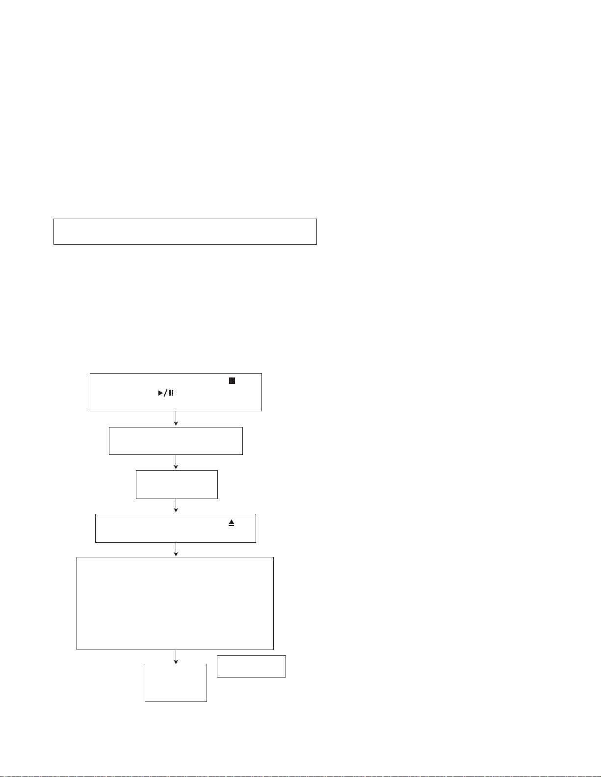
Contents
Safety precautions
Preventing static electricity
Important for laser products
Disassembly method
Adjustment method
SP-NXHD10 CA-NXHD10R SP-NXHD10
1-2
1-4
1-5
1-6
1-20
Flow of functional operation
until TOC read (CD)
Maintenance of laser pickup
Replacement of laser pickup
Description of major ICs
Area Suffix
B ----------------------- U.K.
E-------- Continental Europe
EN----------Northern Europe
1-21
1-22
1-22
1-23~46
COPYRIGHT 2002 VICTOR COMPANY OF JAPAN, LTD.
No.21159
Sep. 2002
1-1
Page 2
NX-HD10R
1. This design of this product contains special hardware and many circuits and components specially for safety
purposes. For continued protection, no changes should be made to the original design unless authorized in
writing by the manufacturer. Replacement parts must be identical to those used in the original circuits. Services
should be performed by qualified personnel only.
2. Alterations of the design or circuitry of the product should not be made. Any design alterations of the product
should not be made. Any design alterations or additions will void the manufacturer`s warranty and will further
relieve the manufacture of responsibility for personal injury or property damage resulting therefrom.
3. Many electrical and mechanical parts in the products have special safety-related characteristics. These
characteristics are often not evident from visual inspection nor can the protection afforded by them necessarily
be obtained by using replacement components rated for higher voltage, wattage, etc. Replacement parts which
have these special safety characteristics are identified in the Parts List of Service Manual. Electrical
components having such features are identified by shading on the schematics and by ( ) on the Parts List in
the Service Manual. The use of a substitute replacement which does not have the same safety characteristics
as the recommended replacement parts shown in the Parts List of Service Manual may create shock, fire, or
other hazards.
4. The leads in the products are routed and dressed with ties, clamps, tubings, barriers and the like to be
separated from live parts, high temperature parts, moving parts and/or sharp edges for the prevention of
electric shock and fire hazard. When service is required, the original lead routing and dress should be
observed, and it should be confirmed that they have been returned to normal, after re-assembling.
5. Leakage currnet check (Electrical shock hazard testing)
After re-assembling the product, always perform an isolation check on the exposed metal parts of the product
(antenna terminals, knobs, metal cabinet, screw heads, headphone jack, control shafts, etc.) to be sure the
product is safe to operate without danger of electrical shock.
Do not use a line isolation transformer during this check.
Plug the AC line cord directly into the AC outlet. Using a "Leakage Current Tester", measure the leakage
current from each exposed metal parts of the cabinet, particularly any exposed metal part having a return
path to the chassis, to a known good earth ground. Any leakage current must not exceed 0.5mA AC (r.m.s.).
Alternate check method
Plug the AC line cord directly into the AC outlet. Use an AC voltmeter having, 1,000 ohms per volt or more
sensitivity in the following manner. Connect a 1,500 10W resistor paralleled by a 0.15 F AC-type capacitor
between an exposed metal part and a known good earth ground.
Measure the AC voltage across the resistor with the AC
voltmeter.
Move the resistor connection to each exposed metal part,
particularly any exposed metal part having a return path to
the chassis, and meausre the AC voltage across the resistor.
Now, reverse the plug in the AC outlet and repeat each
measurement. Voltage measured any must not exceed 0.75 V
AC (r.m.s.). This corresponds to 0.5 mA AC (r.m.s.).
0.15 F AC TYPE
1500 10W
Good earth ground
AC VOLTMETER
(Having 1000
ohms/volts,
or more sensitivity)
Place this
probe on
each exposed
metal part.
!
1. This equipment has been designed and manufactured to meet international safety standards.
2. It is the legal responsibility of the repairer to ensure that these safety standards are maintained.
3. Repairs must be made in accordance with the relevant safety standards.
4. It is essential that safety critical components are replaced by approved parts.
5. If mains voltage selector is provided, check setting for local voltage.
Burrs formed during molding may
be left over on some parts of the
chassis. Therefore, pay attention to
such burrs in the case of
preforming repair of this system.
In regard with component parts appearing on the silk-screen printed side (parts side) of the PWB diagrams, the
parts that are printed over with black such as the resistor ( ), diode ( ) and ICP ( ) or identified by the " "
mark nearby are critical for safety.
(This regulation does not correspond to J and C version.)
1-2
Page 3
NX-HD10R
(U.K only)
1. This design of this product contains special hardware and many circuits and components specially
for safety purposes. For continued protection, no changes should be made to the original
design unless authorized in writing by the manufacturer. Replacement parts must be identical to
those used in the original circuits.
2. Any unauthorised design alterations or additions will void the manufacturer's guarantee ; furthermore the
manufacturer cannot accept responsibility for personal injury or property damage resulting therefrom.
3. Essential safety critical components are identified by ( ) on the Parts List and by shading on the
schematics, and must never be replaced by parts other than those listed in the manual. Please note
however that many electrical and mechanical parts in the product have special safety related
characteristics. These characteristics are often not evident from visual inspection. Parts other than
specified by the manufacturer may not have the same safety characteristics as the recommended
replacement parts shown in the Parts List of the Service Manual and may create shock, fire, or
other hazards.
4. The leads in the products are routed and dressed with ties, clamps, tubings, barriers and the
like to be separated from live parts, high temperature parts, moving parts and/or sharp edges
for the prevention of electric shock and fire hazard. When service is required, the original lead
routing and dress should be observed, and it should be confirmed that they have been returned
to normal, after re-assembling.
1. Service should be performed by qualified personnel only.
2. This equipment has been designed and manufactured to meet international safety standards.
3. It is the legal responsibility of the repairer to ensure that these safety standards are maintained.
4. Repairs must be made in accordance with the relevant safety standards.
5. It is essential that safety critical components are replaced by approved parts.
6. If mains voltage selector is provided, check setting for local voltage.
!
Burrs formed during molding may be left over on some parts of the chassis. Therefore,
pay attention to such burrs in the case of preforming repair of this system.
1-3
Page 4
NX-HD10R
Preventing static electricity
1.Grounding to prevent damage by static electricity
Electrostatic discharge (ESD), which occurs when static electricity stored in the body, fabric, etc. is discharged,
can destroy the laser diode in the traverse unit (optical pickup). Take care to prevent this when performing repairs.
2.About the earth processing for the destruction prevention by static electricity
Static electricity in the work area can destroy the optical pickup (laser diode) in devices such as CD players.
Be careful to use proper grounding in the area where repairs are being performed.
2-1 Ground the workbench
Ground the workbench by laying conductive material (such as a conductive sheet) or an iron plate over
it before placing the traverse unit (optical pickup) on it.
2-2 Ground yourself
Use an anti-static wrist strap to release any static electricity built up in your body.
(caption)
Anti-static wrist strap
Conductive material
(conductive sheet) or iron plate
3. Handling the optical pickup
1. In order to maintain quality during transport and before installation, both sides of the laser diode on the
replacement optical pickup are shorted. After replacement, return the shorted parts to their original condition.
(Refer to the text.)
2. Do not use a tester to check the condition of the laser diode in the optical pickup. The tester's internal power
source can easily destroy the laser diode.
4.Handling the traverse unit (optical pickup)
1. Do not subject the traverse unit (optical pickup) to strong shocks, as it is a sensitive, complex unit.
2. Cut off the shorted part of the flexible cable using nippers, etc. after replacing the optical pickup. For specific
details, refer to the replacement procedure in the text. Remove the anti-static pin when replacing the traverse
unit. Be careful not to take too long a time when attaching it to the connector.
3. Handle the flexible cable carefully as it may break when subjected to strong force.
4. It is not possible to adjust the semi-fixed resistor that adjusts the laser power. Do not turn it
Attention when traverse unit is decomposed
Flexible wire
Shorting round
Shorting round
CN601 on
mechanism
board
*Please refer to "Disassembly method" in the text for pick-up and how to
detach the substrate.
1.Solder is put up before the card wire is removed from connector on
the CD substrate as shown in Figure.
(When the wire is removed without putting up solder, the CD pick-up
assembly might destroy.)
2.Please remove solder after connecting the card wire with
when you install picking up in the substrate.
1-4
Page 5

Important for laser products
NX-HD10R
1.CLASS 1 LASER PRODUCT
2.DANGER : Invisible laser radiation when open and inter
lock failed or defeated. Avoid direct exposure to beam.
3.CAUTION : There are no serviceable parts inside the
Laser Unit. Do not disassemble the Laser Unit. Replace
the complete Laser Unit if it malfunctions.
4.CAUTION : The compact disc player uses invisible
laserradiation and is equipped with safety switches
whichprevent emission of radiation when the drawer is
open and the safety interlocks have failed or are de
feated. It is dangerous to defeat the safety switches.
VARNING : Osynlig laserstrålning är denna del är öppnad
och spårren är urkopplad. Betrakta ej strålen.
VARO : Avattaessa ja suojalukitus ohitettaessa olet
alttiina näkymättömälle lasersäteilylle.Älä katso
säteeseen.
5.CAUTION : If safety switches malfunction, the laser is able
to function.
6.CAUTION : Use of controls, adjustments or performance of
procedures other than those specified herein may result in
hazardous radiation exposure.
CAUTION
!
Please use enough caution not to
see the beam directly or touch it
in case of an adjustment or operation
check.
ADVARSEL : Usynlig laserstråling ved åbning , når
sikkerhedsafbrydere er ude af funktion. Undgå
udsættelse for stråling.
ADVARSEL : Usynlig laserstråling ved åpning,når
sikkerhetsbryteren er avslott. unngå utsettelse
for stråling.
REPRODUCTION AND POSITION OF LABELS
WARNING LABEL
CLASS 1
LASER PRODUCT
1-5
Page 6
NX-HD10R
g
Disassembly method
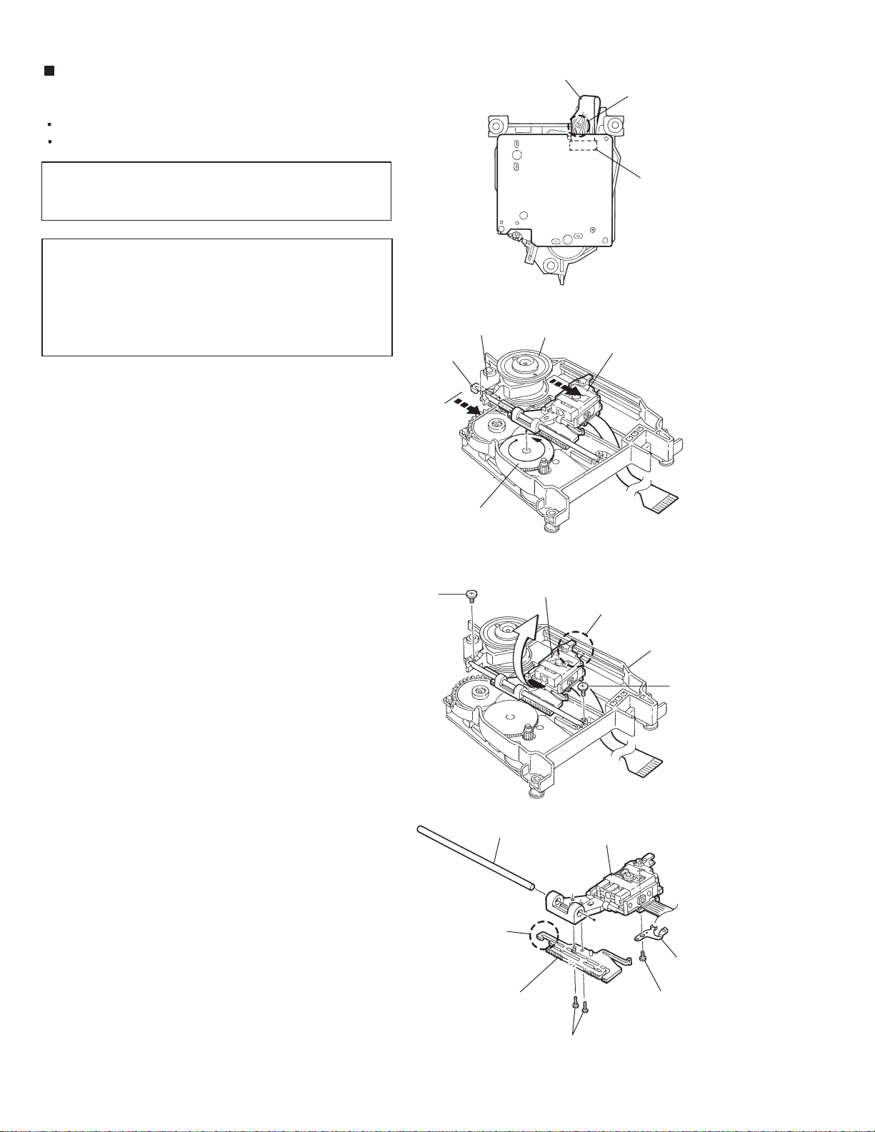
<Main body section>
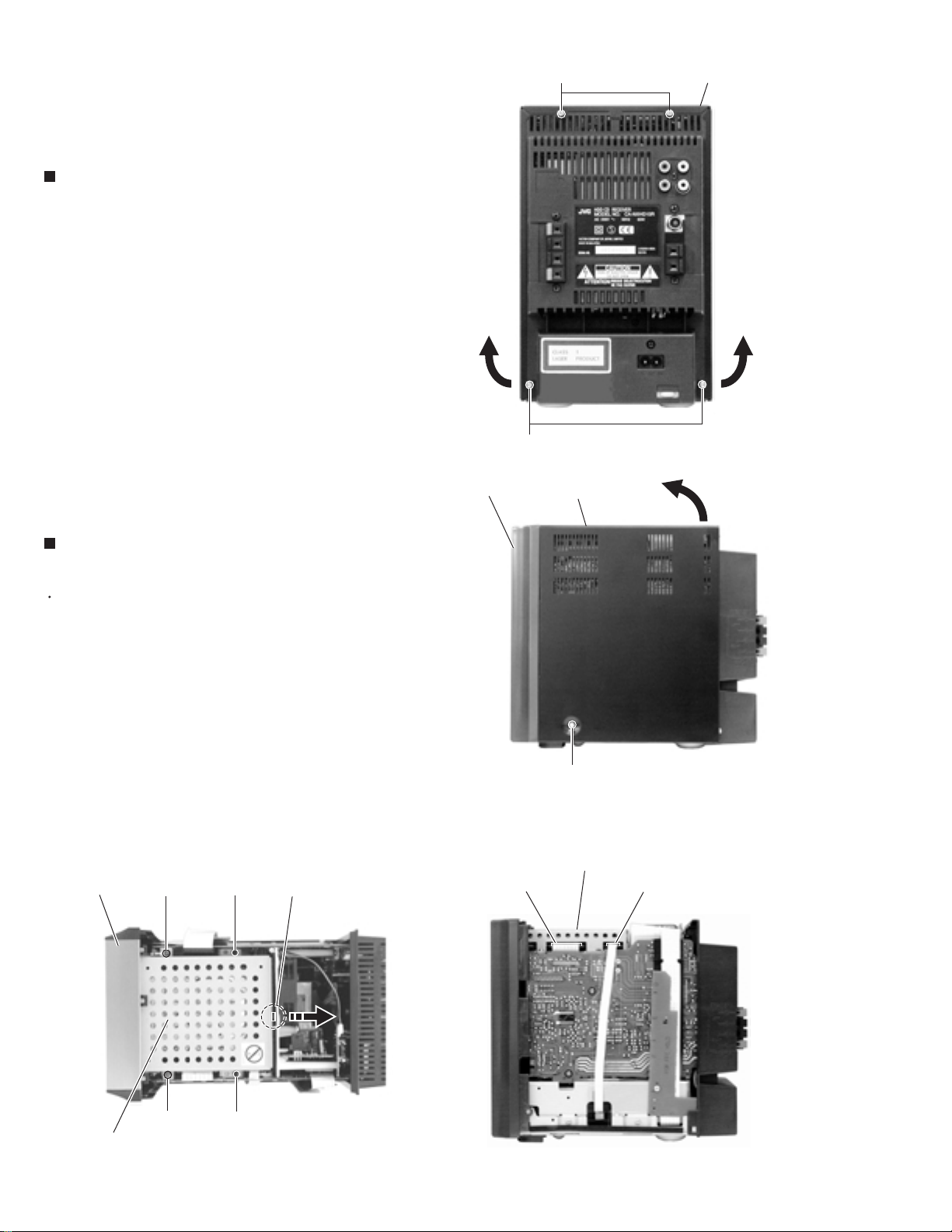
Removing the Top cover (See Fig.1,2)
1.
Remove the four screws A on the back of the body.
2.
Remove the screw B on each side of the body.
3.
Remove the rear side of the top cover upward as
shown in the figure while pulling both sides of the top
cover outward.
Front panel
A
A
Top cover
Top cover
Fig.1
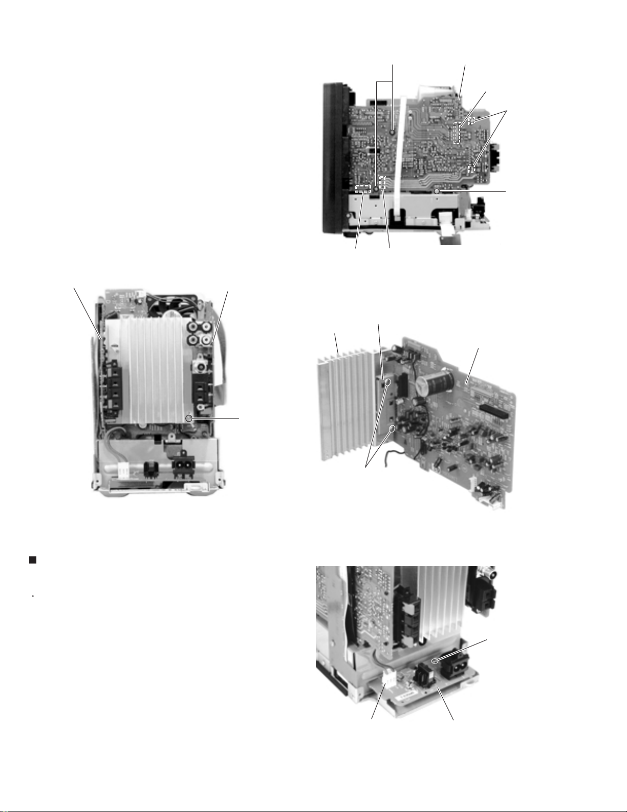
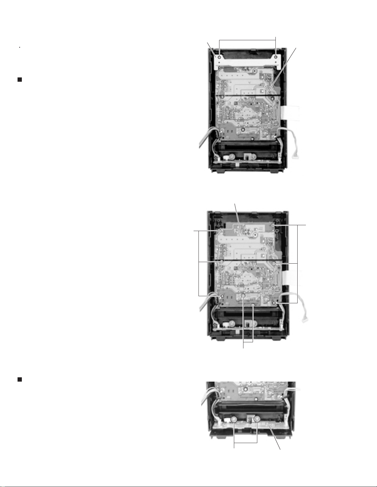
Removing the HDD board assembly
(See Fig.3 and 4)
Prior to performing the following procedure, remove
the top cover.
1.
Disconnect the card wire from connector CN930 and
CN931 on the HDD board assembly on the right side
of the body.
2.
Remove the two screws C and the two special
screws D on top of the body.
3.
Release the joint a on top of the body in the
direction of the arrow. Move the rear side of the HDD
board assembly upward and remove.
Front panel Joint a
CD
B
x2
Fig.2
HDD board assembly
CN930CN931
HDD board assembly
1-6
CD
.3Fig.4
Fi
Page 7
Removing the Front panel assembly
g
(See Fig.5~9)
Prior to performing the following procedure, remove
the top cover and the HDD board assembly.
1.
Disconnect the card wire from connector CN602 on
the inside of the system control board on the left side
of the body.
2.
Remove the screw E on each side of the body.
3.
Remove the two screws F on the bottom of the
body.
4.
Release the joint b on the bottom and the joint c
on each side of the body using a screwdriver. Move
the front panel assembly forward.
5.
Release the wire extending from the headphone
board under the front panel assembly from the two
clamps. Set the front panel assembly apart from the
body as far as possible.
6.
Disconnect the wire from connector CN501 on the
system control board and CN301 on the main
amplifier board. Remove the front panel assembly.
Front panel assembly
Joint c
E
System control board
System control board
CN602
CN301
Main amp board
Fig.5
CN602
NX-HD10R
Front panel assembly
Front panel assembly
Clamp
Fig.7
Front panel assemblyJoint b
FF
CN501
Fig.6
Joint c
E
Front panel assembly
Clamp
Front panel assembly
CN301
Main amp board
Fi
.8 Fig.9
CN501
System control board
Headphone board
1-7
Page 8
NX-HD10R
Remove the Rear cover (See Fig.10~12)
Prior to performing the following procedure, remove
the top cover.
1.
Remove the seven screws G on the back of the
body.
2.
Release the joint d on each lower side of the rear
cover using a screwdriver.
Rear cover
G
G
G
Fig.10
Rear cover
Joint d
Joint d
Fig.11
Rear cover
Fig.12
1-8
Page 9
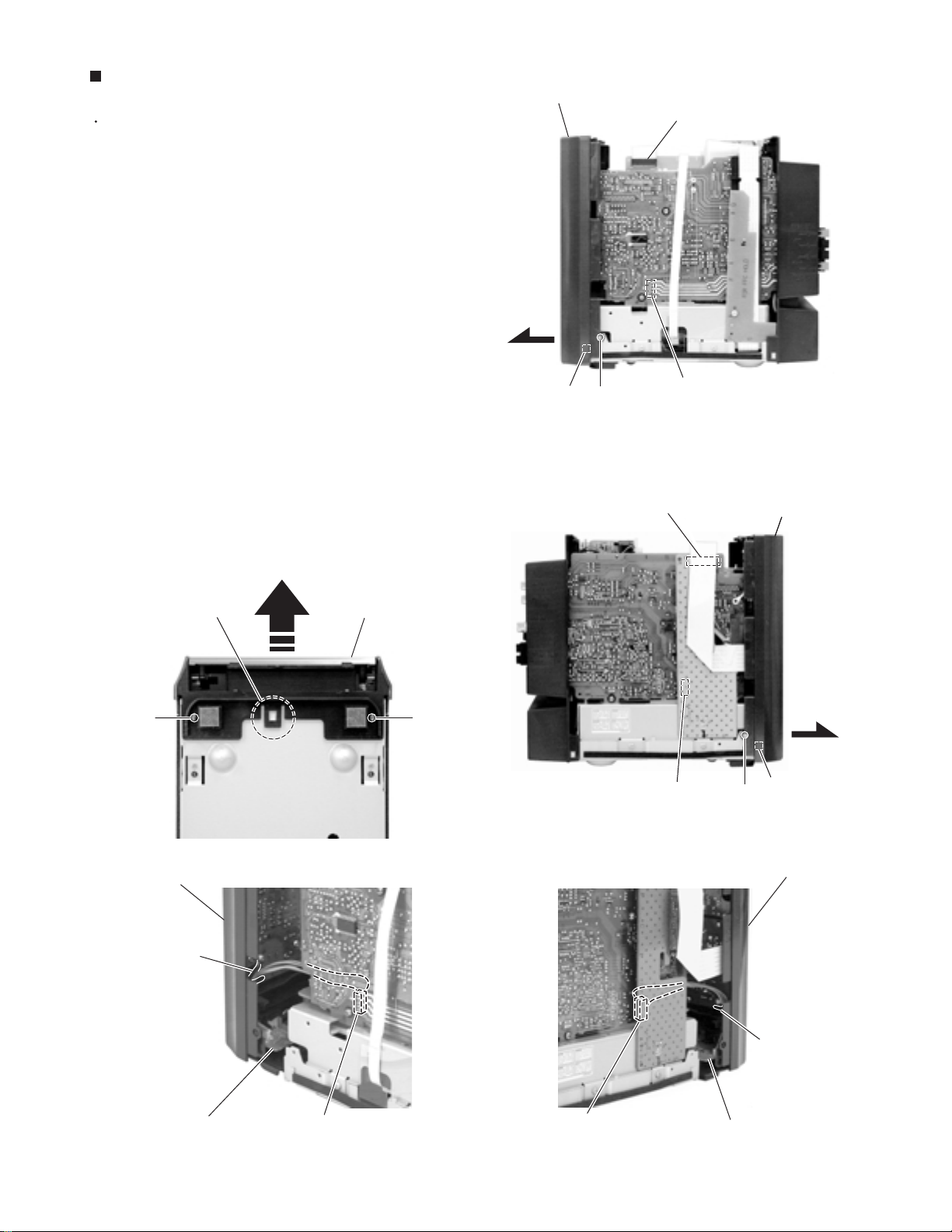
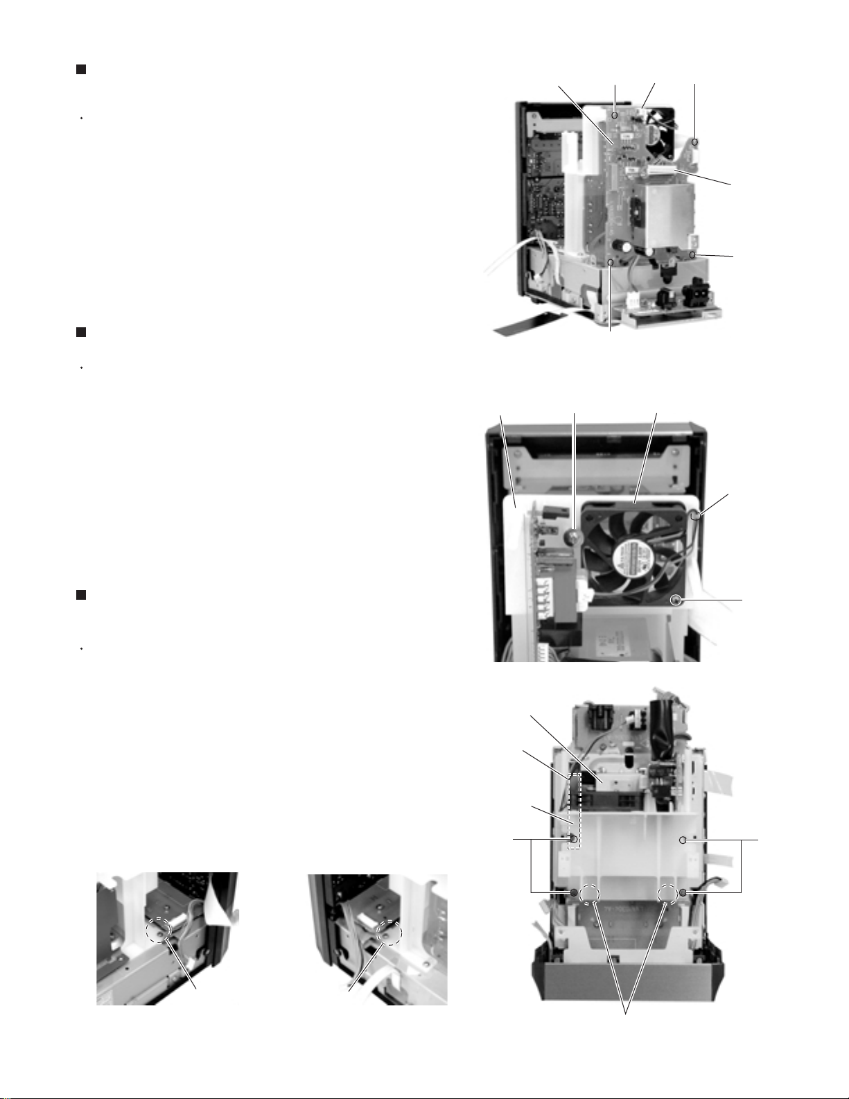
Remove the System control board/Card
g
wire sub board (See Fig.13,14)
Prior to performing the following procedure, remove
the top cover, the HDD board assembly and the rear
cover.
1.
Remove the screw H attaching the card wire sub
board on the left side of the body (The card wire sub
board can be removed if only the top cover has been
removed).
2.
Disconnect the card wire from connector CN602 and
CN605 on the system control board.
3.
Remove the three screws I .
4.
Disconnect the connector CN603 and CN604
outward and remove the system control board.
5.
Disconnect the wire from connector CN501 on the
inside of the system control board.
System control board
Card wire sub board
System control board
CN602 CN605 Front panel
H
Fig.13
CN603
I
NX-HD10R
Removing the Card wire sub board/
Headphone board/ Heat sink
(See Fig.15~18)
Prior to performing the following procedure, remove
the top cover, the HDD board assembly and the rear
cover.
1.
Remove the screw J on the right side of the body
(The card wire sub board can be removed if only the
top cover has been removed).
2.
Disconnect the card wire from connector CN661 and
CN695 on the main amplifier board.
CN501 CN604
II
Fig.14
Main
CN661CN695
J
Fi
.15
amplifier board
Card wire sub board
1-9
Page 10
NX-HD10R
g
3.
Remove the screw K and the two screws L
attaching the main amplifier board.
L
Main amplifier board
4.
Remove the screw M on the back of the body.
5.
Disconnect connector CN901 and CN904 on the
main amplifier board, and remove the main amplifier
board.
6.
Disconnect the wire form connector CN301 on the
inside of the main amplifier board. Remove the main
amplifier board with the heat sink.
7.
Remove the two screws N attaching the heat sink.
8.
Release the bending parts at the two joints e and
remove the heat sink.
Main amplifier board
System control board
Heat sink
CN901
Bracket
CN904
e
K
CN301
Fig.16
Main amplifier board
M
Fig.17
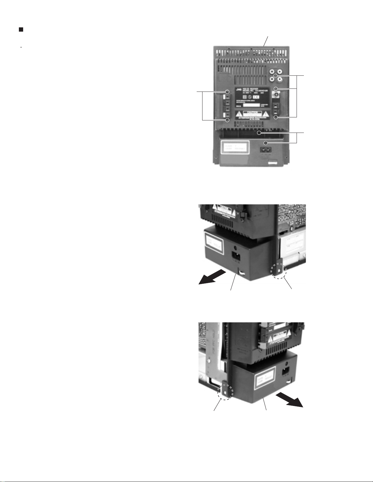
Removing the AC jack board (See Fig.19)
Prior to performing the following procedure, remove
the top cover and the rear cover.
1.
Disconnect the wire from connector CN921 on the
AC jack board.
2.
Remove the screw O attaching the AC jack board.
N
Fig.18
O
1-10
CN921
AC jack board
Fi
.19
Page 11
NX-HD10R
5
Removing the Regulator board
(See Fig.20)
Prior to performing the following procedure, remove
the top cover, the HDD board assembly, the rear
cover, the system control board and the main
amplifier board.
1.
Disconnect the wire from connector CN903 and
CN955 on the back of the body.
2.
Remove the four screws P attaching the regulator
board.
Removing the Fan assembly (See Fig.21)
Prior to performing the following procedure, remove
the top cover, the HDD board assembly, the rear
cover, the system control board, the main amplifier
board and the regulator board.
1.
Remove the band setting the fan assembly wire on
the back of the body.
2.
Loosen the screw Q and remove the screw R
attaching the fan assembly.
Regulator board
Fan assembly
attaching bracket
Q
P
P
Fig.20
CN903
Fan assembly
P
CN99
P
Band
Removing the Power transformer
assembly (See Fig.21~23)
Prior to performing the following procedure, remove
the top cover, the HDD board assembly, the rear
cover, the system control board, the main amplifier
board and the regulator board.
1.
Remove the four screws S attaching the fan
assembly attaching bracket and the silicon steel
plate. Release the two joints d backward and
remove the fan assembly attaching bracket (The fan
assembly will comes off at the same time).
R
Fig.21
Power transformer
Silicon steel plate
Fan assembly
attaching bracket
SS
Joint d Joint d
Joint d
Fig.21-1 Fig.21-3 Fig.21-2
1-11
Page 12
NX-HD10R
2.
Disconnect the wire from connector CN921 on the
AC jack board.
3.
Remove the four screws T attaching the power
transformer assembly.
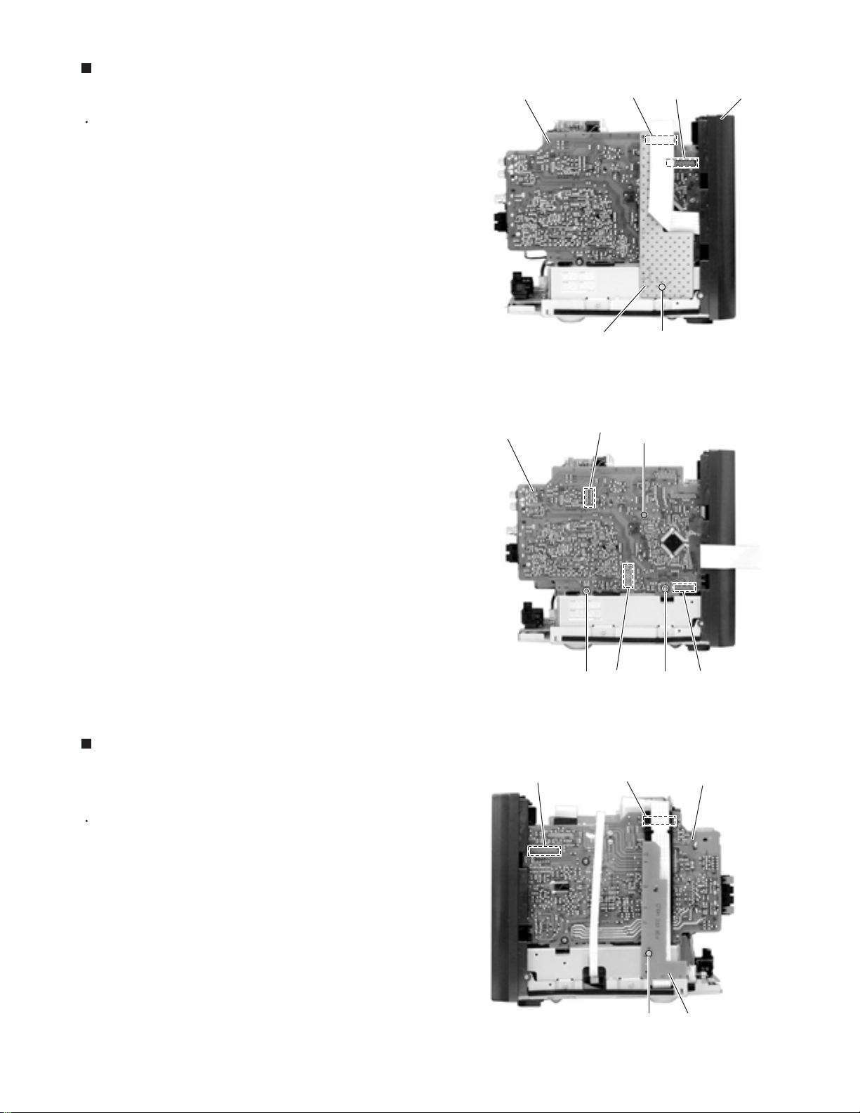
Removing the Relay board (See Fig.24)
Power transformer assembly
T
AC jack board
CN921
T
Fig.23
Relay board
Prior to performing the following procedure, remove
the top cover, the HDD board assembly, the rear
cover, the system control board and the main
amplifier board.
1.
Remove the two screws U on top of the body.
UU
Fig.24
1-12
Page 13
Removing the CD mechanism assembly
y
g
(See Fig.25~28)
Prior to performing the following procedure, remove
the top cover, the HDD board assembly, the front
panel assembly, the rear cover, the system control
board, the main amplifier board, the regulator board,
the fan assembly and the power transformer
assembly.
1.
Remove the five screws V attaching the CD
mechanism cover.
2.
Lift the front side of the CD mechanism cover to
disengage the joint e on the rear side of the CD
mechanism cover.
3.
Remove the three screws W .
V
NX-HD10R
Joint eAC jack board
CD mechanism cover
CD mechanism assembl
Fig.25
CD mechanism coverCD mechanism cover
VV
Fig.27Fig.26
W
WW
CD mechanism assembly
Fi
.28
1-13
Page 14
NX-HD10R
g
<Front assembly section>
Prior to performing the following procedure, remove
the top cover, the HDD board assembly and the front
panel assembly.
Removing the Function switch board
(See Fig.29~31)
1.
Remove the two screws X attaching the bracket.
2.
Remove the eight screws Y attaching the function
board.
Bracket
Function switch board
Fig.29
X
Function switch
board
Removing the Jack board (See Fig.31)
1.
Remove the two screws Z and pull out the jack
board toward the rear.
Y
Y
Y
Fig.30
1-14
Z
Jack board
.31
Fi
Page 15
NX-HD10R
g
<CD Mechanism Assembly>
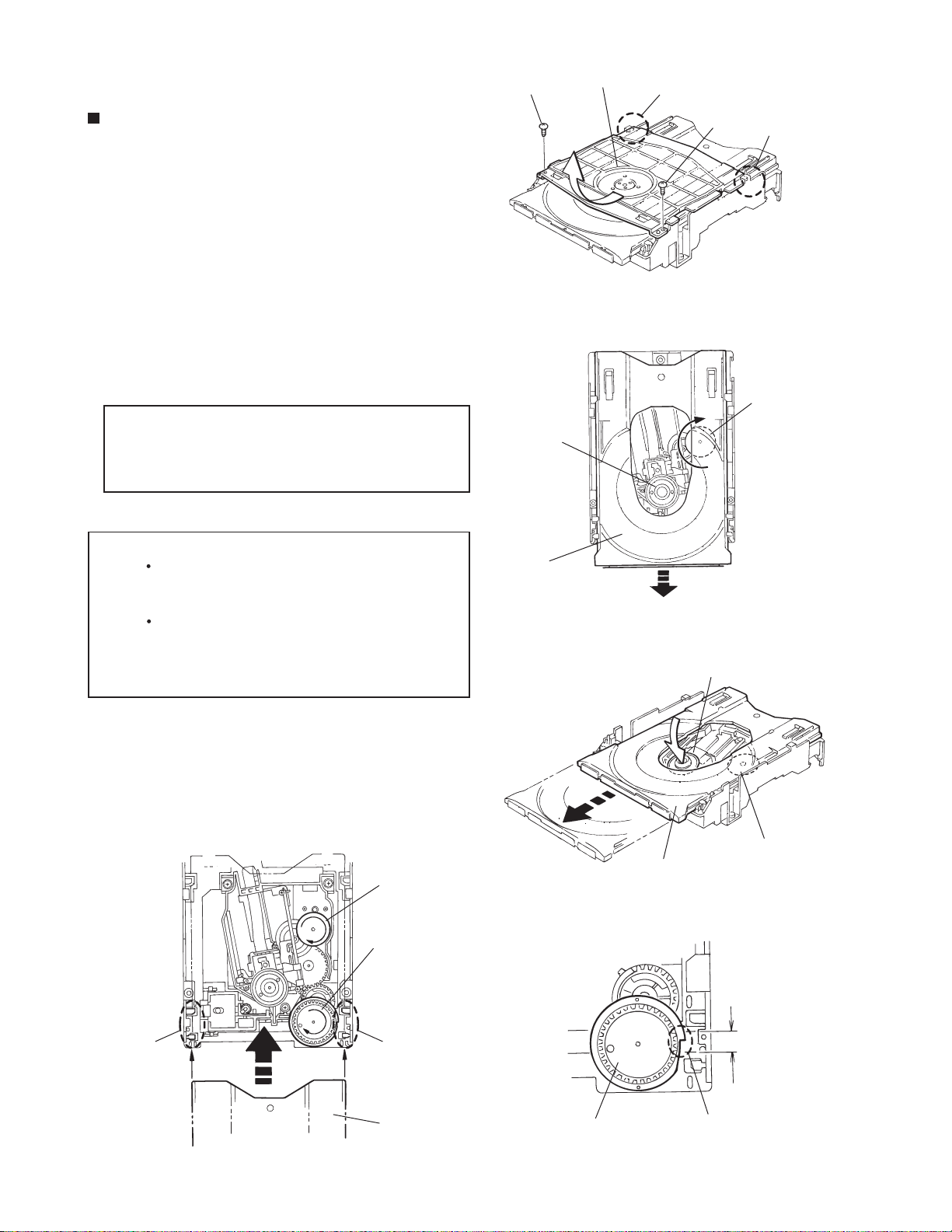
Removing the CL. Base Assembly and Tray
(Refer to Figs. 1 to 5.)
1. Remove the two screws A fastening the CL. base
assembly from the top of the CD mechanism
assembly.
2. Move the CL. base assembly diagonally upwards
as indicated by the arrow to release it from the two
hooks a.
3. Turn the idle gear in the arrow-marked direction
from the upper side of the CD mechanism
assembly. Accordingly, the TRAMECHA assembly
moves downwards.
Note: When drawing out the tray, shift down the
TRAMECHA assembly to the position where
the tray does not contact the T-T assembly
of the TRAMECHA assembly.
4. Draw out the tray frontwards for removing it.
CL. base assembly
A
TRAMECHA
assembly
Hook a
Fig. 1
A
Hook a
Idle gear
Note: When reinstalling the tray:
Turn the idle gear so that the part b of the
tray gear is positioned in the part c shown
in Fig. 4. (Eject position)
Engage the right and left hooks d and e of
the tray with the right and left grooves of the
TRAMECHA assembly respectively for
retaining the tray.
Idle gear
Tray gear
Tray
Fig. 2
TRAMECHA assembly
Idle gear
Tray
Fig. 3
Hook d
Hook d
Tray
Tray gear
Fi
Part c
Part b
. 4Fig. 5
1-15
Page 16
NX-HD10R
Removing the TRAMECHA Assembly
(Refer to Figs. 6 to 9.)
Remove the CL. base assembly and tray.
Reference: The TRAMECHA assembly can be
removed without removal of the
mechanism P.C. board.
1. If the TRAMECHA assembly is lowered and it is
located out of the PLAY position, turn the idle gear
in the arrow-marked direction so that the hole in the
part f of the tray gear meets the hole on the CL.
base assembly. (Set the TRAMECHA assembly at
the PLAY position.)
2. Remove the three screws B fastening the
TRAMECHA assembly and then remove the
TRAMECHA assembly upwards from the front side.
3. At the same time, remove the spring from the groove of
the CH. base assembly in the part g of the TRAMECHA
assembly.
Note: When reinstalling the TRAMECHA assembly:
Check to see if the spring is properly
engaged with groove of the CH. base
assembly in the part g of the TRAMECHA
assembly.
After making sure that the three insulators of
the TRAMECHA assembly are properly set
on the bosses of the L. base assembly's
guide, fasten them with the screws.
TRAMECHA
assembly
B
Part g
L. base assembly
B
Fig. 6
Fig. 7
B
Idle gear
Tray gear
Tray gear
Part f
1-16
Spring
Part g
Fig. 8
Spring
Groove of CH. base assembly
Fig. 9
Page 17
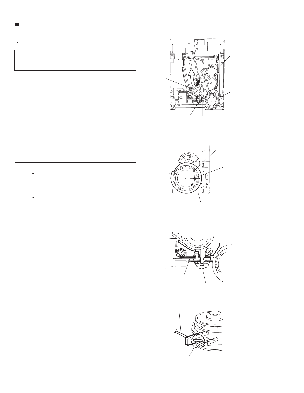
Removing the Mechanism P.C. Board
(Refer to Fig 10.)
Reference:The mechanism P.C. board can be
removed without removal of the
TRAMECHA assembly.
NX-HD10R
Flexible wire
C
Shorting round
Note: Before disconnecting the flexible wire coming
from the pickup from the connector, be sure to
solder its shorting round.
If the flexible wire is connected without
soldering, it may cause breakdown of the
pickup.
1. Solder the shorting round of the flexible wire
connected with the mechanism P.C. board from the
back of the mechanism assembly.
2. Disconnect the flexible wire from the connector
CN601 on the mechanism P.C. board.
3. Remove the three screws C fastening the
mechanism P.C. board.
4. Unsolder the two points of the part h and one point
of the part i of the mechanism P.C. board. Then,
remove the mechanism P.C. board upwards.
Note: When reinstalling the mechanism P.C. board,
connect the flexible wire coming from the
pickup to the connector first and then remove
the solder from the shorting round of the
flexible cable.
Soldered
part h
C
CN601 on
mechanism
P.C. board
C
Soldered part i
Fig. 10
1-17
Page 18
NX-HD10R
Removing the Pickup
(Refer to Figs. 11 to 14.)
Remove the CL. base assembly and tray.
Remove the TRAMECHA assembly.
Reference: The pickup can be removed without
removal of the mechanism P.C. board.
Note: Before disconnecting the flexible wire coming
from the pickup from the connector, be sure to
solder its shorting round.
If the flexible wire is connected without
soldering, it may cause breakdown of the
pickup.
1. Solder the shorting round of the flexible wire
connected with the mechanism P.C. board from the
back of the TRAMECHA assembly.
2. Disconnect the flexible wire from the connector
CN601 on the mechanism P.C. board.
Part j of
rack plate
CH. base
assembly
Flexible wire
Shorting round
CN601 on
mechanism
P.C. board
Fig. 11
T-T assembly
Pickup assembly
3. Turn the idle gear in the arrow-marked direction from
the top of the TRAMECHA assembly so that the
pickup assembly is shifted to the reverse side of the
T-T assembly.
Move the pickup assembly until the part j of the rack
plate in the lower part of the pickup assembly comes
out of the CH. base assembly.
4. Remove the two screws D retaining the shaft of the
pickup assembly. Next, disengage the hook k from
the CH. base assembly and then remove the pickup
assembly together with the shaft.
5. Pull the shaft out of the pickup.
6. Remove the two screws E fastening the rack plate
from the pickup.
7. Remove the screw F retaining the P.S. spring from
the pickup.
D
Idle gear
Shaft
Fig. 12
Pickup assembly
Part k
CH. base
assembly
D
Fig. 13
Pickup
1-18
Part j
Rack plate
P.S. spring
F
E
Fig. 14
Page 19

NX-HD10R
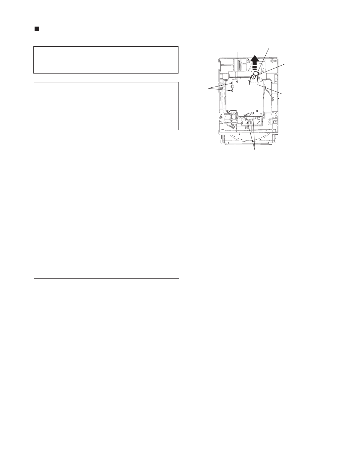
Reinstalling the Pickup Assembly
(Refer to Figs. 15 and 16.)
Reference: Refer to the explanation of "Removing
the Pickup" on the preceding page.
1. Fit the P.S. spring and rack plate to the pickup.
2. Insert the shaft into the pickup.
3. Engage the hook k of the pickup assembly with the
CH. base assembly first, and set the part j of the
rack plate in the opening I next. Then, reinstall the
pickup assembly while shifting it to the T-T side
(inward) so that the part m of the rack plate is
positioned as shown in Fig. 16.
4. Move the pickup assembly to the center position
and fasten the shaft with the two screws D. (Make
sure that the part n of the rack plate is correctly
engaged with the middle gear.)
5. After passing the flexible wire coming from the
pickup through the opening of the CH. base
assembly, connect it to the connector CN601.
Part I
Part j
Part m
Hook k
Pickup
assembly
CH. base
assembly
Fig. 15
Middle gear
Note: When reinstalling the pickup assembly,
remove the solder from the shorting round
after connecting the flexible wire coming from
the pick to the connector CN601.
Removing the Feed Motor Assembly
(Refer to Fig. 17.)
Remove the CL. base assembly and tray.
Remove the mechanism P.C. board.
Remove the two screws E fastening the feed motor
assembly from the top of the mechanism assembly.
Rack plate
Part n
Fig. 16
E
Feed motor assembly
Fig. 17
1-19
Page 20
NX-HD10R
p
Adjustment method
1. Jigs and test instruments
Laser power meter
Laser power meter sensor (or disk sensor)
2. CD check method
Remove the four screws retaining the top cover from the rear panel and the two screws retaining it from
1.
the left and right side panels.
Remove the two screws retaining the front cover from the rear side and the two screws retaining it from
2.
the bottom panel.
Remove the eight screws retaining the rear cover.
3.
Remove the four screws retaining the sub chassis from the left and right sides.
4.
(Caution)
For details of the removal, see the previous
section "Disassembly method".
3. Adjustment and check items
1) CD section
(1) Indication of the C1 error
(2) Cancel of the C1 error indication
4. Adjustment and check method
1) CD section
(1) Indication of the C1 error
While pressing both the STOP key
and CD PLAY key on the main
unit,turn on the primary power supply.
Press the STANDBY/ON key
on the main unit
FL indication
CD TEST
1-20
Press the CD OPEN/CLOSE key
and insert the test disk.
Press key 1, 2 or 4 of the remote control
unit to start measurement. The number of
error corrections will be displayed every 10
seconds.
Key 1: Normal-speed playback
Key 2: 2x-speed playback
Key 4: 4x-speed playback
FL indication
∗∗ ∗∗
∗∗∗Times
(2) Cancel of the C1 error indication
To cancel the C1 error indication, cut off the
200 Hz or less
ower supply.
Page 21
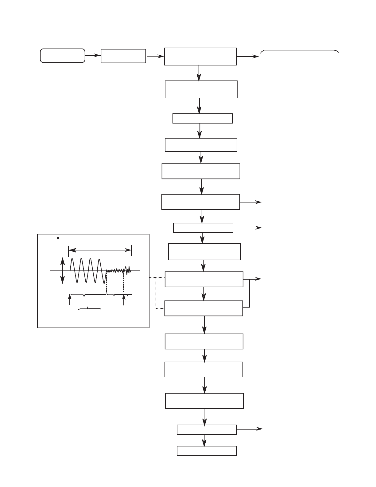
Flow of functional operation until TOC read (CD)
Check Point
Power ON
Play Key
Slider turns REST
SW ON.
Automatic tuning
of TE offset
Laser ON
Detection of disc
Automatic tuning of
Focus offset
Confirm that the voltage at the pin32
of IC251 is "H"\"L"\"H".
NX-HD10R
Tracking error waveform at TOC reading
Approx.3sec
Tracking
servo
off states
Automatic measurement
of TE amplitude and
automatic tuning of
TE balance
VREF
pin 20 of
IC601(TE)
Approx
1.8V
Disc states
to rotate
Tracking
servo
on states
Disc to be
braked to stop
TOC reading
finishes
500mv/div
2ms/div
Fig.1
Automatic measurement of
Focus S-curve amplitude
Disc is rotated
Focus servo ON
(Tracking servo ON)
Automatic measurement of
Tracking error amplitude
Automatic tuning of
Tracking error balance
Automatic tuning of
Focus error balance
Automatic tuning of
Focus error gain
Confirm that the Focus error
S-cuve signal at the pin28 of
IC651 is approx.2Vp-p
Confirm that the signal from
pin24 IC651(R808) is 0V as
a accelerated pulse during
approx.400ms.
Confirm the waveform of
the Tracking error signal.
at the pin 20 of IC601 (R604)
(See fig-1)
Automatic tuning of
Tracking error gain
TOC reading
Play a disc
Confirm the eys-pattern
at the lead of TP1
1-21
Page 22
NX-HD10R
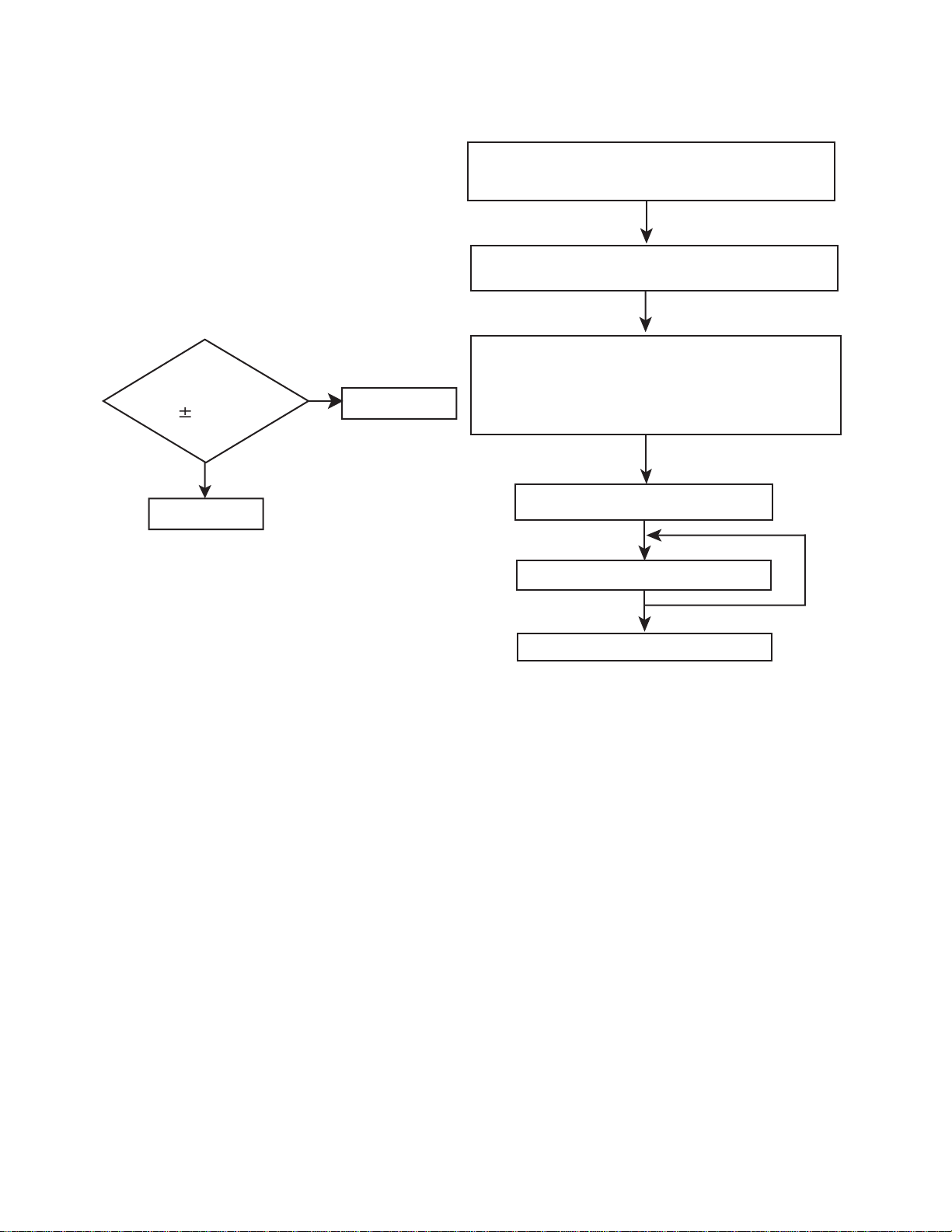
Maintenance of laser pickup (CD)
(1) Cleaning the pick up lens
Before you replace the pick up, please try to
clean the lens with a alcohol soaked cotton
swab.
(2) Life of the laser diode
When the life of the laser diode has expired,
the following symptoms will appear.
1. The level of RF output (EFM output:ampli
tude of eye pattern) will below.
Is the level of
RFOUT under
1.25V 0.22Vp-p?
YES
O.K
NO
Replace it.
Replacement of laser pickup (CD)
Turn off the power switch and,disconnect the
power cord from the AC OUTLET.
Replace the pickup with a normal one.(Refer
to "Pickup Removal" on the previous page)
Plug the power cord in,and turn the power on.
At this time,check that the laser emits for
about 3seconds and the objective lens moves
up and down.
Note: Do not observe the laser beam directly.
Play a disc.
Check the eye-pattern at TP1.
Finish.
(3) Semi-fixed resistor on the APC board
The semi-fixed resistor on the APC board which is attached to the pickup is used to adjust the laser power.
Since this adjustment should be performed to match the characteristics of the whole optical block, do not touch
the semi-fixed resistor.
If the laser power is lower than the specified value,the laser diode is almost worn out, and the laser pickup should
be replaced.
If the semi-fixed resistor would be adjusted when the pickup operates normally,the laser pickup may be damaged
due to excessive current.
1-22
Page 23

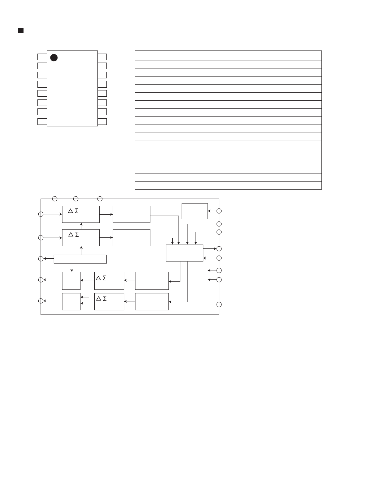
Description of major ICs
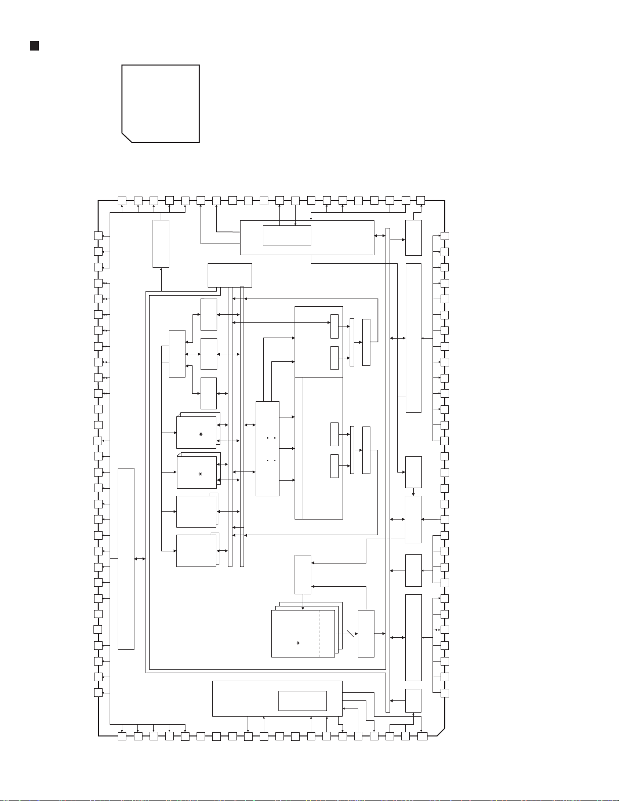
6
LC32V4265T-25 (IC911) : DRAM
NX-HD10R
1.
Pin
layout
1
Vcc Vss
2
I/O1
3
I/O2
4
I/O3
5
I/O4
6
Vcc
7
I/O5
8
I/O6
9
I/O7
10
I/O8
13
N.C.
14
N.C.
15
WE
16
RAS
17
N.C.
18
A0
19
A1
20
A2
21
A3
22
Vcc
44
43
42
41
40
39
38
37
36
35
32
31
30
29
28
27
26
25
24
23
I/O16
I/O15
I/O14
I/O13
Vss
I/O12
I/O11
I/O10
I/O9
N.C.
LCAS
UCAS
OE
A8
A7
A6
A5
A4
Vss
2. Pin function
Symbol
A0 to A8
RAS
UCAS
LCAS
WE
OE
I/O1 to I/ O16
Vcc
Vss
N.C.
Function
Address input
Low address strobe
Column address strobe
(Upper byte control)
Column address strobe
(L+K81ower byte control)
Write enable
Output enable
Data I/O
Power supply
Ground
No connection
3. Block diagram
RAS
UCAS
LCAS
A0
A8
Clock generator No.1
Mode control
Refresh counter
Low address
buffer
Column
address buffer
Clock generator No.2
262144 memory cells
512
Row decoder
X16 bits
512X16
Sense amplifier I/O gate
512
Column decoder
Pre-decoder
Clock generator No.3
Lower byte
Data input buffer
I/O1 to I/O8 I/O9 to I/O16
Data output buffer
I/O1 to I/O8 I/O9 to I/O16
Substrate bias generator
Upper byte
Vcc
Vss
WE
I/O1
I/O1
OE
1-23
Page 24
NX-HD10R
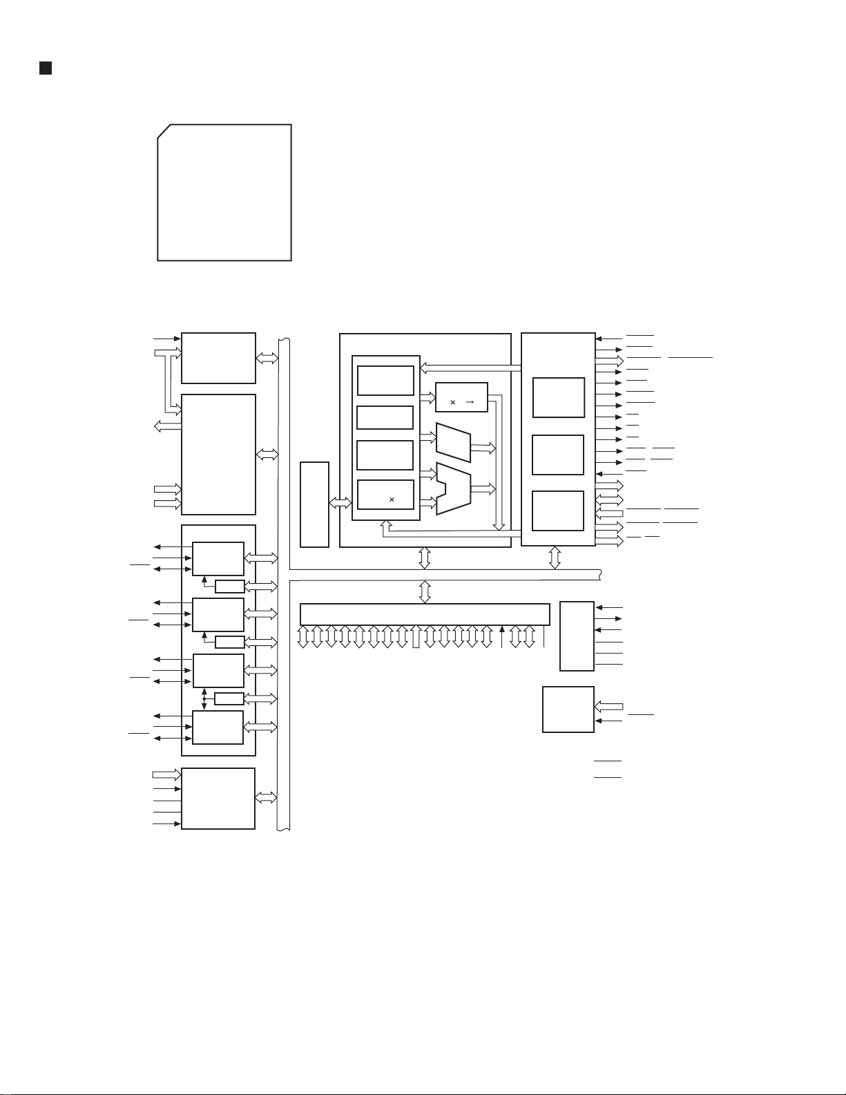
TC9486F-001 (IC930) : DSP
1.
Pin
layout
80 ~ 51
2. Block diagram
51
Po5
52
Po6
53
Po7
54
io0
55
io1
56
io2
57
io3
58
io4
59
io5
60
io6
61
io7
62
VDDT
63
VSS
64
/WR
65
/oE
66
/CE
67
AD0
68
AD1
69
AD2
70
AD3
71
AD4
72
AD5
73
AD6
74
AD7
75
VSS
76
VDDT
77
AD8
78
AD9
79
AD10
80
AD11
81
~
100
Po4
50
External
SRAM I /F
1 ~ 30
Po3
Po2
49 48
General
I-Bus
Po1
47
Output Port
Address
50
~
31
Po0
46
Calc. 2sets
ERAM
CROM
YRAM
XRAM
CKo
45
3 4k
8 4k
4k+0.5k
4k+0.5k
44
register
C-Pointer
register
Y-Pointer
register
X-Pointer
word
word
word
word
LoCKA
43
Bus
Switch
X-Bus
VDD
VSS
42 41
register
Y- B u s
VSSA
AMPo
AMPi
40
38
39
VCO
A Y
A X
M Z
Y0 Y1 Y2
X0 X1 X2
M X M Y
Control
Program
6 4kword
Program ROM
Timing
Generator
VCO
VDDA
A L U
M A C
PDoA
37
36
DIR
A 3A 2A 1A 0
512word
Program RAM
FCoNT
35
40bit
TEST1
TEST0
34 33
round & limit
round & limit
Decoder
Instruction
CKi
RX
32 31
Interrupt
Prog.
TX
DITFlag
Audio I / F
Timer
Control
Microcom. I/F
Start
30
29
28
27
26
25
24
23
22
21
20
19
18
17
16
15
14
13
12
11
10
9
8
7
6
5
4
3
2
1
BCKoB
LRCKoB
BCKoA
LRCKoA
SDi1
SDi0
BCKiB
LRCKiB
SDo3
SDo2
SDo1
SDo0
BCKiA
LRCKiA
VDDT
VSS
VSS
VDD
iRQ
Fi3
Fi2
Fi1
Fi0
MiACK
/MiCK
MiDio
/MiLP
/MiCS
MiMD
/RESET
1-24
81 82
AD12
83 84
AD13
AD14
AD15
85
86
AD16
VSS
87
VDD
88
VDDX
89 90
Xo
91
92
94
93
96 97
95
98
100
99
Xi
VSSX
VSSP
VCOi
VDDP
PDoB
CKS
LoCKB
RUN
ROM
SCKo
Page 25

3. Pin function
NX-HD10R
Pin No. Symbol
1
2
3
4
5
6
7
8
9
10
11
12
13
14
15
16
17
18
19
20
21
22
23
24
25
26
27
28
29
30
31
32
33
34
35
36
37
38
39
40
41
42
43
44
45
46
47
48
49
50
/RST
MiMD0
/MiCS
/MiLP
MiDio
/MiCK
MiACK
Fi0
Fi1
Fi2
Fi3
IRQ0
VDD
VSS
VSS
VDDT
LRCKiA
BCKiA
SDo0
SDo1
SDo2
SDo3
LRCKiB
BCKiB
SDi0
SDi1
LRCKoA
BCKoA
LRCKoB
BCKoB
TX
RX
Cki
TEST0
TEST1
FCoNT
PDoA
VDDA
AMPiA
AMPoA
VSSA
VSS
VDD
LoCKA
Cko
Po0
Po1
Po2
Po3
Po4
I/O
I
Hard reset input terminal (L: reset H: general)
I
Micon I/F mode select input terminal (L: Serial H: I
Micon I/F chip select input terminal
I
Micon I/F latch pulse input
I
Micon I/F data I/O terminal
I/O
Micon I/F clock input terminal
I
Micon I/F acknowledge output terminal
O
Flug input terminal 0
I
Flug input terminal 1
I
Flug input terminal 2
I
Flug input terminal 3
I
Squeeze input terminal
I
Digital power supply terminal (2.5V)
Digital ground terminal
Digital ground terminal
Digital power supply terminal (3.3V)
LR clock input A
I
Bit clock input A
I
Audio I/F data output terminal 0
O
Audio I/F data output terminal 1
O
Audio I/F data output terminal 2
O
Audio I/F data output terminal 3
O
LR clock input B
I
Bit clock input B
I
Audio I/F data input terminal 0
I
Audio I/F data input terminal 1
I
LR clock output terminal A
O
Bit clock output terminal A
O
LR clock output terminal B
O
Bit clock output terminal B
O
SPDIF output terminal
O
SPDIF input terminal
I
Outside clock input terminal
I
Test input terminal 0 (H: test L: general)
I
Test input terminal 1 (H: test L: general)
I
PLL frequency control output terminal for DIR
PLL phase error signal output
PLL power supply terminal (2.5V) for DIR
PLL filter amp input terminal for DIR
I
PLL filter amp output terminal for DIR
O
PLL ground terminal for DIR
Digital ground terminal
Digital power supply terminal (2.5V)
DIR lock output terminal
O
DIR clock output terminal
O
General output terminal 0
O
General output terminal 1
O
General output terminal 2
O
General output terminal 3
O
General output terminal 4
O
Function
2
C)
1-25
Page 26

NX-HD10R
Pin No. Symbol
51
52
53
54
55
56
57
58
59
60
61
62
63
64
65
66
67
68
69
70
71
72
73
74
75
76
77
78
79
80
81
82
83
84
85
86
87
88
89
90
91
92
93
94
95
96
97
98
99
100
Po5
Po6
Po7
Io0
Io1
Io2
Io3
Io4
Io5
Io6
Io7
VDDT
VSS
/WR
/OE
/CE
AD0
AD1
AD2
AD3
AD4
AD5
AD6
AD7
VSS
VDDT
AD8
AD9
AD10
AD11
AD12
AD13
AD14
AD15
AD16
VSS
VDD
VDDX
Xo
Xi
VSSX
VSSP
VCOi
VDDP
PDoB
CKS
LoCKB
RUN
ROM
SCKo
I/O
O
General output terminal 5
O
General output terminal 6
O
General output terminal 7
I/O
Outside SRAM data I/O terminal 0
I/O
Outside SRAM data I/O terminal 1
I/O
Outside SRAM data I/O terminal 2
I/O
Outside SRAM data I/O terminal 3
I/O
Outside SRAM data I/O terminal 4
I/O
Outside SRAM data I/O terminal 5
I/O
Outside SRAM data I/O terminal 6
I/O
Outside SRAM data I/O terminal 7
-
Digital ground terminal (3.3V)
-
Digital ground terminal
O
Outside SRAM write signal
O
Outside SRAM output enable signal output terminal
O
Outside SRAM chip enable signal output terminal
O
Outside SRAM addess output terminal 0
O
Outside SRAM addess output terminal 1
O
Outside SRAM addess output terminal 2
O
Outside SRAM addess output terminal 3
O
Outside SRAM addess output terminal 4
O
Outside SRAM addess output terminal 5
O
Outside SRAM addess output terminal 6
O
Outside SRAM addess output terminal 7
-
Digital ground
-
Digital power supply (3.3V)
O
Outside SRAM address output terminal 8
O
Outside SRAM address output terminal 9
O
Outside SRAM address output terminal 10
O
Outside SRAM address output terminal 11
O
Outside SRAM address output terminal 12
O
Outside SRAM address output terminal 13
O
Outside SRAM address output terminal 14
O
Outside SRAM address output terminal 15
O
Outside SRAM address output terminal 16
-
Digital ground
-
Digital power supply (2.5V)
-
Power supply terminal (2.5V) for oscillation
O
Oscillate connect terminal (Output)
I
Oscillate connect terminal (Input)
-
Ground for oscillation
-
Ground for VCO
-
Voltage control input terminal for VCO
-
Power supply for VCO
-
PLL phase error signal output
I
VCO select (H: VCO L: XI input)
O
PLL clock output
I
Program ROM boot control terminal 0
I
Program ROM boot control terminal 1
O
System clock output
Function
1-26
Page 27

LC895871 (IC910) : Digital audio I / F input and output
1.
Pin
layout
144 ~ 109
NX-HD10R
1
~
36
37 ~ 72
2. Block diagram
DITOUT
(2x)
108
73
DIT
~
0
(MUTE)
FADER 0
MUTE
DIRERR
DITO
SEL
1
DAC
DACEMPH
Bit Form
10
METER 0
DACLRCK
Convert
0
DACBCK
DACDATA
for DAC
SEL
DACO
1
FADER 1
DSP
DSPOUT
Convert
Bit Form
CLOCK
for DAC
Generator
(MUTE)
for DSPOUT
SEL
DSPO
0
1
MEMSEL
10
METER 1
01
DRAM
ZRAS,ZCAS
ZWE,ZOE
MEMCON
SINA,SOUTA,SCKA
SINB,SOUTB,SCKB
RA9-0,IO15-0
SIO
(256Word)
FIFO (Rec)
CIN
ZSIOADONE,ZSIOAERR
COUT
ZSIOBDONE,ZSIOBERR
Count
IOCON
MICON
CLCK
SBSY,SFSY,SBDATA
SUBC
Gnd
3.3V
TESTIN,TESTOUT
LSIMODE
I/F
ZCS,ZRD,ZWRH,ZWRL
SUA10-0,D15-0,
ZINT,ZFULL,ZEMPTY
DIRRS
DIRVCO
DIRERR
DIRLPF
0
FSC
0
DIR
DIR
SEL
123
(2x)
DINO-3
0
SEL
DATA
123
Convert
Bit Form
AUXBCK
AUXLRCK
for AUX
AUXDATA(x4)
CLOCK
Generator
DATA
123
for AUX
Bit Form
ADCDATA
SEL
1
Convert
ADC
0
for ADC
CLOCK
Generator
ADCBCK
ADCLRCK
for ADC
ZRESET
ADCCKOUT
(256Word)
FIFO (Play)
System
Clock
CLOCK
Convert
Bit Form
DSPIN
DSP
for DSPIN
Generator
for DEC-DSP
DSPBCK
DSPLRCK
AUXCKIN
XTALIN
XTALOUT
DACCKOUT
DSPCKOUT
1-27
Page 28

NX-HD10R
3. Pin function
Pin No. Symbol
1
2
3
4
5
6
7
8
9
10
11
12
13
14
15
16
17
18
19
20
21
22
23
24
25
26
27
28
29
30
31
32
33
34
35
36
37
38
39
40
41
42
43
44
45
46
47
48
49
50
51
52
53
54
DVss
IO0
IO1
IO2
IO3
IO4
IO5
IO6
IO7
IO8
IO9
IO10
IO11
IO12
IO13
IO14
IO15
DVdd
DVss
ZRAS
ZCAS
ZWE
ZOE
RA0
RA1
RA2
RA3
RA4
RA5
RA6
RA7
RA8
RA9
LSIMODE
DVdd
DVss
DVdd
DVss
D0
D1
D2
D3
D4
D5
D6
D7
D8
D9
D10
D11
D12
D13
D14
DVdd
I/O
-
Digital Vss
-
Buffer RAM Data lines with
-
Pull-Up register
-
-
-
-
-
-
-
-
-
-
-
-
-
-
-
Digital 3.3V
-
Digital Vss
RAS signal output
O
for Buffer RAM
CAS signal output
O
for Buffer RAM
Write Enable signal output
O
for Buffer RAM
Read Enable signal output
O
for Buffer RAM
O
Address lines for Buffer RAM
O
O
O
O
O
O
O
O
O
I
LSI mode input
3.3V DRAM I/F Power supply
(
Same as External RAM
-
Digital Vss
-
Digital 3.3V
-
Digital Vss
-
Microcontroller Data lines
-
with Pull Up register
-
-
-
-
-
-
-
-
-
-
-
-
-
3.3V Microcontroller I/F
-
supply (Same as Microcontroller
Power supply)
Function Pin No. Function
)
Power
55
56
57
58
59
60
61
62
63
64
65
66
67
68
69
70
71
72
73
74
75
76
77
78
79
80
81
82
83
84
85
86
87
88
89
90
91
92
93
94
95
96
97
98
99
100
101
Symbol
DVss
D15
ZCS
ZRD
ZWRH
ZWRL
SUA0
SUA1
SUA2
SUA3
SUA4
SUA5
SUA6
SUA7
SUA8
SUA9
SUA10
DVss
DVdd
ZINT
ZFULL
ZEMPTY
ZSIOADON
ZSIOAERR
ZSIOBDON
ZSIOBERR
DVdd
DVss
ZRESET
SINA
SOUTA
SCKA
SINB
SOUTB
SCKB
DVdd
DVss
CIN
COUT
DSPIN
DSPLRCK
DSPBCK
DSPOUT
DSPCKOUT
ADCLRCK
ADCBCK
ADCDATA
I/O
-
Digital Vss
Microcontroller Data lines
with Pull Up register
Chip Sellect signal
I
from Microcontroller
I
Read signal from Microcontroller
Write (Upper 8 bits) signal
I
from Microcontroller
Write (Lower 8 bits) signal
I
from Microcontroller
I
Command register selection
I
address
I
I
I
I
I
I
I
I
I
-
Digital Vss
3.3V Microcontroller I/F
Power supply
Interrupt request output to
O
Microcontroller
Interrupt request output to
O
Microcontroller (FIFO Read)
Interrupt request output to
O
Microcontroller (FIFO Write)
Interrupt request output to
O
Microcontroller (Serial IO port 0)
O
Interrupt request output to
O
Microcontroller (Serial IO port 1)
O
Digital 3.3V
Digital Vss
RESET
I
Serial IO input (port 0)
I
Serial IO output (port 0)
O
Serial IO Clock (port 0)
Serial IO input (port 1)
I
Serial IO output (port 1)
O
Serial IO Clock (port 1)
-
3.3V DSP I/F Power supply
(Same as DSP,SIO Power supply)
Digital Vss
Count input for Counter
I
Count output for Counter
O
Serial data input for DSP
I
LRCK output for DSP
O
BCK output for DSP
O
Serial data output for DSP
O
Clock output for DSP
O
(33.8688MHz or 16.9344MHz)
LRCK output for ADC
O
BCK output for ADC
O
Serial data output for ADC
I
1-28
Page 29

NX-HD10R
Pin No. Symbol
102
103
104
105
106
107
108
109
110
111
112
113
114
115
116
117
118
119
120
121
122
DACLRCK
DACBCK
DA CD ATA
DACEMPH
DACCKOUT
ADCCKOUT
DVss
DVdd
DVdd
DVss
XTALIN
XTALOUT
DVss
DVdd
AUXCKIN
AUXLRCK
AUXBCK
AUXDATA
TESTIN
TESTOUT
SBSY
I/O
O
LRCK output for DAC
O
BCK output for DAC
O
Serial data output for DAC
O
Emphasis output for DAC
Clock output for DAC
O
(
33.8688MHz or 16.9344MHz
Clock output for ADC
O
(
33.8688MHz or 16.9344MHz
-
Digital Vss
3.3V AD I/F Power supply
(
Same as AD/DA Power supply
-
Digital 3.3V
-
Digital Vss
Crystal oscillator circuit input
I
(
33.8688MHz
O
Crystal oscillator circuit output
-
Digital Vss
-
Digital 3.3V (for IO
External Clock input
I
(
33.8688MHz)
I
External LRCK input
I
External BCK input
I
External Serial data input
I
TEST input
O
TEST output
I
Block Sync signal for SUBCODE
Function Pin No. Function
)
)
Symbol
123
124
125
126
)
127
128
)
129
130
131
)
132
133
134
135
136
137
138
139
140
141
142
143
144
SFSY
SBDATA
CLCK
DVd d
DVs s
DVs s
DVd d
DITOUT
DIN0
DIN1
DIN2
DIN3
DIRERR
DIRRS
DIRVCO
DIRLPF
NC
AVdd
AVss
DVs s
DVd d
DVd d
I/O
I
Frame Sync signal for SUBCODE
I
Data input signal for SUBCODE
Data Clock output signal
O
for SUBCODE
-
Digital 3.3V
-
Digital Vss
-
Digital Vss
-
Digital 3.3V (for IO
O
DIT data output
I
Digital Audio I/F inputs
)
I
I
I
DIR-PLL Lock,
O
DIR Data Error output
I
VCO Gain controll input
VCO Free Run oscillator
I
frequency controll input
O
Loop filter setting
-
No Connect (Must be Open
-
Analog 3.3V (for DIR
Analog Vss (for DIR)
Digital Vss
Digital 3.3V
-
3.3V DRAM I/F Power supply
(Same as External DRAM)
)
)
TC7SA08FU-X (IC931) : 2-input and gate
Vcc
5 4
1
IN B IN A
2
OUT Y
3
GND
A
L
L
H
H
INPUTS
OUTPUTS
B
L
H
L
H
Y
L
L
L
H
1-29
Page 30

NX-HD10R
T
LC75345M-X (IC302) : E.volume
1. Pin layout
CL
VDD
ROPOUT
RINM
36 35 34 33 32 31 30 29 28 27 26 25 24 23 22 21 20 19
DI
CE
VSS
LOPOUT
RINP
LINM
ROOUT
LINP
RSB
LOUT
RBASS2
RBASS1
LSB
LBASS2
RTRE
RVRIN
LTRE
LBASS1
RSELOR5R4
L5
LVRIN
LSELO
R3
L4
R2
L3
R1
L2
Vref
181716151413121110987654321
L1
2. Block diagram
14
L5
15
L4
16
L3
17 18
L2
L1
19
Vref
20
R1
21
R2
22 23
R3
R4
24
R5
LSELO
13
LV RI N
12
LTRE
11
LV re f
RVref
CONTROL
CIRCUIT
LOGIC
CIRCUIT
CONTROL
CIRCUIT
LBASS1
10
LBASS2
9
LSB
8
CCB
INTERFACE
LOUT
7
6
LINP
5
LINM
LOPOUT
34
VSS
2
CE
1
DI
36
CL
35
VDD
34
ROPOU
33
RINM
32
RINP
1-30
25
RESLO
26
RVRIN
27
RTRE
28
RBASS1
29
RBASS2
30
RSB
31
ROUT
Page 31

3. Pin function
NX-HD10R
Pin No.
1
2
3
4
5
6
7
8
9
10
11
12
13
14
15
16
17
18
19
20
21
22
23
24
25
26
27
28
29
30
31
32
33
34
35
36
Symbol
DI
CE
VSS
LOPOUT
LINM
LINP
LOUT
LSB
LBASS2
LBASS1
LT RE
LV RI N
LSELO
L5
L4
L3
L2
L1
Vref
R1
R2
R3
R4
R5
RSELO
RVRIN
RTRE
RBASS1
RBASS2
RSB
ROUT
RINP
RINM
ROPOUT
VDD
CL
Function
Serial data and clock input pin for control.
Chip enable pin.
Ground pin.
Output pin of general-purpose operation amplifier.
Non-inverted input pin of general-purpuse operation amplifier.
Non-inverted input pin of general-purpuse operation amplifier.
ATT + equalizer output pin.
Capacitor and resistor connection pin comprising filters for bass and super-bass band.
Capacitor and resistor connection pin comprising filters for bass and super-bass band.
Capacitor and resistor connection pin comprising filters for bass and super-bass band.
Capacitor and resistor connection pin comprising treble band filter.
Volume input pin.
Input selector output pin.
Input signal pin.
Input signal pin.
Input signal pin.
Input signal pin.
Input signal pin.
0.5 x VDD voltage generation block for analog ground.
Input signal pin.
Input signal pin.
Input signal pin.
Input signal pin.
Input signal pin.
Input selector output pin.
Volume input pin.
Capacitor connection pin comprising treble band filter.
Capacitor and resistor connection pin comprising filter for bass and super-bass band.
Capacitor and resistor connection pin comprising filter for bass and super-bass band.
Capacitor and resistor connection pin comprising filter for bass and super-bass band.
ATT + equalizer output pin.
Non inverted input pin of general-purpose operation amplifier.
Non inverted input pin of general purpose operation amplifier.
Output pin of general-purpose operation amplifier.
Supply pin.
Serial data and clock input pin for control.
1-31
Page 32
NX-HD10R
UPD703100AGJ-33 (IC940) : MOS
1.
Pin
layout
144 ~ 109
2. Block diagram
NMI
INTP100-INTP103,
INTP110-INTP113,
INTP120-INTP123,
INTP130-INTP133,
INTP140-INTP143,
INTP150-INTP153
TO100, TO101,
TO110, TO111,
TO120, TO121,
TO130, TO131,
TO140, TO141,
TO150, TO151
TCLR10-TCLR15
TI10-TI15
SO0/TXD0
SI0/RXD0
SCK0
SO1/TXD1
SI1/RXD1
SCK1
SO2
SCK2
SO3
SI3
SCK3
ANI0-ANI7
AV
AV
AV
ADTRG
SI2
REF
1
~
36
108
~
73
37 ~ 72
HLDRQ
HLDAK
CS0-CS7 / RAS0-RAS7
IOWR
IORD
REFRQ
BCYST
WE
RD
OE
UWR / UCAS
LWR / LCAS
WAIT
A0-A23
D0-D15
DMARQ0-DMARQ3
DMAAK0-DMAAK3
TC0-TC3
CKSEL
CLKOUT
X1
X2
DD
CV
CV
SS
MODE0-MODE3
RESET
V
DD
V
SS
Page ROM
P10-P17
P00-P07
BCU
DRAMC
controler
DMAC
DD
HV
System
controler
CG
P90-P97
P80-P87
CPU
Por t
P70-P77
Multiplier
(32 32 64)
Barrel
shifter
ALU
P60-P67
P50-P57
P40-P47
P30-P37
P21-P27
P20
INTC
Command
cue
PC
PA 0- PA 7
P120-P127
System
resister
General resister
(32 bits 32)
P110-P117
P100-P107
RPU
SIO
UART0/CSI0
BRG0
UART1/CI11
BRG1
CSI2
BRG2
CSI3
SS
DD
ADC
RAM
4k
bytes
PX5-PX7
PB0-PB7
1-32
Page 33
3. Pin function
Pin No. Symbol
1,2
3
4
5~8
9
10
11
12
13
14~17
18~21
22~25
26~33
34
35
36
37
38
39
40
41
42
43
44
45
46
47
48
49~53
54
55
56
57
P07,P06
DMARQ1
DMARQ0
P03~P00
INTP113
INTP112
DMAAK1
DMAAK0
P13~P10
INTP123~120
P103~P100
P77~P70
AVD D
AVR EF
SCK0
TXD1
RXD1
SCK2
P34~P30
SCK3
INTP140
VSS
GND
NMI
P21
SO0
SI0
P27
VDD
SI2
SO2
SI3
SO3
I/O
I/O
I
I
I/O
I
I
O
O
I/O
I
I/O
I
-
-
I
I
I/O
O
I
I/O
O
I
I/O
-
I/O
I
O
I/O
I/O
I
O
I
Function Pin No. Symbol Function
Port 0
DMA Request
DMA Request
Port 0
Ground
Interrupt request from peripherals
Interrupt request from peripherals
DMA acknowledge
DMA acknowledge
Port 1
Interrupt request from peripherals
Port 10
Port 7
Analog power supply
Ground
Analog reference voltage
Non-Maskable interrupt request
Port 2
Serial output
Serial input
Serial clock
Transmit data
Receive data
Port 2
Power supply for internal unit
Serial clock
Serial input
Serial output
Port 3
Serial clock
Serial input
Serial output
Interrupt request from peripherals
58~61
62
63
64
65
66
67~70
71
72~74
75
76~79
80
81
82
83
84~86
87
88
89
90
91
92~99
100
101~104
105~116
117
118~125
126
127~134
135
136~143
144
P113~P110
CVDD
X2
X1
CVSS
CKSEL
MODE0~3
RESET
P127~P125
INTP150
P123~P120
PX7
WAIT
PX5
VSS
P97~P95
BCYST
P93
RD
UWR
LWR
CS7~CS0
HVDD
P67~P64
A19~A8
VSS
A7~A0
HVDD
D15~D8
VSS
D7~D0
VDD
NX-HD10R
I/O
I/O
Port 11
-
Clock generator power supply
-
Crystal
I
Crystal
-
Clock generator ground
I
Clock generator operating mode select
I
Mode
I
Reset
I/O
Port 12
I
Interrupt request from peripherals
I/O
Port 12
I/O
Port X
I
Wait
I/O
Port X
-
Ground
I/O
Port 9
O
Bus cycle start timing
I/O
Port 9
O
Read
O
Upper write strobe
O
Lower write strobe
O
Chip select
-
Power supply for external pins
I/O
Port 6
O
Address bus
-
Ground
O
Address bus
-
Power supply for external pins
I/O
Data bus
-
Ground
I/O
Data bus
-
Power supply for internal unit
TC74LCX04FT-X (IC960) : Low voltage hex inverter
1A Vcc
1Y
2A
2Y
3A
3Y
GND
1
2
3
4
5
6
7
14
13
12
11
10
9
8
6A
6Y
5A
5Y
4A
4Y
INPUTS
A
L
H
OUTPUTS
Y
H
L
1-33
Page 34
NX-HD10R
UPD442012AGYC70 (IC951) : 2M-bit cmos static ram
1. Pin layout
1
~
24
2. Block diagram
VCC
GND
A0
A16
48
~
25
Address
buffer
Row
decoder
Memory cell array
2,097,152 bits
I/O1 - I/O8
I/O9 - I/O16
/CE1
CE2
/LB
/UB
/WE
Input data
controller
Sense amplifier/
Switching circuit
Column decoder
Address buffer
Output data
controller
1-34
/OE
Page 35

3. Pin function
Pin No. Symbol Function Pin No. Symbol Function
1~8
9,10
11
12
13
14
15
16,17
18~25
26
27
28
29
30
31
32
A15~A8
NC
/WE
CE2
IC
/UB
/LB
NC
A7~A0
/CE1
GND
/OE
I/O1
I/O9
I/O2
I/O10
Address inputs
No Connection
Write Enable
Chip Enable 2
Internal Connection
Byte data select
Byte data select
No Connection
Address inputs
Chip Enable 1
Ground
Output Enable
Data inputs/outputs
Data inputs/outputs
Data inputs/outputs
Data inputs/outputs
33
34
35
36
37
38
39
40
41
42
43
44
45
46
47
48
I/O3
I/O11
I/O4
I/O12
Vcc
I/O5
I/O13
I/O6
I/O14
I/O7
I/O15
I/O8
I/O16
GND
NC
A16
Data inputs/outputs
Data inputs/outputs
Data inputs/outputs
Data inputs/outputs
Power supply
Data inputs/outputs
Data inputs/outputs
Data inputs/outputs
Data inputs/outputs
Data inputs/outputs
Data inputs/outputs
Data inputs/outputs
Data inputs/outputs
Ground
No Connection
Address inputs
NX-HD10R
GP1UM271XK (IC721) : Dual operation amplifier
1. Block diagram
Amp
B.P.FLimiter
Demodulator
Integrator
Comparator
GND Vcc Vout
R
L
1-35
Page 36
NX-HD10R
AK4552VT-X (IC904) : ADC / DAC
1. Pin layout
RIN 1
LIN 2
VSS 3
VA 4
VD 5
DEM0 6
DEM1 7
STDO 8
3. Block diagram
VA VSS VD
LIN
RIN
VCOM
Common Voltage
Modulator
Modulator
16 ROUT
15 LOUT
14 VCOM
13 PDN
12 BCLK
11 MCLK
10 LRCK
9 SDTI
Decimation
filter
Decimation
filter
2. Pin function
PIN No.
10
11
12
13
14
15
16
Symbol
1
2
3
4
5
6
7
8
9
DEM0
DEM1
SDTO
LRCK
MCLK
BCLK
VCOM
LOUT
ROUT
RIN
LIN
VSS
VA
VD
SDTI
PDN
Serial I/O
Interface
I/O
I
I
-
-
I
I
O
I
I
I
I
I
O
O
O
Clock
Divider
Function
Rch analog input terminal
Lch analog input terminal
Ground terminal
Analog power terminal
Digital power terminal
De Emphasis control terminal
De Emphasis control terminal
Audio serial data output terminal
Audio serial data input terminal
L/R channel clock terminal
Master clock input terminal
Audio serial data clock terminal
ADC & DAC power down & reset mode terminal
Common voltage output terminal 0.45xVA
Lch analog output terminal
Rch analog output terminal
MCLK
LRCK
BCLK
SDTO
SDTI
LOUT
ROUT
LPF
LPF
Modulator
Modulator
8x
Interpolator
8x
Interpolator
DEM0
DEM1
PDN
1-36
Page 37
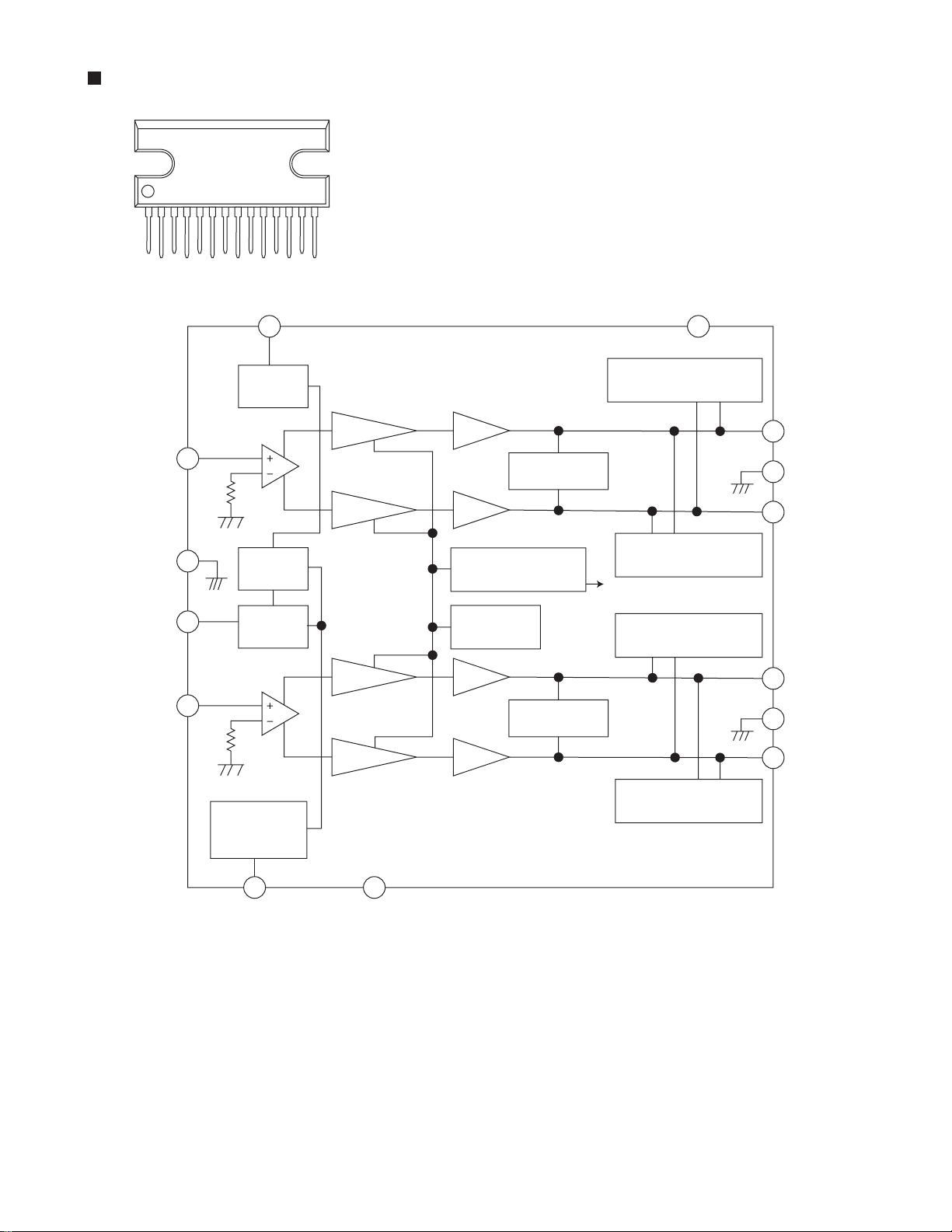
LA4628 (IC301) : Power amp.
1. Pin layout
NX-HD10R
1
2
2. Block diagram
PRE GND
4
IN2
13
14
Vcc
2
RIPPLE
FILTER
PREDRIVER
1
3
6
IN
PREDRIVER
BIAS
CIRCUIT
STANDBY
SW
PREDRIVER
IN
PREDRIVER
POWER
LOAD SHORT
PROTECTOR
POWER
OVER VOLTAGE/
SURGE PROTECTOR
THERMAL
SHUT DOWN
POWER
LOAD SHORT
PROTECTOR
POWER
OUTPUT PPIN TO VCC
SHORT PROTECTOR
OUTPUT PIN TO GND
SHORT PROTECTOR
Vcc
OUTPUT PIN TO GND
SHORT PROTECTOR
1314-OUT1
POWER
12
GND
11
+OUT1
-OUT2
9
POWER
10
GND2
+OUT2
8
POP NOISE
PREVENTION
CIRCUIT
5
OUTOUT PIN TO VCC
SHORT PROTECTOR
7
1-37
Page 38

NX-HD10R
MN101C49HJT (IC801) : System micon
1. Pin layout
2. Pin function
Pin No. Symbol
A/D GND
1
2
3
4
5
6
7
8
9
10
11
12
13
14
15
16
17
18
19
20
21
22
23
24
25
26
27
28
29
30
31
32
33
34
35
36
37
38
39
40
41
42
43
44
45
46
47
48
49
50
KEY1
KEY2
GND
GND
SAFETY1
SAFETY2
GND
SAFETY3
AD POWER
OSC2
OSC1
GND
NMOD
BEAT
OPEN
OPEN
KCMD
MSTAT
CD CLOCK
CD RESET
KBON
RM IN
HD_READY
GND
CD REQUEST
KBCLK
RDSCK
GND
HARD RESET
HD RESET
HD REQ
RDSDI
CONTRAST1
CONTRAST2
CONTRAST3
FAN S W
FCD
HD TX
HD RX
HD CLK
LCD SDA
LCD CS
LCD SCL
LCD RS
LCD RESET
TUNER DATA
Vdd
XI
XO
75 ~ 51
76
~
100
50
~
26
1 ~ 25
I/O
I
I
I
I
I
I
I
I
-
-
O
I
I
O
I
O
O
O
O
I
O
O
O
I
I
I
I
I
I
I
I
O
O
I
O
O
O
O
O
O
I
O
O
O
O
O
O
I/O
Function Pin No. Symbol Function
A/D GND
KEY1 (A/D)
KEY2 (A/D)
[L]
[L]
5V SAFETY DETECT
9V SAFETY DETECT
[L]
8V SAFETY DETECT
A/D power (=Vdd)
Vdd
MAIN SYSTEM CLOCK 8.00MHz
MAIN SYSTEM CLOCK 8.00MHz
GND
SUB SYSTEM CLOCK 32.768KHz
SUB SYSTEM CLOCK 32.768KHz
GND
BEAT CUT (MAIN CLOCK SHIFT)
[L]
[L]
KCMND
MSTAT
KCLK
reset
KEYBORD ON
remocon in
READY
[L]
MRDY
KEYBORD CLOCK
RDS CLOCK IN
[L]
hard reset
HD reset
REQUEST
RDS DATA IN
CONTRAST ADJUST1
CONTRAST ADJUST2
CONTRAST ADJUST3
FAN MORTOR ON/OFF
FUNCTION CD
TX
RX
CLOCK
LCD DATA OUT
LCD CHIP SELECT
LCD CLOCK
LCD REGISTER SELECT
LCD RESET
TUNER data in/out
51
52
53
54
55
56
57
58
59
60
61
62
63
64
65
66
67
68
69
70
71
72
73
74
75
76
77
78
79
80
81
82
83
84
85
86
87
88
89
90
91
92
93
94
95
96
97
98
99
100
TUNER SCK
TUNER PERIOD
MPX
OPEN
KBDATAI
KBDATAO
OPEN
OPEN
SMUTE
LINE OUT MUTE
STANBY
OPEN
OPEN
OPEN
AHB
VCE
VCLK
VDATA
POWER
TR SW
OPEN
OPEN
OPEN
OPEN
OPEN
OPEN
OPEN
PRT
VOL IND
INH
HD REC IND
BAND-0
BAND-1
STANDBY IND
POWER IND
FTU
HD PLAY IND
OPEN
OPEN
OPEN
OPEN
OPEN
OPEN
OPEN
DAVss
OPEN
OPEN
OPEN
BLCTL
DAVdd
I/O
TUNER SERIAL CLOCK
O
TUNER PLL STROBE
O
TUNER MPX (STEREO)
I
[L]
I
Data Input
I
Data Output
O
[L]
O
[L]
O
source mute
O
line out mute
O
STANDBY
O
[L]
O
[L]
O
[L]
O
ON/OFF
O
CHIP ENABLE
O
CLOCK
O
O
DATA OUT
O
power
O
Tr. Switch
O
[L]
[L]
O
[L]
O
[L]
O
[L]
O
[L]
O
[L]
O
SPK DC DETECT
I
VOLUME (BLUE)
O
INH
I
HD REC (RED)
O
band-0 (CHIP SELECT)
I
I
band-1 (CHIP SELECT)
O
STANDBY (RED)
O
POWER (GREEN)
O
FUNCTION TUNER
O
HD PLAY (BLUE)
[L]
O
[L]
O
[L]
O
[L]
O
[L]
O
[L]
O
[L]
O
DAVss
[L]
O
[L]
O
[L]
O
BACK LIGHT ON/DIMMER/OFF
O
DAVdd
-
1-38
Page 39
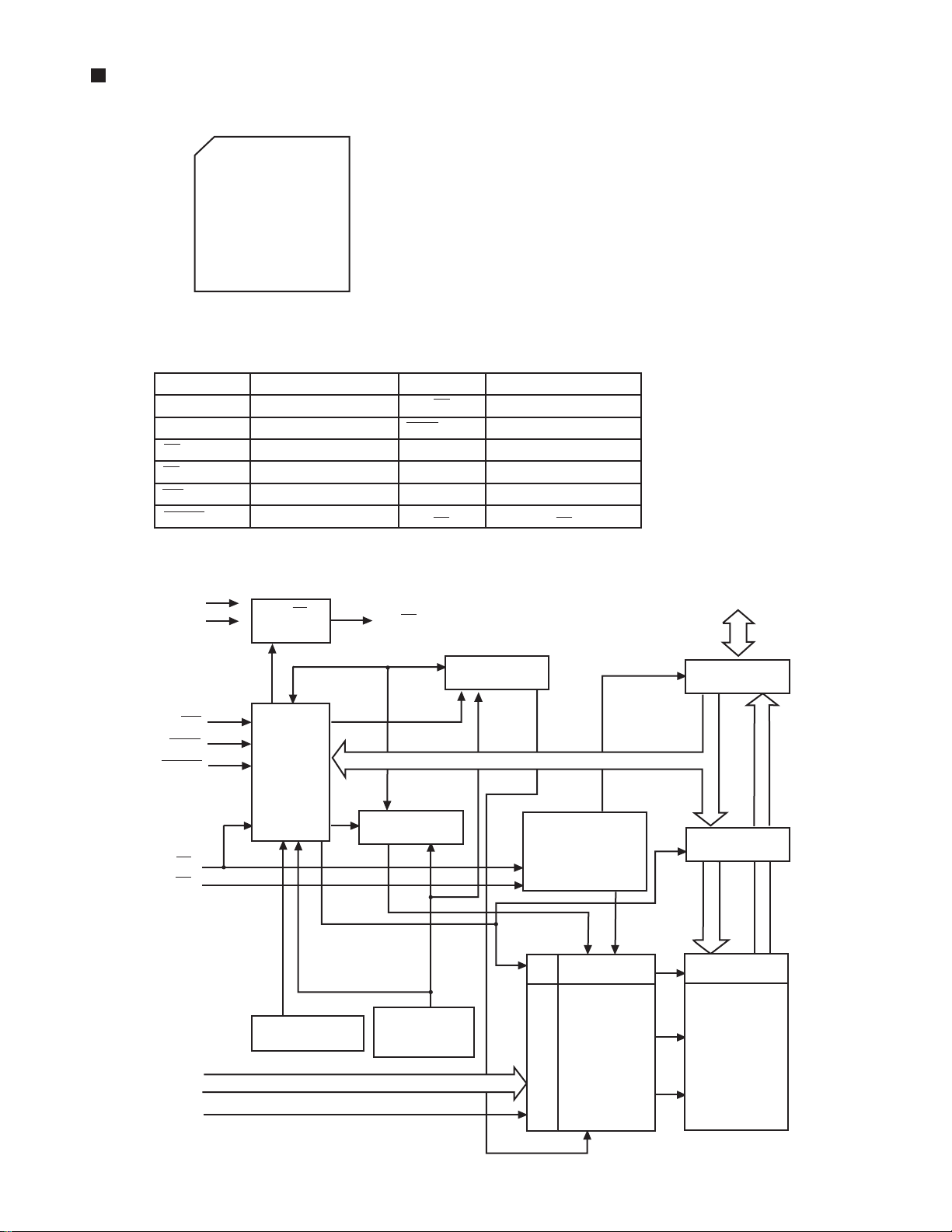
MBV400TC70PTB03 (IC950) : 4M-bit flash memory
1. Pin layout
NX-HD10R
1
~
24
48
~
25
2. Pin function
Symbol Function Symbol Function
A-
1
, A0~A
17 Address input RY / BY Ready / Busy output
~DQ
DQ0
CE Chip enable Vss GND
OE Output enable Vcc Power supply
WE Write enable N.C. Not connect
RESET Hardware reset
15 Data input / Output BYTE 8bit, 16bit select
3. Block diagram
Vcc
Vss
RY/BY
buffer
RY / BY
DQ
0
~
DQ
15
BYTE
RESET
CE
OE
A
0
~
A
WE
17
A-
STB
Input / Output
buffer
Data latch
Y gate
4, 194, 304
cell matrix
Erase circuit
Control circuit
(command resistor)
Low Vcc detect
circuit
1
Write circuit
se
palus
timer
STB
enable
Output
enable
Y decoder
X decoder
Address latch
1-39
Page 40
NX-HD10R
LA1838 (IC1): FM AM IF amp & detector, FM MPX decoder
1. Block Diagram
30
ALC
BUFF
FM
S-METER
FM IF
1
2. Pin Function
Pin
Symbol
No.
FM IN
1
AM MIX
2
3
FM IF
AM IF
4
GND
5
6
TUNED
STEREO
7
8
VCC
9
FM DET
10
AM SD
FM VSM
11
AM VSM
12
13
MUTE
14
FM/AM
MONO/ST O
15
29
28
AM
OSC
SD
COMP
S-CLRVE
PM
DET
2
I/O
I
This is an input terminal of FM IF
REG
AM
MIX
AM/FM
IF-BUFF
3
27
FM
RF.AMP
AM IF
4
26
AGC
AM
S-METER
GND
Function
DET
5
signal.
This is an out put terminal for AM
O
mixer.
I
Bypass of FM IF
Input of AM IF Signal.
I
I
This is the device ground terminal.
When the set is tunning,this terminal
O
becomes "L".
O
Stereo indicator output. Stereo "L",
Mono: "H"
III
This is the power supply terminal.
I
FM detect transformer.
I
This is a terminal of AM ceramic filter.
O
Adjust FM SD sensitivity.
O
Adjust AM SD sensitivity.
I/O
When the signal of IF REQ of IC121(
LC72131) appear, the signal of FM/AM
IF output. //Muting control input.
Change over the FM/AM input.
I
"H" :FM, "L" : AM
Stereo : "H", Mono: "L"
25
TUNING
DRIVE
6
24
STEREO
DRIVE
7
22
23
P-DET
VCC
89
Pin
Symbol
No.
16
L OUT
17
R OUT
18
19
20
21
22
23
24
25
26
27
28
29
30
L IN
R IN
RO
LO
MPX IN
FM OUT
AM DET
AM AGC
AFC
AM RF
REG
AM OSC
OSC BUFFER
21
DECODER
ANIT-BIRDIE
VCO
384KHz
10
20
STEREO
5N
SW
FF
38k
11
I/O
O
Left channel signal output.
O
Right channel signal output.
Input terminal of the Left channel post
I
18
19
MUTE
FF
/
19k
2
12 13
FF
19k
/
LS
Function
17 16
PILOT
DET
14
AMP.
Input terminal of the Right channel
I
post AMP.
Mpx Right channel signal output.
O
O
Mpx Left channel signal output.
I
Mpx input terminal
FM detection output.
O
AM detection output.
O
This is an AGC voltage input terminal
I
for AM
I
This is an output terminal of voltage
for FM-AFC.
AM RF signal input.
I
Register value between pin 26 and pin28
O
besides the frequency width of the
input signal.
I
This is a terminal of AM Local
oscillation circuit.
AM Local oscillation Signal output.
O
15
1-40
Page 41
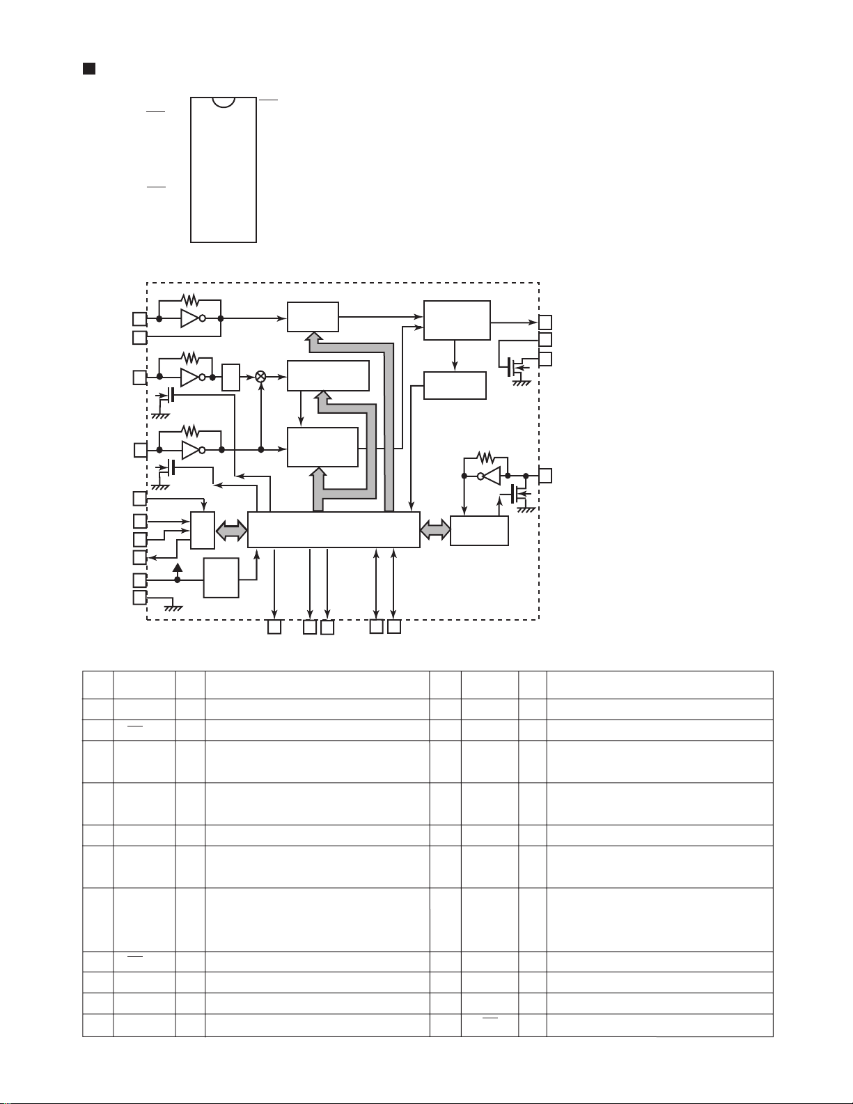
LC72136N (IC2) : PLL frequency synthesizer
1. Pin layout
FM/AM
CLOCK
FM/ST/VCO
AM/FM
2. Block diagram
XT
CE
DI
DO
SDIN
1
2
3
4
5
6
7
8
9
10
11
22
21
20
19
18
17
16
15
14
13
12
XT
GND
LPFOUT
LPFIN
PD
VCC
FMIN
AMIN
IFCONT
IFIN
NX-HD10R
1
22
16
15
3
4
5
6
17
21
3. Pin function
Pin
Symbol
No.
1
2
3
4
5
6
7
8
9
10
11
XT
FM/AM
CE
DI
CLOCK
DO
FM/ST/VCO
AM/FM
LW
MW
SDIN
Reference
Driver
Swallow Counter
1/2
C
2
B
I/F
Powe r
on
Reset
Function
I/O
X'tal oscillator connect (75kHz)
I
LOW:FM mode
O
When data output/input for 4pin(input) and
I
Swallow Counter
1/16,1/17 4bit
1/16,1/17 4bit
12bit
Programmable
DriverS
Data Shift Register & Latch
7821113
6pin(output): H
Input for receive the serial data from
I
controller
Sync signal input use
I
Data output for Controller
O
Output port
"Low": MW mode
O
Open state after the power on reset
O
Input/output port
I/O
Input/output port
I/O
Data input/output
I/O
Phase
Detector
Charge Pump
Unlock
Detector
Universal
Counter
Pin
Symbol
No.
12
IFCONT
13
14
15
16
17
18
19
LPFOUT
20
21
22
IFIN
AMIN
FMIN
VCC
PD
LPFIN
GND
XT
18
19
20
12
I/O
Function
IF counter signal input
I
IF signal output
O
Not use
-
AM Local OSC signal output
I
FM Local OSC signal input
I
Power suplly(VDD=4.5-5.5V)
When power ON:Reset circuit move
PLL charge pump output(H: Local OSC
O
frequency Height than Reference frequency.
L: Low Agreement: Height impedance)
Input for active lowpassfilter of PLL
I
Output for active lowpassfilter of PLL
O
Connected to GND
X'tal oscillator(75KHz)
I
1-41
Page 42

NX-HD10R
LA72723(IC3): RDS demodulation
1. Pin layout
VREF
MPXIN
Vdda
Vssa
FLOUT
CIN
TES
XOUT
2. Block Diagram
+5V
Vdda
Vssa
MPXIN
TEST
1
2
3
4
5
6
7
8
REFERENCE
VOLTAGE
ANTI ALIASING
FILTER
TEST
RDS-ID/READY
16
RDCL
15
RDDA
14
RST
13
MODE
12
Vddd
11
Vssd
10
XIN
9
VREF
57kHz
BPF
(SCF)
FLOUT
SMOOTHING
FILTER
CLK(4.332MHz)
OSC
VREF
CIN
+
PLL
(57kHz)
-
CLOCK
RECOVERY
(1187.5Hz)
DATA
DECODER
RAM
(128-bits)
RDS-ID
DETECT
Vddd
Vssd
RDDA
RDCL
MODE
RST
RDS-ID/
READY
+5V
3. Pin functions
Pin
Symbol
No.
1
VREF
2
MPXIN
Vdda
3
4
Vssa
5
FLOUT
6
CIN
TEST
7
8
XOUT
9
XIN
10
Vssd
11
Vddd
12
MODE
13
RST
14
RDDA
RDCL
15
16
RDS-ID
READY
I/O
O
I
O
I
I
O
I
I
O
I/O
O
XIN
XOUT
Function
Reference voltage output (Vdda/2)
Baseband (multiplexed) signal input
Analog power supply (+5V)
Analog ground
Subcarrier input (filter output)
Subcarrier input (comparator input)
Test input
Crystal oscillator output (4.332MHz)
Crystal oscillator input (exeternal reference input)
Digtal ground
Digtal power supply
I
Read mode setting (0:master,1:slave)
RDS-ID/RAM reset (positive polarity)
RDS data output
RDS clock output (master mode)/RDS clock input (slave mode)
RDS-ID/READY output (negative polarity)
1-42
Page 43

UPC2933AT-W (IC901) : Regulator
1. Pin layout 2. Pin function
4
Pin No.
1
2
123
3. Block diagram
3
4
NX-HD10R
Function
Input
Gnd
Output
Gnd (Fin)
INPUT
Safe operating
area protection
Start-up
circuit
Reference
voltage
Error
amp.
Drive
circuit
Thermal
shut down
Over current
protection
TC74VHC125FT-X (IC932) :
Buffer
1. Pin layout & block diagram 2. Truth table
1G 1
1A 2
1Y 3
2G 4
14 Vcc
13 4G
12 4A
11 4Y
INPUTS OUTPUTS
G
H
L
L
Saturation
protection
A
X
L
H
OUTPUT
GND
Y
Z
L
H
2A 5
2Y 6
GND 7
10 3G
9 3A
8 3Y
X: Don't care
Z:High impedance
1-43
Page 44

NX-HD10R
UPC2925T-W (IC902) : Regulator
1. Pin layout
4
123
3. Block diagram
Startup circuit
Reference voltage
circuit
Error
amp.
2. Pin function
Pin No.
1
2
3
4
Drive circuit
Function
Input
Gnd
Output
Gnd (Fin)
INPUT
Safe operation
area protection
OUTPUT
Thermal shut down
TC74VHC244FT-X (IC906) : Buffer
19
18
17
16
15
14
13
12
20
11
Vcc
2G
1Y1
2A4
1Y2
2A3
1Y3
2A2
1Y4
2A1
1G
1A1
2Y4
1A2
2Y3
1A3
2Y2
1A4
2Y1
GND
1
2
3
4
5
6
7
8
9
10
Over current
protection
INPUTS
G
An
L
LL
L
HH
H
XZ
X : Don't Care
Z : High Impedance
Yn : TC74VHC244
Yn : TC74VHC240
Saturation protection
OUTPUTS
Yn
Yn
Z
GND
H
L
1-44
Page 45

XC61FN2712M-X (IC903) : Regulator
NX-HD10R
1. Pin layout
1
3. Block diagram
3
2. Pin function
Pin No.
1
2
3
Symbol
V
OUT
V
SS
V
IN
Function
Output
Ground
Supply voltage input
2
V
IN
V
OUT
Delay
Circuit
Vref
V
SS
UPC7805AHF (IC961) : Regulator
1. Pin layout 2. Block diaglam
R4 R18
Q13
R5
D1
IN GND OUT
Q6
R6
Q12
R7
R8 R9
Q8 Q9
Q10
Q5
R1
R2
C1
Q7
Q1
R10
Q2
R3 R14
Q4
Q14
R16
Q15
Q3
R13
Q11
Q16
R15
R12R17
INPUT
Q17
R11
OUTPUT
R20
R19
GND
1-45
Page 46

NX-HD10R
TC74VHCT08AFT-X (IC905) : QUAD 2-input and gate
1A
1B
1Y
2A
2B
2Y
GND
Vcc
13
12
14
11
10
4B
4A
4Y
3B
9
3A
3Y
8
1
2
3
4
5
6
7
INPUTS
A
L
L
H
H
B
L
H
L
H
OUTPUTS
Y
L
L
L
H
TC74LCX32FT-X (IC961,IC962,IC963) : QUAD 2-input or gate
1A Vcc
1B
1Y
2A
2B
1
2
3
4
5
14
13
12
11
10
4B
4A
4Y
3B
INPUTS
A
L
L
H
H
B
L
H
L
H
OUTPUTS
Y
L
H
H
H
2Y
GND
6
7
9
3A
3Y
8
TC74LCX08FT-X (IC952) : QUAD 2-input and gate
1A
1B
1Y
2A
2B
2Y
GND
1
2
3
4
5
6
7
14
13
12
11
10
Vcc
4B
4A
4Y
3B
9
3A
3Y
8
INPUTS
A
L
L
H
H
B
L
H
L
H
OUTPUTS
Y
L
L
L
H
1-46
Page 47

< MEMO >
NX-HD10R
1-47
Page 48

NX-HD10R
NX-HD10R
VICTOR COMPANY OF JAPAN, LIMITED
AUDIO & COMUNICATION BUSINESS DIVISION
PERSONAL & MOBILE NETWORK BUSINESS UNIT. 10-1,1chome,Ohwatari-machi,Maebashi-city,371-8543,Japan
1-48
(No.21159)
Printed in Japan
200209
 Loading...