

Page 1
SERVICE MANUAL
COMPACT COMPONENT SYSTEM
MX-J170V
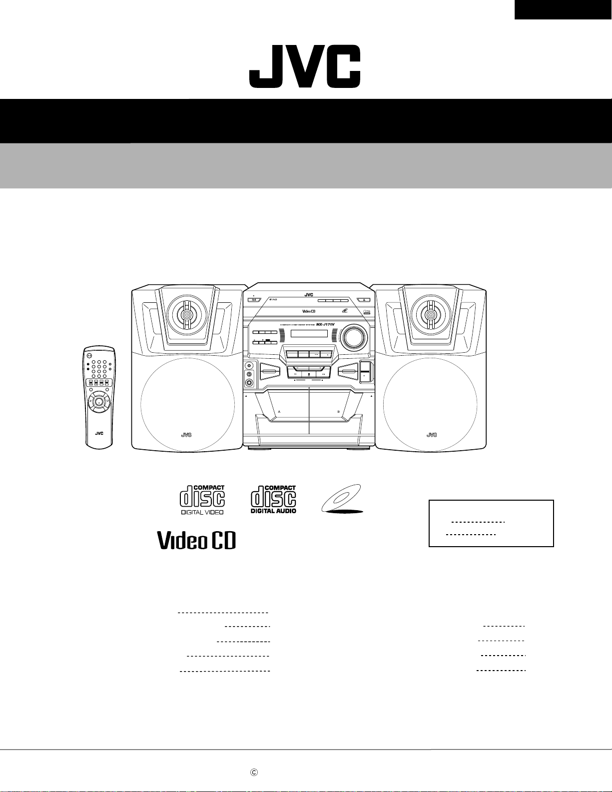
MX-J170V
SLEEP
L
NTSC/PA
KEY CONTROL
T
REPEA
PROGRAM/SET
CD
DECK A/B TUNING MODEFM MODE
0
T
CD
APE
SELECT
DISC SKIP
PREV
RM–SMXJ170V REMOTE CONTROL
TIMER
ON/OFF
SLOWSINGLE STEP
ECHO
BASS
VOLUME
VOLUME
FADE MUTING
+
7
–
STANDBY
PLAY & EXCHANGER
NTSC/PAL COMPATIBILITY
CLOCK
ACTIVE
COUNTER
SOUND
/TIMER
BASS EX.
RESET
MODE
DEMO
MPX
KEY
/V.REPLACE
CONTROL
/V.MASKING
ECHO
PBC
(MENU)
+
VCD
NUMBER
V. MASKING
–
SOUND MODE
AUX
FM/AM
NEXT
PHONES
MIC LEVEL
MIN
MAX
MIC
AUX FM/AM
PROGRAM/SET
NTSC/PAL
PLAY REC/PLAY
FULL-LOGIC CONTROL
PREV NEXT
CD TAPE
-
VCD NUMBER
VCD NUMBER +
PRESET
CD SYNCHRO RECORDING
CD
2
CD
1
SELECT
OPEN / CLOSE
DISC CHANGE
CD
3
COMPACT
DIGITAL VIDEO
VIDEO CD
VOLUME
+
–
CD REC
START
TAPE A/B
REC/PAUSE
A B
DUBBING
EJECTEJECT
Area Suffix
PlayBack
Control
VIDEO CD
US
U
Singapore
Other Areas
Contents
Safety precautions
Important for laser products
Preventing static electricity
Disassembly method
Adjustment method
COPYRIGHT 2000 VICTOR COMPANY OF JAPAN, LTD.
1-2
1-3
1-4
1-5
1-21
Flow of functional operation
until TOC read
Maintenance of laser pickup
Replacement of laser pickup
Description of major ICs
1-25
1-26
1-26
1-27
No.20859
Nov. 2000
Page 2
MX-J170V
Safety Precautions
1. This design of this product contains special hardware and many circuits and components specially
for safety purposes. For continued protection, no changes should be made to the original design
unless authorized in writing by the manufacturer. Replacement parts must be identical to those
used in the original circuits. Services should be performed by qualified personnel only.
2. Alterations of the design or circuitry of the product should not be made. Any design alterations of
the product should not be made. Any design alterations or additions will void the manufacturer`s
warranty and will further relieve the manufacture of responsibility for personal injury or proper ty
damage resulting therefrom.
3. Many electrical and mechanical par ts in the products have special safety-related characteristics.
These characteristics are often not evident from visual inspection nor can the protection afforded
by them necessarily be obtained by using replacement components rated for higher voltage,
wattage, etc. Replacement parts which have these special safety characteristics are identified in
the Parts List of Service Manual. Electrical components having such features are identified by
shading on the schematics and by ( ) on the Parts List in the Service Manual. The use of a
substitute replacement which does not have the same safety characteristics as the recommended
replacement parts shown in the Parts List of Service Manual may create shock, fire, or other
hazards.
4. The leads in the products are routed and dressed with ties, clamps, tubings, barriers and the
like to be separated from live parts, high temperature parts, moving parts and/or sharp edges
for the prevention of electric shock and fire hazard. When service is required, the or iginal lead
routing and dress should be observed, and it should be confirmed that they have been returned
to normal, after re-assembling.
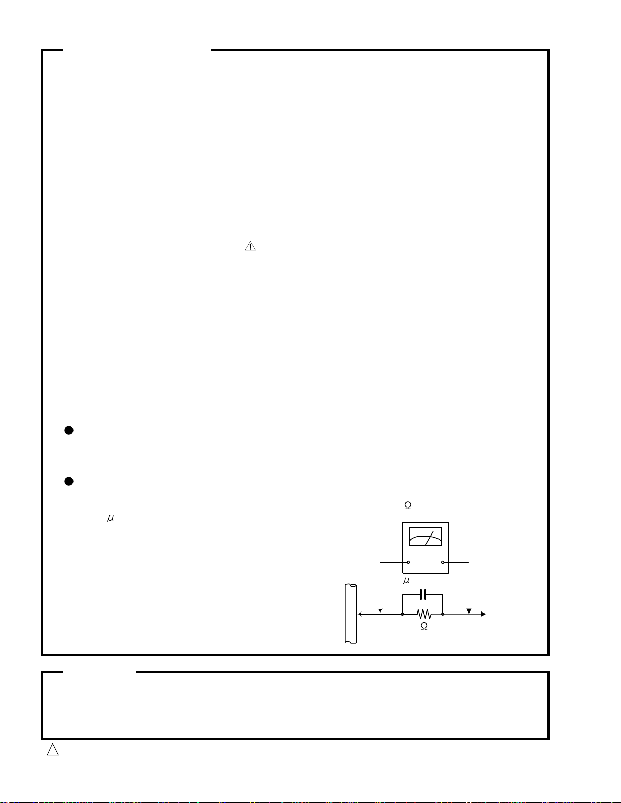
5. Leakage current check (Electrical shock hazard testing)
After re-assembling the product, always perform an isolation check on the exposed metal parts
of the product (antenna terminals, knobs, metal cabinet, screw heads, headphone jack, control
shafts, etc.) to be sure the product is safe to operate without danger of electrical shock.
Do not use a line isolation transformer during this check.
Plug the AC line cord directly into the AC outlet. Using a "Leakage Current Tester", measure
the leakage current from each exposed metal parts of the cabinet , particularly any exposed
metal part having a return path to the chassis, to a known good earth ground. Any leakage
current must not exceed 0.5mA AC (r.m.s.)
Alternate check method
Plug the AC line cord directly into the AC outlet. Use an AC voltmeter having 1,000 ohms
per volt or more sensitivity in the following manner. Connect a 1,500 10W resistor paralleled by
a 0.15 F AC-type capacitor between an exposed
metal part and a known good earth ground.
Measure the AC voltage across the resistor with the
AC voltmeter.
Move the resistor connection to each exposed metal
part, par ticularly any exposed metal part having a
return path to the chassis, and measure the AC
voltage across the resistor. Now, reverse the plug in
the AC outlet and repeat each measurement. Voltage
measured any must not exceed 0.75 V AC (r.m.s.).
This corresponds to 0.5 mA AC (r.m.s.).
0.15 F AC TYPE
1500 10W
Good earth ground
AC VOLTMETER
(Having 1000
ohms/volts,
or more sensitivity)
Place this
probe on
each exposed
metal part.
Warning
1. This equipment has been designed and manufactured to meet international safety standards.
2. It is the legal responsibility of the repairer to ensure that these safety standards are maintained.
3. Repairs must be made in accordance with the relevant safety standards.
4. It is essential that safety critical components are replaced by approved parts.
5. If mains voltage selector is provided, check setting for local voltage.
Burrs formed during molding may be left over on some parts of the chassis. Therefore,
pay attention to such burrs in the case of preforming repair of this system.
1-2
CAUTION
!
Page 3
Important for laser products
MX-J170V
1.CLASS 1 LASER PRODUCT
2.DANGER : Invisible laser radiation when open and inter
lock failed or defeated. Avoid direct exposure to beam.
3.CAUTION : There are no serviceable parts inside the
Laser Unit. Do not disassemble the Laser Unit. Replace
the complete Laser Unit if it malfunctions.
4.CAUTION : The compact disc player uses invisible
laserradiation and is equipped with safety switches
whichprevent emission of radiation when the drawer is
open and the safety interlocks have failed or are de
feated. It is dangerous to defeat the safety switches.
VARNING : Osynlig laserstrålning är denna del är öppnad
och spårren är urkopplad. Betrakta ej strålen.
VARO : Avattaessa ja suojalukitus ohitettaessa olet
alttiina näkymättömälle lasersäteilylle.Älä katso
säteeseen.
5.CAUTION : If safety switches malfunction, the laser is able
to function.
6.CAUTION : Use of controls, adjustments or performance of
procedures other than those specified herein may result in
hazardous radiation exposure.
CAUTION
!
Please use enough caution not to
see the beam directly or touch it
in case of an adjustment or operation
check.
ADVARSEL : Usynlig laserstråling ved åbning , når
sikkerhedsafbrydere er ude af funktion. Undgå
udsættelse for stråling.
ADVARSEL : Usynlig laserstråling ved åpning,når
sikkerhetsbryteren er avslott. unngå utsettelse
for stråling.
REPRODUCTION AND POSITION OF LABELS
WARNING LABEL
DANGER : Invisibie laser radiation
when open and interlock or
defeated.
AVOID DIRECT EXPOSURE TO
BEAM (e)
VARO : Avattaessa ja suojalukitus
ohitettaessa olet alttiina
näkymättömälle lasersäteilylle.Älä
katso säteeseen. (d)
CLASS 1
LASER PRODUCT
VARNING : Osynlig laserstrålning är
denna del är öppnad och spårren är
urkopplad. Betrakta ej strålen. (s)
ADVARSEL :Usynlig laserstråling
ved åbning , når
sikkerhedsafbrydere er ude af
funktion. Undgå udsættelse for
stråling. (f)
1-3
Page 4
MX-J170V
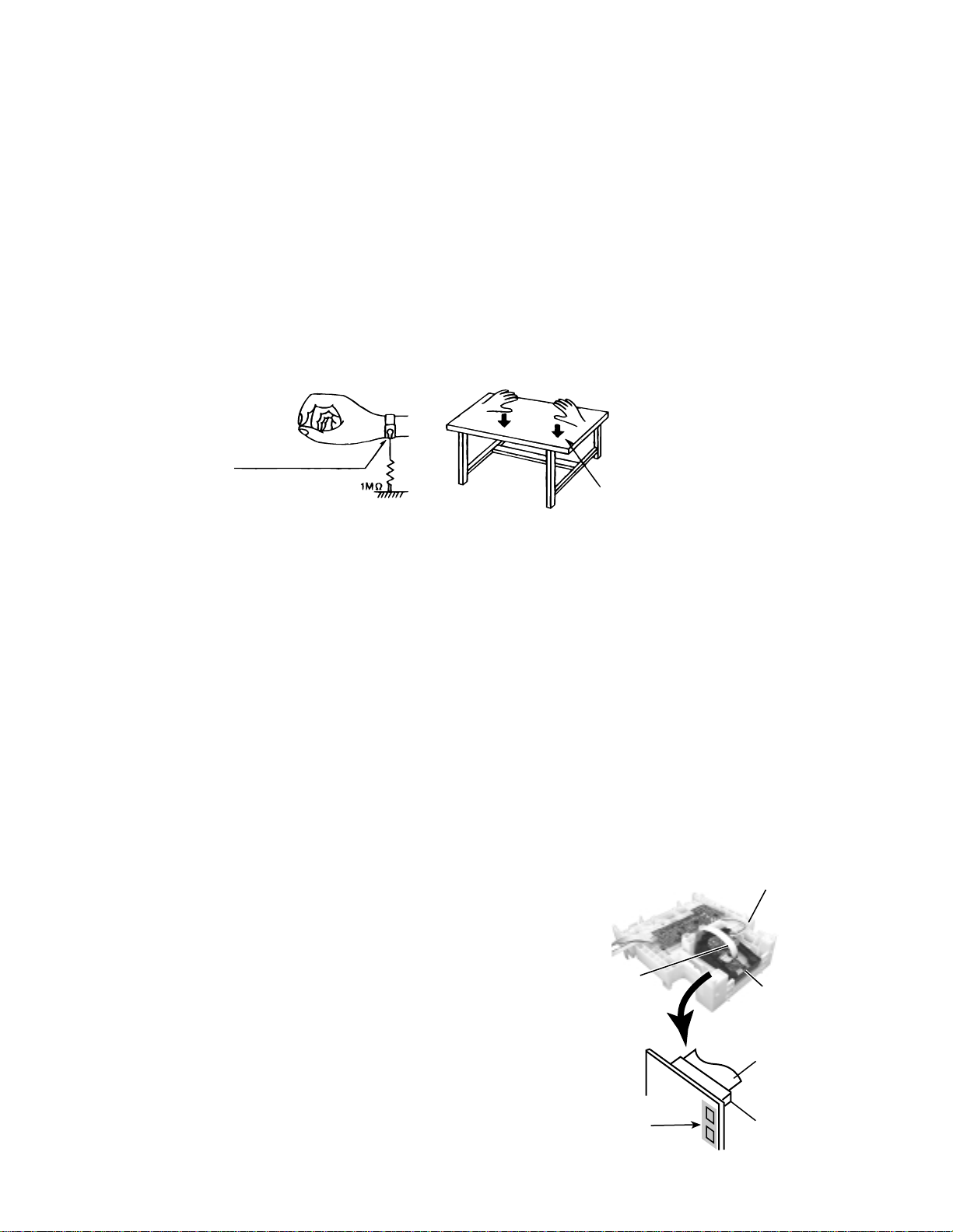
Preventing static electricity
1. Grounding to prevent damage by static electricity
Electrostatic discharge (ESD), which occurs when static electricity stored in the body, fabric, etc. is discharged,
can destroy the laser diode in the traverse unit (optical pickup). Take care to prevent this when performing repairs.
2. About the earth processing for the destruction prevention by static electricity
In the equipment which uses optical pick-up (laser diode), optical pick-up is destroyed by the static electricity of
the work environment.
Be careful to use proper grounding in the area where repairs are being performed.
2-1 Ground the workbench
Ground the workbench by laying conductive material (such as a conductive sheet) or an iron plate over
it before placing the traverse unit (optical pickup) on it.
2-2 Ground yourself
Use an anti-static wrist strap to release any static electricity built up in your body.
(caption)
Anti-static wrist strap
Conductive material
(conductive sheet) or iron plate
3. Handling the optical pickup
1. In order to maintain quality during transport and before installation, both sides of the laser diode on the
replacement optical pickup are shorted. After replacement, return the shorted parts to their original condition.
(Refer to the text.)
2. Do not use a tester to check the condition of the laser diode in the optical pickup. The tester's internal power
source can easily destroy the laser diode.
4. Handling the traverse unit (optical pickup)
1. Do not subject the traverse unit (optical pickup) to strong shocks, as it is a sensitive, complex unit.
2. Cut off the shorted part of the flexible cable using nippers, etc. after replacing the optical pickup. For specific
details, refer to the replacement procedure in the text. Remove the anti-static pin when replacing the traverse
unit. Be careful not to take too long a time when attaching it to the connector.
3. Handle the flexible cable carefully as it may break when subjected to strong force.
4. It is not possible to adjust the semi-fixed resistor that adjusts the laser power. Do not turn it
Attention when CD mechanism assembly is decomposed
*Please refer to "Disassembly method" in the text for pick-up and how to
detach the CD mechanism assembly.
CD changer unit
1. Remove the CD changer unit.
2. Remove the CD changer mechanism.
3. Solder is put up before the card wire is removed from the pickup unit
connector on the CD mechanism assembly.
(When the card wire is removed without putting up solder, the CD pick-up
assembly might destroy.)
4. Please remove solder after connecting the card wire with the pickup unit
connector when you install picking up in the substrate.
1-4
Card wire
Pickup unit
connector
Soldering
CD mechanism
Fig.1
Card wire
Pickup unit
connector
Fig.2
Page 5
MX-J170V
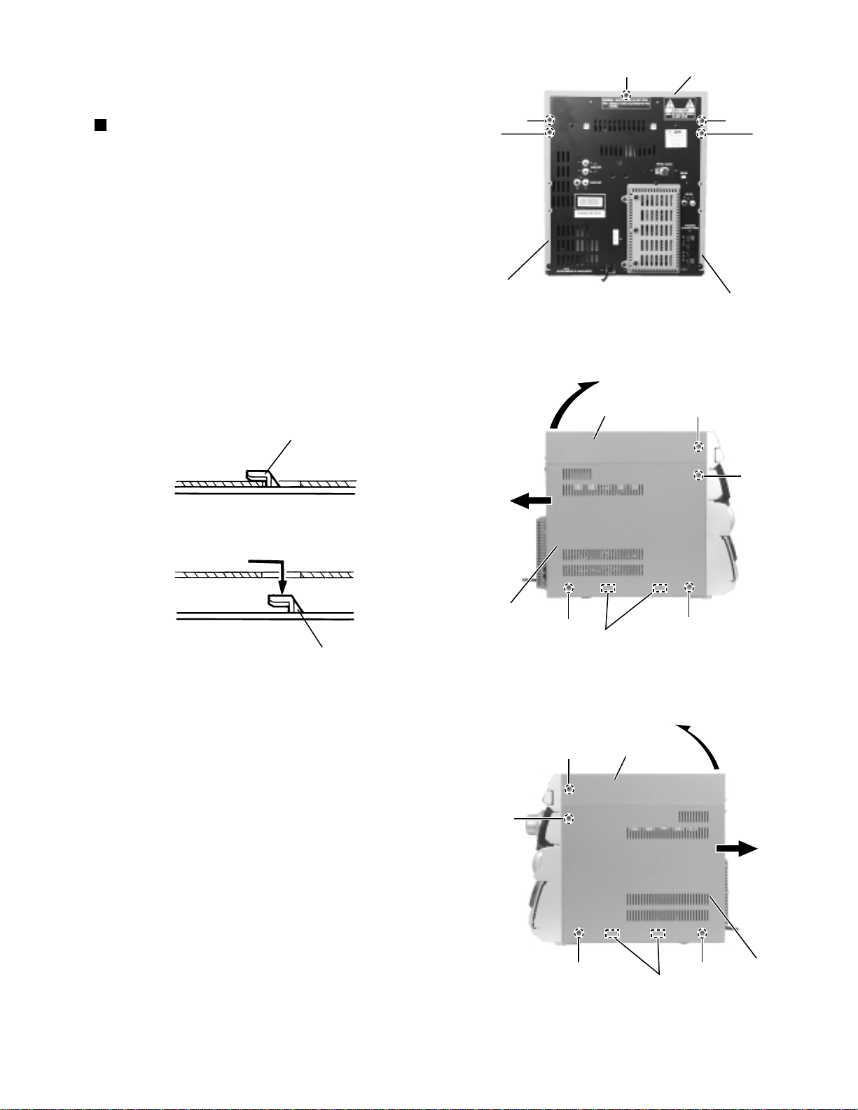
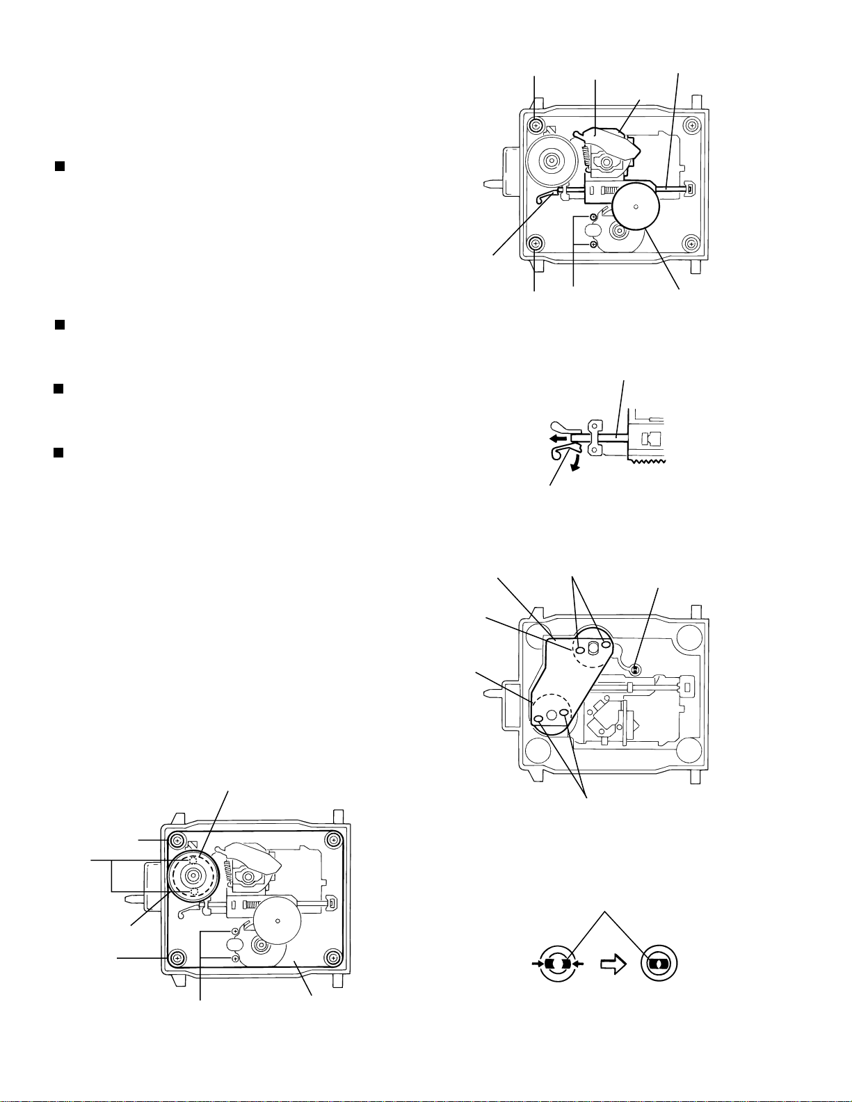
Disassembly method
<Main body>
Removing the top cover and the side
covers (See Fig.1 to 3)
1.
Remove the five screws A on the back of the body
and the both sides of the body.
2.
Remove the top cover upward from behind.
3.
Remove the eight screws B attaching the side
covers on the back of the body and the both side of
the body.
4.
Slide the right and left covers backward and unhook
the two hooks a in the lower part of the side covers
as shown in Fig.2-2.
Hook
A
B
Side cover (L)
A
Fig.1
Top cover
Top cover
A
B
Side cover (R)
A
Hook
Side cover (R)
B
B
A
Hooks a
Fig.2Fig.2-2
Top cover
B
B
B
Hooks a
Fig.3
Side cover (L)
B
1-5
Page 6

MX-J170V
Removing the CD Tray fitting
(See Fig. 4 to 6)
Prior to performing the following procedure, remove
the top cover and the side covers.
ATTENTION:
1.
Press the POWER button. Press the OPEN/CLOSE
button to eject the CD tray.
2.
Move the CD tray fitting upward and release the joint
b.
3.
Press the OPEN/CLOSE button to insert the CD tray.
Be sure to remove the CD tray fitting
before removing the CD changer unit.
CD tray
OPEN/CLOSE button
POWER button
Fig.4
Joint b
CD tray fitting
Joint b
CD tray
Fig.5
Fig.6
1-6
Page 7
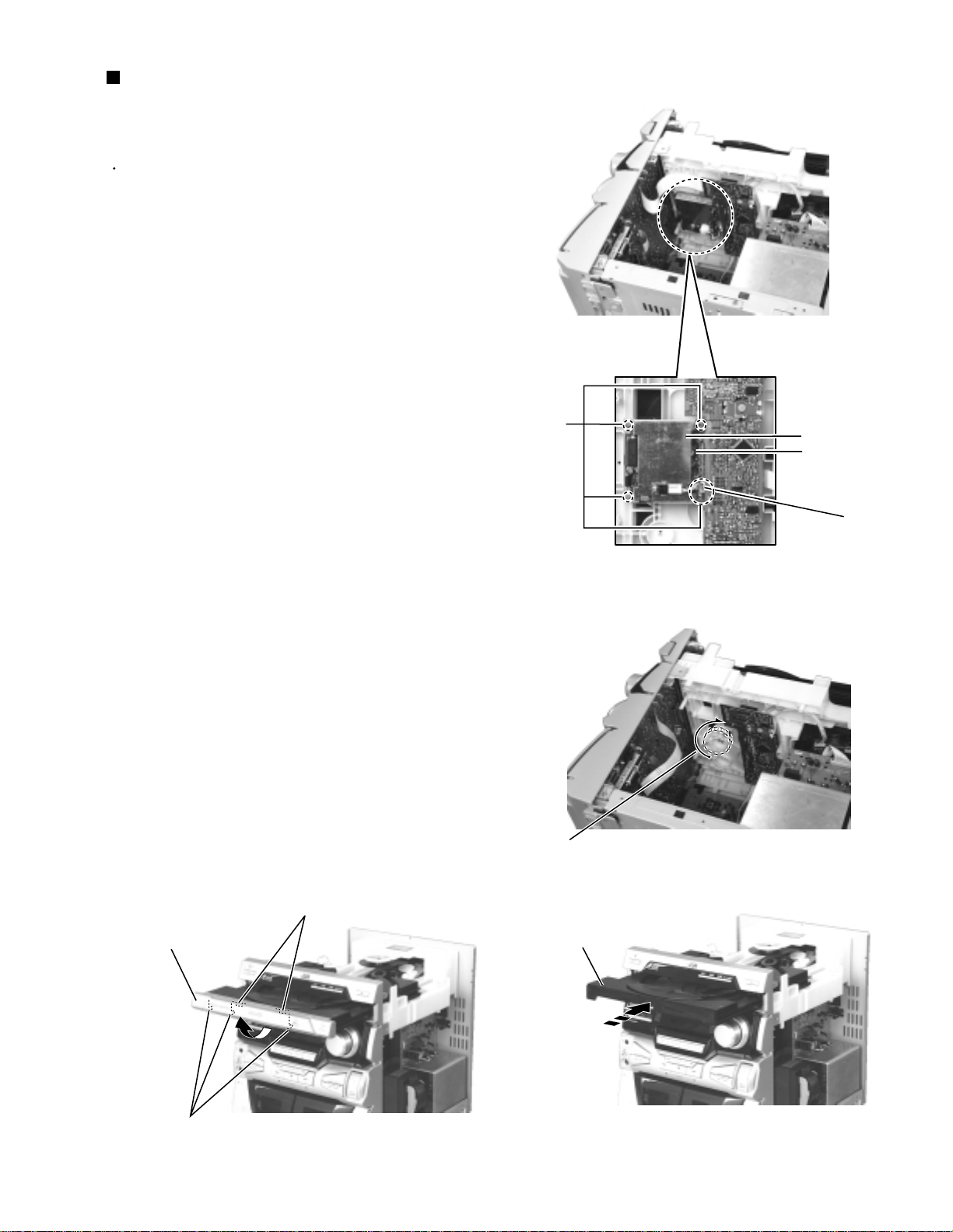
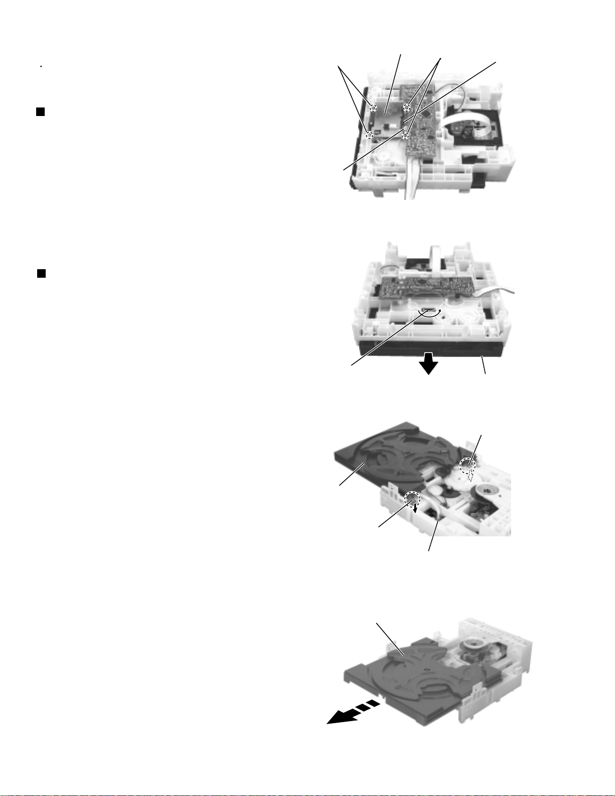
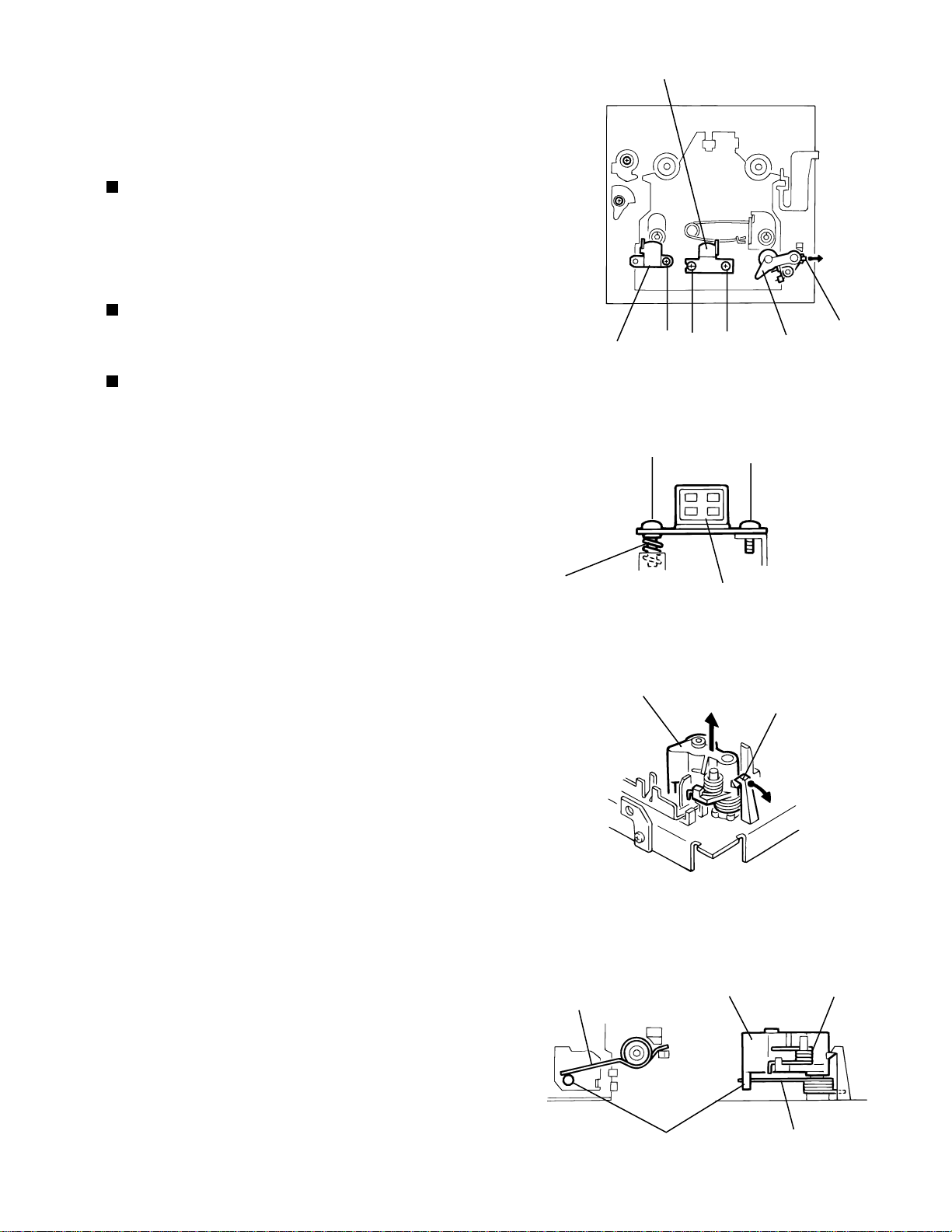
Prior to performing the following procedure, remove
the top cover and the side covers.
Disconnect the harness from connector PCON1 of
the VCD board.
Remove the four screws W attaching the sealed and
VCD board.
Turn the black loading pulley gear marked c from the
back of the CD changer unit as shown in Fig.8 and
draw the CD tray toward the front.
Move the CD tray fitting upward and release the joint
b.
Push and insert the CD tray manually.
1.
2.
3.
4.
5.
Removing the CD Tray fitting & the VCD
board (See Fig.7 to 10)
Be sure to remove the CD tray fitting
before removing the CD changer unit.
ATTENTION:
- How to eject the CD tray without turning on power -
Fig.9
Fig.10
Joint b
Joint b
CD tray fitting
CD tray
Fig.7
Fig.8
W
VCD board
Sealed
PCON1
Marked c
Loading pulley gear
MX-J170V
1-7
Page 8
MX-J170V
Removing the CD changer unit
(See Fig.11 to 13)
Prior to performing the following procedure, remove
the top cover, the side covers and the CD Tray
fitting.
1.
Disconnect the card wire from connector SCW1 of
the CD servo board on the back of the CD changer
unit.
2.
Disconnect the harness from connector FW2 on the
inner side of the main board in the body.
3.
Disconnect the harness from connector VCW2 on
the VDC power board .
4.
Remove the two screws C attaching the CD changer
unit on the back of the body.
5.
Draw the CD changer unit upward from behind while
pulling the rear panel outward.
CD servo board
SCW1
Main board
CD changer unit
FW2
Fig.11
VCD power board
VCW2
C
Rear panel
Front panel assembly
CD changer unit
Fig.12
Rear panel
VCD power board
Fig.13
1-8
Page 9
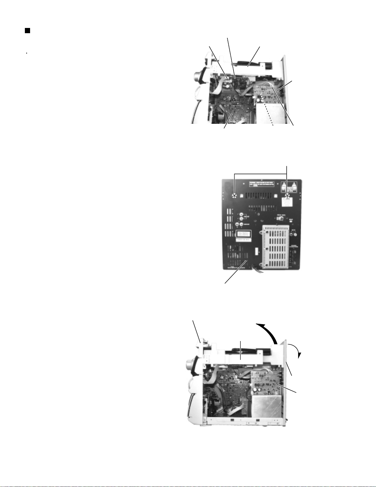
MX-J170V
Removing the front panel assembly
(See Fig.14 to 16)
Prior to performing the following procedure, remove
the top cover, the side covers, the CD Tray fitting
and the CD changer unit.
There is no need to remove the rear panel.
1.
Disconnect the harness from head wire connector
ECW1,DW1 and DW2 on the inner side of the main
board in the body.
2.
Disconnect the harness from connector HCW1 of the
headphone board on the right side of the body.
3.
Remove the three screws D attaching the front panel
assembly on both sides of the body.
Remove the screw E attaching the earth terminal
extending from the front compartment.
4.
Remove the screw F attaching the front panel
assembly on the bottom of the body.
5.
Release the two joints d on both sides and two joints
e on the bottom of the body using a screwdriver. At
the same time, disconnect the front compartment
from connector CCW1 and CCW2 of the main board.
Front panel assembly
Joint d
D
CCW1
CCW2
E
Fig.14
earth wire
Front panel assembly
D
MIC
/Headphone board
HCW1
Main board
DW1
DW2
ECW1
Joint e
D
Main board
Fig.15
F
Fig.16
Joint d
Joint e
1-9
Page 10
MX-J170V
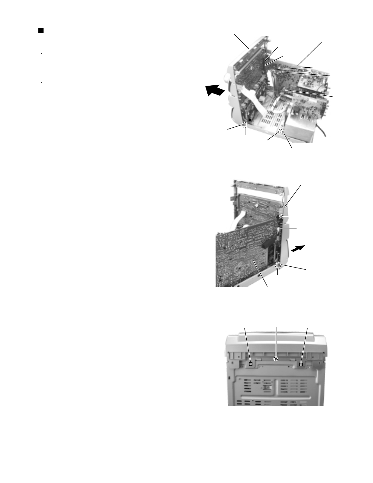
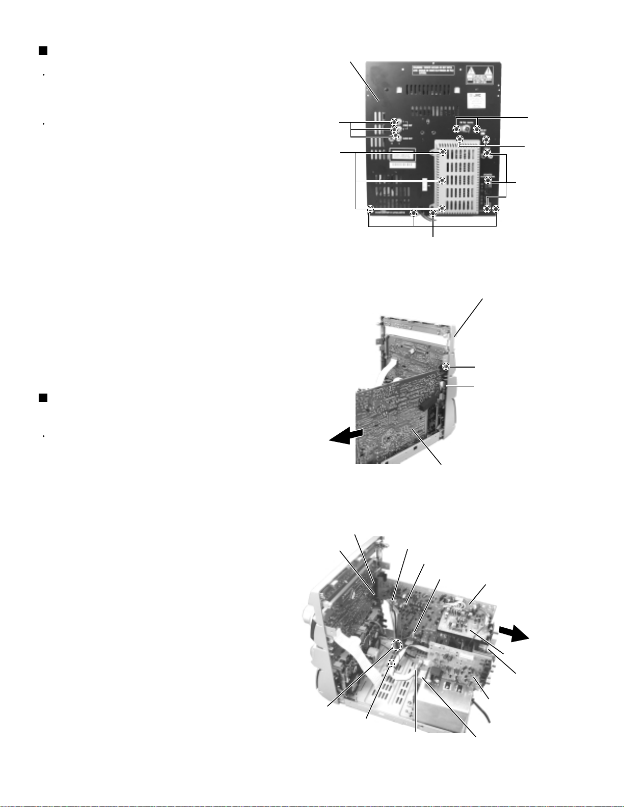
Removing the rear panel (See Fig.17)
Prior to performing the following procedure, remove
the top cover, the side covers, the CD Tray fitting
and the CD changer unit.
There is no need to remove the front panel
assembly.
1.
Remove the ten screws G attaching the main board,
the tuner board and the heat sink to the rear panel
on the back of the body.
2.
Remove the three screws H attaching the VCD
power board to the rear panel on the back of the
body.
3.
Remove the four screws I attaching the rear panel on
the back of the body.
Rear panel
H
G
G
G
G
I
Fig.17
Front panel assembly
Removing the main board
(See Fig.18 and 19)
Prior to performing the following procedure, remove
the rear panel.
1.
Disconnect the harness from connector HCW1 of the
MIC/headphone board on the right side of the body.
Release the harness from the clamp in the body.
2.
Disconnect the harness from head wire connector
ECW1,DW1 and DW2 extending to the main board
in the body.
3.
Disconnect the harness from connector RCW1 of the
power transformer.
4.
Remove the screws D attaching the front panel
assembly on both sides of the body.
5.
Remove the screw J attaching the earth terminal to
the base chassis.
6.
Disconnect connector CCW1 and CCW2 connected
to the main board.
CCW2
Clamp
CCW1
D
MIC/
headphone board
HCW1
Main board
Fig.18
DW1
DW2
ECW1
Main board
Tuner board
Heat sink
VCD board
J
RCW1
Fig.19
Power transformer
1-10
Page 11
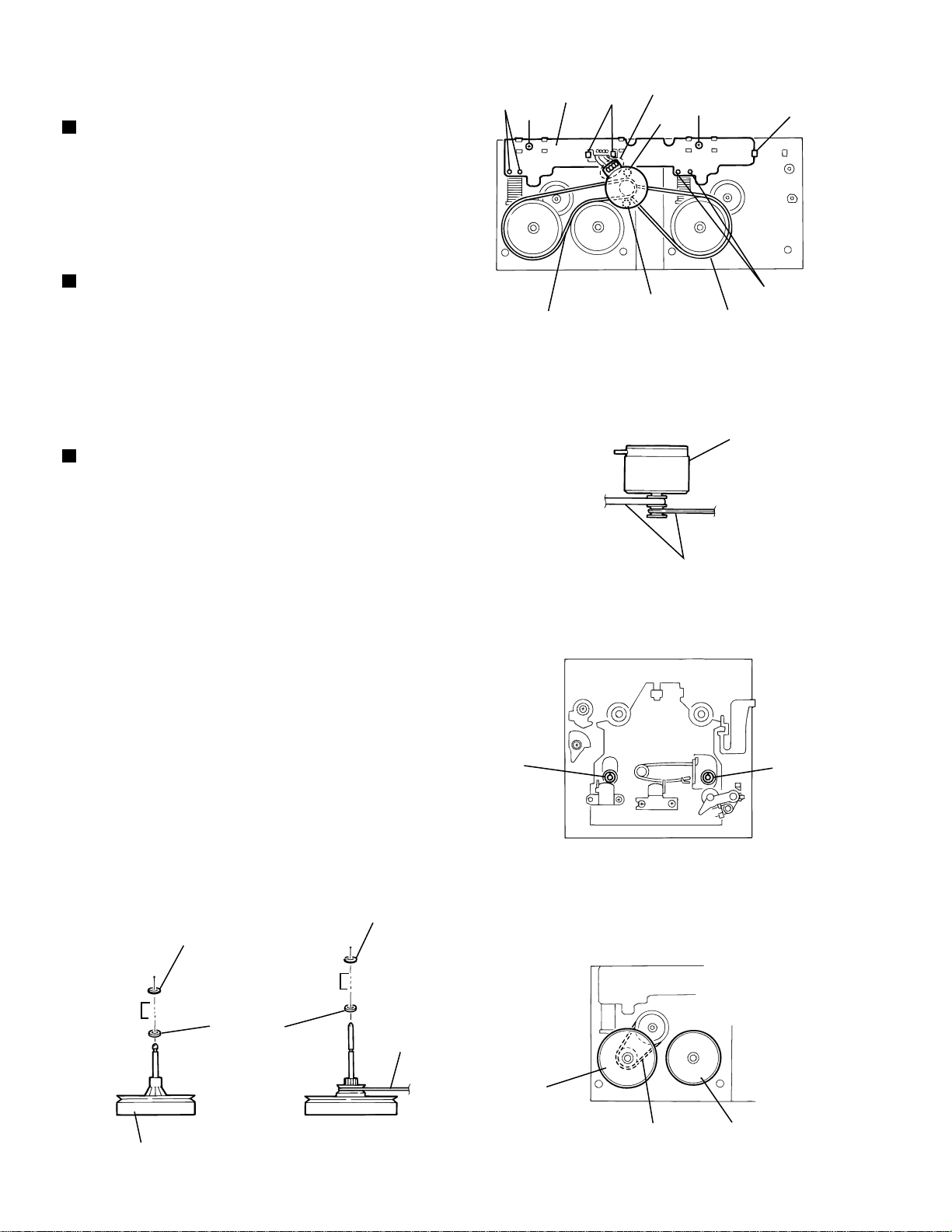
MX-J170V
Prior to performing the following procedure, remove
the main board.
Disconnect the harness from connector MJW1 of the
main board.
Remove the three screws K attaching the heat sink
cover plate and cooling fan.
Remove the two screws L attaching the power IC to
the heat sink and the three screws M attaching the
heat sink to the main board.
1.
2.
3.
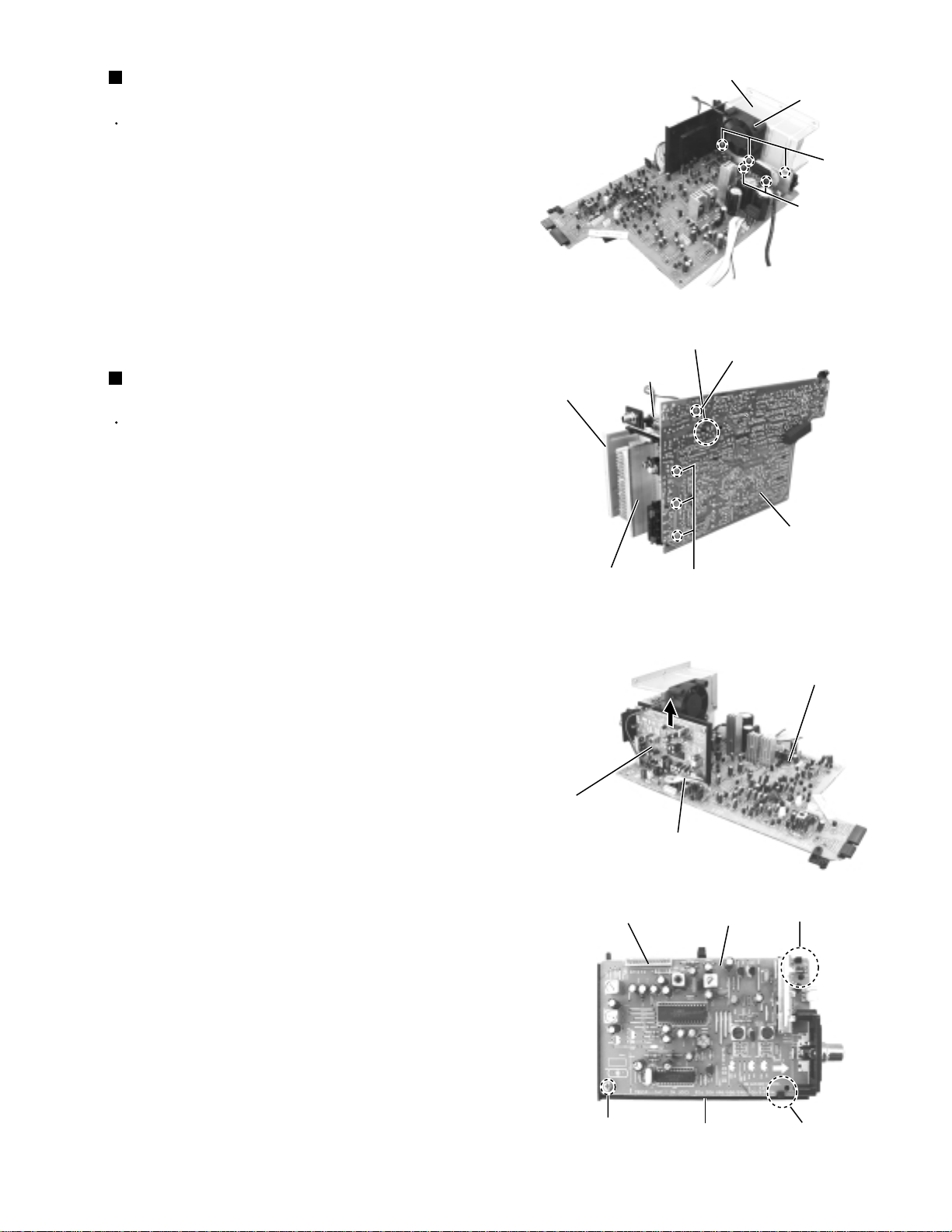
Removing the heat sink & cooling fan
(See Fig.20 and 21)
The tuner board can be removed even if the main
board is attached.
Release the joint tab f of the tuner board holder and
the main board, and disconnect connector FW1
connected to the main board. Remove the tuner
board assembly (Refer to Fig.21).
Remove the screw N attaching the tuner board
holder. Release the two tabs g outward and remove
the tuner board from the tuner board holder.
1.
2.
Removing the tuner Board
(See Fig.21 to 23)
Fig.23
Fig.22
Fig.21
Fig.20
K
L
Main board
Joint tab f
Tuner board
M
Heat sink
Tuner board
Main board
TWA1
Tuner board
Tab g
Tab g
Tuner board holder
Heat sink cover plate
Heat sink cover plate
N
Cooling Fan
TWA1
MJW1
1-11
Page 12
MX-J170V
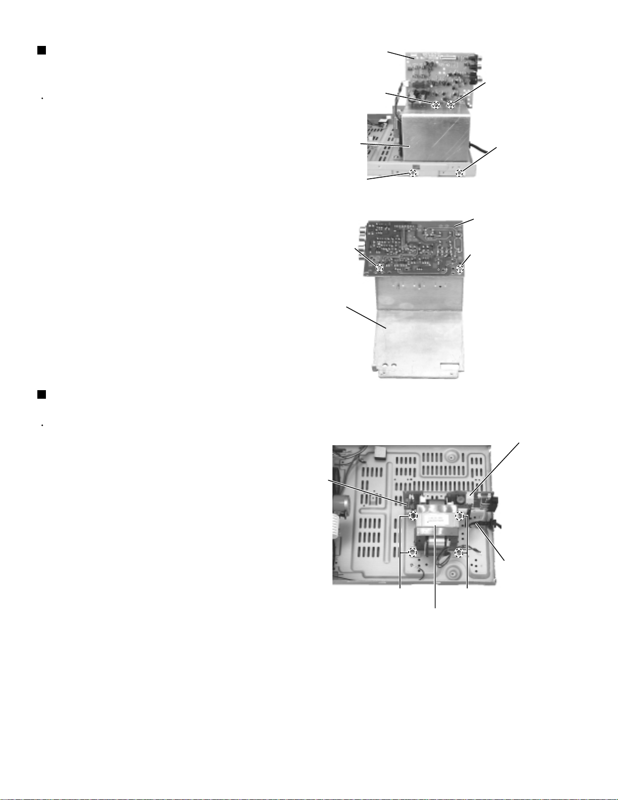
Removing the heat sink & VCD Power
board (See Fig.24 and 25)
Prior to performing the following procedure, remove
the top cover and the side covers.
1.
Remove the two screws O attaching the heat sink
plate.
2.
Remove the two screws P attaching the power IC to
the heat sink and the two screws Q attaching the
heat sink to the VCD Power board.
VCD Power board
Heat sink
O
Q
Heat sink
P
P
O
Fig.24
VCD Power board
Q
Removing the power transformer
(See Fig.26)
Prior to performing the following procedure, remove
the VCD Power board.
1.
Disconnect the power cord from connector RCW2 of
the power transformer.
2.
Disconnect the harness from connector RCW1 of the
power transformer.
3.
Remove the four screws R attaching the power
transformer.
ATTENTION:
Prior to disconnecting the power cord
from the body, remove the rear panel.
RCW1
Fig.25
R
Power transformer
Fig.26
RCW2
Power cord
R
1-12
Page 13
MX-J170V
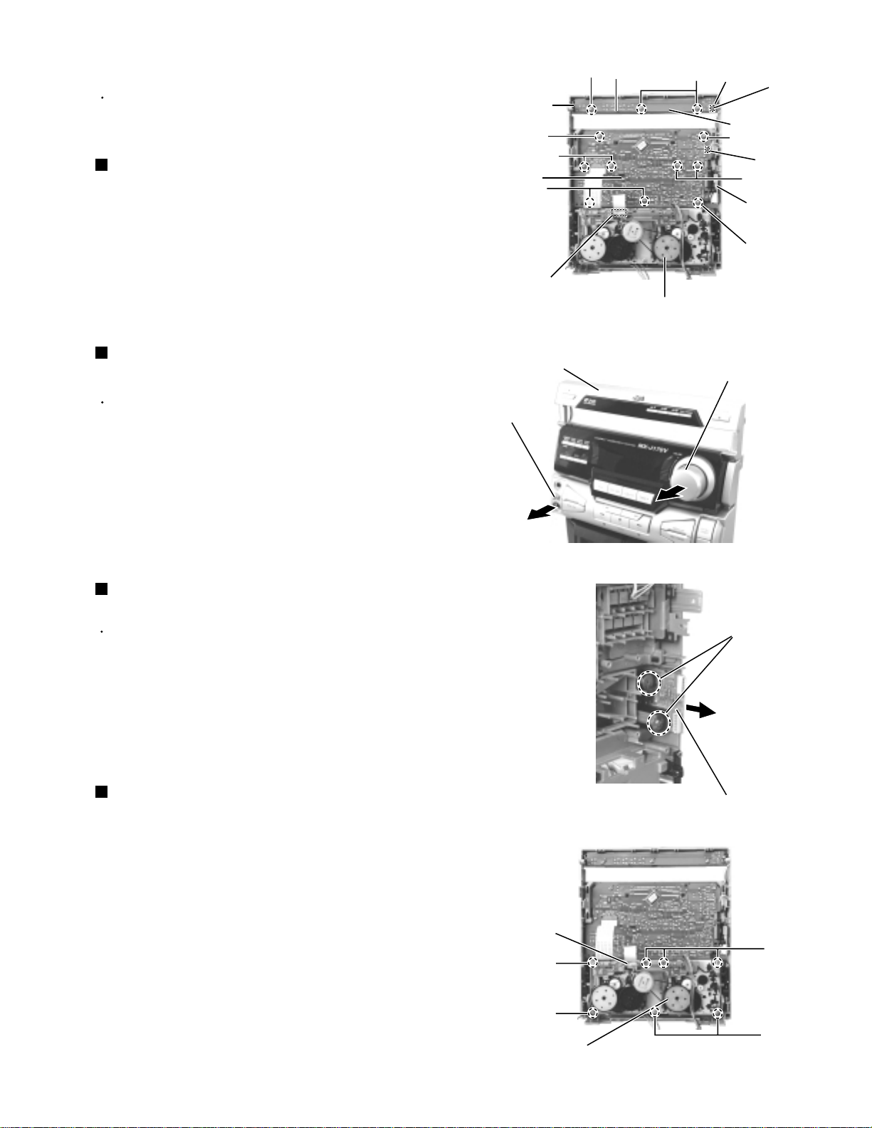
Prior to performing the following procedure, remove
the power / CD switch board.
Pull out the volume knob toward the front.
Disconnect the card wire from the mechanism board
of the cassette mechanism assembly.
Remove the nine screws T attaching the front board.
1.
2.
3.
Removing the front board
(See Fig.27 and 28)
Remove the three screws S attaching the power/CD
switch board and release the three tabs h outward.
Disconnect the harness from connector UCW9 of
the power / CD switch board.
1.
2.
Prior to performing the following procedure, remove
the top cover, the side covers, the CD tray fitting and
the front panel assembly.
Removing the power / CD switch board
(See Fig.27)
Disconnect the card wire from the mechanism board
of the cassette mechanism assembly.
Remove the seven screws V attaching the cassette
mechanism assembly.
1.
2.
Removing the cassette mechanism
assembly (See Fig.30)
<Front panel assembly>
Pull out the MIC level knob toward you.
Remove the two screws U attaching the
MIC/headphone board.
1.
2.
Removing the MIC/headphone board
(See Fig.28 and 29)
Prior to performing the following procedure, remove
the front board.
Fig.27
Fig.28
Fig.29
Fig.30
Tab h
Power / CD
switch board
S
T
MIC/
headphone
board
Tab h
Tab h
Cassette mechanism assembly
JW1
S
T
T
T
T
T
Front board
Mechanism board
Front panel assembly
Volume knob
MIC/headphone board
U
Cassette mechanism assembly
Mechanism board
V
V
V
V
UCW9
MIC level knob
1-13
Page 14
MX-J170V
<CD changer unit>
Prior to performing the following procedure, remove
the CD changer unit.
Removing the VCD board
(See Fig.31)
1.
Disconnect the harness from connector PCON1 of
the VCD board .
2.
Remove the four screws W attaching the Sealed and
VCD board.
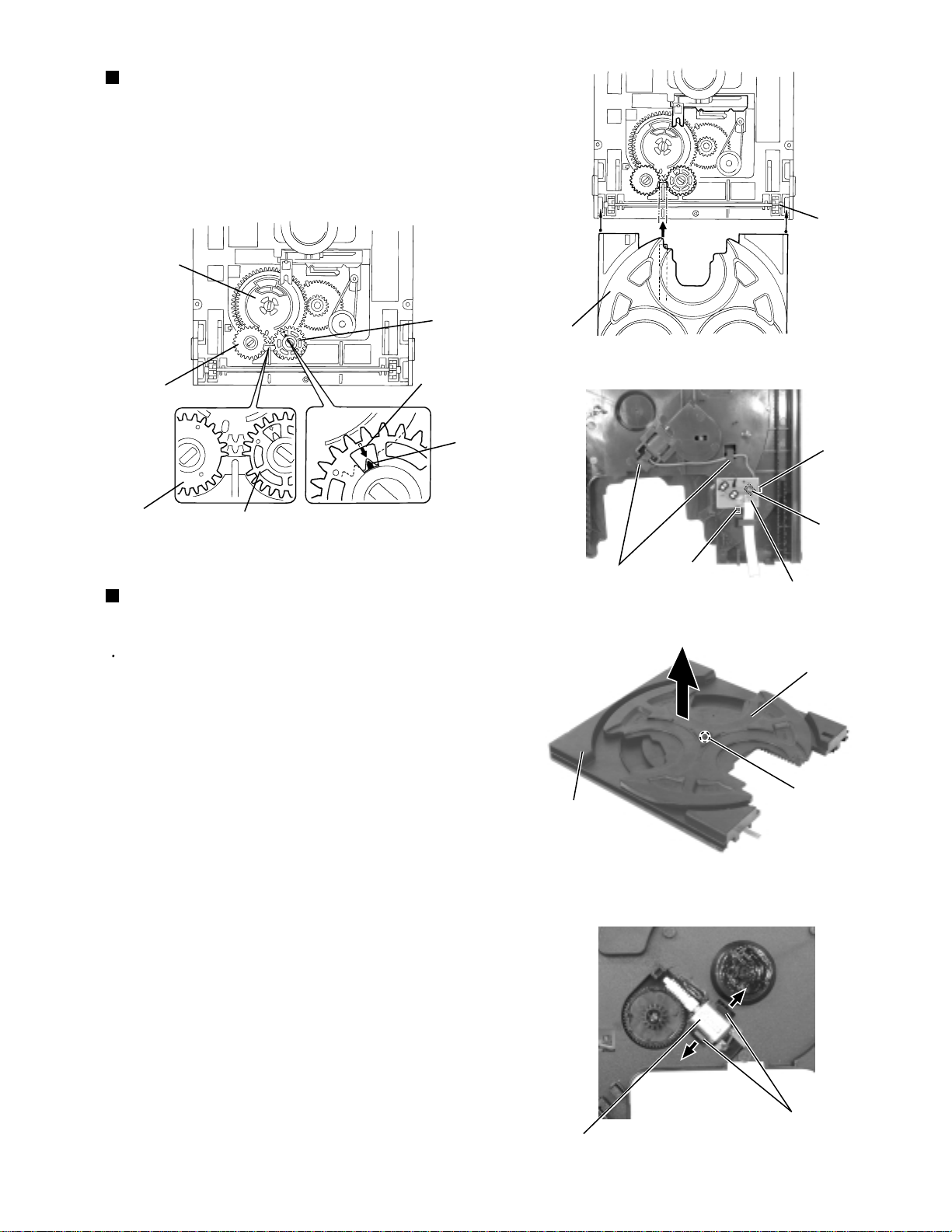
Removing the CD tray (See Fig.32 to 34)
1.
Turn the black loading pulley gear marked c on the
under side of the CD changer unit in the direction of
the arrow and draw the CD tray toward the front until
it stops.
W
PCON1
Shield
Fig.31
W
VCD board
2.
Disconnect the card wire from connector SCW5 of
the CD servo board on the upper side of the CD
changer unit.
3.
Push down the two tray stoppers marked i and pull
out the CD tray.
Loading pulley gear marked c
CD tray
Fig.32
Tray stopper marked i
CD tray
Tray stopper marked i
CD servo board
SCW5
Fig.33
CD tray
1-14
Fig.34
Page 15
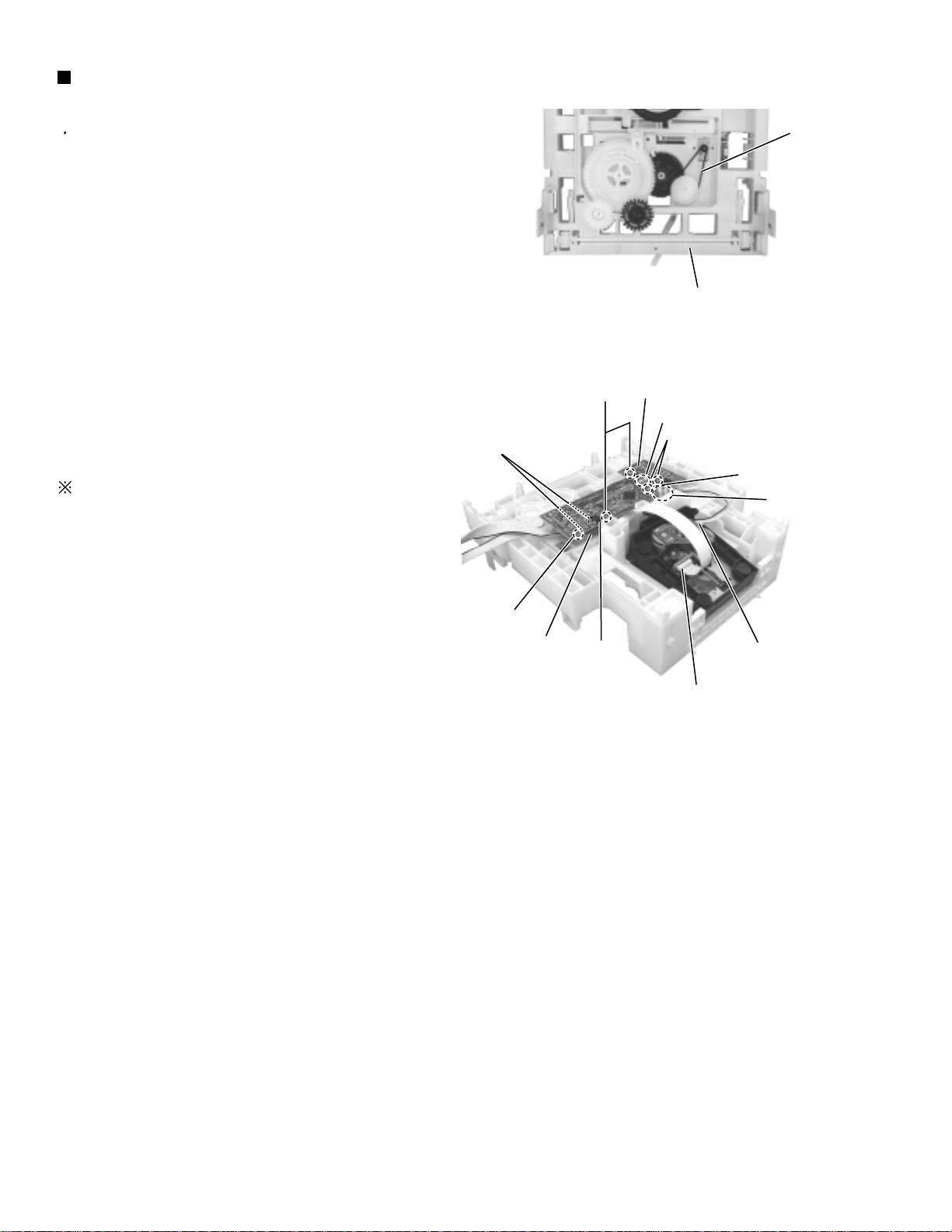
Prior to performing the following procedure, remove
the CD tray.
Release the two tabs j attaching the sensor board on
the under side of the CD tray.
Disconnect the harness from connector CW1 on the
sensor board and release the harness from the two
hooks k. Remove the sensor board.
Remove the screw X attaching the tray turn table.
Detach the tray turn table from the tray.
Pull outward the tab m attaching the tray turn table
motor assembly on the upper side of the tray and
detach the tray turn table motor assembly from the
tray.
1.
2.
3.
4.
Removing the sensor board / the tray
motor (See Fig.37 to 39)
Align the gear-cam with the gear-tray as shown
fig.28, then mount the CD tray.
When assembling the CD tray, take extreme care not
engage with gear - synchro.
1.
2.
Reinstall the CD tray (See Fig.35 and 36)
Fig.35
Gear-convert
Gear-convert
Gear-cam
Gear-tray
Gear-tray
Gear-tray
Gear-cam
timing point
Fig.36
Gear-synchro
CD tray
Fig.38
Fig.37
Fig.39
Tab j
Tab j
Hooks k
Sensor board
CW1
Tray turn table
Tray
X
Tray turn table motor
assembly
Tab m
MX-J170V
1-15
Page 16
MX-J170V
Removing the belt, the CD servo board
and the switch board (See Fig.40 and 41)
Prior to performing the following procedure, remove
the CD tray.
1.
Detach the belt from the pulley on the upper side of
the CD changer unit (Do not stain the belt with
grease).
2.
Disconnect the card wire from the pickup unit
connector on the under side of the CD changer unit.
3.
Disconnect the motor wire harness from connector
on the CD mechanism board.
4.
Remove the two screws Y attaching the CD servo
board. First release the n side of the two tabs n and
two tabs o attaching the CD servo board motor to
raise the CD servo board slightly, then release the o
side.
If the tabs n and o are hard to release, it is
recommendable to unsolder the two soldered parts
on the motor terminal of the CD servo board.
Disconnect the terminal CW3 connected to the
switch board and remove the CD servo board.
Tabs p
Fig.40
Y
CD servo board
Belt
CD changer unit
Tabs o
Soldered parts
Motor
Tabs n
5.
Remove the screw Z attaching the CD Changer unit
and release the three tabs p attaching the switch
board outward and detach the switch board.
Z
Switch board
CW3
CD mechanism board
motor connecter
Pickup unit connector
Fig.41
1-16
Page 17
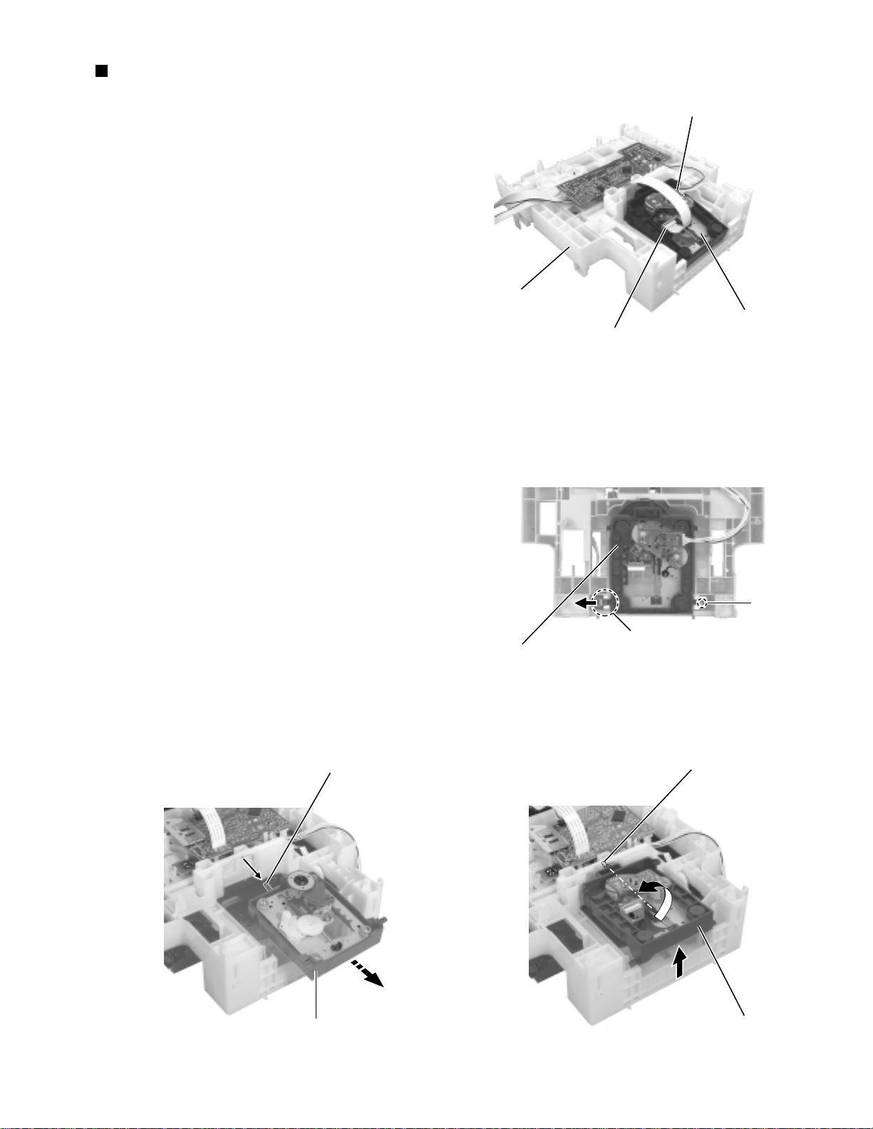
Disconnect the harness from connector on the CD
mechanism board in the CD mechanism assembly
on the under side of the CD changer unit. Disconnect
the card wire from the pickup unit connector.
Remove the screw A attaching the shaft on the right
side of the CD mechanism holder assembly. Pull
outward the stopper fixing the shaft on the left side
and remove the CD mechanism holder assembly
from behind in the direction of the arrow.
Turn the CD mechanism holder assembly half
around the lift up slide shaft r of the CD mechanism
holder assembly until the turn table is reversed, and
pull out the CD mechanism holder assembly.
1.
2.
3.
Removing the CD mechanism holder
assembly (mechanism included)
(See Fig.42 to 45)
Fig.42
Fig.43
Fig.45
Fig.44
Motor connecter
CD mechanism assembly
CD changer unit
Pickup unit connector
A
CD mechanism holder assembly
Stopper
CD mechanism holder assembly
Lift up slide shaft r
Lift up slide shaft
CD mechanism holder assembly
MX-J170V
1-17
Page 18
MX-J170V
<CD mechanism section>
•
Removing the CD mechanism holder from the CD
chassis to remove the CD mechanism.
(Refer to "Removing the CD mechanism holder
assembly" (Pag.2-11))
Removing the pickup unit.
1. Loosen the two screws A fixing the chassis.(Fig.1)
2. Removing the feed gear stopper c on the
bottom of the mechanism and pull out the gear.
(Fig.1, Fig.3, Fig.4)
3. Pull out the shaft by opening the pickup shaft
stopper outward to unlock.(Fig.1, Fig.2)
4. Removing the pickup unit.(Fig.1)
Removing the motor board.
1. Unsolder the motor terminal on the motor board.(Fig.3)
2. Remove the motor board.(Fig.3)
Removing the feed motor.
Remove the two motor fixing screws at B and
removing the feed motor.(Fig.1, Fig.3)
Removing the spindle motor.
The spindle motor cannot be removed as a single unit.
When removing the spindle motor, change the chassis
and turntable together as aunit.(Fig.5)
Stopper
A
A
Stopper
Shutter
Pickup unit
B
Fig.1
Fig.2
Shaft
Feed Gear
Shaft
Screw
W
Turn table
Screw
Spindle motor
Motor board
Feed motor
Spindle motor
Unsolder
c
Unsolder
Fig.3
c
1-18
B
Chassis
(Feed gear stopper)
Fig.4Fig.5
Page 19
MX-J170V
<Cassette mechanism section>
• Removing the record/playback mechanism.
Removing the R/P head.
1. Remove the screw A on the right side of the
R/P head.(Fig.1, Fig.2)
2. Remove the screw B on the left side of the
R/P head.(Fig.1, Fig.2)
Remove the erase head.
Remove the screw C fixing the erase head.(Fig.1)
Removing the pinch roller.
1. Pull out the pinch roller by opening the pinch
roller stopper outward to unlock .(Fig.3)
2. When reassembling the pinch roller, refer to
fig. 4 to hook up the spring.
Fig.1
Fig.2
Fig.3
Fig.4
R/P Head
R/P Head
E. Head
Spring
Stopper
Pinch roller
assembly
A
A
B
B
C
Pinch roller
Pinch roller
stopper
Pinch roller
Pinch roller
spring
Return spring
Return spring
Return spring
1-19
Page 20
MX-J170V
Removing the motor.
1. Remove the two screws D fixing the motor.
Be careful to grease's splash when the
drive belt comes off.(Fig.5, Fig.6)
2. Unsolder the motor terminal.(Fig.5)
Removing the mechanism board.
1. Unsolder the four parts a on the solenoid
coil terminal.(Fig.5)
2. Remove the two screws E fixing the board.(Fig.5)
3. Unhook the three parts b from the board.(Fig.5)
4. Remove the mechanism board.(Fig.5)
Removing the flywheel.
Remove the cut-washers at c and d from the
capstan shaft, then remove the flywheel.
When reassembling the flywheel,
be sure to use new washers as they
cannot be reused.(Fig.8, Fig.9)
a
E
Drive belt
Mecha.
board
b
Motor
terminal
Motor
Fig.5
E
D
D
Drive belt
Fig.6
Drive belt
b
a
Motor
1-20
Sleeve
Flywheel
c
Washer
Sleeve
d
FR belt
Capstan
washer
Flywheel
Fig.7
FR belt
Fig.8Fig.9
Capstan
washer
Flywheel
Page 21
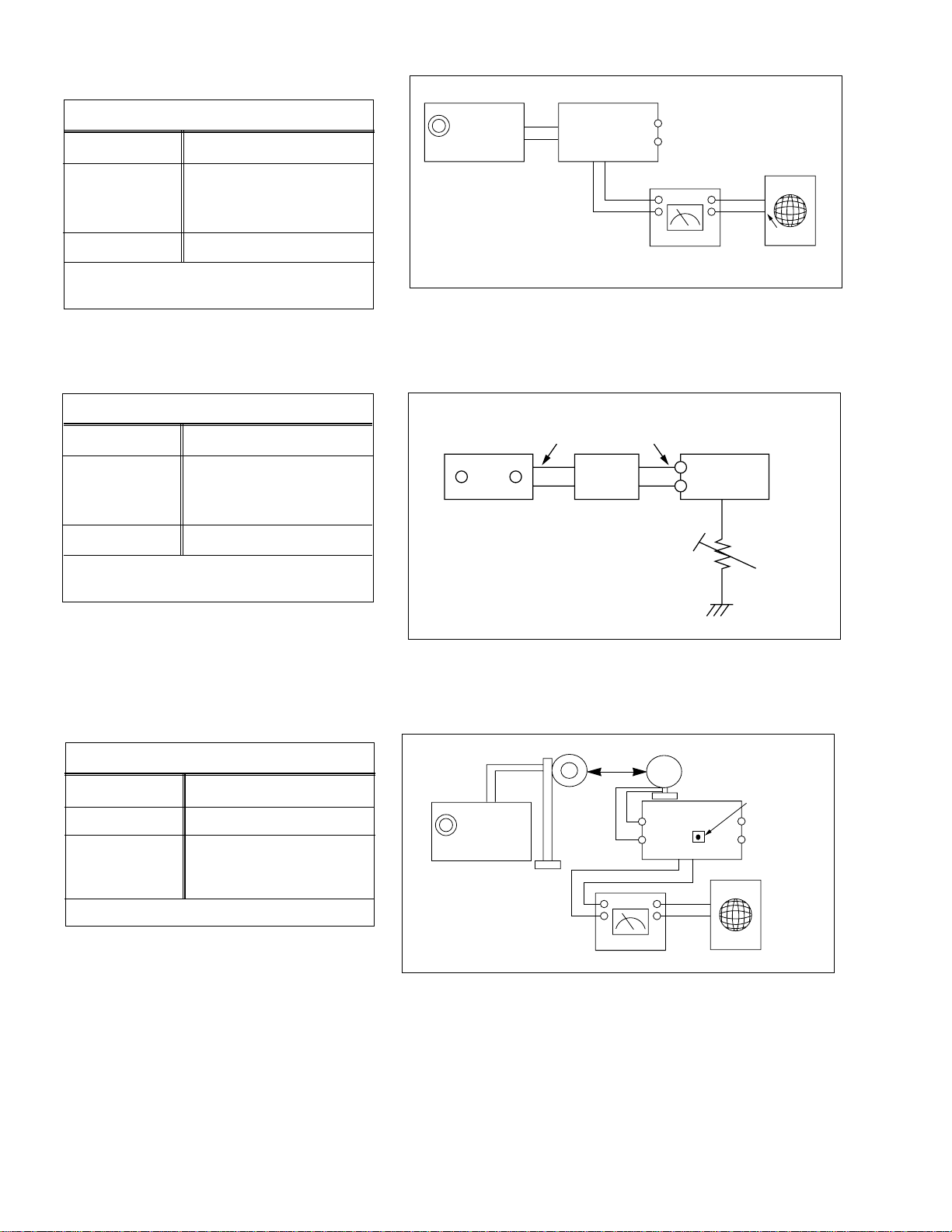
Adjustment method
Tuner
MX-J170V
Adjustment Location of Tuner PCB
*
ITEAM
Received FREQ.
Adjustment
point
Output
AM(MW) OSC Adjustment
520~1720 KHz
Adjustment
Non-
1~7.0±0.5V
MAIN
PCB
VT GND
AM(MW) RF Adjustment
590 KHz
MW -ANT
Maximum Output(Fig1-4)
TESTER
Fig 1-4 OSC Voltage
1-21
Page 22
MX-J170V
FM THD Adjustment
SSG FREQ.
98 MHz
Adjustment
point
FM DETECTOR COIL
(TL3)
Output
60 dB
Minumum Distortion (0.3% below)
(Figure 1-1)
FM Search Level Adjustment
SSG FREQ.
Adjustment
point
(TSR1)
Output
BEACON
SENSITIVITY
SEMI-VR(20K½)
28 dB(±2dB)
98 MHz
Output
GND
FM S.S.G
FM
Antenna
Terminal
Speaker
Terminal
SET
Input
output
Distortion Meter
Figure1-1 IF CENTER and THD Adjustment
FM Antenna
SET
FM IN
FM S.S.G
28 dB
GND
Oscilloscope
Input
Adjust TSR1 so that “TUNED” of FL T
is lighted (Figure 1-2)
*Adjust FM S.S.G level to 28dB
AM(MW) I.F Adjustment
SSG FREQ.
Frequency
450 kHz
520 kHz
Adjustment
point
AM I.F COIL
(TL2)
Maximum output (Figure 1-3)
Figure1-2 FM Auto Search Level Adjustment
60cm
OUTPUT
AM SSG
450KHZ
INPUT
AM ANT
IN
Speaker Terminal
OUTPUT
VTVM Oscilloscope
Figure1-3 AM I.F Adjustment
20 k½
TL2
1-22
Page 23
1. To adjust tape speed
Cassette deck
(GND)
VTVM
1) Measuring tape: i) MTT -111 (or equivalent)
(Tapes recorded with 3kHz)
ii) MTT-5512 (or equivalent)
2) Connect the cassette deck to the frequency counter
as in figure 1-5.
Notes
NOR
SPEED
Control
1
OUT
(connected
to the frequency
counter)
Turn UVR2 to
left and right
(FRONT PCB)
3KHz
Remark
Standard
To Adjust
Pre-Setup
Item
Step
Pre-Setup
Condition
1) Deck 1:MTT-111
2) Press PLAY
SW button
3) Deck 2:Same
as above
Cassette Deck
output
SPK OUT
Frequency Counter
Figure 1-5
Figure 1-6
SPK OUT
Recording /Play head
FWD PLAY
REVERSE PLAY
AZIMUTH control screw
Figure 1-7
In Out
Cassette Deck
Oscilloscope
±1%
range
Figure 1-8
Audio OSC.
SET
(MAIN PCB)
Oscilloscope
AUX IN
LINE OUT
VTVM
IN
DW2
IN OUT
TP
MX-J170V
1-23
Page 24
MX-J170V
2. To adjust playback lebel/REC
Notes
1) Before the actual adjustment, clean the play/recording
head.
2) Measuring tape :
i) MTT -114NA(or equivalent 12.5kHz AZIMUTH control)
ii) MTT-5512
3) The cassette deck is connections as shown in figure 1-7.
1 Adjust Deck 1 Play Level
Step
1
Item
AZIMUTH
Pre-Setup
Condition
TP1 OUT
(VTVM is
connected to
the scope)
Pre-Setup
After putting MTT114NA into Deck 1
- Press FWD PLAY
button.
2 Adjust Deck 2 Play Level/REC BIAS
Step
1
Item
AZIMUTH
Pre-Setup
Condition
TP1 OUT
(VTVM is
connected to
the scope)
Pre-Setup
After putting MTT 114NA into Deck 2
1)Press FWD PLAY
button.
2)Press REV PLAY
button.
To Adjust
- Turn the control
screw to as shown
in Figure 1-6.
To Adjust
- Turn the control
screw to as shown
in Figure 1-6.
Standard
Max output
and same phase
(both channels)
Standard
Max output
and same phase
(both channels)
Remark
After
adjustment
secure it with
REGION
LOCK.
Remark
After
adjustment
secure it with
REGION
LOCK.
1-24
2
Recording
Bias
Voltage
Fig 1-8
After putting MTT5512 into Deck 2
1)Press REC PLAY
button.
2)MAIN PCB DCW2,
connectted to VTVM
Turn DVR1,DVR2
to the right and left
7V(±0.5V)
Page 25

Flow of functional operation until TOC read
RESET a CD LSI
Set A servo coefficient
Is focus search done properly ?
Does SLED move to INNER
Detection of disk
Disc is Rotated
Limit SWITCH on
Automatic adjusting of focus,
tracking servo
Power ON
Play Key
Confirm that the signal from pin59,
60 of IC327 is as a accelerated
pulse during approximations.
CD-DA, VCD, Detection.
TOC reading
Play a disc
CD-DA
Check Point
Confirm that the voltage at the pin38
of IC327 is "L" "H".
Confirm that the voltage at the pin63
of IC327 is "H" "L" "H".
Confirm that the signal at the pin39
(SDA), 40(SCLK), 41(RAB) is output.
Set A decoder register
0 F
Confirm that the signal at the pin39
(SDA), 40(SCLK), 42(SILD) is output.
Check IC327 #16resonator signal
(16.93MHz)
Check IC327 #56(SL)
Check IC073-2 #9
#12
Confirm that the voltage at the pin63
of IC327 is "H" "L" "H".
Confirm that the voltage swing at
the pin #55 of IC327 and the pin
13, pin16.
With servo coefficient.
Communication with VCD micom
MI1.
MX-J170V
1-25
Page 26

MX-J170V
Maintenance of laser pickup
(1) Cleaning the pick up lens
Before you replace the pick up, please try to
clean the lens with a alcohol soaked cotton
swab.
(2) Life of the laser diode
When the life of the laser diode has expired,
the following symptoms will appear.
1. The level of RF output (EFM output:ampli
tude of eye pattern) will below.
Is the level of
RFOUT under
1.8V 0.2Vp-p?
YES
O.K
NO
Replace it.
Replacement of laser pickup
Turn off the power switch and,disconnect the
power cord from the ac outlet.
Replace the pickup with a normal one.(Refer
to "Pickup Removal" on the previous page)
Plug the power cord in,and turn the power on.
At this time,check that the laser emits for
about 3seconds and the objective lens moves
up and down.
Note: Do not observe the laser beam directly.
Play a disc.
Check the eye-pattern at TP1.
Finish.
(3) Semi-fixed resistor on the APC PC board
The semi-fixed resistor on the APC printed circuit board which is attached to the pickup is used to adjust the
laser power.Since this adjustment should be performed to match the characteristics of the whole optical block,
do not touch the semi-fixed resistor.
If the laser power is lower than the specified value,the laser diode is almost worn out, and the laser pickup should
be replaced.
If the semi-fixed resistor is adjusted while the pickup is functioning normally,the laser pickup may be damaged
due to excessive current.
1-26
Page 27

Trouble shooting guide
Tray does not close/open
Check the SW, SW2 of
mecha
mecha initial position
Check the pin 20,10
of IC082 when
open button is
pressed
Check the pulse pin
RL+, RL- of SCW1
connector
No
No
No
Yes
Yes
Yes
No
Check the UIC1
Check for IC082
No logo display
Check for VIDEO
signal at pin V.OUT of CT1
Check for 27MHz
signal at CI1 of VCD board
pin No. 106
No
No
Yes
No
Check VIDEO pattern
line(OQ2, OQ3)
Check the X-TAL
VX101(27MHz)
Check the communication
line of MI1 with UIC1
Check pin RST of
CT1:low
pin No. 60
No
Check VCD board,
resoldering or
replase vcd board
MX-J170V
1-27
Page 28

MX-J170V
Check pick-up
Yes
Check for resistance
at pin T+,T- of NCW8:
about 10ohm
Yes
Check for resistance
at pin F+,F- of NCW8:
about 5ohm
Yes
(When CD lead in)
Check for voltage
at pin1 of SIC2
1.7Vp-p
No
Pickup OK
No
Pickup OK
No
1-28
Yes
(When CD lead in)
Check for voltage at PD of SW4
connector.
about : 0.15V
Yes
Pickup OK
Pickup OK
No
Pickup OK
Page 29

Description of major ICs
BA4560 (UIC1) / KA4558 (DIC2) : Dual OP AMP
1.Pin layout
1
OUT1
VCC
8
MX-J170V
– IN1
+ IN1
V
2
1ch
+
–
3
EE
4
2ch
+
OUT2
7
– IN2
6
–
+ IN2
5
TC7SU04F (C12) : Inverter
1
NC
IN A
GND
2
3
4
5
Vcc
OUT Y
NJU3711M (UIC2) : 8-BIT Serial to parallel conveter
1. Pin layout
P3
1
2
P4
3
P5
V
SS
4
P6
5
6
P7
P8
7
V
14
DD
13
P2
12
P1
CLR
11
10
STB
9
CLK
8
DATA
2. Pin function
4
12
13
14
SymbolPin.No
P31
P42
P53
V
SS
P65
P76
P87
DATA8 Serial data input termnal
CLK9
STB10
CLR11
P1
P2
V
DD
Function
Parallel converts darta output terminals
Ground
Parallel converts darta output terminals
Clock signal input termnal
Strove signal input termnal
Clear signal input termnal
Parallel converts darta output terminals
Power supply terminal
1-29
Page 30

MX-J170V
KA22291 (DIC1) : Cassette amp.
PBOUT(2)
Vcc
Vcc
REC GND
PB OUT(1)
24
16
17
9
1
100K
RECORD
LREF
PLAYBACK
LREF
100K
PB
NF(2)
PR IN(2)
R/PSWMUTE
SW
MUTE
(IN2)
23 22 21 8 20 19 18 15
R/P SW
A-IN
B-IN
N.F
PRE
INPUT
REC.BIAS
PRE
PB.BIAS
INPUT
NF
MODE CONTROL
/BIAS CIRCUIT
A/B SELECT S/W
A-IN
B-IN
2 3 4 5 7 6 10
PU
NF(1)
PB IN(1) A/BSWPB GND MUTE
IN(1)
ALC RECOUT(2)
ALC TIME CONSTANT
ALC
DET
REC
OUT(1)
100K
PRE
PRE
100K
N.F
INPUT
INPUT
N.F
14
REC NF(2)
REC IN(2)
13
12
REC IN(1)
REC IN(1)
11
LC72131D (HIC1) : PLL
1
XIN
22
XOUT
1/2
16
FMIN
15
AMIN
3
CE
4
DI
CL
DO
5
6
C2B
1/F
REFERENCE
DIVIDER
SWALLOW COUNTER
1/16, 1/17 4D1ts
12bita PROGRAMMABLE
DIVIDER
DATA SHIFT REGISTER
LATCH
PHASE DETECTOR
CHARGE PUMP
UNLOCK
DETECTOR
UNIVERSAL
COUNTER
18
19
20
12
PD
AIN
ADUT
IFIN
1-30
VDD
Vss
17
21
P0WER
ON
RESET
7 8 9 10
BO1 BO2 BO3 BO4
11
IO1
13
IO2
Page 31

Pin Number Pin Name I/O Pin Function Descriptio n
1 GND - Ground
2V
O1
O Output 1
3V
Z1
- Phase compensation
4V
CTL
I Motor speed control
5V
IN1
I Input 1
6V
IN2
I Input 2
7SV
CC
- Supply voltage (Signal)
8PV
CC
- Supply voltage (Power)
9V
Z2
- Phase compensation
10 V
O2
O Output 2
12345678910
GND V
O1
V
Z1
V
CTLVIN1
V
IN2
SV
CC
V
O2
PV
CCVZ2
KA3082
DRIVER OUT
PRE DRIVER
LOGIC SWITCH
TSD
BIAS
1234
5
678910
GND
V
O1
V
Z1
V
CTL
V
IN1
V
IN2
SV
CC
PV
CC
V
Z2
V
O2
KA3082 (IC3082) : Bi-directional DC motor driver
3.Block Diagram
1.Pin layout
2.Pin function
MX-J170V
1-31
Page 32

MX-J170V
LA1837 (TIC1) : FM IF/DET AM RF/IF/DET
1-32
Page 33

LC75341 (FIC1) : Function
MX-J170V
1-33
Page 34

MX-J170V
y
o
0
e
s
e
7
8
2
3
4
5
C
g
g
e
W
r
0
LC86P5032 (MI1) : 8-Bit single-chip microcontroller
1.Pin layout
TEST1
RES
XT1/P74
XT2
VSS
CF1
CF2
VDD
P80/AN0
P81/AN1
P82/AN2
P83/AN3
P84/AN4
P85/AN5
P86/AN6
P87/AN7
2.Block Diagram
0
P10/SO0
P13/SO1
P16/BUZ
P14/SI1/SB1
P15/SCK1
P17/PWM
48
47
46
49
50
51
52
53
54
55
56
57
58
59
60
61
62
63
1
4
3
2
64
P70/INT0
P71/INT1
P72/INT2/T0IN
P73/INT3/T0IN
Interrupt control
Interrupt Contro
Standby control
Stand-b
P12/SCK0
434445
6
5
P30
P31
P06
P11/SI0/SB
P07
41
42
789
10
P34
P35
P32
P33
CF
RC
X tal
X'tal
P03
P05
P04
383940
12
13
11
P40
P36
P37
Contr
P00
P02
P01
32
34
353637
33
31
30
29
28
27
26
25
24
23
22
21
20
19
18
17
14
15
16
P43
P41
P42
Clock
Clock
Generator
generator
P27
P26
P25
P24
P23
P22
P21
P20
VDD
VSS
P51
P50
P47
P46
P45
P44
IR PLA
EPROM
Control
control
EPROM(32KB)
A15-A0
A15 to A0
D7-D0
D7 to D0
TA
TA
CE
CE
OE
OE
DASEC
DASEC
VDDV
VDDVPP
PP
P
Base Time
Base timer Bus interface
SIO0
SIO1
Timer
Timer 1
ADC
Noise filter
INT0 to INT3
Real Tim
Real-time
Service
service
Bus Interfac
Port 1
Port
Port
Port
Port
Port
Port
RAM
128 byte
ACC
iste
B Re
B register
ist
C Re
C register
ALU
PS
RAR
RAM
Stack
Stack
Pointe
pointer
Port
Watchdog timer
Watchdog Time
1-34
Page 35

M65855FP(EIC1) : Sound processor
14
15
6
Main control
Oscillator
8
16
9
10
3
2
1
4
5
11
7
13
12
V
cc
3. Block diagram.
1. Pin layout
2. Pin function
SymbolPin No. DESCRIPTION
GND1
2
3
4
5
6
7
8
9
10
11
12
13
14
15
16
1
2
3
4
5
6
7
8
16
15
14
13
12
11
10
9
CLOCKGND
ECHOMUTE
ECHOVOL
ECHOVOL
REF
REF
V
CC
OP2 IN
OP1 IN
LPF2 IN
LPF1 IN LPF2 OUT
LPF1 OUT
MIC OUT
MIC IN
OP2 OUT
OP1 OUT
CLOCK
ECHOMUTE
V
CC
OP1 IN
LPF1 IN
LPF1 OUT
MIC IN
OP1 OUT
Echo level control with external DC voltage
Echo mute control and clock stop control
with external DC voltage
Controls a built -in clock generation circuit with
external R
To connect 1/2 Vcc output and filter capacitor
Uses external C to from an D/A conversion
integrator
Uses external C to from an D/A conversion
integrator
Uses external CR to from a low pass filter at the
input side
Uses external CR to from a low pass filter at the
input side
Mixing output echo output and microphone
Microphone input
Applies a voltage of 3.5V to 5.5V(Rated5V)
REF
CLOCK
ECHOMUTE
ECHOVOL
MIC OUT
20Kbit
SRAM
AUTO
RESET
A/D
D/A
LPF1
LPF2
VOL
D1
DO1
DO0
CLOCK
MO
MI
RESET
1/2 Vss
MIX
GND
MX-J170V
1-35
Page 36

MX-J170V
NJU3711M (UIC2) : 8-BIT Serial to parallel converter
1. Pin layout
P3
1
2
P4
3
P5
V
SS
4
P6
5
6
P7
P8
7
2. Pin function
V
14
DD
13
P2
12
P1
CLR
11
10
STB
9
CLK
8
DATA
SymbolPin.No
P31
P42
Parallel converts data output terminals
P53
4
V
SS
Ground
P65
P76
Parallel converts data output terminals
P87
Function
DATA8 Serial data input termnal
12
13
14
CLK9
STB10
CLR11
P1
P2
V
DD
Clock signal input termnal
Strove signal input termnal
Clear signal input termnal
Parallel converts data output terminals
Power supply terminal
1-36
Page 37

SAA7327 (IC327) :Digital servo processor
1. Block diagram
MX-J170V
R1
R2
V
RIN
SCL
SDA
RAB
SILD
HFIN
HFREF
ISLICE
I
TEST1
TEST2
TEST3
V
DDA1
V
DDA2
CONTROL
V
SSA2
D1 D2 D3 D4
8 9 10 11 4 14 5 17 33 50 58 52 57
12
13
7
40
39
41
42
2
1
FRONT-END
3
6
ref
25
31
44
ADC
V
ref
GENERATOR
MICROCONTROLLER
INTERFACE
TEST
DEMODULATOR
V
PROCESSING
DIGITAL
PLL
EFM
SRAM
SSA1
PRE-
V
SSD1
CONTROL
FUNCTION
PART
SAA7327
V
SSD2
V
SSD3
AUDIO
PROCESSOR
V
DDD1(P)
V
DDD2(C)
OUTPUT
STAGES
MOTOR
CONTROL
ERROR
CORRECTOR
FLAGS
EBU
INTERFACE
54
RA
55
FO
56
SL
64
LDON
59
MOTO1
60
MOTO2
53
CFLG
51
DOBM
SELPLL
CRIN
CROUT
CL16
CL11/4
SBSY
SFSY
SUB
RCK
STATUS
RESET
24
16
15
TIMING
26
49
48
47
46
45
43
38
DECODER
MICRO-
CONTROLLER
INTERFACE
RAM
ADDRESSER
SUBCODE
PROCESSOR
VERSATILE PINS
INTERFACE
63 34 61 62 32
V1 V2/V3 V4 V5 KILL
PEAK
DETECT
KILL
SERIAL DATA
INTERFACE
SERIAL DATA
(LOOPBACK)
INTERFACE
BITSTREAM
DAC
30
29
28
27
37
35
36
20
21
18
19
22
23
MGS234
EF
SCLK
WCLK
DATA
SCLI
WCLI
SDI
V
neg
V
pos
LN
LP
RN
RP
1-37
Page 38

MX-J170V
2. Pin function
(1)
4
(1)
5
6 reference current output
7 reference voltage for servo ADCs
14
17
20 DAC negative reference input
21 DAC positive reference input
33
(1)
(1)
(1)
SymbolPin No. Function
HFREF1 comparator common mode input
HFIN2 comparator signal input
ISLICE3 current feedback output from data slicer
V
V
I
ref
V
SSA1
DDA1
RIN
analog ground 1
analog supply voltage 1
D18 unipolar current input 1 (central diode signal input)
D29 unipolar current input 2 (central diode signal input)
D310 unipolar current input 3 (central diode signal input)
D411 unipolar current input 4 (central diode signal input)
R112 unipolar current input 1 (satellite diode signal input)
R213 unipolar current input 2 (satellite diode signal input)
V
SSA2
analog ground 2
CROUT15 crystal/resonator output
CRIN16 crystal/resonator input
V
DDA2
analog supply voltage 2
LN18 DAC left channel differential negative output
LP19 DAC left channel differential positive output
V
neg
V
pos
RN22 DAC right channel differential negative output
RP23 DAC right channel differential positive output
SELPLL24 selects whether internal clock multiplier PLL is used
TEST125 test control input 1 (this pin should be tied LOW)
CL1626 16.9344 MHz system clock output
DATA27 serial d4(1) data output (3-state)
WCLK28 word clock output (3-state)
SCLK29 serial bit clock output (3-state)
EF30 C2 error ßag output (3-state)
TEST231 test control input 2 (this pin should be tied LOW)
KILL32 kill output (programmable; open-drain)
V
SSD1
digital ground 1
V2/V334 versatile I/O: versatile input 2 or versatile output 3 (open-drain)
WCLI35 word clock input (for data loopback to DAC)
SDI36 serial data input (for data loopback to DAC)
SCLI37 serial bit clock input (for data loopback to DAC)
RESET38 power-on reset input (active LOW)
SDA39 microcontroller interface data I/O line (I
SCL40 microcontroller interface clock line input (I
2
C-bus; open-drain output)
2
C-bus)
1-38
Page 39

2. Pin function(2/2)
MX-J170V
Pin No.
(1)
50
(1)
52
(1)
57
(1)
58
Symbol
RAB41 microcontroller interface R/
SILD42 microcontroller interface
Function
W and load control line input (4-wire bus mode)
R/W and load control line input (4-wire bus mode)
STATUS43 servo interrupt request line/decoder status register output (open-drain)
TEST344 test control input 3 (this pin should be tied LOW)
RCK45 subcode clock input
SUB46 P-to-W subcode bits output (3-state)
SFSY47 subcode frame sync output (3-state)
SBSY48 subcode block sync output (3-state)
CL11/449 11.2896 or 4.2336 MHz (for microcontroller) clock output
V
SSD2
digital ground 2
DOBM51 bi-phase mark output (externally buffered; 3-state)
V
DDD1(P)
digital supply voltage 1 for periphery
CFLG53 correction ßag output (open-drain)
RA54 radial actuator output
FO55 focus actuator output
SL56 sledge control output
V
DDD2(C)
V
SSD3
digital supply voltage 2 for core
digital ground 3
MOTO159 motor output 1; versatile (3-state)
MOTO260 motor output 2; versatile (3-state)
V461 versatile output 4
V562 versatile output 5
V163 versatile input 1
LDON64 laser drive on output (open-drain)
1-39
Page 40

MX-J170V
TDA7073A(IC805) : Dual BTL power driver
1. Pin layout
1
IN1–
IN1+
2
3
n.c.
4
n.c.
V
IN2 +
IN2 –
n.c.
P
TDA7073A
TDA7073AT
5
6
7
8
2. Pin function
SymbolPin No.
16
OUT1+
n.c.
15
14
GND1
13
OUT1 –
12
OUT2 –
11
n.c.
10
GND2
9
OUT2 +
5 positive supply voltage
IN1-1 negative input 1
IN1+2 positive input 1
n.c.3 not connected
n.c.4 not connected
V
P
IN2+6 positive input 2
IN2-7 negative input 2
n.c.8 not connected
OUT2+9 positive output 2
GND210 ground 2
Function
n.c.11 not connected
OUT2+12 negative output 2
OUT1-13 negative output 1
GND114 ground 1
n.c.15 not connected
OUT1+16 positive output 1
3. Block diagram
positive input 1
negative input 1
positive input 2
negative input 2
V
P
5
16I + i
2
1
6
7
Ι
SHORT - CIRCUIT AND
THERMAL PROTECTION
I – i
ΙΙ
13I – i
12
9I + i
positive output 1
negative output 1
negative output 2
positive output 2
1-40
10
ground 2
14
ground 1
3, 4, 8, 11, 15
n.c.
Page 41

TDA7295 (AIC1, 2) : Audio amp.
1.Pin layout
12345678910
N.C.
SUR
STAND-BY GND
INVERTING INPUT
INPUT
NON INVERTING
BOOT STARD
KA3082
+US(SIGNAL)
-US(SIGNAL)
STAND-BY
MUTE
MX-J170V
2
1
1
N.C.
3
1
4
+US(POWER)
OUT
5
1
-US(POWER)
1
1
N.C.
2.Block Diagram
IN+
IN-
BIPOLAR
TRANSCONDUCTANCE
INPUT STAGE
MOS GAIN &
LEVEL SHIFTING
STAGE
BOOTSTRAP
+
-
MOS OUTPUT STAGE
+
-
+
+
-
+
SHORT CIRCUIT
PROTECTION
+US
BOOTSTRAP
OUTPUT
-US
1-41
Page 42

MX-J170V
TZA1024 (IC024) : Data ampliÞer and laser supply
1. Pin Layout
LD
1
V
PWRON
DD(L)
CFIL
MON
DIN
GND
2
3
4
5
6
7
TZA1024
14
13
12
11
10
9
8
RGADJ
V
DD
EQSEL
CDRW
RFEQO
RFFB
CMFB
2. Pin function
2 laser supply voltage
13 supply voltage
SYMBOLPIN.No
Function
LD1 current output to laser diode
V
DD(L)
CFIL3 external Þlter capacitor
MON4 laser monitor diode input
DIN5 central diode input
GND6 ground
PWRON7 power-on select input
CMFB8 common mode feedback voltage
input
RFFB9 external RF feedback resistor
RFEQO10 RF ampliÞer output
CDRW1 gain select input for CD-A/V , CD-R/W
EQSEL12 equalizer/speed select input
(n = 1, 2 or 4)
V
DD
RGADJ14 external laser supply gain adjust
resistor
3. Block diagram
DIN
MON
11
5
4
CDRW
GND
V
DD
V
13
GAP
1×
4×
2×
TZA1024
V/I
(1)
V/I
26
V
DD(L)
V
DD
12
EQSEL
9
RFFB
10
RFEQO
8
250
kHz
V
DD
MGR517
CMFB
1
LD
14
RGADJ
3
CFIL
7
PWRON
1-42
Page 43

UDA1330AT (AI1) : Stereo filter DAC
MGL401
DAC
UDA1330ATS
NOISE SHAPER
INTERPOLATION FILTER
VOLUME/MUTE/DE-EMPHASIS
CONTROL
INTERFACE
14
15
DAC
6
DIGITAL INTERFACE
8
16
9
10
3
2
1
4
5
11
7
13 12
VOUTR
BCK
V
SSA
WS
VOUTL
DATAI
V
DDA
V
DDD
V
ref(DAC)
V
SSD
APPL0
SYSCLK
APPL1
APPSEL
APPL2
APPL3
3. Block diagram.
1. Pin layout
2. Pin function
SYMBOL PIN DESCRIPTION
BCK 1 bit clock input
WS 2 word select input
DATAI 3 data input
V
DDD
4 digital supply voltage
V
SSD
5 digital ground
SYSCLK 6 system clock input: 256f
s
, 384f
s
and 512f
s
APPSEL 7 application mode select input
APPL3 8 application input 3
APPL2 9 application input 2
APPL1 10 application input 1
APPL0 11 application input 0
V
ref(DAC)
12 DAC reference voltage
V
DDA
13 analog supply voltage for DAC
VOUTL 14 left channel output
V
SSA
15 analog ground
VOUTR 16 right channel output
UDA1330ATS
MGL402
1
2
3
4
5
6
7
8
16
15
14
13
12
11
10
9
VOUTRBCK
V
SSA
WS
VOUTL
DATAI
V
DDA
V
DDD
V
ref(DAC)
V
SSD
APPL0SYSCLK
APPL1APPSEL
APPL2APPL3
MX-J170V
1-43
Page 44

MX-J170V
VICTOR COMPANY OF JAPAN, LIMITED
AUDIO & COMMUNICATION BUSINESS DIVISION
PERSONAL & MOBILE NETWORK BUSINESS UNIT 10-1,1Chome,Ohwatari-machi,maebashi-city,371-8543,Japan
(No.20859)
Printed in Japan
200011(V)
Page 45

Block diagrams
Main section
5
4
MX-J170V
3
2
1
ABC
2-1
Page 46

MX-J170V
CD & VCD section
5
4
SIGNAL
PROCESSOR
CI 1
VIDEO
AI 1
STEREO
FILTER DAC
R
ARI 1
L
AMP AMP
ALI 1
R
L
MAIN section
FRONT section
VCD section
SCON3 DIGITAL
NCW3
L
NCW2
R
VIDEO
L
NCW1
R
OPEN/
CLOSE
3
SERVO
DIGITAL
PROCESSOR
IC327
OPEN/CLOSE
2
DATA AMP
&
LASER
IC024
SUPPLY
MOTOR
DRIVER
IC073
MOTOR
DRIVER
IC082
1
2-2
CD section
PICK-UP
MOTOR
SPINDLE
SLED
MOTOR
OPEN/
CLOSE
MOTOR
ABCD
Page 47

MX-J170V
Standard schematic diagrams
Front section
5
SHEET2/5
SHEET3/5
SHEET3/5
4
SHEET2/5
3
SHEET2/5
2
1
Audio signal
MIC signal
Video signal
ABCD E F G
SHEET1/5
2-3
Page 48

MX-J170V
Main section
SHEET5/5
5
SHEET1/5
SHEET1/5
4
SHEET1/5
3
SHEET3/5
2
AUX signal
CD signal
Tape signal
1
Parts are safety assurance parts.
When replacing those parts make
sure to use the specified one.
Main signal
Tuner signal
MIC signal
SHEET2/5
2-4
HABC DEFG
Page 49

MX-J170V
CD servo section
5
SHEET 1/5
4
SHEET 4/5
3
SHEET 2/5
2
SHEET 1/5
Audio signal
1
Video signal
CD signal
SHEET 3/5
ABCD E F G
2-5
Page 50

MX-J170V
VCD section
5
4
3
SHEET 3/5
2
1
CD signal
2-6
Audio signal
Video signal
SHEET 4/5
HABC DEFG
Page 51

MX-J170V
Tuner section
5
4
180(1/2W)
TR64
3
TR63
2
FM/TUNER signal
AM signal
1
SHEET 5/5
ABCD E F G
2-7
Page 52

MX-J170V
Printed circuit boards
Main board
5
4
3
2
1
2-8
HABC DEFG
Page 53

MX-J170V
Front board
5
4
3
2
1
ABCD E F G
2-9
Page 54

MX-J170V
CD servo board
5
4
3
MIC / Headphone board
2
1
2-10
HABC DEFG
Page 55

MX-J170V
Tuner board
5
4
3
2
1
ABCD E F G
2-11
Page 56

MX-J170V
VCD board
VCD power board
TOP Vie w
5
4
3
BOTT OM View
2
1
2-12
HABC DEFG
Page 57

PARTS LIST
[ MX-J170V ]
* All printed circuit boards and its assemblies are not available as service parts.
MX-J170V
- Contents -
Exploded view of general assembly and parts list
CD mechanism assembly and parts list
CD changer mechanism assembly and parts list
Cassette mechanism assembly and parts list
Electrical parts list
Packing materials and accessories parts list
CA-MXJ170V/SP-MXJ170V
Area suffix
US --------------------- Singapore
U --------------------- Other Areas
3- 3
3- 4
3- 5
3- 7
3- 8
3-21
3-1
Page 58

MX-J170V
-MEMO-
3-2
Page 59

MX-J170V
Exploded view of general assembly and parts list
5
30
39
44
25
24
26
4
1
2
3
48
3
17
Block No.
27
M
28
CD-Key board
M
1
44
45
M
Front board
31
22
23
44
38
Main board
Tuner board
53
32
46
44
45
36
33
42
37
43
50
AC primary board
47
44
41
51
VCD board
35
40
52
4
6
5
7
2
8
9
10
1
18
20
19
48
18
14
17
12
16
15
13
11
21
48
29
44
44
45
49
34
ABCD E F G
3-3
Page 60

MX-J170V
Parts list(General assembly)
Item
A
1 AH64-00426C
2 AH64-00414C
3 AH64-00429C
4 AH64-00462A
5 AH64-00417B
6 AH63-00107A
7 AH64-00430D
8 AH61-00271B
9 AH64-00422B
10 AH64-00427B
11 AH64-00428B
12 AH64-00412B
13 AH64-00413B
14 AH61-62004A
15 AH61-62005A
16 AH64-00364D
17 AH61-80030A
18 AH95-50001A
19 AH64-00421B
20 AH64-00423B
21 AH64-00420B
22 AH64-00415C
23 AH64-00418C
24 AH64-00425C
25 AH67-00035A
26 AH64-00440D
27 AH64-00419A
28 AH64-00416A
29 AH64-00432A
30 AH64-00431A
31 AH64-30443D
32 AH61-00021B
33 AH61-20540B
34 AH64-30416C
35 AH64-00366B
36 AH62-00023C
37 AN61-00250B
38 AH61-00252A
39 AH61-00380A
40 AH62-32002B
41 AH61-00278A
42 AH31-10020A
43 AH26-00054B
44 6003-000275
45 6003-000276
46 AH60-10182A
47 AH60-00014A
48 6003-000277
49 AH39-10002L
50 AH68-50275D
51 AH68-50482B
52 AH68-50282D
53 AH61-40014A
Parts number Parts name Area
Q'ty
WINDOW
CD DOOR
WINDOW-DOOR CD
BADGE-JVC
KNOB
SHEET-FRONT
WINDOW
CAP-VOLUME
KNOB-VOLUME
WINDOW-DOOR A
WINDOW-DOOR B
DOOR-CASSETTE A
DOOR-CASSETTE B
SPRING-EJECT A
SPRING-EJECT B
CABINET-FRONT
DAMPER-ASSY
ASSY-LATCH
KNOB-RECORD
KNOB-DUBBING
KNOB-CD OPEN
KNOB
KNOB
KNOB-DUBBING
LENS-POWER 1
KNOB
KNOB-KARAOKE
KNOB-DISC CHANGE
CABINET-SIDE R
CABINET-SIDE L
CABINET
SUPPORT-PCB
HOLDER 1
CABINET-BOTTOM
CABINET
HEAT-SINK-MAIN
BRAKET-H/SINK
HOLDER-VFD
SHAFT-H/PHONE
HEAT SINK 1
CAP-REAR 1
FAN-DC
POWER TRANS
SCREW-TAPTITE
SCREW-TAPPING
SCREW-TAPPING 2
SCREW-TAPTITE
SCREW
POWER CODE
LASER-CAUTION
LABEL-CLASS1-5L
CAUTION LABEL
SUPPORT-RIVET
1
CD
1
1
DOOR,CD
2
JVC
1
MIC
1
1
VFD
1
1
VOLUME
1
DOOR A
1
DOOR B
1
CASS,A
1
CASS,B
1
1
1
2
2
1
REC
1
DUBBING
1
CD OPEN
1
FUNCTION
1
PRESET
1
POWER
LENS-POWER
1
PROGRAM
1
KARAOKE
1
DISC CHANGE
1
SIDE-R
1
SIDE-L
1
TOP
1
TUNER
1
BOTTOM
1
REAR
1
1
1
1
AL3.0T,
1
D0620B-12M,12VD
1
115/230V,50/60H
33
3X10 BLK
15
3X10
FAN DC
4
TH,S-TITE,M4
11
3X12
1
CP2,KLCE-2F,2.1
1
1
1
1
Description
Block No. M1MM
CD mechanism assembly and parts list
4
3
2
1
ABC D
Parts list(CD mechanism)
A
Item
1 AH30-00007A
2 AH91-60150A
Parts number Parts name Area
1
PIC UP
CDP DECK ASSY
2
Q'ty
Description
1
SOH-AA,D51SG6(W
1
CMS-300D,-
Block No.
Block No. M2MM
M
2
M
M
3-4
Page 61

CD changer mechanism assembly and parts list
Block No.
8
MX-J170V
3
M
M
M
5
7
6
5
2
1
3
4
4
Base main
15
Tray stopper
3
16
19
21
17
20
12
2
10
13
11
9
VCD board
CD mechanism
CD sub board
25
24
18
22
1
14
23
ABC
3-5
Page 62

MX-J170V
Parts list(CD changer mechanism)
Item
A
1 AH66-80022A
2 AH66-60034A
3 AH66-20186A
4 AH66-20187A
5 AH66-20188A
6 AH66-20189A
7 AH66-20190A
8 AH66-20191A
9 AH66-20192A
10 AH31-12001A
11 AH66-20193A
12 AH66-90056A
13 AH66-90055A
14 AH32-10001E
15 AH61-20428A-1
16 3302-000159
17 AH66-90057A
18 AH69-20342B
19 3405-000101
20 AH31-10021A
21 AH66-10008A
22 AH73-10031A
23 AH66-30098A
24 AH73-10034A
25 AH63-40157B
Parts number Parts name Area
SLIDER-CAM 1
BELY-LOAD
GEAR
GEAR-LOAD 1
GEAR-CAM
GEAR-TRAY 1
GEAR-CONVERT
GEAR-SYNCRO
GEAR-WORM
MOTOR -LOADING
GEAR-ROULETTE
TRAY-ROULBTTE
TRAY-DISC
SENSOR
BASE MAIN
MAGNET FERRITE
TABLE-CHUCK
SHEET-CHUCK
MICRO SWITCH
DC MORTOR
PULLEY-MOTOR
RUBBER-CD
LEVER-LIFTER
RUBBER-CD(G)
SHIELD-TOP
Q'ty
1
1
1
1
1
1
1
1
1
1
1
1
1
1
4
1
1
9VDC/130MA,
1
CMS-CR3
2
1
2
GREEN
1
Block No. M3MM
Description
3-6
Page 63

Cassette mechanism assembly and parts list
1
SAM CASSETTE
9
Block No.
1
MX-J170V
4
M
M
M
8
3
7
10
6
8
7
6
2
12
11
5
14
13
11
14
3
5
4
1
ABCD
Parts list(Cassette mechanism)
Item Parts number Parts name Area
A
1 AH81-00141A R/P HEAD 2 TC881CB
2 AH81-00142A C.MOTOR ASS'Y 1 ADR2400-SHU2L
3 AH81-00143A MAIN BELT 1 1 ADR2400-MAIN76.
4 AH81-00144A MAIN BELT 2 1 ADR2400-MAIN64.
5 AH81-00101A SUB BELT 2 ADR2400-FR34.7
6 AH81-00102A SOLENOIDE 2 ADR2400-1
7 AH81-00282A SPRING 2
8 AH81-00283A PINCH LOLLER 2 ASS'Y PARTS
9 AH81-00284A E-HEAD 1 TC2131F
10 AH81-00285A MOTOR BRACKET 1
11 AH81-00286A LEAF SWITCH 2 ADR2400-MODE
12 AH81-00287A PHOTO SENSOR 2 ADR2400-SENSOR
13 AH81-00288A CONNECTOR 1 ADR2400-16
14 AH81-00289A LEAF SWITCH 6 ADR2400-MXS0022
15 AH81-00290A P.C.BOARD 1
12
2
Note: Parts listed on the Parts List below can be supplied.
However, parts that are not listed below cannot be supplied
individually but only by purchasing the whole Cassette
Mechanism Assembly Unit. (When ordering, use the Parts No.
AH59-20006U for Cassette Mechanism Assembly Unit.)
Q'ty Description
15
Block No. M4MM
3-7
Page 64

MX-J170V
Electrical parts list
Electrical parts list(Main board)
Item
A
AC 1 2401-001954 E CAPACITOR
AC 2 2401-001954 E CAPACITOR
AC 3 2401-001912 E CAPACITOR
AC 4 2401-001975 C CAPACITOR
AC 5 2401-000970 E CAPACITOR
AC 6 2202-000821 C CAPACITOR
AC 8 2202-000817 C CAPACITOR
AC 10 2202-000854 C CAPACITOR
AC 11 2202-000854 C CAPACITOR
AC 13 2202-000817 C CAPACITOR
AC 14 2401-001912 E CAPACITOR
AC 15 2401-000970 E CAPACITOR
AC 16 2401-001954 E CAPACITOR
AC 17 2401-001954 E CAPACITOR
AC 18 2401-001975 C CAPACITOR
AC 19 2202-000821 C CAPACITOR
AC 20 2301-000375 C CAPACITOR
AC 21 2301-000375 C CAPACITOR
AC 22 2401-001092 E CAPACITOR
AC 23 2401-002180 E CAPACITOR
AC 24 2401-002180 E CAPACITOR
AC 25 2401-001538 E CAPACITOR
AC101 2401-001975 C CAPACITOR
AC102 2401-000419 E CAPACITOR
AD 1 0401-000101 DIODE 1N4148
AD 2 0401-000101 DIODE 1N4148
AD 3 0401-000101 DIODE 1N4148
AD 10 0401-000101 DIODE 1N4148
AIC 1 1201-001654 IC
A
AIC 2 1201-001654 IC
A
AJACK 3716-000209 TERMINAL BLOCK
AJW 1 AH39-00157D LEAD-CONNECTOR
AQ 1 0504-000118 TRANSISTOR KSR1003
AQ 6 0504-001003 TRANSISTOR KSR2003
AQ 7 0501-000294 TRANSISTOR KSA708-Y
AR 1 2001-000890 C RESISTOR
AR 2 2001-000290 C RESISTOR
AR 3 2001-000522 C RESISTOR
AR 6 2001-000924 C RESISTOR
AR 7 2001-000786 C RESISTOR
AR 10 2001-000522 C RESISTOR
AR 12 2001-000290 C RESISTOR
AR 18 2001-000924 C RESISTOR
AR 20 2001-000786 C RESISTOR
AR 24 2001-000522 C RESISTOR
AR 30 2003-000689 OM RESISTOR
AR 31 2003-000689 OM RESISTOR
AR 32 2001-000290 C RESISTOR
AR 33 2001-000786 C RESISTOR
AR 34 2001-000591 C RESISTOR
AR 36 2001-000429 C RESISTOR
AR 39 2001-000522 C RESISTOR
AR100 2001-000429 C RESISTOR
AR203 2001-000660 C RESISTOR
AR204 2001-000008 C RESISTOR
AR205 2001-000008 C RESISTOR
AR206 2001-000977 C RESISTOR
AR208 2001-000429 C RESISTOR
CCW 1 3710-001567 CONNECTOR
CCW 2 3710-001571 CONNECTOR
CON 1 AH39-50001L LEAD-FASTEN
CONA- 3811-000131 WIRE-PVC CU
D 200 2301-000407 C CAPACITOR
Parts number Parts name Area
Block No. 01
Remarks
7295
7295
Item
A
DC 1 2301-000412 C CAPACITOR
DC 2 2301-000379 C CAPACITOR
DC 3 2301-000404 C CAPACITOR
DC 4 2301-000422 M CAPACITOR
DC 5 2201-000368 C CAPACITOR
DC 6 2201-000368 C CAPACITOR
DC 7 2401-001912 E CAPACITOR
DC 9 2301-000390 C CAPACITOR
DC 10 2301-000379 C CAPACITOR
DC 11 2301-000370 C CAPACITOR
DC 12 2301-000370 C CAPACITOR
DC 13 2401-001022 E CAPACITOR
DC 14 2401-001975 C CAPACITOR
DC 15 2401-000240 E CAPACITOR
DC 16 2301-000474 C CAPACITOR
DC 17 2301-000393 C CAPACITOR
DC 18 2301-000375 C CAPACITOR
DC 19 2401-002180 E CAPACITOR
DC 20 2401-001954 E CAPACITOR
DC 21 2401-001022 E CAPACITOR
DC 22 2202-000781 C CAPACITOR
DC 23 2401-001975 C CAPACITOR
DC 24 2401-000795 E CAPACITOR
DC 25 2401-001022 E CAPACITOR
DC 26 2201-000300 C CAPACITOR
DC 27 2301-000400 C CAPACITOR
DC 31 2401-001080 E CAPACITOR
DC 32 2401-001022 E CAPACITOR
DC 33 2401-001912 E CAPACITOR
DC 34 2401-001080 E CAPACITOR
DC 36 2201-000300 C CAPACITOR
DC 37 2301-000400 C CAPACITOR
DC 38 2401-001022 E CAPACITOR
DC 39 2401-001975 C CAPACITOR
DC 40 2202-000781 C CAPACITOR
DC 41 2401-001022 E CAPACITOR
DC 42 2301-000375 C CAPACITOR
DC 43 2202-000781 C CAPACITOR
DC 44 2401-002180 E CAPACITOR
DC 45 2202-000781 C CAPACITOR
DC 46 2202-000781 C CAPACITOR
DC 47 2301-000400 C CAPACITOR
DC 48 2202-000796 C CAPACITOR
DC 49 2401-000240 E CAPACITOR
DC 50 2401-001975 C CAPACITOR
DC 51 2301-000393 C CAPACITOR
DC 52 2401-001022 E CAPACITOR
DC 54 2301-000390 C CAPACITOR
DC 55 2301-000370 C CAPACITOR
DC 56 2301-000370 C CAPACITOR
DC 57 2301-000379 C CAPACITOR
DC 58 2301-000474 C CAPACITOR
DC 59 2401-000438 E CAPACITOR
DC 60 2401-000438 E CAPACITOR
DC 61 2401-001022 E CAPACITOR
DC 62 2401-001912 E CAPACITOR
DC 63 2202-000821 C CAPACITOR
DC 64 2202-000821 C CAPACITOR
DC 70 2401-001895 E CAPACITOR
DC 71 2202-000781 C CAPACITOR
DC 72 2202-000781 C CAPACITOR
DC 73 2301-000400 C CAPACITOR
DC 74 2202-000243 C CAPACITOR
Parts number Parts name Area
Remarks
3-8
Page 65

MX-J170V
Electrical parts list(Main board)
Item
A
DC 75 2202-000243 C CAPACITOR
DC301 2202-000781 C CAPACITOR
DC302 2202-000781 C CAPACITOR
DC303 2202-000781 C CAPACITOR
DD 1 0401-000101 DIODE 1N4148
DD 2 0401-000101 DIODE 1N4148
DD 3 0401-000101 DIODE 1N4148
DD 4 0401-000101 DIODE 1N4148
DIC 1 1201-000358 IC 22291
DIC 2 1201-000191 IC 4558
DL 1 AH26-10002Y COIL
DL 2 AH26-10002Y COIL
DL 5 AH27-00018A COIL LTRT1500-X00021
DL 6 2701-000298 INDUCTOR-AXIAL
DQ 1 0501-000369 TRANSISTOR KSC2331-Y
DQ 2 0501-000610 TRANSISTOR KSA928A-Y
DQ 3 0501-000398 TRANSISTOR KSC945
DQ 4 0504-000118 TRANSISTOR KSR1003
DQ 5 0501-000010 TRANSISTOR KSC1008
DQ 6 0501-000010 TRANSISTOR KSC1008
DQ 7 0501-000010 TRANSISTOR KSC1008
DQ 8 0501-000010 TRANSISTOR KSC1008
DQ 9 0504-001003 TRANSISTOR KSR2003
DQ 10 0504-000118 TRANSISTOR KSR1003
DQ 11 0501-000398 TRANSISTOR KSC945
DQ 12 0501-000398 TRANSISTOR KSC945
DQ 13 0501-000398 TRANSISTOR KSC945
DQ 14 0501-000398 TRANSISTOR KSC945
DQ 15 0504-001003 TRANSISTOR KSR2003
DQ 16 0501-000398 TRANSISTOR KSC945
DQ 17 0501-000398 TRANSISTOR KSC945
DQ 18 0504-001003 TRANSISTOR KSR2003
DQ 20 0504-000118 TRANSISTOR KSR1003
DR 1 2001-000440 C RESISTOR
DR 2 2001-000440 C RESISTOR
DR 3 2001-000734 C RESISTOR
DR 5 2001-000290 C RESISTOR
DR 6 2001-001096 C RESISTOR
DR 7 2001-000786 C RESISTOR
DR 8 2001-000591 C RESISTOR
DR 9 2001-000290 C RESISTOR
DR 10 2001-000429 C RESISTOR
DR 11 2001-000734 C RESISTOR
DR 12 2001-000924 C RESISTOR
DR 13 2001-000003 C RESISTOR
DR 15 2001-000290 C RESISTOR
DR 16 2001-000290 C RESISTOR
DR 18 2001-000734 C RESISTOR
DR 19 2001-000290 C RESISTOR
DR 20 2001-000977 C RESISTOR
DR 21 2001-000397 C RESISTOR
DR 22 2001-000890 C RESISTOR
DR 23 2001-000003 C RESISTOR
DR 24 2001-000786 C RESISTOR
DR 25 2001-000890 C RESISTOR
DR 26 2001-000708 C RESISTOR
DR 27 2001-000331 C RESISTOR
DR 28 2001-000325 C RESISTOR
DR 40 2001-000522 C RESISTOR
DR 41 2001-000734 C RESISTOR
DR 42 2001-000613 C RESISTOR
DR 43 2001-000258 C RESISTOR
DR 47 2001-000522 C RESISTOR
Parts number Parts name Area
Block No. 01
Remarks
Item
A
DR 48 2001-000591 C RESISTOR
DR 49 2001-000734 C RESISTOR
DR 50 2001-000613 C RESISTOR
DR 58 2001-000325 C RESISTOR
DR 59 2001-000331 C RESISTOR
DR 61 2001-000734 C RESISTOR
DR 62 2001-000786 C RESISTOR
DR 63 2001-000591 C RESISTOR
DR 64 2001-000290 C RESISTOR
DR 65 2001-000429 C RESISTOR
DR 66 2001-000003 C RESISTOR
DR 67 2001-000924 C RESISTOR
DR 68 2001-000290 C RESISTOR
DR 69 2001-000331 C RESISTOR
DR 70 2001-000003 C RESISTOR
DR 71 2001-000397 C RESISTOR
DR 72 2001-000977 C RESISTOR
DR 73 2001-000449 C RESISTOR
DR 74 2001-000786 C RESISTOR
DR 75 2001-000449 C RESISTOR
DR 76 2001-000429 C RESISTOR
DR 77 2001-000522 C RESISTOR
DR 78 2001-000734 C RESISTOR
DR 79 2001-000449 C RESISTOR
DR 80 2001-000449 C RESISTOR
DR 81 2001-000449 C RESISTOR
DR 82 2001-000449 C RESISTOR
DR 83 2001-000449 C RESISTOR
DR 84 2001-000449 C RESISTOR
DR 85 2001-000786 C RESISTOR
DR 86 2001-000773 C RESISTOR
DR 87 2001-000525 C RESISTOR
DR 88 2001-000449 C RESISTOR
DR 89 2001-000008 C RESISTOR
DR 90 2001-000591 C RESISTOR
DR 91 2001-000008 C RESISTOR
DR 92 2001-000591 C RESISTOR
DR 93 2001-000591 C RESISTOR
DR 94 2001-000864 C RESISTOR
DR 95 2001-000449 C RESISTOR
DR 96 2001-000864 C RESISTOR
DR 97 2001-000563 C RESISTOR
DR 98 2001-000449 C RESISTOR
DR 99 2001-000563 C RESISTOR
DR100 2001-000258 C RESISTOR
DR101 2001-000281 C RESISTOR
DR102 2001-000281 C RESISTOR
DR120 2001-000449 C RESISTOR
DR200 2001-001140 C RESISTOR
DR201 2001-001153 C RESISTOR
DR203 2001-000522 C RESISTOR
DVR 1 2103-000248 SEMI F.VR.
DVR 2 2103-000248 SEMI F.VR.
DVR 3 2103-000492 SEMI F.VR.
DW 1 3711-003111 CO N NECTOR
DW 2 3711-003107 CO N NECTOR
DW 3 3711-003107 CO N NECTOR
EC 1 2401-001912 E CAPACITOR
EC 2 2401-001912 E CAPACITOR
EC 3 2202-000797 C CAPACITOR
EC 4 2202-000809 C CAPACITOR
EC 5 2401-001889 E CAPACITOR
EC 6 2401-000907 E CAPACITOR
Parts number Parts name Area
Remarks
3-9
Page 66

MX-J170V
Electrical parts list(Main board)
Item
A
EC 7 2202-000797 C CAPACITOR
EC 8 2202-000797 C CAPACITOR
EC 9 2202-000781 C CAPACITOR
EC 10 2202-000148 C CAPACITOR
EC 11 2202-000817 C CAPACITOR
EC 12 2202-000817 C CAPACITOR
EC 20 2202-000854 C CAPACITOR
ECW 1 3711-001011 CONNECTOR
ED 1 0401-000101 DIODE 1N4148
ED 2 0401-000101 DIODE 1N4148
EIC 1 1204-001470 IC M65855FP
EQ 1 0504-000118 TRANSISTOR KSR1003
EQ 2 0504-000118 TRANSISTOR KSR1003
EQ 3 0504-000118 TRANSISTOR KSR1003
ER 1 2001-000008 C RESISTOR
ER 2 2001-000508 C RESISTOR
ER 3 2001-000273 C RESISTOR
ER 4 2001-000522 C RESISTOR
ER 5 2001-000977 C RESISTOR
ER 6 2001-000290 C RESISTOR
ER 7 2001-000319 C RESISTOR
ER 8 2001-000563 C RESISTOR
ER 9 2001-000429 C RESISTOR
ER 11 2001-000273 C RESISTOR
ER 12 2001-000734 C RESISTOR
ER 13 2001-000008 C RESISTOR
ER 14 2001-000290 C RESISTOR
ER 15 2001-000290 C RESISTOR
FAN AH31-10020A FAN
FC 1 2301-000375 C CAPACITOR
FC 2 2301-000375 C CAPACITOR
FC 3 2201-000928 C CAPACITOR
FC 5 2401-001975 C CAPACITOR
FC 6 2301-000375 C CAPACITOR
FC 7 2301-000375 C CAPACITOR
FC 8 2201-000928 C CAPACITOR
FC 10 2202-000781 C CAPACITOR
FC 11 2202-000781 C CAPACITOR
FC 12 2202-000781 C CAPACITOR
FC 13 2401-000907 E CAPACITOR
FC 14 2401-001917 E CAPACITOR
FC 15 2401-001917 E CAPACITOR
FC 16 2201-000368 C CAPACITOR
FC 17 2201-000368 C CAPACITOR
FC 18 2401-001954 E CAPACITOR
FC 19 2401-001912 E CAPACITOR
FC 20 2401-001912 E CAPACITOR
FC 21 2301-000379 C CAPACITOR
FC 22 2201-000504 C CAPACITOR
FC 23 2401-001912 E CAPACITOR
FC 24 2401-001912 E CAPACITOR
FC 25 2401-001912 E CAPACITOR
FC 26 2401-001912 E CAPACITOR
FC100 2401-001895 E CAPACITOR
FC103 2201-000368 C CAPACITOR
FC104 2201-000368 C CAPACITOR
FD 1 0401-000101 DIODE 1N4148
FIC 1 1204-001621 IC LC75341
FJACK 3722-000377 JACK-RCA
FQ 1 0504-000122 TRANSISTOR KSR1009Y
FQ 2 0504-000122 TRANSISTOR KSR1009Y
FQ 3 0504-001003 TRANSISTOR KSR2003
FQ 4 0501-000407 TRANSISTOR KSD471A-Y
Parts number Parts name Area
Block No. 01
Remarks
Item
A
FR 1 2001-000613 C RESISTOR
FR 1 3602-000147 FUSE CLIP
FR 2 3601-000216 FUSE-CARTRIDGE
FR 2 2001-000241 C RESISTOR
FR 3 2001-000023 C RESISTOR
FR 4 2001-000281 C RESISTOR
FR 5 2001-000281 C RESISTOR
FR 6 2001-000281 C RESISTOR
FR 7 2001-000613 C RESISTOR
FR 8 2001-000411 C RESISTOR
FR 9 2001-000008 C RESISTOR
FR 10 2001-000008 C RESISTOR
FR 11 2001-000411 C RESISTOR
FR 12 2001-000008 C RESISTOR
FR 13 2001-000786 C RESISTOR
FR 14 2001-000008 C RESISTOR
FR 15 2001-000786 C RESISTOR
FR 16 2001-000429 C RESISTOR
FR 17 2001-000429 C RESISTOR
FR 18 2001-000221 C RESISTOR
FR 19 2001-000221 C RESISTOR
FR2CL 3602-000147 FUSE CLIP
FR2CL 3602-000147 FUSE CLIP
FW 2 3711-002809 CONNECTOR
FW 7 AH39-00157E LEAD-CONNECTOR
FZD 1 0403-000372 ZENER DIODE
JW122 2202-000854 C CAPACITOR
MC 1 2201-000565 C CAPACITOR
MC 2 2401-000303 E CAPACITOR
MC 3 2401-001975 C CAPACITOR
MCW 1 3711-000820 CONNECTOR
MD 1 0401-000101 DIODE 1N4148
MD 2 0401-000101 DIODE 1N4148
ML 1 2701-000298 INDUCTOR-AXIAL
MQ 2 0501-000398 T R A N SISTOR KSC945
MQ 3 0501-000610 T R A N SISTOR KSA928A-Y
MR 5 2001-000449 C RESISTOR
MR 6 2001-000786 C RESISTOR
MR 7 2001-000864 C RESISTOR
MR 8 2001-000786 C RESISTOR
PC 1 2401-001943 E CAPACITOR
PC 2 2401-001943 E CAPACITOR
PC 3 2201-000783 C CAPACITOR
PC 4 2201-000783 C CAPACITOR
PC 5 2201-000783 C CAPACITOR
PC 6 2201-000783 C CAPACITOR
PC 7 2401-003116 E CAPACITOR
PC 8 2401-001413 E CAPACITOR
PC 9 2401-001954 E CAPACITOR
PC 10 2401-001954 E CAPACITOR
PC 11 2401-001895 E CAPACITOR
PC 13 2401-001895 E CAPACITOR
PC 14 2401-001954 E CAPACITOR
PC 15 2401-001954 E CAPACITOR
PC 16 2401-001912 E CAPACITOR
PC 17 2401-000475 E CAPACITOR
PC 18 2401-001975 C CAPACITOR
PC 19 2401-000475 E CAPACITOR
PC 20 2401-000230 E CAPACITOR
PC 21 2401-001954 E CAPACITOR
PC 23 2201-000783 C CAPACITOR
PC 24 2201-000783 C CAPACITOR
PC 25 2401-001975 C CAPACITOR
Parts number Parts name Area
Remarks
3-10
Page 67

MX-J170V
Electrical parts list(Main board)
Item
A
PC 26 2301-000449 C CAPACITOR
PC 27 2401-001538 E CAPACITOR
PC 28 2401-000795 E CAPACITOR
PC 29 2401-001975 C CAPACITOR
PC 30 2201-000565 C CAPACITOR
PC 31 2401-001895 E CAPACITOR
PC 32 2401-001102 E CAPACITOR
PC 33 2202-000797 C CAPACITOR
PCW 1 AH39-00144A LEAD-CONNECTOR
PC200 2401-000795 E CAPACITOR
PD 1 0402-000450 DIODE-BRIDGE
A
PD 2 0402-000151 DIODE
A
PD 3 0402-000151 DIODE
A
PD 4 0402-000151 DIODE
A
PD 5 0402-000151 DIODE
A
PD 6 0402-000127 DIODE 1N4002
PD 7 0402-000127 DIODE 1N4002
PD 8 0402-000127 DIODE 1N4002
PD 9 0402-000151 DIODE 1N5392
PD 10 0402-000151 DIODE 1N5392
PIC 1 1203-000242 IC 7812
PIC 2 1203-000276 IC
A
PIC 3 1203-000110 IC 7912
PL 1 2701-000114 INDUCTOR-AXIAL
PL 2 2701-000298 INDUCTOR-AXIAL
PQ 1 0502-000424 POWER TRANSISTOA2SB1566-F
PQ 2 0502-000424 POWER TRANSISTOA2SB1566-F
PQ 3 0501-000331 TRANSISTOR KSC1009-Y
PQ 4 0501-000398 TRANSISTOR KSC945
PQ 5 0501-000294 TRANSISTOR KSA708-Y
PQ 6 0501-000610 TRANSISTOR KSA928A-Y
PQ 8 0501-000407 TRANSISTOR KSD471A-Y
PQ 9 0504-000118 TRANSISTOR KSR1003
PQ 10 0501-000294 TRANSISTOR KSA708-Y
PQ 11 0502-000407 POWER TRANSISTOAKTC4369Y
PR 1 2003-000689 OM RESISTOR
PR 2 2001-000019 C RESISTOR
PR 3 2001-000793 C RESISTOR
PR 4 2001-000793 C RESISTOR
PR 5 2008-000135 FUSE RESISTOR
A
PR 6 2008-000135 FUSE RESISTOR
PR 6 13954-500-210 CERAMIC-PIPE
A
PR 7 13954-500-210 CERAMIC-PIPE PI1.4 7MM FOR L
PR 7 2008-000135 FUSE RESISTOR
A
PR 8 2001-000890 C RESISTOR
PR 9 2001-000613 C RESISTOR
PR 10 2001-000734 C RESISTOR
PR 11 13954-500-210 CERAMIC-PIPE PI1.4 7MM FOR L
PR 11 2003-000701 OM RESISTOR
PR 12 2001-001153 C RESISTOR
PR 13 2001-001153 C RESISTOR
PR 14 2001-000290 C RESISTOR
PR 15 2001-000522 C RESISTOR
PR 16 2001-000786 C RESISTOR
PR 17 2001-000734 C RESISTOR
PR 18 2001-000977 C RESISTOR
PR 19 2001-000290 C RESISTOR
PR 20 2003-000690 OM RESISTOR
A
PR 21 2001-000290 C RESISTOR
PR 22 2001-000522 C RESISTOR
PR 23 2001-000780 C RESISTOR
PR 25 2001-000591 C RESISTOR
PR 26 2003-000468 OM RESISTOR
Parts number Parts name Area
Block No. 01
Remarks
1N5392
1N5392
1N5392
1N5392
7805
PI1.4 7MM FOR L
Item
A
PR 27 2001-000027 C RESISTOR
PR 28 2001-000020 C RESISTOR
PR 29 2001-000023 C RESISTOR
PR 30 2001-000290 C RESISTOR
PR 31 2001-000429 C RESISTOR
PR300 2001-000525 C RESISTOR
PZD 1 0403-000564 ZENER DIODE
PZD 2 0403-000564 ZENER DIODE
PZD 3 0403-001010 ZENER DIODE
PZD 4 0403-000354 ZENER DIODE
PZD 5 0403-000377 ZENER DIODE
PZD 6 0403-000377 ZENER DIODE
PZD 7 0403-000354 ZENER DIODE
PZD 8 0403-000377 ZENER DIODE
RC 1 2201-000546 C CAPACITOR
A
RC 2 2201-000546 C CAPACITOR
RCW 1 3711-001167 CONNECTOR
RCW 2 3711-000190 CONNECTOR
RF 2 3601-000162 FUSE CARTRIDGE
A
RF 2 3602-000147 FUSE CLIP
RL 1 AH27-10001F COIL 27UH
RL 2 AH27-10001F COIL 27UH
RR 1 13954-500-210 CERAMIC-PIPE PI1.4 7MM FOR L
RR 1 2008-000135 FUSE RESISTOR
A
RR 2 2008-000135 FUSE RESISTOR
A
RR 2 13954-500-210 CERAMIC-PIPE PI1.4 7MM FOR L
RR 3 13954-500-210 CERAMIC-PIPE PI1.4 7MM FOR L
RR 3 2008-000137 FUSE RESISTOR
A
RR 4 2008-000137 FUSE RESISTOR
A
RR 4 13954-500-210 CERAMIC-PIPE PI1.4 7MM FOR L
RSW 1 3408-000177 SWITCH-SLIDE
A
VC 1 2401-001954 E CAPACITOR
VC 2 2401-002180 E CAPACITOR
VC 3 2401-001954 E CAPACITOR
VC 4 2401-001954 E CAPACITOR
VC 5 2401-001954 E CAPACITOR
VC 6 2401-002180 E CAPACITOR
VC 7 2202-000781 C CAPACITOR
VC 8 2202-000781 C CAPACITOR
VC 9 2202-000263 C CAPACITOR
VC 10 2202-000263 C CAPACITOR
VC 12 2401-001954 E CAPACITOR
VC 13 2401-001954 E CAPACITOR
VC 14 2401-001954 E CAPACITOR
VC 15 2202-000854 C CAPACITOR
VC 20 2401-000795 E CAPACITOR
VC200 2202-000279 C CAPACITOR
VIC 1 1201-000163 IC 4560
VIC 2 1201-000163 IC 4560
VQ 1 0504-001003 TRANSISTOR KSR2003
VQ 2 0504-000118 TRANSISTOR KSR1003
VQ 3 0504-001003 TRANSISTOR KSR2003
VQ 4 0501-000398 TRANSISTOR KSC945
VQ 7 0501-000398 TRANSISTOR KSC945
VQ 8 0501-000398 TRANSISTOR KSC945
VQ 9 0501-000398 TRANSISTOR KSC945
VQ 10 0501-000398 TRANSISTOR KSC945
VQ 11 0501-000398 TRANSISTOR KSC945
VR 1 2001-000660 C RESISTOR
VR 2 2001-000660 C RESISTOR
VR 3 2001-000660 C RESISTOR
VR 4 2001-000734 C RESISTOR
VR 5 2001-000290 C RESISTOR
Parts number Parts name Area
VOLTAGE SELECTR
Remarks
3-11
Page 68

MX-J170V
Electrical parts list(Main board)
Item
A
VR 6 2001-000522 C RESISTOR
VR 7 2001-000273 C RESISTOR
VR 8 2001-000522 C RESISTOR
VR 9 2001-000522 C RESISTOR
VR 10 2001-000734 C RESISTOR
VR 11 2001-000734 C RESISTOR
VR 15 2001-000411 C RESISTOR
VR 16 2001-000734 C RESISTOR
VR 17 2001-000734 C RESISTOR
VR 19 2001-000522 C RESISTOR
VR 20 2001-000522 C RESISTOR
VR 21 2001-000331 C RESISTOR
VR 22 2001-000734 C RESISTOR
VR 23 2001-000734 C RESISTOR
VR 24 2001-000411 C RESISTOR
VR 25 2001-000734 C RESISTOR
VR 26 2001-000786 C RESISTOR
VR 27 2001-000786 C RESISTOR
VR 28 2001-000331 C RESISTOR
VR 29 2001-000331 C RESISTOR
VR 30 2001-000331 C RESISTOR
VR 31 2001-000273 C RESISTOR
VR 32 2001-000786 C RESISTOR
VR 35 2001-000786 C RESISTOR
VR 36 2001-000331 C RESISTOR
VR 37 2001-000273 C RESISTOR
VR 38 2001-000331 C RESISTOR
VR 39 2001-000786 C RESISTOR
VR 40 2001-000786 C RESISTOR
VR200 2001-000786 C RESISTOR
VR201 2001-000786 C RESISTOR
Parts number Parts name Area
Block No. 01
Remarks
3-12
Page 69

MX-J170V
Electrical parts list(Front board)
Item
A
DECK 3809-001146 FLAT CABLE
GND 2 AH39-50001L LEAD-FASTEN
RE 1 AC59-60060A MODULE-REMOCON
SW 1 3404-000165 TACT SWITCH
SW 2 3404-000165 TACT SWITCH
SW 3 3404-000165 TACT SWITCH
SW 4 3404-000165 TACT SWITCH
SW 5 3404-000165 TACT SWITCH
SW 6 3404-000165 TACT SWITCH
SW 11 3404-000165 T A CT SWITCH
SW 12 3404-000165 T A CT SWITCH
SW 13 3404-000165 T A CT SWITCH
SW 14 3404-000165 T A CT SWITCH
SW 15 3404-000165 T A CT SWITCH
SW 16 3404-000165 T A CT SWITCH
SW 17 3404-000165 T A CT SWITCH
SW 18 3404-000165 T A CT SWITCH
SW 19 3404-000165 T A CT SWITCH
SW 20 3404-000165 T A CT SWITCH
SW 21 3404-000165 T A CT SWITCH
SW 22 3404-000165 T A CT SWITCH
SW 23 3404-000165 T A CT SWITCH
SW 24 3404-000165 T A CT SWITCH
SW 25 3404-000165 T A CT SWITCH
SW 27 3404-000165 T A CT SWITCH
SW 28 3404-000165 T A CT SWITCH
SW 29 3404-000165 T A CT SWITCH
SW 30 3404-000165 T A CT SWITCH
SW 31 3404-000165 T A CT SWITCH
SW 32 3404-000165 T A CT SWITCH
SW 33 3404-000165 T A CT SWITCH
SW 34 3404-000165 T A CT SWITCH
TAPE 3809-001146 FLAT CABLE
UC 1 2401-000459 E CAPACITOR
UC 2 2401-000475 E CAPACITOR
UC 3 2201-000565 C CAPACITOR
UC 4 2201-000565 C CAPACITOR
UC 5 2201-000565 C CAPACITOR
UC 6 2401-000240 E CAPACITOR
UC 7 2201-000389 C CAPACITOR
UC 8 2201-000389 C CAPACITOR
UC 9 2201-000483 C CAPACITOR
UC 10 2201-000483 C CAPACITOR
UC 11 2401-000459 E CAPACITOR
UC 12 2401-001931 E CAPACITOR
UC 13 2401-001952 E CAPACITOR
UC 15 2202-000854 C CAPACITOR
UC 16 2201-000300 C CAPACITOR
UC 17 2202-000797 C CAPACITOR
UC 18 2202-000797 C CAPACITOR
UC 30 2401-001355 E CAPACITOR
UCW 1 3711-004420 CONNECTOR
UCW 2 3711-004424 CONNECTOR
UCW 3 3708-000454 CONNECTOR
UCW 5 AH39-00157C LEAD CONNECTOR
UCW 6 AH39-00157B LEAD CONNECTOR
UCW 7 3711-000906 CONNECTOR
UCW 8 3708-000451 CONNECTOR
UCW 9 AH39-00157A LEAD CONNECTOR
UD 20 0402-000127 DIODE 1N4002
UD 21 0402-000127 DIODE 1N4002
UD 22 0402-000127 DIODE 1N4002
UD 23 0401-000101 DIODE 1N4148
Parts number Parts name Area
Block No. 02
Remarks
Item
A
UD 24 0402-000127 DIODE 1N4002
UD 25 0401-000101 DIODE 1N4148
UD 26 0401-000101 DIODE 1N4148
UD 27 0401-000101 DIODE 1N4148
UD 28 0401-000101 DIODE 1N4148
UD 29 0401-000101 DIODE 1N4148
UD 30 0402-000127 DIODE 1N4002
UIC 1 AH11-00017B IC ROM
UIC 2 AH14-10007C IC
UIC 3 1201-000163 IC 4560
ULD 1 0601-001238 LED
UMC 1 2401-001917 E CAPACITOR
UMC 2 2401-001917 E CAPACITOR
UMC 3 2401-001917 E CAPACITOR
UMC 4 2401-001952 E CAPACITOR
UMC 5 2202-000781 C CAPACITOR
UMC 6 2401-001965 E CAPACITOR
UMC 7 2401-001917 E CAPACITOR
UMC 8 2202-000796 C CAPACITOR
UMC 9 2201-000653 C CAPACITOR
UMC10 2201-000614 C CAPACITOR
UMC21 2401-001919 E CAPACITOR
UMC22 2401-001904 E CAPACITOR
UMC23 2401-001019 E CAPACITOR
UMC24 2401-001904 E CAPACITOR
UMD 1 0401-000101 DIODE 1N4148
UMD 2 0401-000101 DIODE 1N4148
UMD 3 0401-000101 DIODE 1N4148
UMD 4 0401-000101 DIODE 1N4148
UMR 1 2001-000977 C RESISTOR
UMR 2 2001-000290 C RESISTOR
UMR 3 2001-000429 C RESISTOR
UMR 4 2001-000780 C RESISTOR
UMR 5 2001-000786 C RESISTOR
UMR 6 2001-000780 C RESISTOR
UMR 7 2001-000660 C RESISTOR
UMR 8 2001-000273 C RESISTOR
UMR 9 2001-000449 C RESISTOR
UMR10 2001-000010 C RESISTOR
UMR11 2001-000429 C RESISTOR
UMR12 2001-000290 C RESISTOR
UMR13 2001-000786 C RESISTOR
UMR14 2001-000734 C RESISTOR
UMR21 2001-000290 C RESISTOR
UMR22 2001-000319 C RESISTOR
UMR23 2001-000734 C RESISTOR
UMR24 2001-000405 C RESISTOR
UMR30 2001-000290 C RESISTOR
UMR31 2001-000786 C RESISTOR
UQ 1 0501-000398 TRANSISTOR KSC945
UQ 2 0501-000398 TRANSISTOR KSC945
UQ 3 0501-000610 TRANSISTOR KSA928A-Y
UQ 4 0504-000118 TRANSISTOR KSR1003
UQ 5 0504-000118 TRANSISTOR KSR1003
UQ 6 0501-000610 TRANSISTOR KSA928A-Y
UQ 7 0501-000610 TRANSISTOR KSA928A-Y
UQ 8 0504-000118 TRANSISTOR KSR1003
UQ 9 0501-000398 TRANSISTOR KSC945
UQ 10 0504-000118 TRANS I S T O R KSR1003
UQ 15 0504-000118 TRANS I S T O R KSR1003
UQ 16 0501-000398 TRANS I S T O R KSC945
UQ 16 0501-000407 TRANS I S T O R KSD471A-Y
UQ 17 0501-000398 TRANS I S T O R KSC945
Parts number Parts name Area
Remarks
3-13
Page 70

MX-J170V
Electrical parts list(Front board)
Item
A
UQ 21 0501-000398 TRANSISTOR KSC945
UQ 22 0504-000118 TRANSISTOR KSR1003
UQ 23 0504-001003 TRANSISTOR KSR2003
UR 1 2001-000258 C RESISTOR
UR 2 2001-000405 C RESISTOR
UR 3 2001-000241 C RESISTOR
UR 4 2001-000429 C RESISTOR
UR 5 2001-000429 C RESISTOR
UR 6 2001-000429 C RESISTOR
UR 7 2001-000734 C RESISTOR
UR 8 2001-000734 C RESISTOR
UR 9 2001-000734 C RESISTOR
UR 10 2001-000734 C RESISTOR
UR 11 2001-000734 C RESISTOR
UR 12 2001-000734 C RESISTOR
UR 13 2001-000734 C RESISTOR
UR 14 2001-000734 C RESISTOR
UR 15 2001-000734 C RESISTOR
UR 16 2001-000734 C RESISTOR
UR 17 2001-000734 C RESISTOR
UR 18 2001-000281 C RESISTOR
UR 19 2001-000429 C RESISTOR
UR 20 2001-000290 C RESISTOR
UR 21 2001-000290 C RESISTOR
UR 22 2001-000290 C RESISTOR
UR 23 2001-000290 C RESISTOR
UR 24 2001-000281 C RESISTOR
UR 25 2001-000429 C RESISTOR
UR 26 2001-000429 C RESISTOR
UR 27 2001-000429 C RESISTOR
UR 28 2001-000429 C RESISTOR
UR 29 2001-000429 C RESISTOR
UR 30 2001-000429 C RESISTOR
UR 31 2001-000591 C RESISTOR
UR 32 2001-000429 C RESISTOR
UR 33 2001-000429 C RESISTOR
UR 34 2001-000429 C RESISTOR
UR 35 2001-000429 C RESISTOR
UR 36 2001-000429 C RESISTOR
UR 37 2001-000429 C RESISTOR
UR 38 2001-000290 C RESISTOR
UR 39 2001-000290 C RESISTOR
UR 40 2001-000290 C RESISTOR
UR 41 2001-000290 C RESISTOR
UR 42 2001-000281 C RESISTOR
UR 43 2001-000281 C RESISTOR
UR 44 2001-000281 C RESISTOR
UR 45 2001-000281 C RESISTOR
UR 46 2001-000734 C RESISTOR
UR 47 2001-000449 C RESISTOR
UR 48 2001-000591 C RESISTOR
UR 49 2001-000449 C RESISTOR
UR 50 2001-000258 C RESISTOR
UR 51 2001-001178 C RESISTOR
UR 52 2001-000241 C RESISTOR
UR 53 2001-000429 C RESISTOR
UR 54 2001-000734 C RESISTOR
UR 55 2001-000591 C RESISTOR
UR 56 2001-000508 C RESISTOR
UR 57 2001-000793 C RESISTOR
UR 58 2001-000429 C RESISTOR
UR 59 2001-000241 C RESISTOR
UR 60 2001-000258 C RESISTOR
Parts number Parts name Area
Block No. 02
Remarks
Item
A
UR 61 2001-000273 C RESISTOR
UR 62 2001-000273 C RESISTOR
UR 63 2001-000273 C RESISTOR
UR 64 2001-000273 C RESISTOR
UR 65 2001-000429 C RESISTOR
UR 66 2001-000429 C RESISTOR
UR 67 2001-000449 C RESISTOR
UR 68 2001-000281 C RESISTOR
UR 69 2001-000281 C RESISTOR
UR 70 2001-000281 C RESISTOR
UR 71 2001-000429 C RESISTOR
UR 72 2001-000522 C RESISTOR
UR 73 2001-000429 C RESISTOR
UR 74 2001-000429 C RESISTOR
UR 75 2001-000429 C RESISTOR
UR 76 2001-000429 C RESISTOR
UR 77 2001-000429 C RESISTOR
UR 78 2001-000429 C RESISTOR
UR 79 2001-000429 C RESISTOR
UR 80 2001-000290 C RESISTOR
UR 81 2001-000290 C RESISTOR
UR 82 2001-000429 C RESISTOR
UR 83 2001-000273 C RESISTOR
UR 84 2001-000977 C RESISTOR
UR 85 2001-000411 C RESISTOR
UR 86 2001-000786 C RESISTOR
UR 87 2001-000290 C RESISTOR
UR 88 2001-000613 C RESISTOR
UR 89 2001-000613 C RESISTOR
UR 90 2001-000613 C RESISTOR
UR 91 2001-001178 C RESISTOR
UR 92 2001-001178 C RESISTOR
UR 93 2001-000449 C RESISTOR
UR 94 2001-000591 C RESISTOR
UR 95 2001-000290 C RESISTOR
UR 95 2001-000734 C RESISTOR
UR 96 2001-000977 C RESISTOR
UR 97 2001-000411 C RESISTOR
UR 99 2001-000522 C RESISTOR
UR100 2001-000411 C RESISTOR
UR101 2001-000977 C RESISTOR
UR102 2001-000734 C RESISTOR
UR103 2001-000786 C RESISTOR
UR201 2001-000273 C RESISTOR
UR401 2001-000290 C RESISTOR
UR402 2001-000290 C RESISTOR
UVR 1 3406-001047 ROTARY SWITC H
UVR 2 2103-000492 SEMI F.VR.
UX 1 2802-000181 CERAMIC RESONAT
UX 2 2801-001394 CRYSTAL-UNIT 32.768KHZ
UXR 1 2001-000850 C RESISTOR
UXR 2 2001-000295 C RESISTOR
UXR 3 2001-000454 C RESISTOR
VFD AH07-00016A VF-DISPLAY
Parts number Parts name Area
Remarks
3-14
Page 71

MX-J170V
Electrical parts list(Front board)
Item
A
IC024 1204-001532 IC TZA1024T
IC073 1003-001192 IC TDA7073AT
IC082 1003-001162 IC-MOTOR DRIVER KA3082
IC327 0904-001353 IC 7327
IC805 AC14-12001G IC KA78L05
JR101 2007-000029 CHIP RESISTOR
JR102 2007-000029 CHIP RESISTOR
JR103 2007-000033 CHIP RESISTOR
JR104 2007-000029 CHIP RESISTOR
JR105 2007-000029 CHIP RESISTOR
JR106 2007-000029 CHIP RESISTOR
JR107 2007-000029 CHIP RESISTOR
JR109 2007-000029 CHIP RESISTOR
JR110 2007-000029 CHIP RESISTOR
JR201 2007-000029 CHIP RESISTOR
JR202 2007-000029 CHIP RESISTOR
JR203 2007-000033 CHIP RESISTOR
JR204 2007-000029 CHIP RESISTOR
JR205 2007-000029 CHIP RESISTOR
JR206 2007-000033 CHIP RESISTOR
JR207 2007-000033 CHIP RESISTOR
JR209 2007-000029 CHIP RESISTOR
JR212 2007-000033 CHIP RESISTOR
JR301 2007-000033 CHIP RESISTOR
JR302 2007-000029 CHIP RESISTOR
JR303 2007-000029 CHIP RESISTOR
JR304 2007-000029 CHIP RESISTOR
JR304 2007-000033 CHIP RESISTOR
JR305 2007-000029 CHIP RESISTOR
JR306 2007-000029 CHIP RESISTOR
JR307 2007-000033 CHIP RESISTOR
JR308 2007-000029 CHIP RESISTOR
JR309 2007-000033 CHIP RESISTOR
JR310 2007-000029 CHIP RESISTOR
JR311 2007-000033 CHIP RESISTOR
JR312 2007-000033 CHIP RESISTOR
JR313 2007-000033 CHIP RESISTOR
JR314 2007-000033 CHIP RESISTOR
JR401 2007-000033 CHIP RESISTOR
JR402 2007-000033 CHIP RESISTOR
JR403 2007-000029 CHIP RESISTOR
JR404 2007-000029 CHIP RESISTOR
JR405 2007-000033 CHIP RESISTOR
JR406 2007-000029 CHIP RESISTOR
JR407 2007-000033 CHIP RESISTOR
JW202 2007-000029 CHIP RESISTOR
MONO 3811-000122 WIRE-PVC CU
NCW 1 AH39-00061A LEAD CONNECTORNCW 2 AH39-00060A LEAD CONNECTOR
NCW 3 3711-003673 CONNECTOR
NCW 5 AH39-20561P LEAD CONNECTOR
NCW 6 3708-001131 CONNECTOR
NCW 7 3711-003379 CONNECTOR
NCW 8 3708-001252 CONNECTOR
NC101 2203-000206 C CAPACITOR
NC102 2203-000595 C CAPACITOR
NC103 2203-000595 C CAPACITOR
NC104 2203-000595 C CAPACITOR
NC105 2203-000595 C CAPACITOR
NC106 2203-000787 C CAPACITOR
NC107 2203-000787 C CAPACITOR
NC108 2401-000243 E CAPACITOR
NC109 2203-000206 C CAPACITOR
Parts number Parts name Area
Block No. 03
Remarks
Item
A
NC110 2203-000206 C CAPACITOR
NC111 2203-000260 C CAPASITOR
NC114 2401-000243 E CAPACITOR
NC115 2203-000206 C CAPACITOR
NC116 2401-000243 E CAPACITOR
NC201 2203-001537 C CAPACITOR
NC202 2203-001524 C CAPASITOR
NC203 2203-000477 C CAPACITOR
NC204 2203-000609 C CAPASITOR
NC205 2203-000206 C CAPACITOR
NC206 2401-000243 E CAPACITOR
NC207 2203-000206 C CAPACITOR
NC208 2401-000243 E CAPACITOR
NC209 2401-000243 E CAPACITOR
NC210 2203-000575 C CAPACITOR
NC211 2203-000260 C CAPASITOR
NC212 2203-000260 C CAPASITOR
NC213 2203-000260 C CAPASITOR
NC214 2203-000260 C CAPASITOR
NC215 2203-000787 C CAPACITOR
NC216 2203-000787 C CAPACITOR
NC217 2203-000206 C CAPACITOR
NC218 2203-000206 C CAPACITOR
NC219 2203-000206 C CAPACITOR
NC220 2203-000260 C CAPASITOR
NC221 2202-000797 C CAPACITOR
NC301 2203-000206 C CAPACITOR
NC301 2401-000243 E CAPACITOR
NC303 2401-001511 E CAPACITOR
NC304 2401-001502 E CAPACITOR
NC305 2203-000206 C CAPACITOR
NC306 2203-000206 C CAPACITOR
NC307 2203-000802 C CAPACITOR
NC308 2203-000802 C CAPACITOR
NC309 2203-000802 C CAPACITOR
NC310 2203-000260 C CAPASITOR
NC311 2401-001511 E CAPACITOR
NC312 2401-000243 E CAPACITOR
NC313 2203-000206 C CAPACITOR
NC314 2203-000260 C CAPASITOR
NC401 2401-000243 E CAPACITOR
NC402 2401-001364 E CAPACITOR
NC403 2401-000243 E CAPACITOR
NDZ 1 0403-000341 ZENER DIODE
NDZ40 0403-000352 ZENER DIODE
NDZ40 0403-000361 ZENER DIODE
NL 2 2007-000033 CHIP RESISTOR
NL401 2001-000458 C RESISTOR
NQ401 0501-000616 TRANSIS T OR KSC2328A-Y
NR101 2007-000267 CHIP RESISTOR
NR102 2007-000267 CHIP RESISTOR
NR104 2007-000267 CHIP RESISTOR
NR105 2007-000355 CHIP RESISTOR
NR106 2007-000355 CHIP RESISTOR
NR107 2007-000355 CHIP RESISTOR
NR108 2007-000355 CHIP RESISTOR
NR109 2007-000586 CHIP RESISTOR
NR110 2007-000586 CHIP RESISTOR
NR111 2007-000468 CHIP RESISTOR
NR112 2007-000468 CHIP RESISTOR
NR113 2007-001216 CHIP RESISTOR
NR114 2007-000941 CHIP RESISTOR
NR115 2007-000300 CHIP RESISTOR
Parts number Parts name Area
Remarks
3-15
Page 72

MX-J170V
Electrical parts list(CD serve board)
Item
A
NR116 2007-000502 CHIP RESISTOR
NR201 2007-000468 CHIP RESISTOR
NR202 2007-000586 CHIP RESISTOR
NR203 2007-000735 CHIP RESISTOR
NR204 2007-000502 CHIP RESISTOR
NR206 2007-000502 CHIP RESISTOR
NR207 2007-000981 CHIP RESISTOR
NR208 2007-000267 CHIP RESISTOR
NR209 2007-000872 CHIP RESISTOR
NR210 2001-000331 C RESISTOR
NR211 2001-000331 C RESISTOR
NR217 2001-000522 C RESISTOR
NR218 2001-000522 C RESISTOR
NR219 2001-000522 C RESISTOR
NR220 2007-000941 CHIP RESISTOR
NR221 2001-000458 C RESISTOR
NR301 2007-000468 CHIP RESISTOR
NR302 2007-000468 CHIP RESISTOR
NR303 2001-000456 C RESISTOR
NR304 2001-000456 C RESISTOR
NR305 2007-000355 CHIP RESISTOR
NR306 2007-001201 CHIP RESISTOR
NR307 2007-000355 CHIP RESISTOR
NR308 2007-001201 CHIP RESISTOR
NR309 2007-000221 CHIP RESISTOR
NR310 2007-000572 CHIP RESISTOR
NR311 2007-000572 CHIP RESISTOR
NR312 2007-000468 CHIP RESISTOR
NR313 2007-000468 CHIP RESISTOR
NR314 2007-000872 CHIP RESISTOR
NR320 2007-000241 CHIP RESISTOR
NR401 2007-001216 CHIP RESISTOR
SCW 1 3708-001438 CONNECTOR
WIRE 3811-000122 WIRE
Parts number Parts name Area
Block No. 03
Remarks
Electrical parts list(Mic/Headphon board)
Item
A
HC 1 2202-000854 C CAPACITOR
HC 2 2202-000854 C CAPACITOR
HC 3 2202-000263 C CAPACITOR
HC 4 2202-000263 C CAPACITOR
HCW 1 3711-001009 CONNECTOR
HJACK 3722-000351 PHONE JACK
HL 1 2701-000114 INDUCTOR-AXIAL
HL 2 2701-000114 INDUCTOR-AXIAL
HR 1 2001-001178 C RESISTOR
HR 2 2001-001178 C RESISTOR
MC 1 2202-000854 C CAPACITOR
MC 1 2202-000854 C CAPACITOR
MCW 1 3711-003111 CO N N ECTOR
MCW 1 3711-003111 CO N N ECTOR
MJACK 3722-000363 JACK PHONE
MJACK 3722-000363 JACK PHONE
MR 1 2001-000977 C RESISTOR
MR 1 2001-000977 C RESISTOR
MVR 1 2101-001068 V RESISTOR
MVR 1 2101-001068 V RESISTOR
Parts number Parts name Area
Block No. 04
Remarks
3-16
Page 73

MX-J170V
Electrical parts list(Tuner board)
Item
A
FM PA AH40-10025N TUNER FM
HIC 1 AH14-10007G IC
MW AN AH27-00013A OSC COIL LKS75M00-0060LM
MW OS AH27-00008A OSC COIL LKS75M00-0060LM
TC 1 2203-000609 C CAPASITOR
TC 2 2203-001517 C CAPASITOR
TC 3 2203-000260 C CAPASITOR
TC 4 2401-001975 E CAPACITOR
TC 5 2203-000609 C CAPASITOR
TC 6 2203-000979 C CAPASITOR
TC 7 2203-000429 C CAPASITOR
TC 9 2401-001975 E CAPACITOR
TC 10 2203-000979 C CAPASITOR
TC 11 2401-001912 E CAPACITOR
TC 12 2401-000419 E CAPACITOR
TC 13 2203-000979 C CAPASITOR
TC 14 2201-000565 C CAPACITOR
TC 15 2203-000979 C CAPASITOR
TC 16 2401-001954 E CAPACITOR
TC 17 2401-001912 E CAPACITOR
TC 18 2401-001968 E CAPACITOR
TC 19 2401-001912 E CAPACITOR
TC 21 2401-000240 E CAPACITOR
TC 23 2401-001954 E CAPACITOR
TC 25 2401-001954 E CAPACITOR
TC 26 2401-000419 E CAPACITOR
TC 27 2401-000419 E CAPACITOR
TC 28 2203-000260 C CAPASITOR
TC 29 2203-000260 C CAPASITOR
TC 30 2401-000419 E CAPACITOR
TC 32 2203-001132 C CAPASITOR
TC 33 2203-000844 C CAPASITOR
TC 34 2401-000907 E CAPACITOR
TC 35 2203-000979 C CAPASITOR
TC 37 2401-001022 E CAPACITOR
TC 38 2401-001164 E CAPACITOR
TC 39 2201-000565 C CAPACITOR
TC 40 2202-000796 C CAPACITOR
TC 41 2203-000239 C CAPASITOR
TC 42 2202-000796 C CAPACITOR
TC 43 2401-001968 E CAPACITOR
TC 44 2203-000260 C CAPASITOR
TC 45 2203-000979 C CAPASITOR
TC 46 2401-000240 E CAPACITOR
TC 47 2401-001895 E CAPACITOR
TC 48 2202-000807 C CAPASITOR
TC 50 2203-001611 C CAPASITOR
TC 51 2203-001611 C CAPASITOR
TC 61 2203-001105 C CAPASITOR
TC 62 2203-001105 C CAPASITOR
TC 63 2203-001551 C CAPASITOR
TC 64 2203-001551 C CAPASITOR
TC 99 2203-000609 C CAPASITOR
TD 3 0401-000101 DIODE
TD 4 0401-000101 DIODE
TD 5 0401-000101 DIODE
TD 6 0401-000101 DIODE
TFL 1 2903-000119 CERAMIC FILTER SFE10.7MJA-10-A
TFL 2 2903-000105 CERAMIC FILTER
TFL 4 14529-304-610 CERAMIC FILTER AHCM2-450BL
TIC 1 AH14-10008B IC
TJ 1 3716-001156 TERMINAL BLOCK
TJ 2 3711-000814 CONNECTOR
Parts number Parts name Area
Block No. 05
Remarks
Item
A
TJW10 2007-000029 CHIP RESISTOR
TJW41 2007-000029 CHIP RESISTOR
TJW42 2007-000029 CHIP RESISTOR
TJW43 2007-000029 CHIP RESISTOR
TJW44 2007-000029 CHIP RESISTOR
TJW45 2007-000029 CHIP RESISTOR
TJW46 2007-000029 CHIP RESISTOR
TL 2 AH26-10001E IFT
TL 3 AH26-10020A TRANS DET
TLPF1 AH26-00005A IFT LKS75M00-X0002
TLPF2 AH26-00005A IFT LKS75M00-X0002
TQ 1 0501-000398 TRANSISTOR KSC945
TQ 2 0501-000392 TRANSISTOR KSC838-O
TQ 3 0501-000392 TRANSISTOR KSC838-O
TQ 4 0501-000294 TRANSISTOR
TR 1 2001-000331 C RESISTOR
TR 2 2007-000029 CHIP RESISTOR
TR 3 2001-000449 C RESISTOR
TR 4 2007-000872 CHIP RESISTOR
TR 5 2001-000281 C RESISTOR
TR 6 2007-000030 CHIP RESISTOR
TR 7 2007-000518 CHIP RESISTOR
TR 8 2007-000822 CHIP RESISTOR
TR 9 2007-000468 CHIP RESISTOR
TR 10 2007-000308 CHIP RESISTOR
TR 11 2007-000572 CHIP RESISTOR
TR 12 2007-000686 CHIP RESISTOR
TR 13 2001-000515 C RESISTOR
TR 15 2007-000586 CHIP RESISTOR
TR 16 2001-000745 C RESISTOR
TR 17 2007-000981 CHIP RESISTOR
TR 18 2001-000449 C RESISTOR
TR 19 2007-000282 CHIP RESISTOR
TR 20 2007-000409 CHIP RESISTOR
TR 21 2007-000300 CHIP RESISTOR
TR 22 2007-000300 CHIP RESISTOR
TR 23 2007-000710 CHIP RESISTOR
TR 24 2007-000290 CHIP RESISTOR
TR 25 2007-001043 CHIP RESISTOR
TR 27 2007-001071 CHIP RESISTOR
TR 28 2007-000457 CHIP RESISTOR
TR 29 2007-000686 CHIP RESISTOR
TR 30 2001-000117 C RESISTOR
TR 32 2001-000241 C RESISTOR
TR 34 2001-000241 C RESISTOR
TR 35 2007-000493 CHIP RESISTOR
TR 36 2007-000493 CHIP RESISTOR
TR 37 2007-000830 CHIP RESISTOR
TR 38 2007-001177 CHIP RESISTOR
TR 39 2001-000290 C RESISTOR
TR 40 2007-000493 CHIP RESISTOR
TR 40 2001-000522 C RESISTOR
TR 41 2001-000522 C RESISTOR
TR 42 2001-000734 C RESISTOR
TR 43 2007-000290 CHIP RESISTOR
TR 44 2001-000118 C RESISTOR
TR 44 2007-001177 CHIP RESISTOR
TR 45 2007-000282 CHIP RESISTOR
TR 46 2007-000300 CHIP RESISTOR
TR 47 2007-000282 CHIP RESISTOR
TR 48 2007-000300 CHIP RESISTOR
TR 49 2007-000282 CHIP RESISTOR
TR 50 2007-000300 CHIP RESISTOR
Parts number Parts name Area
Remarks
3-17
Page 74

MX-J170V
Electrical parts list(Tuner board)
Item
A
TR 51 2007-000872 CHIP RESISTOR
TR 52 2007-000468 CHIP RESISTOR
TR 53 2007-000300 CHIP RESISTOR
TR 54 2007-000300 CHIP RESISTOR
TR 55 2001-000429 C RESISTOR
TR 56 2007-000300 CHIP RESISTOR
TR 57 2001-000290 C RESISTOR
TR 58 2001-000273 C RESISTOR
TR 61 2001-000591 C RESISTOR
TR 62 2001-000591 C RESISTOR
TR101 2007-000033 CHIP RESISTOR
TR102 2007-000033 CHIP RESISTOR
TR103 2007-000033 CHIP RESISTOR
TR104 2007-000033 CHIP RESISTOR
TR105 2007-000586 CHIP RESISTOR
TSR 1 2103-000290 SEMI F.VR
TUNER 2202-000263 C CAPACITOR
TWA 1 3711-000666 CONNECTOR-HEAD
TX 1 2801-000734 CRYSTAL UNIT
TZD 1 0403-000367 ZENER DIODE
TZD 2 0403-000393 ZENER DIODE
VVC 1 0405-000137 VARACTOR DIODE
Parts number Parts name Area
Block No. 05
Remarks
Electrical parts list(VCD board)
Item
A
AAR 1 2007-000241 C RESISTOR
AC 1 2401-000243 E CAPACITOR
AC 2 2203-000206 C CAPACITOR
AC 3 2203-000206 C CAPACITOR
AC 4 2401-001502 E CAPACITOR
AI 1 1002-001124 IC
AL 1 2703-000001 INDUCTOR 10UH
ALC 1 2404-000367 TA CAPACITOR
ALC 2 2203-000323 C CAPASITOR
ALC 3 2203-000495 C CAPACIT O R
ALC 4 2203-001551 C CAPASITOR
ALC 5 2404-000190 TA CAPACITOR
ALC 6 2203-001537 C CAPACIT O R
ALI 1 1201-000163 IC 4560
ALR 1 2007-000872 CHIP RESISTOR
ALR 2 2007-000241 C RESISTOR
ALR 3 2007-000872 CHIP RESISTOR
ALR 4 2007-001239 C RESISTOR
ALR 5 2007-001239 C RESISTOR
ALR 6 2007-001224 C RESISTOR
ALR 7 2007-001239 C RESISTOR
ALR 8 2007-000872 CHIP RESISTOR
ALR10 2007-000282 CHIP RESISTOR
ALR11 2007-001239 C RESISTOR
AR 3 2007-000029 CHIP RESISTOR
ARC 1 2404-000367 TA CAPACITOR
ARC 2 2203-001537 C CAPACITOR
ARC 2 2203-000323 C CAPASITOR
ARC 3 2203-000495 C CAPACITOR
ARC 4 2203-001551 C CAPASITOR
ARC 5 2404-000190 TACAPACITOR
ARL 1 1201-000163 IC 4560
ARR 2 2007-000872 CHIP RESISTOR
ARR 3 2007-000872 CHIP RESISTOR
ARR 4 2007-001239 C RESISTOR
ARR 5 2007-000872 CHIP RESISTOR
ARR 6 2007-001224 C RESISTOR
ARR 7 2007-001239 C RESISTOR
ARR 8 2007-001239 C RESISTOR
ARR10 2007-000282 CHIP RESISTOR
ARR11 2007-001239 C RESISTOR
BO 2 2007-000029 CHIP RESISTOR
BR 2007-000033 CHIP RESISTOR
BR 1 2007-000290 CHIP RESISTOR
BR 2 2007-000290 CHIP RESISTOR
C 1 2203-000295 C CAPASITOR
C 2 2203-000295 C CAPASITOR
C 3 2007-000029 CHIP RESISTOR
C 4 2203-001611 C CAPASITOR
C 5 2203-001611 C CAPASITOR
C 6 2203-000260 C CAPASITOR
C 12 0801-000305 IC
CC 1 2404-000367 TA CAPACITOR
CC 2 2203-000206 C CAPACITOR
CC 3 2203-000206 C CAPACITOR
CC 4 2203-000206 C CAPACITOR
CC 5 2401-000243 E CAPACITOR
CC 6 2401-000243 E CAPACITOR
CC 7 2007-000401 CHIP RESISTOR
CC 11 2203-000749 C CAPACITOR
CC 12 2203-000749 C CAPACITOR
CC 14 2203-000206 C CAPACITOR
CI 1 1204-001141 IC CL680
Parts number Parts name Area
Block No. 06
Remarks
3-18
Page 75

MX-J170V
Electrical parts list(VCD board)
Item
A
Parts number Parts name Area
CJ 1 2007-000029 CHIP RESISTOR
CJ 2 2007-000029 CHIP RESISTOR
CJ 4 2007-000029 CHIP RESISTOR
CL 1 2007-000033 CHIP RESISTOR
CQ 1 0502-000425 TR-POWER 2SD2395-F
CR 1 2007-000300 CHIP RESISTOR
CR 2 2007-000300 CHIP RESISTOR
CR 3 2007-000300 CHIP RESISTOR
CR 4 2007-000300 CHIP RESISTOR
CR 5 2007-000468 CHIP RESISTOR
CR 6 2007-000290 CHIP RESISTOR
CR 7 2007-000290 CHIP RESISTOR
CR 8 2007-000290 CHIP RESISTOR
CR 9 2007-000290 CHIP RESISTOR
CR 10 2007-000290 CHIP RESISTOR
CR 11 2203-001537 C CAPACITOR
CR 12 2007-000468 CHIP RESISTOR
CR 13 2007-000290 CHIP RESISTOR
CR 14 2007-000290 CHIP RESISTOR
CR 15 2007-000290 CHIP RESISTOR
CR 16 2007-000290 CHIP RESISTOR
CR 17 2007-000493 CHIP RESISTOR
CR 19 2007-000300 CHIP RESISTOR
CR 20 2007-000477 CHIP RESISTOR
CR 21 2007-000300 CHIP RESISTOR
CR 22 2007-000300 CHIP RESISTOR
CR 23 2007-000300 CHIP RESISTOR
CR 24 2007-000300 CHIP RESISTOR
CR 25 2007-000300 CHIP RESISTOR
CR 26 2007-000300 CHIP RESISTOR
CR 27 2007-000300 CHIP RESISTOR
CR 28 2007-000572 CHIP RESISTOR
CR 31 2007-000572 CHIP RESISTOR
CX 1 2801-003348 CRYSTAL 27MHZ
CZD 1 0403-000344 ZENER DIODE
DC 1 2203-000818 C CAPACITOR
DC 2 2203-000818 C CAPACITOR
GR 1 2007-000781 CHIP RESISTOR
I 1 AH14-10004R IC M74HCU04
L 1 2703-000002 INDUCTOR 100UH
LINK 6002-000398 SCREW-TAPPING 3X6
LINK 1203-000276 IC 7805
MC 1 2203-001611 C CAPASITOR
MC 2 2203-001611 C CAPASITOR
MC 3 2203-000206 C CAPACITOR
MI 1 AH09-00017B IC
MPJ 1 2007-000029 CHIP RESISTOR
MR 1 2007-000477 CHIP RESISTOR
MR 2 2007-000290 CHIP RESISTOR
MR 3 2007-000290 CHIP RESISTOR
MR 4 2007-000290 CHIP RESISTOR
MR 5 2007-000290 CHIP RESISTOR
MR 6 2007-000290 CHIP RESISTOR
MX 1 2802-000181 CERAMIC RESONAT 6MHZ
OC 8 2203-000206 C CAPACITOR
OC 12 2401-002183 E CAPACITOR
OC 13 2401-002183 E CAPACITOR
OC 15 2401-000243 E CAPACITOR
OP 1 2007-000477 CHIP RESISTOR
OQ 2 0501-000314 TR-SMALL SIGNAL KSA812
OQ 3 0501-000314 TR-SMALL SIGNAL KSA812
OR 1 2007-000029 CHIP RESISTOR
OR 6 2007-000572 CHIP RESISTOR
Block No. 06
Remarks
Item
A
OR 7 2007-000572 CHIP RESISTOR
OR 8 2007-000572 CHIP RESISTOR
OR 9 2007-000572 CHIP RESISTOR
OR 10 2203-000661 C CAPAC I T O R
OR 11 2007-001166 C RESISTOR
OR 12 2007-001166 C RESISTOR
PB 1 2007-000033 CHIP RESISTOR
PC 1 2401-000243 E CAPACITOR
PC 2 2203-000206 C CAPACITOR
PC 3 2203-000206 C CAPACITOR
PC 4 2203-000206 C CAPACITOR
PC 5 2203-000206 C CAPACITOR
PCON1 3711-003107 C ONNECTOR
PCON1 1203-000276 IC 7805
PR 1 2007-000290 CHIP RESISTOR
R 1 2007-000267 C RESISTOR
R 2 2007-000290 CHIP RESISTOR
R 3 2007-000267 C RESISTOR
R 4 2007-000290 CHIP RESISTOR
R 5 2007-000267 C RESISTOR
R 6 2007-000290 CHIP RESISTOR
RB 2 3301-000325 CORE-FERRITE BE
RC 1 2404-000190 TA CAPACITOR
RC 2 2203-000206 C CAPACITOR
RC 3 2203-000206 C CAPACITOR
RI 1 AH11-12001A-1 IC MBH416256A-35J
RI 2 3704-000472 SOCKET-IC
RI 2 1102-001082 IC 27C020 EPROM
RR 1 2007-000290 CHIP RESISTOR
RR 1 2007-000300 CHIP RESISTOR
RR 2 2007-000300 CHIP RESISTOR
RR 2 2007-000290 CHIP RESISTOR
RR 3 2007-000290 CHIP RESISTOR
RR 5 2007-000290 CHIP RESISTOR
RR 7 2007-000290 CHIP RESISTOR
RR 8 2007-000290 CHIP RESISTOR
RR 9 2007-000290 CHIP RESISTOR
RR 10 2007-000290 CHIP RESISTOR
RR 11 2007-000290 CHIP RESISTOR
RR 12 2007-000290 CHIP RESISTOR
RR 13 2007-000290 CHIP RESISTOR
RR 14 2007-000290 CHIP RESISTOR
RR 15 2007-000290 CHIP RESISTOR
SCON3 3710-001222 CONNECTOR-SOCKE 30P
SJ 1 2007-000029 CHIP RESISTOR
SJ 2 2007-000029 CHIP RESISTOR
VB 1 2007-000029 CHIP RESISTOR
VJ 1 2007-000029 CHIP RESISTOR
VJ 2 2007-000029 CHIP RESISTOR
X 1 2801-001423 CRYSTAL 16.9344MHZ
ZR 1 2007-000931 C RESISTOR
Parts number Parts name Area
Remarks
3-19
Page 76

MX-J170V
Electrical parts list(VCD power board)
Item
A
FR 1 3602-000147 FUSE CLIP
FR 2 3602-000147 FUSE CLIP
VBD 1 0402-000450 DIO DE-BRIDGE
VC 1 2201-000565 C CAPACITOR
VC 2 2201-000565 C CAPACITOR
VC 3 2201-000565 C CAPACITOR
VC 4 2201-000565 C CAPACITOR
VC 5 2401-001928 E CAPACITOR
VC 6 2401-001886 E CAPACITOR
VC 7 2401-000303 E CAPACITOR
VC 8 2401-001954 E CAPACITOR
VC 9 2401-001954 E CAPACITOR
VC 10 2201-000368 C CAPACITOR
VC 11 2201-000368 C CAPACITOR
VC 12 2401-001538 E CAPACITOR
VC 13 2303-000312 M CAPACITOR
VC 14 2401-001538 E CAPACITOR
VC 15 2303-000312 M CAPACITOR
VC 16 2401-001968 E CAPACITOR
VCW 1 3711-000898 CONNECTOR-HEAD
VCW 2 3711-000666 CONNECTOR-HEAD
VD 1 0401-000101 DIODE 1N4148
VD 2 0401-000101 DIODE 1N4148
VD 3 0401-000101 DIODE 1N4148
VD 4 0401-000101 DIODE 1N4148
VD 5 0401-000101 DIODE 1N4148
VD 6 0401-000101 DIODE 1N4148
VD 7 0401-000101 DIODE 1N4148
VF 1 3601-000207 FUSE CARTRIDGE
VF 2 3601-000207 FUSE CARTRIDGE
VF 2 3602-000147 FUSE CLIP
VJACK AH37-00005A RCA JACK
VJACK 3722-000379 RCA JACK
VL 1 AH27-10001F CHOKE COIL 27UH
VL 2 AH27-10001F CHOKE COIL 27UH
VPC 1 2201-000565 C CAPACITOR
VPC 2 2201-000565 C CAPACITOR
VPC 3 2201-000565 C CAPACITOR
VPC 4 2201-000565 C CAPACITOR
VQ 1 0501-000407 TRANSISTOR KSD471A-Y
VQ 2 0501-000294 TRANSISTOR KSA708-Y
VQ 3 0503-001014 TRANSISTOR 2SD2495-P
VQ 4 0504-001003 TRANSISTOR KSR2003
VQ 5 0501-000407 TRANSISTOR KSD471A-Y
VQ 6 0501-000407 TRANSISTOR KSD471A-Y
VQ 7 0501-000294 TRANSISTOR KSA708-Y
VQ 8 0502-000425 TRANSISTOR 2SD2395-F
VQ 8 0501-000398 TRANSISTOR KSC945
VR 1 2001-000786 C RESISTOR
VR 2 2001-000786 C RESISTOR
VR 3 2001-000429 C RESISTOR
VR 4 2001-000429 C RESISTOR
VR 5 2001-000429 C RESISTOR
VR 6 2001-000429 C RESISTOR
VR 7 2001-000734 C RESISTOR
VR 8 2001-000734 C RESISTOR
VR 9 2001-000522 C RESISTOR
VR 10 2001-000008 C RESISTOR
VR 11 2001-000042 C RESISTOR
VR 12 2001-000522 C RESISTOR
VR 13 2001-000734 C RESISTOR
VR 14 2001-000522 C RESISTOR
VR 15 2001-000290 C RESISTOR
Parts number Parts name Area
Block No. 07
Remarks
Item
A
VR 16 2001-000522 C RESISTOR
VR 17 2003-000798 OMF RESISTOR
VR 18 2001-001178 C RESISTOR
VR 19 2001-000290 C RESISTOR
VR 20 2001-000786 C RESISTOR
VR 21 2001-000449 C RESISTOR
VSC 1 2201-000565 C CAPACITOR
VSC 2 2201-000565 C CAPACITOR
VSC 3 2201-000565 C CAPACITOR
VSC 4 2202-000854 C CAPACITOR
VZD 1 0403-000398 ZENER DIODE
VZD 2 0403-000399 ZENER DIODE
Parts number Parts name Area
Remarks
3-20
Page 77

Packing materials and accessories parts list
P10
Block No.
Block No.
M
M
5
6
MX-J170V
M
M
M
M
A1 A7
P5
P1
P2
P4
P9
P7
P8
P6
A8
P3
3-21
Page 78

MX-J170V
Parts list(Packing)
Item
A
P 1 AH69-00180D
P 2 AH69-00152A
P 3 AH69-00153A
P 4 AH69-30012T
P 5 18654-101-071
P 6 AH81-00243M
P 7 AH81-00243L
P 8 AH81-00243P
P 9 AH69-00185A
P 10 AH69-00185B
Parts number Parts name Area
Parts list(Accessories)
Item
A
A 1 AH59-00045A
A 2 AH42-20001S
A 3 AH38-10001A
A 4 --------------A 5 AC39-42001L
A 6 AH68-00337F
A 7 3721-000117
A 8 MXJ100K-SPBOX
Parts number Parts name Area
Q'ty
CARTON 1
CUSHION-L
CUSHION-R
PE-BAG 1
PE-BAG I.B
BOTTOM CUSHION 1
TOP CUSHION
POLY BAG
PAD-ROLE A
PAD-ROLE B
Q'ty
REMOCON
LOOP ANT
FM WIRE ANT
BATTERY
CABLE RF
INSTRUCTIONS
CONVERSION PLUG
SPEAKER BOX
1
L
1
R
1
SPEAKER
1
SPEAKER
2
SPEAKER
1
1
SPEAKER
1
1
1
2
1
1
ENG CHI ARA
1
2
Block No. M5MM
Description
Block No. M6MM
Description
3-22
 Loading...