

Page 1
SERVICE MANUAL
LCD DATA PROJECTOR
LX-P1010ZU/ZE
LX-P1010ZU/ZE
Dimensions :(W)276mm × (H)74mm × (D)208mm
(Legs are not included)
Mass :2.5kg
Note:
The attached card remote controller becomes
necessary to adjust the following.
Keep the card remote controller also together
Specifications
Optical mechanisms
Display Method Poly-silicon LCD panel × 3 units, Lens × 1,
Optical System
LCD panels Poly-silicon TFT(Thin Film Transistor)
Projection lens
Lens axis shift 6:1 Low position (fixed)
Keystone distortion correction
Screen size 30"-300" diagonal (aspect Ratio: 4:3)
Screen aspect ratio 4:3 (16:9 compatible)
Installation desk, front/rear (menu selection)
Projector lamp AC 130 Watts UHM Lamp
No. of colors 16,777,216 colors (Full color)
Brightness 700 lumen / ANSI
Light output uniformity 85%
Contrast ratio 300:1
Resolution RGB 800 × 600 pixels, Video 500 TV lines
Electrical system
PC-RGB input Display :RGB/Y • P
Accessories
•Card remote control unit •Lithium battery (CR2025) •Power cord •VGA cable •Video cable •Audio cable •Swivel stand unit •Carrying bag
•Inst.book (Quick reference manual) •Inst.book (CD-ROM)
RGB shutter method, using Translucent TN liquid crystal panels
Dichroic mirror separation, Dichroic prism composition
LCD panels × 3 (4:3 Aspect Ratio panels)
Display method : Translucent TN liquid crystal panels
Material : Poly-Silicon
Panel size : 0.7" (diagonal)
Drive method : TFT(Thin Film Transistor) active matrix panel
No. of pixels : 480,000(800 × 600)
stripe pixels × 3 panels (1,440,000 pixels)
Pixel Configuration : Stripe
Manual zoom/focus lens (1:1-1:1.3), F2.3-2.6, f=28mm-37mm
±15˚
B
1pin : R/PR, 2pin:G/Y, 3pin:B/PB,
12pin : DDC data, 13pin:HD/SYNC,
14pin : VD,15pin:DDC clock
(Jack also used for component video
input.Signal type is selected on-screen.)
Type : D-sub HD 15-pin ×1
Input signal : Analog RGB standard input level
0.7(p-p)/75Ω terminated
Dot clock frequency : 135MHz or less
Scanning frequency : fH 24kHz-80kHz, fV 50Hz-86Hz
HD/SYNC : TTL level, positive/negative(compatible)
DV : TTL level, positive/negative(compatible)
• PR IN
S-video input Display : S VIDEO IN
Composite video input Display : VIDEO IN
Component video input Display : RGB/Y • P
Audio input Display :AUDIO IN
(Jack used for audio of PC-RGB input,
Serial port Display : RS-232C
Others
Built-in speaker Size : 36mm round type
Power supply 100V-240V AC, 50/60 Hz
Power consumption
Usage temperature 0˚C-40˚C(0˚F-104˚F)
Usage humidity 20%-80% (no condensation)
Storage temperature -20˚C-40˚C (-4˚F-104˚F) , 40˚C-60˚C(104˚F-140˚F)
Storage humidity 5%-85% Normal humidity(non-condensing)
Card remote control unit Battery : Lithium battery (CR2025), DC3V
with the product to be repaired.
Type : Mini Din 4-pin ×1
Input signal :Y(luminance signal) 1.0V(p-p),
Scanning frequency : fH 15.75kHz, fV 60Hz
Type : RCA jack (yellow) ×1
Input signal : 1.0V(p-p)/75
Scanning frequency : Refer to S-video
(Jack also used for composite video input.
Signal type is selected on-screen.)
Input signal :
Scanning frequency : f
Type : L/R, M3 stereo mini jack ×1
Input signal : 0.32V(rms)
Type : Mini Din 8-pin ×1
Output power : 0.5 Watts, Mono
210 Watts (standby mode* : 15 Watts) *with fan stopped.
Range for operation : approximately 7m
sync negative, 75Ω terminated
C(chrominance signal) burst 0.286V(p-p),
75Ω terminated
(NTSC/NTSC4.43/PAL-M)
f
Y(luminance signal) 1.0V(p-p)/75Ω terminated
PB,PR 0.7V(p-p)/75Ω terminated
f
f
f
f
S-video input and composite video input.)
H
15.63kHz, fV 50Hz
(PAL/SECAM/PAL-N)
Ω
terminated
B
• PR IN
H
15.75kHz, fV 60Hz (480i),
H
15.63kHz, fV 50Hz (625i),
H
31.5kHz, fV 60Hz (480p),
H
45kHz, fV 60Hz(720p),
H
33.75kHz, fV 60Hz (1080i)
COPYRIGHT C 2001 VICTOR COMPANY OF JAPAN, LTD.
No.PA014
Apr. 2001
Page 2

LX-P1010ZU/ZE
Table of Contents
Important safety precautions...................... I
INSTRUCTION BOOK(CD-ROM)
1 SERVICE CAUTIONS AND NOTES
1.1. SERVICE POSITION.............................................1
1.2. How to display Lamp operation time
(Service Mode)...................................................... 2
1.3. How to initialize EEPROM IC ................................ 2
1.4. Lamp replacement procedure ............................... 3
1.5. Cleaning the Projection Lens ................................ 4
1.6. Connection of the Flexible Cables to Trap
Connector..............................................................4
1.7. How to replace the lithium battery......................... 4
2 DISASSEMBLY/ASSEMBLY
PROCEDURES.......................................... 5
2.1. DISASSEBLY FLOWCHART OF
CABINET PARTS .................................................. 5
2.2. DISASSEMBLY METHOD OF
CABINET PARTS .................................................. 5
2.3. DISASSEBLY FLOWCHART OF
OPTICAL UNIT ................................................... 10
2.4. DISASSEMBLY METHOD OF OPTICAL UNIT ... 11
3 ADJUSTMENT PROCEDURES .............. 13
3.1. INITIAL GUIDE LINE........................................... 13
3.2. TEST EQUIPMENT ............................................. 13
3.3. HOW TO READ THE ADJUSTMENT
PROCEDURES................................................... 15
3.4. ADJUSTMENT PROCEDURES .......................... 15
5.7. POWER/AUDIO SECTION SCHEMATIC
DIAGRAM (MAIN PWB) V-LSEP3030D1............ 36
5.8. AD/DA/TG SECTION SCHEMATIC
DIAGRAM (MAIN PWB) V-LSEP3030D1............ 38
5.9. IO/ROM SECTION SCHEMATIC
DIAGRAM (MAIN PWB) V-LSEP3030D1............ 40
5.10. OPERATION SCHEMATIC DIAGRAM
(V-LESP0A34A1) ................................................42
5.11. THERMISTOR SCHEMATIC DIAGRAM
(V-LSEP0A35A1) ..............................................42
5.12. OPERATION PWB (V-LESP0A34A1)................43
5.13. THERMISTOR PWB (V-LSEP0A35A1) ............. 43
5.14. MAIN PWB (V-LSEP3030D1)............................44
6 VOL TAGE CHART.................................... 48
6.1. DIGITAL SECTION VOLTAGE CHART................ 48
6.2. LCD DRIVE SECTION VOLTAGE CHART .......... 48
6.3. RGB/VIDEO SECTION VOLTAGE CHART ......... 49
6.4. POWER/AUDIO SECTION VOLTAGE CHART....49
6.5. AD/DA/TG SECTION VOLTAGE CHART ............ 50
6.6. IO/ROM SECTION VOLTAGE CHART ................ 50
7 WA VEFORM............................................. 51
8 PARTS LIST............................................. 52
8.1. BOTTOM CASE SECTION ................................. 52
8.2. TOP CHASSIS SECTION ................................... 53
8.3. OPTICAL BLOCK SECTION............................... 54
8.4. TOP COVER SECTION.......................................55
8.5. FRONT COVER SECTION ................................. 56
8.6. PACKING SECTION............................................ 57
8.7. ASSEMBLY PARTS LIST .................................... 58
4 TROUBLESHOO TING HINTS ................. 22
5 SCHEMATIC DIAGRAM .......................... 26
5.1. SCHEMATIC DIAGRAM NOTES.........................26
5.2. BLOCK DIAGRAM ..............................................27
5.3. INTERCONNECTION SCHEMATIC DIAGRAM..28
5.4. DIGITAL SECTION SCHEMATIC
DIAGRAM (MAIN PWB) V-LSEP3030D1............ 30
5.5. LCD DRIVE SECTION SCHEMATIC
DIAGRAM (MAIN PWB) V-LSEP3030D1............ 32
5.6. RGB/VIDEO SECTION SCHEMATIC
DIAGRAM (MAIN PWB) V-LSEP3030D1............ 34
(PA014)
Page 3
LX-P1010ZU/ZE
1 SERVICE CAUTIONS AND NOTES
1.1. SERVICE POSITION
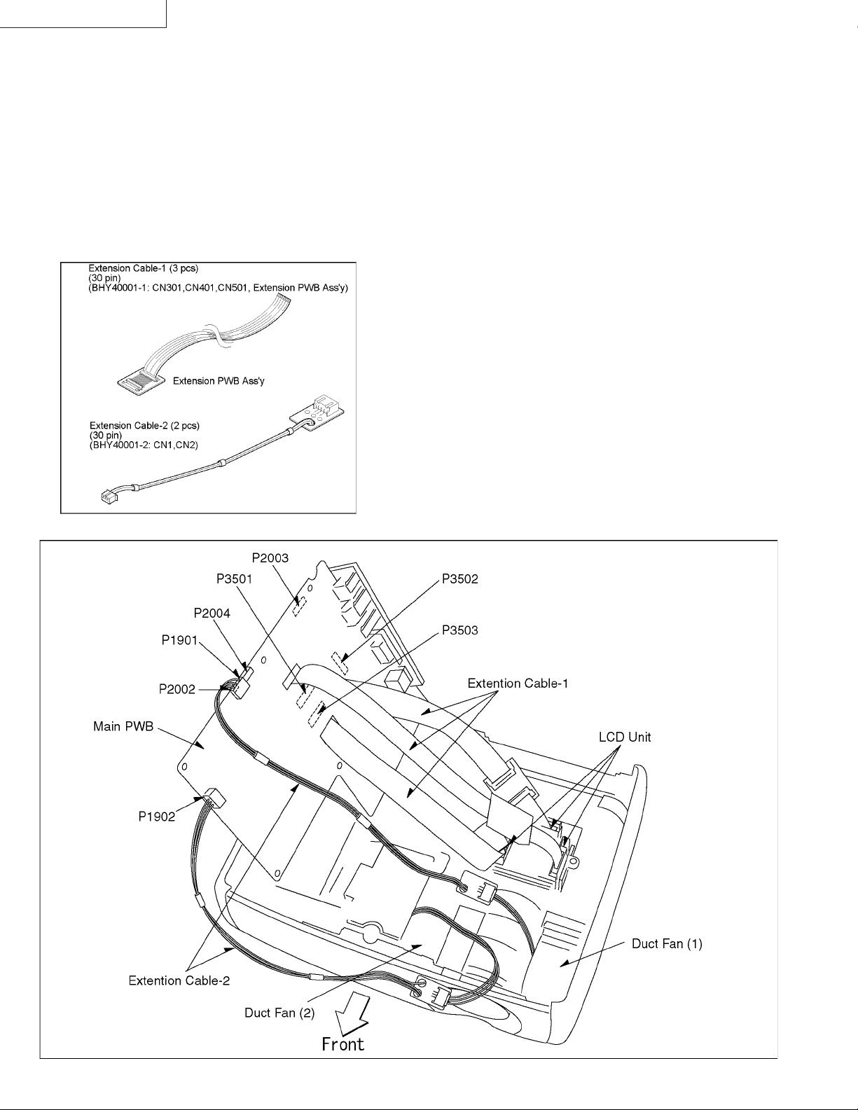
Because of this projector’s structure, service should be
provided by turning this projector over, accordingly the
screens are seen reversely during the service.
The position shown in Fig. 1-1-2 is used for checking, adjusting
and replacing parts.
Extension Cable (Extension cable is the same as the Extension
Cable Kit [BHY40001] of the LX-D300/LX-D350 service jigs.) is
necessary for servicing as shown in Fig. 1-1-1.
*Extension cables may be slightly
different in shape.
Fig. 1-1-1
1. In the order described in the “2.2. Disassemb ly Method of Cabinet
Parts” of “2. Disassembly/Assembly Procedures”, remove the
Bottom Case Unit.
2. Remove the Joint Plate L, R and Ballast Holder as shown in
Fig. 2-2-7.
3. Disconnect connectors P1901, P1902, P2002-P2004 and
P3501-P3503 on the Main PWB as shown in Fig. 2-2-8.
a. Connect Extension Cables as follows:
b. Connect Extension Cable-1 (30 pin) between P3501 on
the Main PWB and the LCD Red Unit.
c. Connect Extension Cable-1 (30 pin) between P3502 on
the Main PWB and the LCD Green Unit.
d. Connect Extension Cable-1 (36 pin) between P3503 on
the Main PWB and the LCD Blue Unit.
e. Connect Extension Cable-2 (3 pin) between P1901 on the
Main PWB and the Duct Fan (1).
4. Connect Extension Cable-2 (3 pin) between P1902 on the Main
PWB and the Duct Fan (2).
5. Carefully place the Main PWB as shown in Fig. 1-1-2.
6. After servicing, remove Extension Cables.
7. Reinstall the Main PWB, and reconnect connectors.
8. Make sure that all wires and leads are placed in their original
position.
1 (PA014)
Fig. 1-1-2
Page 4
LX-P1010ZU/ZE
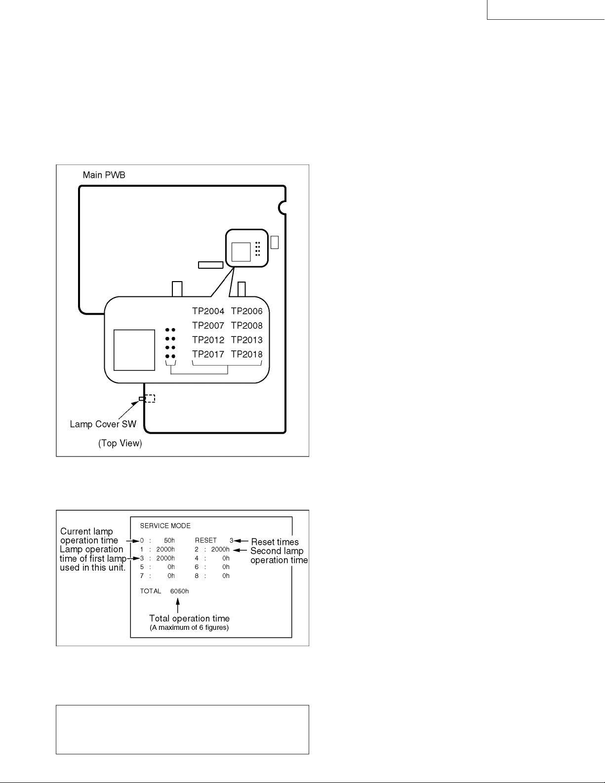
1.2. Ho w to display Lamp operation time
(Service Mode)
1. Remove the BOTTOM CASE UNIT according to the procedures
mentioned in [2.2 DISASSEMBL Y METHOD OF CABINET P AR TS].
2. Under the condition of the Lamp Cover SW “ON”, plug in the
Power Cord.
3. Input a Signal.
4. Connect a jumper wire between TP2007 and TP2008 on Main
PWB for over 5 seconds as shown in Fig. 1-2-1.
1.3. How to initialize EEPROM IC
If EEPROM IC (IC2006) on Main PWB are replaced:
After replacing EEPROM IC (IC2006), be sure to perform each of
following steps in the order presented.
1. Connect a jumper wire between TP2017 and TP2018 on Main
PWB for over 5 seconds to set to factory set mode. Then,
remove the jumper wire.
2. “FACTORY” appears on screen.
3. Connect a jumper wire between TP2017 and TP2018 again
for ov er 5 seconds to initializ e EEPROM IC. Then, remove the
jumper wire.
4. “SELF CHECK” appears on screen.
5. Remove jumper wires and “MEMORY OK” appears on screen.
6. Perform adjustments 3.4.1. through 3.4.8., 3.4.11. and 3.4.12.
7. After completing all adjustments, press the MENU button to
memorize adjustment data in EEPROM IC and release from
the Factory Adjust mode.
Otherwise, adjustment data will be cancelled.
Note:
When initializing EEPROM IC, memory data such as history
of lamp operation time and adjustment data will be reset.
Fig. 1-2-1
5. Lamp operation time will be displayed as shown in Fig. 1-2-2.
(As the set is turned upside down, actually the screen also
looks upside down.)
Fig. 1-2-2
6. Connect a jumper wire between TP2007 and TP2008 for over
5 seconds again or press MENU button on remote control in
order to release from service mode.
Note:
After replacing Main PWB, memory data such as history of lamp
operation time will be reset. How ever, it can be remained by installing
EEPROM IC (IC2006) to replaced Main PWB from original Main PWB.
(PA014) 2
Page 5
LX-P1010ZU/ZE
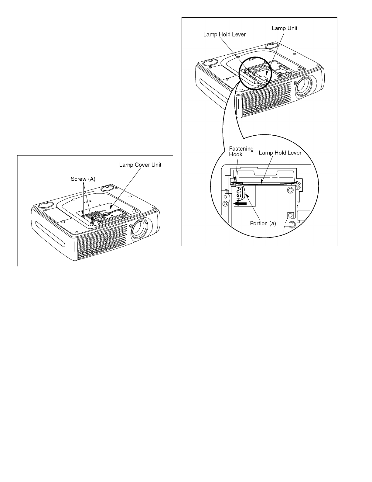
1.4. Lamp replacement procedure
Caution:
Because of possibility of injury, strictly follow the replacement
procedure below.
1. After the cooling fan has stopped, and STANDBY(R) ON(G)
indicator turns solid red, unplug the power cord.
Note:
Please wait more than one hour for lamp replacement.
[ If you need to replace the lamp more urgently ]
The LCD Projector has a forced cooling feature . After the POWER
switch is turned OFF, and sometime dur ing about the first
minute of the normal cooling fan operation, press MENU for 5
seconds. The cooling fan will change to high speed for about
10 minutes. (The “C-d” STATUS CODE will be displayed.)
2. Loosen 2 screws (A) using a screwdriver as sho wn in Fig. 1-4-1.
3. Remove the Lamp Cover Unit.
Fig. 1-4-1
4. Push the portion (a) of the Lamp Hold Lev er to the direction of
the arrow as shown in Fig. 1-4-2 and release the Lamp Hold
Lever from the Fastening Hook.
5. Carefully pull the Lamp Unit.
WARNING:
• The lamp may be hot. Be careful when handling.
CAUTION
• High-pressure lamp may explode if improperly handled.
• Danger of injury due to lamp fragments.
Fig. 1-4-2
6. Install the new Lamp Unit.
CAUTION
• Make sure that the Lamp Hold Lev er is in the original position
as shown in Fig. 1-4-2.
• Properly dispose of old Lamp.
7. Replace 2 screws (A) using a screwdriver as sho wn in Fig. 1-4-1.
8. Plug the power code.
9. Press POWER and INPUT buttons together for about 5 seconds
when lighting up red by POWER LED to reset lamp time.
3 (PA014)
Page 6
LX-P1010ZU/ZE
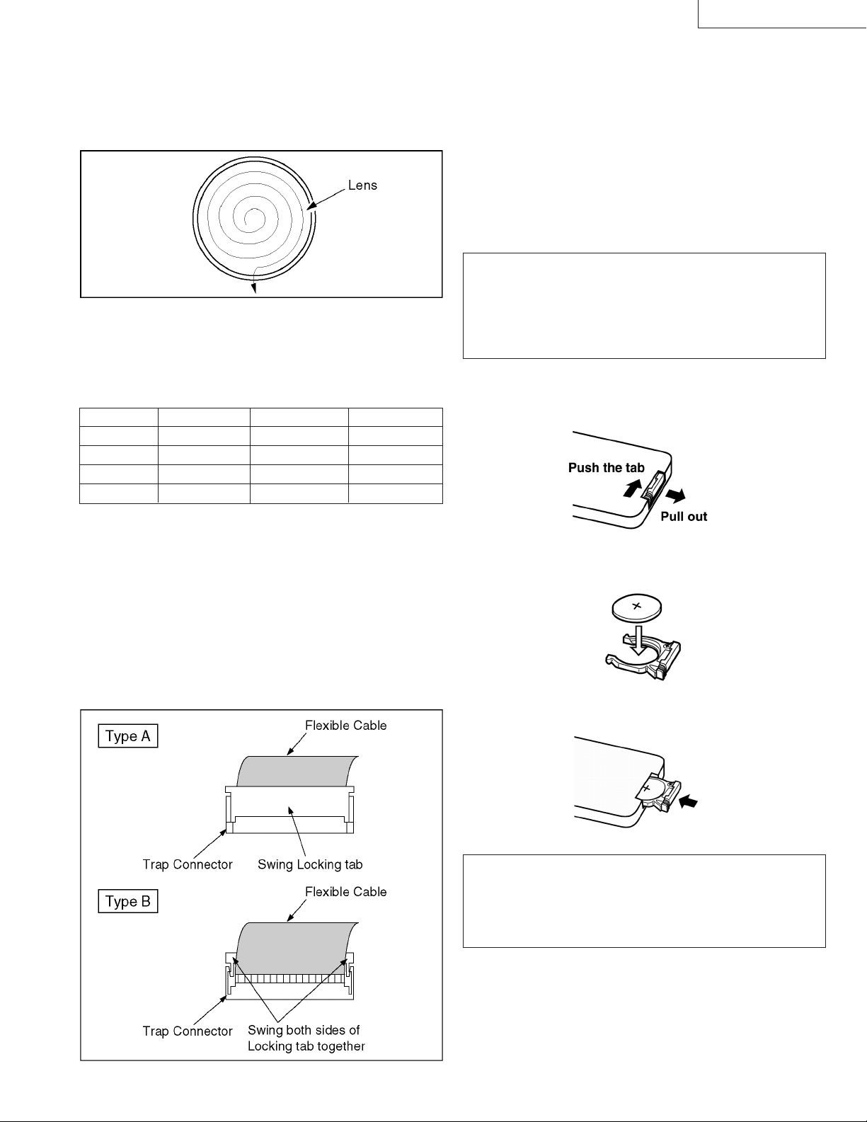
1.5. Cleaning the Projection Lens
Use lens cleaning paper and cleaner available at y our local camera
shop, etc.Dampen the cleaning paper with cleaner and gently wipe
the surface of the lens from the center outward to remove dust as
shown in Fig. 1-5-1.
Note:
Do not use excessive force when cleaning the lens.
Fig. 1-5-1
1.6. Connection of the Flexible Cables
to T rap Connector
Fig No. No. of Pins PWB Type
P3501 30Pin Main PWB A
P3502 30Pin Main PWB B
P3503 30Pin Main PWB A
P2003 18Pin Main PWB B
• Installation
1. Insert the end of the Flexible Cab le into the Trap Connector.
2. Without twisting the Cable, press the Locking Tab in into its
locked positions.
3. Gently and slightly pull up on the Cable to confirm if it is
installed firmly.
1.7. How to replace the lithium battery
7 Inserting the battery
Insert the lithium battery which is supplied with the remote
control unit, making sure that the polarities are correct.
WARNING:
Replace battery with CR2025 only. Use of another battery may present
a risk of fire or explosion.
Caution: Battery may explode if mistreated. Dispose of used battery
promptly. Keep aw ay from children. Do not recharge, disassemble or
dispose of in fire.
1. While pushing the battery holder tab to the r ight, pull out the
battery holder.
(Removal and Installation of Flexible Cable)
• Removal
(Type A)
1. On the T rap Connector, swing the Locking Tab to release the
Trap portion of the Connector. Then pull Flexible Cable out
to remove as shown in Fig. 1-6-1.
(Type B)
1. On the Trap Connector, swing both ends of the Loc king Tab
to release the Trap portion of the Connector. Then pull Flexib le
Cable out to remove as shown in Fig. 1-6-1.
2. Insert the battery into the battery holder so that the + side
is facing upward.
3. Insert the battery holder.
Note:
• Do not drop the remote control unit.
• Keep the remote control unit away from liquids.
• Remove the battery if not using the remote control unit for long
periods.
Fig. 1-6-1
(PA014) 4
Page 7
LX-P1010ZU/ZE
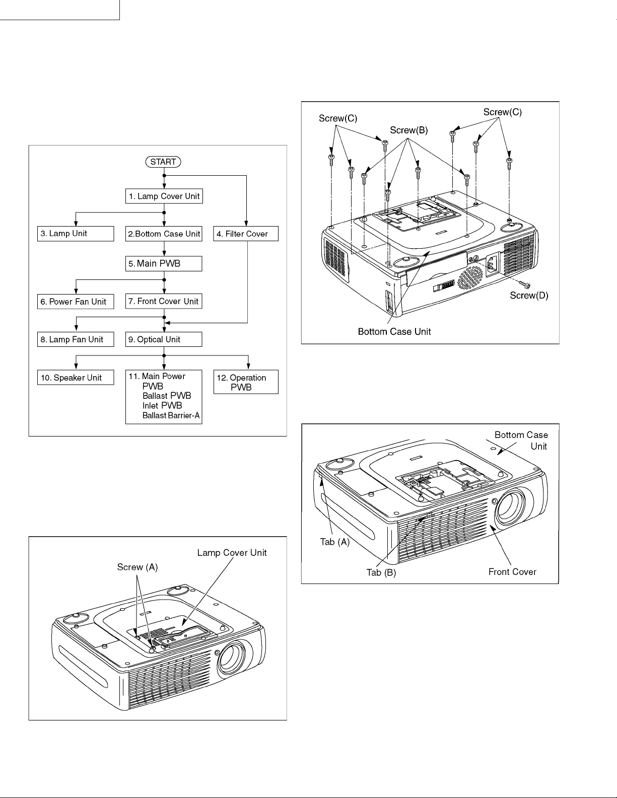
2 DISASSEMBLY/ASSEMBLY PROCEDURES
2.1. DISASSEBLY FLOWCHART OF
CABINET PARTS
This flowchart indicates the disassembly steps of the cabinet parts
and the P.W. Boards. When reassembling, perform the step(s) in
the reverse order.
2.2.2. Removal of the Bottom Case Unit
1. Remove 4 screws (B), 6 screws (C) and a screw (D) as shown
in Fig. 2-2-2.
Fig. 2-2-2
Fig. 2-4-1
2.2. DISASSEMBLY METHOD OF
CABINET PARTS
2.2.1. Removal of the Lamp Cover Unit
1. Loosen 2 screws (A) as shown in Fig. 2-2-1.
2. Carefully pull the Tab (A) side of the Bottom Case Unit as shown
in Fig. 2-2-3.
3. Carefully remove the Bottom Case Unit with paying attention
to the Tab (B).
Fig. 2-2-3
Assembly Note:
When removing the bottom Case Unit, be sure to remove the
Lamp Cover Unit first.
If it is assembled without removing the Lamp Cover Unit, the
Interlock switch of the Main PWB will be damaged. (If it is
damaged, the Projector won’t operate and the indication of it
is “C-0”.)
5 (PA014)
Fig. 2-2-1
Page 8
2.2.3. Removal of the Lamp Unit
1. Push the portion (a) of the Lamp Hold Lev er to the direction of
the arrow as shown in Fig. 2-2-4 and release the Lamp Hold
Lever from the Fastening Hook.
2. Carefully pull the Lamp Unit.
Caution:
Do not touch the Lamp Unit until it is completely cooled off.
LX-P1010ZU/ZE
Fig. 2-2-5
2.2.5. Removal of the Main PWB
1. Remove a screw (E) as shown in Fig. 2-2-6.
Fig. 2-2-4
Assembly Note:
1. Make sure that the Lamp Hold Lever is in the original
position as shown in Fig. 2-2-4.
2. Be extra cautious during operation not to damage the Detect
Switch (Lamp Cover Switch) provided on the Portion (b) of
the Main PWB.
2.2.4. Removal of the Filter Cover
1. Hold the indent on the Filter Cover and pull the Filter Cover
with the Filter as shown in Fig. 2-2-5.
Assembly Note:
Before installing the Optical Unit, be sure to remove the Filter
Cover first. If it is installed without removing the Filter Cover,
the Filter Switch may be damaged.
Fig. 2-2-6
2. Open the Barrier Unit.
3. Remove the Joint Plate R, L and the Ballast Holder as shown
in Fig. 2-2-7.
Fig. 2-2-7
4. Disconnect 13 connectors P1901-P1907, P2002-P2004, P3501P3503 and P4001 on the Main PWB as shown in Fig. 2-2-8.
(PA014) 6
Page 9
LX-P1010ZU/ZE
Assembly Note:
1. Make sure that the Joint Plate R, L and the Ballast Holder
are in their original position as shown in Fig. 2-2-7.
2. Be extra cautious during operation not to damage the Detect
Switch (Lamp Cover Switch) provided on the Portion (a) of
the Main PWB as shown in Fig. 2-2-8.
2.2.7. Removal of the Front Cover
1. Remove 3 screws (F) as shown in Fig. 2-2-10.
2. Carefully pull and remove the portion (a) of the Front cover in
the direction of the arrow with paying attention to the Tab (A).
3. Remove the Front cover with paying attention to the Tab (B).
Fig. 2-2-8
2.2.6.Removal of the Power Fan
1. Carefully pull out the Power Fan with the Fan Piece as shown
in Fig. 2-2-9.
Fig. 2-2-9
Fig. 2-2-10
2.2.8. Removal of the Lamp Fan Unit
1. Remove 3 screws (G) as shown in Fig. 2-2-11.
2. Remove the Lamp Fan Unit with the Front Barrier L and R.
Fig. 2-2-11
Assembly Note:
Installing the Lamp Fan Unit so that the name plate faces to
the side of the Front Cover.
Assembly Note:
1. Installing the Power Fan so that the name plate faces in.
2. Make sure that the connector cable of the power Fan is in
the original position as shown in Fig. 2-2-9.
7 (PA014)
Page 10
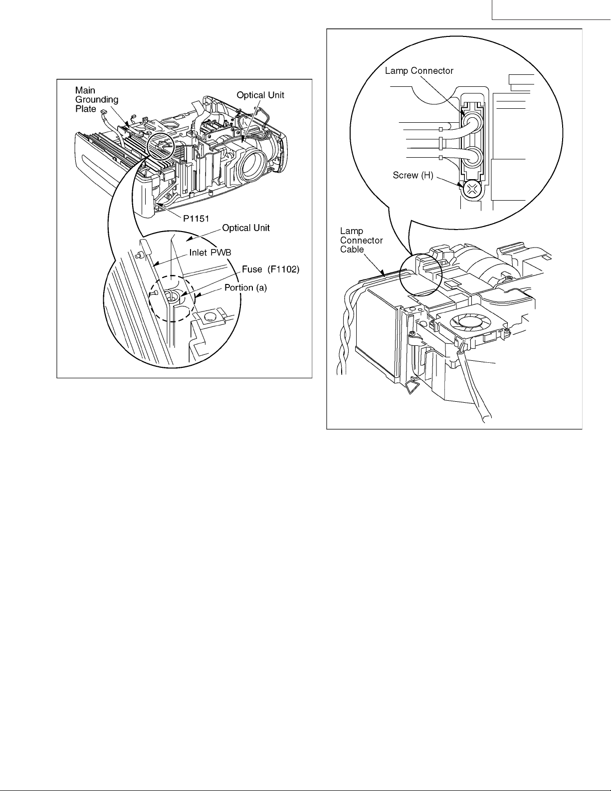
2.2.9. Removal of the Optical Unit
1. Remove the Main Grounding Plate as shown in Fig. 2-2-12.
2. Carefully pull out the Optical Unit.
LX-P1010ZU/ZE
Fig. 2-2-12
3. Remove a screw (H) as shown in Fig. 2-2-13 and remove the
Lamp Connector.
Fig. 2-2-13
Assembly Note:
1. Twist the Lamp Connector cab le 3 times on the right and insert
in the original position as shown in Fig. 2-2-13.
2. When installing the Lamp Connector, be careful of the direction
of the insertion as shown in Fig. 2-2-13.
3. Before installing the Optical Unit, be sure to remove the Filter
Cover first. If it is installed without removing the Filter Cover,
the Filter Switch may be damaged.
4. When installing the Optical Unit, make sure that the position of
portion (a) is at the fuse (F1102) and pay attention not to nip
the connector cable of P1151 under the Optical Unit as shown
in Fig. 2-2-12.
(PA014) 8
Page 11
LX-P1010ZU/ZE
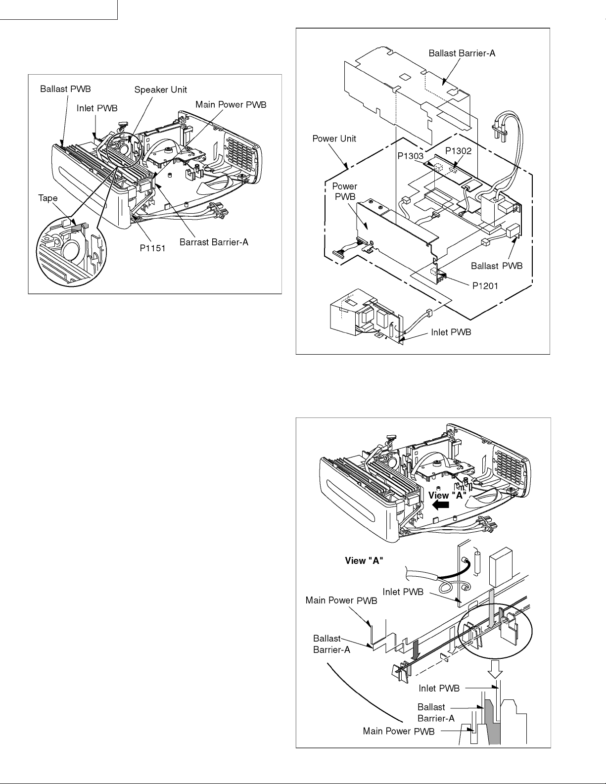
2.2.10. Removal of the Speaker Unit
1. Detach the tape and carefully pull out the Speaker Unit as
shown in Fig. 2-2-13.
Fig. 2-2-14
Assembly Note:
After the installation of the speaker, put on the tape in the
original position.
2.2.11. Removal of the Main Power PWB the
Ballast PWB, the Inlet PWB and the
Ballast Barrier-A
1.
Carefully pull out the Main Power PWB, the Ballast PWB and the
Inlet PWB along with the Ballast Barrier-A as shown in Fig. 2-2-14.
2. Disconnect 3 connectors P1151, P1201, P1302 and P1303 as
shown in Fig. 2-2-15.
Fig. 2-2-15
Assembly Note:
Make sure that the Main Power PWB, the Ballast PWB the
Inlet PWB and the Ballast Barrier-A are in the original position
as shown in Fig. 2-2-16.
9 (PA014)
Fig. 2-2-16
Page 12
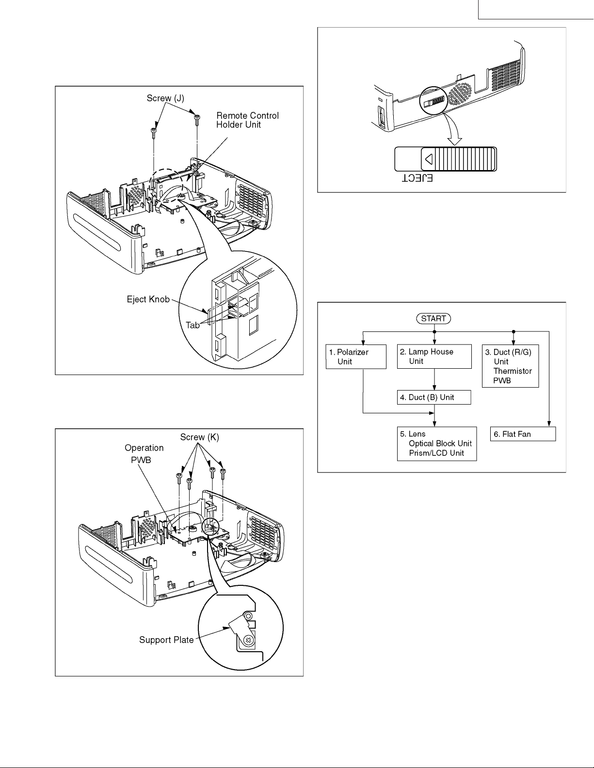
2.2.12. Removal of the Operation PWB
1. Remove 2 screws (J) as shown in Fig. 2-2-17.
2. releasing 2 tabs, remove the Eject Knob.
3. Remove the Remote Control Holder Unit.
LX-P1010ZU/ZE
Fig. 2-2-19
2.3. DISASSEBLY FLOWCHART OF
OPTICAL UNIT
This flowchart indicates the disassembly steps of the main parts
of Optical Unit. When reassembling, perform the step(s) in the
reverse order.
Fig. 2-2-17
4. Remove 4 screw (K) and the Support Plate as shown in Fig. 2-2-18.
5. Carefully pull out the Operation PWB
Fig. 2-3-1
Fig. 2-2-18
Assembly Note:
When installing the Eject Knob, be careful of the direction of
the insertion as shown in Fig. 2-2-19.
(PA014) 10
Page 13
LX-P1010ZU/ZE
2.4. DISASSEMBLY METHOD OF
OPTICAL UNIT
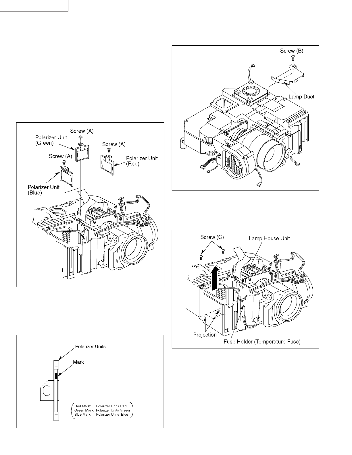
2.4.1. Removal of the Polarizer Units
1. Remove 3 screws (A) to remove the Polarizer Red Unit, the
Polarizer Green unit and the Polarizer Blue Unit as shown in
Fig. 2-4-1.
Note:
1. Take extreme care not to damage the Polarizer Units, when
servicing.
2. Make sure that no dust gets on the Polarizer Units. Either b lo w
it away with air or clean the P olarizing Units with cleaning paper
moistened with lens cleaner if necessary.
2.4.2. Removal of the Lamp House Unit
1. Remove a screw (B) as shown in Fig. 2-4-3.
2. Remove the Lamp Duct.
Fig. 2-4-1
1. After replacing the Polarizer Unit, adjustment is necessary
(Refer to 3.1. Initial Guide Line).
2. Make sure of the Mark color to distinguish the Polarizer Unit
(Red, Green, Blue) as shown in Fig. 2-4-2.
Fig. 2-4-3
3. Remove 2 screws (C) as shown in Fig. 2-4-4.
4. Remove the Fuse Holder.
5. Lift the Lamp House Unit up to release 2 projections.
Fig. 2-4-4
11 (PA014)
Assembly Note:
After Installing the Lamp House Unit, install the Temperature Fuse
and Fuse Holder in the original position as shown in Fig. 2-4-4.
Fig. 2-4-2
Page 14
LX-P1010ZU/ZE LX-P1010ZU/ZE
2.4.3. Removal of the Duct Blue Unit
1. Remove 2 screws (D) as shown in Fig. 2-4-5.
2. Detach 2 tapes which is fixing the cable of the Temperature Fuse.
3. Remove the Duct Blue Unit carefully.
Fig. 2-4-5
2.4.4. Remo val of the Duct Red/Green Unit and
Thermistor PWB
1. Remove 3 screws (E) as shown in Fig. 2-4-6.
2. Detach a tape which is fixing the cable of the Temperature Fuse.
3. Remove the Duct Red/Green Unit carefully.
4. Remove a screw (F) and the Thermistor PWB.
Fig. 2-4-6
Assembly Note:
After Installing the Duct Red/Green Unit, fix the cable of the
Temperature Fuse in the original position as shown in Fig. 2-4-6.
2.2.5. Remo val of the Lens, Optical Block Unit
and Prism/LCD Unit
1. Remove 4 screws (G) as shown in Fig. 2-4-7.
2. Remove the Prism/LCD Unit with the Lens carefully.
3. Remove 4 screws (H) and separate the Lens from the Prism/
LCD Unit.
Fig. 2-4-7
2.4.6. Removal of the Flat Fan
1. Remove a screw (I) as shown in Fig. 2-4-8.
Fig. 2-4-8
3 ADJUSTMENT PROCEDURES
The attached card remote controller becomes necessary to
adjust the following.
Keep the card remote controller also together with the pr oduct
to be repaired.
3.1. INITIAL GUIDE LINE
The tables below show adjustments which will be necessary
according to the unit parts and optical parts to be replaced.
Make sure to perform these adjustments shown below as
necessary.
If you replace: Adjustments
MAIN PWB (3-4-1), 3-4-2, 3-4-3, 3-4-4, 3-4-5, 3-4-6,
3-4-7, 3-4-8
OPTICAL BLOCK UNIT 3-4-9
POLARIZER UNIT 3-4-10
List of necessary adjustments
3-4-1 LCD VOL TEGE ADJUSTMENT
3-4-2 RGB INPUT LEVEL ADJUSTMENT
3-4-3 VIDEO INPUT LEVEL ADJUSTMENT
3-4-4 COMPONENT VIDEO COLOR ADJUSTMENT
3-4-5 LCD COMMON ADJUSTMENT
3-4-6 WHITE LEVEL ADJUSTMENT
3-4-7 BLACK LEVEL ADJUSTMENT
3-4-8 WHITE BALANCE ADJUSTMENT
3-4-9 FULL MIRROR ADJUSTMENT
3-4-10 POLARIZER ADJUSTMENT
Notes:
1. ( ) : Items which need the confirmation when replaced.
2. When any adjustments 3.4.1. through 3.4.4. are necessary,
please refer to “Preparation for Adjustments 5.4.1. through
3.4.4.”.
3. When any adjustments 3.4.5. through 3.4.8., 3.4.11. and
3.4.12. are necessary, please refer to “Preparation for
Adjustments 3.4.5. through 3.4.8., 3.4.11. and 3.4.12.”.
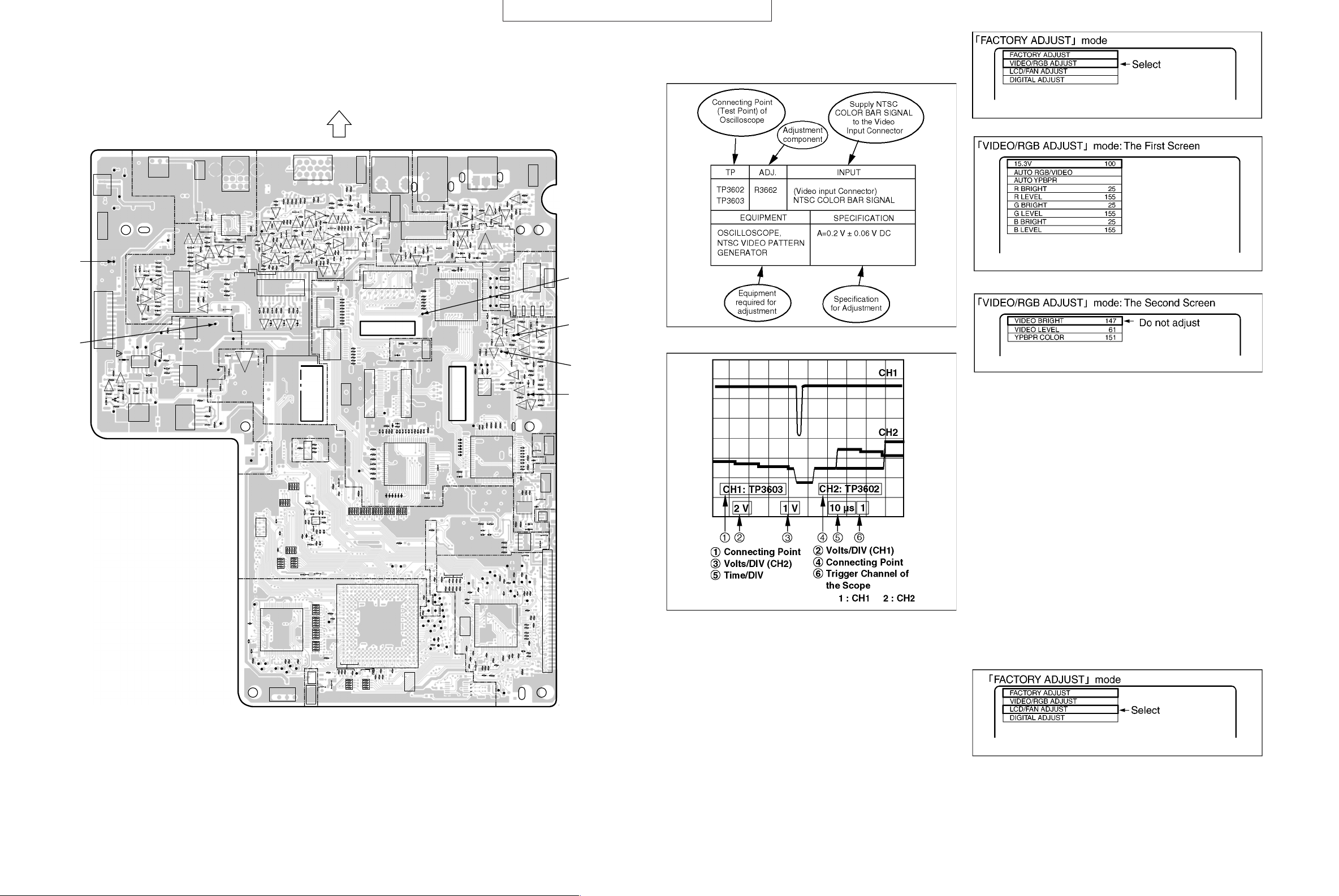
3.1.1. The “F ACT ORY ADJUST” mode
All Electrical Adjustments are performed on the “FACTORY
ADJUST” mode which is used remote control unit instead of
variable resistor to control the adjustment value.
1. Connect a jumper wire between TP2017 and TP2018 on Main
PWB for over 5 seconds to enter the “FACTORY ADJUST”
mode.
2. Press the POWER button on remote control once.
3. While "Please press POWER button again to power off." is
displayed, press the MENU button.
4. Press 5 or ∞ button on remote control to select and press the
ENTER button to set the item to be adjusted.
Note:
Do not adjust all items in “DIGITAL ADJUST”, and VIDEO BRIGHT
in “VIDEO/RGB ADJUST”, and GAMMA R, G, B in “LCD/FAN
ADJUST”.
13 (PA014)(PA014) 12
Fig. 3-1-1
Fig. 3-1-2
Fig. 3-1-3
3.2. TEST EQUIPMENT
T o do all of these adjustments , the f ollowing equipment is required.
1. Dual-Trace Oscilloscope
Voltage Range : 0.001 - 50 V/Div.
Frequency Range : DC - 50 MHz
Probes : 10:1, 1:1
2. NTSC Video Pattern Generator
4. (+) Screwdriver and (-) Screwdriver
5. Standard Screen
6. DVM (Digital Volt Meter)
7. Programmable Video Signal Generator
8. Test pattern signal (Service Engineerring Section,System
Engineerring Dept. JVC Projection & System Network
Business Unit.(AVS)Consult with (AVS).)
9. Luminance Color Meter/Chroma Meter/Chroma Meter and
Data Processor
(Recommended meter:
• Luminance Color Meter, BM-7 made by TOPCON
• Chroma Meter, CL-200 made by MINOLTA
• Chroma Meter and Data Processor, CL-100,DP-100,
made by MINOLTA)
10.Jumper wire
Page 15
LX-P1010ZU/ZE LX-P1010ZU/ZE
TEST POINT
MAIN PWB
TP4001
TP4002
P1906
12
TP1963
TP1964
POWER/AUDIO
SECTION
P1905
R1904
Q1901
C
E
B
R1979
D1961
TP1907
112
PR1904
R1905
Q1902
C
E
B
R1903
R1977
D1967
R1978
R1976
TP1962
TP1907
TP1904
C3026
C3027
C3024
R3041
TP3002
C3025
R3040
R3043
R3042
Q3012
Q3014
E
B
E
C
B
C
C3009
BE
R3046R3044
C
Q3013
R3045
BE
C
C3028
R3049
E
B
R3048
Q3016
C
C3017
R3033
R3050
TP1912
TP1903
TP1902
Q1903
E
1
4
C
B
IC1903
TP1911
R1907
C1907
8
5
R1912
C1903
R1970
R1969
R1966
C1964
R1968
1
5
TP1914
IC1962
(FOILSIDE)
321
U2001
TP1915
C3012
C3013
R3028
R3031
R3032
IC3003
Q3015
2011
R1919
TP3001
R1906
1515
Q3010
C
BCE
IC1901
IC1904
IC1961
3.3. HOW TO READ THE ADJUSTMENT
PROCEDURES
LENS SIDE
Fig. 3-4-1
RGB/VIDEO
SECTION
11
DIGITAL
SECTION
C2056
L2008
C2049
C2055
Q3007
R3026
C3011
E
B
Q3005
R3027
R3029
C
Q3008 Q3009
E
B
BE
C
Q3006
R3030
BE
C
C3020
R3039
R3038
C3019
R3036
R3034
R3035
R3037
Q3011
E
C
110
B
TP1904
TP1905
R2325
R1965
R1964
R1963
15
C1962
R1961
5
8
110
R2044
E
B
C
R3025 R3022
L3003
C2014
R2326
TP1913
2
7
IC2009
E
C
B
TP1901
R2327
JK2003
63
41
20 11
R2032
R2048
R5071
Q3004
R3024
R5070
R3023
R3021
R5081
R5079
R5040
Q5033
R5080
C5038
C5042
R5074
Q5029
R5075
R5073
Q5022
R5051
Q5031
Q5030
C5040
R5082
Q5035
Q5036
R5083
R5086
R5088
R5084 R5087
R5085
IC2005
TP1961
C2041
C2044
C2059
R2033
Q5034
TP5001
E
R5072
BE
12 13
C5034
Q5037
C2025
TP1910
AD/DA/TG
SECTION
100
TP2005
125
26
TP2009
TP2011
15
5
R3013
R3014
R3017
R3018
Q5032
R5076
R5077
E
B
C5039
C
R5078
C
E
B
E
B
E
B
C
C
B
C
C
C
C
E
B
BE
E
B
C
E
B
C
E
C
C
B
E
B
IC5002
C5033
R5068
R5066
R5069
R5043
C5032
R5041
R5064
E
BCE
BCE
B
C
C5036
C5035
Q5012
Q5011
Q5010
R5034
R5036
R5063
Q5015
Q5025
R5037 R5061 R5047
R5035
R5027
R5067
Q5014
R5039
C5019
C5021
Q5026
Q5020
Q5021
R5050
R5029
Q5018
C5020
Q5019
R5046
R5048
R5045
R5044
R5065
R5042
R5049
Q5017
1
R2065
R2096
C2067
C2068
C2069
R2097
R2098
R2099
IC2008
R2046
R2045
TP2010
TP2019
TP2020
TP2015
TP2014
TP2016
U2002
123
10
R3019
B
1
24
C5037
L5002
Q5027
R5030
R2095
C2005
R2051
C2030
76
50
R2056
R3020
BE
C
B
C
B
C
E
Q5008
C5011
Q5028
R5031
Q5009
IO/ROM
SECTION
L2009
C2020
R2005
C2010
C2017
R2086
C2028
C2007
5175
SECTION
C
E
E
R5032
C2156
C2006
R2091
R2092
R2093 R2094
SW2002
6
1
R3016
R3015
R3005
Q5013
Q5016
R3004
BE
C
C
BE
E
B
C
BE
C
B
E
B
C
115
IC3508
1
15
R5028
R5060
R2060
R2061
R2062
C2018
C2016
Q2016
C2155
R2087
C2012
R2006
C2011
C2013
R2007
L2004
R2114
R2267
R2051
R2113
R2130
C2080
L2016
IO/ROM
JK3001
R3003
R3008
R5023
C
E
BCE
R5024
C
BE
E
E
B
C
30 16
IC3507
C2168
R2255
R2324
1
C
C3594
R3002
R3007
R3009
B
R5025
R5026
C5015
R3601
R3602
R3603
R3604
R3605
R3606
R3607
R3608
R3609
30 16
LCD DRIVE
SECTION
R2128
R2123
R2137
JK4001
1
2
3
R3011R3001
R3010
Q5007
C5052 R5053
R5057
R5058
C5016
E
1
IC5001
R5055
R3594
R3595
R3596
R3597
R3598
R3599
R3584
R3583
R3582
C3573
TP3506
R3581
R3580
R3579
R2243
R2322
R2133
R2164
TP2027
R2140
R3012
R5056
BE
B
C
R5054
L5003
1
P3503
R2167
C
Q5023
Q5024
L3001
130
R3588
C3578
C3576
21 40
IC2012
R2165
R2172
R2173
POWER/AUDIO
SECTION
C3004
56
1
L4001
C4007
R4017
R4012
Q4003
E
B
C4005
E
C
30
P3502
R3569
R3568
R3567
R3566
R3565
R3564
TP3505
R2002
R2001
C2002
1
P3501
TP3510
30
C3577
C3579
R3590
R3585
C3585
C3584
C3583
C3582
C3581
C3580
R3586
R3587
R3589
20
IC3506
41
C3571
C3570
C3569
C3568
C3567
C3566
R2247 R2248R2254R2253R2245
R2258
TP2002
TP2003
R2169
DIGITAL
SECTION
JK5002
JK5002
R2302
TP2075
TP2069
R5021
R5018
R5011
R5013
R5019
R5020
Q5006
BE
29
R5022
R5062
C5008
R4026
E
B
Q4007
C
R4024
28
C
R4030
C4009
B
Q4008
R4027
C4014
R4021
D4008
C3563
R3577
C3553
R3570
20
21 40
IC3505
41
IO/ROM
R3591
C3520
C3521
C3522
C3523
C3524
C3525
C3572
R3548
C3519
6180
C3565
R3578
R2025
R2077 R2076
R2079 R2078
R2081 R2080
R2083 R2082
R2084
R2085
R2183
TP2073
TP2023
TP2067
R2122
TP2070
R2109
TP2068
TP2024
TP2025
TP2062
TP2057
SECTION
TP2074
TP2061
TP2063
TP2060
TP2066
R2266
R2116
TP2050
TP2052
TP2054
2
IC4001
R4019
C4013
Q4005
B
C
SECTION
C3587
R3592
C3586
1
60
R2058
TP2056
R2182
2
C5004
R5012
C
R4025
E
R4036
41 60
TP2040
R2284
IO/ROM
R2328
R2135
R5016
E
C
B
Q5004
D4009
C
R4031
B
R4035
D4006
1
C3502
6180
L3501
60
R3512
R3510
TP3508
TP3507
R3541
R3540
14
IC3503
TP3504
R3550
R3549
40
61
R2200
C2131
C2124
TP2028
R2138
75
76 100
1
R2313
R2125
R2124
C2091
R2152
115
364
Q5003
C5002
C
E
B
R5001
C
Q4010
E
TP2018TP2013TP2008TP2006
TP2017TP2012TP2007TP2004
R3502
R3504
R3511
E
C
TP3509
R3542
85
R3553
R3552
R3551
IC3504
C2133
C2125
R2293
R2295
R2294
TP2032
TP2029
TP2031
R2261
R2126
R2034
R2195
JK5001
R5002
E
B
FL2006
FL2015
FL2007
FL2016
FL2008
R3501
E
C
B
C
B
B
Q3506
R3538
R3539
R3554
R2003
R2136
TP2047
E
Q5001
Q3504
E
TP3502
R2141
R5014
B
Q5002
C
C
D3502
Q3507
R3507
E
R3523
R3519
21
80
TP2045
R2262
C2094
TP2083
IC2011
R2142
R2088
TP2048
Q5005
E
C
B
R5004
C5001
R5005
R5003
118
FL2013
Q3501
R3503
E
B
BE
C
TP3501
C
R3509
B
C
Q3509
C
R3524
D3504
R3515
Q3515
E
C
B
D3506
E
C
B
C
C3534
C3535
C3536
C3537
C3538
C3539
C3541
R3561
C2004
120
R2287
4
5
R2017
R2018
14
L2017
R2166
R2168
TP2042
TP2084
R2161
C2095
51
R2265
R2154
R2155
R2139
R2157
R2158
2650
25
C2098
R2316
R2159
R2297
SECTION
R5017
R5015
P2003
FL2012
Q3502
E
B
Q3510Q3505
E
B
R3521
D3505
Q3512
TP3503
E
E
C
B
Q3514
R3562R3555
R2285
R2286
1
IC2006
8
85
IC2019
TP2041
R2171
TP2044
TP2043
R2162
R2163
TP2085
R2318
R2156
R2151
R2312
RGB/VIDEO
FL2011
D3501
R3506
BE
R3526
R3525
R3528
R3529
B
Q3511
L2022
C3540
L2002
C2021
12
D2001
D2002
L2024
R2317
R2153
SECTION
FL2009
R3505
Q3503
C
R3508
R3516
C3503
R3527
C3506
C3507
R3530
C3505
R3518
R3520
R3517
SECTION
DIGITAL
SECTION
P2002
C2153
60
P2001
2
IO/ROM
AD/DA/TG
TP3505
TP3501
TP3502
TP3503
* Test Pattern Signal
Software Select Menu
is also included
(installed).
Fig. 3-3-1
Fig. 3-3-2
3.4. ADJUSTMENT PROCEDURES
Preparation for Adjustments 3.4.1. through 3.4.4.
1. Connect a jumper wire between TP2017 and TP2018 on Main
Fig. 3-4-2
Fig. 3-4-3
5. After completing adjustments 3.4.1. through 3.4.4., press the
“MENU” button to release from “VIDEO/RGB ADJUST” mode.
(Adjustment data is memorized in EEPROM IC (IC2006) by
pressing “MENU” button.) Otherwise, adjustment data 3.4.1.
through 3.4.4. will be cancelled.
Preparation for Adjustments 3.4.5. through 3.4.8., 3.4.11. and
3.4.12.
1. Connect a jumper wire between TP2017 and TP2018 on Main
PWB for over 5 seconds to set to the “FACTORY ADJUST”
mode.
2. Press the POWER button on remote control once.
3. While “Please press POWER button again to power off.” is
displayed, press the MENU button.
4. Press 5 or ∞ button on remote control to select “LCD/FAN
ADJUST” mode, and press ENTER buttonto set to “LCD/FAN
ADJUST” mode.
PWB for over 5 seconds to set to the “FACTORY ADJUST”
mode.
2. Press the POWER button on remote control once.
3. While “Please press POWER button again to power off.” is
displayed, press the MENU on remote control button.
Fig. 3-4-4
4. Press 5 or ∞ button to select “VIDEO/RGB ADJUST” mode,
and press ENTER button to set to “VIDEO/RGB ADJUST”
mode.
15 (PA014)(PA014) 14
Page 16

LX-P1010ZU/ZE
Fig. 3-4-5
Fig. 3-4-6
5. After completing adjustments 3.4.5. through 3.4.8., 3.4.11. and
3.4.12., press the “MENU” button to release from “LCD/FAN
ADJUST” mode. (Adjustment data is memorized in EEPROM
IC (IC2006) by pressing “MENU” button.) Otherwise, adjustment
data 3.4.5. through 3.4.8., 3.4.11. and 3.4.12. will be cancelled.
3.4.1. LCD VOLTAGE ADJUSTMENT
(“15.3V”ADUSTMENT)
Purpose:
To set the standard voltage for LCD panel.
Symptom of Misadjustment:
LCD panel may be damaged.
TP
ADJ. INPUT
TP
TP3501
TP3502
TP3503
OSCILLOSCOPE
TEST PATTERN SIGNAL
Note:
TP3501, TP3502, TP3503: Main PWB
1. Supply Gray Scale Pattern Signal (3 scales).
2. Connect the oscilloscope to TP3501.
3. Press 5 or ∞ button on remote control to select “R BRIGHT”.
4. Press 2 or 3 button so that Black lev el becomes the same as
OSD(On Screen Display) Black level.
5. Select “R LEVEL”, and press 2 or 3 button so that White le vel
becomes the same as OSD White level.
6. Connect the oscilloscope to TP3502.
7. Press 5 or ∞ button on remote control to select “G BRIGHT”.
8. Press 2 or 3 button so that Black lev el becomes the same as
OSD Black level.
9. Select “G LEVEL”, and press 2 or 3 button so that White le v el
becomes the same as OSD White level.
10.Connect the oscilloscope to TP3503.
11.Press 5 or ∞ button on remote control to select “B BRIGHT”.
12.Press 2 or 3 button so that Black level becomes the same as
OSD Black level.
13.Select “B LEVEL”, and press 2 or 3 button so that White level
becomes the same as OSD White level.
ADJ.
EQUIPMENT SPECIFICATION
INPUT / Test Pattern signal softwear menu
(RGB Input Connector)
GRAYSCALEPATTERN
(3 SCALE:
RightClickmenu=6 Bar=4 3Division
Refer to Description below
)
TP1904
TP1907 (GND)
EQUIPMENT SPECIFICATION
DVM
(DIGITAL VOLT METER)
Note:
TP1904, TP1907: MAIN PWB
1. Connect the DVM (Digital Volt Meter) to TP1904.
2. Press button on the remote control to select “15.3V”.
3. Press 2 or 3 button so that the voltage shown in the displa y of
DVM is 15.3 V ± 0.05 V DC.
15.3V ± 0.05 V DC
3.4.2. RGB INPUT LEVEL ADJUSTMENT
(“BRIGHT”,“LEVEL”ADUSTMENT)
Purpose:
To set the optimum signal level.
Symptom of Misadjustment:
The picture will be too light or too dark.
Fig. 3-4-7
(PA014)16
Page 17

LX-P1010ZU/ZE
3.4.3. VIDEO INPUT ADJUSTMENT
Purpose:
To set the optimum signal level.
Symptom of Misadjustment:
The picture will be too light or too dark.
TP
TP3502
OSCILLOSCOPE
NTSC VIDEO PATTERN
GENERATOR
Note:
TP3502: Main PWB
1. Supply Gray Scale Pattern Signal (3 scales).
2. Connect the oscilloscope to TP3502.
3. Press 5 or ∞ or MENU button on remote control to select
“VIDEO LEVEL”.
4. Press 2 or 3 button so that the white level becomes the same
as OSD white level.
ADJ.
EQUIPMENT SPECIFICATION
INPUT / Test Pattern signal softwear menu
(VIDEO Input Connector)
GRAYSCALEPATTERN
(3 SCALE=RightClickmenu=6 Bar=4 3Division)
Refer to Description below
TP
TP3503
EQUIPMENT SPECIFICATION
OSCILLOSCOPE
PROGRAMMABLE VIDEO
SIGNAL GENERATOR
Note:
TP3503: Main PWB
1. Supply Component Video 480P or 480i Blue 100 % Raster Signal.
(Refer to “System Configuration Example ” of “INSTRUCTION
BOOK”)
2. Connect the oscilloscope to TP3503.
3. Press 5 or ∞ button on remote control to select “YPBPR
COLOR”.
4. Press 2 or 3 button so that the Blue level becomes the same
as OSD White level.
ADJ.
INPUT /
Test Pattern signal softwear menu
(RGB Input Connector)
COMPONENTVIDEO
(480Por480iBLUE100%
RASTERSIGNAL
(SETUP:YP
Refer to Description below
BPR
)
Fig. 3-4-8
3.4.4.COMPONENT VIDEO COLOR
Purpose:
Symptom of Misadjustment:
17 (PA014)
ADJUSTMENT
(“YPBPR COLOR”ADUSTMENT)
To set the optimum signal level.
The picture will be too light or too dark.
Fig. 3-4-9
Note:
After completing adjustments, press the “MENU” button to
release from “VIDEO/RGB ADJUST” mode. (Adjustment data
is memorized in EEPROM IC (IC2006) by pressing “MENU”
button.)Otherwise, adjustment data 3.4.1. through 3.4.4. will
be cancelled.
3.4.5. LCD COMMON ADJUSTMENT
Purpose:
Symptom of Misadjustment:
(“VCOM”ADUSTMENT)
To set the optimum LCD common voltage.
The picture will be bluish or reddish.
Page 18

LX-P1010ZU/ZE
TP
TEST PATTERN SIGNAL
Note:
This adjustment should be done in a darkroom.
1. Supply 70 % Red Horizontal Signal and project on the screen.
2. Press 5 or ∞ button on remote control to select “VCOM R”.
3. Press 2 or 3 button so that the flicker on the whole screen
becomes minimal.
4. Supply 70 % Green Horizontal Signal and project on the screen.
5. Press 5 or ∞ button on remote control to select “VCOM G”.
6. Press 2 or 3 button so that the flicker on the whole screen
becomes minimal.
7. Supply 70 % Blue Horizontal Signal and project on the screen.
8. Press 5 or ∞ button remote control to select “VCOM B”.
9. Press 2 or 3 button so that the flicker on the whole screen
becomes minimal.
Note:
When the flicker is hard to see in the screen in step 1, 4, 7,
press 5 or ∞ button on remote control to select “BLACK
LEVEL”, and press 2 or 3 button so that it appears.
However, be sure to return “BLACK LEVEL” to previous
value after LCD COMMON adjustment.
ADJ.
EQUIPMENT SPECIFICATION
INPUT / Test Pattern signal softwear menu
(RGB Input Connector)
70 % Red Horizontal Siganal
70 % Green Horizontal Siganal
70 % Blue Horizontal Siganal
(Right Click menu=3 Phase=2 Horizontal=
2 Red 70% / 3 Green 70% / 4 Blue 70%)
Refer to Description below
3.4.6. WHITE LEVEL ADJUSTMENT
(“WHITE LEVEL”ADUSTMENT)
Purpose:
To set the optimum signal level.
Symptom of Misadjustment:
The picture will be too light or too dark.
TP
TP3505
ADJ.
INPUT / Test Pattern signal softwear menu
(RGB Input Connector)
GRAYSCALEPATTERNSIGNAL
(3 SCALE:
RightClickmenu=6 Bar=4 3Division
)
1. Supply Gray Scale Pattern Signal (3 scales).
2. Connect the oscilloscope to TP3505.
3. Press 5 or ∞ button on remote control to select “WHITE
LEVEL”.
4. Press 2 or 3 button so that level A becomes 3.7 V ± 0.05 V [p-p].
*When vertical side of the setting is in reversal, the pattern on the screen alsoappearsinreversal.
Fig. 3-4-10
Fig. 3-4-11
3.4.7. BLACK LEVEL ADJUSTMENT
Purpose:
Symptom of Misadjustment:
(“BLACK LEVEL”ADUSTMENT)
To set the optimum signal level.
The picture will be too light or too dark.
TP
TEST PATTERN SIGNAL
ADJ.
INPUT / Test Pattern signal softwear menu
(RGB Input Connector)
GREEN LEVEL ADJUSTMENT SIGNAL
(Right Click menu=4 Level=3 Green Level)
EQUIPMENT SPECIFICATION
Refer to Description below
EQUIPMENT SPECIFICATION
OSCILLOSCOPE
TEST PATTERN SIGNAL
Note:
TP3505: Main PWB
A=3.7 V ± 0.05 V [p-p]
Note:
This adjustment should be done in a darkroom.
1. Supply Green Level Adjustment Signal and project on the
screen.
2. Press 5 or ∞ button on remote control to select “BLACK
LEVEL”.
3. Press 2 or 3 button so that Portion (B) are invisible and P ortion
(A) are visible on the screen.
(PA014) 18
Page 19

LX-P1010ZU/ZE
3.4.8.2. METHOD 2
*When vertical side of the setting is in reversal, the pattern on the screen alsoappearsinreversal.
Fig. 3-4-12
3.4.8. WHITE BALANCE ADJUSTMENT
(“CUT OFF”ADUSTMENT)
Purpose:
To set the standard white level for each color temperature.
Symptom of Misadjustment:
White will become bluish or reddish.
This adjustment should be done in a darkroom.
5.4.8.1. METHOD 1
TP
NTSC VIDEO PATTERN
GENERATOR
Note:
This adjustment should be done in a darkroom.
1. Supply Gray Scale Pattern Signal (10 scales) and Project on
the screen.
2. Press 5 or ∞ button on remote control to select “CUTOFF R”
or “CUTOFF B”.
3. Press 2 or 3 button to adjust “CUT OFF R” or “CUTOFF B” so
that the area around 4rd and 6th scale (A) becomes pure gray
with no red or blue tint.
ADJ. INPUT
(VIDEO Input Connector)
GRAY SCALE PATTERN SIGNAL
(10 scales)
EQUIPMENT SPECIFICATION
Refer to Description below
TP
ADJ.
INPUT / Test Pattern signal softwear menu
(RGB Input Connector)
50 % WHITE(GRAY)
ADJUSTMENT SIGNAL
(Right Click menu=1 Coror=9 Gray)
EQUIPMENT SPECIFICATION
TEST PATTERN SIGNAL
LUMINANCE COLOR METER,
CHROMA METER or CHROMA
METER and DATA PROCESSOR
1. Supply 50 % White Pattern Signal (0.35 V [p-p]) and project on
the screen.
2. Press 5 or ∞ button on remote control to select “CUTOFF R”
or "CUTOFF B".
3. Press 2 or 3 button to adjust “CUTOFF R” or “CUTOFF B” so
that color temperature (K) and its deviation (uv) at the center of
screen are 9500 K ± 1000 K and 0.015 uv + 0.003 uv - 0.005 uv
respectively by Luminance Color Meter, Chroma Meter or
Chroma Meter and Data Processor.
Note:
After completing adjustments, press the “MENU” button to
release from “LCD/FAN ADJUST” mode. (Adjustment data is
memorized in EEPROM IC (IC2006) by pressing “MENU”
button.) Otherwise, adjustment data 3.4.5. through 3.4.8. will
be cancelled.
Refer to Description below
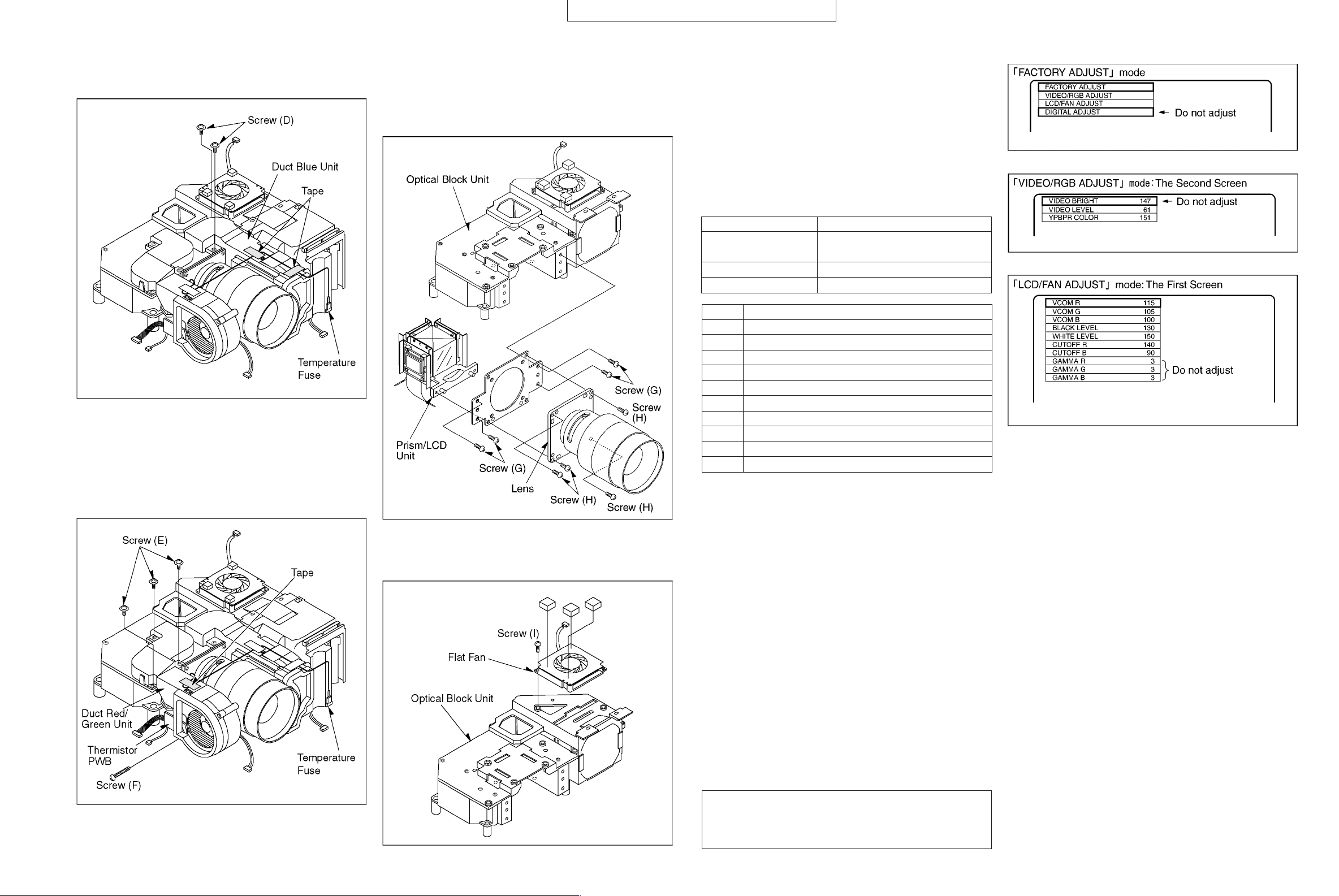
3.4.9 FULL MIRROR ADJUSTMENT
This adjustment needs Extension Cable.(Prease refer to “1.1.
SERVICE POSITION”)
Purpose:
To set the Full Mirror in the proper position.
Symptom of Misadjustment:
The non-uniformity color will appear.
TP
EQUIPMENT
ADJ.
FULL MIRROR
FULL MIRROR
RED-2
FULL MIRROR
BLUE
INPUT /
Test Pattern signal softwear menu
(RGB Input Connector)
100 % GREEN SIGNAL
100 % YERROW SIGNAL
100 % WHITE SIGNAL
(Right Click menu=1 Color=
3 Green/5 Yellow/1 White)
SPECIFICATION
19 (PA014)
Fig. 3-4-13
TEST PATTERN SIGNAL
Adjustment:
Adjust the right and left sides of the screen by adjusting portion
(a), portion (b) or portion (c) and adjust the top and bottom
sides of the screen by adjusting back and forth direction.
1. FULL MIRROR ADJUSTMENT
a. Supply 100 % Green Signal and project on the screen.
b. Loosen 2 Screws (A) of the Full Mirror.
c. Insert a (-) screwdriver into Portion (a) and move the Full
Mirror in the direction shown by the arrows so that color
uniformity is achieved over the whole screen. And then
tighten 2 Screws (A).
Refer to Description below
Page 20

Fig. 3-4-14
LX-P1010ZU/ZE
3. FULL MIRROR BULE ADJUSTMENT
a. Supply 100 % White Signal and project on the screen.
b. Loosen 2 Screws (C) of the Full Mirror Blue.
c. Insert a (-) screwdriver into Portion (c) and move the Full
Mirror Blue in the direction shown by the arrows so that
color uniformity is achieved over the whole screen. And
then tighten 2 screws (C).
2. FULL MIRROR RED-2 ADJUSTMENT
a. Supply 100 % Yellow Signal and project on the screen.
b. Loosen 2 Screws (B) of the Full Mirror Red-2.
c. Insert a (-) screwdriver into Portion (b) and move the Full
Mirror Red-2 in the direction shown by the arrows so that
color uniformity is achieved over the whole screen. And
then tighten 2 screws (B).
Fig. 3-4-15
Fig. 3-4-16
4. If the Full Mirror Blue adjustment can not be done, repeat step
1 through 2.
Note:
Do not use excessive force when adjusting the Mirror.
Otherwise, the Mirror may be damaged.
3.4.10. POLARIZER ADJUSTMENT
This adjustment needs Extension Cable.(Prease refer to “1.1.
SERVICE POSITION”)
Purpose:
To set the polarizer in the proper position.
Symptom of Misadjustment:
The picture will become bluish or reddish or greenish.
TP
EQUIPMENT
ADJ.
POLARIZER RED
POLARIZER
GREEN
POLARIZER
BLUE
INPUT /
Test Pattern signal softwear menu
(RGB Input Connector)
BLACK SIGNAL (0 %)
(Right Click menu=4 LEVEL
=1 Black Level)
SPECIFICATION
TEST PATTERN SIGNAL
Refer to Description below
(PA014) 20
Page 21

LX-P1010ZU/ZE
Note:
This adjustment should be done in a darkroom.
• POLARIZER RED ADJUSTMENT
1. Supply Black Signal (0 %) and project on the screen.
2. Loosen a Screw (A) of Polarizer Red Unit.
3. Move the Polarizer Red Unit to the right and left so that the
whole screen becomes the blackest possible value, and
then tighten a Screw (A).
• POLARIZER GREEN ADJUSTMENT
1. Supply Black Signal (0 %) and project on the screen.
2. Loosen a Screw (B) of Polarizer Green Unit.
3. Move the Polarizer Green Unit to the right and left so that
the whole screen becomes the blackest possib le value , and
then tighten a Screw (B).
• POLARIZER BLUE ADJUSTMENT
1. Supply Black Signal (0 %) and project on the screen.
2. Loosen a Screw (C) of Polarizer Blue Unit.
3. Move the Polarizer Blue Unit to the right and left so that the
whole screen becomes the blackest possible value, and
then tighten a Screw (C).
Fig. 3-4-17
(PA014) 2021 (PA014)
Page 22

4 TROUBLESHOOTING HINTS
Status Code Display Indications
Following Status Code will be displayed in the STATUS CODE
display.
LX-P1010ZU/ZE
STATUS
CODE
F-L
Symptom
Lamp Unit automaticaliy
turns oft due to abnormally high internal temperature.
(Stand-by condition)
Problem
• Cooling fan (Duct Fan (1),
Duct Fan (2) Lamp Fan
and/or Flat Fan) mal function.
Possible Solution
1) Confirm that all cabies are connected to Main PWB of connectors
(P1901, P1902, P1903, P1906, P1907) correctly.
2) Check following fan lock signal
Lamp ON
Check the voltage at
following pins of
IC1905.
Pin 2-Pin 11 (GND):
approx. 14 V
YES
Check the voltage at
following pins of
connectors P1901,
P1902. P1903, P1907.
Pin 3-Pin 2 (GND):
above 7~11 V
NO
YES
Check the power voltage
NO
line on Main PWB. Refer to
"POWER DOSE NOT TURN ON"
Check Pin 3 of P1901.
(Fan1 lock signal)
High
Replace Duct Fan (1).
Check Pin 3 of P1902.
(Fan2 lock signal)
High
c-o
•
Misinstalled Air Filter
cover or Lamp cover.
•
Temperature Fuse
malfunction.
Replace Duct Fan (2).
Check Pin 3 of P1903.
(Fan4 Iock signal)
Replace Lamp Fan.
Check Pin 3 of P1907.
(Fan5 Iock signal)
Replace Flat Fan.
Replace Main PWB Ass'y.
•
Properly instali Filter cover or Lamp cover.
•
Replace Temperature Fuse.
High
High
Low
21 (PA014) (PA014) 22
Page 23

LX-P1010ZU/ZE
STATUS
CODE
A-n
A-0
L-n
P-2
P-3
P-4
Symptom
Lampdoes not light up.
Abnormally high internal
temperature.
Problem Possible Solution
• The surrounding tem-
perature of the place of
use may be too low.
• Clogged air filter.
• Blocked air intake.
• Thesurrounding tem-
perature of the place of
use may be too high.
• There is the possibility
that Lamp is burned-out.
• Lamp Voltage is not
correct.
• Abnormal temperature
rise.
• Other cause.
• Relocate projector to a proper location.
• Place projector so that surrounding temperature is between
0 °C (32 °F) and 40 °C (104 °F) andthe humidity is between
10 % and 80 %(with no condensation).
• Clean the filter
• Relocate projector to a proper location.
• Place projector so that surrounding temperature is between
0 °C (32 °F) and 40 °C (104 °F) andthe humidity is between
10 % and 80 %(with no condensation).
• Wait until the Lamp Unit is cooled off (approx, 5 minutes)
and try to turn the power back on.
• If this code appears, try above again and again.
• If this code appears continuously more than 5 or 6 times,
replace the Lamp Unit.
• If this code appears again after replacement of the Lamp Unit,
replace the Main Power PWB and Ballast PWB.
• Wait until the Lamp Unit has cooled off (approx, 5 minutes)
and try to turn the power back on.
• Replace the Lamp unit.
• Wait until the Lamp Unit has cooled off (approx, 5 minutes)
and try to turn the power back on.
• Replace the Main Power PWB and Ballast PWB.
L-1
L-0
C-d
Lamp operation time is
over 1900 hours.
Lamp operation time is
over 2000 hours.
Forced cooling fan operating to expedite lamp
replacement.
• It is nearly time to
replace the Lamp Unit.
• Replace the Lamp unit.
• The Lamp Unit must be
replaced.
23 (PA014)
Page 24

LX-P1010ZU/ZE
POWER DOSE NOT
TURN ON
Turn the Power ON
Lamp dose not light up
Is Duct fan (1) and (2) turning?
YES YES
Is the signal (Lamp ON-H) at Pin
1 of P1904 High (approx. 5V)?
YES OK
Is there a slight cracking sound
when voltage is generated for
Lamp?
YES
NO
Caution:
Use a separate Isolation Transformer for this
unit when servicing.
Because a Hot Chassis Ground is preset in the Main
Power Circuit, an Isolation Transformer must be used.
Dose the Power LED on the
NO
Power button light Red or Green
(Solid or flashing light)?
NO
Relace the Main Power PWB.
Check Operation PWB.
NG
NO
Pull out the power code
and wait for approx. 10 minutes.
Plug in the power cord.
Replace Lamp Unit
Is Lamp ON?
NO
Check the voltage at following
pins of connector P1905.
Pin 1-Pin 8 (GND): approx. 16 V
Pin 2-Pin 8 (GND): approx. 14 V
Pin 4-Pin 8 (GND): approx. 7 V
Pin 5-Pin 8 (GND): approx. 3.3 V
Note: Disconnect connector
P1905 to check abobe
voltage if you checked
previously.
YES
NO
Relace the Oparation PWB.
Pull out hte power code and
disconnect Connector P1904,
P1905 on the Main PWB.
Wait approx. 10 minutes and
plug in the power cord.
YES
Is there any sound of relay on
with connector P1904, P1905
disconnected?
NO
YES
Is there any sound of relay on?
OK
Check Fuse (F1101, F1102) on the Inlet PWB.
NO
Replace the Main Power PWB
and Ballast PWB.
NG
Replace defective fuse and the Main Power
PWB and Ballast PWB.
(PA014) 24
Page 25

LX-P1010ZU/ZE
NO PICTURE (VIDEO INPUT)
WAVEFORM OF
CHECK POINTS
Is Lamp ON?
YES
Are all voltages at P1905 connector of Main
Are all voltages at P1905 connector of Main
PWB correct?
PWB correct?
YES
Is there video signai at Pin 2 of JK5002
(RCA connector)?
YES YES
Replace the Main PWB.
NO PICTURE (RGB/YPBPR INPUT)
NO
NO
NO
NO
Lamp or Power circuit is defective.
See troubleshooting of "Power deos not turn
on"
Power circuit is defective. See troubleshooting
of "Power does not turn on".
Is Video cabie connected properly?
WAVEFORM OF
CHECK POINTS
Is Lamp ON?
YES
Are all voltages at P1905 connector of Main
PWB correct?
YES
Is there RGB signals at Pin 1, Pin 2,Pin 3
of JK3001(D-SUB 15-Pin connector)?
YES
Replace the Main PWB.
NO
NO
NO
Lamp or Power circuit is defective.
See troubleshooting of "Power deos not turn
on"
Power circuit is defective. See troubleshooting
of "Power does not turn on".
Is Video cabie connected properly?
OK
25 (PA014)
Page 26

LX-P1010ZU/ZE LX-P1010ZU/ZE
LCD UNIT
CONVERTER
INTEGRATOR
SCREEN
LENS
PROJECTION
GREEN
LCD
LCD BLUE
DICROIC PRISM
LCD RED
FM-B
FM-R2
FM-R1
DGDYFM
SW
RGB
CONTROLLER
PROCESS MICRO
ROM
RS-232C
TRANSCIVER
RS-232C
GENERATOR
TIMING
A/D
PROCESS
SIGNAL
SYNC
DECODER
VIDEO
DIGITAL
SECTION
POWER
SWITCHING
SIG B
SIG G
SIG R
LCD DRIVE SECTION
PC IN
(YP
BPR
IN)
RGB/VIDEO SECTION
AC IN
VIDEO IN
S-VIDEO IN
AUDIO SECTION
AMP
AUDIO
SPEAKER
AUDIO IN
AD/DA/TG
SECTION
IO/ROM SECTION
DIGITAL
SECTION
CONTROL
I/O
D/A
HOLD
AND
SAMPLE
PROSESS
SIGNAL
RGB
BLOCK
POWER SUPPLY/BALLAST
BALLAST
POWER SUPPLY
OVERALL
MATRIX
(MAIN PWB)
(MAIN PWB)
(MAIN PWB)
(MAIN PWB)
(MAIN PWB)
(MAIN PWB)
(MAIN PWB)
5 SCHEMATIC DIAGRAM
5.1. SCHEMATIC DIAGRAM NOTES
1. Important safety notice
Components identified by the sign ! hav e special characteristics important for saf ety. When replacing any of these components .
Use only the specified parts.
2. The following block diagram, schematic diagram, P.W. board diagram, etc., are presented merely as reference materials to help
judge any unsatisfactory PWB to be replaced for eventual repair. Except a part of the component parts, electrical parts are not
included in the service parts supply targets.
5.2. BLOCK DIAGRAM
27 (PA014)(PA014) 26
Page 27

5.3. INTERCONNECTION SCHEMATIC DIAGRAM
INTERCONNECTION
MAIN PWB
V-LSEP3030D1:LX-P1010ZU/ZE
JK5001
3
Y
5
5
F
E
D
C
B
SPEAKER UNIT
LSYF0476
A
1
1
3
2
4
6
2
4
6
C
JK5002
2
1
JK4001
AUDIO_IN
1
L
2
3
R
JK3001
RED (Pr)
GREEN (Y)
BLUE (Pb)
NC
CSYNC(MAC2)
RED(Pr)_RETURN
GREEN(Y)_RETURN
BLUE(Pb)_RETURN
NC
GND
GND
(I2C)
HSYNC
VSYNC
(I2C_SCK)
JK2003
5
8
2
7
4
1
6
3
P4001
AMP_OUT(+)
1
AMP_OUT(-)
2
S.VIDEO-IN
VIDEO IN
1
2
3
4
5
6
7
8
9
(YPbPr_IN)
10
11
12
13
14
15
2
RTS (HSKO)
1
5
2
CTS (HSKI)
8
TXD (TXD-)
3
7
GND
4
9
RXD (RXD-)
5
6
DSR (TXD+)
6
3
7
DTR (GPI)
4
(RXD+)
8
1
PRISM/LCD UNIT
V-LSVQ0027
PC_IN
LCD
LCD
LCD
(R)
(G)
(B)
DY
VSSY
VSSY
NRS2
NRS1
LCCOM
VSSX
SIG6
SIG5
SIG4
SIG3
SIG2
SIG1
VSSX
NC
NC
VDDX
DX
XCLX
CLX
DIRX
ENB2
ENB1
LCCOM
DIRY
NRG
VDDY
XCLY
CLY
DY
DY
VSSY
VSSY
NRS2
NRS1
LCCOM
VSSX
SIG6
SIG5
SIG4
SIG3
SIG2
SIG1
VSSX
NC
NC
VDDX
DX
XCLX
CLX
DIRX
ENB2
ENB1
LCCOM
DIRY
NRG
VDDY
XCLY
CLY
DY
DY
VSSY
VSSY
NRS2
NRS1
LCCOM
VSSX
SIG6
SIG5
SIG4
SIG3
SIG2
SIG1
VSSX
NC
NC
VDDX
DX
XCLX
CLX
DIRX
ENB2
ENB1
LCCOM
DIRY
NRG
VDDY
XCLY
CLY
DY
LX-P1010ZU/ZE LX-P1010ZU/ZE
BALLAST PWB
V-
LSEP1062A1
P1904
L_ON_H
1
L_ERR
2
GND
3
NC
4
P3501
30
29
28
27
26
25
24
23
22
21
20
19
18
17
16
15
14
13
12
11
10
9
8
7
6
5
4
3
2
1
30
29
28
27
26
25
24
23
22
21
20
19
18
17
16
15
14
13
12
11
10
9
8
7
6
5
4
3
2
1
30
29
28
27
26
25
24
23
22
21
20
19
18
17
16
15
14
13
12
11
10
9
8
7
6
5
4
3
2
1
30
29
28
27
26
25
24
23
22
21
20
19
18
17
16
15
14
13
12
11
10
9
8
7
6
5
4
3
2
1
P3502
1
2
3
4
5
6
7
8
9
10
11
12
13
14
15
16
17
18
19
20
21
22
23
24
25
26
27
28
29
30
P3503
30
29
28
27
26
25
24
23
22
21
20
19
18
17
16
15
14
13
12
11
10
9
8
7
6
5
4
3
2
1
DY
VSSY
VSSY
NRS2
NRS1
LCCOM
VSSX
SIG6
SIG5
SIG4
SIG3
SIG2
SIG1
VSSX
NC
NC
VDDX
DX
XCLX
CLX
DIRX
ENB2
ENB1
LCCOM
DIRY
NRG
VDDY
XCLY
CLY
DY
DY
VSSY
VSSY
NRS2
NRS1
LCCOM
VSSX
SIG6
SIG5
SIG4
SIG3
SIG2
SIG1
VSSX
NC
NC
VDDX
DX
XCLX
CLX
DIRX
ENB2
ENB1
LCCOM
DIRY
NRG
VDDY
XCLY
CLY
DY
DY
VSSY
VSSY
NRS2
NRS1
LCCOM
VSSX
SIG6
SIG5
SIG4
SIG3
SIG2
SIG1
VSSX
NC
NC
VDDX
DX
XCLX
CLX
DIRX
ENB2
ENB1
LCCOM
DIRY
NRG
VDDY
XCLY
CLY
DY
P1905
UNSW16V
UNSW 14V[FAN]
UNSW14V[SIG]
UNSW7V
UNSW3.3V
UNSW3.3V
GND(ANA)
GND(ANA)
GND(DIG)
GND(DIG)
GND(FAN)
STBY
P1901
FAN1_+B
FAN_GND
FAN1_LOCK
P1902
FAN2_+B
FAN_GND
FAN2_LOCK
P1906
FAN_GND
FAN3_+B
P1903
FAN4_+B
FAN_GND
FAN4_LOCK
P1907
FAN5_+B
FAN_GND
FAN5_LOCK
P2004
UNSW3.3V
SCL
GND
SDA
GND
HI_THERMO_L
P2002
FILTER_SW
GND
P2003
AGND
UNSW 3.3V
P_LED_G
P_LED_R
7SEG_8
7SEG_7
7SEG_5
7SEG_4
7SEG_3
7SEG_2
7SEG_1
KEY_IN2
KEY_IN1
KEY_IN0
SCAN_3
SCAN_2
SCAN_1
SCAN_0
1
2
3
4
5
6
7
8
9
10
11
12
1
2
3
1
2
3
1
2
1
2
3
1
2
3
1
2
3
4
5
6
1
2
18
17
16
15
14
13
12
11
10
9
8
7
6
5
4
3
2
1
P1852
L_ON
1
L_ERR
2
3
GND
MAIN POWER PWB
V-
LSEP1061A1
P1701
1
UNSW 16V
2
UNSW 14V[FAN]
3
UNSW 14V[SIG]
4
UNSW 7V
5
UNSW 3.3V
6
UNSW 3.3V
7
GND
8
GND
9
GND
10
GND
11
GND
12
STBY
DUCT
FAN(1)
V-
DUCT
FAN(2)
V-
POWER
FAN
V-
LAMP FAN
UNIT
V-
FLAT
FAN
V-
THERMISTER PWB :
P6401
UNSW3.3V
1
SCL
2
GND
3
SDA
4
GND
5
HI_THERMO_L
6
FILTER SWITCH/TEMPERATURE FUSE UNIT :
OPERATION PWB :
P7001
1
AGND
2
UNSW 3.3V
3
P_LED_G
4
P_LED_R
5
7SEG_8
6
7SEG_7
7
7SEG_5
8
7SEG_4
9
7SEG_3
10
7SEG_2
11
7SEG_1
12
KEY_IN2
13
KEY_IN1
14
KEY_IN0
15
SCAN_3
16
SCAN_2
17
SCAN_1
18
SCAN_0
P1302
P1706
LSRF0010
LSRF0010
VRFS0014
LSEM0038
LSRF0012
V-
V-
LSEP0A34A1
P1151
N C
N CN C
DC 19V
VCC 17V
DC/DC_ON_H
BALLAST GND
ACTIVE OUT[-]
ACTIVE OUT[+]
P1303
65432
1
1
DC 19V
DC/DC_ON_H
N C
65432
VCC 17V
BALLAST GND
P1202
1
2
2
1
ACTIVE OUT[-]
ACTIVE OUT[+]
CAUTION : FOR CONTINUED PROTECTION AGAINST FIRE HAZARD,
IMPORTANT SAFETY NOTICE:
COMPONENTS IDENTIFIED BY THE SINE HAVE
SPECIAL CHARACTERISTICS IMPORTANT FOR SAFETY.
WHEN REPLACING ANY OF THESE COMPONENTS, USE
ONLY THE SPECIFIED PARTS.
LSEP0A35A1
AC_IN(L)
AC_IN(N)
AC_IN(L)
P1153
1
1
AC_IN(L)
P1201
5A 250V
INLET PWB
V-
LSEP1063A1
P1102
1
AC_IN(L)
2
AC_IN(N)
T1301
AC_IN(N)
2
2
AC_IN(N)
P1301
LAMP [+]
LAMP [-]
LAMP [+]
1
1
LAMP [-]
2
2
LAMP UNIT
REPLACE ONLY WITH THE SAME TYPE 5A 250V FUSE.
ATTENTION:POUR UNE PROTECTION CONTINUE LES
RISQUES
D'INCEIE N'UTILISER QUE DES FUSIBLE DE MEME
TYPE 5A 250V
V-
LSJA0346
F1101
5A250V
F1102
P1101
AC100-240V_IN
AC100-240V_IN
LAMP
1
2
FG
3
POWER CORD
V-LSJA0308 : LX-P1010ZU
V-VJAS0188 : LX-P1010ZE(EU)
V-VJAS0189 : LX-P1010ZE(EK)
L
N
12 3 4 5 6 7 8 9
29 (PA014)(PA014) 28
Page 28

LX-P1010ZU/ZE LX-P1010ZU/ZE
5.4. DIGITAL SECTION SCHEMATIC DIAGRAM (MAIN PWB) V-LSEP3030D1
DIGITAL SECTION
F
TO POWER/
1
JK2003
2
4
5
6
7
8
9
10
11
12
13
14
15
16
17
18
19
20
21
22
23
24
25
26
TP2901
TP2905
UNSW5V
LSJJ0155
5
8
2
7
4
1
6
3
(SHASSIS)
UNSW3.3V
S_DATA
S_CLK
TG_CS
XPWR_DOWN
KEY_IN2
KEY_IN1
KEY_IN0
SCAN_3
SCAN_2
SCAN_1
SCAN_0
KEY_IN3
I2C DATA
I2C SCK
I2C DATA
I2C SCK
I2C DATA
I2C SCK
I2C_DATA
I2C_SCK
SVIDEO_C
VIDEO
SVIDEO_Y
/VSYNC
/HSYNC
2
5
8
7
9
6
3
4
1
AUDIO
RS232C
RTS (HSKO)
1
CTS (HSKI)
2
3
TXD (TXD-)
4
GND
5
RXD (RXD-)
6
DSR (TXD+)
7
DTR (GPI)
(RXD+)
8
E
TO POWER/
AUDIO
TO AD/DA/TG
TO IO/ROM
TO LCD DRIVE
TO POWER/
AUDIO
TO AD/DA/TG
D
TO IO/ROM
C
TO RGB/
VIDEO
B
TO
AD/DA/TG
SECTION
FL2017
LSLFAA1H102
D2005
NNCD12F
LSLFAA1H102
D2003
RD13S-T1B
D2004
RD13S-T1B
NC
SMBus2
435
L2002
PNA4611M00YA
U2001
IR RECEIVER
VCC
OUT
GND
321
C2001
0.1
L2008
22U
TXD
R2027
1
2
3
FL2018
1
2
3
C2004
0.1
21
GND
IC2003
LTC1694
SMBus1
4R7U
VCC
RXD
1K
R2032
C2049
0.1
C2048
2.2/35V
R2028
1K
D2001
MA8039-L
D2002
MA8039-L
0.1
C2021
R2017
8765
WP
VDD
IC2006
S-24C16AFJA-01
EEPROM1
(16kbit EEPROM)
A0
A1
0
R2287
R22850R2286
C2022
0.047
C2023
0.047
C2024
0.047
R2298
0
C2050
2R2/35V
56
SCL
0
IR_R
R2299
39K
11
RI2
12
RI1
13
DO2
14
DO1
0
15
VCH
16
STBY
17
VSS(-10V)
18
C4-
19
GND
20
C4+
56
R2018
SDA
GND
4321
U2002
IR RECEIVER
VCC
321
C2008
0.1
FROM PC
RO2
RO1
DI2
FROM SYSTEM
DI1
C5-
C5+
IC2009
C1-
VCC
UPD4721GS-GJG
C1+
(+10V)VDD
C2056
10/10V
X2001
VSXS0810
8P
C2033
0
C2031
C2043
C2044
0.1
C2045
22/6.3V
L2006
4.7U
L2007
4.7U
PNA4611M00YA
GND
OUT
10
TXD
9
8
RXD
7
6
5
4
3
2
1
C2058
2R2/35V
1
2
3
TP2005
4
5
6
7
8
9
C2039
10
0.1
11
12
13
C2041
14
0.1
15
16
17
0.1
18
19
20
21
22
23
24
25
IR_F
R2300
0
R2044
560
C2057
2R2/35V
I2C_DATA
I2C_SCK
VDDE
TDO
TDI
XTOUT
VXSS
XTAL
XTALI
VXDD
VSSA2
AI24
VDDA2
AI23
AI2D
AI22
VSSA1
AI21
VDDA1
AI12
AI1D
AI11
AGND
AOUT
VDDA0
VSSA0
C2047
22/6.3V
R2301
39K
1K
R2048
0
0.1
C2053
R2035
100
97 96 889093 82849298
95 94 8799 8389 8591 8186 80 79 78 77 76
VSSE
TMS
TCK
XRDY
TRSTN
XDQ
XCLK
VDDI
XRH
XRV
XPD0
XPD1
VSSI
IC2008
SAA7114H
DI1
SCL
0
0
R2038
R2040
SDA
VDDI
RTS0
RTS1
3635343332313029282726
AMCLK
RTCO
C2059
0.1
TP2014
TP2015
VSSI
VSSE
CE
LLC2
LLC
TP2009
TP2010
RESON
TP2011
XPD2
XPD3
ASCLK
ALRCLK
0
R2045
TP2016
XPD4
XPD5
ITRDY
AMXCLK
0
R2046
TP2019
VDDI
XPD6
TEST0
VDDCI
XPD7
ICLK
47
R2053
R2054
XTRI
IDQ
47
R2055
10K
TEST5
ITRI
R2056
10K
TP2020
TEST3
TEST4
UV-OUT
Y-OUT
IGP1
IGP0
47
R2057
5049484746454443424140393837
VSSE
TEST2
TEST1
VSSE
VDDE
HPD0
HPD1
HPD2
HPD3
VDDI
HPD4
HPD5
HPD6
HPD7
VSSI
IPD0
IPD1
IPD2
IPD3
VDDI
IPD4
IPD5
IPD6
IPD7
IGPH
IGPV
VDDEVDDE
TO
AD/DA/TG
40
41
27
RESET
/PBRST
RST
C2082
0.1
0.1
0.1
IC2016
C2081
R2106
100
R2107
100
R2113
C2080
0.1
R2112
C2085
0.1
R2114
R2115
8
/RST
7
NC
6
NMI
5
22/6.3V
1
VDD2.5
GND
2
3
PORTA2(BOOTWE)
PORTA3(S_DATA)
4
5
PORTA4(S_CLK)
PORTA5(TG_CS)
6
PORTA6(7114_CE)
7
8
PORTA7(/PWR_DOWN)
9
PORTB0(KEY_IN2)
10
PORTB1(KEY_IN1)
11
PORTB2(KEY_IN0)
12
PORTB3(SCAN_3)
PORTB4(SCAN_2)
13
14
PORTB5(SCAN_1)
PORTB6(SCAN_0)
15
16
PORTB7(KEY_IN3)
0
DTMB
17
18
DTCLK
0
VDD3.3
19
20
GND
VG0(VY0)
21
22
VG1(VY1)
23
VG2(VY2)
VG3(VY3)
24
25
VG4(VY4)
VG5(VY5)
26
27
VG6(VY6)
VG7(VY7)
28
VDD2.5
29
GND
30
31
VB0(VUV0)
VB1(VUV1)
32
VB2(VUV2)
33
VB3(VUV3)
34
VB4(VUV4)
35
36
VDD2.5
GND
37
VB5(VUV5)
38
39
VDD2.5
GND
40
VB6(VUV6)
41
42
VB7(VUV7)
68
43
SCANMOD
44
VCLK
0
VCLKEN
45
VPEN
46
VHS
47
VVS
48
VFIELD
49
VDD2.5
50
51
GND
52
GBO0
GBO1
53
GBO2
54
GBO3
55
GBO4
56
GBO5
57
GBO6
58
GBO7
59
60
GBE0
GBE1
61
GBE2
62
GBE3
63
GBE4
64
C2090
0.1
1
0
R2321
VCC
2
DS1708SESA
0.1
C2089
GND
3
IN
4
3300
R2108
L2016
FBM2125HS420
IC2004
PQ2TZ15U
VO
GND
VC
NC
VI
R2102
1K
C2077
C2078
0.1
10/6.3V
C2071
0.1
75
74
73
47
R2091
72
71
70
69
C2072
68
47
R2092
0.1
67
66
65
64
63
R2093
47
62
61
60
59
C2073
58
0.1
47
R2094
57
56
55
54
47
R2089
53
47
R2090
52
C2074
51
0.1
C2079
22/6.3V
54321
0.1
C2083
C2084
R2267
0
C2086
28
XRESET29XRESET
0
0
R2123
R2128
256 255 254
253
TXD
RXD
(SCL)PORTA1
(SDA)PORTA0
Y-IN
UV-IN
DI2
DI3
DI4
BLUE-ODD
BLUE
-EVEN
GND
VDD3.3
GBE6
GBE5
C2151
0
0
R2130
R2131
252 251 250 249 248 247 246
IRRCVR1
IRRCVR0
PORT-A
PORT-B
VIDEO-IN
BLUE-IN
GREEN-ODD
GGO0
GBE7
6968676665
30
31
CPU_RESET33D235D437D639D8
D0
0
R2133
0.1
TP2027
0
R2322
D0
NMI
RESET
EXTINT
GGO2
GGO1
GGO4
GGO3
32
34
D1
D3
47
R2137
0.1
C2092
245 244 243 242 241 240 239 238
D3
D2
D1
GND
VDD2.5
ROM/RAM-DATA
RGB-IN
GREEN-IN
GGO7
GGO5
GGO6
GGE0
GGE1
76757473727170
7877
36
38
D5
D7
47
R2140
237
236 235 234 233 232 231 230
D4
D7
D8
D5
D6
GREEN-EVEN
GCOAST
GGE2
GBLKSPL
GND
VDD2.5
C2093
0.1
R2145
1K
D9
47
R2143
D9
GFBK
D1042D11
D10
GREF
TO
IO/ROM
43
46
45
D15
D12
D1444D13
47
R2146
0.1
C2099
C2096
229 228 227 226 225
D11
D14
D13
D12
D15
GND
GND
VDD3.3
RAMWE
IC2012
PW164-10RK
GGE3
GHS
GGE5
GCLK
GGE7
GPENSOG
GGE4
GGE6
GVS
949392
919089
88878685848382818079
0
R2147
0
R2011
50
52
49
ROMOE51CS0
CS1
ROMWE
47
47
47
47
0.1
R2165
R2167
R2169
R2164
222 221 220 219 218 217 216 215 214 213 212
224
223
CS0
CS1
BHEN
VDD2.5
RAMOE
ROMOE
ROMWE
RED-ODD
GRO1
GRO4
GRO2
VDD2.5
GRO3
GND
GRO0
9998
979695
C2100
0.1
55WR56A057
54
RD
47
R217347R2172
RD
WR
RED-IN
GRO6
GRO5
104103102101100
60
59
61A558
A4
A1
A3
A2
47
47
R2174
R2175
211 210 209 208 207 206 205
A3
A0
A5
A2
A1
A4
ROM/RAM-ADDRESS
RED-EVEN
GRE1
GRE0
GRE3
GRE2
GRO7
GRE4
A6
C2101
GND
GRE5
63A762
0.1
A6
VDD2.5
GRE7
GRE6
C2102
0.1
64
A8
47
R2176
A7
A8
GND
VDD2.5
116115114113112111110109108107106105
R2177
67
66
65
A1168A12
A10
A9
A9
A10
A11A2A12
RED-EVEN
DRE0
DRE1
DRE2
47
69
A1370A1471A1573A17
47
R2178
A13
A14
GND
VDD3.3
DRE3
C2103
0.1
47
R2179
74
72
A18
A16
47
R2180
A18
A17
A16
A15
ODD-OUT
PANEL-OUT
EVEN_OUT
DRE5
DRE4
DRE7
DRE6
75
A19
0.1
C2104
193198 197 196 195 194201 200 199204 203 202
A19
GND
VDD3.3
PTSTEN
DBO7
DBO6
DBO5
GND
VDD2.5
DBO4
DBO3
DBO2
BLUE-ODD
DBO1
DBO0
DGO7
GND
VDD3.3
GND
VDD2.5
DGO6
DGO5
DGO4
DGO3
DGO2
DGO1
DGO0
GND
VDD3.3
DRO7
DRO6
DRO5
DRO4
DRO3
DRO2
RED-ODD
DRO1
DRO0
DCLK
GND
VDD2.5
DCKEXT
MCKEXT
GND
VDD3.3
GND
VDD2.5
DVS
DHS
DEN
GND
VDD2.5
DBE7
DBE6
DBE5
DBE4
GND
VDD3.3
DBE3
DBE2
BLUE-EVEN GREEN-ODD
DBE1
DBE0
DGE7
DGE6
DGE5
DGE4
DGE3
-EVEN
GREEN
GND
VDD3.3
DGE2
DGE1
DGE0
128127126125124123122121120119118117
C2105
22/6.3V
R2181
0
TP2051
R2266
68
TP2052
TP2053
TP2054
0.1
TP2055
TP2056
TP2057
TP2058
TP2059
TP2060
0.1
0.1
TP2061
TP2062
TP2063
TP2064
TP2065
TP2066
TP2067
0.1
TP2068
TP2069
TP2070
TP2071
TP2072
TP2073
TP2074
TP2075
47
0.1
0.1
0.1
0.1
0.1
0.1
SCANMOD
TP2050
PTSEN
R2058
47
R2187
47
R2188
47
R2189
47
POCLK1
MCLK
DVS
DHS
158
159
TO
AD/
DA/
TG
160
161
R2182
192
191
190
189
188
187
C2107
186
185
184
183
182
181
180
179
C2108
178
177
C2109
176
175
174
173
172
171
170
169
168
C2110
167
166
165
164
163
162
161
160
159
R2183
158
157
C2111
156
155
154
153
C2112
152
151
C2113
150
149
148
C2114
147
146
145
144
143
142
C2115
141
140
139
138
137
136
135
134
133
132
131
C2116
130
129
C2106
22/6.3V
47
A
GBO0
76
GBE0
GBO782GBO681GBO580GBO479GBO378GBO277GBO1
84
83
GBE2
GBE188GBE4
GBE3
86
85
87
GBE5
89
GBE790GBE6
91
GGO0
92
GGO1
93
GGO2
94
GGO3
95
GGO4
96
GGO5
97
GGE0
GGE1
GGE2
GGO798GGO6
GBLKSPL
99
103
100
101
102
GFBK
GCOAST
105
104
VSYNC
108
RGB/
VIDEO
GCLK
GGE4
GGE3
GPENSOG
110
109
112
111
GGE5
113
GGE6
114
GGE7
115
GRO0
117
GRO1
118
GRO2
119
GRO3
120
GRO4
121
GRO5
122
GRO6
123
GRO7
124
GRE0
125
GRE1
126
TO AD/DA/TG TO AD/DA/TGTO AD/DA/TG TO
GRE2
127
GRE3
128
GRE4
129
GRE5
130
GRE6
131
GRE7
132
DRE0
133
DRE1
134
DRE2
135
DRE3
136
DRE4
137
DRE5
138
DRE6
139
DRE7
140
DGE0
141
DGE1
142
DGE2
143
DGE3
144
DGE4
145
DGE5
146
DGE6
147
DGE7
148
DBE0
149
DBE1
150
DBE2
151
DBE3
152
DBE4
153
DBE5
154
DBE6
155
DBE7
156
DCLK
157
12 3 4 5 6 7 8 9
31 (PA014)(PA014) 30
Page 29

LX-P1010ZU/ZE LX-P1010ZU/ZE
5.5. LCD DRIVE SECTION SCHEMATIC DIAGRAM (MAIN PWB) V -LSEP3030D1
LCD DRIVE SECTION
162
TO POWER/
G
AUDIO
F
TO AD/DA/TG
E
D
C
TO DIGITAL
TO POWER/
AUDIO
B
TO POWER/
AUDIO
TO AD/DA/TG
A
TO AD/DA/TG
SW15.3V
163
UNSW5V
164
SW5V
LD1
165
SIG_R
TP3501
LSJE0001
L3501
VLPS0090
C3501
33/25V
C3502
0.1
R3502
680
R3501
6800
R3503
560
R3504
*
*
6800
R3505
3300
Q3501
2SC563200L
D3501
MA111
*
Q3502
2SB1218AR
0.1
C3503
LD4
16 15 14 13 12 11
Q3504
2SC563200L
Q3503
2SD601ARS
*
R3506
560
VDD
IC3501
BU4053BCF
H
H
D3502
MA111
R3507
2700
H
INH
10
VEE
9
VSS
87654321
*
820
R3508
Q3505
2SB709ARS
C3520
C3521
C3522
C3523
C3524
C3525
C3519
R3548
0.1
0.1
0.1
0.1
0.1
0.1
0.1
15K
LD5
LD2
Q3509
R3512
R3510
*
*
680
TP3502
LSJE0001
166
SIG_G
LD3
TP3503
LSJE0001
167
SIG_B
C3504
0.1
C3505
0.1
R3509
6800
R3511
560
R3518
680
R3517
6800
R3519
560
6800
R3513
3300
Q3506
2SC563200L
D3503
MA111
*
Q3507
2SB1218AR
R3520
*
*
6800
R3521
3300
Q3511
2SC563200L
D3505
MA111
*
Q3512
2SB1218AR
*
R3514
2SC563200L
Q3513
2SD601ARS
*
R3522
LD6
16 15 14 13 12 11
VDD
C3508
C3506
0.1
R3528
12K
R3529
6.8K
R3530
1.1K
R3525
12K
R3526
1500
R3527
220
I2C_DATA
16
I2C_SCK
17
168
UNSW3.3V
169
VOLUME
170
171
172
173
174
175
176
177
178
179
180
181
182
183
184
185
186
187
188
SH7
SH6
SH5
SH4
SH3
SH2
SH1
FRP
XFRP
CLP
ENB1
ENB2
XCLY
DIRY
DY
NRG
DX
DIRX
CLX
C3507
0.1
0.1
H
L3502
VLPS0090
8765
VCC
IC3503
M62339FP
AO1
VCOM_R
5600
R3540
2SC563200L
Q3508
2SD601ARS
D3504
MA111
R3515
2700
560
Q3514
D3506
MA111
R3523
560
2700
H
IC3502
BU4053BCF
H
0
R3539
R3538
0.1
C3517
SCL
SDA
DAC2
VCOM_G
AO3
AO2
5600
R3542
R3541
10
9
VEE
INH
87654321
0
GND
VOLUME
VCOM_B
AO4
4321
5600
*
R3516
2SB709ARS
Q3510
*
R3524
2SB709ARS
Q3515
VSS
L3503
L3505
L3507
C3543
C3544
C3545
C3546
C3547
C3548
C3542
R3563
C3566
C3567
C3568
C3569
C3570
C3571
C3565
R3578
22U
0.1
0.1
0.1
0.1
0.1
0.1
0.1
15K
22U
0.1
0.1
0.1
0.1
0.1
0.1
0.1
15K
22U
820
820
TP3504
22
22
R3550
R3551
R3549
403938373635343332313029282726
GND
GND
GND
GND
GND
VOUT1
GND
41
GND
42
HOLD32
43
HOLD31
HOLD22
45 44
HOLD21
HOLD12
47 46
HOLD11
GND
49 48
SHCLK7
50
SHCLK6
SHCLK5
SHCLK4
SHCLK3
SHCLK2
SHCLK1
GND
R S/H
GND
GND
60 59 58 57 56 55 54 53 52 51
GND
41
GND
42
HOLD32
43
HOLD31
HOLD22
45 44
HOLD21
HOLD12
47 46
HOLD11
GND
49 48
SHCLK7
50
SHCLK6
SHCLK5
SHCLK4
SHCLK3
SHCLK2
SHCLK1
GND
R S/H
GND
GND
60 59 58 57 56 55 54 53 52 51
GND
41
GND
42
HOLD32
43
HOLD31
HOLD22
45 44
HOLD21
HOLD12
47 46
HOLD11
GND
49 48
SHCLK7
50
SHCLK6
SHCLK5
SHCLK4
SHCLK3
SHCLK2
SHCLK1
GND
R S/H
GND
GND
60 59 58 57 56 55 54 53 52 51
VOUT2
GND
VIN1
GND
GND
VIN2
GND
GND
66
67
63
62
65
64
61
TP3505
LSJE0001
22
22
R3565
R3566
R3564
403938373635343332313029282726
GND
GND
GND
GND
GND
VOUT1
VOUT2
GND
GND
VIN2
VIN1
GND
GND
GND
66
67
63
62
65
64
61
TP3506
22
22
R3581
R3580
R3579
403938373635343332313029282726
GND
GND
GND
GND
GND
VOUT2
VOUT1
GND
GND
VIN1
GND
GND
VIN2
GND
66
67
63
62
65
64
61
0.1
22
C3527
GND
GND
VCC2
VOUT3
IC3504
ET6040S0A
R
GND
VIN3
GND
VCC3
706968
0.1
C3526
0.1
22
C3550
GND
GND
VCC2
VOUT3
IC3505
ET6040S0A
G
GND
GND
VIN3
VCC3
706968
0.1
C3549
0.1
22
C3573
GND
GND
VCC2
VOUT3
IC3506
ET6040S0A
B
GND
GND
VCC3
VIN3
706968
0.1
C3572
22
R3552
VOUT4
VIN4
22
R3567
VOUT4
VIN4
22
R3582
VOUT4
VIN4
R3553
GND
GND
R3568
GND
GND
GND
GND
VOUT5
VIN5
VOUT5
VIN5
R3583
VOUT5
VIN5
22
22
R3554
25
242322
GND
GND
VOUT6
GATE PULSE IN
VIN6
GND
GND
7574737271
22
22
R3569
25
242322
GND
GND
VOUT6
GATE PULSE IN
VIN6
GND
GND
7574737271
22
22
R3584
25
242322
GND
GND
VOUT6
GATE PULSE IN
GND
VIN6
GND
7574737271
21
GND
GND
GND
GND
VCC1
GND
VCLP2
VCLP1
R DRIVE
HOLD42
HOLD41
HOLD52
HOLD51
HOLD62
HOLD61
VT
FRP
TIME CONST
VREF2
VREF1
GND
GND
GND
GND
GND
8079787776
21
GND
GND
GND
GND
VCC1
GND
VCLP2
VCLP1
R DRIVE
HOLD42
HOLD41
HOLD52
HOLD51
HOLD62
HOLD61
VT
FRP
TIME CONST
VREF2
VREF1
GND
GND
GND
GND
GND
8079787776
21
GND
GND
GND
GND
VCC1
GND
VCLP2
VCLP1
R DRIVE
HOLD42
HOLD41
HOLD52
HOLD51
HOLD62
HOLD61
VT
FRP
TIME CONST
VREF2
VREF1
GND
GND
GND
GND
GND
8079787776
L3504
22U
R3558
R3556
18K
39K
C3531
0.1
R3557
R3559
22K
33K
C3532
R3555
C3528
C3529
R3570
C3551
C3552
L3508
R3585
C3574
C3575
47K
L3506
R3571
R3572
47K
R3586
R3587
47K
C3530
R3560
C3533
C3534
C3535
C3536
C3537
C3538
C3539
C3540
C3541
R3561
39K
C3554
22K
C3555
C3553
R3575
C3556
C3557
C3558
C3559
C3560
C3561
C3562
C3563
C3564
R3576
39K
C3577
22K
C3578
C3576
R3590
C3579
C3580
C3581
C3582
C3583
C3584
C3585
C3586
C3587
R3591
0.1
R3562
12K
33/25V
22/6.3V
R3573
18K
R3574
33K
0.1
R3577
12K
33/25V
22/6.3V
R3588
18K
R3589
33K
0.1
R3592
12K
33/25V
22/6.3V
0.1
47K
0.1
0.1
0.1
0.1
0.1
0.1
0.1
0.1
0.1
22K
22U
0.1
0.1
47K
0.1
0.1
0.1
0.1
0.1
0.1
0.1
0.1
0.1
22K
22U
0.1
0.1
47K
0.1
0.1
0.1
0.1
0.1
0.1
0.1
0.1
0.1
22K
2019181716151413121110
987654
321
2019181716151413121110
987654
321
2019181716151413121110
987654
321
L3509
VLPS0090
ENB1
ENB2
XCLY
DIRY
DY
NRG
DX
XFRP
DIRX
CLX
R3593
R3600
22K
C3588
0.1
22K
C3592
0.1
C3589
0.1
C3593
0.1
TP3507
L3511
22U
R3612
R3610
4700
12K
L3510
22U
1
VDD
2
VCC
NC
3
NC
4
IN1
5
6
IN2
IN3
7
8
IN4
9
IN5
10
IN6
11
IN7
12
NC
13
NC
14
VSS
15
VSS1
1
VDD
2
VCC
3
NC
NC
4
5
IN1
6
IN2
7
IN3
8
IN4
9
IN5
10
IN6
11
IN7
12
NC
13
NC
14
VSS
VSS1
15
IC3507
LC4105V
IC3508
LC4105V
VDD1
OUT1
OUT2
OUT3
OUT4
/OUT4
OUT5
/OUT5
OUT6
/OUT6
OUT7
/OUT7
VSS1
VDD1
OUT1
OUT2
OUT3
OUT4
/OUT4
OUT5
/OUT5
OUT6
/OUT6
OUT7
/OUT7
VSS1
30
C3590
0.1
NC
29
R3594
22
28
27
R3595
22
26
25
24
R3596
22
23
R3597
22
22
21
R3598
22
20
R3599
22
19
18
NC
17
16
30
C3594
C3595
NC
29
0.1
33/25V
R3601
22
28
R3602
22
27
R3603
22
26
R3604
22
25
24
23
R3605
100
22
R3606
22
21
R3607
22
20
R3608
22
19
R3609
22
18
NC
17
16
L3512
L3513
R3618
12K
R3626
12K
22U
22U
R3620
4700
R3628
4700
Q3517
2SD1819ARS
Q3516
2SB1218ARS
Q3523
2SD1819ARS
Q3522
2SB1218ARS
Q3529
2SD1819ARS
Q3528
2SB1218ARS
Q3518
2SD1819ARS
2SB1218ARS
4700
R3613
Q3524
2SD1819ARS
2SB1218ARS
4700
R3621
Q3530
2SD1819ARS
2SB1218ARS
4700
R3629
Q3519
Q3525
Q3531
R3614
10
R3615
10
R3622
10
R3623
10
R3630
10
R3631
10
R3616
10
Q3520
2SD1819ARS
R3617
10
Q3521
2SB1218ARS
TP3508
R3624
10
Q3526
2SD1819ARS
R3625
10
Q3527
2SB1218ARS
TP3509
R3632
10
Q3532
2SD1819ARS
R3633
10
Q3533
2SB1218ARS
TP3510
LSJE0001
C3596
*
1
C3597
0.1
C3598
0.1
C3599
33/25V
C3600
*
1
C3601
0.1
C3602
0.1
C3603
33/25V
C3604
*
1
C3605
0.1
C3606
0.1
C3607
33/25V
P3501
30
29
28
27
26
25
24
23
22
21
20
19
18
17
16
15
14
13
12
11
10
9
8
7
6
5
4
3
2
1
P3502
1
2
3
4
5
6
7
8
9
10
11
12
13
14
15
16
17
18
19
20
21
22
23
24
25
26
27
28
29
30
P3503
30
29
28
27
26
25
24
23
22
21
20
19
18
17
16
15
14
13
12
11
10
9
8
7
6
5
4
3
2
1
LSJS07BC030
DY
VSSY
VSSY
NRS2
NRS1
LCCOM
VSSX
SIG6
SIG5
SIG4
SIG3
SIG2
SIG1
VSSX
NC
NC
VDDX
DX
XCLX
CLX
DIRX
ENB2
ENB1
LCCOM
DIRY
NRG
VDDY
XCLY
CLY
DY
VJSS3332
DY
VSSY
VSSY
NRS2
NRS1
LCCOM
VSSX
SIG6
SIG5
SIG4
SIG3
SIG2
SIG1
VSSX
NC
NC
VDDX
DX
XCLX
CLX
DIRX
ENB2
ENB1
LCCOM
DIRY
NRG
VDDY
XCLY
CLY
DY
LSJS07BC030
DY
VSSY
VSSY
NRS2
NRS1
LCCOM
VSSX
SIG6
SIG5
SIG4
SIG3
SIG2
SIG1
VSSX
NC
NC
VDDX
DX
XCLX
CLX
DIRX
ENB2
ENB1
LCCOM
DIRY
NRG
VDDY
XCLY
CLY
DY
LD7
LD8
TO
LCD
RED
LD9
LD10
LD11
LD12
LD7
LD13
LD14
TO
LCD
GREEN
LD15
TO
LCD
BLUE
12 3 4 5 6 7 8 9
33 (PA014)(PA014) 32
Page 30

LX-P1010ZU/ZE LX-P1010ZU/ZE
5.6. RGB/VIDEO SECTION SCHEMATIC DIAGRAM (MAIN PWB) V-LSEP3030D1
RGB/VIDEO SECTION
Q3003
C3004
2SC563200L
1K
Q3002
2SC563200L
1K
Q3001
2SC563200L
1K
L3001
22U
0.1
22/16V
C3005
TP3001
L3003
47K
47K
R3015
R3013
56
56
R3016
R3014
8765
0.1
C3006
IC3001
AT24C21
22/6.3V
C3007
4321
0.1
C3008
R3017
47K
R3020
R3019
100
14 13 12 11 10
VDD
IC3002
SN74AHCT32PW
100
R3018
47K
98
VSS
7654321
L3002
22U
0.1
C3009
R3022
R3023
2700
2700
Q3004
2SD1819A
100K
R3024
C3010
R3021
R3025
Q3005
10/16V
0
R3026
1K
Q3006
2SB1218A
2SC563200L
R3027
560
C3011
10P
560
0.01
C3012
R3028
R3029
100K
C3013
10K
Q3007
2SB1218A
120P
R3031
Q3008
2SB1218A
1K
R3030
560
Q3009
2SB1218A
2200
R3032
Q3010
2SB1218A
47/6.3V
C3015
18K
0.01
20 19 18 17 16 15 14 13 12 11
120P
CLMP
H
V
TMNG
POL
POL
R3033
C3016
C3014
10/16V
C3017
H
STATE
R3034
120K
Q3011
UN5213
V
STATE
IC3003
M52347FP
CLP
SW
HD+
CLP+
HD-
VCC
OUT
OUT
OUT
C/H
C/H
IN
G_IN
GND SW
DET
C3018
4.7/16V
0.068
100K
R3035
R3036
470
C3019
R3037
1800
VD+
OUT
V_IN
0.01
C3020
C3021
R3038
R3039
1800
VSS
OUT
V
DET
987654321
4.7/16V
1K
VSS
IN
VGATE
10
C3022
10/16V
R3041
8200
C3024
560P
R3040
8200
R3042
R3043
C3025
47K
47K
100P
C3026
100P
Q3012
2SD1819A
R3044
100K
1
C3027
R3045
R3046
Q3013
2SD1819A
100K
47K
Q3014
2SD1819A
Q3015
2SD1819A
R3048
100K
0.1
C3028
R3049
180K
22U
10K
R3050
Q3016
2SD1819A
TP3002
SW9V
DTV_L
UNSW5V
HSYNC
SW5V
PC_NC_H
VSYNC
CPS_L
191
192
1
193
194
195
108
196
TO POWER/
AUDIO
TO IO/ROM
TO POWER/
AUDIO
TO AD/DA/TG
TO POWER/
AUDIO
TO IO/ROM
TO DIGITAL
TO IO/ROM
F
15K
R3010
27K
R3012
FL3001
LSLFAA1H101
2
FL3002
NFM51R20P207
2
FL3003
LSLFAA1H101
2
FL3004
LSLFAA1H101
2
R3011
R3007
R3008
R3004
R3005
15K
27K
15K
27K
R3009
R3006
RGB1
C3001
LSJJ0125A
JK3001
RED
GREEN
BLUE
NC
CSYNC(MAC2)
RED_RETURN
GREEN_RETURN
PC_IN
BLUE_RETURN
NC
GND
GND
(I2C)
E
HSYNC
VSYNC
(I2C_SCK)
R3001
75
1
R3002
2
75
3
R3003
4
75
5
6
7
8
9
10
11
12
13
14
15
1
10/16V
C3002
10/16V
C3003
10/16V
1
3
1
3
435
D3001
DF5A6.8F
2
1
3
1
3
D
L5001
100U
R5001
R5002
22K
15K
Q5002
(SHASSIS)
2SB1218ARS
Q5001
2SD1819ARS
D5002
DF3A6.8FE
D5003
DF3A6.8FE
FL5003
LSLFAA1H101
1
D5004
DF3A6.8FE
R5003
22K
3
S1_L
189
TO IO/ROM
C
B
S.VIDEO-IN
TO IO/ROM
VIDEO IN
TO DIGITAL
JK5001
LSJJ0157
Y
5
1
3
4
2
C
190
JK5002
LSJJ0158
25
26
24
3
5
1
2
6
4
(SHASSIS)
S_IN_L
2
1
VIDEO
SVIDEO_Y
SVIDEO_C
D5001
RD6.2S-T1B
A
Q5003
2SB1218ARS
C5001
0.01
FL5001
LSLFAA1H101
1
2
3
FL5002
LSLFAA1H101
1
2
3
R5062
10K
R5018
2
18
R5019
56
R5004
22K
C5002
0.01
R5005
33K
R5007
18
R5008
100K
R5009
56
R5006
10K
C5003
0.047
R5010
18
C5006
22/6.3V
R5011
56
C5004
0.01
C5005
22/6.3V
C5008
0.1
C5007
47/6.3V
R5012
22K
R5013
33K
R5014
22K
R5015
33K
R5020
22K
R5021
33K
Q5004
2SD1819ARS
R5016
1500
Q5005
2SD1819ARS
R5017
1500
Q5006
2SD1819ARS
R5022
1500
RGB2
C5010
33/25V
C5009
22/16V
L5003
22U
R5052
12K
R5053
12K
RGB3
R5023
39K
R5024
150K
RGB4
R5054
10K
Q5023
2SB1218ARS
R5026
560
Q5007
R5025
3300
2SD1819ARS
C5012
22/6.3V
C5013
R5055
12K
Q5024
2SD1819ARS
R5056
560
C5014
22/6.3V
2SC563200L
Q5008
L5002
3.9U
C5011
15P
8765
0.1
47/6.3V
VCC
C5015
R5027
3300
IC5001
BA7655AF
PB
0.1
C5016
R5029
680
R5028
2700
R5030
390
R5031
1800
Q5009
2SB1218ARS
PR
GND
4321
R5058
15
Q5026
2SD1819ARS
R5032
Q5028
2SC563200L
Q5027
2SC563200L
820
2200
R5033
R5060
15
R5037
680
R5034
2700
R5035
390
R5036
2700
Q5013
2SB1218ARS
Q5014
2SD1819ARS
Q5015
2SC563200L
2SB1218ARS
R5067
820
0.1
C5019
R5070
4700
R5061
8200
Q5025
C5038
2.2
R5039
R5040
R5071
4700
2200
3900
Q5016
2SC563200L
R5042
3900
2200
R5063
Q5017
R5074
560K
Q5031
2SD1819ARSTX
Q5029
2SC563200L
R5072
220
Q5030
2SD1819ARSTX
R5073
5600
R5045
3900
R5065
390
R5046
1K
Q5018
2SB1218ARS
R5075
1K
R5047
680
Q5021
2SC563200L
Q5019
2SC563200L
R5049
2SB1218ARS
R5048
680
R5076
4700
Q5020
2SD1819ARS
0.1
C5020
R5050
3300
C5039
2.2
R5077
4700
2SC563200L
0.1
Q5022
C5021
2200
R5051
2200
R5080
560K
Q5034
2SD1819ARSTX
Q5032
2SC563200L
R5078
220
Q5033
2SD1819ARSTX
R5079
5600
L5004
22U
R5081
1K
RGB6
RGB7
C5040
2.2
R5082
4700
R5084
4700
R5083
8200
RGB5
TP5001
R5087
560K
Q5037
2SD1819ARSTX
Q5035
2SC563200L
R5085
220
Q5036
2SD1819ARSTX
R5086
5600
C5041
0.1
L5005
R5066
Q5012
R5043
Q5011
R5064
Q5010
10
B2
RC2
560
560
560
2SB1218A
2SB1218A
2SB1218A
9
/A2
VSS
87654321
22U
C5045
0.1
C5031
100/6.3V
C5025
10/16V
IN1-R
R5038
SYNC-DET
10K
IN1-G
C5026
10/16V
GND
C5027
IN1-B
10/16V
GND
C5028
IN2-R
10/16V
GND
C5029
987654321
IN2-G
10/16V
10
GND6OUT-B
C5030
11
IN2-B
10/16V
12
IN1-V
C5042
0.1
R5089
R5088
4700
1K
IN1-H
IN2-H
OUT-H
OUT-R
VCC
IC5002
BA7657F
OUT-G
G.SYNC-IN
SYNC-OUT
SW
OUT-V
IN2-V
R5091
2200
Q5038
R5090
2SC563200L
4700
2423
R5068
220
C5033
0.1
2019181716151413 2221
220
R5069
C5032
0.1
R5041
220
16 15 14 13 12 11
VDD/A1
R5093
2200
C5043
270P
RC1
IC5003
B1
C1
/RES1
Q1
/Q1
0.1
C5034
10P
C5037
10P
C5036
10P
C5035
/Q2
/RES2
74VHC123AMTX
Q2
C2
C5044
150P
R5094
2200
SW15.3V
AD_R
AD_G
AD_B
YUV_L
REF_HS
COLOR
197
TO POWER/AUDIO
198
199
TO AD/DA/TG
200
201
TO IO/ROM
TO AD/DA/TG
202
203
TO POWER/AUDIO
12 3 4 5 6 7 8 9
35 (PA014)(PA014) 34
Page 31

LX-P1010ZU/ZE LX-P1010ZU/ZE
5.7. POWER/AUDIO SECTION SCHEMATIC DIAGRAM (MAIN PWB) V-LSEP3030D1
POWER/AUDIO SECTION
G
LSJSME12E
P1905
UNSW16V
UNSW14V[FAN]
UNSW14V[SIG]
F
E
D
C
TO MAIN
POWER
PWB
(P1701)
TO
IO/ROM
TO
BALLAST
PWB
(P1852)
TO
DUCT
FAN(1)
TO
DUCT
FAN(2)
TO
LAMP
FAN
TO
IO/ROM
TO
POWER
FAN
TO
IO/ROM
UNSW7V
UNSW3.3V
UNSW3.3V
GND(ANA)
GND(ANA)
GND(DIG)
GND(DIG)
GND(FAN)
STBY
204
205
L_ON_H
L_ERR
GND
N C
P1901
FAN1_+B
FAN_GND
FAN1_LOCK
P1902
FAN2_+B
FAN_GND
FAN2_LOCK
P1903
FAN4_+B
FAN_GND
FAN4_LOCK
206
P1906
FAN_GND
FAN3_+B
207
208
209
L_ON_H
L_ERR
P1904
LSJSME04E
LSJSPC03F
LSJSPC03F
LSJSME03E
FAN_LOCK_H
LSJSME02E
FAN1_ON_H
FAN2_ON_H
STBY
1
2
3
4
5
6
7
8
9
10
11
12
1
2
3
4
D1964
SFPL-62V
1
2
3
1
2
3
1
2
3
TP1910
1
2
IMPORTANT SAFETY NOTICE:
COMPONENTS IDENTIFIED BY THE SINE HAVE SPECIAL
CHARACTERISTICS IMPORTANT FOR SAFETY.
WHEN REPLACING ANY OF THESE COMPONENTS, USE
ONLY THE SPECIFIED PARTS.
TP1907
LSJE0001
[SHASSIS]
R1903
10K
Q1902
2SB1218ARS
R1904
Q1901
10K
UN5211
D1965
ERJ8GEY0R00V
R1977
R1976
6800
6800
D1961
MA111
D1962
MA142WK
R1979
8.2K
R1978
6800
R1905
R1981
6.8K
D1963
MA111
47K
C1961
33/25V
C1962
0.1
C1964
0.1
C1966
0.1
TP1913
R1961
1K
TP1914
R1966
1K
TP1915
R1971
1K
IC1961
PQ20VZ1U
R1963
6800
R1964
1K
IC1962
PQ20VZ1U
R1968
6800
R1969
1K
IC1963
PQ20VZ1U
R1973
4700
R1974
1K
R1965
R1970
54321
C1963
47/16V
FAN1/2_SD_CTL
3300[D]
54321
C1965
47/16V
3300
54321
C1967
10/25V
TP1961
TP1962
FAN4_SD_CTL
TP1963
FAN3_SD_CTL
C1968
22/16V
R1982
0
TP1916
PR1901
ICP-S1.8
PR1903
ICP-S1.8
PR1904
ICP-S2.3
R1980
1K
TP1911
IC1964
PQ05DZ1U
C1902
100/6.3V
R1906
4700
R1907
4700
54321
Q1904
UN5111
Q1903
2SD1819ARS
C1903
0.1
TP1964
C1969
10/16V
C1911
10/25V
IC1901
PQ20VZ1U
TP1912
C1912
0.1
R1917
1K
1K
PT ONLY
IC1904
PQ05DZ1U
C1908
100/10V
C1907
R1912
0.1
10K
R1913
2200
C1910
10/25V
0
R4037
R4038
8765
SCL
VCC
IC4002
M62338FP
FAN_1/2
COLOR
AO1
AO2
R1919
10K
R1920
R1914
47K
0
C4021
0.1
SDA
DAC3
AO3
FAN_3/4
C4026
C4022
C4023
C1909
22/6.3V
GND
NC
4321
0.1
0.1
0.1
TP1904
LSJE0001
54321
C1913
10/25V
R1921
1200
TP1905
54321
8765
R1915
100
R1916
100
4321
R1922
*
22
C1904
IC1903
HAT2043R-EL
TP1903
SW 3.3V
TP1902
L4002
VLPS0090
IN
321
0.1
IC1902
AN78L09M
GND
10/16V
OUT
C1906
TP1901
POWER ON H FROM MCON
SW 15.3V VIDEO
SW 9V
UNSW 5V
SW 5V
POWER_ON_H
SW15.3V
SW15.3V
SW9V
SW9V
15.3ADJ
LCD_ON_H
UNSW7V
UNSW5V
UNSW5V
UNSW5V
UNSW3.3V
UNSW3.3V
UNSW3.3V
UNSW3.3V
SW5V
SW5V
SW5V
I2C_SCK
I2C_DATA
DAC_3.3V
COLOR
210
162
197
191
211
212
213
214
1
163
215
2
168
216
217
164
194
218
18
19
219
203
TO IO/ROM
TO LCD DRIVE
TO RGB/VIDEO
TO RGB/VIDEO
TO AD/DA/TG
TO IO/ROM
TO AD/DA/TG
TO DIGITAL
TO LCD DRIVE
TO RGB/VIDEO
TO DIGITAL
TO LCD DRIVE
TO AD/DA/TG
TO IO/ROM
TO LCD DRIVE
TO RGB/VIDEO
TO AD/DA/TG
TO
POWER/
AUDIO
TO
AD/DA/TG
TO RGB/VIDEO
P1907
LSJSME03E
LSJJ0156
1
2
3
L4001
270U
R4015
R4016
2700
2700
R4005
R4006
330K
390K
Q4002
2SD1819A
R4011
3900
4700
R4008
R4010
R4013
2700
Q4004
2SB1218A
Q4001
1
R4001
330K
R4003
R4004
330K
390K
R4007
2SD1819A
C4002
1
4700
R4002
330K
FL4001
C4001
1
L
2
3
R
LSLFAA1H102
1
D4001
DF3A6.8FE
FL4002
LSLFAA1H102
1
D4002
DF3A6.8FE
2
3
2
3
3900
0.047
R4012
2700
C4003
C4005
5600P
C4007
R4017
1
10K
Q4003
2SB1218A
3.9K
0.022
2SD1819A-RTX
C4009
R4019
Q4005
R4021
10K
C4011
100/6.3V
56 55 54 53 52 51
NCNCNC
OUT1(-)
NC
NC
NC
STAND-BY
R4023
68K
C4012
10/16V
270K
R4024
50 49 48 47 46 45
NCNCNC
GND
IC4001
NCNCNC
NC
OUT1(+)
IN1
987654321
C4013
Q4010
2SD1119
44 43 42 41 40 39 38 37
NC
NC
VCC
NCNCNC
NC
NC
TAB
AN7512SH
TAB
GND
NC
NC
10
1
NC
NC
17161514131211
36 35 34 33 32 31 30 29
NC
NCNCNC
OUT2(-)
IN2
NC
C4014
0.01
NC
212019
NCNCNC
18
NC
22
NCNCNC
GND
NC
NCNCNC
25
2423
Q4007
2SD1819A-RTX
R4025
10K
NC
C4015
2726
0.1
*
R4026
OUT2(+)
VOLUME
28
R4027
18K
47K
0.1
C4016
330/6.3V
C4017
Q4008
2SB1218A
R4030
10K
R4031
2200
D4009
MA111
R4035
18K
D4006
R4036
330
MA8051-M
C4020
100/10V
D4008
MA111
TP4001
TP4002
P4001
AMP_OUT(+)
1
AMP_OUT(-)
2
MUTE2_H
VOLUME
LSJSPC02F
220
169
TO
SPEAKER
TO IO/ROM
TO LCD DRIVE
FAN5_+B
TO
FAN_GND
FLAT
FAN5_LOCK
FAN
B
JK4001
AUDIO_IN
A
12 3 4 5 6 7 8 9
37 (PA014)(PA014) 36
Page 32

LX-P1010ZU/ZE LX-P1010ZU/ZE
5.8. AD/DA/TG SECTION SCHEMATIC DIAGRAM (MAIN PWB) V-LSEP3030D1
AD/DA/TG SECTION
G
F
AD_R
198
TO
RGB/VIDEO
AD_G
199
TO
AD_B
200
RGB/VIDEO
E
D
C
B
A
TO
AD/DA/TG
TO
POWER/AUDIO
TO
DIGITAL
SECTION
20
21
219
214
216
I2C_DATA
I2C_SCK
DAC_3.3V
UNSW7V
UNSW3.3V
/VSYNC
/HSYNC
R2325
1.2
R2326
1.2
R2327
1.2
IC2005
L1087DTX-3.3
C2014
0.1
321
C2025
10/6.3V
103
104
GCOAST
GBLKSPL
C2005
0.033
R2087
100K
C2006
0.033
C2007
0.033
L2004
FBM2125HS420
L2010
FBM2125HS420
L2009
FBM2125HS420
C2010
R2005
10P
220
R2006
C2012
220
10P
C2013
R2007
10P
220
R2010
R2014
R2021
C2020
10/10V
7
109
GPENSOG
XPWR_DOWN
1M
47
R2024
0.1
C2063
0.1
C2065
128 127 126 125 124 123
VD
REFIN
REFOUT
1
NC
AD1
2
NC
3
NC
0.1
C2016
4
VD
5
GND
6
GND
7
RAIN
0.1
C2018
8
VD
9
GND
10
0.1
C2017
VD
11
VD
12
GND
13
GND
14
SOGIN
15
GAIN
C2011
0.1
16
VD
17
GND
0.1
C2028
18
VD
19
VD
20
GND
21
GND
22
BAIN
C2019
23
0.1
VD
24
GND
25
VD
26
GND
0
R2052
27
CKINV
0
28
CLAMP
0
29
SDA
0
30
SCL
10K
R2051
31
A0
R2016
0
32
A1
C2029
33
PVD
34
PVD
0.1
35
GND
36
NC
37
NC
38
NC
HSYNC
GND
COAST
1M
R2030
0
R2009
1M
R2013
R2037
0.1
0.1
C2051
C2015
122
121 120 119 118 117 116 115 114 113 112 111 110 109 108 107 106 105 104 103
VD
VDD
GND
GND
GND
GND
/PWRDN
SOGOUT
IC2007
AD9884AKS100
FILT
NC
GND
PVD
GND
PVD
GND
CKEXT
10K
C2030
R2034
C2070
10/6.3V
0.1
3300
C2035
R2020
3900P
C2027
0.039
C2026
105
GFBK
HSOUT
/DATACK
PVD
GND
0.1
110
GCLK
47
R2036
DATACK
GND
C2052
C2046
VDD
GND
GND
VDD
0.1
R2095
0.1
R2015
125
GRE0
47
DRA0
DBB7
47
126
GRE1
DRA1
R(OLD)
B(NEW)
DBB6
127
GRE2
DRA2
EVEN
ODD
DBB5
128
GRE3
DRA3
DBB4
129
GRE4
R2096
DRA4
DBB3
R2019
132
131
130
GRE7
GRE6
GRE5
47
0.1
C2064
VDD
GND
DRA6
DRA5
DRA7
R(NEW)
EVEN ODDODD
G(OLD)
G(NEW)
EVEN
B(OLD)
DBB0
GND
DBB2
VDD
DBB1
6463626160595857565554535251504948474645444342414039
47
DRB0
DRB1
DRB2
DRB3
DRB4
DRB5
DRB6
DRB7
VDD
GND
DGA0
DGA1
DGA2
DGA3
DGA4
DGA5
DGA6
DGA7
VDD
GND
DGB0
DGB1
DGB2
DGB3
DGB4
DGB5
DGB6
DGB7
VDD
GND
DBA0
DBA1
DBA2
DBA3
DBA4
DBA5
DBA6
DBA7
C2060
10/6.3V
R2097
102
101
100
99
98
97
96
95
C2067
94
93
0.1
92
91
90
89
88
87
86
85
C2068
84
83
0.1
82
81
80
79
78
77
76
75
C2069
74
73
0.1
72
71
70
69
68
67
66
65
MAIN CHILD
PWB
(SYNC CELECT)
TP2907
0.1
C2901
COAST
R2901
22K[F]
C2902
16 15 14 13 12 11
VCC/1A
1RX/CX
74VHC123AMTX
1B
0.022[KB]
1Q
1CX
IC2901
/1Q
/1CLR
C2903
10
2B
/2Q
/2CLR
2RX/CX
2CX
2Q
0.022[KB]
87654321
9
/2A
GND
R2902
33K[F]
0.1
C2904
8
VCC
7
6
5
Y3
A2
Y1
IC2902
SN7AH2G14HCR
Y2
A3A1
GND
4321
8
6
0.1
VCC
/CLR/PRE
IC2903
TC7WH74FU
C2905
/QDCLK GND
3
2
1
TP2908
PWHS
R2903
4Y
4A
IC2904
1Y
/2OE
98
3A
/3OE
2Y
2A
7654321
3Y
GND
22
14 13 12 11 10
VCC
/4OE
10/6.3V
0.1
SN74LVC125PW
C2907
C2906
1A
/1OE
57
Q
4
TP2901
TP2902
480I625I
L2901
FBM2125HS420
TP2903
VCC3
TP2904
GND
TP2905
TP2906
PLLHSOUT
NOTE: MAIN CHILD PWB(SYNC SELECT)
From certain lot of manufacturing process,
MAIN CHILD PWB will be absorbed by
MAIN PWB.
47
R2098
47
R2099
47
R2047
47
R2043
47
R2039
47
R2031
47
R2026
47
117
GRO0
118
GRO1
119
GRO2
120
GRO3
121
GRO4
TO DIGITAL
122
124
123
GRO5
GRO7
GRO6
100
GGE0
101
GGE1
102
GGE2
111
GGE3
TO
RGB/
VIDEO
113
112
GGE5
GGE4
REF_HS
SYSH
116
107
TO
DIGITAL
114
GGE6
94
115
93
92
GGE7
GGO2
GGO1
GGO0
L2020
FBM2125HS420
C2137
0.1
R2242
22
C2145
R2244
0
HSYNC
193
TO
RGB/
VIDEO
95
GGO3
0.1
96
GGO4
97
GGO5
99
98
GGO7
GGO6
105
GND
106
GND
GDIN0
107
108
GDIN1
109
GDIN2
110
GDIN3
111
GDIN4
GDIN5
112
113
GDIN6
GDIN7
114
115
GDIN8
GDIN9
116
GDIN10
117
GDIN11
118
GDIN12
119
GDIN13
120
GDIN14
121
GDIN15
122
123
RDIN0
RDIN1
124
125
RDIN2
RDIN3
126
127
RDIN4
128
RDIN5
RDIN6
129
130
VDD
131
GND
132
RDIN7
RDIN8
133
134
RDIN9
RDIN10
135
RDIN11
136
RDIN12
137
RDIN13
138
RDIN14
139
140
RDIN15
141
GND
142
AD_CLK
143
GND
144
PLL_VHLD
145
REF_HS
PLLVID_H
146
147
VDD
148
GND
149
AD_CLP1
150
AD_CLP2
151
AD_BLK
SYSH_OUT
152
XHS_IN
153
XVS_IN
154
GND
155
156
GND
C2150
0.1
C2121
85
86
88
87
84
GBE1
GBE2
GBE4
GBE3
GBE090GBE6
0.1
103
100
104
102 101
VDD
GND
PLL_H
WCK_IN
OSO1_LCD
GND
OSI1_LCD
VDD
160
158157
159
R2263
1M
330
R2269
X2002
LSSX0052
C2076
C2075
8P
8P
91
89
GBE7
GBE5
999897 96 95
BDIN14
BDIN15
BDIN12
BDIN13
OSCO_LCD
GND
RCLK_LCD
TMD0
163162161
164
R2246
RESET
27
BDIN11
TMD1
0
76
GBO0
BDIN10
TMD2
166165
77
GBO1
94 93
167
78
GBO2
BDIN9
GND
79
GBO3
92
BDIN8
BDIN7
TOUT0_L
LOCK_L
169168
83
82
80
81
GBO7
GBO6
GBO4
GBO5
91
90 89
888786 858483
BDIN0
BDIN2
BDIN4
BDIN6
BDIN5
BDIN1
BDIN3
UPD65945-071
S_CLK
TOUT1_L
TOUT3_L
GND
VDD
TG_CS
TOUT2_L
173172
176175174
171170
0
0
0.1
C2149
R2252
R2251
S_CLK
5
6 TG_CS
TO
DIGITAL
157
140
DCLK
DRE7
81 80
82
YD7
YD6
GND
IC2015
S_DAT
INTLACE
R_DAT
179178177
180
0
R2250
S_DATA
4
138
139
DRE5
DRE6
79
YD4
YD5
XRESET
SRCH_H
181
182
0
R2249
XRESET
28
137
DRE4
GND
GND
C2148
C2120
78 77
136
DRE3
0.1
VDD
VDD
0.1
R2248
135
134
DRE2
DRE1
76 75 74 73
YD3
YD2
SH_ENB
SHCLK1
22
SH1
176
133
DRE0
YD0
YD1
SHCLK2
SHCLK3
188187186185184183
SH2
SH3
175
174
132
DGE7
72
GND
SHCLK4
189
SH4
173
128
129
130
131
127
126
DGE3
DGE4
DGE5
DGE6
DGE2
DGE1
71 70
696867 666564 63 626160
GND
UVD5
UVD7
UVD6
UVD3
UVD4
GND
GND
SHCLK7
M_CLK
SHCLK5
SHCLK6
192191190
193
C2147
22
R2247
R2254
SH6
SH5
SH7
171
172
170
125
DGE0
13
14
15
16
17
18
19
20
21
22
23
24
C2122
22/6.3V
UVD2
VDD
0.1
22
G1
G2
G3
G4
G5
G6
G7
R0
R1
R2
R3
R4
GND
UVD0
UVD1
XFRP_OUT
CLAMP1
FRP_OUT
FRP
XFRP
CLP
179
177
178
154
156
149
150
153
151
155
152
DBE5
DBE7
DBE0
DBE1
DBE4
DBE2
DBE6
DBE3
0.1
12 11 10
987654
B6
B7
B5
G0
BLUE-IN
C2125
321
B3
B0
B2
B1
B4
AD4
GREEN-IN
AD3
IC2014
MB40C958V
AD2
RED-IN
R6
R5
R2192
VDD
VID_VS
RCKIN_L
GND
ENB1
NRG_OUT
22
R2253
NRG
ENB1
185
180
R7
GCLK
BCLK
R2196
0
59 585756 55 54 53
GND
GND
OSI1_MEM
RCLK_MEM
OSCO_MEM
ENB4
ENB2
TEST
DIR_X
ENB3
204203202201200199198197196195194
205
DIRX
ENB2
187
181
TO
LCD DRIVE
RCLK
DVSS
0
C2123
VDD
OSOI_MEM
MEM_CLK
LOCK_M
TOUT0_M
TOUT1_M
TOUT2_M
TOUT3_M
PLLHSEL
PIFLD_O
PIV_OUT
PIH_OUT
POHVSEL
POFLD_O
POV_OUT
POH_OUT
RCLK_IN
POCLK1
POCLK2
OSD_CLK
OSD_XHS
OSD_XVS
PRG_OUT
XCLY_OUT
CLY_OUT
XCLX_OUT
CLX_OUT
DY_OUT
DX_OUT
VDD
XDIR_X
208207206
VA
0.1
C2124
C2119
0.1
GND
GND
GND
GND
DEV4_H
VDD
GND
GND
PICLK
GND
VDD
VDD
GND
GND
GND
VDD
GND
GND
VGATE
VDD
GND
GND
DIR_Y
GND
GND
C2146
22/6.3V
RVB
0.1
R2197
52
51
50
49
48
47
46
45
44
43
42
41
40
39
38
37
36
35
34
33
32
31
30
29
28
27
26
25
24
23
22
21
20
19
18
17
16
15
14
13
12
11
10
9
8
7
6
5
4
3
2
1
BVB
RIREF
3300
3300
R2198
BIREF
RVRIN
R2268
0
R2199
0
R2202
0
C2144
0.1
R2258
22
BOUT
GOUT
ROUT
363534333231302928272625
C2126
0.1
C2127
0.1
BVRIN
DVDD
AVDD
AVSS
AVSS
AVDD
GIREF
GVB
GVRIN
VROUT
C2128
0.1
C2136
0.1
R2255
0
R2257
47
10/6.3V
R2324
4700
R2243
R2245
22
/CE
C2168
218
L2022
VLPS0090
C2135
L2023
VLPS0090
C2134
10/10V
L2021
VLPS0090
1
C2133
*
48
47
46
C2129
0.1
45
44
43
42
C2130
0.1
41
40
R2200
3300
39
C2131
0.1
38
37
0.1
C2132
R2293
12K
R2294
6800
C2167
R2302
0
1
CLK
2
REFEN
R2303
3
VDD
0
4
VDD
5
VDD
6
X2
7
S1
8
X1/ICLK
R2305
0
TP2023
TP2003
TP2002
R2203
0
R2212
0
R2256
47
22
DIRY
CLX
DY
XCLY
DX
15.3ADJ
212
184
182
186
183
188
TO
POWER/
AUDIO
47/16V
1K
R2221
R2213
68
1K
R2216
R2214
68
1K
R2217
Q2005
2SC563200L
R2215
68
27K
R2295
4321
AO2
AO3
AO4
AO1
IC2019
M62334FP
4ch DAC
VCC
SDA
SCL
GND
5
876
*
C2153
0.1
0
0
R2292
R2291
L2024
VLPS0090
0.1
16
GND
15
GND
14
GND
13
REFOUT
TP2001
12
OE
R2307
11
S0
IC2020
R2308
10
S3
9
S2
ICS601G01TEF
1K
R2224
Q2003
2SC563200L
82
R2225
R2236
1K
R2226
Q2004
2SC563200L
82
R2227
R2237
1K
R2228
82
R2229
R2238
1K
0
2SC563200L
R2230
8200
Q2006
2SB1218A
C2138
47K
8200
R2231
Q2007
2SB1218A
C2139
47K
2SC563200L
R2232
8200
Q2008
2SB1218A
C2140
47K
TP2024
TP2025
Q2009
33K
R2218
0.1
R2233
Q2010
2SC563200L
33K
R2219
0.1
R2234
Q2011
33K
R2220
0.1
R2235
SW5V
SW9V
0.1
C2141
SIG_B
1K
R2239
4700
0.1
C2142
SIG_G
1K
R2240
4700
0.1
C2143
SIG_R
1K
R2241
4700
MCLK
DVS
DHS
POCLK1
CLY
211
167
166
165
159
160
161
158
221
TO
POWER/AUDIO
TO
LCD/DRIVE
TO
DIGITAL
TO
IO/ROM
12 3 4 5 6 7 8 9
39 (PA014)(PA014) 38
Page 33

LX-P1010ZU/ZE LX-P1010ZU/ZE
5.9. IO/ROM SECTION SCHEMATIC DIAGRAM (MAIN PWB) V-LSEP3030D1
IO/ROM SECTION
F
1K
Q2002
2SB1218A
Q2001
2SB1218A
R2003
R2060
R2061
R2062
R2063
R2064
R2065
R2067
R2068
R2069
R2070
R2071
R2072
R2073
R2074
R2075
R2076
R2077
R2078
R2079
R2080
R2081
R2082
R2083
R2084
R2085
TP2004
TP2007
TP2012
TP2017
1K
1K
1K
1K
1K
1K
1K
1K
1K
1K
1K
1K
1K
1K
1K
1K
4700
4700
270
270
270
270
270
270
270
TP2006
TP2008
TP2013
TP2018
L2017
FBM2125HS420
10K
18K
18K
R2284
R2105
R2323
TP2022
TP2021
D2006
D2008
D2007
D2009
MA111
MA111
MA111
MA111
10K
10K
R2104
R2103
R2109
R2264
0
R2110
R2117
R2118
C2087
0.1
C2088
0.1
0
76
77
78
79
80
81
82
68
83
84
85
0
86
0
87
88
89
90
91
92
93
94
95
96
97
98
99
100
0
R2116
PT-LC50U/ E
ONLY
0
0
TP2028
GND
STBY
PGND
LCD_ON_H
POWER_ON_H
VCCI
CPU_RESET
OPTION4
PGND
OPTION3
0
R2313
C2091
22/6.3V
PT-LC150
ONLY
TP2031
S1_L
D_RESET
PC_NC_H
DAC_RESET
IC2011
XC9572XL
OPTION1
OPTION2
OPTION0
D0
987654
0
R2261
10K
R2134
R2122
R2138
75 74 73 72 71 70 69 68 67 66 65 64 63 62 61 60 59 58 57 56 55 54 53 52 51
(V)GND
L_ON_H
PGND
L_ERR
FAN1_ON_H
FAN2_ON_H
PGND
FAN_LOCK_H
COVER_OPEN_H
TDO
GND
HI_THERMO_L
LAMP_ON_H
RGB_H
VCCIO
P_LED_G
P_LED_R
7SEG_8(b)
7SEG_7(c)
7SEG_5(d)
7SEG_4(e)
7SEG_3(g)
7SEG_2(f)
7SEG_1(a)
VCCI
/RST
GND
PGND
PGND
321
0
R2328
R2315
10K
R2124
10K
R2125
10K
R2126
10K
R2127
10K
CPS_L
YUV_L
D2
D1
TP2032
GND
MUTE1_H
MUTE2_H
D3
D4
D5
TP2029
V_AUDIO_H
D6
E
D
C
B
TO
RGB/VIDEO
TO
POWER/AUDIO
TO
RGB/VIDEO
TO
POWER/AUDIO
TO
FILTER
CHECK
SW
TO
OPERATION
PWB
(P7001)
TO
THERMISTER
PWB
(P6401)
TO
DIGITAL
192
DTV_L
190
S_IN_L
220
MUTE2_H
201
YUV_L
196
CPS_L
195
PC_NC_H
189
S1_L
210
POWER_ON_H
213
LCD_ON_H
209
STBY
204
L_ON_H
217
UNSW3.3V
L_ERR
205
FAN1_ON_H
207
FAN2_ON_H
208
FAN_LOCK_H
206
P2002
P2003
LSJS0085
P2004
HI_THERMO_L
22
I2C_DATA
23
I2C_SCK
VJPW0250
FILTER_SW
GND
AGND
UNSW3.3V
P_LED_G
P_LED_R
7SEG_8
7SEG_7
7SEG_5
7SEG_4
7SEG_3
7SEG_2
7SEG_1
KEY_IN2
KEY_IN1
KEY_IN0
SCAN_3
SCAN_2
SCAN_1
SCAN_0
LSJS07AF006
UNSW3.3V
SCL
GND
SDA
GND
LAMP-COVER-SW
1
2
18
17
16
15
14
13
12
11
10
9
8
7
6
5
4
3
2
1
SW2001
ESE13H01
FL2001
1
2
3
LSLFAA1H101
FL2002
1
2
3
LSLFAA1H101
FL2003
1
2
3
LSLFAA1H101
FL2004
1
2
3
LSLFAA1H101
FL2005
1
2
3
LSLFAA1H101
FL2006
1
2
3
LSLFAA1H101
FL2007
1
2
3
LSLFAA1H101
FL2008
1
2
3
LSLFAA1H101
FL2010
1
2
3
LSLFAA1H101
FL2009
2
1
3
LSLFAA1H101
FL2011
1
2
3
LSLFAA1H101
FL2012
1
2
3
LSLFAA1H101
FL2013
1
2
3
LSLFAA1H101
FL2014
1
2
3
LSLFAA1H101
FL2015
1
2
3
LSLFAA1H101
FL2016
1
2
3
LSLFAA1H101
R2022
150
R2023
150
SERVICE1
SERVICE2
1
2
3
4
5
6
F_ADJUST
FACTORY
0.1
C2094
VCCI
DTV_L
D7
PGND
0
R2141
S_IN_L
PGND
0
R2142
10K
R2262
TEST
OP_IN0
GND
CLK_IN
0
R2088
0
R2152
TP2083
TIMER_ON
OP_IN1
0
R2316
C2095
0.1
TP2084
CPU
(V)VCCIO
50
PGND
49
MAIN_CK
48
TCK
47
TMS
46
PGND
45
TDI
44
GND
43
PGND
42
PGND
41
OPTION6
40
OPTION5
R2153
39
PGND
38
VCCIO
R2154
37
PGND
36
WR
35
RD
R2139
34
PGND
33
CS1
R2158
32
CS0
31
GND
R2312
30
TIME_S
29
PGND
R2151
28
A2
27
A1
26
(G)VCCIO
PGND
PGND
25242322212019181716151413121110
R2304
10K
FOOT-DETECT-SW
SW2002
LSSM0002
R2150
R2161
R2265
0
TP2085
68
0
0
C2097
0.1
0
0
0
0
0
C2098
0
0.1
R2159
R2162
R2163
R2318
R2155
R2156
R2157
R2166
10K
0
0
0
4700
68
68
R2168
4700
R2317
10K
4700
R2171
TP2040
LSJE0001
TP2041
LSJE0001
TP2042
LSJE0001
TP2043
LSJE0001
TP2044
LSJE0001
TP2045
LSJE0001
TDO
VCC
TCK
TMS
TDI
GND
L2018
FBM2125HS420
ICE CONNECT
R2185
PT
R2186
3300
R2190
10/6.3V
0
R2184
0
C2118
0.1
C2117
25
A0
26
/CE
27
VSS
28
/OE
29
DQ0
30
DQ8
31
DQ1
32
DQ9
33
DQ2
34
DQ10
35
DQ3
36
37
38
39
40
41
42
43
44
45
46
47
48
IC2013
DQ11
VCC
MBM29LV850S1
DQ4
DQ12
DQ5
DQ13
DQ6
DQ14
DQ7
DO15
VSS
/BYTE
A16
A1
A2
A3
A4
A5
A6
A7
A17
A18
RY/BY
NC
NC
/RESET
/WE
NC
NC
A8
A9
A10
A11
A12
A13
A14
A15
ICE CONNECT
P2001
1
A2
2
A1
3
A4
4
A3
5
A6
6
A5
7
GND
8
A7
9
A9
10
47K
R2193
24
23
22
21
20
19
18
17
0
R2195
16
TP2047
15
14
TP2048
13
12
11
10
0
R2194
9
8
7
6
5
4
3
2
1
A8
11
A11
12
A10
13
VCC
14
15
A12
16
17
A14
18
A13
19
20
A15
21
A17
22
A16
23
A19
24
A18
25
A0
26
27
28
29
30
31
32
33
D15
34
D7
35
D14
36
D6
37
GND
38
D13
39
D5
40
D12
41
D4
42
VCC
43
GND
44
D11
45
D3
46
D10
47
D2
48
VCC
49
D9
50
D1
51
D8
52
D0
53
54
55
56
57
58
59
60
CS1
SCAN_0
KEY_IN3
SCAN_2
SCAN_3
KEY_IN1
KEY_IN0
SCAN_1
9
14
15
12
11
10
13
A
XRESET
KEY_IN2
8
29
TO DIGITAL TO AD/DA/TG
CPU_RESET
30
CLY
221
CS0
51
RD
WR
52
54
55
D4
D3
D2
D1
D0
D5
35
34
33
37D639
32
31
36
TO DIGITAL
D13
D9
D12
D8
D10
D7
D11
D14
D15
46
44
40
43
41
38
42
45
A4
A6
A1
A0
57
A7
A8
A9
A5
A3
60
58A256
59
A10
66
62
63
61
64
65
A16
A19
A14
A12
A11
A13
A15
70
68
67
69
71
ROMWE
A17
ROMOE
A18
49
72
50
75
73
74
12 3 4 5 6 7 8 9
41 (PA014)(PA014) 40
Page 34

LX-P1010ZU/ZE LX-P1010ZU/ZE
5.10. OPERATION SCHEMATIC DIAGRAM (V-LESP0A34A1)
OPERATION
SW7005
LSSP0014
C
SW7002
LSSP0014
LSJS0085
P7001
SCAN_0
SCAN_1
SCAN_2
SCAN_3
KEY_IN0
KEY_IN1
TO
KEY_IN2
MAIN
PWB
:IO/ROM
(P2003)
7SEG_1
7SEG_2
7SEG_3
7SEG_4
7SEG_5
7SEG_7
7SEG_8
P_LED_R
P_LED_G
UNSW 3.3V
GND
B
18
17
16
15
14
13
12
11
10
9
8
7
6
5
4
3
2
{RED}
1
3
4
1
{GREEN}
D7008
2
LN2162C13
D7001
LNJ206R5ARA
AUTO SETUP
SW7003
LSSP0014
POWER
D7002
LNJ206R5ARA
a
D7003
LNJ206R5ARA
f
DOWN
SW7006
LSSP0014
MENU
SW7004
LSSP0014
LEFT
D7004
LNJ206R5ARA
g
D7005
LNJ206R5ARA
e
d
SW7007
LSSP0014
UP
SW7008
LSSP0014
ENTER
D7006
LNJ206R5ARA
D7007
LNJ206R5ARA
c
SW7010
LSSP0014
INPUT
SW7011
LSSP0014
RIGHT
b
5.12. OPERATION PWB (V-LESP0A34A1)
OPERATION PWB
C
181 P7001
B
A
D7007
D7001
D7002
D7006
D7003
D7004
D7005
SW7003
POWER
D7008
POWER
1
3
2
4
SW7010
INPUT
SW7007
UP
SW7002
KEYSTONE
SW7004
LEFT
SW7011
RIGHT
SW7008
ENTRE
SW7005
SW7006
MENU
DOWN
A
POWER LED
7SEGMENT
f
e
12 3 4
5.11. THERMISTOR SCHEMATIC DIAGRAM (V-LSEP0A35A1)
THERMISTOR
B
TO
MAIN
PWB
:IO/ROM
(P2004)
A
P6401
LSJS07AF006
UNSW3.3V
SCL
GND
SDA
GND
HI_THERMO_L
1
2
3
4
5
6
L6401
FBM2125HS420
R6401
0
5
SDA
IC6401
DS1775R/TRL
GND
SCL
R6402
21
0
4
VDD
OS
3
0.1
C6401
a
b
g
c
d
12 3 4
(FOIL SIDE)(COMPONENT SIDE)
5.13. THERMISTOR PWB (V-LSEP0A35A1)
THERMISTOR PWB
B
A
314
IC6401
R6401
R6402
16
P6401
5
C6401
R6403
L6401
(FOIL SIDE)(COMPONENT SIDE)
12 3
12 3
43 (PA014)(PA014) 42
Page 35

5.14. MAIN PWB (V-LSEP3030D1)
LX-P1010ZU/ZE LX-P1010ZU/ZE
MAIN PWB
F
E
D
C
IMPORTANT SAFETY NOTICE:
COMPONENTS IDENTIFIED BY THE SINE
B
A
HAVE SPECIAL CHARACTERISTICS
IMPORTANT FOR SAFETY.
WHEN REPLACING ANY OF THESE
COMPONENTS, USE ONLY THE
SPECIFIED PARTS.
NOTE: MAIN CHILD PWB(SYNC SELECT)
From certain lot of manufacturing process,
MAIN PWB(SYNC SELECT) will be absorbed by
MAIN PWB.
1 59
IO/ROM
R2108
R2119
IC2016
DIGITAL
SECTION
C2089
14
85
C2008
P1902
R2143
R2194
R2193
1
3
R2174
R2146
SECTION
1
24
R2321
R2300
R2301
C2077
L2006
L2007
R2176
R2175
R2180
TP2055
TP2053
C2151
R2131
R2107
R2106
C2078
R2102
R2040 C2043
1
5
C2045
R2178
TP2058
C2108
C2104
C2101
C2099
C2092
C2096
C2047
TP2059
TP2064
IC2004
IC2013
C2088
TP2065
TP2072
C2107
C2109
C2082
R2038
C2111
C2081
R2112
C2097
TP2071
C2110
C2083
C2039
(COMPONENT SIDE)
C2087
TP2022
TP2021
R2308
R2307
C2112
C2084
R2104
9
16
C2105
C2085
R2055
C2079
R2118
C2113
C2100
C2093
R2053
C2033
C2031
P2001
R2117
IC2020
C2114
C2106
R2115
R2089
R2090
R2057
R2054
B
B
B
1
R2236
C2138
R2233
E
B
C
E
B
C
E
B
C
C2137
IC2015
R2256
R2257
R2212
128
C2051
R2037
103
AD/DA/TG
SECTION
IO/ROM
SECTION
61
5
R2218
R2239
E
B
C
E
B
C
E
B
C
C2136
R2203
C2063
C2065
R2024
C2015
C2064
48
25
R2103
C2167
C2086
X2001
R2184
C2115
C2090
R2035
R2105
R2110
R2264
C2116
R2150
8
1
C2103
C2102
R2190
R2185
R2186
R2305
R2303
J1
J2
J5
J3
J4
C2118
C2117
R2323
R2019
R2004
R2075
C2022
C2023
R2187 R2181
R2188
R2015
C2035
R2020
C2027
C2070
C2052
C2060
C2024
R2291
R2292
13
IC2014
24
R2196
X2002
C2150
R2269
R2252
C2029
R2246
C2075
C2076
C2147
C2146
R2263
C2149
R2151
R2250
R2249
C2148
157
208
IC2007
R2189
R2177
R2179
R2147
R2145
R2011
R2016
R2009
R2030
38
39
C2026
R2034
64
65 102
L2010
D1964
C2123
1
R2043R2039R2031R2026
D1965
R2198
156
C2127
C2129
R2197
R2010
112
3625
R2244
R2021
POWER/
AUDIO
SECTION
P1901
31
R2230
R2225
E
C
R2213
48
E
R2227
R2214
C
C2130
37
E
R2215
C
R2229
C2126
C2132
C2134
C2145
R2242
C2144
R2014
R2052
C2019
R2047
(QUADRUPLE PATTERNS)
MAIN CHILD PWB(SYNC SELECT)
C2903
R2902
IC2901
C2902
J1
J1: Blue
J2: Green
J3: Brown
J4: Yellow
C2905 C2907
IC2903
148
18
169
TP2905TP2901
J2 J3 J4 J5
R2901
5
C2901
C2904
IC2902
L2901
TP2904
5
14 8
148
17
C2906
IC2904
R2903
J5: Red
J6: Black
J7: White
J8: Orange
TP2908
TP2902
TP2906
TP2907TP2903
P2004
314
IC2003
C2142
R2224
R2221
C3526
R2216
R2226
C2141
R2217
R2228
C2143
Q2003
Q2006 Q2009
R2231
C2139
R2234
R2219
R2237
Q2004 Q2007 Q2010
R2232
C2140
R2235
R2220
R2238
Q2005 Q2008 Q2011
R2202
R2268
R2199
J7
R2013
R2036
J8
J6
J8
J7
J6
DIGITAL
SECTION
C3533
C3529
R2240
R2241
105
52
C2128
R2067
R2064
IO/ROM
SECTION
L2020
C2135
L3503
R2063
R2071
104
53
R2070
R2074
C3527
R2068
R2069
R3560
C3531
C3530
L3504
C2121
C2120
R2073
C3558
R3556
R2192
R2072
C3532
C2122
C2119
C3559
R3557
C3575
C3528
L3507
C3574
L3508
Q3517
BE
C3596
Q3521
R3610
C3597
C3598
R3626
R3633
R3632
C3604
Q3528 C3631
E
E
B
B
C
C
C1908
C1963
C1965
Q3519
C3605
E
C
BE
R3613
R3628
B
E
L4002
LCD DRIVE
SECTION
C3517
R3614
C
CBEC
R3615
C
C
R3616
R3617
Q3530
C
BE
E
B
C
C
Q3531Q3529Q3533Q3532
C4021
85
14
C4026
C1909
IC3502
Q3513
BE
L3502
C
Q3518
E
BE
Q3516
B
E
B
Q3520
R3612
R3630
B
R3629
R4037
R4038
IC4002
C4023
C4022
C1910
C1911
C1902
C1961
P1903
13
18
16 9
169
C
C3599
C3606
L3513
R1914
R1915
R1913
R1916
IC3501
C3508
18
E
Q3508
C
R3522
B
C3607
D3503
R3593
C3588
PR1903
B
E
R3514
C3504
L3509
R5094
R1920
Q1904
C
PR1901
POWER/AUDIO
SECTION
R3513
L3511
C3501
C3590
C3593
R5089
C5045 C5043
C5041
R1917
R1921
C3542
C3548
C3547
C3546
C3545
C3544
C3543
C5044
IC5003
R3563
R3600
C1912
R5090
R1922
IO/ROM
SECTION
FL2002
FL2003
FL2004
C3549
C3550
C3551
Q3526
R3620
Q3524
Q5038
B
E
18
R5091
R5093
169
C1904
D2009
C3603
BE
C3592
C
IC1902
Q3522
Q3525
C3593
C3016
D2008
C3564
R3576
C3558
Q3523
CBEC
Q3527
CBEC
CBEC
C3595
R5038
L5005
C5031
13
C3574
C3557
L3506
BE
R1981
C3555
C3556
C3022
C1906
C1913
D1963
Q2001
D2007
R3671
R3572
C3562
C3561
C3560
C3559
BE
R3621
C3015
C3554
R3575
C3552
R3625
R3622
L3510
L3512
R3618
R3623
D2006
C3601
E
C3602
R3624
C
C3014
E
B
B
Q2002
C
R2022
R2023
FL2010FL2005
FL2001
FL2014
R3573
R4013
L3505
R4016
R4015
E
C
B
Q4004
C3600
C4011
C5013
C5025
R5033
C5026
L5004
C5027
C5028
C5029
C5030
C3010
C3021
C3018
R1980
R1982
R1971
R1974
P1904
14
C4020
R4023
C5012
TP1916
C4003
Q4001
R4010
R4011
C1966
C4015
C4012
C5010
C3008
C3007
1
5
Q4002
R4008
C2057
L5001
C4017
R4007
B
E
E
C
C
B
C5014
C2048
IC1964
C3005
L3002
C2058
R1973
C5007
R4005
C5009
1
4
8
14
R4003
R4006
C3006
1
5
R5006
R5008
C5003
C4001
IC3001
IC3002
C2050
R2028
RGB/VIDEO SECTION
R5009
C5005
D5003
R5007
D5001
R5010
C5006
D5002
FL5003
D5004
C4016
FL4001
R4004
D4001
R4001
FL4002
R4002
C4002
D4002
Q3003
E
B
C3001
C
Q3002
E
B
C3002
C
Q3001
R3006
E
B
C3003
C
8
D3001D3001D3001
5
7
D3001
1
D2004
D2003
FL2018
D2005
FL2017
R2027
IC1963
C1967
P1907
1
3
FL5002
FL5001
P4001
FL3001
FL3002
FL3003
FL3004
C1969
R2298
R2299
2
1
POWER/
AUDIO
SECTION
RGB/VIDEO
SECTION
DIGITAL
SECTION
C1968
C2001
12 3 4 5 6 7 8 9
45 (PA014)(PA014) 44
Page 36

LX-P1010ZU/ZE LX-P1010ZU/ZE
MAIN PWB
F
E
D
C
B
A
RGB/VIDEO
SECTION
JK5001
1
5
2
JK5002
JK5002
JK4001
RGB/VIDEO
SECTION
JK3001
6
11
10
15
JK2003
DIGITAL
SECTION
U2001
3
2
1
TP4001
IO/ROM
SECTION
D4006
C3563
D4008
R3577
R4021
Q4005
B
C
E
C4005
B
C
E
C5015
E
B
E
C
B
E
B
C
E
C
B
C
BE
R3021
R3023
R3025 R3022
E
R3030
B
Q3006
BE
Q3008 Q3009
R3031
C3013
R3028
C3024
C3026
C3027
TP1907
P2003
FL2007
FL2015
FL2006
1
R3570
20
C3553
21 40
30
P3502
1
C3594
B
C
E
B
C
E
1
IC5002
12 13
R5040
R5081
C5038
R5079
Q5033
R5080
R3039
R3038
CBEC
C3020
R3032
Q3014
R3042
R3040
R3041
E
B
C
TP3002
R3043
B
C3025
C
E
Q3012
R5015
R5017
C5001
E
B
R5005
R5004
C
Q5005
R5002
3
Q5003
6
C5004
4
R5021
1
1
1
5
2
5
TP4002
12
P1906
2
3
R3002
63
41
7
8
R3015
R3016
2
POWER/AUDIO
SECTION
R3011R3001
R3020
R3019
R3018
R3017
R3014
R3013
TP1963
R5014
C5002
R3003
Q5032
R5018
R3010
R3007
R3008
R3005
R5076
TP1964
R5011
R3012
Q5013
Q5016
R5077
C
R5016
R5013
R5019
R5023
B
E
B
E
R5012
R3009
C5039
E
B
R5020
Q5006
Q5007
R3004
BE
C
BE
C
Q5034
C2056
L2008
R5003
Q5002
C
Q5001
E
B
C
Q4010
R5001
B
Q5004
C
BE
29
56
C3004
C5052 R5053
R5078
R5022
R5056
E
B
E
B
C
C
R5062
C
BE
B
E
B
E
TP5001
R2032
IC2009
Q5023
R5024
E
B
E
B
C
C
D4009
R4025
B
C5008
E
R4026
Q5024
C5016
R5057
R5058
R5025
R5026
C2055
Q3007
Q3010
Q4007
IC4001
L3001
B
E
1
BE
C
B
E
C
C
C
E
B
R3026
C
C
C
R4024
28
R4019
R5054
C
R5055
IC5001
C
C
C
R2048
R2044
R4031
R4030
1
L4001
C
BE
C
R5071
C3011
E
B
E
B
TP1915
R4017
C4007
Q3005
E
C
C
C
C
20 11
110
C2049
POWER/AUDIO
SECTION
E
B
C4009
C4013
R4012
E
B
E
B
C
BE
R5070
R3024
Q3004
B
E
R3027
R3029
E
B
C
E
B
C
R5072
E
C3012
BE
C
C
Q4008
R4027
Q4003
E
B
B
C
R4035
R4036
C4014
L5003
C
FL2009
FL2011
FL2012
118
FL2013
FL2008
FL2016
TP2018TP2013TP2008TP2006
TP2017TP2012TP2007TP2004
IC3505
R3569
R3568
R3567
R3566
R3565
R3601
R3602
R3603
30 16
IC3508
115
24
C5033
R5068
R5066
R5069
R5043
C5032
R5041
R5064
C5034
Q5022
R5051
C5042
R5075
Q5030
R5073
Q5031
R5074
Q5029
R3036
R3037
Q3011
R3035
E
C3019
C
R3034
IC3003
Q3015
C3009
R3048
C3028
C
BE
Q3013
R3049
C
B
BE
R3046R3044
E
Q3016
R3045
112
C3502
R3564
R3604
C5040
R5082
L3003
B
110
2011
C3017
C
TP3505
R3605
Q5037
Q5036
Q5035
P1905
R3501
R3502
6180
R3606
R3033
D3501
Q3502
R3503
Q3501
E
L3501
R3607
C5037
B
E
B
E
B
E
Q3503
C
R3505
BE
R3506
E
B
C
C
BE
TP3501
B
R3507
D3502
C
Q3507
Q3504
E
B
C
C
R3504
R3511
60
41
R3608
R3609
30 16
IC3507
1
Q5012
C
C5036
Q5011
C
C5035
Q5010
C
R5088
R5086
R5083
R5084 R5087
R5085
TP1901
TP1904
IC1901
R1919
TP1912
TP1903
R3050
TP1902
R3516
R3508
Q3510Q3505
E
C
Q3509
R3509
B
E
TP3502
E
B
B
E
R3510
R3512
IO/ROM
SECTION
R2002
R2001
R3594
TP3001
Q1903
E
C3503
R3527
C3506
R3526
R3525
B
R3521
R3515
D3504
Q3515
E
R3524
C
C
Q3506
C
R3542
TP3509
R3541
TP3508
TP3507
R3540
1
C2002
130
R3595
R3596
R3597
R3598
R3599
15
Q5008
L5002
R5034
R5027
R5036
R5067
R5035
Q5015
R5037 R5061 R5047
R5063
Q5025
C2025
IC2005
R2327
C2014
TP1905
IC1904
1515
R1906
C1907
B
TP1911
C
R1907
1
8
IC1903
4
5
Q1902
PR1904
R1905
R3530
C3507
R3529
R3528
D3505
Q3512
E
C
D3506
B
R3523
R3538
85
IC3503
14
LCD DRIVE
SECTION
C5011
Q5026
Q5014
R5050
Q5021
C5019
Q5020
R5039
C5021
R2326
R1912
C1903
R1970
R1969
E
C
B
R1903
E
C
R1904
B
Q1901
C3505
TP3503
B
R3539
P3501
P3503
R5028
R5032
Q5028
Q5027
R5029
Q5018
R2325
R1977
R3518
R1966
C1964
D1967
R3519
C5020
R1968
R1979
D1961
Q5019
R3520
B
E
E
R5060
R5031
R5046
R5048
1
5
R1978
Q3511
C
R5030
R5042
R5044
R5045
R5065
R1964
R1965
TP1914
R3517
C
B
R5049
IC1962
Q3514
TP3510
Q5009
R1976
R3554
R3553
R3552
R3551
TP3504
30
C3577
Q5017
IC1961
TP1962
R3550
R3549
TP1913
R1963
C3587
1
C3579
R3588
C1962
15
21
40
R3590
R1961
AD/DA/TG
SECTION
C3535
C3534
IC3504
41 60
C3524
C3523
C3522
C3521
C3520
R3591
1
R3592
C3586
R3585
C3585
C3584
C3583
C3582
C3581
C3580
R3586
R3587
R3589
20
C3578
21 40
C3576
R3584
R2062
R2061
R2060
IO/ROM
SECTION
R2065
TP1910
L2022
C3536
C3525
R3583
C3537
IC3506
R3582
C3540
C3538
TP1961
R3562R3555
C3539
C3572
C3573
TP3506
C3541
R3581
DIGITAL
SECTION
C2004
120
R3561
R3548
R3580
80
61
C3519
6180
R3579
C2168
R2285
R2286
R2287
R2255
R2095
P2002
C2021
L2002
1
IC2006
4
R3578
C3565
60
C3571
C3570
C3569
C3568
C3567
C3566
41
R2243
R2324
C2018
C2016
R2005
C2020
L2009
C2005
R2096
(QUADRUPLE PATTERNS)
TP2084
R2262
TP2031
R2138
R2163
R2161
C2094
R2284
TP2083
R2058
TP2085
C2095
TP2067
TP2073
TP2023
P2001
R2317
R2153
TP2061
TP2074
IC2012
R2051
C2041
R2139
R2155
R2154
TP2060
R2266
TP2063
TP2066
TP2069
R2093 R2094
IC2008
R2157
C2044
R2156
2650
R2158
TP2056
25
1
R2116
TP2050
R2182
5175
C2059
C2098
R2134
(PT-LC150
ONLY)
R2261
R2313
TP2052
TP2054
R2318
R2265
51
IC2011
75
76 100
IO/ROM
SECTION
R2109
R2122
TP2057
TP2062
TP2068
TP2025
TP2070
TP2024
R2302
TP2075
R2267
R2114
R2091
R2092
76
100
125
TP2005
R2046
R2045
12
8
5
R2247 R2248R2254R2253R2245
Q2016
C2010
C2067
D2002
D2001
R2017
R2018
C2133
C2131
R2200
C2155
R2087
C2156
R2086
C2017
C2068
AD/DA/TG
SECTION
60
C2153
L2024
85
IC2019
14
R2293
R2295
C2125
C2124
R2025
R2258
C2011
C2012
C2013
R2006
R2007
C2006
C2007
C2028
R2051
R2097
C2069
L2017
R2294
TP2032
R2077 R2076
R2079 R2078
R2081 R2080
R2083 R2082
R2098
R2099
TP2041
R2166
TP2029
R2084
R2168
TP2045
R2141
R2003
TP2003
TP2002
R2171
TP2040
L2004
C2030
TP2044
TP2043
TP2042
R2085
R2183
R2162
TP2028
NOTE: QUADRUPLE PATTERNS PWB
THIS PWB IS QUADRUPLE PATTERNS PWB
THIS CIRCUIT BOARD SHOWS COMPONENT
LAYOUT-PATTERN FOR COMPONENT SIDE
AND FOIL SIDE. LAYOUT-PATTERNS ARE SINGLE
PATTERN FOR EACH SIDE THAT MAKE EASY TO
SIGHT THE COMPOENT LAYOUT.
IMPORTANT SAFETY NOTICE:
COMPONENTS IDENTIFIED BY THE SINE
HAVE SPECIAL CHARACTERISTICS
IMPORTANT FOR SAFETY.
WHEN REPLACING ANY OF THESE
COMPONENTS, USE ONLY THE
SPECIFIED PARTS.
2
R2312
R2151
R2297
R2159
R2316
R2088
R2142
R2126
(PT-LC50U/E
ONLY)
R2034
50
26
R2328
R2133
R2322
R2128
R2123
R2113
R2127
R2125
R2124
R2056
R2033
C2091
R2135
1
TP2019
TP2010
TP2009
DIGITAL
SECTION
R2169
R2167
R2164
TP2027
R2130
SW2002
TP2020
TP2016
TP2015
TP2014
TP2011
R2195
R2152
R2165
R2172
R2173
R2140
R2137
C2080
(FOIL SIDE)
TP2048
TP2047
L2016
IO/ROM
SECTION
U2002
1
2
3
12 3 4 5 6 7 8 9
47 (PA014)(PA014) 46
Page 37

LX-P1010ZU/ZE LX-P1010ZU/ZE
6 V OL T AGE CHART
6.1. DIGITAL SECTION VOLTAGE CHART
PIN NO. VOLTAGE PIN NO. VOLTAGE PIN NO. VOLTAGE PIN NO. VOLTAGE PIN NO. VOLTAGE PIN NO. VOLTAGE PIN NO. VOLTAGE PIN NO. VOLTAGE PIN NO. VOLTAGE PIN NO. VOLTAGE PIN NO. VOLTAGE PIN NO. VOLTAGE
IC2003 1 0 7 1.4 20 0.3 33 3.2 46 0.4 59 0.3 72 0.4 85 3.1 98 0 10 5.0 2 3.2
1 3.2 2 0 8 3.2 21 0 34 3.1 47 0.2 60 0.3 73 2.6 86 3.1 99 0 11 0 3 0
2 0 3 0 9 0 22 0 35 3.1 48 3.2 61 0.3 74 2.5 87 3.1 100 0 12 0 4 3.2
3 - 4 0 10 1.3 23 3.2 36 0.6 49 0.4 62 0.3 75 3.2 88 0 IC2009 13 -9.7 5 3.3
4 3.1 5 3.1 11 3.2 24 0 37 0 50 0 63 0 76 0 89 3.1 1 9.8 14 -9.7 6 5 3.1 6 3.1 12 1.3 25 3.2 38 0 51 3.2 64 0.4 77 2.6 90 3.0 2 3.8 15 0 7 -
IC2004 IC2008 13 0 26 0 39 3.2 52 0.4 65 0.4 78 3.1 91 3.0 3 5.0 16 5.0 8 0
1 3.2 1 3.2 14 1.3 27 2.5 40 0 53 0.4 66 0.4 79 2.8 92 3.0 4 -1.1 17 -9.7
2 3.1 2 3.1 15 0 28 1.5 41 0 54 0.3 67 0.4 80 0.1 93 3.2 5 4.0 18 -1.0
3 2.5 3 2.6 16 0.3 29 1.5 42 2.9 55 0.3 68 3.2 81 3.1 94 3.1 6 0.2 19 0
4 - 4 - 17 3.2 30 3.2 43 3.2 56 0.4 69 0.4 82 3.0 95 3.1 7 3.2 20 4.0
5 0 5 0 18 0.4 31 3.1 44 3.1 57 0.3 70 0.4 83 3.2 96 0 8 5.0 IC2016
IC2006 6 1.6 19 0 32 3.1 45 0.4 58 3.2 71 0.4 84 3.1 97 0 9 4.9 1 3.2
6.2. LCD DRIVE SECTION VOLTAGE CHART
PIN NO. VOLTAGE PIN NO. VOLTAGE PIN NO. VOLTAGE PIN NO. VOLTAGE PIN NO. VOLTAGE PIN NO. VOLTAGE PIN NO. VOLTAGE PIN NO. VOLTAGE PIN NO. VOLTAGE PIN NO. VOLTAGE PIN NO. VOLTAGE PIN NO. VOLTAGE
IC3501 9 12.6 61 0 32 0 3 0.1 55 1.0 26 5.4 16 0 6 15.2 B 3.6 B 5.1 B 4.0
1 0 10 12.5 62 0 33 7.0 4 4.9 56 3.3 27 0 17 0 7 6.8 Q3508 Q3521 TP3501 4.3
2 0 11 12.6 63 0 34 0 5 9.2 57 0 28 5.4 18 7.0 8 5.4 E 4.1 E 4.5 TP3502 4.3
3 9.8 12 12.6 64 7.0 35 7.0 6 1.2 58 1.2 29 0 19 7.0 9 5.4 C 15.3 C 0 TP3503 4.1
4 7.0 13 12.7 65 0 36 0 7 1.6 59 0 30 15.2 20 7.0 10 15.2 B 4.7 B 4.0 TP3504 7.0
5 4.1 14 12.5 66 7.0 37 7.0 8 1.0 60 0 IC3508 21 7.0 11 7.2 Q3509 Q3522 TP3505 7.0
6 0 15 1.2 67 0 38 0 9 12.5 61 0 1 15.2 22 7.0 12 8.0 E 9.7 E 5.1 TP3506 7.0
7 0 16 4.9 68 7.0 39 0 10 12.5 62 0 2 5.0 23 7.0 13 0.1 C 15.3 C 0 TP3507 6.8
8 0 17 9.2 69 0 40 0 11 12.5 63 0 3 0 24 0 14 15.3 B 10.4 B 4.5 TP3508 5.5
9 7.6 18 0 70 15.1 41 0 12 12.5 64 7.0 4 0 25 6.8 15 0 Q3510 Q3523 TP3509 6.8
10 0 19 5.0 71 0 42 0 13 12.5 65 0 5 0.3 26 4.5 16 0 E 9.7 E 4.0 TP3510 4.5
11 7.6 20 0 72 7.0 43 12.5 14 12.5 66 7.0 6 0.3 27 4.5 17 0 C 0 C 15.3
12 9.8 21 0 73 0 44 12.5 15 1.2 67 0 7 0.3 28 0 18 7.0 B 9.1 B 4.5
13 4.2 22 0 74 7.0 45 12.5 16 4.9 68 7.0 8 0 29 0 19 7.0 Q3511 Q3524
14 7.0 23 0 75 0 46 12.5 17 9.2 69 0 9 1.6 30 0.1 20 7.0 E 3.4 E 4.5
15 0 24 0 76 7.0 47 12.4 18 0 70 15.2 10 4.5 P3502 21 7.0 C 10.6 C 15.3
16 15.3 25 7.0 77 0 48 12.5 19 5.0 71 0 11 1.6 1 0.1 22 7.0 B 4.1 B 5.1
IC3502 26 0 78 0 49 0 20 0 72 7.0 12 0 2 0 23 7.0 Q3512 Q3525
1 7.0 27 7.0 79 0 50 1.0 21 0 73 0 13 0 3 0 24 0 E 4.0 E 4.5
2 1.9 28 0 80 0 51 3.3 22 0 74 7.0 14 0 4 4.5 25 6.8 C 0 C 0
3 1.9 29 7.0 IC3505 52 1.0 23 0 75 0 15 0 5 4.5 26 4.5 B 3.4 B 4.0
4 4.5 30 15.1 1 0 53 1.0 24 0 76 7.0 16 0 6 5.5 27 4.5 Q3513 Q3526
5 7.0 31 0 2 0 54 1.0 25 7.0 77 0 17 0 7 0 28 0 E 4.2 E 4.5
6 0 32 0 3 0.1 55 1.0 26 0 78 0 18 7.2 8 7.0 29 0 C 15.3 C 15.3
7 0 33 7.0 4 4.9 56 1.0 27 7.0 79 0 19 7.9 9 7.0 30 0.1 B 4.7 B 5.1
8 0 34 0 5 9.3 57 0 28 0 80 0 20 0 10 7.0 Q3501 Q3514 Q3527
9 7.6 35 7.0 6 1.2 58 1.2 29 7.0 IC3507 21 15.2 11 7.0 E 3.6 E 9.9 E 4.5
10 7.6 36 0 7 1.6 59 0 30 15.2 1 15.2 22 7.7 12 7.0 C 10.4 C 15.3 C 0
11 7.6 37 7.0 8 0 60 0 31 0 2 5.0 23 7.7 13 7.0 B 4.3 B 10.6 B 4.0
12 9.8 38 0 9 12.6 61 0 32 0 3 0 24 15.2 14 0 Q3502 Q3515 Q3528
13 4.2 39 0 10 12.5 62 0 33 7.0 4 0 25 0.1 15 0 E 4.1 E 9.9 E 5.1
14 7.0 40 0 11 12.6 63 0 34 0 5 0 26 4.2 16 0 C 0 C 0 C 0
15 4.5 41 0 12 12.6 64 7.0 35 7.0 6 1.1 27 4.2 17 15.3 B 3.5 B 9.3 B 4.5
16 15.3 42 0 13 12.5 65 0 36 0 7 0 28 4.1 18 0.1 Q3503 Q3516 Q3529
IC3503 43 12.5 14 12.5 66 7.0 37 7.0 8 1.6 29 0 19 8.0 E 4.2 E 5.1 E 4.0
1 2.7 44 12.6 15 0 67 0 38 0 9 0 30 15.2 20 7.2 C 15.3 C 0 C 15.3
2 0.9 45 12.5 16 4.9 68 7.0 39 0 10 0 P3501 21 0 B 4.8 B 4.5 B 4.5
3 2.9 46 12.6 17 9.3 69 0 40 0 11 0 1 0.1 22 5.4 Q3504 Q3517 Q3530
4 2.1 47 12.5 18 0 70 15.1 41 0 12 0 2 7.7 23 5.4 E 9.7 E 4.0 E 4.5
5 0 48 12.5 19 5.0 71 0 42 0 13 0 3 7.7 24 5.5 C 15.3 C 15.3 C 15.3
6 3.1 49 0 20 0 72 7.0 43 12.6 14 0 4 15.3 25 15.2 B 10.4 B 4.5 B 5.1
7 3.1 50 1.0 21 0 73 0 44 12.7 15 0 5 4.1 26 4.1 Q3505 Q3518 Q3531
8 3.2 51 1.0 22 0 74 7.0 45 12.6 16 0 6 15.2 27 15.3 E 9.7 E 4.5 E 4.5
IC3504 52 1.0 23 0 75 0 46 12.7 17 0 7 6.8 28 7.7 C 0 C 15.3 C 0
1 0 53 1.0 24 0 76 7.0 47 12.6 18 15.2 8 5.4 29 7.7 B 9.1 B 5.1 B 4.0
2 0 54 1.0 25 7.0 77 0 48 12.7 19 0.1 9 5.4 30 0.1 Q3506 Q3519 Q3532
3 0.1 55 1.0 26 0 78 0 49 0 20 15.2 10 15.2 P3503 E 3.6 E 4.5 E 4.5
4 4.9 56 3.3 27 7.0 79 0 50 1.0 21 0 11 7.2 1 0.1 C 10.4 C 0 C 15.3
5 9.2 57 0 28 0 80 0 51 1.0 22 7.7 12 8.0 2 7.7 B 4.3 B 4.0 B 5.1
6 1.2 58 1.2 29 7.0 IC3506 52 1.0 23 7.7 13 0.1 3 7.7 Q3507 Q3520 Q3533
7 1.6 59 0 30 15.1 1 0 53 1.0 24 15.2 14 15.3 4 15.3 E 4.2 E 4.5 E 4.5
8 1.0 60 0 31 0 2 0 54 1.0 25 0 15 0 5 4.1 C 0 C 15.3 C 0
6.3. RGB/VIDEO SECTION VOLTAGE CHART
PIN NO. VOLTAGE PIN NO. VOLTAGE PIN NO. VOLTAGE PIN NO. VOLTAGE PIN NO. VOLTAGE PIN NO. VOLTAGE PIN NO. VOLTAGE PIN NO. VOLTAGE PIN NO. VOLTAGE PIN NO. VOLTAGE PIN NO. VOLTAGE PIN NO. VOLTAGE
IC3001 13 0.4 20 2.9 12 4.9 E 5.0 B 3.0 E 0 B 0.1 E 2.9 B 10.4 E 9.8 B 3.2
1 - 14 5.0 IC5001 13 4.9 C 8.9 Q3009 C 3.1 Q5004 C 0 Q5015 C 15.1 Q5026
2 0.4 IC3003 1 2.8 14 5.3 B 5.6 E 3.5 B 0.2 E 2.3 B 2.2 E 3.1 B 10.4 E 9.8
3 - 1 4.4 2 3.5 15 2.1 Q3004 C 0 Q3015 C 5.0 Q5010 C 6.7 Q5021 C 15.1
4 0 2 4.4 3 2.2 16 3.2 E 2.2 B 3.2 E 4.3 B 2.9 E 2.7 B 3.8 E 4.3 B 10.4
5 0 3 0 4 0 17 0 C 4.8 Q3010 C 4.9 Q5005 C 0 Q5016 C 7.2 Q5027
6 0 4 3.8 5 2.2 18 2.5 B 2.4 E 3.2 B 0.4 E 2.3 B 2.1 E 6.1 B 5.0 E 3.1
7 0 5 0 6 3.5 19 2.1 Q3005 C 0 Q3016 C 5.0 Q5011 C 15.2 Q5022 C 6.7
8 5.0 6 - 7 2.8 20 4.9 E 1.6 B 2.7 E 0 B 2.9 E 2.7 B 6.7 E 6.6 B 3.9
IC3002 7 4.0 8 5.0 21 2.1 C 4.2 Q3011 C 0 Q5006 C 0 Q5017 C 15.1 Q5028
1 0 8 2.3 IC5002 22 5.3 B 2.2 E 0 B 0.5 E 2.3 B 2.1 E 2.8 B 7.2 E 6.0
2 0 9 3.9 1 3.5 23 4.9 Q3006 C -0.1 Q5001 C 5.0 Q5012 C 0 Q5023 C 15.2
3 0 10 - 2 4.5 24 4.9 E 4.8 B 3.2 E 0 B 2.9 E 2.7 B 2.2 E 1.0 B 6.7
4 0 11 0.8 3 3.5 Q3001 C 2.7 Q3012 C 4.1 Q5007 C 0 Q5018 C 0
5 0 12 0.7 4 0 E 4.9 B 4.2 E 0.6 B 0 E 11.1 B 2.1 E 2.8 B 0.5
6 0 13 0.2 5 3.5 C 8.9 Q3007 C 4.9 Q5002 C 15.1 Q5013 C 0.1 Q5024
7 0 14 0.8 6 0 B 5.6 E 2.7 B 0.7 E 0.7 B 11.7 E 2.9 B 2.2 E 0.5
8 0 15 4.2 7 0.4 Q3002 C 0 Q3013 C 0 Q5008 C 0.1 Q5019 C 3.5
9 0 16 4.9 8 0 E 4.9 B 2.7 E 0 B 2.9 E 10.4 B 2.2 E 2.2 B 1.0
10 0 17 0.4 9 0 C 8.9 Q3008 C 3.7 Q5003 C 15.1 Q5014 C 4.3 Q5025
11 0.6 18 0 10 0 B 5.6 E 3.5 B 0.2 E 0.7 B 11.1 E 9.8 B 2.8 E 3.8
12 0 19 0 11 0.3 Q3003 C 1.4 Q3014 C 0 Q5009 C 15.1 Q5020 C 0
6.4. POWER/AUDIO SECTION VOLTAGE CHART
PIN NO. VOLTAGE PIN NO. VOLTAGE PIN NO. VOLTAGE PIN NO. VOLTAGE PIN NO. VOLTAGE PIN NO. VOLTAGE PIN NO. VOLTAGE PIN NO. VOLTAGE PIN NO. VOLTAGE PIN NO. VOLTAGE PIN NO. VOLTAGE PIN NO. VOLTAGE
IC1901 IC1961 1 3.3 26 - 51 - 2 0 2 0 Q4002 E 4.6
1 15.7 1 13.9 2 - 27 - 52 0 3 0 3 0 E 2.6 C 6.9
2 3.0 2 2.9 3 - 28 0.9 53 - P1904 P4001 C 5.0 B 5.2
3 15.3 3 8.5 4 - 29 2.1 54 - 1 5.0 1 2.3 B 2.4 TP1901 9.0
4 0.7 4 1.1 5 - 30 - 55 - 2 3.2 2 2.3 Q4003 TP1902 5.0
5 0 5 0 6 - 31 - 56 2.3 3 0 Q1901 E 3.1 TP1903 3.3
IC1902 IC1962 7 - 32 - IC4002 4 E 0 C 0 TP1904 15.3
1 9.0 1 13.9 8 - 33 0 1 1.2 P1905 C 0 B 2.5 TP1905 5.0
2 0 2 3.0 9 1.4 34 - 2 1.4 1 15.7 B 3.0 Q4004 TP1907 0
3 13.8 3 8.5 10 - 35 - 3 1.4 2 13.9 Q1902 E 2.5 TP1910 0.2
IC1903 4 1.1 11 - 36 - 4 - 3 13.9 E 5.0 C 0 TP1911 0.6
1 3.3 5 0 12 0 37 2.4 5 0 4 6.9 C 4.9 B 1.9 TP1912 3.0
2 14.9 IC1963 13 - 38 - 6 0 5 3.3 B 4.4 Q4005 TP1913 2.9
3 5.0 1 13.8 14 - 39 - 7 3.1 6 3.3 Q1903 E 0 TP1914 3.0
4 14.9 2 2.7 15 0 40 - 8 3.3 7 0 E 0 C 0 TP1915 2.7
5 5.0 3 7.1 16 - 41 - P1901 8 0 C 0 B - TP1916 3.0
6 5.0 4 1.1 17 - 42 0 1 9.4 9 0 B 0.6 Q4007 TP1961 8.3
7 3.3 5 0 18 - 43 - 2 0 10 0 Q1904 E 0.9 TP1962 8.3
8 3.3 IC1964 19 - 44 - 3 0 11 0 E 15.6 C 0 TP1963 7.1
IC1904 1 6.9 20 1.4 45 4.6 P1902 12 2.8 C 15.6 B - TP1964 5.0
1 6.9 2 3.0 21 - 46 - 1 9.4 P1906 B 0 Q4008 TP4001 2.3
2 4.8 3 5.0 22 - 47 - 2 0 1 0 Q4001 E 0.4 TP4002 2.2
3 5.0 4 - 23 - 48 2.3 3 0 2 7.1 E 2.4 C 0.4
4 0 5 0 24 - 49 - P1903 P1907 C 5.0 B 0
5 0 IC4001 25 - 50 - 1 9.4 1 5.0 B 2.4 Q4010
49 (PA014)(PA014) 48
Page 38

LX-P1010ZU/ZE
6.5. AD/DA/TG SECTION VOLTAGE CHART
PIN NO. VOLTAGE PIN NO. VOLTAGE PIN NO. VOLTAGE PIN NO. VOLTAGE PIN NO. VOLTAGE PIN NO. VOLTAGE PIN NO. VOLTAGE PIN NO. VOLTAGE PIN NO. VOLTAGE PIN NO. VOLTAGE PIN NO. VOLTAGE PIN NO. VOLTAGE
IC2005 36 - 76 1.0 116 1.6 27 1.7 18 - 58 0 98 0 138 0 178 - IC2020 B 1.1
1 0 37 - 77 1.0 117 0.4 28 1.5 19 0 59 0 99 0 139 0 179 - 1 - Q2009
2 3.3 38 - 78 1.0 118 1.8 29 1.5 20 3.3 60 0 100 0 140 0 180 - 2 0 E 4.3
3 6.5 39 0 79 1.9 119 0 30 1.5 21 1.4 61 0 101 0 141 0 181 - 3 3.3 C 9.0
IC2007 40 2.9 80 1.0 120 3.2 31 0 22 0 62 3.3 102 0 142 - 182 0 4 3.3 B 4.9
1 - 41 0 81 0.9 121 0 32 1.5 23 1.3 63 0 103 0 143 0 183 3.4 5 3.3 Q2010
2 - 42 0 82 1.2 122 0 33 3.5 24 0 64 - 104 0 144 - 184 - 6 1.2 E 4.2
3 - 43 3.3 83 0 123 0 34 1.8 25 0 65 - 105 0 145 2.8 185 3.3 7 - C 9.0
4 3.3 44 0.1 84 3.3 124 3.3 35 1.8 26 0 66 - 106 0 146 - 186 0.6 8 - B 4.8
5 0 45 1.7 85 1.0 125 3.2 36 2.0 27 3.3 67 - 107 0 147 3.3 187 0.6 9 - Q2011
6 0 46 - 86 1.0 126 1.2 37 1.8 28 3.1 68 0 108 0 148 0 188 0.6 10 0 E 4.2
7 0.5 47 0 87 1.0 127 1.2 38 3.5 29 3.2 69 - 109 0 149 - 189 0.6 11 0 C 9.0
8 3.3 48 3.3 88 1.0 128 3.3 39 1.8 30 - 70 - 110 0 150 - 190 0.6 12 - B 4.9
9 0 49 0 89 1.8 IC2014 40 5.0 31 3.3 71 - 111 0 151 - 191 0.6 13 1.3 Q2016
10 3.3 50 3.3 90 1.0 1 1.8 41 1.2 32 3.3 72 - 112 0 152 0 192 0 14 0 1 0
11 3.3 51 0 91 0.9 2 1.8 42 0 33 0 73 0 113 0 153 - 193 - 15 0 2 0.5
12 0 52 0 92 1.2 3 3.5 43 1.2 34 - 74 - 114 0 154 0 194 0 16 0 3 3.3
13 0 53 0 93 0 4 0.8 44 0 35 0 75 - 115 0 155 0 195 3.3 Q2003 4 1.7
14 1.3 54 3.3 94 3.2 5 1.2 45 1.3 36 - 76 - 116 0 156 0 196 0.1 E 1.0 5 0.5
15 1.5 55 1.0 95 1.0 6 1.2 46 5.0 37 - 77 - 117 0 157 3.3 197 1.6 C 4.9 6 0.5
16 3.3 56 1.0 96 1.0 7 1.1 47 0 38 - 78 3.3 118 0 158 - 198 1.6 B 1.6 TP2001 1.3
17 0 57 1.0 97 1.0 8 1.0 48 5.0 39 0 79 0 119 0 159 - 199 0.3 Q2004 TP2002 3.1
18 3.3 58 1.0 98 1.0 9 0.9 IC2015 40 0 80 - 120 0 160 0 200 0 E 1.0 TP2003 3.2
19 3.3 59 2.0 99 1.6 10 1.3 1 0 41 3.3 81 - 121 0 161 1.5 201 1.1 C 4.9 TP2023 20 0 60 1.1 100 1.2 11 1.9 2 0 42 3.3 82 - 122 0 162 0 202 1.1 B 1.6 TP2024 21 0 61 1.0 101 1.3 12 1.3 3 0 43 0 83 - 123 0 163 1.5 203 - Q2005 TP2025 22 0.5 62 1.1 102 1.2 13 0.8 4 0 44 - 84 0 124 0 164 0 204 0 E 1.0
23 3.3 63 0 103 0 14 1.3 5 0 45 - 85 0 125 0 165 0 205 - C 4.9
24 0 64 3.3 104 3.2 15 1.2 6 1.6 46 - 86 0 126 0 166 0 206 4.5 B 1.6
25 3.3 65 1.0 105 1.0 16 1.0 7 0 47 - 87 0 127 0 167 0 207 - Q2006
26 0 66 1.0 106 1.0 17 0.9 8 - 48 - 88 0 128 0 168 - 208 3.3 E 1.6
27 0 67 1.0 107 1.0 18 1.1 9 - 49 0 89 0 129 0 169 - IC2019 C0
28 3.2 68 1.0 108 1.0 19 1.7 10 1.6 50 - 90 0 130 3.3 170 - 1 0.3 B 1.1
29 3.1 69 1.9 109 1.6 20 1.0 11 0.3 51 0 91 0 131 0 171 - 2 0.1 Q2007
30 3.1 70 1.2 110 1.2 21 0.8 12 0 52 0 92 0 132 0 172 - 3 0.6 E 1.6
31 3.1 71 1.1 111 1.2 22 1.3 13 3.3 53 3.3 93 0 133 0 173 0 4 1.3 C 0
32 0 72 1.1 112 1.2 23 1.2 14 - 54 - 94 0 134 0 174 3.3 5 0 B 1.1
33 3.3 73 0 113 0 24 1.0 15 - 55 0 95 0 135 0 175 0 6 3.1 Q2008
34 3.3 74 3.2 114 3.2 25 1.0 16 - 56 0 96 0 136 0 176 0 7 3.1 E 1.6
35 0 75 1.0 115 1.5 26 1.1 17 0 57 - 97 0 137 0 177 0 8 3.2 C 0
6.6. IO/ROM SECTION VOLTAGE CHART
PIN NO. VOLTAGE PIN NO. VOLTAGE PIN NO. VOLTAGE PIN NO. VOLTAGE PIN NO. VOLTAGE PIN NO. VOLTAGE PIN NO. VOLTAGE PIN NO. VOLTAGE PIN NO. VOLTAGE PIN NO. VOLTAGE PIN NO. VOLTAGE PIN NO. VOLTAGE
IC2011 31 0 62 0 93 3.2 23 - 5 - 36 - 3 0.7 TP2004 0.3
1 0 32 3.3 63 3.2 94 3.2 24 - 6 1.4 37 - 4 0.7 TP2006 2 0 33 3.3 64 3.7 95 3.2 25 1.4 7 - 38 - 5 0.1 TP2007 0.3
3 0 34 0 65 0.1 96 3.2 26 - 8 0.7 39 - 6 0.1 TP2008 4 3.2 35 3.3 66 4.0 97 3.2 27 - 9 - 40 - 7 0.1 TP2012 0.3
5 3.2 36 3.3 67 0 98 3.2 28 - 10 0.3 41 - 8 3.2 TP2013 6 3.2 37 0 68 3.2 99 - 29 - 11 - 42 - 9 3.2 TP2017 0.3
7 0 38 3.2 69 0 100 0 30 - 12 0.6 43 - 10 3.2 TP2018 8 3.2 39 0 70 3.2 IC2013 31 - 13 - 44 - 11 3.2 TP2021 3.2
9 3.2 40 3.2 71 3.2 1 - 32 - 14 - 45 - 12 3.2 TP2022 3.2
10 3.2 41 3.2 72 3.2 2 - 33 - 15 - 46 - 13 3.2 TP2028 3.2
11 - 42 0 73 0 3 - 34 - 16 - 47 - 14 3.2 TP2029 0
12 1.5 43 0 74 3.2 4 - 35 - 17 - 48 - 15 0.1 TP2031 0
13 1.4 44 0 75 0 5 - 36 - 18 1.3 49 - 16 2.0 TP2032 0
14 1.2 45 3.2 76 0 6 - 37 - 19 - 50 1.5 17 3.2 TP2040 2.7
15 1.1 46 0 77 3.2 7 - 38 - 20 0 51 - 18 0 TP2041 3.2
16 1.2 47 3.2 78 3.2 8 - 39 - 21 - 52 - P2004 TP2042 0.1
17 1.3 48 0.1 79 3.2 9 - 40 - 22 1.8 53 - 1 3.2 TP2043 3.2
18 1.4 49 0 80 0 10 - 41 - 23 - 54 - 2 3.1 TP2044 3.2
19 0 50 0 81 0.2 11 - 42 - 24 0.1 55 - 3 0 TP2045 0
20 0 51 3.2 82 0.3 12 - 43 - 25 - 56 - 4 3.1 TP2047 2.3
21 0 52 1.7 83 2.7 13 - 44 - 26 - 57 - 5 0 TP2048 22 1.6 53 3.2 84 0 14 - 45 - 27 - 58 - 6 3.2 TP2083 3.2
23 3.2 54 3.2 85 3.2 15 - 46 - 28 - 59 - Q2001 TP2084 1.7
24 0 55 0 86 3.2 16 - 47 - 29 - 60 - E 3.2 TP2085 25 0 56 4.3 87 3.2 17 - 48 - 30 - P2002 C 26 3.2 57 3.2 88 3.2 18 - P2001 31 - 1 0 B 3.3
27 1.4 58 3.2 89 0 19 - 1 - 32 - 2 0 Q2002
28 2.3 59 0 90 3.2 20 - 2 1.4 33 - P2003 E 3.2
29 0 60 0 91 3.2 21 - 3 - 34 - 1 0.8 C 3.2
30 0 61 0 92 3.2 22 - 4 1.1 35 - 2 0.7 B 2.6
(PA014) 50
Page 39

LX-P1010ZU/ZE
7 W A VEFORM
AD1
DI2
LD3
0.7 V [p-p]
1.45 V [p-p]
3.5 V [p-p]
AD2
DI3
LD4
0.5 V [p-p]
1.45 V [p-p]
10 V [p-p]
AD3
DI4
LD5
0.5 V [p-p]
1.45 V [p-p]
10 V [p-p]
AD4
LD1
LD7
0.5 V [p-p]
3.5 V [p-p]
15 V [p-p]
DI1
0.76 V [p-p]
LD2
3.5 V [p-p]
LD8
10 V [p-p]
LD9
LD14
RGB4
15 V [p-p]
10 V [p-p]
0.7 V [p-p]
LD10
LD15
RGB5
15 V [p-p]
10 V [p-p]
1.0 V [p-p]
LD11
RGB1
RGB6
15 V [p-p]
0.7 V [p-p]
1.0 V [p-p]
LD12
RGB2
RGB7
15 V [p-p]
1.0 V [p-p]
1.0 V [p-p]
LD13
10 V [p-p]
RGB3
0.7 V [p-p]
51 (PA014)
Page 40

LX-P1010ZU/ZE
8 PARTS LIST
8.1. EXPLODED VIEW
(BOTTOM CASE SECTION)M1
IMPORTANT SAFETY NOTICE:
COMPONENTS IDENTIFIED BY THE SIGN ! HAVE
SPECIAL CHARACTERISTICS IMPORTANT FOR SAFETY.
WHEN REPLACING ANY OF THESE COMPONENTS, USE
ONLY THE SPECIFIED PARTS.
(PA014) 52
Page 41

LX-P1010ZU/ZE
8.2. EXPLODED VIEW
(TOP CHASSIS SECTION)M2
IMPORTANT SAFETY NOTICE:
COMPONENTS IDENTIFIED BY THE SIGN ! HAVE
SPECIAL CHARACTERISTICS IMPORTANT FOR SAFETY.
WHEN REPLACING ANY OF THESE COMPONENTS, USE
ONLY THE SPECIFIED PARTS.
53 (PA014)
Page 42

LX-P1010ZU/ZE
8.3. EXPLODED VIEW
(OPTICAL BLOCK SECTION)M3
IMPORTANT SAFETY NOTICE:
COMPONENTS IDENTIFIED BY THE SIGN ! HAVE
SPECIAL CHARACTERISTICS IMPORTANT FOR SAFETY.
WHEN REPLACING ANY OF THESE COMPONENTS, USE
ONLY THE SPECIFIED PARTS.
(PA014) 54
Page 43

LX-P1010ZU/ZE
8.4. EXPLODED VIEW
(TOP COVER SECTION)M4
IMPORTANT SAFETY NOTICE:
COMPONENTS IDENTIFIED BY THE SIGN ! HAVE
SPECIAL CHARACTERISTICS IMPORTANT FOR SAFETY.
WHEN REPLACING ANY OF THESE COMPONENTS, USE
ONLY THE SPECIFIED PARTS.
55 (PA014)
Page 44

LX-P1010ZU/ZE
8.5. EXPLODED VIEW
(FRONT COVER SECTION)M5
IMPORTANT SAFETY NOTICE:
COMPONENTS IDENTIFIED BY THE SIGN ! HAVE
SPECIAL CHARACTERISTICS IMPORTANT FOR SAFETY.
WHEN REPLACING ANY OF THESE COMPONENTS, USE
ONLY THE SPECIFIED PARTS.
(PA014) 56
Page 45

LX-P1010ZU/ZE
8.6. EXPLODED VIEW
(PACKING SECTION)M6
57 (PA014)
Page 46

8.7. ASSEMBLY PARTS LIST
PARTS LIST (BOTTOM CASE SECTION)M1
! REF No. PART No. PART NAME, DESCRIPTION
1 V-LSVQ0037 BOTTOM CASE UNIT US (LX-P1010ZU)
V-LSVQ0038 BOTTOM CASE UNIT EU (LX-P1010ZE)
2 V-LSYF0485 LAMP COVER UNIT
3 V-LSYF0475 LENS CAP UNIT
4 V-LSGK0079 JACK DOOR
5 V-LSKF0367 FILTER COVER
6 V-LSMF0058 FILTER
7 V-XTB26+7GFN SCREW × 6(BOTTOM CASE)
8 V-XYM3+K10FN SCREW × 4(BOTTOM CASE)
9 V-XTN3+8GFC SCREW × 1(BOTTOM CASE/REAR SIDE)
PARTS LIST (TOP CHASSIS SECTION)M2
! REF No. PART No. PART NAME, DESCRIPTION
10 V-LSYF0488 FRONT COVER UNIT
11 V-XTB26+7GFR SCREW × 4(FRONT COVER)
! 12 V-VRFS0014 POWER FAN UNIT(TOP COVER/REAR SIDE)
13 V-LSYF0476 SPEAKER UNIT
14 V-LSEP3030D1 MAIN PWB ASS'Y
15 V-LSEP0A45A1 MAIN CHILD PWB ASS'Y(MAIN PWB ASS'Y)
16 V-LSEP1061A1 POWER PWB ASS'Y
17 V-LSEP1062A1 BALLAST PWB ASS'Y
18 V-LSEP1063A1 INLET PWB ASS'Y
LX-P1010ZU/ZE
PARTS LIST (OPTICAL BLOCK SECTION)M3
! REF No. PART No. PART NAME, DESCRIPTION
19 V-LSXA0348 OPTICAL BLOCK UNIT
20 V-LSVQ0027 PRISM/LCD UNIT
21 V-LSXA0361 LAMP HOUSE UNIT
22 V-XTN26+8G SCREW × 2(LAMP HOUSE)
23 V-LSDL0112 PROJECTION LENS
24 V-XYN3+K8FZ SCREW × 4(PROJECTION LENS)
25 V-LSMA0472 OPTICAL PLATE
26 V-XYN3+K10FZ SCREW × 4(OPTICAL BLOCK UNIT/OPTICAL PLATE)
27 V-LSXA0341 POLARIZER RED UNIT
28 V-LSXA0342 POLARIZER GREEN UNIT
29 V-LSXA0343 POLARIZER BLUE UNIT
30 V-XYN25+K6 SCREW× 3(POLARIZER)
! 31 V-LSRF0012 FLAT FAN(OPTICAL BLOCK UNIT/BOTTOM)
32 V-LSMF0069 FLAT FAN CUSHION(FLAT FAN)
! 33 V-LSRF0010 DUCK FAN × 2
34 V-LSMF0056 SIDE FILTER
35 V-LSMF0060 CLOSE FILTER
36 V-LSJA0346 FILTER SWITCH/TEMP.FUSE UNIT
37 V-LSEP0A35A1 THERMISTOR PWB ASS'Y
! 38 BHNPETLAC50 LAMP UNIT
PARTS LIST (TOP COVER SECTION)M4
! REF No. PART No. PART NAME, DESCRIPTION
39 V-LSVQ0040 TOP COVER UNIT
40 V-LSGT0054 EJECT KNOB
41 V-LSXY0259 CARD REMOCON UNIT
42 V-LSXU0007 OPERATION BUTTON(A)
43 V-LSEP0A34A1 OPERATION PWB ASS'Y
44 V-LSJW0021 FLEXIBLE FLAT CABLE (MAIN PWB ASS'Y/OPERATION PWB ASS'Y)
(PA014) 58
Page 47

LX-P1010ZU/ZE
PARTS LIST (FRONT COVER SECTION)M5
! REF No. PART No. PART NAME, DESCRIPTION
! 45 V-LSEM0038 LAMP FAN UNIT(FRONT COVER UNIT)
PARTS LIST (MAIN PWB ASS'Y SECTION)M7
! REF No. PART No. PART NAME, DESCRIPTION
SW2001 V-ESE13H01 DETECT SWITCH(LAMP COVER UNIT)
P3501 - P3503 V-LSJS07BC030 CONNECTOR (A) (30pin) × 2(MAIN PWB ASS'Y/LCD-R/B PANEL)
P3502 V-VJSS3332 CONNECTOR (B) (30pin) × 1(MAIN PWB ASS'Y/LCD-G PANEL)
P2003 V-LSJS0085 CONNECTOR(18pin) × 1(MAIN PWB ASS'Y/OPERATION PWB ASS'Y)
! PR1901,PR1903 ICP-S1.8-X I.C.PROTECTOR × 2(MAIN PWB ASS'Y)
! PR1904 ICP-S2.3-X I.C.PROTECTOR × 1(MAIN PWB ASS'Y)
PARTS LIST (OPERATION PWB ASS'Y SECTION)M8
! REF No. PART No. PART NAME, DESCRIPTION
D7001- 7007 V-LNJ206R5ARA LED CHIP RED(OPERATION PWB ASS'Y)
D7008 V-LN2162C13 LED(OPERATION PWB ASS'Y)
D7002 - 7008,
D7010 - 7011
P7001 V-LSJS0085 CONNECTOR(18pin) × 1(OPERATION PWB ASS'Y/MAIN PWB ASS'Y)
V-LSSP0014 PUSH SWITCH × 9(OPERATION PWB ASS'Y)
PARTS LIST (INLET PWB ASS'Y SECTION)M9
! REF No. PART No. PART NAME, DESCRIPTION
! F1101 V-LSSF0013B50T FUSE 250V 5A(INLET PWB ASS'Y)
! F1102 V-MTG4A50121C FUSE 250V 4A(INLET PWB ASS'Y)
PARTS LIST (PACKING AND ACCESSORY ASS'Y)M6
! REF No. PART No. PART NAME, DESCRIPTION
1 V-LSPG1131 PACKING CASE EU(LX-P1010ZU)
V-LSPG1132 PACKING CASE EU(LX-P1010ZE)
2 V-LSPN0204 CUSHION(LEFT)
3 V-LSPN0205 CUSHION(RIGHT)
4 V-VPFS0054 BAG
5 V-LSPN0208 ACCESSORY PAD(L)
6 V-LSPN0207 ACCESSORY PAD(S)
7 V-LSJA0239 VGA CABLE
8 V-LSJA0074 VIDEO CABLE
9 V-LSJA0240 AUDIO CABLE
! 10 V-LSJA0308 POWER CORD US(LX-P1010ZU)
! V-VJAS0188 POWER CORD EU(LX-P1010ZE)
! V-VJAS0189 POWER CORD UK(LX-P1010ZE)
11 V-LSSQ0296 CARD IRED REMOTE CONTROL UNIT
12 V-LSFC0017 CARRYING BAG
13 V-LSYC0192 SWIVEL STAND UNIT
14 V-LSQT0426A INST BOOK(QRM) US(LX-P1010ZU)
V-LSQT0427A INST BOOK(QRM) EU(LX-P1010ZE)
15 V-LSFT0255 INST BOOK(CD-ROM)
59 (PA014)
Page 48

LX-P1010ZU/ZE
VICTOR COMPANY OF JAPAN, LIMITED
(No.PA014)
Printed in Japan
0104(V)
 Loading...