

JVC LT-Z26SX4B Service Manual
YA208200412
SERVICE MANUAL
WIDE LCD PANEL TELEVISION
LT-Z26SX4B, LT-Z26SX4B/A,
LT-Z26SX4B
/S, LT-Z26SX4S/S
BASIC CHASSIS
FL
TABLE OF CONTENTS
1 PRECAUTION. . . . . . . . . . . . . . . . . . . . . . . . . . . . . . . . . . . . . . . . . . . . . . . . . . . . . . . . . . . . . . . . . . . . . . . . . 1-3
2 SPECIFIC SERVICE INSTRUCTIONS . . . . . . . . . . . . . . . . . . . . . . . . . . . . . . . . . . . . . . . . . . . . . . . . . . . . . . 1-6
3 DISASSEMBLY . . . . . . . . . . . . . . . . . . . . . . . . . . . . . . . . . . . . . . . . . . . . . . . . . . . . . . . . . . . . . . . . . . . . . . 1-10
4 ADJUSTMENT . . . . . . . . . . . . . . . . . . . . . . . . . . . . . . . . . . . . . . . . . . . . . . . . . . . . . . . . . . . . . . . . . . . . . . . 1-16
5 TROUBLESHOOTING . . . . . . . . . . . . . . . . . . . . . . . . . . . . . . . . . . . . . . . . . . . . . . . . . . . . . . . . . . . . . . . . . 1-23
COPYRIGHT © 2004 Victor Company of Japan, Limited
No.YA208
2004/12
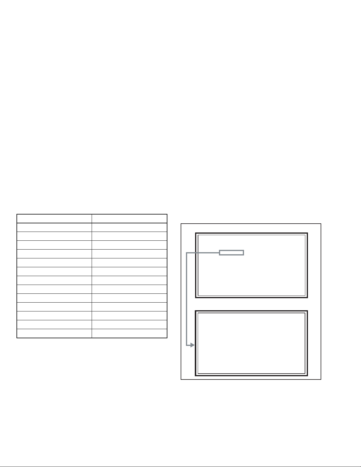
SPECIFICATION
Items Contents
Dimensions ( W × H × D ) 70.3cm × 55.5 cm × 30.0 cm [Included stand]
70.3cm × 49.1 cm × 10.7 cm [TV only]
Mass 16.1kg [Included stand]
12.8kg [TV only]
Power Input AC110V - AC240 V, 50 Hz / 60 Hz
Power Consumption 125W (Standby: 2.8W)
TV RF System B, G, I, D, K, K1, M
Colour System PAL / SECAM / NTSC 3.58 / NTSC 4.43
Stereo System A2 (B/G, D/K), NICAM (B/G, I, D/K)
Teletext System FLOF (Fastext), TOP, WST (World Standard System)
Receiving
Frequency
Intermediate Frequency VIF
Colour Sub
Carrier
LCD panel 26V-inch wide aspect (16:9)
Screen Size Diagonal : 66cm (H:57.6cm × V : 32.4cm)
Display Pixels Horizontal : 1366 dots × Vertical : 768 dots (W-XGA)
Audio Power Output 10W + 10W
Speaker 6.6cm, round type × 2 (Oblique corn)
Aerial terminal (VHF/UHF) 75Ω unbalanced, coaxial
Video / Audio
Input-1/2/3
Video / Audio Output S-Video
PC (RGB) Input D-sub 15pin × 1
Audio Output 500mV (rms), Low impedance, RCA pin jack × 2
Headphone 3.5mm stereo mini jack × 1
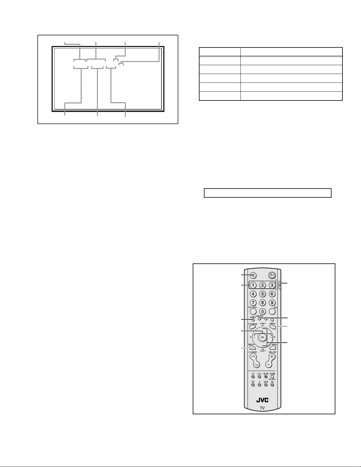
Remote Control Unit RM-C1830H (AA/R6 dry cell battery × 2)
Design & specifications are subject to change without notice.
Component Video
VHF Low
VHF High
UHF
CATV
SIF
PAL
SECAM
NTSC
[Input-1/3]
1125i
625p / 525p
625i / 525i
S-Video
[Input-1/2]
Video
Audio
Video
Audio
46.25MHz - 168.25MHz
175.25MHz - 463.25MHz
471.25MHz - 863.25MHz
Mid (X - Z+2, S1 - S10) / Super (S11 - S20) / Hyper (S21 - S41) bands
38.0MHz (B, G, I, D, K, L)
32.26MHz (5.74MHz: B), 32.15MHz (5.85MHz: G), 31.45MHz (6.55MHz: I)
31.75MHz (6.25MHz: D), 32.15MHz (5.85MHz: K)
4.43MHz
4.40625MHz / 4.25MHz
3.58MHz / 4.43MHz
Component connector (2-row 14-pn × 1) (Input-1)
RCA pin jack × 3 (Input-3)
Y : 1V (p-p) (Sync signal: ±0.35V(p-p), 3-value sync.), 75 Ω
Pb/Pr : ±0.35V(p-p), 75 Ω
Y : 1V (p-p), Positive (Negative sync provided), 75 Ω
Pb/Pr : 0.7V(p-p), 75 Ω
Mini-DIN 4 pin connector × 2
Y: 1V (p-p), Positive (Negative sync provided), 75 Ω
C: 0.286V (p-p) (Burst signal), 75 Ω
1V (p-p), Positive (Negative sync provided), 75 Ω, RCA pin jack × 3
500mV (rms), High impedance, RCA pin jack × 6
Mini-DIN 4 pin connector × 1
Y: 1V (p-p), Positive (Negative sync provided), 75 Ω
C: 0.286V (p-p) (Burst signal), 75 Ω
1V (p-p), Positive (Negative sync provided), 75 Ω, RCA pin jack × 1
500mV (rms), Low impedance, RCA pin jack × 2
R/G/B : 0.7V (p-p), 75Ω
HD / VD : 1V (p-p) to 5V (p-p), high impedance
< Available signal >
VGA : 640 pixels × 480 pixels (Horizontal : 31.5kHz / Vertical : 60Hz)
XGA : 1024 pixels × 768 pixels (Horizontal : 48.4kHz / Vertical : 60Hz)
1-2 (No.YA208)

SECTION 1
PRECAUTION
1.1 SAFETY PRECAUTIONS
(1) The design of this product contains special hardware,
many circuits and components specially for safety
purposes. For continued protection, no changes should be
made to the original design unless authorized in writing by
the manufacturer. Replacement parts must be identical to
those used in the original circuits. Service should be
performed by qualified personnel only.
(2) Alterations of the design or circuitry of the products should
not be made. Any design alterations or additions will void
the manufacturer's warranty and will further relieve the
manufacturer of responsibility for personal injury or
property damage resulting therefrom.
(3) Many electrical and mechanical parts in the products have
special safety-related characteristics. These
characteristics are often not evident from visual inspection
nor can the protection afforded by them necessarily be
obtained by using replacement components rated for
higher voltage, wattage, etc. Replacement parts which
have these special safety characteristics are identified in
the parts list of Service manual. Electrical components
having such features are identified by shading on the
schematics and by ( ) on the parts list in Service
manual. The use of a substitute replacement which does
not have the same safety characteristics as the
recommended replacement part shown in the parts list of
Service manual may cause shock, fire, or other hazards.
(4) Don't short between the LIVE side ground and
ISOLATED (NEUTRAL) side ground or EARTH side
ground when repairing.
Some model's power circuit is partly different in the GND.
The difference of the GND is shown by the LIVE : ( ) side
GND, the ISOLATED (NEUTRAL) : ( ) side GND and
EARTH : ( ) side GND.
Don't short between the LIVE side GND and ISOLATED
(NEUTRAL) side GND or EARTH side GND and never
measure the LIVE side GND and ISOLATED (NEUTRAL)
side GND or EARTH side GND at the same time with a
measuring apparatus (oscilloscope etc.). If above note will
not be kept, a fuse or any parts will be broken.
(5) When service is required, observe the original lead dress.
Extra precaution should be given to assure correct lead
dress in the high voltage circuit area. Where a short circuit
has occurred, those components that indicate evidence of
overheating should be replaced. Always use the
manufacturer's replacement components.
(6) Isolation Check (Safety for Electrical Shock Hazard)
After re-assembling the product, always perform an
isolation check on the exposed metal parts of the cabinet
(antenna terminals, video/audio input and output terminals,
Control knobs, metal cabinet, screw heads, earphone jack,
control shafts, etc.) to be sure the product is safe to operate
without danger of electrical shock.
a) Dielectric Strength Test
The isolation between the AC primary circuit and all metal
parts exposed to the user, particularly any exposed metal
part having a return path to the chassis should withstand a
voltage of 3000V AC (r.m.s.) for a period of one second. (.
. . . Withstand a voltage of 1100V AC (r.m.s.) to an
appliance rated up to 120V, and 3000V AC (r.m.s.) to an
appliance rated 200V or more, for a period of one second.)
This method of test requires a test equipment not generally
found in the service trade.
b) Leakage Current Check
Plug the AC line cord directly into the AC outlet (do not use
a line isolation transformer during this check.). Using a
"Leakage Current Tester", measure the leakage current
from each exposed metal part of the cabinet, particularly
any exposed metal part having a return path to the chassis,
to a known good earth ground (water pipe, etc.). Any
leakage current must not exceed 0.5mA AC (r.m.s.).
However, in tropical area, this must not exceed 0.2mA AC
(r.m.s.).
Alternate Check Method
Plug the AC line cord directly into the AC outlet (do not
use a line isolation transformer during this check.). Use
an AC voltmeter having 1000Ω per volt or more
sensitivity in the following manner. Connect a 1500Ω
10W resistor paralleled by a 0.15µF AC-type capacitor
between an exposed metal part and a known good earth
ground (water pipe, etc.). Measure the AC voltage
across the resistor with the AC voltmeter. Move the
resistor connection to each exposed metal part,
particularly any exposed metal part having a return path
to the chassis, and measure the AC voltage across the
resistor. Now, reverse the plug in the AC outlet and
repeat each measurement. Any voltage measured must
not exceed 0.75V AC (r.m.s.). This corresponds to
0.5mA AC (r.m.s.).
However, in tropical area, this must not exceed 0.3V AC
(r.m.s.). This corresponds to 0.2mA AC (r.m.s.).
AC VOLTMETER
(HAVING 1000 /V,
OR MORE SENSITIVITY)
0.15 F AC-TYPE
GOOD EARTH GROUND
1500 10W
PLACE THIS PROBE
ON EACH EXPOSED
ME TAL PAR T
(No.YA208)1-3
1.2 INSTALLATION
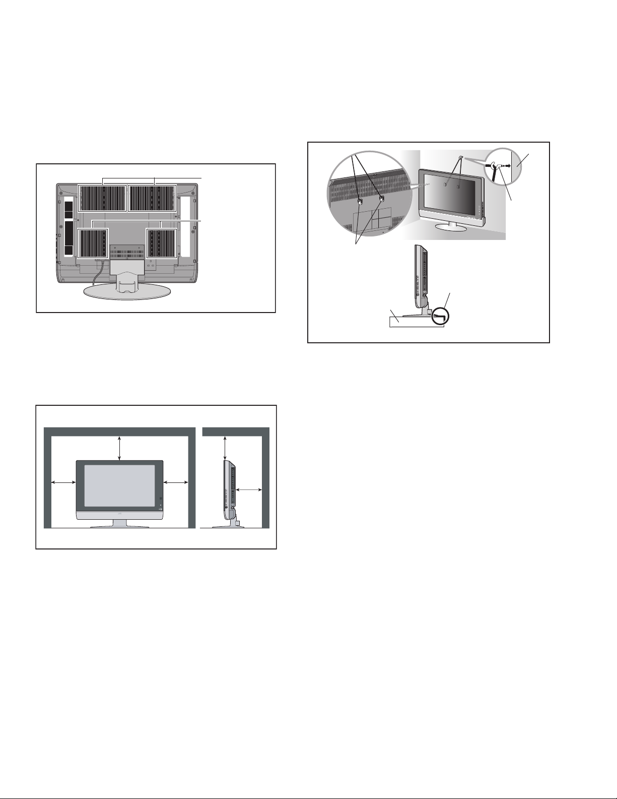
1.2.1 HEAT DISSIPATION
If the heat dissipation vent behind this unit is blocked, cooling
efficiency may deteriorate and temperature inside the unit will
rise. The temperature sensor that protects the unit will be
activated when internal temperature exceeds the pre-determined
level and power will be turned off automatically.Therefore,
please make sure pay attention not to block the heat dissipation
vent as well as the ventilation outlet behind the unit and ensure
that there is room for ventilation around it.
Ventilation hole
Ventilation hole
1.2.3 INSTALLATION REQUIREMENTS
To ensure safety in an emergency such as an earthquake, and
to prevent accidents, ensure that measures are taken to prevent
the TV dropping or falling over.
Use the supplied screws to firmly attach the supplied hooks
(OPTION) to the back of the TV, and use commercially available
cord to fix the TV to rigid components such as walls and columns.
Wall
Hook
The hook for fall
prevention(option)
It fixes in a band.
TV Stand
1.2.2 INSTALLATION REQUIREMENTS
Ensure that the minimal distance is maintained, as specified
below, between the unit with and the surrounding walls, as well
as the floor etc.Install the unit on stable flooring or stands.Take
precautionary measures to prevent the unit from tipping in order
to protect against accidents and earthquakes.
150 mm
200 mm
150 mm
200 mm
50 mm
*Diagram differs from actual appearance.
1.2.4 NOTES ON HANDLING
(1) WHEN TAKING UNIT OUT OF A PACKING CASE
When taking the unit out of a packing case, do not grasp
the upper part of the unit. If you take the unit out while
grasping the upper part, the LCD PANEL may be damaged
because of a pressure. Instead of grasping the upper part,
put your hands on the lower backside or sides of the unit.
(2) AS FOR PRESSING OR TOUCHING A SPEAKER
Be careful not to press the opening of the speaker in the
lower part of the unit and around them since the decorative
sheet on the surface of the openings may be deformed.
1-4 (No.YA208)

1.3 HANDLING LCD PANEL
1.3.1 PRECAUTIONS FOR TRANSPORTATION
When transporting the unit, pressure exerted on the internal LCD
panel due to improper handling (such as tossing and dropping)
may cause damages even when the unit is carefully packed. To
prevent accidents from occurring during transportation, pay
careful attention before delivery, such as through explaining the
handling instructions to transporters.
Ensure that the following requirements are met during
transportation, as the LCD panel of this unit is made of glass and
therefore fragile:
(1) USE A SPECIAL PACKING CASE FOR THE LCD PANEL
When transporting the LCD panel of the unit, use a special
packing case (packing materials). A special packing case
is used when a LCD panel is supplied as a service spare
part.
(2) ATTACH PROTECTION SHEET TO THE FRONT
Since the front (display part) of the panel is vulnerable,
attach the protection sheet to the front of the LCD panel
before transportation. Protection sheet is used when a LCD
panel is supplied as a service spare part.
(3) AVOID VIBRATIONS AND IMPACTS
The unit may be broken if it is toppled sideways even when
properly packed. Continuous vibration may shift the gap of
the panel, and the unit may not be able to display images
properly. Ensure that the unit is carried by at least 2
persons and pay careful attention not to exert any vibration
or impact on it.
(4) DO NOT PLACE EQUIPMENT HORIZONTALLY
Ensure that it is placed upright and not horizontally during
transportation and storage as the LCD panel is very
vulnerable to lateral impacts and may break. During
transportation, ensure that the unit is loaded along the
traveling direction of the vehicle, and avoid stacking them
on one another. For storage, ensure that they are stacked
in 2 layers or less even when placed upright.
1.3.2 OPTICAL FILTER (ON THE FRONT OF THE LCD PANEL)
(1) Avoid placing the unit under direct sunlight over a
prolonged period of time. This may cause the optical filter
to deteriorate in quality and COLOUR.
(2) Clean the filter surface by wiping it softly and lightly with a
soft and lightly fuzz cloth (such as outing flannel).
(3) Do not use solvents such as benzene or thinner to wipe the
filter surface. This may cause the filter to deteriorate in
quality or the coating on the surface to come off. When
cleaning the filter, usually use the neutral detergent diluted
with water. When cleaning the dirty filter, use water-diluted
ethanol.
(4) Since the filter surface is fragile, do not scratch or hit it with
hard materials. Be careful enough not to touch the front
surface, especially when taking the unit out of the packing
case or during transportation.
1.3.3 PRECAUTIONS FOR REPLACEMENT OF EXTERIOR
PARTS
Take note of the following when replacing exterior parts (REAR
COVER, FRONT PANEL, etc.):
(1) Do not exert pressure on the front of the LCD panel (filter
surface). It may cause irregular COLOUR.
(2) Pay careful attention not to scratch or stain the front of the
LCD panel (filter surface) with hands.
(3) When replacing exterior parts, the front (LCD panel) should
be placed facing downward. Place a mat, etc. underneath
to avoid causing scratches to the front (filter surface).
(No.YA208)1-5
SECTION 2
SPECIFIC SERVICE INSTRUCTIONS
2.1 FEATURES
D.I.S.T. (Digital Image Scaling Technology)
This system uses line interpolation to double the number of
scanning lines and achieve high resolution, flicker-free picture.
COLOUR MANAGEMENT
This function ensures dull colours are compensated to
produce natural hues.
PICTURE MANAGEMENT
This function makes it easier to see the dark areas when a
picture has many dark areas, and makes it easier to see the
bright areas when a picture has many bright areas.
ZOOM
This function can change the screen size according to the
picture aspect ratio.
2.2 MAIN DIFFERENCE LIST
Item LT-Z26SX4B LT-Z26SX4B/A LT-Z26SX4B/S LT-Z26SX4S/S
FRONT PANEL COLOUR BLACK ←←SILVER
POWER CORD Round pin (2-pin) type
SHIELD COVER(DIGITAL SIGNAL PWB)
TOP SHIELD CASE(DIGITAL SIGNAL PWB)
SIDE SHIELD CASE(DIGITAL SIGNAL PWB)
DIGITAL SIGNAL P.W.B SFL0D301A-H2 SFL0D303A-H2 SFL0D302A-H2 ←
Not used ← Used ←
Not used Not used Used ←
Not used Not used Used ←
DIGITAL VNR
This function cuts down the amount of noise in the original
picture.
SUPER DIGIPURE
This function uses the latest in digital technology to give you a
natural-looking picture.
PULL DOWN
This function displays a cinema film picture more smoothly and
naturally on the screen.
3D CINEMA SOUND
You can enjoy sounds with a widerambience.
Australia pin (2-pin) type
UK pin (3-pin) type ←
1-6 (No.YA208)
2.3 TECHNICAL INFORMATION
2.3.1 LCD PANEL
This unit uses the flat type panel LCD (Liquid Crystal Display) panel that occupies as little space as possible, instead of the
conventional CRT (Cathode Ray Tube), as a display unit.
Since the unit has the two polarizing filter that are at right angles to each other, the unit adopts "normally black" mode, where light
does not pass through the polarizing filter and the screen is black when no voltage is applied to the liquid crystals.
2.3.1.1 SPECIFICATIONS
The following table shows the specifications of this unit.
Item Specifications Remarks
Maximum dimensions ( W × H × D ) 627mm × 374mm × 52mm
Weight 4.5kg
Effective screen size Diagonal: 660.4mm (H:575.7mm × V : 323.7mm) 26V type
Aspect ratio 16 : 9
Drive device / system a-Si-TFT, active matrix system
Resolution Horizontally 1366 × Vertically 768 × RGB <W-XGA> 3147264 dots in total
Pixel pitch (pixel size) Horizontally:0.4215mm, Vertically:0.4215mm
Displayed colour 16777216 colours 256 colours for R, G, and B
Brightness 500cd/m
2
Contrast ratio 800: 1
Response time 8ms
View angle Horizontally: 170°, Vertically: 170°
Surface polarizer Anti-Glare type, Low reflective coat
Colour filter Vertical stripe
Backlight U-type Cold cathode fluorescent lamp × 8
Power supply voltage in LCD 6.5V
Power supply voltage in inverter 18V
Panel interface system LVDS (Low Voltage Differential Signaling)
2.3.1.2 PIXEL FAULT
There are three pixel faults - bright fault , dark fault and flicker fault - that are respectively defined as follows.
BRIGHT FAULT
In this pixel fault, a cell that should not light originally is lighting on and off.
For checking this pixel fault, input ALL BLACK SCREEN and find out the cell that is lighting on and off.
DARK FAULT
In this pixel fault, a cell that should light originally is not lighting or lighting with the brightness twice as brighter as originally lighting.
For checking this pixel fault, input 100% of each R/G/B colour and find out the cell that is not lighting.
FLICKER FAULT
In the pixel fault, a cell that should light originally or not light originally is flashing on and off.
For checking this pixel fault, input ALL BLACK SCREEN signal or 100% of each RGB colour and find out the cell that is flashing on
and off.
(No.YA208)1-7
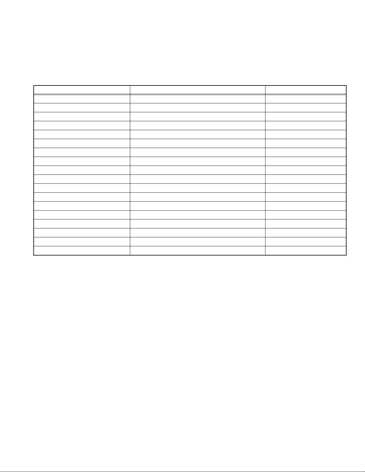
2.3.2 MAIN CPU PIN FUNCTION [IC7501 : DIGITAL SIGNAL PWB ASS'Y]
Pin Pin name I/O Function Pin Pin name I/O Function
1 TCK I Test purpose 65 D2 I/O Program ROM data for main CPU
2 TMS I Test purpose 66 D12 I/O Program ROM data for main CPU
3 TDI I Test purpose 67 D10 I/O Program ROM data for main CPU
4 TDO O Test purpose 68 VSS33 - GND
5 P2.8 O Not used 69 VDD33 I 3.3V
6 P2.9 O Blue for OSD 70 D4 I/O Program ROM data for main CPU
7 P2.10 O Blue for OSD 71 D3 I/O Program ROM data for main CPU
8 P2.11 O Blue for OSD 72 D11 I/O Program ROM data for main CPU
9 P2.12 O Blue for OSD 73 RSTIN I Reset
10 P2.13 O Blue for OSD 74 POWER O Sleep state release for chassis CPU [Relese : L]
11 P2.14 I Not used 75 P3.1 O Not used
12 P2.15 O Request for chassis CPU communication 76 REMOCON I Remote control
13 VSS33 - GND 77 P3.3 I Clock for OSD
14 VDD33 I 3.3V 78 P3.4 O Red for OSD
15 P4.5 O Not used 79 P3.5 O Red for OSD
16 A20 O Program ROM address for main CPU 80 P3.6 O Red for OSD
17 A19 O Program ROM address for main CPU 81 P3.7 O Red for OSD
18 A18 O Program ROM address for main CPU 82 MTST O Data transmission for chassis CPU communication
19 A17 O Program ROM address for main CPU 83 MTSR I Data receive for chassis CPU communication
20 VSS25 - GND 84 VSS33 - GND
21 VDD25 I 2.5V 85 VDD33 I 3.3V
22 A16 O Program ROM address for main CPU 86 VSS25 - GND
23 A8 O Program ROM address for main CPU 87 VDD25 I 2.5V
24 A7 O Program ROM address for main CPU 88 TXD0 O Communication for adjustment
25 A9 O Program ROM address for main CPU 89 RXD0 O Communication for adjustment
26 A6 O Program ROM address for main CPU 90 P3.12 O Red for OSD
27 A5 O Program ROM address for main CPU 91 CLK O Clock for chassis CPU communication
28 A10 O Program ROM address for main CPU 92 P3.15 O Green for OSD
29 A11 O Program ROM address for main CPU 93 P5.14 O Green for OSD
30 A12 O Program ROM address for main CPU 94 P5.15 O Green for OSD
31 VSS33 - GND 95 TRIG_IN O Green for OSD
32 VDD33 I 3.3V 96 TRIG_OUT O Green for OSD
33 A4 O Program ROM address for main CPU 97 P6.2 O Green for OSD
34 A3 O Program ROM address for main CPU 98 P6.3 O I
35 A2 O Program ROM address for main CPU 99 P6.4 I/O I
36 A1 O Program ROM address for main CPU 100 P6.5 O Teletext signal select [Analog RGB : H / Digital RGB : L]
37 A0 O Program ROM address for main CPU 101 IRQ O Not used
38 A13 O Program ROM address for main CPU 102 VSYNC I Vertical sync
39 ARAS/A14 O Program ROM address for main CPU 103 HSYNC I Horizontal sync
40 CAS/A15 O Program ROM address for main CPU 104
41 VSS33 - GND 105 BLANK O Ys for OSD / Teletext
42 VDD33 I 3.3V 106 VDD33 I 3.3V
43 MEMCLK O Clock for memory 107 VSS33 - GND
44 CSSDRAM O Chip select for memory 108 XTAL1 I 6MHz for system clock
45 CLKEN O Clock enable for memory 109 XTAL2 O 6MHz for system clock
46 CSROM O Chip select for memory 110 VSSA - GND
47 RD O Read for memory 111 VDDA I 2.5V
48 UDQM O Control buffer of memory 112 R O R for OSD / Teletext
49 LDQM O Control buffer of memory 113 G O G for OSD / Teletext
50 WR O Write for memory 114 B O B for OSD / Teletext
51 D15 I/O Program ROM data for main CPU 115 VSSA - GND
52 VSS33 - GND 116 VDDA I 2.5V
53 VDD33 I 3.3V 117 CVBS2 I Video for Teletext
54 D7 I/O Program ROM data for main CPU 118 VSSA - GND
55 D0 I/O Program ROM data for main CPU 119 VDDA I 2.5V
56 D14 I/O Program ROM data for main CPU 120 CVBS1B I Video for Teletext
57 D8 I/O Program ROM data for main CPU 121 CVBS1A I Video for Teletext
58 D6 I/O Program ROM data for main CPU 122 VSSA - GND
59 D1 I/O Program ROM data for main CPU 123 VDDA I 2.5V
60 VSS33 - GND 124 KEY1 I Key scan data 1 [ON : H]
61 VDD33 I 3.3V 125 KEY2 I Key scan data 2 [ON : H]
62 D13 I/O Program ROM data for main CPU 126 MECA_SW I Main power ON / OFF control [ON : L]
63 D9 I/O Program ROM data for main CPU 127 P5.3 I Not used
64 D5 I/O Program ROM data for main CPU 128 TMODE I Test purpose
COR/RSTOUT
2
C bus clock (for main memory)
2
C bus Data (for main memory)
O Not used
1-8 (No.YA208)
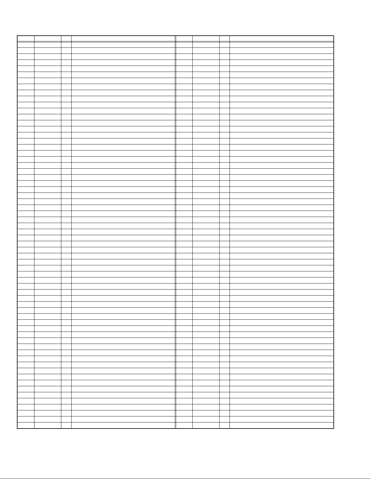
2.3.3 SUB (CHASSIS) CPU PIN FUNCTION [IC7001 : DIGITAL SIGNAL PWB ASS'Y]
Pin Pin name I/O Function Pin Pin name I/O Function
1 LB_PRO O Not used 51 BS_TXD O
2 P_MU O Picture muting [Muting = H] 52 BS_RXD I Not used : Data receive for digital tuner communication
3 JP_CSB O Not used (NC) 53 NC O Not used (NC)
4 A_MU O Audio muting [Muting = H] 54 VREF+ I 3.3V power supply
5 M_MU O Audio muting (for AUDIO OUT) [Muting = H] 55 PDP_TX O
6 PC_SEL O RGB(PC) INPUT select 56 PDP_RX I Data receive for SUB (DRIVE) CPU communication
7 ON_TIMER O POWER INDICATOR (LED) brightness [LOW = L] 57 SDA0 I/O Data for Inter IC (serial) bus : EEP-ROM (IC7002)
8 ILA0 O Not used : LCD back light lighting 58 SCL0 O Clock for Inter IC (serial) bus : EEP-ROM (IC7002)
9 ILA1 O Not used : LCD panel overshoot refresh timing 59 SDA_DVI I/O
10 ILA2 O Not used 60 SCL_DVI O
11 POW_LED O POWER LED lighting [ON = H] 61 AVSS - GND
12 WORD O Not used 62 DIGII_PHOT I
13 MI_CK I Clock for main CPU communication 63 AGC I Not used
14 MI_TX I Data receive for main CPU communication 64 EXT_YS1 I Not used
15 MI_RX O Data transmission for MAIN CPU communication 65 EXT_YS2 I Not used
16 MI_REQ O
17 VDD I 3.3V power supply 67 DIGI_PRO O Not used : For DIGITAL-IN (HDMI)
18 FOSC O Not used (NC) 68 GCR_RST O Not used (NC)
19 VSS - GND 69 GR_ON O Not used (NC)
20 X1 I Not used : Low speed oscillatior 70 SYNC_SEL O Not used : Sync select for digital tuner
21 X0 O Not used : Low speed oscillatior 71 NC O Not used (NC)
22 VDD I 3.3V power supply 72 NC O Not used (NC)
23 OSC1 I System clock osillation (crystal) : 16MHz 73 SBD5 I/O
24 OSC0 O System clock osillation (crystal) : 16MHz 74 SBT5 I
25 MODE I Single chip mode 75 NMI I 3.3V power supply
26 BS1.5CTL O Not used : Digital tuner power / reset control 76 COMP I Not used : AV COMPULINK lll control
27 A92RES O
28 BS_RST O Not used: Reset for Digital tuner power / reset control 78 VSYNC I V. sync pulse
29 LIP_RST O Not used: Reset for Sound delay (Lip sync) 79 WAKE I Reset for sub(chassis) CPU
30 SOFT_OFF O Not used 80
31 VMUTE I Not used: Picture muting request from digital tuner 81 NC O Not used (NC)
32 VOUTENB O Not used: Video cutoff for digital tuner 82 RST I Reset for MAIN CPU [Reset = L]
33 MDR_CON I Not used: System cable connection monitor for PDP 83 VDD I 3.3V power supply
34 AVDD I 3.3V power supply 84 SCL3A O Clock for Inter IC (serial) bus control
35 BS_POW O Not used : Digital tuner power control 85 SDA3A I/O Data for Inter IC (serial) bus control
DsyncSW2
36
37 LB_POW O Not used : Power control for low bias line 87 SDA3B I/O Data for Inter IC (serial) bus control
38 NC O Not used (NC) 88
39 HOTPLUG I
40 MECA_SW I Mechanical monitor for POWER switch [Push = L] 90 DIGI_INT I Not used : Reset for HDMI process [Reset = L ]
41 MAIN_POW O Main power control [ON = L] 91 DVI_RST O Not used : Reset for DVI format conversion
42 MSP_RST O AUDIO OUT output mode select [VARIABLE = L] 92 VSS - GND
43 VREF- I Not used 93 SCL5055 O
44 AFT2 I Not used : AFT voltage for sub tuner 94
45 AFT1 I AFT voltage for VHF/UHF tuner 95 SDA5055 I/O Data for Inter IC (serial) bus : JCC5055 (DIST process)
46 KEY2 I Key scan data for front switch (MENU/CH+/CH-) 96
47 KEY1 I Key scan data for front switch (VOL+/VOL-) 97 NC O Not used (NC)
48 NC O Not used (NC) 98 15K/OTH O Main video select [Fixed = H]
49 NC O Not used (NC) 99 DsyncSW1 O
50 AC_IN I AC power pulse for timer clock 100 57 BUSY I Busy monitor for JCC5057 (New DIST process)
Data request for main CPU communication [Request = L]
Reset for IC1001(3D YC SEP / COLOUR DEMODULAT) [Reset = H]
O Sync select for DIGITAL-IN [Cotrolled with 99-pin] 86 SCL3B O Clock for Inter IC (serial) bus control
Not used : Video communiation monitor for receiver unit (PDP)
66 VDD I 3.3V power supply
77 REMO I Remote control
POWERGOOD
DIGI_SYNCSEL
89 DIGI_LRSW O Not used : For DIGITAL-IN (HDMI)
VFORMATSEL
OSD_MODE_SEL
Not used : Data transmission for digital tuner communication
Data transmission for SUB (DRIVE) CPU communication
Not used : Data for Inter IC (serial) bus for panel communication
Not used : Clock for Inter IC (serial) bus for panel communication
Not used: Photo sensor for DIGITAL-IN illegal copy protection
Not used : Data for writing on board (connect CN01P : for Frash ROM type)
Not used : Clock for writing on board (connect CN01P : for Frash ROM type)
I Power error detection [NG = H]
O Not used
Clock for Inter IC (serial) bus : JCC5055 (DIST process)
O Not used : Digital tuner clock control
O Not used : OSD mode select
Not used : Sync select for DIGITAL-IN [Cotrolled with 36-pin]
(No.YA208)1-9

SECTION 3
DISASSEMBLY
3.1 DISASSEMBLY PROCEDURE
NOTE:
• Make sure that the power cord is disconnected from the outlet.
• Pay special attention not to break or damage the parts.
• When removing each board, remove the connectors as required. Taking notes of the connecting points (connector numbers)
makes service procedure manageable.
• Make sure that there is no bent or stain on the connectors before inserting, and firmly insert the connectors.
3.1.1 REMOVING THE STAND (Fig.1)
(1) Remove the 2 screws [A], then remove the STAND
COVER.
(2) Remove the 4 screws [B], then remove the STAND.
3.1.2 REMOVING THE REAR COVER (Fig.1)
• Remove the STAND.
(1) Remove the JACK COVER (L/R).
(2) Remove the 7 screws [C], the 4 screws [D], and the 1
screws [E] .
(3) Remove the REAR COVER.
3.1.3 REMOVING THE POWER PWB / REGULATOR PWB
(Fig.1)
• Remove the STAND.
• Remove the REAR COVER.
(1) Remove the 5 screws [F], then remove the FAN
BRACKET.
(2) Remove the 1 screw [G], then remove the POWER CORD
HOLDER.
(3) Remove the POWER CORD from the POWER PWB.
(4) Remove the REGULATOR PWB.
(5) Remove the 5 screw [H], then remove the POWER PWB.
3.1.4 REMOVING THE ANALOG SYGNAL PWB (Fig.1)
• Remove the STAND.
• Remove the REAR COVER.
• Remove the FAN BRACKET.
(1) Remove the 6 screws [J] then remove the TERMINAL
BASE.
(2) Remove the 6 screws [K] and the 2 hex screws [W] then
remove the ANALOG SYGNAL PWB.
3.1.6 REMOVING THE RECEIVER PWB / CONNECTOR
PWB (Fig.1)
• Remove the STAND.
• Remove the REAR COVER.
(1) Remove the 3 screws [U], then remove the TUNER BASE
and SIDE SHIELD CASE.
(2) Remove the 4 screws [O] then remove the RECEIVER
PWB.
(3) Remove the 4 screws [P] then remove the RECEIVER
PWB BRACKET.
(4) Remove the 2 screws [Q] then remove the CONNECTOR
PWB.
3.1.7 REMOVING THE DIGITAL SIGNAL PWB (Fig.1)
• Remove the STAND.
• Remove the REAR COVER.
• Remove the TUNER BASE.
(1) Remove the 9 screws [S] and the 3screws [T], then
remove the SHIELD COVER.
(2) Remove the 5 screws [V], then remove the DIGITAL
SIGNAL PWB.
3.1.8 REMOVING THE SPEAKER (Fig.2)
• Remove the STAND.
• Remove the REAR COVER.
(1) Remove the 5 screws [a], then remove the SPEAKER
BOX.
(2) Remove the 4 screws [b], then remove the SPEAKER (L /R).
(3) Remove the 4 screws [c], then remove the DUCT(L/R).
NOTE:
Since the speaker is attached in a certain direction, attach the
speaker in the same correct direction as it has been attached.
3.1.5 REMOVING THE FRONT CONTROL PWB CONTROL /
FRONT SENSOR PWB (Fig.1)
• Remove the STAND.
• Remove the REAR COVER.
(1) Remove the 2 screws [L], then remove the CONTROL
KNOB ASSY.
(2) Remove the 2 screws [M], then remove the FRONT
CONTROL PWB.
(3) Remove the FRONT SENSOR PWB.
1-10 (No.YA208)
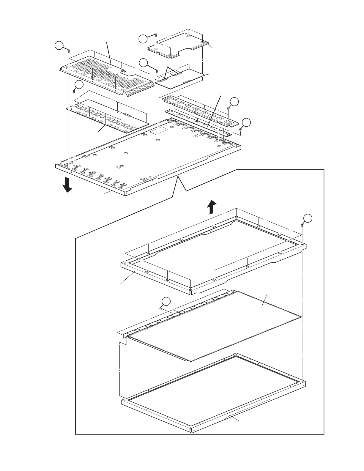
3.1.9 REMOVING THE LCD PANEL UNIT (Fig.2)
• Remove the STAND.
• Remove the REAR COVER.
(1) Remove the 6 screws [d] and the 4 screws [e].
(2) Remove the LCD PANEL UNIT.
(3) Remove the 7 screws [f]. then remove the MAIN BASE.
(4) Remove the 2 screws [g]. then remove the TOP FRAME.
(5) Remove the 2 screws [h]. then remove the BOTTOM
FRAME.
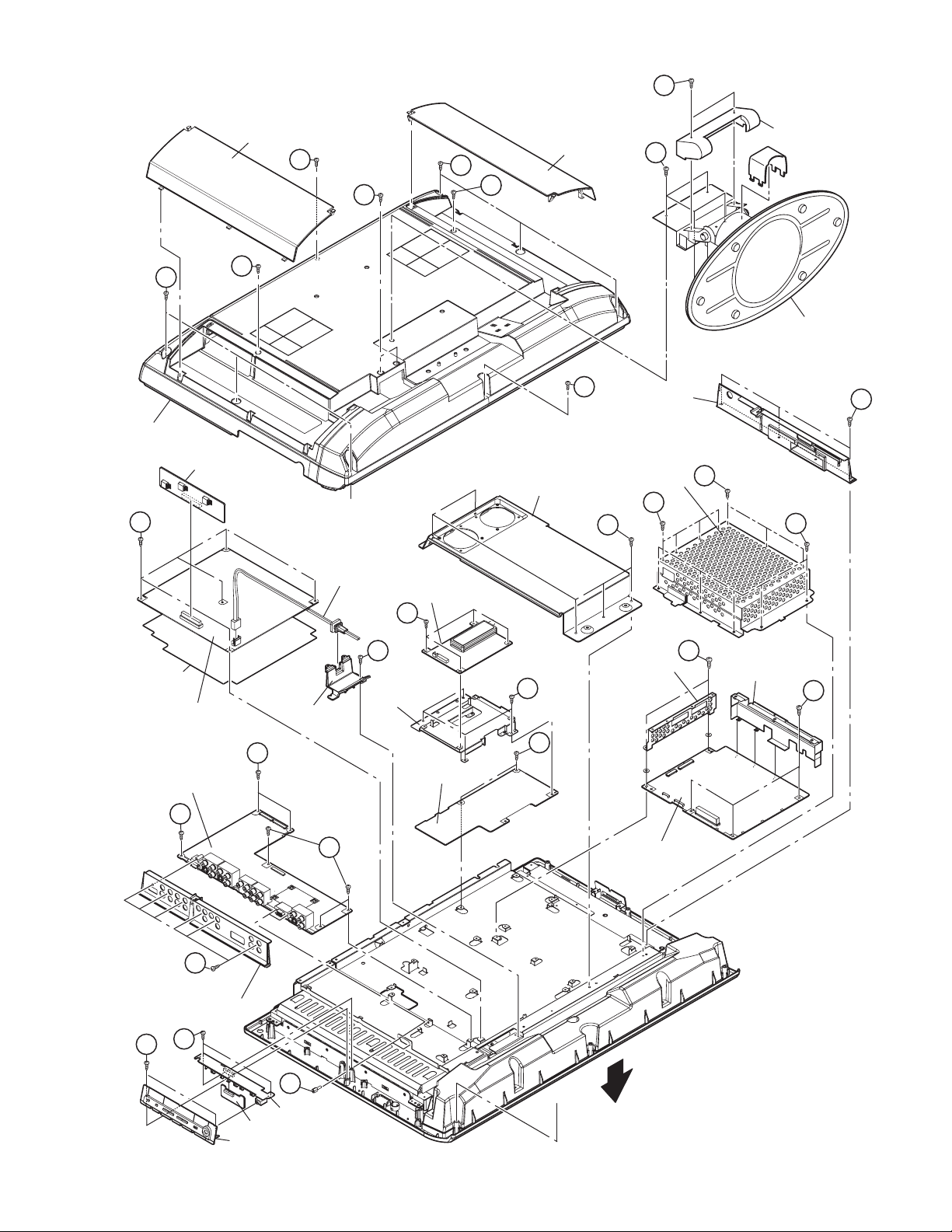
A
C
REAR COVER
REGULATOR PWB
H
JACK COVER
D
E
D
a
POWER CORD
RECEIVER PWB
O
STAND COVER
JACK COVER
B
C
D
STAND
C
FAN BRACKET
TUNER BASE
SHIELD COVER
[LT-Z26SX4B/S,
LT-Z26SX4S/S]
S
F
T
S
U
INSULATOR
POWER PWB
ANALOG SIGNAL PWB
K
J
TERMINAL BASE
M
L
FRONT SENSOR PWB
POWER CORD
HOLDER
K
K
W
FRONT CONTROL PWB
CONTROL KNOB ASSY
G
RECEIVER PWB
BRACKET
CONNECTOR PWB
Fig.1
SIDE SHIELD CASE
V
TOP SHIELD CASE
P
[LT-Z26SX4B/S,
LT-Z26SX4S/S]
[LT-Z26SX4B/S,
LT-Z26SX4S/S]
V
Q
DIGITAL SIGNAL PWB
a
FRONT
(No.YA208)1-11
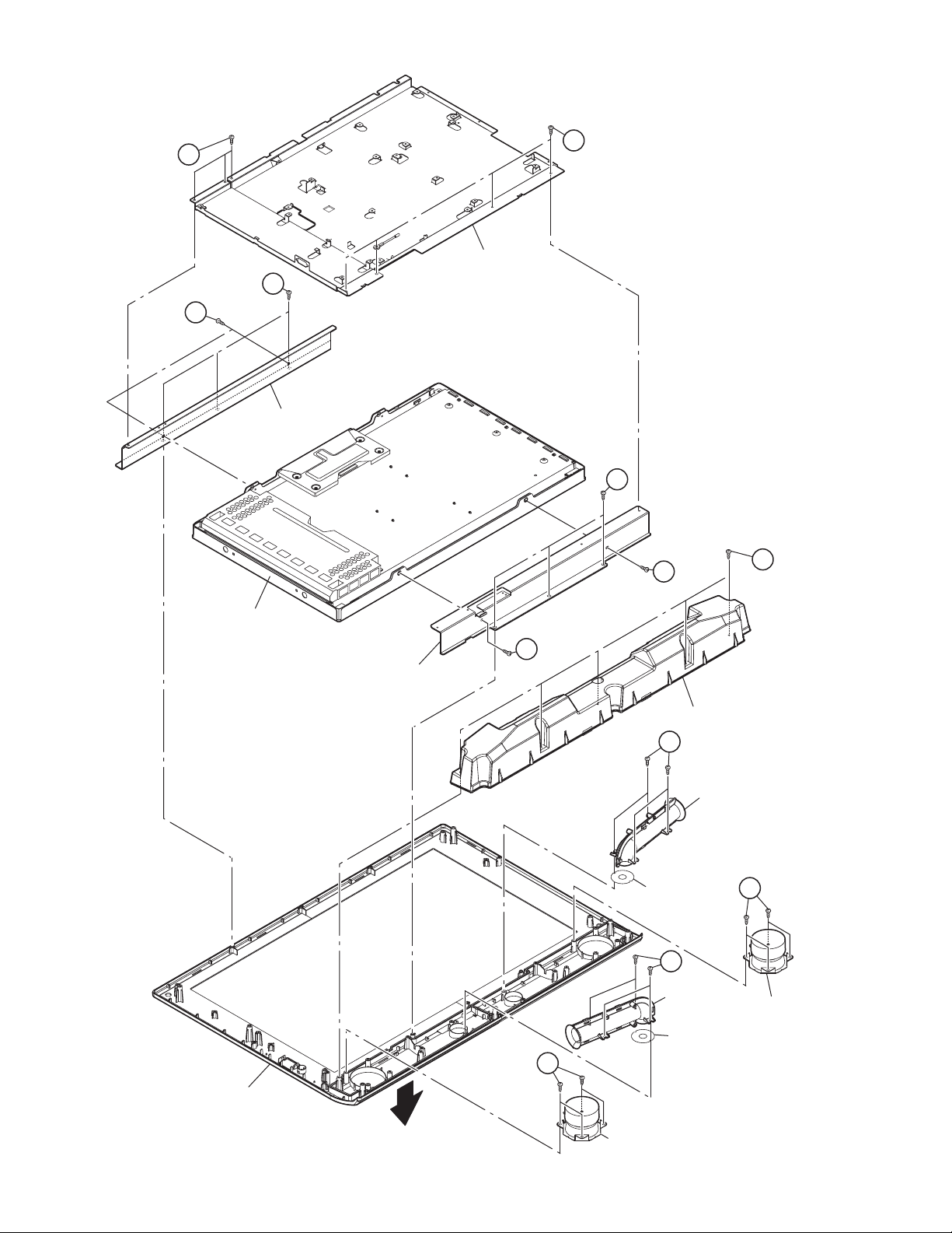
f
f
MAIN BASE
d
h
TOP FRAME
d
LCD PANEL UNIT
BOTTOM FRAME
g
a
g
SPEAKER BOX
b
DUCT
DUCT SHEET
c
b
DUCT
SPEAKER
1-12 (No.YA208)
FRONT PANEL
FRONT
DUCT SHEET
c
SPEAKER
Fig.2
3.2 MEMORY IC REPLACEMENT
S001 PREPARE 0
PAL50 FULL STD H
SERVICE MENU
1.ADJUST
2.SELF_CHK
3.I2C STOP
• This model uses the memory IC.
• This memory IC stores data for proper operation of the video and drive circuits.
• When replacing, be sure to use an IC containing this (initial value) data.
3.2.1 MEMORY IC REPLACEMENT PROCEDURE
1. Power off
Switch off the power and disconnect the power plug from the AC outlet.
2. Replace the memory IC
Be sure to use the memory IC written with the initial setting values.
3. Power on
Connect the power plug to the AC outlet and switch on the power.
4. Receiving channel setting
Refer to the OPERATING INSTRUCTIONS and set the receive channels (Channels Preset) as described.
5. User setting
Check the user setting items according to the given in page later. Where these do not agree, refer to the OPERATING
INSTRUCTIONS and set the items as described.
6. SERVICE MODE setting
Verify what to set in the SERVICE MODE, and set whatever is necessary (Fig.1). Refer to the SERVICE ADJUSTMENT for setting.
3.2.2 SERVICE MODE SETTING
SERVICE MODE SCREEN
MAIN MENU SCREEN
SETTING ITEM
Setting items Settings Item No.
Video system setting Adjust S001 - S039
SERVICE MENU
1.ADJUST
2.SELF_CHK
3.I2C STOP
Audio system setting Fixed T001 - T010
Panel control system setting Fixed P001 - P010
Drive system setting Fixed D001 - D187
Main CPU system setting Fixed Z001 - Z010
ADJUSTMENT MODE SCREEN
S001 PREPARE 0
PAL50 FULL STD H
Fig.1
(No.YA208)1-13
3.2.3 SETTINGS OF FACTORY SHIPMENT
3.2.3.1 BUTTON OPERATION 3.2.3.2 REMOTE CONTROL DIRECT OPERATION
Setting item Setting position
POWER Off
CHANNEL PR1
VOLUME 10
TV/VIDEO TV
STANDBY MODE OFF
3.2.3.3 REMOTE CONTROL MENU OPERATION
(1) PICTURE
Setting item Setting position
PICTURE MODE BRIGHT
WHITE BALANCE COOL
FEATURES
DIGITAL VNR AUTO (LOW)
Super DigiPure AUTO
PULL DOWN AUTO
COLOUR MANAGEMENT ON
PICTURE MANAGEMENT ON
COLOUR SYSTEM MAIN Depends on PR/CH
SUB AUTO
4:3 AUTO ASPECT PANORAMIC
(2) SOUND
Setting item Setting position
STEREO / I•II Stereo sound
BASS Centre
TREBLE Centre
BALANCE Centre
CINEMA SURROUND OFF
A.H.B. ON
BBE ON
CHANNEL PR1
VOLUME 10
ZOOM PANORAMIC
CINEMA OFF
SUB PICTURE VIDEO-1
(4) FEATURES
SLEEP TIMER OFF
APPEARANCE TYPE D
CHILD LOCK ID NO.0000, All CH off
BLUE BACK ON
AUTO SHUTOFF OFF
FAVORITE SETTING RESET
(5) SET UP
AUTO PROGRAM TV channel automatically set
EDIT/MANUAL PRESET CH only
LANGUAGE ENGLISH
VIDEO-1 SETTING COMPONENT
VIDEO-3 SETTING COMPONENT
AI VOLUME ON
TELETEXT LANGUAGE GROUP-1
Setting item Setting position
Setting item Setting position
Setting item Setting position
1-14 (No.YA208)
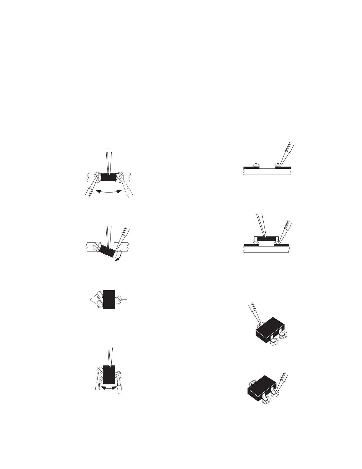
3.3 REPLACEMENT OF CHIP COMPONENT
3.3.1 CAUTIONS
(1) Avoid heating for more than 3 seconds.
(2) Do not rub the electrodes and the resist parts of the pattern.
(3) When removing a chip part, melt the solder adequately.
(4) Do not reuse a chip part after removing it.
3.3.2 SOLDERING IRON
(1) Use a high insulation soldering iron with a thin pointed end of it.
(2) A 30w soldering iron is recommended for easily removing parts.
3.3.3 REPLACEMENT STEPS
1. How to remove Chip parts
2. How to install Chip parts
[Resistors, capacitors, etc.]
(1) As shown in the figure, push the part with tweezers and
alternately melt the solder at each end.
(2) Shift with the tweezers and remove the chip part.
[Transistors, diodes, variable resistors, etc.]
(1) Apply extra solder to each lead.
SOLDER
SOLDER
[Resistors, capacitors, etc.]
(1) Apply solder to the pattern as indicated in the figure.
(2) Grasp the chip part with tweezers and place it on the
solder. Then heat and melt the solder at both ends of the
chip part.
[Transistors, diodes, variable resistors, etc.]
(1) Apply solder to the pattern as indicated in the figure.
(2) Grasp the chip part with tweezers and place it on the
solder.
(3) First solder lead A as indicated in the figure.
(2) As shown in the figure, push the part with tweezers and
alternately melt the solder at each lead. Shift and remove
the chip part.
NOTE :
After removing the part, remove remaining solder from the
pattern.
A
B
C
(4) Then solder leads B and C.
A
B
C
(No.YA208)1-15
SECTION 4
SERVICE MENU
1.ADJUST
2.SELF_CHK
3.I2C STOP
S001 PREPARE 0
PAL50 FULL STD H
ADJUSTMENT
4.1 ADJUSTMENT PREPARATION
(1) There are 2 ways of adjusting this TV : One is with the
REMOTE CONTROL UNIT and the other is the
conventional method using adjustment parts and
components.
(2) The adjustment using the REMOTE CONTROL UNIT is
made on the basis of the initial setting values. The
setting values which adjust the screen to the optimum
condition can be different from the initial setting
values.
(3) Make sure that connection is correctly made AC to AC
power source.
(4) Turn on the power of the TV and measuring instruments for
warning up for at least 30 minutes before starting
adjustments.
(5) If the receive or input signal is not specified, use the most
appropriate signal for adjustment.
(6) Never touch the parts (such as variable resistors,
transformers and condensers) not shown in the adjustment
items of this service adjustment.
4.2 PRESET SETTING BEFORE ADJUSTMENTS
Unless otherwise specified in the adjustment items, preset the
following functions with the REMOTE CONTROL UNIT.
Setting item Settings position
PICTURE MODE STANDARD
PICTURE adjustments Centre
WHITE BALANCE MID
DIGITAL VNR MIN
Super DigiPure AUTO
PULL DOWN AUTO
COLOUR MANAGEMENT ON
PICTURE MANAGEMENT ON
SOUND adjustments Centre
BBE OFF
CINEMA SORROUND OFF
A.H.B OFF
ZOOM FULL
4.3 MEASURING INSTRUMENT AND FIXTURES
• Oscilloscope
• Signal generator (Pattern generator)
[PAL / 625i / 625p / 1125i(50Hz)]
• Remote control unit
4.4 ADJUSTMENT ITEMS
VIDEO CIRCUIT
• 625i A-D OFFSET adjustment
• 1125i(50Hz) BRIGHTNESS adjustment
• 1125i(50Hz) A-D OFFSET adjustment
• SUB SCREEN A-D OFFSET adjustment
• WHITE BALANCE (HIGH LIGHT) adjustment
4.5 BASIC OPERATION OF SERVICE MODE
4.5.1 HOW TO ENTER THE SERVICE MODE
(1) Press [DISPLAY] key and [MUTING] key on the remote
control unit simultaneously to enter the SERVICE MODE
SCREEN.
(2) In the SERVICE MENU, press the [1] key to display
ADJUSTMENT MODE SCREEN.
NOTE:
• Before entering the SERVICE MODE, confirm that the
setting of PIP/TV/DVD switch is at the "TV" side. If the
switches have not been properly set, you cannot enter the
SERVICE MODE.
• When a number key other than the [1] to [3] key is pressed
in the SERVICE MODE SCREEN, the other relevant screen
may be displayed.
This is not used in the adjustment procedure. Press the
[MENU] key to return to the SERVICE MODE SCREEN.
SERVICE MODE SCREEN
SERVICE MENU
1.ADJUST
2.SELF_CHK
3.I2C STOP
ADJUSTMENT MODE SCREEN
S001 PREPARE 0
PAL50 FULL STD H
1-16 (No.YA208)
4.5.2 HOW TO EXIT THE SERVICE MODE
Press the [MENU] key to exit the Service mode.
4.5.3 DESCRIPTION OF STATUS DISPLAY
S001 PREPARE 0
PAL50 FULL STD H
S001 PREPARE 0
PAL50 FULL STD H
SIGNAL SYSTEM
SETTING VALUE (DATA)SETTINGITEM No. SETTING ITEM
ZOOM MODE
PICTURE MODE
COLOUR TEMP.
(1) SIGNAL SYSTEM
The signal displayed on the screen is displayed.
PAL50 : PAL50Hz (Composite / S-video)
PAL60 : PAL60Hz (Composite / S-video)
SECAM : SECAM
NTSC3 : NTSC3.58
NTSC4 : NTSC4.43
525I : 525i (Component)
525P : 525p
625I : 625i (Component)
625P : 625p
1125I5 : 1125i 50Hz
1125I6 : 1125i 60Hz
PCVGA : PC (VGA)
PCXGA : PC (XGA)
(2) ZOOM MODE
State of the SCREEN SIZE or MULTI PICTURE is displayed.
SINGLE SCREEN
FULL : FULL
PANO : PANORAMIC
1609 : 16:9 ZOOM
1609S : 16:9 ZOOM SUBTITLE
1409 : 14:9 ZOOM
REGU : REGULAR
MULTI SCREEN
M2 : 2-pictures multi
M12 : 12-pictures multi
(3) PICTURE MODE
STD : STANDARD
BRI : BRIGHT
SOFT : SOFT
(5) SETTING ITEM NAME
Setting item name are displayed. The setting item numbers to
be displayed are listed below.
Item No. Setting item
S001 - S039 Video system setting
T001 - T010 Audio system setting
P001 - P010 Panel control system setting
D001 - D187 Drive system setting
Z001 - Z010 Main CPU system setting
(6) SETTING ITEM NO.
Setting item numbers are displayed. For the setting item
names to be displayed, refer to "INITIAL SETTING VALUES
IN THE SERVICE MODE".
(7) SETTING VALUE (DATA)
The SETTING VALUE is displayed.
4.5.4 CHANGE AND MEMORY OF SETTING VALUE
SELECTION OF SETTING ITEM
• [FUNCTION /] key.
For scrolling up / down the setting items.
S001... ↔ T001... ↔ P001... ↔ D001... ↔ Z001...
CHANGE OF SETTING VALUE (DATA)
• [FUNCTION /] key.
For scrolling up / down the setting values.
MEMORY OF SETTING VALUE (DATA)
Changed setting value is memorized by pressing [MUTING]
key.
4.5.5 SERVICE MODE SELECT KEY LOCATION
MUTING
NUMBER
PIP/TV/DVD
switch
ZOOM
FUNCTION /
CINEMA
MENU
FUNCTION /
DISPLAY
(4) WHITE BALANCE
L: WARM
H : MID, COOL
(No.YA208)1-17
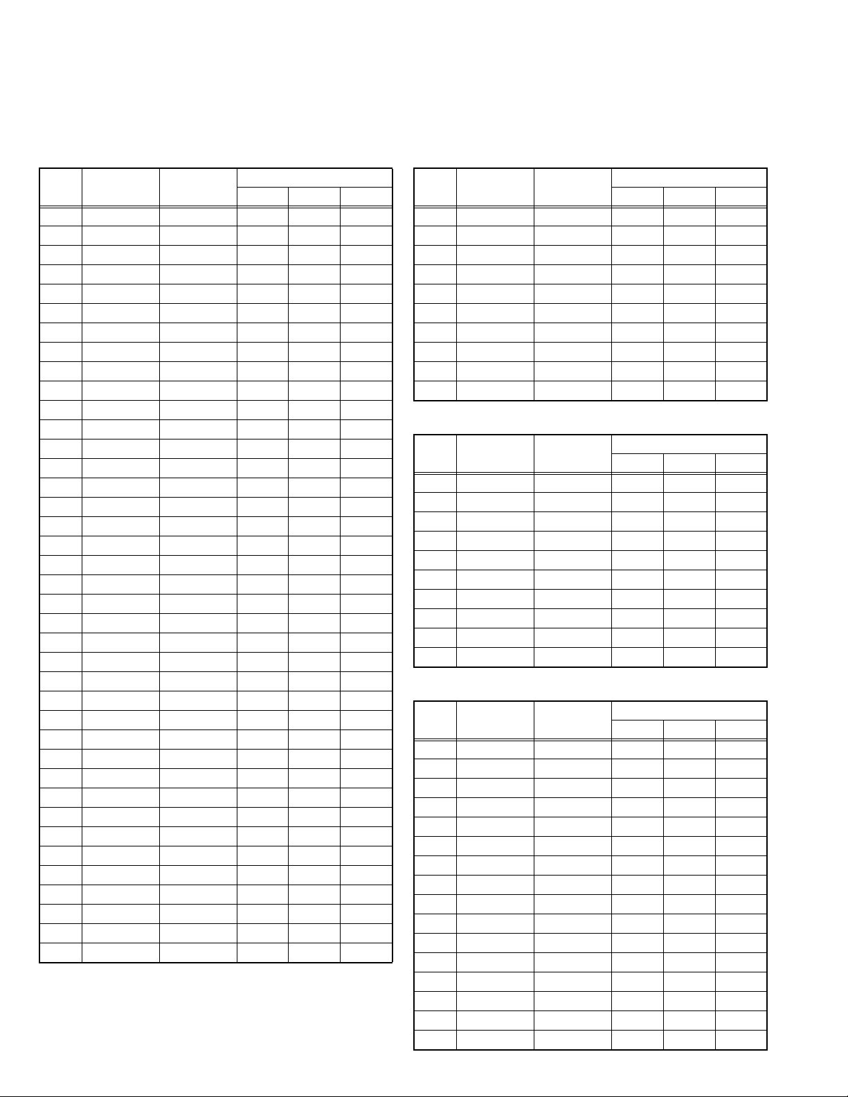
4.6 INITIAL SETTING VALUES IN THE SERVICE MODE
• Perform fine-tuning based on the "initial values" using the remote control when in the Service mode.
• The "initial values" serve only as an indication rough standard and therefore the values with which optimal display can be achieved
may be different from the default values. But, don't change the values that are not written in "ADJUSTMENT PROCEDURE". They
are fixed values.
4.6.1 VIDEO SYSTEM SETTING 4.6.2 AUDIO SYSTEM SETTING (*Fixed values)
Item
S001 PREPARE 0 - 31 0 0 0
S002 NTSC BL 0 - 15 0 0 0
S003 NTSC CNT 0 - 255 36 36 36
S004 NT CR OF 0 - 15 6 6 6
S005 NT CB OF 0 - 15 6 6 6
S006 525i BL 0 - 15 0 0 0
S007 525i CNT 0 - 255 36 36 36
S008 5i CB OF 0 - 15 0 0 0
S009 5i CR OF 0 - 15 0 0 0
S010 5i CR GN 0 - 15 6 6 6
S011 5i CB GN 0 - 15 6 6 6
S012 HD BL 0 - 63 55 55 55
S013 HD CB OF 0 - 63 56 56 56
S014 HD CR OF 0 - 63 58 58 58
S015 RT CONT 0 - 15 7 7 7
S016 RT CB OF 0 - 15 5 5 5
S017 RT CR OF 0 - 15 6 6 6
S018 RT CL GA 0 - 15 12 12 12
S019 PC CL MB 0 - 7 0 0 0
S020 PC CL LB 0 - 31 0 0 0
S021 PC CL MR 0 - 71 0 0 0
S022 PC CL LR 0 - 31 0 0 0
S023 (Not display) 0 - 255 0 0 0
S024 (Not display) 0 - 255 0 0 0
S025 (Not display) 0 - 255 0 0 0
S026 (Not display) 0 - 255 0 0 0
S027 (Not display) 0 - 255 0 0 0
S028 (Not display) 0 - 255 0 0 0
S029 (Not display) 0 - 255 0 0 0
S030 R DRIVE 0 - 255 133 133 133
S031 G DRIVE 0 - 255 130 130 130
S032 B DRIVE 0 - 255 132 132 132
S033 (Not display) 0 - 255 0 0 0
S034 (Not display) 0 - 255 0 0 0
S035 (Not display) 0 - 255 0 0 0
S036 (Not display) 0 - 255 0 0 0
S037 (Not display) 0 - 255 0 0 0
S038 (Not display) 0 - 255 0 0 0
S039 ILA COM 0 - 1 0 0 0
No.
Item name
Variable
range
Setting value
PAL SECAM NTSC
Item
T001 IN LEVEL 0 - 255 0 0 0
T002 LOW SEP 0 - 255 0 0 0
T003 HIGH SEP 0 - 255 0 0 0
T004 AFC 0 - 255 4 4 4
T005 (Not display) 0 - 255 0 0 0
T006 ATT V ON 0 - 1 0 0 0
T007 ATT U ON 0 - 1 0 0 0
T008 ATT C ON 0 - 1 0 0 0
T009 (Not display) 0 - 255 0 0 0
T010 (Not display) 0 - 255 0 0 0
4.6.3 PANEL CONTOROL SYSTEM SETTING (*Fixed values)
Item
P001 TM HOR H 00 - FF 00 00 00
P002 TM HOR L 00 - FF 00 00 00
P003 TM MIN 00 - FF 00 00 00
P004 TEMP0 0 - 255 0 0 0
P005 (Not display) 0 - 255 0 0 0
P006 (Not display) 0 - 255 0 0 0
P007 (Not display) 0 - 255 0 0 0
P008 (Not display) 0 - 255 0 0 0
P009 (Not display) 0 - 255 0 0 0
P010 (Not display) 0 - 255 0 0 0
4.6.4 DRIVE SYSTEM SETTING (*Fixed values)
Item
D001 SLV GN 00 - 3F 15 15 15
D002 SLVH GN 00 - 3F 13 13 13
D003 SLH GN 00 - 3F 15 15 15
D004 SLV Pf 00 - 03 01 01 01
D005 SLH Pf H 00 - 01 01 01 01
D006 SLH Pf L 00 - 03 01 01 01
D007 SL EGCON 00 - 3F 08 08 08
D008 SL EGONF 00 - 01 01 01 01
D009 SL CRGON 00 - 3F 06 06 06
D010 SL CRGON 00 - 01 01 01 01
D011 SL ON OF 00 - 01 01 01 01
D012 SV GN 00 - 3F 1A 1A 1A
D013 SVH GN 00 - 3F 1B 1B 1B
D014 SH GN 00 - 3F 2E 2E 2E
D015 SV Pf 00 - 03 00 00 00
D016 SV PfH 00 - 01 01 01 01
No.
No.
No.
Item name
Item name
Item name
Variable
range
Variable
range
Variable
range
Setting value
PAL SECAM NTSC
Setting value
PAL SECAM NTSC
Setting value
PAL SECAM NTSC
1-18 (No.YA208)
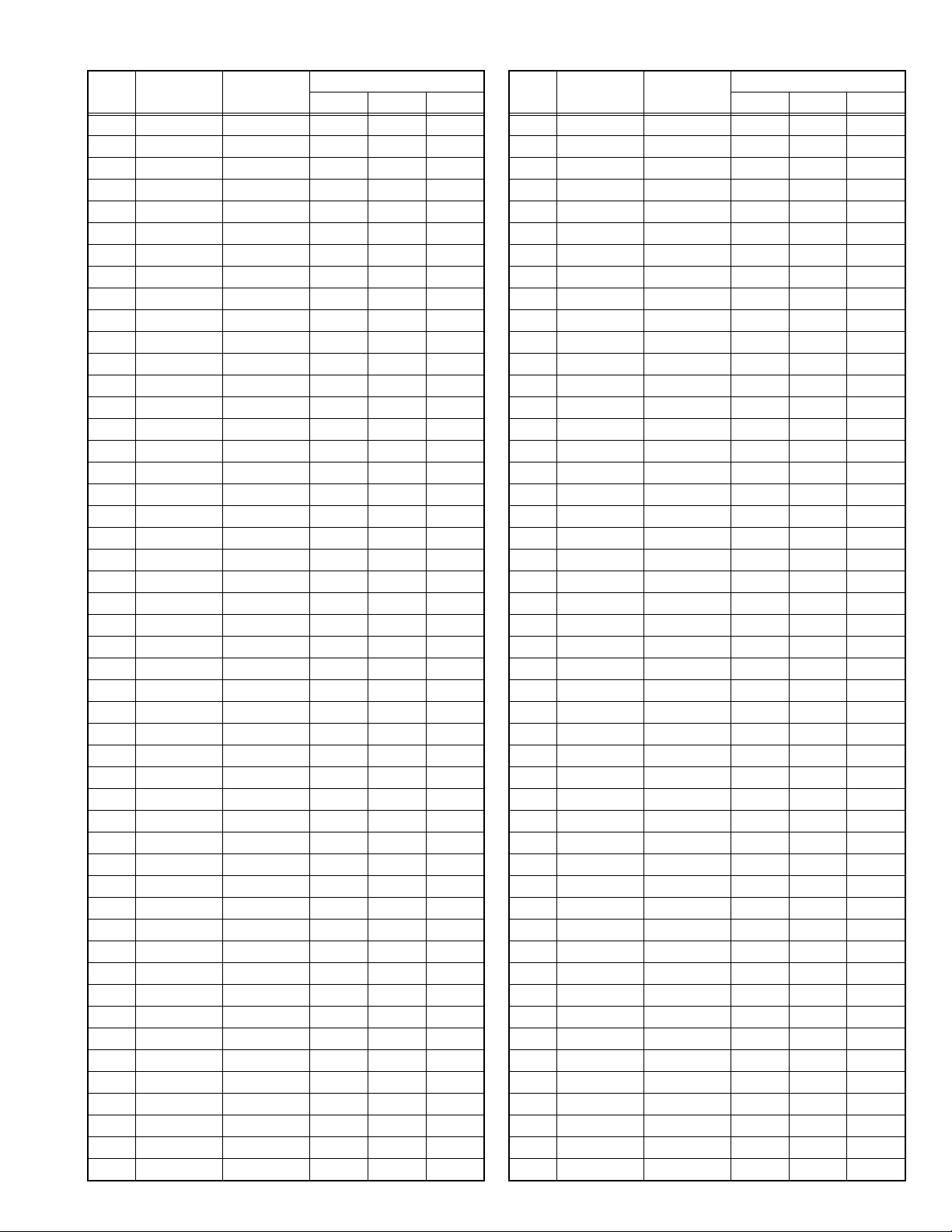
Item
Item name
No.
D017 SV PfL 00 - 03 00 00 00
D018 SYL CON 00 - 3F 30 30 30
D019 SYL CONF 00 - 01 01 01 01
D020 SYH CON 00 - 3F 00 00 00
D021 SYH CONF 00 - 01 01 01 01
D022 SC CON 00 - 3F 1A 1A 1A
D023 SC CNONF 00 - 01 01 01 01
D024 SPM BLC 00 - 3F 0B 0B 0B
D025 SPM BLCO 00 - 01 01 01 01
D026 SLIM 00 - 3F 20 20 20
D027 SLIMONF 00 - 01 01 01 01
D028 SCRG 00 - 3F 10 10 10
D029 SRGONF 00 - 01 01 01 01
D030 S ONF 00 - 01 01 01 01
D031 pb GN 00 - 3F 15 15 15
D032 pb PfH 00 - 01 01 01 01
D033 pb PfL 00 - 03 00 00 00
D034 pb CRG 00 - 3F 04 04 04
D035 pb CRGON 00 - 01 01 01 01
D036 pb ONF 00 - 01 01 01 01
D037 pr GN 00 - 3F 15 15 15
D038 pr PfH 00 - 01 01 01 01
D039 pr PfL 00 - 03 00 00 00
D040 pr CRG 00 - 3F 05 05 05
D041 pr CRGON 00 - 01 01 01 01
D042 pr ONF 00 - 01 01 01 01
D043 ENH ONF 00 - 01 01 01 01
D044 (Not display) 00 - FF 00 00 00
D045 (Not display) 00 - FF 00 00 00
D046 (Not display) 00 - FF 00 00 00
D047 (Not display) 00 - FF 00 00 00
D048 (Not display) 00 - FF 00 00 00
D049 (Not display) 00 - FF 00 00 00
D050 (Not display) 00 - FF 00 00 00
D051 (Not display) 00 - FF 00 00 00
D052 (Not display) 00 - FF 00 00 00
D053 (Not display) 00 - FF 00 00 00
D054 (Not display) 00 - FF 00 00 00
D055 (Not display) 00 - FF 00 00 00
D056 (Not display) 00 - FF 00 00 00
D057 (Not display) 00 - FF 00 00 00
D058 (Not display) 00 - FF 00 00 00
D059 (Not display) 00 - FF 00 00 00
D060 (Not display) 00 - FF 00 00 00
D061 (Not display) 00 - FF 00 00 00
D062 (Not display) 00 - FF 00 00 00
D063 (Not display) 00 - FF 00 00 00
D064 (Not display) 00 - FF 00 00 00
D065 (Not display) 00 - FF 00 00 00
Variable
range
Setting value
PAL SECAM NTSC
Item
D066 (Not display) 00 - FF 00 00 00
D067 (Not display) 00 - FF 00 00 00
D068 (Not display) 00 - FF 00 00 00
D069 (Not display) 00 - FF 00 00 00
D070 (Not display) 00 - FF 00 00 00
D071 (Not display) 00 - FF 00 00 00
D072 (Not display) 00 - FF 00 00 00
D073 (Not display) 00 - FF 00 00 00
D074 (Not display) 00 - FF 00 00 00
D075 (Not display) 00 - FF 00 00 00
D076 (Not display) 00 - FF 00 00 00
D077 (Not display) 00 - FF 00 00 00
D078 (Not display) 00 - FF 00 00 00
D079 (Not display) 00 - FF 00 00 00
D080 (Not display) 00 - FF 00 00 00
D081 (Not display) 00 - FF 00 00 00
D082 (Not display) 00 - FF 00 00 00
D083 (Not display) 00 - FF 00 00 00
D084 (Not display) 00 - FF 00 00 00
D085 (Not display) 00 - FF 00 00 00
D086 (Not display) 00 - FF 00 00 00
D087 (Not display) 00 - FF 00 00 00
D088 (Not display) 00 - FF 00 00 00
D089 (Not display) 00 - FF 00 00 00
D090 (Not display) 00 - FF 00 00 00
D091 (Not display) 00 - FF 00 00 00
D092 (Not display) 00 - FF 00 00 00
D093 (Not display) 00 - FF 00 00 00
D094 (Not display) 00 - FF 00 00 00
D095 (Not display) 00 - FF 00 00 00
D096 (Not display) 00 - FF 00 00 00
D097 (Not display) 00 - FF 00 00 00
D098 (Not display) 00 - FF 00 00 00
D099 (Not display) 00 - FF 00 00 00
D100 (Not display) 00 - FF 00 00 00
D101 (Not display) 00 - FF 00 00 00
D102 (Not display) 00 - FF 00 00 00
D103 (Not display) 00 - FF 00 00 00
D104 (Not display) 00 - FF 00 00 00
D105 (Not display) 00 - FF 00 00 00
D106 (Not display) 00 - FF 00 00 00
D107 (Not display) 00 - FF 00 00 00
D108 (Not display) 00 - FF 00 00 00
D109 (Not display) 00 - FF 00 00 00
D110 (Not display) 00 - FF 00 00 00
D111 (Not display) 00 - FF 00 00 00
D112 (Not display) 00 - FF 00 00 00
D113 (Not display) 00 - FF 00 00 00
D114 (Not display) 00 - FF 00 00 00
No.
Item name
Variable
range
Setting value
PAL SECAM NTSC
(No.YA208)1-19
Item
D115 (Not display) 00 - FF 00 00 00
D116 (Not display) 00 - FF 00 00 00
D117 (Not display) 00 - FF 00 00 00
D118 (Not display) 00 - FF 00 00 00
D119 (Not display) 00 - FF 00 00 00
D120 (Not display) 00 - FF 00 00 00
D121 (Not display) 00 - FF 00 00 00
D122 (Not display) 00 - FF 00 00 00
D123 (Not display) 00 - FF 00 00 00
D124 (Not display) 00 - FF 00 00 00
D125 (Not display) 00 - FF 00 00 00
D126 (Not display) 00 - FF 00 00 00
D127 (Not display) 00 - FF 00 00 00
D128 (Not display) 00 - FF 00 00 00
D129 (Not display) 00 - FF 00 00 00
D130 (Not display) 00 - FF 00 00 00
D131 (Not display) 00 - FF 00 00 00
D132 (Not display) 00 - FF 00 00 00
D133 (Not display) 00 - FF 00 00 00
D134 (Not display) 00 - FF 00 00 00
D135 (Not display) 00 - FF 00 00 00
D136 (Not display) 00 - FF 00 00 00
D137 (Not display) 00 - FF 00 00 00
D138 (Not display) 00 - FF 00 00 00
D139 (Not display) 00 - FF 00 00 00
D140 (Not display) 00 - FF 00 00 00
D141 (Not display) 00 - FF 00 00 00
D142 (Not display) 00 - FF 00 00 00
D143 (Not display) 00 - FF 00 00 00
D144 (Not display) 00 - FF 00 00 00
D145 (Not display) 00 - FF 00 00 00
D146 (Not display) 00 - FF 00 00 00
D147 (Not display) 00 - FF 00 00 00
D148 (Not display) 00 - FF 00 00 00
D149 (Not display) 00 - FF 00 00 00
D150 (Not display) 00 - FF 00 00 00
D151 (Not display) 00 - FF 00 00 00
D152 (Not display) 00 - FF 00 00 00
D153 (Not display) 00 - FF 00 00 00
D154 (Not display) 00 - FF 00 00 00
D155 (Not display) 00 - FF 00 00 00
D156 (Not display) 00 - FF 00 00 00
D157 (Not display) 00 - FF 00 00 00
D158 (Not display) 00 - FF 00 00 00
D159 (Not display) 00 - FF 00 00 00
D160 (Not display) 00 - FF 00 00 00
D161 (Not display) 00 - FF 00 00 00
D162 (Not display) 00 - FF 00 00 00
D163 (Not display) 00 - FF 00 00 00
No.
Item name
Variable
range
Setting value
PAL SECAM NTSC
Item
D164 (Not display) 00 - FF 00 00 00
D165 (Not display) 00 - FF 00 00 00
D166 (Not display) 00 - FF 00 00 00
D167 (Not display) 00 - FF 00 00 00
D168 (Not display) 00 - FF 00 00 00
D169 (Not display) 00 - FF 00 00 00
D170 (Not display) 00 - FF 00 00 00
D171 (Not display) 00 - FF 00 00 00
D172 (Not display) 00 - FF 00 00 00
D173 (Not display) 00 - FF 00 00 00
D174 (Not display) 00 - FF 00 00 00
D175 (Not display) 00 - FF 00 00 00
D176 (Not display) 00 - FF 00 00 00
D177 (Not display) 00 - FF 00 00 00
D178 (Not display) 00 - FF 00 00 00
D179 (Not display) 00 - FF 00 00 00
D180 (Not display) 00 - FF 00 00 00
D181 (Not display) 00 - FF 00 00 00
D182 (Not display) 00 - FF 00 00 00
D183 (Not display) 00 - FF 00 00 00
D184 (Not display) 00 - FF 00 00 00
D185 (Not display) 00 - FF 00 00 00
D186 (Not display) 00 - FF 00 00 00
D187 (Not display) 00 - FF 00 00 00
4.6.5 MAIN CPU SYETEM SETTING (*Fixed values)
Item
Z001 (Not display) 00 - FF 00 00 00
Z002 (Not display) 00 - FF 00 00 00
Z003 (Not display) 00 - FF 00 00 00
Z004 (Not display) 00 - FF 00 00 00
Z005 (Not display) 00 - FF 00 00 00
Z006 (Not display) 00 - FF 00 00 00
Z007 (Not display) 00 - FF 00 00 00
Z008 (Not display) 00 - FF 00 00 00
Z009 (Not display) 00 - FF 00 00 00
Z010 (Not display) 00 - FF 00 00 00
No.
No.
Item name
Item name
Variable
range
Variable
range
Setting value
PAL SECAM NTSC
Setting value
PAL SECAM NTSC
1-20 (No.YA208)
4.7 ADJUSTMENT PROCEDURE
4.7.1 VIDEO CIRCUIT
Item
625i
A-D OFFSET
Measuring
instrument
Remote
control unit
Test point Adjustment part Description
Signal
generator
Disappears the color at both ends.
1125i (50Hz)
BRIGHTNESS
Remote
control unit
Signal
generator
Set the 0% black part to be brightest.
1125i (50Hz)
A-D OFFSET
Remote
control unit
Signal
generator
Minimize the red and blue noises in
the upper half of the screen.
[1.ADJUST]
S001: PREPARE
(Adjustment setting mode change)
S008: 5i CB OF(625i cb offset)
S009: 5i CR OF(625i cr offset)
S030: R DRIVE(Red drive)
S031: G DRIVE(Green drive)
S032: B DRIVE(Blue drive)
[1.ADJUST]
S001: PREPARE
(Adjustment setting mode change)
S012: HD BL(1125i brightness)
S030: R DRIVE(Red drive)
S031: G DRIVE(Green drive)
S032: B DRIVE(Blue drive)
[1.ADJUST]
S001: PREPARE
(Adjustment setting mode change)
S013: HD CB OF(1125i cb offset)
S014: HD CR OF(1125i cr offset)
S030: R DRIVE(Red drive)
S031: G DRIVE(Green drive)
S032: B DRIVE(Blue drive)
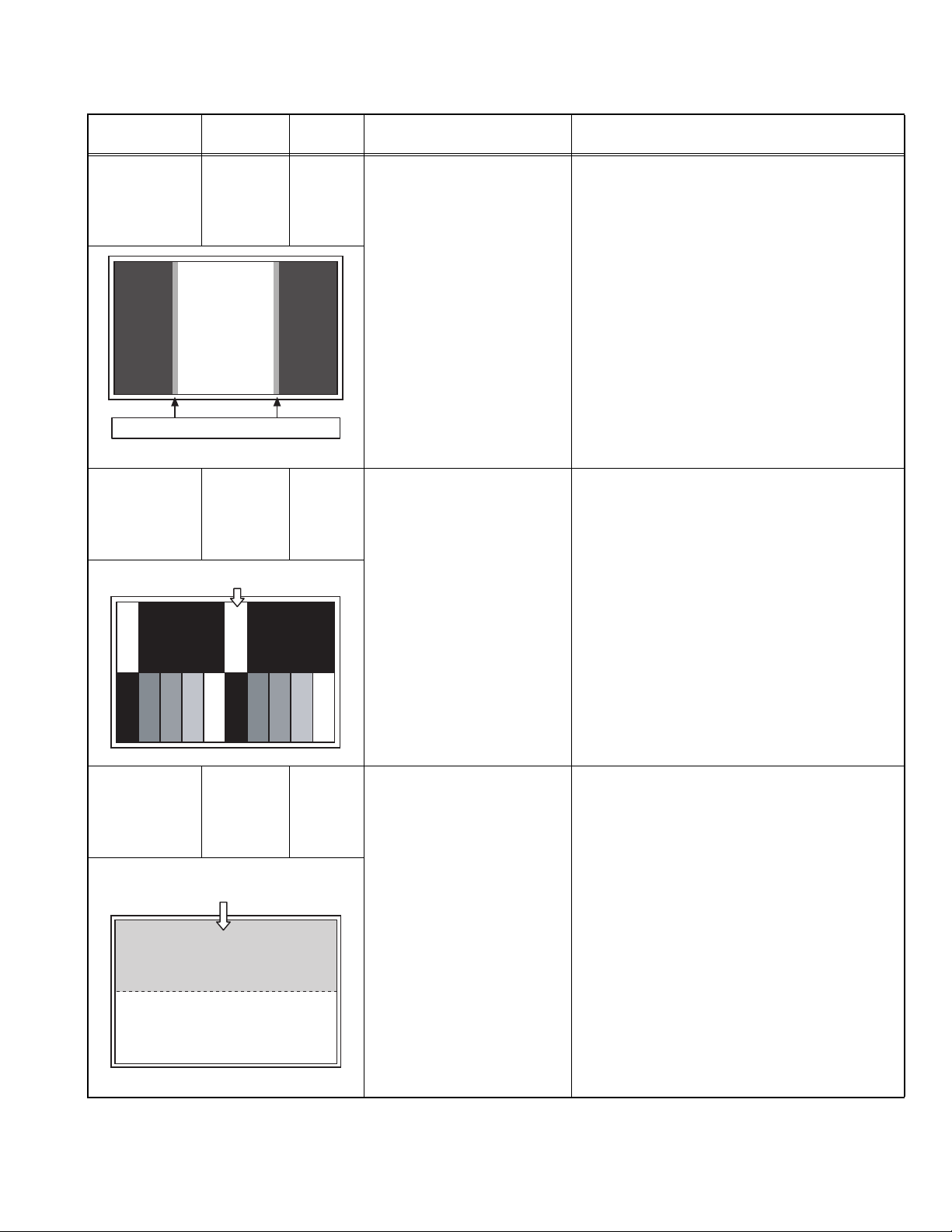
(1) Receive a 625i component ramp pattern signal.
(2) Set "PICTURE MODE" to STANDARD.
(3) Set "ZOOM" to FULL.
(4) Set "WHITE BALANCE" to MID.
(5) Select "1.ADJUST" from the SERVICE MODE.
(6) Set < S030 > (R DRIVE), < S031> (G DRIVE)
and < S032 > (B DRIVE) to "133".
(7) Set < S001 >(adjustment setting mode change)
to set "8" and it change to the 625i A-D offset
adjustment setting mode.
(8) Adjust < S008 > (625i Cb offset) and < S009 >
(625i Cr offset) to lose the gap (red line, green
line and blue line) which appears at both ends
of a white part at the centre of the screen.
(9) Set < S001 > to set "0" and it change to the
normal mode.
(10) Press the [MUTING] key to memoirze the set
value.
(1) Receive a 1125i (50Hz) gray scale pattern signal.
(2) Set "PICTURE MODE" to STANDARD.
(3) Set "ZOOM" to FULL.
(4) Set "WHITE BALANCE" to MID.
(5) Select "1.ADJUST" from the SERVICE MODE.
(6) Set < S030 > (R DRIVE), < S031> (G DRIVE)
and < S032 > (B DRIVE) to "133".
(7) Set < S001 > (adjustment setting mode change)
to set the values "12" and it change to the 1125i
black level adjustment setting mode.
(8) Adjust < S012 > (1125i brightness) to set the
0% black part in the upper half of the screen to
be brightest.
(9) Set < S001 > to set "0" and it change to the
normal mode.
(10) Press the [MUTING] key to memoirze the set
value.
(1) Receive a 1125i (50Hz) 30% all white pattern
signal.
(2) Set "PICTURE MODE" to STANDARD.
(3) Set "ZOOM" to FULL.
(4) Set "WHITE BALANCE" to MID.
(5) Select "1.ADJUST" from the SERVICE MODE.
(6) Set < S030 > (R DRIVE), < S031> (G DRIVE)
and < S032 > (B DRIVE) to "133".
(7) Set < S001 > (adjustment setting mode change)
to set "13" and it change to the 1125i A-D offset
adjustment setting mode.
(8) Adjust < S013 > (1125i Cb offset) to minimize
the blue noise in the upper half of the screen.
(9) Adjust < S014 > (1125i Cr offset) to minimize
the blue noise in the upper half of the screen.
(10) Set < S001 > to set "0" and it change to the
normal mode.
(11) Press the [MUTING] key to memoirze the set
value.
(No.YA208)1-21
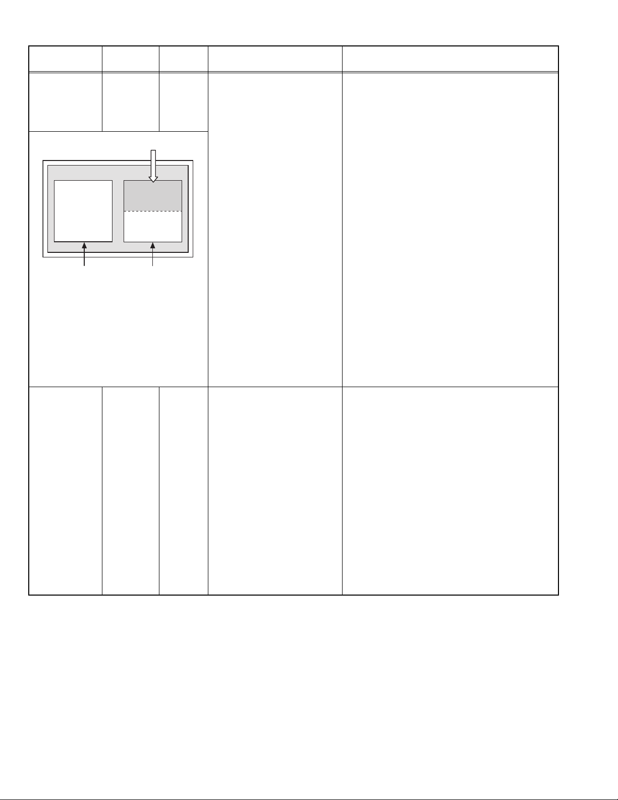
Item
SUB SCREEN
A-D OFFSET
Set the 0% block part to be brightest.
VIDEO-1
<NO SIGNAL>
WHITE
BALANCE
(HIGHLIGHT)
Measuring
instrument
Remote
control unit
Signal
generator
TV(RF)
<30% all white>
Remote
control unit
Signal
generator
Test point Adjustment part Description
[1.ADJUST]
S001: PREPARE
(Adjustment setting mode change)
(1) Set "PICTURE MODE" to STANDARD.
(2) Set "ZOOM" to FULL.
(3) Set "WHITE BALANCE" to MID.
(4) Set "MULTI PICTURE" to 2 pictures.
S016: RT CB OF
(Sub screen cb offset)
S017: RT CR OF
(Sub screen cr offset)
(5) Receive a PAL 30% all white pattern signal on
the Right screen. At the same time, set the Left
screen in VIDEO-1 mode (No signal).
(6) Select "1.ADJUST" from the SERVICE MODE.
(7) Set < S030 > (R DRIVE), < S031> (G DRIVE)
S030: R DRIVE(Red drive)
S031: G DRIVE(Green drive)
S032: B DRIVE(Blue drive)
and < S032 > (B DRIVE) to "133".
(8) Set < S001 > (adjustment setting mode change)
to set "17" and it change to the sub screen A-D
offset adjustment setting mode.
(9) Adjust < S016 > (Sub screen cb offset) to
minimize the blue noise in the upper half of the
screen.
If you select an adjustment item < S016 >,
then the screen automatically turn to twin
pictures mode.
(10) Set < S017 > (Sub screen cr offset) to minimize
the red noise in the upper half of the screen.
(11) Readjust < S016 > and < S017 > to set the
upper half of the screen to be the blackest. (See
Fig.9)
(12) Set < S001 > to set "0" and it change to the
normal mode.
(13) Press the [MUTING] key to memoirze the set
value.
[1.ADJUST]
S030: R DRIVE (Red drive)
S031: G DRIVE (Green drive)
S032: B DRIVE (Blue drive)
(1) Receive a PAL 75% all white signal.
(2) Set "PICTURE MODE" to STANDARD.
(3) Set "ZOOM" to FULL.
(4) Set "WHITE BALANCE" to MID.
(5) Select "1.ADJUST" from the SERVICE MODE.
(6) Adjust to keep one of < S030 > (Red drive),
< S031 > (Green drive) or < S032 > (Blue drive)
unchanged, then lower the other two so that the
all-white screen is equally white throughout.
NOTE:
Set one or more of < S030 >, < S031 >, and
< S032 > to "85".
(7) Check that white balance is properly tracked
from low light to high light. If the white balance
tracking is deviated, adjust to correct it.
(8) Press the [MUTING] key to memoirze the set
value.
1-22 (No.YA208)
SECTION 5
SERVICE MENU
1.ADJUST
2.SELF_CHK
3.I2C STOP
LOB OK FAN OK
SYNC M:OK S:OK HD:NG
TIM OK
MSM OK DIGI 0000
MEM OK AVSW OK
YC OK AIO OK
TUN OK GCR NG 1
IP OK RGB OK 8
DVI OK HDMI OK
FAN OK ALM OK
TMP OK
ATP OK ASH OK
PNL OK MEM OK
TMP OK AIO OK
TROUBLESHOOTING
5.1 SELF CHECK FEATURE
5.1.1 OUTLINE
This unit comes with the "Self check" feature, which checks the
operational state of the circuit and displays/saves it during
failure.Diagnosis is performed when power is turned on, and
information input to the main microcomputer is monitored at all
time.Diagnosis is displayed in 2 ways via screen display and LED
flashes. Failure detection is based on input state of I
2
C bus and
the various control lines connected to the main microcomputer.
5.1.2 HOW TO ENTER THE SELF CHECK MODE
Before entering the SERVICE MODE, confirm that the setting of
PIP/TV/ DVD switch is at the "TV" side. If the switches have not
been properly set, you cannot enter the SERVICE MODE.
(1) Press [DISPLAY] key and [MUTING] key simultaneously,
then enter the SERVICE MODE.
(2) Press the [2] key SELF CHECK MODE.
(3) Press the [ZOOM] key to enter Page 2 of the SELF CHECK
MODE.
*Use the [CINEMA] key to toggle between Page 1 and
Page 2.
NOTE:
When a number key other than the [1] to [3] key is pressed in
the SERVICE MODE screen, the other relevant screen may be
displayed.
This is not used in the adjustment procedure. Press the
[MENU] key to return to the MAIN MENU SCREEN.
5.1.3 HOW TO EXIT THE SELF CHECK MODE
To Save Failure History:
Turn off the power by unplugging the AC power cord plug when
in the Self check display mode.
To Clear (Reset) Failure History:
Turn off the power by pressing the [POWER] key on the remote
control unit when in the Self check display mode.
5.1.4 FAILURE HISTORY
Failure history can be counted up to 9 times for each item. When
the number exceeds 9, display will remain as 9. Failure history
will be stored in the memory unless it has been deleted.
NOTE:
Only SYNC (with/without sync signals) will be neither counted
nor stored.
5.1.5 POINTS TO NOTE WHEN USING THE SELF CHECK
FEATURE
In addition to circuit failures (abnormal operation), the following
cases may also be iagnosed as "Abnormal" and displayed and
counted as "NG".
(1) Temporary defective transmissions across circuits due to
pulse interruptions
(2) Misalignment in the on/off timing of power for I
2
C bus
(VCC) when turning on/off the main power.
Diagnosis may be impeded if a large number of items are
displayed as "NG". As such, start Self check check only after 3
seconds in the case of receivers and 5 seconds in the case of
panels upon turning on the power. If recurrences are expected,
ensure to clear (reset) the failure history and record the new
diagnosis reults.
SERVICE MODE SCREEN
SERVICE MENU
1.ADJUST
2.SELF_CHK
3.I2C STOP
SELF CHECK MODE SCREEN (Page 1)
LOB OK FAN OK
SYNC M:OK S:OK HD:NG
TIM OK
MSM OK DIGI 0000
MEM OK AVSW OK
YC OK AIO OK
TUN OK GCR NG 1
IP OK RGB OK 8
DVI OK HDMI OK
Item
CHECK
Normality=OK
Abnormality=NG
SELF CHECK MODE SCREEN (Page 2)
FAN OK ALM OK
TMP OK
ATP OK ASH OK
PNL OK MEM OK
TMP OK AIO OK
Item
* As "SYNC" is not counted, the number of failures not displayed.
CHECK
Normality=OK
Abnormality=NG
Fig.1
(No.YA208)1-23
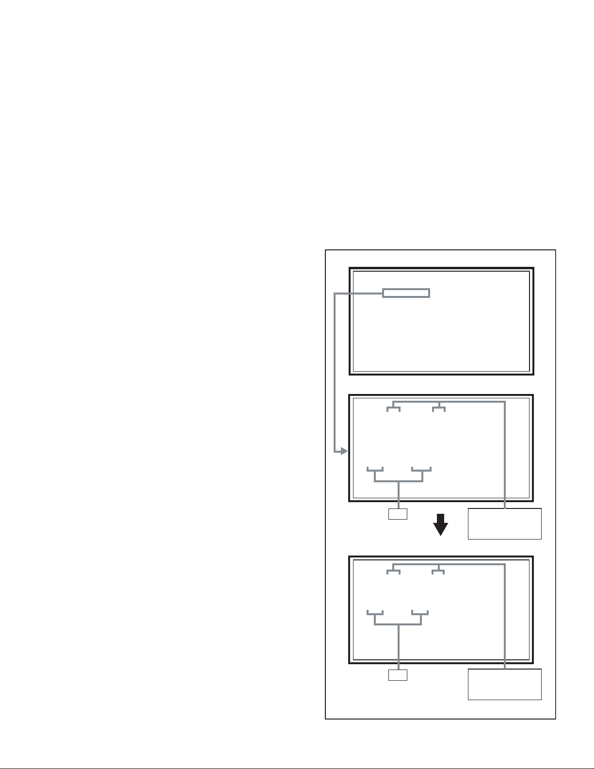
5.1.6 DETAILS
Self check is performed for the following items:
< Page 1 of screen >
Detection item Display Detection content
Low bias line short
protection
LOB Confirmation of operation of the low bais
(2.5V / 3.3V / 5V / 9V) protection circuit.
Q9822 [REGULATOR PWB]
Diagnosis
signal (line)
Detection timing
LB_PRO Detection starts 3 seconds after the
power is turned on.
If error continues between 400ms the
power is turned off.
Abnormal rise of
temperature in audio
circuit
FAN Confirmation of the temperature of
audio circuit.
TH6661 [ANALOG SIGNAL PWB]
SDA Detection starts 3 seconds after the
power is turned on.
If the temperture of 90°C is detected for
3 seconds the power is turned off.
Presence of sync signal SYNC Confirmation of presence of video
sync signal.
SDA Confirmation of presence of sync signal
in video signal.
M : Main sync signal
S : Sub sync signal
HD : Component sync signal
IC201 [ANALOG SIGNAL PWB]
AC power input TIM Not used. --- ---
Main CPU
MSM Not used. --- ---
communication
Digital tuner DIGI Not used. --- ---
Main memory MEM Confirmation of reply of ACK signal
which uses I
2
C communication.
IC7602 [DIGITAL SIGNAL PWB]
AV select switch AVSW Same as above.
SDA If it checks whenever I2C communication
is performed and no reply of ACK signal
an error will be counted.
SDA Same as above.
IC301, IC501 [ANALOG SIGNAL PWB]
3 dimensions YC
YC Not used. --- ---
separator
Multi sound process AIO Not used. --- ---
RF tuner TUN Confirmation of reply of ACK signal
which uses I
2
C communication.
TU3001 [RECEIVER PWB]
SDA If it checks whenever I2C communication
is performed and no reply of ACK signal
an error will be counted.
Ghost reduction GCR Not used. --- ---
DIST process IP Confirmation of reply of ACK signal
which uses I
2
C communication.
IC3001 [DIGITAL SIGNAL PWB]
RGB process RGB Confirmation of reply of ACK signal
which uses I
2
C communication.
IC3001 [DIGITAL SIGNAL PWB]
DVI (Digital communication)
DVI Not used. --- ---
SDA If it checks whenever I
is performed and no reply of ACK signal
an error will be counted.
SDA If it checks whenever I
is performed and no reply of ACK signal
an error will be counted.
Digital input HDMI Not used. --- ---
2
C communication
2
C communication
1-24 (No.YA208)
< Page 2 of screen >
Detection item Display Detection content
Diagnosis
signal (line)
Detection timing
Fan lock FAN Not used. --- ---
Abnormal of operation of
ALM Not used. --- ---
PANEL
Abnormal rise
TMP Not used. --- ---
oftemperature in PANEL
Abnormal rise of
ATP Not used. --- --temperature in audio
circuit
Short circuit detection of
ASH Not used. --- --audio circuit
Panel communication PNL Not used. --- ---
Sub memory MEM Not used. --- ---
Temp. sensor TMP Not used. --- ---
Audio control AIO Confirmation of reply of ACK signal
which uses I
2
C communication.
IC6521 [ANALOG SIGNAL PWB]
SDA If it checks whenever I
is performed and no reply of ACK signal
an error will be counted.
5.1.7 METHOD OF DISPLAY WHEN A RASTER IS NOT OUTPUT
In the state where a raster is not output by breakdown of the set, an error is displayed by blink of the POWER LED.
Type of error POWER LED flash cycle
Low bias line short protection Low luminance blue turnig on and off at 1 second intervals.
Abnormal rise of temperature in audio circuit High luminance blue turnig on and off at 0.1 second intervals.
2
C communication
< Explanation of operation >
If error is detected, the power is turned off.
Shortly after a power is turned off, POWER LED will be blinked.
Power cannot be turned on until the power cord takes out and inserts, after a power is turned off.
(No.YA208)1-25

Victor Company of Japan, Limited
AV & MULTIMEDIA COMPANY VIDEO DISPLAY CATEGORY 12, 3-chome, Moriya-cho, kanagawa-ku, Yokohama, kanagawa-prefecture, 221-8528, Japan
(No.YA208)
Printed in Japan
VPT
SERVICE MANUAL
WIDE LCD PANEL TELEVISION
YA208C20054
BASIC CHASSIS
LT-Z26SX4B,
FL
LT-Z26SX4B
LT-Z26SX4B
LT-Z26SX4S
LT-Z26SX4B
Supplementary
Please be informed that this service manual contains the related matters following the parts replacement in
the LCD PANEL UNIT.
For details other than those described in this manual, please refer to the LT-Z26SX4B, LT-Z26SX4B/A, LTZ26SX4B/S and LT-Z26SX4S/S service manual (No.YA208, 2004/12) LT-Z26SX4B/C service manual
(No.YA208B, 2005/1).
SECTION 1
/A,
/S,
/S,
/C
PRECAUTION
Please refer to "LT-Z26SX4B, LT-Z26SX4B/A, LT-Z26SX4B/S and LT-Z26SX4S/S (No.YA208)" about this section.
SECTION 2
SPECIFIC SERVICE INSTRUCTIONS
Please refer to "LT-Z26SX4B, LT-Z26SX4B/A, LT-Z26SX4B/S and LT-Z26SX4S/S (No.YA208)" about this section.
COPYRIGHT © 2005 Victor Company of Japan, Limited
No.YA208C
2005/4
SECTION 3
DISASSEMBLY
CAUTION AT DISASSEMBLY:
• Make sure that the power cord is disconnected from the outlet.
• Pay special attention not to break or damage the parts.
• When removing each board, remove the connectors as required. Taking notes of the connecting points (connector numbers)
makes service procedure manageable.
• During the procedure, place a mirror mat etc. under the LCD UNIT and be careful not to damage the PANEL.
• Make sure that there is no bent or stain on the connectors before inserting, and firmly insert the connectors.
3.1 DISASSEMBLY PROCEDURE
3.1.1 CAUTION ON REMOVING THE LCD PANEL UNIT
The LCD PANEL is fixed to the FRONT PANEL (at the back side)
by using double-side adhesive tapes. To remove the LCD
PANEL UNIT, remove the adhesive tape on the FRONT PANEL
slowly.
LCD PANEL UNIT
Double-side adhesive tapes
Double-side adhesive tapes
FRONT PANEL
3.1.2 REMOVING THE CONTROL PWB (Fig.1)
• Remove the STAND.
• Remove the REAR COVER.
• Remove the LCD PANEL UNIT.
(1) Remove the 4 screws [A], then remove the CONTROL
PWB COVER.
(2) Remove the 2 screws [B], then remove the CONTROL
PWB.
CAUTION:
Carry out the procedure with extra care as the FERRITE
CORE is affixed with double-side adhesive tapes and it may
break if extra force is applied.
3.1.3 REMOVING THE INVERTER PWB (Fig.1)
• Remove the STAND.
• Remove the REAR COVER.
• Remove the LCD PANEL UNIT.
(1) Remove the 6 screws [C], then remove the INVERTER
PWB COVER.
(2) Remove the 3 screws [D], then remove the INVERTER
PWB.
(3) Remove the 8 screws [E], then remove the INVERTER
PWB COVER.
(4) Remove the 3 screws [F], then remove the INVERTER
COLD PWB.
3.1.4 REMOVING THE BACK LIGHT UINT (Fig.1)
CAUTION:
When replacing the BACK LIGHT UINT, be careful to
prevent dust attachment to the UNIT. If dust particles
attached to the UNIT, it becomes the cause of uneven
brightness.
• Remove the STAND.
• Remove the REAR COVER.
• Remove the LCD PANEL UNIT.
• Remove the CONTROL PWB.
• Remove the INVERTER PWB.
• Remove the INVERTER COLD PWB.
(1) Remove the 14 screws [G], then remove the TOP PANEL
FRAME.
(2) Remove the 4 screws [H], then remove the LCD PANEL.
CAUTION:
When removing the LCD PANEL, be careful not to give
stress to the FPC which connects the PWB and the LCD
PANEL.
CAUTION ON EXCHAGING THE BACK LIGHT UINT
• If the screws that are not specified in this section are
removed, the LCD PANEL will be removed and it cannot be
reassembled.
1-2 (No.YA208C)
INVERTER PWB COVER
C
D
INVERTER PWB
A
FERRITE CORE
B
CONTROL PWB
COVER
CONTROL PWB
INVERTER COLD PWB
E
F
FRONT
LCD PANEL UNIT
TOP PANEL FRAME
FRONT
G
LCD PANEL
H
Fig.1
BACK LIGHT UNIT
(No.YA208C)1-3

SECTION 4
ADJUSTMENT
Please refer to "LT-Z26SX4B, LT-Z26SX4B/A, LT-Z26SX4B/S and LT-Z26SX4S/S (No.YA208)" about this section.
SECTION 5
TROUBLESHOOTING
Please refer to "LT-Z26SX4B, LT-Z26SX4B/A, LT-Z26SX4B/S and LT-Z26SX4S/S (No.YA208)" about this section.
1-4 (No.YA208C)
 Loading...