

Page 1

SERVICE MANUAL
INTEGRATED DIGITAL TERRESTRIAL/SATELLITE LCD TELEVISION
YA707<Rev.001>20097SERVICE MANUAL
LT-42HB1BU/AX
COPYRIGHT © 2009 Victor Company of Japan, Limited
TABLE OF CONTENTS
1 PRECAUTION. . . . . . . . . . . . . . . . . . . . . . . . . . . . . . . . . . . . . . . . . . . . . . . . . . . . . . . . . . . . . . . . . . . . . . . . . 1-3
2 SPECIFIC SERVICE INSTRUCTIONS . . . . . . . . . . . . . . . . . . . . . . . . . . . . . . . . . . . . . . . . . . . . . . . . . . . . . . 1-6
3 DISASSEMBLY . . . . . . . . . . . . . . . . . . . . . . . . . . . . . . . . . . . . . . . . . . . . . . . . . . . . . . . . . . . . . . . . . . . . . . . 1-8
4 ADJUSTMENT . . . . . . . . . . . . . . . . . . . . . . . . . . . . . . . . . . . . . . . . . . . . . . . . . . . . . . . . . . . . . . . . . . . . . . . 1-13
5 TROUBLESHOOTING . . . . . . . . . . . . . . . . . . . . . . . . . . . . . . . . . . . . . . . . . . . . . . . . . . . . . . . . . . . . . . . . . 1-15
COPYRIGHT © 2009 Victor Company of Japan, Limited
No.YA707<Rev.001>
2009/7
Page 2
Items Contents
Dimensions (W × H × D) [Without stand] 101.4 cm × 63.55 cm × 27.86 cm [101.4 cm × 64.65 cm × 10.87 cm]
Mass [Without stand] 22.7 kg [21.42 kg]
Power Input AC220 V - AC240 V, 50 Hz
Power Consumption 170 W (Standby: 0.8 W)
TV RF System Analog CCIR (B/G, I, D/K, L)
Digital DVB-T / DVB-S
Colour System PAL, SECAM, NTSC 3.58/4.43 [EXT only]
Stereo System NICAM (B/G, I, D/K, L), A2 (B/G, D/K)
Receiving
Frequency
Analog VHF: 45.25 MHz - 470MHz
UHF: 470 MHz - 855.25 MHz
CATV: 116MHz - 172MHz / 220 MHz - 469 MHz
Digital Terrestrial: 474 MHz - 858 MHz(UHF), 177.5 MHz - 6.5 MHz (VHF)
Satellite: 950 MHz - 2150 MHz
Intermediate
Frequency
VIF 38.9 MHz (B/G, I, D/K, L)
SIF 33.4 MHz (5.5 MHz:B/G)
32.9 MHz (6.0 MHz:I)
32.4 MHz (6.5MHz:D/K)
Colour Sub
Carrier Frequency
PAL 4.43MHz
SECAM 4.40625 MHz / 4.25 MHz
NTSC 3.58 MHz / 4.43 MHz
Teletext System Analog FLOF (Fastext), TOP
Digital EBU TEXT
LCD panel 42 V-inch wide aspect (16 : 9)
Screen Size Diagonal : 107.0 cm (H: 93.0 cm × V:52.32 cm)
Display Pixels Horizontal : 1920 dots × Vertical : 1080 dots
Audio Power Output 10 W + 10 W
Speaker 4.0 cm × 20.0 cm, oval type × 2
Aerial terminal (VHF/UHF/BS) 75 Ω unbalanced, coaxial × 2
EXT-1 / EXT-2 (Input/Output) 21-pin Euro connector (SCART socket ) × 2
EXT-3
(Input)
Component Video
750p / 1125i
625p / 525p / 625i / 525i
RCA pin jack × 3
Y: 1 V (p-p) (Sync signal: ±0.35V(p-p), 3-value sync.), 75 Ω / Pb/Pr: ±0.35V(p-p), 75 Ω
Y: 1 V (p-p), Positive (Negative sync.), 75 Ω / Cb/Cr: 0.7 V(p-p), 75 Ω
Audio 500 mV(rms) (-4dBs), high impedance, RCA pin jack × 2
EXT-4
(Input)
S-Video Mini-DIN 4 pin × 1
Y: 1 V (p-p), Positive (Negative sync provided), 75 Ω
C: 0.286 V (p-p) (Burst signal), 75 Ω
Video 1V (p-p), Positive (Negative sync provided), 75 Ω, RCA pin jack × 1
Audio 500 mV (rms), High impedance, RCA pin jack × 2
EXT-5 / EXT-6 / EXT-7
(Digital Input)
Video / Audio HDMI 2-row 19pin connector × 3
(Digital-input terminal is not compatible with picture signals of personal computer)
• 576i(625i),576p(625p),480i(525i),480p(525p),720p(750p),1080i(1125i) signals are
available.
• All HDMI inputs support DVI video but only first HDMI input (EXT-5) supports DVI audio
through component audio input (EXT-2 or EXT-3).
PC (RGB) Input Video D-sub 15 pin × 1
R/G/B : 0.7 V (p-p), 75Ω
HD / VD : 1 V (p-p) to 5 V (p-p), high impedance
Audio 3.5 mm stereo mini jack × 1
Digital Audio Optical Output Digital SPDIF × 1
Headphone 3.5 mm stereo mini jack × 1
Remote Control Unit RM-C2503 (AAA/R03 dry cell battery × 2)
Design & specifications are subject to change without notice.
1-2 (No.YA707<Rev.001>)
Page 3

SECTION 1
PRECAUTION
1.1 SAFETY PRECAUTIONS
(1) The design of this product contains special hardware,
many circuits and components specially for safety
purposes. For continued protection, no changes should be
made to the original design unless authorized in writing by
the manufacturer. Replacement parts must be identical to
those used in the original circuits. Service should be
performed by qualified personnel only.
(2) Alterations of the design or circuitry of the products should
not be made. Any design alterations or additions will void
the manufacturer's warranty and will further relieve the
manufacturer of responsibility for personal injury or
property damage resulting therefrom.
(3) Many electrical and mechanical parts in the products have
special safety-related characteristics. These
characteristics are often not evident from visual inspection
nor can the protection afforded by them necessarily be
obtained by using replacement components rated for
higher voltage, wattage, etc. Replacement parts which
have these special safety characteristics are identified in
the parts list of Service manual. Electrical components
having such features are identified by shading on the
schematics and by ( ) on the parts list in Service
manual. The use of a substitute replacement which does
not have the same safety characteristics as the
recommended replacement part shown in the parts list of
Service manual may cause shock, fire, or other hazards.
(4) Don't short between the LIVE side ground and
ISOLATED (NEUTRAL) side ground or EARTH side
ground when repairing.
Some model's power circuit is partly different in the GND.
The difference of the GND is shown by the LIVE : ( ) side
GND, the ISOLATED (NEUTRAL) : ( ) side GND and
EARTH : ( ) side GND.
Don't short between the LIVE side GND and ISOLATED
(NEUTRAL) side GND or EARTH side GND and never
measure the LIVE side GND and ISOLATED (NEUTRAL)
side GND or EARTH side GND at the same time with a
measuring apparatus (oscilloscope etc.). If above note will
not be kept, a fuse or any parts will be broken.
(5) When service is required, observe the original lead dress.
Extra precaution should be given to assure correct lead
dress in the high voltage circuit area. Where a short circuit
has occurred, those components that indicate evidence of
overheating should be replaced. Always use the
manufacturer's replacement components.
(6) Isolation Check (Safety for Electrical Shock Hazard)
After re-assembling the product, always perform an isolation check on the exposed metal parts of the cabinet (antenna terminals, video/audio input and output terminals,
Control knobs, metal cabinet, screw heads, earphone jack,
control shafts, etc.) to be sure the product is safe to operate
without danger of electrical shock.
a) Dielectric Strength Test
The isolation between the AC primary circuit and all metal
parts exposed to the user, particularly any exposed metal
part having a return path to the chassis should withstand a
voltage of 3000V AC (r.m.s.) for a period of one second. (.
. . . Withstand a voltage of 1100V AC (r.m.s.) to an appliance rated up to 120V, and 3000V AC (r.m.s.) to an appliance rated 200V or more, for a period of one second.)
This method of test requires a test equipment not generally
found in the service trade.
b) Leakage Current Check
Plug the AC line cord directly into the AC outlet (do not use
a line isolation transformer during this check.). Using a
"Leakage Current Tester", measure the leakage current
from each exposed metal part of the cabinet, particularly
any exposed metal part having a return path to the chassis,
to a known good earth ground (water pipe, etc.). Any leakage current must not exceed 0.5mA AC (r.m.s.).
However, in tropical area, this must not exceed 0.2mA AC
(r.m.s.).
Alternate Check Method
Plug the AC line cord directly into the AC outlet (do not
use a line isolation transformer during this check.). Use
an AC voltmeter having 1000Ω per volt or more
sensitivity in the following manner. Connect a 1500Ω
10W resistor paralleled by a 0.15µF AC-type capacitor
between an exposed metal part and a known good earth
ground (water pipe, etc.). Measure the AC voltage
across the resistor with the AC voltmeter. Move the
resistor connection to each exposed metal part,
particularly any exposed metal part having a return path
to the chassis, and measure the AC voltage across the
resistor. Now, reverse the plug in the AC outlet and
repeat each measurement. Any voltage measured must
not exceed 0.75V AC (r.m.s.). This corresponds to
0.7mA AC (r.m.s.).
However, in tropical area, this must not exceed 0.35V
AC (r.m.s.). This corresponds to 0.3mA AC (r.m.s.).
AC VOLTMETER
(HAVING 1000 /V,
OR MORE SENSITIVITY)
0.15 F AC-TYPE
GOOD EARTH GROUND
1500 10W
PLACE THIS PROBE
ON EACH EXPOSED
ME TAL PAR T
(No.YA707<Rev.001>)1-3
Page 4
1.2 INSTALLATION
1.2.1 HEAT DISSIPATION
If the heat dissipation vent behind this unit is blocked, cooling
efficiency may deteriorate and temperature inside the unit will
rise. The temperature sensor that protects the unit will be
activated when internal temperature exceeds the pre-determined
level and power will be turned off automatically.Therefore,
please make sure pay attention not to block the heat dissipation
vent as well as the ventilation outlet behind the unit and ensure
that there is room for ventilation around it.
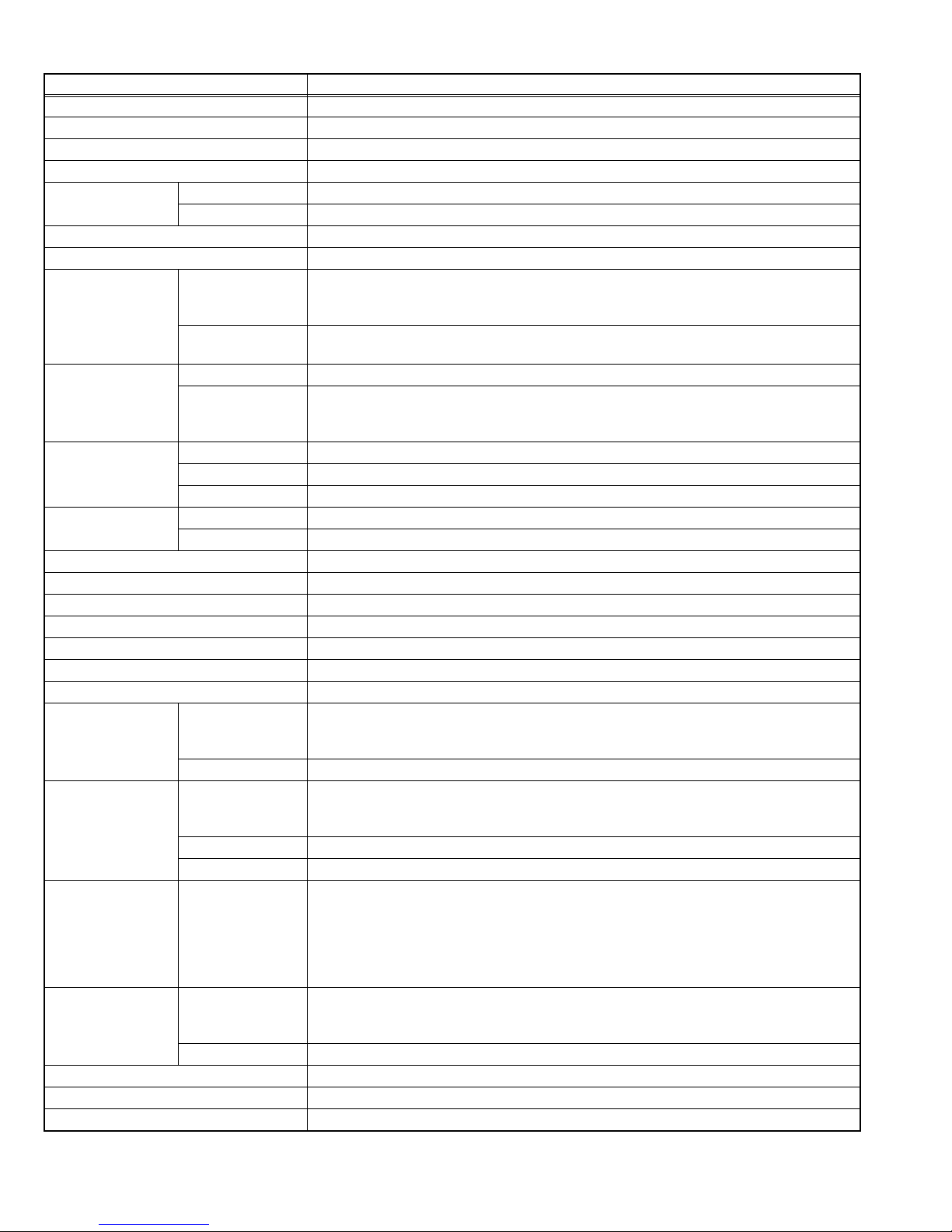
Ventilation hole
1.2.3 INSTALLATION REQUIREMENTS
Ensure that the minimal distance is maintained, as specified
below, between the unit with and the surrounding walls, as well
as the floor etc.Install the unit on stable flooring or stands.
200 mm
*Diagram differs from actual appearance.
1.2.2 NOTES ON HANDLING
When taking the unit out of a packing case, do not grasp the
upper part of the unit. If you take the unit out while grasping the
upper part, the LCD PANEL may be damaged because of a
pressure. Instead of grasping the upper part, put your hands on
the lower backside or sides of the unit.
150 mm 50
*Diagram differs from actual appearance.
mm
150 mm 50 mm
To ensure safety in an emergency such as an earthquake, and
to prevent accidents, ensure that measures are taken to prevent
the TV dropping or falling over.
It fixes in a band.
TV STAND
*Diagram differs from actual appearance.
1-4 (No.YA707<Rev.001>)
Page 5

1.3 HANDLING LCD PANEL
1.3.1 PRECAUTIONS FOR TRANSPORTATION
When transporting the unit, pressure exerted on the internal LCD
panel due to improper handling (such as tossing and dropping)
may cause damages even when the unit is carefully packed. To
prevent accidents from occurring during transportation, pay
careful attention before delivery, such as through explaining the
handling instructions to transporters.
Ensure that the following requirements are met during
transportation, as the LCD panel of this unit is made of glass and
therefore fragile:
(1) USE A SPECIAL PACKING CASE FOR THE LCD PANEL
When transporting the LCD panel of the unit, use a special
packing case (packing materials). A special packing case
is used when a LCD panel is supplied as a service spare
part.
(2) ATTACH PROTECTION SHEET TO THE FRONT
Since the front (display part) of the panel is vulnerable,
attach the protection sheet to the front of the LCD panel
before transportation. Protection sheet is used when a LCD
panel is supplied as a service spare part.
(3) AVOID VIBRATIONS AND IMPACTS
The unit may be broken if it is toppled sideways even when
properly packed. Continuous vibration may shift the gap of
the panel, and the unit may not be able to display images
properly. Ensure that the unit is carried by at least 2
persons and pay careful attention not to exert any vibration
or impact on it.
(4) DO NOT PLACE EQUIPMENT HORIZONTALLY
Ensure that it is placed upright and not horizontally during
transportation and storage as the LCD panel is very
vulnerable to lateral impacts and may break. During
transportation, ensure that the unit is loaded along the
traveling direction of the vehicle, and avoid stacking them
on one another. For storage, ensure that they are stacked
in 2 layers or less even when placed upright.
1.3.2 OPTICAL FILTER (ON THE FRONT OF THE LCD PANEL)
(1) Avoid placing the unit under direct sunlight over a
prolonged period of time. This may cause the optical filter
to deteriorate in quality and COLOUR.
(2) Clean the filter surface by wiping it softly and lightly with a
soft and lightly fuzz cloth (such as outing flannel).
(3) Do not use solvents such as benzene or thinner to wipe the
filter surface. This may cause the filter to deteriorate in
quality or the coating on the surface to come off. When
cleaning the filter, usually use the neutral detergent diluted
with water. When cleaning the dirty filter, use water-diluted
ethanol.
(4) Since the filter surface is fragile, do not scratch or hit it with
hard materials. Be careful enough not to touch the front
surface, especially when taking the unit out of the packing
case or during transportation.
1.3.3 PRECAUTIONS FOR REPLACEMENT OF EXTERIOR
PARTS
Take note of the following when replacing exterior parts (REAR
COVER, FRONT PANEL, etc.):
(1) Do not exert pressure on the front of the LCD panel (filter
surface). It may cause irregular COLOUR.
(2) Pay careful attention not to scratch or stain the front of the
LCD panel (filter surface) with hands.
(3) When replacing exterior parts, the front (LCD panel) should
be placed facing downward. Place a mat, etc. underneath
to avoid causing scratches to the front (filter surface).
(No.YA707<Rev.001>)1-5
Page 6
SECTION 2
SPECIFIC SERVICE INSTRUCTIONS
2.1 FEATURES
DIGITAL TUNER
This TV can receive both DVB-T (Digital terrestrial broadcasting),
DVB-S(Digital satellite broadcasting), and Analogue terrestrial
broadcasting.
HDMI INPUT
By connecting a HDMI compatible device, high definition
pictures can be displayed on your TV in their digital form.
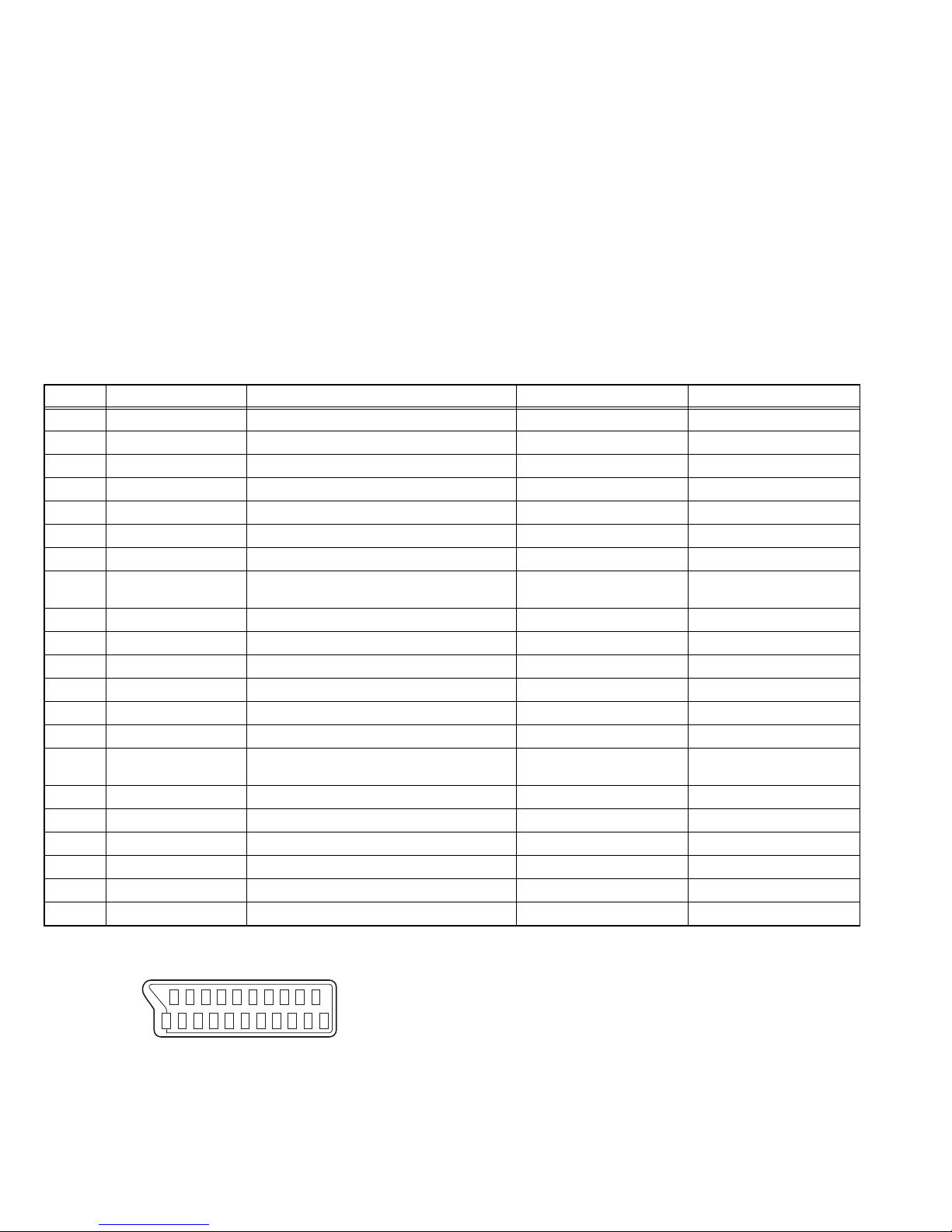
2.2 21-PIN EURO CONNECTOR (SCART) : EXT-1 / EXT-2
Pin No. Signal designation Matching value EXT-1 EXT-2
1 AUDIO R output 500mV(rms) (Nominal), Low impedance Used (TV OUT) Used (LINE OUT)
2 AUDIO R input 500mV(rms) (Nominal), High impedance Used (R1) Used (R2)
3 AUDIO L output 500mV(rms) (Nominal), Low impedance Used (TV OUT) Used (LINE OUT)
4 AUDIO GND Used Used
5 GND (B) Used Used
6 AUDIO L input 500mV(rms) (Nominal), High impedance Used (L1) Used (L2)
7 B input 700mV
8 FUNCTION SW
(SLOW SW)
Low : 0V-3V
High : 8V-12V, High impedance
, 75Ω Used Not used
(B-W)
9 GND (G) Used Used
10 SCL Not used Used (SCL2)
11 G input 700mV
, 75Ω Used Not used
(B-W)
12 SDA Not used Used (SDA2)
13 GND (R) Used Used
14 GND (YS) Used Not used
15 R / C input R : 700mV
C : 300mV
(B-W)
(P-P)
, 75Ω
, 75Ω
16 Ys input (FAST SW) Low : 0V-0.4V, High : 1V-3V, 75Ω Used Not used
17 GND (VIDEO output) Used Used
18 GND (VIDEO input) Used Used
19 VIDEO output 1V
20 VIDEO / Y input 1V
(Negative sync), 75Ω Used (TV OUT) Used (LINE OUT)
(P-P)
(Negative sync), 75Ω Used Used
(P-P)
21 COMMON GND Used Used
PICTURE MODE
This function can adjust the picture settings automatically.
There are BRIGHT, STANDARD, SOFT and MANUAL in the
PICTURE MODE.
ZOOM
This function can change the screen size according to the
picture aspect ratio.
3D CINEMA SURROUND
You can enjoy sounds with a wider ambience.
Used Used
Used (R) Used (C2)
(P-P= Peak to Peak, B-W= Blanking to white peak)
[Pin assignment]
20 18 16 14 12 10 8 6 4 2
21 19 17 15 13 11 9 7 5 3 1
1-6 (No.YA707<Rev.001>)
Page 7

2.3 TECHNICAL INFORMATION
2.3.1 LCD PANEL
This unit uses the flat type panel LCD (Liquid Crystal Display) panel that occupies as little space as possible, instead of the
conventional CRT (Cathode Ray Tube), as a display unit.
Since the unit has the two polarizing filter that are at right angles to each other, the unit adopts "normally black" mode, where light
does not pass through the polarizing filter and the screen is black when no voltage is applied to the liquid crystals.
2.3.1.1 SPECIFICATIONS
The following table shows the specifications of this unit.
Item Specifications
Maximum dimensions ( W × H × D ) 983.0 mm × 576.0 mm × 52.7 mm
Weight 13.6 kg
Effective screen size Diagonal : 107.0 cm (H: 93.0 cm × V:52.32 cm)
Aspect ratio 16 : 9
Drive device / system a-Si-TFT active matrix system
Resolution Horizontally 1920 × Vertically 1080 × RGB < W-XGA > 6220800 dots in total
Pixel pitch (pixel size) Horizontally: 0.4845 mm, Vertically: 0.4845 mm
Displayed color 1073.7 million colors 256 colors for R G and B
Brightness 500 cd/m
2
Contrast ratio 5000 : 1
Response time ( G to G ) less than 5.5 ms
View angle (Horizontally) 178°
View angle (Vertically) 178°
Surface polarizer Anti-Glare type Low reflective coat
Color filter Vertical stripe
Backlight Cold cathode fluorescent lamp
Power supply voltage in LCD 12 V
Power supply voltage in inverter 24 V
Panel interface system LVDS (Low Voltage Differential Signaling)
2.3.1.2 PIXEL FAULT
There are three pixel faults - bright fault , dark fault and flicker fault - that are respectively defined as follows.
BRIGHT FAULT
In this pixel fault, a cell that should not light originally is lighting on and off.
For checking this pixel fault, input ALL BLACK SCREEN and find out the cell that is lighting on and off.
DARK FAULT
In this pixel fault, a cell that should light originally is not lighting or lighting with the brightness twice as brighter as originally lighting.
For checking this pixel fault, input 100% of each R/G/B colour and find out the cell that is not lighting.
FLICKER FAULT
In the pixel fault, a cell that should light originally or not light originally is flashing on and off.
For checking this pixel fault, input ALL BLACK SCREEN signal or 100% of each RGB colour and find out the cell that is flashing on
and off.
(No.YA707<Rev.001>)1-7
Page 8

SECTION 3
DISASSEMBLY
3.1 CAUTION AT DISASSEMBLY
• Make sure that the power cord is disconnected from the outlet.
• Pay special attention not to break or damage the parts.
• Make sure that there is no bent or stain on the connectors before inserting, and firmly insert the connectors.
• Be sure to reattach the wire clamps removed during the procedure to the original positions. (Attaching the wire clamps in wrong
positions may affect the performance.)
REFERENCE:
When removing each board, remove the connector if necessary. The operation is easier if you write down the connection points
(connector numbers) of the connector. For connection of each board, refer to the "WIRING DIAGRAM" of the Standard Circuit
Diagram.
3.2 DISASSEMBLY PROCEDURE
3.2.1 REMOVING THE REAR COVER (Fig.3-1)
(1) Remove the 16 screws [A].
(2) Remove the REAR COVER.
3.2.2 REMOVING THE POWER UNIT (Fig.3-1)
• Remove the REAR COVER.
(1) Remove the 4 screws [B].
(2) Remove the POWER UNIT.
3.2.8 REMOVING BACK BRACKET (Fig.3-1)
• Remove the REAR COVER.
(1) Remove the 4 screws [J].
(2) Remove the BACK BRACKET.
3.2.9 REMOVING THE IR PWB (Fig.3-1)
• Remove the REAR COVER.
(1) Remove the 1 screw [K].
(2) Remove the IR PWB.
3.2.3 REMOVING THE MAIN PWB (Fig.3-1)
• Remove the REAR COVER.
(1) Remove the 1 screw [C].
(2) Remove the SIDE SHIELD.
(3) Remove the 6 screws [D].
(4) Remove the MAIN PWB.
3.2.4 REMOVING THE KEY PWB (Fig.3-1)
• Remove the REAR COVER.
(1) Remove the 1 screws [E].
(2) Remove the CONTROL BASE and KEY PWB together.
(3) Remove the 2 screws [F].
(4) Remove the KEY PWB from the CONTROL BASE.
3.2.5 REMOVING THE INVERTER PWB (Fig.3-1)
• Remove the REAR COVER.
(1) Remove the 6 screws [G].
(2) Remove the INVERTER PWB COVER.
(3) Remove the INVERTER PWB.
3.2.6 REMOVING THE POWER BRACKET (Fig.3-1)
• Remove the REAR COVER.
(1) Remove the 2 screws [H].
(2) Remove the POWER BRACKET.
3.2.7 REMOVING THE SPEAKER (Fig.3-1)
• Remove the REAR COVER.
(1) Remove the SPEAKER(x2).
3.2.10 REMOVING THE STAND (Fig.3-1)
(1) Remove the 4 screws [L].
(2) Remove the STAND.
3.2.11 REMOVING THE LCD CONTROL PWB (Fig.3-1)
• Remove the REAR COVER.
• Remove the STAND.
(1) Remove the 5 screws [L], 2 screws [M] and 5 screws [N].
(2) Remove the MAIN SHIELD.
(3) Remove the 6 screws [P].
(4) Remove the LCD CONTROL PWB.
3.2.12 REMOVING THE LED PWB (Fig.3-1)
• Remove the REAR COVER.
• Remove the STAND.
• Remove the MAIN SHIELD.
(1) Remove the 2 screws [Q] and 2 screws [R].
(2) Remove the BOTTOM FRAME.
(3) Remove the 2screws [S].
(4) Remove the LED PWB.
3.2.13 REMOVING THE LCD PANEL UNIT (Fig.3-1)
• Remove the REAR COVER.
• Remove the STAND.
• Remove the MAIN SHIELD.
• Remove the BOTTOM FRAME.
• Remove the IR PWBand PANEL BRACKET together.
(1) Remove the 3 screws [T].
(2) Remove the PANEL BRACKET(x3).
(3) Remove the LCD PANEL UNIT.
1-8 (No.YA707<Rev.001>)
Page 9

REAR COVER
A
POWER UNIT
INVERTER
PWB COVER
SIDE SHIELD
MAIN PWB
B
J
SUPPORT
BRACKET
L
H
M
POWER
BRACKET
C
D
N
MAIN SHIELD
L
Q
M
G
LCD CONTROL
PWB COVER
P
LCD CONTROL
PWB
Q
BOTTOM FRAME
R
T
PAN EL
BRACKET
R
STAND
T
PANEL BRACKET
LCD PANEL
INVERTER PWB
F
KEY PWB
E
CONTROL
KNOB
IR PWB
S
K
PANEL BRACKET
Fig.3-1
T
PANEL BRACKET
LED PWB
SPEAKER
FRONT CABINET
SPEAKER
(No.YA707<Rev.001>)1-9
Page 10
3.3 MEMORY IC REPLACEMENT
• This model uses the memory IC.
• This memory IC stores data for proper operation of the video and drive circuits.
• When replacing, be sure to use an IC containing this (initial value) data.
3.3.1 MEMORY IC REPLACEMENT PROCEDURE
1. Power off
Switch off the power and disconnect the power plug from the AC outlet.
2. Replace the memory IC
Be sure to use the memory IC written with the initial setting values.
3. Power on
Connect the power plug to the AC outlet and switch on the power.
4. Receiving channel setting
Refer to the OPERATING INSTRUCTIONS and set the receive channels (Channels Preset) as described.
5. User setting
Check the user setting items according to the given in page later. Where these do not agree, refer to the OPERATING
INSTRUCTIONS and set the items as described.
6. FACTORY MODE setting
Verify what to set in the FACTORY MODE, and set whatever is necessary.
3.3.2 FACTORY MODE SETTING
FACTORY MODE SCREEN SETTING ITEM
FACTORY MODE SCREEN
Factory Menu
ADC Calibration
White Balance
Miscellaneous
Engineering Menu
Panel Select xxxxxxxxxxx
Factry Default
Model Name : xxxxxx
Software Version : xxxxxx
OTA Loader Version : xxxxxx
MCU Version : xxxxxx
System Version : xxxxxx
Kernel Version : xxxxxx
Boot Loader Version : xxxxxx
Update Date : xxxxxx
Setting items Settings
ADC Calibration [Do not adjust]
White Balance Adjust
Miscellaneous [Do not adjust]
Engineering Menu [Do not adjust]
Panel Select [Do not adjust]
Factory Default ---
1-10 (No.YA707<Rev.001>)
Page 11

3.3.3 SETTINGS OF FACTORY SHIPMENT
3.3.3.1 BUTTON OPERATION 3.3.3.2 REMOTE CONTROL DIRECT OPERATION
Setting item Setting position
POWER Off
CHANNEL PR1
VOLUME 10
AV TV
3.3.3.3 REMOTE CONTROL MENU OPERATION
(1) Picture
Setting item Setting position
Mode Bright
Colour Temperature Cool
Noise Reduction Low
Fleshtone Off
24p Cinema On
(2) Sound
Setting item Setting position
Bass 0
Treble 0
Balance 0
Auto Volume Control Off
Digital Audio Output PCM
3D Cinema surround Off
TV Speaker On
(3) Installation
Setting item Setting item Setting position
Terrestrial Channel
Search
Antenna Power Off
Auto Channel
Enable
Numbering
Satellite Channel
Antenna Type LNB Only
Search
Software Update ---
Edit Channel List ---
Edit Favourite List ---
Signal Detection ---
Setting item Setting position
CHANNEL PR1
VOLUME 10
ZOOM AUTO
SUB POWER OFF
(4) Feature
Setting item Setting position
Language Setting Menu Language English
Audio Language German
Subtitle Language German
Subtitle Display Auto
Subtitle Font Variable
Audio Description Off
Time Setting Date --/--/20--
Local Time --:--
Sleep Timer Off
Power On Timer Off
Channel ---
Volume 20
Power Off Timer Off
Auto Shut Off Off
Parental Control Child Lock Disable
Maturity Rating View All
Change PIN Code ---
PC ---
Other Settings Zoom Auto
4 : 3 Aspect Setting Panoramic
OSD Transparency 30%
Blue Back Off
Power Lamp On
Control with HDMI On
Auto Demonstration
Off
(No.YA707<Rev.001>)1-11
Page 12
3.4 REPLACEMENT OF CHIP COMPONENT
3.4.1 CAUTIONS
(1) Avoid heating for more than 3 seconds.
(2) Do not rub the electrodes and the resist parts of the pattern.
(3) When removing a chip part, melt the solder adequately.
(4) Do not reuse a chip part after removing it.
3.4.2 SOLDERING IRON
(1) Use a high insulation soldering iron with a thin pointed end of it.
(2) A 30w soldering iron is recommended for easily removing parts.
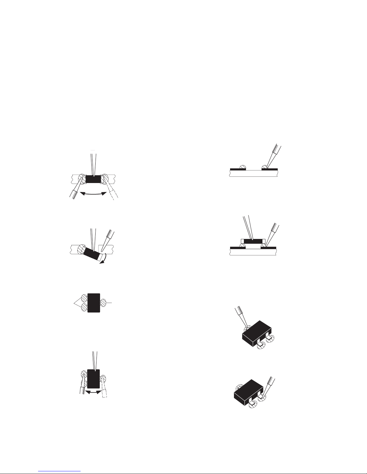
3.4.3 REPLACEMENT STEPS
1. How to remove Chip parts
2. How to install Chip parts
[Resistors, capacitors, etc.]
(1) As shown in the figure, push the part with tweezers and
alternately melt the solder at each end.
(2) Shift with the tweezers and remove the chip part.
[Transistors, diodes, variable resistors, etc.]
(1) Apply extra solder to each lead.
SOLDER
SOLDER
[Resistors, capacitors, etc.]
(1) Apply solder to the pattern as indicated in the figure.
(2) Grasp the chip part with tweezers and place it on the
solder. Then heat and melt the solder at both ends of the
chip part.
[Transistors, diodes, variable resistors, etc.]
(1) Apply solder to the pattern as indicated in the figure.
(2) Grasp the chip part with tweezers and place it on the
solder.
(3) First solder lead A as indicated in the figure.
(2) As shown in the figure, push the part with tweezers and
alternately melt the solder at each lead. Shift and remove
the chip part.
NOTE :
After removing the part, remove remaining solder from the
pattern.
1-12 (No.YA707<Rev.001>)
A
B
C
(4) Then solder leads B and C.
A
B
C
Page 13
SECTION 4
ADJUSTMENT
4.1 ADJUSTMENT PREPARATION
(1) This TV is adjusted by using REMOTE CONTROL UNIT.
(2) The adjustment using the REMOTE CONTROL UNIT is made on the basis of the initial setting values. The setting values
which adjust the screen to the optimum condition can be different from the initial setting values.
(3) Make sure that connection is correctly made AC to AC power source.
(4) Turn on the power of the TV and measuring instruments for warming up for at least 30 minutes before starting adjustments.
(5) If the receive or input signal is not specified, use the most appropriate signal for adjustment.
(6) Never touch the parts (such as variable resistors, transformers and condensers) not shown in the adjustment items of this service
adjustment.
4.2 PRESET SETTING BEFORE ADJUSTMENTS
Unless otherwise specified in the adjustment items, preset the
following functions with the REMOTE CONTROL UNIT.
Setting item Settings position
Picture Mode Standard
Colour Temperature Normal
4.5 BASIC OPERATION OF FACTORY MODE
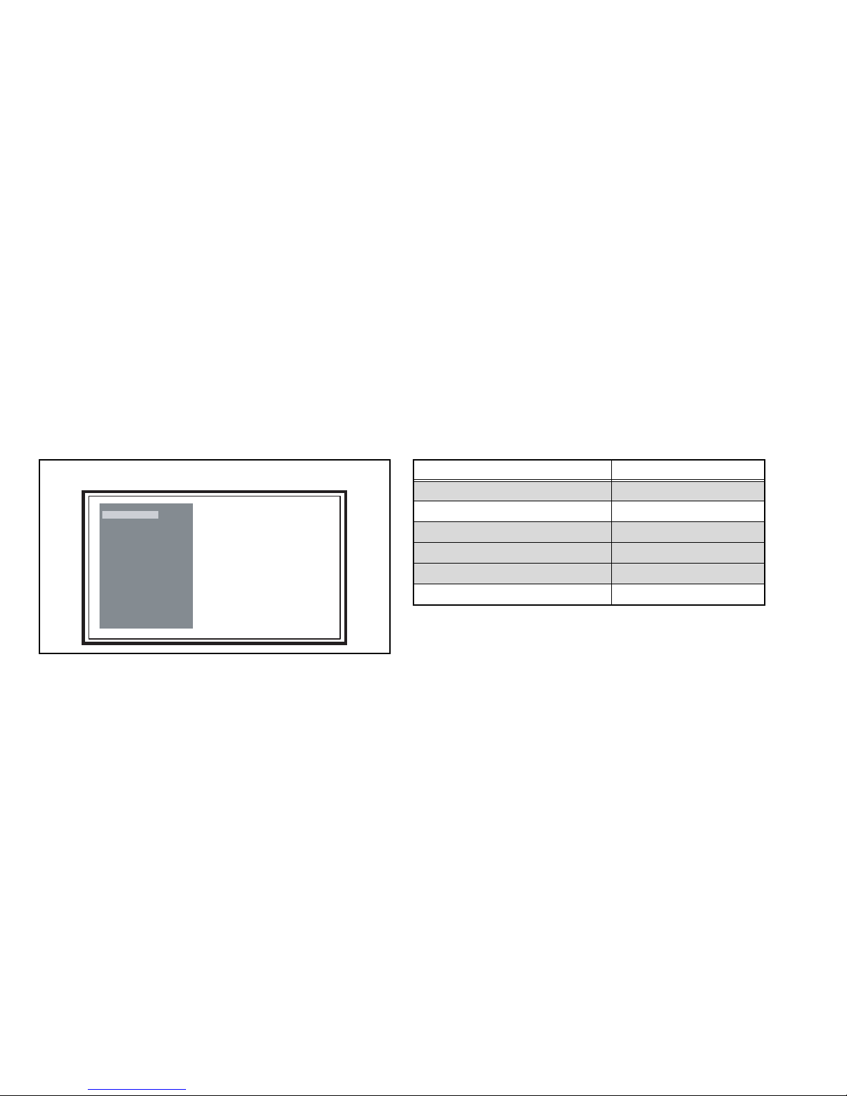
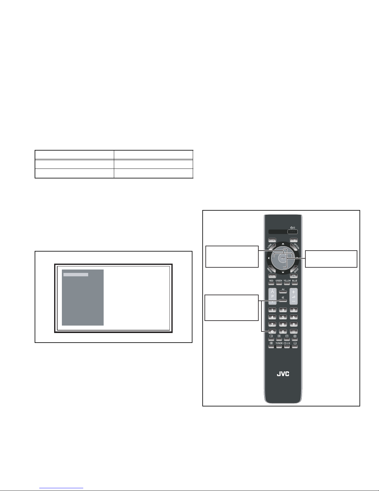
4.5.1 HOW TO ENTER THE FACTORY MODE
(1) Press [INFORMATION] key and [MUTING] key on the
remote control unit simultaneously to enter the FACTORY
MODE SCREEN. (Fig.4-1)
4.5.2 HOW TO EXIT THE FACTORY MODE
Press the [OK] key to exit the factory mode.
FACTORY MODE SCREEN
Factory Menu
ADC Calibration
White Balance
Miscellaneous
Engineering Menu
Panel Select xxxxxxxxxxx
Factry Default
Model Name : xxxxxx
Software Version : xxxxxx
OTA Loader Version : xxxxxx
MCU Version : xxxxxx
System Version : xxxxxx
Kernel Version : xxxxxx
Boot Loader Version : xxxxxx
Update Date : xxxxxx
4.3 MEASURING INSTRUMENT AND FIXTURES
• Signal generator (Pattern generator)[PAL]
• Remote control unit
4.4 ADJUSTMENT ITEMS
VIDEO CIRCUIT
• WHITE BALANCE adjustment
4.5.4 FACTORY MODE SELECT KEY LOCATION
[Function/] key
Scrolling up / down the
setting value.
[MUTING] key +
[INFORMATION] key
Enter The Factry Mode.
[FUNCTION /] key
Select the setting item.
Fig.4-1
4.5.3 CHANGE AND MEMORY OF SETTING VALUE
SELECTION OF SETTING ITEM
• [FUNCTION /] key.
For scrolling up / down the setting items.
• [FUNCTION /] key.
For select the setting items.
CHANGE OF SETTING VALUE (DATA)
• [FUNCTION /] key.
For scrolling up / down the setting values.
MEMORY OF SETTING VALUE (DATA)
The setting value will be stored automatically when release the
REMOTE CONTROL UNIT keys.
(No.YA707<Rev.001>)1-13
Page 14
4.6 ADJUSTMENT PROCEDURE
4.6.1 VIDEO CIRCUIT
Item
WHITE
BALANCE
Measuring
instrument
Test point Adjustment part Description
Remote
control unit
Signal
generator
FACTORY MODE SCREEN
Factory Menu
ADC Calibration
White Balance
Miscellaneous
Engineering Menu
Panel Select xxxxxxxxxxx
Factry Default
Model Name : xxxxxx
Software Version : xxxxxx
OTA Loader Version : xxxxxx
MCU Version : xxxxxx
System Version : xxxxxx
Kernel Version : xxxxxx
Boot Loader Version : xxxxxx
Update Date : xxxxxx
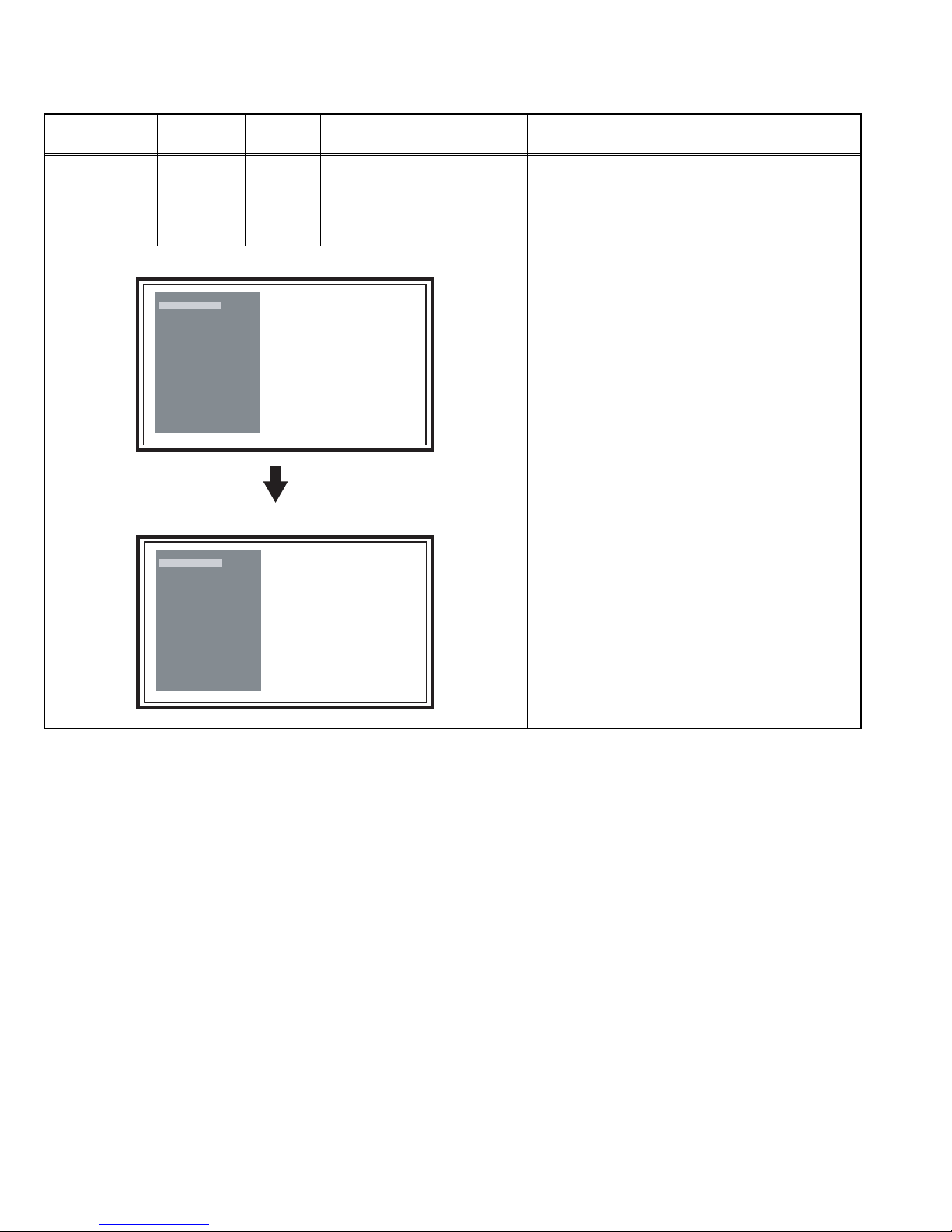
WHITE BALANCE MODE
White Balance
Color Temp Normal
R XX
G XX
B XX
[White Balance]
Normal R
Normal G
Normal B
(1) Set COLOUR TEMP. to "Normal".
(2) Enter the FACTRY MODE.
(3) Press [] / [] key on the remote control unit
simultaneously to select the White balance.
(4) Press [] key on the remote control unit
simultaneously to enter White balnce mode.
(5) Receive a PAL 75% all white signal.
(6) Adjust the setting values of <Normal R>,
<Normal G> and <Normal B> so that the
screen becomes maximum white.
NOTE:
When the normal mode is adjusted, other modes
(cool/ warm) are automatically adjusted.
1-14 (No.YA707<Rev.001>)
Page 15

SECTION 5
TROUBLESHOOTING
5.1 SOFTWARE UPDATE PROCEDURE
In case of writing the software on the Main PWB that is not
contained the software, or in case of the software update is
required, please write the software by the following procedure.
5.1.1 REQUIRED EQUIPMENT
• PC (Equipped with an RS-232C TERMINAL)
• Writing tool (Download the data from JS-net.)
• Program data (Download the data from JS-net.)
• RS-232C JIG cable (Part number: HU-0130200004)
(Female to 3.5mm stereo mini plug cable)
NOTE:
Please confirm SMIS on the JVC Service Information Network
or confirm to your local JVC subsidiary / dealer for software
version.
5.1.2 PROGRAM DATA WRITING PROCEDURE
(7) Turn the power of the main unit OFF.
(8) Unzip Writing tool into your PC.
These 5 files will be unzipped in the folder.
(9) Unzip Program data into your PC.
(10) Connect PC and TV (service only port on rear side of your
TV) with RS-232C JIG cable.
(11) Click WDN4OAK.exe. You will see the following program.
(15) Click the "DownLoad" button to start downloading.
(16) You will see the downloading status bar.
(17) Turn on your TV.
(18) After you finish the downloading, the status bar will be dis-
appeared.
(19) During the download, TV will display a downloading status
OSD and it will be disappeared when you finish the downloading.
(20) Unplug the AC power and wait for a few seconds, then plug
in to the AC power.
(21) Go to the Main menu → TV Setting → Feature → System
Status. You can check the Software version before and after the downloading.
(12) Select the proper COM port to download Software from
your PC. (Default: COM1)
(13) To select hdf file, click the yellow folder button.
(14) See the below picture and double click correct hdf file.
(No.YA707<Rev.001>)1-15
Page 16

Victor Company of Japan, Limited
Display Division 12, 3-chome, Moriya-cho, Kanagawa-ku, Yokohama-city, Kanagawa-prefecture, 221-8528, Japan
(No.YA707<Rev.001>)
Printed in Japan
VSE
Page 17
SCHEMATIC DIAGRAMS
INTEGRATED DIGITAL TERRESTRIAL/SATELLITE LCD TELEVISION
LT-42HB1BU/AX
DVD-ROM No.SML2009Q1
COPYRIGHT © 2009 Victor Company of Japan, Limited.
No.YA707<Rev.001>
2009/7
Page 18
LT-42HB1BU
/AX
STANDARD CIRCUIT DIAGRAM
NOTE ON USING CIRCUIT DIAGRAMS
1.SAFETY
The components identified by the symbol and shading are
critical for safety. For continued safety replace safety ciritical
components only with manufactures recommended parts.
2.SPECIFIED VOLTAGE AND WAVEFORM VALUES
The voltage and waveform values have been measured under the
following conditions.
(1)Input signal : Colour bar signal
(2)Setting positions of
each knob/button and
variable resistor
(3)Internal resistance of tester
(4)Oscilloscope sweeping time
(5)Voltage values
Since the voltage values of signal circuit vary to some extent
according to adjustments, use them as reference values.
: Original setting position
when shipped
: DC 20kΩ/V
: H
: V
: Othters
: All DC voltage values
20µs / div
5ms / div
Sweeping time is
specified
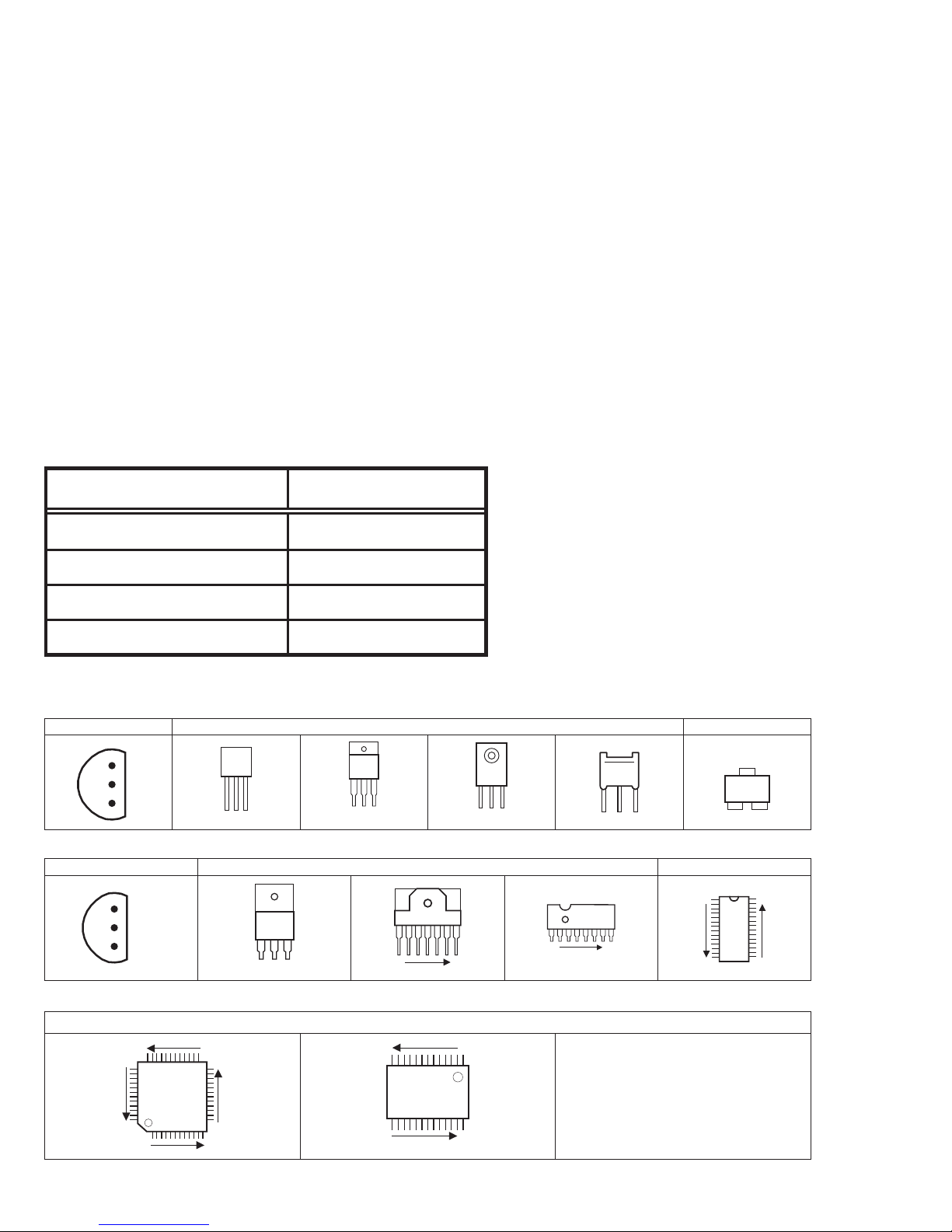
3.INDICATION OF PARTS SYMBOL [EXAMPLE]
In the PW board
: R1209
R209
Type
No indication
MM
PP
MPP
MF
TF
BP
TAN
(3)Coils
No unit
Others
(4)Power Supply
Respective voltage values are indicated
(5)Test point
: Test point
(6)Connecting method
: Ceramic capacitor
: Metalized mylar capacitor
: Polypropylene capacitor
: Metalized polypropylene capacitor
: Metalized film capacitor
: Thin film capacitor
: Bipolar electrolytic capacitor
: Tantalum capacitor
: [µH]
: As specified
: B1
: 9V
: Connector
: Receptacle
: Only test point display
: Wrapping or soldering
: B2 (12V
: 5V
)
4.INDICATIONS ON THE CIRCUIT DIAGRAM
(1)Resistors
Resistance value
No unit : [Ω]
K
M
Rated allowable power
No indication : 1/16 [W]
Others : As specified
Type
No indication
OMR
MFR
MPR
UNFR
FR
Composition resistor 1/2 [W] is specified as 1/2S or Comp.
(2)Capacitors
Capacitance value
1 or higher : [pF]
less than 1
Withstand voltage
No indication : DC50[V]
Others : DC withstand voltage [V]
AC indicated
Electrolytic Capacitors
47/50[Example]: Capacitance value [µF]/withstand voltage[V]
: [kΩ]
: [MΩ]
: Carbon resistor
: Oxide metal film resistor
: Metal film resistor
: Metal plate resistor
: Uninflammable resistor
: Fusible resistor
: [µF]
: AC withstand voltage [V]
(7)Ground symbol
: LIVE side ground
: ISOLATED(NEUTRAL) side ground
: EARTH ground
: DIGITAL ground
5.NOTE FOR REPAIRING SERVICE
This model's power circuit is partly different in the GND. The
difference of the GND is shown by the LIVE : ( ) side GND and the
ISOLATED(NEUTRAL) : ( ) side GND. Therefore, care must be
taken for the following points.
(1)Do not touch the LIVE side GND or the LIVE side GND and the
ISOLATED(NEUTRAL) side GND simultaneously. if the above
caution is not respected, an electric shock may be caused.
Therefore, make sure that the power cord is surely removed from
the receptacle when, for example, the chassis is pulled out.
(2)Do not short between the LIVE side GND and ISOLATED(NEUTRAL
side GND or never measure with a measuring apparatus measure
with a measuring apparatus ( oscilloscope, etc.) the LIVE side GND
and ISOLATED(NEUTRAL) side GND at the same time.
If the above precaution is not respected, a fuse or any parts will be broken.
Since the circuit diagram is a standard one, the circuit and
circuit constants may be subject to change for improvement
without any notice.
NOTE
Due improvement in performance, some part numbers show
in the circuit diagram may not agree with those indicated in
the part list.
When ordering parts, please use the numbers that appear
in the Parts List.
)
(No.YA707<Rev.001>)2-1
Page 19
CONTENTS
SEMICONDUCTOR SHAPES ......................................................................2-2
WIRING DIAGRAM .......................................................................................2-3
BLOCK DIAGRAM ........................................................................................2-5
BLOCK DIAGRAM [MPEG4 BLOCK].........................................................2-7
CIRCUIT DIAGRAMS ...................................................................................2-9
MAIN PWB CIRCUIT DIAGRAM ................................................................................................................. 2-9
IR PWB CIRCUIT DIAGRAM .................................................................................................................. 2-101
KEY PWB CIRCUIT DIAGRAM............................................................................................................... 2-103
LED PWB CIRCUIT DIAGRAM............................................................................................................... 2-105
PATTERN DIAGRAMS ............................................................................ 2-107
MAIN PWB P ATTERN ............................................................................................................................ 2-107
IR PWB P ATTERN.................................................................................................................................. 2-111
KEY PWB P ATTERN .............................................................................................................................. 2-111
LED PWB P ATTERN .............................................................................................................................. 2-111
USING P.W. BOARD
P.W.B ASS㵭Y name LT-42HB1BU/AX
MAIN P.W. BOARD
IR P.W. BOARD
KEY P.W. BOARD
LED P.W. BOARD
HU-71100006
HU-72200004
HU-72200003
HU-72200017
SEMICONDUCTOR SHAPES
TRANSISTOR
BOTTOM VIEW FRONT VIEW TOP VIEW
CHIP TR
E
C
B
ECB
IC
BOTTOM VIEW FRONT VIEW TOP VIEW
OUT
E
IN
IN OUTE
B
(G)E(S)C(D)
1 N
ECB
ECB
1
1 N
C
BE
N
CHIP IC
N
1
2-2(No.YA707<Rev.001>)
TOP VIEW
1
N
Page 20
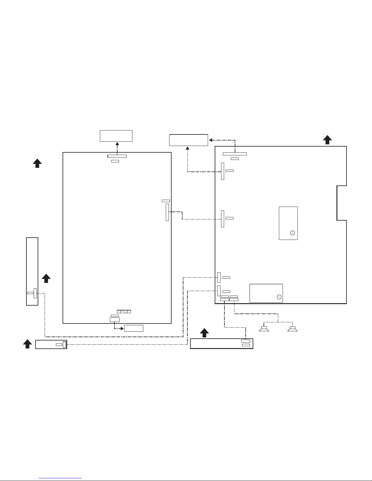
2-4(No.YA707<Rev.001>)(No.YA707<Rev.001>)2-3
FRONT
LED PWB
JP3
1
5
JP2
5
1
TOP
TOP
TOP
TOP
POWER UNIT
IR PWB
KEY PWB
LCD PANEL UNIT
[INVERTER PWB]
LCD PANEL UNIT
[LCD CONTROL PWB]
5
1
6
1
24
1
1
24
CN3
CN1
JP2
JP3
JP761
JP1
31
1
JP642
1
6
JP1
1
41
JP4
1
4
1
15
CN2
N
L
JP641
F1
250V/6.3A
AC INLET
SPEAKER(R)SPEAKER(L)
MAIN PWB
SATELLITE TUNER
TERRESTRIAL TUNER
WIRING DIAGRAM
Page 21

(No.YA707<Rev.001>)2-5 2-6(No.YA707<Rev.001>)
KEY PWB
&
LED PWB
U82
MICOM CTRL
U102
SCALER & MPEG2
U321
HDMI SWITCH
POWER UNIT
UD321, UD322
U181
DDR2
PC
RS232
HDMI
HDMI
HDMI
SPEAKER(L)
SPEAKER(R)
HEADPHONE
AUDIO
PC
JTAG
ILX232
U831
TA_A/RA_A
LCD PANEL
+7V
+12V
PC2
JTAG
PC4
PC5
LS
LS
PC3
HOST_A[1:23]
HOST_D[0:15]
USB_FLAG
HDMIA TDMS IN
HDMIA_I2C
HDMIA_CEC
HDMIA_HPD
HDMIB TDMS IN
HDMIB_HPD
HDMIB_I2C
AHS, AVS
VGA_R,VGA_G,VGA_B
S0_SCL/SDA
TA_A/RA_A
IR_IN
KEY_ADC1
KEY_ADC2
LED_B
LED_R
SCART_ID1
SCART_ID2
PWR_STB
PWM_DIM
A_DIM
BKLT_EN
P_PWM_DIM
P_A_DIM
P_BKLT_EN
+24V
+5V_STB
+5V
XTAL
Y961
M_I2C
CEC_A
ID1
ID2
A_RESET
FRC_RST
LPM_RST_N
HeaderHeader
KIA7042AF
PB5,6,7,RESETn
CLK IN/OUT
4Pin Con.
UART0_TXD/RXD
UART1_TXD/RXD
TXD/RXD
PD0,PD1
PC0,PC1
PB2
PA4
PA5
INT_OUT
FLI_I2C1
*I2C ADDR : 0xA2/3
UART0
UART1
CLK IN/OUT
PWM0
I2C1
IRDATA
LBADC_IN1
LBADC_IN2
EJTAG
DDR MEM
CTL. BUS
ROM MEM
CTL. BUS
BUS BUFFER
HOST_D[0:15]
HOST_A[1:24]
EMI ADDR[1:23]
/EMI DATA[0:15]
FLASH MEMORY
MPEG4 (H264)
BLOCK
(TUNER & STi7103)
AUDO_SPDIF_OUT
I2S_OUT
AUDIO_MUTE
HEAD_OUT_L/R
GPIO134
TNR_SIF
SV4P
AUD_IN_L5/R5
SV3P
B4P,A4P
DDR memory
DDRA[0:12]
/DDRDQ[0:31]
PD6
PA1
PA0
PA2
PA3
PA5
PA6
PB4
Y81
XTAL
* Development Only
IR_IN
KEY_ADC1
KEY_ADC2
PWM3
PWM2
PBIAS
PPWR
LVTX_ODD
LVTX_EVN
RESET_N
UART1_CTS
UART1_RTS
USB2.0 HOST
USB_PWREN
* FRC Option
FLI_I2C1
FRC_RST
FRC_RST
PANEL_PWR
LVDS_OUT
PWM_DIM
A_DIM
BKLT_EN
LPM_RST_N
RESETn_MAIN
FRC_RST
USB_HOST
+5V
+5V_USB
USF-T
TMDS_A
HDMI_SCL/SDA
FLI_I2C1
CEC_A
HPDA
VGA_HS/VS 74HC14 HS/VS
EEPROM
SCART1_RI/LI
PC_R/G/B
VGA_SDA/SCL
SCART_ID1
SCART1_R/G/B/CVBS
SCART1_FB
SCART1_RI/LI
SCART1_CVBSO
SC1_R/L_OUT_O
SCART2_CVBSO
SC2_R/L_OUT_O
SC1_R/L_OUT_O
SC2_R/L_OUT_O
DTT_CVBS
RF_CVBS
SCART1_CVBSO
SCART2_CVBSO
SCART_ID2
SCART2_R/G/B/CVBS
SCART2_FB
SCART2_RI/LI
SCART1_RO/LO
SCART2_RO/LO
SCART2_CVBS_OUT
YPbPr
Component_R/L
SVHS_Y/C
AV_CVBS
AL/AR_CVBS
RF_CVBS
SIF
HEADPHONE_ID
HPO_L/R
AMP_R-
AMP_R+
AMP_L-
AMP_L+
A_RESET
FLI_I2C1
I2S_OUT
AUDO_MUTE
HP_LO/RO
U761
U764
Digital Audio AMP
OP AMP
U582
EEPROM
AUD_IN_L3/R3
LBADC_IN4
A1P,B1P,C1P/SV1P
SCART_FB
AUD_OUT1R/L
AUD_IN_L1/R1
AUD_OUT2R/L
VOUT
LBADC_IN5
A2P,B2P,C2P/SV2P
VXO_D7
AUD_IN_L2/R2
A3P,B3P,C3P
AUD_IN_L4/R4
SPDIF
DIGITAL AUDIO
SCART2
SCART1
CEC
CEC
CEC
TMDS 1
HPD1
TMDS 2
HPD2
TMDS 3
HPD3
EXT4
EXT3
EXT1
EXT5
EXT6
EXT7
EXT2
PC IN
USB IN
U381,U383
VIDEO
SWITCH
U1541,U1581
OP AMP
U382
VIDEO FILTER
U114
USB SWITCH
SERVICE PORT
BLOCK DIAGRAM
Page 22

2-8(No.YA707<Rev.001>)(No.YA707<Rev.001>)2-7
TX
RX
R
CLK/BLANK/HSYNC/VSYNC
DVO[0..23]
I2S / SPDIF
I2S / SPDIF
VXI
CONT
DATA
UART1
CVBS
ROM MEM
CTL. BUS
POD_CTL.
STI7103 System DDR memory
EMI ADDR[1:23]
/EMI DATA[0:15]
NOR FLASH
PC28F320J3D75/BGA
(32Mbit(4Mx8))
Douglas DEMO B/D 256Mbit
SLMI DDRA[0:12]
/SLMI DDRDQ[0:31]
EMI ADDR[1:23]
/EMI DATA[0:15]
CIO TS
Cl contro
I2S / SPDIF
DVO
CONT
DATA
UART1
CVBS
RF_IN1
SIF
RF_CVBS
TUNER0_I2C
TNR0_IF+/-
DEV_/RESET
TUNER0_I2C
DEV_/RESET
TNR1_IF+/-
TUNER1_I2C
LNB_OUT
RF_IN1
FLI_I2C0
TS0
TS
TS
TS_SEL0
FLI_I2C0
DEV_/RESET
FLI_I2C0
nTS_SEL0
22K_TONE
U961
DEMOD
U921 TERRESTRIAL TUNER
U1021 SATELLITE TUNER
U51
BCM4506
U1051
A8293(LNB)
CII TS
POD_DET
nTS_SEL1
TS Selector
MUX TS
TS_SEL1
DTT_CVBS
U102
SCALER
U1131
MPEG CPU
JP221
CI SLOT
Buffer&SW
HOST_A[1:2]/HOST_D[0:7]
POD_CTL
POD_DET
TSIN0
DTT_CVBS
TS_Parallel
[POD]
Inputs
FLI_I2C0 I2C0
GP0132
TS_SEL0
TS_SEL1
UD1261, UD1262
DDR SDRAM
BLOCK DIAGRAM [MPEG4 BLOCK]
Page 23
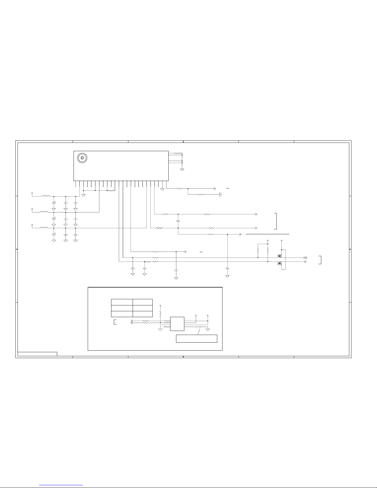
(No.YA707<Rev.001>)2-9 2-10(No.YA707<Rev.001>)
MAIN PWB ASS'Y(1/46)
[TERRESTRIAL TUNER]
HU-71100006
hb1_main_0612_24/48_0.0
1
1
2
2
3
3
4
4
5
5
6
6
A A
B B
C C
D D
DTT_IF_NARROW-
DTT_IF_NARROW+
+5VTA
+5VT_ANT
+5VTA
+5VTA +3V3DT
+5VTA +5VT_ANT
+3V3DT
RF_CVBS
SIF
TUNER0_SCL
TUNER0_AGC
TUNER0_SDA
ANT_PWR_EN
ANT_PWR_CHK
DTT_IF_NARROW-
DTT_IF_NARROW+
All location are from 921 to 960
IIC AS : Tuner : 0xC0h
Analog Demod : 0x86h
Antenna Current Limiting Circuit (100mA Limiting)
Antenna Power Short Protection Circuit
IF ANT_PWR_CTRL is L
--> ANT_PWR_EN L
Fault Flag (Output):
Active-low, open-drain output.
Indicates overcurrent or
thermal shutdown conditions
ANT_PWR_EN
LOW
HIGH
ON
+5V_ANT
OFF
Current limit threshold is determined by
ILIMIT = 230V / RSET,
where : 154 < RSET < 2.29k
C935
4R7p/50V/1005
R923 101/1005
C926
102p/50V/1005
Q924
FDV301N_NL
1
32
L923
BLM18PG300SN1D
C934
104p/16V/1005
C933
OPEN-330p/1005
C925
104p/16V/1005
220uF/16V/MVK/S
C921
R940 201/1005
C936
220p/50V/1005
R926
000/1005
C931
220uF/16V/MVK/S
RF IN
U921
FQD1116AME/BH
RF PIN IN/OUT(OPTION)
1
ANT_PWR2GND3NC4RF_AGC5GND6VP_TUN_+5v7VT8GND9NC10AS11SCL12SDA13REF14IF-AGC15DIF116DIF217WIF OUT/NC18+5V IF192nd IF SOUND/LOW DIG IF1
20
2nd IF SOUND/LOW DIG IF2
21NC22
AS_IF23CVBS
24
GND
25
GND
26
GND
27
GND
28
R939 201/1005
R925
121/1005
R921
562/1005
R930
562/1005
R927 222/1005
C932
OPEN-330p/1005
R929
121/1005
C923
102p/50V/1005
C929
104p/16V/1005
C927
220uF/16V/MVK/S
U922
POWER SW MIC2544-1YMM
EN
1
FLG
2
NC4ILIM
5
OUT
6
IN
7
OUT
8
GND
3
R924
103/1005
L922
BLM18PG300SN1D
C930
102p/50V/1005
Q925
FDV301N_NL
1
32
C922
104p/16V/1005
R933 000/1005
L921
BLM18PG300SN1D
R922 330/1005
R934 000/1005
R932 000/1005
R931 330/1005
R928
750/F/1005
MAIN PWB(13/46)
MAIN PWB(26/46)
MAIN PWB(13/46)
MAIN PWB(26/46)
MAIN PWB(26/46)
MAIN PWB(7/46)
CIRCUIT DIAGRAMS
MAIN PWB CIRCUIT DIAGRAM (1/46) [TERRESTRIAL TUNER]
Page 24

2-12(No.YA707<Rev.001>)(No.YA707<Rev.001>)2-11
MAIN PWB ASS'Y(2/46)
[SATELLITE TUNER]
HU-71100006
hb1_main_0612_26/48_0.0
5
5
4
4
3
3
2
2
1
1
D D
C C
B B
A A
TS_DO0
TS1_DATA5
TS1_DATA6
TS1_DATA7
TS1_DATA4
TS1_DATA3
TS1_DATA2
TS1_DATA1
TS1_DATA0TS_DO0
2.5VS_BCM4505
+5V_STUNER
+3.3V_STUNER
A1V2S_BCM4505
22K_TONE
FLI_SCL_1
FLI_SDA_1
LNB_OUT
TS1_CLK
TS1_VLD
TS1_STR
TS1_DATA[7..0]
CH_RESET
All location are from 1021 to 1050
*I2C Address : 0xD2
Must be pull-down register because gpio default
high. then default voltage is about 0.3V
L1021
BLM18PG300SN1D
L1024
BLM18PG300SN1D
R1021
222/1005
CD1021
OPEN-AVL26K05121
1
1
2
2
2X12 Connector
SHIELD CAN
BCM4505
U51
LNB-IN
LNB-OUT (option)
HSN-5000HS/DTV
1X8 connector
U1021
LNB_A1GND23.3V3GND4HS0_VALID5HS0_D06HS0_CLK7HS0_SYNC8GND9GND10IRQ011NC12SCL13nRESET014GND15GND162.5V17SDA185V1922K_TONE020GND21GND221.2V23LNB_B
24
HS0_D7
25
HS0_D6
26
HS0_D5
27
HS0_D4
28
HS0_D3
29
HS0_D2
30
HS0_D1
31
GND
32
220uF/16V/MVK/S
C1026
C1024
104p/16V/1005
R1023
330/1005
JP230
OPEN_DK-504-039(F-CON)
GND
1
GND
2
GND
3
GND
4
C1023
220uF/16V/MVK/S
C1032
220uF/16V/MVK/S
C1021
102p/50V/1005
C1027
104p/16V/1005
L1023
BLM18PG300SN1D
R1022
330/1005
L1022
BLM18PG300SN1D
C1031
104p/16V/1005
C1022
104p/16V/1005
C1025
102p/50V/1005
C1030
102p/50V/1005
C1028
102p/50V/1005
C1029
220uF/16V/MVK/S
MAIN PWB(27/46)
MAIN PWB(24/46)
MAIN PWB(6/46),(26/46),(27/46)
MAIN PWB(7/46)
MAIN PWB(27/46)
MAIN PWB(24/46)
MAIN PWB CIRCUIT DIAGRAM (2/46) [SATELLITE TUNER]
Page 25
(No.YA707<Rev.001>)2-13 2-14(No.YA707<Rev.001>)
MAIN PWB ASS'Y(3/46)
[Power and Interface Connectors]
HU-71100006
hb1_main_0612_1/48_0.0
5
5
4
4
3
3
2
2
1
1
D D
C C
B B
A A
SMPS_ON
IR
LEDR
LEDB
LEDB
LEDR
BL_EN_O
ANA_DIM
SMPS_ON
ANA_DIM
PWM_DIM_IN
BLT_EN
BL_EN_O
+5V
+12V
+5V4STB
+5V4STB
+5VSTB
+5VSTB
+5VSTB
+5VSTB
+5V+5V
STBY_EN
IR_IN
KEY_ADC2
KEY_ADC1
LED_B
LED_R
AC_DETECT
PWM_DIM_IN
A_DIM
P_DIM
PWM_DIM_IN
PWM_DIM_OUT
BLT_EN
AUO_Panel
MAX.3.5A
MAX.3A
MAX.500mA
Power on : L
Power off : H
FRONT BLUE LED
All location are from 1 to 20
L : ON
H : OFF
L : ON
H : OFF
[+5V]
USB : 500mA
CAM : 500mA
PANEL : 1200mA(Option)
[+12V]
AMP : 1500mA
QPSK : 400mA
PANEL : 800mA
[+5.8V]
MICOM : 9mA
RS232 : 10mA
TUNER : 220mA
Backlight on : L
Backlight off : H
R3
103/1005
C1
100uF/25V/BXE/S
Q3
MMBT4403
1
23
R5 OPEN-000/1005
R14
301/3216
R21
103/1005
C5
OPEN-104p/16V/1005
R2
102/1005
R8
103/1005
2mm
JP1
SMW200-24C
1
2
3
4
5
6
7
8
9
10
11
12
13
14
15
16
17
18
19
20
21
22
23
24
2mm
JP4
53014-0410
2mm
4
3
2
1
R7 102/1005
R12
103/1005
2.5mm
JP2
SMW250-05
2
3
4
1
5
R19
102/1005
R18
472/1005
C3
470uF/16V/MVK/S
R17
472/1005
L3
BLM21PG600SN1D
C8
104p/16V/1005
2.5mm
JP3
SMW250-06
6
5
4
3
2
1
L4
BLM18PG300SN1D
R11
OPEN-332/1005
L1
BLM41PG600SN1L
R1
472/1005
C7
104p/50V
Q1
MMBT4401
1
23
C4
104p/50V
Q2
MMBT4403
1
23
C2
104p/50V
C6
100uF/25V/BXE/S
C9
106p/10V/2012
Q5
MMBT4401
1
23
L2
BLM41PG600SN1L
R9
301/3216
R10 OPEN-102/1005
POWER UNIT
CN1
KEY PWB
JP2
IR PWB
JP1
LED PWB
JP3
MAIN PWB
(4/46),(5/46),(22/46),(43/46)
MAIN PWB(7/46)
MAIN PWB(5/46)
MAIN PWB(14/46),(19/46)
MAIN PWB(14/46),(19/46)
MAIN PWB(5/46)
MAIN PWB(5/46)
MAIN PWB(6/46)
MAIN PWB(5/46)
MAIN PWB CIRCUIT DIAGRAM (3/46) [Power and Interface Connectors]
Page 26
2-16(No.YA707<Rev.001>)(No.YA707<Rev.001>)2-15
MAIN PWB ASS'Y(4/46)
[Power Regulation]
HU-71100006
hb1_main_0612_2/48_0.0
1
1
2
2
3
3
4
4
5
5
6
6
A A
B B
C C
D D
+3V3
+5V
+1V8
+3V3 +3V3_A
VDDR_MEM
+1V8
DDR_VRF
+3V3H
+5VSTB
+5V
+1V2
+5V
+3V3_D
+3V3_D
+5V4STB
+5V4STB
+3V3
+5V
AC_DETECT
[Douglas Core]
+1.216V,
Max.1634mA
[Douglas DDR]
+1.816V,
Max.781mA
3V3 Power Branch
1V8 Power Branch
Max.3A
All location are from 30 to 80
DGND GND_A
MAX 29mA
STAND-BY POWER
Vout=0.8V(R1+R2)/R2
+3.3V
MAX 642mA
Vout=0.8V(R1+R2)/R2
R1
R1
R2
R2
GND_D
MAX 1.5A
R1
R2
Vout = 0.925 x (1+R1/R2)
+3.366V, Max.1.3A
NORMAL POWER
MAX: 3A
C80
105p/25V
R45
4021/F/1005
L35
BLM18PG300SN1D
L31
4.7uH/SPC7040-4R7/3.5A
C78
OPEN-561p/1005
C51 220uF/16V/MVK/S
C59
105p/25V
C48
104p/16V/1005
U32
MP2121DQ
BS
5
FB
1
SW
3
IN
4
IN
7
POK
6
SW
8
GND9GND
2
EN/SYNC
10
GND-PAD
11
C75
822p/25V/1005
R35
102/F/1005
TP35
PCB_TP10
1
R33
104/1005
C55
104p/16V/1005
L32
SPC6025-1R0M
C76
OPEN-106p/10V/2012
C45 104p/16V/1005
C42
106p/10V/2012
C54
106p/10V/2012
C92
OPEN-104p/16V/1005
R50
104/1005
R36
593/F/1005
U34
LD29150PT/P-PAK 5P
/INH1VIN2GND3VOUT4ADJ5GND
6
R38
102/F/1005
C74
220uF/16V/MVK/S
R37
104/1005
C62
100uF/25V/BXE/S
U31
MP2307
BS
1
IN
2
SW
3
GND
4
FB
5
COMP
6
EN
7
SS
8
GND_P
9
D31
OPEN-LL4148
12
C64
104p/16V/1005
C44
104p/16V/1005
C69
106p/10V/2012
TP36
PCB_TP10
1
R34
753/F/1005
C77
104p/16V/1005
TP38
PCB_TP10
1
C71
106p/10V/2012
TP32
PCB_TP10
1
R41
103/F/1005
C68
104p/16V/1005
C61
226p/6.3V/2012
R47
OPEN-104/1005
104p/16V/1005
C34
C73
226p/6.3V/2012
C72
226p/6.3V/2012
U36
OPEN-ASM811REUSF-T
GND
1
RESET
2
VCC
4
MR
3
C41
106p/10V/2012
R43
243/F/1005
C46
104p/16V/1005
C49 104p/16V/1005
C67
106p/10V/2012
C50
335p/10V/2012
L34
BLM18PG300SN1D
C31
104p/16V/1005
D30
OPEN-B340A
12
TP39
PCB_TP10
1
C60
104p/16V/1005
TP33
PCB_TP10
1
R44
912/F/1005
R46
OPEN-103/1005
L33
BLM18PG300SN1D
R48
104/1005
C65
OPEN-105p/16V/1005
C57
100uF/25V/BXE/S
C63
106p/10V/2012
C47 220uF/16V/MVK/S
C79
103p/50V/1005
TP37
PCB_TP10
1
C58
OPEN-105p/16V/1005
R32
6043/F/1005
104p/16V/1005
C53
R49
104/1005
R40
1692/F/1005
C52
106p/10V/2012
R39
000/1005
R31
304/F/1005
U35 RT9167-50PB
VOUT
5
BP
4
EN
3
GND
2
VIN
1
R42
104/1005
TP34
PCB_TP10
1
R51
OPEN-104/1005
C43
103p/50V/1005
R52
750/F/1005
C30
105p/25V
C66
OPEN-102p/50V/1005
U33
RT9018B25PSP
EN
2
VDD
4
VIN
3
NC
5
PGOOD
1
VOUT
6
ADJ
7
GND
8
TAP
9
C70
103p/50V/1005
C56
104p/16V/1005
TP31
PCB_TP10
1
TP17
PCB_TP10
1
MAIN PWB
(3/46),(5/46),(22/46),(43/46)
MAIN PWB CIRCUIT DIAGRAM (4/46) [Power Regulation]
Page 27
(No.YA707<Rev.001>)2-17 2-18(No.YA707<Rev.001>)
MAIN PWB ASS'Y(5/46)
[MICRO CTRL]
HU-71100006
hb1_main_0612_3/48_0.0
5
5
4
4
3
3
2
2
1
1
D D
C C
B B
A A
KEY_ADC2
KEY_ADC1
MISO
SCK
MOSI
RESETn
MOSI
RESETn
SCK
MISO
RESETn
M_SDA
M_SCL
MOD2_ID
MOD1_ID
M_RST_N
INT_OUT
M_RST_N
INT_OUT
MOD2_IDMOD1_ID
MOD3_ID
MOD3_ID
+5VSTB +5VSTB
+3V3_A
+5VSTB
+5VSTB +5VSTB
+5VSTB
+5VSTB
+5VSTB +5VSTB
+5VSTB
+3V3_A
+5VSTB
+5VSTB+5VSTB +5VSTB
LED_R
LED_B
FLI_SDA_0
KEY_ADC2
IR_IN
STBY_EN
KEY_ADC1
A_RESET
AC_DETECT
CEC_A
TA
RA
FLI_SCL_0
LPM_RST_N
FLI_INT
SC_MUTE
M_SDA
M_SCL
CEC_O
M_RST_N
PA5
UART0(to RS232)
PA4
PA3
UART0(to RS232)
PB7
PA2
PB1
PB0
PA7
PA6
PA0
PA1
KEY_ADC2
PB2
PB3
PB4
PB5
PB6
PC0
PC1
PC2
PC3
PC4
PC5
PC6
PC7
PD0
PD1
PD2
PD3
PD4
PD5
PD6
PD7
KEY_ADC1
LED_R
LED_B
FLI_SCL1
FLI_SDA1
A_RESET
AC_DETECT
Front Key ADC2
HDD Recording LED
Display LED
Front Key ADC1
CEC_A
STBY_EN
MOSI
MISO
SCK
RA
TA
IR_IN IR Input
AMP Reset Control(to AMP)
SMPS AC Detect
I2C(to Douglas)
I2C(to Douglas)
HDMI CEC Control
Stand-by ON/OFF
JTAG
JTAG
JTAG
System Reset
M_RST_N Douglas Chip Reset
All location are from 81 to 110
L : Normal
H : Reset
INT_OUT Douglas Interrupt
Scart_Mute Scart Audio Output Mute
MOD2_ID
MOD1_ID
Model_Detect
Model_Detect
R88
472/1005
R104
Open_103/1005
Y81
16MHZ/20pF/SMD
12
R81
103/1005
C85
104p/16V/1005
R89 330/1005
R100
103/1005
R105
103/1005
R87
472/1005
R97 162/1005
C90
104p/16V/1005
R84 101/1005
C84
104p/16V/1005
R106
Open_103/1005
Q83
MMBT4401
1
23
R94 101/1005
C87
OPEN-103p/50V/1005
C86
104p/16V/1005
C88
200p/50V/1005
R107
103/1005
R108
OPEN-103/1005
S81
OPEN-JTP1127WEM
1
2
34
R82
101/1005
R91 101/1005
R93
OPEN_103/1005
Q81
FDV301N_NL
1
32
C83
106p/10V/2012
C81
OPEN-104p/16V/1005
C82
104p/16V/1005
U81
OPEN-KIA7042AF
VCC1GND2OUT3GND
4
U82
ATMEGA324P-20AU
(ADC0) PA0
37
(ADC1) PA1
36
(ADC2) PA2
35
(ADC3) PA3
34
(ADC4) PA4
33
(ADC5) PA5
32
(ADC6) PA6
31
(ADC7) PA7
30
(SCL) PC0
19
(SDA) PC1
20
(TCK) PC2
21
(TMS) PC3
22
(TDO) PC4
23
(TDI) PC5
24
(TOSC1) PC6
25
(TOSC2) PC7
26
PB0 (XCK/T0)
40
PB1 (T1)
41
PB2 (AIN0/INT2)
42
PB3 (AIN1/OC0)
43
PB4 (SS)
44
PB5 (MOSI)
1
PB6 (MISO)
2
PB7 (SCK)
3
PD0 (RXD)
9
PD1 (TXD)
10
PD2 (INT0)
11
PD3 (INT1)
12
PD4 (OC1B)
13
PD5 (OC1A)
14
PD6 (ICP)
15
PD7 (OC2)
16
XTAL2
7
XTAL1
8
AREF
29
AVCC
27
RESETn
4
VCC1
5
VCC2
17
VCC3
38
GND1
6
GND2
18
GND3
28
GND4
39
Q82
FDV301N_NL
1
32
R103
183/F/1005
JP81
OPEN-HPH-DS06-02
12
34
56
C91
104p/16V/1005
R83
OPEN_103/1005
R98 162/1005
R101
102/1005
R95 101/1005
R102 103/1005
C89
200p/50V/1005
R90 330/1005
R99
103/1005
R109
103/1005
R96 000/1005
MAIN PWB(23/46)
MAIN PWB(40/46),(42/46)
MAIN PWB(42/46)
MAIN PWB(43/46)
MAIN PWB(3/46)
MAIN PWB(3/46)
MAIN PWB(3/46)
MAIN PWB(6/46)
MAIN PWB(37/46)
MAIN PWB(22/46)
MAIN PWB(39/46)
MAIN PWB
(6/46),(17/46),(22/46),(40/46)
MAIN PWB
(3/46),(4/46),(22/46),(23/46)
MAIN PWB CIRCUIT DIAGRAM (5/46) [MICRO CTRL]
Page 28
2-20(No.YA707<Rev.001>)(No.YA707<Rev.001>)2-19
MAIN PWB ASS'Y(6/46)
[USB,I2C,JTAG]
HU-71100006
hb1_main_0612_4/48_0.0
5
5
4
4
3
3
2
2
1
1
D D
C C
B B
A A
USB_D0+
USB_D0-
UART0_RX
UART0_TX
UART1_TX
UART1_RX
UART0_TX
UART0_RX
DINT
TRST#
EJTAG_RST#
TDI
TDO
TMS
FLI_SCL_0
FLI_SDA_0
TCK
WP
NVRAM_WP
NVRAM_WP
FLI_SCL_0
FLI_SDA_0
FLI_SDA_1
FLI_SCL_1
+5V_USB
+5V
+1V2
+5V_USB
+3V3_A
+3V3_A
+3V3_A
+3V3_A
+3V3_A +3V3_A
+3V3_A
+3V3_A +3V3_A
+3V3_A
+5V
+5V
P_DIM
A_DIM
CI_PWR
LPM_RST_N
FLI_INT
PWR_/RESET
BLT_EN
FRC_/RST
FLI_SDA_0
FLI_SCL_0
FLI_SDA_1
FLI_SCL_1
UART1_RX
UART1_TX
UART0_RX
UART0_TX
EJTAG
All location are from 111 to 160
EEPROM
Address:0xA4/A5
UART0 : PC Display Debug message
UART1 : G-Probe application run at PC
Reset Threshole
: +3.08V
NVRAM_WP : H = Enable write
NVRAM_WP : L = Disable write
Active high
STi7103_UART
C129
100uF/16V/MVK/S
C116
104p/16V/1005
R126
102/1005
C112
OPEN-680p/50V/1005
C123
104p/16V/1005
C122
104p/16V/1005
R137
103/1005
R119 330/1005
R128
622/F/1005
R127
103/1005
R129 OPEN-472/1005
R111
OPEN-104/1005
R135
OPEN-472/1005
TP112
PCB_TP08
1
C119
105p/16V/1005
C126
5R0p/50V/1005
C125
5R0p/50V/1005
C120
104p/16V/1005
C127
106p/10V/2012
TP111
PCB_TP08
1
R124
OPEN-000
PR111 103*4/1005
18
27
36
45
R112 000/1005
R125 OPEN-200/1005
C114
270p/50V/1005
RV111
OPEN-AVRL161A1R1NTB
C113
270p/50V/1005
U111
OPEN-ASM811REUSF-T
GND
1
RESET
2
VCC
4
MR
3
R121 330/1005
C124
106p/10V/2012
L111
BLM18PG300SN1D
Q111
MMBT4401
1
23
2mm
JP113
OPEN-53014-0410
4
3
2
1
R133
OPEN-153/1005
U113
24LC256
A0
1
A1
2
A2
3
VSS
4
VCC
8
SCL
6
SDA
5
WP
7
R115 222/1005
R131
103/1005
R116 222/1005
R120 330/1005
R134
OPEN-153/1005
R138
103/1005
R139
000/1005
C121
104p/16V/1005
L113
ACM2012H-900
3
21
4
R113 222/1005
L114
BLM21PG600SN1D
Y111
19.6608MHZ/
20PF/SX-1/SMD
12
R132
103/1005
R118 330/1005
R136
OPEN-472/1005
JP111
OPEN-2110-DS14-G
1
3
5
7
9
11
13 14
12
10
8
6
4
2
RV112
OPEN-AVRL161A1R1NTB
R122 000/1005
R123 102/1005
JP112
KJA-UB-4-0004
VBUS
1
D-
2
D+
3
GND
4
1
2
3
4
SGND
5
SGND
6
C118
47uF/16V/MVK/S
TP113
PCB_TP08
1
R117 222/1005
R130 OPEN-472/1005
C115 200p/50V/1005
L112
BLM18PG300SN1D
U114
R5523N USB HIGH-SIDE POWER SWITCH
EN
1
GND2FLG
3
IN
4
OUT
5
C117
104p/16V/1005
C128
104p/16V/1005
U102G
FLI10620H
USBPHY_VRES
AG20
USB_FLAG
C29
USBPHY_PADM
AH20
USBPHY_PADP
AJ20
PWM0_GPIO4_/INT4
D13
PWM1_GPIO5_/INT5
C13
PWM2_GPIO6
B13
PWM3
A13
CLKOUT
E12
TESTMODE0
C27
TESTMODE1
C26
TRST
B26
TDO
A27
TDI
B27
TMS
A28
TCK
B28
EJ_RST_N
A29
EJ_DINT
B29
2WIRE_M0_SDA
F20
2WIRE_M0_SCL
E20
2WIRE_M1_SCL_UART2_RX
D20
2WIRE_M1_SDA_UART2_TX
D21
UART0_RXD
A19
UART0_TXD
B19
UART1_TXD
B20
UART1_RXD
A20
UART1_RTS
C20
UART1_CTS
C19
RESET_N
D23
REF_CLK
A22
XTAL_IN
A23
OBUFC_CLK
F21
DFSYNC_IN_OUT_GPIO8
E13
USB_GND
AD20
USB_AVDD33
AH19
USB_AVDD33
AF20
USB_GND
AF19
USB_GND
AJ19
USB_AVDD12
AE20
USB_AVDD33
AG19
USB_PWREN
C28
OTP_VDD33
A26
S111
OPEN-JTP1127WEM
12
34
R114
OPEN-104/1005
MAIN PWB(2/46),(26/46),(27/46)
MAIN PWB(36/46)
MAIN PWB(23/46)
MAIN PWB(3/46)
MAIN PWB(5/46),(17/46),(22/46),(40/46)
MAIN PWB(17/46)
MAIN PWB(10/46)
MAIN PWB(5/46)
MAIN PWB(5/46)
MAIN PWB(8/46)
MAIN PWB(3/46)
MAIN PWB CIRCUIT DIAGRAM (6/46) [USB,I2C,JTAG]
Page 29

(No.YA707<Rev.001>)2-21 2-22(No.YA707<Rev.001>)
MAIN PWB ASS'Y(7/46)
[I2S]
HU-71100006
hb1_main_0612_5/48_0.0
5
5
4
4
3
3
2
2
1
1
D D
C C
B B
A A
LBADC_IN1
LBADC_IN2
LBADC_IN3
LBADC_IN6
SCART1_ID
SCART2_ID
HEADPHONE_ID HEADPHONE_ID
SCART1_ID
SCART2_ID
VXI_D0
VXI_D1
VXI_D2
VXI_D3
VXI_D4
VXI_D5
VXI_D6
VXI_D7
VXI_D8
VXI_D9
VXI_D10
VXI_D11
VXI_D12
VXI_D13
VXI_D14
VXI_D15
Model1_ID
Model2_ID
Model3_ID
Model4_ID
AUO_Panel
LBADC_IN6
LBADC_IN1
LBADC_IN2
LBADC_IN3
Model2_ID
Model3_ID
Model4_ID
AUO_Panel
Model1_ID
CI_ACC_EN
CI_ACC_EN
ST7103_FLASH_EN
+3V3_A
+3V3_A
+3V3_A
+3V3_A
+3V3_A
SCART1_ID
SCART2_ID
SPDIF_OUT
HEADPHONE_ID
ANT_PWR_CHK
TS_SEL
ANT_PWR_EN
PD_RESET
ST_SPDIF
ST_PCM_SCLK
ST_PCM_LRCLK
ST_PCMOut0
CH_TER_RESET
VXI_DE
VXI_VS
VXI_HS
VXI_D[0..15]
VXI_CLK
TS_SEL_CI
ST_RESET
PANEL_PWR
OPC_CTL
CH_RESET
I2S_OUT_MCLK
I2S_OUT_CLK
I2S_OUT_WS
I2S_OUT_DAT
SC_FB_SEL
SC1_SEL
FRC_MODE0
FRC_MODE1
EMIBUSREQ
EMIBUSGNT
ST_PCM_MCLK
AUO_Panel
VGA_SW
CI_ACC_EN
BIT_SEL
FRC_MODESEL
ST7103_FLASH_EN
All location are from 161 to 180
Model1_ID : Panel (H:WXGA,L:FHD)
Model2_ID : Model (H:19,20", L: More than 26")
Model3_ID :
Model4_ID : (H: HB1, L: DB1 )
R164 103/1005
C161
106p/10V/2012
R161
OPEN-103/1005
PR161
330*4/1005
18
27
36
45
R170 103/1005
R168 102/1005
R178 103/1005
R163 103/1005
R172 OPEN-103/1005
R173 103/1005
R167 OPEN-000/1005
R176 103/1005
R171 OPEN-103/1005
TP165 PCB_TP08
1
R162 103/1005
R174 103/1005
L161
BLM18PG300SN1D
C162
104p/16V/1005
R169 103/1005
R165 000/1005
C165
103p/50V/1005
U102D
FLI10620H
LBADC_IN1
C25
LBADC_IN2
C24
LBADC_IN3
B25
LBADC_IN4
B24
LBADC_IN5
A25
LBADC_IN6
A24
LBADC_RETURN
F22
IRDATA
C21
AUD_MCLK0
AC1
AUDIN_I2S_BCLK
AC2
AUDIN_I2S_WCLK
AB3
AUDIN_I2S_DAT
AA4
AUDIN_SPDIF_IN
AA5
AUD_MCLK1
AB5
AUDO_I2SA_BCLK
AB4
AUDO_I2SA_WCLK
AC5
AUDO_I2SA_DAT0
AC4
AUDO_I2SB_BCLK
AC3
AUDO_I2SB_WCLK
AD3
AUDO_I2SB_DAT1
AD2
AUDO_I2SB_DAT2
AE2
AUDO_SPDIF_OUT
AD1
LBADC_33
D24
LBADC_GND
E23
R166 000/1005
R179 OPEN-103/1005
U102F
FLI10620H
VXO_CLK
AD19
VXO_DE
AE19
VXO_VS
AG18
VXO_HS
AF18
VXO_D0
AF15
VXO_D1
AH16
VXO_D2
AJ16
VXO_D3
AE15
VXO_D4
AE16
VXO_D5
AF16
VXO_D6
AG16
VXO_D7
AH17
VXO_D8
AJ17
VXO_D9
AE17
VXO_D10
AF17
VXO_D11
AG17
VXO_D12
AH18
VXO_D13
AJ18
VXO_D14
AD15
VXO_D15
AE18
VXI_CLK
A18
VXI_DE
C18
VXI_VS
B18
VXI_HS
D18
VXI_D0
E19
VXI_D1
A17
VXI_D2
B17
VXI_D3
C17
VXI_D4
D17
VXI_D5
F17
VXI_D6
A16
VXI_D7
B16
VXI_D8
C16
VXI_D9
D16
VXI_D10
D19
VXI_D11
E16
VXI_D12
A15
VXI_D13
B15
VXI_D14
C15
VXI_D15
D15
VXI_D16
E15
VXI_D17
A14
VXI_D18/TS_ERR
B14
VXI_D19/DREQ_I
C14
VXI_D20/TS_VALID_O
D14
VXI_D21/TS_SYNC_O
E14
VXI_D22/TS_D_O
E17
VXI_D23/TS_CLK_O
E18
TP164 PCB_TP08
1
R177 OPEN-103/1005
TP172
PCB_TP08
1
R175 103/1005
C166
103p/50V/1005
MAIN PWB(38/46)
MAIN PWB(22/46)
MAIN PWB(38/46)
MAIN PWB(39/46)
MAIN PWB(24/46)
MAIN PWB(35/46)
MAIN PWB(35/46),(36/46)
MAIN PWB(26/46)
MAIN PWB(22/46)
MAIN PWB(14/46)
MAIN PWB(9/46)
MAIN PWB(40/46)
MAIN PWB(39/46)
MAIN PWB(37/46)
MAIN PWB(2/46)
MAIN PWB(1/46)
MAIN PWB(13/46)
MAIN PWB(14/46)
MAIN PWB(17/46)
MAIN PWB (43/46)
MAIN PWB (9/46)
MAIN PWB (3/46)
MAIN PWB (46/46)
MAIN PWB (44/46)
MAIN PWB(36/46)
MAIN PWB(38/46)
MAIN PWB CIRCUIT DIAGRAM (7/46) [I2S]
Page 30

2-24(No.YA707<Rev.001>)(No.YA707<Rev.001>)2-23
MAIN PWB ASS'Y(8/46)
[Flash and CI Interface]
HU-71100006
hb1_main_0612_6/48_0.0
5
5
4
4
3
3
2
2
1
1
D D
C C
B B
A A
HOST_D0
HOST_D1
HOST_D4
HOST_D5
HOST_D6
HOST_D7
HOST_D0
HOST_D1
HOST_D2
HOST_D3
HOST_D4
HOST_D5
HOST_D6
HOST_D7HOST_A0
HOST_A1
HOST_A2
HOST_A3
HOST_A4
HOST_A5
HOST_A6
HOST_A7
HOST_A10
HOST_A11
HOST_A12
HOST_A13
HOST_WE#
HOST_OE#
HOST_ACK
HOST_RD
#CS_FLASH_DG
POD_DET#
POD_DAT_DIR
CI_CD1_N
CI_CD2_N
CI_CE1_N
CI_WAIT_N
CI_IRQ_N
CI_RESET
HOST_BOOT_CS#
HOST_RD
HOST_D2
HOST_D3
HOST_A0
HOST_A2
HOST_A4
HOST_A5
HOST_A7
MUX_TSI_SYNC
MUX_TSI_VAL
MUX_TSI_CLK
MUX_TSI_D0
MUX_TSI_D1
MUX_TSI_D2
MUX_TSI_D3
MUX_TSI_D4
MUX_TSI_D5
MUX_TSI_D6
MUX_TSI_D7
POD_A4
POD_A5
POD_A6
POD_A7
POD_A8
POD_A9
POD_A14
HOST_A8
HOST_A9
HOST_A14
HOST_D8
HOST_D9
HOST_D10
HOST_D11
HOST_D12
HOST_D13
HOST_D14
HOST_D15
HOST_D8
HOST_D9
HOST_D10
HOST_D11
HOST_D12
HOST_D13
HOST_D14
HOST_D15
HOST_A15
HOST_A16
HOST_A17
HOST_A18
HOST_A19
HOST_A20
HOST_A21
HOST_A22
HOST_A23
HOST_A24
HOST_A15
HOST_A16
HOST_A17
HOST_A18
HOST_A8
HOST_A19
HOST_A9
HOST_A20
HOST_A21
HOST_A14
HOST_A22
HOST_A1
HOST_A2
HOST_A3
HOST_A4
HOST_A5
HOST_A6
HOST_A7
HOST_A10
HOST_A11
HOST_A12
HOST_A13
HOST_A23
HOST_A24
HOST_ACK
Flash_WP#
POD_DET#
HOST_A24
Flash_WP#
Flash_WP#
HOST_A1
HOST_A3
HOST_A6
HOST_A23
HOST_WE#
HOST_WE#
HOST_OE#
HOST_CS0#
HOST_BOOT_CS#
+3V3_A
+3V3_A
+3V3_A
+3V3_A
+3V3_A
+3V3_A
+3V3_A
CI_RESET
CI_CE1_N
CI_WAIT_N
PWR_/RESET
POD_A4
POD_A5
POD_A6
POD_A7
POD_A8
POD_A9
POD_A14
CI_CD1_N
CI_CD2_N
CI_IRQ_N
HOST_D[15..0]
HOST_A[24..0]
MUX_TSI_VAL
MUX_TSI_SYNC
MUX_TSI_CLK
POD_DET#
POD_DAT_DIR
#CS_FLASH_DG
MUX_TSI_D2
MUX_TSI_D1
MUX_TSI_D6
MUX_TSI_D5
MUX_TSI_D4
MUX_TSI_D3
MUX_TSI_D7
MUX_TSI_D0
HOST_WE#
HOST_OE#
HOST_CS0#
HOST_BOOT_CS#
BOOT STRAP SETTING
All location are from 181 to 220
BSTRAP_BOOT_MODE
BSTRAP_EXT_OSC
BSTRAP_16BIT_FLASH
BSTRAP_NAND_FLASH_EN
BSTRAP_PAGESIZE
BSTRAP_NAND_FLASH_DWIDTH
BSTRAP_NOR_FLASH_SEL
Bootstrap Pin Name
POD_HOST_A0
POD_HOST_A1
POD_HOST_A2
Pins POD_HOST_A[1:0] indicate on chip
hardware the host interface configuration
to use after hard reset:
A1;A0 = 00 = Function test, vendor mode.
A1;A0 = 01 = Function test, vendor mode.
A1;A0 = 10 = Boot from FLASH
A1;A0 = 11 = Boot from IROM
Pin POD_HOST_A2 indicates:
0 = Internal osc
1 = External osc
Pin POD_HOST_A3 indicates type of
memory for external boot FLASH.
0 = 8-bit FLASH
1 = 16-bit FLASH
Pin PODREG_HOST_A4 indicates type of
memory for external boot FLASH.
0 = NOR FLASH
1 = NAND FLASH
Pin POD_IOWR_HOST_A5 indicates page
size for off chip NAND FLASH.
0 = Small page NAND FLASH
1 = Large page NAND FLASH
Pin POD_IORD_HOST_A6 indicates data
width for NAND FLASH (used by IROM
boot s/w only).
0 = 8-bit NAND FLASH
1 = 16-bit NAND FLASH
Pin HOST_A[7] selects whether parallel
NOR flash or SPI flash is used for boot
when BSTRAP_BOOT_MODE=10 (IROM
bypass). Ignored if
BSTRAP_BOOT_MODE != 10.
0 = boot from parallel NOR flash
1 = boot from SPI flash
POD_HOST_A3
POD_HOST_A4
POD_HOST_A5
POD_HOST_A6
POD_HOST_A7
Description
NOTE.
64 MBit FLASH : R203, R204, L26 OPEN
128 MBit FLASH : R204, L26 OPEN
256 MBit FLASH : L27 OPEN(P30 Series)
A24 setting default value "0" when STi7103 access flash
HOST WE# setting default value "1" when STi7103 access flash
R184 OPEN-103/1005
C183
104p/16V/1005
R186
C184
104p/16V/1005
R185
103/1005
R181
330/1005
R205 103/1005
R190 103/1005
R197 103/1005
R182 103/1005
R195 103/1005
R203 000/1005
R191 103/1005
TP181
PCB_TP08
1
R234
103/1005
C185
104p/16V/1005
R200 103/1005
R204
000/1005
R199 000/1005
U102C
FLI10620H
POD_DETEC_N
AD4
POD_DIR_N
AD5
POD_CE_1
AE4
POD_A4_CTX
AE3
POD_A5_ITX
AF3
POD_A6_ETX
AF2
POD_A7_QTX
AG2
POD_A8_CRX
AF1
POD_A9_DRX
AG1
POD_A14_MCLKO
W5
POD_VS2_MCLKO
W6
POD_BVD2_MOVAL
Y5
POD_BVD1_MOSTRT
Y4
POD_D15_MDO7
AB1
POD_D14_MDO6
AA1
POD_D13_MDO5
Y1
POD_D12_MDO4
AB2
POD_D11_MDO3
AA2
POD_D10_MDO2
Y2
POD_D9_MDO1
AA3
POD_D8_MDO0
Y3
POD_HOST_D0/SPI_SDI
AG7
POD_HOST_D1
AJ8
POD_HOST_D2
AG8
POD_HOST_D3
AE7
POD_HOST_D4
AH9
POD_HOST_D5
AF9
POD_HOST_D6
AJ10
POD_HOST_D7
AG10
HOST_D8
AF7
HOST_D9
AH8
HOST_D10
AE8
HOST_D11
AJ9
HOST_D12
AG9
HOST_D13
AE9
HOST_D14
AH10
HOST_D15
AF10
POD_WE_HOST_WR
AJ13
POD_OE_HOST_RD
AF8
HOST_ACK
AG3
HOST_DEV_CS2_N
AE5
HOST_DEV_CS1_N
AF4
HOST_DEV_CS0_N
AJ4
HOST_BOOT_CS_N
AG6
POD_HOST_A0
AJ15
POD_HOST_A1
AH15
POD_HOST_A2/SPI_SDO
AG15
POD_HOST_A3/SPI_CLK
AE14
POD_REG_HOST_A4
AF14
POD_IOWR_HOST_A5
AG14
POD_IORD_HOST_A6
AH14
HOST_A7
AJ14
HOST_A8
AE13
HOST_A9
AF12
POD_HOST_A10
AG12
POD_HOST_A11
AH12
POD_HOST_A12
AJ12
POD_HOST_A13
AE11
HOST_A14
AF11
HOST_A15
AG11
HOST_A16
AH11
HOST_A17
AE10
HOST_A18
AF13
HOST_A19
AG13
HOST_A20
AE12
HOST_A21
AD13
HOST_A22
AH13
HOST_A23
AJ11
HOST_A24
AD9
HOST_READY
AH5
POD_CD1
V5
POD_CD2
V4
POD_CE_2
W4
POD_WAIT_N
V3
POD_READY_IRQ_N
V2
POD_RESET
V1
OOB_CTX
W1
OOB_CRX
W2
OOB_DRX
W3
R187 103/1005
R192 OPEN-103/1005
L182
BLM18PG300SN1D
R198 OPEN-103/1005
R202 OPEN-103/1005
R193 330/1005
R196 OPEN-103/1005
R183 472/1005
R220
103/1005
R206 472/1005
U181
PC28F256P33BF/BGA
A1
A1
A2
B1
A3
C1
A4
D1
A5
D2
A6
A2
A7
C2
A8
A3
A9
B3
A10
C3
A11
D3
A12
C4
A13
A5
A14
B5
A15
C5
A16
D7
A17
D8
A18
A7
A19
B7
A20
C7
A21
C8
A22
A8
A23
G1
A24
H8
NC(A25)
B6
CE
B4
OE
F8
WE
G8
WP
C6
RFU5
B8
RFU4
E8
RFU3
F1
RFU2
G2
RFU1
H1
VPP
A4
VCCA6VCC
H3
VCCQD5VCCQD6VCCQ
G4
VSSB2VSSH2VSSH4VSS
H6
DQ0
F2
DQ1
E2
DQ2
G3
DQ3
E4
DQ4
E5
DQ5
G5
DQ6
G6
DQ7
H7
DQ8
E1
DQ9
E3
DQ10
F3
DQ11
F4
DQ12
F5
DQ13
H5
DQ14
G7
DQ15
E7
RST
D4
CLK
E6
ADV
F6
WAIT
F7
C182
106p/10V/2012
C181
104p/16V/1005
R217
103/1005
R194 103/1005
R188 OPEN-103/1005
R189 330/1005
R201 103/1005
MAIN PWB(9/46)
MAIN PWB(10/46)
MAIN PWB(9/46)
MAIN PWB(10/46)
MAIN PWB
(9/46),(24/46)
MAIN PWB(9/46),(45/46),(46/46)
MAIN PWB(45/46),(46/46)
MAIN PWB(45/46)
MAIN PWB(45/46)
MAIN PWB(6/46)
MAIN PWB(9/46),(46/46)
MAIN PWB(9/46)
MAIN PWB CIRCUIT DIAGRAM (8/46) [Flash and CI Interface]
Page 31

(No.YA707<Rev.001>)2-25 2-26(No.YA707<Rev.001>)
MAIN PWB ASS'Y(9/46)
[CI Select]
HU-71100006
hb1_main_0612_7/48_0.0
5
5
4
4
3
3
2
2
1
1
D D
C C
B B
A A
HOST_D0
HOST_D1
HOST_D2
HOST_D3
HOST_D4
HOST_D5
HOST_D6
HOST_D7
CI_BUFF_EN
POD_A14
CI_BUFF_EN
CI_REG_N
CI_A0
CI_A1
CI_A2
CI_A3
POD_DET#
CI_D0
CI_D1
CI_D2
CI_D3
CI_D4
CI_D5
CI_D6
CI_D7
HOST_A0
HOST_A1
HOST_A2
HOST_A3
HOST_A4
HOST_A5
CI_BUFF_EN
CI_OE_N
CI_WE_N
CI_IOWR_N
CI_A14
PPKT_D0
PPKT_D1
PPKT_D2
PPKT_D3
PPKT_D4
PPKT_D5
PPKT_D6
PPKT_D7
POD_DAT_DIR
MDO_D6
MDO_D7
MDO_D1
MDO_D2
MDO_D3
MDO_D4
MDO_D5
MUX_TSI_D4
MUX_TSI_D3
MUX_TSI_D2
MUX_TSI_D1
MDO_D0MUX_TSI_D0
MUX_TSI_D7
MUX_TSI_D5
MUX_TSI_D6
TS_SEL_CI0
nTS_SEL_CI0
MUX_TSI_D1
MUX_TSI_D2
MUX_TSI_D3
MUX_TSI_D4
MUX_TSI_D7
MUX_TSI_D0
MUX_TSI_D5
MUX_TSI_D6
nTS_SEL_CI0
nTS_SEL_CI0
TS_SEL_CI0
TS_ST_SYNC
TS_ST_VAL
TS_ST_CLK
PPKT_SYNC
PPKT_VAL
PPKT_CLK
TS_SEL_CI0
TS_ST_DATA7
TS_ST_DATA6
TS_ST_DATA5
TS_ST_DATA4
TS_ST_DATA3
TS_ST_DATA2
TS_ST_DATA1
TS_ST_DATA0
MUX_TSI_VAL
MUX_TSI_SYNC
MUX_TSI_CLK
POD_DET#
POD_A7
POD_A6
POD_A8
POD_A4
POD_A9
POD_A5
CI_A7
CI_A6
CI_A8
CI_A4
CI_A9
CI_A5
HOST_A13
HOST_A11
HOST_A12
HOST_A10
CI_A13
CI_A11
CI_A12
CI_A10
MDO_CLK
MDO_VAL
MDO_SYNC
MUX_TSI_CLK
MUX_TSI_SYNC
MUX_TSI_VAL
HOST_WE#
HOST_OE#
CI_CE1_N#CI_CE1_N
HOST_A6
CI_IORD_N
CI_CE1_N
CI_BUFF_ENPOD_DET#
CI_BUFF_EN
+3V3_D
+3V3_D
+3V3_D +3V3_D
+3V3_D
+3V3_D
+3V3_D
+3V3_D
+3V3_D
+3V3_D
+3V3_D
+3V3_D
CI_D[7..0]
CI_A[14..0]
CI_REG_N
CI_IOWR_N
CI_OE_N
CI_WE_N
PPKT_D[7..0]
HOST_D[15..0]
HOST_A[24..0]
POD_DAT_DIR
MDO_D[7..0]
TS_SEL_CI
MUX_TSI_D0
MUX_TSI_D7
MUX_TSI_D1
MUX_TSI_D2
MUX_TSI_D3
MUX_TSI_D4
MUX_TSI_D5
MUX_TSI_D6
POD_DET#
TS_ST_CLK
TS_ST_VAL
TS_ST_SYNC
PPKT_SYNC
PPKT_VAL
PPKT_CLK
TS_ST_DATA[7..0]
MUX_TSI_VAL
MUX_TSI_SYNC
MUX_TSI_CLK
MUX_TSI_D2
MUX_TSI_D1
MUX_TSI_D6
MUX_TSI_D5
MUX_TSI_D4
MUX_TSI_D3
MUX_TSI_D7
MUX_TSI_D0
POD_A14
POD_A7
POD_A6
POD_A8
POD_A4
POD_A9
POD_A5
MDO_CLK
MDO_VAL
MDO_SYNC
MUX_TSI_CLK
MUX_TSI_VAL
MUX_TSI_SYNC
HOST_WE#
HOST_OE#
CI_CE1_N#
CI_CE1_N
CI_IORD_N
POD_DET#
CI_ACC_EN
All location are from 211 to 220
TS_SEL_CI
1 : TUNER out TS (free)
0 : CI out TS ( scramble)
R243 000/1005
C214
104p/16V/1005
U215
SN74LVC244AZQNR
1A1
A1
1A2
B1
1A3
C1
1A4
D1
2A1
E3
2A2
D2
2A3
C3
2A4
B2
1OE
A2
2OE
A4
1Y1
B4
1Y2
C4
1Y3
D4
1Y4
E4
2Y1
E2
2Y2
D3
2Y3
C2
2Y4
B3
VCC
A3
DGND
E1
U216
SN74LVC244AZQNR
1A1
A1
1A2
B1
1A3
C1
1A4
D1
2A1
E3
2A2
D2
2A3
C3
2A4
B2
1OE
A2
2OE
A4
1Y1
B4
1Y2
C4
1Y3
D4
1Y4
E4
2Y1
E2
2Y2
D3
2Y3
C2
2Y4
B3
VCC
A3
DGND
E1
C217
104p/16V/1005
U213
SN74LVC244AZQNR
1A1
A1
1A2
B1
1A3
C1
1A4
D1
2A1
E3
2A2
D2
2A3
C3
2A4
B2
1OE
A2
2OE
A4
1Y1
B4
1Y2
C4
1Y3
D4
1Y4
E4
2Y1
E2
2Y2
D3
2Y3
C2
2Y4
B3
VCC
A3
DGND
E1
R218 330/1005
C212
104p/16V/1005
U219
SN74LVC244AZQNR
1A1
A1
1A2
B1
1A3
C1
1A4
D1
2A1
E3
2A2
D2
2A3
C3
2A4
B2
1OE
A2
2OE
A4
1Y1
B4
1Y2
C4
1Y3
D4
1Y4
E4
2Y1
E2
2Y2
D3
2Y3
C2
2Y4
B3
VCC
A3
DGND
E1
C211
104p/16V/1005
C219
104p/16V/1005
U211
SN74LVC245AZQNR
A1
A1
A2
B3
A3
B1
A4
C2
A5
C1
A6
D3
A7
D1
A8
E2
DIR
A2
OE
A4
B1
B4
B2
B2
B3
C4
B4
C3
B5
D4
B6
D2
B7
E4
B8
E3
VCC
A3
DGND
E1
R211
000/1005
Q211
MMBT4401
1
23
C215
104p/16V/1005
U212
SN74LVC244AZQNR
1A1
A1
1A2
B1
1A3
C1
1A4
D1
2A1
E3
2A2
D2
2A3
C3
2A4
B2
1OE
A2
2OE
A4
1Y1
B4
1Y2
C4
1Y3
D4
1Y4
E4
2Y1
E2
2Y2
D3
2Y3
C2
2Y4
B3
VCC
A3
DGND
E1
U218
SN74LVC244AZQNR
1A1
A1
1A2
B1
1A3
C1
1A4
D1
2A1
E3
2A2
D2
2A3
C3
2A4
B2
1OE
A2
2OE
A4
1Y1
B4
1Y2
C4
1Y3
D4
1Y4
E4
2Y1
E2
2Y2
D3
2Y3
C2
2Y4
B3
VCC
A3
DGND
E1
R213
103/1005
U214
74LVC1G125
OE
1
INA
2
GND
3
Y
4
VCC
5
PR213
101*4/1005
18
27
36
45
PR211
101*4/1005
18
27
36
45
R212
OPEN-000/1005
C218
104p/16V/1005
U217
SN74LVC244AZQNR
1A1
A1
1A2
B1
1A3
C1
1A4
D1
2A1
E3
2A2
D2
2A3
C3
2A4
B2
1OE
A2
2OE
A4
1Y1
B4
1Y2
C4
1Y3
D4
1Y4
E4
2Y1
E2
2Y2
D3
2Y3
C2
2Y4
B3
VCC
A3
DGND
E1
R1024 OPEN-330/1005
R216 OPEN-000/1005
C213
104p/16V/1005
R219 330/1005
C216
104p/16V/1005
PR212
101*4/1005
18
27
36
45
R215
472/1005
R214
103/1005
MAIN PWB(8/46),(24/46)
MAIN PWB(8/46),(24/46)
MAIN PWB(10/46)
MAIN PWB
(8/46),(24/46)
MAIN PWB(10/46)
MAIN PWB(7/46)
MAIN PWB(34/46)
MAIN PWB
(10/46)
MAIN PWB
(10/46)
MAIN PWB(34/46)
MAIN PWB
(10/46)
MAIN PWB(10/46)
MAIN PWB(8/46)
MAIN PWB(8/46)
MAIN PWB(8/46)
MAIN PWB(8/46),(46/46)
MAIN PWB(8/46),(45/46),(46/46)
MAIN PWB(8/46),(45/46),(46/46)
MAIN PWB(8/46)
MAIN PWB(7/46)
MAIN PWB(8/46)
MAIN PWB(8/46),(24/46)
MAIN PWB CIRCUIT DIAGRAM (9/46) [CI Select]
Page 32

2-28(No.YA707<Rev.001>)(No.YA707<Rev.001>)2-27
MAIN PWB ASS'Y(10/46)
[CI Slot]
HU-71100006
hb1_main_0612_8/48_0.0
5
5
4
4
3
3
2
2
1
1
D D
C C
B B
A A
CI_D4
CI_D5
CI_D6
CI_D7
CI_MDI_4
CI_MDI_5
CI_MDI_6
CI_MIVAL
CI_MCLKI
CI_A12
CI_A7
CI_A6
CI_A5
CI_A4
CI_A3
CI_A2
CI_A1
CI_A0
CI_D0
CI_D1
CI_D2
CI_A9
CI_MDO_3
CI_MDO_4
CI_MDO_5
CI_MDO_6
CI_A10
CI_MDO_7
CI_A11
CI_MDO_4
CI_MDO_5
CI_MDO_6
CI_MDI_7
CI_MDO_7
PPKT_D0
PPKT_D1
PPKT_D2
PPKT_D3
PPKT_D4
CI_MDO_0
PPKT_D5
CI_MDO_1
PPKT_D6
CI_MDO_2
CI_MDO_3
PPKT_D7
CI_IOWR_N
CI_MISTART
CI_MDI_0
CI_MDI_1
CI_MDI_2
CI_A12
CI_MISTART
CI_MDI_3
CI_A13
CI_A4
CI_A5
CI_A6
CI_A7
CI_A0
CI_A1
CI_A2
CI_A3
CI_MDI_4
CI_MDI_5
CI_MDI_6
CI_MDI_7
CI_MCLKO
CI_RESET
CI_WAIT_N
CI_MIVAL
CI_A14
CI_MOVAL
CI_MOSTART
CI_MDO_0
CI_MDO_1
CI_MDO_2
CI_D3
CI_D4
CI_D5
CI_D6
CI_D0
CI_MDI_0
CI_D7
CI_CE1_N#
CI_A10
CI_OE_N
CI_D1
CI_MDI_1
CI_A11
CI_A9
CI_A8
CI_A13
CI_A14
CI_WE_N
CI_IRQ_N
CI_D2
CI_D3
CI_MDI_2
CI_MDI_3
CI_A8
MDO_VAL
MDO_SYNC
MDO_D7
MDO_D6
MDO_D5
MDO_D4
MDO_D3
MDO_D2
MDO_D1
MDO_D0
CI_MCLKI MDO_CLK
CI_REG_N
CI_CD2_N
CI_MOSTART
M_CLK PPKT_CLK
PPKT_VAL
PPKT_SYNC
CI_MOVAL
M_CLK
CI_MCLKO
CI_IORD_N
M_CLK
VCC_CI
VCC_CI
VCC_CI
+3V3_A
+3V3_A
+5V
VCC_CI
+3V3_AVCC_CI
+3V3_A
CI_A[14..0]
PPKT_D[7..0]
CI_CD1_N
CI_WAIT_N
CI_CD2_N
CI_CE1_N#
CI_OE_N
CI_RESET
CI_IORD_N
CI_IOWR_N
CI_WE_N
CI_IRQ_N
CI_D[7..0]
CI_PWR
MDO_SYNC
MDO_VAL
MDO_D[7..0]
MDO_CLK
CI_REG_N
PPKT_CLK
PPKT_VAL
PPKT_SYNC
TS INPUT
TS OUTPUT
These all of components must be located near Douglas
All location are from 221 to 250
472/1005 --> 473/1005
PR221
330*4/1005
18
27
36
45
R228 103/1005
C228
104p/16V/1005
C225
OPEN-682p/50V/1005
PR224
330*4/1005
18
27
36
45
C226
106p/10V/2012
R223
103/1005
C227
104p/16V/1005
R231 103/1005
PR223
330*4/1005
18
27
36
45
R229 104/1005
Q221
IRLML6402TRPBF
2
1
3
R230 103/1005
C224
225p/16V
R222
121/5025
PR226
330*4/1005
18
27
36
45
PR222
330*4/1005
18
27
36
45
C229
104p/16V/1005
R225
103/1005
U221
OPEN-74HC14
O4
8
A4
9
O5
10
A5
11
O6
12
A6
13
+5V14A1
1
O1
2
A2
3
O2
4
A3
5
O3
6
DGND
7
R221
103/1005
R233 103/1005
C222
106p/10V/2012
R236
OPEN-752/1005
R226 103/1005
R238
103/1005
R232 103/1005
JP221
A01C5A0045P1P00/1-SLOT
1
1
2
2
3
3
4
4
5
5
6
6
7
7
8
8
9
9
10
10
11
11
12
12
13
13
14
14
15
15
16
16
17
17
18
18
19
19
20
20
21
21
22
22
23
23
24
24
25
25
26
26
27
27
28
28
29
29
30
30
31
31
32
32
33
33
34
34
35
35
36
36
37
37
38
38
39
39
40
40
41
41
42
42
43
43
44
44
45
45
46
46
47
47
48
48
49
49
50
50
51
51
52
52
53
53
54
54
55
55
56
56
57
57
58
58
59
59
60
60
61
61
62
62
63
63
64
64
65
65
66
66
67
67
68
68
696970
70
R237
332/1005
C221
104p/16V/1005
R224
103/1005
Q222
MMBT4401
1
23
R235
473/1005
R227 103/1005
R240 000/1005
R242
OPEN_000/1005
R239 103/1005
R241 OPEN_000/1005
PR225
330*4/1005
18
27
36
45
C223
104p/16V/1005
MAIN PWB(9/46)
MAIN PWB(9/46)
MAIN PWB(8/46)
MAIN PWB(6/46)
MAIN PWB(9/46)
MAIN PWB(8/46)
MAIN PWB(9/46)
MAIN PWB(8/46)
MAIN PWB(8/46)
MAIN PWB
(9/46)
MAIN PWB
(9/46)
MAIN PWB CIRCUIT DIAGRAM (10/46) [CI Slot]
Page 33

(No.YA707<Rev.001>)2-29 2-30(No.YA707<Rev.001>)
MAIN PWB ASS'Y(11/46)
[DDR Interface]
HU-71100006
hb1_main_0612_9/48_0.0
5
5
4
4
3
3
2
2
1
1
D D
C C
B B
A A
DDR2_CKE
SDDR_DM0
SDDR_DQS0
SDDR_DQS0#
SDDR_DM2
SDDR_DQS2
SDDR_DQS2#
SDDR_D30
SDDR_D31
SDDR_D28
SDDR_D29
SDDR_D18
SDDR_D19
SDDR_D16
SDDR_D17
SDDR_D2
SDDR_D3
SDDR_D0
SDDR_D1
SDDR_D10
SDDR_D11
SDDR_D8
SDDR_D9
SDDR_D26
SDDR_D27
SDDR_D24
SDDR_D25
SDDR_D14
SDDR_D15
SDDR_D12
SDDR_D13
SDDR_DM3
SDDR_DQS3
SDDR_DQS3#
SDDR_D22
SDDR_D23
SDDR_D20
SDDR_D21
SDDR_D6
SDDR_D7
SDDR_D4
SDDR_D5
SDDR_DM1
SDDR_DQS1
SDDR_DQS1#
SDDR_BA0
SDDR_BA1
SDDR_A7
SDDR_A8
SDDR_A9
SDDR_A10
SDDR_A11
SDDR_A0
SDDR_A1
SDDR_A2
SDDR_A3
SDDR_A4
SDDR_A5
SDDR_A6
SDDR_A12
SDDR_CAS
SDDR_RAS
SDDR_CS
SDDR_WE
DDR2_A6
DDR2_A10
DDR2_A12
DDR2_A3
SDDR_BA0
SDDR_BA1
SDDR_RAS
DDR2_A7
DDR2_A1
SDDR_CS
SDDR_WE
DDR2_A11
SDDR_A6
SDDR_A10
SDDR_A12
SDDR_A3
SDDR_A7
SDDR_A11
SDDR_A2
SDDR_A8
SDDR_A0
SDDR_A5
SDDR_A4
SDDR_A9
DDR2_A2
DDR2_BA0
DDR2_A8
DDR2_BA1
DDR2_A0
SDDR_A1
SDDR_CAS
DDR2_A5
DDR2_A4
DDR2_A9
SDDR_D10
SDDR_DQS3
SDDR_DQS3#
SDDR_D9
SDDR_D14
SDDR_D12
SDDR_D23
SDDR_D21
SDDR_D18
SDDR_D16
SDDR_D19
SDDR_D17
SDDR_D29
SDDR_D24
SDDR_D31
SDDR_D25
SDDR_D30
SDDR_D28
SDDR_D11
SDDR_D7
SDDR_D5
SDDR_D3
SDDR_D6
SDDR_D4
SDDR_D1
SDDR_D8
SDDR_D13
SDDR_D15
SDDR_DM0
SDDR_DQS0
SDDR_DQS0#
SDDR_D2
SDDR_D0
SDDR_DM1
SDDR_DQS1
SDDR_DQS1#
SDDR_D26
SDDR_D27
SDDR_DM2
DDR2_D7
DDR2_DM1
DDR2_DQS1
DDR2_DQS1#
DDR2_D5
DDR2_D3
DDR2_D6
DDR2_D4
DDR2_D1
DDR2_DM2
DDR2_D9
DDR2_D14
DDR2_D12
DDR2_D23
DDR2_D21
DDR2_D18
DDR2_D16
DDR2_D19
DDR2_D17
DDR2_DQS3
DDR2_DQS3#
DDR2_D11
DDR2_D29
DDR2_D24
DDR2_D31
DDR2_D25
DDR2_D30
DDR2_D28
DDR2_D10
DDR2_D27
DDR2_D26
DDR2_D2
DDR2_D0
DDR2_DM0
DDR2_DQS0
DDR2_DQS0#
DDR2_D8
DDR2_D13
DDR2_D15
DDR2_DM3SDDR_DM3
DDR2_DQS2
DDR2_DQS2#
SDDR_DQS2
SDDR_DQS2#
DDR2_D[31:0]
DDR2_D22
DDR2_D20
SDDR_D22
SDDR_D20
DDR2_A[12:0]
VDDR_MEM
DDR_VRF
+1V2
VDDR_MEM
VDDR_MEM
+3V3_A
+3V3_A
DDR2_ODT
DDR2_CKE
DDR2_CLK
DDR2_CLK_N
DDR2_BA0
DDR2_BA1
DDR2_RAS
DDR2_A[12:0]
DDR2_CS
DDR2_WE
DDR2_CAS
DDR2_DQS1
DDR2_DQS2
DDR2_DQS0
DDR2_DQS3
DDR2_DQS0#
DDR2_D[31:0]
DDR2_DM1
DDR2_DM0
DDR2_DM2
DDR2_DM3
DDR2_DQS1#
DDR2_DQS2#
DDR2_DQS3#
The CKE pull down is for power off
mode DDR self refresh
All location are from D251 to D320
CD297
105p/16V/1005
PR262 100*4/1005
18
27
36
45
CD298
105p/16V/1005
CD270
104p/16V/1005
RD271 100/1005
PR251 100*4/1005
18
27
36
45
CD254
105p/16V/1005
CD300
226p/6.3V/2012
CD252
104p/16V/1005
RD257 100/1005
RD255 100/1005
PR259 100*4/1005
18
27
36
45
CD275
104p/16V/1005
CD296
102p/50V/1005
PR258 100*4/1005
18
27
36
45
RD265 103/1005
CD267
104p/16V/1005
CD283
104p/16V/1005
CD286
102p/50V/1005
CD287
102p/50V/1005
CD291
102p/50V/1005
LD252
BLM18PG300SN1D
RD264 100/1005
RD272 100/1005
CD257
103p/50V/1005
RD262 100/1005
RD253 100/1005
CD281
104p/16V/1005
CD290
102p/50V/1005
CD279
104p/16V/1005
RD274 100/1005
CD256
103p/50V/1005
CD278
104p/16V/1005
RD259 100/1005
RD251
1R0/2012
CD293
102p/50V/1005
CD253
102p/50V/1005
RD261 100/1005
CD266
103p/50V/1005
RD273 100/1005
CD255
226p/6.3V/2012
RD268 2940/F/1005
CD262
226p/6.3V/2012
CD284
104p/16V/1005
PR260 100*4/1005
18
27
36
45
CD277
104p/16V/1005
RD276 103/1005
CD276
104p/16V/1005
U102A
FLI10620H
DDR_D0
F24
DDR_D4
M26
DDR_D2
J25
DDR_D3
K26
DDR_D1
M24
DDR_D5
E25
DDR_D6
L25
DDR_D7
F26
DDR_DM0
K24
DDR_DQS0
H25
DDR_DQS0_N
H26
DDR_D8
E29
DDR_D9
L29
DDR_D10
H28
DDR_D11
J29
DDR_D12
L27
DDR_D13
E27
DDR_D14
K28
DDR_D15
F28
DDR_DM1
J27
DDR_DQS1
G28
DDR_DQS1_N
G29
DDR_D16
Y24
DDR_D17
AF28
DDR_D18
AC25
DDR_D19
AD26
DDR_D20
AF26
DDR_D21
W25
DDR_D22
AE25
DDR_D23
Y26
DDR_DM2
AD24
DDR_DQS2
AB25
DDR_DQS2_N
AB26
DDR_D24
W29
DDR_D25
AE29
DDR_D26
AB28
DDR_D27
AC29
DDR_D28
AE27
DDR_D29
W27
DDR_D30
AD28
DDR_D31
Y28
DDR_DM3
AC27
DDR_DQS3
AA28
DDR_DQS3_N
AA29
DDR_A8
R29
DDR_A1
U29
DDR_A11
R28
DDR_A3
U26
DDR_A0
P27
DDR_BA1
T27
DDR_A6
R27
DDR_A7
V28
DDR_A4
P25
DDR_A9
T29
DDR_CKE
U27
DDR_A2
R26
DDR_A12
V26
DDR_BA0
U28
DDR_A5
T28
DDR_CAS_N
P24
DDR_RAS_N
N26
DDR_CS_N
N25
DDR_WE_N
T25
CVSS
N28
DDR_VDD
Y25
DDR_A10
V25
DDR_ODT
M27
DDR_VDD
F25
DDR_VDD
F27
DDR_VDD
F29
DDR_VDD
H24
DDR_VDD
H27
DDR_VDD
H29
DDR_VDD
K25
DDR_VDD
K27
DDR_VDD
K29
DDR_VDD
M29
DDR_VDD
N24
DDR_VDD
P28
DDR_VDD
R25
DDR_VDD
U25
DDR_VDD
V27
DLL_VAA0
M28
DDR_VDD
Y27
DDR_VDD
Y29
DDR_VDD
AB24
DDR_VDD
AB27
DDR_VDD
AB29
DDR_VDD
AD25
DDR_VDD
AD27
DDR_VDD
AD29
DDR_VDD
AF27
CVSS
E24
CVSS
E26
CVSS
E28
CVSS
G24
CVSS
G26
CVSS
G27
CVSS
J24
CVSS
J26
CVSS
J28
CVSS
L24
CVSS
L26
CVSS
L28
CVSS
N27
DDR_CK_N
N29
CVSS
P26
CVSS
T24
CVSS
T26
CVSS
V29
CVSS
W24
CVSS
W26
CVSS
W28
CVSS
AA24
CVSS
AA26
CVSS
AA27
CVSS
AC24
CVSS
AC26
CVSS
AC28
CVSS
AE24
CVSS
AE26
CVSS
AE28
DLL_VAA1
V24
DDR_CK
P29
DDR_VRF_1
R24
DDR_VRF_2
AA25
DDR_VRF_0
G25
DDR_CAL
U24
DDR_VDDI
AD23
DDR_VDD
AF25
DDR_VDD
AF29
DDR_VDD
D25
DDR_VDD
D27
DDR_VDD
D29
CVSS
D26
CVSS
D28
RPLL_AVDD33
B23
DDRPLL_AVDD12
D22
DDRPLL_AVDD33
E22
DDRPLL_AGND
E21
RPLL_AVDD12
C23
RPLL_AGND
C22
RPLL_AGND
B22
DDR_VDDI
F23
DDR_VDD
M25
CD289
102p/50V/1005
CD282
104p/16V/1005
RD269 100/1005
RD270 100/1005
RD258 100/1005
RD266 100/1005
CD269
104p/16V/1005
RD277 100/1005
102p/50V/1005
CD285
CD294
102p/50V/1005
CD264
103p/50V/1005
CD292
102p/50V/1005
CD288
102p/50V/1005
RD267 100/1005
PR253 100*4/1005
18
27
36
45
CD251
104p/16V/1005
CD274
104p/16V/1005
CD263
103p/50V/1005
CD261
103p/50V/1005
PR255 100*4/1005
18
27
36
45
CD280
104p/16V/1005
CD265
103p/50V/1005
CD268
104p/16V/1005
RD263 100/1005
CD299
226p/6.3V/2012
CD259
226p/6.3V/2012
RD275 100/1005
PR252 100*4/1005
18
27
36
45
CD273
104p/16V/1005
LD251
BLM18PG300SN1D
CD260
103p/50V/1005
CD272
104p/16V/1005
PR254 100*4/1005
18
27
36
45
RD252
1R0/2012
PR261 100*4/1005
18
27
36
45
CD295
102p/50V/1005
RD254 100/1005
RD260 100/1005
PR256 100*4/1005
18
27
36
45
CD258
226p/6.3V/2012
RD256 100/1005
CD271
104p/16V/1005
PR257 100*4/1005
18
27
36
45
MAIN PWB(12/46)
MAIN PWB(12/46)
MAIN PWB CIRCUIT DIAGRAM (11/46) [DDR Interface]
Page 34

2-32(No.YA707<Rev.001>)(No.YA707<Rev.001>)2-31
MAIN PWB ASS'Y(12/46)
[DDR2 Memory]
HU-71100006
hb1_main_0612_10/48_0.0
5
5
4
4
3
3
2
2
1
1
D D
C C
B B
A A
DDR2_A0
DDR2_A1
DDR2_A2
DDR2_A3
DDR2_A4
DDR2_A5
DDR2_A6
DDR2_A7
DDR2_A8
DDR2_A9
DDR2_A10
DDR2_A11
DDR2_A12
DDR2_A6
DDR2_A7
DDR2_A8
DDR2_A9
DDR2_A10
DDR2_A11
DDR2_A12
DDR2_A0
DDR2_A1
DDR2_A2
DDR2_A3
DDR2_A4
DDR2_A5
DDR2_CLK
DDR2_CLK_N
DDR2_CLK
DDR2_CLK_N
DDR2_CLK
DDR2_CLK_N
DDR2_CLK
DDR2_CLK_N
DDR2_A6
DDR2_A7
DDR2_A8
DDR2_A9
DDR2_A10
DDR2_A11
DDR2_A12
DDR2_A0
DDR2_A1
DDR2_A2
DDR2_A3
DDR2_A4
DDR2_A5
DDR2_D5
DDR2_D0
DDR2_D1
DDR2_D2
DDR2_D3
DDR2_D4
DDR2_D6
DDR2_D7
DDR2_D8
DDR2_D9
DDR2_D10
DDR2_D11
DDR2_D12
DDR2_D13
DDR2_D14
DDR2_D15
DDR2_D16
DDR2_D17
DDR2_D18
DDR2_D19
DDR2_D20
DDR2_D21
DDR2_D22
DDR2_D23
DDR2_D24
DDR2_D25
DDR2_D26
DDR2_D27
DDR2_D28
DDR2_D29
DDR2_D30
DDR2_D31
DDR2_BA0
DDR2_BA1
DDR2_CLK
DDR2_CLK_N
DDR2_CKE
DDR2_ODT
DDR2_CS
DDR2_RAS
DDR2_CAS
DDR2_WE
DDR2_DQS0
DDR2_DQS1
DDR2_DQS2
DDR2_DQS3
DDR2_DM0
DDR2_DM1
DDR2_DM2
DDR2_DM3
DDR2_DM1
DDR2_DM2
DDR2_DM3
DDR2_ODT
DDR2_CS
DDR2_BA0
DDR2_RAS
DDR2_CAS
DDR2_BA1
DDR2_WE
DDR2_DM0
DDR2_CKE
DDR2_DQS2
DDR2_DQS3
DDR2_DQS0
DDR2_DQS1
DDR2_BA0
DDR2_BA1
DDR2_CKE
DDR2_ODT
DDR2_CS
DDR2_RAS
DDR2_CAS
DDR2_WE
DDR2_DQS3#
DDR2_DQS0#
DDR2_DQS1#
DDR2_DQS2#
DDR2_DQS3#
DDR2_DQS0# DDR2_DQS2#
DDR2_DQS1#
DDR2_D5
DDR2_D0
DDR2_D3
DDR2_D7
DDR2_D4
DDR2_D1
DDR2_D6
DDR2_D2
DDR2_D8
DDR2_D9
DDR2_D10
DDR2_D11
DDR2_D12
DDR2_D13
DDR2_D14
DDR2_D15
DDR2_D16
DDR2_D20
DDR2_D23
DDR2_D17
DDR2_D22
DDR2_D21
DDR2_D19
DDR2_D18
DDR2_D29
DDR2_D25
DDR2_D26
DDR2_D27
DDR2_D28
DDR2_D24
DDR2_D30
DDR2_D31
VDDR_MEM VDDR_MEM
VDDR_MEM
DDR_VRF
VDDR_MEM
DDR_VRF
VDDR_MEM
VDDR_MEM
VDDR_MEM
VDDR_MEM
DDR2_A[12:0]
DDR2_BA0
DDR2_BA1
DDR2_CLK
DDR2_CLK_N
DDR2_ODT
DDR2_CS
DDR2_RAS
DDR2_CAS
DDR2_CKE
DDR2_WE
DDR2_DQS2
DDR2_DQS3
DDR2_DM2
DDR2_DM3
DDR2_D[31:0]
DDR2_DQS1
DDR2_DQS0
DDR2_DM1
DDR2_DM0
DDR2_DQS1#
DDR2_DQS0#
DDR2_DQS2#
DDR2_DQS3#
333MHz/512Mbit333MHz/512Mbit
All location are from D321 to D380
UD322
H5PS5162FFR-Y5
WE#
K3
RAS#
K7
CAS#
L7
CS#
L8
CKE
K2
CK
J8
CK#
K8
UDQS#/NU
A8
BA0
L2
BA1
L3
A2
M7
A3
N2
A4
N8
A5
N3
A6
N7
A7
P2
A8
P8
A9
P3
A10
M2
A11
P7
DQ0
G8
DQ1
G2
DQ2
H7
DQ3
H3
DQ4
H1
DQ5
H9
DQ6
F1
DQ7
F9
VSSQ
A7
VSS
A3
VSS
J3
VSS
E3
NC
A2
VDD
A1
VDD
E1
VDDQ
A9
VDDQ
C1
VDDQ
C3
VDDQ
C7
NC
E2
NC
R8
RFU
R7
VDDQ
C9
RFU
R3
RFU
L1
LDQS
F7
UDM
B3
LDM
F3
VSSQ
B2
VSSQ
B8
VSSQ
D2
VSSQ
D8
UDQS
B7
VSSQ
E7
LDQS#/NU
E8
VDDQ
E9
VSSQ
F2
VSSQ
F8
VDDQ
G1
VDDQ
G3
VDDQ
G7
VDDQ
G9
VSSQ
H2
VSSQ
H8
VDDL
J1
VREF
J2
VSS
N1
VSSDL
J7
VDD
J9
ODT
K9
A0
M8
A1
M3
VDD
M9
A12
R2
VSS
P9
VDD
R1
DQ9
C2
DQ10
D7
DQ11
D3
DQ12
D1
DQ13
D9
DQ14
B1
DQ15
B9
DQ8
C8
CD350
105p/16V/1005
CD351
105p/16V/1005
CD346
226p/6.3V/2012
CD348
226p/6.3V/2012
CD337
104p/16V/1005
CD349
105p/16V/1005
LD321
BLM18PG300SN1D
CD355
103p/50V/1005
CD339
104p/16V/1005
CD327
105p/16V/1005
CD358
473p/16V/1005
CD333
226p/6.3V/2012
CD331
226p/6.3V/2012
CD360
473p/16V/1005
CD323
102p/50V/1005
CD353
104p/16V/1005
CD332
226p/6.3V/2012
CD328
104p/16V/1005
RD322
201/1005
CD340
103p/50V/1005
CD330
105p/16V/1005
CD322
104p/16V/1005
CD336
105p/16V/1005
LD322
BLM18PG300SN1D
CD335
105p/16V/1005
RD321
201/1005
CD342
103p/50V/1005
CD334
105p/16V/1005
CD359
473p/16V/1005
CD329
104p/16V/1005
CD344
473p/16V/1005
CD326
102p/50V/1005
UD321
H5PS5162FFR-Y5
WE#
K3
RAS#
K7
CAS#
L7
CS#
L8
CKE
K2
CK
J8
CK#
K8
UDQS#/NU
A8
BA0
L2
BA1
L3
A2
M7
A3
N2
A4
N8
A5
N3
A6
N7
A7
P2
A8
P8
A9
P3
A10
M2
A11
P7
DQ0
G8
DQ1
G2
DQ2
H7
DQ3
H3
DQ4
H1
DQ5
H9
DQ6
F1
DQ7
F9
VSSQ
A7
VSS
A3
VSS
J3
VSS
E3
NC
A2
VDD
A1
VDD
E1
VDDQ
A9
VDDQ
C1
VDDQ
C3
VDDQ
C7
NC
E2
NC
R8
RFU
R7
VDDQ
C9
RFU
R3
RFU
L1
LDQS
F7
UDM
B3
LDM
F3
VSSQ
B2
VSSQ
B8
VSSQ
D2
VSSQ
D8
UDQS
B7
VSSQ
E7
LDQS#/NU
E8
VDDQ
E9
VSSQ
F2
VSSQ
F8
VDDQ
G1
VDDQ
G3
VDDQ
G7
VDDQ
G9
VSSQ
H2
VSSQ
H8
VDDL
J1
VREF
J2
VSS
N1
VSSDL
J7
VDD
J9
ODT
K9
A0
M8
A1
M3
VDD
M9
A12
R2
VSS
P9
VDD
R1
DQ9
C2
DQ10
D7
DQ11
D3
DQ12
D1
DQ13
D9
DQ14
B1
DQ15
B9
DQ8
C8
CD345
473p/16V/1005
CD321
104p/16V/1005
CD352
104p/16V/1005
CD325
226p/6.3V/2012
CD357
103p/50V/1005
CD338
104p/16V/1005
CD354
104p/16V/1005
CD347
226p/6.3V/2012
CD343
473p/16V/1005
CD341
103p/50V/1005
CD356
103p/50V/1005
CD324
226p/6.3V/2012
MAIN PWB(11/46)
MAIN PWB CIRCUIT DIAGRAM (12/46) [DDR2 Memory]
Page 35

(No.YA707<Rev.001>)2-33 2-34(No.YA707<Rev.001>)
MAIN PWB ASS'Y(13/46)
[A/V Input]
HU-71100006
hb1_main_0612_11/48_0.0
5
5
4
4
3
3
2
2
1
1
D D
C C
B B
A A
SC_FB_IN
RF_CVBS
AUDI_L1
AUDI_R1
AUDI_L2
AUDI_R2
AUDI_L3
AUDI_R3
AUDI_L4
AUDI_R4
AUDI_L5
AUDI_R5
AUDI_L1
AUDI_R1
AUDI_L2
AUDI_R2
AUDI_L3
AUDI_R3
AUDI_L4
AUDI_R4
AUDI_L5
AUDI_R5
VDAC_OUT
SC2_CVBS_OUT
SC_FB_INFB1
FB2
SC2_CVBS_OUT
SC1_CVBS_OUTVDAC_OUT
SC1_CVBS_OUT
RF_CVBS
HP_L_OUT
HP_R_OUT
+1V2
+3V3_D +1V2
+3V3_D
+3V3_D
+3V3_D
+5V
+5V
+3V3_A
+5V
+3V3_A
+3V3_D
PC_R
PC_G
PC_B
SCART1_G
SCART2_G
COMP_Y
SVHS_C
SCART1_B
SCART2_B
COMP_Pb
SVHS_Y
SCART1_R
SCART2_R
COMP_Pr
SCART1_CVBS
SCART2_CVBS
AV_CVBS
RF_CVBS
PC_HSYNC
PC_VSYNC
SIF
SCART1_LO
SCART1_RO
SCART2_LO
SCART2_RO
SCART1_LI
SCART1_RI
SCART2_LI
SCART2_RI
PC_LI
PC_RI
COMP_LI
COMP_RI
CVBS_LI
CVBS_RI
SC1_CVBSO
SC2_CVBSO
SC1_SEL
SC_FB_SEL
FB2
FB1
ST_CVBS_OUT
HP_L_OUT
HP_R_OUT
All location are from 381 to 450
2Vrms
Video 6dB Amplifier
C407 104p/16V/1005
C397
106p/10V/2012
C394
104p/16V/1005
R420
000/1005
C408 104p/16V/1005
C421 104p/16V/1005
C404 104p/16V/1005
C425 105p/16V/1005
C438 106p/10V/2012
C422
104p/16V/1005
R417 103/1005
C431 105p/16V/1005
R399 200/1005
C420 104p/16V/1005
C449
104p/16V/1005
R404
182/F/1005
C447
106p/10V/2012
TP385
PCB_TP08
1
C415 104p/16V/1005 R400 200/1005
L383
BLM18PG300SN1D
R435
200/1005
C384
104p/16V/1005
C423 104p/16V/1005
R416 103/1005
C382
103p/50V/1005
L385
BLM18PG300SN1D
R434 750/F/1005
U382
FMS6143
IN1
1
IN2
2
IN3
3
VCC
4
OUT1
8
OUT2
7
OUT3
6
GND
5
U102I
FLI10620H
AUD_OUT2_R
T4
LS_OUT_SW
R5
LS_OUT_L
R3
LS_OUT_R
R4
AUD_AVSS33
P3
AUD_OUT_HP_L
T1
AUD_OUT_HP_R
T2
VDAC_BU_P
AJ1
VDAC_BU_N
AH1
VDAC_GY_YC_P
AJ3
VDAC_GY_YC_N
AH3
VDAC_RV_P
AJ2
VDAC_RV_N
AH2
VDAC_COMP
AG5
VDAC_RSET
AH4
AUDIO_MUTE
AE1
VDAC_AVDD33
AF5
VDAC_AVDD33
AF6
VDAC_AVSS33
AD7
VDAC_AVDD33
AE6
VDAC_AVSS33
AG4
AUD_AVSS33P5AUD_AVSS33
P4
AUD_OUT2_L
T3
AUD_HP_AVSS33
U1
AUD_AVDD33
U4
AUD_AVDD33
U5
AUD_OUT1_L
R1
AUD_OUT1_R
R2
AUD_AVDD33
U3
AUD_HP_AVDD33
U2
VDAC_VSS12
AC6
VDAC_VDD12
AD6
C441
104p/16V/1005
C413 104p/16V/1005
R415 103/1005
R439
200/1005
R405 200/1005
R427 392/1005
C401 104p/16V/1005
R395 200/1005
C440 470uF/16V/MVK/S
C416 104p/16V/1005
R408 103/1005
R437
200/1005
C410 104p/16V/1005
C442
106p/10V/2012
C396
104p/16V/1005
C444
106p/10V/2012
R396 200/1005
R412 103/1005
C434
104p/16V/1005
C406 104p/16V/1005
C392
104p/16V/1005
R384 200/1005
C389
104p/16V/1005
U381
IDTVS330QG
DC
9
DA
4
DB
7
GND
8
VCC
16
S1C
11
S1A
2
S1B
5
S2C
10
S2A
3
S2B
6
IN
1
EN
15
DD
12
S1D
14
S2D
13
C418
104p/16V/1005
R385 200/1005
R386 200/1005
C429 105p/16V/1005
R428 392/1005
R422 392/1005
C402 104p/16V/1005
C446
104p/16V/1005
R444
000/1005
R403 57R6/F/1005
R407
OPEN-102/1005
C390
104p/16V/1005
C437 105p/16V/1005
R418
000/1005
R402 200/1005
R392 200/1005
C381
103p/50V/1005
C417
106p/10V/2012
R436
200/1005
C393
104p/16V/1005
R411 103/1005
C426 105p/16V/1005
R389 200/1005
R406 57R6/F/1005
C439 470uF/16V/MVK/S
C430 105p/16V/1005
R419
OPEN-750/F/1005
R394 57R6/F/1005
C443
104p/16V/1005
R397 200/1005
C403 104p/16V/1005
R398 57R6/F/1005
R425 392/1005
R393 200/1005
L386
BLM18PG300SN1D
R431 392/1005
R430 392/1005
C387 104p/16V/1005
TP383
PCB_TP08
1
R410 103/1005
R387 200/1005
C419
104p/16V/1005
C409 104p/16V/1005
C445 106p/10V/2012
C391
104p/16V/1005
R426 392/1005
R429 392/1005
R409 103/1005
R440
472/1005
C383
104p/16V/1005
C428 105p/16V/1005
L381
BLM18PG300SN1D
C411 104p/16V/1005
L382
BLM18PG300SN1D
R388 57R6/F/1005
R414 103/1005
C450
104p/16V/1005
C405 104p/16V/1005
R423 392/1005
C385
106p/10V/2012
TP384
PCB_TP08
1
C435 105p/16V/1005
C388 104p/16V/1005
R413 103/1005
U383
IDTVS330QG
DC
9
DA
4
DB
7
GND
8
VCC
16
S1C
11
S1A
2
S1B
5
S2C
10
S2A
3
S2B
6
IN
1
EN
15
DD
12
S1D
14
S2D
13
C432
106p/10V/2012
C386 104p/16V/1005
C424 104p/16V/1005
C398
106p/10V/2012
U102B
FLI10620H
SV1P
D3
A1P
C2
B1P
B1
C1P
C1
AN
D2
SV2P
F3
A2P
E2
B2P
D1
C2P
E1
BN
F2
SV3P
H3
A3P
G2
B3P
G1
C3P
H1
CN
H2
SV4P
J3
B_GRA
J2
G_GRA
J1
R_GRA
K1
SVN
K2
AHS_ACS
J6
AVS
H6
2WIRE_S0_SCL
A12
2WIRE_S0_SDA
B12
AUD_IN_L1
M3
AUD_IN_R1
M4
AUD_IN_L2
M1
AUD_IN_L3
N5
AUD_IN_L4
N3
AUD_IN_L5
N1
AUD_IN_R2
M2
AUD_IN_R3
M5
AUD_IN_R4
N4
AUD_IN_R5
N2
AUD_VREFP
L3
AUD_VREFN
L4
AUD_VCM
L5
SCART_FB
G6
ADC_VDDA33
E4
ADC_VDDA33
F4
ADC_VDDA33
G4
ADC_VDDA33
H4
ADC_VDDA33
K4
ADC_GNDA
E3
ADC_GNDA
F1
ADC_GNDA
G3
A4P
K3
ADC_GNDA
F5
ADC_GNDA
G5
ADC_GNDA
H5
ADC_GNDA
J5
ADC_GNDA
K5
SIF_RTN
M6
AUD_AVSS12
N6
AUD_AVDD12
P6
AUD_AVDD12
R6
AUD_MONO_IN
L6
B4P
L2
AUD_AVSS33
P2
AUD_AVSS33
P1
C4P
L1
AUD_AVDD33
T6
AUD_AVDD33
T5
VOUT2
J4
SIF_IN
K6
C433
104p/16V/1005
L384
BLM18PG300SN1D
C427 105p/16V/1005
C412 104p/16V/1005
C399 104p/16V/1005
R382 200/1005
R390 200/1005
C414 104p/16V/1005
R421
OPEN-750/F/1005
TP381
PCB_TP08
1
C395
104p/16V/1005
R401 200/1005
R383 200/1005
R424 392/1005
R438
472/1005
C436 105p/16V/1005
R443
000/1005
R381 200/1005
R391 200/1005 TP382
PCB_TP08
1
C400 104p/16V/1005
MAIN PWB(43/46)
MAIN PWB(44/46)
MAIN PWB(7/46)
MAIN PWB(43/46)
MAIN PWB(7/46)
MAIN PWB(44/46)
MAIN PWB(43/46)
MAIN PWB(39/46)
MAIN PWB(39/46)
MAIN PWB(21/46)
MAIN PWB(39/46)
MAIN PWB(43/46)
MAIN PWB(44/46)
MAIN PWB(21/46)
MAIN PWB(43/46)
MAIN PWB(44/46)
MAIN PWB(21/46)
MAIN PWB(43/46)
MAIN PWB(44/46)
MAIN PWB(43/46)
MAIN PWB(44/46)
MAIN PWB(21/46)
MAIN PWB(38/46)
MAIN PWB(43/46)
MAIN PWB(44/46)
MAIN PWB(21/46)
MAIN PWB(1/46)
MAIN PWB(1/46)
MAIN PWB(44/46)
MAIN PWB
(22/46)
MAIN PWB CIRCUIT DIAGRAM (13/46) [A/V Input]
Page 36

2-36(No.YA707<Rev.001>)(No.YA707<Rev.001>)2-35
MAIN PWB ASS'Y(14/46)
[LVDS Interface]
HU-71100006
hb1_main_0612_12/48_0.0
5
5
4
4
3
3
2
2
1
1
D D
C C
B B
A A
TXA0TXA0+
TXA1TXA1+
TXA2TXA2+
TXACLKTXACLK+
TXA3TXA3+
TXA4TXA4+
TXB0TXB0+
TXB1TXB1+
TXB2TXB2+
TXBCLKTXBCLK+
TXB3TXB3+
TXB4TXB4+
PANEL_PWR
PANEL_PWR
BIT_SELECT
OPC_CONTROL
TXA1-
TXB2+
TXB0+
TXA3+
TXB4+
TXACLK+
TXA1+
TXBCLK-
TXB1-
TXA4-
TXB3-
TXA2-
TXA0-
TXB1+
TXB0-
TXA4+
TXB3+
TXA2+
TXBCLK+
TXA0+
TXB2-
TXA3-
TXB4-
TXACLK-
+3V3_A
MODULE_POWER
+12V+5V
+3V3_A +3V3_A
+3V3_A +3V3_A
MODULE_POWER
TXA0TXA0+
TXA1TXA1+
TXA2TXA2+
TXACLKTXACLK+
TXA3TXA3+
TXA4TXA4+
TXB0TXB0+
TXB1TXB1+
TXB2TXB2+
TXBCLKTXBCLK+
TXB3TXB3+
TXB4TXB4+
PANEL_PWR
BIT_SEL
BIT_SELECT
OPC_CTL
OPC_CONTROL
PWM_DIM_IN
PWM_DIM_OUT
OPC_CONTROL
BIT_SELECT
All location are from 451 to 480
PANEL CONTROL
Module Power
6
7
8
9
10
11
12
13
14
15
16
17
18
19
20
21
22
23
24
25
TOP View
26
27
28
29
30
31
32
33
34
35
36
37
3
5
38
1
39
2
40
4
41
‘H’ = 8Bits
‘L’ = 10Bits
[OPC Enable]
‘H’ =Enable
‘L’ or NC = Disable
[OPC Enable]
‘H’ =Enable
‘L’ or NC = Disable
[LVDS Select]
‘H’ =JEIDA
‘L’ or NC = VESA
R480 OPEN-101/1005
TP455 PCB_TP10
1
C452
104p/16V/1005
TP479 PCB_TP08
1
R482 OPEN-101/1005
R463 330/1005
R491 330/1005
TP478 PCB_TP10
1
R483 OPEN-101/1005
TP456 PCB_TP10
1
R461 330/1005
TP483 PCB_TP10
1
C451
106p/10V/2012
R469
472/1005
TP465 PCB_TP10
1
TP475
PCB_TP08
1
TP472 PCB_TP10
1
R459 330/1005
R495
472/1005
R499
332/1005
R479 OPEN-000/1005
R489 330/1005
R481 OPEN-101/1005
C453
104p/16V/1005
TP481 PCB_TP10
1
R457 330/1005
L457
OPEN-BLM31PG121SN1L
Q457
IRLML6402TRPBF
2
1
3
TP468 PCB_TP10
1
R488 330/1005
R455 330/1005
TP470 PCB_TP10
1
TP451 PCB_TP10
1
C463
104p/50V
R486 330/1005
TP467 PCB_TP10
1
R493 OPEN-000/1005
TP482 PCB_TP10
1
L452
BLM18PG300SN1D
TP473 PCB_TP10
1
R453 330/1005
TP476 PCB_TP10
1
R484 330/1005
R500 103/1005
TP462 PCB_TP10
1
C462
104p/50V
TP460 PCB_TP10
1
R468 330/1005
TP452 PCB_TP10
1
JP451
OPEN-FW12501-41AR
1
2
3
4
5
6
7
8
9
10
11
12
13
14
15
16
17
18
19
20
21
22
23
24
25
26
27
28
29
30
31
32
33
34
35
36
37
38
39
40
41 42
43
R496
472/1005
R471
472/1005
C464
106p/25V/3216
R473 000/1005
R466 330/1005
TP454 PCB_TP10
1
C461
106p/25V/3216
TP471 PCB_TP10
1
TP466 PCB_TP10
1
TP459 PCB_TP10
1
R494 OPEN-000/1005
TP480 PCB_TP15
1
R464 330/1005
R492 330/1005
TP474 PCB_TP10
1
TP461
PCB_TP08
1
R462 330/1005
C460
475p/16V/3216
R460 330/1005
L451
BLM18PG300SN1D
U102E
FLI10620H
PBIAS
B21
PPWR
A21
LVTX_ODD_CH0N_DISP23
AH29
LVTX_ODD_CH0P_DISP22
AJ29
LVTX_ODD_CH1N_DISP21
AH28
LVTX_ODD_CH1P_DISP20
AJ28
LVTX_ODD_CH2N_DISP19
AH27
LVTX_ODD_CH2P_DISP18
AJ27
LVTX_ODD_CLKN_DISP17
AH26
LVTX_ODD_CLKP_DISP16
AJ26
LVTX_ODD_CH3N_DISP15
AH25
LVTX_ODD_CH3P_DISP14
AJ25
LVTX_ODD_CH4N_DISP3
AH24
LVTX_ODD_CH4P_DISP2
AJ24
LVTX_ODD_CH5N_DISPCLK
AG29
LVTX_ODD_CH5P_DISPDE
AG28
LVTX_EVN_CH0N_DISP13
AH23
LVTX_EVN_CH0P_DISP12
AJ23
LVTX_EVN_CH1N_DISP11
AF23
LVTX_EVN_CH1P_DISP10
AG23
LVTX_EVN_CH2N_DISP9
AH22
LVTX_EVN_CH2P_DISP8
AJ22
LVTX_EVN_CLKN_DISP7
AF22
LVTX_EVN_CLKP_DISP6
AG22
LVTX_EVN_CH3N_DISP5
AH21
LVTX_EVN_CH3P_DISP4
AJ21
LVTX_EVN_CH4N_DISP1
AF21
LVTX_EVN_CH4P_DISP0
AG21
LVTX_EVN_CH5N_DISPVS
AG25
LVTX_EVN_CH5P_DISPHS
AG24
LVTX_VDD33
AF24
LVTX_VDD33
AE21
LVTX_VDD33
AE22
LVTX_PLL_VDD33
AG26
LVTX_VSS
AD21
LVTX_VSS
AD22
LVTX_VSS
AE23
LVTX_VSS
AG27
TP477
PCB_TP08
1
R490 330/1005
Q459
MMBT4401
1
23
R458 330/1005
R498
511/1005
Q458
MMBT4401
1
23
R451 330/1005
L456
BLM31PG121SN1L
R456 330/1005
TP453 PCB_TP10
1
TP457 PCB_TP10
1
R487 330/1005
R478 OPEN-102/1005
TP464 PCB_TP10
1
R454 330/1005
TP484 PCB_TP10
1
R485 330/1005
TP469 PCB_TP10
1
R472 330/1005
R497 103/1005
R452 330/1005
R467 330/1005
Q456
MMBT4401
1
23
TP458 PCB_TP10
1
R470
103/1005
R465 330/1005
TP463
PCB_TP08
1
MAIN PWB(19/46)
MAIN PWB(19/46)
MAIN PWB(7/46)
MAIN PWB
(19/46)
MAIN PWB(7/46)
MAIN PWB(3/46),(19/46)
MAIN PWB(19/46)
MAIN PWB CIRCUIT DIAGRAM (14/46) [LVDS Interface]
Page 37

(No.YA707<Rev.001>)2-37 2-38(No.YA707<Rev.001>)
MAIN PWB ASS'Y(15/46)
[Power]
HU-71100006
hb1_main_0612_13/48_0.0
5
5
4
4
3
3
2
2
1
1
D D
C C
B B
A A
+3V3_A
+3V3_A
+1V2
+1V2
All location are from 481 to 520
C498
105p/16V/1005
C488
104p/16V/1005
C489
104p/16V/1005
C491
104p/16V/1005
C497
105p/16V/1005
C495
226p/6.3V/2012
C485
105p/16V/1005
C506
104p/16V/1005
C502
104p/16V/1005
C501
104p/16V/1005
C500
104p/16V/1005
C508
104p/16V/1005
C490
104p/16V/1005
C482
105p/16V/1005
C499
105p/16V/1005
C504
104p/16V/1005
C493
104p/16V/1005
C507
104p/16V/1005
C496
105p/16V/1005
C503
104p/16V/1005
C494
104p/16V/1005
U102K
FLI10620H
CVSS
L13
CVSS
L14
CVSS
L15
CVSS
L16
CVDD12
L17
CVSS
M13
CVSS
M14
CVSS
M15
CVSS
M16
CVSS
N11
CVSS
N12
CVSS
N13
CVSS
N14
CVSS
N15
CVSS
N16
CVSS
N17
CVSS
N18
CVSS
N19
CVSS
P11
CVSS
P12
CVSS
P13
CVSS
P14
CVSS
P15
CVSS
P16
CVSS
P17
CVSS
P18
CVSS
P19
CVSS
R11
CVSS
R12
CVSS
R13
CVSS
R14
CVSS
R15
CVSS
R16
CVSS
R17
CVSS
R18
CVSS
R19
CVSS
T11
CVSS
T12
CVSS
T13
CVSS
T14
CVSS
T15
CVSS
T16
CVSS
T17
CVSS
T18
CVSS
T19
CVSS
U11
CVSS
U12
CVSS
U13
CVSS
U14
CVSS
U15
CVSS
U16
CVSS
U17
CVSS
U18
CVSS
U19
CVSS
V14
CVSS
V15
CVSS
V16
CVSS
V17
CVDD12
W13
CVSS
W14
CVSS
W15
CVSS
W16
CVSS
W17
CVDD12
L11
CVDD12
L12
CVDD12
L18
CVDD12
L19
CVDD12
M11
CVDD12
M12
CVDD12
M17
CVDD12
M18
CVDD12
M19
CVDD12
V11
CVDD12
V12
CVDD12
V13
CVDD12
V18
CVDD12
V19
CVDD12
W11
CVDD12
W12
CVDD12
W18
CVDD12
W19
IOVDD33
F12
IOVDD33
F13
IOVDD33
F14
IOVDD33
F15
IOVDD33
F16
IOVDD33
F18
IOVDD33
F19
IOVDD33
U6
IOVDD33
V6
IOVDD33
Y6
IOVDD33
AA6
IOVDD33
AB6
IOVDD33
AD8
IOVDD33
AD10
IOVDD33
AD11
IOVDD33
AD12
IOVDD33
AD14
IOVDD33
AD16
IOVDD33
AD17
IOVDD33
AD18
C487
104p/16V/1005
C484
105p/16V/1005
C486
104p/16V/1005
C483
105p/16V/1005
C505
104p/16V/1005
C481
226p/6.3V/2012
C492
104p/16V/1005
MAIN PWB CIRCUIT DIAGRAM (15/46) [Power]
Page 38

2-40(No.YA707<Rev.001>)(No.YA707<Rev.001>)2-39
MAIN PWB ASS'Y(16/46)
[FRC POWER [DC/DC]]
HU-71100006
hb1_main_0612_14/48_0.0
1
1
2
2
3
3
4
4
5
5
A A
B B
C C
D D
+3V3FRC
+2V5FRC
+5V
+2V5FRC FRC_VTT FRC_VREF
+1V2FRC+12V
+3V3DIG
+3V3FRC
+12V
FRCQ Power
All location are from 541 to 580
FRC DDR1 2.5V
VTT, Vref
[DDR1]
+2.49V
R1
R2
Vout=0.8V(R1+R2)/R2
Max.3A
SOIC14
[FRC Core]
+1.28V
R1
R2
Vout = 0.925 * (R1+R2)/R2
MAX: 3A
R1
R2
Vout = 0.92 * (R1+R2)/R2
+3.34V,
Max.2.5A
MAX: 3A
C555
103p/50V/1005
C544
104p/16V/1005
R541
4021/F/1005
C580
822p/25V/1005
R547
272/F/1005
C577
OPEN_561p/50V/1005
R546
103/1005
D541
OPEN-B340A
12
TP542
PCB_TP10
1
C541
103p/50V/1005
R557
OPEN-104/1005
C566
105p/16V/2012
C566
105p/16V/2012
C579
220uF/16V/MVK/S
C552
105p/25V
R555
103/1005
C574
104p/16V/1005
C557
106p/25V/3216
C557
106p/25V/3216
C578
102p/50V/1005
L541
4.7uH/SPC7040-4R7/3.5A
C572
102p/50V/1005
D543
OPEN-LL4148
12
R552
912/F/1005
C547
100uF/16V/MVK/S
C571
OPEN-561p/1005
C571
C558
226p/6.3V/2012
C551
OPEN_104p/16V/1005
R545
912/F/1005
TP548
PCB_TP10
1
TP549
PCB_TP10
1
C549
106p/10V/2012
TP543
PCB_TP10
TP543
PCB_TP10
1
C542
106p/25V/3216
C550
104p/16V/1005
U544
MP2307
U544
MP2307
BS
1
IN
2
SW
3
GND
4
FB
5
COMP
6
EN
7
SS
8
GND_P
9
R558
750/F/1005
C568
104p/16V/1005
C568
104p/16V/1005
C567
822p/25V/1005
C543
106p/25V/3216
C548
105p/16V/2012
R551
104/1005
R554
392/1005
R554
392/1005
D542
OPEN-B340A
12
R550
132/F/1005
R542
103/1005
TP541
PCB_TP10
1
R548
103/1005
R548
103/1005
R553
4021/F/1005
R543
392/1005
L542
4.7uH/SPC7040-4R7/3.5A
C562
226p/6.3V/2012
R559
750/F/1005
TP547
PCB_TP10
1
U542
RT9018B25PSP
EN
2
VDD
4
VIN
3
NC
5
PGOOD
1
VOUT
6
ADJ
7
GND
8
TAP
9
D544
OPEN-LL4148
12
TP544
PCB_TP10
1
U541
MP2307
BS
1
IN
2
SW
3
GND
4
FB
5
COMP
6
EN
7
SS
8
GND_P
9
C556
106p/25V/3216
C556
106p/25V/3216
C576
104p/16V/1005
R544
302/F/1005
C560
220uF/16V/BLA/S
C575
102p/50V/1005
TP546
PCB_TP10
1
C573
100uF/16V/BLA/S
R549
243/F/1005
C546
226p/6.3V/2012
R556
OPEN-104/1005
C559
226p/6.3V/2012
C545
226p/6.3V/2012
C554
104p/16V/1005
C563
226p/6.3V/2012
C553
106p/10V/2012
C561
226p/6.3V/2012
U545
FAN1655M
VDD
1
VDD
2
VTTFORCE
3
VSS
4
VSS
5
VTTFORCE
6
VDD
7
VDDQ
14
VREFOUT
13
VSSQ
12
/SHDN
11
VREFIN
10
VTTSENSE
9
VSS
8
L543
BLM18PG300SN1D
TP545
PCB_TP10
1
MAIN PWB CIRCUIT DIAGRAM (16/46) [FRC POWER [DC/DC]]
Page 39

(No.YA707<Rev.001>)2-41 2-42(No.YA707<Rev.001>)
MAIN PWB ASS'Y(17/46)
[FRC [GPIO]]
HU-71100006
hb1_main_0612_15/48_0.0
1
1
2
2
3
3
4
4
5
5
6
6
A A
B B
C C
D D
MFC_SCL
MFC_SDA
MFC_SDA_ROM
MFC_SCL_ROM
/RESET
MFC_SDA_ROM
MFC_SCL_ROM
/RESET
MFC_SCL_ROM
MFC_SDA_ROM
WP_EEPROM
MFC_EEPROM_SEL
MFC_SCL
FLI_SCL_0
MFC_SDA
FLI_SDA_0
FRC_MODESEL
WP_EEPROM
FRC_/RST
+3V3DIG
+3V3DIG
+3V3DIG
+3V3DIG
+3V3DIG
+3V3DIG
+5V
+5V
+3V3DIG
+3V3DIG
+3V3DIG
FRC_/RST
FRC_MODE0
FRC_MODE1
FRC_MODESEL
FLI_SCL_0
FLI_SDA_0
All location are from 581 to 600
FRC_MODESEL : H Douglas connection
FRC_MODESEL : L K-FRC connection
FRC_/RST : H FRC RESET
FRC_/RST : L FRC NORMAL OPERATION
R583
472/1005
R600 220/1005
OSC
Y581
74.175MHz/15p/+-50PPM
OSC
NC
1
GND2OUT
3
VDD
4
L581
BLM18PG300SN1D
TP583 PCB_TP08
1
R584
472/1005
U581A
KL5AMFC201B
MS_SCL
A7
MS_SDA
A6
MODE[1]
A5
MODE[0]
A4
MODESEL
A8
RST
A9
TEST[0]
C4
TEST[1]
B4
TEST[2]
C5
RESERVEDI
A10
XCKI
A11
C592
104p/16V/1005
R581
OPEN-472/1005
2mm
JP581
OPEN-53014-0410
2mm
4
3
2
1
C582
104p/16V/1005
R588
103/1005
U585
HEF4053BT
S1
11
S2
10
S3
9
1Y0
12
1Y1
13
2Y0
2
2Y1
1
3Y0
5
3Y1
3
E
6
1Z
14
2Z
15
3Z
4
GND
8
VCC
16
VEE
7
Q581
MMBT4401
1
23
R585
472/1005
JP582
OPEN-HEADER 2P
1
2
TP581 PCB_TP08
1
R599 103/1005
C583
104p/16V/1005
R586
472/1005
TP582 PCB_TP08
1
Q582
MMBT4401
1
23
R601 220/1005
R590 OPEN-000/1005R598 101/1005
C581 104p/16V/1005
R589
472/1005
R591
472/1005
R582
OPEN-472/1005
R597
472/1005
R587
472/1005
U582
24LC64T-I/SN
A0
1
A1
2
A2
3
VSS
4
VCC
8
SCL
6
SDA
5
WP
7
S581
OPEN-JTP1127WEM
12
34
C584
104p/16V/1005
MAIN PWB(7/46)
MAIN PWB
(5/46),(6/46),(22/46),(40/46)
MAIN PWB(6/46)
MAIN PWB(7/46)
MAIN PWB CIRCUIT DIAGRAM (17/46) [FRC [GPIO]]
Page 40

2-44(No.YA707<Rev.001>)(No.YA707<Rev.001>)2-43
MAIN PWB ASS'Y(18/46)
[FRC [DDR2 SDRAM]]
HU-71100006
hb1_main_0612_16/48_0.0
1
1
2
2
3
3
4
4
5
5
6
6
A A
B B
C C
D D
RAMDQ0
RAMDQ1
RAMDQ2
RAMDQ3
RAMDQ4
RAMDQ5
RAMDQ6
RAMDQ7
RAMDQ9
RAMDQ10
RAMDQ11
RAMDQ12
RAMDQ13
RAMDQ14
RAMA0
RAMA1
RAMA2
RAMA3
RAMA4
RAMA5
RAMA6
RAMA7
RAMA8
RAMA9
RAMA10
RAMA11
RAMBA0
RAMBA1
RAMCLK1_P
RAMCLK1_N
RAMCAS_N
RAMCLKE
RAMRAS_N
RAMWE_N
RAMCA_N
RAM_DQS0
RAMDQ15
RAMDQ8
RAMDQ16
RAMDQ17
RAMDQ18
RAMDQ19
RAMDQ20
RAMDQ21
RAMDQ22
RAMDQ23
RAMDQ24
RAMDQ25
RAMDQ26
RAMDQ27
RAMDQ28
RAMDQ29
RAMDQ30
RAMDQ31
RAMDQ32
RAMDQ33
RAMDQ34
RAMDQ35
RAMDQ36
RAMDQ37
RAMDQ38
RAMDQ39
RAMDQ40
RAMDQ41
RAMDQ42
RAMDQ43
RAMDQ44
RAMDQ45
RAMDQ46
RAMDQ47
RAMDQ48
RAMDQ49
RAMDQ50
RAMDQ51
RAMDQ52
RAMDQ53
RAMDQ54
RAMDQ55
RAMDQ56
RAMDQ57
RAMDQ58
RAMDQ59
RAMDQ60
RAMDQ61
RAMDQ62
RAMDQ63
RAM_DQS1
RAM_DQS2
RAM_DQS3
RAM_DQS4
RAM_DQS5
RAM_DQS6
RAM_DQS7
RAMCLK2_N
RAMCLK2_P
RAMDQ20
RAMDQ21
RAMDQ22
RAMDQ23
RAMDQ24
RAMDQ25
RAMDQ26
RAMDQ27
RAMDQ28
RAMDQ0
RAMDQ1
RAMDQ2
RAMDQ3
RAMDQ4
RAMDQ5
RAMDQ6
RAMDQ7
RAMDQ9
RAMDQ10
RAMDQ11
RAMDQ12
RAMDQ13
RAMDQ14
RAMDQ15
RAMDQ29
RAMDQ16
RAMDQ30
RAMDQ31
RAMDQ8
RAMDQ17
RAMDQ18
RAMDQ19
RAMDQ49
RAMDQ39
RAMDQ59
RAMDQ50
RAMDQ40
RAMDQ60
RAMDQ32
RAMDQ41
RAMDQ51
RAMDQ61
RAMDQ42
RAMDQ52
RAMDQ62
RAMDQ43
RAMDQ53
RAMDQ33
RAMDQ63
RAMDQ44
RAMDQ54
RAMDQ34
RAMDQ45
RAMDQ55
RAMDQ35
RAMDQ46
RAMDQ56
RAMDQ36
RAMDQ47
RAMDQ37
RAMDQ57
RAMDQ48
RAMDQ38
RAMDQ58
DDR_D0
DDR_D1
DDR_D2
DDR_D3
DDR_D4
DDR_D5
DDR_D6
DDR_D7
DDR_D8
DDR_D9
DDR_D10
DDR_D11
DDR_D12
DDR_D13
DDR_D14
DDR_D15
DDR_D16
DDR_D17
DDR_D18
DDR_D19
DDR_D20
DDR_D21
DDR_D22
DDR_D23
DDR_D24
DDR_D25
DDR_D26
DDR_D27
DDR_D28
DDR_D29
DDR_D30
DDR_D31
DDR_D32
DDR_D40
DDR_D41
DDR_D42
DDR_D43
DDR_D44
DDR_D45
DDR_D46
DDR_D47
DDR_D48
DDR_D49
DDR_D50
DDR_D51
DDR_D52
DDR_D53
DDR_D54
DDR_D55
DDR_D33
DDR_D34
DDR_D56
DDR_D57
DDR_D58
DDR_D59
DDR_D60
DDR_D61
DDR_D62
DDR_D63
DDR_D35
DDR_D36
DDR_D37
DDR_D38
DDR_D39
RAM_DQS5
RAM_DQS6
RAM_DQS7
RAM_DQS0
RAM_DQS1
RAM_DQS2
RAM_DQS4
RAM_DQS3
RAMCLK2_N
RAMCLK2_P
RAMCLK1_P
RAMCLK1_N
DDR_D0
DDR_D8
DDR_D9
DDR_D10
DDR_D11
DDR_D12
DDR_D13
DDR_D14
DDR_D15
DDR_D16
DDR_D17
DDR_D18
DDR_D19
DDR_D20
DDR_D21
DDR_D22
DDR_D23
DDR_D1
DDR_D2
DDR_D24
DDR_D25
DDR_D26
DDR_D27
DDR_D28
DDR_D29
DDR_D30
DDR_D31
DDR_D3
DDR_D4
DDR_D5
DDR_D6
DDR_D7
DDR_D40
DDR_D41
DDR_D42
DDR_D43
DDR_D44
DDR_D45
DDR_D46
DDR_D32
DDR_D47
DDR_D48
DDR_D49
DDR_D50
DDR_D51
DDR_D52
DDR_D53
DDR_D54
DDR_D55
DDR_D33
DDR_D34
DDR_D56
DDR_D57
DDR_D58
DDR_D59
DDR_D60
DDR_D61
DDR_D62
DDR_D63
DDR_D35
DDR_D36
DDR_D37
DDR_D38
DDR_D39
DQS0
DQS1
DQS2
DQS3
DQS6
DQS7
DQS4
DQS5
CLK1_P
CLK1_N
CLK2_P
CLK2_N
DDR_A10
DDR_A11
DDR_A8
DDR_BANK0
DDR_BANK1
DDR_A9
DDR_A2
DDR_A3
DDR_A0
DDR_A6
DDR_A7
DDR_A4
DDR_A5
DDR_A1
DDR_A10
DDR_A11
DDR_A8
DDR_BANK0
DDR_BANK1
DDR_A9
DDR_A2
DDR_A3
DDR_A0
DDR_A6
DDR_A7
DDR_A4
DDR_A5
DDR_A1
DQS2
DQS3
DQS0
DQS6
DQS7
DQS4
DQS5DQS1
CLK1_P
CLK1_N
CLK2_P
CLK2_N
WE_N
RAS_N
CA_N
CAS_N
CKE
WE_N
RAS_N
CA_N
CAS_N
CKE
DDR_D0
DDR_D8
DDR_D9
DDR_D10
DDR_D11
DDR_D12
DDR_D13
DDR_D14
DDR_D15
DDR_D16
DDR_D17
DDR_D18
DDR_D19
DDR_D20
DDR_D21
DDR_D22
DDR_D23
DDR_D1
DDR_D2
DDR_D24
DDR_D25
DDR_D26
DDR_D27
DDR_D28
DDR_D29
DDR_D30
DDR_D3
DDR_D4
DDR_D31
DDR_D5
DDR_D6
DDR_D7
DDR_D40
DDR_D41
DDR_D42
DDR_D43
DDR_D44
DDR_D45
DDR_D46
DDR_D32
DDR_D47
DDR_D48
DDR_D49
DDR_D50
DDR_D51
DDR_D52
DDR_D53
DDR_D54
DDR_D55
DDR_D33
DDR_D34
DDR_D56
DDR_D57
DDR_D58
DDR_D59
DDR_D60
DDR_D61
DDR_D62
DDR_D63
DDR_D35
DDR_D36
DDR_D37
DDR_D38
DDR_D39
DQS6
DQS7
DQS5
DQS4
DQS2
DQS3
DQS1
DQS0
CLK1_P
CLK1_N
CLK2_P
CLK2_N
CKE
RAMCAS_N
RAMCLKE
RAMRAS_N
RAMWE_N
RAMCA_N
RAMA0
RAMA1
RAMA2
RAMA3
RAMA4
RAMA5
RAMA6
RAMA7
RAMA8
RAMA9
RAMA10
RAMA11
RAMBA0
RAMBA1
WE_N
RAS_N
DDR_A10
DDR_A11
DDR_A8
CA_N
DDR_BANK0
DDR_BANK1
DDR_A9
CAS_N
DDR_A2
DDR_A3
DDR_A6
DDR_A7
DDR_A4
DDR_A5
DDR_A1
DDR_A0
CKE
DDR_A10
DDR_A11
DDR_A8
DDR_BANK0
DDR_BANK1
DDR_A9
DDR_A2
DDR_A3
DDR_A0
DDR_A6
DDR_A7
DDR_A4
DDR_A5
DDR_A1
WE_N
RAS_N
CA_N
CAS_N
CKE
FRC_VREF
+2V5FRC
FRC_VTT
+2V5FRC
+2V5FRC +2V5FRC
FRC_VREF
FRC_VTT
All location are from D610 to D640
Place RD621/R622 just past
the pins on UD601/UD602.
The net should route to the pin
first then to R621/R622 to
be terminated.
Place these resistors as
close to the MEFC201 U581
as possible
PR608
240*4/1005
18
27
36
45
RD601 240/1005
RD612 220/1005
RD608 240/1005
CD648 104p/16V/1005
PR628
510*4/1005
18
27
36
45
CD673 104p/16V/1005
CD624
103p/50V/1005
RD606 240/1005
CD682 104p/16V/1005
CD637
105p/16V/1005
CD666 104p/16V/1005
CD650 104p/16V/1005
CD635
226p/6.3V/2012
CD646
473p/16V/1005
RD602 240/1005
PR638
510*4/1005
18
27
36
45
CD660 104p/16V/1005
CD639
104p/16V/1005
CD664 104p/16V/1005
RD617 510/1005
CD643
103p/50V/1005
CD679 104p/16V/1005
CD619
105p/16V/1005
CD655 104p/16V/1005
PR616
240*4/1005
18
27
36
45
PR637
510*4/1005
18
27
36
45
PR610
240*4/1005
18
27
36
45
PR607
240*4/1005
18
27
36
45
CD613 104p/16V/1005
PR621
240*4/1005
18
27
36
45
PR642
510*4/1005
18
27
36
45
RD615 510/1005
CD611 104p/16V/1005
CD653 104p/16V/1005
CD677 104p/16V/1005
CD667 104p/16V/1005
CD616
226p/6.3V/2012
PR609
240*4/1005
18
27
36
45
CD609 104p/16V/1005
CD626
473p/16V/1005
CD642
103p/50V/1005
PR604
240*4/1005
18
27
36
45
PR605
240*4/1005
18
27
36
45
CD623
103p/50V/1005
PR631
510*4/1005
18
27
36
45
PR633
510*4/1005
18
27
36
45
CD617
105p/16V/1005
CD636
105p/16V/1005
RD609 240/1005
CD678 104p/16V/1005
RD619 510/1005
CD610 104p/16V/1005
RD604 240/1005
CD649 104p/16V/1005
CD681 104p/16V/1005
CD615
226p/6.3V/2012
CD641
104p/16V/1005
PR613
240*4/1005
18
27
36
45
UD601
K4D263238K-FC50
WE#
K2
RAS#
L1
CAS#
K1
CS#
M1
CKE
M11
CK
L10
CK#
L11
DQS3
A12
BA1
L4
A2
L5
A3
M6
A4
M7
A5
L8
A6
M8
A7
M9
A8
M10
A9
L7
A10
K5
A11
L6
DQ0
A6
DQ1
B5
DQ2
A5
DQ3
A4
DQ4
B1
DQ5
C2
DQ6
C1
DQ7
D1
DQS0
A1
DQS1
G12
DQS2
G1
VREF
M12
A0
M4
A1
M5
BA0
M3
DQ9
J11
DQ10
H12
DQ11
H11
DQ12
F12
DQ13
F11
DQ14
E12
DQ15
E11
DQ8
J12
DQ30
B8
DQ31
A7
DQ18
F2
DQ24
D12
DQ29
A8
DQ26
C11
DQ22
J1
DQ25
C12
DQ19
F1
DQ20
H2
DQ28
A9
DQ16
E2
DQ17
E1
DQ23
J2
DQ21
H1
DQ27
B12
DM0
A2
DM1
G11
DM2
G2
DM3
A11
NCL3NCM2NCL2NC
L12
NC
K12NCK11
NCG3NC
G10
NCB3NC
B10
RFUL9RFU
K8
VDD
K10
VDD
K7
VDD
K6
VDD
K3
VDD
D3
VDD
D10
VDD
C7
VDD
C6
VDDQ
J3
VDDQ
J10
VDDQ
H3
VDDQ
H10
VDDQ
F3
VDDQ
F10
VDDQ
E3
VDDQ
E10
VDDQ
D2
VDDQ
D11
VDDQ
B9
VDDQ
B7
VDDQ
B6
VDDQ
B4
VDDQ
B2
VDDQ
B11
VSS
K4
VSS
K9
VSS
J8
VSS
J7
VSS
J6
VSS
J5
VSS
H8
VSS
H7
VSS
H6
VSS
H5
VSS
G8
VSS
G7
VSS
G6
VSS
G5
VSS
F8
VSS
F7
VSS
F6
VSS
F5
VSS
E8
VSS
E7
VSS
E6
VSS
E5
VSS
D9
VSS
D7
VSS
D6
VSS
D4
VSSQ
J9
VSSQ
J4
VSSQ
H9
VSSQ
H4
VSSQ
G9
VSSQ
G4
VSSQ
F9
VSSQ
F4
VSSQ
E9
VSSQ
E4
VSSQ
D8
VSSQ
D5
VSSQ
C9
VSSQ
C8
VSSQ
C5
VSSQ
C4
VSSQ
C3
VSSQ
C10
VSSQ
A3
VSSQ
A10
PR634
510*4/1005
18
27
36
45
PR630
510*4/1005
18
27
36
45
PR618
240*4/1005
18
27
36
45
PR624
510*4/1005
18
27
36
45
RD611 220/1005
CD662 104p/16V/1005
RD616 510/1005
CD608 104p/16V/1005
PR620
240*4/1005
18
27
36
45
CD656 104p/16V/1005
CD654 104p/16V/1005
RD614 510/1005
CD671 104p/16V/1005
PR606
240*4/1005
18
27
36
45
PR623
510*4/1005
18
27
36
45
RD623 240/1005
CD674 104p/16V/1005
CD645
473p/16V/1005
CD658 104p/16V/1005
CD647
473p/16V/1005
PR614
240*4/1005
18
27
36
45
PR602
240*4/1005
18
27
36
45
CD631 104p/16V/1005
PR641
510*4/1005
18
27
36
45
PR617
240*4/1005
18
27
36
45
CD675 104p/16V/1005
CD606 104p/16V/1005
CD621
104p/16V/1005
CD625
103p/50V/1005
CD657 104p/16V/1005
CD633
226p/6.3V/2012
CD620
104p/16V/1005
CD644
103p/50V/1005
PR611
240*4/1005
18
27
36
45
CD614
226p/6.3V/2012
RD621 101/1005
CD630 104p/16V/1005
PR615
240*4/1005
18
27
36
45
CD680 104p/16V/1005
RD610 220/1005
PR626
510*4/1005
18
27
36
45
RD607 240/1005
PR601
240*4/1005
18
27
36
45
RD613 220/1005
CD672 104p/16V/1005
CD632 104p/16V/1005
CD659 104p/16V/1005
CD622
104p/16V/1005
CD634
226p/6.3V/2012
CD670 104p/16V/1005
PR622
510*4/1005
18
27
36
45
U581B
KL5AMFC201B
ADQ[0]
AB3
ADQ[1]
AB2
ADQ[2]
AB1
ADQ[3]
AA3
ADQ[4]
AA1
ADQ[5]
Y3
ADQ[6]
Y2
ADQ[7]
Y1
ADQ[8]
AF7
ADQ[9]
AE7
ADQ[10]
AD7
ADQ[11]
AF6
ADQ[12]
AD6
ADQ[13]
AF5
ADQ[14]
AE5
ADQ[15]
AD5
ADQ[16]
V3
ADQ[17]
V2
ADQ[18]
V1
ADQ[19]
U3
ADQ[20]
U1
ADQ[21]
T3
ADQ[22]
T2
ADQ[23]
T1
ADQ[24]
AF4
ADQ[25]
AE4
ADQ[26]
AD4
ADQ[27]
AF3
ADQ[28]
AD1
ADQ[29]
AC3
ADQ[30]
AC2
ADQ[31]
AC1
BDQ[0]
AC26
BDQ[1]
AC25
BDQ[2]
AC24
BDQ[3]
AD26
BDQ[4]
AF24
BDQ[5]
AD23
BDQ[6]
AE23
BDQ[7]
AF23
BDQ[8]
T26
BDQ[9]
T25
BDQ[10]
T24
BDQ[11]
U26
BDQ[12]
U24
BDQ[13]
V26
BDQ[14]
V25
BDQ[15]
V24
BDQ[16]
AD22
BDQ[17]
AE22
BDQ[18]
AF22
BDQ[19]
AD21
BDQ[20]
AF21
BDQ[21]
AD20
BDQ[22]
AE20
BDQ[23]
AF20
BDQ[24]
Y26
BDQ[25]
Y25
BDQ[26]
Y24
BDQ[27]
AA26
BDQ[28]
AA24
BDQ[29]
AB26
BDQ[30]
AB25
BDQ[31]
AB24
ADQS[0]
AA2
ADQS[1]
AE6
ADQS[2]
U2
ADQS[3]
AD2
BDQS[0]
AD25
BDQS[1]
U25
BDQS[2]
AE21
BDQS[3]
AA25
ADDR0
AE15
ADDR1
AE14
ADDR2
AF14
ADDR3
AE13
ADDR4
AE12
ADDR5
AF11
ADDR6
AE11
ADDR7
AD10
ADDR8
AE10
ADDR9
AF12
ADDR10
AF15
ADDR11
AF13
BA0
AE16
BA1
AF16
ECHO_OUT
AC14
ECHO_IN
AD14
/CS
AD16
CKE
AF10
/WE
AE17
RAS
AF17
CAS
AD17
ACLKP
AE9
ACLKN
AF9
BCLKP
AE18
BCLKN
AF18
RD624 510/1005
PR625
510*4/1005
18
27
36
45
RD622 101/1005
PR627
510*4/1005
18
27
36
45
PR612
240*4/1005
18
27
36
45
PR640
510*4/1005
18
27
36
45
CD661 104p/16V/1005
UD602
K4D263238K-FC50
WE#
K2
RAS#
L1
CAS#
K1
CS#
M1
CKE
M11
CK
L10
CK#
L11
DQS3
A12
BA1
L4
A2
L5
A3
M6
A4
M7
A5
L8
A6
M8
A7
M9
A8
M10
A9
L7
A10
K5
A11
L6
DQ0
A6
DQ1
B5
DQ2
A5
DQ3
A4
DQ4
B1
DQ5
C2
DQ6
C1
DQ7
D1
DQS0
A1
DQS1
G12
DQS2
G1
VREF
M12
A0
M4
A1
M5
BA0
M3
DQ9
J11
DQ10
H12
DQ11
H11
DQ12
F12
DQ13
F11
DQ14
E12
DQ15
E11
DQ8
J12
DQ30
B8
DQ31
A7
DQ18
F2
DQ24
D12
DQ29
A8
DQ26
C11
DQ22
J1
DQ25
C12
DQ19
F1
DQ20
H2
DQ28
A9
DQ16
E2
DQ17
E1
DQ23
J2
DQ21
H1
DQ27
B12
DM0
A2
DM1
G11
DM2
G2
DM3
A11
NCL3NCM2NCL2NC
L12
NC
K12NCK11
NCG3NC
G10
NCB3NC
B10
RFUL9RFU
K8
VDD
K10
VDD
K7
VDD
K6
VDD
K3
VDD
D3
VDD
D10
VDD
C7
VDD
C6
VDDQ
J3
VDDQ
J10
VDDQ
H3
VDDQ
H10
VDDQ
F3
VDDQ
F10
VDDQ
E3
VDDQ
E10
VDDQ
D2
VDDQ
D11
VDDQ
B9
VDDQ
B7
VDDQ
B6
VDDQ
B4
VDDQ
B2
VDDQ
B11
VSS
K4
VSS
K9
VSS
J8
VSS
J7
VSS
J6
VSS
J5
VSS
H8
VSS
H7
VSS
H6
VSS
H5
VSS
G8
VSS
G7
VSS
G6
VSS
G5
VSS
F8
VSS
F7
VSS
F6
VSS
F5
VSS
E8
VSS
E7
VSS
E6
VSS
E5
VSS
D9
VSS
D7
VSS
D6
VSS
D4
VSSQ
J9
VSSQ
J4
VSSQ
H9
VSSQ
H4
VSSQ
G9
VSSQ
G4
VSSQ
F9
VSSQ
F4
VSSQ
E9
VSSQ
E4
VSSQ
D8
VSSQ
D5
VSSQ
C9
VSSQ
C8
VSSQ
C5
VSSQ
C4
VSSQ
C3
VSSQ
C10
VSSQ
A3
VSSQ
A10
CD605 104p/16V/1005
CD640
104p/16V/1005
PR635
510*4/1005
18
27
36
45
PR632
510*4/1005
18
27
36
45
CD676 104p/16V/1005
CD601
104p/16V/1005
CD604
220p/50V/1005
CD628
473p/16V/1005
CD603
104p/16V/1005
CD638
105p/16V/1005
CD612 104p/16V/1005
CD629 104p/16V/1005
CD651 104p/16V/1005
PR629
510*4/1005
18
27
36
45
RD618 510/1005
CD602
220p/50V/1005
PR636
510*4/1005
18
27
36
45
CD663 104p/16V/1005
RD625 473/F/1005
PR639
510*4/1005
18
27
36
45
RD620 510/1005
CD652 104p/16V/1005
CD618
105p/16V/1005
CD668 104p/16V/1005
CD665 104p/16V/1005
PR619
240*4/1005
18
27
36
45
CD669 104p/16V/1005
CD607 104p/16V/1005
PR603
240*4/1005
18
27
36
45
CD627
473p/16V/1005
MAIN PWB CIRCUIT DIAGRAM (18/46) [FRC [DDR2 SDRAM]]
Page 41

(No.YA707<Rev.001>)2-45 2-46(No.YA707<Rev.001>)
MAIN PWB ASS'Y(19/46)
[FRC [LVDS IN/OUT]]
HU-71100006
hb1_main_0612_17/48_0.0
1
1
2
2
3
3
4
4
5
5
6
6
A A
B B
C C
D D
XA_TXA3-
XA_TXA2-
XA_TXACLK-
XA_TXA2+
XA_TXA1+
XA_TXA0+
XA_TXA4XA_TXA4+
XA_TXACLK+
XA_TXA0-
XA_TXA1-
XA_TXA3+
P_XA_TXB4+
P_XA_TXB2+
P_XA_TXB2-
P_XA_TXBCLKP_XA_TXBCLK+
P_XA_TXB3+
P_XA_TXB1-
P_XA_TXB3-
P_XA_TXB1+
P_XA_TXB0+
P_XA_TXB0-
P_XA_TXB4-
XA_TXB4+
XA_TXB2+
XA_TXB2-
XA_TXBCLKXA_TXBCLK+
XA_TXB3+
XA_TXB1-
XA_TXB3-
XA_TXB0-
XA_TXB1+
XA_TXB0+
XA_TXB4-
P_YA_TXBCLKP_YA_TXBCLK+
P_YA_TXB3P_YA_TXB3+
P_YA_TXB4P_YA_TXB4+
P_YA_TXB0P_YA_TXB0+
P_YA_TXB1P_YA_TXB1+
P_YA_TXB2P_YA_TXB2+
YA_TXBCLKYA_TXBCLK+
YA_TXB3YA_TXB3+
YA_TXB4YA_TXB4+
YA_TXB0YA_TXB0+
YA_TXB1YA_TXB1+
YA_TXB2YA_TXB2+
P_XA_TXA3-
P_XA_TXA2-
P_XA_TXACLK-
P_XA_TXA2+
P_XA_TXA1+
P_XA_TXA0+
P_XA_TXA4P_XA_TXA4+
P_XA_TXACLK+
P_XA_TXA0-
P_XA_TXA1-
P_XA_TXA3+
P_YA_TXACLKP_YA_TXACLK+
P_YA_TXA3P_YA_TXA3+
P_YA_TXA4P_YA_TXA4+
P_YA_TXA2+
P_YA_TXA2-
P_YA_TXA1+
P_YA_TXA1-
P_YA_TXA0+
P_YA_TXA0-
YA_TXACLKYA_TXACLK+
YA_TXA3YA_TXA3+
YA_TXA4YA_TXA4+
YA_TXA2+
YA_TXA2-
YA_TXA1+
YA_TXA1-
YA_TXA0+
YA_TXA0-
TXA3-
TXA2-
TXB4+
TXB2+
TXACLK-
TXB2-
TXA2+
TXA1+
TXBCLKTXBCLK+
TXB3+
TXB1-
TXA0+
TXB3-
TXA4TXA4+
TXACLK+
TXA0-
TXB0-
TXB1+
TXB0+
TXA1-
TXB4-
TXA3+
TXA3-
TXA2-
TXB4+
TXB2+
TXACLK-
TXB2-
TXA2+
TXA1+
TXBCLK-
TXBCLK+
TXB3+
TXB1-
TXA0+
TXB3-
TXA4-
TXA4+
TXACLK+
TXA0-
TXB0-
TXB1+
TXB0+
TXA1-
TXB4-
TXA3+
XA_TXB3+
XA_TXA1+
XA_TXACLK+
XA_TXA4+
XA_TXB1-
XA_TXBCLK-
XA_TXA0-
XA_TXB4-
XA_TXA2-
XA_TXA3-
XA_TXB1+
XA_TXBCLK+
XA_TXA0+
XA_TXB4+
XA_TXA2+
XA_TXA3+
XA_TXB0-
XA_TXB2-
XA_TXB3-
XA_TXA1-
XA_TXACLK-
XA_TXA4-
XA_TXB0+
XA_TXB2+
YA_TXA4-
YA_TXB1-
YA_TXBCLK-
YA_TXA1+
YA_TXACLK+
YA_TXA4+
YA_TXB0YA_TXB1+
YA_TXA0-
YA_TXB4-
YA_TXBCLK+
YA_TXA2-
YA_TXA3-
YA_TXB2-
YA_TXB3-
YA_TXA0+
YA_TXB4+
YA_TXA2+
YA_TXA3+
YA_TXB0+
YA_TXB2+
YA_TXB3+
YA_TXA1-
YA_TXACLK-
LTO_3V3
+1V2FRC LRA_1V2
LTP_3V3
+3V3FRC
LRA_1V2
LRH_3V3
LRH_3V3 LTP_3V3
LTO_3V3
LTP_3V3
LTO_3V3
MODULE_POWER
TXA0TXA0+
TXA1TXA1+
TXA2TXA2+
TXACLK-
TXACLK+
TXA3TXA3+
TXA4TXA4+
TXB0TXB0+
TXB1TXB1+
TXB2TXB2+
TXBCLK-
TXBCLK+
TXB3TXB3+
TXB4TXB4+
PWM_DIM_OUT
BIT_SELECT
PWM_DIM_IN
OPC_CONTROL
All location are from 641 to 690
[OPC Enable]
‘H’ =Enable
‘L’ or NC = Disable
[LVDS Select]
‘H’ =JEIDA
‘L’ or NC = VESA
R680 330/1005
R710 330/1005
R690 330/1005
R702 330/1005
R682 330/1005
TP646 PCB_TP10
1
R712 330/1005
R694 330/1005
R704 330/1005
R684 330/1005
R696 330/1005
R657 OPEN-101/1005
R706 330/1005
R686 330/1005
TP680 PCB_TP10
1
R698 330/1005
R678 330/1005
R643 OPEN-101/1005
R708 330/1005
R688 330/1005
R700 330/1005
TP675 PCB_TP10
1
R648 OPEN-101/1005
JP641
FW12501-41AR
1
2
3
4
5
6
7
8
9
10
11
12
13
14
15
16
17
18
19
20
21
22
23
24
25
26
27
28
29
30
31
32
33
34
35
36
37
38
39
40
41 42
43
TP653 PCB_TP10
1
R659 OPEN-101/1005
TP673 PCB_TP10
1
R675 330/1005
TP682 PCB_TP10
1
R667 330/1005
R677 330/1005
C647
104p/16V/1005
R669 330/1005
TP642 PCB_TP10
1
R671 330/1005
R673 330/1005
TP643 PCB_TP10
1
C648
103p/50V/1005
TP681 PCB_TP10
1
R661 OPEN-101/1005
L644
BLM18PG300SN1D
C641
104p/16V/1005
TP694 PCB_TP10
1
U581D
KL5AMFC201B
TX1AN
J25
TX1AP
J26
TX1BN
K25
TX1BP
K26
TX1CN
L25
TX1CP
L26
TX1CLKN
M25
TX1CLKP
M26
TX1DN
N25
TX1DP
N26
TX1EN
P25
TX1EP
P26
TX2AN
C25
TX2AP
C26
TX2BN
D25
TX2BP
D26
TX2CN
E25
TX2CP
E26
TX2CLKN
F25
TX2CLKP
F26
TX2DN
G25
TX2DP
G26
TX2EN
H25
TX2EP
H26
LTOVDDA
C14
LTOVDDB
C20
LTPVDDA
C18
LTPVDDB
C23
LTOGNDA
A25
LTOGNDB
B26
LTOGNDC
C13
LTOGNDD
C15
LTOGNDE
C17
LTOGNDF
C19
LTPGNDA
D18
LTPGNDB
D22
TP648 PCB_TP10
1
TP670 PCB_TP10
1
TP686 PCB_TP10
1
R664 330/1005
TP679 PCB_TP10
1
TP684 PCB_TP10
1
R649 OPEN-101/1005
TP665 PCB_TP15
1
TP662 PCB_TP10
1
TP655 PCB_TP10
1
R717 OPEN-000/1005
TP669 PCB_TP10
1
R663 OPEN-101/1005
TP657 PCB_TP10
1
R718 OPEN-000/1005
TP645 PCB_TP10
1
TP678 PCB_TP10
1
TP652 PCB_TP10
1
R701 330/1005
TP689 PCB_TP10
1
R681 330/1005
R711 330/1005
R693 330/1005
R703 330/1005
R683 330/1005
R713 330/1005
R695 330/1005
R705 330/1005
R685 330/1005
R697 330/1005
R656 OPEN-101/1005
TP663 PCB_TP10
1
R707 330/1005
R687 330/1005
R699 330/1005
R679 330/1005
TP668 PCB_TP10
1
R651 OPEN-101/1005
R709 330/1005
R689 330/1005
TP641 PCB_TP10
1
TP674 PCB_TP10
1
C646
103p/50V/1005
TP654 PCB_TP10
1
L641
BLM18PG300SN1D
TP650 PCB_TP10
1
R645 OPEN-101/1005
TP685 PCB_TP10
1
R658 OPEN-101/1005
R674 330/1005
R642 OPEN-101/1005
R666 330/1005
R676 330/1005
TP690PCB_TP10
1
R668 330/1005
R716 OPEN-000/1005
R647 OPEN-101/1005
TP651 PCB_TP10
1
R646 OPEN-101/1005
R670 330/1005
R662 OPEN-101/1005
L642
BLM18PG300SN1D
TP677 PCB_TP10
1
R672 330/1005
R715 OPEN-102/1005
C644
103p/50V/1005
TP671 PCB_TP10
1
TP666 PCB_TP10
1
JP642
FW12501-31A
1
2
3
4
5
6
7
8
9
10
11
12
13
14
15
16
17
18
19
20
21
22
23
24
25
26
27
28
29
303132
33
R644 OPEN-101/1005
TP676 PCB_TP10
1
C643
103p/50V/1005
U581C
KL5AMFC201B
RX1AN
C2
RX1AP
C1
RX1BN
D2
RX1BP
D1
RX1CN
E2
RX1CP
E1
RX1CLKN
F2
RX1CLKP
F1
RX1DN
G2
RX1DP
G1
RX1EN
H2
RX1EP
H1
RX2AN
J2
RX2AP
J1
RX2BN
K2
RX2BP
K1
RX2CN
L2
RX2CP
L1
RX2CLKN
M2
RX2CLKP
M1
RX2DN
N2
RX2DP
N1
RX2EN
P2
RX2EP
P1
LRAGNDA
J3
LRAGNDB
P3
LRHGNDC
G3
LRHGNDD
N3
LRAVDDA
J4
LRAVDDB
M4
LRHVDDC
E3
LRHVDDD
L3
TP649 PCB_TP10
1
U581E
KL5AMFC201B
TX3AN
A19
TX3AP
B19
TX3BN
A20
TX3BP
B20
TX3CN
A21
TX3CP
B21
TX3CLKN
A22
TX3CLKP
B22
TX3DN
A23
TX3DP
B23
TX3EN
A24
TX3EP
B24
TX4AN
A13
TX4AP
B13
TX4BN
A14
TX4BP
B14
TX4CN
A15
TX4CP
B15
TX4CLKN
A16
TX4CLKP
B16
TX4DN
A17
TX4DP
B17
TX4EN
A18
TX4EP
B18
LTOVDDC
D24
LTOVDDD
K24
LTPVDDC
H24
LTPVDDD
P24
LTOGNDG
C21
LTOGNDH
E24
LTOGNDI
G24
LTOGNDJ
J24
LTOGNDK
L24
LTOGNDL
N24
LTPGNDC
H23
LTPGNDD
P23
TP659 PCB_TP10
1
TP644 PCB_TP10
1
R650 OPEN-101/1005
TP672 PCB_TP10
1
TP658 PCB_TP10
1
C642
104p/16V/1005
L643
BLM18PG300SN1D
TP664 PCB_TP10
1
TP667 PCB_TP10
1
TP692PCB_TP10
1
TP661 PCB_TP10
1
TP687 PCB_TP10
1
R652 OPEN-101/1005
TP691PCB_TP10
1
R660 OPEN-101/1005
TP647 PCB_TP10
1
TP688 PCB_TP10
1
TP660 PCB_TP10
1
TP683 PCB_TP10
1
R641 OPEN-101/1005
TP656 PCB_TP10
1
R665 330/1005
C645
104p/16V/1005
MAIN PWB
(14/46)
MAIN PWB
(3/46),(14/46)
MAIN PWB
(14/46)
LCD PANEL UNIT
[LCD CONTROL PWB]
LCD PANEL UNIT
[LCD CONTROL PWB]
MAIN PWB CIRCUIT DIAGRAM (19/46) [FRC [LVDS IN/OUT]]
Page 42

2-48(No.YA707<Rev.001>)(No.YA707<Rev.001>)2-47
MAIN PWB ASS'Y(20/46)
[FRC [POWER]]
HU-71100006
hb1_main_0612_18/48_0.0
1
1
2
2
3
3
4
4
5
5
6
6
A A
B B
C C
D D
+1V2FRC
+1V2FRC
FRC_VREF
SSP_1V2
DDR_1V2
+3V3FRC
+1V2FRC
+3V3DIG
SSP_3V3
SSP_3V3
+1V2FRC SSP_1V2
FRC_VREF
FSP_1V2
+2V5FRC
FSP_1V2+1V2FRC
All location are from 691 to 730
C692
103p/50V/1005
C704
226p/6.3V/2012
C701
104p/16V/1005
C694
104p/16V/1005
C716
103p/50V/1005
C729
104p/16V/1005
L692
BLM18PG300SN1D
C708
103p/50V/1005
C709
104p/16V/1005
C722
106p/10V/2012
C726
104p/16V/1005
C747
103p/50V/1005
C727
104p/16V/1005
C757
104p/16V/1005
C695
104p/16V/1005
C691
103p/50V/1005
C750
103p/50V/1005
C748
103p/50V/1005
C723
103p/50V/1005
C702
104p/16V/1005
C705
226p/6.3V/2012
C713
104p/16V/1005
L691
BLM18PG300SN1D
C700
103p/50V/1005
R691 101101
C717
104p/16V/1005
L693
BLM18PG300SN1D
C698
226p/6.3V/2012
C711
104p/16V/1005
C696
104p/16V/1005
C712
104p/16V/1005
R692 101101
C707
103p/50V/1005
C714
226p/6.3V/2012
C718
104p/16V/1005
C728
103p/50V/1005
C706
226p/6.3V/2012
C719
104p/16V/1005
C721
226p/6.3V/2012
L694
BLM18PG300SN1D
C693
104p/16V/1005
C725
103p/50V/1005
C730
104p/16V/1005
C703
104p/16V/1005
C749
103p/50V/1005
U581F
KL5AMFC201B
GND1
A1
GND2
A2
GND3
A12
GND4
A26
GND5
B2
GND6
B3
GND7
B6
GND8
B7
GND9
B8
GND10
B9
GND11
B10
GND12
B11
GND13
B12
GND14
B25
GND15
C3
GND16
C7
GND17
C8
GND18
C9
GND19
C10
GND20
C11
GND21
C12
GND22
C16
GND23
C22
GND24
C24
GND25
D4
GND26
D7
GND27
D9
GND28
D12
GND29
D13
GND30
D14
GND31
D15
GND32
D16
GND33
D17
GND34
D20
GND35
D21
GND36
D23
GND37
E4
GND38
E23
GND39
F3
GND40
F4
GND41
F23
GND42
F24
GND43
G4
GND44
G23
GND45
H3
GND46
H4
GND47
J23
GND48
K3
GND49
K4
GND50
K23
GND51
L4
GND52
L11
GND53
L13
GND54
L14
GND55
L15
GND56
L16
GND57
L23
GND58
M3
GND59
M11
GND60
M12
GND61
M13
GND62
M14
GND63
M15
GND64
M16
GND65
M23
GND66
M24
GND67
N12
GND68
N13
GND69
N14
GND70
N15
GND71
P11
GND72
P12
GND73
P13
GND74
P14
GND75
P15
GND76
P16
GND77
R12
GND78
R13
GND79
R14
GND80
R15
GND81
R24
GND82
R26
GND83
T11
GND84
T13
GND85
T14
GND86
T16
GND87
V4
GND88
W2
GND89
W24
GND90
W26
GND91
AC4
GND92
AC7
GND93
AC12
GND94
AC17
GND95
AC23
GND96
AD3
GND97
AD9
GND98
AD15
GND99
AD18
GND100
AD19
GND101
AD24
GND102
AE2
GND103
AE8
GND104
AE25
GND105
AF1
GND106
AF2
GND107
AF19
GND108
AF25
GND109
AF26
VDDP12FSA
A3
VDDP12FSB
B1
VDDP12FSC
R4
VDDP12SS
R2
VDDP33SS
R3
VSSPSS
R1
MVREF0
Y4
MVREF1
AC5
MVREF2
AC10
MVREF3
AC22
MVREF4
V23
VDDPA
B5
PFCAPA
C6
VDDPB
AC13
PFCAPB
AD13
VDD12A
D3
VDD12B
D6
VDD12C
D10
VDD12D
D19
VDD12E
L12
VDD12F
N4
VDD12G
N11
VDD12I
T23
VDD12J
W4
VDD12K
W23
VDD12L
AC6
VDD12H
N16
VDD12N
AC15
VDD12M
AC21
VDD12_2A
R23
VDD12_2B
T4
VDD12_2C
AA4
VDD12_2D
AA23
VDD12_2E
AB23
VDD12_2F
AC11
VDD12_2G
AC8
VDD12_2H
AC19
VDD12_2I
AD11
VDD33A
D5
VDD33B
D8
VDD33C
D11
VDD33D
N23
VDD33E
P4
VDD25A
R11
VDD25B
R16
VDD25C
R25
VDD25D
T12
VDD25E
T15
VDD25F
U4
VDD25G
U23
VDD25H
W1
VDD25I
W3
VDD25J
W25
VDD25K
Y23
VDD25L
AB4
VDD25N
AC9
VDD25M
AC16
VDD25O
AC18
VDD25P
AC20
VDD25Q
AD8
VDD25R
AD12
VDD25S
AE1
VDD25T
AE3
VDD25U
AE19
VDD25V
AE24
VDD25W
AE26
VDD25X
AF8
C741
104p/16V/1005
C724
104p/16V/1005
C720
226p/6.3V/2012
C710
104p/16V/1005
C697
104p/16V/1005
C715
103p/50V/1005
C746
103p/50V/1005
C699
103p/50V/1005
C734
104p/16V/1005
MAIN PWB CIRCUIT DIAGRAM (20/46) [FRC [POWER]]
Page 43

(No.YA707<Rev.001>)2-49 2-50(No.YA707<Rev.001>)
MAIN PWB ASS'Y(21/46)
[Component In and Side A/V In]
HU-71100006
hb1_main_0612_19/48_0.0
5
5
4
4
3
3
2
2
1
1
D D
C C
B B
A A
COMP_LI
COMP_RI
SVHS_C
SVHS_Y
AV_CVBS
CVBS_LI
CVBS_RI
COMP_Y
COMP_Pb
COMP_Pr
All location are from 741 to 760
R744
750/F/1005
RV748
SV060314B431N
R755
224/1005
JP741
TPSS-0738-3(STRAIGHT)
Y
Pb
Pr
1
2
3
4
5
6
7
8
9
R758
224/1005
RV744
SV060305E101N
L742
BLM11B470SB
R749 OPEN-000/1005
RV745
SV060305E101N
Z742
ZMMC5V6
12
R752
750/F/1005
RV743
SV060305E101N
R741 OPEN-000/1005
JP742
DUAE-9619
C
4
Y
3
GND
1
GND
2
SGND
5
SGND
6
SGND
7
SGND
8
RV749
SV060314B431N
RV746
SV060314B431N
L743
CIL21J1R8KNE
C752
102p/50V/1005
RV742
SV060305E101N
RV741
SV060305E101N
R748
750/F/1005
L741
CIL21J1R8KNE
RV747
SV060314B431N
C751
102p/50V/1005
R757
224/1005
White(L)
RED(R)
JP744
TPSE-0604-2
White(L)
RED(R)
1
2
3
4
5
R747
750/F/1005
JP743
IJBH3-SYNPH
CVBS
AL
AR
1
2
3
4
5
6
7
8
9
Z741
ZMMC5V6
12
R750
750/F/1005
R746 OPEN-000/1005
L744
BLM11B470SB
R743
750/F/1005
R754
224/1005
MAIN PWB(13/46)
MAIN PWB(13/46)
MAIN PWB CIRCUIT DIAGRAM (21/46) [Component In and Side A/V In]
Page 44

2-52(No.YA707<Rev.001>)(No.YA707<Rev.001>)2-51
MAIN PWB ASS'Y(22/46)
[Audio AMP and HP AMP]
HU-71100006
hb1_main_0612_20/48_0.0
1
1
2
2
3
3
4
4
5
5
6
6
D D
C C
B B
A A
HPO_L
AMP_R-
AMP_R-
LFM
AMP_L-
LFM
AMP_R+
AMP_L-
AMP_R+
AMP_L+
AMP_L+
AC_DETECT
HP_L_OUT
HP_R_OUT
HP_L_OUTHP_L_OUT
HP_R_OUT
HPO_R
+12V
+5V
AVDD_PLL
DVDD_PLL
AVDD_PLL
+3V3_A
DVDD
DVDD
DVDD_PLL
AVDD_PLL
AMP_3.3V
AMP_3.3V
+3V3_A
+12V
+3V3_D
HEADPHONE_ID
AC_DETECT
I2S_OUT_CLK
I2S_OUT_WS
A_RESET
I2S_OUT_DAT
I2S_OUT_MCLK
FLI_SDA_0
FLI_SCL_0
HP_L_OUT
HP_R_OUT
SC2_MUTE
MAIN AMP
HEADPHONE AMP
+1.833V
All location are from 761 to 830
Address:0x54
C764
470uF/25V/BXE/S
C775
103p/50V/1005
R800 102/1005
C771
391p/50V
C784
474p/50V/2012
R793
103/1005
C777 105p/25V
R788
000/1005
C790
106p/10V/2012
R786
103/F/1005
C792
104p/16V/1005
R787
220/1005
C772
106p/10V/2012
L764
BLM18PG300SN1D
R795
473/F/1005
C763
103p/50V/1005
C768
391p/50V
L768
CIL10J1R8KNC
U763
LD1117AL-ADJ
VIN
3
ADJ
1
VO
2
TAP
4
L770
BLM18PG300SN1D
L761
BLM18PG300SN1D
C803
106p/10V/2012
C800
105p/25V
C820
472p/50V/1005
C812
105p/25V
R768
5R6/F
C796
106p/10V/2012
R806
102/1005
R780
560/F/1005
C773 223p/50V
C813 220uF/16V/MVK/S
C789
391p/50V
L765
BLM18PG300SN1D
R781 000/1005
D764
OPEN-MBRS130L3
12
C819
472p/50V/1005
R771
5R6/F
R773 000/1005
C799
104p/16V/1005
R778
332/F/1005
C809
223p/16V/1005
C761
104p/50V
C798
106p/10V/2012
R763
472/1005
D763
OPEN-MBRS130L3
12
C788
470uF/25V/BXE/S
U762
OPEN-74AHC1G08DCKR
A
1
B
2
DGND
3
Y
4
VCC
5
C774
104p/50V
R779
121/F/1005
R767
472/1005
C815
105p/25V
C781
104p/50V
R794
103/1005
L762
COIL(15UH)
AD-8580
12
34
C801
223p/50V
C807
105p/25V
C770
474p/50V/2012
R784 OPEN-000/1005
C797
104p/16V/1005
C802
104p/16V/1005
C765
104p/50V
R783 473/1005
Q765
KTD1304
2
13
C806 102p/50V/1005
R805 OPEN-102/1005
R769
472/1005
D761
OPEN-MBRS130L3
12
C767
105p/25V
R776
5R6/F
C762
105p/50V/3216
C769
103p/50V/1005
R796
222/1005
R804 OPEN-102/1005
TP763
PCB_TP10
1
R777
472/1005
C787
104p/50V
L769
OPEN-BLM18PG300SN1D
R770
472/1005
R766
3R3
D762
OPEN-MBRS130L3
12
C785
104p/16V/1005
C766
223p/50V
R764
3R3
C810 220uF/16V/MVK/S
L763
COIL(15UH)
AD-8580
12
34
TP761
PCB_TP10
1
C780
102p/50V/1005
C805 OPEN-330p/50V/1005
C817
106p/10V/2012
C794
104p/50V
R762
5R6/F
C822
OPEN-472p/50V/1005
Q766
KTD1304
2
13
C783
391p/50V
JP762
IJA03
1
3
11
10
2
7
8
96
5
4
C791
101p/50V/1005
C818
105p/25V
C776 105p/25V
C786
105p/50V/3216
R782 000/1005
C804 OPEN-330p/50V/1005
C778
104p/16V/1005
R775
3R3
L767
CIL10J1R8KNC
C795
103p/50V/1005
U761
AMP NTP-3000A
BST1A
1
VDR1A
2
/RESET
3
AD
4
VSS_IO
5
CLK_I
6
CLK_O
7
VDD_IO
8
DGND_PLL
9
AGND_PLL
10
LFM
11
AVDD_PLL
12
DVDD_PLL
13
VSS
14
DVSS15DVDD16SDATA17WCK18BCK19SDA20SCL21PWM_3B/PWM_HP2
22
PWM_3A/PWM_HP1
23
PROTECT24FAULT25VDR2B26BST2B27PGND2B
28
NC
42
VDR2A
41
BST2A
40
PGND2A
39
PGND2A
38
OUT2A
37
OUT2A
36
PVDD2A
35
PVDD2A
34
PVDD2B
33
PVDD2B
32
OUT2B
31
OUT2B
30
PGND2B
29
PGND1A56PGND1A
55
OUT1A54OUT1A
53
PVDD1A52PVDD1A51PVDD1B50PVDD1B
49
OUT1B48OUT1B
47
PGND1B46PGND1B
45
BST1B
44
VDR1B
43
PAD_GND
57
R801 102/1005
C814
223p/16V/1005
L766
BLM18PG300SN1D
R790
220/1005
C782
103p/50V/1005
R802
102/1005
R765
101/1005
R792
103/F/1005
R785
473/F/1005
2mm
JP761
SMW200-04
1
2
3
4
U764
TPA6110A2DGN
BYPASS
1
GND
2
Shutdown
3
IN2-
4
IN1-
8
VDD
6
Vo2
5
Vo1
7
GND
9
C779 223p/50V
R774
3R3
C821
OPEN-472p/50V/1005
R772
472/1005
TP762
PCB_TP10
1
R761
3R3
C793
102p/50V/1005
MAIN PWB(5/46)
MAIN PWB(7/46)
MAIN PWB(7/46)
MAIN PWB(13/46)
MAIN PWB(3/46),(4/46),(5/46),(43/46)
MAIN PWB(43/46),(44/46)
MAIN PWB(5/46),(6/46),(17/46),(40/46)
SPEAKER
MAIN PWB(7/46)
MAIN PWB CIRCUIT DIAGRAM (22/46) [Audio AMP and HP AMP]
Page 45

(No.YA707<Rev.001>)2-53 2-54(No.YA707<Rev.001>)
MAIN PWB ASS'Y(23/46)
[RS232]
HU-71100006
hb1_main_0612_21/48_0.0
1
1
2
2
3
3
4
4
5
5
6
6
A A
B B
C C
D D
RXD_PC
TXD_PCTA
RA
TA
RA
UART_RX_OUT
UART_TX_OUT
+5VSTB
+5VSTB
+3V3_A +3V3_A
TA
RA
UART1_TX
UART1_RX
TXD_PC
RXD_PC
All location are from 831 to 850
ATMEGA324P_UART
Douglas_UART
VGA connector
R835
472/1005
R832 101/1005
RV832
SV060314B431N
C831
104p/50V
R834
472/1005
R833
472/1005
R831 101/1005
RV831
SV060314B431N
Q832
FDV301N_NL
1
32
C832
104p/50V
C835
104p/50V
R836
472/1005
Q831
FDV301N_NL
1
32
C834
104p/50V
R
L
JP831
THSE-0734T
R
L
1
3
5
4
2
C833
106p/10V/2012
U831
ILX232
T1IN
11
T2IN
10
R1O
12
R2O
9
C1+
1
C1-
3
C2+
4
C2-5V-
6
V+
2
GND
15
VCC
16
R2IN
8
R1IN
13
T2O
7
T1O
14
MAIN PWB(5/46)
MAIN PWB(6/46)
MAIN PWB(39/46)
MAIN PWB CIRCUIT DIAGRAM (23/46) [RS232]
Page 46

2-56(No.YA707<Rev.001>)(No.YA707<Rev.001>)2-55
MAIN PWB ASS'Y(24/46)
[TS Switch]
HU-71100006
hb1_main_0612_22/48_0.0
1
1
2
2
3
3
4
4
5
5
6
6
A A
B B
C C
D D
SEL_TS0
TS0_DATA2
TS0_DATA5
TS0_DATA6
TS0_DATA0
TS0_DATA1
TS0_DATA4
TS0_DATA7
TS0_DATA3
SEL_TS1
TS1_DATA3
TS1_DATA2
TS1_DATA0
TS1_DATA1
TS1_DATA7
TS1_DATA6
TS1_DATA5
TS1_DATA4
MUX_TSI_CLK
MUX_TSI_D1
MUX_TSI_D2
MUX_TSI_D3
MUX_TSI_D4
MUX_TSI_D7
MUX_TSI_D0
MUX_TSI_D5
MUX_TSI_D6
TSI_D2
TSI_D1
TSI_D4
TSI_D7
TSI_D0
TSI_D6
TSI_D3
TSI_D5
SEL_TS1
SEL_TS0
MUX_TSI_SYNC
MUX_TSI_VAL
+3V3_D
+3V3_D
+3V3_D +3V3_D
TS1_DATA[7..0]
TS_SEL
MUX_TSI_CLK
TS1_VLD
TS1_STR
TS0_CLK
TS0_DATA[7..0]
MUX_TSI_D0
MUX_TSI_D1
MUX_TSI_D2
MUX_TSI_D3
MUX_TSI_D4
MUX_TSI_D5
MUX_TSI_D6
MUX_TSI_D7
TS0_VLD
TS0_STR
MUX_TSI_VAL
MUX_TSI_SYNC
TS1_CLK
TS0_DATA from T and CABLE
TS1_DATA from SATELLITE
All location are from 851 to 880
L : Satellite
H : T and Cable
R851 101/1005
Q851
MMBT4401
1
23
R858 101/1005
R855 101/1005
C853
104p/16V/1005
R852 101/1005
C851
104p/16V/1005
U853
SN74LVC244AZQNR
1A1
A1
1A2
B1
1A3
C1
1A4
D1
2A1
E3
2A2
D2
2A3
C3
2A4
B2
1OE
A2
2OE
A4
1Y1
B4
1Y2
C4
1Y3
D4
1Y4
E4
2Y1
E2
2Y2
D3
2Y3
C2
2Y4
B3
VCC
A3
DGND
E1
R856 101/1005
R866
103/1005
R862 101/1005
R861 101/1005
C852
104p/16V/1005
R863 101/1005
U851
SN74LVC244AZQNR
1A1
A1
1A2
B1
1A3
C1
1A4
D1
2A1
E3
2A2
D2
2A3
C3
2A4
B2
1OE
A2
2OE
A4
1Y1
B4
1Y2
C4
1Y3
D4
1Y4
E4
2Y1
E2
2Y2
D3
2Y3
C2
2Y4
B3
VCC
A3
DGND
E1
R853 101/1005
R865
472/1005
R864
103/1005
R854 101/1005
U852
SN74LVC244AZQNR
1A1
A1
1A2
B1
1A3
C1
1A4
D1
2A1
E3
2A2
D2
2A3
C3
2A4
B2
1OE
A2
2OE
A4
1Y1
B4
1Y2
C4
1Y3
D4
1Y4
E4
2Y1
E2
2Y2
D3
2Y3
C2
2Y4
B3
VCC
A3
DGND
E1
U102H
FLI10620H
OOB_CTX
W1
OOB_CRX
W2
OOB_DRX
W3
CDI_VALID
AH6
CDI_CLK
AH7
CDI_SYNC
AJ6
CDI_D0
AJ7
CDI_ERROR
AJ5
R857 101/1005
MAIN PWB(7/46),(9/46)
MAIN PWB(7/46),(9/46)
MAIN PWB(7/46)
MAIN PWB(2/46)
MAIN PWB(26/46)
MAIN PWB(2/46)
MAIN PWB(26/46)
MAIN PWB CIRCUIT DIAGRAM (24/46) [TS Switch]
Page 47

(No.YA707<Rev.001>)2-57 2-58(No.YA707<Rev.001>)
MAIN PWB ASS'Y(25/46)
[CHANNEL POWER]
HU-71100006
hb1_main_0612_23/48_0.0
1
1
2
2
3
3
4
4
5
5
A A
B B
C C
D D
2.5VS_BCM4505
A1V2S_BCM4505
+3.3V_STUNER
+3.3V_STUNER
+5V_STUNER
+5V
+5VTA +1V2DT+3V3DT
+5V4STB
+5VTA
+5V
QPSK POWER
All location are from 881 to 920
800 mA
Vout = 0.8x(1+R1/R2)
MAX 1.5A
(D-PAK)
Max 1.5A
400 mA
[SAT TUNER : NIM HSN5000LHS]
1.2V : 400mA
2.5V : 400mA
3.3V : 30mA
5V : 80mA
30 mA
80 mA
MAX 1.5A
R1
R2
MAX 1.5A
DVB-T POWER
[TUNER : FQD1116]
ANT_PWR : 100mA
VP_TUN : 230mA
+5V_IF : 160mA
[DVB-T DEMOD : TDA10048]
+3V3DT : 78mA
+1V2DT : 82mA
+5.03V
MAX 330mA
MAX 490mA
+1V2DT : Minimum 100uF because
ripple noise affect RF sensitive
R891
272/F/1005
U887 RT9183H-PM5
VI2VO
4
GND
3
SEN
5
SD1GND
6
C881
106p/10V/2012
TP890
PCB_TP10
1
C898
106p/10V/2012
C885
101p/50V/1005
C896
104p/16V/1005
TP884
PCB_TP10
1
R887
201/F/1005
U884
LD1117AL-1.2/SOT-223
ADJ
1
TAP
4
VIN3VO
2
C902
104p/16V/1005
U881
LD29150PT/P-PAK 5P
/INH1VIN2GND3VOUT4ADJ5GND
6
U882
LD1117AL-ADJ
ADJ
1
TAP
4
VIN3VO
2
TP885
PCB_TP10
1
TP883
PCB_TP10
1
TP888
PCB_TP10
1
C889
226p/6.3V/2012
C891
104p/16V/1005
C884
106p/10V/2012
C904
106p/10V/2012
C903
100uF/16V/MVK/S
R885
121/F/1005
C883
105p/16V/1005
C890
104p/16V/1005
C897
104p/16V/1005
TP891
PCB_TP10
1
C886
106p/10V/2012
U883
LD1117AL-ADJ
ADJ
1
TAP
4
VIN3VO
2
R882
3092/F/1005
U886
LD29150PT/P-PAK 5P
/INH1VIN2GND3VOUT4ADJ5GND
6
C892
104p/16V/1005
C905
101p/50V/1005
TP889
PCB_TP10
1
R893
121/3216
TP882
PCB_TP10
1
C900
103p/50V
R889
1692/F/1005
C901
470uF/16V/MVK/S
C887
220uF/16V/BLA/S
TP881
PCB_TP10
1
R890
103/1005
C882
104p/16V/1005
C888
106p/10V/2012
R884
103/F/1005
L883
BLM18PG300SN1D
R892
132/F/1005
TP887
PCB_TP10
1
C899
105p/25V
R883
103/F/1005
C895
100uF/16V/MVK/S
MAIN PWB CIRCUIT DIAGRAM (25/46) [CHANNEL POWER]
Page 48

2-60(No.YA707<Rev.001>)(No.YA707<Rev.001>)2-59
MAIN PWB ASS'Y(26/46)
[OFDM Demodulator]
HU-71100006
hb1_main_0612_25/48_0.0
1
1
2
2
3
3
4
4
5
5
6
6
A A
B B
C C
D D
TT_DEN
TT_PSYNC
TT_OCLK
TT_DO5
TT_PSYNC
TT_DO4
TT_DEN
TT_OCLK
TT_DO6
TT_DO7 TS0_DATA7
TS0_DATA6
TS0_DATA4
TS0_DATA0
TS0_DATA5
TT_DO3
TT_DO2
TT_DO0
TS0_DATA2
TT_DO1 TS0_DATA1
TS0_DATA3
TT_DO4
TT_DO5
TT_DO0
IF_AGC0
TT_DO3
IF_AGC0
TT_DO1
TT_DO2
TT_DO7
TT_DO6
FLI_SCL_1
FLI_SDA_1
SDAT0
SCLT0
SDAT0
SCLT0
+3V3DT
VDDA_1V2
VDDD_3V3
VDDDC_1V2
+3V3DT
VDDA_3V3
VDDDC_1V2
VDDD_3V3
VDDD_1V2
VDDDC_1V2
VDDD_3V3
+1V2DT VDDA_1V2
VDDD_3V3
VDDD_1V2 VDDDC_1V2+3V3DT
VDDA_3V3+3V3DT
+3V3DT
TS0_CLK
TS0_VLD
TS0_DATA[7..0]
TS0_STR
TUNER0_AGC
CH_TER_RESET
DTT_IF_NARROW+
DTT_IF_NARROW-
TUNER0_SCL
TUNER0_SDA
FLI_SCL_1
FLI_SDA_1
Near By Tuner
SMD Type(Sunny,30pF)
PIN1 PIN5 PIN28 PIN46 PIN9 PIN48 PIN31 PIN12
*I2C Address : 0x10
All location are from 961 to 980
R973 000/1005
R965 000/1005
C963 104p/16V/1005
L965
BLM18PG300SN1D
R961
OPEN-103/1005
R974
183/1005
PR962
470*4/1005
18
27
36
45
L963
BLM18PG300SN1D
PR961
470*4/1005
18
27
36
45
R966
000/1005
C969
104p/16V/1005
L964
BLM18PG300SN1D
U961
TDA10048HN
VDDA_3V3
1
VIM
2
VIP
3
VSSA_3V3
4
VDDD_3V3
5
VSSA_3V3
6
XIN
7
XOUT
8
VDDA_1V2
9
VSSA_1V2
10
VDDA_1V2
11
VDDDC_1V2
12
VSSDC13VSSD14SDA_TUN15SCL_TUN16PSYNC/S_PSYNC17DEN/S_DEN18OCLK/S_OCLK19DO0/S_UCOR20DO1/S_DO21DO2/GPIO122DO3/GPIO223DO4/GPIO3
24
DO5
25
DO6
26
DO7
27
VDDD_3V3
28
VSSD
29
VSSDC
30
VDDDC_1V2
31
GPIO0
32
SADDR
33
SDA
34
SCL
35
TRST_N
36
TMS
37
TDI
38
TCK
39
TDO
40
CLR_N
41
AGC_IF
42
AGC_TUN
43
VSSDC
44
VDDDC_1V2
45
VDDD_3V3
46
VSSD
47
VDDD_1V2
48
GND
49
R968 330/1005
C972
104p/16V/1005
C964 104p/16V/1005
C971
104p/16V/1005
R969 OPEN-103/1005
L961
BLM18PG300SN1D
PR963
470*4/1005
18
27
36
45
R963
102/1005
L962
BLM18PG300SN1D
R967 330/1005
Y961
16MHZ/20pF/SMD
C974
104p/16V/1005
C967
104p/16V/1005
C970
104p/16V/1005
R964
000/1005
R970 000/1005
C962
104p/16V/1005
C968
104p/16V/1005
R972
183/1005
R962
OPEN-472/1005
C973
104p/16V/1005
C966 300p/50V/1005
C961
OPEN-104p/16V/1005
C965 300p/50V/1005
MAIN PWB
(1/46)
MAIN PWB(1/46)
MAIN PWB(1/46)
MAIN PWB(7/46)
MAIN PWB(2/46),(6/46),(27/46)
MAIN PWB(24/46)
MAIN PWB CIRCUIT DIAGRAM (26/46) [OFDM Demodulator]
Page 49

(No.YA707<Rev.001>)2-61 2-62(No.YA707<Rev.001>)
MAIN PWB ASS'Y(27/46)
[LNB Supply]
HU-71100006
hb1_main_0612_27/48_0.0
1
1
2
2
3
3
4
4
5
5
6
6
A A
B B
C C
D D
+12V
+3.3V_STUNER
+5V_STUNER
22K_TONE
LNB_OUT
FLI_SCL_1
FLI_SDA_1
to. TUNER
All location are from 1051 to 1070
*I2C Address : 0x16
Near by Tuner
R1055
330/1005
R1056 330/1005
C1053
104p/50V/2012
L1052
CIB21P260NE
C1064
474p/50V/2012
C1062
224p/50V/2012
C1055
474p/50V/2012
R1053 220/1005
C1063
104p/50V/2012
D1052
OPEN-SX34
C1061
224p/50V/2012
R1060
103/1005
R1051
OPEN-222/1005
D1054
SS14
D1051
SS14
L1051
SPC12080-330M
C1052
104p/50V/2012
D1055
SMDJ20A-101
12
R1061
102/6432
C1057
104p/50V
C1060
104p/50V
D1053 US1M
U1051
A8293SESTR-T
BOOST
1
VREG
8
GND
7
NC
6
SDA
9
ADD
10
VCP
2
TCAP
3
FLOAT
4
EXTM
5
FLOAT15GND14NC13SCL12IRQ
11
NC
16
VIN
17
LX
18
GND
19
LNB
20
GND
21
C1054
100uF/35V/SMD/BXE 6.3P
C1058
100uF/25V/BXE/S
C1056
100uF/35V/SMD/BXE 6.3P
C1051
103p/50V
MAIN PWB(2/46),(6/46),(26/46)
MAIN PWB(2/46)
MAIN PWB(2/46)
MAIN PWB CIRCUIT DIAGRAM (27/46) [LNB Supply]
Page 50

2-64(No.YA707<Rev.001>)(No.YA707<Rev.001>)2-63
MAIN PWB ASS'Y(28/46)
[STi7103 REGULATORS and DC/DC]
HU-71100006
hb1_main_0612_28/48_0.0
1
1
2
2
3
3
4
4
5
5
6
6
A A
B B
C C
D D
ST2V6_ON
ST2V6_ON
ST_2V6
ST_3V3
ST_3V3
+SYS_VDD_DDR +SYS_VTT_DDR
+SYS_VREF_DDR
+SYS_VDD_DDRST_3V3
ST_1V1
ST_3V3
+3V3_STI7103
ST_3V3
+SYS_VDD_DDR
+SYS_VDD_DDR
ST_3V3
+5V
+5V
ST_1V1
STb7100 CORE +2.5V
SYSTEM DDR SDRAM
Typ.
120mA
STb7100_+3V3IO
STb7100 Power ON sequnce
+1V(+VDD1) -> +2V5(+VDD_2V5) --> +2V6(DDR) --> +3V3(IO)
2.6V (+/-)100mV
TO263-5
Max 1500mA
Max
790mA
R1
R2
Vout = 0.8(1 + R1/R2)
SOIC14
3.364V Max.2.790A
NORMAL POWER
All location are from 1071 to 1120
STb710 CORE +1V
Vout=0.925 x (1+R1/R2)
MAX: 3A
R1
R2
Vout = 0.92 * (R1+R2)/R2
1.128 V
Typ. 1200mA
MAX: 3A
R2
R1
C1111
104p/16V/1005
L1072
4.7uH/SPC7040-4R7/3.5A
C1081
822p/25V/1005
C1088
100uF/16V/MVK/S
TP1074
PCB_TP10
1
R1071
104/1005
C1091
104p/16V/1005
C1077
103p/50V/1005
R1094
750/F/1005
R1088
333/1005
R1083
912/F/1005
D1071
OPEN-B340A
12
L1074
BLM18PG300SN1D
D1072
OPEN-B340A
12
R1095
750/F/1005
D1073
OPEN-LL4148
12
C1082
226p/6.3V/2012
L1071
SPC10040-4R7M
R1079
104/1005
CD1095
102p/50V/1005
TP1073
PCB_TP10
1
U1071
MP2307
BS
1
IN
2
SW
3
GND
4
FB
5
COMP
6
EN
7
SS
8
GND_P
9
C1075
106p/10V/2012
C1087
226p/6.3V/2012
CD1094
226p/6.3V/2012
C1105
OPEN-104p/16V/1005
C1108
475p/6.3V/2012
C1085
103p/50V/1005
Q1073
MMBT4401
1
23
UD1075
FAN1655M
VDD
1
VDD
2
VTTFORCE
3
VSS
4
VSS
5
VTTFORCE
6
VDD
7
VDDQ
14
VREFOUT
13
VSSQ
12
/SHDN
11
VREFIN
10
VTTSENSE
9
VSS
8
C1071
220uF/16V/MVK/S
R1085
103/1005
CD1090
104p/16V/1005
Q1071
MMBT4401
1
23
CD1102
226p/6.3V/2012
TP1071
PCB_TP10
1
RD1077
122/F/1005
R1073
243/F/1005
C1080
OPEN-106p/16V/2012
TP1080
PCB_TP10
1
C1078
822p/25V/1005
R1089
103/1005
R1081
4021/F/1005
CD1104
102p/50V/1005
TP1078
PCB_TP10
1
R1092
101/1005
TP1079
PCB_TP10
1
CD1092
226p/6.3V/2012
RD1078
103/1005
C1107
OPEN-104p/16V/1005
R1076
OPEN-104/1005
R1082
202/F/1005
U1073
MP2307
BS
1
IN
2
SW
3
GND
4
FB
5
COMP
6
EN
7
SS
8
GND_P
9
Q1075
IRLML6402TRPBF
2
1
3
C1083
OPEN-106p/16V/2012
R1074
4021/F/1005
R1086
103/1005
TP1072
PCB_TP10
1
C1089
100uF/16V/MVK/S
R1075
OPEN-104/1005
C1076
104p/16V/1005
CD1099
226p/6.3V/2012
TP1077
PCB_TP10
1
R1072
912/F/1005
CD1096
104p/16V/1005
C1086
106p/10V/2012
C1106
105p/16V/1005
R1091
472/1005
C1097
104p/16V/1005
R1090
OPEN-222/1005
C1109
104p/16V/1005
C1072
106p/10V/2012
C1098
106p/10V/2012
C1079
226p/6.3V/2012
CD1089
104p/16V/1005
CD1103
104p/16V/1005
TP1076
PCB_TP10
1
RD1076
272/F
C1074
OPEN-561p/50V/1005
C1100
OPEN-561p/50V/1005
UD1074 RT9183H-PM5
VI2VO
4
GND
3
SEN
5
SD1GND
6
C1073
226p/6.3V/2012
Q1072
MMBT4401
1
23
CD1101
102p/50V/1005
C1084
220uF/16V/MVK/S
R1093
121/3216
R1087
104/1005
D1074
OPEN-LL4148
12
C1110
106p/10V/2012
TP1075
PCB_TP10
1
MAIN PWB CIRCUIT DIAGRAM (28/46) [STi7103 REGULATORS and DC/DC]
Page 51

(No.YA707<Rev.001>)2-65 2-66(No.YA707<Rev.001>)
MAIN PWB ASS'Y(29/46)
[STi7103_POWER]
HU-71100006
hb1_main_0612_29/48_0.0
5
5
4
4
3
3
2
2
1
1
D D
C C
B B
A A
+3V3_ST
ST_2V6
ST_1V1
ST_2V6
+3V3_ST
ST_2V6
+2V6_ST
+2V6_ST
+2V6_ST
ST_1V1
ST_1V1
ST_2V6
+2V6_ST_AUD
+2V6_ST_AUD
+3V3_STI7103
ST_1V1
TO PLACE AS CLOSE AS
POSSIBLE TO THE ST17103
All location are from 1131 to 1180
C1141
104p/16V/1005
C1159
104p/16V/1005
C1148
105p/16V/1005
C1157
105p/16V/1005
C1165
106p/10V/2012
L1131
BLM18PG300SN1D
C1144
105p/16V/1005
C1170
104p/16V/1005
C1145
105p/16V/1005
C1143
104p/16V/1005
Power
SATA
HDMI
CLK GEN ACLK GEN BCLK GEN C
USB
ST-7103AUD
U1131H
USBVDDBS
AC22
USBVDDP
AD22
USBVDDBC2V5
AF21
USBVDDP2V5
AE22
DVDDPLL80V0
N25
FS0_VCCA
M26
FS0_VDDD
N26
DA_HD_0_VCCA
E30
DA_SD_0_VCCA
F30
CKGA_PLL1_AVDDPLL2V5
J10
CKGA_PLL2_AVDDPLL2V5
J11
CKGA_PLL_VDDE2V5
J9
CKGA_PLL1_DVDDPLL1V0
K9
CKGA_PLL2_DVDDPLL1V0
K10
CKGB_4FS0_VCCA
J24
CKGB_4FS1_VCCA
K24
AVDDPLL80V0
G27
CKGB_4FS1_VDDD
K23
CKGB_4FS0_VDDD
J23
AUD_VCCA
B24
USBVSSBS
AK24
USBVSSP
AJ24
USBVSSC2V5
AH23
USBVSSP2V5
AK23
GNDE_4FS_ANA
T29
GNDE_AUD_ANA
K28
GNDE_FS0_ANA
M29
GNDE_PLL80_ANA
J30
GNDE_VID_ANA
P25
GND_ANA
F21
GND_ANA
C20
GND_ANA
F23
GND_ANA
G19
GND_ANA
F19
GND_ANA
G22
FS0_GNDD
R28
FS0_GNDA
P27
CKGA_PLL1_DGNDPLL1V0
B2
CKGA_PLL2_AGNDPLL2V5
C3
CKGA_PLL2_DGNDPLL1V0
F4
CKGB_4FS0_GNDA
L22
CKGB_4FS1_GNDA
M22
DGNDPLL80V0
N27
DA_HD_0_GNDA
C32
DA_SD_0_GNDA
A29
CKGB_4FS0_GNDD
L21
CKGB_4FS1_GNDD
M21
VDDE2V5_4FS_ANA
P23
VDDE2V5_AUD_ANA
R23
VDDE2V5_FS0_ANA
T23
U23
VDDE2V5_PLL80_ANA
AUD_GNDA
E26
AUD_GNDAS
F25
AGNDPLL80V0
H26
GND_ANA
H20
VDDE3V3
AA10
VDDE3V3
AA12
VDDE3V3
AA11
VDDE3V3
AA22
VDDE3V3
L11
VDDE3V3
L12
VDDE3V3
AA21
VDDE3V3
K22
VDDE3V3
M11
VDDE3V3
M12
VDDE3V3
L23
VDDE3V3
L24
VDDE3V3
K21
VDDE3V3
AB10
VDDE3V3
AB11
VDDE3V3
AB12
VDDE3V3
AB21
VDDE3V3
AB22
VDDE3V3
AB9
VDDE3V3
AC21
VDDE3V3
J21
VDDE3V3
AA9
VDDE3V3
J22
VDDE2V5_VID_ANA
W23
VDDE2V5_VID_ANA
V23
TMDSVSSC0
U32
TMDSVSSC1
U31
TMDSVSSC2
V31
TMDSVSSCK
V30
TMDSVSSD
AA29
TMDSVSSP
Y28
TMDSVSSSL
W28
TMDSVSSX
AA27
TMDSVDD
P24
TMDSVDDC0
R24
TMDSVDDC1
T24
TMDSVDDC2
U24
TMDSVDDCK
V24
TMDSVDDD
W24
TMDSVDDP
AA23
TMDSVDDSL
AB23
TMDSVDDX
AC23
TMDSVDDE3V3
M24
SATAVDDDELAYDLL
AB24
SATAVDDDLL
AC24
SATAVDDOSC
AD23
SATAVDDOSC2V5
AF23
SATAVDDR[0]
AK25
SATAVDDR[1]
AJ22
SATAVDDREF
AA24
SATAVDDT[0]
AJ26
SATAVDDT[1]
AK27
SATAVSSDELAYDLL
AE29
SATAVSSDLL
AF28
SATAVSSOSC
AG27
SATAVSSR
AH27
SATAVSSREF
AJ27
SATAVSSSUBOSC
AF26
SATAVSST
AD24
USBVDDB3V3
AD21
TMDSGNDE
Y25
B1
VDDE2V5
K11
VDDE2V5
J12
VDDE2V5
K12
VDDE2V5
AD10
VDDE2V5
AD9
VDDE2V5
AC10
VDDE2V5
AC9
GNDE
M19
GNDE
M20
GNDE
AA19
GNDE
AB14
GNDE
AA14
GNDE
AB16
GNDE
AB17
GNDE
AB18
GNDE
AB15
GNDE
AA17
GNDE
AA18
GNDE
L15
GNDE
L16
GNDE
L17
GNDE
L18
GNDE
L19
GNDE
W12
GNDE
AA15
GNDE
AA16
GNDE
M15
GNDE
M16
GNDE
M17
GNDE
M18
GNDE
P21
GNDE
P22
GNDE
M23
GNDE
N11
GNDE
AB19
GNDE
L13
GNDE
L14
GNDE
P11
GNDE
P12
GNDE
Y22
GNDE
W22
GNDE
W11
GNDE
Y12
GNDE
W21
GNDE
N22
GNDE
Y11
GNDE
N12
GNDE
Y21
GNDE
M14
GNDE
L20
GNDE
N21
GNDE
M13
C1162
106p/10V/2012
C1147
105p/16V/1005
C1156
105p/16V/1005
L1134
BLM21PG600SN1D
C1153
105p/16V/1005
C1133
104p/16V/1005
C1149
104p/16V/1005
C1154
105p/16V/1005
C1137
104p/16V/1005
C1163
106p/10V/2012
C1150
105p/16V/1005
C1169
106p/10V/2012
C1167
106p/10V/2012
C1166
106p/10V/2012
C1164
106p/10V/2012
C1135
104p/16V/1005
C1140
104p/16V/1005
L1136
BLM21PG600SN1D
C1138
104p/16V/1005
L1135
BLM21PG600SN1D
C1171
104p/16V/1005
C1160
106p/10V/2012
C1136
104p/16V/1005
C1155
105p/16V/1005
L1133
BLM18PG300SN1D
C1132
104p/16V/1005
C1168
106p/10V/2012
C1152
105p/16V/1005
C1134
104p/16V/1005
L1132
BLM18PG300SN1D
C1139
104p/16V/1005
C1151
105p/16V/1005
C1146
105p/16V/1005
C1161
106p/10V/2012
C1158
105p/16V/1005
C1131
103p/50V/1005
C1142
104p/16V/1005
CKGA_PLL1_AGNDPLL2V5
MAIN PWB CIRCUIT DIAGRAM (29/46) [STi7103_POWER]
Page 52

2-68(No.YA707<Rev.001>)(No.YA707<Rev.001>)2-67
MAIN PWB ASS'Y(30/46)
[STi7103_POWER_2]
HU-71100006
hb1_main_0612_30/48_0.0
5
5
4
4
3
3
2
2
1
1
D D
C C
B B
A A
ST_1V1+1V1_ST
+1V1_ST
TO PLACE AS CLOSE AS
POSSIBLE TO THE STi7103
All location are from 1181 to 1210
C1182
103p/50V/1005
C1186
103p/50V/1005
C1203
105p/16V/1005
C1188
104p/16V/1005
Power_2
ST-7103AUD
U1131J
GND
V16
GND
AG20
GND
AF14
GND
AA13
GND
V17
GND
AE13
GND
L3
GND
AF20
GND
AG14
GND
N17
GND
AE19
GND
AH18
GND
U20
GND
V13
GND
V15
GND
D11
GND
AE20
GND
N15
GND
N16
GND
E12
GND
AA20
GND
AB13
GND
AB20
GND
N19
GND
Y20
GND
W13
GND
W20
GND
D16
GND
V20
GND
F13
GND
F6
GND
N18
GND
G5
GND
V18
GND
N20
GND
G13
VDD
AD15
VDD
AD14
GND
N14
VDD
T12
VDD
U21
VDD
T22
VDD
T11
VDD
T21
VDD
AC19
VDD
AC18
VDD
U11
VDD
U12
VDD
AD16
VDD
AD11
VDD
U22
VDD
V11
VDD
V12
VDD
V21
VDD
V22
VDD
AD12
VDD
AC12
VDD
R12
VDD
R21
VDD
R22
VDD
AD18
VDD
AD19
VDD
L10
VDD
L9
VDD
AC11
VDD
M10
VDD
AC14
VDD
AC15
VDD
AD17
VDD
AC17
VDD
R11
VDD
M9
VDD
AC16
GND
N13
GND
M4
GND
Y13
GND
W27
GND
W26
GND
Y19
GND
Y18
GND
Y17
GND
Y16
GND
Y15
GND
Y14
GND
C7
GND
AM32
GND
AH31
GND
U18
GND
U15
GND
U13
GND
T20
GND
T2
GND
T18
GND
T15
GND
T13
GND
R20
GND
R18
GND
R17
GND
R16
GND
R15
GND
R13
GND
P7
GND
P6
GND
P20
GND
P13
GND
N8
NC1
AA5
NC2
AA7
NC3
AF3
NC4
AF6
NC5
AG8
NC6
AK8
NC7
AM1
NC8
AM3
C1181
103p/50V/1005
C1184
103p/50V/1005
C1205
106p/10V/2012
C1187
104p/16V/1005
C1185
103p/50V/1005
C1204
106p/10V/2012
C1183
103p/50V/1005
C1200
104p/16V/1005
C1202
105p/16V/1005
C1190
104p/16V/1005
L1181
BLM21PG600SN1D
C1201
104p/16V/1005
C1189
104p/16V/1005
MAIN PWB CIRCUIT DIAGRAM (30/46) [STi7103_POWER_2]
Page 53

(No.YA707<Rev.001>)2-69 2-70(No.YA707<Rev.001>)
MAIN PWB ASS'Y (31/46)
[STi7103 CLOCKS, RESET and DEBUG]
HU-71100006
hb1_main_0612_31/48_0.0
5
5
4
4
3
3
2
2
1
1
D D
C C
B B
A A
TrigIn_ST
TDO_ST
TrigOut_ST
TMS_ST
TCK_ST
nASEBRK_ST
nTRST_ST
TDI_ST
JTAG_nRESET
TCK_ST
TMS_ST
nASEBRK_ST
TDI_ST
nTRST_ST
TDO_ST
TrigOut_ST
TrigIn_ST
ST_3V3
ST_2V6
ST_3V3
ST_3V3ST_3V3
DCU_nRESET
STb7100_nRESET
All location are from 1211 to 1230
R1216
103/1005
R1217
OPEN-470/1005
R1228 220/1005
R1215
103/1005
TP1211 PCB_TP08
1
R1224
OPEN-472/1005
R1222
R1225
103/1005
C1213
090p/50V/1005
R1223
OPEN-472/1005
R1219
103/1005
C1214
090p/50V/1005
R1214
103/1005
R1221
472/1005
R1227 220/1005
TP1214 PCB_TP08
1
R1212
103/1005
103/1005
System&Debug
U1131C ST-7103AUD
sysaclkin
A1
sysbclkin
AM25
sysbclkinalt
G24
sysbclkosc
AL25
sysclkout
E22
tck
C24
tdi
C23
tdo
D23
sysitrq[0]
AG24
sysitrq[1]
AH25
sysitrq[2]
AF25
sysitrq[3]
AG26
tms
C22
tmuclk
C21
triggerin
B22
triggerout
A22
nmi
E20
notasebrk
B21
notresetin
A24
nottrst
D21
rtcclkin
H23
wdogrstout
E24
R1213
103/1005
TP1213 PCB_TP08
1
R1226 220/1005
R1211
103/1005
C1216
102p/50V/1005
Y1211
27MHz/13.5pF/SMD
C1212
104p/16V/1005
JP1211
OPEN_HE10_20CM
12
34
56
78
910
1112
1314
1516
1718
1920
C1215
104p/16V/1005
C1211
104p/16V/1005
R1218
100/F/1005
R1218
TP1212 PCB_TP08
1
MAIN PWB(37/46)
MAIN PWB(37/46)
MAIN PWB CIRCUIT DIAGRAM (31/46) [STi7103 CLOCKS, RESET and DEBUG]
Page 54

2-72(No.YA707<Rev.001>)(No.YA707<Rev.001>)2-71
MAIN PWB ASS'Y(32/46)
[STi7103 LMI DDR_SDRAM]
HU-71100006
hb1_main_0612_32/48_0.0
5
5
4
4
3
3
2
2
1
1
D D
C C
B B
A A
LMI_DQM2
LMI_notCAS
LMI_notCLK
LMI_WE
LMI_DQM1
LMI_DQS2
LMI_notRAS
LMI_DQM0
LMI_BANK0
LMI_CLK
LMI_DQS1
LMI_notCS0
LMI_DQM3
LMI_DQS3
LMI_CKEN
LMI_notCS1
LMI_BANK1
LMI_ADDR0
LMI_ADDR1
LMI_ADDR6
LMI_ADDR5
LMI_ADDR10
LMI_ADDR11
LMI_ADDR9
LMI_ADDR8
LMI_ADDR3
LMI_ADDR2
LMI_ADDR4
LMI_ADDR7
LMI_ADDR12
LMI_DATA5
LMI_DATA15
LMI_DATA23
LMI_DATA16
LMI_DATA9
LMI_DATA18
LMI_DATA10
LMI_DATA26
LMI_DATA4
LMI_DATA20
LMI_DATA21
LMI_DATA24
LMI_DATA29
LMI_DATA31
LMI_DATA30
LMI_DATA0
LMI_DATA3
LMI_DATA1
LMI_DATA22
LMI_DATA13
LMI_DATA14
LMI_DATA7
LMI_DATA27
LMI_DATA2
LMI_DATA11
LMI_DATA25
LMI_DATA17
LMI_DATA12
LMI_DATA19
LMI_DATA28
LMI_DATA8
LMI_DATA6
LMI_DQS0
LMI_ADDR[12..0]
LMI_DATA[31..0]
+SYS_VDD_DDR+SYS_VDD_DDR
+SYS_VREF_DDR +SYS_VDD_DDR
+SYS_VDD_DDR
+SYS_VDD_DDR
LMI_DATA[31..0]
LMI_BANK0
LMI_BANK1
LMI_DQS0
LMI_DQS1
LMI_DQS2
LMI_DQS3
LMI_DQM0
LMI_DQM1
LMI_DQM2
LMI_DQM3
LMI_notRAS
LMI_notCAS
LMI_WE
LMI_notCS0
LMI_CLK
LMI_notCLK
LMI_CKEN
LMI_ADDR[12..0]
Close to VDD pins of DDR parts
Close to
STi7103
On Components side
Close to STi7103
All location are from 1231 to 1260
PR1233D
220*4/1005
45
System
LMI Interface
U1131A ST-7103AUD
lmisysdata[0]
M2
lmisysdata[1]
M3
lmisysdata[2]
N5
lmisysdata[3]
N3
lmisysdata[4]
N4
lmisysdata[5]
P5
lmisysdata[6]
P4
lmisysdata[7]
R4
lmisysdata[8]
C2
lmisysdata[9]
C1
lmisysdata[10]
D3
lmisysdata[11]
D1
lmisysdata[12]
D2
lmisysdata[13]
E4
lmisysdata[14]
E2
lmisysdata[15]
E3
lmisysdata[16]
U3
lmisysdata[17]
U4
lmisysdata[18]
V3
lmisysdata[19]
V1
lmisysdata[20]
V2
lmisysdata[21]
W3
lmisysdata[22]
W2
lmisysdata[23]
W4
lmisysdata[24]
H3
lmisysdata[25]
H2
lmisysdata[26]
H4
lmisysdata[27]
J2
lmisysdata[28]
J1
lmisysdata[29]
J3
lmisysdata[30]
K4
lmisysdata[31]
K3
lmisysdatamask[0]
R3
lmisysdatamask[1]
F3
lmisysdatamask[2]
T1
lmisysdatamask[3]
G3
lmisysdatastrobe[0]
R2
lmisysdatastrobe[1]
F5
lmisysdatastrobe[2]
T3
lmisysdatastrobe[3]
G4
lmisysadd[0]
M8
lmisysadd[1]
N7
lmisysadd[2]
L7
lmisysadd[3]
M6
lmisysadd[4]
K8
lmisysadd[5]
H6
lmisysadd[6]
J7
lmisysadd[7]
G7
lmisysadd[8]
H8
lmisysadd[9]
J5
lmisysadd[10]
R6
lmisysadd[11]
L5
lmisysadd[12]
K6
lmisysbksel[0]
T5
lmisysbksel[1]
R8
lmisysclk
L1
lmisysclken
W6
LMISYSGNDBGCOMP
Y8
notlmisyscas
U8
notlmisysclk
L2
notlmisyscs[0]
T7
notlmisyscs[1]
V5
notlmisysras
U6
notlmisyswe
V7
LMISYSREF
E5
LMISYSVREF
W8
LMISYSVDDE2V5
P9
LMISYSVDDE2V5
V9
LMISYSVDDE2V5
P10
LMISYSVDDE2V5
U10
LMISYSVDDE2V5
R9
LMISYSVDDE2V5
T9
LMISYSVDDE2V5
R10
LMISYSVDDE2V5
T10
LMISYSVDDE2V5
V10
LMISYSVDDE2V5
U9
LMISYSVDDE2V5
W9
LMISYSVDDE2V5
W10
RD1233 220/1005
CD1233
104p/16V/1005
PR1239D
220*4/1005
45
CD1247
104p/16V/1005
PR1239B
220*4/1005
27
PR1238D
220*4/1005
45
PR1241B
220*4/1005
27
CD1236
104p/16V/1005
PR1245D
220*4/1005
45
RD1239 220/1005
PR1231C
220*4/1005
36
PR1239C
220*4/1005
36
CD1240
47uF/16V/MVK/S
PR1234D
220*4/1005
45
PR1232A
220*4/1005
18
PR1245B
220*4/1005
27
PR1235D
220*4/1005
45
PR1245C
220*4/1005
36
PR1234C
220*4/1005
36
CD1248
103p/50V/1005
PR1240D
220*4/1005
45
RD1232
124/F/1005
CD1234
104p/16V/1005
RD1238 220/1005
PR1235B
220*4/1005
27
PR1233B
220*4/1005
27
CD1245
103p/50V/1005
PR1242C
220*4/1005
36
PR1238C
220*4/1005
36
PR1233A
220*4/1005
18
CD1246
104p/16V/1005
PR1231B
220*4/1005
27
PR1241D
220*4/1005
45
PR1232D
220*4/1005
45
PR1231A
220*4/1005
18
PR1242B
220*4/1005
27
RD1237 220/1005
CD1238
104p/16V/1005
PR1234A
220*4/1005
18
PR1240A
220*4/1005
18
TP1231 PCB_TP08
1
RD1235 220/1005
PR1237C
220*4/1005
36
PR1242A
220*4/1005
18
RD1242 220/1005
PR1235A
220*4/1005
18
PR1232B
220*4/1005
27
PR1233C
220*4/1005
36
PR1236C
220*4/1005
36
PR1239A
220*4/1005
18
PR1237A
220*4/1005
18
RD1236 220/1005
RD1231 220/1005
PR1238B
220*4/1005
27
CD1237
47uF/16V/MVK/S
PR1232C
220*4/1005
36
CD1242
47uF/16V/MVK/S
PR1245A
220*4/1005
18
PR1237B
220*4/1005
27
RD1241 220/1005
PR1236B
220*4/1005
27
PR1231D
220*4/1005
45
PR1236D
220*4/1005
45
CD1241
104p/16V/1005
PR1240C
220*4/1005
36
RD1234 220/1005
PR1242D 220*4/1005
45
PR1240B
220*4/1005
27
PR1236A
220*4/1005
18
PR1238A
220*4/1005
18
PR1234B
220*4/1005
27
PR1237D
220*4/1005
45
PR1235C
220*4/1005
36
PR1241C
220*4/1005
36
PR1241A
220*4/1005
18
RD1240 220/1005
CD1239
104p/16V/1005
MAIN PWB(33/46)
MAIN PWB(33/46)
MAIN PWB(33/46)
MAIN PWB CIRCUIT DIAGRAM (32/46) [STi7103 LMI DDR_SDRAM]
Page 55

(No.YA707<Rev.001>)2-73 2-74(No.YA707<Rev.001>)
MAIN PWB ASS'Y(33/46)
[STi7103 LMI DDR_SDRAM]
HU-71100006
hb1_main_0612_33/48_0.0
5
5
4
4
3
3
2
2
1
1
D D
C C
B B
A A
LMI_DATA10
LMI_DATA13
LMI_DATA12
LMI_DATA8
LMI_DATA15
LMI_DATA11
LMI_DATA14
LMI_DATA9
LMI_DATA29
LMI_DATA28
LMI_DATA27
LMI_DATA24
LMI_DATA26
LMI_DATA25
LMI_DATA30
LMI_DATA31
LMI_CKEN
LMI_CLK
LMI_notCLK
LMI_BANK0
LMI_BANK1
LMI_DQS1
LMI_DQS0
LMI_DQS2
LMI_DQS3
LMI_DQM0
LMI_DQM1
LMI_DQM3
LMI_DQM2
LMI_notCAS
LMI_notRAS
LMI_notCS0
LMI_WE
LMI_BANK1
LMI_BANK0
LMI_ADDR12
LMI_ADDR11
LMI_ADDR10
LMI_ADDR9
LMI_ADDR8
LMI_ADDR7
LMI_ADDR6
LMI_ADDR5
LMI_ADDR4
LMI_ADDR3
LMI_ADDR2
LMI_ADDR1
LMI_ADDR0
LMI_DQM3
LMI_DQM1
LMI_DQS3
LMI_DQS1
LMI_DQM1
LMI_DQS1
LMI_DQS3
LMI_DQM3
LMI_DATA9
LMI_DATA14
LMI_DATA13
LMI_DATA8
LMI_DATA12
LMI_DATA15
LMI_DATA11
LMI_DATA10
LMI_DATA27
LMI_DATA24
LMI_DATA25
LMI_DATA28
LMI_DATA31
LMI_DATA30
LMI_DATA29
LMI_DATA26
LMI_notCLK
LMI_CLK
LMI_CKEN
LMI_notCAS
LMI_notRAS
LMI_WE
LMI_notCS0
LMI_DATA[31..0]
LMI_ADDR[12..0]
LMI_notCLK
LMI_CLK
LMI_DQM2
LMI_DQM0
LMI_ADDR0
LMI_BANK1
LMI_BANK0
LMI_ADDR12
LMI_ADDR11
LMI_ADDR10
LMI_ADDR9
LMI_ADDR8
LMI_ADDR7
LMI_ADDR6
LMI_ADDR5
LMI_ADDR4
LMI_ADDR3
LMI_ADDR2
LMI_ADDR1
LMI_ADDR0
LMI_ADDR1
LMI_ADDR2
LMI_ADDR3
LMI_ADDR4
LMI_ADDR5
LMI_ADDR6
LMI_ADDR7
LMI_ADDR8
LMI_ADDR9
LMI_ADDR10
LMI_ADDR11
LMI_ADDR12
LMI_DQS2
LMI_DQS0
LMI_WE
LMI_notCS0
LMI_notRAS
LMI_notCAS
LMI_DATA1
LMI_DATA6
LMI_DATA5
LMI_DATA0
LMI_DATA4
LMI_DATA7
LMI_DATA3
LMI_DATA2
LMI_DATA20
LMI_DATA21
LMI_DATA18
LMI_DATA22
LMI_DATA17
LMI_DATA23
LMI_DATA19
LMI_DATA16
LMI_DATA5
LMI_DATA4
LMI_DATA2
LMI_DATA3
LMI_DATA7
LMI_DATA0
LMI_DATA1
LMI_DATA6
LMI_DATA22
LMI_DATA20
LMI_DATA21
LMI_DATA19
LMI_DATA18
LMI_DATA17
LMI_DATA23
LMI_DATA16
LMI_CKEN
+SYS_VTT_DDR
+SYS_VTT_DDR
+SYS_VDD_DDR
+SYS_VDD_DDR +SYS_VREF_DDR
+SYS_VTT_DDR
+SYS_VDD_DDR
+SYS_VTT_DDR
+SYS_VREF_DDR
+SYS_VDD_DDR
+SYS_VTT_DDR
+SYS_VTT_DDR
+SYS_VDD_DDR
+SYS_VDD_DDR
LMI_CLK
LMI_notCLK
LMI_CKEN
LMI_BANK0
LMI_BANK1
LMI_DQS0
LMI_DQS1
LMI_DQS2
LMI_DQS3
LMI_DQM0
LMI_DQM1
LMI_DQM2
LMI_DQM3
LMI_notRAS
LMI_notCAS
LMI_WE
LMI_notCS0
LMI_DATA[31..0]
LMI_DATA[31..0]
LMI_ADDR[12..0]
LMI_ADDR[12..0]
* DDR SDRAM MULTI-VENDOR*
- 1st VENDOR: 00004-0950 HY5DU121622DTP-D43(HYNIX)
- 2nd VENDOR: 00004-00002 K4H511638D-UCCC(SAMSUNG)
Manual Swap : RS36 >>RS45
RS45-pin2 on DQS1
RS45-pin4 on DQM1
R and C, On
Components side
near device
R and C, On
Components side
near device
All location are from 1261 to 1280
PR1261C 101*4/1005
36
CD1301
104p/16V/1005
RD1270 101/1005
PR1274B 101*4/1005
27
PR1270B 101*4/1005
27
CD1309
104p/16V/1005
PR1269B 101*4/1005
27
CD1289
104p/16V/1005
PR1270D 101*4/1005
45
RD1261
OPEN-101/1005
RD1261
OPEN-101/1005
CD1323
104p/16V/1005
CD1288
226p/6.3V/2012
CD1320
104p/16V/1005
PR1275C 101*4/1005
36
PR1269C 101*4/1005
36
CD1306
104p/16V/1005
PR1264C 101*4/1005
36
CD1299
226p/6.3V/2012
PR1268D 101*4/1005
45
CD1331
104p/16V/1005
CD1307
104p/16V/1005
PR1267B 101*4/1005
27
CD1298
226p/6.3V/2012
PR1275B 101*4/1005
27
CD1300
104p/16V/1005
CD1305
226p/6.3V/2012
RD1267 101/1005
CD1292
104p/16V/1005
CD1304
104p/16V/1005
PR1262A 101*4/1005
18
PR1262B 101*4/1005
27
RD1268 101/1005
PR1275D 101*4/1005
45
PR1272B 101*4/1005
27
CD1308
104p/16V/1005
PR1270C 101*4/1005
36
PR1264D 101*4/1005
45
RD1266 101/1005
PR1265B 101*4/1005
27
CD1321
104p/16V/1005
CD1330
104p/16V/1005
PR1273D 101*4/1005
45
CD1293
226p/6.3V/2012
PR1273B 101*4/1005
27
RD1269 101/1005
PR1268B 101*4/1005
27
RD1263 121/F/1005
CD1263
104p/16V/1005
PR1274C 101*4/1005
36
CD1294
104p/16V/1005
PR1261B 101*4/1005
27
PR1267C 101*4/1005
36
CD1290
226p/6.3V/2012
CD1322
104p/16V/1005
PR1269A 101*4/1005
18
CD1291
104p/16V/1005
CD1317
104p/16V/1005
PR1262D 101*4/1005
45
PR1261A 101*4/1005
18
CD1264
104p/16V/1005
CD1303
104p/16V/1005
CD1324
104p/16V/1005
CD1327
104p/16V/1005
CD1271
226p/6.3V/2012
PR1267A 101*4/1005
18
CD1262
104p/16V/1005
PR1275A 101*4/1005
18
RD1262
OPEN-101/1005
PR1272A 101*4/1005
18
PR1272C 101*4/1005
36
CD1326
104p/16V/1005
CD1261
104p/16V/1005
PR1261D 101*4/1005
45
PR1273A 101*4/1005
18
CD1267
226p/6.3V/2012
RD1273 101/1005
PR1274D 101*4/1005
45
PR1263D 101*4/1005
45
CD1270
226p/6.3V/2012
CD1329
104p/16V/1005
RD1264 121/F/1005
CD1310
104p/16V/1005
CD1318
104p/16V/1005
PR1265D 101*4/1005
45
CD1269
104p/16V/1005
PR1274A 101*4/1005
18
PR1265C 101*4/1005
36
RD1272 101/1005
PR1268A 101*4/1005
18
CD1296
104p/16V/1005
PR1270A 101*4/1005
18
CD1295
104p/16V/1005
PR1268C 101*4/1005
36
CD1333
104p/16V/1005
CD1325
104p/16V/1005
PR1264B 101*4/1005
27
PR1272D 101*4/1005
45
PR1273C 101*4/1005
36
DDR SDRAM
512Mbits
8M X 4 banks X
16bits
UD1261
HY5DU121622DTP-D43
66PIN TSOP-2
VDD
1
VDDQ
3
VSSQ
6
VDDQ
9
VSSQ
12
NC
14
VDDQ
15
LDQS
16
VDD
18
NC
19
LDM
20
WE
21
CAS
22
RAS
23
CS
24
NC
25
BA0
26
BA1
27
VDD
33
VSS
66
VSSQ
64
VDDQ
61
VSSQ
58
VDDQ
55
NC
53
VSSQ
52
UDQS
51
NC
50
VREF
49
VSS
48
UDM
47
CK
46
CK
45
CKE44NC
43
VSS
34
DQ0
2
DQ1
4
DQ2
5
DQ3
7
DQ4
8
DQ5
10
DQ6
11
DQ7
13
DQ8
54
DQ9
56
DQ10
57
DQ11
59
DQ12
60
DQ13
62
DQ14
63
DQ15
65
A12
42
A11
41
AP/A10
28
A9
40
A8
39
A7
38
A6
37
A5
36
A4
35
A3
32
A2
31
A1
30
A0
29
NC
17
CD1302
104p/16V/1005
CD1311
104p/16V/1005
PR1264A 101*4/1005
18
PR1263C 101*4/1005
36
PR1269D 101*4/1005
45
CD1268
104p/16V/1005
PR1263A 101*4/1005
18
DDR SDRAM
512Mbits
8M X 4 banks X
16bits
UD1262
HY5DU121622DTP-D43
66PIN TSOP-2
VDD
1
VDDQ
3
VSSQ
6
VDDQ
9
VSSQ
12
NC
14
VDDQ
15
LDQS
16
VDD
18
NC
19
LDM
20
WE
21
CAS
22
RAS
23
CS
24
NC
25
BA0
26
BA1
27
VDD
33
VSS
66
VSSQ
64
VDDQ
61
VSSQ
58
VDDQ
55
NC
53
VSSQ
52
UDQS
51
NC
50
VREF
49
VSS
48
UDM
47
CK
46
CK
45
CKE44NC
43
VSS
34
DQ0
2
DQ1
4
DQ2
5
DQ3
7
DQ4
8
DQ5
10
DQ6
11
DQ7
13
DQ8
54
DQ9
56
DQ10
57
DQ11
59
DQ12
60
DQ13
62
DQ14
63
DQ15
65
A12
42
A11
41
AP/A10
28
A9
40
A8
39
A7
38
A6
37
A5
36
A4
35
A3
32
A2
31
A1
30
A0
29
NC
17
PR1262C 101*4/1005
36
CD1319
104p/16V/1005
RD1271 101/1005
PR1267D 101*4/1005
45
CD1328
104p/16V/1005
PR1263B 101*4/1005
27
PR1265A 101*4/1005
18
CD1314
226p/6.3V/2012
MAIN PWB
(32/46)
MAIN PWB
(32/46)
MAIN PWB
(32/46)
MAIN PWB CIRCUIT DIAGRAM (33/46) [STi7103 LMI DDR_SDRAM]
Page 56

2-76(No.YA707<Rev.001>)(No.YA707<Rev.001>)2-75
MAIN PWB ASS'Y(34/46)
[STi7103 VIDEO LMI DDR_SDRAM and STi7103 TS_HEADERS and VIDEO_IN]
HU-71100006
hb1_main_0612_34/48_35/48_0.0
5
5
4
4
3
3
2
2
1
1
D D
C C
B B
A A
+SYS_VDD_DDR
+SYS_VDD_DDR
+SYS_VDD_DDR+SYS_VREF_DDR
Close to
STi7103
All location are from 1281 to 1300
On Components side
Close to STi7103
LMI Interface
Video
U1131I ST-7103AUD
lmividclk
C11
lmividclken
E15
LMIVIDGNDBGCOMP
H13
lmividadd[0]
F16
lmividadd[1]
G15
lmividadd[2]
F14
lmividadd[3]
H14
lmividadd[4]
H9
lmividadd[5]
F9
lmividadd[6]
E8
lmividadd[7]
G8
lmividadd[8]
F7
lmividadd[9]
E10
lmividadd[10]
H11
lmividadd[11]
G10
lmividadd[12]
F11
lmividbksel[0]
H16
lmividbksel[1]
E17
lmividdata[0]
C12
lmividdata[1]
D12
lmividdata[2]
E13
lmividdata[3]
D13
lmividdata[4]
D14
lmividdata[5]
B14
lmividdata[6]
C14
lmividdata[7]
B15
lmividdata[8]
A3
lmividdata[9]
B3
lmividdata[10]
D4
lmividdata[11]
B4
lmividdata[12]
C4
lmividdata[13]
E6
lmividdata[14]
C5
lmividdata[15]
D5
lmividdata[16]
A17
lmividdata[17]
B17
lmividdata[18]
C18
lmividdata[19]
B18
lmividdata[20]
D18
lmividdata[21]
D19
lmividdata[22]
E19
lmividdata[23]
D20
lmividdata[24]
B8
lmividdata[25]
A8
lmividdata[26]
C8
lmividdata[27]
D9
lmividdata[28]
C9
lmividdata[29]
C10
lmividdata[30]
A10
lmividdata[31]
B10
lmividdatamask[0]
C15
lmividdatamask[1]
D6
lmividdatamask[2]
C16
lmividdatamask[3]
B7
lmividdatastrobe[0]
A15
lmividdatastrobe[1]
C6
lmividdatastrobe[2]
C17
lmividdatastrobe[3]
D7
notlmividcas
G20
notlmividclk
B11
notlmividcs[0]
F18
notlmividcs[1]
G17
notlmividras
H18
notlmividwe
H21
LMIVIDREF
A2
LMIVIDVDDE2V5
J14
LMIVIDVDDE2V5
J17
LMIVIDVDDE2V5
J15
LMIVIDVDDE2V5
J18
LMIVIDVDDE2V5
K16
LMIVIDVDDE2V5
J19
LMIVIDVDDE2V5
K17
LMIVIDVDDE2V5
K14
LMIVIDVDDE2V5
K19
LMIVIDVDDE2V5
K15
LMIVIDVDDE2V5
J16
LMIVIDVDDE2V5
K18
LMIVIDVREF
G12
CD1281
47uF/16V/MVK/S
CD1283
104p/16V/1005
CD1286
OPEN-104p/16V/1005
CD1284
103p/50V/1005
CD1282
104p/16V/1005
CD1285
103p/50V/1005
RD1281
OPEN-124/F/1005
TS_ST_DATA5
TS_ST_DATA3
TS_ST_DATA6
TS_ST_DATA4
TS_ST_DATA0
TS_ST_DATA2
TS_ST_DATA1
TS_ST_DATA7
TS_ST_DATA[7..0]
TS_ST_CLK
TS_ST_VAL
TS_ST_SYNC
R1293
103/1005
R1292
103/1005
Transport Stream
Digital Video In
U1131E ST-7103AUD
tsin2byteclk
AL3
tsin2byteclkvalid
AH5
tsin2data[0]
AK4
tsin2data[1]
AM4
tsin2data[2]
AL4
tsin2data[3]
AJ5
tsin2data[4]
AL5
tsin2data[5]
AK5
tsin2data[6]
AH6
tsin2data[7]
AK6
tsin2error
AJ6
tsin2packetclk
AJ7
tsin0data[0]
AB3
tsin0data[1]
AB2
tsin0data[2]
AB4
tsin0data[3]
AC2
tsin0data[4]
AC1
tsin0data[5]
AC3
tsin0data[6]
AD3
tsin0data[7]
AD4
tsin0byteclk
AA3
tsin0packetclk
AE2
tsin0error
AE3
tsin0byteclkvalid
Y5
tsin1data[0]
AH4
tsin1data[1]
AH3
tsin1data[2]
AG5
tsin1data[3]
AJ3
tsin1data[4]
AJ2
tsin1data[5]
AJ4
tsin1data[6]
AK2
tsin1data[7]
AK1
tsin1byteclk
AG4
tsin1packetclk
AL2
tsin1error
AK3
tsin1byteclkvalid
AF2
vidindatain[8]
AB8
vidindatain[9]
AB6
vidindatain[10]
AC7
vidindatain[11]
AC5
vidindatain[12]
AD8
vidindatain[13]
AD6
vidindatain[14]
AE5
vidindatain[15]
AE7
R1291
103/1005
MAIN PWB(9/46)
MAIN PWB CIRCUIT DIAGRAM (34/46) [STi7103 VIDEO LMI DDR_SDRAM and STi7103 TS_HEADERS and VIDEO_IN]
Page 57

(No.YA707<Rev.001>)2-77 2-78(No.YA707<Rev.001>)
MAIN PWB ASS'Y(35/46)
[STi7103 EMI_FLASH]
HU-71100006
hb1_main_0612_36/48_0.0
5
5
4
4
3
3
2
2
1
1
D D
C C
B B
A A
EMI_DATA15
EMI_DATA0
EMI_DATA4
EMI_DATA8
EMI_DATA10
EMI_DATA11
EMI_DATA9
EMI_DATA14
EMI_DATA5
EMI_DATA12
EMI_DATA7
EMI_DATA1
EMI_DATA13
EMI_DATA2
EMI_DATA6
EMI_DATA3
PCMOUT[4..2]
EMI_ADDR6
EMI_ADDR17
EMI_ADDR9
EMI_ADDR20
EMI_ADDR4
EMI_ADDR10
EMI_ADDR12
EMI_ADDR2
EMI_ADDR22
EMI_ADDR5
EMI_ADDR19
EMI_ADDR18
EMI_ADDR11
EMI_ADDR14
EMI_ADDR13
EMI_ADDR7
EMI_ADDR15
EMI_ADDR3
EMI_ADDR21
EMI_ADDR8
EMI_ADDR16
EMI_ADDR1
EMI_nOE
EMI_nCS_A
EMI_ADDR13
EMI_ADDR9
EMI_ADDR10
EMI_ADDR15
PCMOUT4
PCMOUT3
EMI_ADDR14
EMI_ADDR12
PCMOUT2
EMI_ADDR8
EMI_DATA[15..0]
EMI_ADDR[22..1]
EMI_ADDR7
EMI_ADDR6
EMI_ADDR5
EMI_ADDR4
EMI_ADDR3
EMI_ADDR2
EMI_ADDR1
ST_3V3
ST_3V3
EMI_nOE
EMI_nFLASH
PCMOUT[4..2]
EMI_ADDR[22..1]
EMI_DATA[15..0]
EMIBUSGNT
EMIBUSREQ
Same Array or
separated resistor
on component side
All location are from 1301 to 1350
: Must be "00"RESERVED
RESERVED
0
0
0
0
0
0
0
0
0
0
0
0
0
0
0
0
0
: Must be "00"
RESERVED : Must be "00"
: 1 - 8bits 0 - 16bits
Reserved
Mode14
MPX Boot for STi7103
Mode15
EMI/EMPI Clock for STi7103
Mode16
Mode8
Mode10
Mode13
Mode11
Mode5
Mode2
Mode0
Mode6
Mode7
Mode9
Mode1
Mode12
Mode4
Mode3
PLL1 Clock Mode
Reset Mode
PLL2 Clock Mode
TAPMux Antifuse
0 - FLASH 1 - MPX
RESERVED : Must be "0"
0 - Master 1 - Slaver
EMI_RDnWR
BOOT MODE SETTING
PR1304C
220*4/1005
36
PR1309B
220*4/1005
27
R1319 472/1005
PR1302A
220*4/1005
18
PR1305D
220*4/1005
45
C1301
103p/50V/1005
PR1309A
220*4/1005
18
PR1303C
220*4/1005
36
PR1304A
220*4/1005
18
R1306 472/1005
R1322 472/1005
PR1301D
220*4/1005
45
C1303
103p/50V/1005
EMI Interface
U1131B ST-7103AUD
emibusgnt
AH9
emibusreq
AF9
emiflashclk
AE10
emirdnotwr
AE17
emitreadyorwait
AG17
emiaddr[1]
AK13
emiaddr[2]
AJ13
emiaddr[3]
AH14
emiaddr[4]
AJ14
emiaddr[5]
AJ15
emiaddr[6]
AL15
emiaddr[7]
AK15
emiaddr[8]
AL16
emiaddr[9]
AM16
emiaddr[10]
AL8
emiaddr[11]
AJ8
emiaddr[12]
AL9
emiaddr[13]
AM9
emiaddr[14]
AK9
emiaddr[15]
AJ10
emiaddr[16]
AK10
emiaddr[17]
AK11
emiaddr[18]
AM11
emiaddr[19]
AL11
emiaddr[20]
AJ12
emiaddr[21]
AL12
emiaddr[22]
AK12
emiaddr[23]
AH13
emidata[0]
AK16
emidata[1]
AK17
emidata[2]
AJ17
emidata[3]
AK18
emidata[4]
AM18
emidata[5]
AL18
emidata[6]
AK19
emidata[7]
AL19
emidata[8]
AJ19
emidata[9]
AJ20
emidata[10]
AH20
emidata[11]
AJ21
emidata[12]
AK21
emidata[13]
AH21
emidata[14]
AK22
emidata[15]
AL22
emidmareq[0]
AF18
emidmareq[1]
AG19
notemibaa
AH11
notemibe[0]
AG10
notemibe[1]
AF11
notemilba
AG12
notemioe
AH16
notemicsa
AE12
notemicsb
AF13
notemicsc
AE15
notemicsd
AG15
notemicse
AF16
PR1306A
220*4/1005
18
R1313 472/1005
PR1301C
220*4/1005
36
PR1305B
220*4/1005
27
R1305 OPEN-470/1005
PR1310B
220*4/1005
27
R1325
OPEN-472/1005
PR1303D
220*4/1005
45
PR1308A
220*4/1005
18
R1344 220/1005
R1316 472/1005
R1309 472/1005
PR1307D
220*4/1005
45
PR1301B
220*4/1005
27
R1323 472/1005
R1312 472/1005
R1321 472/1005
PR1306B
220*4/1005
27
PR1307C
220*4/1005
36
PR1309D
220*4/1005
45
PR1308D
220*4/1005
45
PR1303A
220*4/1005
18
TP1301 PCB_TP08
1
TP1302
PCB_TP10
1
TP1303
PCB_TP10
1
PR1307A
220*4/1005
18
PR1302C
220*4/1005
36
PR1306D
220*4/1005
45
C1304
47uF/16V/MVK/S
PR1304D
220*4/1005
45
PR1305C
220*4/1005
36
R1320 472/1005
R1307 472/1005
PR1301A
220*4/1005
18
R1318 472/1005
R1308 472/1005
PR1310D
220*4/1005
45
R1315 472/1005
PR1310A
220*4/1005
18
PR1306C
220*4/1005
36
C1302
103p/50V/1005
PR1307B
220*4/1005
27
PR1308C
220*4/1005
36
R1324 472/1005
R1310 472/1005
PR1305A
220*4/1005
18
R1314 472/1005
R1303 470/1005
PR1309C
220*4/1005
36
PR1304B
220*4/1005
27
PR1310C
220*4/1005
36
R1311 472/1005
R1301 472/1005
PR1308B
220*4/1005
27
TP1305
PCB_TP08
1
PR1302D
220*4/1005
45
R1304 470/1005
PR1302B
220*4/1005
27
R1317 472/1005
TP1304 PCB_TP08
1
PR1303B
220*4/1005
27
MAIN PWB
(46/46)
MAIN PWB(46/46)
MAIN PWB(7/46)
MAIN PWB(7/46),(36/46)
MAIN PWB(46/46)
MAIN PWB(38/46)
MAIN PWB CIRCUIT DIAGRAM (35/46) [STi7103 EMI_FLASH]
Page 58

2-80(No.YA707<Rev.001>)(No.YA707<Rev.001>)2-79
MAIN PWB ASS'Y(36/46)
[STi7103 PERIPHERALS_PIO_SATA_USB]
HU-71100006
hb1_main_0612_37/48_0.0
5
5
4
4
3
3
2
2
1
1
D D
C C
B B
A A
ST_RS232_RXD0
ST_RS232_TXD0
EMIBUSGNT_PIO
EMIBUSGNT_PIO
+3V3_STI7103
+3V3_A
+3V3_STI7103+3V3_A
+3V3_STI7103
+3V3_A
+3V3_STI7103
+3V3_STI7103
+3V3_STI7103
RS232_RXD3
RS232_TXD3
VXI_DE
UART0_TX
UART0_RX
EMIBUSGNT
VXI_CLK
All location are from 1351 to 1360
Peripherals
U1131G ST-7103AUD
Peripherals
usbdm
AM23
usbdp
AL23
usbref
AG22
satatxp
AL26
satatxn
AK26
satarxn
AJ28
satarxp
AK28
sataref
AE24
daa_c1a
AE8
daa_c2a
AF7
R1357
103/1005
R1359
103/1005
TP1351 PCB_TP08
1
R1353
332/1005
Q1352
FDV301N_NL
1
32
R1354
332/1005
C1351
104p/16V/1005
U1351
74LVC1G125
OE
1
INA
2
GND
3
Y
4
VCC
5
TP1353PCB_TP08
1
C1353
104p/16V/1005
TP1355 PCB_TP08
1
TP1356 PCB_TP08
1
R1351
220/1005
R1358
102/1005
Q1353
MMBT4401
1
23
PIO Ports
U1131D ST-7103AUD
pio0[0]/UART0_TXD/SC0_UART_TXD
AK29
pio0[1]/UART0_RXD/SC0_UART_RXD
AL29
pio0[2]/SC0_EXTCLKIN
AJ29
pio0[3]/EMPIDRACK[3]/SC0_CLKOUT(CLK_DSS)
AL30
pio0[4]//UART0_CTS
AM30
pio0[5]/EMPIDRACK[2]
AK30
pio0[6]/EMPIDRACK[1]/UART0_DIR
AM31
pio0[7]/UART0_RTS
AL31
pio1[0]/EMPIDRACK[0]/UART1_TXD/SC1_UART_TXD
AH28
pio1[1]/UART1_RXD/SC1_UART_RXD
AL32
pio1[2]/SC1_EXTCLKIN
AK31
pio1[3]/SC1_CLK_OUT(CLK_DSS)
AK32
pio1[4]/UART1_CTS
AJ30
pio1[5]/UART1_RTS
AJ32
pio1[6]/UART1_DIR
AJ31
pio1[7]
AH29
pio2[0]/SSC0_SCL/DVO_BLANK
AH30
pio2[1]/SSC0_MTSR_MRST(MTSR)
AG28
pio2[2]/SSC0_MRST
AG30
pio2[3]
AG29
pio2[4]
AF30
pio2[5]/EMPIDREQ[3]
AF29
pio2[6]/EMPIDREQ[2]
AE30
pio2[7]/EMPIDREQ[1]
AE31
pio3[0]/SSC1_SCL
AE25
pio3[1]/SSC1_MTSR_MRST(MTSR)
AE27
pio3[2]/SSC1_SSC1_MRST
AD26
pio3[3]/EMPIDREQ[0]/IRB_IR_IN
AD28
pio3[4]/IRB_UHF_IN
AC25
pio3[5]/IRB_IR_DATAOUT
AC27
pio3[6]/IRB_IR_DATAOUT_OD
AB28
pio3[7]
AB26
pio4[0]/SSC2_SCL
AD31
pio4[1]/SSC2_MTSR_MRST
AD32
pio4[2]/UART2_RXD/SCI_RXD
AD30
pio4[3]/UART2_TXD/SCI_TXD
AC29
pio4[4]/UART2_CTS/SCI_CTS
AC30
pio4[5]/UART2_RTS/SCI_RTS
AB30
pio4[6]/SCI_SCK/PWM_OUT0
AB32
pio4[7]/PWM_OUT1
AB31
pio5[0]/UART3_TXD
AA25
pio5[1]/UART3_RXD/EMI_ACCESS_PENDING
Y26
pio5[2]/UART3_CTS/SYSCLKOUTB
V25
pio5[3]/UART3_RTS
V27
pio5[4]/PWM_COMPAREOUT0/DISEQC_RX
U26
pio5[5]/PWM_CAPTUREIN0/DISEQC_TX
U28
pio5[6]/PWM_COMPAREOUT1/USB2_OVCUR
T25
pio5[7]/PWM_CAPTUREIN1/USB_PWR
T27
R1356
472/1005
R1355
472/1005
TP1354PCB_TP08
1
R1360 560/1005
R1352 220/1105
Q1351
FDV301N_NL
1
32
C1352
104p/16V/1005
TP1352 PCB_TP08
1
MAIN PWB(7/46)
MAIN PWB(7/46),(35/46)
MAIN PWB(7/46)
MAIN PWB(37/46)
MAIN PWB(6/46)
MAIN PWB CIRCUIT DIAGRAM (36/46) [STi7103 PERIPHERALS_PIO_SATA_USB]
Page 59

(No.YA707<Rev.001>)2-81 2-82(No.YA707<Rev.001>)
MAIN PWB ASS'Y(37/46)
[STi7103 DEBUG PORT and RESET S/W]
HU-71100006
hb1_main_0612_38/48_0.0
1
1
2
2
3
3
4
4
5
5
6
6
A A
B B
C C
D D
ST_RESET
+5V
+5V
ST_3V3ST_3V3
ST_3V3
+3V3_STI7103
+5V+3V3_STI7103
DCU_nRESET
RS232_TXD3
RS232_RXD3
ST_RESET
STb7100_nRESET
M_RST_N
DEBUG PORT 1
JTAG Open drain output
All location are from 1361 to 1380
JP1362
OPEN-HEADER 2P
1
2
R1376
103/1005
R1370
472/1005
R1374
472/1005
Q1366
OPEN-MMBT4401
1
23
Q1364
MMBT4401
1
23
C1365
104p/16V/1005
Q1362
MMBT4401
1
23
R1364
332/1005
Q1361
MMBT4401
1
23
R1363
332/1005
R1362
103/1005
R1373
331/1005
R1372
103/1005
R1367
473/1005
R1367
473/1005
Q1365
FDV301N_NL
Q1369
FDV301N_NL
1
32
1
32
R1361
472/1005
R1375
OPEN-102/1005
C1366
104p/16V/1005
R1368
472/1005
R1365
472/1005
R1371 103/1005
S1361
OPEN-JTP1127WEM
12
34
Q1363
MMBT4401
1
23
2mm
JP1361
OPEN-53014-0410
4
3
2
1
MAIN PWB(36/46)
MAIN PWB(7/46)
MAIN PWB(5/46)
MAIN PWB(31/46)
MAIN PWB(31/46)
MAIN PWB CIRCUIT DIAGRAM (37/46) [STi7103 DEBUG PORT and RESET S/W]
Page 60

2-84(No.YA707<Rev.001>)(No.YA707<Rev.001>)2-83
MAIN PWB ASS'Y(38/46)
[STi7103 VIDEO_AUDIO]
HU-71100006
hb1_main_0612_39/48_0.0
5
5
4
4
3
3
2
2
1
1
D D
C C
B B
A A
HSYNCO
VSYNCO
PCMOUT2
PCMOUT3
PCMOUT4
ST_PCM_LRCLK
ST_PCM_SCLK
PCMOut0PCMOUT0
ST_SPDIF
VXI_VS
VXI_HS
VXI_D0
VXI_D1
VXI_D2
VXI_D3
VXI_D4
VXI_D5
VXI_D6
VXI_D7
VXI_D8
VXI_D9
VXI_D10
VXI_D11
VXI_D12
VXI_D13
VXI_D14
VXI_D15
AUD_IREF
ST_PCMOut0
ST_PCM_MCLK
+5V
VXI_VS
VXI_HS
VXI_D[0..15]
ST_SPDIF
ST_PCM_SCLK
ST_PCM_LRCLK
ST_PCMOut0
PCMOUT[4..2]
ST_PCM_MCLK
ST_CVBS_OUT
These 2 resistors
must be placed on
components side
OPTICAL OUT
CHROMA
COMP PUT
LUMA
RED
GREEN
BLUE
AUDIO RIGHT PLUS OUT
AUDIO RIGHT MINUS OUT
AUDIO LEFT PLUS OUT
AUDIO LEFT MINUS OUT
All location are from 1381 to 1400
C1381
106p/10V/2012
TP1387 PCB_TP08
1
R1382 7681/F/1005
PR1383C 220*4/1005
36
TP1385 PCB_TP08
1
R1385 220/1005
TP1399PCB_TP08
1
L1381
BLM18PG300SN1D
U1381
OPEN-AMP FMS6141S5X/SO8
GND
1
GND
2
VDin3VDout
4
VCC
5
R1394
151/F/1005
TP1398PCB_TP08
1
TP1391PCB_TP08
1
R1390 220/1005
PR1383A 220*4/1005
18
R1389 220/1005
TP1397PCB_TP08
1
R1393
OPEN-750/F/1005
TP1382PCB_TP08
1
PR1381B 220*4/1005
27
PR1383D 220*4/1005
45
TP1386 PCB_TP08
1
TP1396PCB_TP08
1
R1391 OPEN-220/1005
TP1395PCB_TP08
1
PR1381D 220*4/1005
45
R1386 220/1005
TP1394PCB_TP08
1
PR1381A 220*4/1005
18
R1383 7681/F/1005
TP1393PCB_TP08
1
PR1382B 220*4/1005
27
R1381
5760/F/1005
TP1392PCB_TP08
1
R1387 220/1005
PR1384D 220*4/1005
45
PR1384B 220*4/1005
27
R1392 OPEN-750/F/1005
VIDEO-AUDIO
U1131F ST-7103AUD
VIDEO-AUDIO
viddigouthsync
L25
viddigoutvsync
L27
viddigoutyc[0]
F29
viddigoutyc[1]
G30
viddigoutyc[2]
G31
viddigoutyc[3]
G29
viddigoutyc[4]
H31
viddigoutyc[5]
H32
viddigoutyc[6]
H30
viddigoutyc[7]
J29
viddigoutyc[8]
K30
viddigoutyc[9]
K32
viddigoutyc[10]
K31
viddigoutyc[11]
L29
viddigoutyc[12]
L31
viddigoutyc[13]
L30
viddigoutyc[14]
M28
viddigoutyc[15]
M30
viddigoutyc[16]
N28
viddigoutyc[17]
N29
viddigoutyc[18]
P29
viddigoutyc[19]
P31
viddigoutyc[20]
P30
viddigoutyc[21]
R31
viddigoutyc[22]
R32
viddigoutyc[23]
R30
vidanab0out
F28
vidanag0out
E29
VIDANAGNDAREXT[0]
K26
vidanar0out
D31
vidanac1out
B31
vidanacv1out
C30
vidanay1out
C31
VIDANAIDUMPR0
D30
VIDANAIDUMPG0
D29
VIDANAIDUMPB0
F27
VIDANAIDUMPC1
A32
VIDANAIDUMPCV1
B30
VIDANAIDUMPY1
B32
VIDANAREXT[0]
J25
VIDANAREXT[1]
H28
VIDANAGNDAREXT[1]
J27
NC
U30
NC
T30
NC
Y30
NC
Y29
NC
AA31
NC
AA30
NC
W29
NC
V29
NC
R26
AUDANAIREF
G26
audanamleftout
C29
audanamrightout
A31
audanapleftout
A30
audanaprightout
E28
audanavbgfil
H25
audlrclkout
C28
audpcmclkout
B25
audsclkout
C25
audspdifout
D25
audpcmout0
E27
audpcmout1
C27
audpcmout2
D27
audpcmout3
C26
audpcmout4
D26
auddigdatain
B29
auddigstrbin
B28
auddiglrclkin
D28
PR1384A 220*4/1005
18
TP1381PCB_TP08
1
TP1389PCB_TP08
1
C1383
OPEN-104p/16V/1005
C1382
OPEN-104p/16V/1005
PR1381C 220*4/1005
36
PR1384C 220*4/1005
36
TP1390PCB_TP08
1
R1384 000/1005
PR1383B 220*4/1005
27
PR1382A 220*4/1005
18
TP1388 PCB_TP08
1
R1388 220/1005
PR1382D 220*4/1005
45
PR1382C 220*4/1005
36
MAIN PWB(7/46)
MAIN PWB(7/46)
MAIN PWB(35/46)
MAIN PWB(13/46)
MAIN PWB CIRCUIT DIAGRAM (38/46) [STi7103 VIDEO_AUDIO]
Page 61

(No.YA707<Rev.001>)2-85 2-86(No.YA707<Rev.001>)
MAIN PWB ASS'Y(39/46)
[VGA INPUT and SPDIF]
HU-71100006
hb1_main_0612_40/48_0.0
5
5
4
4
3
3
2
2
1
1
D D
C C
B B
A A
DET_PWR
HSYNC1 PC_HSYNC
HSYNC1
VSYNC1
DDC_SCL
DDC_SDA
VSYNC1 PC_VSYNC
DDC_SCL
DDC_SDA
TXD_PC_O
RXD_PC_O
TXD_PC_O
RXD_PC_O
TXD_PC
RXD_PC
VGA_SCL
VGA_SDA
DDC_SCL
DDC_SDA
SW_ON
DET_PWR
DET_PWR
SW_ON
VGA_SCL
VGA_SDA DET_POWERDET_PWR
+5V
+5V +5V
+5V +5V
+5V+5V
+5V
+3V3_A
+5VSTB
+5V
PC_B
PC_G
PC_R
SPDIF_OUT
PC_RI
PC_LI
PC_HSYNC
PC_VSYNC
TXD_PC
RXD_PC
M_SDA
M_SCL
VGA_SW
PC_Audio
2
1
R3L
All location are from 1401 to 1430
VGA_SW(L) : EEPROM<-->VGA
VGA_SW(H) : EEPROM<->Douglas
R1422 000/1005
R1402
750/F/1005
R1409
220/1005
D1403
DAN202K
2
3
1
RV1406
SV060314B431N
JP1402
RFT6112
VCC
2
Vin
1
GND
3
SH1
4
SH2
5
R1404
750/F/1005
D1400
KDS226
2
3
1
RV1402
SV060305E101N
D1402
KDS226
2
3
1
R1426 OPEN-000/1005
C1408
104p/16V/1005
C1404
104p/16V/1005
L1406
000
U1401D
OPEN-74HC14
98
147
R1428
470/1005
L1403
BLM18PG300SN1D
R1401
472/1005
RV1401
SV060305E101N
R1427
470/1005
C1402
OPEN-100p/50V/1005
U1401B
OPEN-74HC14
34
147
R1420 OPEN-101/1005
JP1400
D250FD015S116BY
8
15
7
14
6
13
5
12
4
11
3
10
2
9
1
16
17
U1401C
OPEN-74HC14
56
147
U1401F
OPEN-74HC14
13 12
147
R1429
470/1005
C1407
104p/16V/1005
Q521
MMBT4401
1
23
U1402
AT24C08BN-10SU-2.7
A0
1
A1
2
A2
3
VSS
4
VCC
8
SCL
6
SDA
5
WP
7
U523
HEF4053BT
S1
11
S2
10
S3
9
1Y0
12
1Y1
13
2Y0
2
2Y1
1
3Y0
5
3Y1
3
E
6
1Z
14
2Z
15
3Z
4
GND
8
VCC
16
VEE
7
R1403 470/1005
R1405
472/1005
D1401
KDS226
2
3
1
R
L
JP1401
THSE-0734T
1
3
5
4
2
U1401E
OPEN-74HC14
11 10
147
R1423 OPEN-000/1005
L1401
000
R1416 000/1005
C1405
OPEN-102p/50V/1005
R1418
750/F/1005
R1415 4R7
RV1405
SV060314B431N
R538
472/1005
RV1404
SV060314B431N
RV1403
SV060314B431N
R1425 000/1005
R1407
472/1005
C1406
106p/10V/2012
C1401
OPEN-102p/50V/1005
R1421 000/1005
R1417
224/1005
R1414
224/1005
U1401A
OPEN-74HC14
12
147
C1410
OPEN-100p/50V/1005
L1405
CIL10J1R8KNC
R1408
472/1005
R1419 OPEN-101/1005
L1404
CIL10J1R8KNC
L1402
000
R1406 470/1005
R539
103/1005
C1403
OPEN-100p/50V/1005
R1424 OPEN-000/1005
C1409
104p/16V/1005
MAIN PWB(13/46)
MAIN PWB(13/46)
MAIN PWB(23/46)
MAIN PWB(13/46)
MAIN PWB(5/46)
MAIN PWB(7/46)
MAIN PWB(5/46)
MAIN PWB(7/46)
MAIN PWB CIRCUIT DIAGRAM (39/46) [VGA INPUT and SPDIF]
Page 62

2-88(No.YA707<Rev.001>)(No.YA707<Rev.001>)2-87
MAIN PWB ASS'Y(40/46)
[HDMI SWITCH]
HU-71100006
hb1_main_0612_41/48_0.0
5
5
4
4
3
3
2
2
1
1
D D
C C
B B
A A
AHDMI_SCL
AHDMI_SDA
AHDMI_SCL
AHDMI_SDA
AHPD
AHPD
ATX0+
ATX1+
ATX0-
ATXC+
ATX2-
ATX1-
ATXC-
ATX2+
AHPD
AHDMI_SCL
AHDMI_SDA
ATX0+
ATX1+
ATX0-
ATXCATXC+
ATX2-
ATX1-
ATX2+
+1V2
+3V3_A
+3V3H
+1V8H
+3V3H
+3V3_D
+5V
+1V8H
+3V3H
2D2-
1CK+
1D1-
1CK-
2D0+
1D0+
1D0-
1D2+
2CK-
2D1+
2D2+
2D0-
2CK+
1D1+
2D1-
1D2-
D2SDA
D1SCL
D2SCL
D1SDA
HPD1
HPD2
CEC_A
FLI_SCL_0
FLI_SDA_0
HDMI1VCC
HDMI2VCC
PD_RESET
3D2-
3D0+
3CK-
3D1+
3D2+
3D0-
3CK+
3D1-
D3SDA
D3SCL
HPD3
HDMI3VCC
TDA9996 4:1 HDMI Switch
All location are from 1431 to 1490
+1.833V
I2C Address : 0xC0
C1461
104p/16V/1005
R1449 330/1005
C1432
106p/10V/2012
C1434
103p/50V/1005
C1438
103p/50V/1005
R1438 330/1005
C1447
104p/16V/1005
C1465
106p/10V/2012
C1444
103p/50V/1005
C1443
104p/16V/1005
TP1433
PCB_TP08
1
R1453 000/1005
C1454
104p/16V/1005
C1463
106p/10V/2012
R1441 330/1005
R1435 330/1005
C1446
104p/16V/1005
TP1432
PCB_TP08
1
R1439 330/1005
R1446 123/F/1005
R1443 330/1005
C1436
104p/16V/1005
C1452
104p/16V/1005
C1445
103p/50V/1005
C1459
104p/16V/1005
C1435
104p/16V/1005
L1431
BLM18PG300SN1D
C1462
104p/16V/1005
R1437 472/1005
C1448
104p/16V/1005
R1452
560/F/1005
R1436 472/1005
R1434 472/1005
C1453
104p/16V/1005
R1448
2490/F/1005
TP1434
PCB_TP10
1
U1432
LD1117AL-ADJ
VIN
3
ADJ
1
VO
2
TAP
4
C1458
104p/16V/1005
C1467
104p/16V/1005
R1432 330/1005
R1450
OPEN-000/1005
R1445 000/1005
C1464
106p/10V/2012
C1451
106p/10V/2012
C1457
106p/10V/2012
C1442
104p/16V/1005
R1442 330/1005
TDA9996
TDA9996
U321
NC
25
TEST
27
I2C_SCL
50
I2C_SDA
49
OUT_CN
3
OUT_CP
2
OUT_D1N
97
OUT_D1P
96
OUT_D0N
100
OUT_D0P
99
RXA_CN
13
RXA_CP
14
VSS
1
VDDC_1V8
8
INT_HP_CTRL
53
RXA_HPD
9
R12K
74
OUT_DDC_DAT
6
OUT_DDC_CLK
5
VSS
7
VSS
18
VSS
26
VSS
37
VSS
43
VSS
56
VSS
67
VSS
73
RXA_5V
10
RXA_DDC_DAT
11
RXA_DDC_CLK
12
RXA_D0N
16
RXA_D0P
17
RXA_D1N
19
RXA_D1P
20
RXA_D2N
22
RXA_D2P
23
RXB_HPD
28
RXB_5V
29
RXB_DDC_DAT
30
RXB_DDC_CLK
31
RXB_CN
32
RXB_CP
33
RXB_D0N
35
RXB_D0P
36
RXB_D1N
38
RXB_D1P
39
RXB_D2N
41
RXB_D2P
42
RXC_HPD
58
RXC_5V
59
RXC_DDC_DAT
60
RXC_DDC_CLK
61
RXC_CN
62
RXC_CP
63
RXC_D0N
65
RXC_D0P
66
RXC_D1N
68
RXC_D1P
69
RXC_D2N
71
RXC_D2P
72
RXD_HPD
76
RXD_5V
77
RXD_DDC_DAT
78
RXD_DDC_CLK
79
RXD_CN
80
RXD_CP
81
RXD_D0N
83
RXD_D0P
84
RXD_D1N
86
RXD_D1P
87
RXD_D2N
89
RXD_D2P
90
OUT_D2N
94
OUT_D2P
93
CEC
57
XTAL_IN
51
XTAL_OUT
52
CDEC_STBY
54
CDEC_DDC
44
MODE
47
PD
48
VSS
85
VSS
92
VSS
98
VDDC_1V8
24
VDDC_1V8
45
VDDH_1V8
75
VDDC_1V8
91
VDDC_1V8
95
VDDO_3V3
4
VDDH_3V3
15
VDDH_3V3
21
VDDH_3V3
34
VDDH_3V3
40
VDDC_3V3
46
VDDH_3V3
64
VDDH_3V3
70
VDDH_3V3
82
VDDH_3V3
88
VDDS_3V3
55
C1455
104p/16V/1005
C1439 104p/16V/1005
L1432
BLM18PG300SN1D
R1431 330/1005
R1447 000/1005
C1456
104p/16V/1005
C1441
104p/16V/1005
TP1431
PCB_TP10
1
C1440
106p/10V/2012
U102J
FLI10620H
DVI_ARXCM
A10
DVI_ARXCP
B10
DVI_ARX0M
A9
DVI_ARX0P
B9
DVI_ARX1M
A8
DVI_ARX1P
B8
DVI_ARX2M
A7
DVI_ARX2P
B7
HDMI_AHPD
B11
HDMI_CEC
A11
2WIRE_S1_SDA
D12
2WIRE_S1_SCL
C12
DVI_BRXCM
A6
DVI_BRXCP
B6
DVI_BRX0M
A5
DVI_BRX0P
B5
DVI_BRX1M
A4
DVI_BRX1P
B4
DVI_BRX2M
A3
DVI_BRX2P
B3
DVI_REXT
D9
HDMI_BHPD
C11
2WIRE_S2_SDA
E11
2WIRE_S2_SCL
D11
HDMI_GNDA
C9
HDMI_GNDA
C8
HDMI_GNDA
C7
HDMI_GNDA
C6
HDMI_GNDA
C5
HDMI_GNDA
A2
HDMI_VDDA33
C4
HDMI_VDDA33
D5
HDMI_VDDA33
D6
HDMI_VDDA33
E6
HDMI_VDD12
D10
HDMI_VDD12
E8
HDMI_VDD12
E9
ADC_VDD12
A1
ADC_VDD12
B2
ADC_VDD12
C3
ADC_GND12
D4
ADC_GND12
E5
ADC_GND12
F6
HDMI_VDDA33
E7
HDMI_VDD12
E10
HDMI_GNDA
C10
HDMI_GNDA
D7
HDMI_GNDA
D8
R1440 330/1005
C1433
103p/50V/1005
C1450
106p/10V/2012
C1431 104p/16V/1005
R1451
121/F/1005
C1449
104p/16V/1005
C1466
104p/16V/1005
R1444 000/1005
C1437
104p/16V/1005
C1460
104p/16V/1005
R1433 330/1005
MAIN PWB(41/46)
MAIN PWB(42/46)
MAIN PWB(5/46),(6/46),(17/46),(22/46)
MAIN PWB(7/46)
MAIN PWB(5/46),(42/46)
MAIN PWB CIRCUIT DIAGRAM (40/46) [HDMI SWITCH]
Page 63

(No.YA707<Rev.001>)2-89 2-90(No.YA707<Rev.001>)
MAIN PWB ASS'Y(41/46)
[REAR HDMI INPUT]
HU-71100006
hb1_main_0612_42/48_0.0
5
5
4
4
3
3
2
2
1
1
D D
C C
B B
A A
DDC1_SCL
DDC1_SDA
DDC2_SCL
DDC2_SDA
D2SDADDC2_SDA
D2SCL
DDC1_SDA
DDC1_SCL
D1SDA
D1SCL
HDMI1_PWR HDMI2_PWR
DDC2_SCL
HP1_DET
HDMI1_PWR
HP2_DET
HDMI2_PWR
HDMI2VCCHDMI1VCC
HDMI1VCC HDMI2VCC
2D0-
2D1+
2CK-
2D0+
2D1-
2D2-
2CK+
2D2+
1D0-
1D1-
1D21D1+
1D2+
1D0+
1CK+
1CK-
D2SDA
D2SCL
D1SDA
D1SCL
HDMI1VCC HDMI2VCC
HDMI_CEC HDMI_CEC
HPD1 HPD2
HDMI1_INPUT HDMI2_INPUT
All location are from 1491 to 1520
C1494
104p/16V/1005
FOOSUNG
1
2
3
4
5
6
7
8
9
10
11
12
13
14
15
16
17
18
19
JP1492
FW05050-21
D2+
1
D2_SHIELD
2
D2-
3
D1+
4
D1_SHIELD
5
D1-
6
D0+
7
D0_SHIELD
8
D0-
9
CK+
10
CK_SHIELD
11
CK-
12
CE_REMOTE
13
NC
14
DDC_CLK
15
DDC_DATA
16
GND
17
+5V
18
HP_DET
19
SH1
22
SH2
23
SH3
24
SH4
25
SH5
26
Dummy1
20
Dummy2
21
C1492
104p/16V/1005
L1491
BLM18PG300SN1D
R1495
473/1005
L1492
BLM18PG300SN1D
FOOSUNG
1
2
3
4
5
6
7
8
9
10
11
12
13
14
15
16
17
18
19
JP1491
FW05050-21
13
D2+
1
D2_SHIELD
2
D2-
3
D1+
4
D1_SHIELD
5
D1-
6
D0+
7
D0_SHIELD
8
D0-
9
CK+
10
CK_SHIELD
11
CK-
12
CE_REMOTE
13
NC
14
DDC_CLK
15
DDC_DATA
16
GND
17
+5V
18
HP_DET
19
SH1
22
SH2
23
SH3
24
SH4
25
SH5
26
Dummy1
20
Dummy2
21
R1494
473/1005
C1491
106p/10V/2012
R1500 220/1005
C1493
106p/10V/2012
R1493
473/1005
R1499 220/1005
R1497 220/1005 R1498 220/1005
R1491
OPEN-102/1005
R1496
473/1005
R1492
OPEN-000/1005
MAIN PWB(40/46) MAIN PWB(40/46)
MAIN PWB(40/46) MAIN PWB(40/46)
MAIN PWB(42/46)
MAIN PWB(42/46)
MAIN PWB CIRCUIT DIAGRAM (41/46) [REAR HDMI INPUT]
Page 64

2-92(No.YA707<Rev.001>)(No.YA707<Rev.001>)2-91
MAIN PWB ASS'Y(42/46)
[SIDE HDMI INPUT]
HU-71100006
hb1_main_0612_43/48_0.0
5
5
4
4
3
3
2
2
1
1
D D
C C
B B
A A
HDMI_CEC
DDC3_SCL
DDC3_SDA
DDC3_SCL
DDC3_SDA
HDMI3_PWR
HDMI3_PWR
HDMI_CEC
HDMI3VCC
HDMI3VCC
+3V5STB+5VSTB
+5VSTB
+3V5STB
HPD3
3D2-
3D0-
3CK-
3D1+
3D2+
3CK+
3D1-
3D0+
D3SDA
D3SCL
HDMI_CEC
HDMI3VCC
CEC_AHDMI_CEC
CEC_O
HDMI3_INPUT
All location are from 1531 to 1540
JP1531
DC1R019JBA
R1531
OPEN-102/1005
SHIELD1
20
SHIELD2
21
D2+
1
D2_SHIELD
2
D2-
3
D1+
4
D1_SHIELD
5
D1-
6
D0+
7
D0_SHIELD
8
D0-
9
CK+
10
CK_SHIELD
11
CK-
12
CE_REMOTE
13
NC
14
DDC_CLK
15
DDC_DATA
16
GND
17
+5V
18
HP_DET
19
SHIELD3
22
SHIELD4
23
R1534
473/1005
R1535
473/1005
C1531
R1536 220/1005
R1537 220/1005
106p/10V/2012
C1532
104p/16V/1005
L1531
BLM18PG300SN1D
R1566 101/1005
C1533
106p/10V/2012
C1534
104p/16V/1005
TP1532
PCB_TP10
1
U1531
LD1117AL-ADJ
VIN
3
ADJ
1
VO
2
TAP
4
D1531
BAS316
Q1531
BSS83
Q1532
1
MMBT4401
12
32
R1538
473/1005
R1539
111/F/1005
R1540
201/F/1005
C1535
106p/10V/2012
C1536
104p/16V/1005
R1533
220/1005
R1532
683/F/1005
MAIN PWB(40/46)
MAIN PWB(40/46)
MAIN PWB(40/46)
MAIN PWB(5/46),(40/46)
MAIN PWB(5/46)
MAIN PWB(41/46)
MAIN PWB(41/46)
MAIN PWB CIRCUIT DIAGRAM (42/46) [SIDE HDMI INPUT]
Page 65

(No.YA707<Rev.001>)2-93 2-94(No.YA707<Rev.001>)
MAIN PWB ASS'Y(43/46)
[SCART1]
HU-71100006
hb1_main_0612_44/48_0.0
5
5
4
4
3
3
2
2
1
1
D D
C C
B B
A A
SC1_R_OUT_O
SC1_RI
SC1_RO
SC1_BLUE
SC1_LO
SC1_GREEN
SC1_BLUE
SC1_LI
SC1_RED
SC1_GREEN
SC1_RED
SC1_L_OUT_O
OPAMP_P
OPAMP_P
SC1_L_OUT_O
SC1_FB
SC1_LI
SC1_RI
SC1_RO
SC1_LO
SC1_R_OUT_O
SC1_FB
+9V1_OPAMP
+3V3_A
+12V
+3V3_A
+9V1_OPAMP
+5VSTB
SCART1_CVBS
SCART1_LI
SCART1_RI
SCART1_R
SCART1_G
SCART1_B
SCART1_ID
SCART1_RO
SCART1_LO
OPAMP_P
SC1_CVBSO
FB1
AC_DETECT
SC_MUTE
SC2_MUTE
8Pin(Function Select/Slow Switching)
9.5V ~ 12V --> 4:3 Mode
4.5V ~ 7V -->16:9 Mode
0V ~ 2V --> TV Mode
16Pin(RGB Control/Fast Blanking)
1V ~ 3V -->RGB Mode
0V ~ 0.4V -->CVBS Mode
SCART Mode Detection
Attenuation = 10K/(10K+30K) = 0.25
Comparator for trigerring
on 1V Fast Blank Signal
All location are from 1541 to 1580
AC ON-> Hi : mute off
AC off -> Low : mute on
Scart mute -> Hi : mute on
Scart mute -> Low : mute off
R1565
103/1005
C1545
102p/50V/1005
C1545
102p/50V/1005
C1544
OPEN-331p/50V/1005
Q1546
MMBT4401
1
23
RV1549
SV060314B431N
R1563
103/1005
RV1543
SV060305E101N
R1569 OPEN-331/1005
R1549
103/1005
C1542
OPEN-331p/50V/1005
RV1544
SV060305E101N
L1545
CIL21J1R8KNE
R1570 000/1005 L1541
CIL21J1R8KNE
R1552 153/F/1005
RV1542
SV060305E101N
R1553
224/1005
R1568
102/F/1005
RV1545
SV060305E101N
R1556
224/1005
C1552
102p/50V/1005
R1548
750/F/1005
R1545 000/1005
C1546
104p/50V
C1554
10uF/16V/MVK/S
Q1548
MMBT4401
1
23
C1548
100p/50V/1005
C1557
47uF/25V/BLA/S
RV1548
SV060314B431N
R1561
102/1005
R1572
332/F/1005
R1554 101/1005
R1573
473/1005
JP1541
TSSM-0741-21(STRAIGHT)
AOR
1
AIR
2
AOL
3
GND(A)
4
GND(B)
5
AIL
6
BLUE
7
FNS
8
GND(G)
9
DATA2
10
GREEN
11
DATA1
12
GND(R)
13
GND(D)
14
R/CHROMA
15
RGBC
16
GND(V)
17
GND(R)
18
C/LUMA
19
CVBSI
20
GND
21
C1555
102p/50V/1005
R1562
103/1005
+
-
+
-
U1541
TL072CD
2
3
6
5
1
7
84
R1546
750/F/1005
RV1546
SV060314B431N
R1544
750/F/1005
C1550
10uF/16V/MVK/S
R1575
103/1005
R1567 OPEN-331/1005
R1564
4021/F/1005
R1555 153/F/1005
R1557
683/F/1005
C1549
102p/50V/1005
R1547
303/1005
R1577
103/1005
RV1541
SV060305E101N
C1551
10uF/16V/MVK/S
D1541
OPEN-ZMM5239B(9V1)
12
R1558 101/1005
R1551
683/F/1005
R1560
102/1005
R1550
224/1005
R1550
224/1005
R1541
750/F/1005
Q1544
KTD1304
2
13
Q1545
KTD1304
2
13
L1544
CIL21J1R8KNE
RV1547
SV060314B431N
C1556
104p/16V/1005
-
+
U1542A
LM393MX
-
+
3
2
1
84
R1543 750/F/1005
C1547
106p/25V/3216
RV1550
SV060314B431N
C1541
10uF/16V/MVK/S
L1543
CIL21J1R8KNE
R1576
103/1005
Q1547
MMBT4403
1
23
C1553
100p/50V/1005
R1574
103/1005
C1543
OPEN-331p/50V/1005
R1571
332/F/1005
R1542
750/F/1005
R1559
224/1005
MAIN PWB(13/46)
MAIN PWB(3/46),(4/46),(5/46),(22/46)
MAIN PWB(22/46),(44/46)
MAIN PWB(44/46)
MAIN PWB(13/46)
MAIN PWB(7/46)
MAIN PWB(5/46)
MAIN PWB(13/46)
MAIN PWB(13/46)
MAIN PWB CIRCUIT DIAGRAM (43/46) [SCART1]
Page 66

2-96(No.YA707<Rev.001>)(No.YA707<Rev.001>)2-95
MAIN PWB ASS'Y(44/46)
[SCART2]
HU-71100006
hb1_main_0612_45/48_0.0
5
5
4
4
3
3
2
2
1
1
D D
C C
B B
A A
SC2_RI
SC2_RO
SC2_BLUE
SC2_LO
SC2_GREEN
SC2_BLUE
SC2_L_OUT_O
SC2_LI
SC2_RED
SC2_GREEN
SC2_RED
SC2_R_OUT_O
SC2_L_OUT_O
SC2_FB
SC2_LI
SC2_RI
SC2_RO
SC2_LO
SC2_R_OUT_O
SC2_FB
+3V3_A
+9V1_OPAMP
SCART2_CVBS
SCART2_LI
SCART2_RI
SCART2_R
SCART2_G
SCART2_B
SC2_CVBSO
SCART2_ID
OPAMP_P
SCART2_RO
SCART2_LO
FB2
SC2_MUTE
8Pin(Function Select/Slow Switching)
9.5V ~ 12V --> 4:3 Mode
4.5V ~ 7V -->16:9 Mode
0V ~ 2V --> TV Mode
16Pin(RGB Control/Fast Blanking)
1V ~ 3V -->RGB Mode
0V ~ 0.4V -->CVBS Mode
SCART Mode Detection
Attenuation = 10K/(10K+30K) = 0.25
Comparator for trigerring
on 1V Fast Blank Signal
All location are from 1581 to 1620
R1594 101/1005
RV1586
SV060314B431N
R1602
103/1005
R1590
224/1005
Q1581
KTD1304
2
13
Q1582
KTD1304
2
13
R1596 153/F/1005
R1593 153/F/1005
L1585
CIL21J1R8KNER1597
683/F/1005
R1586
750/F/1005
R1600
102/1005
RV1585
SV060305E101N
RV1581
SV060305E101N
C1595
102p/50V/1005
C1593
10uF/16V/MVK/S
R1604
102/F/1005
C1594
100p/50V/1005
C1581
10uF/16V/MVK/S
R1598 101/1005
R1589
103/1005
R1601
4021/F/1005
C1588
100p/50V/1005
-
+
U1542B
LM393MX
-
5
6
7
84
R1592
224/1005
JP1581
TSSM-0741-21(STRAIGHT)
AOR
1
AIR
2
AOL
3
GND(A)
4
GND(B)
5
AIL
6
BLUE
7
FNS
8
GND(G)
9
DATA2
10
GREEN
11
DATA1
12
GND(R)
13
GND(D)
14
R/CHROMA
15
RGBC
16
GND(V)
17
GND(R)
18
C/LUMA
19
CVBSI
20
GND
21
C1590
10uF/16V/MVK/S
+
-
+
-
U1581
TL072CD
2
3
6
5
1
7
84
C1586
104p/50V
R1584 750/F/1005
C1591
102p/50V/1005
R1606
103/1005
R1599
224/1005
RV1583
SV060305E101N
RV1587
SV060314B431N
R1588
303/1005
C1583
OPEN-331p/50V/1005
C1585
102p/50V/1005
C1592
10uF/16V/MVK/S
RV1589
SV060314B431N
L1581
CIL21J1R8KNE
R1585 000/1005
C1589
102p/50V/1005
L1583
CIL21J1R8KNE
C1584
OPEN-331p/50V/1005
R1605
102/1005
R1582
750/F/1005
R1583
750/F/1005
RV1582
SV060305E101N
C1587
106p/25V/3216
R1587
750/F/1005
R1591
683/F/1005
RV1584
SV060305E101N
R1581
750/F/1005
L1584
CIL21J1R8KNE
RV1588
SV060314B431N
RV1590
SV060314B431N
C1582
OPEN-331p/50V/1005
R1595
224/1005
MAIN PWB(13/46)
MAIN PWB(7/46)
MAIN PWB(13/46)
MAIN PWB(13/46)
MAIN PWB(22/46),(43/46)
MAIN PWB
(13/46)
MAIN PWB(43/46)
MAIN PWB CIRCUIT DIAGRAM (44/46) [SCART2]
Page 67

(No.YA707<Rev.001>)2-97 2-98(No.YA707<Rev.001>)
MAIN PWB ASS'Y(45/46)
[FLEX ROM CONNECTOR]
HU-71100006
hb1_main_0612_46/48_0.0
5
5
4
4
3
3
2
2
1
1
D D
C C
B B
A A
HOST_D11
HOST_D3
HOST_D5
HOST_D10
HOST_D9
HOST_D0
HOST_D8
HOST_D12
HOST_D1
HOST_D2
HOST_D14
HOST_D15
HOST_D4
HOST_D7
HOST_D13
HOST_D6
HOST_A6
HOST_A2
HOST_A11
HOST_A7
HOST_A8
HOST_A14
HOST_A5
HOST_A17
HOST_A12
HOST_A19
HOST_A18
HOST_A3
HOST_A15
HOST_A13
HOST_A4
HOST_A9
HOST_A1
HOST_A16
HOST_A10
#CS_FLASH_DG
DG_PE1
HOST_A20
#CS_FLASH_DG
HOST_A22
HOST_A23
HOST_A24
DG_PE1
+5V
+5V +3V3_A
#CS_FLASH_DG
HOST_D[15..0]HOST_A[24..0]
HOST_BOOT_CS#
HOST_A21
HOST_CS0#
All location are from 1631 to 1730.
To Bottum side
TP1708PCB_TP10
1
R1632
222/1005
C1633
104p/16V/1005
TP1692PCB_TP10
1
R1631
222/1005
TP1676PCB_TP10
1
TP1667 PCB_TP10
1
TP1715 PCB_TP10
1
TP1712PCB_TP10
1
TP1656PCB_TP10
1
TP1716PCB_TP10
1
TP1648PCB_TP10
1
TP1652PCB_TP10
1
TP1664PCB_TP10
1
TP1720 PCB_TP10
1
TP1718 PCB_TP10
1
TP1647 PCB_TP10
1
TP1640PCB_TP10
1
TP1683 PCB_TP10
1
TP1644PCB_TP10
1
TP1699 PCB_TP10
1
TP1671 PCB_TP10
1
C1631
OPEN-104p/16V/1005
TP1703 PCB_TP10
1
TP1688PCB_TP10
1
TP1695 PCB_TP10
1
TP1655 PCB_TP10
1
C1635
106p/10V/2012
TP1639 PCB_TP10
1
TP1668PCB_TP10
1
TP1687 PCB_TP10
1
TP1704PCB_TP10
1
TP1711 PCB_TP10
1
TP1660PCB_TP10
1
TP1672PCB_TP10
1
TP1651 PCB_TP10
1
TP1636 PCB_TP10
1
TP1680PCB_TP10
1
TP1675 PCB_TP10
1
TP1631 PCB_TP10
1
TP1721 PCB_TP10
1
TP1691 PCB_TP10
1
TP1679 PCB_TP10
1
TP1707 PCB_TP10
1
TP1659 PCB_TP10
1
TP1700PCB_TP10
1
TP1663 PCB_TP10
1
TP1684PCB_TP10
1
TP1643 PCB_TP10
1
TP1696PCB_TP10
1
TP1634 PCB_TP10
1
Q1631
MMBT4401
1
23
MAIN PWB(8/46)
MAIN PWB(8/46),(9/46),(46/46)
MAIN PWB(8/46),(9/46),(46/46)
MAIN PWB(8/46),(9/46),(46/46)
MAIN PWB(8/46),(46/46)
MAIN PWB(8/46)
MAIN PWB CIRCUIT DIAGRAM (45/46) [FLEX ROM CONNECTOR]
Page 68

2-100(No.YA707<Rev.001>)(No.YA707<Rev.001>)2-99
MAIN PWB ASS'Y(46/46)
[FLEX ROM CONNECTOR]
HU-71100006
hb1_main_0612_47/48_0.0
5
5
4
4
3
3
2
2
1
1
D D
C C
B B
A A
HOST_A[24..0]
ST7103_FLASH_EN
ST7103_FLASH_EN
EMI_ADDR[22..1]
EMI_DATA1HOST_D1
EMI_DATA0HOST_D0
EMI_DATA2HOST_D2
EMI_DATA3HOST_D3
EMI_DATA4HOST_D4
EMI_DATA5HOST_D5
EMI_DATA6HOST_D6
EMI_DATA7HOST_D7
EMI_DATA8HOST_D8
EMI_DATA10HOST_D10
EMI_DATA9HOST_D9
EMI_DATA11HOST_D11
EMI_DATA12HOST_D12
EMI_DATA13HOST_D13
EMI_DATA14HOST_D14
EMI_DATA15HOST_D15
HOST_D[15..0]
EMI_DATA[15..0]
ST7103_FLASH_EN
EMI_ADDR7
HOST_A5
HOST_A6
EMI_ADDR5
EMI_ADDR4
HOST_A8
HOST_A9
EMI_ADDR6
EMI_ADDR9
HOST_A7
HOST_A4
EMI_ADDR8
EMI_ADDR11
HOST_A17
HOST_A13
EMI_ADDR14
EMI_ADDR17
HOST_A12
EMI_ADDR13
HOST_A16
HOST_A10
HOST_A15
EMI_ADDR12
HOST_A11
EMI_ADDR16
EMI_ADDR10
EMI_ADDR15
HOST_A14
HOST_A1
EMI_ADDR20
EMI_ADDR2
HOST_A18
EMI_ADDR1
HOST_A22
HOST_A3
EMI_ADDR18
EMI_ADDR22
EMI_ADDR3
HOST_A20
HOST_A2
HOST_A19
HOST_A21
EMI_ADDR19
EMI_ADDR21
EMI_nFLASH
EMI_nOE
ST7103_FLASH_EN
HOST_BOOT_CS#
HOST_OE#
+3V3_D
+3V3_D
+3V3_D
HOST_D[15..0]
EMI_DATA[15..0]
HOST_A[24..0]
EMI_ADDR[22..1]
EMI_nFLASH
EMI_nOE
ST7103_FLASH_EN
HOST_BOOT_CS#
HOST_OE#
All location are from 1731 to 1760.
STi7103 FLASH access
enable : L
disable : H ( default )
C1732
104p/16V/1005
C1731
104p/16V/1005
U1735
SN74LVC245AZQNR
A1
A1
A2
B3
A3
B1
A4
C2
A5
C1
A6
D3
A7
D1
A8
E2
DIR
A2
OE
A4
B1
B4
B2
B2
B3
C4
B4
C3
B5
D4
B6
D2
B7
E4
B8
E3
VCC
A3
DGND
E1
R1733 101/1005
R1732
472/1005
U1732
SN74LVC245AZQNR
A1
A1
A2
B3
A3
B1
A4
C2
A5
C1
A6
D3
A7
D1
A8
E2
DIR
A2
OE
A4
B1
B4
B2
B2
B3
C4
B4
C3
B5
D4
B6
D2
B7
E4
B8
E3
VCC
A3
DGND
E1
R1731 101/1005
C1733
104p/16V/1005
U1733
SN74LVC245AZQNR
A1
A1
A2
B3
A3
B1
A4
C2
A5
C1
A6
D3
A7
D1
A8
E2
DIR
A2
OE
A4
B1
B4
B2
B2
B3
C4
B4
C3
B5
D4
B6
D2
B7
E4
B8
E3
VCC
A3
DGND
E1
MAIN PWB(7/46)
MAIN PWB(35/46)
MAIN PWB(8/46),(45/46)
MAIN PWB(8/46),(9/46),(45/46)
MAIN PWB(8/46),(9/46)
MAIN PWB(35/46)
MAIN PWB(8/46),(9/46),(45/46)
MAIN PWB(35/46)
MAIN PWB CIRCUIT DIAGRAM (46/46) [FLEX ROM CONNECTOR]
Page 69

(No.YA707<Rev.001>)2-101 2-102(No.YA707<Rev.001>)
IR PWB ASS'Y
HU-72200004
lt-32da9bj_ir32_42_0612_2/4_0.0
1
1
2
2
3
3
4
4
5
5
6
6
A A
B B
C C
D D
IR_OUT
IR_OUT
+5VSTB
+5VSTB
RED
TP1 TP10
1
TP3 TP10
1
U1
ROM-L0138SH14
SIG1Vcc2GND3S4S
5
D1 SLR124-WOS
12
RV2
SV060305E101N
C3
220UF/10V
1.25mm
JP1
12505WR-06A
5
4
3
2
1
67
8
RV1
SV060305E101N
TP2 TP10
1
C2
105p
C1
105p
R10 200/F
TP4 TP10
1
MAIN PWB(3/46)
JP3
IR PWB CIRCUIT DIAGRAM
Page 70

2-104(No.YA707<Rev.001>)(No.YA707<Rev.001>)2-103
KEY PWB ASS'Y
HU-72200003
lt-32da9bj_key32_42_0612_2/4_0.0
SW Setting Point Center Voltage Min Voltage Max VoltageADC1
TV/AV/OK 0V~1.15V 0.750802139 0.654329977 0.85828112
Menu 1.16V~2.15V 1.644444444 1.457331095 1.846939486
VOL - 2.16V~3.25V 2.708982036 2.449990999 2.980406334
VOL + 3.26V 4.5V 3.822516556 3.532878942 4.117521838
SW Setting Point Center Voltage Min Voltage Max VoltageADC2
CH + 0V~1.15V 0.750802139 0.654329977 0.85828112
CH - 1.16V~2.15V 1.644444444 1.457331095 1.846939486
Not Used 2.16V~3.25V 2.708982036 2.449990999 2.980406334
Power 3.26V 4.5V 3.822516556 3.532878942 4.117521838
1
1
2
2
3
3
4
4
5
5
6
6
A A
B B
C C
D D
KEY2KEY1
KEY2
KEY1
VOL+ STANDBY
MENU
TV/AV
CH-
CH+
VOL-
R11
272/1005
R4
OPEN-302/1005
S1
DHT-1106T
23
41
R8
471/1005
S2
DHT-1106T
23
41
S4
DHT-1106T
23
41
R12
102/1005
R13
272/1005
S7
DHT-1106T
23
41
1.25mm
JP2
12505WR-05P
5
4
3
2
1
6
7
RV3
SV060305E101N
S3
DHT-1106T
23
41
RV4
SV060305E101N
R7
471/1005
TP5 TP10
1
S6
DHT-1106T
23
41
TP6 TP10
1
R5
271/F/1005
R3
OPEN-302/1005
R9
102/1005
TP7 TP10
1
R6
271/F/1005
S5
DHT-1106T
23
41
TV/AV
MENU/OK
VOL-
VOL+
CH+
CH-
STANDBY
MAIN PWB(3/46)
JP2
KEY PWB CIRCUIT DIAGRAM
Page 71

(No.YA707<Rev.001>)2-105 2-106(No.YA707<Rev.001>)
LED PWB ASS'Y
HU-72200017
lt-32da9bj_designled32_42_0612_2/4_0.0
1
1
2
2
3
3
4
4
5
5
6
6
A A
B B
C C
D D
FRONT_BLUE
FRONT_BLUETP8 TP10
1
R2
000/2012
1.25mm
JP3
12505WR-05P
5
4
3
2
1
6
7
LED1
BLUE LB580A
1
2
RV5
SV060305E101N
TP9 TP10
1
MAIN PWB(3/46)
JP4
LED PWB CIRCUIT DIAGRAM
Page 72

(No.YA707<Rev.001>)2-107 2-108(No.YA707<Rev.001>)
TOP
PATTERN DIAGRAMS
MAIN PWB PATTERN [SOLDER SIDE]
Page 73

(No.YA707<Rev.001>)2-109 2-110(No.YA707<Rev.001>)
TOP
MAIN PWB PATTERN [PARTS SIDE]
Page 74

(No.YA707<Rev.001>)2-111 2-112No.YA707<Rev.001>)
TOP
TOP
TOP
TOP
TOP
TOP
IR PWB PATTERN [SOLDER SIDE]
KEY PWB PATTERN [SOLDER SIDE]
LED PWB PATTERN [SOLDER SIDE]
IR PWB PATTERN [PARTS SIDE]
KEY PWB PATTERN [PARTS SIDE]
LED PWB PATTERN [PARTS SIDE]
Page 75

Victor Company of Japan, Limited
Display Division 12, 3-chome, Moriya-cho, Kanagawa-ku, Yokohama-city, Kanagawa-prefecture, 221-8528, Japan
(No.YA707<Rev.001>)
Printed in Japan
VSE
Page 76

PARTS LIST
CAUTION
J The parts identified by the symbol are important for the safety . Whenever replacing these parts, be sure to use specified ones to secure the
safety.
J The parts not indicated in this Parts List and those which are filled with lines --- in the Parts No. columns will not be supplied.
J P.W. BOARD Ass'y will not be supplied, but those which are filled with the Parts No. in the Parts No. columns will be supplied.
ABBREVIATIONS OF RESISTORS, CAPACITORS AND TOLERANCES
RESISTORS CAPACITORS
CR Carbon Resistor C CAP. Ceramic Capacitor
FR Fusible Resistor E CAP. Electrolytic Capacitor
PR Plate Resistor M CAP. Mylar Capacitor
VR Variable Resistor CH CAP. Chip Capacitor
HV R High Voltage Resistor HV CAP. High Voltage Capacitor
MF R Metal Film Resistor MF CAP. Metalized Film Capacitor
MG R Metal Glazed Resistor MM CAP. Metalized Mylar Capacitor
MP R Metal Plate Resistor MP CAP. Metalized Polystyrol Capacitor
OM R Metal Oxide Film Resistor PP CAP. Polypropylene Capacitor
CMF R Coating Metal Film Resistor PS CAP. Polystyrol Capacitor
UNF R Non-Flammable Resistor TF CAP. Thin Film Capacitor
CH V R Chip Variable Resistor MPP CAP. Metalized Polypropylene Capacitor
CH MG R Chip Metal Glazed Resistor TAN. CAP. Tantalum Capacitor
COMP. R Composition Resistor CH C CAP. Chip Ceramic Capacitor
LPTC R Linear Positive Temperature Coefficient Resistor BP E CAP. Bi-Polar Electrolytic Capacitor
CH AL E CAP. Chip Aluminum Electrolytic Capacitor
CH AL BP CAP. Chip Aluminum Bi-Polar Capacitor
CH TAN. E CAP. Chip Tantalum Electrolytic Capacitor
CH AL BP E CAP. Chip Tantalum Bi-Polar Electrolytic Capacitor
RESISTORS
FGJ KMNRHZ P
±1% ±2% ±5% ±10% ±20% ±30%
+30%
-10%
+50%
-10%
+80%
-20%
+100%
-0%
(No.YA707<Rev.001>)3-1
Page 77

CONTENTS
USING P.W. BOARD & REMOTE CONTROL UNIT ................................................................................................... 3-2
EXPLODED VIEW PARTS LIST ................................................................................................................................. 3-2
EXPLODED VIEW ....................................................................................................................................................... 3-3
PRINTED WIRING BOARD PARTS LIST ................................................................................................................... 3-4
MAIN P.W. BOARD ASS'Y (HU-71100006) ...................................................................................................... 3-4
IR P.W. BOARD ASS'Y (HU-72200004) .......................................................................................................... 3-15
KEY P.W. BOARD ASS'Y (HU-72200003) ...................................................................................................... 3-15
LED P.W. BOARD ASS'Y (HU-72200017) ...................................................................................................... 3-15
PACKING ................................................................................................................................................................... 3-16
PACKING PARTS LIST ............................................................................................................................................. 3-16
USING P.W. BOARD & REMOTE CONTROL UNIT
P.W.B ASS'Y name LT-42HB1BU/AX
MAIN P.W.B HU-71100006
IR P.W.B HU-72200004
KEY P.W.B HU-72200003
LED P.W.B HU-72200017
REMOTE CONTROL UNIT HU-0320200064
EXPLODED VIEW PARTS LIST
Ref.No. Part No. Part Name Description Local
LV1 HU-0130100081 DIGITAL(LVDS) CABLE MAIN-LCD PANEL UNIT
LV2 HU-0130100082 DIGITAL(LVDS) CABLE MAIN-LCD PANEL UNIT
TU1 HU-0140400027 TERRESTRIAL TUNER
TU2 HU-72200080 SATELLITE TUNER
1 HU-3021120002 REAR COVER
2 GG10561-010B-HK FRONT CABINET HU-014213275
3 QLD0608-001-HUP LCD PANEL UNIT HU-0141300055/Inc.3A-3B
3A AU-55.42T06.C03 LCD CONTROL PWB
3B AU-19.42T06.008 INVERTER PWB
5 HU-0321700011 SPEAKER 4
8 HU-3010311003CO SIDE SHIELD
9 HU-3010121003 MAIN SHIELD
11 HU-3011720001CO BACK BRACKET
14 HU-3011606002 FRONT BRACKET
16 LC43175-001A-C STAND BASE HU-3022119001
17 LC34390-001B-C SUPPORT UNIT HU-3011901001
21 HU-3025221001PN CONTROL KNOB
29 HU-3029305001CO CI GUIDE
33 HU-3011309002 PANEL BRACKET (x4)
45 HU-0120000001 AC INLET
46 HU-3011503001CO POWER BRACKET
50 HU-M1308301217 SCREW M3x12(x16)
51 HU-M1118300615 SCREW M3x6
53 HU-0130100012 E-HARNESS ASSY MAIN-LED
54 HU-0130100009 E-HARNESS ASSY MAIN-IR
55 HU-0130100007 E-HARNESS ASSY MAIN-KEY
56 HU-M1040500817 SCREW M5x8(x8)
57 HU-0130100079 E-HARNESS ASSY MAIN-POWER UNIT
58 HU-0130100066 E-HARNESS ASSY POWER UNIT-INVERTER
200 HU-0140300045 POWER UNIT
202 HU-71100006 MAIN PWB Not writing program data
203 HU-72200003 KEY PWB
204 HU-72200017 LED PWB
210 HU-72200004 IR PWB
Ω
10W 2pcs 1set/Inc.SPEAKER WIRE
3-2(No.YA707<Rev.001>)
Page 78

EXPLODED VIEW
50
1
INVERTER
PWB COVER
58
200
57
11
LCD CONTROL
PWB COVER
3A
45
33
46
14
LV2
29
17
16
8
51
202
TU1
TU2
LV1
55
54
53
9
3
56
56
33
203
21
3B
33
210
204
2
5
33
5
(No.YA707<Rev.001>)3-3
Page 79

PRINTED WIRING BOARD PARTS LIST
MAIN P.W. BOARD ASS'Y (HU-71100006)
Ref No. Part No. Part Name Description Local
U31 HU-000140583 IC DC-DC CONV
U32 HU-000140581 IC DC-DC CONV
U33 HU-0000900001 IC REGULATOR
U34 HU-000090090 IC REGULATOR
U35 HU-000091030 IC LDO REGULATOR
U82 HU-000010610 IC MICOM
U102 HU-0004300003 IC SCALER&MPEG2
U113 ------------ IC Not supply
U114 HU-0003400001 IC USB
U181 HU-0001300011 IC FLASH
U211 HU-000120810 IC CMOS
U212 HU-000120800 IC CMOS
U213 HU-000120800 IC CMOS
U214 HU-000120084 IC CMOS
U215 HU-000120800 IC CMOS
U216 HU-000120800 IC CMOS
U217 HU-000120800 IC CMOS
U218 HU-000120800 IC CMOS
U219 HU-000120800 IC CMOS
U321 HU-0002300003 IC HDMI SWITCH
U381 HU-000380010 IC VIDEO SWITCH
U382 HU-000550010 IC VIDEO FILTER
U383 HU-000380010 IC VIDEO SWITCH
U523 HU-000120630 IC CMOS
U541 HU-000140583 IC DC-DC CONV
U542 HU-0000900001 IC REGULATOR
U544 HU-000140583 IC DC-DC CONV
U545 HU-000090086 IC REGULATOR
U581 HU-0005300003 IC FRC
U582 ------------ IC Not supply
U585 HU-000120630 IC CMOS
U761 HU-0001000001 IC AUDIO AMP
U763 HU-000091100 IC REGULATOR
U764 HU-000060510 IC HEADPHONE AMP
U831 HU-000170030 IC RS232 DRIVER
U851 HU-000120800 IC CMOS
U852 HU-000120800 IC CMOS
U853 HU-000120800 IC CMOS
U881 HU-000090090 IC REGULATOR
U882 HU-000091100 IC REGULATOR
U883 HU-000091100 IC REGULATOR
U884 HU-0000900004 IC REGULATOR
U886 HU-000090090 IC REGULATOR
U887 HU-000090280 IC REGULATOR
U922 HU-0009000001 IC POWER SW
U961 HU-000270090 IC DEMODULATOR
U1051 HU-0001800001 IC LNB
U1071 HU-000140583 IC DC-DC CONV
U1073 HU-000140583 IC DC-DC CONV
U1131 HU-0000000024 IC MPEG
U1351 HU-000120084 IC CMOS
U1402 ------------ IC Not supply
U1432 HU-000091100 IC REGULATOR
U1531 HU-000091100 IC REGULATOR
U1541 HU-000060007 IC OP AMP
U1542 HU-000300001 IC DUAL COMPARATOR
U1581 HU-000060007 IC OP AMP
U1732 HU-000120810 IC CMOS
U1733 HU-000120810 IC CMOS
U1735 HU-000120810 IC CMOS
UD321 HU-0000400008 IC DDR2
UD322 HU-0000400008 IC DDR2
UD601 HU-0000400012 IC SDRAM
UD602 HU-0000400012 IC SDRAM
UD1074 HU-000090280 IC REGULATOR
UD1075 HU-000090086 IC REGULATOR
UD1261 HU-000040950 IC DDR SDRAM
UD1262 HU-000040950 IC DDR SDRAM
Q1 HU-004000410 TRANSISTOR
Q2 HU-004000390 TRANSISTOR
Q3 HU-004000390 TRANSISTOR
Q5 HU-004000410 TRANSISTOR
Q81 HU-004000260 FET
Q82 HU-004000260 FET
Q83 HU-004000410 TRANSISTOR
Q111 HU-004000410 TRANSISTOR
Q211 HU-004000410 TRANSISTOR
Q221 HU-004020030 MOS FET
Q222 HU-004000410 TRANSISTOR
Q456 HU-004000410 TRANSISTOR
Q457 HU-004020030 MOS FET
Q458 HU-004000410 TRANSISTOR
Q459 HU-004000410 TRANSISTOR
Ref No. Part No. Part Name Description Local
Q521 HU-004000410 TRANSISTOR
Q581 HU-004000410 TRANSISTOR
Q582 HU-004000410 TRANSISTOR
Q765 HU-004000017 TRANSISTOR
Q766 HU-004000017 TRANSISTOR
Q831 HU-004000260 FET
Q832 HU-004000260 FET
Q851 HU-004000410 TRANSISTOR
Q924 HU-004000260 FET
Q925 HU-004000260 FET
Q1071 HU-004000410 TRANSISTOR
Q1072 HU-004000410 TRANSISTOR
Q1073 HU-004000410 TRANSISTOR
Q1075 HU-004020030 MOS FET
Q1351 HU-004000260 FET
Q1352 HU-004000260 FET
Q1353 HU-004000410 TRANSISTOR
Q1361 HU-004000410 TRANSISTOR
Q1362 HU-004000410 TRANSISTOR
Q1363 HU-004000410 TRANSISTOR
Q1364 HU-004000410 TRANSISTOR
Q1365 HU-004000260 FET
Q1369 HU-004000260 FET
Q1531 HU-0040200002 FET
Q1532 HU-004000410 TRANSISTOR
Q1544 HU-004000017 TRANSISTOR
Q1545 HU-004000017 TRANSISTOR
Q1546 HU-004000410 TRANSISTOR
Q1547 HU-004000390 TRANSISTOR
Q1548 HU-004000410 TRANSISTOR
Q1581 HU-004000017 TRANSISTOR
Q1582 HU-004000017 TRANSISTOR
Q1631 HU-004000410 TRANSISTOR
D1051 HU-003060190 DIODE
D1053 HU-0030000002 DIODE
D1054 HU-003060190 DIODE
D1055 HU-0330000002 DIODE
D1400 HU-003041002 SI DIODE
D1401 HU-003041002 SI DIODE
D1402 HU-003041002 SI DIODE
D1403 HU-003040008 SI DIODE
D1531 HU-003100001 DIODE
Z741 HU-003010053 Z DIODE
Z742 HU-003010053 Z DIODE
C1 HU-001071194 E CAPACITOR 100uF 25V
C2 HU-001060318 C CAPACITOR 0.1uF 50V
C3 HU-001071228 E CAPACITOR 470uF 16V
C4 HU-001060318 C CAPACITOR 0.1uF 50V
C6 HU-001071194 E CAPACITOR 100uF 25V
C7 HU-001060318 C CAPACITOR 0.1uF 50V
C8 HU-001060250 C CAPACITOR 0.1uF 16V K
C9 HU-001060321 C CAPACITOR 10uF 10V K
C30 HU-001060288 C CAPACITOR 1uF 25V
C31 HU-001060250 C CAPACITOR 0.1uF 16V K
C34 HU-001060250 C CAPACITOR 0.1uF 16V K
C41 HU-001060321 C CAPACITOR 10uF 10V K
C42 HU-001060321 C CAPACITOR 10uF 10V K
C43 HU-001060297 C CAPACITOR 0.01pF 50V K
C44 HU-001060250 C CAPACITOR 0.1uF 16V K
C45 HU-001060250 C CAPACITOR 0.1uF 16V K
C46 HU-001060250 C CAPACITOR 0.1uF 16V K
C47 HU-001071224 E CAPACITOR 220uF 16V
C48 HU-001060250 C CAPACITOR 0.1uF 16V K
C49 HU-001060250 C CAPACITOR 0.1uF 16V K
C50 HU-001060343 C CAPACITOR 3.3uF 10V
C51 HU-001071224 E CAPACITOR 220uF 16V
C52 HU-001060321 C CAPACITOR 10uF 10V K
C53 HU-001060250 C CAPACITOR 0.1uF 16V K
C54 HU-001060321 C CAPACITOR 10uF 10V K
C55 HU-001060250 C CAPACITOR 0.1uF 16V K
C56 HU-001060250 C CAPACITOR 0.1uF 16V K
C57 HU-001071194 E CAPACITOR 100uF 25V
C59 HU-001060288 C CAPACITOR 1uF 25V
C60 HU-001060250 C CAPACITOR 0.1uF 16V K
C61 HU-001060312 C CAPACITOR 22uF 6.3V M
C62 HU-001071194 E CAPACITOR 100uF 25V
C63 HU-001060321 C CAPACITOR 10uF 10V K
C64 HU-001060250 C CAPACITOR 0.1uF 16V K
C67 HU-001060321 C CAPACITOR 10uF 10V K
C68 HU-001060250 C CAPACITOR 0.1uF 16V K
C69 HU-001060321 C CAPACITOR 10uF 10V K
C70 HU-001060297 C CAPACITOR 0.01pF 50V K
C71 HU-001060321 C CAPACITOR 10uF 10V K
C72 HU-001060312 C CAPACITOR 22uF 6.3V M
3-4(No.YA707<Rev.001>)
Page 80

Ref No. Part No. Part Name Description Local
Ref No. Part No. Part Name Description Local
C73 HU-001060312 C CAPACITOR 22uF 6.3V M
C74 HU-001071224 E CAPACITOR 220uF 16V
C75 HU-001060335 C CAPACITOR 0.0082uF 25V
C77 HU-001060250 C CAPACITOR 0.1uF 16V K
C79 HU-001060297 C CAPACITOR 0.01pF 50V K
C80 HU-001060288 C CAPACITOR 1uF 25V
C82 HU-001060250 C CAPACITOR 0.1uF 16V K
C83 HU-001060321 C CAPACITOR 10uF 10V K
C84 HU-001060250 C CAPACITOR 0.1uF 16V K
C85 HU-001060250 C CAPACITOR 0.1uF 16V K
C86 HU-001060250 C CAPACITOR 0.1uF 16V K
C88 HU-001063073 C CAPACITOR 20pF 50V J
C89 HU-001063073 C CAPACITOR 20pF 50V J
C90 HU-001060250 C CAPACITOR 0.1uF 16V K
C91 HU-001060250 C CAPACITOR 0.1uF 16V K
C113 HU-001060256 C CAPACITOR 270pF 50V J
C114 HU-001060256 C CAPACITOR 270pF 50V J
C115 HU-001063073 C CAPACITOR 20pF 50V J
C116 HU-001060250 C CAPACITOR 0.1uF 16V K
C117 HU-001060250 C CAPACITOR 0.1uF 16V K
C118 HU-001071227 E CAPACITOR 47uF 16V
C119 HU-001060346 C CAPACITOR 1uF 16V K
C120 HU-001060250 C CAPACITOR 0.1uF 16V K
C121 HU-001060250 C CAPACITOR 0.1uF 16V K
C122 HU-001060250 C CAPACITOR 0.1uF 16V K
C123 HU-001060250 C CAPACITOR 0.1uF 16V K
C124 HU-001060321 C CAPACITOR 10uF 10V K
C125 HU-001063055 C CAPACITOR 5pF 50V
C126 HU-001063055 C CAPACITOR 5pF 50V
C127 HU-001060321 C CAPACITOR 10uF 10V K
C128 HU-001060250 C CAPACITOR 0.1uF 16V K
C129 HU-001071223 E CAPACITOR 100uF 16V
C161 HU-001060321 C CAPACITOR 10uF 10V K
C162 HU-001060250 C CAPACITOR 0.1uF 16V K
C165 HU-001060297 C CAPACITOR 0.01pF 50V K
C166 HU-001060297 C CAPACITOR 0.01pF 50V K
C181 HU-001060250 C CAPACITOR 0.1uF 16V K
C182 HU-001060321 C CAPACITOR 10uF 10V K
C183 HU-001060250 C CAPACITOR 0.1uF 16V K
C184 HU-001060250 C CAPACITOR 0.1uF 16V K
C185 HU-001060250 C CAPACITOR 0.1uF 16V K
C211 HU-001060250 C CAPACITOR 0.1uF 16V K
C212 HU-001060250 C CAPACITOR 0.1uF 16V K
C213 HU-001060250 C CAPACITOR 0.1uF 16V K
C214 HU-001060250 C CAPACITOR 0.1uF 16V K
C215 HU-001060250 C CAPACITOR 0.1uF 16V K
C216 HU-001060250 C CAPACITOR 0.1uF 16V K
C217 HU-001060250 C CAPACITOR 0.1uF 16V K
C218 HU-001060250 C CAPACITOR 0.1uF 16V K
C219 HU-001060250 C CAPACITOR 0.1uF 16V K
C221 HU-001060250 C CAPACITOR 0.1uF 16V K
C222 HU-001060321 C CAPACITOR 10uF 10V K
C223 HU-001060250 C CAPACITOR 0.1uF 16V K
C224 HU-001060311 C CAPACITOR 2.2uF 16V
C226 HU-001060321 C CAPACITOR 10uF 10V K
C227 HU-001060250 C CAPACITOR 0.1uF 16V K
C228 HU-001060250 C CAPACITOR 0.1uF 16V K
C229 HU-001060250 C CAPACITOR 0.1uF 16V K
C381 HU-001060297 C CAPACITOR 0.01pF 50V K
C382 HU-001060297 C CAPACITOR 0.01pF 50V K
C383 HU-001060250 C CAPACITOR 0.1uF 16V K
C384 HU-001060250 C CAPACITOR 0.1uF 16V K
C385 HU-001060321 C CAPACITOR 10uF 10V K
C386 HU-001060250 C CAPACITOR 0.1uF 16V K
C387 HU-001060250 C CAPACITOR 0.1uF 16V K
C388 HU-001060250 C CAPACITOR 0.1uF 16V K
C389 HU-001060250 C CAPACITOR 0.1uF 16V K
C390 HU-001060250 C CAPACITOR 0.1uF 16V K
C391 HU-001060250 C CAPACITOR 0.1uF 16V K
C392 HU-001060250 C CAPACITOR 0.1uF 16V K
C393 HU-001060250 C CAPACITOR 0.1uF 16V K
C394 HU-001060250 C CAPACITOR 0.1uF 16V K
C395 HU-001060250 C CAPACITOR 0.1uF 16V K
C396 HU-001060250 C CAPACITOR 0.1uF 16V K
C397 HU-001060321 C CAPACITOR 10uF 10V K
C398 HU-001060321 C CAPACITOR 10uF 10V K
C399 HU-001060250 C CAPACITOR 0.1uF 16V K
C400 HU-001060250 C CAPACITOR 0.1uF 16V K
C401 HU-001060250 C CAPACITOR 0.1uF 16V K
C402 HU-001060250 C CAPACITOR 0.1uF 16V K
C403 HU-001060250 C CAPACITOR 0.1uF 16V K
C404 HU-001060250 C CAPACITOR 0.1uF 16V K
C405 HU-001060250 C CAPACITOR 0.1uF 16V K
C406 HU-001060250 C CAPACITOR 0.1uF 16V K
C407 HU-001060250 C CAPACITOR 0.1uF 16V K
C408 HU-001060250 C CAPACITOR 0.1uF 16V K
C409 HU-001060250 C CAPACITOR 0.1uF 16V K
C410 HU-001060250 C CAPACITOR 0.1uF 16V K
C411 HU-001060250 C CAPACITOR 0.1uF 16V K
C412 HU-001060250 C CAPACITOR 0.1uF 16V K
C413 HU-001060250 C CAPACITOR 0.1uF 16V K
C414 HU-001060250 C CAPACITOR 0.1uF 16V K
C415 HU-001060250 C CAPACITOR 0.1uF 16V K
C416 HU-001060250 C CAPACITOR 0.1uF 16V K
C417 HU-001060321 C CAPACITOR 10uF 10V K
C418 HU-001060250 C CAPACITOR 0.1uF 16V K
C419 HU-001060250 C CAPACITOR 0.1uF 16V K
C420 HU-001060250 C CAPACITOR 0.1uF 16V K
C421 HU-001060250 C CAPACITOR 0.1uF 16V K
C422 HU-001060250 C CAPACITOR 0.1uF 16V K
C423 HU-001060250 C CAPACITOR 0.1uF 16V K
C424 HU-001060250 C CAPACITOR 0.1uF 16V K
C425 HU-001060346 C CAPACITOR 1uF 16V K
C426 HU-001060346 C CAPACITOR 1uF 16V K
C427 HU-001060346 C CAPACITOR 1uF 16V K
C428 HU-001060346 C CAPACITOR 1uF 16V K
C429 HU-001060346 C CAPACITOR 1uF 16V K
C430 HU-001060346 C CAPACITOR 1uF 16V K
C431 HU-001060346 C CAPACITOR 1uF 16V K
C432 HU-001060321 C CAPACITOR 10uF 10V K
C433 HU-001060250 C CAPACITOR 0.1uF 16V K
C434 HU-001060250 C CAPACITOR 0.1uF 16V K
C435 HU-001060346 C CAPACITOR 1uF 16V K
C436 HU-001060346 C CAPACITOR 1uF 16V K
C437 HU-001060346 C CAPACITOR 1uF 16V K
C438 HU-001060321 C CAPACITOR 10uF 10V K
C439 HU-001071228 E CAPACITOR 470uF 16V
C440 HU-001071228 E CAPACITOR 470uF 16V
C441 HU-001060250 C CAPACITOR 0.1uF 16V K
C442 HU-001060321 C CAPACITOR 10uF 10V K
C443 HU-001060250 C CAPACITOR 0.1uF 16V K
C444 HU-001060321 C CAPACITOR 10uF 10V K
C445 HU-001060321 C CAPACITOR 10uF 10V K
C446 HU-001060250 C CAPACITOR 0.1uF 16V K
C447 HU-001060321 C CAPACITOR 10uF 10V K
C449 HU-001060250 C CAPACITOR 0.1uF 16V K
C450 HU-001060250 C CAPACITOR 0.1uF 16V K
C451 HU-001060321 C CAPACITOR 10uF 10V K
C452 HU-001060250 C CAPACITOR 0.1uF 16V K
C453 HU-001060250 C CAPACITOR 0.1uF 16V K
C460 HU-001060222 C CAPACITOR 4.7uF 16V
C461 HU-001060320 C CAPACITOR 10uF 25V
C462 HU-001060318 C CAPACITOR 0.1uF 50V
C463 HU-001060318 C CAPACITOR 0.1uF 50V
C464 HU-001060320 C CAPACITOR 10uF 25V
C481 HU-001060312 C CAPACITOR 22uF 6.3V M
C482 HU-001060346 C CAPACITOR 1uF 16V K
C483 HU-001060346 C CAPACITOR 1uF 16V K
C484 HU-001060346 C CAPACITOR 1uF 16V K
C485 HU-001060346 C CAPACITOR 1uF 16V K
C486 HU-001060250 C CAPACITOR 0.1uF 16V K
C487 HU-001060250 C CAPACITOR 0.1uF 16V K
C488 HU-001060250 C CAPACITOR 0.1uF 16V K
C489 HU-001060250 C CAPACITOR 0.1uF 16V K
C490 HU-001060250 C CAPACITOR 0.1uF 16V K
C491 HU-001060250 C CAPACITOR 0.1uF 16V K
C492 HU-001060250 C CAPACITOR 0.1uF 16V K
C493 HU-001060250 C CAPACITOR 0.1uF 16V K
C494 HU-001060250 C CAPACITOR 0.1uF 16V K
C495 HU-001060312 C CAPACITOR 22uF 6.3V M
C496 HU-001060346 C CAPACITOR 1uF 16V K
C497 HU-001060346 C CAPACITOR 1uF 16V K
C498 HU-001060346 C CAPACITOR 1uF 16V K
C499 HU-001060346 C CAPACITOR 1uF 16V K
C500 HU-001060250 C CAPACITOR 0.1uF 16V K
C501 HU-001060250 C CAPACITOR 0.1uF 16V K
C502 HU-001060250 C CAPACITOR 0.1uF 16V K
C503 HU-001060250 C CAPACITOR 0.1uF 16V K
C504 HU-001060250 C CAPACITOR 0.1uF 16V K
C505 HU-001060250 C CAPACITOR 0.1uF 16V K
C506 HU-001060250 C CAPACITOR 0.1uF 16V K
C507 HU-001060250 C CAPACITOR 0.1uF 16V K
C508 HU-001060250 C CAPACITOR 0.1uF 16V K
C541 HU-001060297 C CAPACITOR 0.01pF 50V K
C542 HU-001060320 C CAPACITOR 10uF 25V
C543 HU-001060320 C CAPACITOR 10uF 25V
C544 HU-001060250 C CAPACITOR 0.1uF 16V K
C545 HU-001060312 C CAPACITOR 22uF 6.3V M
C546 HU-001060312 C CAPACITOR 22uF 6.3V M
C547 HU-001071223 E CAPACITOR 100uF 16V
C548 HU-001060205 C CAPACITOR 1uF 16V
C549 HU-001060321 C CAPACITOR 10uF 10V K
C550 HU-001060250 C CAPACITOR 0.1uF 16V K
C552 HU-001060288 C CAPACITOR 1uF 25V
C553 HU-001060321 C CAPACITOR 10uF 10V K
C554 HU-001060250 C CAPACITOR 0.1uF 16V K
C555 HU-001060297 C CAPACITOR 0.01pF 50V K
C556 HU-001060320 C CAPACITOR 10uF 25V
(No.YA707<Rev.001>)3-5
Page 81

Ref No. Part No. Part Name Description Local
Ref No. Part No. Part Name Description Local
C557 HU-001060320 C CAPACITOR 10uF 25V
C558 HU-001060312 C CAPACITOR 22uF 6.3V M
C559 HU-001060312 C CAPACITOR 22uF 6.3V M
C560 HU-001071234 E CAPACITOR 220uF 16V
C561 HU-001060312 C CAPACITOR 22uF 6.3V M
C562 HU-001060312 C CAPACITOR 22uF 6.3V M
C563 HU-001060312 C CAPACITOR 22uF 6.3V M
C566 HU-001060205 C CAPACITOR 1uF 16V
C567 HU-001060335 C CAPACITOR 0.0082uF 25V
C568 HU-001060250 C CAPACITOR 0.1uF 16V K
C572 HU-001060219 C CAPACITOR 1000pF 50V K
C573 HU-001071233 E CAPACITOR 100uF 16V
C574 HU-001060250 C CAPACITOR 0.1uF 16V K
C575 HU-001060219 C CAPACITOR 1000pF 50V K
C576 HU-001060250 C CAPACITOR 0.1uF 16V K
C578 HU-001060219 C CAPACITOR 1000pF 50V K
C579 HU-001071224 E CAPACITOR 220uF 16V
C580 HU-001060335 C CAPACITOR 0.0082uF 25V
C581 HU-001060250 C CAPACITOR 0.1uF 16V K
C582 HU-001060250 C CAPACITOR 0.1uF 16V K
C583 HU-001060250 C CAPACITOR 0.1uF 16V K
C584 HU-001060250 C CAPACITOR 0.1uF 16V K
C592 HU-001060250 C CAPACITOR 0.1uF 16V K
C641 HU-001060250 C CAPACITOR 0.1uF 16V K
C642 HU-001060250 C CAPACITOR 0.1uF 16V K
C643 HU-001060297 C CAPACITOR 0.01pF 50V K
C644 HU-001060297 C CAPACITOR 0.01pF 50V K
C645 HU-001060250 C CAPACITOR 0.1uF 16V K
C646 HU-001060297 C CAPACITOR 0.01pF 50V K
C647 HU-001060250 C CAPACITOR 0.1uF 16V K
C648 HU-001060297 C CAPACITOR 0.01pF 50V K
C691 HU-001060297 C CAPACITOR 0.01pF 50V K
C692 HU-001060297 C CAPACITOR 0.01pF 50V K
C693 HU-001060250 C CAPACITOR 0.1uF 16V K
C694 HU-001060250 C CAPACITOR 0.1uF 16V K
C695 HU-001060250 C CAPACITOR 0.1uF 16V K
C696 HU-001060250 C CAPACITOR 0.1uF 16V K
C697 HU-001060250 C CAPACITOR 0.1uF 16V K
C698 HU-001060312 C CAPACITOR 22uF 6.3V M
C699 HU-001060297 C CAPACITOR 0.01pF 50V K
C700 HU-001060297 C CAPACITOR 0.01pF 50V K
C701 HU-001060250 C CAPACITOR 0.1uF 16V K
C702 HU-001060250 C CAPACITOR 0.1uF 16V K
C703 HU-001060250 C CAPACITOR 0.1uF 16V K
C704 HU-001060312 C CAPACITOR 22uF 6.3V M
C705 HU-001060312 C CAPACITOR 22uF 6.3V M
C706 HU-001060312 C CAPACITOR 22uF 6.3V M
C707 HU-001060297 C CAPACITOR 0.01pF 50V K
C708 HU-001060297 C CAPACITOR 0.01pF 50V K
C709 HU-001060250 C CAPACITOR 0.1uF 16V K
C710 HU-001060250 C CAPACITOR 0.1uF 16V K
C711 HU-001060250 C CAPACITOR 0.1uF 16V K
C712 HU-001060250 C CAPACITOR 0.1uF 16V K
C713 HU-001060250 C CAPACITOR 0.1uF 16V K
C714 HU-001060312 C CAPACITOR 22uF 6.3V M
C715 HU-001060297 C CAPACITOR 0.01pF 50V K
C716 HU-001060297 C CAPACITOR 0.01pF 50V K
C717 HU-001060250 C CAPACITOR 0.1uF 16V K
C718 HU-001060250 C CAPACITOR 0.1uF 16V K
C719 HU-001060250 C CAPACITOR 0.1uF 16V K
C720 HU-001060312 C CAPACITOR 22uF 6.3V M
C721 HU-001060312 C CAPACITOR 22uF 6.3V M
C722 HU-001060321 C CAPACITOR 10uF 10V K
C723 HU-001060297 C CAPACITOR 0.01pF 50V K
C724 HU-001060250 C CAPACITOR 0.1uF 16V K
C725 HU-001060297 C CAPACITOR 0.01pF 50V K
C726 HU-001060250 C CAPACITOR 0.1uF 16V K
C727 HU-001060250 C CAPACITOR 0.1uF 16V K
C728 HU-001060297 C CAPACITOR 0.01pF 50V K
C729 HU-001060250 C CAPACITOR 0.1uF 16V K
C730 HU-001060250 C CAPACITOR 0.1uF 16V K
C734 HU-001060250 C CAPACITOR 0.1uF 16V K
C741 HU-001060250 C CAPACITOR 0.1uF 16V K
C746 HU-001060297 C CAPACITOR 0.01pF 50V K
C747 HU-001060297 C CAPACITOR 0.01pF 50V K
C748 HU-001060297 C CAPACITOR 0.01pF 50V K
C749 HU-001060297 C CAPACITOR 0.01pF 50V K
C750 HU-001060297 C CAPACITOR 0.01pF 50V K
C751 HU-001060219 C CAPACITOR 1000pF 50V K
C752 HU-001060219 C CAPACITOR 1000pF 50V K
C757 HU-001060250 C CAPACITOR 0.1uF 16V K
C761 HU-001060318 C CAPACITOR 0.1uF 50V
C762 HU-001060270 C CAPACITOR 1uF 50V
C763 HU-001060297 C CAPACITOR 0.01pF 50V K
C764 HU-001071250 E CAPACITOR 470uF 25V
C765 HU-001060318 C CAPACITOR 0.1uF 50V
C766 HU-001060194 C CAPACITOR 0.022uF 50V
C767 HU-001060288 C CAPACITOR 1uF 25V
C768 HU-001060185 C CAPACITOR 390pF 50V J
C769 HU-001060297 C CAPACITOR 0.01pF 50V K
C770 HU-001060317 C CAPACITOR 470nF 50V
C771 HU-001060185 C CAPACITOR 390pF 50V J
C772 HU-001060321 C CAPACITOR 10uF 10V K
C773 HU-001060194 C CAPACITOR 0.022uF 50V
C774 HU-001060318 C CAPACITOR 0.1uF 50V
C775 HU-001060297 C CAPACITOR 0.01pF 50V K
C776 HU-001060288 C CAPACITOR 1uF 25V
C777 HU-001060288 C CAPACITOR 1uF 25V
C778 HU-001060250 C CAPACITOR 0.1uF 16V K
C779 HU-001060194 C CAPACITOR 0.022uF 50V
C780 HU-001060219 C CAPACITOR 1000pF 50V K
C781 HU-001060318 C CAPACITOR 0.1uF 50V
C782 HU-001060297 C CAPACITOR 0.01pF 50V K
C783 HU-001060185 C CAPACITOR 390pF 50V J
C784 HU-001060317 C CAPACITOR 470nF 50V
C785 HU-001060250 C CAPACITOR 0.1uF 16V K
C786 HU-001060270 C CAPACITOR 1uF 50V
C787 HU-001060318 C CAPACITOR 0.1uF 50V
C788 HU-001071250 E CAPACITOR 470uF 25V
C789 HU-001060185 C CAPACITOR 390pF 50V J
C790 HU-001060321 C CAPACITOR 10uF 10V K
C791 HU-001060249 C CAPACITOR 100pF 50V J
C792 HU-001060250 C CAPACITOR 0.1uF 16V K
C793 HU-001060219 C CAPACITOR 1000pF 50V K
C794 HU-001060318 C CAPACITOR 0.1uF 50V
C795 HU-001060297 C CAPACITOR 0.01pF 50V K
C796 HU-001060321 C CAPACITOR 10uF 10V K
C797 HU-001060250 C CAPACITOR 0.1uF 16V K
C798 HU-001060321 C CAPACITOR 10uF 10V K
C799 HU-001060250 C CAPACITOR 0.1uF 16V K
C800 HU-001060288 C CAPACITOR 1uF 25V
C801 HU-001060194 C CAPACITOR 0.022uF 50V
C802 HU-001060250 C CAPACITOR 0.1uF 16V K
C803 HU-001060321 C CAPACITOR 10uF 10V K
C806 HU-001060219 C CAPACITOR 1000pF 50V K
C807 HU-001060288 C CAPACITOR 1uF 25V
C809 HU-001060230 C CAPACITOR 0.022uF 16V K
C810 HU-001071224 E CAPACITOR 220uF 16V
C812 HU-001060288 C CAPACITOR 1uF 25V
C813 HU-001071224 E CAPACITOR 220uF 16V
C814 HU-001060230 C CAPACITOR 0.022uF 16V K
C815 HU-001060288 C CAPACITOR 1uF 25V
C817 HU-001060321 C CAPACITOR 10uF 10V K
C818 HU-001060288 C CAPACITOR 1uF 25V
C819 HU-001060285 C CAPACITOR 0.0047uF 50V
C820 HU-001060285 C CAPACITOR 0.0047uF 50V
C831 HU-001060318 C CAPACITOR 0.1uF 50V
C832 HU-001060318 C CAPACITOR 0.1uF 50V
C833 HU-001060321 C CAPACITOR 10uF 10V K
C834 HU-001060318 C CAPACITOR 0.1uF 50V
C835 HU-001060318 C CAPACITOR 0.1uF 50V
C851 HU-001060250 C CAPACITOR 0.1uF 16V K
C852 HU-001060250 C CAPACITOR 0.1uF 16V K
C853 HU-001060250 C CAPACITOR 0.1uF 16V K
C881 HU-001060321 C CAPACITOR 10uF 10V K
C882 HU-001060250 C CAPACITOR 0.1uF 16V K
C883 HU-001060346 C CAPACITOR 1uF 16V K
C884 HU-001060321 C CAPACITOR 10uF 10V K
C885 HU-001060249 C CAPACITOR 100pF 50V J
C886 HU-001060321 C CAPACITOR 10uF 10V K
C887 HU-001071234 E CAPACITOR 220uF 16V
C888 HU-001060321 C CAPACITOR 10uF 10V K
C889 HU-001060312 C CAPACITOR 22uF 6.3V M
C890 HU-001060250 C CAPACITOR 0.1uF 16V K
C891 HU-001060250 C CAPACITOR 0.1uF 16V K
C892 HU-001060250 C CAPACITOR 0.1uF 16V K
C895 HU-001071223 E CAPACITOR 100uF 16V
C896 HU-001060250 C CAPACITOR 0.1uF 16V K
C897 HU-001060250 C CAPACITOR 0.1uF 16V K
C898 HU-001060321 C CAPACITOR 10uF 10V K
C899 HU-001060288 C CAPACITOR 1uF 25V
C900 HU-001060108 C CAPACITOR 0.01uF 50V
C901 HU-001071228 E CAPACITOR 470uF 16V
C902 HU-001060250 C CAPACITOR 0.1uF 16V K
C903 HU-001071223 E CAPACITOR 100uF 16V
C904 HU-001060321 C CAPACITOR 10uF 10V K
C905 HU-001060249 C CAPACITOR 100pF 50V J
C921 HU-001071224 E CAPACITOR 220uF 16V
C922 HU-001060250 C CAPACITOR 0.1uF 16V K
C923 HU-001060219 C CAPACITOR 1000pF 50V K
C925 HU-001060250 C CAPACITOR 0.1uF 16V K
C926 HU-001060219 C CAPACITOR 1000pF 50V K
C927 HU-001071224 E CAPACITOR 220uF 16V
C929 HU-001060250 C CAPACITOR 0.1uF 16V K
C930 HU-001060219 C CAPACITOR 1000pF 50V K
C931 HU-001071224 E CAPACITOR 220uF 16V
C934 HU-001060250 C CAPACITOR 0.1uF 16V K
C935 HU-001063093 C CAPACITOR 4.7pF 50V
3-6(No.YA707<Rev.001>)
Page 82

Ref No. Part No. Part Name Description Local
Ref No. Part No. Part Name Description Local
C936 HU-001060221 C CAPACITOR 22pF 50V J
C962 HU-001060250 C CAPACITOR 0.1uF 16V K
C963 HU-001060250 C CAPACITOR 0.1uF 16V K
C964 HU-001060250 C CAPACITOR 0.1uF 16V K
C965 HU-001060258 C CAPACITOR 30pF 50V J
C966 HU-001060258 C CAPACITOR 30pF 50V J
C967 HU-001060250 C CAPACITOR 0.1uF 16V K
C968 HU-001060250 C CAPACITOR 0.1uF 16V K
C969 HU-001060250 C CAPACITOR 0.1uF 16V K
C970 HU-001060250 C CAPACITOR 0.1uF 16V K
C971 HU-001060250 C CAPACITOR 0.1uF 16V K
C972 HU-001060250 C CAPACITOR 0.1uF 16V K
C973 HU-001060250 C CAPACITOR 0.1uF 16V K
C974 HU-001060250 C CAPACITOR 0.1uF 16V K
C1021 HU-001060219 C CAPACITOR 1000pF 50V K
C1022 HU-001060250 C CAPACITOR 0.1uF 16V K
C1023 HU-001071224 E CAPACITOR 220uF 16V
C1024 HU-001060250 C CAPACITOR 0.1uF 16V K
C1025 HU-001060219 C CAPACITOR 1000pF 50V K
C1026 HU-001071224 E CAPACITOR 220uF 16V
C1027 HU-001060250 C CAPACITOR 0.1uF 16V K
C1028 HU-001060219 C CAPACITOR 1000pF 50V K
C1029 HU-001071224 E CAPACITOR 220uF 16V
C1030 HU-001060219 C CAPACITOR 1000pF 50V K
C1031 HU-001060250 C CAPACITOR 0.1uF 16V K
C1032 HU-001071224 E CAPACITOR 220uF 16V
C1051 HU-001060108 C CAPACITOR 0.01uF 50V
C1052 HU-001060082 C CAPACITOR 0.1uF 50V
C1053 HU-001060082 C CAPACITOR 0.1uF 50V
C1054 HU-0010700004 E CAPACITOR 100uF 35V
C1055 HU-001060317 C CAPACITOR 470nF 50V
C1056 HU-0010700004 E CAPACITOR 100uF 35V
C1057 HU-001060318 C CAPACITOR 0.1uF 50V
C1058 HU-001071194 E CAPACITOR 100uF 25V
C1060 HU-001060318 C CAPACITOR 0.1uF 50V
C1061 HU-001060091 C CAPACITOR 0.01uF 50V
C1062 HU-001060091 C CAPACITOR 0.01uF 50V
C1063 HU-001060082 C CAPACITOR 0.1uF 50V
C1064 HU-001060317 C CAPACITOR 470nF 50V
C1071 HU-001071224 E CAPACITOR 220uF 16V
C1072 HU-001060321 C CAPACITOR 10uF 10V K
C1073 HU-001060312 C CAPACITOR 22uF 6.3V M
C1075 HU-001060321 C CAPACITOR 10uF 10V K
C1076 HU-001060250 C CAPACITOR 0.1uF 16V K
C1077 HU-001060297 C CAPACITOR 0.01pF 50V K
C1078 HU-001060335 C CAPACITOR 0.0082uF 25V
C1079 HU-001060312 C CAPACITOR 22uF 6.3V M
C1081 HU-001060335 C CAPACITOR 0.0082uF 25V
C1082 HU-001060312 C CAPACITOR 22uF 6.3V M
C1084 HU-001071224 E CAPACITOR 220uF 16V
C1085 HU-001060297 C CAPACITOR 0.01pF 50V K
C1086 HU-001060321 C CAPACITOR 10uF 10V K
C1087 HU-001060312 C CAPACITOR 22uF 6.3V M
C1088 HU-001071223 E CAPACITOR 100uF 16V
C1089 HU-001071223 E CAPACITOR 100uF 16V
C1091 HU-001060250 C CAPACITOR 0.1uF 16V K
C1097 HU-001060250 C CAPACITOR 0.1uF 16V K
C1098 HU-001060321 C CAPACITOR 10uF 10V K
C1106 HU-001060346 C CAPACITOR 1uF 16V K
C1108 HU-001060341 C CAPACITOR 4.7uF 6.3V
C1109 HU-001060250 C CAPACITOR 0.1uF 16V K
C1110 HU-001060321 C CAPACITOR 10uF 10V K
C1111 HU-001060250 C CAPACITOR 0.1uF 16V K
C1131 HU-001060297 C CAPACITOR 0.01pF 50V K
C1132 HU-001060250 C CAPACITOR 0.1uF 16V K
C1133 HU-001060250 C CAPACITOR 0.1uF 16V K
C1134 HU-001060250 C CAPACITOR 0.1uF 16V K
C1135 HU-001060250 C CAPACITOR 0.1uF 16V K
C1136 HU-001060250 C CAPACITOR 0.1uF 16V K
C1137 HU-001060250 C CAPACITOR 0.1uF 16V K
C1138 HU-001060250 C CAPACITOR 0.1uF 16V K
C1139 HU-001060250 C CAPACITOR 0.1uF 16V K
C1140 HU-001060250 C CAPACITOR 0.1uF 16V K
C1141 HU-001060250 C CAPACITOR 0.1uF 16V K
C1142 HU-001060250 C CAPACITOR 0.1uF 16V K
C1143 HU-001060250 C CAPACITOR 0.1uF 16V K
C1144 HU-001060346 C CAPACITOR 1uF 16V K
C1145 HU-001060346 C CAPACITOR 1uF 16V K
C1146 HU-001060346 C CAPACITOR 1uF 16V K
C1147 HU-001060346 C CAPACITOR 1uF 16V K
C1148 HU-001060346 C CAPACITOR 1uF 16V K
C1149 HU-001060250 C CAPACITOR 0.1uF 16V K
C1150 HU-001060346 C CAPACITOR 1uF 16V K
C1151 HU-001060346 C CAPACITOR 1uF 16V K
C1152 HU-001060346 C CAPACITOR 1uF 16V K
C1153 HU-001060346 C CAPACITOR 1uF 16V K
C1154 HU-001060346 C CAPACITOR 1uF 16V K
C1155 HU-001060346 C CAPACITOR 1uF 16V K
C1156 HU-001060346 C CAPACITOR 1uF 16V K
C1157 HU-001060346 C CAPACITOR 1uF 16V K
C1158 HU-001060346 C CAPACITOR 1uF 16V K
C1159 HU-001060250 C CAPACITOR 0.1uF 16V K
C1160 HU-001060321 C CAPACITOR 10uF 10V K
C1161 HU-001060321 C CAPACITOR 10uF 10V K
C1162 HU-001060321 C CAPACITOR 10uF 10V K
C1163 HU-001060321 C CAPACITOR 10uF 10V K
C1164 HU-001060321 C CAPACITOR 10uF 10V K
C1165 HU-001060321 C CAPACITOR 10uF 10V K
C1166 HU-001060321 C CAPACITOR 10uF 10V K
C1167 HU-001060321 C CAPACITOR 10uF 10V K
C1168 HU-001060321 C CAPACITOR 10uF 10V K
C1169 HU-001060321 C CAPACITOR 10uF 10V K
C1170 HU-001060250 C CAPACITOR 0.1uF 16V K
C1171 HU-001060250 C CAPACITOR 0.1uF 16V K
C1181 HU-001060297 C CAPACITOR 0.01pF 50V K
C1182 HU-001060297 C CAPACITOR 0.01pF 50V K
C1183 HU-001060297 C CAPACITOR 0.01pF 50V K
C1184 HU-001060297 C CAPACITOR 0.01pF 50V K
C1185 HU-001060297 C CAPACITOR 0.01pF 50V K
C1186 HU-001060297 C CAPACITOR 0.01pF 50V K
C1187 HU-001060250 C CAPACITOR 0.1uF 16V K
C1188 HU-001060250 C CAPACITOR 0.1uF 16V K
C1189 HU-001060250 C CAPACITOR 0.1uF 16V K
C1190 HU-001060250 C CAPACITOR 0.1uF 16V K
C1200 HU-001060250 C CAPACITOR 0.1uF 16V K
C1201 HU-001060250 C CAPACITOR 0.1uF 16V K
C1202 HU-001060346 C CAPACITOR 1uF 16V K
C1203 HU-001060346 C CAPACITOR 1uF 16V K
C1204 HU-001060321 C CAPACITOR 10uF 10V K
C1205 HU-001060321 C CAPACITOR 10uF 10V K
C1211 HU-001060250 C CAPACITOR 0.1uF 16V K
C1212 HU-001060250 C CAPACITOR 0.1uF 16V K
C1213 HU-001063068 C CAPACITOR 90pF 50V
C1214 HU-001063068 C CAPACITOR 90pF 50V
C1215 HU-001060250 C CAPACITOR 0.1uF 16V K
C1216 HU-001060219 C CAPACITOR 1000pF 50V K
C1301 HU-001060297 C CAPACITOR 0.01pF 50V K
C1302 HU-001060297 C CAPACITOR 0.01pF 50V K
C1303 HU-001060297 C CAPACITOR 0.01pF 50V K
C1304 HU-001071227 E CAPACITOR 47uF 16V
C1351 HU-001060250 C CAPACITOR 0.1uF 16V K
C1352 HU-001060250 C CAPACITOR 0.1uF 16V K
C1353 HU-001060250 C CAPACITOR 0.1uF 16V K
C1365 HU-001060250 C CAPACITOR 0.1uF 16V K
C1366 HU-001060250 C CAPACITOR 0.1uF 16V K
C1381 HU-001060321 C CAPACITOR 10uF 10V K
C1404 HU-001060250 C CAPACITOR 0.1uF 16V K
C1406 HU-001060321 C CAPACITOR 10uF 10V K
C1407 HU-001060250 C CAPACITOR 0.1uF 16V K
C1408 HU-001060250 C CAPACITOR 0.1uF 16V K
C1409 HU-001060250 C CAPACITOR 0.1uF 16V K
C1431 HU-001060250 C CAPACITOR 0.1uF 16V K
C1432 HU-001060321 C CAPACITOR 10uF 10V K
C1433 HU-001060297 C CAPACITOR 0.01pF 50V K
C1434 HU-001060297 C CAPACITOR 0.01pF 50V K
C1435 HU-001060250 C CAPACITOR 0.1uF 16V K
C1436 HU-001060250 C CAPACITOR 0.1uF 16V K
C1437 HU-001060250 C CAPACITOR 0.1uF 16V K
C1438 HU-001060297 C CAPACITOR 0.01pF 50V K
C1439 HU-001060250 C CAPACITOR 0.1uF 16V K
C1440 HU-001060321 C CAPACITOR 10uF 10V K
C1441 HU-001060250 C CAPACITOR 0.1uF 16V K
C1442 HU-001060250 C CAPACITOR 0.1uF 16V K
C1443 HU-001060250 C CAPACITOR 0.1uF 16V K
C1444 HU-001060297 C CAPACITOR 0.01pF 50V K
C1445 HU-001060297 C CAPACITOR 0.01pF 50V K
C1446 HU-001060250 C CAPACITOR 0.1uF 16V K
C1447 HU-001060250 C CAPACITOR 0.1uF 16V K
C1448 HU-001060250 C CAPACITOR 0.1uF 16V K
C1449 HU-001060250 C CAPACITOR 0.1uF 16V K
C1450 HU-001060321 C CAPACITOR 10uF 10V K
C1451 HU-001060321 C CAPACITOR 10uF 10V K
C1452 HU-001060250 C CAPACITOR 0.1uF 16V K
C1453 HU-001060250 C CAPACITOR 0.1uF 16V K
C1454 HU-001060250 C CAPACITOR 0.1uF 16V K
C1455 HU-001060250 C CAPACITOR 0.1uF 16V K
C1456 HU-001060250 C CAPACITOR 0.1uF 16V K
C1457 HU-001060321 C CAPACITOR 10uF 10V K
C1458 HU-001060250 C CAPACITOR 0.1uF 16V K
C1459 HU-001060250 C CAPACITOR 0.1uF 16V K
C1460 HU-001060250 C CAPACITOR 0.1uF 16V K
C1461 HU-001060250 C CAPACITOR 0.1uF 16V K
C1462 HU-001060250 C CAPACITOR 0.1uF 16V K
C1463 HU-001060321 C CAPACITOR 10uF 10V K
C1464 HU-001060321 C CAPACITOR 10uF 10V K
C1465 HU-001060321 C CAPACITOR 10uF 10V K
C1466 HU-001060250 C CAPACITOR 0.1uF 16V K
C1467 HU-001060250 C CAPACITOR 0.1uF 16V K
(No.YA707<Rev.001>)3-7
Page 83

Ref No. Part No. Part Name Description Local
Ref No. Part No. Part Name Description Local
C1491 HU-001060321 C CAPACITOR 10uF 10V K
C1492 HU-001060250 C CAPACITOR 0.1uF 16V K
C1493 HU-001060321 C CAPACITOR 10uF 10V K
C1494 HU-001060250 C CAPACITOR 0.1uF 16V K
C1531 HU-001060321 C CAPACITOR 10uF 10V K
C1532 HU-001060250 C CAPACITOR 0.1uF 16V K
C1533 HU-001060321 C CAPACITOR 10uF 10V K
C1534 HU-001060250 C CAPACITOR 0.1uF 16V K
C1535 HU-001060321 C CAPACITOR 10uF 10V K
C1536 HU-001060250 C CAPACITOR 0.1uF 16V K
C1541 HU-001071190 E CAPACITOR 10uF 16V
C1545 HU-001060219 C CAPACITOR 1000pF 50V K
C1546 HU-001060318 C CAPACITOR 0.1uF 50V
C1547 HU-001060320 C CAPACITOR 10uF 25V
C1548 HU-001063035 C CAPACITOR 10pF 50V C
C1549 HU-001060219 C CAPACITOR 1000pF 50V K
C1550 HU-001071190 E CAPACITOR 10uF 16V
C1551 HU-001071190 E CAPACITOR 10uF 16V
C1552 HU-001060219 C CAPACITOR 1000pF 50V K
C1553 HU-001063035 C CAPACITOR 10pF 50V C
C1554 HU-001071190 E CAPACITOR 10uF 16V
C1555 HU-001060219 C CAPACITOR 1000pF 50V K
C1556 HU-001060250 C CAPACITOR 0.1uF 16V K
C1557 HU-001071210 E CAPACITOR 47uF 25V
C1581 HU-001071190 E CAPACITOR 10uF 16V
C1585 HU-001060219 C CAPACITOR 1000pF 50V K
C1586 HU-001060318 C CAPACITOR 0.1uF 50V
C1587 HU-001060320 C CAPACITOR 10uF 25V
C1588 HU-001063035 C CAPACITOR 10pF 50V C
C1589 HU-001060219 C CAPACITOR 1000pF 50V K
C1590 HU-001071190 E CAPACITOR 10uF 16V
C1591 HU-001060219 C CAPACITOR 1000pF 50V K
C1592 HU-001071190 E CAPACITOR 10uF 16V
C1593 HU-001071190 E CAPACITOR 10uF 16V
C1594 HU-001063035 C CAPACITOR 10pF 50V C
C1595 HU-001060219 C CAPACITOR 1000pF 50V K
C1633 HU-001060250 C CAPACITOR 0.1uF 16V K
C1635 HU-001060321 C CAPACITOR 10uF 10V K
C1731 HU-001060250 C CAPACITOR 0.1uF 16V K
C1732 HU-001060250 C CAPACITOR 0.1uF 16V K
C1733 HU-001060250 C CAPACITOR 0.1uF 16V K
CD251 HU-001060250 C CAPACITOR 0.1uF 16V K
CD252 HU-001060250 C CAPACITOR 0.1uF 16V K
CD253 HU-001060219 C CAPACITOR 1000pF 50V K
CD254 HU-001060346 C CAPACITOR 1uF 16V K
CD255 HU-001060312 C CAPACITOR 22uF 6.3V M
CD256 HU-001060297 C CAPACITOR 0.01pF 50V K
CD257 HU-001060297 C CAPACITOR 0.01pF 50V K
CD258 HU-001060312 C CAPACITOR 22uF 6.3V M
CD259 HU-001060312 C CAPACITOR 22uF 6.3V M
CD260 HU-001060297 C CAPACITOR 0.01pF 50V K
CD261 HU-001060297 C CAPACITOR 0.01pF 50V K
CD262 HU-001060312 C CAPACITOR 22uF 6.3V M
CD263 HU-001060297 C CAPACITOR 0.01pF 50V K
CD264 HU-001060297 C CAPACITOR 0.01pF 50V K
CD265 HU-001060297 C CAPACITOR 0.01pF 50V K
CD266 HU-001060297 C CAPACITOR 0.01pF 50V K
CD267 HU-001060250 C CAPACITOR 0.1uF 16V K
CD268 HU-001060250 C CAPACITOR 0.1uF 16V K
CD269 HU-001060250 C CAPACITOR 0.1uF 16V K
CD270 HU-001060250 C CAPACITOR 0.1uF 16V K
CD271 HU-001060250 C CAPACITOR 0.1uF 16V K
CD272 HU-001060250 C CAPACITOR 0.1uF 16V K
CD273 HU-001060250 C CAPACITOR 0.1uF 16V K
CD274 HU-001060250 C CAPACITOR 0.1uF 16V K
CD275 HU-001060250 C CAPACITOR 0.1uF 16V K
CD276 HU-001060250 C CAPACITOR 0.1uF 16V K
CD277 HU-001060250 C CAPACITOR 0.1uF 16V K
CD278 HU-001060250 C CAPACITOR 0.1uF 16V K
CD279 HU-001060250 C CAPACITOR 0.1uF 16V K
CD280 HU-001060250 C CAPACITOR 0.1uF 16V K
CD281 HU-001060250 C CAPACITOR 0.1uF 16V K
CD282 HU-001060250 C CAPACITOR 0.1uF 16V K
CD283 HU-001060250 C CAPACITOR 0.1uF 16V K
CD284 HU-001060250 C CAPACITOR 0.1uF 16V K
CD285 HU-001060219 C CAPACITOR 1000pF 50V K
CD286 HU-001060219 C CAPACITOR 1000pF 50V K
CD287 HU-001060219 C CAPACITOR 1000pF 50V K
CD288 HU-001060219 C CAPACITOR 1000pF 50V K
CD289 HU-001060219 C CAPACITOR 1000pF 50V K
CD290 HU-001060219 C CAPACITOR 1000pF 50V K
CD291 HU-001060219 C CAPACITOR 1000pF 50V K
CD292 HU-001060219 C CAPACITOR 1000pF 50V K
CD293 HU-001060219 C CAPACITOR 1000pF 50V K
CD294 HU-001060219 C CAPACITOR 1000pF 50V K
CD295 HU-001060219 C CAPACITOR 1000pF 50V K
CD296 HU-001060219 C CAPACITOR 1000pF 50V K
CD297 HU-001060346 C CAPACITOR 1uF 16V K
CD298 HU-001060346 C CAPACITOR 1uF 16V K
CD299 HU-001060312 C CAPACITOR 22uF 6.3V M
CD300 HU-001060312 C CAPACITOR 22uF 6.3V M
CD321 HU-001060250 C CAPACITOR 0.1uF 16V K
CD322 HU-001060250 C CAPACITOR 0.1uF 16V K
CD323 HU-001060219 C CAPACITOR 1000pF 50V K
CD324 HU-001060312 C CAPACITOR 22uF 6.3V M
CD325 HU-001060312 C CAPACITOR 22uF 6.3V M
CD326 HU-001060219 C CAPACITOR 1000pF 50V K
CD327 HU-001060346 C CAPACITOR 1uF 16V K
CD328 HU-001060250 C CAPACITOR 0.1uF 16V K
CD329 HU-001060250 C CAPACITOR 0.1uF 16V K
CD330 HU-001060346 C CAPACITOR 1uF 16V K
CD331 HU-001060312 C CAPACITOR 22uF 6.3V M
CD332 HU-001060312 C CAPACITOR 22uF 6.3V M
CD333 HU-001060312 C CAPACITOR 22uF 6.3V M
CD334 HU-001060346 C CAPACITOR 1uF 16V K
CD335 HU-001060346 C CAPACITOR 1uF 16V K
CD336 HU-001060346 C CAPACITOR 1uF 16V K
CD337 HU-001060250 C CAPACITOR 0.1uF 16V K
CD338 HU-001060250 C CAPACITOR 0.1uF 16V K
CD339 HU-001060250 C CAPACITOR 0.1uF 16V K
CD340 HU-001060297 C CAPACITOR 0.01pF 50V K
CD341 HU-001060297 C CAPACITOR 0.01pF 50V K
CD342 HU-001060297 C CAPACITOR 0.01pF 50V K
CD343 HU-001060296 C CAPACITOR 47nF 16V
CD344 HU-001060296 C CAPACITOR 47nF 16V
CD345 HU-001060296 C CAPACITOR 47nF 16V
CD346 HU-001060312 C CAPACITOR 22uF 6.3V M
CD347 HU-001060312 C CAPACITOR 22uF 6.3V M
CD348 HU-001060312 C CAPACITOR 22uF 6.3V M
CD349 HU-001060346 C CAPACITOR 1uF 16V K
CD350 HU-001060346 C CAPACITOR 1uF 16V K
CD351 HU-001060346 C CAPACITOR 1uF 16V K
CD352 HU-001060250 C CAPACITOR 0.1uF 16V K
CD353 HU-001060250 C CAPACITOR 0.1uF 16V K
CD354 HU-001060250 C CAPACITOR 0.1uF 16V K
CD355 HU-001060297 C CAPACITOR 0.01pF 50V K
CD356 HU-001060297 C CAPACITOR 0.01pF 50V K
CD357 HU-001060297 C CAPACITOR 0.01pF 50V K
CD358 HU-001060296 C CAPACITOR 47nF 16V
CD359 HU-001060296 C CAPACITOR 47nF 16V
CD360 HU-001060296 C CAPACITOR 47nF 16V
CD601 HU-001060250 C CAPACITOR 0.1uF 16V K
CD602 HU-001060221 C CAPACITOR 22pF 50V J
CD603 HU-001060250 C CAPACITOR 0.1uF 16V K
CD604 HU-001060221 C CAPACITOR 22pF 50V J
CD605 HU-001060250 C CAPACITOR 0.1uF 16V K
CD606 HU-001060250 C CAPACITOR 0.1uF 16V K
CD607 HU-001060250 C CAPACITOR 0.1uF 16V K
CD608 HU-001060250 C CAPACITOR 0.1uF 16V K
CD609 HU-001060250 C CAPACITOR 0.1uF 16V K
CD610 HU-001060250 C CAPACITOR 0.1uF 16V K
CD611 HU-001060250 C CAPACITOR 0.1uF 16V K
CD612 HU-001060250 C CAPACITOR 0.1uF 16V K
CD613 HU-001060250 C CAPACITOR 0.1uF 16V K
CD614 HU-001060312 C CAPACITOR 22uF 6.3V M
CD615 HU-001060312 C CAPACITOR 22uF 6.3V M
CD616 HU-001060312 C CAPACITOR 22uF 6.3V M
CD617 HU-001060346 C CAPACITOR 1uF 16V K
CD618 HU-001060346 C CAPACITOR 1uF 16V K
CD619 HU-001060346 C CAPACITOR 1uF 16V K
CD620 HU-001060250 C CAPACITOR 0.1uF 16V K
CD621 HU-001060250 C CAPACITOR 0.1uF 16V K
CD622 HU-001060250 C CAPACITOR 0.1uF 16V K
CD623 HU-001060297 C CAPACITOR 0.01pF 50V K
CD624 HU-001060297 C CAPACITOR 0.01pF 50V K
CD625 HU-001060297 C CAPACITOR 0.01pF 50V K
CD626 HU-001060296 C CAPACITOR 47nF 16V
CD627 HU-001060296 C CAPACITOR 47nF 16V
CD628 HU-001060296 C CAPACITOR 47nF 16V
CD629 HU-001060250 C CAPACITOR 0.1uF 16V K
CD630 HU-001060250 C CAPACITOR 0.1uF 16V K
CD631 HU-001060250 C CAPACITOR 0.1uF 16V K
CD632 HU-001060250 C CAPACITOR 0.1uF 16V K
CD633 HU-001060312 C CAPACITOR 22uF 6.3V M
CD634 HU-001060312 C CAPACITOR 22uF 6.3V M
CD635 HU-001060312 C CAPACITOR 22uF 6.3V M
CD636 HU-001060346 C CAPACITOR 1uF 16V K
CD637 HU-001060346 C CAPACITOR 1uF 16V K
CD638 HU-001060346 C CAPACITOR 1uF 16V K
CD639 HU-001060250 C CAPACITOR 0.1uF 16V K
CD640 HU-001060250 C CAPACITOR 0.1uF 16V K
CD641 HU-001060250 C CAPACITOR 0.1uF 16V K
CD642 HU-001060297 C CAPACITOR 0.01pF 50V K
CD643 HU-001060297 C CAPACITOR 0.01pF 50V K
CD644 HU-001060297 C CAPACITOR 0.01pF 50V K
CD645 HU-001060296 C CAPACITOR 47nF 16V
CD646 HU-001060296 C CAPACITOR 47nF 16V
CD647 HU-001060296 C CAPACITOR 47nF 16V
3-8(No.YA707<Rev.001>)
Page 84

Ref No. Part No. Part Name Description Local
Ref No. Part No. Part Name Description Local
CD648 HU-001060250 C CAPACITOR 0.1uF 16V K
CD649 HU-001060250 C CAPACITOR 0.1uF 16V K
CD650 HU-001060250 C CAPACITOR 0.1uF 16V K
CD651 HU-001060250 C CAPACITOR 0.1uF 16V K
CD652 HU-001060250 C CAPACITOR 0.1uF 16V K
CD653 HU-001060250 C CAPACITOR 0.1uF 16V K
CD654 HU-001060250 C CAPACITOR 0.1uF 16V K
CD655 HU-001060250 C CAPACITOR 0.1uF 16V K
CD656 HU-001060250 C CAPACITOR 0.1uF 16V K
CD657 HU-001060250 C CAPACITOR 0.1uF 16V K
CD658 HU-001060250 C CAPACITOR 0.1uF 16V K
CD659 HU-001060250 C CAPACITOR 0.1uF 16V K
CD660 HU-001060250 C CAPACITOR 0.1uF 16V K
CD661 HU-001060250 C CAPACITOR 0.1uF 16V K
CD662 HU-001060250 C CAPACITOR 0.1uF 16V K
CD663 HU-001060250 C CAPACITOR 0.1uF 16V K
CD664 HU-001060250 C CAPACITOR 0.1uF 16V K
CD665 HU-001060250 C CAPACITOR 0.1uF 16V K
CD666 HU-001060250 C CAPACITOR 0.1uF 16V K
CD667 HU-001060250 C CAPACITOR 0.1uF 16V K
CD668 HU-001060250 C CAPACITOR 0.1uF 16V K
CD669 HU-001060250 C CAPACITOR 0.1uF 16V K
CD670 HU-001060250 C CAPACITOR 0.1uF 16V K
CD671 HU-001060250 C CAPACITOR 0.1uF 16V K
CD672 HU-001060250 C CAPACITOR 0.1uF 16V K
CD673 HU-001060250 C CAPACITOR 0.1uF 16V K
CD674 HU-001060250 C CAPACITOR 0.1uF 16V K
CD675 HU-001060250 C CAPACITOR 0.1uF 16V K
CD676 HU-001060250 C CAPACITOR 0.1uF 16V K
CD677 HU-001060250 C CAPACITOR 0.1uF 16V K
CD678 HU-001060250 C CAPACITOR 0.1uF 16V K
CD679 HU-001060250 C CAPACITOR 0.1uF 16V K
CD680 HU-001060250 C CAPACITOR 0.1uF 16V K
CD681 HU-001060250 C CAPACITOR 0.1uF 16V K
CD682 HU-001060250 C CAPACITOR 0.1uF 16V K
CD1089 HU-001060250 C CAPACITOR 0.1uF 16V K
CD1090 HU-001060250 C CAPACITOR 0.1uF 16V K
CD1092 HU-001060312 C CAPACITOR 22uF 6.3V M
CD1094 HU-001060312 C CAPACITOR 22uF 6.3V M
CD1095 HU-001060219 C CAPACITOR 1000pF 50V K
CD1096 HU-001060250 C CAPACITOR 0.1uF 16V K
CD1099 HU-001060312 C CAPACITOR 22uF 6.3V M
CD1101 HU-001060219 C CAPACITOR 1000pF 50V K
CD1102 HU-001060312 C CAPACITOR 22uF 6.3V M
CD1103 HU-001060250 C CAPACITOR 0.1uF 16V K
CD1104 HU-001060219 C CAPACITOR 1000pF 50V K
CD1233 HU-001060250 C CAPACITOR 0.1uF 16V K
CD1234 HU-001060250 C CAPACITOR 0.1uF 16V K
CD1236 HU-001060250 C CAPACITOR 0.1uF 16V K
CD1237 HU-001071227 E CAPACITOR 47uF 16V
CD1238 HU-001060250 C CAPACITOR 0.1uF 16V K
CD1239 HU-001060250 C CAPACITOR 0.1uF 16V K
CD1240 HU-001071227 E CAPACITOR 47uF 16V
CD1241 HU-001060250 C CAPACITOR 0.1uF 16V K
CD1242 HU-001071227 E CAPACITOR 47uF 16V
CD1245 HU-001060297 C CAPACITOR 0.01pF 50V K
CD1246 HU-001060250 C CAPACITOR 0.1uF 16V K
CD1247 HU-001060250 C CAPACITOR 0.1uF 16V K
CD1248 HU-001060297 C CAPACITOR 0.01pF 50V K
CD1261 HU-001060250 C CAPACITOR 0.1uF 16V K
CD1262 HU-001060250 C CAPACITOR 0.1uF 16V K
CD1263 HU-001060250 C CAPACITOR 0.1uF 16V K
CD1264 HU-001060250 C CAPACITOR 0.1uF 16V K
CD1267 HU-001060312 C CAPACITOR 22uF 6.3V M
CD1268 HU-001060250 C CAPACITOR 0.1uF 16V K
CD1269 HU-001060250 C CAPACITOR 0.1uF 16V K
CD1270 HU-001060312 C CAPACITOR 22uF 6.3V M
CD1271 HU-001060312 C CAPACITOR 22uF 6.3V M
CD1281 HU-001071227 E CAPACITOR 47uF 16V
CD1282 HU-001060250 C CAPACITOR 0.1uF 16V K
CD1283 HU-001060250 C CAPACITOR 0.1uF 16V K
CD1284 HU-001060297 C CAPACITOR 0.01pF 50V K
CD1285 HU-001060297 C CAPACITOR 0.01pF 50V K
CD1288 HU-001060312 C CAPACITOR 22uF 6.3V M
CD1289 HU-001060250 C CAPACITOR 0.1uF 16V K
CD1290 HU-001060312 C CAPACITOR 22uF 6.3V M
CD1291 HU-001060250 C CAPACITOR 0.1uF 16V K
CD1292 HU-001060250 C CAPACITOR 0.1uF 16V K
CD1293 HU-001060312 C CAPACITOR 22uF 6.3V M
CD1294 HU-001060250 C CAPACITOR 0.1uF 16V K
CD1295 HU-001060250 C CAPACITOR 0.1uF 16V K
CD1296 HU-001060250 C CAPACITOR 0.1uF 16V K
CD1298 HU-001060312 C CAPACITOR 22uF 6.3V M
CD1299 HU-001060312 C CAPACITOR 22uF 6.3V M
CD1300 HU-001060250 C CAPACITOR 0.1uF 16V K
CD1301 HU-001060250 C CAPACITOR 0.1uF 16V K
CD1302 HU-001060250 C CAPACITOR 0.1uF 16V K
CD1303 HU-001060250 C CAPACITOR 0.1uF 16V K
CD1304 HU-001060250 C CAPACITOR 0.1uF 16V K
CD1305 HU-001060312 C CAPACITOR 22uF 6.3V M
CD1306 HU-001060250 C CAPACITOR 0.1uF 16V K
CD1307 HU-001060250 C CAPACITOR 0.1uF 16V K
CD1308 HU-001060250 C CAPACITOR 0.1uF 16V K
CD1309 HU-001060250 C CAPACITOR 0.1uF 16V K
CD1310 HU-001060250 C CAPACITOR 0.1uF 16V K
CD1311 HU-001060250 C CAPACITOR 0.1uF 16V K
CD1314 HU-001060312 C CAPACITOR 22uF 6.3V M
CD1317 HU-001060250 C CAPACITOR 0.1uF 16V K
CD1318 HU-001060250 C CAPACITOR 0.1uF 16V K
CD1319 HU-001060250 C CAPACITOR 0.1uF 16V K
CD1320 HU-001060250 C CAPACITOR 0.1uF 16V K
CD1321 HU-001060250 C CAPACITOR 0.1uF 16V K
CD1322 HU-001060250 C CAPACITOR 0.1uF 16V K
CD1323 HU-001060250 C CAPACITOR 0.1uF 16V K
CD1324 HU-001060250 C CAPACITOR 0.1uF 16V K
CD1325 HU-001060250 C CAPACITOR 0.1uF 16V K
CD1326 HU-001060250 C CAPACITOR 0.1uF 16V K
CD1327 HU-001060250 C CAPACITOR 0.1uF 16V K
CD1328 HU-001060250 C CAPACITOR 0.1uF 16V K
CD1329 HU-001060250 C CAPACITOR 0.1uF 16V K
CD1330 HU-001060250 C CAPACITOR 0.1uF 16V K
CD1331 HU-001060250 C CAPACITOR 0.1uF 16V K
CD1333 HU-001060250 C CAPACITOR 0.1uF 16V K
R1 HU-002000417 MG RESISTOR 4.7k
R2 HU-002000405 MG RESISTOR 1k
R3 HU-002000437 MG RESISTOR 10k
R7 HU-002000405 MG RESISTOR 1k
R8 HU-002000437 MG RESISTOR 10k
R9 HU-002000470 MG RESISTOR 300
R12 HU-002000437 MG RESISTOR 10k
R14 HU-002000470 MG RESISTOR 300
R17 HU-002000417 MG RESISTOR 4.7k
R18 HU-002000417 MG RESISTOR 4.7k
R19 HU-002000405 MG RESISTOR 1k
R21 HU-002000437 MG RESISTOR 10k
R31 HU-002001183 MG RESISTOR 300k
R32 HU-0020000023 MG RESISTOR 604k
R33 HU-002000436 MG RESISTOR 100k
R34 HU-002001163 MG RESISTOR 75k
R35 HU-002000465 MG RESISTOR 1k
R36 HU-002000604 MG RESISTOR 59k
R37 HU-002000436 MG RESISTOR 100k
R38 HU-002000465 MG RESISTOR 1k
R39 HU-002000433 MG RESISTOR 0
R40 HU-002001039 MG RESISTOR 16.9k
R41 HU-002000499 MG RESISTOR 10k
R42 HU-002000436 MG RESISTOR 100k
R43 HU-002001064 MG RESISTOR 24k
R44 HU-002001173 MG RESISTOR 9.1k
R45 HU-002000615 MG RESISTOR 4.02k
R48 HU-002000436 MG RESISTOR 100k
R49 HU-002000436 MG RESISTOR 100k
R50 HU-002000436 MG RESISTOR 100k
R52 HU-002000421 MG RESISTOR 75
R81 HU-002000437 MG RESISTOR 10k
R82 HU-002000527 MG RESISTOR 100
R84 HU-002000527 MG RESISTOR 100
R87 HU-002000417 MG RESISTOR 4.7k
R88 HU-002000417 MG RESISTOR 4.7k
R89 HU-002000448 MG RESISTOR 33
R90 HU-002000448 MG RESISTOR 33
R91 HU-002000527 MG RESISTOR 100
R94 HU-002000527 MG RESISTOR 100
R95 HU-002000527 MG RESISTOR 100
R96 HU-002000433 MG RESISTOR 0
R97 HU-002000592 MG RESISTOR 1.6k
R98 HU-002000592 MG RESISTOR 1.6k
R99 HU-002000437 MG RESISTOR 10k
R100 HU-002000437 MG RESISTOR 10k
R101 HU-002000405 MG RESISTOR 1k
R102 HU-002000437 MG RESISTOR 10k
R103 HU-002000565 MG RESISTOR 18k
R105 HU-002000437 MG RESISTOR 10k
R107 HU-002000437 MG RESISTOR 10k
R109 HU-002000437 MG RESISTOR 10k
R112 HU-002000433 MG RESISTOR 0
R113 HU-002000407 MG RESISTOR 2.2K
R115 HU-002000407 MG RESISTOR 2.2K
R116 HU-002000407 MG RESISTOR 2.2K
R117 HU-002000407 MG RESISTOR 2.2K
R118 HU-002000448 MG RESISTOR 33
R119 HU-002000448 MG RESISTOR 33
R120 HU-002000448 MG RESISTOR 33
R121 HU-002000448 MG RESISTOR 33
R122 HU-002000433 MG RESISTOR 0
R123 HU-002000405 MG RESISTOR 1k
R126 HU-002000405 MG RESISTOR 1k
Ω
Ω
Ω
Ω
Ω
Ω
Ω
Ω
Ω
Ω
Ω
Ω
Ω
Ω
Ω
Ω
Ω
Ω
Ω
Ω
Ω
Ω
Ω
Ω
Ω
Ω
Ω
Ω
Ω
Ω
Ω
Ω
Ω
Ω
Ω
Ω
Ω
Ω
Ω
Ω
Ω
Ω
Ω
Ω
Ω
Ω
Ω
Ω
Ω
Ω
Ω
Ω
Ω
Ω
Ω
Ω
Ω
Ω
Ω
Ω
Ω
Ω
Ω
Ω
(No.YA707<Rev.001>)3-9
Page 85

Ref No. Part No. Part Name Description Local
Ref No. Part No. Part Name Description Local
R127 HU-002000437 MG RESISTOR 10k
R128 HU-002000557 MG RESISTOR 6.2k
R131 HU-002000437 MG RESISTOR 10k
R132 HU-002000437 MG RESISTOR 10k
R137 HU-002000437 MG RESISTOR 10k
R138 HU-002000437 MG RESISTOR 10k
R139 HU-002000433 MG RESISTOR 0
R162 HU-002000437 MG RESISTOR 10k
R163 HU-002000437 MG RESISTOR 10k
R164 HU-002000437 MG RESISTOR 10k
R165 HU-002000433 MG RESISTOR 0
R166 HU-002000433 MG RESISTOR 0
R168 HU-002000405 MG RESISTOR 1k
R169 HU-002000437 MG RESISTOR 10k
R170 HU-002000437 MG RESISTOR 10k
R173 HU-002000437 MG RESISTOR 10k
R174 HU-002000437 MG RESISTOR 10k
R175 HU-002000437 MG RESISTOR 10k
R176 HU-002000437 MG RESISTOR 10k
R178 HU-002000437 MG RESISTOR 10k
R181 HU-002000448 MG RESISTOR 33
R182 HU-002000437 MG RESISTOR 10k
R183 HU-002000417 MG RESISTOR 4.7k
R185 HU-002000437 MG RESISTOR 10k
R187 HU-002000437 MG RESISTOR 10k
R189 HU-002000448 MG RESISTOR 33
R190 HU-002000437 MG RESISTOR 10k
R191 HU-002000437 MG RESISTOR 10k
R193 HU-002000448 MG RESISTOR 33
R194 HU-002000437 MG RESISTOR 10k
R195 HU-002000437 MG RESISTOR 10k
R197 HU-002000437 MG RESISTOR 10k
R199 HU-002000433 MG RESISTOR 0
R200 HU-002000437 MG RESISTOR 10k
R201 HU-002000437 MG RESISTOR 10k
R203 HU-002000433 MG RESISTOR 0
R204 HU-002000433 MG RESISTOR 0
R205 HU-002000437 MG RESISTOR 10k
R206 HU-002000417 MG RESISTOR 4.7k
R211 HU-002000433 MG RESISTOR 0
R213 HU-002000437 MG RESISTOR 10k
R214 HU-002000437 MG RESISTOR 10k
R215 HU-002000417 MG RESISTOR 4.7k
R217 HU-002000437 MG RESISTOR 10k
R218 HU-002000448 MG RESISTOR 33
R219 HU-002000448 MG RESISTOR 33
R220 HU-002000437 MG RESISTOR 10k
R221 HU-002000437 MG RESISTOR 10k
R222 HU-002000538 MG RESISTOR 120
R223 HU-002000437 MG RESISTOR 10k
R224 HU-002000437 MG RESISTOR 10k
R225 HU-002000437 MG RESISTOR 10k
R226 HU-002000437 MG RESISTOR 10k
R227 HU-002000437 MG RESISTOR 10k
R228 HU-002000437 MG RESISTOR 10k
R229 HU-002000436 MG RESISTOR 100k
R230 HU-002000437 MG RESISTOR 10k
R231 HU-002000437 MG RESISTOR 10k
R232 HU-002000437 MG RESISTOR 10k
R233 HU-002000437 MG RESISTOR 10k
R234 HU-002000437 MG RESISTOR 10k
R235 HU-002000454 MG RESISTOR 47k
R237 HU-002000526 MG RESISTOR 3.3k
R238 HU-002000437 MG RESISTOR 10k
R239 HU-002000437 MG RESISTOR 10k
R240 HU-002000433 MG RESISTOR 0
R243 HU-002000433 MG RESISTOR 0
R381 HU-002000601 MG RESISTOR 20
R382 HU-002000601 MG RESISTOR 20
R383 HU-002000601 MG RESISTOR 20
R384 HU-002000601 MG RESISTOR 20
R385 HU-002000601 MG RESISTOR 20
R386 HU-002000601 MG RESISTOR 20
R387 HU-002000601 MG RESISTOR 20
R388 HU-002001141 MG RESISTOR 57.6
R389 HU-002000601 MG RESISTOR 20
R390 HU-002000601 MG RESISTOR 20
R391 HU-002000601 MG RESISTOR 20
R392 HU-002000601 MG RESISTOR 20
R393 HU-002000601 MG RESISTOR 20
R394 HU-002001141 MG RESISTOR 57.6
R395 HU-002000601 MG RESISTOR 20
R396 HU-002000601 MG RESISTOR 20
R397 HU-002000601 MG RESISTOR 20
R398 HU-002001141 MG RESISTOR 57.6
R399 HU-002000601 MG RESISTOR 20
R400 HU-002000601 MG RESISTOR 20
R401 HU-002000601 MG RESISTOR 20
R402 HU-002000601 MG RESISTOR 20
Ω
Ω
Ω
Ω
Ω
Ω
Ω
Ω
Ω
Ω
Ω
Ω
Ω
Ω
Ω
Ω
Ω
Ω
Ω
Ω
Ω
Ω
Ω
Ω
Ω
Ω
Ω
Ω
Ω
Ω
Ω
Ω
Ω
Ω
Ω
Ω
Ω
Ω
Ω
Ω
Ω
Ω
Ω
Ω
Ω
Ω
Ω
Ω
Ω
Ω
Ω
Ω
Ω
Ω
Ω
Ω
Ω
Ω
Ω
Ω
Ω
Ω
Ω
Ω
Ω
Ω
Ω
Ω
Ω
Ω
Ω
Ω
Ω
Ω
Ω
Ω
Ω
Ω
Ω
Ω
Ω
Ω
Ω
Ω
Ω
Ω
Ω
Ω
Ω
R403 HU-002001141 MG RESISTOR 57.6
R404 HU-002001007 MG RESISTOR 1.8k
R405 HU-002000601 MG RESISTOR 20
R406 HU-002001141 MG RESISTOR 57.6
R408 HU-002000437 MG RESISTOR 10k
R409 HU-002000437 MG RESISTOR 10k
R410 HU-002000437 MG RESISTOR 10k
R411 HU-002000437 MG RESISTOR 10k
R412 HU-002000437 MG RESISTOR 10k
R413 HU-002000437 MG RESISTOR 10k
R414 HU-002000437 MG RESISTOR 10k
R415 HU-002000437 MG RESISTOR 10k
R416 HU-002000437 MG RESISTOR 10k
R417 HU-002000437 MG RESISTOR 10k
R418 HU-002000433 MG RESISTOR 0
R420 HU-002000433 MG RESISTOR 0
R422 HU-002001079 MG RESISTOR 3.9k
R423 HU-002001079 MG RESISTOR 3.9k
R424 HU-002001079 MG RESISTOR 3.9k
R425 HU-002001079 MG RESISTOR 3.9k
R426 HU-002001079 MG RESISTOR 3.9k
R427 HU-002001079 MG RESISTOR 3.9k
R428 HU-002001079 MG RESISTOR 3.9k
R429 HU-002001079 MG RESISTOR 3.9k
R430 HU-002001079 MG RESISTOR 3.9k
R431 HU-002001079 MG RESISTOR 3.9k
R434 HU-002000421 MG RESISTOR 75
R435 HU-002000601 MG RESISTOR 20
R436 HU-002000601 MG RESISTOR 20
R437 HU-002000601 MG RESISTOR 20
R438 HU-002000417 MG RESISTOR 4.7k
R439 HU-002000601 MG RESISTOR 20
R440 HU-002000417 MG RESISTOR 4.7k
R443 HU-002000433 MG RESISTOR 0
R444 HU-002000433 MG RESISTOR 0
R451 HU-002000448 MG RESISTOR 33
R452 HU-002000448 MG RESISTOR 33
R453 HU-002000448 MG RESISTOR 33
R454 HU-002000448 MG RESISTOR 33
R455 HU-002000448 MG RESISTOR 33
R456 HU-002000448 MG RESISTOR 33
R457 HU-002000448 MG RESISTOR 33
R458 HU-002000448 MG RESISTOR 33
R459 HU-002000448 MG RESISTOR 33
R460 HU-002000448 MG RESISTOR 33
R461 HU-002000448 MG RESISTOR 33
R462 HU-002000448 MG RESISTOR 33
R463 HU-002000448 MG RESISTOR 33
R464 HU-002000448 MG RESISTOR 33
R465 HU-002000448 MG RESISTOR 33
R466 HU-002000448 MG RESISTOR 33
R467 HU-002000448 MG RESISTOR 33
R468 HU-002000448 MG RESISTOR 33
R469 HU-002000417 MG RESISTOR 4.7k
R470 HU-002000437 MG RESISTOR 10k
R471 HU-002000417 MG RESISTOR 4.7k
R472 HU-002000448 MG RESISTOR 33
R473 HU-002000433 MG RESISTOR 0
R484 HU-002000448 MG RESISTOR 33
R485 HU-002000448 MG RESISTOR 33
R486 HU-002000448 MG RESISTOR 33
R487 HU-002000448 MG RESISTOR 33
R488 HU-002000448 MG RESISTOR 33
R489 HU-002000448 MG RESISTOR 33
R490 HU-002000448 MG RESISTOR 33
R491 HU-002000448 MG RESISTOR 33
R492 HU-002000448 MG RESISTOR 33
R495 HU-002000417 MG RESISTOR 4.7k
R496 HU-002000417 MG RESISTOR 4.7k
R497 HU-002000437 MG RESISTOR 10k
R498 HU-002000901 MG RESISTOR 510
R499 HU-002000526 MG RESISTOR 3.3k
R500 HU-002000437 MG RESISTOR 10k
R538 HU-002000417 MG RESISTOR 4.7k
R539 HU-002000437 MG RESISTOR 10k
R541 HU-002000615 MG RESISTOR 4.02k
R542 HU-002000437 MG RESISTOR 10k
R543 HU-002001079 MG RESISTOR 3.9k
R544 HU-002000414 MG RESISTOR 3k
R545 HU-002001173 MG RESISTOR 9.1k
R546 HU-002000437 MG RESISTOR 10k
R547 HU-0020000001 MG RESISTOR 2.7k
R548 HU-002000437 MG RESISTOR 10k
R549 HU-002001064 MG RESISTOR 24k
R550 HU-002001015 MG RESISTOR 1.3k
R551 HU-002000436 MG RESISTOR 100k
R552 HU-002001173 MG RESISTOR 9.1k
R553 HU-002000615 MG RESISTOR 4.02k
R554 HU-002001079 MG RESISTOR 3.9k
Ω
Ω
Ω
Ω
Ω
Ω
Ω
Ω
Ω
Ω
Ω
Ω
Ω
Ω
Ω
Ω
Ω
Ω
Ω
Ω
Ω
Ω
Ω
Ω
Ω
Ω
Ω
Ω
Ω
Ω
Ω
Ω
Ω
Ω
Ω
Ω
Ω
Ω
Ω
Ω
Ω
Ω
Ω
Ω
Ω
Ω
Ω
Ω
Ω
Ω
Ω
Ω
Ω
Ω
Ω
Ω
Ω
Ω
Ω
Ω
Ω
Ω
Ω
Ω
Ω
Ω
Ω
Ω
Ω
Ω
Ω
Ω
Ω
Ω
Ω
Ω
Ω
Ω
Ω
Ω
Ω
Ω
Ω
Ω
Ω
Ω
Ω
Ω
Ω
3-10(No.YA707<Rev.001>)
Page 86

Ref No. Part No. Part Name Description Local
Ref No. Part No. Part Name Description Local
R555 HU-002000437 MG RESISTOR 10k
R558 HU-002000421 MG RESISTOR 75
R559 HU-002000421 MG RESISTOR 75
R583 HU-002000417 MG RESISTOR 4.7k
R584 HU-002000417 MG RESISTOR 4.7k
R585 HU-002000417 MG RESISTOR 4.7k
R586 HU-002000417 MG RESISTOR 4.7k
R587 HU-002000417 MG RESISTOR 4.7k
R588 HU-002000437 MG RESISTOR 10k
R589 HU-002000417 MG RESISTOR 4.7k
R591 HU-002000417 MG RESISTOR 4.7k
R597 HU-002000417 MG RESISTOR 4.7k
R598 HU-002000527 MG RESISTOR 100
R599 HU-002000437 MG RESISTOR 10k
R600 HU-002000443 MG RESISTOR 22
R601 HU-002000443 MG RESISTOR 22
R664 HU-002000448 MG RESISTOR 33
R665 HU-002000448 MG RESISTOR 33
R666 HU-002000448 MG RESISTOR 33
R667 HU-002000448 MG RESISTOR 33
R668 HU-002000448 MG RESISTOR 33
R669 HU-002000448 MG RESISTOR 33
R670 HU-002000448 MG RESISTOR 33
R671 HU-002000448 MG RESISTOR 33
R672 HU-002000448 MG RESISTOR 33
R673 HU-002000448 MG RESISTOR 33
R674 HU-002000448 MG RESISTOR 33
R675 HU-002000448 MG RESISTOR 33
R676 HU-002000448 MG RESISTOR 33
R677 HU-002000448 MG RESISTOR 33
R678 HU-002000448 MG RESISTOR 33
R679 HU-002000448 MG RESISTOR 33
R680 HU-002000448 MG RESISTOR 33
R681 HU-002000448 MG RESISTOR 33
R682 HU-002000448 MG RESISTOR 33
R683 HU-002000448 MG RESISTOR 33
R684 HU-002000448 MG RESISTOR 33
R685 HU-002000448 MG RESISTOR 33
R686 HU-002000448 MG RESISTOR 33
R687 HU-002000448 MG RESISTOR 33
R688 HU-002000448 MG RESISTOR 33
R689 HU-002000448 MG RESISTOR 33
R690 HU-002000448 MG RESISTOR 33
R691 HU-002000100 MG RESISTOR 100
R692 HU-002000100 MG RESISTOR 100
R693 HU-002000448 MG RESISTOR 33
R694 HU-002000448 MG RESISTOR 33
R695 HU-002000448 MG RESISTOR 33
R696 HU-002000448 MG RESISTOR 33
R697 HU-002000448 MG RESISTOR 33
R698 HU-002000448 MG RESISTOR 33
R699 HU-002000448 MG RESISTOR 33
R700 HU-002000448 MG RESISTOR 33
R701 HU-002000448 MG RESISTOR 33
R702 HU-002000448 MG RESISTOR 33
R703 HU-002000448 MG RESISTOR 33
R704 HU-002000448 MG RESISTOR 33
R705 HU-002000448 MG RESISTOR 33
R706 HU-002000448 MG RESISTOR 33
R707 HU-002000448 MG RESISTOR 33
R708 HU-002000448 MG RESISTOR 33
R709 HU-002000448 MG RESISTOR 33
R710 HU-002000448 MG RESISTOR 33
R711 HU-002000448 MG RESISTOR 33
R712 HU-002000448 MG RESISTOR 33
R713 HU-002000448 MG RESISTOR 33
R743 HU-002000421 MG RESISTOR 75
R744 HU-002000421 MG RESISTOR 75
R747 HU-002000421 MG RESISTOR 75
R748 HU-002000421 MG RESISTOR 75
R750 HU-002000421 MG RESISTOR 75
R752 HU-002000421 MG RESISTOR 75
R754 HU-002001060 MG RESISTOR 220k
R755 HU-002001060 MG RESISTOR 220k
R757 HU-002001060 MG RESISTOR 220k
R758 HU-002001060 MG RESISTOR 220k
R761 HU-002000426 MG RESISTOR 3.3
R762 HU-002000598 MG RESISTOR 5.6
R763 HU-002000417 MG RESISTOR 4.7k
R764 HU-002000426 MG RESISTOR 3.3
R765 HU-002000527 MG RESISTOR 100
R766 HU-002000426 MG RESISTOR 3.3
R767 HU-002000417 MG RESISTOR 4.7k
R768 HU-002000598 MG RESISTOR 5.6
R769 HU-002000417 MG RESISTOR 4.7k
R770 HU-002000417 MG RESISTOR 4.7k
R771 HU-002000598 MG RESISTOR 5.6
R772 HU-002000417 MG RESISTOR 4.7k
R773 HU-002000433 MG RESISTOR 0
Ω
Ω
Ω
Ω
Ω
Ω
Ω
Ω
Ω
Ω
Ω
Ω
Ω
Ω
Ω
Ω
Ω
Ω
Ω
Ω
Ω
Ω
Ω
Ω
Ω
Ω
Ω
Ω
Ω
Ω
Ω
Ω
Ω
Ω
Ω
Ω
Ω
Ω
Ω
Ω
Ω
Ω
Ω
Ω
Ω
Ω
Ω
Ω
Ω
Ω
Ω
Ω
Ω
Ω
Ω
Ω
Ω
Ω
Ω
Ω
Ω
Ω
Ω
Ω
Ω
Ω
Ω
Ω
Ω
Ω
Ω
Ω
Ω
Ω
Ω
Ω
Ω
Ω
Ω
Ω
Ω
Ω
Ω
Ω
Ω
Ω
Ω
Ω
Ω
R774 HU-002000426 MG RESISTOR 3.3
R775 HU-002000426 MG RESISTOR 3.3
R776 HU-002000598 MG RESISTOR 5.6
R777 HU-002000417 MG RESISTOR 4.7k
R778 HU-002000502 MG RESISTOR 3.3k
R779 HU-002000547 MG RESISTOR 120
R780 HU-002001002 MG RESISTOR 56
R781 HU-002000433 MG RESISTOR 0
R782 HU-002000433 MG RESISTOR 0
R783 HU-002000454 MG RESISTOR 47k
R785 HU-002001124 MG RESISTOR 47k
R786 HU-002000499 MG RESISTOR 10k
R787 HU-002000443 MG RESISTOR 22
R788 HU-002000433 MG RESISTOR 0
R790 HU-002000443 MG RESISTOR 22
R792 HU-002000499 MG RESISTOR 10k
R793 HU-002000437 MG RESISTOR 10k
R794 HU-002000437 MG RESISTOR 10k
R795 HU-002001124 MG RESISTOR 47k
R796 HU-002000407 MG RESISTOR 2.2K
R800 HU-002000405 MG RESISTOR 1k
R801 HU-002000405 MG RESISTOR 1k
R802 HU-002000405 MG RESISTOR 1k
R806 HU-002000405 MG RESISTOR 1k
R831 HU-002000527 MG RESISTOR 100
R832 HU-002000527 MG RESISTOR 100
R833 HU-002000417 MG RESISTOR 4.7k
R834 HU-002000417 MG RESISTOR 4.7k
R835 HU-002000417 MG RESISTOR 4.7k
R836 HU-002000417 MG RESISTOR 4.7k
R851 HU-002000527 MG RESISTOR 100
R852 HU-002000527 MG RESISTOR 100
R853 HU-002000527 MG RESISTOR 100
R854 HU-002000527 MG RESISTOR 100
R855 HU-002000527 MG RESISTOR 100
R856 HU-002000527 MG RESISTOR 100
R857 HU-002000527 MG RESISTOR 100
R858 HU-002000527 MG RESISTOR 100
R861 HU-002000527 MG RESISTOR 100
R862 HU-002000527 MG RESISTOR 100
R863 HU-002000527 MG RESISTOR 100
R864 HU-002000437 MG RESISTOR 10k
R865 HU-002000417 MG RESISTOR 4.7k
R866 HU-002000437 MG RESISTOR 10k
R882 HU-002001082 MG RESISTOR 30.9k
R883 HU-002000499 MG RESISTOR 10k
R884 HU-002000499 MG RESISTOR 10k
R885 HU-002000547 MG RESISTOR 120
R887 HU-002000509 MG RESISTOR 200
R889 HU-002001039 MG RESISTOR 16.9k
R890 HU-002000437 MG RESISTOR 10k
R891 HU-0020000001 MG RESISTOR 2.7k
R892 HU-002001015 MG RESISTOR 1.3k
R893 HU-002000171 MG RESISTOR 120
R921 HU-002000529 MG RESISTOR 5.6k
R922 HU-002000448 MG RESISTOR 33
R923 HU-002000527 MG RESISTOR 100
R924 HU-002000437 MG RESISTOR 10k
R925 HU-002001030 MG RESISTOR 120
R926 HU-002000433 MG RESISTOR 0
R927 HU-002000407 MG RESISTOR 2.2K
R928 HU-002000421 MG RESISTOR 75
R929 HU-002001030 MG RESISTOR 120
R930 HU-002000529 MG RESISTOR 5.6k
R931 HU-002000448 MG RESISTOR 33
R932 HU-002000433 MG RESISTOR 0
R933 HU-002000433 MG RESISTOR 0
R934 HU-002000433 MG RESISTOR 0
R939 HU-002000599 MG RESISTOR 200
R940 HU-002000599 MG RESISTOR 200
R963 HU-002000405 MG RESISTOR 1k
R964 HU-002000433 MG RESISTOR 0
R965 HU-002000433 MG RESISTOR 0
R966 HU-002000433 MG RESISTOR 0
R967 HU-002000448 MG RESISTOR 33
R968 HU-002000448 MG RESISTOR 33
R970 HU-002000433 MG RESISTOR 0
R972 HU-002000591 MG RESISTOR 18k
R973 HU-002000433 MG RESISTOR 0
R974 HU-002000591 MG RESISTOR 18k
R1021 HU-002000407 MG RESISTOR 2.2K
R1022 HU-002000448 MG RESISTOR 33
R1023 HU-002000448 MG RESISTOR 33
R1053 HU-002000443 MG RESISTOR 22
R1055 HU-002000448 MG RESISTOR 33
R1056 HU-002000448 MG RESISTOR 33
R1060 HU-002000437 MG RESISTOR 10k
R1061 HU-0020000025 MG RESISTOR 1k
R1071 HU-002000436 MG RESISTOR 100k
Ω
Ω
Ω
Ω
Ω
Ω
Ω
Ω
Ω
Ω
Ω
Ω
Ω
Ω
Ω
Ω
Ω
Ω
Ω
Ω
Ω
Ω
Ω
Ω
Ω
Ω
Ω
Ω
Ω
Ω
Ω
Ω
Ω
Ω
Ω
Ω
Ω
Ω
Ω
Ω
Ω
Ω
Ω
Ω
Ω
Ω
Ω
Ω
Ω
Ω
Ω
Ω
Ω
Ω
Ω
Ω
Ω
Ω
Ω
Ω
Ω
Ω
Ω
Ω
Ω
Ω
Ω
Ω
Ω
Ω
Ω
Ω
Ω
Ω
Ω
Ω
Ω
Ω
Ω
Ω
Ω
Ω
Ω
Ω
Ω
Ω
Ω
Ω
Ω
(No.YA707<Rev.001>)3-11
Page 87

Ref No. Part No. Part Name Description Local
Ref No. Part No. Part Name Description Local
R1072 HU-002001173 MG RESISTOR 9.1k
R1073 HU-002001064 MG RESISTOR 24k
R1074 HU-002000615 MG RESISTOR 4.02k
R1079 HU-002000436 MG RESISTOR 100k
R1081 HU-002000615 MG RESISTOR 4.02k
R1082 HU-002000983 MG RESISTOR 2k
R1083 HU-002001173 MG RESISTOR 9.1k
R1085 HU-002000437 MG RESISTOR 10k
R1086 HU-002000437 MG RESISTOR 10k
R1087 HU-002000436 MG RESISTOR 100k
R1088 HU-002000578 MG RESISTOR 33k
R1089 HU-002000437 MG RESISTOR 10k
R1091 HU-002000417 MG RESISTOR 4.7k
R1092 HU-002000527 MG RESISTOR 100
R1093 HU-002000171 MG RESISTOR 120
R1094 HU-002000421 MG RESISTOR 75
R1095 HU-002000421 MG RESISTOR 75
R1211 HU-002000437 MG RESISTOR 10k
R1212 HU-002000437 MG RESISTOR 10k
R1213 HU-002000437 MG RESISTOR 10k
R1214 HU-002000437 MG RESISTOR 10k
R1215 HU-002000437 MG RESISTOR 10k
R1216 HU-002000437 MG RESISTOR 10k
R1218 HU-002000508 MG RESISTOR 10
R1219 HU-002000437 MG RESISTOR 10k
R1221 HU-002000417 MG RESISTOR 4.7k
R1222 HU-002000437 MG RESISTOR 10k
R1225 HU-002000437 MG RESISTOR 10k
R1226 HU-002000443 MG RESISTOR 22
R1227 HU-002000443 MG RESISTOR 22
R1228 HU-002000443 MG RESISTOR 22
R1291 HU-002000437 MG RESISTOR 10k
R1292 HU-002000437 MG RESISTOR 10k
R1293 HU-002000437 MG RESISTOR 10k
R1301 HU-002000417 MG RESISTOR 4.7k
R1303 HU-002000520 MG RESISTOR 47
R1304 HU-002000520 MG RESISTOR 47
R1306 HU-002000417 MG RESISTOR 4.7k
R1307 HU-002000417 MG RESISTOR 4.7k
R1308 HU-002000417 MG RESISTOR 4.7k
R1309 HU-002000417 MG RESISTOR 4.7k
R1310 HU-002000417 MG RESISTOR 4.7k
R1311 HU-002000417 MG RESISTOR 4.7k
R1312 HU-002000417 MG RESISTOR 4.7k
R1313 HU-002000417 MG RESISTOR 4.7k
R1314 HU-002000417 MG RESISTOR 4.7k
R1315 HU-002000417 MG RESISTOR 4.7k
R1316 HU-002000417 MG RESISTOR 4.7k
R1317 HU-002000417 MG RESISTOR 4.7k
R1318 HU-002000417 MG RESISTOR 4.7k
R1319 HU-002000417 MG RESISTOR 4.7k
R1320 HU-002000417 MG RESISTOR 4.7k
R1321 HU-002000417 MG RESISTOR 4.7k
R1322 HU-002000417 MG RESISTOR 4.7k
R1323 HU-002000417 MG RESISTOR 4.7k
R1324 HU-002000417 MG RESISTOR 4.7k
R1344 HU-002000443 MG RESISTOR 22
R1351 HU-002000443 MG RESISTOR 22
R1352 HU-002000443 MG RESISTOR 22
R1353 HU-002000526 MG RESISTOR 3.3k
R1354 HU-002000526 MG RESISTOR 3.3k
R1355 HU-002000417 MG RESISTOR 4.7k
R1356 HU-002000417 MG RESISTOR 4.7k
R1357 HU-002000437 MG RESISTOR 10k
R1358 HU-002000405 MG RESISTOR 1k
R1359 HU-002000437 MG RESISTOR 10k
R1360 HU-002001003 MG RESISTOR 56
R1361 HU-002000417 MG RESISTOR 4.7k
R1362 HU-002000437 MG RESISTOR 10k
R1363 HU-002000526 MG RESISTOR 3.3k
R1364 HU-002000526 MG RESISTOR 3.3k
R1365 HU-002000417 MG RESISTOR 4.7k
R1367 HU-002000454 MG RESISTOR 47k
R1368 HU-002000417 MG RESISTOR 4.7k
R1370 HU-002000417 MG RESISTOR 4.7k
R1371 HU-002000437 MG RESISTOR 10k
R1372 HU-002000437 MG RESISTOR 10k
R1373 HU-002000908 MG RESISTOR 330
R1374 HU-002000417 MG RESISTOR 4.7k
R1376 HU-002000437 MG RESISTOR 10k
R1381 HU-002001143 MG RESISTOR 576
R1382 HU-002001159 MG RESISTOR 7.68K
R1383 HU-002001159 MG RESISTOR 7.68K
R1384 HU-002000433 MG RESISTOR 0
R1385 HU-002000443 MG RESISTOR 22
R1386 HU-002000443 MG RESISTOR 22
R1387 HU-002000443 MG RESISTOR 22
R1388 HU-002000443 MG RESISTOR 22
R1389 HU-002000443 MG RESISTOR 22
Ω
Ω
Ω
Ω
Ω
Ω
Ω
Ω
Ω
Ω
Ω
Ω
Ω
Ω
Ω
Ω
Ω
Ω
Ω
Ω
Ω
Ω
Ω
Ω
Ω
Ω
Ω
Ω
Ω
Ω
Ω
Ω
Ω
Ω
Ω
Ω
Ω
Ω
Ω
Ω
Ω
Ω
Ω
Ω
Ω
Ω
Ω
Ω
Ω
Ω
Ω
Ω
Ω
Ω
Ω
Ω
Ω
Ω
Ω
Ω
Ω
Ω
Ω
Ω
Ω
Ω
Ω
Ω
Ω
Ω
Ω
Ω
Ω
Ω
Ω
Ω
Ω
Ω
Ω
Ω
Ω
Ω
Ω
Ω
Ω
Ω
Ω
Ω
Ω
R1390 HU-002000443 MG RESISTOR 22
R1394 HU-002000427 MG RESISTOR 150
R1401 HU-002000417 MG RESISTOR 4.7k
R1402 HU-002000421 MG RESISTOR 75
R1403 HU-002000520 MG RESISTOR 47
R1404 HU-002000421 MG RESISTOR 75
R1405 HU-002000417 MG RESISTOR 4.7k
R1406 HU-002000520 MG RESISTOR 47
R1407 HU-002000417 MG RESISTOR 4.7k
R1408 HU-002000417 MG RESISTOR 4.7k
R1409 HU-002000443 MG RESISTOR 22
R1414 HU-002001060 MG RESISTOR 220k
R1415 HU-002000099 MG RESISTOR 4.7
R1416 HU-002000433 MG RESISTOR 0
R1417 HU-002001060 MG RESISTOR 220k
R1418 HU-002000421 MG RESISTOR 75
R1421 HU-002000433 MG RESISTOR 0
R1422 HU-002000433 MG RESISTOR 0
R1425 HU-002000433 MG RESISTOR 0
R1427 HU-002000520 MG RESISTOR 47
R1428 HU-002000520 MG RESISTOR 47
R1429 HU-002000520 MG RESISTOR 47
R1431 HU-002000448 MG RESISTOR 33
R1432 HU-002000448 MG RESISTOR 33
R1433 HU-002000448 MG RESISTOR 33
R1434 HU-002000417 MG RESISTOR 4.7k
R1435 HU-002000448 MG RESISTOR 33
R1436 HU-002000417 MG RESISTOR 4.7k
R1437 HU-002000417 MG RESISTOR 4.7k
R1438 HU-002000448 MG RESISTOR 33
R1439 HU-002000448 MG RESISTOR 33
R1440 HU-002000448 MG RESISTOR 33
R1441 HU-002000448 MG RESISTOR 33
R1442 HU-002000448 MG RESISTOR 33
R1443 HU-002000448 MG RESISTOR 33
R1444 HU-002000433 MG RESISTOR 0
R1445 HU-002000433 MG RESISTOR 0
R1446 HU-002000439 MG RESISTOR 12k
R1447 HU-002000433 MG RESISTOR 0
R1448 HU-002000517 MG RESISTOR 249
R1449 HU-002000448 MG RESISTOR 33
R1451 HU-002000547 MG RESISTOR 120
R1452 HU-002001002 MG RESISTOR 56
R1453 HU-002000433 MG RESISTOR 0
R1493 HU-002000454 MG RESISTOR 47k
R1494 HU-002000454 MG RESISTOR 47k
R1495 HU-002000454 MG RESISTOR 47k
R1496 HU-002000454 MG RESISTOR 47k
R1497 HU-002000443 MG RESISTOR 22
R1498 HU-002000443 MG RESISTOR 22
R1499 HU-002000443 MG RESISTOR 22
R1500 HU-002000443 MG RESISTOR 22
R1532 HU-002001009 MG RESISTOR 68k
R1533 HU-002000443 MG RESISTOR 22
R1534 HU-002000454 MG RESISTOR 47k
R1535 HU-002000454 MG RESISTOR 47k
R1536 HU-002000443 MG RESISTOR 22
R1537 HU-002000443 MG RESISTOR 22
R1538 HU-002000454 MG RESISTOR 47k
R1539 HU-002001022 MG RESISTOR 110
R1540 HU-002000509 MG RESISTOR 200
R1541 HU-002000421 MG RESISTOR 75
R1542 HU-002000421 MG RESISTOR 75
R1543 HU-002000421 MG RESISTOR 75
R1544 HU-002000421 MG RESISTOR 75
R1545 HU-002000433 MG RESISTOR 0
R1546 HU-002000421 MG RESISTOR 75
R1547 HU-002000445 MG RESISTOR 30k
R1548 HU-002000421 MG RESISTOR 75
R1549 HU-002000437 MG RESISTOR 10k
R1550 HU-002001060 MG RESISTOR 220k
R1551 HU-002001009 MG RESISTOR 68k
R1552 HU-002000511 MG RESISTOR 15k
R1553 HU-002001060 MG RESISTOR 220k
R1554 HU-002000527 MG RESISTOR 100
R1555 HU-002000511 MG RESISTOR 15k
R1556 HU-002001060 MG RESISTOR 220k
R1557 HU-002001009 MG RESISTOR 68k
R1558 HU-002000527 MG RESISTOR 100
R1559 HU-002001060 MG RESISTOR 220k
R1560 HU-002000405 MG RESISTOR 1k
R1561 HU-002000405 MG RESISTOR 1k
R1562 HU-002000437 MG RESISTOR 10k
R1563 HU-002000437 MG RESISTOR 10k
R1564 HU-002000615 MG RESISTOR 4.02k
R1565 HU-002000437 MG RESISTOR 10k
R1566 HU-002000527 MG RESISTOR 100
R1568 HU-002000465 MG RESISTOR 1k
R1570 HU-002000433 MG RESISTOR 0
Ω
Ω
Ω
Ω
Ω
Ω
Ω
Ω
Ω
Ω
Ω
Ω
Ω
Ω
Ω
Ω
Ω
Ω
Ω
Ω
Ω
Ω
Ω
Ω
Ω
Ω
Ω
Ω
Ω
Ω
Ω
Ω
Ω
Ω
Ω
Ω
Ω
Ω
Ω
Ω
Ω
Ω
Ω
Ω
Ω
Ω
Ω
Ω
Ω
Ω
Ω
Ω
Ω
Ω
Ω
Ω
Ω
Ω
Ω
Ω
Ω
Ω
Ω
Ω
Ω
Ω
Ω
Ω
Ω
Ω
Ω
Ω
Ω
Ω
Ω
Ω
Ω
Ω
Ω
Ω
Ω
Ω
Ω
Ω
Ω
Ω
Ω
Ω
Ω
3-12(No.YA707<Rev.001>)
Page 88

Ref No. Part No. Part Name Description Local
Ref No. Part No. Part Name Description Local
R1571 HU-002000502 MG RESISTOR 3.3k
R1572 HU-002000502 MG RESISTOR 3.3k
R1573 HU-002000454 MG RESISTOR 47k
R1574 HU-002000437 MG RESISTOR 10k
R1575 HU-002000437 MG RESISTOR 10k
R1576 HU-002000437 MG RESISTOR 10k
R1577 HU-002000437 MG RESISTOR 10k
R1581 HU-002000421 MG RESISTOR 75
R1582 HU-002000421 MG RESISTOR 75
R1583 HU-002000421 MG RESISTOR 75
R1584 HU-002000421 MG RESISTOR 75
R1585 HU-002000433 MG RESISTOR 0
R1586 HU-002000421 MG RESISTOR 75
R1587 HU-002000421 MG RESISTOR 75
R1588 HU-002000445 MG RESISTOR 30k
R1589 HU-002000437 MG RESISTOR 10k
R1590 HU-002001060 MG RESISTOR 220k
R1591 HU-002001009 MG RESISTOR 68k
R1592 HU-002001060 MG RESISTOR 220k
R1593 HU-002000511 MG RESISTOR 15k
R1594 HU-002000527 MG RESISTOR 100
R1595 HU-002001060 MG RESISTOR 220k
R1596 HU-002000511 MG RESISTOR 15k
R1597 HU-002001009 MG RESISTOR 68k
R1598 HU-002000527 MG RESISTOR 100
R1599 HU-002001060 MG RESISTOR 220k
R1600 HU-002000405 MG RESISTOR 1k
R1601 HU-002000615 MG RESISTOR 4.02k
R1602 HU-002000437 MG RESISTOR 10k
R1604 HU-002000465 MG RESISTOR 1k
R1605 HU-002000405 MG RESISTOR 1k
R1606 HU-002000437 MG RESISTOR 10k
R1631 HU-002000407 MG RESISTOR 2.2K
R1632 HU-002000407 MG RESISTOR 2.2K
R1731 HU-002000527 MG RESISTOR 100
R1732 HU-002000417 MG RESISTOR 4.7k
R1733 HU-002000527 MG RESISTOR 100
RD251 HU-002000016 MG RESISTOR 1
RD252 HU-002000016 MG RESISTOR 1
RD253 HU-002000519 MG RESISTOR 10
RD254 HU-002000519 MG RESISTOR 10
RD255 HU-002000519 MG RESISTOR 10
RD256 HU-002000519 MG RESISTOR 10
RD257 HU-002000519 MG RESISTOR 10
RD258 HU-002000519 MG RESISTOR 10
RD259 HU-002000519 MG RESISTOR 10
RD260 HU-002000519 MG RESISTOR 10
RD261 HU-002000519 MG RESISTOR 10
RD262 HU-002000519 MG RESISTOR 10
RD263 HU-002000519 MG RESISTOR 10
RD264 HU-002000519 MG RESISTOR 10
RD265 HU-002000437 MG RESISTOR 10k
RD266 HU-002000519 MG RESISTOR 10
RD267 HU-002000519 MG RESISTOR 10
RD268 HU-0020000021 MG RESISTOR 294
RD269 HU-002000519 MG RESISTOR 10
RD270 HU-002000519 MG RESISTOR 10
RD271 HU-002000519 MG RESISTOR 10
RD272 HU-002000519 MG RESISTOR 10
RD273 HU-002000519 MG RESISTOR 10
RD274 HU-002000519 MG RESISTOR 10
RD275 HU-002000519 MG RESISTOR 10
RD276 HU-002000437 MG RESISTOR 10k
RD277 HU-002000519 MG RESISTOR 10
RD321 HU-002000599 MG RESISTOR 200
RD322 HU-002000599 MG RESISTOR 200
RD601 HU-002001066 MG RESISTOR 24
RD602 HU-002001066 MG RESISTOR 24
RD604 HU-002001066 MG RESISTOR 24
RD606 HU-002001066 MG RESISTOR 24
RD607 HU-002001066 MG RESISTOR 24
RD608 HU-002001066 MG RESISTOR 24
RD609 HU-002001066 MG RESISTOR 24
RD610 HU-002000443 MG RESISTOR 22
RD611 HU-002000443 MG RESISTOR 22
RD612 HU-002000443 MG RESISTOR 22
RD613 HU-002000443 MG RESISTOR 22
RD614 HU-002001137 MG RESISTOR 51
RD615 HU-002001137 MG RESISTOR 51
RD616 HU-002001137 MG RESISTOR 51
RD617 HU-002001137 MG RESISTOR 51
RD618 HU-002001137 MG RESISTOR 51
RD619 HU-002001137 MG RESISTOR 51
RD620 HU-002001137 MG RESISTOR 51
RD621 HU-002000527 MG RESISTOR 100
RD622 HU-002000527 MG RESISTOR 100
RD623 HU-002001066 MG RESISTOR 24
RD624 HU-002001137 MG RESISTOR 51
RD625 HU-002001124 MG RESISTOR 47k
Ω
Ω
Ω
Ω
Ω
Ω
Ω
Ω
Ω
Ω
Ω
Ω
Ω
Ω
Ω
Ω
Ω
Ω
Ω
Ω
Ω
Ω
Ω
Ω
Ω
Ω
Ω
Ω
Ω
Ω
Ω
Ω
Ω
Ω
Ω
Ω
Ω
Ω
Ω
Ω
Ω
Ω
Ω
Ω
Ω
Ω
Ω
Ω
Ω
Ω
Ω
Ω
Ω
Ω
Ω
Ω
Ω
Ω
Ω
Ω
Ω
Ω
Ω
Ω
Ω
Ω
Ω
Ω
Ω
Ω
Ω
Ω
Ω
Ω
Ω
Ω
Ω
Ω
Ω
Ω
Ω
Ω
Ω
Ω
Ω
Ω
Ω
Ω
Ω
RD1076 HU-002000313 MG RESISTOR 2.7K
RD1077 HU-002000548 MG RESISTOR 1.2k
RD1078 HU-002000437 MG RESISTOR 10k
RD1231 HU-002000443 MG RESISTOR 22
RD1232 HU-002000561 MG RESISTOR 120K
RD1233 HU-002000443 MG RESISTOR 22
RD1234 HU-002000443 MG RESISTOR 22
RD1235 HU-002000443 MG RESISTOR 22
RD1236 HU-002000443 MG RESISTOR 22
RD1237 HU-002000443 MG RESISTOR 22
RD1238 HU-002000443 MG RESISTOR 22
RD1239 HU-002000443 MG RESISTOR 22
RD1240 HU-002000443 MG RESISTOR 22
RD1241 HU-002000443 MG RESISTOR 22
RD1242 HU-002000443 MG RESISTOR 22
RD1263 HU-002000547 MG RESISTOR 120
RD1264 HU-002000547 MG RESISTOR 120
RD1266 HU-002000527 MG RESISTOR 100
RD1267 HU-002000527 MG RESISTOR 100
RD1268 HU-002000527 MG RESISTOR 100
RD1269 HU-002000527 MG RESISTOR 100
RD1270 HU-002000527 MG RESISTOR 100
RD1271 HU-002000527 MG RESISTOR 100
RD1272 HU-002000527 MG RESISTOR 100
RD1273 HU-002000527 MG RESISTOR 100
L1 NQR0297-001X FERRITE CORE
L2 NQR0297-001X FERRITE CORE
L3 HU-011030350 FERRITE BEAD
L4 NQR0154-002X FERRITE CORE
L31 HU-0110000027 CHOKE COIL 4.7uH
L32 HU-011001940 COIL 1uH
L33 NQR0154-002X FERRITE CORE
L34 NQR0154-002X FERRITE CORE
L35 NQR0154-002X FERRITE CORE
L111 NQR0154-002X FERRITE CORE
L112 NQR0154-002X FERRITE CORE
L113 HU-011050050 CHOKE COIL
L114 HU-011030350 FERRITE BEAD
L161 NQR0154-002X FERRITE CORE
L182 NQR0154-002X FERRITE CORE
L381 NQR0154-002X FERRITE CORE
L382 NQR0154-002X FERRITE CORE
L383 NQR0154-002X FERRITE CORE
L384 NQR0154-002X FERRITE CORE
L385 NQR0154-002X FERRITE CORE
L386 NQR0154-002X FERRITE CORE
L451 NQR0154-002X FERRITE CORE
L452 NQR0154-002X FERRITE CORE
L456 HU-011030300 FERRITE BEAD
L541 HU-0110000027 CHOKE COIL 4.7uH
L542 HU-0110000027 CHOKE COIL 4.7uH
L543 NQR0154-002X FERRITE CORE
L581 NQR0154-002X FERRITE CORE
L641 NQR0154-002X FERRITE CORE
L642 NQR0154-002X FERRITE CORE
L643 NQR0154-002X FERRITE CORE
L644 NQR0154-002X FERRITE CORE
L691 NQR0154-002X FERRITE CORE
L692 NQR0154-002X FERRITE CORE
L693 NQR0154-002X FERRITE CORE
L694 NQR0154-002X FERRITE CORE
L741 NQL812K-1R8X PEAKING COIL 1.8uH K
L742 HU-011030006 BEAD
L743 NQL812K-1R8X PEAKING COIL 1.8uH K
L744 HU-011030006 BEAD
L761 NQR0154-002X FERRITE CORE
L762 HU-0110000029 COIL 15uH
L763 HU-0110000029 COIL 15uH
L764 NQR0154-002X FERRITE CORE
L765 NQR0154-002X FERRITE CORE
L766 NQR0154-002X FERRITE CORE
L767 HU-011000056 INDUCTOR 1.8uH
L768 HU-011000056 INDUCTOR 1.8uH
L770 NQR0154-002X FERRITE CORE
L883 NQR0154-002X FERRITE CORE
L921 NQR0154-002X FERRITE CORE
L922 NQR0154-002X FERRITE CORE
L923 NQR0154-002X FERRITE CORE
L961 NQR0154-002X FERRITE CORE
L962 NQR0154-002X FERRITE CORE
L963 NQR0154-002X FERRITE CORE
L964 NQR0154-002X FERRITE CORE
L965 NQR0154-002X FERRITE CORE
L1021 NQR0154-002X FERRITE CORE
L1022 NQR0154-002X FERRITE CORE
L1023 NQR0154-002X FERRITE CORE
L1024 NQR0154-002X FERRITE CORE
L1051 HU-011002720 CHIP COIL
Ω
Ω
Ω
Ω
Ω
Ω
Ω
Ω
Ω
Ω
Ω
Ω
Ω
Ω
Ω
Ω
Ω
Ω
Ω
Ω
Ω
Ω
Ω
Ω
Ω
(No.YA707<Rev.001>)3-13
Page 89

Ref No. Part No. Part Name Description Local
Ref No. Part No. Part Name Description Local
L1052 HU-011030160 FERRITE CORE
L1071 HU-0110000010 INDUCTOR
L1072 HU-0110000027 CHOKE COIL 4.7uH
L1074 NQR0154-002X FERRITE CORE
L1131 NQR0154-002X FERRITE CORE
L1132 NQR0154-002X FERRITE CORE
L1133 NQR0154-002X FERRITE CORE
L1134 HU-011030350 FERRITE BEAD
L1135 HU-011030350 FERRITE BEAD
L1136 HU-011030350 FERRITE BEAD
L1181 HU-011030350 FERRITE BEAD
L1381 NQR0154-002X FERRITE CORE
L1401 HU-002000090 COIL
L1402 HU-002000090 COIL
L1403 NQR0154-002X FERRITE CORE
L1404 HU-011000056 INDUCTOR 1.8uH
L1405 HU-011000056 INDUCTOR 1.8uH
L1406 HU-002000090 COIL
L1431 NQR0154-002X FERRITE CORE
L1432 NQR0154-002X FERRITE CORE
L1491 NQR0154-002X FERRITE CORE
L1492 NQR0154-002X FERRITE CORE
L1531 NQR0154-002X FERRITE CORE
L1541 NQL812K-1R8X PEAKING COIL 1.8uH K
L1543 NQL812K-1R8X PEAKING COIL 1.8uH K
L1544 NQL812K-1R8X PEAKING COIL 1.8uH K
L1545 NQL812K-1R8X PEAKING COIL 1.8uH K
L1581 NQL812K-1R8X PEAKING COIL 1.8uH K
L1583 NQL812K-1R8X PEAKING COIL 1.8uH K
L1584 NQL812K-1R8X PEAKING COIL 1.8uH K
L1585 NQL812K-1R8X PEAKING COIL 1.8uH K
LD251 NQR0154-002X FERRITE CORE
LD252 NQR0154-002X FERRITE CORE
LD321 NQR0154-002X FERRITE CORE
LD322 NQR0154-002X FERRITE CORE
JP112 HU-009100033 USB CONNECTOR USB
JP221 HU-009030370 PC CONNECTOR PC
JP741 HU-0090100001 PIN JACK EXT-3 Pr/Pb/Y
JP742 HU-009010036 S-JACK EXT-4 S-VIDEO
JP743 HU-009010940 PIN JACK
JP744 HU-009130050 PIN JACK EXT-3 AUDIO(L/R)
JP762 HU-009010076 HEADPHONE JACK HEADPHONE
JP831 HU-009130030 JACK SERVICE
JP1401 HU-009130030 JACK PC AUDIO
JP1402 HU-009090120 OPT CONNECTOR DIGITAL AUDIO OUT
JP1491 HU-009100750 HDMI CONNECTOR EXT-5 HDMI
JP1492 HU-009100750 HDMI CONNECTOR EXT-6 HDMI
JP1531 HU-009100600 HDMI CONNECTOR EXT-7 HDMI
JP1541 HU-0090400001
JP1581 HU-0090400001
PR111 HU-002070049 NET RESISTOR 10k
PR161 HU-002070039 NET RESISTOR 33
PR211 HU-002070025 NET RESISTOR 100
PR212 HU-002070025 NET RESISTOR 100
PR213 HU-002070025 NET RESISTOR 100
PR221 HU-002070039 NET RESISTOR 33
PR222 HU-002070039 NET RESISTOR 33
PR223 HU-002070039 NET RESISTOR 33
PR224 HU-002070039 NET RESISTOR 33
PR225 HU-002070039 NET RESISTOR 33
PR226 HU-002070039 NET RESISTOR 33
PR251 HU-002070034 NET RESISTOR 10
PR252 HU-002070034 NET RESISTOR 10
PR253 HU-002070034 NET RESISTOR 10
PR254 HU-002070034 NET RESISTOR 10
PR255 HU-002070034 NET RESISTOR 10
PR256 HU-002070034 NET RESISTOR 10
PR257 HU-002070034 NET RESISTOR 10
PR258 HU-002070034 NET RESISTOR 10
PR259 HU-002070034 NET RESISTOR 10
PR260 HU-002070034 NET RESISTOR 10
PR261 HU-002070034 NET RESISTOR 10
PR262 HU-002070034 NET RESISTOR 10
PR601 HU-002070024 NET RESISTOR 24
PR602 HU-002070024 NET RESISTOR 24
PR603 HU-002070024 NET RESISTOR 24
PR604 HU-002070024 NET RESISTOR 24
PR605 HU-002070024 NET RESISTOR 24
PR606 HU-002070024 NET RESISTOR 24
PR607 HU-002070024 NET RESISTOR 24
PR608 HU-002070024 NET RESISTOR 24
PR609 HU-002070024 NET RESISTOR 24
PR610 HU-002070024 NET RESISTOR 24
PR611 HU-002070024 NET RESISTOR 24
PR612 HU-002070024 NET RESISTOR 24
PR613 HU-002070024 NET RESISTOR 24
PR614 HU-002070024 NET RESISTOR 24
PR615 HU-002070024 NET RESISTOR 24
SCART CONNECTOR
SCART CONNECTOR
EXT-4 VIDEO/AUDIO(L/R)
EXT-1
EXT-2
Ω
x4
Ω
x4
Ω
x4
Ω
x4
Ω
x4
Ω
x4
Ω
x4
Ω
x4
Ω
x4
Ω
x4
Ω
x4
Ω
x4
Ω
x4
Ω
x4
Ω
x4
Ω
x4
Ω
x4
Ω
x4
Ω
x4
Ω
x4
Ω
x4
Ω
x4
Ω
x4
Ω
x4
Ω
x4
Ω
x4
Ω
x4
Ω
x4
Ω
x4
Ω
x4
Ω
x4
Ω
x4
Ω
x4
Ω
x4
Ω
x4
Ω
x4
Ω
x4
Ω
x4
PR616 HU-002070024 NET RESISTOR 24Ωx4
PR617 HU-002070024 NET RESISTOR 24
PR618 HU-002070024 NET RESISTOR 24
PR619 HU-002070024 NET RESISTOR 24
PR620 HU-002070024 NET RESISTOR 24
PR621 HU-002070024 NET RESISTOR 24
PR622 HU-002070033 NET RESISTOR 51
PR623 HU-002070033 NET RESISTOR 51
PR624 HU-002070033 NET RESISTOR 51
PR625 HU-002070033 NET RESISTOR 51
PR626 HU-002070033 NET RESISTOR 51
PR627 HU-002070033 NET RESISTOR 51
PR628 HU-002070033 NET RESISTOR 51
PR629 HU-002070033 NET RESISTOR 51
PR630 HU-002070033 NET RESISTOR 51
PR631 HU-002070033 NET RESISTOR 51
PR632 HU-002070033 NET RESISTOR 51
PR633 HU-002070033 NET RESISTOR 51
PR634 HU-002070033 NET RESISTOR 51
PR635 HU-002070033 NET RESISTOR 51
PR636 HU-002070033 NET RESISTOR 51
PR637 HU-002070033 NET RESISTOR 51
PR638 HU-002070033 NET RESISTOR 51
PR639 HU-002070033 NET RESISTOR 51
PR640 HU-002070033 NET RESISTOR 51
PR641 HU-002070033 NET RESISTOR 51
PR642 HU-002070033 NET RESISTOR 51
PR961 HU-002070050 NET RESISTOR 47
PR962 HU-002070050 NET RESISTOR 47
PR963 HU-002070050 NET RESISTOR 47
PR1231 HU-002070041 NET RESISTOR 22
PR1232 HU-002070041 NET RESISTOR 22
PR1233 HU-002070041 NET RESISTOR 22
PR1234 HU-002070041 NET RESISTOR 22
PR1235 HU-002070041 NET RESISTOR 22
PR1236 HU-002070041 NET RESISTOR 22
PR1237 HU-002070041 NET RESISTOR 22
PR1238 HU-002070041 NET RESISTOR 22
PR1239 HU-002070041 NET RESISTOR 22
PR1240 HU-002070041 NET RESISTOR 22
PR1241 HU-002070041 NET RESISTOR 22
PR1242 HU-002070041 NET RESISTOR 22
PR1245 HU-002070041 NET RESISTOR 22
PR1261 HU-002070025 NET RESISTOR 100
PR1262 HU-002070025 NET RESISTOR 100
PR1263 HU-002070025 NET RESISTOR 100
PR1264 HU-002070025 NET RESISTOR 100
PR1265 HU-002070025 NET RESISTOR 100
PR1267 HU-002070025 NET RESISTOR 100
PR1268 HU-002070025 NET RESISTOR 100
PR1269 HU-002070025 NET RESISTOR 100
PR1270 HU-002070025 NET RESISTOR 100
PR1272 HU-002070025 NET RESISTOR 100
PR1273 HU-002070025 NET RESISTOR 100
PR1274 HU-002070025 NET RESISTOR 100
PR1275 HU-002070025 NET RESISTOR 100
PR1301 HU-002070041 NET RESISTOR 22
PR1302 HU-002070041 NET RESISTOR 22
PR1303 HU-002070041 NET RESISTOR 22
PR1304 HU-002070041 NET RESISTOR 22
PR1305 HU-002070041 NET RESISTOR 22
PR1306 HU-002070041 NET RESISTOR 22
PR1307 HU-002070041 NET RESISTOR 22
PR1308 HU-002070041 NET RESISTOR 22
PR1309 HU-002070041 NET RESISTOR 22
PR1310 HU-002070041 NET RESISTOR 22
PR1381 HU-002070041 NET RESISTOR 22
PR1382 HU-002070041 NET RESISTOR 22
PR1383 HU-002070041 NET RESISTOR 22
PR1384 HU-002070041 NET RESISTOR 22
RV741 HU-002110004 VARISTOR 100pF 5.6V
RV742 HU-002110004 VARISTOR 100pF 5.6V
RV743 HU-002110004 VARISTOR 100pF 5.6V
RV744 HU-002110004 VARISTOR 100pF 5.6V
RV745 HU-002110004 VARISTOR 100pF 5.6V
RV746 HU-002110008 VARISTOR
RV747 HU-002110008 VARISTOR
RV748 HU-002110008 VARISTOR
RV749 HU-002110008 VARISTOR
RV831 HU-002110008 VARISTOR
RV832 HU-002110008 VARISTOR
RV1401 HU-002110004 VARISTOR 100pF 5.6V
RV1402 HU-002110004 VARISTOR 100pF 5.6V
RV1403 HU-002110008 VARISTOR
RV1404 HU-002110008 VARISTOR
RV1405 HU-002110008 VARISTOR
RV1406 HU-002110008 VARISTOR
RV1541 HU-002110004 VARISTOR 100pF 5.6V
RV1542 HU-002110004 VARISTOR 100pF 5.6V
Ω
x4
Ω
x4
Ω
x4
Ω
x4
Ω
x4
Ω
x4
Ω
x4
Ω
x4
Ω
x4
Ω
x4
Ω
x4
Ω
x4
Ω
x4
Ω
x4
Ω
x4
Ω
x4
Ω
x4
Ω
x4
Ω
x4
Ω
x4
Ω
x4
Ω
x4
Ω
x4
Ω
x4
Ω
x4
Ω
x4
Ω
x4
Ω
x4
Ω
x4
Ω
x4
Ω
x4
Ω
x4
Ω
x4
Ω
x4
Ω
x4
Ω
x4
Ω
x4
Ω
x4
Ω
x4
Ω
x4
Ω
x4
Ω
x4
Ω
x4
Ω
x4
Ω
x4
Ω
x4
Ω
x4
Ω
x4
Ω
x4
Ω
x4
Ω
x4
Ω
x4
Ω
x4
Ω
x4
Ω
x4
Ω
x4
Ω
x4
Ω
x4
Ω
x4
Ω
x4
Ω
x4
Ω
x4
Ω
x4
Ω
x4
Ω
x4
Ω
x4
Ω
x4
Ω
x4
Ω
x4
3-14(No.YA707<Rev.001>)
Page 90

Ref No. Part No. Part Name Description Local
RV1543 HU-002110004 VARISTOR 100pF 5.6V
RV1544 HU-002110004 VARISTOR 100pF 5.6V
RV1545 HU-002110004 VARISTOR 100pF 5.6V
RV1546 HU-002110008 VARISTOR
RV1547 HU-002110008 VARISTOR
RV1548 HU-002110008 VARISTOR
RV1549 HU-002110008 VARISTOR
RV1550 HU-002110008 VARISTOR
RV1581 HU-002110004 VARISTOR 100pF 5.6V
RV1582 HU-002110004 VARISTOR 100pF 5.6V
RV1583 HU-002110004 VARISTOR 100pF 5.6V
RV1584 HU-002110004 VARISTOR 100pF 5.6V
RV1585 HU-002110004 VARISTOR 100pF 5.6V
RV1586 HU-002110008 VARISTOR
RV1587 HU-002110008 VARISTOR
RV1588 HU-002110008 VARISTOR
RV1589 HU-002110008 VARISTOR
RV1590 HU-002110008 VARISTOR
Y81 HU-005000940 CRYSTAL 16MHz
Y111 HU-0050000007 CRYSTAL 19.6608MHz
Y581 HU-0050100001 CRYSTAL 74.175MHz
Y961 HU-005000940 CRYSTAL 16MHz
Y1211 HU-005001080 CRYSTAL 27MHz
IR P.W. BOARD ASS'Y (HU-72200004)
Ref No. Part No. Part Name Description Local
U1 HU-006050270 REMOCON SENSOR
D1 HU-006020000 LED STANDBY
C1 HU-001060288 C CAPACITOR 1uF 25V
C2 HU-001060288 C CAPACITOR 1uF 25V
C3 HU-0010900002 TA CAPACITOR 220uF 10V
R10 HU-002000390 MG RESISTOR 20
RV1 HU-002110004 VARISTOR 100pF 5.6V
RV2 HU-002110004 VARISTOR 100pF 5.6V
Ω
KEY P.W. BOARD ASS'Y (HU-72200003)
Ref No. Part No. Part Name Description Local
R5 HU-002001068 MG RESISTOR 270
R6 HU-002001068 MG RESISTOR 270
R7 HU-002000453 MG RESISTOR 470
R8 HU-002000453 MG RESISTOR 470
R9 HU-002000405 MG RESISTOR 1k
R11 HU-002001050 MG RESISTOR 2.7k
R12 HU-002000405 MG RESISTOR 1k
R13 HU-002001050 MG RESISTOR 2.7k
RV3 HU-002110004 VARISTOR 100pF 5.6V
RV4 HU-002110004 VARISTOR 100pF 5.6V
S1 HU-008020007 TACT SWITCH TV/AV
S2 HU-008020007 TACT SWITCH PROGRAM +
S3 HU-008020007 TACT SWITCH MENU/OK
S4 HU-008020007 TACT SWITCH PROGRAM S5 HU-008020007 TACT SWITCH VOL S6 HU-008020007 TACT SWITCH POWER ON/OFF
S7 HU-008020007 TACT SWITCH VOL +
Ω
Ω
Ω
Ω
Ω
Ω
Ω
Ω
LED P.W. BOARD ASS'Y (HU-72200017)
Ref No. Part No. Part Name Description Local
R2 HU-002000000 MG RESISTOR 0
LED1 HU-0141300007 LED POWER
RV5 HU-002110004 VARISTOR 100pF 5.6V
Ω
(No.YA707<Rev.001>)3-15
Page 91

PACKING
1
2
2
21
2
2
3 4 5
13 18
27
15
PACKING PARTS LIST
Ref.No. Part No. Part Name Description Local
1 ------------ CARTON BOX(TOP) Not supply
2 ------------ CUSHION Not supply(x4)
3 HU-0320200064 REMOTE CONTROL UNIT RM-C2503
4 ------------ BATTERY AAA/R03(x2)
5 HU-2000000140 INST BOOK English/French/German/Italian/Polish
13 ------------ WARRANTY CARD HU-2030000021
15 ------------ CARTON BOX(BOTTOM) Not supply
18 HU-2000700106 CAUTION SHEET
21 ------------ POLY BAG Not supply
27 HU-0130000030 POWER CORD
3-16(No.YA707<Rev.001>)
 Loading...