

Page 1
YA363200511
Preliminary
SERVICE MANUAL
LCD FLAT TELEVISION
LT-40FH96/S
BASIC CHASSIS
FL3
TABLE OF CONTENTS
1 PRECAUTION. . . . . . . . . . . . . . . . . . . . . . . . . . . . . . . . . . . . . . . . . . . . . . . . . . . . . . . . . . . . . . . . . . . . . . . . . 1-3
2 SPECIFIC SERVICE INSTRUCTIONS . . . . . . . . . . . . . . . . . . . . . . . . . . . . . . . . . . . . . . . . . . . . . . . . . . . . . . 1-6
3 DISASSEMBLY . . . . . . . . . . . . . . . . . . . . . . . . . . . . . . . . . . . . . . . . . . . . . . . . . . . . . . . . . . . . . . . . . . . . . . . 1-9
4 ADJUSTMENT . . . . . . . . . . . . . . . . . . . . . . . . . . . . . . . . . . . . . . . . . . . . . . . . . . . . . . . . . . . . . . . . . . . . . . . 1-16
5 TROUBLESHOOTING . . . . . . . . . . . . . . . . . . . . . . . . . . . . . . . . . . . . . . . . . . . . . . . . . . . . . . . . . . . . . . . . . 1-22
COPYRIGHT © 2005 Victor Company of Japan, Limited
No.YA363
2005/11
Page 2
If you need more information on Computer and Electronic Repair, please visit these
in fact
websites to improve yourself.
http://www.fastrepairguide.com
http://www.protech2u.com
http://www.plasma-television-repair.com
http://www.lcd-television-repair.com
Happy Repairing!!
Highly Recommended Repair Ebook:
If you’re a LCD Monitor repairer, then this is the best guide for you.
Why? Because, the author revealed all his LCD Monitor Repairing
secrets for you. I think, with just few Repair tips you learned from
this guide you will get back your investment!
Click Here to read more.
This eBook will show you how to test the electronic component
correctly and accurately. Some of you may say that I don’t
need this eBook because it is too simple! Do you know that,
there is lots of testing electronic components secrets I have learned
from this guide? Do you know how to test a‘TRIAC’ correctly and
accurately? If you answer no then I guess you have to get this
EBook. Click Here to read more.
Are you tired of searching the service manuals to look for the value
of a burnt resistor? If the answer is YES, then this eBook is a ‘must
have’ guide for you. You can save a lot of time and be able to repair
customer’s Electronic equipment with burnt resistors in it.
Click here to read more.
Page 3
SPECIFICATION
Items Contents
Dimensions ( W × H × D ) 100.0 cm × 73.4 cm × 32.9 cm (39-3/8" × 29" × 13") [Included stand]
100.0 cm × 67.1 cm × 11.7 cm (39-3/8" × 26-1/2" × 4-5/8") [TV only]
Mass 32.0 kg (70.4 lbs) [Included stand]
25.0 kg (55.0 lbs) [TV only]
Power Input AC120 V , 60 Hz
Power Consumption 255 W (Max)
TV RF System
(Analog / Digital)
Color System (Analog) NTSC
Stereo System (Analog) BTSC (Multi Channel Sound)
Teletext System (Analog) Closed caption (T1-T4 / CC1-CC4)
TV Receiving Channels
and Frequency (Analog)
TV / CATV Total Channel 191 Channels
Intermediate Frequency
(Analog)
Color Sub Carrier Frequency (Analog) 3.58 MHz
LCD panel 40V-inch wide aspect (16:9)
Screen Size Diagonal : 101.8 cm (H:88.5 cm × V : 49.8 cm)
Display Pixels Horizontal : 1920 dots × Vertical : 1080 dots (FULL HD)
Audio Power Output 10 W + 10 W
Speaker 6.6 cm, round type × 4
Antenna terminal (VHF/UHF) F-type connector, 75 Ω unbalanced, coaxial
Video / Audio input
[INPUT-1/2/3]
Digital input Video
Monitor / Recording
Output
Audio output 500 mV (rms), Low impedance, RCA pin jack × 2
iLink Input/Output TS In/Out (4-pin, S400) × 2, IEEE1394 compliant DTCP digital copy protection compatible
Digital Audio Optical Output Digital SPDIF × 1
Headphone 3.5 mm stereo mini jack × 1
Remote Control Unit RM-C14G (AA/R6 / UM-3 battery × 2)
Component Video
Design & specifications are subject to change without notice.
Analog
Digital
VHF Low
VHF High
UHF
CATV
Video IF
Sound IF
[INPUT-1]
1125i / 750p
525p / 525i
S-Video
[INPUT-1/2]
Video
Audio
Audio
S-Video
Video
Audio
CCIR (M)
ATSC terrestrial / Digital cable
02 ch - 06 ch : 54 MHz - 88 MHz
07 ch - 13 ch : 174 MHz - 216 MHz
14 ch - 69 ch : 470 MHz - 806 MHz
54 MHz - 804 MHz
Low Band : 02 - 06
High Band : 07 - 13
Mid Band : 14 - 22
Super Band : 23 - 36
Hyper Band : 37 - 64
Ultra Band : 65 - 94, 100 - 135
Sub Mid Band : 01, 96 - 99
45.75 MHz
41.25 MHz (4.5 MHz)
RCA pin jack × 3
Y : 1 V (p-p) (Sync signal: 0.35V(p-p), 3-value sync.), 75 Ω
Pb/Pr : ±0.35V(p-p), 75 Ω
Y : 1 V (p-p), Positive (Negative sync provided), 75 Ω
Cb/Cr : 0.7V(p-p), 75 Ω
Mini-DIN 4 pin × 2
Y: 1 V (p-p), Positive (Negative sync provided), 75 Ω
C: 0.286V (p-p) (Burst signal), 75 Ω
1 V (p-p), Positive (Negative sync provided), 75 Ω, RCA pin jack × 3
500 mV (rms), High impedance, RCA pin jack × 6
HDMI 2-row 19pin connector × 2
(Digital-input terminal is not compatible with picture signals of personal computer)
Digital: HDMI 2-row 19pin connector × 1
Anarog: 500mV(rms) (-4dBs), high impedance, RCA pin jack × 2
Mini-DIN 4pin × 1
Y: 1 V (p-p), 75 Ω
C: 0.286 V(p-p) (burst signal), 75 Ω
1 V (p-p), 75 Ω, RCA pin jack × 1
250 mV(rms) (-10 dBs), Fs-18 dB low impedance, RCA pin jack × 2
1-2 (No.YA363)
Page 4
SECTION 1
PRECAUTION
1.1 SAFETY PRECAUTIONS
(1) The design of this product contains special hardware,
many circuits and components specially for safety
purposes. For continued protection, no changes should be
made to the original design unless authorized in writing by
the manufacturer. Replacement parts must be identical to
those used in the original circuits. Service should be
performed by qualified personnel only.
(2) Alterations of the design or circuitry of the products should
not be made. Any design alterations or additions will void
the manufacturer's warranty and will further relieve the
manufacturer of responsibility for personal injury or
property damage resulting therefrom.
(3) Many electrical and mechanical parts in the products have
special safety-related characteristics. These
characteristics are often not evident from visual inspection
nor can the protection afforded by them necessarily be
obtained by using replacement components rated for
higher voltage, wattage, etc. Replacement parts which
have these special safety characteristics are identified in
the parts list of Service manual. Electrical components
having such features are identified by shading on the
schematics and by ( ) on the parts list in Service
manual. The use of a substitute replacement which does
not have the same safety characteristics as the
recommended replacement part shown in the parts list of
Service manual may cause shock, fire, or other hazards.
(4) Don't short between the LIVE side ground and
ISOLATED (NEUTRAL) side ground or EARTH side
ground when repairing.
Some model's power circuit is partly different in the GND.
The difference of the GND is shown by the LIVE : ( ) side
GND, the ISOLATED (NEUTRAL) : ( ) side GND and
EARTH : ( ) side GND.
Don't short between the LIVE side GND and ISOLATED
(NEUTRAL) side GND or EARTH side GND and never
measure the LIVE side GND and ISOLATED (NEUTRAL)
side GND or EARTH side GND at the same time with a
measuring apparatus (oscilloscope etc.). If above note will
not be kept, a fuse or any parts will be broken.
(5) When service is required, observe the original lead dress.
Extra precaution should be given to assure correct lead
dress in the high voltage circuit area. Where a short circuit
has occurred, those components that indicate evidence of
overheating should be replaced. Always use the
manufacturer's replacement components.
(6) Isolation Check (Safety for Electrical Shock Hazard)
After re-assembling the product, always perform an
isolation check on the exposed metal parts of the cabinet
(antenna terminals, video/audio input and output terminals,
Control knobs, metal cabinet, screw heads, earphone jack,
control shafts, etc.) to be sure the product is safe to operate
without danger of electrical shock.
a) Dielectric Strength Test
The isolation between the AC primary circuit and all metal
parts exposed to the user, particularly any exposed metal
part having a return path to the chassis should withstand a
voltage of 3000V AC (r.m.s.) for a period of one second. (.
. . . Withstand a voltage of 1100V AC (r.m.s.) to an
appliance rated up to 120V, and 3000V AC (r.m.s.) to an
appliance rated 200V or more, for a period of one second.)
This method of test requires a test equipment not generally
found in the service trade.
b) Leakage Current Check
Plug the AC line cord directly into the AC outlet (do not use
a line isolation transformer during this check.). Using a
"Leakage Current Tester", measure the leakage current
from each exposed metal part of the cabinet, particularly
any exposed metal part having a return path to the chassis,
to a known good earth ground (water pipe, etc.). Any
leakage current must not exceed 0.5mA AC (r.m.s.).
However, in tropical area, this must not exceed 0.2mA AC
(r.m.s.).
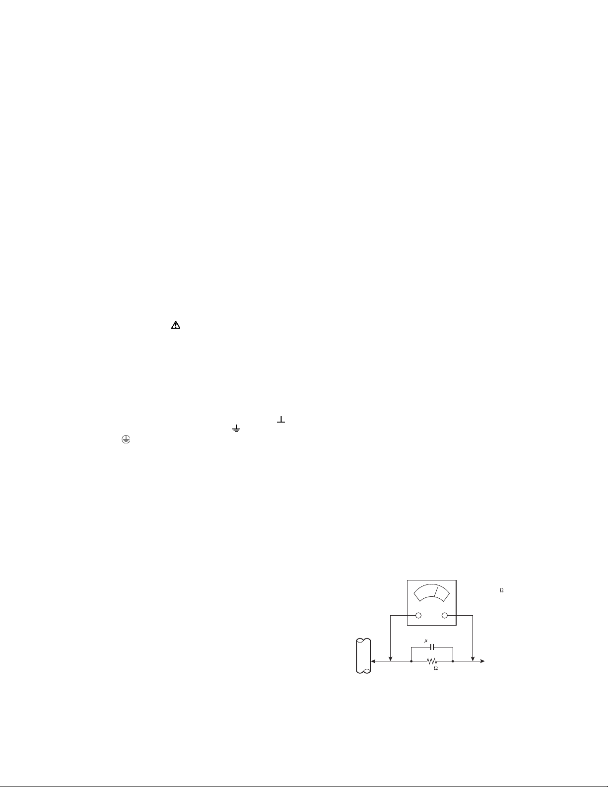
Alternate Check Method
Plug the AC line cord directly into the AC outlet (do not
use a line isolation transformer during this check.). Use
an AC voltmeter having 1000Ω per volt or more
sensitivity in the following manner. Connect a 1500Ω
10W resistor paralleled by a 0.15µF AC-type capacitor
between an exposed metal part and a known good earth
ground (water pipe, etc.). Measure the AC voltage
across the resistor with the AC voltmeter. Move the
resistor connection to each exposed metal part,
particularly any exposed metal part having a return path
to the chassis, and measure the AC voltage across the
resistor. Now, reverse the plug in the AC outlet and
repeat each measurement. Any voltage measured must
not exceed 0.75V AC (r.m.s.). This corresponds to
0.5mA AC (r.m.s.).
However, in tropical area, this must not exceed 0.3V AC
(r.m.s.). This corresponds to 0.2mA AC (r.m.s.).
AC VOLTMETER
(HAVING 1000 /V,
OR MORE SENSITIVITY)
0.15 F AC-TYPE
GOOD EARTH GROUND
1500 10W
PLACE THIS PROBE
ON EACH EXPOSED
ME TAL PAR T
(No.YA363)1-3
Page 5
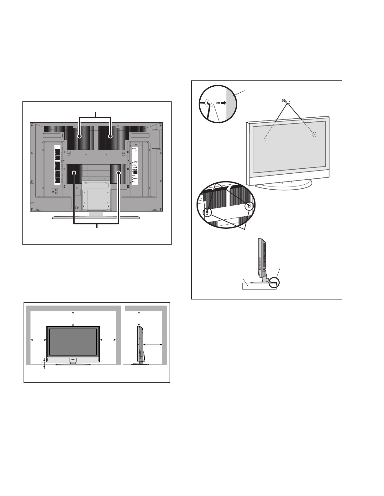
1.2 INSTALLATION
1.2.1 HEAT DISSIPATION
If the heat dissipation vent behind this unit is blocked, cooling
efficiency may deteriorate and temperature inside the unit will
rise. The temperature sensor that protects the unit will be
activated when internal temperature exceeds the pre-determined
level and power will be turned off automatically.Therefore,
please make sure pay attention not to block the heat dissipation
vent as well as the ventilation outlet behind the unit and ensure
that there is room for ventilation around it.
Ventilation hole
1.2.3 INSTALLATION REQUIREMENTS
To ensure safety in an emergency such as an earthquake, and
to prevent accidents, ensure that measures are taken to prevent
the TV dropping or falling over.
Tie commercially available tough cord(s) to the hooks in the back
of the TV, and fix the TV to solid walls or columns.
WALL
HOOK
Ventilation hole
*Diagram differs from actual appearance.
1.2.2 INSTALLATION REQUIREMENTS
Ensure that the minimal distance is maintained, as specified
below, between the unit with and the surrounding walls, as well
as the floor etc.Install the unit on stable flooring or stands.Take
precautionary measures to prevent the unit from tipping in order
to protect against accidents and earthquakes.
䎕䎓䎓䏐䏐䎕䎓䎓䏐䏐
150mm150mm
䎘䎓䏐䏐
*Diagram differs from actual appearance.
䎘䎓䏐䏐
HOOK
It fixes in a band.
TV STAND
*Diagram differs from actual appearance.
1.2.4 NOTES ON HANDLING
(1) WHEN TAKING UNIT OUT OF A PACKING CASE
When taking the unit out of a packing case, do not grasp
the upper part of the unit. If you take the unit out while
grasping the upper part, the LCD PANEL may be damaged
because of a pressure. Instead of grasping the upper part,
put your hands on the lower backside or sides of the unit.
(2) AS FOR PRESSING OR TOUCHING A SPEAKER
Be careful not to press the opening of the speaker in the
lower part of the unit and around them since the decorative
sheet on the surface of the openings may be deformed.
1-4 (No.YA363)
Page 6

1.3 HANDLING LCD PANEL
1.3.1 PRECAUTIONS FOR TRANSPORTATION
When transporting the unit, pressure exerted on the internal LCD
panel due to improper handling (such as tossing and dropping)
may cause damages even when the unit is carefully packed. To
prevent accidents from occurring during transportation, pay
careful attention before delivery, such as through explaining the
handling instructions to transporters.
Ensure that the following requirements are met during
transportation, as the LCD panel of this unit is made of glass and
therefore fragile:
(1) USE A SPECIAL PACKING CASE FOR THE LCD PANEL
When transporting the LCD panel of the unit, use a special
packing case (packing materials). A special packing case
is used when a LCD panel is supplied as a service spare
part.
(2) ATTACH PROTECTION SHEET TO THE FRONT
Since the front (display part) of the panel is vulnerable,
attach the protection sheet to the front of the LCD panel
before transportation. Protection sheet is used when a LCD
panel is supplied as a service spare part.
(3) AVOID VIBRATIONS AND IMPACTS
The unit may be broken if it is toppled sideways even when
properly packed. Continuous vibration may shift the gap of
the panel, and the unit may not be able to display images
properly. Ensure that the unit is carried by at least 2
persons and pay careful attention not to exert any vibration
or impact on it.
(4) DO NOT PLACE EQUIPMENT HORIZONTALLY
Ensure that it is placed upright and not horizontally during
transportation and storage as the LCD panel is very
vulnerable to lateral impacts and may break. During
transportation, ensure that the unit is loaded along the
traveling direction of the vehicle, and avoid stacking them
on one another. For storage, ensure that they are stacked
in 2 layers or less even when placed upright.
1.3.2 OPTICAL FILTER (ON THE FRONT OF THE LCD PANEL)
(1) Avoid placing the unit under direct sunlight over a
prolonged period of time. This may cause the optical filter
to deteriorate in quality and color.
(2) Clean the filter surface by wiping it softly and lightly with a
soft and lightly fuzz cloth (such as outing flannel).
(3) Do not use solvents such as benzene or thinner to wipe the
filter surface. This may cause the filter to deteriorate in
quality or the coating on the surface to come off. When
cleaning the filter, usually use the neutral detergent diluted
with water. When cleaning the dirty filter, use water-diluted
ethanol.
(4) Since the filter surface is fragile, do not scratch or hit it with
hard materials. Be careful enough not to touch the front
surface, especially when taking the unit out of the packing
case or during transportation.
1.3.3 PRECAUTIONS FOR REPLACEMENT OF EXTERIOR
PARTS
Take note of the following when replacing exterior parts (REAR
COVER, FRONT PANEL, etc.):
(1) Do not exert pressure on the front of the LCD panel (filter
surface). It may cause irregular color.
(2) Pay careful attention not to scratch or stain the front of the
LCD panel (filter surface) with hands.
(3) When replacing exterior parts, the front (LCD panel) should
be placed facing downward. Place a mat, etc. underneath
to avoid causing scratches to the front (filter surface).
(No.YA363)1-5
Page 7
2.1 SYSTEM SETTEING
SERVICE MENU
1. ADJUST
2. SELF CHECK
3. I2C STOP
LOB 0 FAN 0
AUD 0
ANA 9 DIG 9
0000 0
0
SECTION 2
SPECIFIC SERVICE INSTRUCTIONS
Be sure to carry out the following operation at the end of
the procedure.
(1) Set to 0 minutes using the [SLEEP TIMER] key.
(2) Press the [VIDEO STATUS] key and [DISPLAY] key
simultaneously, then enter the SERVICE MODE.
(3) When the Main Menu is displayed, press [2] key to enter
the self check mode.
(4) Turn off the power by pressing the [POWER] key on the
remote control unit.
2.2 FEATURES
Built in ATSC (Advanced Television Systems Committee)
TUNER
This TV can receive both Digital broadcasting (ATSC) and
Analogue broadcasting.
D.I.S.T. (Digital Image Scaling Technology)
This system uses line interpolation to double the number of
scanning lines and achieve high resolution, flicker-free picture.
SMART CAPTION
Smart caption will appear when you press the MUTING button,
only on channels where the broadcast contains CLOSED
CAPTION information.
SMART SOUND
Decreases high sound levels, giving a regulated sound level.
VIDEO STATUS
Expression of a favorite screen can be chosen by the VIDEO
STATUS function.
[STANDARD ↔ DYNAMIC ↔ THEATER ↔ GAME]
DIGITAL INPUT
Digital-in will display when any picture signal in Digital-in is
displayed.
SERVICE MENU SCREEN
SERVICE MENU
1. ADJUST
2. SELF CHECK
3. I2C STOP
SELF CHECK MODE SCREEN
LOB 0 FAN 0
AUD 0
ANA 9 DIG 9
0000 0
0
V-CHIP
Since the V-CHIP is built in, it can choose, view and listen to a
healthy program.
MTS STEREO
The voice multiplex function of the MTS system is built in.
(MTS = Multi channel Television Sound system)
NATURAL CINEMA
Watching the movie or animation, press the Natural Cinema to
adjust the out line of the images to make thin more sharp.
BBE
High definition audio adds natural, clear and extraordinary
sound quality to any program.
VIDEO INPUT LABEL
This function is used to label video input connections for the
onscreen displays.
A.H.S.
Adds a more spacious surround sound. Music gives basic
effect and Movie for more effect.
1-6 (No.YA363)
Page 8

2.3 TECHNICAL INFORMATION
2.3.1 LCD PANEL
This unit uses the flat type panel LCD (Liquid Crystal Display) panel that occupies as little space as possible, instead of the
conventional CRT (Cathode Ray Tube), as a display unit.
Since the unit has the two polarizing filter that are at right angles to each other, the unit adopts "normally black" mode, where light
does not pass through the polarizing filter and the screen is black when no voltage is applied to the liquid crystals.
2.3.1.1 SPECIFICATIONS
The following table shows the specifications of this unit.
Item Specifications
Maximum dimensions ( W × H × D ) 952 mm × 551 mm × 51 mm
Weight 10.5 kg
Effective screen size Diagonal: 1018 mm (H: 885 mm × V : 498 mm) / 40 V
Aspect ratio 16 : 9
Drive device / system a-Si-TFT, active matrix system
Resolution Horizontally 1920 × Vertically 1080 × RGB <W-XGA> / 6,220,800 dots in total
Pixel pitch (pixel size) H: 0.15375 mm, V: 0.46125 mm
Displayed color 16777216 colors / 256 colors for R, G, and B
Brightness 500 cd/m
2
Contrast ratio 1000 : 1
Response time less than 20 ms
View angle Horizontally: 178°, Vertically: 178°
Surface polarizer Anti-Glare type, Low reflective coat
Color filter Vertical stripe
Backlight Cold cathode fluorescent lamp × 22
Power supply voltage in LCD 5 V
Power supply voltage in inverter 24 V
Panel interface system LVDS (Low Voltage Differential Signaling)
2.3.1.2 PIXEL FAULT
There are three pixel faults - bright fault , dark fault and flicker fault - that are respectively defined as follows.
(1) BRIGHT FAULT
In this pixel fault, a cell that should not light originally is lighting on and off.
For checking this pixel fault, input ALL BLACK SCREEN and find out the cell that is lighting on and off.
(2) DARK FAULT
In this pixel fault, a cell that should light originally is not lighting or lighting with the brightness twice as brighter as originally lighting.
For checking this pixel fault, input 100% of each R/G/B colour and find out the cell that is not lighting.
(3) FLICKER FAULT
In the pixel fault, a cell that should light originally or not light originally is flashing on and off.
For checking this pixel fault, input ALL BLACK SCREEN signal or 100% of each RGB colour and find out the cell that is flashing on
and off.
(No.YA363)1-7
Page 9

2.3.2 MAIN CPU PIN FUNCTION [IC7601
Pin Pin name I/O Function Pin Pin name I/O Function
1 VHOLD1 I Data slice for main screen closed caption 51 NC O Not used
2 HFLT1 I/O LPF for main screen closed caption video input 52 NC O Not used
3 NC O Not used 53 NC O Not used
4 NC O Not used 54 NC O Not used
5 DIGR0 O R [0] for OSD 55 NC O Not used
6 TB1in I AC power for timer clock 56 NC O Not used
7 REMO I Remote control 57 NC O Not used
8 BYTE I Data bus width select [L = 16bit (fixed)] 58 NC O Not used
9 CNVss I CPU programming mode select [Normal = L] 59 NC O Not used
10 DIGG0 O G [0] for OSD 60 NC O Not used
11 DIGB0 O B [0] for OSD 61 NC O Not used
12 RESET I Reset for main CPU [Reset = L] 62 HSYNC I H. sync for OSD
13 Xout O System clock osillation (crystal) : 16MHz 63 NC O Not used
14 Vss - GND 64 VSYNC I V. sync for OSD
15 Xin I System clock osillation (crystal) : 16MHz 65 NC O Not used
16 VccI I 3.3V stand-by power supply 66 NC O Not used
17 OSC1 I Clock for OSD 67 NC O Not used
18 OSC2 O Not used : Clock for OSD 68 NC O Not used
19 INT1 I Not used : AV COMPULINK control 69 NC O Not used
20 INT0 I
21 OUT1 O Ys (blanking) for OSD 71 P2.1 O Clock for Inter IC (serial) bus control
22 OUT2 O YM (transparence) for OSD 72 P2.0 I/O Data for Inter IC (serial) bus control
23 NC O Not used 73 NC O Not used
24 NC O Not used 74 NC O Not used
25 NC O Not used 75 NC O Not used
26 NC O Not used 76 NC O Not used
27 CTA2/RTS2 O Not used 77 NC O Not used
28 CLK2 O Not used 78 NC O Not used
29 RxD2 I Digital tuner control 79 NC O Not used
30 TxD2 O Digital tuner control 80 P1.0 O Function LED lighting
31 SDA2 I/O Not used 81 P0.7 O Communication LED lighting
32 DIGR1 O R [1] for OSD 82 P0.6 O Test point
33 DIGG1 O G [1] for OSD 83 NC O Not used
34 DIGB1 O B [1] for OSD 84 WAKE O Reset for sub(chassis) CPU
35 TxD0 I Data receive (serial) for external programming 85 CARD_DET I Not used
36 RxD0 O Data transmission (serial) for external programming 86
37 CLK0 I Clock for external programming 87 SDA I/O Data for Inter IC (serial) bus control : memory
38 RTS0 O Busy for external programming [Operation = H] 88 SLC O Clock for Inter IC (serial) bus control : memory
39 P5.7 I Not used 89 DIGR2 O R [2] for OSD
40 P5.6 O Not used 90 DIGG2 O G [2] for OSD
41 HOLD I CPU programming mode select [Normal = H] 91 DIGB2 O B [2] for OSD
42 P5.4 O Not used 92 NC O Not used
43 P5.3 O Not used 93 KEY2 I
44 P5.2 O Not used 94 KEY1 I
45 P5.1 O Not used 95 VHOLD2 I Data slice for sub screen closed caption
46 WR O CPU programming mode select [Normal = L] 96 HLF2 I/O LPF for sub screen closed caption video input
47 P4.7 O
48 P4.6 I
49 P4.5 I Clock for sub(chassis) CPU communication (serial) 99 VCCE I 5V stand-by power supply
50 P4.4 O Not used 100 CVIN1 I Video(Y) for main screen closed caption
Request for sub(chassis) CPU communication (serial data)
Data transmission for sub(chassis) CPU communication (serial)
Data receive for sub(chassis) CPU communication (serial)
: DIGITAL PWB ASS'Y]
70 NC O Not used
POWER_SW
97 CVIN2 I Video(Y) for sub screen closed caption
98 TVSETB I Test terminal [L Fixed]
I Power switch (mechanical) detection
Key scan data for front control button (MENU/CH+/CH-) KEY2
Key scan data for front control button (INPUT/VOL+/VOL-) KEY1
1-8 (No.YA363)
Page 10

SECTION 3
DISASSEMBLY
3.1 DISASSEMBLY PROCEDURE
CAUTION AT DISASSEMBLY:
• Be sure to perform the SYSTEM SETTEING, at the end of the procedure.
• Make sure that the power cord is disconnected from the outlet.
• Pay special attention not to break or damage the parts.
• When removing each board, remove the connectors as required. Taking notes of the connecting points (connector numbers)
makes service procedure manageable.
• Make sure that there is no bent or stain on the connectors before inserting, and firmly insert the connectors.
3.1.1 REMOVING THE STAND (Fig.1)
(1) loosens the 2 screw [A].
(2) Remove the STAND COVER.
(3) Remove the 2 screws [B] and 2 screw [C].
(4) Remove the STAND.
3.1.2 REMOVING THE REAR COVER (Fig.1)
• Remove the STAND.
(1) Remove the JACK COVER (L/R).
(2) Remove the 10 screws [D], the 6 screws [E], and the 2
screws [F].
(3) Remove the REAR COVER.
3.1.3 REMOVING THE POWER PWB (Fig.1)
• Remove the STAND.
• Remove the REAR COVER.
(1) Remove the 1 screw [G].
(2) Remove the POWER CORD HOLDER.
(3) Remove the POWER CORD.
(4) Remove the 4 screws [H].
(5) Remove the POWER PWB.
3.1.4 REMOVING THE D-AMP PWB (Fig.1)
• Remove the STAND.
• Remove the REAR COVER.
(1) Remove the 2 screw [I].
(2) Remove the D-AMP PWB.
3.1.5 REMOVING THE ANALOG PWB (Fig.1)
• Remove the STAND.
• Remove the REAR COVER.
• Remove the D-AMP PWB.
(1) Remove the 3 screws [K] and 2 screws [J].
(2) Remove the TERMINAL BASE.
(3) Remove the 1 screw [L].
(4) Remove the TUNER BASE.
(5) Remove the 2 screws [M].
(6) Remove the D-AMP BRACKET.
(7) Remove the 2 screws [N].
(8) Remove the ANALOG PWB.
3.1.6 REMOVING THE SW PWB (Fig.1)
• Remove the STAND.
• Remove the REAR COVER.
(1) Remove the 3 screws [O].
(2) Remove the CONTROL ASSY with the SW PWB.
(3) Remove the SW PWB.
3.1.7 REMOVING THE DC-DC PWB (Fig.1)
• Remove the STAND.
• Remove the REAR COVER.
(1) Remove the 4 screws [P].
(2) Remove the BACK BRACKET.
(3) Remove the 4 screws [Q].
(4) Remove the DC-DC PWB.
3.1.8 REMOVING THE COOLING FAN (Fig.1)
• Remove the STAND.
• Remove the REAR COVER.
• Remove the BACK BRACKET.
(1) Remove the SHIELD COVER.
(2) Remove the 2 screws [R].
(3) Remove the COOLING FAN.
3.1.9 REMOVING THE DIGITAL TUNER UNIT (Fig.1)
• Remove the STAND.
• Remove the REAR COVER.
• Remove the BACK BRACKET.
• Remove the SHIELD COVER.
(1) Remove the 5 screws [S].
(2) Remove the DIGITAL TUNER UNIT.
3.1.10 REMOVING THE SD CARD PWB (Fig.1)
• Remove the STAND.
• Remove the REAR COVER.
• Remove the BACK BRACKET.
• Remove the SHIELD COVER.
• Remove the DIGITAL TUNER UNIT.
(1) Remove the 7 screws [T].
(2) Remove the DIGITAL PWB BRACKET.
(3) Remove the 1 screw [U].
(4) Remove the SD CARD PWB.
3.1.11 REMOVING THE DIGITAL SIGNAL PWB (Fig.1)
• Remove the STAND.
• Remove the REAR COVER.
• Remove the BACK BRACKET.
• Remove the SHIELD COVER.
• Remove the DIGITAL TUNER UNIT.
• Remove the DIGITAL PWB BRACKET.
(1) Remove the 2 screws [V] and 2 screws [W].
(2) Remove the SHIELD TERMINAL.
(3) Remove the DIGITAL SIGNALPWB.
CAUTION :
Make sure to perform the "SYSTEM SETTEING", when
DIGITAL SIGNAL PWB is replaced.
(No.YA363)1-9
Page 11
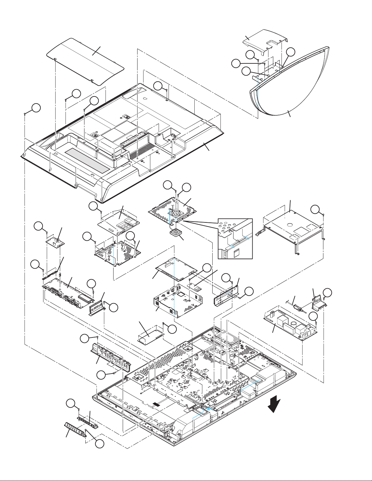
STAND COVER
JACK COVER
B
A
C
A
E
F
E
D
STAND
REAR COVER
I
M
D-AMP PWB
D-AMP PWB
BRACKET
T
ANALOG PWB
J
S
N
DIGITAL TUNER
MODULE PWB
TUNER BASE
L
DC-DC CON PWB
DIGITAL PWB
T
BRACKET
DIGITAL PWB
SHIELD BASE
R
R
SHIELD COVER
COOLING FAN
Q
SD CARD PWB
U
SHIELD TERMINAL
W
V
POWER PWB
BACK BRACKET
POWER CORD HOLDER
POWER CORD
P
G
H
CONTROL ASSY
1-10 (No.YA363)
TERMINAL BASE
K
O
SW PWB
FRONT
O
Fig.1
Page 12

3.1.12 REMOVING THE SPEAKER (Fig.2)
• Remove the STAND.
• Remove the REAR COVER.
(1) Remove the 6 screws [A].
(2) Remove the SPEAKER (L /R).
NOTE:
• Since the speaker is attached in a certain direction, attach
the speaker in the same correct direction as it has been
attached.
• When the speaker is decomposed, the performance cannot
be kept.
3.1.13 REMOVING THE LED PWB (Fig.2)
• Remove the STAND.
• Remove the REAR COVER.
(1) Remove the 2 screws [B].
(2) Remove the LED PWB.
3.1.14 REMOVING THE LED LENS (Fig.2)
• Remove the STAND.
• Remove the REAR COVER.
• Remove the LED PWB.
(1) Remove the 2 screws [C].
(2) Remove the LED LENS.
3.1.15 REMOVING THE CARD PWB (Fig.2)
• Remove the STAND.
• Remove the REAR COVER.
(1) Remove the 3 screws [D].
(2) Remove the CARD BASE ASS’Y.
(3) Remove the CARD SHIELD.
(4) Remove the 4 screws [E].
(5) Remove the CARD PWB.
3.1.17 REMOVING THE LCD PANEL UNIT (Fig.2)
• Remove the STAND.
• Remove the REAR COVER.
• Remove the BACK BRACKET.
(1) Remove the 2 screws [G], 2 screws [H], 3 screws [J] and
1 screw [K].
(2) Remove the MAIN BASE.
(3) Remove the 3 screws [L] and 2 screw [M].
(4) Remove the TOP FARAME.
(5) Remove the 2 screws [N] and 2 screw [P].
(6) Remove the BOTTOM FARAME.
(7) Remove the LCD PANEL UNIT from the FRONT PANEL.
(8) Remove the 2 screws [Q].
(9) Remove the CARD PWB BRACKET from the LCD PANEL
UNIT.
NOTE:
• Pay special attention not to break or damage on the FRONT
PANEL.
• The LCD PANEL UNIT is fixed to the FRONT PAMEL (at the
back side)by using double-side adhesive tapes. To remove
the LCD PANEL UNIT, remove the adhesive tape on the
FRONT PANEL slowly.
3.1.16 REMOVING THE SUB POWER PWB (Fig.2)
• Remove the STAND.
• Remove the REAR COVER.
(1) Remove the 4 screws [F].
(2) Remove the SUB POWER PWB.
(No.YA363)1-11
Page 13
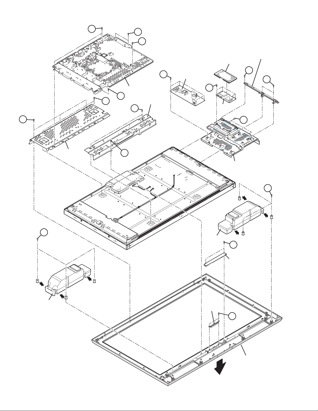
G
M
J
CARD BASE ASSY
D
D
MAIN BASE
F
CARD PWB SHIELD
SUB POWER PWB
E
K
M
L
TOP FRAME
N
BOTTOM FRAME
P
CARD PWB
Q
CARD PWB BRACKET
A
A
SPEAKER
SPEAKER
B
LED PWB
LED LENS
C
FRONT PANEL
FRONT
1-12 (No.YA363)
Fig.2
Page 14
3.2 MEMORY IC REPLACEMENT
S001 R DRIVE137
NTSC3 FULL STD LOW
SERVICE MENU
1. ADJUST
2. SELF CHECK
3. I2C STOP
• This model uses the memory IC.
• This memory IC stores data for proper operation of the video and drive circuits.
• When replacing, be sure to use an IC containing this (initial value) data.
3.2.1 MEMORY IC REPLACEMENT PROCEDURE
1. Power off
Switch off the power and disconnect the power plug from the AC outlet.
2. Replace the memory IC
Be sure to use the memory IC written with the initial setting values.
3. Power on
Connect the power plug to the AC outlet and switch on the power.
4. Receiving channel setting
Refer to the OPERATING INSTRUCTIONS and set the receive channels (Channels Preset) as described.
5. User setting
Check the user setting items according to the given in page later. Where these do not agree, refer to the OPERATING
INSTRUCTIONS and set the items as described.
6. SERVICE MODE setting
Verify what to set in the SERVICE MODE, and set whatever is necessary (Fig.1). Refer to the SERVICE ADJUSTMENT for setting.
3.2.2 SERVICE MODE SETTING
SERVICE MODE SCREEN
SETTING ITEM
Setting items Settings Item No.
MAIN MENU SCREEN
SERVICE MENU
1. ADJUST
2. SELF CHECK
3. I2C STOP
Video system setting Adjust S001 - S009
Audio system setting Adjust T001 - T003
Main CPU system setting Fixed M001 - M224
Drive system setting Fixed F001 - F002
(NOT USED) Fixed D001
(NOT USED) Fixed Z001
ADJUSTMENT MODE SCREEN
S001 R DRIVE137
NTSC3 FULL STD LOW
Fig.1
(No.YA363)1-13
Page 15
3.2.3 SETTINGS OF FACTORY SHIPMENT
3.2.3.1 BUTTON OPERATION 3.2.3.2 REMOTE CONTROL DIRECT OPERATION
Setting item Setting position
POWER Off
CHANNEL CABLE-02
VOLUME 10
3.2.3.3 REMOTE CONTROL MENU OPERATION
1. PICTURE ADJUST
Customers can adjust the picture setting of menu screen as their
own like but the picture standard value during factory shipment is as
below.
< NTSC MODE >
Setting item
PICTURE 00 00 00 00
BRIGHT 00 00 00 00
COLOR +10 00 -10 00
TINT 00 00 00 00
DETAIL +05 00 00 00
ENERGY SAVER MODE
COLOR TEMPERATURE
COLOR MANAGEMENT
DYNAMIC GAMMA ON ON ON ON
SMART PICTURE ON ON ON ON
DIGITAL VNR AUTO AUTO AUTO AUTO
MPEG NR ON ON ON ON
< HD MODE >
Setting item
PICTURE 00 00 00 00
BRIGHT 00 00 00 00
COLOR +05 00 -10 00
TINT 00 00 00 00
DETAIL +05 00 00 00
ENERGY SAVER MODE
COLOR TEMPERATURE
COLOR MANAGEMENT
DYNAMIC GAMMA ON ON ON ON
SMART PICTURE ON ON ON ON
DIGITAL VNR AUTO AUTO AUTO AUTO
MPEG NR ON ON ON ON
DYNAMIC
+30 +20 00 -10
HIGH LOW HIGH HIGH
DYNAMIC
+30 +20 00 -10
HIGH LOW HIGH HIGH
STANDARD
ON ON ON ON
STANDARD
ON ON ON ON
GAME
GAME
THEATER
THEATER
INPUT TV
CHANNEL CABLE-02
VOLUME 10
MUTING OFF
DISPLAY OFF
ASPECT NTSC PANORAMA
SLEEP TIMER OFF
THEATER PRO OFF
NATURAL CINEMA AUTO
VIDEO STATUS DYNAMIC
MTS STEREO
SOUND
EFFECT
2. SOUND ADJUST
BASS 00
TREBLE 00
BALANCE 00
3. CLOCK / TIMERS
ON / OFF TIMER OFF
4. INITIAL SETUP
VIDEO-1 MONITOR OUT
DIGITAL-IN
DIGITAL-AUDIO
NOISE MUTING ON
FRONT PANEL LOCK OFF
V1 SMART INPUT OFF
VIDEO INPUT LABEL All blank
POSITION ADJUSTMENT Center
POWER INDICATOR HIGH
ILLUMINATION LOW
LANGUAGE ENG.
CLOSED CAPTION OFF(CC1/T1)
AUTO SHUT OFF OFF
XDS ID ON
V-CHIP OFF
Setting item Setting position
HD / ATSC FULL
A.H.S.+ OFF
BBE ON
SMART SOUND OFF
HYPER BASS OFF
Setting item Setting position
Setting item Setting position
Setting item Setting position
OFF
AUTO
DIGITAL
1-14 (No.YA363)
Page 16
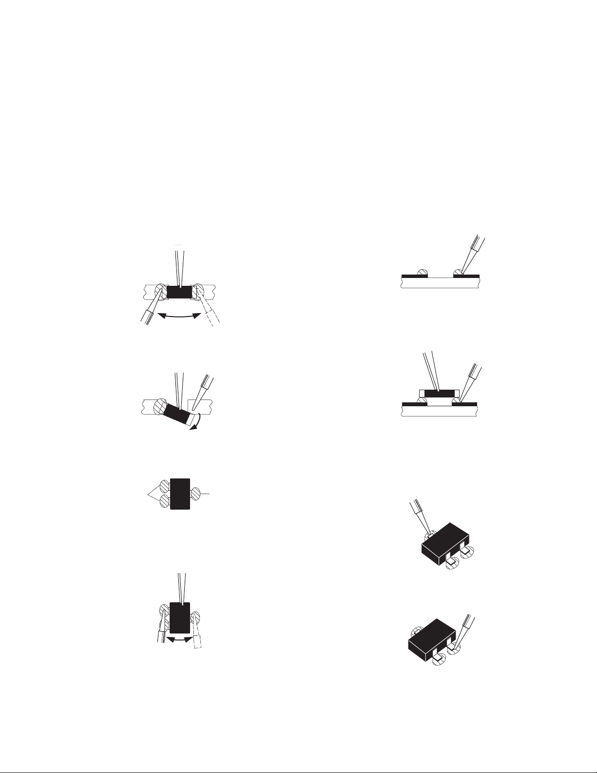
3.3 REPLACEMENT OF CHIP COMPONENT
3.3.1 CAUTIONS
(1) Avoid heating for more than 3 seconds.
(2) Do not rub the electrodes and the resist parts of the pattern.
(3) When removing a chip part, melt the solder adequately.
(4) Do not reuse a chip part after removing it.
3.3.2 SOLDERING IRON
(1) Use a high insulation soldering iron with a thin pointed end of it.
(2) A 30w soldering iron is recommended for easily removing parts.
3.3.3 REPLACEMENT STEPS
1. How to remove Chip parts
2. How to install Chip parts
[Resistors, capacitors, etc.]
(1) As shown in the figure, push the part with tweezers and
alternately melt the solder at each end.
(2) Shift with the tweezers and remove the chip part.
[Transistors, diodes, variable resistors, etc.]
(1) Apply extra solder to each lead.
SOLDER
SOLDER
[Resistors, capacitors, etc.]
(1) Apply solder to the pattern as indicated in the figure.
(2) Grasp the chip part with tweezers and place it on the
solder. Then heat and melt the solder at both ends of the
chip part.
[Transistors, diodes, variable resistors, etc.]
(1) Apply solder to the pattern as indicated in the figure.
(2) Grasp the chip part with tweezers and place it on the
solder.
(3) First solder lead A as indicated in the figure.
(2) As shown in the figure, push the part with tweezers and
alternately melt the solder at each lead. Shift and remove
the chip part.
NOTE :
After removing the part, remove remaining solder from the
pattern.
A
B
C
(4) Then solder leads B and C.
A
B
C
(No.YA363)1-15
Page 17
SECTION 4
SERVICE MENU
1. ADJUST
2. SELF CHECK
3. I2C STOP
ADJUSTMENT
4.1 ADJUSTMENT PREPARATION
(1) There are 2 ways of adjusting this TV : One is with the
REMOTE CONTROL UNIT and the other is the
conventional method using adjustment parts and
components.
(2) The adjustment using the REMOTE CONTROL UNIT is
made on the basis of the initial setting values. The
setting values which adjust the screen to the optimum
condition can be different from the initial setting
values.
(3) Make sure that connection is correctly made AC to AC
power source.
(4) Turn on the power of the TV and measuring instruments for
warning up for at least 30 minutes before starting
adjustments.
(5) If the receive or input signal is not specified, use the most
appropriate signal for adjustment.
(6) Never touch the parts (such as variable resistors,
transformers and condensers) not shown in the adjustment
items of this service adjustment.
4.2 PRESET SETTING BEFORE ADJUSTMENTS
Unless otherwise specified in the adjustment items, preset the
following functions with the REMOTE CONTROL UNIT.
Setting item Settings
VIDEO STATUS STANDARD
BRIGHT / CONTRAST / COLOR / TINT
00
COLOR TEMPERATURE LOW
DIG. NOISE CLEAR OFF
COLOR MANAGEMENT ON
NATURAL CINEMA OFF
TREBLE / BASS / BALANCE 00
SMART SOUND OFF
MTS STEREO
BBE OFF
A.H.S OFF
A.H.B OFF
ASPECT FULL
4.3 MEASURING INSTRUMENT AND FIXTURES
• Signal generator (Pattern generator) [NTSC]
• TV audio multiplex signal generator
• Remote control unit
4.5 BASIC OPERATION OF SERVICE MODE
4.5.1 HOW TO ENTER THE SERVICE MODE
(1) Set to 0 minutes using the [SLEEP TIMER] key.
(2) Press the [VIDEO STATUS] key and [DISPLAY] key
simultaneously, then enter the SERVICE MODE (Fig.1)
SERVICE MENU SCREEN
SERVICE MENU
1. ADJUST
2. SELF CHECK
3. I2C STOP
Fig.1
NOTE:
• Before entering the SERVICE MODE, confirm that the
setting of TV/CATV switch of the REMOTE CONTROL UNIT
is at the "TV" side and the setting of VCR/DVD switch is at
the "VCR" side. If the switches have not been properly set,
you cannot enter the SERVICE MODE.
• When a number key other than the [1] keys is pressed in the
SERVICE MENU SCREEN, the other relevant screen may
be displayed.
This is not used in the adjustment procedure. Press the
[MENU] key to return to the SERVICE MENU SCREEN.
4.5.2 HOW TO EXIT THE SERVICE MODE
Press the [ BACK ] key to exit the Service mode.
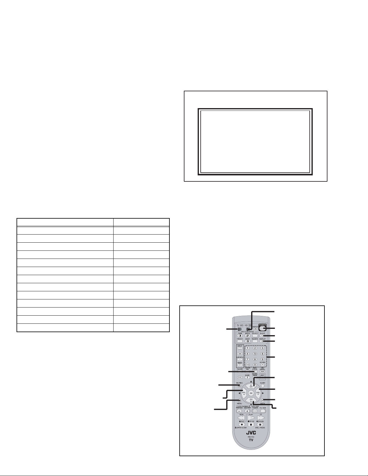
4.5.3 SERVICE MODE SELECT KEY LOCATION
VCR/DVD switch
TV/CATV switch
POWER
SLEEP TIMER
DISPLAY
NUMBER
4.4 ADJUSTMENT ITEMS
VIDEO CIRCUIT
• WHITE BALANCE (HIGHLIGHT) adjustment
MTS CIRCUIT
• MTS INPUT LEVEL adjustment
• MTS SEPARATION adjustment
1-16 (No.YA363)
VIDEO STATUS
MUTING
VOLUME -
MENU
CHANNEL +
VOLUME +
BACK
CHANNEL -
Page 18
4.5.4 ADJUSTMENT MODE
S001 R DRIVE137
NTSC3 FULL STD LOW
This mode is used to adjust the VIDEO CIRCUIT and the MTS CIRCUIT.
4.5.4.1 HOW TO ENTER THE ADJUSTMENT MODE
When the SERVICE MENU SCREEN of SERVICE MODE is displayed, press [1] key to enter the ADJUSTMENT MODE (Fig.2).
4.5.4.2
DESCRIPTION OF STATUS DISPLAY OF ADJUSTMENT MODE
ADJUSTMENT MODE
SETTING ITEM No.
S001 R DRIVE137
NTSC3 FULL STD LOW
SIGNAL SYSTEM
SCREEN MODE
SETTING ITEM
Fig.2
(1) SIGNAL SYSTEM
The signal displayed on the screen is displayed.
NTSC3 : 525i (Composite / S-video input)
525I : 525i (Component input)
525P : 525p
1125I6 : 1125i
750P : 750p
H525I : HDMI 525i
H525P : HDMI 525p
H125I6 : HDMI 1125i
H750P : HDMI 750p
D525I : ATSC 525i
D525P : ATSC 525p
D125I6 : ATSC 1125i
(2) SCREEN MODE
State of the SCREEN SIZE or MULTI PICTURE is displayed.
SINGLE SCREEN
FULL : FULL
1609 : CINEMA, CINEMA ZOOM
PANO : PANORAMA, HD PANORAMA
REGU : REGULAR, SLIM
JUST : FULL NATIVE
MULTI SCREEN
M2 : TWIN, FREEZE screen
M12 : INDEX screen
(3) VIDEO STATUS
STD : STANDARD
DYN : DYNAMIC
TH : THEATER
GAME : GAME
SETTING VALUE (DATA)
VIDEO STATUS
WHITE BALANCE
(4) WHITE BALANCE
HIGH : HIGH
LOW : LOW
(5) SETTING ITEM NAME
Setting item name are displayed. The setting item numbers to
be displayed are listed below.
Item No. Setting item
S001 - S009 Video system setting
T001 - T003 Audio system setting
M001 - M224 Main CPU system setting
F001 - F002 Drive system setting
D001 (NOT USED)
Z001 (NOT USED)
(6) SETTING ITEM NO.
Setting item numbers are displayed. For the setting item
names to be displayed, refer to "Initial setting value of
adjustment mode".
(7) SETTING VALUE (DATA)
The SETTING VALUE is displayed.
4.5.4.3 CHANGE AND MEMORY OF SETTING VALUE
SELECTION OF SETTING ITEM
• [CH+] / [CH-] key.
Change the setting items up/ down.
S001... ↔ T001... ↔ M001... ↔ F001... ↔ D001... ↔ Z001...
• [SLEEP TIMER] key.
Switches to the next items.
S001 → T001 → M001... → F001... → D001 → Z001
CHANGE OF SETTING VALUE (DATA)
• [VOL+] / [VOL-] key.
Change the setting values up/down.
MEMORY OF SETTING VALUE (DATA)
Changed setting value is memorized by pressing [MUTING]
key.
(No.YA363)1-17
Page 19
4.6 INITIAL SETTING VALUES IN THE SERVICE MODE
• Perform fine-tuning based on the "initial values" using the remote control when in the Service mode.
• The "initial values" serve only as an indication rough standard and therefore the values with which optimal display can be achieved
may be different from the default values. But, don't change the values that are not written in "ADJUSTMENT PROCEDURE". They
are fixed values.
4.6.1 VIDEO SYSTEM SETTING
Item No. Item Variable range Setting value
S001 R DRIVE 000 - 255 119
S002 G DRIVE 000 - 255 138
S003 B DRIVE 000 - 255 140
S004 RESREV 000 - 255 000
S005 RESREV 000 - 255 002
S006 RESREV 000 - 255 002
S007 RESREV 000 - 255 002
S008 RESREV 000 - 255 002
S009 RESREV 000 - 255 002
4.6.2 AUDIO SYSTEM SETTING
Item No. Item Variable range Setting value
T001 INPLEVEL 000 - 015 008
T002 LOWSEPA 000 - 063 031
T003 HIGHSEPA 000 - 063 031
4.6.3 MAIN CPU SYSTEM SETTING (Fixed values)
Item No. Item Variable range Setting value
M001 1E00 00 - FF 00
M002 1E01 00 - FF 00
M003 1E02 00 - FF 05
M004 1E03 00 - FF 38
M005 1E04 00 - FF 10
M006 1E05 00 - FF 00
M007 1E06 00 - FF 00
M008 1E07 00 - FF 00
M009 1E08 00 - FF 11
M010 1E09 00 - FF 00
M011 1E0A 00 - FF 01
M012 1E0B 00 - FF 00
M013 1E0C 00 - FF 01
M014 1E0D 00 - FF 00
M015 1E0E 00 - FF 00
M016 1E0F 00 - FF 00
M017 1E10 00 - FF 00
M018 1E11 00 - FF 00
M019 1E12 00 - FF 00
M020 1E13 00 - FF 01
M021 1E14 00 - FF 01
M022 1E15 00 - FF 00
M023 1E16 00 - FF 00
M024 1E17 00 - FF 00
M025 1E18 00 - FF 00
M026 1E19 00 - FF 00
M027 1E1A 00 - FF 00
Item No. Item Variable range Setting value
M028 1E1B 00 - FF 00
M029 1E1C 00 - FF 00
M030 1E1D 00 - FF 00
M031 1E1E 00 - FF 00
M032 1E1F 00 - FF 00
M033 1E20 00 - FF 00
M034 1E21 00 - FF 00
M035 1E22 00 - FF 00
M036 1E23 00 - FF 00
M037 1E24 00 - FF 00
M038 1E25 00 - FF 00
M039 1E26 00 - FF 00
M040 1E27 00 - FF 00
M041 1E28 00 - FF 00
M042 1E29 00 - FF 00
M043 1E2A 00 - FF 00
M044 1E2B 00 - FF 00
M045 1E2C 00 - FF 00
M046 1E2D 00 - FF 00
M047 1E2E 00 - FF 00
M048 1E2F 00 - FF 00
M049 1E30 00 - FF 00
M050 1E31 00 - FF 00
M051 1E32 00 - FF 00
M052 1E33 00 - FF 00
M053 1E34 00 - FF 00
M054 1E35 00 - FF 00
M055 1E36 00 - FF 02
M056 1E37 00 - FF 00
M057 1E38 00 - FF 01
M058 1E39 00 - FF 0A
M059 1E3A 00 - FF 10
M060 1E3B 00 - FF 83
M061 1E3C 00 - FF 00
M062 1E3D 00 - FF 00
M063 1E3E 00 - FF 00
M064 1E3F 00 - FF 00
M065 1E40 00 - FF 00
M066 1E41 00 - FF 00
M067 1E42 00 - FF 03
M068 1E43 00 - FF 03
M069 1E44 00 - FF 02
M070 1E45 00 - FF 03
M071 1E46 00 - FF 3F
M072 1E47 00 - FF 00
1-18 (No.YA363)
Page 20
Item No. Item Variable range Setting value
M073 1E48 00 - FF 00
M074 1E49 00 - FF 00
M075 1E4A 00 - FF 00
M076 1E4B 00 - FF 00
M077 1E4C 00 - FF 00
M078 1E4D 00 - FF 00
M079 1E4E 00 - FF 00
M080 1E4F 00 - FF 00
M081 1E50 00 - FF 00
M082 1E51 00 - FF 00
M083 1E52 00 - FF 00
M084 1E53 00 - FF 00
M085 1E54 00 - FF 00
M086 1E55 00 - FF 00
M087 1E56 00 - FF 00
M088 1E57 00 - FF 00
M089 1E58 00 - FF 00
M090 1E59 00 - FF 00
M091 1E5A 00 - FF 00
M092 1E5B 00 - FF 00
M093 1E5C 00 - FF 00
M094 1E5D 00 - FF 00
M095 1E5E 00 - FF 00
M096 1E5F 00 - FF 00
M097 1E60 00 - FF 00
M098 1E61 00 - FF 00
M099 1E62 00 - FF 00
M100 1E63 00 - FF 00
M101 1E64 00 - FF 00
M102 1E65 00 - FF 00
M103 1E66 00 - FF 00
M104 1E67 00 - FF 00
M105 1E68 00 - FF 00
M106 1E69 00 - FF 00
M107 1E6A 00 - FF 02
M108 1E6B 00 - FF 00
M109 1E6C 00 - FF 00
M110 1E6D 00 - FF 00
M111 1E6E 00 - FF 00
M112 1E6F 00 - FF 00
M113 1E70 00 - FF 00
M114 1E71 00 - FF 00
M115 1E72 00 - FF 00
M116 1E73 00 - FF 00
M117 1E74 00 - FF 00
M118 1E75 00 - FF 00
M119 1E76 00 - FF 00
M120 1E77 00 - FF 14
M121 1E78 00 - FF 03
M122 1E79 00 - FF 00
Item No. Item Variable range Setting value
M123 1E7A 00 - FF 00
M124 1E7B 00 - FF 00
M125 1E7C 00 - FF 00
M126 1E7D 00 - FF 00
M127 1E7E 00 - FF 01
M128 1E7F 00 - FF 00
M129 1E80 00 - FF 01
M130 1E81 00 - FF 00
M131 1E82 00 - FF 01
M132 1E83 00 - FF 00
M133 1E84 00 - FF 00
M134 1E85 00 - FF 00
M135 1E86 00 - FF 00
M136 1E87 00 - FF 00
M137 1E88 00 - FF 00
M138 1E89 00 - FF 00
M139 1E8A 00 - FF 00
M140 1E8B 00 - FF 00
M141 1E8C 00 - FF 00
M142 1E8D 00 - FF 00
M143 1E8E 00 - FF 00
M144 1E8F 00 - FF 00
M145 1E90 00 - FF 00
M146 1E91 00 - FF 00
M147 1E92 00 - FF 00
M148 1E93 00 - FF 00
M149 1E94 00 - FF 00
M150 1E95 00 - FF 00
M151 1E96 00 - FF 00
M152 1E97 00 - FF 00
M153 1E98 00 - FF 00
M154 1E99 00 - FF 00
M155 1E9A 00 - FF 01
M156 1E9B 00 - FF 00
M157 1E9C 00 - FF 03
M158 1E9D 00 - FF 00
M159 1E9E 00 - FF 00
M160 1E9F 00 - FF 00
M161 1EA0 00 - FF 00
M162 1EA1 00 - FF 00
M163 1EA2 00 - FF 01
M164 1EA3 00 - FF 00
M165 1EA4 00 - FF 00
M166 1EA5 00 - FF 00
M167 1EA6 00 - FF 00
M168 1EA7 00 - FF 00
M169 1EA8 00 - FF 00
M170 1EA9 00 - FF 00
M171 1EAA 00 - FF 00
M172 1EAB 00 - FF 00
(No.YA363)1-19
Page 21
Item No. Item Variable range Setting value
M173 1EAC 00 - FF 09
M174 1EAD 00 - FF 00
M175 1EAE 00 - FF 00
M176 1EAF 00 - FF 00
M177 1EB0 00 - FF 0A
M178 1EB1 00 - FF 00
M179 1EB2 00 - FF 01
M180 1EB3 00 - FF 00
M181 1EB4 00 - FF 00
M182 1EB5 00 - FF 00
M183 1EB6 00 - FF 00
M184 1EB7 00 - FF 00
M185 1EB8 00 - FF 00
M186 1EB9 00 - FF 00
M187 1EBA 00 - FF 00
M188 1EBB 00 - FF 00
M189 1EBC 00 - FF 00
M190 1EBD 00 - FF 00
M191 1EBE 00 - FF 00
M192 1EBF 00 - FF 00
M193 1EC0 00 - FF 00
M194 1EC1 00 - FF 00
M195 1EC2 00 - FF 01
M196 1EC3 00 - FF 00
M197 1EC4 00 - FF 00
M198 1EC5 00 - FF 00
M199 1EC6 00 - FF 00
M200 1EC7 00 - FF 00
M201 1EC8 00 - FF 01
M202 1EC9 00 - FF 00
M203 1ECA 00 - FF 00
M204 1ECB 00 - FF 00
M205 1ECC 00 - FF 02
M206 1ECD 00 - FF 00
M207 1ECE 00 - FF 00
M208 1ECF 00 - FF 00
M209 1ED0 00 - FF 00
M210 1ED1 00 - FF 00
M211 1ED2 00 - FF 00
M212 1ED3 00 - FF 00
M213 1ED4 00 - FF 00
M214 1ED5 00 - FF FF
M215 1ED6 00 - FF 00
M216 1ED7 00 - FF 00
M217 1ED8 00 - FF 00
M218 1ED9 00 - FF 00
M219 1EDA 00 - FF 00
M220 1EDB 00 - FF 00
M221 1EDC 00 - FF 00
M222 1EDD 00 - FF 00
Item No. Item Variable range Setting value
M223 1EDE 00 - FF 00
M224 1EDF 00 - FF 00
4.6.4 DRIVE SYSTEM SETTING (Fixed values)
Item No. Item Variable range Setting value
F001 DD 000 - 001 000
F002 RAM REF 000 - 001 000
4.6.5 NOT USED (Fixed values)
Item No. Item Variable range Setting value
D001 RESREV 000 - 255 002
4.6.6 NOT USED (Fixed values)
Item No. Item Variable range Setting value
Z001 RESREV 000 - 255 002
1-20 (No.YA363)
Page 22
4.7 ADJUSTMENT PROCEDURE
4.7.1 VIDEO CIRCUIT
Item
WHITE
BALANCE
Measuring
instrument
Remote
control unit
(HIGHLIGHT)
Signal
generator
4.7.2 MTS CIRCUIT
Test point Adjustment part Description
[1.ADJUST]
S030: R DRIVE (Red drive)
S031: G DRIVE (Green drive)
S032: B DRIVE (Blue drive)
(1) Receive a NTSC 75% all white signal.
(2) Set "VIDEO STATUS" to "STANDARD".
(3) Set "ASPECT" to "FULL".
(4) Select "COLOR TEMPERATURE" to "LOW".
(5) Select "1.ADJUST" from the SERVICE
MODE.
(6) Adjust to keep one of < S030 > (Red drive), < S031
> (Green drive) or < S032 > (Blue drive) unchanged,
then lower the other two so that the all-white
screen is equally white throughout.
NOTE:
Set one or more of < S030 >, < S031 >, and
< S032 > to "133".
(7) Check that white balance is properly tracked
from low light to high light. If the white balance
tracking is deviated, adjust to correct it.
(8) Press the [MUTING] key to memoirze the set
value.
Item
MTS INPUT
LEVEL
MTS
SEPARATION
Measuring
instrument
Remote
control unit
TV audio
multiplex
signal
generator
Oscilloscope
Remote
control unit
L-Channel
signal waveform
1 cycle
Test point Adjustment part Description
[1.ADJUST]
T001: IN LEVEL
(1) Receive the any broadcast.
(2) Select "1.ADJUST" from the SERVICE
MODE.
(3) Verify that the < T001 > (IN LEVEL) is set at its
initial setting value.
(4) Press the [MUTING] key to memorize the set
value.
L OUT
R OUT
[1.ADJUST]
T002: LOW SEP
T003: HI SEP
(1) Input the stereo L signal (300Hz) from the TV
audio multiplex signal generator to the antenna
terminal.
(2) Connect an oscilloscope to L OUT pin of the
AUDIO OUT, and display one cycle portion of
the 300Hz signal.
(3) Change the connection of the oscilloscope to
R OUT pin of the AUDIO OUT, and enlarge the
voltage axis.
(4) Select "1.ADJUST" from the SERVICE
MODE.
R-Channel
crosstalk portion
Minimum
(5) Set the initial setting value of the < T002 >
(LOW SEP).
(6) Adjust the < T002 > so that the stroke element
of the 300Hz signal will become minimum.
(7) Change the signal to 3kHz, and similarly ad-
just the < T003> (HI SEP).
(8) Press the [MUTING] key to memorize the set
value.
(No.YA363)1-21
Page 23
SECTION 5
SERVICE MENU
1. ADJUST
2. SELF CHECK
3. I2C STOP
TMP 0 L 1 0
L 2 0 DDT 0
FAN 0 L C 0
IRS 0
LOB 0 FAN 0
AUD 0
ANA 9 DIG 9
0000 0
0
TROUBLESHOOTING
5.1 SELF CHECK FEATURE
5.1.1 OUTLINE
This unit comes with the "Self check" feature, which checks the
operational state of the circuit and displays/saves it during
failure.Diagnosis is performed when power is turned on, and
information input to the main microcomputer is monitored at all
time. Diagnosis is displayed in 2 ways via screen display and
LED flashes. Failure detection is based on input state of I
2
C bus
and the various control lines connected to the main
microcomputer.
5.1.2 HOW TO ENTER THE SELF CHECK MODE
Before entering the Self check Display mode, confirm that the
setting of TV/CATV SW of the REMOTE CONTROL UNIT is at
the "TV" side and the setting of VCR/DVD SW is at the "VCR"
side. If the switches have not been properly set, you cannot enter
the Self check Display mode.
(1) Set to "0 minutes" using the [SLEEP TIMER] key.
(2) Press the [VIDEO STATUS] key and [DISPLAY] key
simultaneously, then enter the service mode.
(3) Press the [2] key (SELF CHECK) before the service mode
screen disappears.
(4) Press the [SLEEP TIMER] key to enter Page 2 of the SELF
CHECK MODE.
• When the [RETURN+] key pressed, the first page
change screen.
NOTE:
When a number key other than the [2] key is pressed in
the SERVICE MENU SCREEN, the other relevant
screen may be displayed.
This is not used in the SELF CHECK. Press the [MENU]
key to return to the SERVICE MENU SCREEN.
5.1.3 HOW TO EXIT THE SELF CHECK MODE
TO SAVE FAILURE HISTORY:
Turn off the power by unplugging the AC power cord plug when
in the Self check display mode.
TO CLEAR (RESET) FAILURE HISTORY:
Turn off the power by pressing the [POWER] key on the remote
control unit when in the Self check display mode.
5.1.5 POINTS TO NOTE WHEN USING THE SELF CHECK
FEATURE
In addition to circuit failures (abnormal operation), the following
cases may also be diagnosed as "Abnormal" and displayed and
counted as "NG".
(1) Temporary defective transmissions across circuits due to
pulse interruptions
(2) Misalignment in the on/off timing of power for I
2
C bus
(VCC) when turning on/off the main power.
Diagnosis may be impeded if a large number of items are
displayed as "NG". As such, start Self check check only after 3
seconds in the case of receivers and 5 seconds in the case of
panels upon turning on the power. If recurrences are expected,
ensure to clear (reset) the failure history and record the new
diagnosis reults.
SERVICE MENU SCREEN
SERVICE MENU
1. ADJUST
2. SELF CHECK
3. I2C STOP
SELF CHECK MODE SCREEN (Page 1)
LOB 0 FAN 0
AUD 0
ANA 9 DIG 9
0000 0
0
Item Failure history
5.1.4 FAILURE HISTORY
Failure history can be counted up to 9 times for each item. When
the number exceeds 9, display will remain as 9. Failure history
will be stored in the memory unless it has been deleted.
NOTE:
Only SYNC (with/without sync signals) will be neither counted
nor stored.
1-22 (No.YA363)
SELF CHECK MODE SCREEN (Page 2)
TMP 0 L 1 0
L 2 0 DDT 0
FAN 0 L C 0
IRS 0
Item
Fig.1
Failure history
Page 24

5.1.6 DETAILS
Self check is performed for the following items:
< Page 1 of screen >
Detection item Display Detection content
Low bias line short
protection
Fan lock FAN Not used ---- ----
Audio AUD Not used ---- ----
Devices on the ANALOG
PWB
Devices on the DIGITAL
PWB
< Page 2 of screen >
Detection item Display Detection content
Temp. sensor TEM Not used ---- ----
Lamp does not light up L1 Not used ---- ----
Lamp goes out L2 Not used ---- ----
Abnormal DD CPU
circuit
Fan lock FAN Not used ---- ----
Lamp cover open LC Not used ---- ----
Abnormal of optical iris IRS Not used ---- ----
LOB Confirm the operation of the low bais (16V / 5V /
LCD5V / 3.3V / 1.2V) protection circuit.
, Q9651[POWER PWB]
Q9601
ANA Confirmation of reply of ACK signal which uses
I2C communication.
, IC102, IC281, IC381, IC601, IC606,
IC101
IC061, TU001 [ANALOG PWB]
DIG Confirmation of reply of ACK signal which uses
I2C communication.
, IC8831 [DIGITAL PWB]
IC6401
DDT Not used ---- ----
Diagnosis
signal (line)
LB_PRO Detection starts 3 seconds after
the power is turned on. If error
continues between 200 ms the
power is turned off.
SDA If it checks whenever I2C
communication is performed and
no reply of ACK signal an error
will be counted.
SDA If it checks whenever I2C
communication is performed and
no reply of ACK signal an error
will be counted.
Diagnosis
signal (line)
Detection timing
Detection timing
5.1.7 METHOD OF DISPLAY WHEN A RASTER IS NOT OUTPUT
In the state where a raster is not output by breakdown of the set, an error is displayed by blink of the POWER LED.
Type of error POWER LED flash cycle
Low bias line short protection Low luminance blue turnig on and off at 1 second intervals.
MAIN CPU error detection Low luminance blue turnig on and off at 2 second intervals.
ATSC TUNER error detection Low luminance blue turnig on and off at 2 second intervals.
< Explanation of operation >
If error is detected, the power is turned off.
Shortly after a power is turned off, POWER LED will be blinked.
Power cannot be turned on until the power cord takes out and inserts, after a power is turned off.
(No.YA363)1-23
Page 25

Victor Company of Japan, Limited
AV & MULTIMEDIA COMPANY DISPLAY CATEGORY 12, 3-chome, Moriya-cho, Kanagawa-ku, Yokohama-city, Kanagawa-prefecture, 221-8528, Japan
(No.YA363)
Printed in Japan
VPT
Page 26
LT-40FH96
/S
STANDARD CIRCUIT DIAGRAM
NOTE ON USING CIRCUIT DIAGRAMS
Preliminary
1.SAFETY
The components identified by the symbol and shading are
critical for safety. For continued safety replace safety ciritical
components only with manufactures recommended parts.
2.SPECIFIED VOLTAGE AND WAVEFORM VALUES
The voltage and waveform values have been measured under the
following conditions.
(1)Input signal : Colour bar signal
(2)Setting positions of
each knob/button and
variable resistor
(3)Internal resistance of tester
(4)Oscilloscope sweeping time
(5)Voltage values
Since the voltage values of signal circuit vary to some extent
according to adjustments, use them as reference values.
: Original setting position
when shipped
: DC 20kΩ/V
: H
: V
: Othters
: All DC voltage values
20µs / div
5ms / div
Sweeping time is
specified
3.INDICATION OF PARTS SYMBOL [EXAMPLE]
In the PW board
: R209
R209
Type
No indication
MM
PP
MPP
MF
TF
BP
TAN
(3)Coils
No unit
Others
(4)Power Supply
Respective voltage values are indicated
(5)Test point
: Test point
(6)Connecting method
: Ceramic capacitor
: Metalized mylar capacitor
: Polypropylene capacitor
: Metalized polypropylene capacitor
: Metalized film capacitor
: Thin film capacitor
: Bipolar electrolytic capacitor
: Tantalum capacitor
: [µH]
: As specified
: B1
: 9V
: Connector
: Receptacle
: Only test point display
: Wrapping or soldering
: B2 (12V
: 5V
)
4.INDICATIONS ON THE CIRCUIT DIAGRAM
(1)Resistors
Resistance value
No unit : [Ω]
K
M
Rated allowable power
No indication : 1/16 [W]
Others : As specified
Type
No indication
OMR
MFR
MPR
UNFR
FR
Composition resistor 1/2 [W] is specified as 1/2S or Comp.
(2)Capacitors
Capacitance value
1 or higher : [pF]
less than 1
Withstand voltage
No indication : DC50[V]
Others : DC withstand voltage [V]
AC indicated
Electrolytic Capacitors
47/50[Example]: Capacitance value [µF]/withstand voltage[V]
: [kΩ]
: [MΩ]
: Carbon resistor
: Oxide metal film resistor
: Metal film resistor
: Metal plate resistor
: Uninflammable resistor
: Fusible resistor
: [µF]
: AC withstand voltage [V]
(7)Ground symbol
: LIVE side ground
: ISOLATED(NEUTRAL) side ground
: EARTH ground
: DIGITAL ground
5.NOTE FOR REPAIRING SERVICE
This model's power circuit is partly different in the GND. The
difference of the GND is shown by the LIVE : ( ) side GND and the
ISOLATED(NEUTRAL) : ( ) side GND. Therefore, care must be
taken for the following points.
(1)Do not touch the LIVE side GND or the LIVE side GND and the
ISOLATED(NEUTRAL) side GND simultaneously. if the above
caution is not respected, an electric shock may be caused.
Therefore, make sure that the power cord is surely removed from
the receptacle when, for example, the chassis is pulled out.
(2)Do not short between the LIVE side GND and ISOLATED(NEUTRAL
side GND or never measure with a measuring apparatus measure
with a measuring apparatus ( oscilloscope, etc.) the LIVE side GND
and ISOLATED(NEUTRAL) side GND at the same time.
If the above precaution is not respected, a fuse or any parts will be broken.
Since the circuit diagram is a standard one, the circuit and
circuit constants may be subject to change for improvement
without any notice.
NOTE
Due improvement in performance, some part numbers show
in the circuit diagram may not agree with those indicated in
the part list.
When ordering parts, please use the numbers that appear
in the Parts List.
)
(No.YA363)2-1
Page 27
CONTENTS
SEMICONDUCTOR SHAPES ......................................................................2-2
WIRING DIAGRAM ........................................................................................2-3
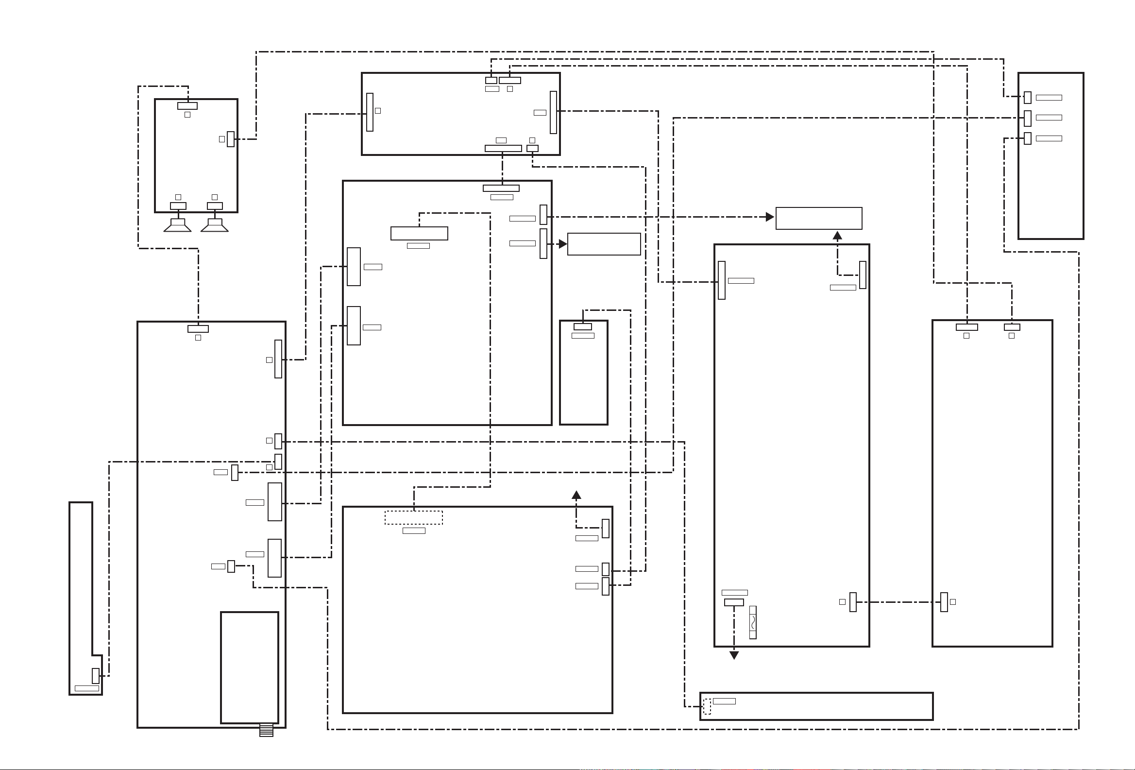
BLOCK DIAGRAM ........................................................................................2-5
CIRCUIT DIAGRAMS
ANALOG PWB CIRCUIT DIAGRAM ........................................................................................................... 2-7
DIGITAL PWB CIRCUIT DIAGRAM .......................................................................................................... 2-19
POWER PWB CIRCUIT DIAGRAM .......................................................................................................... 2-51
LED PWB CIRCUIT DIAGRAM ................................................................................................................. 2-55
SW PWB CIRCUIT DIAGRAM ................................................................................................................. 2-56
D-AMP PWB CIRCUIT DIAGRAM ............................................................................................................ 2-57
CARD PWB CIRCUIT DIAGRAM .............................................................................................................. 2-59
DC-DC PWB CIRCUIT DIAGRAM ............................................................................................................. 2-63
SUB POWER PWB CIRCUIT DIAGRAM .................................................................................................. 2-65
SD CARD PWB CIRCUIT DIAGRAM ........................................................................................................ 2-66
PATTERN DIAGRAMS
ANALOG PWB PATTERN ........................................................................................................................ 2-69
DIGITAL PWB PATTERN ......................................................................................................................... 2-71
POWER PWB PATTERN .......................................................................................................................... 2-75
CARD PWB PATTERN ............................................................................................................................. 2-77
DC-DC PWB PATTERN ............................................................................................................................ 2-78
SUB POWER PWB PATTERN .................................................................................................................. 2-79
LED PWB PATTERN ................................................................................................................................ 2-81
SW PWB PATTERN ................................................................................................................................. 2-81
SD CARD PWB PATTERN ........................................................................................................................ 2-81
D-AMP PWB PATTERN ............................................................................................................................ 2-82
VOLTAGE CHATRS ................................................................................... 2-xx
WAVEFORMS ............................................................................................ 2-xx
USING P.W. BOARD
P.W.B ASS’Y name
ANALOG P.W. BOARD
SD-CARD P.W. BOARD
D-AMP P.W. BOARD
SW P.W. BOARD
CARD P.W. BOARD
LED P.W. BOARD
POWER P.W. BOARD
DC-DC P.W. BOARD
SUB POWER P.W. BOARD
DIGITAL P.W. BOARD
SFL-1211A-M2
SFL-1302A-M2
SFL-6201A-M2
SFL-7203A-M2
SRP-8511A-M2
SFL-8702A-M2
SFL-9041A-M2
SFL-9141A-M2
SFL-9705A-M2
SFL0D151A-M2
HD-56FH96
SEMICONDUCTOR SHAPES
TRANSISTOR
BOTTOM VIEW FRONT VIEW TOP VIEW
E
C
B
IC
BOTTOM VIEW FRONT VIEW TOP VIEW
OUT
E
IN
CHIP IC
ECB
IN OUTE
B
(G)E(S)C(D)
TOP VIEW
1 N
ECB
1
ECB
1 N
CHIP TR
1
C
BE
N
N
1
2-2(No.YA363)
N
Page 28
WIRING DIAGRAM
110
S
4
F
1
D-AMP PWB
R L
12 1
SPEAKER(R) SPEAKER(L)
10
2
1
S
DC-DC PWB
15
H
1
55
1
CN001
49250
1392
CN002
15
H
1
40
CN110
1
11056
31 61
CV3
J
DC
15
131
15
1
CN0DC
CN000W
CN0LV1
1
10A
15
K
12
1
31
1
LCD PANEL UNIT
(CONTROL PWB:CN2)
16
CN200L
POWER PWB
1
CN00A
15
LCD PANEL UNIT
(INVERTER PWB:CN1)
CN00P
1
CN8CV3
3
1
CN8CV1
12
1
CN8CV2
4
CARD PWB
10
1
61 41
J
F
1
9
CN100R
SW PWB
ANALOG PWB
1
CV1
12
CN001
CN002
1
CV2
4
TU3001
U/V ANALOG TUNER
U
R
1
49250
1
39240
SD CARD
DIGITAL PWB
10
1
9
1
55
CN1502
1
11056
PWB
COOLING FAN
CN9701
CN9601
CN1302
4
1
3
1
6
1
CN0PW
12
F9001
250V/6.3A
1
D D
2
1
2
SUB POWER PWB
POWER CORD
CN200U
ATSC TUNER MODULE PWB
10
1
LED PWB
2-4(No.YA363)(No.YA363)2-3
Page 29

(No.YA363)2-5 2-6(No.YA363)
Page 30
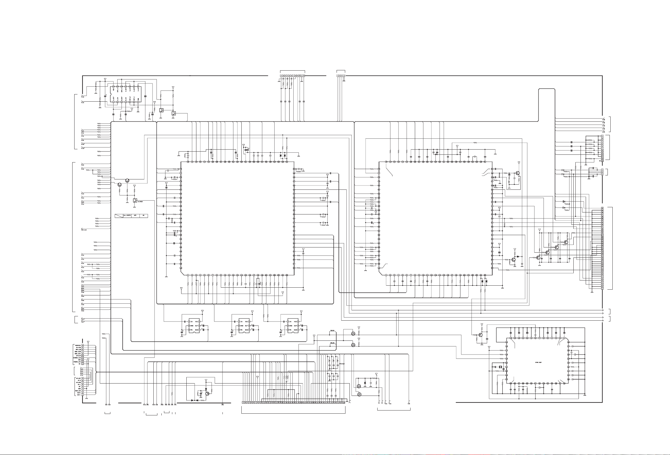
A
NALOG PWB CIRCUIT DIAGRAM (1/6) SHEET 1
ANALOG PWB ASS'Y (1/6)
SFL-1211A-M2
SHEET2
SHEET2
SHEET4
LED PWB ASS'Y
CN200U
(SHEET25)
SHEET5
SW PWB ASS'Y
CN100R
(SHEET26)
V3_G_Y
V3_B_Cb
V3_R_Cr
V3_VIN
V3_LIN
V3_RIN
V2_RIN
V2_LIN
V2_VIN
V2_YIN
V2_CIN
DIN_PHOTO
V1_G_Y
V1_B_Cb
V1_R_Cr
V1_RIN
V1_LIN
V1_VIN
V1_YIN
V1_CIN
MON_R
MON_L
MON_V
MON_Y
MON_C
MON_SDC
SDA3A
SCL3A
QGA1217C1-10X
HP_GND
HP_R
HP_DET
QGA1217C1-09X
CARD PWB ASS'Y (2/2)
CN8CV1 (SHEET29)
GND
GND
GND
GND
75
R209
/10
C217
CARD_Cb
SDATA
C_OUT1
OUT1_GND
C_OUT2
OUT2_GND
CVBS_OUT4
CVBS_OUT5
R1_OUT
L1_OUT
R2_OUT
L2_OUT
R3_OUT
L3_OUT
R10_IN
L10_IN
R9_IN
L9_IN
0
R160
DIN_SL
V1_YS
OPEN
R200
R201
0
R204
EXT_YS1
[EXT_YS2]
/10
C218
CARD_Cr
NC
IC105
MM1510XN-XMM1510XN-X
DBS_LED1
DBS_LED2
OPEN
AGC
DBS_LED1
75
R210
CARD_HD
GND
DBS_LED2
R161
CARD_VD
CARD_LIN
C126
1
/16
R167
220k
R163
0
R162
0
BS_A9V
STB3.3V
STB3.3V
GND
GND
/16
1
C219
CARD_RIN
GND
GND
0
C154
100
C155
10
A_MUTE
M_MUTE
YCbCrHDVDLR
CNCV1
/16
CVBS_IN1_DET
R6_IN
6.8k
R154
DTU_RIN
C150
100
/16
SCL0
SDA0
STB_5V
SDA0
/16
0.1
C129
/16
0.1
C107
/10
SCL0
Y_IN1_DET
AU_I_VCC9V
/16
MON_V
TV_LINK
STB_5V
DEC_Y
/10B1
/16
10
0.1
C128
C116
CVBS_IN6S4CVBS_IN7
L7_IN
6.8k
6.8k00
R155
C108
R156
DTU2_RIN
DTU2_LIN
MON_YOUT
AC_IN
POW_GOOD
GND
AC_IN
TVLINK
POW_GOOD
QGA1217C1-12X
R7_IN
P_EXP4
TV_MAIN
R193R194
OPEN0
LB_POW0
OPEN
R202
LB_PR
LB_POW
V1_S
/16
1
C127
33k
R157
R158
TV_L
MAIN_POW
0
R203
MAINPOW
S1
L8_IN
C153
10
TALK
AUDIO_L
[AUDIO_R}
GND
R159
TV_R
/16
B1_POW
0
R198
75
R208
/10
B1 B1 B1
101010
C216
CARD_Y
R169 R168
100 100
D101 D102
OPEN OPEN
SCLK
CVBS1
FBC_Y_OUT1
CVBS/Y_OUT1
OUT1_VCC5V
CVBS/Y_OUT2
OUT2_VCC5V
FBC_Y_OUT2
FBC_CVBS_OUT4
FBC_CVBS_OUT5
AU_O_VCC9V
R8_IN
AU_O_GND
BS_A9V
C152
/16
1
GND
V2_YS
DSP_RST
OPEN
REC_LED
R199
B1_POW
REC_LED
CODECRST
BS_A9V
R101
100k
R102
100k
C101
100
GND
DVI_L
DVI_R
R277
V2_S
R279
V1_S
M_MU
CN00U
HP_L
CN00R
/16
R103
100k
R104
100k
GND
2.2
R107
V4_LIN
OPEN
R108
V4_RIN
OPEN
R109
V3__D
OPEN
0
V3__G_Y
R110
V3__B_Cb
R111
0
V3__R_Cr
R112
0
R113
OPEN
V3_SL
V3_VIN
V3_LIN
V3_RIN
R114
OPEN
DTU_LIN
R115
OPEN
DTU_RIN
V2_RIN
V2_LIN
R116
OPEN
OPEN
V2__S2
V2_R_Cr
R281
R117
OPEN
V2_SL
TV_LINK
R287
OPEN
V2_B_Cb
R282
OPEN
R118
V2_G_Y
R283
V2_YS
R119
OPEN
V2_VIN
V2__YIN
R120
0
R121
V2__CIN
0
R122
V2__S
0
R126
OPEN
V3_YIN
R127
OPEN
V3_CIN
R128
OPEN
V3_S
R129
OPEN
V3_S2
DIN_PHOTO
R276
BS__IR
OPEN
TV_L
R130
OPEN
TV_R
R131
OPEN
V1_G_Y
V1_B_Cb
V1_R_Cr
R132
OPEN
REMOCON
EE_CDS1
REC_LED
DBS_LED2
DBS_LED1
DIMMER
VCC5
POW_LED
MECA_SW
KEY2
KEY1
V1__D
V1_RIN
R133
OPEN
V1_YS
V1_LIN
R134
OPEN
V1__S2
V1_VIN
R135
OPEN
V1_SL
V1_YIN
V1_CIN
V1_S
MON_R
MON_L
MON_V
MON_Y
MON_C
MON_SDC
R138
OPEN
R139
OPEN
D
D
SUB_MUTE
R278
OPEN
OPEN
STB_5V
GND
IC106
CD4066BNS-X
R295 R297
100k 100k
B1
B1
DIN_SR
Q103
OPEN
SDA3A
SCL3A
R280
100k
R123
OPEN
DIN_R
GND
Q104
OPEN
R124
OPEN
R298
OPEN
GND
OL-CX2046 OLLC08619
C206
4.7
C102
/16
BBOUT
B1
C103
2.2
/16
BS_A9V
BS_A9V
/16
BS_A9V
R125
OPEN
GND
MON
B1
GND
R296
100k
DIN_SL
DIN_L
GND
Q105
OPEN
OLLC08607
AC_IN
M.PACK
MAIN_POW
M.PACK
MAIN_POW
C204
4.7
AC_IN
/16
V3_S2
V3_CIN
MON_VOUT
MON_YOUT
MON_SDC
MON_COUT
DTU_VIN
DTU_YIN
DTU_CIN
POW_GOOD
POW_GOOD
R105 R106
10k 10k
Q101
UN2213-X
GND GND
C201
R182
/16
0.1
C133
GND
R184
BS_A5V
C134
1
/16
C135
C136
10
/10
R186
B1
C137
10
/10
R187
B1
C138
0.01
/16
R188
10k
R189
OPEN
C211
/16
0.1
10
C202
/16
0.1
GND
MON_COUT
TALK
MSP_RST0
TALK
A_MUTE
MSP_RST0
BS_A9V
C141
/16
C142
C143
LB_POW0
0
R195
LB_POW
Q102
UN2213-X
OPEN
1
220k
1
OPEN
0
0.1
0.1
DSP_RST
DSP_RST
/16
C139
1
/16
/16
/16
/16
10
GND
BS_A5V
C145
/16
R181
220k
C3_DC
C_IN3
FBC_CVBS_OUT3
CVBS_OUT3
DRIVER_VCC5V
Y_OUT3
DC_OUT
C_OUT3
DRIVER_GND
CVBS_IN4
CVBS4
Y_IN4
C4_DC
C_IN4
INPUT_GND
CVBS_IN5
VREF
Y_IN5
C5_DC
C_IN5
CVBS5
COMP_Y_IN1
S5
COMP_Y_IN2
ATT_MON_OUT
C144
/16
1
GND
DVI/DIN
C132
1
/16
FBC_Y_OUT3
L1_IN
V1_LIN
1SS355-X
V3_YIN
6.8k
R140
V1_RIN
IC103
MM1510XN-XMM1510XN-X
D283
V3_S
V3_VIN
S3
Y_IN3
CVBS_IN3
V2__S
V2__S2
V2__YIN
V2__CIN
/16
C200
0.1
OPEN
R177
CVBS3
C_IN2
C2_DC
Y_IN2
V1__S2
V1_VINDIMMER
V1_YIN
V1_CIN
V2_VIN
BS_A5V
C131
/16
0.1
/16
C199
0.1
C130
47
OPEN
CVBS_IN2
R173
C_IN
CVBS2
C1_DC
Y_IN1
CVBS_IN1
INPUT_VCC5V
S2
IC101
R2S11004FT
R1_IN
P_EXP1
L2_IN
R2_IN
P_EXP2
L3_IN
R3_IN
AU_I_GND
L4_IN
R4_IN
P_EXP3
L5_IN
R5_IN
AU_1/2_VCC
L6_IN
6.8k
R141
R285
OPEN
D282
1SS355-X
33k
R142
DVI/DIN
V2_LIN
BS_A9V
D281
1SS355-X
C281
47
R286
OPEN
V3_LIN
R284
56k
6.8k
R146
V3_RIN
MON_VOUT
OPEN
6.8k
R148
R147
R149
V4_LIN
V4_RIN
C149
10
/16
GND
B1_POW
QGF0508C1-50W
B1_POW
6.8k
6.8k
33k
R145
R143
R144
V2_RIN
C146
/10
100
C147
/16
10
MON_C
BS_A9V
Q281
/16
PNP
GND
33k
6.8k
R151
R152
OPEN47OPEN
33k
B1
R153
R150
C106
4.7
/16
DTU_LIN
BS_A9V
IC104
MM1510XN-XMM1510XN-X
C148
1
/16
C151
10
BS__IR
KEY1
KEY2
REMOCON
CN001
KEY2
KEY1
BS_IR
ONTIMER
REMOCON
DIGITAL PWB ASS'Y(1/16)
CN001 (SHEET7)
SHEET5
SHEET3
SHEET6
SHEET3
SHEET5
SHEET4
SHEET5
SHEET6
CARD PWB ASS'Y (1/2)
CN8CV2 (SHEET28)
CNCV2
QGA1217C1-04X
/16
1
C220
C125
1
/16
MAIN_VY
BS_A5V
C124
1
/16
C123
0.1
/16
GND
BS_A5V
C122
1
/16
C120
0.1
/16
C121
1
/16
220k
R166
1
/16
C119
220k
R165
1
C118
/16
GND
220k
R164
MON_R
MON_L
BS_A9V
C117
0.1
GND
/10
/16
MON_Y
CARD_INT
POW_LED
POW_LED
/16
MECA_SW
CARD_INT
STB3.3V
AFT1
MECA_SW
EE_CDS1
EE_CDS
MSP_RST0
MSP_RST
CARD_RIN
CARD_LIN
DIN_SR
SDA3A
SCL3A
TEXT_R
TEXT_G
OPEN
CARD_DA
CARD_CK
DIN_PHOTO
L102C282
OPEN
GND
C285
OPEN
GND
OPEN
R190
R191
OPEN
C291
C292
GND
SCL3A
SDA3A
TEXT_FR
TEXT_FG
CARD_DA
CARD_CK
DIN_PHOT
MAIN_C
OPEN
L103
C283
C286
OPEN
OPEN
SUB_C
INT
GND
SDA
SCL
GND
CARD_DA
CARD_CK
CARD_INT
AV_SW
V1_R_Cr
V2_G_Y
V2_B_Cb
V2_R_Cr
OPEN
OPEN
OPEN
/16
/16
R233
R235
R234
0.01
0.01
C183
C182
CL_Y1
R_IN1
V1_YS
V3__G_Y
V3__B_Cb
V3__R_Cr
V1__D
V2_YS
V3__D
PC_G
PC_B
PC_R
DTU_Y
R249
0
V1_SL
DTU_Cb
R253
0
V2_SL
DTU_Cr
R257
0
V3_SL
BS_A5V
R206
Q106
5.6k
2SK1374-X
DGS
BS_A5V
R207
Q107
5.6k
2SK1374-X
DGS
SDA0
OPEN
L104
C284
C287
OPEN
OPEN
TXET_FB
SCL0
DEC_Y
TV_MAIN
R197
0
OPEN
OPEN
GND
DEC_Y
Q114
OPEN
DGS
Q115
OPEN
DGS
GND
GND
AFT1
MAIN_VY
TEXT_B
OPEN
OPEN
R192
C293
GND
R237
R238
R239
R240
R241
R242
R243
R244
C186
R245
C187
0.1
R246
C189
10
R247
R248
R250
R251
R252
R254
R255
R256
R258
R259
GND
D290 C290
OPEN OPEN
GND
/16
/16
SDA3A5
BS_A5V
SCL3A5
GND
0
OPEN
OPEN
0
0
0
R290
OPEN
0
0
0
OPEN
OPEN
0
0
0
0
OPEN
OPEN
OPEN
OPEN
OPEN
OPEN
BS_A5V
OPEN
R291
R292
OPEN
FB_IN1
FB_DET_IN2
Y/G_IN3
COMP/RGB_T3
Cb/Pb/B_IN3
COMP/RGB_T4
Cr/Pr/R_IN3
DC1
FB_IN2
DC2
Y/G_IN4
INPUT_VCC
Cb/Pb/B_IN4
VREF
Cr/Pr/R_IN4
INPUT_GND
FB_IN3
DC3
Y_IN5
DC4
Cb_IN5
DC5
Cr_IN5
DC6 COMP_T5
SUB_GND1
TV_R
TV_R
SCL0A5
SDA0A5
SHEET3
TV_L
Cr/Pr/R_IN2
Y/G_IN6
MAIN_VY
TV_L
COMP/RGB_T2
FB_DET_IN1
CL_Y2
/16
0.01
C156
Cb/Pb/B_IN2
Cb/B_IN6
SUB_C
/16
0.0100.01
C157
OPEN
R236
Y/G_IN2
COMP/RGB_T1
CL_Cb2
Cr/R_IN6
MAIN_C
TV_MAIN
/16
C158
TV_MAIN
CL_Cr2
R211
CARD_Y
CL_Cb1
G_IN7
MAIN_GND
V1_B_Cb
/16
0.01
C181
B_IN1
CL_Cr1
R2S11003FT
B_IN7
HD_IN_DET
/16
0
.01
R212
C161
CARD_Cb
V1_G_Y
/16
0.1
C180
C179
G_IN1
MAIN_VCC2
IC102
R_IN7NCHD_IN2
0
R213
CARD_Cr
PC_HS
PC_VS
/16
47
C178
HD_IN1
VD_IN1
VD_IN2NCG_IN8NCB_IN8
CARD_HD
CARD_VD
/16
1
G_IN1_DET
R216
BS_A5V
FB_OUT1
OPEN
TEXT_G
R227
C177
0.1
/16
C176 C174
0.01 330p
/16 /16
FB_OUT2
Sync2_VCC
VD_slice2
ATT_MON_OUT
Clamp_driver1
INPUT_GND2
R_IN8NCNC
OPEN
OPEN
R217
R218
TEXT_R
TEXT_B
C175
0.01
Clamp_driver2
VD_filter1
R581
OPEN
R582
OPEN
OPEN
Clamp_in2
Sync_slice2
Sync_slice1
Cb/Pb/B_OUT1
Cr/Pr/R_OUT1
INT_HD_OUT1
INT_VD_OUT1
Clamp_Pulse1_in
Cb/Pb/B_OUT2
Cr/Pr/R_OUT2
INT_HD_OUT2
INT_VD_OUT2
Clamp_Pulse2_in
SDATA
100
R219
BS_A5V
GND
CH/16
VD_filter2
Clamp_in1
VD_slice1
Y/G_OUT1
Sync2_GND
HD_DET1
OUT_VCC
HD_poldet1
OUT_GND
Y/G_OUT2
SUB_GND3
Sync_VCC1
Sync1_GND1
SCLK
OPEN
D103
100
R220
R583
OPEN
Q540
OPEN
C591
OPEN
CH
BS_A5V
GND
C173
68p
CH
R229
OPEN
C172
0.1
/16
R230
OPEN
C171
0.01
/16
GND
270k
R183
C170
0.01
/16
BS_A5V
C169
0.01
/16
C168
0.1
/16
BS_A5V
C167
0.1
/16
R222
OPEN
OPEN
D104
X540
OPEN
C547
OPEN
CH
R544
OPEN
R546
R545
OPEN
OPEN
BS_A5V
Q113
NPN
R228
330
C184
220p
CH
R231
C185
33
82p
R232
470
CH
L101
NQL79GM-100X
GND
R588
0
0
R589
R226
OPEN
BS_A5V
R225
D105
10k
MA111-X
R224
22k
Q108
NPN
R223
C166
22k
0.01
GND
0
R221
GND
C545
C546
OPEN
OPEN
LINE1-2
LINE2-2
SYNC2-IN
R541
OPEN
R542
OPEN
R543
OPEN
C548
OPEN
Cb2/B2-IN
DAC1
SDA
Y2/G2-IN
SCL
XTAL
B1
VD1-IN
VD2-IN
HD1-IN
HD2-IN
ADDRESS
B1
C580
C549
R547
OPEN
OPEN
OPEN
BS_A5V
R261
2.7k
R260
100
Q109
PNP2
LINE3-2
GND
SYNC1_IN
R540
OPEN
C544
OPEN
C543
OPEN
SYNC1-IN
Cr2/R2-IN
GND
IC540
OPEN
SYNC-OUT
VD-OUT
HD-OUT
B1
R549
C582
R548
C581
OPEN
OPEN
OPEN
OPEN
PC_R
PC_G
PC_B
PC_HS
PC_VS
OPEN
C194
DTU_Cr
OPEN
C195
DTU_Y
OPEN
C196
DTU_Cb
DTU_VIN
OPEN
OPEN
C207
R584
2.2
10k
/16
DTU_RIN
B1
DTU_LIN
B1
C208
2.2
/16
R585
10k
DIN_L
DIN_R
C209
2.2
/16
DTU2_RIN
B1
R586
10k
DTU2_LIN
B1
C210
2.2
/16
R587
10k
DTU_CIN
DTU_YIN
R267
330
R265
330
R266
100
R263
R264
330
R262
100
R294
0
C261
0.1
NC
LINE1-1
Y-OUT
R289
100
75
Q111
PNP2
R293
75
Q110
PNP2
C263C262
/16/16
0.10.1
/16
C540
C541
C542
OPEN
OPEN
OPEN
LINE2-1
Y1/G1-IN
Y-IN
Cb1/B1-IN
LINE3-1
Cr1/R1-IN
C-IN
Cr3/R3-IN
DAC2
Cb3/B3-IN
Y3/G3-IN
NC
SYNC3-IN
Cb-OUT
Vf0ADJ
Cr-OUT
C583
OPEN
GND
R273
R274
R288
75
Q112
PNP2
C264
/16
0.1
C590
OPEN
C589
OPEN
C588
OPEN
B1
C587
OPEN
R580
OPEN
C586
OPEN
C585
OPEN
C584
OPEN
GND
PC_R
PC_G
PC_B
SHEET2
PC_HS
PC_VS
CN0UV
QGA1217C1-13X
GND
SLOW
R268
GND
OPEN
V
R269
GND
OPEN
Y
R270
GND
OPEN
OPEN
U
R271
GND
OPEN
CV
GND
C
R272
OPEN
C197
OPEN
CN0UA
QGA1217C1-03X
U_R
GND
OPEN
U_L
C198
OPEN
GND
CN002
QGF0508C1-40W
MR
GND
ML
GND
BS_COUT
GND
BS_YOUT
GND
BS_ROUT
GND
BS_LOUT
GND
YMIN
YMAIN_GND
BYMIN
BYMINGND
DIGITAL PWB
RYMIN
RYMINGND
SUB_VY
ASS'Y (5/16)
GND
GND
CN002
CLPH_Y1V
(SHEET11)
FBMIN
CLPH_Y2G
GND
GND
NC
GND
GND
CmpHS
CmpVS
GND
DIN_DL
GND
DIN_DR
GND
SCL3A5
SHEET3,5,6
SDA3A5
MAIN_R
SHEET4
MAIN_L
c10413001a001_1014_1/6_0.0
2-8(No.YA363)(No.YA363)2-7
Page 31

A
NALOG PWB CIRCUIT DIAGRAM (2/6) SHEET 2
QNZ0726-001
GND GND
QNN0650-001
QNZ0726-001
GND
J401
J401
J401
GND
R402
J401
GND
J401
GND
J402
GND
J402
GND
J403
J403
J403
GND
J403
75
GND
J403
GND
GND
GND
GND
R401
75
GND
R403
75
GND
R404
220k
GND
R405
220k
GND
R406
75
GND
R407
75
GND
R408
75
GND
R410
75
R411
75
GND
R412
75
GND
2.2
R413
220k
GND GND
2.2
R414
220k
GND
C402
/10
2.2
C403
/10
2.2
C404
2.2
C405
2.2
C406
2.2
C407
2.2
C408
2.2
C409
2.2
/10
C410
.01
C411
2.2
/10
C412
/10
C413
/10
V1_S
D401
*1
V1_YIN
GND
CB2
D403
*1
V1_CIN
C401
.01
D402
*1
GND
GND
V1_VIN
CB2
D404
*1
GND
/10
V1_LIN
CB2
D405
*1
GND
/10
V1_RIN
CB2
D406
*1
GND
CB2
/10
CB2
/10
CB2
/10
CB2
CB2
CB2
CB2
V1_G_Y
D407
*1
GND
V1_B_Cb
D408
*1
GND
V1_R_Cr
D409
*1
GND
V2_S
D411
*1
GND
V2_YIN
D412
*1
V2_CIN
D413
*1
GND
GND
V2_VIN
D414
*1
GND
V2_LIN
D415
*1
V2_RIN
D416
*1
GND
GND
R464
75
C463C462C461
100p100p100p
J410
QNZ0561-001
PC_DET
D464
R467R461
7575
CHCHCH
GND
C464
2.2
/10CB2
C465
2.2
/10CB2
C466
2.2
/10CB2
D462D461
*1*1
*1
R475
330
CH
D465 D466
C469
*1 *1
100p
D463
*1
PC_VS
PC_HS
R476
330
C468
100p
/50
CH
/50
PC_B
PC_G
PC_R
D492
S9648
R491
1M
C491
/16
10
C492
/16
0.1
D491
MA8033-X
C493
/16
100
GND
BS_A5V
C494
1000p
GND
PC_DET
PC_VS
PC_HS
PC_R
PC_G
PC_B
DIN_PHOTO
V1_S
V1_CIN
V1_YIN
V1_VIN
V1_LIN
V1_RIN
V1_G_Y
V1_B_Cb
V1_R_Cr
V2_S
V2_YIN
V2_CIN
V2_VIN
V2_LIN
V2_RIN
PC_DET
PC_VS
PC_HS
PC_R
PC_G
PC_B
DIN_PHOTO
V1_S
V1_CIN
V1_YIN
V1_VIN
V1_LIN
V1_RIN
V1_G_Y
V1_B_Cb
V1_R_Cr
V2_S
V2_YIN
V2_CIN
V2_VIN
V2_LIN
V2_RIN
SHEET3
SHEET1
V3_VIN
V3_VIN
V3_LIN
V3_LIN
V3_RIN
V3_RIN
V3_G_Y
V3_G_Y
V3_B_Cb
V3_B_Cb
V3_R_Cr
V3_R_Cr
QNZ0726-001
J405
J405
QNN0651-001
QNN0650-001
J407
QNN0652-001
GND
C417
2.2
/10
CB2
R418
GND
GND
J406
GND
J406
GND
GND
J408
J408J408
GND
GND
J408
GND
J408
GND
75
GND
R419
220k
GND GND
R420
220k
GND
R421
2.2
75
2.2
GND
R422
75
GND
2.2
R423
75
GND
R426
220k
GND
R427
220k
GND
R431
75
GND
R434
2.2k
GND
R436
2.2k
GND
R438
22k
GND
R441
22k
GND
C418
2.2
/10
CB2
C419
2.2
/10
CB2
C420
CB2
/10
/10
CB2
C421
/10
CB2
C422
C424
2.2
/10
CB2
C425
2.2
/10
CB2
R432
OPEN
R433
75
R435
75
R437
390
R440
390
V3_VIN
D420
*1
V3_LIN
GND
D421
*1
V3_RIN
D422
*1
GND
V3_G_Y
D423
*1
V3_B_Cb
GND
D424
*1
GND
V3_R_Cr
D425
*1
GND
DVI_L
D427
*1
GND
GND
DVI_R
D428
*1
C431
R439
2.2
470
R442
470
Q433
UN2110-X
/16
CB1
D431
*1
C432
GND
2.2
/16
CB1
D432
*1
GND
R443
CB1
1k
C433
1
/16
GND
GND
Q431
UN2226-X
UN2226-X
GND
Q432
GND
MON_C
MON_SDC
MON_Y
MON_V
MON_L
MON_R
M_MU
R444
39k
GND
ANALOG PWB ASS'Y (2/6)
DVI_R
DVI_L
MON_SDC
MON_C
MON_Y
MON_V
MON_L
MON_R
M_MU
DVI_R
DVI_L
MON_SDC
MON_C
MON_Y
MON_V
MON_L
MON_R
M_MU
SFL-1211A-M2
(No.YA363)2-9 2-10(No.YA363)
c10413001a006_1014_6/6_0.0
Page 32

A
NALOG PWB CIRCUIT DIAGRAM (3/6) SHEET 3
TU3001
!
QAU0430-001
ANALOG PWB ASS'Y (3/6)
BS_A5V
U/V ANALOG TUNER
GND
SFL-1211A-M2
C3006 C3007
47/16 OPEN
R3008
OPEN
R3009
C3008
OPEN
R3011
0
0
C3005
10
47k
R3001
CB1
/10
D3001
GND
OPEN
L3002
OPEN
D3002
R3018
0
/16
47
C3001
OPEN
C3003
NQL79GM-100X
L3001
NQL79GM-100X
OPEN
10
C3004
R3201
0
NRSA02J-0R0X
Q3201
OPEN
R3203
OPEN
R3204
OPEN
Q3202
OPEN
C3002
/50
Q3001
R3206
NRSA02J-0R0X
R3202
OPEN
*2
TU_5V
R3003
R3004
GND
R3005
10k
R3207
OPEN
R3006
OPEN
GND
R384
R385
R383
R382
TV_V1
32V
R3014
OPEN
R3015
R3012
0
R3013
0
BS_A9V
0
0
OPEN
SDA0A5
SCL0A5
R381
IC381
M62320FP-X
GND
CH
C381
68p
CH
C382
68p
R386
OPEN
R394
100
R390
GND
C383
1
/10
R391
100
M.PACK
PC_DET
SHEET1
SHEET2
OPEN
0
0
OPEN
0
SHEET1
Q3002
*1
C/N_AFT1
27k
10k
R3007
BS_A5V
TV_L
TV_R
AFT1
TV_MAIN
SDA3A5
SCL3A5
SHEET1
SHEET1,5,6
R387
R396
R397
R398
R399
OPEN
OPEN
OPEN
OPEN
OPEN
MSP_RST0
MSPIN_L
MSPIN_R
MSPOUT_L
MSPOUT_R
SHEET1
SHEET4
C3156
C3201 R3205
OPEN OPEN
GND
R3122
3.9k
/16
0.1
C3118
C3119
C3120
10
CB1
NCB21CK-105X
IC3101
CXA2205Q-X
220
220
R3167
R3126
/10
C3121
/10
4.7
CB1
C3126
4.7
C3115
0.1
C3106
/16
0.1
C3107
C3108
R3119
C3109
C3110
C3111
C3112
C3113
C3114
F
/16
0.1
F
10/10
CB1
2.2M
0.022
0.0047
10/10
CB1
/25
0.1
0.0047
10/10
CB1
C3155
2.2/16
CB1
2.2/16
CB1
/16
FF
C3125
/25
0.1
0.1
C3116
0.1
FF
C3117
/16
/16
R3124
R3123
OPEN
3k
R3125
/10CB1
C3122
CB1
/10
3.3k
3.3
1M
R3128
C3127
.0056
C3123
.047
C3124
.0027
C3130
CB1
CB1
C3133
CB1
R3130
R3131
C3134
CB1
C3135
CB1
C3136
NCB21CK-105X
C3128R3129
.012100k
CB1
4.7
4.7
C3131
4.7
4.7
68k
10
4.7
C3129
OPEN
/10
/10
/10
/10
C3137
/16
0.1
C3132
/16
47
/10
R3306
OPEN
R3133
/10
1k
R3132
12k
GND
C3301 C3303C3302
OPEN OPENOPEN
L3301
OPEN
BS_A5V
VDD
AIN0
GND
R3301
OPEN
AOUT
AIN1
R3302
OPEN
GNDGNDGNDGNDGND
EXT
AGND
VREF
AIN2
AIN3A0A1A2VSS SDA
BS_A5V
R3304R3303
OPENOPEN
IC3301
SCL
OSC
GND
GND
R3305
OPEN
OPEN
c10413001a002_1014_2/6_0.0
2-12(No.YA363)(No.YA363)2-11
Page 33

A
NALOG PWB CIRCUIT DIAGRAM (4/6) SHEET 4
SHEET5
SHEET1
SHEET5
SHEET1
SHEET3
VOL_R
VOL_L
MAIN_R
MAIN_L
CO_RST
SDA3A
SCL3A
DSP_RST
MSPIN_R
MSPOUT_R
MSPOUT_L
R592R591
R593
R594
R595 R596
R597 R598MSPIN_L
VCC5 VCC12V
LC552
R501
C501
C502
R502
LC551
R555
IC501
IC501
R554
R503
R506
C504
D501
D502
R504
C503
R505
C506
R509 C507
R507
R510
C505
R508
R515
R516
R531
C531
C508
R512
C510
R511
R513
R514
GND
C509
DSP12V
L501
DSP12V
R517
C511
R518
R519
NN
C512
Q501
R522
R521
Q502
R523
C513
R525
R526
R524
C514
R520
R533
Q503
GND
Q553
C532
R557
R532
R553
C551 C552
R556
GND
C576C577C578C579
OLLC09108
OLLC09108
OLLC09448
-02
0OPEN
OPEN
0
0
OPEN
OPEN
OPEN
OPEN
NCB31HK-223X
NCB31HK-223X
0.0022
0.0022
0.0082
0.0082
NEHL1AM-107X
1/50
1/50
NEHL1CM-476X
NENA1CM-475X
NENA1CM-475X
NENA1CM-475X
NENA1CM-475X
1000p
1000p
NEHL1EM-475X
0.1
0.1
NEHL1CM-106X
1000p
1000p
1000p
1000p
47/16
0.1
NEHL1AM-107X
0.1
0.1
NCB30JK-225X
NEHL0JM-226X
NCB30JK-225X
NEHL0JM-226X
NEHL0JM-226X
0.01
0.01
0.1
0.1
0.01
0.01
0.01
NRSA63J-222X
NEHL0JM-226X
NCB31CK-105X
NEHL0JM-226X
0.01
0.01
NEHL1AM-107X
NEHL1AM-107X
NEHL1AM-107X
NEHL1AM-107X
OPEN
OPEN
0
0
OPEN
OPEN
OPEN
OPEN
OLLC09108
-02
NCB31HK-223X
NCB31HK-223X
0.0022
0.0022
0.0082
0.0082
NEHL1AM-107X
1/50
1/50
NEHL1CM-476X
NENA1CM-475X
NENA1CM-475X
NENA1CM-475X
NENA1CM-475X
1000p
1000p
NEHL1EM-475X
0.1
0.1
NEHL1CM-106X
1000p
1000p
1000p
1000p
47/16
0.1
NEHL1AM-107X
0.1
0.1
NCB30JK-225X
NEHL0JM-226X
NCB30JK-225X
NEHL0JM-226X
NEHL0JM-226X
0.01
0.01
0.1
0.1
0.01
0.01
0.01
NRSA63J-222X
NEHL0JM-226X
NCB31CK-105X
NEHL0JM-226X
0.01
0.01
NEHL1AM-107X
NEHL1AM-107X
NEHL1AM-107X
NEHL1AM-107X
0
OPEN
OPEN
OPEN
OPEN
OPEN
OPEN
OLLC09448OLLC09108
OPEN
OPEN
OPEN
OPEN
OPEN
OPEN
OPEN
OPEN
OPEN
OPEN
OPEN
OPEN
OPEN
OPEN
OPEN
OPEN
OPEN
OPEN
OPEN
OPEN
OPEN
OPEN
OPEN
OPEN
OPEN
OPEN
NEHL1AM-107X
OPEN
OPEN
OPEN
OPEN
OPEN
OPEN
OPEN
OPEN
OPEN
OPEN
OPEN
OPEN
OPEN
OPEN
OPEN
OPEN
OPEN
OPEN
OPEN
OPEN
NEHL1AM-107X
NEHL1AM-107X
NEHL1AM-107X
NEHL1AM-107X
R591
R592
R593
ANALOG PWB ASS'Y (4/6)
SFL-1211A-M2
X551
R529
R530
GND
R571
IC502
R528
NN
C515
C516
C517
C518 C519
AOUTRIN
VCOM
AINR
/PWDA
AOUTL
AINL
GND
/PWAD
VSS
R527
SCLK
VDD
MCLK
DEM0
LRCK
DEM1
SDTI
SDTO
C520
R921
R565
R570
C566C565
VDDP
R573
VCOI
VSSP
C567
NIMO
R574
TEST
VSSX
R572
C568
R927
R926
XI
XO
VDDX
CKO
VDD
VSS
R594
R595
R596
R597
R598
C501
C502
C503
C504
C505
C506
C507
C508
C509
C510
C511
C512
C513
C514
C515
C516
C517
C518
C519
C520
C531
C532
C551
C552
C553
C554
C555
C556
C557
C558
C559
C560
C561
C562
C563
C564
C565
C566
C567
C568
C569
C570
C571
C572
C573
C574
C575
C576
C577
C578
C579
RST
C553
DSP12V
IC552
C554
C556C555
VCC3.3
VO1
VCC1.5
GND
VO2
Nr
C557
C558
C559
C560
C561
GND
R561
R560
R562
R563
R564
R922
C562
C564
R566
R568
R569
GND
R567
C563
STANDBY
SDA
SCL
VDDP
VSS
SDO0
BCK0
LRCK0
SDI0
BCKIA
LRCKIA
R575
SDI1
BCKIB
R576
LRCKIB
R923
R577
VDD
C569
CKI
R578
IC551
VSS
VDDT
SAMSTB
VDDM
R925
R924
C574
C575
C570
C571
C572
C573
IC501
IC502
IC551
IC552
LC551
LC552
X551
L501
Q501
Q502
Q503
Q553
R501
R502
R503
R504
R505
R506
R507
R508
R509
R510
R511
R512
R513
R514
R515
R516
R517
R518
R519
R520
R521
R522
R523
R524
R525
R526
R527
R528
R529
R530
R531
R532
R533
R553
R554
R555
R556
R557
R560
R561
R562
R563
R564
R565
R566
R567
R568
R569
R570
R571
R572
R573
R574
R575
R576
R577
R578
R921
R922
R923
R924
R925
R926
R927
D501
D502
HA17558AF-X
AK4554VT-X
JCV8010
PQ2L3152MS-X
NAX0623-001X
NRSA02J-0R0X
1SS355-X
1SS355-X
OLLC09448OLLC09108
OLLC09108
-02
OPEN
HA17558AF-X
OPEN
AK4554VT-X
OPEN
JCV8010
OPEN
PQ2L3152MS-X
OPEN
NAX0623-001X
OPEN
NRSA02J-0R0X
OPEN
OPEN
NPN
NPN
NPN
NPN
220
220
4.7k
3.3k
3.3k
4.7k
3.3k
1k
1k
3.3k
10k
33k
33k
10k
0
0
33k
33k
33k
33k
2.2k
2.2k
1k
1k
1k
1k
470
470
100
10k
10k
10k
10k
0
0
10k
10k
6.8k
220
220
220
220
100
100
10k
10k
100
1M
4.7
10k
10k
10k
10k
10k
0
0
0
0
0
0
0
1SS355-X
1SS355-X
OPEN
OPEN
OPEN
OPEN
OPEN
OPEN
OPEN
OPEN
OPEN
OPEN
OPEN
OPEN
OPEN
OPEN
OPEN
OPEN
OPEN
OPEN
OPEN
OPEN
OPEN
OPEN
OPEN
OPEN
OPEN
OPEN
OPEN
OPEN
OPEN
OPEN
OPEN
OPEN
OPEN
OPEN
OPEN
OPEN
0
OPEN
OPEN
OPEN
OPEN
OPEN
0
OPEN
OPEN
OPEN
OPEN
OPEN
OPEN
OPEN
OPEN
0
OPEN
OPEN
OPEN
OPEN
OPEN
OPEN
OPEN
OPEN
OPEN
0
OPEN
OPEN
OPEN
OPEN
OPEN
OPEN
OPEN
OPEN
OPEN
OPEN
OPEN
OPEN
OPEN
OPEN
OPEN
NPN
NPN
NPN
NPN
220
220
4.7k
3.3k
3.3k
4.7k
3.3k
1k
1k
3.3k
10k
33k
33k
10k
0
0
33k
33k
33k
33k
2.2k
2.2k
1k
1k
1k
1k
470
470
100
0
10k
10k
10k
10k
0
0
10k
10k
6.8k
220
220
220
220
0
100
100
10k
10k
100
1M
4.7
10k
0
10k
10k
10k
10k
0
0
0
0
0
0
0
(No.YA363)2-13 2-14(No.YA363)
c10413001a004_1014_4/6_0.0
Page 34

A
NALOG PWB CIRCUIT DIAGRAM (5/6) SHEET 5
VCC12V
C609
CB2
R609
R611 R612
/16
/16
OPEN
R699
100
R752
R632
OPEN
R633
OPEN
R636
R634
R635
100
R700
OPEN
R705
C608
CB1
R619
C638
C637
C635
C636
R638
18k
VE3
VE2
VE1
TONE_HB
SUR_FIL2
INB
INA
SUR_FIL1
TONE_HA
LP2
TONE_LA
LP1
LP3
18k.022
R647C653
C633
/25
C634
BS_A5V
100
R701
R702
SHEET1
SHEET1,3,6
SHEET1
SHEET4
SHEET1
SHEET4
LB_POW
SDA3A5
SCL3A5
A_MUTE
TALK
VOL_L
VOL_R
BBOUT
SUB_MUTE
CO_RST
C614
/16
4.7
NENA1CM-475X
N
N
C615
/16
4.7
NENA1CM-475X
BBOUT
R631
Q603
OPEN
R693
R610
R616
C626
OPEN
C627
OPEN
C621
0
0
R694
R695
0
OPEN
R696
R697
IC606
M62320FP-X
100
100
R704
R703
Q604
C622
C623
0.18
CB2
C624
0.0022
C625
0.018
0.012
C628
0.0022
C629
0.18
C630
CB2
C631
C632
D602
OPEN
D603
OPEN
OPEN
R698
1k
R751
GND
/25
.022
C639
HBSTB
HBSTA
OPEN
R706
R613
R614
C610
ANALOG PWB ASS'Y (5/6)
SFL-1211A-M2
GND
IC603
VCC
C611
CB2
R615
R617
CB1
R618 C613C612
/16
100
GND
C642
10
/16
R643
OPEN
C644
C641
4.7
/25
R654
R644
SENSE
BBAGCINT
OUT1B
OUT1A
R645
2.2k
/25
/16
/16
/16
/16
1
1
1
C647
C648
ADDIN2
ADDIN1
OPEN
C658
C659
/25
4.7
R722 R723
OPEN 0
CTL
CSR
C714
OPEN
/16
1
C660
BS_A5V
GND
C649
/16
C661
Q609
VCC12V
1
C650
CA2
CTH
CBB
AGCINT
/10
2.211
CB2
C662
R687
10K
R689
R688
C715
OPEN
R716
OPEN
R715
OPEN
4.7
C646
OUT2B
OUT2A
/25
4.7
C657
AU_+VCC
/16
1
C651
VREF
/16
C663
CO2
CO1TONE_LB
AUX
V+
GND
SCL
SDA
CA1
CVB
CVA CBH
R646
NCB11AK-106X
R690 R691
R717
OPEN
GND
Q613
OPEN
C652
C668
1
/16
C667
1
/16
C666
/10
10
CB1
R653
C669
100k
1
/16
R652
100
R651
100
C665
1
/16
C664
1
/16
VCC5
C752
1
R755
0
R762
C751
0.0022
OPEN
GND
R767
C758
OPEN
R756
0
OPEN
R692C710
OPEN
AMP_MUTE
D608
1SS355-X
C716
D615
/16
47
1SS355-X
R718
100k
NEHL1CM-476X
R720
15k
1SS355-X
D605
1SS355-X
R719
56k
GND
D751
1SS355-X
D606
A_MUTE
D607
1SS355-X
D752
1SS355-X
Q614
*2
R757
4.7k
R758
100k
0.0022
R759
Q751
0
*2
UN2226-X
/50
IC751
BH3547F-X
C761
100
/10
NEHL1AM-107X
R760
47k
C757
1
/50
R761
0
C756
1
Q752
/50
C753
220
/4
C754
47
/16
NEHL1CM-476X
C755
220
/4
R765
R764
1k220.1
R768
1k220.1
R769
C759
R770
0
C760
NEHL0GM-227X
NEHL0GM-227X
GND
VCC12VAU_+VCC
CN00S
QGA1501F4-10X
D-AMP PWB ASS'Y
CN00S SHEET25
GND
HP_R
HP_GND
OLLC09108 OLLC09448
HP_L
HP_DET
SHEET1
OLLC09108
NJW1182FP1
IC601
C622
C631
C632
C633
C634
C635
C636
C637
R634
R635
R636
R646
C652
R639
R640
R641
R642
R644
R654
C640
C641
C670
RC4558D-X
IC603
Q603
Q604
R609
R610
R611
R612
R613
R614
R615
R616
R617
R618
R619
R631
C608
C609
C610
C611
NCB11AK-106XNCB11AK-106X
C613
C621
R701
Q609
R688
R689
R690
C710
-02
NJW1182FP1
OPEN
OPEN
OPEN
OPEN
0.1
0.1
0.0082
0.0082
0.0082
0.0082
680p
680p
680p
680p
OPEN
15k
56k
56k
47k
47k
22k
22k
1/16
1/16
1k820
820
1k
OPEN
OPEN
5.6k
6.8k
3.9k
3.9k
1.8k
1.8k
1/16
1/16
1/16
1/16
1/16
1/16
RC4558D-X
*1
*1
*1
*1
10k
10k
22k
22k
1k
1k
10k
10k
220k
220k
220k
220k
180k
180k
18k
18k
22k
22k
22k
22k
OPEN
OPEN
15k
15k
NCB11AK-106XNCB11AK-106X
0.12/25
0.12/25
0.22/16
0.22/16
0.12/25
0.12/25
0.0039
0.0039
100
100 OPEN
OPEN
OPEN
OPEN
OPEN
OPEN
OPEN
OPEN
OPEN
OPEN
OPEN
NJW1181FP1
.0033
.0033
OPEN
OPEN
.033
OPEN
OPEN
.033OPEN
OPEN15k
OPEN
OPEN
OPEN
OPEN
1k
1k
OPEN
6.8k
3.9k
1.8k
1/16
1/16
1/16
OPEN
OPEN
OPEN
OPEN
OPEN
OPEN
OPEN
OPEN
OPEN
OPEN
OPEN
OPEN
OPEN
OPEN
OPEN
OPEN
OPEN
OPEN
OPEN
OPEN
OPEN
OPEN
OPEN
OPEN
OPEN
OPEN
C640
R642
C643
OPEN
R640 R639
0.1
C670
R641
BB1
BB2
BBAGCOUT
ealaBASS
IC601
BB3
BB4
BBFIXOUT
R650
33k
/16
R649
68k
10
C654
.047
/16
C655
R707
OPEN
C717
1
/10
c10413001a003_1014_3/6_0.0
2-16(No.YA363)(No.YA363)2-15
Page 35

A
NALOG PWB CIRCUIT DIAGRAM (6/6) SHEET 6
ANALOG PWB ASS'Y (6/6)
SFL-1211A-M2
DC-DC PWB ASS'Y
CN00H
(SHEET30)
CN00H
QGA2001F6-15X
32V
GND
LCD_POW
AC_IN
STB_5V
GND
SCL3A5
GND
SDA3A5
5V
9V
GND
GND
GND
BA33BC0FP-X
C904
NCB11AK-106X
IC902
GND
C905
47
NEHM1CM-476X
C906
/25
0.1
NCB31EK-104X
/16
NQL52EM-220X
D903
OPEN
GND
NQR0562-010X
L902
L903
C913
NEX51CM-335X
GND
C914
NEX50JM-156X
GND
BS_A5VSTB_5V32V STB3.3V BS_A9V
R912
OPEN
L906
NQL52EM-221X
NEX50JM-156X
VCC5
C920
SHEET1,3,5
SCL3A5
SDA3A5
Y610
Y611
Y612
OPEN
OPEN
OPEN
GND
Y607
Y608
Y609
OPEN
OPEN
OPEN
OPEN GND
Y604
OPEN
Y605
OPEN
Y606
GND GNDGND
(No.YA363)2-17 2-18(No.YA363)
Y601
Y602
Y603
Y905Y902Y903 Y904
OPEN
OPEN
OPEN
OPENOPENOPEN OPEN
B1_POW
SHEET1
MAIN_POW
AC_IN
POW_GOOD
c10413001a005_1014_5/6_0.0
Page 36

DIGITAL PWB CIRCUIT DIAGRAM (1/16) SHEET 7
DIGITAL PWB ASS'Y (1/16)
SFL0D151A-M2
ACINPOW
R7505
R7526
10k
SHEET21
OPEN
SHEET12
SHEET15,16,18,19,20,22
SHEET16
SHEET18
TVLINK
QGA1501F4-06W
SDA3A
SCL3A
TEST0
POW_GOOD
REC_LED
CODECRST
B1_POW
AUDIO_L
AUDIO_R
BS_IR
CN7501
GND
TEST0
SDA3A_2
SCL3A_2
GND
VCC3D
R7501
R7502
OPEN
D7501
0
0
Q7501
UN2213-X
F
STB3.3V
C7513
C7505
IC7501
STB3.3V
OPEN
VCC
1OE
1A
1B
GND
GND
OPEN
OPEN
C7519
C7518
CH
GND
C7512
R7536
OPEN
EXT_YS1
OPEN
Q7508
OPEN
GND
AGC
STB3.3V
K7501
A_MUTE
M_MUTE
C7506
CH
D7510
OPEN
D7511
OPEN
POW_LED
C7507
C7508
CH
CH
STB3.3V
GND
MECA_SW
K7504
C7510
R7537
OPEN
R7538
NRSA63J-0R0X
OPENOPEN
D7513D7512
CH
GND
L7501
OPEN
TEXT_FR
TEXT_FG
TEXT_FB
TEXT_FR
TEXT_FG
TEXT_FB
0
0
R7523
R7524
LC7507
OPEN
LC7508
OPEN
R7525
LC7509
OPEN
STB3.3VA
R7539
OPEN
LC8801
R8885
OPEN
LC8802
R8886
OPEN
L7502
CEC/TVLK
SHEET16
CECIN
DIGITAL INPUT BLOCK
TVLINKIN
SHEET22
TVLINKOUT
LB_PRO
SHEET16,20
LB_POW
SHEET10,11,16,20
MAIN_POW
EXT_YS2
SHEET16
EXT_YS1
AGC
DBS_LED1
SHEET21
DBS_LED2
A_MUTE
SHEET16
M_MUTE
POW_LED
SHEET16,19
CARD_INT
SHEET16
MECA_SW
SHEET12,19,21,22
AFT1
SHEET16,21,22
EE_CDS1
SHEET16
MSP_RST
DINPHOT
SDA3A
SHEET8,9,10,16,17,19, DIGITAL INPUT BLOCK
SCL3A
CARD_CK
SHEET16
CARD_DA
TEXT_FR
TEXT_FG
SHEET22
TEXT_FB
DEC_Y
SHEET8
TV_MAIN
OLLC09109
OLLC09109
-04
-03
QGF0508C1
QGF0508C1
LC7505
CN001
CN011
IC7502
K7501
D7501
D7508
RA7503
R7521
R7523
R7524
R7525
R7530
R7532
R7533
R7544
R8885
R8886
C7502
C7504
C7505
C7506
C7507
C7508
C7510
C7511
C7513
-50W
-50W
OPEN
OPEN
OPEN
OPEN
NRSA02J
NRSA02J
-0R0X
-0R0X
OPEN
OPEN
OPEN
OPEN
OPEN
OPEN
NRZ0040
NRZ0040
-0R0X
-0R0X
0
0
OPEN
OPEN
OPEN
OPEN
OPEN
OPEN
OPEN
OPEN
OPEN
OPEN
OPEN
OPEN
OPEN OPEN OPEN OPEN OPEN
0
0
0
0
OPEN
OPEN
OPEN
OPEN
OPEN
OPEN
OPEN
OPEN
OPEN
OPEN
OPEN
OPEN
OPEN
OPEN
OPEN OPEN OPEN OPEN 12p
OPEN
OPEN
OLLC09109
-02
QGF0508C1
OPEN
OPEN
NRSA02J
OPEN
OPEN
OPEN
NRZ0040
OPEN
OPEN
OPEN
OPEN
OPEN
OPEN
OPEN
OPEN
OPEN
OPEN
OPEN
OPEN
OPEN
OPEN
-0R0X
-0R0X
0
0
0
-50W
OLLC09109
QGF0508C1
-50W
OPEN OPEN
OPEN
NRSA02J
-0R0X
OPEN
OPEN
OPEN
NRZ0040
-0R0X
0
OPEN
OPEN
OPEN
OPEN
OPEN
OPEN
0
0
OPEN
OPEN
OPEN
OPEN
OPEN
OPEN
OPEN
OPEN
OLLC09109
-05
QGF0508C1
OPEN
NQR0413
NQR0483
OPEN
OPEN
NQR0271
OPEN
OPEN
OPEN
OPEN
OPEN
OPEN
OPEN
OPEN
OPEN
OPEN
12p
12p
12p
12p
12p
12p
OPEN
-50W
-002X
-005X
-004X
2OE
2B
2A
EXT_YS2
IC7502
1Y
1A
VCC
GND
2Y
2A
GND
RA7503
STB_5V
R7532
R7533
D7508
D7509
OPEN
OPEN
OPEN
OPEN
OPEN
OPEN
OPEN
C7514
C7515
GND
STB3.3V
R7504
100k
D7502C7501
*40.1/16
GND
C7502
GND
K7502
K7503
K7505
K7506
C7516
OPEN
C7517
STB3.3V
OPEN
R7529
OPEN
R7530
R7544
0
R7534
STB_5V
C7511
R7521
LC7505
C7504
CH
CH
SHEET16,19
DIMMER
KEY_2
REMOCON
GND
GND
DEC_Y
KEY_1
MAIN_VY
SHEET19
R7540
OPEN
R7541
OPEN
R7542
SDA3A_1
AFT1
MECA_SW
EE_CDS
SDA3A
MSP_RST
SCL3A_1
SCL3A
CARD_CK
CARD_DA
TEXT_FR
DIN_PHOT
GND
CN001
TEXT_FG
GND
GND
GND
GND
DEC_Y
TV_MAIN
TEXT_FB
BS_IR_1
GND
GND
GND
TEXT_FB
TEXT_FR
TEXT_FG
CARD_DA
DIN_PHOT
SCL3A
CARD_CK
SDA3A
EE_CDS
MSP_RST
AFT1
CARD_INT
MECA_SW
M_MUTE
POW_LED
A_MUTE
STB3.3V
STB3.3V
GND
DBS_LED1
DBS_LED2
EXT_YS1
REC_LED
( EXT_YS2)
B1_POW
CODECRST
AUDIO_L
( AUDIO_R)
AGC
OPEN
LB_POW
MAINPOW
LB_PR
AC_IN
CN011
GND
POW_GOOD
TVLINK
STB_5V
SCL0
KEY1
KEY2
SDA0
BS_IR
ONTIMER
REMOCON
KEY2
KEY1
ONTIMER
REMOCON
BS_IR
GND
SCL0
SDA0
STB_5V
TVLINK
AC_IN
POW_GOOD
LB_PR
LB_POW
MAINPOW
( AUDIO_R)
AUDIO_L
B1_POW
REC_LED
CODECRST
EXT_YS1
( EXT_YS2)
AGC
DBS_LED2
DBS_LED1
GND
STB3.3V
STB3.3V
A_MUTE
M_MUTE
POW_LED
CARD_INT
ANALOG PWB ASS'Y (1/6)
CN001 (SHEET1)
R7543
OPEN
OPEN
SCLM
SHEET21,22
SDAM
SCL1
SHEET21
SDA1
c10408001a011_1014_11/17_0.0
2-20(No.YA363)(No.YA363)2-19
Page 37

DIGITAL PWB CIRCUIT DIAGRAM (2/16) SHEET 8
BS_9V
R8893
SHEET7
TV_MAIN
R8894
OPEN
GR_RST
BS_5VBS_9V
GR_3V
BS_5V
L8801
L8802
OPEN
L8803
SHEET16
SHEET7
GR_ON
DEC_Y
C8808
C8807
IC8801
CF1
VccCK
DPR
CLRQ
GND Q
R8888
C8880
OPEN
R8889
C8811
R8884
OPEN
GND
C8809
IC8802
Vin3
SW2
VDD Vin2
SW1Vout
GND Vin1
OPEN
R8822
R8823
DIGITAL PWB ASS'Y (2/16)
SFL0D151A-M2
GND
GROUT_7
R8895
OPEN
Q8837
OPEN
C8802
TV_MAIN1
R8824
OLLC09109
OLLC09109
-03
NAX0118
-001X
-001X
TC7W74F-X
NJM2235V-X
S-80928
CLNB-G-W
OR43304
BMQC
BMQC
EL8101
IWZ-X
IWZ-X
TC7S04FU
-X
-X
TC7WHU
04FU-X
04FU-X
R1170H
331B-X
331B-X
NPN
NPN
NPN
NPN
PNP
PNP
NPN
NPN
NPN
NPN
*5
*5
*5
*5
NQR0489
-002X
-002X
NRSA02J
-0R0X
-0R0X
NQR0499
-001X
-001X
NQL52EM
-101X
-101X
*1
*1
*4
*4
NRSA02J
-0R0X
-0R0X
NRSA02J
-0R0X
-0R0X
NQL914K
-470X
-470X
*1 *1
*2
*2
*2 *2 *2
*2
*2
*2 *2 *2
*1
*1 *1
*1 *1 *1
*1
*3
*3
*3
*3
NRZ0034
-103W
-103W
NRZ0034
-103W
-103W
0
0
0
0
560
1M
470k
0
0
2.2k
100
1.2k
180
680
100
1k
1k
1k
1k
5.6k
4.7k
3.9k
3.9k
1k
1k
1.2k
4.7k
47k
47k
10k
10k
10k
10k
10k
10k
10k
10k
10k
10k
1M
1M
1.8k
100
100
330
330
47
47
330
330
47
47
330
330
3.3k
3.3k
47k
47k
1k
1k
8.2k
8.2k
390
390
1.8k
1.8k
75
75
75
75
1k
1k
1M
1M
1k
0
1M
0
3.9k
10/10
0.1/16
4.7/16
0.01/50
10/10
0.1/16
4.7/16
0.1/16
15p/50
220p/50
120p/50
4.7/16
4.7/16
0.1/16
4.7/16
0.1/16
0.1/16
0.1/16
0.1/16
0.1/16
0.1/16
0.1/16
0.1/16
0.1/16
0.1/16
0.1/16
0.1/16
0.1/16
0.1/16
0.1/16
1000p/50
270p/50
560p/50
390p/50
0.1/16
4.7/16
0.1/16
1000p/50
0.1/16
10/10
0.1/16
1/16
4.7/16
10/10
10/10
0.1/16
1000p
NEX60JM
-227X
-227X
OLLC09109
-02
NAX0118
TC7W74F-X
NJM2235V-X
S-80928
CLNB-G-W
OR43304
EL8101
TC7S04FU
TC7WHU
R1170H
NPN
NPN
PNP
NPN
NPN
NQR0489
NRSA02J
NQR0499
NQL52EM
NRSA02J
NRSA02J
NQL914K
NRZ0034
NRZ0034
560
1M
470k
2.2k
100
1.2k
180
680
100
1k
1k
5.6k
4.7k
3.9k
3.9k
1k
1.2k
4.7k
47k
10k
10k
10k
10k
10k
1M
1.8k
100
330
47
330
47
330
3.3k
47k
1k
8.2k
390
1.8k
1.8k
75
75
1k
1M
1k
0
1M
0
3.9k
10/10
0.1/16
4.7/16
0.01/50
10/10
0.1/16
4.7/16
0.1/16
15p/50
220p/50
120p/50
4.7/16
4.7/16
0.1/16
4.7/16
0.1/16
0.1/16
0.1/16
0.1/16
0.1/16
0.1/16
0.1/16
0.1/16
0.1/16
0.1/16
0.1/16
0.1/16
0.1/16
0.1/16
0.1/16
1000p/50
270p/50
560p/50
390p/50 390p/50
0.1/16
4.7/16
0.1/16
1000p/50
0.1/16
10/10
0.1/16
1/16
4.7/16
10/10
10/10
0.1/16
1000p
NEX60JM
-04
NAX0118
BS_9V
L8831
CF1
C8831
C8832
TV_MAIN_1
R8832
TV_MAIN_4
R8834
GND
GR_3V
CB1
CB1
CB1
C8879
C8877
C8878
VSS
VDD
R8890
R8808
OPEN
GND
L8846
C9622
OPEN
BS_5V
BS_5V
C9623
C8883
OPEN
L8804
K8801
C8873 C8874
CB1
GND
C8875
CB1
IC8841
R8887
D8801
VOUT
NC VDDCEGND
C8876
GND
L8847
CF1
C8865
CB1
C8810
CB1
OPEN
Q8835
OPEN
R8801R8802
Q8836
GROUT_4
L8848
C8868
OPEN
R8803
GROUT_6
GROUT_5
R8878
R8831
R8825
C8869
GND
L8849
R8864R8863
OPENOPEN
GROUT_3
R8867 C8867
R8865
GROUT_1
CH
C8870
C8866
R8868
C8871
GROUT_2
R8866
CH
V-
OUT
V+
-IN IN
IC8832
R8869
GROUT
R8870
GND
Q8831
R8835
TV_MAIN_2
C8834
R8813 R8814
GND
IC8803
OUT
CD
C8881
R8871
R8872
R8874
GROUT2_1
R8875
GROUT1_1
R8876
L8832
TV_MAIN_3
R8836
CH
OPEN
C8838
GND
GROUT2_2
CH
GND
OPEN
R8891
C8872
R8873
R8877
R8841
TV_MAIN_5
CF1
Q8832
R8837
TV_MAIN_6
R8839
R8840
Q8833
CB1
C8836
TV_MAIN_7
D8831
Q8834
TV_MAIN_8
C8806
OPEN
AD8
AD7
AD6
GND
AD5
C8843
R8851
AD8
RA8832
AD0
AD5
AD6
AD7
AD2
AD3
AD4
AD1
RA8831
R8850
C8842
C8833
CH
R8838
C8835
L8833
L8834
C8837
CF1
C8839
AIN
DIN5
DIN6
VREF
BOOT_EN
C8850
DIN7
GND_AFE_A
GND_DAC_DIG/A
NCO_IN
VDD_NCO_A
GND_NCO_A
PRM0
DIN8( MSB)
VDD_AFE_A
IC8831
NCO_OUT
VDD_NCO_DIG
GND_NCO_DIG
C8851
PRM1
VDD_AFE_DIG
GND_AFE_DIG
VDD_CORE
STATUS0
GND_CORE
DSTB
CS_N
PRM2
PRM3
VDD_PERR
VDRIVE#
VDD_CORE
C8852
PRM4
PRM5
GND_CORE
STATUS1
STATUS2
CHARGEP
CHARGEN
DOUT0( LSB)
GND_PER
DOUT1
VDD_PER
DOUT2
DOUT3
DOUT4
GND_CORE
DOUT5
VDD_CORE
DOUT6
DOUT7
DOUT8
DOUT9( MSB)
SDAA
CLMP_GT
HDRIVE#
GND_PER
C8848
C8849
SDA3A_GR
SDA
SCL3A_GR
SCL
L8842
L8843
SDA3A
SCL3A
SHEET7,9,10,16,17,19
DIGITAL INPUT BLOCK
GND
R8892
L8837
GROUT2
GROUT1
3M58_CLK4
R8846
Gnd
InA
IC8833
OutY
C8841
R8849
Vcc
R8845R8844
R8847
R8853
R8854
C8840
R8848
3M58_CLK3
L8841
C8844
C8846
AD4
AD3
AD2
AD1
AD0
C8845
C8847
DIN4
DIN3
DIN2
CLMP_REF1
DIN1
CLMP_REF0
DIN0( LSB)
GND_AFE_A
VDD_AFE_A
BYPASS
RESET
VDD_PLL_DIG
CLK_IN
GND_PLL_DIG
CRY_SEL1
VDD_PLL_A
GND_PLL_A
CRY_SEL0
VDD_DAC_DIG
VDD_DAC_A
GND_DAC_DIG/A
AOUT2
AOUT1
C8853
R8852
C8855
R8858
R8859
C8856
3M58_CLK2
L8844
CH
C8857
20M_NCO1
3M58_CLK1
C8858
CH
CH
C8859
L8845
R8860
C8860
20M_CLK1
20M_NCO4
20M_NCO3
X8831
R8883
IN-A
20M_CLK2
CH
OUT-B
OUT-A
IN-C
GND
OUT-C
C8861
IC8834
CH
CH CH
C8862
R8861
20M_NCO2
Vcc
IN-B
C8882
OPEN
C8864
C8863
X8831
IC8801
TC7W74F-X
NJM2235V-X
IC8802
S-80928
IC8803
CLNB-G-W
OR43304
IC8831
EL8101
IC8832
TC7S04FU
IC8833
TC7WHU
IC8834
R1170H
IC8841
Q8831
Q8832
Q8833
Q8834
Q8836
D8801
D8831
NQR0489
K8801
NRSA02J
L8801
NQR0499
L8803
NQL52EM
L8804
L8831
L8832
NRSA02J
L8833
NRSA02J
L8834
NQL914K
L8837
L8841
L8842
L8843
L8844
L8845
L8846
L8847
L8848
L8849
NRZ0034
RA8831
NRZ0034
RA8832
R8801
R8803
R8813
560
1M
R8823
470k
R8824
R8825
R8831
2.2k
R8832
100
R8834
1.2k
R8835
180
R8836
680
R8837
100
R8838
R8839
R8840
5.6k
R8841
4.7k
R8844
3.9k
R8845
3.9k
R8846
R8847
1.2k
R8848
4.7k
R8849
R8850
R8851
R8852
R8853
R8854
R8858
R8859
1.8k
R8860
R8861
R8865
R8866
R8867
R8868
R8869
R8870
R8871
R8872
R8873
R8874
1.8k
R8875
1.8k
R8876
R8877
R8878
R8883
1k
R8887
0
R8888
1M
R8889
R8890
0
R8892
3.9k
0 0 OPEN00
R8893
C8802
10/10
0.1/16
C8807
C8808
4.7/16
C8809
0.01/50
C8810
10/10
C8811
0.1/16
C8831
4.7/16
C8832
0.1/16
C8833
15p/50
C8834
220p/50
C8835
120p/50
C8836
4.7/16
C8837
4.7/16
C8838
0.1/16
C8839
4.7/16
C8840
0.1/16
C8841
0.1/16
C8842
0.1/16
C8843
0.1/16
C8844
0.1/16
C8845
0.1/16
C8846
0.1/16
C8847
0.1/16
C8848
0.1/16
0.1/16
C8849
C8850
0.1/16
C8851
0.1/16
C8852
0.1/16
C8853
0.1/16
C8855
0.1/16
C8856
1000p/50
C8857
270p/50
C8858
560p/50
270p/50 270p/50 270p/50 270p/50
C8859
390p/50
C8860
33p/50 33p/50 33p/50 33p/50
C8861
10p/50 10p/50 10p/50 10p/50
C8862
C8863
0.1/16
33p/50 33p/50 33p/50 33p/50
C8864
C8865
4.7/16
C8866
0.1/16
330p/50 330p/50 330p/50 330p/50
C8867
C8869
1000p/50
1500p/50 1500p/50 1500p/50 1500p/50
C8870
220p/50 220p/50 220p/50 220p/50
C8871
C8872
0.1/16
10/10
C8873
0.1/16
C8874
1/16
C8875
4.7/16
C8876
10/10
C8877
10/10
C8878
0.1/16
C8879
C8881
1000p
NEX60JM
C8883
OLLC09109
NAX0118
-001X
TC7W74F-X
NJM2235V-X
S-80928
OR43304
BMQC
EL8101
IWZ-X
TC7S04FU
-X
TC7WHU
04FU-X
R1170H
331B-X
*5
*5
NQR0489
-002X
NRSA02J
-0R0X
NQR0499
-001X
NQL52EM
-101X
*1
*4
NRSA02J
-0R0X
NRSA02J
-0R0X
NQL914K
-470X
*1
*2
*2 *2
*3
*3
NRZ0034
-103W
NRZ0034
-103W
0
0
0
1000p/50
1000p/50
NEX60JM
-227X
CLNB-G-W
560
1M
470k
2.2k
100
1.2k
180
680
100
5.6k
4.7k
3.9k
3.9k
1.2k
4.7k
1.8k
1.8k
1.8k
1k
0
1M
0
3.9k
10/10
0.1/16
4.7/16
0.01/50
10/10
0.1/16
4.7/16
0.1/16
15p/50
220p/50
120p/50
4.7/16
4.7/16
0.1/16
4.7/16
0.1/16
0.1/16
0.1/16
0.1/16
0.1/16
0.1/16
0.1/16
0.1/16
0.1/16
0.1/16
0.1/16
0.1/16
0.1/16
0.1/16
0.1/16
270p/50
560p/50
0.1/16
4.7/16
0.1/16
0.1/16
10/10
0.1/16
1/16
4.7/16
10/10
10/10
0.1/16
1000p
OLLC09109
-05
OPEN
-001X
OPEN
OPEN
OPEN
OPEN
BMQC
OPEN
IWZ-X
OPEN
-X
OPEN
04FU-X
OPEN
331B-X
OPEN
NPN
OPEN
NPN
OPEN
PNP
OPEN
NPN
OPEN
NPN
OPEN
*5
OPEN
*5
OPEN
-002X
OPEN
-0R0X
OPEN
-001X
OPEN
-101X
OPEN
*1
OPEN
*4
OPEN
-0R0X
OPEN
-0R0X
OPEN
-470X
OPEN
*1
OPEN
*2
OPEN
*2
OPEN
OPEN
*2
OPEN
*1
OPEN
OPEN
*3
OPEN
*3
OPEN
-103W
OPEN
-103W
0
OPEN
0
OPEN
OPEN
OPEN
OPEN
0
OPEN
OPEN
OPEN
OPEN
OPEN
OPEN
OPEN
1k
OPEN
1k
OPEN
OPEN
OPEN
OPEN
OPEN
OPEN
1k
OPEN
OPEN
OPEN
47k
10k
OPEN
OPEN
10k
OPEN
10k
OPEN
10k
OPEN
10k
OPEN
1M
OPEN
OPEN
100
330
OPEN
OPEN
47
OPEN
330
OPEN
47
OPEN
330
OPEN
3.3k
47k
OPEN
OPEN
1k
OPEN
8.2k
OPEN
390
OPEN
OPEN
OPEN
75
OPEN
75
OPEN
1k
OPEN
1M
OPEN
OPEN
OPEN
OPEN
OPEN
OPEN
OPEN
OPEN
OPEN
OPEN
OPEN
OPEN
OPEN
OPEN
OPEN
OPEN
OPEN
OPEN
OPEN
OPEN
OPEN
OPEN
OPEN
OPEN
OPEN
OPEN
OPEN
OPEN
OPEN
OPEN
OPEN
OPEN
OPEN
OPEN
OPEN
OPEN
OPEN
OPEN
OPEN
OPEN
OPEN
OPEN
OPEN
OPEN
OPEN
OPEN
OPEN
OPEN
OPEN
OPEN
OPEN
OPEN
OPEN
OPEN
OPEN
OPEN
OPEN
OPEN
OPEN
OPEN
-227X
(No.YA363)2-21 2-22(No.YA363)
c10408001a015_1014_15/17_0.0
Page 38

DIGITAL PWB CIRCUIT DIAGRAM (3/16) SHEET 9
SHEET11
3DYC_V
C8703
OPEN
C8704
OPEN
BS_9V
BS_9V
C8707
OPEN
OPEN
C8723
OPEN
K8704
OPEN
C8706
CH
OPEN
3DYC_V_4
OPEN
R8707
OPEN
L8701
OPEN
C8708
TESTIC1
TESTIC2
TEST01
TEST02
TEST03
TEST04
TEST05
TEST06
TEST07
TEST08
TEST09
EXTALTF
EXTDYCO0
EXTDYCO1
EXTDYCO2
EXTDYCO3
EXTDYCO4
EXTDYCO5
EXTDYCO6
EXTDYCO7
EXTDYCO8
EXTDYCO9
DGNDRAM
DGNDRAM
CB
C8724
OPEN
OPEN
CH
C8745
OPEN
DVDD
3DYC_V_5
CH
DVDDRAM
TEST26
DVDDRAM
R8708
OPEN
AVDD
TEST10
R8703
OPEN
C8744
OPEN
Q8702
OPEN
VCOMY
TEST11
R8701
OPEN
C8705
CB
OPEN
CB
3DYC_V_1
R8704
OPEN
GND
R8702
OPEN
3DYC_V_2
C8721
OPEN
R8705
OPEN
VCC2.5D
CB
Q8701
OPEN
3DYC_V_3
K8709
OPEN
C8722
OPEN
R8706
K8703
VCC2.5D
C8743
R8711
C8742
OPEN
OPEN
C8725
OPEN
VRTY
TEST12
OPEN
K8701
OPEN
3DYC_V_6
OPEN
C8741
CB
C8740
OPEN
R8709
C8701
OPEN
VRBY
DVDDIO
OPEN
C8746
CB
OPEN
VC9-1
VC9-1
VCLY
TEST13
GND
CH
CB
R8714
OPEN
Q8703
OPEN
3DYC_V_7
R8712
R8713
OPEN
C8709
OPEN
3DYC_V_9
AYI
DGND
OPEN
R8715
OPEN
C8769
AGND
AGND
C8702
OPEN
OPEN
C8739
OPEN
IC8702
OPEN
SYNC_3
TEST21
SLA0
R8728
OPEN
CE
VOUT
GND
NC VDD
VC_SYNC
VC_SYNC
GND
Q8706
OPEN
R8725
OPEN
SYNC_4
SYNC_5
R8724
OPEN
TEST18
TEST19
TEST20
DGND
SCL
SDA
OPEN
GND
CSI
AGND
C8714 C8715
OPEN OPEN
CB
C8713
OPEN
R8726
OPEN
SYNC_6
Q8707
OPEN
GND
SYNC_7
YCSEP_C
YCSEP_Y
K8708
OPEN
C8735
OPEN
CB
DGNDDGND
LINE
ALTF
DYCO9
DYCO8
DYCO7
DYCO6
DYCO5
DYCO4
DYCO3
DYCO2
DYCO1
DYCO0
DVDD
NTSD
ST1
ST0
RSTB
CLKB
CKMD
AVDD
FSCI
AGND
AGND
FSCO
AVDD KIL
C8731
OPEN
VCC3D
VCC3D
K8702
OPEN
C8717
3DYC_V_8
CB
OPEN
C8738
AGND
OPEN
C8736
C8737
AYO
ACO
CBPY
C8711
C8710
OPEN
OPEN
CB CB CB
GND
R8720
OPEN
Q8705
OPEN
R8772
OPEN
CB
SYNC_1
C8718
OPEN
CB1
OPEN
OPEN
AVDD
CBPC
TEST25
R8719
R8721
OPEN
TEST24
OPEN
SYNC_2
R8722
TEST23
C8712
OPEN
OPEN
CB
TEST22
R8718
R8723
OPEN
IC8701
OPEN
AGND
AVDD
XO
20M_XO0
R8773
OPEN
DVDD
TEST14
TEST15
XI
TEST16
TEST17
RPLL
YC2.5A
R8730
OPEN
C8719
OPEN
R8727
OPEN
R8729
OPEN
C8734
C8733
C8732
OPEN
OPEN
OPEN
C8716
CB
OPEN
YC2.5A
YC2.5A
YC2.5A
C8720
GND
OPEN
K8707
VCC3D
OPEN
CB
C8770
OPEN
DIGITAL
PWB ASS'Y (3/16)
SFL0D151A-M2
C8758
OPEN
CH
R8744
R8742
OPEN
OPEN
R8743
K8706
OPEN
R8741
R8757
OPEN
OPEN
YCSEP_Y_1
YCSEP_C_1
Q8709
OPEN
Q8713
C8755
R8758
OPEN
OPEN
OPEN
YCSEP_Y_2
GND
YCSEP_C_2
GND
R8759
OPEN
OPEN
R8736
OPEN
YCSEP_Y_3
C8757
OPEN
YCSEP_C_3
C8763
OPEN
R8737
CH
CH
OPEN
YCSEP_Y_4
L8704
OPEN
CH
C8759
OPEN
C8764
OPEN
R8760
OPEN
YCSEP_C_4
L8705
OPEN
CH
C8765 R8764
OPEN
GND NC
IC8703
OPEN
OUT VCC
C8756
OPEN
GND
R8762
OPEN
R8745
OPEN
R8746
OPEN
R8761
OPEN
YCSEP_Y_5
YCSEP_C_5
R8747
Q8710
R8748
Q8714
OPEN
OPEN
OPEN
R8763
OPEN
OPEN
OPEN
R8738
R8739
OPEN
OPEN
C8760
C8766
OPEN
OPEN
YCSEP_Y_6
R8752
OPEN
CH
YCSEP_C_6
R8765
OPEN
Q8711
R8750
R8751
Q8715
R8766
R8767
OPEN
OPEN
OPEN
OPEN
OPEN
OPEN
R8749
R8768
OPEN
OPEN
R8755
R8771
OPEN
OPEN
C8761
C8767
OPEN
OPEN
C8762
OPEN
CB
3DYC_Y
C8768
OPEN
CB
SHEET11
3DYC_C
SDA3A
SHEET7,8,10,16,17,19
SCL3A
DIGITAL INPUT BLOCK
20M_XO
20M_XI
C8728
GND
C8726
OPEN
X8701
CH
OPEN
OPEN
C8727
OPEN
CH
C8729
OPEN
GND
C8730
OPEN
YC2.5A
K8705
OPEN
CB
20M_FSC0
20M_FSC1
R8731
C8747
OPEN
OPEN
20M_FSC2
R8732
OPEN
Q8708
OPEN
R8733
OPEN
L8702
OPEN
C8748
R8734
OPEN
OPEN
3M58_FSC1
CB1
20M_FSC3
C8749
OPEN
GND
C8750
OPEN
CH
C8751
OPEN
L8703
OPEN
C8752
OPEN
CB1
3M58_FSC2
R8735
OPEN
C8753
CH
OPEN
3M58_FSC3
C8754
OPEN
c10408001a014_1014_14/17_0.0
2-24(No.YA363)(No.YA363)2-23
Page 39

DIGITAL PWB CIRCUIT DIAGRAM (4/16) SHEET 10
SHEET7,11,16,20
SHEET11
LB_POW
RYMIN_EAD
YMIN_EAD
BYMIN_EAD
HD_A2_EAD
VD_A2_EAD
27M_CLK_EAD
R6401
R6402
47K
47K
GND
IC6402
R1170H331B-X
C6401
OPEN
VOUT
CE
GND
RYMIN_EAD
YMIN_EAD
BYMIN_EAD
HD_A2_EAD
VD_A2_EAD
GND
VDD
NC
BS_5V
C6402
10010
B1
C6403
/10B1/10
C6411
/16
0.1
C6414
/16
0.1
C6415
0.01
C6418
/16
0.1
F
C6419
0.1
F
C6420
0.1
C6422
0.1
F
NRSA02J-0R0X
R6426
R6427
R6403
R6428
K6405
0
0
470
K6403
*K1
C6445
NEX60GM-337X
C6406
/10
10
C6442
OPEN
C6443
OPEN
C6444
OPEN
B1
K6404
NRSA02J-0R0X
GNDGND
R6429
OPEN
C6408
C6409
L6405
OPEN
C6412
L6406
OPEN
C6416
L6407
OPEN
OPEN
0.1
0.1
0.1
C6424
C6407
OPEN
FF
FFFF
FF
R6405
K6401
*K1
C6410
C6413
C6417
R6404
100
F
C6425
0.1
R6425
0.1
0.1
0.1
C6421
OPEN
C6423
0.1
0
SHEET12,18
DIGITAL INPUT BLOCK
CLK_DV1
HD_DV1
VD_DV1
HD_DV1
OPEN
33
R6420
R6421
C6441K6402
0.1*K1
F
F
1k
0.1
R6409
C6429
NQL79GM-100X
R6410
10
R6411 L6403
10 10
NQL79GM-100X
L6402
10
CLK_DV1
33
R6419
OPEN
10k
R6412
R6413
R6415
0
DV1_R0
1k
R6414
DV1_R1
VD_DV1
33
10k
OPEN
R6424
R6423
R6422
0.1
10k
R6406
X6401
OPEN
OPEN
R6407
OPEN
C6427C6426
OPENOPEN
C6428
0.1
0
R6408
F
SFL0D151A-M2
DV1_R7
DV1_R6
DV1_R5
DV1_R4
DV1_R3
DV1_R2
RA6403
8R
33
C6439
0.1
C6440
0.1
FF
IC6401
ISL98001CQZ-140
100
100
0.1
0.1
C6430
F
C6431
R6416
R6417
R6418
OPEN
L6404
10
NQL79GM-100X
DV1_R0
DV1_R0
DV1_R1
DV1_R1
DV1_R2
DV1_R2
DV1_R3
DV1_R3
DV1_R4
DV1_R4
DV1_R5
DV1_R5
DV1_R6
DV1_R[7-0]DV1_B[7-0] DV1_Y[7-0]
C6438
0.1
C6436
0.1
C6435
0.1
FFFF F
F
C6433
0.1
B1F
C6432
/10
10
GND
GND
C6437
0.1
C6434
0.1
RA6402
8R
RA6401
8R
33
DV1_Y0
DV1_Y1
DV1_Y2
DV1_Y3
DV1_Y4
DV1_Y5
DV1_Y6
DV1_Y7
33
DV1_B0
DV1_B1
DV1_B2
DV1_B3
DV1_B4
DV1_B5
DV1_B6
DV1_B7
DV1_R7
DV1_Y0
DV1_Y1
DV1_Y2
DV1_Y3
DV1_Y4
DV1_Y5
DV1_Y6
DV1_Y7
DV1_B0
DV1_B1
DV1_B2
DV1_B3
DV1_B4
DV1_B5
DV1_B6
DV1_B7
DV1_R6
DV1_R7
DV1_Y0
DV1_Y1
DV1_Y2
DV1_Y3
DV1_Y4
SHEET12,18
DIGITAL INPUT BLOCK
DV1_Y5
DV1_Y6
DV1_Y7
DV1_B0
DV1_B1
DV1_B2
DV1_B3
DV1_B4
DV1_B5
DV1_B6
DV1_B7
DIGITAL PWB ASS'Y (4/16)
(No.YA363)2-25 2-26(No.YA363)
SCL3A
SDA3A
RST_EAD
SCL3A
SHEET7,8,9,16,17,19,DIGITAL INPUT BLOCK
SDA3A
RST_EAD
SHEET12
c10408001a017_1014_17/17_0.0
Page 40

DIGITAL PWB CIRCUIT DIAGRAM (5/16) SHEET 11
OPEN
3DYC_C
EXT3DON
3DYC_V
3DYC_Y
MAIN_CCD
SUB_CCD1
BS_LOUT
BS_ROUT
BS_YOUT
BS_COUT
ILA
CLPH_Y2G
CLPH_Y1V
RYMINGND
BYMINGND
YMIN_GND
BS_COUNT
LCD
YMIN_GND
RYMINGND
CLPH_Y1V
CLPH_Y2G
DIN_DR
DIN_DL
CmpHS
SUB_VY
BS_LOUT
BS_ROUT
BS_YOUT
BS_COUT
BS_YOUT
BS_ROUT
BS_LOUT
BYMIGND
SUB_VY
CmpHS
CmpVS
DIN_DL
DIN_DR
ML
MR
CmpVS
FBMIN
RYMIN
BYMIN
BYMIN
RYMIN
FBMIN
MR_1
BS_COUT_1
ML_1
BS_YOUT_1
BS_ROUT_1
BS_LOUT_1
C6226
CN012
GND
GND
GND
GND
GND
GND
GND
GND
YMIN
GND
GND
GND
GND
GND
ML
GND
MR
CN002
MR
GND
ML
GND
GND
GND
GND
GND
YMIN
GND
GND
GND
GND
NC
GND
GND
GND
GND
GND
SHEET9
SHEET16
SHEET9
SHEET21
SHEET18
ANALOG PWB
ASS'Y(1/6)
CN002
(SHEET1)
BS_5V
K8781
IC8781
OPEN
OPEN
R8786
OPEN
YMIN_3
R8787
OPEN
R8788
OPEN
BYMIN_3
R8789
OPEN
R8790
OPEN
3DYC_C_1
R6221
LC6221C6221
OPENOPEN
CH
R6222
LC6222C6222
OPENOPEN
CH
R6223
0
LC6223C6223
OPENOPEN
CH
R6224
0
LC6224C6224
OPENOPEN
CH
R6225
0
GND
LC6225C6225
OPENOPEN
CH
R6226
0
LC6226
OPENOPEN
CH
SUB_VY
DIN_DL_1
DIN_DR_1
R8782
OPEN
R8781
GND
R6201
YMIN
0
LC6201C6201
OPENOPEN
CH
R6202
BYMIN
0
LC6202C6202
OPENOPEN
CH
R6203
RYMIN
0
LC6203C6203
OPENOPEN
CH
R6204
0
LC6204C6204
OPENOPEN
CH
R6206
OPEN
LC6206C6206
OPENOPEN
CH
R6207
0
LC6207C6207
CH
OPENOPEN
R6208
OPEN
LC6208C6208
CH
OPENOPEN
R6209
0
LC6209C6209
CH
OPENOPEN
R6210
OPEN
LC6210C6210
OPEN
CH
OPEN
R6213
OPEN
LC6212C6212
OPENOPEN
CH
R6214
0
LC6213C6213
OPENOPEN
CH
R6215
0
LC6214C6214
OPENOPEN
CH
R6216
0
LC6215C6215
OPENOPEN
CH
R6217
0
LC6216C6216
OPEN
OPEN
CH
GND
RYMIN_1
R8783
OPEN
YMIN_1
BYMIN_1
2SA1022/BC/-X
2SA1022/BC/-X
R6211
R6212
R8784
OPEN
Q8781
OPEN
R6281
R6235
2SA1022/BC/-X
R6238
R6241
R6283
R6244
2SA1022/BC/-X
BS_5V
GNDGND
YMIN_2
100
Q6203
100
Q6204
100
Q6205
SUB_VY_2
100
Q6206
R8791
DIN_DL
OPEN
RYMIN_3
R8792
OPEN
R8793
OPEN
SUB_VY_3
R8794
OPEN
R8795
OPEN
3DYC_Y_1
FBin
C8781
OPEN
GND
Q8782
OPEN
R8785
OPEN
BS_5V
R6280
Q6201
GND
BS_5V
R6236
330
C6236
0.1/16
GND
BS_5V
R6239
330
C6237
0.1/16
GND
BS_5V
R6242
330
C6238
0.1/16
GND
BS_5V
R6282
Q6202
GND
BS_5V
R6245
330
C6239
0.1/16
GND
OPEN
DIN_DR
DIGITAL
INPUT
BLOCK
SHEET22
GGAY1
INH
Y0
COM
VCC
C8782
OPEN
IC8782
OPEN
GGAY1
INH
Y0
COM
VCC
C8783
OPEN
IC8783
OPEN
GA
Y1
G
Y0
INH
VCC
COM
C8784
OPEN
IC8784
OPEN
GGAY1
INH
Y0
COM
VCC
OPEN
C8785
R8796
0
YMIN_4
R8797
0
BYMIN_4
R8798
0
RYMIN_4
R8799
0
SUB_VY_4
R6298R6297
00
VD_A2_EAD
HD_A2_EAD
SHEET10
DIGITAL PWB ASS'Y (5/16)
GND
GND
GND
BS_5V
K6250
NRSA02J-0R0X
C6250
GND
0
R6296
C6252
10
/10
YMIN_5
B1
0
C6253
R6295
10
/10
BYMIN_5
B1
0
C6254
R6294
10
/10
RYMIN_5
B1
Q6250
NPN
Q6251
NPN
C6255
10
/10
SUB_VY_5
B1
B1
10
/10
C6251
0.1/16
IC6250
CLUMP1
CLUMP4
VCC
VCC
OUT4
OUT1
GND
PWM1
DCLUMP1
GND
CLUMP2
VCC VCC
OUT2 OUT3
GND GND
PWM2
UPC5702GS-027-X
R6248
R6250
47k
OPEN
C6249
1
/10
R6249
33k
R6251
0
GND
ClampSW
DCLUMP4
CLUMP3
R6278
GND
OPEN
PWM4
GND
R6279
0
PWM3
SHEET16
SFL0D151A-M2
R6291
47K
R6292
47k
GND
2SC3837K/NP/-X
2SC3837K/NP/-X2SC3837K/NP/-X
B2B2B2
C6261
C6262
2.2/10
2.2/10
2.2/10
2SC3837K/NP/-X
R6253
2.2k
Q6211
R6255
4.7k
R6257
2.2k
R6259
4.7k
R6261
2.2k
R6263
4.7k
R6265
10k
R6267
4.7k
OPEN
OPEN
L6250
L6251
C6263
2.2/10
OPEN
OPEN
C6264
C6265
SHEET22
OPEN
L6252
OPEN
C6266
0
R6252
YMIN_6
150
R6254
0
R6256
BYMIN_6
150
R6258
0
R6260
RYMIN_6
150
R6262
0
R6264
SUB_VY_6
220
R6266
OPEN
OPEN
OPEN
OPEN
B2B2B2B2B2
C6257
C6258
C6259
C6256
C6260
VOUT
CE
GND
IC6251
C6298
OPEN
BS_5V
C6217 C6218
0.1 0.1
GND GND
Q6212
Q6213
OPEN
390
L6253
R6286
OPEN
C6267
0
R6284
R6285
0
C6235 C6234
OPEN OPEN
FBout
27M_CLK_EAD
SHEET10
VDD
NC
GND
BS_5V
C6296 C6297
10 10
R1170H331B-X
390
390
R6287
R6288
GND
C6292
OPEN
/10B1/10
PWM_Y2G
CLPH_Y2G
ADY2G_IN
PWM_C1B
CLPH_C1B
ADC1B_IN
PWM_C2R
ADY1V_IN
CLPH_C2R
ADC2R_IN
PWM_Y1V
Q6214
CLPH_Y1V
GND
VCC3D
GND
NBZ0007-107X
B1
1K
R6289
L6254
B1
C6293
YMIN_EAD
BYMIN_EAD
SHEET10
RYMIN_EAD
LB_POW
SHEET7,10,16,20
L6256
L6255
*2
*2
C6294
C6295
NBZ0007-107X
C6268
0.1/16
GND
NQR0489-002X
ADY2G_IN
NRSA02J-0R0X
PWM_Y2G
CLPH_Y2G
NQR0489-002X
ADC1B_IN
NRSA02J-0R0X
PWM_C1B
CLPH_C1B
NQR0489-002X
ADC2R_IN
K6267
NRSA02J-0R0X
PWM_C2R
CLPH_C2R
K6264
NQR0489-002X
ADY1V_IN
GND
K6268
NRSA02J-0R0X
PWM_Y1V
CLPH_Y1V
VCC3D
R6272
OPEN
R6273
GND
R6299
R6274
22
22
27M_CLK_A1_0
X6250
VDD OUT
NAX0580-001X
GNDEN/DL
0.1/16
R6230
K6261
K6265
K6262
K6266
K6263
0
C6269
OPEN
2.4k
R6268
0.1/16
1/10
10/1010/10
B1
C6273
0.1/16
C6242
C6270
C6271
C6272
C6241C6245
0.1/16
0.1/16
C6274
0.1/16
R6231
0
C6275
OPEN
10/10
1/10
2.4k
R6269
0.5%0.5%0.5% 0.5%
B1
C6279
0.1/16
0.1/16
C6277
C6278
C6243
C6244
0.1/16
C6280
0.1/16
R6232
0
C6281
OPEN
2.4k
R6270
0.1/16 0.1/16
1/10
B1
C6285
0.1/16
C6282 C6276
0.1/16
0.1/16
C6283
C6284
C6246
C6286
0.1/16
R6233
0
C6287
OPEN
10/10
0.1/16
2.4k
1/10
R6271
B1
C6291
0.1/16
C6247
0.1/16
0.1/16
C6288
C6289
C6290
C6248
R6219
R6218
R6275
OPEN
0
R6276
GND
27M_CLK_A1
IC6001
JCC5060
ADCY2GADY2G_DVDD
ADCY2GADY2G_DGND
L6257
OPEN
C6230
OPEN
L6258
OPEN
C6231
OPEN
L6259
OPEN
C6232
OPEN
L6260
OPEN
C6233
OPEN
ADCY2GADY2G_AVDD1
ADCY2GADY2G_AVDD2
ADCY2GADY2G_IN
ADCY2GADY2G_IB
ADCY2GADY2G_IBG
ADCY2GADY2G_VRT
ADCY2GADY2G_VRB
ADCY2GADY2G_VCOM
ADCY2GADY2G_AGND1
ADCY2GADY2G_AGND2
ADCY2GPWM_Y2G
ADCY2GCLPH_Y2G
ADCC1BADC1B_DVDD
ADCC1BADC1B_DGND
ADCC1BADC1B_AVDD1
ADCC1BADC1B_AVDD2
ADCC1BADC1B_IN
ADCC1BADC1B_IB
ADCC1BADC1B_IBG
ADCC1BADC1B_VRT
ADCC1BADC1B_VRB
ADCC1BADC1B_VCOM
ADCC1BADC1B_AGND1
ADCC1BADC1B_AGND2
ADCC1BPWM_C1B
ADCC1BCLPH_C1B
ADCC2RADC2R_DVDD
ADCC2RADC2R_DGND
ADCC2RADC2R_AVDD1
ADCC2RADC2R_AVDD2
ADCC2RADC2R_IN
ADCC2RADC2R_IB
ADCC2RADC2R_IBG
ADCC2RADC2R_VRT
ADCC2RADC2R_VRB
ADCC2RADC2R_VCOM
ADCC2RADC2R_AGND1
ADCC2RADC2R_AGND2
ADCC2RPWM_C2R
ADCC2RCLPH_C2R
ADCY1VADY1V_DVDD
ADCY1VADY1V_DGND
ADCY1VADY1V_AVDD1
ADCY1VADY1V_AVDD2
ADCY1VADY1V_IN
ADCY1VADY1V_IB
ADCY1VADY1V_IBG
ADCY1VADY1V_VRT
ADCY1VADY1V_VRB
ADCY1VADY1V_VCOM
ADCY1VADY1V_AGND1
ADCY1VADY1V_AGND2
ADCY1VPWM_Y1V
ADCY1VCLPH_Y1V
A2HD_A2
A2VD_A2
ADCFB
A2CLK_A2
A2CLK_HPLL0
A2FD_A2
A1CLK_A1
OLLC09109
-04
QGF0508C1
CN002
CN012
OPEN
Q6201
OPEN
OPEN
Q6202
NRSA02J
L6254
R6208
OPEN
OPEN OPEN OPEN OPEN OPEN
R6212
R6219
OPEN OPEN OPEN OPEN OPEN
R6221
R6222
R6273
R6276
OPEN
R6280
R6281
OPEN
OPEN
R6282
R6283
OPEN
OPEN
R8781
QGF0508C1
QGF0508C1
-40W
-40W
OPEN
OPEN
OPEN
NRSA02J
NRSA02J
-0R0X
-0R0X
OPEN
0
0
0
0
0
0
0
0
OPEN
OPEN
OPEN
OPEN
OPEN
OLLC09109
OLLC09109
OLLC09109
-03
-02
OPEN
OPEN
OPEN
OPEN
OPEN
OPEN
OPEN
OPEN
OPEN
OLLC09109
-05
QGF0508C1
QGF0508C1
-40W
-40W
-0R0X
0
0
0
0
NRSA02J
-40W
OPEN
OPEN
PNP
OPEN
OPEN
PNP
NRSA02J
-0R0X
-0R0X
OPEN
OPEN
OPEN
0
OPEN
0
0
0
0
0
330
OPEN
100
OPEN
330
OPEN
100
OPEN
OPEN
OPEN
c10408001a001_1014_1/17_0.0
2-28(No.YA363)(No.YA363)2-27
Page 41

DIGITAL PWB CIRCUIT DIAGRAM (6/16) SHEET 12
CLK_DV1
DV1_B0
DV1_B1
DV1_B2
DV1_B3
DV1_B4
DV1_B5
DV1_B6
DV1_B7
DV1_R0
DV1_R1
DIGITAL INPUT BLOCK
SHEET10,18
DV1_R2
DV1_R3
DV1_R4
DV1_R5
DV1_R6
DV1_R7
DV1_Y0
DV1_Y1
DV1_Y2
DV1_Y3
DV1_Y4
DV1_Y5
DV1_Y6
DV1_Y7
HD_DV1
VD_DV1
RA6003
DIGITAL PWB ASS'Y (6/16)
SFL0D151A-M2
OPEN
GND
RA6004
OPEN
GND
OLLC09109
OLLC09109
-04
*4
D6001
NRZ0080
RA6011
OPEN OPEN OPEN OPEN OPEN
RA6014
OLLC09109
-03
*4
NRZ0080
NRZ0080
-0R0X
-0R0X
RA6005
OPEN
GND
OLLC09109
-02
*4 *4 *4
NRZ0080
-0R0X
-0R0X
OLLC09109
-05
NRZ0080
RA6007
OPEN
RA6006
-0R0X
NRZ0080-0R0X
GND
RA6008
NRZ0080-0R0X
(No.YA363)2-29 2-30(No.YA363)
RA6009
NRZ0034-0R0W
DV2_RB1
DV2_RB2
DV2_RB3
DV2_RB4
DV2_RB5
DV2_RB6
DV2_RB7
DV2_Y0
DV2_Y1
DV2_Y2
DV2_Y3
DV2_Y4
DV2_Y5
DV2_Y6
DV2_Y7
CLK_DV1
DV1_B0
DV1_B1
DV1_B2
DV1_B3
DV1_B4
DV1_B5
DV1_B6
DV1_B7
DV1_R0
DV1_R1
DV1_R2
DV1_R3
DV1_R4
DV1_R5
DV1_R6
DV1_R7
DV1_Y0
DV1_Y1
DV1_Y2
DV1_Y3
DV1_Y4
DV1_Y5
DV1_Y6
DV1_Y7
HD_DV1
VD_DV1
CLK_DV2
DV2_RB0
DV2_RB1
DV2_RB2
DV2_RB3
DV2_RB4
DV2_RB5
DV2_RB6
DV2_RB7
DV2_Y0
DV2_Y1
DV2_Y2
DV2_Y3
DV2_Y4
DV2_Y5
DV2_Y6
DV2_Y7
HD_DV2
VD_DV2
IC6001
JCC5060
CPU_ADVREFP
CPU_ADVREFM
TRCDATA0
TRCDATA1
TRCDATA2
TRCDATA3
P30_INTPZ8
P31_INTPZ9_EVT
P32_INTPZ10_DB
TRCCLK
TRCEND
EXCLKO
EXDIO0
EXDIO1
EXDIO2
EXDIO3
EXDIO4
EXDIO5
EXDIO6
EXDIO7
EXDIO8
EXDIO9
EXDIO10
EXDIO11
EXDIO12
EXDIO13
EXDIO14
EXDIO15
EXHDIO
EXVDIO
ASI0
ASI1
ASI2
ASI3
BSI0
BSI1
BSI2
BSI3
BSI4
BSI5
GCKI
GCKO
GHDI
GHDO
GSI0
GSI1
GSI2
GSI3
GSI4
GSI5
GVDO
RSI0
RSI1
RSI2
RSI3
RSI4
RSI5
DRSTZ
PSEL0
PSEL1
TRST
XRST
TEST0
TEST1
TEST2
TEST3
TEST4
TMC1
TMC2
HD_MO
VD_MO
FD_MO
MI_OSDYM
SHEET21,22
MI_OSDYS
SHEET17,21,22
OSDB1
OSDB2
0
R6017
0
R6018
GND
OPEN
R6012
R6013
NRZ0034-0R0W
DCK
DDI
DDO
DMS
SMC
TEN
STB3.3V
R6007
OPEN
R6078
OPEN
OPEN
RA6010
R6019
0
R6020
0
RA6002
NRZ0034-0R0W
R6023
OPEN
VCC3D
0
R6075
0
R6073 OSDCKO
GND
GND
STB3.3V
R6001
OPEN
R6003 R6004
0 OPEN
RA6001
NRZ0080-0R0X
R6014
GND
VCC3D
R6005
OPEN
R6006
0
GND
RA6012
OPEN
RA6013
OPEN
RA6014
0
R6008
D6001
0
R6009
22
R6011
OPEN
GND
0
R6074
OPEN
R6076
RA6011
GND
TP-DCK
TP-DDI
TP-DMS
TP-DRSTZ
R6002
0
TP-DDO
TP-TRCK
TP-TREND
TP-TRD0
TP-TRD1
TP-TRD2
TP-TRD3
R6732
0
C6723
C6001
0.0022
OPEN
R6733
0
OPEN
R6021
OPEN
R6022
TP-JW
TP-EVT
TP-DBINT
IC6002
SN74LVC1G08V-X
IC6724
S-80928CLNB-G-W
OUT
VCC3D
0.1/16
C6002
OPEN
R6077
GND
OPEN
R6079
VCC3D
R6730
R6731
0
0
VDDCD
VSS
C6724
0.01
GND
GND
SHEET22
OSDB3
OSDB4
SHEET21,22
OSDB5
DD_OSDCK
SHEET17,21,22
SHEET17
DD_OSDHS
SHEET13,21,22
OSDG1
SHEET22
OSDG2
OSDG3
OSDG4
SHEET21,22
OSDG5
DD_OSDVS
SHEET13,21,22
OSDR1
SHEET22
OSDR2
OSDR3
OSDR4
SHEET21,22
OSDR5
RST_EAD
SHEET10
TEST0
SHEET7
TEXT_HD
SHEET22
TEXT_VD
JW
SHEET21
MECA_SW
SHEET7,19,21,22
c10408001a002_1014_2/17_0.0
Page 42

DIGITAL PWB CIRCUIT DIAGRAM (7/16) SHEET 13
SHEET12,21,22
DD_OSDVS
DD_OSDHS
OPEN
R6715
R6714
IC6001
JCC5060
OPEN
NEP
DA_AGND
DA_AVDD
DA_REF
DA_RSET
DAB_AGND
DAB_AVDD
DAB_IO
DAR_AGND
DAR_AVDD
DAR_IO
DAVM_AGND
DAVM_AVDD
DAVM_IO
DAY_AGND
DAY_AVDD
DAY_IO
DIGITAL PWB ASS'Y (7/16)
VCC3D
L6701
NQR0413-003X
CF1
C6701
/16
4.7
NCF11CZ-475X
R6713
GND
0
R6706
OPEN
B2
C6707
OPEN
R6707
0
FLS
HSI
VSI
R6701
R6702
OPEN
R6703
OPEN
R6704
OPEN
R6705
OPEN
OPEN
R6712
0
C6705
C6708
OPEN
C6709
OPEN
C6710
OPEN
C6711
OPEN
OPEN
SFL0D151A-M2
SHEET17,19
LV_VS
LV_HS
LV_AREA
GND
VCC3D
OPEN
IC6721
GND
C6721
OPEN
OPEN
IC6722
F3
C6722
OPEN
GND
R6726
OPEN
R6727
OPEN
R6724
OPEN
R6725
OPEN
c10408001a005_1014_5/17_0.0
2-32(No.YA363)(No.YA363)2-31
Page 43

DIGITAL PWB CIRCUIT DIAGRAM (8/16) SHEET 14
SD_ADRS8
SD_ADRS6
SD_ADRS7
SD_ADRS8_M
SD_ADRS6_M
SD_ADRS7_M
SD_ADRS9
SD_ADRS4
SD_ADRS5
SD_ADRS9_M
SD_ADRS4_M
SD_ADRS5_M
SD_ADRS3
SD_ADRS11
SD_ADRS10
SD_ADRS11_M
SD_ADRS3_M
SD_ADRS10_M
SD_ADRS1
SD_ADRS2
SD_ADRS0_M
SD_ADRS1_M
SD_ADRS2_M
SD_BA1
SD_BA0
RA6107RA6108
NRZ0080-220XNRZ0080-220X
SD_BA0_M
DIGITAL PWB ASS'Y (8/16)
SFL0D151A-M2
SD_CKE
CLK_SDNO
CLK_SDPO
SD_DQM1
SD_DQM0
SD_DQ1
SD_DQ2
SD_DQ0
SD_DQ3
SD_DQ5
SD_DQ6
SD_DQ4
SD_DQ7
SD_DQ8
SD_DQ9
SD_DQ10
SD_DQ11
VCC3D
L6104
OPEN
R6106
R6107
R6108
R6109
R6110
RA6101
NRZ0040-220X
RA6102
NRZ0080-220X
IC6103
OPEN
22
10
10
22
22
SD_CKE_M
CLK_SDNO_M
CLK_SDPO_M
SD_DQM1_M
SD_DQM0_M
SD_DQ2_M
SD_DQ3_M
SD_DQ5_M
SD_DQ6_M
SD_DQ4_M
SD_DQ7_M
SD_DQ8_M
SD_DQ9_M
SD_DQ10_M
SD_DQ11_M
C6116
0.47
R6117
R6118
R6119
R6120
R6121
C6112
C6114
C6115
/10
C6117
0.1
0.1/16
RA6110
NRZ0080-470X
2.2
PS
C6118
0.47
/10
47
47
47
47
47
OPEN
C6109C6111
RA6116
C6110
OPEN
NRZ0080-470X
47
R6122
A3
A10
A11
N.C.
VDD
DQ0
VDDQ
DQS
N.C.
VDD
/10
0.47
OPEN
C6121
C6120
A9
A5A6A7
A4
N.C.
VSS
A8[AP]
MCL
CKE
CK
CK
DM1
/16
/6.3
DM3
VREF
VDDQ
DQ8
DQ9
VSSQ
DQ10
DQ11
VDD
VSS
VDDQ
DQ12
DQ13
VSSQ
DQ14
DQ15
VDDQ
DQ24
DQ25
VSSQ
DQ26
DQ27
VDDQ
DQ28
RA6111
NRZ0040-470X
DQ29
VSSQ
DQ30
EDD1232AAFA-6B
VDDQ
VSS
DQ31
N.C.
N.C.
N.C.
N.C.
IC6101
N.C.
N.C.
N.C.
/10
0.47
C6119
N.C.
N.C.
VSSQ
N.C.
RA6115
0.1/160.1/16
NRZ0080-470X
A0A1A2
BA1
BA0
CS
RAS
CAS
WE
DM2
DM0
VDDQ
DQ23
DQ22
VSSQ
DQ21
DQ20
VSS
VDD
VDDQ
DQ19
DQ18
VSSQ
DQ17
DQ16
VDDQ
DQ7
DQ6
VSSQ
DQ5
DQ4
VDDQ
DQ3
DQ2
VSSQ
DQ1
RA6112
NRZ0040-470X
47
47
47
47
47
C6107C6113
RA6114
NRZ0040-470X
C6106
C6105
RA6113
NRZ0080-470X
C6103
C6108
PS
OPEN
0.470.47
OPEN
OPEN
0.47
C6102
OPEN
C6101
2.2
R6116
R6115
R6114
R6113
R6112 R6101
/10/10
/10
/6.3
SD_RAS_M
SD_CAS_M
SD_WE_M
SD_DQM2_M
SD_DQM3_M
SD_DQ31_MSD_DQ1_M
SD_DQ30_M
SD_DQ29_MSD_DQ0_M
SD_DQ28_M
C6104
OPEN
SD_DQ26_M
SD_DQ27_M
SD_DQ24_M
SD_DQ25_M
SD_DQ23_M
SD_DQ20_M
SD_DQ21_M
SD_DQ22_M
R6105
R6104
R6103
R6102
NRZ0040-220XNRZ0040-470X
RA6106RA6109
RA6105
NRZ0080-220X
C6125
0.1/16
100
IC6102
VREFVDDQ
VS
AVIN
SD
PVIN
GND
VTT
/6.3
0.1
/16
100
/6.3
C6139
0.1/16
R6143
R6142
R6141
0
OLLC09109
VCC2.5D
OLLC09109
-04
LP2996MR
IC6102
R6142
R6143
-X
OPEN0OPEN0OPEN0OPEN0OPEN
OLLC09109
-03
LP2996MR-XLP2996MR-XLP2996MR-XLP2996MR
-02
OLLC09109
OLLC09109
-05
-X
0
C6124
C6123
C6122
22
SD_RAS
22
SD_CAS
22
SD_WE
22
SD_DQM2
22
SD_DQM3
SD_DQ31
SD_DQ30
SD_DQ29
SD_DQ28
L6101
NRSA02J-0R0X
SD_DQ26
SD_DQ27
SD_DQ24
SD_DQ25
SD_DQ23
SD_DQ20
SD_DQ21
SD_DQ22
VSSQ
VSSQ
VSSQ
JCC5060
IC6001
VSSQ
VSSQ
VSSQ
R6128
R6129
OPEN
VSSQ
VSSQ
VSSQ
OPEN
CLK_SDI_0
VSSQ
VSSQ
VSSQ
VSSQ
VSSQ
CLK_SDI
VSSQ
CLK_SDNO
CLK_SDI
CLK_SDNO
SD_DQ1
SD_DQ0
SD_DQ10
SD_DQ1
SD_DQ11
SD_DQ10
SD_DQ11
SD_GDQS_M
22
R6111
SD_GDQS
SD_DQ12
SD_DQ13
SD_DQ12
SD_DQ14
SD_DQ13
SD_DQ14
SD_DQ15
SD_DQ16
SD_DQ15
SD_DQ15_MSD_DQ15
SD_DQ14_MSD_DQ14
SD_DQ13_MSD_DQ13
RA6103 RA6104
NRZ0040-220X NRZ0040-220X
SD_DQ12 SD_DQ12_M
SD_ADRS0
SD_ADRS1
CLK_SDPO
SD_ADRS0
CLK_SDPO
SD_ADRS10
SD_ADRS1
SD_ADRS10
SD_ADRS2
SD_ADRS11
SD_ADRS2
SD_ADRS11
SD_ADRS3
SD_ADRS4
SD_ADRS3
SD_ADRS6
SD_ADRS5
SD_ADRS4
SD_ADRS5
SD_ADRS7
SD_ADRS6
SD_ADRS7
SD_ADRS8
SD_ADRS9
SD_ADRS8
SD_BA0
SD_BA0
SD_ADRS9
SD_BA1
SD_BA1
SD_CAS
SD_CAS
SD_CKE
SD_CKE
SD_DQ0
SD_DQ17_M
SD_DQ18_MSD_DQ18
SD_DQ17
SD_DQ17
SD_DQ16
SD_DQ17
SD_DQ16_MSD_DQ16 SD_ADRS0
SD_DQ18
SD_DQ19
SD_DQ18
SD_DQ19_MSD_DQ19 SD_BA1_M
SD_DQ2
SD_DQ2
SD_DQ19
SD_DQ20
SD_DQ21
SD_DQ20
SD_DQ22
SD_DQ21
SD_DQ22
SD_DQ24
SD_DQ23
SD_DQ23
SD_DQ25
SD_DQ24
SD_DQ25
SD_DQ26
SD_DQ27
SD_DQ26
SD_DQ28
SD_DQ27
SD_DQ28
SD_DQ29
SD_DQ3
SD_DQ29
SD_DQ30
SD_DQ3
SD_DQ31
SD_DQ30
SD_DQ31
SD_DQ4
SD_DQ4
SD_DQ5
SD_DQ5
SD_DQ6
SD_DQ6
SD_DQ7
SD_DQ7
SD_DQ8
SDDQ8
SD_DQ9
SD_DQ9
SD_DQM0
SD_DQM1
SD_DQM0
SD_DQM2
SD_DQM1
SD_DQM2
OPEN
R6123
SD_DQS0
SD_DQM3
SD_DQM3
OPEN
R6124
SD_DQS1
SD_DQS0
SD_DQS1
OPEN
R6125
SD_DQS2
SD_DQS2
OPEN
R6126
SD_DQS3
SD_DQS3
L6103
C6132
22
OPEN
0.15
C6138
SD_GDQS
SD_GDQS
SD_MDLL_GND1
L22
VCC1.2D VCC_PLL5
L6105
*2
L6102
R6127
L22
1.5
C6134
10
/25
C6135
0.1/16
C6133
/16
SD_MDLL_VDD1
SD_MDLL_VDD2
SD_MDLL_GND2
SD_MDLL_GND3
/10
B1
SD_PLL_AGND
SD_MDLL_VDD3
SD_RAS
SD_RAS
SD_PLL_AVDD
SD_SDLL_GND01
SD_SDLL_VDD01
SD_SDLL_GND02
SD_SDLL_GND11
SD_SDLL_GND12
SD_VREF0
SD_SDLL_VDD02
SD_SDLL_VDD11
SD_SDLL_VDD12
SD_WE
C6126 C6129
C6127 C6131C6128
2.2 OPENOPEN OPEN2.2
/6.3
VDDQ
VDDQ
VDDQ
VDDQ
VDDQ
VDDQ
VDDQ
VDDQ
SD_WE
SD_VREF1
VDDQ
VDDQ
VDDQ
VDDQ
VDDQ
GND
VDDQ
VDDQ
C6130
2.2
VDDQ
VDDQ
VDDQ
VDDQ
/6.3
VDDQ
/6.3
VDDQ
VDDQ
VDDQ
OPEN
OPEN
VDD
OUTGND
En/Pl
C6136
R6130
GND
VSSQ
VSSQ
VSSQ
VSSQ
VSSQ
VSSQ
VSSQ
VSSQ
c10408001a003_1014_3/17_0.0
(No.YA363)2-33 2-34(No.YA363)
Page 44

DIGITAL PWB CIRCUIT DIAGRAM (9/16) SHEET 15
SHEET21,22
SHEET7,16,18,19,20,22
CPURST
POW_GOOD
IC6001
JCC5060
P17_CSZ2_A19
CSZ0
P12_SDBANKSEL0
P13_SDBANKSEL1
WRSTBZ
P16_A18
CPURST
P03_SDCKE
P14_BUSCLK
P11_SDDQMH
P10_SDDQML
P02_SDWEZ
P00_SDCASZ
P01_SDRASZ
P15_CSZ1
47K
RA7204
NRZ0080-473X
D15
D14
D13
D12
D11
RA7201
OPEN
IC7205
SN74LV00APW-X
D10
D9
D8
D7
D6
D5
D4
D3
D2
D1
D0
RA7205
NRZ0080-473X
R7223
A17
R7224
A16
RA7202
NRZ0080-473X
A15
A14
A13
A12
A11
A10
A9
A8
A7
A6
A5
A4
A3
A2
A1
RA7203
NRZ0080-473X
C7214
1000p
47K
STB3.3V
GND
D15
D15
D14
D14
D13
D13
D12
D12
D11
D11
D10
D10
D9
D9
D8
D8
D7
D7
D6
D6
D5
D5
D4
D4
D3
D3
D2
D2
D1
D1
D0
D0
RDZ
A17
A16
A15
A14
A13
A12
A11
A10
A9
A8
A7
A6
A5
A4
A3
A2
A1
A0
A17
A16
A15
A14
A13
A12
A11
A10
A9
A8
A7
A6
A5
A4
A3
A2
A1
A0
BUSCLK
D7201
*4
47K
47K
47K
47K
R7233
OPEN
CH
STB3.3V
R7201 R7202
47k 47K
GND
R7203
47K
GND
STB3.3V
R7207
100
R7229
0
C7212
NCB31HK-104X
R7235
R7234
6.8k
STB3.3V
0
R7236
OPEN
47k
R7215
GND
IC7204
S-80928CLNB-G-W
VSS
OUT
VDD
C7202
/16
0.1
F
100k
R7237
CD
R7232
R7211
OPEN
R7216
1M
R7208
0
R7212
OPEN
GND
0
47K
R7217
GNDA0GND
C7211
1000p
GND
STB3.3V
C7213
GND
DIGITAL PWB ASS'Y (9/16)
STB3.3V
SFL0D151A-M2
R7225
47K
R7221
0
0.1
STB3.3V
A16
A15
A14
A13
A12
A11
A10
A9
A8
A19
A20
R7228
OPEN
R7226
R7227
OPEN
GND
R7214
C7203
0.1/16
C7204
0.1/16
C7205
0.1/16
C7206
0.1/16
OPEN
A17
A7
A6
A5
A4
A3
A2
A1
A0
0
D0
D1
D2
D3
D4
D5
D6
D7
A10
A0
A1
A2
A3
IC7201
A15
A14
A13
A12
A11
A10
A9
A8
A19
A20
_WE
_RESET
A21
WP#/ACC
RY/_BY
A18
A17
A7
A6
A5
A4
A3
A2
A1
IC7201
D7201
K7201
C7215
IC7203
M12L16161A-7TG
VDD
DQ0
DQ1
VSSQ
DQ2
DQ3
VDDQ
DQ4
DQ5
VSSQ
DQ6
DQ7
VDDQ
LDQM
_WE
_CAS
_RAS
_CS
BA
A10/AP
A0
A1
A2
A3
VDD
A16
_BYTE
VSS
DQ15/A-1
DQ7
DQ14
DQ6
DQ13
DQ5
DQ12
DQ4
VCC
DQ11
DQ3
DQ10
DQ2
DQ9
DQ1
DQ8
DQ0
_OE
VSS
_CE
A0
OLLC09109
OLLC09109
-03
39VF800A7
RB501V
NQR0413
IEKD02
-40-X
-002X
CH
GND
A9
A8
A7
A6
A5
A4
OLLC09109
-02
39VF800A7
RB501V
NQR0413
C7215
2SC3928A/QR/-X
IEKD09
-40-X
-002X
NRSA63J-0R0X
Q7201
-04
39VF800A7
IEKD12
RB501V
-40-X
NQR0413
-002X
OPEN OPEN OPEN OPEN OPEN
VSS
DQ15
DQ14
VSSQ
DQ13
DQ12
VDDQ
DQ11
DQ10
VSSQ
DQ9
DQ8
VDDQ
N.C./RFU
UDQM
CLK
CKE
N.C.
A9
A8
A7
A6
A5
A4
VSS
D15
D7
D14
D6
D13
D5
D12
D4
D11
D3
D10
D2
D9
D1
D8
D0
D15
D14
D13
D12
D11
D10
D9
D8
K7202
OLLC09109
39VF800A7
IEKD10
RB501V
-40-X
NQR0413
-002X
GND
STB3.3V
0.1/16
0.1/16
R7230
R7231
22k
K7201
C7207
C7208
4.7k
STB3.3V
OLLC09109
-05
39VF800A7
IEKD11
RB501V
NQR0413
GND
-40-X
-002X
C7209
0.1/16
GND
c10408001a008_1014_8/17_0.0
2-36(No.YA363)(No.YA363)2-35
Page 45

DIGITAL PWB CIRCUIT DIAGRAM (10/16) SHEET 16
DIGITAL INPUT BLOCK
SHEET18
SHEET21,22
DIGITAL INPUT BLOCK
SHEET18
SHEET19
SHEET18
SHEET7,15,18,19,20,22
SHEET7
SHEET7,20
SHEET19
SHEET21,22
SHEET7
SHEET8
SHEET7,9
SHEET18
SHEET7
SHEET7,8,9,10,17,19
DIGITAL INPUT BLOCK
SHEET7
SHEET17
SHEET19
SHEET18
SHEET17
VMUTE
DIN_INT
WAKE
DIN_HOTP
DIN_RST
VOUTENB
DVI_HOTP
BS_POWEN
POW_GOOD
EE_CDS1
EXT_YS1
EXT_YS2
DINPHOT
LB_PRO
MDR_CON
MI_REQ
CODECRST
MSP_RST
GR_RST
REMOCON
BS_RST
A_MUTE
M_MUTE
SCL3A
SDA3A
CARD_CK
CARD_DA
PWM_DIM
DVI_RST
DBSPWOFF
ANA_DIM
STB3.3V
DIGITAL
R7030
0
R7031
0
R7032
150
R7033
0
R7034
0
R7035
0
R7036
0
0
R7128
R7188
OPEN
R7038
OPEN
R7039
R7064
B1
K7030
R7172
10K
R7078
GNDGNDGND
0
R7049
10K
R7065
C7032
OPEN
0
00OPEN
R7184
R7051
R7173
5.6k
R7066
STB3.3V
R7081
47K
STB3.3V
R7067
GND
OPEN
R7185
5.6k
R7075
VCC3DLCD5V
R7186
GND
R7187
SCL3A_0
SDA3A_0
CARD_CK_0
CARD_DA_0
OPEN
R7077R7076
Q7030
UN2213-X
R7040
R7073
OPEN
R7043
R7045
R7046
R7047
R7052
R7053
GND
0
0
OPEN
R7055
R7056
R7057
R7058
R7059
R7061
R7062
R7063
R7068
R7069
R7070
R7071
R7189
R7072
R7130
AGC
C7031C7030
R7044
GND
R7171
GND
0
0
0
0
0
C7039 R7060
.001 150K
GNDGND
0
0
0
0
0
0
OPEN
R7170
P20_INTPZ0
P21_INTPZ1
P22_INTPZ2
P23_INTPZ3
P24_INTPZ4
P25_INTPZ5
P26_INTPZ6
P27_INTPZ7
VCC3D
0
CPU_ADIN0
CPU_ADIN1
CPU_ADIN2
CPU_ADIN3
CPU_ADIN4
CPU_ADIN5
CPU_ADIN6
CPU_ADIN7
CPU_ADIN8
CPU_ADIN9
CPU_ADIN10
CPU_ADIN11
0
R7054
P41_TMC0INTP0
P42_TMC0INTP1
P80_TMC3INTP0
P81_TMC3INTP1
P82_TMC4INTP0
P83_TMC4INTP1
P46_TMC5INTP0
P47_TMC5INTP1
SCL0
SDA0
SCL1
SDA1
P40_TMC0TO
P43_TMC1TO
P44_TMC2TO
P45_PWM
NMI
IC6001
JCC5060
P50_TXD0
P51_RXD0
P52_TXD1
P53_RXD1
P54_TXD2
P55_RXD2
P56_TXD3
P57_RXD3
P60_SCK0
P61_SI0
P62_SO0
P63_SCK1
P64_SI1
P65_SO1
P70_SCK2
P71_SI2
P72_SO2
P73_SCK3
P74_SI3
P75_SO3
A_MCLK_O
A_LRCLK_O
A_BCLK_O
A_MCLK_I2
A_DATA_O
P04_INTPZ11
POWER_SEL
NAX0669-001X
C7041
CLK_7001_3
CLK_7001_1
OPEN
X7001
C7042
OPEN
GND
R7084
R7085
R7086
R7087
R7088
R7089
R7090
R7091
STB3.3V
XTO
XTI
OPEN
A
VCC
IC7031
B
GND Y
GND
220
220
0
0
0
0
0
R7083
R7082
OPEN
R7113
0
D7031
OPEN
0
Q7031
OPEN
GND
IC7038
STB3.3V
R7174
GND
P63_SCK1_1
P70_SCK2_1
R7126
A_MCLK_2
A_BCLK_2
A_DATA_2
A_LRCLK_2
OPEN
C7045
OPEN
D7033
OPEN
47k
STB3.3V
ST
R7104 R7105
OPEN
S
Q
W
VSS
GND
Q7036
OPEN
GND
D7032
B1
B1
GND AUDIO_R_0
GND
Q7032 Q7033 Q7034C7040
UN2113-X UN2113-X UN2113-X
IC7032
C7046
OPEN
R7120
OPEN
OPEN
R7119
HOLD
Q7037
OPEN
OPEN
VCC
C
C7043
D
OPEN
R7106
R7107
R7108
R7109
R7183
OPEN
MCLK DZFL
SDTI VDD
PDN VCOM
SMUTE
ACKS
/CCLK
DIFO
CDTI
GND
R7154
OPEN
0
0
OPEN
0
IC7034
/CSN
OPEN
P70_SCK2_2
DZFRBICK
VSSLRCK
AOUTL
AOUTR
P/S
STB3.3V
R7155
OPEN
R7158
R7159
R7160
R7161
B1
OPEN
OPEN
OPEN
OPEN
GND
C7047
OPEN
Q7035
C7048
S1
CK
Q1
Q2
Q3
Q4
GND
IC7033
CD74HC4094PW-X
ST
S1
CK
Q1
Q2
Q3
Q4
GND
GND
K7031
B1
C7049
OPEN
OPEN
BS_5V
IC7037
OPEN
VCC
OE
Q5
Q6
Q7
Q8
QS2
QS1
VCC
OE
Q5
Q6
Q7
Q8
QS2
QS1
C7050
OPEN
AUDIO_L_0
R7162
R7163
R7164
R7165
VCC3D
VCC3D
R7156
OPEN
R7157
STB3.3V
C7072
OPEN
OPEN
OPEN
OPEN
OPEN
STB3.3V
C7044
0.1/16
R7110
R7112
R7127
R7111
OPEN
0
R7121
OPEN
R7122
OPEN
R7123
0
0
R7124
0
R7125
R7131
C7074
R7175
P63_SCK1
P70_SCK2
VA
GND
VIN SC
R7114
R7115
R7116
R7117
R7118
IC7036
R7041
R7042
OPEN
OPEN
OPEN
OPEN
OPEN
C7076
R7092
R7093
R7094
R7095
R7097
R7096
R7098
R7100
R7099
R7101
CS
SD
R7103
100
0
0
OPEN
0
0
0
OPEN
0
R7177
R7178
R7179R7176
C7033
GNDGND GND
GND
C7075
OPEN
CH
GND
STB3.3V
C7073
GND
C7034
A_MCLK_1
A_LRCLK_1
A_BCLK_1
A_MCLK_I2
A_DATA_1
P05
P06
P07
OPEN
PWB ASS'Y (10/16)
SFL0D151A-M2
TCCS_TX
SHEET21
TCCS_RX
PDP_RX
SHEET17,19
PDP_TX
CARD_INT
SHEET7
POW_LED
SHEET7,19
REC_LED
SHEET7
DIMMER
SHEET7,19
MI_CK
MI_TX
SHEET21,22
MI_RX
EXT3DON
SHEET11
ClampSW
0
DSyncSW1
0
0
SHEET18
LCDFRAME
SHEET17
GR_ON
SHEET8
BL_ON
SHEET17
CEC/TVLK
SHEET7
DIN_RWSW
DIGITAL INPUT BLOCK
DINHOTP2
AFT1
SHEET7,21,22
AUDIO_L
SHEET7
AUDIO_R
MAIN_POW
SHEET7
LB_POW
SHEET7,10,11,20
B1_POW
SHEET7
PFC_POW
SHEET20
STB1.2V
STB3.3V
STB1.2V
JCC5060
K7034
NRSA02J-0R0X
K7032
NRSA02J-0R0X
K7033
NRSA02J-0R0X
C7051
C7052
C7053
C7054
C7055
C7056
C7057
C7058
C7059
C7060
C7061
C7062
C7063
C7064
C7065
C7066
C7068
C7067
OLLC09109
-04
OPEN OPEN OPEN OPEN
IC7036
OPEN OPEN OPEN OPEN OPEN
IC7038
OPEN OPEN
Q7035
*4
D7032
OPEN OPEN OPEN OPEN OPEN
K7030
NQR0470
K7031
-007X
R7039
1k
R7040
OPEN
OPEN
R7041
R7042
OPEN
R7043
OPEN
R7044
0
OPEN
R7045
OPEN
R7046
OPEN OPEN OPEN OPEN 0
R7061
R7070
000000000
R7071
OPEN
R7072
OPEN
R7076
R7077
470 470
1k
R7078
00000
R7088
R7092
100
R7093
100
1k
R7119
0
R7130
R7131
OPEN 000OPEN
R7171
R7172
R7175
OPEN
R7176
OPEN
R7177
OPEN
R7178
OPEN
R7179
OPEN
R7184
C7030
0.01/50
C7031
0.01/50
OPEN
C7033
OPEN
C7034
10/10
C7040
C7073
OPEN
C7074
OPEN OPEN OPEN OPEN OPEN
IC6001
0.1/16
0.1/16
0.1/16
0.1/16
0.1/16
0.1/16
0.1/16
0.1/16
0.1/16
0.1/16
0.1/16
0.1/16
GND
0.1/16
0.1/16
0.1/16
0.1/16
0.1/16
GND
0.1/16
GND
OLLC09109
-03
NQR0470
OPEN
OPEN
OPEN
OPEN
OPEN
OPEN
OPEN
OPEN
OPEN
OPEN
OPEN
OPEN
OPEN
0.01/50
0.01/50
OPEN
OPEN
10/10
OPEN
-007X
1k
0
1k
1k
0
OLLC09109
OLLC09109
-05
ADC081S
021CIS-X
UN2113-XUN2113-X UN2113-X
OPEN
*4
NQR0470
OPEN
-007X
1k
OPEN
OPEN
OPEN
OPEN
OPEN
OPEN
OPEN
0
OPEN
OPEN
OPEN
OPEN
OPEN
OPEN
OPEN
OPEN
1k
100
100
OPEN
1k
OPEN
0
0000 0
0000 0
OPEN
OPEN
OPEN
OPEN
OPEN
0000 0
0.01/50
0.01/50
0.01/50
0.01/50
OPEN
OPEN
OPEN
OPEN
10/10
10/10
0.1/16
OPEN
1k
22k
0
0
1k
1k
100
100
0
0
0
0
0
OLLC09109
-02
*4
*4
NQR0470
-007X
1k
OPEN
OPEN
OPEN
OPEN
0
OPEN
OPEN
OPEN
OPEN
470 1k
1k
100
100
100
100
1k
0
OPEN
OPEN
OPEN
OPEN
OPEN
0.01/50
0.01/50
OPEN
OPEN
10/10
OPEN
(No.YA363)2-37 2-38(No.YA363)
c10408001a009_1014_9/17_0.0
Page 46

DIGITAL PWB CIRCUIT DIAGRAM (11/16) SHEET 17
PL_SDA
IC6001
JCC5060
PL_SCL
PL_SLE
PL_PLE
DBU00
DBU01
DBU02
DBU03
DBU04
DBU05
DBU06
DBU07
DBU08
DBU09
DGY00
DGY01
DGY02
DGY03
DGY04
DGY05
DGY06
DGY07
DGY08
DGY09
DRV00
DRV01
DRV02
DRV03
DRV04
DRV05
DRV06
DRV07
DRV08
DRV09
AREA
FDO
HDO
VDO
LV_HS
LV_VS
LV_AREA
PDP_TX
PDP_RX
MI_OSDYS
LV_CK
DD_OSDCK
OSDCKO
RA6541
NRZ0033-0R0W
150M_DDB01
150M_DDB00
150M_LVB4
150M_LVB0
150M_LVB2
150M_LVB3
150M_LVB5
150M_LVB1
150M_LVB6
150M_LVB7
150M_DDG00
150M_DDG01
150M_LVG0
150M_LVG1
150M_LVG2
150M_LVG3
150M_LVG4
150M_LVG5
150M_LVG6
150M_LVG7
150M_DDR00
150M_DDR01
150M_LVR0
150M_LVR1
150M_LVR2
150M_LVR3
150M_LVR4
150M_LVR5
150M_LVR6
150M_LVR7
R6561
R6503
R6579
R6580
R6571
OPEN
OPEN
C6571
OPEN
CH
GND
R6581
OPEN
R6585
OPEN
R6586
OPEN
R6589
OPEN
R6590
OPEN
DDB01
DDB00
LVB4
LVB0
LVB2
LVB3
LVB5
LVB1
LVB6
LVB7
RA6542
NRZ0080-0R0X
RA6543
NRZ0033-0R0W
DDG00
DDG01
LVG0
LVG1
LVG2
LVG3
LVG4
LVG5
LVG6
LVG7
RA6544
NRZ0080-0R0X
RA6545
NRZ0033-0R0W
DDR00
DDR01
LVR0
LVR1
LVR2
LVR3
LVR4
LVR5
LVR6
LVR7
RA6546
NRZ0080-0R0X
OPEN
0
OPEN
R6575
0
R6577
OPEN
R6576
0
R6578
OPEN
R6592
IC6505
VCC3D
OPEN
CLK VCC
R6582
D
PR
R6583
CLR
Q
R6584
GND
Q
GND
IC6506
VCC3D
OPEN
VCC
R6588
GND
GND
GND
IC6507
OPEN
CK
GNDDQ
VCC3D
VCC
R6591
SHEET19
SHEET13,19
SHEET16,19
SHEET12,21,22
SHEET20
SHEET12,21,22
SHEET12
DIGITAL PWB ASS'Y (11/16)
SFL0D151A-M2
LVR2
LVR3
LVR4
VCC3.3LV
LVB5
LVB6
LVB7 520M_TB1-1
RA6503
RA6504
RA6505
RA6506
R6566
OPEN
R6572
R6567
OPEN
R6573
C6562
OPEN
OPEN
OPEN
OPEN
GND
C6563
OPEN
GND
R6587
OPEN
OPEN
C6564
OPEN
GND
OPEN
LVR0
LVR2
LVR3
LVR4
LVR5
LVR6
LVR1
LVR7
LVG2
LVG3
LVG4
LVG0
LVG1
LVG5
LVG6
LVG7
LVB2
LVB0
LVB1
LVB3
LVB4
LVB5
LVB7
R6521
R6522
F
C6513
C6514
F
C6515
F
VCC3.3LV
R6529
C6521
C6522
C6523
LVB6
R6523
R6525
R6524
R6526
OPEN
F
C6512
B11
B12
B13
B14
B15
B16
VCC
GND
N/C
B17
B18
B19
VCC
GND
R20
R21
R22
R23
R24
R25
R26
PL_PLE
R27
R28
PL_SLE
R29
PL_SCL
VCC
GND
G20
G21
G22
G23
G24
PL_SDA
G25
G26
G27
G28
G29
VCC
GND
B20
B21
B22
B23
B24
B25
B26
B27
VCC
GND
B28
B29
HSYNC
VSYNCDERESERVED
F
C6501
RA6501
R6501
R6502
IC6502
R6530
OPEN
RS
R1
R7
G2
GND
G3
G4
G0
VCC
G1
G5
G6
GND
G7
B2
B0
R_FB
B1
B3
B4
GND
B5
B6
B7
RES
VCC
HSYNC
VSYNC
GND
B10
DOT_CLK
G18
G19
RESERVED
RESERVED
R6
R5
R4
GND
R3
R2
R0
GND
0-
0+
1-
1+
VCC
GND
2-
2+
CLK-
CLK+
3-
3+
GND
GND
VCC
GND
PDWN
EN
GND
C6511
G15
G16
G17
GND
VCC
GND
CLKIN
F
C6502
VCC3.3LV
LVG3
LVG4
LVG5
LVG6
LVG7
DDB00
DDB01
LVB0
LVB1
LVB2
LVB3
LVB4
F
G12
G13
G14
VCC
IC6501
MI_OSDYS
RESERVED
CONT11
CONT12
CONT21
RA6502
LV_CK1
C6525
C6524
R6527
OPEN
R6528
OPEN
LVR6
LVR7
R16
R17
R18
R19
G10
G11
CONT22
R/FRSRESERVED
MODE1/2 H/L
MODE1
OPEN
R6505
R6507
R6513
R6509
R6511
OPEN
OPEN
OPEN
R6506
R6508
R6510
R6512
R6569R6568 IC6504
LVR5
DDG00
DDG01
LVG0
LVG1
LVG2
DDR00
DDR01
LVR0
LVR1
FF
GND
MODE0
R6514
C6510
VCC
RESERVED
LV_CK2
R14
R15
RESERVED
N/C
R13
/PDWN
R11
R12
RESERVED
RESERVED
C6509C6503
R10
PVCC
PGND
LGND
TA1-
TA1+
TB1-
TB1+
LVCC
LGND
TC1-
TC1+
TCLK1-
TCLK1+
LVCC
LGND
TD1-
TD1+
TE1-
TE1+
LVCC
LGND
TA2-
TA2+
TB2-
TB2+
LVCC
LGND
TC2-
TC2+
TCLK2-
TCLK2+
LVCC
LGND
TD2-
TD2+
TE2-
TE2+
LGND
N/C
PGND
PVCC
PGND PGND
F
520M_0-1
520M_0+1
520M_1-1
520M_1+1
520M_2-1
520M_2+1
520M_CLK-1
520M_3-1
520M_3+1
SHEET16
VCC3D VCC3.3LV
C6508
F
C6507
F
C6506
F
C6505
F
C6504
F
GND
L6521
L6522
LCD5V
VCC3D
R6541 R6531
OPEN
R6538
Q6501
C6531 C6532 C6533
R6539
GND
BL_ON
ANA_DIM
PWM_DIM
2-40(No.YA363)(No.YA363)2-39
NQR0351-001X
C6561
L6523
L6501
C6520
/10
10
B1
GND
520M_TA1-1
520M_TA1+1
520M_TB1+1
520M_TC1-1
520M_TC1+1
520M_TCLK1-1
520M_TCLK1+1
520M_TD1-1
520M_TD1+1
520M_TE1-1
520M_TE1+1
520M_TA2-1
520M_TA2+1
520M_TB2-1
520M_TB2+1
520M_TC2-1
520M_TC2+1
520M_TCLK2-1
520M_TCLK2+1
520M_TD2-1
520M_TD2+1
520M_TE2-1
520M_TE2+1
R6562
OPEN
GND
GND
NC
VCC
GND
ROUT1
RIN1+
RIN1-
NC
520M_0-2
520M_0+2
520M_1-2
520M_1+2
520M_2-2
520M_2+2
520M_CLK-2
520M_CLK+2520M_CLK+1
520M_3-2
520M_3+2
Q6502
NC
R6565
OPEN
R6542
R6534R6533R6532
D6501
GND
R6547
OPEN
R6548
R6549
OPEN
L6511
520M_TA1-2
520M_TA1+2
520M_TB1-2
520M_TB1+2
L6512
520M_TC1-2
520M_TC1+2
520M_TCLK1-2
520M_TCLK1+2
L6513
520M_TD1-2
520M_TD1+2
520M_TE1-2
520M_TE1+2
L6514
520M_TA2-2
520M_TA2+2
520M_TB2-2
520M_TB2+2
L6515
520M_TC2-2
520M_TC2+2
520M_TCLK2-2
520M_TCLK2+2
L6516
520M_TD2-2
520M_TD2+2
520M_TE2-2
520M_TE2+2
R6563
OPEN OPEN
GND
RA6534 RA6533
R6515
R6516
RA6532
OPEN
RA6531
LCD5V
L6502
R6537
LC6501LC6501LC6501
LC6501
GND
GND
LCD5V
L6503
R6570
OPEN
OPEN
VCC3D
OPEN
OPEN
OPEN
R6535
R6545
R6546
R6543
R6536
VCC3D
R6553R6552R6551
R6555
R6556 R6557
OPEN
OPEN OPEN
CN0LV1
GND
TA1-
TA1+
TB1-
TB1+
GND
GND
TC1-
TC1+
TCLK1-
TCLK1+
GND
GND
TD1-
TD1+
TE1-
TE1+
GND
GND
TA2-
TA2+
TB2-
TB2+
GND
GND
TC2-
TC2+
LCD PANEL UNIT
TCLK2-
TCLK2+
GND
GND
TD2-
TD2+
TE2-
TE2+
GND
DISPEN
SDATA
SCK
SLE
R6574
GND
OPEN
GND
GND
GND
GND
GND
GND
LCD5V
LCD5V
LCD5V
LCD5V
LCD5V
R6564
ALARM
PSS
SHEET19
I2CREADY
R6550
OPEN
SHEET7,8,9,10,16,19
SDA3A
SCL3A
DIGITAL INPUT BLOCK
CN0LV2
GND
GND
0-
0+
GND
GND
1-
1+
GND
GND
2-
2+
GND
GND
CLK-
CLK+
GND
OPEN
GND
3-
3+
GND
I2CREADY
RSV1
RSV2
RSV3
R6544
GND
SCL
GND
SDA
GND
NC
GND
R6558
LCDFRAME
SHEET16
CN000W
QGA1501F2-12V
FRAME
O/SSET
R6554
GND
GND
TEMP3
TEMP2
TEMP1
LCD PANEL UNIT
BL-ON
PWM_DIM
DC_DIM
GND
GND
CN0LV1
CN0LV2
IC6501
IC6502
Q6501
Q6502
D6501
LC6501
L6502
L6503
L6511
L6512
L6513
L6514
L6515
L6516
L6521
L6522
L6523
RA6501
RA6502
RA6503
RA6504
RA6505
RA6506
RA6531
RA6534
R6501
R6502
R6505
R6507
R6508
R6509
R6511
R6514
R6515
R6516
R6521
R6522
R6523
R6524
R6525
R6529
R6531
R6532
R6533
R6534
R6536
R6537
R6538
R6539
R6542
R6543
R6544
R6548
R6551
R6552
R6553
R6554
R6558
R6568
R6569
R6572
R6573
R6592
C6501
C6502
C6503
C6504
C6505
C6506
C6507
C6508
C6509
C6510
C6511
C6512
C6513
C6514
C6515
C6521
C6522
C6523
C6524
C6525
C6531
C6532
C6533
OLLC09109
OLLC09109
OLLC09109
-03
-04
QGA0504F1
QGA0504F1
-51X
QGA0504F1
QGA0504F1
-31X
OPEN
OPEN
THC63LV
THC63LV
DM83R-W
DM83R-W
NPN
NPN
OPEN
OPEN
OPEN OPEN OPEN OPEN OPEN
NQR0479
NQR0479
-001X
NRSA02J
NRSA02J
-0R0X
OPEN
OPEN
OPEN
OPEN
OPEN
OPEN
OPEN
OPEN
OPEN
OPEN
OPEN
OPEN
OPEN
OPEN
RA0 RA0
RA0
RA0
RA0 RA0
OPEN
OPEN
OPEN
OPEN
OPEN
OPEN
OPEN
OPEN
OPEN
OPEN
OPEN
OPEN
RA0 RA0
RA0 OPEN
RA0
OPEN
OPEN
OPEN
OPEN
OPEN
OPEN
OPEN
OPEN
OPEN
OPEN
OPEN
OPEN
OPEN
OPEN
OPEN
OPEN
OPEN
OPEN
OPEN
OPEN
100
100
100
100
1K
1K
0
0
1K
1K
0
0
0
OPEN
OPEN
10K
10K
47K
47K
0
0
OPEN
OPEN
OPEN
OPEN
1K
1K
1K
1K
1K
1K
0
1K
1K
OPEN
OPEN
0
OPEN
OPEN
OPEN
OPEN
OPEN
OPEN
OPEN
OPEN
OPEN
OPEN
OPEN
OPEN
OPEN
OPEN
OPEN
OPEN
OPEN
OPEN
OPEN
OPEN
OPEN
OPEN
OPEN
OPEN
OPEN
OPEN
OPEN
OPEN
OPEN
OPEN
OPEN
OPEN
OPEN
OPEN
OPEN
OPEN
0.1/16
0.1/16
0.1/16
0.1/16
0.1/16
0.1/16
0.1/16
0.1/16
0.1/16
0.1/16
0.1/16
0.1/16
0.1/16
0.1/16
0.1/16
0.1/16
OLLC09109
-02
QGA0504F1
QGA0504F1
QGA0504F1
THC63LV
NQR0479
NRSA02J
0.1/16
0.1/16
0.1/16
0.1/16
0.1/16
0.1/16
0.1/16
0.1/16
OPEN
DM83R-W
NPN
OPEN
-001X
-0R0X
OPEN
OPEN
OPEN
OPEN
OPEN
OPEN
OPEN
RA0
RA0
RA0
OPEN
OPEN
OPEN
OPEN
OPEN
OPEN
RA0
OPEN
OPEN
OPEN
OPEN
OPEN
OPEN
OPEN
OPEN
0
0
100
100
1K
1K
0
0
1K
1K
0
0
0
OPEN
10K
47K
0
0
0
OPEN
1K
1K
1K
0
1K
OPEN
0
OPEN
OPEN
OPEN
OPEN
OPEN
OPEN
OPEN
OPEN
OPEN
OPEN
OPEN
OPEN
OPEN
OPEN
OPEN
OPEN
OPEN
OPEN
-51X
-31X
QGA0504F1
THC63LVD
OPEN
NPN
NPN
NQR0479
-001X
OPEN
NRSA02J
-0R0X
RA0
RA0 RA0
RA0
RA0 RA0
RA0
RA0 RA0
OPEN
OPEN
OPEN
RA0
RA0 RA0
RA0
NRZ0080
-0R0X
NRZ0080
-0R0X
NRZ0080
-0R0X
OPEN
OPEN
100
100
1K
1K
OPEN
1K
1K
0
OPEN
OPEN
OPEN
OPEN
OPEN
OPEN
OPEN
OPEN
1K
1K
0
0
OPEN
OPEN
10K
47K
1k
OPEN
OPEN
1k
1K
1K
1K
0
1K
0
OPEN
OPEN
OPEN
OPEN
0.1/16
0.1/16
0.1/16
0.1/16
0.1/16
0.1/16
0.1/16
0.1/16
0.1/16
0.1/16
0.1/16
0.1/16
0.1/16
0.1/16
0.1/16
OPEN
OPEN
OPEN
OPEN
OPEN
0.1/16
0.1/16
OPEN
-51X
-31X
1023
-51X
-31X
-001X
-0R0X
1K
1K
0
0
1K
1K
0
0
0
0
0
0
0
OLLC09109
-05
QGA0504F1
OPEN
THC63LVD
OPEN
NQR0479
OPEN
NRSA02J
OPEN
OPEN
OPEN
NRZ0080
NRZ0080
NRZ0080
OPEN
OPEN
OPEN
OPEN
OPEN
OPEN
OPEN
OPEN
OPEN
OPEN
OPEN
OPEN
OPEN
OPEN
OPEN
OPEN
OPEN
OPEN
OPEN
0.1/16
0.1/16
0.1/16
0.1/16
0.1/16
0.1/16
0.1/16
0.1/16
0.1/16
0.1/16
0.1/16
0.1/16
0.1/16
0.1/16
0.1/16
OPEN
OPEN
OPEN
OPEN
OPEN
0.1/16
0.1/16
OPEN
-51X
1023
NPN
NPN
-001X
-0R0X
RA0
RA0
RA0
RA0
RA0
-0R0X
-0R0X
-0R0X
100
100
1K
1K
1K
1K
0
1K
1K
0
0
10K
47K
1k
1k
1K
1K
1K
0
1K
0
c10408001a004_1014_4/17_0.0
Page 47

DIGITAL PWB CIRCUIT DIAGRAM (12/16) SHEET 18
SHEET20
SHEET7,15,16,19,20,22
SHEET16
SHEET21
SHEET16
SHEET7
SHEET16
SHEET11
BS_BT30
BS_ODU
POW_GOOD
DBSPWOFF
BS_TXD
BS_RXD
VOUTENB
BS_POWEN
BS_RST
VMUTE
BS_IR
DSyncSW1
BS_LOUT
BS_ROUT
BS_YOUT
BS_COUT
BSY7
BSY6
BSY5
BSY4
BSY3
BSY2
BSY1
BSY0
BSV7
BSV6
BSV5
BSV4
BSV3
BSV2
BSV1
BSV0
BSUV7
BSUV6
BSUV5
BSUV4
BSUV3
BSUV2
BSUV1
BSUV0
C6031
VCC3D
NC 1OE
1A2
1A3
1A4
1A5
1A6
GND GND
1A7
1A8
1A9
1A10
1A11
1A12
2A1
2A2
VCC
2A3
GND
2A4
2A5
2A6
2A7
2A8
2A9
2A10
2A11
2A12
GND
IC6011
VCC3D
VCC
2OE
2B
2A
VD_DV1
BSVP
HD_DV1
2OE
2B
2AGND
R6072
CLK_DV1
1B10
1B11
1B12
2B10
2B11
2B12
2OE1A1
1B1
1B2
1B3
1B4
1B5
1B6
1B7
1B8
1B9
2B1
2B2
2B3
GND
2B4
2B5
2B6
2B7
2B8
2B9
DV1_Y7
DV1_Y6
DV1_Y5
DV1_Y4
DV1_Y3
DV1_Y2
DV1_Y1
DV1_Y0
DV1_R7
DV1_R6
DV1_R5
DV1_R4
DV1_R3
DV1_R2
DV1_R1
DV1_R0
DV1_B7
DV1_B6
DV1_B5
DV1_B4
DV1_B3
DV1_B2
DV1_B1
DV1_B0
BSHP
BSCLK
IC6012
1OE
1A
1B
GND
C6054
GND
IC6013
1OE VCC
1A
1B
C6055
GND
DIGITAL PWB ASS'Y (12/16)
SFL0D151A-M2
OLLC09109
OLLC09109
-03
QGA1501C5
QGB0603L1
SN74CBQ
16211G-X
SN74CBQ
3306AU-X
SN74CBQ
3306AU-X
*4
OPEN
*4
*2
OPEN
*2
OPEN
NRS181J
22
0
OPEN
OPEN
OPEN
0.1/16
OPEN
OPEN
0.1/16
0.1/16
-B0
-0R0X
OLLC09109
-02
QGA1501C5
-03W
QGB0603L1
SN74CBQ
16211G-X
SN74CBQ
3306AU-X
SN74CBQ
3306AU-X
*4
OPEN
*4
*2
*2
*2
OPEN
NRS181J
22
0
OPEN
OPEN
OPEN
0.1/16
OPEN
OPEN
0.1/16
0.1/16
-04
QGA1501C5
CN0BS
-03W
QGB0603L1
CN110
-B0
SN74CBQ
IC6011
16211G-X
SN74CBQ
IC6012
3306AU-X
SN74CBQ
IC6013
3306AU-X
*4
D6051
OPEN
D6052
D6053
*4
*2
K6051
OPEN
K6052
*2
K6053
OPEN
L6051
NRS181J
R6055
-0R0X
22 22 22 22 22
R6057
22
R6058
0
R6059
R6060
OPEN
OPEN
R6061
22 22 22 22 22
R6064
22 22 22 22 22
R6065
22 22 22 22 22
R6066
OPEN
R6068
00000
R6072
0.1/16
C6031
0.1 0.1 0.1 0.1 0.1
C6051
C6052
OPEN
OPEN
C6053
0.1/16
C6054
0.1/16
C6055
-B0
-0R0X
CLK_DV1
DV1_B0
DV1_B1
DV1_B2
DV1_B3
DV1_B4
DV1_B5
DV1_B6
DV1_B7
DV1_R0
DV1_R1
DV1_R2
DV1_R3
DV1_R4
DV1_R5
DV1_R6
SHEET12,10
DIGITAL INPUT BLOCK
DV1_R7
DV1_Y0
DV1_Y1
DV1_Y2
DV1_Y3
DV1_Y4
DV1_Y5
DV1_Y6
DV1_Y7
HD_DV1
VD_DV1
OLLC09109
OLLC09109
-05
QGA1501C5
-03W
QGB0603L1
-B0
SN74CBQ
16211G-X
SN74CBQ
3306AU-X
SN74CBQ
3306AU-X
*4
OPEN
*4
*2
*2*2*2
OPEN
NRS181J
-0R0X
22
0
OPEN
OPEN
OPEN
0.1/16
OPEN
OPEN
0.1/16
0.1/16
OPEN
QGB0603L1
SN74CBQ
16211G-X
SN74CBQ
3306AU-X
SN74CBQ
3306AU-X
OPEN
*4
OPEN
NRSA02J
NRSA02J
NRSA02J
NRS181J
22
100
NRZ0080
0.1/16
NCJ41CK-
10p/50
0.1/16
0.1/16
-B0
-0R0X
-0R0X
-0R0X
-0R0X
0
0
-0R0X
226X-U
-03W
OPEN
ATSC TUNER MODULE
CN0BS
CN110
TGND
TGND
TGND
NC
NC
NC
NC
BT30V
NC
DDGND
ODU
( NC)
GND
BS7V
BS7V
POWER_DET
( NC)
GND
GND
TDA
RDA
VOUTENB
1.5CTRL
RST
NC
F_EDGE
GND
NC
NC
NC
NC
NC
GND
NC
NC
NC
NC
NC
IRSYS
GND
NC
GND
DL
GND
DR
GND
DY
GND
DC
DDGND
DDGND
DDGND
BS9V
BS9V
BS9V
BS5V
GND
( US)
GND
BSCLK
GND
HSYNC
VSYNC
PR9
( BSUV7)
PR8
( BSUV6)
PR7
( BSUV5)
PR6
( BSUV4)
GND
PR5
( BSUV3)
PR4
( BSUV2)
PR3
( BSUV1)
PR2
( BSUV0)
Y9
( BSY7)
Y8
( BSY6)
GND
Y7
( BSY5)
Y6
( BSY4)
Y5
( BSY3)
Y4
( BSY2)
Y3
( BSY1)
Y2
( BSY0)
NC
GND
NC
PB9
( NC)
NC
PB8
( NC)
PB7
( NC)
PB6
( NC)
PB5
( NC)
PB4
( NC)
PB3
JPN
( NC)
PB2
( NC)
GND
GND
PR
GND
PB
GND
Y
GND
NC
NC
NC
NC
NC
NC
GND
ML
GND
MR
BS5V
GND
BSCLK_0
BSHP_0
BSVP_0
GND
R6068
R6064
R6065
R6066
BSCLK
BSHP
BSVP
BSUV7
BSUV6
BSUV5
BSUV4
BSUV3
BSUV2
BSUV1
BSUV0
BSY7
BSY6
BSY5
BSY4
BSY3
BSY2
BSY1
BSY0
BSV7
BSV6
BSV5
BSV4
BSV3
BSV2
BSV1
BSV0
L6051
C6053
D6051
D6053
R6057
R6058
R6059
GND
C6052
GND
R6055
B2
R6060
C6051
0.1
*4
GND
R6061
GND
D6052
CH
BS_9V
BSD_5V
GND
GND
ML
MR
(No.YA363)2-41 2-42(No.YA363)
c10408001a013_1014_13/17_0.0
Page 48

DIGITAL PWB CIRCUIT DIAGRAM (13/16) SHEET 19
SHEET7,16
SHEET17
SHEET20
SHEET7,15,16,18,20,22
SHEET16
SHEET13,17
DIMMER
PSS
LW_CK
POW_GOOD
MDR_CON
LV_AREA
R6601
R6602
10k
GND
OPEN
DIGITAL PWB ASS'Y (13/16)
SFL0D151A-M2
R6615
R6617
K6601
K6602
K6603
K6604
K6605
STB3.3V
VCC3D
OPEN
OPEN
OPEN
OPEN
OPEN
OPEN
OPEN
ALARM
POW_LED
PL_PLE
PL_SLE
I2CREADY
PL_SDA
PL_SCL
CN0FC
OPEN
SHEET17
SHEET7,16
SHEET17
SHEET7
SHEET7,16
SHEET7,8,9,10,16,17
SHEET16
SHEET21,22
SHEET7,12,21,22
SHEET16,17
SHEET13,17
KEY_1
KEY_2
REMOCON
SDA3A
SCL3A
DVI_HOTP
DVI_RST
REMO
KEY2
KEY1
MECA_SW
PDP_RX
PDP_TX
LV_VS
LV_HS
R6603
R6604
OPEN
OPEN
0.1/16
GND
R6605
100
R6606
OPEN
R6607
100
R6608
OPEN
R6609
100
C6603C6602C6601 C6604
0.1/160.1/16
R6610
OPEN
GND GNDGND
R6612
OPEN
R6613
R6614
R6611
OPEN
OPEN
1k
OPEN
BS_5V
OPEN
STB_5V
GND
c10408001a012_1014_12/17_0.0
2-44(No.YA363)(No.YA363)2-43
Page 49

DIGITAL PWB CIRCUIT DIAGRAM (14/16) SHEET 20
DIGITAL PWB ASS'Y (14/16)
SFL0D151A-M2
OLLC09109
-02
OPEN OPEN
NQR0562
-014X
NQR0483
-005X
OPEN
1000p/50
IC6001
JCC5060
1.2V_GND
OLLC09109
NQR0562
NQR0483
OPEN
1000p/50
-014X
-007X
SHEET17
SHEET19
SHEET7,16
SHEET16
LV_CK
LW_CK
LB_PRO
PFC_POW
0.1/16
0.1/16
0.1/16
0.1/16
0.1/16
0.1/16
0.1/16
0.1/16
0.1/16
0.1/16
0.1/16
C6902
C6903
C6904
C6905
C6906
C6907
C6908
C6909
C6910
C6911
C6656
OLLC09109
OLLC09109
-04
-03
OPEN OPEN *2 *2 *2
OPEN
OPEN
OPEN OPEN OPEN OPEN OPEN
OPEN OPEN OPEN OPEN OPEN
OPEN OPEN OPEN OPEN OPEN
NQR0562
NQR0562
-014X
NQR0483
1000p/50
-014X
NQR0483
-005X
-005X
OPEN
OPEN
1000p/50
OPEN OPEN OPEN OPEN OPEN
OPEN OPEN OPEN OPEN OPEN
OPEN OPEN OPEN OPEN OPEN
OPEN OPEN OPEN OPEN OPEN
OPEN OPEN OPEN OPEN OPEN
1.2V_VDD
VCC1.2D
K6052
C6646
C6671
C6672
C6673
L9204
LC9306
R9306
C9209
C9301
C9611
C9617
C9619
C9621
L6901
NQR0413-003X
C6901
100
NBZ0007-107X
F
/4
OLLC09109
-05
OPEN
NQR0562
-014X
NQR0483
-007X
OPEN
1000p/50
VCC3D
BS_5V
C6929
CEVDD
VOUT GND
IC6901
VCC3D
L6902
NQR0413-003X
C6912
10/10
NCB11AK-106X
B1
C6913
0.1/16
C6914
0.1/16
C6915
0.1/16
C6916
0.1/16
C6917
0.1/16
C6918
0.1/16
C6919
0.1/16
GND GND
3.3V_VDD
IC6001
JCC5060
3.3V_GND
NQR0489-002X
VCC1.2D
K6921
NRSA02J-0R0X
VCC3D
L6921
VCC_PLL5
GND
QGA2001C6-15X
BT32V
BS_AODV
GND
GND
LCD5V
GND
GND
19V
LCD5V
LB_POW
GND
PFC_POW
LB_PRO
QGA2001F6-15X
BT32V
BS_AODV
GND
GND
LCD5V
GND
GND
19V
LCD5V
LB_POW
GND
PFC_POW
LB_PRO
IC6001
JCC5060
R6924
0`
L6922
L22
C6921 C6922
/10
10 0.1/16
L6923
L22
C6923
/10
10
L6924
L22
C6925
/10
10
L6925
L22
C6927
/10
10
R6925
CN0DC
9V
5V
CN1DC
9V
5V
C9313 C9314
OPEN OPEN
GND
LV_CK0
B1
B1
C6924
0.1/16
B1
C6926
0.1/16
B1
C6928
0.1/16
OPEN
R6921
0
LW_CK0
R6922
0
R6923
0
GND
LCD5V
LC9306
C9305
OPEN
R9306
C9209
K6052
GND
BSD_5V
GND
L9204
PLL3CLK_RO
HPLL_KPLLK_AVDD
HPLL_KPLLK_DVDD
HPLL_KPLLK_AGND
HPLL_KPLLK_DGND
PLL1PLL1_AVDD
PLL1PLL1_AGND
PLL2PLL2_AVDD
PLL4PLL4_AVDD
PLL2PLL2_AGND
PLL4PLL4_AGND
PLL3PLL3_AVDD1
PLL3PLL3_AVDD2
PLL3PLL3_AGND1
PLL3PLL3_AGND2
PLL2TCLKI
PLL3CLK_RI
PLL4CLK_RWI
PLL5PLL5_AVDD
PLL5PLL5_AGND
R9307
OPEN
C9301
(No.YA363)2-45 2-46(No.YA363)
NRSA02J-0R0X
LC9307
NQR0483-005X
BS_5V
GND
BS_9V
GND
LCD5V
GND
STB3.3MI
OPEN
GND
STB_5V
GND
VCC1.8 VCC1.2D
C6658C6657
0.1/160.1/16
GND
VCC3D
C6610
F
0.1/16
GND
STB2.5MI
GND
R9301
OPEN
LC9301
NQR0470-003X
R9302
0
LC9302
BS_9V
OPEN
R9303
OPEN
LC9303
NQR0483-005X
C9309
BS_5V
R9305
OPEN
LC9305
NQR0483-005X
C9311
C6655C6654C6653C6652C6651
OPENOPENOPENOPEN
C6617 C6618C6616C6615
R9001
1000p
STB3.3V
STB1.2V
47K
/50
C9001
0
/50
C9304
4.7
R9208
FFFF
0.1/16 0.1/160.1/16
IC9001
MP2263DN-C053-X
47K
C9003
0.1/25
C9002
IC9301
R9308
MM1701CH-X
0
/16
NCB11CK-475X
OPEN
C9211
OPEN
GND
C9203
0.1/25
C9202
NCJ41EK-106X-U
FF FFFFFF
0.1/16
GND
C9306 C9307 C9308
OPEN OPEN OPEN
GND
R9002
NRSA02J-0R0X
L9003
C9310
OPEN
OPEN
C9315
GND
OPEN
GND
NDC31HJ-102X
C9316
OPEN
R9201
D9204
OPEN
NRSA02J-0R0X
R9202
L9203
OPEN
1000p
NDC31HJ-102X
NCB11CK-475X
C9201
OPEN
OPEN
C6632C6631C6630C6629C6628C6627C6626C6625C6624
FFFFFFFFF
0.1/160.1/160.1/160.1/160.1/160.1/160.1/160.1/160.1/16
C6685C6684C6683C6682C6681C6680C6679C6678C6677
FFFFFFFFF
0.1/160.1/160.1/160.1/160.1/160.1/160.1/160.1/160.1/16
STB3.3V
C6670C6669C6668C6667C6666C6665C6664C6663C6662
OPENOPENOPENOPENOPENOPENOPENOPENOPEN
GND
C9612C9611 C9613 C9614 C9615 C9616 C9617 C9618 C9619 C9620 C9621
F FFF
OPEN OPEN OPEN OPEN OPEN OPEN OPEN
C9601 C9602 C9603 C9604 C9605 C9606
C6645C6644C6643C6642C6641C6640C6639C6638
FFFFFFFF
0.1/160.1/160.1/160.1/160.1/160.1/160.1/160.1/16
OPEN OPEN OPEN OPEN OPEN OPEN
VCC2.5D
C6660C6623C6622C6621C6620C6619
0.1/160.1/160.1/160.1/160.1/160.1/16
GND
C6694C6693C6692C6614C6613C6612C6611
FFFFFFF
0.1/160.1/160.1/160.1/160.1/160.1/160.1/16
BS_5V
OPENOPENOPEN
C9004C9204
0.01/500.01/50
NCJ41EK-106X-U
VINVOUT
NC NC
C9302
/16
4.7
C6646C6676C6675C6674C6673C6672C6671
SSFBEN
BS
R9008
NCGND
SSFBEN
BS
R9209
0
0
COMP
INSWGND
R9309
OPEN
STB3.3VA
ONOFFCN
C9303
0.01
COMP
INSWGND
FFFF
EC30HA03L-X
D9001
STB_5V
C9401
NQLC8CM-150X
D9201
NQLC8CM-150X
OPEN
IC9201
MP2263DN-C053-X
L9201
EC30HA03L-X
D9202
L9001
EC30HA03L-X
D9002
C9005
IC9401
OPEN
EC30HA03L-X
C9205
NCJ41CK-226X-U
R9501
4.7k
Q9501
UN2213-X
12p
C9006
R9003
0.5%
27k 680k
R9005
0.5%
10k
NCJ41CK-226X-U
R9401
OPEN
12p
CH
C9206
R9203 R9204
3.0k
0.5%
R9205
0.5%
10k
D9501
MA111-X
C9501
NCB31CK-105X
C9007
/50
0.01
R9006
5.1k
CH
C9012
OPEN
R9004
CN
OPEN
R9402
C9402 C9403
OPEN OPEN
C9207
/50
0.015
R9206
3.3K
D9206
OPEN
OPEN
C9212
OPEN
D9208
C9208
22/16
NCJ41CK-226X-U
R9502
22k
/16
D9401
OPEN
NRSA02J-0R0X
OPEN
D9207
OPEN
D9502
MA111-X
GND
OPEN
C9008
POW_GOOD
L9202
R9207
OPEN
D9203
PTZ3.9B-X
STB_5V
C9607
OPEN
C6699C6698C6697C6696C6695
0.1/160.1/160.1/160.1/160.1/16
VCC3D
R9503
39k1NPN
R9504
22k
NRSA02J-0R0X
C9210
OPEN
GND
C6637C6636C6635C6634C6633
0.1/160.1/160.1/160.1/160.1/16
F
C9610
FFFFF
OPEN
R9505 D9503
10k OPEN
Q9502
R9007
L9002
OPEN
D9003
PTZ3.9B-X
C9103
2.2/16
GND
FFFFF
C6691C6690C6689C6688C6687C6686
0.1/160.1/160.1/160.1/160.1/160.1/16
R9506 R9507
22k 10k
C9502
NCB31CK-105X
VCC3D
C9010
NCJ41CK-226X-U
IC9101
MM1662FT-X
GND
VIN
B1 B1
VCC1.2D
1
VOUT
/16
C9101
4.7/16
FFFFFF
VCC1.2D
VCC2.5D
R9508
22k
R9509
10k
Q9503
R9510
D9504
OPEN
NPN
100k
BS_BT30
SHEET18
BS_ODU
LB_POW
SHEET7,10,11,16
POW_GOOD
SHEET7,15,16,18,19,22
c10408001a010_1014_10/17_0.0
Page 50

DIGITAL PWB CIRCUIT DIAGRAM (15/16) SHEET 21
DBS_LED1
SHEET7
DBS_LED2
DIGITAL PWB ASS'Y (15/16)
SCL1
SDA1
SFL0D151A-M2
SHEET16,22
SHEET7,22
OPEN
SHEET16
OPEN
SHEET12
SHEET7,16,22
WAKE
STB3.3V
TCCS_RX
TCCS_TX
CN0MM
STB3.3V
TCCS_TX
TCCS_RX
OSDB5
OSDB4
OSDB3
OSDG5
OSDG4
OSDG3
OSDR5
OSDR4
STB3.3V
IC7602
GND
A0A1A2
Vcc
B1
OSDR5
OSDG5
OSDB5
KEY2
KEY1
SUBCCD
MAINCCD1
C7601
1
/16
GND
RA7601
RA0
0.1/16
C7602
SUBCCD_1 SUBCCD_2
0.1/16
C7603
MAINCCD1_1
MECA_SW
STB3.3V
R7643
0
SCLM
SDAM
CN0C1
SDAM
SCLM
GND
GND
STB3.3V
GND
JW
GND
JW
AFT1
TEST
OSDR5_0
OSDG5_0
OSDB5_0
10k010k
Vss
SCL1
SDA1
R7601
R7602
STB3.3V
R7658
R7610
10K
TP_IIC
R7651R7650 C7628C7627
OPENOPEN OPENOPEN
GND
GND
GND
C7606
470
R7605
1M
R7606
STB_5V
C7607
C7608
0.1/16
GND
STB3.3V
D7601
0
R7603
0
R7604
C7604
1000p
220p
C7605
2.2
/10
B2
R7611
1k
680p
R7607
6.8k
470
R7612
R7608
1M
K7601
MAINCCD1_2
C7609
680p
P0.7
P0.6
P0.5
WAKE
CARD_DET
POWER_SW
SDA
SCL
DIGR2
DIGG2
DIGB2
P10.0
KEY2
KEY1
VHOLD2
HLF2
CVIN2
TVSETB
VCCE
CVIN1
R7609
00
P4.3
P4.2
P4.1
P4.0
P3.7
P3.6
P3.5
P3.4
P3.3
P3.2
P3.1
P3.0
P2.7
P2.6
P2.5
P2.4
P2.3
P2.2
P2.1
P2.0
P1.7
P1.6
P1.5
P1.4
P1.3
P1.2
P1.1
P1.0
IC7601
VHOLD1
HFLT1
DIGR0
BYTE
CNVss
DIGG0
DIGB0
RESET
OSDG3
OSDB3
Xout
CLK_7601_1
0.1/16
C7615
RST_RE
GND
X7601
CH
OPEN
C7613
TB1in
P9.4
220p
1000p
1k
CH
CH
C7611
C7610
R7613
B2
C7612
2.2
/10
REMO
P9.3
0
R7615
R7614
0
RA7602
R7616
RA0
OSDR3
REMO
ACINPOW
VSYNC
HSYNC
Vss
Xin
Vccl
OSC1
OSC2
OUT1
OUT2
INT0
INT1
CLK_7601_3
0.1/16
R7644
CH
C7616
OSDCK_IN
GND
RA7603
RA0
OPEN
C7614
TVLINK
MI_REQ
MI_OSDYS
MI_OSDYM
P7.7
CTA2/RTS2
P7.6
P7.5
P7.4
C7617
0.1/16
R7617
GND
P4.4
P4.5
P4.6
P4.7
WR
P5.1
P5.2
P5.3
P5.4
HOLD
P5.6
P5.7
RTS0
CLK0
RxD0
TxD0
DIGB1
DIGG1
DIGR1
SDA2
CLK2
RxD2
TxD2
R7618
0
OPEN
R7619
R7620
BS_5V
YGND
VCC
R7621
IC7603
OPEN
A
NC
GND
BS_RXD
BS_TXD
R7624
R7625
R7654
OPEN
0
DD_OSDHS
0
RA7606
STB3.3V
R7649
10k
R7626
R7627
RA7605
R7622
0
IC7604
Vcc
R7623
0
Y
R7655
4.7k
R7656
R7657 C7630
2.7k 22k 0.1
GND
MI_CK
MI_RX
MI_TX
0
0
RA0
NC
A
GND
SBT5/RTS
PW/CLK
SBD5
WORD/TXD
OSDB4
OSDG4
OSDR4
MI_SW
R7628
33k
GND
DD_OSDVS
OSDR3
MI_OSDYS
MI_OSDYM
DD_OSDHS
DD_OSDVS
OSDCK_IN
REMO
KEY1
KEY2
BS_RXD
BS_TXD
SUBCCD
MAINCCD1
MI_REQ
MI_CK
MI_TX
MI_RX
ACINPOW
TVLINK
MECA_SW
C7622
C7623
C7624
MI_SW
PW/CLK
RST_RE
SBT5/RTS
SBD5
WORD/TXD
0
R7629
CF1
BS_5V
C7618
GND
VccPS
GND
IC7605
OUT
B1
CF1
BS_5V
C7620
GND
VccPS
GND
IC7606
OUT
B1
EF7601
OPEN
R7652
R7653
R7637
D7606
D7604
D7605D7607
C7625
IC7607
EN FOFF
VCCC1+
GNDV+
C1- T1O
FONC2+
C2- T1I
INVALV-
R1I R1O
GND
SUB_CCD1_2
IN
SAG
C7619
MAIN_CCD_2
IN
SAG
C7621
EF7602
OPEN
STB3.3V
SUB_CCD1_1
C7631
R7631
R7632
GND
R7647
OPEN
MAIN_CCD_1
C7632
R7634
R7635
GND
R7648
OPEN
J7601
R7636
GND
C7629
B1
GND
C7626
R7640R7639
R7641R7642
OPENOPEN
R7645
OPEN
R7646
0
CN232SW
CN0C2
GND
OSDB5
OSDB4
OSDB3
OSDG5
OSDG4
SHEET12,22
OSDG3
OSDR5
OSDR4
OSDR3
MI_OSDYS
SHEET12,17,22
MI_OSDYM
SHEET12,22
DD_OSDHS
SHEET12,13,22
DD_OSDVS
DD_OSDCK
SHEET12,17,22
REMO
KEY1
SHEET19,22
KEY2
BS_RXD
BS_TXD
SHEET18
SUB_CCD1
SHEET11
MAIN_CCD
MAINCCD2
SHEET22
MI_REQ
MI_CK
MI_TX
SHEET16,22
MI_RX
ACINPOW
SHEET7
TVLINK
MECA_SW
SHEET7,12,19,22
R1O
T1O
OPEN
SBDS
WORD
CPURST2
SHEET22
CPURST
SHEET15,22
MI_SW
PW/CLK
RESET
SBT5
OPEN
SBD5
WORD
GND
CN0C1
CN0C2
CN0MM
CN232SW
X7601
IC7601
IC7602
IC7603
IC7604
IC7605
IC7606
IC7607
J7601
D7601
D7604
D7605
D7606
D7607
K7601
RA7601
RA7602
RA7603
RA7605
RA7606
R7603
R7604
R7605
R7606
R7607
R7608
R7609
R7610
R7611
R7612
R7613
R7614
R7615
R7616
R7618
R7620
R7622
R7623
R7624
R7625
R7626
R7627
R7628
R7629
R7631
R7632
R7634
R7635
R7636
R7637
R7639
R7640
R7644
R7646
R7649
R7652
R7653
C7602
C7603
C7604
C7605
C7606
C7607
C7608
C7609
C7610
C7611
C7612
C7615
C7616
C7617
C7618
C7619
C7620
C7621
C7622
C7623
C7624
C7625
C7626
C7629
C7631
C7632
OLLC09109
-04
QGA1501F4
QGA1501F4
QGA1501F4
QGA1501F4
NAX0613
M306V7FG
24LC16B
-I/SNG-X
SN74LVC1G
SN74LVC1G
OPEN
OPEN
OPEN
OPEN
OPEN
OPEN
OPEN
OPEN
OPEN
NRSA02J
NRZ0034
470
6.8k
470
OPEN
OPEN
OPEN
OPEN
OPEN
OPEN
OPEN
OPEN
OPEN
OPEN
0.1/16
0.1/16
1000p
220p
2.2/10
680p
0.1/16
680p
1000p
220p
2.2/10
0.1/16
0.1/16
0.1/16
OPEN
OPEN
OPEN
OPEN
OPEN
OPEN
OPEN
OPEN
OPEN
10/10
OPEN
OPEN
-04W
-07W
-06W
-04W
-001X
-143FP
08V-X
04V-X
-0R0X
RA0
RA0
RA0
-101W
0
0
1M
1M
0
0
1k
1k
0
0
0
0
1k 1k
0
0
0
0
0
0
33k
0
0
0
10k
OLLC09109
-03
QGA1501F4
QGA1501F4
QGA1501F4
QGA1501F4
NAX0613
M306V7FG
24LC16B
-I/SNG-X
SN74LVC1G
SN74LVC1G
OPEN
OPEN
OPEN
OPEN
OPEN
OPEN
OPEN
OPEN
OPEN
NRSA02J
RA0RA0
RA0
RA0
RA0
NRZ0034
470
1M
6.8k
1M
1k
470
1k
33k
OPEN
OPEN
OPEN
OPEN
OPEN
OPEN
OPEN
OPEN
10k
OPEN
OPEN
0.1/16
0.1/16
1000p
220p
2.2/10
680p
0.1/16
680p
1000p
220p
2.2/10
0.1/16
0.1/16
0.1/16
OPEN
OPEN
OPEN
OPEN
OPEN
OPEN
OPEN
OPEN
OPEN
10/10
OPEN
OPEN
OLLC09109
OLLC09109
-02
QGA1501F4
-04W
QGA1501F4
-07W
QGA1501F4
-06W
QGA1501F4
-04W
NAX0613
-001X
M306V7FG
-143FP
24LC16B
-I/SNG-X
SN74LVC1G
08V-X
SN74LVC1G
04V-X
OPEN
OPEN
OPEN
OPEN
OPEN
OPEN
OPEN
OPEN
OPEN
NRSA02J
-0R0X
RA0
RA0
RA0
RA0
NRZ0034
-101W
0
0
470
1M
6.8k
1M
0
0
1k
470
1k
0
0
0
0
0
0
0
0
0
0
33k
0
OPEN
OPEN
OPEN
OPEN
OPEN
OPEN
OPEN
OPEN
0
0
10k
OPEN
OPEN
0.1/16
0.1/16
1000p
220p
2.2/10
680p
0.1/16
680p
1000p
220p
2.2/10
0.1/16
0.1/16
0.1/16
OPEN
OPEN
OPEN
OPEN
OPEN
OPEN
OPEN
OPEN
OPEN
10/10
OPEN
OPEN
QGA1501F4
-04W
QGA1501F4
-07W
QGA1501F4
-06W
QGA1501F4
-04W
NAX0613
-001X
M306V7FG
-143FP
24LC16B
SN74LVC1G
08V-X
SN74LVC1G
04V-X
NRSA02J
-0R0X
NRZ0034
-101W
0
0
0
0
0
0
0
0
1k 1k
0
0
0
0
0
0
0
0
0
-I/SNG-X
OPEN
OPEN
OPEN
OPEN
OPEN
OPEN
OPEN
OPEN
OPEN
470
6.8k
470
OPEN
OPEN
OPEN
OPEN
OPEN
OPEN
OPEN
OPEN
OPEN
OPEN
0.1/16
0.1/16
1000p
220p
2.2/10
680p
0.1/16
680p
1000p
220p
2.2/10
0.1/16
0.1/16
0.1/16
OPEN
OPEN
OPEN
OPEN
OPEN
OPEN
OPEN
OPEN
OPEN
10/10
OPEN
OPEN
OLLC09109
-05
QGA1501F4
-04W
-04W
QGA1501F4
-07W
-07W
QGA1501F4
-06W
-06W
QGA1501F4
-04W
-04W
NAX0613
-001X
-001X
M306V7FG
-143FP
-146FP
24LC16B
-I/SNG-X
SN74LVC1G
08V-X
08V-X
SN74LVC1G
04V-X
04V-X
MM1673XN
-X
MM1673XN
-X
OPEN
OPEN
OPEN
OPEN
OPEN
OPEN
OPEN
NRSA02J
-0R0X
-0R0X
RA0RA0
RA0
RA0
RA0
RA0
RA0
RA0
NRZ0034
-101W
-101W
0
0
0
0
470
1M
1M
6.8k
1M
1M
0
0
0
0
1k
1k
470
1k
1k
0
0
0
0
0
0
0
0
1k
0
0
0
0
0
0
0
0
0
0
0
0
33k
33k
0
0
1k
2.2k
1k
2.2k
OPEN
OPEN
OPEN
OPEN
0
0
0
0
10k
10k
OPEN
OPEN
0.1/16
0.1/16
1000p
220p
2.2/10
680p
0.1/16
680p
1000p
220p
2.2/10
0.1/16
0.1/16
0.1/16
4.7/16
10/10
4.7/16
10/10
OPEN
OPEN
OPEN
OPEN
OPEN
10/10
0.22/10
0.22/10
c10408001a006_1014_6/17_0.0
2-48(No.YA363)(No.YA363)2-47
Page 51

DIGITAL PWB CIRCUIT DIAGRAM (16/16) SHEET 22
DIGITAL PWB ASS'Y (16/16)
SFL0D151A-M2
L7301
IC7302
SA16M90TFIR1
MI_A15
MI_A14
MI_A13
MI_A12
MI_A11
MI_A10
MI_A9
MI_A8
MI_A19
MI_A20
WR
C7301
/16
0.1
F
MI_A18
4.7k
4.7k
MI_A17
MI_A7
MI_A6
R7303
R7302
MI_A5
MI_A4
MI_A3
MI_A2
MI_A1 MI_A0
GND
MI_A16
MI_D15
MI_D7
MI_D14
MI_D6
MI_D13
MI_D5
MI_D12
MI_D4
MI_D11
MI_D3
MI_D10
MI_D2
MI_D9
MI_D1
MI_D8
MI_D0
CSROM
K7302
GND
C7302
0.1
RD
GND
NQR0389-003X
/16F
C7305
0.1
/16
F
MI_D0
C7306
F
0.1
0.1
0.1
0.1
MI_D1
/16
MI_D2
MI_D3
MI_D4
C7307
/16
MI_D5
F
MI_D6
MI_D7
C7308
/16 F
LDQM
WR
MI_A15
MI_A14
CSSDRAM
MI_A13
MI_A12
MI_A10
MI_A0
MI_A1
MI_A2
MI_A3
C7309
/16 F
GND
IC7303
K4S641632H-UC75
MI_D15
MI_D14
MI_D13
MI_D12
MI_D11
MI_D10
MI_D9
MI_D8
CK100
MI_A11
MI_A9
MI_A8
MI_A7
MI_A6
MI_A5
MI_A4
UDQM
OPEN
TCK
TMS
TDI
TDO
TCK
TMS
TDI
TDO
GND
STB3.3V
10k
10k
R7351
R7350
R7349
27k
27k
27k
R7353
R7352
GNDGND
R7361
B1
C7351
L7302
C7304
C7303
/10
0.1
10
/16
F
B1
GNDGND
C7310
0.1
/16
F
C7350
0.1
/16
F
CKE
R7348
OSDB1
OSDB2
OSDB3
OSDB4
OSDB5
R7310
100
4.7k
4.7k
4.7k
4.7k
R7312
R7311
R7305
R7304
0
R7309
4.7k
GND
MI_A8
MI_A7
MI_A9
MI_A6
MI_A5
MI_A10
MI_A11
MI_A12
MI_A16
MI_A20
MI_A19
MI_A18
MI_A17
L7303
L7315
*6
L7304
*6
R7362
GND
GND
GND
R7363
TCK
TMS
TDI
TDO
R7355
100
R7317
R7318
100
F
C7311
*6
0.1
/16
F
C7312
0.1
/16
C7313
0.1
/16
F
GND
KEY1
KEY2
MECA_SW
R7354
GND
100
100
100
F
C7315
0.1
/16
R7316
R7314
R7315
*6
R7313
/10
10k
10
C7314
C7352
MI_A4
MI_A3
MI_A2
MI_A1
MI_A0
*6
C7318
10
/16
/10
L7305
0.1
C7319
L7306
B1
FFFF
F
B1
C7323
F
C7324
*6
0.1
/16
L7316
MI_A13
MI_A14
MI_A15
CK100
R7367
GND
GND
/16
0.1
C7320
CK100_0
K7308
CSSDRAM
RST
3.3V
C7325
R7321
*6
L7307
CKE
CSROM
CN0MI
A16
5Vin
R7356
0
10k
R7319
10k
R7320
0.01
82
TEXT_FR
TEXT_FG
TEXT_FB
R7324
/16
0.1
C7321
IC7301
C7322
RD
UDQM
LDQMWRMI_D15
C7326
100
STB_5V
MI_OSDYS
Q7301
GND
R7325
X7309
NAX0618-001X
C7327
27p
33p
CH CH
CLK_7309_3
GND
CLK_7309_1
*6
/16
/16
0.1
0.1
L7308
CLK_7309_2
*6
L7309
C7328
C7329
F
C7330 C7331
*6
0.1 0.1
/16
L7310
MI_D7
MI_D0
MI_D14
R7329
MI_OSDYM
R7328
MI_D8
GND
OPEN
10k
R7323
R7322
F
*6
/16
L7311
MI_D6
MI_D1
MI_D13
OPEN
UKD_RX
UKD_TX
GND
IRQ
DM_RESET
CN0ID
GND
MECA_SW
KEY1
KEY2
MI_OSDYS
MI_OSDYM
TEXT_FR
100
100
R7332
R7333
A1
AN
BN
VCC
IC7304
CD74HC4053PW-X
B1B0C1CNC0EVEE
C7340
0.01
GND
STB2.5MI
STB3.3MI
IC7305
PQ2L3252MS-X
STB_5V
VO1
VO2
IN
/6.3
STB3.3MI
B1
GND
Nr
/6.3
/10
10
2.2
C7345
C7346
F
C7347
0.1
/16
GND
SDAM
SCLM
B1
C7338
10
/10
GND
OSDG5
OSDG4
OSDG3
OSDG2
OSDG1
100
R7340
OSDR5
R7369
100
R7341
100
R7342
OSDR4
OSDR3
OSDR2
OSDR1
100
R7343
MI_D11
MI_D3
MI_D4
MI_D10
MI_D12
MI_D2
GND
STB3.3MI
STB3.3V
C7348
/16
0.1
R7359
0
R7360
OPEN
R7357
OPEN
R7358
D7301
IC7306
S-80928CLNB-G-W
VSS
VDD
F
/6.3
/10
C7341
10
2.2
B1
C7342
10k
R7330
10k
R7327
MI_D5
MI_D9
B1
C7343
C7344
2.2
10
/10
100
R7334
100
R7335
R7368
C7333
0.1
/16
*6
L7314
F
L7312
*6
F
C7334
0.1
/16
R7337
100
*6
L7313
C7335
F
0.1
/16
R7338
R7366
R7364
R7365
4.7k
4.7k
R7339
R7346
R7347
OPEN
OUT
CD
C7349
1000p
GND
TEXT_FG
TEXT_FB
S1S0A0
GND S2
SDAM
SCLM
OSDR1
OSDR2
OSDR3
OSDR4
OSDR5
OSDG1
OSDG2
OSDG3
OSDG4
OSDG5
OSDB1
OSDB2
OSDB3
OSDB4
MI_CK
MI_TX
MI_RX
REMO
WAKE
CPURST2
POW_GOOD
OSDB5
MI_CK
MI_RX
MI_TX
REMO
WAKE
CPURST2
POW_GOOD
SHEET7
TVLINKOUT
MI_REQ
SHEET16,21
TVLINKIN
SHEET7
MECA_SW
SHEET7,12,19,21
KEY1
SHEET19,21
KEY2
AFT1
SHEET7,16,21
MAINCCD2
SHEET21
CPURST
SHEET15,21
MI_OSDYS
SHEET12,17,21
MI_OSDYM
SHEET12,21
TEXT_FR
TEXT_FG
SHEET7
TEXT_FB
FBin
SHEET11
FBout
SDAM
SHEET7,21
SCLM
DD_OSDHS
SHEET12,13,21
DD_OSDVS
TEXT_HD
SHEET12
TEXT_VD
DD_OSDCK
SHEET12,17,21
OSDR1
SHEET12
OSDR2
OSDR3
OSDR4
SHEET12,21
OSDR5
OSDG1
SHEET12
OSDG2
OSDG3
OSDG4
SHEET12,21
OSDG5
OSDB1
SHEET12
OSDB2
OSDB3
OSDB4
SHEET12,21
OSDB5
MI_CK
MI_RX
SHEET16,21
MI_TX
REMO
SHEET19,21
WAKE
SHEET16,21
CPURST2
SHEET21
POW_GOOD
SHEET7,15,16,18,19,20
OLLC09109
OLLC09109
-04
-03
CN0ID
CN0MI
X7309
IC7301
IC7302
IC7303
IC7304
IC7305
IC7306
Q7301
D7301
K7302
K7308
K7309
L7301
L7302
L7303
L7304
L7305
L7306
L7307
L7308
L7309
L7310
L7311
L7312
L7313
L7314
L7315
L7316
R7302
R7303
R7304
R7305
R7309
R7310
R7311
R7312
R7313
R7314
R7315
R7316
R7317
R7318
R7319
R7320
R7321
R7322
R7323
R7324
R7325
R7327
R7328
R7329
R7330
R7332
R7333
R7334
R7335
R7337
R7338
R7339
R7340
R7341
R7342
R7343
R7346
R7347
R7348
R7349
R7350
R7351
R7352
R7353
R7354
R7355
R7356
R7357
R7358
R7359
R7360
R7361
R7362
R7363
R7364
R7365
R7366
R7367
R7368
R7369
C7301
C7302
C7303
C7304
C7305
C7306
C7307
C7308
C7309
C7310
C7311
C7312
C7313
C7314
C7315
C7318
C7319
C7320
C7321
C7322
C7323
C7324
C7325
C7326
C7327
C7328
C7329
C7330
C7331
C7333
C7334
C7335
C7338
C7340
C7341
C7342
C7343
C7344
C7345
C7346
C7347
C7348
C7349
C7350
C7351
C7352
OPEN
OPEN
OPEN
OPEN
OPEN
OPEN
OPEN
OPEN
OPEN
OPEN
OPEN
OPEN
OPEN
OPEN
OPEN
OPEN
OPEN
OPEN
OPEN OPEN OPEN OPEN OPEN
OPEN OPEN OPEN OPEN OPEN
OPEN
OPEN
OPEN
OPEN
OPEN
OPEN
OPEN
OPEN
OPEN
OPEN
OPEN
OPEN
OPEN
OPEN
OPEN
OPEN
OPEN
OPEN
OPEN
OPEN
OPEN
OPEN
OPEN
OPEN
OPEN
OPEN
OPEN
OPEN
OPEN
OPEN
OPEN
OPEN
OPEN
OPEN
OPEN
OPEN
OPEN
OPEN
OPEN
OPEN
OPEN
OPEN
OPEN
OPEN
OPEN
OPEN
OPEN
OPEN
OPEN
OPEN
OPEN
OPEN
OPEN
OPEN
OPEN
OPEN
OPEN
OPEN
OPEN
OPEN
OPEN
OPEN
OPEN
OPEN
OPEN
OPEN
OPEN
OPEN
OPEN
OPEN
OPEN
OPEN
OPEN
OPEN
OPEN
OPEN
OPEN
OPEN
OPEN
OPEN
OPEN
OPEN
OPEN
OPEN
OPEN
OPEN
OPEN
OPEN
OPEN
OPEN
OPEN
OPEN
OPEN
OPEN
OPEN
OPEN
OPEN
OPEN
OPEN
OPEN
OPEN
OPEN
OPEN
OPEN
OPEN
OPEN
OPEN
OPEN
OPEN
OPEN
OPEN
OPEN
OPEN
OPEN
OPEN
OPEN
10k
10k
10k
10k
10k
10k
OPEN
OPEN
OPEN
OPEN
OPEN
OPEN
OPEN
OPEN
OPEN
OPEN
OPEN
OPEN
OPEN
OPEN
OPEN
OPEN
OPEN
OPEN
OPEN
OPEN
OPEN
OPEN
OPEN OPEN OPEN OPEN OPEN
OPEN
OPEN
OPEN
OPEN
OPEN
OPEN
OPEN OPEN OPEN OPEN OPEN
OPEN
OPEN
OPEN OPEN OPEN OPEN OPEN
OPEN
OPEN
OPEN
OPEN
OPEN
OPEN
OPEN
OPEN
OPEN
OPEN
OPEN
OPEN
OPEN
OPEN
OPEN
OPEN
OPEN
OPEN
OPEN
OPEN
OPEN
OPEN
OPEN
OPEN
OPEN
OPEN
OPEN
OPEN
OPEN
OPEN
OPEN
OPEN
OPEN
OPEN
OPEN
OPEN
OPEN
OPEN
OPEN
OPEN
OPEN
OPEN
OPEN
OPEN
OPEN
OPEN
OPEN
OPEN
OPEN
OPEN
OPEN
OPEN
OPEN
OPEN
OPEN
OPEN
OPEN
OPEN
OPEN
OPEN
OPEN
OPEN
OPEN
OPEN
OPEN
OPEN
OPEN
OPEN
OPEN
OPEN
OPEN
OPEN
OPEN
OPEN
OPEN
OPEN
OPEN
OPEN
OPEN
OPEN
OPEN
OPEN
OPEN
OPEN
OPEN
OPEN
OPEN
OPEN
OPEN
OPEN
OPEN
OPEN
OLLC09109
-02
OPEN
OPEN
OPEN
OPEN
OPEN
OPEN
OPEN
OPEN
OPEN
OPEN
OPEN
OPEN
OPEN
OPEN
OPEN
OPEN
OPEN
OPEN
OPEN
OPEN
OPEN
OPEN
OPEN
OPEN
OPEN
OPEN
OPEN
OPEN
OPEN
OPEN
OPEN
OPEN
OPEN
OPEN
OPEN
OPEN
OPEN
OPEN
OPEN
OPEN
OPEN
OPEN
OPEN
OPEN
OPEN
OPEN
OPEN
OPEN
OPEN
OPEN
OPEN
OPEN
OPEN
OPEN
OPEN
OPEN
OPEN
OPEN
OPEN
OPEN
OPEN
OPEN
OPEN
OPEN
OPEN
OPEN
OPEN
OPEN
OPEN
OPEN
OPEN
OPEN
OPEN
OPEN
OPEN
OPEN
OPEN
OPEN
OPEN
OPEN
OPEN
OPEN
OPEN
OPEN
OPEN
OPEN
OPEN
OPEN
OPEN
OPEN
OPEN
OPEN
OPEN
OPEN
OPEN
OPEN
OPEN
OPEN
OPEN
OPEN
OPEN
OPEN
OPEN
OPEN
OPEN
OPEN
OPEN
OPEN
OPEN
OPEN
OPEN
OPEN
OPEN
OPEN
OPEN
OPEN
OPEN
OPEN
OPEN
OPEN
OPEN
OPEN
OPEN
OPEN
OPEN
OPEN
OPEN
OPEN
OLLC09109
OLLC09109
-05
OPEN
OPEN
OPEN
OPEN
OPEN
OPEN
OPEN
OPEN
OPEN
OPEN
OPEN
OPEN
OPEN
OPEN
OPEN
OPEN
OPEN
OPEN
OPEN
OPEN
OPEN
OPEN
OPEN
OPEN
OPEN
OPEN
OPEN
OPEN
OPEN
OPEN
OPEN
OPEN
OPEN
OPEN
OPEN
OPEN
OPEN
OPEN
OPEN
OPEN
OPEN
OPEN
OPEN
OPEN
OPEN
OPEN
OPEN
OPEN
OPEN
OPEN
OPEN
OPEN
OPEN
OPEN
OPEN
OPEN
OPEN
OPEN
OPEN
OPEN
OPEN
OPEN
OPEN
OPEN
OPEN
OPEN
OPEN
OPEN
OPEN
OPEN
OPEN
OPEN
OPEN
OPEN
OPEN
OPEN
OPEN
OPEN
OPEN
OPEN
OPEN
OPEN
OPEN
OPEN
OPEN
OPEN
OPEN
OPEN
OPEN
OPEN
OPEN
OPEN
OPEN
OPEN
OPEN
OPEN
OPEN
OPEN
OPEN
OPEN
OPEN
OPEN
OPEN
OPEN
OPEN
OPEN
OPEN
OPEN
OPEN
OPEN
OPEN
OPEN
OPEN
OPEN
OPEN
OPEN
OPEN
OPEN
OPEN
OPEN
OPEN
OPEN
OPEN
OPEN
OPEN
OPEN
OPEN
OPEN
OPEN
OPEN
OPEN
OPEN
OPEN
OPEN
10k
10k
10k
10k
10k
10k
10k
10k
10k
OPEN
OPEN
OPEN
OPEN
OPEN
OPEN
OPEN
OPEN
OPEN
OPEN
OPEN
OPEN
OPEN
OPEN
OPEN
OPEN
OPEN
OPEN
OPEN
OPEN
OPEN
OPEN
OPEN
OPEN
OPEN
OPEN
OPEN
OPEN
OPEN
OPEN
OPEN
OPEN
OPEN
OPEN
OPEN
OPEN
OPEN
OPEN
OPEN
OPEN
OPEN
OPEN
OPEN
OPEN
OPEN
OPEN
OPEN
OPEN
OPEN
OPEN
OPEN
OPEN
OPEN
OPEN
OPEN
OPEN
OPEN
OPEN
OPEN
OPEN
OPEN
OPEN
OPEN
OPEN
OPEN
OPEN
OPEN
OPEN
OPEN
OPEN
OPEN
OPEN
OPEN
OPEN
OPEN
OPEN
OPEN
OPEN
OPEN
OPEN
OPEN
OPEN
OPEN
OPEN
OPEN
OPEN
OPEN
OPEN
OPEN
OPEN
OPEN
OPEN
OPEN
OPEN
OPEN
OPEN
OPEN
OPEN
OPEN
OPEN
OPEN
OPEN
OPEN
OPEN
OPEN
OPEN
OPEN
OPEN
OPEN
OPEN
OPEN
OPEN
OPEN
OPEN
OPEN
OPEN
OPEN
OPEN
OPEN
OPEN
OPEN
OPEN
c10408001a007_1014_7/17_0.0
(No.YA363)2-49 2-50(No.YA363)
Page 52

POWER POWER PWB CIRCUIT DIAGRAM (1/2) SHEET 23
Y9001
OPEN
Y9002
OPEN
!
Y9003
OPEN
Y9004
OPEN
!
C9004C9003
Q9001
NPN
R9003
47k
R9203
470k
1/2W
R9204
33k
1/2W
CN0PW LF9001 LF9002 LF9003
QGA7901C1-02
POWER CORD
CN0E1
OPEN
OPEN
!
F9001
QMF5AD2-6R3-J1
VA9001
QAF0060-621
! !
!
C9001
!
1
QFZ9072-105
!
R9002
2.2k
GND1
Y9201
OPEN
R9205
4.7
QRZ0216-4R7
GND3
SUB POWER PWB
CN900D (SHEET31)
!
1
C9002
QFZ9072-105
!
RY9001
QSK0162-001
D9002
MA111-X
GND2
R9201
56k
1/2W
R9202
0
NRS12BJ-0R0W
R9004
CN000D
QGA7901C1-02
POWER PWB ASS'Y (1/2)
R9006
!
L9501
QQR1468-001
H9001
LC33138-001A
D9001
D25XB60
C9009
!
C9008
!
R9506
0.5%
15k
L9502
QQR1513-001
R9503
470k
1/8W
R9504
470k
1/8W
NCB31HK-222X
R9505
330k
1/8W
C9505
0.01
R9507
22k
1/2W
C9503
450VMPP
C9504
0.0022
IC9502
!
FA5500AN-W
GND3
R9574
C9506
C9507
D9503D9202
.001
C9512
CB2
MA111-XMA8047-X
CH
D9502
D1FL20U-X
R9529
220
R9510
100
1/2W
QQR0621-002Z
R9530
22
K9502
1/2W
GS
GND3
R9508
220k
R9509
220k
C9508
QEHR1VM-476Z
!
R9001
QRZ9046-105Z
!
!
RY9002
QSK0162-001
D9003
MA111-X
Q9002
NPN
2.2k
R9005
47k
GND2
C9005
GND5 GND3
R9211
18k
!
PC9201
PS2581AL2/QW/-W
GND2
C9006
C9007
!
D9501
YG972S6R
C9502
K9503
QQR0621-002Z
D
Q9501
2SK3522-01-F1
R9502
QRM059J-R22
R9501
QRM059J-R22
R9514
18k
0.5%
R9515
270k
0.5%
H9502
LC33293-001A
QEZ0739-337
R9572
5.6K
NRSA02J-562X
Q9508
UN2212-X
SFL-9041A-M2
R9520
R9516
330k
1/8W
R9517
330k
1/8W
R9518
390k
1/8W
R9519
470k
1/8W
68k
Q9503
2SC3928A/QR/-X
C9509
NCB31HK-103X
GND3
D9505
D1FL20U-X
C9501
D9504
MA111-X
2SB1188/QR/-W
Q9507
R9511
R9512
R9513
820k
1/8W
820k
1/8W
820k
1/8W
R9571
47K
Q9502
2SC3928A/QR/-X
QMFZ043-2R0Z-J1
R9521
.01
R9522
15k
CP9501
R9523
47k
D9508
Q9504
UN2213-X
100k
GND3
C9510
0.1
MA111-X
R9524
D9507
0
MA8100/M/-X
R9525
820k
100
R9527
47k
/50
R9526
1k
1/2W
Q9506
UN2212-X
QEHR1HM-107Z
C9511
D9506
MA111-X
Q9505
UN2212-X
R9528
220k
GND3
375V
PON
GND3
18V
PFC_CTR
SW18V
STB_5V
AC
POW_GOOD
PFC_POW
MAIN_POW
SHEET24
GND3
MA8330/M/-X
OPEN
EM1A-LFF4
D9215
D9213
D9212D9211
EM1A-LFF4
D9214
EM1A-LFF4
R9229
OPEN
C9223
OPEN
C9222
OPEN
QMFZ052-2R0-E
C9204
GND3
CP
CP9201
MA8330/M/-X
K9201
C9205
QFP32JK-222
C9207
D9216
D9203
EG01C-T2
IC9201
MIP2C20MSSCF
0.1
0.0022
C9208
R9230
100k
1/2W
R9206
100k
1/2W
R9228
NRSA02J-0R0X
C9219
QEHR1VM-107Z
R9208
390k
R9219
R9231
OPEN
R9207
QRE121J-220Y
C9206
QEHR1HM-105Z
D9208
D1FL20U-X
D9204
D1FL20U-X
R9209
T9201
!
QQS0363-001
15k
GND3
GND1
!
PC9202
PS2581AL2/QW/-W
!
R9210
QRZ9046-685Z
C9209
GND2
!
EC21QS10-X
D9206
QECR1CM-477Z
UTCTL431-T
R9212
D9205
C9211
470
47
L9201
QQL26AM-5R6Z
/16
R9213
3.3k
PS
GND2
C9212
330
/16
QEHR1AM-337Z
GND2
R9215
10k
0.5%
R9216
470
R9214C9210
1k.1
R9217
10k
0.5%
R9221
33k
2SA1530A/QR/-X
Q9221
R9222
R9223
6.8k
100k
GND2
D9221
R9224 R9225
MA8024-X
47 3.3k
C9221
QEHR1HM-226Z
R9226
R9227
0
Q9222
2SC3928A/QR/-X
8.2k
OLLC09494 OLLC09450 OLLC09450-02
QCZ9071-102 QCZ9071-102
C9003
QCZ9071-102 QCZ9071-102
C9004
QCZ9071-102
C9005
LF9001
QQR1514-001 QQR1655-001
LF9002
QQR1281-005 QQR1281-005
QQR1514-001 QQR1654-001
LF9003
QCZ9082-222Z
C9006
C9007
QCZ9082-222Z QCZ9082-222Z
C9008
QCZ9082-222Z
QCZ9082-222Z
C9009
QCZ9071-102
C9209
QCZ0354-331Z
C9502
OPEN
R9574
OPEN
C9512
QEHQ2GM
C9204
OPEN
K9201
QFZ0222
C9503
.47/25
C9506
QRZ9058
R9006
OPEN
CN000D
QCZ9071-471
QCZ9071-471
OPEN
OPEN
QQR1655-001
QQR1281-005
QQR1654-001
QCZ9078-222
QCZ9082-222Z
QCZ9078-222
QCZ9078-222
QCZ9082-222Z
QCZ9078-222
QCZ9082-222Z
QCZ9071-471
QCZ9071-102
QCZ0340-331
QCZ0354-331Z
47k
47k
0.1
0.1
QEHQ2EM
QEHQ2EM
-226
-336
-336
NQR0499
NQR0499
-001X
-001X
QFZ0231
QFZ0231
0.1
QRZ9058
QGA7901C1
-225
-225
CB2
CB2
0.1
QRZ0121
-200
-8R2
QGA7901C1
-02
-02
-105
CB2
-8R2
c10414001a001_1017_1/2_0.0
2-52(No.YA363)(No.YA363)2-51
Page 53

POWER PWB CIRCUIT DIAGRAM (2/2) SHEET 24
SHEET23
SW18V
GND3
PFC_CTR
POWER PWB ASS'Y (2/2)
SFL-9041A-M2
R9531
1M
1/2W
QRE121J-105Y
Q9537
2SA1530A/QR/-X
R9549
6.8k
C9538
NCB11AK-335X
Q9533
UN2212-X
MA8056/M/-X
UDZS5.6B-X
3.3
R9544
47k
C9540
R9533
NRSA02J-180X
D9533
Q9534
UN2213-X
18
R9534
270
QRK126J-271X
GND3
R9545
68k
R9548
100k
SD883-04-X
1/2W
R9536
47k
H9501
LC32819-001B
375V
D9535
GND3
D9537
1SS355-X
C9537
C9541
0.0047
330p
PTZ27B-X
D9536
PTZ27B-X
Q9536
2SA1530A/QR/-X
C9539
3.3/50
NRSA02J-562X
Q9531
2SC3928A/QR/-X
R9539
33k
R9540
22k
D9532
MA111-X
Q9532
2SB1188/QR/-W
R9543
5.6k
GND3
R9532
22k
R9537
1k
C9531
330p
C9532
0.022
C9533
0.022
R9538
C9534
10k
0.1
C9535
0.1
C9536
0.1
IC9501
F9222L-F219
D9531
D1FS4-X
18V
PON
R9542
QRM059J-R22
R9541
LCD PANEL UNIT
CN00P
QGA2001F6-10X
GND5
L9551
GND4
QECQ1VM-128
C9562
C9552
1200/35
GND2
R9555
NRSA02J-103X
CB1
QECQ1VM-128
10k
R9558
1200/35
OPEN
Y9551
QUY360-100H
C9557
C9553
D9554
OPEN
R9553
1/2W
GND5
R9556
27k
0.5%
R9557
6.8k
0.5%
R9559
3.9k
0.5%
GND5
CP9551
T9501
!
D9534
GND3
R9535
3.3k
1/2W
C9554
CP9552
!
PC9501
PS2581AL2/QW/-W
D9561
OPEN
!
PC9502
PS2581AL2/QW/-W
R9561
1.8k
!
PC9503
PS2581AL2/QW/-W
Q9552
UN2212-X
CP
R9554
10k
R9560
1.8k
T9502
GND5
!
GND5
R9546
OPEN
R9547
100k
Q9535
UN2213-X
Q9551
UN2212-X
GND2
GND3
GND3
GND2
C9542
!
GND3
GND2
CP
H9551
LC32802-001B
D9551
FCH20A10
GND4
D9556
GND4
D9555
R9551
C9551
1200/35
QECQ1VM-128
D9552
FCH20A10
D9553
FCH20A10
D9550
FCH20A10
C9555
C9556 K9551
OPEN
CN00Q
K9557
NQR0499-002X
C9561
Y9552
QUY360-100H
D9558
N
D9557
GND5
IC9551
!
UTCTL431-T
GND5
R9552
C9558
D9563
D9559
D9560
R9575
OPEN
GND5
L9552
C9560
GND2
L9553
C9559
C9563
R9564
R9562
R9563
GND2
R9565
R9566
D9562
Q9553
R9569
R9570
NQR0499-002X
NQR0499-002X
NQR0499-002X
NQR0499-002X
R9567
K9556
NQR0499-002X
K9552
K9553
K9554
K9555
GND2
R9573
OPEN
GND5
PFC_POW
STB_5V
AC
SHEET23
POW_GOOD
MAIN_POW
CN00A
QGA2001F6-15X
MAIN_POW
LB_POW
PFC_POW
POW_GOOD
LB_PRO
AC_IN
DC-DC PWB ASS'Y
STB_5V
CN10A
24V
24V
(SHEET30)
16V
16V
GND
GND
GND
BT32V
GND2
R9568
CN00F
OPEN
GND4
OLLC09494 OLLC09450 OLLC09450-02
QECR1EM-687Z
C9554
C9555
QECR1EM-687Z
C9556
0.022
QMFZ034
CP9551
-5R0Z-J1
QMFZ034
CP9552
-5R0Z-J1
D9555
RU3YX-LFC4
D9556
RU3YX-LFC4
NQR0499
K9551
-001X
C9542
QCZ9071-102
QCZ9071-102
C9557
QTNC1HM-106Z
QECR2AM
C9558
-156Z
C9559
10/50
C9560
C9561
C9562
C9563
D9557
D9558
D9559
D9560
D9562
D9563
Q9553
L9552
R9552
R9553
R9558
R9562
R9563
R9564
R9565
R9566
R9541
L9553
R9551
R9567
R9568
R9569
R9570
R9575
C9540
T9501
T9502
CN00Q
CN00F
QECQ1VM
100/50
QECQ1VM
OPEN
CB1
0.1 0.47 0.47
100/50
D1FL20U-X
D1FL20U-X
MA3100/H/-X
MA3100/H/-X
MA111-X
MA3100/H/-X
NPN OPEN OPEN
NQLC8CM-150X
QRK126J-222X
NRS12BJ-222W
OPEN
68k 330k 330k
15k
1.2k
18k
QRT03EJ-1R2X
QRT03EJ-1R2X
QRT02EJ-1R0X
QRT02EJ-1R0X
NQL932K-101X
CBW
0
OPEN
0 OPEN OPEN
OPEN
OPEN CBW CBW
QFZ0230-393
QFZ0230-563
QQS0347
QQS0347
-002
QQS0347
QQS0347
-002
QGA2001C6
-10X
QGA2001C6
-04X
OPEN
OPEN
OPEN
OPEN
OPEN
OPEN
OPEN
OPEN
QCZ9071-102
OPEN
OPEN
OPEN
QECQ1VM
-128
QECQ1VM
-128
CB1
OPEN
OPEN
OPEN
OPEN
OPEN
OPEN OPEN
OPEN
OPEN
OPEN
NRS12BJ-222W
OPEN
OPEN
OPEN
OPEN
OPEN
QRT029J-1R0
OPEN
OPEN
OPEN
0
0
QFZ0230-563
-003
-003
OPEN
OPEN
OPEN
OPEN
OPEN
OPEN
OPEN
OPEN
OPEN
OPEN
OPEN
OPEN
OPEN
OPEN
OPEN
OPEN
OPEN
OPEN
OPEN
OPEN
OPEN
OPEN
OPEN
OPEN
OPEN
OPEN
OPEN
OPEN
OPEN
QQS0347
QQS0347
OPEN
OPEN
-128
-128
CB1
0
0
-003
-003
(No.YA363)2-53 2-54(No.YA363)
c10414001a002_1017_2/2_0.0
Page 54

LED PWB CIRCUIT DIAGRAM SHEET 25 SW PWB CIRCUIT DIAGRAM SHEET 26
OPEN
ANALOG PWB
ASS'Y (1/6)
CN00U
(SHEET25)
CN100U
CN200U
LED PWB ASS'Y
SFL-8702A-M2
5V
GND
STB5V
GND
R8724
Q8713
D8705
R8723
GND
D8712
D8713
R8722
Q8712
D8704
Q8711
GND
D8711
R8721
D8703
R8720
Q8710
R8725
GND
R8718
R8755
1K
SW PWB ASS'Y
CN100R
R8716
R8717
Q8706
Q8709 Q8701
UN2212-X
D8708D8710
D8709
R8719
Q8707
Q8708
D8706
Q8705
UN2110-X
D8702
R8714 R8713R8715
R8712 R8711
Q8704
Q8702
ANALOG PWB
ASS'Y (1/5)
(SHEET1)
Q8703
D8701
QGA1217C1-09X
CN00R
GND
SFL-7203A-M2
GND
5V
C7701
OPEN
S7703 S7702
QSW1131-001Z QSW1131-001Z
GND
S7706
QSW1131-001Z
GND
C7702
OPEN
R7701 R7702
5.6k 15k
S7705
QSW1131-001Z
S7701
QSW1131-001Z
S7704
QSW1131-001Z
D8707
C8751
C8753
OPEN
GND
R8751
R8753
C8752
47
GND
C7703
OPEN
GND
IC8751
R8754R8752
IC8752
GP1UM261RKVF
/16
R7015
10K
R7016
100
D7011
UDZS6.2B-X
HPGND
R7011
1K
R7012
1K
HPGND
R7013
K7001
R7014
0
R7703
0
0
5.6k
L7001
NRSA02J-0R0X
C7011
0.1
C7012
0.1
L7002
NRSA02J-0R0X
R7704
15k
HPGND
GND
QSW1131-001Z
GND
J7001
QNS0097-001
S7707
GND
HPGND
R7017
0
R7018
OPEN
OLLC09103
SML72420C-T
D8701
OPEN
D8702
D8703
SEL5920A-T
D8704
SEL5420E-T
OPEN
D8705
OPEN
D8706
OPEN
D8707
OPEN
D8708
OPEN
D8709
OPEN
D8710
OPEN
D8711
OPEN
D8712
OPEN
D8713
UN2212-X
Q8701
OPEN
Q8702
OPEN
Q8703
Q8704
UN2110-X
OPEN
Q8706
Q8707
OPEN
OPEN
Q8708
Q8710
UN2212-X
Q8711
UN2212-X
Q8712
OPEN
OPEN
Q8713
OPEN
R8711
10K
R8712
OPEN
R8713
330
R8714
330
R8715
OPEN
R8716
OPEN
R8717
10K
R8718
OPEN
R8719
OPEN
R8720
330
R8721
330
R8722
OPEN
R8723
OPEN
R8724
OPEN
0
R8725
IC8751
S9648
R8751
150K
R8752
100
R8753
33K
R8754
15K
NEHL1EM-226X
C8751
CN100U
OPEN OPEN
QGA1217F1
CN200U
-10X
OLLC09103
-05
SML72420C-T
OPEN
SEL5920A-T
SEL5420E-T
OPEN
OPEN
OPEN
OPEN
OPEN
OPEN
OPEN
OPEN
OPEN
UN2212-X
OPEN
OPEN
UN2110-X
OPEN
OPEN
OPEN
UN2212-X
UN2212-X
OPEN
OPEN
OPEN
10K
OPEN
330
330
OPEN
OPEN
10K
OPEN
OPEN
330
330
OPEN
OPEN
OPEN
0
S9648
150K
100
33K
15K
NEHL1EM-226X
QGA1217F1
-10X
OPEN
OLLC09103
-02
OPEN
SEL5E20C-T
SEL5920A-T
OPEN
SELU5E20C-T
MA8068-X
MA8068-X
OPEN
OPEN
OPEN
OPEN
MA8068-X
MA8068-X
UN2212-X
UN2110-X
UN2110-X
UN2110-X
UN2110-X
UN2110-X
UN2212-X
OPEN
OPEN
UN2212-X
UN2212-X
10K
1K
470
470
1K
10K
10K
0
0
OPEN
OPEN
100
270
0
OPEN
OPEN
OPEN
OPEN
OPEN
OPEN
OPEN
QGA1217F1
-10X
c30171001a001_1017_1/1_0.0c30169001a001_1017_1/1_0.0
2-56(No.YA363)(No.YA363)2-55
Page 55

D-AMP PWB CIRCUIT DIAGRAM SHEET 27
CN00S
QGA1501F4-10X
ANALOG PWB
ASS'Y (5/6)
CN00S
(SHEET5)
AU_+VCC
Y6201Y6202
00
D6201
1SS355-X
R6201
0
C6202 C6205C6201
33 0.010.01
5.6k
R6507
D6501
UDZS6.2B-X
IC6201
PQ20WZ11-X
/25
R6202 R6204
1.8K 5.6K
VCC12V
R6206
Y6021
Y6022
Y6023
Y6024
C6507
10
C6508
10
OPEN
GND
OPEN
OPEN
OPEN
OPEN
R6601
1k1k0
R6605
/16
/16
GND
C6204
/25
0.1
R6203
18K
R6205
47K
C6203
/25
33
GND
C6505
47
/16
R6502
R6503
10k
100K
C6506
47
/16
C6501
/16
4.7
C6502
/16
4.7
R6504
8.2k
C6504
10P
Y6011
Y6012
Y6013
Y6014
CH
C6503
10P
R6501
8.2k
IC6501
RC4558D-X
NN
CH
R6505
R6506
10k
100K
OPEN
OPEN
OPEN
OPEN
GND GND
R6603
R6602
33K
R6606
33K
R6607
0
R6604 C6601
OPEN 100P
CH
C6602R6608
100POPEN
CH
Y6001
0
Y6002
0
Y6003
0
Y6004
0
GND GND2
C6625
0.1/16
C6630
0.1/16
Q6661
UN2112-X
Q6663
UN2212-X
GND2
C6682
/50
0.1
3300p
3300p
C6632
AU_+VCC
C6621
R6626
R6630
R6673
2.2k
/50
2200p
1.5k
1.5k
2200p
/50
GND2
R6621 R6622
100 10k
R6623
3.9k
R6625
1k
C6624
/50
R6627
C6626
100k
2200p
/50
C6629
R6629
2200p
100k
/50
C6631
/50
R6631
1k
R6632
3.9k
R6633 R6634
150 10k
R6670
15k
R6672
Q6662
OPEN
*1
D6661
OPEN
R6680 R6691
10k 33k
R6674
4.7k
R6675
27k
D6663
UDZS3.3B-X
IC6621
LM393DR-X
IC6621
LM393DR-X
C6688
OPEN
C6622
0.1
/50
C6627
0.1
/50
C6683
0.1
R6671
10k
/50
C6623
22
C6628
22
TH6401
OPEN
AU_-VCC
1SS355-X
AU_-VCC
/25
/25
D6664
R6624
1k
QRJ146J-102X
GND2
AU_+VCC
AU_-VCC
C6672
QETN1EM-477Z
R6676
1k
AU_+VCC
IC6661
R6664
0
C6663
C6664
22
QETN1HM-226Z
C6689
OPEN
QETN1EM-477Z
GND2
D-AMP PWB ASS'Y
SFL-6201A-M2
TDA8928ST/N1
R6677
1k
R6662R6661
AU_+VCC
AU_+VCC
AU_+VCC
1k1k
L6661
NQLC8CM-560X
C6668
560p
/50
AU_-VCC
C6676
560p
/50
L6662
NQLC8CM-560X
AU_-VCC
C6681
560p
/50
AU_+VCC
56
56
R6663
39k
C6669
GND2
R6667
22
QRK126J-220X
C6678
GND2
R6669
22
QRK126J-220X
QFV21HJ-224Z
0.22
QFV21HJ-224Z
0.22
C6690
OPEN
0.1
/50
/50
QETN1HM-226Z
0.1
/50
C6674
470/25470/25
C6661
/25
1
NCB11EK-105X
/25
1
C6662
NCB11EK-105X
C6694
OPEN
C6665
0.1
/50
AU_-VCC
C6666
/50
22
C6667
0.1
/50
C6675C6673
0.1
/50
C6695
OPEN
QRK126J-5R6X
QRK126J-5R6X /50
R6665
39k
R6666
5.6
R6668 C6677
5.6 560p
AU_-VCC AU_+VCC
GND2
C6671
0.015
/50
D6671
UDZS20B-X
QFVF1HJ-474Z
C6670
0.47
D6673
UDZS20B-X
C6680
0.015
/50
QFVF1HJ-474Z
C6679
0.47
K6601
NQR0499-002X
K6602
NQR0499-002X
D6672
UDZS20B-X
D6674
UDZS20B-X
QETN1EM-477Z
C6685
470
/25
C6687
470
/25
QETN1EM-477Z
K6661
NQR0499-002X
K6662
NQR0499-002X
K6663
NQR0499-002X
K6664
NQR0499-002X
C6684
0.1
C6686
0.1
CN10F
/50
QGA2001C6-04X
SUB POWER
PWB ASS'Y
CN900F
CN0SL
QGA2001F6-03X
(SHEET31)
/50
SPEAKER(L)
SPEAKER(R)
CN0SR
QGA2001F6-04X
(No.YA363)2-57 2-58(No.YA363)
c10407001a001_1014_1/1_0.0
Page 56

CARD PWB CIRCUIT DIAGRAM (1/2) SHEET 28
3.3V
IC1202
SN74LVC1G04V-X
GND
SHEET29
CARD_POW
NNZ0132-001
NNZ0132-001
CN1001
CN1001
CD_FOR_xD
CD/DAT3
Reserve
Reserve
CD_SW
COMMON
WP_SW
CN1002
CN1002
NNZ0119-001
NNZ0119-001
ATASEL#
IOCS16#
IORD#
IOWR#
INTRQ
CSEL#
RESET#
IORDY
INPACK#
REG#
DASP#
PDIAG#
DAT2
SCLK
DAT0
DAT1
CS0#
CD2#
CD1#
CS1#
VS1#
VS2#
Y
VCC
C1205
0.1
IC1203
SN74LVC1G08V-X
R1233
100
R1248
C1201 C1202
68k
0.1 10/16
VCC
D7
D6
D5
D4
D3
D2
D1
D0
GND
-WP
-WE
ALE
CLE
-CE
-RE
R/-B
GND
GND
CMD
VSS
VSS
VCC
INS
DIO
VCC
BS
VSS
VDD
CLK
VSS
GND
D03
D04
D05
D06
D07
A10
A9
A08
A07
VCC
A06
A05
A04
A03
A02
A01
A00
D00
D01
D02
D11
D12
D13
D14
D15
WE#
VCC
D08
D09
D10
GND
GND
GND
3.3V_MD
R1302
OPEN
GND
R1241
OPEN
R1243
OPEN
R1245
OPEN
R1230
47k
GND
GND
C1301
0.1
GND
GND
B
A
C1206
0.1
Q1201
2SB1188/QR/-W
R1202
10k
R1201
270
Q1202
UN2213-X
R1205
47k
R1206
47k
R1207
47k
R1208
47k
R1209
47k
R1210
47k
R1211
47k
R1212
47k
EAUX40
R1213
2.2k
R1214
47k
R1215
47k
R1216
47k
R1217
2.2k
R1218
47k
R1247
10k
R1219
33
R1220
R1221
47k
33
R1222 R1223
47k
33
R1224
47k
R1240
33
R1225
33
R1242
33
R1244
33
R1226
33
R1227R1228
3347k
R1229
33
C1203
0.1
HD15
HD14
HD13
HD12
HD11
HD10
HD9
HD8
HWR
HA1
HA0
AUX7
HRD
HIOCS16
HIORDY
Y
GND
A
VCC
NC
GND
GND
3.3V
R1234
R1235
R1203
10k
10k
10k
R1236
0
HD2
HD3
AUX3
AUX2
HD0
AUX3
AUX2
HD0
HD1
D1203
MA111-X
HD11
HD12
HD13
HD14
HD15
HCS1
HA2
HA1
HA0
HD8
HD9
HD10
D1204
MA111-X
HD3
HD4
HCS2
HIRQ
HRST
HD5
HD6
HD7
HRD
HWR
HD0
HD1
HD2
R1301
3.3V
10k
D1201
MA111-X
D1202
MA111-X
R1231
10k
R1232
100
SN74LVC244APW-X
LD7
LD6
LD5
GND
GND
TWS
TSD0
CLKDA
TBCK
C1042
0.1
GND
GND
OPEN
R1064
R1012
IC1201
1G
1A1
2Y4
1A2
2Y3
1A3
2Y2
1A4 2A2
2Y1 1Y4
GND
3.3V
3.3V
R1246
10k
3.3V
3.3V
VC
100
K1005
CORE
ANALOG PWB ASS'Y(1/6)
CNCV2 (SHEET1)
3.3V
IC1005
RPI-352
GND
GND
R1013
100
3.3V
R1204
10k
R1239
SN74LVC2G74T-X
NAX0587-001X
SN74LVC2G241T-X
GND
GND
10k
R1237
0
C1009
M/R
SUB
GND
IC1002
IC-PST596N/J/-X
C1010
GND
GND
IC1006
CLK
D
Q%
GND
IC1007
1OE%
1A
2Y
GND
VCC
PRE%
CLR%
VCC
2OE
C1204
Q
1Y
2A
0.1
LD0
LD1
LD2
LD3LD4
3.3V
0.1
VCC
VOUT
100p
C1041
0.1
VCC
2G
1Y1
2A4
1Y2
2A3
1Y3
2A1
R1065
R1066
33
OUT
X1001
GND
GND
GND
R1003
4.7k
C1040
0.1
RST
R1067
R1068
R1070
R1069
33
33
33
33
LA4
LA5
LA6
LA7
LA8
LA9
LA10
LA11
LA12
LA13
LA14
LA15
LA16
LA17
LA18
LA19
LA20
LA21
RSEL
PCLK2X_1
RST_ETC
LD[0-15]
LA[0-21]_RSEL
C1001
NBZ0007-107X
C1006
C1007
R1001
OPEN
R1006
4.7k
C1011
C1012
VFORMAT
K1001
NBZ0007-107X
C1005
0.1
0.1
0.1
C1008
0.1
0.1
R1010
4.7K
R1011
0.1
3.3V
GND
GND
CORE
0
LOE
LCS3
WRLL
LD4
LD5
LD6
LD7
LD8
LD9
LD10
LD11
LD12
LD13
LD14
LD15
LA0
LA1
LA2
LA3
3.3V
2V
K1002
CORE
C1002
0.1
C1004C1003
0.1
LA2
LA3
VSS
VEE
LA4
LA5
LA6
LA7
LA8
LA9
VSS
VCC
LA10
LA11
LA12
LA13
LA14
LA15
LA16
VSS
VEE
LA17
LA18
LA19
LA20
LA21
RESET#
TDMDX/RSEL
R1002
VSS
4.7K
VEE
TDMDR
TDMCLK
TDMFS
TDMTSC#
TWS/SEL_PLL2
R1005R1004
OPEN4.7k
TSD0/SEL_PLL0
R1007
OPEN
VSS
VCC
R1009R1008
TSD1/SEL_PLL1
OPEN4.7k
TSD2
NC
MCLK
TBCK
SPDIF/SEL_PLL3
NC
VSS
VCC
RSD
RWS
RBCK
CAMIN3
XIN
XOUT
K1003
CORE
AVEE
AVSS DCLK
C1016
0.1
DMA0
DMA1
DMA2
DMA0
DMA1
DMA2
DMA3
DMA[0-11]
DMA0
DMA1
DMA2
DMA3
DMA4
DMA5
DMA6
DMA7
MA0
MA1
MA2
MA3
MA4
MA5
MA6
MA7
RA1
RA1
RA1401
RA1402
LA1
DMA3
DMA4
LA0
DMA4
DMA8
MA8
DMA5
CAMIN1
DMA5
0.1
C1017
DMA9
MA9
RA1403
C1038
CAMIN0
VEE
DMA10
MA10
RA1
0.1
VEE
VSS
DMA11
MA11
DMA6
VSS
DMA6
RA1010
LWRHL#
DMA7
DMA7
OPEN
DMA8
LWRLL#
DMA8
DMA9
CKE
LD15
DMA9
DMA10
LD14
DMA10
LD13
DAM11
DMA11
OPEN
RA1009
C1037
0.1
VSS
VEE
LD12
VSS
VEE
DCAS#
33
R1016
R1015
0.1
C1018
CAS
MB15
VSS
DQ15
VSSQ
VCCQ
VCC
DQ0
C1404
C1405
0.1
MB0
MB[0-15]
BANK_ETC
MA[0-11]
CLK_ETC
Y[0-7]_ETC
HD[0-15]_ETC
LD9
LD10
LD11
DOE#/DSCK_EN
DWE#
DRAS#
R1019
R1018
R1017
BANK0
RAS0WECKE
MB13
MB14
C1403
0.1
DQ14
DQ13
VSSQ VCCQ
DQ2
DQ1
0.1
MB1
MB2
C1036
0.1
LD5
LD6
LD7
LD8
VEE
VSS
IC1001
ES6425FF
DMBS0
DMBS1
VEE
VSS
DB0
DB1
3333333333
R1020
0.1
C1019
DB0
DB1
DB2
BANK1
DB0
DB1
DB2
RA1
RA1404
MB0
MB1
MB2
MB9
MB10
MB11
MB12
C1402
0.1
DQ9
DQ12
DQ10
DQ11
VSSQ
VCCQ
IC1401
K4S281632F-UC75
VSSQ
VCCQ
DQ6
DQ5
DQ4
DQ3
C1406
0.1
MB3
MB4
MB5
MB6
LCS2
LD0
LD1
LD2
LD3
AUX6
AUX2
AUX5
AUX3
AUX7
CN8CV2
QGA1501F4-04W
SDA
SCL
INT
C1044
OPEN
GND
R1055
OPEN
C1029
C1028
C1027
0
GND
GND
RA1006
C1030
0.1
RA1005
0.1
RA1004
RA1003
0.1
RA1002
RA1001
0.1
100p
100p
C1045
R1073
OPEN
R1044
4.7k
R1072
OPEN
R1032
R1031
OPEN
C1024
OPEN
R1027
OPEN
C1023
OPEN
0
LOE#
VSS
C1021
RA1407
MA5
A5A6A7A8A9
MA2
AUX7
VEE
0.1
DB12
RA1
MB12
MA3 MA4
DB12
A3 A4
AUX6
DB12
DB13
MB13
1k
R1061
DB13
VSS
VCC
C1408
33
R1060
AUX5
DB13
DB14
MB14
0.1
AUX4
I2C_CLK/AUX1
DB14
DB14
DB15
DB15
MB15
C1034
0.1
33
33
C1033 C1032
0.1 0.1
R1056
R1058
R1057
R1059
OPEN
OPEN
VSS
VEE
HA1/AUX4[3]
IOW#/AUX2
IORD#/AUX3
HA0/AUX4[2]
HCS3FX3#/AUX3[6]
HCS1FX#/AUX3[7]
HIOCS16#/AUX3[4]
HRD#/AUX4[6]
VEE
HWR#/AUX4[5]
HA2/AUX4[4]
I2CDATA/AUX0
HIORDY/AUX3[3]
HRET#/AUX3[5]
HIRQ/AUX4[7]
HRRQ#/AUX4[0]/CAMIN2
HWRQ#/AUX4[1]
HD15/AUX2[7]/IR
HD14/AUX2[6]
HD13/AUX2[5]
HD12/AUX2[4]
HD11/AUX2[3]
HD10/AUX2[2]
HD9/AUX2[1]
HD8/AUX2[0]/VFD_CLK
HD7/AUX1[7]/VFD_DIN
HD6/AUX1[6]/VFD_DOUT
HD5/AUX1[5]
HD4/AUX1[4]
HD3/AUX1[3]
HD2/AUX1[2]
HD1/AUX1[1]
HD0/AUX1[0]
HSYNC#/AUX3[0]/CAMIN7
VSYNC#/AUX3[1]/CAMIN6
PCLKQSCN/AUX3[2]/CAMIN5
PCLK2XSCN/CAMIN4
YUV7/PIXOUT7
YUV6/VDAC/PIXOUT6
YUV5/YDAC/PIXOUT5
YUV4/RSET/PIXOUT4
YUV3/COMP/PIXOUT3
YUV2/CDAC/PIXOUT2
YUV1/VREF/PIXOUT1
YUV0/UDAC/PIXOUT0
DB15
DCS1#
VSS
VEE
DCS0#
DQM
DSCK
C1022
0.1
33
33
33
R1403
R1402
R1401
3.3V
K1401
CORE
GND
GND
100p
C1043
VSS
VEE
VSS
VCC
VSS
VEE
VSS
VCC
VSS
ADVSS
ADVEE
R1040
VSS
VEE VEE
R1024
C1401
OPEN
C1035
0.1
LD0
LD1
LD2
LD3
LD4
DB2
DB3
DB4
DB5
VCC
DB3
DB4
DB5
DB3
DB4
DB5
RA1
RA1405
MB3
MB4
MB5
NC
VSS
DQ8DQ7
DQMH
VCC
0.1
C1407
MB7 MB8
CAS
WE
VSS
VSS
C1020
0.1
DB[0-15]
DB6
MB6
CLK
CASWEDQML
RAS0
LCS3#
DB6
DB6
DB7
DB7
MB7
NC
CKE
CS
RAS
LCS1#
LCS2#
LCS0#/PIXOUT_CLK
DB7
DB8
DB9
DB8
DB9
DB8
DB9
RA1
RA1406
MB8
MB9
MA8
MA9
MA11
A11
BA0
BA1
BANK1
BANK0
MA10
DB10
A10
VCC
DB10
DB10
MB10
MA7
MA0
VSS
DB11
DB11
DB11
MB11
MA6
A0A1A2
MA1
R1071
OPEN
IC1003
SN74LVC1G126V-X
OE
VCC
A
Y
GND
C1039
0.1
R1054
33
R1053
R1052
RA3
RA3
RA3
RA3
RA3
RA3
PCLK2X_1
R1039
33
R1038
33
VFORMAT
R1037
33
R1036
33
RA1008
RA3
RA1007
RA3
33
33
HSYNC
VSYNC
PCLK2X
CLKDA
TBCK
TSD0
TWS
YUV7
YUV6
YUV5
YUV4
YUV3
YUV2
YUV1
YUV0
3.3V
HIOCS16
HCS2
HCS1
HIORDY
HRST
HIRQ
EAUX40
HD15
HD14
HD13
HD12
HD11
HD10
HSYNC
VSYNC
PCLK2X
YUV7
YUV6
YUV5
YUV4
YUV3
YUV2
YUV1
YUV0
AUX3
AUX5
AUX6
C1025
WRLL
RST
K1004
CORE
C1026
NEHM0JM-336X
0.133
GND
GND
R1023
OPEN
R1022
OPEN
R1021
OPEN
HA2
HA1
HA0
HRD
HWR
HD9
HD8
HD7
HD6
HD5
HD4
HD3
HD2
HD1
HD0
3.3V
K1501
CORE
LA0
LA17
LA16
LA15
LA14
LA13
LA12
LA11
LA10
LA9
LA20
R1508
LA21
OPEN
R1501
33
R1502
33
R1509
OPEN
R1510
OPEN
LA19
LA18
LA8
LA7
LA6
LA5
LA4
LA3
LA2
LA1
RST
RST
AUX3
AUX5
AUX6
VFORMAT
3.3V
OLLC07716
IC1501
A15 A16
A14
A13
A12
I/O15/A-1
A11
A10
A9
A8
A19
A20
WE
RESET
WP
IC1501
VPP
RDY/BUSY
A18
A17
A7
A6
A5
A4
A3
A2
SHEET29
Y
PB
PR
HSYNC
VSYNC
PCLK2X
YUV7
YUV6
YUV5
YUV4
YUV3
YUV2
YUV1
YUV0
CLKDA
TBCK
TSD0
TWS
RSEL
LA21
LA20
LA19
LA18
LA17
LA16
LA15
LA14
LA13
LA12
LA11
LA10
LA9
LA8
LA7
LA6
LA5
LA4
LA3
LA2
LA1
LA0
OLLC07716-03OLLC07716-02
SA16M90TFIR1D08SA16M90TFIR1D03SA16M90TFIR1D03
R1507
33
BYTE
GND
I/O7
I/O14
I/O6
I/O13
I/O5
I/O12
I/O4
VCC
I/O11
I/O3
I/O10
I/O2
I/O9
I/O1
I/O8
I/O0
OE
GND
CE
A0A1
LOE
WRLL
C1501
LD15GND
LD7
R1506
OPEN
LD14
LD6
LD13
LD5
LD12
LD4
LD11
0.1
LD3
LD10
LD2
LD9
LD1
LD8
LD0
LOE
R1505
33
LCS3
R1503
RST
R1504
OPEN
3.3V 5V
LD7
LD6
LD5
LD4
LD3
LD2
LD1
LD0
LCS2
R1511
10k
CN1003CN1003
OPEN
GND
GND
5V
LCS2
RSEL
CE_FLASH
3.3V
LCS3
RST
WRLL
NC
LCS2
LCS3
LOE
NC
LD7
LD6
LD5
LD4
LD3
LD2
LD1
LD0
LA21
LA20
LA19
LA18
LA17
LA16
LA15
LA14
LA13
LA12
LA11
LA10
LA9
LA8
LA7
LA6
LA5
LA4
LA3
LA2
LA1
LA0
GND
GND
4.7K
GND
GND
LCS2
LCS3
CARD PWB ASS'Y(1/2)
SRP-8511A-M2
OPEN
c20158001_1014_1/2_0.0
2-60(No.YA363)(No.YA363)2-59
Page 57

CARD PWB CIRCUIT DIAGRAM (2/2) SHEET 29
SHEET28
DC-DC PWB ASS'Y
CNCV3
(SHEET30)
Y
PB
PR
HSYNC
VSYNC
PCLK2X
YUV7
YUV6
YUV5
YUV4
YUV3
YUV2
YUV1
YUV0
RST
VFORMAT
CN8CV3
QGA1501F4-03W
9V
GND
5V
C2220
Y/PB/PR[0-7]_DCLK
PB3
PB2
PB1
PB0
RA3
RA2004
PB1
PB2
PB3
PB4
IC2004
XC9572L10VG6401
DHS
VCC
DVS
SYNCNCNC
TP2006
OPEN3333
R2045
R2043
DVSYNC
R2047
K2201
CORE
C2201
0.1
IC2201
R1170H331B-X
NC VDD
GND
CE
GND
GND
NCB31CK-105X
Y7Y6Y5Y4Y3Y2Y1
RA3
RA2005
GND
PB0
YUV0
YUV1
OPEN
OPEN
TP2007
YUV2
YUV1
YUV0
33
GND
GND
C2202
47/16
VOUT
C2214
PB6
PB7
PB5
RA3
RA2003
PB6
PB7
NC
NC
TDO
GND
PR0
PR1
PR2
PR3
PR4
PR5
PR6
PR7
RST
33
R2044
DCLK
D2201
PTZ3.9B-X
C2210
NCJ41CK-226X-U
PB4
PB5
DCL
R2042
DHSYNC
Y
PB
PR
HSYNC
VSYNC
PCLK2X
YUV7
YUV6
YUV5
YUV4
YUV3
YUV2
YUV1
YUV0
RST
VFORMAT
PR0
PR1
PR2
PR3
PR4
PR5
PR6
PR7
RST
0.1
IC2202
MP1580HS-X
L2202
NQL52EM-220X
R2205
68
C2208
C2209
NCJ41EK-106X-U
EN
SYNC
BSINSW
0.01
NCJ41CK-226X-U
RA2001
RA3
RA2002
RA3
R2014
0
COMP
GND FB
L2201
NQL98EM-150X
C2003
R2201
10k
D2202
EC30HA03L-X
C2004
NCB31HK-102X
TP2001
TP2002
GND
GND
15k2.2k
0.5%
R2202
OPEN
C2207
R2203
0.5%
3.3V
K2002
CORE
OPEN
OPEN
C2206
NCB31HK-222X
R2204
10k
C2216
NCJ41CK-226X-U
VCC
YUV2
YUV3
YUV4
YUV5
YUV4
YUV3
SN74LVC2G08T-X
C2217
NCJ41EK-106X-U
C2218
NCJ41EK-106X-U
RA3
RA2006
Y3Y4Y5Y6Y7
YUV5
GND
YUV6
IC2005
R2210
IC2204
MM1562AF-X
SUB
VIN
Y0
Y0Y1Y2
VFORMAT
YUV6
YUV7
YUV7
2.7k
GND
NC
NC
TCK
TMS
TDI
NC
VCCVCC
NC
NC
NC
GND
VP
HP
NC
PCL
CNCONT
NC
VO
3.3V
R2007
R2008
R2009
R2010
TP2015
OPEN
TP2014
OPEN
TP2013
OPEN
TP2012
OPEN
TP2011
OPEN
TP2010
OPEN
TP2008
OPEN
VSYNC
HSYNC
PCLK2X
C2031
0.1
Q2201
2SC2411K/QR/-X
C2219
OPEN
GND
GND
C2213
470p
C2215
NCJ41CK-226X-U
4.7k
4.7k
4.7k
4.7k
VFORMAT
CN2004
OPEN
VCC
R2056
OPEN
R2057
OPEN
TDI
TDO
A9V
5V
CARD_POW
3.3V_MD
3.3V
2V
TMS
R2046
100
TCK
DGND
GND
GND
SHEET28
SHEET28
Y/PB/PR[0-7]_DCLK
K2004
CORE
C2025
C2001
NCB31HK-103X
NCJ41CK-226X-U
Y0
Y1
Y2
Y3
Y4
Y5
Y6
Y7
GND
GND
R2015
CLKDA
R2016
TBCK
R2017
TSD0
R2018
TWS
R2022
RST
R2019
AUX3
R2020
AUX5
R2021
AUX6
AGND GND
C2029
NCB31HK-103X
R2037
100
100
100
100
100
100
100
100
R2208
NRSA02J-0R0X
R2209
NRSA02J-0R0X
PB7
3.3V
K2003
CORE
C2002
NCJ41CK-226X-U
PB6
R7
GND
GND
G0
G1
G2
G3
G4
G5
G6
G7 IOB%
10k
BLANK%
SYNC%
GND
VAAB0B1B2B3B4B5B6B7
C2026
0.1
IC2002
AK4384VT-X
MCLK
DZFL
BICK
DZFR
SDTI
LRCK
PDN
VCOM
SMUTE/CSN
AOUTL
ACKS/CCLK
AOUTR
DIF0/CDTI
GNDAGND
PB5
PB4
PB3
PB2
IC2001
ADV7125KST140
GND
PR0
PR1
PR2
VDD
VSS
C2017
10/16
P/S
PB1
PR3
C2015
C2018
PB0
10k
R2040
0
R2041
R2039
470
0.5%
R0R1R2R3R4R5R6
GND
GND
PSAVE%
VREF
COMP
IOR
IOR%
IOG
IOG%
VAA
VAA
IOB
GND
GND
CLOCK RSET
DCLK
PR4
PR5
PR6
PR7
5V
K2001
NRSA02J-0R0X
C2016
0.1
NBZ0010-396X
NCB11CK-225X
0.1
AGND
AGND
NCB11CK-225X
C2019
C2020
AGND
AGND
AGND
AGND
C2027
0.1
C2030
NCB31CK-104X
A9V
R2052
68k
R2025
1.5k
R2054
68k
A9V
R2053
68k
R2026
1.5k
R2055
68k
C2028
0.1
R2001
R2003
R2005
C2034
NCB31HK-182X
R2027
1.8k
C2022
NCB31HK-182X
C2035
NCB31HK-182X
R2028
1.8k
C2024
NCB31HK-182X
R2001
R2003
R2005
R2029
R2030
R2002
R2004
C2005
C2006
R2006
1.5k
1.5k
0
0
0.1
0.1
0
R2031
1k
IC2003
NJM4580V-X
R2032
1k
IC2003
NJM4580V-X
OLLC07716
7575150
75 150
AGND
AGND
OLLC07716-02
R2036
3.3k
150
R2013
R2012
R2011
A9V
R2034
3.3k
AGND
AGND
OLLC07716-03
CN8CV1
DHSYNC
DVSYNC
AGND
AGND
QGA1501F4-12W
Y
GND
Pb
GND
ANALOG PWB ASS'Y
Pr
GND
CNCV1
H
GND
(SHEET1)
V
L
GND
R
0
0
0
PR
PB
Y
R2048
100
R2050
100
C2033
47/16
150
150
150
C2009
100p
C2010
100p
R2049
100k
R2051
100k
C2011
100p
L2001
NQL092K-1R0X
L2002
NQL092K-1R0X
L2003
NQL092K-1R0X
C2013
C2012
100p
C2014
100p
100p
GND
GND
CARD PWB ASS'Y(2/2)
SRP-8511A-M2
GND
GND
c20158002_1014_2/2_0.0
(No.YA363)2-61 2-62(No.YA363)
Page 58

DC-DC PWB CIRCUIT DIAGRAM SHEET 30
DC-DC PWB ASS'Y
SFL-9141A-M2
CNCV3
R9611
CBW
CARD PWB ASS'Y(2/2)
CN8CV3 (SHEET29)
POWER PWB
ASS'Y(2/2)
CN00A
(SHEET24)
CN10A
QGA2001C6-15X
MAIN_POW
LB_POW
PFC_POW
POW_GOOD
LB_PRO
STB_5V
C9608
0.0033
R9603
C9606
0.1
GND
GND
IC9601
R9601
MP1593DN-X
CBW
L9601
R9602
OPEN
CBW
C9601
C9603
3.3
/50
R9681
3.3k
GND
GND
C9654
1/2W
NEHM1HM-105X
R9703
OPEN
C9703
OPEN
C9602
0.33
/10
NCJ41HK-335X-U
C9655
R9661
C9681
1
/50
R9688
0
IC9701
OPEN
D9701
OPEN
0.01
GND
D9601
EC30HA04-X
D9605
EC30HA04-X
D9606
EC30HA04-X
R9660
Q9650
C9658
D9652
C9657
C9664
OPEN
GND
D9681
T
UDZS9.1B-X
GND
C9707
C9706
OPEN
R9704
GND
L9701
OPEN
C9704
OPEN
D9702
C9705
OPEN
OPEN
GND
NCJ41HK-335X-U
R9651
R9663
R9662
R9668
AC_IN
24V
24V
16V
16V
GND
GND
GND
BT32V
R9687
OPEN
GND
R9655
R9652
R9654
CB1
C9651
R9653
IC9602
C9652
C9653
R9656
D9683
OPEN
R9669
4.7k
R9670
C9685
100k
OPEN
GND
R9689
OPEN
C9708
OPEN
C9701
OPEN
C9607
0.0022
L9602
NQLC8CM-150X
NCJ41CK-226X-U
C9656
OPEN
OPEN
OPEN
GND
R9707
OPEN
D9703
OPEN
C9605
22
C9659
D9651
0.5%
/16
NCJ41CK-226X-U
Q9652
C9663
C9682
0.1/25
R9708
OPEN
0.5%
R9710
OPEN
0.5%
5.6k
GND
C9609
OPEN
C9604
22
/16
R9604
47k
NRVA02D-473X
L9652
C9661
R9666
R9667
R9664
R9665
OPEN
GND
R9682
R9683
4.7k
6.8k
0.5%
GND
R9684
4.7k
0.5%
C9753
OPEN
GND
IC9751
OPEN
C9751
OPEN
R9609
18k
D9604
D9603
UDZS3.0B-X
IC9603
LM393DR-X
C9684
0.1/25
GND
C9610
1/50
NEHM1HM-105X
PTZ6.8B-X
R9610
22k
GND
R9659
D9655
Q9651
R9685
27k
0.5%
D9682
1SS355-X
R9686
4.7k
0.5%
C9806
OPEN
GND
R9801
R9802
L9801
OPEN
C9803
C9801
C9802
OPEN
D9801
GND
IC9901
R9902
OPEN
R9910
C9902
R9901
R9903
R9928
C9807
OPEN
L9802
D9802
C9804
D9901
C9901
R9905
GND
IC9801
C9808
OPEN
R9803
R9804
C9805
T
GND
R9914
R9916
R9915
Q9901
GND
GND
IC9902
C9951
C9952
GND
R9951
R9952
C9809
R9809
R9807
R9805
R9806
D9803
Q9801
R9808
GND
D9903
R9911
R9913
R9912
D9904
GND
R9918
GND
C9904
GND
C9903
R9852
R9810
OPEN
L9803
C9810
D9804
OPEN
GND
GND
C9853 C9854
33/25 33/25
D9602
1SS355-X
R9607
R9605
6.8k
100k
0.5%
Q9601
R9608
NPN
1.8k
R9606
10k
0.5%
GND GND
GND
L9653
C9660
GND
C9662
D9654
R9657
GND
R9658
C9683
0.1/25
GND
C9754
CH
C9752
OPEN
OPEN
GND
R9925
R9851
OPEN
IC9852
BA09FP-X
GND
Q9904
R9926
Q9905
C9911
GND
R9927
GND
C9912
R9920
R9924
R9919
OPEN
GND
GND
C9961
OPEN
IC9851
BA09FP-X
C9851
33/25
GND
R9909
GND
GND
C9960
C9852
33/25
CN00Y
OPEN
OPEN
CN00B
VCC
LCD_POW
LB_POW
GND
QGA2001C6-03X
CN00K
ATSC
TUNER MODULE
CN00UD
2.5V
33V
12V
GND
OPEN
GND
5V
3.3V
GND
CN0DC
QGA2001C6-15X
BT32V
BS_ODU
GND
9V
GND
LCD_5V
GND
5V
GND
16V
LCD_5V
LB_POW
GND
PFC_POW
LB_PRO
GND
CN00H
QGA2001C6-15X
BT32V
GND
MAIN_POW
POW_GOOD
LCD_POW
AC_IN
STB_5V
GND
SCL
GND
SDA
5V
9V
GND
GND
GND
CN00J
SUB POWER
BT32V
16V
PWB ASS'Y
16V
GND
CN900J
GND
11V
(SHEET31)
GND
OPEN
OPEN
DIGITAL PWB
ASS'Y(14/16)
CN0DC
(SHEET20)
ANALOG PWB
ASS'Y(6/6)
CN00H
(SHEET6)
OLLC09506 OLLC09451 OLLC09451
CN0CV3
OPEN
QGA2001C6
CN00B
-04X
CN00J
OPEN
IC9602
OPEN
Q9650
OPEN
Q9651
OPEN
Q9652
OPEN
D9651
OPEN
D9652
OPEN
D9654
OPEN
D9655
OPEN
L9652
OPEN
L9653
OPEN
R9651
OPEN CBW CBW
R9652
R9653
OPEN
R9654
OPEN
R9655
OPEN
R9656
OPEN
R9657
OPEN
R9658
OPEN
R9659
OPEN
R9660
OPEN
R9661
OPEN
R9662
OPEN
R9663
OPEN CBWCBW
R9665
R9666
OPEN
R9667
OPEN 330k 330k
R9668
R9669
OPEN
R9670
C9651
OPEN 0.47 0.47
C9652
OPEN
C9653
OPEN
C9654
OPEN
C9655
C9656
C9657
OPEN
C9658
OPEN
C9659
OPEN
C9660
OPEN
C9661
OPEN
C9662
OPEN
C9663
OPEN
NCJ41HK
C9801
-335X-U
MP1593DN-X
IC9801
R9801
CBW
R9802
0
R9803
10k
0.5%
R9804
390k
0.5%
R9805
180k
0.5%
R9806
10k
R9807
8.2k
R9808
1.2k
R9809
18k
NCJ41HK
C9802
-335X-U
C9803
0.01
NCJ41EK
C9804
-106X-U
NCJ41EK
C9805
-106X-U
C9809
0.027/25
C9810
33/25
EC30HA04-X
D9801
EC30HA04-X
D9802
1SS355-X
D9803
NQLC8CM
L9802
-150X
NQR0562
L9803
-001X
Q9801
NPN
R9852
CBW
PQ20WZ11
IC9901
-X
R9901
OPEN
R9903
OPEN CBW CBW
R9928
CBW
C9901
33/25
R9905
100k
D9901
D1FS4-X
R9916
10k
C9902
33/25
0.5%
R9914
680
0.5%
R9915
4.7k
0.5%
R9913
12k
UN2213-X
Q9901
0.5%
R9910
18k
R9912
10k
1SS355-X
D9903
R9911
12k
UDZS5.1B
D9904
-X
M62320FP-X
IC9902
CH
C9951
68p
CH
C9952
68p
R9951
100
R9952
100
NCB11CK
C9903
-475X
C9904
0.1/25
1/2W
R9918
220
R9924
OPEN
R9920
CBW
Q9904
OPEN
R9925
OPEN
R9926
OPEN
Q9905
OPEN
C9911
OPEN
NBZ0017
C9912
-106X
R9927
0
R9909
OPEN
C9960
OPEN
QGA1501C5
OPEN
OPEN OPEN
QGA2001C6
QGA2001C6
-06X
BD9300F-X BD9300F-X
2SC5734K
2SC5734K
/QR/-X
/QR/-X
NPN NPN
RSS075P03-XRSS075P03
EA60QC03L-X EA60QC03L-X
1SS355-X 1SS355-X
PTZ6.8B-X PTZ6.8B-X
1SS355-X 1SS355-X
QQR1432-001
QQR1432-001
NQR0562
NQR0562
-002X
-002X
15k15kOPEN
30k
30k
20k 20k
22k
22k
20k
20k
6.8k 6.8k
1.8k 1.8k
18k 18k
470 470
470 470
CBW CBW
0.5%
20k
20kOPEN
82k82k
0.5% 0.5%
OPENOPENCBW
4.7k
4.7k
100kOPEN
100k
CB1 CB1
0.033/16
0.033/16
3300p
3300p
CH CH
330p 330p
0.1
0.1OPEN
1/101/10OPEN
4700p
4700p
NBZ0017-106X
NBZ0017-106X
QCZ0397-106Z
QCZ0397-106Z
NBZ0008-107X
NBZ0008-107X
QCZ0396-226Z
QCZ0396-226Z
NBZ0008-107X
NBZ0008-107X
0.068/16
0.068/16
OPENOPEN
OPEN
OPEN
OPEN
OPEN
OPEN
OPEN
OPEN
OPEN
OPEN
OPEN
OPEN
OPEN
OPEN
OPEN
OPEN
OPEN
OPEN
OPEN
OPEN
OPEN
OPEN
OPEN
OPEN
OPEN
OPEN
OPEN
OPEN
OPEN
OPEN
OPEN
OPEN
OPEN
OPEN
OPEN
OPEN
OPEN
OPEN
OPEN
OPEN
OPEN
OPEN
OPEN
OPEN
OPEN
OPEN
OPEN
PQ20WZ11
OPEN
-X
CBW CBW
OPEN OPEN
33/25 OPEN
100k OPEN
D1FS4-X
OPEN
10k OPEN
33/25 OPEN
0.5%
680 OPEN
0.5%
4.7k OPEN
0.5%
12k OPEN
UN2213-X
OPEN
0.5%
18k OPEN
10k OPEN
1SS355-X
OPEN
12k OPEN
UDZS5.1B
OPEN
-X
M62320FP-X
OPEN
CH
68p OPEN
CH
68p OPEN
100 OPEN
100 OPEN
NCB11CK
OPEN
-475X
0.1/25 OPEN
1/2W
220 OPEN
OPEN
0
CBW
OPEN
2SB1188
OPEN
/QR/-W
OPEN
47k
NRSA02J
OPEN
UN2213-X
OPEN
NBZ0017
OPEN
NBZ0017
NBZ0017
-106X
0
OPEN
OPEN
CBW
QFVC1HJ
QFVC1HJ
-104Z
-02
-03X
-06X
-X
0.5%
0.5%0.5%
-222X
-106X
-106X
-104Z
c10415001a001_1017_1/1_0.0
2-64(No.YA363)(No.YA363)2-63
Page 59

SUB POWER PWB CIRCUIT DIAGRAM SHEET 31
L9053
R9021
OPEN
H9001
LC32757-001B
C9012
0.1
PS
C9010
3.3
/50
R9002
0.39
QRT01EJ-R39X
GND3
POWER PWB
ASS'Y(1/2)
CN00D
(SHEET23)
CN900D
QGA3901C1-02
!
C9024
QFZ9075-224
STR-W6765-F5
QRF074K-3R3
IC9001
C9021 C9022
OPEN OPEN
D9021
D2SBA60
C9023
OPEN
R9022
220k
1/2W
R9023
220k
1/2W
D9023
1SS133-T2
R9024
47k
CH
C9004
470p
R9003
0.82
QRT01EJ-R82X
C9001
QEZ0802-687
GND3
R9012
1k
PS
C9008
.1
R9001
220
QRK126J-221X
2KV
C9003
470p
K9003
BW
GND3
D9005
D9022
FR105GT-T3
R9004
1W
47k
QRL02EJ-473X
D9001
MTZJ33B-T2
*3
2W
R9006
1k
1/2W
C9006
0.0015
SUB POWER PWB ASS'Y
SFL-9705A-M2
C9903
OPEN
GND6
!
C9901
QCZ9071-471
GND3
CP9001
!
QMFZ043-5R0Z-J1
R9008
3W
D9008
D9004
FR105GT-T3
560K
1/2W
R9009
QRL03EJ-220X
C9005
OPEN
D9011
*3
22
D9009
SARS01-T2
QRE121J-101Y
C9009
OPEN
R9010
100
R9011
3.3k
1/2W
C9002 R9050
0.0033 820
630V
QFP32JK-332
K9001
BW
SARS01-T2
K9002
BW
C9011
22/50
D9006
FR105GT-T3
!
T9001
QQS0341-001
PC9001
!
PS2581AL1/QW/
GND2
C9050
OPEN
K9051
QQR0621-002Z
GND2
Y9051 R9071
OPEN 820
K9071
QQR0621-002Z
K9072
BW
GND1
K9074
BW
R9059
1k
D9051
RU3AM-LFC4
D9071 CP9072
RU3AM-LFC4CPQMFZ034-5R0Z-J1
H9002
LC42138-001A
C9075
OPEN
D9054
FR105GT-T3
R9051
1k
QQR0621-002Z
C9071
OPEN
CP9073
!
ICP-N50-T
CP
UTCTL431-T
K9075
CP9071
QMFZ034-5R0Z-J1
C9055
10
/100
QEHR2AM-106Z
IC9051
D9056
RK14-T3
!
CP
!
D9053
FMX-22S
PS
C9057
.1
QRA14CF-3301Y
C9051
QECR1EM-687Z
QECR1EM-687Z
C9054
/25
1800
QECQ1EM-188
R9053
12k
R9057
3.3k
!
CP9074
ICP-N70-T
CP
C9061
1200
QECQ1CM-128
680
/25
C9072
680
/25
QECQ1EM-188
R9055
18k
QRA14CF-1802Y
/16
R9058
1800
OPEN
C9060
CN900F
QGA2501C5-04Z
D-AMP
1W
QRL01EJ-821X
1W
QRL01EJ-821X
L9056
100
QQL01BK-101Z
C9078
QFLC1HJ-222Z
CN900J
QGA2501C5-06Z
PWB ASS'Y
CN10F (SHEET27)
DC-DC PWB ASS'Y
/25
R9060
1.5k
2W
QRL02EJ-152X
D9055
MTZJ33B-T2
QEHR1HM-106Z
C9073
1
/50
QEHR1HM-105Z
C9076
10
/50
CN00J (SHEET30)
(No.YA363)2-65 2-66(No.YA363)
c10416001a001_1017_1/1_0.0
Page 60

SD CARD PWB CIRCUIT DIAGRAM SHEET 32
VDD3
VDD5
SD CARD PWB ASS'Y
SFL-1302A-M2
NCNC
TEST
PWD
VSSIO
SDWP
SCK
SDCD
47k
R2008
SDA
IC2001
SDDATA
0.01
C2012
USB_DP
SDCLK
VDD3
VDD5
10/16
NQR0413-002X
K2002
C2011
VCCIO
USB_DM
AU9331C23-MAS-X
SDCMD
VSSK
C2008
0.1
C2010
VCC5V
VCCK
0.1
NQR0413-002X
K2001
0.1
C2009
AVCC
AVSS
GPI2
GPI1
R2007
XTAL2
GPI0
470
1M
R2006
XTAL1
GPO7
X2001
NAX0812-001X
NC
NC
C2006
12p
C2007
12p
0
R2005
15p
C2005
15p
C2004
IC2101
R2004
R2103
R2003
2B
VCC
2OE%
1OE%1A1B
33
2A
GND
OPEN
33
OPEN
OPEN
C2104
1.5K
R2001
27p
C2003
27p
C2002
R2105
OPEN
C2101
OPEN
R2104
D2102
OPEN
OPEN
D2101
OPEN
R2101
R2106
OPEN
OPEN
R2102
NQR0603-002X
OPEN
C2102
OPEN
LC2001
NQR0483-006X
10/16
C2001
L2001
CN200L
QGA1217F1-08X
SD_RESET
SD_INT
VCC
DATAN
DATAP
GND
RXD
TXD
CN2103
OPEN
VCC
DATAN
OPEN
DATAP
GND
ATSC TUNER MODULE
R2010
2SA1576A/QRS/-X
1K
Q2001
2.2K
0.1OPEN
R2009
C2013R2012
0.1
C2014
SDCMD
SDCLK
SDDATA
SDCD
SDWP
OPEN
R2013
R2011
OPEN
D2001
OPEN
DGND
DGND
47k
R2014
OPEN
R2108
RA2001 RA2002
NRZ0040-103XNRZ0040-473X
10k
R2015
Q2101
OPEN
C2015
220/4
OPEN OPEN
R2107 R2002
OPEN
D2103
OPEN
C2103
OPEN
R2110
C2016
OPEN
R2109
0.1
IC2102
1Y
VCC
2OE
1OE1A2Y
2A
OPEN
GND
JK2001
NNZ0058-001X
CD/DAT3
CMD
VSS
VDD
CLK
VSS
DAT0
DAT1
DAT2
NC
NC
SDDTC
PRO/DTC
SDPRO
DGND
DGND
CN2102
OPEN
NC
GND
RXD
TXD
OPEN
DGND
DGND
c30189001a001_1014_1/1_0.0
2-68(No.YA363)(No.YA363)2-67
Page 61

OPTOP
PATTERN DIAGRAMS
A
NALOG PWB PATTERN [SOLDER SIDE]
ANALOG PWB PATTERN [PARTS SIDE]
Y904
Y606
J408
J407
D492
J401
R104
R103
R106
R295
J402
R280
J403
J405
J406
J410
R699
R467
R706
R464
R461
R705
C638
C670
R654
Y905
Y603
C3301
L3301
R3306
R3305
IC3301
R3124
R3123
C3124
C3121
C3122
C3123
R3122
C3120
C3119
C3118
C3117
C3116
C3115
C3106
C3107
C3155
C3156
R3119
C3108
R396
R397
R399
R398
IC106
R105
R101
R102
R296
R297
C181
C180
C178
C176
R183
C174
C173
R229
R228
R573
R574
R519 R520
R565
C563
R922
R568
R529
R569
Q603
R631
R632
R633
C626
R634
C627
R635R636
C632
R639
R640
C630
C633
C634
C653
R647 R649
C640
R641R642
R650
C641
C654
C643
C637
R638
C639
C636
R697
R644
C635
R698
R696
R707
R645
C647
C652
C648
R646
C649
R653
R3301
R3302
Q3202
C3201
R3205
R3207
R3125
C3130
C3129
C3131
C3137
IC3101
C3110
C3109
R387
C137
C136
C134
C131
C186
C177
C170
C171
R230
C172
Q502
R521
R526
R530
R512
R3126
C3111
C123
R294
C187
C168
R517
R524
C665
R3167
C3125
C3114
C3112
C3113
R287
C142
C143
C202
C211
R142
R145
R150
C107
R157
C117
C122
C116
C156
C219
C220
C183
C157
C158
C182
C161
C167
C169
R598
R597
Q501
R595
R596
R518
R522
R523
R525
R527
R528
C516
R765
C515
R764
L501
R758
D752
D751
R612
R610
R611
R619
R616
C611
Q604
D608
D607
C658
C660
C661
C662
C663
Q613
R716
C3005
Y609
D3001
R3013
R3015
R3014
R3012
R3202
R3203
R3201
R3204
R3011
Q3201
R3206
C3133
R3130
R3007
R3131
Q3002
R3005
R3006
C3134
R3132
R3133
C3136
C3135
C3128
Q3001
C3126
C3127
R3128
R3129
TU3001
C546
C545
C544
C542
C541
C583
C540
C588
C584
C585
C587
C556
R555
C560
R560
C558
C554
R554
R760R761
Q752
C759
Q751
R767
C758
R759
R762
C751
R613
R615
C610
R614
D606
D605
R617
R618
R720
Q614
D615
R717R718
Y902
R3004
D3002
R3003
L3001
L3002
R3001
R3018
C197
C198
R195
C548
C549
C580
C582
R198
R206
R207
C292
R268
R191
R269
C291
C293
R270
R271
R190
R192
R272
R770
R769
R768
C760
C906
Y612
Y903
Y607
Y608
R3009
R3008
C3001
C3003
C3004
C3002
C3132
C3006
C3007
C3008
R291
R292
D290
Q115
R290
C290
Q114
CN002
C207
UA
R584
CV2
C210
R141
R585
R143
R587
C208
R144
R586
R146
C209
R147
C281
Q281
R286
D283
R284
D282
CN001
R202
R203
R204
R197
UV
R274
R
C286
L103
U
C577
C576
C905
IC902
H
Y611
Y610
C106
R152
C547
R285
C108
D281
X540
R545
R548
C581
R547
R549
Q106
Q107
C283
R273
C285
LC552
C557
C579
C578
C755
C756
L902
R160
R544
R161
R541
R542
R543
R546
IC540
R208
C586
R209 R210
C590
C589
R580
C194
C195
C196
CV1
C284
L104
C287
L102
C282
C555
C561
IC552
C559
C553
IC751
C754
C757
C752
R757
R755
R756
C920
L906
IC603
R912
C904
C914
C609
R719
L903
C913
C714
D903
R188
C141
R140
C139
R189
R148
R149
R151
R153
R154
R155
R156
R158
R159
R162
R163
R164
R165
R166
R167
C118
C119
C120
C121
C124
C125
C126
C543
R255
R257
R249
R253
R251
R540
R259
R250
R247
R248
R258
R256
R252
R254
C216
R211
C218
R216
R212
R213
R217
R218
C217
R219
D103
D104
R220
R225
Q108
D105
C166
C591
R221
R222
R223
R224
Q540
R583
R581
R226
R588
R582
R515
C511
R594
R591
R592R593
C513
LC551
C761
C517
IC502
C518
C753
C519
C510
C520
R502
C509
R506
R513
R510
C505
R509
C504
R507
C612
C615
C507
C608
C621
C628
C629
C631
R609
C613
C655
C716
C657
R715
C715
C659
R723
R722
TU3001
R443 R444
C3302
C433
D431
D432
C3303
C381 C382
R3303
R3304
R391
IC381
R394
D492
D491
C492
R491
C494
C493
C101
C491
Q104
R124
Q105
C138
C133
R182
R184
R186
R187
C135
IC101
Q109
R260
R261
C261
C189
R199
R243
R241
R245
R246
R239
R244
R242
R240
R589
R516
C512
C514
C564
C502
IC501
R508
R511
R514
C664
R651
R652
C669
S
Q102
Q101
C103
R123
C204
Q103
C201
R125
R298
C154
C132
R181
R177
C152
C200
IC105
C199
R173
C155
C129
C128
C150
C153
C127
R169
C148
D101
R168
IC104
102
D
C151
D412
C149
C130
R410
R412
D414
C146
R194
R193
R201
R200
R238
R237
C144
IC103
R236
R235
C147
C145
R234
R233
IC102
C179
C175
R288
R267
R227
Q112
C263
R266
R263
C262
Q110
Q111
C264
R262
R264
R293
R289
R265
D502
R533
D501
R557
C552
R531
C532
Q503
C562
C508
R553
C531
C551
Q553
R556
R532
C566
R570
IC551
R921
R575
R576
R577
R578
R923
R566
R567
R501
C501
R564
C569
R563
R562
R503
R505
R561
C503
C506
R504
C614
C622
C623
C624
C625
D602D603
C642
R643
C644
IC606
C646
C650
IC601
C651
R688
R689
C666
C667
C668
C710
Y605
Y604
R438
R437
Q431
Q433
R439
R441
C431
Q432
R440
R442
R435
C432
R436
R434
R433
R432
R381
R382
R383
J408
R431
R384
R385
J407
R386
R426
C383
R390
C424
D427
R427
C425
J401
D428
D405
C404
R404
D406
C405
R405
D403
C402
R402 R403
D404
C403
D401
C401
R401
D402
R407
C206
C407
D408
R408
D409
C102
R118
D407
R131
C408
R130
R115
R114
R406
C406
R108
R107
R129
R127
J402
R126
R128
R279
R134
R135
R276
D415
R278
C412
R132
J403
R413
R133
D416
C413
R414
R113
R110
R120
C409
R109
R119
C411
R117
R411
D413
C410
R116
R277
D411
R122
R419
R121
R281
C418
R282
R283
R232
Q113
C419
D422
C184
R231
R420
D420D421
R112
C185
R418
C417
L101
R111
J405
R422
C421
R572
C567
C422
C565
X551
C568
R926
R927
R571
R423
D423D424 D425
C420
R421
C572
J406
C573
C468
R476
D466
C571
C469
R475
D465
C570
C463
D461
C574
C466
R925
D462
R924
C465
C575
D463
C461C462
C464
D464
R138
R139
C717
R693
R694
R695
R700
R701
R702
R703
R704
R751
R752
Q609
J410
R687
Y602
R690
Y601
R691 R692
T
(No.YA363)2-69 2-70(No.YA363)
Page 62

OP
DIGITAL PWB PATTERN [SOLDER SIDE]
㪚㪥㪎㪌㪇㪈
㪢㪏㪏㪇㪈
㪚㪏㪏㪎㪊
㪚㪎㪍㪈㪉
㪩㪘㪎㪍㪇㪉
㪢㪎㪍㪇㪈
㪚㪎㪍㪈㪎
㪩㪎㪍㪌㪌
㪚㪎㪍㪊㪇
㪩㪍㪌㪌㪏
㪩㪍㪌㪍㪋
㪩㪍㪌㪍㪊
㪚㪣㪠㪧㪉
㪚㪎㪍㪉㪇
㪚㪐㪍㪈㪌
㪩㪘㪎㪍㪇㪊
㪠㪚㪎㪍㪇㪊
㪚㪥㪇㪙㪪
㪣㪎㪊㪇㪉
㪚㪎㪊㪇㪊
㪚㪍㪍㪐㪉
㪩㪏㪏㪐㪌
㪩㪎㪍㪌㪎
㪩㪘㪍㪌㪇㪈
㪩㪘㪍㪌㪇㪉
㪩㪍㪌㪍㪉
㪢㪎㪌㪇㪋
㪛㪎㪌㪈㪊
㪛㪎㪌㪈㪉
㪩㪏㪏㪐㪋
㪚㪎㪊㪇㪋
㪚㪍㪌㪇㪈
㪚㪍㪌㪇㪉
㪚㪍㪌㪇㪊
㪨㪏㪏㪊㪎
㪚㪎㪍㪈㪏
㪩㪎㪍㪌㪋
㪩㪎㪌㪉㪌
㪩㪘㪎㪍㪇㪌
㪩㪍㪇㪎㪎
㪩㪎㪌㪉㪋
㪠㪚㪎㪍㪇㪌
㪩㪎㪍㪉㪎
㪚㪍㪍㪉㪇
㪚㪏㪏㪎㪌
㪚㪏㪏㪎㪍
㪠㪚㪏㪏㪊㪉
㪚㪐㪍㪉㪊
㪚㪍㪍㪊㪊
㪚㪏㪏㪎㪉
㪩㪏㪏㪎㪊
㪚㪏㪏㪍㪌
㪨㪏㪏㪊㪌
㪩㪏㪏㪎㪎
㪣㪏㪏㪋㪎
㪩㪏㪏㪎㪍
㪩㪏㪏㪍㪏
㪠㪚㪏㪏㪋㪈
㪚㪍㪍㪉㪐
㪩㪏㪏㪍㪌
㪩㪏㪏㪍㪍
㪣㪏㪏㪋㪊
㪨㪏㪏㪊㪍
㪚㪏㪏㪎㪇
㪚㪏㪏㪎㪈
㪩㪏㪏㪍㪎
㪣㪏㪏㪋㪉
㪚㪍㪍㪊㪌
T
㪚㪍㪍㪊㪇
㪩㪐㪌㪇㪏
㪨㪐㪌㪇㪊
㪛㪐㪌㪇㪋
㪩㪐㪌㪇㪌
㪛㪐㪌㪇㪊
㪚㪍㪍㪍㪌
㪚㪥㪈㪛㪚
㪚㪏㪏㪈㪇
㪚㪍㪍㪍㪊
㪨㪍㪌㪇㪉
㪣㪏㪏㪇㪋
㪚㪍㪍㪐㪌
㪛㪐㪌㪇㪉
㪚㪍㪍㪍㪍
㪚㪍㪍㪏㪋
㪚㪐㪊㪇㪐
㪚㪐㪊㪈㪇
㪚㪍㪍㪍㪋
㪣㪚㪐㪊㪇㪌
㪚㪍㪍㪊㪉
㪚㪍㪍㪍㪉
㪚㪏㪏㪊㪋
㪚㪍㪍㪐㪍
㪛㪐㪌㪇㪈
㪨㪍㪌㪇㪈
㪠㪚㪏㪏㪇㪈
㪚㪏㪏㪇㪉
㪩㪏㪏㪊㪉
㪨㪏㪏㪊㪈
㪨㪐㪌㪇㪈
㪣㪚㪐㪊㪇㪍
㪣㪚㪐㪊㪇㪎
㪣㪚㪐㪊㪇㪊
㪣㪚㪐㪊㪇㪈
㪣㪍㪇㪌㪈
㪣㪚㪐㪊㪇㪉
㪚㪍㪌㪊㪊
㪛㪍㪇㪌㪉
㪚㪍㪇㪌㪊
㪚㪐㪊㪇㪎
㪩㪍㪌㪊㪋
㪣㪏㪏㪊㪉
㪚㪍㪍㪊㪋
㪩㪍㪇㪍㪇
㪨㪐㪌㪇㪉
㪩㪐㪌㪈㪇
㪚㪐㪊㪈㪊
㪚㪐㪊㪈㪋
㪚㪍㪌㪊㪉
㪚㪍㪍㪏㪌
㪚㪏㪏㪊㪈
㪣㪏㪏㪊㪈
㪚㪎㪍㪈㪌
㪩㪎㪍㪋㪋
㪩㪍㪇㪍㪈
㪩㪍㪌㪊㪊
㪣㪚㪍㪌㪇㪈
㪚㪐㪊㪇㪌
㪚㪏㪏㪊㪌
㪚㪍㪍㪐㪎
㪩㪍㪌㪋㪎
㪚㪍㪌㪊㪈
㪨㪏㪏㪊㪉
㪚㪍㪍㪈㪐
㪚㪐㪊㪇㪏
㪩㪍㪌㪊㪉
㪚㪏㪏㪇㪎
㪢㪍㪇㪌㪉
㪚㪎㪍㪈㪊
㪚㪎㪍㪈㪋
㪚㪍㪇㪌㪈
㪩㪍㪌㪋㪈
㪚㪍㪍㪐㪋
㪣㪏㪏㪇㪊
㪣㪏㪏㪇㪈 㪣㪏㪏㪇㪉
㪩㪍㪇㪌㪐
㪩㪍㪌㪌㪈
㪣㪍㪌㪇㪊
㪠㪚㪏㪏㪇㪉
㪚㪏㪏㪇㪏
㪚㪍㪍㪏㪊
㪯㪎㪍㪇㪈
㪠㪚㪎㪊㪇㪍
㪚㪎㪊㪋㪐
㪚㪐㪍㪇㪍
㪩㪍㪌㪌㪌
㪚㪏㪏㪇㪍
㪨㪏㪏㪊㪋
㪩㪏㪏㪊㪐
㪩㪏㪏㪊㪎
㪚㪍㪇㪌㪉
㪚㪎㪍㪈㪍
㪩㪍㪇㪌㪏
㪩㪍㪌㪌㪉
㪛㪏㪏㪊㪈
㪛㪎㪍㪇㪈
㪩㪍㪇㪌㪎
㪛㪎㪊㪇㪈
㪛㪍㪇㪌㪊
㪩㪍㪌㪌㪍
㪚㪏㪏㪊㪍
㪩㪏㪏㪋㪇
㪨㪏㪏㪊㪊
㪚㪐㪍㪈㪉
㪩㪎㪍㪈㪎
㪚㪐㪍㪈㪊
㪩㪎㪍㪉㪇
㪩㪎㪍㪈㪐
㪩㪎㪍㪉㪈
㪩㪍㪌㪌㪊
㪚㪍㪍㪐㪊
㪠㪚㪎㪍㪇㪍
㪚㪎㪍㪉㪈
㪚㪐㪍㪇㪌
㪩㪎㪍㪇㪏
㪚㪎㪍㪈㪇
㪩㪎㪍㪈㪊
㪚㪎㪍㪈㪈
㪩㪎㪍㪈㪍
㪩㪎㪍㪈㪋
㪩㪎㪍㪈㪌
㪩㪎㪍㪈㪏
㪩㪎㪊㪌㪐
㪛㪍㪇㪌㪈
㪩㪍㪇㪍㪍
㪩㪍㪇㪍㪌
㪩㪍㪇㪍㪋
㪩㪍㪌㪌㪎
㪩㪍㪌㪌㪇
㪚㪍㪍㪏㪏
㪩㪍㪌㪌㪋
㪩㪍㪌㪎㪇
㪩㪎㪌㪉㪊
㪩㪎㪍㪈㪈
㪚㪎㪍㪇㪌
㪩㪎㪍㪉㪍
㪩㪍㪌㪏㪍
㪚㪍㪇㪇㪉
㪠㪚㪍㪇㪇㪉
㪩㪘㪍㪌㪇㪍
㪚㪐㪊㪇㪋
㪩㪎㪍㪉㪊
㪚㪐㪍㪉㪇
㪩㪍㪎㪉㪋
㪛㪐㪋㪇㪈
㪚㪐㪋㪇㪊
㪩㪐㪊㪇㪐
㪩㪐㪊㪇㪏
㪚㪍㪍㪎㪋
㪩㪍㪌㪏㪌
㪩㪍㪎㪉㪌
㪣㪍㪌㪈㪍
㪠㪚㪍㪌㪇㪎
㪩㪍㪎㪉㪎
㪩㪍㪌㪏㪈
㪚㪥㪇㪈㪈
㪩㪎㪍㪌㪇
㪚㪎㪍㪇㪍
㪣㪍㪌㪈㪌
㪚㪎㪍㪉㪎
㪩㪘㪎㪍㪇㪈
㪠㪚㪎㪍㪇㪋
㪠㪚㪍㪌㪇㪌
㪣㪍㪌㪈㪋
㪚㪥㪇㪣㪭㪈
㪠㪚㪐㪋㪇㪈
㪫㪧㪠㪠㪚
㪩㪍㪌㪏㪊
㪚㪍㪌㪈㪋 㪚㪍㪌㪈㪌
㪠㪚㪐㪊㪇㪈
㪠㪚㪎㪍㪇㪈
㪚㪍㪍㪎㪌
㪠㪚㪎㪇㪊㪎
㪩㪘㪎㪍㪇㪍
㪩㪎㪍㪉㪉
㪩㪎㪍㪉㪏
㪣㪍㪌㪈㪊
㪩㪍㪎㪈㪋
㪩㪍㪌㪏㪎
㪚㪎㪇㪋㪊
㪚㪐㪍㪉㪈
㪩㪍㪎㪈㪌
㪠㪚㪍㪌㪇㪍
㪩㪘㪍㪌㪇㪊
㪚㪐㪊㪇㪉
㪠㪚㪎㪇㪊㪉
㪨㪎㪇㪊㪈
㪩㪎㪇㪋㪊
㪩㪍㪎㪈㪉
㪠㪚㪍㪎㪉㪈
㪣㪍㪌㪈㪉
㪚㪐㪋㪇㪈
㪩㪎㪈㪉㪏
㪩㪎㪇㪊㪈
㪩㪎㪇㪊㪋
㪩㪎㪈㪇㪋
㪣㪍㪌㪈㪈
㪠㪚㪎㪇㪊㪊
㪩㪘㪍㪇㪈㪈
㪢㪎㪇㪊㪇
㪚㪍㪌㪈㪊
㪛㪎㪌㪇㪉
㪨㪎㪌㪇㪈
㪩㪎㪈㪉㪌
㪠㪚㪎㪇㪊㪏
㪩㪎㪈㪏㪎
㪚㪍㪌㪈㪉
㪚㪍㪌㪇㪐 㪚㪍㪌㪈㪇 㪚㪍㪌㪈㪈
㪠㪚㪎㪌㪇㪉
㪩㪍㪎㪉㪍
㪚㪍㪎㪉㪈
㪠㪚㪍㪎㪉㪉
㪚㪍㪎㪉㪉
㪠㪚㪍㪌㪇㪈
㪚㪍㪍㪈㪍
㪩㪍㪌㪍㪍
㪠㪚㪎㪇㪊㪍
㪩㪘㪍㪌㪋㪊
㪩㪍㪌㪍㪎
㪩㪍㪌㪎㪊
㪚㪍㪍㪍㪐
㪩㪎㪇㪏㪈
㪩㪍㪇㪈㪊
㪩㪘㪍㪌㪋㪍
㪩㪘㪍㪌㪋㪌
㪩㪍㪌㪎㪉
㪩㪘㪍㪌㪊㪉
㪠㪚㪎㪌㪇㪈
㪩㪍㪎㪇㪋
㪩㪍㪐㪉㪋
㪩㪍㪌㪈㪍
㪩㪍㪌㪋㪍
㪛㪎㪇㪊㪈
㪚㪍㪌㪎㪈
㪩㪍㪎㪇㪌
㪩㪘㪍㪌㪋㪉
㪩㪘㪍㪌㪋㪈
㪩㪍㪌㪍㪌
㪛㪎㪌㪇㪏
㪩㪍㪇㪎㪍
㪩㪍㪎㪇㪊
㪩㪍㪈㪋㪉
㪚㪣㪠㪧㪈
㪛㪎㪌㪇㪐
㪩㪎㪈㪊㪈
㪨㪎㪇㪊㪌
㪠㪚㪎㪇㪊㪈
㪩㪎㪇㪍㪇
㪩㪘㪍㪇㪇㪉
㪩㪎㪈㪇㪈
㪩㪎㪇㪐㪏
㪩㪎㪈㪇㪇
㪩㪎㪇㪏㪏
㪩㪎㪇㪏㪌
㪩㪍㪇㪎㪏
㪩㪍㪇㪈㪉
㪚㪎㪇㪊㪈
㪩㪎㪈㪎㪉
㪩㪍㪎㪇㪈
㪩㪍㪎㪇㪉
㪩㪘㪍㪌㪋㪋
㪩㪎㪈㪉㪋
㪩㪎㪇㪌㪎
㪩㪎㪇㪌㪏
㪩㪍㪈㪇㪌
㪢㪎㪉㪇㪈
㪨㪎㪇㪊㪋
㪚㪎㪉㪇㪊㪚㪎㪉㪇㪋
㪩㪘㪎㪉㪇㪈
㪩㪍㪈㪇㪊
㪩㪍㪈㪇㪋
㪩㪍㪈㪇㪍
㪩㪘㪍㪈㪇㪋
㪩㪍㪈㪋㪊
㪩㪍㪉㪉㪊
㪨㪎㪌㪇㪏
㪛㪎㪌㪈㪈
㪛㪎㪌㪈㪇
㪨㪎㪇㪊㪉
㪚㪍㪈㪉㪈
㪚㪍㪈㪇㪊
㪚㪍㪈㪇㪋
㪩㪘㪍㪈㪇㪌
㪚㪍㪈㪇㪌
㪚㪍㪈㪇㪍
㪩㪘㪍㪈㪇㪍
㪚㪍㪈㪇㪎
㪚㪎㪌㪈㪉
㪚㪍㪈㪉㪇
㪩㪍㪈㪇㪈
㪩㪍㪈㪇㪉
㪩㪍㪉㪉㪋
㪨㪎㪇㪊㪊
㪩㪍㪈㪈㪈
㪩㪎㪌㪊㪍
㪚㪎㪉㪇㪎
㪩㪍㪉㪉㪌
㪚㪐㪍㪈㪍
㪩㪎㪌㪊㪎
㪩㪍㪉㪉㪍
㪩㪎㪌㪊㪏
㪩㪘㪍㪈㪇㪎
㪩㪍㪉㪇㪈
㪚㪎㪉㪇㪌
㪚㪍㪈㪈㪇
㪚㪥㪇㪈㪉
㪚㪍㪍㪌㪈
㪩㪎㪊㪌㪍
㪩㪎㪍㪋㪌
㪨㪏㪌㪇㪌
㪩㪏㪌㪈㪎
㪩㪏㪌㪈㪏
㪚㪏㪌㪇㪊
㪩㪏㪌㪋㪇
㪨㪏㪌㪈㪇
㪨㪏㪌㪇㪐
㪩㪏㪌㪊㪎
㪩㪏㪌㪊㪏
㪩㪏㪌㪊㪌
㪩㪏㪌㪋㪈
㪩㪏㪌㪈㪋
㪩㪏㪌㪊㪐
㪨㪏㪌㪇㪊
㪛㪏㪌㪇㪍
㪫㪧㪏㪌㪈㪋
㪩㪎㪍㪋㪉
㪩㪎㪍㪋㪐
㪩㪎㪍㪋㪈
㪩㪎㪍㪋㪇
㪛㪏㪌㪇㪌
㪫㪧㪏㪌㪈㪊
㪩㪎㪍㪊㪐
㪨㪏㪎㪇㪎
㪚㪥㪇㪤㪠
㪚㪥㪇㪚㪉
㪨㪏㪎㪇㪍
㪫㪧㪏㪌㪈㪈
㪫㪧㪏㪌㪈㪉
㪚㪍㪍㪊㪏
㪚㪏㪎㪇㪌
㪩㪏㪎㪇㪋
㪛㪏㪌㪊㪌
㪩㪍㪉㪇㪋
㪩㪍㪉㪇㪉
㪩㪍㪉㪇㪊
㪩㪍㪉㪇㪍
㪩㪍㪉㪇㪎
㪩㪍㪉㪇㪏
㪩㪎㪉㪊㪉
㪨㪎㪉㪇㪈
㪚㪎㪉㪇㪍
㪩㪎㪉㪉㪊
㪠㪚㪍㪇㪈㪈
㪩㪘㪎㪉㪇㪊
㪚㪍㪈㪇㪏
㪚㪍㪈㪊㪏
㪠㪚㪍㪈㪇㪈
㪩㪘㪎㪉㪇㪉
㪩㪍㪈㪇㪎
㪩㪍㪈㪇㪏
㪚㪍㪇㪊㪈
㪩㪘㪎㪉㪇㪋 㪩㪘㪎㪉㪇㪌
㪠㪚㪎㪉㪇㪌
㪠㪚㪎㪉㪇㪊
㪩㪎㪉㪉㪋
㪚㪍㪍㪌㪋
㪩㪎㪉㪉㪏
㪩㪍㪐㪉㪉
㪚㪍㪍㪋㪇
㪚㪎㪉㪈㪉
㪩㪍㪐㪉㪌
㪠㪚㪍㪇㪇㪈
㪩㪘㪍㪈㪇㪊
㪩㪍㪉㪇㪐
㪩㪎㪉㪉㪐
㪩㪍㪉㪈㪇
㪩㪏㪌㪏㪊
㪩㪏㪌㪏㪋
㪩㪍㪇㪉㪉
㪩㪍㪐㪉㪊
㪩㪘㪍㪈㪇㪏
㪚㪍㪈㪈㪎
㪚㪍㪈㪈㪍
㪚㪍㪈㪈㪌
㪚㪍㪈㪈㪋
㪩㪘㪍㪈㪇㪈
㪚㪍㪈㪈㪊
㪚㪍㪈㪈㪉
㪩㪍㪈㪈㪇
㪩㪍㪈㪇㪐
㪩㪍㪉㪈㪊
㪠㪚㪏㪌㪇㪍
㪩㪍㪇㪉㪈
㪩㪍㪉㪈㪐
㪩㪘㪍㪈㪇㪉
㪩㪍㪉㪈㪋
㪚㪏㪌㪎㪍
㪚㪏㪌㪎㪏
㪚㪍㪉㪎㪎
㪩㪍㪉㪎㪋
㪩㪍㪉㪎㪌㪩㪍㪉㪎㪍
㪩㪘㪍㪇㪇㪏
㪩㪘㪍㪇㪇㪍
㪩㪏㪌㪎㪊
㪚㪏㪌㪌㪍
㪚㪍㪍㪊㪐
㪚㪍㪉㪎㪏
㪣㪍㪉㪌㪋
㪩㪏㪌㪎㪏
㪩㪍㪉㪈㪌
㪩㪘㪍㪇㪈㪊
㪩㪘㪍㪇㪈㪋
㪩㪏㪌㪎㪎
㪩㪏㪌㪎㪋
㪠㪚㪏㪌㪇㪋
㪩㪏㪌㪎㪌
㪩㪍㪉㪈㪎
㪩㪘㪍㪇㪇㪐
㪩㪘㪍㪇㪇㪊
㪩㪘㪍㪇㪇㪌
㪩㪍㪉㪈㪍
㪢㪏㪌㪈㪉
㪩㪘㪍㪇㪈㪉
㪚㪏㪎㪉㪋
㪯㪍㪉㪌㪇
㪚㪍㪉㪐㪊
㪩㪍㪐㪉㪈
㪩㪘㪍㪇㪇㪋
㪛㪏㪌㪇㪈
㪩㪏㪌㪇㪈
㪚㪏㪌㪌㪌
㪚㪏㪎㪇㪈
㪚㪏㪎㪉㪈
㪢㪏㪎㪇㪐
㪢㪏㪎㪇㪊
㪠㪚㪍㪎㪉㪋
㪨㪏㪌㪇㪏
㪨㪏㪌㪈㪌
㪚㪍㪉㪐㪉
㪚㪍㪍㪍㪇
㪨㪏㪌㪇㪎
㪢㪏㪌㪇㪏
㪢㪏㪌㪈㪈
㪠㪚㪏㪎㪇㪈
㪢㪏㪎㪇㪋
㪩㪏㪌㪇㪏
㪛㪏㪌㪇㪉
㪚㪏㪌㪌㪏
㪢㪏㪌㪇㪐
㪚㪏㪌㪎㪌
㪚㪏㪎㪈㪇
㪚㪏㪎㪊㪌
㪩㪘㪍㪇㪇㪎
㪩㪍㪎㪊㪈
㪚㪍㪎㪉㪋
㪛㪏㪌㪊㪍
㪩㪏㪌㪏㪉
㪚㪏㪎㪈㪉
㪢㪏㪎㪇㪏
㪯㪏㪎㪇㪈
㪩㪍㪎㪊㪇
㪛㪏㪌㪊㪈
㪛㪏㪌㪊㪊
㪛㪏㪌㪊㪋
㪩㪏㪌㪉㪊
㪩㪏㪎㪇㪌
㪠㪚㪏㪌㪇㪉
㪚㪏㪌㪍㪇
㪚㪍㪐㪈㪉
㪣㪍㪐㪇㪉
㪛㪏㪌㪊㪉
㪩㪏㪌㪌㪉
㪩㪏㪌㪌㪊
㪚㪏㪌㪌㪐
㪚㪏㪌㪍㪏
㪢㪏㪌㪈㪇
㪚㪏㪌㪍㪈
㪚㪏㪎㪇㪐
㪩㪏㪌㪇㪉
㪛㪏㪌㪈㪍
㪩㪏㪌㪉㪇
㪩㪏㪌㪋㪋
㪚㪏㪎㪍㪐
㪚㪏㪎㪊㪇
㪠㪚㪏㪌㪇㪈
㪚㪏㪌㪏㪇
㪚㪏㪌㪏㪈
㪚㪏㪎㪇㪋
㪩㪏㪌㪋㪊
㪫㪧㪏㪌㪇㪊
㪚㪏㪌㪋㪌
㪚㪏㪎㪇㪊
㪫㪧㪏㪌㪇㪈
㪩㪏㪌㪉㪎
㪛㪏㪌㪈㪎
㪨㪏㪎㪇㪊
㪣㪏㪎㪇㪈
㪨㪏㪎㪇㪉
㪠㪚㪏㪎㪇㪉
㪚㪏㪎㪍㪎
㪨㪏㪎㪈㪌
㪨㪏㪎㪇㪈
㪩㪏㪎㪇㪐
㪫㪧㪏㪌㪇㪉
㪨㪏㪎㪈㪊
㪚㪏㪌㪇㪈
㪨㪏㪌㪇㪉
㪨㪏㪌㪇㪈
㪨㪏㪌㪈㪋
㪚㪏㪌㪋㪊
㪠㪚㪏㪌㪇㪌
㪚㪏㪎㪍㪏
㪚㪏㪎㪍㪊
㪨㪏㪌㪈㪊
㪣㪏㪎㪇㪌
㪚㪏㪌㪎㪈
㪚㪏㪎㪍㪈
㪨㪏㪎㪈㪈
㪨㪏㪎㪈㪋
㪩㪏㪎㪋㪉
㪚㪏㪎㪈㪌
㪚㪍㪍㪌㪎
㪚㪏㪌㪇㪍
㪫㪧㪏㪌㪇㪋
㪚㪍㪍㪍㪈
㪛㪏㪌㪇㪊
㪚㪏㪎㪈㪊
㪨㪏㪎㪇㪌
㪣㪏㪎㪇㪊
㪢㪏㪎㪇㪍
㪛㪏㪌㪉㪈
㪨㪏㪎㪇㪐
㪚㪏㪎㪈㪋
㪠㪚㪏㪎㪇㪊
㪛㪏㪌㪉㪉
㪚㪏㪎㪍㪉
㪚㪏㪎㪈㪎
㪚㪏㪎㪈㪏
㪩㪏㪎㪉㪈
㪚㪍㪋㪇㪊
㪩㪍㪋㪈㪉
㪩㪍㪋㪈㪏
㪩㪍㪋㪈㪌
㪩㪍㪋㪈㪊
㪩㪍㪋㪈㪋
㪛㪏㪌㪇㪎
㪛㪏㪌㪈㪏
㪩㪏㪎㪋㪐
㪚㪎㪍㪉㪉
㪩㪍㪋㪇㪏
㪛㪏㪌㪉㪇
㪩㪏㪎㪋㪈
㪚㪎㪍㪉㪊
㪛㪎㪍㪇㪌
㪚㪍㪋㪇㪉
㪢㪏㪌㪇㪉
㪩㪏㪎㪌㪌
㪩㪏㪎㪌㪈
㪚㪏㪎㪌㪎
㪜㪝㪎㪍㪇㪉
㪚㪍㪍㪌㪐
㪨㪏㪎㪈㪇
㪣㪏㪎㪇㪋
㪚㪎㪍㪉㪋
㪛㪎㪍㪇㪋
㪩㪎㪍㪌㪉
㪣㪏㪎㪇㪉
㪩㪏㪎㪊㪉
㪚㪏㪎㪍㪇
㪩㪏㪎㪌㪉
㪛㪎㪍㪇㪎
㪩㪎㪍㪊㪎
㪜㪝㪎㪍㪇㪈
㪨㪏㪎㪇㪏
㪚㪏㪎㪎㪇
㪢㪏㪌㪇㪊
㪨㪏㪌㪇㪋
㪩㪎㪊㪉㪈
㪚㪍㪍㪌㪌
㪩㪎㪊㪉㪇
㪩㪎㪍㪋㪊
㪩㪎㪍㪇㪉
㪩㪎㪍㪇㪈
㪛㪎㪍㪇㪍
㪨㪏㪌㪈㪉
㪨㪏㪌㪇㪍
㪩㪏㪌㪋㪉
㪨㪏㪌㪈㪈
㪚㪏㪌㪇㪌
2-72(No.YA363)(No.YA363)2-71
Page 63

OP
DIGITAL PWB PATTERN [PARTS SIDE]
CN0MM
CN0C1
C9316
D8504
R7319
CN232SW
X6401
C8520
J8501
D8519
J8502
C7325
IC7602
J7601
D8527
C6445
IC6402
D8509
IC8782
D8508
D8512
D8513
D8523
D8524
C8539
C8540
R8782
R8781
R8788
C7601
IC7607
C8522
C7626
D8511
D8528
Q6250
C6252
C7629
R8563
C8541
C8542
Q8781
C6253
R6286
Q6211
C6218
K6404
D8530
R8783
C6260
R6253
K6405
IC6401
C6658
C8526
C8528
D8510
C8530
D8514
D8515
R8554
D8526
D8525
D8529
C8547C8548
C8546
C8544
Q8782
IC6250
C6262
C8529
C8533
C8534
C8535
C8536
C8537
C8538
C8781
IC8781
IC8784
Q6212
R6261
C6406
K8507
C8531
C8532
C8549
C6296
C6623
R8555
IC6251
R8556
R8557
R6280
C6436
K8506
R8558
Q6201
C6418
C8521
TP8505
R8559
R8560
Q6213
C6297
C6437
R8561
R8562
C6652
Q6214
L6255
C6438
K8505
R8551
R8564
C6250
C6254
L6256
C6295
R8565
C6653
R6282
Q6202
IC8783
R8798
C8741
K8504
IC8503
TP8506
C6266
R6288
C6255
Q6251
C8743
C6267
R6289
L6252
Q7036
C8746
C6613
IC6901
RA6401 RA6402
L6253
K7031
R7119
C6294
C6901
C6656
LC6215
C7050
D7032
L6921
LC6216
C7049
C7048
C7046
K6921
RA6403
X8501
C7047
K6262
K6266
C8513
C8554
R8585
C6625
C6921
L6901
L6922
L6923
C6642
C6236
R7121
IC7034
C8599
R6236
R7122
C6612
R6232
C6132
C8564
RA8501
R8599
Q6203
R6235
Q7037
R7215
C6927
C6928
C6243
C6924
L6105
RA8502
RA8503
D8537
C6133
R8549
R8550
C8514
C8516
D7201
C6923
L6103
C6907
R8548
R8547
R8546
R8545
R8579
R6239
C6237
R7208
C6922
C6915
C6903
C6118
RA6111
R6238
Q6204
R7212
R7225
R7211
R7217
R7203
R7226
R7227
R7216
C6913
C6126
RA6109RA6110
R6121
R6120
R6119
R6118
R6117
C6101
C7211
C6904
C6919
IC6013
R6241
R6242
C6238
R7207
R7221
R7214
L6924
C6925
C6271
RA6116
IC6012
Q6205
IC7204
X7001
C6272
C6273
C6131
R6123
R6124
TP-TRD0
TP-TRD1
TP-TRD2
TP-TRD3
CN002
C7202
R6244
Q6206
C6245C6247
C6241
LC6202
R6245
C6239
LC6213
LC6214
K7033
K6265
L6102
C6911
R6125
C6130
C6127
TP-DDO
TP-TRCK
TP-TREND
RA6115
C6055
R6072
C6054
LC6201
LC6212
LC6210
R7065
K7034
C6906
C6128
LC6226
LC6209
R7064
R7066
C7064
C7053
K6264
C6626
LC6225
LC6207
LC6208
IC7201
R7067
C7065
K6268
K6267
K6261
C6134
RA6112
C6111
C6681
LC6224
LC6206
R7070
R7071
C7054
K6263
TP-DDI
C6119
R6122
C6109
RA6113 RA6114
LC6223
LC6203
LC6204
R7069
TP-DCK
C6102
R7068
R6112
R6113
C6125
R6114
R6115
R6116
R6141
C6139
C6643
LC6222
TP-DBINT
K7032
C7057
C6916
C6917
R6128
C9101
C6124
R6543
LC6221
R7354
R7353
R7352
R7313
C6676
C7209
R7201
C7061
RA6010
TP-DMS
TP-DRSTZ
C9103
L6101
C7519
RA7503
R7202
TP-EVT
RA6533
RA6531
C6679
R6023
IC6102
C7514
R7316
R7315
L7305
R7314
R7351
R7350
R7349
R6014
TP-JW
R6537
C7515
K7502
K7503
K7505
K7506
C7315
C9617
C9618
R7310
IC6103
L6502
C7516
L7306
Q7301
L7315
L7304
IC9101
RA6534
C7517
R7361
C7351
L7307
R7355
R7363
R7317
R7318
D6001
Q7030
RA6001
C6701
L6701
C6136
R6130
L6104
C6615
C6561
C6122
C7511
C6691
R7362
R7534
LC7505
C7505
C7352
C7301
R7302
R7303
IC6504
C7314
C7040
R6522
C7504
C7518
C6671
L7316
R6521
K7501
K7308
IC7303
CN001
C7507
C7309
IC7302
R6526
L6523
C6672
C7318
RA6504
CN0LV2
L7501
C6689
IC6502
L6522
C7322
L6521
L7502
C6644
C7326
LC7507
LC7508
LC7509
C6686
L7309
L7310L7311
RA6505
R6506
R6508
R6510R6511
R6512R6513
R6514
LC8801
C7327
X7309
C6520
C6611
C7340
C7302
R6502
R6501
R6568 R6569
C6670
C8880
C7305
C7345
C7342
R6574
C6677
R8888
IC7301
C6673
C7346
K7302
L6501
C9005
R6509
LC8802
IC7304
IC7305
C7341
L9001
K6602
L7301
C6678
K6604
L7313
K6601
L7314
R6068
C7344
C7343
C9008
C7338
C7347
L8837
D9204
R8813
R8814
CN000W
C6687
K6603
IC8803
L8833
L8834
D9003
C9003
L9002
K6605
C8839
C8837
D8801
L8841
IC8833
CN110
C6617
R6055
C9201
IC9001
R6605
C6603
IC8834
D9002
C9202
C9002
C9001
RA8831
R8859
D9001
R9007
C6698
C9210
IC9201
C6618
C9204
C9010
R8851
RA8832
L9202
L9203
R6603
R9209
D9201
R9202
R6614
C9208
L9003
R6617
D9203
C9205
C8863
R9002
CN0FC
L9201
D9202
CN0DC
CN0ID
C6627
C8853
X8831
D9206
R6549
R6548
IC8831
C8850
C9311
C8877
C8878
C6628
C8848 C8849
C8851
D9208
D9207
C9315
C8852
C8883
C9604
T
(No.YA363)2-73 2-74(No.YA363)
Page 64

TOP
TOP
POWER PWB PATTERN [SOLDER SIDE] POWER PWB PATTERN [PARTS SIDE]
R9211
Q9001
Q9002
C9003
C9004
C9210
C9211
C9212
L9201
R9002
R9003
R9004
R9005
CN0E1
R9212
D9206
D9003
D9002
R9558
T9201
C9562
C9561
IC9551
C9005
R9216
R9217
D9205
R9214
C9209
Y9004
RY9002
RY9001
D
R9204
R9210
K9552
K9553
K9554
R9213
D9204
D9211
Y9003
R9215
R9230
D9208
Y9552
D9203
C9208
R9202
D9212
LF9003
IC9201
R9219
R9207
R9201
Y9551
Y9201
R9205
C9219
C9002
D9550
T9502
C9205
Q9537
R9206
C9204
R9006
C9552
R9549
D9214
C9551
R9532
C9206
Q9536
C9223
C9207
R9553
D9554
C9532
D9537
C9536
R9229
R9228
CP9201
D9536
C9222
C9503
R9537
C9535
D9216
D9213
R9534
D9535
D9532
C9510
R9528
Q9505
R9522
D9505
R9001
C9553
D9557
D9553
C9006
C9539
R9507
H9501
R9001
IC9501
R9572
R9505
LF9002
D9558
R9536
D9533
C9531
C9541
C9533
R9539
D9531
Q9532
C9557
Q9508
C9008
R9527
L9502
R9540
R9523
D9508
D9506
R9520
R9521
R9510
C9560
Q9531
R9503 R9504
C9558
C9538
R9552
R9541
IC9502
H9001
K9555
C9540
CP9501
C9511
R9525
R9524
D9001
K9556
T9501
R9542
R9545
K9557
C9559
R9526
Q9504
Q9503
Q9502
R9508
C9508
L9553
R9509
D9560
R9531
R9546
C9009
R9511
R9512R9513
D9504
Q9533
Q9534
Q95
07
LF9001
D9551D9552
Q9506
C9509
C9563
D9507
R9543
C9007
R9565
R9566
C9501
R9516
R9517
R9518
R9519
L9501
R9501
K9502 K9503
R9529
R9223
CP9551
CP9552
D9502
R9502
C9001
C9502
F9001
H9551
C9221
Q9501
D9501
D9555
D9556
R9530
R9514
C9506
R9506
C9505
C9507
D9503
H9502
R9573
C9512
C9556
K9551
C9554
C9555
R9574
C9504
R9515
C9542
R9569
R9568
R9567
R9570
VA9001
PW
R9571
C9554
C9555
R9222
Q9221
C9221
R9226
A
R9562 R9563
R9227
Q9222
R9564
R9565
H9551
D9221
D9562
Q9553
R9224R9225
R9566
D9551
R9221
C9563
D9563
C9560
D9559
D9560
C9559
R9552
D9552 D9553
C9558
C9557
C9553
L9552
R9551
R9575
C9551
D9550
C9552
Y9551
Y9552
L9551
P
C9561
Q
F
D9555
CP9551
D9556
CP9552
Q9551
Q9552
R9561
H9502
PC9503
VA9001
R9548
FC9001
Q9501
Q9535
C9502
R9560
R9502
PC9502
R9547
C9501
D9501
FC9002
K9503
K9502
R9535
F9001
R9501
C9511
R9531
R9542
C9508
C9007
C9540
C9009
D9001
T9501
H9001
CP9501
R9541
C9008
L9502
H9501
R9544
C9539
R9001
R9534
IC9501
R9209
C9006
R9001
R9538
C9537
C9205
R9208
D9215
IC9201
CP9201
L9501
C9503
C9002
C9534
K9201
D9213
D9534
R9533
R9205
C9206
C9204
Y9002
T9502
D9214
C9005
D9203
R9006
Y9201
Y9001
PC9501
C9219
R9231
D9212
R9203
Y9003
R9219
D9211
D9205
R9207
D9202
RY9002
R9210
RY9001
Y9004
D9561
R9559
C9211
R9554
T9201
R9557
R9556
R9555
C9212
IC9
551
L9201
PC9202
PC9201
C9209
E1
D
C9003
C9004
C9542
PW
Y9001
Y9002
LF9003
C9001
LF9
001
LF9002
2-76(No.YA363)(No.YA363)2-75
Page 65

TOP
OP
TOP
TOP
CARD PWB PATTERN [SOLDER SIDE]
DC-DC PWB PATTERN [SOLDER SIDE]
R2210
R2041
Q2201
K2002
C2001
R2044
K2004
K2003
C2002
T
D2202
R2205
C2208
IC2202
R2201
R2202
C2207
R2203
C2206
R2204
C2210
C2029
R2006
C2216
L2201
C2006
IC2001
C2005
IC2201
R2004
R2002
D2201
C2218
C2030
C2004
C2027
C2028
R1071
K1401
R2039
R1302
C2003
C1408
C2217
R2040
R1055
C2215
C1039
C1301
TP2001
TP2002
RA2001
RA2002
R2014
C2214
C2213
IC1003
R1301
IC1401
IC2004
IC2204
03 04 05 06
TP2006
TP2007
R2045
R1246
R1233
R2047
C1205
IC2005
C1406C1407
C1001
C1402
C2031
K1001
IC1203
C2219
C2025
C2026
R2037
C1404
Q1201
R2046
IC1202
TP2015
TP2014
R1202
C1202
R1201
C1403
13
11
10
C1206
Q1202
C1405
R1402
R1401
C2015
K2001
C2016
12
08
C1201
C1016
C1203
K1003
01 02 03
C1018
04 05 06 07
C1019
C1021
C1022
C1002
R1403
R1013
R1231
R1232
R1012
R1066
IC1007
IC1006
R1067
C1012
R1065
C1027
X1001
IC1001
D1201
C1011
R1031
C1028
R1040
R1064
08
19
07
K1005
26
20
01 02
D1202
12
27
28
R1011
21
C1029
29
R1010
22
23
C1006C1007C1008
30
R1001
24
03 04
09
06
07
08
R1225
C1005
C1030
05 06
05060708091011
131516
R1502
04
05
IC1002
R1501
R9852
R9918
C9903
C9904
C9951
R9951
IC9902
R9952
C9960
C9952
R1052
R1053
R1236
R1073
R1072
C1204
R1204
C1010
K1501
IC1201
IC1501
R1002
C1038
C1037
C1036
C1035
RA1010
R1203
R1003
R1510
R1235
R1509
R1506
R1504
R1508
R1507
RA1009
R9652
C9651
C9652
C9653
C9656
R9654
R9655
R9653
R9656
C9654
R9611
C9657
C9659
R9661
R9663
R9662
R9664
R9665
R9667
R9666
C9663
D9651
L9652
R9657
Q9651
R9658
D9654
D9655
R9659
R9607R9608
Q9601
C9661
D9602
R9610
R9609
R9808
R9807
R9809
Q9801
D9803
CARD PWB PATTERN [PARTS SIDE]
R2030
C2035
C2024
R2029
C2034
C2022
18
19
21
C1025
C2017
K2201
37
C2202
C1020
39
15
R1237
R1247
R1239
R1214
R1234
R1218
R1217
K1002
CN1003
D1203
CN1001
C1004
C1003
R1243
R1242
R1245
R1244
R1240
R1241
R2053
R2026
R2028
R2054
R2025
R2027
DC-DC PWB PATTERN [PARTS SIDE]
16
17
22
20
C2018
R2036
C2033
R2209
R2208
C2201
C1017
C1026
K1004
38
36
222324
27
32
C1024
C1023
IC1005
R2055
C2019 C2020
15
16
17
18
19
20
21
CN1002
IC2002
CN8CV2
IC2003
R2031
R9686
C9684
D9701
R9810
C9704
C9705
L9802
D9703
C9804
R9920
C9805
D9804
D9702
C9703
IC9701
R9708 R9710
D9802
R9804
IC9801
R9703
D9801
R9805
C9803
C9707
C9706
C9807
UD
R9806
R9685
R9802
IC9603
C9708
R9704R9707
C9809
Y
R9915
C9854
Q9901
R9914
R9912R9913
R9851
D9904
R9916
R9902
R9911
R9905
C9751
D9903
C9754
R9910
D9901
C9810
IC9852
C9853
C9752
IC9751
C9901
R9928
C9753
R9903
R9901
L9803
R9919
L9701
R9924
CN8CV1
L2003
R2049
C2011
L2002
C2012
2048
2050
2051
R2043
R2042
R2005
R2001
R2012
C2010
C2009
R2013
R2003
R2011
D1204
C2220
C2013
L2001
C2014
R2010
R2009
R2008
R2007
CN8CV3
L2202
CN2004
C2209
C9961
C9960
IC9901
C9902
H
C9852
C9851
IC9851
C9808
R9801
C9701
C9682 C9683
C9806
R9684
R9682
D9682
R9683
L9801
R9803
L9653
D9681
R9926
R9681
Q9904
C9681
R9925
C9660
D9603
C9610
C9801
C9802
D9604
B
DC
C9661
Q9905
C9662
C9911
CV3
L9652
L9602
C9604
C9605
R9605
R9604
IC9601
C9603
C9609
C9658
R9606
J
D9652
Q9652
Q9650
R9602
D9601
D9605
D9606
C9606
C9601
C9608
R9603
C9607
R9651
R9601
R9660
C9602
C9655
R9909
IC9602
C9912
C9659
C9664
R9668
L9601
R9927
R9687
10A
R9689
R9669
R9670
C9685
R9688
D9683
K
(No.YA363)2-77 2-78(No.YA363)
Page 66

TOPTOP
SUB POWER PWB PATTERN [SOLDER SIDE] SUB POWER PWB PATTERN [PARTS SIDE]
C9903
L9053
R9021
D9021
C9021
C9021
C9903
C9022
D9021
R9021
D
R9060
D9054
D
CP9073
C9055
D9056
C9073
C9011
K9074
D9055
C9005
C9061
C9024
R9004
R9006
CP9074
D9004
W9002
L9056
D9006
R9010
K9075
C9076
D9022
CP9001
H9002
W9011
R9022
C9060
R9008
D9053
C9075
J
C9002
T9001
K9072
C9010
D9023
R9023
R9009
D9009
K9051
C9001
R9024
Y9051
W9012
C9054
C9004
R9001
D9008
C9078
K9001
D9051
R9003
K9002
W9009
C9003
C9050
CP9071
R9002
D9001
C9012
C9051
C9901
K9071
R9050
H9001
R9012
W9010
IC9001
D9005
W9005
D9011
01
C9057
W9003
W9007
C9006
C9008
PC90
D9071
F
C9022
W9008
K9003
R9051
R9071
C9072
W9006
C9071
R9011
W9004
R9059
R9053
C9023
R9058
CP9072
C9009
IC9051
R9055
57
R90
IC9051
R9051
R9057
R9055
C9071
CP9072
C9023
W9008
W9006
R9011
C9009
W9004
PC9001
R9059
R9058
C9006
R9053
W9007
D9011
C9057
D9071
W9010
H9001
C9008
R9012
W9005
C9901
CP9071
C9072
W9009
R9002
IC9001
D9005
C9012
K9002
K9071
W9003
R9071
FJ
R9003
D9001
K9001
C9050
C9051
R9001
R9050
K9003
D9008
L9053
C9004
C9003
D9051
R9024
D9009
K9051
C9075
C9078
C9002
Y9051
C9054
R9009
K9072
D9053
W9012
C9001
R9023
H9002
D9022
C9010
R9022
D9023
CP9001
R9008
C9060
R9010
K9075
C9024
D9004
L9056
R9004
R9006
W9011
C9005
D9006
CP9074
T9001
D9055
W9002
K9074
C9061
C9011
D9054
D9056
CP9073
C9055
R9060
C9073
C9076
2-80(No.YA363)(No.YA363)2-79
Page 67

TOP
OP
OP
OP
TOP
TOP
OP
OP
LED PWB PATTERN [SOLDER SIDE]
R8715
R8717
Q8706
D87
Q8709
03
Q8708
Q8703
Q8710
R8711
Q8701
R8713
Q8704
R8712
Q8702
R8720
R8719
D8709
D8708
D-AMP PWB PATTERN [SOLDER SIDE]
D8705
D8712
D87
01
D8702
Q87
Q87
05
D8706
07
D8711
R8721
D8704
D8710
R8725
R8716
R8714
R8718
D8713
D8707
R8724
R8723
Q8713
R8722
Q8712
Q8711
IC8752
IC8751
T
C6678
R6669
C6679
R6624
C6664
C6672
LED PWB PATTERN [PARTS SIDE]
C8751
IC8751
R8753
R8751
R8752
R8754
C8753
R8755
IC8752
C8752
SW PWB PATTERN [SOLDER SIDE]
T
R7701 R7702
SW PWB PATTERN [PARTS SIDE]
J7001
D7011
SD CARD PWB PATTERN [SOLDER SIDE]
S7707
R7011
12
CN100R
R70
D8702
R7703
D8703
C7703
CN100U
C7701
D8705
D8704
D8701
S7701S7702S7703S7704 S7705 S7706 S7707
S7701 S7702 S7703 S7704S7705S7706
R7704
C7702
R7015
R7016
K7001
C7012
L7002
R7017
R7014
J7001
C7011
R7013
L7001
R7018
CN200U
T
C6687
C6666
C6685
C6674
IC6661
R6668
R6666
C6669
C6670
R6667
D-AMP PWB PATTERN [PARTS SIDE]
C6632
R6625
C6624
R6622
C6625
Q6661
C6623
C6622
IC6621
R6623
Q6663
C6628
R6633
C6627
K6602
R6634
R6632
C6631
R6631
R6603
C6601
R6602
R6604
C6686
CN10F
Y6002
D6501
C6506
R6605
R6601
Y6001
R6630
C6629
R6629
C6630
C6202
C6203
Y6004
Y6003
R6607
C6505
R6608
R6204
C6602
R6606
Y6021
Y6022
Y6023
Y6024
C6507C6508
R6203
R6506
Y6012 Y6013
R6507
R6503
D6201
Y6011
Y6014
C6201
R6505
C6204
R6205
C6205
R6206
Y6201
Y6202
R6502
R6504
R6501
IC6501
C6503C6504
R6202
C6501C6502
R6201
T
CN00S
IC6201
Q6662
D6661
C6664
C6666
D6664
C6685
R6674
R6670
D6663
IC6661
K6601
C6682
R6680R6691
C6684
R6673
R6624
C6687
R6672
R6621
C6621
R6627
C6626
R6626
D6674
K6664
D6673
R
T
K6661
L
K6662
D6672
D6671
L6661L6662
K6663
C6670
C6680
C6671
R6669
R6667
C6679
R6668
R6666
C6678
C6669
R6676
C6661 C6662
TH6401
R6677
C6672
R6661
R6662
C6674
R6664
C6667
C6695
C6689
C6690
C6665
C6681
C6677
R6663
R6665
C6668
C6676
C6673
C6675
C6683
C6688
R6675
R6671
C6663
C6694
R2005
SD CARD PWB PATTERN [PARTS SIDE]
CN200L
L2001
LC2001
C2001
R2104
R2103
R2106
CN2102
R2101 R2102
C2003
C2002
R2001 R2002
C2102
D2101
D2102
R2004
IC2101
R2003
C2101
D21
03
C2104
07
C2004C2005
R21
IC2102
C2007
Q2101
R2006
R2108
R2109
R2110
R2007
C2006
R2105
C2010
X2001
C2009
C2103
R2010
C2011 C2013
Q2001
R2013
IC2001
R2009
R2012
C2012
R2008
K2002
K2001
C2008
RA2001
C2015
D2001
R2011
C2014
C2016
R2015
R2014
RA2
002
CN2103
JK2001
(No.YA363)2-81 2-82(No.YA363)
Page 68

PARTS LIST
Preliminary
CAUTION
J The parts identified by the symbol are important for the safety . Whenever replacing these parts, be sure to use specified ones to secure the
safety.
J The parts not indicated in this Parts List and those which are filled with lines --- in the Parts No. columns will not be supplied.
J P.W. BOARD Ass'y will not be supplied, but those which are filled with the Parts No. in the Parts No. columns will be supplied.
ABBREVIATIONS OF RESISTORS, CAPACITORS AND TOLERANCES
RESISTORS CAPACITORS
CR Carbon Resistor C CAP. Ceramic Capacitor
FR Fusible Resistor E CAP. Electrolytic Capacitor
PR Plate Resistor M CAP. Mylar Capacitor
VR Variable Resistor CH CAP. Chip Capacitor
HV R High Voltage Resistor HV CAP. High Voltage Capacitor
MF R Metal Film Resistor MF CAP. Metalized Film Capacitor
MG R Metal Glazed Resistor MM CAP. Metalized Mylar Capacitor
MP R Metal Plate Resistor MP CAP. Metalized Polystyrol Capacitor
OM R Metal Oxide Film Resistor PP CAP. Polypropylene Capacitor
CMF R Coating Metal Film Resistor PS CAP. Polystyrol Capacitor
UNF R Non-Flammable Resistor TF CAP. Thin Film Capacitor
CH V R Chip Variable Resistor MPP CAP. Metalized Polypropylene Capacitor
CH MG R Chip Metal Glazed Resistor TAN. CAP. Tantalum Capacitor
COMP. R Composition Resistor CH C CAP. Chip Ceramic Capacitor
LPTC R Linear Positive Temperature Coefficient Resistor BP E CAP. Bi-Polar Electrolytic Capacitor
CH AL E CAP. Chip Aluminum Electrolytic Capacitor
CH AL BP CAP. Chip Aluminum Bi-Polar Capacitor
CH TAN. E CAP. Chip Tantalum Electrolytic Capacitor
CH AL BP E CAP. Chip Tantalum Bi-Polar Electrolytic Capacitor
RESISTORS
FGJ KMNRHZ P
±1% ±2% ±5% ±10% ±20% ±30%
+30%
-10%
+50%
-10%
+80%
-20%
+100%
-0%
(No.YA363)3-1
Page 69

CONTENTS
USING P.W. BOARD & REMOTE CONTROL UNIT ................................................................................................... 3-3
EXPLODED VIEW PARTS LIST -1 ............................................................................................................................. 3-4
EXPLODED VIEW -1 ................................................................................................................................................... 3-5
EXPLODED VIEW PARTS LIST -2 ............................................................................................................................. 3-6
EXPLODED VIEW -2 ................................................................................................................................................... 3-7
PRINTED WIRING BOARD PARTS LIST ................................................................................................................... 3-8
ANALOG P.W. BOARD ASS'Y (SFL-1211A-M2) .............................................................................................. 3-8
SD-CARD P.W. BOARD ASS'Y (SFL-1302A-M2) ........................................................................................... 3-11
D-AMP P.W. BOARD ASS'Y (SFL-6201A-M2) ................................................................................................ 3-11
SW P.W. BOARD ASS'Y (SFL-7203A-M2) ...................................................................................................... 3-12
CARD P.W. BOARD ASS'Y (SFL-8511A-M2) ................................................................................................. 3-12
LED P.W. BOARD ASS'Y (SFL-8702A-M2) .................................................................................................... 3-14
POWER P.W. BOARD ASS'Y (SFL-9041A-M2) .............................................................................................. 3-14
DC-DC P.W. BOARD ASS'Y (SFL-9141A-M2) ................................................................................................ 3-15
SUB POWER P.W. BOARD ASS'Y (SFL-9705A-M2) ..................................................................................... 3-16
DIGITAL P.W. BOARD ASS'Y (SFL0D151A-M2) ............................................................................................ 3-16
ATSC TUNER MODULE P.W. BOARD ASS'Y (SSD-2101B-M2) ................................................................... 3-21
REMOTE CONTROL UNIT PARTS LIST (RM-C14G-1H) ........................................................................................ 3-21
PACKING ................................................................................................................................................................... 3-22
PACKING PARTS LIST ............................................................................................................................................. 3-23
3-2(No.YA363)
Page 70

USING P.W. BOARD & REMOTE CONTROL UNIT
P.W.B ASS'Y name P.W.B ASS'Y No.
ANALOG P.W.B SFL-1211A-M2
SD-CARD P.W.B SFL-1302A-M2
D-AMP P.W.B SFL-6201A-M2
SW P.W.B SFL-7203A-M2
CARD P.W.B SRP-8511A-M2
LED P.W.B SFL-8702A-M2
POWER P.W.B SFL-9041A-M2
DC-DC P.W.B SFL-9141A-M2
SUB POWER P.W.B SFL-9705A-M2
DIGITAL P.W.B SFL0D151A-M2
ATSC TUNER MODULE P.W.B SSD-2101B-M2
REMOTE CONTROL UNIT RM-C14G-1H
(No.YA363)3-3
Page 71

EXPLODED VIEW PARTS LIST -1
Ref.No. Part No. Part Name Description Local
101 LC12550-001A-0K JACK COVER
102 LC32925-001A-A LICENSE LABEL
103 LC42377-001A-C STAND BASE UNIT
104 QYSPSPD5016MA SCREW M5 x 16mm(x2)
105 QYSPSPD5020ZA SCREW M5 x 20mm(x2)
106 LC42378-001A-C SUPPORT UNIT Inc.106A/106B
106A T0148-01 STAND COVER
106B M4R-0909-C3-16 SCREW (x2)
107 QYSPSPD5016MA SCREW M5 x 16mm(x4)
108 LC12601-002B-0K REAR COVER Inc.108A-108C
108A LC33287-003A OPERATION SHEET
108B LC33288-004B OPERATION SHEET
108C LC33167-008B OPERATION SHEET
109 QYSBSFG4016MA TAP SCREW M4 x 16mm(x10)
110 QYSBSF3010MA TAP SCREW M3 x 10mm(x6)
111 LC42063-002A SCREW (x2)
112 QQR0490-001 NOISE FILTER (x2)
113 LC12507-002A TUNER BASE
114 QAR0370-002 COOLING FAN
115 QQR0490-001 NOISE FILTER
116 QUQ105-5009AA-E FFC WIRE 50pin 9cm
117 QUQ105-4009AA-E FFC WIRE 40pin 9cm
118 LC42340-001B-HK SERVICE COVER
119 LC42063-001A SCREW
120 LC12497-003B-HK SHIELD TERMINAL
121 LC42063-001A SCREW
122 QYSPSP3008ZA SCREW M3 x 8mm(x2)
123 LC12506-002B TERMINAL BASE
124 LC42063-002A SCREW (x2)
125 QYSBSF3010MA TAP SCREW M3 x 10mm(x3)
126 QNB0036-001 HEX SCREW (x2)
127 QMPD460-170-JC POWER CORD(US/CA) 1.7m BLACK
128 QQR0491-001 FERRITE CORE
129 LC22007-002A POWER CORD HOLDER
131 LC33196-006A CONTROL ASSY
201 SFL-6201A-M2 D-AMP PWB
202 SFL-1211A-M2 ANALOG PWB
203 SSD-2101B-M2 ATSC TUNER MODULE PWB
204 SFL-1302A-M2 SD-CARD PWB
205 SFL0D151A-M2 DIGITAL PWB
206 SFL-9141A-M2 DC-DC PWB
207 SFL-9041A-M2 POWER PWB
208 SFL-7203A-M2 SW PWB
3-4(No.YA363)
Page 72

EXPLODED VIEW -1
101
106A
106B
104
105
109
108A
111
201
D-AMP PWB
BRACKET
112
112
110
202
102
108B
203
DIGITAL PWB
BRACKET
116
117
205
110
108C
SHIELD COVER
115
114
204
108
119
103
118
106B
121
107
106
BACK BRACKET
127
128
131
208
124
123
125
126
113
SHIELD BASE
XXX206
120
122
207
FRONT
129
(No.YA363)3-5
Page 73

EXPLODED VIEW PARTS LIST -2
Ref.No. Part No. Part Name Description Local
151 QLD0398-001-JIM LCD PANEL UNIT
152 WJW0038-001A-E DIGITAL(LVDS) CABLE
153 WJZ0181-001B-E E-HARNESS ASSY
154 LC41913-006A-C SPEAKER ASSY LEFT
155 LC41458-002A TAPPING SCREW (x6)
156 LC41913-005A-C SPEAKER ASSY RIGHT
157 LC12197-003A-0K FRONT PANEL ASSY
158 LC33125-001B-HK LED LENS
159 QQR0491-001 FERRITE CORE
160 LC22046-002B-0K CARD BASE ASSY
209 SFL-8702A-M2 LED PWB
210 SFL-9705A-M2 SUB POWER PWB
211 SRP-8511A-M2 CARD PWB
3-6(No.YA363)
Page 74

EXPLODED VIEW -2
CARD PWB SHIELD
TOP FRAME
MAIN BASE
BOTTOM FRAME
152
210
160
211
159
CARD PWB BRACKET
155
151
155
155
156
155
153
157
158
209
155
154
155
FRONT
(No.YA363)3-7
Page 75

PRINTED WIRING BOARD PARTS LIST
ANALOG P.W. BOARD ASS'Y (SFL-1211A-M2)
Ref No. Part No. Part Name Description Local
IC101 R2S11004FT IC
IC102 R2S11003FT IC
IC103 MM1510XN-X IC
IC104 MM1510XN-X IC
IC105 MM1510XN-X IC
IC106 CD4066BNS-X IC
IC381 M62320FP-X IC
IC601 NJW1181FP1 IC
IC606 M62320FP-X IC
IC751 BH3547F-X IC
IC902 BA33BC0FP-X IC
IC3101 CXA2205Q-X IC
Q101 UN2213-X DIGI TRANSISTOR
Q102 UN2213-X DIGI TRANSISTOR
Q106 2SK1374-X MOS FET
Q107 2SK1374-X MOS FET
Q108 2SC3928A/QR/-X TRANSISTOR
Q109 2SA1022/BC/-X TRANSISTOR
Q110 2SA1022/BC/-X TRANSISTOR
Q111 2SA1022/BC/-X TRANSISTOR
Q112 2SA1022/BC/-X TRANSISTOR
Q113 2SC3928A/QR/-X TRANSISTOR
Q281 2SA1530A/QR/-X TRANSISTOR
Q431 UN2226-X DIGI TRANSISTOR
Q432 UN2226-X DIGI TRANSISTOR
Q433 UN2110-X DIGI TRANSISTOR
Q614 2SA1530A/QR/-X TRANSISTOR
Q751 2SA1530A/QR/-X TRANSISTOR
Q752 UN2226-X DIGI TRANSISTOR
Q3001 2SA1530A/QR/-X TRANSISTOR
Q3002 2SC3928A/QR/-X TRANSISTOR
D105 1SS355-X SI DIODE
D281 1SS355-X SI DIODE
D282 1SS355-X SI DIODE
D283 1SS355-X SI DIODE
D401 UDZS10B-X Z DIODE
D402 UDZS10B-X Z DIODE
D403 UDZS10B-X Z DIODE
D404 UDZS10B-X Z DIODE
D405 UDZS10B-X Z DIODE
D406 UDZS10B-X Z DIODE
D407 UDZS10B-X Z DIODE
D408 UDZS10B-X Z DIODE
D409 UDZS10B-X Z DIODE
D411 UDZS10B-X Z DIODE
D412 UDZS10B-X Z DIODE
D413 UDZS10B-X Z DIODE
D414 UDZS10B-X Z DIODE
D415 UDZS10B-X Z DIODE
D416 UDZS10B-X Z DIODE
D420 UDZS10B-X Z DIODE
D421 UDZS10B-X Z DIODE
D422 UDZS10B-X Z DIODE
D423 UDZS10B-X Z DIODE
D424 UDZS10B-X Z DIODE
D425 UDZS10B-X Z DIODE
D427 UDZS10B-X Z DIODE
D428 UDZS10B-X Z DIODE
D431 UDZS10B-X Z DIODE
D432 UDZS10B-X Z DIODE
D461 UDZS10B-X Z DIODE
D462 UDZS10B-X Z DIODE
D463 UDZS10B-X Z DIODE
D464 UDZS10B-X Z DIODE
D465 UDZS10B-X Z DIODE
D466 UDZS10B-X Z DIODE
D491 UDZS3.3B-X Z DIODE
D492 S9648 PHOTO CONDUCTOR
D605 1SS355-X SI DIODE
D606 1SS355-X SI DIODE
D607 1SS355-X SI DIODE
D608 1SS355-X SI DIODE
D615 1SS355-X SI DIODE
D751 1SS355-X SI DIODE
D752 1SS355-X SI DIODE
C101 NEHL1CM-107X E CAPACITOR 100uF 16V M
C102 NCB11CK-225X C CAPACITOR 2.2uF 16V K
C103 NCB11CK-225X C CAPACITOR 2.2uF 16V K
C106 NCB11CK-475X C CAPACITOR 4.7uF 16V K
C107 NCB31CK-104X C CAPACITOR 0.1uF 16V K
C108 NEHL1CM-476X E CAPACITOR 47uF 16V M
C116 NCB11AK-106X C CAPACITOR 10uF 10V K
Ref No. Part No. Part Name Description Local
C117 NCB31CK-104X C CAPACITOR 0.1uF 16V K
C118 NCB31CK-105X C CAPACITOR 1uF 16V K
C119 NCB31CK-105X C CAPACITOR 1uF 16V K
C120 NCB31CK-105X C CAPACITOR 1uF 16V K
C121 NCB31CK-105X C CAPACITOR 1uF 16V K
C122 NCB31CK-104X C CAPACITOR 0.1uF 16V K
C123 NCB31CK-104X C CAPACITOR 0.1uF 16V K
C124 NCB31CK-105X C CAPACITOR 1uF 16V K
C125 NCB31CK-105X C CAPACITOR 1uF 16V K
C126 NCB31CK-105X C CAPACITOR 1uF 16V K
C127 NCB31CK-105X C CAPACITOR 1uF 16V K
C128 NCB31CK-104X C CAPACITOR 0.1uF 16V K
C129 NCB31CK-104X C CAPACITOR 0.1uF 16V K
C130 NEHL1CM-476X E CAPACITOR 47uF 16V M
C131 NCB31CK-104X C CAPACITOR 0.1uF 16V K
C132 NCB31CK-105X C CAPACITOR 1uF 16V K
C133 NCB31CK-105X C CAPACITOR 1uF 16V K
C134 NCB31CK-105X C CAPACITOR 1uF 16V K
C135 NCB31CK-105X C CAPACITOR 1uF 16V K
C136 NCB11AK-106X C CAPACITOR 10uF 10V K
C137 NCB11AK-106X C CAPACITOR 10uF 10V K
C138 NCB31CK-103X C CAPACITOR 0.01uF 16V K
C139 NCB31CK-105X C CAPACITOR 1uF 16V K
C141 NEHL1CM-106X E CAPACITOR 10uF 16V M
C142 NCB31CK-104X C CAPACITOR 0.1uF 16V K
C143 NCB31CK-104X C CAPACITOR 0.1uF 16V K
C144 NCB31CK-105X C CAPACITOR 1uF 16V K
C145 NEHL1CM-106X E CAPACITOR 10uF 16V M
C146 NEHL1AM-107X E CAPACITOR 100uF 10V M
C147 NEHL1CM-106X E CAPACITOR 10uF 16V M
C148 NCB31CK-105X C CAPACITOR 1uF 16V K
C149 NEHL1CM-106X E CAPACITOR 10uF 16V M
C150 NEHL1AM-107X E CAPACITOR 100uF 10V M
C151 NEHL1CM-106X E CAPACITOR 10uF 16V M
C152 NCB31CK-105X C CAPACITOR 1uF 16V K
C153 NEHL1CM-106X E CAPACITOR 10uF 16V M
C154 NEHL1AM-107X E CAPACITOR 100uF 10V M
C155 NEHL1CM-106X E CAPACITOR 10uF 16V M
C156 NCB31CK-103X C CAPACITOR 0.01uF 16V K
C157 NCB31CK-103X C CAPACITOR 0.01uF 16V K
C158 NCB31CK-103X C CAPACITOR 0.01uF 16V K
C161 NCB31CK-103X C CAPACITOR 0.01uF 16V K
C166 NCB31HK-103X C CAPACITOR 0.01uF 50V K
C167 NCB31CK-104X C CAPACITOR 0.1uF 16V K
C168 NCB31CK-104X C CAPACITOR 0.1uF 16V K
C169 NCB31CK-103X C CAPACITOR 0.01uF 16V K
C170 NCB31CK-103X C CAPACITOR 0.01uF 16V K
C171 NCB31CK-103X C CAPACITOR 0.01uF 16V K
C172 NCB31CK-104X C CAPACITOR 0.1uF 16V K
C173 NDC31HJ-680X C CAPACITOR 68pF 50V J
C174 NDC31HJ-331X C CAPACITOR 330pF 50V J
C175 NCB31CK-103X C CAPACITOR 0.01uF 16V K
C176 NCB31CK-103X C CAPACITOR 0.01uF 16V K
C177 NCB31CK-104X C CAPACITOR 0.1uF 16V K
C178 NCB31CK-105X C CAPACITOR 1uF 16V K
C179 NEHL1CM-476X E CAPACITOR 47uF 16V M
C180 NCB31CK-104X C CAPACITOR 0.1uF 16V K
C181 NCB31CK-103X C CAPACITOR 0.01uF 16V K
C182 NCB31CK-103X C CAPACITOR 0.01uF 16V K
C183 NCB31CK-103X C CAPACITOR 0.01uF 16V K
C184 NDC31HJ-221X C CAPACITOR 220pF 50V J
C185 NDC31HJ-820X C CAPACITOR 82pF 50V J
C187 NCB31CK-104X C CAPACITOR 0.1uF 16V K
C189 NEHL1CM-106X E CAPACITOR 10uF 16V M
C199 NCB31CK-104X C CAPACITOR 0.1uF 16V K
C200 NCB31CK-104X C CAPACITOR 0.1uF 16V K
C201 NCB31CK-104X C CAPACITOR 0.1uF 16V K
C202 NCB31CK-104X C CAPACITOR 0.1uF 16V K
C204 NCB11CK-475X C CAPACITOR 4.7uF 16V K
C206 NCB11CK-475X C CAPACITOR 4.7uF 16V K
C207 NCB11CK-225X C CAPACITOR 2.2uF 16V K
C208 NCB11CK-225X C CAPACITOR 2.2uF 16V K
C209 NCB11CK-225X C CAPACITOR 2.2uF 16V K
C210 NCB11CK-225X C CAPACITOR 2.2uF 16V K
C211 NCB31CK-104X C CAPACITOR 0.1uF 16V K
C216 NCB11AK-106X C CAPACITOR 10uF 10V K
C217 NCB11AK-106X C CAPACITOR 10uF 10V K
C218 NCB11AK-106X C CAPACITOR 10uF 10V K
C219 NCB31CK-105X C CAPACITOR 1uF 16V K
C220 NCB31CK-105X C CAPACITOR 1uF 16V K
C261 NCB31CK-104X C CAPACITOR 0.1uF 16V K
C262 NCB31CK-104X C CAPACITOR 0.1uF 16V K
C263 NCB31CK-104X C CAPACITOR 0.1uF 16V K
C264 NCB31CK-104X C CAPACITOR 0.1uF 16V K
C281 NEHL1CM-476X E CAPACITOR 47uF 16V M
C381 NDC31HJ-680X C CAPACITOR 68pF 50V J
C382 NDC31HJ-680X C CAPACITOR 68pF 50V J
3-8(No.YA363)
Page 76

Ref No. Part No. Part Name Description Local
Ref No. Part No. Part Name Description Local
C383 NCB31AK-105X C CAPACITOR 1uF 10V K
C401 NCB31HK-103X C CAPACITOR 0.01uF 50V K
C402 NCB21AK-225X C CAPACITOR 2.2uF 10V K
C403 NCB21AK-225X C CAPACITOR 2.2uF 10V K
C404 NCB21AK-225X C CAPACITOR 2.2uF 10V K
C405 NCB21AK-225X C CAPACITOR 2.2uF 10V K
C406 NCB21AK-225X C CAPACITOR 2.2uF 10V K
C407 NCB21AK-225X C CAPACITOR 2.2uF 10V K
C408 NCB21AK-225X C CAPACITOR 2.2uF 10V K
C409 NCB21AK-225X C CAPACITOR 2.2uF 10V K
C410 NCB31HK-103X C CAPACITOR 0.01uF 50V K
C411 NCB21AK-225X C CAPACITOR 2.2uF 10V K
C412 NCB21AK-225X C CAPACITOR 2.2uF 10V K
C413 NCB21AK-225X C CAPACITOR 2.2uF 10V K
C417 NCB21AK-225X C CAPACITOR 2.2uF 10V K
C418 NCB21AK-225X C CAPACITOR 2.2uF 10V K
C419 NCB21AK-225X C CAPACITOR 2.2uF 10V K
C420 NCB21AK-225X C CAPACITOR 2.2uF 10V K
C421 NCB21AK-225X C CAPACITOR 2.2uF 10V K
C422 NCB21AK-225X C CAPACITOR 2.2uF 10V K
C424 NCB21AK-225X C CAPACITOR 2.2uF 10V K
C425 NCB21AK-225X C CAPACITOR 2.2uF 10V K
C431 NCB11CK-225X C CAPACITOR 2.2uF 16V K
C432 NCB11CK-225X C CAPACITOR 2.2uF 16V K
C433 NCB11CK-105X C CAPACITOR 1uF 16V K
C461 NDC31HJ-101X C CAPACITOR 100pF 50V J
C462 NDC31HJ-101X C CAPACITOR 100pF 50V J
C463 NDC31HJ-101X C CAPACITOR 100pF 50V J
C464 NCB21AK-225X C CAPACITOR 2.2uF 10V K
C465 NCB21AK-225X C CAPACITOR 2.2uF 10V K
C466 NCB21AK-225X C CAPACITOR 2.2uF 10V K
C468 NDC31HJ-101X C CAPACITOR 100pF 50V J
C469 NDC31HJ-101X C CAPACITOR 100pF 50V J
C491 NEHL1CM-106X E CAPACITOR 10uF 16V M
C492 NCB31CK-104X C CAPACITOR 0.1uF 16V K
C493 NEHL1CM-107X E CAPACITOR 100uF 16V M
C494 NCB31HK-102X C CAPACITOR 1000pF 50V K
C612 NEHL1CM-107X E CAPACITOR 100uF 16V M
C614 NENA1CM-475X BP E CAPACITOR 4.7uF 16V M
C615 NENA1CM-475X BP E CAPACITOR 4.7uF 16V M
C622 NCB31HK-332X C CAPACITOR 3300pF 50V K
C623 NCB21CK-184X C CAPACITOR 0.18uF 16V K
C624 NCB31HK-222X C CAPACITOR 2200pF 50V K
C625 NCB31HK-183X C CAPACITOR 0.018uF 50V K
C628 NCB31HK-123X C CAPACITOR 0.012uF 50V K
C629 NCB31HK-222X C CAPACITOR 2200pF 50V K
C630 NCB21CK-184X C CAPACITOR 0.18uF 16V K
C631 NCB31HK-332X C CAPACITOR 3300pF 50V K
C634 NCB31HK-333X C CAPACITOR 0.033uF 50V K
C637 NCB31HK-333X C CAPACITOR 0.033uF 50V K
C638 NCB31EK-223X C CAPACITOR 0.022uF 25V K
C639 NCB31HK-104X C CAPACITOR 0.1uF 50V K
C640 NCB31CK-105X C CAPACITOR 1uF 16V K
C641 NCB31CK-105X C CAPACITOR 1uF 16V K
C642 NEHL1CM-106X E CAPACITOR 10uF 16V M
C644 NEHL1EM-475X E CAPACITOR 4.7uF 25V M
C646 NEHL1EM-475X E CAPACITOR 4.7uF 25V M
C647 NCB31CK-105X C CAPACITOR 1uF 16V K
C648 NCB31CK-105X C CAPACITOR 1uF 16V K
C649 NCB31CK-105X C CAPACITOR 1uF 16V K
C650 NCB31CK-105X C CAPACITOR 1uF 16V K
C651 NCB31CK-105X C CAPACITOR 1uF 16V K
C653 NCB31EK-223X C CAPACITOR 0.022uF 25V K
C654 NCB31CK-473X C CAPACITOR 0.047uF 16V K
C655 NEHL1CM-106X E CAPACITOR 10uF 16V M
C657 NEHL1EM-475X E CAPACITOR 4.7uF 25V M
C659 NEHL1EM-475X E CAPACITOR 4.7uF 25V M
C660 NCB31CK-105X C CAPACITOR 1uF 16V K
C661 NCB31CK-105X C CAPACITOR 1uF 16V K
C662 NCB21AK-225X C CAPACITOR 2.2uF 10V K
C663 NCB31CK-105X C CAPACITOR 1uF 16V K
C664 NCB31CK-105X C CAPACITOR 1uF 16V K
C665 NCB31CK-105X C CAPACITOR 1uF 16V K
C666 NCB11AK-106X C CAPACITOR 10uF 10V K
C667 NCB31CK-105X C CAPACITOR 1uF 16V K
C668 NCB31CK-105X C CAPACITOR 1uF 16V K
C669 NCB31CK-105X C CAPACITOR 1uF 16V K
C670 NCB31CK-105X C CAPACITOR 1uF 16V K
C716 NEHL1CM-476X E CAPACITOR 47uF 16V M
C717 NCB31AK-105X C CAPACITOR 1uF 10V K
C751 NCB31HK-222X C CAPACITOR 2200pF 50V K
C752 NEHL1HM-105X E CAPACITOR 1uF 50V M
C753 NEHL0GM-227X E CAPACITOR 220uF 4V M
C754 NEHL1CM-476X E CAPACITOR 47uF 16V M
C755 NEHL0GM-227X E CAPACITOR 220uF 4V M
C756 NEHL1HM-105X E CAPACITOR 1uF 50V M
C757 NEHL1HM-105X E CAPACITOR 1uF 50V M
C758 NCB31HK-222X C CAPACITOR 2200pF 50V K
C759 NCB31HK-104X C CAPACITOR 0.1uF 50V K
C760 NCB31HK-104X C CAPACITOR 0.1uF 50V K
C761 NEHL1AM-107X E CAPACITOR 100uF 10V M
C904 NCB11AK-106X C CAPACITOR 10uF 10V K
C905 NEHM1CM-476X E CAPACITOR 47uF 16V M
C906 NCB31EK-104X C CAPACITOR 0.1uF 25V K
C913 NEX51CM-335X E CAPACITOR 3.3uF 16V M
C914 NEX50JM-156X E CAPACITOR 15uF 6.3V M
C920 NEX50JM-156X E CAPACITOR 15uF 6.3V M
C3001 NEHL1CM-476X E CAPACITOR 47uF 16V M
C3002 NEHL1HM-106X E CAPACITOR 10uF 50V M
C3005 NCB11AK-106X C CAPACITOR 10uF 10V K
C3006 NEHL1CM-476X E CAPACITOR 47uF 16V M
C3106 NCF31CZ-104X C CAPACITOR 0.1uF 16V Z
C3107 NCF31CZ-104X C CAPACITOR 0.1uF 16V Z
C3108 NCB11AK-106X C CAPACITOR 10uF 10V K
C3109 NCB31HK-223X C CAPACITOR 0.022uF 50V K
C3110 NCB31HK-472X C CAPACITOR 4700pF 50V K
C3111 NCB11AK-106X C CAPACITOR 10uF 10V K
C3112 NCB31EK-104X C CAPACITOR 0.1uF 25V K
C3113 NCB31HK-472X C CAPACITOR 4700pF 50V K
C3114 NCB11AK-106X C CAPACITOR 10uF 10V K
C3115 NCF31CZ-104X C CAPACITOR 0.1uF 16V Z
C3116 NCF31CZ-104X C CAPACITOR 0.1uF 16V Z
C3117 NCF31CZ-104X C CAPACITOR 0.1uF 16V Z
C3118 NCF31CZ-104X C CAPACITOR 0.1uF 16V Z
C3119 NCB21CK-105X C CAPACITOR 1uF 16V K
C3120 NCB11AK-106X C CAPACITOR 10uF 10V K
C3121 NCB11AK-475X C CAPACITOR 4.7uF 10V K
C3122 NCB11AK-335X C CAPACITOR 3.3uF 10V K
C3123 NCB31HK-473X C CAPACITOR 0.047uF 50V K
C3124 NCB31HK-272X C CAPACITOR 2700pF 50V K
C3125 NCB31EK-104X C CAPACITOR 0.1uF 25V K
C3126 NCB11AK-475X C CAPACITOR 4.7uF 10V K
C3127 NCB31HK-562X C CAPACITOR 5600pF 50V K
C3128 NCB31HK-123X C CAPACITOR 0.012uF 50V K
C3129 NCB11AK-475X C CAPACITOR 4.7uF 10V K
C3130 NCB11AK-475X C CAPACITOR 4.7uF 10V K
C3131 NCB11AK-475X C CAPACITOR 4.7uF 10V K
C3132 NEHL1CM-476X E CAPACITOR 47uF 16V M
C3133 NCB11AK-475X C CAPACITOR 4.7uF 10V K
C3134 NCB11AK-106X C CAPACITOR 10uF 10V K
C3135 NCB11AK-475X C CAPACITOR 4.7uF 10V K
C3136 NCB21CK-105X C CAPACITOR 1uF 16V K
C3137 NCB31CK-104X C CAPACITOR 0.1uF 16V K
C3155 NCB11CK-225X C CAPACITOR 2.2uF 16V K
C3156 NCB11CK-225X C CAPACITOR 2.2uF 16V K
R101 NRSA63J-104X MG RESISTOR 100kΩ 1/16W J
R102 NRSA63J-104X MG RESISTOR 100kΩ 1/16W J
R103 NRSA63J-104X MG RESISTOR 100kΩ 1/16W J
R104 NRSA63J-104X MG RESISTOR 100kΩ 1/16W J
R105 NRSA63J-103X MG RESISTOR 10kΩ 1/16W J
R106 NRSA63J-103X MG RESISTOR 10kΩ 1/16W J
R110 NRSA63J-0R0X MG RESISTOR 0Ω 1/16W J
R111 NRSA63J-0R0X MG RESISTOR 0Ω 1/16W J
R112 NRSA63J-0R0X MG RESISTOR 0Ω 1/16W J
R120 NRSA63J-0R0X MG RESISTOR 0Ω 1/16W J
R121 NRSA63J-0R0X MG RESISTOR 0Ω 1/16W J
R122 NRSA63J-0R0X MG RESISTOR 0Ω 1/16W J
R140 NRSA63J-682X MG RESISTOR 6.8k
R141 NRSA63J-682X MG RESISTOR 6.8kΩ 1/16W J
R142 NRSA63J-333X MG RESISTOR 33k
R143 NRSA63J-682X MG RESISTOR 6.8k
R144 NRSA63J-682X MG RESISTOR 6.8kΩ 1/16W J
R145 NRSA63J-333X MG RESISTOR 33kΩ 1/16W J
R146 NRSA63J-682X MG RESISTOR 6.8k
R147 NRSA63J-682X MG RESISTOR 6.8k
R150 NRSA63J-333X MG RESISTOR 33k
R153 NRSA63J-682X MG RESISTOR 6.8k
R154 NRSA63J-682X MG RESISTOR 6.8k
R155 NRSA63J-682X MG RESISTOR 6.8k
R156 NRSA63J-682X MG RESISTOR 6.8k
R157 NRSA63J-333X MG RESISTOR 33k
R158 NRSA63J-0R0X MG RESISTOR 0Ω 1/16W J
R159 NRSA63J-0R0X MG RESISTOR 0Ω 1/16W J
R160 NRSA63J-0R0X MG RESISTOR 0
R161 NRSA63J-0R0X MG RESISTOR 0Ω 1/16W J
R162 NRSA63J-0R0X MG RESISTOR 0
R163 NRSA63J-0R0X MG RESISTOR 0
R164 NRSA63J-224X MG RESISTOR 220kΩ 1/16W J
R165 NRSA63J-224X MG RESISTOR 220kΩ 1/16W J
R166 NRSA63J-224X MG RESISTOR 220k
R167 NRSA63J-224X MG RESISTOR 220kΩ 1/16W J
R168 NRSA63J-101X MG RESISTOR 100
R169 NRSA63J-101X MG RESISTOR 100Ω 1/16W J
R181 NRSA63J-224X MG RESISTOR 220k
R183 NRSA63J-274X MG RESISTOR 270k
R184 NRSA63J-224X MG RESISTOR 220kΩ 1/16W J
R187 NRSA63J-0R0X MG RESISTOR 0
R188 NRSA63J-103X MG RESISTOR 10kΩ 1/16W J
R194 NRSA63J-0R0X MG RESISTOR 0
Ω
1/16W J
Ω
1/16W J
Ω
1/16W J
Ω
1/16W J
Ω
1/16W J
Ω
1/16W J
Ω
1/16W J
Ω
1/16W J
Ω
1/16W J
Ω
1/16W J
Ω
1/16W J
Ω
1/16W J
Ω
1/16W J
Ω
1/16W J
Ω
1/16W J
Ω
1/16W J
Ω
1/16W J
Ω
1/16W J
Ω
1/16W J
Ω
1/16W J
(No.YA363)3-9
Page 77

Ref No. Part No. Part Name Description Local
Ref No. Part No. Part Name Description Local
R195 NRSA63J-0R0X MG RESISTOR 0Ω 1/16W J
R197 NRSA63J-0R0X MG RESISTOR 0Ω 1/16W J
R198 NRSA63J-0R0X MG RESISTOR 0
R203 NRSA63J-0R0X MG RESISTOR 0
R204 NRSA63J-0R0X MG RESISTOR 0Ω 1/16W J
R206 NRSA63J-562X MG RESISTOR 5.6kΩ 1/16W J
R207 NRSA63J-562X MG RESISTOR 5.6kΩ 1/16W J
R208 NRSA63J-750X MG RESISTOR 75Ω 1/16W J
R209 NRSA63J-750X MG RESISTOR 75Ω 1/16W J
R210 NRSA63J-750X MG RESISTOR 75
R211 NRSA63J-0R0X MG RESISTOR 0Ω 1/16W J
R212 NRSA63J-0R0X MG RESISTOR 0
R213 NRSA63J-0R0X MG RESISTOR 0Ω 1/16W J
R219 NRSA63J-101X MG RESISTOR 100Ω 1/16W J
R220 NRSA63J-101X MG RESISTOR 100Ω 1/16W J
R221 NRSA63J-0R0X MG RESISTOR 0Ω 1/16W J
R223 NRSA63J-223X MG RESISTOR 22kΩ 1/16W J
R224 NRSA63J-223X MG RESISTOR 22k
R225 NRSA63J-103X MG RESISTOR 10k
R228 NRSA63J-331X MG RESISTOR 330Ω 1/16W J
R231 NRSA63J-330X MG RESISTOR 33Ω 1/16W J
R232 NRSA63J-471X MG RESISTOR 470Ω 1/16W J
R237 NRSA63J-0R0X MG RESISTOR 0Ω 1/16W J
R238 NRSA63J-0R0X MG RESISTOR 0Ω 1/16W J
R239 NRSA63J-0R0X MG RESISTOR 0
R241 NRSA63J-0R0X MG RESISTOR 0Ω 1/16W J
R243 NRSA63J-0R0X MG RESISTOR 0
R245 NRSA63J-0R0X MG RESISTOR 0Ω 1/16W J
R246 NRSA63J-0R0X MG RESISTOR 0Ω 1/16W J
R247 NRSA63J-0R0X MG RESISTOR 0Ω 1/16W J
R249 NRSA63J-0R0X MG RESISTOR 0Ω 1/16W J
R251 NRSA63J-0R0X MG RESISTOR 0
R253 NRSA63J-0R0X MG RESISTOR 0
R255 NRSA63J-0R0X MG RESISTOR 0Ω 1/16W J
R257 NRSA63J-0R0X MG RESISTOR 0Ω 1/16W J
R259 NRSA63J-0R0X MG RESISTOR 0Ω 1/16W J
R260 NRSA63J-101X MG RESISTOR 100Ω 1/16W J
R261 NRSA63J-272X MG RESISTOR 2.7kΩ 1/16W J
R262 NRSA63J-101X MG RESISTOR 100Ω 1/16W J
R263 NRSA63J-331X MG RESISTOR 330Ω 1/16W J
R264 NRSA63J-101X MG RESISTOR 100Ω 1/16W J
R265 NRSA63J-331X MG RESISTOR 330Ω 1/16W J
R266 NRSA63J-101X MG RESISTOR 100Ω 1/16W J
R267 NRSA63J-331X MG RESISTOR 330Ω 1/16W J
R280 NRSA63J-104X MG RESISTOR 100kΩ 1/16W J
R284 NRSA63J-563X MG RESISTOR 56kΩ 1/16W J
R286 NRSA63J-333X MG RESISTOR 33kΩ 1/16W J
R288 NRSA63J-820X MG RESISTOR 82Ω 1/16W J
R289 NRSA63J-820X MG RESISTOR 82Ω 1/16W J
R293 NRSA63J-820X MG RESISTOR 82Ω 1/16W J
R294 NRSA63J-0R0X MG RESISTOR 0Ω 1/16W J
R295 NRSA63J-104X MG RESISTOR 100kΩ 1/16W J
R296 NRSA63J-104X MG RESISTOR 100kΩ 1/16W J
R297 NRSA63J-104X MG RESISTOR 100kΩ 1/16W J
R382 NRSA63J-0R0X MG RESISTOR 0Ω 1/16W J
R384 NRSA63J-0R0X MG RESISTOR 0Ω 1/16W J
R385 NRSA63J-0R0X MG RESISTOR 0Ω 1/16W J
R390 NRSA63J-101X MG RESISTOR 100Ω 1/16W J
R391 NRSA63J-101X MG RESISTOR 100
R401 NRSA63J-750X MG RESISTOR 75Ω 1/16W J
R402 NRSA63J-750X MG RESISTOR 75
R403 NRSA63J-750X MG RESISTOR 75
R404 NRSA63J-224X MG RESISTOR 220kΩ 1/16W J
R405 NRSA63J-224X MG RESISTOR 220kΩ 1/16W J
R406 NRSA63J-750X MG RESISTOR 75
R407 NRSA63J-750X MG RESISTOR 75
R408 NRSA63J-750X MG RESISTOR 75
R410 NRSA63J-750X MG RESISTOR 75
R411 NRSA63J-750X MG RESISTOR 75
R412 NRSA63J-750X MG RESISTOR 75
R413 NRSA63J-224X MG RESISTOR 220k
R414 NRSA63J-224X MG RESISTOR 220k
R418 NRSA63J-750X MG RESISTOR 75Ω 1/16W J
R419 NRSA63J-224X MG RESISTOR 220kΩ 1/16W J
R420 NRSA63J-224X MG RESISTOR 220k
R421 NRSA63J-750X MG RESISTOR 75Ω 1/16W J
R422 NRSA63J-750X MG RESISTOR 75
R423 NRSA63J-750X MG RESISTOR 75
R426 NRSA63J-224X MG RESISTOR 220kΩ 1/16W J
R427 NRSA63J-224X MG RESISTOR 220kΩ 1/16W J
R431 NRSA63J-750X MG RESISTOR 75
R433 NRSA63J-750X MG RESISTOR 75Ω 1/16W J
R434 NRSA63J-222X MG RESISTOR 2.2k
R435 NRSA63J-750X MG RESISTOR 75Ω 1/16W J
R436 NRSA63J-222X MG RESISTOR 2.2k
R437 NRSA63J-391X MG RESISTOR 390
R438 NRSA63J-223X MG RESISTOR 22kΩ 1/16W J
R439 NRSA63J-471X MG RESISTOR 470
R440 NRSA63J-391X MG RESISTOR 390Ω 1/16W J
R441 NRSA63J-223X MG RESISTOR 22k
Ω
1/16W J
Ω
1/16W J
Ω
1/16W J
Ω
1/16W J
Ω
1/16W J
Ω
1/16W J
Ω
1/16W J
Ω
1/16W J
Ω
1/16W J
Ω
1/16W J
Ω
1/16W J
Ω
1/16W J
Ω
1/16W J
Ω
1/16W J
Ω
1/16W J
Ω
1/16W J
Ω
1/16W J
Ω
1/16W J
Ω
1/16W J
Ω
1/16W J
Ω
1/16W J
Ω
1/16W J
Ω
1/16W J
Ω
1/16W J
Ω
1/16W J
Ω
1/16W J
Ω
1/16W J
Ω
1/16W J
Ω
1/16W J
Ω
1/16W J
R442 NRSA63J-471X MG RESISTOR 470Ω 1/16W J
R443 NRSA63J-102X MG RESISTOR 1kΩ 1/16W J
R444 NRSA63J-393X MG RESISTOR 39k
R461 NRSA63J-750X MG RESISTOR 75
R464 NRSA63J-750X MG RESISTOR 75Ω 1/16W J
R467 NRSA63J-750X MG RESISTOR 75Ω 1/16W J
R475 NRSA63J-331X MG RESISTOR 330Ω 1/16W J
R476 NRSA63J-331X MG RESISTOR 330Ω 1/16W J
R491 NRSA63J-105X MG RESISTOR 1MΩ 1/16W J
R584 NRSA63J-103X MG RESISTOR 10k
R585 NRSA63J-103X MG RESISTOR 10kΩ 1/16W J
R586 NRSA63J-103X MG RESISTOR 10k
R587 NRSA63J-103X MG RESISTOR 10kΩ 1/16W J
R588 NRSA63J-0R0X MG RESISTOR 0Ω 1/16W J
R589 NRSA63J-0R0X MG RESISTOR 0Ω 1/16W J
R591 NRSA63J-0R0X MG RESISTOR 0Ω 1/16W J
R592 NRSA63J-0R0X MG RESISTOR 0Ω 1/16W J
R638 NRSA63J-183X MG RESISTOR 18k
R639 NRSA63J-102X MG RESISTOR 1k
R640 NRSA63J-102X MG RESISTOR 1kΩ 1/16W J
R642 NRSA63J-682X MG RESISTOR 6.8kΩ 1/16W J
R644 NRSA63J-392X MG RESISTOR 3.9kΩ 1/16W J
R645 NRSA63J-222X MG RESISTOR 2.2kΩ 1/16W J
R647 NRSA63J-183X MG RESISTOR 18kΩ 1/16W J
R649 NRSA63J-683X MG RESISTOR 68k
R650 NRSA63J-333X MG RESISTOR 33kΩ 1/16W J
R651 NRSA63J-101X MG RESISTOR 100
R652 NRSA63J-101X MG RESISTOR 100Ω 1/16W J
R653 NRSA63J-104X MG RESISTOR 100kΩ 1/16W J
R654 NRSA63J-182X MG RESISTOR 1.8kΩ 1/16W J
R687 NRSA63J-103X MG RESISTOR 10kΩ 1/16W J
R694 NRSA63J-0R0X MG RESISTOR 0
R695 NRSA63J-0R0X MG RESISTOR 0
R696 NRSA63J-0R0X MG RESISTOR 0Ω 1/16W J
R700 NRSA63J-101X MG RESISTOR 100Ω 1/16W J
R702 NRSA63J-101X MG RESISTOR 100Ω 1/16W J
R703 NRSA63J-101X MG RESISTOR 100Ω 1/16W J
R704 NRSA63J-101X MG RESISTOR 100Ω 1/16W J
R718 NRSA63J-104X MG RESISTOR 100kΩ 1/16W J
R719 NRSA63J-563X MG RESISTOR 56kΩ 1/16W J
R720 NRSA63J-153X MG RESISTOR 15kΩ 1/16W J
R723 NRSA63J-0R0X MG RESISTOR 0Ω 1/16W J
R751 NRSA63J-102X MG RESISTOR 1kΩ 1/16W J
R752 NRSA63J-101X MG RESISTOR 100Ω 1/16W J
R755 NRSA63J-0R0X MG RESISTOR 0Ω 1/16W J
R756 NRSA63J-0R0X MG RESISTOR 0Ω 1/16W J
R757 NRSA63J-472X MG RESISTOR 4.7kΩ 1/16W J
R758 NRSA63J-104X MG RESISTOR 100kΩ 1/16W J
R759 NRSA63J-0R0X MG RESISTOR 0Ω 1/16W J
R760 NRSA63J-473X MG RESISTOR 47kΩ 1/16W J
R761 NRSA63J-0R0X MG RESISTOR 0Ω 1/16W J
R764 NRSA63J-102X MG RESISTOR 1kΩ 1/16W J
R765 NRSA63J-220X MG RESISTOR 22Ω 1/16W J
R768 NRSA63J-102X MG RESISTOR 1kΩ 1/16W J
R769 NRSA63J-220X MG RESISTOR 22Ω 1/16W J
R770 NRSA63J-0R0X MG RESISTOR 0Ω 1/16W J
R3001 NRSA63J-473X MG RESISTOR 47kΩ 1/16W J
R3003 NRSA63J-0R0X MG RESISTOR 0Ω 1/16W J
R3004 NRSA63J-0R0X MG RESISTOR 0
R3005 NRSA63J-103X MG RESISTOR 10kΩ 1/16W J
R3006 NRSA63J-273X MG RESISTOR 27k
R3007 NRSA63J-103X MG RESISTOR 10k
R3009 NRSA63J-0R0X MG RESISTOR 0Ω 1/16W J
R3011 NRSA63J-0R0X MG RESISTOR 0Ω 1/16W J
R3012 NRSA63J-0R0X MG RESISTOR 0
R3013 NRSA63J-0R0X MG RESISTOR 0
R3018 NRSA63J-0R0X MG RESISTOR 0
R3119 NRSA63J-225X MG RESISTOR 2.2M
R3122 NRSA63J-392X MG RESISTOR 3.9k
R3123 NRSA63J-302X MG RESISTOR 3k
R3125 NRSA63J-332X MG RESISTOR 3.3k
R3126 NRSA63J-221X MG RESISTOR 220
R3128 NRSA63J-105X MG RESISTOR 1MΩ 1/16W J
R3129 NRSA63J-104X MG RESISTOR 100kΩ 1/16W J
R3131 NRSA63J-683X MG RESISTOR 68k
R3132 NRSA63J-123X MG RESISTOR 12kΩ 1/16W J
R3133 NRSA63J-102X MG RESISTOR 1k
R3167 NRSA63J-221X MG RESISTOR 220
R3201 NRSA02J-0R0X MG RESISTOR 0Ω 1/10W J
R3206 NRSA02J-0R0X MG RESISTOR 0Ω 1/10W J
L101 NQL79GM-100X COIL 10uH M
L902 NQL52EM-220X COIL 22uH M
L903 NQR0562-010X CHOKE COIL
L906 NQL52EM-220X COIL 22uH M
L3001 NQL79GM-100X COIL 10uH M
L3002 NQL79GM-100X COIL 10uH M
CN001 QGF0508C1-50W CONNECTOR FFC/FPC (1-50)
CN002 QGF0508C1-40W CONNECTOR FFC/FPC (1-40)
Ω
1/16W J
Ω
1/16W J
Ω
1/16W J
Ω
1/16W J
Ω
1/16W J
Ω
1/16W J
Ω
1/16W J
Ω
1/16W J
Ω
1/16W J
Ω
1/16W J
Ω
1/16W J
Ω
1/16W J
Ω
1/16W J
Ω
1/16W J
Ω
1/16W J
Ω
1/16W J
Ω
1/16W J
Ω
1/16W J
Ω
1/16W J
Ω
1/16W J
Ω
1/16W J
Ω
1/16W J
Ω
1/16W J
Ω
1/16W J
3-10(No.YA363)
Page 78

Ref No. Part No. Part Name Description Local
Ref No. Part No. Part Name Description Local
J401 QNZ0726-001 AV JACK INPUT-1(S/V/L/R)
J402 QNN0650-001 PIN JACK
J403 QNZ0726-001 AV JACK INPUT-2(S/V/L/R)
J405 QNN0651-001 PIN JACK INPUT-3(V/L/R)
J406 QNN0650-001 PIN JACK
J407 QNN0652-001 PIN JACK AUDIO IN
J408 QNZ0726-001 AV JACK MONITOR/REC OUT
J410 QNZ0561-001 D CONNECTOR PC IN
TU3001 QAU0430-001 TUNER
INPUT-1(COMPONENT)
INPUT-3(COMPONENT)
SD-CARD P.W. BOARD ASS'Y (SFL-1302A-M2)
Ref No. Part No. Part Name Description Local
IC2001 AU9331C23-MAS-X IC
Q2001 2SA1576A/QRS/-X TRANSISTOR
C2001 NEHL1CM-106X E CAPACITOR 10uF 16V M
C2002 NDC31HJ-270X C CAPACITOR 27pF 50V J
C2003 NDC31HJ-270X C CAPACITOR 27pF 50V J
C2004 NDC31HJ-150X C CAPACITOR 15pF 50V J
C2005 NDC31HJ-150X C CAPACITOR 15pF 50V J
C2006 NDC31HJ-120X C CAPACITOR 12pF 50V J
C2007 NDC31HJ-120X C CAPACITOR 12pF 50V J
C2008 NCF31CZ-104X C CAPACITOR 0.1uF 16V Z
C2009 NCF31CZ-104X C CAPACITOR 0.1uF 16V Z
C2010 NCF31CZ-104X C CAPACITOR 0.1uF 16V Z
C2011 NEHL1CM-106X E CAPACITOR 10uF 16V M
C2012 NCB31EK-103X C CAPACITOR 0.01uF 25V K
C2013 NCF31CZ-104X C CAPACITOR 0.1uF 16V Z
C2014 NCF31CZ-104X C CAPACITOR 0.1uF 16V Z
C2015 NEHL0GM-227X E CAPACITOR 220uF 4V M
C2016 NCF31CZ-104X C CAPACITOR 0.1uF 16V Z
R2001 NRSA63J-152X MG RESISTOR 1.5k
R2003 NRSA63J-330X MG RESISTOR 33Ω 1/16W J
R2004 NRSA63J-330X MG RESISTOR 33Ω 1/16W J
R2005 NRSA63J-0R0X MG RESISTOR 0Ω 1/16W J
R2006 NRSA63J-105X MG RESISTOR 1MΩ 1/16W J
R2007 NRSA63J-471X MG RESISTOR 470Ω 1/16W J
R2008 NRSA63J-473X MG RESISTOR 47kΩ 1/16W J
R2009 NRSA63J-222X MG RESISTOR 2.2kΩ 1/16W J
R2010 NRSA63J-102X MG RESISTOR 1kΩ 1/16W J
R2014 NRSA63J-473X MG RESISTOR 47kΩ 1/16W J
R2015 NRSA63J-103X MG RESISTOR 10kΩ 1/16W J
RA2001 NRZ0040-103X NET RESISTOR 10kΩ 1/16W J x4
RA2002 NRZ0040-473X NET RESISTOR 47kΩ 1/16W J x4
L2001 NQR0603-002X EMI FILTER
K2001 NQR0413-002X FERRITE BEADS
K2002 NQR0413-002X FERRITE BEADS
LC2001 NQR0483-006X EMI FILTER
X2001 NAX0812-001X CRYSTAL
Ω
1/16W J
D-AMP P.W. BOARD ASS'Y (SFL-6201A-M2)
Ref No. Part No. Part Name Description Local
IC6201 PQ20WZ11-X IC
IC6501 RC4558D-X IC
IC6621 LM393DR-X IC
IC6661 TDA8928ST/N1 IC
Q6661 UN2112-X DIGI TRANSISTOR
Q6662 2SC3928A/QR/-X TRANSISTOR
Q6663 UN2212-X DIGI TRANSISTOR
D6201 1SS355-X SI DIODE
D6501 UDZS6.2B-X Z DIODE
D6663 UDZS3.3B-X Z DIODE
D6664 1SS355-X SI DIODE
D6671 UDZS20B-X Z DIODE
D6672 UDZS20B-X Z DIODE
D6673 UDZS20B-X Z DIODE
D6674 UDZS20B-X Z DIODE
C6201 NCB31HK-103X C CAPACITOR 0.01uF 50V K
C6202 NEHL1EM-336X E CAPACITOR 33uF 25V M
C6203 NEHL1EM-336X E CAPACITOR 33uF 25V M
C6204 NCB31EK-104X C CAPACITOR 0.1uF 25V K
C6205 NCB31HK-103X C CAPACITOR 0.01uF 50V K
C6501 NENA1CM-475X BP E CAPACITOR 4.7uF 16V M
C6502 NENA1CM-475X BP E CAPACITOR 4.7uF 16V M
C6503 NDC31HJ-100X C CAPACITOR 10pF 50V J
C6504 NDC31HJ-100X C CAPACITOR 10pF 50V J
C6505 NEHL1CM-476X E CAPACITOR 47uF 16V M
C6506 NEHL1CM-476X E CAPACITOR 47uF 16V M
C6507 NEHL1HM-105X E CAPACITOR 1uF 50V M
C6508 NEHL1HM-105X E CAPACITOR 1uF 50V M
C6601 NDC31HJ-101X C CAPACITOR 100pF 50V J
C6602 NDC31HJ-101X C CAPACITOR 100pF 50V J
C6621 NCB31HK-332X C CAPACITOR 3300pF 50V K
C6622 NCB31HK-104X C CAPACITOR 0.1uF 50V K
C6623 NEHL1EM-226X E CAPACITOR 22uF 25V M
C6624 NCB31HK-222X C CAPACITOR 2200pF 50V K
C6625 NCB31CK-104X C CAPACITOR 0.1uF 16V K
C6626 NCB31HK-222X C CAPACITOR 2200pF 50V K
C6627 NCB31HK-104X C CAPACITOR 0.1uF 50V K
C6628 NEHL1EM-226X E CAPACITOR 22uF 25V M
C6629 NCB31HK-222X C CAPACITOR 2200pF 50V K
C6630 NCB31CK-104X C CAPACITOR 0.1uF 16V K
C6631 NCB31HK-222X C CAPACITOR 2200pF 50V K
C6632 NCB31HK-332X C CAPACITOR 3300pF 50V K
C6661 NCB11EK-105X C CAPACITOR 1uF 25V K
C6662 NCB11EK-105X C CAPACITOR 1uF 25V K
C6663 NCB31HK-104X C CAPACITOR 0.1uF 50V K
C6664 QETN1HM-226Z E CAPACITOR 22uF 50V M
C6665 NCB31HK-104X C CAPACITOR 0.1uF 50V K
C6666 QETN1HM-226Z E CAPACITOR 22uF 50V M
C6667 NCB31HK-104X C CAPACITOR 0.1uF 50V K
C6668 NCB31HK-561X C CAPACITOR 560pF 50V K
C6669 QFV21HJ-224Z MF CAPACITOR 0.22uF 50V J
C6670 QFVF1HJ-474Z MF CAPACITOR 0.47uF 50V J
C6671 NCB31HK-153X C CAPACITOR 0.015uF 50V K
C6672 QETN1EM-477Z E CAPACITOR 470uF 25V M
C6673 NCB31HK-104X C CAPACITOR 0.1uF 50V K
C6674 QETN1EM-477Z E CAPACITOR 470uF 25V M
C6675 NCB31HK-104X C CAPACITOR 0.1uF 50V K
C6676 NCB31HK-561X C CAPACITOR 560pF 50V K
C6677 NCB31HK-561X C CAPACITOR 560pF 50V K
C6678 QFV21HJ-224Z MF CAPACITOR 0.22uF 50V J
C6679 QFVF1HJ-474Z MF CAPACITOR 0.47uF 50V J
C6680 NCB31HK-153X C CAPACITOR 0.015uF 50V K
C6681 NCB31HK-561X C CAPACITOR 560pF 50V K
C6682 NCB31HK-104X C CAPACITOR 0.1uF 50V K
C6683 NCB31HK-104X C CAPACITOR 0.1uF 50V K
C6684 NCB31HK-104X C CAPACITOR 0.1uF 50V K
C6685 QETN1EM-477Z E CAPACITOR 470uF 25V M
C6686 NCB31HK-104X C CAPACITOR 0.1uF 50V K
C6687 QETN1EM-477Z E CAPACITOR 470uF 25V M
R6201 NRSA63J-0R0X MG RESISTOR 0Ω 1/16W J
R6202 NRSA63J-182X MG RESISTOR 1.8kΩ 1/16W J
R6203 NRSA63J-183X MG RESISTOR 18kΩ 1/16W J
R6204 NRSA63J-562X MG RESISTOR 5.6kΩ 1/16W J
R6205 NRSA63J-473X MG RESISTOR 47kΩ 1/16W J
R6501 NRSA63J-822X MG RESISTOR 8.2kΩ 1/16W J
R6502 NRSA63J-103X MG RESISTOR 10kΩ 1/16W J
R6503 NRSA63J-104X MG RESISTOR 100kΩ 1/16W J
R6504 NRSA63J-822X MG RESISTOR 8.2kΩ 1/16W J
R6505 NRSA63J-103X MG RESISTOR 10k
R6506 NRSA63J-104X MG RESISTOR 100kΩ 1/16W J
R6507 NRSA63J-562X MG RESISTOR 5.6k
R6601 NRSA63J-102X MG RESISTOR 1k
R6602 NRSA63J-333X MG RESISTOR 33kΩ 1/16W J
R6603 NRSA63J-0R0X MG RESISTOR 0Ω 1/16W J
R6605 NRSA63J-102X MG RESISTOR 1k
R6606 NRSA63J-333X MG RESISTOR 33k
R6607 NRSA63J-0R0X MG RESISTOR 0
R6621 NRSA63J-101X MG RESISTOR 100
R6622 NRSA63J-103X MG RESISTOR 10k
R6623 NRSA63J-392X MG RESISTOR 3.9k
R6624 QRJ146J-102X UNF C RESISTOR 1k
R6625 NRSA63J-102X MG RESISTOR 1k
R6626 NRSA63J-152X MG RESISTOR 1.5kΩ 1/16W J
R6627 NRSA63J-104X MG RESISTOR 100kΩ 1/16W J
R6629 NRSA63J-104X MG RESISTOR 100k
R6630 NRSA63J-152X MG RESISTOR 1.5kΩ 1/16W J
R6631 NRSA63J-102X MG RESISTOR 1k
R6632 NRSA63J-392X MG RESISTOR 3.9k
R6633 NRSA63J-151X MG RESISTOR 150Ω 1/16W J
R6634 NRSA63J-103X MG RESISTOR 10kΩ 1/16W J
R6661 NRSA63J-102X MG RESISTOR 1k
R6662 NRSA63J-102X MG RESISTOR 1kΩ 1/16W J
R6663 NRSA63J-393X MG RESISTOR 39k
R6664 NRSA63J-0R0X MG RESISTOR 0Ω 1/16W J
R6665 NRSA63J-393X MG RESISTOR 39k
R6666 QRK126J-5R6X UNF C RESISTOR 5.6
R6667 QRK126J-220X UNF C RESISTOR 22Ω 1/2W J
R6668 QRK126J-5R6X UNF C RESISTOR 5.6
R6669 QRK126J-220X UNF C RESISTOR 22Ω 1/2W J
R6670 NRSA63J-153X MG RESISTOR 15k
Ω
1/16W J
Ω
1/16W J
Ω
1/16W J
Ω
1/16W J
Ω
1/16W J
Ω
1/16W J
Ω
1/16W J
Ω
1/16W J
Ω
1/16W J
Ω
1/4W J
Ω
1/16W J
Ω
1/16W J
Ω
1/16W J
Ω
1/16W J
Ω
1/16W J
Ω
1/16W J
Ω
1/16W J
Ω
1/2W J
Ω
1/2W J
Ω
1/16W J
(No.YA363)3-11
Page 79

Ref No. Part No. Part Name Description Local
Ref No. Part No. Part Name Description Local
R6671 NRSA63J-103X MG RESISTOR 10kΩ 1/16W J
R6673 NRSA63J-222X MG RESISTOR 2.2kΩ 1/16W J
R6674 NRSA63J-472X MG RESISTOR 4.7k
R6675 NRSA63J-273X MG RESISTOR 27k
R6676 NRSA63J-102X MG RESISTOR 1kΩ 1/16W J
R6677 NRSA63J-102X MG RESISTOR 1kΩ 1/16W J
R6680 NRSA63J-103X MG RESISTOR 10kΩ 1/16W J
R6691 NRSA63J-333X MG RESISTOR 33kΩ 1/16W J
L6661 NQLC8CM-560X COIL 56uH M
L6662 NQLC8CM-560X COIL 56uH M
K6601 NQR0499-002X FERRITE BEADS
K6602 NQR0499-002X FERRITE BEADS
K6661 NQR0499-002X FERRITE BEADS
K6662 NQR0499-002X FERRITE BEADS
K6663 NQR0499-002X FERRITE BEADS
K6664 NQR0499-002X FERRITE BEADS
Ω
1/16W J
Ω
1/16W J
SW P.W. BOARD ASS'Y (SFL-7203A-M2)
Ref No. Part No. Part Name Description Local
D7011 UDZS6.2B-X Z DIODE
C7011 NCB31HK-104X C CAPACITOR 0.1uF 50V K
C7012 NCB31HK-104X C CAPACITOR 0.1uF 50V K
R7011 NRSA63J-102X MG RESISTOR 1kΩ 1/16W J
R7012 NRSA63J-102X MG RESISTOR 1kΩ 1/16W J
R7013 NRSA63J-0R0X MG RESISTOR 0Ω 1/16W J
R7014 NRSA63J-0R0X MG RESISTOR 0Ω 1/16W J
R7015 NRSA63J-103X MG RESISTOR 10kΩ 1/16W J
R7016 NRSA63J-101X MG RESISTOR 100Ω 1/16W J
R7017 NRSA63J-0R0X MG RESISTOR 0Ω 1/16W J
R7701 NRSA63J-562X MG RESISTOR 5.6kΩ 1/16W J
R7702 NRSA63J-153X MG RESISTOR 15kΩ 1/16W J
R7703 NRSA63J-562X MG RESISTOR 5.6kΩ 1/16W J
R7704 NRSA63J-153X MG RESISTOR 15kΩ 1/16W J
L7001 NRSA02J-0R0X MG RESISTOR 0Ω 1/10W J
L7002 NRSA02J-0R0X MG RESISTOR 0Ω 1/10W J
J7001 QNS0097-001 3.5 JACK HEADPHONE
K7001 NRSA63J-0R0X MG RESISTOR 0Ω 1/16W J
S7701 QSW1131-001Z TACT SWITCH CHANNELS7702 QSW1131-001Z TACT SWITCH CHANNEL+
S7703 QSW1131-001Z TACT SWITCH MENU/OK
S7704 QSW1131-001Z TACT SWITCH INPUT
S7705 QSW1131-001Z TACT SWITCH VOLUME+
S7706 QSW1131-001Z TACT SWITCH VOLUMES7707 QSW1131-001Z TACT SWITCH POWER
CARD P.W. BOARD ASS'Y (SFL-8511A-M2)
Ref No. Part No. Part Name Description Local
IC1001 ES6425FF IC
IC1002 IC-PST596N/J/-X IC
IC1003 SN74LVC1G126V-X IC
IC1005 RPI-352 PHOTO TRANSISTOR
IC1006 SN74LVC2G74T-X IC
IC1007 SN74LVC2G241T-X IC
IC1201 SN74LVC244APW-X IC
IC1202 SN74LVC1G04V-X IC
IC1203 SN74LVC1G08V-X IC
IC1401 K4S281632F-UC75 IC(DIGITAL)
IC1501 SA16M90TFIR1D03 IC(MICRO C ROM)
IC2001 ADV7125KST140 IC
IC2002 AK4384VT-X IC
IC2003 NJM4580V-X IC
IC2004 XC9572L10VG6401 IC
IC2005 SN74LVC2G08T-X IC
IC2201 R1170H331B-X IC
IC2202 MP1580HS-X IC
IC2204 MM1562AF-X IC
Q1201 2SB1188/QR/-W TRANSISTOR
Q1202 UN2213-X DIGI TRANSISTOR
Q2201 2SC2411K/QR/-X TRANSISTOR
D1201 MA111-X SI DIODE
D1202 MA111-X SI DIODE
D1203 MA111-X SI DIODE
D1204 MA111-X SI DIODE
D2201 PTZ3.9B-X Z DIODE
D2202 EC30HA03L-X SB DIODE
C1001 NBZ0007-107X SP E CAPACITOR 100uF 4V M
C1002 NCF31CZ-104X C CAPACITOR 0.1uF 16V Z
C1003 NBZ0007-107X SP E CAPACITOR 100uF 4V M
C1004 NCF31CZ-104X C CAPACITOR 0.1uF 16V Z
C1005 NCF31CZ-104X C CAPACITOR 0.1uF 16V Z
C1006 NCF31CZ-104X C CAPACITOR 0.1uF 16V Z
C1007 NCF31CZ-104X C CAPACITOR 0.1uF 16V Z
C1008 NCF31CZ-104X C CAPACITOR 0.1uF 16V Z
C1009 NCF31CZ-104X C CAPACITOR 0.1uF 16V Z
C1010 NDC31HJ-101X C CAPACITOR 100pF 50V J
C1011 NCF31CZ-104X C CAPACITOR 0.1uF 16V Z
C1012 NCF31CZ-104X C CAPACITOR 0.1uF 16V Z
C1016 NCF31CZ-104X C CAPACITOR 0.1uF 16V Z
C1017 NCF31CZ-104X C CAPACITOR 0.1uF 16V Z
C1018 NCF31CZ-104X C CAPACITOR 0.1uF 16V Z
C1019 NCF31CZ-104X C CAPACITOR 0.1uF 16V Z
C1020 NCF31CZ-104X C CAPACITOR 0.1uF 16V Z
C1021 NCF31CZ-104X C CAPACITOR 0.1uF 16V Z
C1022 NCF31CZ-104X C CAPACITOR 0.1uF 16V Z
C1025 NCF31CZ-104X C CAPACITOR 0.1uF 16V Z
C1026 NEHM0JM-336X E CAPACITOR 33uF 6.3V M
C1027 NCF31CZ-104X C CAPACITOR 0.1uF 16V Z
C1028 NCF31CZ-104X C CAPACITOR 0.1uF 16V Z
C1029 NCF31CZ-104X C CAPACITOR 0.1uF 16V Z
C1030 NCF31CZ-104X C CAPACITOR 0.1uF 16V Z
C1032 NCF31CZ-104X C CAPACITOR 0.1uF 16V Z
C1033 NCF31CZ-104X C CAPACITOR 0.1uF 16V Z
C1034 NCF31CZ-104X C CAPACITOR 0.1uF 16V Z
C1035 NCF31CZ-104X C CAPACITOR 0.1uF 16V Z
C1036 NCF31CZ-104X C CAPACITOR 0.1uF 16V Z
C1037 NCF31CZ-104X C CAPACITOR 0.1uF 16V Z
C1038 NCF31CZ-104X C CAPACITOR 0.1uF 16V Z
C1039 NCF31CZ-104X C CAPACITOR 0.1uF 16V Z
C1040 NCF31CZ-104X C CAPACITOR 0.1uF 16V Z
C1041 NCF31CZ-104X C CAPACITOR 0.1uF 16V Z
C1042 NCF31CZ-104X C CAPACITOR 0.1uF 16V Z
C1043 NDC31HJ-101X C CAPACITOR 100pF 50V J
C1044 NDC31HJ-101X C CAPACITOR 100pF 50V J
C1045 NDC31HJ-101X C CAPACITOR 100pF 50V J
C1201 NCF31CZ-104X C CAPACITOR 0.1uF 16V Z
C1202 NEHL1CM-106X E CAPACITOR 10uF 16V M
C1203 NCF31CZ-104X C CAPACITOR 0.1uF 16V Z
C1204 NCF31CZ-104X C CAPACITOR 0.1uF 16V Z
C1205 NCF31CZ-104X C CAPACITOR 0.1uF 16V Z
C1206 NCF31CZ-104X C CAPACITOR 0.1uF 16V Z
C1301 NCF31CZ-104X C CAPACITOR 0.1uF 16V Z
C1402 NCF31CZ-104X C CAPACITOR 0.1uF 16V Z
C1403 NCF31CZ-104X C CAPACITOR 0.1uF 16V Z
C1404 NCF31CZ-104X C CAPACITOR 0.1uF 16V Z
C1405 NCF31CZ-104X C CAPACITOR 0.1uF 16V Z
C1406 NCF31CZ-104X C CAPACITOR 0.1uF 16V Z
C1407 NCF31CZ-104X C CAPACITOR 0.1uF 16V Z
C1408 NCF31CZ-104X C CAPACITOR 0.1uF 16V Z
C1501 NCF31CZ-104X C CAPACITOR 0.1uF 16V Z
C2001 NCJ41CK-226X-U C CAPACITOR 22mF 16V K
C2002 NCJ41CK-226X-U C CAPACITOR 22mF 16V K
C2003 NCJ41CK-226X-U C CAPACITOR 22mF 16V K
C2004 NCB31HK-102X C CAPACITOR 1000pF 50V K
C2005 NCF31CZ-104X C CAPACITOR 0.1uF 16V Z
C2006 NCF31CZ-104X C CAPACITOR 0.1uF 16V Z
C2009 NDC31HJ-101X C CAPACITOR 100pF 50V J
C2010 NDC31HJ-101X C CAPACITOR 100pF 50V J
C2011 NDC31HJ-101X C CAPACITOR 100pF 50V J
C2012 NDC31HJ-101X C CAPACITOR 100pF 50V J
C2013 NDC31HJ-101X C CAPACITOR 100pF 50V J
C2014 NDC31HJ-101X C CAPACITOR 100pF 50V J
C2015 NCF31CZ-104X C CAPACITOR 0.1uF 16V Z
C2016 NBZ0010-396X SP E CAPACITOR 39uF 16V M
C2017 NEHL1CM-106X E CAPACITOR 10uF 16V M
C2018 NCF31CZ-104X C CAPACITOR 0.1uF 16V Z
C2019 NCB11CK-225X C CAPACITOR 2.2uF 16V K
C2020 NCB11CK-225X C CAPACITOR 2.2uF 16V K
C2022 NCB31HK-182X C CAPACITOR 1800pF 50V K
C2024 NCB31HK-182X C CAPACITOR 1800pF 50V K
C2025 NCB31HK-103X C CAPACITOR 0.01uF 50V K
C2026 NCF31CZ-104X C CAPACITOR 0.1uF 16V Z
C2027 NCF31CZ-104X C CAPACITOR 0.1uF 16V Z
C2028 NCF31CZ-104X C CAPACITOR 0.1uF 16V Z
C2029 NCB31HK-103X C CAPACITOR 0.01uF 50V K
C2030 NCB31CK-104X C CAPACITOR 0.1uF 16V K
C2031 NCF31CZ-104X C CAPACITOR 0.1uF 16V Z
C2033 NEHL1CM-476X E CAPACITOR 47uF 16V M
C2034 NCB31HK-182X C CAPACITOR 1800pF 50V K
C2035 NCB31HK-182X C CAPACITOR 1800pF 50V K
C2201 NCF31CZ-104X C CAPACITOR 0.1uF 16V Z
C2202 NEHL1CM-476X E CAPACITOR 47uF 16V M
3-12(No.YA363)
Page 80

Ref No. Part No. Part Name Description Local
Ref No. Part No. Part Name Description Local
C2206 NCB31HK-222X C CAPACITOR 2200pF 50V K
C2208 NCB31CK-103X C CAPACITOR 0.01uF 16V K
C2209 NCJ41EK-106X-U C CAPACITOR 10mF 25V K
C2210 NCJ41CK-226X-U C CAPACITOR 22mF 16V K
C2213 NDC31HJ-471X C CAPACITOR 470pF 50V J
C2214 NCB31CK-105X C CAPACITOR 1uF 16V K
C2215 NCJ41CK-226X-U C CAPACITOR 22mF 16V K
C2216 NCJ41CK-226X-U C CAPACITOR 22mF 16V K
C2217 NCJ41EK-106X-U C CAPACITOR 10mF 25V K
C2218 NCJ41EK-106X-U C CAPACITOR 10mF 25V K
C2220 NCF31CZ-104X C CAPACITOR 0.1uF 16V Z
R1002 NRSA63J-472X MG RESISTOR 4.7kΩ 1/16W J
R1003 NRSA63J-472X MG RESISTOR 4.7kΩ 1/16W J
R1004 NRSA63J-472X MG RESISTOR 4.7kΩ 1/16W J
R1006 NRSA63J-472X MG RESISTOR 4.7kΩ 1/16W J
R1008 NRSA63J-472X MG RESISTOR 4.7kΩ 1/16W J
R1010 NRSA63J-472X MG RESISTOR 4.7k
R1011 NRSA63J-0R0X MG RESISTOR 0
R1012 NRSA63J-101X MG RESISTOR 100Ω 1/16W J
R1013 NRSA63J-101X MG RESISTOR 100Ω 1/16W J
R1015 NRSA63J-330X MG RESISTOR 33Ω 1/16W J
R1016 NRSA63J-330X MG RESISTOR 33Ω 1/16W J
R1017 NRSA63J-330X MG RESISTOR 33Ω 1/16W J
R1018 NRSA63J-330X MG RESISTOR 33
R1019 NRSA63J-330X MG RESISTOR 33Ω 1/16W J
R1020 NRSA63J-330X MG RESISTOR 33
R1036 NRSA63J-330X MG RESISTOR 33Ω 1/16W J
R1037 NRSA63J-330X MG RESISTOR 33Ω 1/16W J
R1038 NRSA63J-330X MG RESISTOR 33Ω 1/16W J
R1039 NRSA63J-330X MG RESISTOR 33Ω 1/16W J
R1040 NRSA63J-0R0X MG RESISTOR 0
R1044 NRSA63J-472X MG RESISTOR 4.7k
R1052 NRSA63J-330X MG RESISTOR 33Ω 1/16W J
R1053 NRSA63J-330X MG RESISTOR 33Ω 1/16W J
R1054 NRSA63J-330X MG RESISTOR 33Ω 1/16W J
R1055 NRSA63J-0R0X MG RESISTOR 0Ω 1/16W J
R1056 NRSA63J-330X MG RESISTOR 33Ω 1/16W J
R1058 NRSA63J-330X MG RESISTOR 33Ω 1/16W J
R1060 NRSA63J-330X MG RESISTOR 33Ω 1/16W J
R1061 NRSA63J-102X MG RESISTOR 1kΩ 1/16W J
R1065 NRSA63J-330X MG RESISTOR 33Ω 1/16W J
R1066 NRSA63J-330X MG RESISTOR 33Ω 1/16W J
R1067 NRSA63J-330X MG RESISTOR 33Ω 1/16W J
R1068 NRSA63J-330X MG RESISTOR 33Ω 1/16W J
R1069 NRSA63J-330X MG RESISTOR 33Ω 1/16W J
R1070 NRSA63J-330X MG RESISTOR 33Ω 1/16W J
R1201 NRSA63J-271X MG RESISTOR 270Ω 1/16W J
R1202 NRSA63J-103X MG RESISTOR 10kΩ 1/16W J
R1203 NRSA63J-103X MG RESISTOR 10kΩ 1/16W J
R1204 NRSA63J-103X MG RESISTOR 10kΩ 1/16W J
R1205 NRSA63J-473X MG RESISTOR 47kΩ 1/16W J
R1206 NRSA63J-473X MG RESISTOR 47kΩ 1/16W J
R1207 NRSA63J-473X MG RESISTOR 47kΩ 1/16W J
R1208 NRSA63J-473X MG RESISTOR 47kΩ 1/16W J
R1209 NRSA63J-473X MG RESISTOR 47kΩ 1/16W J
R1210 NRSA63J-473X MG RESISTOR 47kΩ 1/16W J
R1211 NRSA63J-473X MG RESISTOR 47kΩ 1/16W J
R1212 NRSA63J-473X MG RESISTOR 47k
R1213 NRSA63J-222X MG RESISTOR 2.2kΩ 1/16W J
R1214 NRSA63J-473X MG RESISTOR 47k
R1215 NRSA63J-473X MG RESISTOR 47k
R1216 NRSA63J-473X MG RESISTOR 47kΩ 1/16W J
R1217 NRSA63J-222X MG RESISTOR 2.2kΩ 1/16W J
R1218 NRSA63J-473X MG RESISTOR 47k
R1219 NRSA63J-330X MG RESISTOR 33
R1220 NRSA63J-473X MG RESISTOR 47k
R1221 NRSA63J-330X MG RESISTOR 33
R1222 NRSA63J-473X MG RESISTOR 47k
R1223 NRSA63J-330X MG RESISTOR 33
R1224 NRSA63J-473X MG RESISTOR 47k
R1225 NRSA63J-330X MG RESISTOR 33
R1226 NRSA63J-330X MG RESISTOR 33Ω 1/16W J
R1227 NRSA63J-330X MG RESISTOR 33Ω 1/16W J
R1228 NRSA63J-473X MG RESISTOR 47k
R1229 NRSA63J-330X MG RESISTOR 33Ω 1/16W J
R1230 NRSA63J-473X MG RESISTOR 47k
R1231 NRSA63J-103X MG RESISTOR 10k
R1232 NRSA63J-101X MG RESISTOR 100Ω 1/16W J
R1233 NRSA63J-101X MG RESISTOR 100Ω 1/16W J
R1234 NRSA63J-103X MG RESISTOR 10k
R1235 NRSA63J-103X MG RESISTOR 10kΩ 1/16W J
R1236 NRSA63J-0R0X MG RESISTOR 0
R1237 NRSA63J-0R0X MG RESISTOR 0Ω 1/16W J
R1239 NRSA63J-103X MG RESISTOR 10k
R1240 NRSA63J-330X MG RESISTOR 33
R1242 NRSA63J-330X MG RESISTOR 33Ω 1/16W J
R1244 NRSA63J-330X MG RESISTOR 33
R1246 NRSA63J-103X MG RESISTOR 10kΩ 1/16W J
R1247 NRSA63J-103X MG RESISTOR 10k
Ω
1/16W J
Ω
1/16W J
Ω
1/16W J
Ω
1/16W J
Ω
1/16W J
Ω
1/16W J
Ω
1/16W J
Ω
1/16W J
Ω
1/16W J
Ω
1/16W J
Ω
1/16W J
Ω
1/16W J
Ω
1/16W J
Ω
1/16W J
Ω
1/16W J
Ω
1/16W J
Ω
1/16W J
Ω
1/16W J
Ω
1/16W J
Ω
1/16W J
Ω
1/16W J
Ω
1/16W J
Ω
1/16W J
Ω
1/16W J
Ω
1/16W J
Ω
1/16W J
R1248 NRSA63J-683X MG RESISTOR 68kΩ 1/16W J
R1301 NRSA63J-103X MG RESISTOR 10kΩ 1/16W J
R1401 NRSA63J-330X MG RESISTOR 33
R1402 NRSA63J-330X MG RESISTOR 33
R1403 NRSA63J-330X MG RESISTOR 33Ω 1/16W J
R1501 NRSA63J-330X MG RESISTOR 33Ω 1/16W J
R1502 NRSA63J-330X MG RESISTOR 33Ω 1/16W J
R1503 NRSA63J-472X MG RESISTOR 4.7kΩ 1/16W J
R1505 NRSA63J-330X MG RESISTOR 33Ω 1/16W J
R1507 NRSA63J-330X MG RESISTOR 33
R1511 NRSA63J-103X MG RESISTOR 10kΩ 1/16W J
R2001 NRSA63J-750X MG RESISTOR 75
R2002 NRSA63J-0R0X MG RESISTOR 0Ω 1/16W J
R2003 NRSA63J-750X MG RESISTOR 75Ω 1/16W J
R2004 NRSA63J-0R0X MG RESISTOR 0Ω 1/16W J
R2005 NRSA63J-750X MG RESISTOR 75Ω 1/16W J
R2006 NRSA63J-0R0X MG RESISTOR 0Ω 1/16W J
R2007 NRSA63J-472X MG RESISTOR 4.7k
R2008 NRSA63J-472X MG RESISTOR 4.7k
R2009 NRSA63J-472X MG RESISTOR 4.7kΩ 1/16W J
R2010 NRSA63J-472X MG RESISTOR 4.7kΩ 1/16W J
R2011 NRSA63J-0R0X MG RESISTOR 0Ω 1/16W J
R2012 NRSA63J-0R0X MG RESISTOR 0Ω 1/16W J
R2013 NRSA63J-0R0X MG RESISTOR 0Ω 1/16W J
R2014 NRSA63J-0R0X MG RESISTOR 0
R2015 NRSA63J-101X MG RESISTOR 100Ω 1/16W J
R2016 NRSA63J-101X MG RESISTOR 100
R2017 NRSA63J-101X MG RESISTOR 100Ω 1/16W J
R2018 NRSA63J-101X MG RESISTOR 100Ω 1/16W J
R2019 NRSA63J-101X MG RESISTOR 100Ω 1/16W J
R2020 NRSA63J-101X MG RESISTOR 100Ω 1/16W J
R2021 NRSA63J-101X MG RESISTOR 100
R2022 NRSA63J-101X MG RESISTOR 100
R2025 NRSA63J-152X MG RESISTOR 1.5kΩ 1/16W J
R2026 NRSA63J-152X MG RESISTOR 1.5kΩ 1/16W J
R2027 NRSA63J-182X MG RESISTOR 1.8kΩ 1/16W J
R2028 NRSA63J-182X MG RESISTOR 1.8kΩ 1/16W J
R2029 NRSA63J-152X MG RESISTOR 1.5kΩ 1/16W J
R2030 NRSA63J-152X MG RESISTOR 1.5kΩ 1/16W J
R2031 NRSA63J-102X MG RESISTOR 1kΩ 1/16W J
R2032 NRSA63J-102X MG RESISTOR 1kΩ 1/16W J
R2034 NRSA63J-332X MG RESISTOR 3.3kΩ 1/16W J
R2036 NRSA63J-332X MG RESISTOR 3.3kΩ 1/16W J
R2037 NRSA63J-103X MG RESISTOR 10kΩ 1/16W J
R2039 NRSA63D-471X MG RESISTOR 470Ω 1/16W D
R2040 NRSA63J-0R0X MG RESISTOR 0Ω 1/16W J
R2041 NRSA63J-103X MG RESISTOR 10kΩ 1/16W J
R2042 NRSA63J-330X MG RESISTOR 33Ω 1/16W J
R2043 NRSA63J-330X MG RESISTOR 33Ω 1/16W J
R2044 NRSA63J-330X MG RESISTOR 33Ω 1/16W J
R2046 NRSA63J-101X MG RESISTOR 100Ω 1/16W J
R2047 NRSA63J-330X MG RESISTOR 33Ω 1/16W J
R2048 NRSA63J-101X MG RESISTOR 100Ω 1/16W J
R2049 NRSA63J-104X MG RESISTOR 100kΩ 1/16W J
R2050 NRSA63J-101X MG RESISTOR 100Ω 1/16W J
R2051 NRSA63J-104X MG RESISTOR 100kΩ 1/16W J
R2052 NRSA63J-683X MG RESISTOR 68kΩ 1/16W J
R2053 NRSA63J-683X MG RESISTOR 68kΩ 1/16W J
R2054 NRSA63J-683X MG RESISTOR 68k
R2055 NRSA63J-683X MG RESISTOR 68kΩ 1/16W J
R2201 NRSA63J-103X MG RESISTOR 10k
R2202 NRSA63D-153X MG RESISTOR 15k
R2203 NRSA63D-222X MG RESISTOR 2.2kΩ 1/16W D
R2204 NRSA63J-103X MG RESISTOR 10kΩ 1/16W J
R2205 NRSA63J-680X MG RESISTOR 68
R2208 NRSA02J-0R0X MG RESISTOR 0
R2209 NRSA02J-0R0X MG RESISTOR 0
R2210 NRSA63J-272X MG RESISTOR 2.7k
RA1001 NRZ0034-330W NET RESISTOR 33
RA1002 NRZ0034-330W NET RESISTOR 33
RA1003 NRZ0034-330W NET RESISTOR 33
RA1004 NRZ0034-330W NET RESISTOR 33
RA1005 NRZ0034-330W NET RESISTOR 33Ω 1/32W J x4
RA1006 NRZ0034-330W NET RESISTOR 33Ω 1/32W J x4
RA1007 NRZ0034-330W NET RESISTOR 33
RA1008 NRZ0034-330W NET RESISTOR 33Ω 1/32W J x4
RA1401 NRZ0034-100W NET RESISTOR 10
RA1402 NRZ0034-100W NET RESISTOR 10
RA1403 NRZ0034-100W NET RESISTOR 10Ω 1/32W J x4
RA1404 NRZ0034-100W NET RESISTOR 10Ω 1/32W J x4
RA1405 NRZ0034-100W NET RESISTOR 10
RA1406 NRZ0034-100W NET RESISTOR 10Ω 1/32W J x4
RA1407 NRZ0034-100W NET RESISTOR 10
RA2001 NRZ0034-330W NET RESISTOR 33Ω 1/32W J x4
RA2002 NRZ0034-330W NET RESISTOR 33
RA2003 NRZ0034-330W NET RESISTOR 33
RA2004 NRZ0034-330W NET RESISTOR 33Ω 1/32W J x4
RA2005 NRZ0034-330W NET RESISTOR 33
RA2006 NRZ0034-330W NET RESISTOR 33Ω 1/32W J x4
Ω
1/16W J
Ω
1/16W J
Ω
1/16W J
Ω
1/16W J
Ω
1/16W J
Ω
1/16W J
Ω
1/16W J
Ω
1/16W J
Ω
1/16W J
Ω
1/16W J
Ω
1/16W J
Ω
1/16W J
Ω
1/16W D
Ω
1/16W J
Ω
1/10W J
Ω
1/10W J
Ω
1/16W J
Ω
1/32W J x4
Ω
1/32W J x4
Ω
1/32W J x4
Ω
1/32W J x4
Ω
1/32W J x4
Ω
1/32W J x4
Ω
1/32W J x4
Ω
1/32W J x4
Ω
1/32W J x4
Ω
1/32W J x4
Ω
1/32W J x4
Ω
1/32W J x4
(No.YA363)3-13
Page 81

Ref No. Part No. Part Name Description Local
Ref No. Part No. Part Name Description Local
L2001 NQL092K-1R0X COIL 1uH K
L2002 NQL092K-1R0X COIL 1uH K
L2003 NQL092K-1R0X COIL 1uH K
L2201 NQL98EM-150X COIL 15uH M
L2202 NQL52EM-220X COIL 22uH M
CN1001 NNZ0132-001
CN1002 NNZ0119-001 CF CARD CONNE
K1001 NQR0413-002X FERRITE BEADS
K1002 NQR0413-002X FERRITE BEADS
K1003 NQR0413-002X FERRITE BEADS
K1004 NQR0413-002X FERRITE BEADS
K1005 NQR0413-002X FERRITE BEADS
K1401 NQR0413-002X FERRITE BEADS
K1501 NQR0413-002X FERRITE BEADS
K2001 NRSA02J-0R0X MG RESISTOR 0Ω 1/10W J
K2002 NQR0413-002X FERRITE BEADS
K2003 NQR0413-002X FERRITE BEADS
K2004 NQR0413-002X FERRITE BEADS
K2201 NQR0413-002X FERRITE BEADS
X1001 NAX0587-001X CXO 54.0000MHz
MEMORY CARD CONNECTOR
LED P.W. BOARD ASS'Y (SFL-8702A-M2)
Ref No. Part No. Part Name Description Local
IC8752 GP1UM261RKVF IR DETECT UNIT
Q8701 UN2212-X DIGI TRANSISTOR
Q8702 UN2110-X DIGI TRANSISTOR
Q8703 UN2110-X DIGI TRANSISTOR
Q8704 UN2110-X DIGI TRANSISTOR
Q8705 UN2110-X DIGI TRANSISTOR
Q8706 UN2110-X DIGI TRANSISTOR
Q8707 UN2110-X DIGI TRANSISTOR
Q8708 UN2212-X DIGI TRANSISTOR
Q8709 UN2212-X DIGI TRANSISTOR
Q8712 UN2212-X DIGI TRANSISTOR
Q8713 UN2212-X DIGI TRANSISTOR
D8702 SEL5E20C-T LED POWER
D8703 SEL5920A-T LED PROGRAM/TIMER
D8705 SELU5E20C-T LED ILLUMINATION
D8706 MA8068-X Z DIODE
D8707 MA8068-X Z DIODE
D8712 MA8068-X Z DIODE
D8713 MA8068-X Z DIODE
C8752 NEHL1CM-476X E CAPACITOR 47uF 16V M
R8711 NRSA63J-103X MG RESISTOR 10kΩ 1/16W J
R8712 NRSA63J-471X MG RESISTOR 470Ω 1/16W J
R8713 NRSA63J-102X MG RESISTOR 1kΩ 1/16W J
R8714 NRSA63J-102X MG RESISTOR 1kΩ 1/16W J
R8715 NRSA63J-471X MG RESISTOR 470Ω 1/16W J
R8716 NRSA63J-103X MG RESISTOR 10kΩ 1/16W J
R8717 NRSA63J-103X MG RESISTOR 10k
R8718 NRSA63J-0R0X MG RESISTOR 0Ω 1/16W J
R8719 NRSA63J-0R0X MG RESISTOR 0Ω 1/16W J
R8722 NRSA63J-101X MG RESISTOR 100Ω 1/16W J
R8723 NRSA63J-271X MG RESISTOR 270Ω 1/16W J
R8724 NRSA63J-0R0X MG RESISTOR 0
R8755 NRSA63J-102X MG RESISTOR 1k
Ω
1/16W J
Ω
1/16W J
Ω
1/16W J
POWER P.W. BOARD ASS'Y (SFL-9041A-M2)
Ref No. Part No. Part Name Description Local
IC9201 MIP2C20MSSCF IC
IC9501 F9222L-F219 IC
IC9502 FA5500AN-W IC
IC9551 UTCTL431-T IC
Q9001 2SC3928A/QR/-X TRANSISTOR
Q9002 2SC3928A/QR/-X TRANSISTOR
Q9221 2SA1530A/QR/-X TRANSISTOR
Q9222 2SC3928A/QR/-X TRANSISTOR
Q9501 2SK3522-01-F1 POWER MOS FET
Q9502 2SC3928A/QR/-X TRANSISTOR
Q9503 2SC3928A/QR/-X TRANSISTOR
Q9504 UN2213-X DIGI TRANSISTOR
Q9505 UN2212-X DIGI TRANSISTOR
Q9506 UN2212-X DIGI TRANSISTOR
Q9507 2SB1188/QR/-W TRANSISTOR
Q9508 UN2212-X DIGI TRANSISTOR
Q9531 2SC3928A/QR/-X TRANSISTOR
Q9532 2SB1188/QR/-W TRANSISTOR
Q9533 UN2212-X DIGI TRANSISTOR
Q9534 UN2213-X DIGI TRANSISTOR
Q9535 UN2213-X DIGI TRANSISTOR
Q9536 2SA1530A/QR/-X TRANSISTOR
Q9537 2SA1530A/QR/-X TRANSISTOR
Q9551 UN2212-X DIGI TRANSISTOR
Q9552 UN2212-X DIGI TRANSISTOR
D9001 D25XB60 BRIDGE DIODE
D9002 MA111-X SI DIODE
D9003 MA111-X SI DIODE
D9202 MA8047-X Z DIODE
D9203 EG01C-T2 SI DIODE
D9204 D1FL20U-X SI DIODE
D9205 UTCTL431-T IC
D9206 EC21QS10-X SB DIODE
D9208 D1FL20U-X SI DIODE
D9212 EM1A-LFF4 SI DIODE
D9213 EM1A-LFF4 SI DIODE
D9214 EM1A-LFF4 SI DIODE
D9215 MA8330/M/-X Z DIODE
D9216 MA8330/M/-X Z DIODE
D9221 MA8024-X Z DIODE
D9501 YG972S6R SI DIODE
D9502 D1FL20U-X SI DIODE
D9503 MA111-X SI DIODE
D9504 MA111-X SI DIODE
D9505 D1FL20U-X SI DIODE
D9506 MA111-X SI DIODE
D9507 MA8100/M/-X Z DIODE
D9508 MA111-X SI DIODE
D9531 D1FS4-X SB DIODE
D9532 MA111-X SI DIODE
D9533 UDZS5.6B-X Z DIODE 1.5kΩ 1/10W J
D9534 SD883-04-X IC
D9535 PTZ27B-X Z DIODE
D9536 PTZ27B-X Z DIODE
D9537 1SS355-X SI DIODE
D9550 FCH20A10 SB DIODE
D9551 FCH20A10 SB DIODE
D9552 FCH20A10 SB DIODE
D9553 FCH20A10 SB DIODE
C9001 QFZ9072-105 MM CAPACITOR 1uF AC250V K
C9002 QFZ9072-105 MM CAPACITOR 1uF AC250V K
C9003 QCZ9071-471 C CAPACITOR 470pF AC400V K
C9004 QCZ9071-471 C CAPACITOR 470pF AC400V K
C9006 QCZ9078-222 C CAPACITOR 2200pF AC250V M
C9007 QCZ9078-222 C CAPACITOR 2200pF AC250V M
C9008 QCZ9078-222 C CAPACITOR 2200pF AC250V M
C9009 QCZ9078-222 C CAPACITOR 2200pF AC250V M
C9204 QEHQ2GM-226 E CAPACITOR 22uF 400V M
C9205 QFP32JK-222 PP CAPACITOR 2200pF 630V K
C9206 QEHR1HM-105Z E CAPACITOR 1uF 50V M
C9207 NCB31HK-104X C CAPACITOR 0.1uF 50V K
C9208 NCB31HK-222X C CAPACITOR 2200pF 50V K
C9209 QCZ9071-471 C CAPACITOR 470pF AC400V K
C9210 NCB31HK-104X C CAPACITOR 0.1uF 50V K
C9211 QECR1CM-477Z E CAPACITOR 470uF 16V M
C9212 QEHR1AM-337Z E CAPACITOR 330uF 10V M
C9219 QEHR1VM-107Z E CAPACITOR 100uF 35V M
C9221 QEHR1HM-226Z E CAPACITOR 22uF 50V M
C9501 QEZ0739-337 E CAPACITOR 330uF
C9502 QCZ0340-331 C CAPACITOR 330pF 2kV K
C9503 QFZ0231-225 MPP CAPACITOR 2.2uF
C9504 NCB31HK-222X C CAPACITOR 2200pF 50V K
C9505 NCB31HK-103X C CAPACITOR 0.01uF 50V K
C9506 NCB21HK-104X C CAPACITOR 0.1uF 50V K
C9507 NDC31HJ-102X C CAPACITOR 1000pF 50V J
C9508 QEHR1VM-476Z E CAPACITOR 47uF 35V M
C9509 NCB31HK-103X C CAPACITOR 0.01uF 50V K
C9510 NCB31HK-104X C CAPACITOR 0.1uF 50V K
C9511 QEHR1HM-107Z E CAPACITOR 100uF 50V M
C9512 NCB31HK-104X C CAPACITOR 0.1uF 50V K
C9531 NCB31HK-331X C CAPACITOR 330pF 50V K
C9532 NCB31HK-223X C CAPACITOR 0.022uF 50V K
C9533 NCB31HK-223X C CAPACITOR 0.022uF 50V K
C9534 NCB31HK-104X C CAPACITOR 0.1uF 50V K
C9535 NCB31HK-104X C CAPACITOR 0.1uF 50V K
C9536 NCB31HK-104X C CAPACITOR 0.1uF 50V K
C9537 NCB31HK-331X C CAPACITOR 330pF 50V K
C9538 NCB11AK-335X C CAPACITOR 3.3uF 10V K
C9539 QEHR1HM-335Z E CAPACITOR 3.3uF 50V M
C9540 QFZ0230-563 MPP CAPACITOR 0.056uF
C9541 NCB31HK-472X C CAPACITOR 4700pF 50V K
C9542 QCZ9071-102 C CAPACITOR 1000pF AC400V M
C9551 QECQ1VM-128 E CAPACITOR 1200uF 35V M
3-14(No.YA363)
Page 82

Ref No. Part No. Part Name Description Local
Ref No. Part No. Part Name Description Local
C9552 QECQ1VM-128 E CAPACITOR 1200uF 35V M
C9553 QECQ1VM-128 E CAPACITOR 1200uF 35V M
C9562 NCB11HK-104X C CAPACITOR 0.1uF 50V K
R9001 QRZ9046-105Z C RESISTOR 1MΩ 1/2W K
R9002 NRSA63J-222X MG RESISTOR 2.2kΩ 1/16W J
R9003 NRSA63J-473X MG RESISTOR 47kΩ 1/16W J
R9004 NRSA63J-222X MG RESISTOR 2.2kΩ 1/16W J
R9005 NRSA63J-473X MG RESISTOR 47kΩ 1/16W J
R9006 QRZ0121-200 UNF WW RESISTOR 20Ω 5W J
R9201 NRS12BJ-563W MG RESISTOR 56kΩ 1/2W J
R9202 NRS12BJ-0R0W MG RESISTOR 0
R9203 NRS12BJ-474W MG RESISTOR 470kΩ 1/2W J
R9204 NRS12BJ-333W MG RESISTOR 33kΩ 1/2W J
R9205 QRZ0216-4R7 UNF WW RESISTOR 4.7Ω 7W K
R9206 NRS12BJ-104W MG RESISTOR 100kΩ 1/2W J
R9207 QRE121J-220Y C RESISTOR 22Ω 1/2W J
R9208 NRSA63J-394X MG RESISTOR 390k
R9209 NRSA63J-153X MG RESISTOR 15k
R9210 QRZ9046-685Z C RESISTOR 6.8MΩ 1/2W K
R9211 NRSA63J-183X MG RESISTOR 18kΩ 1/16W J
R9212 NRSA63J-470X MG RESISTOR 47Ω 1/16W J
R9213 NRSA63J-332X MG RESISTOR 3.3kΩ 1/16W J
R9214 NRSA63J-123X MG RESISTOR 12kΩ 1/16W J
R9215 NRSA63D-103X MG RESISTOR 10k
R9216 NRSA63J-471X MG RESISTOR 470Ω 1/16W J
R9217 NRSA63D-103X MG RESISTOR 10k
R9221 NRSA63J-333X MG RESISTOR 33kΩ 1/16W J
R9222 NRSA63J-104X MG RESISTOR 100kΩ 1/16W J
R9223 NRSA63J-682X MG RESISTOR 6.8kΩ 1/16W J
R9224 NRSA63J-470X MG RESISTOR 47Ω 1/16W J
R9225 NRSA63J-332X MG RESISTOR 3.3k
R9226 NRSA63J-822X MG RESISTOR 8.2k
R9227 NRSA63J-0R0X MG RESISTOR 0Ω 1/16W J
R9230 NRS12BJ-104W MG RESISTOR 100kΩ 1/2W J
R9231 NRSA02J-0R0X MG RESISTOR 0Ω 1/10W J
R9501 QRM059J-R22 MP RESISTOR 0.22Ω 5W J
R9502 QRM059J-R22 MP RESISTOR 0.22Ω 5W J
R9503 NRS181J-474X MG RESISTOR 470kΩ 1/8W J
R9504 NRS181J-474X MG RESISTOR 470kΩ 1/8W J
R9505 NRS181J-334X MG RESISTOR 330kΩ 1/8W J
R9506 NRSA63D-153X MG RESISTOR 15kΩ 1/16W D
R9507 NRS12BJ-223W MG RESISTOR 22kΩ 1/2W J
R9508 NRSA63J-224X MG RESISTOR 220kΩ 1/16W J
R9509 NRSA63J-224X MG RESISTOR 220kΩ 1/16W J
R9510 NRSA63J-101X MG RESISTOR 100Ω 1/16W J
R9511 NRS181J-824X MG RESISTOR 820kΩ 1/8W J
R9512 NRS181J-824X MG RESISTOR 820kΩ 1/8W J
R9513 NRS181J-824X MG RESISTOR 820kΩ 1/8W J
R9514 NRSA63D-183X MG RESISTOR 18kΩ 1/16W D
R9515 NRSA63D-274X MG RESISTOR 270kΩ 1/16W D
R9516 NRS181J-334X MG RESISTOR 330kΩ 1/8W J
R9517 NRS181J-334X MG RESISTOR 330kΩ 1/8W J
R9518 NRS181J-394X MG RESISTOR 390kΩ 1/8W J
R9519 NRS181J-474X MG RESISTOR 470kΩ 1/8W J
R9520 NRSA63J-683X MG RESISTOR 68kΩ 1/16W J
R9521 NRSA63J-104X MG RESISTOR 100kΩ 1/16W J
R9522 NRSA63J-153X MG RESISTOR 15kΩ 1/16W J
R9523 NRSA63J-473X MG RESISTOR 47k
R9524 NRSA63J-0R0X MG RESISTOR 0Ω 1/16W J
R9525 NRSA63J-824X MG RESISTOR 820k
R9526 NRS12BJ-102W MG RESISTOR 1k
R9527 NRSA63J-473X MG RESISTOR 47kΩ 1/16W J
R9528 NRSA63J-224X MG RESISTOR 220kΩ 1/16W J
R9529 NRS12BJ-221W MG RESISTOR 220
R9530 NRS12BJ-220W MG RESISTOR 22
R9531 QRE121J-105Y C RESISTOR 1M
R9532 NRSA63J-223X MG RESISTOR 22k
R9533 NRSA02J-180X MG RESISTOR 18
R9534 QRK126J-271X UNF C RESISTOR 270
R9535 NRS12BJ-332W MG RESISTOR 3.3k
R9536 NRSA63J-473X MG RESISTOR 47k
R9537 NRSA63J-102X MG RESISTOR 1kΩ 1/16W J
R9538 NRSA63J-103X MG RESISTOR 10kΩ 1/16W J
R9539 NRSA63J-333X MG RESISTOR 33k
R9540 NRSA63J-223X MG RESISTOR 22kΩ 1/16W J
R9541 QRT029J-1R0 MF RESISTOR 1
R9542 QRM059J-R22 MP RESISTOR 0.22
R9543 NRSA02J-562X MG RESISTOR 5.6kΩ 1/10W J
R9544 NRSA63J-473X MG RESISTOR 47kΩ 1/16W J
R9545 NRSA63J-683X MG RESISTOR 68k
R9547 NRSA63J-104X MG RESISTOR 100kΩ 1/16W J
R9548 NRSA63J-104X MG RESISTOR 100k
R9549 NRSA63J-682X MG RESISTOR 6.8kΩ 1/16W J
R9553 NRS12BJ-222W MG RESISTOR 2.2k
R9554 NRSA63J-103X MG RESISTOR 10k
R9555 NRSA02J-103X MG RESISTOR 10kΩ 1/10W J
R9556 NRSA63D-273X MG RESISTOR 27k
R9557 NRSA63D-682X MG RESISTOR 6.8kΩ 1/16W D
R9558 NRSA63J-683X MG RESISTOR 68k
Ω
1/2W J
Ω
1/16W J
Ω
1/16W J
Ω
1/16W D
Ω
1/16W D
Ω
1/16W J
Ω
1/16W J
Ω
1/16W J
Ω
1/16W J
Ω
1/2W J
Ω
1/2W J
Ω
1/2W J
Ω
1/2W J
Ω
1/16W J
Ω
1/10W J
Ω
1/2W J
Ω
1/2W J
Ω
1/16W J
Ω
1/16W J
Ω
Ω
Ω
1/16W J
Ω
1/16W J
Ω
1/2W J
Ω
1/16W J
Ω
1/16W D
Ω
1/16W J
2W J
5W J
R9559 NRSA63D-392X MG RESISTOR 3.9kΩ 1/16W D
R9560 NRSA63J-182X MG RESISTOR 1.8kΩ 1/16W J
R9561 NRSA63J-182X MG RESISTOR 1.8k
R9568 NRSA63J-0R0X MG RESISTOR 0
R9570 NRSA63J-0R0X MG RESISTOR 0Ω 1/16W J
R9571 NRSA63J-473X MG RESISTOR 47kΩ 1/16W J
R9572 NRSA02J-562X MG RESISTOR 5.6kΩ 1/10W J
R9574 NRSA63J-473X MG RESISTOR 47kΩ 1/16W J
R9575 NRSA02J-0R0X MG RESISTOR 0Ω 1/10W J
L9201 QQL26AM-5R6Z CHOKE COIL 5.6uH M
L9501 QQR1468-001 CHOKE COIL
L9502 QQR1513-001 CHOKE COIL
T9201 QQS0363-001 SW TRANSF
T9501 QQS0347-003 SW TRANSF
T9502 QQS0347-003 SW TRANSF
CP9201 QMFZ052-2R0-E FUSE 2A AC250V
CP9501 QMFZ043-2R0Z-J1 FUSE 2A AC250V
F9001 QMF5AD2-6R3-J1 FUSE 6.3A AC250V
K9201 NQR0499-001X FERRITE BEADS
K9502 QQR0621-002Z FERRITE BEADS
K9503 QQR0621-002Z FERRITE BEADS
K9552 NQR0499-002X FERRITE BEADS
K9553 NQR0499-002X FERRITE BEADS
K9554 NQR0499-002X FERRITE BEADS
K9555 NQR0499-002X FERRITE BEADS
K9556 NQR0499-002X FERRITE BEADS
K9557 NQR0499-002X FERRITE BEADS
LF9001 QQR1655-001 LINE FILTER
LF9002 QQR1281-005 LINE FILTER
LF9003 QQR1654-001 LINE FILTER
PC9201 PS2581AL2/QW/-W PHOTO COUPLER
PC9202 PS2581AL2/QW/-W PHOTO COUPLER
PC9501 PS2581AL2/QW/-W PHOTO COUPLER
PC9502 PS2581AL2/QW/-W PHOTO COUPLER
PC9503 PS2581AL2/QW/-W PHOTO COUPLER
RY9001 QSK0162-001 RELAY
RY9002 QSK0162-001 RELAY
VA9001 QAF0060-621 VARISTOR 620V
Ω
1/16W J
Ω
1/16W J
DC-DC P.W. BOARD ASS'Y (SFL-9141A-M2)
Ref No. Part No. Part Name Description Local
IC9601 MP1593DN-X IC
IC9602 BD9300F-X IC
IC9603 LM393DR-X IC
IC9851 BA09FP-X IC
IC9852 BA09FP-X IC
Q9601 2SC3928A/QR/-X TRANSISTOR
Q9650 2SC5734K/QR/-X TRANSISTOR
Q9651 2SC3928A/QR/-X TRANSISTOR
Q9652 RSS075P03-X MOS FET
Q9904 2SB1188/QR/-W TRANSISTOR
Q9905 UN2213-X DIGI TRANSISTOR
D9601 EC30HA04-X SB DIODE
D9602 MA111-X SI DIODE
D9603 MA8030/H/-X Z DIODE
D9604 PTZ6.8B-X Z DIODE
D9605 EC30HA04-X SB DIODE
D9606 EC30HA04-X SB DIODE
D9651 EA60QC03L-X SB DIODE
D9652 1SS355-X SI DIODE
D9654 PTZ6.8B-X Z DIODE
D9655 MA111-X SI DIODE
D9681 UDZS9.1B-X Z DIODE
D9682 MA111-X SI DIODE
C9601 NCJ41HK-335X-U CHIP C CAPACITO
C9602 NCJ41HK-335X-U CHIP C CAPACITO
C9603 NCB31HK-103X C CAPACITOR 0.01uF 50V K
C9604 NCJ41CK-226X-U C CAPACITOR 22mF 16V K
C9605 NCJ41CK-226X-U C CAPACITOR 22mF 16V K
C9606 NCB31HK-104X C CAPACITOR 0.1uF 50V K
C9607 NCB31HK-222X C CAPACITOR 2200pF 50V K
C9608 NCB31HK-332X C CAPACITOR 3300pF 50V K
C9610 NEHM1HM-105X E CAPACITOR 1uF 50V M
C9651 NCJ10JM-226X-U CHIP C CAPACITO
C9652 NCB31CK-333X C CAPACITOR 0.033uF 16V K
C9653 NCB31HK-332X C CAPACITOR 3300pF 50V K
C9654 NDC31HJ-151X C CAPACITOR 150pF 50V J
C9655 NCB31HK-104X C CAPACITOR 0.1uF 50V K
C9657 NCB31HK-472X C CAPACITOR 4700pF 50V K
C9658 NBZ0017-106X SP E CAPACITOR 10uF 25V M
(No.YA363)3-15
Page 83

Ref No. Part No. Part Name Description Local
Ref No. Part No. Part Name Description Local
C9659 QCZ0397-106Z C CAPACITOR 10uF 25V M
C9660 NBZ0008-107X SP E CAPACITOR 100uF 6.3V M
C9661 QCZ0396-226Z C CAPACITOR 22uF 16V M
C9662 NBZ0008-107X SP E CAPACITOR 100uF 6.3V M
C9664 NEHM0JM-476X E CAPACITOR 47uF 6.3V M
C9681 NEHM1HM-105X E CAPACITOR 1uF 50V M
C9682 NCB31EK-104X C CAPACITOR 0.1uF 25V K
C9683 NCB31EK-104X C CAPACITOR 0.1uF 25V K
C9684 NCB31EK-104X C CAPACITOR 0.1uF 25V K
C9851 NEHM1EM-336X E CAPACITOR 33uF 25V M
C9852 NEHM1EM-336X E CAPACITOR 33uF 25V M
C9853 NEHM1EM-336X E CAPACITOR 33uF 25V M
C9854 NEHM1EM-336X E CAPACITOR 33uF 25V M
C9911 NBZ0017-106X SP E CAPACITOR 10uF 25V M
C9912 NBZ0017-106X SP E CAPACITOR 10uF 25V M
C9960 QFVC1HJ-104Z MF CAPACITOR 0.1uF 50V J
Ω
R9601 NRSA02J-0R0X MG RESISTOR 0
R9602 NRSA02J-0R0X MG RESISTOR 0
R9603 NRSA63J-562X MG RESISTOR 5.6kΩ 1/16W J
R9604 NRVA02D-473X CMF RESISTOR 47kΩ 1/10W D
R9605 NRSA63D-104X MG RESISTOR 100kΩ 1/16W D
R9606 NRSA63D-103X MG RESISTOR 10kΩ 1/16W D
R9607 NRSA63J-682X MG RESISTOR 6.8kΩ 1/16W J
R9608 NRSA63J-182X MG RESISTOR 1.8k
R9609 NRSA63J-183X MG RESISTOR 18kΩ 1/16W J
R9610 NRSA63J-223X MG RESISTOR 22k
R9611 NRSA02J-0R0X MG RESISTOR 0Ω 1/10W J
R9651 NRSA02J-0R0X MG RESISTOR 0Ω 1/10W J
R9652 NRSA63J-153X MG RESISTOR 15kΩ 1/16W J
R9653 NRSA63J-303X MG RESISTOR 30kΩ 1/16W J
R9654 NRSA63J-203X MG RESISTOR 20k
R9655 NRSA63J-223X MG RESISTOR 22k
R9656 NRSA63J-203X MG RESISTOR 20kΩ 1/16W J
R9657 NRSA63J-682X MG RESISTOR 6.8kΩ 1/16W J
R9658 NRSA63J-182X MG RESISTOR 1.8kΩ 1/16W J
R9659 NRSA63J-183X MG RESISTOR 18kΩ 1/16W J
R9660 NRSA63J-471X MG RESISTOR 470Ω 1/16W J
R9661 NRSA63J-471X MG RESISTOR 470Ω 1/16W J
R9662 NRSA02J-0R0X MG RESISTOR 0Ω 1/10W J
R9663 NRSA02J-0R0X MG RESISTOR 0Ω 1/10W J
R9665 NRSA63D-203X MG RESISTOR 20kΩ 1/16W D
R9666 NRSA63D-683X MG RESISTOR 68kΩ 1/16W D
R9667 NRSA63J-684X MG RESISTOR 680kΩ 1/16W J
R9669 NRSA63J-472X MG RESISTOR 4.7kΩ 1/16W J
R9670 NRSA63J-104X MG RESISTOR 100kΩ 1/16W J
R9681 NRS12BJ-332W MG RESISTOR 3.3kΩ 1/2W J
R9682 NRSA63D-472X MG RESISTOR 4.7kΩ 1/16W D
R9683 NRSA63J-682X MG RESISTOR 6.8kΩ 1/16W J
R9684 NRSA63D-472X MG RESISTOR 4.7kΩ 1/16W D
R9685 NRSA63D-273X MG RESISTOR 27kΩ 1/16W D
R9686 NRSA63D-472X MG RESISTOR 4.7kΩ 1/16W D
R9901 NRSA02J-0R0X MG RESISTOR 0Ω 1/10W J
R9903 NRSA02J-0R0X MG RESISTOR 0Ω 1/10W J
R9909 NRSA02J-0R0X MG RESISTOR 0Ω 1/10W J
R9924 NRSA63J-103X MG RESISTOR 10kΩ 1/16W J
R9925 NRSA63J-473X MG RESISTOR 47kΩ 1/16W J
R9926 NRSA02J-102X MG RESISTOR 1kΩ 1/10W J
L9602 NQLC8CM-150X COIL 15uH M
L9652 QQR1432-001 CHOKE COIL
L9653 NQR0562-002X CHOKE COIL
1/10W J
Ω
1/10W J
Ω
1/16W J
Ω
1/16W J
Ω
1/16W J
Ω
1/16W J
C9001 QEZ0169-337 E CAPACITOR 330uF
C9002 QFP32JK-332 PP CAPACITOR 3300pF 630V K
C9003 QCZ0340-471 C CAPACITOR 470pF 2kV K
C9004 QCS31HJ-471Z C CAPACITOR 470pF 50V J
C9006 QCB31HK-152Z C CAPACITOR 1500pF 50V K
C9008 QFLC1HJ-104Z M CAPACITOR 0.1uF 50V J
C9010 QEHR1HM-335Z E CAPACITOR 3.3uF 50V M
C9011 QEHR1HM-226Z E CAPACITOR 22uF 50V M
C9012 QFLC1HJ-104Z M CAPACITOR 0.1uF 50V J
C9024 QFZ9075-224 MPP CAPACITOR 0.22uF AC275V M
C9051 QECR1EM-687Z E CAPACITOR 680uF 25V M
C9054 QECQ1EM-188 E CAPACITOR 1800uF 25V M
C9055 QEHR2AM-106Z E CAPACITOR 10uF 100V M
C9057 QFLC1HJ-104Z M CAPACITOR 0.1uF 50V J
C9060 QECQ1EM-188 E CAPACITOR 1800uF 25V M
C9061 QEHR1EM-477Z E CAPACITOR 470uF 25V M
C9072 QECR1EM-687Z E CAPACITOR 680uF 25V M
C9073 QEHR1HM-105Z E CAPACITOR 1uF 50V M
C9076 QEHR1HM-106Z E CAPACITOR 10uF 50V M
C9078 QFN31HJ-222Z M CAPACITOR 2200pF 50V J
C9901 QCZ9079-471 C CAPACITOR 470pF AC250V K
R9001 QRK126J-221X UNF C RESISTOR 220Ω 1/2W J
R9002 QRX01GJ-R39 MF RESISTOR 0.39Ω 1W J
R9003 QRX01GJ-R82 MF RESISTOR 0.82
R9004 QRL029J-473 OMF RESISTOR 47kΩ 2W J
R9006 QRE121J-102Y C RESISTOR 1k
R9008 QRE121J-564Y C RESISTOR 560kΩ 1/2W J
R9009 QRL039J-220 OMF RESISTOR 22Ω 3W J
R9010 QRE121J-101Y C RESISTOR 100Ω 1/2W J
R9011 QRE141J-332Y C RESISTOR 3.3kΩ 1/4W J
R9012 QRE141J-102Y C RESISTOR 1k
R9021 QRF074K-3R3 UNF WW RESISTOR 3.3
R9022 QRE121J-224Y C RESISTOR 220kΩ 1/2W J
R9023 QRE121J-224Y C RESISTOR 220kΩ 1/2W J
R9024 QRE141J-473Y C RESISTOR 47kΩ 1/4W J
R9050 QRG01GJ-821 OMF RESISTOR 820Ω 1W J
R9051 QRE141J-102Y C RESISTOR 1kΩ 1/4W J
R9053 QRE141J-123Y C RESISTOR 12kΩ 1/4W J
R9055 QRA14CF-1802Y CMF RESISTOR 18kΩ 1/4W F
R9057 QRA14CF-3301Y CMF RESISTOR 3.3kΩ 1/4W F
R9059 QRE141J-102Y C RESISTOR 1kΩ 1/4W J
R9060 QRL029J-152 OMF RESISTOR 1.5kΩ 2W J
R9071 QRG01GJ-821 OMF RESISTOR 820Ω 1W J
L9056 QQL01BK-101Z PEAKING COIL 100uH K
T9001 QQS0341-001 SW TRANSF
CN900D WJK0050-008A-E E-SI C WIRE C-C
CP9001 QMFZ043-5R0Z-J1 FUSE 5A AC250V
CP9071 QMFZ034-5R0Z-J1 FUSE 5A 125V
CP9072 QMFZ034-5R0Z-J1 FUSE 5A 125V
CP9073 ICP-N50-T IC PROTECTOR 2.0A
CP9074 ICP-N70-T IC PROTECTOR 2.5A
K9051 QQR0621-002Z FERRITE BEADS
K9071 QQR0621-002Z FERRITE BEADS
K9075 QQR0621-002Z FERRITE BEADS
PC9001 PS2581AL1/QW/ PHOTO COUPLER
Ω
1W J
Ω
1/2W J
Ω
1/4W J
Ω
7W K
DIGITAL P.W. BOARD ASS'Y (SFL0D151A-M2)
Ref No. Part No. Part Name Description Local
SUB POWER P.W. BOARD ASS'Y (SFL-9705A-M2)
Ref No. Part No. Part Name Description Local
IC9001 STR-W6765-F5 IC
IC9051 TL431/A/-T IC
D9001 MTZJ33B-T2 Z DIODE
D9004 FR105GT-T3 SI DIODE
D9005 1SS133-T2 SI DIODE
D9006 FR105GT-T3 SI DIODE
D9008 SARS01-T2 SI DIODE
D9009 SARS01-T2 SI DIODE
D9011 1SS133-T2 SI DIODE
D9021 D2SBA60 BRIDGE DIODE
D9022 FR105GT-T3 SI DIODE
D9023 1SS133-T2 SI DIODE
D9051 RU3AM-LFC4 SI DIODE
D9053 FMX-22S SI DIODE
D9054 FR105GT-T3 SI DIODE
D9055 MTZJ33B-T2 Z DIODE
D9056 RU3AM-LFC4 SI DIODE
D9071 RU3AM-LFC4 SI DIODE
3-16(No.YA363)
IC6001 JCC5060 IC
IC6002 SN74LVC1G08V-X IC
IC6011 SN74CBQ16211G-X IC
IC6012 SN74CBQ3306AU-X IC
IC6013 SN74CBQ3306AU-X IC
IC6101 EDD1232AAFA-6B IC
IC6102 LP2996MR-X IC
IC6250 UPC5702GS-027-X IC
IC6251 R1170H331B-X IC
IC6401 ISL98001CQZ-140 IC
IC6402 R1170H331B-X IC
IC6501 THC63LVD1023 IC
IC6724 S-80928CLNB-G-W IC
IC7033 CD74HC4094PW-X IC
IC7036 ADC081S021CIS-X IC
IC7201 MBV160-40FH96S IC(MICRO C ROM) (SERVICE)
IC7203 M12L16161A-7TG IC
IC7204 S-80928CLNB-G-W IC
IC7205 SN74LV00APW-X IC
IC7601 M306V7MG-146FP IC(MCU)
IC7602 ATF16-40FH96S IC (SERVICE)
IC7603 SN74AHCT1G08V-X IC
IC7604 SN74LVC1G04V-X IC
IC7605 MM1673XN-X IC
Page 84

Ref No. Part No. Part Name Description Local
Ref No. Part No. Part Name Description Local
IC7606 MM1673XN-X IC
IC9001 MP2263DN-C053-X IC
IC9101 MM1662FT-X IC
IC9201 MP2263DN-C053-X IC
IC9301 MM1701CH-X IC
Q6201 2SA1530A/QR/-X TRANSISTOR
Q6202 2SA1530A/QR/-X TRANSISTOR
Q6203 2SA1022/BC/-X TRANSISTOR
Q6204 2SA1022/BC/-X TRANSISTOR
Q6205 2SA1022/BC/-X TRANSISTOR
Q6206 2SA1022/BC/-X TRANSISTOR
Q6211 2SC3837K/NP/-X TRANSISTOR
Q6212 2SC3837K/NP/-X TRANSISTOR
Q6213 2SC3837K/NP/-X TRANSISTOR
Q6214 2SC3837K/NP/-X TRANSISTOR
Q6250 2SC3928A/QR/-X TRANSISTOR
Q6251 2SC3928A/QR/-X TRANSISTOR
Q6501 2SC3928A/QR/-X TRANSISTOR
Q6502 2SC3928A/QR/-X TRANSISTOR
Q7030 UN2213-X DIGI TRANSISTOR
Q7032 UN2113-X TRANSISTOR
Q7033 UN2113-X TRANSISTOR
Q7034 UN2113-X TRANSISTOR
Q7035 UN2113-X TRANSISTOR
Q7201 2SC3928A/QR/-X TRANSISTOR
Q7501 UN2213-X DIGI TRANSISTOR
Q9501 UN2213-X DIGI TRANSISTOR
Q9502 2SC3928A/QR/-X TRANSISTOR
Q9503 2SC3928A/QR/-X TRANSISTOR
D6052 MA111-X SI DIODE
D7201 RB501V-40-X SB DIODE
D7502 MA111-X SI DIODE
D9001 EC30HA03L-X SB DIODE
D9002 EC30HA03L-X SB DIODE
D9003 PTZ3.9B-X Z DIODE
D9201 EC30HA03L-X SB DIODE
D9202 EC30HA03L-X SB DIODE
D9203 PTZ3.9B-X Z DIODE
D9501 MA111-X SI DIODE
D9502 MA111-X SI DIODE
C6002 NCB31CK-104X C CAPACITOR 0.1uF 16V K
C6031 NCB31CK-104X C CAPACITOR 0.1uF 16V K
C6051 NCB21HK-104X C CAPACITOR 0.1uF 50V K
C6052 NCJ41CK-226X-U C CAPACITOR 22mF 16V K
C6053 NDC31HJ-100X C CAPACITOR 10pF 50V J
C6054 NCB31CK-104X C CAPACITOR 0.1uF 16V K
C6055 NCB31CK-104X C CAPACITOR 0.1uF 16V K
C6101 NCB30JK-225X C CAPACITOR 2.2uF 6.3V K
C6103 NCB31AK-474X C CAPACITOR 0.47uF 10V K
C6107 NCB31AK-474X C CAPACITOR 0.47uF 10V K
C6109 NCB31CK-104X C CAPACITOR 0.1uF 16V K
C6111 NCB31CK-104X C CAPACITOR 0.1uF 16V K
C6112 NCB31CK-104X C CAPACITOR 0.1uF 16V K
C6113 NCB31AK-474X C CAPACITOR 0.47uF 10V K
C6114 NCB31CK-104X C CAPACITOR 0.1uF 16V K
C6116 NCB31AK-474X C CAPACITOR 0.47uF 10V K
C6117 NCB30JK-225X C CAPACITOR 2.2uF 6.3V K
C6118 NCB31AK-474X C CAPACITOR 0.47uF 10V K
C6119 NCB31AK-474X C CAPACITOR 0.47uF 10V K
C6121 NCB31AK-474X C CAPACITOR 0.47uF 10V K
C6122 NEHL0JM-107X E CAPACITOR 100uF 6.3V M
C6123 NCB31CK-104X C CAPACITOR 0.1uF 16V K
C6124 NEHL0JM-107X E CAPACITOR 100uF 6.3V M
C6125 NCB31CK-104X C CAPACITOR 0.1uF 16V K
C6126 NCB30JK-225X C CAPACITOR 2.2uF 6.3V K
C6128 NCB30JK-225X C CAPACITOR 2.2uF 6.3V K
C6130 NCB30JK-225X C CAPACITOR 2.2uF 6.3V K
C6132 NEHL1EM-226X E CAPACITOR 22uF 25V M
C6133 NCB31CK-154X C CAPACITOR 0.15uF 16V K
C6134 NCB11AK-106X C CAPACITOR 10uF 10V K
C6135 NCB31CK-104X C CAPACITOR 0.1uF 16V K
C6139 NCB31CK-104X C CAPACITOR 0.1uF 16V K
C6217 NCB31CK-104X C CAPACITOR 0.1uF 16V K
C6218 NCB31CK-104X C CAPACITOR 0.1uF 16V K
C6236 NCB31CK-104X C CAPACITOR 0.1uF 16V K
C6237 NCB31CK-104X C CAPACITOR 0.1uF 16V K
C6238 NCB31CK-104X C CAPACITOR 0.1uF 16V K
C6239 NCB31CK-104X C CAPACITOR 0.1uF 16V K
C6241 NCB11AK-106X C CAPACITOR 10uF 10V K
C6242 NCB31AK-105X C CAPACITOR 1uF 10V K
C6243 NCB11AK-106X C CAPACITOR 10uF 10V K
C6244 NCB31AK-105X C CAPACITOR 1uF 10V K
C6245 NCB11AK-106X C CAPACITOR 10uF 10V K
C6246 NCB31AK-105X C CAPACITOR 1uF 10V K
C6247 NCB11AK-106X C CAPACITOR 10uF 10V K
C6248 NCB31AK-105X C CAPACITOR 1uF 10V K
C6249 NCB31AK-105X C CAPACITOR 1uF 10V K
C6250 NCB11AK-106X C CAPACITOR 10uF 10V K
C6251 NCB31CK-104X C CAPACITOR 0.1uF 16V K
C6252 NCB11AK-106X C CAPACITOR 10uF 10V K
C6253 NCB11AK-106X C CAPACITOR 10uF 10V K
C6254 NCB11AK-106X C CAPACITOR 10uF 10V K
C6255 NCB11AK-106X C CAPACITOR 10uF 10V K
C6260 NCB21AK-225X C CAPACITOR 2.2uF 10V K
C6261 NCB21AK-225X C CAPACITOR 2.2uF 10V K
C6262 NCB21AK-225X C CAPACITOR 2.2uF 10V K
C6263 NCB21AK-225X C CAPACITOR 2.2uF 10V K
C6268 NCB31CK-104X C CAPACITOR 0.1uF 16V K
C6270 NCB31CK-104X C CAPACITOR 0.1uF 16V K
C6271 NCB31CK-104X C CAPACITOR 0.1uF 16V K
C6272 NCB31CK-104X C CAPACITOR 0.1uF 16V K
C6273 NCB31CK-104X C CAPACITOR 0.1uF 16V K
C6274 NCB31CK-104X C CAPACITOR 0.1uF 16V K
C6276 NCB31CK-104X C CAPACITOR 0.1uF 16V K
C6277 NCB31CK-104X C CAPACITOR 0.1uF 16V K
C6278 NCB31CK-104X C CAPACITOR 0.1uF 16V K
C6279 NCB31CK-104X C CAPACITOR 0.1uF 16V K
C6280 NCB31CK-104X C CAPACITOR 0.1uF 16V K
C6282 NCB31CK-104X C CAPACITOR 0.1uF 16V K
C6283 NCB31CK-104X C CAPACITOR 0.1uF 16V K
C6284 NCB31CK-104X C CAPACITOR 0.1uF 16V K
C6285 NCB31CK-104X C CAPACITOR 0.1uF 16V K
C6286 NCB31CK-104X C CAPACITOR 0.1uF 16V K
C6288 NCB31CK-104X C CAPACITOR 0.1uF 16V K
C6289 NCB31CK-104X C CAPACITOR 0.1uF 16V K
C6290 NCB31CK-104X C CAPACITOR 0.1uF 16V K
C6291 NCB31CK-104X C CAPACITOR 0.1uF 16V K
C6293 NCB31CK-104X C CAPACITOR 0.1uF 16V K
C6294 NBZ0007-107X SP E CAPACITOR 100uF 4V M
C6295 NBZ0007-107X SP E CAPACITOR 100uF 4V M
C6296 NCB11AK-106X C CAPACITOR 10uF 10V K
C6297 NCB11AK-106X C CAPACITOR 10uF 10V K
C6402 NCB11AK-106X C CAPACITOR 10uF 10V K
C6403 NCB11AK-106X C CAPACITOR 10uF 10V K
C6406 NCB11AK-106X C CAPACITOR 10uF 10V K
C6409 NCF31CZ-104X C CAPACITOR 0.1uF 16V Z
C6410 NCF31CZ-104X C CAPACITOR 0.1uF 16V Z
C6411 NCB31CK-104X C CAPACITOR 0.1uF 16V K
C6412 NCF31CZ-104X C CAPACITOR 0.1uF 16V Z
C6413 NCF31CZ-104X C CAPACITOR 0.1uF 16V Z
C6414 NCB31CK-104X C CAPACITOR 0.1uF 16V K
C6415 NCB31HK-103X C CAPACITOR 0.01uF 50V K
C6416 NCF31CZ-104X C CAPACITOR 0.1uF 16V Z
C6417 NCF31CZ-104X C CAPACITOR 0.1uF 16V Z
C6418 NCB31CK-104X C CAPACITOR 0.1uF 16V K
C6419 NCF31CZ-104X C CAPACITOR 0.1uF 16V Z
C6420 NCF31CZ-104X C CAPACITOR 0.1uF 16V Z
C6422 NCF31CZ-104X C CAPACITOR 0.1uF 16V Z
C6423 NCF31CZ-104X C CAPACITOR 0.1uF 16V Z
C6424 NCF31CZ-104X C CAPACITOR 0.1uF 16V Z
C6425 NCF31CZ-104X C CAPACITOR 0.1uF 16V Z
C6428 NCF31CZ-104X C CAPACITOR 0.1uF 16V Z
C6429 NCF31CZ-104X C CAPACITOR 0.1uF 16V Z
C6430 NCF31CZ-104X C CAPACITOR 0.1uF 16V Z
C6431 NCF31CZ-104X C CAPACITOR 0.1uF 16V Z
C6432 NCB11AK-106X C CAPACITOR 10uF 10V K
C6433 NCF31CZ-104X C CAPACITOR 0.1uF 16V Z
C6434 NCF31CZ-104X C CAPACITOR 0.1uF 16V Z
C6435 NCF31CZ-104X C CAPACITOR 0.1uF 16V Z
C6436 NCF31CZ-104X C CAPACITOR 0.1uF 16V Z
C6437 NCF31CZ-104X C CAPACITOR 0.1uF 16V Z
C6438 NCF31CZ-104X C CAPACITOR 0.1uF 16V Z
C6439 NCF31CZ-104X C CAPACITOR 0.1uF 16V Z
C6440 NCF31CZ-104X C CAPACITOR 0.1uF 16V Z
C6441 NCF31CZ-104X C CAPACITOR 0.1uF 16V Z
C6445 NEX60GM-337X E CAPACITOR 330uF 4V M
C6501 NCF31CZ-104X C CAPACITOR 0.1uF 16V Z
C6502 NCF31CZ-104X C CAPACITOR 0.1uF 16V Z
C6503 NCF31CZ-104X C CAPACITOR 0.1uF 16V Z
C6504 NCF31CZ-104X C CAPACITOR 0.1uF 16V Z
C6505 NCF31CZ-104X C CAPACITOR 0.1uF 16V Z
C6506 NCF31CZ-104X C CAPACITOR 0.1uF 16V Z
C6507 NCF31CZ-104X C CAPACITOR 0.1uF 16V Z
C6508 NCF31CZ-104X C CAPACITOR 0.1uF 16V Z
C6509 NCF31CZ-104X C CAPACITOR 0.1uF 16V Z
C6510 NCF31CZ-104X C CAPACITOR 0.1uF 16V Z
C6511 NCF31CZ-104X C CAPACITOR 0.1uF 16V Z
C6512 NCF31CZ-104X C CAPACITOR 0.1uF 16V Z
C6513 NCF31CZ-104X C CAPACITOR 0.1uF 16V Z
C6514 NCF31CZ-104X C CAPACITOR 0.1uF 16V Z
C6515 NCF31CZ-104X C CAPACITOR 0.1uF 16V Z
C6520 NCB11AK-106X C CAPACITOR 10uF 10V K
C6531 NCB31CK-104X C CAPACITOR 0.1uF 16V K
C6532 NCB31CK-104X C CAPACITOR 0.1uF 16V K
C6601 NCB31CK-104X C CAPACITOR 0.1uF 16V K
C6602 NCB31CK-104X C CAPACITOR 0.1uF 16V K
C6603 NCB31CK-104X C CAPACITOR 0.1uF 16V K
(No.YA363)3-17
Page 85

Ref No. Part No. Part Name Description Local
Ref No. Part No. Part Name Description Local
C6610 NCF31CZ-104X C CAPACITOR 0.1uF 16V Z
C6611 NCF31CZ-104X C CAPACITOR 0.1uF 16V Z
C6612 NCF31CZ-104X C CAPACITOR 0.1uF 16V Z
C6613 NCF31CZ-104X C CAPACITOR 0.1uF 16V Z
C6614 NCF31CZ-104X C CAPACITOR 0.1uF 16V Z
C6615 NCF31CZ-104X C CAPACITOR 0.1uF 16V Z
C6616 NCF31CZ-104X C CAPACITOR 0.1uF 16V Z
C6617 NCF31CZ-104X C CAPACITOR 0.1uF 16V Z
C6618 NCF31CZ-104X C CAPACITOR 0.1uF 16V Z
C6619 NCF31CZ-104X C CAPACITOR 0.1uF 16V Z
C6620 NCF31CZ-104X C CAPACITOR 0.1uF 16V Z
C6621 NCF31CZ-104X C CAPACITOR 0.1uF 16V Z
C6622 NCF31CZ-104X C CAPACITOR 0.1uF 16V Z
C6623 NCF31CZ-104X C CAPACITOR 0.1uF 16V Z
C6624 NCF31CZ-104X C CAPACITOR 0.1uF 16V Z
C6625 NCF31CZ-104X C CAPACITOR 0.1uF 16V Z
C6626 NCF31CZ-104X C CAPACITOR 0.1uF 16V Z
C6627 NCF31CZ-104X C CAPACITOR 0.1uF 16V Z
C6628 NCF31CZ-104X C CAPACITOR 0.1uF 16V Z
C6629 NCF31CZ-104X C CAPACITOR 0.1uF 16V Z
C6630 NCF31CZ-104X C CAPACITOR 0.1uF 16V Z
C6631 NCF31CZ-104X C CAPACITOR 0.1uF 16V Z
C6632 NCF31CZ-104X C CAPACITOR 0.1uF 16V Z
C6633 NCF31CZ-104X C CAPACITOR 0.1uF 16V Z
C6634 NCF31CZ-104X C CAPACITOR 0.1uF 16V Z
C6635 NCF31CZ-104X C CAPACITOR 0.1uF 16V Z
C6636 NCF31CZ-104X C CAPACITOR 0.1uF 16V Z
C6637 NCF31CZ-104X C CAPACITOR 0.1uF 16V Z
C6638 NCF31CZ-104X C CAPACITOR 0.1uF 16V Z
C6639 NCF31CZ-104X C CAPACITOR 0.1uF 16V Z
C6640 NCF31CZ-104X C CAPACITOR 0.1uF 16V Z
C6641 NCF31CZ-104X C CAPACITOR 0.1uF 16V Z
C6642 NCF31CZ-104X C CAPACITOR 0.1uF 16V Z
C6643 NCF31CZ-104X C CAPACITOR 0.1uF 16V Z
C6644 NCF31CZ-104X C CAPACITOR 0.1uF 16V Z
C6645 NCF31CZ-104X C CAPACITOR 0.1uF 16V Z
C6656 NCF31CZ-104X C CAPACITOR 0.1uF 16V Z
C6657 NCF31CZ-104X C CAPACITOR 0.1uF 16V Z
C6658 NCF31CZ-104X C CAPACITOR 0.1uF 16V Z
C6659 NCF31CZ-104X C CAPACITOR 0.1uF 16V Z
C6660 NCF31CZ-104X C CAPACITOR 0.1uF 16V Z
C6661 NCF31CZ-104X C CAPACITOR 0.1uF 16V Z
C6677 NCF31CZ-104X C CAPACITOR 0.1uF 16V Z
C6678 NCF31CZ-104X C CAPACITOR 0.1uF 16V Z
C6679 NCF31CZ-104X C CAPACITOR 0.1uF 16V Z
C6680 NCF31CZ-104X C CAPACITOR 0.1uF 16V Z
C6681 NCF31CZ-104X C CAPACITOR 0.1uF 16V Z
C6682 NCF31CZ-104X C CAPACITOR 0.1uF 16V Z
C6683 NCF31CZ-104X C CAPACITOR 0.1uF 16V Z
C6684 NCF31CZ-104X C CAPACITOR 0.1uF 16V Z
C6685 NCF31CZ-104X C CAPACITOR 0.1uF 16V Z
C6686 NCF31CZ-104X C CAPACITOR 0.1uF 16V Z
C6687 NCF31CZ-104X C CAPACITOR 0.1uF 16V Z
C6688 NCF31CZ-104X C CAPACITOR 0.1uF 16V Z
C6689 NCF31CZ-104X C CAPACITOR 0.1uF 16V Z
C6690 NCF31CZ-104X C CAPACITOR 0.1uF 16V Z
C6691 NCF31CZ-104X C CAPACITOR 0.1uF 16V Z
C6692 NCF31CZ-104X C CAPACITOR 0.1uF 16V Z
C6693 NCF31CZ-104X C CAPACITOR 0.1uF 16V Z
C6694 NCF31CZ-104X C CAPACITOR 0.1uF 16V Z
C6695 NCF31CZ-104X C CAPACITOR 0.1uF 16V Z
C6696 NCF31CZ-104X C CAPACITOR 0.1uF 16V Z
C6697 NCF31CZ-104X C CAPACITOR 0.1uF 16V Z
C6698 NCF31CZ-104X C CAPACITOR 0.1uF 16V Z
C6699 NCF31CZ-104X C CAPACITOR 0.1uF 16V Z
C6701 NCF11CZ-475X C CAPACITOR 4.7uF 16V Z
C6723 NCB31HK-222X C CAPACITOR 2200pF 50V K
C6724 NCB31HK-103X C CAPACITOR 0.01uF 50V K
C6901 NBZ0007-107X SP E CAPACITOR 100uF 4V M
C6902 NCB31CK-104X C CAPACITOR 0.1uF 16V K
C6903 NCB31CK-104X C CAPACITOR 0.1uF 16V K
C6904 NCB31CK-104X C CAPACITOR 0.1uF 16V K
C6905 NCB31CK-104X C CAPACITOR 0.1uF 16V K
C6906 NCB31CK-104X C CAPACITOR 0.1uF 16V K
C6907 NCB31CK-104X C CAPACITOR 0.1uF 16V K
C6908 NCB31CK-104X C CAPACITOR 0.1uF 16V K
C6909 NCB31CK-104X C CAPACITOR 0.1uF 16V K
C6910 NCB31CK-104X C CAPACITOR 0.1uF 16V K
C6911 NCB31CK-104X C CAPACITOR 0.1uF 16V K
C6912 NCB11AK-106X C CAPACITOR 10uF 10V K
C6913 NCB31CK-104X C CAPACITOR 0.1uF 16V K
C6914 NCB31CK-104X C CAPACITOR 0.1uF 16V K
C6915 NCB31CK-104X C CAPACITOR 0.1uF 16V K
C6916 NCB31CK-104X C CAPACITOR 0.1uF 16V K
C6917 NCB31CK-104X C CAPACITOR 0.1uF 16V K
C6918 NCB31CK-104X C CAPACITOR 0.1uF 16V K
C6919 NCB31CK-104X C CAPACITOR 0.1uF 16V K
C6921 NCB11AK-106X C CAPACITOR 10uF 10V K
C6922 NCB31CK-104X C CAPACITOR 0.1uF 16V K
C6923 NCB11AK-106X C CAPACITOR 10uF 10V K
C6924 NCB31CK-104X C CAPACITOR 0.1uF 16V K
C6925 NCB11AK-106X C CAPACITOR 10uF 10V K
C6926 NCB31CK-104X C CAPACITOR 0.1uF 16V K
C6927 NCB11AK-106X C CAPACITOR 10uF 10V K
C6928 NCB31CK-104X C CAPACITOR 0.1uF 16V K
C7030 NCB31HK-103X C CAPACITOR 0.01uF 50V K
C7031 NCB31HK-103X C CAPACITOR 0.01uF 50V K
C7039 NCB31HK-102X C CAPACITOR 1000pF 50V K
C7040 NCB11AK-106X C CAPACITOR 10uF 10V K
C7044 NCB31CK-104X C CAPACITOR 0.1uF 16V K
C7051 NCB31CK-104X C CAPACITOR 0.1uF 16V K
C7052 NCB31CK-104X C CAPACITOR 0.1uF 16V K
C7053 NCB31CK-104X C CAPACITOR 0.1uF 16V K
C7054 NCB31CK-104X C CAPACITOR 0.1uF 16V K
C7055 NCB31CK-104X C CAPACITOR 0.1uF 16V K
C7056 NCB31CK-104X C CAPACITOR 0.1uF 16V K
C7057 NCB31CK-104X C CAPACITOR 0.1uF 16V K
C7058 NCB31CK-104X C CAPACITOR 0.1uF 16V K
C7059 NCB31CK-104X C CAPACITOR 0.1uF 16V K
C7060 NCB31CK-104X C CAPACITOR 0.1uF 16V K
C7061 NCB31CK-104X C CAPACITOR 0.1uF 16V K
C7062 NCB31CK-104X C CAPACITOR 0.1uF 16V K
C7063 NCB31CK-104X C CAPACITOR 0.1uF 16V K
C7064 NCB31CK-104X C CAPACITOR 0.1uF 16V K
C7065 NCB31CK-104X C CAPACITOR 0.1uF 16V K
C7066 NCB31CK-104X C CAPACITOR 0.1uF 16V K
C7067 NCB31CK-104X C CAPACITOR 0.1uF 16V K
C7068 NCB31CK-104X C CAPACITOR 0.1uF 16V K
C7073 NCB31CK-104X C CAPACITOR 0.1uF 16V K
C7202 NCB31CK-104X C CAPACITOR 0.1uF 16V K
C7203 NCB31CK-104X C CAPACITOR 0.1uF 16V K
C7204 NCB31CK-104X C CAPACITOR 0.1uF 16V K
C7205 NCB31CK-104X C CAPACITOR 0.1uF 16V K
C7206 NCB31CK-104X C CAPACITOR 0.1uF 16V K
C7207 NCB31CK-104X C CAPACITOR 0.1uF 16V K
C7208 NCB31CK-104X C CAPACITOR 0.1uF 16V K
C7209 NCB31CK-104X C CAPACITOR 0.1uF 16V K
C7211 NCB31HK-102X C CAPACITOR 1000pF 50V K
C7212 NCB31HK-104X C CAPACITOR 0.1uF 50V K
C7213 NCB31HK-104X C CAPACITOR 0.1uF 50V K
C7214 NDC31HJ-102X C CAPACITOR 1000pF 50V J
C7215 QCS31HJ-330Z C CAPACITOR 33pF 50V J
C7501 NCF31CZ-104X C CAPACITOR 0.1uF 16V Z
C7506 NCB31HK-103X C CAPACITOR 0.01uF 50V K
C7507 NCB31HK-103X C CAPACITOR 0.01uF 50V K
C7508 NCB31HK-103X C CAPACITOR 0.01uF 50V K
C7510 NCB31HK-103X C CAPACITOR 0.01uF 50V K
C7514 NCB31HK-103X C CAPACITOR 0.01uF 50V K
C7515 NCB31HK-103X C CAPACITOR 0.01uF 50V K
C7517 NCB31HK-103X C CAPACITOR 0.01uF 50V K
C7601 NCB11CK-105X C CAPACITOR 1uF 16V K
C7602 NCB31CK-104X C CAPACITOR 0.1uF 16V K
C7603 NCB31CK-104X C CAPACITOR 0.1uF 16V K
C7604 NCB31HK-102X C CAPACITOR 1000pF 50V K
C7605 NCB31HK-221X C CAPACITOR 220pF 50V K
C7606 NCB21AK-225X C CAPACITOR 2.2uF 10V K
C7607 NCB31HK-681X C CAPACITOR 680pF 50V K
C7608 NCB31CK-104X C CAPACITOR 0.1uF 16V K
C7609 NCB31HK-681X C CAPACITOR 680pF 50V K
C7610 NDC31HJ-102X C CAPACITOR 1000pF 50V J
C7611 NDC31HJ-221X C CAPACITOR 220pF 50V J
C7612 NCB21AK-225X C CAPACITOR 2.2uF 10V K
C7615 NCB31CK-104X C CAPACITOR 0.1uF 16V K
C7616 NCB31CK-104X C CAPACITOR 0.1uF 16V K
C7617 NCB31CK-104X C CAPACITOR 0.1uF 16V K
C7618 NCF11CZ-475X C CAPACITOR 4.7uF 16V Z
C7619 NCB11AK-106X C CAPACITOR 10uF 10V K
C7620 NCF11CZ-475X C CAPACITOR 4.7uF 16V Z
C7621 NCB11AK-106X C CAPACITOR 10uF 10V K
C7627 NDC31HJ-151X C CAPACITOR 150pF 50V J
C7629 NCB11AK-106X C CAPACITOR 10uF 10V K
C7630 NCB31CK-104X C CAPACITOR 0.1uF 16V K
C7631 NCB31AK-224X C CAPACITOR 0.22uF 10V K
C7632 NCB31AK-224X C CAPACITOR 0.22uF 10V K
C9001 NDC31HJ-102X C CAPACITOR 1000pF 50V J
C9002 NCJ41EK-106X-U C CAPACITOR 10mF 25V K
C9003 NCB31EK-104X C CAPACITOR 0.1uF 25V K
C9004 NCB31HK-103X C CAPACITOR 0.01uF 50V K
C9005 NCJ41CK-226X-U C CAPACITOR 22mF 16V K
C9006 NDC31HJ-120X C CAPACITOR 12pF 50V J
C9007 NCB31HK-103X C CAPACITOR 0.01uF 50V K
C9010 NCJ41CK-226X-U C CAPACITOR 22mF 16V K
C9101 NCB11CK-475X C CAPACITOR 4.7uF 16V K
C9103 NCB11CK-225X C CAPACITOR 2.2uF 16V K
C9201 NDC31HJ-102X C CAPACITOR 1000pF 50V J
C9202 NCJ41EK-106X-U C CAPACITOR 10mF 25V K
C9203 NCB31EK-104X C CAPACITOR 0.1uF 25V K
C9204 NCB31HK-103X C CAPACITOR 0.01uF 50V K
C9205 NCJ41CK-226X-U C CAPACITOR 22mF 16V K
C9206 NDC31HJ-120X C CAPACITOR 12pF 50V J
3-18(No.YA363)
Page 86

Ref No. Part No. Part Name Description Local
Ref No. Part No. Part Name Description Local
C9207 NCB31HK-153X C CAPACITOR 0.015uF 50V K
C9208 NCJ41CK-226X-U C CAPACITOR 22mF 16V K
C9302 NCB11CK-475X C CAPACITOR 4.7uF 16V K
C9303 NCB31HK-103X C CAPACITOR 0.01uF 50V K
C9304 NCB11CK-475X C CAPACITOR 4.7uF 16V K
C9306 NRSA63J-0R0X MG RESISTOR 0Ω 1/16W J
C9501 NCB31CK-105X C CAPACITOR 1uF 16V K
C9502 NCB31CK-105X C CAPACITOR 1uF 16V K
Ω
R6002 NRSA63J-0R0X MG RESISTOR 0
R6003 NRSA63J-0R0X MG RESISTOR 0Ω 1/16W J
R6006 NRSA63J-0R0X MG RESISTOR 0
R6008 NRSA63J-0R0X MG RESISTOR 0Ω 1/16W J
R6009 NRSA63J-220X MG RESISTOR 22Ω 1/16W J
R6014 NRSA63J-0R0X MG RESISTOR 0Ω 1/16W J
R6017 NRSA63J-0R0X MG RESISTOR 0Ω 1/16W J
R6018 NRSA63J-0R0X MG RESISTOR 0Ω 1/16W J
R6019 NRSA63J-0R0X MG RESISTOR 0
R6020 NRSA63J-0R0X MG RESISTOR 0
R6055 NRS181J-0R0X MG RESISTOR 0Ω 1/8W J
R6057 NRSA63J-220X MG RESISTOR 22Ω 1/16W J
R6058 NRSA63J-220X MG RESISTOR 22Ω 1/16W J
R6059 NRSA63J-101X MG RESISTOR 100Ω 1/16W J
R6060 NRSA63J-0R0X MG RESISTOR 0Ω 1/16W J
R6061 NRSA63J-0R0X MG RESISTOR 0
R6064 NRSA63J-220X MG RESISTOR 22Ω 1/16W J
R6065 NRSA63J-220X MG RESISTOR 22
R6066 NRSA63J-220X MG RESISTOR 22Ω 1/16W J
R6068 NRZ0080-0R0X NET RESISTOR 0Ω 1/16W J
R6072 NRSA63J-0R0X MG RESISTOR 0Ω 1/16W J
R6073 NRSA63J-0R0X MG RESISTOR 0Ω 1/16W J
R6074 NRSA63J-0R0X MG RESISTOR 0
R6075 NRSA63J-0R0X MG RESISTOR 0
R6101 NRSA63J-220X MG RESISTOR 22Ω 1/16W J
R6102 NRSA63J-220X MG RESISTOR 22Ω 1/16W J
R6103 NRSA63J-220X MG RESISTOR 22Ω 1/16W J
R6104 NRSA63J-220X MG RESISTOR 22Ω 1/16W J
R6105 NRSA63J-220X MG RESISTOR 22Ω 1/16W J
R6106 NRSA63J-220X MG RESISTOR 22Ω 1/16W J
R6107 NRSA63J-100X MG RESISTOR 10Ω 1/16W J
R6108 NRSA63J-100X MG RESISTOR 10Ω 1/16W J
R6109 NRSA63J-220X MG RESISTOR 22Ω 1/16W J
R6110 NRSA63J-220X MG RESISTOR 22Ω 1/16W J
R6111 NRSA63J-220X MG RESISTOR 22Ω 1/16W J
R6112 NRSA63J-470X MG RESISTOR 47Ω 1/16W J
R6113 NRSA63J-470X MG RESISTOR 47Ω 1/16W J
R6114 NRSA63J-470X MG RESISTOR 47Ω 1/16W J
R6115 NRSA63J-470X MG RESISTOR 47Ω 1/16W J
R6116 NRSA63J-470X MG RESISTOR 47Ω 1/16W J
R6117 NRSA63J-470X MG RESISTOR 47Ω 1/16W J
R6118 NRSA63J-470X MG RESISTOR 47Ω 1/16W J
R6119 NRSA63J-470X MG RESISTOR 47Ω 1/16W J
R6120 NRSA63J-470X MG RESISTOR 47Ω 1/16W J
R6121 NRSA63J-470X MG RESISTOR 47Ω 1/16W J
R6122 NRSA63J-470X MG RESISTOR 47Ω 1/16W J
R6127 NRSA63J-1R5X MG RESISTOR 1.5Ω 1/16W J
R6141 NRSA63J-0R0X MG RESISTOR 0Ω 1/16W J
R6142 NRSA63J-0R0X MG RESISTOR 0Ω 1/16W J
R6201 NRSA63J-0R0X MG RESISTOR 0
R6202 NRSA63J-0R0X MG RESISTOR 0Ω 1/16W J
R6203 NRSA63J-0R0X MG RESISTOR 0
R6204 NRSA63J-0R0X MG RESISTOR 0
R6207 NRSA63J-0R0X MG RESISTOR 0Ω 1/16W J
R6209 NRSA63J-0R0X MG RESISTOR 0Ω 1/16W J
R6214 NRSA63J-0R0X MG RESISTOR 0
R6215 NRSA63J-0R0X MG RESISTOR 0
R6216 NRSA63J-0R0X MG RESISTOR 0
R6217 NRSA63J-0R0X MG RESISTOR 0
R6223 NRSA63J-0R0X MG RESISTOR 0
R6224 NRSA63J-0R0X MG RESISTOR 0
R6230 NRSA63J-0R0X MG RESISTOR 0
R6231 NRSA63J-0R0X MG RESISTOR 0
R6232 NRSA63J-0R0X MG RESISTOR 0Ω 1/16W J
R6233 NRSA63J-0R0X MG RESISTOR 0Ω 1/16W J
R6235 NRSA63J-101X MG RESISTOR 100
R6236 NRSA63J-331X MG RESISTOR 330Ω 1/16W J
R6238 NRSA63J-101X MG RESISTOR 100
R6239 NRSA63J-331X MG RESISTOR 330
R6241 NRSA63J-101X MG RESISTOR 100Ω 1/16W J
R6242 NRSA63J-331X MG RESISTOR 330Ω 1/16W J
R6244 NRSA63J-101X MG RESISTOR 100
R6245 NRSA63J-331X MG RESISTOR 330Ω 1/16W J
R6248 NRSA63J-473X MG RESISTOR 47k
R6249 NRSA63J-333X MG RESISTOR 33kΩ 1/16W J
R6251 NRSA63J-0R0X MG RESISTOR 0
R6252 NRSA63J-0R0X MG RESISTOR 0
R6253 NRSA63J-222X MG RESISTOR 2.2kΩ 1/16W J
R6254 NRSA63J-151X MG RESISTOR 150
R6255 NRSA63J-472X MG RESISTOR 4.7kΩ 1/16W J
R6256 NRSA63J-0R0X MG RESISTOR 0
1/16W J
Ω
1/16W J
Ω
1/16W J
Ω
1/16W J
Ω
1/16W J
Ω
1/16W J
Ω
1/16W J
Ω
1/16W J
Ω
1/16W J
Ω
1/16W J
Ω
1/16W J
Ω
1/16W J
Ω
1/16W J
Ω
1/16W J
Ω
1/16W J
Ω
1/16W J
Ω
1/16W J
Ω
1/16W J
Ω
1/16W J
Ω
1/16W J
Ω
1/16W J
Ω
1/16W J
Ω
1/16W J
Ω
1/16W J
Ω
1/16W J
Ω
1/16W J
Ω
1/16W J
Ω
1/16W J
R6257 NRSA63J-222X MG RESISTOR 2.2kΩ 1/16W J
R6258 NRSA63J-151X MG RESISTOR 150Ω 1/16W J
R6259 NRSA63J-472X MG RESISTOR 4.7k
R6260 NRSA63J-0R0X MG RESISTOR 0
R6261 NRSA63J-222X MG RESISTOR 2.2kΩ 1/16W J
R6262 NRSA63J-151X MG RESISTOR 150Ω 1/16W J
R6263 NRSA63J-472X MG RESISTOR 4.7kΩ 1/16W J
R6264 NRSA63J-0R0X MG RESISTOR 0Ω 1/16W J
R6265 NRSA63J-103X MG RESISTOR 10kΩ 1/16W J
R6266 NRSA63J-221X MG RESISTOR 220
R6267 NRSA63J-472X MG RESISTOR 4.7kΩ 1/16W J
R6268 NRSA63D-242X MG RESISTOR 2.4k
R6269 NRSA63D-242X MG RESISTOR 2.4kΩ 1/16W D
R6270 NRSA63D-242X MG RESISTOR 2.4kΩ 1/16W D
R6271 NRSA63D-242X MG RESISTOR 2.4kΩ 1/16W D
R6273 NRSA63J-0R0X MG RESISTOR 0Ω 1/16W J
R6274 NRSA63J-220X MG RESISTOR 22Ω 1/16W J
R6275 NRSA63J-0R0X MG RESISTOR 0
R6276 NRSA63J-0R0X MG RESISTOR 0
R6279 NRSA63J-0R0X MG RESISTOR 0Ω 1/16W J
R6280 NRSA63J-331X MG RESISTOR 330Ω 1/16W J
R6281 NRSA63J-101X MG RESISTOR 100Ω 1/16W J
R6282 NRSA63J-331X MG RESISTOR 330Ω 1/16W J
R6283 NRSA63J-101X MG RESISTOR 100Ω 1/16W J
R6284 NRSA63J-0R0X MG RESISTOR 0
R6285 NRSA63J-0R0X MG RESISTOR 0Ω 1/16W J
R6286 NRSA63J-391X MG RESISTOR 390
R6287 NRSA63J-391X MG RESISTOR 390Ω 1/16W J
R6288 NRSA63J-391X MG RESISTOR 390Ω 1/16W J
R6289 NRSA63J-102X MG RESISTOR 1kΩ 1/16W J
R6291 NRSA63J-473X MG RESISTOR 47kΩ 1/16W J
R6292 NRSA63J-473X MG RESISTOR 47k
R6294 NRSA63J-0R0X MG RESISTOR 0
R6295 NRSA63J-0R0X MG RESISTOR 0Ω 1/16W J
R6296 NRSA63J-0R0X MG RESISTOR 0Ω 1/16W J
R6297 NRSA63J-0R0X MG RESISTOR 0Ω 1/16W J
R6298 NRSA63J-0R0X MG RESISTOR 0Ω 1/16W J
R6299 NRSA63J-220X MG RESISTOR 22Ω 1/16W J
R6401 NRSA63J-473X MG RESISTOR 47kΩ 1/16W J
R6402 NRSA63J-473X MG RESISTOR 47kΩ 1/16W J
R6403 NRSA63J-471X MG RESISTOR 470Ω 1/16W J
R6404 NRSA63J-101X MG RESISTOR 100Ω 1/16W J
R6405 NRSA63J-103X MG RESISTOR 10kΩ 1/16W J
R6408 NRSA63J-0R0X MG RESISTOR 0Ω 1/16W J
R6409 NRSA63J-102X MG RESISTOR 1kΩ 1/16W J
R6410 NRSA63J-100X MG RESISTOR 10Ω 1/16W J
R6411 NRSA63J-100X MG RESISTOR 10Ω 1/16W J
R6412 NRSA63J-103X MG RESISTOR 10kΩ 1/16W J
R6414 NRSA63J-102X MG RESISTOR 1kΩ 1/16W J
R6415 NRSA63J-0R0X MG RESISTOR 0Ω 1/16W J
R6416 NRSA63J-101X MG RESISTOR 100Ω 1/16W J
R6417 NRSA63J-101X MG RESISTOR 100Ω 1/16W J
R6419 NRSA63J-330X MG RESISTOR 33Ω 1/16W J
R6421 NRSA63J-330X MG RESISTOR 33Ω 1/16W J
R6423 NRSA63J-103X MG RESISTOR 10kΩ 1/16W J
R6424 NRSA63J-330X MG RESISTOR 33Ω 1/16W J
R6425 NRSA63J-0R0X MG RESISTOR 0Ω 1/16W J
R6426 NRSA63J-0R0X MG RESISTOR 0Ω 1/16W J
R6427 NRSA63J-0R0X MG RESISTOR 0
R6428 NRSA63J-0R0X MG RESISTOR 0Ω 1/16W J
R6501 NRSA63J-101X MG RESISTOR 100
R6502 NRSA63J-101X MG RESISTOR 100
R6503 NRSA63J-0R0X MG RESISTOR 0Ω 1/16W J
R6505 NRSA63J-102X MG RESISTOR 1kΩ 1/16W J
R6507 NRSA63J-102X MG RESISTOR 1k
R6509 NRSA63J-102X MG RESISTOR 1k
R6511 NRSA63J-102X MG RESISTOR 1k
R6514 NRSA63J-0R0X MG RESISTOR 0
R6531 NRSA63J-102X MG RESISTOR 1k
R6532 NRSA63J-102X MG RESISTOR 1k
R6533 NRSA63J-0R0X MG RESISTOR 0
R6534 NRSA63J-0R0X MG RESISTOR 0
R6538 NRSA63J-103X MG RESISTOR 10kΩ 1/16W J
R6539 NRSA63J-473X MG RESISTOR 47kΩ 1/16W J
R6542 NRSA63J-102X MG RESISTOR 1k
R6548 NRSA63J-102X MG RESISTOR 1kΩ 1/16W J
R6551 NRSA63J-102X MG RESISTOR 1k
R6552 NRSA63J-102X MG RESISTOR 1k
R6553 NRSA63J-102X MG RESISTOR 1kΩ 1/16W J
R6554 NRSA63J-0R0X MG RESISTOR 0Ω 1/16W J
R6558 NRSA63J-102X MG RESISTOR 1k
R6568 NRSA63J-0R0X MG RESISTOR 0Ω 1/16W J
R6575 NRSA63J-0R0X MG RESISTOR 0
R6576 NRSA63J-0R0X MG RESISTOR 0Ω 1/16W J
R6602 NRSA63J-103X MG RESISTOR 10k
R6605 NRSA63J-101X MG RESISTOR 100
R6607 NRSA63J-101X MG RESISTOR 100Ω 1/16W J
R6609 NRSA63J-101X MG RESISTOR 100
R6611 NRSA63J-102X MG RESISTOR 1kΩ 1/16W J
R6707 NRSA63J-0R0X MG RESISTOR 0
Ω
1/16W J
Ω
1/16W J
Ω
1/16W J
Ω
1/16W D
Ω
1/16W J
Ω
1/16W J
Ω
1/16W J
Ω
1/16W J
Ω
1/16W J
Ω
1/16W J
Ω
1/16W J
Ω
1/16W J
Ω
1/16W J
Ω
1/16W J
Ω
1/16W J
Ω
1/16W J
Ω
1/16W J
Ω
1/16W J
Ω
1/16W J
Ω
1/16W J
Ω
1/16W J
Ω
1/16W J
Ω
1/16W J
Ω
1/16W J
Ω
1/16W J
Ω
1/16W J
Ω
1/16W J
Ω
1/16W J
Ω
1/16W J
Ω
1/16W J
(No.YA363)3-19
Page 87

Ref No. Part No. Part Name Description Local
Ref No. Part No. Part Name Description Local
R6712 NRSA63J-0R0X MG RESISTOR 0Ω 1/16W J
R6713 NRSA63J-0R0X MG RESISTOR 0Ω 1/16W J
R6730 NRSA63J-0R0X MG RESISTOR 0
R6731 NRSA63J-0R0X MG RESISTOR 0
R6732 NRSA63J-0R0X MG RESISTOR 0Ω 1/16W J
R6733 NRSA63J-0R0X MG RESISTOR 0Ω 1/16W J
R6921 NRSA63J-0R0X MG RESISTOR 0Ω 1/16W J
R6922 NRSA63J-0R0X MG RESISTOR 0Ω 1/16W J
R6923 NRSA63J-0R0X MG RESISTOR 0Ω 1/16W J
R6924 NRSA63J-0R0X MG RESISTOR 0
R7030 NRSA63J-0R0X MG RESISTOR 0Ω 1/16W J
R7031 NRSA63J-0R0X MG RESISTOR 0
R7032 NRSA63J-151X MG RESISTOR 150Ω 1/16W J
R7033 NRSA63J-0R0X MG RESISTOR 0Ω 1/16W J
R7034 NRSA63J-0R0X MG RESISTOR 0Ω 1/16W J
R7035 NRSA63J-0R0X MG RESISTOR 0Ω 1/16W J
R7036 NRSA63J-0R0X MG RESISTOR 0Ω 1/16W J
R7039 NRSA63J-102X MG RESISTOR 1k
R7041 NRSA63J-223X MG RESISTOR 22k
R7044 NRSA63J-0R0X MG RESISTOR 0Ω 1/16W J
R7047 NRSA63J-0R0X MG RESISTOR 0Ω 1/16W J
R7049 NRSA63J-0R0X MG RESISTOR 0Ω 1/16W J
R7051 NRSA63J-0R0X MG RESISTOR 0Ω 1/16W J
R7052 NRSA63J-0R0X MG RESISTOR 0Ω 1/16W J
R7054 NRSA63J-0R0X MG RESISTOR 0
R7055 NRSA63J-0R0X MG RESISTOR 0Ω 1/16W J
R7056 NRSA63J-0R0X MG RESISTOR 0
R7057 NRSA63J-0R0X MG RESISTOR 0Ω 1/16W J
R7058 NRSA63J-0R0X MG RESISTOR 0Ω 1/16W J
R7059 NRSA63J-0R0X MG RESISTOR 0Ω 1/16W J
R7060 NRSA63J-154X MG RESISTOR 150kΩ 1/16W J
R7061 NRSA63J-0R0X MG RESISTOR 0
R7062 NRSA63J-0R0X MG RESISTOR 0
R7063 NRSA63J-0R0X MG RESISTOR 0Ω 1/16W J
R7064 NRSA63J-103X MG RESISTOR 10kΩ 1/16W J
R7065 NRSA63J-103X MG RESISTOR 10kΩ 1/16W J
R7066 NRSA63J-562X MG RESISTOR 5.6kΩ 1/16W J
R7067 NRSA63J-562X MG RESISTOR 5.6kΩ 1/16W J
R7068 NRSA63J-0R0X MG RESISTOR 0Ω 1/16W J
R7069 NRSA63J-0R0X MG RESISTOR 0Ω 1/16W J
R7070 NRSA63J-0R0X MG RESISTOR 0Ω 1/16W J
R7071 NRSA63J-0R0X MG RESISTOR 0Ω 1/16W J
R7077 NRSA63J-331X MG RESISTOR 330Ω 1/16W J
R7078 NRSA63J-331X MG RESISTOR 330Ω 1/16W J
R7081 NRSA63J-473X MG RESISTOR 47kΩ 1/16W J
R7083 NRSA63J-0R0X MG RESISTOR 0Ω 1/16W J
R7084 NRSA63J-221X MG RESISTOR 220Ω 1/16W J
R7085 NRSA63J-221X MG RESISTOR 220Ω 1/16W J
R7086 NRSA63J-0R0X MG RESISTOR 0Ω 1/16W J
R7087 NRSA63J-0R0X MG RESISTOR 0Ω 1/16W J
R7088 NRSA63J-0R0X MG RESISTOR 0Ω 1/16W J
R7089 NRSA63J-0R0X MG RESISTOR 0Ω 1/16W J
R7090 NRSA63J-0R0X MG RESISTOR 0Ω 1/16W J
R7091 NRSA63J-0R0X MG RESISTOR 0Ω 1/16W J
R7092 NRSA63J-101X MG RESISTOR 100Ω 1/16W J
R7093 NRSA63J-101X MG RESISTOR 100Ω 1/16W J
R7094 NRSA63J-101X MG RESISTOR 100Ω 1/16W J
R7095 NRSA63J-0R0X MG RESISTOR 0Ω 1/16W J
R7097 NRSA63J-0R0X MG RESISTOR 0
R7098 NRSA63J-0R0X MG RESISTOR 0Ω 1/16W J
R7099 NRSA63J-0R0X MG RESISTOR 0
R7100 NRSA63J-0R0X MG RESISTOR 0
R7103 NRSA63J-0R0X MG RESISTOR 0Ω 1/16W J
R7106 NRSA63J-0R0X MG RESISTOR 0Ω 1/16W J
R7107 NRSA63J-0R0X MG RESISTOR 0
R7109 NRSA63J-0R0X MG RESISTOR 0
R7110 NRSA63J-0R0X MG RESISTOR 0
R7112 NRSA63J-0R0X MG RESISTOR 0
R7113 NRSA63J-0R0X MG RESISTOR 0
R7123 NRSA63J-0R0X MG RESISTOR 0
R7124 NRSA63J-0R0X MG RESISTOR 0
R7125 NRSA63J-0R0X MG RESISTOR 0
R7127 NRSA63J-0R0X MG RESISTOR 0Ω 1/16W J
R7128 NRSA63J-0R0X MG RESISTOR 0Ω 1/16W J
R7131 NRSA63J-0R0X MG RESISTOR 0
R7157 NRSA63J-0R0X MG RESISTOR 0Ω 1/16W J
R7170 NRSA63J-0R0X MG RESISTOR 0
R7171 NRSA63J-0R0X MG RESISTOR 0
R7172 NRSA63J-0R0X MG RESISTOR 0Ω 1/16W J
R7173 NRSA63J-0R0X MG RESISTOR 0Ω 1/16W J
R7174 NRSA63J-473X MG RESISTOR 47k
R7175 NRSA63J-0R0X MG RESISTOR 0Ω 1/16W J
R7176 NRSA63J-0R0X MG RESISTOR 0
R7177 NRSA63J-0R0X MG RESISTOR 0Ω 1/16W J
R7178 NRSA63J-0R0X MG RESISTOR 0
R7179 NRSA63J-0R0X MG RESISTOR 0
R7184 NRSA63J-0R0X MG RESISTOR 0Ω 1/16W J
R7187 NRSA63J-0R0X MG RESISTOR 0
R7201 NRSA63J-473X MG RESISTOR 47kΩ 1/16W J
R7202 NRSA63J-473X MG RESISTOR 47k
Ω
1/16W J
Ω
1/16W J
Ω
1/16W J
Ω
1/16W J
Ω
1/16W J
Ω
1/16W J
Ω
1/16W J
Ω
1/16W J
Ω
1/16W J
Ω
1/16W J
Ω
1/16W J
Ω
1/16W J
Ω
1/16W J
Ω
1/16W J
Ω
1/16W J
Ω
1/16W J
Ω
1/16W J
Ω
1/16W J
Ω
1/16W J
Ω
1/16W J
Ω
1/16W J
Ω
1/16W J
Ω
1/16W J
Ω
1/16W J
Ω
1/16W J
Ω
1/16W J
Ω
1/16W J
Ω
1/16W J
Ω
1/16W J
Ω
1/16W J
R7203 NRSA63J-473X MG RESISTOR 47kΩ 1/16W J
R7207 NRSA63J-101X MG RESISTOR 100Ω 1/16W J
R7208 NRSA63J-0R0X MG RESISTOR 0
R7211 NRSA63J-0R0X MG RESISTOR 0
R7214 NRSA63J-0R0X MG RESISTOR 0Ω 1/16W J
R7215 NRSA63J-473X MG RESISTOR 47kΩ 1/16W J
R7217 NRSA63J-473X MG RESISTOR 47kΩ 1/16W J
R7221 NRSA63J-0R0X MG RESISTOR 0Ω 1/16W J
R7223 NRSA63J-473X MG RESISTOR 47kΩ 1/16W J
R7224 NRSA63J-473X MG RESISTOR 47k
R7225 NRSA63J-473X MG RESISTOR 47kΩ 1/16W J
R7229 NRSA63J-0R0X MG RESISTOR 0
R7230 NRSA63J-472X MG RESISTOR 4.7kΩ 1/16W J
R7231 NRSA63J-223X MG RESISTOR 22kΩ 1/16W J
R7232 NRSA63J-105X MG RESISTOR 1MΩ 1/16W J
R7234 NRSA63J-682X MG RESISTOR 6.8kΩ 1/16W J
R7235 NRSA63J-0R0X MG RESISTOR 0Ω 1/16W J
R7237 NRSA63J-104X MG RESISTOR 100k
R7349 NRSA63J-103X MG RESISTOR 10k
R7350 NRSA63J-103X MG RESISTOR 10kΩ 1/16W J
R7351 NRSA63J-103X MG RESISTOR 10kΩ 1/16W J
R7501 NRSA63J-0R0X MG RESISTOR 0Ω 1/16W J
R7502 NRSA63J-0R0X MG RESISTOR 0Ω 1/16W J
R7504 NRSA63J-104X MG RESISTOR 100kΩ 1/16W J
R7505 NRSA63J-103X MG RESISTOR 10k
R7601 NRSA63J-103X MG RESISTOR 10kΩ 1/16W J
R7602 NRSA63J-103X MG RESISTOR 10k
R7603 NRSA63J-0R0X MG RESISTOR 0Ω 1/16W J
R7604 NRSA63J-0R0X MG RESISTOR 0Ω 1/16W J
R7605 NRSA63J-471X MG RESISTOR 470Ω 1/16W J
R7606 NRSA63J-105X MG RESISTOR 1MΩ 1/16W J
R7607 NRSA63J-682X MG RESISTOR 6.8k
R7608 NRSA63J-105X MG RESISTOR 1M
R7609 NRSA63J-0R0X MG RESISTOR 0Ω 1/16W J
R7610 NRSA63J-0R0X MG RESISTOR 0Ω 1/16W J
R7611 NRSA63J-102X MG RESISTOR 1kΩ 1/16W J
R7612 NRSA63J-471X MG RESISTOR 470Ω 1/16W J
R7613 NRSA63J-102X MG RESISTOR 1kΩ 1/16W J
R7614 NRSA63J-0R0X MG RESISTOR 0Ω 1/16W J
R7615 NRSA63J-0R0X MG RESISTOR 0Ω 1/16W J
R7616 NRSA63J-0R0X MG RESISTOR 0Ω 1/16W J
R7618 NRSA63J-0R0X MG RESISTOR 0Ω 1/16W J
R7620 NRSA63J-102X MG RESISTOR 1kΩ 1/16W J
R7622 NRSA63J-0R0X MG RESISTOR 0Ω 1/16W J
R7623 NRSA63J-0R0X MG RESISTOR 0Ω 1/16W J
R7624 NRSA63J-0R0X MG RESISTOR 0Ω 1/16W J
R7625 NRSA63J-0R0X MG RESISTOR 0Ω 1/16W J
R7626 NRSA63J-0R0X MG RESISTOR 0Ω 1/16W J
R7627 NRSA63J-0R0X MG RESISTOR 0Ω 1/16W J
R7628 NRSA63J-333X MG RESISTOR 33kΩ 1/16W J
R7629 NRSA63J-0R0X MG RESISTOR 0Ω 1/16W J
R7631 NRSA63J-102X MG RESISTOR 1kΩ 1/16W J
R7632 NRSA63J-222X MG RESISTOR 2.2kΩ 1/16W J
R7634 NRSA63J-102X MG RESISTOR 1kΩ 1/16W J
R7635 NRSA63J-222X MG RESISTOR 2.2kΩ 1/16W J
R7643 NRSA63J-0R0X MG RESISTOR 0Ω 1/16W J
R7644 NRSA63J-0R0X MG RESISTOR 0Ω 1/16W J
R7646 NRSA63J-0R0X MG RESISTOR 0Ω 1/16W J
R7649 NRSA63J-103X MG RESISTOR 10k
R7650 NRSA63J-560X MG RESISTOR 56Ω 1/16W J
R7655 NRSA63J-472X MG RESISTOR 4.7k
R7656 NRSA63J-272X MG RESISTOR 2.7k
R7657 NRSA63J-223X MG RESISTOR 22kΩ 1/16W J
R7658 NRSA63J-103X MG RESISTOR 10kΩ 1/16W J
R9001 NRSA63J-473X MG RESISTOR 47k
R9002 NRSA02J-0R0X MG RESISTOR 0
R9003 NRSA63D-273X MG RESISTOR 27k
R9004 NRSA63J-684X MG RESISTOR 680k
R9005 NRSA63D-103X MG RESISTOR 10k
R9006 NRSA63J-512X MG RESISTOR 5.1k
R9007 NRSA02J-0R0X MG RESISTOR 0
R9008 NRSA63J-0R0X MG RESISTOR 0
R9201 NRSA63J-473X MG RESISTOR 47kΩ 1/16W J
R9202 NRSA02J-0R0X MG RESISTOR 0Ω 1/10W J
R9203 NRSA63D-302X MG RESISTOR 3k
R9205 NRSA63D-103X MG RESISTOR 10kΩ 1/16W D
R9206 NRSA63J-332X MG RESISTOR 3.3k
R9207 NRSA02J-0R0X MG RESISTOR 0
R9209 NRSA63J-0R0X MG RESISTOR 0Ω 1/16W J
R9302 NRSA02J-0R0X MG RESISTOR 0Ω 1/10W J
R9308 NRSA63J-0R0X MG RESISTOR 0
R9501 NRSA63J-472X MG RESISTOR 4.7kΩ 1/16W J
R9502 NRSA63J-223X MG RESISTOR 22k
R9503 NRSA63J-393X MG RESISTOR 39kΩ 1/16W J
R9504 NRSA63J-223X MG RESISTOR 22k
R9505 NRSA63J-103X MG RESISTOR 10k
R9506 NRSA63J-223X MG RESISTOR 22kΩ 1/16W J
R9507 NRSA63J-103X MG RESISTOR 10k
R9508 NRSA63J-223X MG RESISTOR 22kΩ 1/16W J
R9509 NRSA63J-103X MG RESISTOR 10k
Ω
1/16W J
Ω
1/16W J
Ω
1/16W J
Ω
1/16W J
Ω
1/16W J
Ω
1/16W J
Ω
1/16W J
Ω
1/16W J
Ω
1/16W J
Ω
1/16W J
Ω
1/16W J
Ω
1/16W J
Ω
1/16W J
Ω
1/16W J
Ω
1/10W J
Ω
1/16W D
Ω
1/16W J
Ω
1/16W D
Ω
1/16W J
Ω
1/10W J
Ω
1/16W J
Ω
1/16W D
Ω
1/16W J
Ω
1/10W J
Ω
1/16W J
Ω
1/16W J
Ω
1/16W J
Ω
1/16W J
Ω
1/16W J
Ω
1/16W J
3-20(No.YA363)
Page 88

Ref No. Part No. Part Name Description Local
Ref No. Part No. Part Name Description Local
R9510 NRSA63J-104X MG RESISTOR 100kΩ 1/16W J
RA6001 NRZ0080-0R0X NET RESISTOR 0Ω 1/16W J
RA6002 NRZ0034-0R0W NET RESISTOR 0
RA6007 NRZ0080-0R0X NET RESISTOR 0
RA6008 NRZ0080-0R0X NET RESISTOR 0Ω 1/16W J
RA6009 NRZ0034-0R0W NET RESISTOR 0Ω 1/32W J x4
RA6010 NRZ0034-0R0W NET RESISTOR 0Ω 1/32W J x4
RA6011 NRZ0080-0R0X NET RESISTOR 0Ω 1/16W J
RA6101 NRZ0040-220X NET RESISTOR 22Ω 1/16W J x4
RA6102 NRZ0080-220X NET RESISTOR 22
RA6103 NRZ0040-220X NET RESISTOR 22Ω 1/16W J x4
RA6104 NRZ0040-220X NET RESISTOR 22
RA6105 NRZ0080-220X NET RESISTOR 22
RA6106 NRZ0040-220X NET RESISTOR 22Ω 1/16W J x4
RA6107 NRZ0080-220X NET RESISTOR 22
RA6108 NRZ0080-220X NET RESISTOR 22
RA6109 NRZ0040-470X NET RESISTOR 47Ω 1/16W J x4
RA6110 NRZ0080-470X NET RESISTOR 47
RA6111 NRZ0040-470X NET RESISTOR 47Ω 1/16W J x4
RA6112 NRZ0040-470X NET RESISTOR 47Ω 1/16W J x4
RA6113 NRZ0080-470X NET RESISTOR 47
RA6114 NRZ0040-470X NET RESISTOR 47Ω 1/16W J x4
RA6115 NRZ0080-470X NET RESISTOR 47
RA6116 NRZ0080-470X NET RESISTOR 47
RA6401 NRZ0080-330X NET RESISTOR 33Ω 1/16W J
RA6402 NRZ0080-330X NET RESISTOR 33Ω 1/16W J
RA6403 NRZ0080-330X NET RESISTOR 33
RA6501 NRZ0034-0R0W NET RESISTOR 0Ω 1/32W J x4
RA6502 NRZ0034-0R0W NET RESISTOR 0Ω 1/32W J x4
RA6503 NRZ0034-0R0W NET RESISTOR 0Ω 1/32W J x4
RA6504 NRZ0080-0R0X NET RESISTOR 0Ω 1/16W J
RA6505 NRZ0080-0R0X NET RESISTOR 0
RA6506 NRZ0080-0R0X NET RESISTOR 0
RA6541 NRZ0033-0R0W NET RESISTOR 0
RA6542 NRZ0080-0R0X NET RESISTOR 0Ω 1/16W J
RA6543 NRZ0033-0R0W NET RESISTOR 0
RA6544 NRZ0080-0R0X NET RESISTOR 0Ω 1/16W J
RA6545 NRZ0033-0R0W NET RESISTOR 0
RA6546 NRZ0080-0R0X NET RESISTOR 0Ω 1/16W J
RA7202 NRZ0080-473X NET RESISTOR 47k
RA7203 NRZ0080-473X NET RESISTOR 47k
RA7204 NRZ0080-473X NET RESISTOR 47k
RA7205 NRZ0080-473X NET RESISTOR 47k
RA7503 NQR0271-004X EMI FILTER
RA7601 NRZ0034-0R0W NET RESISTOR 0Ω 1/32W J x4
RA7602 NRZ0034-0R0W NET RESISTOR 0Ω 1/32W J x4
RA7603 NRZ0034-0R0W NET RESISTOR 0Ω 1/32W J x4
RA7605 NRZ0034-0R0W NET RESISTOR 0Ω 1/32W J x4
RA7606 NRZ0034-101W NET RESISTOR 100Ω 1/32W J x4
L6051 NRSA02J-0R0X MG RESISTOR 0Ω 1/10W J
L6101 NRSA02J-0R0X MG RESISTOR 0Ω 1/10W J
L6102 NQL79GM-220X COIL 22uH M
L6103 NQL79GM-220X COIL 22uH M
L6105 NQR0489-002X FERRITE BEADS
L6254 NRSA02J-0R0X MG RESISTOR 0Ω 1/10W J
L6255 NQR0489-002X FERRITE BEADS
L6256 NQR0489-002X FERRITE BEADS
L6402 NQL79GM-100X COIL 10uH M
L6403 NQL79GM-100X COIL 10uH M
L6404 NQL79GM-100X COIL 10uH M
L6501 NQR0351-001X FERRITE BEADS
L6503 NRSA02J-0R0X MG RESISTOR 0
L6511 NRZ0034-0R0W NET RESISTOR 0Ω 1/32W J x4
L6512 NRZ0034-0R0W NET RESISTOR 0
L6513 NRZ0034-0R0W NET RESISTOR 0
Ω
1/32W J x4
Ω
1/16W J
Ω
1/16W J x4
Ω
1/16W J
Ω
1/16W J
Ω
1/16W J
Ω
1/10W J
Ω
1/32W J x4
Ω
1/32W J x4
Ω
Ω
Ω
Ω
Ω
Ω
Ω
Ω
Ω
Ω
Ω
Ω
Ω
Ω
Ω
L6514 NRZ0034-0R0W NET RESISTOR 0Ω 1/32W J x4
L6515 NRZ0034-0R0W NET RESISTOR 0Ω 1/32W J x4
L6516 NRZ0034-0R0W NET RESISTOR 0
L6701 NQR0413-003X FERRITE BEADS
L6901 NQR0413-003X FERRITE BEADS
L6902 NQR0413-003X FERRITE BEADS
L6921 NQR0489-002X FERRITE BEADS
L6922 NQL79GM-220X COIL 22uH M
L6923 NQL79GM-220X COIL 22uH M
L6924 NQL79GM-220X COIL 22uH M
L6925 NQL79GM-220X COIL 22uH M
L7501 NRSA63J-0R0X MG RESISTOR 0
L7502 NRSA63J-0R0X MG RESISTOR 0Ω 1/16W J
L9001 NQLC8CM-150X COIL 15uH M
L9201 NQLC8CM-150X COIL 15uH M
CN001 QGF0508C1-50W CONNECTOR FFC/FPC (1-50)
CN002 QGF0508C1-40W CONNECTOR FFC/FPC (1-40)
CN110 QGB0603L1-B0 CONNECTOR B-B (1-110)
J8501 NNZ0117-001 HDMI CONNECTOR DIGITAL IN-1
J8502 NNZ0117-001 HDMI CONNECTOR DIGITAL IN-2
K6052 NQR0489-002X FERRITE BEADS
K6250 NRSA02J-0R0X MG RESISTOR 0Ω 1/10W J
K6261 NQR0489-002X FERRITE BEADS
K6262 NQR0489-002X FERRITE BEADS
K6263 NQR0489-002X FERRITE BEADS
K6264 NQR0489-002X FERRITE BEADS
K6265 NRSA02J-0R0X MG RESISTOR 0Ω 1/10W J
K6266 NRSA02J-0R0X MG RESISTOR 0Ω 1/10W J
K6267 NRSA02J-0R0X MG RESISTOR 0Ω 1/10W J
K6268 NRSA02J-0R0X MG RESISTOR 0Ω 1/10W J
K6401 NQR0499-001X FERRITE BEADS
K6402 NQR0499-001X FERRITE BEADS
K6403 NQR0499-001X FERRITE BEADS
K6404 NRSA02J-0R0X MG RESISTOR 0Ω 1/10W J
K6405 NRSA02J-0R0X MG RESISTOR 0Ω 1/10W J
K6921 NRSA02J-0R0X MG RESISTOR 0Ω 1/10W J
K7032 NRSA02J-0R0X MG RESISTOR 0Ω 1/10W J
K7033 NRSA02J-0R0X MG RESISTOR 0Ω 1/10W J
K7034 NRSA02J-0R0X MG RESISTOR 0Ω 1/10W J
K7201 NQR0413-002X FERRITE BEADS
K7501 NQR0413-002X FERRITE BEADS
K7504 NRSA63J-0R0X MG RESISTOR 0Ω 1/16W J
K7601 NRSA02J-0R0X MG RESISTOR 0Ω 1/10W J
LC6225 NQR0470-007X EMI FILTER
LC6226 NQR0470-007X EMI FILTER
LC6501 NQR0479-001X EMI FILTER
LC7505 NQR0483-005X EMI FILTER 100uF 25V Z
LC9301 NQR0470-003X EMI FILTER
LC9303 NQR0483-005X EMI FILTER 100uF 25V Z
LC9305 NQR0483-005X EMI FILTER 100uF 25V Z
LC9306 NQR0483-007X EMI FILTER
LC9307 NQR0483-005X EMI FILTER 100uF 25V Z
X6250 NAX0580-001X CXO 27.0000MHz
X7001 NAX0669-001X CRYSTAL
X7601 NAX0613-001X C RESONATOR
Ω
1/32W J x4
Ω
1/16W J
2200pF 50V +50%-20%
2200pF 50V +50%-20%
100pF 50V +50%-20%
ATSC TUNER MODULE P.W. BOARD ASS'Y
(SSD-2101B-M2)
Ref No. Part No. Part Name Description Local
MD001 SSD-2101B-M2 ATSC TUNER MODULE PWB
REMOTE CONTROL UNIT PARTS LIST (RM-C14G-1H)
Ref.No. Part No. Part Name Description Local
UR77EC1403A BATTERY COVER
(No.YA363)3-21
Page 89

PACKING
002
002
001
002
002
007
008 009 010
011 012 013
014 015
006
004
004
005
017
004
004
016
018
3-22(No.YA363)
003
Page 90

PACKING PARTS LIST
Ref.No. Part No. Part Name Description Local
001 LC21941-001B-A PACKING CASE TOP
002 LC32958-001A JOINT (x4)
003 LC21942-001A-A PACKING CASE BOTTOM
004 LC12626-001A-A CUSION ASSY 4pcs in 1set
005 CP30974-001 POLY BAG
006 LC21927-001B-A ACCESSORY BOX
007 QPA02503505P POLY BAG 25cm x 35cm
008 ------------ WARRANTY CARD BT-52006-2Q
009 BT-51034-2Q REGIST. CARD
010 ------------ BATTERY R6P/AA(x2)
011 LCT1976-001A-A INST BOOK English
012 LCT1977-001A-A INST BOOK French
013 QAU0382-002 RF SPLITTER
014 QAM0523-003 RF CABLE 30cm(x2)
015 LCT1922-001A-A INST SHEET
016 RM-C14G-1H REMOCON
017 QPA01002305 POLY BAG 10cm x 23cm
018 LCT1883-001A-A CAUTION SHEET
(No.YA363)3-23
Page 91

LCD Flat Television Users Guide
For Model:
LT-40FH96
Illustration of LT-40FH96 and RM-C14G
Important Note:
In the spaces below, enter the model and serial number of your television (located at the
rear of the television cabinet). Staple your sales receipt or invoice to the inside cover of this
guide. Keep this user’s guide in a convenient place for future reference. Keep the carton
and original packaging for future use.
Model Number:
Serial Number:
LCT1976-001A-A
0905TNH-II-IM
Page 92

Important Safety Precautions
CAUTION
RISK OF ELECTRIC SHOCK
DO NOT OPEN
CAUTION: To reduce the risk of electric shock. Do not
remove cover (or back). No user serviceable
parts inside. Refer servicing to qualified service
personnel.
The lightning flash with arrowhead symbol, within an
equilateral triangle is intended to alert the user to the
presence of uninsulated “dangerous voltage” within
the product’s enclosure that may be of sufficient
magnitude to constitute a risk of electric shock to
persons.
The exclamation point within an equilateral triangle is
intended to alert the user to the presence of important
operating and maintenance (servicing) instructions in
the literature accompanying the appliance.
WARNING: TO PREVENT FIRE OR SHOCK HAZARDS, DO NOT EXPOSE THIS TV SET
TO RAIN OR MOISTURE.
CAUTION: TO INSURE PERSONAL SAFETY, OBSERVE THE FOLLOWING RULES
REGARDING THE USE OF THIS UNIT.
1. Operate only from the power source specified on the unit.
2. Avoid damaging the AC plug and power cord.
3. Avoid Improper installation and never position the unit where good ventilation is unattainable.
4. Do not allow objects or liquid into the cabinet openings.
5. In the event of trouble, unplug the unit and call a service technician. Do not attempt to repair
it yourself or remove the rear cover.
Changes or modifications not approved by JVC could void the warranty.
* When you don’t use this TV set for a long period of time, be sure to disconnect both the
power plug from the AC outlet and antenna for your safety.
* To prevent electric shock do not use this polarized plug with an extension cord, receptacle or
other outlet unless the blades can be fully inserted to prevent blade exposure.
IMPORTANT RECYCLING INFORMATION
This product has a fluorescent lamp that contains a small amount of mercury. It also
contains lead in some components. Disposal of the materials may be regulated in your
community due to environmental considerations. For disposal or recycling information,
please contact your local authorities, or the Electronic Industries Alliance:
http://www.eiae.org
2
Page 93

This product incorporates copyright protection technology that is protected by U.S. patents
and other intellectual property rights. Use of this copyright protection technology must
be authorized by Macrovision, and is intended for home and other limited viewing uses
only unless otherwise authorized by Macrovision. Reverse engineering or disassembly is
prohibited.
Some pay-per-view programs may be licensed from producers as "view-only" programs.
These are copyrighted programs and may not be copied or reproduced for any purpose
without the express written permission of the copyright owner.
For best viewing, if your VCR is "ON", turn the TV/VCR switch to the "TV" position.
IMPORTANT SAFETY INSTRUCTIONS
1) Read these instructions.
2) Keep these instructions.
3) Heed all warnings.
4) Follow all instructions.
5) Do not use this apparatus near water.
6) Clean only with dry cloth.
7) Do not block any ventilation openings. Install in accordance with the manufacturer's
instructions.
8) Do not install near any heat sources such as radiators, heat registers, stoves, or other
apparatus (including amplifiers) that produce heat.
9) Do not defeat the safety purpose of the polarized or grounding-type plug. A polarized plug
has two blades with one wider than the other. A grounding type plug has two blades and
a third grounding prong. The wide blade or the third prong are provided for your safety. If
the provided plug does not fit into your outlet, consult an electrician for replacement of the
obsolete outlet.
10) Protect the power cord from being walked on or pinched particularly at plugs, convenience
receptacles, and the point where they exit from the apparatus.
11) Only use attachments/accessories specified by the manufacturer.
12) Use only with a cart, stand, tripod, bracket, or table specified by the manufacturer, or sold
with the apparatus. When a cart is used, use caution when moving the cart/apparatus
combination to avoid injury from tip-over.
3
Page 94

13) Unplug this apparatus during lightning storms or when unused for long periods of time.
14) Refer all servicing to qualified service personnel. Servicing is required when the apparatus has
been damaged in any way, such as power-supply cord or plug is damaged, liquid has been
spilled or objects have fallen into the apparatus, the apparatus has been exposed to rain or
moisture, does not operate normally, or has been dropped.
15) Apparatus shall not be exposed to dripping or splashing and no objects filled with liquids, such as
vases, shall be placed on the apparatus.
16) Avoid improper installation and never position the unit where good ventilation is impossible. When
installing this TV, distance recommendations must be maintained between the set and the wall,
as well as inside a tightly enclosed area or piece of furniture. Keep to the minimum distance
guidelines shown for safe operation.
150 mm
17) Cautions for installation
— Do not tilt the TV towards the left or right, or towards the back.
— Install the TV in a corner on the floor so as to keep cords out of the way.
— The TV will generate a slight amount of heat during operation. Ensure that sufficient space is
available around the TV to allow satisfactory cooling.
200 mm
150 mm
200 mm
50 mm
FCC Notice:
Note: This equipment has been tested and found to comply with the limits for a Class B
digital device, pursuant to Part 15 of the FCC Rules. These limits are designed to provide
reasonable protection against harmful interference in a residential installation. This
equipment generates, uses and can radiate radio frequency energy and, if not installed
and used in accordance with the instructions, may cause harmful interference to radio
communications. However, there is no guarantee that interference will not occur in a
particular installation. If this equipment does cause harmful interference to radio or television
reception, which can be determined by turning the equipment off and on, the user is
encouraged to try to correct the interference by one or more of the following measures:
– Reorient or relocate the receiving antenna.
– Increase the separation between the equipment and receiver.
– Connect the equipment into an outlet on a circuit different from that to which the receiver is
connected.
– Consult the dealer or an experienced radio/TV technician for help.
WALL MOUNTING
Your panel display can be wall mounted. If you choose to mount it on a wall, an optional
mounting plate (model TS-C180B6), and wall mounting bracket (model PRF-100 made by
Premier), should be used. Both parts are available from our Parts & Service Center.
You may call 1(800) 882-2345 or visit JVC accessory store at www.jvc.com.
4
Page 95

Warnings
Avoiding Ghost Images
Displaying fi xed images for extended periods of time can leave a subtle but temporary ghost
image on your screen. To avoid this, mix your viewing pattern.
Examples include, but are not limited to the following:
• Stock-market report bars
• Shopping channel logos and pricing
displays
• Video game patterns or scoreboards
• Bright station logos
• Internet web sites or other computer-style
images.
• DVD discs, video tapes, laser discs
• Broadcast, cable, satellite channels or
digital television tuners/converters.
TV on
Caring for the Cabinet
Normally, light dusting with a soft, non-scratching duster will keep your TV clean.
If you wish to wipe down the television, first unplug it. Then wipe gently with a soft cloth, slightly
moistened with water. You can add a few drops of mild liquid detergent to the water to help
remove spots of oily dirt.
• DO NOT allow liquid to enter the TV through the ventilation slots.
• DO NOT use strong or abrasive cleaners on the TV.
• DO NOT spray liquids or cleaners directly on the TV’s surface.
• DO NOT rub or scrub the TV harshly. Wipe the set gently with a soft cloth.
For example...
TV off
XYZ XYZ
Caring for the Screen
The screen is treated with an electrostatic-proof coating. When it gets dirty, wipe it gently with a
soft cloth. If the screen is very dirty, wipe it down with a cloth dipped in a diluted kitchen cleaner
and thoroughly wrung-out. Then wipe immediately after with a clean, dry cloth.
Do not apply alcohol, organic solvents (like acetone), acidic or alkaline cleansers to the screen.
These will remove the coating layer and cause discolorations.
Do not push or hit the screen. This could cause scratches on the screen surface and image
distortions.
5
Page 96

Warnings (Continued...)
How to move the cabinet
Your fingers may become trapped under
the TV, causing injuries. Hold the TV at the
bottom in the middle, and do not allow the TV
to tilt up or down.
The TV may fall causing injuries. Hold the
bottom of the stand with your hand and tilt
the TV up or down.
6
Page 97

Table of Contents
Important Safety Precautions . 2
Warnings . . . . . . . . . . . . 5
Quick Setup . . . . . . . . . . . 9
Unpacking your TV . . . . . . . . . . . . 9
TV Models . . . . . . . . . . . . . . . . 10
TV Remote Control . . . . . . . . . . . 11
Getting Started . . . . . . . . . . . . . 12
Using the Stand . . . . . . . . . . . . 12
The Remote Control . . . . . . . . . . 13
Connecting Your Devices . . . . . . . 14
Interactive Plug In Menu . . . . . . . . 26
Remote Programming . . . . . 29
Setting CATV, VCR and DVD Codes . . . 29
CATV or Satellite Codes . . . . . . . . 29
VCR Codes . . . . . . . . . . . . . . 30
DVD Codes . . . . . . . . . . . . . . 31
Search Codes . . . . . . . . . . . . . 32
Onscreen Menus . . . . . . . . 33
Using the Guide . . . . . . . . . . . . . 33
Onscreen Menu System . . . . . . . . . 34
Initial Setup . . . . . . . . . . 36
Auto Tuner Setup . . . . . . . . . . . . 36
Channel Summary . . . . . . . . . . . . 37
V-Chip . . . . . . . . . . . . . . . . . . 39
Set Lock Code . . . . . . . . . . . . . 45
Illumination . . . . . . . . . . . . . 46
Language . . . . . . . . . . . . . . . . 46
Closed Caption . . . . . . . . . . . . . 47
Auto Shut Off . . . . . . . . . . . . . . 49
XDS ID . . . . . . . . . . . . . . . . . 49
Noise Muting . . . . . . . . . . . . . . 50
Front Panel Lock . . . . . . . . . . . . 50
V1 Smart Input . . . . . . . . . . . 51
Video Input Label . . . . . . . . . . 51
Position Adjustment . . . . . . . . . . . 52
Power Indicator . . . . . . . . . . . . . 52
Video-1 Monitor Out . . . . . . . . . . 52
Digital-In . . . . . . . . . . . . . . . . . 53
Digital-In Audio . . . . . . . . . . . . . 53
Picture Adjust . . . . . . . . . 54
Picture Settings . . . . . . . . . . . . . 54
Adjust Picture Settings . . . . . . . . . 54
Color Temperature . . . . . . . . . . . . 54
Color Management . . . . . . . . . . 55
Dynamic Gamma . . . . . . . . . . 55
Smart Picture . . . . . . . . . . . . . . 55
Digital VNR . . . . . . . . . . . . . . 56
MPEG NR . . . . . . . . . . . . . . 56
Reset . . . . . . . . . . . . . . . . . . 56
Sound Adjust . . . . . . . . . 57
Sound Settings . . . . . . . . . . . . . 57
Adjust Sound Settings . . . . . . . . . 57
Reset . . . . . . . . . . . . . . . . 57
Clock Timers . . . . . . . . . . 58
Set Clock . . . . . . . . . . . . . . . . 58
On/Off Timer . . . . . . . . . . . . . . . 59
Button Functions . . . . . . . 60
Multi Screen Function . . . . . . . . . . 60
Twin . . . . . . . . . . . . . . . . . . 60
Index . . . . . . . . . . . . . . . . . 61
Freeze . . . . . . . . . . . . . . . . . . 61
Swap . . . . . . . . . . . . . . . . . 61
Select . . . . . . . . . . . . . . . . . . 61
Power . . . . . . . . . . . . . . . . . . 62
Number Buttons . . . . . . . . . . . . . 62
Tune . . . . . . . . . . . . . . . 62
Input . . . . . . . . . . . . . . . . . . . 62
TheaterPro D6500K . . . . . . . . . . . 62
Return+/TV . . . . . . . . . . . . . . . 63
Sound . . . . . . . . . . . . . . . . . . 63
Muting . . . . . . . . . . . . . . . . . . 64
Video Status . . . . . . . . . . . . . . . 64
Natural Cinema . . . . . . . . . . . . . . . 64
Sleep Timer . . . . . . . . . . . . . . . 65
ML/MTS . . . . . . . . . . . . . . . . . 65
Display . . . . . . . . . . . . . . . . . 66
C.C. . . . . . . . . . . . . . . . . . . . 66
Channel +/- . . . . . . . . . . . . . 66
Volume +/- . . . . . . . . . . . . . 66
Favorite . . . . . . . . . . . . . . . . . 67
Aspect . . . . . . . . . . . . . . . . . 68
Aspect Ratios . . . . . . . . . . . . . 69
Menu . . . . . . . . . . . . . . . . . . 69
OK . . . . . . . . . . . . . . . . . . . 69
Back . . . . . . . . . . . . . . . . . . . 69
TV/CATV Slide Switch . . . . . . . . . . 70
VCR/DVD Slide Switch . . . . . . . . . 70
VCR Buttons . . . . . . . . . . . . . . . 70
DVD Buttons . . . . . . . . . . . . . . . 70
Light . . . . . . . . . . . . . . . . . . . 70
7
Page 98

Table of Contents
Digital Setup . . . . . . . . . 71
Digital Setup . . . . . . . . . . . . . 71
Antenna Level . . . . . . . . . . . . . 71
Digital Sound . . . . . . . . . . . . . 72
Aspect Ratio . . . . . . . . . . . . . 72
Cable Card Application . . . . . . . . . 73
i.LINK Auto Play . . . . . . . . . . . 73
Software Update . . . . . . . . . . . 73
Digital Button Functions . . . 74
Digital CH D/A (Digital/Analog) . . . . . 74
Sub Channel . . . . . . . . . . . . . 74
i.LINK Menu . . . . . . . . . . . . . . . 75
Controller . . . . . . . . . . . . . 75
Device . . . . . . . . . . . . . . 76
Timer . . . . . . . . . . . . . . . 77
Reservation . . . . . . . . . . . . . . 77
Timer Edit . . . . . . . . . . . . . . 78
Guide . . . . . . . . . . . . . . . 79
Media Card Viewer . . . . . . 80
Readable Media Card . . . . . . . . . 80
Supported Card Media . . . . . . . . . . . 80
How to insert Media Card . . . . . . . . 81
How to operate Media Card Viewer . . . . 82
PHOTO . . . . . . . . . . . . 83
VIDEO . . . . . . . . . . . . 83
FILE . . . . . . . . . . . . . 84
Operation Note . . . . . . . . . . 85
Specifications for Media Card Viewer . . 86
OSD Information . . . . . . 87
Weak Signal . . . . . . . . . . . . . 87
No Program . . . . . . . . . . . . . 87
Invalid Signal . . . . . . . . . . . . . 87
Cable Card Information . . . . 88
Cable Card Connection . . . . . . . . 88
Appendices . . . . . . . . . . 89
Troubleshooting . . . . . . . . . . . . . 89
Warranty . . . . . . . . . . . . . . 91
Specifications . . . . . . . . . . . . . 93
Notes . . . . . . . . . . . . . . . . . 94
8
Page 99

Quick Setup Unpacking your TV
Thank you for your purchase of a JVC LCD Flat Television. Before you begin setting up your
new television, please check to make sure you have all of the following items. In addition to
this guide, your television box should include:
1 Television
RF Cable × 2
1 Remote Control
POWER
TV
CATV VCR DVD
ASPECT
MULTI SCREEN
INDEX
SELECT
TWIN
SLEEP
FREEZE
SWAP
ML/MTS
DISPLAY
+
INPUT
123
D/A
456
i.LINK MENU
789
RETURN+
TIMER
TUNE
TV
0
THEATER
VIDEO
SUB
FAVORITE
CHANNEL
PRO
STATUS
SUB
NATURAL
SOUND
CINEMA
LIGHT
C.C.
MUTING
GUIDE
CH
VOL VOL
OK
CH
MENU
BACK
VCR CHANNEL
VCR DVD
PREV NEXT
POWER
TV VCR
REW
FFPLAY
STOP
REC PAUSE
OPEN CLOSE
STILL PAUSE
RM-C14G
2-WAY SPLITTER
Two Way Splitter x 1
Two AA
Batteries
AA Alkaline
AA Alkaline
Note: Your television
and/or remote
control may differ
from the examples
illustrated here.
9
Page 100

Quick Setup TV Models
NOTE: Before you connect your television to another device, please refer to the proper
diagrams for your specific TV and remote. These will help assist you in understanding
how to connect your television to another device, as well as use the remote to set up
your television.
Rear Panel Diagram
P
C
I
N
(
D
-
S
U
B
)
INPUT 2 INPUT 3
INPUT 1
HDMI 1
MONITOR / REC OUT
AUDIO OUT
S
S
S
P
r
R - AUDIO - L
-
V
I
D
E
O
O
V
E
R - AUDIO - L
P
r
-
V
I
D
E
O
O
V
E
R - AUDIO - L
AUDIO INPUT
R
-
V
I
D
E
O
O
V
E
R - AUDIO - L
Y
P
b
V
I
D
E
O
V
I
D
E
O
R
Y
P
b
V
I
D
E
O
R
L
V
I
D
E
O
R
N
I
C
P
)
B
U
S
D
(
Y
r
P
b
P
INPUT 3
O
E
D
I
V
L
-
O
I
D
U
A
-
R
O
E
D
I
V
-
S
O
E
D
I
V
R
E
V
O
INPUT 2
L
-
O
I
D
A
U
-
R
Y
r
P
b
P
INPUT 1
O
E
D
I
V
-
S
O
E
ID
V
R
E
V
O
L
I
O
D
A
U
-
R
T
P
U
N
I
D
A
I
U
O
L
R
HDMI 1
O
E
ID
V
-
S
O
E
D
I
V
R
E
V
O
ITOR / REC OUT
L
-
O
I
D
U
A
-
R
ON
M
AUDIO OUT
Side Panel Diagram
PUSH-OPEN
MEDIA CARD SLOT
Illumination Lamp
(Page 46)
POWER PROGRAM/TIMER
Note:
• To open the Media Card slot door, gently press the "PUSH-OPEN".
10
INPUT MENU/OK POWER< CHANNEL > + VOLUME -
OPERATE
 Loading...