

Page 1
YA361200511
SERVICE MANUAL
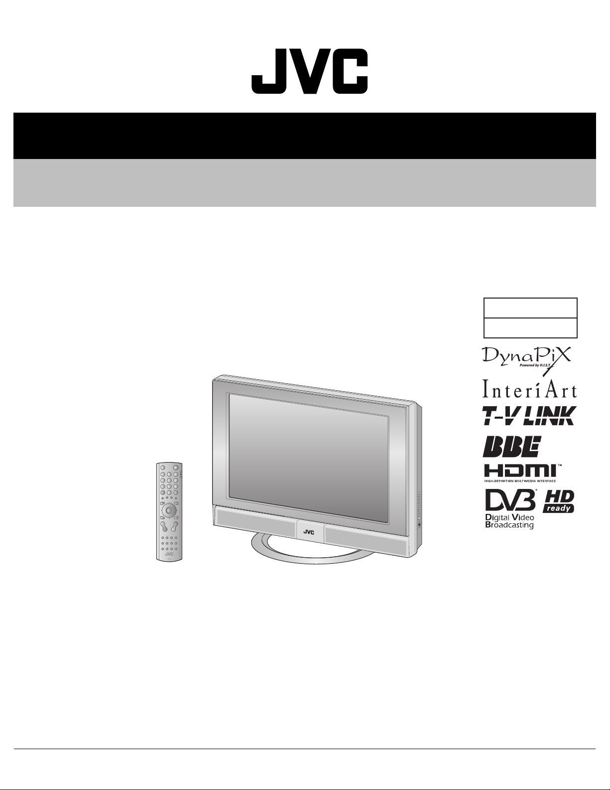
LCD INTEGRATED DIGITAL TV
LT-37DM6ZJ,
LT-37DM6ZJ
/P
BASIC CHASSIS
FL2
TABLE OF CONTENTS
1 PRECAUTION. . . . . . . . . . . . . . . . . . . . . . . . . . . . . . . . . . . . . . . . . . . . . . . . . . . . . . . . . . . . . . . . . . . . . . . . . 1-3
2 SPECIFIC SERVICE INSTRUCTIONS . . . . . . . . . . . . . . . . . . . . . . . . . . . . . . . . . . . . . . . . . . . . . . . . . . . . . . 1-6
3 DISASSEMBLY . . . . . . . . . . . . . . . . . . . . . . . . . . . . . . . . . . . . . . . . . . . . . . . . . . . . . . . . . . . . . . . . . . . . . . 1-11
4 ADJUSTMENT . . . . . . . . . . . . . . . . . . . . . . . . . . . . . . . . . . . . . . . . . . . . . . . . . . . . . . . . . . . . . . . . . . . . . . . 1-18
5 TROUBLESHOOTING . . . . . . . . . . . . . . . . . . . . . . . . . . . . . . . . . . . . . . . . . . . . . . . . . . . . . . . . . . . . . . . . . 1-25
COPYRIGHT © 2005 Victor Company of Japan, Limited
No.YA361
2005/11
Page 2
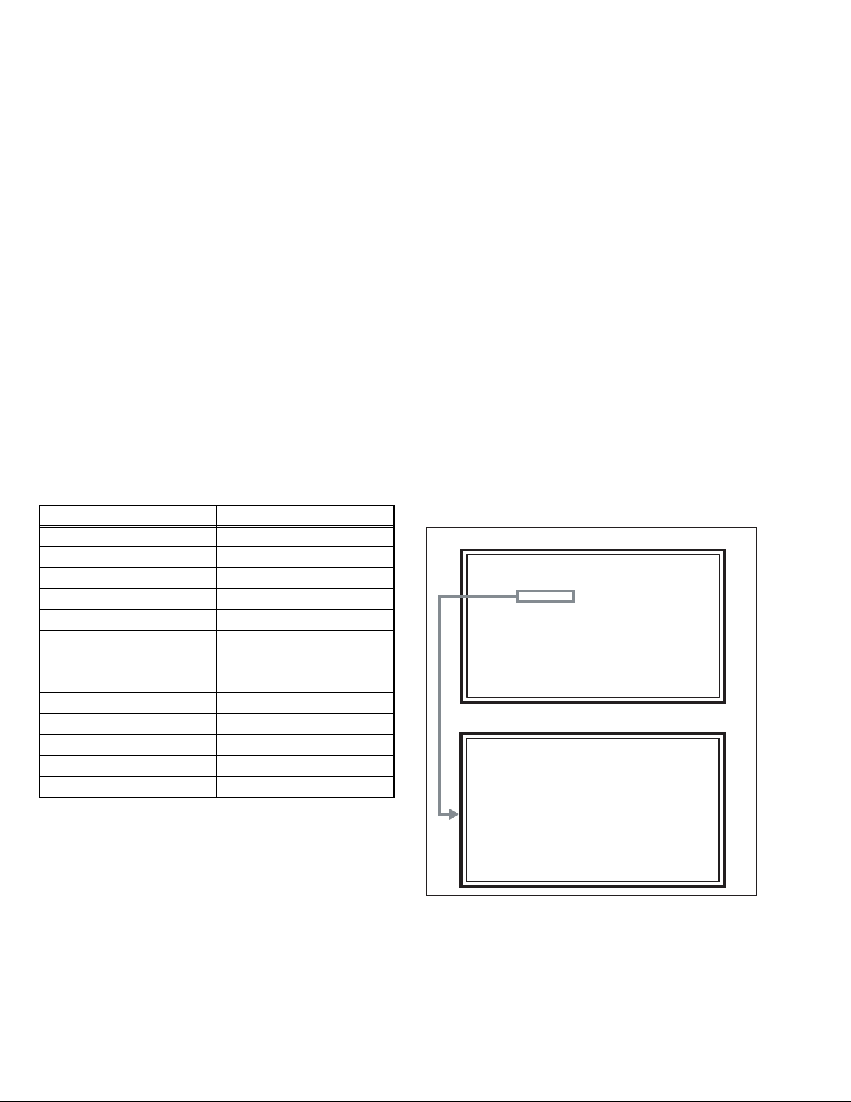
SPECIFICATION
Items Contents
Dimensions ( W × H × D ) 92.6 cm × 68.9 cm × 29.7 cm [Included stand]
92.6 cm × 63.1 cm × 10.8 cm [TV only]
Mass 26.5 kg [Included stand]
21.0 kg [TV only]
Power Input AC110V - AC240 V, 50 Hz / 60 Hz
Power Consumption 171 W (Standby: 2.6 W)
TV RF System Analog
Colour System PAL / NTSC 3.58/4.43 [EXT only]
Stereo System NICAM (I)
Receiving Frequency Analog
Intermediate
Frequency
Colour Sub
Carrier Frequency
Teletext System Analog
LCD panel 37V-inch wide aspect (16 : 9)
Screen Size Diagonal : 94.0 cm (H: 82.6 cm × V: 46.1 cm)
Display Pixels Horizontal : 1366 dots × Vertical : 768 dots (W-XGA)
Audio Power Output 10 W + 10 W
Speaker 6.6 cm, round type × 2 (Oblique corn)
Aerial terminal (VHF/UHF) 75 Ω unbalanced, coaxial
EXT-1 / EXT-2 (Input / Output) 21-pin Euro connector (SCART socket ) × 2
EXT-3 (Input) S-Video
EXT-4 (Input) Component Video
750p / 1125i
625p / 525p / 625i / 525i
HDMI Input Video
PC (RGB) Input D-sub 15 pin × 1
Audio output 500 mV (rms), Low impedance, RCA pin jack × 2
Headphone 3.5 mm stereo mini jack × 1
Remote Control Unit RM-C1813H (AA/R6 dry cell battery × 2)
Design & specifications are subject to change without notice.
CCIR (I)
Digital
DVB-T
UHF: 470 MHz - 862 MHz
Digital
UHF: 474 MHz - 850 MHz
VIF
38.9 MHz (I)
SIF
32.9 MHz (6.0 MHz :I)
PAL
4.43 MHz
NTSC
3.58 MHz / 4.43 MHz
FLOF (Fastext level 2.5), WST(World Standard system)
Digital
MHEG 5 UK profile
Mini-DIN 4 pin × 1
Y: 1 V (p-p), Positive (Negative sync provided), 75 Ω
C: 0.286 V (p-p) (Burst signal), 75 Ω
Video
1 V (p-p), Positive (Negative sync provided), 75 Ω, RCA pin jack × 1
Audio
500 mV (rms), High impedance, RCA pin jack × 2
RCA pin jack × 3
Y : 1 V (p-p) (Sync signal: ±0.35V(p-p), 3-value sync.), 75Ω
Pb/Pr : ±0.35V(p-p), 75 Ω
Y : 1 V (p-p), Positive (Negative sync provided), 75 Ω
Cb/Cr : 0.7V(p-p), 75 Ω
Audio
500 mV(rms) (-4dBs), high impedance, RCA pin jack × 2
HDMI 2-row 19pin connector × 1
(Digital-input terminal is not compatible with picture signals of personal computer)
Audio
Digital: HDMI 2-row 19pin connector × 1
Anarog: 500mV(rms) (-4dBs), high impedance, RCA pin jack × 2
R/G/B : 0.7 V (p-p), 75Ω
HD / VD : 1 V (p-p) to 5 V (p-p), high impedance
< Available signal >
VGA : 640 pixels × 480 pixels (Horizontal : 31.5 kHz / Vertical : 60 Hz)
XGA : 1024 pixels × 768 pixels (Horizontal : 48.4 kHz / Vertical : 60 Hz)
1-2 (No.YA361)
Page 3

SECTION 1
PRECAUTION
1.1 SAFETY PRECAUTIONS
(1) The design of this product contains special hardware and many circuits and components specially for safety purposes. For
continued protection, no changes should be made to the original design unless authorized in writing by the manufacturer.
Replacement parts must be identical to those used in the original circuits. Service should be performed by qualified personnel
only.
(2) Alterations of the design or circuitry of the product should not be made. Any design alterations or additions will void the
manufacturer's warranty and will further relieve the manufacturer of responsibility for personal injury or property damage
resulting therefrom.
(3) Many electrical and mechanical parts in the product have special safety-related characteristics. These characteristics are often
not evident from visual inspection nor can the protection afforded by them necessary be obtained by using replacement
components rated for higher voltage, wattage, etc. Replacement parts which have these special safety characteristics are
identified in the Parts List of Service Manual. Electrical components having such features are identified by shading on the
schematics and by ( ) on the Parts List in the Service Manual. The use of a substitute replacement which does not have the
same safety characteristics as the recommended replacement part shown in the Parts List of Service Manual may cause shock,
fire, or other hazards.
(4) The leads in the products are routed and dressed with ties, clamps, tubing’s, barriers and the like to be separated from live parts,
high temperature parts, moving parts and / or sharp edges for the prevention of electric shock and fire hazard. When service is
required, the original lead routing and dress should be observed, and it should be confirmed that they have been returned to
normal, after re-assembling.
WARNING
(1) The equipment has been designed and manufactured to meet international safety standards.
(2) It is the legal responsibility of the repairer to ensure that these safety standards are maintained.
(3) Repairs must be made in accordance with the relevant safety standards.
(4) It is essential that safety critical components are replaced by approved parts.
(5) If mains voltage selector is provided, check setting for local voltage.
(No.YA361)1-3
Page 4
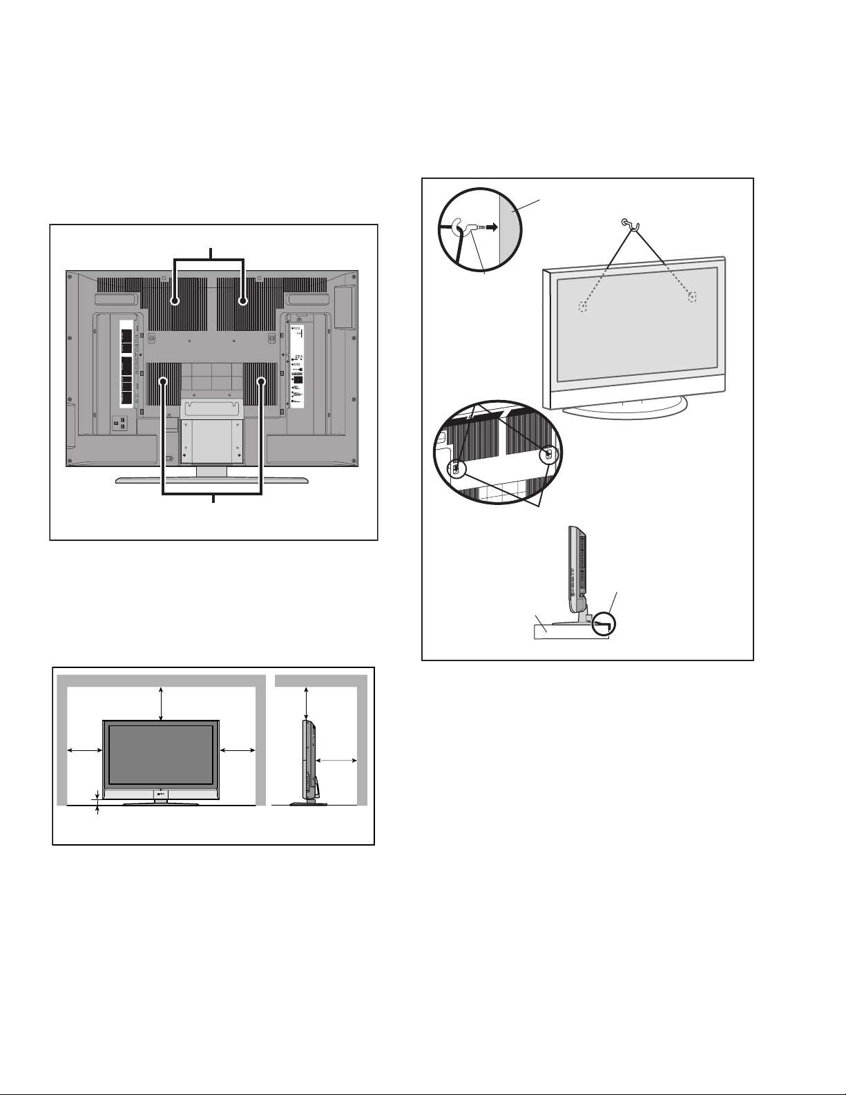
1.2 INSTALLATION
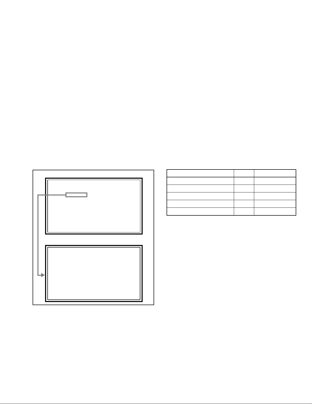
1.2.1 HEAT DISSIPATION
If the heat dissipation vent behind this unit is blocked, cooling
efficiency may deteriorate and temperature inside the unit will
rise. The temperature sensor that protects the unit will be
activated when internal temperature exceeds the pre-determined
level and power will be turned off automatically.Therefore,
please make sure pay attention not to block the heat dissipation
vent as well as the ventilation outlet behind the unit and ensure
that there is room for ventilation around it.
Ventilation hole
1.2.3 INSTALLATION REQUIREMENTS
To ensure safety in an emergency such as an earthquake, and
to prevent accidents, ensure that measures are taken to prevent
the TV dropping or falling over.
Tie commercially available tough cord(s) to the hooks in the back
of the TV, and fix the TV to solid walls or columns.
WALL
HOOK
Ventilation hole
*Diagram differs from actual appearance.
1.2.2 INSTALLATION REQUIREMENTS
Ensure that the minimal distance is maintained, as specified
below, between the unit with and the surrounding walls, as well
as the floor etc.Install the unit on stable flooring or stands.Take
precautionary measures to prevent the unit from tipping in order
to protect against accidents and earthquakes.
䎕䎓䎓䏐䏐䎕䎓䎓䏐䏐
150mm150mm
䎘䎓䏐䏐
*Diagram differs from actual appearance.
䎘䎓䏐䏐
HOOK
It fixes in a band.
TV STAND
*Diagram differs from actual appearance.
1.2.4 NOTES ON HANDLING
(1) WHEN TAKING UNIT OUT OF A PACKING CASE
When taking the unit out of a packing case, do not grasp
the upper part of the unit. If you take the unit out while
grasping the upper part, the LCD PANEL may be damaged
because of a pressure. Instead of grasping the upper part,
put your hands on the lower backside or sides of the unit.
(2) AS FOR PRESSING OR TOUCHING A SPEAKER
Be careful not to press the opening of the speaker in the
lower part of the unit and around them since the decorative
sheet on the surface of the openings may be deformed.
1-4 (No.YA361)
Page 5

1.3 HANDLING LCD PANEL
1.3.1 PRECAUTIONS FOR TRANSPORTATION
When transporting the unit, pressure exerted on the internal LCD
panel due to improper handling (such as tossing and dropping)
may cause damages even when the unit is carefully packed. To
prevent accidents from occurring during transportation, pay
careful attention before delivery, such as through explaining the
handling instructions to transporters.
Ensure that the following requirements are met during
transportation, as the LCD panel of this unit is made of glass and
therefore fragile:
(1) USE A SPECIAL PACKING CASE FOR THE LCD PANEL
When transporting the LCD panel of the unit, use a special
packing case (packing materials). A special packing case
is used when a LCD panel is supplied as a service spare
part.
(2) ATTACH PROTECTION SHEET TO THE FRONT
Since the front (display part) of the panel is vulnerable,
attach the protection sheet to the front of the LCD panel
before transportation. Protection sheet is used when a LCD
panel is supplied as a service spare part.
(3) AVOID VIBRATIONS AND IMPACTS
The unit may be broken if it is toppled sideways even when
properly packed. Continuous vibration may shift the gap of
the panel, and the unit may not be able to display images
properly. Ensure that the unit is carried by at least 2
persons and pay careful attention not to exert any vibration
or impact on it.
(4) DO NOT PLACE EQUIPMENT HORIZONTALLY
Ensure that it is placed upright and not horizontally during
transportation and storage as the LCD panel is very
vulnerable to lateral impacts and may break. During
transportation, ensure that the unit is loaded along the
traveling direction of the vehicle, and avoid stacking them
on one another. For storage, ensure that they are stacked
in 2 layers or less even when placed upright.
1.3.2 OPTICAL FILTER (ON THE FRONT OF THE LCD PANEL)
(1) Avoid placing the unit under direct sunlight over a
prolonged period of time. This may cause the optical filter
to deteriorate in quality and COLOUR.
(2) Clean the filter surface by wiping it softly and lightly with a
soft and lightly fuzz cloth (such as outing flannel).
(3) Do not use solvents such as benzene or thinner to wipe the
filter surface. This may cause the filter to deteriorate in
quality or the coating on the surface to come off. When
cleaning the filter, usually use the neutral detergent diluted
with water. When cleaning the dirty filter, use water-diluted
ethanol.
(4) Since the filter surface is fragile, do not scratch or hit it with
hard materials. Be careful enough not to touch the front
surface, especially when taking the unit out of the packing
case or during transportation.
1.3.3 PRECAUTIONS FOR REPLACEMENT OF EXTERIOR
PARTS
Take note of the following when replacing exterior parts (REAR
COVER, FRONT PANEL, etc.):
(1) Do not exert pressure on the front of the LCD panel (filter
surface). It may cause irregular COLOUR.
(2) Pay careful attention not to scratch or stain the front of the
LCD panel (filter surface) with hands.
(3) When replacing exterior parts, the front (LCD panel) should
be placed facing downward. Place a mat, etc. underneath
to avoid causing scratches to the front (filter surface).
(No.YA361)1-5
Page 6
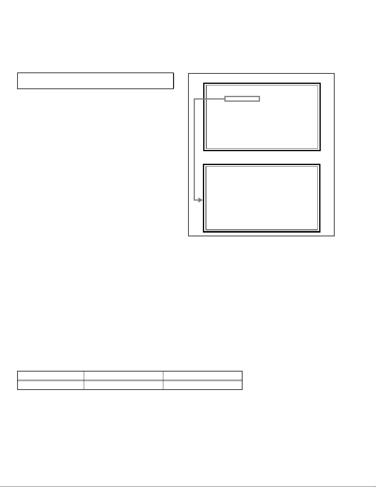
2.1 SYSTEM SETTEING
LOB OK FAN OK
SYNC M:OK S:OK HD:NG
TIM OK
MSM OK DIGI 0000
MEM OK AVSW OK
YC OK AIO OK
TUN OK GCR NG 1
IP OK RGB OK 8
DVI OK HDMI OK
SERVICE MENU
1.ADJUST
2.SELF_CHECK
3.I2C STOP
SECTION 2
SPECIFIC SERVICE INSTRUCTIONS
Be sure to carry out the following operation at the end of
the procedure.
(1) Press the [INFORMATION] key and [MUTING] key
simultaneously, then enter the SERVICE MODE.
(2) When the Main Menu is displayed, press [2] key to enter
the self check mode.
(3) Turn off the power by pressing the [POWER] key on the
remote control unit.
2.2 FEATURES
DVB-T (DIGITAL TERRESTRIAL BROADCASTING)
This TV can receive both Digital terrestrial broadcasting (DVBT) and Analogue terrestrial broadcasting.
D.I.S.T. (Digital Image Scaling Technology)
This system uses line interpolation to double the number of
scanning lines and achieve high resolution, flicker-free picture.
COLOUR MANAGEMENT
This function ensures dull colours are compensated to
produce natural hues.
PICTURE MANAGEMENT
This function makes it easier to see the dark areas when a
picture has many dark areas, and makes it easier to see the
bright areas when a picture has many bright areas.
2.3 MAIN DIFFERENCE LIST
MAIN MENU SCREEN
SERVICE MENU
1.ADJUST
2.SELF_CHECK
3.I2C STOP
SELF CHECK MODE SCREEN
LOB OK FAN OK
SYNC M:OK S:OK HD:NG
TIM OK
MSM OK DIGI 0000
MEM OK AVSW OK
YC OK AIO OK
TUN OK GCR NG 1
IP OK RGB OK 8
DVI OK HDMI OK
ZOOM
This function can change the screen size according to the
picture aspect ratio.
DIGITAL VNR
This function cuts down the amount of noise in the original
picture.
SUPER DIGIPURE
This function uses the latest in digital technology to give you a
natural-looking picture.
MOVIE THEATRE
This function displays a cinema film picture more smoothly and
naturally on the screen.
3D CINEMA SOUND
You can enjoy sounds with a widerambience.
Item LT-37DM6ZJ LT-37DM6ZJ/P
DIGITAL SIGNAL PWB SFL0D231A-U2 LCA10557-64A (SFL-0D231A)
1-6 (No.YA361)
Page 7
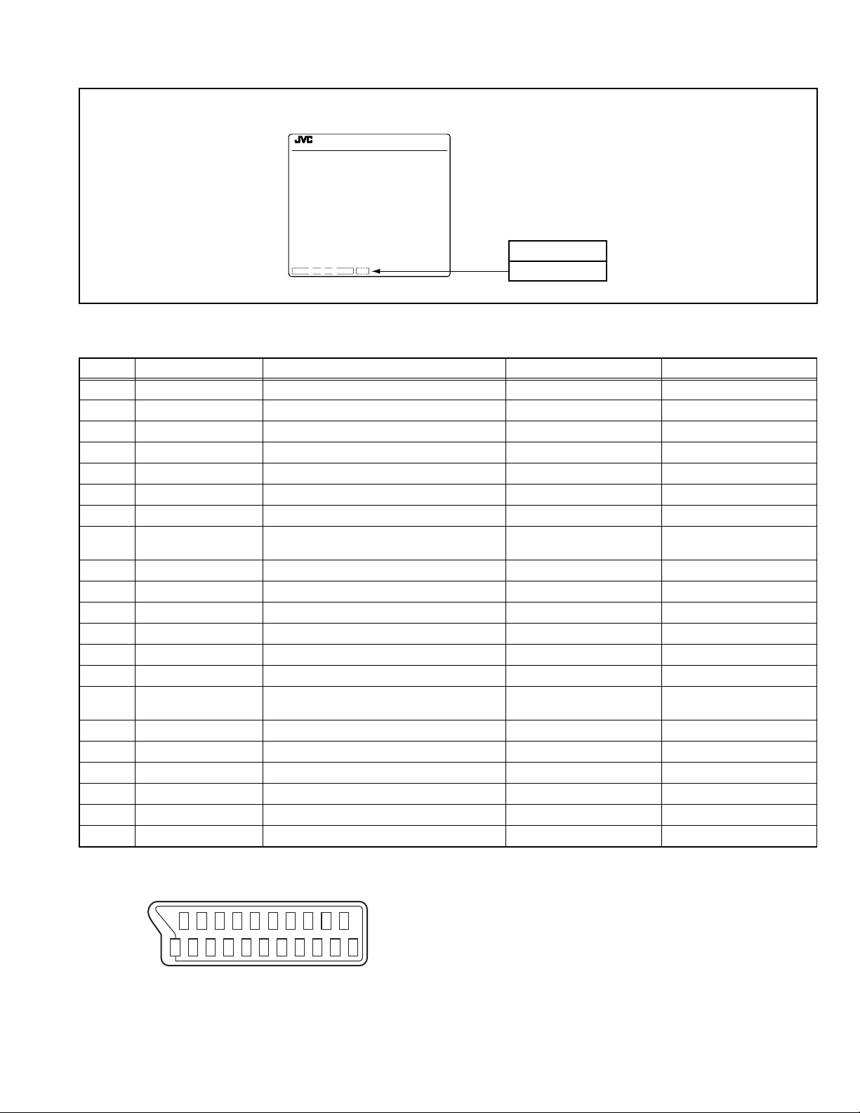
2.4 HOW TO IDENTIFY MODELS
LT-37DM6ZJ : "AE" is added to the serial No. after at the Rating label.
LT-37DM6ZJ/P : "PE" is added to the serial No. after at the Rating label.
MODEL No.
LT-37DM6ZJ
AE
SERIAL NO.
PE
Indicated
2.5 21-PIN EURO CONNECTOR (SCART) : EXT-1 / EXT-2
Pin No. Signal designation Matching value EXT-1 EXT-2
1 AUDIO R output 500mV(rms) (Nominal), Low impedance Used (TV OUT) Used (LINE OUT)
2 AUDIO R input 500mV(rms) (Nominal), High impedance Used (R1) Used (R2)
3 AUDIO L output 500mV(rms) (Nominal), Low impedance Used (TV OUT) Used (LINE OUT)
4 AUDIO GND Used Used
5 GND (B) Used Used
6 AUDIO L input 500mV(rms) (Nominal), High impedance Used (L1) Used (L2)
7 B input 700mV
8 FUNCTION SW
(SLOW SW)
Low : 0V-3V
High : 8V-12V, High impedance
, 75Ω Used Used
(B-W)
Used Used
9 GND (G) Used Used
10 SCL / T-V LINK Not used Used (SCL2 / TV-LINK)
11 G input 700mV
, 75Ω Used Used
(B-W)
12 SDA Not used Used (SDA2)
13 GND (R) Used Used
14 GND (YS) Used Not used
15 R / C input R : 700mV
C : 300mV
(B-W)
(P-P)
, 75Ω
, 75Ω
Used (R) Used (C2/R)
16 Ys input (FAST SW) Low : 0V-0.4V, High : 1V-3V, 75Ω Used Used
17 GND (VIDEO output) Used Used
18 GND (VIDEO input) Used Used
19 VIDEO output 1V
20 VIDEO / Y input 1V
(Negative sync), 75Ω Used (TV OUT) Used (LINE OUT)
(P-P)
(Negative sync), 75Ω Used Used
(P-P)
21 COMMON GND Used Used
(P-P= Peak to Peak, B-W= Blanking to white peak)
[Pin assignment]
20 18 16 14 12 10 8 6 4 2
21 19 17 15 13 11 9 7 5 3 1
(No.YA361)1-7
Page 8

2.6 TECHNICAL INFORMATION
2.6.1 LCD PANEL
This unit uses the flat type panel LCD (Liquid Crystal Display) panel that occupies as little space as possible, instead of the
conventional CRT (Cathode Ray Tube), as a display unit.
Since the unit has the two polarizing filter that are at right angles to each other, the unit adopts "normally black" mode, where light
does not pass through the polarizing filter and the screen is black when no voltage is applied to the liquid crystals.
2.6.1.1 SPECIFICATIONS
The following table shows the specifications of this unit.
Item Specifications
Maximum dimensions ( W × H × D ) 877.0 mm × 514.6 mm × 56.0 mm
Weight 8.5 kg
Effective screen size Diagonal: 940 mm (H: 819.6 mm × V: 460.8 mm)
Aspect ratio 16 : 9
Drive device / system a-Si-TFT active matrix system
Resolution Horizontally 1366 × Vertically 768 × RGB < W-XGA > 3147264 dots in total
Pixel pitch (pixel size) Horizontally: 0.6 mm Vertically: 0.6 mm
Displayed colour 16777216 colours 256 colours for R G and B
Brightness 500 cd/m2
Contrast ratio 1050 : 1
Response time less than 12 ms
View angle Horizontally: 176° Vertically: 176°
Surface polarizer Anti-Glare type Low reflective coat
Colour filter Vertical stripe
Backlight Direct-type Cold cathode fluorescent lamp × 18
Power supply voltage in LCD 5 V
Power supply voltage in inverter 24 V
Panel interface system LVDS (Low Voltage Differential Signaling)
2.6.1.2 PIXEL FAULT
There are three pixel faults - bright fault , dark fault and flicker fault - that are respectively defined as follows.
BRIGHT FAULT
In this pixel fault, a cell that should not light originally is lighting on and off.
For checking this pixel fault, input ALL BLACK SCREEN and find out the cell that is lighting on and off.
DARK FAULT
In this pixel fault, a cell that should light originally is not lighting or lighting with the brightness twice as brighter as originally lighting.
For checking this pixel fault, input 100% of each R/G/B colour and find out the cell that is not lighting.
FLICKER FAULT
In the pixel fault, a cell that should light originally or not light originally is flashing on and off.
For checking this pixel fault, input ALL BLACK SCREEN signal or 100% of each RGB colour and find out the cell that is flashing on
and off.
1-8 (No.YA361)
Page 9
2.6.2 MAIN CPU PIN FUNCTION [IC7501 : DIGITAL SIGNAL PWB]
Pin Pin name I/O Function Pin Pin name I/O Function
1 TCK I Test purpose 65 D2 I/O Program ROM data for main CPU
2 TMS I Test purpose 66 D12 I/O Program ROM data for main CPU
3 TDI I Test purpose 67 D10 I/O Program ROM data for main CPU
4 TDO O Test purpose 68 VSS33 - GND
5 P2.8 O Not used 69 VDD33 I 3.3V
6 P2.9 O Blue for OSD 70 D4 I/O Program ROM data for main CPU
7 P2.10 O Blue for OSD 71 D3 I/O Program ROM data for main CPU
8 P2.11 O Blue for OSD 72 D11 I/O Program ROM data for main CPU
9 P2.12 O Blue for OSD 73 RSTIN I Reset
10 P2.13 O Blue for OSD 74 POWER O Sleep state release for chassis CPU [Relese : L]
11 P2.14 I Not used 75 P3.1 O Not used
12 P2.15 O Request for chassis CPU communication 76 REMOCON I Remote control
13 VSS33 - GND 77 P3.3 I Clock for OSD
14 VDD33 I 3.3V 78 P3.4 O Red for OSD
15 P4.5 O Not used 79 P3.5 O Red for OSD
16 A20 O Program ROM address for main CPU 80 P3.6 O Red for OSD
17 A19 O Program ROM address for main CPU 81 P3.7 O Red for OSD
18 A18 O Program ROM address for main CPU 82 MTST O Data transmission for chassis CPU communication
19 A17 O Program ROM address for main CPU 83 MTSR I Data receive for chassis CPU communication
20 VSS25 - GND 84 VSS33 - GND
21 VDD25 I 2.5V 85 VDD33 I 3.3V
22 A16 O Program ROM address for main CPU 86 VSS25 - GND
23 A8 O Program ROM address for main CPU 87 VDD25 I 2.5V
24 A7 O Program ROM address for main CPU 88 TXD0 O Communication for adjustment
25 A9 O Program ROM address for main CPU 89 RXD0 O Communication for adjustment
26 A6 O Program ROM address for main CPU 90 P3.12 O Red for OSD
27 A5 O Program ROM address for main CPU 91 CLK O Clock for chassis CPU communication
28 A10 O Program ROM address for main CPU 92 P3.15 O Green for OSD
29 A11 O Program ROM address for main CPU 93 P5.14 O Green for OSD
30 A12 O Program ROM address for main CPU 94 P5.15 O Green for OSD
31 VSS33 - GND 95 TRIG_IN O Green for OSD
32 VDD33 I 3.3V 96 TRIG_OUT O Green for OSD
33 A4 O Program ROM address for main CPU 97 P6.2 O Green for OSD
34 A3 O Program ROM address for main CPU 98 P6.3 O I
35 A2 O Program ROM address for main CPU 99 P6.4 I/O I
36 A1 O Program ROM address for main CPU 100 P6.5 O Teletext signal select [Analog RGB : H / Digital RGB : L]
37 A0 O Program ROM address for main CPU 101 IRQ O Not used
38 A13 O Program ROM address for main CPU 102 VSYNC I Vertical sync
39 ARAS/A14 O Program ROM address for main CPU 103 HSYNC I Horizontal sync
40 CAS/A15 O Program ROM address for main CPU 104
41 VSS33 - GND 105 BLANK O Ys for OSD / Teletext
42 VDD33 I 3.3V 106 VDD33 I 3.3V
43 MEMCLK O Clock for memory 107 VSS33 - GND
44 CSSDRAM O Chip select for memory 108 XTAL1 I 6MHz for system clock
45 CLKEN O Clock enable for memory 109 XTAL2 O 6MHz for system clock
46 CSROM O Chip select for memory 110 VSSA - GND
47 RD O Read for memory 111 VDDA I 2.5V
48 UDQM O Control buffer of memory 112 R O R for OSD / Teletext
49 LDQM O Control buffer of memory 113 G O G for OSD / Teletext
50 WR O Write for memory 114 B O B for OSD / Teletext
51 D15 I/O Program ROM data for main CPU 115 VSSA - GND
52 VSS33 - GND 116 VDDA I 2.5V
53 VDD33 I 3.3V 117 CVBS2 I Video for Teletext
54 D7 I/O Program ROM data for main CPU 118 VSSA - GND
55 D0 I/O Program ROM data for main CPU 119 VDDA I 2.5V
56 D14 I/O Program ROM data for main CPU 120 CVBS1B I Video for Teletext
57 D8 I/O Program ROM data for main CPU 121 CVBS1A I Video for Teletext
58 D6 I/O Program ROM data for main CPU 122 VSSA - GND
59 D1 I/O Program ROM data for main CPU 123 VDDA I 2.5V
60 VSS33 - GND 124 KEY1 I Key scan data 1 [ON : H]
61 VDD33 I 3.3V 125 KEY2 I Key scan data 2 [ON : H]
62 D13 I/O Program ROM data for main CPU 126 MECA_SW I Main power ON / OFF control [ON : L]
63 D9 I/O Program ROM data for main CPU 127 P5.3 I Not used
64 D5 I/O Program ROM data for main CPU 128 TMODE I Test purpose
COR/RSTOUT
2
C bus clock (for main memory)
2
C bus Data (for main memory)
O Not used
(No.YA361)1-9
Page 10
2.6.3 SUB (CHASSIS) CPU PIN FUNCTION [IC7001 : DIGITAL SIGNAL PWB]
Pin Pin name I/O Function Pin Pin name I/O Function
1 LB_PRO O Not used 51 BS_TXD O
2 P_MU O Picture muting [Muting = H] 52 BS_RXD I Data receive for digital tuner communication
3 JP_CSB O Not used (NC) 53 NC O Not used (NC)
4 A_MU O Audio muting [Muting = H] 54 VREF+ I 3.3V power supply
5 M_MU O Audio muting (for AUDIO OUT) [Muting = H] 55 PDP_TX O
6 PC_SEL O RGB(PC) INPUT select 56 PDP_RX I Data receive for SUB (DRIVE) CPU communication
7 ON_TIMER O POWER INDICATOR (LED) brightness [LOW = L] 57 SDA0 I/O Data for Inter IC (serial) bus : EEP-ROM (IC7002)
8 ILA0 O LCD back light lighting 58 SCL0 O Clock for Inter IC (serial) bus : EEP-ROM (IC7002)
9 ILA1 O LCD panel overshoot refresh timing 59 SDA_DVI I/O
10 ILA2 O Not used 60 SCL_DVI O
11 POW_LED O POWER LED lighting [ON = H] 61 AVSS - GND
12 WORD O Not used 62 DIGII_PHOT I Photo sensor for DIGITAL-IN illegal copy protection
13 MI_CK I Clock for main CPU communication 63 AGC I Not used
14 MI_TX I Data receive for main CPU communication 64 EXT_YS1 I Not used
15 MI_RX O Data transmission for MAIN CPU communication 65 EXT_YS2 I Not used
16 MI_REQ O
17 VDD I 3.3V power supply 67 DIGI_PRO O Not used : For DIGITAL-IN (HDMI)
18 FOSC O Not used (NC) 68 GCR_RST O Not used (NC)
19 VSS - GND 69 GR_ON O Not used (NC)
20 X1 I Not used : Low speed oscillatior 70 SYNC_SEL O Not used : Sync select for digital tuner
21 X0 O Not used : Low speed oscillatior 71 NC O Not used (NC)
22 VDD I 3.3V power supply 72 NC O Not used (NC)
23 OSC1 I System clock osillation (crystal) : 16MHz 73 SBD5 I/O
24 OSC0 O System clock osillation (crystal) : 16MHz 74 SBT5 I
25 MODE I Single chip mode 75 NMI I 3.3V power supply
26 BS1.5CTL O Not used : Digital tuner power / reset control 76 COMP I Not used : AV COMPULINK lll control
27 A92RES O
28 BS_RST O Reset for Digital tuner power / reset control 78 VSYNC I V. sync pulse
29 LIP_RST O Not used : Reset for Sound delay (Lip sync) 79 WAKE I Reset for sub(chassis) CPU
30 SOFT_OFF O Not used 80
31 VMUTE I Picture muting request from digital tuner 81 NC O Not used (NC)
32 VOUTENB O Video cutoff for digital tuner 82 RST I Reset for MAIN CPU [Reset = L]
33 MDR_CON I Not used: System cable connection monitor for PDP 83 VDD I 3.3V power supply
34 AVDD I 3.3V power supply 84 SCL3A O Clock for Inter IC (serial) bus control
35 BS_POW O Not used : Digital tuner power control 85 SDA3A I/O Data for Inter IC (serial) bus control
DsyncSW2
36
37 LB_POW O Power control for low bias line 87 SDA3B I/O Data for Inter IC (serial) bus control
38 NC O Not used (NC) 88
39 HOTPLUG I
40 MECA_SW I Mechanical monitor for POWER switch [Push = L] 90 DIGI_INT I Reset for HDMI process [Reset = L ]
41 MAIN_POW O Main power control [ON = L] 91 DVI_RST O Not used : Reset for DVI format conversion
42 MSP_RST O AUDIO OUT output mode select [VARIABLE = L] 92 VSS - GND
43 VREF- I Not used 93 SCL5055 O
44 AFT2 I Not used : AFT voltage for sub tuner 94
45 AFT1 I AFT voltage for VHF/UHF tuner 95 SDA5055 I/O Data for Inter IC (serial) bus : JCC5055 (DIST process)
46 KEY2 I Key scan data for front switch (MENU/CH+/CH-) 96
47 KEY1 I Key scan data for front switch (VOL+/VOL-) 97 NC O Not used (NC)
48 NC O Not used (NC) 98 15K/OTH O Main video select [Fixed = H]
49 NC O Not used (NC) 99 DsyncSW1 O Sync select for DIGITAL-IN [Cotrolled with 36-pin]
50 AC_IN I Not used : AC 50/60Hz detect 100 57 BUSY I Busy monitor for IC4001 (New DIST process)
Data request for main CPU communication [Request = L]
Reset for IC1001(3D YC SEP / COLOUR DEMODULAT) [Reset = H]
O Sync select for DIGITAL-IN [Cotrolled with 99-pin] 86 SCL3B O Clock for Inter IC (serial) bus control
Not used : Video communiation monitor for receiver unit (PDP)
66 VDD I 3.3V power supply
77 REMO I Remote control
POWERGOOD
DIGI_SYNCSEL
89 DIGI_LRSW O Not used : For DIGITAL-IN (HDMI)
VFORMATSEL
OSD_MODE_SEL
Data transmission for digital tuner communication
Data transmission for SUB (DRIVE) CPU communication
Not used : Data for Inter IC (serial) bus for panel communication
Not used : Clock for Inter IC (serial) bus for panel communication
Not used : Data for writing on board (connect CN01P : for Frash ROM type)
Not used : Clock for writing on board (connect CN01P : for Frash ROM type)
I Power error detection [NG = H]
O Not used
Clock for Inter IC (serial) bus : JCC5055 (DIST process)
O Digital tuner clock control
O Not used : OSD mode select
1-10 (No.YA361)
Page 11

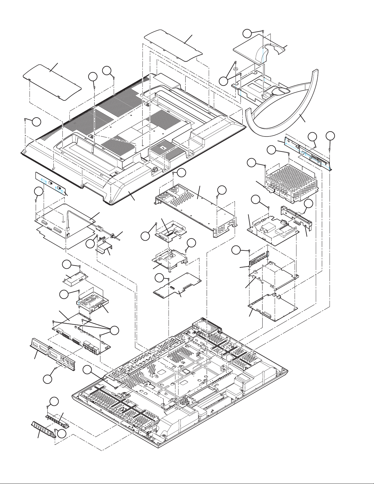
SECTION 3
DISASSEMBLY
3.1 DISASSEMBLY PROCEDURE
CAUTION AT DISASSEMBLY:
• Be sure to perform the SYSTEM SETTEING, at the end of the procedure.
• Make sure that the power cord is disconnected from the outlet.
• Pay special attention not to break or damage the parts.
• When removing each board, remove the connectors as required. Taking notes of the connecting points (connector numbers)
makes service procedure manageable.
• Make sure that there is no bent or stain on the connectors before inserting, and firmly insert the connectors.
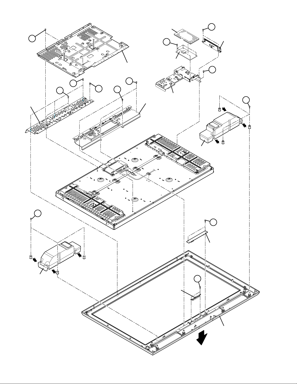
3.1.1 REMOVING THE STAND (Fig.1)
(1) Remove the 2 screw [A], then remove the STAND
COVER.
(2) Remove the 4 screws [B], then remove the STAND.
3.1.2 REMOVING THE REAR COVER (Fig.1)
• Remove the STAND.
(1) Remove the JACK COVER (L/R).
(2) Remove the 10 screws [C], the 3 screws [D], and the 2
screws [E].
(3) Remove the REAR COVER.
3.1.3 REMOVING THE REGULATOR PWB (Fig.1)
• Remove the STAND.
• Remove the REAR COVER.
(1) Remove the 4 screws [F], then remove the FAN
BRACKET.
(2) Remove the 1 screw [G], then remove the POWER CORD
HOLDER.
(3) Remove the POWER CORD from the POWER PWB.
(4) Remove the REGULATOR PWB.
3.1.4 REMOVING THE POWER PWB (Fig.1)
• Remove the STAND.
• Remove the REAR COVER.
• Remove the FAN BRACKET.
(1) Remove the 4 screw [H], then remove the POWER PWB.
3.1.5 REMOVING THE PANEL I/F PWB (Fig.1)
• Remove the STAND.
• Remove the REAR COVER.
• Remove the FAN BRACKET.
(1) Remove the 4 screws [J], then remove the PANEL I/F
PWB.
3.1.6 REMOVING THE ANALOG SYGNAL PWB (Fig.1)
• Remove the STAND.
• Remove the REAR COVER.
• Remove the FAN BRACKET.
(1) Remove the 3 screws [K], then remove the TERMINAL
BASE.
(2) Remove the 4 screws [L], then remove the PANEL I/F
PWB BRACKET.
(3) Remove the 3 screws [M] and 2screw [N], then remove the
ANALOG SIGNAL PWB.
3.1.7 REMOVING THE FRONT CONTROL PWB (Fig.1)
• Remove the STAND.
• Remove the REAR COVER.
(1) Remove the 3 screws [P], then remove the CONTROL
ASSY with the FRONT CONTROL PWB.
(2) Remove the FRONT CONTROL PWB.
3.1.8 REMOVING THE RECEIVER PWB (Fig.1)
• Remove the STAND.
• Remove the REAR COVER.
(1) Remove the 3 screws [Q] and the 1 screw [R], then remove
the TUNER BASE.
(2) Remove the 4 screws [S], then remove the RECEIVER PWB.
3.1.9 REMOVING THE CONNECTOR PWB (Fig.1)
• Remove the STAND.
• Remove the REAR COVER.
• Remove the TOP SHIELD CASE.
(1) Remove the 4 screws [T], then remove the RECEIVER
PWB BRACKET.
(2) Remove the 1 screw [U], then remove the CONNECTOR PWB.
3.1.10 REMOVING THE DIGITAL TUNER UNIT (Fig.1)
• Remove the STAND.
• Remove the REAR COVER.
• Remove the TUNER BASE.
(1) Remove the 7 screws [V] and the 3 screws [W], then
remove the SHIELD COVER.
(2) Remove the 2 screws [X] , then remove the SIDE SHIELD
CASE.
(3) Remove the 5 screws [Y], then remove the DIGITAL
TUNER UNIT.
3.1.11 REMOVING THE DIGITAL SIGNAL PWB (Fig.1)
• Remove the STAND.
• Remove the REAR COVER.
• Remove the TUNER BASE.
• Remove the DIGITAL TUNER UNIT.
(1) Remove the 5 screws [Z], then remove the DIGITAL
BRACKET.
(2) Remove the DIGITAL SIGNALPWB.
CAUTION :
Make sure to perform the "SYSTEM SETTEING", when
DIGITAL SIGNAL PWB is replaced.
(No.YA361)1-11
Page 12
JACK COVER
JACK COVER
A
STAND COVER
E
D
B
C
H
J
PANEL I/F PWB
L
ANALOG SIGNAL PWB
REGULATOR PWB
G
POWER PWB
POWER CORD
POWER CORD
HOLDER
PANEL I/F PWB
BRACKET
M
REAR COVER
S
RECEIVER PWB
BRACKET
RECEIVER PWB
U
CONNECTOR PWB
F
FAN BRACKET
T
SHIELD COVER
F
DIGITAL
TUNER UNIT
Z
TOP SHIELD CASE
DIGITAL BRACKET
DIGITAL SIGNAL PWB
TUNER BASE
W
V
Y
STAND
X
SIDE
SHIELD
CASE
Q
R
TERMINAL BASE
K
P
CONTROL
ASSY
1-12 (No.YA361)
N
FRONT
CONTROL
PWB
P
Fig.1
Page 13

3.1.12 REMOVING THE SPEAKER (Fig.2)
• Remove the STAND.
• Remove the REAR COVER.
(1) Remove the 6 screws [A], then remove the SPEAKER (L /R).
NOTE:
• Since the speaker is attached in a certain direction, attach
the speaker in the same correct direction as it has been
attached.
• When the speaker is decomposed, the performance cannot
be kept.
3.1.13 REMOVING THE FRONT LED PWB (Fig.2)
• Remove the STAND.
• Remove the REAR COVER.
• Remove the FAN BRACKET.
(1) Remove the 2 screws [B], then remove the FRONT LED
PWB.
3.1.14 REMOVING THE LED LENS (Fig.2)
• Remove the STAND.
• Remove the REAR COVER.
• Remove the FAN BRACKET.
• Remove the FRONT LED PWB.
(1) Remove the 2 screws [C], then remove the LED LENS.
3.1.15 REMOVING THE CARD PWB (Fig.2)
• Remove the STAND.
• Remove the REAR COVER.
(1) Remove the CARD SHIELD.
(2) Remove the 4 screws [D], then remove the CARD PWB.
3.1.16 REMOVING THE LCD PANEL UNIT (Fig.2)
• Remove the STAND.
• Remove the REAR COVER.
• Remove the FAN BRACKET.
(1) Remove the 2 screws [E], then remove the CARD BASE.
(2) Remove the 2 screws [F], then remove the CARD PWB
BRACKET.
(3) Remove the 2 screws [G], then remove the MAIN BASE.
(4) Remove the 3 screws [H], the 2 screws [J] and the 1 screw
[K], then remove the TOP FRAME.
(5) Remove the 2 screws [L] and the 2 screws [M], then
remove the BOTTOM FRAME.
(6) Remove the LCD PANEL UNIT from the FRONT PANEL.
NOTE:
• Pay special attention not to break or damage on the FRONT
PANEL.
• The LCD PANEL UNIT is fixed to the FRONT PAMEL (at the
back side)by using double-side adhesive tapes. To remove
the LCD PANEL UNIT, remove the adhesive tape on the
FRONT PANEL slowly.
(No.YA361)1-13
Page 14
CARD SHIELD
E
G
TOP FRAME
D
CARD PWB
MAIN BASE
CARD BASE
F
H
J
K
L
M
CARD PWB BRACKET
BOTTOM FRAME
SPEAKER
A
A
SPEAKER
B
FRONT LED PWB
C
LED LENS
FRONT PANEL
FRONT
1-14 (No.YA361)
Fig.2
Page 15
3.2 MEMORY IC REPLACEMENT
S001 PREPARE 0
PAL50 FULL STD H
SERVICE MENU
1.ADJUST
2.SELF_CHECK
3.I2C STOP
• This model uses the memory IC.
• This memory IC stores data for proper operation of the video and drive circuits.
• When replacing, be sure to use an IC containing this (initial value) data.
3.2.1 MEMORY IC REPLACEMENT PROCEDURE
1. Power off
Switch off the power and disconnect the power plug from the AC outlet.
2. Replace the memory IC
Be sure to use the memory IC written with the initial setting values.
3. Power on
Connect the power plug to the AC outlet and switch on the power.
4. Receiving channel setting
Refer to the OPERATING INSTRUCTIONS and set the receive channels (Channels Preset) as described.
5. User setting
Check the user setting items according to the given in page later. Where these do not agree, refer to the OPERATING
INSTRUCTIONS and set the items as described.
6. SERVICE MODE setting
Verify what to set in the SERVICE MODE, and set whatever is necessary (Fig.1). Refer to the SERVICE ADJUSTMENT for setting.
3.2.2 SERVICE MODE SETTING
SERVICE MODE SCREEN
MAIN MENU SCREEN
SETTING ITEM
Setting items Settings Item No.
Video system setting Adjust S001 - S039
SERVICE MENU
1.ADJUST
2.SELF_CHECK
3.I2C STOP
Audio system setting Fixed T001 - T010
Panel control system setting Fixed P001 - P010
Drive system setting Fixed D001 - D187
Main CPU system setting Fixed Z001 - Z010
ADJUSTMENT MODE SCREEN
S001 PREPARE 0
PAL50 FULL STD H
Fig.1
(No.YA361)1-15
Page 16
3.2.3 SETTINGS OF FACTORY SHIPMENT
3.2.3.1 BUTTON OPERATION 3.2.3.2 REMOTE CONTROL DIRECT OPERATION
Setting item Setting position
POWER Off
CHANNEL PR1
VOLUME 10
TV/AV TV
3.2.3.3 REMOTE CONTROL MENU OPERATION
(1) PICTURE
Setting item Setting position
PICTURE MODE BRIGHT
COLOUR TEMP. COOL
FEATURES
DIGITAL VNR AUTO (LOW)
Super DigiPure AUTO
MOVIE THEATRE AUTO
COLOUR MANAGEMENT ON
PICTURE MANAGEMENT ON
COLOUR SYSTEM TV Depends on PR/CH
EXT AUTO
4:3 AUTO ASPECT PANORAMIC
(2) SOUND
Setting item Setting position
STEREO / I•II Stereo sound
BASS Centre
TREBLE Centre
BALANCE Centre
3D SOUND OFF
A.H.B. ON
BBE ON
CHANNEL PR1
VOLUME 10
ZOOM PANORAMIC
3D SOUND OFF
(4) FEATURES
SLEEP TIMER OFF
CHILD LOCK ID NO.0000, All CH off
APPEARANCE TYPE D
BLUE BACK ON
FAVOURITE SETTING Reset
ILLUMINATION BRIGHT
(5) SET UP
AUTO PROGRAM TV channel automatically set
EDIT/MANUAL PRESET CH only
LANGUAGE ENGLISH
DECODER (EXT-2) OFF
COMPONENT AUTO SELECT ON
HDMI SETTING AUTO
ATTENUATOR OFF
EXT SETTING
S-IN BLANK
ID BLANK
DUBBING EXT-1 → EXT-2
(6) DTV
Timers
Name ∗∗∗∗
Start 00:00
End 00:00
Date 01/01/2004
Mode Inactive
Configuration
Audio Language English
Subtitle English
Favourite Mode off
Receiver Upgrade V.∗.∗
Menu Lock Disabled
Setting item Setting position
Setting item Setting position
Setting item Setting position
Setting item Setting position
1-16 (No.YA361)
Page 17
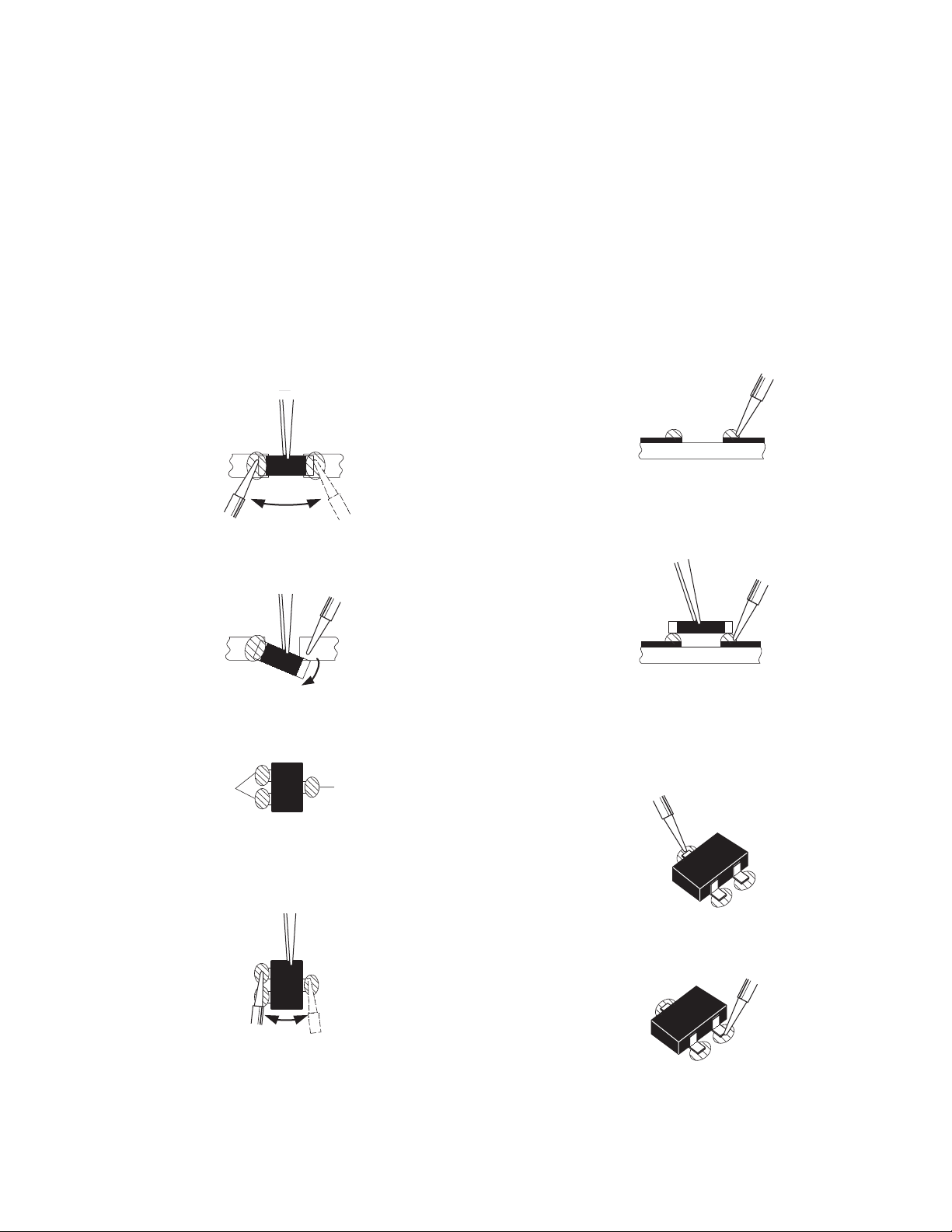
3.3 REPLACEMENT OF CHIP COMPONENT
3.3.1 CAUTIONS
(1) Avoid heating for more than 3 seconds.
(2) Do not rub the electrodes and the resist parts of the pattern.
(3) When removing a chip part, melt the solder adequately.
(4) Do not reuse a chip part after removing it.
3.3.2 SOLDERING IRON
(1) Use a high insulation soldering iron with a thin pointed end of it.
(2) A 30w soldering iron is recommended for easily removing parts.
3.3.3 REPLACEMENT STEPS
1. How to remove Chip parts
2. How to install Chip parts
[Resistors, capacitors, etc.]
(1) As shown in the figure, push the part with tweezers and
alternately melt the solder at each end.
(2) Shift with the tweezers and remove the chip part.
[Transistors, diodes, variable resistors, etc.]
(1) Apply extra solder to each lead.
SOLDER
SOLDER
[Resistors, capacitors, etc.]
(1) Apply solder to the pattern as indicated in the figure.
(2) Grasp the chip part with tweezers and place it on the
solder. Then heat and melt the solder at both ends of the
chip part.
[Transistors, diodes, variable resistors, etc.]
(1) Apply solder to the pattern as indicated in the figure.
(2) Grasp the chip part with tweezers and place it on the
solder.
(3) First solder lead A as indicated in the figure.
(2) As shown in the figure, push the part with tweezers and
alternately melt the solder at each lead. Shift and remove
the chip part.
NOTE :
After removing the part, remove remaining solder from the
pattern.
A
B
C
(4) Then solder leads B and C.
A
B
C
(No.YA361)1-17
Page 18
SECTION 4
SERVICE MENU
1.ADJUST
2.SELF_CHK
3.I2C STOP
S001 PREPARE 0
PAL50 FULL STD H
ADJUSTMENT
4.1 ADJUSTMENT PREPARATION
(1) There are 2 ways of adjusting this TV : One is with the
REMOTE CONTROL UNIT and the other is the
conventional method using adjustment parts and
components.
(2) The adjustment using the REMOTE CONTROL UNIT is
made on the basis of the initial setting values. The
setting values which adjust the screen to the optimum
condition can be different from the initial setting
values.
(3) Make sure that connection is correctly made AC to AC
power source.
(4) Turn on the power of the TV and measuring instruments for
warming up for at least 30 minutes before starting
adjustments.
(5) If the receive or input signal is not specified, use the most
appropriate signal for adjustment.
(6) Never touch the parts (such as variable resistors,
transformers and condensers) not shown in the adjustment
items of this service adjustment.
4.2 PRESET SETTING BEFORE ADJUSTMENTS
Unless otherwise specified in the adjustment items, preset the
following functions with the REMOTE CONTROL UNIT.
Setting item Settings position
PICTURE MODE STANDARD
PICTURE adjustments Centre
COLOUR TEMP. NORMAL
DIGITAL VNR AUTO (LOW)
Super DigiPure AUTO
MOVIE THEATRE AUTO
COLOUR MANAGEMENT ON
PICTURE MANAGEMENT ON
SOUND adjustments Centre
BBE OFF
3D SOUND OFF
A.H.B OFF
ZOOM FULL
4.3 MEASURING INSTRUMENT AND FIXTURES
• Oscilloscope
• Signal generator (Pattern generator)
[PAL / 625i / 625p / 1125i(50Hz)]
• Remote control unit
4.4 ADJUSTMENT ITEMS
VIDEO CIRCUIT
• 625i A-D OFFSET adjustment
• 1125i(50Hz) BRIGHTNESS adjustment
• 1125i(50Hz) A-D OFFSET adjustment
• SUB SCREEN A-D OFFSET adjustment
• WHITE BALANCE (HIGH LIGHT) adjustment
4.5 BASIC OPERATION OF SERVICE MODE
4.5.1 HOW TO ENTER THE SERVICE MODE
(1) Press [INFORMATION] key and [MUTING] key on the
remote control unit simultaneously to enter the SERVICE
MODE SCREEN.
(2) In the SERVICE MENU, press the [1] key to display
ADJUSTMENT MODE SCREEN.
NOTE:
• Before entering the SERVICE MODE, confirm that the
setting of VCR/TV/DVD switch is at the "TV" side. If the
switches have not been properly set, you cannot enter the
SERVICE MODE.
• When a number key other than the [1] key is pressed in the
SERVICE MODE SCREEN, the other relevant screen may
be displayed.
This is not used in the adjustment procedure. Press the
[MENU] key to return to the SERVICE MODE SCREEN.
SERVICE MODE SCREEN
SERVICE MENU
1.ADJUST
2.SELF_CHK
3.I2C STOP
ADJUSTMENT MODE SCREEN
S001 PREPARE 0
PAL50 FULL STD H
1-18 (No.YA361)
4.5.2 HOW TO EXIT THE SERVICE MODE
Press the [MENU] key to exit the Service mode.
Page 19
4.5.3 DESCRIPTION OF STATUS DISPLAY
S001 PREPARE 0
PAL50 FULL STD H
SETTING VALUE (DATA)SETTINGITEM No. SETTING ITEM
S001 PREPARE 0
PAL50 FULL STD H
SIGNAL SYSTEM
ZOOM MODE
PICTURE MODE
COLOUR TEMP.
(1) SIGNAL SYSTEM
The signal displayed on the screen is displayed.
PAL50 : PAL50Hz (Composite / S-video)
PAL60 : PAL60Hz (Composite / S-video)
SECAM : SECAM
NTSC3 : NTSC3.58
NTSC4 : NTSC4.43
525I : 525i (Component)
525P : 525p
625I : 625i (Component)
625P : 625p
1125I5 : 1125i 50Hz
1125I6 : 1125i 60Hz
RGB5 : RGB 525i
RGB6 : RGB 625i
PCVGA : PC (VGA)
PCXGA : PC (XGA)
H525I : HDMI 525i
H525P : HDMI 525p
H625I : HDMI 625i
H625P : HDMI 625p
H750P : HDMI 750p
H125I5 : HDMI 1125i 50Hz
H125I6 : HDMI 1125i 60Hz
(2) ZOOM MODE
State of the SCREEN SIZE or MULTI PICTURE is displayed.
SINGLE SCREEN
FULL : FULL
PANO : PANORAMIC
1609 : 16:9 ZOOM
1609S : 16:9 ZOOM SUBTITLE
1409 : 14:9 ZOOM
REGU : REGULAR
MULTI SCREEN
M2 : 2-pictures multi
M12 : 12-pictures multi
(3) PICTURE MODE
STD : STANDARD
BRI : BRIGHT
SOFT : SOFT
(4) COLOUR TEMP.
H : COOL
M : NORMAL
L: WARM
(5) SETTING ITEM NAME
Setting item name are displayed. The setting item numbers to
be displayed are listed below.
Item No. Setting item
S001 to S039 Video system setting
T001 to T010 Audio system setting
P001 to P010 Panel control system setting
D001 to D187 Drive system setting
Z001 to Z010 Main CPU system setting
(6) SETTING ITEM NO.
Setting item numbers are displayed. For the setting item
names to be displayed, refer to "INITIAL SETTING VALUES
IN THE SERVICE MODE".
(7) SETTING VALUE (DATA)
The SETTING VALUE is displayed.
4.5.4 CHANGE AND MEMORY OF SETTING VALUE
SELECTION OF SETTING ITEM
• [FUNCTION /] key.
For scrolling up / down the setting items.
S001... ↔ T001... ↔ P001... ↔ D001... ↔ Z001...
CHANGE OF SETTING VALUE (DATA)
• [FUNCTION /] key.
For scrolling up / down the setting values.
MEMORY OF SETTING VALUE (DATA)
Changed setting value is memorized by pressing [MUTING]
key.
4.5.5 SERVICE MODE SELECT KEY LOCATION
MUTING
NUMBER
VCR/TV/DVD
switch
INFORMATION
MENU
FUNCTION /
FUNCTION /
(No.YA361)1-19
Page 20
4.6 INITIAL SETTING VALUES IN THE SERVICE MODE
• Perform fine-tuning based on the "initial values" using the remote control when in the Service mode.
• The "initial values" serve only as an indication rough standard and therefore the values with which optimal display can be achieved
may be different from the default values. But, don't change the values that are not written in "ADJUSTMENT PROCEDURE". They
are fixed values.
4.6.1 VIDEO SYSTEM SETTING 4.6.2 AUDIO SYSTEM SETTING (*Fixed values)
Item No. Item name Variable range Setting value
S001 PREPARE 0 - 31 0
S002 NTSC BL 0 - 15 0
S003 NTSC CNT 0 - 255 53
S004 NT CR OF 0 - 15 6
S005 NT CB OF 0 - 15 6
S006 525i BL 0 - 15 0
S007 525i CNT 0 - 255 53
S008 5i CB OF 0 - 15 0
S009 5i CR OF 0 - 15 0
S010 5i CR GN 0 - 15 6
S011 5i CB GN 0 - 15 6
S012 HD BL 0 - 63 62
S013 HD CB OF 0 - 63 59
S014 HD CR OF 0 - 63 57
S015 RT CONT 0 - 15 8
S016 RT CB OF 0 - 15 6
S017 RT CR OF 0 - 15 6
S018 RT CL GA 0 - 15 1
S019 PC CL MB 0 - 7 0
S020 PC CL LB 0 - 31 0
S021 PC CL MR 0 - 71 0
S022 PC CL LR 0 - 31 0
S023 (Not display) 0 - 255 0
S024 (Not display) 0 - 255 0
S025 (Not display) 0 - 255 0
S026 (Not display) 0 - 255 0
S027 (Not display) 0 - 255 0
S028 (Not display) 0 - 255 0
S029 (Not display) 0 - 255 0
S030 R DRIVE 0 - 255 133
S031 G DRIVE 0 - 255 106
S032 B DRIVE 0 - 255 72
S033 (Not display) 0 - 255 0
S034 (Not display) 0 - 255 0
S035 (Not display) 0 - 255 0
S036 (Not display) 0 - 255 0
S037 (Not display) 0 - 255 0
S038 (Not display) 0 - 255 0
S039 ILA COM 0 - 1 0
Item No. Item name Variable range Setting value
T001 IN LEVEL 0 - 255 0
T002 LOW SEP 0 - 255 0
T003 HIGH SEP 0 - 255 0
T004 AFC 0 - 255 0
T005 (Not display) 0 - 255 0
T006 ATT V ON 0 - 1 0
T007 ATT U ON 0 - 1 0
T008 ATT C ON 0 - 1 0
T009 (Not display) 0 - 255 0
T010 (Not display) 0 - 255 0
4.6.3 PANEL CONTOROL SYSTEM SETTING (*Fixed values)
Item No. Item name Variable range Setting value
P001 TM HOR H 00 - FF 00
P002 TM HOR L 00 - FF 00
P003 TM MIN 00 - FF 00
P004 TEMP 0 - 255 0
P005 (Not display) 0 - 255 0
P006 (Not display) 0 - 255 0
P007 (Not display) 0 - 255 0
P008 (Not display) 0 - 255 0
P009 (Not display) 0 - 255 0
P010 (Not display) 0 - 255 0
4.6.4 DRIVE SYSTEM SETTING (*Fixed values)
Item No. Item name Variable range Setting value
D001 SLV GN 00 - 3F 15
D002 SLVH GN 00 - 3F 12
D003 SLH GN 00 - 3F 15
D004 SLV Pf 00 - 03 01
D005 SLH Pf H 00 - 01 01
D006 SLH Pf L 00 - 03 01
D007 SL EGCON 00 - 3F 10
D008 SL EGONF 00 - 01 01
D009 SL CRGON 00 - 3F 09
D010 SL CRGON 00 - 01 01
D011 SL ON OF 00 - 01 01
D012 SV GN 00 - 3F 0A
D013 SVH GN 00 - 3F 09
D014 SH GN 00 - 3F 0B
D015 SV Pf 00 - 03 01
D016 SV PfH 00 - 01 01
D017 SV PfL 00 - 03 01
D018 SYL CON 00 - 3F 30
D019 SYL CONF 00 - 01 01
1-20 (No.YA361)
Page 21
Item No. Item name Variable range Setting value
D020 SYH CON 00 - 3F 00
D021 SYH CONF 00 - 01 01
D022 SC CON 00 - 3F 1A
D023 SC CNONF 00 - 01 01
D024 SPM BLC 00 - 3F 00
D025 SPM BLCO 00 - 01 01
D026 SLIM 00 - 3F 30
D027 SLIMONF 00 - 01 01
D028 SCRG 00 - 3F 09
D029 SRGONF 00 - 01 01
D030 S ONF 00 - 01 01
D031 pb GN 00 - 3F 15
D032 pb PfH 00 - 01 01
D033 pb PfL 00 - 03 00
D034 pb CRG 00 - 3F 10
D035 pb CRGON 00 - 01 01
D036 pb ONF 00 - 01 01
D037 pr GN 00 - 3F 15
D038 pr PfH 00 - 01 01
D039 pr PfL 00 - 03 00
D040 pr CRG 00 - 3F 10
D041 pr CRGON 00 - 01 01
D042 pr ONF 00 - 01 01
D043 ENH ONF 00 - 01 01
D044 (Not display) 00 - FF 00
D045 (Not display) 00 - FF 00
D046 (Not display) 00 - FF 00
D047 (Not display) 00 - FF 00
D048 (Not display) 00 - FF 00
D049 (Not display) 00 - FF 00
D050 (Not display) 00 - FF 00
D051 (Not display) 00 - FF 00
D052 (Not display) 00 - FF 00
D053 (Not display) 00 - FF 00
D054 (Not display) 00 - FF 00
D055 (Not display) 00 - FF 00
D056 (Not display) 00 - FF 00
D057 (Not display) 00 - FF 00
D058 (Not display) 00 - FF 00
D059 (Not display) 00 - FF 00
D060 (Not display) 00 - FF 00
D061 (Not display) 00 - FF 00
D062 (Not display) 00 - FF 00
D063 (Not display) 00 - FF 00
D064 (Not display) 00 - FF 00
D065 (Not display) 00 - FF 00
D066 (Not display) 00 - FF 00
D067 (Not display) 00 - FF 00
D068 (Not display) 00 - FF 00
D069 (Not display) 00 - FF 00
Item No. Item name Variable range Setting value
D070 (Not display) 00 - FF 00
D071 (Not display) 00 - FF 00
D072 (Not display) 00 - FF 00
D073 (Not display) 00 - FF 00
D074 (Not display) 00 - FF 00
D075 (Not display) 00 - FF 00
D076 (Not display) 00 - FF 00
D077 (Not display) 00 - FF 00
D078 (Not display) 00 - FF 00
D079 (Not display) 00 - FF 00
D080 (Not display) 00 - FF 00
D081 (Not display) 00 - FF 00
D082 (Not display) 00 - FF 00
D083 (Not display) 00 - FF 00
D084 (Not display) 00 - FF 00
D085 (Not display) 00 - FF 00
D086 (Not display) 00 - FF 00
D087 (Not display) 00 - FF 00
D088 (Not display) 00 - FF 00
D089 (Not display) 00 - FF 00
D090 (Not display) 00 - FF 00
D091 (Not display) 00 - FF 00
D092 (Not display) 00 - FF 00
D093 (Not display) 00 - FF 00
D094 (Not display) 00 - FF 00
D095 (Not display) 00 - FF 00
D096 (Not display) 00 - FF 00
D097 (Not display) 00 - FF 00
D098 (Not display) 00 - FF 00
D099 (Not display) 00 - FF 00
D100 (Not display) 00 - FF 00
D101 (Not display) 00 - FF 00
D102 (Not display) 00 - FF 00
D103 (Not display) 00 - FF 00
D104 (Not display) 00 - FF 00
D105 (Not display) 00 - FF 00
D106 (Not display) 00 - FF 00
D107 (Not display) 00 - FF 00
D108 (Not display) 00 - FF 00
D109 (Not display) 00 - FF 00
D110 (Not display) 00 - FF 00
D111 (Not display) 00 - FF 00
D112 (Not display) 00 - FF 00
D113 (Not display) 00 - FF 00
D114 (Not display) 00 - FF 00
D115 (Not display) 00 - FF 00
D116 (Not display) 00 - FF 00
D117 (Not display) 00 - FF 00
D118 (Not display) 00 - FF 00
D119 (Not display) 00 - FF 00
(No.YA361)1-21
Page 22
Item No. Item name Variable range Setting value
D120 (Not display) 00 - FF 00
D121 (Not display) 00 - FF 00
D122 (Not display) 00 - FF 00
D123 (Not display) 00 - FF 00
D124 (Not display) 00 - FF 00
D125 (Not display) 00 - FF 00
D126 (Not display) 00 - FF 00
D127 (Not display) 00 - FF 00
D128 (Not display) 00 - FF 00
D129 (Not display) 00 - FF 00
D130 (Not display) 00 - FF 00
D131 (Not display) 00 - FF 00
D132 (Not display) 00 - FF 00
D133 (Not display) 00 - FF 00
D134 (Not display) 00 - FF 00
D135 (Not display) 00 - FF 00
D136 (Not display) 00 - FF 00
D137 (Not display) 00 - FF 00
D138 (Not display) 00 - FF 00
D139 (Not display) 00 - FF 00
D140 (Not display) 00 - FF 00
D141 (Not display) 00 - FF 00
D142 (Not display) 00 - FF 00
D143 (Not display) 00 - FF 00
D144 (Not display) 00 - FF 00
D145 (Not display) 00 - FF 00
D146 (Not display) 00 - FF 00
D147 (Not display) 00 - FF 00
D148 (Not display) 00 - FF 00
D149 (Not display) 00 - FF 00
D150 (Not display) 00 - FF 00
D151 (Not display) 00 - FF 00
D152 (Not display) 00 - FF 00
D153 (Not display) 00 - FF 00
D154 (Not display) 00 - FF 00
D155 (Not display) 00 - FF 00
D156 (Not display) 00 - FF 00
D157 (Not display) 00 - FF 00
D158 (Not display) 00 - FF 00
D159 (Not display) 00 - FF 00
D160 (Not display) 00 - FF 00
D161 (Not display) 00 - FF 00
D162 (Not display) 00 - FF 00
D163 (Not display) 00 - FF 00
D164 (Not display) 00 - FF 00
D165 (Not display) 00 - FF 00
D166 (Not display) 00 - FF 00
D167 (Not display) 00 - FF 00
D168 (Not display) 00 - FF 00
D169 (Not display) 00 - FF 00
Item No. Item name Variable range Setting value
D170 (Not display) 00 - FF 00
D171 (Not display) 00 - FF 00
D172 (Not display) 00 - FF 00
D173 (Not display) 00 - FF 00
D174 (Not display) 00 - FF 00
D175 (Not display) 00 - FF 00
D176 (Not display) 00 - FF 00
D177 (Not display) 00 - FF 00
D178 (Not display) 00 - FF 00
D179 (Not display) 00 - FF 00
D180 (Not display) 00 - FF 00
D181 (Not display) 00 - FF 00
D182 (Not display) 00 - FF 00
D183 (Not display) 00 - FF 00
D184 (Not display) 00 - FF 00
D185 (Not display) 00 - FF 00
D186 (Not display) 00 - FF 00
D187 (Not display) 00 - FF 00
4.6.5 MAIN CPU SYETEM SETTING (*Fixed values)
Item No. Item name Variable range Setting value
Z001 (Not display) 00 - FF 00
Z002 (Not display) 00 - FF 00
Z003 (Not display) 00 - FF 00
Z004 (Not display) 00 - FF 00
Z005 (Not display) 00 - FF 00
Z006 (Not display) 00 - FF 00
Z007 (Not display) 00 - FF 00
Z008 (Not display) 00 - FF 00
Z009 (Not display) 00 - FF 00
Z010 (Not display) 00 - FF 00
1-22 (No.YA361)
Page 23
4.7 ADJUSTMENT PROCEDURE
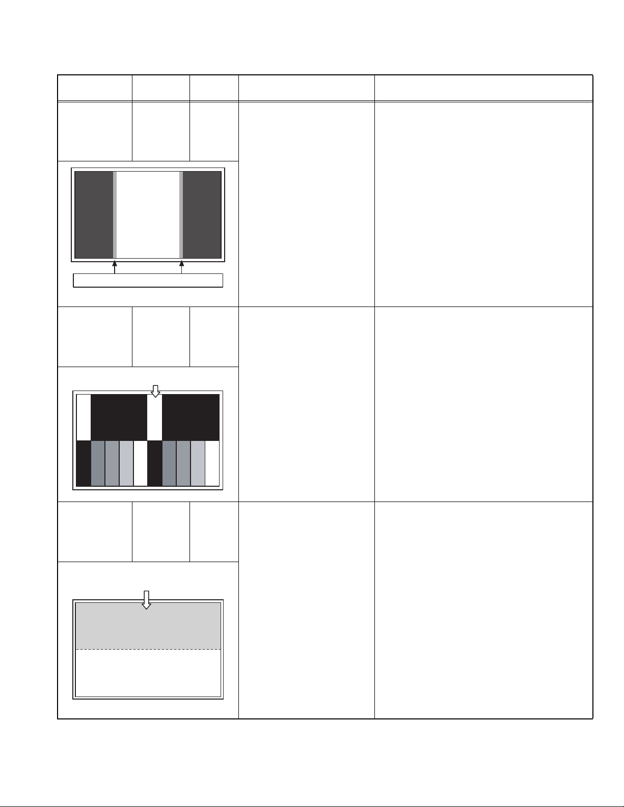
4.7.1 VIDEO CIRCUIT
Item
625i
A-D OFFSET
Measuring
instrument
Remote
control unit
Test point Adjustment part Description
Signal
generator
Disappears the color at both ends.
1125i (50Hz)
BRIGHTNESS
Remote
control unit
Signal
generator
Set the 0% black part to be brightest.
1125i (50Hz)
A-D OFFSET
Remote
control unit
Signal
generator
Minimize the red and blue noises in
the upper half of the screen.
[1.ADJUST]
S001: PREPARE
(Adjustment setting mode change)
S008: 5i CB OF(625i cb offset)
S009: 5i CR OF(625i cr offset)
S030: R DRIVE(Red drive)
S031: G DRIVE(Green drive)
S032: B DRIVE(Blue drive)
[1.ADJUST]
S001: PREPARE
(Adjustment setting mode change)
S012: HD BL(1125i brightness)
S030: R DRIVE(Red drive)
S031: G DRIVE(Green drive)
S032: B DRIVE(Blue drive)
[1.ADJUST]
S001: PREPARE
(Adjustment setting mode change)
S013: HD CB OF(1125i cb offset)
S014: HD CR OF(1125i cr offset)
S030: R DRIVE(Red drive)
S031: G DRIVE(Green drive)
S032: B DRIVE(Blue drive)
(1) Receive a 625i component ramp pattern signal.
(2) Set PICTURE MODE to "STANDARD".
(3) Set ZOOM to "FULL".
(4) Set COLOUR TEMP. to "NORMAL".
(5) Select "1.ADJUST" from the SERVICE MODE.
(6) Set < S030 > (R DRIVE), < S031 > (G DRIVE)
and < S032 > (B DRIVE) to "133".
(7) Set < S001 > (adjustment setting mode change)
to set "8" and it change to the 625i A-D offset
adjustment setting mode.
(8) Adjust < S008 > (625i Cb offset) and < S009 >
(625i Cr offset) to lose the gap (red line, green
line and blue line) which appears at both ends
of a white part at the centre of the screen.
(9) Set < S001 > to set "0" and it change to the
normal mode.
(10) Press the [MUTING] key to memoirze the set
value.
(1) Receive a 1125i (50Hz) gray scale pattern signal.
(2) Set PICTURE MODE to "STANDARD".
(3) Set ZOOM to "FULL".
(4) Set COLOUR TEMP. to "NORMAL".
(5) Select "1.ADJUST" from the SERVICE MODE.
(6) Set < S030 > (R DRIVE), < S031 > (G DRIVE)
and < S032 > (B DRIVE) to "133".
(7) Set < S001 > (adjustment setting mode change)
to set the values "12" and it change to the 1125i
black level adjustment setting mode.
(8) Adjust < S012 > (1125i brightness) to set the
0% black part in the upper half of the screen to
be brightest.
(9) Set < S001 > to set "0" and it change to the
normal mode.
(10) Press the [MUTING] key to memoirze the set
value.
(1) Receive a 1125i (50Hz) 30% all white pattern
signal.
(2) Set PICTURE MODE to "STANDARD".
(3) Set ZOOM to "FULL".
(4) Set COLOUR TEMP. to "NORMAL".
(5) Select "1.ADJUST" from the SERVICE MODE.
(6) Set < S030 > (R DRIVE), < S031 > (G DRIVE)
and < S032 > (B DRIVE) to "133".
(7) Set < S001 > (adjustment setting mode change)
to set "13" and it change to the 1125i A-D offset
adjustment setting mode.
(8) Adjust < S013 > (1125i Cb offset) to minimize
the blue noise in the upper half of the screen.
(9) Set < S014 > (1125i Cr offset) to minimize the
blue noise in the upper half of the screen.
(10) Set < S001 > to set "0" and it change to the
normal mode.
(11) Press the [MUTING] key to memoirze the set
value.
(No.YA361)1-23
Page 24
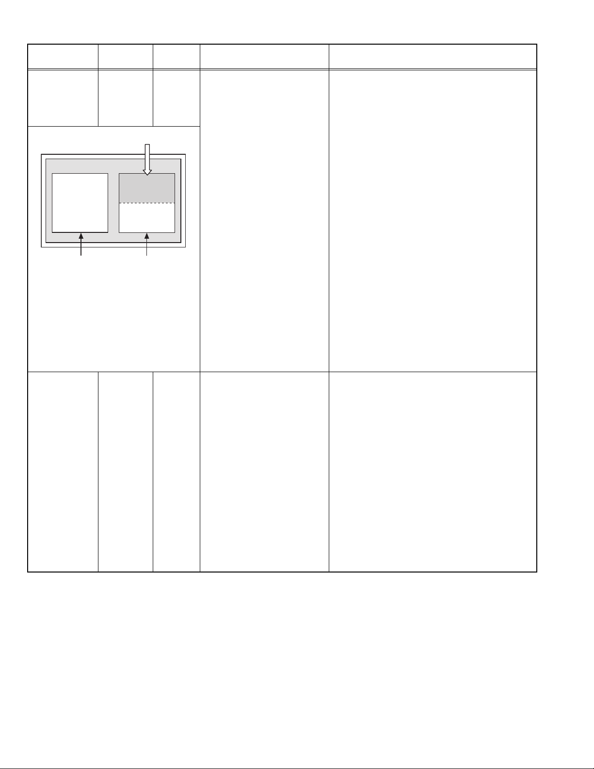
Item
SUB SCREEN
A-D OFFSET
Set the 0% block part to be brightest.
VIDEO-1
<NO SIGNAL>
WHITE
BALANCE
(HIGHLIGHT)
Measuring
instrument
Remote
control unit
Signal
generator
TV(RF)
<30% all white>
Remote
control unit
Signal
generator
Test point Adjustment part Description
[1.ADJUST]
S001: PREPARE
(Adjustment setting mode change)
(1) Set PICTURE MODE to "STANDARD".
(2) Set ZOOM" to "FULL".
(3) Set COLOUR TEMP. to "NORMAL".
(4) Set MULTI SCREEN to "2 pictures".
S016: RT CB OF
(Sub screen cb offset)
S017: RT CR OF
(Sub screen cr offset)
(5) Receive a PAL 30% all white pattern signal on
the right screen. At the same time, set the Left
screen in VIDEO-1 mode (No signal).
(6) Select "1.ADJUST" from the SERVICE MODE.
(7) Set < S030 > (R DRIVE), < S031 > (G DRIVE)
S030: R DRIVE(Red drive)
S031: G DRIVE(Green drive)
S032: B DRIVE(Blue drive)
and < S032 > (B DRIVE) to "133".
(8) Set < S001 > (adjustment setting mode change)
to set "17" and it change to the sub screen A-
D offset adjustment setting mode.
(9) Adjust < S016 > (Sub screen cb offset) to
minimize the blue noise in the upper half of the
screen.
If you select an adjustment item < S016 >,
then the screen automatically turn to twin
pictures mode.
(10) Adjust < S017 > (Sub screen cr offset) to
minimize the red noise in the upper half of the
screen.
(11) Readjust < S016 > and < S017 > to set the
upper half of the screen to be the blackest.
(12) Set < S001 > to set "0" and it change to the
normal mode.
(13) Press the [MUTING] key to memoirze the set
value.
[1.ADJUST]
S030: R DRIVE (Red drive)
S031: G DRIVE (Green drive)
S032: B DRIVE (Blue drive)
(1) Receive a PAL 75% all white signal.
(2) Set PICTURE MODE to "STANDARD".
(3) Set ZOOM to "FULL".
(4) Set COLOUR TEMP. to "NORMAL".
(5) Select "1.ADJUST" from the SERVICE MODE.
(6) Adjust to Keep one of < S030 > (Red drive),
< S031 > (Green drive) or < S032 > (Blue drive)
unchanged, then lower the other two so that the
all-white screen is equally white throughout.
NOTE:
Set one or more of < S030 >, < S031 >, and
< S032 > to "85".
(7) Check that white balance is properly tracked
from low light to high light. If the white balance
tracking is deviated, adjust to correct it.
(8) Press the [MUTING] key to memoirze the set
value.
1-24 (No.YA361)
Page 25
SECTION 5
SERVICE MENU
1.ADJUST
2.SELF_CHECK
3.I2C STOP
LOB OK FAN OK
SYNC M:OK S:OK HD:NG
TIM OK
MSM OK DIGI 0000
MEM OK AVSW OK
YC OK AIO OK
TUN OK GCR NG 1
IP OK RGB OK 8
DVI OK HDMI OK
FAN OK ALM OK
TMP OK
ATP OK ASH OK
PNL OK MEM OK
TMP OK AIO OK
TROUBLESHOOTING
5.1 SELF CHECK FEATURE
5.1.1 OUTLINE
This unit comes with the "Self check" feature, which checks the
operational state of the circuit and displays/saves it during
failure.Diagnosis is performed when power is turned on, and
information input to the main microcomputer is monitored at all
time.Diagnosis is displayed in 2 ways via screen display and LED
flashes. Failure detection is based on input state of I
2
C bus and
the various control lines connected to the main microcomputer.
5.1.2 HOW TO ENTER THE SELF CHECK MODE
Before entering the SERVICE MODE, confirm that the setting of
VCR/TV/ DVD switch is at the "TV" side. If the switches have not
been properly set, you cannot enter the SERVICE MODE.
(1) Press the [INFORMATION] key and [MUTING] key
simultaneously, then enter the SERVICE MODE.
(2) Press the [2] key SELF CHECK MODE.
(3) Press the [RED] key to enter Page 2 of the SELF CHECK
MODE.
*Use the
[GREEN]
key to toggle between Page 1 and Page 2.
NOTE:
When a number key other than the [2] key is pressed in the
SERVICE MODE screen, the other relevant screen may be
displayed.
This is not used in the SELF CHECK MODE. Press the
[MENU] key to return to the MAIN MENU SCREEN.
5.1.3 HOW TO EXIT THE SELF CHECK MODE
To Save Failure History:
Turn off the power by unplugging the AC power cord plug when
in the Self check display mode.
To Clear (Reset) Failure History:
Turn off the power by pressing the [POWER] key on the remote
control unit when in the Self check display mode.
5.1.4 FAILURE HISTORY
Failure history can be counted up to 9 times for each item. When
the number exceeds 9, display will remain as 9. Failure history
will be stored in the memory unless it has been deleted.
NOTE:
Only SYNC (with/without sync signals) will be neither counted
nor stored.
5.1.5 POINTS TO NOTE WHEN USING THE SELF CHECK
FEATURE
In addition to circuit failures (abnormal operation), the following
cases may also be iagnosed as "Abnormal" and displayed and
counted as "NG".
(1) Temporary defective transmissions across circuits due to
pulse interruptions
(2) Misalignment in the on/off timing of power for I
(VCC) when turning on/off the main power.
Diagnosis may be impeded if a large number of items are
displayed as "NG". As such, start Self check check only after 3
seconds in the case of receivers and 5 seconds in the case of
panels upon turning on the power. If recurrences are expected,
ensure to clear (reset) the failure history and record the new
diagnosis reults.
SERVICE MODE SCREEN
SERVICE MENU
1.ADJUST
2.SELF_CHECK
3.I2C STOP
SELF CHECK MODE SCREEN (Page 1)
LOB OK FAN OK
SYNC M:OK S:OK HD:NG
TIM OK
MSM OK DIGI 0000
MEM OK AVSW OK
YC OK AIO OK
TUN OK GCR NG 1
IP OK RGB OK 8
DVI OK HDMI OK
Item
CHECK
Normality=OK
Abnormality=NG
SELF CHECK MODE SCREEN (Page 2)
2
C bus
FAN OK ALM OK
TMP OK
ATP OK ASH OK
PNL OK MEM OK
TMP OK AIO OK
Item
* As "SYNC" is not counted, the number of failures not displayed.
CHECK
Normality=OK
Abnormality=NG
Fig.1
(No.YA361)1-25
Page 26
5.1.6 DETAILS
Self check is performed for the following items:
< Page 1 of screen >
Detection item Display Detection content
Low bias line short
protection
LOB Confirmation of operation of the low bais
(2.5V / 3.3V / 5V / 9V) protection circuit.
Q9801 , Q9822 [REGULATOR PWB]
Diagnosis
signal (line)
Detection timing
LB_PRO Detection starts 3 seconds after the
power is turned on.
If error continues between 400ms the
power is turned off.
Abnormal rise of
temperature in audio
circuit
FAN Confirmation of the temperature of
audio circuit.
TH6661
[ANALOG SIGNAL PWB]
SDA Detection starts 3 seconds after the
power is turned on.
If the temperture of 90°C is detected for
3 seconds the power is turned off.
Presence of sync signal SYNC Confirmation of presence of video
sync signal.
SDA Confirmation of presence of sync signal
in video signal.
M : Main sync signal
S : Sub sync signal
HD : Component sync signal
[ANALOG SIGNAL PWB]
IC201
AC power input TIM Not used. --- ---
Main CPU
MSM Not used. --- ---
communication
Digital tuner DIGI Not used. --- ---
Main memory MEM Confirmation of reply of ACK signal
which uses I
2
C communication.
SDA Same as above.
IC7602 [DIGITAL SIGNAL PWB]
AV select switch AVSW Same as above.
, IC501 [ANALOG SIGNAL PWB]
IC301
3 dimensions YC
YC Not used. --- ---
SDA Same as above.
separator
Multi sound process AIO Not used. --- ---
RF tuner TUN Confirmation of reply of ACK signal
which uses I2C communication.
TU3001
[RECEIVER PWB]
SDA If it checks whenever I
is performed and no reply of ACK signal
an error will be counted.
Ghost reduction GCR Not used. --- ---
DIST process IP Confirmation of reply of ACK signal
which uses I
2
C communication.
IC3001 [DIGITAL SIGNAL PWB]
RGB process RGB Confirmation of reply of ACK signal
which uses I
IC3001
DVI (Digital communication)
DVI Not used. --- ---
Digital input HDMI Confirmation of reply of ACK signal
which uses I
2
C communication.
[DIGITAL SIGNAL PWB]
2
C communication.
SDA If it checks whenever I
is performed and no reply of ACK signal
an error will be counted.
SDA If it checks whenever I
is performed and no reply of ACK signal
an error will be counted.
SDA If it checks whenever I2C communication
is performed and no reply of ACK signal
an error will be counted.
2
C communication
2
C communication
2
C communication
1-26 (No.YA361)
Page 27
< Page 2 of screen >
Detection item Display Detection content
Diagnosis
signal (line)
Detection timing
Fan lock FAN Not used. --- ---
Abnormal of operation of
ALM Not used. --- ---
PANEL
Abnormal rise of
TMP Not used. --- ---
temperature in PANEL
Abnormal rise of
ATP Not used. --- --temperature in audio
circuit
Short circuit detection of
ASH Not used. --- --audio circuit
Panel communication PNL Not used. --- ---
Sub memory MEM Not used. --- ---
Temp. sensor TMP Not used. --- ---
Audio control AIO Confirmation of reply of ACK signal
which uses I
2
C communication.
IC6521 [ANALOG SIGNAL PWB]
SDA If it checks whenever I
is performed and no reply of ACK signal
an error will be counted.
5.1.7 METHOD OF DISPLAY WHEN A RASTER IS NOT OUTPUT
In the state where a raster is not output by breakdown of the set, an error is displayed by blink of the POWER LED.
Type of error POWER LED flash cycle
Low bias line short protection Green turnig on and off at 1 second intervals.
Abnormal rise of temperature in audio circuit Green turnig on and off at 0.1 second intervals.
2
C communication
< Explanation of operation >
If error is detected, the power is turned off.
Shortly after a power is turned off, POWER LED will be blinked.
Power cannot be turned on until the power cord takes out and inserts, after a power is turned off.
(No.YA361)1-27
Page 28

Victor Company of Japan, Limited
AV & MULTIMEDIA COMPANY DISPLAY CATEGORY 12, 3-chome, Moriya-cho, Kanagawa-ku, Yokohama-city, Kanagawa-prefecture, 221-8528, Japan
(No.YA361)
Printed in Japan
VPT
Page 29
SCHEMATIC DIAGRAMS
LCD INTEGRATED DIGITAL TV
YA361200510
LT-37DM6ZJ,
LT-37DM6ZJ
CD-ROM No.SML200511
/P
BASIC CHASSIS
FL2
COPYRIGHT © 2005 Victor Company of Japan, Limited
No.YA361
2005/11
Page 30
LT-37DM6ZJ, LT-37DM6ZJ/P
STANDARD CIRCUIT DIAGRAM
NOTE ON USING CIRCUIT DIAGRAMS
1.SAFETY
The components identified by the symbol and shading are
critical for safety. For continued safety replace safety ciritical
components only with manufactures recommended parts.
2.SPECIFIED VOLTAGE AND WAVEFORM VALUES
The voltage and waveform values have been measured under the
following conditions.
(1)Input signal : Colour bar signal
(2)Setting positions of
each knob/button and
variable resistor
(3)Internal resistance of tester
(4)Oscilloscope sweeping time
(5)Voltage values
Since the voltage values of signal circuit vary to some extent
according to adjustments, use them as reference values.
: Original setting position
when shipped
: DC 20kΩ/V
: H
: V
: Othters
: All DC voltage values
20µs / div
5ms / div
Sweeping time is
specified
3.INDICATION OF PARTS SYMBOL [EXAMPLE]
In the PW board
: R209
R209
Type
No indication
MM
PP
MPP
MF
TF
BP
TAN
(3)Coils
No unit
Others
(4)Power Supply
Respective voltage values are indicated
(5)Test point
: Test point
(6)Connecting method
: Ceramic capacitor
: Metalized mylar capacitor
: Polypropylene capacitor
: Metalized polypropylene capacitor
: Metalized film capacitor
: Thin film capacitor
: Bipolar electrolytic capacitor
: Tantalum capacitor
: [µH]
: As specified
: B1
: 9V
: Only test point display
: Connector
: Receptacle
: B2 (12V
: 5V
: Wrapping or soldering
)
4.INDICATIONS ON THE CIRCUIT DIAGRAM
(1)Resistors
Resistance value
No unit : [Ω]
K
M
Rated allowable power
No indication : 1/16 [W]
Others : As specified
Type
No indication
OMR
MFR
MPR
UNFR
FR
Composition resistor 1/2 [W] is specified as 1/2S or Comp.
(2)Capacitors
Capacitance value
1 or higher : [pF]
less than 1
Withstand voltage
No indication : DC50[V]
Others : DC withstand voltage [V]
AC indicated
Electrolytic Capacitors
47/50[Example]: Capacitance value [µF]/withstand voltage[V]
: [kΩ]
: [MΩ]
: Carbon resistor
: Oxide metal film resistor
: Metal film resistor
: Metal plate resistor
: Uninflammable resistor
: Fusible resistor
: [µF]
: AC withstand voltage [V]
(7)Ground symbol
: LIVE side ground
: ISOLATED(NEUTRAL) side ground
: EARTH ground
: DIGITAL ground
5.NOTE FOR REPAIRING SERVICE
This model's power circuit is partly different in the GND. The
difference of the GND is shown by the LIVE : ( ) side GND and the
ISOLATED(NEUTRAL) : ( ) side GND. Therefore, care must be
taken for the following points.
(1)Do not touch the LIVE side GND or the LIVE side GND and the
ISOLATED(NEUTRAL) side GND simultaneously. if the above
caution is not respected, an electric shock may be caused.
Therefore, make sure that the power cord is surely removed from
the receptacle when, for example, the chassis is pulled out.
(2)Do not short between the LIVE side GND and ISOLATED(NEUTRAL
side GND or never measure with a measuring apparatus measure
with a measuring apparatus ( oscilloscope, etc.) the LIVE side GND
and ISOLATED(NEUTRAL) side GND at the same time.
If the above precaution is not respected, a fuse or any parts will be broken.
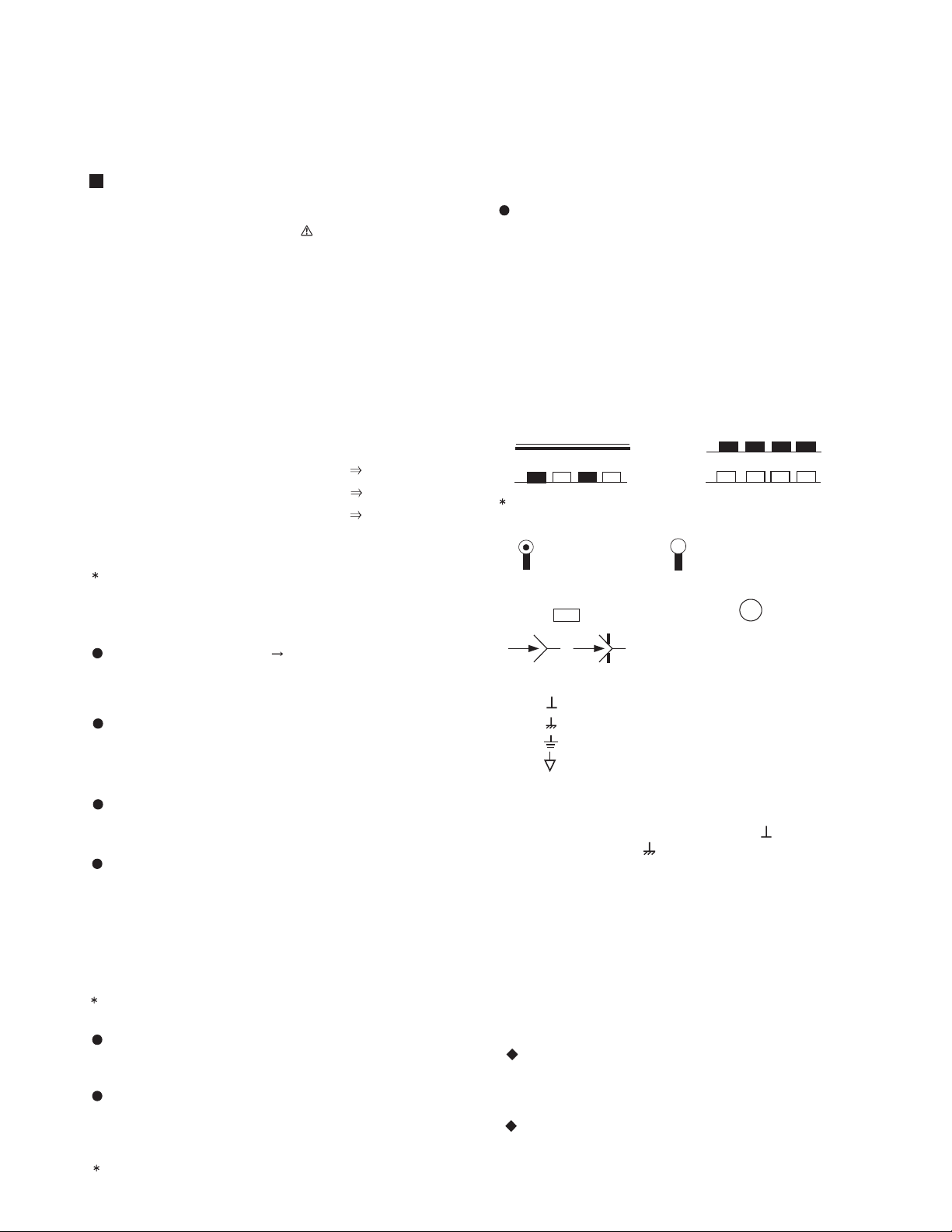
Since the circuit diagram is a standard one, the circuit and
circuit constants may be subject to change for improvement
without any notice.
NOTE
Due improvement in performance, some part numbers show
in the circuit diagram may not agree with those indicated in
the part list.
When ordering parts, please use the numbers that appear
in the Parts List.
(No.YA361)2-1
)
Page 31

CONTENTS
SEMICONDUCTOR SHAPES ......................................................................2-3
WIRING DIAGRAM ........................................................................................2-5
BLOCK DIAGRAM ........................................................................................2-7
CIRCUIT DIAGRAMS
RECEIVER PWB CIRCUIT DIAGRAM ........................................................................................................ 2-9
ANALOG SIGNAL PWB CIRCUIT DIAGRAM ...........................................................................................2-11
DIGITAL SIGNAL PWB CIRCUIT DIAGRAM ........................................................................................... 2-21
PANEL I/F PWB CIRCUIT DIAGRAM ....................................................................................................... 2-43
CONNECTOR PWB CIRCUIT DIAGRAM .................................................................................................. 2-45
FRONT CONTROL PWB CIRCUIT DIAGRAM .......................................................................................... 2-47
FRONT LED PWB CIRCUIT DIAGRAM .................................................................................................... 2-48
POWER PWB CIRCUIT DIAGRAM .......................................................................................................... 2-49
REGULATOR PWB CIRCUIT DIAGRAM .................................................................................................. 2-53
CARD PWB CIRCUIT DIAGRAM .............................................................................................................. 2-55
PATTERN DIAGRAMS
RECEIVER PWB PATTERN ...................................................................................................................... 2-59
ANALOG SIGNAL PWB PATTERN .......................................................................................................... 2-61
DIGITAL SIGNAL PWB PATTERN ........................................................................................................... 2-65
PANEL I/F PWB PATTERN ...................................................................................................................... 2-69
CONNECTOR PWB PATTERN ................................................................................................................. 2-71
POWER PWB PATTERN .......................................................................................................................... 2-73
REGULATOR PWB PATTERN .................................................................................................................. 2-77
CARD PWB PATTERN ............................................................................................................................. 2-79
FRONT CONTROL PWB PATTERN ......................................................................................................... 2-81
FRONT LED PATTERN ............................................................................................................................. 2-81
VOLTAGE CHATRS ................................................................................... 2-83
WAVEFORMS ............................................................................................ 2-86
USING P.W. BOARD
P.W.B ASS’Y name
ANALOG SIGNAL P.W. BOARD
CONNECTOR P.W. BOARD
FRONT CONTROL P.W. BOARD
FRONT LED P.W. BOARD
CARD P.W. BOARD
POWER P.W. BOARD
REGULATOR P.W. BOARD
DIGITAL SIGNAL P.W. BOARD
RECEIVER P.W. BOARD
PANEL I/F P.W. BOARD
LT-37DM6ZJ LT-37DM6ZJ/P
SFL-1115A-U2
SFL-4113A-U2
SFL-7111A-U2
SFL-8113A-U2
SFL-8512A-U2
SFL-9038A-U2
SFL-9138A-U2
SFL0D231A-U2
SFL0F203A-U2
SFL0H001A-U2
LCA10557-64A (SFL-0D231A)
2-2(No.YA361)
Page 32

SEMICONDUCTOR SHAPES
TRANSISTOR
BOTTOM VIEW FRONT VIEW TOP VIEW
CHIP TR
E
C
B
ECB
IC
BOTTOM VIEW FRONT VIEW TOP VIEW
B
(G)E(S)C(D)
ECB
ECB
C
BE
CHIP IC
N
OUT
E
IN
1
IN OUTE
1 N
TOP VIEW
1
1 N
1
N
N
(No.YA361)2-3
Page 33

2-4(No.YA361)
Page 34

WIRING DIAGRAM
TOP
TOP
TOP
TOP
ANALOG SIGNAL PWB
UA
13
UV
1
12
1
10
21
UB
F
SL SR
SPEAKER (L) SPEAKER (R)
14413
CV2
50
CN0011
1
50
A
1
3
1
9
U
CN0012
1
LCD PANEL UNIT
131
CN5121
1
CN1011
50
1
CN1012
50
14
1CV1
121
40
1
T
6
UB
1
TOP
CONNECTOR PWB
CN0002 CN0001
11
30 50
1
UD
1
T
40
1
1A
3
TU3001
ANALOG TUNER
UD3001
RF
SPLITTER
RECEIVER PWB
7
PANEL I/F PWB
CARD PWB
4
CN8CV2
1
12
CN8CV1
1
3
CN8CV3
1
TOP
K
1
CN0006
7
1
CN0007
10
F9001
CN5001
1
CN003
LCD PANEL UNIT
POWER PWB
LCD PANEL UNIT
TOP
CN003
1
CN000W
12
31
CN0LV2
1
130151
CN002 CN001
DIGITAL SIGNAL PWB
1
7
150
PL103
51
CN0ID
12 1
PL207
DIGITAL TUNER
PL200
135 1
TOP
PL107
CN502
14 311
R
H
1
TOP
1
6
LCD PANEL UNIT
LCD PANEL UNIT
1
TOP
1
CV3
10
P
1
10
Q
1
21
H
1
113 4 15
CN9806
7
1
F
4
PW
1
CN9807
10
12
250V/6.3A
POWER CORD
REGULATOR
PWB
TOP
1
CN100R
10
FRONT CONTROL PWB
CN100U
9
1
FRONT LED PWB
DIGITAL TUNER UNIT
2-6(No.YA361)(No.YA361)2-5
Page 35

BLOCK DIAGRAM
J2001
EXT-1
J2002
EXT-2
J2003
EXT-3
J2005
EXT 4
AUDIO IN
J2005
AUDIO
J2004
EXT-4
J2007
PC IN
XD
SD
MS
CF
RECEIVER PWB
UD3001
RF
SPLIT
TV_V1
*3
IC502
AMP
TV
V1/Y1
C1
LV1/RV1
R1
G1
B1
LTVOUT/RTVOUT
R2
G2
B2
V2/Y2
VOUT 2
C2
LV2/RV2
C3
S
V
L/R
L/R
OUT
Y
Cb
Cr
LOUT 3
/ROUT 3
CPY3
CPB3
CPR3
PC RBG
HS,VS
LV3/RV3
LV4/RV4
CARD VIEWER PWB
IC1001
CARD READER
YUV0-7
IC2004
S-P
CONV.
U/V FRONTEND
DIGITAL
TUNER
UNIT
L/R
Y3
V3
H /V SYNC
Y0-7 / Pb0-7 / Pr0-7
H/V SYNC
TU3001
Y/CV/C/U/V
SIF_OUT
TV_L1
TV_R1
IC2002
AUIO
D-A CONV.
IC2005
SYNC GEN
AGC DEMOD.
D-A
TV
V2
V3
Y2
Y3
Y4
V4
VOUT 3
AMP
IC503
C2
C3
C4
TV_L1/TV_R1
LV1/RV1
LV2/RV2
LV3/RV3
LV4/RV4
LV5/RV5
LOUT 3
/ROUT 3
CARD_LIN/_RIN
IC2001
VIDEO
D-A CONV.
IC3501
MULTI SOUND PROCESS
A-D
SOUND
SELECT
MATRIXVOL
CONNECTOR PWB
IC501
VIDEO/AUDIO SELECT
CONNECTOR
PWB
CARD_Y
CARD_Cb
CARD_Cr
BASS
A-D
ANALOG SIGNAL PWB
RE1,GR1,BU1
RE2,GR2,BU2
VOUT 1
YOUT 1
SUB_VY
MAIN_VY
SUB_C
COUT 1
MAIN _C
COUT 2
L_SWSUB
LOUT 1
R_SWSUB
/ROUT 1
LOUT 2
L_SWMAIN
R_SWMAIN
/ROUT 2
LV6/RV6
INPUT
SEL
RE1
GR1
BU1
RE2
GR2
BU2
SUB_C
IC3503
D-AVOL
COMP_L
COMP_R
COLOUR DEMOD./SYNC SEP./RGB SW
DE-MATRIX
DE-MATRIX
CVBS_out
IC802
3 LINE
DIGITAL
Y/C
COMB
FILTER
PC_HS
PC_VS
*1 *1
LIPL
LIPR
IC801
3
3
C
Y
SYNC
SEP.
S_HD
S_VD
SYNC SEP/SW/DETECT
DETECT
YUVSWY1
IC301
COMPONENT VIDEO
/AUDIO SELECT
PC_R
PC_G
PC_B
EUROL4/EUROR4
DIGI_DL/DIGI_DR
LIPL
LIPR
3
Y
Cb Cr
COLOUR
DEMOD.
IC201
SYNC
SEP.
YUVSWY1
YUVSWPB1
YUVSWPR1
YUVSWY2
YUVSWPB2
YUVSWPR2
LOUT3/ROUT3
IC6001
VOLUME
CONTROL
H.DRIVE
V.DRIVE
L/R
S_Y
S_R_Y
S_B_Y
S_HD
S_VD
YUVSWH2
YUVSWV2
IC4401
COMPONENT
VIDEO
SELECT
IC4402
COMPONENT
VIDEO
SELECT
*2
HEAD
PHONE
J7001
BBE/SURROUND/AOUDIO CONTROL
L/R
AGC VOL1 BBE
SURROUND
PROCESS
DIGITAL SIGNAL PWB
IC1502
MAIN SCREEN
INPUT SW
DEC_Y
YUVSWPB1
YUVSWPR1
YUVSWY2
YUVSWPB2
YUVSWPR2
IC3004
SW
DIN_HS
DIN_VS
DIN_DL
DIN_DR
MAIN_C
3DHS
3DVS
HDMI
DRIVER
MULTIPLEX
IC3001
FORMAT CONVERT/
MULTI-SCREEN/ SUPER DIGIPURE
3DY
3DRB
FORMAT CONVERT
/MULTI-SCREEN
/SUPER DigiPure
/
MOVIE THEATER
A-D
DQ ADRS
MEMORY
CPU
PLDR_UV
PLDG_Y
PLDB
RX0+/RX1+/RX2+/RXC+/-
DIGITAL-IN
(VIDEO/
AUDIO)
SCL
SDA
IC7002
CHASSIS
MEMORY
8
IC6521
VOL2TONE
A-D CONVERT/YC SEPARAT/COLOUR DEMOD.
IC3501
IC3502
IC7001
CHASSIS
CPU
IC1001
SYNC
SEP.
A-D
(10bit)
CONVERT
A-D
(8bit)
CONVERT
IC4003
PROGRAM
Y
ENHANCER
YC SEP.
8
8
8
DYNAMIC GAMMA/ COLOUR MANAGEMENT/
IPHS
IPVS
IPY
IP PB
IP PR
/ CONTRAST
(3D/3L)
C
COLOUR
DEMOD.
OSD COMPOSITION/RGB PROCESS
GAMMA
CORRECTION
10
DIST
ROM
IC4004
DIST
SETTING
MEMORY
ANALOG
SIGNAL
PWB
KEY1
KEY2
MECA_SW
POWER_LED
REMOCON
*1
ANALOG SIGNAL PWB
IC6621
IC6551
AMP
L/R
Y
R-Y
B-Y
IC6552
HPF
ITU-R656
8bit
FORMAT
COMPARAT
L/R
3DHS
3DVS
3DY
3DRB
IC4001
COLOUR
MANAGEMENT
RGB
PROCESS
OSD
MIX
LVR
LVG
LVB
8
CPU
OSDR
5
OSDG
OSDB
IC7501
MAIN
CPU
SCL
SDA
MI_RX
MI_TX
WAKE
FRONT
CONTROL
PWB
S7701~S7706
POWER
IC6661
DIGITAL
AUDIO
OUT
8
8
8
IC6502
LVDS FORMAT
CONVERSION
IC7602
MAIN CPU
MEMORY
FRONT
LED
PWB
POWER
D8702
IC8752
REMOTE
RECEIVER
SPEAKER(L)
L
R
SPEAKER(R)
PANEL I/F PWB
0+/1+/2+/3+/-
IC5001
LVDS RECEIVER
/LCD DRIVER
/TIMING CTL
DQ ADRS
MEMORY
IC5002,IC5003
*1 : CONNECTOR PWB
*2 :
FRONT CONTROL PWB
*3 : DIGITALTUNER UNIT
IC5181
LVDS
TRANSMITTER
LCD
(PANEL)
(No.YA361)2-7 2-8(No.YA361)
Page 36

CIRCUIT DIAGRAMS
RECEIVER PWB CIRCUIT DIAGRAM SHEET 1
RECEIVER PWB ASS'Y
SFL0F203A-U2
!
*
TU3002
UK
MODELS
for
SIF_OUT
DEEN
DET_OUT
AFTOUT
5V( IF)
RFAGC
NC
NC
NC
NC
NC
NC
VIF
AS
DA
CL
5V( TU)
30V
BS_A9V
UD3001
GND
DEEN
5V( IF)
RFAGC
5V( TU)
0
R3530
*
9V
R3041
*
MS
GND
GND
NC
NC
NC
NC
NC
NC
VIF
AS
DA
CL
30V
R3019
**
R3020
*
R3021
*
R3022
*
R3023
*
***
R3025
R3024
R3026
*
R3027
ANALOG SIGNAL
PWB ASS'Y(5/5)
CONNECTOR
PWB ASS'Y
CN000T
(SHEET19)
CN000A
(SHEET6)
OPEN
TV_V2/TU_ATT
DIN_PHOTO
CNF01A
32V
NC
GND
CNF00A
32V
NC
GND
CNF00T
QGF0508F1-40X
GND
TV_V1
GND
TV_L1
GND
TV_R1
GND
AFT1
GND
LIPL
9V
LIPR
BS_A9V
GND
GND
AGC
GND
MSP_RST
GND
SDA3A
SCL3A
SDA3B
SCL3B
AFT2
GND
SUBWOUT
GND
TV_L2
GND
TV_R2
GND
5V
GND
BS_A5V
GND
COMP_R
GND
COMP_L
CNF00T
*
for LCD
for PDP
*
for
UK
MODELS
TU3001
for
GND
EU
DIG_GND
*
*
MODELS
SIF_OUT
DET_OUT
BS_A9V
R3043
AFTOUT
R3028
*
R3029
R3040
*
*
R3039
*
R3038
*
R3037
*
R3036
*
R3035
R3034
*
*
R3033
R3032
*
*
R3031
R3030
OPEN
C3010
GND
R3042
*
C3001
0.0022
R3111
0
R3112
D3104 D3103 D3004 D3003
OPEN OPEN OPEN
R3009
2.2k
R3008
.01
0
R3010 R3011
1k 1k
C3015
C3008
.01
100
R3007
R3006
100
C3002
/50 NEX60JM-227X
10
GND
R3014
0
R3016
R3015
0
100
GND
GND
R3001
OPEN .1
C3007
NCF31AZ-105X
GND
GND
C3003
0
OPEN
C3011
10
C3014
10.01
C3009
10
/16
/50
Q3001
2SC3928A/QR/-X
BUFFER
SIF_GND
NQL79GM-220X
/50
L3002
NQL79GM-100X
/50
L3001
C3004
L3003
R3002
47k
C3012
.01
NQL79GM-220X
R3003
47k
C3005
.033
C3113
CB1
CB1
UK UKEULCD LCD PDP
SFL- SFL0F203A 0F204A
OLLC08303 OLLC08303
CNF00A
OPEN OPEN
QGA2001F6
CNF01A
-03X
TU3001
OPEN
QAU0428
TU3002
NC
NC
IC3301
*
NC
NC
*
C3301
CB1
L3508
NRSA02J-0R0X
C3559
100
C3555
.022
C3556
.022
L3506
NRSA02J-0R0X
C3528 C3527
100
IC3104
*
GND
VCC
GND
GND
GND
IC3204
VCC
C3213
GND
*
GND GND
GND
GND
/10
R3561
220
R3562
220
R3560
2.7k
/10
R3520
100
R3521
100
R3523 R3522
OPEN OPEN
for
PDP
*
OUT
GND
GND
*
for
LCD
OUT
GND
IC3503
HA17558AF-X
C3553
.0082
R3559
2.7k
VCC
C3554
.0082
IC3504
BA80BC0FP-X
IN OUT
G
C3532
NCF31AZ-105X
C3533
NCF31AZ-105X
C3534
NCF31AZ-105X
C3535
NCF31AZ-105X
L3503
NRSA02J-0R0X
R3553
3.3k
R3551
R3555
3.3k
33k
C3551
.0022
R3557
1k
GND
R3558
1k
C3552
.0022
R3552
R3556
33k
3.3k
R3554
3.3k
GND
/16
.1
C3529
/16
10
C3530
*5
C3531
/16
.1
C3536
*5
C3537
/16
.1
GND
NQR0389-003X
C3501
*5
L3507
NRSA02J-0R0X
C3504
R3501
.01
1k
C3115C3114
R3119
***
R3120
*
C3215C3214
R3219
***
R3563
10k
R3564
10k
C3525 C3526
/16
10 .01
CAPL_M
AHVSS
AGNDC
SC2_IN_L
SC2_IN_R
ASG1
SC1_IN_L
SC1_IN_R
VREFTOP
MONO_IN
AVSS
K3501
C3502
.1
C3511
.01
GND
GND
C3560
/16
47
C3544 C3546
/10 /10
11
0
C3547C3545
OPENOPEN
NCB31CK-105X
CHCH
C3523C3524
.001
SC1_OUT_L
SC1_OUT_R
R3519 R3518
00
C3521
CH
C3522
0.001
NC
VREF1
R3546 R3547
0
.001
NC
AHVSUPAVSUP
IC3501
NEW_PARTS
MSP3415GQGB8V3M
MULTI SOUND PROCESS/
AUDIO SELECT/
AUDIO CONTROL
ANA_IN+
ANA_IN-
TESTEN
XTAL_IN
XTAL_OUTNCD_CTR_OUT1
CH
/16
SIF_GND
R3508
1k
C3503
.01
C3513
C3512
2p
.01
Q3502
BUFFER
2SC3928A/QR/-X
CH
C3514
X3501
18.432MHz
QAX0773-001Z
2p
DACM_L
NC
C3519
NCB31CK-105X
CH
C3520
0.001
VREF2
DACM_R
D_CTR_OUT0
R3509
4.7k
4.7k
R3580
R3581
NC
I2S_DA_IN
I2S_DA_OUT
ADR_SEL
OPEN
NC
RESETQ
DVSS
DVSUP
I2S_WS
I2S_CL
STANBY
R3510
OPEN
DIG_GND
SDA2
SCL2
NC
TP
SDA
SCL
DIG_GND
NC
NC
C3302
*
CB1
R3302
*
*
R3301
CB1
C3303
*
GND
R3305
*
*
IC3302
C3311
*
D3301
*
C3305
R3517
10k
R3516
Q3503
100
UN2213-X
C3517
.01
K3502
NQR0389-003X
LC3501 L3504
NQR0431-001X NQL79GM-4R7X
C3516
100
C3515
.1
/16
R3582
100
100
R3583
100
R3584
100
R3585
R3515
100
R3514
100
IN1
NC
IN2
OUT2
NC
OUT1
CHIP
VCC
FILTER
SDA
GND
R3306 R3307
*
*
GND
MSP_RESET
C3518
2200p
/10
IC3506
MC74VHC1GT125TX
OE
A
GND
IC3507
SN74LVC1G125V-X
OE
A
GND
IC3508
SN74LVC1G125V-X
OE
A
GND
IC3509
SN74LVC1G125V-X
OE
A
GND
NCB11AK-106X
SIF_GND
NC
NC
*
R3304
SCL
R3303
C3307
GND
*
C3306
*
*
R3310
*
C3304
GND
R3309
***
*
IC3302
R3308
*
VCC
Y
VCC
Y
VCC
Y
L3509
VCC
R3525R3524
OPENOPEN
R3512R3511 R3513
NRSA02J-0R0X
Y
C3574
000
DIG_GND
R3526
R3527
R3528
OPEN
OPEN
OPEN
GNDGND
C3573
0.01
C3572
NCB11AK-106X
C3308
R3572
R3573
R3574
R3575
OPEN
0
*1
*2
*3
*4
*5
*
BS_A9V
*
L3301
*
R3311
R3312
*
47
IC3505
NJU26901E2-W
47
SDI
47
LRI
47
BCK
CTR1
VSS
CTR0
4.7k
R3578
4.7k
R3579
IC3510
R1141Q251B-X
VOUT
VDD
GND
CE
NCB11AK-106X
- NOTE -
:OPTION( NON MOUNT)
:0
:2SC2412K/QR/-X
:2SA1037AK/QR/-X
:DTC323TK-X
:DTC144EKA-X
:NCB11AK-106X
C3309
C3310
VDD
SDO
C3571
*
CB1
CB1
*
100
100
R3577
R3576
UD3001
R3019
R3020
R3021
R3022
R3023
R3024
R3025
R3026
R3027
R3028
R3029
R3031
R3032
R3033
R3034
R3035
R3036
R3037
R3038
R3039
R3040
R3041
R3042
R3530
IC3104
IC3204
R3119
R3120
R3219
C3113
C3114
C3115
C3213
C3214
C3215
IC3301
IC3302
L3301
R3301
R3303
R3304
R3305
R3306
R3307
R3308
R3309
R3310
R3311
R3312
C3301
C3302
C3303
C3304
C3305
C3306
C3307
C3308
C3309
C3310
C3311
D3301
-001
QAU0429
-001
OPEN
0
0
0
0OPEN
0OPEN
0OPEN
0OPEN
0OPEN
0OPEN
0OPEN
OPEN 0
OPEN 0
OPEN 0
OPEN 0
OPEN 0
OPEN 0
OPEN 0
OPEN 0
OPEN 0
OPEN 0
OPEN
0
0
OPEN
TPS852-W TPS852-W
OPEN
0
100k0100k
OPEN
OPEN
OPEN
NCB11AK
-106X
NCB11AK
-106X
NCB31CK
-104X
OPEN OPEN
OPEN OPEN
OPEN OPEN
OPEN OPEN
OPEN OPEN
OPEN OPEN
OPEN OPEN
OPEN OPEN
OPEN OPEN
OPEN OPEN
OPEN OPEN
OPEN OPEN
OPEN OPEN
OPEN OPEN
OPEN OPEN
OPEN OPEN
OPEN OPEN
OPEN OPEN
OPEN OPEN
OPEN OPEN
OPEN OPEN
OPEN OPEN
OPEN OPEN
OPEN OPEN
OPEN OPEN
OPEN OPEN
QGA2001F6
-03X
QAU0428
-001
OPEN
OPEN
0
OPEN
OPEN
OPEN
0
OPEN
OPEN
OPEN
OPEN
OPEN
OPEN
OPEN
NCB11AK
-106X
NCB11AK
-106X
NCB31CK
-104X
-02
SFP0F205A
OLLC08116
QGA2001C6
-03X
OPEN
OPEN
QAU0428
-001
QAU0429
-001
OPEN
0
0
0
0
0
0
0
0
0
0
OPEN
OPEN
OPEN
OPEN
OPEN
OPEN
OPEN
OPEN
OPEN
OPEN
OPEN
0
0
TPS852-W
OPEN
100k
OPEN
OPEN
NCB11AK
-106X
NCB11AK
-106X
NCB31CK
-104X
OPEN
OPEN
OPEN
BD3869AF
RC4558D
NRSA02J
-0R0X
0
0
0
15k
10k
10k
15k
4.7k
4.7k
10k
10k
NCB11AK
-106X
NCB11AK
-106X
NCB11AK
-106X
NCF11CZ
-475Z
NCB31CK
-683X
NCB31HK
-183X
NEHL1CM
-476X
NEHL1CM
-476X
NCB11AK
-106X
NCB11AK
-106X
NCB11AK
-106X
UDZS10B-X
-03
-X
-X
c10346-001a001_0609_1/1_0.1
2-10(No.YA361)(No.YA361)2-9
Page 37

A
NALOG SIGNAL PWB CIRCUIT DIAGRAM (1/5) [AV SW BLOCK] SHEET 2
DIGITAL TUNER UNIT
PC IN
C2605
OPEN
D2605
UDZS10B-X
J2001
QNZ0463-001
EXT-1
J2002
QNZ0463-001
EXT-2
(T-V LINK)
J2003
QNZ0726-001
EXT-3
VIDEO
J2004
QNN0650-001
J2004
QNN0650-001
EXT-4
J2005
QNN0649-001
J2005
AUDIO
QNN0649-001
OUT
R2605
GND
J2007
QNZ0561-001
C2601
CB1
1
/16
C2602
CB1
1
/16
C2603
CB1
R2601
1
/16
R2603
75
R2606
GND
0
D2603 D2602
D2606
OPEN
UDZS10B-X
R2604
C2604
330
OPEN
D2604
330
UDZS10B-X
GND
GND
GND
GND
GND
AV_GND
GND
UDZS10B-X
GND
D2103
UDZS10B-X
D2105
UDZS10B-X
GND
GND
C2207
.01
C2208
.01
C2304
OPEN
GND
C2305
OPEN
GND
C2306
.01
GND
C2308
.01
GND
C2401
.01
GND
C2402
.01
GND
D2102
UDZS10B-X
R2202
75
GND
UDZS10B-X
D2001
UDZS10B-X
R2001
75
R2002
75 75
GND
GND
GND
GND
R2102
75
R2103
R2104
75
C2107
.0047
HK
CB1
HK
HK
C2110
R2201
75
C2206
1
R2203
75
R2204
220k
R2205
220k
C2011
HK
C2109
/16
HK
R2003
75
R2004
75
HK
C2008
.0047
HK
C2009
C2010
.0047
R2101
75
D2104
UDZS10B-X
UDZS10B-X
C2108
.0047
.0047
C2201
.01
C2202
10
/10
D2204
UDZS10B-X
C2203
10
/10
C2204
2.2
/16
C2205
2.2
/16
D2003
.0047
D2107
.0047
B1
B1
B1
B1
GND
D2002
UDZS10B-X UDZS10B-X
D2004
D2005
HK
75
D2601
R2602
75
UDZS10B-X
C2001
10
/10
B1
R2006
68
R2005
C2005
2.2
/16
B1
.0047
GND
GND GND
GND GND
GND GND
D2101
UDZS10B-X
D2106
UDZS10B-X
R2301
75
R2302
75
R2303
75
R2304
220k
GND
R2305
220k
GND
GND
GND
GND
GND
R2106
R2105
75
D2201
UDZS10B-X
D2202
UDZS10B-X
D2203
UDZS10B-X
D2205
UDZS10B-X
D2206
UDZS10B-X
D2207
UDZS10B-X
C2301
B1
C2302
1
/16
C2303
1
/16
C2307
CB1
1
/16
C2309
CB1
1
R2401
0
R2402
0
C2006
2.2
/16
B1
0
/16
UDZS10B-X
D2301
UDZS10B-X
D2302
UDZS10B-X
GND
D2303
UDZS10B-X
UDZS10B-X
GND
D2305
UDZS10B-X
D2304
C2101
10
B1
C2105
2.2
B1
C2106
2.2
B1
PC_B
/10
/16
/16
EXT2VOUT
EXT2LOUT
EUROL4
EUROR4
C2310
2.2
C2311
2.2
PC_HS
PC_VS
PC_DET
PC_R
PC_G
V1_VIN
V1_LIN
V1_RIN
VTV_OUT
SC_R1
V2_VIN
Q2173
CPR3
R2052
R2055
R2152
R2452
R2455
390
390
R2154
390
R2157
390
390
390
68
V1_VIN
SC_R1
V1_LIN
V1_RIN
V2_VIN
SC_R2
V2_LIN
V2_RIN
TVLINK
BS_A5V
D13_YS1
D13_YS1
SCL3B5
SDA3B5
R2173
10k
GND
Q2051
UN2226-X
Q2052
UN2226-X
Q2151
UN2226-X
Q2152
UN2226-X
Q2451
UN2226-X
UN2226-X
V2_LIN
V2_RIN
SC_R2
L4
R4
C2_IO
R561
C561
ENABLE
SLOW2
C2051
2.2
R2053
B1
470
GND
GND GND GND
R2056
470
B1
C2052
2.2
/16
GND
C2151
2.2
R2155
470
B1
GND
GND GND GND
R2158
470
B1
C2152
2.2
/16
GND
C2451
R2453
2.2
470
B1
GND
Q2452
R2456
GND GND
470
B1
C2452
2.2
/16
GND
YS2
SC_R1
SC_G1
SC_B1
SC_R2
SC_G2
SC_B2
YS2
SC_B1
SC_B2
SC_R1
SC_R2
SC_G1
SC_G2
SHEET3
F
/16
UN2110-X
/16
Q2153
UN2110-X
/16
Q2453
UN2110-X
D13_YS1
SC_G1
SC_B1
SC_G2
SC_B2
V3_V
V3_L
V3_Y
V3_R
V1LOUT
V3_C
V1ROUT
SW
V1LOUT
V1ROUT
PC_HS
PC_HS
EXT2ROUT
PC_VS
PC_DET
PC_VS
PC_DET
PC_R
Q2171
NPN
SW
PC_R
PC_G
PC_G
GND
GND
GND
GND
GND
GND
GND
PC_B
PC_B
Q2172
NPN
R2172
R2171
UN2212-X
R2051
22k
R2054
22k
R2151
2.2k
R2153
22k
R2156
22k
R2451
22k
R2454
22k
CPY3
CPB3
CPY3
CPB3
SHEET3,4
10K
10K
CPR3
YS2
V3_C
V3_Y
V3_V
V3_L
V3_R
CPY3
CPB3
CPR3
/16
B1
L4
/16
R4
B1
SHEET4
R582
R562
OPEN
SLOW1
R563
C562
Q512
Q511
GND
Q513
R553R552
15k8.2k
R554
12k
R2057
3.3K
CB1
C2053
1
/16
CB1
C2153
1
/16
R2457
3.3K
CB1
C2453
1
/16
CN00UV
GND
GND
GND
SLOWVYUCV
GND
R592
R591
B2 B2 B2
C591 C592
R544
R543
15k
8.2k 100
R545
12k
220
R520
6.8k
R521
220
R522
6.8k
R523
R524
220
R526
R566
R567
R556
100
D551
UDZS10B-X
MAIN_L
R2058Q2053
39k
R2159
1K
R2458
39k
GND
OPEN
R568
A_MU
R2162
OPEN
R2160
39k
R2163 R2164
0 OPEN
R564
R565
GND
GND
GND
GND
R595
R593
R594
HL
C593
C594
R542
D541
UDZS10B-X
GND
MON_V
M_MU
MAIN_R
R2161
0
SHEET4
CPB1
C
B1
C595
GND
C509
0.01
GND
S2-3
S-3
V4
LV4
Y4
RV4
C4
S2-4
S-4
R527
6.8k
LV5
OPEN
R528
V5
6.8k
R529
RV5
ADR
D503
OPEN
D504
OPEN
GND
R530
220
MON_L
MON_R
L_SWMAIN
R_SWMAIN
DIGITAL
TUNER
UNIT
CPY1
CPR1
C511 C512
OPEN OPEN
C513 C514
R596
R597
R569 R570
OPEN OPEN
GND
C508
0.01
SCR2C
220
R518
C3SCL
SCR1C
6.8k
220
6.8k
220
220
R512
R517
R516
R514
R513
S-2V3LV3Y3RV3
S2-2
IC501
CXA2069Q
VIDEO/AUDIO
SELECT
SDA
AGND
DC_OUT
COUT3
LOUT3
YOUT3
R532
R531
220 100
SCL3B5
SDA3B5
MON_L
MON_R
ENABLE
R579
U_R
GND
GND
B2 B2
6.8k
R511
C2
ROUT3
VOUT3
/16
47
C501
HL
220
R510
U_L
VCC
CN00UA
C_DIG
6.8k
220
R509
R508
LOUT2
V/YOUT2
L_SWMAIN
R581
OPEN
Q509
OPEN
R580
OPEN
S-1V2LV2Y2RY2
ROUT2
TRAP2
R_SWMAIN
MAIN_VY0
C525
OPEN
SHEET3
R_DIG
C_DIG
Y_DIG
220
6.8k
220
R505
R504
R503
C1
S2-1
COUT2
MUTE
YIN1
HL
R534
1k
2SA1530A/QR/-X
R589
MAIN_C
C524
OPEN
B1
HL
GND
R587
L_DIG
6.8k
R502
LV1Y1RV1
BIAS
R588
R590
2.2K
IC504
ANALOG SIGNAL PWB ASS'Y (1/5)
SFL-1115A-U2
220
R501
V1
RTV
TV
LTV
RV6
V6
LV5
COUT1
VGND
YOUT1
TRAP1
ROUT1
VOUT1
LOUT1
C503
10
/25
N
CIN1
C502
/16
47
R573
0
R574
OPEN
R586
OPEN
2.2K
R576
R578
5.6K
C523
1
/16
Q510
B2
Q508
PNP
R577
2.2K
C521
10
/16
OPEN
C526
OPEN
C527
18k
R540
0
R539
R538
18k
R537
OPEN
R536
R535
GND
R575
C515
5.6K
/16
1
B2
Q507
PNP
HL
C516
10
/16
GND
MM1508XN-X
C520
1
/16
B2
HL
GND
HL
C506
OPEN
CH
HL
MM1510XN-X
IC503
C505
N
C504
IC502
OPEN
10
/25
R571 R572
OPEN
C522
/10
HL
C2_IO
R541
C518
100
C519
10
MON_V
0
0
BS_A9V
/10
HL
HL
/16
VTV_OUT
MAIN_L
MAIN_R
SCL3B5
SDA3B5
MAIN_C
MAIN_VY0
L_SWMAIN
R_SWMAIN
C2_IO
M_MU
A_MU
TVLINK
MAIN_R
TV_V1
MAIN_L
ROUT
TV_V2
LOUT
SUB_C
SUB_VY
R_SWSUB
L_SWSUB
SCL3B5
SDA3B5
MAIN_C
MAIN_VY0
L_SWMAIN
R_SWMAIN
C2_IO
M_MU
A_MU
TVLINK
SHEET3
SHEET4
SHEET3,4,5,6
SHEET3
SHEET4
SHEET3
SHEET5
SHEET3
R532
R535
R537
R579
R587
R588
R589
C527
Q511
Q512
Q513
R561
R563
R564
R565
R566
R567
R568
R582
C561
C562
CN00UV
CN00UA
R591
R592
R593
R594
R595
R596
R597
C591
C592
C593
C594
C595
C513
C514
R2103
C2301
0
OPEN
OPEN
0
5.6K
2.2K
0.01/50
UN2226-X
2SA1530A
/QR/-X
UMX1N-W
1K
68
150
150
5.6K
5.6K
3.3K
3.3K
0.1
/16
QENC1CM
-476Z
QGA2001C6
-12X
QGA2001C6
-03X
75
75
75
75
75
0
1/16
1/16
1/16
10/16
2.2/16
1/16
1/16
OPEN
NCB11AK
-106X
OPEN
0
OPENOPEN
OPEN OPEN
0OPEN
OPEN
5.6K
OPEN
2.2K
0.01/50OPEN
OPEN
UN2226-X
2SA1530A
OPEN
/QR/-X
OPEN
UMX1N-W
OPEN
1K
OPEN
68
OPEN
150
OPEN
150
OPEN
5.6K
OPEN
5.6K
3.3K
OPEN OPEN
OPEN
3.3K
OPEN
0.1
/16
QENC1CM
OPEN OPEN
-476Z
QGA2001C6
OPEN
-12X
QGA2001C6
OPEN
-03X
OPEN
75
75
OPEN
75
OPEN
OPEN
75
OPEN
75
0
OPEN
0
1/16
OPEN
1/16
OPEN
1/16
OPEN
10/16
OPEN
2.2/16
OPEN OPEN
1/16
OPEN
1/16
OPEN
OPEN
75
NCB11AK
NCB11AK
-106X
-106X
OLLC08306-04OLLC08306-03OLLC08306-02OLLC08306
OPEN
OPEN
OPEN
OPEN0OPEN OPEN00
OPEN
OPEN
OPEN
OPEN
OPEN
OPEN
OPEN
OPEN
OPEN
OPEN
OPEN
OPEN
OPEN
OPEN
OPEN
OPEN
OPEN
OPEN
OPEN
OPEN
OPEN
OPEN
OPENOPEN
OPEN0
OPEN
OPEN
OPEN
OPEN
OPEN
OPEN
75
NCB11AK
-106X
0
0
0
0
5.6K
2.2K
0.01/50
UN2226-X
2SA1530A
/QR/-X
UMX1N-W
1K
68
150
150
5.6K
5.6K
3.3K
3.3K
0.1
QENC1CM
-476Z
QGA2001C6
QGA2001C6
75
75
75
75
75
0
1/16
1/16
1/16
10/16
2.2/16
1/16
1/16
OPEN
NCB11AK
-106X
OLLC08306-06OLLC08306-05
OPEN
0
0
OPEN
OPEN
OPEN
OPEN
OPEN
OPEN
OPEN
OPEN
OPEN
OPEN
OPEN
OPEN
OPEN
OPEN
OPEN
OPEN
/16
OPEN
OPEN
-12X
OPEN
-03X
OPEN
OPEN
OPEN
OPEN
OPEN
OPEN
OPEN0
OPEN
OPEN
OPEN
OPEN
OPEN
OPEN
OPEN
75
NCB11AK
-106X
c10369001b001_1006_1/5_0.0
(No.YA361)2-11 2-12(No.YA361)
Page 38

A
NALOG SIGNAL PWB CIRCUIT DIAGRAM (2/5) [SUB DECORD BLOCK] SHEET 3
FRONT LED PWB ASSS'Y
CN100U (SHEET21)
TV_V1
LIP_L
GND
GND
GND
GND
GND
GND
GND
KEY2
KEY1
GND
GND
GND
GND
9V
SHEET5
KEY1
STB_5V
5V
KEY1
CN0011
QGF0508F1-50X
TEXT_FB1
TEXT_FG1
TEXT_FR1
EE_CDS
MECA_SW0
POW_LED
M_MUTE
A_MUTE
REC
FUNC
D13_YS1
YS2
MAIN_POW
LCD_PRO
AC_IN
POW_GOOD
TVLINK
DIMMER
REMOCON
KEY2
KEY1
TV_V1
MAIN_L
MAIN_R
TV_V2
LIP_L
GND
KEY2
MECA_SW0
MECA_SW0
KEY2
GND
CONNECTOR
PWB ASS'Y
CN1011
(SHEET19)
SHEET2
LCD_PRO
DIMMER
REMOCON
TV_L1/MAIN_L
TV_R1/MAIN_R
TV_V2/TU_ATT
SUB_C
SUB_VY
GQA1501C5-09W
CN000U
GND
5V
5V
GND
POWER_LED
GND
DIMMER
POW_LED
STB3.3V
STB_5V
9V
9V
R853
18k
C853
/16
47
HL
R854
8.2k
R840
100
Q810
PNP
FUNC
STB5V
DIMMED_LED
REC
FUNC
SSM3K17FU-X
SSM3K17FU-X
C401
IC803
OPEN
C826C828
/25
22OPEN
Q853
NPN
R851
390 L6R8
R859
820
5V
R839
2.2k
GND
REC_LED
REMOCON
EE_CDS
EE_CDS
REMOCON
BS_A3V
Q402
Q403
Q404
Q405
BS_A5V BS_A3V
R409
2.2K
R410
3.3K
GND
HL
CH
L851
CH CH
C851
56p
SHEET2
MAIN_R
MAIN_R
MAIN_L
C850
18P
R850
OPEN
C852
56p
MAIN_L
TV_V1
BS_A5V
DGS
BS_A5V
DGS
BS_A5V
DGS
BS_A5V
DGS
TV_V1
TV_V2
TV_V2
R402
10K
R403
10K
R404
R405
R852
390
TEXT_FG1
TEXT_FB1
TEXT_FG1
R801
2.2k
R804
2.2k
R805
2.2k
SHEET4
TEXT_FR1
TEXT_FB1
TEXT_FR1
R802
2.2k
C825
18p
C886
10/16
R855
6.8k
Q851
PNP
R406
OPEN
CH
L865
L22
M_MUTE
HL
SHEET5
M_MUTE
A_MUTE
A_MUTE
MAIN_POW
R407
OPEN
5V
L807
CORE3
R803
3.3k
Q801
PNP
R806
3.3k
Q802
PNP
MAIN_POW
LCD_PRO
LCD_PRO
HL
0.1
C854
SHEET6
AC_IN
POW_GOOD
AC_IN
POW_GOOD
C820
.47/10
R819
10K
R817
10k
C822
2.2/16
B1
C824
0.01
C827
100
/6.3
Y801
C878
0.1
C880
100/10
L861
L22
C881
100/10
C859
NCB31AK-474X
L862
L100
L863
L100
SHEET2,4
SHEET4,5
SHEET2
LIP_L
D13_YS1
YS2
LIP_L
YS2
D13_YS1
NAX0621-001X
R816
27k
C821
0.01
R818
3.3k
C823
0.015
C835
0.01
HL
HL
C879
0.1
0.47
C884
100/10
C882
0.01
HL
HL
C883
0.01
C885
100/10
SHEET2
SHEET2,4,5,6
TVLINK
SCL3B5
SDA3B5
TVLINK
SCL3A5
SDA3A5
C819
10p
X801
16.2MHz
C801
0.1
R856
1M
C855
0.01
C856
0.01
C857
0.01
C858
0.01
SC_R2
C834
0.1
Q809
NPN
0
C818
10/50
RB802
CH
0.1
0.1
OPEN
HL
RB801
C817
C816
COLOR DEMOD/
SYNC SEP.
/16
47
C804
0.1
0.1
C803
C802
HL
IC802
TC90A69AF-X
C864
0.01
C863
0.01
C861
680p
C887 C888
0.1 100/10
C860
0.01
100
R861
CH
180
R832R835
150K150K
R836
Q808
NPN
150K
R837
R814R815
1.5K1.5K
0.1
C815
IC801
TB1274BFG
0.01
C805
L808
CORE3
R862
330
HL
100
R860
C862
0.1
/16
47
C813
0.01
C806
SC_G2
180
R833
R834
HL
L864
L100
NQL904J-560X
SHEET4
YUVSWH2
YUVSWH2
HDMI_DR
HDMI_DL
HDMI_DR
HDMI_DL
SHEET2
MAIN_VY0
YUVSWY1
YUVSWY1
MAIN_VY0
R_DIG
R_DIG
L_DIG
L_DIG
C_DIG
C_DIG
Y_DIG
Y_DIG
SHEET4
S_R_Y
S_B_Y
S_Y
S_VD
SC_B1
SC_G1
SC_R1
SC_B2
C830C831
C832C833
0.10.1
180
180
R829
150K
Q807
NPN
150K
R813
1.5K
R827
R830R831
Q806
NPN
150K
150K
R828
C829
0.10.1
0.1
180
R823R826
150K150K
Q805
NPN
R811R812
1.5K1.5K
180
R820
150K
R824
R821R822
Q804
NPN
R841R842R843R844R845R846
150K
R825
150K
OPENOPENOPENOPENOPENOPEN
R810
1.5K
S_HD
YUVSWV2
YUVSWV2
SHEET4
YUVSWPB1
YUVSWPR1
YUVSWPR1
YUVSWPB1
SHEET4
SHEET2
MAIN_C
YUVSWPB2
MAIN_C
YUVSWPB2
YUVSWPR2
YUVSWY2
YUVSWY2
YUVSWPR2
COMP_L
COMP_L
COMP_R
COMP_R
LOUT
SHEET2
ROUT
LOUT
ROUT
SHEET4,5
LIP_R
LIP_R
R412
R413
BS_A9V
5V
BS_A5V
CN0012
QGF0508F1-50X
LIP_R
BS_A9V
GND
SDA3A5
SCL3A5
SDA3B5
SCL3B5
GND
REC
GND
TV_L2/LOUT
GND
TV_R2/ROT
5V
GND
BS_A5V
GND
COMP_R
GND
COMP_L
GND
CONNECTOR
PWB ASS'Y
0.1
0.1
C814
0.01
7.5k
C807
R807
HL
L809
CORE3
R867
0
R877
820
CH
C895
68p
L855
C891
HL
C877
0.01
C812
/16
0.01
47
C808
Q854
NPN
R864 L852
390 L6R8
R863
820
Q858
NPN
R874 L853
390 L6R8
R873
820
47
/16
Q863
NPN
R889
1k
0.1
C811
C810
C809
4.7/16
CF1
100
100
R808
R809
R893
6.8k
C892
CH
18P
R891
OPEN
CH CH
C865 C866 R865
56P 56P 390
CH
C894
18P
R892
OPEN
CH CH
C869 C870
56P 56P
R887 R885
1k 12k
Q862
NPN
R888 R886
1k 5.6k
R838
0
R869 C868
5.6k 0.1
R866
0
R879
5.6k
R876
0
R875
OPEN
C876
0.01
R884 C875
1.5k 10p
Q855
PNP
C872
0.1
Q859
PNP
C874
15p
CH
L854
L27
CH CH
GND
L866 L867
L22 L22
HL
HL
R883
470
C873
33p
10/16
C890
10/16
OLLC08306 OLLC08306-02
SSM3K17
Q404
FU-X
SSM3K17
Q405
FU-X
R404
10k
R405
10k
R412
OPEN
OPEN
R413
BS_A5V
D711 D712
OPEN OPEN
C711
10
/16
F
HL
C712
GND
0.1
/16
CXA1875AM-X
C889
1K
R722
10K
R717
SSM3K17
FU-X
SSM3K17
FU-X
10k
10k
OPEN
OPEN
GND GND
R716
100
VCC
SCL0
SDA0
HP_MUTE
NC
HP_DET
0
100
R713
R711
OLLC08306-03
R715
100
GND
CSYNC/OTH
R712
OPEN
0
0
OPEN0OPEN
R719
R720
CS
CS
IC711
TU_ATT
RGBOTH
0
0
R724
R714
R721
10K
100
HP_VOL
0
OLLC08306-06OLLC08306-05OLLC08306-04
0
0
000
OPEN
OPEN
OPEN OPENOPEN OPEN
00OPEN0OPEN
00OPEN OPEN
R723
OPEN
R718
100
NC
/TEMP
GND
GND
C403
OPEN
C404
OPEN
C405
4.7/10
B1
C406
4.7/10
B1
ANALOG SIGNAL PWB ASS'Y (2/5)
SFL-1115A-U2
GND
GND
YUVSWPR1
GND
YUVSWPB1
GND
GND
GND
GND
YUVSWY1
GND
GND
GND
GND
TEMP
C2_IO
HP_VOL
HP_MUTE
HP_DET
CN1012
(SHEET19)
SHEET5
SHEET2
SHEET5
c10369001b003_1006_3/5_0.0
2-14(No.YA361)(No.YA361)2-13
Page 39

A
NALOG SIGNAL PWB CIRCUIT DIAGRAM (3/5) [COMPONENT SW BLOCK] SHEET 4
SHEET2
SHEET2
SHEET2,3,5
SHEET2
SHEET3
SHEET2
SHEET2,3
SHEET2
SHEET3
SHEET2
SHEET3
PC_VS
PC_HS
PC_DET
PC_R
PC_G
PC_B
SDA3B5
SCL3B5
L_SWMAIN
R_SWMAIN
S_B_Y
S_R_Y
L_SWSUB
R_SWSUB
CPY1
CPB1
CPR1
D13_YS1
CPY3
CPB3
CPR3
TEXT_FR1
TEXT_FG1
TEXT_FB1
EUROL4
EUROR4
HDMI_DL
HDMI_DR
0
Y204
NRSA02J-0R0X
Y203
NRSA02J-0R0X
Y202
0
Y201
GND
GND
GND
5V
CN0CV1
QGA1501C5-12W
Y
GND
Pb
GND
Pr
GND
GND
L
GND
R
12p
C208
C226
C227
OPEN
OPEN
R219
10k
R220
10k
C211
R208
4.7
/16
100
B1
C212
R209
1
/16
100
R207
OPEN
C213
0.01
/16
R206
0
R210
0
/16
C215
B1
4.7
C216
1
/16
/16
C217
1
R213
0
GND
OPEN
R214
0
GND
D201
1SS355-X
F
C225
0.1
/16
GND
/16
C218
1
5V
R232
C223
NRS12BJ-151W
4.7
/16
B1
/16
C219
1
10K
R211
IC202
SN74CBT3253PW-X
CH
X201
NAX0787-001X
IC201
TB1305FG
C220
0
0
10K
R202
R204
R203
C207
1
/16
C206
1
/16
C205
1
/16
C204
R201
1.5K
0.1
/16
C203
1
/16
C202
1
/16
C201
1
/16
C210
4.7
/16
B1
/16
C224
/16
C221
1
0
R217
1
/16
1
GND
R308
OPEN
LIP_L
COMP_L
LIP_R
COMP_R
YUVSWH2
YUVSWV2
YUVSWY1
YUVSWPB1
YUVSWPR1
YUVSWY2
YUVSWPR2
YUVSWPB2
LIP_L
COMP_L
LIP_R
COMP_R
S_HD
S_VD
SHEET3
SHEET3,5
SHEET3
SHEET3,5
SHEET3
SHEET3
R215
R218
R223
OPEN
R224
OPEN
0
0
YUVSWH2
0
R216
SYNC1_IN
YUVSWV2
R222
OPEN
YUVSWH2
YUVSWV2
YUVSWY1
YUVSWPB1
YUVSWPR1
YUVSWY2
YUVSWPR2
YUVSWPB2
R307
OPEN
R221
OPEN
9V
R336
5.6k
C349
10
/10
YUVSWY1
B1
SYNC1_IN
R334
2.2k
Q307
PNP
R335
2.2k
SDA3B5
SCL3B5
CPY3
CPB3
CPR3
RB301
R301
CENTIN
OPEN
OPEN
B1
B1
C339
C340
.01
.01
C342
C341
APD2
Lin2
Rin2
Prin2
AGND2
PbinM
YinM
PrinM
VGND5
LinM
RinM
AGND5
COMPONENT VIDEO/
SLVADR
YinS
PbinS
PrinS
VGND6
RinS
LinS
AGND6
IGND
IVCC
SDA
SCL
F
HL
0
OPEN
OPEN
0
R302
R303
C302
47
/16
SDA3B5
SCL3B5
/16
EUROL4
EUROR4
TEXT_FR1
C309
C310
0.01
0.01
C308
56p
CH
B1
OPEN
C333
APD1
Lin1
Rin1
Yin2
PDD2
AGND1
VGND2
Pbin2
AN15852A
IC301
AUDIO SELECT
VGND3
Yin3
Pbin3
PDD3
Prin3
APD3
Lin3
Rin3
C312
C311
OPEN
C345
C344
OPEN
OPEN
OPEN
B1
B2
B2
C343
C346
1/16
1/16
HDMI_DL
HDMI_DR
CPB1
CPR1
CPY1
TEXT_FB1
TEXT_FG1
B1
B1
NRSA02J-221XB1NRSA02J-221X
C305
C304
C303
C306
C307
56p
56p
CH
CH
Yin1
PDD1
VGND1
Pbin1
Prin1
VGND4
AGND3
Yin4
Pbin4
PPD4
.01
C313
C314
.01
C394
C395
C396
OPEN
OPEN
B2B2B2
PC_DET
NRSA02J-221X
VVCC
VGND7
Yout1
Pbout1
Rout1
BIAS
Pbout3
Prout3
AGND9
Prin4
APD4
Lin4
Rin4
.01
C316
C315
C317
.01
.01
C397
C398
OPEN
OPEN
B2B1B2
C323
NEX61CM-686X
HL
AGND7
Prout1
Yout2
VGND8
Pbout2
Prout2
AGND8
Lout2
Rout2
AVCC
Yout3
VGND9
DCout
AGND4
Rout3
Lout3 Lout1
C318
.01
OPEN
Q301
F
9V
F
C322
0.1
/16
HL
C321
10
/16
C319
47
/16
HL
C320
0.1
/16
R375
R385
R395
2SC3837K/NP/-X
R372
100
R373
R371
OPEN
OPEN
C373
OPEN
GND
2SC3837K/NP/-X
R382
100
R383
R381
OPEN
OPEN
C383
OPEN
GND
2SC3837K/NP/-X
R392
100
R393R391
OPENOPEN
C393
OPEN
GND
OLLC08306 OLLC08306-02 OLLC08306-06OLLC08306-05OLLC08306-03OLLC08306-04
68
68
68
68
68
68
C372
0.1
/16
GND
R375
R374
470
F
Q302
C382
0.1
/16
GND
R385
R384
470
F
C392
0.1
Q303
/16
GND
R395
R394
470
68 68
68 18068180
68
180 180
68
180
PC_DET
PC_R
PC_G
PC_B
5V
OPEN
RB302
SDA3B5
SCL3B5
L_SWMAIN
R_SWMAIN
S_Y
S_B_Y
S_R_Y
L_SWSUB
R_SWSUB
CPY1
CPB1
CPR1
D13_YS1
CPY3
CPB3
CPR3
TEXT_FR1
TEXT_FG1
TEXT_FB1
EUROL4
EUROR4
HDMI_DL
HDMI_DR
S_Y
ANALOG SIGNAL PWB ASS'Y (3/5)
SFL-1115A-U2
D13_YS1
PC_G
PC_B
PC_R
L_SWMAIN
R_SWMAIN
S_Y
S_B_Y
S_R_Y
L_SWSUB
R_SWSUB
OPEN
C335
OPEN
C336
OPEN
C337
C329
1
/16
B2
B2
C330
1
/16
C324
B2
1
/16
C325
B2
1
/16
C326
B2
1
/16
C327
1
/16
C328
1
/16
CHCHCH
B2
B2
C334C332C331
OPENOPENOPEN
CB301
CB302
C301
0.1
GND
CH
C338
OPEN
GND
YUVSWPB1
YUVSWPR1
YUVSWY2
YUVSWPB2
YUVSWPR2
R229
R230
R231
OPEN
OPEN
OPEN
GND
180
(No.YA361)2-15 2-16(No.YA361)
c10369001b002_1006_2/5_0.0
Page 40

A
NALOG SIGNAL PWB CIRCUIT DIAGRAM (4/5) [AUDIO BLOCK] SHEET 5
IC6201
PQ20WZ11-X
SHEET3,4
OPEN
OPEN
SHEET3,4
SHEET2,3,4,6
LIP_R
LIP_L
SDA3B5
SCL3B5
CN00E2
CN00AC
AU_+VCC
Y6202
Y6201
0
0
D6201
1SS355-X
12V
C6201
0.01
LIP_R
LIP_L
L6201
OPEN
R6201
5.6K
C6202
33
/25
HL
HL
R6202
C6203
33
/25
1.8K
C6206
OPEN
R6301
0
GND
R6302
0
R6204
5.6K
C6204
0.1
R6203
18K
VCC12V
GND
/25
R6205
C6205
0.01
47K
GND
4.7
4.7
BS_A5V
C6301
R6311
OPEN
R6312
OPEN
C6302
R6303
10K
/16
NN
/16
R6308
10K
R6307
10K
R6305R6304
R6309
Q6301
NPN
R6306
100
1K10K
1K
R6310
100
Q6302
NPN
C6546
0.01
C6505
4.7
HL
C6510
4.7
Q6521
NPN
Q6522
NPN
Q6523
PNP
R6541
2.2K
R6540
10K
/25
R6521
2.2K
R6522
2.2K
R6525
2.2K
R6526
HL
33K
R6524
2.2K
/25
R6523
33K
C6521
4.7
HL
C6528
4.7
HL
/25
/25
C6522
C6523
.0033
.033
C6529 C6530
.0033 .033
C6525 C6526 C6539
.0047 0.1 0.1
C6532 C6533 C6536
.0047 0.1 0.1
C6540
C6527
4.7
/25
4.7
/16 /16
HL
HL
IC6521
NJW1164M-W
HL
HL
C6535
/50
/16 /16
1
C6534
4.7
/25
C6542
/25
/25
4.7
C6541
/25
4.7
HL
HL
HL
HL
C6538
/25
4.7
C6537
/25
4.7
R6538
100
R6536
100
R6539
R6537
C6543
47
100
100
GND
C6544
/50
1
HL
/16
HL
R6533
10K
R6534
10K
R6535
10K
R6543
2.2K
C6605R6617
D6601
UDZS6.2B-X
HL
C6606
/16
47
/16
475.6k
HL
C6545
R6542
0.01
10K
Q6534Q6531
PNPNPN
Q6532
NPN
Q6533
NPN
R6527
2.2K
R6528
2.2K
R6531
2.2K
R6530
2.2K
R6529
33K
R6532
33K
HL
C6559
/16
47
C6517
10P
R6551
15K
HL
C6551
/50
1
IC6551
RC4558D-X
C6552
1
/50
HL
R6554
15K
C6518
10P
CH
R6555
3.3k
R6552
3.3k
CH
R6556
100K
R6553
100K
C6557
47
/16
HL
IC6552
RC4558D-X
R6560
C6556
C6555
R6570
OPEN
ANALOG SIGNAL PWB ASS'Y (4/5)
SFL-1115A-U2
C6621
R6621 R6622
3300p
/50
C6553
C6554
R6558
R6568 R6567
0120K
HL
HL
C6562
C6561
/50
2.2
1
C6585
10
R6557
560
R6559
560
C6586
10
D6501D6502
1SS355-X1SS355-X
/50
100 10k
R6623
3.9k
R6625
1k
C6624
2200p
Y6001
Y6002
Y6003
Y6004
0
0
0
0
3300p
GND2
R6626
R6630
C6632
1.5k
1.5k
/50
R6627
100k
R6629
100k
C6631
/50
2200p
R6631
1k
R6633 R6634
150 10k
/50
/16
HL
R6520
10k
R6517
10k
R6519
/16
HL
R6563
220K
R6515
R6516
Q6538
NPN
Q6539
NPN
R6518
C6560R6569 R6564
OPEN82K 0
R6601
1K1K0
R6605
R6603
R6602
33K
R6606
33K
R6607
0
R6604
OPEN
R6608
OPEN
CH
C6601
100P
CH
C6602
100P
Q6643
OPEN
R6641
OPEN
R6642
OPEN
R6643
OPEN
GND
Q6641
Q6642
OPEN
NCB31EK-104X
C6625
0.1
OPEN
C6630
0.1
NCB31EK-104X
GND
C6626
2200p
/50
C6629
2200p
/50
R6632
3.9k
C6622
0.1
/25
IC6621
LM393DR-X
C6627
0.1
/25
IC6621
LM393DR-X
HL
HL
C6623
22
C6628
22
/25
/25
R6624
1k
QRJ146J-102X
GND2
AU_+VCC
AU_-VCC
SHEET3
SHEET2
SHEET3
SHEET2
SHEET3
SHEET3
SHEET3
TEMP
M_MU
M_MUTE
A_MUTE
A_MU
HP_DET
HP_MUTE
HP_VOL
MECA_SW0
KEY2
KEY1
C6661
0
C6690
OPEN
C6663
0.1
/50
C6664
22
/50
0.1
/50
C6674
470/25470/25
QETN1EM-477Z
1.5k 1.5k
18k 18k
18k
1.5k 1.5k
220k
220k
0.1/16 0.1/16
0.1/16
0.1/16
0.1/16
QGZ8005C3
-01
TDA8925ST/N1
/25
1
NCB11EK-105X
C6665
0.1
C6667
0.1
/50
C6695
OPEN
OLLC08306-06OLLC08306-05
18k
220k
220k
0.1/16
0.1/16
0.1/16
/25
1
C6662
NCB11EK-105X
C6694
OPEN
/50
AU_-VCC
QETN1HM-226Z
C6675C6673
0.1
/50
R6666
5.6
QRK126J-5R6X
R6668 C6677
QRK126J-5R6X /50
R6677
1k
R6662R6661
1k1k
AU_+VCC
R6665
39K
C6666
22
/50
AU_+VCC
CH
CH
AU_+VCC
CH
5.6 560p
CH
QQL28AK-560
C6668
560p
/50
AU_-VCC
C6676
560p
/50
QQL28AK-560
AU_-VCC
C6681
560p
/50
AU_+VCC
L6661
56
L6662
56
R6663
39K
C6669
0.22
GND2
R6667
22
QRK126J-220X
C6678
0.22
GND2
R6669
22
QRK126J-220X
D6503
1SS355-X
D6504
1SS355-X
C6670
QFV21HJ-224Z
QFVF1HJ-474Z
0.47
C6679
QFV21HJ-224Z
QFVF1HJ-474Z
0.47
AU_-VCCAU_+VCC
GND2
C6563
0.1
/25
C6564
0.1
/25
C6671
0.015
/50
C6680
0.015
/50
R6577
18k
R6578
3.9k
R6579
18k
R6580
3.9k
GND2
D6672
UDZS20B-X
D6671
UDZS20B-X
D6673
UDZS20B-X
D6674
UDZS20B-X
K6601
NQR0499-002X
K6602
NQR0499-002X
C6567
1
/25
CB1
C6568
1
/25
CB1
QETN1EM-477Z
C6685
470
/25
C6687
470
/25
QETN1EM-477Z
K6661
NQR0499-002X
K6662
NQR0499-002X
K6663
NQR0499-002X
K6664
NQR0499-002X
NCB31HK-104X
C6684
0.1
/50
C6686
OPEN
CN00SL
QGA2001C6-03X
SPEAKER(L)
CN00SR
QGA2001C6-04X
SPEAKER(R)
CN000F
QGA2001C2-04V
POWER PWB
ASS'Y(2/2)
CN000F
(SHEET23)
R6676
AU_+VCC
C6672
QETN1EM-477Z
1.5k 1.5k
18k 18k
18k
1.5k 1.5k
220k
220k
-01
1k
0.1/16
0.1/16
0.1/16
0.1/16
220k
220k
OPEN
GND2
18k
IC6661
R6664
QETN1HM-226Z
C6689
OPEN
R6409
10K
Q6421
NPN
1SS355-X
D6433
5V
5V
GND
GND
MECA_SW0
KEY2
KEY1
R6424
2.2K
R6425
2.2K
D6432
1SS355-X
R6423 R6421
3.3K OPEN
/16
R6433
OPEN
R6004
6.8k
GND
R6422C6421
OPEN0.1
1SS355-X
HL
R6432
33K
D6431
C6431
47
/16
R6005
BS_A9V
22K
Q6431
PNP
C6009
1
/10
R6431
56K
F
NCF31AZ-105X
C6001
/10
1
F
F
C6002
/10
1
D6001
1SS355-X
IC6001
NJM2777M-X
HL
R6003
100
C6008 C6006
/50
10 1
C6005
1
HL
HL
TH6661
!
NAD0035-471X
VCC12V
C6693
D6681
470
/16
1SS355-X
R6684
100k
C6692
C6691
OPEN
OPEN
R6683
OPEN
R6682
OPEN
Q6672
R6681
OPEN
9V
R6006
QRL039J-330
C6003
R6007
/10
100
0
HL
0
R6001
22K
C6007
/16
470
QETN1AM-108Z
R6002
22K
HL
C6004
/10
100
C6010
330p
CH
C6011
330p
CH
/50
/50
R6008
OPEN
GND
CN000R
QETN1CM-477Z
R6686
15k
R6685
GND
D6682
1SS355-X
D6683
1SS355-X
D6002
1SS355-X
56k
Q6673
PNP
QGA1501C5-10W
FRONT CONTROL
PWB ASS'Y
CN100R
(SHEET20)
Q6661
UN2112-X
GND2
C6682
0.1
Q6663
UN2212-X
/50
AU_+VCC
R6670
15k
R6672
OPEN
D6661
OPEN
R6680 R6691
10k 33k
R6673
2.2k
R6674
1k
D6663
UDZS3.3B-X
GND2
R6675
Q6662
NPN
5.6k
AU_-VCC
R6671
10k
D6664
1SS355-X
AU_-VCC
C6688
0.1
C6683
0.1
/50
OLLC08306 OLLC08306-02 OLLC08306-04OLLC08306-03
R6515
R6516
R6518
R6519
R6558
R6560
C6553
C6554
C6555
C6556
CN00E2
3.3k
3.3k
22k
22k
22k
22k
3.3k
3.3k
180k
180k
180k
180k
0.068/16
0.068/16
0.068/16
0.068/16
0.068/16
0.068/16
0.068/16
0.068/16
OPEN OPEN
QGA8005C3
-01
0.1/16
0.1/16
0.1/16
0.1/16
QGZ8005C3
c10369001b004_1006_4/5_0.0
2-18(No.YA361)(No.YA361)2-17
Page 41

A
NALOG SIGNAL PWB CIRCUIT DIAGRAM (5/5) SHEET 6
RECEIVER PWB ASS'Y
CN00UB
CONNECTOR
PWB ASS'Y
CN40UB
(SHEET19)
GND
BT
GND
BS5V
BS9V
UK_12V
CNF01A (SHEET1)
CN000A
QGA2001C2-03V
GND
GND_S5
Y909
OPEN
Y910
OPEN
Y921
OPEN
Y922
OPEN
GND2
SCL3B5
SDA3B5
SHEET2,3,4,5
POWER
PWB ASS'Y(2/2)
CN000H
(SHEET23)
CN000H
QGF1201C2-21
POW_GOOD
AC
MAIN_POW
GND
SCL
GND
SDA
GND
STB5V
SW12V
UK_12V
BS9V
BS9V
BS5V
BS5V
BS5V
GND
GND
SW5V
LB_PR05
12V STB_5VBS_ABT30
IC902
TA48M033F-X
D901
NRSA02J-0R0X
C904
D909
OPEN
C903
NCB31CK-154X
BT
GND
R917
0
NRSA02J-0R0X
GND
STB3.3V
C902
NCB31HK-103X
C905
47
/16
NEHL1AM-107X
R901 R903
6.8k 1.5k
R902
1.8k
Q903
2SC3928A/QR/-X
GND
D903
PTZ11B-X
D904
PTZ6.8B-X
GND
D902
1SS355-X
L901
OPEN
L902
NQL52EM-220X
L903
NQL52EM-220X
L904
NQL52EM-220X
D905
MA8030/H/-X
C901
1/50
NEHM1HM-105X
GND
C913
NEX51CM-335X
GNDGND
C914
NEX50JM-156X
GND
C916
NEX50JM-156X
GND
R904
22k
BS_A5VBS_A9V
12V
Q901
R907
0
1/2W
NRS12BJ-0R0W
R908
470
1/2W
BA90BC0FP-X
C912
33
/25
NEHM1EM-336X
GND
GND
9VILA5V
NEHM1CM-476X
GND
Q902
2SC3074/OY/-X
C915
33
/25
NEHM1EM-336X
C906
47
5V
/16
LCD_PRO
LCD_PRO
SHEET3
MAIN_POW
AC_IN
POW_GOOD
OLLC08306 OLLC08306-02
CN00UB
QGA2001C2
C904
OLLC08306-05OLLC08306-06
QGA2001C2
OPEN
NCB11AK
-106X
NCB11AK
-06V
-106X
-06V
OLLC08306-03OLLC08306-04
QGA2001C2
OPEN
NCB11AK
OPENOPEN
-106X
-06V
(No.YA361)2-19 2-20(No.YA361)
OPEN
NCB11AK
-106X
ANALOG SIGNAL PWB ASS'Y (5/5)
SFL-1115A-U2
c10369001b005_1006_5/5_0.0
Page 42

DIGITAL SIGNAL PWB CIRCUIT DIAGRAM (1/11) [GR] SHEET 7
SHEET17
SHEET16
SHEET9
SHEET11
MAIN_VY
YUVSW_Y1
GR_RST
GRON
DEC_Y
MCmp/OTH
L1501
NRSA02J-0R0X
C1508
NCF11CZ-475X
AGND
BS_5VBS_9V
L1502
OPEN
C1507
OPEN
NRSA63J-0R0X
Vcc
CK
D
CLR
Q
GND
IC1501
OPEN
R1584
PR
Q
NRSA63J-105X
C1509
C1511
C1502
10/25
R1523
NCJ41EK-106X-U
R1524
470k
IC1502
NJM2235V-X
Vin3
SW2
VDD
0.01
Vout
GND
Vin2
SW1
Vin1
R1522
OPEN
NCB31CK-104X
DIGITAL SIGNAL PWB ASS'Y (1/11)
SFL0D231A-U2 [LT-37DM6ZJ]
R1525
0
N
C1510
OPEN
BS_9V
L1531
L1546
OPEN
Q1535
OPEN
OPEN
C1531
R1503
OPEN
OPEN
CF1
AGND
R1501R1502
OPENOPEN
Q1536
OPEN
R1531
OPEN
D1501
OPEN
C1532
OPEN
R1578
OPEN
VCC3A
L1547
OPEN
AGND
R1532
OPEN
C1565
OPEN
L1548
OPEN
C1569
OPEN
R1534
OPEN
C1568
OPEN
R1508
OPEN
AGND
Q1531
OPEN
L1549
OPEN
R1564R1563
OPENOPEN
C1570
OPEN
R1535
OPEN
C1534
OPEN
IC1503
OPEN
OUT
VCC
C1566
OPEN
R1567 C1567
OPEN OPEN
R1565
R1568
CH
C1571
OPEN
OPEN
OPEN
GND
L1532
R1536
CH
NC
R1566
OPEN
OPEN
OPEN
CH
AGND
CH
C1533
OPEN
CH
C1535
OPEN
R1513 R1514
OPEN OPEN
R1538
OPEN
AGND
IC1532
OPEN
R1570
Q1532
OPEN
R1537
OPEN
R1539
OPEN
C1538
OPEN
R1569
OPEN
AGND
OPEN
Q1533
OPEN
R1574
R1575
R1571
OPEN
R1572
OPEN
R1576
OPEN
R1540
OPEN
CB1
C1536
OPEN
L1533
NRSA02J-0R0X
L1534
NRSA02J-0R0X
L1537
OPEN
C1572
OPEN
R1573
OPEN
OPEN
OPEN
R1577
OPEN
R1541
OPEN
D1531
OPEN
C1537
OPEN
Q1534
OPEN
CF1
CF1
R1553
R1554
AGND
C1539
OPEN
R1546
OPEN
C1541
R1549
OPEN
OPEN
C1555
OPEN
C4951
OPEN
R1545R1544
OPENOPEN
R1547
OPEN
OPEN
OPEN
C1540
OPEN
IC1533
Gnd
OPEN
R1558
OPEN
R1551
OPEN
AD8
RA1532
OPEN
AD0
AD5
AD6
AD7
AD2
AD3
AD4
AD1
RA1531
OPEN
R1550
AD5
AD6
AD7
AD8
C1543
DIN6
GND_AFE_A
BOOT_EN
GND_NCO_A
R1560
OPEN
C1560
OPEN
OPEN
DIN7
PRM0
VDD_AFE_A
DIN8( MSB)
GND_AFE_DIG
IC1531
OPEN
GND_DAC_DIG/A
NCO_IN
NCO_OUT
VDD_NCO_DIG
GND_NCO_DIG
VDD_NCO_A
C1551
OPEN
CH
CH
CH CH
C1562
OPEN
C1542
OPEN
AD4
AD3
AD2
AD1
C1544
C1546
OPEN
C1558
OPEN
AD0
C1547
OPEN
OPEN
C1545
OPEN
C1553
R1552
OPEN
OPEN
CH
R1548
OPEN
L1541
OPEN
Vcc
C1556
OPEN
L1544
OPEN
CH
R1559
OPEN
C1557
OPEN
AIN
DIN5
DIN4
DIN3
DIN2
CLMP_REF1
DIN1
CLMP_REF0
DIN0( LSB)
GND_AFE_A
VDD_AFE_A
BYPASS
RESET
VDD_PLL_DIG
CLK_IN
GND_PLL_DIG
CRY_SEL1
VDD_PLL_A
GND_PLL_A
CRY_SEL0
VDD_DAC_DIG
VDD_DAC_A
GND_DAC_DIG/A
AOUT2
AOUT1
VREF
C1550
OPEN
L1545
OPEN
CH
C1559
OPEN
OPEN
PRM1
PRM2
PRM3
PRM4
PRM5
GND_CORE
STATUS1
VDD_AFE_DIG
VDD_PERR
VDD_CORE
GND_CORE
DSTB
OPEN
STATUS2
CHARGEP
CHARGEN
DOUT0( LSB)
GND_PER
DOUT1
VDD_PER
DOUT2
DOUT3
DOUT4
GND_CORE
DOUT5
VDD_CORE
DOUT6
DOUT7
DOUT8
DOUT9( MSB)
HDRIVE#
VDRIVE#
GND_PER
X1531
OPEN
OPEN
R1583
IN-A
Vcc
OUT-B
OUT-A
IN-C
IN-B
GND
OUT-C
IC1534
OPEN
SDAA
SDA
SCL
CLMP_GT
R1561
OPEN
VDD_CORE
STATUS0
CS_N
C1552
C1561 C1563
OPEN OPEN
C1548
OPEN
C1549
OPEN
AGND
C1564
OPEN
L1542
OPEN
L1543
OPEN
SDA3A
SHEET9,12,16
SCL3A
LCA10557-64A (SFL-0D231A) [LT-37DM6ZJ/P]
c10374002b010_1004_10/12_0.0
2-22(No.YA361)(No.YA361)2-21
Page 43

DIGITAL SIGNAL PWB CIRCUIT DIAGRAM (2/11) [5055 LPF] SHEET 8
BS_9V
R0101
OPEN
LC0102
NQR0483-005X
R0110
SHEET17
SHEET17
SHEET17
YMIN
BYMIN
RYMIN
R0105
C0102
OPEN
100
C0202
OPEN
R0205
100
C0302
OPEN
R0305
100
Q0301
R0107
Q0201
*1
R0207
330
*1
R0307
330
R0106
330
Q0101
*1
330
R0206
330
R0306
330
R0109
100
R0209
150
R0309
150
Q0102
Q0202
100
*2
R0116
100
R0117
OPEN
R0210
100
*2
R0216 R0221
100 100
R0217
OPEN
R0310
100
Q0302
*2
R0316 R0321
100 100
R0317
OPEN
C0103
OPEN
C0204
NQL092K-R68X
CH CH
C0203
OPEN
R0242
4.7K
R0243
10K
C0304
NQL092K-R68X
CH CH
C0303
OPEN
R0342
4.7K
R0343
10K
R0119
C0104
L0101
NQL092K-R68X
CH
R0219
270
39p
CH
L0201
R0319
270
39p
CH
L0301
270
39p
CH
CH
CH
C0205
C0206
33p
39p
Q0206
NPN
CH
C0305
C0306
33p
39p
Q0306
NPN
C0107
0.1
R0121
100
C0105 R0120
33p OPEN
C0207
0.1
R0220
OPEN
C0307
0.1
R0320
OPEN
R0222
/16
Q0204
*2
R0322
1k
/16
Q0304
*2
L0104
C0401
0.1
OPEN
L0204
OPEN
L0304
OPEN
CmpAY
CmpACB
CmpACR
CLPH
SHEET11
2.2k
R0125
R0225
R0325
/16
DGND
PWMY
2.2k
PWMB
2.2k
PWMR
CmpVS
SHEET10,11,17
TEXT[H]
SHEET17
PC_sel
SHEET16
R0131
C0110
10
C0119
R0139
OPEN
C0210
10
C0219
C0310
10
C0319
/10
OPEN
/10
OPEN
R0239
OPEN
/10
OPEN
R0339
OPEN
AGND
AGND
AGND
C0113
10
C0213
10
C0313
10
4.7k
R0132
4.7k
CH
HN1C01F/Y/-X
C0111
82p
C0112
82p
CH
R0134
4.7k
CB1
C0114
0.1
/10
/16
R0231
4.7k
R0232
4.7k
CH
HN1C01F/Y/-X
C0211
82p
C0212
82p
CH
R0234
4.7k
CB1
C0214
/10
0.1
/16
R0331
4.7k
R0332
4.7k
CH
HN1C01F/Y/-X
C0311
82p
C0312
82p
CH
R0334
4.7k
CB1
C0314
0.1
/10
/16
Q0109
Q0110
HN1C01F/Y/-X
Q0209
Q0210
HN1C01F/Y/-X
Q0309
Q0310
HN1C01F/Y/-X
R0133
0
R0233
0
R0333
0
Q0208
Q0308
NPN
NPN
Q0108
NPN
R0140
1.8k
R0240
1.8k
R0340
1.8k
R0137
150
R0237
270
R0337
270
R0136
OPEN
R0236
OPEN
R0336
OPEN
R0338
R0138
33
L0102
NQL092K-1R0X
CH
C0118
Q0105
Q0205
Q0305
NPN
NPN
NPN
150p
L0202
NQL092K-1R0X
CH
C0218
150p
L0302
NQL092K-1R0X
CH
C0318
150p
R0141
4.7k
CH
C0117
56p
R0238
33
R0241
4.7k
CH
C0217
56p
33
R0341
4.7k
CH
C0317
56p
R0115
OPEN
R0215
OPEN
R0315
OPEN
C0115
0.1/16
R0114
4.7k
R0214
4.7k
R0314
4.7k
0.1
C0215
C0315
0.1
C0116
10/10
AGND DGND
VCC3D
L0401
/16
/16
NRSA02J-0R0X
IC0401
SN74AHCT1G32V-X
CB1 CB1
R0122
1k
/16
Q0104
*2
1k
C0109
10
C0209
10
R0126
10k
R0127
0
CB1
/10
R0128
1k
R0226
4.7k
R0227
180
CB1
/10
R0228
1k
Q0203
NPN
R0326
4.7k
R0327
180
CB1
C0309
/10
10
R0328
1k
Q0303
NPN
AGND
AGND
R0208
680
R0308
680
R0211
R0311
4.7k
R0129
10k
Q0107
PNP
R0229
10k
Q0207
PNP
4.7k
R0329
10k
Q0307
PNP
CB1
CB1
R0345
4.7k
R0344
Q0311
NPN
4.7k
AGND
DIGITAL SIGNAL PWB ASS'Y (2/11)
SFL0D231A-U2 [LT-37DM6ZJ]
LCA10557-64A (SFL-0D231A) [LT-37DM6ZJ/P]
(No.YA361)2-23 2-24(No.YA361)
c10374002b001_1004_1/12_0.0
Page 44

DIGITAL SIGNAL PWB CIRCUIT DIAGRAM (3/11) [3DY/C] SHEET 9
C1066
47/6.3
VCC3D
L1010
NRSA02J-0R0X
C1065
1/6.3
T
AGND
IC1002
MM1572FN-X
B2
C1063 C1062
2.2/10 47/6.3
T
C1064
.01
AGND
D1002
EC30HA03L-X
D1001
EC30HA03L-X
3DFID
3DVSO
3DHSO
3DCO7
3DCO6
3DCO5
3DCO4
3DCO3
3DCO2
3DCO1
3DCO0
3DCKO
L1011
L47
C1076
NBE20GM-106X
T
SHEET15,17
SHEET7
SHEET17
SHEET7,12,16
SHEET16
MAIN_CCD
DEC_Y
C_MAIN
DEC_RY
DEC_BY
SCL3A
SDA3A
A92RES
BS_9V
R1017
100
Q1004
BS_9V
NPN
R1018
SCL3A
SDA3A
A92RES
R1102
100
C1111
AGND
NRSA63J-681X
R1203
100
R1303
100
R1403
100
R1404
3.3k
Q1101
R1104
3.3k
R1204
3.3k
R1304
3.3k
NPN
3.3k
NRSA02J-0R0X
R1108
680
C1107
56p
R1105
560
Q1201
NPN
R1205
560
Q1301
NPN
R1305
560
C1303
33p
Q1401
NPN
R1405
560
C1403
33p
L1102
CH
NQL092K-6R8X
NQL092K-6R8X
NQL092K-3R3X
NQL092K-3R3X
CH
CH
CH
CH
CH
R1106
560
L1101
R1206
470
L1201
R1306
470
L1301
R1406
470
L1401
C1102
C1104C1103
56p68p
C1202
C1302
C1304
150p
C1402
C1404
150p
33p
33p
100p
100p
L1007
OPEN
C1002
OPEN
C1105 C1106
NCF11CZ-475X /16
R1101
1.8k
AGNDAGND
R1107
CHCH
CHCH
NCF11CZ-475X /16
CHCH
CH
Q1103
PNP
330
R1109
OPEN
C1205 C1206
NCF11CZ-475X /16
R1201
1.8k
AGNDAGND
Q1203
PNP
R1207C1204C1203
33056p33p
C1305 C1306
R1307
560
C1405 C1406
NCF11CZ-475X /16
R1407
560
R1301
1.8k
R1401
1.8k
Q1303
PNP
Q1403
PNP
.1
AGNDAGND
.1
AGNDAGND
AGND
.1
R1113
33
L1103
NQL093K-1R0X
CH
C1109
150p
R1213
33
AGND
R1313
33
R1413
.1
33
L1203
L1R0
CH CH CH
C1209 C1309 C1409
150p 150p 150p
C1110
OPEN
L1303 L1403
L1R0 L1R0
C1210
OPEN
AGND
CH
AGND
C1310
OPEN
L1105
OPEN
C1112
OPEN
R1114
R1115
0
0
DIGITAL SIGNAL PWB ASS'Y (3/11)
SFL0D231A-U2 [LT-37DM6ZJ]
LCA10557-64A (SFL-0D231A) [LT-37DM6ZJ/P]
1
1
1
C1048
/6.3
C1049
.01
C1050
/6.3
C1051
/6.3
C1410
OPEN
NQL093K-R10X
NEHM1CM-476X
L1008
L22
L1304
LR10
L1404
C1411
LR10
47P
R1010
R1011
C1077
C1311
Q1003
NPN
RA1003
T
B2
VRTYAD
VRMYAD
VSSYAD
YIN
VDDYAD
VRBYAD
BIASCAD
VRTCAD
CIN
VDDCAD
Cr_IN
VSSCAD
Cb_IN
VRBCAD
VDDDA
DAOUT
VSSDA
BIASDA
VREFDA
T
C1071
NBE20GM-106X
C1008
OPEN
C1009
22p
NRZ0040-101X
C1067
/6.3
1
AGND
C1088
CH
OPEN
AGND
UVFLAG
YCLAMPP
VBI_READY
VDDPLL
PLLIN
VCOFIL
C1005
1500p
C1001
.01
L1002
CORE2
C1072
NBE20GM-106X
L1003
L1R5
CH
OEPK
VSSPLL
R1001
270k
VDOUT
VDDXO
T
HDOUT
XOIN
C1006
IC1003
R1141Q151D-X
C1068
/6.3
47
C1069
/10
2.2
R1015
C1070
OPEN
OPEN
47P
R1012
1.5k
C1034
R1013
1.2k
39p
LR10
C1031
C1032
C1033
CH
L1104
C1038
C1039
C1040
B1
C1041
NCB10JK-106X
C1043
C1046
C1047
CH
C1061
4p
K1004
CORE2
C1003
AGND
AGND
C1035
C1042
2.2
OPEN
.01
.01
.01
.01
.01
.01
.01
.01
.01
CH
C1037
2.2
/6.3
68P
/6.3
C1045
.1
/16
C1004
.01
L1001
CORE2
K1001
NRSA02J-0R0X
X1001
NAX0642-001X
18k
CH
CH
NRZ0080-510X
RA1002
.01
C1030
COUT6
DVDD5
COUT7
COUT8
DVSS5
COUT9
A-D CONVERT/
YC SEPARATE/
COLOR DEMOD
XOOUT
VSSXO
BUSSEL
DVDD1
GRD9
GRD8
.01
C1012
.01
R1002
100
0.5%
CH
C1010
18p
CH
C1011
.001
C1082
0.01
C1083
0.01
NRZ0080-510X
RA1002
COUT3
COUT4
COUT5
VSSIO3
IC1001
TC90A92AFG
GRD7
DVSS12
GRD6
GRD5
3DVSO
3DHSO
3DCK
3DHS
3DVS
100
R1014
.01
.01
C1028
C1029
YOUT3
YOUT2
YOUT1
YOUT0
CKOUT
DVDD4
COUT0
COUT1
DVSS4
COUT2
VDDIO3
DVDD2
GRD4
GRD3
VSSRAM1
VDDRAM1
GRD2
C1014
C1013
.01
.01
3DCO0
VDD
N.C.
VSS
IVS
IHS
MODE0
MODE1
N.C.
MODE2
CLKO
VDD
VSS
N.C.
N.C.
VDD
N.C.
N.C.
N.C.
N.C.
OHS
OVS
HREF
VSS VSS
N.C. N.C.
VDD VDD
3DRB0
GRD1
3DCO1
CI0CO0
3DRB1
C1015
CI1
CO1
VDDIO1
GRD0
.01
3DCO2
3DCO3
CI2
CO2
3DRB2
3DRB3
CI3
CO3
DGND
GC14IN
3DCO4
CI4
VSS
VDDRAMD1
VSSIO1
TESTIN
C1081
3DCO5
3DCO6
CI5
CO4
3DRB4
3DRB5
C1026
.01
VSSRAMD1
VSSRAM2BIASYAD
YOUT4
YOUT5
YOUT6
YOUT7
VSSIO2
YOUT8
YOUT9
VDDIO2
TESTM6
TESTM5
DVSS3
C_SYNCIN
TESTM4
DVDD3
TESTM3
TESTM2
TESTM1
TESTM0
RESET VDDRAM2
C1016
10
0.01
3DCO7
3DCKO
VSS
CI7
CI6
ICLK
IC1005
ML87V2105TBZ03A
VDD
CO5
CO6
CO7
3DRB6
3DRB7
C1084
0.01
SCL
SDA
/10
C1025
.01
DVDD1.5
VDDRAM15
C1023
.01
3DYO0
YI0
VDD
VSS
N.C.
C1075
/6.3
47
L1006
T
CORE2
C1074
C1073
C1019
C1018
R1019
C1017
R1007
R1006
R1005R1004
10k220
B1
NRSA02J-0R0X NRSA02J-0R0X
Q1001
UN2213-X
3DYO1
3DYO2
3DYO3
3DYO4
3DYO5
3DYO6
YI5
YI4
YI3
YI2
YI1
VDD
YO0
YO1
YO2
YO3
3DY0
3DY1
3DY2
3DY3
3DY4
C1085
0.01
L1005
CORE2
K1002
YI6
YO4
3DYO7
3DY5
ADD_GND
YI7
YO5
47
T
C1021
.01
47
T
.01
.01
0
.01
100
100
OPEN
R1024
SLA2
YO6
3DY6
/6.3
/6.3
AGND
OPEN
R1023
SLA1
YO7
3DY7
100
R1022
SCL
VSS
R1021
K1005
NRSA02J-0R0X
K1003
100
VSS
SDA
N.C.
TESTM
TEST1
TEST2
TEST3
TEST4
TEST5
/RESET
TEST7
TEST6
N.C.
SELF
N.C.
N.C.
N.C.
N.C.
N.C.
N.C.
N.C.
N.C.
N.C.
N.C.
N.C.
VDD
VSS
VDD
L1004
CORE2
RA1001
NRZ0080-510X
SCL3A
SDA3A
DGND
A92RES
R1030
R1025
100
3DFID
3DYO0
3DYO1
3DYO2
3DYO3
3DYO4
3DYO5
3DYO6
3DYO7
RA1006
RA1004
RA1005
R1027
10k
DGS
Q1006
2SK1228-X
R1029R1028
10k10k
OPEN
OPEN
OPEN
OPENOPEN
3DCKO 3DCK
3DHSO
3DVSO
3DYO0
3DYO1
3DYO2
3DYO3
3DYO4
3DYO5
3DYO6
3DYO7
3DCO0
3DCO1
3DCO2
VCC3D
3DCO3
3DCO4
3DCO5
3DCO6
3DCO7
SCL3A SDA3A
Q1005
2SK1228-X
DGS
R1026
10k
C1087
0.01
10k
C1086
0.01
3DHS
3DVS
3DY0
3DY1
3DY2
3DY3
3DY4
3DY5
3DY6
3DY7
3DRB0
3DRB1
3DRB2
3DRB3
3DRB4
3DRB5
3DRB6
3DRB7
3DVS
3DHS
3DY7
3DY6
3DY5
3DY4
3DY3
3DY2
3DY1
3DY0
3DCK
3DRB7
3DRB6
3DRB5
3DRB4
3DRB3
3DRB2
3DRB1
3DRB0
3DFID
3DVS
3DHS
3DY7
3DY6
3DY5
3DY4
3DY3
3DY2
3DY1
SHEET11
3DY0
3DCK
3DRB7
3DRB6
3DRB5
3DRB4
3DRB3
3DRB2
3DRB1
3DRB0
RST3
SHEET10,11,12
c10374002b002_1004_2/12_0.0
2-26(No.YA361)(No.YA361)2-25
Page 45

DIGITAL SIGNAL PWB CIRCUIT DIAGRAM (4/11) [DVI IN] SHEET 10
SHEET16
SHEET11
SHEET11
SHEET11
SHEET11
SHEET11,17
SHEET8,11,17
SHEET16
OPEN
SHEET15
SHEET17
SHEET14,16,17
SHEET16
SHEET15,16
SHEET17
SHEET16
SHEET17
VFORMSel
SYNCSEL
PLDR_UV7
PLDR_UV6
PLDR_UV5
PLDR_UV4
PLDR_UV3
PLDR_UV2
PLDR_UV1
PLDR_UV0
PLDG_Y7
PLDG_Y6
PLDG_Y5
PLDG_Y4
PLDG_Y3
PLDG_Y2
PLDG_Y1
PLDG_Y0
PLDCK
PLDHS
PLDVS
CmpHS
CmpVS
ATSCCK
ATSCHS
ATSCVS
CARD_DET
BS_BT30
BS_ODU
POW_GOOD
BS_OFF
BS_TXD
BS_RXD
VOUTENB
BS1.5CTL
BS_RST
VMUTE
DIN_DTB
BS_LOUT
BS_ROUT
BS_9VK
BS_YOUT
BSOUTGND
BS_COUT
PLDB7
PLDB6
PLDB5
PLDB4
PLDB3
PLDB2
PLDB1
PLDB0
BSHS
BSVS
BS_7V
BS_IR
BS_9V
BS_5V
RB2004
RB2004 RB2005RB2005 RB2006RB2006
OPEN OPENOPEN OPENOPEN
OPEN
PLDB0
PLDB1
PLDB2
PLDB3
PLDB5
PLDB6
PLDB7
PLDG_Y6
PLDG_Y7
BSY1
BSY0
PLDB4
IC2001
OPEN
BSY5
BSY4
BSY3
BSY2
PLDR_UV5
PLDR_UV6
PLDR_UV7
PLDR_UV4BSUV7
PLDR_UV0
PLDR_UV1
PLDR_UV2
PLDR_UV3
BS_5V
IC2002
OPEN
Vin
Vout
C2031
OPEN
NC
NC
C2030
OPEN
NC
GND
C2033
OPEN
OPEN
BSUV6
OPEN
R2015
R2013
OPEN
OPEN OPEN
OPEN
OPEN
R2053
R2245
R2024 R2014
R2059
OPEN
C2010
BSUV5
BSUV4
BSUV3
BSUV2
BSUV1
BSUV0
BSY7
BSY6
C2032
OPEN
CH
COUT
Cn
DGND
R2054
OPEN
OPEN
R2045
R2012
OPEN
OPEN
C2011
R2144
R2023
OPEN
R2049
OPEN
R2060
OPEN
C4992C4991C4990
OPENOPENOPEN
DGND
OPEN
OPEN
OPEN
OPEN
R2007
R2006
R2005
R2004
OPEN
OPEN
OPEN
R2048
R2047
R2046
DD_OSDVS
DD_OSDHS
VCC3D
L2001
OPEN
CB1 CF
C2034
OPEN
R2008
OPEN
C2012
OPEN
C2013
OPEN
OPEN
R2139
R2141
DGND
OPEN
OPEN
RA2007
RA2008
RA2009
RA2010
RA2011
R2055
OPEN
X2001
OPEN
C2035
OPEN
OSDR0
OSDR1
OPEN
OPEN
OSDR2
OSDR3
OSDR4
OSDR5
OPEN
OSDG0
OSDG1
OSDG2
OSDG3
OSDG4
OSDG5
OSDB0
OSDB1
OPEN
OPEN
OSDB2
OSDB3
OSDB4
OSDB5
DDOSDCK2
DD_OSDVS
DD_OSDHS
DDOSDCK2
OSDR0
OSDR1
OSDR2
OSDR3
OSDR4
OSDR5
OSDG0
OSDG1
OSDG2
OSDG3
OSDG4
OSDG5
OSDB0
OSDB1
OSDB2
OSDB3
OSDB4
OSDB5
SHEET11
CK_75M
OSD_SEL
SHEET16
DD_OSDVS
SHEET12,15,16,17
DD_OSDHS
DDOSDCK2
SHEET12,16
JP_YS
SHEET16
OSDR0
SHEET12
OSDR1
OSDR2
SHEET12,17
OSDR3
OSDR4
SHEET12,15,17
OSDR5
OSDG0
SHEET12
OSDG1
OSDG2
SHEET12,17
OSDG3
OSDG4
SHEET12,15,17
OSDG5
OSDB0
SHEET12
OSDB1
OSDB2
SHEET12,17
OSDB3
OSDB4
SHEET12,15,17
OSDB5
SHEET12,15,17
MI_OSDYS
MI_OSDYM
JP_R
SHEET12,15
I2CEXT2
SHEET11
DIN_sel
DIN_CK
DIN_VS
SHEET11
DIN_HS
RST3
SHEET9,11,12
SHEET12,15
SHEET16
PLDG_Y0
PLDG_Y1
PLDG_Y2
PLDG_Y3
PLDG_Y4
PLDG_Y5
PLDR_UV7
PLDR_UV6
PLDR_UV5
PLDR_UV4
PLDR_UV3
PLDR_UV2
PLDR_UV1
PLDR_UV0
RA2012RA2012
OPENOPEN
PLDB7
PLDB6
PLDB5
PLDB4
PLDB3
PLDB2
PLDB1
PLDB0
RA2014RA2014
OPENOPEN
PLDG_Y7
PLDG_Y6
PLDG_Y5
PLDG_Y4
PLDG_Y3
PLDG_Y2
PLDG_Y1
PLDG_Y0
RA2018RA2017
OPENOPEN
DGND
OPEN
R2121
OPEN
R2122
OPEN
STB3.3V
R2142
OPEN
R2044
OPEN
R2011
OPEN
OPEN
R2115
C2101
OPEN
D2102
D2103
R2103
R2104
R2105
D2101
OPEN
L2101
OPEN
C2036
OPEN
R2111
K2108
OPEN
K2106
OPEN
C2102
OPEN
R2127
OPEN
R2125
OPEN
R2126
OPEN
Q2101
OPEN
R2128
OPEN
R2129
OPEN
R2106
OPEN
AGND
R2102
OPEN
OPEN
R2101
R2152
R2153
OPEN
CB2
K2104
OPEN
OPEN
*1
OPEN
OPEN
OPEN
R2028
OPEN
OPEN
R2027
OPEN
R2156
OPEN
K2107
R2149
OPEN
OPEN
AGND
OPEN
R2131
R2150
R2130
OPEN
OPEN
R2132
OPEN
Q2102
OPEN
TGND
TGND
TGND
LOSDYM
LOSDYS
RESERVE
NC
BT30V
0
NC
DDGND
ODU
GND
BS7V
BS7V
SW_OFF_DET
GND
GND
SBO
SBI
VOUTENB
BS1.5SW
BSRST
SRQ
VMUTE LOSDHP_to_BA
GND
NC
NC
NC
NC
NC
GND
SCL0
SDA0
MLED
NC
NC
IRSYS
GND
SOFT_OFF
GND
DL
GND
DR
GND
DY
GND
DC
DDGND
DDGND
DDGND
BS9V
BS9V
BS9V
BS5V
GND
R2123
CN005CN005
CN005CN005CN005CN005
OPENOPENOPENOPEN
OPENOPEN
BSCLK
BSUV7
BSUV6
BSUV5
BSUV4
BSUV3
BSUV2
BSUV1
BSUV0
LOSDCLK_to_BA
Losdclk_to_DG
Losdh_to_DG
LOSDVP_to_BA
LOSD0
LOSD1
LOSD2
LOSD3
LOSD4
LOSD5
LOSD6
LOSD7
LOSD8
LOSD9
LOSD10
LOSD11
LOSD12
LOSD13
LOSD14
LOSD15
GND
GND
BSHP
BSVP
GND
BSY7
BSY6
GND
BSY5
BSY4
BSY3
BSY2
BSY1
BSY0
GND
GND
GND
GND
GND
GND
ML
GND
MR
BS5V
GND
DGND
R2056
R2057
R2133
OPEN
R2134
OPEN
RA2013RA2013
OPENOPEN
OPEN
OPEN
R2137
R2138
OPEN
OPEN
OPEN
OPEN
R2154
R2155
DGND
R2151
OPEN
R2157
OPEN
CNSH_GND DGND
RA2015RA2015
AGND
LOSD15
LOSD14
LOSD13
LOSD12
LOSD11
LOSD10
LOSD9
LOSD8
LOSD7
OPEN
R2135
OPEN
R2136
R2112
OPEN
R2113
OPEN
R2114
OPEN
BSUV7
BSUV6
BSUV5
BSUV4
BSUV3
BSUV2
BSUV1
BSUV0
BSY7
BSY6
BSY5
BSY4
BSY3
BSY2
BSY1
BSY0
R2118
OPEN
R2119
OPEN
LOSD0
LOSD1
LOSD2
LOSD3
LOSD4
LOSD5
LOSD6
LOSD7
LOSD8
LOSD9
LOSD10
LOSD11
LOSD12
LOSD13
LOSD14
LOSD15
RA2016RA2016
DGND
OPENOPEN
OPENOPEN
IC2004
R2147
OPEN
OPEN
R2148
OPEN
DGND
LOSD6
LOSD5
LOSD4
LOSD3
LOSD2
LOSD1
LOSD0
R2062
OPEN
DGND
R2146
OPEN
IC2003
OPEN
C2003
OPEN
DGND
C2004
OPEN
DIGITAL SIGNAL PWB ASS'Y (4/11)
SFL0D231A-U2 [LT-37DM6ZJ]
R2010
OPEN
C2001
OPEN
R2003
OPEN
R2002
OPEN
OPEN
R2009
OPEN
R2143
C2002
OPEN
OPEN
R2022
OPEN
R2018
R2020
OPEN
OPEN
R2019
C2015
OPEN
C2026
OPEN
R2061
OPEN
DGND
R2145
OPEN
RB2001
OPEN
RB2002
OPEN
RB2003
OPEN
DGND
OPEN
R2001
OPEN
OPEN
OPEN
OPEN
R2052
R2051
C2014
C2009
OPEN
R2063
OPEN
R2064
OPEN
R2058
LCA10557-64A (SFL-0D231A) [LT-37DM6ZJ/P]
(No.YA361)2-27 2-28(No.YA361)
c10374002b009_1004_9/12_0.0
Page 46

DIGITAL SIGNAL PWB CIRCUIT DIAGRAM (5/11) [DET CORE] SHEET 11
DIGITAL INPUT BLOCK
OPEN
SHEET16
SHEET10,17
SHEET8,10,17
SHEET10
SHEET9
SHEET10
SHEET9
SHEET10
SHEET9
SHEET8
SHEET10
SHEET16
DIGITAL SIGNAL PWB ASS'Y (5/11)
SFL0D231A-U2 [LT-37DM6ZJ]
LCA10557-64A (SFL-0D231A)
[LT-37DM6ZJ/P]
SD_DQ[4]
SD_DQ[5]
SD_DQ[6]
SD_DQ[7]
SD_DQ[16]
SD_DQ[17]
SD_DQ[18]
SD_DQ[19]
SD_DQ[20]
SD_DQ[21]
SD_DQ[22]
SD_DQ[23]
SD_DQM[0]
SD_DQM[2]
VCC2.5D
PLDR_UV0
PLDR_UV1
PLDR_UV2
PLDR_UV3
PLDR_UV4
PLDR_UV5
PLDR_UV6
PLDR_UV7
IC3503
LP2996MR-X
DGND
OPEN
C3112
IC3007
SN74LVC3G17U-X
GND
R3128
OPEN
TP-HS2
R3112
R3113
OPEN
22
0
R3114
R3115
OPEN
DGND
0.01
/50
VCC
DGND
R3129
OPEN
NCNC
VCCCE
X3003
NAX0668-001X
GND
ATSCCK
ATSCHS
DIN_CK
DIN_HS
DIN_VS
ATSCVS
DsyncSW1
DsyncSW2
CmpHS
CmpVS
PLDHS
PLDVS
3DY0
3DY1
3DY2
3DY3
3DY4
3DY5
3DY6
3DY7
3DRB0
3DRB1
3DRB2
3DRB3
3DRB4
3DRB5
3DRB6
3DRB7
PLDG_Y0
PLDG_Y1
PLDG_Y2
PLDG_Y3
PLDG_Y4
PLDG_Y5
PLDG_Y6
PLDG_Y7
PLDB0
PLDB1
PLDB2
PLDB3
PLDB4
PLDB5
PLDB6
PLDB7
3DHS
3DVS
3DFID
PLDCK
3DCK
PWMY
PWMR
PWMB
CLPH
CmpAY
CmpACR
CmpACB
CK_75M
SCL5055
SDA5055
OPEN
R3191
IC3191
SN74LVC3G17U-X
GND
OPEN
R3192
R3010
R3011
VCC3D
L3012
NRSA02J-0R0X
B1
C3110
OPEN
0.1
DGND
VCC3D
L3005
NRSA02J-0R0X
B1
C3039
0.1
OPEN
DGND
VCC3D
K3191
NRSA02J-0R0X
C3191
0.01
/50
VCC
0
R3193
DGND
R3125
OPEN
R3132
R3131
OPEN
OPEN
DGND
OPEN
OPEN
R3045
22
C3111
C3040
X3002
/16
R3038
4.7k
/16
X3001
NAX0635-001X
R3039
OPEN
IC3004
TC7MB3257FK-X
S
1B1
1B2
1A
2B1
2B2
2A
GND 3A
R3127
OPEN
GND
IC3006
SN74LVC2G126T-X
TP-YA
TP-RA
TP-BA
BS_5V
L3011
NRSA02J-0R0X
/50
VCC
OE
0.01
4B1
0
4B2
R3116
OPEN
4A
R3117
3B1
C3109
3B2
VCC3D
VCC
CH
C3028
220p
DGND
DGND
R3002
R3003
R3007
22
R3122
R3037
22
VCC3A
C3021
L3001
0.1
OPEN
VCC5055A
AGND
C3022
NBZ0007-107X
R3012
0
VCC3D
K3009
NRSA02J-0R0X
R3118
VCC
0
DGND
GND
R3120
DGND
C3108
IC3005
OPEN
SN74LVC1G08V-X
TP-CKB
TP-CKA
TP-VC
TP-HC
CH
C3126
OPEN
3DCK_2
OPEN
OPEN
0
L3016
OPEN
PS
R3001R3004
10k10k
C3024
OPEN
C3130
DGND
OPEN
R3018
3.3
1/8W
R3021
1k
Q3001
NPN
0.5%
/16
/16
R3022
0.5%
3.3k
C3031
C3023
R3024
0.1
0.1
1k
R3023
3.3k
AGND
0.5%
R3029
3.9k
R3028
1k
0.5%
/16
/16
R3030
0.5%
1k
C3032
C3030
0.1
0.1
R3031
150
AGND
0.5%
GND
SD
VS
VREF VDDQ
VCC1.5B
C3107
0.01
22
DGND
TP-YC
TP-YB
L3013
LR10
CH
C3127
47P
Q3004
PNP
R3034
5.6
VTT
PVIN
AVIN
/50
TP-VA
L3014
LR10
CH CH CH
C3128
47P
R3019
3.3
1/8W
R3020
3.3
1/8W
Q3002
PNP
Q3003
NPN
R3032
5.6
R3033
5.6
L3501
NQR0413-003X
C3550
0.1
VTT
C3549
100
NBZ0007-107X
C3551
/16
C3004
0.1
C3005
OPEN
C3006
0.1
C3007
OPEN
C3008
0.1
DGND
VCC3D
VCC1.5D
AGND
NRSA02J-0R0X
R1170H331B-X
R3014
0
VCC1.5B
R3006
R3008
C3010
0.1
C3012 C3011
OPEN OPEN
C3014
OPEN
C3016
0.1
C3018
0.1
C3020
OPEN
L3006
R3013
0
100
NBZ0007-107X
SD_CKPO
SD_CKNO
NRZ0080-510X
NRZ0080-510X
SD_DQ[5]
SD_DQ[4]
SD_DQ[0]
SD_DQ[1]
SD_DQ[2]
SD_DQ[3]
515151
RA3032
RA3032
R3104
R3105
5151
SD_DQ0
SD_DQ1
SD_DQ2
SD_DQ3
SD_DQ4
CLK_SDPO34-B
CLK_SDNO34-A
SD_VREF1
SD_VREF2
SD_VREF3
SD_VREF4
VDDI
VDDI
VDDI
VDDI
VDDI
VDDI
VDDI
VDDI
VDDI
VDDI
VDDI
VSS
VSS
VSS
VSS
VSS
VSS
VSS
VSS
VSS
VSS
VSS
HDA
VDA
DVIB_Y0
DVIB_Y1
DVIB_Y2
DVIB_Y3
DVIB_Y4
DVIB_Y5
DVIB_Y6
DVIB_Y7
DVIB_RB0
DVIB_RB1
DVIB_RB2
DVIB_RB3
DVIB_RB4
DVIB_RB5
DVIB_RB6
DVIB_RB7
DVIC_Y0
DVIC_Y1
DVIC_Y2
DVIC_Y3
DVIC_Y4
DVIC_Y5
DVIC_Y6
DVIC_Y7
DVIC_R0
DVIC_R1
DVIC_R2
DVIC_R3
DVIC_R4
DVIC_R5
DVIC_R6
DVIC_R7
DVIC_B0
DVIC_B1
DVIC_B2
DVIC_B3
DVIC_B4
DVIC_B5
DVIC_B6
DVIC_B7
HDC
VDC
FDC
CLKAI
CLKBI
CLKCI
0
CLK_RI
CLK_SDI
0
CLK_MI
PWMY
PWMR
PWMB
CLPH
C3009
ADY_AVDD1
0.1
/16
ADY_AVDD2
ADY_AVSS1
ADY_AVSS2
ADY_IN
ADY_RH
ADY_RL
ADR_AVDD1
ADR_AVDD2
ADR_AVSS1
ADR_AVSS2
C3015
ADR_IN
OPEN
ADR_RH
ADR_RL
ADB_AVDD1
ADB_AVDD2
ADB_AVSS1
ADB_AVSS2
C3019
ADB_IN
0.1
ADB_RH
ADB_RL
DLL1_AVDD
DLL1_AVSS
DLL1_CPO
1k
VCC1.5B
0.1
C3037
IC3008
R3015
DGND
DLL1_VCI
DLL2_AVDD
DLL2_AVSS
DLL2_CPO
DLL2_VCI
PLL1_AVDD1
R3040
200
C3041
100p
C3026
10
PLLGND
CH
B1
DGND
PLL1_AVDD2
0.1
200 1k
C3042
R3042 R3041
CH
C3043
100p
R3043
5.6k
C3051
0.0047
K3003
0
NCB31AK-334X NCB31AK-334X
R3036
VCC3D
OPEN
L3007
BS_5V
/10B1/10
C3025
10
0
C3552
0.1
R3207
NRS144J-0R0X
R3119
OPEN
TP-HA
L3015
LR10
C3129
47P
SD_DQS0
SD_DQS1
SD_DQ[0]
SD_DQ[1]
SD_DQ[3]
SD_DQ[2]
OPEN
0.47/16
F
RA3516
51
C3506
2.2/6.3
C3124
C3508
0.47/16
F
NRZ0080-510X
RA3502
51
C3510
OPEN
NRZ0080-510X
RA3502
51
C3512
OPEN
OPEN
C3513
RA3506
51
F
C3516
0.47/16
R3514
51
R3516
51
R3518
51
R3520
51
R3522
51
C3519 C3524
0.1 0.1
C3554 C3555
NRZ0080-510X
NRZ0080-510X
SD_DQ[9]
SD_DQ[8]
SD_DQ[7]
SD_DQ[6]
SD_DQ[12]
SD_DQ[11]
SD_DQ[10]
RA3030
RA3030
SD_DQ5
SD_DQ6
SD_DQ7
SD_DQ8
SD_DQ9
SD_DQ10
SD_DQ11
C3501
C3502
DQ2
DQ0
DQ1
VDD
VSSQ
DQ3
VDDQ
DQ4
DQ5
VSSQ
DQ6
DQ7
VDDQ
DQ16
DQ17
VSSQ
DQ18
DQ19
IC3501
VDDQ
VDD
VSS
DQ20
DQ21
VSSQ
DQ22
DQ23
VDDQ
DM0
DM2
WE
CAS
RAS
CS
BA0
BA1
A0A1A2A3VDD
RA3508RA3508 RA3512
5151 51
NRZ0080-510XNRZ0080-510X
SD_ADRS[0]
SD_ADRS[1]
SD_ADRS[2]
SD_ADRS[3]
SD_ADRS[10]
NRZ0080-510X
NRZ0080-510X
SD_DQ[25]
SD_DQ[24]
SD_DQ[23]
SD_DQ[22]
SD_DQ[21]
SD_DQ[20]
SD_DQ[19]
SD_DQ[18]
SD_DQ[17]
SD_DQ[16]
SD_DQ[15]
SD_DQ[14]
SD_DQ[13]
51
RA3028
RA3028
RA3026
5151515151515151515151
SD_DQ12
SD_DQ13
SD_DQ14
SD_DQ15
SD_DQ16
SD_DQ17
SD_DQ18
SD_DQ19
SD_DQ20
SD_DQ21
SD_DQ22
SD_DQ23
SD_DQ24
VDDQ
A10
RFU
SD_DQ[0-31]
SD_DQ[26]
SD_DQ25
51
R3502
DQS
SD_DQ[27]
SD_DQ26
SD_DQ[30]
SD_DQ[29]
DQ30
SD_ADRS[5]
SD_DQ[37]
SD_DQ37
VSSQ
SD_ADRS[6]
SD_ADRS[7]
NRZ0080-510X
SD_DQ[38]
SD_DQ[39]
SD_DQ38
RA3518
51
DQ29
DQ28
VDDQ
DQ27
DQ26
VSSQ
DQ25
DQ24
VDDQ
DQ15
DQ14
VSSQ
DQ13
DQ12
VDDQ
DQ11
DQ10
VSSQ
VDDQ
VREF
A8[AP]
SD_ADRS[8]
SD_DQ[40]
RA3022
SD_DQ39
SD_DQ40
VSS
VDD
DQ9
DQ8
DM3
DM1
CK
CK
CKE
MCL
NRZ0080-510X
NRZ0080-510X
SD_DQ[41]
SD_DQ[42]
SD_DQ41
RA3512
51
SD_DQM[0-3]
NRZ0080-510X
SD_DQ[43]
SD_DQ[44]
RA3022
SD_DQ42
SD_DQ43
SD_DQ[28]
F
C3507
0.47/16
C3509
2.2/6.3
SD_DQ[27]
NRZ0080-510X
SD_DQ[26]
RA3521
51
SD_DQ[25]
SD_DQ[24]
F
C3511
0.47/16
SD_DQ[15]
NRZ0080-510X
SD_DQ[14]
RA3521
51
SD_DQ[13]
SD_DQ[12]
C3514
OPEN
0.1
C3515
SD_DQ[11]
SD_DQ[10]
RA3523
SD_DQ[9]
51
SD_DQ[8]
F
C3517
0.47/16
C3518
0.1/16
R3503
51
R3505
51
R3507
51
R3509
51
R3511
51
SD_DQM[3]
SD_DQM[1]
NRZ0080-510X
NRZ0080-510X
NRZ0080-510X
NRZ0080-510X
SD_DQM[1]
SD_DQ[55]
SD_DQ54
SD_DQ55
SD_DQ[56]
RA3018
SD_DQ56
SD_DQ[57]
SD_DQM[0]
SD_DQ[58]
SD_DQ[59]
SD_DQ[60]
SD_DQ[61]
SD_DQ[62]
SD_DQ[63]
515151515151515151
RA3018
51
R3103
R3102
R3101
SD_DQ57
SD_DQ58
SD_DQ59
SD_DQ60
SD_DQ61
SD_DQ62
SD_DQ63
SD_DQS0
SD_DQS1
SD_DQM0
SD_DQ[45]
SD_DQ[46]
SD_DQ[47]
SD_DQ[48]
SD_DQ[49]
SD_DQ[50]
SD_DQ[51]
SD_DQ[52]
SD_DQ[53]
SD_DQ[54]
RA3020
RA3020
SD_DQ44
SD_DQ45
SD_DQ46
SD_DQ47
SD_DQ48
SD_DQ49
SD_DQ50
SD_DQ51
SD_DQ52
SD_DQ53
R3100
SD_DQM[2]
R3099
SD_DQM1
SD_DQM[3]
R3098
SD_DQM2
SD_DQM[4]
R3097
SD_DQM3
SD_DQM4
SD_DQM[5]
R3096
SD_DQ[36]
SD_DQ[37]
SD_DQ[38]
SD_DQ[39]
SD_DQ[49]
SD_DQ[50]
SD_DQ[51]
SD_DQ[52]
SD_DQ[53]
SD_DQ[54]
SD_DQ[55]
SD_DQM[6]
R3095
SD_DQM5
SD_DQM[7]
SD_DQM6
SD_DQM[4]
51
R3094
SD_DQM7
SD_DQM[6]
22
R3093
NRZ0080-510X
NRZ0080-510X
222222
R3090
R3091
R3092
SD_WE
SD_BA0
SD_CAS
SD_CKE
SD_RAS
SD_DQ[31]
0.47/16
F
C3503
N.C.
N.C.
N.C.
N.C.
N.C.
VSS
RFU
DQ31
VSSQ
VDDQ
N.C.
N.C.
N.C.
N.C.
N.C.
N.C.
N.C.A9VSSA5A6A7A4
C3521
OPEN
SD_ADRS[9]
SD_ADRS[4]
SD_DQ[32-63]
SD_DQ[31]
SD_DQ[29]
SD_DQ[30]
SD_DQ[28]
SD_DQ[32]
SD_DQ[33]
SD_DQ[34]
SD_DQ[35]
SD_DQ[36]
RA3025
RA3024
RA3023
SD_DQ27
SD_DQ28
SD_DQ29
SD_DQ30
SD_DQ31
SD_DQ32
SD_DQ33
SD_DQ34
SD_DQ35
SD_DQ36
IC3001
JCC5055A
FORMAT CONVERT
/MULTI SCREEN
/SUPER DIGI PURE
/DSD
VDDP
VSSP
VDDP
VSSP
IP_KFM
I2CEXT0
I2CEXT1
I2CEXT2
PLL1_AVSS1
C3052
0.33
PLL1_AVSS2
PLL1_CPO
R3044
820
PLL1_VCI
PLL2_AVDD1
PLL2_AVDD2
C3045C3044
0.10.1
R3047
5.6k
R3048
820
PLL2_AVSS1
PLL2_AVSS2
PLL2_CPO
L3008
R3054
C3056
0.33
PLL2_VCI
PLL4_AVDD
0.1
C3047
NRSA02J-0R0X
0
PLL4_AVSS
C3060
0.0015
PLL4_VGS
L3009
PLL4_CPO
R3056
R3053
2.7k
C3049
0.1
NRSA02J-0R0X
C3059
0.022
I2CEXT3
TCK
TCLKI
OPEN
OPEN
OPEN
OPEN
OPEN
R3055
R3124
R3052
R3051
R3123
0
3DCK_3
R3058
OPEN
R3060
OPEN
DGND
TRST
TMS
RA3004
NRZ0034-103W
TEST0
TDI
TDO
RA3002
R3063 R3064
100 100
TEST1
TEST2
NRZ0034-103W
XRST
SCL
SDA
TEST3
VPD
PLL_RST
VDDE
VDDE
VDDE
VDDE
VDDE
VDDE
VDDE
VDDE
VDDE
VDDE
VDDE
VDDE
VDDE
VSS
VSS
VSS
VSS
VSS
VSS
VSS
VSS
VSS
VSS
VSS
VSS
VSS
VDDI
VDDI
VDDI
VDDI
VDDI
VDDI
VDDI
VDDI
VDDI
VDDI
0
L3010
R3069
C3065
NRSA02J-0R0X
R3065
R3066
C3063
0.1
VCC1.5B
C3066
C3067
C3068
C3069
C3070
C3071
C3072
0.1
0.1
0.1
0.1
0.1
0.1
0.1
0.1
100
100
GNDPLL4
C3076C3074
0.10.1
C3075
VCC3D
OPEN
K3006
0
DGND
RA3526
RA3526
RA3530
SD_WE
SD_CAS
SD_RAS
51
C3534
51
C3536
C3537
51
C3540
SD_ADRS[0]
SD_BA1
VDDI
C3530
C3531
SD_ADRS[1]
SD_ADRS0
VDDI
0.1
0.1
SD_ADRS1
VDDI
OPEN
OPEN
OPEN
0.47/16
F
SD_DQ[40]
R3536
51
R3538
51
R3540
51
R3542
51
R3544
51
SD_ADRS[2]
SD_ADRS2
VDDI
SD_DQ[35]
C3543
0.1
SD_ADRS[0-10]
SD_DQM[4-7]
SD_ADRS[0-10]
SD_ADRS[3]
SD_ADRS[10]
SD_ADRS3
SD_ADRS4
VDDI
VDDI
SD_ADRS5
VDDI
SD_DQ[32]
SD_DQ[33]
SD_DQ[34]
RA3540 RA3542
51 51
DQ1
DQ2
DQ0
VSSQ
DQ3
VDDQ
DQ4
DQ5
VSSQ
DQ6
DQ7
VDDQ
DQ16
DQ17
VSSQ
DQ18
DQ19
VDDQ
VDD
VSS
DQ20
DQ21
VSSQ
DQ22
DQ23
VDDQ
DM0
DM2
WE
CAS
RAS
CS
BA0
BA1
A0A1A2A3VDD
SD_BA1
SD_BA0
RA3531RA3531 RA3536
5151 51
NRZ0080-510X
SD_ADRS[3]
SD_ADRS[0]
SD_ADRS[1]
SD_ADRS[2]
SD_ADRS[9]
SD_ADRS[4]
SD_ADRS[5]
SD_ADRS[6]
SD_ADRS[7]
SD_ADRS[8]
C3105
2.2/6.3
VDDQ
VDDQ
VDDQ
VDDQ
VDDQ
VDDQ
VDDQ
SD_ADRS6
SD_ADRS7
SD_ADRS8
SD_ADRS9
SD_ADRS10
VSS
VSS
VSS
VSS
VSS
VSS
VSS
VSS
VSS
VSS
VSS
VSS
OPEN
OPEN510.47/16
F
C3525
C3526
C3527
R3524
N.C.
RFU
VDD
DQS
VSSQ
VDDQ
IC3502
A10
RFU
N.C.
N.C.
N.C.
OPEN
C3545
SD_ADRS[10]
RA3015
NRZ0034-220W
C3121
OPEN
VDDQ
VDDQ
VDDQ
VDDQ
VDDQ
VSS
VSS
VSS
VSS
VSS
DGND
N.C.
N.C.
N.C.
N.C.
RA3014RA3016
NRZ0034-220WNRZ0034-220W
DAY_AVDD
DAY_AVSS
DAY_VREF
DAY_VRO
DAY_COMP
DAY_OUT
DAR_AVDD
DAR_AVSS
DAR_VREF
DAR_VRO
DAR_COMP
DAB_AVDD
DAB_AVSS
DAB_VREF
DAB_COMP
DAVM_AVDD
DAVM_AVSS
DAVM_VREF
DAVM_VRO
DAVM_COMP
DAVM_OUT
DAR_OUT
DAB_VRO
DAB_OUT
SD_DQ[60]
SD_DQ[62]
SD_DQ[61]
SD_DQ[63]
C3532
2.2/6.3
C3125
VSSQ
SD_ADRS[7]
DQ29
DGND
DQ28
VDDQ
DQ27
DQ26
VSSQ
DQ25
DQ24
VDDQ
DQ15
DQ14
VSSQ
DQ13
DQ12
VDDQ
DQ11
DQ10
VSSQ
VDDQ
VREF
A8[AP]
SD_ADRS[8]
0
0
0
0
VSS
VDD
DQ9
DQ8
DM3
DM1
CK
CK
CKE
MCL
NRZ0080-510X
NRZ0080-510X
R3089
VCC3D
OPEN
C3533
2.2/6.3
SD_DQ[59]
NRZ0080-510X
SD_DQ[58]
RA3545
51
SD_DQ[57]
SD_DQ[56]
F
C3535
0.47/16
SD_DQ[47]SD_DQ[48]
NRZ0080-510X
SD_DQ[46]
RA3545
SD_DQ[45]
51
SD_DQ[44]
C3538
OPEN
F
0.47/16
C3539
SD_DQ[43]
SD_DQ[42]
RA3547
51
SD_DQ[41]
C3541
OPEN
C3542
0.47/16
F
SD_DQM[7]
SD_DQM[5]
R3525
51
R3527
51
R3529
51
R3531
51
R3533
51
RA3536
51
C3548
0.1
VCC2.5D
SD_CKE
C4926
0.01
C3123
OPEN
C3101
2.2/6.3
C3122
OPEN
C3097
2.2/6.3
DGND
OPEN
K3010
AGND
DGND
TP-T5
TP-T4
TP-T3
TP-T2
TP-T1
22
IC3403
S-80928CLNB-G-W
C3406
1000p
DGND
DGND
R3152
0
R3153
0
OPEN
R3154
0
R3155
OPEN
R3156
OPEN
R3158
0
R3160
0
R3161
OPEN
R3162
0
R3165
R3166
0
R3167
0
NRSA02J-0R0X
R3169
NRS144J-0R0X
R3170
0
R3171
OPEN
R3172
R3173
OPEN
R3174
OPEN
R3176
OPEN
OPEN
R3177
OPEN
R3179
OPEN
R3180
NRS144J-0R0X
R3181
OPEN
R3182
OPEN
R3183
OPEN
R3184
OPEN
R3185
AGND
TP-T13
TP-T12
TP-T11
TP-T10
TP-T9
TP-T8
TP-T7
TP-T6
VCC3D
R3126
0
R3106
R3107
DGNDAGND
TP-T15
TP-T14
TP-T25
NRS144J-0R0X
OPEN
DGND
TP-T23
TP-T22
TP-T21
TP-T20
TP-T19
TP-T18
TP-T17
TP-T16
TP-T24
IPCK
SHEET12
IPY9
IPY8
IPY7
IPY6
IPY5
IPY4
IPY3
IPY2
IPY1
IPY0
IPPR9
IPPR8
IPPR7
IPPR6
IPPR5
SHEET12
IPPR4
IPPR3
IPPR2
IPPR1
IPPR0
IPPB9
IPPB8
IPPB7
IPPB6
IPPB5
IPPB4
IPPB3
IPPB2
IPPB1
IPPB0
RST3
SHEET9,10,12
IPHS
IPVS
SHEET12,16
MICON_V
I2CEXT2
SHEET10
N.C.
N.C.
VSS
DQ31
DQ30
VDDQ
N.C.
N.C.A9VSSA5A6A7A4
SD_ADRS[4]
SD_ADRS[9]
SD_ADRS[5]
SD_ADRS[6]
RA3013
NRZ0034-220W
VDDQ
VDDQ
VDDQ
VDDQ
VDDQ
VDDQ
VDDQ
VDDQ
VDDQ
VDDQ
VDDQ
VDDQ
VDDQ
VDDQ
VDDQ
VDDQ
VDDQ
VDDQ
VDDQ
VDDQ
VSS
VSS
VSS
VSS
VSS
VSS
VSS
VSS
VSS
VSS
VSS
VSS
VSS
VSS
VSS
VSS
VSS
VSS
VSS
VSS
VSS
VSS
VSS
VSS
VSS
VSS
VSS
CLK_RO
DYO9
DYO8
DYO7
DYO6
DYO5
DYO4
DYO3
DYO2
DYO1
DYO0
DRO9
DRO8
DRO7
DRO6
DRO5
DRO4
DRO3
DRO2
DRO1
DRO0
DBO9
DBO8
DBO7
DBO6
DBO5
DBO4
DBO3
DBO2
DBO1
DBO0
R3072
HDO
R3071
VDO
R3070
FDO
R3009
c10374002b003_1004_3/12_0.0
2-30(No.YA361)(No.YA361)2-29
Page 47

DIGITAL SIGNAL PWB CIRCUIT DIAGRAM (6/11) [RGB/DD] SHEET 12
SHEET10
SHEET10
SHEET10
SHEET11
SHEET11
DD_OSDHS
DD_OSDVS
DDOSDCK2
DD_OSDCK
MI_OSDYS
MI_OSDYM
OSDG5
OSDG4
OSDG3
OSDG2
OSDG1
OSDG0
OSDB5
OSDB4
OSDB3
OSDB2
OSDB1
OSDB0
OSDR5
OSDR4
OSDR3
OSDR2
OSDR1
OSDR0
IPPB9
IPPB8
IPPB7
IPPB6
IPPB5
IPPB4
IPPB3
IPPB2
IPPB1
IPPB0
IPPR9
IPPR8
IPPR7
IPPR6
IPPR5
IPPR4
IPPR3
IPPR2
IPPR1
IPPR0
RST3
R4062
IPY9
IPY8
IPY7
IPY6
IPY5
IPY4
IPY3
IPY2
IPY1
IPY0
RA4015
OPEN
RA4014
OPEN
RA4013
OPEN
IPCK
IPVS
IPHS
DGND
OPEN
R4060
47
VCC3D
IC4005
OPEN
C4032 C4033
OPEN OPEN
R4061
0
DGND
SHEET9,10,11
SHEET10,15,16,17
SHEET10,16
SHEET15,17
SHEET10,15,17
SHEET10,15
SHEET10,15,17
SHEET10,17
SHEET10,15,17
SHEET10,17
SHEET10,15,17
SHEET10,17
SHEET11,16
VCC3D
RA4016
OPEN
DA7
DA6
DA5
DA4
DA3
DA2
DA1
/16
0.1
C4023
AA10
DA0
AA0
AA1
AA2
AA3
IC4003
AA4
AA5
AA6
AA7
AA12
AA15
AA16
AA14
AA13
AA8
AA9
AA11
R4015
0
R4006
0
R4007
0
R4008
100
VCC3D
VCC1.5D
L4002
NRSA02J-0R0X
L4003
TP4001
TP4002
C4994
OPEN
NRZ0034-101W
NRSA02J-0R0X
OPEN
R4107
RA4007
1/10
1/10
C4008
C4009
C4010
NCF11CZ-475X
GVDO
GHDO
GCKIO
ASI3
3.3GND
3.3VDD
3.3GND
3.3GND
1.5VDD
3.3VDD
3.3VDD
1.5GND
1.5GND
1/10
C4005
RA4010RA4008
NRZ0034-101WNRZ0034-101W
ASI2
ASI1
ASI0
GSI5
GSI4
GSI3
GSI2
GSI1
GSI0
BSI5
BSI4
BSI3
BSI2
BSI1
BSI0
RSI5
RSI4
RSI3
RSI2
RSI1
RSI0
YGI9
YGI8
YGI7
YGI6
YGI5
YGI4
YGI3
YGI2
YGI1
YGI0
UBI9
UBI8
UBI7
UBI6
UBI5
UBI4
UBI3
UBI2
UBI1
UBI0
VRI9
VRI8
VRI7
VRI6
VRI5
VRI4
VRI3
VRI2
VRI1
VRI0
DGND
AA1
AA0
1/10
1/10
C4011
C4012
C4013
NCF11CZ-475X
A0A1A2A3A4A5A6A7A8
1.5VDD
1.5VDD
1.5VDD
1.5GND
1.5GND
3.3GND
3.3VDD
DYNAMIC GAMMA/
COLOR MANAGEMENT/
OSD COMPOSITION/
1.5GND
1.5VDD
1.5VDD
1.5VDD
1.5VDD
CKI
VDI
HDI
TCK
/16
/16
0.1
0.1
1/10
R4004
C4002
C4003
C4006
RA4012
NRZ0034-101W
RA4011RA4009
NRZ0034-101WNRZ0034-101W
AA9
AA8
AA7
AA6
AA5
AA4
AA3
AA2
AA16
AA15
AA14
AA13
AA12
AA11
AA10
A9
A10
A11
A12
A13
A14
A15
A16
P05_A17
IC4001
JCC5057
RGB PROCESS
TMS
TDO
TRST
TDI
CTRI
TMC2
TMC1
DGYO9
DGYO8
DGYO7
DGYO6
DGYO5
DGYO4
DGYO3
DGYO2
DGYO1
10k
10k
R4005
DA0
DA1
DA2
DA3
DA4
D0D1D2D3D4D5D6
DGYO0
DBUO9
DBUO8
DBUO7
DBUO6
DA5
DBUO5
DBUO4
DA6
DA7
0
0
10k
R4016
R4018
R4019
C4016
1/10
D7
MRST
DBUO3
DBUO2
TMCO
DBUO1
1.5GND
DBUO0
1.5GND
DRVO9
1.5GND
DRVO8
1.5GND
DRVO7
1.5VDD
DRVO6
1.5VDD
1.5VDD
1.5VDD
P11_RXD_INTPZ2
P06_INTPZ0
DRVO5
DRVO4
DRVO3
1.5VDD
1.5VDD
WRSTBZ
P10_TXD
P7_INTPZ1
P04_CSZ2
P03_PWM
P02_DBINT
1.5VDD
TMODE0
TMODE1
TMODE2
3.3VDD
3.3VDD
3.3VDD
3.3VDD
3.3GND
3.3GND
3.3GND
3.3GND
1.5VDD
1.5GND
1.5VDD
1.5VDD
DRVO2
DRVO1
3.3VD
DRSTZ
DBLKO
CSZ0
3.3GND
SDA2
SCL2
SDA1
SCL1
SDA0
SCL0
AGND
AVDD
MODE
DCKO
DVDO
DHDO
DRVO0
RDZ
P01
P00
N.C
XTO
XTI
DDO
NMI
DCK
DMS
DDI
N.C
DA7
DA6
DA5
DA4
DA3
DA2
DA1
DA0
DGND
IC4007
OPEN
R4151
OPEN
C4024
DGND
R4058
220
R4057
220
R4022
R4023
R4024
R4025
R4027
R4028
X4001
NAX0669-001X
C4018
OPEN
C4019
OPEN
R4063
R4042
R4044
R4046
R4047
R4048
R4049
R4050
OPEN
0
R4043
0
OPEN OPEN
C4020
L4001
1/10
10k
NQR0413-003X
OPEN
OPEN
OPEN
OPEN
OPEN
C4025
OPEN
C4026
OPEN
D4001
OPEN
R4064
0
VCC3D
OPEN
100
100
OPEN
10k
R4045
VCC1.5D
R4026
OPEN
R4069
R4035
R4037
R4039
R4041
IC4004
NC0
VCC
NC1
WP
NC2
SCL
GND
SDA
R4104
R4103
R4051
OPEN
R4052
OPEN
R4053
OPEN
R4054
R4056
1k
R4059
0
OPEN
R4102
VCC3D
C4028
OPEN
IC4006
C4027
R4066 R4067
OPEN
R4106
R4105
100
10k
10k
10k
10k
100
C4029
47p
0
0
0
0
OPEN
EN
C1+
V+
C1-
C2+
C2-
V-
INVAL
R1I R10
R4108 R4109
R4055
VCC3D
CH CH
C4030
47p
R4028
R4055
R4068
R4069
R4108
R4109
Q4001
OPEN OPEN
FOFF
VCC
GND
T10
FON
T1I
DGND
LCD5V
VCC3D
R4068
C4031
Q4001
OLLC07697
-15
NCB11AK-106X
DGND
C4022
/16
0.1
OLLC07697
OLLC07697
-20
0
1k
OPEN
OPEN
1k
2SC3928A
/QR/-X
10k
0
1k
OPEN
OPEN
1k
2SC3928A
/QR/-X
-14
OPEN 10k OPEN 10k 10k
OPEN
OPEN
OPEN
OPEN
OPEN
OPEN
R4065
OLLC07697
-18
OPEN
OPEN
OPEN
OPEN
OPEN
OPEN
0
DGND
OLLC07697
1k
OPEN
OPEN
1k
2SC3928A
/QR/-X
Tx5057
SHEET15
Rx5057
Q4002
OPEN
R4152
DDR7
DDR6
DDR5
DDR4
DDR3
DDR2
DDR1
DDR0
DDR01
DDR00
DDB7
DDB6
DDB5
DDB4
DDB3
DDB2
DDB1
DDB0
DDB01
DDB00
DDG7
DDG6
DDG5
DDG4
DDG3
DDG2
DDG1
DDG0
DDG01
DDG00
OLLC07697
OLLC07697
-21
-23
-17
10k
0
1k
OPEN
OPEN
1k
2SC3928A
/QR/-X
0
1k
OPEN
OPEN
1k
2SC3928A
/QR/-X
OLLC07697
-22
10k
1k
OPEN
OPEN
1k
2SC3928A
/QR/-X
OLLC07697
-36
10k
0
00
1k
OPEN
OPEN
1k
2SC3928A
/QR/-X
P_MU
P_MU
SHEET13,16
SHEET13
ANA_DIM
57BUSY
SHEET16
BL_ON
SHEET13
PWM_DIM
0
HALFTONG
SHEET17
DDR7
DDR6
DDR5
DDR4
SHEET14
DDR3
DDR2
DDR1
DDR0
DDR01
SHEET13
DDR00
DDB7
DDB6
DDB5
DDB4
SHEET14
DDB3
DDB2
DDB1
DDB0
DDB01
SHEET13
DDB00
DDG7
DDG6
DDG5
DDG4
SHEET14
DDG3
DDG2
DDG1
DDG0
DDG01
SHEET13
DDG00
SCL3A
SHEET7,9,16
SDA3A
LV_HS
LV_BLK
SHEET13
LV_VS
LV_CKR4101
DDCK
RGBVS
SHEET14
RGBBLK
DDHS
MICON_V
SHEET11,16
DIGITAL SIGNAL PWB ASS'Y (6/11)
SFL0D231A-U2 [LT-37DM6ZJ]
LCA10557-64A (SFL-0D231A) [LT-37DM6ZJ/P]
DDR01
DDR7
DDR6
RA4005
DDB7
DDB6
DDB5
RA4003
OPEN
DDG7
DDG6
RA4001
OPEN
LVG7
LVG6
LVG5
LVG4
LVG3
LVG2
LVG1
LVG0
LVB7
LVB6
LVB5
LVB4
LVB3
LVB2
LVB1
LVB0
LVR7
LVR6
LVR5
LVR4
LVR3
LVR2
LVR1
LVR0
SHEET13
DDG00
DDG5
DDG4
DDG3
DDG2
DDG1
DDG0
DDG01
RA4002
OPEN
OPEN
DDB4
DDB3
DDB2
DDB1
DDB0
DDB01
DDB00
RA4004
OPEN
(No.YA361)2-31 2-32(No.YA361)
DDR00
DDR5
DDR4
DDR3
DDR2
DDR1
DDR0
RA4006
OPEN
NOTE : Refer to the part list for the part number of IC4003 and IC4004.
c10374002b004_1004_4/12_0.0
Page 48

DIGITAL SIGNAL PWB CIRCUIT DIAGRAM (7/11) [LVDS OUT] SHEET 13
LV_HS
SHEET12
SHEET14
SHEET12
SHEET12
LV_VS
LV_BLK
PL_SDA
PL_SCL
PL_SLE
PL_PLE
DDB01
DDB00
DDG01
DDG00
DDR01
DDR00
LV_CK
VCC3D VCC3.3LV
L6501
NQR0351-001X
B1
C6523
10/10
DGND
LVR7
LVR6
LVR5
LVR4
LVR3
LVR2
LVR1
LVR0
LVG7
LVG6
LVG5
LVG4
LVG3
LVG2
LVG1
LVG0
LVB7
LVB6
LVB5
LVB4
LVB3
LVB2
LVB1
LVB0
LVR7
LVR6
LVR5
LVR4
LVR3
LVR2
LVR1
LVR0
LVG7
LVG6
LVG5
LVG4
LVG3
LVG2
LVG1
LVG0
LVB7
LVB6
LVB5
LVB4
LVB3
LVB2
LVB1
LVB0
DDB01
DDB00
DDG01
DDG00
DDR01
DDR00
DIGITAL SIGNAL PWB ASS'Y (7/11)
SFL0D231A-U2 [LT-37DM6ZJ]
LCA10557-64A (SFL-0D231A) [LT-37DM6ZJ/P]
DDB01
DDB00
DDG01
DDG00
DDR01
DDR00
LVB1
LVB0
LVB7
LVB6
LVB5
LVB4
LVB3
LVB2
LVG1
LVG0
LVG7
LVG6
LVG5
LVG4
LVG3
LVG2
LVR0
LVR2
LVR3
LVR4
LVR5
LVR6
LVR1
LVR7
LVG2
LVG3
LVG4
LVG0
LVG1
LVG5
LVG6
LVG7
LVB2
LVB0
LVB1
LVB3
LVB4
LVB5
LVB6
LVB7
RA6508
OPEN
R6514
R6515
OLLC07697
OLLC07697
-15
R6533
0
OPEN
OPEN
B20
B21
G26
G27
IC6501
OPEN
R10
CLKIN
PLLVCC
LVR2
OPEN
C6501
IC6502
DOT_CLK
GND
PDWN
RA6512RA6511RA6510
OPENOPENOPEN
R6507
R6505
R6506
R6522
OPEN
OPEN
OPEN
R6508
C6507
DE
B22
B23
B24
B25
B26
B27
VCC
GND
Vsync
Hsync
AOM
LVDSGND
AOP
LVDSVCC
A1M
A1P
A2M
A2P
LVDSGND
CLK1M
CLK1P
LVDSVCC
A3M
A3P
A4M
A4P
LVDSGND
A5M
A5P
A6M
A6P
LVDSVCC
A7M
CLK2M/NC
A7P
CLLK2P/NC
PRE
PLLSEL
PLLGND
R_FB
R_FDE
PD%
DUAL
BAL
OPEN
R6501
VCC3.3LV
C6516
0.1
C6515
0.1
R6517
OPEN
OPEN
R6502
LVDSGND
OPEN
R6504
OPEN
R6503
R6521R6520
0OPEN
/16
/16
R6516
OPEN
PLLVCC
PLLGND
PLLGND
OPEN
C6502
R6
R5
R4
GND
R3
R2
R0
GND
0-
0+
1-
1+
VCC
GND
2-
2+
CLK-
CLK+
3-
3+
GND
GND
VCC
GND
EN
GND
C6505
C6504
C6503
C6506
OPEN
OPEN
OPEN
OPEN
DGND
R6540
0
R6541
0
SHEET14,16
R6550
C6519
OPEN
DGND
L6508
NRZ0034-0R0W
L6509
NRZ0034-0R0W
R6530
OPEN
R6531
1k
Q6501
NPN
R6529R6528
10k
47kOPEN
R6562
IC6505
OPEN
OPEN
ILA0
P_MU
BL_ON
SHEET12
RA6509
OPEN
VCC3.3LV
OPEN
C6508
R27
G20
G21
G22
G23
G24
G25
VCC
G10
R6538
R6511
OPEN
R6513
GND
R17
R16
R15
R14
R13
R12
R11
LVR3
LVR4
LVR5
LVR6
LVR7
LVR0
LVR1
R6539
THC63LVDM83R-W
OPEN
VCC
0
R1
R7
G2
GND
G3
G4
G0
VCC
G1
G5
G6
GND
G7
B2
B0
R_FB
B1
B3
B4
GND
B5
B6
B7
RES
VCC
HSYNC
VSYNC
0
DGND
R26
R25
R24
R23
R22
OPEN
OPEN
R21
VCC
GND
R20
B17
B16
B15
B14
B13
B12
B11
B10
G17
G16
G15
G14
VCC
GND
G13
G12
G11
VCC3.3LV
C6512
/16
0.1
C6513
/16
0.1
C6514
/16
0.1
R6510
1k
R6512
1k
C6509
C6510
100
100
10k 0 10k 0 0
R6534
R6537
R6542
OPEN 0 OPEN 0 0
R6543
OPEN 0 OPEN 0 0
R6545
OPEN OPEN OPEN OPEN 0
R6546
OPEN OPEN OPEN OPEN 0
R6547
R6548
R6551
OPEN 1k OPEN 1k 1k
R6552
OPEN 1k OPEN 1k 1k
R6553
OPEN 1k OPEN 1k 1k
R6554
OPEN 0 OPEN 0 0
R6560
OPEN
R6561
OPEN00
R6563
R6564
OPEN OPEN OPEN OPEN OPEN
R6565
OPEN OPEN OPEN OPEN OPEN
C6521
OPEN 0.1/16 OPEN 0.1/16 0.1/16
2SC3928A
Q6502
/QR/-X
R6523
OPEN
DGND
DGND
IC6504
OPEN
R6526
OPEN
VCC3D
R6532
1k
R6533
R6534
C6520
/16
0.1
VCC3D
R6548
R6549
OPEN
ANA_DIM
PWM_DIM
OLLC07697
-20
0 1k 0 1k 1k
0 OPEN 0 OPEN OPEN
1k
10k
0 OPEN 0 OPEN OPEN
C6521
R6547
Q6502
DGND
1k
OPEN
OPEN
OPEN
OPEN
OPEN
OPEN
OPEN
1k
1k
1k
OPEN
OPEN
OPEN
0.1/16
OPEN OPEN OPEN
OPEN
LC6501LC6501LC6501
LC6501
NQR0479-001XNQR0479-001XNQR0479-001X
NQR0479-001X
NRZ0034-0R0W
R6535
OPEN
L6502
NRSA02J-0R0X
NRZ0034-0R0W
NCB31CK-104X
C6522
R6542
LCD5V
SHEET17
0
0
0
0
0
0
L6505
L6506
L6510
-14
OPEN
OPEN
RA6515
OLLC07697
-18
10k
OPEN
OPEN00
2SC3928A
/QR/-X
L6507
OPEN
DGND
R6563
DGND
R6559
3V_SW
1k
OPEN
R6524
OPEN
OLLC07697
OPEN
OPEN
-21
OLLC07697
OLLC07697
1k
OPEN
OPEN
OPEN
OPEN
OPEN
1k
1k
1k
OPEN
OPEN
OPEN
0.1/16
OPEN
RA6514 RA6513 R6527
OPEN OPEN OPEN
RA6516
OPEN
R6537
OLLC07697
-23
-22
-17
0
0
0
0
0
0
OPEN
OPEN
OPEN
OPEN
L6503
L6504
OPEN
OPEN
R6545
R6560
R6555
OPEN
VCC3D
R6546
R6561
0.1/16
VCC3D
OPEN
OPEN
OPEN
OPEN
OPEN
OPEN
OPEN
OPEN
OPEN
1k
1k
1k
1k
R6551
0
0
0
0
0
0
R6543
R6556
R6525
OPEN
R6552
R6564
R6565
OLLC07697
-36
0.1/16
DGND
R6558
R6554
R6553
R6557
OPEN
R6544
R6536
OPEN
OPEN
OPEN
OPEN
OPEN
OPEN
OPEN
OPEN
OPEN
1k
1k
1k
1k
0
0
0
0
0
0
DGND
OPEN
DGND
CN0LV1
OPEN
ALARM
SHEET14
PSS
1k
ILA1
SHEET14,16
FRAME
O/SSET
GND
GND
TEMP3
TEMP2
LCD PANEL UNIT
TEMP1
BL-ON
PWM_DIM
DC_DIM
GND
CN000W
QGA1501F2-12V
I2CREADY
SHEET14
CN0LV2
QGA1211F1-31X
GND
GND
0-
0+
GND
GND
1-
1+
GND
GND
2-
2+
GND
GND
PANEL I/F
CLK-
CLK+
PWB ASS'Y
GND
GND
CN5001
3-
3+
0
0
GND
I2CREADY
RSV1
SDA3A
SCL3A
GND
LCD5V
LCD5V
LCD5V
LCD5V
NC
SCL3A
SDA3A
(SHEET18)
SHEET12,16
c10374002b007_1004_7/12_0.0
2-34(No.YA361)(No.YA361)2-33
Page 49

DIGITAL SIGNAL PWB CIRCUIT DIAGRAM (8/11) [DVI OUT] SHEET 14
DIGITAL SIGNAL PWB ASS'Y (8/11)
SFL0D231A-U2 [LT-37DM6ZJ]
LCA10557-64A (SFL-0D231A) [LT-37DM6ZJ/P]
KEY_1
SHEET13
SHEET16
SHEET16
SHEET12
SHEET12
SHEET16
KEY_2
REMOCON
ONTIM
ADRinM
ADRinP
ADLinM
ADLinP
REMO
KEY2
KEY1
MECA_SW
PDP_RX
PDP_TX
RGBVS
DDHS
MDR_CON
DDR7
DDR6
DDR5
DDR4
DDR3
DDR2
DDR1
DDR0
DDG7
DDG6
DDG5
DDG4
DDG3
DDG2
DDG1
DDG0
DDB7
DDB6
DDCK
DDB5
DDB4
DDB3
DDB2
DDB1
DDB0
HOTPLUG
DVI_RST
RGBBLK
SCL_DVI
SDA_DVI
R6053
R6048
OPEN
R6038
R6039
10k
DGND
IC6104
OPEN
R6102
OPEN
R6103
OPEN
R6134
OPEN
PSS
SHEET16
SHEET15,16,17
SHEET16
SHEET16
SHEET12
CN0FC
K6001
OPEN
K6002
OPEN
K6003
OPEN
K6004
OPEN
K6005
OPEN
K6006
OPEN
K6007
OPEN
K6008
OPEN
K6021
OPEN
K6020
OPEN
K6019
R6060
OPEN
AGND
BS_5V
RA6001
OPEN
AGND
STB3.3V
C6017
OPEN
IC6003
OPEN
EN FOFF
R6111
OPEN
OPEN
R6108
OPEN
C1- T1O
C2-
R1I R1O
OPEN
R6109
OPEN
OPEN
R6113
R6112
INVALV-
VCC3D
R6117
OPEN
VCCC1+
GNDV+
FONC2+
T1I
OPEN
R6114
R6120
OPEN
C6018
OPEN
C6019
OPEN
C6020
OPEN
R6040
0
1k
1k
BS_5V
DGND
CF4
C6103
OPEN
C6105
OPEN
VCC3VAP
DGND
K6101
OPEN
CF4 CH
C6106
C6107
OPEN
OPEN
IC6101
R6105
OPEN
R6106
OPEN
C6113
OPEN
R6107
DGND
VCC3VDV
OPEN OPEN
R6110
R6115
OPEN
R6116
OPEN
R6041
C6021
OPEN
OPEN
R6042
OPEN
DGND
L6101
OPEN
CB1
DGND
VCC3VDV
C6108
OPEN
CH CH CF4 CF4 CH CH CH
C6109 C6110 C6111 C6112
OPEN OPEN OPEN OPEN
OPEN
DGND
R6104
OPEN
C6114
R6118
OPEN
C6102
OPEN
VCC3VDC
DGND
R6043
R6119
OPEN
0
K6103
K6102
OPEN
OPEN
C4982
C6119 C6120 C6121 C6122 C6123 C6124
OPEN
OPEN OPEN OPEN OPEN OPEN OPEN
VCC3VDA
VCC3VAP_DVIP
CH
C6115
C6116
OPEN
OPEN
C6117
OPEN
CF4
R6122
OPEN
D6001
D6002
OPEN
OPEN
K6104
OPEN
R6044
OPEN
VCC3VAP
R6045
R6046
OPEN
R6047
DGND
OPEN
OPEN
VCC3VDV
DGND
R6026
OPEN
R6025
100
R6126 R6127
OPEN OPEN
C6126
R6124
OPEN
OPEN
D6003
OPEN
C6022
VCC3VDV
CB
R6028
R6029
OPEN
OPEN
100
R6031
100
C6015C6014C6013 C6016
R6032 R6035
0.1/160.1/160.1/16 OPEN
OPEN OPEN
DGND DGNDDGND
R6049
R6022
OPEN
C6023
OPEN
BS_5V
R6128 R6129
OPEN OPEN
Q6101
OPEN
Q6102
DGS
OPEN
DGS
R6125
OPEN
IC6103
OPEN
DGND
R6133
OPEN
OPEN
R6050
OPEN
R6036
R6037
DGND
C6128
OPEN
Q6001
D6101
OPEN
OPEN
R6034
100
OPEN
1k
R6051
OPEN
R6052
OPEN
D6004
OPEN
D6104 D6106 D6108 D6110D6102
OPEN OPEN OPEN OPENOPEN
D6103
D6105 D6107 D6109
OPEN
R6132
OPEN
OPEN OPEN OPEN
R6130
OPEN
R6131
OPEN
OPEN
K6009
OPEN
K6010
OPEN
K6011
OPEN
K6012
OPEN
K6017
OPEN
K6018
OPEN
K6013
OPEN
K6014
OPEN
K6015
OPEN
K6016
OPEN
R6054
OPEN
R6055
OPEN
R6056
OPEN
R6057
R6058
R6059
C6054 C6055 C6059
OPEN OPEN OPEN
AGND
DGND
C6129
OPEN
DGND
D6111
OPEN
DGND
DGND
VCC3VDV
BS_5V
VCC3VDV
DGND
OPEN
OPEN
ILA0
SHEET13,16
ILA1
SHEET16
ILA2
SHEET13
0
0
0
AGND
ALARM
POW_LED
ONTIMER
PL_PLE
PL_SLE
I2CREADY
PL_SDA
PL_SCL
SHEET16
SHEET13
OPEN
CN0MDR
OPEN
STB_5V
SHEET16
SHEET10,16
POW_GOOD
CN0DVI
OPEN
OPEN
(No.YA361)2-35 2-36(No.YA361)
c10374002b006_1004_6/12_0.0
Page 50

DIGITAL SIGNAL PWB CIRCUIT DIAGRAM (9/11) [RE MICON] SHEET 15
DIGITAL SIGNAL PWB ASS'Y (9/11)
SFL0D231A-U2 [LT-37DM6ZJ]
LCA10557-64A (SFL-0D231A) [LT-37DM6ZJ/P]
SHEET16,17
SHEET11
SHEET16,17
SHEET12
OPEN
WAKE
WAKE
CARD_DET
CARD_DET
SCLM
SDAM
Rx5057
Tx5057
QGA1501F2-06V
BS_TXD
BS_RXD
VCC3D
Tx5057
Rx5057
CN0MM
GND
STB3.3V
IC7602
DGND
DGND
VCC3D
BS_TXD
BS_RXD
OSDR5
OSDG5
OSDB5
KEY2
KEY1
SUBCCD
MAINCCD
C7616
NCB11CK-105X
CB1
RA7601
OPEN
C7612
OPEN
C7613
OPEN
A0A1A2
Vcc
DGND
TEST
10k
10k
Vss
SCL1
SDA1
R7603
R7602
OPEN
R7656
OPEN
R7657
OPEN
C7607
OPEN
C7608
OPEN
MECA_SW
R7685
R7686
STB_5V
STB3.3V
OPEN
OPEN
C7609
C7610
DGND
CB2
OPEN
R7658
OPEN
OPEN
R7659
OPEN
R7661
OPEN
C7611
OPEN
R7660
C7615 C7614
OPEN OPEN
NOTE : Refer to the part list for the part number of IC7602.
WAKE
CARD_DET
POWER_SW
DIGR2
DIGG2
DIGB2
KEY2
KEY1
VHOLD2
HLF2
CVIN2
TVSETB
VCCE
CVIN1
C7601
OPEN
VHOLD1
CH
D7601
OPEN
CH
HFLT1
C7602
OPEN
C7603
R7601
OPEN
OPEN
OSDB5
OPEN
DD_OSDVS
R7681
DD_OSDHS
OPEN
R7680
VSYNC
HSYNC
IC7601
OPEN
DIGR0
BYTE
CNVss
DIGG0
DIGB0
RESET
Xout
Vss
Xin
Vccl
OSC1
OSC2
OUT1
OUT2
INT0
RA7603
OSDCK_IN
OPEN
INT1
TVLINK
MI_REQ
MI_OSDYS
MI_OSDYM
DGND
R7692
10k
TB1in
REMO
DGND
X7601
OSDB3
RESET
OPEN
C7617
OPEN
C7605
OPEN
OPEN
CH
CH
C7606
OPEN
OPEN
R7605
R7604
CB2
RA7602
OPEN
ACINPOW
REMO
OPEN
OSDR3
OSDG3
R7666
C7623
OPEN
CTA2/RTS2
BS_5V
CLK2
IC7609
OPEN
DGND
OPEN
R7663
BS_TXD
P4.4
P4.5
P4.6
P4.7
WR
P5.1
P5.2
P5.3
P5.4
HOLD
P5.6
P5.7
RTS0
CLK0
RxD0
TxD0
DIGB1
DIGG1
DIGR1
SDA2
RxD2
TxD2
R7689
OPEN
OPEN
R7688
OPEN
R7664
BS_RXD
R7690
OPEN
RB7614
RB7615
IC7603
OPEN
Vcc
Y
GND
RA7605
OPEN
RA7604
NC
A
OPEN
OPEN
OPEN
R7691
OPEN
DGND
MI_CK
MI_RX
MI_TX
SBT5/RTS
PW/CLK
SBD5
WORD/TXD
OSDB4
OSDG4
OSDR4
MI_SW
OSDB4
OSDB3
OSDG5
OSDG4
OSDG3
OSDR5
OSDR4
OSDR3
MI_OSDYS
MI_OSDYM
DD_OSDHS
DD_OSDVS
OSDCK_IN
REMO
KEY1
KEY2
BS_RXD
BS_TXD
IC7607
SUBCCD
IC7608
MAINCCD
MI_REQ
MI_CK
MI_TX
MI_RX
ACINPOW
TVLINK
MECA_SW
MI_SW
PW/CLK
RESET
WORD/TXD
SBD5
SBT5/RTS
BS_5V
OPEN
BS_5V
OPEN
R7615
OPEN
R7610
OPEN
RB7605
R7606
R7611
C7619
OPEN
C7622
OPEN
OPEN
OPEN
OPEN
CF1
PS
CF1
R7608
R7607
AGND
OPEN
OPEN
R7609
OPEN
IN
GND
AGND
SAG
OUT
Vcc
R7693
OPEN
CB1
C7618
OPEN
R7613
R7612
AGND
OPEN
OPEN
R7614
OPEN
PS
IN
GND
AGND
SAG
OUT
Vcc
R7694
OPEN
CB1
C7621
OPEN
OSDB5
OSDB4
SHEET10,12,17
OSDB3
OSDG5
OSDG4
SHEET10,12,17
OSDG3
OSDR5
OSDR4
SHEET10,12,17
OSDR3
SHEET10,12,17
MI_OSDYS
MI_OSDYM
SHEET10,12
DD_OSDHS
SHEET10,12,16,17
DD_OSDVS
DD_OSDCK
SHEET12,17
REMO
KEY1
SHEET14,16,17
KEY2
BS_RXD
SHEET10,16
BS_TXD
SUB_CCD1
SHEET16
MAIN_CCD
SHEET9,17
MI_REQ
MI_CK
MI_TX
SHEET16,17
MI_RX
ACINPOW
SHEET16
TVLINK
MECA_SW
SHEET14,16,17
MI_SW
PW/CLK
RESET
SHEET16
WORD/TXD
SBD5
SBT5/RTS
c10374002b005_1004_5/12_0.0
2-38(No.YA361)(No.YA361)2-37
Page 51

DIGITAL SIGNAL PWB CIRCUIT DIAGRAM (10/11) [SH MICON] SHEET 16
NOTE : Refer to the part list for the part number of IC7002.
OLLC07697
OLLC07697
OLLC07697
-20
-15
NRSA02J
NRSA02J
K7002
-0R0X
-0R0X
PNP
PNP
Q7201
NPN
NPN
Q7202
NPN
NPN
Q7203
NPN
NPN
Q7204
NPN
NPN
Q7205
1SS355-X
1SS355-X
D7201
1/10
1/10
C7201
0.1/16
0.1/16
C7202
OPEN OPEN 0 OPEN OPEN 0 OPEN OPEN 0
R7019
0 OPEN0
0
R7077
NRSA63J
NRSA63J
R7078
-0R0X
-0R0X
0
0
R7079
OPEN
OPEN
R7083
OPEN
OPEN
R7096
OPEN
OPEN
R7097
27k
27k
R7202
220
220
R7203
10k
10k
R7204
1k
1k
R7205
10k
10k
R7206
10k
10k
R7207
1k
1k
R7208
1.5k
1.5k
R7209
10k
10k
R7210
10k
10k
R7211
47k
47k
R7212
1k
1k
R7213
OPEN OPEN OPEN OPEN OPEN OPEN
RA7001
MN102HF60
MN102HF60
IC7001
KLH
KLH
-14
NRSA02J
-0R0X
PNP
NPN
NPN
NPN
NPN
1SS355-X
1/10
0.1/16
0
NRSA63J
-0R0X
0
10k
10k
10k
27k
220
10k
1k
10k
10k
1k
1.5k
10k
10k
47k
1k
NRZ0040
-101X
MN102H60KLG
OLLC07697
-18
NRSA02J
-0R0X
PNP
NPN
NPN
NPN
NPN
1SS355-X
1/10
0.1/16
NRSA63J
-0R0X
OPEN
OPEN
OPEN
27k
220
10k
10k
10k
1.5k
10k
10k
47k
MN102HF60
KLH
OLLC07697
OLLC07697
OLLC07697
-21
-23
-17
NRSA02J
NRSA02J
-0R0X
-0R0X
PNP
PNP
NPN
NPN
NPN
NPN
NPN
NPN
NPN
NPN
1SS355-X
1SS355-X
1/10
1/10
0.1/16
0.1/16
0
0
NRSA63J
NRSA63J
-0R0X
-0R0X
0
0
0
OPEN
10k
OPEN
10k
OPEN
10k
27k
27k
220
220
10k
10k
1k
1k
1k
10k
10k
10k
10k
1k
1k
1k
1.5k
1.5k
10k
10k
10k
10k
47k
47k
1k
1k
1k
NRZ0040
-101X
MN102HF60
MN102H60
MN102HF60
KLH
KKK
KLG
DIGITAL INPUT BLOCK
SHEET10,14,17
SHEET11
OLLC07697
-22
OPEN
OPEN
OPEN
OPEN
OPEN
OPEN
OPEN
OPEN
OPEN
OPEN
OPEN
OPEN
OPEN
OPEN
OPEN
OPEN
OPEN
OPEN
OPEN
OPEN
OPEN
OPEN
OPEN
OPEN
OPEN
OPEN
OPEN
OPEN
OPEN
OPEN
OPEN
OPEN
OPEN
OPEN
OPEN
OPEN
OPEN
OPEN
OPEN
OPEN
OPEN
OPEN
OPEN
OPEN
OPEN
OPEN
OPEN
OPEN
OPEN
OPEN
OPEN
OPEN
OPEN
MN102H60
KKK
SHEET15
SHEET17
SHEET10
SHEET11
SHEET14
SHEET12
SHEET7
SHEET10
SHEET8
SHEET10
SHEET7
SHEET14
OLLC07697
-36
OPEN
OPEN
OPEN
OPEN
OPEN
OPEN
OPEN
OPEN
OPEN
OPEN
OPEN
OPEN
10k
10k
10k
OPEN
OPEN
OPEN
OPEN
OPEN
OPEN
OPEN
OPEN
OPEN
OPEN
OPEN
OPEN
NRZ0040
-101X
MN102HF60
KKP
OPEN
ACINPOW
TVLINK
LB_POW
PFC/LBPR
DIN_sel
LR_SW
DIN_HP
QGA1501F2-06V
SCL5055
SDA5055
STB_5V
57BUSY
GR_RST
SYNCSEL
POW_GOOD
VFORMSel
OSD_SEL
MCmp/OTH
DsyncSW1
ADLinM
ADRinP
ADRinM
DIGITAL SIGNAL PWB ASS'Y (10/11)
SFL0D231A-U2 [LT-37DM6ZJ]
LCA10557-64A (SFL-0D231A) [LT-37DM6ZJ/P]
STB3.3V
R7220
C7202
R7205
LB_POWE
Q7209
PFC/LBPR
AGND
OPEN
STB_5V
C7201
AGND
R7209
BS_POWE
UN2113-X
R7222
0
R7223
OPEN
R7401
100
CH
C7402
C7401
330p
0.1/16
SDA00
SCL00
GR_RST
GRON
SYNCSEL
VFORMSel
OSD_SEL
MCmp/OTH
DsyncSW1
VFORMSel
OSD_SEL
MCmp/OTH
DsyncSW1
D7212
OPEN
RESET
D7003
RB501V-40-X
KEY_2
ONTIM
REMOCON
SHEET14
D7010
CHCH
C7015
R7063
C7017
R7064
R7098
R7067
R7039
R7153
R7066
R7068
R7065
R7107
R7108
R7109
R7033 R7047
R7131
C7018
1
R7130
R7132
R7133
AGND
R7162 R7163
OPEN OPEN
AGND
RA7007
NRZ0040-0R0X
LC7007LC7007LC7007LC7007
OPENOPENOPENOPEN
AGND
KEY2
KEY_1
KEY1
CONNECTOR PWB ASS'Y CN0001 (SHEET19)
(No.YA361)2-39 2-40(No.YA361)
PC_sel
ADLinP
OPEN
D7211
D7205
OPEN
Q7201
R7202
D7201
Q7203
R7203
D7202
AGND
OPEN
Q7204
R7210
R7211
AGND
ACINPOW
R7215
100k
Q7206
Q7207 Q7208
UN2213-X
AGND
A0A1A2
Vcc
UN2113-X
D7203C7203
1SS355-X/16
Vss
TEST
SCL1
SDA1
D7207
D7206
R7216
AGND
MAINPOW
OPEN
OPEN
D7209
D7208
0
R7023
0
R7024
OPEN
OPEN
D7204
OPEN
J7001
R7124
OPEN
CN0IP
0
R7015
0
R7016
0
R7017
0
R7018
R7045
OPEN
DGND
AGND
GRON
BS_IR
BSHS
BSVS
J7002
OPEN
R7214
10k
0.1
AC_IN0
STB3.3V
OPEN
AGND
R7125
OPEN
IC7002
D7002
OPEN
C7025
0.1/16
R7129
OPEN
D7004
OPEN
AGND
R7204
Q7202
R7207 R7208
R7206
AGND
AGND
Q7205
R7212
R7213
AGND
MAIN_PW
UN2113-X
R7219
0
0
LB_POW
IC7401
S-80928CLNB-G-W
C7403
1000p
R7404
0
OPEN
CD_INT
CD_SCL
CD_SDA
19/12VA
OPEN
OPEN
390p
C7204
OPEN
0
1k
150
10k
100
R7086
100
R7088
100
R7057R7043
R7085
100
OPEN
R7110
100
R7111
100
R7112
OPEN OPEN
R7117
10k
OPEN
/10
R7118
10k
OPEN
100
0
R7119
100
R7120
100
R7160
AGND
OPEN
OPEN
R7142
R7143
OPEN
OPEN
LC7005
R7141
OPEN
LC7004
NQR0483-003X
C7023
OPEN
LC7006
GND
BSHS
BSVS
STB_5V
TVLINK
REMOCON
DIMMER_LED
DIGITAL INPUT BLOCK
DIN_PRO
SBD5
SBT5/RTS
GRON
EXT_YS2
EXT_YS1
GR_RST
SYNCSEL
R7097
CD_SDA
57BUSY
FUNC_LED
A_MU
100
R7004
ADLinP
ADLinM
R7096
100
R7005
D7001
CD_SCL
M_MU
100
R7006
1SS355-X
REC_LED
OPEN
R7038
SYNC_SEL
PC_SEL
R7020
EXT_YS2
EXT_YS2
OPEN
OPEN
R7050
R7036
OPEN
R7123
GR_ON
GCR_RST
ILA0
DIMMER_LED
OPEN
100
100
R7007
R7008
ILA1
ILA0
AGC
EXT_YS1
AGC
EXT_YS1
OPEN
R7122
0
L7006
OPEN
OPEN
R7074
R7075
R7078
R7079
VDD
EXT_YS2
DIGI_PRO
IC7001
ILA1
ILA2
POW_LED
OPEN
OPEN
100
R7009
R7010
R7115
ILA2
0
L7005
STB3.3V
GND
LCD_PRO
FUNC_LED
RA7001
R7224
NRSA63J-683X
OPEN
0
AC_IN0
OPEN
C7022
CH
GND
POW_GOOD
CH
AC_IN0
10k
10k
10k100
10k
10k
10k
COMP
REMO
VSYNC
WAKE
POWERGOOD
REC_LED
RST
VDD
SCL3A
SDA3A
SCL3B
SDA3B
DIGI_SYNCSEL
DIGI_LRSW
DIGI_INT
DVI_RST
VSS
SCL5055
VFORMATSEL
SDA5055
OSD_MODE_SEL
NC
15K/OTH
DsyncSW1
R7140
CD_SCL
CD_SDA
47k
MAINPOW
CD_INT
33k010k
R7101
NMI
LCD_PRO
100
R7001
ADRinM
MAINPOW
0
R7100
R7080
10k
R7099
R7093
SBT5
SBD5
P_MU
100
100
R7002
R7003
ADRinP
EXT_YS1
WORD
STB3.3V
AGC
OPEN
D7013
R7077
100
R7011
MI_CK
AGC
OPEN
R7073
DIGI_PHOT
MI_CK
100
R7029
MI_TX
A_MUTE0
STB3.3V
K7002
MI_TX
100
R7014
MI_RX
M_MUTE0
OPEN
C7021
A_MUTE
OPEN
R7092
AVSS
MI_RX
100
R7148
MI_REQ
M_MUTE
OPEN
OPEN
R7071
R7072
OPEN
R7091
SCL_DVI
SDA_DVI
MI_REQ
POW_LED0
OPEN
OPEN
C7020
C7019
CHCHCH
POW_LED
SCL00
R7070
R7090
SCL0
VDD
OPEN
C7024
CH
LIP_RST
SDA00
0
R7069
10k010k
R7089
SDA0
FOSC
VSSX1X0
MECA_SW
OPEN
C7026
AFT01
MECA_SW
10k
R7095
AFT01
OPEN
R7082
C7002C7001
11
R7062
OPEN
10k
R7094
PDP_RX
/10/10
AFT02
AFT02
OPEN
R7081
PDP_TX
C7005
OPEN
D7012
D7011
MSP_RST0
10k
R7087
VREF+
MSP_RST0
0
L7004
OPEN
OPEN
C7014
OPEN
R7083
BS_TXD
CD_INT
BS_RXD
REC_RSV_LED
MSP_RST
MAIN_POW
MECA_SW
HOTPLUG
LB_POW
DsyncSW2
PFC_POW
MDR_CON
VOUTENB
VMUTE
LIP_RST
BS_RST
A92RES
BS1.5CTL
VDD
OSC1
OSC0
AGND
0
L7003
SCL3A
SDA3A
AC_IN
NC
KEY1
KEY2
AFT1
AFT2
VREF-
NC
AVDD
MODE
SL7001
NAX0613-001X
CH
C7006
15p
TEXT_FR
NCB30JK-105X
R7144
LC7001
TEXT_FR
SUB_CCD1
REC_RSV_LED
R7025
C7007
/10
1
OPEN
GND
OPEN
R7019
R7055
R7053
R7049
R7225
R7048
10k
10K
R7021
R7022
TEXT_FG
TEXT_FB
NCB30JK-105X
NCB30JK-105X
R7145
R7146
OPEN
LC7003
LC7002
GND
TEXT_FB
TEXT_FG
SHEET11
DIGITAL INPUT
BLOCK
SHEET10
SHEET10
SHEET10,15
TVLINKIN
DIN_DTB
BS_RXD
BS_RST
BS1.5CTL
DsyncSW2
DIN_INT
VMUTE
BS_TXD
VOUTENB
SHEET17
STB3.3V
BS_RXD
BS_TXD
BS_RST
BS1.5CTL
DsyncSW2
VOUTENB
VM_INT
DIN_DTB
DVI_RST
REMO
SCL_DVI
SDA_DVI
PDP_RX
OPEN
R7149
10k
R7152 R7151
27k 27k
BS1.5CTL
AGND
R7150
10k
BS_RXD
BS_TXD
MSP_RST0MAIN_PW
DsyncSW2
VOUTENB
VM_INT
DIN_DTB
BS_RST
PDP_TX
MECA_SW
HOTPLUG
MDR_CON
AFT02
AFT01
POW_LED
ONTIMER
KEY1
KEY2
R7058
R7059
OPEN
OPEN
C7010
AGND
BS_5V
R7060
C7012
/16
0.1
1k
R7061
100k
C7011
OPEN
AGND
R7403R7402
OPENOPEN
Q7401
OPEN
SGD
Q7402
OPEN
SGD
R7157
OPEN
C4993
OPEN
DGND
C7303
OPEN
R7311
OPEN
C7305
OPEN
C7304
OPEN
OPEN
R7312
OPEN
R7313
STB3.3V
R7026
OPEN
R7013
OPEN
R7012
GND
0
R7161
R7046
0
L7002
OPEN
OPEN
OPEN
SDA03B
100
OPEN
0
L7001
R7104
R7041
0
R7040
OPEN
R7035
R7114
R7031
R7030
R7106
R7032
AGND
AGND
CN001
QGF0508F1-50X
SCL03B
0
R7042
C7009
R7034
R7037
0
OPEN
OPEN
OPEN
0
OPEN
C7003
NCF11CZ-475X
/16
47
OPEN
ACINPOW
10k
OPEN
OPEN
LB_POWE
0
BS_POWE
R7158
10k
OPEN
IC7003
SN74LVC2G241T-X
VCC
1/OE
1A1Y2OE
2Y
GND
2A
AGND
QGA1501F2-07V
STB3.3V
220
220
0
0
R7139
OPEN
AGND
DGNDDGND
R7352
R7351
R7355
OPEN
CN0C2
AGND
R7159
0
E2P_WP
SUB_CCD1
R7302
OPEN
Q7302
OPEN
OPEN
OPEN
R7356
ILA0
ILA1
ILA2
OPEN
MECA_SW
REMO
PDP_RX
PDP_TX
SCL_DVI
SDA_DVI
KEY1
KEY2
MDR_CON
HOTPLUG
DVI_RST
POW_LED
ONTIMER
WAKE
MICON_V
TVLINKOUT
WORD/TXD
SBD5
SBT5/RTS
RESET
PW/CLK
MI_SW
MI_SW
PW/CLK
RESET
SBT5
SBD5
WORD
GND
CN0C1
QGA1501F2-08V
NC
GND
SCL3B
SDA3B
SCL0
SDA0
SDAM
SCLM
SCLM
SDAM
E2P_WP
SUB_CCD1
SDA3A
SCL3A
BS_OFF
TEXT_FR
TEXT_FG
TEXT_FB
A92RES
ILA0
SHEET13,14
ILA1
ILA2
MI_REQ
MI_RX
MI_TX
MI_CK
P_MU
DDOSDCK2
IPVS
IPHS
DD_OSDHS
DD_OSDVS
JP_R
JP_YS
OPEN
SHEET15,17
SHEET14
SHEET11,12
SHEET14,15,17
SHEET14
SHEET14,15,17
SHEET14
SHEET15,17
SHEET11,12
SHEET17
SHEET15
OPEN
OPEN
SHEET15
SHEET15,17
SHEET10
SHEET17
SHEET9
SHEET15,17
SHEET12,13
SHEET10,12
SHEET10,12,15,17
SHEET10
MECA_SW
REMO
PDP_RX
PDP_TX
SCL_DVI
SDA_DVI
KEY1
KEY2
MDR_CON
HOTPLUG
DVI_RST
POW_LED
ONTIMER
RESET
SBT5/RTS
SBD5
R7134
R7135
R7136
R7137
R7138
OPEN
UDZS8.2B-X
UDZS8.2B-X
UDZS8.2B-X
UDZS8.2B-X
UDZS8.2B-X
D7005
D7006
D7007
D7008
D7009
47k
C7013
0.01
TEXT_FR
TEXT_FG
TEXT_FB
MI_REQ
MI_RX
MI_TX
MI_CK
R7301
OPEN
Q7301
OPEN
IC7302
CH
OPEN
P0/BLNK0
C7306
NC
OPEN
VDD2
P5/B
P4
P3/G
P2
P1/R
R7353
OPEN
R7354
BIN
VSS1
VERT
OPEN
DGND
DGND
CPOUT
VSS2
/AC
/CS
SCK/SCL
SIN/SDA
TCK
P6
P7
VDD1
NC
NC HOR
c10374002b011_1004_11/12_0.0
Page 52

DIGITAL SIGNAL PWB CIRCUIT DIAGRAM (11/11) [M2 MICON] SHEET 17
POWER PWB
ASS'Y(2/2)
CN0003
(SHEET23)
SHEET16
SHEET13
BT32V
BS_AODU
19/12V
LCD5V
LCD5V
LB_POW
PFC_POW/LB_PRO
PFC/LBPR
LB_POW
LCD5V
CN003
QGA2001C6-15X
GND
9V
5V
GND
3.3V
2.5V
GND
GND
R0522
0
LC0520
OPEN
R0523
0
LC0521
OPEN
R0524
R0527
0
LC0526
OPEN
C4952
OPEN
0
LC0523
OPEN
R0525
OPEN
LC0522
NQR0470-007X
R0529
OPEN
LC0527
NQR0483-006X
R0526
0
LC0525
OPEN
AGND
AGND
C9005
CH
VCC3CN
VCC2.5CN
L9001
NRSA02J-0R0X
L9002
NRSA02J-0R0X
CH
C9004
OPEN
LC0524
NQR0483-005X
OPEN
R0528
OPEN
C9008
OPEN
OPEN
AGND
C9009
IC7504
A15
A14
A13
A12
A11
A10
A9
A8
A19
A20
WR
F
C7532
0.1/16
R7565
R7721
R7722
R7723
R7724
R7727
R7728
CN0ID
C7536
IC7504
TP9001
TP9002
TP9003
0
A18
4.7k
4.7k
A17
A7
A6
R7701
R7720
A5
A4
A3
A2
A1
DGND
OLLC07697
OLLC07697
-15
QGA1501F4
MR27T1602F
2N1TN
LC42312
-001A
LC42312
-001A
LC42312
-001A
OLLC07697
-20
10k
10k
1k
1k
0
0
0
0
47k
47k
100
100
QGA1501F4
QGA1501F4
-05W
-05W
47p 47p 47p 47p OPEN
MR27T1602F
Refer to NOTE
2N1TN
LC42312
LC42312
-001A
-001A
LC42312
LC42312
-001A
-001A
LC42312
LC42312
-001A
-001A
OLLC07697
OLLC07697
-18
-14
10k
OPEN OPEN
1k
OPEN
0
OPEN
0
OPEN
47k
OPEN
100
OPEN
OPEN OPEN
-05W
47p
MR27T1602F
MR27T1602F
2N1TN
2N1TN
LC42312
LC42312
-001A
-001A
LC42312
LC42312
-001A
-001A
LC42312
LC42312
-001A
-001A
SHEET10
BS_5V
BS_BT30
BS_ODU
BS_9V
BS_7V
AGND
BS_9V
C9007
OPEN
AGND
NQR0413-003X
C9001
NEHM1CM-476X
C9003
/16
47
19/12VA
C4953
OPEN
L7513
NQR0489-002X
A16
D15
D7
DGND
D14
D6
D13
D5
D12
D4
D11
D3
D10
F
D2
D9
D1
D8
D0
RD
CSROM
A0
DGND
OLLC07697
OLLC07697
-21
-17
-23
OPEN
OPEN
OPEN
OPEN
OPEN
OPEN
OPEN
OPEN
OPEN
OPEN
OPEN
OPEN
OPEN
OPEN
47p OPEN
MR27T1602F
MR27T1602F
2N0TN
2M9TN
LC42312
-001A
LC42312
-001A
LC42312
-001A
SHEET13
3V_SW
BS_9VK
C9006
OPEN
K9001
VCC2.5D
R9201
D9204
NRSA02J-0R0X
L9203
K7502
0
C7533
0.1/16
OPEN
OPEN
OPEN
OPEN
OPEN
OPEN
OPEN
OPEN
C4919
0.01
AGND
VCC3D
C4934
0.01
C4933
AGND
VCC3A
R9202
C7534
10/10
B1
DGND
K7503
NQR0389-003X
OLLC07697
-22
OPEN
OPEN
OPEN
OPEN
OPEN
OPEN
OPEN
OPEN
MR27T1602F
2M9TN
OPEN
OPEN
OPEN
0.01
C9101
C9010
OPEN
47K
*6
OPEN
C9201
OPEN
C4932
0.01
OPEN
R9208
F
DGND
C4958
OPEN
C4959
OPEN
C4907
0.01
C4931
0.01
IC9101
R9101
OPEN
AGND
1M
DGND
C9202
C7535
0.1/16
C7525
0.1/16
F
C7526
0.1/16
F
DGND
OLLC07697
-36
OPEN
OPEN
OPEN
OPEN
OPEN
OPEN
OPEN
MR27T1602F
2PGTN
OPEN
OPEN
OPEN
C4960
OPEN
C4961C4957
OPENOPEN
C4901
0.01
C4906
0.01
OPEN
C9103
D9101
OPEN
OPEN
K9002
NQR0413-003X
C9211
0.015
C9203
NCB31EK-393X
C9204
0.01
R9209
NCJ41HK-335X-U
D0
D1
D2
D3
D4
D5
D6
D7
LDQM
WR
A15
A14
CSSDRAM
A13
A12
A10
A0
A1
A2
A3
C9102
C4902
OPEN
0.01
SS
BS
STB3.3V
C4963
OPEN
C4939
0.01
C4940
0.01
AGND
EN
COMP
INSWGND
68
WR
OPEN
R7580
C4964C4962
OPENOPEN
C4922
0.01
C4941
0.01
C4942
0.01
FB
IC9201
MP1593DN-X
L9201
NQL71EM-150X
OPEN
D9202
D9201
EC30HA04-X
IC7503
K4S641632H-UC75
LDQM
UDQM
OPEN
OPEN
R7581
R7582
C4921
0.01
C4920
0.01
DGND
C4954
C4988
OPEN
C4987
OPEN
DGND
R9102
OPEN
R9104R9103
OPENOPEN
AGND
C9002
NEHM1CM-476X
R9203 R9204
OPEN 2.7k
0.5% 0.5%
R9205
0.5%
10k
C9205
NCJ41CK-226X-U
A10
CSSDRAM
OPEN
OPEN
R7583
R7584
OPEN
OPEN
C9206
VCC3D
DGND
CH
A11
OPEN
R7585
CK100
OPEN
R7586
R9206
4.7k
UDQM
CKE
A12
R9001
C9207
2200p
OPEN
C9212
FF
D15
D14
D13
D12
D11
D10
A11
2200P
D9
D8
A9
A8
A7
A6
A5
A4
C4973C4972
OPEN
R7587
C4914
A13
0.01
C4923
AGND
0.01
DGND
C9208
F
C4974
OPENOPENOPEN
DGND
A14
220
R7588
VCC1.5D
C4936
0.01
C4937
0.01
C4978
OPEN
C4983
OPEN
VCC3A
C4965
OPEN
NRSA02J-0R0X
D9203
PTZ3.9B-X
OPEN
C9209
NELA1AM-157X
F
F
R7562
OPEN
C7527
0.1/16
F
A15
OPEN
R7589
DGND
C4913
0.01
C4915
0.01
C4985
OPEN
C4910
0.01
C4966
OPEN
C4967
OPEN
R9207
L7512
NQR0489-002X
F
DGNDDGND
C7529
0.1/16
C7528
0.1/16
R7563
OPEN
R7564
OPEN
DGND
C4916
0.01
STB_5V
C4984
OPEN
DGND
C4968
OPEN
L9202
OPEN
C7531C7530
47/160.1/16
C4989
C9210
OPEN
DGND
C4917
OPEN
0.01
C4969
C4955
OPEN
C4986
OPEN
C4908
0.01
VCC1.5B
DGND
OPEN
R9210
0
C4970
OSDB1
OSDB2
OSDB3
OSDB4
OSDB5
R7510R7516
DGND
AGND
VCC2.5D
C4909
0.01
OPEN
AGND
C7524
47/16
4.7kOPEN
R7511R7517
C4971
OPEN
VCC1.5D
4.7kOPEN
C4956
OPEN
C4925
0.01
C4935
0.01
R7512R7518
DGND
SHEET12
DIGITAL TUNER UNIT
OPEN
HALFTONG
HALFTONG
A16
Q7501
2SA1162/YG/-X
R7566
C7536
2.2k
R7568
2.2k
DGND DGND
F
C7520
C7522
10/16
FF
C4981
OPEN
C4980
OPEN
TCK
TMS
TDI
TDO
HALFTONG
/16
0.1
C7502
0.1/16
RA7501
RA7501
NRZ0080-510XNRZ0080-510X
C7557
NCB31CK-104X
DGND
TP7501
OPEN
100
100
NRZ0080-510XNRZ0080-510X
DGND
RA7502
RA7502
R7501
10k
A4A3A2A1A0
DGND
F
C4979
100
4.7kOPEN
R7515R7521
4.7kOPEN
A20
A19
A18
A17
A16 A16
OPEN
DGND
R7703
R7704
C7501
F
A20
A19
A18
A17
F
A8
A7
A9
A6
A5
A10
A11
A12
F
C7503
0.1/16
F
DGND
DGND
C7523
47/16
R7702
OPEN4.7k
OPENOPEN
R7513R7519
R7514R7520
0.1/16
0.1/16
C7515
KEY1
KEY2
MECA_SW
FFF
100
100
100
R7705
R7706
R7707
R7569
F
C7504
A13
A14
A15
CH
R7567
2.2k
F
C7519
OPEN
C7518
0
*4
L7510
OPEN
C7539
NRSA63J-390X
0.1/16
CSSDRAM
CKE
CK100
TEXT_FR
TEXT_FG
TEXT_FB
R7559
100
0.1/16
C7513
IC7501
SDA6000-B12
C7549
OPEN
RA7503
NRZ0040-0R0X
UDQM
LDQM
CSROMRDWR
3.3V
RST
GND
TDO
TDI
TMS
TCK
A16
CN0MI
QGA1501F2-07V
R7709
TCK
TMS
TDI
TDO
R7710
C7550
0.01
R7708
82
DGND
MI_OSDYS
R7711
10k
R7721
Q7508
DTC114EKA-X
DGND
X7501
NAX0618-001X
C7517
C7516
27p
33p
CHCHCH
DGND
R7557
0
220
C7512
0.1/16
C7505
FF
D15D7D0
C7511
0.1/16
F
0.1/16
D14D8D6D1D13
R7558
C7506
RA7504RA7504
NRZ0080-510XNRZ0080-510X
10k
10k
R7712
10k
C4938
R7713
R7714
R7576
R7590
C4976C4977
OPENOPEN
R7722
0.01
DGND
100
100
100
100
NQR0483-006X
LC7501
LC7502
NQR0483-006X
DGND
R7715
C7509
0.1/16
F
F
R7716
C7508
R7717
0.1/16
R7553
0
R7599
R7718
100
C7507
0.1/16
F
R7719
180k
C7551
OPEN
C4975
OPEN
10k
R7556
0.1/16
UKD_RX
UKD_TX
GND
IRQ
N.C.
C7554 C7555
DGND
SDAM
SCLM
OSDG5
C7510
/16
10
OSDG4
OSDG3
OSDG2
OSDG1
100
MI_CK
OSDR5
100
MI_TX
100
MI_RX
OSDR4
OSDR3
OSDR2
OSDR1
REMO
100
WAKE
D11
D3
D4
D10
D12
D2
D5
D9
RA7505RA7505
NRZ0080-510XNRZ0080-510X
CN0ID
R7723
R7725
4.7k 4.7k
R7561
4.7k
R7724
R7726
R7727 R7728
DGND
GNDOUT
Vcc
R7560
47k
D7501
*6
DGND
C7553
OPEN
DGND
IC7502
S-80828CNNB-G-W
C7552
1/10
C7541
0.01
DGND
YMIN
BYMIN
RYMIN
C_MAIN
DEC_RY
DEC_BY
L7511
BS_YOUT
BSOUTGND
BS_COUT
BS_LOUT
BS_ROUT
MAIN_VY
YUVSW_Y1
DIN_DL
DIN_DR
OSDR1
OSDR2
OSDR3
OSDR4
OSDR5
OSDG1
OSDG2
OSDG3
OSDG4
OSDG5
OSDB1
OSDB2
OSDB3
OSDB4
OSDB5
C7556
AGND
STB_5V
IC7506
CD74HC4053PW-X
LC0515 C0516
LC0516
LC0517
AGND
R0501
0
LC0501
OPEN
R0502
0
LC0502 C0502
OPEN OPEN
CH
R0504
0
LC0504 C0504
OPEN OPEN
CH
R0506
0
LC0506 C0506
OPEN OPEN
CH
R0507
0
LC0507
OPEN
CH
R0508
0
LC0508 C0508
OPEN OPEN
CH
R0511
OPEN
LC0510 C0511
OPEN OPEN
CH
R0512
OPEN
R0513
OPEN
LC0511 C0512
OPEN OPEN
CH
R0514
OPEN
LC0512 C0513
OPEN OPEN
CH
R0515
OPEN
LC0513 C0514
OPEN OPEN
CH
R0516
0
LC0514
OPEN
CH
R0517
0
OPEN
CH
R0520
0
LC0518 C0519
OPEN 56p
CH
R0521
OPEN
LC0519 C0520
*2 OPEN
CH
R0518
0
OPEN
CH
R0519
0
OPEN
CH
/6.3
C7543
C7542
2.2
NEHL0GM-227X
NEHL0JM-107X
C0501
OPEN
C0507
OPEN
C0515
OPEN
OPEN
C0517
OPEN
C0518
OPEN
C7544
IC7505
PQ2L3252MS-X
VO1
VO2
IN
GND
Nr
F
C7545
2.2/6.3
C7546
0.1/16
D7502
TVLINKOUT
SHEET16
MI_REQ
SHEET15,16
TVLINKIN
SHEET16
TEXT[H]
MECA_SW
KEY1
KEY2
MAIN_CCD
POW_GOOD
TEXT_FR
TEXT_FG
TEXT_FB
MI_OSDYS
SDAM
SCLM
DD_OSDHS
DD_OSDVS
CmpHS
CmpVS
DD_OSDCK
OSDR1
OSDR2
OSDR3
OSDR4
OSDR5
OSDG1
OSDG2
OSDG3
OSDG4
OSDG5
OSDB1
OSDB2
OSDB3
OSDB4
OSDB5
MI_CK
MI_RX
MI_TX
REMO
WAKE
CN002
QGF0508F1-30X
YMIN
YMIN_GND
BYMIN
BYMINGND
RYMIN
RYMINGND
C_MAIN
GND
DEC_RY
GND
DEC_BY
GND
C_SYNC
BS_YOUT
BSOUTGND
BS_COUT
GND
BS_LOUT
GND
BS_ROUT
MAIN_VY
GND
YUVSW_Y1
GND
CmpHS
CmpVS
GND
DIN_DL
GND
DIN_DR
SHEET8
SHEET14,15,16
SHEET9,15
SHEET10,14,16
SHEET16
SHEET10,12,15
S
H
E
ET15,16
SH
EET10,12,
SHEET10,11
SHEET8,10,11
SHEET12,15
S
H
E
ET10,12
SH
EET10,12,
S
H
EET10,12
SH
EE
T10,12,15
SH
E
E
T10,12
SH
E
E
T10,12,15
SH
E
E
T15,16
SHEET14,15,16
SHEET15,16
CONNECTOR
PWB ASS'Y
CN0002
(SHEET19)
15,16
15
MECA_SW
KEY1
KEY2
*6
TEXT_FR
TEXT_FG
TEXT_FB
MI_OSDYS
/6.3
C7547
C7548
2.2
NEHL0GM-227X
DGND
SDAM
SCLM
DGND
AGND
MI_CK
MI_RX
MI_TX
REMO
WAKE
TP9001
TP9002
TP9003
DIGITAL SIGNAL PWB ASS'Y (11/11)
SFL0D231A-U2 [LT-37DM6ZJ]
LCA10557-64A (SFL-0D231A) [LT-37DM6ZJ/P]
YMIN
BYMIN
C_MAIN
DEC_BY
DEC_RY
BS_YOUT
BSOUTGND
BS_COUT
BS_LOUT
BS_ROUT
MAIN_VY
YUVSW_Y1
DIN_DL
YMIN
SHEET8
BYMIN
RYMIN
RYMIN
C_MAIN
DEC_RY
SHEET9
DEC_BY
BS_YOUT
BS_COUT
BSOUTGND
SHEET10
BS_LOUT
MAIN_VY
BS_ROUT
SHEET7
DIN_DR
DIN_DL
DIN_DR
YUVSW_Y1
for DIGITAL IN
NOTE : Refer to the part list for the part number of IC7504.
c10374002b012_1004_12/12_0.0
2-42(No.YA361)(No.YA361)2-41
Page 53

PANEL I/F PWB CIRCUIT DIAGRAM SHEET 18
PANEL I/F PWB ASS'Y
SFL0H001A-U2
OLLC09348
OLLC09348
OPEN
OPEN
OPEN 10k
OPEN 10k
OPEN
TP5913
R5181
0
R5182
0
R5184
0
GND
K5184
NRSA02J-0R0X
K5185
NRSA02J-0R0X
2SK1228-X
2SK1228-X
0 OPEN
0 OPEN
RA5183
NQR0504-001X
R5186
0
GND
R5183
OPEN
R5185
OPEN
-02
RA5184
NQR0504-001X
LCD5V
RA5182
NQR0504-001X
C5184
0.01
VCC3
K5183
*2
GND
TE+
TE-
TD+
TD-
TCLK+
TCLK-
TC+
TC-
GND
C5183
TB+
0.1
TB-
TA+
TA-
GND
LCD PANEL UNIT
QGA0504F1-31X
READY
READY
CLK+
SELLVDS
LCD5V
LCD5V
LCD5V
LCD5V
Q5002
Q5003
R5071
R5072
R5073
R5074
OPEN
TP5903
GND GND
GND
GND
GND
CN5181
U/D
R/L
GND
3+
3-
GND
CLK-
GND
2+
2-
GND
1+
1-
GND
0+
0-
GND
NC
GND
GND
GND
GND
NC
K5182 K5181
C5185
0.01
C5186
0.1
TE6TA0
TA1
ARE
0
RA5185
NRZ0080-0R0X
IN_R2
IN_R3
IN_R4
*2
C5187
0.01
GND
10K
R5189
TE5
/PDWN
CLK_IN
IC5181
THC63LVD103
TA2
TA3
TA4
TA5
IN_R5
IN_R6
IN_R7
IN_G2
DIGITAL SINGAL PWB ASS'Y (7/11)
CN0LV2 (SHEET13)
GND
SDA3A
SCL3A
LCD5V
LCD5V
SELLVDS
LCD5V
LCD5V
OPEN
OPEN
TP5911
TP5901
GND GND
0
R5005
K5003K5001 K5002
B1
/10
R5011
OPT
R5015
OPT
R5017
OPT
R5019
OPT
C5016 C5017
1000p
C5018
0.1
GND
GND
IN_B7
IN_G0
IN_R7
IN_B6
IN_G1
IN_R6
IN_B5
IN_G2
IN_R5
IN_B4
IN_G3
IN_R4
IN_B3
IN_G4
IN_R3
IN_B2
IN_G5
IN_R2
IN_B1
IN_G6
IN_R1
IN_B0
IN_G7
IN_R0
IN_HD
IN_VD
OUT_DE
OUT_CK
VDD18
K5004
*2*2*2 *2
B1
C5004C5003C5002
/10
101010
R5013
0
1000p
C5019
0.1
R5025
0
GND
R5023
0
TP5012
TP5011
IC5005
K5010
*2
R5041
OPEN
VCC3
K5172
*2
/10
B1
C5172
VCC3
NRSA02J-0R0X
OUT_CK
C5188
C5181
OPEN
0.1
TE0
TE1
TE2
TE3
TE4
TD6
VCC
GND
GND
IN_G3
GND
TA6
TB0
TB1
TB2
TB3
TB4
GND
RS
10K
R5187
OPEN
R5190
RA5186
GND
IN_G4
IN_G5
IN_G6
IN_G7
TD5
TD4
TD3
TD2
TD1
TD0
TC6
TC5
GND
TC4
TC3
TC2
TC1
VCC
TC0
TB6
TB5
NRZ0040-0R0X
RA5188
NRZ0080-0R0X
R5188
R/F
10K
RA5187
NRZ0080-0R0X
C5182
0.1
C5190
OPEN
0.01
C5189
S-80828CLNB-G-W
OUT
VSS
VDD
NC
R5042
1k
Q5001
DPT
UN2213-X
GND
TP5172
R5174
0
0
0.1
CLK
VCC
PS
CTL
GND
C5173
R5173
IC5172
GND
ARE
0
IN_B1
IN_B0
IN_G1
IN_G0
IN_R1
IN_R0
OUT_DE
IN_VD
IN_HD
IN_B7
IN_B6
IN_B5
IN_B4
IN_B3
IN_B2
ARE
0
GND
GND
GND
NAX0637-001X
VDD3
K5011
*2
B1
C5011
/10
10
TP5181
TP5182
GND
K5013
*2
B1
C5013
10
/10
GND
B1
B1
C5001
/10
10
/10
R5012
10k
R5014
OPEN
R5016
10k
R5018
0
C5014
0.1
R5020
0
C5015
/10
1
C5020
OPEN
C5021
OPEN
C5022
OPEN
C5023
OPEN
C5024
/10
1
C5025
OPEN
GND
GND
0
K5009
K5008
NRSA02J-0R0X
NRSA02J-0R0X
R5001
LCD5V
R5071
GND
Q5002
VCC3
DGS
R5072
R5073
DGS
Q5003
R5074
TP5001
TP5002
TP5015
TP5014
TP5013
VSS3IP
DTSEL
XCKSEL
ICKSEL
SDA
SCL
VSS3IP
VDD1IH
DLADJ1
DLADJ0
MRST
VDD3OP
VSS3O
AVDD18D
AVSS18D
VABB
AVDD18A
AVSS18A
AVDD18D
AVSS18D
VABB
AVDD18A
GND
AVSS18A
VSS3O
VDD3OP
VSS3IP
VDD1IH
DBI7
DGI0
DRI7
DBI6
DGI1
DRI6
DBI5
DGI2
VSS3IP
VDD1IH
DRI5
DBI4
DGI3
DRI4
DBI3
DGI4
DRI3
DBI2
DGI5
DRI2
VSS3IP
VDD1IH
DBI1
DGI6
DRI1
DBI0
DGI7
DRI0
DHDI
DVDI
VSS3IP
XCKI
VDD1IH
VDD1IH
DCKI
VSS3IP
DDEO VSS3IP
R5024
0
C5027
0.1
C5026
OPEN
OPEN
OPEN
TP5904
TP5914
READY
VCC3
10k
R5039
GNDGND
0
R5002
NQR0504-001X
10k
R5038
TEST0
DCKO
TEST1
VDD3OP
10k
R5037
RA5003
TEST2
VSS3O
3-3+READY
K5005
*2
B1
C5005
10
GND
OPEN
C5053
VDD3OP
INT_ANA_POW
CLK+
100
/10
R5010
0.1
C5052
R4P
R4N
VSS3O
AVSS3A
AVDD3A
VSSLVDB
INT_ANA_GND
TE4P
TE4N
TECKP
TECKN
TE3P
C5028
0.1
VCC3
R5051 R5052
OPEN OPEN
OPEN
OPEN
R5054
R5055
R5053
GNDGND
GND GND
100
100
R5008
R5009
0.1
C5051
RCLKP
RCLKN
VDDLVDB
TE3N
INT_VDD
INT_GND
OPEN
VSSLVDB
TE2P
RA5002
NQR0504-001X
R3P
TE2N
0-0+1-1+2-2+CLK-
CN5001
QGA0504F1-31X
L5101
NQLC8CM-150X
R5108
0
R5101
OPEN
OPEN
TP5902
TP5912
GND
GND
OPEN
C5101
VDD3
RA5001
NQR0504-001X
100
100
C5006
R5006
R5007
10
R1P
R2P
P3N
R1N
R2N
K5007
K5006
*2
*2
B1
B1
C5007
/10
/10
10
GND
GND
C5050
0.1
OPEN
C5055
DQ0
DQ1
DQ2
DQ3
0.1
C5054
SDQA3
SDQA2
SDQA1
SDQA0
VDD1IH
AVSS3D
AVDD3D
VDDLVDB
MP1593DN-X
C5103
0.01
NRSA02J-0R0X
OPEN
C5102
D5101
D5102
EC30HA04-X
NCJ41HK-335X-U
R5121
NRSA02J-0R0X
OPEN
C5122
C5121
NCJ41HK-335X-U
C5049 C5047 C5046 C5045 C5044
1000p 0.1 0.1 OPEN 1000p
C5048
1000p
DQ5
DQ4
DQ6
DQ7
DQ8
DQ9
VSS3O
SDQA8
SDQA7
SDQA6
SDQA5
SDQA4
VSS3IP
VDD3OP
IC5101
BS
SYNC
IN
EN
SW
COMP
GND FB
L5103
NQLC8CM-150X
R5128
IC5121
0
C5123
0.01
D5121
D5122
EC30HA04-X
EC30HA04-X
DQ10
DQ11
SDQA9
VSS3IP
VDD1IH
SDQA10
MP1593DN-X
BS
SYNC
IN
SW
COMP
GND FB
R5035
DQ12
DQ13CSDQ14WEDQ15
SCLKA
SDQA12
SDQA11
D5104
0
SDQA13
OPEN
R5107
10k
C5106
OPEN
OPEN
C5104
R5102
EN
SCSA
VDD1IH
SDQA14
IC5001
JCC5064
TE1P
TE1N
DIG_GND
DIG_POW
INT_ANA_POW
INT_ANA_GND
TO4P
TO4N
TOCKP
TOCKN
TO3P
TO3N
INT_GND
INT_POW
TO2P
TO2N
TO1P
TO1N
DIG_GND
DIG_POW
VSS3O
VDD3OP
SDQB31
SRASB
SDQB30
SCASB
SDQB29
SWEB
VSS3IP
VDD1IH
SDQB28
SCSB
0.1
DQ31B
C5032
0.1
0.1
C5030
C5029
0.1
RA5016
OPEN
3+
R/L
U/D
GND
READY
READY
C5031
C5033
0.1
GND
OPEN
RA5014
3-
2+
GND
GND
CLK-
CLK+
R5056
OPEN
RA5015
OPEN
0-0+1-1+2-
NC
GND
GND
GND
GND
SELLVDS
DQ28B
RASB
DQ30B
CASB
DQ29B
WEB
CSB
C5034
1000p
LCD5V
OPEN
OPEN
K5051
K5052
NC
GND
GND
GND
LCD5V
LCD5V
LCD5V
LCD5V
GND
GND
GND
GND
GND
GND
GND
GND
GND
GND
GND
OPEN
POWER PWB ASS'Y (2/2)
CN000K (SHEET23)
LB_POW
LCD_POW
24V
K5101
*2
VDD18
*2
0.5%
0.5%
K5102
10k
10k
R5111
R5104
R5105
2200p
100p
4.7k
CH
C5105
R5103
D5124
OPEN
R5127
4.7k
C5126
OPEN
100k
CH
C5124
R5122
CAS
SWEA
VSS3IP
SDQA15
SDQB27
SCLKB
SDQB26
DQ27B
DQ26B
BA0B
0
R5033
OPEN10OPEN
TP5905
GND GND
CN5004CN5004
OPENOPEN
NRSA02J-0R0X
0.5%
NELA1AM-157X
NCJ41CK-226X-U
PTZ3.9B-X
OPEN
10k
C5107
C5108
D5103
C5111
R5106
L5104
NQR0562-001X
LCD5V
0.5%
33k
680k
R5124
R5125
0.01
0.5%
NCJ41CK-226X-U
PTZ6.8B-X
NCJ41CK-226X-U
10k
100p
10k
C5125
C5127
D5123
R5123
R5126
C5128
GND
RAS
DQ16
SRASA
SCASA
SDQA16
SBAB0
SDQB25
SBAB1
DQ25B
BA1B
TP5915
A10
BA0
BA1
DQ17
DQ18
DQ19
SBAA1
SBAA0
VSS3IP
VDD1IH
SADA10
SDQA19
SDQA18
SDQA17
SDQB24
VSS3IP
VDD1IH
SADB10
SDQB23
SADB9
SDQB22
SADB8
A10B
DQ23B
DQ24B
A9B
DQ22B
A8B
C5035 C5036
1000p 0.1
C5112
DQ20
SDQA20
SDQB21
DQ21B
CN5002
QGA2001F6-04X
D5111
NCJ41HK-335X-U
EC30HA04-X
VDD1IH
VSS3O
VDD3OP
SDQA21
SADA9
SDQA22
SADA8
SDQA23
SADA7
SDQA24
SADA6
SDQA25
SADA5
SDQA26
VDD1IH
VSS3IP
SADA4
SDQA27
SADA3
SDQA28
SADA2
VSS3O
VDD3OP
SDQA29
SADA1
SDQA30
SADA0
SDQA31
SDQB0
SDQB1
VDD1IH
VSS3IP
SDQB2
SDQB3
SDQB4
SDQB5
SDQB6
SDQB7
SDQB8
SDQB9
VSS3O
VDD3OP
SDQB10
SDQB11
SDQB12
SDQB13
SDQB14
SDQB15
SADB2
VDD1IH
VSS3IP
SDQB16
SDQB17
SDQB18
SDQB19
SDQB20
VDD1IH
VDD3OP
VSS3O VSS3IP
L5102
NQLC8CM-150X
R5112
82
IC5111
C5113
MP1593DN-X
0.01
BS
IN
SW
GND FB
D5112
OPEN
SADB0
SADB1
SADB3
SADB4
SADB5
SADB6
SADB7
SDRAM2
VDD3 VCC3
K5103
*2
0.5%
0.5%
D5114
OPEN
20k
120k
R5118
10k
SYNC
EN
COMP
DQ21
A9
DQ22
A8
DQ23
A7
DQ24
A6
DQ25
A5
DQ26
A4
DQ27
A3
DQ28
A2
DQ29
A1
DQ30
A0
DQ31
DQ0B
DQ1B
DQ2B
DQ3B
DQ4B
DQ5B
DQ6B
DQ7B
DQ8B
DQ9B
DQ10B
DQ11B
DQ12B
DQ13B
A0B
DQ14B
A1B
DQ15B
A2B
DQ16B
A3B
DQ17B
A4B
DQ18B
A5B
DQ19B
A6B
DQ20B
A7B
SDRAM1
C5039
1000p
R5115
R5116
C5116
2200p
0.5%
CH
OPEN
OPEN
100p
10k
10k
C5115
R5114
R5117
C5114
R5113
C5043
OPEN
C5042
OPEN
C5041
/10
1
C5038
/10
1
C5037
0.1
K5104
*2
NELA1AM-157X
NCJ41CK-226X-U
PTZ3.9B-X
680
C5117
C5118
D5113
R5119
VCC3
K5061
GND
R5063
10k
C5061
*2
/10
10
B1
C5062
0.1
IC5002
K4S643232H-UC60
C5063
0.1
DQ0
C5064
0.1
DQ1
DQ2
DQ3
DQ4
C5065
0.1
DQ5
DQ6
DQ7
C5066
0.1
DQM
WE
CAS
RAS
CS
BA0
BA1
A10
A0
A1
A2
DQM
C5067
0.1
DQ16
DQ17
DQ18
C5068
0.1
DQ19
DQ20
DQ21
DQ22
C5069
0.1
C5070
0.1
SDRAM1
C5082
C5083
0.1
DQ0B
C5084
0.1
DQ1B
DQ2B
DQ3B
DQ4B
C5085
0.1
DQ5B
DQ6B
DQ7B
C5086
0.1
WEB
CASB
RASB
CSB CKEB
BA0B
BA1B
A10B
A0B
A1B
A2B
DQMB
C5087
0.1
DQ16B
DQ17B
DQ18B
C5088
0.1
DQ19B
DQ20B
DQ21B
DQ22B
C5089
0.1
DQ23B
C5090
0.1
DQMB
SDRAM2
/16
/16 F
/16
/16
/16
/16
/16
/16
10
/16
/16
/16
/16
/16
/16
/16
/16
F
F
F
F
F
F
F
VCC3
C5081
/10
B1
0.1
F
F
F
F
F
F
F
F
VDD
DQ0
VDDQ
DQ1
DQ2
VSSQ
DQ3
DQ4
VDDQ
DQ5
DQ6
VSSQ
DQ7
( NC) ( NC)
VDD
DQM0 DQM1
/WE
/CAS
/RAS
/CS
( NC)
BA0
BA1
A10/AP
A0
A1
A2
DQM2 DQM3
VDD
( NC) ( NC)
DQ16
VSSQ
DQ17
DQ18
VDDQ
DQ19
DQ20
VSSQ
DQ21
DQ22
VDDQ
DQ23 DQ24
VDD VSS
R5061
10k
R5062
OPEN
K5062
*2
IC5003
K4S643232H-UC60
VDD
DQ0
VDDQ
DQ1
DQ2
VSSQ
DQ3
DQ4
VDDQ
DQ5
DQ6
VSSQ
DQ7
( NC) ( NC)
VDD
DQM0 DQM1
/WE
/CAS
/RAS
/CS
( NC)
BA0
BA1
A10/AP
A0
A1
A2
DQM2 DQM3
VDD
( NC) ( NC)
DQ16
VSSQ
DQ17
DQ18
VDDQ
DQ19
DQ20
VSSQ
DQ21
DQ22
VDDQ
DQ23 DQ24
VDD VSS
VSS
DQ15
VSSQ
DQ14
DQ13
VDDQ
DQ12
DQ11
VSSQ
DQ10
DQ9
VDDQ
DQ8
VSS
( NC)
( NC)
CLK
CKE
A9
A8
A7
A6
A5
A4
A3
VSS
DQ31
VDDQ
DQ30
DQ29
VSSQ
DQ28
DQ27
VDDQ
DQ26
DQ25
VSSQ
VSS
DQ15
VSSQ
DQ14
DQ13
VDDQ
DQ12
DQ11
VSSQ
DQ10
DQ9
VDDQ
DQ8
VSS
( NC)
( NC)
CLK
CKE
A9
A8
A7
A6
A5
A4
A3
VSS
DQ31
VDDQ
DQ30
DQ29
VSSQ
DQ28
DQ27
VDDQ
DQ26
DQ25
VSSQ
R5064
DQ15
DQ14
DQ13
C5071
/16
0.1
F
DQ12
DQ11
DQ10
DQ9
C5072
0.1
/16
F
DQ8
DQM
R5065
10k
CKE
A9
A8
A7
A6
A5
A4
A3
DQM
DQ31
C5073
0.1
/16
F
DQ30
DQ29
DQ28
DQ27
C5074
0.1
/16
F
DQ26
DQ25
DQ24DQ23
GND
DQM
CKE
DQ15B
DQ14B
DQ13B
C5091
/16
0.1
F
DQ12B
DQ11B
DQ10B
DQ9B
C5092
/16
0.1
F
DQ8B
DQMBDQMB
R5066
10k
A9B
A8B
A7B
A6B
A5B
A4B
A3B
DQMB
DQ31B
C5093
/16
0.1
F
DQ30B
DQ29B
DQ28B
DQ27B
C5094
/16
F
0.1
DQ26B
DQ25B
DQ24B
GND
CKEB
OPEN
c10426001a001_1007_1/1_0.0
(No.YA361)2-43 2-44(No.YA361)
Page 54

CONNECTOR PWB CIRCUIT DIAGRAM SHEET 19
DIGITAL SIGNAL
PWB ASS'Y(10/11)
CN001
(SHEET16)
RECEIVER
PWB ASS'Y
CNF00T
(SHEET1)
DIGITAL SIGNAL
PWB ASS'Y(11/11)
CN002
(SHEET17)
REC_RSV
DIN_PHOTO
DIMMER
REMOCON
CN000T
QGF0540C1-40X
TV_L1/MAIN_L
TV_R1/MAIN_R
DIN_PHOTO
MSP_RST
SUBWOUT
TV_L2/LOUT
TV_R2/ROUT
CN0002
QGF0508F1-30X
GND
GND
GND
GND
GND
GND
KEY2
KEY1
GND
TV_V1
GND
GND
GND
AFT1
GND
TV_V2
LIP_L
LIP_R
BS_A9V
GND
GND
AGC
GND
GND
SDA3A5
SCL3A5
SDA3B5
SCL3B5
AFT2
GND
GND
GND
GND
GND
BS_A5V
GND
COMP_R
GND
COMP_L
9V
5V
CN0001CN0001
QGF0508C1-50W
QGF0508F1-50X
TEXT_FB1
TEXT_FG1
TEXT_FR1
MSP_RST
EE_CDS
AFT1
GND
GND
R4505
C4210 C4211
R4506
3.3V
F
D4501 C4501
GND
R4501
R4507
R4502
IC4501
R4410
R4409
R4408
R4503 R4504
IC4502
R4405
R4406
R4407
CN1011
QGF0508F1-50X
SCL3B
SDA3B
GND
TEXT_FB1
GND
TEXT_FG1
GND
TEXT_FR1
GND
SUB_CCD
GND
SCL_3A
SDA_3A
LIP_RST
EE_CDS
MECA_SW
POW_LED
M_MUTE
A_MUTE
STB3.3V
STB3.3V
GND
REC
FUNC_LED
D13_YS1
YS2
MAIN_POW
LB_PRO
AC_IN
POW_GOOD
GND
TVLINK
STB_5V
GND
BSHS
BSVS
DIMMER
REMOCON
KEY2
KEY1
GND
TV_V1
GND
TV_L1/MAIN_L
GND
TVR1_MAIN_R
GND
CN0CV2
ANALOG SIGNAL
PWB ASS'Y(2/5)
CN0011
(SHEET3)
CARD PWB ASS'Y(1/2)
CN8CV2
(SHEET25)
GND
CN1012
QGF0508F1-50X
C4303
10
/16
C4305
47
/16
C4304
10
/16
GND
ANALOG SIGNAL
PWB ASS'Y (5/5)
GND_S1
R4404
C4301
OPEN
CH
R4301
C4307
4.7K
OPEN
IC4301
RC4558D-X
R4304
4.7K
CH
R4305
4.7K
C4302
OPEN
CN00UB
(SHEET6)
Y4001
OPEN
Y4002
OPEN
Y4003
OPEN
Y4004
OPEN
GND
C4409
C4408
B1
B1
B2
C4419
IC4401
C4402
C4401
B1 B1 B1 B1B1B1
B1
C4403
CH
C4421
R4307
10K
R4302
4.7K
R4306
100K
R4303
100K
C4306
47
R4308
10K
/16
C4407
C4404
CN40UB
QGA2001C2-06V
GND
BT
GND
BS5V
BS9V
UK_12V
C4406
B1
B1
IC4402
B1B1B1
C4405
BS9V
R4901
0
NRSA02J-0R0X
L4901
OPEN
C4901
10
/25
NBZ0017-106X
NCJ41EK-106X-U
GND2
R4801
0
NRSA02J-0R0X
L4801
open
C4801
10
/25
NBZ0017-106X
GND2
NCJ41EK-106X-U
9V
C4416
C4417
C4418
B1
B1
B1
B2
C4420
2.2k
R4422
C4410
C4411
C4412
C4413
ANALOG SIGNAL
PWB ASS'Y(2/5)
CN0012
(SHEET3)
C4902
10
C4802
10
C4415
C4414
CN00UD
QGA2001F2-07V
2.5V
BT
R4910
2.2k
0.5%
R4912
OPEN
12V
GND
GND
5V
3.3V
C4914
100
/6.3
NBZ0008-107X
R4922
OPEN
R4811
OPEN
R4812
OPEN
R4914
0
NRSA02J-0R0X
R4913
0
R4915
R4814
OPEN
NRSA02J-0R0X
NRSA02J-0R0X
L4903
D4902
PTZ3.9B-X
R4813
0
NRSA02J-0R0X
R4808
0
NRSA02J-0R0X
R4809
0
NRSA02J-0R0X
L4803
OPEN
C4814
OPEN
D4802
PTZ6.8B-X
R4908
0
open
C4918
OPEN
NBZ0008-107X
100
/6.3
C4810
100
NBZ0008-107X
NRS12BJ-0R0W
/6.3
C4903
OPEN
D4905
OPEN
R4902
47k
R4903
27k
C4913
OPEN
/25
C4803
OPEN
D4805
OPEN
R4802
OPEN
R4803
820k
OPEN
/25
R4401
R4402
R4403R4424
B1
2.2k
2.2k
R4426
GND
BS
C4904
0.01
EN
SS
BSINSW
C4804
0.01
C4422
NCB21CK-105X
C4423
NCB21CK-105X
EC30HA03L-X
R4810
22k
D4804
open
COMP
GND FB
EC30HA03L-X
GND
IC4901
MP1580HS-X
L4902
NQL71EM-150X
C4905D4903D4901
OPEN
22
/16
NCJ41CK-226X-U
IC4801
MP1580HS-X
L4802
CN1CV1
Y
GND
Pb
GND
Pr
GND
H
GND
V
L
GND
R
NQL71EM-150X
OPEN
R4804
C4805D4803D4801
22
/16
NCJ41CK-226X-U
CARD PWB ASS'Y(2/2)
CN8CV1
(SHEET26)
C4906
R4904
0.5%
R4906
C4806
47k
0.5%
R4806
0.5%
OPEN
20k
10k
0.5%
OPEN
10k
C4907
0.0022
R4907
10k
R4905
120k
0.5%
C4908
/16
22
NCJ41CK-226X-U
C4807
0.0022
R4807
10k
R4805
100k
0.5%
C4808C4811
22
/16
NCJ41CK-226X-U
NRS181J-181X
R4919
OPEN
1/2W
R4920
OPEN
1/2W
R4921
1/2W
100
NEHM0JM-107X
R4923
OPEN OPEN
IC4902
PQ070XH02Z-W
R4909
0
D4904
MA111-X
C4912C4911C4910
/6.3
OPEN
R4911
2.2k
0.5%
C4917
DIGITAL
TUNER
UNIT
C4210
C4211
C4401
C4402
C4403
C4404
C4405
C4406
C4407
C4408
C4409
C4410
C4411
C4412
C4413
C4414
C4415
C4416
C4417
C4418
C4419
C4420
C4421
C4501
R4401
R4402
R4403
R4404
R4405
R4406
R4407
R4408
R4409
R4410
R4501
R4502
R4503
R4504
R4505
R4506
R4507
D4501
IC4401
IC4402
IC4501
IC4502
CN1CV1
CN0CV2
OLLC08309 OLLC08309
-03
QETN0JM
OPEN
-228Z
QETN0JM
OPEN
-228Z
OPEN 10/10
OPEN 10/10
OPEN 0
OPEN 0
OPEN 10/10
OPEN 10/10
OPEN 10/10
OPEN 10/10
OPEN 10/10
OPEN 10/10
OPEN 0
OPEN 0
OPEN 0
OPEN 10/10
OPEN 10/10
OPEN 10/10
OPEN 10/10
OPEN 10/10
OPEN 1/10
OPEN 1/10
OPEN .0001
OPEN 0.1/16
OPEN 150
OPEN 150
OPEN 150
OPEN 100
0 OPEN
0 OPEN
0 OPEN
0
OPEN
OPEN
0
OPEN
0
100
OPEN
22
OPEN
100
OPEN
22
OPEN
270
OPEN
OPEN
0
OPEN
0
OPEN
MA8033-X
TL52055
OPEN
PW-X
TL52055
OPEN
PW-X
TC7WH126
OPEN
FU-X
TC7WH240
OPEN
FU-X
QGA1501C5
OPEN
-12W
QGA1501C5
OPEN
-04W
CONNECTOR PWB ASS'Y
SFL-4113A-U2
c10373001b001_1004_1/1_0.0
2-46(No.YA361)(No.YA361)2-45
Page 55

FRONT CONTROL PWB CIRCUIT DIAGRAM SHEET 20 FRONT LED PWB CIRCUIT DIAGRAM SHEET 21
CN100U
QGA1501C5-09W
5V
ANALOG SIGNAL
PWB ASS'Y(4/5)
CN000R
(SHEET5)
CN100R
QGA1501C5-10W
KEY1
KEY2
MECA_SW
GND
5V
HP_L
HP_GND
HP_R
HP_DET
GND
R7015
10K
D7011
UDZS6.2B-X
MA8062/M/-X
HPGND
R7016
100
GND
C7701
OPEN
S7703 S7702
QSW1131-001Z QSW1131-001Z
MENU
GND
/ASPECT
S7706
QSW1131-001Z
GND
C7702
OPEN
C7703
OPEN
HPGND
R7011
1K
R7012
1K
VOL
R7013
100
K7001
R7014
100
0
S7701
QSW1131-001Z
CH CH
R7701 R7702
**
S7705
QSW1131-001Z
VOL
+-
R7703
*
L7001
NRSA02J-0R0X
C7011
0.1
C7012
0.1
L7002
NRSA02J-0R0X
R7704
*
S7704
QSW1131-001Z
INPUT
HPGND
-+
QSW1131-001Z
GND
J7001
QMS3004-C01
L
R
S7707
POWER
GND
HEADPHONE
R7017
OPEN
R7018
0
HPGND
POWER_LED
GND
DIMMED_LED
STB5V
FUNC
REC_LED
EE_CDS
REMOCON
ANALOG SIGNAL
PWB ASS'Y(2/5)
CN000U
(SHEET3)
GND
ILLUMI
NATION
R8724
*
D8705
*
R8722
*
Q8711
*
GND
R8725
*
D8708
D8709
Q8710
R8726
R8721
*
*
*
R8714
R8716
*
*
Q8707
*
D8712
*
*
R8720
Q8703
*
GND
D8713
*
*
Q8705
*
Q8706
D8706
*
*
D8704
*
*
GND
Q8709
*
D8707
*
GND
R8751
*
R8752
*
C8751
*
Q8704
D8702
*
POWER
R8754
*
R8753
*
R8713 R8712R8715
***
*
GNDGND GND
GND
R8755
1K
C8753
C8752
/16
47OPEN
R8717 R8711
Q8702
*
D8701
*
D8703
*
IC8751
IC8752
GP1UM261RK
*
Q8708
Q8712
*
*
*
Q8701
*
*
GND
D8710
*
D8711
*
GND
FRONT CONTROL PWB ASS'Y
SFL-7111A-U2
DIFFERENCE LIST
NOTE
INCH
ASS'Y
No.
R7701
R7702
R7703
R7704
40/37/32/26
40/37/32/26
LCA90469
SFL-7101A
OLLC07662
UK-DTV
JPN
EUROPE
( non-DTV)
US
ASIA
37/32/26
37/32/26
37/32/26
LCA90469
-01*
SFL-7111A
OLLC08307
5.6K
4.7K
8.2K15K
5.6K 4.7K
8.2K15K
-02*
(No.YA361)2-47 2-48(No.YA361)
FRONT LED PWB ASS'Y
SFL-8113A-U2
NOTE
INCH
ASS'Y
No.
D8701
D8702
D8703
D8704
D8705
D8706
D8707
D8708
D8709
D8710
D8711
D8712
D8713
Q8701
Q8702
Q8703
Q8704
Q8705
Q8706
Q8707
Q8708
Q8709
Q8710
Q8711
Q8712
R8711
R8712
R8713
R8714
R8715
R8716
R8717
R8720
R8721
R8722
R8724
R8725
R8726
IC8751
R8751
R8752
R8753
R8754
C8751
DIFFERENCE LIST
JPN
40/37/32/26
LCA90470
OLLC07665
SML72420C-T
OPEN
OPEN
OPEN
OPEN
OPEN
OPEN
OPEN
OPEN
OPEN
OPEN
OPEN
OPEN
UN2212-X
UN2110-X
UN2212-X
UN2110-X
OPEN
OPEN
OPEN
OPEN
OPEN
OPEN
OPEN
OPEN
10K
330
330
10K
OPEN
OPEN
OPEN
OPEN
OPEN
OPEN
OPEN
OPEN
OPEN
S9648
150K
100
33K
15K
NEHL1EM-226X
-01*
UK-DTV
37/32/26
LCA90470
-02*
SFL-8113ASFL-8103A
OLLC08308
SML72420C-T
OPEN
OPEN
OPEN
SELU5E20C-T
OPEN
OPEN
MA8068-X
MA8068-X
OPEN
OPEN
OPEN
OPEN
UN2212-X
UN2110-X
UN2212-X
UN2110-X
OPEN
OPEN
OPEN
OPEN
OPEN
UN2212-X
UN2212-X
OPEN
10K
330
330
10K
OPEN
OPEN
OPEN
OPEN
100
270
0
OPEN
0
OPEN
OPEN
OPEN
OPEN
OPEN
OPEN
EUROPE
( non-DTV)
ASIA
37/32/26
37/32/26
LCA90470
-03*
SFL-8133A
OLLC08308-02
OPEN
SEL5E20C-T
OPEN
OPEN
SELU5E20C-T
MA8068-X
MA8068-X
MA8068-X
MA8068-X
OPEN
OPEN
OPEN
OPEN
OPEN
OPEN
UN2212-X
UN2110-X
OPEN
OPEN
OPEN
OPEN
OPEN
UN2212-X
UN2212-X
OPEN
OPEN
OPEN
330
10K
OPEN
OPEN
OPEN
OPEN
100
270
0
OPEN
0
OPEN
OPEN
OPEN
OPEN
OPEN
OPEN
US
40/37/32/26
LCA90470
-04*
SFL-8123A
OLLC08322
OPEN
SEL5E20C-T
SEL5920A-T
OPEN
SELU5E20C-T
MA8068-X
MA8068-X
MA8068-X
MA8068-X
OPEN
OPEN
OPEN
OPEN
UN2212-X
UN2110-X
UN2212-X
UN2110-X
UN2212-X
UN2110-X
UN2110-X
UN2110-X
OPEN
UN2212-X
UN2212-X
UN2110-X
10K
470
470
10K
1K
10K
1K
OPEN
100
270
0
OPEN
0
OPEN
OPEN
OPEN
OPEN
OPEN
OPEN
c30157001c001_0930_1/1_0.1c30156001c001_0930_1/1_0.1
Page 56

POWER PWB CIRCUIT DIAGRAM (1/2) SHEET 22
!
!
F9001
!
VA9001
QAF0060-621
R9002
OPEN
R9001
QRZ9046-105Z
C9001
QFZ9072-105
! ! !
LF9001 LF9002 LF9003
QQR1514-001 QQR1467-001 QQR1514-001
!
1
!
Y9011 Y9012
BW10 BW10
C9014
C9012
OPEN
OPEN
K9001
QRN143J-0R0X
R9021
2.2k
GND2
!
C9101
.0047
QCZ9078-472
D9111
S1WB/A/60-4101
GND1
CN00PW
POWER CORD
QGA7901C1-02
AC110V-AC240V,
50 Hz/60Hz
CN00E1
QGZ8005C3-01
OPEN
QMF5AD2-6R3-J1
!
C9013C9011
QCZ9071-102QCZ9071-102
2SC3928A/QR/-X
R9022
47k
R9101
4.7
QRZ0216-4R7
!
QCZ9078-472
QCZ9078-472
C9103
.0047
OPEN
CN000D
QGA7901C1-02
Y9013
OPEN
!
C9002
1
Y9014
QFZ9072-105
OPEN
Y9015
OPEN
Y9016
OPEN
!
RY9021
QSK0162-001
D9021
MA111-X
Q9021
GND5
Y9101
BW10
C9199
OPEN
GND5
R9005
OPEN
R9003
OPEN
R9006
OPEN
R9004
OPEN
C9102
.0047
QMFZ052-2R0-E
!
QEZ0709-106
GND1
10
CP9121
C9111
/450
!
NQR0499-001X
K9111
D9001
OPEN
GND2
!
T9121
QAL0425-002
C9150C9152
OPENOPEN
GND1
R9148
OPEN
PC9001
OPEN
QRX01GJ-R82
R9199
QRZ9046-685Z
C9197
QCZ9071-102
GND2
!
C9198
QCZ9071-102
0.82
!
!
GND3
R9141R9142
QRX01GJ-1R01W
C9141
470
QECR1CM-477Z
L9141
NQL52EN-4R7X
QEHR1AM-337Z
/16
1W
1
C9142
330
R9202
OPEN
!
QRZ9055-8R2
!
RY9201
QSK0163-001
D9202
MA111-X
D9205
MA3082/M/-X
R9203
680
/16
R9201
8.2
7W
1/2W
IC9141
BA50BC0FP-X
GND2
R9143
OPEN
D9141
OPEN
C9143
100
QEHR1CM-107Z
GND2
R9144
OPEN
R9145
OPEN
GND2
QCZ9078-222
QCZ9078-222
/16
POWER PWB ASS'Y (1/2)
QQR1662-001
L9201
C9204
!
.0022
QCZ9078-222
H9201
OPEN
C9201
!
.0022
C9203
!
.0022
D9201
D25XB60
!
!
QCZ9078-222
C9205
.0022
R9214
9.1k
L9202
QQR1513-001
R9211
470k
1/2W
R9212
470k
1/2W
NCB31HK-222X
R9213
330k
1/2W
R9219
22k
1/2W
C9211
1
450VMPP
QFZ0222-105
C9221
C9212
0.0022
0.01
GND3
CB2
C9213
1/16
!
IC9211
FA5500AN-W
C9214
.001
CH
D9213
MA111-X
D9215
D1FL20U-X
R9239
1/2W
R9215
100
1
QQR0621-002Z
22
K9211
R9238
1/2W
GS
GND3
R9216
220k
R9217
220k
C9215
QEHR1VM-476Z
D
R9220
QRM059J-R22
5W
R9221
QRM059J-R22
5W
R9218
0.5%
D9211
YG972S6R
C9219
2kV
330p
QCZ0340-331
K9212
QQR0621-002Z
Q9211
2SK3522-01-F1
18k
R9229
270k
0.5%
H9211
LC32819-001B
QEZ0650-227
R9233
0
1/8W
D9214
MA111-X
C9216
Q9213
IMD3A-W
R9224
R9222
R9223
820k
1/8W
820k
1/8W
820k
1/8W
Q9215
2SD601A/QR/-X
SFL-9038A-U2
!
CP9211
QMFZ043-2R0Z-J1
R9225
330k
1/2W
R9226
330k
1/2W
R9227
390k
1/2W
R9236
470k
1/2W
Q9251
R9237
10K
Q9212
2SD601A/QR/-X
C9218
.01
NCB31HK-103X
D9254
D1FL20U-X
R9256
15k
GND3
R9228
UN2213-X
10k
GND3
C9252
0.1
R9151
OPEN
GND3
R9255
220k
R9251
D9253
MA111-X
Q9252
UN2212-X
R9152
OPEN
Q9151
OPEN
D9252
MA111-X
D9251
MA3100/M/-X
0
R9252
OPEN
R9254
47k
R9153
OPEN
R9154 R9155
OPEN OPEN
GND2
R9253
22k
C9251
/50
100
R9257
1/2W
1k
Q9216
UN2212-X
QEHR1HM-107Z
D9151
OPEN
C9151
OPEN
R9158
OPEN
R9156
OPEN
R9159
OPEN
Q9153
OPEN OPEN
GND2
R9157
OPEN
Q9152
OPEN
D9152
20V
375V
PON
GND3
18V
PFC_CTR
STB5V
PFC_RST2
AC
POW_GOOD
MAIN_POW
SHEET23
c10412001a001_1004_1/2_0.0
2-50(No.YA361)(No.YA361)2-49
Page 57

POWER PWB CIRCUIT DIAGRAM (2/2) SHEET 23
SHEET24
SHEET24
PFC_CTR
LCD PANEL UNIT
CN000P
QGA2001C6-10X
GND5
CN000Q
POWER PWB ASS'Y (2/2)
D9301
SFL-9038A-U2
!
T9501
QQS0347-002
R9520
1M
1/2W
3.3
R9535
OPEN
0
OPEN
OPEN
OPEN
OPEN
OPEN
OPEN
OPEN
OPEN
OPEN
OPEN
OPEN
OPEN
MA8056/M/-X
UDZS5.6B-X
R9534
OPEN
Q9507
OPEN
C9531
OPEN
QRE121J-105Y
R9519
18
NRSA02J-180X
D9508
D9504
D1FL20U-X
C9509
/50
100
QEHR1HM-107Z
R9562
22k
1/2W
OLLC09339OLLC09342
100/25
EC30HA04
-X
PQ1CZ38M2Z
-X
NQL98EM
-101X
NRSA02J
-0R0X
0.5%
18k
270
0.5%
1.8k
NRSA02J
-0R0X
NRSA02J
-0R0X
NRSA02J
-0R0X
47/50
C9511
0.039/1000
QFZ0209-393
R9518
270
QRK126J-271X
GND3
C9532
OPEN
D9509
SD883-04-X
1/2W
R9515
100k
680
QRL039J-681
2SK2018-01S-W
100
QEHR1HM-107Z
R9528
OPEN
R9529
Q9504
C9512
3W
D9505
MA8220/M/-X
/50
R9561
OPEN
GND3
R9517
3.3k
1/2W
R9516
2.2
2W
QRT029J-2R2
DGS
D9507
R9514
D1FL20U-X
100k
C9510
100
QEHR2AM-107Z
GND3
Q9505
OPEN
C9513
GND3
R9525
33k
Q9506
UN2213-X
OPEN
!
QQS0347-002
/100
R9524
OPEN
R9522
OPEN
D9513
OPEN
R9523
OPEN
R9530
OPEN
R9526
150
!
C9196
QCZ9071-471
T9502
QMFZ034-5R0Z-J1
GND5
!
PC9541
PS2581AL2/QW/-W
VOLTAGE
D9547
OPEN
GND5
R9546
!
PC9542
PS2581AL2/QW/-W
VOLTAGE
Q9541
UN2212-X
GND3
GND5
PC9543
OPEN
GND5
GND8
GND3
H9501
LC32819-001B
375V
D9514
PTZ27B-X
D9510
D9515
PTZ27B-X
5W
D1FL20U-X
0.0047
D9503
C9507
Q9531
R9507
OPEN
R9532R9531
47k
C9533
OPENOPEN
1/2W1/2W
OPEN
OPEN
D9511
OPEN
R9512
R9513
Q9503
2SD601A/QR/-X
33k
22k
R9536
CBW
R9533
OPEN
1/2W
D9531
OPEN
MA8110/H/-X
C9608
D9610
IC9603
L9601
R9602
R9620
R9624
R9625
R9646
R9651
R9653
C9910
C9508
NCB11AK-335X
GND3
D9502
R9527
NRSA02J-0R0X
R9521
22k
R9511
1k
C9506
330p
C9505
0.022
C9504
0.022
R9510
C9503
10k
0.1
C9502
0.1
C9520
C9501
0.1
330p
NCB31HK-104X
R9508
0.56
2W
G
2SD601A/QR/-X
GND3
Q9501
GND3
R9506
D
S
47k
Q9502
2SK2865-X
R9509
0.27
QRM059J-R27
D1FS4-X
R9501R9502
3W
10k10k
QRL039J-103
R9504 R9505
R9503
820k15820k 820k
1/8W 1/8W
1/8W
MA8220/M/-X
D9512
QRT029J-R56
3W
D9501
IC9501
F9222L-F219
QRL039J-103
18V
20V
PON
GND3
!
FME-220A
CP9301
QMFZ034-5R0Z-J1
CP
Y9301
OPEN
H9541
LC32802-001B
D9543
FCH20A10
Y9302
670
CP
!
CP9302
GND7
D9302
FME-220A
R9543
10k
1.8k
R9550
OPEN
R9547
OPEN
R9917
OPEN
Q9542
OPEN
1200/35
QECQ1VM-128
C9301
/25 QECR1EM-687Z
C9302
670
GND7
R9661
6.8
1/2W
C9544
D9542
FCH20A10
D9546
FCH20A10
/25
C9552
0.022
NCB11HK-104X
R9932
OPEN
R9934
C9936
GND7
1200/35
QECQ1VM-128
QECR1EM-687Z
NQR0499-001X
C9551
0.1
R9657
6.8
1/2W
GND2
C9932
OPEN
R9933
OPEN
OPEN
OPEN
C9545
K9541
R9542
10k
NRSA02J-103X
R9563
6.8
1/2W
D9931
OPEN
C9931
OPEN
C9937
OPEN
C9541
1200/35
QECQ1VM-128
GND5
GND2
R9541
680k
IC9931
R9935
OPEN
C9935
OPEN
R9544
27k
0.5%
R9545
6.8k
0.5%
R9548
3.9k
0.5%
L9542
47
NQL52EM-470X
R9931
OPEN
OPEN
D9932
OPEN
C9914
/50
10
QTNC1HM-106Z
D9602
OPEN
R9553
OPEN
1/2W
GND5
L9541
NQL71EM-150X
NRSA02J-0R0X
GND5
NQR0499-002X
NQR0499-002X
GND2
L9931
OPEN
D9933
OPEN
GND2
D9905
D1FL20U-X
N
D9909
D1FL20U-X
NRSA02J-0R0X
NRSA02J-0R0X
GND2
R9552
0
!
IC9541
UTCTL431-T
C9553
/25
470
K9506
OPEN
K9507
OPEN
K9501
K9502
GND2
C9933
OPEN
C9938
OPEN
R9667
R9668
C9550
/35
1200
QECQ1VM-128
GND2
GND2
NRSA02J-0R0X
GND2
R9937
OPEN
C9939
OPEN
C9934
OPEN
R9936
OPEN
0
0
D9935
C9908
K9508
OPEN
10/100
R9905
1/2W
2.2k
QRK126J-222X
D9907
MTZJ16B-T2
D9908
MTZJ16B-T2
GND5
IC9603
R9650
R9647
OPEN
D9605
OPEN
GND2
R9301
1.2
R9302
1.2
R9549
R9631
3.3k
0
IC9901
EC30HA04-X
NCJ41CK-226X-U
D9934
OPEN
3W
3W
C9608
GND2
2SB1188/QR/-W
R9916
OPEN
MP1593DN-X
C9917
.0022
L9904
NQL63EM-470X
D9903
C9904
22
R9651
R9629
47k
Q9603
UN2212-X
/16
OPEN
GND2
NRSA02J-0R0X
C9901
NCJ41HK-335X-U
R9943
OPEN
R9901
L9901
OPEN
OPEN
R9940
OPEN
R9941
OPEN
C9915
0
GND5
0
R9942
OPEN
R9938
OPEN
R9939
OPEN
OPEN
C9913
L9932
OPEN
Q9931
OPEN
C9910
NRSA02J-332X
R9909
0
R9911
OPEN
C9905
OPEN
GND2
R9923
0
C9902
0.01
D9901
EC30HA04-X
GND2
R9944
OPEN
QRT039J-1R2
QRT039J-1R2
R9646
R9636
R9644
OPEN
LCD PANEL UNIT
QGA2001C6-10X
C9909
10/50
OPEN
R9652
OPEN
R9622
Q9605
OPEN
OPEN
Q9609
OPEN
GND2
Q9602
IC9602
M62320FP-X
C9610
68p
R9637
0
NRSA02J-0R0X
GND2
R9910
OPEN
C9903
/16
470
QECR1CM-477Z
GND4
CH
R9653 R9654
R9623
OPEN
R9621
OPEN
R9662
OPEN
C9611
68p
CH
R9643
0
R9915
OPEN
D9910
OPEN
C9906
OPEN
R9902
100k
0.5%
OPEN
R9625
GND2
100
R9615
C9907
0.027
NCB31EK-273X
R9913
10k
R9904
180k
0.5%
R9903
10k
0.5%
100
R9616
D9610
CN0CV3
QGA1501C5-03W
CARD PWB ASS'Y (2/2)
CN8CV3
(SHEET26)
CN000Y
OPEN
OPEN
CN000K
GND4
QGA2001C6-04X
PANEL I/F PWB ASS'Y
CN5002
GND6
K9505
NQR0499-002X
R9604
47k
NRSA02J-102X
R9605
1k
Q9608
2SB1188/QR/-W
NBZ0017-106X
Q9604
UN2212-X
C9614
OPEN
C9613
GND4
(SHEET18)
GND4
R9664
OPEN
R9655
OPEN
L9601
D9606
R9620
R9628
OPEN
Q9601
OPEN
GND4
NCB11CK-475X
C9606
/16
4.7
GND4
NCB31EK-104X
R9639
OPEN
OPEN
R9619
OPEN
D9601
OPEN
C9609
0.1
GND4
R9635
220
1/2W
NRS12BJ-221W
GND2
R9627R9624
OPEN
OPEN
OPEN01k
R9617
R9642
R9632
R9648
GND4
R9663
NRS12BJ-681W
GND2
R9658
8.2k
R9659
GND2
R9634
OPEN
R9638
OPEN
1k
NQR0499-002X
K9509
R9602
D9607
OPEN
R9660
R9603
OPEN
4.7k
Q9606
2SC3928A/QR/-X
NQR0499-002X
GND2
GND4
D9609
MA111-X
K9503
GND4
K9504
NQR0499-002X
R9665
OPEN
MAIN_POW
STB5V
SHEET24
AC
POW_GOOD
CN000H
QGF1201C2-21
GND2
ANALOG SIGNAL
PWB ASS'Y(5/5)
CN000H
(SHEET6)
CN0003
QGA2001C6-15X
DIGITAL SIGNAL
PWB ASS'Y(11/11)
CN003
(SHEET17)
R9641
R9640
OPEN
0
R9633
OPEN
NQR0562-001X
L9903
CN0006
QGB2501J1-07
REGULATOR PWB ASS'Y
CN9806
C9911
OPEN
GND2
(SHEET24)
REGULATOR PWB ASS'Y
CN9807
(SHEET24)
R9912
R9906
R9907
OPEN
L9902
NQR0562-001X
R9908
18k
MA111-X
8.2k
Q9901
2SD601A/QR/-X
1.2k
GND2
D9902
D9906
PTZ11B-X
GND2
C9912
470
QEHR1CM-477Z
/16
GND2
CN0007
QGB2501J1-10
CN000F
QGA2001C6-04X
!
GND2
ANALOG SIGNAL
PWB ASS'Y (4/5)
CN000F
GND7
(SHEET5)
PFC_RST2
SHEET24
(No.YA361)2-51 2-52(No.YA361)
c10412001a002_1004_2/2_0.0
Page 58

REGULATOR PWB CIRCUIT DIAGRAM SHEET 24
REGULATOR PWB ASS'Y
SFL-9138A-U2
POWER PWB
ASS'Y(2/2)
SN0006
(SHEET23)
POWER PWB
ASS'Y(2/2)
SN0007
(SHEET23)
CN9806
QGB2501K2-07
CN9807
QGB2501K2-10
GND2
R9833
OPEN
D9801
OPEN
R9801
OPEN
C9801
R9832
OPEN
D9841
OPEN
R9841
NCJ41HK-335X-U
OPEN
NCJ41HK-335X-U
R9821
L9821
OPEN
C9821
GND2
3.3k
47k
C9841
OPEN
C9861
3.3
R9802
OPEN
GND2
R9803
CBW
L9801
OPEN
3.3
R9881
1/2W
NEHM1HM-105X
NCJ41HK-335X-U
R9861
CBW
L9861
OPEN
/50
GND2
MA111-X
C9803
D9821
OPEN
R9822
D9861
R9862
47k
R9863
C9802
/50
C9822
R9823
C9881
1
R9842
OPEN
R9843
CBW
L9841
OPEN
820k
OPEN
GND2
/50
C9843
3.3
GND2
GND2
R9812
CBW
NCB31HK-103X
C9811
OPEN
GND2
R9831
GND2
T
GND2
C9842
OPEN
GND2
GND2
IC9841
MP1593DN-X
/50
GND2
C9863
OPEN
IC9861
MP1593DN-X
MP1593DN-X
IC9801
C9804
0.01
GND2
C9823
D9825
C9824
OPEN
D9881
UDZS9.1B-X
R9844
68
C9844
0.01
GND2
R9864
68
C9864
0.01
C9862
8200p
C9805
0.0022
NCB31HK-222X
GND2
L9802
NQL98EM-150X
D9802
EC30HA04-X
NCJ41CK-226X-U
GND2
IC9821
L9822
D9822
GND2
GND2
D9842
EC30HA04-X
GND2
GND2
GND2
D9864
EC30HA04-X
C9806
/16
22
CH
C9825
R9824
C9826
C9845
120P
CH
L9842
NQL98EM-150X
C9846
22/16
NCJ41CK-226X-U
C9865
120P
L9862
NQL98EM-150X
D9862
EC30HA04-X
NCJ41CK-226X-U
C9807
0.0033
NCB31HK-332X
R9804
5.6k
GND2
C9809
OPEN
C9808
OPEN
C9827
C9831
C9882
0.1/25
GND2
C9847
2200p
R9845
10k
GND2
C9848
22/16
NCJ41CK-226X-U
CH
GND2
C9868
NCJ41CK-226X-U
C9866
22/16
NRVA02D-473X
C9829
OPEN
C9828
OPEN
GND2
R9882
4.7k
0.5%
R9883
4.7k
0.5%
C9849
OPEN
C9867
2200p
R9865
10k
22/16
R9805
47k
R9825
0.5%
R9826
0.5%
GND2
GND2
R9884
6.8k
R9846
22k
0.5%
C9869
R9866
0.5%
R9867
0.5%
OPEN
15k
10k
R9806
120k
0.5%
R9807
10k
0.5%
R9827
0.5%
L9823
GND2
C9883
0.1/25
R9847
150k
R9848
0.5%
R9868
0.5%
R9809
1.8k
GND2
10k
150k
R9808
6.8k
GND2 GND2
GND2
D9823
R9869
CBW
L9863
OPEN
GND2
R9810
18k
C9830
GND2
GND2
GND2
D9863
PTZ3.9B-X
Q9801
2SC3928A/QR/-X
D9803
MA111-X
D9804
OPEN
R9828
R9829
GND2
IC9881
LM393DR-X
C9884
0.1/25
D9843
PTZ3.9B-X
C9870
OPEN
R9811
OPEN
C9810
/50
1
NEHM1HM-105X
R9830
GND2
Q9821
R9849
CBW
L9843
OPEN
D9805
PTZ6.8B-X
GND2
D9824
R9885
27k
0.5%
D9882
MA111-X
R9886
4.7k
0.5%
C9850
OPEN
C9821
C9822
C9823
C9825
C9826
C9827
C9830
C9831
D9822
D9823
D9824
D9825
IC9821
L9822
L9823
Q9821
R9821
R9822
R9823
R9824
R9825
R9826
R9827
R9828
R9829
R9830
R9831
OLLC08327
NCJ41HK
-335X-U
0.1
0.01
100p
NCJ41CK
-226X-U
0.01
NBZ0008
-107X
NCJ41CK
-226X-U
EC30HA04
-X
PTZ6.8B-X
MA111-X
EC30HA04
-X
MP1593DN-X
NQL71EM
-150X
NQR0562
-003X
2SC3928A
/QR/-X
CBW
4.7k
100k
10k
47k
10k
120k
6.8k
1.8k
18k
CBW
OLLC09340
OPEN
OPEN
OPEN
OPEN
OPEN
OPEN
OPEN
OPEN
OPEN
OPEN
OPEN
OPEN
OPEN
OPEN
OPEN
OPEN
OPEN
OPEN
OPEN
OPEN
OPEN
OPEN
OPEN
OPEN
OPEN
OPEN
OPEN
c20159001c.001_1004_1/1_0.0
2-54(No.YA361)(No.YA361)2-53
Page 59

CARD PWB CIRCUIT DIAGRAM (1/2) SHEET25
3.3V
IC1202
SN74LVC1G04V-X
GND
CARD_POW
SHEET25
CF CARD
SLOT
CN1001
NNZ0132-001
CD_FOR_xD
CN1002
NNZ0119-001
ATASEL#
IOCS16#
IORD#
IOWR#
INTRQ
CSEL#
RESET#
IORDY
INPACK#
DASP#
PDIAG#
CD/DAT3
SCLK
Reserve
Reserve
DAT0
DAT1
CD_SW
COMMON
WP_SW
GND
D03
D04
D05
D06
D07
CS0#
A10
A9
A08
A07
VCC
A06
A05
A04
A03
A02
A01
A00
D00
D01
D02
CD2#
CD1#
D11
D12
D13
D14
D15
CS1#
VS1#
WE#
VCC
VS2#
REG#
D08
D09
D10
GND
GND
GND
GND
GND
GND
DAT2
CMD
Y
VCC
C1205
0.1
IC1203
SN74LVC1G08V-X
R1233
100
2SB1188/QR/-W
C1201 C1202
0.1 10/16
VCC
D7
D6
D5
D4
D3
D2
D1
D0
-WP
-WE
ALE
CLE
-CE
-RE
R/-B
VSS
VSS
VCC
INS
DIO
VCC
BS
VSS
VDD
CLK
VSS
3.3V_MD
R1302
OPEN
GND
R1241
100k
R1243
OPEN
R1245
OPEN
R1230
47k
GND
C1301
0.1
GND
B
A
C1206
0.1
Q1201
R1202
10k
R1201
C1203
270
0.1
Q1202
UN2213-X
47k
R1205
47k
R1206
47k
R1207
47k
R1208
47k
R1209
47k
R1210
47k
R1211
47k
R1212
2.2k
R1213
47k
R1214
47k
R1215
47k
R1216
2.2k
R1217
47k
R1218
R1219
33
47k
R1220
R1221
33
47k
R1222 R1223
33
47k
R1224
R1240
33
R1225
33
R1242
33
R1244
33
R1226
33
R1227R1228
3347k
R1229
33
Y
VCC
3.3V
EAUX40
HIOCS16
HIORDY
HD11
HD12
HD13
HD14
HD15
HCS1
HD10
HCS2
HIRQ
HRST
HD15
HD14
HD13
HD12
HD11
HD10
AUX7
AUX3
AUX2
AUX3
AUX2
HA2
HA1
HA0
HD8
HD9
HD3
HD4
HD5
HD6
HD7
HRD
HWR
HD0
HD1
HD2
GND
A
NC
GND
10k
10k
10k
R1234
R1235
R1203
R1236
HD9
HD8
HWR
HA1
HA0
HRD
HD2
HD3
HD0
HD0
HD1
D1203
MA111-X
D1204
MA111-X
R1301
10k
CONNECTOR SIGNAL PWB ASS'Y
CN0CV2 (SHEET19)
3.3V
IC1005
R1231
10k
R1232
100
SN74LVC244APW-X
LD7
0
LD6
LD5
GND
GND
D1201
MA111-X
D1202
MA111-X
TWS
TSD0
CLKDA
TBCK
C1042
0.1
GND
GND
OPEN
R1064
3.3V
RPI-352
R1012
100
R1013
IC1201
1G
VCC
1A1
2G
2Y4
1Y1
R1204
1A2
2A4
2Y3
1Y2
1A3
2A3
2Y2
1Y3
1A4 2A2
2Y1 1Y4
GND
2A1
3.3V
3.3V
R1246
10k
IC1002
IC-PST596N/J/-X
3.3V
K1005
CORE
R1065
R1066
33
OUT
3.3V
X1001
VC
GND
NAX0587-001X
GND
GND
100
GND
10k
R1238
10k
R1239
10k
R1237
GND
IC1006
SN74LVC2G74T-X
CLK
D
Q%
GND
IC1007
SN74LVC2G241T-X
1OE%
1A
2Y
GND
3.3V
0
C1009
C1010
C1204
0.1
LD0
LD1
LD2
LD3LD4
3.3V
0.1
M/R
VCC
SUB
GND
VOUT
100p
VCC
PRE%
CLR%
Q
C1041
VCC
0.1
2OE
1Y
2A
R1003
4.7k
C1040
0.1
R1067
R1068
R1070
RST_ETC
LD[0-15]
LA[0-21]_RSEL
3.3V
2V
K1002
K1001
CORE
CORE
C1001
NBZ0007-107X
C1006
0.1
C1007
0.1
R1001
OPEN
R1006
4.7k
C1011
0.1
C1012
0.1
GND
C1005
C1008
R1010
4.7K
R1011
C1002
0.1
C1004C1003
0.1
0.1
R1002
0.1
3.3V
4.7K
R1005R1004
OPEN4.7k
R1007
OPEN
R1009R1008
OPEN4.7k
0
K1003
C1016
CORE
0.1
DMA0
DMA1
MA0
MA1
NBZ0007-107X
LA4
LA5
LA6
LA7
LA8
LA9
LA10
LA11
LA12
LA13
LA14
LA15
LA16
LA17
LA18
LA19
LA20
LA21
RST
RSEL
33
33
R1069
VFORMAT
33
33
PCLK2X_1
LA1
LA2
LA3
VEE
LA2
LA3
VSS
LA4
LA5
LA6
LA7
LA8
LA9
VSS
VCC
LA10
LA11
LA12
LA13
LA14
LA15
LA16
VSS
VEE
LA17
LA18
LA19
LA20
LA21
RESET#
TDMDX/RSEL
VSS
VEE
TDMDR
TDMCLK
TDMFS
TDMTSC#
TWS/SEL_PLL2
TSD0/SEL_PLL0
VSS
VCC
TSD1/SEL_PLL1
TSD2
NC
MCLK
TBCK
SPDIF/SEL_PLL3
NC
VSS
VCC
RSD
RWS
RBCK
CAMIN3
XIN
XOUT
AVEE
AVSS DCLK
DMA0
DMA1
DMA2
DMA0
DMA1
DMA2
DMA3
DMA[0-11]
DMA2
DMA3
DMA4
DMA5
DMA6
DMA7
MA2
MA3
MA4
MA5
MA6
MA7
RA1
RA1
RA1401
RA1402
LA1
DMA3
LA0
DMA4
LA0
DMA4
DMA8
MA8
DMA5
CAMIN1
DMA5
0.1
C1017
DMA9
MA9
RA1403
C1038
CAMIN0
VEE
DMA10
MA10
RA1
0.1
VEE
VSS
DMA6
DMA11
MA11
VSS
DMA6
RA1010
LWRHL#
DMA7
DMA7
WRLL
OPEN
DMA8
LD15
LWRLL#
DMA8
DMA9
CKE
LD15
DMA9
LD14
LD14
DMA10
DMA10
LD13
DMA11
LD12
LD13
DAM11
LD12
VSS
C1018
RA1009
0.1
C1037
VEE
VEE
33
R1015
0.1
CAS
MB15
VSS
DQ15
LD9
LD10
LD11
OPEN
VSS
LD10
LD11
DCAS#
DOE#/DSCK_EN
DWE#
R1018
R1017
R1016
RAS0WECKE
MB13
MB14
VSSQ
DQ14
DQ13
LD6
LD7
LD8
LD6
LD7
LD8
LD9
IC1001
ES6425FDF
DRAS#
DMBS0
DMBS1
VEE
3333333333
R1020
R1019
BANK1
BANK0
MB11
MB12
0.1
C1403
DQ12
DQ11
LD5
LD5
VSS
0.1
C1019
RA1
RA1404
MB10
VSSQ
DB0
DB0
MB0
DQ10
LD0
LD1
LD2
LD3
LD4
0.1
C1036
LD0
LD1
LD2
LD3
LD4
VEE
VSS
DB0
DB1
DB2
DB3
DB4
DB5
VCC
C1020
DB1
DB2
DB3
DB4
DB5
DB[0-15]
DB1
DB2
DB3
DB4
DB5
DB6
RA1
RA1405
MB1
MB2
MB3
MB4
MB5
MB6
MB9
0.1
C1402
NC
CLK
VSS
DQ9
DQ8DQ7
DQMH
VCCQ
K4S281632F-UC75
CASWEDQML
VSSQ
VSSQ VCCQ
VCCQ
VCCQ
VCC
DQ0
0.1
C1404
C1405
MB0
MB[0-15]
BANK_ETC
MA[0-11]
CLK_ETC
Y[0-7]_ETC
HD[0-15]_ETC
DQ3
DQ2
DQ1
0.1
MB1
MB2
MB3
VCC
DQ6
DQ5
DQ4
0.1
0.1
C1406
C1407
MB4
MB5
MB6
MB7 MB8
CAS
WE
LCS3
LCS2
VSS
LCS1#
LCS2#
LCS3#
VSS
DB6
DB7
DB8
0.1
DB6
DB7
DB8
DB7
DB8
RA1
RA1406
MB7
MB8
MA9
MA11
NC
A11
CKE
IC1401
CS
RAS
BA0
BANK1
BANK0
RAS0
LOE
AUX7
0.1
C1035
VSS
VCC
LOE#
LCS0#/PIXOUT_CLK
DB9
DB10
DB11
VSS
C1021
DB9
DB10
DB11
DB9
DB11
DB10
RA1407
MB9
MB10
MB11
MA5
MA6
MA7
MA8
A5A6A7A8A9
A0A1A2
A10
BA1
MA10
MA0
MA1
MA2
AUX6
AUX5
1k
R1061
AUX6
AUX7
VEE
DB12
0.1
DB12
DB13
DB12
DB13
RA1
MB12
MB13
VSS
A3 A4
VCC
C1408
MA3 MA4
AUX2
AUX3
0.1
C1034
33
R1060
R1059
VSS
VEE
AUX4
AUX5
IORD#/AUX3
VEE
HA2/AUX4[4]
I2CDATA/AUX0
I2C_CLK/AUX1
HRRQ#/AUX4[0]/CAMIN2
HD6/AUX1[6]/VFD_DOUT
HSYNC#/AUX3[0]/CAMIN7
VSYNC#/AUX3[1]/CAMIN6
PCLKQSCN/AUX3[2]/CAMIN5
DB13
DB14
DB15
DCS1#
VSS
C1022
DB14
DB15
DB14
DB15
MB14
MB15
3.3V
K1401
CORE
0.1
GND
33
33
C1033 C1032
0.1 0.1
R1056
R1058
OPEN
OPEN
R1057
HA1/AUX4[3]
IOW#/AUX2
HA0/AUX4[2]
HCS3FX3#/AUX3[6]
HCS1FX#/AUX3[7]
HIOCS16#/AUX3[4]
HRD#/AUX4[6]
HWR#/AUX4[5]
HIORDY/AUX3[3]
HRET#/AUX3[5]
HIRQ/AUX4[7]
HWRQ#/AUX4[1]
HD15/AUX2[7]/IR
HD14/AUX2[6]
HD13/AUX2[5]
HD12/AUX2[4]
HD11/AUX2[3]
HD10/AUX2[2]
HD9/AUX2[1]
HD8/AUX2[0]/VFD_CLK
HD7/AUX1[7]/VFD_DIN
HD5/AUX1[5]
HD4/AUX1[4]
HD3/AUX1[3]
HD2/AUX1[2]
HD1/AUX1[1]
HD0/AUX1[0]
PCLK2XSCN/CAMIN4
YUV7/PIXOUT7
YUV6/VDAC/PIXOUT6
YUV5/YDAC/PIXOUT5
ADVSS
ADVEE
YUV4/RSET/PIXOUT4
YUV3/COMP/PIXOUT3
YUV2/CDAC/PIXOUT2
YUV1/VREF/PIXOUT1
YUV0/UDAC/PIXOUT0
VEE
DCS0#
DQM
DSCK
VSS
VEE VEE
0.1
33
33
33
R1403
R1402
R1401
VSS
VEE
VSS
VCC
VSS
VEE
VSS
VCC
VSS
C1401
OPEN
C1043
CN8CV2
QGA1501F4-04W
SDA
SCL
INT
GND
IC1003
R1055
0
C1029
C1028
C1027
0.1
0.1
0.1
SN74LVC1G126V-X
GND
RA1006
C1030
0.1
RA1005
RA1004
RA1003
RA1002
RA1001
100p
100p
100p
C1045
C1044
R1073
OPEN
R1044
4.7k
R1072
OPEN
R1032
OPEN
R1031
OPEN
C1024
OPEN
R1027
OPEN
C1023
OPEN
R1040
0
R1024
OPEN
R1039
R1038
R1037
R1036
OE
A
GND
C1039
RA3
RA3
RA3
RA3
RA3
RA3
RA1008
RA3
RA1007
RA3
R1053
R1052
R1071
OPEN
33
33
33
33
VCC
0.1
R1054
33
PCLK2X_1
Y
33
33
HSYNC
VSYNC
VFORMAT
PCLK2X
YUV7
YUV6
YUV5
YUV4
YUV3
YUV2
YUV1
YUV0
CLKDA
TBCK
TSD0
TWS
3.3V
HIOCS16
HCS2
HCS1
HIORDY
HRST
HIRQ
EAUX40
HD15
HD14
HD13
HD12
HD11
HD10
HSYNC
VSYNC
PCLK2X
YUV7
YUV6
YUV5
YUV4
YUV3
YUV2
YUV1
YUV0
AUX3
AUX5
AUX6
C1025
WRLL
RST
K1004
CORE
C1026
0.133
NEHM0JM-336X
GND
OPEN
R1023
OPEN
R1022
OPEN
R1021
HA2
HA1
HA0
HRD
HWR
HD9
HD8
HD7
HD6
HD5
HD4
HD3
HD2
HD1
HD0
3.3V
K1501
CORE
LA0
LA17
LA16
LA15
LA14
LA13
LA12
LA11
LA10
LA9
LA20
LA21
LA19
LA18
LA8
LA7
LA6
LA5
LA4
LA3
LA2
LA1
RST
RST
AUX3
AUX5
AUX6
VFORMAT
3.3V
Y
PB
PR
HSYNC
VSYNC
PCLK2X
YUV7
YUV6
YUV5
YUV4
YUV3
YUV2
YUV1
YUV0
CLKDA
TBCK
TSD0
TWS
R1509
OPEN
R1510
OPEN
R1508
OPEN
R1501
33
R1502
33
SHEET25
SHEET25
A15 A16
A14
A13
I/O15/A-1
A12
A11
A10
A9
A8
A19
A20
WE
RESET
WP
IC1501
VPP
RDY/BUSY
A18
A17
A7
A6
A5
A4
A3
A2
RSEL
LA21
LA20
LA19
LA18
LA17
LA16
LA15
LA14
LA13
LA12
LA11
LA10
LA9
LA8
LA7
LA6
LA5
LA4
LA3
LA2
LA1
LA0
R1507
33
BYTE
GND
I/O7
I/O14
I/O6
I/O13
I/O5
I/O12
I/O4
VCC
I/O11
I/O3
I/O10
I/O2
I/O9
I/O1
I/O8
I/O0
OE
GND
CE
A0A1
LOE
WRLL
C1501
LD15
LD7
R1506
OPEN
LD14
LD6
LD13
LD5
LD12
LD4
LD11
0.1
LD3
LD10
LD2
LD9
LD1
LD8
LD0
LOE
R1505
33
LCS3
R1504
R1503
4.7K
RST
LCS3
OPEN
LCS2
R1511
3.3V 5V
LD7
LD6
LD5
LD4
LD3
LD2
LD1
LD0
10k
CN1003CN1003
OPENOPEN
GND
GND
5V
LCS2
RSEL
CE_FLASH
3.3V
LCS3
RST
WRLL
NC
LCS2
LCS3
LOE
NC
LD7
LD6
LD5
LD4
LD3
LD2
FOR DATA WRITE
LD1
LD0
LA21
LA20
LA19
LA18
LA17
LA16
LA15
LA14
LA13
LA12
LA11
LA10
LA9
LA8
LA7
LA6
LA5
LA4
LA3
LA2
LA1
LA0
GND
GND
LCS2
CARD PWB ASS'Y (1/2)
SFL-8512A-U2
c20158001a001_0217_1/2_0.0
(No.YA361)2-55 2-56(No.YA361)
Page 60

CARD PWB CIRCUIT DIAGRAM (2/2) SHEET26
SHEET25
SHEET25
QGA1501F4-03W
POWER
PWB ASS'Y(2/2)
CN0CV3
(SHEET23)
HSYNC
VSYNC
PCLK2X
YUV7
YUV6
YUV5
YUV4
YUV3
YUV2
YUV1
YUV0
VFORMAT
CN8CV3
Y/PB/PR[0-7]_DCLK
PB6
PB7
PB5
RA3
RA2003
PB6
PB7
NC
NC
TDO
GND
PR0
PR1
PR2
PR3
PR4
PR5
PR6
PR7
RST
33
R2044
DCLK
D2201
PTZ3.9B-X
C2210
NCJ41CK-226X-U
PB4
PB5
DCL
R2042
DHSYNC
GND
HSYNC
VSYNC
PCLK2X
YUV7
YUV6
YUV5
YUV4
YUV3
YUV2
YUV1
YUV0
RST
NQL52EM-220X
Y
PB
PR
RST
IC2202
MP1580HS-X
L2202
PR0
PR1
PR2
PR3
PR4
PR5
PR6
PR7
SYNC
BSINSW
R2205
68
C2208
0.01
C2209
NCJ41EK-106X-U
NCJ41CK-226X-U
R2014
0
EN
COMP
GND FB
NQL98EM-150X
C2003
RA2001
RA3
RA2002
RA3
R2201
10k
L2201
D2202
EC30HA03L-X
GND
R2202
R2203
K2002
CORE
C2004
NCB31HK-102X
TP2001
OPEN
TP2002
OPEN
15k2.2k
0.5%
OPEN
C2207
0.5%
C2216
NCJ41CK-226X-U
3.3V
C2206
NCB31HK-222X
R2204
10k
Y
PB
PR
RST
9V
GND
5V
C2220
0.1
VFORMAT
Y7Y6Y5Y4Y3Y2Y1
PB3
PB2
PB1
PB0
RA3
RA2004
Y7
PB0
PB1
PB2
PB3
PB4
IC2004
XC9572L10VG6401
DHS
VCC
DVS
SYNCNCNC
OPEN
OPEN
TP2007
TP2006
OPEN3333
R2045
R2043
DVSYNC
YUV0
R2047
K2201
CORE
C2201
0.1
IC2201
R1170H331B-X
NC
VDD
GND
CE
VOUT
C2214
NCB31CK-105X
GND
YUV0
33
RA2005
YUV1
YUV1
C2202
47/16
RA3
YUV2
GND
VCC
YUV2
YUV3
YUV4
YUV5
YUV4
YUV3
SN74LVC2G08T-X
C2217
NCJ41EK-106X-U
C2218
NCJ41EK-106X-U
MM1562AF-X
Y0
RA3
RA2006
Y0Y1Y2Y3Y4Y5Y6
VFORMAT
YUV5
GND
YUV6
YUV7
YUV7
YUV6
IC2005
R2210
2.7k
IC2204
GND
SUB
VIN
NC
NC
TCK
TMS
TDI
NC
VCCVCC
NC
NC
NC
GND
VP
HP
NC
PCL
CNCONT
NC
VO
3.3V
R2007
R2008
R2009
R2010
TP2015
OPEN
TP2014
OPEN
TP2013
OPEN
TP2012
OPEN
TP2011
OPEN
TP2010
OPEN
TP2008
OPEN
VSYNC
HSYNC
PCLK2X
C2031
0.1
Q2201
2SC2411K/QR/-X
C2219
OPEN
GND
C2213
470p
C2215
NCJ41CK-226X-U
4.7k
4.7k
4.7k
4.7k
VFORMAT
CN2004
QGA1201C2-06X
VCC
R2056
OPEN
R2057
OPEN
FOR ADJUST
TDI
TMS
TDO
TCK
DGND
GND
R2046
100
A9V
5V
CARD_POW
SHEET25
3.3V_MD
3.3V
2V
Y/PB/PR[0-7]_DCLK
C2025
NCB31HK-103X
Y0
Y1
Y2
Y3
Y4
Y5
Y6
Y7
CLKDA
TBCK
TSD0
TWS
RST
AUX3
AUX5
AUX6
K2004
CORE
C2001
NCJ41CK-226X-U
GND
R2015
R2016
R2017
R2018
R2022
R2019
R2020
R2021
AGND
C2029
NCB31HK-103X
R2037
100
100
100
100
100
100
100
100
R2208
NRSA02J-0R0X
R2209
NRSA02J-0R0X
PB7
PB6
PB5
PB4
PB3
PB2
PB1
IC2001
ADV7125KST140
GND
GND
PR0
PR1
PR2
PR3
DZFL
DZFR
C2015
VDD
VSS
C2017
VCOM
10/16
AOUTL
C2018
AOUTR
P/S
PB0
10k
R2040
56
0.5%
R2041
R2039
470
0.5%
R0R1R2R3R4R5R6
GND
GND
VREF
PSAVE%
COMP
IOR
IOR%
IOG
IOG%
VAA
VAA
IOB
GND
GND
CLOCK RSET
DCLK
PR4
PR5
PR6
PR7
5V
K2001
NRSA02J-0R0X
C2016
0.1
NBZ0010-396X
NCB11CK-225X
0.1
AGND
AGND
NCB11CK-225X
C2019
AGND
AGND
C2020
AGND
AGND
C2027
0.1
C2030
NCB31CK-104X
A9V
R2052
68k
R2025
1.5k
R2054
68k
A9V
R2053
68k
R2026
1.5k
R2055
68k
C2028
0.1
R2001
R2003
R2005
C2034
NCB31HK-222X
R2027
1.8k
C2022
NCB31HK-222X
C2035
NCB31HK-222X
R2028
1.8k
C2024
NCB31HK-222X
R2029
R2030
1.5k
1.5k
75
R2002
75
R2004
C2005
C2006
75
R2006
R2031
3.3V
K2003
CORE
C2002
NCJ41CK-226X-U
R7
GND
GND
G0
G1
G2
G3
G4
G5
G6
G7 IOB%
10k
BLANK%
SYNC%
VAAB0B1B2B3B4B5B6B7
C2026
0.1
IC2002
AK4384VT-X
MCLK
BICK
SDTI
LRCK
PDN
SMUTE/CSN
ACKS/CCLK
DIF0/CDTI
GND
CARD PWB ASS'Y (2/2)
SFL-8512A-U2
0
0
0.1
0.1
0
1k
IC2003
NJM4580V-X
AGND
AGND
R2032
1k
IC2003
NJM4580V-X
R2036
3.3k
R2013
R2012
R2011
A9V
R2034
3.3k
AGND
AGND
0
0
0
PR
PB
Y
R2048
R2050
C2033
NCF41CZ-106X
CN8CV1
DHSYNC
DVSYNC
AGND
QGA1501F4-12W
Y
GND
Pb
GND
Pr
GND
H
GND
V
L
GND
R
CONNECTOR
PWB ASSY
CN1CV1
(SHEET19)
L2001
NQL092K-1R0X
C2009
100p
NQL092K-1R0X
C2010
100p
NQL092K-1R0X
C2011
100p
100
R2049
100k
100
R2051
100k
L2002
L2003
C2013
C2012
100p
C2014
100p
100p
GND
GND
GND
c20158001a002_0217_2/2_0.0
2-58(No.YA361)(No.YA361)2-57
Page 61

OP
TOP
PATTERN DIAGRAMS
RECEIVER PWB PATTERN [SOLDER SIDE]
RECEIVER PWB PATTERN [PARTS SIDE]
C3553
R3563
R3010
R3219
C3215
C3214
C3213
D3004
R3553
R3559
Q3001
R3009
R3014
R3015
D3003
R3555
R3561
C3555
R3551
R3557
C3551
IC3503
C3012
R3011
R3008
R3120
R3516
Q3503
C3518
C3517
R3562
C3556
C3010
R3016
C3007
R3003
C3005
R3564
L3508
R3517
R3552
C3015
L3504
R3554
C3554
R3560
R3028
R3027
R3026
R3025
R3024
R3002
C3003
R3019
R3558
C3008
R3039
R3038
R3037
R3036
R3035
R3556
C3001
R3001
R3040
C3515
R3518
R3519
R3034
C3552
R3033
R3032
R3031
R3030
R3029
TU3001
R3023
UD3001
C3521
R3022
R3021
R3020
LC3501
C3519
C3522
R3042
R3041
C3520
D3103
K3502
C3523
C3547
TU3002
R3303
R3111
R3515
R3304
R3572
R3112
D3104
R3514
R3547
C3546
C3302
C3301
IC3506
R3582
C3524
C3545
R3546
C3304
IC3301
R3583
R3584
R3585
C3544
IC3501
C3526
R3528
C3574
IC3507
IC3508
IC3509
R3510
R3509
C3531
C3303
R3302
C3309
C3310
R3301
R3307
R3573
R3574
R3575
R3577
R3581
C3530
R3311
R3312
R3580
C3537
C3535
C3534
R3308
R3310
R3579
R3576
X3501
C3505
C3536
C3514
C3513
C3503
IC3504
R3309
IC3302
R3305
C3306
IC3505
R3513
C3504
R3501
L3507
C3527
L3506
R3525
C3512
R3508
Q3502
C3511
C3305
R3306
D3301
R3527
R3511
C3311
C3113
C3114
C3115
R3119
R3043
TU3002
T
C3516
C3560
C3014
C3002
R3007
R3006
L3001
L3002
C3009
L3509
C3573
C3572
R3578
C3502
UD3001
R3512
R3524
C3528
IC3510
L3503
C3501
K3501
C3506
R3523
C3532
C3529
C3525
C3571
R3520
R3521
R3522
C3533
X3501
IC3104
T
L3301
C3308
C3307
R3530
R3526
TU3001
A
C3559
C3011
L3003
C3004
IC3204
1A
(No.YA361)2-59 2-60(No.YA361)
Page 62

OP
A
NALOG SIGNAL PWB PATTERN [SOLDER SIDE]
R2058
R2601
D2601
C562
C2601
C2053
R2057
R563
R2056
C2052
R2053
C2051
R2054
R2055
R2052
R2051
R724
R723
J2001
D711
D712
R2171
R2172
C6011
C6010
R6006
R904
D905
D902
R902
Q903
J2002
C6001
C6007
R903
R901
R6002
D909
D6681
D901
C6002
R6685
R917
C6693
C904
R6681
R6682
H
E2
R6683
Q6672
Q6302
R6305
D6683
Q6661
R6684
Q6522
Q6301
R6680
Q6673
Q6523
C6546
R6309
R6308
R6307
R6304
R6303
Q6521
R6691
D6661
R6686
Q6662
Q6663
D6682
R6541
R6540
R6672
Q6534
C6529
C6522
C6683
R6674
C6530
C6523
C6688
C6682
C6545
R6542
C6533
C6532
C6525
R6675
D6664
D6663
C6536
C6526
R6671
R6670
R6673
R6534
R6543
R6535
R6617
R6536
C6539
D6601
R6537
J2003
Q6531
R6538
R6532
R6530
R6531
Q6533
Q6532
R6528
R6527
R6529
R6533
R6539
C6555
R6554
C6518
C6517
R6551
C6553
R6555
R6552
R6559
R6560
C6556
R6558
C6554
R6557
R6519
R6518
R6516
R6515
C6206
Q6539
Q6538
C6560
R6564
R6567
R6568
R6569
R6570
R6517
R6563
D6503
D6504
J2004
R6520
R6641 R6642
R6578
C6563
R6577
R6579
D6501
C6564
D6502
R6580
C6685
R6624
C6629
R6629
R6627
C6626
C6567
C6568
R6632
R6631
C6631
R6625
C6624
R6623
C6674
C6675
C6695
C6689
C6672
C2453
R6634
R6633
C6632
C6621
R6621
R6622
C6673
C6681
C6687
Q2453
R2457
C6677
C2452
Q2452
R2458
R6667
C6676
R6668
C6666
R2456
R6661
R6676
C6667
R6669
R2454
R2455
C2451
R6666
R6663
R6677
R6662
C6678
C6679
Q2451
C6668
R6664
C6661
C6662
R6665
J2005
R2451
C6664
IC6661
L6662
Y922
Y921
R2452
R2453
C6694
C6663
C6690
C6665
L6661
C6669
C6670
T
R374
C310
R384
RB302
J2007
C309
C317
C318
R2603
D2603
R2604
R2606
C2603
C2604
D2606
D2604
R2602
D2602
D2605
C2602
C208
C2605
R2605
C815
C816
C817
C810
C811
R856
C812
C802
RB801
RB802
R817
R819
R893
R223
R224
R232
C835
C868
C872
2-62(No.YA361)(No.YA361)2-61
Page 63

TOP
A
NALOG SIGNAL PWB PATTERN [PARTS SIDE]
L6661
C6669
C6670
C2401
SL
SR
C6664
TH6661
C6671
K6662
K6661
D6671
K6663
K6664
D6674
C6680
Y909
C2402
R2401
Y910
D6672
D6673
J2005
R2402
R6669
L6662
C6678
C6679
C2306
R2304
C2307
D2304
R6667
R6666
C2309
C2308
R2305
IC6661
R6668
D2305
C6666
C2302
CL0001
C2304
R2302
K6602
C6623
D2302
R6624
IC6621
C6622
C6672
C6687
C6674
C2305
R2303
R2301
R6630
C6627
C6628
R6626
J2004
D2303
Y6004
Y6003
Y6002
Y6001
C6625
C2301
R2163
R6608
C6602
C6630
Q6641
C6601
R6604
F
C2303
Q6642
C6686
R2164
R6607
R6606
R6603
R6602
R2162
D2301
Q6643
R6601
C6561
C6562
R6643
R6605
C6685
C6586
IC6552
C6585
K6601
C6684
C2207
R6553
C6206
R2204
R6556
C6557
C2204
D2206
C6552
IC6551
C6551
D6201
C2208
C6559
R2205
C6527
IC6201
C2205
C6543
Y6201
L6201
C6534
R6205
C6204
R6202
C6201
D2207
C6606
C6538
R6204
R6203
R6201
C6542
C6203
R2203
C6537
C6202
J2003
C6605
IC6521
C6541
C2203
C6205
Y6202
C6535
D2205
C6540
R2201
C2201
D2201
R2202
C2202
C6544
R6526
R6523
D2202
C6528
C6521
D2204
C2206
D2203
R6525
R6524
R6521
R6522
R2160
R6310
R6306
C6510
C6505
UB
R2159
C2153
Q2153
Q2152
R6311
E2
R6312
C6302
C6301
IC902
J2002
R2156
R2157
R2158
R6302
R6301
C2110
C2152
AC
C2109
C2106
Q2151
C6691
C6692
C6693
C2108
R2154
R2155
C6008
C902
C903
R6423
R6421
R6422
R2153
C6004
R6424
C6421
C2107
C6006
C913
C2105
R6425
C906
C905
C2151
R6008
Q6421
D2107
R2105
R6005
R6409
C6009
R6004
IC6001
Q901
L902
H
D2105
R2104
C6007
R907
D2106
D2104
C6005
L901
R6007
C6003
D903
R6001
D2103
R2103
D6002
C912
D2102
R2102
R6003
D6001
R2161
R2173
L903
C914
R2106
Q508
R577
R6006
R
R2151
R2152
Q2173
R908
D904
R578
R576
Q902
L904
C2101
C520
R2101
D2101
C522
IC503
C916
C915
C901
C523
C521
Q2172
Q510
R588
Q507
Q2171
R590
C518
R575
R589
C515
R6431
R574
Q6431
J2001
R571
R573
R572
R541
D6431
C6431
IC502
C519
R6433
R586
C516
R6432
D6432
D6433
C2011
D551
R554
R718
R552
R714
C2010
R721
R720
C2006
R553
R712
R556
R719
C501
R711
C502
IC711
C2009
D503
R713
R715
D504
C2310
R716
R532
R717
R722
C2008
C2005
C2311
R530
R531
C711
R529
R534
C503
C712
D2005
R2004
R527
R528
C595
D2004
R2003
C594
R526
R595
D2002
R2002
R596
R594
R524
IC501
C593
R523
R569
U
D2003
R593
R2005
R522
R521
C592
R520
R597
R592
R2006
R543
R542
C591
A
R544
R591
C2001
D541
R570
R884
L854
C875
Q851
C852
C891
C876
R540
R538
R537
R536
R535
C506
L864
C885
R860
R886
C874
C873
R518
R512
C886
R508
R883
R545
R861
R505
R504
R503
R539
L863
C877
R888
C509
R517
R516
R514
R513
C508
R511
R510
R509
Q862
D2001
R2001
C505
C850
R850
R852
C854
C883
R885
R502
L851
UV
L862
R889
R501
R855
C884
C882
R887
C887
Q863
C860
Q2053
R564
C851
L861
Q853
R853
C859
C888
R859
R851
Q2052
Q512
R566
IC802
R567
Q513
R854
Q2051
C524
Q511
C858
C857
C406
IC504
R565
C861
L865
C881
C504
Y801
R862
C862
C405
R582
R561
C853
C879
C878
C863
C527
C526
R581
Q509
R562
C561
CN0012
R580
R568
C864
C856
C403
R587
C404
C880
C855
R579
CV1
C562
R867
C895
R877
C513
C512
C511
C514
C525
X201
R873
R863
R204
Q854
L855
Q858
C223
R864
R231
Y202
Q810
C827
R892
R874
C865
C869
R203
Y203
R840
L852
L853
R413
C394
J2007
UA
C866
R891
C892
C870
C894
R412
Y204
R839
C343
R230
R865
R875
C207
C211
R804
R805
C825
RB301
C346
R209
Q859
R876
C889
R301
C395
C206
R208
Q855
R866
C302
R302
R303
C212
Q802
C801
R869
R879
C396
R229
C205
R207
IC201
C215
R206
C213
R806
L866
R210
R802
C316
R201
C204
R801
C824
R803
CN0011
C313
C314
C315
R307
C397
Q801
C328
CB302
C311
C312
C344
C345
C203
C822
C823
C890
L867
C202
C327
CB301
C301
R308
C201
C216
C803
C806
IC803
C398
R220
R816
Y201
R395
C820
X801
C401
C326
C334
C226
C819
C821
C828
R221
C319
R391
R394
C210
R219
C325
C332
C224
R818
C393
R392
R393
C219
C218
C217
R222
C221
C331
R211
C220
C227
R410
C324
IC301
R409
R405
C392
Q303
R822
R828
Q405
C330
C320
R825
C826
R214
R217
R820
R821
R823
R824
R826
R827
R381
C818
C805
R404
R382
R383
C830
C814
Q404
C329
C383
C829
C831
R807
Q804
R841
Q805
R842
Q806
R843
R385
IC801
C804
R407
R403
C337
C321
IC202
L808
Q403
Q302
R810
R811
R812
C808
C382
R372
R218
L809
R402
C336
R371
R336
R831
R834
R837
Q402
C322
C338
L807
R406
C373
R373
R375
R829
R830
R832
R833
R835
R836
C813
C335
C832
C833
C834
C342
C341
C225
R845
Q809
C807
C308
C307
C306
R215
R216
Q807
R844
Q808
R846
C333
C323
Q301
R334
R335
Q307
D201
R809
C372
R202
R213
R813
R814
R815
R808
C340
C339
C809
R838
C303
C349
C305
C304
(No.YA361)2-63 2-64(No.YA361)
Page 64

TOP
DIGITAL SIGNAL PWB PATTERN [SOLDER SIDE]
CN0FC
CN001
CN002
CN003
TP9001
TP9002
TP9003
D7004
Q7205
R7141
R7125
Q7206
R7129
Q7204
R7216R7222
LC7003
R7145
LC7002
R7144
LC7001
LC7004
R0512
LC0501
Q1201
Q7202
R6059
R6056
D7001
D7203
IC1502
C9005
R0528
L9001
C9004
Q7203
C6055
C6054
RA6001
Q0101
RA7007
LC7007
Q1101
C1508
C9007
Q7207
Q0102
C1062
Q1533
C1536
C1531
LC0102
Q7209
Q7208
C0005
Q1203
C1002
C9003
C9006
IC7002
C0006
C1066
C1077
L1544
C0004
L1545
R3172
J7002
R7124
D7205
Q7201
C7003
Q0005
C1502
CN000W
Q0004
Q0006
C1105
C9001
R6558
R7158
R7023
C7018
IC1503
C1555
IC1533
R1560
C1560
K9001
D7009
R7225
C7025
R0005
K9002
R7152
D7003
R0004
R0006
Q0104
Q1532
R9001
R6554
D7212
L8018
IC1002
IC1003
L1002
C1072
C4951
C8021
C7402
C8119
C8118
R8066
R8067
C0107
C1068
Q0109
J7001
R3177
C8038
L8019
C8120
C0113
C1071
R7151
D7005
R0131
Q1531
C9002
C0116
Q6502
LC6501
IC8001
X1001
IC6505
D8007D8008
D1002
RA6513
C8115
R3173
Q0110
Q0108
R6547
C6522
J001
D8009D8010
IC8008
Q0105
L1003
R3171
R8091
D1001
IC1001
R6565
Q6501
RA6514
R8090
R0114
C1073
C1075
R6564
C6508
D8005
D8003D8004
C8113
L0102
Q3002
C1014
D8022
D8016
Q0107
Q3001
K1002
R6520
Q8009
R6521
C3022
R6515
D8017
C1015
C6514
R6514
C3025
R1004
R6510
CN0LV2
R3012
C0109
C1016
R6512
D8002
D8006
D8001
C8039
C8040
C8046
C8045
C8043
R8099
Q3004
Q1001
R6513
L6509L6510
C8112
L8009
Q3003
C1018
R6511
Q8003
Q8004
C4988
C7532
R7565
R7720
R7701
IC3008
L3010
C1017
R1007
R1006
K2108
C6513
IC8005
L3001
C6512
CN0C1
Q8002
D8023
C3026
R3106
C3070
C3069
R3033
RA1001
R3192
C3191
K1005
L6508
R8098
C3074
C4970
C1076
C1074
IC3191
D8024
C3071
C3024
R6538
C7531
C7527
IC7503
C3076
C3068
K3191
R6539
IC6502
R1024
R1023
C3067
C3075
L1011
R3007
R3191
C1081
R3170
C3059
R3054
K3006
R3181
R3056
R3193
RA1005
RA1004
C4913
C3072
R3053
L3008
K3003
C3052
R3044
C3051
R3043
R3058
RA1006
C1082 C1083
L7512
C3060
C3056
R3048
R3047
C1087
C7528
C3008
R1030
IC7504
C3047
L3009
R3207
C3065 C3066
C3037
IC1005
C7526
C3049
C7530
C7529
C4935
C3042
C3007
C3101
C3123
C4915
C1086
C7507
R1025
C7525
R7724
R7723
C3121
C3105
C3006
C3005
C3097
C3122
L2001
R2157
K7502
C3549
C2035
CN0MDR
C6022
C7524
C4962
K7503
C7534
R3093
C4910
C2034
RB2003
RB2002
C1084
R2121
C7510
C7535
R7727R7728
R7726
R7725
R7721R7722
RA3013
RA3014
RA3015
RA3016
C1085
R2112
D7502
L7513
R3092
R3091
R3090
C3004
C4909
C4901
R2010
R2122
R3169
R7715
C4972
R2113
C7557
C7509
C4938
Q7508
R7557
C3543
C4926
R3104
X2001
RB2001
R2001
R3105
C3550
RB2006
RB2004RB2005
R2055
R7556
R7558
RA3540
R3524
RA3542
RA3516
R3502
RA3518
R2012
C7506
R7713
C3532
C3506
C3503
CN005
C7511
C3531
C3533
C3124
C3508
C3509
C3125
C3535
RA3545
RA3502
C3511
RA3521
C7505
RA3526
C3502
C3534
C3525
C3526
C3538
C3510
C3501
C3514
C3551
C3536
C3539
C3512
C3515
C3552
RA2009
R7580
X7501
RA3530
C3537
RA3547
RA3506
C3513
RA3523
IC2004
CN0MM
C3540
C3541
C3516
C3517
C4942
RA2010
C3545
C3542
R3514
R3516
C3521
C3518
RA2011
R2147
C7504
Q7501
C3555
R3518
R3520
R3503
R9202
R3525
R3522
R3505
R2144
R7566
R3527
R3507
R3509
R7501
C3530
C7523
R3529
R3531
C3548
C3507
C3554
R3511
C3524
Q4002
IC2001
IC7501
L7510
R3533
C7522
R4107
IC4007
L9203
R2060
R2245
R2024
R2023
R2049
R2059
R2053
IC4003
C4026
R4064 R4067
K2106
C7503
R4152
C4941
C4028
D4001
L9201
R7355
C4974
R7703
C7542
C7515
C4025
IC4006
R2063
R2064
R2058
C6124
C4024
C9201
Q7401
C2102
C6123
Q7402
R9101
C9101
R2151
C6122
R7521
R7520
C7553
RA4016
C6121
C4023
IC9101
C4916
C6120
C6111
CN0DVI
IC6104
C4003
C4027
C9208
C9209
C7548
C4010
D9101
C6110
D7501
C4006
R9102
C9103
C9102
C6119
K6103
K6102
C6112
C4012 C4013
C4020
C4937
L9202
R3166
C6109
C4009
C4005
L4001
R9207
R9210
C6103
C4994
C4002
R9104
R9103
R3167
C4982
IC7505
IC7502
C4008
C4923
R6120
C4011
C9210
C4939
L4002
L4003
C7544
C6102
R3165
C7545
L6101
2-66(No.YA361)(No.YA361)2-65
Page 65

TOP
DIGITAL SIGNAL PWB PATTERN [PARTS SIDE]
R3185
R3152
RA4003
RA4004
RA4001
RA4012
RA4010
R3184
R3153
IC6103
C6128
R6125
R6133
R6122
C6126
R6124
RA4002
RA4005
RA4006
RA4011
RA4008
RA4007
R4005
R4051
R4101
RA4009
TP-T6
TP-T7
TP-T8
TP-T9
TP-T10
R4004
C4954
IC4004
D6109D6110
D6108
R6103
K6101
C4940
D6107
C6108
R6104
C6105
TP-T5
TP-T4
TP-T3
TP-T2
TP-T1
TP-T14
TP-T13
IC4001
D9203
C6107
TP-T23
R4108
C4956
D6105D6106
C6106
TP-T21
X4001
C4031
C4032
TP-T19
R4008
C2032
IC2002
R3183
CN0DVI
D6103D6104
R6119
IC6101
R6105
TP-T18
TP-T16
C9205
R4068
R4109
K6104
D9202
Q4001
C2033
C4033
TP-T12
R4015
R4019
C4016
R4022
D6102
D6101
C6116
C6115
R6118
C6114
R6114
R6113
R6112
R6108
R6116
R6115
R6110
C6113
TP-T11
D9201
C4917
R4069
R4055
R2054
R6129
C6129
R6128
C6117
IC4005
TP-T20
TP-T24
R4007
R4006
R4026
C2030
C4955
Q6102
R6126
R6117
R6102
R6109
R6131R6132
R6130
R6111
R6036
R6037
R6107
R6106
R6134
TP-T22
R4016
R4024
R4018
R4057R4058
C9202
Q6101
R4061
TP-T17
C4907
R7302
R4060
TP-T15
R9209
R7301
C4992
R3155
R6127
RA7502
C7619
C3527
R4062
C9204
C7306
C7502
C4979
C4981
RA3508
C3519
RA3512 RA3531RA3536
LC7501
R7693
R7613
IC9201
Q7301Q7302
D6111
RA7501
C4906
C4985
IC7607
C7622
D9204
CN0MI
IC7602
IC7608
R9208
R7356
IC7302
R2022
R2145
C7618
RA4014
R7352
R7353
C2003
R2146
C7616
R7351
RA2015RA2016
R7569
RA4013
R2005
R2006
C4983
IC3502
IC3501
R2004
IC2003
R7710
LC7502
RA7503
R2155
R2118
R2119
D7601
IC7506
R2007
R2154
RA4015
R2143
RA2014
R2056
D6002
RA7504
R3096
R3099
R6047
IC7601
RA7602
C7603
D6001
R6045
C4990
C4991
R6048
RA7505
RA3023
R3102
R3094
R3103
RA3026
RA3025
R6034
X7601
R3101
RA2012RA2013
R6031
R6029
R6028
IC6003
R7680
R7681
RA3024
RA3018
RA3022
RA3028
RA3032
L3501
RA2017
R6025
R6026
C4963
RA7603
RA3020
RA3030
CN0MDR
C6021
L3006
RA2018
IC3503
R3162
R2106
R2102
R6043
X3001
R3098
R6041
IC3001
R3100
R6038
R6051
R6039
R6042
Q6001
TP-YC
C3041
R3036
R3040
IC3007
R3128
C3112
R3129
R1029
Q2101 Q2102
R2131
R2149
D2103
R2101
R6052
RA7605
RA7604
R1028
R6050
C6023
R6022
IC7603
IC7609
D6003
C6018
C4908
R3125
R1022
Q1006
R6049
C6017
R7689
R7691
R7688
IC3006
R1021
C6523
R2130
D6004
C6019
R3127
R2150
R3156
C6020
X3003
R3069
L3011
R3131
L6501
C8104
R6040
C7623
X3002
R3008
R3004
R3013
R1026
C4984
R7159
R8071
TP-SDA1
C4932
R3006
IC3004
Q1005
C4953
IC8003
C8105
R8072
IC8002
IC8006
R3089
C3044
R8070
R8086
TP-T25
R3010
R1027
R6503
R6525
CN0C2
R8069
R8044
C3110
C3045
L3007
C6501
R8087
TP-YB
TP-HS2
L6507
R8088
TP-SCL1
TP-VC TP-YA
IC3005
R8081
TP-SCL2
R3051
R3052
R3123
RA3004
R3009
TP-BA
TP-CKA
C6510
R8096
R8043
R8085
CN0LV1
R7134
C8054
TP-SDA2
HDMI_WP
IC3403
C3063
R3124
L0204
R0325
TP-RA
C0309
TP-VA
TP-CKB
TP-HA
L0401
IC6501
L6505L6506
R7135
Q8005
R8082
C0209
TP-HC
Q1536
R7136
R7137
R8097
R8095
Q8008
Q8007
C3406
RA3002
Q0203
RA1003
RA1002
Q1535
IC0401
L6504
C4931
R8041
D8025
Q8006
C8004
C8106
TP-LRSW
C4920
L6503
R8042
R8023
C4933
R3065
R3066
Q0207
C6509
R8024
R3126
R3060
IC1534
X1531
C6505
C4987
D8021
R8011
R3107
Q0208
L0202
Q0205
Q0303
RA6508
C6507
R7083
C7014
R7062
R8010
R7082
TP-HS1
Q0308
Q0305
C1510
R7081
R7122
R7036
R7080
R7100
R8022
C1552
R3182
K7002
D7013
RA7001
R3180
IC1532
R6540
C4952
R7096
R7097
R6541
R6053
R7019
C0210
C1507
Q0310
C6519
IC1501
L1543
IC6504
C4959
Q0210
R0331
C0001
Q0001
R0001
R7026
R7064
Q0209
R7025
R7012
R7098
D7010
C0214
Q1003
L0304
J7001
C7013
R7224
R0222
R0239
C0313
L1008
C1041
L1542
R7060
C7204
C0205
R0220
R0221
C0213
Q0309
C0002
R7061
R7404
Q0204
Q0304
C1549
R0002
R7058
R7059
C7401
C7011
IC7401
C0206
C0204
R0219
L0201
C1305
C1548
C0003
R7042
IC7001
C7403
Q0002
IC1531
R3161
K3010
R7048
C4958
Q1303
Q1403
Q0003
R0003
R7037
R7107
R7108
Q0206
J7002
R7035
R0243
R0242
R0207
Q0301Q0302
R7114
R7109
R7031
R7033
R1513
R7030
R7119
Q0306
R7106
R7120
Q0202
R1017
R0101
C4965
R0527
R7046
R7032
R7132
R7133
C7026
R7040
C7024
Q0311
Q0201
C7023
C7022
Q1004
R1304
C9010
LC0526
L7002
L7001
L7003
L7004
C7019
C7020
C7021
L7005
R1018
Q1301
Q1401
C1537
C4966
C1542
R1551
C1543
R1550
C0519
R0521
C0520
R0518
C0517
R0519
C0518
R0526
R0529
R0525
R0524
R0523
R0522
R7161
R7018
R7017
R7016
R7015
C4957
R0344
IC7003
SL7001
R7007
R7020
R7004
R7140
R7001
L7006
R7163
R7162
R1303
R1403
L1007
L7511
RA1532
R7014
R7029
R7011
R7115
R7010
C6059
D7011
R0501
R0205
C0202
C7555
D7012
C4919
R0345
CN0IP
C4986
CN0ID
C7554
C9008
(No.YA361)2-67 2-68(No.YA361)
Page 66

OPTOP
PANEL I/F PWB PATTERN [SOLDER SIDE] PANEL I/F PWB PATTERN [PARTS SIDE]
TP5903
TP5912
R5005
R5001
R5002
C5018
C5016
C5050
C5052
C5051
TP5911
C5054
K5004
K5003
C5003
K5007
C5007
K5005
C5005
C5001
K5001
IC5172
C5004
C5172
C5045
C5002
K5172
C5173
R5173
R5023
TP5172
R5024
TP5011
IC5005
C5189
K5010
C5188
C5190
R5041
C5031
K5002
K5183
C5027
TP5015
TP5014
TP5013
C5038
C5185
R5190
Q5001
K5011
C5025
C5046
C5184
C5048
C5183
C5011
K5013
C5013
R5016
R5015
R5013
R5014
R5039
C5036
C5015
C5186
R5038
R5037
R5012
R5011
C5020
C5023
C5024
TP5913
TP5914
CN5181
R5185
K5185
TP5904
R5052
R5055
CN5004
R5053
R5054
R5051
R5056
K5051
K5052
R5181
R5182
R5183
R5184
RA5182RA5183
RA5184
K5184
RA5185
IC5181
RA5186
R5189
RA5016
RA5015
R5033
C5187
C5181
RA5014
K5181
RA5187
C5127
K5182
C5182
RA5188
R5020
R5035
R5188
TP5181
TP5012
R5017
R5019
IC5001
L5103
D5123
R5074
R5018
R5073
Q5003
IC5002IC5003
C5128
TP5182
TP5001
C5055
TP5002
R5125
R5124
R5126
R5071
R5009
R5007
R5010
R5008
R5006
D5122
R5123
Q5002
C5006
D5121
D5124
TP5902
K5009
RA5003
RA5002
RA5001
C5121
K5008
K5006
CN5001
TP5901
C5122
IC5121
R5121
L5104
T
C5062
C5061
R5065
K5061
K5062
C5081
C5082
R5066
TP5915
C5091
C5092
R5064
TP5905
C5093
C5094
CN5002
R5111
C5112
C5111
D5114
K5102
IC5111
D5111
D5112
C5117
L5102
D5113
K5101
R5101
C5101
C5102
C5118
IC5101
D5104
D5101
D5102
C5108
C5107
L5101
D5103
2-70(No.YA361)(No.YA361)2-69
Page 67

OP
TOP
CONNECTOR PWB PATTERN [SOLDER SIDE]
Y4004
Y4003
CONNECTOR PWB PATTERN [PARTS SIDE]
C4210
T
C4211
Y4002
C4910
C4918
D4903
R4906
R4905
R4904
C4810
C4814
D4803
D4901
D4801
R4915
R4814
Y4001
D4902
R4806
R4805
R4804
C4905
C4805
C4808
D4802
CL0004
UD
R4908
R4914
R4812
C4906
C4907
D4905
R4810
R4802
R4803
C4901
4801IC
C4811
R4902
C4801
C4911
C4803
R4811
IC4901
C4902
C4903
C4913
R4903
R4919
C4904
R4920
L4801
L4901
R4921
C4917
R4901
R4801
IC4902
R4923
R4909
R4910
D4904
R4911
R4912
C4912
C4914
CN0001
R4922
CN0002
R4913
L4902
C4908
R49
07
03
L49
L4802
R4807
C4807
D4805
R4813
L4803
R4808
R48
09
UB
C4210
C4211
T
C4423
1CV1
CV2
C4422
R4504
IC4502
R4505
R4401
R4402R4403
R4503
R4502
R4507
D4501
R4506
C4501
C4405
C4303
IC4401
C4407
CL0003
R4501
C4408
C4306
IC4501
C4304
IC4301
R4308
C4404
R4306
C4403
R4404
C4409
R4305
C4402
C4401
R4303
R4307
C4421
R4302
C4419
R4304
C4406
C4302
C4301
R4301
C4305
C4414
C4415
C4307
C4416
C4413
R4426
C4412
C4420
CL0002
R4409
C4417
C4411
R4405
R4406
R4407
R4408
R4424
R4422
C4410
C4418
R4410
IC4402
CN1011CN1012
(No.YA361)2-71 2-72(No.YA361)
Page 68

OP
POWER PWB PATTERN [SOLDER SIDE]
E2
C9142
Y9011
C9012
D9001
RY9021
D9205
L9201
Y9012
C9014
K9001
D9021
R9203
R9002
E1
C9013
C9011
R9006
R9004
R9101
RY9201
H9201
C9211
R9005
D9202
C9201
R9003
R9201
F9001
Y9013
C9204
L9202
PW
Y9014
D9201
LF9003
R9001
VA9001
C9001
C9002
R9202
C9203
LF9001
LF9002
C9205
Y9015
Y9016
D
R9633
C9937
C9936
R9916
R9547
R9253
R9257
R9251
R9252
D9253
Q9252
R9229
R9218
C9221
C9213
R9214
C9212
C9214
C9911
CN0007
R9934
C9152
D9252
C9218
Q9212
R9228
R9237
Q9213
R9254
D9213
K9212
K9211
R99
33
T9121
C91
50
Q9215
R9142
R9141
R9145
R9144
R9238
R9302
C9251
R9215
R9301
K9111
C9111
C9215
R9221
K9508
R9552
C9141
CP9121
Q9211
R9151
R9153
R9157
D9251
R9211
Q9251
R9217
IC9211
R9239
R9156
R9148
R9021
R9022
R9255
D9215
R9152
R9155
Q9152
D9141
R9143
C9252
R9216
R9154
IC9141
C9197
C9101
Q9021
R9219
Q9151
C9103
C9102
R9212R9213
R9220
D9151
C9143
D9111
R9256
D9254
R9199
H9211
CP9301
Y9301
Y9302
CP9302
R9546
Q9153
Q9931
R9563
C9552
PC9542
R9530
R9526
Q9506
R9657
R9525
D9211
D9934
C9302
Q9216
C9151
R91
59
R9917
C9934
R9936
R9549
R9550
Q9541
R9236
R9225 R9226 R9227
R9158
C9933
C9935
Q9542
D9931
R9932
C9931
R9935
D9302
D9214
R9233
R9224
R9223
R9222
C9219
R9915
R9931
C9932
D9301
R9909
PC9543
R9631
R9629
R9637
K9505
R9635
R9667
R9668
K9504
D9908
D9547
D9502
R9642
R9632
R9617
R9616
R9615
R9507
R9514
H9501
R9509
CN0006
R9648
C9544
R9504
R9503
D9503
D9546
R95
D9505
R9562
D9909
D9905
C9512
06
R9536
D9504
R9528
C9907
R9913
C9545
R9505
R9527
R9911
C9906
C9914
D9509
Q9501
C9915
R9923
T9502
R9518
C9509
D9512
C9905
R9521
D9511
C9501
R9508
R9907
R9906
C9917
R9902
R9903
R9904
D9501
C9503
C9502
R9513
D9543
Q9531
R9510
C9541
R9535
C9606
D9606
R9619
D9601
R9628
IC9602
C9609
C9611
R9664
C9610
R9665
Q9608
Q9604
R9604
R9605
D9607
R9603
H9541
R9905
C99
09
D9907
T
Y9101
C9198
C9196
R9544
R9542
IC9541
C9199
R9501
R9548
R9545
R9541
C9551
R9543
C9908
R9502
R9529
R9602
R9634
D9610
R9553
D9602
K9506
K9507
D9515
C9520
R9636
R9646
K9509
R9655
D9510
C9533
R9534
C9505
Q9503
C9508
R9644
R9620
R9627
R9519
D9609
K9503
Q9601
C9550
R9511
R9660
Q9606
C9913
D9542
R9659
D9903
D9901
D9514
C9511
R9910
D9910
R9901
D9906
IC9501
D9902
R9658
T9501
R9520
R9512
C9904
R9622
R9517
C9504
38
R96
C9507
C9506
R9640
R9641
Q9603
R9908
C9910
C9902
D9605
R9647
R9653
R9621
R9623
Q9505
CP9211
R9515
C9608
R9651
R9523
Q9507
D9508
R9643
Q9901
C9903
R9624
R9625
R9654
R9650
R9639
R9944
R9940
R9938
R9937
C9939
R9652
C9532
R9561
D9531
C9531
H
Q9605
R9516
R9522
R9662
R9939
C9938
R9912
D95
D9513
R9524
R9941
K9501
07
C9216
R9942
K9502
C9513
Q9609
R9943
D9935
D99
33
D99
32
C9912
D9152
C9553
R9661
K9541
C9301
C9510
R9533
R9532
R9531
2-74(No.YA361)(No.YA361)2-73
Page 69

TOP
POWER PWB PATTERN [PARTS SIDE]
LF9003
R9001
VA9001
Y9016
C9001
LF9001
LF9002
PW
FC9001
Y9015
Y9014
FC9002
Y9013
R9002
C9013
C9011
F9001
C9014
Y9012
PC9001
R9101
E1
Y9011
C9142
K9001
E2
C9143
C9012
R9199
C9103
D9111
C9102
F
L9141
C9197
R9302
R9301
C9141
C9101
C9911
T9121
C9111
CP9121
L9903
PC9543
CN0007
R9142
R9141
D9301
CP9301
C9151
D9302
CP9302
IC9931
C9553
PC9542
C9302
Y9301
Y9302
C9301
L9932
L9931
L9542
C9912
H9541
H
IC9603
L9601
L9902
C9608
C9910
Q9602
IC9901
C99
03
L9904
L9901
C9901
D9542
L9541
C9550
D9543
C9545
C9541
PQ
CN0006
C9914
D9546
C9544
C9614
C9613
IC9541
CV3
K
CN0003
R9905
C9908
D9907
D9908
Y
C9909
Y9101
C9199
C9002
R9202
R9201
D
C9203
RY9201
C9205
C9201
D9201
C9204
L9202
H9201
C9211
RY9021
R9220
Q9211
C9215
R9221
C9251
K9212
K9211
L9201
C9219
D9211
C9216
C9510
H9211
R9516
CP9211
R9520
T9501
C9511
D9510
IC9501
R9518
D9511
C9533
R9508
C9509
T9502
R9502
Q9502
C9512
Q9504
R9529
H9501
R9509
PC9541
C9198
R9501
C9196
(No.YA361)2-75 2-76(No.YA361)
Page 70

T
REGULATOR PWB PATTERN [SOLDER SIDE]
R9864
D9862
R9849
C9865
R9863
R9865
C9867
R9866
R9868
C9869
CN9806 CN9807
C9862
C9863
R9867
R9869
R9862
D9861
D9863
D9864
R9861
C9868
C9864
C9861
C9866
D9843
C9848
R9845
C9847
C9849
R9847
R9848
C9845
C9842
C9846
R9846
R9843
C9843
C9841
R9842
D9841
R9841
R9844
C9844
D9842
R9824
C9825
D9823
C9831
R9825
R9826
C9826
C9827
R9821
C9822
R9822
C9824
C9821
R9823
D9821
R9827
C9829
R9831
C9823
D9822
D9825
C9805
R9804
D9801
R9801
C9802
R9802
C9807
R9803
C9801
D9802
C9804
R9812
R9833
C98
03
D9805
C9809
R9805
R9832
R9806
07
R98
C9806
R9810
03
D98
R9808
R9809
Q9801 Q9821
D9882
D9824
D9804
R9830
R9828
R9829
R9885
C9884
R9886
R9811
C9883
R9883
R9882
R9884
C9882
D9881
R9881
FRONT
REGULATOR PWB PATTERN [PARTS SIDE]
C9810
IC9881
RON
C9881
CN9807
C9808
IC9801
L9802
L9801
L9822
C9811
IC9821
L9821
C9828
IC9841
L9841
L9842
L9862
IC9861
L9823
C9830 C9850
L9861
CN9806
C9870
L9843
L9863
2-78(No.YA361)(No.YA361)2-77
Page 71

TOP
TOP
CARD PWB PATTERN [SOLDER SIDE] CARD PWB PATTERN [PARTS SIDE]
R1502
IC1002
05
04
C2015
R2210
C2219
07
06
09
08
30
29
28
27
26
X1001
IC1007
R1066
K2001
TP2015
03 04 05 06
TP2001
C2004
Q2201
C2026
C2025
R2037
R2041
R1501
R1001
R1010
R1011
D1202
K1005
R1064
R1065
IC1006
C2016
C1202
TP2014
TP2002
C2003
K2002
24
23
22
21
20
19
111213
R1067
08
10
R2039
C2001
R1003
C1010
C1201
RA2001
R2040
R2044
C1005
R1225
C1006C1007C1008
C1011
C1016
R1508
R1509
R1510
C1012
C1203
RA2002
K2004
01 02 03
K1003
Q1201
R2014
R1055
IC2001
C2006
R2006
C2002
K2003
IC1501
R1201
R1202
R2046
TP2007
TP2006
IC2004
C2028
C2027
C2030
R2004
C2005
C2029
Q1202
R2047
R2045
R1002
C2031
IC2005
R1301
IC1003
R1071
R2002
C1036
C1037
C1038
C1018
04 05 06 07
C1404
C1406C1407
IC1401
C1039
C1301
R1302
L2201
D2202
R2205
C2208
RA1010
C1035
C1019
R1507
R1506
K1501
C1405
C1021
C1403
C1408
K1401
IC2202
R1204
C1204
R2202
R2201
RA1009
R1504
R1235
R1203
C1022
R1401
R1402
D2201
R2204
R1403
C1002
C1001
R2203
C2207
C2206
C1402
C2215
C2216
C2210
IC1201
R1236
C1029
C1028
IC1001
C2213
C2218
C1030
C1027
R1013
03 04
01 02
08
R1031
R1012
R1231
R1232
C1206
K1001
C2217
R1073
R1053
R1052
05 06
C1205
R1246
R1072
07
C2214
15
16
13
05
06
07
08
09
10
11
12
D1201
IC2204
IC2201
R1040
IC1202
IC1203
R1233
C1025
IC1005
C1023
R1247
R1214
R1218
R1217
C1024
C2209
R1237
R1239
23
32
22
27
21
24
D1203
36
R1234
37
39
38
C1020
K1004
CN1002
CN1003
C2202
C1026
L2202
181920
CN2004
C1017
151617
K2201
C2201
IC2003
2051
2050
2048
R2043
R2042
R2005
R2001
R2011
R2007
R2208
C2012
L2002
C2011
R2012
R2003
D1204
R2008
R2209
C2033
R2013
R2009
R2036
R2049
C2010
C2009
C2013
L2001
R2010
C2014
C2017
L2003
C2018
C2019 C2020
R2055
R2031
CN8CV1
C2220
CN8CV3
CN1001
R1243
R2025
R2027
C2034
C2022
21
20
IC2002
K1002
R1242
R2054
R2026
R2028
C2035
R2029
C2024
18
19
22
CN8CV2
C1004
C1003
R1245
R1244
R1240
R1241
R2053
R2030
17
15
16
(No.YA361)2-79 2-80(No.YA361)
Page 72

OP
TOP
TOP
TOP
FRONT CONTROL PWB PATTERN [SOLDER SIDE]
S7704
S7703
R7701
S7702
R7702 R7703
S7701
FRONT CONTROL PWB PATTERN [PARTS SIDE]
J7001
R7012
S7707
R7011
CN100R
S7705S7706
S7705
R7704
C7702
S7701 S7702
S7706
S7707
C7701
C7703
S7703 S7704
R7016
R7015
K7001
C7012
R7017
J7001
L7002
R7014
C7011
L7001
R7018
R7013
T
FRONT LED PWB PATTERN [SOLDER SIDE]
Q8705
R8717
Q8712
Q8708
D8711
D8710
FRONT LED PWB PATTERN [PARTS SIDE]
C8751
C8753
R8755
R8752
IC8751
R8751
R8754
R8753
IC8752
C8752
D8704
D8703
R8715
D8701
Q8707
Q8703
D8702
D8705
R8716
Q8702
R8712
R8713
Q8706
R8714
D8701
Q8704
D8705
D8706
D8709
D8707
D8708
D8702
R8722
Q8711
Q8701
D8703
R8711
R8724
R8725
R8721
R8720
Q8709
D8704
Q8710
D8713
D8712
CN100U
R8726
IC8752
IC8751
2-82(No.YA361)(No.YA361)2-81
Page 73

VOLTAGE CHARTS
<RECIEVER PWB>
[P.2-9 - P.2-10]
MODE
DC (V
PIN NO.
IC3501
1 5.0
2 1.5
3 1.5
4 0
5 2.2
6 2.3
7 0.3
8 0
9 0
10 2.5
11 5. 1
12 4.9
13 4.9
14 2.2
15 2.5
16 1.2
17 1.2
18 0.3
19 5.0
20 0
21 0.4
22 5.0
23 0
24 0
25 0
26 2.0
27 2.1
28 0
29 0
30 3.8
31 3.8
32 0
33 8.0
34 6.4
35 0
36 3.7
37 3.8
38 3.8
39 0
40 3.8
41 3.7
42 2.6
43 3.8
44 0
IC3503
1 4.5
2 0
3 4.4
4 0
5 4.4
6 4.5
7 4.4
8 8.9
IC3504
1 8.9
2 0
3 7.9
IC3505
1 0.2
2 1.2
3 1.1
4 0
5 0
6 0
7 0.6
8 2.5
IC3506
1 0
2 0.6
3 0
4 1.2
5 5.1
IC3507
1 0
2 1.2
3 0
4 0.6
5 2.5
IC3508
1 0
2 2.5
3 0
4 1.2
5 2.4
IC3509
1 0
2 2.2
3 0
4 1.1
5 2.5
IC3510
1 2.5
2 0
3 5.1
4 5.1
MODE
)
PIN NO.
Q3001
E 2.1
C 9.0
B 2.8
Q3502
E 0
C 9.0
B 0
Q3503
E 0
C 5.0
B 0
TU3002
1 32.4
2 5.0
3 3.3
4 3.3
5 0
6 NC
7 NC
8 NC
9 NC
10 NC
11 NC
12 NC
13 3.1
14 4.9
15 2.2
16 3.7
17 2.4
18 0
<
ANALOG SIGNAL PWB
[P.2-11 - P.2-12]
MODE
PIN NO.
IC501
1 4.1
2 4.4
3 4.3
4 4.4
5 4.4
6 0
7 0
8 3.9
9 4.4
10 3.9
11 4.4
12 4.4
13 0
14 0
15 3.8
16 4.4
17 3.9
18 4.4
19 4.4
20 0
21 0
22 4.2
23 4.4
24 3.9
25 4.4
26 4.4
27 0
28 4.8
29 4.4
30 3.9
31 4.4
32 8.9
33 4.8
34 4.9
35 0
36 3.7
37 4.4
38 4.4
39 3.6
40 4.4
41 3.5
42 8.9
43 4.4
44 4.2
45 4.4
46 3.6
47 4.3
48 0
49 4.8
50 4.4
51 4.4
52 4.4
53 4.3
54 4.4
55 3.6
56 4.0
57 0
58 4.2
59 4.4
60 3.9
DC (V
DC (V
MODE
)
PIN NO.
61 4.4
62 4.4
63 4.8
64 4.4
IC502
1 2.7
2 2.8
3 8.9
4 2.6
5 0
6 9.0
IC503
1 4.3
2 2.7
3 9.0
4 2.5
5 0
6 3.0
Q507
E 3.6
C 0
B 3.0
Q508
E 2.7
C 0
B 2.1
Q510
E 2.4
C 0
B 1.8
Q511
E 0
C 0
>
B 3.1
Q512
)
E 9.0
C 0
B 9.0
Q513
1 0
2 0
3 0
4 0
5 0.7
6 9.0
Q2051
E 0
C 0
B 0
Q2052
E 0
C 0
B 0
Q2053
E 0
C 0
B 0
Q2151
E 0
C 0
B 0
Q2152
E 0
C 0
B 0
Q2153
E 0
C 0
B 0
Q2171
E 4.9
C 4.5
B 0
Q2172
E 0
C 4.9
B 0
Q2173
E 0
C 0
B 3.7
Q2451
E 0
C 0
B 0
Q2452
E 0
C 0
B 0
Q2453
E 0
C 0
B 0
CN00UA
1 0
2 0
3 0
DC (V
)
MODE
DC (V
PIN NO.
CN00UV
1 0
2 0
3 0
4 1.5
5 0
6 1.3
7 0
8 1.6
9 0
10 1.3
11 0
12 2.2
[P.2-13 - P.2-14]
MODE
DC (V
PIN NO.
IC711
1 5.2
2 0
3 4.6
4 4.6
5 0.2
6 4.3
7 0
8 0
9 5.2
10 5.2
11 5.2
12 5.2
13 0
14 4.6
15 4.8
16 5.2
IC801
1 2.4
2 1.9
3 1.4
4 0.2
5 2.4
6 5.1
7 2.6
8 0
9 0.3
10 0.8
11 2.5
12 5.1
13 4.8
14 4.8
15 0
16 0
17 0
18 0
19 0
20 2.5
21 1.7
22 1.9
23 1.9
24 0
25 2.6
26 2.6
27 2.5
28 0
29 0
30 0
31 0
32 5.1
33 2.6
34 2.6
35 2.6
36 0
37 5.1
38 4.1
39 1.8
40 3.3
41 2.0
42 4.7
43 1.8
44 2.1
45 5.1
46 2.1
47 3.9
48 1.8
IC802
1 1.3
2 3.2
3 5.1
4 2.5
5 0
6 0
7 2.4
8 0
9 0
10 0
11 5.0
12 0
13 5.1
MODE
)
PIN NO.
14 0
15 4.6
16 4.7
17 0
18 0
19 2.4
20 5.1
21 0
22 2.9
23 2.9
24 3.4
25 3.4
26 0
27 3.5
28 1.7
Q402
)
S 3.1
D 3.1
G 4.9
Q403
S 3.1
D 3.0
G 4.7
Q404
S 3.1
D 3.3
G 5.1
Q405
S 3.1
D 3.1
G 5.1
Q801
E 2.7
C 0
B 2.1
Q802
E 2.5
C 0
B 1.9
Q804
E 1.5
C 5.1
B 2.2
Q805
E 1.6
C 5.1
B 2.2
Q806
E 1.5
C 5.2
B 2.1
Q807
E 1.5
C 5.1
B 2.2
Q808
E 1.5
C 5.1
B 2.2
Q809
E 1.6
C 5.2
B 2.2
Q810
E 2.0
C 0
B 1.2
Q851
E 1.6
C 0
B 1.0
Q853
E 2.0
C 9.0
B 2.7
Q854
E 2.6
C 9.0
B 3.2
Q855
E 2.0
C 0
B 1.3
Q858
E 3.1
C 9.0
B 3.8
Q859
E 3.7
C 0
B 3.1
Q862
E 0.9
C 4.1
B 1.6
DC (V
MODE
)
PIN NO.
Q863
E 3.5
C 5.1
B 4.1
[P.2-15 - P.2-16]
MODE
PIN NO.
IC201
1 0.3
2 0
3 2.9
4 0
5 2.3
6 0
7 0
8 1.8
9 0
10 2.9
11 0
12 0
13 0
14 2.3
15 0
16 1.8
17 0
18 4.6
19 4.6
20 0
21 4.3
22 3.4
23 0
24 0
25 1.5
26 1.4
27 0
28 0
29 0
30 0
31 5.1
32 1.6
33 0
34 2.1
35 2.5
36 2.2
37 0
38 0
39 0
40 1.7
41 0
42 5.1
43 0
44 0
45 1.8
46 5.1
47 2.2
48 0
IC202
1 0
2 5.1
3 0
4 0
5 0
6 0
7 0.1
8 0
9 0.3
10 0
11 0.2
12 0.3
13 0
14 0
15 0
16 5.0
IC301
1 5.1
2 4.7
3 4.8
4 0
5 4.3
6 0
7 4.6
8 5.0
9 4.6
10 0.5
11 4.4
12 4.4
13 0
14 4.6
15 0
16 4.6
17 0
18 4.6
19 0.5
20 4.4
21 4.4
22 0
DC (V
DC (V
MODE
)
PIN NO.
23 4.5
24 4.5
25 0
26 4.3
27 4.3
28 0
29 0
)
30 4.3
31 8.9
32 4.5
33 4.5
34 0
35 4.5
36 4.5
37 0
38 4.5
39 4.4
40 4.4
41 0.1
42 4.2
43 4.3
44 4.3
45 0
46 4.3
47 8.9
48 4.7
49 0
50 4.7
51 0
52 4.6
53 0
54 4.4
55 4.3
56 0
57 4.7
58 0
59 4.6
60 0
61 4.6
62 0.5
63 4.4
64 4.4
65 0
66 4.6
67 4.6
68 4.6
69 0
70 0
71 4.4
72 0
73 5.2
74 4.6
75 4.6
76 4.6
77 0
78 4.4
79 4.4
80 0
Q301
E 3.7
C 9.0
B 4.5
Q302
E 3.7
C 8.9
B 4.5
Q303
E 3.7
C 8.9
B 4.5
Q307
E 2.8
C 0
B 2.1
[P.2-17 - P.2-18]
MODE
PIN NO.
IC6001
1 8.8
2 3.7
3 0.2
4 0.5
5 4.0
6 4.2
7 0
8 0
9 4.0
10 4.0
11 0.5
12 0.2
13 4.0
14 0
IC6201
1 16.0
2 3.0
3 12.1
DC (V
DC (V
MODE
)
PIN NO.
4 2.6
5 0
IC6521
1 6.1
2 6.2
3 6.1
4 6.1
5 6.0
6 6.1
7 6.1
8 6.1
9 0.9
10 6.1
11 3.0
12 2.9
13 4.9
14 4.5
15 0
16 12.1
17 0
18 0
19 6.1
20 5.8
21 6.1
22 6.1
23 6.1
24 6.1
25 6.1
26 6.1
27 6.1
28 6.1
29 6.1
30 6.1
IC6551
1 6.3
2 6.2
3 6.1
4 0
5 6.1
6 6.2
7 6.2
8 12.1
IC6552
1 6.2
2 6.2
3 6.1
4 0
5 6.1
6 6.1
7 6.2
8 12.2
IC6621
1 -10.0
2 0
3 0
4 -16.5
5 0
6 0
7 -10.0
8 15.3
IC6661
1 -10.0
2 -10.4
3 0
4 0
5 16.0
6 11.9
7 0
8 -16.5
9 -3.8
10 -16.5
11 0
12 11.9
13 16.0
14 0
15 -4.0
16 -10.4
)
17 -10.0
Q6301
E 5.3
C 12.1
B 5.8
Q6302
E 5.3
C 12.1
B 5.9
Q6421
E 0
C 5.2
B 0.2
Q6431
E 8.9
C 0
B 8.9
DC (V
)
[P.2-19 - P.2-20]
<
[P.2-21 - P.2-22]
[P.2-23 - P.2-24]
IC0401
1 3.2
2 0
3 0
4 3.1
5 3.4
DC (V
DC (V
DC (V
DC (V
MODE
)
PIN NO.
Q0101
E 2.8
C 7.8
B 3.7
Q0102
E 8.5
C 3.6
B 7.8
Q0104
E 4.3
C 0
B 3.5
Q0105
E 0
C 0.2
B 0
Q0107
E 1.5
C 0
B 0.8
Q0108
E 0.8
C 9.0
B 1.4
Q0109
1 1.5
2 0.1
3 1.5
4 1.5
5 0.1
6 1.5
Q0110
1 0
2 0.6
3 0.6
4 0.1
5 0.5
6 0.1
Q0201
E 2.8
C 7.8
B 3.5
Q0202
E 8.5
C 3.5
B 7.8
Q0203
E 0
C 0
B 0
Q0204
E 4.3
C 0
B 3.5
Q0205
)
E 0
C 0.2
B 0
Q0206
E 0
C 0
B 0.6
Q0207
E 2.4
C 0
B 1.7
Q0208
E 1.7
C 9.0
B 2.4
Q0209
1 0
2 0
3 2.4
>
4 2.4
5 0.2
)
6 2.4
Q0210
1 0
2 0.4
3 0.6
4 0.2
5 0.6
6 0.2
Q0301
E 2.8
C 7.8
B 3.5
Q0302
)
E 8.5
C 3.5
B 7.8
Q0303
E 0
C 1.9
B 0
MODE
PIN NO.
Q6521
E 0
C 0
B -0.4
Q6522
E 0
C 0
B -0.3
Q6523
E 0
C -0.5
B 0
Q6531
E 0
C 2.8
B 0
Q6532
E 0
C 0
B 0.6
Q6533
E 0
C 0
B 0.6
Q6534
E 0.7
C 0.6
B 0
Q6538
E 0
C 0
B 0
Q6539
E 0
C 0
B 0
Q6661
E 16.0
C -16.4
B 16.0
Q6662
E -16.5
C -0.1
B -16.4
Q6663
E 0
C 16.0
B 0
Q6673
E 11.6
C 0
B 12.1
MODE
PIN NO.
IC902
1 4.9
2 0
3 3.2
Q901
E 12.9
C 0
B 9.0
Q902
E 5.9
C 5.2
B 5.2
Q903
E 0
C 0
B 0.6
DIGATAL SIGNAL PWB
MODE
PIN NO.
IC1502
1 4.3
2 0
3 3.6
4 0
5 3.6
6 9.0
7 3.6
8 0
MODE
PIN NO.
DC (V
MODE
)
PIN NO.
Q0304
E 4.3
C 0
B 3.6
Q0305
E 0
C 0.2
B 0
Q0306
E 0
C 0
B 0.6
Q0307
E 2.4
C 0
B 1.9
Q0308
E 1.8
C 9.0
B 2.4
Q0309
1 2.5
2 0
3 2.4
4 2.4
5 0
6 2.5
Q0310
1 0
2 0.6
3 0.6
4 0.1
5 0.5
6 0.2
Q0311
E 0
C 3.4
B 0
[P.2-25 - P.2-26]
MODE
PIN NO.
IC1001
1 2.4
2 1.2
3 1.2
4 0
5 3.3
6 1.7
7 1.9
8 0
9 0
10 1.5
11 0.1
12 0
13 0
14 0
15 0
16 0
17 1.5
18 0
19 0
20 0
21 1.5
22 0
23 0
24 3.4
25 0
26 0
27 0
28 0
29 0
30 3.4
31 3.3
32 3.3
33 0
34 0
35 0
36 1.4
37 0
38 0
39 0
40 0
41 0
42 3.4
43 0.6
44 0.9
45 0
46 0.8
47 1.9
48 1.7
49 2.0
50 0
51 1.3
52 0
53 2.5
54 1.5
DC (V
DC (V
MODE
)
PIN NO.
55 1.2
56 0
57 0
58 1.5
59 1.5
60 0
61 0
62 0
63 1.1
64 3.3
65 0.7
66 1.0
67 0
68 0.8
69 0.9
70 1.4
71 0.9
72 1.0
73 0
74 2.4
75 0.2
76 0
77 0
78 1.6
79 0
80 1.1
81 0.9
82 1.5
83 1.2
84 0
85 1.0
86 2.4
87 0.7
88 0.8
89 1.6
90 1.0
91 2.4
92 1.2
93 0
94 1.2
95 0.7
)
96 2.4
97 1.9
98 0
99 1.0
100 1.2
IC1002
1 3.4
2 0
3 3.4
4 1.3
5 2.5
IC1003
1 1.5
2 0
3 2.5
4 2.5
IC1005
1 0
2 0
3 3.4
4 3.4
5 0
6 0
7 0.6
8 0.9
9 0
10 1.8
11 1. 8
12 0
13 0
14 0
15 3.4
16 1.6
17 0
18 2.4
19 0.9
20 1.0
21 1.0
22 0.9
23 0.9
24 0.1
25 1.0
26 3.4
27 0
28 0
29 0
30 0.2
31 0
32 0
33 0
34 0
35 1.5
36 3.4
37 0
38 0
39 0
DC (V
MODE
)
PIN NO.
40 3.4
41 0
42 0
43 0
44 0
45 0.2
46 0
47 2.8
48 0
49 0
50 3.4
51 1.1
52 0.7
53 1.0
54 1.0
55 0
56 0.9
57 0.9
58 0.9
59 2.4
60 0
61 0
62 0
63 1.2
64 0
65 2.0
66 1.8
67 0
68 0
69 0
70 1.0
71 0.6
72 0
73 0
74 0
75 3.4
76 0
77 0
78 0
79 0
80 0
81 0
82 0
83 0
84 0
85 0
86 0
87 0
88 3.3
89 0
90 0
91 0
92 0
93 0
94 0
95 0
96 0
97 0
98 0
99 0
100 3.4
Q1001
E 0
C 3.4
B 0
Q1003
E 1.3
C 2.4
B 1.9
Q1004
E 3.0
C 9.0
B 3.6
Q1005
S 3.4
D 3.3
G 3.2
Q1006
S 3.4
D 3.3
G 3.4
Q1101
E 2.5
C 8.9
B 3.1
Q1103
E 1.4
C 0
B 0.9
Q1201
E 3.8
C 9.0
B 4.4
Q1203
E 2.0
C 0
B 1.4
DC (V
MODE
)
PIN NO.
Q1301
E 3.6
C 9.0
B 4.3
Q1303
E 2.4
C 0
B 1.8
Q1401
E 3.6
C 9.0
B 4.3
Q1403
E 2.5
C 0
B 1.8
[P.2-27 - P.2-28]
MODE
PIN NO.
IC3004
1 0
2 3.4
3 0
4 0
5 0
6 0
7 0
8 0
9 0
10 0
11 0
12 0
13 0
14 0
15 3.3
16 5.2
IC3005
1 0
2 0
3 0
4 0
5 3.4
IC3006
1 3.3
2 0.1
3 0
4 0
5 0
6 0
7 3.3
8 0
IC3007
1 0
2 0
3 0.1
4 0
5 0
6 0
7 0
8 3.4
IC3008
1 3.4
2 0
3 0
4 5.2
5 3.3
IC3191
1 0
2 0
3 3.3
4 0
5 3.4
6 0
7 0
8 3.3
IC3403
1 0
2 3.4
3 0
4 3.4
IC3501
1 1.2
2 2.5
3 1.1
4 1.1
5 0
6 1.2
7 1.2
8 2.5
9 1.2
10 1.2
11 0
12 1.2
13 0
14 2.5
15 2.5
(No.YA361)2-83 2-84(No.YA361)
DC (V
DC (V
MODE
)
PIN NO.
16 0
17 1.2
18 1.2
19 0
20 1.1
21 1.2
22 2.5
23 0.2
24 0
25 1.7
26 1.7
27 0
28 0
29 0.7
30 0.7
31 0.7
32 0.7
33 0.6
34 0.4
)
35 2.5
36 0.7
37 0
38 0
39 0
40 0
41 0
42 0
43 0
44 0
45 0.7
46 0
47 0.7
48 0.7
49 0.7
50 0.7
51 0.7
52 0
53 1.7
54 1.3
55 1.2
56 0.2
57 0.3
58 1.2
59 2.5
60 1.2
61 1.2
62 0
63 1.2
64 1.2
65 2.4
66 0
67 2.5
68 1.2
69 1.1
70 0
71 1.1
72 1.2
73 2.4
74 1.2
75 1.2
76 0
77 1.2
78 1.2
79 2.4
80 1.2
81 1.2
82 0
83 1.2
84 1.1
85 0
86 2.5
87 0
88 0
89 0
90 0
91 0
92 0
93 0
94 1.2
95 2.5
96 2.5
97 1.0
98 1.0
99 0
100 1.2
IC3502
1 1.2
2 2.5
3 1.2
4 1.2
5 0
6 1.2
7 0
8 2.5
9 1.2
10 1.2
11 0
DC (V
MODE
)
PIN NO.
12 1.2
13 1.2
14 2.5
15 1.9
16 0
17 1.2
18 1.2
19 0
20 1.1
21 1.2
22 2.5
23 0.4
24 0
25 1.7
26 1.7
27 1.7
28 0
29 0.7
30 0.6
31 0.7
32 0.7
33 0.7
34 0.7
35 2.5
36 0
37 0
38 0
39 0
40 0
41 0
42 0
43 0
44 0
45 0.7
46 0
47 0.7
48 0.7
49 0.6
50 0.6
51 0.7
52 0
53 1.8
54 1.2
55 1.2
56 0.4
57 0.4
58 1.2
59 2.5
60 1.2
61 1.2
62 0
63 1.2
64 1.3
65 2.5
66 0
67 2.5
68 1.2
69 1.2
70 0
71 1.2
72 1.0
73 2.5
74 1.3
75 1.2
76 0
77 1.3
78 1.1
79 2.5
80 1.2
81 1.1
82 0
83 1.1
84 1.2
85 0
86 2.5
87 0
88 0
89 0
90 0
91 0
92 0
93 0
94 0
95 2.4
96 2.5
97 2.5
98 1.2
99 0
100 1.2
IC3503
1 0
2 2.6
3 1.2
4 1.2
5 2.6
6 2.6
7 2.5
DC (V
MODE
)
PIN NO.
8 1.3
Q3001
E 2.2
C 3.2
B 2.8
Q3002
E 2.9
C 0
B 2.2
Q3003
E 0.7
C 3.2
B 1.4
Q3004
E 1.3
C 0
B 0.7
[P.2-31 - P.2-32]
MODE
PIN NO.
IC4003
1 0
2 0
3 0
4 0
5 0
6 0
7 3.4
8 3.4
9 0
10 0
11 0
12 0
13 0
14 0
15 0
16 0
17 0
18 0
19 0
20 0
21 0.2
22 0.3
23 0.3
24 0
25 0.2
26 0.3
27 0
28 0.3
29 0.3
30 3.3
31 0
32 3.4
IC4004
1 0
2 0
3 0
4 0
5 3.4
6 3.4
7 0
8 3.3
Q4001
E 0
C 3.2
B 0
[P.2-33 - P.2-34]
MODE
PIN NO.
IC6502
1 3.4
2 0.6
3 1.2
4 1.0
5 0
6 0.6
7 0.8
8 0.9
9 3.4
10 0
11 0. 5
12 0.1
13 0.1
14 1.2
15 0
16 0.9
17 0
18 0.8
19 0.7
20 0.8
21 0
22 0.5
23 0.3
24 1.2
25 1.7
DC (V
DC (V
DC (V
MODE
)
PIN NO.
26 3.3
27 3.4
28 0
29 0
30 2.4
31 1.5
32 3.4
33 0
34 3.4
35 0
36 0
37 1.2
38 1.3
39 1.2
40 0
41 1.2
42 0
43 0
44 0
45 1.2
)
46 1.4
47 1.1
48 1.4
49 0
50 0.9
51 0
52 0
53 0
54 0.6
55 0.7
56 0.2
Q6501
E 0
C 4.3
B 0
CN000W
1 0
2 0
3 0
4 0
5 0
6 0
7 0
8 3.4
9 2.9
10 0
11 0
12 0
CN0LV2
1 0
2 0
3 1.4
4 1.1
5 0
6 0
7 1.4
8 1.1
9 0
10 0
11 1. 2
12 1.1
13 0
14 0
15 1.1
16 1.3
17 0
18 0
19 1.3
20 1.2
21 0
)
22 0
23 0
24 0
25 0
26 0
27 5.0
28 4.7
29 5.0
30 5.0
31 5.1
[P.2-37 - P.2-38]
MODE
PIN NO.
IC7602
1 0
2 0
3 0
4 0
5 3.3
6 3.3
7 0
8 3.3
DC (V
DC (V
[P.2-39 - P.2-40]
MODE
)
PIN NO.
IC7001
1 2.9
2 0
3 3.2
4 0
5 0
6 0
7 3.3
8 0
9 0
10 3.2
11 3. 3
12 3.2
13 3.2
14 3.3
15 3.3
16 3.3
17 3.3
18 3.3
19 0
20 3.3
21 0
22 3.3
23 1.6
24 1.4
25 3.3
26 3.2
27 0
28 3.3
29 3.3
30 3.3
31 3.3
32 3.3
33 0
34 3.3
35 0
36 3.3
37 0
38 3.3
39 3.3
40 2.8
41 0
42 0
43 0
44 3.3
45 1.8
46 3.3
47 3.3
48 3.3
49 3.3
50 3.2
51 3.3
52 3.3
53 3.3
54 3.3
55 3.3
56 3.3
57 3.3
58 3.3
59 3.3
60 3.3
61 0
62 0.3
63 1.5
64 0
65 0
66 3.3
67 0
68 3.3
69 3.3
70 3.3
71 3.3
72 3.3
73 3.3
74 3.3
75 3.3
76 3.3
77 3.1
78 0
79 3.3
80 3.0
81 0
82 3.3
)
83 3.3
84 3.3
85 3.3
86 3.3
87 3.3
88 0
89 3.3
90 3.3
91 3.3
92 0
93 3.3
94 0
95 3.3
96 3.3
DC (V
MODE
)
PIN NO.
97 0
98 3.3
99 3.3
100 3.4
IC7002
1 0
2 0
3 0
4 0
5 3.3
6 3.3
7 0
8 3.2
IC7003
1 3.3
2 0.2
3 3.3
4 0
5 0.1
6 3.3
7 3.3
8 3.3
IC7401
1 0
2 3.3
3 0
4 3.3
Q7201
E 4.7
C 0
B 4.2
Q7202
E 4.1
C 4.2
B 2.3
Q7203
E 4.0
C 4.7
B 4.6
Q7204
E 0
C 4.5
B 0
Q7205
E 0
C 0
B 0
Q7206
E 0
C 3.2
B 0
Q7207
E 3.3
C 3.2
B 0
Q7208
E 3.3
C 3.3
B 0
Q7209
E 3.3
C 3.3
B 0
[P.2-41 - P.2-42]
MODE
PIN NO.
IC7501
1 3.2
2 0.1
3 0.2
4 3.3
5 0
6 0.2
7 0.2
8 0.2
9 0.2
10 0.3
11 0
12 3.3
13 0
14 3.2
15 0
16 0
17 0
18 1.6
19 0
20 0
21 2.4
22 0
23 1.3
24 3.1
25 1.3
26 3.3
27 0.9
28 3.1
29 1.7
DC (V
DC (V
MODE
)
PIN NO.
30 1.7
31 0
32 3.3
33 2.8
34 2.4
35 1.0
36 1.5
37 1.2
38 3.1
39 2.9
40 1.1
41 0
42 3.3
43 1.4
44 3.2
45 3.3
46 1.0
47 1.9
48 0
49 0
50 3.2
51 1.6
52 0
53 3.3
54 1.6
55 0.8
56 1.2
57 0.5
58 1.9
59 2.4
60 0
61 3.3
62 1.2
63 0.6
64 1.3
65 1.9
66 1.2
67 0.6
68 0
69 3.3
70 1.2
71 1.9
72 0.7
73 3.2
74 3.3
75 3.4
76 3.1
77 1.5
78 3.2
79 3.2
80 0
81 3.2
82 3.2
83 3.3
84 0
85 3.3
86 0
87 2.4
88 3.3
89 3.2
90 3.2
91 3.2
92 3.2
93 0.2
94 0.2
95 3.2
)
96 3.2
97 3.2
98 3.2
99 3.3
100 0.8
101 3.3
102 3.4
103 3.4
104 0
105 1.5
106 3.3
107 0
108 0.6
109 0.3
110 0
111 2. 4
112 0.2
113 0.3
114 0.1
115 0
116 2.4
117 0
118 0
119 2.4
120 0
121 0.7
122 0
123 2.4
124 2.4
125 2.4
126 2.8
DC (V
MODE
)
PIN NO.
127 0.5
128 0
IC7502
1 3.2
2 3.0
3 0
4 0
IC7503
1 3.3
2 0.2
3 3.3
4 0.4
5 0.6
6 0
7 0.2
8 0.9
9 3.2
10 0.4
11 1. 0
12 0
13 1.1
14 3.2
15 0
16 3.2
17 2.7
18 2.4
19 2.4
20 0.9
21 1.2
22 0
23 0
24 0
25 1.5
26 2.6
27 3.3
28 0
29 2.6
30 0.6
31 2.6
32 2.6
33 0
34 0
35 0
36 0
37 3.3
38 1.4
39 0
40 0
41 0
42 0.2
43 3.2
44 0
45 0.8
46 0
47 1.0
48 0.5
49 3.2
50 0.1
51 1.0
52 0
53 1.3
54 0
IC7504
1 2.7
2 2.4
3 1.2
4 1.2
5 0
6 0
7 0
8 0
9 0
10 0
11 3. 2
12 3.2
13 0
14 0
15 0
16 0
17 0
18 2.6
19 2.6
20 0.6
21 2.6
22 2.6
23 1.5
24 0
25 0
26 3.2
27 0
28 3.2
29 0.2
30 0.3
31 0.6
32 0
33 0.6
34 0
DC (V
MODE
)
PIN NO.
35 0.4
36 1.0
37 3.3
38 0.8
39 0.4
40 0.4
41 0.1
42 1.0
43 1.1
44 1.1
45 1.4
46 0
47 3.2
48 0
IC7505
1 4.7
2 0.1
3 1.2
4 2.4
5 3.3
IC7506
1 0.2
2 3.4
3 0
4 0
5 0
6 0
7 0
8 0
9 0
10 0
11 0
12 3.3
13 0.1
14 3.4
15 3.4
16 3.3
IC9201
1 6.2
2 24.0
3 1.4
4 0
5 1.2
6 0.9
7 3.1
8 1.0
Q7501
E 2.1
C 0
B 1.5
Q7508
E 0
C 0.7
B 0
CN0ID
1 3.3
2 3.3
3 0
4 3.3
5 3.4
<POWER PWB>
[P.2-43 - P.2-44]
MODE
PIN NO.
IC9141
1 5.6
2 0
3 5.0
IC9211
1 2.5
2 2.7
3 0.6
4 0
5 2.6
6 0
7 12.7
8 19.8
Q9021
E -0.1
C 0
B 0.6
Q9211
S 0
D 89.5
G 12.8
Q9212
E 0
C 9.9
B 0
Q9213
1 19.8
2 0
3 0
4 0
5 9.9
6 19.8
DC (V
DC (V
MODE
)
PIN NO.
Q9215
E 0
C 0
B 0.6
Q9216
E 0
C 10.7
B 0
Q9251
E 0
C 9.9
B 0.5
Q9252
E 0
C 0
B 7.0
[P.2-45 - P.2-46]
MODE
PIN NO.
IC9501
4 0
7 19.8
8 0
10 4.8
11 1. 2
12 4.8
13 2.9
14 0.8
15 4.8
16 1.6
19 231.2
20 230.0
23 371.9
IC9541
1 2.4
2 0
3 10.2
IC9602
1 0
2 4.5
3 4.6
4 5.1
5 0
6 5.1
7 0
8 0
9 4.9
10 5.1
11 5. 0
12 0
13 5.1
14 0
15 0
16 0
IC9603
1 15.8
2 3.4
3 15.8
4 2.6
5 0
IC9901
1 13.5
2 15.8
)
3 8.8
4 0
5 1.1
6 1.5
7 6.8
8 0
Q9501
E 0
C 0
B 0.6
Q9502
S 0
D 371.2
G 0
Q9503
E 0
C 0
B 0.6
Q9504
S 22.2
D 36.9
G 20.6
Q9506
E 0
C 9.9
B 0
Q9541
E 0
C 0
B 3.2
DC (V
DC (V
MODE
)
PIN NO.
Q9602
E 10.5
C 11.2
B 11.2
Q9603
E 0
C 0
B 3.2
Q9604
E 0
C 0
B 5.1
Q9606
E 0
C 0
B 0.6
Q9608
E 8.1
C 8.8
)
B 8.9
Q9901
E 0
C 0
B 0.5
CN000P
1 24.0
2 24.0
3 24.0
4 24.0
5 24.0
6 0
7 0
8 0
9 0
10 0
<
FRONT LED PWB
[P.2-49]
MODE
PIN NO.
IC8752
1 3.1
2 4.9
3 0
Q8701
E 0
C 4.9
B 0
Q8702
E 4.9
C -0.2
B 4.9
Q8703
E 0
C 0
B 3.3
Q8704
E 2.4
C 2.0
B 0
Q8710
E 0
C 0
B 3.1
Q8711
E 0
C 0
B 3.3
DC (V
DC (V
)
>
)
Page 74

<
CONNECTOR PWB
[P.2-51 - P.2-52]
MODE
DC (V
PIN NO.
IC4301
1 0
2 4.5
3 4.6
4 0
5 4.6
6 4.5
7 4.5
8 9.0
IC4401
1 5.1
2 3.2
3 4.4
4 0
5 4.4
6 4.4
7 3.2
8 5.2
9 5.1
10 0.2
11 5. 2
12 3.1
13 0.2
14 5.1
15 0
16 5.2
IC4402
1 5.1
2 3.2
3 4.3
4 0
5 4.4
6 0
7 3.2
8 5.1
9 5.1
10 0
11 5. 2
12 3.1
13 8.9
14 5.1
15 0
16 0
IC4501
1 0.2
2 0.2
3 0.2
4 0
5 0.3
6 0
7 3.2
8 3.4
IC4502
1 3.2
2 3.3
3 0.2
4 0.2
5 0
6 0
7 3.2
8 3.4
IC4801
1 9.8
2 8.9
3 5.0
4 0
5 1.2
6 1.1
7 3.2
8 0
IC4901
1 8.1
2 9.0
3 3.2
4 0
5 1.2
6 1.5
7 3.3
8 0
IC4902
1 3.2
2 3.3
3 2.5
4 1.2
5 0
CN00UD
1 2.5
2 32.1
3 12.1
4 0
5 0
6 5.1
7 3.1
>
<CARD PWB>
[P.2-53 - P.2-54]
MODE
)
PIN NO.
IC1001
1 3.3
2 3.3
3 0.9
4 0.9
5 1.1
6 1.7
7 0.8
8 0
9 2.0
10 2.2
11 1. 6
12 1.5
13 1.2
14 1.5
15 1.7
16 2.4
17 0
18 3.3
19 3.3
20 0.5
21 1.1
22 1.0
23 0
24 3.3
25 0
26 0
27 3.3
28 3.2
29 1.3
30 1.3
31 0
32 1.6
33 0.1
34 0
35 2.0
36 0
37 0
38 0
39 1.3
40 1.5
41 0
42 1.3
43 0
44 2.0
45 1.4
46 1.3
47 1.3
48 1.4
49 1.5
50 1.4
51 3.3
52 0
53 0
54 1.1
55 1.6
56 1.6
57 1.3
58 1.1
59 3.3
60 0
61 1.0
62 2.0
63 2.2
64 0.1
65 0
66 0.1
67 0
68 3.3
69 3.2
70 3.3
71 3.2
72 3.1
73 0
74 0
75 3.3
76 0
77 0.5
78 0.6
79 0.8
80 0.5
81 0.6
82 0.6
83 2.0
84 0
85 0.6
86 0.4
87 0.5
88 0.5
89 0.5
90 0.5
91 0
92 3.3
93 0.6
94 0.8
95 0.6
96 0.8
DC (V
MODE
)
PIN NO.
97 3.3
98 0
99 3.3
100 2.9
101 0
102 1.5
103 0
104 3.3
105 0
106 1.1
107 1.0
108 1.0
109 1.0
110 1.5
111 3. 3
112 0
113 0.8
114 0.6
115 2.2
116 1.6
117 3.0
118 0
119 0
120 0
121 1.8
122 0
123 0
124 0
125 0
126 1.4
127 1.4
128 1.4
129 0
130 3.3
131 1.4
132 0
133 0
134 0
135 0
136 0
137 0
138 0
139 2.0
140 0
141 0
142 0
143 0
144 1.4
145 1.3
146 3.4
147 0
148 3.3
149 0
150 0
151 1.4
152 3.3
153 3.3
154 0
155 0
156 0
157 3.3
158 3.3
159 3.3
160 3.3
161 3.3
162 3.3
163 0
164 3.3
165 3.3
166 3.3
167 3.3
168 3.3
169 1.7
170 3.3
171 0
172 2.0
173 3.3
174 3.3
175 3.3
176 3.3
177 0
178 0.2
179 0.2
180 0.2
181 0.1
182 0.1
183 3.3
184 0.1
185 0.1
186 0.1
187 0.2
188 0.2
189 0.2
190 0.2
191 0.2
192 0
193 3.3
DC (V
MODE
)
PIN NO.
194 0.2
195 0.2
196 0.2
197 0.2
198 3.3
199 3.3
200 0
201 3.3
202 1.5
203 1.5
204 0
205 0
206 0.9
207 0.9
208 0
IC1002
1 0
2 0
3 0
4 3.3
5 3.3
IC1003
1 0
2 3.3
3 0
4 0
5 3.3
IC1005
1 1.2
2 0.2
3 1.3
4 0
IC1006
1 0.9
2 0.3
3 0.4
4 0.1
5 1.4
6 0.3
7 3.3
8 0.3
IC1007
1 0.9
2 0.8
3 1.1
4 0.1
5 1.4
6 1.5
7 0.4
8 0.4
IC1201
1 3.3
2 3.3
3 0
4 0
5 0.5
6 3.3
7 0.6
8 3.3
9 0
10 0
11 0. 5
12 0.1
13 3.3
14 0.5
15 0
16 0
17 3.3
18 0
19 3.3
20 3.3
IC1202
1 0.1
2 3.3
3 0
4 0.1
5 3.3
IC1203
1 0
2 0
3 0
4 0
5 3.3
IC1401
1 3.3
2 0.5
3 3.3
4 0.6
5 0.9
6 0
7 0.9
8 0.9
9 3.3
10 0.1
11 1. 0
12 0
13 1.0
DC (V
MODE
)
PIN NO.
14 3.3
15 0
16 3.2
17 3.2
18 3.2
19 3.0
20 0
21 0
22 0
23 0
24 0.5
25 0.4
26 2.0
27 3.3
28 0.1
29 0
30 1.6
31 1.0
32 2.0
33 2.2
34 0
35 0
36 0.1
37 0
38 0
39 0
40 0
41 0
42 0.5
43 3.3
44 0.5
45 0.5
46 0
47 0.3
48 0.4
49 3.3
50 0.8
51 0.5
52 0
53 0.8
54 0
IC1501
1 2.4
2 0.6
3 1.6
4 0.6
5 1.5
6 1.5
7 2.3
8 0.8
9 1.1
10 0.6
11 3. 3
12 3.3
13 0.6
14 0.6
15 1.7
16 1.0
17 0.8
18 1.7
19 1.2
20 1.3
21 0.9
22 1.5
23 0.9
24 0.8
25 0
26 3.3
27 0.5
28 3.3
29 0.1
30 1.2
31 0
32 0.9
33 0.1
34 1.2
35 0.1
36 1.2
37 3.3
38 0.1
39 1.2
40 0.3
41 1.2
42 0
43 1.2
44 0
45 0
46 0
47 0
48 1.5
Q1201
E 3.3
C 0
B 3.3
DC (V
MODE
)
PIN NO.
Q1202
E 0
C 3.3
B 0
[P.2-55 - P.2-56]
MODE
PIN NO.
IC2001
1 0
2 0
3 1.2
4 1.2
5 1.3
6 1.2
7 2.1
8 1.3
9 0.7
10 2.0
11 3. 3
12 3.2
13 3.2
14 0
15 0
16 1.4
17 1.1
18 0
19 1.1
20 1.2
21 1.2
22 1.2
23 2.1
24 0.2
25 0
26 0
27 0
28 0.7
29 3.3
30 3.3
31 0
32 1.2
33 0
34 0.8
35 1.2
36 1.2
37 1.2
38 3.3
39 0
40 0
41 1.1
42 0
43 0.8
44 0.9
45 1.5
46 0
47 0
48 3.3
IC2002
1 1.5
2 1.6
3 0
4 1.6
5 3.3
6 0
7 3.3
8 0.2
9 0
10 2.6
11 2. 6
12 2.6
13 0.2
14 5.2
15 0.2
16 5.2
IC2003
1 4.4
2 0.3
3 4.4
4 0
5 4.4
6 4.4
7 4.4
8 8.8
IC2004
1 0.4
2 0
3 3.3
4 0.4
5 0
6 3.3
7 0
8 3.2
9 0.1
10 0.5
11 0
12 0.1
13 0
DC (V
DC (V
MODE
)
PIN NO.
14 0
15 0
16 0.5
17 0.5
18 0
19 3.3
20 0.5
)
21 0
22 0
23 3.3
24 0
25 0
26 3.3
27 0
28 3.3
29 0.5
30 3.3
31 3.3
32 0
33 0.6
34 0
35 0.1
36 0
37 3.3
38 0
39 0
40 0
41 0
42 0
43 3.3
44 0
45 0
46 0
47 0
48 0
49 0
50 0
51 3.3
52 0
53 3.3
54 0
55 3.3
56 3.3
57 0
58 0
59 0
60 1.0
61 0
62 0
63 0
64 3.3
IC2005
1 3.1
2 3.3
3 3.0
4 0.4
5 3.3
6 3.0
7 3.0
8 0.1
IC2201
1 0.1
2 0
3 0.1
4 5.0
5 0
IC2202
1 8.2
2 8.7
3 3.3
4 0
5 1.2
6 1.3
7 5.7
8 0
IC2204
1 1.9
2 0
3 0
4 0.7
5 3.3
6 0
7 0
8 3.3
Q2201
E 5.2
C 5.2
B 5.9
DC (V
)
<
REGULATOR PWB
[P.2-57 - P.2-58]
MODE
PIN NO.
IC9801
1 9.9
2 15.8
3 5.1
4 0
5 1.1
6 1.7
7 6.8
8 0
IC9841
1 8.3
2 15.8
3 3.4
4 0
5 1.0
6 1.3
7 3.2
8 0
IC9861
1 7.7
2 15.8
3 2.7
4 0
5 1.1
6 1.5
7 3.0
8 0
IC9881
1 0
2 4.4
3 3.5
4 0
5 0
6 0
7 0
8 9.2
Q9801
E 0
C 0
B 0.6
DC (V
)
>
<PANEL I/F PWB>
[P.2-47 - P.2-48]
MODE
DC (V
PIN NO.
IC5002
1 3.2
2 1.5
3 3.3
4 0.6
5 0.8
6 0
7 1.0
8 0.9
9 3.3
10 0.6
11 0. 1
12 0
13 0.8
14 0
15 3.3
16 0
17 3.2
18 3.2
19 3.1
20 2.9
21 0
22 0
23 0
24 0
25 0
26 0
27 0
28 0
29 3.3
30 0
31 1.5
32 0
33 0.5
34 0.7
35 3.3
36 0
37 1.0
38 0
39 0.8
40 0.4
41 3.3
42 0.8
43 3.3
44 0
45 0
46 0
47 0
48 1.8
49 0
50 1.8
51 1.5
52 0
53 0
54 1.7
55 3.2
56 0
57 0
58 0
59 0
60 0
61 0
62 0
63 0
64 0
65 0
66 0
67 3.3
68 1.5
69 1.6
70 0
71 0
72 0
73 0
74 0.5
75 3.2
76 0.6
77 0.7
78 0
79 0
80 1.1
81 3.3
82 0.9
83 0.8
84 0
85 1.7
86 0
IC5003
1 3.1
2 2.0
3 3.3
4 0.6
5 1.0
6 0
7 1.3
8 1.5
9 3.3
MODE
)
PIN NO.
10 0.9
11 0. 2
12 0
13 0.9
14 0
15 3.2
16 0
17 3.1
18 3.1
19 3.0
20 2.9
21 0
22 0
23 0
24 0
25 0
26 0
27 0
28 0
29 3.3
30 0
31 2.0
32 0
33 0.6
34 1.0
35 3.3
36 1.3
37 1.3
38 0
39 1.0
40 0.3
41 3.3
42 0.9
43 3.3
44 0
45 0
46 0
47 0
48 0
49 3.3
50 1.3
51 0
52 0
53 0
54 1.0
55 3.3
56 2.2
57 0
58 0
59 0
60 0
61 0
62 0
63 0
64 0
65 0
66 0
67 3.2
68 1.6
69 0
70 0
71 0
72 0
73 0
74 1.4
75 3.3
76 2.3
77 1.6
78 0
79 2.3
80 2.1
81 3.3
82 2.2
83 2.0
84 0
85 1.1
86 0
IC5005
1 0.4
2 3.3
3 0.2
4 0.3
IC5101
1 6.3
2 23.9
3 1.6
4 0
5 1.2
6 0.7
7 3.2
8 0.1
IC 5111
1 7.7
2 24.0
3 3.2
4 0
5 1.2
DC (V
MODE
)
PIN NO.
6 0.8
7 3.2
8 1.1
IC5121
1 9.5
2 0
3 4.8
4 0
5 1.2
6 1.0
7 0
8 0
IC5172
1 3.3
2 0
3 1.5
4 3.3
IC5181
1 0.6
2 0
3 0
4 0
5 0
6 0
7 3.3
8 0
9 0
10 0
11 0
12 1.6
13 3.2
14 0
15 3.3
16 0
17 0
18 0.1
19 2.8
20 1.1
21 1.4
22 1.3
23 1.2
24 0
25 1.4
26 0
27 3.3
28 0
29 1.3
30 1.1
31 0
32 0
33 0.2
34 0.7
35 0.8
36 1.3
37 0
38 1.3
39 0
40 0.3
41 0.5
42 0.5
43 3.1
44 0.7
45 0
46 1.3
47 0
48 0.6
49 0.2
50 0.5
51 3.3
52 0.7
53 0
54 1.3
55 0
56 0
57 0
58 2.6
59 0
60 3.2
61 0.5
62 1.1
63 0.8
64 0.5
Q5001
E 0
C 0
B 3.3
CN5181
1 0
2 0
3 0
4 0
5 0
6 1.1
7 1.4
8 0
9 0
10 1.1
MODE
)
DC (V
DC (V
PIN NO.
11 0
12 0
13 1.4
14 0
15 0
16 0.1
17 0
18 0
19 0
20 0
21 0
22 0
23 0
24 0
25 0
26 0
27 0
28 0
29 0
30 0
31 0
(No.YA361)2-85
)
Page 75

WAVEFORMS
RECEIVER PWB
(SHEET1)
TU3002-16
0.8 Vp-p
ANALOG SIGNAL PWB (2/5)
(SHEET3)
IC801-1
0.9 Vp-p
IC801-22
0.6 Vp-p
ANALOG SIGNAL PWB (3/5)
(SHEET4)
IC201-8
0.7 Vp-p
ANALOG SIGNAL PWB (1/5)
(SHEET2)
IC501-41
(H)
IC801-3
(H)
IC801-23
(H)
IC201-21
(H)
2.1 Vp-p
2.0 Vp-p
0.6 Vp-p
0.2Vp-p
(H)
(H)
(H)
(2µs)
IC501-44
IC801-4
IC801-38
IC201-29
2.1 Vp-p
4.0 Vp-p
0.3 Vp-p
3.6 Vp-p
(0.5µs)
(H)
(V)
(V)
IC501-49
IC801-5
IC801-46
IC201-30
2.1 Vp-p
0.6 Vp-p
0.8 Vp-p
3.0 Vp-p
(1µs)
(H)
(H)
(H)
IC501-53
IC801-7
IC802-7
IC202-4
2.1 Vp-p
0.8 Vp-p
1.0 Vp-p
5.0 Vp-p
IC501-56 IC501-63
(H)
2.1 Vp-p
IC801-9
(H)
4.2 Vp-p
IC802-19
(H)
IC202-5
(V)
(2µs)
0.4 Vp-p
3.5 Vp-p
(H)
(H)
(V)
IC801-11
0.8 Vp-p
IC802-25
1.8 Vp-p
IC202-7
1.0 Vp-p
5.0 Vp-p
(H)
(H)
(H)
(V)
IC801-21
IC802-27
IC202-9
(H)
0.6 Vp-p
(H)
1.2 Vp-p
(H)
4.0 Vp-p
IC202-11
3.2 Vp-p
IC301-74
0.6 Vp-p
DIGITAL SIGNAL PWB (3/11)
(SHEET9)
IC1001-6
1.5 Vp-p
DIGITAL SIGNAL PWB (7/11)
(SHEET13)
IC6502-27
3.5 Vp-p
DIGITAL SIGNAL PWB (11/11)
(SHEET17)
IC7501-102
(0.2µs)
(H)
(H)
(H)
(V)
IC202-12
IC301-75
IC1001-7
IC6502-28
IC7501-103
4.2 Vp-p
0.6 Vp-p
6.0 Vp-p
3.5 Vp-p
(H)
(H)
(0.2µs)
(V)
(H)
IC301-35
1.4 Vp-p
IC301-76
0.6 Vp-p
IC1001-58
5.2 Vp-p
IC6502-31
2.0 Vp-p
IC7501-108
IC301-36
(H)
1.4 Vp-p
DIGITAL SIGNAL PWB (1/11)
(SHEET7)
IC1502-1
(H)
2.0 Vp-p
IC1001-75
(0.5µs)
3.1 Vp-p
DIGITAL SIGNAL PWB (10/11)
(SHEET16)
IC7001-23
(0.1µs)
2.0 Vp-p
IC7501-109
(1µs)
IC301-38
(H)
1.5 Vp-p
IC1502-5
(H) (H)
1.7 Vp-p
IC1001-76
(H)
3.5 Vp-p
IC7001-24
(0.5µs)
3.6 Vp-p
IC7501-121
(1µs)
(0.5µs)
(H)
(H)
(H)
(V)
IC301-43
1.8 Vp-p
IC1502-7
2.0 Vp-p
IC1001-85
0.4 Vp-p
IC7001-78
3.4 Vp-p
IC7506-1
(H)
(H)
(V)
(H)
IC301-44
1.8 Vp-p
IC1001-92
0.7 Vp-p
IC7506-2
(H)
(H)
(H)
IC301-46
1.1 Vp-p
IC7506-12
(H)
(V)
3.6 Vp-p
IC7506-13
(V)
3.8 Vp-p
2-86(No.YA361)
3.6 Vp-p
IC7506-14
3.4 Vp-p
(V)
1.4 Vp-p
IC7506-15
3.6 Vp-p
(H)
1.2 Vp-p
1.3 Vp-p
3.8 Vp-p
3.2 Vp-p
3.6 Vp-p
Page 76

Victor Company of Japan, Limited
AV & MULTIMEDIA COMPANY DISPLAY CATEGORY 12, 3-chome, Moriya-cho, Kanagawa-ku, Yokohama-city, Kanagawa-prefecture, 221-8528, Japan
(No.YA361)
Printed in Japan
VPT
Page 77

PARTS LIST
CAUTION
J The parts identified by the symbol are important for the safety . Whenever replacing these parts, be sure to use specified ones to secure the
safety.
J The parts not indicated in this Parts List and those which are filled with lines --- in the Parts No. columns will not be supplied.
J P.W. BOARD Ass'y will not be supplied, but those which are filled with the Parts No. in the Parts No. columns will be supplied.
ABBREVIATIONS OF RESISTORS, CAPACITORS AND TOLERANCES
RESISTORS CAPACITORS
CR Carbon Resistor C CAP. Ceramic Capacitor
FR Fusible Resistor E CAP. Electrolytic Capacitor
PR Plate Resistor M CAP. Mylar Capacitor
VR Variable Resistor CH CAP. Chip Capacitor
HV R High Voltage Resistor HV CAP. High Voltage Capacitor
MF R Metal Film Resistor MF CAP. Metalized Film Capacitor
MG R Metal Glazed Resistor MM CAP. Metalized Mylar Capacitor
MP R Metal Plate Resistor MP CAP. Metalized Polystyrol Capacitor
OM R Metal Oxide Film Resistor PP CAP. Polypropylene Capacitor
CMF R Coating Metal Film Resistor PS CAP. Polystyrol Capacitor
UNF R Non-Flammable Resistor TF CAP. Thin Film Capacitor
CH V R Chip Variable Resistor MPP CAP. Metalized Polypropylene Capacitor
CH MG R Chip Metal Glazed Resistor TAN. CAP. Tantalum Capacitor
COMP. R Composition Resistor CH C CAP. Chip Ceramic Capacitor
LPTC R Linear Positive Temperature Coefficient Resistor BP E CAP. Bi-Polar Electrolytic Capacitor
CH AL E CAP. Chip Aluminum Electrolytic Capacitor
CH AL BP CAP. Chip Aluminum Bi-Polar Capacitor
CH TAN. E CAP. Chip Tantalum Electrolytic Capacitor
CH AL BP E CAP. Chip Tantalum Bi-Polar Electrolytic Capacitor
RESISTORS
FGJ KMNRHZ P
±1% ±2% ±5% ±10% ±20% ±30%
+30%
-10%
+50%
-10%
+80%
-20%
+100%
-0%
(No.YA361)3-1
Page 78

CONTENTS
USING P.W. BOARD & REMOTE CONTROL UNIT ................................................................................................... 3-3
EXPLODED VIEW PARTS LIST -1 ............................................................................................................................. 3-4
EXPLODED VIEW -1 ................................................................................................................................................... 3-5
EXPLODED VIEW PARTS LIST -2 ............................................................................................................................. 3-6
EXPLODED VIEW -2 ................................................................................................................................................... 3-7
PRINTED WIRING BOARD PARTS LIST [LT-37DM6ZJ] .......................................................................................... 3-8
ANALOG SIGNAL P.W. BOARD ASS'Y (SFL-1115A-U2) ................................................................................. 3-8
CONNECTOR P.W. BOARD ASS'Y (SFL-4113A-U2) ..................................................................................... 3-13
FRONT CONTROL P.W. BOARD ASS'Y (SFL-7111A-U2) ............................................................................. 3-13
FRONT LED P.W. BOARD ASS'Y (SFL-8113A-U2) ....................................................................................... 3-13
CARD P.W. BOARD ASS'Y (SFL-8512A-U2) .................................................................................................. 3-14
POWER P.W. BOARD ASS'Y (SFL-9038A-U2) .............................................................................................. 3-15
REGULATOR P.W. BOARD ASS'Y (SFL-9138A-U2) ..................................................................................... 3-17
DIGITAL SIGNAL P.W. BOARD ASS'Y (SFL0D231A-U2) .............................................................................. 3-18
RECEIVER P.W. BOARD ASS'Y (SFL0F203A-U2) ........................................................................................ 3-24
PANEL I/F P.W. BOARD ASS'Y (SFL0H001A-U2) ......................................................................................... 3-25
PRINTED WIRING BOARD PARTS LIST [LT-37DM6ZJ/P] ..................................................................................... 3-27
ANALOG SIGNAL P.W. BOARD ASS'Y (SFL-1115A-U2) ............................................................................... 3-27
CONNECTOR P.W. BOARD ASS'Y (SFL-4113A-U2) ..................................................................................... 3-27
FRONT CONTROL P.W. BOARD ASS'Y (SFL-7111A-U2) ............................................................................. 3-27
FRONT LED P.W. BOARD ASS'Y (SFL-8113A-U2) ....................................................................................... 3-27
CARD P.W. BOARD ASS'Y (SFL-8512A-U2) .................................................................................................. 3-27
POWER P.W. BOARD ASS'Y (SFL-9038A-U2) .............................................................................................. 3-27
REGULATOR P.W. BOARD ASS'Y (SFL-9138A-U2) ..................................................................................... 3-27
DIGITAL SIGNAL P.W. BOARD ASS'Y (LCA10557-64A) (SFL-0D231A) ....................................................... 3-27
RECEIVER P.W. BOARD ASS'Y (SFL0F203A-U2) ........................................................................................ 3-33
PANEL I/F P.W. BOARD ASS'Y (SFL0H001A-U2) ......................................................................................... 3-33
REMOTE CONTROL UNIT PARTS LIST (RM-C1813H-2C) ..................................................................................... 3-33
PACKING ................................................................................................................................................................... 3-34
PACKING PARTS LIST ............................................................................................................................................. 3-34
3-2(No.YA361)
Page 79

USING P.W. BOARD & REMOTE CONTROL UNIT
P.W.B ASS'Y name
LT-37DM6ZJ LT-37DM6ZJ/P
ANALOG SIGNAL P.W.B SFL-1115A-U2 ←
CONNECTOR P.W.B SFL-4113A-U2 ←
FRONT CONTROL P.W.B SFL-7111A-U2 ←
FRONT LED P.W.B SFL-8113A-U2 ←
CARD P.W.B SFL-8512A-U2 ←
POWER P.W.B SFL-9038A-U2 ←
REGULATOR P.W.B SFL-9138A-U2 ←
DIGITAL SIGNAL P.W.B SFL0D231A-U2 LCA10557-64A (SFL-0D231A)
RECEIVER P.W.B SFL0F203A-U2 ←
PANEL I/F P.W.B SFL0H001A-U2 ←
REMOTE CONTROL UNIT RM-C1813H-2C ←
P.W.B ASS'Y No.
(No.YA361)3-3
Page 80

EXPLODED VIEW PARTS LIST -1
Ref.No. Part No. Part Name Description Local
101 LC21923-001A-U JACK COVER (x2)
102 LC12450-002A-U REAR COVER
103 GA10134-002A-U STAND ASSY Inc.103A/103B
103A GA30094-001A-U STAND COVER
103B GA30081-002A-U CABLE COVER
104 QYSPSPD5014MA SCREW M5 x 14mm(x4)
105 GA40088-001A-U PANEL HOOK (x2)
106 QYSBSFG4016MA TAP SCREW M4 x 16mm(x10)
107 QYSBSF3010MA TAP SCREW M3 x 10mm(x3)
108 QYSPSPD3008MA SCREW M3 x 8mm(x2)
109 QMPN260-170-JC POWER CORD(EK) 1.7m BLACK
110 QQR0942-001 CORE FILTER
111 LC33103-002A-0K POWER CORD HOLDER
112 QQR0917-001 CORE FILTER
113 LC32760-002A-HK SERVICE COVER
114 QYSBSF3010MA TAP SCREW M3 x 10mm
115 LC21734-003B-U TUNER BASE
116 QYSPSP3008MA SCREW M3 x 8mm
117 QYSPSPD3008MA SCREW M3 x 8mm(x3)
118 QAU0420-001 DIGITAL TUNER UNIT
119 QQR0490-001 NOISE FILTER (x2)
120 QNB0036-001 HEX SCREW (x2)
121 QQR0491-001 FERRITE CORE
122 WJW0035-001A-E DIGITAL(LVDS) CABLE
123 WJX0029-001A-E F CABLE
124 QUQ105-4006AL-E FFC WIRE 40pin 6cm
125 QUQ105-5004AA-E FFC WIRE 50pin 4cm
126 QUQ105-3004AA-E FFC WIRE 30pin 4cm
127 QUQ105-5009AE-E FFC WIRE 50pin 9cm
128 QUQ105-5009AE-E FFC WIRE 50pin 9cm
129 QUQK12-2106CH-E FFC WIRE 21pin 6cm
130 LC21735-002A-U TERMINAL BASE
131 QYSBSF3010MA TAP SCREW M3 x 10mm(x3)
132 LC33216-001A-U CONTROL ASSY
133 QNB0036-001 HEX SCREW (x2)
134 LC32749-005A-H OPERATION SHEET
201 SFL-9138A-U2 REGULATOR PWB
202 SFL-9038A-U2 POWER PWB
203 SFL0D231A-U2 DIGITAL SIGNAL PWB LT-37DM6ZJ
203 LCA10557-64A DIGITAL SIGNAL PWB LT-37DM6ZJ/P
204 SFL0F203A-U2 RECEIVER PWB
205 SFL-4113A-U2 CONNECTOR PWB
206 SFL0H001A-U2 PANEL I/F PWB
207 SFL-1115A-U2 ANALOG SIGNAL PWB
208 SFL-7111A-U2 FRONT CONTROL PWB
3-4(No.YA361)
Page 81

EXPLODED VIEW -1
201
112
106
202
101
206
207
107
108
110
109
111
PANEL I/F PWB
BRACKET
129
124
RECEIVER PWB
BRACKET
205
128
204
127
101
FAN BRACKET
123
126
103A
104
105
104
134
102
SHIELD COVER
TOP SHIELD CASE
125
DIGITAL BRACKET
121
122
118
103
119
119
115
103B
116
113
120
SIDE
SHIELD
CASE
203
114
117
130
132
131
133
208
(No.YA361)3-5
Page 82

EXPLODED VIEW PARTS LIST -2
Ref.No. Part No. Part Name Description Local
151 QLD0399-001-JUK LCD PANEL UNIT
152 WJW0036-001A-E DIGITAL(LVDS) CABLE
153 QQR0490-001 NOISE FILTER (x2)
154 QQR0917-001 CORE FILTER
155 LC41913-004A-C SPEAKER ASSY LEFT
156 LC40226-005A-H SPACER (x6)
157 LC41913-003A-C SPEAKER ASSY RIGHT
158 LC12449-003B-U FRONT PANEL ASSY
159 LC33125-001B-HK LED LENS
160 GA40077-001A-U HD READY LOGO
161 LC33197-005B-0K CARD BASE ASSY
162 QQR0491-001 FERRITE CORE (x2)
209 SFL-8113A-U2 FRONT LED PWB
210 SFL-8512A-U2 CARD PWB
3-6(No.YA361)
Page 83

EXPLODED VIEW -2
TOP FRAME
MAIN BASE
153
CARD SHIELD
210
CARD PWB BRACKET
BOTTOM FRAME
151
162
156
161
155
156
156
156
156
157
154
156
152
153
209
158
159
FRONT
160
(No.YA361)3-7
Page 84

PRINTED WIRING BOARD PARTS LIST [LT-37DM6ZJ]
ANALOG SIGNAL P.W. BOARD ASS'Y
(SFL-1115A-U2)
Ref No. Part No. Part Name Description Local
IC201 TB1305FG IC
IC202 SN74CBT3253PW-X IC
IC301 AN15852A IC
IC501 CXA2069Q IC
IC502 MM1510XN-X IC
IC503 MM1508XN-X IC
IC711 CXA1875AM-X IC
IC801 TB1274BFG IC
IC802 TC90A69AF-X IC
IC902 TA48M033F-X IC
IC6001 NJM2777M-X IC
IC6201 PQ20WZ11-X IC
IC6521 NJW1164M-W IC
IC6551 RC4558D-X IC
IC6552 RC4558D-X IC
IC6621 LM393DR-X IC
IC6661 TDA8925ST/N1 IC
Q301 2SC3837K/NP/-X TRANSISTOR
Q302 2SC3837K/NP/-X TRANSISTOR
Q303 2SC3837K/NP/-X TRANSISTOR
Q307 2SA1530A/QR/-X TRANSISTOR
Q402 SSM3K17FU-X MOS FET
Q403 SSM3K17FU-X MOS FET
Q404 NRSA63J-0R0X MG RESISTOR 0Ω 1/16W J
Q405 NRSA63J-0R0X MG RESISTOR 0Ω 1/16W J
Q507 2SA1530A/QR/-X TRANSISTOR
Q508 2SA1530A/QR/-X TRANSISTOR
Q510 2SA1530A/QR/-X TRANSISTOR
Q511 UN2226-X DIGI TRANSISTOR
Q512 2SA1530A/QR/-X TRANSISTOR
Q513 UMX1N-W PAIR TRANSISTOR
Q801 2SA1530A/QR/-X TRANSISTOR
Q802 2SA1530A/QR/-X TRANSISTOR
Q804 2SC3928A/QR/-X TRANSISTOR
Q805 2SC3928A/QR/-X TRANSISTOR
Q806 2SC3928A/QR/-X TRANSISTOR
Q807 2SC3928A/QR/-X TRANSISTOR
Q808 2SC3928A/QR/-X TRANSISTOR
Q809 2SC3928A/QR/-X TRANSISTOR
Q810 2SA1530A/QR/-X TRANSISTOR
Q851 2SA1530A/QR/-X TRANSISTOR
Q853 2SC3928A/QR/-X TRANSISTOR
Q854 2SC3928A/QR/-X TRANSISTOR
Q855 2SA1530A/QR/-X TRANSISTOR
Q858 2SC3928A/QR/-X TRANSISTOR
Q859 2SA1530A/QR/-X TRANSISTOR
Q862 2SC3928A/QR/-X TRANSISTOR
Q863 2SC3928A/QR/-X TRANSISTOR
Q901 BA90BC0FP-X IC
Q902 2SC3074/OY/-X TRANSISTOR
Q903 2SC3928A/QR/-X TRANSISTOR
Q2051 UN2226-X DIGI TRANSISTOR
Q2052 UN2226-X DIGI TRANSISTOR
Q2053 UN2110-X DIGI TRANSISTOR
Q2151 UN2226-X DIGI TRANSISTOR
Q2152 UN2226-X DIGI TRANSISTOR
Q2153 UN2110-X DIGI TRANSISTOR
Q2171 2SC3928A/QR/-X TRANSISTOR
Q2172 2SC3928A/QR/-X TRANSISTOR
Q2173 UN2212-X DIGI TRANSISTOR
Q2451 UN2226-X DIGI TRANSISTOR
Q2452 UN2226-X DIGI TRANSISTOR
Q2453 UN2110-X DIGI TRANSISTOR
Q6301 2SC3928A/QR/-X TRANSISTOR
Q6302 2SC3928A/QR/-X TRANSISTOR
Q6421 2SC3928A/QR/-X TRANSISTOR
Q6431 2SA1530A/QR/-X TRANSISTOR
Q6521 2SC3928A/QR/-X TRANSISTOR
Q6522 2SC3928A/QR/-X TRANSISTOR
Q6523 2SA1530A/QR/-X TRANSISTOR
Q6531 2SC3928A/QR/-X TRANSISTOR
Q6532 2SC3928A/QR/-X TRANSISTOR
Q6533 2SC3928A/QR/-X TRANSISTOR
Q6534 2SA1530A/QR/-X TRANSISTOR
Q6538 2SC3928A/QR/-X TRANSISTOR
Q6539 2SC3928A/QR/-X TRANSISTOR
Q6661 UN2112-X DIGI TRANSISTOR
Q6662 2SC3928A/QR/-X TRANSISTOR
Q6663 UN2212-X DIGI TRANSISTOR
Q6673 2SA1530A/QR/-X TRANSISTOR
D201 1SS355-X SI DIODE
D541 UDZS10B-X Z DIODE
Ref No. Part No. Part Name Description Local
D551 UDZS10B-X Z DIODE
D901 NRSA02J-0R0X MG RESISTOR 0Ω 1/10W J
D902 1SS355-X SI DIODE
D903 PTZ11B-X Z DIODE
D904 PTZ6.8B-X Z DIODE
D905 MA8030/H/-X Z DIODE
D2001 UDZS10B-X Z DIODE
D2002 UDZS10B-X Z DIODE
D2003 UDZS10B-X Z DIODE
D2004 UDZS10B-X Z DIODE
D2005 UDZS10B-X Z DIODE
D2101 UDZS10B-X Z DIODE
D2102 UDZS10B-X Z DIODE
D2103 UDZS10B-X Z DIODE
D2104 UDZS10B-X Z DIODE
D2105 UDZS10B-X Z DIODE
D2106 UDZS10B-X Z DIODE
D2107 UDZS10B-X Z DIODE
D2201 UDZS10B-X Z DIODE
D2202 UDZS10B-X Z DIODE
D2203 UDZS10B-X Z DIODE
D2204 UDZS10B-X Z DIODE
D2205 UDZS10B-X Z DIODE
D2206 UDZS10B-X Z DIODE
D2207 UDZS10B-X Z DIODE
D2301 UDZS10B-X Z DIODE
D2302 UDZS10B-X Z DIODE
D2303 UDZS10B-X Z DIODE
D2304 UDZS10B-X Z DIODE
D2305 UDZS10B-X Z DIODE
D2601 UDZS10B-X Z DIODE
D2602 UDZS10B-X Z DIODE
D2603 UDZS10B-X Z DIODE
D2604 UDZS10B-X Z DIODE
D2605 UDZS10B-X Z DIODE
D6001 1SS355-X SI DIODE
D6002 1SS355-X SI DIODE
D6201 1SS355-X SI DIODE
D6431 1SS355-X SI DIODE
D6432 1SS355-X SI DIODE
D6433 1SS355-X SI DIODE
D6501 1SS355-X SI DIODE
D6502 1SS355-X SI DIODE
D6503 1SS355-X SI DIODE
D6504 1SS355-X SI DIODE
D6601 UDZS6.2B-X Z DIODE
D6663 UDZS3.3B-X Z DIODE
D6664 1SS355-X SI DIODE
D6671 UDZS20B-X Z DIODE
D6672 UDZS20B-X Z DIODE
D6673 UDZS20B-X Z DIODE
D6674 UDZS20B-X Z DIODE
D6681 1SS355-X SI DIODE
D6682 1SS355-X SI DIODE
D6683 1SS355-X SI DIODE
C201 NCB31CK-105X C CAPACITOR 1uF 16V K
C202 NCB31CK-105X C CAPACITOR 1uF 16V K
C203 NCB31CK-105X C CAPACITOR 1uF 16V K
C204 NCB31CK-104X C CAPACITOR 0.1uF 16V K
C205 NCB31CK-105X C CAPACITOR 1uF 16V K
C206 NCB31CK-105X C CAPACITOR 1uF 16V K
C207 NCB31CK-105X C CAPACITOR 1uF 16V K
C208 NDC31HJ-120X C CAPACITOR 12pF 50V J
C210 NCB11CK-475X C CAPACITOR 4.7uF 16V K
C211 NCB11CK-475X C CAPACITOR 4.7uF 16V K
C212 NCB31CK-105X C CAPACITOR 1uF 16V K
C213 NCB31CK-103X C CAPACITOR 0.01uF 16V K
C215 NCB11CK-475X C CAPACITOR 4.7uF 16V K
C216 NCB31CK-105X C CAPACITOR 1uF 16V K
C217 NCB31CK-105X C CAPACITOR 1uF 16V K
C218 NCB31CK-105X C CAPACITOR 1uF 16V K
C219 NCB31CK-105X C CAPACITOR 1uF 16V K
C220 NCB31CK-105X C CAPACITOR 1uF 16V K
C221 NCB31CK-105X C CAPACITOR 1uF 16V K
C223 NCB11CK-475X C CAPACITOR 4.7uF 16V K
C224 NCB31CK-105X C CAPACITOR 1uF 16V K
C225 NCF31CZ-104X C CAPACITOR 0.1uF 16V Z
C301 NCF31CZ-104X C CAPACITOR 0.1uF 16V Z
C302 NEHL1CM-476X E CAPACITOR 47uF 16V M
C303 NRSA02J-221X MG RESISTOR 220
C304 NRSA02J-221X MG RESISTOR 220
C305 NRSA02J-221X MG RESISTOR 220Ω 1/10W J
C306 NDC31HJ-560X C CAPACITOR 56pF 50V J
C307 NDC31HJ-560X C CAPACITOR 56pF 50V J
C308 NDC31HJ-560X C CAPACITOR 56pF 50V J
C309 NCB31HK-103X C CAPACITOR 0.01uF 50V K
Ω
1/10W J
Ω
1/10W J
3-8(No.YA361)
Page 85

Ref No. Part No. Part Name Description Local
Ref No. Part No. Part Name Description Local
C310 NCB31HK-103X C CAPACITOR 0.01uF 50V K
C313 NCB31HK-103X C CAPACITOR 0.01uF 50V K
C314 NCB31HK-103X C CAPACITOR 0.01uF 50V K
C315 NCB31HK-103X C CAPACITOR 0.01uF 50V K
C316 NCB31HK-103X C CAPACITOR 0.01uF 50V K
C317 NCB31HK-103X C CAPACITOR 0.01uF 50V K
C318 NCB31HK-103X C CAPACITOR 0.01uF 50V K
C319 NEHL1CM-476X E CAPACITOR 47uF 16V M
C320 NCB31CK-104X C CAPACITOR 0.1uF 16V K
C321 NEHL1CM-106X E CAPACITOR 10uF 16V M
C322 NCF31CZ-104X C CAPACITOR 0.1uF 16V Z
C323 NEX61CM-686X E CAPACITOR 68uF 16V M
C324 NCB21CK-105X C CAPACITOR 1uF 16V K
C325 NCB21CK-105X C CAPACITOR 1uF 16V K
C326 NCB21CK-105X C CAPACITOR 1uF 16V K
C327 NCB21CK-105X C CAPACITOR 1uF 16V K
C328 NCB21CK-105X C CAPACITOR 1uF 16V K
C329 NCB21CK-105X C CAPACITOR 1uF 16V K
C330 NCB21CK-105X C CAPACITOR 1uF 16V K
C341 NCB31HK-103X C CAPACITOR 0.01uF 50V K
C342 NCB31HK-103X C CAPACITOR 0.01uF 50V K
C343 NCB21CK-105X C CAPACITOR 1uF 16V K
C346 NCB21CK-105X C CAPACITOR 1uF 16V K
C349 NCB11AK-106X C CAPACITOR 10uF 10V K
C372 NCF31CZ-104X C CAPACITOR 0.1uF 16V Z
C382 NCF31CZ-104X C CAPACITOR 0.1uF 16V Z
C392 NCF31CZ-104X C CAPACITOR 0.1uF 16V Z
C405 NCB11AK-475X C CAPACITOR 4.7uF 10V K
C406 NCB11AK-475X C CAPACITOR 4.7uF 10V K
C501 NEHL1CM-476X E CAPACITOR 47uF 16V M
C502 NEHL1CM-476X E CAPACITOR 47uF 16V M
C503 NENA1EM-106X BP E CAPACITOR 10uF 25V M
C505 NENA1EM-106X BP E CAPACITOR 10uF 25V M
C508 NCB31HK-103X C CAPACITOR 0.01uF 50V K
C509 NCB31HK-103X C CAPACITOR 0.01uF 50V K
C513 NCB21CK-105X C CAPACITOR 1uF 16V K
C514 NCB21CK-105X C CAPACITOR 1uF 16V K
C515 NCB21CK-105X C CAPACITOR 1uF 16V K
C516 NEHL1CM-106X E CAPACITOR 10uF 16V M
C518 NEHL1AM-107X E CAPACITOR 100uF 10V M
C519 NEHL1CM-106X E CAPACITOR 10uF 16V M
C520 NCB21CK-105X C CAPACITOR 1uF 16V K
C521 NEHL1CM-106X E CAPACITOR 10uF 16V M
C522 NEHL1AM-107X E CAPACITOR 100uF 10V M
C523 NCB21CK-105X C CAPACITOR 1uF 16V K
C527 NCB31HK-103X C CAPACITOR 0.01uF 50V K
C561 NCB31HK-104X C CAPACITOR 0.1uF 50V K
C562 QENC1CM-476Z BP E CAPACITOR 47uF 16V M
C591 NCB21CK-105X C CAPACITOR 1uF 16V K
C592 NCB21CK-105X C CAPACITOR 1uF 16V K
C593 NCB21CK-105X C CAPACITOR 1uF 16V K
C594 NEHL1CM-106X E CAPACITOR 10uF 16V M
C595 NCB11CK-225X C CAPACITOR 2.2uF 16V K
C711 NEHL1CM-106X E CAPACITOR 10uF 16V M
C712 NCF31CZ-104X C CAPACITOR 0.1uF 16V Z
C801 NCB31HK-104X C CAPACITOR 0.1uF 50V K
C802 NCB31HK-104X C CAPACITOR 0.1uF 50V K
C803 NCB31HK-104X C CAPACITOR 0.1uF 50V K
C804 NEHL1CM-476X E CAPACITOR 47uF 16V M
C805 NCB31HK-103X C CAPACITOR 0.01uF 50V K
C806 NCB31HK-103X C CAPACITOR 0.01uF 50V K
C807 NEHL1CM-476X E CAPACITOR 47uF 16V M
C808 NCB31HK-103X C CAPACITOR 0.01uF 50V K
C809 NCF11CZ-475X C CAPACITOR 4.7uF 16V Z
C810 NCB31HK-104X C CAPACITOR 0.1uF 50V K
C811 NCB31HK-104X C CAPACITOR 0.1uF 50V K
C812 NCB31HK-104X C CAPACITOR 0.1uF 50V K
C813 NEHL1CM-476X E CAPACITOR 47uF 16V M
C814 NCB31HK-103X C CAPACITOR 0.01uF 50V K
C815 NCB31HK-104X C CAPACITOR 0.1uF 50V K
C816 NCB31HK-104X C CAPACITOR 0.1uF 50V K
C817 NCB31HK-104X C CAPACITOR 0.1uF 50V K
C818 NEHL1HM-106X E CAPACITOR 10uF 50V M
C819 NDC31HJ-100X C CAPACITOR 10pF 50V J
C820 NCB31AK-474X C CAPACITOR 0.47uF 10V K
C821 NCB31HK-103X C CAPACITOR 0.01uF 50V K
C822 NCB11CK-225X C CAPACITOR 2.2uF 16V K
C823 NCB31HK-153X C CAPACITOR 0.015uF 50V K
C824 NCB31HK-103X C CAPACITOR 0.01uF 50V K
C825 NDC31HJ-180X C CAPACITOR 18pF 50V J
C826 NEHL1EM-226X E CAPACITOR 22uF 25V M
C827 NEHL0JM-107X E CAPACITOR 100uF 6.3V M
C829 NCB31HK-104X C CAPACITOR 0.1uF 50V K
C830 NCB31HK-104X C CAPACITOR 0.1uF 50V K
C831 NCB31HK-104X C CAPACITOR 0.1uF 50V K
C832 NCB31HK-104X C CAPACITOR 0.1uF 50V K
C833 NCB31HK-104X C CAPACITOR 0.1uF 50V K
C834 NCB31HK-104X C CAPACITOR 0.1uF 50V K
C835 NCB31HK-103X C CAPACITOR 0.01uF 50V K
C850 NDC31HJ-180X C CAPACITOR 18pF 50V J
C851 NDC31HJ-560X C CAPACITOR 56pF 50V J
C852 NDC31HJ-560X C CAPACITOR 56pF 50V J
C853 NEHL1CM-476X E CAPACITOR 47uF 16V M
C854 NCB31HK-104X C CAPACITOR 0.1uF 50V K
C855 NCB31HK-103X C CAPACITOR 0.01uF 50V K
C856 NCB31HK-103X C CAPACITOR 0.01uF 50V K
C857 NCB31HK-103X C CAPACITOR 0.01uF 50V K
C858 NCB31HK-103X C CAPACITOR 0.01uF 50V K
C859 NCB31AK-474X C CAPACITOR 0.47uF 10V K
C860 NCB31HK-103X C CAPACITOR 0.01uF 50V K
C861 NDC31HJ-681X C CAPACITOR 680pF 50V J
C862 NCB31HK-104X C CAPACITOR 0.1uF 50V K
C863 NCB31HK-103X C CAPACITOR 0.01uF 50V K
C864 NCB31HK-103X C CAPACITOR 0.01uF 50V K
C865 NDC31HJ-560X C CAPACITOR 56pF 50V J
C866 NDC31HJ-560X C CAPACITOR 56pF 50V J
C868 NCB31HK-104X C CAPACITOR 0.1uF 50V K
C869 NDC31HJ-560X C CAPACITOR 56pF 50V J
C870 NDC31HJ-560X C CAPACITOR 56pF 50V J
C872 NCB31HK-104X C CAPACITOR 0.1uF 50V K
C873 NDC31HJ-330X C CAPACITOR 33pF 50V J
C874 NDC31HJ-150X C CAPACITOR 15pF 50V J
C875 NDC31HJ-100X C CAPACITOR 10pF 50V J
C876 NCB31HK-103X C CAPACITOR 0.01uF 50V K
C877 NCB31HK-103X C CAPACITOR 0.01uF 50V K
C878 NCB31HK-104X C CAPACITOR 0.1uF 50V K
C879 NCB31HK-104X C CAPACITOR 0.1uF 50V K
C880 NEHL1AM-107X E CAPACITOR 100uF 10V M
C881 NEHL1AM-107X E CAPACITOR 100uF 10V M
C882 NCB31HK-103X C CAPACITOR 0.01uF 50V K
C883 NCB31HK-103X C CAPACITOR 0.01uF 50V K
C884 NEHL1AM-107X E CAPACITOR 100uF 10V M
C885 NEHL1AM-107X E CAPACITOR 100uF 10V M
C886 NEHL1CM-106X E CAPACITOR 10uF 16V M
C887 NCB31HK-104X C CAPACITOR 0.1uF 50V K
C888 NEHL1AM-107X E CAPACITOR 100uF 10V M
C889 NEHL1CM-106X E CAPACITOR 10uF 16V M
C890 NEHL1CM-106X E CAPACITOR 10uF 16V M
C891 NEHL1CM-476X E CAPACITOR 47uF 16V M
C892 NDC31HJ-180X C CAPACITOR 18pF 50V J
C894 NDC31HJ-180X C CAPACITOR 18pF 50V J
C895 NDC31HJ-680X C CAPACITOR 68pF 50V J
C901 NEHM1HM-105X E CAPACITOR 1uF 50V M
C902 NCB31HK-103X C CAPACITOR 0.01uF 50V K
C903 NCB31CK-154X C CAPACITOR 0.15uF 16V K
C904 NCB11AK-106X C CAPACITOR 10uF 10V K
C905 NEHL1AM-107X E CAPACITOR 100uF 10V M
C906 NEHM1CM-476X E CAPACITOR 47uF 16V M
C912 NEHM1EM-336X E CAPACITOR 33uF 25V M
C913 NEX51CM-335X E CAPACITOR 3.3uF 16V M
C914 NEX50JM-156X E CAPACITOR 15uF 6.3V M
C915 NEHM1EM-336X E CAPACITOR 33uF 25V M
C916 NEX50JM-156X E CAPACITOR 15uF 6.3V M
C2001 NCB11AK-106X C CAPACITOR 10uF 10V K
C2005 NCB11CK-225X C CAPACITOR 2.2uF 16V K
C2006 NCB11CK-225X C CAPACITOR 2.2uF 16V K
C2008 NCB31HK-472X C CAPACITOR 4700pF 50V K
C2009 NCB31HK-472X C CAPACITOR 4700pF 50V K
C2010 NCB31HK-472X C CAPACITOR 4700pF 50V K
C2011 NCB31HK-472X C CAPACITOR 4700pF 50V K
C2051 NCB11CK-225X C CAPACITOR 2.2uF 16V K
C2052 NCB11CK-225X C CAPACITOR 2.2uF 16V K
C2053 NCB31CK-105X C CAPACITOR 1uF 16V K
C2101 NCB11AK-106X C CAPACITOR 10uF 10V K
C2105 NCB11CK-225X C CAPACITOR 2.2uF 16V K
C2106 NCB11CK-225X C CAPACITOR 2.2uF 16V K
C2107 NCB31HK-472X C CAPACITOR 4700pF 50V K
C2108 NCB31HK-472X C CAPACITOR 4700pF 50V K
C2109 NCB31HK-472X C CAPACITOR 4700pF 50V K
C2110 NCB31HK-472X C CAPACITOR 4700pF 50V K
C2151 NCB11CK-225X C CAPACITOR 2.2uF 16V K
C2152 NCB11CK-225X C CAPACITOR 2.2uF 16V K
C2153 NCB31CK-105X C CAPACITOR 1uF 16V K
C2201 NCB31HK-103X C CAPACITOR 0.01uF 50V K
C2202 NCB11AK-106X C CAPACITOR 10uF 10V K
C2203 NCB11AK-106X C CAPACITOR 10uF 10V K
C2204 NCB11CK-225X C CAPACITOR 2.2uF 16V K
C2205 NCB11CK-225X C CAPACITOR 2.2uF 16V K
C2206 NCB31CK-105X C CAPACITOR 1uF 16V K
C2207 NCB31HK-103X C CAPACITOR 0.01uF 50V K
C2208 NCB31HK-103X C CAPACITOR 0.01uF 50V K
C2301 NCB11AK-106X C CAPACITOR 10uF 10V K
C2302 NCB31CK-105X C CAPACITOR 1uF 16V K
C2303 NCB31CK-105X C CAPACITOR 1uF 16V K
C2306 NCB31HK-103X C CAPACITOR 0.01uF 50V K
C2307 NCB31CK-105X C CAPACITOR 1uF 16V K
C2308 NCB31HK-103X C CAPACITOR 0.01uF 50V K
C2309 NCB31CK-105X C CAPACITOR 1uF 16V K
C2310 NCB11CK-225X C CAPACITOR 2.2uF 16V K
C2311 NCB11CK-225X C CAPACITOR 2.2uF 16V K
(No.YA361)3-9
Page 86

Ref No. Part No. Part Name Description Local
Ref No. Part No. Part Name Description Local
C2401 NCB31HK-103X C CAPACITOR 0.01uF 50V K
C2402 NCB31HK-103X C CAPACITOR 0.01uF 50V K
C2451 NCB11CK-225X C CAPACITOR 2.2uF 16V K
C2452 NCB11CK-225X C CAPACITOR 2.2uF 16V K
C2453 NCB31CK-105X C CAPACITOR 1uF 16V K
C2601 NCB31CK-105X C CAPACITOR 1uF 16V K
C2602 NCB31CK-105X C CAPACITOR 1uF 16V K
C2603 NCB31CK-105X C CAPACITOR 1uF 16V K
C6001 NCF31AZ-105X C CAPACITOR 1uF 10V Z
C6002 NCF31AZ-105X C CAPACITOR 1uF 10V Z
C6003 NEHL1AM-107X E CAPACITOR 100uF 10V M
C6004 NEHL1AM-107X E CAPACITOR 100uF 10V M
C6005 NEHL1HM-105X E CAPACITOR 1uF 50V M
C6006 NEHL1HM-105X E CAPACITOR 1uF 50V M
C6007 QETN1AM-108Z E CAPACITOR 1000uF 10V M
C6008 NEHL1HM-106X E CAPACITOR 10uF 50V M
C6009 NCF31AZ-105X C CAPACITOR 1uF 10V Z
C6010 NDC31HJ-331X C CAPACITOR 330pF 50V J
C6011 NDC31HJ-331X C CAPACITOR 330pF 50V J
C6201 NCB31HK-103X C CAPACITOR 0.01uF 50V K
C6202 NEHL1EM-336X E CAPACITOR 33uF 25V M
C6203 NEHL1EM-336X E CAPACITOR 33uF 25V M
C6204 NCB31EK-104X C CAPACITOR 0.1uF 25V K
C6205 NCB31HK-103X C CAPACITOR 0.01uF 50V K
C6301 NENA1CM-475X BP E CAPACITOR 4.7uF 16V M
C6302 NENA1CM-475X BP E CAPACITOR 4.7uF 16V M
C6421 NCB31CK-104X C CAPACITOR 0.1uF 16V K
C6431 NEHL1CM-476X E CAPACITOR 47uF 16V M
C6505 NEHL1EM-475X E CAPACITOR 4.7uF 25V M
C6510 NEHL1EM-475X E CAPACITOR 4.7uF 25V M
C6517 NDC31HJ-100X C CAPACITOR 10pF 50V J
C6518 NDC31HJ-100X C CAPACITOR 10pF 50V J
C6521 NEHL1EM-475X E CAPACITOR 4.7uF 25V M
C6522 NCB31HK-332X C CAPACITOR 3300pF 50V K
C6523 NCB31HK-333X C CAPACITOR 0.033uF 50V K
C6525 NCB31HK-472X C CAPACITOR 4700pF 50V K
C6526 NCB31CK-104X C CAPACITOR 0.1uF 16V K
C6527 NEHL1EM-475X E CAPACITOR 4.7uF 25V M
C6528 NEHL1EM-475X E CAPACITOR 4.7uF 25V M
C6529 NCB31HK-332X C CAPACITOR 3300pF 50V K
C6530 NCB31HK-333X C CAPACITOR 0.033uF 50V K
C6532 NCB31HK-472X C CAPACITOR 4700pF 50V K
C6533 NCB31CK-104X C CAPACITOR 0.1uF 16V K
C6534 NEHL1EM-475X E CAPACITOR 4.7uF 25V M
C6535 NEHL1HM-105X E CAPACITOR 1uF 50V M
C6536 NCB31CK-104X C CAPACITOR 0.1uF 16V K
C6537 NEHL1EM-475X E CAPACITOR 4.7uF 25V M
C6538 NEHL1EM-475X E CAPACITOR 4.7uF 25V M
C6539 NCB31CK-104X C CAPACITOR 0.1uF 16V K
C6540 NEHL1EM-475X E CAPACITOR 4.7uF 25V M
C6541 NEHL1EM-475X E CAPACITOR 4.7uF 25V M
C6542 NEHL1EM-475X E CAPACITOR 4.7uF 25V M
C6543 NEHL1CM-476X E CAPACITOR 47uF 16V M
C6544 NEHL1HM-105X E CAPACITOR 1uF 50V M
C6545 NCB31HK-103X C CAPACITOR 0.01uF 50V K
C6546 NCB31HK-103X C CAPACITOR 0.01uF 50V K
C6551 NEHL1HM-105X E CAPACITOR 1uF 50V M
C6552 NEHL1HM-105X E CAPACITOR 1uF 50V M
C6553 NCB31CK-104X C CAPACITOR 0.1uF 16V K
C6554 NCB31CK-104X C CAPACITOR 0.1uF 16V K
C6555 NCB31CK-104X C CAPACITOR 0.1uF 16V K
C6556 NCB31CK-104X C CAPACITOR 0.1uF 16V K
C6557 NEHL1CM-476X E CAPACITOR 47uF 16V M
C6559 NEHL1CM-476X E CAPACITOR 47uF 16V M
C6561 NEHL1HM-105X E CAPACITOR 1uF 50V M
C6562 NEHL1HM-225X E CAPACITOR 2.2uF 50V M
C6563 NCB31EK-104X C CAPACITOR 0.1uF 25V K
C6564 NCB31EK-104X C CAPACITOR 0.1uF 25V K
C6567 NCB11EK-105X C CAPACITOR 1uF 25V K
C6568 NCB11EK-105X C CAPACITOR 1uF 25V K
C6585 NEHL1CM-106X E CAPACITOR 10uF 16V M
C6586 NEHL1CM-106X E CAPACITOR 10uF 16V M
C6601 NDC31HJ-101X C CAPACITOR 100pF 50V J
C6602 NDC31HJ-101X C CAPACITOR 100pF 50V J
C6605 NEHL1CM-476X E CAPACITOR 47uF 16V M
C6606 NEHL1CM-476X E CAPACITOR 47uF 16V M
C6621 NCB31HK-332X C CAPACITOR 3300pF 50V K
C6622 NCB31EK-104X C CAPACITOR 0.1uF 25V K
C6623 NEHL1EM-226X E CAPACITOR 22uF 25V M
C6624 NCB31HK-222X C CAPACITOR 2200pF 50V K
C6625 NCB31EK-104X C CAPACITOR 0.1uF 25V K
C6626 NCB31HK-222X C CAPACITOR 2200pF 50V K
C6627 NCB31EK-104X C CAPACITOR 0.1uF 25V K
C6628 NEHL1EM-226X E CAPACITOR 22uF 25V M
C6629 NCB31HK-222X C CAPACITOR 2200pF 50V K
C6630 NCB31EK-104X C CAPACITOR 0.1uF 25V K
C6631 NCB31HK-222X C CAPACITOR 2200pF 50V K
C6632 NCB31HK-332X C CAPACITOR 3300pF 50V K
C6661 NCB11EK-105X C CAPACITOR 1uF 25V K
C6662 NCB11EK-105X C CAPACITOR 1uF 25V K
C6663 NCB31HK-104X C CAPACITOR 0.1uF 50V K
C6664 QETN1HM-226Z E CAPACITOR 22uF 50V M
C6665 NCB31HK-104X C CAPACITOR 0.1uF 50V K
C6666 QETN1HM-226Z E CAPACITOR 22uF 50V M
C6667 NCB31HK-104X C CAPACITOR 0.1uF 50V K
C6668 NDC31HJ-561X C CAPACITOR 560pF 50V J
C6669 QFV21HJ-224Z MF CAPACITOR 0.22uF 50V J
C6670 QFVF1HJ-474Z MF CAPACITOR 0.47uF 50V J
C6671 NCB31HK-153X C CAPACITOR 0.015uF 50V K
C6672 QETN1EM-477Z E CAPACITOR 470uF 25V M
C6673 NCB31HK-104X C CAPACITOR 0.1uF 50V K
C6674 QETN1EM-477Z E CAPACITOR 470uF 25V M
C6675 NCB31HK-104X C CAPACITOR 0.1uF 50V K
C6676 NDC31HJ-561X C CAPACITOR 560pF 50V J
C6677 NDC31HJ-561X C CAPACITOR 560pF 50V J
C6678 QFV21HJ-224Z MF CAPACITOR 0.22uF 50V J
C6679 QFVF1HJ-474Z MF CAPACITOR 0.47uF 50V J
C6680 NCB31HK-153X C CAPACITOR 0.015uF 50V K
C6681 NDC31HJ-561X C CAPACITOR 560pF 50V J
C6682 NCB31HK-104X C CAPACITOR 0.1uF 50V K
C6683 NCB31HK-104X C CAPACITOR 0.1uF 50V K
C6684 NCB31HK-104X C CAPACITOR 0.1uF 50V K
C6685 QETN1EM-477Z E CAPACITOR 470uF 25V M
C6687 QETN1EM-477Z E CAPACITOR 470uF 25V M
C6688 NCB31HK-104X C CAPACITOR 0.1uF 50V K
C6693 QETN1CM-477Z E CAPACITOR 470uF 16V M
R201 NRSA63J-152X MG RESISTOR 1.5kΩ 1/16W J
R202 NRSA63J-103X MG RESISTOR 10kΩ 1/16W J
R203 NRSA63J-0R0X MG RESISTOR 0Ω 1/16W J
R204 NRSA63J-0R0X MG RESISTOR 0Ω 1/16W J
R206 NRSA63J-0R0X MG RESISTOR 0
R208 NRSA63J-101X MG RESISTOR 100
R209 NRSA63J-101X MG RESISTOR 100Ω 1/16W J
R210 NRSA63J-0R0X MG RESISTOR 0Ω 1/16W J
R211 NRSA63J-103X MG RESISTOR 10kΩ 1/16W J
R213 NRSA63J-0R0X MG RESISTOR 0Ω 1/16W J
R214 NRSA63J-0R0X MG RESISTOR 0Ω 1/16W J
R215 NRSA63J-0R0X MG RESISTOR 0Ω 1/16W J
R216 NRSA63J-0R0X MG RESISTOR 0Ω 1/16W J
R217 NRSA63J-0R0X MG RESISTOR 0Ω 1/16W J
R218 NRSA63J-0R0X MG RESISTOR 0Ω 1/16W J
R219 NRSA63J-103X MG RESISTOR 10kΩ 1/16W J
R220 NRSA63J-103X MG RESISTOR 10kΩ 1/16W J
R232 NRS12BJ-151W MG RESISTOR 150Ω 1/2W J
R302 NRSA63J-0R0X MG RESISTOR 0Ω 1/16W J
R303 NRSA63J-0R0X MG RESISTOR 0Ω 1/16W J
R334 NRSA63J-222X MG RESISTOR 2.2kΩ 1/16W J
R335 NRSA63J-222X MG RESISTOR 2.2kΩ 1/16W J
R336 NRSA63J-562X MG RESISTOR 5.6kΩ 1/16W J
R372 NRSA63J-101X MG RESISTOR 100Ω 1/16W J
R374 NRSA63J-471X MG RESISTOR 470Ω 1/16W J
R375 NRSA63J-181X MG RESISTOR 180Ω 1/16W J
R382 NRSA63J-101X MG RESISTOR 100Ω 1/16W J
R384 NRSA63J-471X MG RESISTOR 470Ω 1/16W J
R385 NRSA63J-181X MG RESISTOR 180Ω 1/16W J
R392 NRSA63J-101X MG RESISTOR 100Ω 1/16W J
R394 NRSA63J-471X MG RESISTOR 470Ω 1/16W J
R395 NRSA63J-181X MG RESISTOR 180
R402 NRSA63J-103X MG RESISTOR 10kΩ 1/16W J
R403 NRSA63J-103X MG RESISTOR 10k
R409 NRSA63J-222X MG RESISTOR 2.2k
R410 NRSA63J-332X MG RESISTOR 3.3kΩ 1/16W J
R412 NRSA63J-0R0X MG RESISTOR 0Ω 1/16W J
R413 NRSA63J-0R0X MG RESISTOR 0
R501 NRSA63J-221X MG RESISTOR 220
R502 NRSA63J-682X MG RESISTOR 6.8k
R503 NRSA63J-221X MG RESISTOR 220
R504 NRSA63J-682X MG RESISTOR 6.8k
R505 NRSA63J-221X MG RESISTOR 220
R508 NRSA63J-221X MG RESISTOR 220
R509 NRSA63J-682X MG RESISTOR 6.8k
R510 NRSA63J-221X MG RESISTOR 220Ω 1/16W J
R511 NRSA63J-682X MG RESISTOR 6.8kΩ 1/16W J
R512 NRSA63J-221X MG RESISTOR 220
R513 NRSA63J-221X MG RESISTOR 220Ω 1/16W J
R514 NRSA63J-682X MG RESISTOR 6.8k
R516 NRSA63J-221X MG RESISTOR 220
R517 NRSA63J-682X MG RESISTOR 6.8kΩ 1/16W J
R518 NRSA63J-221X MG RESISTOR 220Ω 1/16W J
R520 NRSA63J-221X MG RESISTOR 220
R521 NRSA63J-682X MG RESISTOR 6.8kΩ 1/16W J
R522 NRSA63J-221X MG RESISTOR 220
R523 NRSA63J-682X MG RESISTOR 6.8kΩ 1/16W J
R524 NRSA63J-221X MG RESISTOR 220
R527 NRSA63J-682X MG RESISTOR 6.8k
R529 NRSA63J-682X MG RESISTOR 6.8kΩ 1/16W J
R530 NRSA63J-221X MG RESISTOR 220
R531 NRSA63J-221X MG RESISTOR 220Ω 1/16W J
R532 NRSA63J-0R0X MG RESISTOR 0
Ω
1/16W J
Ω
1/16W J
Ω
1/16W J
Ω
1/16W J
Ω
1/16W J
Ω
1/16W J
Ω
1/16W J
Ω
1/16W J
Ω
1/16W J
Ω
1/16W J
Ω
1/16W J
Ω
1/16W J
Ω
1/16W J
Ω
1/16W J
Ω
1/16W J
Ω
1/16W J
Ω
1/16W J
Ω
1/16W J
Ω
1/16W J
Ω
1/16W J
Ω
1/16W J
Ω
1/16W J
3-10(No.YA361)
Page 87

Ref No. Part No. Part Name Description Local
Ref No. Part No. Part Name Description Local
R534 NRSA63J-102X MG RESISTOR 1kΩ 1/16W J
R535 NRSA63J-0R0X MG RESISTOR 0Ω 1/16W J
R537 NRSA63J-0R0X MG RESISTOR 0
R538 NRSA63J-183X MG RESISTOR 18k
R539 NRSA63J-0R0X MG RESISTOR 0Ω 1/16W J
R540 NRSA63J-183X MG RESISTOR 18kΩ 1/16W J
R541 NRSA63J-0R0X MG RESISTOR 0Ω 1/16W J
R542 NRSA63J-101X MG RESISTOR 100Ω 1/16W J
R543 NRSA63J-822X MG RESISTOR 8.2kΩ 1/16W J
R544 NRSA63J-153X MG RESISTOR 15k
R545 NRSA63J-123X MG RESISTOR 12kΩ 1/16W J
R552 NRSA63J-822X MG RESISTOR 8.2k
R553 NRSA63J-153X MG RESISTOR 15kΩ 1/16W J
R554 NRSA63J-123X MG RESISTOR 12kΩ 1/16W J
R556 NRSA63J-101X MG RESISTOR 100Ω 1/16W J
R561 NRSA63J-102X MG RESISTOR 1kΩ 1/16W J
R563 NRSA63J-680X MG RESISTOR 68Ω 1/16W J
R564 NRSA63J-151X MG RESISTOR 150
R565 NRSA63J-151X MG RESISTOR 150
R566 NRSA63J-562X MG RESISTOR 5.6kΩ 1/16W J
R567 NRSA63J-562X MG RESISTOR 5.6kΩ 1/16W J
R568 NRSA63J-332X MG RESISTOR 3.3kΩ 1/16W J
R572 NRSA63J-0R0X MG RESISTOR 0Ω 1/16W J
R573 NRSA63J-0R0X MG RESISTOR 0Ω 1/16W J
R575 NRSA63J-562X MG RESISTOR 5.6k
R576 NRSA63J-222X MG RESISTOR 2.2kΩ 1/16W J
R577 NRSA63J-222X MG RESISTOR 2.2k
R578 NRSA63J-562X MG RESISTOR 5.6kΩ 1/16W J
R579 NRSA63J-0R0X MG RESISTOR 0Ω 1/16W J
R582 NRSA63J-332X MG RESISTOR 3.3kΩ 1/16W J
R587 NRSA63J-0R0X MG RESISTOR 0Ω 1/16W J
R588 NRSA63J-562X MG RESISTOR 5.6k
R589 NRSA63J-222X MG RESISTOR 2.2k
R590 NRSA63J-222X MG RESISTOR 2.2kΩ 1/16W J
R591 NRSA63J-750X MG RESISTOR 75Ω 1/16W J
R592 NRSA63J-750X MG RESISTOR 75Ω 1/16W J
R593 NRSA63J-750X MG RESISTOR 75Ω 1/16W J
R594 NRSA63J-750X MG RESISTOR 75Ω 1/16W J
R595 NRSA63J-750X MG RESISTOR 75Ω 1/16W J
R596 NRSA63J-0R0X MG RESISTOR 0Ω 1/16W J
R597 NRSA63J-0R0X MG RESISTOR 0Ω 1/16W J
R711 NRSA63J-0R0X MG RESISTOR 0Ω 1/16W J
R713 NRSA63J-101X MG RESISTOR 100Ω 1/16W J
R714 NRSA63J-0R0X MG RESISTOR 0Ω 1/16W J
R715 NRSA63J-101X MG RESISTOR 100Ω 1/16W J
R716 NRSA63J-101X MG RESISTOR 100Ω 1/16W J
R717 NRSA63J-103X MG RESISTOR 10kΩ 1/16W J
R718 NRSA63J-101X MG RESISTOR 100Ω 1/16W J
R719 NRSA63J-103X MG RESISTOR 10kΩ 1/16W J
R720 NRSA63J-101X MG RESISTOR 100Ω 1/16W J
R721 NRSA63J-0R0X MG RESISTOR 0Ω 1/16W J
R722 NRSA63J-102X MG RESISTOR 1kΩ 1/16W J
R724 NRSA63J-0R0X MG RESISTOR 0Ω 1/16W J
R801 NRSA63J-222X MG RESISTOR 2.2kΩ 1/16W J
R802 NRSA63J-222X MG RESISTOR 2.2kΩ 1/16W J
R803 NRSA63J-332X MG RESISTOR 3.3kΩ 1/16W J
R804 NRSA63J-222X MG RESISTOR 2.2kΩ 1/16W J
R805 NRSA63J-222X MG RESISTOR 2.2kΩ 1/16W J
R806 NRSA63J-332X MG RESISTOR 3.3k
R807 NRSA63J-752X MG RESISTOR 7.5kΩ 1/16W J
R808 NRSA63J-101X MG RESISTOR 100
R809 NRSA63J-101X MG RESISTOR 100
R810 NRSA63J-152X MG RESISTOR 1.5kΩ 1/16W J
R811 NRSA63J-152X MG RESISTOR 1.5kΩ 1/16W J
R812 NRSA63J-152X MG RESISTOR 1.5k
R813 NRSA63J-152X MG RESISTOR 1.5k
R814 NRSA63J-152X MG RESISTOR 1.5k
R815 NRSA63J-152X MG RESISTOR 1.5k
R816 NRSA63J-273X MG RESISTOR 27k
R817 NRSA63J-103X MG RESISTOR 10k
R818 NRSA63J-332X MG RESISTOR 3.3k
R819 NRSA63J-103X MG RESISTOR 10k
R820 NRSA63J-154X MG RESISTOR 150kΩ 1/16W J
R821 NRSA63J-181X MG RESISTOR 180Ω 1/16W J
R822 NRSA63J-154X MG RESISTOR 150k
R823 NRSA63J-154X MG RESISTOR 150kΩ 1/16W J
R824 NRSA63J-181X MG RESISTOR 180
R825 NRSA63J-154X MG RESISTOR 150k
R826 NRSA63J-154X MG RESISTOR 150kΩ 1/16W J
R827 NRSA63J-181X MG RESISTOR 180Ω 1/16W J
R828 NRSA63J-154X MG RESISTOR 150k
R829 NRSA63J-154X MG RESISTOR 150kΩ 1/16W J
R830 NRSA63J-181X MG RESISTOR 180
R831 NRSA63J-154X MG RESISTOR 150kΩ 1/16W J
R832 NRSA63J-154X MG RESISTOR 150k
R833 NRSA63J-181X MG RESISTOR 180
R834 NRSA63J-154X MG RESISTOR 150kΩ 1/16W J
R835 NRSA63J-154X MG RESISTOR 150k
R836 NRSA63J-181X MG RESISTOR 180Ω 1/16W J
R837 NRSA63J-154X MG RESISTOR 150k
Ω
1/16W J
Ω
1/16W J
Ω
1/16W J
Ω
1/16W J
Ω
1/16W J
Ω
1/16W J
Ω
1/16W J
Ω
1/16W J
Ω
1/16W J
Ω
1/16W J
Ω
1/16W J
Ω
1/16W J
Ω
1/16W J
Ω
1/16W J
Ω
1/16W J
Ω
1/16W J
Ω
1/16W J
Ω
1/16W J
Ω
1/16W J
Ω
1/16W J
Ω
1/16W J
Ω
1/16W J
Ω
1/16W J
Ω
1/16W J
Ω
1/16W J
Ω
1/16W J
Ω
1/16W J
Ω
1/16W J
Ω
1/16W J
Ω
1/16W J
R838 NRSA63J-0R0X MG RESISTOR 0Ω 1/16W J
R839 NRSA63J-222X MG RESISTOR 2.2kΩ 1/16W J
R840 NRSA63J-101X MG RESISTOR 100
R851 NRSA63J-391X MG RESISTOR 390
R852 NRSA63J-391X MG RESISTOR 390Ω 1/16W J
R853 NRSA63J-183X MG RESISTOR 18kΩ 1/16W J
R854 NRSA63J-822X MG RESISTOR 8.2kΩ 1/16W J
R855 NRSA63J-682X MG RESISTOR 6.8kΩ 1/16W J
R856 NRSA63J-105X MG RESISTOR 1MΩ 1/16W J
R859 NRSA63J-821X MG RESISTOR 820
R860 NRSA63J-101X MG RESISTOR 100Ω 1/16W J
R861 NRSA63J-101X MG RESISTOR 100
R862 NRSA63J-331X MG RESISTOR 330Ω 1/16W J
R863 NRSA63J-821X MG RESISTOR 820Ω 1/16W J
R864 NRSA63J-391X MG RESISTOR 390Ω 1/16W J
R865 NRSA63J-391X MG RESISTOR 390Ω 1/16W J
R866 NRSA63J-0R0X MG RESISTOR 0Ω 1/16W J
R867 NRSA63J-0R0X MG RESISTOR 0
R869 NRSA63J-562X MG RESISTOR 5.6k
R873 NRSA63J-821X MG RESISTOR 820Ω 1/16W J
R874 NRSA63J-391X MG RESISTOR 390Ω 1/16W J
R876 NRSA63J-0R0X MG RESISTOR 0Ω 1/16W J
R877 NRSA63J-821X MG RESISTOR 820Ω 1/16W J
R879 NRSA63J-562X MG RESISTOR 5.6kΩ 1/16W J
R883 NRSA63J-471X MG RESISTOR 470
R884 NRSA63J-152X MG RESISTOR 1.5kΩ 1/16W J
R885 NRSA63J-123X MG RESISTOR 12k
R886 NRSA63J-562X MG RESISTOR 5.6kΩ 1/16W J
R887 NRSA63J-102X MG RESISTOR 1kΩ 1/16W J
R888 NRSA63J-102X MG RESISTOR 1kΩ 1/16W J
R889 NRSA63J-102X MG RESISTOR 1kΩ 1/16W J
R893 NRSA63J-682X MG RESISTOR 6.8k
R901 NRSA63J-682X MG RESISTOR 6.8k
R902 NRSA63J-182X MG RESISTOR 1.8kΩ 1/16W J
R903 NRSA63J-152X MG RESISTOR 1.5kΩ 1/16W J
R904 NRSA63J-223X MG RESISTOR 22kΩ 1/16W J
R907 NRS12BJ-0R0W MG RESISTOR 0Ω 1/2W J
R908 NRS12BJ-471W MG RESISTOR 470Ω 1/2W J
R917 NRSA02J-0R0X MG RESISTOR 0Ω 1/10W J
R2001 NRSA63J-750X MG RESISTOR 75Ω 1/16W J
R2002 NRSA63J-750X MG RESISTOR 75Ω 1/16W J
R2003 NRSA63J-750X MG RESISTOR 75Ω 1/16W J
R2004 NRSA63J-750X MG RESISTOR 75Ω 1/16W J
R2005 NRSA63J-750X MG RESISTOR 75Ω 1/16W J
R2006 NRSA63J-680X MG RESISTOR 68Ω 1/16W J
R2051 NRSA63J-223X MG RESISTOR 22kΩ 1/16W J
R2052 NRSA63J-391X MG RESISTOR 390Ω 1/16W J
R2053 NRSA63J-471X MG RESISTOR 470Ω 1/16W J
R2054 NRSA63J-223X MG RESISTOR 22kΩ 1/16W J
R2055 NRSA63J-391X MG RESISTOR 390Ω 1/16W J
R2056 NRSA63J-471X MG RESISTOR 470Ω 1/16W J
R2057 NRSA63J-332X MG RESISTOR 3.3kΩ 1/16W J
R2058 NRSA63J-393X MG RESISTOR 39kΩ 1/16W J
R2101 NRSA63J-750X MG RESISTOR 75Ω 1/16W J
R2102 NRSA63J-750X MG RESISTOR 75Ω 1/16W J
R2104 NRSA63J-750X MG RESISTOR 75Ω 1/16W J
R2105 NRSA63J-750X MG RESISTOR 75Ω 1/16W J
R2106 NRSA63J-0R0X MG RESISTOR 0Ω 1/16W J
R2151 NRSA63J-222X MG RESISTOR 2.2k
R2152 NRSA63J-680X MG RESISTOR 68Ω 1/16W J
R2153 NRSA63J-223X MG RESISTOR 22k
R2154 NRSA63J-391X MG RESISTOR 390
R2155 NRSA63J-471X MG RESISTOR 470Ω 1/16W J
R2156 NRSA63J-223X MG RESISTOR 22kΩ 1/16W J
R2157 NRSA63J-391X MG RESISTOR 390
R2158 NRSA63J-471X MG RESISTOR 470
R2159 NRSA63J-102X MG RESISTOR 1k
R2160 NRSA63J-393X MG RESISTOR 39k
R2161 NRSA63J-0R0X MG RESISTOR 0
R2163 NRSA63J-0R0X MG RESISTOR 0
R2171 NRSA63J-103X MG RESISTOR 10k
R2172 NRSA63J-103X MG RESISTOR 10k
R2173 NRSA63J-103X MG RESISTOR 10kΩ 1/16W J
R2201 NRSA63J-750X MG RESISTOR 75Ω 1/16W J
R2202 NRSA63J-750X MG RESISTOR 75
R2203 NRSA63J-750X MG RESISTOR 75Ω 1/16W J
R2204 NRSA63J-224X MG RESISTOR 220k
R2205 NRSA63J-224X MG RESISTOR 220k
R2301 NRSA63J-750X MG RESISTOR 75Ω 1/16W J
R2302 NRSA63J-750X MG RESISTOR 75Ω 1/16W J
R2303 NRSA63J-750X MG RESISTOR 75
R2304 NRSA63J-224X MG RESISTOR 220kΩ 1/16W J
R2305 NRSA63J-224X MG RESISTOR 220k
R2401 NRSA63J-0R0X MG RESISTOR 0Ω 1/16W J
R2402 NRSA63J-0R0X MG RESISTOR 0
R2451 NRSA63J-223X MG RESISTOR 22k
R2452 NRSA63J-391X MG RESISTOR 390Ω 1/16W J
R2453 NRSA63J-471X MG RESISTOR 470
R2454 NRSA63J-223X MG RESISTOR 22kΩ 1/16W J
R2455 NRSA63J-391X MG RESISTOR 390
Ω
1/16W J
Ω
1/16W J
Ω
1/16W J
Ω
1/16W J
Ω
1/16W J
Ω
1/16W J
Ω
1/16W J
Ω
1/16W J
Ω
1/16W J
Ω
1/16W J
Ω
1/16W J
Ω
1/16W J
Ω
1/16W J
Ω
1/16W J
Ω
1/16W J
Ω
1/16W J
Ω
1/16W J
Ω
1/16W J
Ω
1/16W J
Ω
1/16W J
Ω
1/16W J
Ω
1/16W J
Ω
1/16W J
Ω
1/16W J
Ω
1/16W J
Ω
1/16W J
Ω
1/16W J
Ω
1/16W J
Ω
1/16W J
Ω
1/16W J
(No.YA361)3-11
Page 88

Ref No. Part No. Part Name Description Local
Ref No. Part No. Part Name Description Local
R2456 NRSA63J-471X MG RESISTOR 470Ω 1/16W J
R2457 NRSA63J-332X MG RESISTOR 3.3kΩ 1/16W J
R2458 NRSA63J-393X MG RESISTOR 39k
R2601 NRSA63J-750X MG RESISTOR 75
R2602 NRSA63J-750X MG RESISTOR 75Ω 1/16W J
R2603 NRSA63J-750X MG RESISTOR 75Ω 1/16W J
R2604 NRSA63J-331X MG RESISTOR 330Ω 1/16W J
R2605 NRSA63J-331X MG RESISTOR 330Ω 1/16W J
R2606 NRSA63J-0R0X MG RESISTOR 0Ω 1/16W J
R6001 NRSA63J-223X MG RESISTOR 22k
R6002 NRSA63J-223X MG RESISTOR 22kΩ 1/16W J
R6003 NRSA63J-101X MG RESISTOR 100
R6004 NRSA63J-682X MG RESISTOR 6.8kΩ 1/16W J
R6005 NRSA63J-223X MG RESISTOR 22kΩ 1/16W J
R6006 QRL039J-330 OMF RESISTOR 33Ω 3W J
R6007 NRSA63J-0R0X MG RESISTOR 0Ω 1/16W J
R6008 NRSA63J-0R0X MG RESISTOR 0Ω 1/16W J
R6201 NRSA63J-562X MG RESISTOR 5.6k
R6202 NRSA63J-182X MG RESISTOR 1.8k
R6203 NRSA63J-183X MG RESISTOR 18kΩ 1/16W J
R6204 NRSA63J-562X MG RESISTOR 5.6kΩ 1/16W J
R6205 NRSA63J-473X MG RESISTOR 47kΩ 1/16W J
R6301 NRSA63J-0R0X MG RESISTOR 0Ω 1/16W J
R6302 NRSA63J-0R0X MG RESISTOR 0Ω 1/16W J
R6303 NRSA63J-103X MG RESISTOR 10k
R6304 NRSA63J-103X MG RESISTOR 10kΩ 1/16W J
R6305 NRSA63J-102X MG RESISTOR 1k
R6306 NRSA63J-101X MG RESISTOR 100Ω 1/16W J
R6307 NRSA63J-103X MG RESISTOR 10kΩ 1/16W J
R6308 NRSA63J-103X MG RESISTOR 10kΩ 1/16W J
R6309 NRSA63J-102X MG RESISTOR 1kΩ 1/16W J
R6310 NRSA63J-101X MG RESISTOR 100
R6409 NRSA63J-103X MG RESISTOR 10k
R6423 NRSA63J-332X MG RESISTOR 3.3kΩ 1/16W J
R6424 NRSA63J-222X MG RESISTOR 2.2kΩ 1/16W J
R6425 NRSA63J-222X MG RESISTOR 2.2kΩ 1/16W J
R6431 NRSA63J-563X MG RESISTOR 56kΩ 1/16W J
R6432 NRSA63J-333X MG RESISTOR 33kΩ 1/16W J
R6515 NRSA63J-152X MG RESISTOR 1.5kΩ 1/16W J
R6516 NRSA63J-183X MG RESISTOR 18kΩ 1/16W J
R6517 NRSA63J-103X MG RESISTOR 10kΩ 1/16W J
R6518 NRSA63J-183X MG RESISTOR 18kΩ 1/16W J
R6519 NRSA63J-152X MG RESISTOR 1.5kΩ 1/16W J
R6520 NRSA63J-103X MG RESISTOR 10kΩ 1/16W J
R6521 NRSA63J-222X MG RESISTOR 2.2kΩ 1/16W J
R6522 NRSA63J-222X MG RESISTOR 2.2kΩ 1/16W J
R6523 NRSA63J-333X MG RESISTOR 33kΩ 1/16W J
R6524 NRSA63J-222X MG RESISTOR 2.2kΩ 1/16W J
R6525 NRSA63J-222X MG RESISTOR 2.2kΩ 1/16W J
R6526 NRSA63J-333X MG RESISTOR 33kΩ 1/16W J
R6527 NRSA63J-222X MG RESISTOR 2.2kΩ 1/16W J
R6528 NRSA63J-222X MG RESISTOR 2.2kΩ 1/16W J
R6529 NRSA63J-333X MG RESISTOR 33kΩ 1/16W J
R6530 NRSA63J-222X MG RESISTOR 2.2kΩ 1/16W J
R6531 NRSA63J-222X MG RESISTOR 2.2kΩ 1/16W J
R6532 NRSA63J-333X MG RESISTOR 33kΩ 1/16W J
R6533 NRSA63J-103X MG RESISTOR 10kΩ 1/16W J
R6534 NRSA63J-103X MG RESISTOR 10kΩ 1/16W J
R6535 NRSA63J-103X MG RESISTOR 10k
R6536 NRSA63J-101X MG RESISTOR 100Ω 1/16W J
R6537 NRSA63J-101X MG RESISTOR 100
R6538 NRSA63J-101X MG RESISTOR 100
R6539 NRSA63J-101X MG RESISTOR 100Ω 1/16W J
R6540 NRSA63J-103X MG RESISTOR 10kΩ 1/16W J
R6541 NRSA63J-222X MG RESISTOR 2.2k
R6542 NRSA63J-103X MG RESISTOR 10k
R6543 NRSA63J-222X MG RESISTOR 2.2k
R6551 NRSA63J-153X MG RESISTOR 15k
R6552 NRSA63J-332X MG RESISTOR 3.3k
R6553 NRSA63J-104X MG RESISTOR 100k
R6554 NRSA63J-153X MG RESISTOR 15k
R6555 NRSA63J-332X MG RESISTOR 3.3k
R6556 NRSA63J-104X MG RESISTOR 100kΩ 1/16W J
R6557 NRSA63J-561X MG RESISTOR 560Ω 1/16W J
R6558 NRSA63J-224X MG RESISTOR 220k
R6559 NRSA63J-561X MG RESISTOR 560Ω 1/16W J
R6560 NRSA63J-224X MG RESISTOR 220k
R6563 NRSA63J-224X MG RESISTOR 220k
R6564 NRSA63J-0R0X MG RESISTOR 0Ω 1/16W J
R6567 NRSA63J-124X MG RESISTOR 120kΩ 1/16W J
R6568 NRSA63J-0R0X MG RESISTOR 0
R6569 NRSA63J-823X MG RESISTOR 82kΩ 1/16W J
R6577 NRSA63J-183X MG RESISTOR 18k
R6578 NRSA63J-392X MG RESISTOR 3.9kΩ 1/16W J
R6579 NRSA63J-183X MG RESISTOR 18k
R6580 NRSA63J-392X MG RESISTOR 3.9k
R6601 NRSA63J-102X MG RESISTOR 1kΩ 1/16W J
R6602 NRSA63J-333X MG RESISTOR 33k
R6603 NRSA63J-0R0X MG RESISTOR 0Ω 1/16W J
R6605 NRSA63J-102X MG RESISTOR 1k
Ω
1/16W J
Ω
1/16W J
Ω
1/16W J
Ω
1/16W J
Ω
1/16W J
Ω
1/16W J
Ω
1/16W J
Ω
1/16W J
Ω
1/16W J
Ω
1/16W J
Ω
1/16W J
Ω
1/16W J
Ω
1/16W J
Ω
1/16W J
Ω
1/16W J
Ω
1/16W J
Ω
1/16W J
Ω
1/16W J
Ω
1/16W J
Ω
1/16W J
Ω
1/16W J
Ω
1/16W J
Ω
1/16W J
Ω
1/16W J
Ω
1/16W J
Ω
1/16W J
Ω
1/16W J
Ω
1/16W J
Ω
1/16W J
Ω
1/16W J
R6606 NRSA63J-333X MG RESISTOR 33kΩ 1/16W J
R6607 NRSA63J-0R0X MG RESISTOR 0Ω 1/16W J
R6617 NRSA63J-562X MG RESISTOR 5.6k
R6621 NRSA63J-101X MG RESISTOR 100
R6622 NRSA63J-103X MG RESISTOR 10kΩ 1/16W J
R6623 NRSA63J-392X MG RESISTOR 3.9kΩ 1/16W J
R6624 QRJ146J-102X UNF C RESISTOR 1kΩ 1/4W J
R6625 NRSA63J-102X MG RESISTOR 1kΩ 1/16W J
R6626 NRSA63J-152X MG RESISTOR 1.5kΩ 1/16W J
R6627 NRSA63J-104X MG RESISTOR 100k
R6629 NRSA63J-104X MG RESISTOR 100kΩ 1/16W J
R6630 NRSA63J-152X MG RESISTOR 1.5k
R6631 NRSA63J-102X MG RESISTOR 1kΩ 1/16W J
R6632 NRSA63J-392X MG RESISTOR 3.9kΩ 1/16W J
R6633 NRSA63J-151X MG RESISTOR 150Ω 1/16W J
R6634 NRSA63J-103X MG RESISTOR 10kΩ 1/16W J
R6661 NRSA63J-102X MG RESISTOR 1kΩ 1/16W J
R6662 NRSA63J-102X MG RESISTOR 1k
R6663 NRSA63J-393X MG RESISTOR 39k
R6664 NRSA63J-0R0X MG RESISTOR 0Ω 1/16W J
R6665 NRSA63J-393X MG RESISTOR 39kΩ 1/16W J
R6666 QRK126J-5R6X UNF C RESISTOR 5.6Ω 1/2W J
R6667 QRK126J-220X UNF C RESISTOR 22Ω 1/2W J
R6668 QRK126J-5R6X UNF C RESISTOR 5.6Ω 1/2W J
R6669 QRK126J-220X UNF C RESISTOR 22
R6670 NRSA63J-153X MG RESISTOR 15kΩ 1/16W J
R6671 NRSA63J-103X MG RESISTOR 10k
R6673 NRSA63J-222X MG RESISTOR 2.2kΩ 1/16W J
R6674 NRSA63J-102X MG RESISTOR 1kΩ 1/16W J
R6675 NRSA63J-562X MG RESISTOR 5.6kΩ 1/16W J
R6676 NRSA63J-102X MG RESISTOR 1kΩ 1/16W J
R6677 NRSA63J-102X MG RESISTOR 1k
R6680 NRSA63J-103X MG RESISTOR 10k
R6684 NRSA63J-104X MG RESISTOR 100kΩ 1/16W J
R6685 NRSA63J-563X MG RESISTOR 56kΩ 1/16W J
R6686 NRSA63J-153X MG RESISTOR 15kΩ 1/16W J
R6691 NRSA63J-333X MG RESISTOR 33kΩ 1/16W J
RB802 NRSA63J-0R0X MG RESISTOR 0Ω 1/16W J
L807 NQR0499-001X FERRITE BEADS
L808 NQR0499-001X FERRITE BEADS
L809 NQR0499-001X FERRITE BEADS
L851 NQL092K-6R8X P COIL 6.8uH K
L852 NQL092K-6R8X P COIL 6.8uH K
L853 NQL092K-6R8X P COIL 6.8uH K
L854 NQL092M-270X P COIL 27uH M
L855 NQL904J-560X COIL 56uH J
L861 NQL914K-220X COIL 22uH K
L862 NQL914K-101X COIL 100uH K
L863 NQL914K-101X COIL 100uH K
L864 NQL914K-101X COIL 100uH K
L865 NQL914K-220X COIL 22uH K
L866 NQL914K-220X COIL 22uH K
L867 NQL914K-220X COIL 22uH K
L902 NQL52EM-220X COIL 22uH M
L903 NQL52EM-220X COIL 22uH M
L904 NQL52EM-220X COIL 22uH M
L6661 QQL28AK-560 COIL 56uH K
L6662 QQL28AK-560 COIL 56uH K
CN000H QGF1201C2-21 CONNECTOR FFC/FPC (1-21)
CN0011 QGF0508F1-50X CONNECTOR FFC/FPC (1-50)
CN0012 QGF0508F1-50X CONNECTOR FFC/FPC (1-50)
J2001 QNZ0463-001 21P CONNECTOR EXT-1
J2002 QNZ0463-001 21P CONNECTOR EXT-2
J2003 QNZ0726-001 AV JACK EXT-3
J2004 QNN0650-001 PIN JACK EXT-4
J2005 QNN0649-001 PIN JACK AUDIO IN/OUT
J2007 QNZ0561-001 D CONNECTOR RGB IN
K6601 NQR0499-002X FERRITE BEADS
K6602 NQR0499-002X FERRITE BEADS
K6661 NQR0499-002X FERRITE BEADS
K6662 NQR0499-002X FERRITE BEADS
K6663 NQR0499-002X FERRITE BEADS
K6664 NQR0499-002X FERRITE BEADS
TH6661 NAD0035-471X P THERMISTOR 470
X201 NAX0787-001X CRYSTAL
X801 NAX0621-001X CRYSTAL 16.200MHz
Ω
1/16W J
Ω
1/16W J
Ω
1/16W J
Ω
1/16W J
Ω
1/16W J
Ω
1/16W J
Ω
1/2W J
Ω
1/16W J
Ω
1/16W J
Ω
1/16W J
Ω
3-12(No.YA361)
Page 89

CONNECTOR P.W. BOARD ASS'Y (SFL-4113A-U2)
Ref No. Part No. Part Name Description Local
IC4301 RC4558D-X IC
IC4401 TL52055PW-X IC
IC4402 TL52055PW-X IC
IC4501 TC7WH126FU-X IC
IC4502 TC7WH240FU-X IC
IC4801 MP1580HS-X IC
IC4901 MP1580HS-X IC
IC4902 PQ070XH02Z-W IC
D4501 MA8033-X Z DIODE
D4801 EC30HA03L-X SB DIODE
D4802 PTZ6.8B-X Z DIODE
D4901 EC30HA03L-X SB DIODE
D4902 PTZ3.9B-X Z DIODE
D4904 MA111-X SI DIODE
C4303 NEHL1CM-106X E CAPACITOR 10uF 16V M
C4304 NEHL1CM-106X E CAPACITOR 10uF 16V M
C4305 NEHL1CM-476X E CAPACITOR 47uF 16V M
C4306 NEHL1CM-476X E CAPACITOR 47uF 16V M
C4401 NCB11AK-106X C CAPACITOR 10uF 10V K
C4402 NCB11AK-106X C CAPACITOR 10uF 10V K
C4403 NRSA63J-0R0X MG RESISTOR 0Ω 1/16W J
C4404 NRSA63J-0R0X MG RESISTOR 0Ω 1/16W J
C4405 NCB11AK-106X C CAPACITOR 10uF 10V K
C4406 NCB11AK-106X C CAPACITOR 10uF 10V K
C4407 NCB11AK-106X C CAPACITOR 10uF 10V K
C4408 NCB11AK-106X C CAPACITOR 10uF 10V K
C4409 NCB11AK-106X C CAPACITOR 10uF 10V K
C4410 NCB11AK-106X C CAPACITOR 10uF 10V K
C4411 NRSA63J-0R0X MG RESISTOR 0Ω 1/16W J
C4412 NRSA63J-0R0X MG RESISTOR 0
C4413 NRSA63J-0R0X MG RESISTOR 0
C4414 NCB11AK-106X C CAPACITOR 10uF 10V K
C4415 NCB11AK-106X C CAPACITOR 10uF 10V K
C4416 NCB11AK-106X C CAPACITOR 10uF 10V K
C4417 NCB11AK-106X C CAPACITOR 10uF 10V K
C4418 NCB11AK-106X C CAPACITOR 10uF 10V K
C4419 NCB21AK-105X C CAPACITOR 1uF 10V K
C4420 NCB21AK-105X C CAPACITOR 1uF 10V K
C4421 NDC31HJ-101X C CAPACITOR 100pF 50V J
C4422 NCB21CK-105X C CAPACITOR 1uF 16V K
C4423 NCB21CK-105X C CAPACITOR 1uF 16V K
C4501 NCF31CZ-104X C CAPACITOR 0.1uF 16V Z
C4801 NBZ0017-106X SP E CAPACITOR 10uF 25V M
C4802 NCJ41EK-106X-U C CAPACITOR 10mF 25V K
C4804 NCB31HK-103X C CAPACITOR 0.01uF 50V K
C4805 NCJ41CK-226X-U C CAPACITOR 22mF 16V K
C4807 NCB31HK-222X C CAPACITOR 2200pF 50V K
C4808 NCJ41CK-226X-U C CAPACITOR 22mF 16V K
C4810 NBZ0008-107X SP E CAPACITOR 100uF 6.3V M
C4901 NBZ0017-106X SP E CAPACITOR 10uF 25V M
C4902 NCJ41EK-106X-U C CAPACITOR 10mF 25V K
C4904 NCB31HK-103X C CAPACITOR 0.01uF 50V K
C4905 NCJ41CK-226X-U C CAPACITOR 22mF 16V K
C4907 NCB31HK-222X C CAPACITOR 2200pF 50V K
C4908 NCJ41CK-226X-U C CAPACITOR 22mF 16V K
C4910 NBZ0008-107X SP E CAPACITOR 100uF 6.3V M
C4911 NEHM0JM-107X E CAPACITOR 100uF 6.3V M
C4914 NBZ0008-107X SP E CAPACITOR 100uF 6.3V M
R4301 NRSA63J-472X MG RESISTOR 4.7k
R4302 NRSA63J-472X MG RESISTOR 4.7kΩ 1/16W J
R4303 NRSA63J-104X MG RESISTOR 100kΩ 1/16W J
R4304 NRSA63J-472X MG RESISTOR 4.7k
R4305 NRSA63J-472X MG RESISTOR 4.7k
R4306 NRSA63J-104X MG RESISTOR 100k
R4307 NRSA63J-103X MG RESISTOR 10k
R4308 NRSA63J-103X MG RESISTOR 10k
R4401 NRSA63J-151X MG RESISTOR 150
R4402 NRSA63J-151X MG RESISTOR 150
R4403 NRSA63J-151X MG RESISTOR 150
R4404 NRSA63J-101X MG RESISTOR 100Ω 1/16W J
R4422 NRSA63J-222X MG RESISTOR 2.2k
R4424 NRSA63J-222X MG RESISTOR 2.2kΩ 1/16W J
R4426 NRSA63J-222X MG RESISTOR 2.2kΩ 1/16W J
R4501 NRSA63J-101X MG RESISTOR 100
R4502 NRSA63J-220X MG RESISTOR 22Ω 1/16W J
R4503 NRSA63J-101X MG RESISTOR 100
R4504 NRSA63J-220X MG RESISTOR 22Ω 1/16W J
R4505 NRSA63J-271X MG RESISTOR 270
R4801 NRSA02J-0R0X MG RESISTOR 0
R4803 NRSA63J-824X MG RESISTOR 820kΩ 1/16W J
R4804 NRSA63D-473X MG RESISTOR 47kΩ 1/16W D
R4805 NRSA63D-104X MG RESISTOR 100k
R4806 NRSA63D-103X MG RESISTOR 10k
R4807 NRSA63J-103X MG RESISTOR 10kΩ 1/16W J
R4808 NRSA02J-0R0X MG RESISTOR 0
Ω
1/16W J
Ω
1/16W J
Ω
1/16W J
Ω
1/16W J
Ω
1/16W J
Ω
1/16W J
Ω
1/16W J
Ω
1/16W J
Ω
1/16W J
Ω
1/16W J
Ω
1/16W J
Ω
1/16W J
Ω
1/16W J
Ω
1/16W J
Ω
1/16W J
Ω
1/10W J
Ω
1/16W D
Ω
1/16W D
Ω
1/10W J
Ref No. Part No. Part Name Description Local
R4809 NRSA02J-0R0X MG RESISTOR 0Ω 1/10W J
R4810 NRSA63J-223X MG RESISTOR 22kΩ 1/16W J
R4813 NRSA02J-0R0X MG RESISTOR 0
R4901 NRSA02J-0R0X MG RESISTOR 0
R4902 NRSA63J-473X MG RESISTOR 47kΩ 1/16W J
R4903 NRSA63J-273X MG RESISTOR 27kΩ 1/16W J
R4904 NRSA63D-203X MG RESISTOR 20kΩ 1/16W D
R4905 NRSA63D-124X MG RESISTOR 120kΩ 1/16W D
R4906 NRSA63D-103X MG RESISTOR 10kΩ 1/16W D
R4907 NRSA63J-103X MG RESISTOR 10k
R4908 NRSA02J-0R0X MG RESISTOR 0Ω 1/10W J
R4909 NRSA63J-0R0X MG RESISTOR 0
R4910 NRSA63D-222X MG RESISTOR 2.2kΩ 1/16W D
R4911 NRSA63D-222X MG RESISTOR 2.2kΩ 1/16W D
R4913 NRSA02J-0R0X MG RESISTOR 0Ω 1/10W J
R4914 NRSA02J-0R0X MG RESISTOR 0Ω 1/10W J
R4915 NRS181J-181X MG RESISTOR 180Ω 1/8W J
R4921 NRS12BJ-0R0W MG RESISTOR 0
L4802 NQL71EM-150X COIL 15uH M
L4902 NQL71EM-150X COIL 15uH M
CN0001 QGF0508F1-50X CONNECTOR FFC/FPC (1-50)
CN0002 QGF0508F1-30X CONNECTOR FFC/FPC (1-30)
CN000T QGF0540C1-40X CONNECTOR FFC/FPC (1-40)
CN1011 QGF0508F1-50X CONNECTOR FFC/FPC (1-50)
CN1012 QGF0508F1-50X CONNECTOR FFC/FPC (1-50)
Ω
1/10W J
Ω
1/10W J
Ω
1/16W J
Ω
1/16W J
Ω
1/2W J
FRONT CONTROL P.W. BOARD ASS'Y
(SFL-7111A-U2)
Ref No. Part No. Part Name Description Local
D7011 UDZS6.2B-X Z DIODE
C7011 NCB31HK-104X C CAPACITOR 0.1uF 50V K
C7012 NCB31HK-104X C CAPACITOR 0.1uF 50V K
R7011 NRSA63J-102X MG RESISTOR 1kΩ 1/16W J
R7012 NRSA63J-102X MG RESISTOR 1kΩ 1/16W J
R7013 NRSA63J-101X MG RESISTOR 100Ω 1/16W J
R7014 NRSA63J-101X MG RESISTOR 100Ω 1/16W J
R7015 NRSA63J-103X MG RESISTOR 10kΩ 1/16W J
R7016 NRSA63J-101X MG RESISTOR 100Ω 1/16W J
R7018 NRSA63J-0R0X MG RESISTOR 0Ω 1/16W J
R7701 NRSA63J-472X MG RESISTOR 4.7kΩ 1/16W J
R7702 NRSA63J-822X MG RESISTOR 8.2kΩ 1/16W J
R7703 NRSA63J-472X MG RESISTOR 4.7kΩ 1/16W J
R7704 NRSA63J-822X MG RESISTOR 8.2kΩ 1/16W J
L7001 NRSA02J-0R0X MG RESISTOR 0Ω 1/10W J
L7002 NRSA02J-0R0X MG RESISTOR 0Ω 1/10W J
J7001 QNS0097-001 HEADPHONE JACK
K7001 NRSA63J-0R0X MG RESISTOR 0
S7701 QSW1131-001Z TACT SWITCH CHS7702 QSW1131-001Z TACT SWITCH CH+
S7703 QSW1131-001Z TACT SWITCH MENU
S7704 QSW1131-001Z TACT SWITCH TV/AV
S7705 QSW1131-001Z TACT SWITCH VOL+
S7706 QSW1131-001Z TACT SWITCH VOLS7707 QSW1131-001Z TACT SWITCH POWER
Ω
1/16W J
FRONT LED P.W. BOARD ASS'Y (SFL-8113A-U2)
Ref No. Part No. Part Name Description Local
IC8752 GP1UM261RK IR DETECT UNIT
Q8701 UN2212-X DIGI TRANSISTOR
Q8702 UN2110-X DIGI TRANSISTOR
Q8703 UN2212-X DIGI TRANSISTOR
Q8704 UN2110-X DIGI TRANSISTOR
Q8710 UN2212-X DIGI TRANSISTOR
Q8711 UN2212-X DIGI TRANSISTOR
D8701 SML72420C-T LED POWER
D8705 SELU5E20C-T LED ILLUMINATION
D8708 MA8068-X Z DIODE
D8709 MA8068-X Z DIODE
C8752 NEHL1CM-476X E CAPACITOR 47uF 16V M
(No.YA361)3-13
Page 90

Ref No. Part No. Part Name Description Local
Ref No. Part No. Part Name Description Local
R8711 NRSA63J-103X MG RESISTOR 10kΩ 1/16W J
R8712 NRSA63J-331X MG RESISTOR 330Ω 1/16W J
R8713 NRSA63J-331X MG RESISTOR 330
R8714 NRSA63J-103X MG RESISTOR 10k
R8721 NRSA63J-101X MG RESISTOR 100Ω 1/16W J
R8722 NRSA63J-271X MG RESISTOR 270Ω 1/16W J
R8724 NRSA63J-0R0X MG RESISTOR 0Ω 1/16W J
R8726 NRSA63J-0R0X MG RESISTOR 0Ω 1/16W J
R8755 NRSA63J-102X MG RESISTOR 1kΩ 1/16W J
Ω
1/16W J
Ω
1/16W J
CARD P.W. BOARD ASS'Y (SFL-8512A-U2)
Ref No. Part No. Part Name Description Local
IC1001 ES6425FDF IC
IC1002 IC-PST596N/J/-X IC
IC1003 SN74LVC1G126V-X IC
IC1005 RPI-352 PHOTO TRANSISTOR
IC1006 SN74LVC2G74T-X IC
IC1007 SN74LVC2G241T-X IC
IC1201 SN74LVC244APW-X IC
IC1202 SN74LVC1G04V-X IC(DIGITAL)
IC1203 SN74LVC1G08V-X IC
IC1401 K4S281632F-UC75 IC(DIGITAL)
IC2001 ADV7125KST140 IC
IC2002 AK4384VT-X IC
IC2003 NJM4580V-X IC
IC2004 XC9572L10VG6401 IC(MICRO C ROM)
IC2005 SN74LVC2G08T-X IC
IC2201 R1170H331B-X IC
IC2202 MP1580HS-X IC
IC2204 MM1562AF-X IC
Q1201 2SB1188/QR/-W TRANSISTOR
Q1202 UN2213-X DIGI TRANSISTOR
Q2201 2SC2411K/QR/-X TRANSISTOR
D1201 MA111-X SI DIODE
D1202 MA111-X SI DIODE
D1203 MA111-X SI DIODE
D1204 MA111-X SI DIODE
D2201 PTZ3.9B-X Z DIODE
D2202 EC30HA03L-X SB DIODE
C1001 NBZ0007-107X SP E CAPACITOR 100uF 4V M
C1002 NCF31CZ-104X C CAPACITOR 0.1uF 16V Z
C1003 NBZ0007-107X SP E CAPACITOR 100uF 4V M
C1004 NCF31CZ-104X C CAPACITOR 0.1uF 16V Z
C1005 NCF31CZ-104X C CAPACITOR 0.1uF 16V Z
C1006 NCF31CZ-104X C CAPACITOR 0.1uF 16V Z
C1007 NCF31CZ-104X C CAPACITOR 0.1uF 16V Z
C1008 NCF31CZ-104X C CAPACITOR 0.1uF 16V Z
C1009 NCF31CZ-104X C CAPACITOR 0.1uF 16V Z
C1010 NDC31HJ-101X C CAPACITOR 100pF 50V J
C1011 NCF31CZ-104X C CAPACITOR 0.1uF 16V Z
C1012 NCF31CZ-104X C CAPACITOR 0.1uF 16V Z
C1016 NCF31CZ-104X C CAPACITOR 0.1uF 16V Z
C1017 NCF31CZ-104X C CAPACITOR 0.1uF 16V Z
C1018 NCF31CZ-104X C CAPACITOR 0.1uF 16V Z
C1019 NCF31CZ-104X C CAPACITOR 0.1uF 16V Z
C1020 NCF31CZ-104X C CAPACITOR 0.1uF 16V Z
C1021 NCF31CZ-104X C CAPACITOR 0.1uF 16V Z
C1022 NCF31CZ-104X C CAPACITOR 0.1uF 16V Z
C1025 NCF31CZ-104X C CAPACITOR 0.1uF 16V Z
C1026 NEHM0JM-336X E CAPACITOR 33uF 6.3V M
C1027 NCF31CZ-104X C CAPACITOR 0.1uF 16V Z
C1028 NCF31CZ-104X C CAPACITOR 0.1uF 16V Z
C1029 NCF31CZ-104X C CAPACITOR 0.1uF 16V Z
C1030 NCF31CZ-104X C CAPACITOR 0.1uF 16V Z
C1032 NCF31CZ-104X C CAPACITOR 0.1uF 16V Z
C1033 NCF31CZ-104X C CAPACITOR 0.1uF 16V Z
C1034 NCF31CZ-104X C CAPACITOR 0.1uF 16V Z
C1035 NCF31CZ-104X C CAPACITOR 0.1uF 16V Z
C1036 NCF31CZ-104X C CAPACITOR 0.1uF 16V Z
C1037 NCF31CZ-104X C CAPACITOR 0.1uF 16V Z
C1038 NCF31CZ-104X C CAPACITOR 0.1uF 16V Z
C1039 NCF31CZ-104X C CAPACITOR 0.1uF 16V Z
C1040 NCF31CZ-104X C CAPACITOR 0.1uF 16V Z
C1041 NCF31CZ-104X C CAPACITOR 0.1uF 16V Z
C1042 NCF31CZ-104X C CAPACITOR 0.1uF 16V Z
C1043 NDC31HJ-101X C CAPACITOR 100pF 50V J
C1044 NDC31HJ-101X C CAPACITOR 100pF 50V J
C1045 NDC31HJ-101X C CAPACITOR 100pF 50V J
C1201 NCF31CZ-104X C CAPACITOR 0.1uF 16V Z
C1202 NEHL1CM-106X E CAPACITOR 10uF 16V M
C1203 NCF31CZ-104X C CAPACITOR 0.1uF 16V Z
C1204 NCF31CZ-104X C CAPACITOR 0.1uF 16V Z
C1205 NCF31CZ-104X C CAPACITOR 0.1uF 16V Z
C1206 NCF31CZ-104X C CAPACITOR 0.1uF 16V Z
C1301 NCF31CZ-104X C CAPACITOR 0.1uF 16V Z
C1402 NCF31CZ-104X C CAPACITOR 0.1uF 16V Z
C1403 NCF31CZ-104X C CAPACITOR 0.1uF 16V Z
C1404 NCF31CZ-104X C CAPACITOR 0.1uF 16V Z
C1405 NCF31CZ-104X C CAPACITOR 0.1uF 16V Z
C1406 NCF31CZ-104X C CAPACITOR 0.1uF 16V Z
C1407 NCF31CZ-104X C CAPACITOR 0.1uF 16V Z
C1408 NCF31CZ-104X C CAPACITOR 0.1uF 16V Z
C1501 NCF31CZ-104X C CAPACITOR 0.1uF 16V Z
C2001 NCJ41CK-226X-U C CAPACITOR 22mF 16V K
C2002 NCJ41CK-226X-U C CAPACITOR 22mF 16V K
C2003 NCJ41CK-226X-U C CAPACITOR 22mF 16V K
C2004 NCB31HK-102X C CAPACITOR 1000pF 50V K
C2005 NCF31CZ-104X C CAPACITOR 0.1uF 16V Z
C2006 NCF31CZ-104X C CAPACITOR 0.1uF 16V Z
C2009 NDC31HJ-101X C CAPACITOR 100pF 50V J
C2010 NDC31HJ-101X C CAPACITOR 100pF 50V J
C2011 NDC31HJ-101X C CAPACITOR 100pF 50V J
C2012 NDC31HJ-101X C CAPACITOR 100pF 50V J
C2013 NDC31HJ-101X C CAPACITOR 100pF 50V J
C2014 NDC31HJ-101X C CAPACITOR 100pF 50V J
C2015 NCF31CZ-104X C CAPACITOR 0.1uF 16V Z
C2016 NBZ0010-396X SP E CAPACITOR 39uF 16V M
C2017 NEHL1CM-106X E CAPACITOR 10uF 16V M
C2018 NCF31CZ-104X C CAPACITOR 0.1uF 16V Z
C2019 NCB11CK-225X C CAPACITOR 2.2uF 16V K
C2020 NCB11CK-225X C CAPACITOR 2.2uF 16V K
C2022 NCB31HK-182X C CAPACITOR 1800pF 50V K
C2024 NCB31HK-182X C CAPACITOR 1800pF 50V K
C2025 NCB31HK-103X C CAPACITOR 0.01uF 50V K
C2026 NCF31CZ-104X C CAPACITOR 0.1uF 16V Z
C2027 NCF31CZ-104X C CAPACITOR 0.1uF 16V Z
C2028 NCF31CZ-104X C CAPACITOR 0.1uF 16V Z
C2029 NCB31HK-103X C CAPACITOR 0.01uF 50V K
C2030 NCB31CK-104X C CAPACITOR 0.1uF 16V K
C2031 NCF31CZ-104X C CAPACITOR 0.1uF 16V Z
C2033 NEHL1CM-476X E CAPACITOR 47uF 16V M
C2034 NCB31HK-182X C CAPACITOR 1800pF 50V K
C2035 NCB31HK-182X C CAPACITOR 1800pF 50V K
C2201 NCF31CZ-104X C CAPACITOR 0.1uF 16V Z
C2202 NEHL1CM-476X E CAPACITOR 47uF 16V M
C2206 NCB31HK-222X C CAPACITOR 2200pF 50V K
C2208 NCB31CK-103X C CAPACITOR 0.01uF 16V K
C2209 NCJ41EK-106X-U C CAPACITOR 10mF 25V K
C2210 NCJ41CK-226X-U C CAPACITOR 22mF 16V K
C2213 NDC31HJ-471X C CAPACITOR 470pF 50V J
C2214 NCB31CK-105X C CAPACITOR 1uF 16V K
C2215 NCJ41CK-226X-U C CAPACITOR 22mF 16V K
C2216 NCJ41CK-226X-U C CAPACITOR 22mF 16V K
C2217 NCJ41EK-106X-U C CAPACITOR 10mF 25V K
C2218 NCJ41EK-106X-U C CAPACITOR 10mF 25V K
C2220 NCF31CZ-104X C CAPACITOR 0.1uF 16V Z
R1002 NRSA63J-472X MG RESISTOR 4.7kΩ 1/16W J
R1003 NRSA63J-472X MG RESISTOR 4.7kΩ 1/16W J
R1004 NRSA63J-472X MG RESISTOR 4.7kΩ 1/16W J
R1006 NRSA63J-472X MG RESISTOR 4.7k
R1008 NRSA63J-472X MG RESISTOR 4.7kΩ 1/16W J
R1010 NRSA63J-472X MG RESISTOR 4.7k
R1011 NRSA63J-0R0X MG RESISTOR 0
R1012 NRSA63J-101X MG RESISTOR 100Ω 1/16W J
R1013 NRSA63J-101X MG RESISTOR 100Ω 1/16W J
R1015 NRSA63J-330X MG RESISTOR 33
R1016 NRSA63J-330X MG RESISTOR 33
R1017 NRSA63J-330X MG RESISTOR 33
R1018 NRSA63J-330X MG RESISTOR 33
R1019 NRSA63J-330X MG RESISTOR 33
R1020 NRSA63J-330X MG RESISTOR 33
R1036 NRSA63J-330X MG RESISTOR 33
R1037 NRSA63J-330X MG RESISTOR 33
R1038 NRSA63J-330X MG RESISTOR 33Ω 1/16W J
R1039 NRSA63J-330X MG RESISTOR 33Ω 1/16W J
R1040 NRSA63J-0R0X MG RESISTOR 0
R1044 NRSA63J-472X MG RESISTOR 4.7kΩ 1/16W J
R1052 NRSA63J-330X MG RESISTOR 33
R1053 NRSA63J-330X MG RESISTOR 33
R1054 NRSA63J-330X MG RESISTOR 33Ω 1/16W J
R1055 NRSA63J-0R0X MG RESISTOR 0Ω 1/16W J
R1056 NRSA63J-330X MG RESISTOR 33
R1058 NRSA63J-330X MG RESISTOR 33Ω 1/16W J
R1060 NRSA63J-330X MG RESISTOR 33
R1061 NRSA63J-102X MG RESISTOR 1kΩ 1/16W J
R1065 NRSA63J-330X MG RESISTOR 33
R1066 NRSA63J-330X MG RESISTOR 33
R1067 NRSA63J-330X MG RESISTOR 33Ω 1/16W J
R1068 NRSA63J-330X MG RESISTOR 33
R1069 NRSA63J-330X MG RESISTOR 33Ω 1/16W J
R1070 NRSA63J-330X MG RESISTOR 33
Ω
1/16W J
Ω
1/16W J
Ω
1/16W J
Ω
1/16W J
Ω
1/16W J
Ω
1/16W J
Ω
1/16W J
Ω
1/16W J
Ω
1/16W J
Ω
1/16W J
Ω
1/16W J
Ω
1/16W J
Ω
1/16W J
Ω
1/16W J
Ω
1/16W J
Ω
1/16W J
Ω
1/16W J
Ω
1/16W J
Ω
1/16W J
Ω
1/16W J
3-14(No.YA361)
Page 91

Ref No. Part No. Part Name Description Local
Ref No. Part No. Part Name Description Local
R1201 NRSA63J-271X MG RESISTOR 270Ω 1/16W J
R1202 NRSA63J-103X MG RESISTOR 10kΩ 1/16W J
R1203 NRSA63J-103X MG RESISTOR 10k
R1204 NRSA63J-103X MG RESISTOR 10k
R1205 NRSA63J-473X MG RESISTOR 47kΩ 1/16W J
R1206 NRSA63J-473X MG RESISTOR 47kΩ 1/16W J
R1207 NRSA63J-473X MG RESISTOR 47kΩ 1/16W J
R1208 NRSA63J-473X MG RESISTOR 47kΩ 1/16W J
R1209 NRSA63J-473X MG RESISTOR 47kΩ 1/16W J
R1210 NRSA63J-473X MG RESISTOR 47k
R1211 NRSA63J-473X MG RESISTOR 47kΩ 1/16W J
R1212 NRSA63J-473X MG RESISTOR 47k
R1213 NRSA63J-222X MG RESISTOR 2.2kΩ 1/16W J
R1214 NRSA63J-473X MG RESISTOR 47kΩ 1/16W J
R1215 NRSA63J-473X MG RESISTOR 47kΩ 1/16W J
R1216 NRSA63J-473X MG RESISTOR 47kΩ 1/16W J
R1217 NRSA63J-222X MG RESISTOR 2.2kΩ 1/16W J
R1218 NRSA63J-473X MG RESISTOR 47k
R1219 NRSA63J-330X MG RESISTOR 33
R1220 NRSA63J-473X MG RESISTOR 47kΩ 1/16W J
R1221 NRSA63J-330X MG RESISTOR 33Ω 1/16W J
R1222 NRSA63J-473X MG RESISTOR 47kΩ 1/16W J
R1223 NRSA63J-330X MG RESISTOR 33Ω 1/16W J
R1224 NRSA63J-473X MG RESISTOR 47kΩ 1/16W J
R1225 NRSA63J-330X MG RESISTOR 33
R1226 NRSA63J-330X MG RESISTOR 33Ω 1/16W J
R1227 NRSA63J-330X MG RESISTOR 33
R1228 NRSA63J-473X MG RESISTOR 47kΩ 1/16W J
R1229 NRSA63J-330X MG RESISTOR 33Ω 1/16W J
R1230 NRSA63J-473X MG RESISTOR 47kΩ 1/16W J
R1231 NRSA63J-103X MG RESISTOR 10kΩ 1/16W J
R1232 NRSA63J-101X MG RESISTOR 100
R1233 NRSA63J-101X MG RESISTOR 100
R1234 NRSA63J-103X MG RESISTOR 10kΩ 1/16W J
R1235 NRSA63J-103X MG RESISTOR 10kΩ 1/16W J
R1236 NRSA63J-0R0X MG RESISTOR 0Ω 1/16W J
R1237 NRSA63J-0R0X MG RESISTOR 0Ω 1/16W J
R1239 NRSA63J-103X MG RESISTOR 10kΩ 1/16W J
R1240 NRSA63J-330X MG RESISTOR 33Ω 1/16W J
R1242 NRSA63J-330X MG RESISTOR 33Ω 1/16W J
R1244 NRSA63J-330X MG RESISTOR 33Ω 1/16W J
R1246 NRSA63J-103X MG RESISTOR 10kΩ 1/16W J
R1247 NRSA63J-103X MG RESISTOR 10kΩ 1/16W J
R1248 NRSA63J-683X MG RESISTOR 68kΩ 1/16W J
R1301 NRSA63J-103X MG RESISTOR 10kΩ 1/16W J
R1401 NRSA63J-330X MG RESISTOR 33Ω 1/16W J
R1402 NRSA63J-330X MG RESISTOR 33Ω 1/16W J
R1403 NRSA63J-330X MG RESISTOR 33Ω 1/16W J
R1501 NRSA63J-330X MG RESISTOR 33Ω 1/16W J
R1502 NRSA63J-330X MG RESISTOR 33Ω 1/16W J
R1503 NRSA63J-472X MG RESISTOR 4.7kΩ 1/16W J
R1505 NRSA63J-330X MG RESISTOR 33Ω 1/16W J
R1507 NRSA63J-330X MG RESISTOR 33Ω 1/16W J
R1511 NRSA63J-103X MG RESISTOR 10kΩ 1/16W J
R2001 NRSA63J-151X MG RESISTOR 150Ω 1/16W J
R2002 NRSA63J-0R0X MG RESISTOR 0Ω 1/16W J
R2003 NRSA63J-151X MG RESISTOR 150Ω 1/16W J
R2004 NRSA63J-0R0X MG RESISTOR 0Ω 1/16W J
R2005 NRSA63J-151X MG RESISTOR 150
R2006 NRSA63J-0R0X MG RESISTOR 0Ω 1/16W J
R2007 NRSA63J-472X MG RESISTOR 4.7k
R2008 NRSA63J-472X MG RESISTOR 4.7k
R2009 NRSA63J-472X MG RESISTOR 4.7kΩ 1/16W J
R2010 NRSA63J-472X MG RESISTOR 4.7kΩ 1/16W J
R2011 NRSA63J-0R0X MG RESISTOR 0
R2012 NRSA63J-0R0X MG RESISTOR 0
R2013 NRSA63J-0R0X MG RESISTOR 0
R2014 NRSA63J-0R0X MG RESISTOR 0
R2015 NRSA63J-101X MG RESISTOR 100
R2016 NRSA63J-101X MG RESISTOR 100
R2017 NRSA63J-101X MG RESISTOR 100
R2018 NRSA63J-101X MG RESISTOR 100
R2019 NRSA63J-101X MG RESISTOR 100Ω 1/16W J
R2020 NRSA63J-101X MG RESISTOR 100Ω 1/16W J
R2021 NRSA63J-101X MG RESISTOR 100
R2022 NRSA63J-101X MG RESISTOR 100Ω 1/16W J
R2025 NRSA63J-152X MG RESISTOR 1.5k
R2026 NRSA63J-152X MG RESISTOR 1.5k
R2027 NRSA63J-182X MG RESISTOR 1.8kΩ 1/16W J
R2028 NRSA63J-182X MG RESISTOR 1.8kΩ 1/16W J
R2029 NRSA63J-152X MG RESISTOR 1.5k
R2030 NRSA63J-152X MG RESISTOR 1.5kΩ 1/16W J
R2031 NRSA63J-102X MG RESISTOR 1k
R2032 NRSA63J-102X MG RESISTOR 1kΩ 1/16W J
R2034 NRSA63J-332X MG RESISTOR 3.3k
R2036 NRSA63J-332X MG RESISTOR 3.3k
R2037 NRSA63J-103X MG RESISTOR 10kΩ 1/16W J
R2039 NRSA63D-471X MG RESISTOR 470
R2040 NRSA63J-0R0X MG RESISTOR 0Ω 1/16W J
R2041 NRSA63J-103X MG RESISTOR 10k
Ω
1/16W J
Ω
1/16W J
Ω
1/16W J
Ω
1/16W J
Ω
1/16W J
Ω
1/16W J
Ω
1/16W J
Ω
1/16W J
Ω
1/16W J
Ω
1/16W J
Ω
1/16W J
Ω
1/16W J
Ω
1/16W J
Ω
1/16W J
Ω
1/16W J
Ω
1/16W J
Ω
1/16W J
Ω
1/16W J
Ω
1/16W J
Ω
1/16W J
Ω
1/16W J
Ω
1/16W J
Ω
1/16W J
Ω
1/16W J
Ω
1/16W J
Ω
1/16W J
Ω
1/16W J
Ω
1/16W J
Ω
1/16W D
Ω
1/16W J
R2042 NRSA63J-330X MG RESISTOR 33Ω 1/16W J
R2043 NRSA63J-330X MG RESISTOR 33Ω 1/16W J
R2044 NRSA63J-330X MG RESISTOR 33
R2046 NRSA63J-101X MG RESISTOR 100
R2047 NRSA63J-330X MG RESISTOR 33Ω 1/16W J
R2048 NRSA63J-101X MG RESISTOR 100Ω 1/16W J
R2049 NRSA63J-104X MG RESISTOR 100kΩ 1/16W J
R2050 NRSA63J-101X MG RESISTOR 100Ω 1/16W J
R2051 NRSA63J-104X MG RESISTOR 100kΩ 1/16W J
R2052 NRSA63J-683X MG RESISTOR 68k
R2053 NRSA63J-683X MG RESISTOR 68kΩ 1/16W J
R2054 NRSA63J-683X MG RESISTOR 68k
R2055 NRSA63J-683X MG RESISTOR 68kΩ 1/16W J
R2201 NRSA63J-103X MG RESISTOR 10kΩ 1/16W J
R2202 NRSA63D-153X MG RESISTOR 15kΩ 1/16W D
R2203 NRSA63D-222X MG RESISTOR 2.2kΩ 1/16W D
R2204 NRSA63J-103X MG RESISTOR 10kΩ 1/16W J
R2205 NRSA63J-680X MG RESISTOR 68
R2208 NRSA02J-0R0X MG RESISTOR 0
R2209 NRSA02J-0R0X MG RESISTOR 0Ω 1/10W J
R2210 NRSA63J-272X MG RESISTOR 2.7kΩ 1/16W J
RA1001 NRZ0034-330W NET RESISTOR 33Ω 1/32W J x4
RA1002 NRZ0034-330W NET RESISTOR 33Ω 1/32W J x4
RA1003 NRZ0034-330W NET RESISTOR 33Ω 1/32W J x4
RA1004 NRZ0034-330W NET RESISTOR 33
RA1005 NRZ0034-330W NET RESISTOR 33Ω 1/32W J x4
RA1006 NRZ0034-330W NET RESISTOR 33
RA1007 NRZ0034-330W NET RESISTOR 33Ω 1/32W J x4
RA1008 NRZ0034-330W NET RESISTOR 33Ω 1/32W J x4
RA1401 NRZ0034-100W NET RESISTOR 10Ω 1/32W J x4
RA1402 NRZ0034-100W NET RESISTOR 10Ω 1/32W J x4
RA1403 NRZ0034-100W NET RESISTOR 10
RA1404 NRZ0034-100W NET RESISTOR 10
RA1405 NRZ0034-100W NET RESISTOR 10Ω 1/32W J x4
RA1406 NRZ0034-100W NET RESISTOR 10Ω 1/32W J x4
RA1407 NRZ0034-100W NET RESISTOR 10Ω 1/32W J x4
RA2001 NRZ0034-330W NET RESISTOR 33Ω 1/32W J x4
RA2002 NRZ0034-330W NET RESISTOR 33Ω 1/32W J x4
RA2003 NRZ0034-330W NET RESISTOR 33Ω 1/32W J x4
RA2004 NRZ0034-330W NET RESISTOR 33Ω 1/32W J x4
RA2005 NRZ0034-330W NET RESISTOR 33Ω 1/32W J x4
RA2006 NRZ0034-330W NET RESISTOR 33Ω 1/32W J x4
L2001 NQL092K-1R0X P COIL 1uH K
L2002 NQL092K-1R0X P COIL 1uH K
L2003 NQL092K-1R0X P COIL 1uH K
L2201 NQL98EM-150X COIL 15uH M
L2202 NQL52EM-220X COIL 22uH M
CN1001 NNZ0132-001 MEMORY CARD CON
CN1002 NNZ0119-001 CF CARD CONNE
K1001 NQR0413-002X FERRITE BEADS
K1002 NQR0413-002X FERRITE BEADS
K1003 NQR0413-002X FERRITE BEADS
K1004 NQR0413-002X FERRITE BEADS
K1005 NQR0413-002X FERRITE BEADS
K1401 NQR0413-002X FERRITE BEADS
K1501 NQR0413-002X FERRITE BEADS
K2001 NRSA02J-0R0X MG RESISTOR 0
K2002 NQR0413-002X FERRITE BEADS
K2003 NQR0413-002X FERRITE BEADS
K2004 NQR0413-002X FERRITE BEADS
K2201 NQR0413-002X FERRITE BEADS
X1001 NAX0587-001X CXO 54.0000MHz
Ω
1/16W J
Ω
1/16W J
Ω
1/16W J
Ω
1/16W J
Ω
1/16W J
Ω
1/10W J
Ω
1/32W J x4
Ω
1/32W J x4
Ω
1/32W J x4
Ω
1/32W J x4
Ω
1/10W J
POWER P.W. BOARD ASS'Y (SFL-9038A-U2)
Ref No. Part No. Part Name Description Local
IC9141 BA50BC0FP-X IC
IC9211 FA5500AN-W IC
IC9501 F9222L-F219 IC
IC9541 UTCTL431-T IC
IC9602 M62320FP-X IC
IC9603 PQ1CZ38M2Z-X IC
IC9901 MP1593DN-X IC
Q9021 2SC3928A/QR/-X TRANSISTOR
Q9211 2SK3522-01-F1 POWER MOS FET
Q9212 2SD601A/QR/-X TRANSISTOR
Q9213 IMD3A-W DIGI TRANSISTOR
Q9215 2SD601A/QR/-X TRANSISTOR
Q9216 UN2212-X DIGI TRANSISTOR
Q9251 UN2213-X DIGI TRANSISTOR
Q9252 UN2212-X DIGI TRANSISTOR
Q9501 2SD601A/QR/-X TRANSISTOR
Q9502 2SK2865-X POWER MOS FET
(No.YA361)3-15
Page 92

Ref No. Part No. Part Name Description Local
Ref No. Part No. Part Name Description Local
Q9503 2SD601A/QR/-X TRANSISTOR
Q9504 2SK2018-01S-W POWER MOS FET
Q9506 UN2213-X DIGI TRANSISTOR
Q9541 UN2212-X DIGI TRANSISTOR
Q9602 2SB1188/QR/-W TRANSISTOR
Q9603 UN2212-X DIGI TRANSISTOR
Q9604 UN2212-X DIGI TRANSISTOR
Q9606 2SC3928A/QR/-X TRANSISTOR
Q9608 2SB1188/QR/-W TRANSISTOR
Q9901 2SD601A/QR/-X TRANSISTOR
D9021 MA111-X SI DIODE
D9111 S1WB/A/60-4101 BRIDGE DIODE
D9201 D25XB60 BRIDGE DIODE
D9202 MA111-X SI DIODE
D9205 MA3082/M/-X Z DIODE
D9211 YG972S6R SI DIODE
D9213 MA111-X SI DIODE
D9214 MA111-X SI DIODE
D9215 D1FL20U-X SI DIODE
D9251 MA3100/M/-X Z DIODE
D9252 MA111-X SI DIODE
D9253 MA111-X SI DIODE
D9254 D1FL20U-X SI DIODE
D9301 FME-220A SB DIODE
D9302 FME-220A SB DIODE
D9501 MA8220/M/-X Z DIODE
D9502 MA8110/H/-X Z DIODE
D9503 D1FL20U-X SI DIODE
D9504 D1FL20U-X SI DIODE
D9505 MA8220/M/-X Z DIODE
D9507 D1FL20U-X SI DIODE
D9508 UDZS5.6B-X Z DIODE 1.5kΩ 1/10W J
D9509 SD883-04-X SB DIODE
D9512 D1FS4-X SB DIODE
D9514 PTZ27B-X Z DIODE
D9515 PTZ27B-X Z DIODE
D9542 FCH20A10 SB DIODE
D9543 FCH20A10 SB DIODE
D9546 FCH20A10 SB DIODE
D9609 MA111-X SI DIODE
D9610 EC30HA04-X SB DIODE
D9901 EC30HA04-X SB DIODE
D9902 MA111-X SI DIODE
D9903 EC30HA04-X SB DIODE
D9905 D1FL20U-X SI DIODE
D9906 PTZ11B-X Z DIODE
D9907 MTZJ16B-T2 Z DIODE
D9908 MTZJ16B-T2 Z DIODE
D9909 D1FL20U-X SI DIODE
C9001 QFZ9072-105 MM CAPACITOR 1uF AC250V K
C9002 QFZ9072-105 MM CAPACITOR 1uF AC250V K
C9011 QCZ9071-102 C CAPACITOR 1000pF AC400V M
C9013 QCZ9071-102 C CAPACITOR 1000pF AC400V M
C9101 QCZ9078-472 C CAPACITOR 4700pF AC250V M
C9102 QCZ9078-472 C CAPACITOR 4700pF AC250V M
C9103 QCZ9078-472 C CAPACITOR 4700pF AC250V M
C9111 QEZ0709-106 E CAPACITOR 10uF 450V M
C9141 QECR1CM-477Z E CAPACITOR 470uF 16V M
C9142 QEHR1AM-337Z E CAPACITOR 330uF 10V M
C9143 QEHR1CM-107Z E CAPACITOR 100uF 16V M
C9196 QCZ9071-471 C CAPACITOR 470pF AC400V K
C9197 QCZ9071-102 C CAPACITOR 1000pF AC400V M
C9198 QCZ9071-102 C CAPACITOR 1000pF AC400V M
C9201 QCZ9078-222 C CAPACITOR 2200pF AC250V M
C9203 QCZ9078-222 C CAPACITOR 2200pF AC250V M
C9204 QCZ9078-222 C CAPACITOR 2200pF AC250V M
C9205 QCZ9078-222 C CAPACITOR 2200pF AC250V M
C9211 QFZ0222-105 MM CAPACITOR 1uF 450V K
C9212 NCB31HK-103X C CAPACITOR 0.01uF 50V K
C9213 NCB21CK-105X C CAPACITOR 1uF 16V K
C9214 NDC31HJ-102X C CAPACITOR 1000pF 50V J
C9215 QEHR1VM-476Z E CAPACITOR 47uF 35V M
C9216 QEZ0650-227 E CAPACITOR 220uF 450V M
C9218 NCB31HK-103X C CAPACITOR 0.01uF 50V K
C9219 QCZ0340-331 C CAPACITOR 330pF 2kV K
C9221 NCB31HK-222X C CAPACITOR 2200pF 50V K
C9251 QEHR1HM-107Z E CAPACITOR 100uF 50V M
C9252 NCB31HK-104X C CAPACITOR 0.1uF 50V K
C9301 QECR1EM-687Z E CAPACITOR 680uF 25V M
C9302 QECR1EM-687Z E CAPACITOR 680uF 25V M
C9501 NCB31HK-104X C CAPACITOR 0.1uF 50V K
C9502 NCB31HK-104X C CAPACITOR 0.1uF 50V K
C9503 NCB31HK-104X C CAPACITOR 0.1uF 50V K
C9504 NCB31HK-223X C CAPACITOR 0.022uF 50V K
C9505 NCB31HK-223X C CAPACITOR 0.022uF 50V K
C9506 NCB31HK-331X C CAPACITOR 330pF 50V K
C9507 NCB31HK-472X C CAPACITOR 4700pF 50V K
C9508 NCB11AK-335X C CAPACITOR 3.3uF 10V K
C9509 QEHR1HM-107Z E CAPACITOR 100uF 50V M
C9510 QEHR2AM-107Z E CAPACITOR 100uF 100V M
C9511 QFZ0209-393 MPP CAPACITOR 0.039uF
C9512 QEHR1HM-107Z E CAPACITOR 100uF 50V M
C9520 NCB31HK-331X C CAPACITOR 330pF 50V K
C9541 QECQ1VM-128 E CAPACITOR 1200uF 35V M
C9544 QECQ1VM-128 E CAPACITOR 1200uF 35V M
C9545 QECQ1VM-128 E CAPACITOR 1200uF 35V M
C9550 QECQ1VM-128 E CAPACITOR 1200uF 35V M
C9551 NCB11HK-104X C CAPACITOR 0.1uF 50V K
C9552 NCB31HK-223X C CAPACITOR 0.022uF 50V K
C9553 QEHR1EM-477Z E CAPACITOR 470uF 25V M
C9606 NCB11CK-475X C CAPACITOR 4.7uF 16V K
C9608 QEHR1EM-107Z E CAPACITOR 100uF 25V M
C9609 NCB31EK-104X C CAPACITOR 0.1uF 25V K
C9610 NDC31HJ-680X C CAPACITOR 68pF 50V J
C9611 NDC31HJ-680X C CAPACITOR 68pF 50V J
C9613 NBZ0017-106X SP E CAPACITOR 10uF 25V M
C9902 NCB31HK-103X C CAPACITOR 0.01uF 50V K
C9903 QECR1CM-477Z E CAPACITOR 470uF 16V M
C9904 NCJ41CK-226X-U C CAPACITOR 22mF 16V K
C9907 NCB31EK-273X C CAPACITOR 0.027uF 25V K
C9908 QEHR2AM-106Z E CAPACITOR 10uF 100V M
C9909 QEHR1HM-106Z E CAPACITOR 10uF 50V M
C9910 QEHR1HM-476Z E CAPACITOR 47uF 50V M
C9912 QEHR1CM-477Z E CAPACITOR 470uF 16V M
C9913 NCJ41HK-335X-U C CAPACITOR
C9914 QTNC1HM-106Z E CAPACITOR 10uF 50V M
C9917 NCB31HK-222X C CAPACITOR 2200pF 50V K
R9001 QRZ9046-105Z C RESISTOR 1MΩ 1/2W K
R9021 NRSA63J-222X MG RESISTOR 2.2k
R9022 NRSA63J-473X MG RESISTOR 47k
R9101 QRZ0216-4R7 UNF WW RESISTOR 4.7Ω 7W K
R9141 QRX01GJ-1R0 MF RESISTOR 1Ω 1W J
R9142 QRX01GJ-R82 MF RESISTOR 0.82Ω 1W J
R9199 QRZ9046-685Z C RESISTOR 6.8MΩ 1/2W K
R9201 QRZ9055-8R2 FUSI RESISTOR 8.2Ω 2W K
R9203 NRS12BJ-681W MG RESISTOR 680Ω 1/2W J
R9211 NRS12BJ-474W MG RESISTOR 470kΩ 1/2W J
R9212 NRS12BJ-474W MG RESISTOR 470kΩ 1/2W J
R9213 NRS12BJ-334W MG RESISTOR 330kΩ 1/2W J
R9214 NRSA63J-912X MG RESISTOR 9.1kΩ 1/16W J
R9215 NRSA63J-101X MG RESISTOR 100Ω 1/16W J
R9216 NRSA63J-224X MG RESISTOR 220kΩ 1/16W J
R9217 NRSA63J-224X MG RESISTOR 220kΩ 1/16W J
R9218 NRSA63D-183X MG RESISTOR 18kΩ 1/16W D
R9219 NRS12BJ-223W MG RESISTOR 22kΩ 1/2W J
R9220 QRM059J-R22 MP RESISTOR 0.22Ω 5W J
R9221 QRM059J-R22 MP RESISTOR 0.22Ω 5W J
R9222 NRS181J-824X MG RESISTOR 820kΩ 1/8W J
R9223 NRS181J-824X MG RESISTOR 820kΩ 1/8W J
R9224 NRS181J-824X MG RESISTOR 820kΩ 1/8W J
R9225 NRS12BJ-334W MG RESISTOR 330kΩ 1/2W J
R9226 NRS12BJ-334W MG RESISTOR 330kΩ 1/2W J
R9227 NRS12BJ-394W MG RESISTOR 390kΩ 1/2W J
R9228 NRSA63J-103X MG RESISTOR 10kΩ 1/16W J
R9229 NRSA63D-274X MG RESISTOR 270kΩ 1/16W D
R9233 NRS181J-0R0X MG RESISTOR 0
R9236 NRS12BJ-474W MG RESISTOR 470kΩ 1/2W J
R9237 NRSA63J-103X MG RESISTOR 10k
R9238 NRS12BJ-220W MG RESISTOR 22
R9239 NRS12BJ-1R0W MG RESISTOR 1Ω 1/2W J
R9251 NRSA63J-0R0X MG RESISTOR 0Ω 1/16W J
R9253 NRSA63J-223X MG RESISTOR 22k
R9254 NRSA63J-473X MG RESISTOR 47k
R9255 NRSA63J-224X MG RESISTOR 220k
R9256 NRSA63J-153X MG RESISTOR 15k
R9257 NRS12BJ-102W MG RESISTOR 1k
R9301 QRT039J-1R2 MF RESISTOR 1.2
R9302 QRT039J-1R2 MF RESISTOR 1.2
R9501 QRL039J-103 OMF RESISTOR 10k
R9502 QRL039J-103 OMF RESISTOR 10kΩ 3W J
R9503 NRS181J-824X MG RESISTOR 820kΩ 1/8W J
R9504 NRS181J-824X MG RESISTOR 820k
R9505 NRS181J-824X MG RESISTOR 820kΩ 1/8W J
R9506 NRSA63J-473X MG RESISTOR 47k
R9507 NRSA63J-473X MG RESISTOR 47k
R9508 QRT029J-R56 MF RESISTOR 0.56Ω 2W J
R9509 QRM059J-R27 MP RESISTOR 0.27Ω 5W J
R9510 NRSA63J-103X MG RESISTOR 10k
R9511 NRSA63J-102X MG RESISTOR 1kΩ 1/16W J
R9512 NRSA63J-333X MG RESISTOR 33k
R9513 NRSA63J-223X MG RESISTOR 22kΩ 1/16W J
R9514 NRSA63J-104X MG RESISTOR 100k
R9515 NRSA63J-104X MG RESISTOR 100k
R9516 QRT029J-2R2 MF RESISTOR 2.2Ω 2W J
R9517 NRS12BJ-332W MG RESISTOR 3.3k
R9518 QRK126J-271X UNF C RESISTOR 270Ω 1/2W J
R9519 NRSA02J-180X MG RESISTOR 18
Ω
1/16W J
Ω
1/16W J
Ω
1/8W J
Ω
1/16W J
Ω
1/2W J
Ω
1/16W J
Ω
1/16W J
Ω
1/16W J
Ω
1/16W J
Ω
1/2W J
Ω
3W J
Ω
3W J
Ω
3W J
Ω
1/8W J
Ω
1/16W J
Ω
1/16W J
Ω
1/16W J
Ω
1/16W J
Ω
1/16W J
Ω
1/16W J
Ω
1/2W J
Ω
1/10W J
3-16(No.YA361)
Page 93

Ref No. Part No. Part Name Description Local
Ref No. Part No. Part Name Description Local
R9520 QRE121J-105Y C RESISTOR 1MΩ 1/2W J
R9521 NRSA63J-223X MG RESISTOR 22kΩ 1/16W J
R9525 NRSA63J-333X MG RESISTOR 33k
R9526 NRSA63J-151X MG RESISTOR 150
R9527 NRSA02J-0R0X MG RESISTOR 0Ω 1/10W J
R9529 QRL039J-681 OMF RESISTOR 680Ω 3W J
R9536 NRSA02J-0R0X MG RESISTOR 0Ω 1/10W J
R9541 NRSA63J-684X MG RESISTOR 680kΩ 1/16W J
R9542 NRSA02J-103X MG RESISTOR 10kΩ 1/10W J
R9543 NRSA63J-103X MG RESISTOR 10k
R9544 NRSA63D-273X MG RESISTOR 27kΩ 1/16W D
R9545 NRSA63D-682X MG RESISTOR 6.8k
R9546 NRSA63J-182X MG RESISTOR 1.8kΩ 1/16W J
R9548 NRSA63D-392X MG RESISTOR 3.9kΩ 1/16W D
R9549 NRSA63J-0R0X MG RESISTOR 0Ω 1/16W J
R9552 NRSA02J-0R0X MG RESISTOR 0Ω 1/10W J
R9562 NRS12BJ-223W MG RESISTOR 22kΩ 1/2W J
R9563 NRS12BJ-6R8W MG RESISTOR 6.8
R9602 NRSA02J-0R0X MG RESISTOR 0
R9604 NRSA63J-473X MG RESISTOR 47kΩ 1/16W J
R9605 NRSA02J-102X MG RESISTOR 1kΩ 1/10W J
R9615 NRSA63J-101X MG RESISTOR 100Ω 1/16W J
R9616 NRSA63J-101X MG RESISTOR 100Ω 1/16W J
R9620 NRSA63D-183X MG RESISTOR 18kΩ 1/16W D
R9624 NRSA63J-271X MG RESISTOR 270
R9625 NRSA63D-182X MG RESISTOR 1.8kΩ 1/16W D
R9629 NRSA63J-473X MG RESISTOR 47k
R9631 NRSA02J-332X MG RESISTOR 3.3kΩ 1/10W J
R9632 NRSA63J-0R0X MG RESISTOR 0Ω 1/16W J
R9635 NRS12BJ-221W MG RESISTOR 220Ω 1/2W J
R9637 NRSA02J-0R0X MG RESISTOR 0Ω 1/10W J
R9641 NRSA63J-0R0X MG RESISTOR 0
R9643 NRSA63J-0R0X MG RESISTOR 0
R9646 NRSA02J-0R0X MG RESISTOR 0Ω 1/10W J
R9648 NRSA63J-102X MG RESISTOR 1kΩ 1/16W J
R9651 NRSA02J-0R0X MG RESISTOR 0Ω 1/10W J
R9653 NRSA02J-0R0X MG RESISTOR 0Ω 1/10W J
R9657 NRS12BJ-6R8W MG RESISTOR 6.8Ω 1/2W J
R9658 NRSA63J-822X MG RESISTOR 8.2kΩ 1/16W J
R9659 NRSA63J-102X MG RESISTOR 1kΩ 1/16W J
R9660 NRSA63J-472X MG RESISTOR 4.7kΩ 1/16W J
R9661 NRS12BJ-6R8W MG RESISTOR 6.8Ω 1/2W J
R9663 NRS12BJ-681W MG RESISTOR 680Ω 1/2W J
R9667 NRSA02J-0R0X MG RESISTOR 0Ω 1/10W J
R9668 NRSA02J-0R0X MG RESISTOR 0Ω 1/10W J
R9901 NRSA02J-0R0X MG RESISTOR 0Ω 1/10W J
R9902 NRSA63D-104X MG RESISTOR 100kΩ 1/16W D
R9903 NRSA63D-103X MG RESISTOR 10kΩ 1/16W D
R9904 NRSA63D-184X MG RESISTOR 180kΩ 1/16W D
R9905 QRK126J-222X UNF C RESISTOR 2.2kΩ 1/2W J
R9906 NRSA63J-822X MG RESISTOR 8.2kΩ 1/16W J
R9907 NRSA63J-122X MG RESISTOR 1.2kΩ 1/16W J
R9908 NRSA63J-183X MG RESISTOR 18kΩ 1/16W J
R9909 NRSA63J-0R0X MG RESISTOR 0Ω 1/16W J
R9913 NRSA63J-103X MG RESISTOR 10kΩ 1/16W J
R9923 NRSA63J-0R0X MG RESISTOR 0Ω 1/16W J
L9141 NQL52EN-4R7X COIL 4.7uH N
L9201 QQR1662-001 CHOKE COIL
L9202 QQR1513-001 CHOKE COIL
L9541 NQL71EM-150X COIL 15uH M
L9542 NQL52EM-470X COIL 47uH M
L9601 NQL98EM-101X COIL 100uH M
L9902 NQR0562-001X CHOKE COIL
L9903 NQR0562-001X CHOKE COIL
L9904 NQL63EM-470X COIL 47uH M
T9121 QAL0425-002 POWER TRANSF
T9501 QQS0347-002 SW TRANSF
T9502 QQS0347-002 SW TRANSF
CN0006 QGB2501J1-07 CONNECTOR B-B (1-7)
CN0007 QGB2501J1-10 CONNECTOR B-B (1-10)
CN000H QGF1201C2-21 CONNECTOR FFC/FPC (1-21)
CP9121 QMFZ052-2R0-E FUSE 2A AC250V
CP9211 QMFZ043-2R0Z-J1 FUSE 2A AC250V
CP9301 QMFZ034-5R0Z-J1 FUSE 5A 125V
CP9302 QMFZ034-5R0Z-J1 FUSE 5A 125V
F9001 QMF5AD2-6R3-J1 FUSE 6.3A AC250V
K9001 QRN143J-0R0X C RESISTOR 0Ω 1/4W J
K9111 NQR0499-001X FERRITE BEADS
K9211 QQR0621-002Z FERRITE BEADS
K9212 QQR0621-002Z FERRITE BEADS
K9501 NQR0499-002X FERRITE BEADS
K9502 NQR0499-002X FERRITE BEADS
K9503 NQR0499-002X FERRITE BEADS
K9504 NQR0499-002X FERRITE BEADS
K9505 NQR0499-002X FERRITE BEADS
K9508 NRSA02J-0R0X MG RESISTOR 0
K9509 NQR0499-002X FERRITE BEADS
K9541 NQR0499-001X FERRITE BEADS
Ω
1/16W J
Ω
1/16W J
Ω
1/16W J
Ω
1/16W D
Ω
1/2W J
Ω
1/10W J
Ω
1/16W J
Ω
1/16W J
Ω
1/16W J
Ω
1/16W J
Ω
1/10W J
LF9001 QQR1514-001 LINE FILTER
LF9002 QQR1467-001 LINE FILTER
LF9003 QQR1514-001 LINE FILTER
PC9541 PS2581AL2/QW/-W PHOTO COUPLER
PC9542 PS2581AL2/QW/-W PHOTO COUPLER
RY9021 QSK0162-001 RELAY
RY9201 QSK0163-001 RELAY
VA9001 QAF0060-621 VARISTOR 620V
REGULATOR P.W. BOARD ASS'Y (SFL-9138A-U2)
Ref No. Part No. Part Name Description Local
IC9801 MP1593DN-X IC
IC9841 MP1593DN-X IC
IC9861 MP1593DN-X IC
IC9881 LM393DR-X IC
Q9801 2SC3928A/QR/-X TRANSISTOR
D9802 EC30HA04-X SB DIODE
D9803 MA111-X SI DIODE
D9805 PTZ6.8B-X Z DIODE
D9842 EC30HA04-X SB DIODE
D9843 PTZ3.9B-X Z DIODE
D9861 MA111-X SI DIODE
D9862 EC30HA04-X SB DIODE
D9863 PTZ3.9B-X Z DIODE
D9864 EC30HA04-X SB DIODE
D9881 UDZS9.1B-X Z DIODE
D9882 MA111-X SI DIODE
C9803 NCJ41HK-335X-U C CAPACITOR
C9804 NCB31HK-103X C CAPACITOR 0.01uF 50V K
C9805 NCB31HK-222X C CAPACITOR 2200pF 50V K
C9806 NCJ41CK-226X-U C CAPACITOR 22mF 16V K
C9807 NCB31HK-332X C CAPACITOR 3300pF 50V K
C9810 NEHM1HM-105X E CAPACITOR 1uF 50V M
C9843 NCJ41HK-335X-U C CAPACITOR
C9844 NCB31HK-103X C CAPACITOR 0.01uF 50V K
C9845 NDC31HJ-121X C CAPACITOR 120pF 50V J
C9846 NCJ41CK-226X-U C CAPACITOR 22mF 16V K
C9847 NCB31HK-222X C CAPACITOR 2200pF 50V K
C9848 NCJ41CK-226X-U C CAPACITOR 22mF 16V K
C9861 NCJ41HK-335X-U C CAPACITOR
C9862 NCB31HK-822X C CAPACITOR 8200pF 50V K
C9864 NCB31HK-103X C CAPACITOR 0.01uF 50V K
C9865 NDC31HJ-121X C CAPACITOR 120pF 50V J
C9866 NCJ41CK-226X-U C CAPACITOR 22mF 16V K
C9867 NCB31HK-222X C CAPACITOR 2200pF 50V K
C9868 NCJ41CK-226X-U C CAPACITOR 22mF 16V K
C9881 NEHM1HM-105X E CAPACITOR 1uF 50V M
C9882 NCB31EK-104X C CAPACITOR 0.1uF 25V K
C9883 NCB31EK-104X C CAPACITOR 0.1uF 25V K
C9884 NCB31EK-104X C CAPACITOR 0.1uF 25V K
Ω
R9803 NRSA02J-0R0X MG RESISTOR 0
R9804 NRSA63J-562X MG RESISTOR 5.6kΩ 1/16W J
R9805 NRVA02D-473X CMF RESISTOR 47kΩ 1/10W D
R9806 NRSA63D-124X MG RESISTOR 120kΩ 1/16W D
R9807 NRSA63D-103X MG RESISTOR 10kΩ 1/16W D
R9808 NRSA63J-682X MG RESISTOR 6.8k
R9809 NRSA63J-182X MG RESISTOR 1.8k
R9810 NRSA63J-183X MG RESISTOR 18kΩ 1/16W J
R9812 NRSA02J-0R0X MG RESISTOR 0Ω 1/10W J
R9841 NRSA63J-473X MG RESISTOR 47kΩ 1/16W J
R9843 NRSA02J-0R0X MG RESISTOR 0
R9844 NRSA63J-680X MG RESISTOR 68
R9845 NRSA63J-103X MG RESISTOR 10k
R9846 NRSA63D-223X MG RESISTOR 22k
R9847 NRSA63J-154X MG RESISTOR 150k
R9848 NRSA63D-103X MG RESISTOR 10k
R9849 NRSA02J-0R0X MG RESISTOR 0
R9861 NRSA02J-0R0X MG RESISTOR 0
R9862 NRSA63J-473X MG RESISTOR 47kΩ 1/16W J
R9863 NRSA63J-824X MG RESISTOR 820kΩ 1/16W J
R9864 NRSA63J-680X MG RESISTOR 68
R9865 NRSA63J-103X MG RESISTOR 10kΩ 1/16W J
R9866 NRSA63D-153X MG RESISTOR 15k
R9867 NRSA63D-103X MG RESISTOR 10kΩ 1/16W D
R9868 NRSA63D-154X MG RESISTOR 150k
R9869 NRSA02J-0R0X MG RESISTOR 0Ω 1/10W J
R9881 NRS12BJ-332W MG RESISTOR 3.3k
R9882 NRSA63D-472X MG RESISTOR 4.7k
R9883 NRSA63D-472X MG RESISTOR 4.7kΩ 1/16W D
R9884 NRSA63J-682X MG RESISTOR 6.8kΩ 1/16W J
R9885 NRSA63D-273X MG RESISTOR 27k
1/10W J
Ω
1/16W J
Ω
1/16W J
Ω
1/10W J
Ω
1/16W J
Ω
1/16W J
Ω
1/16W D
Ω
1/16W J
Ω
1/16W D
Ω
1/10W J
Ω
1/10W J
Ω
1/16W J
Ω
1/16W D
Ω
1/16W D
Ω
1/2W J
Ω
1/16W D
Ω
1/16W D
(No.YA361)3-17
Page 94

Ref No. Part No. Part Name Description Local
Ref No. Part No. Part Name Description Local
R9886 NRSA63D-472X MG RESISTOR 4.7kΩ 1/16W D
L9802 NQL98EM-150X COIL 15uH M
L9842 NQL98EM-150X COIL 15uH M
L9862 NQL98EM-150X COIL 15uH M
CN9806 QGB2501K2-07 CONNECTOR B-B (1-7)
CN9807 QGB2501K2-10 CONNECTOR B-B (1-10)
DIGITAL SIGNAL P.W. BOARD ASS'Y
(SFL0D231A-U2)
Ref No. Part No. Part Name Description Local
IC0401 SN74AHCT1G32V-X IC
IC1001 TC90A92AFG IC
IC1002 MM1572FN-X IC
IC1003 R1141Q151D-X IC
IC1005 ML87V2105TBZ03A IC
IC1502 NJM2235V-X IC
IC3001 JCC5055A IC
IC3004 TC7MB3257FK-X IC
IC3005 SN74LVC1G08V-X IC
IC3006 SN74LVC2G126T-X IC
IC3007 SN74LVC3G17U-X IC
IC3008 R1170H331B-X IC
IC3191 SN74LVC3G17U-X IC
IC3403 S-80928CLNB-G-W IC
IC3501 EDD1232AAFA-7A IC
IC3502 EDD1232AAFA-7A IC
IC3503 LP2996MR-X IC
IC4001 JCC5057 IC
IC4003 AT29LE-37DM6ZJ IC(MICRO C ROM) (SERVICE)
IC4004 ATF256-37DM6ZJ IC (SERVICE)
IC6502 THC63LVDM83R-W IC
IC7001 MN102H60KLG IC(MCU)
IC7002 ATF512-37DM6ZJ IC(MICRO C ROM) (SERVICE)
IC7003 SN74LVC2G241T-X IC
IC7401 S-80928CLNB-G-W IC
IC7501 SDA6000-B12 IC
IC7502 S-80828CNNB-G-W IC
IC7503 K4S641632H-UC75 IC
IC7504 MBV160-37DM6ZJ IC (SERVICE)
IC7505 PQ2L3252MS-X IC
IC7506 CD74HC4053PW-X IC
IC7602 ATF32-37DM6ZJ IC (SERVICE)
IC9201 MP1593DN-X IC
Q0101 2SC3837K/NP/-X TRANSISTOR
Q0102 2SA1022/BC/-X TRANSISTOR
Q0104 2SA1022/BC/-X TRANSISTOR
Q0105 2SC3928A/QR/-X TRANSISTOR
Q0107 2SA1530A/QR/-X TRANSISTOR
Q0108 2SC3928A/QR/-X TRANSISTOR
Q0109 HN1C01F/Y/-X PAIR TRANSISTOR
Q0110 HN1C01F/Y/-X PAIR TRANSISTOR
Q0201 2SC3837K/NP/-X TRANSISTOR
Q0202 2SA1022/BC/-X TRANSISTOR
Q0203 2SC3928A/QR/-X TRANSISTOR
Q0204 2SA1022/BC/-X TRANSISTOR
Q0205 2SC3928A/QR/-X TRANSISTOR
Q0206 2SC3928A/QR/-X TRANSISTOR
Q0207 2SA1530A/QR/-X TRANSISTOR
Q0208 2SC3928A/QR/-X TRANSISTOR
Q0209 HN1C01F/Y/-X PAIR TRANSISTOR
Q0210 HN1C01F/Y/-X PAIR TRANSISTOR
Q0301 2SC3837K/NP/-X TRANSISTOR
Q0302 2SA1022/BC/-X TRANSISTOR
Q0303 2SC3928A/QR/-X TRANSISTOR
Q0304 2SA1022/BC/-X TRANSISTOR
Q0305 2SC3928A/QR/-X TRANSISTOR
Q0306 2SC3928A/QR/-X TRANSISTOR
Q0307 2SA1530A/QR/-X TRANSISTOR
Q0308 2SC3928A/QR/-X TRANSISTOR
Q0309 HN1C01F/Y/-X PAIR TRANSISTOR
Q0310 HN1C01F/Y/-X PAIR TRANSISTOR
Q0311 2SC3928A/QR/-X TRANSISTOR
Q1001 UN2213-X DIGI TRANSISTOR
Q1003 2SC3928A/QR/-X TRANSISTOR
Q1004 2SC3928A/QR/-X TRANSISTOR
Q1005 2SK1228-X MOS FET
Q1006 2SK1228-X MOS FET
Q1101 2SC3928A/QR/-X TRANSISTOR
Q1103 2SA1530A/QR/-X TRANSISTOR
Q1201 2SC3928A/QR/-X TRANSISTOR
Q1203 2SA1530A/QR/-X TRANSISTOR
Q1301 2SC3928A/QR/-X TRANSISTOR
Q1303 2SA1530A/QR/-X TRANSISTOR
Q1401 2SC3928A/QR/-X TRANSISTOR
Q1403 2SA1530A/QR/-X TRANSISTOR
Q3001 2SC3928A/QR/-X TRANSISTOR
Q3002 2SA1530A/QR/-X TRANSISTOR
Q3003 2SC3928A/QR/-X TRANSISTOR
Q3004 2SA1530A/QR/-X TRANSISTOR
Q4001 2SC3928A/QR/-X TRANSISTOR
Q6501 2SC3928A/QR/-X TRANSISTOR
Q7201 2SA1530A/QR/-X TRANSISTOR
Q7202 2SC3928A/QR/-X TRANSISTOR
Q7203 2SC3928A/QR/-X TRANSISTOR
Q7204 2SC3928A/QR/-X TRANSISTOR
Q7205 2SC3928A/QR/-X TRANSISTOR
Q7206 UN2213-X DIGI TRANSISTOR
Q7207 UN2113-X TRANSISTOR
Q7208 UN2113-X TRANSISTOR
Q7209 UN2113-X TRANSISTOR
Q7501 2SA1162/YG/-X TRANSISTOR
Q7508 DTC114EKA-X DIGI TRANSISTOR
D1001 EC30HA03L-X SB DIODE
D1002 EC30HA03L-X SB DIODE
D2103 1SS355-X SI DIODE
D7001 1SS355-X SI DIODE
D7003 RB501V-40-X SB DIODE
D7005 UDZS8.2B-X Z DIODE
D7006 UDZS8.2B-X Z DIODE
D7007 UDZS8.2B-X Z DIODE
D7008 UDZS8.2B-X Z DIODE
D7009 UDZS8.2B-X Z DIODE
D7201 1SS355-X SI DIODE
D7203 1SS355-X SI DIODE
D7501 1SS355-X SI DIODE
D7502 1SS355-X SI DIODE
D9201 EC30HA04-X SB DIODE
D9203 PTZ3.9B-X Z DIODE
D9204 1SS355-X SI DIODE
C0104 NDC31HJ-390X C CAPACITOR 39pF 50V J
C0105 NDC31HJ-330X C CAPACITOR 33pF 50V J
C0107 NCB31CK-104X C CAPACITOR 0.1uF 16V K
C0109 NCB11AK-106X C CAPACITOR 10uF 10V K
C0110 NCB11AK-106X C CAPACITOR 10uF 10V K
C0111 NDC31HJ-820X C CAPACITOR 82pF 50V J
C0112 NDC31HJ-820X C CAPACITOR 82pF 50V J
C0113 NCB11AK-106X C CAPACITOR 10uF 10V K
C0114 NCB31CK-104X C CAPACITOR 0.1uF 16V K
C0115 NCB31CK-104X C CAPACITOR 0.1uF 16V K
C0116 NCB11AK-106X C CAPACITOR 10uF 10V K
C0117 NDC31HJ-560X C CAPACITOR 56pF 50V J
C0118 NDC31HJ-151X C CAPACITOR 150pF 50V J
C0204 NDC31HJ-390X C CAPACITOR 39pF 50V J
C0205 NDC31HJ-330X C CAPACITOR 33pF 50V J
C0206 NDC31HJ-390X C CAPACITOR 39pF 50V J
C0207 NCB31CK-104X C CAPACITOR 0.1uF 16V K
C0209 NCB11AK-106X C CAPACITOR 10uF 10V K
C0210 NCB11AK-106X C CAPACITOR 10uF 10V K
C0211 NDC31HJ-820X C CAPACITOR 82pF 50V J
C0212 NDC31HJ-820X C CAPACITOR 82pF 50V J
C0213 NCB11AK-106X C CAPACITOR 10uF 10V K
C0214 NCB31CK-104X C CAPACITOR 0.1uF 16V K
C0215 NCB31CK-104X C CAPACITOR 0.1uF 16V K
C0217 NDC31HJ-560X C CAPACITOR 56pF 50V J
C0218 NDC31HJ-151X C CAPACITOR 150pF 50V J
C0304 NDC31HJ-390X C CAPACITOR 39pF 50V J
C0305 NDC31HJ-330X C CAPACITOR 33pF 50V J
C0306 NDC31HJ-390X C CAPACITOR 39pF 50V J
C0307 NCB31CK-104X C CAPACITOR 0.1uF 16V K
C0309 NCB11AK-106X C CAPACITOR 10uF 10V K
C0310 NCB11AK-106X C CAPACITOR 10uF 10V K
C0311 NDC31HJ-820X C CAPACITOR 82pF 50V J
C0312 NDC31HJ-820X C CAPACITOR 82pF 50V J
C0313 NCB11AK-106X C CAPACITOR 10uF 10V K
C0314 NCB31CK-104X C CAPACITOR 0.1uF 16V K
C0315 NCB31CK-104X C CAPACITOR 0.1uF 16V K
C0317 NDC31HJ-560X C CAPACITOR 56pF 50V J
C0318 NDC31HJ-151X C CAPACITOR 150pF 50V J
C0401 NCB31CK-104X C CAPACITOR 0.1uF 16V K
C0519 NDC31HJ-560X C CAPACITOR 56pF 50V J
C1001 NCB31HK-103X C CAPACITOR 0.01uF 50V K
C1004 NCB31HK-103X C CAPACITOR 0.01uF 50V K
C1005 NCB31HK-152X C CAPACITOR 1500pF 50V K
C1006 NCB31HK-103X C CAPACITOR 0.01uF 50V K
C1009 NDC31HJ-220X C CAPACITOR 22pF 50V J
C1010 NDC31HJ-180X C CAPACITOR 18pF 50V J
C1011 NDC31HJ-102X C CAPACITOR 1000pF 50V J
C1012 NCB31HK-103X C CAPACITOR 0.01uF 50V K
C1013 NCB31HK-103X C CAPACITOR 0.01uF 50V K
C1014 NCB31HK-103X C CAPACITOR 0.01uF 50V K
3-18(No.YA361)
Page 95

Ref No. Part No. Part Name Description Local
Ref No. Part No. Part Name Description Local
C1015 NCB31HK-103X C CAPACITOR 0.01uF 50V K
C1016 NCB11AK-106X C CAPACITOR 10uF 10V K
C1017 NCB31HK-103X C CAPACITOR 0.01uF 50V K
C1018 NCB31HK-103X C CAPACITOR 0.01uF 50V K
C1019 NCB31HK-103X C CAPACITOR 0.01uF 50V K
C1021 NCB31HK-103X C CAPACITOR 0.01uF 50V K
C1023 NCB31HK-103X C CAPACITOR 0.01uF 50V K
C1025 NCB31HK-103X C CAPACITOR 0.01uF 50V K
C1026 NCB31HK-103X C CAPACITOR 0.01uF 50V K
C1028 NCB31HK-103X C CAPACITOR 0.01uF 50V K
C1029 NCB31HK-103X C CAPACITOR 0.01uF 50V K
C1030 NCB31HK-103X C CAPACITOR 0.01uF 50V K
C1031 NCB31HK-103X C CAPACITOR 0.01uF 50V K
C1032 NCB31HK-103X C CAPACITOR 0.01uF 50V K
C1033 NCB31HK-103X C CAPACITOR 0.01uF 50V K
C1034 NDC31HJ-390X C CAPACITOR 39pF 50V J
C1035 NDC31HJ-680X C CAPACITOR 68pF 50V J
C1037 NCB30JK-225X C CAPACITOR 2.2uF 6.3V K
C1038 NCB31HK-103X C CAPACITOR 0.01uF 50V K
C1039 NCB31HK-103X C CAPACITOR 0.01uF 50V K
C1040 NCB31HK-103X C CAPACITOR 0.01uF 50V K
C1041 NCB10JK-106X C CAPACITOR 10uF 6.3V K
C1042 NCB30JK-225X C CAPACITOR 2.2uF 6.3V K
C1043 NCB31HK-103X C CAPACITOR 0.01uF 50V K
C1045 NCB31CK-104X C CAPACITOR 0.1uF 16V K
C1046 NCB31HK-103X C CAPACITOR 0.01uF 50V K
C1047 NCB31HK-103X C CAPACITOR 0.01uF 50V K
C1048 NCB30JK-105X C CAPACITOR 1uF 6.3V K
C1049 NCB31HK-103X C CAPACITOR 0.01uF 50V K
C1050 NCB30JK-105X C CAPACITOR 1uF 6.3V K
C1051 NCB30JK-105X C CAPACITOR 1uF 6.3V K
C1061 NDC31HJ-4R0X C CAPACITOR 4pF 50V J
C1062 NBE40JM-476X TA E CAPACITOR 47uF 6.3V M
C1063 NCB21AK-225X C CAPACITOR 2.2uF 10V K
C1064 NCB31HK-103X C CAPACITOR 0.01uF 50V K
C1065 NCB30JK-105X C CAPACITOR 1uF 6.3V K
C1066 NBE40JM-476X TA E CAPACITOR 47uF 6.3V M
C1067 NCB30JK-105X C CAPACITOR 1uF 6.3V K
C1068 NBE40JM-476X TA E CAPACITOR 47uF 6.3V M
C1069 NCB21AK-225X C CAPACITOR 2.2uF 10V K
C1071 NBE20GM-106X TA E CAPACITOR 10uF 4V M
C1072 NBE20GM-106X TA E CAPACITOR 10uF 4V M
C1073 NBE40JM-476X TA E CAPACITOR 47uF 6.3V M
C1074 NBE40JM-476X TA E CAPACITOR 47uF 6.3V M
C1075 NBE40JM-476X TA E CAPACITOR 47uF 6.3V M
C1076 NBE20GM-106X TA E CAPACITOR 10uF 4V M
C1077 NEHM1CM-476X E CAPACITOR 47uF 16V M
C1081 NCB31HK-103X C CAPACITOR 0.01uF 50V K
C1082 NCB31HK-103X C CAPACITOR 0.01uF 50V K
C1083 NCB31HK-103X C CAPACITOR 0.01uF 50V K
C1084 NCB31HK-103X C CAPACITOR 0.01uF 50V K
C1085 NCB31HK-103X C CAPACITOR 0.01uF 50V K
C1086 NCB31HK-103X C CAPACITOR 0.01uF 50V K
C1087 NCB31HK-103X C CAPACITOR 0.01uF 50V K
C1102 NDC31HJ-330X C CAPACITOR 33pF 50V J
C1103 NDC31HJ-680X C CAPACITOR 68pF 50V J
C1104 NDC31HJ-560X C CAPACITOR 56pF 50V J
C1105 NCF11CZ-475X C CAPACITOR 4.7uF 16V Z
C1106 NCB31CK-104X C CAPACITOR 0.1uF 16V K
C1107 NDC31HJ-560X C CAPACITOR 56pF 50V J
C1109 NDC31HJ-151X C CAPACITOR 150pF 50V J
C1111 N RSA 63J-681X MG RESISTOR 680
C1202 NDC31HJ-330X C CAPACITOR 33pF 50V J
C1203 NDC31HJ-330X C CAPACITOR 33pF 50V J
C1204 NDC31HJ-560X C CAPACITOR 56pF 50V J
C1205 NCF11CZ-475X C CAPACITOR 4.7uF 16V Z
C1206 NCB31CK-104X C CAPACITOR 0.1uF 16V K
C1209 NDC31HJ-151X C CAPACITOR 150pF 50V J
C1302 NDC31HJ-101X C CAPACITOR 100pF 50V J
C1303 NDC31HJ-330X C CAPACITOR 33pF 50V J
C1304 NDC31HJ-151X C CAPACITOR 150pF 50V J
C1305 NCF11CZ-475X C CAPACITOR 4.7uF 16V Z
C1306 NCB31CK-104X C CAPACITOR 0.1uF 16V K
C1309 NDC31HJ-151X C CAPACITOR 150pF 50V J
C1311 NDC31HJ-470X C CAPACITOR 47pF 50V J
C1402 NDC31HJ-101X C CAPACITOR 100pF 50V J
C1403 NDC31HJ-330X C CAPACITOR 33pF 50V J
C1404 NDC31HJ-151X C CAPACITOR 150pF 50V J
C1405 NCF11CZ-475X C CAPACITOR 4.7uF 16V Z
C1406 NCB31CK-104X C CAPACITOR 0.1uF 16V K
C1409 NDC31HJ-151X C CAPACITOR 150pF 50V J
C1411 NDC31HJ-470X C CAPACITOR 47pF 50V J
C1502 NCJ41EK-106X-U C CAPACITOR 10mF 25V K
C1508 NCF11CZ-475X C CAPACITOR 4.7uF 16V Z
C1509 NCB31HK-103X C CAPACITOR 0.01uF 50V K
C1511 NRSA63J-105X MG RESISTOR 1M
C3004 NCB31CK-104X C CAPACITOR 0.1uF 16V K
C3006 NCB31CK-104X C CAPACITOR 0.1uF 16V K
C3008 NCB31CK-104X C CAPACITOR 0.1uF 16V K
C3009 NCB31CK-104X C CAPACITOR 0.1uF 16V K
Ω
1/16W J
Ω
1/16W J
C3010 NCB31CK-104X C CAPACITOR 0.1uF 16V K
C3016 NCB31CK-104X C CAPACITOR 0.1uF 16V K
C3018 NCB31CK-104X C CAPACITOR 0.1uF 16V K
C3019 NCB31CK-104X C CAPACITOR 0.1uF 16V K
C3021 NCB31CK-104X C CAPACITOR 0.1uF 16V K
C3022 NBZ0007-107X SP E CAPACITOR 100uF 4V M
C3023 NCB31CK-104X C CAPACITOR 0.1uF 16V K
C3025 NCB11AK-106X C CAPACITOR 10uF 10V K
C3026 NCB11AK-106X C CAPACITOR 10uF 10V K
C3028 NDC31HJ-221X C CAPACITOR 220pF 50V J
C3030 NCB31CK-104X C CAPACITOR 0.1uF 16V K
C3031 NCB31CK-104X C CAPACITOR 0.1uF 16V K
C3032 NCB31CK-104X C CAPACITOR 0.1uF 16V K
C3037 NCB31CK-104X C CAPACITOR 0.1uF 16V K
C3040 NCB31CK-104X C CAPACITOR 0.1uF 16V K
C3041 NDC31HJ-101X C CAPACITOR 100pF 50V J
C3042 NCB31CK-104X C CAPACITOR 0.1uF 16V K
C3043 NDC31HJ-101X C CAPACITOR 100pF 50V J
C3044 NCB31CK-104X C CAPACITOR 0.1uF 16V K
C3045 NCB31CK-104X C CAPACITOR 0.1uF 16V K
C3047 NCB31CK-104X C CAPACITOR 0.1uF 16V K
C3049 NCB31CK-104X C CAPACITOR 0.1uF 16V K
C3051 NCB31HK-472X C CAPACITOR 4700pF 50V K
C3052 NCB31AK-334X C CAPACITOR 0.33uF 10V K
C3056 NCB31AK-334X C CAPACITOR 0.33uF 10V K
C3059 NCB31HK-223X C CAPACITOR 0.022uF 50V K
C3060 NCB31HK-152X C CAPACITOR 1500pF 50V K
C3063 NCB31CK-104X C CAPACITOR 0.1uF 16V K
C3065 NCB31CK-104X C CAPACITOR 0.1uF 16V K
C3066 NCB31CK-104X C CAPACITOR 0.1uF 16V K
C3067 NCB31CK-104X C CAPACITOR 0.1uF 16V K
C3068 NCB31CK-104X C CAPACITOR 0.1uF 16V K
C3069 NCB31CK-104X C CAPACITOR 0.1uF 16V K
C3070 NCB31CK-104X C CAPACITOR 0.1uF 16V K
C3071 NCB31CK-104X C CAPACITOR 0.1uF 16V K
C3072 NCB31CK-104X C CAPACITOR 0.1uF 16V K
C3074 NCB31CK-104X C CAPACITOR 0.1uF 16V K
C3076 NCB31CK-104X C CAPACITOR 0.1uF 16V K
C3097 NCB30JK-225X C CAPACITOR 2.2uF 6.3V K
C3101 NCB30JK-225X C CAPACITOR 2.2uF 6.3V K
C3105 NCB30JK-225X C CAPACITOR 2.2uF 6.3V K
C3107 NCB31HK-103X C CAPACITOR 0.01uF 50V K
C3109 NCB31HK-103X C CAPACITOR 0.01uF 50V K
C3111 NCB31CK-104X C CAPACITOR 0.1uF 16V K
C3112 NCB31HK-103X C CAPACITOR 0.01uF 50V K
C3127 NDC31HJ-470X C CAPACITOR 47pF 50V J
C3128 NDC31HJ-470X C CAPACITOR 47pF 50V J
C3129 NDC31HJ-470X C CAPACITOR 47pF 50V J
C3191 NCB31HK-103X C CAPACITOR 0.01uF 50V K
C3406 NCB31HK-102X C CAPACITOR 1000pF 50V K
C3501 NCF31CZ-474X C CAPACITOR 0.47uF 16V Z
C3503 NCF31CZ-474X C CAPACITOR 0.47uF 16V Z
C3506 NCB30JK-225X C CAPACITOR 2.2uF 6.3V K
C3507 NCF31CZ-474X C CAPACITOR 0.47uF 16V Z
C3508 NCF31CZ-474X C CAPACITOR 0.47uF 16V Z
C3509 NCB30JK-225X C CAPACITOR 2.2uF 6.3V K
C3511 NCF31CZ-474X C CAPACITOR 0.47uF 16V Z
C3515 NCB31CK-104X C CAPACITOR 0.1uF 16V K
C3516 NCF31CZ-474X C CAPACITOR 0.47uF 16V Z
C3517 NCF31CZ-474X C CAPACITOR 0.47uF 16V Z
C3518 NCB31CK-104X C CAPACITOR 0.1uF 16V K
C3519 NCB31CK-104X C CAPACITOR 0.1uF 16V K
C3524 NCB31CK-104X C CAPACITOR 0.1uF 16V K
C3527 NCF31CZ-474X C CAPACITOR 0.47uF 16V Z
C3530 NCB31CK-104X C CAPACITOR 0.1uF 16V K
C3531 NCB31CK-104X C CAPACITOR 0.1uF 16V K
C3532 NCB30JK-225X C CAPACITOR 2.2uF 6.3V K
C3533 NCB30JK-225X C CAPACITOR 2.2uF 6.3V K
C3535 NCF31CZ-474X C CAPACITOR 0.47uF 16V Z
C3539 NCF31CZ-474X C CAPACITOR 0.47uF 16V Z
C3540 NCF31CZ-474X C CAPACITOR 0.47uF 16V Z
C3542 NCF31CZ-474X C CAPACITOR 0.47uF 16V Z
C3543 NCB31CK-104X C CAPACITOR 0.1uF 16V K
C3548 NCB31CK-104X C CAPACITOR 0.1uF 16V K
C3549 NBZ0007-107X SP E CAPACITOR 100uF 4V M
C3550 NCB31CK-104X C CAPACITOR 0.1uF 16V K
C3551 NBZ0007-107X SP E CAPACITOR 100uF 4V M
C3552 NCB31CK-104X C CAPACITOR 0.1uF 16V K
C4002 NCB31CK-104X C CAPACITOR 0.1uF 16V K
C4003 NCB31CK-104X C CAPACITOR 0.1uF 16V K
C4005 NCB31AK-105X C CAPACITOR 1uF 10V K
C4006 NCB31AK-105X C CAPACITOR 1uF 10V K
C4008 NCF11CZ-475X C CAPACITOR 4.7uF 16V Z
C4009 NCB31AK-105X C CAPACITOR 1uF 10V K
C4010 NCB31AK-105X C CAPACITOR 1uF 10V K
C4011 NCF11CZ-475X C CAPACITOR 4.7uF 16V Z
C4012 NCB31AK-105X C CAPACITOR 1uF 10V K
C4013 NCB31AK-105X C CAPACITOR 1uF 10V K
C4016 NCB31AK-105X C CAPACITOR 1uF 10V K
C4020 NCB31AK-105X C CAPACITOR 1uF 10V K
(No.YA361)3-19
Page 96

Ref No. Part No. Part Name Description Local
Ref No. Part No. Part Name Description Local
C4022 NCB31CK-104X C CAPACITOR 0.1uF 16V K
C4023 NCB31CK-104X C CAPACITOR 0.1uF 16V K
C4029 NDC31HJ-470X C CAPACITOR 47pF 50V J
C4030 NDC31HJ-470X C CAPACITOR 47pF 50V J
C4031 NCB11AK-106X C CAPACITOR 10uF 10V K
C4901 NCB31HK-103X C CAPACITOR 0.01uF 50V K
C4902 NCB31HK-103X C CAPACITOR 0.01uF 50V K
C4906 NCB31HK-103X C CAPACITOR 0.01uF 50V K
C4907 NCB31HK-103X C CAPACITOR 0.01uF 50V K
C4908 NCB31HK-103X C CAPACITOR 0.01uF 50V K
C4909 NCB31HK-103X C CAPACITOR 0.01uF 50V K
C4910 NCB31HK-103X C CAPACITOR 0.01uF 50V K
C4913 NCB31HK-103X C CAPACITOR 0.01uF 50V K
C4914 NCB31HK-103X C CAPACITOR 0.01uF 50V K
C4915 NCB31HK-103X C CAPACITOR 0.01uF 50V K
C4916 NCB31HK-103X C CAPACITOR 0.01uF 50V K
C4917 NCB31HK-103X C CAPACITOR 0.01uF 50V K
C4919 NCB31HK-103X C CAPACITOR 0.01uF 50V K
C4920 NCB31HK-103X C CAPACITOR 0.01uF 50V K
C4921 NCB31HK-103X C CAPACITOR 0.01uF 50V K
C4922 NCB31HK-103X C CAPACITOR 0.01uF 50V K
C4923 NCB31HK-103X C CAPACITOR 0.01uF 50V K
C4925 NCB31HK-103X C CAPACITOR 0.01uF 50V K
C4926 NCB31HK-103X C CAPACITOR 0.01uF 50V K
C4931 NCB31HK-103X C CAPACITOR 0.01uF 50V K
C4932 NCB31HK-103X C CAPACITOR 0.01uF 50V K
C4933 NCB31HK-103X C CAPACITOR 0.01uF 50V K
C4934 NCB31HK-103X C CAPACITOR 0.01uF 50V K
C4935 NCB31HK-103X C CAPACITOR 0.01uF 50V K
C4936 NCB31HK-103X C CAPACITOR 0.01uF 50V K
C4937 NCB31HK-103X C CAPACITOR 0.01uF 50V K
C4938 NCB31HK-103X C CAPACITOR 0.01uF 50V K
C4939 NCB31HK-103X C CAPACITOR 0.01uF 50V K
C4940 NCB31HK-103X C CAPACITOR 0.01uF 50V K
C4941 NCB31HK-103X C CAPACITOR 0.01uF 50V K
C4942 NCB31HK-103X C CAPACITOR 0.01uF 50V K
C6013 NCB31CK-104X C CAPACITOR 0.1uF 16V K
C6014 NCB31CK-104X C CAPACITOR 0.1uF 16V K
C6015 NCB31CK-104X C CAPACITOR 0.1uF 16V K
C6512 NCB31CK-104X C CAPACITOR 0.1uF 16V K
C6513 NCB31CK-104X C CAPACITOR 0.1uF 16V K
C6514 NCB31CK-104X C CAPACITOR 0.1uF 16V K
C6515 NCB31CK-104X C CAPACITOR 0.1uF 16V K
C6516 NCB31CK-104X C CAPACITOR 0.1uF 16V K
C6520 NCB31CK-104X C CAPACITOR 0.1uF 16V K
C6521 NCB31CK-104X C CAPACITOR 0.1uF 16V K
C6522 NCB31CK-104X C CAPACITOR 0.1uF 16V K
C6523 NCB11AK-106X C CAPACITOR 10uF 10V K
C7001 NCB31AK-105X C CAPACITOR 1uF 10V K
C7002 NCB31AK-105X C CAPACITOR 1uF 10V K
C7003 NCF11CZ-475X C CAPACITOR 4.7uF 16V Z
C7006 NDC31HJ-150X C CAPACITOR 15pF 50V J
C7007 NCB31AK-105X C CAPACITOR 1uF 10V K
C7012 NCB31CK-104X C CAPACITOR 0.1uF 16V K
C7013 NCB31HK-103X C CAPACITOR 0.01uF 50V K
C7017 NDC31HJ-391X C CAPACITOR 390pF 50V J
C7018 NCB31AK-105X C CAPACITOR 1uF 10V K
C7025 NCB31CK-104X C CAPACITOR 0.1uF 16V K
C7201 NCB31AK-105X C CAPACITOR 1uF 10V K
C7202 NCB31CK-104X C CAPACITOR 0.1uF 16V K
C7203 NCB31CK-104X C CAPACITOR 0.1uF 16V K
C7401 NCB31CK-104X C CAPACITOR 0.1uF 16V K
C7402 NDC31HJ-331X C CAPACITOR 330pF 50V J
C7403 NCB31HK-102X C CAPACITOR 1000pF 50V K
C7501 NCF31CZ-104X C CAPACITOR 0.1uF 16V Z
C7502 NCF31CZ-104X C CAPACITOR 0.1uF 16V Z
C7503 NCF31CZ-104X C CAPACITOR 0.1uF 16V Z
C7504 NCF31CZ-104X C CAPACITOR 0.1uF 16V Z
C7505 NCF31CZ-104X C CAPACITOR 0.1uF 16V Z
C7506 NCF31CZ-104X C CAPACITOR 0.1uF 16V Z
C7507 NCF31CZ-104X C CAPACITOR 0.1uF 16V Z
C7508 NCF31CZ-104X C CAPACITOR 0.1uF 16V Z
C7509 NCF31CZ-104X C CAPACITOR 0.1uF 16V Z
C7510 NEHM1CM-106X E CAPACITOR 10uF 16V M
C7511 NCF31CZ-104X C CAPACITOR 0.1uF 16V Z
C7512 NCF31CZ-104X C CAPACITOR 0.1uF 16V Z
C7513 NCF31CZ-104X C CAPACITOR 0.1uF 16V Z
C7515 NCF31CZ-104X C CAPACITOR 0.1uF 16V Z
C7516 NDC31HJ-330X C CAPACITOR 33pF 50V J
C7517 NDC31HJ-270X C CAPACITOR 27pF 50V J
C7518 NRSA63J-0R0X MG RESISTOR 0
C7520 NCF31CZ-104X C CAPACITOR 0.1uF 16V Z
C7522 NEHM1CM-106X E CAPACITOR 10uF 16V M
C7523 NEHM1CM-476X E CAPACITOR 47uF 16V M
C7524 NEHM1CM-476X E CAPACITOR 47uF 16V M
C7525 NCF31CZ-104X C CAPACITOR 0.1uF 16V Z
C7526 NCF31CZ-104X C CAPACITOR 0.1uF 16V Z
C7527 NCF31CZ-104X C CAPACITOR 0.1uF 16V Z
C7528 NCF31CZ-104X C CAPACITOR 0.1uF 16V Z
C7529 NCF31CZ-104X C CAPACITOR 0.1uF 16V Z
Ω
1/16W J
C7530 NCF31CZ-104X C CAPACITOR 0.1uF 16V Z
C7531 NEHM1CM-476X E CAPACITOR 47uF 16V M
C7532 NCF31CZ-104X C CAPACITOR 0.1uF 16V Z
C7533 NCF31CZ-104X C CAPACITOR 0.1uF 16V Z
C7534 NCB11AK-106X C CAPACITOR 10uF 10V K
C7535 NCF31CZ-104X C CAPACITOR 0.1uF 16V Z
C7536 NDC31HJ-470X C CAPACITOR 47pF 50V J
C7541 NCB31HK-103X C CAPACITOR 0.01uF 50V K
C7542 NEHL0GM-227X E CAPACITOR 220uF 4V M
C7543 NCB30JK-225X C CAPACITOR 2.2uF 6.3V K
C7544 NEHL0JM-107X E CAPACITOR 100uF 6.3V M
C7545 NCB30JK-225X C CAPACITOR 2.2uF 6.3V K
C7546 NCF31CZ-104X C CAPACITOR 0.1uF 16V Z
C7547 NCB30JK-225X C CAPACITOR 2.2uF 6.3V K
C7548 NEHL0GM-227X E CAPACITOR 220uF 4V M
C7550 NCB31HK-103X C CAPACITOR 0.01uF 50V K
C7552 NCB31AK-105X C CAPACITOR 1uF 10V K
C7557 NCB31CK-104X C CAPACITOR 0.1uF 16V K
C7616 NCB11CK-105X C CAPACITOR 1uF 16V K
C9001 NEHM1CM-476X E CAPACITOR 47uF 16V M
C9002 NEHM1CM-476X E CAPACITOR 47uF 16V M
C9003 NEHM1CM-476X E CAPACITOR 47uF 16V M
C9202 NCJ41HK-335X-U C CAPACITOR
C9203 NCB31EK-393X C CAPACITOR 0.039uF 25V K
C9204 NCB31HK-103X C CAPACITOR 0.01uF 50V K
C9205 NCJ41CK-226X-U C CAPACITOR 22mF 16V K
C9207 NCB31HK-222X C CAPACITOR 2200pF 50V K
C9209 NELA1AM-157X E CAPACITOR 150uF 10V M
C9211 NCB31HK-153X C CAPACITOR 0.015uF 50V K
C9212 NCB31HK-222X C CAPACITOR 2200pF 50V K
Ω
R0105 NRSA63J-101X MG RESISTOR 100
R0106 NRSA63J-331X MG RESISTOR 330
R0107 NRSA63J-331X MG RESISTOR 330Ω 1/16W J
R0109 NRSA63J-101X MG RESISTOR 100Ω 1/16W J
R0110 NRSA63J-101X MG RESISTOR 100Ω 1/16W J
R0114 NRSA63J-472X MG RESISTOR 4.7kΩ 1/16W J
R0116 NRSA63J-101X MG RESISTOR 100Ω 1/16W J
R0119 NRSA63J-271X MG RESISTOR 270Ω 1/16W J
R0121 NRSA63J-101X MG RESISTOR 100Ω 1/16W J
R0122 NRSA63J-102X MG RESISTOR 1kΩ 1/16W J
R0125 NRSA63J-222X MG RESISTOR 2.2kΩ 1/16W J
R0126 NRSA63J-103X MG RESISTOR 10kΩ 1/16W J
R0127 NRSA63J-0R0X MG RESISTOR 0Ω 1/16W J
R0128 NRSA63J-102X MG RESISTOR 1kΩ 1/16W J
R0129 NRSA63J-103X MG RESISTOR 10kΩ 1/16W J
R0131 NRSA63J-472X MG RESISTOR 4.7kΩ 1/16W J
R0132 NRSA63J-472X MG RESISTOR 4.7kΩ 1/16W J
R0133 NRSA63J-0R0X MG RESISTOR 0Ω 1/16W J
R0134 NRSA63J-472X MG RESISTOR 4.7kΩ 1/16W J
R0137 NRSA63J-151X MG RESISTOR 150Ω 1/16W J
R0138 NRSA63J-330X MG RESISTOR 33Ω 1/16W J
R0140 NRSA63J-182X MG RESISTOR 1.8kΩ 1/16W J
R0141 NRSA63J-472X MG RESISTOR 4.7kΩ 1/16W J
R0205 NRSA63J-101X MG RESISTOR 100Ω 1/16W J
R0206 NRSA63J-331X MG RESISTOR 330Ω 1/16W J
R0207 NRSA63J-331X MG RESISTOR 330Ω 1/16W J
R0208 NRSA63J-681X MG RESISTOR 680Ω 1/16W J
R0209 NRSA63J-151X MG RESISTOR 150
R0210 NRSA63J-101X MG RESISTOR 100Ω 1/16W J
R0211 NRSA63J-472X MG RESISTOR 4.7k
R0214 NRSA63J-472X MG RESISTOR 4.7k
R0216 NRSA63J-101X MG RESISTOR 100Ω 1/16W J
R0219 NRSA63J-271X MG RESISTOR 270Ω 1/16W J
R0221 NRSA63J-101X MG RESISTOR 100
R0222 NRSA63J-102X MG RESISTOR 1k
R0225 NRSA63J-222X MG RESISTOR 2.2k
R0226 NRSA63J-472X MG RESISTOR 4.7k
R0227 NRSA63J-181X MG RESISTOR 180
R0228 NRSA63J-102X MG RESISTOR 1k
R0229 NRSA63J-103X MG RESISTOR 10k
R0231 NRSA63J-472X MG RESISTOR 4.7k
R0232 NRSA63J-472X MG RESISTOR 4.7kΩ 1/16W J
R0233 NRSA63J-0R0X MG RESISTOR 0Ω 1/16W J
R0234 NRSA63J-472X MG RESISTOR 4.7k
R0237 NRSA63J-271X MG RESISTOR 270Ω 1/16W J
R0238 NRSA63J-330X MG RESISTOR 33
R0240 NRSA63J-182X MG RESISTOR 1.8k
R0241 NRSA63J-472X MG RESISTOR 4.7kΩ 1/16W J
R0242 NRSA63J-472X MG RESISTOR 4.7kΩ 1/16W J
R0243 NRSA63J-103X MG RESISTOR 10k
R0305 NRSA63J-101X MG RESISTOR 100Ω 1/16W J
R0306 NRSA63J-331X MG RESISTOR 330
R0307 NRSA63J-331X MG RESISTOR 330Ω 1/16W J
R0308 NRSA63J-681X MG RESISTOR 680
R0309 NRSA63J-151X MG RESISTOR 150
R0310 NRSA63J-101X MG RESISTOR 100Ω 1/16W J
R0311 NRSA63J-472X MG RESISTOR 4.7k
R0314 NRSA63J-472X MG RESISTOR 4.7kΩ 1/16W J
R0316 NRSA63J-101X MG RESISTOR 100
1/16W J
Ω
1/16W J
Ω
1/16W J
Ω
1/16W J
Ω
1/16W J
Ω
1/16W J
Ω
1/16W J
Ω
1/16W J
Ω
1/16W J
Ω
1/16W J
Ω
1/16W J
Ω
1/16W J
Ω
1/16W J
Ω
1/16W J
Ω
1/16W J
Ω
1/16W J
Ω
1/16W J
Ω
1/16W J
Ω
1/16W J
Ω
1/16W J
Ω
1/16W J
Ω
1/16W J
3-20(No.YA361)
Page 97

Ref No. Part No. Part Name Description Local
Ref No. Part No. Part Name Description Local
R0319 NRSA63J-271X MG RESISTOR 270Ω 1/16W J
R0321 NRSA63J-101X MG RESISTOR 100Ω 1/16W J
R0322 NRSA63J-102X MG RESISTOR 1k
R0325 NRSA63J-222X MG RESISTOR 2.2k
R0326 NRSA63J-472X MG RESISTOR 4.7kΩ 1/16W J
R0327 NRSA63J-181X MG RESISTOR 180Ω 1/16W J
R0328 NRSA63J-102X MG RESISTOR 1kΩ 1/16W J
R0329 NRSA63J-103X MG RESISTOR 10kΩ 1/16W J
R0331 NRSA63J-472X MG RESISTOR 4.7kΩ 1/16W J
R0332 NRSA63J-472X MG RESISTOR 4.7k
R0333 NRSA63J-0R0X MG RESISTOR 0Ω 1/16W J
R0334 NRSA63J-472X MG RESISTOR 4.7k
R0337 NRSA63J-271X MG RESISTOR 270Ω 1/16W J
R0338 NRSA63J-330X MG RESISTOR 33Ω 1/16W J
R0340 NRSA63J-182X MG RESISTOR 1.8kΩ 1/16W J
R0341 NRSA63J-472X MG RESISTOR 4.7kΩ 1/16W J
R0342 NRSA63J-472X MG RESISTOR 4.7kΩ 1/16W J
R0343 NRSA63J-103X MG RESISTOR 10k
R0344 NRSA63J-472X MG RESISTOR 4.7k
R0345 NRSA63J-472X MG RESISTOR 4.7kΩ 1/16W J
R0501 NRSA63J-0R0X MG RESISTOR 0Ω 1/16W J
R0502 NRSA63J-0R0X MG RESISTOR 0Ω 1/16W J
R0504 NRSA63J-0R0X MG RESISTOR 0Ω 1/16W J
R0506 NRSA63J-0R0X MG RESISTOR 0Ω 1/16W J
R0507 NRSA63J-0R0X MG RESISTOR 0
R0508 NRSA63J-0R0X MG RESISTOR 0Ω 1/16W J
R0516 NRSA63J-0R0X MG RESISTOR 0
R0517 NRSA63J-0R0X MG RESISTOR 0Ω 1/16W J
R0518 NRSA63J-0R0X MG RESISTOR 0Ω 1/16W J
R0519 NRSA63J-0R0X MG RESISTOR 0Ω 1/16W J
R0520 NRSA63J-0R0X MG RESISTOR 0Ω 1/16W J
R0522 NRSA63J-0R0X MG RESISTOR 0
R0523 NRSA63J-0R0X MG RESISTOR 0
R0524 NRSA63J-0R0X MG RESISTOR 0Ω 1/16W J
R0526 NRSA63J-0R0X MG RESISTOR 0Ω 1/16W J
R0527 NRSA63J-0R0X MG RESISTOR 0Ω 1/16W J
R1001 NRSA63J-274X MG RESISTOR 270kΩ 1/16W J
R1002 NRSA63D-101X MG RESISTOR 100Ω 1/16W D
R1004 NRSA63J-221X MG RESISTOR 220Ω 1/16W J
R1005 NRSA63J-103X MG RESISTOR 10kΩ 1/16W J
R1006 NRSA63J-101X MG RESISTOR 100Ω 1/16W J
R1007 NRSA63J-101X MG RESISTOR 100Ω 1/16W J
R1010 NRSA63J-183X MG RESISTOR 18kΩ 1/16W J
R1011 NQL093K-R10X COIL 0.1uH K
R1012 NRSA63J-152X MG RESISTOR 1.5kΩ 1/16W J
R1013 NRSA63J-122X MG RESISTOR 1.2kΩ 1/16W J
R1014 NRSA63J-101X MG RESISTOR 100Ω 1/16W J
R1017 NRSA63J-101X MG RESISTOR 100Ω 1/16W J
R1018 NRSA63J-332X MG RESISTOR 3.3kΩ 1/16W J
R1019 NRSA63J-0R0X MG RESISTOR 0Ω 1/16W J
R1021 NRSA63J-101X MG RESISTOR 100Ω 1/16W J
R1022 NRSA63J-101X MG RESISTOR 100Ω 1/16W J
R1025 NRSA63J-101X MG RESISTOR 100Ω 1/16W J
R1026 NRSA63J-103X MG RESISTOR 10kΩ 1/16W J
R1027 NRSA63J-103X MG RESISTOR 10kΩ 1/16W J
R1028 NRSA63J-103X MG RESISTOR 10kΩ 1/16W J
R1029 NRSA63J-103X MG RESISTOR 10kΩ 1/16W J
R1030 NRSA63J-103X MG RESISTOR 10kΩ 1/16W J
R1101 NRSA63J-182X MG RESISTOR 1.8k
R1102 NRSA63J-101X MG RESISTOR 100Ω 1/16W J
R1104 NRSA63J-332X MG RESISTOR 3.3k
R1105 NRSA63J-561X MG RESISTOR 560
R1106 NRSA63J-561X MG RESISTOR 560Ω 1/16W J
R1107 NRSA63J-331X MG RESISTOR 330Ω 1/16W J
R1108 NRSA63J-681X MG RESISTOR 680
R1113 NRSA63J-330X MG RESISTOR 33
R1114 NRSA63J-0R0X MG RESISTOR 0
R1115 NRSA63J-0R0X MG RESISTOR 0
R1201 NRSA63J-182X MG RESISTOR 1.8k
R1203 NRSA63J-101X MG RESISTOR 100
R1204 NRSA63J-332X MG RESISTOR 3.3k
R1205 NRSA63J-561X MG RESISTOR 560
R1206 NRSA63J-471X MG RESISTOR 470Ω 1/16W J
R1207 NRSA63J-331X MG RESISTOR 330Ω 1/16W J
R1213 NRSA63J-330X MG RESISTOR 33
R1301 NRSA63J-182X MG RESISTOR 1.8kΩ 1/16W J
R1303 NRSA63J-101X MG RESISTOR 100
R1304 NRSA63J-332X MG RESISTOR 3.3k
R1305 NRSA63J-561X MG RESISTOR 560Ω 1/16W J
R1306 NRSA63J-471X MG RESISTOR 470Ω 1/16W J
R1307 NRSA63J-561X MG RESISTOR 560
R1313 NRSA63J-330X MG RESISTOR 33Ω 1/16W J
R1401 NRSA63J-182X MG RESISTOR 1.8k
R1403 NRSA63J-101X MG RESISTOR 100Ω 1/16W J
R1404 NRSA63J-332X MG RESISTOR 3.3k
R1405 NRSA63J-561X MG RESISTOR 560
R1406 NRSA63J-471X MG RESISTOR 470Ω 1/16W J
R1407 NRSA63J-561X MG RESISTOR 560
R1413 NRSA63J-330X MG RESISTOR 33Ω 1/16W J
R1523 NCB31CK-104X C CAPACITOR 0.1uF 16V K
Ω
1/16W J
Ω
1/16W J
Ω
1/16W J
Ω
1/16W J
Ω
1/16W J
Ω
1/16W J
Ω
1/16W J
Ω
1/16W J
Ω
1/16W J
Ω
1/16W J
Ω
1/16W J
Ω
1/16W J
Ω
1/16W J
Ω
1/16W J
Ω
1/16W J
Ω
1/16W J
Ω
1/16W J
Ω
1/16W J
Ω
1/16W J
Ω
1/16W J
Ω
1/16W J
Ω
1/16W J
Ω
1/16W J
Ω
1/16W J
Ω
1/16W J
Ω
1/16W J
Ω
1/16W J
Ω
1/16W J
Ω
1/16W J
R1524 NRSA63J-474X MG RESISTOR 470kΩ 1/16W J
R1525 NRSA63J-0R0X MG RESISTOR 0Ω 1/16W J
R1584 NRSA63J-0R0X MG RESISTOR 0
R2152 NRSA63J-0R0X MG RESISTOR 0
R3001 NRSA63J-103X MG RESISTOR 10kΩ 1/16W J
R3004 NRSA63J-103X MG RESISTOR 10kΩ 1/16W J
R3006 NRSA63J-0R0X MG RESISTOR 0Ω 1/16W J
R3007 NRSA63J-0R0X MG RESISTOR 0Ω 1/16W J
R3008 NRSA63J-0R0X MG RESISTOR 0Ω 1/16W J
R3009 NRSA63J-0R0X MG RESISTOR 0
R3012 NRSA63J-0R0X MG RESISTOR 0Ω 1/16W J
R3013 NRSA63J-0R0X MG RESISTOR 0
R3014 NRSA63J-0R0X MG RESISTOR 0Ω 1/16W J
R3015 NRSA63J-0R0X MG RESISTOR 0Ω 1/16W J
R3018 NRSA02J-3R3X MG RESISTOR 3.3Ω 1/10W J
R3019 NRSA02J-3R3X MG RESISTOR 3.3Ω 1/10W J
R3020 NRSA02J-3R3X MG RESISTOR 3.3Ω 1/10W J
R3021 NRSA63D-102X MG RESISTOR 1k
R3022 NRSA63D-332X MG RESISTOR 3.3k
R3023 NRSA63D-332X MG RESISTOR 3.3kΩ 1/16W D
R3024 NRSA63J-102X MG RESISTOR 1kΩ 1/16W J
R3028 NRSA63J-102X MG RESISTOR 1kΩ 1/16W J
R3029 NRSA63D-392X MG RESISTOR 3.9kΩ 1/16W D
R3030 NRSA63D-102X MG RESISTOR 1kΩ 1/16W D
R3031 NRSA63D-151X MG RESISTOR 150
R3032 NRSA63J-5R6X MG RESISTOR 5.6Ω 1/16W J
R3033 NRSA63J-5R6X MG RESISTOR 5.6
R3034 NRSA63J-5R6X MG RESISTOR 5.6Ω 1/16W J
R3036 NRSA63J-102X MG RESISTOR 1kΩ 1/16W J
R3037 NRSA63J-220X MG RESISTOR 22Ω 1/16W J
R3038 NRSA63J-472X MG RESISTOR 4.7kΩ 1/16W J
R3040 NRSA63J-201X MG RESISTOR 200
R3041 NRSA63J-102X MG RESISTOR 1k
R3042 NRSA63J-201X MG RESISTOR 200Ω 1/16W J
R3043 NRSA63J-562X MG RESISTOR 5.6kΩ 1/16W J
R3044 NRSA63J-821X MG RESISTOR 820Ω 1/16W J
R3045 NRSA63J-220X MG RESISTOR 22Ω 1/16W J
R3047 NRSA63J-562X MG RESISTOR 5.6kΩ 1/16W J
R3048 NRSA63J-821X MG RESISTOR 820Ω 1/16W J
R3053 NRSA63J-272X MG RESISTOR 2.7kΩ 1/16W J
R3054 NRSA63J-0R0X MG RESISTOR 0Ω 1/16W J
R3056 NRSA63J-0R0X MG RESISTOR 0Ω 1/16W J
R3063 NRSA63J-101X MG RESISTOR 100Ω 1/16W J
R3064 NRSA63J-101X MG RESISTOR 100Ω 1/16W J
R3065 NRSA63J-101X MG RESISTOR 100Ω 1/16W J
R3066 NRSA63J-101X MG RESISTOR 100Ω 1/16W J
R3069 NRSA63J-0R0X MG RESISTOR 0Ω 1/16W J
R3070 NRSA63J-0R0X MG RESISTOR 0Ω 1/16W J
R3071 NRSA63J-0R0X MG RESISTOR 0Ω 1/16W J
R3072 NRSA63J-0R0X MG RESISTOR 0Ω 1/16W J
R3089 NRSA63J-220X MG RESISTOR 22Ω 1/16W J
R3090 NRSA63J-220X MG RESISTOR 22Ω 1/16W J
R3091 NRSA63J-220X MG RESISTOR 22Ω 1/16W J
R3092 NRSA63J-220X MG RESISTOR 22Ω 1/16W J
R3093 NRSA63J-220X MG RESISTOR 22Ω 1/16W J
R3094 NRSA63J-510X MG RESISTOR 51Ω 1/16W J
R3095 NRSA63J-510X MG RESISTOR 51Ω 1/16W J
R3096 NRSA63J-510X MG RESISTOR 51Ω 1/16W J
R3097 NRSA63J-510X MG RESISTOR 51
R3098 NRSA63J-510X MG RESISTOR 51Ω 1/16W J
R3099 NRSA63J-510X MG RESISTOR 51
R3100 NRSA63J-510X MG RESISTOR 51
R3101 NRSA63J-510X MG RESISTOR 51Ω 1/16W J
R3102 NRSA63J-510X MG RESISTOR 51Ω 1/16W J
R3103 NRSA63J-510X MG RESISTOR 51
R3104 NRSA63J-510X MG RESISTOR 51
R3105 NRSA63J-510X MG RESISTOR 51
R3106 NRS144J-0R0X MG RESISTOR 0
R3112 NRSA63J-220X MG RESISTOR 22
R3114 NRSA63J-0R0X MG RESISTOR 0
R3116 NRSA63J-0R0X MG RESISTOR 0
R3118 NRSA63J-0R0X MG RESISTOR 0
R3120 NRSA63J-220X MG RESISTOR 22Ω 1/16W J
R3122 NRSA63J-220X MG RESISTOR 22Ω 1/16W J
R3126 NRSA63J-0R0X MG RESISTOR 0
R3152 NRSA63J-0R0X MG RESISTOR 0Ω 1/16W J
R3153 NRSA63J-0R0X MG RESISTOR 0
R3155 NRSA63J-0R0X MG RESISTOR 0
R3160 NRSA63J-0R0X MG RESISTOR 0Ω 1/16W J
R3161 NRSA63J-0R0X MG RESISTOR 0Ω 1/16W J
R3165 NRSA63J-0R0X MG RESISTOR 0
R3166 NRSA63J-0R0X MG RESISTOR 0Ω 1/16W J
R3167 NRSA63J-0R0X MG RESISTOR 0
R3169 NRSA02J-0R0X MG RESISTOR 0Ω 1/10W J
R3170 NRS144J-0R0X MG RESISTOR 0
R3171 NRSA63J-0R0X MG RESISTOR 0
R3181 NRS144J-0R0X MG RESISTOR 0Ω 1/4W J
R3193 NRSA63J-0R0X MG RESISTOR 0
R3207 NRS144J-0R0X MG RESISTOR 0Ω 1/4W J
R3502 NRSA63J-510X MG RESISTOR 51
Ω
1/16W J
Ω
1/16W J
Ω
1/16W J
Ω
1/16W J
Ω
1/16W D
Ω
1/16W D
Ω
1/16W D
Ω
1/16W J
Ω
1/16W J
Ω
1/16W J
Ω
1/16W J
Ω
1/16W J
Ω
1/16W J
Ω
1/16W J
Ω
1/16W J
Ω
1/16W J
Ω
1/4W J
Ω
1/16W J
Ω
1/16W J
Ω
1/16W J
Ω
1/16W J
Ω
1/16W J
Ω
1/16W J
Ω
1/16W J
Ω
1/16W J
Ω
1/16W J
Ω
1/4W J
Ω
1/16W J
Ω
1/16W J
Ω
1/16W J
(No.YA361)3-21
Page 98

Ref No. Part No. Part Name Description Local
Ref No. Part No. Part Name Description Local
R3503 NRSA63J-510X MG RESISTOR 51Ω 1/16W J
R3505 NRSA63J-510X MG RESISTOR 51Ω 1/16W J
R3507 NRSA63J-510X MG RESISTOR 51
R3509 NRSA63J-510X MG RESISTOR 51
R3511 NRSA63J-510X MG RESISTOR 51Ω 1/16W J
R3514 NRSA63J-510X MG RESISTOR 51Ω 1/16W J
R3516 NRSA63J-510X MG RESISTOR 51Ω 1/16W J
R3518 NRSA63J-510X MG RESISTOR 51Ω 1/16W J
R3520 NRSA63J-510X MG RESISTOR 51Ω 1/16W J
R3522 NRSA63J-510X MG RESISTOR 51
R3524 NRSA63J-510X MG RESISTOR 51Ω 1/16W J
R3525 NRSA63J-510X MG RESISTOR 51
R3527 NRSA63J-510X MG RESISTOR 51Ω 1/16W J
R3529 NRSA63J-510X MG RESISTOR 51Ω 1/16W J
R3531 NRSA63J-510X MG RESISTOR 51Ω 1/16W J
R3533 NRSA63J-510X MG RESISTOR 51Ω 1/16W J
R3536 NRSA63J-510X MG RESISTOR 51Ω 1/16W J
R3538 NRSA63J-510X MG RESISTOR 51
R3540 NRSA63J-510X MG RESISTOR 51
R3542 NRSA63J-510X MG RESISTOR 51Ω 1/16W J
R3544 NRSA63J-510X MG RESISTOR 51Ω 1/16W J
R4004 NRSA63J-103X MG RESISTOR 10kΩ 1/16W J
R4005 NRSA63J-103X MG RESISTOR 10kΩ 1/16W J
R4006 NRSA63J-0R0X MG RESISTOR 0Ω 1/16W J
R4007 NRSA63J-0R0X MG RESISTOR 0
R4008 NRSA63J-101X MG RESISTOR 100Ω 1/16W J
R4015 NRSA63J-0R0X MG RESISTOR 0
R4016 NRSA63J-103X MG RESISTOR 10kΩ 1/16W J
R4018 NRSA63J-0R0X MG RESISTOR 0Ω 1/16W J
R4019 NRSA63J-0R0X MG RESISTOR 0Ω 1/16W J
R4023 NRSA63J-101X MG RESISTOR 100Ω 1/16W J
R4024 NRSA63J-101X MG RESISTOR 100
R4027 NRSA63J-103X MG RESISTOR 10k
R4028 NRSA63J-103X MG RESISTOR 10kΩ 1/16W J
R4035 NRSA63J-103X MG RESISTOR 10kΩ 1/16W J
R4037 NRSA63J-103X MG RESISTOR 10kΩ 1/16W J
R4039 NRSA63J-103X MG RESISTOR 10kΩ 1/16W J
R4041 NRSA63J-103X MG RESISTOR 10kΩ 1/16W J
R4042 NRSA63J-0R0X MG RESISTOR 0Ω 1/16W J
R4044 NRSA63J-0R0X MG RESISTOR 0Ω 1/16W J
R4046 NRSA63J-103X MG RESISTOR 10kΩ 1/16W J
R4055 NRSA63J-0R0X MG RESISTOR 0Ω 1/16W J
R4056 NRSA63J-102X MG RESISTOR 1kΩ 1/16W J
R4057 NRSA63J-221X MG RESISTOR 220Ω 1/16W J
R4058 NRSA63J-221X MG RESISTOR 220Ω 1/16W J
R4059 NRSA63J-0R0X MG RESISTOR 0Ω 1/16W J
R4060 NRSA63J-470X MG RESISTOR 47Ω 1/16W J
R4061 NRSA63J-0R0X MG RESISTOR 0Ω 1/16W J
R4064 NRSA63J-0R0X MG RESISTOR 0Ω 1/16W J
R4065 NRSA63J-0R0X MG RESISTOR 0Ω 1/16W J
R4068 NRSA63J-102X MG RESISTOR 1kΩ 1/16W J
R4101 NRSA63J-0R0X MG RESISTOR 0Ω 1/16W J
R4102 NRSA63J-0R0X MG RESISTOR 0Ω 1/16W J
R4103 NRSA63J-0R0X MG RESISTOR 0Ω 1/16W J
R4104 NRSA63J-0R0X MG RESISTOR 0Ω 1/16W J
R4105 NRSA63J-101X MG RESISTOR 100Ω 1/16W J
R4106 NRSA63J-101X MG RESISTOR 100Ω 1/16W J
R4109 NRSA63J-102X MG RESISTOR 1kΩ 1/16W J
R4152 NRSA63J-0R0X MG RESISTOR 0
R6025 NRSA63J-101X MG RESISTOR 100Ω 1/16W J
R6028 NRSA63J-101X MG RESISTOR 100
R6031 NRSA63J-101X MG RESISTOR 100
R6034 NRSA63J-102X MG RESISTOR 1kΩ 1/16W J
R6036 NRSA63J-101X MG RESISTOR 100Ω 1/16W J
R6038 NRSA63J-102X MG RESISTOR 1k
R6039 NRSA63J-102X MG RESISTOR 1k
R6040 NRSA63J-0R0X MG RESISTOR 0
R6043 NRSA63J-0R0X MG RESISTOR 0
R6048 NRSA63J-103X MG RESISTOR 10k
R6057 NRSA63J-0R0X MG RESISTOR 0
R6058 NRSA63J-0R0X MG RESISTOR 0
R6059 NRSA63J-0R0X MG RESISTOR 0
R6507 NRSA63J-0R0X MG RESISTOR 0Ω 1/16W J
R6510 NRSA63J-102X MG RESISTOR 1kΩ 1/16W J
R6512 NRSA63J-102X MG RESISTOR 1k
R6513 NRSA63J-0R0X MG RESISTOR 0Ω 1/16W J
R6514 NRSA63J-101X MG RESISTOR 100
R6515 NRSA63J-101X MG RESISTOR 100
R6521 NRSA63J-0R0X MG RESISTOR 0Ω 1/16W J
R6529 NRSA63J-473X MG RESISTOR 47kΩ 1/16W J
R6531 NRSA63J-102X MG RESISTOR 1k
R6532 NRSA63J-102X MG RESISTOR 1kΩ 1/16W J
R6533 NRSA63J-0R0X MG RESISTOR 0
R6534 NRSA63J-102X MG RESISTOR 1kΩ 1/16W J
R6536 NRSA63J-0R0X MG RESISTOR 0
R6538 NRSA63J-0R0X MG RESISTOR 0
R6540 NRSA63J-0R0X MG RESISTOR 0Ω 1/16W J
R6541 NRSA63J-0R0X MG RESISTOR 0
R6542 NRSA63J-0R0X MG RESISTOR 0Ω 1/16W J
R6543 NRSA63J-0R0X MG RESISTOR 0
Ω
1/16W J
Ω
1/16W J
Ω
1/16W J
Ω
1/16W J
Ω
1/16W J
Ω
1/16W J
Ω
1/16W J
Ω
1/16W J
Ω
1/16W J
Ω
1/16W J
Ω
1/16W J
Ω
1/16W J
Ω
1/16W J
Ω
1/16W J
Ω
1/16W J
Ω
1/16W J
Ω
1/16W J
Ω
1/16W J
Ω
1/16W J
Ω
1/16W J
Ω
1/16W J
Ω
1/16W J
Ω
1/16W J
Ω
1/16W J
Ω
1/16W J
Ω
1/16W J
Ω
1/16W J
Ω
1/16W J
Ω
1/16W J
Ω
1/16W J
R6544 NRSA63J-0R0X MG RESISTOR 0Ω 1/16W J
R6550 NRSA63J-103X MG RESISTOR 10kΩ 1/16W J
R6551 NRSA63J-102X MG RESISTOR 1k
R6552 NRSA63J-102X MG RESISTOR 1k
R6553 NRSA63J-102X MG RESISTOR 1kΩ 1/16W J
R6554 NRSA63J-0R0X MG RESISTOR 0Ω 1/16W J
R6558 NRSA63J-102X MG RESISTOR 1kΩ 1/16W J
R6564 NRSA63J-0R0X MG RESISTOR 0Ω 1/16W J
R6565 NRSA63J-0R0X MG RESISTOR 0Ω 1/16W J
R7001 NRSA63J-101X MG RESISTOR 100
R7002 NRSA63J-101X MG RESISTOR 100Ω 1/16W J
R7003 NRSA63J-101X MG RESISTOR 100
R7004 NRSA63J-101X MG RESISTOR 100Ω 1/16W J
R7005 NRSA63J-101X MG RESISTOR 100Ω 1/16W J
R7006 NRSA63J-101X MG RESISTOR 100Ω 1/16W J
R7007 NRSA63J-101X MG RESISTOR 100Ω 1/16W J
R7008 NRSA63J-101X MG RESISTOR 100Ω 1/16W J
R7010 NRSA63J-101X MG RESISTOR 100
R7011 NRSA63J-101X MG RESISTOR 100
R7014 NRSA63J-101X MG RESISTOR 100Ω 1/16W J
R7015 NRSA63J-0R0X MG RESISTOR 0Ω 1/16W J
R7016 NRSA63J-0R0X MG RESISTOR 0Ω 1/16W J
R7017 NRSA63J-0R0X MG RESISTOR 0Ω 1/16W J
R7018 NRSA63J-0R0X MG RESISTOR 0Ω 1/16W J
R7019 NRSA63J-0R0X MG RESISTOR 0
R7021 NRSA63J-101X MG RESISTOR 100Ω 1/16W J
R7023 NRSA63J-0R0X MG RESISTOR 0
R7024 NRSA63J-0R0X MG RESISTOR 0Ω 1/16W J
R7029 NRSA63J-101X MG RESISTOR 100Ω 1/16W J
R7035 NRSA63J-0R0X MG RESISTOR 0Ω 1/16W J
R7037 NRSA63J-0R0X MG RESISTOR 0Ω 1/16W J
R7039 NRSA63J-103X MG RESISTOR 10k
R7041 NRSA63J-0R0X MG RESISTOR 0
R7042 NRSA63J-103X MG RESISTOR 10kΩ 1/16W J
R7043 NRSA63J-101X MG RESISTOR 100Ω 1/16W J
R7048 NRSA63J-103X MG RESISTOR 10kΩ 1/16W J
R7049 NRSA63J-0R0X MG RESISTOR 0Ω 1/16W J
R7057 NRSA63J-103X MG RESISTOR 10kΩ 1/16W J
R7058 NRSA63J-102X MG RESISTOR 1kΩ 1/16W J
R7060 NRSA63J-473X MG RESISTOR 47kΩ 1/16W J
R7061 NRSA63J-104X MG RESISTOR 100kΩ 1/16W J
R7064 NRSA63J-0R0X MG RESISTOR 0Ω 1/16W J
R7065 NRSA63J-101X MG RESISTOR 100Ω 1/16W J
R7066 NRSA63J-101X MG RESISTOR 100Ω 1/16W J
R7067 NRSA63J-151X MG RESISTOR 150Ω 1/16W J
R7068 NRSA63J-101X MG RESISTOR 100Ω 1/16W J
R7069 NRSA63J-0R0X MG RESISTOR 0Ω 1/16W J
R7070 NRSA63J-0R0X MG RESISTOR 0Ω 1/16W J
R7077 NRSA63J-0R0X MG RESISTOR 0Ω 1/16W J
R7078 NRSA63J-0R0X MG RESISTOR 0Ω 1/16W J
R7079 NRSA63J-0R0X MG RESISTOR 0Ω 1/16W J
R7080 NRSA63J-0R0X MG RESISTOR 0Ω 1/16W J
R7083 NRSA63J-103X MG RESISTOR 10kΩ 1/16W J
R7085 NRSA63J-103X MG RESISTOR 10kΩ 1/16W J
R7086 NRSA63J-103X MG RESISTOR 10kΩ 1/16W J
R7087 NRSA63J-103X MG RESISTOR 10kΩ 1/16W J
R7088 NRSA63J-103X MG RESISTOR 10kΩ 1/16W J
R7089 NRSA63J-103X MG RESISTOR 10kΩ 1/16W J
R7090 NRSA63J-103X MG RESISTOR 10k
R7093 NRSA63J-103X MG RESISTOR 10kΩ 1/16W J
R7094 NRSA63J-103X MG RESISTOR 10k
R7095 NRSA63J-103X MG RESISTOR 10k
R7096 NRSA63J-103X MG RESISTOR 10kΩ 1/16W J
R7097 NRSA63J-103X MG RESISTOR 10kΩ 1/16W J
R7098 NRSA63J-102X MG RESISTOR 1k
R7099 NRSA63J-103X MG RESISTOR 10k
R7100 NRSA63J-0R0X MG RESISTOR 0
R7101 NRSA63J-333X MG RESISTOR 33k
R7104 NRSA63J-0R0X MG RESISTOR 0
R7106 NRSA63J-0R0X MG RESISTOR 0
R7108 NRSA63J-101X MG RESISTOR 100
R7109 NRSA63J-101X MG RESISTOR 100
R7111 NRSA63J-103X MG RESISTOR 10kΩ 1/16W J
R7112 NRSA63J-103X MG RESISTOR 10kΩ 1/16W J
R7117 NRSA63J-103X MG RESISTOR 10k
R7118 NRSA63J-103X MG RESISTOR 10kΩ 1/16W J
R7119 NRSA63J-101X MG RESISTOR 100
R7120 NRSA63J-101X MG RESISTOR 100
R7132 NRSA63J-101X MG RESISTOR 100Ω 1/16W J
R7133 NRSA63J-0R0X MG RESISTOR 0Ω 1/16W J
R7134 NRSA63J-221X MG RESISTOR 220
R7135 NRSA63J-221X MG RESISTOR 220Ω 1/16W J
R7136 NRSA63J-0R0X MG RESISTOR 0
R7137 NRSA63J-0R0X MG RESISTOR 0Ω 1/16W J
R7140 NRSA63J-473X MG RESISTOR 47k
R7144 NCB30JK-105X C CAPACITOR 1uF 6.3V K
R7145 NCB30JK-105X C CAPACITOR 1uF 6.3V K
R7146 NCB30JK-105X C CAPACITOR 1uF 6.3V K
R7148 NRSA63J-101X MG RESISTOR 100Ω 1/16W J
R7149 NRSA63J-103X MG RESISTOR 10k
Ω
1/16W J
Ω
1/16W J
Ω
1/16W J
Ω
1/16W J
Ω
1/16W J
Ω
1/16W J
Ω
1/16W J
Ω
1/16W J
Ω
1/16W J
Ω
1/16W J
Ω
1/16W J
Ω
1/16W J
Ω
1/16W J
Ω
1/16W J
Ω
1/16W J
Ω
1/16W J
Ω
1/16W J
Ω
1/16W J
Ω
1/16W J
Ω
1/16W J
Ω
1/16W J
Ω
1/16W J
Ω
1/16W J
Ω
1/16W J
Ω
1/16W J
Ω
1/16W J
Ω
1/16W J
Ω
1/16W J
3-22(No.YA361)
Page 99

Ref No. Part No. Part Name Description Local
Ref No. Part No. Part Name Description Local
R7150 NRSA63J-103X MG RESISTOR 10kΩ 1/16W J
R7151 NRSA63J-273X MG RESISTOR 27kΩ 1/16W J
R7152 NRSA63J-273X MG RESISTOR 27k
R7153 NRSA63J-101X MG RESISTOR 100
R7158 NRSA63J-103X MG RESISTOR 10kΩ 1/16W J
R7159 NRSA63J-0R0X MG RESISTOR 0Ω 1/16W J
R7160 NRSA63J-0R0X MG RESISTOR 0Ω 1/16W J
R7161 NRSA63J-103X MG RESISTOR 10kΩ 1/16W J
R7202 NRSA63J-273X MG RESISTOR 27kΩ 1/16W J
R7203 NRSA63J-221X MG RESISTOR 220
R7204 NRSA63J-103X MG RESISTOR 10kΩ 1/16W J
R7205 NRSA63J-102X MG RESISTOR 1k
R7206 NRSA63J-103X MG RESISTOR 10kΩ 1/16W J
R7207 NRSA63J-103X MG RESISTOR 10kΩ 1/16W J
R7208 NRSA63J-102X MG RESISTOR 1kΩ 1/16W J
R7209 NRSA63J-152X MG RESISTOR 1.5kΩ 1/16W J
R7210 NRSA63J-103X MG RESISTOR 10kΩ 1/16W J
R7211 NRSA63J-103X MG RESISTOR 10k
R7212 NRSA63J-473X MG RESISTOR 47k
R7213 NRSA63J-102X MG RESISTOR 1kΩ 1/16W J
R7214 NRSA63J-103X MG RESISTOR 10kΩ 1/16W J
R7215 NRSA63J-104X MG RESISTOR 100kΩ 1/16W J
R7216 NRSA63J-0R0X MG RESISTOR 0Ω 1/16W J
R7219 NRSA63J-0R0X MG RESISTOR 0Ω 1/16W J
R7222 NRSA63J-0R0X MG RESISTOR 0
R7224 NRSA63J-683X MG RESISTOR 68kΩ 1/16W J
R7401 NRSA63J-101X MG RESISTOR 100
R7404 NRSA63J-0R0X MG RESISTOR 0Ω 1/16W J
R7501 NRSA63J-103X MG RESISTOR 10kΩ 1/16W J
R7510 NRSA63J-472X MG RESISTOR 4.7kΩ 1/16W J
R7511 NRSA63J-472X MG RESISTOR 4.7kΩ 1/16W J
R7514 NRSA63J-472X MG RESISTOR 4.7k
R7515 NRSA63J-472X MG RESISTOR 4.7k
R7518 NRSA63J-472X MG RESISTOR 4.7kΩ 1/16W J
R7553 NRSA63J-0R0X MG RESISTOR 0Ω 1/16W J
R7556 NRSA63J-103X MG RESISTOR 10kΩ 1/16W J
R7557 NRSA63J-221X MG RESISTOR 220Ω 1/16W J
R7558 NRSA63J-0R0X MG RESISTOR 0Ω 1/16W J
R7559 NRSA63J-101X MG RESISTOR 100Ω 1/16W J
R7560 NRSA63J-473X MG RESISTOR 47kΩ 1/16W J
R7561 NRSA63J-472X MG RESISTOR 4.7kΩ 1/16W J
R7565 NRSA63J-0R0X MG RESISTOR 0Ω 1/16W J
R7566 NRSA63J-222X MG RESISTOR 2.2kΩ 1/16W J
R7567 NRSA63J-222X MG RESISTOR 2.2kΩ 1/16W J
R7568 NRSA63J-222X MG RESISTOR 2.2kΩ 1/16W J
R7569 NRSA63J-390X MG RESISTOR 39Ω 1/16W J
R7576 NRSA63J-101X MG RESISTOR 100Ω 1/16W J
R7588 NRSA63J-221X MG RESISTOR 220Ω 1/16W J
R7590 NRSA63J-101X MG RESISTOR 100Ω 1/16W J
R7599 NRSA63J-101X MG RESISTOR 100Ω 1/16W J
R7602 NRSA63J-103X MG RESISTOR 10kΩ 1/16W J
R7603 NRSA63J-103X MG RESISTOR 10kΩ 1/16W J
R7692 NRSA63J-103X MG RESISTOR 10kΩ 1/16W J
R7701 NRSA63J-472X MG RESISTOR 4.7kΩ 1/16W J
R7702 NRSA63J-101X MG RESISTOR 100Ω 1/16W J
R7703 NRSA63J-101X MG RESISTOR 100Ω 1/16W J
R7704 NRSA63J-101X MG RESISTOR 100Ω 1/16W J
R7705 NRSA63J-101X MG RESISTOR 100Ω 1/16W J
R7706 NRSA63J-101X MG RESISTOR 100
R7707 NRSA63J-101X MG RESISTOR 100Ω 1/16W J
R7708 NRSA63J-820X MG RESISTOR 82
R7709 NRSA63J-103X MG RESISTOR 10k
R7710 NRSA63J-103X MG RESISTOR 10kΩ 1/16W J
R7711 NRSA63J-103X MG RESISTOR 10kΩ 1/16W J
R7712 NRSA63J-103X MG RESISTOR 10k
R7713 NRSA63J-101X MG RESISTOR 100
R7714 NRSA63J-101X MG RESISTOR 100
R7715 NRSA63J-101X MG RESISTOR 100
R7716 NRSA63J-101X MG RESISTOR 100
R7717 NRSA63J-101X MG RESISTOR 100
R7718 NRSA63J-101X MG RESISTOR 100
R7719 NRSA63J-184X MG RESISTOR 180k
R7720 NRSA63J-472X MG RESISTOR 4.7kΩ 1/16W J
R7721 NRSA63J-103X MG RESISTOR 10kΩ 1/16W J
R7722 NRSA63J-102X MG RESISTOR 1k
R7723 NRSA63J-0R0X MG RESISTOR 0Ω 1/16W J
R7724 NRSA63J-0R0X MG RESISTOR 0
R7725 NRSA63J-472X MG RESISTOR 4.7k
R7726 NRSA63J-472X MG RESISTOR 4.7kΩ 1/16W J
R7727 NRSA63J-473X MG RESISTOR 47kΩ 1/16W J
R7728 NRSA63J-101X MG RESISTOR 100
R9201 NRSA63J-473X MG RESISTOR 47kΩ 1/16W J
R9202 NRSA02J-0R0X MG RESISTOR 0
R9204 NRSA63D-272X MG RESISTOR 2.7kΩ 1/16W D
R9205 NRSA63D-103X MG RESISTOR 10k
R9206 NRSA63J-472X MG RESISTOR 4.7k
R9207 NRSA02J-0R0X MG RESISTOR 0Ω 1/10W J
R9208 NRSA63J-105X MG RESISTOR 1M
R9209 NRSA63J-680X MG RESISTOR 68Ω 1/16W J
R9210 NRSA63J-0R0X MG RESISTOR 0
Ω
1/16W J
Ω
1/16W J
Ω
1/16W J
Ω
1/16W J
Ω
1/16W J
Ω
1/16W J
Ω
1/16W J
Ω
1/16W J
Ω
1/16W J
Ω
1/16W J
Ω
1/16W J
Ω
1/16W J
Ω
1/16W J
Ω
1/16W J
Ω
1/16W J
Ω
1/16W J
Ω
1/16W J
Ω
1/16W J
Ω
1/16W J
Ω
1/16W J
Ω
1/16W J
Ω
1/16W J
Ω
1/16W J
Ω
1/16W J
Ω
1/16W J
Ω
1/10W J
Ω
1/16W D
Ω
1/16W J
Ω
1/16W J
Ω
1/16W J
RA1001 NRZ0080-510X NET RESISTOR 51Ω 1/16W J
RA1002 NRZ0080-510X NET RESISTOR 51Ω 1/16W J
RA1003 NRZ0040-101X NET RESISTOR 100
RA3002 NRZ0034-103W NET RESISTOR 10k
RA3004 NRZ0034-103W NET RESISTOR 10kΩ 1/32W J x4
RA3013 NRZ0034-220W NET RESISTOR 22Ω 1/32W J x4
RA3014 NRZ0034-220W NET RESISTOR 22Ω 1/32W J x4
RA3015 NRZ0034-220W NET RESISTOR 22Ω 1/32W J x4
RA3016 NRZ0034-220W NET RESISTOR 22Ω 1/32W J x4
RA3018 NRZ0080-510X NET RESISTOR 51
RA3020 NRZ0080-510X NET RESISTOR 51Ω 1/16W J
RA3022 NRZ0080-510X NET RESISTOR 51
RA3023 NRZ0040-510X NET RESISTOR 51Ω 1/16W J x4
RA3024 NRZ0040-510X NET RESISTOR 51Ω 1/16W J x4
RA3025 NRZ0040-510X NET RESISTOR 51Ω 1/16W J x4
RA3026 NRZ0040-510X NET RESISTOR 51Ω 1/16W J x4
RA3028 NRZ0080-510X NET RESISTOR 51Ω 1/16W J
RA3030 NRZ0080-510X NET RESISTOR 51
RA3032 NRZ0080-510X NET RESISTOR 51
RA3502 NRZ0080-510X NET RESISTOR 51Ω 1/16W J
RA3506 NRZ0040-510X NET RESISTOR 51Ω 1/16W J x4
RA3508 NRZ0080-510X NET RESISTOR 51Ω 1/16W J
RA3512 NRZ0080-510X NET RESISTOR 51Ω 1/16W J
RA3516 NRZ0040-510X NET RESISTOR 51Ω 1/16W J x4
RA3518 NRZ0040-510X NET RESISTOR 51
RA3521 NRZ0080-510X NET RESISTOR 51Ω 1/16W J
RA3523 NRZ0040-510X NET RESISTOR 51
RA3526 NRZ0080-510X NET RESISTOR 51Ω 1/16W J
RA3530 NRZ0040-510X NET RESISTOR 51Ω 1/16W J x4
RA3531 NRZ0080-510X NET RESISTOR 51Ω 1/16W J
RA3536 NRZ0080-510X NET RESISTOR 51Ω 1/16W J
RA3540 NRZ0040-510X NET RESISTOR 51
RA3542 NRZ0040-510X NET RESISTOR 51
RA3545 NRZ0080-510X NET RESISTOR 51Ω 1/16W J
RA3547 NRZ0040-510X NET RESISTOR 51Ω 1/16W J x4
RA4007 NRZ0034-101W NET RESISTOR 100Ω 1/32W J x4
RA4008 NRZ0034-101W NET RESISTOR 100Ω 1/32W J x4
RA4009 NRZ0034-101W NET RESISTOR 100Ω 1/32W J x4
RA4010 NRZ0034-101W NET RESISTOR 100Ω 1/32W J x4
RA4011 NRZ0034-101W NET RESISTOR 100Ω 1/32W J x4
RA4012 NRZ0034-101W NET RESISTOR 100Ω 1/32W J x4
RA6515 NRZ0034-0R0W NET RESISTOR 0Ω 1/32W J x4
RA7001 NRZ0040-101X NET RESISTOR 100Ω 1/16W J x4
RA7007 NRZ0040-0R0X NET RESISTOR 0Ω 1/16W J x4
RA7501 NRZ0080-510X NET RESISTOR 51Ω 1/16W J
RA7502 NRZ0080-510X NET RESISTOR 51Ω 1/16W J
RA7503 NRZ0040-0R0X NET RESISTOR 0Ω 1/16W J x4
RA7504 NRZ0080-510X NET RESISTOR 51Ω 1/16W J
RA7505 NRZ0080-510X NET RESISTOR 51Ω 1/16W J
L0101 NQL092K-R68X P COIL 0.68uH K
L0102 NQL092K-1R0X P COIL 1uH K
L0201 NQL092K-R68X P COIL 0.68uH K
L0202 NQL092K-1R0X P COIL 1uH K
L0301 NQL092K-R68X P COIL 0.68uH K
L0302 NQL092K-1R0X P COIL 1uH K
L0401 NRSA02J-0R0X MG RESISTOR 0Ω 1/10W J
L1001 NQR0489-002X FERRITE BEADS
L1002 NQR0489-002X FERRITE BEADS
L1003 NQL092K-1R5X COIL 1.5uH K
L1004 NQR0489-002X FERRITE BEADS
L1005 NQR0489-002X FERRITE BEADS
L1006 NQR0489-002X FERRITE BEADS
L1008 NQL79GM-220X COIL 22uH M
L1010 NRSA02J-0R0X MG RESISTOR 0Ω 1/10W J
L1011 NQL79GM-470X COIL 47uH M
L1101 NQL092K-6R8X P COIL 6.8uH K
L1102 NRSA02J-0R0X MG RESISTOR 0
L1103 NQL093K-1R0X P COIL 1uH K
L1104 NQL093K-R10X COIL 0.1uH K
L1201 NQL092K-6R8X P COIL 6.8uH K
L1203 NQL092K-1R0X P COIL 1uH K
L1301 NQL092K-3R3X COIL 3.3uH K
L1303 NQL092K-1R0X P COIL 1uH K
L1304 NQL093K-R10X COIL 0.1uH K
L1401 NQL092K-3R3X COIL 3.3uH K
L1403 NQL092K-1R0X P COIL 1uH K
L1404 NQL093K-R10X COIL 0.1uH K
L1501 NRSA02J-0R0X MG RESISTOR 0
L1533 NRSA02J-0R0X MG RESISTOR 0Ω 1/10W J
L1534 NRSA02J-0R0X MG RESISTOR 0
L3005 NRSA02J-0R0X MG RESISTOR 0Ω 1/10W J
L3006 NRSA02J-0R0X MG RESISTOR 0
L3008 NRSA02J-0R0X MG RESISTOR 0Ω 1/10W J
L3009 NRSA02J-0R0X MG RESISTOR 0
L3010 NRSA02J-0R0X MG RESISTOR 0
L3011 NRSA02J-0R0X MG RESISTOR 0Ω 1/10W J
L3012 NRSA02J-0R0X MG RESISTOR 0
L3013 NQL093K-R10X COIL 0.1uH K
L3014 NQL093K-R10X COIL 0.1uH K
Ω
1/16W J x4
Ω
1/32W J x4
Ω
1/16W J
Ω
1/16W J
Ω
1/16W J
Ω
1/16W J
Ω
1/16W J x4
Ω
1/16W J x4
Ω
1/16W J x4
Ω
1/16W J x4
Ω
1/10W J
Ω
1/10W J
Ω
1/10W J
Ω
1/10W J
Ω
1/10W J
Ω
1/10W J
Ω
1/10W J
(No.YA361)3-23
Page 100

Ref No. Part No. Part Name Description Local
Ref No. Part No. Part Name Description Local
L3015 NQL093K-R10X COIL 0.1uH K
L3501 NQR0413-003X FERRITE BEADS
L4001 NQR0413-003X FERRITE BEADS
L4002 NRSA02J-0R0X MG RESISTOR 0Ω 1/10W J
L4003 NRSA02J-0R0X MG RESISTOR 0Ω 1/10W J
L6501 NQR0351-001X FERRITE BEADS
L6502 NRSA02J-0R0X MG RESISTOR 0Ω 1/10W J
L6508 NRZ0034-0R0W NET RESISTOR 0Ω 1/32W J x4
L6509 NRZ0034-0R0W NET RESISTOR 0Ω 1/32W J x4
L6510 NRZ0034-0R0W NET RESISTOR 0
L7001 NRSA63J-0R0X MG RESISTOR 0Ω 1/16W J
L7002 NRSA63J-0R0X MG RESISTOR 0
L7003 NRSA63J-0R0X MG RESISTOR 0Ω 1/16W J
L7004 NRSA63J-0R0X MG RESISTOR 0Ω 1/16W J
L7005 NRSA63J-0R0X MG RESISTOR 0Ω 1/16W J
L7006 NRSA63J-0R0X MG RESISTOR 0Ω 1/16W J
L7510 NQL092K-4R7X COIL 4.7uH K
L7512 NQR0489-002X FERRITE BEADS
L7513 NQR0489-002X FERRITE BEADS
L9001 NRSA02J-0R0X MG RESISTOR 0Ω 1/10W J
L9002 NRSA02J-0R0X MG RESISTOR 0Ω 1/10W J
L9201 NQL71EM-150X COIL 15uH M
CN001 QGF0508F1-50X CONNECTOR FFC/FPC (1-50)
CN002 QGF0508F1-30X CONNECTOR FFC/FPC (1-30)
J001 NNZ0117-001 HDMI CONNECTOR DIGITAL IN
K1001 NRSA02J-0R0X MG RESISTOR 0Ω 1/10W J
K1002 NRSA02J-0R0X MG RESISTOR 0Ω 1/10W J
K1003 NRSA02J-0R0X MG RESISTOR 0Ω 1/10W J
K1004 NQR0489-002X FERRITE BEADS
K1005 NRSA02J-0R0X MG RESISTOR 0Ω 1/10W J
K3003 NRSA63J-0R0X MG RESISTOR 0
K3006 NRSA63J-0R0X MG RESISTOR 0
K3009 NRSA02J-0R0X MG RESISTOR 0Ω 1/10W J
K3191 NRSA02J-0R0X MG RESISTOR 0Ω 1/10W J
K7002 NRSA02J-0R0X MG RESISTOR 0Ω 1/10W J
K7502 NRSA63J-0R0X MG RESISTOR 0Ω 1/16W J
K7503 NQR0389-003X FERRITE BEADS
K9001 NQR0413-003X FERRITE BEADS
K9002 NQR0413-003X FERRITE BEADS
LC0102 NQR0483-005X EMI FILTER 100uF 25V Z
LC0519 NQR0416-001X EMI FILTER 240pF 16V M
LC0522 NQR0470-007X EMI FILTER
LC0524 NQR0483-005X EMI FILTER 100uF 25V Z
LC0527 NQR0483-006X EMI FILTER
LC6501 NQR0479-001X EMI FILTER
LC7004 NQR0483-003X EMI FILTER
LC7501 NQR0483-006X EMI FILTER
LC7502 NQR0483-006X EMI FILTER
SL7001 NAX0613-001X C RESONATOR
TP9001 LC42312-001A EARTH TERMINAL
TP9002 LC42312-001A EARTH TERMINAL
TP9003 LC42312-001A EARTH TERMINAL
X1001 NAX0642-001X CRYSTAL
X3001 NAX0635-001X CXO
X3003 NAX0668-001X CXO
X4001 NAX0669-001X C RESONATOR
X7501 NAX0618-001X CRYSTAL
Ω
1/32W J x4
Ω
1/16W J
Ω
1/16W J
Ω
1/16W J
2200pF 50V +50%-20%
RECEIVER P.W. BOARD ASS'Y (SFL0F203A-U2)
Ref No. Part No. Part Name Description Local
IC3204 TPS852-W PHOTO CONDUCTOR
IC3501 MSP3415GQGB8V3M IC
IC3503 HA17558AF-X IC
IC3504 BA80BC0FP-X IC
IC3505 NJU26901E2-W IC
IC3506 MC74VHC1GT125TX IC
IC3507 SN74LVC1G125V-X IC
IC3508 SN74LVC1G125V-X IC
IC3509 SN74LVC1G125V-X IC
IC3510 R1141Q251B-X IC
Q3001 2SC3928A/QR/-X TRANSISTOR
Q3502 2SC3928A/QR/-X TRANSISTOR
Q3503 UN2213-X DIGI TRANSISTOR
C3001 NCB31HK-222X C CAPACITOR 2200pF 50V K
C3002 NEHL1HM-106X E CAPACITOR 10uF 50V M
C3003 NCB31CK-104X C CAPACITOR 0.1uF 16V K
C3004 NEX60JM-227X E CAPACITOR 220uF 6.3V M
C3005 NCB31HK-333X C CAPACITOR 0.033uF 50V K
C3007 NCF31AZ-105X C CAPACITOR 1uF 10V Z
C3008 NCB31HK-103X C CAPACITOR 0.01uF 50V K
C3009 NEHL1HM-106X E CAPACITOR 10uF 50V M
C3010 NCB31HK-103X C CAPACITOR 0.01uF 50V K
C3011 NEHL1HM-106X E CAPACITOR 10uF 50V M
C3012 NCB31HK-103X C CAPACITOR 0.01uF 50V K
C3014 NEHL1HM-106X E CAPACITOR 10uF 50V M
C3015 NCB31HK-103X C CAPACITOR 0.01uF 50V K
C3213 NCB11AK-106X C CAPACITOR 10uF 10V K
C3214 NCB11AK-106X C CAPACITOR 10uF 10V K
C3215 NCB31CK-104X C CAPACITOR 0.1uF 16V K
C3501 NCB11AK-106X C CAPACITOR 10uF 10V K
C3502 NCB31CK-273X C CAPACITOR 0.027uF 16V K
C3503 NCB31HK-103X C CAPACITOR 0.01uF 50V K
C3504 NCB31HK-103X C CAPACITOR 0.01uF 50V K
C3505 NCB31CK-273X C CAPACITOR 0.027uF 16V K
C3506 NCB31CK-273X C CAPACITOR 0.027uF 16V K
C3511 NCB31HK-103X C CAPACITOR 0.01uF 50V K
C3512 NCB31HK-103X C CAPACITOR 0.01uF 50V K
C3513 NDC31HJ-2R0X C CAPACITOR 2pF 50V J
C3514 NDC31HJ-2R0X C CAPACITOR 2pF 50V J
C3515 NCB31CK-273X C CAPACITOR 0.027uF 16V K
C3516 NEHL1AM-107X E CAPACITOR 100uF 10V M
C3517 NCB31HK-103X C CAPACITOR 0.01uF 50V K
C3518 NCB31HK-222X C CAPACITOR 2200pF 50V K
C3519 NCB31CK-105X C CAPACITOR 1uF 16V K
C3520 NDC31HJ-102X C CAPACITOR 1000pF 50V J
C3521 NCB31CK-105X C CAPACITOR 1uF 16V K
C3522 NDC31HJ-102X C CAPACITOR 1000pF 50V J
C3523 NDC31HJ-102X C CAPACITOR 1000pF 50V J
C3524 NDC31HJ-102X C CAPACITOR 1000pF 50V J
C3525 NEHL1CM-106X E CAPACITOR 10uF 16V M
C3526 NCB31HK-103X C CAPACITOR 0.01uF 50V K
C3527 NCB31CK-104X C CAPACITOR 0.1uF 16V K
C3528 NEHL1AM-107X E CAPACITOR 100uF 10V M
C3529 NEHL1CM-106X E CAPACITOR 10uF 16V M
C3530 NCB11AK-106X C CAPACITOR 10uF 10V K
C3531 NCB31CK-104X C CAPACITOR 0.1uF 16V K
C3532 NCF31AZ-105X C CAPACITOR 1uF 10V Z
C3533 NCF31AZ-105X C CAPACITOR 1uF 10V Z
C3534 NCF31AZ-105X C CAPACITOR 1uF 10V Z
C3535 NCF31AZ-105X C CAPACITOR 1uF 10V Z
C3536 NCB11AK-106X C CAPACITOR 10uF 10V K
C3537 NCB31CK-104X C CAPACITOR 0.1uF 16V K
C3544 NCB31AK-105X C CAPACITOR 1uF 10V K
C3546 NCB31AK-105X C CAPACITOR 1uF 10V K
C3551 NCB31HK-222X C CAPACITOR 2200pF 50V K
C3552 NCB31HK-222X C CAPACITOR 2200pF 50V K
C3553 NCB31HK-822X C CAPACITOR 8200pF 50V K
C3554 NCB31HK-822X C CAPACITOR 8200pF 50V K
C3555 NCB31HK-223X C CAPACITOR 0.022uF 50V K
C3556 NCB31HK-223X C CAPACITOR 0.022uF 50V K
C3559 NEHL1AM-107X E CAPACITOR 100uF 10V M
C3560 NEHL1CM-476X E CAPACITOR 47uF 16V M
C3571 NCB11AK-106X C CAPACITOR 10uF 10V K
C3572 NCB11AK-106X C CAPACITOR 10uF 10V K
C3573 NCB31HK-103X C CAPACITOR 0.01uF 50V K
C3574 NCB11AK-106X C CAPACITOR 10uF 10V K
R3002 NRSA63J-473X MG RESISTOR 47kΩ 1/16W J
R3003 NRSA63J-473X MG RESISTOR 47kΩ 1/16W J
R3006 NRSA63J-101X MG RESISTOR 100Ω 1/16W J
R3007 NRSA63J-101X MG RESISTOR 100
R3008 NRSA63J-0R0X MG RESISTOR 0Ω 1/16W J
R3009 NRSA63J-222X MG RESISTOR 2.2k
R3010 NRSA63J-102X MG RESISTOR 1k
R3011 NRSA63J-102X MG RESISTOR 1kΩ 1/16W J
R3014 NRSA63J-0R0X MG RESISTOR 0Ω 1/16W J
R3015 NRSA63J-0R0X MG RESISTOR 0
R3016 NRSA63J-101X MG RESISTOR 100
R3020 NRSA63J-0R0X MG RESISTOR 0
R3021 NRSA63J-0R0X MG RESISTOR 0
R3022 NRSA63J-0R0X MG RESISTOR 0
R3023 NRSA63J-0R0X MG RESISTOR 0
R3024 NRSA63J-0R0X MG RESISTOR 0
R3025 NRSA63J-0R0X MG RESISTOR 0
R3026 NRSA63J-0R0X MG RESISTOR 0Ω 1/16W J
R3027 NRSA63J-0R0X MG RESISTOR 0Ω 1/16W J
R3028 NRSA63J-0R0X MG RESISTOR 0
R3029 NRSA63J-0R0X MG RESISTOR 0Ω 1/16W J
R3042 NRSA63J-0R0X MG RESISTOR 0
R3043 NRSA63J-0R0X MG RESISTOR 0
R3111 NRSA63J-0R0X MG RESISTOR 0Ω 1/16W J
R3112 NRSA63J-0R0X MG RESISTOR 0Ω 1/16W J
R3120 NRSA63J-0R0X MG RESISTOR 0
R3219 NRSA63J-104X MG RESISTOR 100kΩ 1/16W J
R3501 NRSA63J-102X MG RESISTOR 1k
R3508 NRSA63J-102X MG RESISTOR 1kΩ 1/16W J
R3511 NRSA63J-0R0X MG RESISTOR 0
R3512 NRSA63J-0R0X MG RESISTOR 0
R3513 NRSA63J-0R0X MG RESISTOR 0Ω 1/16W J
R3514 NRSA63J-101X MG RESISTOR 100
R3515 NRSA63J-101X MG RESISTOR 100Ω 1/16W J
R3516 NRSA63J-101X MG RESISTOR 100
Ω
1/16W J
Ω
1/16W J
Ω
1/16W J
Ω
1/16W J
Ω
1/16W J
Ω
1/16W J
Ω
1/16W J
Ω
1/16W J
Ω
1/16W J
Ω
1/16W J
Ω
1/16W J
Ω
1/16W J
Ω
1/16W J
Ω
1/16W J
Ω
1/16W J
Ω
1/16W J
Ω
1/16W J
Ω
1/16W J
Ω
1/16W J
Ω
1/16W J
3-24(No.YA361)
 Loading...