

Page 1
SERVICE MANUAL
LCD FLAT TELEVISION
YA08920043
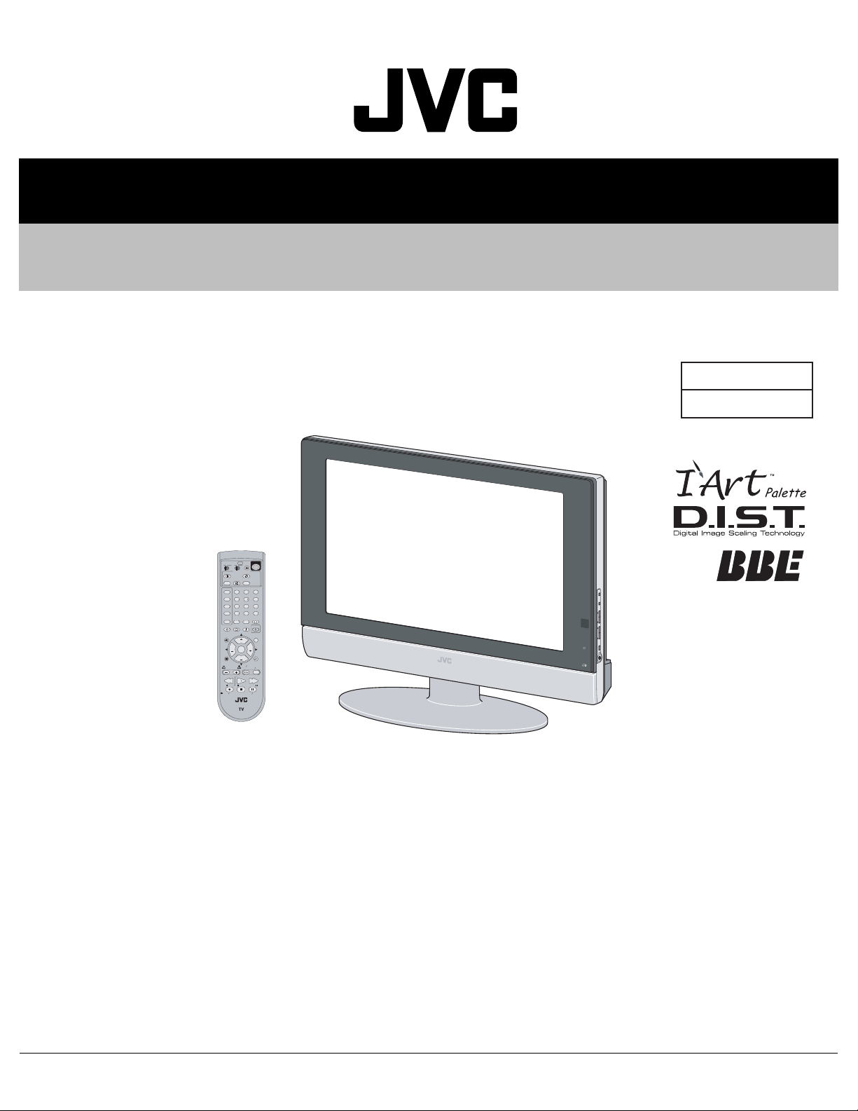
LT-26WX84 /K
BASIC CHASSIS
SB5
POWER
TV
CATV VCR DVD
ASPECT
MULTI SCREEN
INDEX
SPLIT
FREEZE
SWAP SELECT
INPUT 1
V1
123
INPUT 2
V2
456
INPUT 3
V3
789
RETURN+
INPUT 4
100+
TV
0
V4
THEATER
NATURAL
VIDEO
DIGITAL-IN
PRO
CINEMA
STATUS
D-IN
SLEEP TIMER
DISPLAY SOUND
LIGHT
+
MUTING
C.C.
C.C.
VOL VOL
MENU
VCR CHANNEL
PREV NEXT
REW
REC PAUSE
OPEN CLOSE
CH
OK
CH
BACK
VCR DVD
POWER
TV VCR
FFPLAY
STOP
STILL PAUSE
RM-C13G
P
OW
E
R
TABLE OF CONTENTS
1 PRECAUTION. . . . . . . . . . . . . . . . . . . . . . . . . . . . . . . . . . . . . . . . . . . . . . . . . . . . . . . . . . . . . . . . . . . . . . . . . 1-3
2 SPECIFIC SERVICE INSTRUCTIONS . . . . . . . . . . . . . . . . . . . . . . . . . . . . . . . . . . . . . . . . . . . . . . . . . . . . . . 1-6
3 DISASSEMBLY . . . . . . . . . . . . . . . . . . . . . . . . . . . . . . . . . . . . . . . . . . . . . . . . . . . . . . . . . . . . . . . . . . . . . . 1-12
4 ADJUSTMENT . . . . . . . . . . . . . . . . . . . . . . . . . . . . . . . . . . . . . . . . . . . . . . . . . . . . . . . . . . . . . . . . . . . . . . . 1-22
5 TROUBLESHOOTING . . . . . . . . . . . . . . . . . . . . . . . . . . . . . . . . . . . . . . . . . . . . . . . . . . . . . . . . . . . . . . . . . 1-54
COPYRIGHT © 2004 VICTOR COMPANY OF JAPAN, LIMITED
No.YA089
2004/3
Page 2
If you need more information on Computer and Electronic Repair, please visit these
in fact
websites to improve yourself.
http://www.fastrepairguide.com
http://www.protech2u.com
http://www.plasma-television-repair.com
http://www.lcd-television-repair.com
Happy Repairing!!
Highly Recommended Repair Ebook:
If you’re a LCD Monitor repairer, then this is the best guide for you.
Why? Because, the author revealed all his LCD Monitor Repairing
secrets for you. I think, with just few Repair tips you learned from
this guide you will get back your investment!
Click Here to read more.
This eBook will show you how to test the electronic component
correctly and accurately. Some of you may say that I don’t
need this eBook because it is too simple! Do you know that,
there is lots of testing electronic components secrets I have learned
from this guide? Do you know how to test a‘TRIAC’ correctly and
accurately? If you answer no then I guess you have to get this
EBook. Click Here to read more.
Are you tired of searching the service manuals to look for the value
of a burnt resistor? If the answer is YES, then this eBook is a ‘must
have’ guide for you. You can save a lot of time and be able to repair
customer’s Electronic equipment with burnt resistors in it.
Click here to read more.
Page 3
SPECIFICATION
Items Contents
Dimensions ( W × H × D ) 70.3cm × 56.0cm × 26.0cm (Included stand)
70.3cm × 49.1cm × 9.4cm (TV only)
Mass 22.0kg (Included stand)
19.2kg (TV only)
Power Input AC220V , 60Hz
Power Consumption 155W (Max)
TV RF System CCIR (M)
Color System NTSC
Sound System BTSC (Multi Channel Sound)
Teletext System Closed caption
TV Receiving Channels
and Frequency
TV / CATV Total Channel 180 Channels
Intermediate Frequency Video IF
Color Sub Carrier 3.58 MHz
LCD panel 26-inch wide aspect (15:9)
Screen Size Diagonal : 66cm (H:33.9cm × V : 56.6cm)
Display Pixels Horizontal : 1280 dots × Vertical : 768 dots (W-XGA)
Audio Power Output 10W + 10W
Speaker 6.6cm, round type × 2 (Oblique corn)
Antenna terminal (VHF/UHF) F-type connector, 75Ω unbalanced, coaxial
Video / Audio input
Input-1/2/3
Digital-in Video
Monitor output S-Video
Headphone 3.5mm stereo mini jack × 1
Remote Control Unit RM-C13G (AA/R6/UM-3 battery × 2)
Design & specifications are subject to change without notice.
Component Video
VHF Low
VHF High
UHF
CATV
Sound IF
[Input-1]
1125i / 750p
525p / 525i
S-Video
[Input-1/2]
Video
Audio
Audio
Video
Audio
02ch~06ch : 54MHz~88MHz
07ch~13ch : 174MHz~216MHz
14ch~69ch : 470MHz~806MHz
54MHz~804MHz
Low Band : 02~06, A-8 by 02~06&01
High Band : 07~13 by 07~13
Mid Band : A~I by 14~22
Super Band : J~W by 23~36
Hyper Band : W+1~W+28 by 37~64
Ultra Band : W+29~W+84 by 65~94, 100~125
Sub Mid Band : A4~A1 by 96~99
45.75 MHz
41.25 MHz (4.5MHz)
RCA pin jack × 3
Y : 1V (p-p) (Sync signal: 0.35V(p-p), 3-value sync.), 75 Ω
Pb/Pr : ±0.35V(p-p), 75 Ω
Y : 1V (p-p), Positive (Negative sync provided), 75 Ω
Pb/Pr : 0.7V(p-p), 75 Ω
Mini-DIN 4 pin × 2
Y: 1V (p-p), Positive (Negative sync provided), 75 Ω
C: 0.286V (p-p) (Burst signal), 75 Ω
1V (p-p), Positive (Negative sync provided), 75 Ω, RCA pin jack × 3
500mV (rms), High impedance, RCA pin jack × 6
RCA pin jack × 3
DVI-D 24-pin connector × 1
(Digital-input terminal is not compatible with computer signal)
500mV (rms), Low impedance, RCA pin jack × 2
Mini-DIN 4 pin × 1
Y: 1V (p-p), Positive (Negative sync provided), 75 Ω
C: 0.286V (p-p) (Burst signal), 75 Ω
1V (p-p), Positive (Negative sync provided), 75 Ω RCA pin jack × 1
500mV (rms), Low impedance, RCA pin jack × 2
1-2 (No.YA089)
Page 4

SECTION 1
PRECAUTION
1.1 SAFETY PRECAUTIONS
(1) The design of this product contains special hardware,
many circuits and components specially for safety
purposes. For continued protection, no changes should be
made to the original design unless authorized in writing by
the manufacturer. Replacement parts must be identical to
those used in the original circuits. Service should be
performed by qualified personnel only.
(2) Alterations of the design or circuitry of the products should
not be made. Any design alterations or additions will void
the manufacturer's warranty and will further relieve the
manufacturer of responsibility for personal injury or
property damage resulting therefrom.
(3) Many electrical and mechanical parts in the products have
special safety-related characteristics. These
characteristics are often not evident from visual inspection
nor can the protection afforded by them necessarily be
obtained by using replacement components rated for
higher voltage, wattage, etc. Replacement parts which
have these special safety characteristics are identified in
the parts list of Service manual. Electrical components
having such features are identified by shading on the
schematics and by ( ) on the parts list in Service
manual. The use of a substitute replacement which does
not have the same safety characteristics as the
recommended replacement part shown in the parts list of
Service manual may cause shock, fire, or other hazards.
(4) Don't short between the LIVE side ground and
ISOLATED (NEUTRAL) side ground or EARTH side
ground when repairing.
Some model's power circuit is partly different in the GND.
The difference of the GND is shown by the LIVE : ( ) side
GND, the ISOLATED (NEUTRAL) : ( ) side GND and
EARTH : ( ) side GND.
Don't short between the LIVE side GND and ISOLATED
(NEUTRAL) side GND or EARTH side GND and never
measure the LIVE side GND and ISOLATED (NEUTRAL)
side GND or EARTH side GND at the same time with a
measuring apparatus (oscilloscope etc.). If above note will
not be kept, a fuse or any parts will be broken.
(5) If any repair has been made to the chassis, it is
recommended that the PDP voltage setting should be
checked or adjusted.
(6) When service is required, observe the original lead dress.
Extra precaution should be given to assure correct lead
dress in the high voltage circuit area. Where a short circuit
has occurred, those components that indicate evidence of
overheating should be replaced. Always use the
manufacturer's replacement components.
(7) Isolation Check (Safety for Electrical Shock Hazard)
After re-assembling the product, always perform an
isolation check on the exposed metal parts of the cabinet
(antenna terminals, video/audio input and output terminals,
Control knobs, metal cabinet, screw heads, earphone jack,
control shafts, etc.) to be sure the product is safe to operate
without danger of electrical shock.
a) Dielectric Strength Test
The isolation between the AC primary circuit and all metal
parts exposed to the user, particularly any exposed metal
part having a return path to the chassis should withstand a
voltage of 3000V AC (r.m.s.) for a period of one second. (.
. . . Withstand a voltage of 1100V AC (r.m.s.) to an
appliance rated up to 120V, and 3000V AC (r.m.s.) to an
appliance rated 200V or more, for a period of one second.)
This method of test requires a test equipment not generally
found in the service trade.
b) Leakage Current Check
Plug the AC line cord directly into the AC outlet (do not use
a line isolation transformer during this check.). Using a
"Leakage Current Tester", measure the leakage current
from each exposed metal part of the cabinet, particularly
any exposed metal part having a return path to the chassis,
to a known good earth ground (water pipe, etc.). Any
leakage current must not exceed 0.5mA AC (r.m.s.).
However, in tropical area, this must not exceed 0.2mA AC
(r.m.s.).
Alternate Check Method
Plug the AC line cord directly into the AC outlet (do not
use a line isolation transformer during this check.). Use
an AC voltmeter having 1000Ω per volt or more
sensitivity in the following manner. Connect a 1500Ω
10W resistor paralleled by a 0.15µF AC-type capacitor
between an exposed metal part and a known good earth
ground (water pipe, etc.). Measure the AC voltage
across the resistor with the AC voltmeter. Move the
resistor connection to each exposed metal part,
particularly any exposed metal part having a return path
to the chassis, and measure the AC voltage across the
resistor. Now, reverse the plug in the AC outlet and
repeat each measurement. Any voltage measured must
not exceed 0.75V AC (r.m.s.). This corresponds to
0.5mA AC (r.m.s.).
However, in tropical area, this must not exceed 0.3V AC
(r.m.s.). This corresponds to 0.2mA AC (r.m.s.).
AC VOLTMETER
(HAVING 1000 /V,
OR MORE SENSITIVITY)
0.15 F AC-TYPE
GOOD EARTH GROUND
1500 10W
PLACE THIS PROBE
ON EACH EXPOSED
ME TAL PAR T
(No.YA089)1-3
Page 5
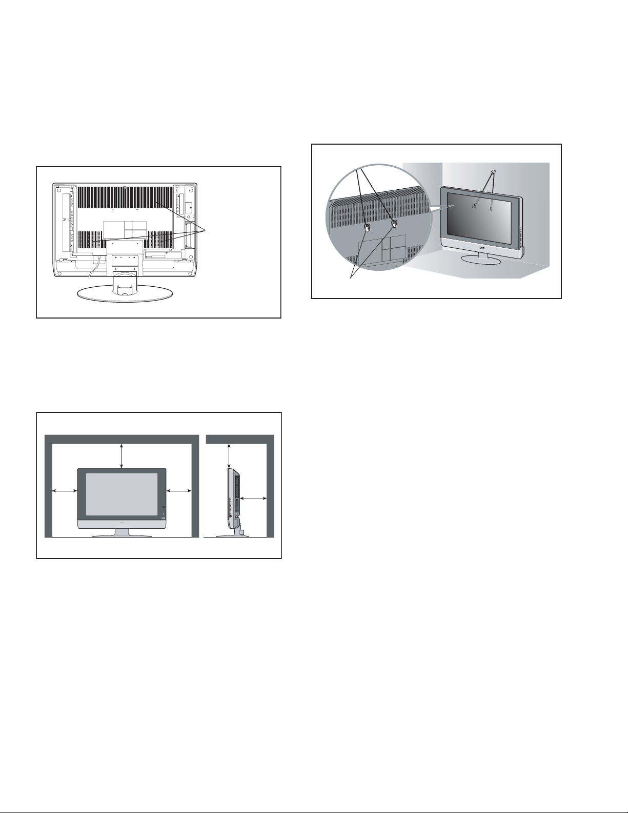
1.2 INSTALLATION
1.2.1 HEAT DISSIPATION
If the heat dissipation vent behind this unit is blocked, cooling
efficiency may deteriorate and temperature inside the unit will
rise. The temperature sensor that protects the unit will be
activated when internal temperature exceeds the pre-determined
level and power will be turned off automatically.Therefore,
please make sure pay attention not to block the heat dissipation
vent as well as the ventilation outlet behind the unit and ensure
that there is room for ventilation around it.
Ventilation hole
1.2.2 INSTALLATION REQUIREMENTS
Ensure that the minimal distance is maintained, as specified
below, between the unit with and the surrounding walls, as well
as the floor etc.Install the unit on stable flooring or stands.Take
precautionary measures to prevent the unit from tipping in order
to protect against accidents and earthquakes.
200 mm
200 mm
1.2.3 INSTALLATION REQUIREMENTS
To ensure safety in an emergency such as an earthquake, and
to prevent accidents, ensure that measures are taken to prevent
the TV dropping or falling over.
Use the supplied screws to firmly attach the supplied hooks
(OPTION) to the back of the TV, and use commercially available
cord to fix the TV to rigid components such as walls and columns.
Supplied hooks (OPTION)
1.2.4 NOTES ON HANDLING
(1) WHEN TAKING UNIT OUT OF A PACKING CASE
When taking the unit out of a packing case, do not grasp
the upper part of the unit. If you take the unit out while
grasping the upper part, the LCD PANEL may be damaged
because of a pressure. Instead of grasping the upper part,
put your hands on the lower backside or sides of the unit.
(2) AS FOR PRESSING OR TOUCHING A SPEAKER
Be careful not to press the opening of the speaker in the
lower part of the unit and around them since the decorative
sheet on the surface of the openings may be deformed.
150 mm
150 mm
50 mm
1-4 (No.YA089)
Page 6

1.3 HANDLING LCD PANEL
1.3.1 PRECAUTIONS FOR TRANSPORTATION
When transporting the unit, pressure exerted on the internal LCD
panel due to improper handling (such as tossing and dropping)
may cause damages even when the unit is carefully packed. To
prevent accidents from occurring during transportation, pay
careful attention before delivery, such as through explaining the
handling instructions to transporters.
Ensure that the following requirements are met during
transportation, as the LCD panel of this unit is made of glass and
therefore fragile:
(1) USE A SPECIAL PACKING CASE FOR THE LCD PANEL
When transporting the LCD panel of the unit, use a special
packing case (packing materials). A special packing case
is used when a LCD panel is supplied as a service spare
part.
(2) ATTACH PROTECTION SHEET TO THE FRONT
Since the front (display part) of the panel is vulnerable,
attach the protection sheet to the front of the LCD panel
before transportation. Protection sheet is used when a LCD
panel is supplied as a service spare part.
(3) AVOID VIBRATIONS AND IMPACTS
The unit may be broken if it is toppled sideways even when
properly packed. Continuous vibration may shift the gap of
the panel, and the unit may not be able to display images
properly. Ensure that the unit is carried by at least 2
persons and pay careful attention not to exert any vibration
or impact on it.
(4) DO NOT PLACE EQUIPMENT HORIZONTALLY
Ensure that it is placed upright and not horizontally during
transportation and storage as the LCD panel is very
vulnerable to lateral impacts and may break. During
transportation, ensure that the unit is loaded along the
traveling direction of the vehicle, and avoid stacking them
on one another. For storage, ensure that they are stacked
in 2 layers or less even when placed upright.
1.3.3 PRECAUTIONS FOR REPLACEMENT OF EXTERIOR
PARTS
Take note of the following when replacing exterior parts (REAR
COVER, FRONT PANEL, etc.):
(1) Do not exert pressure on the front of the LCD panel (filter
surface). It may cause irregular color.
(2) Pay careful attention not to scratch or stain the front of the
LCD panel (filter surface) with hands.
(3) When replacing exterior parts, the front (LCD panel) should
be placed facing downward. Place a mat, etc. underneath
to avoid causing scratches to the front (filter surface).
1.3.2 OPTICAL FILTER (ON THE FRONT OF THE LCD PANEL)
(1) Avoid placing the unit under direct sunlight over a
prolonged period of time. This may cause the optical filter
to deteriorate in quality and color.
(2) Clean the filter surface by wiping it softly and lightly with a
soft and lightly fuzz cloth (such as outing flannel).
(3) Do not use solvents such as benzene or thinner to wipe the
filter surface. This may cause the filter to deteriorate in
quality or the coating on the surface to come off. When
cleaning the filter, usually use the neutral detergent diluted
with water. When cleaning the dirty filter, use water-diluted
ethanol.
(4) Since the filter surface is fragile, do not scratch or hit it with
hard materials. Be careful enough not to touch the front
surface, especially when taking the unit out of the packing
case or during transportation.
(No.YA089)1-5
Page 7
SECTION 2
SPECIFIC SERVICE INSTRUCTIONS
2.1 FEATURES
• New chassis design enable use of an interactive on screen control.
• MOTION COMPENSATION : With this function, the seamless reproduction of dynamic motion on the screen has been realized.
• Bullet-in 3 dimension Y/C separate circuit.
• Receive DTV broadcast (1125i / 750p / 525p / 525i)
• Built-in HDCP / Component (Y / Pb / Pr) input.
• Built-in Hyper Sound, BBE circuit.
• DIST is a digital high-definition image processing technology that converts various image input signals such as NTSC(480i), 480p,
720p, and 1080i into a format with the best resolution for a display device such as a plasma display panel, and displays highdefinition images.
2.2 TECHNICAL INFORMATION
2.2.1 LCD PANEL
This unit uses the flat type panel LCD (Liquid Crystal Display) panel that occupies as little space as possible, instead of the
conventional CRT (Cathode Ray Tube), as a display unit.
2.2.1.1 STRUCTURE
The LCD panel of the unit is constructed with the metal chassis that surrounds the panel unit and supports the LCD panel part and
the backlight part to protect them.
The color filter glass and the TFT glass (thin film transistor) are inserted between the front polarizing filter and the rear polarizing filter.
Liquid crystals are inserted between the color filter glass and the TFT glass. Since the gap between the two glasses is only a few µm,
a spacer (bead) is inserted in the gap to retain the gap.
The backlight unit is placed behind the LCD panel. Since liquid crystals themselves do not emit light, the backlight as an external light
source emits light to the LCD panel from behind through the diffuser.
Circuit boards for controlling the LCD panel and the backlight are attached around the back part of the LCD panel unit.
Since the unit has the two polarizing filter that are at right angles to each other, the unit adopts "normally black" mode, where light
does not pass through the polarizing filter and the screen is black when no voltage is applied to the liquid crystals.
Top chassis
Lower frame
Upper frame
Panel ASSY
Diffuser (including board)
Diffuser supporter
Source board
Lamp supporter
Inverter shield cover
Sield case
Inverter board
Reflection plate
1-6 (No.YA089)
Fig.1 Structure of the LCD panel unit
Page 8
2.2.1.2 SPECIFICATIONS
The following table shows the specifications of this unit.
Item Specifications Remarks
Maximum dimensions ( W × H × D ) 62.7cm × 38.9cm × 4.9cm
Weight 8.0kg
Effective screen size Diagonal : 66cm (H:33.9cm × V : 56.6cm) 26V type
Aspect ratio 15:9
Drive device/ system a-Si-TFT, active matrix system
Resolution Horizontally 1280 × Vertically 768 × RGB <W-XGA> 2949120 dots in total
Pixel pitch (pixel size) Horizontally:0.4425mm, Vertically:0.4425mm
Displayed color 16777216 colors 256 colors for R, G, and B
Brightness 450cd/m
2
500cd/m2 at maximum
Contrast ratio 500:1
Response time 16.7ms
View angle Vertically 170°, horizontally 170°
2.2.1.3 PIXEL FAULT
There are three pixel faults - bright fault , dark fault and flicker fault - that are respectively defined as follows.
(1) BRIGHT FAULT
In this pixel fault, a cell that should not light originally is lighting on and off.
For checking this pixel fault, input ALL BLACK SCREEN and find out the cell that is lighting on and off.
(2) DARK FAULT
In this pixel fault, a cell that should light originally is not lighting or lighting with the brightness twice as brighter as originally lighting.
For checking this pixel fault, input 100% of each R/G/B colour and find out the cell that is not lighting.
(3) FLICKER FAULT
In the pixel fault, a cell that should light originally or not light originally is flashing on and off.
For checking this pixel fault, input ALL BLACK SCREEN signal or 100% of each RGB colour and find out the cell that is flashing on
and off.
(No.YA089)1-7
Page 9

2.2.2 MAIN MICRO COMPUTER (CPU) FUNCTION
Pin No. Pin name I/O Function
1 BS_RXD O Not used
2 MICON_V I Vertical sync for OSD / CLOSED CAPTION
3 LB_PRO I Low B protection detect [Detection : H]
4 NC --- Not used
5 /RST I Reset [Reset : L]
6 HDMI_INT I Not used
7/TEST I3.3V
8 OSD_YS O YS for OSD / CLOSED CAPTION
9 (DPCRST) O Not used
10 BS/DIN O Not used
11 (A_MU)(LED_5) O Not used
12 MICON_H I Horizontal sync for OSD / CLOSED CAPTION
13 (A_MU)(LED_4) O Not used
14 P46,OSDXI --- Not used
15 P45,OSDXO --- Not used
16 (SDA2) I/O Not used
17 AC_IN I AC power (60Hz) for time clock
18 (SCL2) O Not used
19 (TU_POW) O Not used
20 VCOI I LPF input
21 PDO O LPF output
22 /IP_RESET O Reset (L) [Reset : L]
23 OSD_YM O YM for OSD / CLOSED CAPTION
24 OSD_B O B signal output for OSD / CLOSED CAPTION
25 POW_LED O Lighting for power [Lighting : H]
26 OSD_G O G for OSD / CLOSED CAPTION
27 OSD_R O R for OSD / CLOSED CAPTION
28 VRE I Reference voltage
29 IP_ERR I AMDP program load
30 IREF I Reference current
31 COMP I Reference conpare
32 AVDD I 3.3V
33 CLL O Not used
34 VREFLS I Reference voltage (For SUB CCD)
35 SUB_CCD I Not used
36 NC --- Not used
37 VSS I GND
38 MAIN_CCD I Not used
39 VREFHS I Standard voltage (For Main CCD)
40 CLH I Not used
41 VDD/VPP I 3.3V
42 CLKSW1 O IP clock switch [ON : L]
43 CLKSW2 O IP clock switch [ON : L]
44 ON_TIM O Not used
45 SBO01 O Port for writing on board
1-8 (No.YA089)
Page 10

Pin No. Pin name I/O Function
46 SBD01 I Port for writing on board / Communication (XTD) for SUB CPU
47 SBT1 I Port for writing on board / Communication (RTD) for SUB CPU
48 HP_VOL O Headpone volume control (0V-3.3V)
49 /BS_RESET O Not used
50 HDMI_ASW O Not used
51 BS1.5CTL O Not used
52 ODU_OUT O Not used
53 15/11_SW O Not used
54 ODU_PRO O Not used
55 BS_POW --- Not used
56 BS3.3CTL O Not used
57 AFT2 I Not used
58 /LOB_POW O Low B power control [Detection : H]
59 COMPULING I Not used
60 /POWERGOOD I Power condition check [ON : L]
61 MECHA_SW I Mechanical (POWER) swtich detection [Pussing : L]
62 /MAIN_POW O Main power control [ON : L]
63 NC --- Not used
64 (B1_POW) O Not used
65 AFT1 --- Not used
66 (X_RAY) I GND
67 (EE_CDS) I GND
68 KEY2 I Key scan data [ON : H]
69 KEY1 I Key scan data [ON : H]
2
70 SCL1 O I
71 SDA1 I/O I
C bus clock (For Main memory)
2
C bus data (For Main memory)
72 REMO I Remote control data
73 (AP_REQ)(LED_2) O Not used
74 VSS I GND
75 OSC2 O 4MHz oscillation for system clock
76 OSC1 I 4MHz oscillation for system clock
77 VDD I 3.3V
2
78 SCL0 O I
C bus clock (For general)
79 (AP_CLK)(LED_1) O Not used
2
80 SDA0 I/O I
C bus data (For general)
81 BSLK(D_CLOCK) O Not used
82 BS_TXD(D_DATA) I Not used
83 NC --- Not used
84 P_MU O Picture muting [Muting : H]
(No.YA089)1-9
Page 11

2.2.3 SUB MICRO COMPUTER (CPU) FUNCTION
Pin No. Pin name I/O Function
1 (SYSTEM0) I GND
2 (SYSTEM3) I GND
3 AVCC - 5V
4 X2 - Not used
5 X1 - Not used
6 VCL - Internal down voltage
7 RES I Reset [Reset : L]
8 TEST I Operation test for SUB CPU
9 VSS - GND
10 OSC2 O 10MHz oscillation for system clock
11 OSC1 I 10MHz oscillation for system clock
12 VCC - 5V
13 NC O Not used
14 NC O Not used
15 BL_D2 O Back light 20ms delay for LCD panel [On:L]
16 BL_D1 O Back light 10ms delay for LCD panel [On:L]
17 I2C_STOP O Not used
18 BL_ON O Back light reset for LCD panel [Reset:L]
19 NC O Not used
20 NC O Not used
21 NC O Not used
22 NC O Not used
2
23 SDA1 I/O I
C bus data (For Sub memory)
24 A.DIM O Not used
2
25 SCL1 O I
26 SDA0 I/O I
27 SCL0 O I
C bus clock (For Sub memory)
2
C bus data (For general)
2
C bus clock (For general)
28 NC O Not used
29 NC O Not used
30 NC O Not used
31 NC O Not used
32 NC O Not used
33 NC O Not used
34 NC O Not used
35 NMI I Port for writing on board [Writning:L]
36 NC O Not used
37 (HD) I Not used
38 NC O Not used
39 (REMO) I Not used
40 NC O Not used
41 P85 -/I Not used
42 P86 - Not used
43 P87 - Not used
44 SCK3 O Port for writing on board
45 RXD I Port for writing on board
1-10 (No.YA089)
Page 12
Pin No. Pin name I/O Function
46 TXD O Port for writing on board
47 (PROTECTOR0) I Not used
48 NC O Not used
49 RXD2 I Port for communication (Main cpu)
50 TXD2 O Port for communication (Main cpu)
51 NC O Not used
52 (ACTIVE) I Not used
53 VD I Vertical sync
54 (REC_DET) I Not used
55 (PSS) I Not used
56 (ALARM) I Not used
57 (SYSTEM2) I Not used
58 (SYSTEM1) I Not used
59 (PROTECTOR1) I Not used
60 (AMP_PRO2) I Not used
61 (AMP_PRO1) I Not used
62 EE_CDS I Not used
63 (KEY_IN1) I Not used
64 (KEY_IN2) I Not used
(No.YA089)1-11
Page 13
SECTION 3
DISASSEMBLY
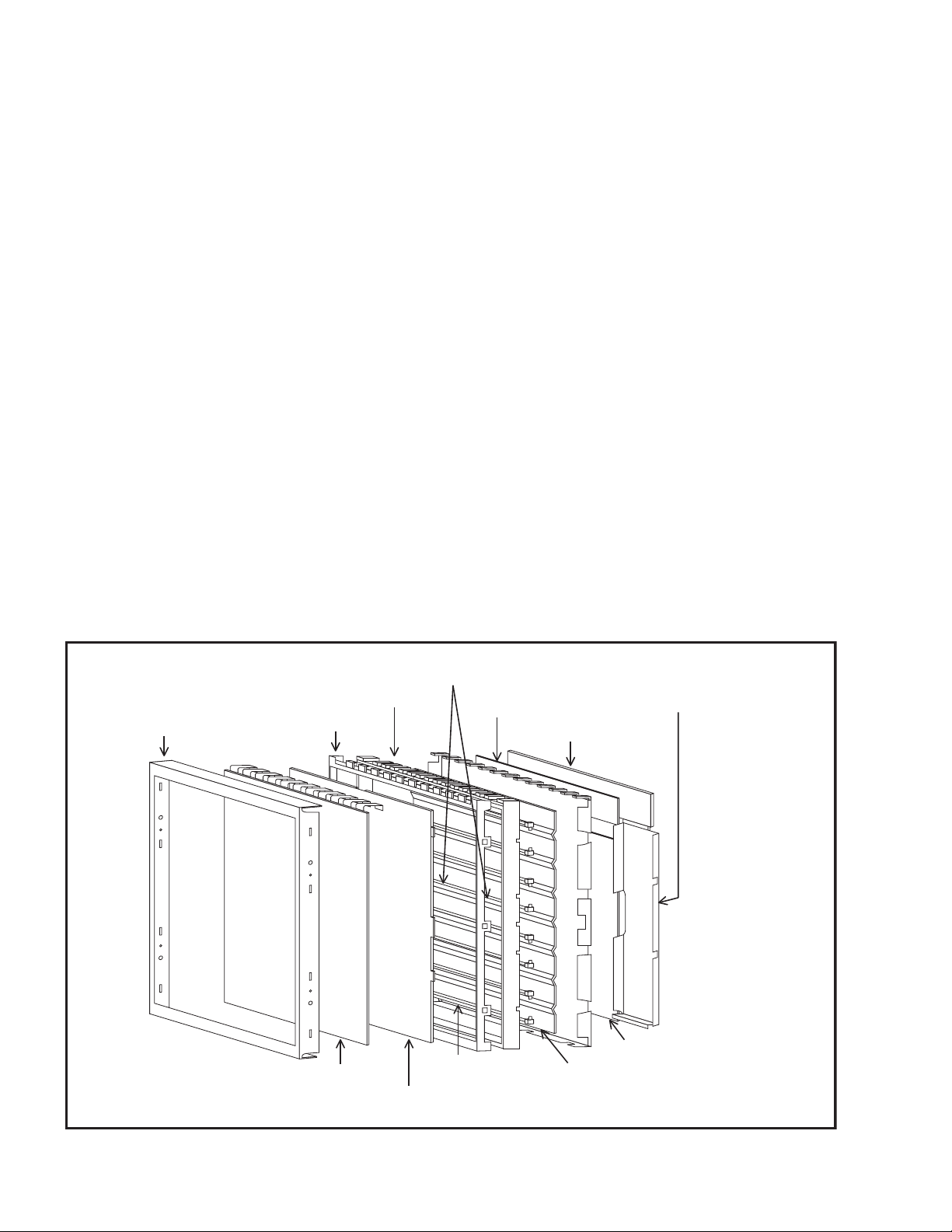
3.1 DISASSEMBLY PROCEDURE
NOTE:
Since this model adopts a layer structure, follow the procedure
below in disassembling this model.
Be careful enough not to damage or scratch parts.
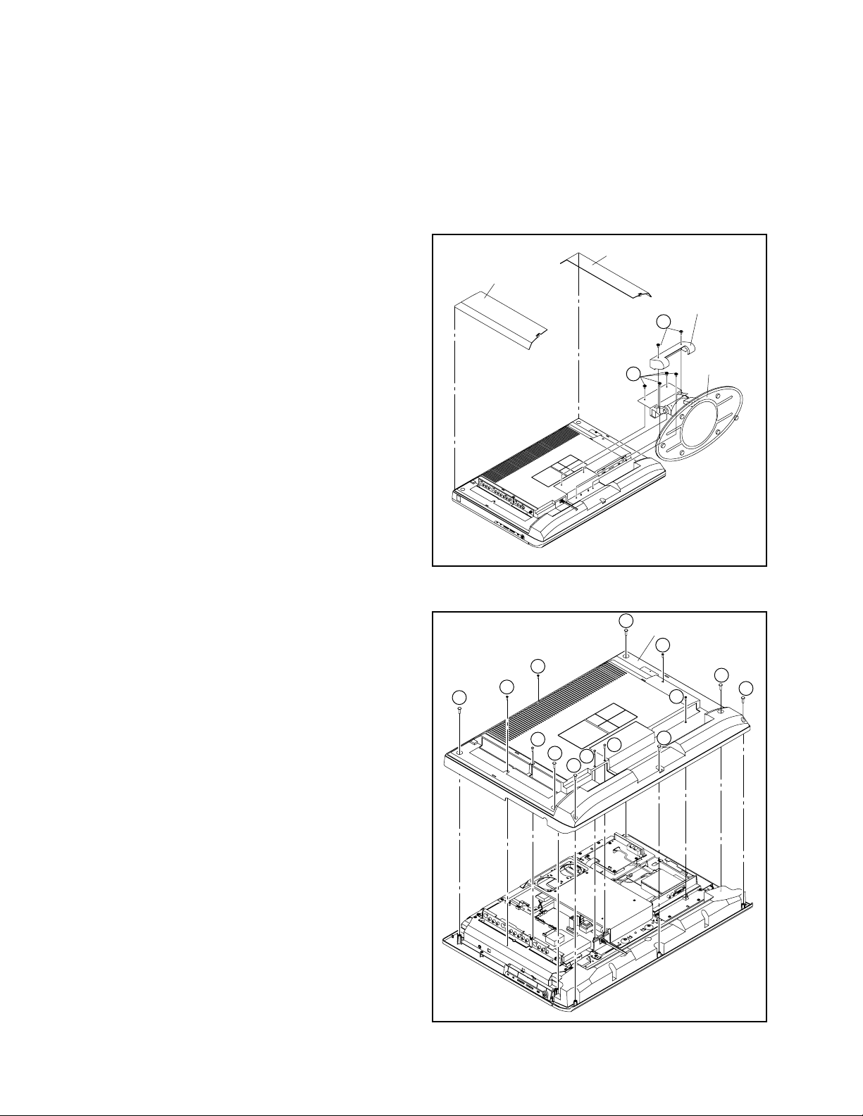
3.1.1 REMOVING THE STAND
(1) Remove the 2 screws [A], and remove the STAND
COVER.
(2) Remove the 4 screws [B], and remove the STAND.
JACK COVER(R)
JACK COVER(R)
STAND COVER
A
3.1.2 REMOVING THE REAR COVER
• Remove the STAND.
(1) Remove the JACK COVER (R).
(2) Remove the JACK COVER (L).
(3) Remove the 7 screws [C], 3 screws [D], and 4 screws [E]
(14 screws in total).
(4) Remove the REAR COVER.
B
STAND
Fig.3-1-1
C
REAR COVER
E
E
C
E
D
C
D
D
C
E
C
C
C
1-12 (No.YA089)
Fig.3-1-2
Page 14
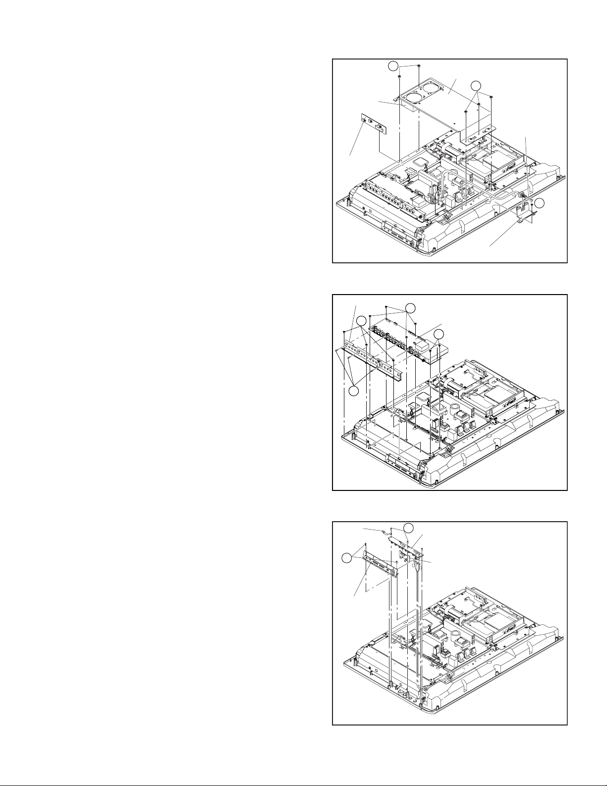
3.1.3 REMOVING THE FAN BRACKET / REGULATOR PWB / POWER CORD
• Remove the STAND.
• Remove the REAR COVER.
(1) Pull out the wire of COOLING FAN (the connector [Y] of the
POWER PWB).
(2) Remove the 5 screws [F], and remove the FAN BRACKET.
(3) Remove the REGULATOR PWB.
COOLING
FAN
(4) Pull out the POWER CORD.
(5) Remove 1 screw [G], and remove the POWER CORD
HOLDER.
REGULATOR
PWB
F
FAN BRACKET
F
POWER CORD
3.1.4 REMOVING THE RECEIVER PWB
• Remove the STAND.
• Remove the REAR COVER.
(1) Remove the 3 screws [H] and 3 screws [J] (6 screws in
total). Then, remove the TERMINAL BASE.
(2) Remove the 6 screws [K], and remove the RECEIVER
PWB.
TERMINAL BASE
H
J
K
G
Fig.3-1-3
RECEIVER PWB
K
G
POWER CORD HOLDER
3.1.5 REMOVING THE FRONT CONTROL PWB CONTROL / FRONT SENSOR PWB
• Remove the STAND.
• Remove the REAR COVER.
(1) Remove the 2 screws [L], and remove the CONTROL
KNOB.
EARTH
PLATE
L
(2) Remove the 3 screws [M], and remove the FRONT
CONTROL PWB.
(3) Remove the FRONT SENSOR PWB.
KNOB
Fig.3-1-4
M
FRONT CONTROL PWB
FRONT SENSOR PWB
T
U
Fig.3-1-5
(No.YA089)1-13
Page 15
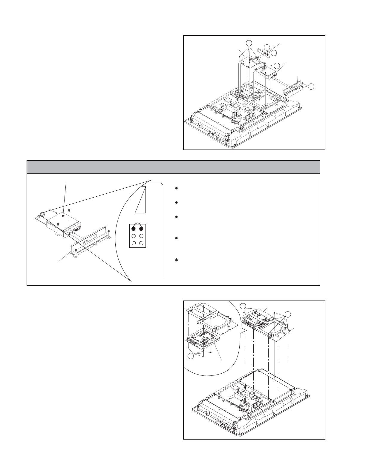
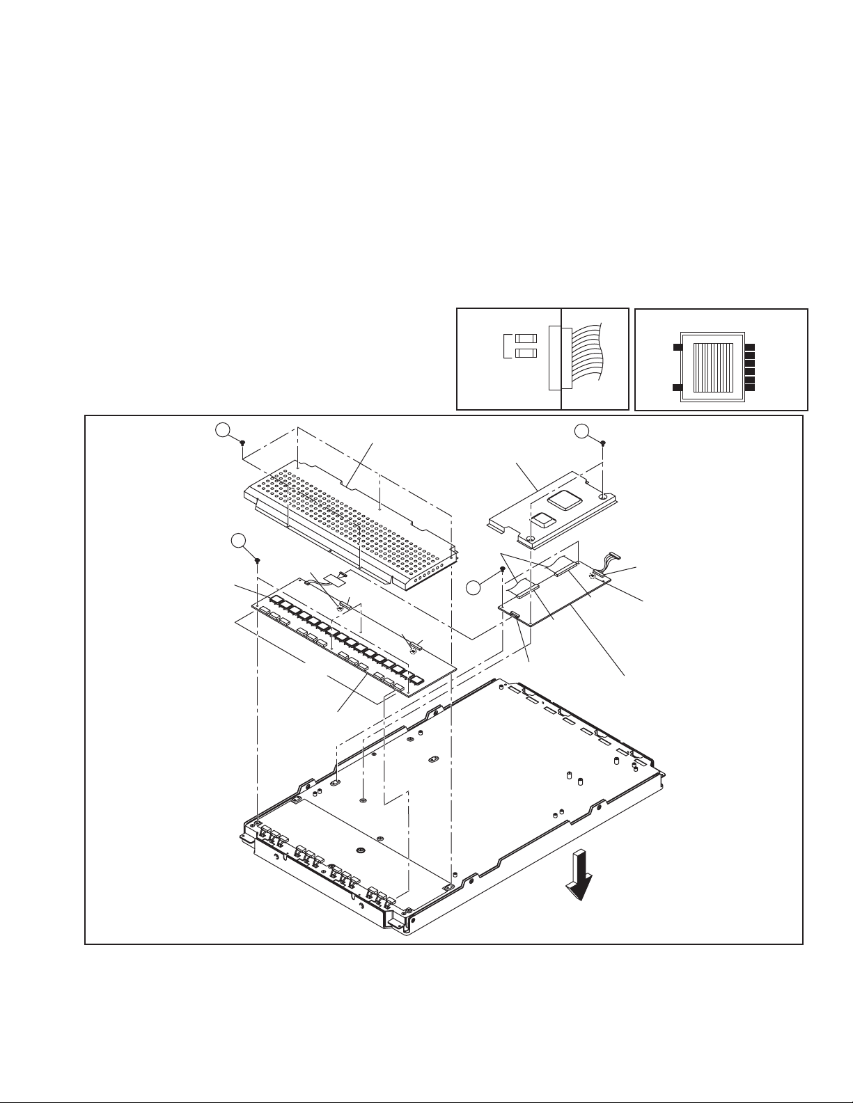
3.1.6 REMOVING THE VIDEO PWB / DIGITAL INPUT MODULE PWB
• Remove the STAND.
• Remove the REAR COVER.
(1) Remove the 1 screw [N] and 1 screw [P]. Then, remove the
JACK BASE.
(2) Remove the 4 screws [Q], and remove the VIDEO PWB.
(3) Remove the 2 screws [R], and remove the DIGITAL INPUT
MODULE BASE.
(4) Remove the 4 screws [S], and remove the DIGITAL INPUT
MODULE PWB.
CAUTION AT DISASSEMBLY
DIGITAL INPUT MODULE
Prior to disassembly, unplug the power code from the AC
outlet without fail. (Turn the power "off".)
Short the SB connector
INPUT MODULE. (At the time of assembling)
Before the rear panel is inserted into the cabinet, release
the short-circuit between the SB connector
pin of the DIGITAL INPUT MODULE.
After releasing the short-circuit between the SB
connectors, do not turn the power on until the rear panel
is inserted into the cabinet.
Negligence in carrying out the above steps may cause
the inactivation of the TV.
DIGITAL INPUT
MODULE BASE
1
3
5
SB
connector
2
4
6
VIDEO PWB
Q
N
P
S
JACK BASE
DIGITAL INPUT
MODULE
DIGITAL INPUT
MODULE BASE
R
Fig.3-1-6
[1] pin and [2] pin of the DIGITAL
[1] pin and [2]
3.1.7 REMOVING THE MI-COM & DIST MODULE PWB
• Remove the STAND.
• Remove the REAR COVER.
• DIGITAL INPUT MODULE PWB
(1) Remove the 7 screws [T], and remove the VIDEO PWB
BRACKET.
(2) Remove the 4 screws [U], and remove the MI-COM & DIST
MODULE PWB from the VIDEO PWB BRACKET.
1-14 (No.YA089)
U
MI-COM & DIST
MODULE PWB
T
Fig.3-1-7
VIDEO PWB BRACKET
T
Page 16
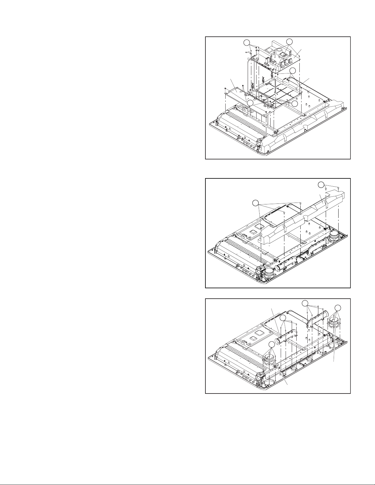
3.1.8 REMOVING THE POWER PWB
• Remove the STAND.
• Remove the REAR COVER.
• Remove the FAN BRACKET.
• Remove the POWER CORD.
• Remove the RECEIVER PWB.
(1) Remove the 4 screws [X], and remove the AV JACK
BRACKET.
(2) Remove the 6 screws [Y], and remove the POWER PWB.
(3) Remove the 6 screws [Z], and remove the CHASSIS
BASE.
3.1.9 REMOVING THE SPEAKER
• Remove the STAND.
• Remove the REAR COVER.
• Remove the POWER CORD.
(1) Remove the 5 screws [a], and remove the SPEAKER BOX.
AV JACK
BRACKET
Y
Q
P
X
Y
POWER PWB
Z
CHASSIS BASE
Z
Fig.3-1-8
a
SPEAKER BOX
a
(2) Remove the 4 screws [b], and remove the SPEAKER (L /
R).
(3) Remove the 4 screws [c], and remove the DUCT COVER/
DUCT BASE.
NOTE:
Since the speaker is attached in a certain direction, attach the
speaker in the same correct direction as it has been attached.
Fig.3-1-9A
DUCT BASE/DUCT COVER
c
b
SPEAKER(R)
Fig.3-1-9B
c
b
SPEAKER(L)
(No.YA089)1-15
Page 17
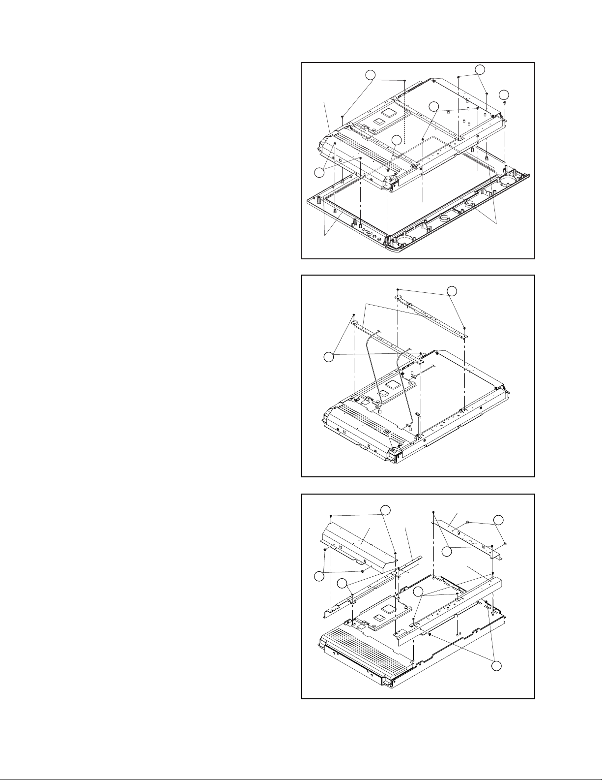
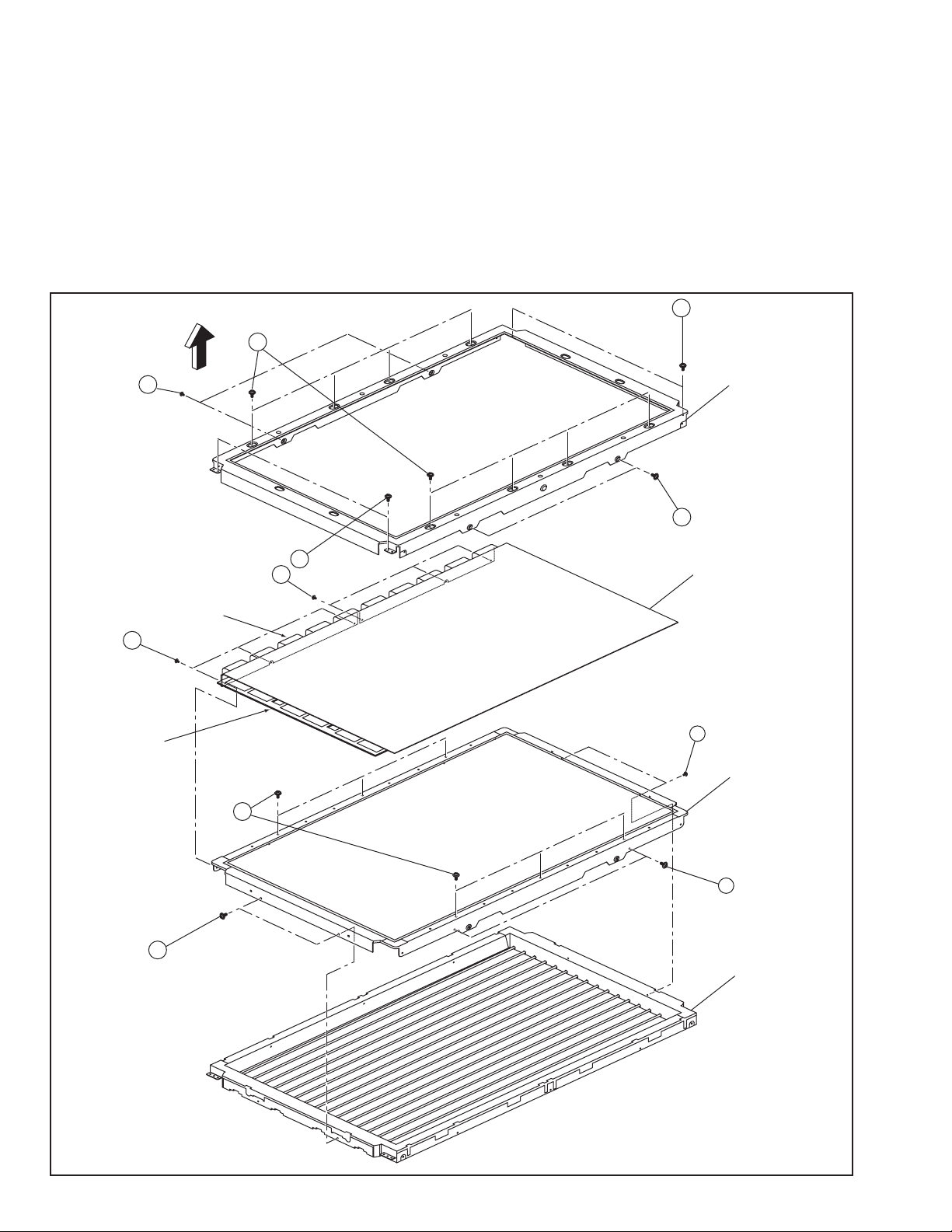
3.1.10 REMOVING THE LCD PANEL UNIT
NOTE:
The LCD PANEL is fixed to the FRONT PANEL (at the back
side) by using double-side adhesive tapes. To remove the
LCD PANEL, remove the adhesive tape on the FRONT PANEL slowly.
• Remove the STAND.
• Remove the REAR COVER.
• Remove the POWER CORD.
• Remove the RECEIVER.
• Remove the FRONT CONTROL PWB.
• Remove the FRONT SENSOR PWB.
• Remove the VIDEO PWB.
• Remove the DIGITAL INPUT MODULE PWB.
• Remove the MI-COM & DIST MODULE PWB.
• Remove the POWER PWB.
(1) Remove the 8 screws [d] and the 2 screws [e] (ten screws
in total). Then, remove the LCD PANEL UNIT.
LCD PANEL
d
Adhesive tape
a
d
e
d
e
Adhesive tape
Fig.3-1-10A
(2) Remove the 2 screws [f], and remove the CENTER
FRAME (x2).
(3) Remove the 2 screws [g] and the 2 screws [h] (4 screws in
total). Then, remove the FRAME (R).
(4) Remove the 2 screws [g] and the 2 screws [h] (4 screws in
total). Then, remove the FRAME (L).
(5) Remove the 2 screws [j], and remove the TOP FRAME.
(6) Remove the 3 screws [k] and the 2 screws [m] (5 screws in
total). Then, remove the BOTTM FRAME.
CENTER FRAME
f
FRAME(R)
h
j
P
Fig.3-1-10B
g
TOP FRAME
f
X
Q
FRAME(L)
h
g
BOTTOM FRAME
h
1-16 (No.YA089)
m
Fig.3-1-10c
Page 18
3.1.11 REMOVING THE LCD PANEL
3.1.11.1 REMOVING THE CONTROL PWB
• Place the LCD PANEL with its backside facing upward.
Be careful not to damage the surface of the screen.
(1) Remove the 2 screws [A], and remove the CONTROL
PWB COVER.
(2) Remove the claws in the connectors [FPC RIGHT] and
[FPC LEFT], and pull out to remove the FLEXIBLE PWB.
NOTE:
Be careful not to damage the FLEXIBLE PWB.
Especially during assembly procedure, be careful not to
insert the FLEXIBLE PWB in the Panel.
(3) Remove the 2 screws [B], and remove the CONTROL
PWB.
[Confirmation after replacement]
• Confirm that voltage of 10 pin (B/L On/Off) in the connector
[CNI1] is approx.5.0V.
• Confirm that the voltage in output of the fuses [F1] and [F2]
in the connector [CNI1] is approx.5.0V.
3.1.11.2 REMOVING THE INVERTER PWB
(1) Remove the 5 screws [C], and remove the INVERTER
PWB COVER.
(2) Pull out and remove the wires from connectors [CN4]-
[CN15] (12 connectors in total).
(3) Remove the 4 screws [D], and remove the INVERTER
PWB.
[Confirmation after replacement]
• Confirm that the voltage in output of the fuses [F1] and [F2]
in the connector [CN1] and the fuses [F3] and [F4] in the
connector [CN2] is 16V.
• Confirm that the voltage in input of the TRANSFORMER in
the Inverter Board is 8V.
• Be careful about high voltage (approx. AC900V) in output.
FUSE
OUTPUT
CONTOROL PWB
INVERTER PWB
CONNECTOR
OUTPUT
TRANSFORMER
GND
8V
8V
8V
8V
GND
INPUT
C
TRANSFORMER
D
FUSE
(F3, F4)
[CN4㨪CN15]
INVERTER PWB
INVERTER PWB COVER
CONTROL PWB COVER
FLEXIBLE
CN2
FUSE
(
)
F1, F2
CN1
PWB
B
CNI1
A
LEFT
FRC
RIGHT
CONTROL PWB
FRC
CNT1
FUSE
(F1, F2)
FRONT
(No.YA089)1-17
Page 19
3.1.11.3 REMOVING THE BACKLIGHT UNIT
NOTE:
Do not carry out the following procedure in a dusty and dirty
place.
If the surface of LCD GLASS, the surface of DIFFUSER
SHEET, and the inside of BACKLIGHT UNIT are dusty or dirty,
they cause unevenness of a displayed screen.
• Remove the CONTROL PWB.
• Remove the INVERTER PWB.
• Place the LCD UNIT with the screen facing upward.
(1) Remove the 8 screws [E], 4screws [F], and 4 screws [G]
(16 screws in total), and remove the MAIN CHASSIS.
NOTE:
Be careful not to damage the SOURCE IC and the GATE
IC on the side of LCD GLASS when removing the MAIN
CHASSIS.
(2) Remove the 6 screws [H] from the top side of the LCD
UNIT.
(3) Remove the 12 screws [I] from the sides of the LCD UNIT.
Then, LCD GLASS, DIFFUSER SHEET, and BACKLIGHT
UNIT are removed.
G
SOURCE IC
I
GATE IC
FRONT
F
E
MAIN CHASSIS
G
F
I
LCD GLASS
I
DIFFUSER SHEET
1-18 (No.YA089)
H
I
I
BACKLIGHT UNIT
Page 20
3.2 MEMORY IC REPLACEMENT
• This model uses the memory IC.
• This memory IC stores data for proper operation of the video and drive circuits.
• When replacing, be sure to use an IC containing this (initial value) data.
3.2.1 MEMORY IC REPLACEMENT PROCEDURE
1. Power off
Switch off the power and disconnect the power plug from the
AC outlet.
2. Replace the memory IC
Be sure to use the memory IC written with the initial setting
values.
3. Power on
Connect the power plug to the AC outlet and switch on the
power.
4. Receiving channel setting
Refer to the OPERATING INSTRUCTIONS and set the
receive channels (Channels Preset) as described.
5. User setting
Check the user setting items according to the given in page
later. Where these do not agree, refer to the OPERATING
INSTRUCTIONS and set the items as described.
6. SERVICE MENU setting
Verify what to set in the SERVICE MENU, and set whatever is
necessary (Fig.1). Refer to the SERVICE ADJUSTMENT for
setting.
3.2.2 SERVICE MENU SETTING ITEMS
SERVICE MODE
1.PICTURE/SOUND
2.YC SEP
3.WHITE BALANCE
4.MEMORY SETUP
5.RF AFC
6.DD/CM
7.PANEL
8.PP
9.IP
0.HDMI
Fig.1
Setting items Settings Item No.
1. PICTURE/SOUND (sound and picture setting)
Audio circuits (A) Fixed A01~A27
Video circuits (S) Adjust S01~S99
Drive circuits (D) Fixed D01~D32
Factory setting items (F) Adjust F01~F59
2. YC SEP (3-dimensional YC separation setting)
Adjust YCM001~YCM185
Fixed YCS001~YCS114
3. WHITE BALANCE [Can not adjust]
4. MEMORY SETUP (Memory data edit) [Do not adjust]
5. RF AFC: AFC setting (Automaticaly set) [Do not adjust]
6. DD/CM (Panel image processing setting)
Adjust DDT01~DDT34
Fixed CMT01~CMT57
7. PANEL (Panel power limit control) [Do not adjust]
Fixed PDA001~PDA012
8. PP (Multi-screen processing setting)
Adjust ADM001~ADM034
Fixed PPA001~PPA008
Fixed PPB001~PPB036
Fixed PPC001~PPC008
Fixed PPD001~PPD025
9. IP (DIST processing setting) [Do not adjust]
Fixed IPA001~IPA120
Fixed IPB001~IPB079
Fixed IPC001~IPC044
Fixed IPD001~IPD026
Fixed IPE001~IPE015
0. HDMI (Digital input process setting) [Do not adjust]
Fixed HDM001~HDM080
Fixed RHD001~RHD170
(No.YA089)1-19
Page 21
3.2.3 SETTINGS OF FACTORY SHIPMENT
3.2.3.1 BUTTON OPERATION 3.2.3.2 REMOTE CONTROL DIRECT OPERATION
Setting item Setting position
POWER OFF
INPUT TV
CHANNEL CABLE-02
VOLUME 10
3.2.3.3 REMOTE CONTROL MENU OPERATION
(1) PICTURE ADJUSTMENT
Customers can adjust the picture setting of menu screen as their own like but the picture standard value during factory shipment is as
below.
NTSC MODE
Setting item PICTURE BRIGHT COLOR TINT DETAIL
DINAMIC +07 +05 00 00 +04 HIGH OFF VIVID
STANDARD 00 00 00 00 00 LOW OFF STD
GAME -05 00 +05 00 -03 HIGH OFF STD
THEATER 00 00 00 00 00 HIGH OFF STD
INPUT TV
CHANNEL CABLE-02
VOLUME 10
MUTING OFF
DISPLAY OFF
SOUND A.H.S OFF
ASPECT NTSC, 525i,525p PANORAMA
OFF TIMER OFF
VIDEO STATUS DYNAMIC
NATURAL CINEMA AUTO
Setting item Setting position
BBE ON
A.H.B ON
750p,1125i FULL
COLOR
TEMPERATURE
DIGI. NOISE
CLEAR
COLOR
MANAGEMENT
HD MODE
Setting item PICTURE BRIGHT COLOR TINT DETAIL
DINAMIC +04 +06 -08 00 +02 HIGH OFF VIVID
STANDARD 00 00 00 00 00 LOW OFF STD
GAME -05 00 +05 00 00 HIGH OFF STD
THEATER 00 00 00 00 00 LOW OFF STD
(2) SOUND ADJUST (3) CLOCK / TIMERS
Setting item Setting position
TREBLE 00
BASS 00
BALANCE 00
MTS STEREO
(4) INITIAL SETUP
Setting item Setting position Setting item Setting position
POSITION ADJUSTMENT Center NOISE MUTING ON
VIDEO STATUS DYNAMIC FRONT PANEL LOCK OFF
XDS ID ON AUTO SHUT OFF OFF
POWER INDICATOR HIGH DIGITAL-IN SIZE-1
VIDEO-1 MONITOR OUT OFF V-CHIP OFF
LANGUAGE KOR AUTO DEMO OFF
CLOSED CAPTION
CAPTION CC1 IMAGE SHIFT STD
TEXT T1 V1 SMART INPUT OFF
SET CLOCK --ON / OFF TIMER NO
Setting item Setting position
COLOR
TEMPERATURE
DIGI. NOISE
CLEAR
COLOR
MANAGEMENT
1-20 (No.YA089)
Page 22
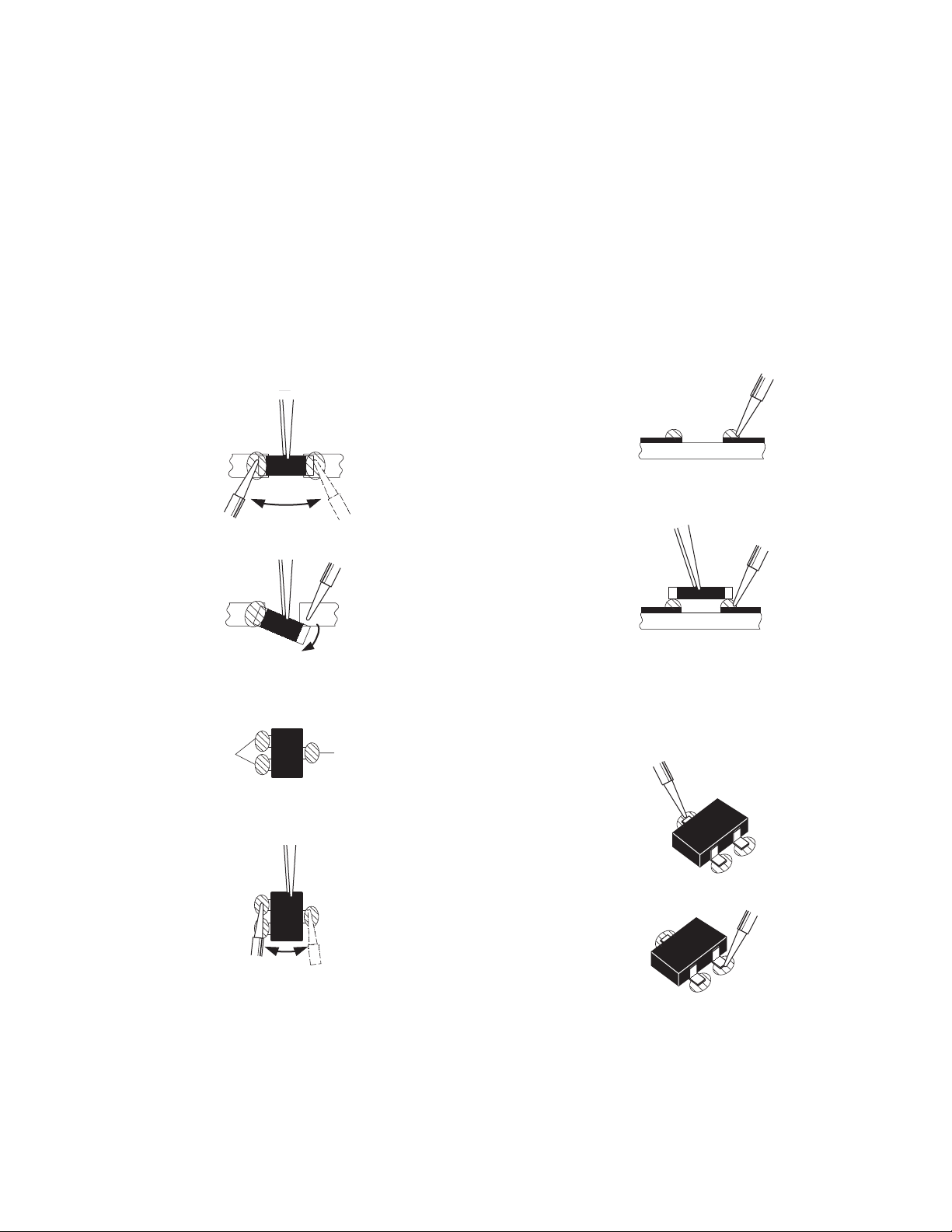
3.3 REPLACEMENT OF CHIP COMPONENT
3.3.1 CAUTIONS
(1) Avoid heating for more than 3 seconds.
(2) Do not rub the electrodes and the resist parts of the pattern.
(3) When removing a chip part, melt the solder adequately.
(4) Do not reuse a chip part after removing it.
3.3.2 SOLDERING IRON
(1) Use a high insulation soldering iron with a thin pointed end of it.
(2) A 30w soldering iron is recommended for easily removing parts.
3.3.3 REPLACEMENT STEPS
1. How to remove Chip parts
2. How to install Chip parts
[Resistors, capacitors, etc.]
(1) As shown in the figure, push the part with tweezers and
alternately melt the solder at each end.
(2) Shift with the tweezers and remove the chip part.
[Transistors, diodes, variable resistors, etc.]
(1) Apply extra solder to each lead.
SOLDER
SOLDER
[Resistors, capacitors, etc.]
(1) Apply solder to the pattern as indicated in the figure.
(2) Grasp the chip part with tweezers and place it on the
solder. Then heat and melt the solder at both ends of the
chip part.
[Transistors, diodes, variable resistors, etc.]
(1) Apply solder to the pattern as indicated in the figure.
(2) Grasp the chip part with tweezers and place it on the
solder.
(3) First solder lead A as indicated in the figure.
(2) As shown in the figure, push the part with tweezers and
alternately melt the solder at each lead. Shift and remove
the chip part.
NOTE :
After removing the part, remove remaining solder from the
pattern.
A
B
C
(4) Then solder leads B and C.
A
B
C
(No.YA089)1-21
Page 23

SECTION 4
ADJUSTMENT
4.1 ADJUSTMENT PREPARATION
(1) There are 2 ways of adjusting this TV : One is with the
REMOTE CONTROL UNIT and the other is the
conventional method using adjustment parts and
components.
(2) The adjustment using the REMOTE CONTROL UNIT is
made on the basis of the initial setting values. The
setting values which adjust the screen to the optimum
condition can be different from the initial setting
values.
(3) Make sure that connection is correctly made AC to AC
power source.
(4) Turn on the power of the TV and measuring instruments for
warning up for at least 30 minutes before starting
adjustments.
(5) If the receive or input signal is not specified, use the most
appropriate signal for adjustment.
(6) Never touch the parts (such as variable resistors,
transformers and condensers) not shown in the adjustment
items of this service adjustment.
(7) Preparation for adjustment. Unless otherwise specified in
the adjustment items, preset the following functions with
the REMOTE CONTROL UNIT.
Setting item Settings
VIDEO STATUS STANDARD
BRIGHT / CONTRAST / COLOR / TINT
COLOR TEMPERATURE LOW
DIG. NOISE CLEAR OFF
COLOR MANEGMENT STANDARD
NATURAL CINEMA OFF
TREBLE / BASS / BALANCE 00
BBE OFF
A.H.S OFF
A.H.B OFF
ASPECT FULL
00
4.2 MEASURING INSTRUMENT AND FIXTURES
• DC voltmeter (or digital voltmeter)
• Oscilloscope
• Signal generator (Pattern generator)
[NTSC / 525i / 525p / 750p / 1125i / DIGITAL]
• TV audio multiplex signal generator
• Remote control unit
4.3 ADJUSTMENT ITEMS
VIDEO CIRCUIT
• COMPONENT INPUT BLACK LEVEL adjustment
• COMPONENT INPUT A-D CONVERTER GAIN adjustment
• COMPONENT INPUT A-D CONVERTER OFFSET
adjustment
• COMPOSITE INPUT BLACK LEVEL adjustment
• COMPOSITE INPUT A-D CONVERTER OFFSET
adjustment
• SUB-SCREEN BLACK LEVEL adjustment
• SUB-SCREEN A-D CONVERTER GAIN adjustment
• WHITE BALANCE (HIGHLIGHT) adjustment
MTS CIRCUIT
• MTS INPUT LEVEL adjustment
• MTS SEPARATION adjustment
1-22 (No.YA089)
Page 24
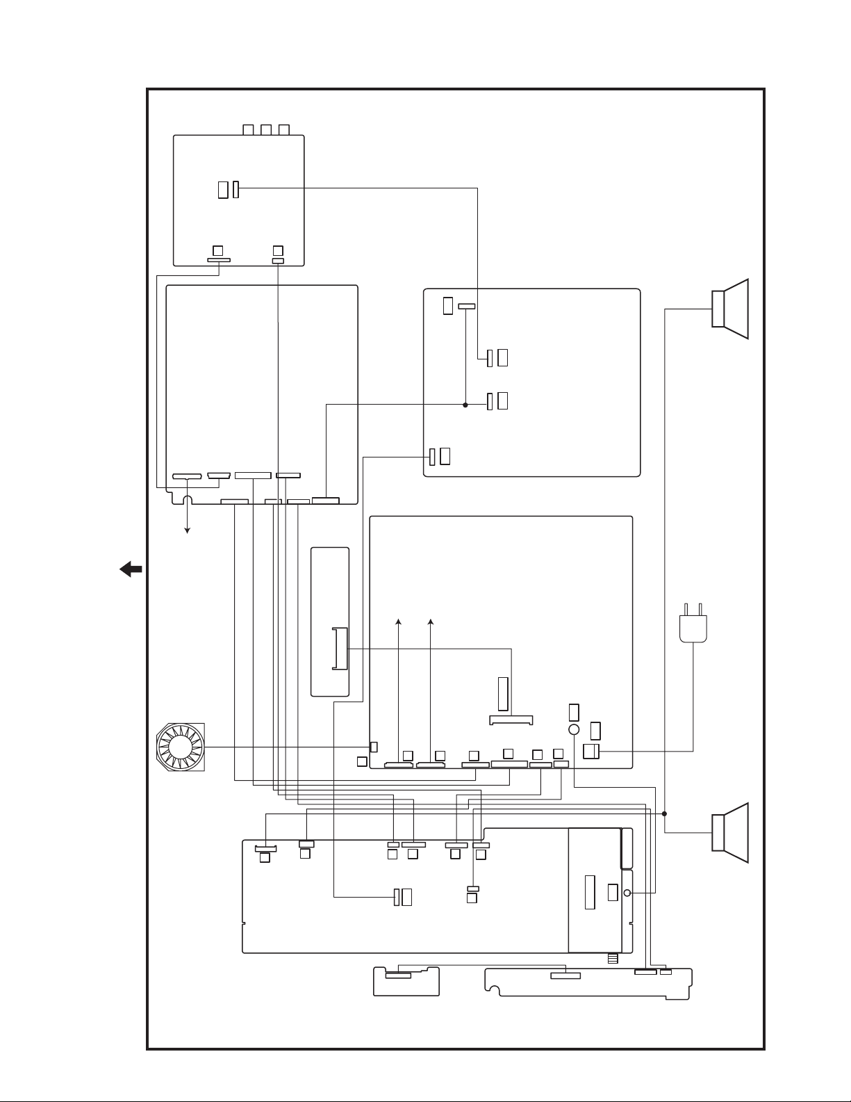
4.4 ADJUSTMENT LOCATION & WIRING
AQ
VIDEO PWB
H
MI-COM & DIST MODULE PWB
CN000H
CN000X
TOP
CONTOROL PWB
(LCD UNIT : CNT1)
CN000A
CN000B
N
CN000J
CN000K
CN000T
CN00DS
PWB
REGULATOR
SR
AU
INVERTER PWB
(LCD UNIT : CN2)
INVERTER PWB
(LCD UNIT : CN1)
Q
DC
DIGITAL INPUT MODULE PWB
POWER PWB
POWER CORD
COOLING FAN
F
S
RECEIVER PWB
CN1001
FRONT
Y
P
J
N
AU
CN8003
SENSOR PWB
CN0001
A
B
Q
E1
PW
F
G
SPEAKER(L) SPEAKER(R)
K
G
U
CN3003
TU1101
E1
CN300T
CN300U
FRONT CONTROL PWB
(No.YA089)1-23
Page 25
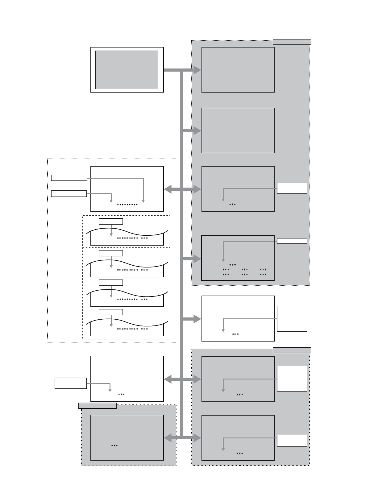
4.5 BASIC OPERATION OF SERVICE MODE
VOLUME(+/-) key
CHANNEL(+/-) key
MAIN MENU
1.PICTURE/SOUND
2.YC SEP
3.WHITE BALANCE
4.MEMORY SETUP
5.RF AFC
6.DD/CM
1.PICTURE/SOUND
NTSC CINE ST L FL MUTE
A01 001
7.PANEL
8.PP
9.IP
0.HDMI
4.MEMORY SETUP
ADDRESS(H) 0000
0
1
2
3
4
AA
55
00
0
1
AA
55
00
5
00
FF
00
2
3
4
5
00
FF
00
5.RF AFC
TOO HIGH GOOD TOO LOW
TUNER MAIN
AFC ON
FINE -10
6.DD/CM
NTSC CINE ST L FL MUTE
DDT01
DO NOT ADJUST
6
7
00
00
6
7
00
00
DDT01~34
CMT01~57
YCM001~185
YCS001~114
A01~A27
A01
S01~S99
S01
D01~D32
D01
F01~F59
F01
2.YC SEP
NTSC CINE ST L FL MUTE
YCM01
7. PANEL
PDA001
IN
APL
OUT
MIN
8.PP
NTSC CINE ST L FL MUTE
PPA001
9.IP
NTSC CINE ST L FL MUTE
IPA001
TEM
MAX
PDA001~012
ADM001~034
PPA001~008
PPB001~036
PPC001~008
PPD001~025
DO NOT ADJUST
IPA001~120
IPB001~079
IPC001~044
IPD001~026
IPE001~015
1-24 (No.YA089)
DO NOT ADJUST
3. WHITE BALANCE
BR
DRV R069 B054
CUT R078 G079 B079
0.HDMI
NTSC CINE ST L FL MUTE
GCR001
HDM001~080
RHD001~170
Page 26
4.5.1 TOOL OF SERVICE MODE OPERATION
Operate the SERVICE MODE with the REMOTE CONTROL UNIT.
4.5.2 SERVICE MODE ITEMS
In general, basic setting (adjustments) items or verifications are performed in the SERVICE MODE.
1.PICTURE / SOUND This sets the setting values of the VIDEO, AUDIO and DEFLECTION circuits.
2.YC SEP This is used when the YC separation circuit is adjusted.
3.WHITE BALANCE This sets the setting values of the WHITE BALANCE. [Do not adjust]
4.MEMORY SETUP This sets the setting values of the MEMORY ADDRESS. [Do not adjust]
5.RF AFC This is used when the IF VCO is adjusted. [Do not adjust]
6.DD/CM This sets the setting values of the panel image processing.
7.PANEL This sets the setting values of the panel power limit control.
8.PP This sets the setting value of the output of MULTI-PICTURE circuit.
9.IP This sets the setting value of the DIST circuit. [Do not adjust]
0.HDMI This sets the setting value of the DIGITAL INPUT MODULE circuit. [Do not adjust].
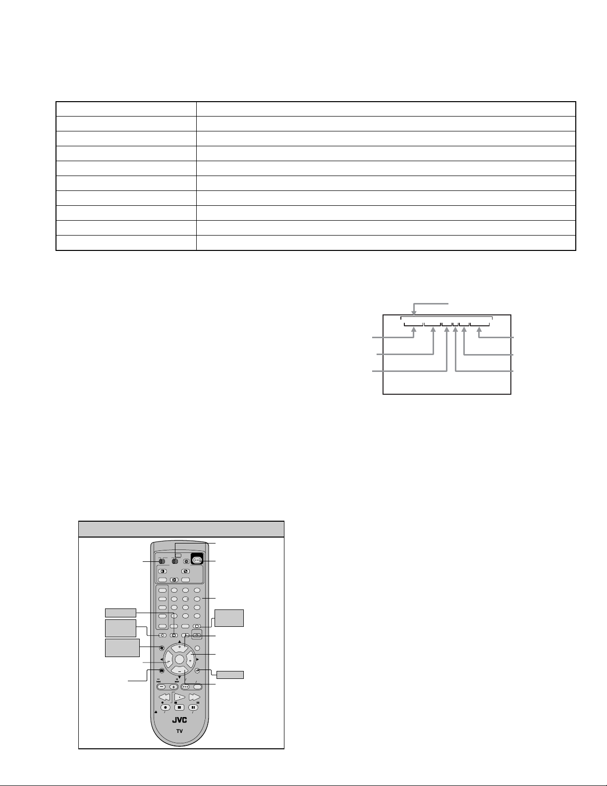
4.5.3 HOW TO ENTER THE SERVICE MODE
NOTE:
Ensure that the cursor (arrow) of the User Menu screen is
pointing at Picture Control.
Before entering the SERVICE MODE, confirm that the setting
of TV / CATV switch of the REMOTE CONTROL UNIT is at the
"TV" side and the setting of VCR / DVD switch is at the "VCR"
side. If the switches have not been properly set, you cannot
enter the SERVICE MODE.
(1) Set to 0 minutes using the [SLEEP TIMER] key.
(2) Press the [VIDEO STATUS] key and [DISPLAY] key
simultaneously, then enter the SERVICE MODE mode.
(3) When the Main Menu is displayed, press any key of the [0]
to [9] key to enter the corresponding menu mode.
*Press any of the [0] to [9] keys before the SERVICE
MODE mode disappears.
(4) Select the service item using the [ CH + ] / [ CH - ] key.
(5) Set the value using the [ VOL + ] / [ VOL - ] key.
(6) Press the [MUTING] key to save the value.
4.5.4 HOW TO EXIT THE SERVICE MODE
Press the [ BACK ] key to exit the Service mode.
SERVICE MENU SELECT KEY
VCR/DVD
switch
TV/CATV
switch
DISPLAY
SLEEP
TIMER
MEMORY
(MUTING)
FUNCTION
(LEFT)
MENU
TV
SPLIT
FREEZE
INPUT 1
V1
INPUT 2
V2
INPUT 3
V3
INPUT 4
V4
DIGITAL-IN
D-IN
SLEEP TIMER
MUTING
MENU
VCR CHANNEL
PREV NEXT
OPEN CLOSE
CATV VCR DVD
ASPECT
MULTI SCREEN
INDEX
SWAP SELECT
123
456
789
100+
THEATER
NATURAL
PRO
CINEMA
DISPLAY SOUND
+
CH
VOL VOL
OK
CH
VCR DVD
POWER
REW
REC PAUSE
STOP
RM-C13G
0
STILL PAUSE
POWER
RETURN+
VIDEO
STATUS
LIGHT
BACK
TV VCR
FFPLAY
TV
C.C.
C.C.
POWER
NUMBER
VIDEO
STATUS
FUNCTION
(UP)
FUNCTION
(RIGHT)
BACK
FUNCTION
(DOWN)
4.5.5 DESCRIPTION OF STATUS DISPLAY
The status display on the upper part of the SERVICE MODE
screen is common (to all models).
STATUS DISPLAY
NTSC CINE ST L FL MUTE
SIGNAL
SYSTEM
ASPECT/
MULTI
VIDEO
STATUS
A01 IN LEVEL 001
MEMORY
MODE
IP CHANGIN
MODE
WHITE
BALANCE
[SERVICE SCREEN]
(1) SIGNAL SYSTEM
NTSC : Composite, S-video (Y / C), RF, No signal.
DVD : 525i (component)
ED : 525p
HD : 1125i
750p : 750p
HED1 : DIGITAL 525p SIZE1
HED2 : DIGITAL 525p SIZE2
HHD : DIGITAL 1125i
H750 : DIGITAL 750p
(2) ASPECT / MULTI
ONE SCREEN
FULL : FULL
PANO : PANORAMA
CINE : CINEMA
REGU : REGULAR
MULTI SCREEN
M1 : One screen (for adjustment)
M2-1 : SPLIT
M12 : INDEX
(No.YA089)1-25
Page 27
(3) VIDEO STATUS
ST : STANDARD
DA : DYNAMIC
TH : THEATER
GA : GAME
(4) WHITE BALANCE
H: HIGH
L: LOW
(5) IP CHANGING MODE
FL : FRAME
L1 : LINE
23 : COMPULSORY NATURAL CINEMA IN
(6) MEMORY MODE
MUTE : Press [MUTING] key
DIR : Change data then memory at the same time.
4.5.6 SERVICE MODE SETTING
1. PICTURE/SOUND
AUDIO, VIDEO, DEFLECTION data adjustment.
(1) SETTING ITEM No.
A: AUDIO
S : SIGNAL
D : DEFLECTION
F : FACTORY SETTING
• Press [CH+] / [CH-] key
F01D01S01A01
Item No. is up/down
2. YC SEP (3D Y/C separation setting)
[Do not change settings of items that are not included in the
"ADJUSTMENT PROCEDURE" section. ]
Sets output data to the 3D Y/C separation circuit.
• Press [CH+] / [CH-] key
For scrolling up/down the item codes.
• Press [VOL+] / [VOL-] key
For scrolling up/down the data values.
3. WHITE BALANCE (White balance setting)
[Setting for this item is not required in servicing.]
4. MEMORY SETUP (Memory setting)
[Do not change settings]
5. RF AFC
Setting for this item is not required in servicing.
6. DD/CM
[Do not change settings]
Adjustment of color manegment and device driver
7. PANEL (Panel power limit control)
[Do not change settings]
8. PP (Multi-screen processing setting)
[Do not change settings of items that are not included in the
"ADJUSTMENT PROCEDURE" section.]
Sets output data to the multi-screen processing circuit.
• Press [CH+] / [CH-] key
For scrolling up/down the item codes.
• Press [VOL+] / [VOL-] key
For scrolling up/down the data values.
9. IP (DIST setting)
[Do not change settings]
Sets output data to the DIST circuit.
• Press [SLEEP TIMER] key
F01D01S01A01
Skip change
(2) SETTING ITEM NAME
Describe setting item name
(3) SETTING VALUE
Set the setting value.
• Press [VOL+] / [VOL-] key
Set the setting value.
• Press [MUTING] key
Memorize the data.
NOTE:
Setting for any of the following items that is not included in the
“ADJUSTMENT PROCEDURE” section found in the later part
of this manual will not be performed in servicing.
0. HDMI
[Do not change settings]
Sets output data to the DIGITAL INPUT circuit
1-26 (No.YA089)
Page 28
4.6 INITIAL SETTING VALUES IN THE SERVICE MODE
• Perform fine-tuning based on the "initial values" using the remote control when in the Service mode.
• The "initial values" serve only as an indication rough standard and therefore the values with which optimal display can be achieved
may be different from the default values. But, don't change the values that are not written in "ADJUSTMENT PROCEDURE". They
are fixed values.
NOTE:
As for the items whose settings are "Fixed" in Table 1 in "3.3 MEMORY IC REPLACEMENT", the following tables show initial
values in NTSC signal input mode. As for the items whose conditions of SETTING VALUE are not written in the following tables,
the following tables show initial values in NTSC signal input mode.
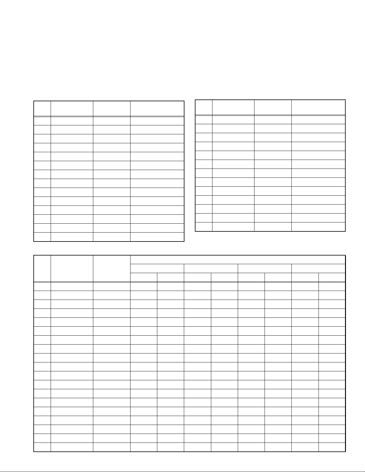
4.6.1 [1.PICTURE/SOUND]
Item
No.
A01 (Not display) 000~007 001
A02 (Not display) 000~007 001
A03 (Not display) 000~007 001
A04 (Not display) 000~007 000
A05 (Not display) 000~015 003
A06 (Not display) 000~015 004
A07 (Not display) 000~015 006
A08 (Not display) 000~015 003
A09 (Not display) 000~007 006
A10 (Not display) 000~007 004
A11 (Not display) 000~063 063
A12 (Not display) 000~063 063
A13 (Not display) 000~003 000
A14 (Not display) 000~007 000
Item
Variable
range
Setting value
Item
No.
A15 (Not display) 000~003 000
A16 (Not display) 000~003 000
A17 (Not display) 000~003 000
A18 IN LEVEL 000~015 007
A19 LOW SEP 000~063 026
A20 HI SEP 000~063 063
A21 (Not display) 000~001 (Not used)
A22 (Not display) 000~001 (Not used)
A23 (Not display) 000~001 (Not used)
A24 (Not display) 000~001 (Not used)
A25 (Not display) 000~001 (Not used)
A26 (Not display) 000~001 (Not used)
A27 (Not display) 000~001 (Not used)
Item
Variable
range
Setting value
Item
No.
S01 COLOR 000~255 163 122 163 121 163 124 155 146
S02 TINAD -127~128 000 000 000 000 000 000 000 000
S03 OF COLOR -127~128 000 000 000 000 000 000 000 000
S04 OF TINAD -127~128 000 000 000 000 000 000 000 000
S05 BRIG 000~255 048 060 048 060 048 060 036 043
S06 CONT 000~255 126 126 126 126 126 126 128 128
S07 OF BRIG -127~128 000 000 000 000 000 000 000 000
S08 OF CONT -127~128 000 000 000 000 000 000 000 000
S09 BYGN 000~255 133 117 125 116 125 116 147 118
S10 OF BYGN -127~128 000 000 000 000 000 000 000 000
S11 RYAXIS -127~128 +006 000 +006 000 +006 000 000 000
S12 MIX 000~003 000 000 000 000 000 000 001 001
S13 RDRV 000~255 255 255 255 255 255 255 246 246
S14 RDRV -127~128 000 000 000 000 000 000 000 000
S15 GDRV 000~255 254 254 254 254 254 254 255 255
S16 GDRV -127~128 000 -038 000 -038 000 -038 000 -027
S17 BDRV 000~255 255 255 255 255 255 255 225 225
S18 BDRV -127~128 000 -043 000 -043 000 -043 000 -038
S19 CUTR 000~255 128 128 128 128 128 128 128 128
Item
Variable
range
NTSC 525i 525p 750p/1125i
STANDARD THEATER STANDARD THEATER STANDARD THEATER STANDARD THEATER
Setting value
(No.YA089)1-27
Page 29
Item
No.
S20 OF CUTR -127~128 000 +004 000 +004 000 +004 000 000
S21 CUTG 000~255 128 128 128 128 128 128 128 128
S22 OF CUTG -127~128 000 000 000 000 000 000 000 000
S23 CUTB 000~255 128 128 128 128 128 128 128 128
S24 OF CUTB -127~128 000 000 000 000 000 000 000 000
S25 CUTR 000~001 000 000 000 000 000 000 000 000
S26 CUTG 000~001 000 000 000 000 000 000 000 000
S27 CUTB 000~001 000 000 000 000 000 000 000 000
S28 BTHN 000~001 000 000 000 000 000 000 001 000
S29 BCALM 000~001 000 000 000 000 000 000 000 000
S30 BKAKOU 000~031 000 012 000 000 000 000 000 000
S31 BLIM 000~063 010 000 010 000 010 000 002 000
S32 BSTPO 000~063 050 063 050 063 050 063 018 063
S33 BKAKON 000~001 001 001 001 001 001 001 001 001
S34 WTHN 000~001 001 001 001 001 001 001 001 001
S35 WCALM 000~001 000 000 000 000 000 000 000 001
S36 WKAKOU 000~031 000 000 000 000 000 000 000 000
S37 WLIM 000~255 220 213 220 213 220 213 220 225
S38 WSTPO 000~063 050 036 050 036 050 036 050 050
S39 WPEAK 000~063 060 063 060 063 060 063 060 060
S40 WKAKON 000~001 001 001 001 001 001 001 001 001
S41 WGAINC 000~001 000 001 001 001 001 001 001 001
S42 GAINB 000~003 001 000 001 000 001 000 002 000
S43 SLIC 000~031 009 009 009 009 009 009 009 009
S44 APG 000~003 001 001 001 001 001 001 001 001
S45 GAINA 000~003 002 002 002 002 002 002 002 002
S46 (Not used) 000~015 015 015 015 015 015 015 015 015
S47 (Not used) 000~015 015 015 015 015 015 015 015 015
S48 DCTRAN 000~015 015 015 015 015 015 015 015 015
Item
Variable
range
NTSC 525i 525p 750p/1125i
STANDARD THEATER STANDARD THEATER STANDARD THEATER STANDARD THEATER
Setting value
Item
No.
S49 HSTR 000~001 001 000
S50 HSTR 000~255 010 018
S51 HEND 000~001 000 000
S52 HEND 000~255 087 079
S53 VSTR 000~001 000 000
S54 VSTR 000~255 026 006
S55 VEND 000~001 000 000
S56 VEND 000~255 077 096
S57 BHSTR 000~255 000 000
S58 BHSTR 000~015 000 000
S59 BHEND 000~255 000 000
1-28 (No.YA089)
Item
Variable
range
MULTI-SCREEN ASPECT
SPLIT REGULAR
Setting value
Page 30
Item
No.
S60 BHEND 000~015 000 000
Data of the setting value is selected in the order of "SPLIT" and "REGULAR".
Item
No.
S61 PLPOL2 000~001 001 001 001 001 001 001
S62 PLEV2 000~127 016 016 016 016 016 016
S63 PLPOL1 000~001 000 000 000 000 000 000
S64 PLEV1 000~127 000 000 000 000 000 000
Item
No.
S65 MODC 000~003 002 002 002 002 002 002 002 002
S66 RMC 000~003 003 003 001 003 000 003 003 003
S67 RGA 000~003 003 003 003 003 002 003 003 003
S68 CLIP 000~015 000 000 000 000 000 000 000 000
S69 COR 000~063 019 019 019 019 019 019 019 019
Item
Item
Item
Variable
range
Variable
range
Variable
range
MULTI-SCREEN ASPECT
STANDARD THEATER STANDARD THEATER STANDARD THEATER
STANDARD THEATER STANDARD THEATER STANDARD THEATER STANDARD THEATER
Setting value
SPLIT REGULAR
Setting value
NTSC 525i/525p 750p/1125i
Setting value
NTSC
525i/525p 750p/1125iMULTI-SCREEN ASPECT
SPLIT REGULAR
Item
No.
S70 TINTON 001~001 001
S71 DRIVER 000~255 240
S72 DRIVEG 000~255 240
S73 DRIVEB 000~255 255
S74 EECONT 000~031 000
S75 EEBRT 000~031 000
S76 EETBRT -127~128 000
S77 EETCONT -127~128 000
S78 PICMAX 000~255 255
S79 PICMIN 000~255 000
S80 BRTMAX 000~255 255
S81 BRTMIN 000~255 000
S82 COLMAX 000~255 255
S83 COLMIN 000~255 000
S84 PWMDIM 000~255 216
S85 ADIM 000~255 127
S86 (Not display) 000~255 127
S87 (Not display) 000~007 003
S88 APLGAIN 000~007 000
S89 APLLIM 000~255 000
S90 ABSGAIN 000~127 000
S91 BLKGAIN 000~007 007
Item
Variable
range
Setting value
Item
No.
S92 BLKLIM 000~031 031
S93 WHTGAIN 000~007 007
S94 WHTLIM 000~031 031
S95 DCSTART 000~255 035
S96 DCGAIN 000~015 006
S97 DCLIM 000~063 035
S98 (Not display) 000~001 000
S99 (Not display) 000~003 000
Item
Variable
range
Setting value
(No.YA089)1-29
Page 31

Item
No.
D01 (Not display) 000~001 000
D02 (Not display) 000~001 000
D03 (Not display) 000~001 000
D04 (Not display) 000~001 000
D05 (Not display) 000~001 000
D06 (Not display) 000~001 000
D07 (Not display) 000~001 000
D08 (Not display) 000~001 000
D09 (Not display) 000~001 000
D10 (Not display) 000~001 000
D11 (Not display) 000~001 000
D12 (Not display) 000~001 000
D13 (Not display) 000~001 000
D14 (Not display) 000~001 000
D15 (Not display) 000~001 000
D16 (Not display) 000~001 000
D17 (Not display) 000~001 000
D18 (Not display) 000~001 000
D19 (Not display) 000~001 000
D20 (Not display) 000~001 000
D21 (Not display) 000~001 000
D22 (Not display) 000~001 000
D23 (Not display) 000~001 000
D24 (Not display) 000~001 000
D25 (Not display) 000~001 000
D26 (Not display) 000~001 000
D27 (Not display) 000~001 000
D28 (Not display) 000~001 000
D29 (Not display) 000~001 000
D30 (Not display) 000~001 000
D31 (Not display) 000~001 000
D32 (Not display) 000~001 000
Item
Variable
range
Setting value
Item
No.
F01 (Not display) 000~255 001
F02 (Not display) 000~255 000
F03 (Not display) 000~255 000
F04 (Not display) 000~255 032
F05 CATVMAX 000~001 000
F06 (Not display) 000~001 002
F07 (Not display) 000~255 027
F08 (Not display) 000~255 000
F09 AUTOCSR1 000~015 002
F10 AUTOCSR2 000~015 004
F11 AUTOCSR3 000~015 004
F12 AUTOCSR4 000~015 005
F13 AUTOCSR5 000~015 006
F14 AUTOCSR6 000~015 007
F15 AUTOCSR7 000~015 007
F16 (Not display) 000~127 070
F17 (Not display) 000~001 000
F18 FIX DATA 000~001 000
F19 (Not display) 000~001 000
F20 (Not display) 000~255 005
F21 (Not display) 000~255 002
F22 (Not display) 000~001 000
F23 (Not display) 000~255 000
F24 (Not display) 000~255 098
F25 (Not display) 000~255 006
F26 (Not display) 000~255 040
F27 (Not display) 000~255 040
F28 (Not display) 000~001 000
F29 (Not display) 000~001 000
F30 (Not display) 000~001 000
F31 (Not display) 000~001 000
F32 (Not display) 000~001 000
F33 (Not display) 000~001 000
F34 (Not display) 000~001 000
F35 (Not display) 000~001 000
F36 (Not display) 000~001 000
F37 (Not display) 000~001 000
F38 (Not display) 000~001 000
F39 (Not display) 000~001 000
F40 (Not display) 000~001 000
Item
Variable
range
Setting value
1-30 (No.YA089)
Page 32

Item
No.
F41 (Not display) 000~003 000 002 002 002 002
F42 (Not display) 000~001 000 000 000 000 000
F43 (Not display) 000~063 039 040 037 024 024
Item
Variable
range
NTSC 525i 525p 750p 1125i
Setting value
Item
No.
F44 (Not display) 000~001 000
F45 (Not display) 000~007 000
F46 OUT LV. 000~255 090
F47 LIMIT B 000~255 000
F48 LIMIT A 000~255 000
F49 (Not display) 000~255 128
F50 (Not display) 000~255 128
F51 (Not display) 000~255 128
F52 (Not display) 000~255 255
F53 (Not display) 000~001 000
F54 (Not display) 000~001 000
F55 (Not display) 000~001 255
F56 (Not display) 000~001 141
F57 (Not display) 000~001 000
F58 (Not display) 000~001 141
F59 (Not display) 000~001 001
F60 (Not display) 000~001 000
F61 (Not display) 000~001 000
F62 (Not display) 000~001 015
F63 ATT GAIN 000~001 001
F64 (Not display) 000~001 073
F65 (Not display) 000~001 001
F66 (Not display) 000~001 000
F67 (Not display) 000~001 070
F68 (Not display) 000~001 000
F69 (Not display) 000~001 000
F70 (Not display) 000~001 000
Item
Variable
range
Setting value
(No.YA089)1-31
Page 33

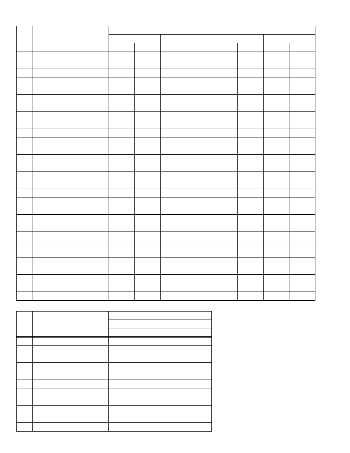
4.6.2 [2.YC SEP]
NOTE :
Initial setting value is reference value at following condition.
INPUT SIGNAL : NTSC
ASPECT : FULL
MULTI-SCREEN : SINGLE
VIDEO STATUS : STANDARD
COLOR TEMPERATURE : LOW
Item No. Item Variable range
YCM001 (Not display) 000~001 000
YCM002 (Not display) 000~001 000
YCM003 (Not display) 000~001 000
YCM004 (Not display) 000~003 001
YCM005 (Not display) 000~255 239
YCM006 (Not display) 000~003 001
YCM007 (Not display) 000~255 239
YCM008 (Not display) 000~001 000
YCM009 (Not display) 000~003 000
YCM010 (Not display) 000~001 000
YCM011 (Not display) 000~001 000
YCM012 (Not display) 000~001 000
YCM013 (Not display) 000~001 000
YCM014 (Not display) 000~003 000
YCM015 (Not display) 000~001 000
YCM016 (Not display) 000~003 000
YCM017 (Not display) 000~001 001
YCM018 (Not display) 000~003 000
YCM019 (Not display) 000~001 000
YCM020 (Not display) 000~001 000
YCM021 (Not display) 000~003 002
YCM022 (Not display) 000~007 004
YCM023 (Not display) 000~001 001
YCM024 (Not display) 000~001 000
YCM025 (Not display) 000~015 005
YCM026 (Not display) 000~015 003
YCM027 (Not display) 000~003 000
YCM028 (Not display) 000~007 004
YCM029 (Not display) 000~007 006
YCM030 (Not display) 000~003 000
YCM031 (Not display) 000~001 000
YCM032 (Not display) 000~003 003
YCM033 (Not display) 000~001 001
YCM034 (Not display) 000~001 001
YCM035 (Not display) 000~255 096
YCM036 (Not display) 000~001 001
YCM037 (Not display) 000~003 001
YCM038 (Not display) 000~127 062
Setting
value
Item No. Item Variable range
YCM039 (Not display) 000~127 068
YCM040 (Not display) 000~003 002
YCM041 (Not display) 000~063 016
YCM042 (Not display) 000~001 000
YCM043 (Not display) 000~001 000
YCM044 (Not display) 000~255 182
YCM045 (Not display) 000~001 000
YCM046 (Not display) 000~255 127
YCM047 (Not display) 000~001 001
YCM048 (Not display) 000~001 001
YCM049 (Not display) 000~001 001
YCM050 (Not display) 000~001 001
YCM051 (Not display) 000~001 000
YCM052 (Not display) 000~001 000
YCM053 (Not display) 000~001 000
YCM054 (Not display) 000~003 003
YCM055 (Not display) 000~003 003
YCM056 (Not display) 000~003 000
YCM057 (Not display) 000~001 000
YCM058 (Not display) 000~001 001
YCM059 (Not display) 000~001 001
YCM060 (Not display) 000~001 000
YCM061 (Not display) 000~001 001
YCM062 (Not display) 000~015 001
YCM063 (Not display) 000~015 005
YCM064 (Not display) 000~003 000
YCM065 (Not display) 000~063 060
YCM066 (Not display) 000~063 040
YCM067 (Not display) 000~063 025
YCM068 (Not display) 000~063 012
YCM069 (Not display) 000~063 036
YCM070 (Not display) 000~063 031
YCM071 (Not display) 000~127 031
YCM072 (Not display) 000~001 001
YCM073 (Not display) 000~001 001
YCM074 (Not display) 000~063 024
YCM075 (Not display) 000~001 000
YCM076 (Not display) 000~001 001
YCM077 (Not display) 000~063 010
YCM078 (Not display) 000~063 001
YCM079 (Not display) 000~255 000
YCM080 (Not display) 000~255 000
YCM081 (Not display) 000~255 000
YCM082 (Not display) 000~255 000
Setting
value
1-32 (No.YA089)
Page 34

Item No. Item Variable range
YCM083 (Not display) 000~001 001
YCM084 (Not display) 000~063 012
YCM085 (Not display) 000~001 000
YCM086 (Not display) 000~001 000
YCM087 (Not display) 000~063 028
YCM088 (Not display) 000~001 001
YCM089 (Not display) 000~031 000
YCM090 (Not display) 000~003 000
YCM091 (Not display) 000~015 000
YCM092 (Not display) 000~015 000
YCM093 (Not display) 000~015 003
YCM094 (Not display) 000~063 002
YCM095 (Not display) 000~255 050
YCM096 (Not display) 000~001 000
YCM097 (Not display) 000~063 032
YCM098 (Not display) 000~015 008
YCM099 (Not display) 000~015 005
YCM100 (Not display) 000~015 008
YCM101 (Not display) 000~015 005
YCM102 (Not display) 000~015 000
YCM103 (Not display) 000~015 002
YCM104 (Not display) 000~015 008
YCM105 (Not display) 000~015 006
YCM106 (Not display) 000~255 010
YCM107 (Not display) 000~255 032
YCM108 (Not display) 000~255 031
YCM109 (Not display) 000~255 064
YCM110 (Not display) 000~001 000
YCM111 (Not display) 000~001 001
YCM112 (Not display) 000~001 001
YCM113 (Not display) 000~001 001
YCM114 (Not display) 000~001 000
YCM115 (Not display) 000~001 001
YCM116 (Not display) 000~001 000
YCM117 (Not display) 000~001 000
YCM118 (Not display) 000~001 001
YCM119 (Not display) 000~001 000
YCM120 (Not display) 000~001 000
YCM121 (Not display) 000~003 003
YCM122 (Not display) 000~001 000
YCM123 (Not display) 000~255 000
YCM124 (Not display) 000~001 000
YCM125 (Not display) 000~255 002
YCM126 (Not display) 000~001 000
YCM127 (Not display) 000~001 001
Setting
value
Item No. Item Variable range
YCM128 (Not display) 000~001 001
YCM129 (Not display) 000~001 001
YCM130 (Not display) 000~003 001
YCM131 (Not display) 000~255 046
YCM132 (Not display) 000~255 152
YCM133 (Not display) 000~255 055
YCM134 (Not display) 000~007 001
YCM135 (Not display) 000~255 136
YCM136 (Not display) 000~001 000
YCM137 (Not display) 000~001 001
YCM138 (Not display) 000~007 003
YCM139 (Not display) 000~255 141
YCM140 (Not display) 000~007 000
YCM141 (Not display) 000~255 014
YCM142 (Not display) 000~001 000
YCM143 (Not display) 000~007 005
YCM144 (Not display) 000~255 128
YCM145 (Not display) 000~001 000
YCM146 (Not display) 000~001 001
YCM147 (Not display) 000~001 001
YCM148 (Not display) 000~001 001
YCM149 (Not display) 000~001 000
YCM150 (Not display) 000~001 000
YCM151 (Not display) 000~255 136
YCM152 (Not display) 000~001 001
YCM153 (Not display) 000~001 001
YCM154 (Not display) 000~001 001
YCM155 (Not display) 000~003 000
YCM156 (Not display) 000~015 015
YCM157 (Not display) 000~015 004
YCM158 (Not display) 000~001 001
YCM159 (Not display) 000~127 004
YCM160 (Not display) 000~001 001
YCM161 (Not display) 000~031 000
YCM162 (Not display) 000~001 000
YCM163 (Not display) 000~015 003
YCM164 (Not display) 000~007 002
YCM165 (Not display) 000~031 016
YCM166 (Not display) 000~255 235
YCM167 (Not display) 000~003 000
YCM168 (Not display) 000~063 000
YCM169 (Not display) 000~015 003
YCM170 (Not display) 000~015 003
YCM171 (Not display) 000~007 000
YCM172 (Not display) 000~255 096
Setting
value
(No.YA089)1-33
Page 35

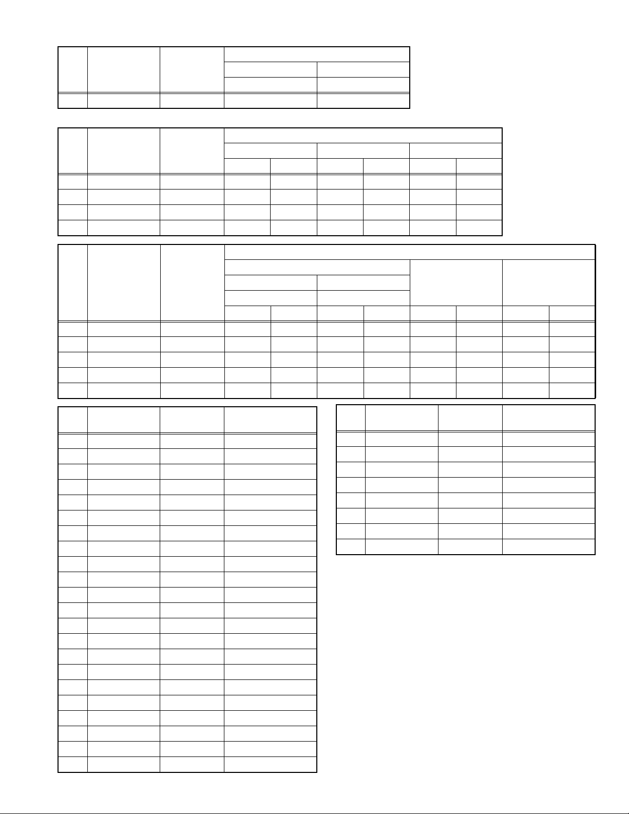
Item No. Item Variable range
YCM173 (Not display) 000~007 003
YCM174 (Not display) 000~255 056
YCM175 (Not display) 000~001 000
YCM176 (Not display) 000~001 000
YCM177 (Not display) 000~255 022
YCM178 (Not display) 000~001 001
YCM179 (Not display) 000~001 000
YCM180 (Not display) 000~007 003
YCM181 (Not display) 000~003 001
YCM182 (Not display) 000~003 001
YCM183 (Not display) 000~003 001
YCM184 (Not display) 000~003 001
YCM185 (Not display) 000~255 000
Item No. Item Variable range
YCS001 (Not display) 000~001 000
YCS002 (Not display) 000~001 000
YCS003 (Not display) 000~001 000
YCS004 (Not display) 000~003 001
YCS005 (Not display) 000~255 239
YCS006 (Not display) 000~003 001
YCS007 (Not display) 000~255 239
YCS008 (Not display) 000~001 000
YCS009 (Not display) 000~003 000
YCS010 (Not display) 000~001 000
YCS011 (Not display) 000~001 000
YCS012 (Not display) 000~001 000
YCS013 (Not display) 000~001 000
YCS014 (Not display) 000~003 000
YCS015 (Not display) 000~001 000
YCS016 (Not display) 000~003 000
YCS017 (Not display) 000~001 001
YCS018 (Not display) 000~003 000
YCS019 (Not display) 000~001 000
YCS020 (Not display) 000~001 000
YCS021 (Not display) 000~003 002
YCS022 (Not display) 000~007 004
YCS023 (Not display) 000~001 001
YCS024 (Not display) 000~001 000
YCS025 (Not display) 000~015 005
YCS026 (Not display) 000~015 003
YCS027 (Not display) 000~003 000
YCS028 (Not display) 000~007 004
YCS029 (Not display) 000~007 006
YCS030 (Not display) 000~003 000
Setting
value
Setting
value
Item No. Item Variable range
YCS031 (Not display) 000~001 000
YCS032 (Not display) 000~003 003
YCS033 (Not display) 000~001 001
YCS034 (Not display) 000~001 001
YCS035 (Not display) 000~255 096
YCS036 (Not display) 000~001 001
YCS037 (Not display) 000~003 001
YCS038 (Not display) 000~127 062
YCS039 (Not display) 000~127 068
YCS040 (Not display) 000~003 002
YCS041 (Not display) 000~063 016
YCS042 (Not display) 000~001 000
YCS043 (Not display) 000~001 000
YCS044 (Not display) 000~255 160
YCS045 (Not display) 000~001 000
YCS046 (Not display) 000~255 111
YCS047 (Not display) 000~001 001
YCS048 (Not display) 000~031 000
YCS049 (Not display) 000~003 000
YCS050 (Not display) 000~015 000
YCS051 (Not display) 000~015 008
YCS052 (Not display) 000~015 001
YCS053 (Not display) 000~063 015
YCS054 (Not display) 000~255 020
YCS055 (Not display) 000~001 000
YCS056 (Not display) 000~063 025
YCS057 (Not display) 000~015 008
YCS058 (Not display) 000~015 005
YCS059 (Not display) 000~015 008
YCS060 (Not display) 000~015 005
YCS061 (Not display) 000~015 000
YCS062 (Not display) 000~015 002
YCS063 (Not display) 000~015 008
YCS064 (Not display) 000~015 006
YCS065 (Not display) 000~255 010
YCS066 (Not display) 000~255 032
YCS067 (Not display) 000~255 031
YCS068 (Not display) 000~255 089
YCS069 (Not display) 000~001 000
YCS070 (Not display) 000~001 001
YCS071 (Not display) 000~001 001
YCS072 (Not display) 000~001 001
YCS073 (Not display) 000~001 000
YCS074 (Not display) 000~001 001
YCS075 (Not display) 000~001 000
Setting
value
1-34 (No.YA089)
Page 36

Item No. Item Variable range
YCS076 (Not display) 000~001 000
YCS077 (Not display) 000~001 000
YCS078 (Not display) 000~001 000
YCS079 (Not display) 000~001 000
YCS080 (Not display) 000~003 003
YCS081 (Not display) 000~001 000
YCS082 (Not display) 000~255 000
YCS083 (Not display) 000~255 000
YCS084 (Not display) 000~007 000
YCS085 (Not display) 000~255 010
YCS086 (Not display) 000~001 001
YCS087 (Not display) 000~001 001
YCS088 (Not display) 000~001 000
YCS089 (Not display) 000~001 000
YCS090 (Not display) 000~255 136
YCS091 (Not display) 000~001 001
YCS092 (Not display) 000~001 001
YCS093 (Not display) 000~001 001
YCS094 (Not display) 000~003 000
YCS095 (Not display) 000~015 015
YCS096 (Not display) 000~015 002
YCS097 (Not display) 000~001 001
YCS098 (Not display) 000~127 007
YCS099 (Not display) 000~031 000
YCS100 (Not display) 000~001 000
YCS101 (Not display) 000~015 003
YCS102 (Not display) 000~007 002
YCS103 (Not display) 000~031 016
YCS104 (Not display) 000~255 235
YCS105 (Not display) 000~003 000
YCS106 (Not display) 000~063 000
YCS107 (Not display) 000~015 003
YCS108 (Not display) 000~015 003
YCS109 (Not display) 000~001 000
YCS110 (Not display) 000~003 001
YCS111 (Not display) 000~003 001
YCS112 (Not display) 000~003 001
YCS113 (Not display) 000~003 001
YCS114 (Not display) 000~255 000
Setting
value
4.6.3 [3.WHITE BALANCE]
NOTE :
Initial setting value is reference value at following condition.
INPUT SIGNAL : NTSC
ASPECT : FULL
MULTI-SCREEN : SINGLE
VIDEO STATUS : STANDARD
COLOR TEMPERATURE : LOW
Item No. Item Variable range
BR (Not display) 00000~238 000
DRV R (Not display) 00000~255 000
DRV B (Not display) 00000~255 000
CUT R (Not display) 00000~255 000
CUT G (Not display) 00000~255 000
CUT B (Not display) 00000~255 000
4.6.4 [6.DD/CM]
Item No. Item Variable range
DDT01 (Not display) 000~015 000
DDT02 (Not display) 000~255 000
DDT03 (Not display) 000~255 000
DDT04 (Not display) 000~255 255
DDT05 (Not display) 000~255 254
DDT06 (Not display) 000~255 255
DDT07 (Not display) 000~003 000
DDT08 (Not display) 000~255 032
DDT09 (Not display) 000~003 000
DDT10 (Not display) 000~255 000
DDT11 (Not display) 000~007 000
DDT12 (Not display) 000~255 115
DDT13 (Not display) 000~255 000
DDT14 (Not display) 000~003 002
DDT15 (Not display) 000~007 000
DDT16 (Not display) 000~255 187
DDT17 (Not display) 000~001 000
DDT18 (Not display) 000~001 000
DDT19 (Not display) 000~063 002
DDT20 (Not display) 000~015 014
DDT21 (Not display) 000~015 014
DDT22 (Not display) 000~015 002
DDT23 (Not display) 000~015 004
DDT24 (Not display) 000~001 000
DDT25 (Not display) 000~001 000
DDT26 (Not display) 000~001 000
DDT27 (Not display) 000~007 000
DDT28 (Not display) 000~255 127
DDT29 (Not display) 000~003 002
Setting
value
Setting
value
(No.YA089)1-35
Page 37

Item No. Item Variable range
DDT30 (Not display) 000~001 000
DDT31 (Not display) 000~007 000
DDT32 (Not display) 000~255 000
DDT33 (Not display) 000~255 000
DDT34 (Not display) 000~255 033
Item No. Item Variable range
CMT01 (Not display) 000~003 000
CMT02 (Not display) 000~0FF 090
CMT03 (Not display) 000~255 015
CMT04 (Not display) 000~255 030
CMT05 (Not display) -032~+031 -010
CMT06 (Not display) -128~+127 000
CMT07 (Not display) -128~+127 +010
CMT08 (Not display) -128~+127 +005
CMT09 (Not display) -128~+127 000
CMT10 (Not display) 000~003 000
CMT11 (Not display) 000~0FF 160
CMT12 (Not display) 000~255 020
CMT13 (Not display) 000~255 020
CMT14 (Not display) -032~+031 -005
CMT15 (Not display) -128~+127 +005
CMT16 (Not display) -128~+127 000
CMT17 (Not display) -128~+127 000
CMT18 (Not display) -128~+127 000
CMT19 (Not display) 000~003 000
CMT20 (Not display) 000~0FF 196
CMT21 (Not display) 000~255 025
CMT22 (Not display) 000~255 055
CMT23 (Not display) -032~+031 000
CMT24 (Not display) -128~+127 000
CMT25 (Not display) -128~+127 +010
CMT26 (Not display) -128~+127 +005
CMT27 (Not display) -128~+127 +015
CMT28 (Not display) 000~003 001
CMT29 (Not display) 000~0FF 070
CMT30 (Not display) 000~255 035
CMT31 (Not display) 000~255 040
CMT32 (Not display) -032~+031 000
CMT33 (Not display) -128~+127 +002
CMT34 (Not display) -128~+127 +015
CMT35 (Not display) -128~+127 000
CMT36 (Not display) -128~+127 +020
CMT37 (Not display) 000~255 064
CMT38 (Not display) 000~255 066
Setting
value
Setting
value
Item No. Item Variable range
CMT39 (Not display) 000~255 085
CMT40 (Not display) -128~+127 000
CMT41 (Not display) -128~+127 +010
CMT42 (Not display) 000~001 000
CMT43 (Not display) 000~0FF 080
CMT44 (Not display) 000~001 001
CMT45 (Not display) 000~0FF 080
CMT46 (Not display) 000~001 000
CMT47 (Not display) 000~0FF 128
CMT48 (Not display) 000~001 000
CMT49 (Not display) 000~001 001
CMT50 (Not display) -016~+015 000
CMT51 (Not display) -016~+015 000
CMT52 (Not display) 000~001 000
CMT53 (Not display) 000~001 000
CMT54 (Not display) 000~003 000
CMT55 (Not display) 000~001 000
CMT56 (Not display) 000~001 001
CMT57 (Not display) 000~001 000
4.6.5 [7.PANEL] (*All the values are fixed values.)
Item No. Item Variable range
PDA001 (Not display) 000~255 000
PDA002 (Not display) 000~255 000
PDA003 (Not display) 000~255 000
PDA004 (Not display) 000~255 000
PDA005 (Not display) 000~001 000
PDA006 (Not display) 000~001 000
PDA007 (Not display) 000~255 000
PDA008 (Not display) 000~255 000
PDA009 (Not display) 000~255 000
PDA010 (Not display) 000~255 000
PDA011 (Not display) 000~255 000
PDA012 (Not display) 000~127 000
4.6.6 [8.PP]
NOTE :
Initial setting value is reference value at following condition.
INPUT SIGNAL : NTSC
ASPECT : FULL
MULTI-SCREEN : SINGLE
VIDEO STATUS : STANDARD
COLOR TEMPERATURE : LOW
Item No. Item Variable range
ADM001 (Not display) 000~0FF 0D6
ADM002 (Not display) 000~00F 007
Setting
value
Setting
value
Setting
value
1-36 (No.YA089)
Page 38

Item No. Item Variable range
ADM003 (Not display) 000~003 001
ADM004 (Not display) 000~007 005
ADM005 (Not display) 000~01F 016
ADM006 (Not display) 000~0FF 036
ADM007 (Not display) 000~0FF 08A
ADM008 (Not display) 000~0FF 020
ADM009 (Not display) 000~0FF 0FF
ADM010 (Not display) 000~0FF 0C6
ADM011 (Not display) 000~0FF 0FF
ADM012 (Not display) 000~07F 03B
ADM013 (Not display) 000~07F 031
ADM014 (Not display) 000~07F 044
ADM015 (Not display) 000~001 001
ADM016 (Not display) 000~001 001
ADM017 (Not display) 000~001 000
ADM018 (Not display) 000~001 001
ADM019 (Not display) 000~001 000
ADM020 (Not display) 000~001 000
ADM021 (Not display) 000~001 001
ADM022 (Not display) 000~001 000
ADM023 (Not display) 000~001 000
ADM024 (Not display) 000~001 001
ADM025 (Not display) 000~001 000
ADM026 (Not display) 000~001 001
ADM027 (Not display) 000~001 001
ADM028 (Not display) 000~001 001
ADM029 (Not display) 000~001 001
ADM030 (Not display) 000~01F 003
ADM031 (Not display) 000~001 001
ADM032 (Not display) 000~001 000
ADM033 (Not display) 000~001 001
ADM034 (Not display) 000~0FF 032
Item No. Item Variable range
PPA001 (Not display) 000~255 040
PPA002 (Not display) 000~255 000
PPA003 (Not display) 000~255 05A
PPA004 (Not display) 000~255 000
PPA005 (Not display) 000~255 000
PPA006 (Not display) 000~255 001
PPA007 (Not display) 000~255 05A
PPA008 (Not display) 000~255 023
Item No. Item Variable range
PPB001 (Not display) 000~031 000
Setting
value
Setting
value
Setting
value
Item No. Item Variable range
PPB002 (Not display) 000~255 000
PPB003 (Not display) 000~255 000
PPB004 (Not display) 000~031 000
PPB005 (Not display) 000~255 000
PPB006 (Not display) 000~255 000
PPB007 (Not display) 000~031 000
PPB008 (Not display) 000~255 000
PPB009 (Not display) 000~255 000
PPB010 (Not display) 000~031 000
PPB011 (Not display) 000~255 000
PPB012 (Not display) 000~255 000
PPB013 (Not display) 000~031 000
PPB014 (Not display) 000~255 000
PPB015 (Not display) 000~255 000
PPB016 (Not display) 000~031 000
PPB017 (Not display) 000~255 000
PPB018 (Not display) 000~255 000
PPB019 (Not display) 000~031 000
PPB020 (Not display) 000~255 000
PPB021 (Not display) 000~255 000
PPB022 (Not display) 000~031 000
PPB023 (Not display) 000~255 000
PPB024 (Not display) 000~255 000
PPB025 (Not display) 000~031 000
PPB026 (Not display) 000~255 000
PPB027 (Not display) 000~255 000
PPB028 (Not display) 000~031 000
PPB029 (Not display) 000~255 000
PPB030 (Not display) 000~255 000
PPB031 (Not display) 000~031 000
PPB032 (Not display) 000~255 000
PPB033 (Not display) 000~255 000
PPB034 (Not display) 000~031 000
PPB035 (Not display) 000~255 000
PPB036 (Not display) 000~255 000
Item No. Item Variable range
PPC001 (Not display) 000~255 000
PPC002 (Not display) 000~255 00E
PPC003 (Not display) 000~255 002
PPC004 (Not display) 000~001 000
PPC005 (Not display) 000~001 000
PPC006 (Not display) 000~001 000
PPC007 (Not display) 000~001 000
PPC008 (Not display) 000~001 000
Setting
value
Setting
value
(No.YA089)1-37
Page 39

Item No. Item Variable range
PPC007 (Not display) 000~001 01C
PPC008 (Not display) 000~001 004
Item No. Item Variable range
PPD001 (Not display) 000~255 008
PPD002 (Not display) 000~255 000
PPD003 (Not display) 000~255 019
PPD004 (Not display) 000~255 001
PPD005 (Not display) 000~255 09A
PPD006 (Not display) 000~255 000
PPD007 (Not display) 000~255 019
PPD008 (Not display) 000~255 001
PPD009 (Not display) 000~255 0B3
PPD010 (Not display) 000~255 000
PPD011 (Not display) 000~255 024
PPD012 (Not display) 000~255 001
PPD013 (Not display) 000~255 039
PPD014 (Not display) 000~255 000
PPD015 (Not display) 000~255 096
PPD016 (Not display) 000~255 001
PPD017 (Not display) 000~255 086
PPD018 (Not display) 000~255 000
PPD019 (Not display) 000~255 024
PPD020 (Not display) 000~255 001
PPD021 (Not display) 000~255 050
PPD022 (Not display) 000~255 000
PPD023 (Not display) 000~255 0AA
PPD024 (Not display) 000~255 001
PPD025 (Not display) 000~255 072
4.6.7 [9.IP] (*All the values are fixed values.)
NOTE :
Initial setting value is reference value at following condition.
INPUT SIGNAL : NTSC
ASPECT : FULL
MULTI-SCREEN : SINGLE
VIDEO STATUS : STANDARD
COLOR TEMPERATURE : LOW
Item No. Item Variable range
IPA001 (Not display) 000~001 001
IPA002 (Not display) 000~063 015
IPA003 (Not display) 000~063 010
IPA004 (Not display) 000~063 015
IPA005 (Not display) 000~003 001
IPA006 (Not display) 000~003 001
IPA007 (Not display) 000~015 00F
Setting
value
Setting
value
Setting
value
Item No. Item Variable range
IPA008 (Not display) 000~063 005
IPA009 (Not display) 000~063 000
IPA010 (Not display) 000~063 01F
IPA011 (Not display) 000~063 01F
IPA012 (Not display) 000~063 02F
IPA013 (Not display) 000~003 000
IPA014 (Not display) 000~003 000
IPA015 (Not display) 000~063 00F
IPA016 (Not display) 000~063 005
IPA017 (Not display) 000~001 001
IPA018 (Not display) 000~063 029
IPA019 (Not display) 000~001 001
IPA020 (Not display) 000~001 001
IPA021 (Not display) 000~063 015
IPA022 (Not display) 000~003 000
IPA023 (Not display) 000~063 004
IPA024 (Not display) 000~001 001
IPA025 (Not display) 000~001 001
IPA026 (Not display) 000~063 015
IPA027 (Not display) 000~003 000
IPA028 (Not display) 000~063 005
IPA029 (Not display) 000~063 000
IPA030 (Not display) 000~015 000
IPA031 (Not display) 000~007 000
IPA032 (Not display) 000~063 000
IPA033 (Not display) 000~001 000
IPA034 (Not display) 000~063 000
IPA035 (Not display) 000~001 001
IPA036 (Not display) 000~063 00D
IPA037 (Not display) 000~063 00D
IPA038 (Not display) 000~063 010
IPA039 (Not display) 000~003 001
IPA040 (Not display) 000~003 001
IPA041 (Not display) 000~015 00F
IPA042 (Not display) 000~063 005
IPA043 (Not display) 000~063 005
IPA044 (Not display) 000~063 00C
IPA045 (Not display) 000~063 00C
IPA046 (Not display) 000~063 00F
IPA047 (Not display) 000~003 001
IPA048 (Not display) 000~003 001
IPA049 (Not display) 000~015 00F
IPA050 (Not display) 000~063 008
IPA051 (Not display) 000~001 001
IPA052 (Not display) 000~063 008
Setting
value
1-38 (No.YA089)
Page 40

Item No. Item Variable range
IPA053 (Not display) 000~001 001
IPA054 (Not display) 000~001 001
IPA055 (Not display) 000~063 025
IPA056 (Not display) 000~003 000
IPA057 (Not display) 000~063 00A
IPA058 (Not display) 000~001 001
IPA059 (Not display) 000~001 001
IPA060 (Not display) 000~063 025
IPA061 (Not display) 000~003 000
IPA062 (Not display) 000~063 00A
IPA063 (Not display) 000~063 000
IPA064 (Not display) 000~015 000
IPA065 (Not display) 000~007 000
IPA066 (Not display) 000~063 000
IPA067 (Not display) 000~001 000
IPA068 (Not display) 000~063 000
IPA069 (Not display) 000~003 000
IPA070 (Not display) 000~255 000
IPA071 (Not display) 000~015 005
IPA072 (Not display) 000~255 0DC
IPA073 (Not display) 000~001 000
IPA074 (Not display) 000~001 000
IPA075 (Not display) 000~255 016
IPA076 (Not display) 000~001 000
IPA077 (Not display) 000~001 000
IPA078 (Not display) 000~001 000
IPA079 (Not display) 000~001 000
IPA080 (Not display) 000~001 000
IPA081 (Not display) 000~001 000
IPA082 (Not display) 000~001 000
IPA083 (Not display) 000~001 000
IPA084 (Not display) 000~001 000
IPA085 (Not display) 000~001 000
IPA086 (Not display) 000~001 000
IPA087 (Not display) 000~001 000
IPA088 (Not display) 000~001 000
IPA089 (Not display) 000~001 000
IPA090 (Not display) 000~001 000
IPA091 (Not display) 000~015 000
IPA092 (Not display) 000~255 000
IPA093 (Not display) 000~015 003
IPA094 (Not display) 000~255 0FF
IPA095 (Not display) 000~015 000
IPA096 (Not display) 000~255 000
IPA097 (Not display) 000~015 005
Setting
value
Item No. Item Variable range
IPA098 (Not display) 000~255 0D3
IPA099 (Not display) 000~015 000
IPA100 (Not display) 000~255 000
IPA101 (Not display) 000~015 000
IPA102 (Not display) 000~255 000
IPA103 (Not display) 000~015 000
IPA104 (Not display) 000~255 000
IPA105 (Not display) 000~015 000
IPA106 (Not display) 000~255 000
IPA107 (Not display) 000~015 000
IPA108 (Not display) 000~255 080
IPA109 (Not display) 000~015 000
IPA110 (Not display) 000~255 040
IPA111 (Not display) 000~015 005
IPA112 (Not display) 000~255 040
IPA113 (Not display) 000~015 000
IPA114 (Not display) 000~255 0C0
IPA115 (Not display) 000~015 002
IPA116 (Not display) 000~255 0EF
IPA117 (Not display) 000~001 000
IPA118 (Not display) 000~001 000
IPA119 (Not display) 000~001 000
IPA120 (Not display) 000~001 000
Item No. Item Variable range
IPB001 (Not display) 000~255 001
IPB002 (Not display) 000~255 00F
IPB003 (Not display) 000~015 000
IPB004 (Not display) 000~255 0B7
IPB005 (Not display) 000~015 002
IPB006 (Not display) 000~255 0C9
IPB007 (Not display) 000~015 002
IPB008 (Not display) 000~255 038
IPB009 (Not display) 000~015 001
IPB010 (Not display) 000~255 0AB
IPB011 (Not display) 000~015 001
IPB012 (Not display) 000~255 01C
IPB013 (Not display) 000~015 000
IPB014 (Not display) 000~255 08E
IPB015 (Not display) 000~015 000
IPB016 (Not display) 000~255 01D
IPB017 (Not display) 000~015 000
IPB018 (Not display) 000~255 01E
IPB019 (Not display) 000~015 000
IPB020 (Not display) 000~255 023
Setting
value
Setting
value
(No.YA089)1-39
Page 41

Item No. Item Variable range
IPB021 (Not display) 000~015 000
IPB022 (Not display) 000~255 03E
IPB023 (Not display) 000~015 001
IPB024 (Not display) 000~255 07B
IPB025 (Not display) 000~015 000
IPB026 (Not display) 000~255 000
IPB027 (Not display) 000~015 004
IPB028 (Not display) 000~255 037
IPB029 (Not display) 000~015 000
IPB030 (Not display) 000~255 04C
IPB031 (Not display) 000~015 000
IPB032 (Not display) 000~255 000
IPB033 (Not display) 000~015 000
IPB034 (Not display) 000~255 000
IPB035 (Not display) 000~015 001
IPB036 (Not display) 000~255 02E
IPB037 (Not display) 000~001 000
IPB038 (Not display) 000~007 000
IPB039 (Not display) 000~015 000
IPB040 (Not display) 000~015 00F
IPB041 (Not display) 000~015 006
IPB042 (Not display) 000~255 000
IPB043 (Not display) 000~015 002
IPB044 (Not display) 000~255 038
IPB045 (Not display) 000~015 003
IPB046 (Not display) 000~255 000
IPB047 (Not display) 000~015 000
IPB048 (Not display) 000~255 0CA
IPB049 (Not display) 000~015 000
IPB050 (Not display) 000~255 0D0
IPB051 (Not display) 000~015 000
IPB052 (Not display) 000~255 000
IPB053 (Not display) 000~015 000
IPB054 (Not display) 000~255 000
IPB055 (Not display) 000~015 000
IPB056 (Not display) 000~255 0C4
IPB057 (Not display) 000~015 006
IPB058 (Not display) 000~255 040
IPB059 (Not display) 000~007 001
IPB060 (Not display) 000~003 000
IPB061 (Not display) 000~003 000
IPB062 (Not display) 000~001 000
IPB063 (Not display) 000~255 000
IPB064 (Not display) 000~255 080
IPB065 (Not display) 000~255 080
Setting
value
Item No. Item Variable range
IPB066 (Not display) 000~001 000
IPB067 (Not display) 000~015 000
IPB068 (Not display) 000~015 000
IPB069 (Not display) 000~015 000
IPB070 (Not display) 000~015 00F
IPB071 (Not display) 000~255 000
IPB072 (Not display) 000~015 000
IPB073 (Not display) 000~255 000
IPB074 (Not display) 000~001 000
IPB075 (Not display) 000~001 000
IPB076 (Not display) 000~001 000
IPB077 (Not display) 000~015 009
IPB078 (Not display) 000~001 001
IPB079 (Not display) 000~255
Item No. Item Variable range
IPC001 (Not display) 000~003 002
IPC002 (Not display) 000~255 0EA
IPC003 (Not display) 000~001 000
IPC004 (Not display) 000~001 000
IPC005 (Not display) 000~015 000
IPC006 (Not display) 000~255 000
IPC007 (Not display) 000~015 005
IPC008 (Not display) 000~255 0DB
IPC009 (Not display) 000~015 006
IPC010 (Not display) 000~255 071
IPC011 (Not display) 000~015 000
IPC012 (Not display) 000~255 000
IPC013 (Not display) 000~003 001
IPC014 (Not display) 000~001 000
IPC015 (Not display) 000~001 001
IPC016 (Not display) 000~255 0EE
IPC017 (Not display) 000~001 000
IPC018 (Not display) 000~127 000
IPC019 (Not display) 000~001 000
IPC020 (Not display) 000~127 000
IPC021 (Not display) 000~015 001
IPC022 (Not display) 000~255 03F
IPC023 (Not display) 000~003 002
IPC024 (Not display) 000~255 01E
IPC025 (Not display) 000~001 000
IPC026 (Not display) 000~127 00F
IPC027 (Not display) 000~001 000
IPC028 (Not display) 000~127 000
IPC029 (Not display) 000~001 001
Setting
value
042
Setting
value
1-40 (No.YA089)
Page 42

Item No. Item Variable range
IPC030 (Not display) 000~001 000
IPC031 (Not display) 000~001 000
IPC032 (Not display) 000~001 000
IPC033 (Not display) 000~001 001
IPC034 (Not display) 000~001 001
IPC035 (Not display) 000~001 000
IPC036 (Not display) 000~001 000
IPC037 (Not display) 000~001 000
IPC038 (Not display) 000~001 000
IPC039 (Not display) 000~001 000
IPC040 (Not display) 000~001 000
IPC041 (Not display) 000~001 000
IPC042 (Not display) 000~001 000
IPC043 (Not display) 000~001 000
IPC044 (Not display) 000~001 000
Setting
value
Item No. Item Variable range
IPE001 (Not display) 000~255 001
IPE002 (Not display) 000~255 002
IPE003 (Not display) 000~255 001
IPE004 (Not display) 000~255 002
IPE005 (Not display) 000~255 001
IPE006 (Not display) 000~255 002
IPE007 (Not display) 000~255 001
IPE008 (Not display) 000~255 002
IPE009 (Not display) -128~+127 +005
IPE010 (Not display) -128~+127 +006
IPE011 (Not display) -128~+127 +005
IPE012 (Not display) -128~+127 -005
IPE013 (Not display) -128~+127 +0FB
IPE014 (Not display) -128~+127 +005
IPE015 (Not display) 000~015 001
Setting
value
Item No. Item Variable range
IPD001 (Not display) 000~255 040
IPD002 (Not display) 000~255 000
IPD003 (Not display) 000~255 000
IPD004 (Not display) 000~007 000
IPD005 (Not display) 000~255 01C
IPD006 (Not display) 000~007 000
IPD007 (Not display) 000~255 0E1
IPD008 (Not display) 000~001 000
IPD009 (Not display) 000~015 000
IPD010 (Not display) 000~255 012
IPD011 (Not display) 000~015 004
IPD012 (Not display) 000~255 0BB
IPD013 (Not display) 000~007 000
IPD014 (Not display) 000~007 000
IPD015 (Not display) 000~001 000
IPD016 (Not display) 000~001 000
IPD017 (Not display) 000~255 000
IPD018 (Not display) 000~007 000
IPD019 (Not display) 000~255 01D
IPD020 (Not display) 000~007 002
IPD021 (Not display) 000~255 0E6
IPD022 (Not display) 000~001 001
IPD023 (Not display) 000~015 001
IPD024 (Not display) 000~255 00E
IPD025 (Not display) 000~015 004
IPD026 (Not display) 000~255 0C0
Setting
value
4.6.8 [0.HDMI] *All the values are fixed values.
Item No. Item Variable range
HDM001 (Not display) 000~001 000
HDM002 (Not display) 000~001 000
HDM003 (Not display) 000~001 000
HDM004 (Not display) 000~001 000
HDM005 (Not display) 000~001 000
HDM006 (Not display) 000~003 000
HDM007 (Not display) 000~001 000
HDM008 (Not display) 000~001 000
HDM009 (Not display) 000~001 000
HDM010 (Not display) 000~001 000
HDM011 (Not display) 000~001 000
HDM012 (Not display) 000~001 000
HDM013 (Not display) 000~001 000
HDM014 (Not display) 000~001 000
HDM015 (Not display) 000~001 000
HDM016 (Not display) 000~255 000
HDM017 (Not display) 000~255 000
HDM018 (Not display) 000~255 000
HDM019 (Not display) 000~001 000
HDM020 (Not display) 000~255 000
HDM021 (Not display) 000~007 000
HDM022 (Not display) 000~063 000
HDM023 (Not display) 000~063 000
HDM024 (Not display) 000~063 000
HDM025 (Not display) 000~001 000
HDM026 (Not display) 000~003 000
HDM027 (Not display) 000~255 000
Setting
value
(No.YA089)1-41
Page 43

Item No. Item Variable range
HDM028 (Not display) 000~003 000
HDM029 (Not display) 000~255 000
HDM030 (Not display) 000~003 000
HDM031 (Not display) 000~255 000
HDM032 (Not display) 000~003 000
HDM033 (Not display) 000~255 000
HDM034 (Not display) 000~003 000
HDM035 (Not display) 000~255 000
HDM036 (Not display) 000~255 000
HDM037 (Not display) 000~255 000
HDM038 (Not display) 000~255 000
HDM039 (Not display) 000~001 000
HDM040 (Not display) 000~001 000
HDM041 (Not display) 000~001 000
HDM042 (Not display) 000~255 000
HDM043 (Not display) 000~007 000
HDM044 (Not display) 000~003 000
HDM045 (Not display) 000~003 000
HDM046 (Not display) 000~001 000
HDM047 (Not display) 000~015 000
HDM048 (Not display) 000~255 000
HDM049 (Not display) 000~255 000
HDM050 (Not display) 000~015 000
HDM051 (Not display) 000~001 000
HDM052 (Not display) 000~001 000
HDM053 (Not display) 000~001 000
HDM054 (Not display) 000~001 000
HDM055 (Not display) 000~001 000
HDM056 (Not display) 000~001 000
HDM057 (Not display) 000~001 000
HDM058 (Not display) 000~001 000
HDM059 (Not display) 000~001 000
HDM060 (Not display) 000~001 000
HDM061 (Not display) 000~001 000
HDM062 (Not display) 000~001 000
HDM063 (Not display) 000~001 000
HDM064 (Not display) 000~001 000
HDM065 (Not display) 000~001 000
HDM066 (Not display) 000~001 000
HDM067 (Not display) 000~001 000
HDM068 (Not display) 000~031 000
HDM069 (Not display) 000~001 000
HDM070 (Not display) 000~001 000
HDM071 (Not display) 000~001 000
HDM072 (Not display) 000~001 000
Setting
value
Item No. Item Variable range
HDM073 (Not display) 000~001 000
HDM074 (Not display) 000~031 000
HDM075 (Not display) 000~001 000
HDM076 (Not display) 000~001 000
HDM077 (Not display) 000~001 000
HDM078 (Not display) 000~001 000
HDM079 (Not display) 000~001 000
HDM080 (Not display) 000~001 000
Item No. Item Variable range
RHD001 (Not display) --- 000
RHD002 (Not display) --- 000
RHD003 (Not display) --- 000
RHD004 (Not display) --- 000
RHD005 (Not display) --- 000
RHD006 (Not display) --- 000
RHD007 (Not display) --- 000
RHD008 (Not display) --- 000
RHD009 (Not display) --- 000
RHD010 (Not display) --- 000
RHD011 (Not display) --- 000
RHD012 (Not display) --- 000
RHD013 (Not display) --- 000
RHD014 (Not display) --- 000
RHD015 (Not display) --- 000
RHD016 (Not display) --- 000
RHD017 (Not display) --- 000
RHD018 (Not display) --- 000
RHD019 (Not display) --- 000
RHD020 (Not display) --- 000
RHD021 (Not display) --- 000
RHD022 (Not display) --- 000
RHD023 (Not display) --- 000
RHD024 (Not display) --- 000
RHD025 (Not display) --- 000
RHD026 (Not display) --- 000
RHD027 (Not display) --- 000
RHD028 (Not display) --- 000
RHD029 (Not display) --- 000
RHD030 (Not display) --- 000
RHD031 (Not display) --- 000
RHD032 (Not display) --- 000
RHD033 (Not display) --- 000
RHD034 (Not display) --- 000
RHD035 (Not display) --- 000
Setting
value
Setting
value
1-42 (No.YA089)
Page 44

Item No. Item Variable range
RHD036 (Not display) --- 000
RHD037 (Not display) --- 000
RHD038 (Not display) --- 000
RHD039 (Not display) --- 000
RHD040 (Not display) --- 000
RHD041 (Not display) --- 000
RHD042 (Not display) --- 000
RHD043 (Not display) --- 000
RHD044 (Not display) --- 000
RHD045 (Not display) --- 000
RHD046 (Not display) --- 000
RHD047 (Not display) --- 000
RHD048 (Not display) --- 000
RHD049 (Not display) --- 000
RHD050 (Not display) --- 000
RHD051 (Not display) --- 000
RHD052 (Not display) --- 000
RHD053 (Not display) --- 000
RHD054 (Not display) --- 000
RHD055 (Not display) --- 000
RHD056 (Not display) --- 000
RHD057 (Not display) --- 000
RHD058 (Not display) --- 000
RHD059 (Not display) --- 000
RHD060 (Not display) --- 000
RHD061 (Not display) --- 000
RHD062 (Not display) --- 000
RHD063 (Not display) --- 000
RHD064 (Not display) --- 000
RHD065 (Not display) --- 000
RHD066 (Not display) --- 000
RHD067 (Not display) --- 000
RHD068 (Not display) --- 000
RHD069 (Not display) --- 000
RHD070 (Not display) --- 000
RHD071 (Not display) --- 000
RHD072 (Not display) --- 000
RHD073 (Not display) --- 000
RHD074 (Not display) --- 000
RHD075 (Not display) --- 000
RHD076 (Not display) --- 000
RHD077 (Not display) --- 000
RHD078 (Not display) --- 000
RHD079 (Not display) --- 000
RHD080 (Not display) --- 000
Setting
value
Item No. Item Variable range
RHD081 (Not display) --- 000
RHD082 (Not display) --- 000
RHD083 (Not display) --- 000
RHD084 (Not display) --- 000
RHD085 (Not display) --- 000
RHD086 (Not display) --- 000
RHD087 (Not display) --- 000
RHD088 (Not display) --- 000
RHD089 (Not display) --- 000
RHD090 (Not display) --- 000
RHD091 (Not display) --- 000
RHD092 (Not display) --- 000
RHD093 (Not display) --- 000
RHD094 (Not display) --- 000
RHD095 (Not display) --- 000
RHD096 (Not display) --- 000
RHD097 (Not display) --- 000
RHD098 (Not display) --- 000
RHD009 (Not display) --- 000
RHD100 (Not display) --- 000
RHD101 (Not display) --- 000
RHD102 (Not display) --- 000
RHD103 (Not display) --- 000
RHD104 (Not display) --- 000
RHD105 (Not display) --- 000
RHD106 (Not display) --- 000
RHD107 (Not display) --- 000
RHD108 (Not display) --- 000
RHD109 (Not display) --- 000
RHD110 (Not display) --- 000
RHD111 (Not display) --- 000
RHD112 (Not display) --- 000
RHD113 (Not display) --- 000
RHD114 (Not display) --- 000
RHD115 (Not display) --- 000
RHD116 (Not display) --- 000
RHD117 (Not display) --- 000
RHD118 (Not display) --- 000
RHD119 (Not display) --- 000
RHD120 (Not display) --- 000
RHD121 (Not display) --- 000
RHD122 (Not display) --- 000
RHD123 (Not display) --- 000
RHD124 (Not display) --- 000
RHD125 (Not display) --- 000
Setting
value
(No.YA089)1-43
Page 45

Item No. Item Variable range
RHD126 (Not display) --- 000
RHD127 (Not display) --- 000
RHD128 (Not display) --- 000
RHD129 (Not display) --- 000
RHD130 (Not display) --- 000
RHD131 (Not display) --- 000
RHD132 (Not display) --- 000
RHD133 (Not display) --- 000
RHD134 (Not display) --- 000
RHD135 (Not display) --- 000
RHD136 (Not display) --- 000
RHD137 (Not display) --- 000
RHD138 (Not display) --- 000
RHD139 (Not display) --- 000
RHD140 (Not display) --- 000
RHD141 (Not display) --- 000
RHD142 (Not display) --- 000
RHD143 (Not display) --- 000
RHD144 (Not display) --- 000
RHD145 (Not display) --- 000
RHD146 (Not display) --- 000
RHD147 (Not display) --- 000
RHD148 (Not display) --- 000
RHD149 (Not display) --- 000
RHD150 (Not display) --- 000
RHD151 (Not display) --- 000
RHD152 (Not display) --- 000
RHD153 (Not display) --- 000
RHD154 (Not display) --- 000
RHD155 (Not display) --- 000
RHD156 (Not display) --- 000
RHD157 (Not display) --- 000
RHD158 (Not display) --- 000
RHD159 (Not display) --- 000
RHD160 (Not display) --- 000
RHD161 (Not display) --- 000
RHD162 (Not display) --- 000
RHD163 (Not display) --- 000
RHD164 (Not display) --- 000
RHD165 (Not display) --- 000
RHD166 (Not display) --- 000
RHD167 (Not display) --- 000
RHD168 (Not display) --- 000
RHD169 (Not display) --- 000
RHD170 (Not display) --- 000
Setting
value
1-44 (No.YA089)
Page 46

4.7 ADJUSTMENT PROCEDURE
4.7.1 SETTING BEFORE ADJUSTMENT
(1) Check the following settings before adjustment.
Item setting value contents
S19 128 R CUT OFF
S21 128 G CUT OFF
S23 128 B CUT OFF
(2) Take note of initial values in the following table before adjustment. Then, set the values to adjustment setting values shown in
the following table. After adjustment procedure, return the values to the initial values you have taken note of (except white
balance adjustment).
The values can be set for each input signal (NTSC etc.), but the values are basically the same among the input signals.
Since the values are not adjusted for 525p/720p (because the values change according to the reference adjustment values), you
do not have to take note of the values if unnecessary.
Item
S13 255 R DRIVE
S15 255 G DRIVE
S17 255 B DRIVE
(3) Unless otherwise specified in the adjustment instructions, preset the following functions with the remote control unit:
VIDEO STATUS STANDARD
BRIGHT / CONTRAST / COLOR / TINT 00
COLOR TEMPERATURE LOW
DIG. NOISE CLEAR OFF
COLOR MANEGMENT STANDARD
NATURAL CINEMA OFF
TREBLE / BASS / BALANCE 00
BBE OFF
A.H.S OFF
A.H.B OFF
ASPECT FULL
NOTE:
Follow the order instructed in adjustment procedure.
Initial value
NTSC
Setting item Settings
Initial value
525p
Initial value
1125i
Initial value
750p
setting value contents
(No.YA089)1-45
Page 47

4.7.2 VIDEO CIRCUIT
Item
COMPONENT
INPUT BLACK
Mesuring
instrument
Remote control
unit
LEVEL
Signal generator
Item No.
Setting value
F46 090 Output level upon detection
F47 016 Minimum value upon detection
F48 016 Maximum value upon detection
Test point Adjustment part Description
[8.PP]
ADM013: (NO DISPLAY)
(G offset)
(1) Input 525i signal that shows brightness gradation
with 0% black into a component input terminal.
(2) Set “VIDEO STATUS” to STANDARD.
(3) Set “ASPECT” to FULL.
[1. PICTURE/SOUND]
S13: RDRV (R DRIVE)
S15: GDRV (G DRIVE)
S17: BDRV (B DRIVE)
S19: CUTR (R CUTOFF)
S21: CUTG (G CUTOFF)
S23: CUTB (B CUTOFF)
(4) Select "COLOR TEMPERATURE" to "LOW".
(5) Select "1.PICTURE/SOUND" from the SERVICE
MODE.
(6) Set < F44 > (Picture control) to "001" and < F45 >
(Picture control mode sw) to "000" to set Y ADJUST
MAX MODE.
(7) Set < F46 > (Output level upon detection),< F47 >
(Minimum value upon detection), and < F48 >
F44: (NO DISPLAY)
(Picture control)
F45: (NO DISPLAY)
(Picture control mode sw)
F46: OUT LV.
(Output level upon
detection)
F47: LMT BTM
(Minimum value upon
detection)
F48: LMT TOP
(Maximum value upon
detection)
(Maximum value upon detection) to values as
shown in the left table.
(8) Press the [MUTING] key to memoirze the set value.
(9) Select "8.PP" from the SERVICE MODE.
(10) Adjust < ADM013 > (G OFFSET) to set the 0% black
part on the upper half of the screen to maximum
brightness. (Fig.2)
(11) Add reference offset value "0" to the < ADM013 > (G
OFFSET) value.
(12) Press the [MUTING] key to memoirze the set value.
(13) Select "1.PICTURE/SOUND" from the SERVICE
MODE.
(14) Check the black level. Adjust the black level again if
it is not proper.
(15) Set < F44 > (Picture control) to "001" to cancel Y
Adjustment item
ADJUST MAX MODE.
(16) Press the [MUTING] key to memoirze the set value.
(17) Input 1125i signal.
(18) Repeat steps (5) to (15) above.
(19) Press the [MUTING] key to memoirze the set value.
Adjust the 0% black to maximum brightness
Fig.2
1-46 (No.YA089)
Page 48

Item
COMPONENT
INPUT A-D
CONVERTER
GAIN
Item No.
F46
F47
F48
Mesuring
instrument
Remote control
unit
Test point Adjustment part Description
[8.PP]
ADM010: (NO DISPLAY)
(G GAIN)
Signal generator
[1. PICTURE/SOUND]
S13: RDRV (R DRIVE)
S15: GDRV (G DRIVE)
S17: BDRV (B DRIVE)
S19: CUTR (R CUTOFF)
S21: CUTG (G CUTOFF)
S23: CUTB (B CUTOFF)
F44: (NO DISPLAY)
(Picture control)
F45: (NO DISPLAY)
(Picture control mode sw)
F46: OUT LV.
(Output level upon
detection)
F47: LMT BTM
(Minimum value upon
Detection)
F48: LMT TOP
(Maximum value upon
detection)
Setting value
Adjustment item
090 Output level upon detection
220 Minimum value upon detection
220 Maximum value upon detection
(1) Input 525i 100% all-white signal into a component
input terminal.
(2) Set "VIDEO STATUS" to STANDARD.
(3) Set "ASPECT" to FULL.
(4) Select "COLOR TEMPERATURE" to "LOW".
(5) Select "1.PICTURE/SOUND" from the SERVICE
MODE.
(6) Set < F44 > (Picture control) to "001" and < F45 >
(Picture control mode sw) to "000" to set Y ADJUST
MAX MODE.
(7) Set < F46 > (Output level upon detection), < F47 >
(Minimum value upon detection), and < F48 >
(Maximum value upon detection) to values as
shown in the left table.
(8) Press the [MUTING] key to memoirze the set value.
(9) Select "8.PP" from the SERVICE MODE.
(10) Adjust < ADM010 > (G GAIN) to set the upper half
of the screen to maximum brightness. (Fig.3)
(11) Press the [MUTING] key to memoirze the set value.
(12) Check the black level. Perform the "BLACK LEVEL
Adjustment" again if the adjusted value is not
proper.
(13) Select "1.PICTURE/SOUND" from the SERVICE
MODE.
(14) Set < F44 > (Picture control) to "000" to cancel Y
ADJUST MAX MODE.
(15) Press the [MUTING] key to memoirze the set value.
(16) Input 1125i signal.
(17) Repeat steps (5) to (14) above.
(18) Press the [MUTING] key to memoirze the set value.
Adjust this part to maximum brightness.
Fig.3
(No.YA089)1-47
Page 49

Item
COMPONENT
INPUT A-D
CONVERTER
OFFSET
Item No.
F46
F47
F48
Mesuring
instrument
Remote control
unit
Test point Adjustment part Description
[8.PP]
ADM012: (NO DISPLAY)
(R OFFSET)
Signal generator
ADM014: (NO DISPLAY)
(B OFFSET)
[1. PICTURE/SOUND]
S13: RDRV (R DRIVE)
S15: GDRV (G DRIVE)
S17: BDRV (B DRIVE)
S19: CUTR (R CUTOFF)
S21: CUTG (G CUTOFF)
S23: CUTB (B CUTOFF)
F44: (NO DISPLAY)
(Picture control)
F45: (NO DISPLAY)
(Picture control mode sw)
F46: OUT LV.
(Output level upon
detection)
F47: LMT BTM
(Minimum value upon
detection)
F48: LMT TOP
(Maximum value upon
detection)
Setting value
Adjustment item
090 Output level upon detection
000 Minimum value upon detection
000 Maximum value upon detection
Change the color in this part.
(1) Input 525i component 30% all-white signal into a
component input terminal.
(2) Set "VIDEO STATUS" to STANDARD.
(3) Set "ASPECT" to FULL.
(4) Select "COLOR TEMPERATURE" to "LOW".
(5) Select "1.PICTURE/SOUND" from the SERVICE
MODE.
(6) Set < F44 > (Picture control) to "001" and < F45 >
(Picture control mode sw) to "003" to set the
chrominance adjustment zero mode.
(7) Set < F46 > (Output level upon detection), < F47 >
(Minimum value upon detection), and < F48 >
(Maximum value upon detection) to values as
shown in the left table.
(8) Press the [MUTING] key to memoirze the set value.
(9) Select "8.PP" from the SERVICE MODE.
(10) Change the value of < ADM014 > (B OFFSET) from
the initial value in the range of ±5 to set the upper
half of the screen magenta.
(11) Adjust < ADM012 > (R OFFSET) to change the
upper half of the screen from magenta to blue.
(12) Take a note of the value of < ADM012 > (R
OFFSET) adjusted in (11).
(13) Change the value of < ADM012 > (R OFFSET) from
the value that you have taken note of in the range of
±5 to set the upper half of the screen magenta.
(14) Adjust < ADM014 > (B OFFSET) to change the
upper half of the screen from magenta to red.
(15) Return the value of < ADM012 > (R OFFSET) to the
value that you have taken note of in (12).
(16) Press the [MUTING] key to memoirze the set value.
(17) Set the SPLIT screen mode.
(18) Input monochrome signal such as cross hatch both
to the right and the left screen.
(19) Set < ADM012 > (R OFFSET) and < ADM014 > (B
OFFSET) to the same values as in single-screen
mode.
(20) Press the [MUTING] key to memoirze the set value.
(21) Set < F44 > (Picture control) to "000" to cancel the
chrominance adjustment zero mode.
(22) Input 1125i 30% all-white signal.
(23) Repeat steps (5) to (21) above.
(24) Press the [MUTING] key to memoirze the set value.
1-48 (No.YA089)
Fig.4
Page 50

Item
COMPOSITE
INPUT BLACK
LEVEL
Mesuring
instrument
Remote control
unit
Signal generator
Test point Adjustment part Description
[2. YC SEP]
YCM131: (NO DISPLAY)
(BRIGHTNESS)
(1) Input NTSC signal that shows brightness gradation
with 0% black.
(2) Set "VIDEO STATUS" to STANDARD.
(3) Set "ASPECT" to FULL.
[1. PICTURE/SOUND]
S13: RDRV (R DRIVE)
S15: GDRV (G DRIVE)
S17: BDRV (B DRIVE)
S19: CUTR (R CUTOFF)
S21: CUTG (G CUTOFF)
S23: CUTB (B CUTOFF)
(4) Select "COLOR TEMPERATURE" to "LOW".
(5) Select "1.PICTURE/SOUND" from the SERVICE
MODE.
(6) Set < F44 > (Picture control) to "001" and < F45 >
(Picture control mode sw) to "000" to set Y ADJUST
MAX MODE.
(7) Set < F46 > (Output level upon detection), < F47 >
(Minimum value upon detection), and < F48 >
F44: (NO DISPLAY)
(Picture control)
F45: (NO DISPLAY)
(Picture control mode sw)
F46: OUT LV.
(Output level upon
detection)
F47: LMT BTM
(Minimum value upon
detection)
F48: LMT TOP
(Maximum value upon detection) to values as
shown in the left table.
(8) Select "2. YC SEP" from the SERVICE MODE.
(9) Adjust < YCM131 > (BRIGHTNESS) so that 0% part
of gradation is the brightest. (Fig. 6)
(10) Press the [MUTING] key to memoirze the set value.
(11) Select "1.PICTURE/SOUND" from the SERVICE
MODE.
(12) Set < F44 > (Picture control) to "000" to cancel Y
ADJUST MAX MODE.
(13) Press the [MUTING] key to memoirze the set value.
(Maximum value upon
detection)
Item No.
F46
F47
F48
Setting value
Adjustment item
090 Output level upon detection
016 Minimum value upon detection
016 Maximum value upon detection
Adjust so that 0% black is the brightest.
Fig.5
(No.YA089)1-49
Page 51

Item
COMPOSITE
INPUT A-D
CONVERTER
OFFSET
Item No.
F46
F47
F48
Mesuring
instrument
Remote control
unit
Test point Adjustment part Description
[2. YC SEP]
YCM132: (NO DISPLAY)
(CONTRAST)
Signal generator
[1. PICTURE/SOUND]
S13: RDRV (R DRIVE)
S15: GDRV (G DRIVE)
S17: BDRV (B DRIVE)
S19: CUTR (R CUTOFF)
S21: CUTG (G CUTOFF)
S23: CUTB (B CUTOFF)
F44: (NO DISPLAY)
(Picture control)
F45: (NO DISPLAY)
(Picture control mode sw)
F46: OUT LV.
(Output level upon
detection)
F47: LMT BTM
(Minimum value upon
detection)
F48: LMT TOP
(Maximum value upon
detection)
Setting value
Adjustment item
090 Output level upon detection
165 Minimum value upon detection
165 Maximum value upon detection
(1) Input a signal that shows brightness gradation with
75% white.
(2) Set "VIDEO STATUS" to STANDARD.
(3) Set "ASPECT" to FULL.
(4) Select "COLOR TEMPERATURE" to "LOW".
(5) Select "1.PICTURE/SOUND" from the SERVICE
MODE.
(6) Set < F44 > (Picture control) to "001" and <F45 >
(Picture control mode sw) to "000" to set Y ADJUST
MAX MODE.
(7) Set < F46 > (Output level upon detection), < F47 >
(Minimum value upon detection), and < F48 >
(Maximum value upon detection) to values as
shown in the left table.
(8) Select "2.YC SEP" from the SERVICE MODE.
(9) Adjust < YCM132 > (CONTRAST) so that the 75%
white of gradation is white. (Fig.7)
(10) Press the [MUTING] key to memoirze the set value.
(11) Check the black level adjusted in composite input
black level adjustment. Perform the "Composite
input black level Adjustment" again if the adjusted
value is not proper.
(12) Perform (9) and (10) if you readjust the black level
in (11).
(13) Select "1.PICTURE/SOUND" from the SERVICE
MODE.
(14) Set < F44 > (Picture control) to "000" to cancel Y
ADJUST MAX MODE.
(15) Press the [MUTING] key to memoirze the set value.
Adjust so that 75%“ white is the brightest.
Adjust so that 75%“ white is the brightest.
Fig.6
1-50 (No.YA089)
Page 52

Item
SUB-SCREEN
BLACK
LEVEL
Mesuring
instrument
Remote control
unit
Signal generator
Test point Adjustment part Description
[8. PP]
ADM013: (NO DISPLAY)
(G offset)
(1) Input NTSC signal that shows brightness gradation
with 0% black into both the right and the left screen.
(2) Set "VIDEO STATUS" to STANDARD.
(3) Set "ASPECT" to FULL.
[1. PICTURE/SOUND]
S13: RDRV (R DRIVE)
S15: GDRV (G DRIVE)
S17: BDRV (B DRIVE)
S19: CUTR (R CUTOFF)
S21: CUTG (G CUTOFF)
S23: CUTB (B CUTOFF)
(4) Select "COLOR TEMPERATURE" to "LOW".
(5) Set SPLIT screen mode.
(6) Select "1.PICTURE/SOUND" from the SERVICE
MODE for the right screen.
(7) Set < F44 > (Picture control) to "001" and <F45 >
(Picture control mode sw) to "000" to set Y ADJUST
MAX MODE.
(8) Set < F46 > (Output level upon detection), < F47 >
F44: (NO DISPLAY)
(Picture control)
F45: (NO DISPLAY)
(Picture control mode sw)
F46: OUT LV.
(Output level upon
detection)
F47: LMT BTM
(Minimum value upon
detection)
F48: LMT TOP
(Maximum value upon
detection)
(Minimum value upon detection), and < F48 >
(Maximum value upon detection) to values as
shown in the left table.
(9) Press the [MUTING] key to memoirze the set value.
(10) Select "8.PP" from the SERVICE MODE.
(11) Adjust < ADM013 > (G OFFSET) to set the 0% black
part on the upper right half of the screen to the same
color as on the upper left half of the screen. (Fig.9)
(12) Press the [MUTING] key to memoirze the set value.
(13) Select "1.PICTURE/SOUND" from the SERVICE
MODE.
(14) Set < F44 > (Picture control) to "000" to cancel Y
ADJUST MAX MODE
(15) Press the [MUTING] key to memoirze the set value.
Item No.
F46
F47
F48
Setting value
Adjustment item
090 Output level upon detection
016 Minimum value upon detection
016 Maximum value upon detection
SPLIT screen mode
Set the 0% black part in this part to the same
black color as on the left screen.
Fig.7
(No.YA089)1-51
Page 53

Item
SUB-SCREEN
A-D
CONVERTER
GAIN
Item No.
F46
F47
F48
Mesuring
instrument
Remote control
unit
Test point Adjustment part Description
[8. PP]
ADM010: (NO DISPLAY)
(G GAIN)
Signal generator
[1. PICTURE/SOUND]
S13: RDRV (R DRIVE)
S15: GDRV (G DRIVE)
S17: BDRV (B DRIVE)
S19: CUTR (R CUTOFF)
S21: CUTG (G CUTOFF)
S23: CUTB (B CUTOFF)
F44: (NO DISPLAY)
(Picture control)
F45: (NO DISPLAY)
(Picture control mode sw)
F46: OUT LV.
(Output level upon
detection)
F47: LMT BTM
(Minimum value upon
detection)
F48: LMT TOP
(Maximum value upon
detection)
Setting value
Adjustment item
090 Output level upon detection
168 Minimum value upon detection
168 Maximum value upon detection
(1) Input NTSC signal that shows brightness gradation
with 75% white into both the right and the left
screen.
(2) Set "VIDEO STATUS" to STANDARD.
(3) Set "ASPECT" to FULL.
(4) Select "COLOR TEMPERATURE" to "LOW".
(5) Set SPLIT screen mode.
(6) Select "1.PICTURE/SOUND" from the SERVICE
MODE for the right screen.
(7) Set < F44 > (Picture control) to "001" and <F45 >
(Picture control mode sw) to "000" to set Y ADJUST
MAX mode.
(8) Set < F46 > (Output level upon detection), < F47 >
(Minimum value upon detection), and < F48 >
(Maximum value upon detection) to values as
shown in the left table.
(9) Press the [MUTING] key to memoirze the set value.
(10) Select "8.PP" from the SERVICE MODE.
(11) Adjust < ADM010 > (G OFFSET) so that the 75%
white part on the upper right part of the screen is
white. (Fig.8)
(12) Press the [MUTING] key to memoirze the set value.
(13) Check the black level adjusted in "SPLIT screen
BLACK LEVEL adjustment". Adjust the black level
of SUB SCREEN again if it is not proper.
(14) Select "1.PICTURE/SOUND" from the SERVICE
MODE.
(15) Set < F44 > (Picture control) to "000" to cancel Y
ADJUST MAX MODE.
(16) Press the [MUTING] key to memoirze the set value.
SPLIT screen mode
Adjust so that 75%“ white is the brightest.
Adjust so that 75%“ white is the brightest.
Fig.8
1-52 (No.YA089)
Page 54

Item
WHITE
BALANCE
Remote control
unit
(HIGHLIGHT)
Signal generator
4.7.3 MTS CIRCUIT
Item
MTS INPUT
LEVEL
MPX Signal
generator
Remote
control unit
MTS
SEPARATION
TV audio
multiplex
signal
generator
Oscilloscope
Remote
control unit
L-Channel
signal waveform
1 cycle
Mesuring
instrument
Measuring
instrument
Test point Adjustment part Description
[1. PICTURE/SOUND]
S13: RDRV (R DRIVE)
S15: GDRV (G DRIVE)
S17: BDRV (B DRIVE)
S19: CUTR (R CUTOFF)
S21: CUTG (G CUTOFF)
(1) Input NTSC 75% all-white signal.
(2) Set "VIDEO STATUS" to STANDARD.
(3) Set "ASPECT" to FULL.
(4) Select "COLOR TEMPERATURE" to "LOW".
(5) Select "1.PICTURE/SOUND" from the SERVICE
MODE.
(6) Fix one of < S13 > (R DRIVE), < S15 > (G DRIVE),
or < S17 > (B DRIVE). Lower the two that are not
fixed so that the all-white screen is equally white
throughout.
Set one or more of < S13 >, < S15 >, and < S17 >
to "255".
(7) Check that white balance is properly tracked from
lowlight to highlight.
(8) Press the [MUTING] key to memoirze the set value.
(9) Input 1125i 75% all-white signal.
(10) Repeat steps (5) to (8) above.
(11) Input 525i all-white signal.
(12) Repeat steps (5) to (8) above.
Test point Adjustment part Description
[1.PICTURE/SOUND]
A18: IN LEVEL
(1) Input the color bar signal (400Hz).
(2) Select 1.PICTURE/SOUND from the SERVICE
MODE.
(3) Verify that the < A18 > (IN LEVEL) is set at its initial
setting value.
(4) Press the [MUTING] key to memorize the set value.
L OUT
R OUT
[1.PICTURE/SOUND]
A19: LOW SEP
A20: HI SEP
(1) Input the stereo L signal (300Hz) from the TV audio
multiplex signal generator to the antenna terminal.
(2) Connect an oscilloscope to L OUT pin of the
MONITOR OUT, and display one cycle portion of the
300Hz signal.
(3) Change the connection of the oscilloscope to R OUT
pin of the MONITOR OUT, and enlarge the voltage
axis.
(4) Select 1.PICTURE/SOUND from the SERVICE
MODE.
(5) Set the initial setting value of the < A19 > (LOW
R-Channel
crosstalk portion
Minimum
SEP).
(6) Adjust the < A19 > so that the stroke element of the
300Hz signal will become minimum.
(7) Change the signal to 3kHz, and similarly adjust the
< A20 > (HI SEP).
(8) Press the [MUTING] key to memorize the set value.
(No.YA089)1-53
Page 55

SECTION 5
LOB
SYNC
MEM
VCD
AIO
TUN
PP
HDMI
OK
HD:NG
OK
OK
OK
TIM
S:OK
AVSW
YC
IP
OK
M:OK
OK
OK
OK
OK
NG 4
OK
AP 1
MEMP
DDT
OK
OK
OK
OK
TMP
AP 2
TEMP
AD
NG 1
OK
OK
TROUBLESHOOTING
5.1 SELF-DIAGNOSIS FEATURE
5.1.1 OUTLINE
This unit comes with the "Self-diagnosis" feature, which checks
the operational state of the circuit and displays/saves it during
failure.Diagnosis is performed when power is turned on, and
information input to the main microcomputer is monitored at all
time.Diagnosis is displayed in 2 ways via screen display and LED
flashes. Failure detection is based on input state of I
the various control lines connected to the main microcomputer.
5.1.2 HOW TO ENTER THE SELF-DIAGNOSIS DISPLAY MODE
Before entering the Self-diagnosis Display mode, confirm that
the setting of TV / CATV SW of the REMOTE CONTROL UNIT
is at the "TV" side and the setting of VCR / DVD SW is at the
"VCR" side. If the switches have not been properly set, you
cannot enter the Self-diagnosis Display mode.
(1) Press the [SLEEP TIMER] key and set it to 30 minutes.
(2) Press the [VIDEO STATUS] key and [DISPLY] key
simultaneously, then enter the TEST MODE.
(3) Press the [4] key (Self-diagnosis Display mode) before the
service mode screen disappears.
(4) Press the [MTS] key to enter Page 2 of the Self-diagnosis
Display mode.
*Use the [MTS] key to toggle between Page 1 and Page 2.
NOTE:
The remote control unit attached to this set does not
contain the [MTS] key. To perform the procedure (4), use
a remote control unit that contains the [MTS] key.
2
C bus and
TEST MODE
TEST MODE
1. I2C STOP
2. STATUS DISP
4. SELF-CHK
5. CONVER OFF
ROM CORRECTION : ACT
ROM VERSION :
Fig.1
<Self-diagnosis Display Mode (Page 1)>
LOB
SYNC
MEM
VCD
AIO
TUN
PP
HDMI
OK
M:OK
OK
OK
OK
OK
NG 4
OK
TIM
S:OK
AVSW
YC
IP
OK
HD:NG
OK
OK
OK
5.1.3 HOW TO EXIT THE SELF-DIAGNOSIS DISPLAY MODE
To Save Failure History:
Turn off the power by unplugging the AC power cord plug when
in the self-diagnosis display mode.
To Clear (Reset) Failure History:
Turn off the power by pressing the [POWER] key on the remote
control unit when in the self-diagnosis display mode.
5.1.4 FAILURE HISTORY
Failure history can be counted up to 9 times for each item.When
the number exceeds 9, display will remain as 9. Failure history
will be stored in the memory unless it has been deleted.
NOTE:
Only SYNC (with/without sync signals) will be neither counted
nor stored.
5.1.5 POINTS TO NOTE WHEN USING THE SELF-DIAGNOSIS
FEATURE
In addition to circuit failures (abnormal operation), the following
cases may also be iagnosed as "Abnormal" and displayed and
counted as "NG".
(1) Temporary defective transmissions across circuits due to
pulse interruptions
(2) Misalignment in the on/off timing of power for I
2
C bus
(VCC) when turning on/off the main power.
Diagnosis may be impeded if a large number of items are
displayed as "NG". As such, start self-diagnosis check only after
3 seconds in the case of receivers and 5 seconds in the case of
panels upon turning on the power. If recurrences are expected,
ensure to clear (reset) the failure history and record the new
diagnosis reults.
1-54 (No.YA089)
ItemItem
Diagnosis
Normal = OK
Abnormal = NG
* As "SYNC" is not counted, the number of failures is not displayed.
<Self-diagnosis Display Mode (Page 2)>
OK
AP 1
MEMP
DDT
NG 1
OK
OK
TMP
AP 2
TEMP
AD
OK
OK
OK
Fig.2
Page 56

5.1.6 DETAILS
Self-diagnosis is performed for the following items:
• PAGE 1
Item Display Description of detection
LOW B LINE
SHORT
PROTECTION
LOB Was Low B line short protector activated?
No. of times short circuit protection is
triggered
Diagnosis
signal (line)
Means of detection
PROTECTOR Detection starts 3 seconds upon power on
Turns off power if NG is detected within
200ms
[POWER PWB]
(3.3V / LCD 5V / 9V / 13V / AVCC)
TIMER TIM Did power supply frequency fluctuated
from:
50Hz → 60Hz
60Hz → 50Hz
AC Regularly detects power supply frequency
by AC pulse counts and monitors
frequency fluctuations other than
instances immediately after reset
Number of counts
[POWER PWB (PC9001)]
WITH / WITHOUT
SYNC SIGNALS
SYNC Are there synchronized signals?
HD: Color difference synchronized signals
SDA Checks whether there are synchronized
signal in video signal
M: Main Synchronized signals
S: Sub-synchronized signals
[IC1211]
MEMORY MEM Is ACK returned during I
[IC1703]
C transmission?
SDA Monitors upon every I2C transmission and
counts if ACK is not returned
2
AV SWITCH AVSW Same as above [IC1301] SDA Same as above
VIDEO CHROMA VCD Same as above [IC7301] SDA Same as above
AUDIO
AIO Same as above [IC6501] SDA Same as above
PROCESSING
3D Y/C
YC Same as above [IC3001] SDA Same as above
SEPARATION
RF TUNER TUN Same as above [TU1101] SDA Same as above
2
MULTI-SCREEN
PROCESSING
DIST
PP Is ACK returned during I
IP Same as above [IC201] SDA Same as above
C transmission? SDA Monitors upon every I2C transmission and
counts if ACK is not returned
PROCESSING
HDMI HDMI Not used (Only display) ---- ----
• PAGE 2
Item Display Description of detection
DEFECTIVE AUDIO
OUTPUT PART
AP1 Detects short and abnormal temperature
in audio circuit.
[IC6641]
AP2 Fault load of audio output part..
[IC6641]
DEVICE DRIVE
COLOR
DDT Is ACK returned during I
[IC401]
MANAGEMENT
A-D CONVERTER AD Is ACK returned during I
[IC001]
2
C transmission?
2
C transmission?
Diagnosis
signal (line)
Means of detection
SDA Detection starts 3 seconds upon power
on. Performs detection every 16ms. If NG
lasts for 300ms, audio output part is defec-
tive.
Controls [ /AMP_RST] to [L]→(0.5S)→[H].
Monitors again, and turns off power if the
defect is not corrected within 3 seconds.
SDA Monitors upon every I2C transmission and
counts if ACK is not returned.
SDA Monitors upon every I2C transmission and
counts if ACK is not returned.
(No.YA089)1-55
Page 57

5.1.7 DISPLAY METHOD WHEN RASTER IS NOT AVAILABLE
When raster is not displayed due to failure of the set, the POWER LED light will flash to indicate the ailure mode. Trigger for forced
shutdown of power is stored and displayed.
Trigger of error Display LED flash cycle of display unit
LOW B LINE SHORT PROTECTION LOB Blue every 1.0 sec
DEFECTIVE AUDIO OUTPUT PART AP1 Blue every 0.1 sec
AP2 Blue every 0.5 sec
Details on Operation
Power of TV will be turned off when NG is detected for LOW B short Protection". "POWER LED" will start flashing immediately after
power is turned off and power of tuner and panel cannot be turned on upon shutdown until the AC plugs are disconnected once and
reconnected.
1-56 (No.YA089)
Page 58

VICTOR COMPANY OF JAPAN, LIMITED
AV & MULTIMEDIA COMPANY VIDEO DISPLAY CATEGORY 12, 3-chome, Moriya-cho, kanagawa-ku, Yokohama, kanagawa-prefecture, 221-8528, Japan
(No.YA089)
Printed in Japan
WPC
Page 59

PARTS LIST
CAUTION
J The parts identified by the symbol are important for the safety . Whenever replacing these parts, be sure to use specified ones to secure the
safety.
J The parts not indicated in this Parts List and those which are filled with lines --- in the Parts No. columns will not be supplied.
J P.W. BOARD Ass'y will not be supplied, but those which are filled with the Parts No. in the Parts No. columns will be supplied.
ABBREVIATIONS OF RESISTORS, CAPACITORS AND TOLERANCES
RESISTORS CAPACITORS
CR Carbon Resistor C CAP. Ceramic Capacitor
FR Fusible Resistor E CAP. Electrolytic Capacitor
PR Plate Resistor M CAP. Mylar Capacitor
VR Variable Resistor CH CAP. Chip Capacitor
HV R High Voltage Resistor HV CAP. High Voltage Capacitor
MF R Metal Film Resistor MF CAP. Metalized Film Capacitor
MG R Metal Glazed Resistor MM CAP. Metalized Mylar Capacitor
MP R Metal Plate Resistor MP CAP. Metalized Polystyrol Capacitor
OM R Metal Oxide Film Resistor PP CAP. Polypropylene Capacitor
CMF R Coating Metal Film Resistor PS CAP. Polystyrol Capacitor
UNF R Non-Flammable Resistor TF CAP. Thin Film Capacitor
CH V R Chip Variable Resistor MPP CAP. Metalized Polypropylene Capacitor
CH MG R Chip Metal Glazed Resistor TAN. CAP. Tantalum Capacitor
COMP. R Composition Resistor CH C CAP. Chip Ceramic Capacitor
LPTC R Linear Positive Temperature Coefficient Resistor BP E CAP. Bi-Polar Electrolytic Capacitor
CH AL E CAP. Chip Aluminum Electrolytic Capacitor
CH AL BP CAP. Chip Aluminum Bi-Polar Capacitor
CH TAN. E CAP. Chip Tantalum Electrolytic Capacitor
CH AL BP E CAP. Chip Tantalum Bi-Polar Electrolytic Capacitor
RESISTORS
FGJ KMNRHZ P
±1% ±2% ±5% ±10% ±20% ±30%
+30%
-10%
+50%
-10%
+80%
-20%
+100%
-0%
(No.YA089)3-1
Page 60

CONTENTS
USING P.W. BOARD & REMOTE CONTROL UNIT ................................................................................................... 3-2
EXPLODED VIEW PARTS LIST ................................................................................................................................ 3-3
EXPLODED VIEW ...................................................................................................................................................... 3-4
PRINTED WIRING BOARD PARTS LIST
VIDEO P.W. BOARD ASS'Y (LCA90152-03C)(SSB-1086A) ............................................................................. 3-7
POWER P.W. BOARD ASS'Y (LCA90149-03F)(SSB-9086A) ........................................................................... 3-9
REGULATOR P.W. BOARD ASS'Y (LCA90150-03D)(SSB-9186A) ............................................................... 3-10
RECEIVER P.W. BOARD ASS'Y (LCA90182-01B)(SSB-0J086A) .................................................................. 3-10
FRONT SENSOR SW P.W. BOARD ASS'Y (LCA90155-03B)(SSB-0L286A) ................................................. 3-13
FRONT CONTROL P.W. BOARD ASS'Y (LCA90154-03D)(SSB-0L386A) ..................................................... 3-13
MI-COM & DIST MODULE P.W. BOARD ASS'Y (LCA10291-06A)(SSB-0D098A) ......................................... 3-14
DIGITAL INPUT MODULE P.W. BOARD ASS'Y (26WX84KCP-S) ................................................................. 3-14
REMOTE CONTROL UNIT PARTS LIST (RM-C13G-1H) ........................................................................................ 3-14
PACKING ................................................................................................................................................................... 3-15
PACKING PARTS LIST ............................................................................................................................................. 3-15
USING P.W. BOARD & REMOTE CONTROL UNIT
P.W.B ASS'Y Name P.W.B ASS'Y No.
VIDEO P.W.B LCA90152-03C(SSB-1086A)
POWER P.W.B LCA90149-03F(SSB-9086A)
REGULATOR P.W.B LCA90150-03D(SSB-9186A)
RECEIVER P.W.B LCA90182-01B(SSB-0J086A)
FRONT SENSOR P.W.B LCA90155-03B(SSB-0L286A)
FRONT CONTROL P.W.B LCA90154-03D(SSB-0L386A)
MI-COM & DIST MODULE P.W.B LCA10291-06A(SSB-0D098A)
DIGITAL INPUT MODULE P.W.B 26WX84KCP-S
REMOTE CONTROL UNIT RM-C13G-1H
3-2(No.YA089)
Page 61

EXPLODED VIEW PARTS LIST
Ref.No. Part No. Part Name Description Local
101 LC11627-001B-HK JACK COVER R
102 LC11628-001B-HK JACK COVER L
103 LC21594-001A-0L RATING LABEL
104 LC41424-002A HDCP WARNING
105 LC41749-001A CAUTION LABEL
106 LC41609-001C STAND ASSY Inc.No.106A-106B
106A N0354 STAND COVER
106B N0355 CORD HOLDER
107 QYSPSPD5012M SCREW M5 x 12mm(x4)
108 QYSPSPD3008N SCREW 3mm x 8mm(x2)
109 LC11656-002E REAR COVER ASSY Inc.No.109A-109D
109A LC11626-002C REAR COVER
109B LC32367-002A OPERATION SHEET
109C LC32368-002A OPERATION SHEET
109D LC32370-004A OPERATION SHEET
110 QYSBSFG4016M TAP SCREW 4.0mm x 16mm(x7)
111 QYSSSF3010M TAP SCREW M3 x 10mm(x3)
112 QYSPSPD3008M SCREW 3mm x 8mm(x4)
113 LC30599-054A STICK SHEET (x2)
114 LC32366-001A-HK SERVICE COVER
115 QYSBSF3012M TAP SCREW 3.0mm x 12mm
116 QAR0295-001 COOLING FAN
117 LC21334-001D TERMINAL BASE
118 LC32351-002A CONT KNOB ASSY Inc.No.118A
118A LC21342-002A KNOB BASE
119 QMPR610-170-JC POWER CORD 1.7m BLACK
120 LC21348-001D-HK
121 LC21349-002A-HK CARD BASE
122 LC32346-002A JACK BASE
123 LC32348-004A
124 QLD0282-001 LCD PANEL UNIT
125 LC11633-001B SPEAKER BOX
126 QAS0142-001 SPEAKER SP01/SP02(x2)
127 LC21339-001A-HK DUCT BASE (x2)
128 LC21340-001B-HK DUCT COVER (x2)
129 LC11623-002B F PANEL ASSY Inc.No.129A-129B
129A CM48006-010-C JVC MARK
129B LC21325-001D PUNCHING SHEET
130 LJ96-01100A BACKLIGHT UNIT
200 LCA90182-01B RECEIVER PWB
201 LCA90150-03D REGULATOR PWB
202 LCA90154-03D FRONT CONTROL PWB
203 LCA90155-03B FRONT SENSOR PWB
204 LCA90152-03C VIDEO PWB
205 LCA10352-25A DIGITAL INPUT MODULE PWB
206 LCA90149-03F POWER PWB
207 LCA10291-06A MI-COM & DIST MODULE PWB
208 CONTROL-26 CONTROL PWB
209 INVERTER-26 INVERTER PWB
POWER CORD HOLDER
DIGITAL INPUT BASE
(No.YA089)3-3
Page 62

EXPLODED VIEW
< OPERATION SHEET (REAR) >
109A
109B
109C
109D
102
!
110
101
112
103
108
107
!
115
110
104
114
!
112
!
106B
106A
106
110
!
200
111
110
!
109
105
111
110
113
FAN BRACKET
!
201
!
116
INSULATOR
!
!
202
203
!
118
!
117
!
118A
121
119
!
120
!
!
3-4(No.YA089)
Page 63

EARTH PLATE
RECIEVER PWB BRACKET
CHASSIS BASE
CENTER FRAME
206
204
!
122
!
!
205
!
123
!
MAIN PWB BRACKET
207
!
RIGHT FRAME
TOP FRAME
126
124
LEFT FRAME
!
< FRONT PANEL ASS'Y >
BOTTOM FRAME
125
126
129A
128
127
129B
129
!
127
128
(No.YA089)3-5
Page 64

INVERTER PWB COVER
FRONT
209
CONTROL PWB COVER
208
!
!
MAIN CHASSIS
SOURCE IC
GATE IC
LCD GLASS
DIFFUSER SHEET
130
!
3-6(No.YA089)
Page 65

PRINTED WIRING BOARD PARTS LIST
VIDEO P.W. BOARD ASS'Y
(LCA90152-03C)(SSB-1086A)
Ref No. Part No. Part Name Description Local
IC1211 TA1318N IC
IC1212 SN74AHC2G08T-X IC
IC1301 AN15852A IC
IC3001 MN82832 IC
IC3002 R1170H331B-X IC
Q1232 2SA1530A/QR/-X TRANSISTOR
Q1301 2SC3837K/NP/-X TRANSISTOR
Q1302 2SC3837K/NP/-X TRANSISTOR
Q1303 2SC3837K/NP/-X TRANSISTOR
Q3001 2SC3928A/QR/-X TRANSISTOR
Q3002 2SC3928A/QR/-X TRANSISTOR
Q3003 2SA1530A/QR/-X TRANSISTOR
Q3004 2SC3928A/QR/-X TRANSISTOR
Q3005 2SC3928A/QR/-X TRANSISTOR
Q3006 2SA1530A/QR/-X TRANSISTOR
Q3007 2SA1530A/QR/-X TRANSISTOR
Q3501 2SA1530A/QR/-X TRANSISTOR
Q3502 2SC3928A/QR/-X TRANSISTOR
Q3505 2SA1530A/QR/-X TRANSISTOR
Q3506 2SC3928A/QR/-X TRANSISTOR
Q3509 2SA1530A/QR/-X TRANSISTOR
Q3510 2SC3928A/QR/-X TRANSISTOR
D2402 MA8100/M/-X Z DIODE
D2404 MA8100/M/-X Z DIODE
D2405 MA8100/M/-X Z DIODE
C1213 QETN1CM-107Z E CAPACITOR 100uF 16V M
C1214 QETN1HM-225Z E CAPACITOR 2.2uF 50V M
C1215 QFLC1HJ-103Z M CAPACITOR 0.01uF 50V J
C1216 NCF11CZ-475X C CAPACITOR 4.7uF 16V Z
C1218 NCB21CK-105X C CAPACITOR 1uF 16V K
C1219 NCF11CZ-475X C CAPACITOR 4.7uF 16V Z
C1233 NDC31HJ-180X C CAPACITOR 18pF 50V J
C1301 QETN1CM-107Z E CAPACITOR 100uF 16V M
C1302 QETN1CM-107Z E CAPACITOR 100uF 16V M
C1303 NCB11CK-225X C CAPACITOR 2.2uF 16V K
C1304 NCB31CK-104X C CAPACITOR 0.1uF 16V K
C1305 NCB31CK-104X C CAPACITOR 0.1uF 16V K
C1306 NCB31CK-104X C CAPACITOR 0.1uF 16V K
C1307 QETN1HM-106Z E CAPACITOR 10uF 50V M
C1311 NCB21CK-105X C CAPACITOR 1uF 16V K
C1312 NCB21CK-105X C CAPACITOR 1uF 16V K
C1313 NCB21CK-105X C CAPACITOR 1uF 16V K
C1314 NCB31HK-103X C CAPACITOR 0.01uF 50V K
C1315 NCB31HK-103X C CAPACITOR 0.01uF 50V K
C1322 NCB31HK-103X C CAPACITOR 0.01uF 50V K
C1323 NCB31HK-103X C CAPACITOR 0.01uF 50V K
C1324 NCB31HK-103X C CAPACITOR 0.01uF 50V K
C1325 NCB31HK-103X C CAPACITOR 0.01uF 50V K
C1326 NDC31HJ-101X C CAPACITOR 100pF 50V J
C1327 NDC31HJ-101X C CAPACITOR 100pF 50V J
C1328 NDC31HJ-101X C CAPACITOR 100pF 50V J
C1332 NCB31HK-103X C CAPACITOR 0.01uF 50V K
C1333 NCB31HK-103X C CAPACITOR 0.01uF 50V K
C1342 NCB31HK-103X C CAPACITOR 0.01uF 50V K
C1343 NCB31HK-103X C CAPACITOR 0.01uF 50V K
C1354 NCB31HK-103X C CAPACITOR 0.01uF 50V K
C1355 NCB31HK-103X C CAPACITOR 0.01uF 50V K
C1356 NCB31HK-103X C CAPACITOR 0.01uF 50V K
C1361 NCB31HK-103X C CAPACITOR 0.01uF 50V K
C1362 NCB31HK-103X C CAPACITOR 0.01uF 50V K
C1363 NCB31HK-103X C CAPACITOR 0.01uF 50V K
C1364 NCB31HK-103X C CAPACITOR 0.01uF 50V K
C1365 NCB31HK-103X C CAPACITOR 0.01uF 50V K
C1372 NCB31CK-104X C CAPACITOR 0.1uF 16V K
C1382 NCB31CK-104X C CAPACITOR 0.1uF 16V K
C1392 NCB31CK-104X C CAPACITOR 0.1uF 16V K
C2321 NCB21CK-105X C CAPACITOR 1uF 16V K
C2322 NCB21CK-105X C CAPACITOR 1uF 16V K
C2323 NCB21CK-105X C CAPACITOR 1uF 16V K
C2341 NCB21CK-105X C CAPACITOR 1uF 16V K
C2342 NCB21CK-105X C CAPACITOR 1uF 16V K
C2343 NCB21CK-105X C CAPACITOR 1uF 16V K
C3001 QENC1AM-336Z BP E CAPACITOR 33uF 10V M
C3002 NDC31HJ-151X C CAPACITOR 150pF 50V J
C3003 NDC31HJ-121X C CAPACITOR 120pF 50V J
C3004 NDC31HJ-150X C CAPACITOR 15pF 50V J
C3005 NCF11CZ-475X C CAPACITOR 4.7uF 16V Z
Ref No. Part No. Part Name Description Local
C3006 NCF31CZ-104X C CAPACITOR 0.1uF 16V Z
C3007 NCB31AK-334X C CAPACITOR 0.33uF 10V K
C3008 NDC31HJ-151X C CAPACITOR 150pF 50V J
C3009 NDC31HJ-121X C CAPACITOR 120pF 50V J
C3010 NDC31HJ-150X C CAPACITOR 15pF 50V J
C3011 NCF11CZ-475X C CAPACITOR 4.7uF 16V Z
C3012 NCF31CZ-104X C CAPACITOR 0.1uF 16V Z
C3013 NCF31CZ-104X C CAPACITOR 0.1uF 16V Z
C3014 QETN1CM-107Z E CAPACITOR 100uF 16V M
C3015 NCF31CZ-104X C CAPACITOR 0.1uF 16V Z
C3016 NCF31CZ-104X C CAPACITOR 0.1uF 16V Z
C3017 QENC1HM-475Z BP E CAPACITOR 4.7uF 50V M
C3018 NCF31CZ-104X C CAPACITOR 0.1uF 16V Z
C3019 NCB31HK-103X C CAPACITOR 0.01uF 50V K
C3020 NCB31HK-103X C CAPACITOR 0.01uF 50V K
C3021 NCB31HK-103X C CAPACITOR 0.01uF 50V K
C3022 NCF31CZ-104X C CAPACITOR 0.1uF 16V Z
C3023 NCF31CZ-104X C CAPACITOR 0.1uF 16V Z
C3024 NCF31CZ-104X C CAPACITOR 0.1uF 16V Z
C3025 QETN1HM-106Z E CAPACITOR 10uF 50V M
C3026 NCF31CZ-104X C CAPACITOR 0.1uF 16V Z
C3027 NDC31HJ-7R0X C CAPACITOR 7pF 50V J
C3028 NDC31HJ-7R0X C CAPACITOR 7pF 50V J
C3029 NCF31CZ-104X C CAPACITOR 0.1uF 16V Z
C3030 NCF31CZ-104X C CAPACITOR 0.1uF 16V Z
C3031 NCF31CZ-104X C CAPACITOR 0.1uF 16V Z
C3032 NDC31HJ-560X C CAPACITOR 56pF 50V J
C3033 NDC31HJ-330X C CAPACITOR 33pF 50V J
C3034 NDC31HJ-560X C CAPACITOR 56pF 50V J
C3035 NDC31HJ-330X C CAPACITOR 33pF 50V J
C3036 NCF31CZ-104X C CAPACITOR 0.1uF 16V Z
C3037 NCF31CZ-104X C CAPACITOR 0.1uF 16V Z
C3038 NCF31CZ-104X C CAPACITOR 0.1uF 16V Z
C3039 NCF31CZ-104X C CAPACITOR 0.1uF 16V Z
C3041 QETN1HM-106Z E CAPACITOR 10uF 50V M
C3042 NCB31HK-472X C CAPACITOR 4700pF 50V K
C3044 NCB31HK-472X C CAPACITOR 4700pF 50V K
C3045 NCB31HK-472X C CAPACITOR 4700pF 50V K
C3046 NCB31HK-472X C CAPACITOR 4700pF 50V K
C3047 QETN1HM-106Z E CAPACITOR 10uF 50V M
C3048 NCB31HK-472X C CAPACITOR 4700pF 50V K
C3049 NCB31HK-472X C CAPACITOR 4700pF 50V K
C3050 NCB31HK-472X C CAPACITOR 4700pF 50V K
C3051 NCB31HK-472X C CAPACITOR 4700pF 50V K
C3052 NCB31HK-472X C CAPACITOR 4700pF 50V K
C3053 NCB31HK-472X C CAPACITOR 4700pF 50V K
C3054 NCB31HK-472X C CAPACITOR 4700pF 50V K
C3055 NCB31HK-472X C CAPACITOR 4700pF 50V K
C3056 NCB31HK-472X C CAPACITOR 4700pF 50V K
C3057 QETN1HM-106Z E CAPACITOR 10uF 50V M
C3058 NCF31CZ-104X C CAPACITOR 0.1uF 16V Z
C3059 QETN1HM-105Z E CAPACITOR 1uF 50V M
C3060 NCF31CZ-104X C CAPACITOR 0.1uF 16V Z
C3061 QETN1HM-105Z E CAPACITOR 1uF 50V M
C3062 NCF31CZ-104X C CAPACITOR 0.1uF 16V Z
C3063 QETN1HM-105Z E CAPACITOR 1uF 50V M
C3064 NCF31CZ-104X C CAPACITOR 0.1uF 16V Z
C3065 QETN1HM-106Z E CAPACITOR 10uF 50V M
C3066 NCF31CZ-104X C CAPACITOR 0.1uF 16V Z
C3068 NCB31HK-103X C CAPACITOR 0.01uF 50V K
C3069 QETN1CM-476Z E CAPACITOR 47uF 16V M
C3070 NCB31HK-103X C CAPACITOR 0.01uF 50V K
C3071 QETN1CM-476Z E CAPACITOR 47uF 16V M
C3072 NCF31CZ-104X C CAPACITOR 0.1uF 16V Z
C3073 NCB10JK-106X C CAPACITOR 10uF 6.3V K
C3074 NDC31HJ-680X C CAPACITOR 68pF 50V J
C3077 NCB31AK-334X C CAPACITOR 0.33uF 10V K
C3078 NCF31CZ-104X C CAPACITOR 0.1uF 16V Z
C3080 QBTC1CK-106Z TA E CAPACITOR 10uF 16V K
C3082 NDC31HJ-151X C CAPACITOR 150pF 50V J
C3086 NCB31HK-152X C CAPACITOR 1500pF 50V K
C3088 NDC31HJ-100X C CAPACITOR 10pF 50V J
C3089 NDC31HJ-100X C CAPACITOR 10pF 50V J
C3090 NDC31HJ-100X C CAPACITOR 10pF 50V J
C3099 NCB31HK-472X C CAPACITOR 4700pF 50V K
C3100 NCB31HK-472X C CAPACITOR 4700pF 50V K
C3501 NCF31CZ-104X C CAPACITOR 0.1uF 16V Z
C3502 NDC31HJ-101X C CAPACITOR 100pF 50V J
C3503 NDC31HJ-121X C CAPACITOR 120pF 50V J
C3504 NDC31HJ-150X C CAPACITOR 15pF 50V J
C3506 NCF11CZ-475X C CAPACITOR 4.7uF 16V Z
C3507 NCF31CZ-104X C CAPACITOR 0.1uF 16V Z
C3508 NDC31HJ-101X C CAPACITOR 100pF 50V J
C3509 NDC31HJ-121X C CAPACITOR 120pF 50V J
(No.YA089)3-7
Page 66

Ref No. Part No. Part Name Description Local
Ref No. Part No. Part Name Description Local
C3510 NDC31HJ-150X C CAPACITOR 15pF 50V J
C3512 NCF11CZ-475X C CAPACITOR 4.7uF 16V Z
C3513 NCF31CZ-104X C CAPACITOR 0.1uF 16V Z
C3514 NDC31HJ-101X C CAPACITOR 100pF 50V J
C3515 NDC31HJ-121X C CAPACITOR 120pF 50V J
C3516 NDC31HJ-150X C CAPACITOR 15pF 50V J
C3518 NCF11CZ-475X C CAPACITOR 4.7uF 16V Z
C3519 QENC1CM-336Z BP E CAPACITOR 33uF 16V M
C3520 QENC1CM-336Z BP E CAPACITOR 33uF 16V M
C3521 QENC1CM-336Z BP E CAPACITOR 33uF 16V M
R1202 NRSA63J-101X MG RESISTOR 100Ω 1/16W J
R1203 NRSA63J-101X MG RESISTOR 100Ω 1/16W J
R1218 NRSA63J-822X MG RESISTOR 8.2kΩ 1/16W J
R1219 NRSA63J-331X MG RESISTOR 330Ω 1/16W J
R1220 NRSA63J-101X MG RESISTOR 100Ω 1/16W J
R1221 NRSA63J-101X MG RESISTOR 100Ω 1/16W J
R1226 NRSA63J-103X MG RESISTOR 10kΩ 1/16W J
R1228 NRSA63J-222X MG RESISTOR 2.2kΩ 1/16W J
R1229 NRSA63J-332X MG RESISTOR 3.3kΩ 1/16W J
R1230 NRSA63J-101X MG RESISTOR 100Ω 1/16W J
R1231 NRSA63J-221X MG RESISTOR 220Ω 1/16W J
R1232 NRSA63J-562X MG RESISTOR 5.6kΩ 1/16W J
R1234 NRSA63J-562X MG RESISTOR 5.6kΩ 1/16W J
R1236 NRSA63J-562X MG RESISTOR 5.6kΩ 1/16W J
R1301 NRSA63J-101X MG RESISTOR 100
R1302 NRSA63J-101X MG RESISTOR 100
R1321 NRSA63J-151X MG RESISTOR 150Ω 1/16W J
R1322 NRSA63J-151X MG RESISTOR 150Ω 1/16W J
R1323 NRSA63J-151X MG RESISTOR 150Ω 1/16W J
R1351 NRSA63J-0R0X MG RESISTOR 0Ω 1/16W J
R1352 NRSA63J-0R0X MG RESISTOR 0Ω 1/16W J
R1353 NRSA63J-0R0X MG RESISTOR 0Ω 1/16W J
R1372 NRSA63J-101X MG RESISTOR 100Ω 1/16W J
R1374 NRSA63J-471X MG RESISTOR 470Ω 1/16W J
R1375 NRSA63J-0R0X MG RESISTOR 0Ω 1/16W J
R1376 NRSA63J-0R0X MG RESISTOR 0Ω 1/16W J
R1377 NRSA63J-0R0X MG RESISTOR 0Ω 1/16W J
R1382 NRSA63J-101X MG RESISTOR 100Ω 1/16W J
R1384 NRSA63J-471X MG RESISTOR 470Ω 1/16W J
R1385 NRSA63J-0R0X MG RESISTOR 0Ω 1/16W J
R1386 NRSA63J-0R0X MG RESISTOR 0Ω 1/16W J
R1387 NRSA63J-0R0X MG RESISTOR 0Ω 1/16W J
R1392 NRSA63J-101X MG RESISTOR 100Ω 1/16W J
R1394 NRSA63J-471X MG RESISTOR 470Ω 1/16W J
R1395 NRSA63J-0R0X MG RESISTOR 0Ω 1/16W J
R1396 NRSA63J-0R0X MG RESISTOR 0Ω 1/16W J
R1397 NRSA63J-0R0X MG RESISTOR 0Ω 1/16W J
R2322 NRSA63J-750X MG RESISTOR 75Ω 1/16W J
R2325 NRSA63J-750X MG RESISTOR 75Ω 1/16W J
R2328 NRSA63J-750X MG RESISTOR 75Ω 1/16W J
R3001 NRSA63J-123X MG RESISTOR 12kΩ 1/16W J
R3002 NRSA63J-333X MG RESISTOR 33kΩ 1/16W J
R3003 NRSA63J-101X MG RESISTOR 100Ω 1/16W J
R3004 NRSA63J-332X MG RESISTOR 3.3kΩ 1/16W J
R3005 NRSA63J-181X MG RESISTOR 180
R3006 NRSA63J-152X MG RESISTOR 1.5kΩ 1/16W J
R3007 NRSA63J-102X MG RESISTOR 1k
R3008 NRSA63J-0R0X MG RESISTOR 0
R3009 NRSA63D-102X MG RESISTOR 1kΩ 1/16W D
R3010 NRSA63J-152X MG RESISTOR 1.5kΩ 1/16W J
R3011 NRSA63J-0R0X MG RESISTOR 0Ω 1/16W J
R3012 NRSA63J-123X MG RESISTOR 12kΩ 1/16W J
R3013 NRSA63J-333X MG RESISTOR 33k
R3014 NRSA63J-101X MG RESISTOR 100
R3015 NRSA63J-332X MG RESISTOR 3.3k
R3016 NRSA63J-181X MG RESISTOR 180
R3017 NRSA63J-152X MG RESISTOR 1.5k
R3018 NRSA63J-102X MG RESISTOR 1k
R3019 NRSA63J-0R0X MG RESISTOR 0
R3020 NRSA63D-102X MG RESISTOR 1k
R3021 NRSA63J-152X MG RESISTOR 1.5kΩ 1/16W J
R3022 NRSA63J-0R0X MG RESISTOR 0
R3023 NRSA63J-473X MG RESISTOR 47k
R3024 NRSA63J-223X MG RESISTOR 22kΩ 1/16W J
R3025 NRSA63J-223X MG RESISTOR 22k
R3026 NRSA63J-223X MG RESISTOR 22kΩ 1/16W J
R3027 NRSA63J-471X MG RESISTOR 470
R3028 NRSA63J-471X MG RESISTOR 470Ω 1/16W J
R3029 NRSA63J-471X MG RESISTOR 470
R3030 NRSA63J-471X MG RESISTOR 470Ω 1/16W J
R3031 NRSA63J-0R0X MG RESISTOR 0
R3032 NRSA63J-0R0X MG RESISTOR 0
R3033 NRSA63J-0R0X MG RESISTOR 0Ω 1/16W J
R3035 NRSA63J-0R0X MG RESISTOR 0Ω 1/16W J
R3036 NRSA63J-0R0X MG RESISTOR 0
R3037 NRSA63J-0R0X MG RESISTOR 0
Ω
1/16W J
Ω
1/16W J
Ω
1/16W J
Ω
1/16W J
Ω
1/16W J
Ω
1/16W J
Ω
1/16W J
Ω
1/16W J
Ω
1/16W J
Ω
1/16W J
Ω
1/16W J
Ω
1/16W J
Ω
1/16W D
Ω
1/16W J
Ω
1/16W J
Ω
1/16W J
Ω
1/16W J
Ω
1/16W J
Ω
1/16W J
Ω
1/16W J
Ω
1/16W J
Ω
1/16W J
R3039 NRSA63J-101X MG RESISTOR 100Ω 1/16W J
R3040 NRSA63J-101X MG RESISTOR 100Ω 1/16W J
R3042 NRSA63J-103X MG RESISTOR 10kΩ 1/16W J
R3043 NRSA63J-0R0X MG RESISTOR 0Ω 1/16W J
R3044 NRSA63J-0R0X MG RESISTOR 0Ω 1/16W J
R3045 NRSA63J-101X MG RESISTOR 100Ω 1/16W J
R3047 NRSA63J-221X MG RESISTOR 220Ω 1/16W J
R3048 NRSA63J-331X MG RESISTOR 330Ω 1/16W J
R3049 NRSA63J-104X MG RESISTOR 100kΩ 1/16W J
R3050 NRSA63J-563X MG RESISTOR 56kΩ 1/16W J
R3051 NRSA63J-123X MG RESISTOR 12kΩ 1/16W J
R3052 NRSA63J-331X MG RESISTOR 330Ω 1/16W J
R3053 NRSA63J-123X MG RESISTOR 12kΩ 1/16W J
R3054 NRSA63J-103X MG RESISTOR 10kΩ 1/16W J
R3055 NRSA63J-682X MG RESISTOR 6.8kΩ 1/16W J
R3056 NRSA02J-0R0X MG RESISTOR 0Ω 1/10W J
R3057 NRSA02J-0R0X MG RESISTOR 0Ω 1/10W J
R3058 NRSA63J-102X MG RESISTOR 1kΩ 1/16W J
R3059 NRSA63J-102X MG RESISTOR 1kΩ 1/16W J
R3060 NRSA63J-182X MG RESISTOR 1.8kΩ 1/16W J
R3061 NRSA63J-0R0X MG RESISTOR 0Ω 1/16W J
R3062 NRSA63J-0R0X MG RESISTOR 0Ω 1/16W J
R3063 NRSA63J-0R0X MG RESISTOR 0Ω 1/16W J
R3064 NRSA63J-0R0X MG RESISTOR 0Ω 1/16W J
R3065 NRSA63J-101X MG RESISTOR 100Ω 1/16W J
R3066 NRSA63J-101X MG RESISTOR 100
R3071 NRSA63J-0R0X MG RESISTOR 0
R3072 NRSA63J-0R0X MG RESISTOR 0Ω 1/16W J
R3073 NRSA63J-0R0X MG RESISTOR 0Ω 1/16W J
R3074 NRSA63J-0R0X MG RESISTOR 0Ω 1/16W J
R3075 NRSA63J-0R0X MG RESISTOR 0Ω 1/16W J
R3076 NRSA63J-0R0X MG RESISTOR 0Ω 1/16W J
R3077 NRSA63J-0R0X MG RESISTOR 0Ω 1/16W J
R3078 NRSA63J-0R0X MG RESISTOR 0Ω 1/16W J
R3079 NRSA63J-0R0X MG RESISTOR 0Ω 1/16W J
R3080 NRSA63J-0R0X MG RESISTOR 0Ω 1/16W J
R3081 NRSA63J-0R0X MG RESISTOR 0Ω 1/16W J
R3082 NRSA63J-0R0X MG RESISTOR 0Ω 1/16W J
R3501 NRSA63J-0R0X MG RESISTOR 0Ω 1/16W J
R3502 NRSA63J-101X MG RESISTOR 100Ω 1/16W J
R3503 NRSA63J-182X MG RESISTOR 1.8kΩ 1/16W J
R3504 NRSA63J-181X MG RESISTOR 180Ω 1/16W J
R3505 NRSA63J-103X MG RESISTOR 10kΩ 1/16W J
R3507 NRSA63J-101X MG RESISTOR 100Ω 1/16W J
R3508 NRSA63J-0R0X MG RESISTOR 0Ω 1/16W J
R3509 NRSA63J-222X MG RESISTOR 2.2kΩ 1/16W J
R3511 NRSA63J-0R0X MG RESISTOR 0Ω 1/16W J
R3516 NRSA63J-680X MG RESISTOR 68Ω 1/16W J
R3517 NRSA63J-0R0X MG RESISTOR 0Ω 1/16W J
R3518 NRSA63J-101X MG RESISTOR 100Ω 1/16W J
R3519 NRSA63J-182X MG RESISTOR 1.8kΩ 1/16W J
R3520 NRSA63J-181X MG RESISTOR 180Ω 1/16W J
R3521 NRSA63J-103X MG RESISTOR 10kΩ 1/16W J
R3523 NRSA63J-101X MG RESISTOR 100Ω 1/16W J
R3525 NRSA63J-222X MG RESISTOR 2.2kΩ 1/16W J
R3532 NRSA63J-680X MG RESISTOR 68
R3533 NRSA63J-0R0X MG RESISTOR 0Ω 1/16W J
R3534 NRSA63J-101X MG RESISTOR 100
R3535 NRSA63J-182X MG RESISTOR 1.8k
R3536 NRSA63J-181X MG RESISTOR 180Ω 1/16W J
R3537 NRSA63J-103X MG RESISTOR 10kΩ 1/16W J
R3539 NRSA63J-101X MG RESISTOR 100Ω 1/16W J
R3541 NRSA63J-222X MG RESISTOR 2.2kΩ 1/16W J
R3548 NRSA63J-680X MG RESISTOR 68
R3549 NRSA63J-223X MG RESISTOR 22k
R3550 NRSA63J-223X MG RESISTOR 22k
R3551 NRSA63J-0R0X MG RESISTOR 0
R3552 NRSA63J-223X MG RESISTOR 22k
R3553 NRSA63J-223X MG RESISTOR 22k
R3554 NRSA63J-223X MG RESISTOR 22k
R3555 NRSA63J-223X MG RESISTOR 22k
RA3001 NRZ0040-103X NET RESISTOR 10kΩ 1/16W J x4
RA3002 NRZ0040-103X NET RESISTOR 10k
RA3003 NRZ0040-103X NET RESISTOR 10k
RA3004 NRZ0040-103X NET RESISTOR 10kΩ 1/16W J x4
L1211 QQL25CK-100Z COIL 10uH K
L1301 QRN143J-0R0X C RESISTOR 0Ω 1/4W J
L1302 QRN143J-0R0X C RESISTOR 0Ω 1/4W J
L3001 NQL092K-6R8X P COIL 6.8uH K
L3002 NQL092K-6R8X P COIL 6.8uH K
L3003 NQR0413-003X FERRITE BEADS
L3004 NRSA63J-0R0X MG RESISTOR 0
L3005 NRSA02J-0R0X MG RESISTOR 0Ω 1/10W J
L3006 NRSA02J-0R0X MG RESISTOR 0Ω 1/10W J
L3007 NRSA02J-0R0X MG RESISTOR 0
L3501 NQL092K-6R8X P COIL 6.8uH K
Ω
1/16W J
Ω
1/16W J
Ω
1/16W J
Ω
1/16W J
Ω
1/16W J
Ω
1/16W J
Ω
1/16W J
Ω
1/16W J
Ω
1/16W J
Ω
1/16W J
Ω
1/16W J
Ω
1/16W J
Ω
1/16W J
Ω
1/16W J x4
Ω
1/16W J x4
Ω
1/16W J
Ω
1/10W J
3-8(No.YA089)
Page 67

Ref No. Part No. Part Name Description Local
Ref No. Part No. Part Name Description Local
L3502 NQL092K-6R8X P COIL 6.8uH K
L3503 NQL092K-6R8X P COIL 6.8uH K
CN100H QGF0508C1-30W CONNECTOR FFC/FPC (1-30)
CN100N QGA1501C2-04V CONNECTOR W-B (1-4)
CN10AQ QGA2001C2-09V CONNECTOR W-B (1-9)
J2121 QNN0584-001 PIN JACK COMPONENT IN
K3001 NRSA02J-0R0X MG RESISTOR 0Ω 1/10W J
LC3001 NQR0450-002X EMI FILTER 22pF 50V M
LC3002 NQR0450-002X EMI FILTER 22pF 50V M
LC3003 NQR0415-005X EMI FILTER 0.1uF 25V M
LC3004 NQR0450-004X EMI FILTER 100pF 50V M
LC3005 NQR0450-002X EMI FILTER 22pF 50V M
LC3006 NQR0450-004X EMI FILTER 100pF 50V M
LC3007 NQR0450-002X EMI FILTER 22pF 50V M
LC3008 NQR0450-002X EMI FILTER 22pF 50V M
LC3501 NQR0450-004X EMI FILTER 100pF 50V M
LC3502 NQR0450-004X EMI FILTER 100pF 50V M
LC3503 NQR0450-004X EMI FILTER 100pF 50V M
SL1211 CSB503F30 C RESONATOR
X3001 NAX0570-001X CRYSTAL 27.000MHz
POWER P.W. BOARD ASS'Y
(LCA90149-03F)(SSB-9086A)
Ref No. Part No. Part Name Description Local
IC9211 MC33262D-X IC
IC9501 STR-F6268S-F3 IC
IC9541 SE015N-LF12 IC
IC9901 SI-8033S/F1 IC
IC9902 PQ1CG2032FZ IC
Q9021 UN2211-X TRANSISTOR
Q9211 2SK2196 POWER MOS FET
Q9212 2SC3928A/QR/-X TRANSISTOR
Q9213 IMD3A-W DIGI TRANSISTOR
Q9215 2SC3928A/QR/-X TRANSISTOR
Q9502 2SC3928A/QR/-X TRANSISTOR
Q9541 UN2213-X DIGI TRANSISTOR
Q9901 2SC3928A/QR/-X TRANSISTOR
Q9902 2SC3928A/QR/-X TRANSISTOR
Q9903 UN2213-X DIGI TRANSISTOR
Q9904 2SC3928A/QR/-X TRANSISTOR
Q9905 2SC3928A/QR/-X TRANSISTOR
Q9906 UN2213-X DIGI TRANSISTOR
D9001 MA3047/H/-X Z DIODE
D9021 MA111-X SI DIODE
D9111 S1WB/A/60-4101 BRIDGE DIODE
D9201 D25XB60 BRIDGE DIODE
D9202 MA111-X SI DIODE
D9211 D5L60 SI DIODE
D9213 MA111-X SI DIODE
D9214 MA111-X SI DIODE
D9501 RD12E/B2/-T5 Z DIODE
D9502 RD33E/B/-T5 Z DIODE
D9503 RD5.1E/B2/-T5 Z DIODE
D9504 SARS01-T2 SI DIODE
D9505 SARS01-T2 SI DIODE
D9506 D1FL20U-X SI DIODE
D9507 PG104RS-T2 FR DIODE
D9509 D1FS4-X SB DIODE
D9510 D1FS4-X SB DIODE
D9511 MA111-X SI DIODE
D9513 MA111-X SI DIODE
D9541 FME-220A SB DIODE
D9542 EU2-T3 SI DIODE
D9543 FME-220A SB DIODE
D9544 FME-220A SB DIODE
D9545 RD16E/B/-T5 Z DIODE
D9546 RD16E/B/-T5 Z DIODE
D9901 RK44-LFT4 SB DIODE
D9902 MA111-X SI DIODE
D9903 EC30HA03L-X SB DIODE
D9904 MA111-X SI DIODE
D9905 PTZ16B-X Z DIODE
C9001 QFZ9073-225 MM CAPACITOR 2.2uF AC250V M
C9002 QFZ9075-105 MPP CAPACITOR 1uF AC275V M
C9011 QCZ9079-102 C CAPACITOR 1000pF AC250V M
C9013 QCZ9079-102 C CAPACITOR 1000pF AC250V M
C9101 QCZ9082-472Z C CAPACITOR 4700pF AC250V M
C9102 QCZ9082-472Z C CAPACITOR 4700pF AC250V M
C9103 QCZ9082-472Z C CAPACITOR 4700pF AC250V M
C9111 QEHQ2GM-226 E CAPACITOR 22uF 400V M
C9141 QTMN1CM-477Z E CAPACITOR 470uF 16V M
C9142 QEHR1AM-337Z E CAPACITOR 330uF 10V M
C9143 QEHR1CM-107Z E CAPACITOR 100uF 16V M
C9197 QCZ9079-102 C CAPACITOR 1000pF AC250V M
C9198 QCZ9079-222 C CAPACITOR 2200pF AC250V M
C9201 QCZ9082-222Z C CAPACITOR 2200pF AC250V M
C9203 QCZ9082-222Z C CAPACITOR 2200pF AC250V M
C9204 QCZ9082-222Z C CAPACITOR 2200pF AC250V M
C9205 QCZ9082-222Z C CAPACITOR 2200pF AC250V M
C9211 QFZ0128-474 MPP CAPACITOR 0.47uF DC400V H
C9212 NCB31HK-103X C CAPACITOR 0.01uF 50V K
C9213 NCB21CK-684X C CAPACITOR 0.68uF 16V K
C9214 NDC31HJ-102X C CAPACITOR 1000pF 50V J
C9215 QEHR1VM-476Z E CAPACITOR 47uF 35V M
C9216 QEZ0650-227 E CAPACITOR 220uF 450V M
C9218 NCB31HK-103X C CAPACITOR 0.01uF 50V K
C9501 NCB31EK-104X C CAPACITOR 0.1uF 25V K
C9502 NDC31HJ-221X C CAPACITOR 220pF 50V J
C9503 QFP32JK-332 PP CAPACITOR 3300pF 630V K
C9504 QFP32JK-332 PP CAPACITOR 3300pF 630V K
C9505 QCZ0354-331Z C CAPACITOR 330pF 2kV K
C9506 QCZ0354-331Z C CAPACITOR 330pF 2kV K
C9508 NDC31HJ-471X C CAPACITOR 470pF 50V J
C9509 QEHR1HM-476Z E CAPACITOR 47uF 50V M
C9510 QEHR1HM-107Z E CAPACITOR 100uF 50V M
C9511 QEHR1HM-475Z E CAPACITOR 4.7uF 50V M
C9512 NCB31HK-472X C CAPACITOR 4700pF 50V K
C9541 QCZ0354-681Z C CAPACITOR 680pF 2kV K
C9543 QECR1EM-687Z E CAPACITOR 680uF 25V M
C9544 QECR1EM-687Z E CAPACITOR 680uF 25V M
C9545 QEHR2AM-106Z E CAPACITOR 10uF 100V M
C9546 QCZ0354-681Z C CAPACITOR 680pF 2kV K
C9547 QCZ0354-681Z C CAPACITOR 680pF 2kV K
C9548 QECQ1EM-188 E CAPACITOR 1800uF 25V M
C9549 QECQ1EM-188 E CAPACITOR 1800uF 25V M
C9550 QECQ1EM-188 E CAPACITOR 1800uF 25V M
C9551 QECQ1EM-188 E CAPACITOR 1800uF 25V M
C9552 QEHR1HM-106Z E CAPACITOR 10uF 50V M
C9553 QEHR1HM-107Z E CAPACITOR 100uF 50V M
C9554 NCB31HK-104X C CAPACITOR 0.1uF 50V K
C9901 NBZ0017-106X SP E CAPACITOR 10uF 25V M
C9903 QECR1AM-128Z E CAPACITOR 1200uF 10V M
C9905 NBZ0017-106X SP E CAPACITOR 10uF 25V M
C9906 QEZ0255-128 E CAPACITOR 1200uF 16V M
C9908 NCB31EK-104X C CAPACITOR 0.1uF 25V K
C9910 QEHR1HM-476Z E CAPACITOR 47uF 50V M
C9911 QEZ0256-128 E CAPACITOR 1200uF 10V M
C9912 QEHR1CM-477Z E CAPACITOR 470uF 16V M
R9001 QRZ9046-105Z C RESISTOR 1MΩ 1/2W K
R9003 QRE121J-473Y C RESISTOR 47kΩ 1/2W J
R9004 QRE121J-473Y C RESISTOR 47kΩ 1/2W J
R9101 QRZ0216-4R7 UNF WW RESISTOR 4.7
R9148 NRSA63J-103X MG RESISTOR 10kΩ 1/16W J
R9199 QRZ9046-685Z C RESISTOR 6.8MΩ 1/2W K
R9201 QRZ0121-200 UNF WW RESISTOR 20
R9203 QRL01EJ-561X OMF RESISTOR 560Ω 1W J
R9211 NRS12BJ-474W MG RESISTOR 470kΩ 1/2W J
R9212 NRS12BJ-474W MG RESISTOR 470kΩ 1/2W J
R9213 NRS12BJ-334W MG RESISTOR 330kΩ 1/2W J
R9214 NRSA63J-153X MG RESISTOR 15k
R9215 NRSA63J-331X MG RESISTOR 330
R9216 NRSA63J-224X MG RESISTOR 220k
R9217 NRSA63J-224X MG RESISTOR 220k
R9218 NRSA63D-103X MG RESISTOR 10k
R9219 NRS12BJ-223W MG RESISTOR 22k
R9220 QRM059J-R15 MP RESISTOR 0.15
R9221 QRM059J-R27 MP RESISTOR 0.27
R9222 NRS12BJ-334W MG RESISTOR 330kΩ 1/2W J
R9223 NRS12BJ-334W MG RESISTOR 330k
R9224 NRS12BJ-394W MG RESISTOR 390k
R9225 NRS12BJ-334W MG RESISTOR 330kΩ 1/2W J
R9226 NRS12BJ-334W MG RESISTOR 330k
R9227 NRS12BJ-394W MG RESISTOR 390kΩ 1/2W J
R9228 NRSA63J-103X MG RESISTOR 10k
R9233 NRS12BJ-474W MG RESISTOR 470kΩ 1/2W J
R9236 NRS12BJ-474W MG RESISTOR 470k
R9237 NRSA63J-103X MG RESISTOR 10kΩ 1/16W J
R9501 QRL03EJ-333X OMF RESISTOR 33k
R9502 QRL03EJ-333X OMF RESISTOR 33k
R9503 NRS12BJ-224W MG RESISTOR 220kΩ 1/2W J
R9504 NRS12BJ-224W MG RESISTOR 220kΩ 1/2W J
R9505 QRL03EJ-220X OMF RESISTOR 22
R9506 QRL03EJ-220X OMF RESISTOR 22
Ω
7W K
Ω
5W J
Ω
1/16W J
Ω
1/16W J
Ω
1/16W J
Ω
1/16W J
Ω
1/16W D
Ω
1/2W J
Ω
5W J
Ω
5W J
Ω
1/2W J
Ω
1/2W J
Ω
1/2W J
Ω
1/16W J
Ω
1/2W J
Ω
3W J
Ω
3W J
Ω
3W J
Ω
3W J
(No.YA089)3-9
Page 68

Ref No. Part No. Part Name Description Local
R9507 QRM059J-R15 MP RESISTOR 0.15Ω 5W J
R9508 QRT02EJ-1R5X MF RESISTOR 1.5Ω 2W J
R9509 QRZ9009-1R5 FUSI RESISTOR 1.5Ω 1/2W J
R9512 QRK126J-152X UNF C RESISTOR 1.5kΩ 1/2W J
R9513 NRSA63J-332X MG RESISTOR 3.3kΩ 1/16W J
R9514 NRSA63J-154X MG RESISTOR 150kΩ 1/16W J
R9515 QRK126J-221X UNF C RESISTOR 220Ω 1/2W J
R9516 NRS12BJ-332W MG RESISTOR 3.3kΩ 1/2W J
R9517 NRSA63J-224X MG RESISTOR 220kΩ 1/16W J
R9518 NRS12BJ-100W MG RESISTOR 10Ω 1/2W J
R9519 NRSA63J-0R0X MG RESISTOR 0Ω 1/16W J
R9541 QRL02EJ-152X OMF RESISTOR 1.5kΩ 2W J
R9542 NRSA63J-152X MG RESISTOR 1.5kΩ 1/16W J
R9544 NRSA63J-181X MG RESISTOR 180Ω 1/16W J
R9545 QRL02EJ-331X OMF RESISTOR 330Ω 2W J
R9546 NRSA63J-472X MG RESISTOR 4.7kΩ 1/16W J
R9626 NRSA63J-682X MG RESISTOR 6.8kΩ 1/16W J
R9902 NRS12BJ-220W MG RESISTOR 22Ω 1/2W J
R9903 NRSA63J-102X MG RESISTOR 1kΩ 1/16W J
R9905 NRSA63J-102X MG RESISTOR 1kΩ 1/16W J
R9906 NRSA63J-682X MG RESISTOR 6.8kΩ 1/16W J
R9907 NRSA63J-332X MG RESISTOR 3.3kΩ 1/16W J
R9908 NRSA63J-472X MG RESISTOR 4.7kΩ 1/16W J
R9909 NRSA63J-102X MG RESISTOR 1kΩ 1/16W J
R9911 NRSA63J-224X MG RESISTOR 220kΩ 1/16W J
R9912 NRSA63J-0R0X MG RESISTOR 0
R9915 NRSA63D-102X MG RESISTOR 1k
R9916 NRSA63D-103X MG RESISTOR 10kΩ 1/16W D
R9918 NRSA63J-472X MG RESISTOR 4.7kΩ 1/16W J
R9919 NRSA63J-102X MG RESISTOR 1kΩ 1/16W J
R9920 NRSA63J-224X MG RESISTOR 220kΩ 1/16W J
R9921 NRSA63J-122X MG RESISTOR 1.2kΩ 1/16W J
R9922 NRSA63J-123X MG RESISTOR 12kΩ 1/16W J
R9923 NRSA63J-182X MG RESISTOR 1.8kΩ 1/16W J
L9141 NQL52EN-4R7X COIL 4.7uH N
L9201 QQR1399-001 CHOKE COIL
L9541 NQL52EM-220X COIL 22uH M
L9902 QQR1401-001 CHOKE COIL
L9904 NQL63EM-470X COIL 47uH M
L9905 NQL80CL-100X COIL 10uH L
T9121 QAL0515-001 POWER TRANSF
T9541 QQS0222-001 SW TRANSF
CN0001 QGB2501J1-13 CONNECTOR B-B (1-13)
CN000A QGA2001C2-13V CONNECTOR W-B (1-13)
CN000B QGA1501C2-13V CONNECTOR W-B (1-13)
CN000F QGA2001C2-04V CONNECTOR W-B (1-4)
CN000G QGA1501C2-10V CONNECTOR W-B (1-10)
CN000P QGA1201C2-15X CONNECTOR W-B (1-15)
CN000Q QGA1201C2-15X CONNECTOR W-B (1-15)
CN000Y QGA2001C2-02V CONNECTOR W-B (1-2)
CN00E1 CE41507-001P LV CONNECTOR
CN00PW QGA7901C1-02 CONNECTOR W-B (1-2)
CP9121 QMFZ043-2R0Z-J1 FUSE 2A AC250V
CP9211 QMFZ043-5R0Z-J1 FUSE 5A AC250V
F9001 QMF51D2-6R3-J1 FUSE 6.3A AC250V
H9211 LC32378-001A HEAT SINK/AL-F/
H9541 LC32377-001A HEAT SINK/AL-F/
H9901 CM42862-A0A HEAT SINK ASSY
H9902 LC31334-002A HEAT SINK/AL-F/
K9001 QRN143J-0R0X C RESISTOR 0
K9501 QRN143J-0R0X C RESISTOR 0Ω 1/4W J
K9502 QRN143J-0R0X C RESISTOR 0
K9503 QRN143J-0R0X C RESISTOR 0
K9504 QQR0621-002Z FERRITE BEADS
K9505 QQR0621-002Z FERRITE BEADS
K9541 QRN143J-0R0X C RESISTOR 0
K9542 QRN143J-0R0X C RESISTOR 0
K9543 QRN143J-0R0X C RESISTOR 0
K9544 QRN143J-0R0X C RESISTOR 0
K9545 QRN143J-0R0X C RESISTOR 0Ω 1/4W J
K9901 NQR0413-003X FERRITE BEADS
LF9001 QQR1281-004 LINE FILTER
LF9002 QQR1281-004 LINE FILTER
LF9003 QQR1376-001 LINE FILTER
PC9001 PC123Y22 PHOTO COUPLER
PC9541 PC123Y22 PHOTO COUPLER
PC9542 PC123Y22 PHOTO COUPLER
RY9021 QSK0119-001 RELAY
RY9201 QSK0117-001 RELAY
VA9001 ERZV10V621CS ZNR
Ω
1/16W J
Ω
1/16W D
Ω
1/4W J
Ω
1/4W J
Ω
1/4W J
Ω
1/4W J
Ω
1/4W J
Ω
1/4W J
Ω
1/4W J
REGULATOR P.W. BOARD ASS'Y
(LCA90150-03D)(SSB-9186A)
Ref No. Part No. Part Name Description Local
IC9801 SI-8090JD-W IC
IC9802 SI-8050JD-W IC
IC9803 SI-8050JD-W IC
Q9801 2SC3928A/QR/-X TRANSISTOR
Q9802 2SC3928A/QR/-X TRANSISTOR
Q9803 2SC3928A/QR/-X TRANSISTOR
Q9804 2SC3928A/QR/-X TRANSISTOR
Q9805 UN2213-X DIGI TRANSISTOR
D9801 EC30HA03L-X SB DIODE
D9802 MA111-X SI DIODE
D9803 EC30HA03L-X SB DIODE
D9804 MA111-X SI DIODE
D9805 MA3030/H/-X Z DIODE
D9806 EC30HA03L-X SB DIODE
D9807 PTZ6.8B-X Z DIODE
D9808 MA111-X SI DIODE
D9809 PTZ11B-X Z DIODE
D9810 PTZ6.8B-X Z DIODE
C9801 NBZ0017-106X SP E CAPACITOR 10uF 25V M
C9803 NBZ0010-396X SP E CAPACITOR 39uF 16V M
C9805 NBZ0017-106X SP E CAPACITOR 10uF 25V M
C9807 NBZ0010-396X SP E CAPACITOR 39uF 16V M
C9809 NEH91HM-105X E CAPACITOR 1uF 50V M
C9810 NBZ0017-106X SP E CAPACITOR 10uF 25V M
C9811 NBZ0010-396X SP E CAPACITOR 39uF 16V M
C9813 NCB31HK-473X C CAPACITOR 0.047uF 50V K
C9814 NEH90JM-107X E CAPACITOR 100uF 6.3V M
C9815 NEH91CM-476X E CAPACITOR 47uF 16V M
C9816 NEH90JM-107X E CAPACITOR 100uF 6.3V M
C9817 NEH90JM-107X E CAPACITOR 100uF 6.3V M
R9801 NRSA63J-0R0X MG RESISTOR 0Ω 1/16W J
R9802 NRS12BJ-6R8W MG RESISTOR 6.8Ω 1/2W J
R9803 NRSA63D-152X MG RESISTOR 1.5kΩ 1/16W D
R9804 NRSA63D-152X MG RESISTOR 1.5kΩ 1/16W D
R9807 NRSA63J-472X MG RESISTOR 4.7kΩ 1/16W J
R9808 NRSA63J-102X MG RESISTOR 1kΩ 1/16W J
R9809 NRSA63J-103X MG RESISTOR 10kΩ 1/16W J
R9810 NRSA63J-122X MG RESISTOR 1.2kΩ 1/16W J
R9811 NRSA63J-0R0X MG RESISTOR 0Ω 1/16W J
R9812 NRS12BJ-220W MG RESISTOR 22Ω 1/2W J
R9813 NRSA63J-102X MG RESISTOR 1kΩ 1/16W J
R9815 NRSA63J-102X MG RESISTOR 1kΩ 1/16W J
R9816 NRSA63J-682X MG RESISTOR 6.8kΩ 1/16W J
R9817 NRSA63J-182X MG RESISTOR 1.8kΩ 1/16W J
R9818 NRSA63J-472X MG RESISTOR 4.7kΩ 1/16W J
R9819 NRSA63J-102X MG RESISTOR 1kΩ 1/16W J
R9820 NRSA63J-223X MG RESISTOR 22kΩ 1/16W J
R9821 NRSA63J-0R0X MG RESISTOR 0
R9822 NRS12BJ-220W MG RESISTOR 22Ω 1/2W J
R9823 NRSA63J-102X MG RESISTOR 1k
R9825 NRSA63J-102X MG RESISTOR 1kΩ 1/16W J
R9826 NRSA63J-682X MG RESISTOR 6.8k
R9827 NRSA63J-182X MG RESISTOR 1.8kΩ 1/16W J
R9828 NRSA63J-472X MG RESISTOR 4.7kΩ 1/16W J
R9829 NRSA63J-102X MG RESISTOR 1kΩ 1/16W J
R9831 NRSA63J-224X MG RESISTOR 220k
L9802 NQL63EM-101X COIL 100uH M
L9804 NQL63EM-101X COIL 100uH M
L9806 NQL63EM-101X COIL 100uH M
L9807 NQL80CL-100X COIL 10uH L
CN1001 QGB2501K2-13 CONNECTOR B-B (1-13)
K9801 NRSA02J-0R0X MG RESISTOR 0Ω 1/10W J
K9802 NRSA02J-0R0X MG RESISTOR 0Ω 1/10W J
K9803 NRSA02J-0R0X MG RESISTOR 0Ω 1/10W J
Ω
1/16W J
Ω
1/16W J
Ω
1/16W J
Ω
1/16W J
RECEIVER P.W. BOARD ASS'Y
(LCA90182-01B)(SSB-0J086A)
Ref No. Part No. Part Name Description Local
3-10(No.YA089)
IC1101 M62320FP-X IC
IC1102 CXA2134Q-X IC
IC1501 CXA2069Q IC
Page 69

Ref No. Part No. Part Name Description Local
Ref No. Part No. Part Name Description Local
IC6101 AN77L12-T IC
IC6401 TA8119P IC
IC6501 NJW1137M-W IC
IC6531 RC4558D-X IC
IC6551 RC4558D-X IC
IC6641 TA2024ASE-X IC
IC6701 M62320FP-X IC
Q1101 2SC3928A/QR/-X TRANSISTOR
Q1102 2SA1530A/QR/-X TRANSISTOR
Q1103 2SC3928A/QR/-X TRANSISTOR
Q2251 KTA1267/YG/-T TRANSISTOR
Q2252 KTA1267/YG/-T TRANSISTOR
Q2253 KTA1267/YG/-T TRANSISTOR
Q2254 UN2226-X DIGI TRANSISTOR
Q2255 UN2226-X DIGI TRANSISTOR
Q2256 UN2110-X DIGI TRANSISTOR
Q2260 2SA1530A/QR/-X TRANSISTOR
Q6401 UN2110-X DIGI TRANSISTOR
Q6402 UN2226-X DIGI TRANSISTOR
Q6504 2SC3928A/QR/-X TRANSISTOR
Q6505 2SC3928A/QR/-X TRANSISTOR
Q6506 2SA1530A/QR/-X TRANSISTOR
Q6551 2SC3928A/QR/-X TRANSISTOR
Q6552 2SC3928A/QR/-X TRANSISTOR
Q6581 2SC3928A/QR/-X TRANSISTOR
Q6582 2SA1530A/QR/-X TRANSISTOR
Q6591 DTC323TK-X DIGI TRANSISTOR
Q6592 DTC323TK-X DIGI TRANSISTOR
Q6593 2SA1530A/QR/-X TRANSISTOR
Q6601 2SC3928A/QR/-X TRANSISTOR
Q6702 2SA1530A/QR/-X TRANSISTOR
Q6703 2SC3928A/QR/-X TRANSISTOR
Q6704 2SC3928A/QR/-X TRANSISTOR
Q6705 2SA1530A/QR/-X TRANSISTOR
D2101 MA8100/M/-X Z DIODE
D2121 MA8100/M/-X Z DIODE
D2201 MA8100/M/-X Z DIODE
D2204 MA8100/M/-X Z DIODE
D2205 MA8100/M/-X Z DIODE
D2206 MA8100/M/-X Z DIODE
D2209 MA8100/M/-X Z DIODE
D2210 MA8100/M/-X Z DIODE
D2212 MA8100/M/-X Z DIODE
D2213 MA8100/M/-X Z DIODE
D2215 MA8100/M/-X Z DIODE
D2216 MA8100/M/-X Z DIODE
D2217 MA8100/M/-X Z DIODE
D2218 MA8100/M/-X Z DIODE
D2219 MA8100/M/-X Z DIODE
D2251 MA8100/M/-X Z DIODE
D2252 MA8100/M/-X Z DIODE
D2253 MA8100/M/-X Z DIODE
D2258 MA111-X SI DIODE
D2259 MA111-X SI DIODE
D6401 1SR35-400A-T2 SI DIODE
D6541 MA8062/M/-X Z DIODE
D6561 MA111-X SI DIODE
D6562 MA111-X SI DIODE
D6571 MA111-X SI DIODE
D6572 MA111-X SI DIODE
D6573 MA111-X SI DIODE
D6574 MA111-X SI DIODE
D6581 MA111-X SI DIODE
D6582 MA111-X SI DIODE
D6583 MA111-X SI DIODE
D6584 MA111-X SI DIODE
D6585 MA111-X SI DIODE
D6641 D1FS4-X SB DIODE
D6642 D1FS4-X SB DIODE
D6643 D1FS4-X SB DIODE
D6644 D1FS4-X SB DIODE
D6701 MA111-X SI DIODE
D6702 MA111-X SI DIODE
C1102 QETN1CM-477Z E CAPACITOR 470uF 16V M
C1103 QETN1HM-106Z E CAPACITOR 10uF 50V M
C1109 NCB11CK-225X C CAPACITOR 2.2uF 16V K
C1110 NCF31CZ-104X C CAPACITOR 0.1uF 16V Z
C1118 NDC31HJ-221X C CAPACITOR 220pF 50V J
C1119 NDC31HJ-221X C CAPACITOR 220pF 50V J
C1141 QENC1HM-475Z BP E CAPACITOR 4.7uF 50V M
C1142 NCB31EK-104X C CAPACITOR 0.1uF 25V K
C1143 QENC1HM-475Z BP E CAPACITOR 4.7uF 50V M
C1144 NCB31HK-562X C CAPACITOR 5600pF 50V K
C1145 NCB31HK-123X C CAPACITOR 0.012uF 50V K
C1146 QETN1HM-105Z E CAPACITOR 1uF 50V M
C1147 QETN1HM-475Z E CAPACITOR 4.7uF 50V M
C1148 QETN1HM-106Z E CAPACITOR 10uF 50V M
C1149 QETN1HM-475Z E CAPACITOR 4.7uF 50V M
C1150 QETN1CM-107Z E CAPACITOR 100uF 16V M
C1151 QENC1HM-475Z BP E CAPACITOR 4.7uF 50V M
C1152 QETN1HM-475Z E CAPACITOR 4.7uF 50V M
C1153 QENC1HM-475Z BP E CAPACITOR 4.7uF 50V M
C1154 NCB31HK-272X C CAPACITOR 2700pF 50V K
C1155 NCB31HK-473X C CAPACITOR 0.047uF 50V K
C1156 QETN1HM-335Z E CAPACITOR 3.3uF 50V M
C1157 QENC1HM-475Z BP E CAPACITOR 4.7uF 50V M
C1158 QETN1HM-106Z E CAPACITOR 10uF 50V M
C1159 QETN1HM-105Z E CAPACITOR 1uF 50V M
C1160 NCF31CZ-104X C CAPACITOR 0.1uF 16V Z
C1161 NCF31CZ-104X C CAPACITOR 0.1uF 16V Z
C1162 NCF31CZ-104X C CAPACITOR 0.1uF 16V Z
C1163 NCF31CZ-104X C CAPACITOR 0.1uF 16V Z
C1164 NCB31HK-223X C CAPACITOR 0.022uF 50V K
C1165 NCB31HK-472X C CAPACITOR 4700pF 50V K
C1166 QENC1HM-475Z BP E CAPACITOR 4.7uF 50V M
C1167 NCB31EK-104X C CAPACITOR 0.1uF 25V K
C1168 NCB31HK-472X C CAPACITOR 4700pF 50V K
C1170 NCB11CK-225X C CAPACITOR 2.2uF 16V K
C1171 NCB11CK-225X C CAPACITOR 2.2uF 16V K
C1505 NCB31HK-103X C CAPACITOR 0.01uF 50V K
C1506 NCB31HK-103X C CAPACITOR 0.01uF 50V K
C1507 NCB31HK-103X C CAPACITOR 0.01uF 50V K
C1508 NCB31HK-103X C CAPACITOR 0.01uF 50V K
C1510 QENC1CM-106Z BP E CAPACITOR 10uF 16V M
C1522 QENC1HM-475Z BP E CAPACITOR 4.7uF 50V M
C1532 QETN1HM-226Z E CAPACITOR 22uF 50V M
C1535 NCB31HK-103X C CAPACITOR 0.01uF 50V K
C1536 NCB31HK-103X C CAPACITOR 0.01uF 50V K
C1537 NCB31HK-103X C CAPACITOR 0.01uF 50V K
C1538 NCB31HK-103X C CAPACITOR 0.01uF 50V K
C1539 NCB31HK-103X C CAPACITOR 0.01uF 50V K
C1540 NCB31HK-103X C CAPACITOR 0.01uF 50V K
C1541 NCB31HK-103X C CAPACITOR 0.01uF 50V K
C1591 QETN1CM-477Z E CAPACITOR 470uF 16V M
C1593 QETN0JM-108Z E CAPACITOR 1000uF 6.3V M
C2102 NCB31HK-103X C CAPACITOR 0.01uF 50V K
C2103 QETN1HM-106Z E CAPACITOR 10uF 50V M
C2104 QETN1HM-106Z E CAPACITOR 10uF 50V M
C2105 NCB11CK-225X C CAPACITOR 2.2uF 16V K
C2106 NCB11CK-225X C CAPACITOR 2.2uF 16V K
C2123 NCB31HK-103X C CAPACITOR 0.01uF 50V K
C2124 QETN1HM-106Z E CAPACITOR 10uF 50V M
C2125 QETN1HM-106Z E CAPACITOR 10uF 50V M
C2127 NCB11CK-225X C CAPACITOR 2.2uF 16V K
C2128 NCB11CK-225X C CAPACITOR 2.2uF 16V K
C2144 QETN1HM-106Z E CAPACITOR 10uF 50V M
C2145 NCB11CK-225X C CAPACITOR 2.2uF 16V K
C2146 NCB11CK-225X C CAPACITOR 2.2uF 16V K
C2251 QETN1HM-105Z E CAPACITOR 1uF 50V M
C2252 NCB11CK-225X C CAPACITOR 2.2uF 16V K
C2253 QETN1AM-108Z E CAPACITOR 1000uF 10V M
C2254 NCB11CK-225X C CAPACITOR 2.2uF 16V K
C2255 NCB11CK-225X C CAPACITOR 2.2uF 16V K
C2256 NCB21CK-105X C CAPACITOR 1uF 16V K
C2257 NCB11CK-225X C CAPACITOR 2.2uF 16V K
C2261 NCB11CK-225X C CAPACITOR 2.2uF 16V K
C2262 QETN1AM-108Z E CAPACITOR 1000uF 10V M
C2263 QETN1EM-476Z E CAPACITOR 47uF 25V M
C6101 QETN1EM-476Z E CAPACITOR 47uF 25V M
C6102 NCF31CZ-104X C CAPACITOR 0.1uF 16V Z
C6103 QETN1EM-476Z E CAPACITOR 47uF 25V M
C6104 NCB31HK-102X C CAPACITOR 1000pF 50V K
C6401 QETN1HM-106Z E CAPACITOR 10uF 50V M
C6402 QETN1HM-106Z E CAPACITOR 10uF 50V M
C6403 QETN1HM-475Z E CAPACITOR 4.7uF 50V M
C6404 QETN1HM-475Z E CAPACITOR 4.7uF 50V M
C6405 QETN1AM-227Z E CAPACITOR 220uF 10V M
C6406 NCB31HK-103X C CAPACITOR 0.01uF 50V K
C6407 QETN1AM-227Z E CAPACITOR 220uF 10V M
C6408 QETN1AM-227Z E CAPACITOR 220uF 10V M
C6409 QETN1HM-105Z E CAPACITOR 1uF 50V M
C6410 QETN1HM-105Z E CAPACITOR 1uF 50V M
C6503 QETN1HM-475Z E CAPACITOR 4.7uF 50V M
C6504 QETN1HM-475Z E CAPACITOR 4.7uF 50V M
C6505 NCB31HK-332X C CAPACITOR 3300pF 50V K
C6506 NCB31HK-332X C CAPACITOR 3300pF 50V K
C6507 NCB31HK-333X C CAPACITOR 0.033uF 50V K
C6508 NCB31HK-333X C CAPACITOR 0.033uF 50V K
C6509 NCB31HK-472X C CAPACITOR 4700pF 50V K
C6510 NCB31HK-472X C CAPACITOR 4700pF 50V K
C6511 NCF31CZ-104X C CAPACITOR 0.1uF 16V Z
(No.YA089)3-11
Page 70

Ref No. Part No. Part Name Description Local
Ref No. Part No. Part Name Description Local
C6512 NCF31CZ-104X C CAPACITOR 0.1uF 16V Z
C6513 QETN1HM-225Z E CAPACITOR 2.2uF 50V M
C6514 QETN1HM-225Z E CAPACITOR 2.2uF 50V M
C6515 QETN1EM-476Z E CAPACITOR 47uF 25V M
C6516 NCF31CZ-104X C CAPACITOR 0.1uF 16V Z
C6517 QETN1HM-475Z E CAPACITOR 4.7uF 50V M
C6518 QETN1HM-475Z E CAPACITOR 4.7uF 50V M
C6519 QETN1HM-475Z E CAPACITOR 4.7uF 50V M
C6520 QETN1HM-105Z E CAPACITOR 1uF 50V M
C6521 NCF31CZ-104X C CAPACITOR 0.1uF 16V Z
C6522 QETN1HM-475Z E CAPACITOR 4.7uF 50V M
C6523 QETN1HM-475Z E CAPACITOR 4.7uF 50V M
C6531 QETN1HM-105Z E CAPACITOR 1uF 50V M
C6532 QETN1HM-105Z E CAPACITOR 1uF 50V M
C6533 QETN1EM-476Z E CAPACITOR 47uF 25V M
C6534 NDC31HJ-100X C CAPACITOR 10pF 50V J
C6535 NDC31HJ-100X C CAPACITOR 10pF 50V J
C6541 QETN1EM-476Z E CAPACITOR 47uF 25V M
C6551 NCB31CK-683X C CAPACITOR 0.068uF 16V K
C6552 NCB31CK-683X C CAPACITOR 0.068uF 16V K
C6553 NCB31CK-683X C CAPACITOR 0.068uF 16V K
C6554 NCB31CK-683X C CAPACITOR 0.068uF 16V K
C6555 QETN1HM-106Z E CAPACITOR 10uF 50V M
C6556 QETN1HM-106Z E CAPACITOR 10uF 50V M
C6557 QETN1EM-476Z E CAPACITOR 47uF 25V M
C6561 QETN1HM-105Z E CAPACITOR 1uF 50V M
C6563 QETN1HM-225Z E CAPACITOR 2.2uF 50V M
C6571 NCB11EK-105X C CAPACITOR 1uF 25V K
C6572 NCB11EK-105X C CAPACITOR 1uF 25V K
C6573 NCB11EK-105X C CAPACITOR 1uF 25V K
C6574 NCB11EK-105X C CAPACITOR 1uF 25V K
C6575 NCF31CZ-104X C CAPACITOR 0.1uF 16V Z
C6576 NCF31CZ-104X C CAPACITOR 0.1uF 16V Z
C6577 NCF31CZ-104X C CAPACITOR 0.1uF 16V Z
C6578 NCF31CZ-104X C CAPACITOR 0.1uF 16V Z
C6581 QETN1HM-106Z E CAPACITOR 10uF 50V M
C6582 QETN1EM-476Z E CAPACITOR 47uF 25V M
C6583 QETN1HM-105Z E CAPACITOR 1uF 50V M
C6591 NDC31HJ-101X C CAPACITOR 100pF 50V J
C6592 NDC31HJ-101X C CAPACITOR 100pF 50V J
C6593 QETN1HM-106Z E CAPACITOR 10uF 50V M
C6602 QETN1EM-227Z E CAPACITOR 220uF 25V M
C6603 NCF31CZ-104X C CAPACITOR 0.1uF 16V Z
C6604 QETN1EM-227Z E CAPACITOR 220uF 25V M
C6605 NCF31CZ-104X C CAPACITOR 0.1uF 16V Z
C6606 NCB11EK-105X C CAPACITOR 1uF 25V K
C6607 NCF31CZ-104X C CAPACITOR 0.1uF 16V Z
C6608 NCF31CZ-104X C CAPACITOR 0.1uF 16V Z
C6610 NCF31CZ-104X C CAPACITOR 0.1uF 16V Z
C6611 NCB11EK-105X C CAPACITOR 1uF 25V K
C6612 NCF31CZ-104X C CAPACITOR 0.1uF 16V Z
C6613 NCF31CZ-104X C CAPACITOR 0.1uF 16V Z
C6614 NCF31CZ-104X C CAPACITOR 0.1uF 16V Z
C6621 NCB11EK-105X C CAPACITOR 1uF 25V K
C6622 NCB11EK-105X C CAPACITOR 1uF 25V K
C6623 NDC31HJ-121X C CAPACITOR 120pF 50V J
C6624 NDC31HJ-121X C CAPACITOR 120pF 50V J
C6641 NCB21EK-224X C CAPACITOR 0.22uF 25V K
C6642 NCB21EK-224X C CAPACITOR 0.22uF 25V K
C6643 NCB21EK-224X C CAPACITOR 0.22uF 25V K
C6644 NCB21EK-224X C CAPACITOR 0.22uF 25V K
C6645 NCB31HK-104X C CAPACITOR 0.1uF 50V K
C6646 NCB31HK-104X C CAPACITOR 0.1uF 50V K
C6647 NCF31CZ-104X C CAPACITOR 0.1uF 16V Z
C6648 NCF31CZ-104X C CAPACITOR 0.1uF 16V Z
C6701 NCB11CK-225X C CAPACITOR 2.2uF 16V K
C6702 NCF31CZ-104X C CAPACITOR 0.1uF 16V Z
C6704 NCB11EK-105X C CAPACITOR 1uF 25V K
C6705 QETN1HM-106Z E CAPACITOR 10uF 50V M
Ω
R1102 NRSA63J-221X MG RESISTOR 220
R1103 NRSA63J-221X MG RESISTOR 220Ω 1/16W J
R1107 NRSA63J-333X MG RESISTOR 33k
R1111 NR SA6 3J-101X MG RESISTOR 100
R1112 NRSA63J-101X MG RESISTOR 100Ω 1/16W J
R1120 NRSA63J-0R0X MG RESISTOR 0
R1126 NRSA63J-103X MG RESISTOR 10kΩ 1/16W J
R1131 NRSA63J-103X MG RESISTOR 10k
R1132 NRSA63J-273X MG RESISTOR 27kΩ 1/16W J
R1133 NRSA63J-103X MG RESISTOR 10k
R1141 NRSA63J-473X MG RESISTOR 47kΩ 1/16W J
R1144 NRSA63J-221X MG RESISTOR 220
R1145 NRSA63J-221X MG RESISTOR 220
R1146 NRSA63J-105X MG RESISTOR 1MΩ 1/16W J
R1147 NRSA63J-104X MG RESISTOR 100kΩ 1/16W J
R1148 NRSA63J-123X MG RESISTOR 12k
R1149 NRSA63J-682X MG RESISTOR 6.8k
1/16W J
Ω
1/16W J
Ω
1/16W J
Ω
1/16W J
Ω
1/16W J
Ω
1/16W J
Ω
1/16W J
Ω
1/16W J
Ω
1/16W J
Ω
1/16W J
R1150 NRSA63F-623X MG RESISTOR 62kΩ 1/16W F
R1152 NRSA63J-332X MG RESISTOR 3.3kΩ 1/16W J
R1154 NRSA63J-302X MG RESISTOR 3kΩ 1/16W J
R1155 NRSA63J-392X MG RESISTOR 3.9kΩ 1/16W J
R1501 NRSA63J-682X MG RESISTOR 6.8kΩ 1/16W J
R1502 NRSA63J-682X MG RESISTOR 6.8kΩ 1/16W J
R1503 NRSA63J-0R0X MG RESISTOR 0Ω 1/16W J
R1504 NRSA63J-0R0X MG RESISTOR 0Ω 1/16W J
R1505 NRSA63J-0R0X MG RESISTOR 0Ω 1/16W J
R1506 NRSA63J-0R0X MG RESISTOR 0Ω 1/16W J
R1511 NRSA63J-102X MG RESISTOR 1kΩ 1/16W J
R1514 NRSA63J-102X MG RESISTOR 1kΩ 1/16W J
R1515 NRSA63J-221X MG RESISTOR 220Ω 1/16W J
R1516 NRSA63J-682X MG RESISTOR 6.8kΩ 1/16W J
R1517 NRSA63J-221X MG RESISTOR 220Ω 1/16W J
R1518 NRSA63J-682X MG RESISTOR 6.8kΩ 1/16W J
R1519 NRSA63J-221X MG RESISTOR 220Ω 1/16W J
R1520 NRSA63J-0R0X MG RESISTOR 0Ω 1/16W J
R1521 NRSA63J-221X MG RESISTOR 220Ω 1/16W J
R1522 NRSA63J-221X MG RESISTOR 220Ω 1/16W J
R1523 NRSA63J-102X MG RESISTOR 1kΩ 1/16W J
R1524 NRSA63J-221X MG RESISTOR 220Ω 1/16W J
R1525 NRSA63J-102X MG RESISTOR 1kΩ 1/16W J
R1526 NRSA63J-682X MG RESISTOR 6.8kΩ 1/16W J
R1527 NRSA63J-221X MG RESISTOR 220Ω 1/16W J
R1528 NRSA63J-682X MG RESISTOR 6.8k
R1529 NRSA63J-221X MG RESISTOR 220
R1530 NRSA63J-102X MG RESISTOR 1kΩ 1/16W J
R1533 NRSA63J-221X MG RESISTOR 220Ω 1/16W J
R1534 NRSA63J-682X MG RESISTOR 6.8kΩ 1/16W J
R1536 NRSA63J-682X MG RESISTOR 6.8kΩ 1/16W J
R1551 NRSA63J-0R0X MG RESISTOR 0Ω 1/16W J
R1552 NRSA63J-0R0X MG RESISTOR 0Ω 1/16W J
R1553 NRSA63J-0R0X MG RESISTOR 0Ω 1/16W J
R1555 NRSA63J-0R0X MG RESISTOR 0Ω 1/16W J
R1557 NRSA63J-0R0X MG RESISTOR 0Ω 1/16W J
R1574 NRSA63J-101X MG RESISTOR 100Ω 1/16W J
R2102 NRSA63J-750X MG RESISTOR 75Ω 1/16W J
R2103 NRSA63J-750X MG RESISTOR 75Ω 1/16W J
R2104 NRSA63J-750X MG RESISTOR 75Ω 1/16W J
R2105 NRSA63J-224X MG RESISTOR 220kΩ 1/16W J
R2106 NRSA63J-224X MG RESISTOR 220kΩ 1/16W J
R2122 NRSA63J-750X MG RESISTOR 75Ω 1/16W J
R2123 NRSA63J-750X MG RESISTOR 75Ω 1/16W J
R2125 NRSA63J-750X MG RESISTOR 75Ω 1/16W J
R2126 NRSA63J-224X MG RESISTOR 220kΩ 1/16W J
R2127 NRSA63J-224X MG RESISTOR 220kΩ 1/16W J
R2144 NRSA63J-750X MG RESISTOR 75Ω 1/16W J
R2145 NRSA63J-224X MG RESISTOR 220kΩ 1/16W J
R2146 NRSA63J-224X MG RESISTOR 220kΩ 1/16W J
R2251 NRSA63J-680X MG RESISTOR 68Ω 1/16W J
R2252 NRSA63J-222X MG RESISTOR 2.2kΩ 1/16W J
R2253 NRSA63J-222X MG RESISTOR 2.2kΩ 1/16W J
R2254 NRSA63J-223X MG RESISTOR 22kΩ 1/16W J
R2255 NRSA63J-223X MG RESISTOR 22kΩ 1/16W J
R2259 NRSA63J-151X MG RESISTOR 150
R2261 NRSA63J-151X MG RESISTOR 150Ω 1/16W J
R2262 NRSA63J-101X MG RESISTOR 100
R2263 NRSA63J-680X MG RESISTOR 68
R2264 NRSA63J-391X MG RESISTOR 390Ω 1/16W J
R2265 NRSA63J-391X MG RESISTOR 390Ω 1/16W J
R2268 NRSA63J-680X MG RESISTOR 68Ω 1/16W J
R2269 NRSA63J-471X MG RESISTOR 470Ω 1/16W J
R2270 NRSA63J-471X MG RESISTOR 470
R2273 NRSA63J-470X MG RESISTOR 47
R2274 NRSA63J-470X MG RESISTOR 47
R2275 NRSA63J-470X MG RESISTOR 47
R2276 NRSA63J-101X MG RESISTOR 100
R2277 NRSA63J-102X MG RESISTOR 1k
R2278 NRSA63J-393X MG RESISTOR 39k
R2281 NRSA63J-470X MG RESISTOR 47
R2282 NRSA63J-470X MG RESISTOR 47Ω 1/16W J
R2283 NRSA63J-470X MG RESISTOR 47
R2284 NRSA63J-101X MG RESISTOR 100
R2286 NRSA63J-333X MG RESISTOR 33kΩ 1/16W J
R2288 NRSA63J-563X MG RESISTOR 56k
R6101 NRSA63J-0R0X MG RESISTOR 0Ω 1/16W J
R6102 NRSA63J-0R0X MG RESISTOR 0
R6103 NRSA63J-0R0X MG RESISTOR 0Ω 1/16W J
R6104 NRSA63J-0R0X MG RESISTOR 0
R6105 NRSA63J-0R0X MG RESISTOR 0Ω 1/16W J
R6106 NRSA63J-0R0X MG RESISTOR 0
R6107 NRSA63J-0R0X MG RESISTOR 0
R6108 NRSA63J-0R0X MG RESISTOR 0Ω 1/16W J
R6401 NRSA63J-103X MG RESISTOR 10kΩ 1/16W J
R6402 NRSA63J-103X MG RESISTOR 10k
R6403 NRSA63J-822X MG RESISTOR 8.2k
Ω
1/16W J
Ω
1/16W J
Ω
1/16W J
Ω
1/16W J
Ω
1/16W J
Ω
1/16W J
Ω
1/16W J
Ω
1/16W J
Ω
1/16W J
Ω
1/16W J
Ω
1/16W J
Ω
1/16W J
Ω
1/16W J
Ω
1/16W J
Ω
1/16W J
Ω
1/16W J
Ω
1/16W J
Ω
1/16W J
Ω
1/16W J
Ω
1/16W J
Ω
1/16W J
Ω
1/16W J
3-12(No.YA089)
Page 71

Ref No. Part No. Part Name Description Local
Ref No. Part No. Part Name Description Local
R6404 NRSA63J-822X MG RESISTOR 8.2kΩ 1/16W J
R6406 NRSA63J-102X MG RESISTOR 1kΩ 1/16W J
R6407 NRSA63J-103X MG RESISTOR 10kΩ 1/16W J
R6408 NRSA63J-822X MG RESISTOR 8.2kΩ 1/16W J
R6409 NRSA63J-153X MG RESISTOR 15kΩ 1/16W J
R6508 NRSA63J-222X MG RESISTOR 2.2kΩ 1/16W J
R6509 NRSA63J-222X MG RESISTOR 2.2kΩ 1/16W J
R6510 NRSA63J-222X MG RESISTOR 2.2kΩ 1/16W J
R6511 NRSA63J-222X MG RESISTOR 2.2kΩ 1/16W J
R6512 NRSA63J-333X MG RESISTOR 33kΩ 1/16W J
R6513 NRSA63J-333X MG RESISTOR 33kΩ 1/16W J
R6514 NRSA63J-101X MG RESISTOR 100Ω 1/16W J
R6515 NRSA63J-101X MG RESISTOR 100Ω 1/16W J
R6517 NRSA63J-222X MG RESISTOR 2.2kΩ 1/16W J
R6518 NRSA63J-103X MG RESISTOR 10kΩ 1/16W J
R6531 NRSA63J-104X MG RESISTOR 100kΩ 1/16W J
R6532 NRSA63J-104X MG RESISTOR 100kΩ 1/16W J
R6533 NRSA63J-103X MG RESISTOR 10kΩ 1/16W J
R6534 NRSA63J-103X MG RESISTOR 10kΩ 1/16W J
R6535 NRSA63J-153X MG RESISTOR 15kΩ 1/16W J
R6536 NRSA63J-153X MG RESISTOR 15kΩ 1/16W J
R6541 NRSA63J-562X MG RESISTOR 5.6kΩ 1/16W J
R6551 NRSA63J-184X MG RESISTOR 180kΩ 1/16W J
R6552 NRSA63J-184X MG RESISTOR 180kΩ 1/16W J
R6553 NRSA63J-561X MG RESISTOR 560Ω 1/16W J
R6554 NRSA63J-561X MG RESISTOR 560
R6555 NRSA63J-332X MG RESISTOR 3.3k
R6556 NRSA63J-332X MG RESISTOR 3.3kΩ 1/16W J
R6557 NRSA63J-223X MG RESISTOR 22kΩ 1/16W J
R6558 NRSA63J-223X MG RESISTOR 22kΩ 1/16W J
R6559 NRSA63J-103X MG RESISTOR 10kΩ 1/16W J
R6560 NRSA63J-103X MG RESISTOR 10kΩ 1/16W J
R6561 NRSA63J-124X MG RESISTOR 120kΩ 1/16W J
R6562 NRSA63J-0R0X MG RESISTOR 0Ω 1/16W J
R6563 NRSA63J-224X MG RESISTOR 220kΩ 1/16W J
R6564 NRSA63J-0R0X MG RESISTOR 0Ω 1/16W J
R6565 NRSA63J-823X MG RESISTOR 82kΩ 1/16W J
R6571 NRSA63J-183X MG RESISTOR 18kΩ 1/16W J
R6572 NRSA63J-183X MG RESISTOR 18kΩ 1/16W J
R6573 NRSA63J-183X MG RESISTOR 18kΩ 1/16W J
R6574 NRSA63J-183X MG RESISTOR 18kΩ 1/16W J
R6575 NRSA63J-822X MG RESISTOR 8.2kΩ 1/16W J
R6576 NRSA63J-822X MG RESISTOR 8.2kΩ 1/16W J
R6577 NRSA63J-822X MG RESISTOR 8.2kΩ 1/16W J
R6578 NRSA63J-822X MG RESISTOR 8.2kΩ 1/16W J
R6579 NRSA63J-0R0X MG RESISTOR 0Ω 1/16W J
R6581 NRSA63J-563X MG RESISTOR 56kΩ 1/16W J
R6582 NRSA63J-563X MG RESISTOR 56kΩ 1/16W J
R6583 NRSA63J-104X MG RESISTOR 100kΩ 1/16W J
R6584 NRSA63J-102X MG RESISTOR 1kΩ 1/16W J
R6585 NRSA63J-563X MG RESISTOR 56kΩ 1/16W J
R6586 NRSA63J-153X MG RESISTOR 15kΩ 1/16W J
R6587 NRSA63J-0R0X MG RESISTOR 0Ω 1/16W J
R6588 NRSA63J-0R0X MG RESISTOR 0Ω 1/16W J
R6591 NRSA63J-563X MG RESISTOR 56kΩ 1/16W J
R6592 NRSA63J-563X MG RESISTOR 56k
R6593 NRSA63J-102X MG RESISTOR 1kΩ 1/16W J
R6594 NRSA63J-102X MG RESISTOR 1k
R6597 NRSA63J-103X MG RESISTOR 10k
R6601 NRSA63D-822X MG RESISTOR 8.2kΩ 1/16W D
R6604 NRSA63J-103X MG RESISTOR 10kΩ 1/16W J
R6606 NRSA63J-103X MG RESISTOR 10kΩ 1/16W J
R6621 NRSA63J-183X MG RESISTOR 18kΩ 1/16W J
R6622 NRSA63J-183X MG RESISTOR 18k
R6623 NRSA63J-473X MG RESISTOR 47k
R6624 NRSA63J-473X MG RESISTOR 47k
R6641 QRK126J-100X UNF C RESISTOR 10
R6642 QRK126J-100X UNF C RESISTOR 10
R6701 NRSA63J-101X MG RESISTOR 100
R6702 NRSA63J-101X MG RESISTOR 100
R6703 NRSA63J-101X MG RESISTOR 100
R6704 NRSA63J-472X MG RESISTOR 4.7kΩ 1/16W J
R6705 NRSA63J-101X MG RESISTOR 100
R6706 NRSA63J-103X MG RESISTOR 10k
R6708 NRSA63J-101X MG RESISTOR 100Ω 1/16W J
R6709 NRSA63J-101X MG RESISTOR 100
R6710 NRSA63J-101X MG RESISTOR 100Ω 1/16W J
R6723 NRSA63J-103X MG RESISTOR 10k
R6724 NRSA63J-103X MG RESISTOR 10kΩ 1/16W J
R6725 NRSA63J-103X MG RESISTOR 10k
R6727 NRSA63J-124X MG RESISTOR 120kΩ 1/16W J
R6728 NRSA63J-103X MG RESISTOR 10k
R6729 NRSA63J-563X MG RESISTOR 56k
R6730 NRSA63J-563X MG RESISTOR 56kΩ 1/16W J
R6731 NRSA63J-103X MG RESISTOR 10kΩ 1/16W J
R6732 NRSA63J-103X MG RESISTOR 10k
R6733 NRSA63J-561X MG RESISTOR 560
Ω
1/16W J
Ω
1/16W J
Ω
1/16W J
Ω
1/16W J
Ω
1/16W J
Ω
1/16W J
Ω
1/16W J
Ω
1/16W J
Ω
1/2W J
Ω
1/2W J
Ω
1/16W J
Ω
1/16W J
Ω
1/16W J
Ω
1/16W J
Ω
1/16W J
Ω
1/16W J
Ω
1/16W J
Ω
1/16W J
Ω
1/16W J
Ω
1/16W J
Ω
1/16W J
Ω
1/16W J
R6734 NRSA63J-561X MG RESISTOR 560Ω 1/16W J
R6735 NRSA63J-561X MG RESISTOR 560Ω 1/16W J
L1102 QRN143J-0R0X C RESISTOR 0Ω 1/4W J
L1591 QQL26AK-330Z COIL 33uH K
L1593 QQL26AK-220Z COIL 22uH K
L6641 QQL28AM-100 COIL 10uH M
L6642 QQL28AM-100 COIL 10uH M
L6643 QQL28AM-100 COIL 10uH M
L6644 QQL28AM-100 COIL 10uH M
CN000F QGA2001C2-04V CONNECTOR W-B (1-4)
CN000G QGA1501C2-10V CONNECTOR W-B (1-10)
CN000J QGA1501C2-11V CONNECTOR W-B (1-11)
CN000K QGA1501C2-07V CONNECTOR W-B (1-7)
CN000N QGA1501C2-04V CONNECTOR W-B (1-4)
CN000S QGA2501C5-06Z CONNECTOR W-B (1-6)
CN000U QGA1501C2-04V CONNECTOR W-B (1-4)
CN00AU QGA2001C2-03V CONNECTOR W-B (1-3)
CN00E1 QUB130-16EPFX SIN TWIST WIRE
J2001 QND0102-001 S JACK INPUT-1 S IN
J2002 QNN0370-001 PIN JACK INPUT-1 V/L/R IN
J2011 QND0102-001 S JACK INPUT-2 S IN
J2012 QNN0370-001 PIN JACK INPUT-2 V/L/R IN
J2021 QNN0370-001 PIN JACK COMPONENT IN
J2031 QND0102-001 S JACK S OUT
J2032 QNN0370-001 PIN JACK V/L/R OUT
K6101 NQR0413-002X FERRITE BEADS
K6591 NQR0413-002X FERRITE BEADS
K6592 NQR0413-002X FERRITE BEADS
K6641 NQR0413-002X FERRITE BEADS
K6642 NQR0413-002X FERRITE BEADS
K6643 NQR0413-002X FERRITE BEADS
K6644 NQR0413-002X FERRITE BEADS
TU1101 QAU0322-001 TUNER
FRONT SENSOR SW P.W. BOARD ASS'Y
(LCA90155-03B)(SSB-0L286A)
Ref No. Part No. Part Name Description Local
IC8752 GP1UM281QK IR DETECT UNIT 38kHz
C8752 QEKJ1CM-476Z E CAPACITOR 47uF 16V M
R8756 NRSA63J-0R0X MG RESISTOR 0Ω 1/16W J
R8757 NRSA63J-0R0X MG RESISTOR 0Ω 1/16W J
R8759 NRSA63J-102X MG RESISTOR 1kΩ 1/16W J
CN8003 QGB2542J1-08 CONNECTOR B-B (1-8)
FRONT CONTROL P.W. BOARD ASS'Y
(LCA90154-03D)(SSB-0L386A)
Ref No. Part No. Part Name Description Local
Q8701 UN2212-X TRANSISTOR
Q8702 UN2212-X TRANSISTOR
Q8703 2SC3928A/QR/-X TRANSISTOR
D6411 MA8062/M/-X Z DIODE
D6412 MA8062/M/-X Z DIODE
D6413 MA8062/M/-X Z DIODE
D8702 HLMPNS30J00-T16 LED POWER
C6411 QETN1AM-227Z E CAPACITOR 220uF 10V M
C6412 QETN1AM-227Z E CAPACITOR 220uF 10V M
C6413 NDC31HJ-102X C CAPACITOR 1000pF 50V J
C6414 NDC31HJ-102X C CAPACITOR 1000pF 50V J
R6411 NRSA63J-390X MG RESISTOR 39Ω 1/16W J
R6412 NRSA63J-390X MG RESISTOR 39
R6413 NRSA63J-390X MG RESISTOR 39Ω 1/16W J
R6414 NRSA63J-390X MG RESISTOR 39
R6415 NRSA63J-103X MG RESISTOR 10kΩ 1/16W J
R6416 NRSA63J-103X MG RESISTOR 10k
R6417 NRSA63J-101X MG RESISTOR 100Ω 1/16W J
R8701 NRSA63J-562X MG RESISTOR 5.6k
R8702 NRSA63J-153X MG RESISTOR 15k
Ω
1/16W J
Ω
1/16W J
Ω
1/16W J
Ω
1/16W J
Ω
1/16W J
(No.YA089)3-13
Page 72

Ref No. Part No. Part Name Description Local
R8703 NRSA63J-562X MG RESISTOR 5.6kΩ 1/16W J
R8704 NRSA63J-153X MG RESISTOR 15kΩ 1/16W J
R8712 NRSA63J-102X MG RESISTOR 1kΩ 1/16W J
R8713 NRSA63J-222X MG RESISTOR 2.2kΩ 1/16W J
R8714 NRSA63J-223X MG RESISTOR 22kΩ 1/16W J
CN3003 QGB2542K1-08 CONNECTOR B-B (1-8)
CN300T QGA1501C2-10V CONNECTOR W-B (1-10)
CN300U QGA1501C2-04V CONNECTOR W-B (1-4)
J6401 QMS3004-C01 H.P.JACK HEADPHONE
S8701 QSW0797-001 TACT SWITCH VOL+
S8702 QSW0797-001 TACT SWITCH VOLS8703 QSW0797-001 TACT SWITCH CH+
S8704 QSW0797-001 TACT SWITCH CHS8705 QSW0797-001 TACT SWITCH INPUT
S8706 QSW0797-001 TACT SWITCH MENU
S8707 QSW0797-001 TACT SWITCH POWER
MI-CON & DIST MODULE P.W. BOARD ASS'Y
(LCA10291-06A)(SSB-0D098A)
Ref No. Part No. Part Name Description Local
MD001 LCA10291-06A MI-COM & DIST MODULE PWB
IC704 IC (SERVICE)
DIGITAL INPUT MODULE P.W. BOARD ASS'Y
(26WX84KCP-S)
Ref No. Part No. Part Name Description Local
MD001 26WX84KCP-S DIGITAL INPUT MODULE PWB
REMOTE CONTROL UNIT PARTS LIST
(RM-C13G-1H)
Ref No. Part No. Part Name Description Local
R25-8173 BATTERY COVER
3-14(No.YA089)
Page 73

PACKING
005
004
007
008
003
013
014
015
016
017
004
011
012
001
002
004
PACKING PARTS LIST
Ref.No. Part No. Part Name Description Local
001 LC10006-027C PACKING CASE
002 GG20025-001A-H CORNER LABEL (x2)
003 LC21411-001A CUSHION
004 LC11697-001B CUSHION ASSY 4pcs in 1set
005 LC41553-002A TOP PAD
006 LC41664-001A SET COVER
007 CP30974-005 POLY BAG
008 RM-C13G-1H REMOCON UNIT Inc.POLY BAG
009 LCT1623-001A CAUTION SHEET
010 QPH02002005 POLY SHEET 20cm x 20cm
011 LCT1624-001A INST SHEET
012 LC41748-001A CARTON SHEET
013 QPA02503505P POLY BAG 25cm x 35cm
014 ------------ BATTERY R6P/AA(x2)
015 BT-56013-1 WARRANTY CARD
016 LCT1622-001A INST BOOK
017 LCT1625-001A INST SHEET
009
006
010
(No.YA089)3-15
Page 74

SCHEMATIC DIAGRAMS
LCD FLAT TELEVISION
YA08920042
LT-26WX84 /K
TV
CATV VCR DVD
SPLIT
FREEZE
INPUT 1
V1
INPUT 2
V2
INPUT 3
V3
INPUT 4
V4
DIGITAL-IN
D-IN
SLEEP TIMER
MUTING
VOL VOL
MENU
VCR CHANNEL
PREV NEXT
REW
REC PAUSE
OPEN CLOSE
ASPECT
MULTI SCREEN
INDEX
SWAP SELECT
123
456
789
100+
0
THEATER
NATURAL
PRO
CINEMA
DISPLAY SOUND
+
CH
OK
CH
VCR DVD
POWER
STOP
RM-C13G
STILL PAUSE
CD-ROM No.SML200404
BASIC CHASSIS
SB5
POWER
RETURN+
TV
VIDEO
STATUS
LIGHT
C.C.
C.C.
BACK
TV VCR
FFPLAY
P
O
W
E
R
COPYRIGHT © 2004 VICTOR COMPANY OF JAPAN, LIMITED
No.YA089
2004/2
Page 75

Page 76

LT-26WX84
/K
STANDARD CIRCUIT DIAGRAM
NOTE ON USING CIRCUIT DIAGRAMS
1.SAFETY
The components identified by the symbol and shading are
critical for safety. For continued safety replace safety ciritical
components only with manufactures recommended parts.
2.SPECIFIED VOLTAGE AND WAVEFORM VALUES
The voltage and waveform values have been measured under the
following conditions.
(1)Input signal : Colour bar signal
(2)Setting positions of
each knob/button and
variable resistor
(3)Internal resistance of tester
(4)Oscilloscope sweeping time
(5)Voltage values
Since the voltage values of signal circuit vary to some extent
according to adjustments, use them as reference values.
: Original setting position
when shipped
: DC 20k
: H
: V
: Othters
: All DC voltage values
/V
20µs / div
5ms / div
Sweeping time is
specified
3.INDICATION OF PARTS SYMBOL [EXAMPLE]
In the PW board
: R1209
R209
Type
No indication
MM
PP
MPP
MF
TF
BP
TAN
(3)Coils
No unit
Others
(4)Power Supply
Respective voltage values are indicated
(5)Test point
: Test point
(6)Connecting method
: Ceramic capacitor
: Metalized mylar capacitor
: Polypropylene capacitor
: Metalized polypropylene capacitor
: Metalized film capacitor
: Thin film capacitor
: Bipolar electrolytic capacitor
: Tantalum capacitor
: [µH]
: As specified
: B1
: 9V
: Only test point display
: Connector
: Receptacle
: Wrapping or soldering
: B2 (12V
: 5V
)
4.INDICATIONS ON THE CIRCUIT DIAGRAM
(1)Resistors
Resistance value
No unit : [
K
M
Rated allowable power
No indication : 1/16 [W]
Others : As specified
Type
No indication
OMR
MFR
MPR
UNFR
FR
Composition resistor 1/2 [W] is specified as 1/2S or Comp.
(2)Capacitors
Capacitance value
1 or higher : [pF]
less than 1
Withstand voltage
No indication : DC50[V]
Others : DC withstand voltage [V]
AC indicated
Electrolytic Capacitors
47/50[Example]: Capacitance value [µF]/withstand voltage[V]
]
: [k
]
: [M
]
: Carbon resistor
: Oxide metal film resistor
: Metal film resistor
: Metal plate resistor
: Uninflammable resistor
: Fusible resistor
: [µF]
: AC withstand voltage [V]
(7)Ground symbol
: LIVE side ground
: ISOLATED(NEUTRAL) side ground
: EARTH ground
: DIGITAL ground
5.NOTE FOR REPAIRING SERVICE
This model's power circuit is partly different in the GND. The
difference of the GND is shown by the LIVE : ( ) side GND and the
ISOLATED(NEUTRAL) : ( ) side GND. Therefore, care must be
taken for the following points.
(1)Do not touch the LIVE side GND or the LIVE side GND and the
ISOLATED(NEUTRAL) side GND simultaneously. if the above
caution is not respected, an electric shock may be caused.
Therefore, make sure that the power cord is surely removed from
the receptacle when, for example, the chassis is pulled out.
(2)Do not short between the LIVE side GND and ISOLATED(NEUTRAL
side GND or never measure with a measuring apparatus measure
with a measuring apparatus ( oscilloscope, etc.) the LIVE side GND
and ISOLATED(NEUTRAL) side GND at the same time.
If the above precaution is not respected, a fuse or any parts will be broken.
Since the circuit diagram is a standard one, the circuit and
circuit constants may be subject to change for improvement
without any notice.
NOTE
Due improvement in performance, some part numbers show
in the circuit diagram may not agree with those indicated in
the part list.
When ordering parts, please use the numbers that appear
in the Parts List.
)
No.YA089 2-1
Page 77

CONTENTS
SEMICONDUCTOR SHAPES ......................................................................2-2
BLOCK DIAGRAM ........................................................................................ 2-3
CIRCUIT DIAGRAMS .................................................................................... 2-5
RECEIVER PWB CIRCUIT DIAGRAM ........................................................................................................ 2-5
VIDEO PWB CIRCUIT DIAGRAM .............................................................................................................. 2-11
POWER PWB CIRCUIT DIAGRAM .......................................................................................................... 2-15
REGURATOR PWB CIRCUIT DIAGRAM .................................................................................................. 2-19
FRONT SENSOR PWB CIRCUIT DIAGRAM ............................................................................................ 2-21
FRONT CONTROL PWB CIRCUIT DIAGRAM .......................................................................................... 2-23
PATTERN DIAGRAMS .............................................................................. 2-25
RECEIVER PWB PATTERN ...................................................................................................................... 2-25
VIDEO PWB PATTERN ............................................................................................................................ 2-27
POWER PWB PATTERN .......................................................................................................................... 2-29
REGURATOR PWB PATTERN .................................................................................................................. 2-33
FRONT SENSOR PWB PATTERN ............................................................................................................ 2-34
FRONT CONTROL PWB PATTERN ......................................................................................................... 2-34
VOLTAGE CHARTS .................................................................................. 2-35
WAVE FORMS ........................................................................................... 2-36
USING P.W. BOARD
PWB ASS'Y name
RECEIV E R P .W. B OARD LCA90182-01B SSB-0J086A
VI DE O P . W. B OARD LCA90152-03C SSB-1086A
POWER P.W. B O A RD LCA90149-03F SSB-9086A
REGURA TO R P .W. B O A RD LCA90150-03D SSB-9186A
FRONT S E NS OR P .W. B OARD LCA90155-03B SSB-0L286A
FRONT CONTROL P . W. B OA RD LCA 90154-03D SSB-0L386A
PWB ASS'Y No.
SEMICONDUCTOR SHAPES
TRANSISTOR
BOTTOM VIEW FRONT VIEW TOP VIEW
E
C
B
IC
BOTTOM VIEW FRONT VIEW TOP VIEW
OUT
E
IN
ECB
IN OUTE
B
(G)E(S)C(D)
1 N
ECB
ECB
1 N
CHIP TR
1
C
BE
N
CHIP IC
2-2
TOP VIEW
N
N
N
1
N
1
N
No.YA089
Page 78

BLOCK DIAGRAM
TU1101[0J
]
U/V FRONTEND
INPUT1[0J]
J2111
J2101
INPUT2[0J]
J2111
J2101
INPUT3[0J]
J2101
MONITOR
OUTPUT
SIF
IC1102[0J]
MTS
DECODE
Y1/C1/V1/L1/R1
Y2/C2/V2/L2/R2
V3/L3/R3
V3/L3/R3
TV L1/R1
IC1501[0J]
VIDEO/AUDIO
SELECT
L-SW MAIN
R-SW MAIN
L-SW SUB
R-SW SUB
VY-SW SUB
C-SW SUB
IC6501[0J]
TONE/VOLUME/
BBE/SURROUD
IC6401[0J]
HEADPHONE
AMP
IC3001[10]
2D YC SEP.
&
SUB COLOR
DEMOD
IC1211[10]
SYNC SEP./
SYNC DET./
SYNC SW
L/R
L
IC6641[0J]
R
AUDI O
OUT
J6401[L3]
(L)
(R)
SPEAKER
IC7301
RGB PROCESS
IC7807
SUB CPU
HEADPHONE
2DYC-Y
2DYC-BY
2DYC-RY
SVPSHP
Y
IC1301[10
COMPONENT
VIDEO SELECT
IC1212
]
COM_Y
COM_PB
COM_PR
MAIN V
MAIN H
VY_SW MAIN
C_SW MAIN
IC4001
A-D
CONVERT
IC4201
ENHANCE
(DSD)
IC4101
W-XG A
CONVERT
&
MULTI-SCREEN
Y/R-Y/B-Y
V/H
IC001
3D YC SEP.
&
MAIN
COLOR DEMOD
IC404
FAL SE
CONTOURE
CORRECT
IC4102
64M
RAM
IC4103
4M
MEMORY
IC401
COLOR MANAGEMENT/
GAMMA CORRECT/
ERROR DIFFUSION
CLK R/G/B
IC4001
A-D CONVERT
IC7805
MEMORY
IC7601
LV DS
FORMAT
CONVERT
LCD PANEL
COMPONENT VIDEO
REMOTE SENSOR
IC8752[L2]
SWITCH
[L3]
INPUT3
[10]
J2121
COM Y3/COM PB3/COM PR3
REMOCON
KEY1,2
REMOCON
KEY1,2
IC701
MAIN CPU
IC704
MEMORY
No.YA089 No.YA089
2-42-3
MI-COM & DIST MODULE
Page 79

CIRCUIT DIAGRAMS
RECEIVER PWB CIRCUIT DIAGRAM (1/3) SHEET1
POWER PWB(1/2)
SHEET6
RECEIVER PWB(2/3)
SHEET2
CN00E1
QUB130-16EPFX
TV_R1
TV_L1
GRVOUT
TV_R1
TV_L1
GRVOUT
C1101
OPEN
GND
OPEN
R1106
GND
OPEN
R1119
GND
C1118
220p
33k
R1107
GND F_MONO
TU1101
QAU0322-001
CH CH
C1119
220p
OPEN
R1117
AGC_MU1
MODE2_2
OPEN
R1116
0OPEN
R1120
C1102
470
QETN1CM-477Z
R1108
GRON
MODE1_1
OPEN
R1115
/16
GR_RST
BIL
OPEN
R1114
C1103 C1104
10 OPEN
/50
QETN1HM-106Z
VDD
CS2
SDA
ST
100
OPEN
R1112
R1113
R1102
R1103
CS1
SCL
!
100
R1111
R1141
47K
L1101
220
220
SO CS0
IC1101
M62320FP-X
TU1101
GND
R1143
OPEN
R1142
OPEN
OPEN
C1110
0.1
NCF31CZ-104X
/16
GND
C1109
NCB11CK-225X
GND
R1123
R1122
OPEN OPEN
C1117
OPEN
GND
10k
R1126
Q1101
2SC3928A/QR/-X
OPEN
R1109
R1131
10K
Q1102
2SA1530A/QR/-X
GND
0
L1102
QRN143J-0R0X
OPEN
R1110
C1106
OPEN
C1107
OPEN
R1134
Q1103
2SC3928A/QR/-X
R1132
27K
R1133
10K
GND
GND
OPEN
C1158
3.3
10
/50
C1157
4.7
/50
PROCESS
IC1102
CXA2134Q-X
4.7
C1156
N
C1143
R1154 R1153
/50
N
/50
3K OPEN
.047
C1155
R1146
1M
C1144
5600p
R1147
100K
R1152
3.3K
C1154
.0027
C1145
.012
C1146
1
C1149
4.7
R1151
OPEN
R1150
62K
NRSA63F-623X
/50
C1153
4.7
/50
N
C1152
4.7
/50
C1151
4.7
/50
N
C1150
100
/16
/50
C1148
10
/50
R1149
6.8K
C1147
4.7
/50
R1148
12K
GND
C1163
0.1
/16
C1171
NCB11CK-225X
C1170
NCB11CK-225X
C1164
0.022
C1165
0.0047
PS
C1167
0.1
C1168
0.0047
C1166
4.7
C1161C1162
0.10.1
/16PS/16
R1155
PS/16 PS
3.9K
/50
C1159
1
MULTI-SOUND
R1144 R1145
220 220
C1160
0.1
/50
N
/25
C1141
4.7
/50
N
C1142
0.1
/25
SCL0
SCL0
SDA0
SDA0
HP_VOL
HP_VOL
CN000K
QGA1501C2-07V
MI-COM & DIST MODULE
GND
9V
9V
CN000G
QGA1501C2-10V
POWER PWB(2/2)
SHEET7
GND
STB5V
STB5V
5V
5V
NOTES) 1.Please refer to page 2-35 for voltages of this circuit diagram.
2.Please refer to page 2-36 for waveforms of this circuit diagram.
No.YA089 No.YA089
L1593
QQL26AK-220Z
QQL26AK-330Z
C1593
1000
GND
L1591
/6.3
C1591
470
/16
GND
32V
RECEIVER PWB ASS'Y
(1/3)
LCA90182-01B
(SSB-0J086A)
2-5 2-6
Page 80

RECEIVER PWB CIRCUIT DIAGRAM
(2/3)
SHEET 2
S1 VIDEO
INPUT-1
S1VIDEO
INPUT-2
INPUT-3
QNN0370-001
MONITOR OUTPUT
QND0102-001
J2002
QNN0370-001
J2002
QNN0370-001
J2002
QNN0370-001
J2011
QND0102-001
J2012
QNN0370-001
J2012
QNN0370-001
J2012
QNN0370-001
J2021
QNN0370-001
J2021
QNN0370-001
J2021
QNN0370-001
J2031
QND0102-001
S-VIDEO
J2032
J2032
QNN0370-001
J2032
QNN0370-001
J2001
QND0102-001
J2001
J2001 J2001
QND0102-001QND0102-001
VIDEO
L
R
J2011
QND0102-001
J2011
QND0102-001
VIDEO
L
R
VIDEO
L
R
J2031
QND0102-001
J2031 J2031
QND0102-001QND0102-001
VIDEO
L
R
GND
GND
J2011
QND0102-001
GND
R2273
47
R2274R2261
47150
R2275
47
470
UN2110-X
GND
C2255
S1
C1
Y1
V1
L1
R1
C2261
2.2
NCB11CK-225X
GND
R2276
100
Q2252
KTA1267/YG/-T
Y BUFFER
2.2
/16 NCB11CK-225X
R2277
1K
C2256
1
/16
NCB21CK-105X
GND GND
C2257
2.2
/16
NCB11CK-225X
RECEIRVER PWB ASS'Y
(2/3)
LCA90182-01B
(SSB-0J086A)
V2
L2
Y2
R2
C2
V3
L3
C1535
0.01
Y3
RV3
C3
C1536
0.01
S2-3
S-3
V4
C1537
0.01
LV4
C1539
0.01
Y4
0.01
RV4
C1540
0.01
C4
C1541
0.01
S2-4
S-4
LV5
C1523
OPEN
V5
GND
RV5
C1524
OPEN
ADR YIN1
GND
GND
R1521
S1DC
MON_C
MON_Y
MON_V
MON_L
MON_R
R1574
100
QENC1HM-475Z
C1521
OPEN
R2281
47
R2282
47
R2283
47
GND
C1522
N
GND
Q2253
KTA1267/YG/-T
VIDEO BUFFER
GND
R1536
6.8k
R1575
R1576
R1577
R1578
R1579
OPEN
OPEN
OPEN
OPEN
OPEN
R1523
R1520
R1525
C2252
2.2
NCB11CK-225X
GND
R2284
100
GND
1K
0
1K
/16
R3
S2
C2
Y2
V2
L2
R2
L3
R3
/16
R2278
39k
R2263
68
C2262
1000
/10
QETN1AM-108Z
D2253
MA8100/M/-X
HP_DET
L_BSD
Y_BSD
R_BSD
C_BSD
TV_L1
GRVOUT
TV_R1
S2
1k
OPEN
6.8k
220
220
6.8k
220
MON_C
47
33k
C2
COUT3
R1518
RY2
LOUT3
MON_L
R1517
R1516
Y2
YOUT3
MON_Y
D2259C2263
MA111-X/25
Q2260
2SA1530A/QR/-X
6.8k
MON_R
R1515
LV2
ROUT3
R1512
R1511
R1534
R1533
R1519
V3
S-2
LV3SCL
S2-2
S2-2
SDA
AGND
DC_OUT
R1524
220
220
SCL0
SDA0
S1DC GND
R2285
OPEN
QETN1EM-476Z
GND
R2286D2258
MA111-X
D6702
MA111-X
220
V2
VOUT3
MON_V
R1514
C1519
R2288
S1
1k
OPEN
56k
S-1
VCC
GND
OPEN
R1513
0
R1551
L_SWSUB
S2-1
LOUT2
R1522
C1
220
C1
V/YOUT2
R1526
R1552
6.8k
0
R1
R1527
RV1
ROUT2
R_SWSUB
V1
L1
Y1
220
6.8k
220
R1528
R1529
IC1501
CXA2069Q
VIDEO/AUDIO SELECT
V1
Y1
TRAP2
R1553
LV1
COUT2
0
C_SWMAIN
MUTE
R1530
COUT1
VGND
YOUT1
TRAP1
ROUT1
VOUT1
LOUT1
CIN1
BIAS
1k
RTV
LTV
RV6
LV5
R1554
OPEN
R1555
R1501
GND
GND
N
VY_SWMAIN
C1503
OPEN
C1504
OPEN
C1510
10
6.8K
R1502
6.8K
R1503
0
R1504C1538
0
R1505
0
R1506
0
/16
C_SWMAIN
VY_SWMAIN
C_BSD
Y_BSD
R_BSD
L_BSD
L_SWSUB
R_SWSUBV3
GRVOUT
TV_L1
TV_R1
SCL0
SDA0
HP_DET
C1505
0.01
TV
C1506
0.01
C1507
0.01
V6
C1508
0.01
GND
C1532
22
/50
QETN1HM-226Z
C1551
OPEN
GND
Q1501
OPEN
0
R1557
R1556
0
OPEN
GND
CN00AU
QGA2001C2-03V
OPEN
GND
CN000N
QGA1501C2-04V
VIDEO PWB (1/2)
SHEET4
GND
GND
R_SWMAIN
L_SWMAIN
CN000J
QGA1501C2-11V
L_SWSUB
R_SWSUB
GRVOUT
TV_L1
TV_R1
SCL0
SDA0
HP_DET
9V
M_MU
RECEIVER PWB
(3/3) SHEET3
MI-COM & DIST
MODULE
RECEIVER PWB (3/3)
SHEET3
RECEIVER PWB (1/3)
SHEET1
VIDEO PWB (1/2)
SHEET5
RECEIVER PWB (3/3)
SHEET3
D2101
Q2254
UN2226-X
MUTE
Q2255
UN2226-X
MUTE
MA8100/M/-X
MA8100/M/-X
MA8100/M/-X
MA8100/M/-X
MA8100/M/-X
MA8100/M/-X
R2268
68
GND
GND
D2217
D2216
D2215
D2218
D2219
GND
GND
GND
GND
GND
C2253
QETN1AM-108Z
MA8100/M/-X
Q2256
MUTE DRIVE
GND
GND
GND
GND
GND
D2121
MA8100/M/-X
D2206
MA8100/M/-X
GND
D2205
MA8100/M/-X
GND
D2204
MA8100/M/-X
D2212
MA8100/M/-X
D2213
MA8100/M/-X
D2201
MA8100/M/-X
D2209
MA8100/M/-X
GND
D2210
MA8100/M/-X
GND
D2252
R2269
GNDGND
R2270
470
C2102
.01
NCB31HK-103X
C2103
10
/50
D2251
QETN1HM-106Z
C2104
QETN1HM-106Z
C2105
NCB11CK-225X
C2106
NCB11CK-225X
C2125
10
/50
QETN1HM-106Z
C2127
2.2
NCB11CK-225X
C2128
2.2
NCB11CK-225X
C2144
10
/50
QETN1HM-106Z
C2145
2.2
NCB11CK-225X
C2146
2.2
NCB11CK-225X
R2259
150
10
/50
2.2
/16
2.2
/16
C2123
.01
NCB31HK-103X
C2124
10
/50
QETN1HM-106Z
/16
/16
/16
/16
NCB11CK-225X
GND
R2262
100
Q2251
KTA1267/YG/-T
C BUFFER
GND
GND
GND
C2254
D2254
OPEN
D2255
OPEN
R2103
R2102
75
75
GND
GND
R2104
75
GND
R2105
220k
GND
R2106
220k
GND
R2123
75
R2122
75
GND
GND
R2125
75
GND
R2126
220k
GND
R2127
220k
GND
R2144
75
GND
R2145
220k
GND
R2146
220k
GND
GND
GND
GND
R2252
2.2k
R2253
R2254
R2255
OPEN
R2258
R2251
68
2.2k
22k
22k
C2251
QETN1HM-105Z
MA8100/M/-X
R2264
390
R2265
390
NOTES) 1.Please refer to page 2-35 for voltages of this circuit diagram.
2.Please refer to page 2-36 for waveforms of this circuit diagram.
No.YA089 No.YA089
2-82-7
Page 81

RECEIVER PWB CIRCUIT DIAGRAM
(3/3)
SHEET 3
IC6101
AN77L12-T
RECEIVER PWB (2/3)
SHEET2
R_SWMAIN
L_SWMAIN
RECEIVER PWB ASS'Y
LCA90182-01B
(SSB-0J086A)
C6505
C6507
.033
C6509 C6511 C6516
.0047 0.1 0.1
/16PS/16
C6510 C6512 C6521
.0047 0.1 0.1
/16
PS
.0033
C6503
4.7
/50
GND
C6504
4.7
/50
C6506 C6508
.0033 .033
C6517
C6513
4.7
2.2
/50
/50
PS
IC6501
NJW1137M-W
C6520
/50
PS
C6514
2.214.7
/50
C6518
4.7
/16
C6522
/50
/50
C6519
4.7
C6523
4.7
/50
/50
(3/3)
R6517
2.2K
R6514
R6515
100
100
C6515
47
D6101
OPEN
K6102
OPEN
R6101
R6102
R6103
R6104
NCB31HK-104X
C6647
0.1
PS
/16
QRK126J-100X
QRK126J-100X
C6648
0.1
PS
/16
NCB31HK-104X
PS
AU_GND
0
0
0
0
AHB_R+
C6102
0.1
/16
AHB_R-
C6101
47
NQR0413-002X
NQR0413-002X
NQR0413-002X
NQR0413-002X
AHB_L-
AHB_L+
/25
K6641
C6649
1000p
C6650
1000p
K6642
K6644
C6652
1000p
C6651
1000p
K6643
AU_VCC
CN000F
QGA2001C2-04V
CN000S
QGA2501C5-06Z
POWER PWB(2/2)
SHEET2
SPEAKER
C6103
K6103
/25
47
OPEN
0
R6105
0
R6106
0
R6107
0
R6108
TA2024ASE-X
CH
C6623
120p
CH
C6624
120p
IC6641
/16
/16
/16
/16
R6603
OPEN
D6601
OPEN
NCB11EK-105X
C6607
0.1
/16PS
C6608
0.1
PS
/16
AU_D_GND
AHB_LV
C6606
C6603
0.1
/16PS
C6605 C6604
0.1 220
/16PS /25
TH6601
OPEN
R6535
15K
C6535
10p
VREF
C6541
47
/25
C6610
0.1
R6606
10K
R6605
OPEN
R6604
10K
PS
C6611
NCB11EK-105X
PS
R6601
NRSA63D-822X
PS
R6621
18K
R6602
OPEN
R6622
18K
PS
Q6601
2SC3928A/QR/-X
R6623
47K
R6624
47K
C6612
0.1
C6613
0.1
C6614
0.1
R_PREAHB
C6557
/25
47
R6533
10K
R6531
100K
CH
R6552
R6587
0
D6581
MA111-X
D6583
MA111-X
D6582
MA111-X
D6584
MA111-X
180K
L_PREAHB
R6566
OPEN
R6585
56K
C6583
1
R6532
100K
R6534
10K
AHB_SW
/50
C6551
0.068
/16
C6553
0.068
/16
R6551
180K
C6554
0.068
/16
C6552
0.068
/16
D6562
MA111-X
R6564
0
R6565 R6562
82K 0
C6563
/50
2.2
C6555
/50
10
R6553
560
R6559
10K
Q6551
2SC3928A/QR/-X
R6560
10K
Q6552
2SC3928A/QR/-X
R6554
560
C6556
/50
10
AHB_CTRL
D6561
MA111-X
R6561
120K
C6561 R6563
/50
1 220K
R6555
3.3K
R6557
22K
R6558
22K
R6556
3.3K
A_MU1
HP_MU1
C6562
OPEN
R_AHBAMP
R6591
56K
R6592
56K
L_AHBAMP
R6593
1K
Q6591
DTC323TK-X
Q6593
2SA1530A/QR/-X
R6597
10K
C6593
10
Q6592
DTC323TK-X
R6594
1K
K6591
NQR0413-002X
C6591
100p
CH
/50
C6621
NCB11EK-105X
C6592
100p
CH
C6622
K6592
NCB11EK-105X
NQR0413-002X
5.6K
R6541
D6541
MA8062/M/-X
C6533
R_VOLPRE
/25
R6512
R6513
L_VOLPRE
R6583
100K
R6584
1K
47
C6531
C6534
1
/50
10p
33K
IC6531 IC6551
RC4558D-X RC4558D-X
33K
C6532
1
/50
CH
R6536
15K
D6585
MA111-X
C6582
/25
47
Q6582
2SA1530A/QR/-X
R6586
15K
Q6581
2SC3928A/QR/-X
Q6504
R6508
2SC3928A/QR/-X
/25
Q6506
2SA1530A/QR/-X
C6526
OPEN
R6588
R6589
OPEN
C6581
/50
10
R6581
2.2K
R6518
10K
C6527
R6509
2.2K
0
56K
OPEN
R6510
2.2K
R6511
2.2K
Q6505
2SC3928A/QR/-X
R6582
56K
R6579
0
K6571
OPEN
C6602
220
/25
AU_D_VCC
D6642
D1FS4-X
D6571
MA111-X
D6572
MA111-X
D6574
MA111-X
D6573
MA111-X
D6641
D1FS4-X
L6641
QQL28AM-100
10
L6642
10
QQL28AM-100
QQL28AM-100
L6644
10
D6644
D1FS4-X
L6643
10
QQL28AM-100
D6643
D1FS4-X
C6575
0.1
PS
/16
C6576
0.1
PS
/16
C6578
0.1
PS
/16
C6577
0.1
PS
/16
K6101
NQR0413-002X
NCB21EK-224X
NCB21EK-224X
NCB21EK-224X
NCB21EK-224X
R6575
8.2K
R6576
8.2K
R6578
8.2K
R6577
8.2K
C6641
C6642
C6644
C6643
R6571
18K
R6572
18K
R6574
18K
R6573
18K
C6104
1000p
C6645
R6641
R6642
C6646
C6571
NCB11EK-105X
C6572
NCB11EK-105X
C6574
NCB11EK-105X
C6573
NCB11EK-105X
RECEIVER PWB
(2/3)SHEET2
RECEIVER PWB
(1/3)SHEET1
RECEIVER PWB
(2/3)SHEET2
RECEIVER PWB
(1/3)SHEET1
RECEIVER PWB
(2/3)SHEET2
RECEIVER PWB
(1/3)SHEET1
HP_DET
SDA0
SCL0
R_SWSUB
L_SWSUB
HP_VOL
M_MU
STB5V
5V
GND
C6701
NCB11CK-225X
PS
C6702
0.1
/16
IC6701
M62320FP-X
GND
R6701
R6710
R6709
R6708
100
100
100
R6702
R6704
R6705
R6706
R6703
100
100
4.7K
100
10K
100
NOTES) 1.Please refer to page 2-36 for waveforms of this circuit diagram.
R6717
OPEN
R6707
OPEN
R6728
10K
Q6701
OPEN
Q6702
2SA1530A/QR/-X
R6723
10K
R6719
OPEN
R6718
OPEN
R6724
10K
C6704
NCB11EK-105X
Q6704
2SC3928A/QR/-X
R6729
56K
R6721R6720
OPENOPEN
C6703 R6722
OPEN OPEN
R6730
56K
C6706
OPEN
R6733
R6734
R6735
R6731
R6725
10K
Q6703
2SC3928A/QR/-X
R6726
OPEN
Q6705
2SA1530A/QR/-X
560
560
560
10K
R6732
10K
D6701
MA111-X
A_MU0
HP_MU0
C6705
10
R6727
120K
/50
RESET
HPSUBVCC
TEMP
OVERLOAD
FAULT
R6406
1K
R6407
10K
D6401
1SR35-400A-T2
R6405
OPEN
R6408
8.2K
C6409
/50
1
C6401
/50
10
C6402
/50
10
Q6401
UN2110-X
R6401
10K
R6402
10K
Q6402
UN2226-X
R6409
15K
R6403
8.2K
R6404
8.2K
220
C6408
C6410
1
CN000U
C6403
/50
4.7
/10
/50
C6404
4.7
IC6401
TA8119P
C6407
/50
/10
220
C6406
0.01
C6405
220
/10
QGA1501C2-04V
FRONT CONTROL PWB
SHEET10
No.YA089 No.YA089
2-9 2-10
Page 82

VIDEO PWB CIRCUIT DIAGRAM (1/2) SHEET 4
RECEIVER PWB (2/3)
SHEET2
VIDEO PWB (2/2)
SHEET5
3.3V
9V
5V
CN100N
QGA1501C2-04V
RST3
SCL0_3.3
SDA0_3.3
VIDEO PWB ASS'Y
LCA90152-03C
(SSB-1086A)
C3077
0.33
R3061
R3062
R3063
R3064
GND2DA
GND2DA
R3005
180
R3016
180
0
0
0
0
R3058
C3004
NRSA63J-152X
NQL092K-6R8X
C3010
NQL092K-6R8X
/16
Q3001
R3004
3.3k
Q3004
R3015
3.3k
LC3002
NQR0450-002X
LC3001
NQR0450-002X
GND
NRSA63J-0R0X
R3001
12k
C3001
/10
33
QENC1AM-336Z
R3002
33k
R3012
12k
C3007
/10
0.33
NCB31AK-334X
R3013
33k
R3081
0
GND2DD
R3082
0
GND2DDGND
L3004
C3080
10
QBTC1CK-106Z
2SC3928A/QR/-X
R3003
100
2SC3928A/QR/-X
R3014
100
GND GND2DA
(1/2)
VDD
GND
CE VOUT
/10
1k
NCF11CZ-475X
15P
CH
R3006
1.5K
L3001
R3007C3003C3002
1k120P150p
CHCH
NCF11CZ-475X
15p
CH
R3017
1.5K
L3002
R3018C3009C3008
1k120p150p
CHCH
GND GND2DA
GND
GND
0
GND2DA GND2DD
GND2DA
GND2DA
GND2DA
IC3002
R1170H331B-X
C3005
/16
4.7
NRSA63D-102X
C3011
/16
4.7
NRSA63D-102X
R3056
NRSA02J-0R0X
0
R3057
NRSA02J-0R0X
0
GND2DD
K3001
NRSA02J-0R0X
GND2DD
C3078
0.1
/16
PS
GND2DAGND2DA
GND2DAGND2DA
Q3002
2SC3928A/QR/-X
R3008
0
R3009
1k
0.5%
GND2DAGND2DA
GND2DAGND2DA
Q3005
2SC3928A/QR/-X
R3019
0
R3020
1k
0.5%
GND2DAGND
GND2DD
L3003
NQR0413-003X
C3070 C3069
0.01 47
GND2DA
GND2DA
R3011
0
C3006
/16
0.1
PS
R3010
1.5k
Q3003
2SA1530A/QR/-X
R3022
0
C3012
/16
0.1
PS
R3021
1.5k
Q3006
2SA1530A/QR/-X
/16
C3091
C3092
C3093
C3094
C3095
C3096
C3097
VCC9VA
C3073
NCB10JK-106X
C3017
C3020
0.01
OPEN
OPEN
OPEN
OPEN
OPEN
OPEN
OPEN
C3068
0.01
GND2DA
GND2DA
N
4.7
/50
CH
C3019
R3025
R3026
C3021
C3027
7p
X3001
NAX0570-001X
C3028
7p
C3033 C3032
33p 56p
C3035 C3034
33p 56p
CH CH
2SA1530A/QR/-X
GND
C3074
68p
0.01
0.01
R3028
470
R3030
470
C3067
OPEN
Q3007
22k
22k
R3060
1.8K
CH
CH
GND2DA
GND2DA
L3006
0
NRSA02J-0R0X
C3099
C3100
C3013
C3014
C3015
C3016
R3023
R3024
C3018
C3022
C3023
C3024
C3025
L3005
NRSA02J-0R0X
C3026
C3029
C3030
R3027
C3031
C3036
C3037
R3029
C3038
C3039
C3040
OPEN
0.1
100
0.1
0.1
0.1
0.1
0.1
0.1
10
0.1
PS
0.1
PS
0.1
PS
470
0.1
PSCH CH
0.1
0.1
PS
470
0.1
PS
0.1
PS
R3031
0
4700p
4700p
47k
22k
/50
/16 PS
/16
/16 PS
/16 PS
/16 PS
/16 PS
/16 PS
/16 PS
0
/16
/16
/16
/16
/16 PS
/16
/16
/16
C3079
OPEN
R3059
NC
NC
NC
NC
1K
AVSS
AVDD( ADC)
AVDD( ADC)
YREFH
YREFM
CLH
YIN
CLL
YREFL
AVSS
AVSS
CREFH
CIN
CREFL
VIN
UIN
AVDD( ADC)
AVDD( ADC)
AVSS
AVSS
TVROUT1
AVSS
AVDD( DLL)
XI
AVSS
XO
AVDD( DLL)
TCLKO
LCKI
AVSS
LCKO
AVDD( DLL)
TCPOUT1
AVDD( BURST)
FSCI
AVSS
FSCO
AVDD( BURST)
TCPOUT2
AVDD( BURST)
HREFI
HREFO
AVSS
AVSS
C3098
OPEN
C3041
10
GND
R3065
100
/50
R3054R3055
10k6.8k
NCNC
NC
NC
GND2DD
10
C3065
AVSS
DVSS
R3032
OPEN
OPEN
OPEN
OPEN
OPEN
OPEN
OPEN
OPEN
OPEN
OPEN
EC3001
EC3002
EC3003
EC3004
EC3005
EC3006
EC3007
EC3008
GND
R3071 R3072 R3073 R3074 R3075
00000
2DYCRY 2DYCBY
R3049
100k
10p
10p
C3066
/16
0.1
PS
/16PS/50
0.1
C3064
R3053
12k
AVDD
AVSS
COMPV
IREFV
/50
1
C3063
VREFV
C3088
330
R3052
VOUT
CH
AVSS
/16
0.1
C3062
AVDD
PS
R3051
C3089
12k
IREFU
CH
/50
1
C3061
COMPU
VREFU
UOUT
R3050
330
R3048
56k
AVSS
/16
0.1
C3060
AVDD
2DYCY
10p
CH
C3090
/16
/50
/50
220
PS
PS
IREFY
1
C3059
COMPY
R3047
VREFY
0.1
AVSS
YOUT
IC3001
MN82832
C3058
AVDD
NC
NC
10
C3057
DVDD
4700p
C3056
DVSS
NC
DYIO9
DYIO8
DYIO7
DYIO6
DYIO5
DYIO4
DYIO3
DYIO2
DYIO1
2D YC SEP./
COLOR DEMOD
DVDD
EXLCKI
LCKS
NLHDA
TEST0
TEST1
TEST2
TEST3
TEST4
SCAN
IOSEP
NC
0
4700p
C3042
R3033
R3034
0
OPEN
000
R3035
R3038
C3043
OPEN
C3081
OPEN
GND2DD
C3082
150p
GND
LC3006
NQR0450-004X
GND
LC3007
NQR0450-002X
GND
LC3008
NQR0450-002X
GND
OPEN
CH
R3036
CKSEL
R3037
RSTN
100
R3066
SCL
100
R3039
SDA
100
R3040
DVDD
SLAS
CK56MI
DVSS
CK56MO
DVSS
PTEST
DAT15
DAT14
DAT13
DAT12
DAT11
DAT10
NC
NC
4700p
C3044
R3041
R3042
GND
RA3001 RA3002 RA3003 RA3004
OPEN
10k
OPEN
10K 10K 10K 10K
NRZ0040-103X NRZ0040-103X NRZ0040-103X NRZ0040-103X
C3084
OPEN
GND
C3083
DAT9
DAT8
DVSS
DVDD
4700p
C3045
NCNCNCNCNCNCNCNCNC
DYIO0
DAT7
4700p
C3055
DVDD
DAT6
DVSS
DAT5
NC
CLKO
DAT4
NC
COID
DAT3
OPEN
R3046
LHD
DAT2
SHPX
100
R3045
LVD
DAT1
SVPX
4700p
C3054
DVDD
DAT0
NC
NC
DVSS
TREFCLK
VREFTEST
CPTEST
DVDD
DVSS
4700p
C3046
C3047
10
DVDD
DVDD
DVSS
DUVO7
DUVO6
DUVO5
DUVO4
DUVO3
DUVO2
DUVO1
DUVO0
DVDD
DVSS
LDQM
UDQM
DVDD
DVSS
DVDD
DVSS
ADS0
ADS1
ADS2
ADS3
ADS4
ADS5
DVDD
ADS6
ADS7
ADS8
ADS9
ADS10
TDCLK
DVSS
/50
GND GND GND2DAGND2DD GND2DA GND
R3080
0
NQR0415-005X
LC3003
0
GND
GND2DD
GND2DD
C3072
0.1
/16
QENC1CM-336Z
PS
L3007
NRSA02J-0R0X
C3071
/16
47
2DYCY
2DYCBY
2DYCRY
C3519
33
NN
C3520
33
C3521
33
N
VCC2YCD
NC
NC
C3053
4700p
NC
FI
NC
NC
NC
NC
NC
NC
NC
NC
C3052
4700p
NC
NC
NC
CKE
C3051
4700p
NC
CS
NC
WE
NC
BA
NC
CAS
NC
RAS
C3050
4700p
NC
NC
NC
NC
NC
NC
C3049
4700p
NC
NC
NC
NC
NC
R3044
0
R3043
0
C3048
4700p
GND2DD
R3076 R3077 R3078 R3079
000 0
GND
R3501
0
R3503
C3501 C3506
/16
0.1 4.7
GND2DA GND2DA
R3549
22k
2SA1530A/QR/-X
/16QENC1CM-336Z
R3502
100
R3550
22k
R3517
0
C3507 C3512
/16
0.1 4.7
GND2DA GND2DA
R3552
22k
2SA1530A/QR/-X
/16
R3518
100
R3553
22k
R3533
0
C3513 C3518
0.1 4.7
/16
GND2DA GND2DA
R3554
22k
2SA1530A/QR/-X
/16QENC1CM-336Z
R3534
100
R3555
22k
SVPX
SHPX
C3085
OPEN
GND
C3504
1.8K
PS
R3504
180
Q3501
NQL092K-6R8X
C3502 R3506
100p OPEN
CH CH
GND2DA
GND2DA
R3519
C3510
1.8K
PS
R3520
180
Q3505
NQL092K-6R8X
C3508 R3522C3509
100p OPEN120p
CH CH
R3535
C3516
1.8K
PS
R3536
180
Q3509
NQL092K-6R8X
C3514 R3538C3515
100p OPEN120p
CH CH
C3086
1500p
R3505
L3501
R3521
L3502
R3537
L3503
10k
C3503
10k
10k
CH
15p
120p
CH
15p
15p
CH
2SC3928A/QR/-X
2SC3928A/QR/-X
2SC3928A/QR/-X
GND2DA GND
GND2DD GND2DD
R3508
0
Q3502
R3507
100
R3509
2.2k
Q3506
R3523
100
R3525
2.2k
Q3510
R3539
100
R3541
2.2k
EC3009
R3512
OPEN
R3511
R3510
OPEN
C3505
OPEN
0
R3513
OPEN
EC3010
GND2DD
GND2DDGND
Q3503
R3514
OPEN
OPEN
EC3011
OPEN
R3551
R3515
0
Q3504
OPEN
OPEN
GND2DAGND2DAGND2DAGNDGND2DA
/16
NCF11CZ-475X
GND2DAGND2DA
LC3501
R3516
GND2DAGND2DA
R3532
GND2DAGND2DA
R3548
68
68
68
NQR0450-004X
/16
NCF11CZ-475X
LC3502
NQR0450-004X
/16
NCF11CZ-475X
LC3503
NQR0450-004X
GND
GND
LC3004
NQR0450-004X
LC3005
NQR0450-002X
2DYC_Y
2DYC_BY
2DYC_RY
SVP
SHP
VIDEO PWB (2/2)
SHEET5
NOTES) 1.Please refer to page 2-35 for voltages of this circuit diagram.
2.Please refer to page 2-36 for waveforms of this circuit diagram.
No.YA089 No.YA089
2-122-11
Page 83

VIDEO PWB CIRCUIT DIAGRAM (2/2) SHEET 5
J1092
*
GND
GND
J2131
*
OPEN
INPUT3
COMPONENT VIDEO
J2121
QNN0584-001
Y
J2121
PB
J2121
PR
CN10AQ
*
OPEN
C2341
C2342
C2343
*
*
*
R2292
*
R2293
*
D2260 D2261
**
GND GNDGND
LC2301
LC2302
LC2303
R2294
OPEN
LC2101
*
R2295
OPEN
R2301
OPEN
OPEN
R2303
OPEN
R2304
OPEN
OPEN
R2306
OPEN
R2307
OPEN
OPEN
R2309
OPEN
OPEN
R2321
LC2321
OPEN
OPEN
R2323
OPEN
R2324
LC2322 R2325
OPEN 75
R2326
OPEN
R2327
OPEN
R2329
OPEN
R2297
*
C2301
*
R2302
*
C2302
*
R2305
*
C2303
*
R2308
*
C2321
/16
1
NCB21CK-105X
R2322
75
C2322
1
/16
NCB21CK-105X
C2323
1
/16
NCB21CK-105X
R2328LC2323
75OPEN
D2423
*
D2421
*
D2422
*
R2453
*
D2405
MA8100/M/-X
D2402
MA8100/M/-X
D2404
MA8100/M/-X
COMY3
COMPR3
COMPB3
L1301
0
150
R1322
PDD1
Pbin1
Yin4
VGND4
100p
C1326
/16
1
C1311
NCB21CK-105X
2DYC_Y
/16
150
R1321
Yin1
VGND1
Pbin4
PPD4
CH
100p
C1327
/16
1
C1312
NCB21CK-105X
2DYC_BY
2DYC_RY
0.01
C1215
C1301
100
VVCC
VGND7
Yout1
Rout1
BIAS
Pbout3
Prout3
AGND9
Prin4
APD4
Lin4
0.01
C1314
CH
CH
100p
C1328
/16
1
C1313
NCB21CK-105X
SVP
QFLC1HJ-103Z
100
100
R1202
R1203
/16
0.01
C1315
SHP
Pbout1
Rin4
GND
QRN143J-0R0X
C1304
0.1
AGND7
Prout1
Yout2
VGND8
Pbout2
Prout2
AGND8
Lout2
Rout2
AVCC
Yout3
VGND9
DCout
AGND4
Rout3
Lout3 Lout1
/16
QRN143J-0R0X
L1302
C1307
10
C1302
/16
100
/50
C1305
/16
0.1
GND
D13
COMY1
COMPR1
COMPB1
OPEN
*
*0*
COMY1
GND
COMPB1
DVI_Y
R1351
*
R1352
DVI_PB
GND
COMPR1
GND
D13
D2453
*
GND
COMY3
GND
COMPB3
GND
COMPR3
GND
DVI_PR
DVI_Y
DVI_PB
DVI_PR
R1353
*
*
*
C1351
*
C1352
C1342
C1343
C1354
C1355
C1356
C1332
C1333
0.01
0.01
0.01
0.01
0.01
0.01
0.01
0.1
C1306
/16
NCB11CK-225X
*
C1353
GND
0.01
C1325
PbinM
PrinM
VGND5
LinM
RinM
AGND5
SLVADR
YinS
PbinS
PrinS
VGND6
LinS
C1303
Rin2
IVCC
R1301
C1329
0.01
C1324
100
SDA0
Lin2
SDA
APD2
AGND2
YinM
RinS
AGND6
SCL
SCL0
R1326
PDD2
Prin2
Yin3
IGND
0.01
C1361
100
R1302
QQL25CK-100Z
Pbin2
VGND3
QETN1HM-225Z
NCF11CZ-475X
150
R1325
R1324
R1323
0.01
0.01
C1323
C1322
APD1
Lin1
Rin1
Yin2
Prin1
AGND1
VGND2
IC1301
AN15852A
COMPONENT VIDEO
SELECT
Pbin3
PDD3
Prin3
APD3
Lin3
Rin3
AGND3
0.01
0.01
0.01
0.01
C1362
C1363
C1364
C1365
L1211
C1214
2.2
C1216
4.7
/50
/16
C1213
100
QETN1CM-107Z
R1217
OPEN
R1218
8.2k
R1372
R1382
R1392
100
100
C1373
OPEN
C1383
OPEN
100
C1384
OPEN
Q1301
2SC3837K/NP/-X
GND
Q1302
2SC3837K/NP/-X
GND
Q1303
2SC3837K/NP/-X
GND
/16
0.1
C1372
GND
R1375
0
R1374
470
C1382
GND
/16
0.1
GND
R1385
0
R1384
470
GND
C1392
/16
0.1
GND
R1395
0
R1394
470
GND
R1376
R1377
R1396
R1386
R1387
R1397
0
0
LC1301
OPEN
0
0
LC1302
OPEN
0
0
LC1303
OPEN
COM_Y
COMYGND
COM_PB
COMPBGND
COM_PR
COMPRGND
SCL0
SDA0
RST3
SDA0_3.3
SCL0_3.3
CN100H
QGF0508C1-30W
VIDEO PWB (1/2)
SHEET4
MI-COM & DIST MODULE
(LCD PANEL)
COM_PR
COMPRGND
COM_PB
COMPBGND
COM_Y
COMYGND
MAIN_H
MAIN_V
GND
5V
VIDEO PWB(1/2)
3.3V
9V
SHEET4
GND
2DYC_Y
2DYC_BY
VIDEO PWB
(1/2)SHEET4
2DYC_RY
SHP
SVP
VIDEO PWB ASS'Y
LCA90152-03C
(SSB-1086A)
NOTES) 1.Please refer to page 2-35 for voltages of this circuit diagram.
2.Please refer to page 2-36 for waveforms of this circuit diagram.
No.YA089 No.YA089
(2/2)
2DYC_Y
2DYC_BY
2DYC_RY
SHP
SVP
R1211
OPEN
CPout
IC1211
TA1318N
SYNC SEP./
R1232
5.6k
R1236
5.6k
GND
SYNC DET./
SYNC SW
C1233
18p
NDC31HJ-180X
R1234
5.6k
Q1232
2SA1530A/QR/-X
GND
HD1out
GND
2-13 2-14
HD3in
D_GND
R1212
OPEN
VD3in
HD2out
SDA0
DAC2
SDA
R1220
100
VCC
SCL
SCL0
SL1211
CSB503F30
H_VCO
ADDR_SW
100
R1221
R1219
330
D1201
AFC_Filter
sync2in
OPEN
GND
A_GND
DAC1
OPEN
D1202
C1218
N
VD1in
sync1in
HD1in
VD1out
/16
1
NCB21CK-105X
VD2in
VD2out
DAC3 HD2in
R1228
IC1212
10k
R1226
SN74AHC2G08T-X
C1219
/16
4.7
NCF11CZ-475X
GND
R1231
R1230
R1235
OPEN
220
100
MAIN_H
MAIN_V
3.3K
2.2k
R1229
GND
Page 84

POWER PWB CIRCUIT DIAGRAM (1/2) SHEET 6
!
R9001
POWER CORD
QGA7901C1-02
CN00PW
RECEIVER PWB(1/3)
CN00E1
SHEET1
!
F9001
QMF51D2-6R3-J1
!
VA9001
ERZV10V621CS
R9002
OPEN
QRZ9046-105Z
C9001
QFZ9075-225
!
LF9001
QQR1281-004
2.2
!
QCZ9079-102
QRN143J-0R0X
QQR1281-004
!
C9011
C9012
K9001
LF9002
!
Y9011 Y9012
BW10 BW10
C9014
openopen
GND2
C9013
LF9003
QQR1376-001
!
QCZ9079-102
Q9021
UN2211-X
!
!
C9002
1
QFZ9075-105
D9021
MA111-X
!
RY9021
QSK0119-001
Y9101
BW10
GND3GND2
C9198C9199
2200pOPEN
QCZ9079-222
!
R9201
7W
20
QRZ0121-200
R9202
OPEN
!
RY9201
QSK0117-001
D9202
MA111-X
R9203
D9201
D25XB60
QRL01EJ-561X
C9201
!
.0022
QCZ9082-222Z
!
!
QCZ9082-222Z
QCZ9082-222Z
C9203
.0022
.0022
C9205
!
C9204
.0022
QCZ9082-222Z
R9211
470k
1/2W
R9212
470k
1/2W
R9213
330k
1/2W
R9219
22k
1/2W
L9201
C9211
.47
400VMPP
QFZ0128-474
IC9211
MC33262D-X
!
QQR1399-001
K9211
OPEN
Y9201
CBW
GS
R9216
220k
R9217
220k
D9211
D5L60
!
D
Q9211
2SK2196
R9220
QRM059J-R15
R9221
QRM059J-R27
GND3
H9211
LC32378-001A
C9216
QEZ0650-227
R9233
1/2W
470k
D9214
MA111-X
Q9213
R9222
330k
1/2W
R9223
330k
1/2W
R9224
390k
1/2W
IMD3A-W
R9225
330k
1/2W
R9226
330k
1/2W
R9227
390k
1/2W
R9236
470k
1/2W
!
CP9211
QMFZ043-5R0Z-J1
CN000D
OPEN
375V
PON
GND3
18V
MAIN_POW
AC
STB5V
OPEN
POWER PWB(2/2)
SHEET5
R9101
QRZ0216-4R7
!
C9101
QCZ9082-472Z
S1WB/A/60-4101
GND1
4700p
D9111
!
C9102
QCZ9082-472Z
C9103
QCZ9082-472Z
!
QEHQ2GM-226
NOTES) 1.Please refer to page 2-35 for voltages of circuit diagram
C9215
R9003
47K
QRE121J-473Y
D9001
MA3047/H/-X
4.7
QRE121J-473Y
/400
GND1
!
CP9121
QMFZ043-2R0Z-J1
GND1
22
4700p
4700p
C9111
R9004
47K
T9121
QAL0425-001
GND2
!
R9148
10K
!
PC9001
GND2
PC123FY2
NQL52EN-4R7X
R9141
QRT01EJ-1R0X
R9142
QRT01EJ-R82X
R9199
QRZ0107-685Z
C9197
QCZ9079-102
IC9141
L9141
GND2
C9141
/16
470
QTMN1CM-477Z
BA05FP-X
D9141
C9142
/16
330
QEHR1AM-337Z
!
!
GND2
OPEN
C9143
100
QEHR1CM-107Z
R9214
15K
C9213C9212
NCB21CK-684X
0.680.01
NCB31HJ-103X
/16
C9214
.001
CH
R9215
D9213
MA111-X
330
POWER PWB ASS'Y (1/2)
LCA90149-03F
QEHR1VM-476Z
R9218
10k
NRSA63D-103X
R9229
open
Q9215
2SD601A/QR/-X
GND3
R9237
10K
Q9212
2SD601A/QR/-X
C9218
NCB31HJ-103X
.01
R9228
10k
(SSB-9086A)
No.YA089 No.YA089
2-162-15
Page 85

POWER PWB CIRCUIT DIAGRAM (2/2) SHEET 7
POWER PWB ASS'Y (2/2)
LCA90149-03F
(SSB-9086A)
POWER PWB (1/2)
SHEET6
375V
18V
PON
GND3
!
IC9501
STR-F6268S-F3
D9503
RD5.1E/B2/-T5
D9501
RD12E/B2/-T5
C9501
C9502
220p
GND3
C9512
.0047
NCB31HK-472X
.1
NCB31EK-104X
D9502
RD33E/B/-T5
K9501
K9502
R9515
QRK126J-221X
LCD PANEL
(INVERTER PWB)
CN000P
GND2
OPEN
D9601
OPEN
R9625
OPEN
GND2
IC9601
R9601
OPEN
Q9601
OPEN
R9612
OPEN
C9609
OPEN
IC9602
R9602
OPEN
R9613
OPEN
R9614
OPEN
OPEN
C9608
OPEN
GND2
GND2
GND2
H9541
LC32377-001A
!
T9541
QQS0222-001
.0033
C9504
QFP32JK-332
C9503
C9506
2kV
330p
QCZ0354-331Z
K9503
BW
D9509
D1FS4-X
0
R9519
D1FS4-X
D9513
MA111-X
.0033
QFP32JK-332
C9505
2KV
330p
QCZ0354-331Z
D9508
open
R9518
Q9501
OPEN
D9512
OPEN
R9505
QRL03EJ-220X
D9504
SARS01-T2
K9505
OPEN
C9507
D9507
AU01Z-T2
R9511
OPEN
NRS12BJ-100W
MA111-X
QRL03EJ-333X
R9502
33K
QRL03EJ-333X
R9507
BW
.1
QRM059J-R15
BW
R9508
R1/2
220
QRT02EJ-1R5X
QEHR1HM-476Z
100
QEHR1HM-107Z
GND3
QRK126J-152X
C9509
/50
47
D9510C9510
R9512
R1/2
1.5k
R9503
220K
1/2W
22
QQR0621-002Z
D9506
D1FL20U-X
R9504
220K
1/2W
R9506
QRL03EJ-220X
D9505
SARS01-T2
K9504
QQR0621-002Z
R9509
1.8
QRZ9009-1R5
C9508 R9516R9510
470p 3.3kOPEN
CH 1/2W
R9513D9511
3.3k
22
!
R9514
150k
C9511
4.7
QEHR1HM-475Z
D9544
FME-220A
!
PC9541
PC123FY2
/50
VOLTAGE
K9541
K9545
K9542
K9543
K9544
C9541
680p
QCZ0354-681Z
BW
D9541
FME-220A
BW
D9542
EU2-T3
BW
C9546
680p
QCZ0354-681Z
BW
BW
R9543
open
D9543
FME-220A
C9548
QECQ1EM-188
C9549
QECQ1EM-188
680p
C9547
QCZ0354-681Z
R9542
1.5K
NCB31HK-104X
QECR1EM-687Z
C9543
QECR1EM-687Z
NRS12BJ-0R0W
Y9549
OPEN
CP9541
C9545
QEHR2AM-106Z
C9550
QECQ1EM-188
GND2
R9544
180
C9554
.1
GND2
C9544
C9551
QECQ1EM-188
!
IC9541
SE015N-LF12
Y9541
OPEN
Y9542
OPEN
R9541
QRL02EJ-152X
D9545
RD16E/B/-T5
D9546
RD16E/B/-T5
L9541
NQL52EM-220X
QEHR1HM-107Z
R9545
QRL02EJ-331X
Y9544
NRS12BJ-0R0W
Y9545
GND2
C9553
GND2
Y9543
NRS12BJ-0R0W
OPEN
C9552
QEHR1HM-106Z
GND2
R9603
OPEN
OPEN
R9615
C9601
OPEN
R9616
OPEN
R9604
OPEN
CN000Q
R9606R9605
OPENOPEN
Y9547
D9602
OPEN
OPEN
C9603
OPEN
Y9548
OPEN
GND2
D9603
C9604
OPEN
OPEN
GND2
C9602
OPEN
GND2GND2
OPEN
R9617
R9618
OPEN
R9619
R9621
R9622
R9623
R9624
R9620
GND2
OPEN
OPEN
OPEN
OPEN
OPEN
OPEN
R9610
R9611
GND2
C9607
OPEN
OPEN
OPEN
R9609R9608
OPENOPEN
NRS12BJ-0R0W
C9606
OPEN
GND2
IC9603
GND2
OPEN
Y9550
Y9546
OPEN
R9626
6.8K
R9923
1.8K
GND2
GND2
GND2
C9605
OPEN
D9604R9501
OPEN33K
CN000Y
CN000Z
OPEN
STB5V
AC
MAIN_POW
CN000B
MI-COM & DIST MODULE
CN000A
COOLING
FAN
OPEN
POWER PWB (1/2)
SHEET6
(LCD PANEL)
NOTES) 1.Please refer to page 2-35 for voltages of circuit diagram
Q9502
2SD601A/QR/-X
R9517
220K
Q9541
GND2
PC9542
PC123FY2
VOLTAGE
R9546
UN2213-X
4.7K
!
NBZ0017-106X
R9912
CBW
OMR
L9903
OPEN
K9901
NQR0413-003X
L9901
OPEN
C9901
IC9902
EC30HA03L-X
D9903
GND2
C9905
NBZ0017-106X
R9920
GND2
220k
Q9906
UN2213-X
IC9901
SI-8033S/F1
GND2
GND2
D9901
RK44-LFT4
R9911
220k
Q9903
UN2213-X
PQ1CG2032FZ
GND2
GND2
2SD601A/QR/-X
Q9905
L9902
R9910
330
Q9902
2SD601A/QR/-X
GND2
R9913
330
H9901
CM42862-A0A
QQR1401-001
C9902
OPEN
C9903
/10
1200
QECR1AM-128Z
H9902
LC31334-002A
L9904
NQL63EM-470X
C9908
NCB31EK-104X
GND2
R9902
22
1/2W
R9903 R9905
1k 1k
GND2
C9906
QEZ0255-128
C9909
OPEN
C9904
OPEN
R9914
R9915
1K
0.5%
NRSA63D-102X
GND2
C9907
OPENOPEN
R9904
OPEN
R9906
6.8k
R9907
3.3K
GND2 GND2
R9916
0.5%
10K
NRSA63D-103X
R9917
OPEN
R9908
4.7K
R9909
1k
D9902
MA111-X
Q9901
2SD601A/QR/-X
D9905
PTZ16B-X
GND2
D9906
GND2
OPEN
R9922
R9921
1.2k
GND2
R9918
4.7K
1k
NQL80CL-100X
D9904
MA111-X
Q9904
2SD601A/QR/-X
GND2
L9905
C9910
QEHR1HM-476Z
C9911
QEZ0256-128
C9912
QEHR1CM-477Z
R9919
12k
GND2
QGB2501J1-13
CN0001
CN000G
CN000F
REGURATOR PWB
SHEET8
RECEIVER PWB (3/3)
SHEET3
No.YA089 No.YA089
2-17 2-18
Page 86

REGURATOR PWB CIRCUIT DIAGRAM SHEET 8
QGB2501K2-13
POWER PWB(2/2)
SHEET5
CN1001
REGURATOR PWB ASS'Y
LCA90150-03D
(SSB-9186A)
SI-8090JD-W
IC9801
K9801
NQR0413-003X
GND2
IC9802
SI-8050JD-W
GND2
GND2
GND2
D9801
EC30HA03L-X
GND2
GND2
D9803
EC30HA03L-X
NRSA02J-0R0X
K9802
L9801
OPEN
R9801
CBW
C9801
NBZ0017-106X
R9811
CBW
L9803
OPEN
C9805
NBZ0017-106X
L9802
NQL63EM-101X
C9802
OPEN
NBZ0010-396X
L9804
NQL63EM-101X
C9806
OPEN
NBZ0010-396X
C9807
C9803
GND2
C9815
NEH91CM-476X
47
/16
R9802
6.8
1/2W
R9804R9803
1.5k1.5k
NRSA63D-152XNRSA63D-152X
GND2
C9816
NEH90JM-107X
100
/6.3
R9812
22
1/2W
C9808
OPEN
R9813 R9815
1k 1k
C9804
OPEN
R9805
OPEN
R9806
OPEN
R9814
OPEN
R9809
10K
R9810
1.2k
GND2 GND2
R9816
6.8k
R9817
1.8k
GND2
Q9801
R9818
4.7K
R9819
1k
R9807
4.7K
R9808
1k
D9802
MA111-X
2SD601A/QR/-X
Q9802
2SD601A/QR/-X
MA111-X
D9804
D9805
MA3030/H/-X
GND2
GND2
R9820
22k
1
/50
C9809
NEH91HM-105X
D9809
PTZ11B-X
D9810
PTZ6.8B-X
GND2
GND2
NOTES) 1.Please refer to page 2-35 for voltages of circuit diagram
No.YA089 No.YA089
R9821
CBW
L9805
OPEN
GND2
K9803
NQR0413-003X
D9806C9810
EC30HA03L-XNBZ0017-106X
R9831
220k
Q9805
UN2213-X
IC9803
SI-8050JD-W
GND2
GND2
GND2
NQL63EM-101X
C9811 R9822
NBZ0010-396X
C9813
R9830
330
0.047
NCB31HK-473X
GND2
Q9804
2SD601A/QR/-X
L9806
C9817
NEH90JM-107X
22
1/2W
R9823
1K
GND2
L9807
10
C9812
OPEN
NQL80CL-100X
GND2
R9824
OPEN
GND2
R9825
1K
C9814
100
NEH90JM-107X
D9807
PTZ6.8B-X
/6.3
R9826
6.8k
R9827
1.8k
GND2 GND2
R9828
4.7K
R9829
1k
D9808
MA111-X
Q9803
2SD601A/QR/-X
2-202-19
Page 87

FRONT SENSOR PWB CIRCUIT DIAGRAM SHEET 9
CN8003
QGB2542J1-08
FRONT SENSOR PWB ASS'Y
LCA90155-03B
(SSB-0L286A)
5V
IC8751
X
NOT USE
GND
FRONT CONTROL PWB
SHEET10
GND
STB5V
R8759
1k
C8753
OPEN
GND
GND
C8752
47
/16
C8751
X
R8756
0
R8755
OPEN
R8758
OPEN
GND
GND
R8751
X
R8752
X
GND
R8754
X
R8753
X
IC8752
GP1UM281QK
R8757
0
NOTES) 1.Please refer to page 2-35 for voltages of circuit diagram
No.YA089 No.YA089
2-21 2-22
Page 88

FRONT CONTROL PWB CIRCUIT DIAGRAM SHEET 10
MI-COM & DIST MODULE
FRONT SENSOR PWB
SHEET9
CN300T
QGA1501C2-10V
CN3003
QGB2542K1-08
GND
S8703 S8702
QSW0797-001 QSW0797-001
R8701 R8702
5.6k 15k
S8706
QSW0797-001
R8703
5.6k
S8705
QSW0797-001
R8704
15k
S8701
QSW0797-001
S8704
QSW0797-001
S8707
QSW0797-001
GND
GND
FRONT CONTROL PWB ASS'Y
LCA90154-03D
(SSB-0L386A)
RECEIVER PWB (3/3)
SHEET3
CN300U
QGA1501C2-04V
HP_ L
HP_GND
HP_R
HP_DET
R6417
D6413
MA8062/M/-X
Q8701
UN2212-X
D6412
MA8062/M/-X
HPGND
D6411
MA8062/M/-X
D8701
X
R8711
X
C6412
/10
220
C6414
.001
C6413
.001100
C6411
/10
220
GND
R6414
39
R6413
39
R6416
10K
R6415
10K
R6411
39
R6412
39
R8713
2.2K
Q8702
UN2212-X
LDBK22440-T16
R8714
22K
GND
HPGND
D8702
POWER
J6401
QMS3004-C01
R8712
1K
Q8703
2SC3928A/QR/-X
GND
HEADPHONE
HPGND
NOTES) 1.Please refer to page 2-35 for voltages of circuit diagram
No.YA089 No.YA089
2-242-23
Page 89

PATTERN DIAGRAMS
RECEIVER PWB PATTERN [SOLDER SIDE
]
D2101
J2001
D2217
R2103
C2103
R2102
C2102
TOP
L6642
L6641
R6641
C6602
R6642
L6644
RECEIVER PWB PATTERN [PARTS SIDE
C6604
L6643
S
D2216
]
C2104
J2002
R2104
D2215
C2105
C6101
R2105
D2218
IC6101
C6103
C6555
R2106
C2106
C6531
C6557
D2219
C6533
R2122
C6561
C2123
C6532
J2011
C6556
D2206
C6593
C6563
D2121
R2123
C6519
C6515
C6541
C2124
C6518
C6523
D2205
C2125
C6517
C6522
J2012
R2125
C6583
D2204
C6513
C6520
C2127
C6503
C6504
C6582
R2126
C6514
D2212
C2128
C6581
R2127
D2213
C1510
C1532
C2144
C1505
C1506
C1507
C1508
R1530
R2144
D2201
C1519
C2145
R2145
D2209
R2261
R2259
C2254
C1591
R2262
L1591
C1523
J2021
D2210
R6402
R6404
C1537
C1538
C2146
Q2251
C6404
C1524
R2146
R2276
C2251
Q2252
C6407
C6402
C1522
L1593
D2251
R2258
D2252
C1593
IC6401
C1521
C2253
R2273
C6410
C6409
C6401
R6405
R2251
R6401
R6403
C6408
D6401
R2275
C2261
C6403
R2274
R2268
C6406
C6405
J2031
R6409
R6408
R2252
Q2253
Q6401
R6407
R6406
R2253
C2262
C1166
C1159
D2253
R2284
R2283
R2282
Q6402
C1141
R1155
R1154
R1153
C1155
C1158
C2252
C1157
R2263
R2281
C2256
C1143
J2032
R2269
Q2254
R2277
D2258
R1150
C1154
R2264
R2286
R1151
R2278
R1152
C1156
D2254
R2254
D2259
Q2256
C1146
C1148
C1147
R1148 R1149
D6702
C1150
C1153
R2285
C2263
C1151
C1152
R2270
Q2260
C1149
R2265
Q2255
R2288
L1101
C6705
C1104
C1107
C1106
R2255
C1101
D2255
L1102
C1102
C1103
R1122
R6727
R1141
Q1101
C1117
R1126
C1118
R1142
R1143
R1119
Q1103
R1133
R1134
Q1102
R1120
C1119
R1123
R1103
R1102
C6703
R6722
R6726
C6706
R6729
R6710
R6709
R6719
R1131
R6728
R1132
R6720
R6721
R1106
Q6704
R6717
R1110
R1107
Q6703
R6708
R1117
IC6701
R6705
R6707
Q6701
R6718
TU1101
C1109
R1108
R6730
R1109
R6723
C6701
IC1101
C1110
Q6702
C6704
R1115
R1116
R6725
C6702
R1113
R1114
R6724
R6706
R6732
R6731
R1111
R1112
R6703
R6704
Q6705
R6735
R6734
R6733
D6701
R6702
R6701
E1
TU1101
E1
L1101
C1101
C1149
C1151
C1152
C1103
C6705
C1104
C1102
C1150
L1102
R1146
C1144
C1148
C1147
C2257
C2263
J2032
C1146
C1153
C1145
IC1102
R1147
C1156
C1143
R1145
C2255
Q2253
C1157
R1144
C1142
C1141
C1163
C1168
C1158
C2262
C6405
C1167
C1170
C1171
C1159
J2031
C1166
C6403
C1165
C1164
C1161
C6408
C1162
C1160
C6401
C6410
K
C2253
IC6401
C6409
D6401
C1593
U
Q2252
C1522
C6402
R1520
L1593
R1523
G
C2251
C6407
R1525
Q2251
C6404
R1521
C1536
J2021
R1536
C1535
R1524
C1591
R1534
R1533
L1591
R1511
R1575
R1577
C1541
R1579
IC1501
Q1501
R1512
C1519
R1519
R1574
C1539
R1576
C1551
R1518
C1540
R1578
R1557
R1556
R1551
C2144
R1517
R1555
R1516
C1510
R1554
R1515
R1552
R1553
R1501
C1503
C1504
R1502
R1503
R1504
R1505
R1506
C1532
R1514
R1513
R1522
R1526
R1527
R1528
R1529
AU
C6506
C6508
J
C6512
C6510
R6588
C6521
C6581
R6589
C6503
R6581
C6504
R6582
Q6581
J2012
C6513
C6514
N
R6586
C6582
R6584
R6583
C6517
C6505
R6585
C2125
C6507
C6520
C6522
Q6582
D6585
C6509
C6511
C6583
C6516
IC6501
R6517
R6514
R6515
R6587
C6518
C6527
C6515
C2124
C6519
D6541
D6582
D6581
D6583
D6584
C6563
R6566
R6508
R6594
C6526
R6541
C6541
R6592
Q6592
C6523
K6592
R6518
C6556
R6554
R6556
R6565
Q6506
Q6505
R6509
R6510
R6560
C6592
R6512
Q6552
D6562
R6564
C6562
Q6504
C6532
R6534
R6532
C6551
R6511
R6552
C6554
C6552
R6558
C6593
D6561
R6513
R6597
R6563
J2011
C6535
R6536
IC6551
Q6551
C6591
C6561
R6562
Q6593
R6561
C6533
IC6531
R6104
R6103
R6102
R6101
K6102
C6104
C6531
K6591
C6557
R6551
C6553
R6559
R6557
R6591
Q6591
C6103
R6108
R6107
R6106
R6105
K6103
C6534
R6531
R6533
R6553
R6535
C6555
R6555
R6593
C6621
C6622
D6101
R6605
R6601
J2002
R6621
R6622
C6611
R6604
IC6101
R6623
C6624
C6612
R6606
F
C6623
R6624
C6613
C6614
R6602
K6101
C6610
C6102
IC6641
C6101
C2104
Q6601
TH6601
C6606
R6603
R6579
C6607
K6571
D6601
D6643
D6574
D6573
D6571
D6572
C6608
D6641
C6605
C6603
C2103
D6642
D6644
C6574
C6573
C6571
C6572
L6641
J2001
C6602
C6604
C6647
C6641
C6645
L6643
K6644
K6643
S
C6646
C6643
C6648
C6642
R6642
C6644
K6641
R6641
K6642
L6642
L6644
C6652
R6575
C6576 C6577 C6578
C6649
C6651
C6575
R6571 R6572 R6573 R6574
R6576 R6577 R6578
C6650
TOP
No.YA089 No.YA089
2-25 2-26
Page 90

TOP
VIDEO PWB PATTERN [PARTS SIDE
]
VIDEO PWB PATTERN [SOLDER SIDE
]
TOP
No.YA089 No.YA089
2-282-27
Page 91

POWER PWB PATTERN [SOLDER SIDE
]
TOP
R9508
Y9201
R9220 R9221
D9502
C9509
D9501
K9501
K9502
R9507
C9204
D
H9211
C9501
C9512
D9510
D9509
C9502
Q9211
C9211
C9510
R9503
D9211
C9212
C9214
K9503
C9504
C9213
R9214
19
C9503
L9201
R9218
Q9501
R95
C9505
IC9501
R9504
C9
R9229
D9202
R9518
D9508
2
1
6
D9213
R9215
R9511
D9512
D9503
R9515
C9506
K9505
K9504
D9504
R9505
R9506
R9502
R9222 R9223 R9224
R9219
R9216
R9217
R9203
RY9201
IC9211
D9507
D9513
Q9213
R9213
C9507
R9516
C9508
R9510
D9505
CP9211
Q9212
R9211
D9506
R9501
R9225
R9228
R9237
R9212
C9511
R9509
T9541
R9514
D9511
R9513
R9226
R9233
C9218
D9214
C9215
R9512
R9227
Q9215
R9236
R9517
C9198
Q9502
Q9021
R9914
C9907
R9916
C9909
C9908
D9021
RY9021
Y9101
C9199
PC9541
C9554
R9543
R9542
R9915
R9917
C9906
R9544
D9903
PC9542
C9102
IC9541
Q9541
R9546
R9101
K9545
IC9902
C9101
D9111
R9003
R9545
H9902
C9547
R9913
R9004
K9541
R9920
C9111
C9546
K9544
K9543
K9542
D9542
R9912
CP9121
C9103
D9001
H9541
Q9905
Q9906
CP9541
Y9549
R9199
PC9001
D9541
T9121
C9197
C9551
Y9141
D9544
D9543
C9902
R9148
C9143
C9014
C9013
R9625
R9603
C9550
C9544
C9541
R9902
Y9012
IC9601
R9611
C9545
C9904
IC9901
K9001
R9610
C9549
C9543
R9906
R9904
Y9142
IC9141
C9142
C9011
IC9603
R9608
R9541
D9901
R9911
C9012
R9604
D9601
C9548
C9552
Q9901
K9901
R9141
C9910
C9553
C9903
H9901
R9910
R9142
Y9143
R9601
R9602
R9903
C9141
R9922
Y9011
D9604
C9605
D9906
R9909
R9905
R9907
Q9903
Q9902
CN0001
D9141
D9905
R9921
C9911
C9603
D9902
R9621
R9609
R9617
R9618
Y9542
Y9544 Y9545
D9904
R9918
R9623
R9622
R9615
R9616
Y9541
R9908
R9919
R9624
R9606
D9545 D9546
R9626
Q9904
C9912
IC9602
R9614
C9604
D9603
C9607
R9612
C9609
R9619
R9923
R9613
Q9601
D9602
R9605
R9620
E1
R9002
C9201
D9201
R9201
C9203
C9205
R9202
C9002
No.YA089 No.YA089
LF9003
2-29 2-30
LF9002
LF9001
FC9002
C9001
F9001
FC9001
PW
VA9001
R9001
Page 92

POWER PWB PATTERN [PARTS SIDE
]
TOP
R9002
PW
P
Q
G
B
A
Z
Y
D9545
D9546
Y9547
C9608
C9606
C9602
Y9546
Y9550
Y9543
Y9548
C9548
L9541
C9553
C9903
C9901
C9552
C9543
L9902
D9901
R9142
R9541
R9141
C9544
C9541
C9601
C9550
C9545
IC9901
T9121
C9551
C9549
D9543
CP9541
D9541
H9901
H9541
D9544
K9544
K9543
D9542
K9541
L9904
C9546
K9542
L9903
R9545
K9545
C9905
IC9902
C9547
CN0001
C9111
C9101
C9141
K9001
Y9012
C9011
C9197
C9143
R9199
C9014
LF9001
PC9001
C9013
L9905
C9910
L9141
C9912
F
C9911
Y9011
C9142
C9012
E1
F9001
FC9001
VA9001
C9001
R9001
FC9002
CP9121
CP9121
R9004
C9103
LF9002
D9111
R9003
C9906
R9101
Y9101
C9199
IC9541
PC9542
C9102
C9198
H9902
RY9021
LF9003
C9511
R9512
PC9541
L9201
C9215
C9507
R9509
T9541
R9501
CP9211
R9203
D9504
Q9501
R9515
D9507
D9505
C9002
K9505
K9504
D9503
R9505
R9506
R9502
RY9201
R9201
C9506
C9505
C9503
C9504
R9202
C9510
IC9501
216
C9
D9211
C9211
C9201
K9503
Q9211
H9211
C9203
D9502
C9509
D9501
K9501
K9502
R9508
R9507
D
K9211
R9221
R9220
C9204
D
9
2
0
1
C9205
No.YA089 No.YA089
2-322-31
Page 93

REGURATOR PWB PATTERN [SOLDER SIDE
CN8003
C8751
C8752
C8753
IC8751
IC8752
R8751
R8752
R8753
R8754
R8755
R8756
R8757
R8758
R8759
T
P
OP
FRONT SENSOR PWB PATTERN [SOLDER SIDE
]
FRONT CONTROL PWB PATTERN [SOLDER SIDE
]
FRONT CONTROL PWB PATTERN [PARTS SIDE
]
FRONT SENSOR PWB PATTERN [SOLDER SIDE
]
D9804
D9808
R9829
D9805
Q9803
R9826
R9827
R9820
IC9803
D9807
R9818
R9819
R9828
R9823
Q9802
R9825
C9813
R9816 R9817
R9830
R9824
C9812
R9822
IC9802
D9806
]
Q9804 Q9805
K9803
R9803
R9804
R9806
K9802
R9831
R9821
L9805
D9803
L9803
R9811
C9806
R9815
R9813
CN1001
R9814
C9808
R9812
IC9801
L9801
R9801
K9801
D9802
R9807
D9801
C9802
Q9801
R9808
C9804
R9805
R9810
R9802
R9809
FRONT
FRONT FRON
REGURATOR PWB PATTERN [PARTS SIDE
L9802 L9804
D9809
C9803
C9801
C9815
T
]
D9810
CN1001
C9816
C9805
C9807
FRONT
C9810
L9806
C9809
L9807
C9811
C9817
C9814
TO
No.YA089 No.YA089
2-33 2-34
Page 94

VOLTAGE CHARTS
<RECEIVER>
[SHEET1]
MODE
DC (V
PIN NO.
IC1101
1 0
2 4.2
3 3.0
4 0.5
5 0.5
6 0.5
7 0.5
8 0
9 0.5
10 0
11 0.5
12 0.5
13 5.2
14 5.2
15 0
16 0
IC1102
1 4.2
2 4.2
3 4.1
4 4.1
5 2.9
6 4.2
7 0
8 4.1
9 0
10 4.1
11 4.0
12 5.3
13 4.1
14 1.3
15 1.3
16 0
17 0
18 3.1
19 9.0
20 0
21 4.1
22 4.1
23 4.2
24 3.9
25 4.1
26 4.0
27 4.1
28 1.7
29 4.1
30 4.1
31 1.7
32 4.0
33 4.1
34 4.1
35 0
36 4.1
37 4.1
38 4.1
39 4.1
40 4.1
41 4.1
42 0
43 4.1
44 0
45 4.2
46 0
47 4.2
48 4.1
Q1101
E 0
C 4.2
B 0
Q1102
E 5.4
C 0
B 4.8
Q1103
E 4.8
C 9.0
B 5.4
TU1101
1 4.2
2 5.8
3 5.2
4 4.3
5 3.0
6 0
7 5.2
8 0
9 31.9
10 0
11 0
12 0
13 0
14 2.4
15 0
16 4.8
17 4.2
18 2.5
)
[SHEET2]
MODE
PIN NO.
19 0
20 0
21 0
22 0
23 0
24 0
25 0
26 0
27 0
CN000K
1 4.8
2 0
3 0
4 2.9
5 4.3
6 3.3
7 0
MODE
PIN NO.
IC1501
1 4.3
2 4.5
3 4.0
4 4.4
5 4.4
6 0
7 5.0
8 4.0
9 4.5
10 3.9
11 4.5
12 4.4
13 0
14 5.0
15 3.9
16 4.5
17 3.9
18 4.5
19 4.4
20 0.1
21 5.1
22 3.9
23 4.5
24 4.0
25 4.5
26 4.4
27 0
28 5.0
29 4.5
30 5.5
31 4.4
32 0
33 4.3
34 2.9
35 0
36 0
37 4.4
38 4.5
39 3.7
40 4.5
41 3.7
42 9.0
43 4.5
44 4.3
45 4.5
46 3.7
47 4.4
48 0
49 3.9
50 4.5
51 4.4
52 4.5
53 3.7
54 4.5
55 3.7
56 3.2
57 0
58 4.3
59 4.5
60 3.9
61 4.5
62 4.5
63 3.9
64 4.4
Q2251
E 5.1
C 0.0
B 4.9
Q2252
E 4.4
C 0.0
B 3.8
Q2253
E 4.5
C 0.0
DC (V
DC (V
)
)
MODE
DC (V
PIN NO.
B 3.8
Q2254
E 0.0
C 0.0
B -0.4
Q2255
E 0.0
C 0.0
B -0.2
Q2256
E 0.0
C -0.2
B 0.0
Q2260
E 9.0
C -0.3
B 8.9
CN000J
1 4.4
2 0
3 4.3
4 0
5 0
6 0
7 0
8 0
9 0
10 0
11 0
[SHEET3]
MODE
DC (V
PIN NO.
IC6101
1 11.9
2 0.0
3 13.9
IC6401
1 0.0
2 2.0
3 1.9
4 1.9
5 2.0
6 3.8
7 1.9
8 0.0
9 4.5
10 1.9
11 0.0
12 1.9
13 2.0
14 1.9
15 1.9
16 1.9
IC6501
1 5.9
2 6.0
3 6.0
4 5.9
5 5.9
6 6.0
7 5.9
8 6.0
9 0.9
10 6.0
11 3.0
12 2.9
13 4.1
14 4.2
15 0.0
16 11.9
17 4.5
18 0.0
19 5.3
20 5.2
21 5.9
22 6.0
23 6.0
24 6.0
25 6.0
26 6.0
27 6.0
28 6.0
29 6.0
30 6.0
IC6531
1 6.2
2 6.3
3 6.2
4 0.0
5 6.2
6 6.2
7 6.3
8 11.9
IC6551
1 6.3
2 6.3
)
)
MODE
DC (V
PIN NO.
3 6.2
4 0.0
5 6.2
6 0.0
7 6.3
8 11.9
IC6641
1 5.1
2 0.0
3 6.9
4 5.1
5 0.0
6 1.0
7 4.3
8 0.0
9 5.1
10 2.4
11 2.3
12 0.0
13 0.0
14 2.4
15 2.4
16 2.4
17 0.0
18 0.0
19 0.0
20 0.0
21 0.0
22 0.0
23 0.0
24 7.0
25 13.9
26 13.9
27 13.9
28 6.9
29 9.6
30 13.9
31 6.9
32 0.0
33 13.9
34 0.0
35 0.0
36 22.1
IC6701
1 0.0
2 4.5
3 4.2
4 5.2
5 0.0
6 5.4
7 5.4
8 0.0
9 0.1
10 5.3
11 5.4
12 0.0
13 5.4
14 0.0
15 0.0
16 5.5
Q6401
E 3.5
C 3.4
B 0.0
Q6402
E 0.0
C 0.0
B 3.5
Q6504
E 0.0
C 0.0
B 0.6
Q6505
E 0.0
C 0.0
B 0.6
Q6506
E 0.8
C 0.6
B 0.2
Q6551
E 0.0
C 0.0
B 0.5
Q6552
E 00
C 0.0
B 0.5
Q6581
E 0.0
C 11.8
B 0.0
Q6582
E 11.4
C -0.4
B 11.8
Q6591
MODE
)
PIN NO.
E 0.0
C 0.0
B -0.7
Q6592
E 0.0
C 0.0
B -0.9
Q6593
E 0.0
C -0.8
B 0.0
Q6601
E 0.0
C 0.0
B 0.6
Q6702
E 5.4
C 5.4
B 4.7
Q6703
E 0.0
C 0.0
B 0.6
Q6704
E 0.0
C 5.4
B 0.0
Q6705
E 5.4
C 0.0
B 5.3
DC (V
<VIDEO>
[SHEET4]
MODE
)
PIN NO.
IC9211
1 -42.5
2 -41.5
3 -43.0
4 -42.9
5 -42.0
6 -42.7
7 -30.8
8 -24.1
Q9021
E 0.0
C 0.3
B 3.2
Q9211
S -43.9
D 45.6
G -30.9
Q9212
E 0.0
C -28.4
B -43.5
Q9213
1 -44.0
2 -44.0
3 -24.0
4 -24.0
5 -28.4
6 -44.0
Q9215
E -42.1
C -42.0
B -41.5
[SHEET5]
MODE
PIN NO.
IC1211
1 0.0
2 0.0
3 0.3
4 0.0
5 0.0
6 6.2
7 4.9
8 8.9
9 1.2
10 0.0
11 0.0
12 0.0
13 0.6
14 0.0
15 0.0
16 4.2
17 4.1
18 4.4
19 2.2
20 1.3
21 2.2
22 0.3
23 0.0
24 0.0
IC1212
1 3.2
2 3.2
3 0.2
4 0.0
5 0.5
6 0.5
7 3.2
8 3.2
IC1301
1 5.0
2 4.1
3 4.4
4 0.0
5 4.6
6 0.0
7 4.7
8 0.0
9 4.6
10 0.0
11 4.4
12 4.4
13 0.0
14 4.6
15 0.0
16 4.6
17 0.0
18 4.6
19 0.0
20 4.4
21 4.4
22 0.0
23 4.5
24 4.4
25 0.0
26 4.5
[SHEET5]
)
DC (V
)
DC (V
No.YA089
MODE
DC (V
PIN NO.
27 4.5
28 0.0
29 0.0
30 4.5
31 8.9
32 4.5
33 4.5
34 0.0
35 4.4
36 4.4
37 0.0
38 4.4
39 4.4
40 4.4
41 4.4
42 0.0
43 4.3
44 4.3
45 0.0
46 4.3
47 8.9
48 4.7
49 0.0
50 4.6
51 0.0
52 4.6
53 0.0
54 4.5
55 4.5
56 0.0
57 4.6
58 0.0
59 4.6
60 0.0
61 0.0
62 0.5
63 4.4
64 4.4
65 0.0
66 4.6
67 4.6
68 4.6
69 0.0
70 4.4
71 4.4
72 0.0
73 5.0
74 4.6
75 4.6
76 4.6
77 0.0
78 4.5
79 4.5
80 0.0
Q1232
E 2.8
C 0.0
B 2.2
Q1301
E 3.6
C 8.9
B 4.3
Q1302
E 3.7
C 8.9
B 4.4
Q1303
E 3.6
C 8.9
B 4.3
CN100H
1 0
2 0
3 0.3
4 2.9
5 0
6 2.7
7 3.6
8 0
9 3.7
10 3.2
11 5.1
12 0
13 3.3
14 5.1
15 9.0
16 8.9
17 5.1
18 3.3
19 0
20 5.1
21 3.2
22 3.7
23 0
24 3.7
25 2.7
26 0.2
)
MODE
DC (V
PIN NO.
27 2.9
28 0.3
29 0
30 0
CN10AQ
1 1.1
2 0
3 1.2
4 0
5 1.4
6 0
7 0
8 0
9 0
<POWER>
[SHEET6]
MODE
)
PIN NO.
IC9211
1 -42.5
2 -41.5
3 -43.0
4 -42.9
5 -42.0
6 -42.7
7 -30.8
8 -24.1
Q9021
E 0.0
C 0.3
B 3.2
Q9211
S -43.9
D 45.6
G -30.9
Q9212
E 0.0
C -28.4
B -43.5
Q9213
1 -44.0
2 -44.0
3 -24.0
4 -24.0
5 -28.4
6 -44.0
Q9215
E -42.1
C -42.0
B -41.5
[SHEET7]
MODE
PIN NO.
IC9501
1 -42.7
2 -43.3
3 340
4 -24.0
5 -40.5
IC9541
1 15.0
2 14.4
3 0.0
IC9901
1 15.6
2 3.6
3 0.0
4 3.3
5 2.4
IC9902
1 21.2
2 13.9
3 0.0
4 1.3
5 6.7
Q9502
E -44.2
C -28.6
B -44.2
Q9541
E 0.0
C 0.0
B 3.2
Q9901
E 0
C 0
B 0.6
Q9902
E 0.0
C 2.4
B 0.0
Q9903
E 0.0
C 0.0
B 3.2
Q9904
E 0.0
C 0.0
B 0.7
Q9905
E 0.0
C 6.7
B 0.0
Q9906
E 0.0
C 0.0
B 5.1
CN000A
1 0
2 0
3 3.3
4 3.3
5 0
6 0
DC (V
DC (V
)
)
MODE
DC (V
PIN NO.
7 5.1
8 0
9 5.2
10 0
11 5.1
12 0
13 2.5
CN000B
1 3.3
2 0
3 3.3
4 3.3
5 0
6 4.3
7 0
8 3.0
9 32.3
10 0
11 20.8
12 0
13 13.7
<REGURTOR>
[SHEET8]
MODE
)
PIN NO.
IC9801
1 21.2
2 9.2
3 0.0
4 9.0
5 2.5
IC9802
1 21.2
2 5.4
3 0.0
4 5.0
5 2.5
IC9803
1 15.7
2 5.2
3 0.0
4 4.9
5 2.1
Q9801
E 0.0
C 0.0
B 0.6
Q9802
E 0.0
C 0.0
B 0.0
Q9803
E 0.0
C 0.0
B 0.6
Q9804
E 0.0
C 0.0
B 3.2
Q9805
E 0.0
C 2.1
B 0.0
<FRONT SENSOR>
[SHEET9]
MODE
PIN NO.
IC8752
1 3.5
2 5.4
3 0.0
<FRONT CONTROL>
[SHEET10]
MODE
PIN NO.
Q8701
E 0
C 2.4
B 0
Q8702
E 0.0
C 0.7
B 0
Q8703
E 0
C 0
B 0.7
CN300T
1 3.3
2 3.3
3 0
4 0
5 0
6 0
7 0
8 0
9 0
10 0
DC (V
DC (V
DC (V
)
)
)
2-35
Page 95

WAVEFORMS
㧙RECIEVER PWB㧙
[SHEET1]
TU1101-18
[H]
0.9Vp-p
[SHEET2]
IC1501-5
IC1501-30
[H]
[H]
IC1501-37
[H]
IC1501-39
[H]
IC1501-41
[H]
IC1501-44
[H]
IC1501-47
[H]
0.7Vp-p
IC1501-49
[H]
2.0Vp-p
㧙VIDEO PWB㧙
[SHEET4]
IC3001-7
[H]
1.6Vp-p
[SHEET5]
IC1301-14
0.8Vp-p
IC1301-48
[H]
IC1501-53
IC3001-13
IC1301-16
IC1301-50
0.9Vp-p
2.0Vp-p
0.1Vp-p
0.6Vp-p
[H]
[H]
[H][H]
[H]
IC1501-56
IC3001-42
IC1301-18
IC1301-52
1.5Vp-p
2.0Vp-p
1.7Vp-p
0.6Vp-p
[H]
[V]
[H]
[H]
1.7Vp-p
IC1501-58
0.1Vp-p
IC3001-136
1.5Vp-p
IC1301-35
1.2Vp-p
IC1211-3
[H]
[V]
[H]
[H]
2.0Vp-p
IC3001-157
0.8Vp-p
IC1301-36
1.2Vp-p
IC1211-4
[H]
[H]
[V]
1.8Vp-p
IC3001-163
0.6Vp-p
IC1301-38
1.5Vp-p
IC1211-7
[H]
[H]
[10uS]
1.5Vp-p
IC3001-169
[H]
0.6Vp-p
IC1301-46
[H]
1.6Vp-p
IC1211-13
[H]
IC1211-22
2-36
0.8Vp-p
1.5Vp-p
0.7Vp-p
[V]
0.7Vp-p
1.5Vp-p
1.5Vp-p
0.2Vp-p
1.5Vp-p
No.YA089
Page 96

Page 97

VICTOR COMPANY OF JAPAN, LIMITED
AV & MULTIMEDIA COMPANY VIDEO DISPLAY CATEGORY 12, 3-chome, Moriya-cho, kanagawa-ku, Yokohama, kanagawa-prefecture, 221-8528, Japan
(No.YA089)
Printed in Japan
WPC
Page 98

If you need more information on Computer and Electronic Repair, please visit these
in fact
websites to improve yourself.
http://www.fastrepairguide.com
http://www.protech2u.com
http://www.plasma-television-repair.com
http://www.lcd-television-repair.com
Happy Repairing!!
Highly Recommended Repair Ebook:
If you’re a LCD Monitor repairer, then this is the best guide for you.
Why? Because, the author revealed all his LCD Monitor Repairing
secrets for you. I think, with just few Repair tips you learned from
this guide you will get back your investment!
Click Here to read more.
This eBook will show you how to test the electronic component
correctly and accurately. Some of you may say that I don’t
need this eBook because it is too simple! Do you know that,
there is lots of testing electronic components secrets I have learned
from this guide? Do you know how to test a‘TRIAC’ correctly and
accurately? If you answer no then I guess you have to get this
EBook. Click Here to read more.
Are you tired of searching the service manuals to look for the value
of a burnt resistor? If the answer is YES, then this eBook is a ‘must
have’ guide for you. You can save a lot of time and be able to repair
customer’s Electronic equipment with burnt resistors in it.
Click here to read more.
 Loading...