Page 1
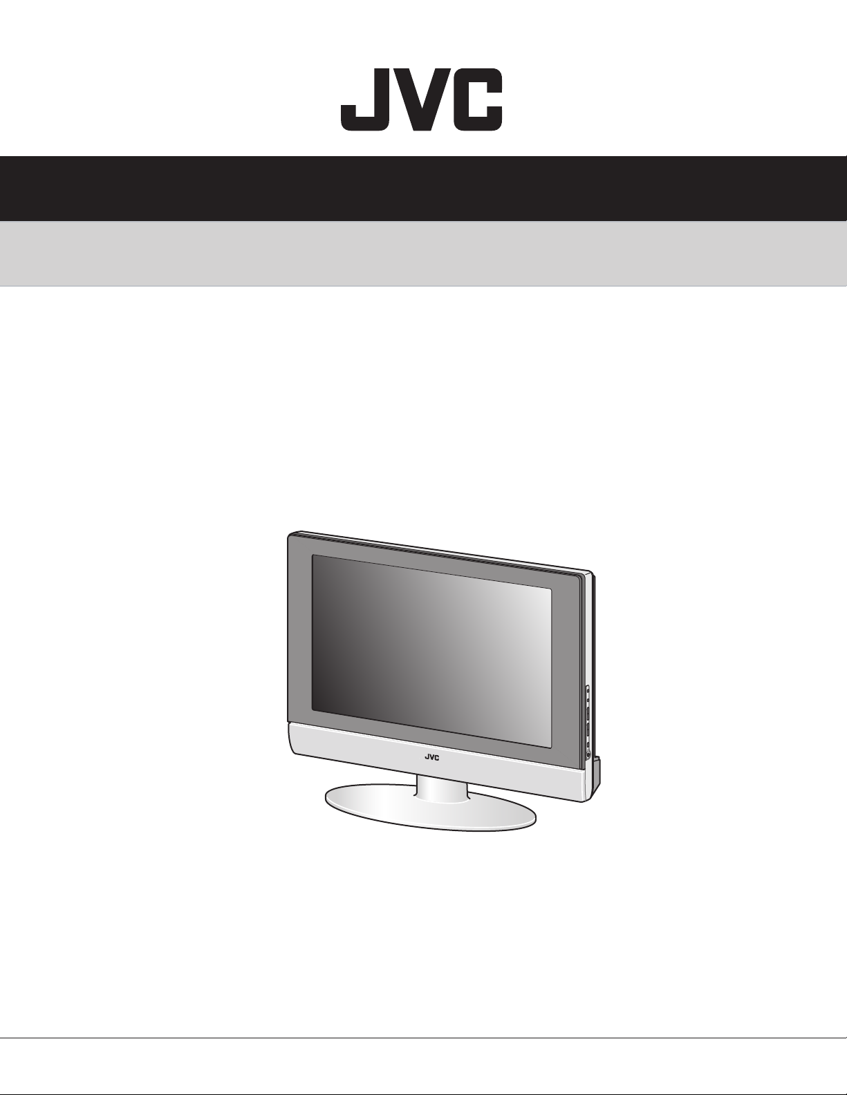
SCHEMATIC DIAGRAMS
LCD FLAT TELEVISION
LT-23X475
CD-ROM No. SML200409
COPYRIGHT © 2004 Victor Company of Japan, Limited
No.YA036
2004/9
Page 2
If you need more information on Computer and Electronic Repair, please visit these
in fact
websites to improve yourself.
http://www.fastrepairguide.com
http://www.protech2u.com
http://www.plasma-television-repair.com
http://www.lcd-television-repair.com
Happy Repairing!!
Highly Recommended Repair Ebook:
If you’re a LCD Monitor repairer, then this is the best guide for you.
Why? Because, the author revealed all his LCD Monitor Repairing
secrets for you. I think, with just few Repair tips you learned from
this guide you will get back your investment!
Click Here to read more.
This eBook will show you how to test the electronic component
correctly and accurately. Some of you may say that I don’t
need this eBook because it is too simple! Do you know that,
there is lots of testing electronic components secrets I have learned
from this guide? Do you know how to test a‘TRIAC’ correctly and
accurately? If you answer no then I guess you have to get this
EBook. Click Here to read more.
Are you tired of searching the service manuals to look for the value
of a burnt resistor? If the answer is YES, then this eBook is a ‘must
have’ guide for you. You can save a lot of time and be able to repair
customer’s Electronic equipment with burnt resistors in it.
Click here to read more.
Page 3
LT-23X475
STANDARD CIRCUIT DIAGRAMS
CONTENTS
USING P.W. BOARD
SEMICONDUCTOR
..................................................................................................................................................................... 2-1
..................................................................................................................................................................... 2-1
BLOCK DIAGRAM
CIRCUIT DIAGRAMS
MAIN PWB CIRCUIT DIAGRAM .............................................................................................................................................................. 2- 3
IR SENSOR PWB CIRCUIT DIAGRAM ................................................................................................................................................. 2-33
AV JACK PWB CIRCUIT DIAGRAM .................................................................................................................................................... 2-35
FRONT CONTROL PWB CIRCUIT DIAGRAM ...................................................................................................................................... 2-36
TUNER PWB CIRCUIT DIAGRAM ........................................................................................................................................................ 2-36
PATTERN DIAGRAMS
MAIN PWB PATTERN .......................................................................................................................................................................... 2-37
IR SENEOR PWB PATTERN ................................................................................................................................................................. 2-39
AV JACK PWB PATTERN .................................................................................................................................................................... 2-39
FRONT CONTROL PWB PATTERN ...................................................................................................................................................... 2-39
TUNER PWB PATTERN ........................................................................................................................................................................ 2-39
......................................................................................................................................................................... 2-2
................................................................................................................................................................... 2-3
............................................................................................................................................................. 2-37
USING P.W. BOARD
MAIN P.W. BOARD DA-5097631902 (PWB-0692-1)
IR SENSOR P.W. BOARD DA-5097631902 (PWB-0692-2)
AV JACK P.W. BOARD DA-5098800731 (PWB-0693-1)
FRONT CONTROL P.W. BOARD DA-5098800732 (PWB-0693-2)
TUNER P.W. BOARD DA-5098800733 (PWB-0693-3)
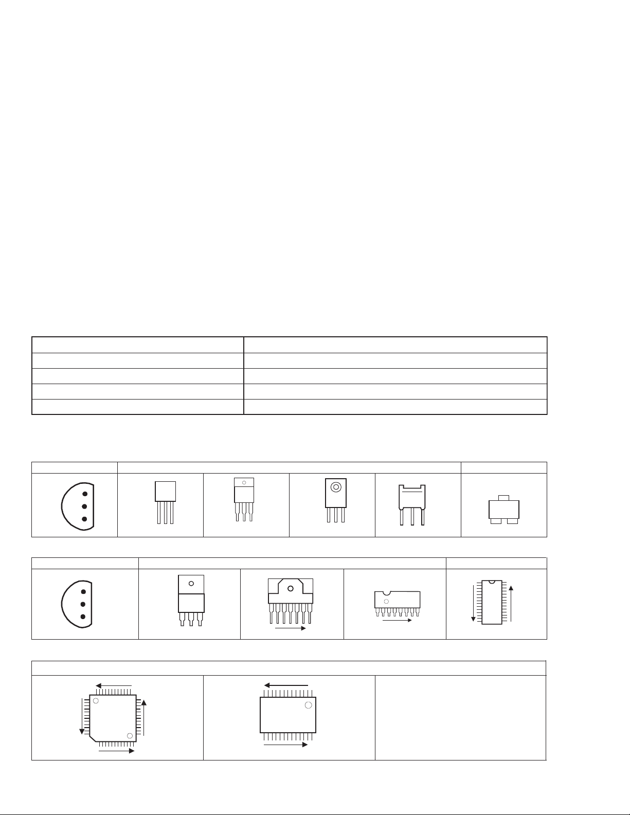
SEMICONDUCTOR SHAPES
TRANSISTOR
BOTTOM V IEW
E
C
FRONT V I EW
B
ECB
BCE
(G)(D)(S )
ECB
ECB
TOP VIEW
CHIP TR
BE
C
IC
BOT TO M V IEW FR ON T VI EW T OP V I EW
OUT
E
IN
IN OUTE
1 N
1 N
CHIP IC
TOP VIEW
1
N
2-1
N
N
N
1
N
No. YA036
1
N
Page 4
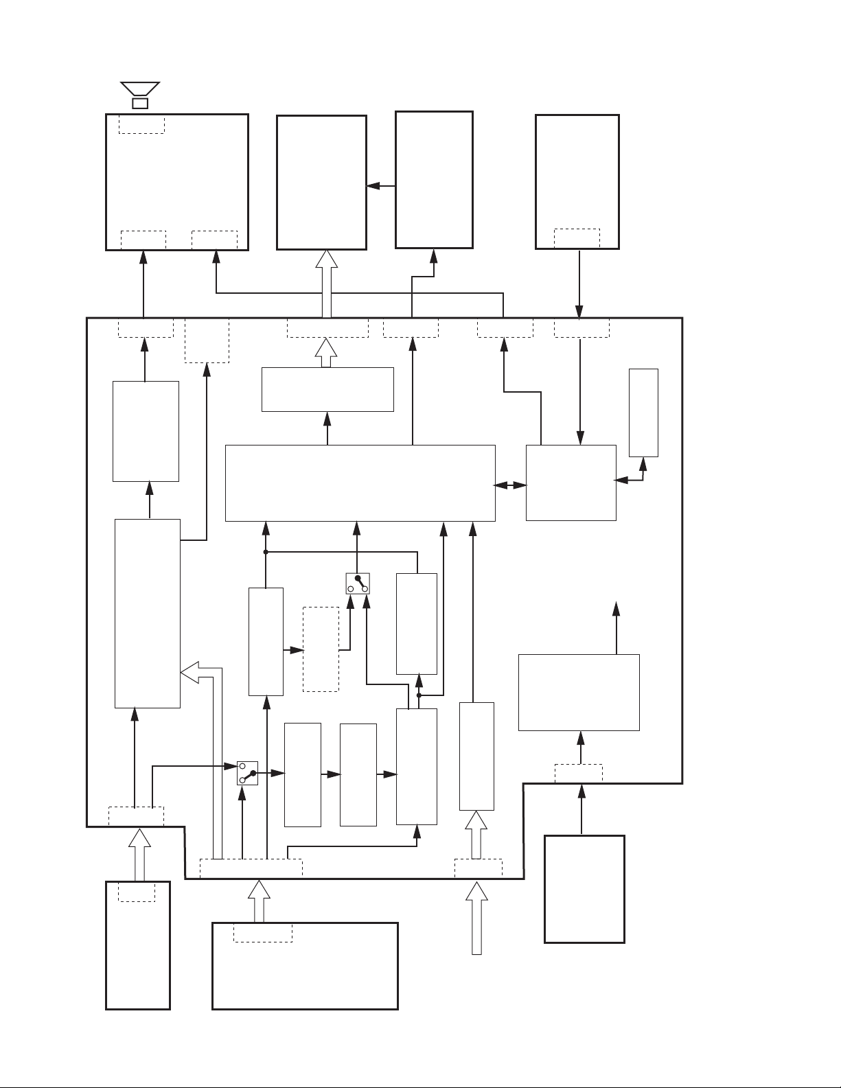
BLOCK DIAGRAM
P603
(Speaker)
FRONT
(Headphone)
P604
P604P602
(TPA1517)
Audio amp
CONTROL
P015
P016
P017
Audio Out
PWB
Port B
24bit
P008P005
LCD PANEL
LVDS I/F
Sync
INVERTER
P007 P003
(DS90CF383)
Scaler
(TP6760)
8bit
Port V
24bit
P002
Port A
PWB
IR SENSOR
P601
MCU
(W78E65)
PROM
2
E
(MSP3440G)
Audio Processor
&
CV Audio
MTS
TV
(Video)
TV
(Audio)
P001
P012
TUNER PWB
AV/SV Audio
PC Audio
ADC
(PI5V330)
CV
AV
P006
P020
De-
(AD9883A-110)
(Z86129)
V-Chip&C.C.
SV
AV
JACK
Macrovision
Y/C Sepa.
(TC90A65F)
AV
SV
CV
PWB
(PI5V330)
De-Interlace
Video decoder
(SiI504)
(SAA7118)
ADC
(AD9883A-110)
PJ01
VGA
24V
5V
24V
3.3V
2.5V
1.8V
Power
Supply
P020
AC
Adapter
50/60Hz
110/220V
MAIN PWB
No. YA036
2-2
Page 5
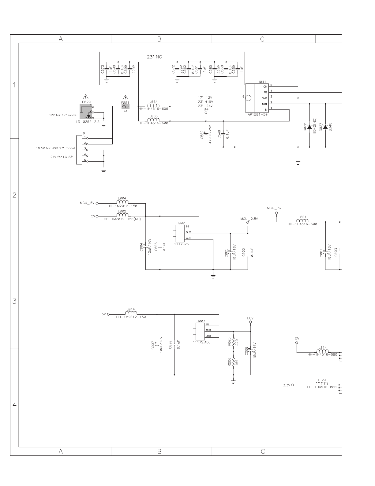
CIRCUIT DIAGRAMS
MAIN PWB CIRCUIT DIAGRAM (1/15)
No. YA0362-3
Page 6
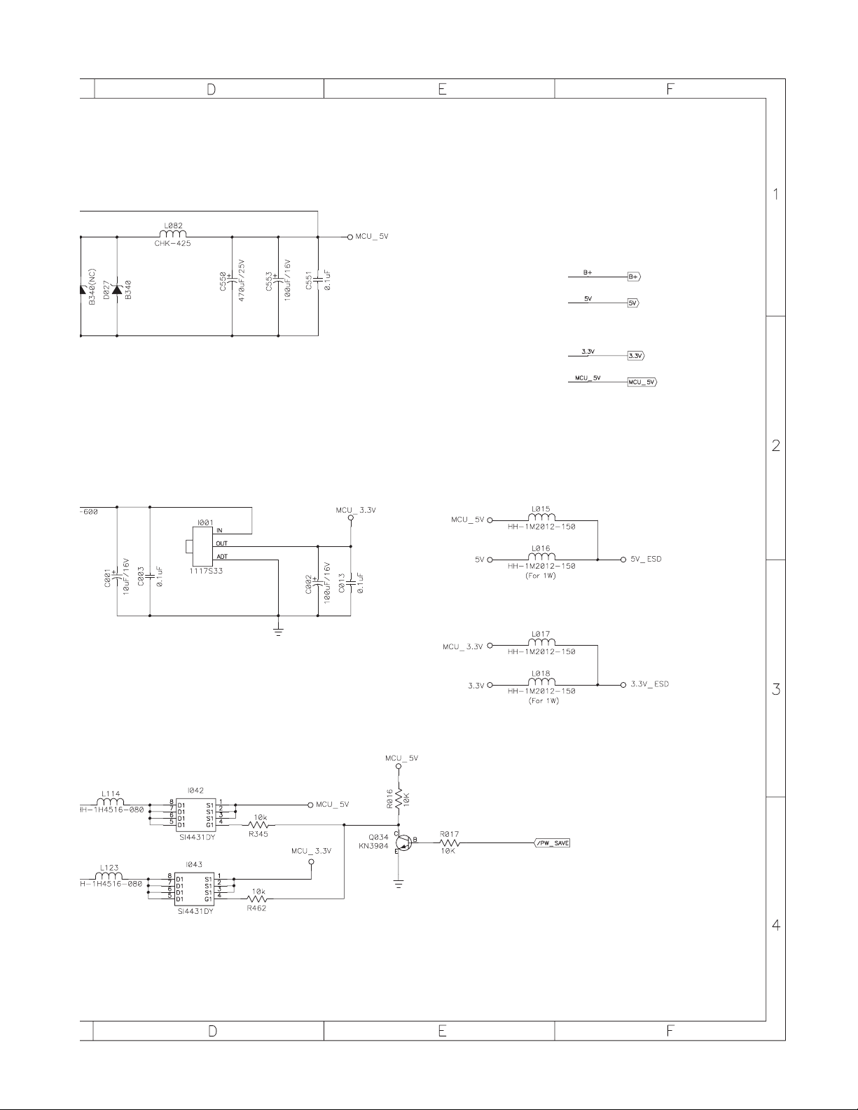
Power save
Sheet 2,7,11,12,13
MAIN PWB ASS'Y (1/15)
No. YA036
2-4
Page 7
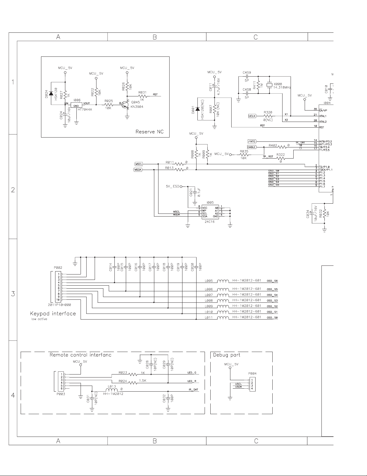
MAIN PWB CIRCUIT DIAGRAM (2/15)
Sheet 3,4,6,7,8,9,10,13
Sheet 3,4,6,7,8,9,10,13
Sheet 11
Sheet 11
Sheet 4
FRONT CONTROL
PWB P602
MPU
IR SENSOR
PWB P601
No. YA0362-5
Page 8
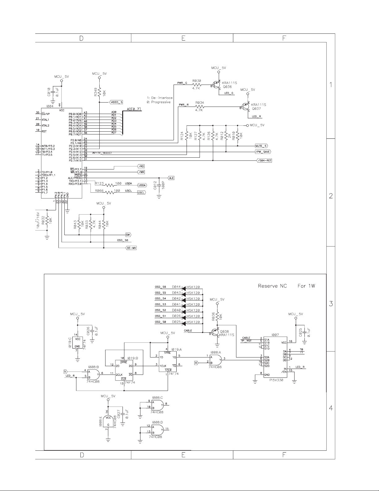
Sheet 9,10,11
Sheet 15
Sheet 11
Sheet 14
Sheet 1,7,11,12,13
Sheet 8,10
Sheet 11
Sheet 11
Sheet 11
MAIN PWB ASS'Y (2/15)
No. YA036
2-6
Page 9
S
S
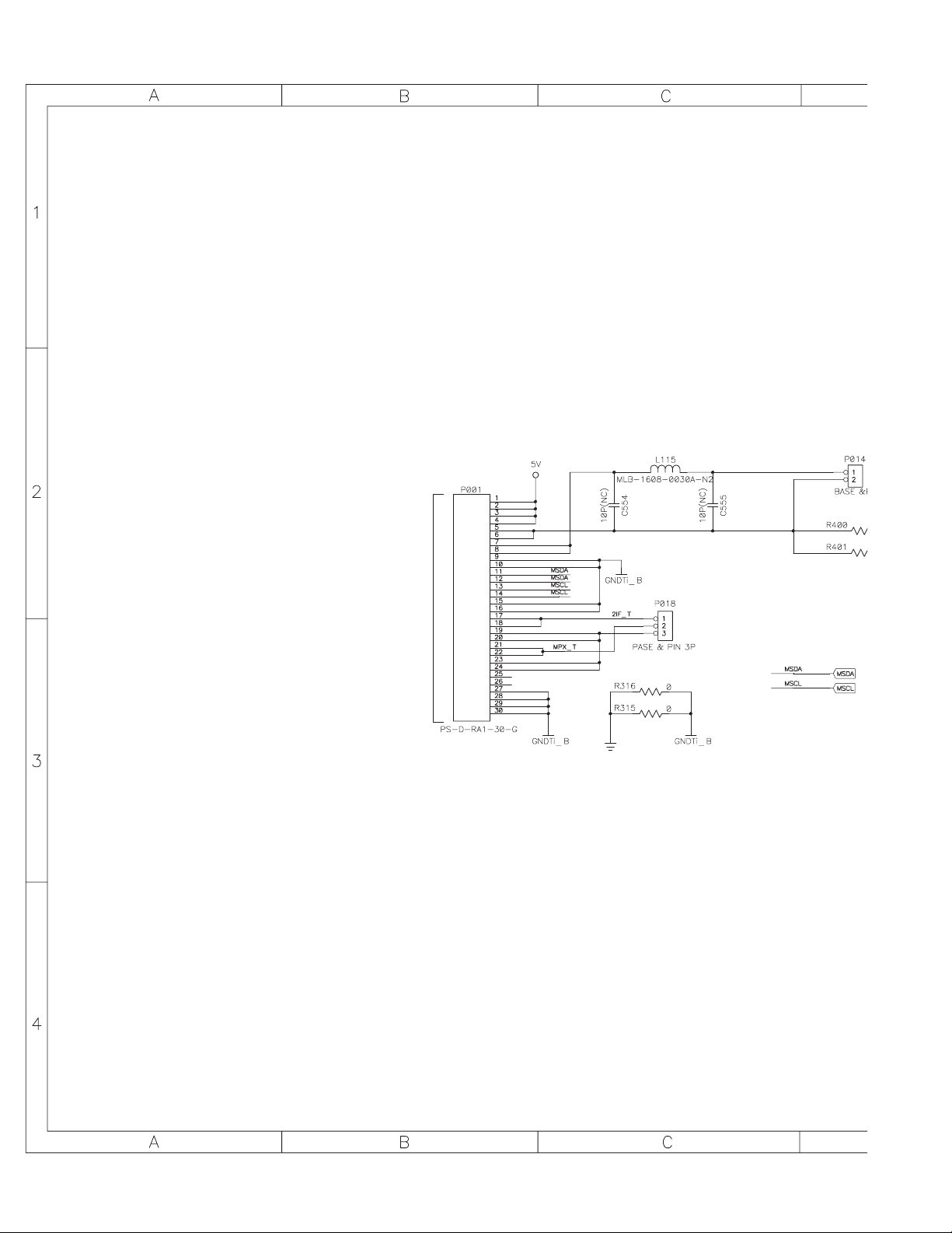
MAIN PWB CIRCUIT DIAGRAM (3/15)
TUNER PWB
P012
No. YA0362-7
Page 10
Sheet 2,3,4,6,8,9,10,13
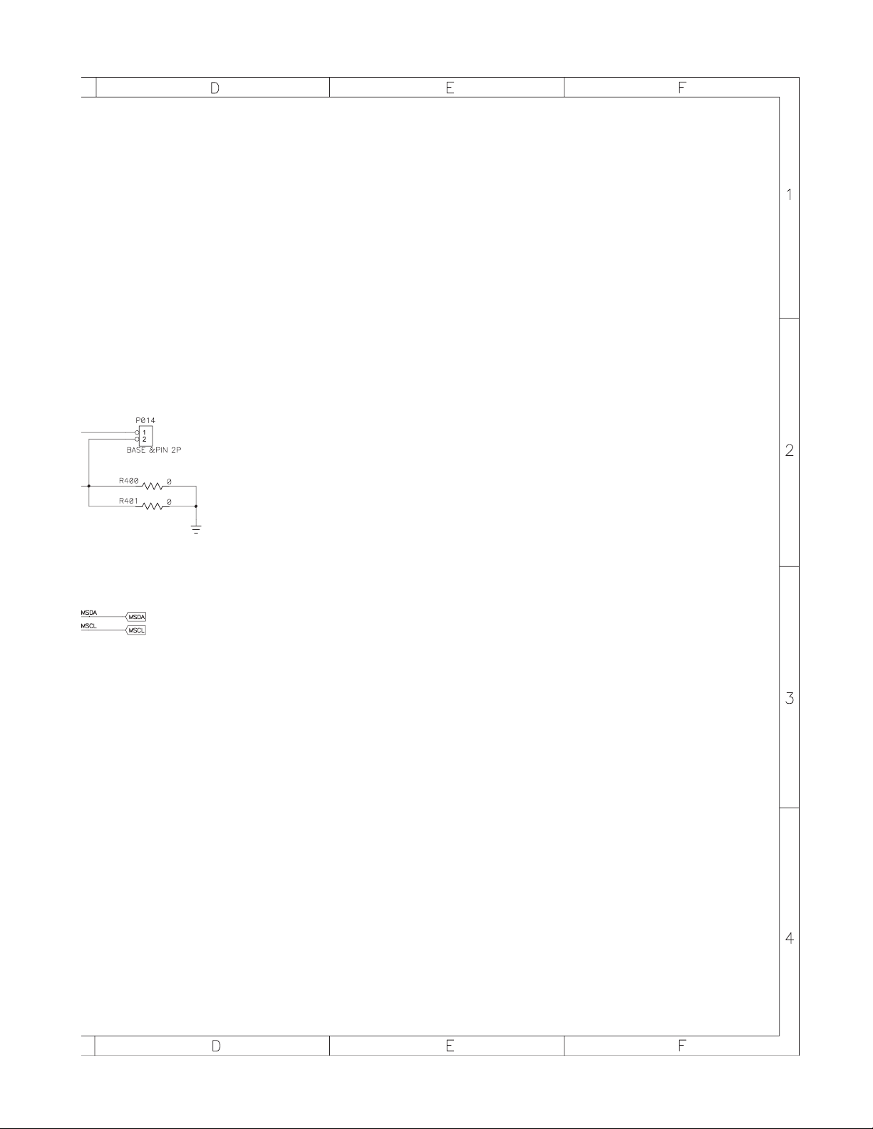
Sheet 2,3,4,6,8,9,10,13
MAIN PWB ASS'Y (3/15)
No. YA036
2-8
Page 11
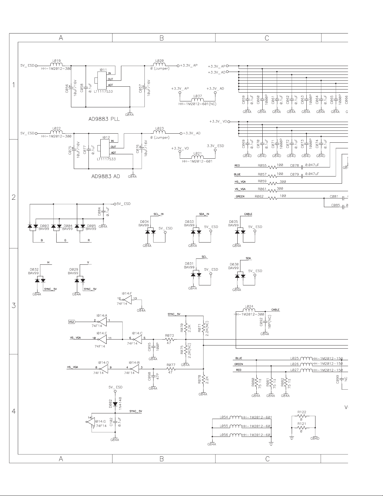
MAIN PWB CIRCUIT DIAGRAM (4/15)
Sheet 11
No. YA0362-9
Page 12
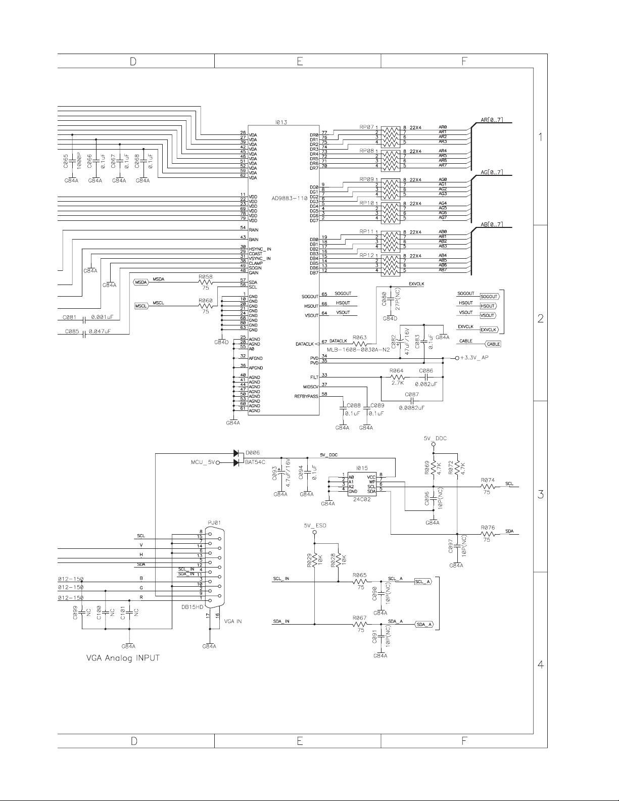
Sheet 2,3,4,6,7,8,9,10,13
A/D CONVERTER
Sheet 12
Sheet 12
Sheet 12
Sheet 2,3,4,6,7,8,9,10,13
Sheet 11
Sheet 2
Sheet 11
No. YA036
MAIN PWB ASS'Y (4/15)
2-10
Page 13
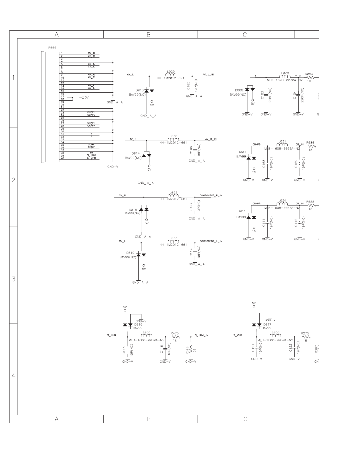
MAIN PWB CIRCUIT DIAGRAM (5/15)
AV JACK PWB
P020
No. YA0362-11
Page 14

Sheet 8,9
Sheet 9
Sheet 9
Sheet 6,9
Sheet 6,9
Sheet 6,9
Sheet 13
Sheet 13
Sheet 13
Sheet 13
MAIN PWB ASS'Y (5/15)
No. YA036
2-12
Page 15

MAIN PWB CIRCUIT DIAGRAM (6/15)
Sheet 2,3,4,7,8,9,10,13
Sheet 2,3,4,7,8,9,10,13
Sheet 5,9
Sheet 5,9
Sheet 5,9
Sheet 11
NOTE:
The circuit block in the bold line is included in the MAIN PWB circuit block.
The service parts of the MAIN PWB is available including this circuit block.
Sheet 5,9
Sheet 5,9
Sheet 9
Sheet 9
No. YA0362-13
Page 16

A/D CONVERTER
Sheet 11
Sheet 11
Sheet 11
Sheet 11
MAIN PWB ASS'Y (6/15)
Sheet 15
Sheet 11
No. YA036
2-14
Page 17

d
a
MAIN PWB CIRCUIT DIAGRAM (7/15)
Sheet 9
Sheet 9
NOTE:
The circuit block in the bold line is include
The service parts of the MAIN PWB is avail
Sheet 2,8
Sheet 8
Y/C SEP.
No. YA0362-15
Page 18

is included in the MAIN PWB circuit block.
B is available including this circuit block.
Y/C SEP.
Sheet 2,3,4,6,7,8,9,10,12,13
Sheet 2,3,4,6,7,8,9,10,12,13
No. YA036
MAIN PWB ASS'Y (7/15)
2-16
Page 19

MAIN PWB CIRCUIT DIAGRAM (8/15)
Sheet 5
Sheet 5
Sheet 2,7
Sheet 2,3,4,6,7,9,10,12,13
Sheet 2,3,4,6,7,9,10,12,13
Sheet 9
No. YA0362-17
V-Chip, CC
Page 20

Sheet 9
Sheet 9
Sheet 9
Sheet 9
Sheet 7
MAIN PWB ASS'Y (8/15)
No. YA036
2-18
Page 21

R
MAIN PWB CIRCUIT DIAGRAM (9/15)
Sheet 5,8
Sheet 5,8
Sheet 8
Sheet 5
Sheet 5
Sheet 7
Sheet 7
Sheet 8
VIDEO DECODE
COMB FILTER
Sheet 5,6
Sheet 8
No. YA0362-19
Page 22

EO DECODER
OMB FILTER
Sheet 10,11
Sheet 2,3,4,6,7,8,10,13
Sheet 2,3,4,6,7,8,10,13
Sheet 8
No. YA036
Sheet 10,11
MAIN PWB ASS'Y (9/15)
2-20
Page 23

MAIN PWB CIRCUIT DIAGRAM (10/15)
Sheet 2,3,4,6,7,8,9,13
Sheet 2,3,4,6,7,8,9,13
Sheet 2,9,11
Sheet 9,11
Sheet 9,11
Sheet 9,11
De -Interlace
Sheet 9,11
Sheet 2,8
No. YA0362-21
Page 24

Sheet 11
Sheet 11
Sheet 11
Sheet 11
Sheet 11
No. YA036
MAIN PWB ASS'Y (10/15)
2-22
Page 25

MAIN PWB CIRCUIT DIAGRAM (11/15)
Sheet 2,9,10
Sheet 2
Sheet 15
Sheet 6
Sheet 9,10
Sheet 4
Sheet 10
Sheet 2,5,7,10,13,14
Sheet 4
Sheet 9,10
Sheet 2
Sheet 2
Sheet 6
PC
MAIN
Sheet 4
Sheet 4
SCALER
Sheet 6
Sheet 6
Sheet 6
Sheet 4
No. YA0362-23
Page 26

Sheet 12
Sheet 12
Sheet 12
No. YA036
Sheet 12
MAIN PWB ASS'Y (11/15)
2-24
Page 27

MAIN PWB CIRCUIT DIAGRAM (12/15)
Sheet 11
Sheet 11
INVERTER
Sheet 11
LVDS
No. YA0362-25
Page 28

Sheet 11
Sheet 1,2,7,11,12,13
LCD PANEL
LVDS DECODER
MAIN PWB ASS'Y (12/15)
No. YA036
2-26
Page 29

MAIN PWB CIRCUIT DIAGRAM (13/15)
Sheet 5
Sheet 5
Sheet 2,3,4,6,7,8,9,10
Sheet 2,3,4,6,7,8,9,10
Sheet 5
Sheet 5
Sheet 1,7,11,12
MTS
No. YA0362-27
Page 30

MTS
Sheet 14
Sheet 14
MAIN PWB ASS'Y (13/15)
No. YA036
2-28
Page 31

MAIN PWB CIRCUIT DIAGRAM (14/15)
Sheet 2
Sheet 13
Sheet 13
AUDIO AMP
No. YA0362-29
Page 32

FRONT CONTROL PWB
P604
MAIN PWB ASS'Y (14/15)
No. YA036
2-30
Page 33

MAIN PWB CIRCUIT DIAGRAM (15/15)
Sheet 6
Sheet 2
No. YA0362-31
Page 34

Sheet 2
Sheet 11
MAIN PWB ASS'Y (15/15)
No. YA036
2-32
Page 35

IR SENSOR PWB CIRCUIT DIAGRAM
MAIN PWB (2/15)
P003
No. YA0362-33
Page 36

IR SENSOR PWB ASS'Y
No. YA036
2-34
Page 37

R
1
B
AV JACK PWB/ FRONT CONTROL PWB/ TUNER PWB CIRCUIT DIAGRAMS
AV JACK PWB ASS'Y
MAIN PWB
(5/15) P006
C024
330P
C026
GND-IN
330P
C034
GND-IN
330P
C032
C033
330P
330P
C025
GND-IN
330P
MAIN PWB
(3/15) P00
C029
C027
C028
330P
330P
330P
C030
330P
C031
330P
MAIN PW
P002
F
No. YA0362-35
Page 38

ANTENNA
TUNER PWB ASS'Y
RT03
0(NC)
RT05
0
5V_TUNER
MAIN PWB
(3/15) P001
ANT
UT01
FQ1236
RT04
CT07
0
NC
CT04
CT02
CT05
1000P(NC)
0.1uF
0.1uF
1K (NC)
CT01
RT07
100uF/16V
RT08
0
RT06
0
CT08
47P (NC)
100UH
HH-1M2012-300(NC)
CT09
100uF/16V
27UH(NC)
LT10
100UH
CT10
47P(NC)
CT06
CT03
47P(NC)
5V_TUNER
5V_TUNER
100uF/16V
SPEAKERS
MAIN PWB (14/15)
P005
MAIN PWB (2/15)
P002
FRONT CONTROL PWB ASS'Y
No. YA036
2-36
Page 39

PATTERN DIAGRAMS
MAIN PWB PATTERN
No. YA0362-37
Page 40

TOP
No. YA036
2-38
Page 41

IR SENSOR PWB PATTERN
AV JACK PWB PATTERN
FRONT CONTROL PWB PATTERN
TUNER PWB PATTERN
No. YA0362-39
Page 42

Victor Company of Japan, Limited
AV & MULTIMEDIA COMPANY VIDEO DISPLAY CATEGORY 12, 3-chome, Moriya-cho, kanagawa-ku, Yokohama, kanagawa-prefecture, 221-8528, Japan
(No. YA036)
Printed in Japan
WPC
Page 43

If you need more information on Computer and Electronic Repair, please visit these
in fact
websites to improve yourself.
http://www.fastrepairguide.com
http://www.protech2u.com
http://www.plasma-television-repair.com
http://www.lcd-television-repair.com
Happy Repairing!!
Highly Recommended Repair Ebook:
If you’re a LCD Monitor repairer, then this is the best guide for you.
Why? Because, the author revealed all his LCD Monitor Repairing
secrets for you. I think, with just few Repair tips you learned from
this guide you will get back your investment!
Click Here to read more.
This eBook will show you how to test the electronic component
correctly and accurately. Some of you may say that I don’t
need this eBook because it is too simple! Do you know that,
there is lots of testing electronic components secrets I have learned
from this guide? Do you know how to test a‘TRIAC’ correctly and
accurately? If you answer no then I guess you have to get this
EBook. Click Here to read more.
Are you tired of searching the service manuals to look for the value
of a burnt resistor? If the answer is YES, then this eBook is a ‘must
have’ guide for you. You can save a lot of time and be able to repair
customer’s Electronic equipment with burnt resistors in it.
Click here to read more.
 Loading...