

Page 1
SERVICE MANUAL
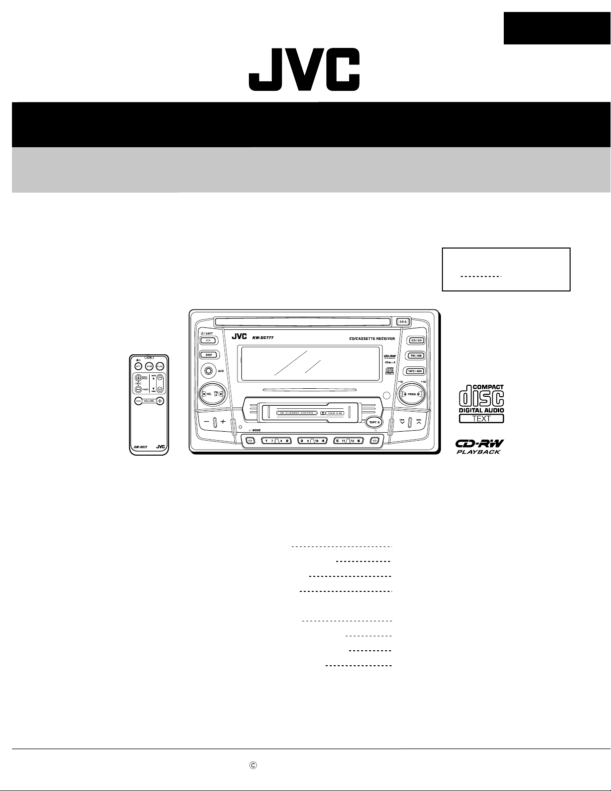
CD/CASSETTE RECEIVER
KW-XC777
Contents
KW-XC777
E
X
Area Suffix
U Other Areas
Safety precaution
Preventing static electricity
Disassembly method
Adjustment method
Flow of functional operation
untill TOC read
Maintenance of laser pickup
Replacement of laser pickup
Description of major ICs
COPYRIGHT 2002 VICTOR COMPANY OF JAPAN, LTD.
1- 2
1- 3
1- 4
1-23
1-27
1-29
1-29
1-30~47
No.49687
Feb. 2002
Page 2
KW-XC777
Safety precaution
!
!
Burrs formed during molding may be left over on some parts of the chassis. Therefore,
pay attention to such burrs in the case of preforming repair of this system.
Please use enough caution not to see the beam directly or touch it in case of an
adjustment or operation check.
1-2
Page 3
KW-XC777
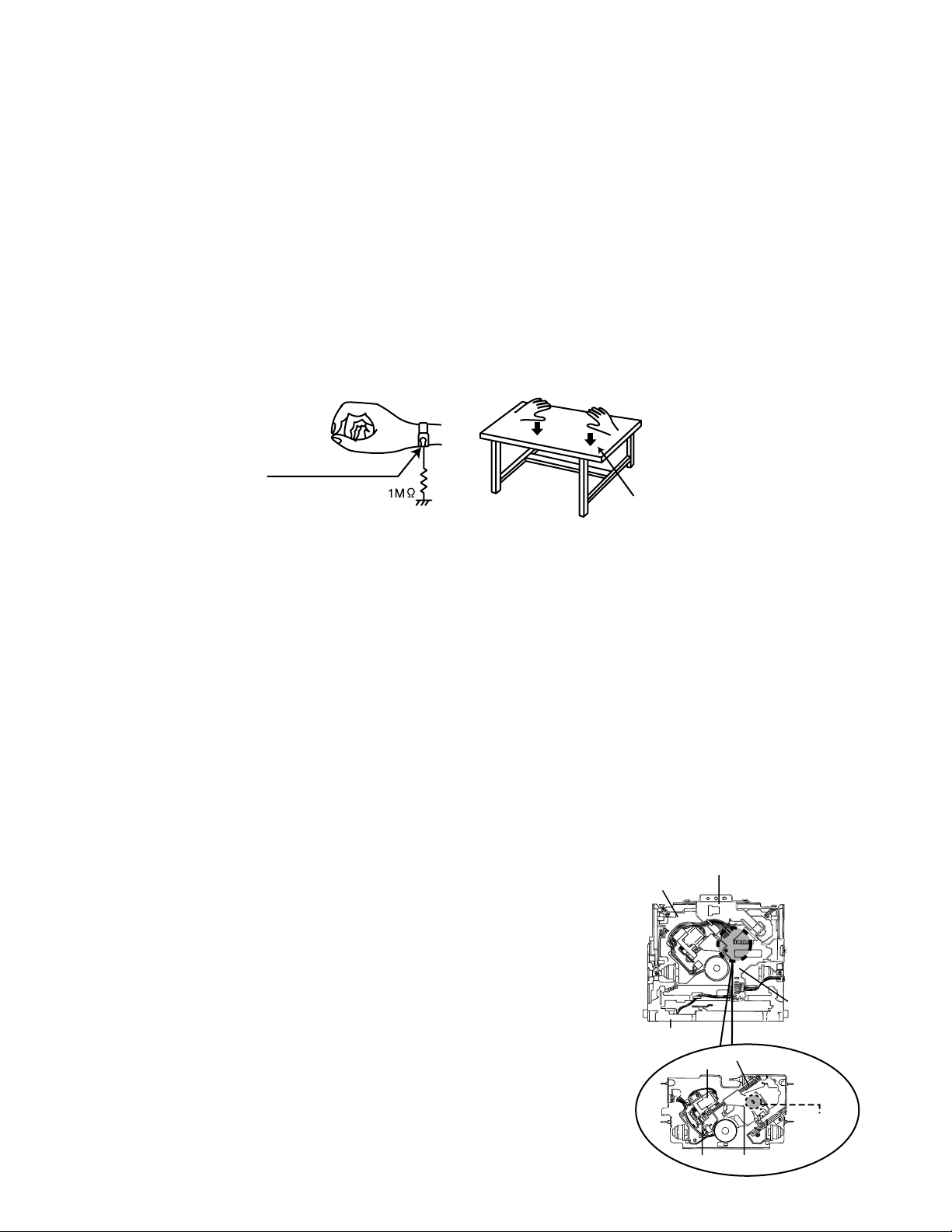
Preventing static electricity
1.Grounding to prevent damage by static electricity
Electrostatic discharge (ESD), which occurs when static electricity stored in the body, fabric, etc. is discharged,
can destroy the laser diode in the traverse unit (optical pickup). Take care to prevent this when performing repairs.
2.About the earth processing for the destruction prevention by static electricity
Static electricity in the work area can destroy the optical pickup (laser diode) in devices such as CD players.
Be careful to use proper grounding in the area where repairs are being performed.
2-1 Ground the workbench
Ground the workbench by laying conductive material (such as a conductive sheet) or an iron plate over
it before placing the traverse unit (optical pickup) on it.
2-2 Ground yourself
Use an anti-static wrist strap to release any static electricity built up in your body.
(caption)
Anti-static wrist strap
Conductive material
(conductive sheet) or iron plate
3. Handling the optical pickup
1. In order to maintain quality during transport and before installation, both sides of the laser diode on the
replacement optical pickup are shorted. After replacement, return the shorted parts to their original condition.
(Refer to the text.)
2. Do not use a tester to check the condition of the laser diode in the optical pickup. The tester's internal power
source can easily destroy the laser diode.
4.Handling the traverse unit (optical pickup)
1. Do not subject the traverse unit (optical pickup) to strong shocks, as it is a sensitive, complex unit.
2. Cut off the shorted part of the flexible cable using nippers, etc. after replacing the optical pickup. For specific
details, refer to the replacement procedure in the text. Remove the anti-static pin when replacing the traverse
unit. Be careful not to take too long a time when attaching it to the connector.
3. Handle the flexible cable carefully as it may break when subjected to strong force.
4. It is not possible to adjust the semi-fixed resistor that adjusts the laser power. Do not turn it
CD mechanism ass’y
Damper bracket
Attention when traverse unit is decomposed
*Please refer to "Disassembly method" in the text for pick-up and how to
detach the substrate.
1.Solder is put up before the card wire is removed from connector on
the CD substrate as shown in Figure.
(When the wire is removed without putting up solder, the CD pick-up
assembly might destroy.)
2.Please remove solder after connecting the card wire with
when you install picking up in the substrate.
Front bracket
Feed motor ass’y
FD screw
CD mechanism
control board
Soldering
FD gear
Pickup unit
1-3
Page 4
KW-XC777
Disassembly method
Removing the front panel assembly
(See Fig.1 to 3)
1.
Remove the four screws A on both sides of the
body.
2.
Release four joints a on both sides of the body using
a screwdriver and remove the front panel assembly
toward the front. The connector which connects the
front panel assembly with the rear section comes off.
CAUTION:
When reassembling, make sure that
connector CN501 on the front panel
assembly is securely connected to
CN701 on the main board (See Fig.3).
Joint a
A
A
Joint a
Front panel assembly
Fig.1
Joint a
A
CN501
A
Joint a
Front panel assembly
Fig.2
1-4
CN701
Front panel assembly
Fig.3
Page 5
Removing the system control board /
switch board (See Fig.4 to 5)
Prior to performing the following procedure, remove
the front panel assembly.
1.
Remove the twelve screws B retaining the system
control board.
2.
Remove the five screws C retaining the switch
board.
3.
Unsolder WR501 and WR502 of the wires
connecting the system control board with the switch
board.
B
B
WR502
System control board
WR502
B
Switch board
Fig.4
KW-XC777
B
B
WR501
WR502
System control board
CC
Switch board
Fig.5
WR501
1-5
Page 6
KW-XC777
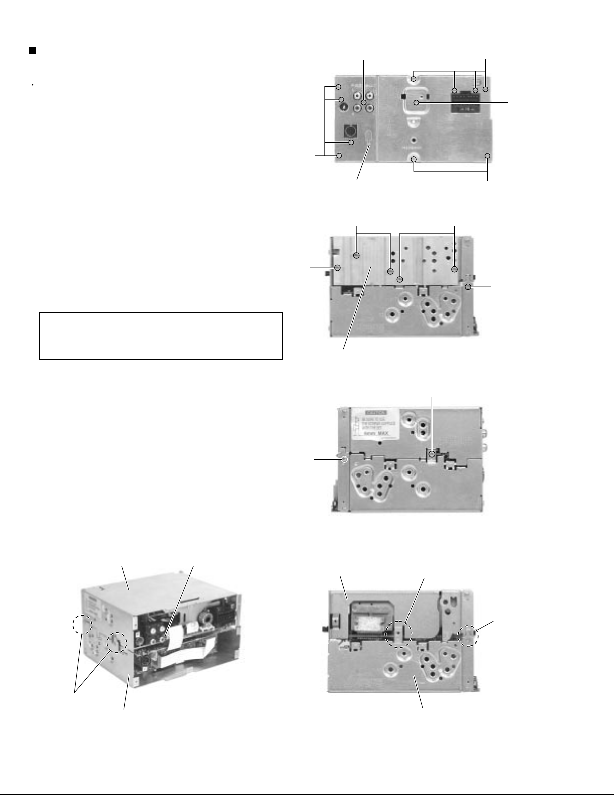
Removing the CD player section /
cassette player section (See Fig.6 to 10)
Prior to performing the following procedure, remove
the front panel assembly.
1.
Remove the ten screws D, the screw E and F
attaching the rear panel on the back of the body.
2.
Remove the three screws G and the two screws H
attaching the heat sink on the left side.
3.
Remove the three screws I attaching the CD player
section and the cassette player section on the both
sides of the body.
4.
Disconnect the card wire from connector CN702 on
the main board in the CD player section on the back
of the body.
5.
Remove the CD player section upward.
CAUTION:
When reassembling, joint the CD player
section and the cassette player section
at four joints b.
D
G
Rear panel
Heat sink
H
E
Fig.6
Fig.7
D
F
D
G
I
CD player section
CN702
I
CD player section
I
Fig.8
Joint b
Joint b
1-6
Joints b
Cassette player section
Cassette player section
Fig.10Fig.9
Page 7
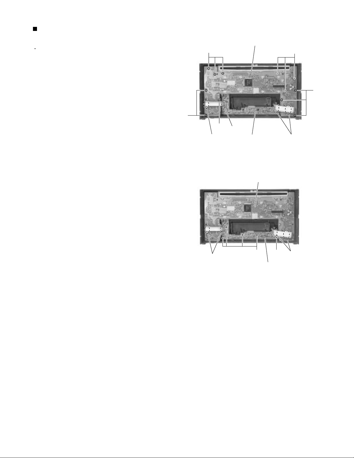
<CD player section>
KW-XC777
Prior to performing the following procedure, remove
the front panel assembly, the CD player section and
the cassette player section.
Removing the main board (See Fig.11)
1.
Remove the three screws J attaching the main
board. The connector CN601 on the main board is
disconnected from the CD mechanism control board.
CAUTION:
When reassembling, securely connect
connector CN601 on the main board to
the connector on the CD mechanism
control board.
Main board
J
J
Fig.11
CN601
J
K
Removing the CD mechanism assembly
(See Fig.12)
Prior to performing the following procedure, remove
the main board.
1.
Remove the three screws K attaching the CD
mechanism assembly.
K
K
CD mechanism assembly
Fig.12
1-7
Page 8
KW-XC777
<Cassette player section>
Prior to performing the following procedures, remove
the front panel assembly, the CD player section and
the cassette player section.
Removing the main board (See Fig.13)
1.
Disconnect the card wire from connector CN972 on
the main board.
2.
Remove the two screws L attaching the main board.
Removing the cassette mechanism
assembly (See Fig.13 and 14)
L
M
CN972
Cassette mechanism assembly
Fig.13
Bottom cover
Main board
L
M
Prior to performing the following procedure, remove
the main board.
1.
Disconnect the card wire from connector CN972 on
the main board.
2.
Remove the four screws M from the bottom cover of
the cassette player section.
Removing the connector board
(See Fig.15)
Prior to performing the following procedure,
remove the cassette mechanism assembly.
1.
Remove the screw N and move the connector
board in the direction of the arrow to release the
two joints c.
2.
Disconnect the wire from connector CJ402 and
the card wire from CN403 on the connector
board respectively.
CJ402
Fig.14
N
Connector board
Joints c
CN403
1-8
Fig.15
Page 9
KW-XC777
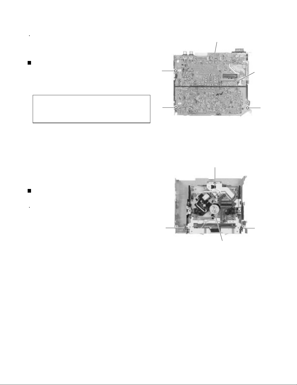
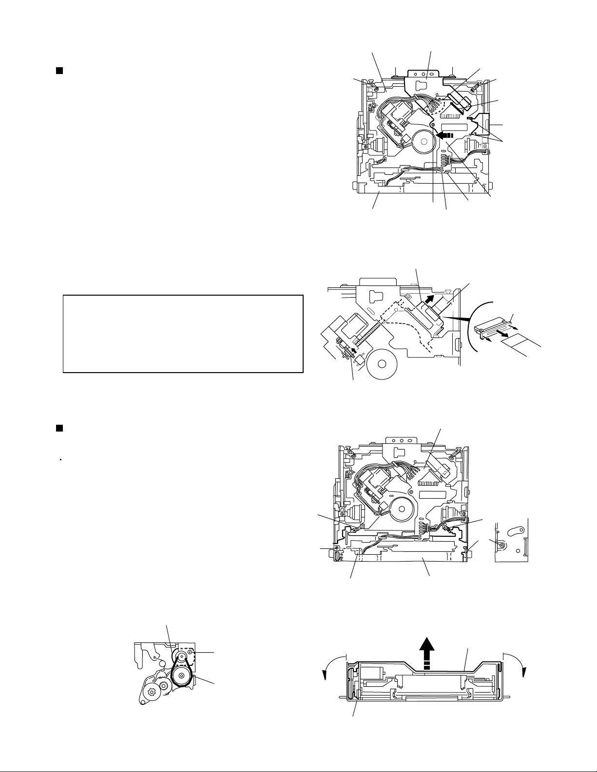
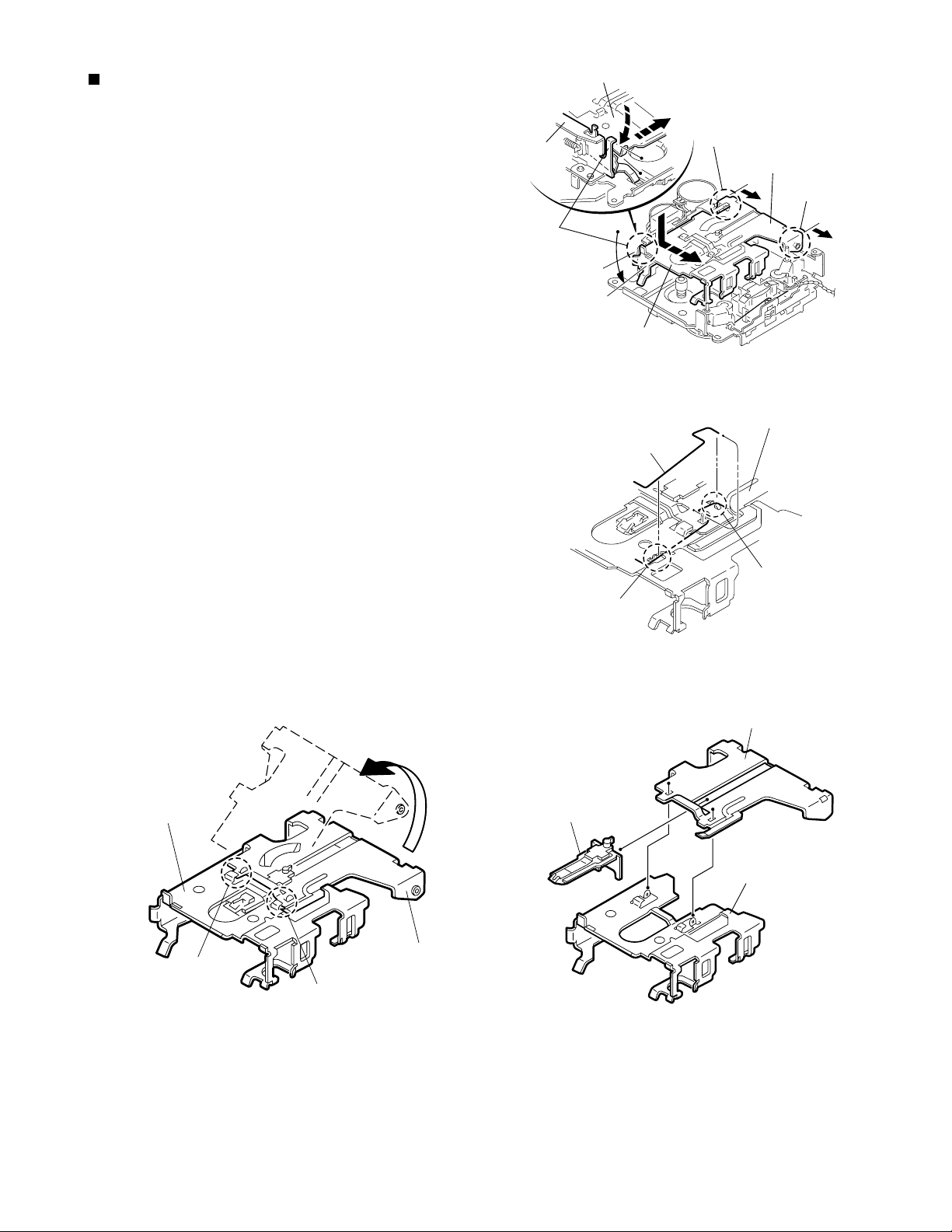
<CD mechanism section>
Removing the CD mechanism control
board (See Fig.1 and 2)
1.
Unsolder the part a and b on the CD mechanism
control board.
2.
Remove the stator fixing the CD mechanism control
board and the damper bracket (To remove the stator
smoothly, pick up the center part).
3.
Remove the screw A attaching the CD mechanism
control board.
4.
Remove the CD mechanism control board in the
direction of the arrow while releasing it from the two
damper bracket slots d and the front bracket slot e.
5.
Disconnect the flexible wire from connector on the
pickup unit.
ATTENTION:
Turn the FD gear in the direction of the
arrow to move the entire pickup unit to
the appropriate position where the
flexible wire of the CD mechanism unit
can be disconnected easily.
(Refer to Fig.2)
CD mechanism assembly
D
h
Front bracket
Pickup unit
Damper bracket
D
A
Fig.1
e
b
Flexible wire
a
h
c
D
d
CD mechanism
control board
Shift the lock
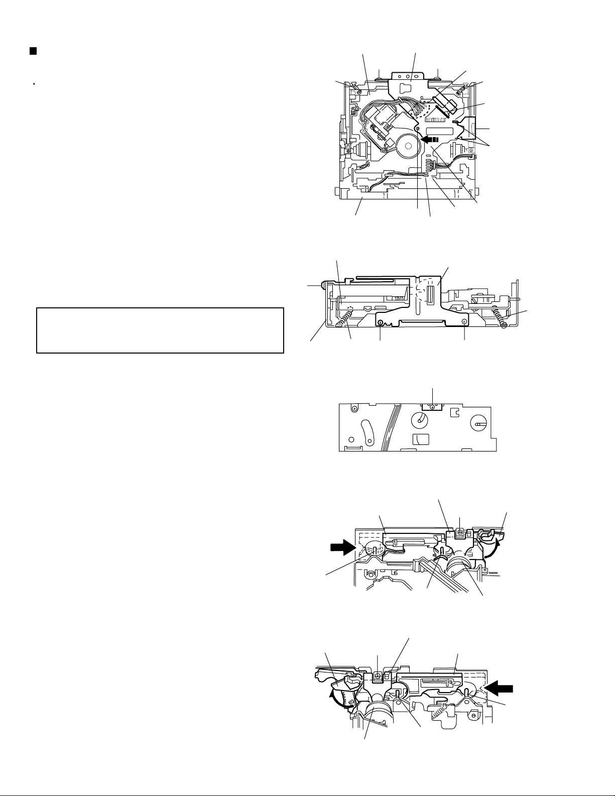
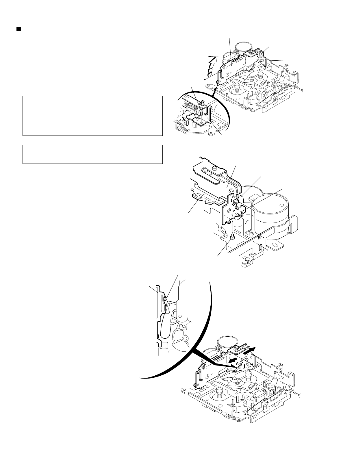
Removing the loading motor
(See Fig.3 to 5)
Prior to performing the following procedure, remove
the CD mechanism control board.
1.
Remove the two springs f attaching the CD
mechanism assembly and the front bracket.
2.
Remove the two screws B and the front bracket
while pulling the flame outward.
3.
Remove the belt and the screw C from the loading
motor.
Loading motor
C
f
B
Loading motor
Pull outward
FD gear
Fig.2
CD mechanism control board
f
B
Front bracket
Fig.3
Front bracket
Pull outward
Fig.5
Belt
Flame
Fig.4
1-9
Page 10
KW-XC777
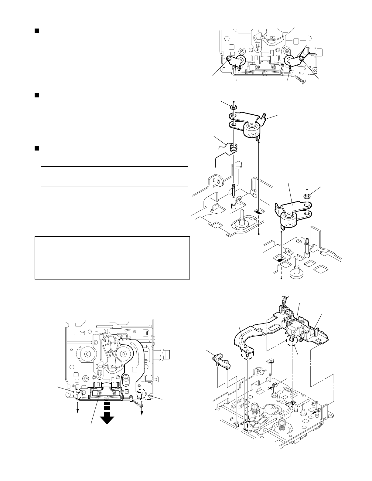
Removing the CD mechanism assembly
(See Fig.1, 6 to 9)
Prior to performing the following procedure, remove
the CD mechanism control board and the front
bracket (loading motor).
1.
Remove the three screws D and the damper
bracket.
2.
Raise the both sides fix arms and move the fix plates
in the direction of the arrow to place the four shafts g
as shown in Fig.8 and 9.
3.
Remove the CD mechanism assembly and the two
springs h attaching the flame.
4.
Remove the two screws E and both sides rear
damper brackets from the dampers. Detach the CD
mechanism assembly from the left side to the right
side.
ATTENTION:
The CD mechanism assembly can be
removed if only the rear damper
bracket on the left side is removed.
CD mechanism
h
Front bracket
CD mechanism
D
Flame
assembly
D
assembly
h
D
Damper bracket
D
A
Fig.5
Fig.6
e
b
Damper bracket
a
h
c
D
d
CD mechanism
control board
h
D
Fix plate (L)
g
Fix arm (R)
D
Fig.7
Rear damper bracket
g
Fig.8
Rear damper bracket
E
Fix plate(R)
E
Fix arm (L)
Damper
1-10
Damper
g
g
Fig.9
Page 11
KW-XC777
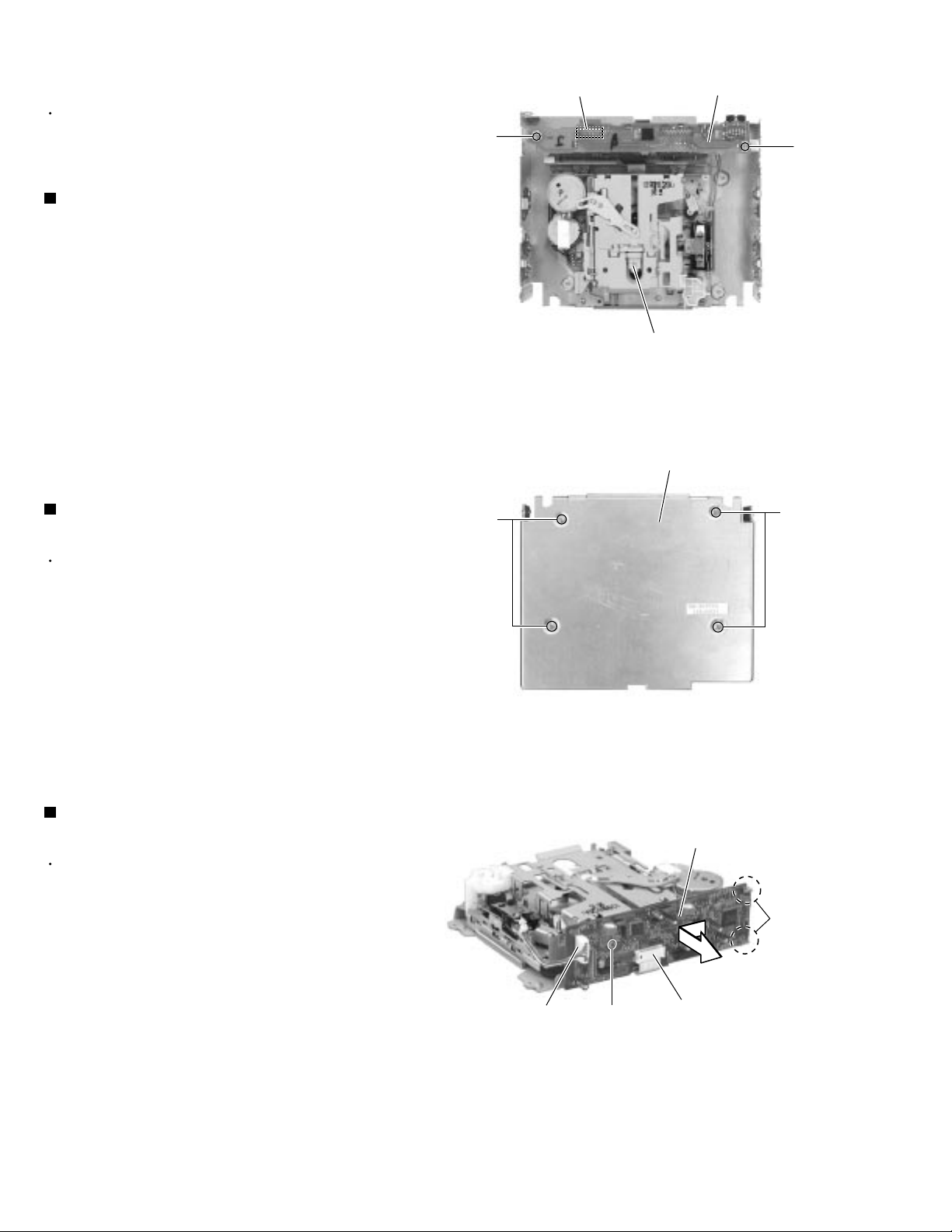
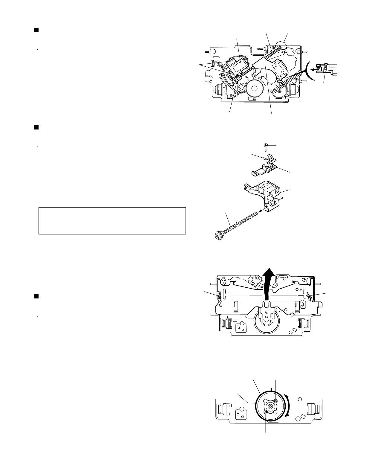
Removing the feed motor assembly
(See Fig.10)
Prior to performing the following procedure, remove
the CD mechanism control board, the front bracket
(loading motor) and the CD mechanism assembly.
1.
Remove the two screws F and the feed motor
assembly.
Removing the pickup unit
(See Fig.10 and 11)
Prior to performing the following procedure, remove
the CD mechanism control board, the front bracket
(loading motor), the CD mechanism assembly and
the feed motor assembly.
1.
Detach the FD gear part of the pickup unit upward.
Then remove the pickup unit while pulling out the
part i of the FD screw.
Feed motor assembly
F
FD gear
Nut push spring plate
FD screw
Pickup unit
Fig.10
Part i
Part j
Pickup unit
G
Pickup mount nut
Pickup unit
ATTENTION:
2.
Remove the screw G attaching the nut push spring
plate and the pickup mount nut from the pickup unit.
Pull out the FD screw.
When reattaching the pickup unit,
reattach the part j of the pickup unit,
then the part i of the FD screw.
Removing the spindle motor
(See Fig.12 and 13)
Prior to performing the following procedure, remove
the CD mechanism control board, the front bracket
(loading motor), the CD mechanism assembly and
the feed motor assembly.
1.
Turn up the CD mechanism assembly and remove
the two springs k on both sides of the clamper arms.
Open the clamper arm upward.
2.
Turn the turn table, and remove the two screws H
and the spindle motor.
k
FD screw
Spindle motor
Fig.11
k
Fig.12
H
H
Fig.13
1-11
Page 12
KW-XC777
REFERENCE:
Prior to performing the following
procedures, turn the mode gear on the
bottom of the body until the respective part
comes to the EJECT position (Refer to
Fig.1).
Removing the cassette guide (See Fig.2)
1.
Turn the mode gear to set to RVS play or
subsequent mode.
2.
Remove the cassette guide from the main chassis
while releasing each two joint tabs a in the direction
of the arrow.
Mode gear
Fig.1
Cassette guide
Removing the load arm (See Fig.3)
1.
Remove the E-washer attaching the load arm.
2.
Move the load arm in the direction of the arrow and
release the joint b on the cassette catch.
Load arm
E-washer
Tab a
Joint b
Tab a
Fig.2
Fig.3
1-12
Page 13
KW-XC777
Removing the cassette hanger assembly /
cassette holder (See Fig.4 to 7)
1.
Check the mode is set to EJECT. Push down the
front part of the cassette holder and move in the
direction of the arrow to release the joint c.
2.
Move the rear part of the cassette hanger assembly
in the direction of the arrow to release it from the two
joint bosses d.
3.
Release the holder stabilizer spring from the hooks e
and f, then pull out from the cassette hanger
assembly.
4.
Bring up the rear side of the cassette hanger
assembly to release the joint g and h.
5.
Pull out the cassette catch from the cassette hanger
assembly.
Cassette holder assembly
Side bracket
Joints c
Cassette holder assembly
Cassette stabilizer spring
Fig.4
Boss d
Cassette hanger assembly
Cassette hanger
assembly
Boss d
Cassette holder
assembly
Hook g
Fig.6
Hook f
Hook e
Fig.5
Cassette hanger assembly
Cassette catch
Cassette holder assembly
Cassette hanger assembly
Hook h
Fig.7
1-13
Page 14
KW-XC777
Removing the side bracket assembly
(See Fig.8 to 10)
1.
Remove the screw A attaching the side bracket
assembly.
2.
Detach the front side of the side bracket assembly
upward and pull out forward to release the joint i and
j in the rear.
CAUTION:
CAUTION:
When reassembling, make sure that the
boss k of the main chassis is set in the
notch of the load rack under the side
bracket assembly. Do not reattach the
load rack on the boss k.
After reattaching the side bracket
assembly, confirm operation.
Side bracket assembly
Joint i
Joint j
A
Side bracket assembly
Fig.8
Side bracket assembly
Joint i
Joint j
Load rack
Load rack
Boss k
Boss k
Fig.9
1-14
Fig.10
Page 15
Removing the pinch arm (F) assembly
(See Fig.11 and 12)
1.
Remove the polywasher and pull out the pinch arm
(F) assembly.
2.
Remove the compulsion spring.
Removing the pinch arm (R) assembly
(See Fig.11 and 13)
1.
Remove the polywasher and pull out the pinch arm
(R) assembly.
Removing the slide chassis assembly
(See Fig.14 and 15)
Polywasher
Polywasher
Compulsion spring
Pinch arm
(R) assembly
Fig.11
Pinch arm
(F) assembly
Pinch arm (F) assembly
Polywasher
KW-XC777
REFERENCE:
It is not necessary to remove the head
and the tape guide.
1.
Move the slide chassis assembly in the direction of
the arrow to release the two joints l and remove from
the main chassis.
2.
Remove the rack link.
CAUTION:
When reassembling, first reattach the rack
link, and next fit the boss m and hook n of
the slide chassis assembly to the hole of
the main chassis, and engage the two joints
l.
Rack link
Fig.12
Boss m
Pinch arm
(R) assembly
Fig.13
Head
Hook n
Polywasher
Tape guide
Joint l
Slide chassis assembly
Fig.14
Joint l
Fig.15
1-15
Page 16

KW-XC777
Removing the head / tape guide
(See Fig.16 and 17)
REFERENCE:
1.
Remove the band attaching the wire to the head.
2.
Remove the two screws B, the head and the head
support spring.
3.
Remove the pinch arm spring from the tape guide.
4.
Remove the tape guide and the pinch spring arm.
CAUTION:
CAUTION:
It is not necessary to remove the slide
chassis assembly.
When reattaching the pinch arm spring, set
both end of it to the pinch spring arm (
remarked o).
When reattaching the head, set the wires
into the groove of the tape guide (Fig.16).
B
Slide chassis assembly
Head
Tape guide
Fig.16
B
Pinch arm spring
Head
Head support spring
Tape guide
Removing the flywheel assembly (F) & (R)
(See Fig.18 and 19)
REFERENCE:
1.
Remove the belt at the bottom.
2.
Remove the two polywashers on the upper side.
3.
Pull out each flywheel assembly downward.
Flywheel assembly (F)
It is not necessary to remove the slide
chassis assembly.
Belt
o
Pinch spring arm
o
Slid chassis assembly
Fig.17
Polywasher
Polywasher
Flywheel assembly (R)
1-16
Fig.18
Flywheel assembly (F)
Fig.19
Flywheel assembly (R)
Page 17

Disassembling the flywheel assembly (F)
(See Fig.20 and 21)
1.
Push and turn counterclockwise the spring holder (F)
to release the three joints p on the bottom of the
flywheel.
2.
The spring holder (F), the TU spring and the friction
gear play come off.
3.
Remove the polywasher and felt.
Flywheel assembly (F)
Joints p
KW-XC777
Flywheel assembly (R)
Joints q
Disassembling the flywheel assembly (R)
(See Fig.20 and 22)
1.
Push and turn clockwise the spring holder (R) to
release the three joints q on the bottom of the
flywheel.
2.
The spring holder (R), the FF spring and the friction
gear FF come off.
3.
Remove the polywasher and the felt.
Removing the reel board
(See Fig.23 and 24)
1.
Remove the two screws C attaching the reel board.
2.
Move the reel board in the direction of the arrow to
release the joint r.
3.
Unsolder the wires if necessary.
CAUTION:
When reattaching, confirm operation of
the MODE switch and the ST-BY switch.
The mode position between EJECT and
ST-BY is optimum for reattaching.
Joint p
Fig.20
Polywasher
Polywasher
Spring holder (R)
Spring holder (F)
TU spring
Friction gear FF
Friction gear play
Felt
Flywheel assembly (F)
FF spring
Felt
Flywheel assembly (R)
Fig.21 Fig.22
Joint q
Connect the card wire extending from
the reel board to the FFC pad before
reattaching the reel board.
FFC pad
C
Reel board
C
Fig.23
Joint r
FFC pad
CT-1 switch
MODE switch
Soldering
ST-BY switch
Fig.24
1-17
Page 18

KW-XC777
Removing the gear base arm / gear base
link assembly (See Fig.25 to 27)
1.
Move the gear base arm in the direction of the arrow.
2.
Insert a slotted screwdriver to the gear base spring
under the gear base arm, and release the gear base
arm upward from the boss on the gear base
assembly.
3.
Remove the gear base arm from the main chassis
while releasing the two joints s.
4.
Move the gear base link assemby in the direction of
the arrow to release the two joints t.
REFERENCE:
When reattaching the gear base arm,
make sure that the boss on the gear
base assembly is inside the gear base
spring.
Removing the FFC pad
(See Fig.27 and 29)
Gear base
link assembly
Gear base spring
Joint t
Gear base arm
Joints s
Hook u
FFC pad
Hook u
Joint t
Fig.25
Gear base arm
Screwdriver
1.
Push each joint hook u of the FFC pad and remove
toward the bottom.
Gear base link assembly
Fig.26
Gear base arm
1-18
FFC pad
Fig.27
Page 19

KW-XC777
Removing the mode gear
(See Fig.28 and 31)
1.
Remove the polywasher on the bottom and pull out
the mode gear.
Removing the mode switch actuator
(See Fig.28, 29 and 31)
1.
Pull out the mode switch actuator at the bottom.
REFERENCE:
When reattaching the mode switch
actuator to the main chassis, make sure to
set on the shaft and insert v into the slot w.
Removing the direction link / direction
plate (See Fig.29 to 31)
1.
Remove the polywasher attaching the direction link.
2.
Bring up the direction link to release the three joints
x, y and z at a time.
3.
Move the direction plate in the direction of the arrow
to release the two joints a’.
REFERENCE:
When reattaching the direction plate,
engage the two joints a’ and move in the
direction of the arrow (Refer to Fig.30).
Mode switch actuator
Direction plate
Direction link
Fig.28
Direction plate
Joints a'
Joint z
Direction link
Slot w
Polywasher
Mode rack assembly
Joint y
Fig.29
Direction plate Mode rack assembly
Joint b'
Mode gear
Polywasher
Joint x
Joint b'
Joint c'
REFERENCE:
When reattaching the direction link,
move the direction plate in the direction
of the arrow and engage the three joint
x, y and z at a time (Refer to Fig.31).
Removing the mode rack assembly
(See Fig.29 and 30)
1.
Move the mode rack assembly in the direction of the
arrow to release the two joints b’ and the joint c’.
REFERENCE:
When reattaching, set the two b’ on the
bottom of the mode rack assembly into the
slots of the main chassis and move in the
direction of the arrow (See Fig.30).
Joints a'
Fig.30
Direction link
Mode switch actuator
Polywasher
v
Mode gear
Direction plate
Mode rack assembly
Fig.31
1-19
Page 20

KW-XC777
Removing the gear base assembly / take
up gear / reflector gear (See Fig.32 to 34)
1.
Push in the pin d’ of the gear base assembly on the
upper side of the body and move the reflector gear
toward the bottom, then pull out.
2.
Remove the polywasher on the bottom and pull out
the take up gear.
3.
Move the gear base assembly in the direction of the
arrow to release it from the two slots e’ of the main
chassis.
REFERENCE:
The parts are damaged when removed.
Please replace with new ones.
Gear base assembly
Pin d'
Polywasher
Slot e'
Slot e'
Fig.32
Take up gear
Removing the reel driver / reel spindle
(See Fig.34)
1.
Draw out the reel driver from the shaft on the main
chassis and remove the reel driver spring and the
reel spindle respectively.
CAUTION:
The reel driver is damaged when
removed. Please replace with a new
one.
Reflector gear
Reel driver
Reel driver spring
Reel spindle
Main chassis
Fig.33
Reel driver
Reel driver spring
Reel spindle
Gear base assembly
Slots e’
Take up gear
1-20
Reflector gear
Polywasher
Fig.34
Page 21

Removing the side bracket assembly
(See Fig.35 to 39)
1.
Remove the eject cam plate spring.
2.
Push the joint f‘ through the slot to remove the load
rack downward.
3.
Move the eject cam limiter in the direction of the
arrow to release it from the boss g’ of the side
bracket assembly and from the two joints h’.
4.
Move the eject cam plate in the direction of the arrow
to release the joint i’.
KW-XC777
Joint f'
CAUTION:
Joint h'
When reassembling, confirm operation of
each part before reattaching the eject cam
plate spring.
Side bracket assembly
Boss g'
Eject cam limiter
Side bracket assembly
Joint h'
Joint f'
Eject cam plate spring
Joint h'
Load rack
Fig.35
Boss g'
Eject cam limiter
Eject cam plate
Fig.37
Joint h'
Fig.36
Side bracket assembly
Boss g'
Eject cam plate
Fig.38
Load rack
Joint i'
Side bracket assembly
Eject cam plate
Joint i'
Fig.39
1-21
Page 22

KW-XC777
Removing the main motor assembly /
sub motor assembly (See Fig.40 to 42)
1.
Remove the belt at the bottom.
2.
Remove the polywasher and pull out the mode gear.
3.
Pull out the reduction gear (B).
4.
Remove the polywasher and pull out the reduction
gear (A).
5.
Remove the two screws D attaching the main motor
assembly.
6.
Remove the two screws E attaching the sub motor
assembly.
7.
Unsolder the wires on the reel board if necessary.
CAUTION:
When reassembling, adjust the length of the
wires extending from the sub motor
asswmbly by attaching them to the side of
the sub motor assembly with the wires
extending from the main motor assembly
using a spacer.
Belt
Reduction gear (B)
Reduction gear (B)
E
Polywasher
Fig.40
D
E
Mode gear
Polywasher
Reduction gear (A)
D
Main motor
assembly
Reduction
gear (A)
Polywasher
Sub motor
assembly
Spacer
Main motor assembly
Sub motor assembly
Main motor assembly
Sub motor assembly
Fig.41
Spacer
Fig.42
1-22
Page 23

Adjustment method
KW-XC777
Test Instruments reqired for adjustment
1.Digital osclloscope(100MHz)
2.Frequency Counter meter
3.Electric voltmeter
4.Wow & flutter meter
5.Test Tapes
VT724
VT739
VT712
VT703
6.Torque gauge
For playback frequency measurement
For wow flutter & tape speed measurement
for DOLBY level measurement
For head azimuth measurement
Cassette type for CTG-N
(mechanism adjustment)
Measuring conditions(Amplifier section)
Power supply voltage
Load impedance
Line out
DC14.4V(10.5~16V)
4 (2Speakers connection)
20k
Tuner area
Band range
FM : 87.5MHz to 108MHz
AM : 531kHz to 1602kHz
DUMMY LOAD
Exclusive dummy load should be used for AM
and FM dummy load,there is a loss of 6dB
between SSG output and antenna input. The
loss of 6dB need not be considered since
direct reading of figures are applied in this
working standard.
Standard volume position
Balance and Bass,Treble volume .Fader
:Center(Indication"0")
Loudness,Dolby NR,Sound,Cruise:Off
Volume position is about 2V at speaker output with
following conditions.Playback the test tape VT721.
AM mode 999kHz/62dB,INT/400Hz,30%
modulation signal on receiving.
FM mono mode 97.9MHz/66dB,INT/400Hz,22.5kHz
deviation pilot off mono.
FM stereo mode 1kHz,67.5kHz dev. pilot7.5kHz dev.
Output level 0dB(1 V,50 /open terminal).
Arrangement of Adjusting
Cassette Mechanism Section
Capstan motor
Cassette mechanism
(Surface)
Playback head
Tape speed adjust
Azimuth screw
(Forward side)
Azimuth screw
(Reverse side)
1-23
Page 24

KW-XC777
Arrangment of adjusting
Head amplifier board section (Reverse side)
R411
VR402
T11
FSMW1093A
B409
R426
C423
R425
D401
VR402:Rch
(Dolby NR level adj)
B407
C425
C424
C419
R410
R416
Q401
R401
B406
D402
C413
1
R424
IC402
VR401:Rch
(Dolby NR Frequency response adj)
C418
R417
R412
11
R414
R415
R418
B411
B410
R413
C417
B404
2
C415
1
C412
1
21
CJ403
IC401
31
C411
B405
B412
B401
R408
VR401
C410
B402
R423
CJ401
C409
C405
R407
C406
C408
C402
R406
C407
R403
1
R405
C404
R404
C403
R422
C401
R402
2
Q402
1
C416
C414
C421
C422
R420
B408
Q403
B403
B413
Information for using a car audio service jig
1. We're advancing efforts to make our extension cords common for all car audio products.
Please use this type of extension cord as follows.
2. As a U-shape type top cover is employed, this type of extension cord is needed to check operation of the
mechanism assembly after disassembly.
3. Extension cord : EXTKSRT002-18P ( 18 pin extension cord ) For connection between mechanism assembly
and main board assembly.
Check for mechanism driving section such as motor ,etc..
Disassembly method
1. Remove the bottom cover
2. Remove the front panel assembly
3. Remove the top cover .
4. Install the front panel.
5. Confirm that current is being carried by connecting
an extension cord jig.
.
.
Use some paper sheet
Note
Available to connect to the CP701 connector when in-
stalling the front panel.
Extension cord
EXTKSRT002-18P
Extension cord
QUQ110-2119AJ
1-24
Use some paper box
Page 25

Item Adjustment and check method Adjust Spec
1.Tape position
a)
Playback at FWD side, use the mirror tape and
adjuste azimuth screw A and B, check the tape
position at tape guide position of the head.
b)
Playback at REV side, use the mirror tape and
adjuste azimuth screw A and B, check the tape
position at tape guide position of the head.
c)
Playback at FWD and REV both side, check the
tape position at tape guide position at the head.
KW-XC777
Azimuth
screw A
Azimuth
screw B
2.Head azimuth ajust
and check
a)
Playback at FWD side, adjuste azimuth screw A
to make peak position of Lch /Rch.
*
Oscilloscope wave forme standard is 45 digrees.
b)
Playback at REV side, adjuste azimuth screw B to
make peak position of Lch/Rch.
*
Oscilloscope wave forme standard si 45 digrees.
c)
Chech the level difference of FWD side and REV
side less than 3dB by VTVM.
d)
After operation check, Lch/Rch azimuth output
level difference is less than 1 dB at adjustment
level.
OK
Head
Tape guide
Tape position NG
0
PHASE
45
3.Tape speed
WOW & Flutter
4.Playback frequency
responce
Head
a)
Check the frequency counter and wow flutter
meter are 2940~3090Hz(FWD/REV), less than
0.35%(RMS).
b)
If tape speed is not clear the specification, adjust
the v.resistor inside of motor.
a)
Playback the test tape(VT724:1kHz), spreaker
output set to 2V by set volume.
Playback the test tape(VT739), check level differe
b)
to 0 3dB at 1kHz/10kHz, -4dB 2dB at
1kHz/63Hz.
10kHz level is not clear the specification, readjust
the head azimuth.
Tape
Internal
v.resistor
Tape speed
2940~3090Hz
WOW & Flutter
less than 0.35%
(RMS)
Speaker output
1kHZ/10kHz
:0 3dB
1kHZ/63Hz
:-4 2dB
1-25
Page 26

KW-XC777
<Service mode>
1.Service mode setting operation
Power off condition, then press button,
button and button together more
than 2sec.
2.Service mode menu
Service mode menu can select the next item
by press button.
After RESET, first operation is start from EEPROM
crear(CD disc title & PSM data), and then continue
from the last operation mode.
Press button, button and button together more than 2sec.
EpromClear
CD_RUNNING
IOP_READ_
C1_C2_ERR_
: Error history crear when connect CD changer
: CD running mode
: Call the pickup laser level
(Pickup laser level indicate when press SEL key. Only CD mode)
: Call the CD C1,C2 error
180
CD_DARTA_RD
CD_ERR_CR_
CD_ERR_RD_
CH_ERR_CR_
CH_ERR_RD_
_VERSION_
: UP key input
: DOWN key input
Decide by SELECT key
Station select UP button and DOWN button can select the mode, it have to press one by one.
Selected menu will done by SEL button to on(press SEL button).
Service mode will release by next condition.
1.Press defferent key.
2.No key input more than 15sec.
3.Pressed remote controller key.
4.ACC to OFF.
: Call the CD LSI data (Only CD mode)
: Crear the CD error history
: Call the CD error history
: Crear the CD changer error history (Only connectd the CD changer)
: Call the CD changer error history (Only connected the CD changer)
: Call microcomputer version of Main, Cassette, and CD changer
1-26
Page 27

Flow of functional operation until TOC read
Power ON
• When the pickup correctly moves
to the inner area of the disc
Set Function to CD
KW-XC777
• When the laser diode correctly
emits
Microprocessor
commands
FMO
TC9462 "53"
FEED MOTOR
+TERMINAL
TERMINAL
IC501 "10"
REST SW
• When correctly focused
FEO
Focus Servo Loop ON
Disc inserted
Pickup feed to the inner area
Laser emitted
Focus search
Disc rotates
RF signal eye-pattern
remains closed
Tracking loop closed
RF signal eye-pattern
opens
TOC readout
YES
YES
Microprocessor
commands
1
"No disc"
display
• When the disc correctly rotates
Microprocessor
commands
Spindle
motor (-)
IC501 "7"
AccelerationAcceleration
0.5 Sec
Rough
Servo
0.5 Sec
Servo CLV
Jump to the first track
Play
Tracking Servo Loop ON
• RF signal
Rough Servo Mode
CLV Servo Mode
(ProgramArea)
CLV Servo Mode
(Lead-In Area;
Digital: 0)
1-27
Page 28

KW-XC777
Feed Section
Is the voltage output at
IC621 pin "40" 5V or 0V?
Is 4V present at both
sides of the feed motor?
YES
YES
NO
Is the wiring for IC621
(56) ~ (64) correct?
NO
Is 6V or 2V present at
IC661 "8" and "9"?
NO
YES
YES
Is 5V present at IC661
pin "32"?
YES
Check the vicinity of
IC621.
Check the feed motor
connection wiring.
NONO
Check CD 9V
and 5V.
Check the feed motor.
Focus Section
When the lens is
moving:
4V
Does the S-search
waveform appear at
IC661 pins "5" and "6"?
Spindle Section
Is the disk rotated?
YES
Does the RF signal
appear at TP1?
YES
Is the RF waveform at TP1
distorted?
YES
Check IC661.
NO
YES
NO
NO
NO
Check the circuits in
the vicinity of IC661
pins "5","6","47","48".
Check the pickup and
its connections.
Is 4V present at IC661
pins "33" and "34" ?
Check the spindle motor
and its wiring.
Check the circuits in the
vicinity of IC601 "19" ~ "24"
or the pickup
YES
YES
NO NO
Is 4V present at IC621
pin "41" ?
YES
Check the vicinity of
IC661.
Check IC601 and
IC621.
Proceed to the Tracking
Tracking Section
1-28
section
When the disc is rotated
at first:
Approx. 1.2 V
Is the tracking error signal
output at IC521 "12"?
YES
Check IC521.
Check the circuit in the
vicinity of IC601 pins
"2" ~ "12".
YESYES
Check the pickup and
its connections.
Page 29

Maintenance of laser pickup
(1) Cleaning the pick up lens
Before you replace the pick up, please try to
clean the lens with a alcohol soaked cotton
swab.
(2) Life of the laser diode
When the life of the laser diode has expired,
the following symptoms will appear.
(1) The level of RF output (EFM output:ampli
tude of eye pattern) will be low.
KW-XC777
Is RF output
1.0 0.35Vp-p?
YES
O.K
(3) Semi-fixed resistor on the APC PC board
The semi-fixed resistor on the APC printed
circuit board which is attached to the pickup
is used to adjust the laser power.Since this
adjustment should be performed to match the
characteristics of the whole optical block,
do not touch the semi-fixed resistor.
If the laser power is lower than the specified
value,the laser diode is almost worn out, and
the laser pickup should be replaced.
If the semi-fixed resistor is adjusted while
the pickup is functioning normally,the laser
pickup may be damaged due to excessive current.
NO
Replace it.
Replacement of laser pickup
Turn off the power switch and,disconnect the
power cord from the ac outlet.
Replace the pickup with a normal one.(Refer
to "Pickup Removal" on the previous page)
Plug the power cord in,and turn the power on.
At this time,check that the laser emits for
about 3seconds and the objective lens moves
up and down.
Note: Do not observe the laser beam directly.
Play a disc.
Check the eye-pattern at TP1.
Finish.
1-29
Page 30

KW-XC777
Description of major ICs
TA2147F-X (IC601) : RF amp.
1.Terminal layout
2.Block diagram
VRO
FEO
FEN
RFRP
RFRPIN
RFGO
RFGC
AGCIN
RFO
RFN
13GVSW
14
15
16
17
18
19
20
21
22
23
10pF
40k
30k
20k 20k
20k
20k
BOTTOM
3k
15k
50 A
12k
12k
PEAK
20k
180k
40pF
20k
20k
PEAK
1.3V
180k
40k
240k
15pF
240k
15pF
60k
40k
40pF
60k
50k
2k
20 A
20k
60 A
50k
14k
k
1
80k
x0.5
x0.5
80k
20k
20k
15k
x2
x2
1k
2k
1.75k
10pF
12 RFDC
11
TEO
10
TEN
TEBC
9
8
SEL
7
LDO
MDI
6
5
TNI
4
TPI
3
FPI
2
FNI
1-30
GND
24
3k
1
Vcc
Page 31

3.Pin function
Pin No.
1
2
3
4
5
6
7
8
Symbol
Vcc
FNI
FPI
TPI
TNI
MDI
LDO
SEL
I/O
Function
-
3.3V Power supply pin
I
Main-beam amp input pin
I
Main-beam amp input pin
I
Sub-beam amp input pin
I
Sub-beam input pin
I
Monitor photo diode amp input pin
O
Laser diode amp output pin
I
APC circuit ON/OFF control signal,laser diode (LDO) control signal input or
bottom/peak detection frequency change pin.
KW-XC777
9
10
11
12
13
TEBC
TEN
TEO
RFDC
GVSW
APC
circuit
GND OFF
HIZ
Vcc
I
Tracking error balance adjustment signal pin
Adjusts TE signal balance by eliminating carrier component from
PWM signal(3-state output, PWM carrier = 88.2kHz) output from
TC9490F/FA TEBC pin using RC-LPF and inputting DC.
TEBC input voltage:GND~Vcc
I
Tracking error signal generation amp negative-phase input pin
O
Tracking error signal generation amp output pin.
Combining TEO signal and RFRP signal with TC9490F/FA configures
tracking search system.
O
RF signal peak detection output pin
I
AGC/FE/TE amp gain change pin
GND
HIZ
Vcc
Connected to Vcc
through 1k resistor
Control signal output
ON
Control signal output
ON
ModeGVSW
CD-RW
CD-DA
CD-DA
LDOSEL
14
15
16
17
18
19
20
21
22
23
24
VRO
FEO
FEN
RFRP
RFRPIN
RFGO
RFGC
AGCIN
RFO
RFN
GND
Reference voltage (VRO) output pin *VRO = 1/2 Vcc when Vcc = 3.3V
O
Focus error signal generation amp output pin
O
Focus error signal generation amp negative-phase input pin
I
Signal amp output pin for track count
O
Combining RFRP signal TEO signal with TC9490F/FA configures tracking
search system.
Signal generation amp input pin for track count
I
RF signal amplitude adjustment amp output pin
O
RF amplitude adjustment control signal input pin
I
Adjusts RF signal amplitude by eliminating carrier component from PWM
signal (3-state output, PWM carrier = 88.2kHz) output from TC9490F/FA
RFGC pin using RC-LPF and inputting DC.
*RFGC input voltage : GND-Vcc
RF signal amplitude adjustment amp input pin
I
RF signal generation amp output pin
O
RF signal generation amp input pin
I
GND pin
-
1-31
Page 32

KW-XC777
LA4743K (IC901) : Power amp.
1.Block diagram
IN 1
0.22 F
TA B
IN 2
0.22 F
+
Vcc 1/2 Vcc 3/4
2200 F 0.022 F
6 20
+
11
-
+
+
-
9
7
OUT 1+
OUT 1-
1
Protective
circuit
+
-
+
12
+
-
PWR GND1
8
OUT 2+
5
OUT 2-
3
PWR GND2
2
ST BY
R.F
47 F
IN 3
PRE GND
IN 4
+5V
ST ON
+
0.22 F
N.C
+
0.22 F
4
Stand by
Switch
Mute
10
+
Ripple
Filter
Mute
22
circuit
3.3 F
+
15
-
+
-
17
19
10K
+
OUT 3+
OUT 3-
Low Level
Mute ON
25
18
21
23
PWR GND3
OUT 4+
OUT 4-
13
14
Protective
circuit
-
+
+
-
1-32
ON TIME C
22 F
Muting &
16
+
ON Time Control
Circuit
PWR GND4
24
Page 33

2.Terminal layout
3.Pin function
1
2
3
4
5
6
7
8
9
10
11
12
13
14
15
16
17
18
19
20
21
22
23
24
25
SymbolPin No. Function
TA B
GND
RFOSTBY
RFO+
VCC1/2
RROGND
RRO+
VREF
RRIN
RFIN
SGND
LFIN
LRIN
ONTIME
LRO+
GND
LROVCC3/4
LFO+
MUTE
LFO-GND
NC
Header of IC
Power GND
Outpur(-) for front Rch
Stand by input
Output (+) for front Rch
Power input
Output (-) for rear Rch
Power GND
Output (+) for rear Rch
Ripple filter
Rear Rch input
Front Rch input
Signal GND
Front Lch input
Rear Lch input
Power on time control
Output (+) for rear Lch
Power GND
Output (-) for rear Lch
Power input
Output (+) for front
Muting control input
Output (-) for front
Power GND
No connection
KW-XC777
LB1641 (IC402) : DC motor driver
1. Pin layout
1 2 3 4 5 6 7 8 9
GND OUT1 P1
VZ IN1 IN2
VCC1
VCC2 P2
10
OUT2
2. Pin function
Input Output
IN1 IN2 OUT1 OUT2
0 0 0 0
1 0 1 0
0 1 0 1
1 1 0 0
Mode
Brake
CLOCKWISE
COUNTER-CLOCKWISE
Brake
1-33
Page 34

KW-XC777
UPD784216AGC160 (IC701) : CPU
1.Pin layout
2.Pin function (1/2)
100 ~ 81
1
~
30
31 ~ 50
80
~
51
Pin No.
1
2
3
4
5
6
7
8
9
10
11
12
13
14
15
16
17
18
19
20
21
22
23
24
25
26
27
28
29
30
31
32
33
34
35
36
37
38
39
40
41
42
43
44
45
Symbol
NC
NC
NC
NC
NC
NC
NC
MUTE
VDD
X2
X1
GND
XT2
XT1
RESET
J-BUS INT
REMOCOM
ACC DET
MEMOREY DET
SW1
CST P.REQ
AD SEL
AVDD
AVREF0
KEY0
KEY 1
KEY 2
KEY 3
S METER
ANA
TEMP
IOP
AVss
DIMMER IN
CFL BRIGHT
AVREF1
J-BUS SI
J-BUS SO
J-BUS SCK
J-BUS I/O
LCD DATA
LCD SCK
LCD CE
BEEP
NC
I/O
O
O
O
I/O
O
O
O
O
O
O
Function
-
Non connect
-
Non connect
-
Non connect
-
Non connect
-
Non connect
-
Non connect
-
Non connect
-
Mute output terminal L:mute
-
Connect to VDD
-
Connect to 12.5MHz X'tal oscillator (output) (Main)
-
Connect to 12.5MHz X'tal oscillator (input) (Main)
-
Connect to GND
-
Connect to 32.768KHz X'tal oscillator (output) (Sub)
-
Connect to 32.768KHz X'tal oscillator (Input) (Sub)
I
System reset input terminal
I
Interlupt signal detection terminal from J-BUS comunication
I
Interlupt signal detection terminal from remote controller
I
ACC power supply detection terminal ("L" input hold)
I
Backup power supply detection terminal
I
CD mechanism SW1 input terminal
I
Cassette mech power supply inclease request signal input
Audio signal switching output (CD-CH/LINE INPUT mode:"H")
-
Connect to VDD (A/D converter power supply)
-
Connect to VDD (A/D converter reference power supply)
I
KEY0 input terminal
I
KEY1 input terminal
I
KEY2 input terminal
I
KEY3 input terminal
I
S meter voltage input terminal
I
Level meter level input terminal
I
Power supply input terminal from thermister (for contrast temp.)
I
Pickup laser level detection terminal
-
Connect to GND (A/D converter, D/A converter GND)
I
Dimmer signal input terminal (dimmer "L" input)
DIMMER ON "H" output
-
Connect to VDD (D/A converter reference power supply)
I
Data input from J-BUS
Data output of J-BUS
Clock output for J-BUS
Input/output select signal outtput of J-BUS (output "H", input "L")
Data output terminal for LCD driver
Clock output terminal for LCD driver
Chip enable output terminal for LCD driver
BEEP output terminal (output frequency 1.5KHz,3.1KHz)
Non connect
1-34
Page 35

2.Pin function (2/2)
KW-XC777
Pin No.
46~50
51
52
53
54
55
56
57
58
59
60
61
62
63
64
65
66
67
68
69
70
71
72
73
74
75
76
77
78
79
80
81
82
83
84
85
86
87
88
89
90
91
92
93
94
95
96
97
98
99
100
Symbol
NC
SD/SI
PLL CE
PLL DATA
PLL CLK
PLL DI
LM1
LM0
SW2
SW3
SW4
REST
E.VOL SO
E.VOL SCK
LCD RESET
TEL MUTE
NC
NC
NC
NC
NC
NC
GND
BUS CLK
CCE
LSI RESET
NC
NC
NC
CD ON
POWER ON
VDD
NC
NC
NC
NC
AREA SET1
AREA SET2
DISC SEL
LCD TEST
FAN
CST P.ON
CST MUTE IN
RESET OUT
TEST
BUS 0
BUS 1
BUS 2
BUS 3
NC
CD-RW
I/O
O
O
O
O
O
I/O
I/O
O
O
O
O
O
O
O
O
O
O
O
O
O
O
Function
-
Non connect
I
Station detector, Stereo signal input terminal (SD : H)
Chip enable output terminal for PLL
Data output terminal for PLL
Clock output terminal for PLL comunication
I
Data input terminal from PLL
Output terminal for CD mecha loading motor (eject side)
Output terminal for CD mecha loading motor (loading side)
I
SW2 input terminal of CD mechanism
I
SW3 input terminal of CD mechanism
I
SW4 input terminal of CD mechanism
I
REST SW input terminal of CD mechanism
Data input/output terminal for E.volume
Communication clock input/output terminal for E.volume
Reset signal output terminal for LCD driver (reset:L)
I
"L" input : Mute output terminal to L
-
Non connect
-
Non connect
-
Non connect
-
Non connect
-
Non connect
-
Non connect
-
Connect to GND
Bus communication clock output terminal for CD LSI
Bus communication chip enable output terminal for CD LSI
RESET output terminal for CD LSI
-
Non connect
-
Non connect
-
Non connect
Power supply control signal output terminal of CD
"H" output at power to ON
-
Connect to VDD
-
Non connect
-
Non connect
-
Non connect
-
Non connect
I
Usual "H"
I
Usual "L"
I
Usual "H"
I
LCD all light to on by "L" input
Output to "H" by templature data
Power supply control signal output terminal of cassette mechanism
I
Mute signal request input terminal from cassette mechanism
Reset output terminal to cassette mechanism
-
Connect to GND
BUS communication data output 0 terminal for CD LSI
BUS communication data output 1 terminal for CD LSI
BUS communication data output 2 terminal for CD LSI
BUS communication data output 3 terminal for CD LSI
-
Non connect
CD-RW select signal output CD-DA:"H" CD-RW:"L"
1-35
Page 36

KW-XC777
TC9490FA (IC621) : DSP & DAC
1.Pin layout & Block daiagram
DVSS3
RO
DVDD3
DVR
LO
DVSS3
ZDET
VSS5
BUS0
BUS1
BUS2
BUS3
BUCK
/CCE
/RST
VXDD3XOXI
XVSS3
TEIN
VDD3
VSS3
DMO
FMO
AVDD3
SEL
TEBC
RFGC
48 47 46 45 44 43 42 41 40 39 38 37 36 35 34 33
49
50
51
52
LPF
Clock
generator
1-bit
DAC
PWM
Servo control
A/D
53
54
55
56
Address
circuit
ROM
RAM
Digital equalizer
automatic
adjustment circuit
57
58
59
60
61
62
Micro-
controller
interface
circuit
Correction
Audio output
circuit
16k
RAM
Digital output
CLV servo
Sync signal
protection
EFM
Sub code
detector
TMAX
63
VCO
PLL
VREF
D/A
Data
slicer
TRO
FOO
32
31
30
29
28
27
26
25
24
23
22
21
20
19
18
TEZI
TEI
SBAD
FEI
RFRP
RFZI
RFCT
AVDD3
RFI
SLCO
AVSS3
VCOF
RVREF
LPFO
LPFN
1-36
VDD5
64
1 2 3 4 5 6 7 8 9 10 11 12 13 14 15 16
BCK
LRCK
AOUT
DOUT
IPF
VDD3
VSS3
SBOK
CLCK
DATA
SFSY
SBSY
/HSO
/UHSO
PVDD3
PDO
17
TMAX
Page 37

KW-XC777
2.Pin function (1/2)
Pin No.
1
2
3
4
Symbol
BCK
LRCK
AOUT
DOUT
5
6
7
8
9
10
11
12
13
14
VDD3
VSS3
SBOK
CLCK
DATA
SFSY
SBSY
/HSO
/UHSO
IPF
I/O
O
O
O
O
O
-
-
O
I/O
O
O
O
O
O
TC9490FA(2/3)
Function
Bit clock outputpin 32fs, 48fs, or 64fs selectable by command.
L/R channel clock output pin."L" for L channe and "H" for R channel.
Output polarity can be inverted by command.
Audio data output pin. MSB-first or LSB-first selectable by command.
Digital data output pin. Outputs up to double-speed playback.
Correction flag output pin.When set to "H",AOUT output cannot be corrected
by C2 correction processing.
Digital 3.3V power supply voltage pin.
Digital GND pin.
Subcode Q data CRCC result output pin."H" level when result is OK.
Subcode P-W data read clockI/O pin. I/O polarity selectable by command.
Subcode P-W data output pin.
Playback frame sync signal output pin.
Subcode block sync signal output pin. "H" level at S1 when subcode sync is
detected.
Playback speed mode flag output pins.
/HSO
H
H
L
--
H
L
L
--
Playback speed/UHSO
Normal
Double
4 times
---
15
16
17
18
19
20
21
22
23
24
25
26
27
28
29
30
31
32
33
34
35
PVDD3
PDO
TMAX
LPFN
LPFO
PVREF
VCOF
SS3
AV
SLCO
RFI
AV
RFCT
RFZI
RFRP
FEI
SBAD
TEI
TEZI
FOO
TRO
REF
V
-
PLL-only 3.3V power supply voltage pin.
O
EFM and PLCK phase difference signal output pin.
O
TMAX detection result output pin.
TMAX OutputTMAX Detection result
Longer than fixed period
Within fixed period
Shorter than fixed period
I
Inverted input pin for PLL LPF amp.
O
Output oin for PLL LPF amp.
REF
-
PLL-only V
VCO filter pin.
O
Analog GND pin.
DAC output pin for data slice level generation.
O
RF signal input pin.Zin selectable by command.
I
Analog 3.3V power supply voltage pin.
RFRP signal center level input pin.
I
RFRP signal zero-cross input pin.
I
RF ripple signal input pin.
I
Focus error signal input pin.
I
Sub-beam adder signal input pin.
I
Tracking error input pin. Inputs when tracking servo is on.
I
Tracking error signal zero-cross input pin.
I
Focus equalizer output pin.
O
Tracking equalizer output pin.
O
Analog reference power supply voltage pin.
-
pin.
"PV
"HIZ"
"AV
DD3
SS3"
"
1-37
Page 38

KW-XC777
2.Pin function (2/2)
Pin No.
36
37
38
39
40
41
42
43
44
45
Symbol
RFGC
TEBC
SEL
AV
FMO
DMO
V
V
TESIN
XV
46
47
48
49
XV
DV
50
51
52
DV
DVR
53
54
55
56
57
58
59
60
61
62
63
64
DV
ZDET
V
BUS0
BUS1
BUS2
BUS3
BUCK
/CCE
/RST
V
DD3
SS3
DD3
SS3
XI
XO
DD3
SS3
RO
DD3
LO
SS3
SS5
DD5
I/O
O
O
O
O
O
O
O
O
O
I/O
Function
RF amplitude adjustment control signal output pin.
Tracking balance control signal output pin.
APC circuit ON/OFF signal output pin. At laser on,high impedance with
UHS="L" ,H output with UHS="H".
-
Analog 3.3V power supply voltage pin.
Feed equalizer output pin.
Disc equalizer output pin.
-
Digital GND pin.
-
Digital 3.3V power supply voltage pin.
I
Test input pin. Normally,fixed to "L".
-
System clock oscillator GND pin.
I
System clock oscilatoe input pin.
System clock oscillator output pin.
-
System clock oscillator 3.3V power supply voltage pin.
-
DA converter GND pin.
R-channel data forward output pin.
-
DA converter 3.3V power supply pin.
-
Reference voltage pin.
L-channel data forward output pin.
-
DA converter GND pin.
1 bit DA converter zero data detection flag output pin.
-
Microcontroller interface GND pin.
Microcontroller interface data I/O pins.
I
Microcontroller interface clock input pin.
I
Microcontroller interface chip enable signal input pin.At "L".
Bus0 to BUS3 are active.
I
Reset signal input pin. At reset,"L".
-
Microcontroller interface 5V power supply pin.
TC9490FA(3/3)
1-38
Page 39

UPD789166GB-590 (IC431) : CPU
1.Pin layout
44 ~ 34
1
KW-XC777
33
2.Pin function
Pin No.
1
2
3
4
5
6
7
8
9
10
11
12
13
14
15
16
17
18
19
20
21
22
23
24
25
26
27
28
29
30
31
32
33
34
35
36
37
38
39
40
41
42
43
44
~
11
12 ~ 22
Symbol
KEY0
KEY1
KEY2
KEY SEL
DOLBY SEL
RPT SEL
B.SKIP
NC
AVSS
NC
BUS-I/O
BUS-INT
TAPE IN
MAIN POWER
PWR_DET
BUS-SCK
VDD1
BUS-SO
BUS-SI
NC
NC
ICO
XT2
XT1
RESET
X2
X1
VSS0
VDD0
DOLBY
MS IN
FF/REW
MOTOR
SUBMO-
SUBMO+
HEAD SEL
VSS1
REEL
STANBY
MODE
PREQ
MUTE
AVDD
AVREF
I/O
I
I
I
I
I
I
I
-
O
O
I
I
I
I
I/O
O
I
-
-
-
-
-
-
-
-
-
O
I
O
O
O
O
O
I
I
I
I
O
O
-
-
~
23
Function
KEY0 input terminal
KEY1 input terminal
KEY2 input terminal
KEY in select setting terminal (H:active)
DOLBY select setting terminal L: No DOLBY
REPEAT select setting input terminal L:No REPEAT
B.SKIP select setting input terminal
Connect to GND
A/D converter GND voltage. Connect to GND
Non connect
J-BUS I/O switching output. output:H input:L
J-BUS signal interlupt input
Tape IN detection switch input
CTRL+B input H:Normal operation L:Save mode
MEMORY detection
J-BUS clock input/output
Power supply (without port section) connect to 5V
J-BUS data output terminal
J-BUS data input terminal
Non connect
Non connect
Connect to VSS0 or VSS1
Non connect
Connect to VSS0 or VSS1
Reset detection terminal
X'tal oscillator (4.1943MHz)
X'tal oscillator (4.1943MHz)
Ground voltage of port section. Connect to GND
Power supply for port section Connect to 5V
DOLBY ON/OFF setting output H:ON
MS input
Input level selrct for MS L:FF,REW H:Normal PLAY
Main motor output H:Motor rotation
Clockwise operation output for sub motor
Counterclockwise operation output for sub motor
HEAD AMP input signal select output L:FWD H:REV
GND voltage (without port section)
REEL palse input
Standby position detection H:EJECT side L:operation side
Mode palse input L: mechanism position fix
Power request output H:cassette mechanism operation
Mute request output L:mute request
A/D converter analog power supply. Connect to 5V
A/D converter reference voltege. Connect to 5V
1-39
Page 40

KW-XC777
CXA2560Q (IC401) : Dolby B type noise reduction system with play back equalizer amp.
1.Pin layout & block diagram
PBTC2
31
PBFB2
32
PBRIN2
33
PBGND
34
PBFIN2
35
VCT
36
PBREF
37
PBFIN1
38
PBGND
39
PBRIN1
40
PBFB1
2. Pin function
PBOUT2
30 29 28
7k/12k
300k
+
F2
30k
45k
30k
F1
+
-
300k
7k/12k
12345
PBTC1
PBOUT1
OUTREF2
27
70 /120
70 /120
OUTREF1
TAPEIN2
100k
1
1
100k
TAPEIN1
GND
26
25
T2
TAPE EQ
FWD/RVS
LPF
T1
6
Vcc
DIREF
BIAS
MUTE
Vcc
NC
24
+
+
-
F3
+
7
TCH2
LINEOUT2
23 22 21
NR
OFF/B
-
MS MODE
NR MODE
DET
OFF/B
-
NR
8910
TCH1
LINEOUT1
NC
MS ON/
NC
OFF
MSSW
MSLPF
20
19
18
17
16
15
14
13
12
11
MSMODE
DRSW
TAPESW
MUTESW
NRSW
NC
MSOUT
MSTC
G1FB
G2FB
Pin No. Symbol
1
2
3
4
5
6
7
8
9
10
11
12
13
14
15
16
17
18
19
20
21
22
23
24
PBTC1
PBOUT1
OUTREF1
TAPEIN1
Vcc
NC
LINEOUT1
TCH1
NC
MSLPF
G2FB
G1FB
MSTC
MSOUT
NC
NRSW
MUTESW
TAPESW
DRSW
MSMODE
MSSW
NC
TCH2
LINEOUT2
I/O Function
Playback equalizer amplifier
capacitance
Playback equalizer amplifier
O
output
Output reference
O
TAPE input
I
Power supply
-
Line output
O
Time constant for the HLS
-
Cut-off frequency adjustment
of the music sensor LPF
Music signal interval detection
Music signal interval detection
Time constant for detecting
music signal interval
Music sensor out
O
No use
Dolby NR control
I
Mute function control
I
Playback equalizer amplifier
I
control
Head select control
I
Music sensor mode control
I
Music sensor control
I
Time constant for the HLS
Line output
O
Pin No. Symbol
25
26
27
28
29
30
31
32
33
34
35
36
37
38
39
40
DIREF
GND
TAPEIN2
OUTREF2
PBOUT2
PBTC2
PBFB2
PBRIN2
PBGND
PBFIN2
VCT
PBREF
PBFIN1
PBGND
PBRIN1
PBFB1
I/O Function
-
Resistance for setting the
reference
-
Ground
I
TAPE input
O
Output reference
O
Playback equalizer amplifier
output
-
Playback equalizer amplifier
capacitance
I
Playback equalizer amplifier
feedback
I
Playback equalizer amplifier
input
-
Playback equalizer amplifier
ground
I
Playback equalizer amplifier
input
O
Center
O
Playback equalizer amplifier
reference
I
Playback equalizer amplifier
input
-
Playback equalizer amplifier
ground
I
Playback equalizer amplifier
input
I
Playback equalizer amplifier
feedback
1-40
Page 41

FAN8037 (IC661) : CD driver
1. Pin layout & Block diagram
48 47 46 45 44 43 42 41 40 39 38 37
KW-XC777
2. Pin function
Pin
Symbol
No.
1
IN2+
2
IN2-
3
OUT2
4
IN3+
5
IN3-
6
OUT3
7
IN4+
8
IN4-
9
OUT4
10
CTL1
11
FWD1
12
REV1
13
CTL2
14
FWD2
15
REV2
16
SGND
17
FWD3
18
REV3
19
CTL3
20
SB
21
PS
22
MUTE
23
PVCC2
24
DO7-
1
2
3
4
5
6
7
8
9
10
11
12
13 14 15 16 17 18 19 20 21 22 23 24
Function
I/O
I
CH2 op-amp input(+)
I
CH2 op-amp input(-)
O
CH2 op-amp output
I
CH3 op-amp input(+)
I
Ch3 op-amp input(-)
O
CH3 op-amp output
I
CH4 op-amp input(+)
I
CH4 op-amp input(-)
O
CH4 op-amp output(+)
I
CH5 motor speed control
I
CH5 forward input
I
CH5 reverse input
I
CH6 motor speed control
I
CH6 forward input
I
CH6 reverse input
-
Signal ground
I
CH7 forward input
I
CH7 reverse input
I
CH7 motor speed control
I
Stand by
I
Power save
I
All mute
-
Power supply voltage
O
CH7 drive output(-)
M
s
S
w
C
M
s
S
w
C
M
s
S
w
C
T.S . D
D
D
D
D
D
D
STAND BY
ALL MUTE
POWER SAVE
Pin
No.
25
26
27
28
29
30
31
32
33
34
35
36
37
38
39
40
41
42
43
44
45
46
47
48
Symbol
DO7+
DO6-
DO6+
PGND2
DO5-
DO5+
DO4-
DO4+
DO3-
DO3+
PGND1
DO2-
DO2+
DO1-
DO1+
PVCC1
REGOX
REGX
RESX
VREF
SVCC
IN1+
IN1-
OUT1
36
35
34
33
32
31
30
29
28
27
26
25
Function
I/O
O
CH7 drive output(+)
O
CH6 drive output(-)
O
CH6 drive output(+)
-
Power ground2
O
CH5 drive output(-)
O
CH5 drive output(+)
O
CH4 drive output(-)
O
CH4 drive output(+)
O
CH3 drive output(-)
O
CH3 drive output(+)
-
Power ground1
O
CH2 drive output(-)
O
CH2 drive output(+)
O
CH1 drive output(-)
O
CH1 drive output(+)
-
Power supply voltage
I
Regulator feedback input
O
Regulator output
I
Regulator reset input
I
Bias voltage input
-
Signal supply voltage
I
CH1 op-amp input(+)
I
CH1 op-amp input(-)
O
CH1 op-amp output
1-41
Page 42

KW-XC777
HA13164A (IC911) : Regulator
1.Terminal layout
123456789101112131415
2.Block diagram
ANT OUT
C3
0.1u
EXT OUT
C4
0.1u
ANT CTRL
CTRL
CD OUT
C5
0.1u
AUDIO OUT
C6
10u
11
12
10
BATT.DET OUT
9
COMPOUT
6
VDD OUT
4
SW5VOUT
5
14
UNIT R:
+B
ACC
ILMOUT
R1
C7
0.1u
0.1u
C8
C1
100u
VCC ACC
8
2
1
7
Surge Protector
BIAS TSD
15
3
TA B
note1) TAB (header of IC)
connected to GND
ILM AJGND GND
13
C2
0.1u
C:F
1-42
3.Pin function
Pin No. Symbol Function
1
2
EXTOUT
ANTOUT
Output voltage is VCC-1 V when M or H level applied to CTRL pin.
Output voltage is VCC-1 V when M or H level to CTRL pin and H level
to ANT-CTRL.
3
4
5
6
7
8
9
10
11
12
13
14
15
ACCIN
VDDOUT
SW5VOUT
COMPOUT
ANT CTRL
VCC
BATT DET
AUDIO OUT
CTRL
CD OUT
ILM AJ
ILM OUT
GND
Connected to ACC.
Regular 5.7V.
Output voltage is 5V when M or H level applied to CTRL pin.
Output for ACC detector.
L:ANT output OFF , H:ANT output ON
Connected to VCC.
Low battery detect.
Output voltage is 9V when M or H level applied to CTRL pin.
L:BIAS OFF, M:BIAS ON, H:CD ON
Output voltage is 8V when H level applied to CTRL pin.
Adjustment pin for ILM output voltage.
Output voltage is 10V when M or H level applied to CTRL pin.
Connected to GND.
Page 43

HD74HC126FP-X (IC461,IC761) : Buffer
1.Pin layout
KW-XC777
2.Pin function
1C
1A
1Y
2C
2A
2Y
GND
3.Block diagram
1
2
3
4
5
6
7
14
13
12
11
10
VU
4C
4A
4Y
3C
3A
9
3Y
8
Vcc Vcc
1A
2A
3A
Input
4A
1C
2C
3C
See Function Table
4C
1Y
2Y
2Y
3Y
4Y
Output
Output
Output
Output
Input
C
L
H
H
A
X
L
H
Output
Y
Z
H
L
Note) H:High level
L:Low level
X:Irrelevant
Z:Off(High-impedance)
State a 3-state input
1k
S1
CL
1k
Sample as Load Circuit 1
Sample as Load Circuit 1
Sample as Load Circuit 1
Note) CL includes probe and jig capacitance
RPM6938-SV4 (IC502) : Remote sensor
1.Block diagram
AMP
I/V
conversion
PD
magnetic shield
BPF
fo
trimming
circuit
AGC
Detector
Vcc
Comp
Vcc
22k
Rout
GND
1-43
Page 44

KW-XC777
IC-PST9333U-X (IC432,IC791) : Regulator
1. Pin layout
2. Block diagram
NC 1
GND 2
3. Pin function
Pin No.
1
2
3
4
Symbol
NC
GND
VOUT
Vcc
4 Vcc
3 VOUT
Function
Non connect
GND terminal
Reset signal output terminal
Vcc terminal/Voltage detect terminal
Vcc 4
NC 1
3 VOUT
2 GND
NJM4580V-X (IC961) : Ope amp.
1. Pin layout & Block diagram
A OUTPUT
A-INPUT
A+INPUT
V-
1
A
2
B
3
4
8
V+
7
B OUTPUT
6
B-INPUT
5
B+INPUT
1-44
Page 45

LC75878W (IC501) : LCD driver
1. Pin layout
100 ~ 76
KW-XC777
2. Block diagram
OSC
VLCD
VLCD0
VLCD1
VLCD2
VLCD3
VLCD4
VDD
VSS
1
~
25
26 ~ 50
P1
GENERAL
PORT
CLOCK
GENERATOR
CONTRAST
ADJUSTER
P4
75
~
51
COM1
COMMON
DRIVER
COM8
S75/COM9
S74/COM10
S73
SEGMENT DRIVER & LATCH
CONTROL
REGISTER
SHIFT REGISTER
CCB
INTERFACE
S1
3. Pin function
No. Symbol
1~73
76~83
84~87
100
74
75
88
89
90
91
92
93
94
95
96
97
98
99
SEG1~SEG73
SEG74
SEG75
COM8~COM1
P1~P4
VDD
VLCD
VLCD0
VLCD1
VLCD2
VLCD3
VLCD4
VSS
OSC
LCD RESET
CE
CL
DI
DI
INH
I/O
O
Segment driver output pin.
O
Segment driver output pin.
O
Segment driver output pin.
O
Common driver output pin.
O
General-purpose output pin.
-
Logic block power supply pin.
-
LCD driver power supply pin.
O
LCD driver bias 4/4 voltage (H-level) power pin.
I
LCD driver bias 3/4 voltage (intermediate level) power pin.
I
LCD driver bias 2/4 voltage (intermediate level) power pin.
I
LCD driver bias 1/4 voltage (intermediate level) power pin.
I
LCD driver bias 0/4 voltage (L-level) power pin.
-
Power supply pin to connect to ground.
I/O
Oscillator pin.
I
Display off, general-purpose output port L fixed input pin.
I
Chip enable
I
Synchronization clock
I
Transfer data
Function
CL
CE
1-45
Page 46

KW-XC777
M61508FP-X (IC951) : E. volume
1. Pin layout & Block diagram
VCC
(Anarog)
REF
2. Pin function
Pin No.
1
2
3
4
5
6
7
8
9
10
11
12
13
14
15
16
17
18
19
20
21
22
23
24
25
26
27
28
29
30
31
32
33
34
35
36
Symbol Function
REF
DEFP IN1
DEFN IN1
INA1
INB1
INC1
IND1
DEFN OUT1
SEL OUT1
VOL IN1
TONE OUT1
FADER IN1
REAR OUT1
FRONT OUT1
NonFader OUT1
GND
DATA
VDDOUT1
VDDOUT2
CLOCK
VDD
NonFader OUT2
FRONT OUT2
REAR OUT2
FADER IN2
TONE OUT2
VOL IN2
SEL OUT2
DEFN OUT1
IND2
INC2
INB2
INA2
DEFN IN1
DEFP IN1
VCC
Grand for IC signal
Differential motion amp. Positive terminal
Differential motion amp. Negative terminal
Input terminal of input selector switch channel 1
Input terminal of input selector switch channel 1
Input terminal of input selector switch channel 1
Input terminal of input selector switch channel 1
Differential output terminal (-)
Input selector output terminal
Volume 1 input terminal
Tone output terminal
Volume 2 input terminal
Fader volume control (Rear) output terminal
Fader volume control (Front) output terminal
Non fader volume output terminal
GND terminal
Control data input terminal
Test terminal
Test terminal
Clock input terminal for serial data transport
Power supply terminal for digital
Non fader volume control output terminal
Fader volume (Front) output terminal
Fader volume (Rear) output terminal
Volume 2 input terminal
Tone output terminal
Volume 1 input terminal
Input selector output terminal
Differential output terminal (-)
Input terminal of input selector switch channel 2
Input terminal of input selector switch channel 2
Input terminal of input selector switch channel 2
Input terminal of input selector switch channel 2
Differential motion amp negative input terminal
Differential motion amp positive input terminal
Power supply terminal
27282930313233343536
50K
LOUDNESS
+
3BAND TONE CONTROL
(BASS/MID/TREBLE)
ZERO CROSS
DETECTOR
ZERO CROSS
DETECTOR
LOUDNESS
+
3BAND TONE CONTROL
(BASS/MID/TREBLE)
A
B
B
A
2526
Zero detect
Select SW
121110987654321
24 23 22 21 20 19
VDO
(Digital)
Soft select
12dB
I/F
12dB
TIMER
DETECTOR
GND
13 14 15 16 17
18
1-46
Page 47

TB2118F-X (IC21) : PLL
1.Terminal Layout
2423222120191817161514
KW-XC777
13
2.Block diagram
osc
2
1
XO
24
XI
FM VCO
AMVCO
IFC
CE
DIN
DOUT
DIMM
15
16
13
3
4
5
6
123456789
Buff.
ON/OFF
OSC circuit
AMP
AMP
AMP
Serial
Interface
101112
Reference Counter
Prescaler
20-bit BINARY COUNTER
Resistor 1
Resistor 2
I/O PORT
Swallow counter
Phase
Comparator
4-bit
12-bit
Programmable counter
22-bit
40bit shift register
OUTPUT PORT
Constant
power supply voltage
switch
Vdd
switch
Vcc
AM CP.
20
+
+
-
REG.
22
19
vt
18
FM cp
3.Pin Function
Pin
Symbol I/O Function
No.
XOUT
10
11
12
1
2
3
4
5
6
7
8
9
OSC
CE
DI
CK
DOUT
SR
I/01
I/02
OUT1
OUT2
VDD2
Crystal oscillator pin
O
Non connect
Chip enable input
I
Serial data input
I
Clock input
I
Serial data output
O
Register control pin
O
I/O ports
I/O
I/O ports
I/O
Non connect
Non connect
Single power supply for REF. frequency block
-
7
SL
8
9
I/O -2I/O -1
10 11
12
out-2out-1
vdd2
Pin
Symbol I/O Function
No.
IFC
13
VDD
14
FMIN
15
AMIN
16
DGND
17
FMCP
18
VT
19
AMCP
20
VCC
21
RF
22
AGND
23
XIN
24
17
14
IF signal input
I
Power pins for digital block
FM band local signal input
I
AM band local signal input
I
Connect to GND (for digital circuit)
Charge pump output for FM
O
Tuning voltage biased to 2.5V.
Charge pump output for AM
O
Power pins for analog block
Ripple filter connecting pin
I
Connect to GND (for analog circuit)
Crystal oscillator pin
I
21
23
a-gnd
vccd-gndvdd
1-47
Page 48

KW-XC777
VICTOR COMPANY OF JAPAN, LIMITED
MOBILE ELECTRONICS DIVISION
PERSONAL & MOBILE NETWORK BUSINESS UNIT. 10-1,1Chome,Ohwatari-machi,Maebashi-city,371-8543,Japan
(No.49687)
200202
 Loading...