

Page 1
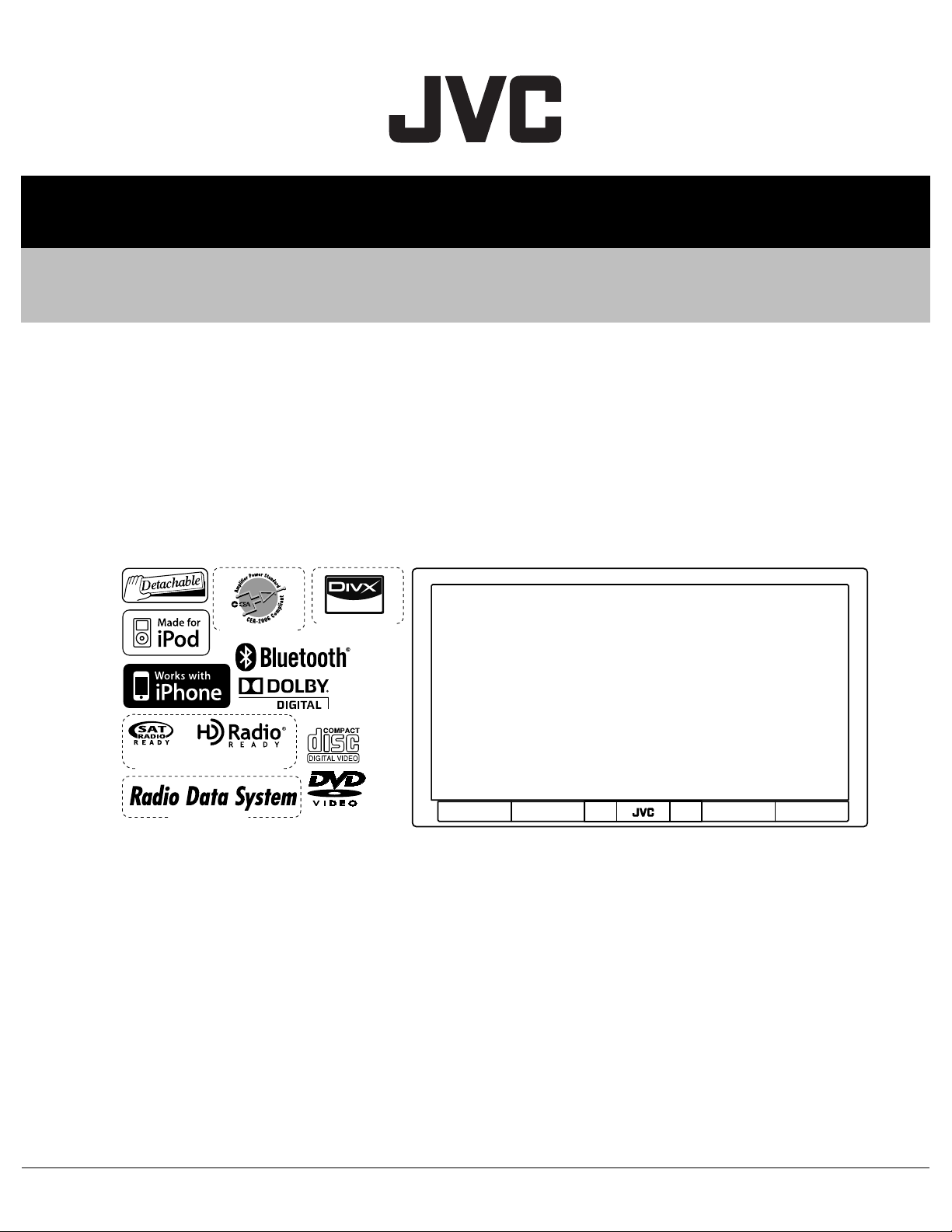
SERVICE MANUAL
DVD RECEIVER WITH MONITOR
MA473<Rev.002>20106SERVICE MANUAL
KW-ADV793J, KW-AVX730E, KW-AVX730EE, KW-AVX730J,
KW-AVX735EU, KW-AVX735U, KW-AVX735UN, KW-AVX736A,
KW-AVX736EU, KW-AVX736U, KW-AVX736UN, KW-AVX736UT,
KW-AVX736UW, KW-AVX738JW, KW-AVX830E, KW-AVX830J,
KW-AVX835EU, KW-AVX835U, KW-AVX835UN, KW-AVX836A,
KW-AVX836EU, KW-AVX836U, KW-AVX836UN, KW-AVX836UT,
KW-AVX836UW, KW-AVX838JW, KW-AVX838UF
Only for J/JW
Only for KW-AVX830J/
KW-ADV793/KW-AVX730J
Only for E/EU
COPYRIGHT © 2010 Victor Company of Japan, Limited
Lead free solder used in the board (material : Sn-Ag-Cu, melting point : 219 Centigrade)
Lead free solder used in the board (material : Sn-Cu, melting point : 230 Centigrade)
Except J/JW
TABLE OF CONTENTS
1 PRECAUTION. . . . . . . . . . . . . . . . . . . . . . . . . . . . . . . . . . . . . . . . . . . . . . . . . . . . . . . . . . . . . . . . . . . . . . . . . 1-6
2 SPECIFIC SERVICE INSTRUCTIONS . . . . . . . . . . . . . . . . . . . . . . . . . . . . . . . . . . . . . . . . . . . . . . . . . . . . . . 1-9
3 DISASSEMBLY . . . . . . . . . . . . . . . . . . . . . . . . . . . . . . . . . . . . . . . . . . . . . . . . . . . . . . . . . . . . . . . . . . . . . . 1-10
4 ADJUSTMENT . . . . . . . . . . . . . . . . . . . . . . . . . . . . . . . . . . . . . . . . . . . . . . . . . . . . . . . . . . . . . . . . . . . . . . . 1-18
5 TROUBLESHOOTING . . . . . . . . . . . . . . . . . . . . . . . . . . . . . . . . . . . . . . . . . . . . . . . . . . . . . . . . . . . . . . . . . 1-31
COPYRIGHT © 2010 Victor Company of Japan, Limited
No.MA473<Rev.002>
2010/6
Page 2
SPECIFICATION
KW-AVX838/KW-AVX830/KW-ADV793/KW-AVX738/KW-AVX730 J/JW
AMPLIFIER
Power Output 20 W RMS × 4 Channels at 4 Ω and < = 1% THD+N
Signal-to-Noise Ratio 80 dBA (reference: 1 W into 4 Ω)
Load Impedance 4 Ω (4 Ω to 8 Ω allowance)
Equalizer Control Range Frequencies Low: 60 Hz, 80 Hz, 100 Hz, 200 Hz
Mid: 500 Hz, 1 kHz, 1.5 kHz, 2.5 kHz
High: 10 kHz, 12.5 kHz, 15 kHz, 17.5 kHz
Level ±12 dB
Audio Output Level
FRONT OUT, REAR OUT, SUBWOOFER OUT
Color System NTSC
Video Output (composite) 1 Vp-p/75 Ω
Other Terminals Input LINE IN, VIDEO IN, CAMERA IN, USB input, MIC IN*, Antenna input
FM/AM TUNER
Frequency Range FM with channel interval set to 100 kHz or 200 kHz 87.5 MHz to 107.9 MHz
FM Tuner Usable Sensitivity 9.3 dBf (0.8 µV/75 Ω)
AM Tuner Sensitivity/Selectivity 20 µV/40 dB
DVD/CD
Signal Detection System Non-contact optical pickup (semiconductor laser)
Frequency Response DVD, fs=48 kHz/96 kHz 16 Hz to 22 000 Hz
Dynamic Range 93 dB
Signal-to-Noise Ratio 95 dB
Wow and Flutter Less than measurable limit
USB
USB Standards USB 2.0 Full Speed
Data Transfer Rate Full Speed Maximum 12 Mbps
Compatible Device Mass storage class
Compatible File System FAT 32/16/12
Max. Current DC 5 V 500 mA
BLUETOOTH (Only for KW-AVX838/KW-AVX830)
Version Bluetooth 2.0 certified
Output Power +4 dBm Max. (Power class 2)
Service Area Within 10 m (10.9 yd)
Profile HFP (Hands-Free Profile) 1.5
MONITOR
Screen Size 7 inch wide liquid crystal display
Number of Pixel 336 960 pixels: 480 × 3 (horizontal) × 234 (vertical)
Drive Method TFT (Thin Film Transistor) active matrix format
Color System NTSC/PAL
Aspect Ratio 16:9 (wide)
GENERAL
Power Requirement Operating Voltage DC 14.4 V (11 V to 16 V allowance)
Grounding System Negative ground
Allowable Storage Temperature -10°C to +60°C (14°F to 140°F)
Allowable Operating Temperature 0°C to +40°C (32°F to 104°F)
Dimensions (W × H × D) Installation Size (approx.) 182 mm × 111 mm × 160 mm (7-3/16” × 4-3/8” × 6-5/16”)
Mass (approx.) 2.8 kg (6.2 lbs) (including the Trim plate and Sleeve)
* Only for KW-AVX838/KW-AVX830.
Design and specifications are subject to change without notice.
Line-Out Level/Impedance 5 V/20 kΩ load (full scale), 2.5 V20 kΩ load (full scale) for KW-AVX730
Output Impedance 1 kΩ
Output 2nd AUDIO OUT*
Others Expansion port, OE REMOTE
with channel interval set to 50 kHz 87.5 MHz to 108.0 MHz
AM with channel interval set to 10 kHz 530 kHz to 1 710 kHz
with channel interval set to 9 kHz 531 kHz to 1 602 kHz
50 dB Quieting Sensitivity 16.3 dBf (1.8 µV/75 Ω)
Alternate Channel Selectivity (400 kHz) 65 dB
Frequency Response 40 Hz to 15 000 Hz
Stereo Separation 40 dB
VCD/CD 16 Hz to 20 000 Hz
Low Speed Maximum 1.5 Mbps
OPP (Object Push Profile) 1.1
A2DP (Advanced Audio Distribution Profile) 1.2
AVRCP (Audio/Video Remote Control Profile) 1.3
Panel Size (approx.) 188 mm × 117 mm × 10 mm (7-7/16” × 4-5/8” × 7/16”)
1-2 (No.MA473<Rev.002>)
Page 3
KW-AVX836/KW-AVX835/KW-AVX736/KW-AVX735 Europe
AMPLIFIER
Maximum Power Output Front/Rear 50 W per channel
Continuous Power Output (RMS) Front/Rear 20 W per channel into 4 Ω, 40 Hz to 20 000 Hz at no more than 0.8% total harmonic
Load Impedance 4 Ω (4 Ω to 8 Ω allowance)
Equalizer Control Range Frequencies Low: 60 Hz, 80 Hz, 100 Hz, 200 Hz
Level ±12 dB
Signal-to-Noise Ratio 70 dB
Audio Output Level
FRONT OUT, REAR OUT, SUBWOOFER OUT
Color System NTSC/PAL
Video Output (composite) 1 Vp-p/75 Ω
Other Terminals Input LINE IN, VIDEO IN, USB input, MIC IN*, Aerial input
Output 2nd AUDIO OUT*
Others OE REMOTE, RGB input
FM/AM TUNER
Frequency Range FM 87.5 MHz to 108.0 MHz
AM (MW) 522 kHz to 1 620 kHz
FM Tuner Usable Sensitivity 9.3 dBf (0.8 µV/75 Ω)
50 dB Quieting Sensitivity 16.3 dBf (1.8 µV/75 Ω)
Alternate Channel Selectivity (400 kHz) 65 dB
Frequency Response 40 Hz to 15 000 Hz
Stereo Separation 40 dB
MW Tuner Sensitivity/Selectivity 20 µV/40 dB
LW Tuner Sensitivity 50 µV
DVD/CD
Signal Detection System Non-contact optical pickup (semiconductor laser)
Frequency Response DVD, fs=48 kHz/96 kHz 16 Hz to 22 000 Hz
VCD/CD 16 Hz to 20 000 Hz
Dynamic Range 93 dB
Signal-to-Noise Ratio 95 dB
Wow and Flutter Less than measurable limit
USB
USB Standards USB 2.0 Full Speed
Data Transfer Rate Full Speed Maximum 12 Mbps
Low Speed Maximum 1.5 Mbps
Compatible Device Mass storage class
Compatible File System FAT 32/16/12
Max. Current DC 5 V 500 mA
BLUETOOTH (Only for KW-AVX836/KW-AVX835)
Version Bluetooth 2.0 certified
Output Power +4 dBm Max. (Power class 2)
Service Area Within 10 m
Profile HFP (Hands-Free Profile) 1.5
OPP (Object Push Profile) 1.1
A2DP (Advanced Audio Distribution Profile) 1.2
AVRCP (Audio/Video Remote Control Profile) 1.3
MONITOR
Screen Size 7 inch wide liquid crystal display
Number of Pixel 336 960 pixels: 480 × 3 (horizontal) × 234 (vertical)
Drive Method TFT (Thin Film Transistor) active matrix format
Color System PAL/NTSC
Aspect Ratio 16:9 (wide)
GENERAL
Power Requirement Operating Voltage DC 14.4 V (11 V to 16 V allowance)
Grounding System Negative ground
Allowable Storage Temperature -10°C to +60°C
Allowable Operating Temperature 0°C to +40°C
Dimensions (W × H × D) Installation Size (approx.) 182 mm × 111 mm × 160 mm
Panel Size (approx.) 188 mm × 117 mm × 10 mm
Mass (approx.) 2.8 kg (including the Trim plate and Sleeve)
distortion
Mid: 500 Hz, 1 kHz, 1.5 kHz, 2.5 kHz
High: 10 kHz, 12.5 kHz, 15 kHz, 17.5 kHz
Line-Out Level/Impedance 5 V/20 kΩ load (full scale)
Output Impedance 1 kΩ
(LW) 144 kHz to 279 kHz
* Only for KW-AVX836/KW-AVX835
Design and specifications are subject to change without notice.
(No.MA473<Rev.002>)1-3
Page 4
KW-AVX830/KW-AVX730 Europe
AMPLIFIER
Maximum Power Output Front/Rear 50 W per channel
Continuous Power Output (RMS) Front/Rear 20 W per channel into 4
Load Impedance 4 Ω (4 Ω to 8 Ω allowance)
Equalizer Control Range Frequencies Low: 60 Hz, 80 Hz, 100 Hz, 200 Hz
Level ±12 dB
Signal-to-Noise Ratio 70 dB
Audio Output Level
FRONT OUT, REAR OUT, SUBWOOFER OUT
Color System PAL
Video Output (composite) 1 Vp-p/75 Ω
Other Terminals Input LINE IN, VIDEO IN, CAMERA IN*1, USB input, MIC IN*1, Aerial input
Output 2nd AUDIO OUT*1
Others Expansion port*2, OE REMOTE
FM/AM TUNER
Frequency Range FM 87.5 MHz to 108.0 MHz
AM (MW) 522 kHz to 1 620 kHz
FM Tuner Usable Sensitivity 9.3 dBf (0.8
50 dB Quieting Sensitivity 16.3 dBf (1.8 µV/75 Ω)
Alternate Channel Selectivity (400 kHz) 65 dB
Frequency Response 40 Hz to 15 000 Hz
Stereo Separation 40 dB
MW Tuner Sensitivity/Selectivity 20 µV/40 dB
LW Tuner Sensitivity 50 µV
DVD/CD
Signal Detection System Non-contact optical pickup (semiconductor laser)
Frequency Response DVD, fs=48 kHz/96 kHz 16 Hz to 22 000 Hz
VCD/CD 16 Hz to 20 000 Hz
Dynamic Range 93 dB
Signal-to-Noise Ratio 95 dB
Wow and Flutter Less than measurable limit
USB
USB Standards USB 2.0 Full Speed
Data Transfer Rate Full Speed Maximum 12 Mbps
Low Speed Maximum 1.5 Mbps
Compatible Device Mass storage class
Compatible File System FAT 32/16/12
Max. Current DC 5 V 500 mA
BLUETOOTH (Only for KW-AVX830)
Version Bluetooth 2.0 certified
Output Power +4 dBm Max. (Power class 2)
Service Area Within 10 m
Profile HFP (Hands-Free Profile) 1.5
OPP (Object Push Profile) 1.1
A2DP (Advanced Audio Distribution Profile) 1.2
AVRCP (Audio/Video Remote Control Profile) 1.3
MONITOR
Screen Size 7 inch wide liquid crystal display
Number of Pixel 336 960 pixels: 480
Drive Method TFT (Thin Film Transistor) active matrix format
Color System PAL/NTSC
Aspect Ratio 16:9 (wide)
GENERAL
Power Requirement Operating Voltage DC 14.4 V (11 V to 16 V allowance)
Grounding System Negative ground
Allowable Storage Temperature -10
Allowable Operating Temperature 0°C to +40°C
Dimensions (W × H × D) Installation Size (approx.) 182 mm × 111 mm × 160 mm
Mass (approx.) 2.8 kg (including the Trim plate and Sleeve)
°C to +60°C
Panel Size (approx.) 188 mm × 117 mm × 10 mm
× 3 (horizontal) × 234 (vertical)
distortion
Mid: 500 Hz, 1 kHz, 1.5 kHz, 2.5 kHz
High: 10 kHz, 12.5 kHz, 15 kHz, 17.5 kHz
Line-Out Level/Impedance
Output Impedance 1 kΩ
(LW) 144 kHz to 279 kHz
µV/75 Ω)
Ω, 40 Hz to 20 000 Hz at no more than 0.8% total harmonic
5 V/20 kΩ load (full scale)
*1 Only for KW-AVX830. *2 Only for KW-AVX730.
Design and specifications are subject to change without notice.
1-4 (No.MA473<Rev.002>)
Page 5
KW-AVX836/KW-AVX835/KW-AVX736/KW-AVX735 Asia & Oceania
AMPLIFIER
Maximum Power Output Front/Rear 50 W per channel
Continuous Power Output (RMS) Front/Rear 20 W per channel into 4
Load Impedance 4 Ω (4 Ω to 8 Ωallowance)
Equalizer Control Range Frequencies Low: 60 Hz, 80 Hz, 100 Hz, 200 Hz
Level ±12 dB
Signal-to-Noise Ratio 70 dB
Audio Output Level
FRONT OUT, REAR OUT, SUBWOOFER OUT
Color System NTSC/PAL
Video Output (composite) 1 Vp-p/75 Ω
Other Terminals Input LINE IN, VIDEO IN, USB input, MIC IN*, Antenna input
Output 2nd AUDIO OUT*
Others OE REMOTE, RGB input
FM/AM TUNER
Frequency Range FM 87.5 MHz to 108.0 MHz
AM 531 kHz to 1 602 kHz
FM Tuner Usable Sensitivity 9.3 dBf (0.8
50 dB Quieting Sensitivity 16.3 dBf (1.8 µV/75 Ω
Alternate Channel Selectivity (400 kHz) 65 dB
Frequency Response 40 Hz to 15 000 Hz
Stereo Separation 40 dB
AM Tuner Sensitivity/Selectivity 20 µV/40 dB
DVD/CD
Signal Detection System Non-contact optical pickup (semiconductor laser)
Frequency Response DVD, fs=48 kHz/96 kHz 16 Hz to 22 000 Hz
VCD/CD 16 Hz to 20 000 Hz
Dynamic Range 93 dB
Signal-to-Noise Ratio 95 dB
Wow and Flutter Less than measurable limit
USB
USB Standards USB 2.0 Full Speed
Data Transfer Rate Full Speed Maximum 12 Mbps
Low Speed Maximum 1.5 Mbps
Compatible Device Mass storage class
Compatible File System FAT 32/16/12
Max. Current DC 5 V 500 mA
BLUETOOTH (Only for KW-AVX836/KW-AVX835)
Version Bluetooth 2.0 certified
Output Power +4 dBm Max. (Power class 2)
Service Area Within 10 m
Profile HFP (Hands-Free Profile) 1.5
OPP (Object Push Profile) 1.1
A2DP (Advanced Audio Distribution Profile) 1.2
AVRCP (Audio/Video Remote Control Profile) 1.3
Max. Current DC 5 V 54.3 mA
MONITOR
Screen Size 7 inch wide liquid crystal display
Number of Pixel 336 960 pixels: 480
Drive Method TFT (Thin Film Transistor) active matrix format
Color System PAL/NTSC
Aspect Ratio 16:9 (wide)
GENERAL
Power Requirement Operating Voltage DC 14.4 V (11 V to 16 V allowance)
Grounding System Negative ground
Allowable Storage Temperature -10
Allowable Operating Temperature 0°C to +40°C
Dimensions (W × H × D) Installation Size (approx.) 180 mm × 100 mm × 160 mm
Mass (approx.) 2.6 kg
°C to +60°C
Panel Size (approx.) 171 mm × 97 mm × 28 mm
× 3 (horizontal) × 234 (vertical)
total harmonic distortion
Mid: 500 Hz, 1 kHz, 1.5 kHz, 2.5 kHz
High: 10 kHz, 12.5 kHz, 15 kHz, 17.5 kHz
Line-Out Level/Impedance 5 V/20 kΩ load (full scale)
Output Impedance 1 kΩ
µV/75 Ω)
Ω, 40 Hz to 20 000 Hz at no more than 0.8%
* Only for KW-AVX836/KW-AVX835.
Design and specifications are subject to change without notice.
(No.MA473<Rev.002>)1-5
Page 6
1.1 Safety Precautions
SECTION 1
PRECAUTION
!
!
Burrs formed during molding may be left over on some parts of the chassis. Therefore,
pay attention to such burrs in the case of preforming repair of this system.
Please use enough caution not to see the beam directly or touch it in case of an
adjustment or operation check.
1-6 (No.MA473<Rev.002>)
Page 7
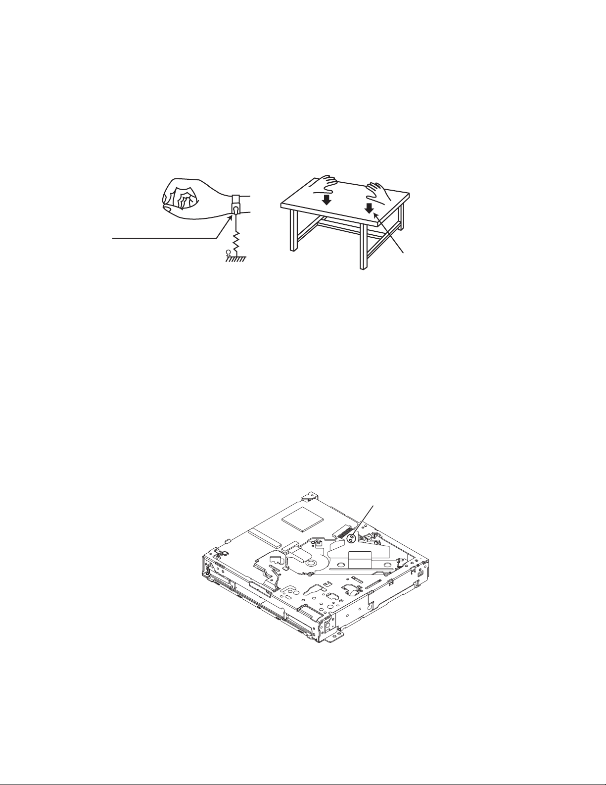
1.2 Preventing static electricity
Electrostatic discharge (ESD), which occurs when static electricity stored in the body, fabric, etc. is discharged, can destroy the laser
diode in the traverse unit (optical pickup). Take care to prevent this when performing repairs.
1.2.1 Grounding to prevent damage by static electricity
Static electricity in the work area can destroy the optical pickup (laser diode) in devices such as laser products.
Be careful to use proper grounding in the area where repairs are being performed.
(1) Ground the workbench
Ground the workbench by laying conductive material (such as a conductive sheet) or an iron plate over it before placing the
traverse unit (optical pickup) on it.
(2) Ground yourself
Use an anti-static wrist strap to release any static electricity built up in your body.
(caption)
Anti-static wrist strap
1M
Conductive material
(conductive sheet) or iron plate
(3) Handling the optical pickup
• In order to maintain quality during transport and before installation, both sides of the laser diode on the replacement optical
pickup are shorted. After replacement, return the shorted parts to their original condition.
(Refer to the text.)
• Do not use a tester to check the condition of the laser diode in the optical pickup. The tester's internal power source can easily
destroy the laser diode.
1.3 Handling the traverse unit (optical pickup)
(1) Do not subject the traverse unit (optical pickup) to strong shocks, as it is a sensitive, complex unit.
(2) Cut off the shorted part of the flexible cable using nippers, etc. after replacing the optical pickup. For specific details, refer to the
replacement procedure in the text. Remove the anti-static pin when replacing the traverse unit. Be careful not to take too long a
time when attaching it to the connector.
(3) Handle the flexible cable carefully as it may break when subjected to strong force.
(4) It is not possible to adjust the semi-fixed resistor that adjusts the laser power. Do not turn it.
1.4 Attention when traverse unit is decomposed
*Please refer to "Disassembly method" in the text for the pickup unit.
• Apply solder to the short land before the card wire is disconnected from the connector on the pickup unit.
(If the card wire is disconnected without applying solder, the pickup may be destroyed by static electricity.)
• In the assembly, be sure to remove solder from the short land after connecting the card wire.
Solder short part
(No.MA473<Rev.002>)1-7
Page 8
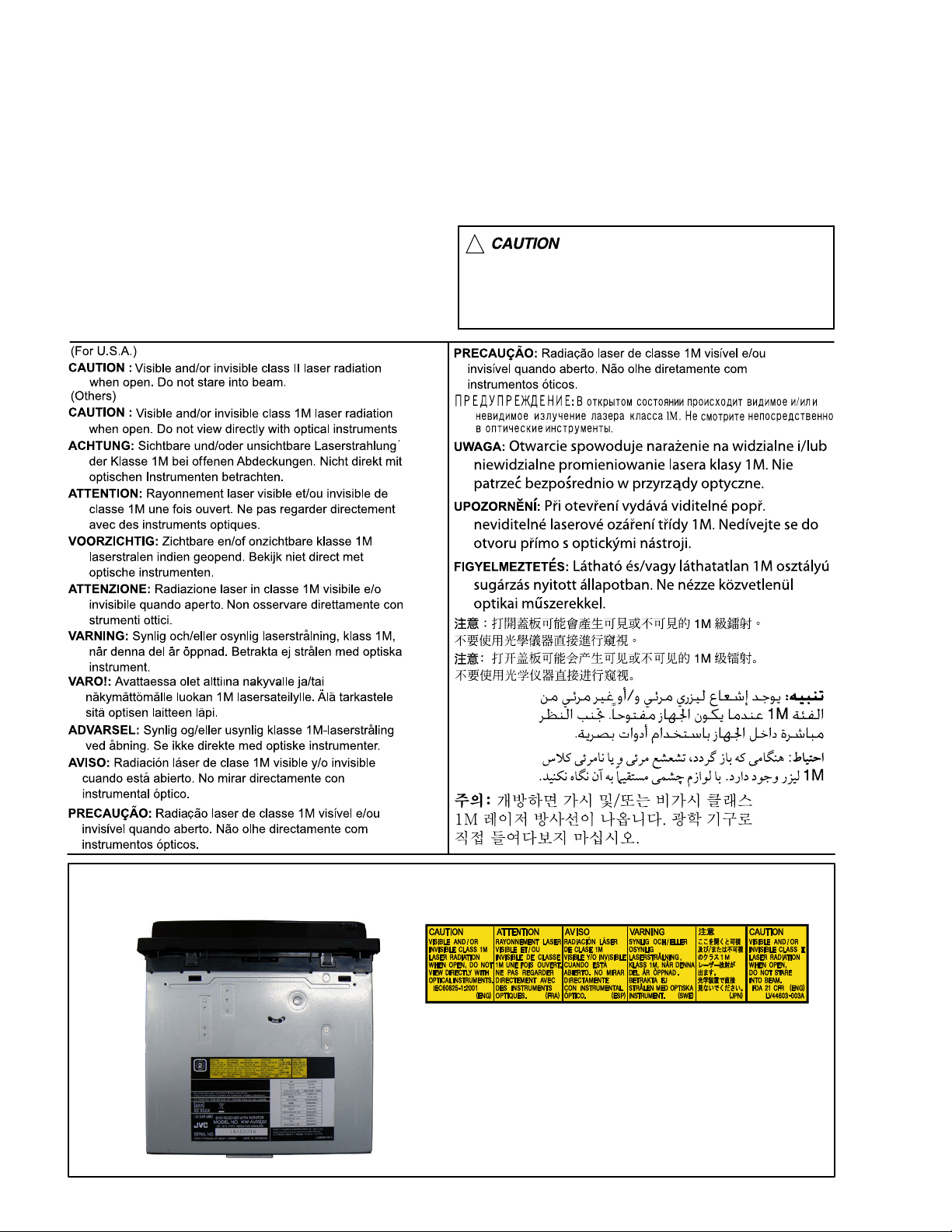
1.5 Important for laser products
1.CLASS 1 LASER PRODUCT
2.CAUTION :
(For U.S.A.) Visible and/or invisible class II laser radiation
when open. Do not stare into beam.
(Others) Visible and/or invisible class 1M laser radiation
when open. Do not view directly with optical instruments.
3.CAUTION : Visible and/or invisible laser radiation when
open and inter lock failed or defeated. Avoid direct
exposure to beam.
4.CAUTION : This laser product uses visible and/or invisible
laser radiation and is equipped with safety switches which
prevent emission of radiation when the drawer is open and
the safety interlocks have failed or are defeated. It is
dangerous to defeat the safety switches.
5.CAUTION : If safety switches malfunction, the laser is able
to function.
6.CAUTION : Use of controls, adjustments or performance of
procedures other than those specified here in may result in
hazardous radiation exposure.
!
Please use enough caution not to
see the beam directly or touch it
in case of an adjustment or operation
check.
REPRODUCTION AND POSITION OF LABELS and PRINT
WARNING LABEL and PRINT
1-8 (No.MA473<Rev.002>)
Page 9

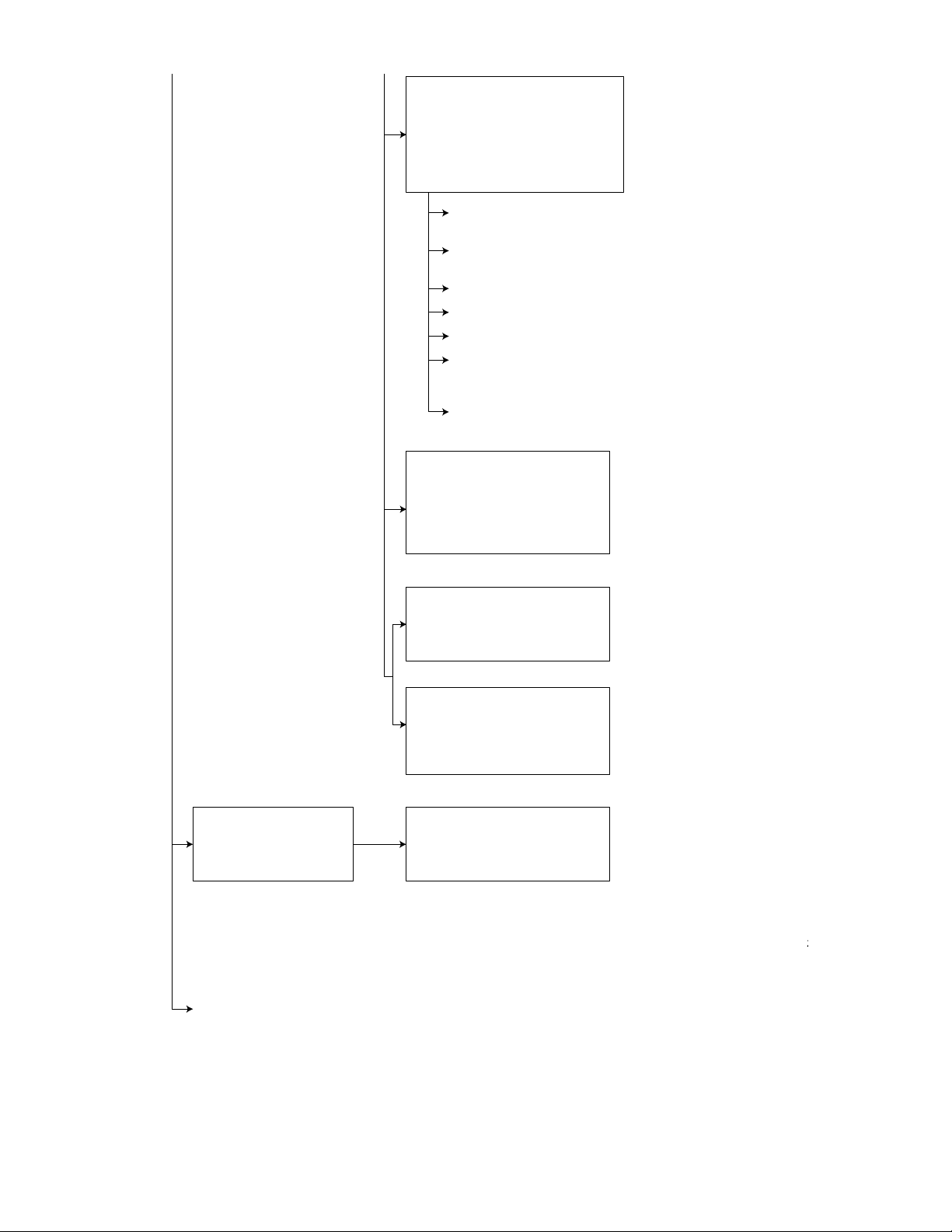
SECTION 2
SPECIFIC SERVICE INSTRUCTIONS
This service manual does not describe SPECIFIC SERVICE INSTRUCTIONS.
(No.MA473<Rev.002>)1-9
Page 10
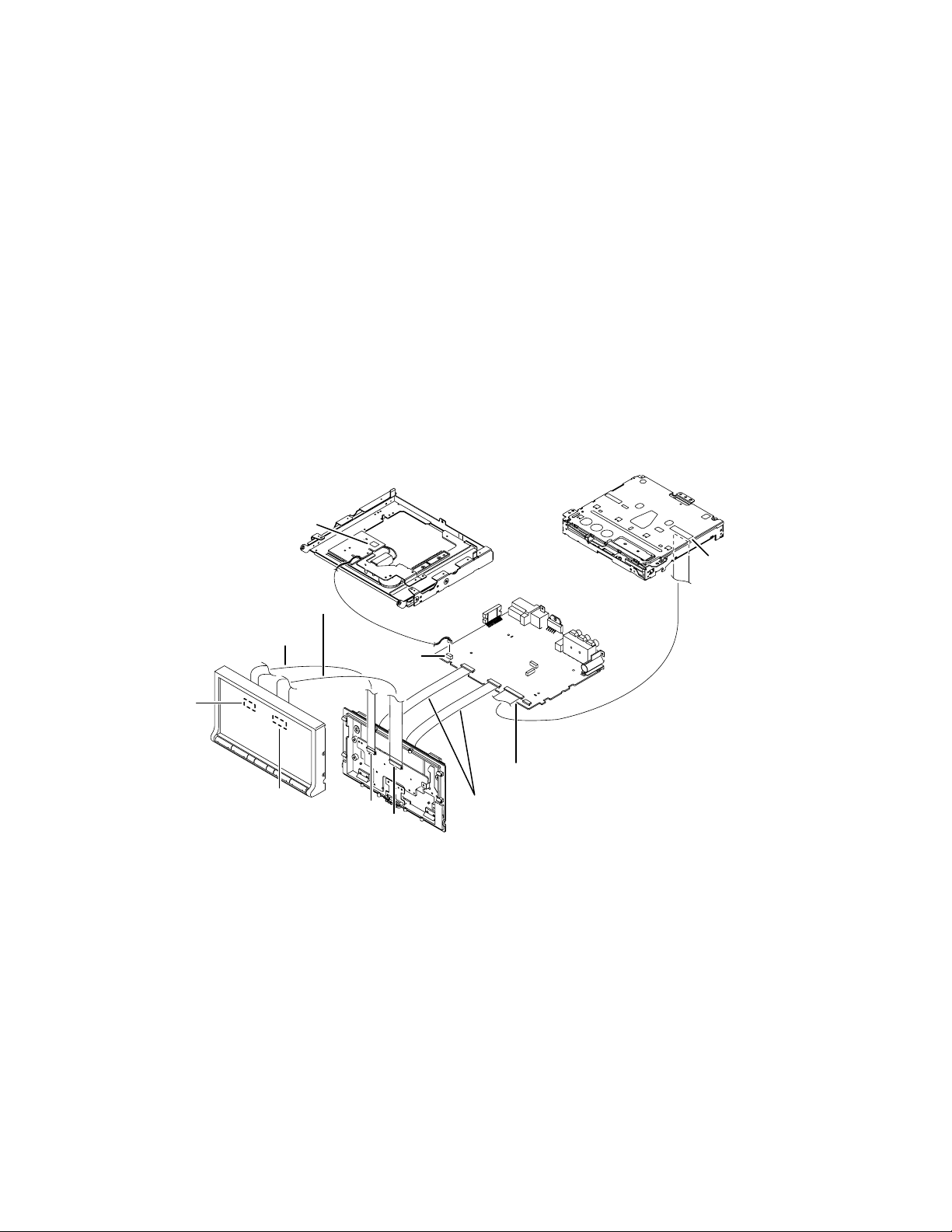
SECTION 3
DISASSEMBLY
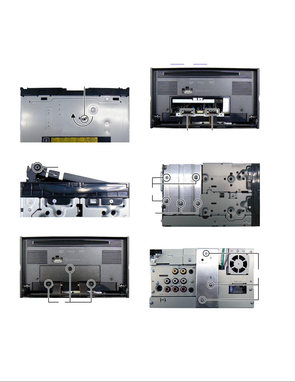
3.1 Main body (Used model: KW-AVX810)
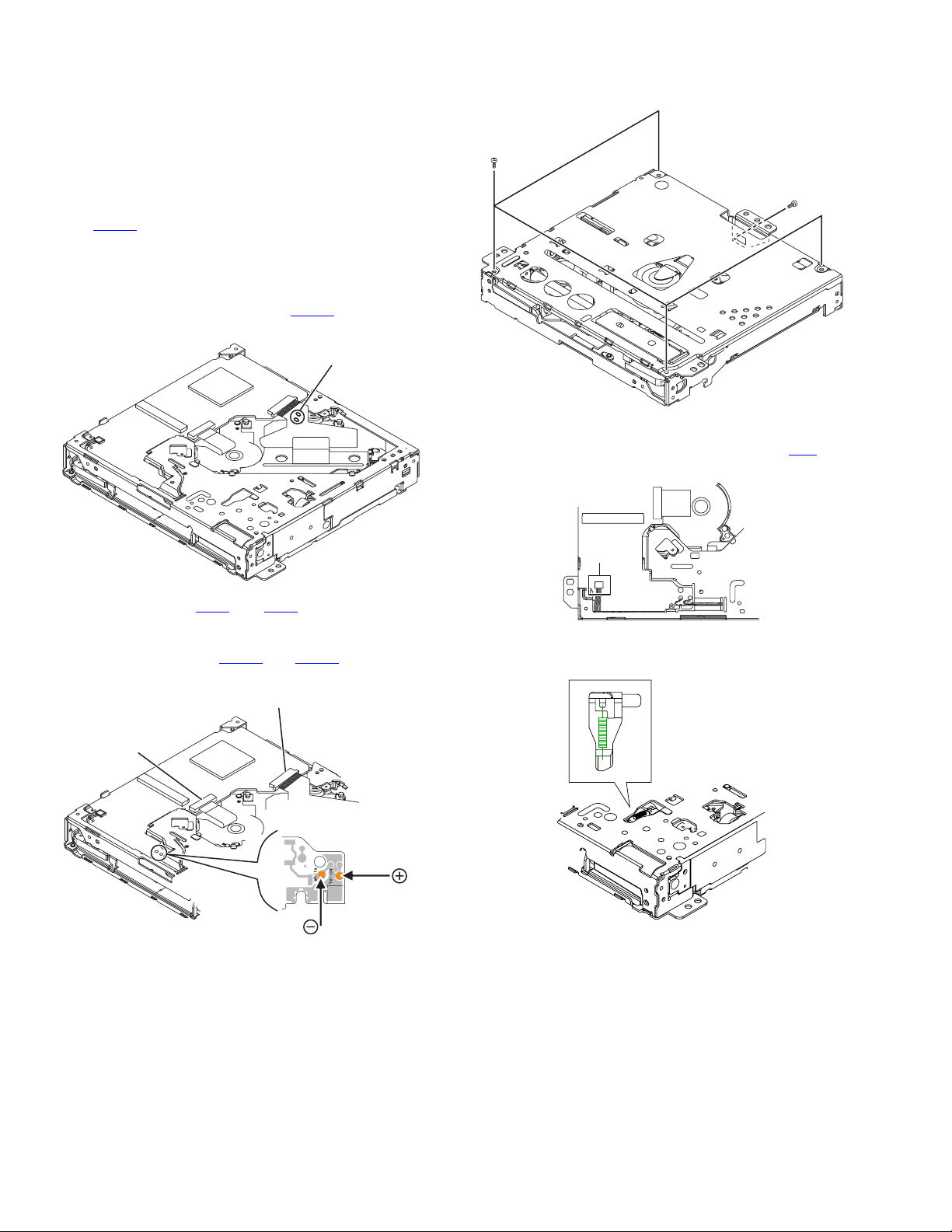
3.1.1 Removing the Front panel (See Fig.1, 2, 3, 4)
(1) From the bottom side of the main body, insert the screw-
driver to hole of the third gear from hole a of the bottom
chassis, and then turn the gear to clockwise until Front
panel comes up. (See Fig.1)
hole a
Fig.1
(2) Remove the two screws A attaching the both side of the
Front panel. (See Fig.2)
(4) Disconnect the FPC from Front panel connected to con-
nectors CN106
3.1.2 Removing the Heat sink (See Fig.5)
(1) Remove the three screws C and two screws D attaching
the Heat sink.
and CN107 of the Main board. (See Fig.4)
CN106CN107
Fig.4
A
Fig.2
(3) Remove the three screws B attaching the FPC cover. (See
Fig.3)
B
Fig.3
C
D
Fig.5
3.1.3 Removing the Rear heat sink (See Fig 6)
(1) Remove the three screws E attaching the Rear heat sink.
E
Fig.6
1-10 (No.MA473<Rev.002>)
Page 11
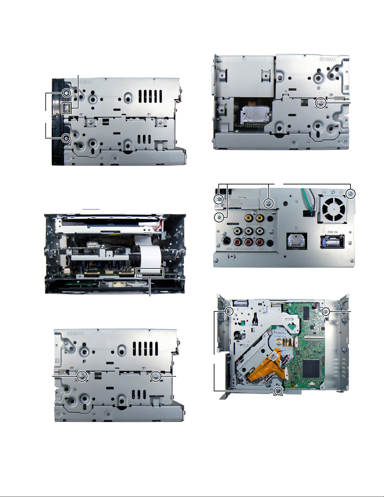
3.1.4 Removing the Front chassis (See Fig.7)
(1) Remove the four screws F attaching the both side of the
Front chassis.
(2) Disengage two hooks a engaged both side of the Front
chassis.
hook
a
F
Fig.7
3.1.5 Removing the DVD mechanism (See Fig.8, 9, 10, 11,
12)
(1) Disconnect the card wire from DVD mechanism connected
to connector CN105
of the Main board. (See Fig.8)
(3) Remove the one screw H attaching the Top chassis. (See
Fig.10)
H
Fig.10
(4) Remove the four screws J attaching the Top chassis. (See
Fig.11)
J
Fig.11
(5) Remove the three screws K attaching the DVD mecha-
nism. (See Fig.12)
CN105
Fig.8
(2) Remove the two screws G attaching the Top chassis. (See
Fig.9)
K
GG
Fig.12
Fig.9
K
(No.MA473<Rev.002>)1-11
Page 12
3.1.6 Removing the BT amp board (See Fig.13)
(1) Disconnect the card wire from Main board connected to
connector CN311
(2) Disconnect Car cable connected to connector CN341
the BT amp board.
(3) Remove the four screws L attaching the BT amp board.
of the BT amp board.
3.1.8 Removing the Rear panel (See Fig.16, 17)
(1) Disconnect the connector wire from Car cable connected to
of
connector CN101
(2) Disconnect the connector wire from FAN connected to con-
nector CN112
of the Main board. (See Fig.16)
of the Main board. (See Fig.16)
CN101
CN311 CN341
Fig.13
3.1.7 Removing the Sub amp board (See Fig.14, 15)
(1) Remove the one screw M attaching the Sub amp board.
(See Fig.14)
M
Fig.14
(2) Disconnect the card wire from Main board connected to
connector CN201
(3) Disconnect the Car cable connected to connector CN241
of the Sub amp board. (See Fig.15)
(4) Remove the three screws N attaching the Sub amp board.
(See Fig.15)
of the Sub amp board. (See Fig.15)
L
CN112
Fig.16
(3) Remove the six screws P and two screws Q attaching the
Rear panel. (Se Fig.17)
P
Q
Fig.17
3.1.9 Removing the Center chassis (See Fig.18)
(1) Remove the three screws R attaching the Center chassis.
R
P
R
CN201
N
CN241
1-12 (No.MA473<Rev.002>)
Fig.15
N
Fig.18
Page 13
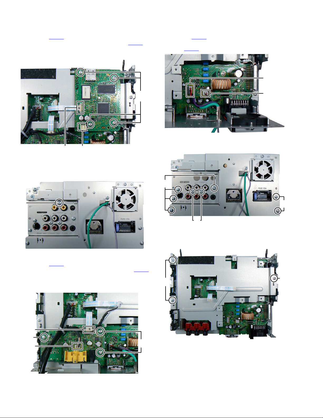
3.1.10 Removing the Main board (See Fig.19)
(1) Disconnect the connector wire from Door switch board con-
nected to connector CN109
(2) Remove the four screws S attaching the Main board.
of the Main board.
CN109
3.1.12 Removing the Front board (See Fig.22)
(1) Remove the five screws V attaching the Front board.
S
Fig.19
3.1.11 Removing the Rear cover (See Fig.20, 21)
(1) Remove the ten screws T and five screws U attaching the
Rear cover. (See Fig.20)
UU
T
T
T
Fig.20
(2) Disconnect the card wires from Front board connected to
connector CN401
Panel-B board. (See Fig.21)
of the Panel-A board and CN601 of the
CN401
T
S
V
Fig.22
3.1.13 Removing the Panel-A board (See Fig.23)
(1) Disconnect the FPC connected to connector CN501
Panel-A board.
(2) Remove the four screws W attaching the Panel-A board.
W
W
CN501 CN604 CN605
Fig.23
3.1.14 Removing the Panel-B board (See Fig.23)
(1) Disconnect the FPC connected to connectors CN604
CN605
of the Panel-B board.
(2) Remove the three screws X attaching the Panel-B board.
V
of the
X
and
CN601
Fig.21
(No.MA473<Rev.002>)1-13
Page 14
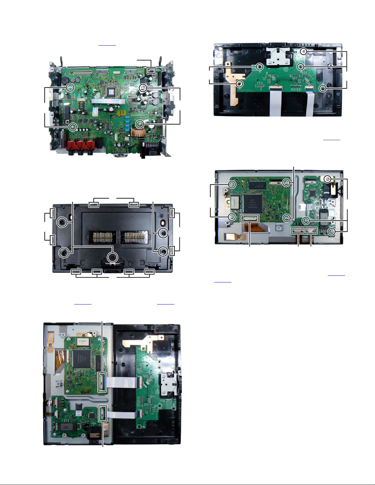
3.2 DVD mechanism assembly section
3.2.1 Removing the Traverse mechanism assembly (See
Fig.1 to 6)
(1) Solder the short land section on the flexible wire of pickup.
(See Fig.1)
Caution:
* Solder the short land section on the flexible wire of pickup
before disconnecting the flexible wire form the connector
on the Front end board.
CN101
If the flexible wire is disconnected without attaching the
solder, the pickup may be destroyed by static electricity.
* When attaching the Traverse mechanism assembly, remove the solder from the short land section after connection
the flexible wire to the connector CN101
on the Front end
board.
Solder short part
(4) Remove the five screws A attaching the Top cover assembly.
(See Fig.3)
A
Fig.3
(5) From the bottom side, disconnect the connector wire from
Top cover assembly connected to connector CN2
Front end board. (See Fig.4)
of the
Fig.1
(2) Voltage supply to TP79
and TP81 approx DC 3.0V until
Clamper is shift to loading complete position. (See Fig.2)
(3) Disconnect the flexible wires from Traverse mechanism assembly
connected to connector CN101
and CN164 of the Front end
board. (See Fig.2)
CN101
CN164
TP79 TP81
TP79
R317
TP67
R312
R21
R357
TP81
TP92
CENTER
D-
DGND_7
WOOFER
Voltage supply
position
Fig.2
CN2
Fig.4
(6) From the bottom side, remove the spring from Traverse
mechanism assembly. (See Fig.5)
Fig.5
1-14 (No.MA473<Rev.002>)
Page 15
(7) From the top side, pull up the traverse mechanism and disengage
three dumper positions. (See Fig.6)
Dumper
(same color spring)
Dumper
(Different color spring)
Fig.6
3.2.2 Removing the Front end board (See Fig.7)
(1) Remove the Motor wires from loading motor soldered to
and TP81 of the Front end board.
TP79
(2) Remove the two screws B attaching the Front end board.
TP81
3.2.3 Removing the Loading arm assembly (See Fig.8)
(1) Remove the Loading arm spring L from Loading arm assembly.
(2) Slide to left side and then disengage hook a then hook b.
hook b
Loading arm
assembly
hook
Loading arm spring L
a
B
TP79
B
Fig.8
3.2.4 Removing the Gear base assembly (See Fig.9, 10)
(1) Remove the Loading arm spring L. (See Fig.9)
Fig.7
Loading arm
spring L
Fig.9
(No.MA473<Rev.002>)1-15
Page 16
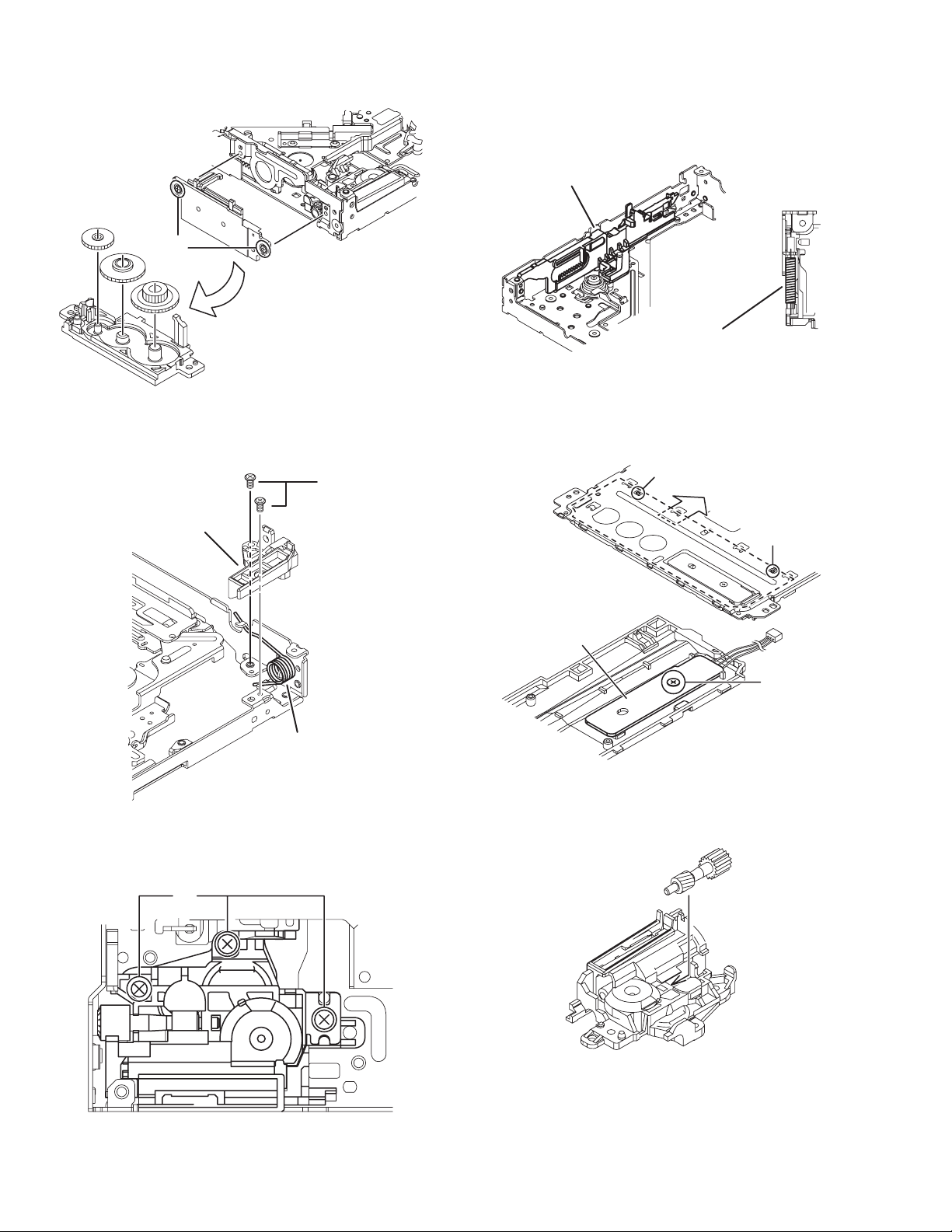
(2) Remove the two screws C attaching the Gear base assembly.
r
(See Fig.10)
C
Fig.10
3.2.5 Removing the Loading arm holder. (See Fig.11)
(1) Remove the two screws D attaching the Loading arm holder.
(2) Remove the Loading arm spring R.
D
Loading arm
holder
3.2.7 Removing the Slide cam assembly (See Fig.13)
(1) Slide to backward the Slide cam assembly and the remove
the Slide cam spring.
(2) Slide to frontward the slide cam assembly, and then take
out it.
Slide cam assembly
Slide cam spring
Fig.13
3.2.8 Removing the Photo board (See Fig.14)
(1) Pressing the hook c and then slide to backward (slide to the
arrow side) the Disc plate.
(2) Remove the one screw F attaching the Photo board.
hook
c
hook
c
Loading arm
spring R
Fig.11
3.2.6 Removing the Loading moor assembly (See Fig.12)
(1) Remove the three screws E attaching the Loading motor
assembly.
E
Photo board
F
Fig.14
3.2.9 Removing the Loading motor (See Fig.15 to 18)
(1) Remove the A wheel gear. (See Fig.15)
A Wheel gea
Fig.15
1-16 (No.MA473<Rev.002>)
Fig.12
Page 17
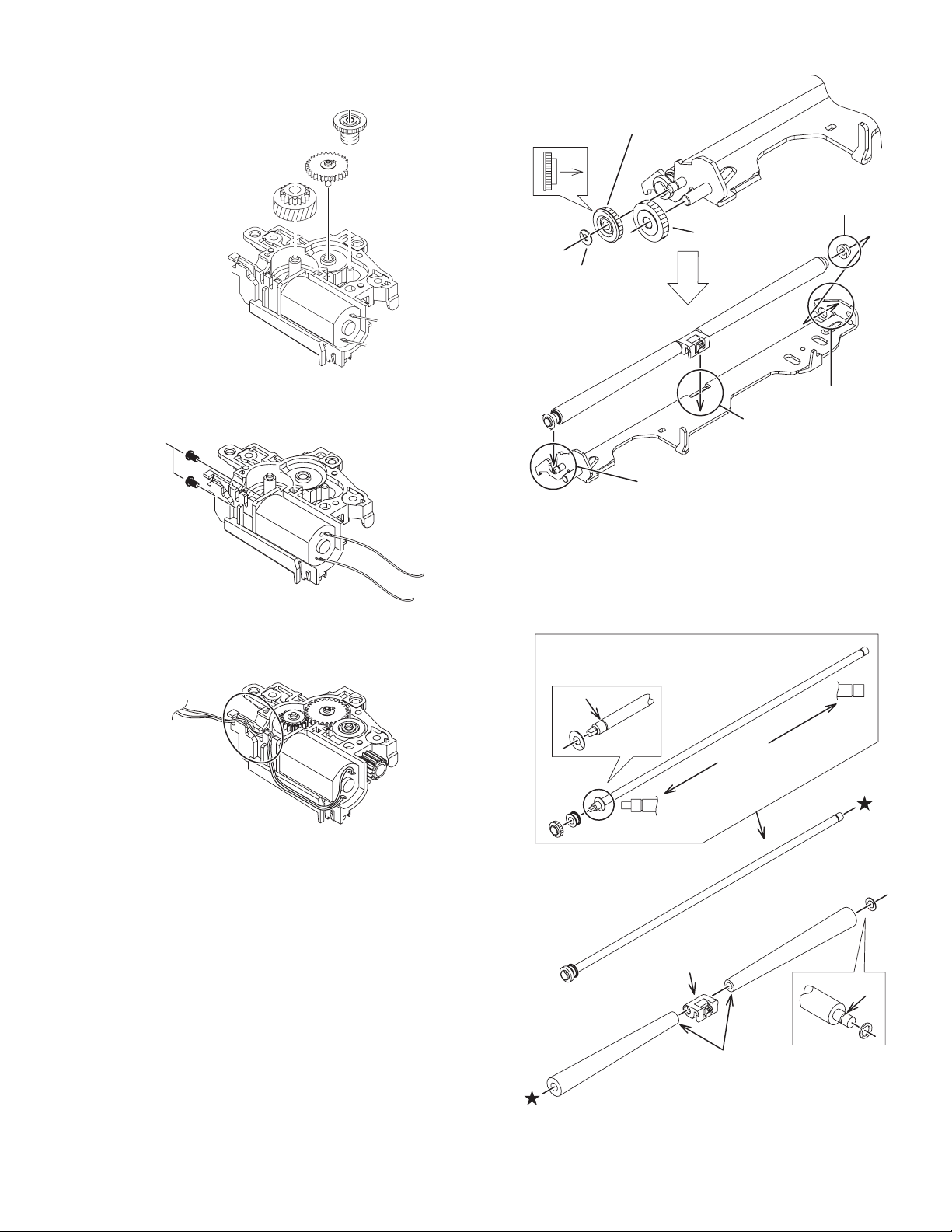
(2) Remove the A worm gear, M connect gear and M wheel
gear by sequentially. (See Fig.16)
A worm gear
M connect gear
M wheel gear
Fig.16
(3) Remove the two screws G attaching the Loading motor.
(Se Fig.17)
G
Fig.17
(4) When attaching the Loading motor, motor wire should arrange
to figure. (See Fig.18)
Direction
R middle gear
R collar R
R connect gear
Slit washer
part c
part a
part b
Fig.19
3.2.11 Removing the Roller (See Fig.20)
(1) Remove the Slit washer.
(2) Pull out the Roller shaft.
CAUTION:
When reattach the Roller shaft, Slit washer should be change
new part.
Wire arrangement
Fig.18
3.2.10 Removing the Roller assembly (See Fig.19)
(1) Remove the Slit washer.
(2) Remove the R middle gear.
(3) Remove the R connect gear.
(4) Snap off the part a of the Roller assembly.
(5) Lift up the part b of the Roller assembly, and then release
part c (When release part c, R collar R is easy to come off,
does not lose it).
CAUTION:
When reattach the Roller assembly, Middle gear should keep
direction and Slit washer should be change new part.
slit
keep direction
keep direction
slit
small side
Fig.20
(No.MA473<Rev.002>)1-17
Page 18
SECTION 4
ADJUSTMENT
4.1 Test instruments required for adjustment
(1) Digital oscilloscope (100MHz)
(2) Digital tester
(3) Test Disc
(4) Extension cable :
EXTXD001-50PF (CN403 --- CN105)
EXTCN001-6P (CN351 --- CN109)
EXTDV002-28PF (CN401 --- CN653)
EXTDV002-16PF (CN601 --- CN654)
4.4 Dummy load
Exclusive dummy load should be used for AM and FM.
For FM dummy load, there is a loss of 6dB between SSG output and antenna input.
The loss of 6dB need not be considered since direct reading of figures are applied in this working standard.
4.5 How to connect the extension cable for adjusting
Caution:
Be sure to attach the heat sink and rear bracket onto the power amplifier IC and regulator IC respectively, before supply the power.
If voltage is applied without attaching these parts, the power amplifier IC and regulator IC will be destroyed by heat.
CN351
4.2 Standard measuring conditions
Power supply voltage DC14.4V(10.5 to 16V)
Load impedance 20K ohm (2 Speakers connection)
Output Level Line out 2.5V (Vol. MAX)
4.3 Standard volume position
Balance and Bass &Treble volume : lndication"0"
Loudness : OFF
CN403
CN601
EXTDV002-28PF
EXTDV002-16PF
CN401
CN654
EXTCN001-6P
CN109
EXTXD001-50PF
CN105
use original wire
CN653
1-18 (No.MA473<Rev.002>)
Page 19
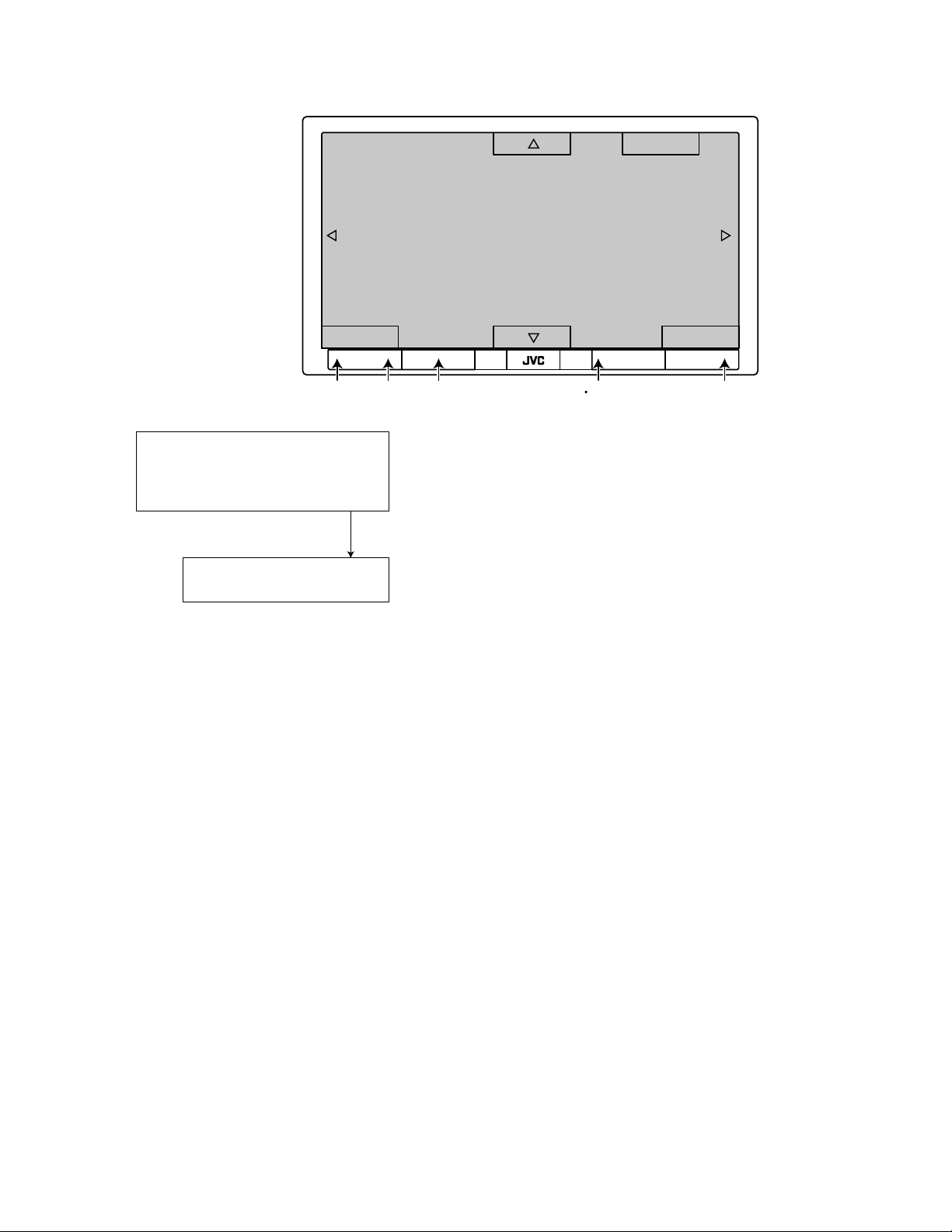
4.6 Service mode
UP Button
ENTER
TOUCH PANEL
DOWN Button
[Back] [Exit]
[STANDBY/ON ATTENUATOR] [DISP] [VOL]
4.6.1 Service mode 1 (Indication of a service mode 1 is nothing.)
Keep this state more 2 seconds
while continuing pressing the
[STANDBY/ON ATTENUATOR] button
and [OPEN] button sequentially.
Screen indication
NO EJECT?
EMERGENCY EJECT?
*1
Exchanging it operate a menu of a service mode with the [UP] button
*2
and [DOWN] button. Operate choice of a menu with a [ENTER] button.
*1 : When an [ENTER] button is pushed in NO EJECT indication, it is set
by an EJECT prohibition mode.
When an [ENTER] button is pushed in EJECT OK indication, it is set
by a normal mode.
*2 : Forced EJECT movement
A screen becomes normal indication after an [ENTER] button was pushed.
[MENU TP/TY]
FF ButtonREW Button
[OPEN]
(No.MA473<Rev.002>)1-19
Page 20
4.6.2 Service mode 2
Keep this state more 2 seconds
[MENU or TP/PTY] button, [DISP]
button and TOUCH PANEL [DOWN]
button sequentially.
Screen indication
SERVICE MODE 2
INITIALIZE ALL
INITIALIZE
INITIALIZE DVD
INITIALIZE BT
TOUCH PANEL CALIBRATION
TOUCH PANEL CHECK MODE
Exchanging it operate a menu of a service mode with the [UP] button
and [DOWN] button. Operate choice of a menu with a [ENTER] button.
INITIALIZE ALL
. . .
NOW
INITIALIZE ALL
INITIALIZE ALL
. . .
NOW
INITIALIZE
INITIALIZE DVD
INITIALIZE DVD
OK **
INITIALIZE BT
INITIALIZE BT
OK **
INITIALIZE ALL (Each EEPROM is
INITIALIZE ALL
OK **
INITIALIZE
OK **
Full initialization of EEPROM of a DVD unit
( It is included a permanent domain)
After clear completion, this indication is continued
till an effective key is input.
Full initialization of EEPROM of Bluetooth module
After clear completion, this indication is continued
till an effective key is input.
initialized by a factory shipment state.)
*Main micon EEPROM initialization
(user entry domain, error history, speaker
setting, subarea of J-version, data to pre-set)
*Panel micon EEPROM initialization
(picture adjustment data)
*DVD unit EEPROM initialization
(except a permanent domain)
*Bluetooth module EEPROM initialization
*After clear completion, a screen returns to
normal indication after OK indication was
displayed for three seconds.
INITIALIZE
(Initialization of a user area of each EEPROM)
*Main micon EEPROM initialization
(a user entry domain )
(a user entry domain, speaker setting, subarea
of J-version, data to pre-set )
*Panel micon EEPROM initialization
(picture adjustment data )
*DVD unit EEPROM initialization
(except a permanent domain)
*Bluetooth module EEPROM initialization
*After clear completion, a screen returns to
normal indication after OK indication was
displayed for three seconds.
TOUCH PANEL CALIBRATION
++
+
TOUCH PANEL CHECK MODE
1-20 (No.MA473<Rev.002>)
+
+
+
+
+
Push the center of a + character displayed in turn.
+
The confirmation mode that the calibration of the
+
touch panel was performed definitely.
*Return to previous menu with a [DISP] button.
Page 21
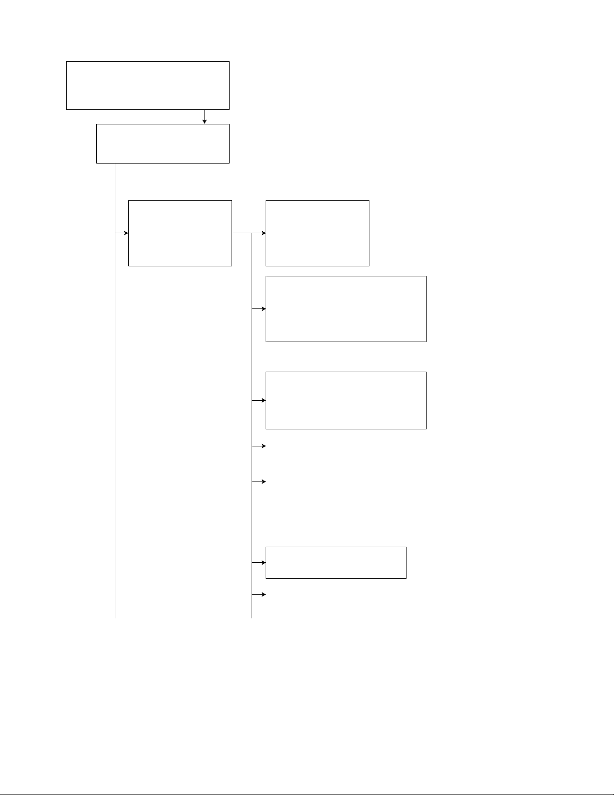
4.6.3 Service mode 3
Keep this state more 2 seconds
while continuing pressing the
[MENU or TP/PTY] button, [VOLUME -]
button and TOUCH PANEL [DOWN]
button sequentially.
Screen indication
SERVICE MODE 3
SERVICE MODE
INITIALIZE ALL
RUNNING MODE
Exchanging it operate a menu of a service mode with the [UP] button
and [DOWN] button. Operate choice of a menu with a [ENTER] button.
SERVICE MODE
SERVICE MODE
VERSION
AREA/REGION
TEMPERATURE
MEMORY CHECK
DVD NTSC/PAL
DVD CHECK MODE
*Exchanging it operate a menu
of a service mode with the [UP]
button and [DOWN] button.
*Operate choice of a menu with
a [ENTER] button.
*Return to previous menu with
a [BACK] button.
SERVICE MODE
ERROR READ
ERROR CLEAR
BT VERSION
VERSION
MAIN
DISC
Macrovision
PN
SW BT MODULE
V**** [**]
****
****
V**** V**** [**] V**** ** *
V***
Micon version indication
*Main micon version and ROM
correction version
*DVD module version
Macrovision version
*Panel micon version and ROM
correction version
*Software version of BT module
AREA/REGION
SYS-AREA
DISC-AREA
REGION
PANEL-AREA
TEMPERATURE Temperature data reading
*Temperature data by the temperature sensor in the main micon and DVD module
is read every 5 seconds and displayed in hex numbers.
MEMORY CHECK ( It is displayed only at the time of the disc insertion )
Memory residual quantity indication mode
*Data residual quantity of a disc is displayed by LCD.
*About the playback control-related key ([FSKIP], [BSKIP], [UP], [DOWN], [VOL]),
only movement is effective.
Indication does not change as memory residual quantity indication.
*About cancellation of this mode, press the [STANDBY/ON ATTENUATOR] button.
DVD NTSC/PAL
NTSC
PAL
DVD CHECK MODE
*See "DVD CHECK MODE h for details.
: **
: **
: *
: **
Area and region indication
Main micon area
DVD module area
Region
Panel area
DVD picture change
DVD unit output picture setting (NTSC)
DVD unit output picture setting (PAL)
(No.MA473<Rev.002>)1-21
Page 22
ERROR READ
p
n
z
o
n
DVD ERROR READ
MECHA ERROR READ
DISC COM ERROR READ
PNL RST ERROR READ
PNL COM ERROR READ
DC OK
READ ALL
DVD ERROR READ
Reading of a DVD unit error history
MECHA ERROR READ
Reading of a door mechanism error history
DISC COM ERROR READ (Only Engineer use)
PNL RST ERROR READ (Only Engineer use)
PNL COM ERROR READ (Only Engineer use)
DC OK
DC offset error information.
* See "DC offset error information" for details.
READ ALL (Only Engineer use)
Reading of a main micon EEPROM (All contents)
INITIALIZE ALL
. . .
NOW
INITIALIZE
RUNNING MODE
*See "Running mode" for details.
ERROR CLEAR
DVD ERROR CLEAR
MECHA ERROR CLEAR
DISC COM ERROR CLEAR
PNL PST ERROR CLEAR
PNL COM ERROR CLEAR
DC ERROR CLEAR
* KW-AVX830 series
BT VERSION
SW BT CORE
SW BT MODULE
ADR-
* KW-AVX730 series
BT VERSION
SW BT CORE
HW BT MODULE
SW BT MODULE
SW HIDEAWAY
ADR-
INITIALIZE
OK **
***
***
***********
***
***
***
***
***********
Clear of each error history
A screen returns to following
indication after clear completion.
Bluetooth version indication
Software version of BT core
Software version of BT Module
BT Address
Bluetooth version indication
*It is displayed in Bluetooth unit co
Software version of BT core
Hardware version of BT Module
Software version of BT Module
Software version of BT Hideaway
BT Address
INITIALIZE ALL (Each EEPROM is
by a factory shipment state.)
*Main micon EEPROM initialization
(user entry domain, error history, s
setting, subarea of J-version, data
*Panel micon EEPROM initializatio
(picture adjustment data)
*DVD unit EEPROM initialization
(except a permanent domain)
*Bluetooth module EEPROM initiali
*After clear completion, a screen re
normal indication after OK indicati
displayed for three seconds.
1-22 (No.MA473<Rev.002>)
Page 23
4.6.4 Service mode 4
Keep this state more 2 seconds
while continuing pressing the
[MENU or TP/PTY] button, [VOLUME -]
button and TOUCH PANEL [ DOWN]
button sequentially.
Screen indication
SERVICE MODE 4
RDS S MODE
MONITOR S MODE
HD RADIO S MODE
Exchanging it operate a menu of a service mode with the [UP] button
and [DOWN] button. Operate choice of a menu with a [ENTER] button.
RDS S MODE
*RDS service mode
MONITOR S MODE
R/W CHROMA
DATA CLEAR
HD RADIO S MODE
*It is displayed in HD Radio unit connection.
*See "Monitor adjustment" for details.
CHROMA DATA read/write
Clear of CHROMA DATA (return to an initial value)
4.7 DVD check mode
DVD CHECK MODE
NORMAL PLAY
EF OUT-TRACKING OFF
EF IN-TRACKING OFF
CD-LASER ON
DVD-LASER ON
DVDx1 JITTER MODE
DVD CHECK MODE
EEPROM DATA DISP
EEPROM DATA CLEAR
TEMPERATURE
SEARCH & JITTER
MONITOR
PLAY
DVD CHECK MODE
STOP
OPEN
CLOSE
Exchanging it operate a menu of a service mode with the [UP] button and [DOWN] button. Operate choice of a menu with a [ENTER]
button.
Command Mechanism unit operation Indication contents
NORMAL PLAY Start at normal speed
Laser current value, jitter value
(After start, jitter is measured by an inner position.)
EF OUT-TRACKING OFF Tracking off the outermost position of CD For EF phase error
EF IN-TRACKING OFF Tracking off the innermost position of CD For EF phase error
CD-LASER ON CD_LD lights and laser current is displayed. Laser current value, jitter value
DVD-LASER ON DVD x1 jitter measuring mode (for use in mechanism adjustment) Laser current value, jitter value
EEPROM DATA DISP Contents of EEPROM is displayed. EEPROM address
EEPROM contents
EEPROM DATA CLEAR Contents of EEPROM is initialized. EEPROM address
EEPROM contents
TEMPERATURE Temperature indication Temperature is displayed in hex
numbers.
SEARCH & JITTER The search and jitter measurement to an appointed position of DVD. Position measured with VT-501
jitter value
MONITOR Monitor terminal setting
DVDx1 PLAY DVD x1 stopped start
Not displayed.
(After start, jitter is measured by an inner position.)
STOP Disc stopped, LD-OFF Not displayed.
EJECT EJECT Not displayed.
LOAD LOADING Not displayed.
EEPROM DATA OSD EEPROM DATA (Only Engineer
use)
(No.MA473<Rev.002>)1-23
Page 24

4.8 DC offset error information
Display indication
DC OK
DC ERROR
VOL
push
BACK
DC 1 OK
DC 1 ERROR
VOL
push
BACK
VOL
push
VOL
push
DC 2 X
4.8.1 DC offset error distinction.
(1) DC ERROR 1
When improper connection or other DC offset errors are detected.
"PROTECT" blinks to the display.
It is possible to return even times how many by reset.
(2) DC ERROR 2
When the DC offset error is detected due to the trouble of the capacitor.
zThe number of times that detected in the case of less than 3 times.
"PROTECT" blinks to the display.
It is possible to return to the 3rd times by reset.
zWhen the detected number becomes 4 times.
"PROTECT" lights to the display.
It is fixed that trouble occurs internally, and reset doesn't return either.
( Operation other than the Power on/off, Eject, Reset, and Service mode are prohibited with "PROTECT" lit.
4.8.2 Error content confirmation.
Whether it turns on power and the "PROTECT" display appears are confirmed.
(1) When the "PROTECT" display appears.
The content of the DC offset error is confirmed in the Service mode.
* Because it takes DC offset protection, the following is displayed.
(1-1) When "DC1 ERROR" is displayed. (DC ERROR1)
zForecast cause
It comes in contact with improper connection or GND of the speaker wiring.
It is confirmed that there is no improper connection of the speaker wiring and pushes reset.
zWhen "PROTECT" is not displayed, it is unquestionable.
The error data of EEPROM, it deletes it. (CLR DC1)
zWhen "PROTECT" is still displayed.
The DC offset has been generated by the reasons other than the improper connection.
Forecast cause: Power AMP is broken.
After parts are exchanged, reset is confirmed pushing again.
(1-2) When "DC2 X" is displayed. (DC ERROR2)
* As for X, the detected number is displayed. (0-4)
* When X is 0, it is unquestionable because the DC offset has never been detected.
When leak of capacitor is detected, it is displayed.
It is confirmed that there is no problem in the capacitor and deletes the error data of EEPROM. (CLR DC2)
It is confirmed that reset is pushed and "PROTECT" is not displayed.
BACK
CLR DC1 VOL push to confirm
CLR DC2 VOL push to confirm
After above-mentioned (1-1) and (1-2) are executed, the connect of the DC offset error is confirmed in the Service mode.
If the part displayed as "DC ERROR" becomes "DC OK", it is unquestionable.
(2) When the "PROTECT" display doesn't appear.
The content of the DC offset error is confirmed in the Service mode.
(2-1) When "DC OK" is displayed, it is unquestionable because the DC offset has not been detected in the past.
(2-2) When "DC ERROR" is displayed, the confirmation similar to (1-1) and (1-2) is done because there is a history that detected
the DC offset error in the past.
1-24 (No.MA473<Rev.002>)
Page 25
4.9 Error code tables
4.9.1 Mechanism error code
Error contents Details Error code Detailed error code
Disc loading error
(3) D1 time out 09 0013
Eject error
(3) B1 time out
(4) C1 time out
Error in loading wait Loading of a running mode Disc was pulled out in a wait. 09 0031
4.9.2 Disc error code
Error contents Details Error code Detailed error code
TOC read error TOC lead movement of a CD is not completed. 84 0059
First track access error Even if TOC reading passes after the end with CD running mode for
30 seconds, the first track access is not finished.
Last track access error Even if first track passes after the end with CD running mode for 30
seconds, the last track access is not finished.
T1 access error Even if T1 access passes in a DVD running mode for 30 seconds,
it is not finished.
T12 access error Even if T12 access passes in a DVD running mode for 30 seconds,
it is not finished.
T24 access error Even if T24 access passes in a DVD running mode for 30 seconds,
it is not finished.
Read-in area read error Read-in area read operation of DVD is not completed. 84 0072
DVD L1 layer adjustment error
DVD L0 layer adjustment error
NO DISC judgment Judgment without disc 80 0090
It is NO DISC by start failure Start is impossible 80 0091
It is stopped by playback inability.
Logic format NG Logic format analysis inability or non-correspondence logic format 80 0094
Seek access error It cannot arrive at an aim address even if it passes for 15 seconds. 80 0095
Adjustment of L1 layer of DVD is not finished normally.
(including focus jump failure)
Adjustment of L0 layer of DVD is not finished normally.
(including focus jump failure)
Stop in running mode playback 80 0093
01
01
0023
0024
80 0060
80 0061
80 0069
80 0070
80 0071
80 0074
80 0075
4.9.3 Error codes of panel mechanism
* As for two columns of the beginning of the error code, as for error contents, two columns of middle, number of the pulse counts, last
two columns are a purpose position and movement directions.
Error contents code
Time out OB
Position error by the external force OC
Abnormal voltage (1) F3
Abnormal voltage (2) F5
Abnormal voltage (3) F7
Abnormal voltage (4) F8
When assumed last two columns XY;, as for X, as for purpose
position, Y, is a movement direction.
Purpose position X
CLOSE 1
5 degrees 2
10 degrees 3
15 degrees 4
20 degrees 5
25 degrees 6
30 degrees 7
OPEN 8
Movement direction Y
Open direction 0
Close direction 1
(No.MA473<Rev.002>)1-25
Page 26
Detail Error code
It is time-out during movement to the closed position. 0B**11
It is time-out during 5 degrees tilt movement.(open direction) 0B**20
It is time-out during 5 degrees tilt movement.(close direction) 0B**21
It is time-out during 10 degrees tilt movement.(open direction) 0B**30
It is time-out during 10 degrees tilt movement.(close direction) 0B**31
It is time-out during 15 degrees tilt movement.(open direction) 0B**40
It is time-out during 15 degrees tilt movement.(close direction) 0B**41
It is time-out during 20 degrees tilt movement.(open direction) 0B**50
It is time-out during 20 degrees tilt movement.(close direction) 0B**51
It is time-out during 25 degrees tilt movement.(open direction) 0B**60
It is time-out during 25 degrees tilt movement.(close direction) 0B**61
It is time-out during 30 degrees tilt movement.(open direction) 0B**70
It is time-out during 30 degrees tilt movement.(close direction) 0B**71
It is time-out during movement to the open position. 0B**80
It is position error during close position stop. 0C0011
It is position error during 5 degree tilt position stop. 0C0020
It is position error during 10 degree tilt position stop. 0C0030
It is position error during 15 degree tilt position stop. 0C0040
It is position error during 20 degree tilt position stop. 0C0050
It is position error during 25 degree tilt position stop. 0C0060
It is position error during 30 degree tilt position stop. 0C0070
It is position error during open position stop. 0C0080
Detect abnormal voltage (1) F3**XY
Detect abnormal voltage (2) F5**XY
Detect abnormal voltage (3) F7**XY
Detect abnormal voltage (4) F8**XY
Note: "**" of the above error code is the number of the pulse counts at the time of the error outbreak.
4.10 Running mode
Indication Explanation Operation contents of 1 cycle In mecha error In disc error
RUNNING1 MECHA Door mecha running 1 Panel close ↔ Panel open - RUNNING2 MECHA Door mecha running 2 Panel close → 5 degrees → 10 degrees → 15 degrees → 20 degrees
→ 25 degrees → 30 degrees → anel open
RUNNING3 MECHA Door mecha running 3 Panel → close → 5 degrees →
grees → Panel close
RUNNING4 DVD DVD+Door mecha running1 Loading → Eject → Wait for 5 seconds+Door open/close Stop RUNNING5 DVD DVD+Door mecha running2 Loading → Eject → Wait for 5 seconds+Door open/close Retry RUNNING6 DVD DVD+Door mecha running3 Loading → Playback → Eject → Wait for 5 seconds+Door open/close Stop Stop
RUNNING7 DVD DVD+Door mecha running4 Loading → Playback → Eject → Wait for 5 seconds+Door open/close Retry Stop
RUNNING8 DVD DVD+Door mecha running5 Loading → Playback → Eject → Wait for 5 seconds+Door open/close Stop Retry
RUNNING9 DVD DVD+Door mecha running6 Loading → Playback → Eject → Wait for 5 seconds+Door open/close Retry Retry
···· → 30 degrees → ···· → 5 de-
--
--
* Cancellation of running1,2 and 3 : Press the [EJECT] key
* In running 1,2 and 3 cancellation, a door does not stop at the position and moves to a panel position.
* Cancellation of running4 to 9 : Press the [POWER] key
* The number of count and an error cord are displayed in running.
Playback contents in a running mode
•CD
The first track is played for 30 seconds.
→ The last track is played for 30 seconds.
(The last track is played in the case of less than till the last for 30 seconds.)
•DVD
2layer disc (Pit disc)
Title 1 (the L0 layer internal circumference) is played for 30 seconds.
→ Title 24 (L1layer internal circumference) is played for 30 seconds.
→ Title 12 (L0 layer circumference) is played for 30 seconds.
2layer disc (Recordable disc)
Title 1 (the L0 layer internal circumference) is played for 30 seconds. → Title 13 (L0 layer circumference) is played for 30 seconds.
→ Title 24 (L1layer internal circumference) is played for 30 seconds.
1layer disc
First chapter of title 1 is played for 30 seconds. → The last chapter of title 1 is played for 30 seconds.
1-26 (No.MA473<Rev.002>)
Page 27

4.11 Monitor adjustment
* When adjusting, switch on the main unit and insert a test disc (VT-501). And play the test disc and pause it.
(1) Set the service mode 4.
(2) Exchanging it operate a menu of a service mode with the [UP] button and [DOWN] button.
(3) Change data with the [B.SKIP]/[F.SKIP] buttons.
(4) Write data with a [ENTER] button.
R/W CHROMA
Indication Minimum value Maximum value Initial value ---- Detail
00001 00000 00001 00000 Fix Color amplitude revision ON/OFF
00002 00000 00003 00000 Adjust Color amplitude revision CAS
00003 00000 00063 00000 Adjust Color amplitude revision APC
00004 00000 00003 00000 Adjust Color amplitude revision CUS
00005 00000 00063 00000 Adjust Color amplitude revision APU
00006 00000 00001 00000 Adjust Black level extension ON/OFF
00007 00000 00001 00001 Fix Black level extension FUNCTION
00008 00000 00511 00176 Adjust Black level extension START POINT
00009 00000 00511 00128 Adjust Black level extension OFFSET
00010 00000 00255 00128 Adjust Enhancer revision effect adjustment (NTSC)
00011 00000 00255 00128 Adjust Enhancer revision effect adjustment (PAL)
00012 00000 00255 00064 Adjust Limiter of the horizontal enhancer (NTSC)
00013 00000 00255 00068 Adjust Limiter of the horizontal enhancer (PAL)
00014 00000 00255 00000 Adjust Filter choice of the horizontal enhancer (NTSC)
00015 00000 00255 00000 Adjust Filter choice of the horizontal enhancer (PAL)
00016 00000 00003 00001 Adjust Tap change of the brightness outline revision (NTSC)
00017 00000 00003 00001 Adjust Tap change of the brightness outline revision (PAL)
00018 00000 00127 00000 Adjust Adjustment of the quantity of brightness outline core ring (NTSC)
00019 00000 00127 00000 Adjust Adjustment of the quantity of brightness outline core ring (PAL)
00020 00000 00006 00000 Adjust Adjustment of the brightness outline revision gain (NTSC)
00021 00000 00006 00000 Adjust Adjustment of the brightness outline revision gain (PAL)
00022 00000 00255 00125 Adjust Change in TINT of the whole picture (NTSC)
00023 00000 00255 00125 Adjust Change in TINT of the whole picture (PAL)
00024 00000 00255 00090 Adjust Change with the deepness of the color of the whole picture (NTSC)
00025 00000 00255 00100 Adjust Change with the deepness of the color of the whole picture (PAL)
00026 00000 00255 00131 Adjust Tint adjustment (NTSC)
00027 00000 00255 00131 Adjust Tint adjustment (PAL)
00028 00000 00255 00043 Adjust Color adjustment (NTSC)
00029 00000 00255 00043 Adjust Color adjustment (PAL)
00030 00000 00511 00094 Fix Set the offset DC of the input video signal (NTSC)
00031 00000 00511 00094 Fix Set the offset DC of the input video signal (PAL)
00032 00000 00001 00000 Adjust Quantity of transmission revision of the YUV DC
00033 00000 00255 00016 Adjust Quantity of transmission revision of the YUV DC
00034 00000 01023 00320 Adjust Contrast adjustment between the black - white (NTSC)
00035 00000 01023 00322 Adjust Contrast adjustment between the black - white (PAL)
00036 00000 00511 00348 Adjust Conversion coefficients from YUV to RGB (PRCL)
00037 00000 00255 00210 Adjust Conversion coefficients from YUV to RGB (PBCL)
00038 00000 00255 00210 Adjust Conversion coefficients from YUV to RGB (YCL)
00039 00000 00255 00158 Adjust Conversion coefficients from YUV to RGB (BCL)
00040 00000 00511 00267 Adjust Conversion coefficients from YUV to RGB (RCL)
(No.MA473<Rev.002>)1-27
Page 28

Indication Minimum value Maximum value Initial value ---- Detail
00041 00000 00001 00001 Fix Noise shaving (NTSC)
00042 00000 00001 00001 Fix Noise shaving (PAL)
00043 00000 00127 00027 Adjust Black level adjustment (NTSC)
00044 00000 00127 00026 Adjust Black level adjustment (PAL)
00045 00000 00127 00058 Adjust Gain setting of Red signal (NTSC)
00046 00000 00127 00059 Adjust Gain setting of Red signal (PAL)
00047 00000 00127 00057 Adjust Gain setting of Green signal (NTSC)
00048 00000 00127 00059 Adjust Gain setting of Green signal (PAL)
00049 00000 00127 00054 Adjust Gain setting of Blue signal (NTSC)
00050 00000 00127 00053 Adjust Gain setting of Blue signal (PAL)
00051 00000 00127 00059 Adjust Set the cut-off of the Red signal (NTSC)
00052 00000 00127 00059 Adjust Set the cut-off of the Red signal (PAL)
00053 00000 00127 00059 Adjust Set the cut-off of the Green signal (NTSC)
00054 00000 00127 00059 Adjust Set the cut-off of the Green signal (PAL)
00055 00000 00127 00061 Adjust Set the cut-off of the Blue signal (NTSC)
00056 00000 00127 00061 Adjust Set the cut-off of the Blue signal (PAL)
00057 00000 00001 00000 Adjust ON/OFF change of the gamma revision
00058 00000 00255 00007 Adjust Adjust 1 gamma revision point position of a Red signal
00059 00000 00255 00015 Adjust Adjust 2 gamma revision point position of a Red signal
00060 00000 00255 00023 Adjust Adjust 3 gamma revision point position of a Red signal
00061 00000 00255 00031 Adjust Adjust 4 gamma revision point position of a Red signal
00062 00000 00255 00039 Adjust Adjust 5 gamma revision point position of a Red signal
00063 00000 00255 00047 Adjust Adjust 6 gamma revision point position of a Red signal
00064 00000 00255 00055 Adjust Adjust 7 gamma revision point position of a Red signal
00065 00000 00255 00032 Adjust Appoint gamma revision gain 1 of the Red signal
00066 00000 00255 00032 Adjust Appoint gamma revision gain 2 of the Red signal
00067 00000 00255 00032 Adjust Appoint gamma revision gain 3 of the Red signal
00068 00000 00255 00032 Adjust Appoint gamma revision gain 4 of the Red signal
00069 00000 00255 00032 Adjust Appoint gamma revision gain 5 of the Red signal
00070 00000 00255 00032 Adjust Appoint gamma revision gain 6 of the Red signal
00071 00000 00255 00032 Adjust Appoint gamma revision gain 7 of the Red signal
00072 00000 00255 00032 Adjust Appoint gamma revision gain 8 of the Red signal
00073 00000 00255 00007 Adjust Adjust 1 gamma revision point position of a Green signal
00074 00000 00255 00015 Adjust Adjust 2 gamma revision point position of a Green signal
00075 00000 00255 00023 Adjust Adjust 3 gamma revision point position of a Green signal
00076 00000 00255 00031 Adjust Adjust 4 gamma revision point position of a Green signal
00077 00000 00255 00039 Adjust Adjust 5 gamma revision point position of a Green signal
00078 00000 00255 00047 Adjust Adjust 6 gamma revision point position of a Green signal
00079 00000 00255 00055 Adjust Adjust 7 gamma revision point position of a Green signal
00080 00000 00255 00032 Adjust Appoint gamma revision gain 1 of the Green signal
00081 00000 00255 00032 Adjust Appoint gamma revision gain 2 of the Green signal
00082 00000 00255 00032 Adjust Appoint gamma revision gain 3 of the Green signal
00083 00000 00255 00032 Adjust Appoint gamma revision gain 4 of the Green signal
00084 00000 00255 00032 Adjust Appoint gamma revision gain 5 of the Green signal
00085 00000 00255 00032 Adjust Appoint gamma revision gain 6 of the Green signal
00086 00000 00255 00032 Adjust Appoint gamma revision gain 7 of the Green signal
1-28 (No.MA473<Rev.002>)
Page 29

Indication Minimum value Maximum value Initial value ---- Detail
00087 00000 00255 00032 Adjust Appoint gamma revision gain 8 of the Green signal
00088 00000 00255 00007 Adjust Adjust 1 gamma revision point position of a Blue signal
00089 00000 00255 00015 Adjust Adjust 2 gamma revision point position of a Blue signal
00090 00000 00255 00023 Adjust Adjust 3 gamma revision point position of a Blue signal
00091 00000 00255 00031 Adjust Adjust 4 gamma revision point position of a Blue signal
00092 00000 00255 00039 Adjust Adjust 5 gamma revision point position of a Blue signal
00093 00000 00255 00047 Adjust Adjust 6 gamma revision point position of a Blue signal
00094 00000 00255 00055 Adjust Adjust 7 gamma revision point position of a Blue signal
00095 00000 00255 00032 Adjust Appoint gamma revision gain 1 of the Blue signal
00096 00000 00255 00032 Adjust Appoint gamma revision gain 2 of the Blue signal
00097 00000 00255 00032 Adjust Appoint gamma revision gain 3 of the Blue signal
00098 00000 00255 00032 Adjust Appoint gamma revision gain 4 of the Blue signal
00099 00000 00255 00032 Adjust Appoint gamma revision gain 5 of the Blue signal
00100 00000 00255 00032 Adjust Appoint gamma revision gain 6 of the Blue signal
00101 00000 00255 00032 Adjust Appoint gamma revision gain 7 of the Blue signal
00102 00000 00255 00032 Adjust Appoint gamma revision gain 8 of the Blue signal
00103 00000 00255 00110 Adjust Adjust the horizontal indication point of the picture (NTSC)
00104 00000 00255 00110 Adjust Adjust the horizontal indication point of the picture (PAL)
00105 00000 00255 00026 Adjust Adjust the vertical indication point of the picture (NTSC)
00106 00000 00255 00026 Adjust Adjust the vertical indication point of the picture (PAL)
00107 00000 00127 00042 Adjust AD clock gain adjustment (NTSC)
00108 00000 00127 00042 Adjust AD clock gain adjustment (PAL)
00109 00000 00007 00001 Adjust Noise reduction of the Y signal (NTSC)
00110 00000 00007 00001 Adjust Noise reduction of the Y signal (PAL)
00111 00000 00003 00032 Adjust Choose a YC separation filter (NTSC)
00112 00000 00003 00048 Adjust Choose a YC separation filter (PAL)
00113 00000 00007 00000 Adjust Color pulling out filter setting (NTSC)
00114 00000 00007 00000 Adjust Color pulling out filter setting (PAL)
00115 00000 00007 00001 Adjust Choose com movement mode and color BPF (NTSC)
00116 00000 00007 00004 Adjust Choose com movement mode and color BPF (PAL)
00117 00000 01023 00180 Adjust Vertical dot cancellation setting (NTSC)
00118 00000 01023 00180 Adjust Vertical dot cancellation setting (PAL)
00119 00000 00063 00001 Adjust Noise reduction setting (NTSC)
00120 00000 00063 00001 Adjust Noise reduction setting (PAL)
00121 00000 01023 00338 Adjust Quantity of brightness adjustment setting (NTSC)
00122 00000 01023 00338 Adjust Quantity of brightness adjustment setting (PAL)
00123 00000 00255 00168 Adjust Brightness gain adjustment (NTSC)
00124 00000 00255 00168 Adjust Brightness gain adjustment (PAL)
00125 00000 00511 00140 Adjust Color signal output level setting (NTSC)
00126 00000 00511 00096 Adjust Color signal output level setting (PAL)
00127 00000 00006 00004 Adjust ACC movement mode setting
00128 00000 00255 00033 Adjust
00129 00000 00255 00033 Adjust C signal filter characteristic setting of the Y/C separation part (PAL)
00130 00000 16383 02464 Adjust Amplitude killer off level setting
00131 00000 16383 02472 Adjust Amplitude killer on level setting
00132 00000 00127 00071 Adjust Clamp DC level adjustment setting
C signal filter characteristic setting of the Y/C separation part (NTSC)
(No.MA473<Rev.002>)1-29
Page 30

Indication Minimum value Maximum value Initial value ---- Detail
00133 00000 00015 00015 Adjust Clamp speed adjustment setting
00134 00000 00063 00049 Adjust Noise filter band setting of horizontal synchronization signal and ver-
tical synchronizing signal (NTSC)
00135 00000 00063 00049 Adjust Noise filter band setting of horizontal synchronization signal and ver-
tical synchronizing signal (PAL)
00136 00000 65535 14976 Adjust Horizontal phase comparison gain setting (NTSC)
00137 00000 65535 14976 Adjust Horizontal phase comparison gain setting (PAL)
00138 00000 00063 00055 Adjust Horizontal loop filter setting 1
00139 00000 00015 00010 Adjust Horizontal loop filter setting 2
00140 00000 00015 00007 Adjust Horizontal loop filter setting 3
00141 00000 00015 00001 Adjust Synchronization separation burst clock setting (NTSC)
00142 00000 00015 00001 Adjust Synchronization separation burst clock setting (PAL)
00143 00000 00255 00252 Adjust
00144 00000 00255 00252 Adjust
Free run center value setting of horizontal synchronization signal (NTSC)
Free run center value setting of horizontal synchronization signal (PAL)
00145 00000 00511 00326 Fix DOKIDET 01
00146 00000 00511 00082 Fix DOKIDET 02
00147 00000 00511 00033 Fix DOKIDET 03
00148 00000 00026 00019 Adjust Horizontal synchronizing signal beginning position and setting regis-
ters (NTSC)
00149 00000 00026 00019 Adjust Horizontal synchronizing signal beginning position and setting regis-
ters (PAL)
00150 00000 00255 00128 Adjust Subcareer center frequency setting (NTSC)
00151 00000 00255 00000 Adjust Unused
00152 00000 00255 00128 Adjust Subcareer center frequency setting (PAL)
00153 00000 00255 00000 Adjust Unused
00154 00000 00255 00018 Adjust Coordinate the delay of the C signal with a Y signal (NTSC)
00155 00000 00255 00023 Adjust Coordinate the delay of the C signal with a Y signal (PAL)
00156 00000 00255 00125 Adjust Coordinate the VCOM amplitude of the LCD (NTSC)
00157 00000 00255 00123 Adjust Coordinate the VCOM amplitude of the LCD (PAL)
00158 00000 00255 00000 Adjust Unused
00159 00000 00255 00000 Adjust Unused
00160 00000 00020 00004 Adjust Set a variable range of the indication VSYNC frequency (NTSC)
00161 00000 00020 00009 Adjust Set a variable range of the indication VSYNC frequency (PAL)
00162 00040 00110 00090 Adjust Set time when indication VSYNC frequency changes (NTSC)
00163 00040 00110 00060 Adjust Set time when indication VSYNC frequency changes (PAL)
00164 00000 00007 00000 Adjust CLAMP MODE (NTSC)
00165 00000 00007 00000 Adjust CLAMP MODE (PAL)
1-30 (No.MA473<Rev.002>)
Page 31

5.1 16PIN CORD DIAGRAM
5.1.1 Except Europe
SECTION 5
TROUBLESHOOTING
1
16
2
15
13
8
GN/BK
7
6
VI/BK
5
4
BL/WH
3
2
1
BK
YL
RD
OR/WH
BR
GN
VI
BL
RD
BK
WH
WH/BK
GY/BK
GY
BR
YG
OR/WH
YL
9
10
11
12
13
14
15
16
BK
RD
BL
WH
VI
GN
Black
Red
Blue
White
Violet
Green
GY
BR
YG
OR
YL
Gray
Brown
Yellow Green
Orange
Yellow
10
12
11
14
3
4
8
7
5
6
9
BL/WH
BL
GN
GN/BK
VI
VI/BK
WH
WH/BK
GY
GY/BK
YG
(No.MA473<Rev.002>)1-31
Page 32

5.1.2 For Europe
8
7
6
5
4
3
2
1
2
16
1
3
13
15
GN
GN/BK
VI/BK
VI
NC
BL/WH
RD
BK
RD1
YL1
BK
BL/WH
BR
OR/WH
WH
WH/BK
GY/BK
GY
BR
YG
OR/WH
YL
9
10
11
12
13
14
15
16
BK
RD
BL
WH
VI
GN
Black
Red
Blue
White
Violet
Green
RD3
GY
BR
YG
OR
YL
Gray
Brown
Yellow Green
Orange
Yellow
RD2
YL2
7
4
8
5
1
3
2
5
7
6
NC
NC
BL/WH
RD
BR
YL
OR/WH
BK
2
4
6
8
10
12
11
14
8
7
5
6
9
GN
GN/BK
VI
VI/BK
WH
WH/BK
GY
GY/BK
YG
7
8
1
2
5
VI/BK
VI
1
6
GY
3
3
4
WH
5
GN
7
GY/BK
WH/BK
GN/BK
2
4
6
8
1-32 (No.MA473<Rev.002>)
Page 33

<MEMO>
(No.MA473<Rev.002>)1-33
Page 34

Victor Company of Japan, Limited
Mobile Entertainment Division 10-1,1chome,Ohwatari-machi,Maebashi-city,371-8543,Japan
(No.MA473<Rev.002>)
Printed in Japan
VSE
Page 35

REVISION INFORMATION
DVD RECEIVER WITH MONITOR
KW-ADV793J, KW-AVX730E, KW-AVX730EE, KW-AVX730J,
KW-AVX735EU, KW-AVX735U, KW-AVX735UN, KW-AVX736A,
KW-AVX736EU, KW-AVX736U, KW-AVX736UN, KW-AVX736UT,
KW-AVX736UW, KW-AVX738JW, KW-AVX830E, KW-AVX830J,
KW-AVX835EU, KW-AVX835U, KW-AVX835UN, KW-AVX836A,
KW-AVX836EU, KW-AVX836U, KW-AVX836UN, KW-AVX836UT,
KW-AVX836UW, KW-AVX838JW, KW-AVX838UF
■ OVERVIEW
Add KW-AVX730J.
■ DETAILS
COVER SECTION
Title Line No.MA473<Rev.001> No.MA473<Rev.002> Description
Revision Rev.001 Rev.002
Issue Date 2010/04 2010/06
Model No. KW-ADV793J, KW-AVX730E, KW-AVX730EE,
Cover Illustration ILLUSTRATION(ma473_0001.png) ILLUSTRATION(ma473_0001.png)
SPECIFICATION 2
11
KW-AVX735EU, KW-AVX735U, KW-AVX735UN,
KW-AVX736A, KW-AVX736EU, KW-AVX736U,
KW-AVX736UN, KW-AVX736UT, KW-AVX736UW,
KW-AVX738JW, KW-AVX830E, KW-AVX830J,
KW-AVX835EU, KW-AVX835U, KW-AVX835UN,
KW-AVX836A, KW-AVX836EU, KW-AVX836U,
KW-AVX836UN, KW-AVX836UT, KW-AVX836UW,
KW-AVX838JW, KW-AVX838UF
KW-AVX838/KW-AVX830/KW-ADV793/KWAVX738 J/JW
Audio Output Level
FRONT OUT, REAR OUT, SUBWOOFER
OUT
Line-Out Level/Impedance
5 V/20 kΩ load (full scale)
KW-ADV793J, KW-AVX730E, KW-AVX730EE,
KW-AVX730J, KW-AVX735EU, KW-AVX735U,
KW-AVX735UN, KW-AVX736A, KW-AVX736EU,
KW-AVX736U, KW-AVX736UN, KW-AVX736UT,
KW-AVX736UW, KW-AVX738JW, KW-AVX830E,
KW-AVX830J, KW-AVX835EU, KW-AVX835U,
KW-AVX835UN, KW-AVX836A, KW-AVX836EU,
KW-AVX836U, KW-AVX836UN, KW-AVX836UT,
KW-AVX836UW, KW-AVX838JW, KW-AVX838UF
KW-AVX838/KW-AVX830/KW-ADV793/KWAVX738/KW-AVX730 J/JW
Audio Output Level
FRONT OUT, REAR OUT, SUBWOOFER OUT
Line-Out Level/Impedance
5 V/20 kΩ load (full scale), 2.5 V20 kΩ load (full
scale) for KW-AVX730
COPYRIGHT © 2010 Victor Company of Japan, Limited
MA473-R002
2010/06
Page 36

STANDARD SCHEMATIC DIAGRAMS
!
Description of Major ICs
Diagram Name No.MA473<Rev.001> No.MA473<Rev.002> Description
Menu IC451: JVM452C IC451: JVM498A
PARTS LIST
MODEL No. LIST
Model No. No.MA473<Rev.002>
KW-ADV793J 01
KW-AVX730E 02
KW-AVX730EE 03
KW-AVX730J 04
KW-AVX735EU 05
KW-AVX735U 06
KW-AVX735UN 07
KW-AVX736A 08
KW-AVX736EU 09
General assembly [M1MM]
Symbol or
!
M1MM 36 ------------ LV11671-002A MID CHASSIS (Addition) 1 04
M1MM 134 ------------ LV39220-001A NAME PLATE (Addition) 1 04
<Rev.001> <Rev.002>
Part No.
DVD mechanism (FMU-XD6-11D) [MJMM]
Symbol or
MJMM 50 CM-FMUXD5D CM-FMUXD3D TRA MECHA UNIT 1 01,02,03,04,05,06,07,08,09,0A,0B,0C,
<Rev.001> <Rev.002>
Part No.
Model No. No.MA473<Rev.002>
KW-AVX736U 0A
KW-AVX736UN 0B
KW-AVX736UT 0C
KW-AVX736UW 0D
KW-AVX738JW 0E
KW-AVX830E 0F
KW-AVX830J 10
KW-AVX835EU 11
KW-AVX835U 12
Part Name Description Qty Models
Part Name Description Qty Models
0D,0E,0F,10,11,12,13,14,15,16,17,18,
19,1A,1B
Model No. No.MA473<Rev.002>
KW-AVX835UN 13
KW-AVX836A 14
KW-AVX836EU 15
KW-AVX836U 16
KW-AVX836UN 17
KW-AVX836UT 18
KW-AVX836UW 19
KW-AVX838JW 1A
KW-AVX838UF 1B
Panel-A board [02]
Symbol or
!
! 02 IC451 ------------ JVM498A PROGRAMED IC (Addition) 1 04
<Rev.001> <Rev.002>
Part No.
Part Name Description Qty Models
Packing and accessories [M3MM]
Symbol or
!
M3MM A1 ------------ LVT2086-001B INST BOOK (Addition) 1 04
M3MM A2 ------------ LVT2086-002B INST BOOK (Addition) 1 04
M3MM A3 ------------ LVT2087-001B INSTALL MANUAL (Addition) 1 04
M3MM A4 ------------ LVT2087-002B INSTALL MANUAL (Addition) 1 04
M3MM P1 ------------ LV39223-001A CARTON (Addition) 1 04
M3MM P4 ------------ QPC03504015PG POLY BAG (Addition) 1 04
<Rev.001> <Rev.002>
Part No.
Part Name Description Qty Models
2 (MA473-R002)
Page 37

(MA473-R002) 3
Page 38

Victor Company of Japan, Limited
Mobile Entertainment Division 10-1,1chome,Ohwatari-machi,Maebashi-city,371-8543,Japan
(MA473-R002)
Printed in Japan
No.MA473<Rev.001> VSE
Page 39

SCHEMATIC DIAGRAMS
31
DVD RECEIVER WITH MONITOR
KW-ADV793J KW-AVX730E KW-AVX730EE
KW-AVX730J KW-AVX735EU KW-AVX735U
KW-AVX735UN KW-AVX736A KW-AVX736EU
KW-AVX736U KW-AVX736UN KW-AVX736UT
KW-AVX736UW KW-AVX738JW KW-AVX830E
KW-AVX830J KW-AVX835EU KW-AVX835U
KW-AVX835UN KW-AVX836A KW-AVX836EU
KW-AVX836U KW-AVX836UN KW-AVX836UT
KW-AVX836UW KW-AVX838JW KW-AVX838UF
(No.MA473<Rev.002>)1/
Page 40

■ PRECAUTIONS ON SCHEMATIC DIAGRAMS
z Due to the improvement in performance, some part numbers shown in the circuit diagrams
may not agree with those indicated in the Parts List.
z The parts numbers, values and rated voltage etc. in the Schematic Diagrams are for
reference only.
z Since the circuit diagrams are standard ones, the circuits and circuit constants may be
subject to change for improvement without any notice.
■ PRECAUTIONS ON PARTS LIST
z
The parts identified by the symbol are critical for safety. Whenever replacing these parts, be sure to
use specified ones to secure the safety.
z
The parts not indicated in this Parts List and those which are filled with lines --- in the Parts No.
columns will not be supplied.
z
P.W. BOARD Ass'y will not be supplied, but those which are filled with the Parts No. in the Parts No.
columns will be supplied.
z
When ordering chips, screws etc., place bulk orders (unit of tens) whenever possible to improve
shipping efficiency.
z
There are cases where the actual implemented parts in the sets and the service parts are different.
When ordering parts, make sure to refer to the Parts List.
■
PRECAUTIONS ON SERVICE
Certain parts of the power circuits and the GNDs differ according to the models. Care must be
taken for the following points as the differences are indicated separately in the LIVE GND ( ) and
the ISOLATED (NEUTRAL) GND ( ).
1. Do not touch the LIVE GND, or do not touch the LIVE GND and the ISOLATED (NEUTRAL)
GND at the same time. It may cause an electric shock.
Before pulling out the chassis or other parts, make sure to pull out the power cord from the
wall outlet first.
2. Do not short circuit between the LIVE GND and ISOLATED (NEUTRAL) GND, or never
measure the LIVE GND and ISOLATED (NEUTRAL) GND at the same time using measuring
instruments (oscilloscope, etc.). It may blow fuses or damage other parts.
■ DEVIATION TOLERANCE RANGE
DEVIATION TOLERANCE RANGE
F G J K M N R H Z P
± 1% ± 2% ± 5% ±10% ±20% ±30%
+30%
-10%
+50%
-10%
+80%
-20%
+100%
-0%
31
(No.MA473<Rev.002>)2/
Page 41

Q8203Q8202
Q8201
17.2V/-15V SW.REG
Q8104
Q8103Q8102
Q8101
3.3V SW.REG
Q8032
Q8031
USB
5V REG
Q8021
Q3501
Q1961
Q1951
ILUM
Q1941
PARK.BLK
Q1931
TEL MUTE
Q1507Q1506
Q1505
Q1504
Q1503Q1502
SW MUTING
Q1401
-9V REG.
Q1321
Q1304
MUTE
STBY
Q1303
Q1221
Q1121
L.O.MUTING
Q981
Q972
PS2
Q971
Q951
BUZZER
Q922
Q921
FAN CONTROL
Q881
Q875Q871
SW
Q822
Q821
Q802
Q801
Q799
MUTING
Q791
Q304
Q302
Q301
Q105
Q103
Q101
Q7
Q4
PHOTO SW
Q2
PANEL DRIVER
IC981
IC931
JVC BUS
IC821
3.3V
SW.REG
CNTROL
IC803
IC802
5V SWREG.
IC801
REGULATOR
IC731
RESET
IC721
EEPROM
IC701
CPU
IC502IC501
IC481
EPROM
DAC
IC400
IC399
SDRAM
IC398
FLASH ROM
IC351
PANEL SW /
PHOTO SENSOR
IC308
48MHz
1.2V_REG
IC302
IC301
DV5
QD1
QD2
SE2
SE1
SE3
IC141
E.VOLUME
IC131
IC121
BOOST
AMP
IC111
IC101
POWER AMP.
IC31
RDS
IC11
FM/AM TUNER
IC10
IC9
IC8
IPOD DECODER
IC7
MPX
3.2V_REG
IC3
IC1
DRIVER
,
to
DAC4
DGND
DETACH
BTTX, BTRX, BTRST, BT_MUTE_CTL
Used on
KW-AVX83x
models only
MIC CABLE
CN341
USB FRONT
DONGL
CN301
CN241
see 2/2 for
the details
see 2/2 for the details
see 2/2 for the details
see 2/2 for the details
CFL PWB
KEY PWB
CN501
PANEL-A PWB
LCD
MODULE
CN603
CN631
TOUCH
PANEL
CN604
CN605
see 2/2 for the details
see 2/2 for the details
NAVI_R, NAVI_G
NAVI_B, CSYNC
EXT_NAVI_DATA
1/2
BT PWB
CN311
VIDEO_M_SW1
VIDEO_M_SW2
VOUTSW1
VOUTSW2
COMPOSITE
(DAC4_CVBS)
(DVD_CV)
Used on
KW-AVX83x
models only
2ND_AUDIO_MUTE
2ND_MUTE
D+, D-
USB
CN111
DVD_FL (2ND_L)
DVD_FR (2ND_R)
V.PANEL (CVBS)
V.PANEL
(CVOUT )
DETACH
NAVI_R, NAVI_G
NAVI_B, CSYNC
PANEL-B PWB
RESET
VDD3.3V
5.3V
(CN111)
VDD5V
VDD3.3V
VDD3.3V
PON3.3V
D1921
ST_REM
AMP_RESET
MUTE
STBY
LMUTEO
A9V
-15V
FL, FR
RL, RR
,
,
,
,
VOLMUTE
PWIC_DC_DET
BT_L
BT_R
DVD_FL
DVD_FR
Used on KW-ADV793J, KW-AVX738JW, KW-AVX730E, EE
KW-AVX830J, AVX830E and KW-AVX838JW only
Used on KW-AVX83x models only
Used on KW-ADV793J, KW-AVX738JW,
KW-AVX830J, AVX830E,
and KW-AVX838JW only
Used on KW-AVX735 series, 736 series,
KW-AVX835 series, 836 series,
and KW-AVX838UF only
NRST
MA0 to 11, MDQ0 to 15, DQM0/1
BA0, BA1, MCK, NWE
NCSM, NCAS, NRAS
ASW
S5V
FAN
,
MEMORY
CFL_PWR
MEMORY
CCFL+B
(CN107)
SW_FREQ_SEL
SW3.3V
USB_PWR
MUTE
SW_MUTE
R_MUTE
CHL, CHR
MOTOR+
MOTOR-
SW1, USBNEN
SW4, CPURST
S2UDT_
U2SDT_
SCLK_
SCS_UCS_
LRMUTE
FAN OUT
ASSY
POWER CORD
,
-15V
17.2V
MEMORY
USBNEN
BCK, PCMCLK, LRCLK
DAC0CS, DACPDN
DDATA, DCLK
SL2IN
LINE-L, LINE-R
BKLAMP
AV-IN
FRONT_OUT
REAR_OUT
J1001
CN101
FROL-CH
FROR-CH
AOUT0, AOUT3
D+, D-
UCS, SCS, , SCLK, LRMUTE
U2SDT, S2UDT
,
D3.3V
P3.3V
S3.3V
D4V
D1.2V
/FL_RST
D2V
CPURST
EXADT0 to 15
EXADR16 to 20
NEXOE, NEXCE
NEXWE
OE_REMOTE
DETACH_SW
DISP_CE
TRT_PWR
DISP_DATA
KEY_DATA
DISP_CLK
HMI_RST
SUB_RST
REMOCON
SUB_REQ
CFL_F_CTL
BUSSCK, BUSIO, /BUSIO
BUSSO ,BUSSI
,
BZ951
,
,
,
X354
,
,
EXTERNAL
NAVIGATION
RGB IN
M
FAN
MOTOR
CN112
I2CSCL_I
RST_I, I2CSDT_I
CN2
CN105
CN403
SW4
X351
27MHz
SW1, SW4
SW1
SW3
CD LD
LPCO2
CDLDCUR
DVD LD
LPCO1
DVDLDCUR
FOCUS
&
TRACKING
COIL
PICK UP
Front end section
CN101
M5V
ACC5V
S1
DETECT SW
D6,D7
IR LED
CN1
REST SW
SPINDLE
MOTOR
LM, FG, DRVCNT
/DRVMUTE
TRDRV, FODRV
SPDRV, PRTOUT
SL1IN, VHALF
TRVSW
H1+/H2+/H3+/-
SLED1+/SLED2+/SM1 to SM3
REST
LDO+, LDO-
LOAD
MOTOR
M
M
F+, F-
T+, T-
EPWP
I2CSCL
I2CSDT
D9,D11
PHOTO
SENSOR
HFM VCC
CD VR
DVD VR
CD/DVD
A, B, C, D, E, F, RF+/-, LPC, HAGUP, VREFH
USBCLK
M
DOOR
MOTOR
CN352
S3501,S3502
DOOR PWB
CN351
CN109
CN108
CN202
PON
CTRL
CD CHANGER
CONTROL
PNL_SW
Panel section
CN106
CAMERA IN
Used on J, JW, A
and U series models only
Used on
E, EU, EE series only
EACH BLOCK
,
TELMUTE
DIMMER
PARK
ILL
TEL
PBRK
AMPKILL
VOLDA
VOLCK
PM+, PM-, PM-KICK
J1381
BUZZER
SCK
SI/SO
ANT-CTRL
ANT
ACC, REMOTE
AUTO ANT
MPX
RDSSDA
RDSSCK
FM/AM
TU_SDA
TU_SCL
CN901
(SPK)
(BATTERY)
J101
ANTENNA
JACK
FRONT L+/-
FRONT R+/-
REAR L+/-
REAR R+/-
OUTSWL
FL, FR
RL, RR
TU_L, TU_R
Main section
VIDEO section
X702
32.768KHz
X701
20MHz
X1
4MHz
X31
4.332MHz
,
M5V, S5V
D4V, A5V
BT5V
ILMI
VDD5V, SW5V, ACC5V
A9V, CD8V, ILMI, EXT
,
BATT
CN104
CN201
J1002
SW_OUT
REVERSE
GEAR
,
,
MEMORY
CN107
CN653
CN601
CN651
CN652
CN401
CN654
J261
CN103
Block diagram
created date:2010-06-18No.MA473
31
(No.MA473<Rev.002>)3/
Page 42

Q6502
Q6501
RESET
Q6210
Q6209
TOUCH SENSE AMP.
Q6208Q6206
LED DRIVER
Q6205Q6201
LED-ON & DIMMER
Q6102
Q6101
Q6002
Q6001
Q5204Q5202
Q5201
Q5105
Q5103
Q5101
Q5002
5V SW.
Q5001
Q4401
Q4301
Q4003
Q3311
DAC 5V
Q3002
USB 5V SW
Q3001
Q2111
2ND AUDIO
OUT MUTING
IC631
REMOCON
IC614
IC613IC612
CFL CTL & DRIVER
IC611
MICON
IC601
IC552
REG.
IC551
AD CONVERTER
IC511
VCOM Circuit
IC501
T_CON
IC404
GERDA
IC402
9.6MHZ
IC401
IC371
1.8V REG.
IC341
MIC AMP
IC332
L.P.F.
IC331
DAC
IC311
EPROM
IC303
SDRAM
IC302
FLASH ROM
IC301
BLUETOOTH MICON
CAMERA IN AMP
IC241
PANEL
OUT SW
IC231
VIDEO IN AMP
IC221
VIDEO
OUT SW
IC211
6 dB AMP
IC201
IC200
2ND AUDIO
AMP
,
BT PWB
2/2
CN103
Used on
KW-AVX735 series, 736 series,
KW-AVX835 series, 836 series,
and KW-AVX838UF only
CFL PWB
CCFL+B
R_SW
TP_INT
KEY_INT
TPKEY2
CFL-CTL
BL-ON
OZ-PWR
SCL, SDA
S-RST
SUB-REQ
X6001
10.0MHZ
KEY1, KEY2
KEYLED1 to
KEYLED4
POWERLED
LOGOLED
CN603
Used on KW-ADV793J,
KW-AVX738JW, and
KW-AVX83x models only
LOGOLED
D6321, D6323
LOGO LED
KEYLED1 to
KEYLED4
D6312, D6344
POWER LED
POWERLED
D6331
M LED
KEY1, KEY2, RESETSW
M-LED
REMOCON
D6301 to D6311
D6341, D6342
BUTTON LED
S6301 to S6309
KEYMATRIX
KEY PWB
CN631
CN604
PANEL-B PWB
PANEL-A PWB
D3.3V
PANEL5V
5V
(IC501)
(LCD MOD.)
AINP0
CVBS
SDATA, SCLCLK
DISPDATA, KEYDATA
DISPCLK, DISPCE
HMI-RST
IR0 to IR5
IG0 to IG5
IB0 to IB5
CLK
T_DATA
T_CLK
T_CS, DEN
VOUT
,
to
,
,
POL
D3.3V
1.8V
(IC551)
HOUT
R0 to R5, G0 to G5
B0 to B5
HIN, VIN
DVCLK
NAVI-R, NAVI-G
NAVI-B, CSYNC
CVBS
SCL
SDA
SUB-RST
S-RST
DETACHSW2
S6501
REMOCON
RESETSW
SUB-REQ
CFL+B
CFL-F-CTL
TFT_PWR
HMI-RST
DISPDATA
SDATA
KEYDATA
DISPCE
DISPCLK
SCLCLK
NAVI-R, NAVI-G
NAVI-B, CSYNC, CVBS
CN601
CN654
CN653
CN401
CV_OUT
Used on
KW-AVX83x
models only
RESET
TRST
UTX
URX
MUTE_CTL
XA21
SD_CLK
SD_CKE
XA12
XA17 to XA19
OE, NOR_CS
MODE0
XD0 to XD15
XA0 to XA11
XA13 to XA16
XA20, WE
USBPWR2_EN
MIC CABLE
USB FRONT
DONGL
UH1+, UH1-
BT5V
DAC_MS
DAC_MC
DAC_MD
DAC_MCLK
DAC_DAO
DAC_BCLK
DAC_LRCK
BT_L
BR_R
SCL
SDA
1.8V
BT3.3V
X402
12MHz
MIC
CN301
CN311
IN3
IN2
IN1
VIDEO OUT / VIDEO IN
Used on KW-ADV793, KW-AVX738,
KW-AVX830J, AVX830E,
and KW-AVX838JW only
Used on KW-AVX735 series, 736 series,
KW-AVX835 series, 836 series,
and KW-AVX838UF only
2ND AUDIO OUT
Used on
KW-AVX83x models only
2ND_AUDIO_MUTE
2ND_L
2ND_R
J2000
to
,
,
,,
,
VIDEO_M_SW1
VIDEO_M_SW2
IN1
LED-ON
DIMMER
M-LED
H-SENSE
,
X4002
EXTERNAL
NAVIGATION
RGB IN
DVD_CV
J261
CN108
CN202
D0 to 15, A0 to 21
CS, WE, FOE, FRST
NAVI_R, NAVI_G
NAVI_B
NAVI_CSYNC
POTITION_OUT
CFL-F-CTL
RESETSW, REMOCON
TFT_PWR
COMAC
VCOM
M-LED
SDA, SCL
Panel section
VR, VG, VB
LRC, UDC
OEH, OEV
CKV
STVD
STVU
STHL
STHR
CPH1
TOUCH
PANEL
LCD
MODULE
CN501
CN106
CN651
CAMERA IN
CN241
Main section
VIDEO section
CN605
X4001
16.5MHZ
TPX1, TPX2, TPY1, TPY2
CN104
CN201
J201
VOUTSW1
VOUTSW2
IN2
CN341
5V
(IC331)
9V
CN107
CN652
STV-RST
T_V_RST
SDRAM
SDDATA0 to 15, SDAD0 to 12, SDBA0, SDBA1
SDM0, SDM1, SDCKE, SDWE, SDCS, SDRAS
SDCAS, MEMCLK, MIMCLK
STV_RST
FLASH
ROM
,
to
TPKEY1
Block diagram
created date:2010-06-18No.MA473
31
(No.MA473<Rev.002>)4/
Page 43

OR
JW
KW-AVX838
1.6V
0V
3.0V
1.5V
1.5V
0V
4.0V
4.0V
4.0V
4.0V
4.0V
4.0V
9.0V
3.3V
3.3V
0.2V
3.9V
3.3V
3.3V
3.3V
3.3V
3.3V
3.3V
3.3V
3.3V
3.3V
3.3V
3.3V
3.3V
3.3V
0V
0V
-10.0V
-14.7V -9.3V
0V
0V
0V
0V
0V
0V
0V
0V
0V
0V
0V
0V
CN103 QGF0536C3-12WNI
-
EU,U,UN,UT,A
KW-AVX736
EU,U,UN
KW-AVX735
E,EE
KW-AVX730
J,E
KW-AVX830
QAM1281-001QAM1280-001QAM1279-001
QNZ0095-001
CRS03-W
NCB31EK-104X
NI
NI
NI
J1381
D1381
C1383
NCB31HK-102X
NI
NI
KW-AVX830J,JW
KW-ADV793J
KW-AVX730E,EE,738JW
*10 J-BUS
NRSA63J-151X
NI
NCB31CK-105X
C1163/1263
R1181/1281
C1181/1281
KW-AVX838UF
KW-AVX836EU,U,UN,UT,A
KW-AVX835EU,U,UN
KW-AVX736EU,U,UN,UT,A
KW-AVX735EU,U,UN
KW-AVX830E
NI
NI
RT1P141C-XNI
R1501
*9 2nd_Audio
NRSA63J-471X
RT1P141C-X
Q1504
KW-AVX838UF,JW
KW-AVX836EU,U,UN,UT,A
KW-AVX835EU,U,UN
KW-AVX830J,E,
Q1505
KW-AVX736EU,U,UN,UT,A
KW-AVX735EU,U,UN
KW-ADV793J
KW-AVX730E,EE,738JW
NCB31CK-105X
KW-AVX838UF,JW
KW-AVX836EU,U,UN,UT,A
KW-AVX835EU,U,UN
KW-AVX830J,E,
C1262
*6 Bluetooth
NI
NCB31CK-105XNI
C1162
KW-AVX736EU,U,UN,UT,A
KW-AVX735EU,U,UN
KW-AVX730E,EE
KW-ADV793J
KW-AVX738JW
KW-AVX838UF,JW
KW-AVX836U,UN,UT,A
KW-AVX835U,UN
KW-AVX830J
KW-AVX736U,UN,UT,A
KW-AVX735U,UN
KW-ADV793J
KW-AVX738JW
KW-AVX836EU
KW-AVX835EU
KW-AVX830E
KW-AVX736EU
KW-AVX735EU
KW-AVX730E,EE
R1161/1261
KW-AVX838UF
KW-AVX836EU,U,UN,UT,A
KW-AVX835EU,U,UN
KW-AVX830E
KW-AVX736EU,U,UN,UT,A
KW-AVX735EU,U,UN
KW-AVX730E,EE
*4 Tuner Level
NI
47kR1162/1262
0 15k
KW-AVX838JW
KW-AVX830J
KW-ADV793J
KW-AVX738JW
CRS03-W
UF
KW-AVX838
EU,U,UN,UT,A
KW-AVX836
EU,U,UN
KW-AVX835
J
KW-ADV793
JW
KW-AVX738
KW-AVX838JW,UF
KW-AVX836U,UN,UT,UW,A
KW-AVX835U,UN
KW-AVX830J
KW-AVX738JW
KW-AVX736U,UN,UT,UW,A
KW-AVX735U,UN
KW-ADV793J
KW-AVX836EU
KW-AVX835EU
KW-AVX830E
KW-AVX736EU
KW-AVX735EU
KW-AVX730E,EE
KW-AVX838UF,JW
KW-AVX836U,UN,UT,A
KW-AVX835U,UN
KW-AVX830J
KW-AVX736U,UN,UT,A
KW-AVX735U,UN
KW-ADV793J
KW-AVX738JW
KW-AVX836EU
KW-AVX835EU
KW-AVX736EU
KW-AVX735EU
KW-AVX830E
KW-AVX730E,EE
REAR_OUT Rch
FRONT_OUT Rch
AV-IN Rch
REAR_OUT Lch
FRONT_OUT Lch
AV-IN Lch
OE_REMOTE
0V
0V
0V
0V
0V
9.0V
0V
0V
0V
-9.3V
0V
9.0V
0V
0V
BOOST AMP.
0V
-9.3V
-9.3V
0V 0V
0V
0V
9.0V
0V
0V
4.4V
NI
47k
47k
R38
R39 NI
ASSY
AV CABLE
0V
3.1V0V3.8V
3.1V0V8.7V
0.4V
3.8V0V1.4V
6.4V
0.7V
3.6V
6.4V
3.7V
0V
3.2V
7.4V
0.2V
3.9V
3.5V
0V
8.7V
8.7V
5.6V0V2.2V
8.7V
1.6V
0V
*AV CABLE ASSY
NI
2.2k
2.2k
R9
QAM1181-002
MAIN PWB
11.0V
13.4V
13.4V
3.9V
11.0V
LVA10920-A1
NI
NI
R1921
NI
4.7k 1/10W
NI
D1922
C1921
CRS03-W
0.1/50
D1921
*5 AUTO ANTENNA
NI
0.01
560p
33p
C31
C32
R36
NIQAX0263-001Z
X31
33p
22/16
0.01
C33
C34
C35
C36
NILC72725KV-X
IC31
NI
10/6.3
NI
C37
330p
C38
NI
NI
NI
NI
NI
NI
*POWER CODE ASSY
POWER CODE ASSY QAM1180-002
*3 RDS
*4 Tuner Level
*3 RDS
*5 AUTO ANTENNA
SW
(1.1V)
LAMP
BK.
ILUM
PARK.BLK
0V
0V
0V
0V
0V
3.3V
0V
0V
1.5V
RT1P441C
RT1N441C
47k
47k
47k
RT1P141C
RT1N141C
10k
(0V)
3.3V
AM MODE.( ) FM MODE,
NI OR OPEN STANDS FOR NOT MOUNTED PARTS3.
F --- FILM CAPACITOR
NOTES
ALL E.CAPACITORS ARE SHOWN IN THE FORM OF CAPACITANCE(uF)/RATED VOLTAGE(V)
ALL CAPACITANCE VALUES ARE IN uF(P=pF)
ALL RESISTANCE VALUES ARE IN OHM.
ALL CAPACITORS ARE 50V,25V CERAMIC CAPACITOR.
ALL RESISTORS ARE 1/16W +5% METAL GLAZE RESISTOR.
UNLESS OTHERWISE SPECIFIED.2.
CONDITION --- DVD PLAYBACK MODE WITH DVD TEST DISC V-507.
1. VOLTAGES ARE DC-MEASURED WITH A DIGITAL VOLT METER WITHOUT INPUT SIGNAL
0V
0V
0V
4.3V
13.4V
0V
4.4V
4.4V
11.0V
0V
4.4V
0V
4.4V
4.4V
4.7V
3.3V
0V
0V
2.6V
0V
0V
FR
RR
RL
0V
47k
10k
6.9V
FR
RR
RL
FL
0V
0V
(0V)
0V
FUSE
0V
(1.7V)
(1.5V)
(1.5V)
(1.5V)
3.3V3.3V
0V
3.3V
0V
0V
7.2V
7.2V
3.3V
7.2V0V7.2V
14.4V
6.9V
6.9V
PARK
(1.5V)
(1.5V)
0V
3.3V
0V
0V
3.3V
(1.7V)
0V
6.9V
6.9V
8.0V
7.2V0V7.2V
14.4V
7.2V
4.7V
7.2V
0V
0V
MEMORY
GND
ILL
ACC
AUTO ANT
REMOTE
FRONT L-
FRONT L+
REAR L-
REAR L+
REAR R-
REAR R+
FRONT R-
FRONT R+
TEL
LINE OUT MUTING
2nd AUDIO OUT
FL
10k
10k
TEL MUTE
0V
AGND
PWIC_DC_DET
VIDEO_M_SW2
BT_MUTE_CTL
LINE-G
LINE-G
SW5V
SW5V
SW5V
SW3.3V
SW3.3V
A9V
A9V
A9V
LMUTEO
ST_REM
EXT
TEL
TEL
PARK
BTTX
BTRX
BTRST
BT_MUTE_CTL
PWIC_DC_DET
VOLMUTE
VOLCK
VOLDA
BTTX
BTRX
BTRST
VOUTSW2
VOUTSW1
VOUTSW2
VOUTSW1
VIDEO_M_SW1
TU_SDA
TU_SCL
RDSSDA
RDSSCLK
ILL
PARK
LINE-L
LINE-L
LINE-R
LINE-R
VIDEO_M_SW2
VIDEO_M_SW1
ST_REM
FM/AM
FM/AM
SI/SO
ANT
AMPKILL
VOLMUTE
VOLCK
VOLDA
AMPKILL
TU_SCL
TU_SDA
RDSSCLK
RDSSDA
SCK
CHL
CHR
ILL
BT_MUTE_CTL
R_MUTE
ST_REM
PAMPTH
MEMORY
BKLAMP
ACC
RDSSDA
RDSSCLK
TELMUTE
PBRK
DIMMER
V.PANEL
PWIC_DC_DET
BTTX
BTRX
BTRST
SW3.3V
TU_SDA
VOLDA
DVD_FR
VOLCK
VOLMUTE
AMPKILL
FM/AM
AMP_RESET
EXT
-15V
VIDEO_M_SW2
TU_SCL
AGND
SCK
COMPOSITE
ANT
DVD_FL
VIDEO_M_SW1
SI/SO
MGND
DGND
SW3.3V
2ND_MUTE
A9V
DGND
SW5V
DGND
VOUTSW1
MUTE
VOUTSW2
DACGND
SW_MUTE
BT5V
!
!
!
!
!
!
+
-
+
-
+
-
+
-
+
-
+
-
!
15A
F901
QMFZ064-150-J1
4MHz
X1
QAX0928-001Z
X31
QAX0263-001Z
QZW0010-001
PP3
TH721
NAD0028-103X
R1133 1k
R1223
1k
R1233
1k
R1123 1k
R1138
47k
R1152
47k
R1961
10k
R1351
470
18k
R1125
18k
R1235
470
R1263
470
R1163
R1252
47k
R36
2.2k
R1202
100
1/10W
R1121
220
R1212
100
R1151
2.2k
R1402
10k
R1971
270
1/8W
R21
22
R1251
2.2k
R1362
10k
R1361
1k
1/10W
R1231 220
R1941
4.7k
1/10W
R1221 220
R1503
470
R1952
10k
R1137
1k
*10
R1181
150
*10
R1281
150
R1127
1k
1/10W
R1401
220
R1953
47k
R1403
820
R14
4.7k
R16
470k
1/10W
R1131 220
R1135
18k
R1301
33k
R1951
100k
100R19
1/8W
R1912
3.3k
R1306
1k
R1211
1k
R1201
1k
R1111
1k
R1101
1k
R1305
47k
OPEN
1/8W
R1911
OPEN
R1213
R1237
1k
R1363
220
1/8W
R901
1k
R1225
18k
R1227
1k
R22
470k
R1222
47k
100R23
R1302
2.2k
R1234
2.2k
R1304
27k
R1224
2.2k
R1124
2.2k
18k
R1405
R1134
2.2k
R1408
100k
R1943
10k
R1942
47k
R1502
470
R39
47k
R38
47k
R1232
47k
R1132
47k
R1122
47k
R1128
47k
OPEN
R1203
*4
OPEN
R1162
R9
2.2k
12k
R1226
OPEN
R13
R1238
47k
*4
0
R1161
R1932
47k
R1931
1k
12k
R1136
12k
R1406
*4
0
R1261
*4
OPEN
R1262
12k
R1236
R1407
1k
OPEN
R98
R1228
47k
12k
R1126
R1404
4.7k
*9
R1501
470
R1322
4.7k
R1321
100
OPEN
R17
R1112
100
R1102
100
1/10W
R1921
4.7k
OPEN
R1103
OPEN
R1113
OPEN
R99
R1303
10
R1364
100k
OPEN
R9991
456
1 2 3
IMX9-W
Q1121
456
1 2 3
IMX9-W
Q1221
Q1961
RT1N141C-X
OPEN
Q1301
Q1303
RT1N441C-X
Q1941
RT1N141C-X
Q1931
RT1N141C-X
Q1503
RT1P141C-X
OPEN
Q1302
Q1506
RT1P141C-X
*9
Q1505
RT1P141C-X
Q1507
RT1P141C-X
Q1502
RT1P141C-X
*9
Q1504
RT1P141C-X
Q1951
2SC1623A/5-6/-X
Q1401
2SD2704K-X
Q1304
2SC1623A/5-6/-X
-9V REGULATOR
Q1321
2SA812A/5-6/-X
QQR1852-001
L901
560
L2
0.22
L3
560
L5
0.47
L10
4.7
L6
4.7L9
1.8
L11
0.47
L8
3
2
1
6
5
4
9
8
7
QNN0861-001
J1001
AMRFIN1AMRFDEC2FMIN23FMIN14GNDRF5VCC26AMRFAGC7LOUT8ROUT9GNDAUD10AMIFAGC211MPXIN12MPXOUT13RSSI14XTAL215XTAL1
16
GNDD
17
SCL
18
SDA
19
VREF
20
VREGSUP
21
VCC1
22
GND
23
VCODEC
24
PLL
25
PLLREF
26
TEST
27
AMSELIN128AMSELIN2
29
AMIFAGC1
30
AMSELOUT131AMSELOUT2
32
TEF6606T/V5-X
IC11
SE1L
1
SE1R
2
SE2L
3
SE2R
4
SE3L
5
SE3R
6
QD1L
7
QD1G
8
QD1R
9
QD2L
10
QD2G
11
QD2G
12
QD2R
13
CREF
14
GND
15
OUTSWR
16
OUTSWL
17
OUTRF
18
OUTRR
19
OUTLR
20
OUTLF
21
WINTC
22
MUTE
23
VCC
24
SCL
25
SDA
26
DCERR
27
WININ
28
E.VOLUME
TDA7718N-X
IC141
GND1GND2FR OUT-3STBY4FR OUT+5Vcc16RR OUT-7GND8RR OUT+9REF10RR IN11FR IN12S-GND13FL IN14RL IN15AC-GND16RL OUT+17GND18RL OUT-19Vcc220HSD25GND24FL OUT-23MUTE22FL OUT+
21
POWER AMP.
TB2926CHQ
IC101
RDSID
1
RDDA
2
Vref
3
MPXIN
4
Vdda
5
Vssa
6
FLOUT
7
CIN8TEST
9
MODE
10
Vssd
11
Vddd
12
XIN
13
XOUT
14
RST
15
RDCL
16
LC72725KV-X
IC31
4 3 2 1
5 6 7 8
NJM4565E-X
IC121
4 3 2 1
5 6 7 8
NJM4565E-X
IC131
4 3 2 1
5 6 7 8
NJM4565E-X
IC111
8 7
6 4
321
QQR1813-001
L1
D1121
MC2836-X
D1221
MC2836-X
D1931
MC2836-X
D1501
MC2838-X
D1971
RKZ6.2B2KG-X
D1961
RKZ18B2KG-X
RKZ10B2KG-X
D1321
D1502
RKZ11B2KG-X
OPEN
D1301
HSU119-X
D1302
D1911
CRS03-W
D1921
CRS03-W
*10
D1381
CRS03-W
HSU119-X
D1941
OPEN
D12
HSU119-X
D1351
D901
1N5401-BPC04
D1922 CRS03-W
HSU119-X
D1352
OPEN
D11
D13
CRS03-W
D1505
HSU119-X
D1912 CRS03-W
C1329
22/50
C1371
100/16
C1122
4.7/50
C1132
4.7/50
C1232
4.7/50
C1502 47/25
C1222
4.7/50
OPEN
C1311
C1952
22/16
C1942
10/25
C1330
47/25
OPEN
C41
C1304
4.7/50
C1312
22/16
C1306
10/25
C1402
10/25
C902
2.2/50
C1264 4.7/50
C1164 4.7/50
C1963
10/25
C1501
220/10
C901
2700/16
C1305
4.7/50
C1375
10/25
C17
100/16
C1364 4.7/50
C1328
22/50
C32
22/16
1/16
C780
C1165
0.0033
C1265
0.0033
OPEN
C1307C1308
82p
OPEN
C1302
C1303
82p
OPEN
C1104
OPEN
C1114
OPEN
C1204
OPEN
C1214
C1373
1/16
C1374
4.7/10
C1376
1/16
C1166 1/16
C1366 1/16
C1266 1/16
C1161
1/16
C1261
1/16
*6
C1162 1/16
*6
C1262 1/16
*10
C1163
1/16
*10
C1263
1/16
C1236
1/16
100p
C1123
C1136
1/16
C1103
0.47/50
OPEN
C1124
C1133
100p
C1235
100p
OPEN
C1322
C1135
100p
C1223
100p
C1126
1/16
C1406
1/16
OPEN
C1321
OPEN
C1323
OPEN
C1405
100p
C1233
OPEN
C1325
C1125
100p
OPEN
C1327
OPEN
C1324
C1226
1/16
OPEN
C1134
OPEN
C1224
OPEN
C1326
100p
C1403
C1225
100p
OPEN
C1234
C1313
1/16
OPEN
C1205
OPEN
C1105
OPEN
C1314
C1400
100p
C1352
0.1/16
C1353
0.1/16
OPEN
C1932
C1221
100p
C1231
100p
C1151
100p
C23
15p
C9
0.22/16
C10
0.01
OPEN
C11
C12 0.01
C13
0.1/16
C34
33p
C33
33p
C14
0.01
C35
560p
C31
0.01
C16
0.01
C1131
100p
C36
0.01
C18
0.1/16
C19
1/16
C20
6p
C21
0.1/16
C22
0.001
C1121
100p
C24
0.22/16
C25
0.01
C26
1/16
C27
15p
OPEN
C1961
OPEN
C28
C1401
0.001
C29
0.1/16
C30 0.01
C1351
0.047/16
OPEN
C44
C1251
100p
C1372
1/16
C45
7p
C38 330p
C1921
0.1/50
C8
22p
C1301 0.01
C1911
0.1/50
C37
10/6.3
OPEN
C1382
C1211
100p
C1111
100p
C1101
100p
C1201
100p
OPEN
C1962
C1931
0.1/50
C1310
0.1/16
C1951
0.001
C46 2p
OPEN
C1941
OPEN
C1381
*10
C1281
0.001
*10
C1181
0.001
C1202
100p
C1212
100p
C1102 100p
*10
C1383
0.1/50
C1112 100p
OPEN
C1267
OPEN
C1167
C1203
0.47/50
C1213
0.47/50
C1113
0.47/50
C1309
0.01
C42
0.1/16
OPEN
C1404
sure to use the specified one.
When replacing those parts make
Parts are safety assurance parts.!
1
2
3
QNB0190-001
ANTENNA JACK
J101
QNB0348-001
1
3
2
QNS0283-001
J1002
2
386
547
1
*10
J-BUS
J1381
QNZ0095-001
18
17
16
15
14
13
12
11
10
9
8
7
6
5
4
3
2
1
CN901
QNZ0607-001
VOUTSW2 14
VOUTSW1 13
VIDEO_M_SW2 12
VIDEO_M_SW1 11
SW5V 10
DVD_CV 9
VG 8
CVOUT 7
AG 6
2nd_AUDIO_MUTE 5
2nd_R 4
DACGND 3
2nd_L 2
A9V 1
QGF0536C3-14W
CN104
BT_MUTE_CTL 12
BTTX 11
BTRX 10
DGND 9
BTRST 8
BT3.3V 7
BT5V 6
DGND 5
A9V 4
BT_L 3
AG 2
BT_R 1
*6
QGF0536C3-12W
CN103
3
2
1
REVERSE GEAR
SW_OUT
QGA2501C1-03
CN101
<Main section 1>
CN311
To BT AMP section
CN201
To Video section
To Main section 2
ASSY
POWER CARD
created date:2010-06-18No.MA473
31
(No.MA473<Rev.002>)5/
Page 44

NRZ0114-102W
OR
M24C32-RMN6-X
NI
FOR MAIN PROGRAM
KW-AVX838
A/UT/UW
KW-AVX836
KW-AVX736
U/UN
KW-AVX836
KW-AVX835
KW-AVX736
KW-AVX735
1.6V0V1.6V
0V
5.3V
1.0V
14.4V
5.3V
4.6V
5.3V
0V
3.2V
0.1V
0V
3.0V
0V
0V
14.3V
14.3V
14.4V
14.3V
14.3V
NRSA63J-102XNI
R7095
47k
10k
RT1N144C
NRSA63J-104X
NRSA63J-682X
NRSA63J-392X
NRSA63J-103X
NRSA63J-101X
NI
NI
NI
NI
NI
R941/R942
R939/R940
R936/R938
R935/R937
R933/R934
NRZ0114-102W
TC74VHCT126AFTX
IC931
KW-AVX838UF
UT,UW,A
KW-AVX836EU,U,UN
KW-AVX835EU,U,UN
UT,UW,A
KW-AVX736EU,U,UN
KW-AVX735EU,U,UN
KW-AVX830E,EE
R931/R932
RA728
R7071
NRSA63J-102X
NI
NI
NRSA63J-102X
KW-AVX838JW
KW-AVX830J
KW-AVX738JW
KW-AVX730E,EE
KW-ADV793J
NI
C931
NI
NI
*10 J-BUS
NRSA63J-473X
R7086
NCB31CK-473X
NI
NRSA63J-473XNI
R7094
NI
RKZ6.2B2KG-X
RKZ6.2B2KG-X
D753
D752
NRSA63J-102X
NRSA63J-102X
KW-AVX838JW,UF
UT,UW,A
KW-AVX836EU,U,UN
KW-AVX835EU,U,UN
KW-AVX830J,E
R7063
*6 Bluetooth
R7072
NI
NI
NI
RA727
KW-AVX738JW
UT,UW,A
KW-AVX736EU,U,UN
KW-AVX735EU,U,UN
KW-AVX730E,EE
KW-ADV793J
KW-AVX836
KW-AVX835
KW-AVX736
KW-AVX735
KW-AVX730
KW-AVX830
KW-AVX730
KW-AVX838
KW-AVX738
27k
22k
EU
22k
27k
UF
NI
47k
R746
NI47kR745
KW-AVX838UF
UT,UW,A
KW-AVX836EU,U,UN
KW-AVX835EU,U,UN
UT,UW,A
KW-AVX736EU,U,UN
KW-AVX735EU,U,UN
KW-AVX830E
KW-AVX730E,EE
*2 Divx
KW-AVX838JW
KW-AVX830J
KW-AVX738JW
KW-ADV793J
4.3V
18k
33k
E EEJWJ
3.3V
3.3V
3.3V
4.7V
0V
6.5V
0V
5.0V 0V
3.2V
0V
0V
5.0V
0V
0V
NI2.2kR7041
KW-AVX836EU
KW-AVX835EU
KW-AVX830E,
KW-AVX736EU
KW-AVX735EU
KW-AVX730E,EE
KW-AVX838JW,UF
KW-AVX836U,UN,UT,UW,A
KW-AVX835U,UN
KW-AVX830J
KW-AVX738JW
KW-AVX736U,UN,UT,UW,A
KW-AVX735U,UN
KW-ADV793J
*3 RDS
CN108
D751
KW-AVX838JW
KW-AVX830J,E
KW-AVX738JW
KW-AVX730E,EE
KW-ADV793J
NI
KW-AVX838UF
KW-AVX836EU,U,UN,UT,UW,A
KW-AVX835EU,U,UN
KW-AVX736EU,U,UN,UT,UW,A
KW-AVX735EU,U,UN
RKZ6.2B2KG-X
NI QGF0534F5-09X
NI
KW-AVX830
KW-ADV793
3.2V
0V
3.3V
0V
3.3V
3.3V0V3.3V
QAM1077-007
USB CABLE
3.3V
3.3V
4.4V
4.4V 3.3V
3.3V
*8 RGB
10.9V
1.9V
10.9V
0V
10.9V
10.9V
2
1
3
42
3
4
1
5
1.2V
MAIN PWB
0V
12.1V
14.4V
14.4V
14.4V
14.4V
14.4V
3.3V
0V
0V
0V
0V
0V
0V
0V
0.4V
1.2V
9.7V
9.3V
5.1V
10.6V
1.5V
1.7V
1.2V
1.2V
0.1V
2.5V
0V
9.1V
1.0V
1.9V
1.2V
1.2V
2.5V
1.6V
0.1V
0V
0V
12.1V
12.1V
14.4V
12.0V 14.4V
3.3V
4.7V
0V
0V
0V
4.3V
3.3V
0V
0V
6.5V
4.7V
5.1V
0V
4.7V
0V
0V
0V
0V 4.7V
4.3V
4.8V
14.4V
14.4V
14.4V14.4V
0V
11.0V
3.3V
0V
0V
5.8V5.8V
0V
0V
3.3V
2.7V
2.0V
2.8V
1.9V
2.6V
3.0V
4.4V
3.3V
0V0.1V
1.4V
0V
1.6V
0.1V
3.3V
3.3V
3.3V
3.2V
3.3V
3.3V
1.2V
3.3V
3.3V
3.3V
3.3V
3.3V
3.3V
3.3V
3.3V0V3.3V0V3.3V0V3.3V0V3.3V
0V
0V
3.3V
3.2V
3.3V
3.3V
3.3V
3.2V
3.3V
3.3V
3.3V
3.3V
3.3V
3.3V
3.3V
3.3V
3.3V
0V
0.3V
3.2V
3.2V
0V0V0V
3.3V0V0V
0V
3.3V
3.3V
3.3V
3.3V
0V
0.2V
0V
1.8V
0V
0V
1.1V
0V
0V
0V
0V0V0V
0V0V0V
0V
0.2V
0V
3.3V
*1 AREA
12k
39k
5.6k
47kR775
R776
0
*1 AREA
3.3V
5.3V
USB
0V
0V
0V
0V
11.0V
0V
RT1P441C
RT1N441C
47k
47k
47k
RT1P141C
RT1N141C
10k
0V
NI OR OPEN STANDS FOR NOT MOUNTED PARTS3.
F --- FILM CAPACITOR
NOTES
ALL E.CAPACITORS ARE SHOWN IN THE FORM OF CAPACITANCE(uF)/RATED VOLTAGE(V)
ALL CAPACITANCE VALUES ARE IN uF(P=pF)
ALL RESISTANCE VALUES ARE IN OHM.
ALL CAPACITORS ARE 50V,25V CERAMIC CAPACITOR.
ALL RESISTORS ARE 1/16W +5% METAL GLAZE RESISTOR.
UNLESS OTHERWISE SPECIFIED.2.
CONDITION --- DVD PLAYBACK MODE WITH DVD TEST DISC V-507.
1. VOLTAGES ARE DC-MEASURED WITH A DIGITAL VOLT METER WITHOUT INPUT SIGNAL
3.0V
0V
0V
0V
13.4V
0V0V0V
LVA10920-A1
TO FAN
5.8V
6.5V
6.5V
CPU
0V
0V
0V
0V
47k
10k
0V
0V 3.3V
3.3V
5.7V0V7.8V
7.8V
0V
0V
11.0V
0V
13.4V
1.3V
5.2V
0V
3.3V
0.2V
3.3V0V
14.4V
9.1V
5.8V
0V
5.1V
8.1V
5.8V
4.2V
0V
11.0V
10k
10k
DGND
DGND
DGND
PWIC_DC_DET
SW4
SW1
17.2V
17.2V
17.2V
SUB_RST
ANT-CTRL
VDD3.3V
VDD3.3V
VDD3.3V
VDDP3.3V
AGND
MGND
DGND
SW3.3V
SW3.3V
-15V
-15V
SUB_RST
TFT_PWR
DISP_CE
DETACH
SW_FRQ_SEL
BTTX
BTRX
DVD_FL
DISP_CLK
DISP_DATA
KEY_DATA
UCS_
S2UDT_
U2SDT_
SCLK_
SCS_
M5V
CFL_PWR
PON3.3V
DETACH_SW
DETACH_SW
HMI_RST
CFL_F_CTL
CFL_F_CTL
TFT_PWR
ACC5V
NAVI_R
NAVI_G
NAVI_B
SUB_REQ
RESET
CSYNC
DGND
M8V
HMI_RST
BUSI/O
SW5V
SW5V
RDSSCLK
RDSSDA
FM/AM
TU_SCL
TU_SDA
RDSSCLK
RDSSDA
FM/AM
VOUTSW2
VOUTSW1
VIDEO_M_SW2
VIDEO_M_SW1
BUSSCK
/BUSI/O
/BUSI/O
BUSI/O
DACGND
DACGND
USB_PWR
EXT_NAVI_DATA
AMP_RESET
BKLAMP
USBNEN
PWIC_DC_DET
PNL_SW
BUSSI
BUSSO
BT_MUTE_CTL
BUSSO
BUSSI
BUSSCK
BTRST
BTTX
BTRX
BT_MUTE_CTL
BTRST
TELMUTE
PBRK
DIMMER
SUB_REQ
DISP_CLK
DISP_DATA
DISP_CE
DETACH
KEY_DATA
VOUTSW1
VOUTSW2
VIDEO_M_SW1
VIDEO_M_SW2
CSYNC
NAVI_B
NAVI_G
NAVI_R
REMOCON
LRMUTE
USBNEN
VDD5V
SW4
SW1
UCS_
SCS_
SCLK_
U2SDT_
S2UDT_
CPURST
D-
D+
DVD_FR
DVD_FL
A9V
SCK
SI/SO
ACC
PAMPTH
USB_PWR
PON
TU_SDA
TU_SCL
R_MUTE
R_MUTE
ST_REM
VOLDA
SW_MUTE
RESET
PAMPTH
DVD_FR
FAN
SW_FRQ_SEL
FAN
SW_MUTE
SI/SO
SCK
PMKICK
SCS_
MUTE
REMOCON
ST_REM
PON
VOLMUTE
AMPKILL
PM+
PM-
PMKICK
VOLCK
2ND_MUTE
SCLK_
U2SDT_
S2UDT_
LRMUTE
CPURST
VOLDA
UCS_
AMP_RESET
PM+
PM-
VOLCK
VOLMUTE
AMPKILL
2ND_MUTE
MUTE
TELMUTE
DIMMER
PBRK
BKLAMP
ANT
EXT
VOLMUTE
DVD_FL
VOLDA
FM/AM
AMP_RESET
AGND
SW5V
SCK
MGND
DGND
DGND
AMPKILL
-15V
SW_MUTE
COMPOSITE
TU_SCL
VOLCK
MUTE
2ND_MUTE
SI/SO
A9V
VIDEO_M_SW2
DVD_FR
DACGND
TU_SDA
DGND
VIDEO_M_SW1
SW3.3V
SW3.3V
VOUTSW1
VOUTSW2
PWIC_DC_DET
BT5V
ACC
BTTX
DIMMER
BTRX
BTRST
BT_MUTE_CTL
R_MUTE
BKLAMP
RDSSCLK
RDSSDA
PAMPTH
TELMUTE
MEMORY
V.PANEL
ST_REM
PBRK
DGND
!
!
!
!
!
QAR0455-001
FAN MOTOR
M921
20MHz
X701
QAX0932-001Z
32.768kHz
X702
QAX0401-001
OPEN
PP2
QZW0010-001
PP1
TP709
TP708
TP774
TP31
TP72
TP71
TP710
TP706
TP787
TP776
TP707
TESTLAND
TP766
TESTLAND
TP765
TP750
TP728
TP749
TP748
TH700
NAD0028-103X
NRZ0114-102W
*10
RA728
1k
NRZ0114-102W*6RA727
1k
1k
RA724
NRZ0114-102W
OPEN
RA822
OPEN
RA821
1k
RA722
NRZ0114-102W
12k
RA951
NRZ0065-123X
1k
RA723
NRZ0114-102W
1k
RA721
NRZ0114-102W
R7075
4.7k
OPEN
R975
*6
R7072 1k
R7059 1k
R70571kR7056
1k
R7028 1k
R778
4.7k
R7080 10k
82k
R8003
*10
R7086 1k
OPEN
R8005
150k
R8001
43k
R8004
*1
R775
*2
OPEN
R745
10k
R8002
*10
R942
100k
*8
R7095
1k
R7302
47k
R8212
33k
R961
10k
*10
R939
6.8k
*10
R940
6.8k
*10
R938
3.9k
*10
R935
10k
R8203
33k
R7304
10k
R7078 1k
*10
R932
47k
OPEN
R744
OPEN
R802
R803
4.7k
R801 9.1k
OPEN
R9997
R702
47k
R7002 1k
R7036
100
OPEN
R8117
OPEN
R8021
R752
22k
R7052
2.2k
R875
10k
R755
47k
R7055
1k
R8204
33k
R8213
33k
R7100
220
R7303
22k
OPEN
R972
OPEN
R973
R8103
33k
R7006 1k
R7047
47k
R8205
5.6k
R8208
10K
R8209
2.7k
R8210
10k
R8211
1k
*10
R936 3.9k
R8111
1k
R8206
47
R8201 39k
R981
1k
R8207
470
R951
47k
R8302
47k
R8301
33k
R8214
150
R8032
390
R724
4.7k
R725
4.7k
R8033
10k
R728
100k
*3
R7041
2.2k
R8303
1.2k
OPEN
R718
*10
R934
100
R8101
56k
R797
12k
R8102
82k
2.2k
R982
R8105
120
R8109
470
R8110
1.2k
OPEN
R8108
R7005 1k
R8031
4.7k
R7004 100
R7301
22k
R881
10k
1/10W
R8216
10
R701
4.7k
R777
10k
R8107
470
R8106 470
OPEN
R9996
R8215
10
OPEN
R765
*6
OPEN
R7063
*10
OPEN
R7071
R7084 1k
R8115
5.6
*8
R7094
47k
R7060 1k
OPEN
R805
OPEN
R9998
OPEN
R953
R7017 100
R7000
4.7k
R7024 100
OPEN
R8217
OPEN
R8304
*2
R746 47k
R751
47k
R872
10k
R7025 100
R7098
47
R874
4.7k
*10
R933
100
R873
470
R7104
47k
R871
22k
*10
R937
10k
*10
R941
100k
R758
2.7k
OPEN
R7087
R7088 1k
R7092
1k
R7085 1k
R740
47k
R7001 220
R715
10M
R757
4.7k
R779
10k
*1
R776
R974
18k
R7034 22k
*10
R931
47k
R971
56k
R921
100
R952
22k
R922
10k
R806
33k
R8202
62k
OPEN
R804
R8104
33k
R700
220
R796 12k
Q8032
RT1N144C-X
Q8021
RT1N141C-X
Q882
RT1N141C-X
Q791
RT1N441C-X
Q981
RT1N141C-X
Q874
RT1N141C-X
Q8104
RT1N141C-X
Q801
RT1N441C-X
Q822
RT1N441C-X
PS2
Q971
RT1N441C-X
Q799
RT1N441C-X
Q873
RT1N441C-X
Q922
RT1N441C-X
Q802
RT1P441C-X
RT1P141C-X
Q872
Q821
RT1P141C-X
RT1P141C-X
Q875
OPEN
Q973
Q951
2SC1623A/5-6/-X
Q8301
2SC1623A/5-6/-X
Q8102
/5-6/-X
2SC1623A
Q8203
/5-6/-X
2SC1623A
Q8103
2SA812A/5-6/-X
Q972
2SA812A/5-6/-X
Q8202
2SA812A/5-6/-X
2SB1424/QR/-W
Q8031
2341
NQR0536-001X
L961
NQLC8CM-220X
L8201
22
NQLC8CM-220X
L8101 22
NQL79GM-1R0X
L8202
NQL52EM-220X
L801 22
NQLC8CM-220X
L8001
22
NQL52EM-220X
L8002
NQL382M-220X
L702 22
I2C_DA100
SUBWMUTE99
SW freq SEL98
MSW497
MSW196
EXT_NAVI_DATA95
NC94
NC93
CFL_F_CNT92
R_MUTE91
BUS_IO90
TFT_PWR_CONT89
DVD_SW88
HMI_PWR87
/BUS_IO86
CFL_PWR85
USBNEN84
USBPWR83
NC82
NC81
PWIC_DC_DET80
PAMPTH79
PNL_SW78
TEMP77
AREA76
TEST KEY1
75
AVSS
74
AVREF0
73
BT_MUTE_CTL
72
SUB_RESET
71
AVREF1
70
BUS_SCK
69
BUS_SI
68
BUS_SO
67
BT Tx
66
BT Rx
65
BT RESET
64
ANTREM
63
AMPKILL
62
PWCONT
61
VOL_MUTE
60
ILLUMI
59
ACC
58
P_BRK
57
TELMUTE
56
SUB_REQUEST
55
FANCONT
54
EVDD1
53
ST_REM
52
BACKLAMP
51
DISP_SCK 50
DISP_DATA 49
DISP_CE 48
PNL_MODE 47
SLOT LED 46
Divix_SET 45
HMI_RESET 44
EVSS1 43
RDS_DA 42
FM/AM 41
DETACH 40
PMKICK 39
PM1 38
PM0 37
REMOCON 36
RDS_SCK 35
BATT 34
BUSINT 33
VOUTSW2 32
VOUTSW1 31
VIDEO_M_SW2 30
VIDEO_M_SW1 29
KEY_DATA 28
MUTE 27
2nd_AUDIO_MUTE 26
TUNER_DA25TUNER_CK24EVDD023VDD22EVSS021VSS20REGC19X118X217FLMD016XT115XT214RESET13DEBAG/PRG_DA12DEBAG_CK11XDSCS10XDSCLK9XDU2SDT8XDS2UDT7UCS6XDLRMUTE5XD_RST4BUZZER3DETACH_SW2I2C_CL
1
UPD78F1167AGC
IC701
CT1RT2+IN13-IN14FB15DTC16OUT17GND
8
Vcc
9
OUT2
10
DTC2
11
FB2
12
-IN2
13
+IN2
14
SCP
15
Vref
16
BA9743AFV-X
IC803
GND15ILMI14AJ13CD8V12CTRL119V10BATT DET9MEMORY8ANT.CTRL7ACC5V6SW5V5VDD4ACC3ANT2EXT
1
REGULATOR
IC801
R2S25400DS-E
1G
1
1A
2
1Y
3
2G
4
2A
5
2Y
6
GND
73Y8
3A
9
3G
10
4Y
11
4A
12
4G
13
VDD
14
*10
JVC BUS
TC74VHCT126AFTX
IC931
RIN
9
GND
8
FIN
7
VCC
6VM5
OUT1
4
RNF
3
OUT22VREF
1
PANEL.DRIVER
BA6956AN
IC981
A01A12A23GND
4
SDA
5
SCL
6
WPIN
7
VDD
8
EEPROM
R1EX24032ASAA-X
IC721
S
1
S
2
S
3
G4D
5
D
6
D
7
D
8
MTM98140-X
Q871
EN/SYNC7INV6FB5GND4RT3SW2VIN
1
5V REG.
BD9781HFP-W
IC802
D36D4
5S4
G3D12D2
1
Q8101
RSQ030P03-W
D6D
5S4
G3D2D
1
Q8201
RTQ035N03-W
D36D4
5S4
G3D12D2
1
FAN CONTROL
Q921
RSQ030P03-W
D36D4
5S4
G3D12D2
1
Q881
RSQ030P03-W
GND
4NC3
VDD
2
Vout
1
RESET
S-80824CNNB-G-W
IC731
VIN
4
VOUT3GND
2
STBY
1
NJM2878F4-33-X
IC821
!
NMFZ026-2R0X-J1
F831
!
NMFZ026-5R0X-J1
F801
!
NMFZ026-2R0X-J1
F881
*8
D751
RKZ6.2B2KG-X
D871
RKZ18B2KG-X
OPEN
D779
D767
RKZ6.2B2KG-X
D778
RKZ6.2B2KG-X
D776
RKZ6.2B2KG-X
D775
RKZ6.2B2KG-X
D774
RKZ6.2B2KG-X
OPEN
D773
OPEN
D772
D780
RKZ6.2B2KG-X
D982
RKZ5.6B2KG-X
*8
D752
RKZ6.2B2KG-X
*8
D753
RKZ6.2B2KG-X
D754
RKZ6.2B2KG-X
OPEN
D757
D762
RKZ6.2B2KG-X
OPEN D761
OPEN
D760
OPEN
D759
OPEND758D771 RKZ6.2B2KG-X
D770 RKZ6.2B2KG-X
D769 RKZ6.2B2KG-X
D765
RKZ6.2B2KG-X
D766
RKZ6.2B2KG-X
OPEN
D961
D768
RKZ6.2B2KG-X
OPEN
D962
OPEN
D764
D8106
RKZ6.2B2KG-X
D8021
RKZ6.2B2KG-X
D8201
CRS03-W
D8203
RB521S-30-X
D8011
CRS03-W
D8205
RB521S-30-X
D8204
RB521S-30-X
D8301
HSU119-X
D821
HSU119-X
D8004
HSU119-X
OPEN
D756
OPEN
D755
OPEN
D951
D811
HSU119-X
D7301
HSU119-X
D8001
RB051L-40-X
CRS03-W
D981
D8101
RB051L-40-X
C803 220/10
C8108 470/10
C981
100/16
C723
220/10
C809 220/16
OPEN
C815
OPENC8115
C961
100/16
C812
100/16
C8208 100/25
C8007 330/25
C8213
100/25
C88210/25
C801 10/25
C8006
470/10
C821
1000/6.3
C822 10/25
OPEN
C721
OPEN
C813
0.0047
C8001
0.1
C8002
OPEN
C8011
OPEN
C8012
C7175pC718
5p
1/16
C8306
OPEN
C8102
C8110
0.1/50
OPEN
C8214
1/16
C7302
C804
1/16
C8107 10/6.3
0.33/10
C8101
C7301
0.01
C8106
10/25
C807 1/16
OPEN
C7303
C806 0.1/16
C8004
10/6.3
OPEN
C8109
OPENC811
C713 0.001
10/25C810
*10
C931
0.047/16
C8203
0.0022
OPENC722
C8103
0.0033
OPEN
C7201
C8207 10/25
C719
1/16
OPENC982
C8206 10/25
C8304
0.001
OPEN
C952
OPEN
C8104
OPEN
C720
C714
27p
C715
22p
C871
0.01
C8031
0.1
C705
0.1/16
C8303 0.1/16
1/16C8201
OPEN
C8305
C8204
0.0068
OPEN
C703
C777
0.1/16
OPEN
C921
NI
C951
0.1/50
C802 0.1/50
C8205
220p
OPEN
C814
C8003
10/25
OPEN
C8005
C8211
1/25
C8210
0.1/50
0.01
C962
C805 0.1/16
C8301
0.1/16
C8202 0.001
C8302
0.0027
OPENC808
BZ951
QAN0023-001Z
sure to use the specified one.
When replacing those parts make
Parts are safety assurance parts.!
DGND 1
D+ 2
D-/IPOD_DATA 3
DGND 4
D5V 5
NC(WOOFER) 6
LRMUTE 7
NC(CENTER) 8
DACGND 9
NC(R-Lch) 10
AGND 11
NC(R-Rch) 12
A5V 13
F-Lch 14
AGND 15
F-Rch 16
D2V 17
D2V 18
DGND 19
TX 20
DGND 21
UCS 22
SCS 23
NC 24
SCLK 25
U2SDT 26
S2UDT 27
CPURST 28
29
DGND 30
DAC4 CVBS 31
VGND 32
DAC1 Y 33
DGND 34
DAC2 C 35
SW4 36
USBNEN 37
SW1 38
S5V 39
D4V 40
D4V 41
M5V 42
M5V 43
M8V 44
M8V 45
M8V 46
MGND 47
MGND 48
MGND 49
MGND 50
QGF0534F3-50X
CN105
DETACH 1
DGND 2
A5V 3
DGND 4
D3.3V 5
D3.3V 6
A3.3V 7
DGND 8
-17V 9
DGND 10
17.2V 11
DGND 12
CSYNC 13
DGND 14
DGND 15
DGND 16
CVBS 17
DGND 18
DGND 19
NAVI-R 20
DGND 21
NAVI-G 22
FGND 23
NAVI-B 24
QGF0567F1-24W
CN106
INVGND 1
INVGND 2
INVGND 3
INVGND 4
CFL-F-CTL 5
CFL+B 6
SUB-REQ 7
REMOCON 8
SUB-RST 9
RESETSW 10
CFL+B 11
U3.3V 12
DGND 13
ACC5V 14
HMI-RST 15
SCLCLK 16
DISPCLK 17
KEYDATA 18
SDATA 19
DISPDATA 20
TFT_PWR 21
DISPCE 22
DETACH_SW 23
PANEL5V 24
QGF0567F1-24W
CN107
EXT_NAVI_DATA 9
DG 8
CSYNC 7
NAVI_GND 6
NAVI_R 5
NAVI_GND 4
NAVI_G 3
NAVI_GND 2
NAVI_B 1
*8
QGF0534F5-09X
CN108
SCK8SI7SO6HS5RESET4VDD3FLMD2GND
1
OPEN
CN110
M-6M+5DG4PNL_SW3DG2SW5V
1
CN109
QGA1002C1-06X
VBUS
5
D-
4
D+
3
USBGND
2
SHIELD
1
QGA2001C1-05
CN111
2
1
CN112
QGA2001C1-02
<Main section 2>
CN403
To Front end section
CN651
To Panel-B section
CN652
To Panel-B section
CN202
To Video section
CN351
To Video section
To Main section 1
created date:2010-06-18No.MA473
31
(No.MA473<Rev.002>)6/
Page 45

2.0V
-10V
2.0V
2.0V
14.7V
0V
-10V-15V
-10.6V
-10.6V
-0.5V
0V
17V 14.7V
15.4V
15.4V
0V
0V
3.0V
0V
0V
4.5V
5.3V 5.2V
0.6V
0V 0V
0V
2.7V0V
0V 1.8V
3.2V 3.2V
1.5V
1.5V
1.5V
1.6V
0.8V
0.8V
0.8V
0.8V
0.8V
0.8V
0.5V
1.0V
0.4V
1.3V
1.0V
0.9V
0.2V
0.7V
1.2V
0.9V
1.2V
1.2V
3.2V
2.6V
0V
0V
3.2V
3.2V0V0V
2.6V
2.6V
2.6V
0V
3.2V
0V
5.2V
3.1V
2.8V
3.2V
0V
3.2V
3.2V
3.2V
2.7V
3.2V
3.2V
3.2V
1.6V
0V0V0V
3.2V
3.1V
0.2V
0.3V
0V0V0V
0V
0.9V
3.2V
0V
5.2V
0.8V
0.8V
0.8V
NI47k
NI47k
R4162
KW-AVX838UF
KW-AVX836UW
KW-AVX836A
KW-AVX836UT
KW-AVX836UN
KW-AVX836U
KW-AVX835UN
KW-AVX835U
KW-AVX836EU
KW-AVX736UW
KW-AVX736A
KW-AVX736UT
KW-AVX736UN
KW-AVX736U
KW-AVX735UN
KW-AVX735U
KW-AVX736EU
KW-AVX730EE
KW-AVX838JW
KW-AVX738JW
KW-AVX830E
KW-AVX830J
KW-AVX730E
KW-ADV793J
KW-AVX835EUKW-AVX735EU
MODEL
REF
KW-AVX838UF
KW-AVX836UW
KW-AVX836A
KW-AVX836UT
KW-AVX836UN
KW-AVX836U
KW-AVX835UN
KW-AVX835U
KW-AVX836EU
KW-AVX736UW
KW-AVX736A
KW-AVX736UT
KW-AVX736UN
KW-AVX736U
KW-AVX735UN
KW-AVX735U
KW-AVX736EU
KW-AVX730EE
KW-AVX838JW
KW-AVX738JW
EN29LV640T90TPEN29LV320BT70TI
KW-AVX830E
KW-AVX830J
KW-AVX730E
KW-ADV793J
KW-AVX835EUKW-AVX735EU
*1
NI47k
R4161
R4159
*1
ONLY EU,U,UN,UW,UT,UF,A Ver
PANEL-A
LVA10921-A1
0.3V
VCOM Circuit
0.7V
14.7V
4.1V
1.0V
1.5V0V1.5V
2.0V
-10V
0.8V
MODEL
REF
(MICRO C ROM)
IC451
RESET
T_CON_CLK
T_CON_DATA
RXD0
TFT_PWR
T_CON
1.8V
0V
0V
3.2V
1.8V
1.8V
3.2V
3.2V
3.2V
0.4V
3.2V
2.0V
0V
3.2V
1.8V
0V
1.2V
2.0V
0V
0V
3.2V
1.8V
0V
0V
0V
3.2V
1.8V
0.5V
3.2V
3.2V
0V
0V
0V
0V
0V
3.2V
0.6V
3.2V
3.2V
0V
0V
0V
3.2V
3.2V
0V
2.8V
3.2V
0V
0V
2.0V
3.2V
3.2V
3.2V3.2V
3.2V
0V
0V
0V
0V
0V
3.2V
0V
0V 3.2V
3.2V
0V
0V
3.2V
3.2V
0V
3.2V
0V
3.2V
0V
3.2V
2.6V
3.2V
0V
AD CONVERTER
0V
0V
LCD MODULE
QLD0647-001
3.2V
3.2V
1.7V
Q8
1.3V
3.2V
Q2
1.2V
RESET
1.5V
A14
0V
1.9V
1.8V
0V
1.0V
3.2V
1.0V
0V
0V
0V
0.2V
1.3V
0.4V
0V
1.4V
3.2V
0V
0V
2.6V
2.7V
3.2V
3.2V
1.5V
0V
FLASH ROM
3.2V
3.1V
0.1V
GERDA
1.6V
3.2V
2.7V
0V
0V
WP
0.1V
0V
0V
0.1V
A10
1.5V
0V
1.5V
Q10
Q6
0V
0V
Q3
Q13
1.3V
A16
A7
0.9V
0.4V
A2
A1
Q11
1.6V
0V
3.2V
A20
0V
0V
1.2V
0V
3.2V
0V
1.5V
0V
0.8V
0V
A4
1.3V
0.8V
Q7
0.1VQ11.5V
3.2V
1.2V
A6
3.2V
0.7V
0V
1.1V
3.2V
A8
1.2V
0.5V
3.2V
3.2V
A17
0V
0V
1.3V
0.8V
1.8V
0V
0V
0V
1.5V
1.8V
1.0V
1.5V
0.2V
3.2V
3.2V
3.2V
0.5V
3.2V
3.2V
0V
1.4V
1.8V
0V
0.1V
2.1V
3.2V
1.3V
1.4V
1.2V
1.5V
1.5V
1.6V
0V
A18
Q5
3.2V
A11
1.2V
A15
3.2V
0V
0.6V
SDRAM
0V
1.3V
3.2V
0V
3.2V
1.2V
3.2V
0V
3.2V
0.8V
3.2V
3.1V
0V
0.9V
1.0V
0V
2.2V
1.5V
3.2V
0.5V
3.2V
1.2V
0V
1.8V
3.2V
1.6V
2.7V
1.8V
0V
1.8V
3.2V
0.5V
Q15/A-1
A13
3.2V
0.5%
1.0V
0V
1.1V
WE Q4
3.1V
0.1V
1.5V
0V
3.2V
3.2V
1.5V
1.8V
A5
0V
3.2V
0V
CE
1.3V
3.2V
3.2V
3.1VQ00.1V
3.2V
BYTE
0V
0V
0V
1.5V
0V
1.2V
3.2V
1.7V
GND
3.1V
0.1V
3.2V
A3
0.1V
1.5V
A12
0V
1.8V
1.0V
Q14
0V
A19
0V
2.7V
1.6V
A9
0V
0.1V
1.0V
1.9V
0V
0V
GND
2.1V
1.2V
3.2V
3.2V
OE
3.2V
0V
1.0V
3.2V
0V
1.5V
3.2V
1.5V
1.0V
0.7V
0V
1.0V
0.8V
0V
3.2V
3.2V
0.8V
0V
0V
0V
3.2V
0V
0.1V
A0
1.2V
3.2V
1.6V
2.7V
0V
RY/BY
0.5V
0V
3.2V
0V
2.2V
0V
0V
1.9V
0V
3.2V
1.5V
3.2V
0V
0V
0.1V
0V
1.5V
3.2V
0V
0.1V
3.1V
1.5V
0V
1.5V
3.2V
3.2V
2.8V
1.2V
1.6V
0.5V
1.8V
0V
1.5V
0V
VCC
0V
A21
0V
0V
Q9
0V
0V
1.5V
1.8V
Q12
0V
3.2V
0.4V
0.4V
3.2V
1.0V
1.8V
3.2V
0V
1.6V
1.5V
3.2V
1.8V
2.7V
3.2V
0V
0V
1.5V
3.2V
3.2V
3.1V
0V
0V
1.5V
1.2V
3.2V
1.8V
3.2V
3.2V
0V
0.8V
1.8V
0V
3.2V
0V
0.9V
0V
0V
3.2V
0.8V
0V
1.0V
1.0V
1.2V
0V
0.1V
1.2V
3.1V
0V
0V
0.1V
0.8V
1.6V
1.5V
0V
0.2V
0V
0.5V
1.2V
UN2111-X
47k
ALL RESISTORS ARE 1/10W +5% METAL GRAZE RESISTOR.
RT1P141C
10k
10k
F --- FILM CAPACITOR
NOTES
CONDITION --- DVD MODE
RT1N141C
1.VOLTAGES ARE DC-MEASURED WITH A DIGITAL VOLT METER WITHOUT INPUT SIGNAL.
10k
DTA114EKA-X
2.UNLESS OTHERWISE SPECIFIED.
DTC114EKA-X
ALL CAPACITANCE VALUES ARE IN uF(p=pF)
RT1P441C
3.NI OR OPEN STANDS FOR NOT MOUNTED PARTS.
ALL CAPACITORS ARE 50V,25V,16V CERAMIC CAPACITOR.
47k
RT1N441C
47k
10k
ALL RESISTANCE VALUES ARE IN OHM.
ALL E.CAPACITORS ARE SHOWN IN THE FORM OF CAPACITANCE(uF)/RATED VOLTAGE(V).
47k
NAVI-B
NAVI-G
NAVI-R
COMAC
CSYNC
HMI-RST
STVU
T_V_RST
VOUT
T_CS
T_V_RST
T_V_RST
T_DATA
T_CLK
SDA
SCL
DISPCLK
KEYDATA
DISPDATA
DISPCE
SDATA
SCLCLK
STV_RST
SCL
SDA
DISPCE
R4
R5
FRST
DISPDATA
VIN
HIN
DVCLK
HMI-RST
DISPCLK
NAVI-B
NAVI-G
NAVI-R
CSYNC
KEYDATA
SDATA
SCLCLK
STHL
HOUT
IG4
IG5
IG2
IG3
IR0
IR1
SDDATA13
HOUT
HOUT
HOUT
STV_RST
SDDATA12
SDM1
SDCKE
UDC
LRC
T_CS
T_DATA
T_CLK
R2
DVCLK
VIN
HIN
B5
B4
B3
B2
B1
B0
G5G4G3G2G1
G0
R3R2R1
R0
R5
R3
R4
G3
G4
G5
G2
B5
B4
B3
B2
DEN
LRC
UDC
T_V_RST
OEH
CPH1
VB
VG
VR
STHR
OEV
CKV
STVD
CPH1
OEH
STHR
STHL
STVU
STVD
CKV
OEV
IB5
IB4
IB3
IB2
IB1
IB0
IG0
IR2
IR1
IG4
VR
IR0
VG
VB
IR4
IR5
IG3
IG1
CLK
IG5
IG2
IR3
A15
SDDATA0
COMAC
B1
R1
R0
G0
G1
B0
A7
A6
A5
A4
A3
A2
A1
A17
WE
A20
A19
A8
A9
A10
A11
A12
A13
A14
A21
A0
CS
D3
D10
D2
D9
D1
D8
D0
FOE
D11
D7
D14
D6
D13
D5
D12
D4
D15
A16
SDAD5
SDAD4
SDAD6
SDAD7
SDAD8
SDAD9
SDAD11
SDCKE
SDM1
SDDATA8
SDDATA9
SDDATA11
SDDATA12
SDDATA13
SDDATA14
SDDATA15
SDDATA10
SDAD3
SDAD2
SDAD1
SDRAS
SDCS
SDBA0
SDBA1
SDAD10
SDAD0
SDCAS
SDWE
SDM0
SDDATA7
SDDATA6
SDDATA5
SDDATA4
SDDATA3
SDDATA2
SDDATA1
SDDATA0
A18
FRST
A20A6A19
FOE
A18
SDAD12
D9
IB1
A17
D10
D11
D12
D13
D14
D15
CS
SDDATA7
IB2
SDDATA6
WE
A0
SDDATA5
SDAD2
A1
SDDATA3
SDAD12
SDAD1
IB3
A2
SDDATA2
SDAD3
IB4
A3
SDDATA1
SDAD11
SDAD0
A4
SDAD9
SDDATA8
SDBA1
IB5
A5
SDAD8
SDDATA9
IR5
SDBA0
D1
SDDATA10
IR4
A16
SDAD10
D2
SDDATA15
SDDATA11
IR3
A15
D0
SDCS
D3
SDDATA14
IR2
A14
A21
IG0
SDRAS
D4
IG1
A13
SDCAS
D5
SDAD7
A12
SDWE
D6
SDAD6
A11
SDM0
D7
SDAD5
A10
D8
VOUT
SDAD4
SDDATA4
A9
CLK
DEN
A8
A7
IB0
DGND
sure to use the specified one.
When replacing those parts make
Parts are safety assurance parts.!
!
!
!
!
+
-
+
-
9.6MHz
NAX0970-001X
X4002
TP401
TP416
TP415
TP414
TP413TP412
TP411
TP531
TP410TP409
TP408
TP501
TP451
TP407
TP406
TP402
TP403
TP404
TP551
TP552
TP405
NAD0028-103X
TH531
5
6
7
8
4
3
2
1
68
RA409
567
8
432
1
68
RA553
5
6
7
8
4
3
2
1
100
RA503
123
4
876
5
100
RA502
123
4
876
5
68RA413
123
4
876
5
68RA414
432
1
567
8
68RA415
8
7
6
5
1
2
3
4
68
RA401
5
6
7
8
4
3
2
1
68
RA405
5
6
7
8
4
3
2
1
68
RA406
8
7
6
5
1
2
3
4
68
RA407
8
7
6
5
1
2
3
4
68
RA408
5
6
7
8
4
3
2
1
68
RA404
5
6
7
8
4
3
2
1
68
RA403
5
6
7
8
4
3
2
1
68
RA411
5
6
7
8
4
3
2
1
68
RA402
123
4
876
5
68RA412
5
6
7
8
4
3
2
1
68
RA410
567
8
432
1
68
RA552
5
6
7
8
4
3
2
1
68
RA551
567
8
432
1
68
RA554
123
4
876
5
100
RA501
560
R5503
1k
R5501
R5105
8.2k
R5202
10k
OPEN
R5216
R5210
10
0
R5033
R5206
10k
R5213
2.2
R5305
10k
R5102
8.2k
R5065
47k
OPEN
R5209
0
R4408
R5208
27k
R5201
10k
0
R4314
OPEN
R4313
100R4130
R5205
10k
R5214
2.2
OPEN
R4403
OPEN
R4177
R5211
10
10k
R4187
OPEN
R4402
OPEN
R4406
OPEN
R4168
2.2k
R5520
10k
R4115
OPEN
R5304
100R4126
0
R4309
R5307
10k
560
R5505
R5104
10k
10k
R4178
1kR4129
R5312
2.7k
R5302
68k
OPEN
R4117
R5311
2.7k
R5310
5.6k
R5218
22
R5215
39
R5303
68k
OPEN
R5524
R5204
5.6k
R5309
10k
R5306
10k
R5308
5.6k
22R5515
100R4123
100R4122
10k
R4119
R5101
47k
10k
R4114
OPEN
R4312
R5106
39
100
R4135
R5301
100k
OPEN
R4162
OPEN
R4161
OPEN
R4159
0
R4310
470
R4175
22
R4190
100R4131
100R4125
100R4127
R4401
390
1kR4128
R5203
33k
100R5514
R5207
3.9k
22
R4017
R5018 1k
R5103
16k
7.5k
R4171
R5028 1k
R5066
3.9k
R5068
4.7k
R5067
10k
22k
R4307
OPEN
R4305
470
R4174
1k
R4136
100
R5022
680
R4180
R4306 10k
12k
R4163
OPEN
R5031
OPEN
R5521
OPEN
R5021
OPEN
R5024
R5015
1k
100
R4118
4.7k
R4303
100
R4116
68
R5510
1k
R4302
100
R5508
100
R5509
68
R5511
68
R5512
OPEN
R5522
OPEN
R5523
4.7k
R4304
R4547
10k
100
R4308
OPEN
R5502
OPEN
R4160
100
R4200
1k
R4301
1k
R4189
10K
R4120
2.7k
R4173
22
R4137
OPEN
R5519
100R5513
1.5k
R4405
560
R5504
OPEN
R5516
OPEN
R4404
OPEN
R5507
6.2k
R4172
OPEN
R4636
100
R4124
1M
R4311
470
R4407
R4514
10k
R5001
1k
OPEN
R5030
47k
R5506
OPEN
R5032
R5029 1k
330
R5064
100
R5023
1.5k
R5518
R5016
1k
1k
R5517
RT1N141C-X
Q4301
RT1N141C-X
Q5101
2SC1623A/5-6/-X
Q5105
Q5102
/5-6/-X
2SC1623A
2SC1623A/5-6/-X
Q5002
2SC1623A/5-6/-X
Q5103
2SC1623A/5-6/-X
Q4003
2SA812A/5-6/-X
Q5204
2SA812A/5-6/-X
Q5001
2SA812A/5-6/-X
Q5202
2SA812A/5-6/-X
Q4401
2SA812A/5-6/-X
Q5201
NQL382M-220X
L5201
NQL382M-220X
L5101
NQLD8DJ-470X
L4402
216
LCD_R_1
215 LCD_R_0
214 LCD_G_5
213 LCD_G_4
212 VSS
211 VDD3
210 LCD_G_3
209 LCD_G_2
208 LCD_G_1
207 LCD_G_0
206 LCD_B_5
205 LCD_B_4
204 LCD_B_3
203 LCD_B_2
202 LCD_B_1
201 LCD_B_0
200 LCDICLK
199 VDD
198 VSS
197 VDD3
196 LCDCLK
195 LCDVSY
194 LCDHSY
193 LCDDEN
192 LCDCSY
191 LCDCE
190 VCOMAC_PWM
189 T_CON_CS
188 LCDMUTE
187 MCKSL
186 VDD3
185 VSS
184 VDD
183 TSTC0
182 TSTC1
181 TSTCK
180 OSCXO
179 OSCXI
178 PMODE0
177 AVCLK
176 TSTIO
175 AVDDB
174 DAOUT
173 AVSSB
172 CLL
171 CLH
170 AVSSA
169 AINP1
168 AINP0
167 AVDDA
166 VREFL
165 VREFH
164 VCMO
163 IREF
162
DVVSY
161
DVHSY
160
DVCLK
159
DVR_0
158
DVR_1
157
VDD3
156
VSS
155
DVR_2
154
DVR_3
153
DVR_4
152
DVR_5
151
DVG_0
150
DVG_1
149
DVG_2
148
DVG_3
147
DVG_4
146
DVG_5
145
VDD3
144
VSS
143
DVB_0
142
DVB_1
141
DVB_2
140
DVB_3
139
DVB_4
138
DVB_5
137
DISP_CLK
136
INTR
135
XRST
134
VDD3
133
VSS
132
VDD
131
KEY_DATA
130
DISP_DATA
129128 127126
SDA
125
SCL
124
DPSEL
123
SDATA
122
SCLOCK
121
VDD3
120
VSS
119118
F_RESET
117
STV_RESET
116
DISP_CE
115
RON
114
VDDP_2
113
VDDP_1
112
VDDP_0
111
VOUT_2
110
VOUT_1
109
VOUT_0
108VSS
107FDATA_0
106FDATA_1
105FDATA_2
104FDATA_3
103FDATA_4
102VSS
101VDD3
100FDATA_5
99FDATA_6
98FDATA_7
97FDATA_8
96FDATA_9
95FDATA_10
94FDATA_11
93FDATA_12
92FDATA_13
91FDATA_14
90VDD
89VSS
88VDD3
87FDATA_15
86FROE
85FRCS
84FRWE
83FAD_0
82FAD_1
81FAD_2
80FAD_3
79FAD_4
78FAD_5
77VDD
76VSS
75VDD3
74FAD_6
73FAD_7
72FAD_8
71FAD_9
70FAD_10
69FAD_11
68FAD_12
67FAD_13
66FAD_14
65FAD_15
64FAD_16
63FAD_17
62VDD3
61VSS
60FAD_18
59FAD_19
58FAD_20
57FAD_21
56FAD_22
55VSS
54
SDDATA_0
53
SDDATA_1
52
SDDATA_2
51
SDDATA_3
50
SDDATA_4
49
VSS
48
VDD3
47
SDDATA_5
46
SDDATA_6
45
SDDATA_7
44
SDM_0
43
SDWE
42
SDCAS
41
SDRAS
40
SDCS
39
SDAD_10
38
SDBA_0
37
VDD
36
VSS
35
VDD3
34
SDBA_1
33
SDAD_0
32
SDAD_1
31
SDAD_2
30
SDAD_3
29
SDAD_4
28
SDAD_5
27
SDAD_6
26
SDAD_7
25
SDAD_8
24
SDAD_9
23
VDD3
22
VSS
21
VDD
20
SDAD_11
19
SDAD_12
18
MIMCLK
17
MEMCLK
16
SDCKE
15
SDM_1
14
SDDATA_8
13
SDDATA_9
12
SDDATA_10
11
SDDATA_11
10
SDDATA_12
9
VDD3
8
VSS
7
SDDATA_13
6
SDADTA_14
5
SDDATA_15
4
LCD_R_5
3
LCD_R_4
2
LCD_R_3
1
LCD_R_2
MN103SE60P
IC401
GND80
PVD 1.8V79
FILTER78
GND77
PVD 1.8V76
GND75
PVD 1.8V74
C-CLAMP73
EXTCLK/COAST72
V-SYNC071
H-SYNC070
V-SYNC169
H-SYNC168
SCL67
SDA66
GND65
VDD 3.3V64
BLUE063
BLUE162
BLUE261
BLUE360BLUE459BLUE558BLUE657BLUE756BLUE855BLUE9
54
GND
53
VDD 3.3V
52
GREEN051GREEN150GREEN249GREEN348GREEN447GREEN546GREEN645GREEN744GREEN843GREEN9
42
DAVDD 1.8V
41
GND 40
GND 39
VDD 3.3V 38
RED0 37
RED1 36
RED2 35
RED3 34
RED4 33
RED5 32
RED6 31
RED7 30
RED8 29
RED9 28
GND 27
VDD 3.3V 26
DATACLK 25
SOG-OUT 24
HS-OUT 23
VS-OUT 22
O/EFIELD 21
REFHI20REFCM19REFLO18PWR-DN CTL17R-AIN116GND15R-AIN014VD 3.3V13SOG-IN112GND11G-AIN110VD 3.3V9SOG-IN08GND7G-AIN06VD 3.3V5B-AIN14GND3B-AIN02VD 3.3V
1
AD9980KSTZ-80
IC551
CPH164
CHP263
CHP362
CLK161
D1760
D1659
D1558
D1457
D1356
D1255
D1154
D1053
CLK052
D0751
D0650
D0549
D0448D0347D0246D0145D00
44B143B042
NPC/DS
41DE40MS39
SDO
38
SDI
37
SCLK
36CS35
VSSA
34
VDDA
33
VR 32
VG 31
VB 30
FBK2 29
FBK1 28
VSSD 27
VDD 26
V123 25
HREF 24
LRC 23
UDC 22
IF3 21
IF2 20
IF1 19
HWRESETZ 18
RSC3 17
RSC216RSC115PWS214PWS113POL12Q1H11VSSIO10VDDIO9OEH8CKV7OEV6STVD(STV1)5STVU(STV2)4STHL(STH2)3STHR(STH1)2AGEN
1
HX8817A
IC501
VSS
54
DQ15
53
VDD
1
DQ0
2
VDDQ
3
DQ1
4
DQ2
5
VSSQ
6
DQ3
7
DQ4
8
VDDQ
9
DQ5
10
DQ6
11
VSSQ
12
DQ7
13
VDD
14
LDQM
15
WE
16
CAS
17
RAS
18
CS
19
BA0
20
BA1
21
A10/AP
22
A0
23
A1
24
A2
25
A3
26
VSSQ
52
DQ14
51
DQ13
50
VDDQ
49
DQ12
48
DQ11
47
VSSQ
46
DQ10
45
DQ9
44
VDDQ
43
DQ8
42
VSS
41
N.C/RFU
40
UDQM
39
CLK
38
CKE
37
A12
36
A11
35
A9
34
A8
33
A7
32
A6
31
A5
30
A4
29
VSS
28
VDD
27
M12L64164A-7TG
IC461
123456789101112131415161718192021222324
25 26 27 28 29 30 31 32 33 34 35 36 37 38 39 40 41 42 43 44 45 46 47 48
EN29LV320BT70TI
IC451
1 2 3 4
5678
NJM4565E-X
IC511
54
3 2 1
TC7SZ17FE-X
IC404
5 4
321
TC7SU04FU-X
IC402
VIN
4
VOUT
3
GND2STBY
1
NJM2878F4-18-X
IC552
43
2 1
OPEN
IC403
4 3
21
16.5MHz
NAX0971-001X
X4001
RKZ15B2KG-X
D5101
OPEN
D5052
OPEN
D4004
RB521S-30-X
D4001
OPEN
D5051
HSU119-X
D5102
OPEN
D4003
OPEN
D5502
RB521S-30-X
D4002
OPEN
D5501
30
29
28
27
26
25
24
23
22
21
20
19
18
17
16
15
14
13
12
11
10
9
8
7
6
5
4
3
2
1
2
1
47/6.3
C4305
T
C5527 0.1/10
C5508 0.1/10
C5511 0.1/10
0.1/10
C4601
0.1/10
C4169
C5515 0.1/10
68p
C4174
OPEN
C4403
C5503
10/6.3
0.1/10
C4303
C4309
10p
0.1/10
C4023
0.1/10
C4163
C5522
0.1/10
10/6.3
C4175
C5517
10/6.3
0.1/10
C4077
0.1/10
C4603
C5524
0.1/10
C5509 0.001
C5531
0.082/16
C5520
47p
0.1/10
C4037
C5519
47p
C5518
47p
10/6.3
C4405
C4308
10p
0.1/10
C4088
0.1/10
C4609
0.1/10
C4401
C5528 0.1/10
10/6.3
C4306
0.1/10
C5054
C4537
10/6.3
0.1/10
C4090
18p
C4404
0.1/10
C4199
OPENC4302
10/6.3
C4112
OPEN
C4301
33p
C4173
C4307
0.1/10
0.1/10
C4164
0.1/10
C4614
0.1/10
C4101
OPEN
C5303
0.1/10
C4145
0.1/10C4121
C5532
0.0082/50
0.1/10
C4157
0.1/10
C4197
10/6.3
C4109
C4179
10p
C5533
0.1/10
0.1/10
C4035
C5504
10/6.3
0.1/10
C4211
C5521 0.1/10
C5516
10/6.3
0.1/10
C4186
C4180
10p
10/6.3
C4627
C5507 0.1/10
0.1/10
C4135
OPEN
C5055
0.1/10
C4048
C5203
0.1/16
C5510 0.001
0.1/10
C4166
10/6.3
C5026
C5513
0.1/10
10/6.3
C5033
C4016 10/16
0.1/10
C4134
C5501
0.1/10
C5102
1/25
0.1/10
C4184
C5526 0.1/10
C5201
0.1/16
10/6.3
C4304
0.1/10
C4062
0.1/10
C4643
C5530
0.1/10
C5529
0.1/10
0.1/10
C4132
10/6.3
C4075
0.1/10
C4009
C5534
10/6.3
C5202
10/16
C5512 0.1/10
0.1/10
C4649
C5525
10/6.3
0.1/10
C5018
C5523
0.1/10
0.01/16
C4177
C5101
0.1/25
68p
C4402
0.1/10
C4165
0.1/10
C4021
C5506 0.001
C5103
10/25
C5514 0.001
10/6.3
C5009
0.1/16
C5051
0.1/25
C5053
C5301
0.47/10
C5302
0.47/10
0.1/10
C5052
C5304
0.1/25
GND30
STHL29
OEH28
LRC27
MOD26
GND25
CPH324
CPH223
CPH122
AGND21
VB20
VG19
VR18
AVDD17
STHR16
VCOM15
NC14
VGH13
DVCC12
VCC11
STVU10
NC9
NC8
OEV7
CKV6
UDC5
STVD4
VGL3
NC2
GND1
QGF0534F2-30X
CN501
DGND 28
17V 27
-12V 26
DGND 25
CSYNC 24
A3.3V 23
D3.3V 22
A5V 21
TFT_PWR 20
SDATA 19
DISPCLK 18
HMI-RST 17
STV_RST 16
SDA 15
SCL 14
SCLCLK 13
KEYDATA 12
DISPDATA 11
DISPCE 10
PANEL5V 9
NAVI-R 8
DGND 7
NAVI-G 6
DGND 5
NAVI-B 4
DGND 3
DGND 2
CVBS 1
QGF0523F5-28W
CN401
<Panel-A section>
CN653
To Panel-B section
CN603
To Panel-B section
created date:2010-06-18No.MA473
31
(No.MA473<Rev.002>)7/
Page 46

KW-AVX736A
KW-AVX736UT
KW-AVX736UN
R6240
KW-AVX736UW
KW-AVX836U
KW-AVX835UN
KW-AVX835U
1.2k
2.7k
1.2k
4.7k
2.2k
KW-ADV793J KW-AVX730EE
KW-AVX838JW KW-AVX736EU
KW-AVX835EU
KW-AVX735EU
R6207
R6206
330
R6205
R6204
R6203
KW-AVX738JW
KW-AVX838UF
KW-AVX836UW
1k
1.2k
3.9k
KW-AVX736U
KW-AVX735UN
KW-AVX735U
390
4.7k
1.5k
KW-AVX836EU
1.5k
NI
47k
NI
R6210
R6209
R6208
1.2k
R6242
1k
1.2k
1.5k
47k
2.2k
R6218
3.9k
390
1.5k
1.5k
4.7k
1M
1.5k
2.2k
1.2k
KW-AVX836A
KW-AVX836UT
KW-AVX836UN
3.9k
2.7k
KW-AVX830E
KW-AVX830J
KW-AVX730E
0V
0V
0V
3.2V
0V
0V
0V
6.2V
12.6V
12.6V
2.5V
6.2V
6.2V
6.2V
6.2V
6.2V
6.2V
6.2V
0V
0V
0V
0V
4.3V
0V
0V
3.2V
0V
0V
3.2V
*1
*3
*2*2*2
*2
*2
*2
*2
*1*1*1*1*1*1*1*1*1
KW-AVX836EU
PANEL-B_PANEL-B_PWB
RESET
RKZ6.2B2KG-X
KW-AVX736A
KW-AVX736UW
KW-AVX736UT
KW-AVX736UN
*2
KW-AVX736U
KW-AVX738JW
KW-AVX735UN
KW-AVX735U
LVA10922-A2
KW-AVX736EU
KW-AVX735EU KW-AVX835EU
NRSA6AJ-0R0W
KW-AVX830E
D6529
KW-AVX838JW
KW-AVX830J
*2
KW-AVX730EE
NI
RKZ6.2B2KG-XNI
KW-AVX730E
~R6507
KW-ADV793J
R6504
KW-AVX836UT
KW-AVX838UF
KW-AVX836UN
KW-AVX836UW
KW-AVX836U
NI
KW-AVX836A
~D6503
D6501
KW-AVX835UN
KW-AVX835U
iPod
KW-AVX735EU
KW-AVX830E
RST
Power
*3
VCC
DISP
KW-AVX736EU
KW-AVX835EU
JVC LOG LED
(TP/PTY)
GND
KW-AVX735UN
KW-AVX735U
KW-AVX736UN
KW-AVX736U
KW-AVX736A
KW-AVX736UT
OUT
QSMR-C13G-X
QSMR-C13G-X
KW-AVX836EU
KW-AVX736UW
MENU
LVA10922-A3
VOL +
~D6312
D6301
VOL -
5.0V
SOURCE
PANEL-B_KEY_PWB
QSMR-C13G-X HSMW-C130-X
D6321-D6323
D6342
D6341
OPEN
QSMR-C13G-X
3.0V
KW-AVX836UN
KW-AVX836U
D6301-D6312,D6341,D6342,D6344
D6321
D6344
*3 LED
KW-AVX838JW
0V
HSMW-C130-X
KW-AVX738JW
POWER
NI
KW-ADV793J
~D6323
HSMW-C130-X
KW-AVX730EE
HSMW-C130-X
KW-AVX835UN
KW-AVX838UF
KW-AVX835U KW-AVX836UW
KW-AVX836A
KW-AVX830J
KW-AVX836UT
KW-AVX730E
LVA10922-A1
PANEL-B_CFL_PWB
*1 LED
*1
3 244
LOGOLED
KEYLED3
KEYLED2
KEYLED4
KEYLED1
R_SW
NC
M_SENSE
NC
NC
1.VOLTAGES ARE DC-MEASURED WITH A DIGITAL VOLT METER WITHOUT INPUT SIGNAL.
2.UNLESS OTHERWISE SPECIFIED.
ALL CAPACITANCE VALUES ARE IN uF(p=pF)
CONDITION --- DVD MODE
3.NI OR OPEN STANDS FOR NOT MOUNTED PARTS.
NOTES
ALL RESISTANCE VALUES ARE IN OHM.
F --- FILM CAPACITOR
ALL CAPACITORS ARE 50V,25V,16V CERAMIC CAPACITOR.
ALL E.CAPACITORS ARE SHOWN IN THE FORM OF CAPACITANCE(uF)/RATED VOLTAGE(V).
ALL RESISTORS ARE 1/10W +5% METAL GRAZE RESISTOR.
10k47k
RT1N441C-X
47k
10k
10k
DTC114EKA-X
RT1P141C-X
DTA114EKA-X
UN2111-XRT1P441C-X
10k
47k
RT1N141C-X
47k
5.2V
5.2V
S1
3.2V
4.3V
0.5V
PDRA
PDRC
0V
RT1
G2
3.2V
NDRB
12.6V
1.1V0.2V
LPWM
16.2V
CMP
0V
3.3V
0V
0V
D2
0V
1.8V
0V
0V
2.5V
3.2V
OVP
CT
0V
NDRD
2.6V
RT
S1
0V
D1
3.8V
5.3V
4.1V
D2
17V
QAL1243-001
17V
0V
3.2V
GNDA
4.6V
0V
0V
0V
LCT
1.3V
3.2V
0V
S2
17V
0V
0V
0V
3.2V
2.5V
0V
D2
REF
CFL CTL&DRIVER
12.6V
D1
D2
1.3V
5.2V
2.6V
2.5V
FB
G1
0.5V
5.2V
0V
0V
ENA
0.3V
VDDA
17V
3.2V
0V
G1
TOUCH PANEL
DIM
17V
0V
S2
PGND
3.3V
D1
2.6V
G2
D1
0V
0V
1.6V
5.2V
SST
CTIMR
-.-V
3.2V
3.2V
3.3V
1.7V
3.2V
3.2V
-.-V
3.2V
0V
0V
3.2V
0V
2.5V
0V
0V
0V
3.2V
3.2V
0V
3.2V
0V
3.2V
0V
PROGRAM&DEBUGGER
0V
0V
0V
0V
3.2V
0V
0V
0V
3.2V
0V0V0V
0V
0V0V3.2V
3.2V
MICON
3.2V
0V
1.7V
0V
3.2V
0V
0V
0V
3.2V
0V
HMI-RST
DISPCLK
SUB-REQ
SDATA
SDATA
KEYDATA
SUB-RST
NAVI-B
SCLCLK
SUB-REQ
REMOCON
CSYNC
DISPDATA
HMI-RST
SUB-RST
KEYDATA
CSYNC
NAVI-B
REMOCON
TFT_PWR
DISPDATA
DISPCLK
DISPCE
DISPCE
NAVI-R
CVBS
RESETSW
NAVI-G
SCLCLK
NAVI-R
TFT_PWR
CVBS
NAVI-G
RESETSW
KEY1
KEY2
RSTSW
RMCN
H-SENSE
SDA
SCL
RSTSW
RMCN
H-SENSE
TPY1
LED-ON
TPX2
TPKEY1
TPY2
OZ-PWR
TPX1
BL-ON
TPKEY2
CFL-CTL
M-LED
DIMMER
BL-ON
TPY1
TPX2
SDAOZ-PWR
M-LED
CFL-CTL
KEY2
DIMMER
TPKEY1
TPX1
KEY1
SCL
TPKEY2
LED-ON
TPY2
GNDGND
DGND
GND
!
sure to use the specified one.
When replacing those parts make
Parts are safety assurance parts.!
!
TP605
TP601
TP607
TP608
TP604
TP612
TP614
TP613
TP603
TP606
TP611
2
3
4
5610
NQR0636-001
T6101
2 1
4 3
NSW0331-001X
S6309
4 3
2 1
NSW0331-001X
S6304
2 1
4 3
NSW0331-001X
S6306
4 3
2 1
NSW0331-001X
S6303
4 3
2 1
NSW0331-001X
S6305
2 1
4 3
NSW0331-001X
S6307
2 1
4 3
NSW0331-001X
S6308
4 3
2 1
NSW0331-001X
S6301
4 3
2 1
NSW0331-001X
S6302
NSW0225-001X
S6501
567
8
432
1
NRZ0114-102W
1k
RA601
47kR6008
R6103 100
R6114
82k
0
R6506
0
R6505
R6214
8.2k
R6216
5.6k
R6235
100
R6223
1.2k
R6211
47k
R6213
47k
2.2k
R6501
R6010
100k
3k
R6302
3k
R6305
1kR6015
R6218
390
R6217
5.6k
R6118
5.1k
R6119 1M
2.2k
R6228
3.3k
R6225
3.9k
R6304
R6112 47
22k
R6227
R6301
47k
R6121
51k
2.7k
R6306
R6102
5.6k
R6210
1.5k
R6208
2.2k
1kR6016
3.9k
R6307
R6113
270k
OPEN
R6222
R6105
5.1M
R6006
470k
R6108
180k
R6503
47k
22k
R6224
R6111 100k
OPEN
R6109
R6116
47
2.2k
R6231
R6107 33k
2.7k
R6303
22k
R6233
R6110
47
R6117
5.1k
R6101
47k
R6204
1.2k
22k
R6230
R6120
390
3.3k
R6226
R6212
8.2k
OPEN
R6122
39kR6004
R6242
3.9k
R6241
4.7k
R6240
2.7k
39kR6003
100R6013
R6234
47
10k
R6011
R6207
1.2k
1kR6005
R6205
1.5k
R6209
47k
R6206
4.7k
39kR6002
R6203
1.5k
R6115
47
0
R6504
R6106
220k
R6201
4.7k
0
R6507
R6104
6.8k
R6012
47k
47kR6007
R6009
47k
R6502
470k
R6219
4.7k
OPEN
R6237
OPEN
R6236
R6221
15k
R6220
3.3k
100R6014
R6202
2.7k
39kR6001
3.3k
R6229
3.3k
R6232
R6215
5.6k
4 5 6
123
IMX9-W
Q6210
6 5 4
321
UMT18N-W
Q6209
RT1N141C-X
Q6208
RT1N141C-X
Q6502
RT1N141C-X
Q6202
RT1N141C-X
Q6003
RT1N141C-X
Q6206
RT1N141C-X
Q6204
RT1N141C-X
Q6102
RT1N141C-X
Q6002
RT1P141C-X
Q6205
2SC1623A/5-6/-X
Q6207
2SC1623A/5-6/-X
Q6501
2SA812A/5-6/-X
Q6101
2SA812A/5-6/-X
Q6201
2SA812A/5-6/-X
Q6203
2SA812A/5-6/-X
Q6001
NQL382M-220X
L6001
NQL79GM-4R7X
L6102
NQL382M-220X
L6101
VDD 48
VSS 47
REGC 46
X1 45
X2 44
FLMDO 43
NC 42
NC 41
SUB_RST 40
KEY_LED 39
KEY_DIM 38
37
TP_INT
36
CFL-GATE2
35NC34
SUB_REQ
33NC32NC31NC30NC29
TP_KEY2(Y)28TP_KEY1(X)
27
KEY226KEY1
25
AVSS24
AVREF23
BL_ON22
CFL_GATE21
SELF20
TXD619
RXD618
17
M_LED16
15
KEY_INT14
13
12
TPY211TPX210TPY19TPX1
8
BL_DIM2
7
BL_DIM
6NC5NC4NC3
SDA2SCL
1
UPD78F0515GA
IC601
12345678910
11 12 13 14 15 16 17 18 19 20
OZ964ISN-X
IC611
1234
5 6 7 8
TPCP8402JVC-X
IC613
1234
5 6 7 8
TPCP8402JVC-X
IC614
54
3 2 1
TC7SET08FU-J-X
IC612
321
RS-771-X
IC631
4 3
21
10.0MHz
NAX0974-001X
X6001
BAV99L-X
D6106
BAV99L-X
D6105
MC2838-X
D6202
QSMR-C13G-X
D6312
D6309
CL-201IR-X-X
D6331
D6306
D6308
D6301
D6321
D6303
D6302
D6305 D6304
D6307
D6322
HSMW-C130-X
D6323
D6344
D6341
D6342
D6311 D6310
OPEN
D6511
RKZ4.7B2KG-X
D6107
OPEN
D6205
RKZ4.7B2KG-X
D6102
OPEN
D6204
OPEN
D6209
OPEN
D6211
OPEN
D6207
OPEN
D6206
RKZ4.7B2KG-X
D6103
OPEN
D6210
RKZ6.2B2KG-X
D6523
RKZ6.2B2KG-X
D6528
RKZ6.2B2KG-X
D6519
RKZ6.2B2KG-X
D6516
RKZ4.7B2KG-X
D6104
RKZ6.2B2KG-X
D6514
RKZ6.2B2KG-X
D6520
RKZ6.2B2KG-X
D6515
RKZ6.2B2KG-X
D6510
RKZ6.2B2KG-X
D6513
RKZ6.2B2KG-X
D6512
RKZ6.2B2KG-X
D6526
RKZ20B2KG-X
D6509
RKZ6.2B2KG-X
D6502
RKZ6.2B2KG-X
D6527
OPEN
D6332
OPEN
D6507
RKZ6.2B2KG-X
D6505
RKZ6.2B2KG-X
D6504
OPEN
D6508
RKZ6.2B2KG-X
D6503
RKZ6.2B2KG-X
D6521
RKZ6.2B2KG-X
D6517
RKZ6.2B2KG-X
D6529
OPEN
D6506
OPEN
D6208
RKZ6.2B2KG-X
D6518
RKZ6.2B2KG-X
D6501
OPEN
D6522
HSU119-X
D6201
HSU119-X
D6101
4
3
2
1
C6119
0.047
C6116
10/25
C6121
0.033
100p
C6209
C6102
1/16
100p
C6208
C6104
0.01/16
C6105
0.47/10
0.001
C6205
C6112
0.047
C6117
10/25
100p
C6207
C6118
2.2/25
C6101
0.1/10
C6111
100p
OPEN
C6201
C6120
0.0039
0.001
C6204
C6103
2.2/10
C6107
0.047
C6122
22p
C6004
5p
C6108
100p
C6114
10/25
C6115
10/25
OPEN
C6210
C6003
0.1/16
C6001
10/6.3
0.047/16
C6009
OPEN
C6211
C6008
0.1/10
OPEN
C6212
C6109
100p
100p
C6206
OPEN
C6124
C6007
0.1/10
C6123
220p
OPEN
C6202
C6306
0.001
C6307
0.1/10
C6006
1/16
OPEN
C6305
C6005
5p
OPEN
C6504
OPEN
C6501
C6110
100p
C6113
0.047
OPEN
C6203
0.047/16
C6002
C6106
0.1/10
CVBS28
DGND27
DGND26
NAVI-B25
DGND24
NAVI-G23
DGND22
NAVI-R21
LCD5V20
DISPCE19
DISPDATA18
KEYDATA17
SCLCLK16
SCL15
SDA14
STV_RST13
HMI-RST12
DISPCLK11
SDATA10
TFT_PWR9
A5V8
D3.3V7
A3.3V6
CSYNC5
DGND4
-12V3
17V2
DGND1
QGF0534F5-28X
CN653
DETACH 24
DGND 23
A5V 22
DGND 21
D3.3V 20
D3.3V 19
A3.3V 18
DGND 17
-12V 16
DGND 15
17V 14
DGND 13
CSYNC 12
DGND 11
DGND 10
DGND 9
CVBS 8
DGND 7
DGND 6
NAVI-R 5
DGND 4
NAVI-G 3
DGND 2
NAVI-B 1
QGZ2204M1-24X
CN651
INVGND 24
INVGND 23
INVGND 22
INVGND 21
CFL-F-CTL 20
CFL+B 19
SUB-REQ 18
REMOCON 17
SUB-RST 16
RESETSW 15
CFL+B 14
U3.3V 13
DGND 12
ACC5V 11
HMI-RST 10
SCLCLK 9
DISPCLK 8
KEYDATA 7
SDATA 6
DISPDATA 5
TFT_PWR 4
DISPCE 3
DETACHSW 2
PANEL5V 1
QGZ2204M1-24X
CN652
M-LED 16
KEYLED1 15
GND 14
KEYLED4 13
17V 12
KEY2 11
POWERLED 10
RESETSW 9
GND 8
KEYLED3 7
KEY1 6
KEYLED2 5
ACC5V 4
GND 3
LOGOLED 2
REMOCON 1
QGF0523F5-16W
CN604
INVGND16
INVGND15
CFL+B14
CFL-F-CTL13
CFL+B12
SUB-REQ11
S-RST10
SDA9
SCL8
RESETSW7
REMOCON6
ACC5V5
U3.3V4
PANEL5V3
17V2
DGND1
QGF0534F5-16X
CN654
DGND 16
17V 15
PANEL5V 14
U3.3V 13
ACC5V 12
REMOCON 11
RESETSW 10
SCL 9
SDA 8
S-RST 7
SUB-REQ 6
CFL+B 5
CFL-F-CTL 4
CFL+B 3
INVGND 2
INVGND 1
QGF0523F5-16W
CN601
REMOCON16
LOGOLED15
GND14
ACC5V13
KEYLED212
KEY111
KEYLED310
GND9
RESETSW8
POWERLED7
KEY26
17V5
KEYLED44
GND3
KEYLED12
M-LED1
QGF0545F2-16X
CN631
RESET9
PS28
FLMDO7
TX6
RX5
VDD4
VSS3
OCD1A2
OCD1B1
OPEN
CN602
y-top 1
x-right 2
y-bottom 3
x-left 4
QGF1039F2-04X
CN605
2
1
QGA8002F1-02X
CN603
<Panel-B section>
To Panel-A section
CN401
To Panel-A section
CN106
To Main section 2
CN107
To Main section 2
created date:2010-06-18No.MA473
31
(No.MA473<Rev.002>)8/
Page 47

OR
OR
RA271
RA281
R267/R277
C285/C295
4.5V
4.5V
L-ch
4.5V
9.0V
R-ch
4.5V
0V
4.5V
4.5V
2ND AUDIO AMP
LVA10923-A1
DOOR PWB
LVA10923-A2
0V
DOOR MOTOR
PHOTO
SENSOR
0V0V0.2V
0.1V
1.2V
M
QAR0378-002
0V
NRSA63J-0R0XNI
R274/R287
NI
NRSA63J-105X
R233
NI
NI
NI
NI
NI
NI
NI
NI
NI
NI
NI
NRZ0065-301X
NRSA63J-104X
NRSA63J-390X
NRSA63J-471X
NDC31HJ-101X
NCB31CK-104X
NCB31HK-102X
NCB20JK-106X
C233
RA241
R244
R245/R246
R241/R242
C245
C244
C243
NI
RA261
NRZ0065-301X
NDC31HJ-101X
C265/C275
NI
KW-AVX838JW
KW-AVX830J,E
KW-AVX738JW
KW-ADV793J
KW-AVX730E,EE
KW-AVX838UF
UT,UW,A
KW-AVX836EU,U,UN,
KW-AVX835EU,U,UN
UT,UW,A
KW-AVX736EU,U,UN,
KW-AVX735EU,U,UN
QND0160-001
QGF0522F5-09WCN202
*8 RGB
J261
NI
NI
NRSA63J-103XR2302
R2301 NI NRSA02J-103X
NI
NI
QNS0301-001J2000
NRSA63J-473X
NRSA63J-222X
R2114/R2214
R2113/R2213
NI NRSA02J-221X
R2111/R2211
R2110/R2210
NI NRSA63J-102X
NI
NI
NRSA63J-153X
R2105/R2205
NI
R2104/R2204
NI NRSA63J-912X
R2103/R2203
NI NRSA63J-153X
R2101/R2201
NEAF1CM-476X
NRSA63J-912X
NDC31HJ-101X
NCB20JK-475X
NDC31HJ-331X
NDC31HJ-821X
NCB20JK-475X
C2302
C2301
C2112/C2212
C2111/C2211
C2104/C2204
C2103/C2203
C2102/C2202
NI
NI
NI
NI
NI
NI
NI
C2101/C2201
NJM4565E-X
NI
IC200
MC2836-X
*9 2nd_Audio
UT,UW,A
KW-AVX736EU,U,UN,
KW-AVX735EU,U,UN
KW-AVX738JW
KW-ADV793J
KW-AVX730E,EE
IMX9-W
NI
Q2111
NI
KW-AVX838UF,JW
UT,UW,A
KW-AVX836EU,U,UN,
KW-AVX835EU,U,UN
KW-AVX830J,E
D2111
CSYNC
2ND AUDIO OUT
2ND AUDIO OUT
RED IN AMPGREEN IN AMP
DGND
TX
BLUE
VGND
GREEN
RED
SH_GND
RX
Lch
AGND
REMO
Rch
NC
VIN3
H
L
SW1
L/H
L
VIN1
VIN2
L
OUTHSW2
CAMERA INVIDEO OUT
0V
VGND
VCC
GND
OUT
5.0V
VIN
2.0V1.3V
2.4V
0V
(O.7V)
2ND_R
2ND_L
MUTIING
0V
(0.7V)
0V
CAMERA IN AMP
PANEL OUT SW
5.0V
VIN
2.0V1.3V
0V
VGND
VCC
GND
OUT
2.4V
5.0V
VIN
2.0V1.3V
0V
VGND
VCC
GND
OUT
2.4V
OUT
2.4V5.0V
VIN
2.0V1.3V
0V
VGND
VCC
GND
VIDEO PWB
KW-AVX838UF
UT,UW,A
KW-AVX836EU,U,UN,
KW-AVX835EU,U,UN
UT,UW,A
KW-AVX736EU,U,UN,
KW-AVX735EU,U,UN
KW-AVX730E,EE
6dB AMP
VGND
VCC
GND
5.0V
2.0V1.3V
2.4V
VIN
0V
OUT
5.0V
1.3V
1.3V
5.0V
0V
1.6V
1.2V
0V
5.0V
1.5V
3.2V
1.6V
2.0V
0V
1.1V0V5.0V
1.5V
3.2V
1.7V
2.0V
0V
KW-AVX830JW
KW-AVX830J,E
KW-ADV793J
KW-AVX738JW
VIDEO IN
VIDEO IN AMP
BLUE IN AMP
VIDEO OUT SW
C241/C242
QGA2501C1-02
NJM2505AF-X
CN241
NCB20JM-475X
HSU119-X
D243/D244
NIIC241
*7 CAMERA IN
NI OR OPEN STANDS FOR NOT MOUNTED PARTS3.
F --- FILM CAPACITOR
NOTES
ALL E.CAPACITORS ARE SHOWN IN THE FORM OF CAPACITANCE(uF)/RATED VOLTAGE(V)
ALL CAPACITANCE VALUES ARE IN uF(P=pF)
ALL RESISTANCE VALUES ARE IN OHM.
ALL CAPACITORS ARE 50V,25V CERAMIC CAPACITOR.
ALL RESISTORS ARE 1/16W +5% METAL GLAZE RESISTOR.
UNLESS OTHERWISE SPECIFIED.2.
CONDITION --- DVD PLAYBACK MODE WITH DVD TEST DISC V-507.
1. VOLTAGES ARE DC-MEASURED WITH A DIGITAL VOLT METER WITHOUT INPUT SIGNAL
DGNDDGND
DGND
NAVI_GND
VOUTSW2
VOUTSW1
VIDEO_M_SW2
VIDEO_M_SW1
NAVI_CSYNC
POSITION_OUT
NAVI_R
NAVI_G
NAVI_B
VIDEO_M_SW2
VIDEO_M_SW1
VOUTSW2
VOUTSW1
V.OUT
GND
GND
QZW0010-001
P201
QZW0010-001
P200
TP211
TP212
TP201
TP232
TP231
close
NSW0126-001X
S3502
NSW0225-001X
S3501
5
6
7
8
4
3
2
1
*8
NRZ0065-301X
RA281
5
6
7
8
4
3
2
1
*8
NRZ0065-301X
RA271
567
8
432
1
NRZ0065-301X
RA221
5
6
7
8
4
3
2
1
NRZ0065-301X
*8 RA261
5
6
7
8
4
3
2
1
OPEN
RA291
5
6
7
8
4
3
2
1
*7
NRZ0065-301X
RA241
*9
R2110
1k
*9
R2210
1k
*9
R2302
10k
OPEN
R275
*9
R2101
9.1k
R3508
2.2k
R201
75
*8
R277
0
R3503
39k
OPEN
R3502
*7
OPEN
R233
150
R3510
100k
R226
33k
R3504
OPEN
R3506
R222
470
R3501
750
*9
R2103
15k
R3509
1k
R3507 6.8k
33k
R3505
OPEN
R247
OPEN
R227
R221
470
*7
100k
R245
*7
100k
R246
*7
R242
470
*7
R244
39
*7
R241
470
OPEN
R285
*8
R287
0
OPEN
R286
OPEN
R282
OPEN
R281
*8
R274
0
*9
R2204
9.1k
*8
R267
0
OPEN
R276
*9
R2205
15k
OPEN
R272
OPEN
R261
R224
39
OPEN
R236
OPEN
R216
OPEN
R271
R214
2.2k
100k
R225
*9
R2214
2.2k
*9
R2211
47k
*9R2104
9.1k
*9
R2114
2.2k
1/10W
*9
R2213
220
1/10W
*9
R2113
220
*9
R2203
15k
(0.5%)
R215
180
*9
R2105
15k
*9
R2301
10k
R213
1M
*9
R2111
47k
OPEN
R266
*9
R2201
9.1k
OPEN
R265
OPEN
R262
4
1
5
6 3
2
*9
Q2111
IMX9-W
2SC1623A/5-6/-X
Q3501
1
2
3
4
CPI-210/BC/-X
IC351
NQL382M-220X
L200
15 14
13
12 11 10 9
8 7 6 5
4 3 2 1
*8
QND0160-001
J261
SW24VIN23SW12VIN1
1
VIN3
5+B6
Vout
7
GND
8
NJM2535V-X
IC211
4 3 2 1
5 6 7 8
NJM4565E-X
*9
IC200
SW24VIN23SW12VIN1
1
VIN3
5+B6
Vout
7
GND
8
NJM2535V-X
IC231
V+
6
GND
5IN4
SAG3OUT
2PS1
NJM2561F1-X
IC201
5 4
321
OPEN
IC281
5 4
321
*7 IC241
NJM2505AF-X
5 4
321
IC221
NJM2505AF-X
5 4
321
OPEN
IC261
5 4
321
OPEN
IC271
3
2
1
*9
D2111
MC2836-X
RKZ6.2B2KG-X
D201
UDZW6.2B-X
RKZ6.2B2KG-X
D202
UDZW6.2B-X
OPEN
D274
*7 D244
HSU119-X
OPEN
D273
D224
HSU119-X
D223
HSU119-X
*7
D243
HSU119-X
A9V 1
2ND_L 2
DAC_GND 3
2ND_R 4
2ND_AUDIO_MUTE 5
AG 6
CVOUT 7
VG 8
DVD_CV 9
SW5V 10
VIDEO_M_SW1 11
VIDEO_M_SW2 12
VOUTSW1 13
VOUTSW2 14
CN201
QGF0522F5-14W
POSITION_OUT 9
VGND 8
NAVI_CSYNC 7
VGND 6
NAVI_R 5
VGND 4
NAVI_G 3
VGND 2
NAVI_B 1
*8
QGF0522F5-09W
CN202
*9 C2302
47/16
C202
330/4
*9
C2301
47/16
OPEN
C273
OPEN
C261
OPEN
C271
OPEN
C272
OPEN
C281
OPEN
C282
OPEN
C284
*7
10/6.3
C241
OPEN
C274
*7 C243
0.001
*7
10/6.3
C242
OPEN
C262
10/6.3
C222
*9 C2111
4.7/6.3
*7 C244
0.1/16
*9 C2211
4.7/6.3
*7
C233
4.7/6.3
OPEN
C235
*9 C2212
100p
*8
C265
100p
OPEN
C213
*9 C2112
100p
*8
C275
100p
*8
C285
100p
C224
0.1/16
C200
10/6.3
*9
C2204
4.7/6.3
C201
0.1/16
C203
0.1/16
*8
C295
100p
C225
100p
*9
4.7/6.3
C2101
*9
4.7/6.3
C2201
*9
C2103
330p
*9
C2102
820p
*9
C2104
4.7/6.3
*7 C245
100p
*9
C2202
820p
*9
C2203
330p
OPEN
C2305
OPEN
C294
OPEN
C293
OPEN
C291
OPEN
C292
OPEN
C264
C231
4.7/6.3
C232
4.7/6.3
C223
0.001
C211
4.7/6.3
C234
0.1/16
C212
4.7/6.3
C214
0.1/16
10/6.3
C221
432
1
QNN0011-001
J201
321
*9
QNS0301-001
J2000
MOTOR-6
MOTOR+5
DGND4
PNL_SW3
DGND2
SW5V1
QGA1002C1-06X
CN351
2
1
QGA1002F1-02X
CN352
CAMERA2
GND1
*7
QGA2501C1-02
CN241
<Video section>
CN109
To Main section 2
CN104
To Main section 1
CN108
To Main section 2
created date:2010-06-18No.MA473
31
(No.MA473<Rev.002>)9/
Page 48

NI OR OPEN STANDS FOR NOT MOUNTED PARTS.
0.9V
1.8V
0.9V
3.2V
3.2V
0V
0.1V
0.9V
2.3V
0V
3.2V
3.2V
4.3V
5.0V
5.0V
9.0V
0V
0V
0V
3.2V
DTC114EKA-X
RT1N141C
10k
10k
QAU0526-001
LD_3.3
LD_CUR
SW2
NRST
BLKCK
REV
BTL_MUTE
FWD
3.2V
1.8V
MCLK
MLD
STAT
SW1
CLRCK
CBCLK
MDATA
SRDATA
USB 5V SW
3.0V
5.0V
0V
0V
LVA10924-A1
H=CD_OFF
CLK_SW
3.2V
DONGL
L=NORMAL
1.8V
1.8V
0V
3.2V
3.2V
0V
3.2V
EEPROM
5.0V
8.4V
DAC 5V
5.8V
BLUETOOTH MICON
0V
0V
IPOD_RST
4.5V
4.5V
+
4.5V
4.5V
0V
4.5V
4.5V
-
+
L.P.F.
VCC
-
GND
2.5V3.2V
LRCK
ZEROR
D.A.C.
MC
0V
5.0V
DATA
BCK
0.1V
2.5V
NC
0V
2.5V
OUTL
VCC
SCK
/MS
0V
3.2V
ZEROL
0V
OUTR
MD VCOM
AGND
NC
0V
3.2V
3.2V
3.1V
2.9V
3.2V
3.1V
2.9V
3.2V
3.3V
0V
3.3V
1.8V
4.5v
4.5V
9.0V
4.5V
4.5V
0V
4.5V
4.5V
3.2V
3.2V
3.2V
0V
3.2V
0V
3.2V
3.2V
3.2V
0V
0V
0V
0V
3.2V
0V
0V
0V
0V
1.6V
0V
0V
0V
3.2V
0V
0V
0.3V
1.2V
3.2V
0V
0V
3.2V
3.2V
3.2V
3.2V
3.1V
3.2V
0V
0V
3.2V
0V
3.2V
0V
3.2V
0.3V
0V
0.1V
0.3V
0.2V
0V
3.2V
0.4V
0.3V
0V
3.2V
0.1V
0V
0.3V
0.3V
3.2V
3.2V
0.3V
0.4V
0.2V
2.9V
3.2V
0V
0V
3.2V
0V
0V
3.2V
0.3V
3.2V
1.2V
3.2V
0V
0V
0V
0V
3.2V
0V
0.1V
0V
3.2V
0V
3.2V
3.2V
2.6V
2.5V
0V
0.2V
0V
1.4V
0V
0V
3.2V
0V
3.2V
0V
NOTES
ALL E.CAPACITORS ARE SHOWN IN THE FORM OF CAPACITANCE(uF)/RATED VOLTAGE(V)
UNLESS OTHERWISE SPECIFIED.
CONDITION---FM MODE.
1. VOLTAGES ARE DC-MEASURED WITH A DIGITAL VOLT METER WITHOUT INPUT SIGNAL
2.
3.
ALL CAPACITANCE VALUES ARE IN uF(p=pF)
ALL RESISTANCE VALUES ARE IN OHM.
ALL CAPACITORS ARE 50V OR 25V CERAMIC CAPACITOR.
ALL RESISTORS ARE 1/16W 5% METAL GLAZE RESISTOR.
BLUETOOTH PWB
-
+
-
+
0.3V
0.3V
0.1V
0.2V
3.2V
3.2V
3.2V
0V
0V
0V
3.2V
3.2V
3.2V
1.8V
3.2V0V0V0V0V0V3.2V
3.2V
3.2V
3.2V
0V
0V
3.0V
1.8V
0V
0V
0.1V
0V
3.2V
3.2V
0V
3.0V
0V
0V
3.2V
0V
1.2V
1.8V
0V
3.2V
0V
3.2V
3.2V
3.2V
3.2V0V1.8V
0.9V
2.9V
3.2V
3.2V
3.2V
1.6V
3.1V
3.2V
1.8V
2.5V
2.6V
0.1V
3.2V
3.2V0V0V
0V
0.3V
0.4V
1.2V
0.3V
0V
1.8V
0V
3.2V
0V
0V
0V
3.2V
3.2V
3.2V
3.2V
0V
0V
3.2V
0V
3.2V
0V
0V
1.8V
0V
3.2V
0V
0V
0V
0V
0V
GPIOA14/EXINT2
GPIOA11/SCL
GPIOA10/SDA
GPIOA2/CLRCK
GPIOA1/CBCLK
nTRST_JTAG
VDDUSB
USBH1D+
USBH1D-
USBH0D+
USBH0D-
VSSADC
VDDADC
ADIN0
0V
FLAG/
CTRL/
nCS3/ND_nOE3/GPIOB5
nCS2/ND_nOE2/GPIOB4
ND_nWE/GPIOB7
GPIOB6/IIDE_nCS
GPIOD21/MUTECRTL
GPIOA0/SPDIFTX
TDO
TCK
TMS
TDI
D16/SDA/AAC
GPIOD15/UART1CTSn
VDDI
GPIOB25/DAI
VDDPLL1
ADIN2
ADIN4
UART0RX/GPIOB9
UARTOTX/GPIOB8
VSS
VDDI
nCS0/ND_nOE0/GPIOB2
SD_nCS/GPIOB1
SD_CLK
VDDIO
XA21
XA13
XA14
XA15
XA16
XA18
XA19
VDDI
XFILT1
VSS
VDDI
GPIOA8/SDA
GPIOA13/EXINT1
GPIOA7/SDI1
GPIOA5/SCK1
GPIOA3/CDAI
GPIOD17/SCL
UART_1TX
/Cp_READY
nCS1/ND_nOE1/GPIOB3
nOE
nWE
GPIOA15/EXINT3/P.DET
UART_1RX
GPIOA9/SCL/BW SD_CKE/GPIOB0
XA7
XD15
XD14
XD13
XD12
XD11
XD10
XD9
XD8
XD7
XD6
XD5
XD4
XD3
XD2
XD1
XD0
XA11
XA10
XA9
XA8
VDDIO
XA6
XA5
XA4
XA3
XA2
XA1
XA0
XA12
VSS
VSS
GPIOD20/UART1CTSn
GPIOB23/MCLK
VDDI
GPIOA12/EXINT0
VSS
VSS
VDDIO
VSS
GPIOB21/BCLK/BM0
VDDIO
VSS
nRESET
VSSPLL
GPIOB24/DAO/BM2
VDDIO
XA17
GPIOA6/FRM1
MODE1
VDDIO
GPIOA4/SDO1
GPIOB22/LRCK/BM1
XA20
VDDI
VDDI
XFILT
VDDPLL
XOUT
XIN
VSSPLL1
XTOUT
L=AAC OFF
[2Mx16bitx4BANKS]
VCC
GND
XTIN
DAC SELECTION STAGE
READY/MODE0
MIC AMP
0V
0V
0V
3.3V
12MHz
0V
3.3V
3.3V
0V
A11
VSS
A0
VDD VSS
A3 A4
A5
A6
A7
A8
A9
CKE
CLK
UDQM
N.C/RFU
DQ8
VDDQ
DQ9
DQ10
VSSQ
DQ11
DQ12
VDDQ
DQ13
DQ14
VSSQ
DQ15
VSS
A2
A1
A0
A10/AP
N.C
BA1
CS
RAS
CAS
WE
LDQM
DQ7
VSSQ
DQ6
DQ5
VDDQ
DQ4
DQ3
VSSQ
DQ2
DQ1
VDDQ
DQ0
VDD
A0
A9
A10
A11
A12
A13
A14
A15 A16
A17
VSS
D15
D7
D14
D6
D13
D5
D12
D4
VCC
D11
D3
D10
D2
D9
D1
D8
D0
/OE
VSS
/CE
A1
A2
A3
A4
A5
A6
A7
A8
*/BYTE
NC(A20)
NC(R//B)
NC
NC(VPP)
NC(/RST)
A18
A19
/WE
STBY
GND
VIN
VOUT
SDRAM
A1
BA0
VDD
A2
WPIN
GND
FLASH ROM
Vdd
SCL
SDA
JTAG
1.8V REG.
USB FRONT
NOR_CS
USBPWR2_EN
NOR_CS
SD_CLK
SD_CKE
UH1+
UH1-
MUTE_CTL
UTX
URX
TRST
SD3.3V
TRST
MIC
MUTE_CTL
DAC_MD
DAC_MC
DAC_MS
DAC_LRCK
DAC_BCLK
DAC_DAO
DAC_MCLK
DAC_MD
DAC_MC
DAC_MS
USBPWR2_EN
IPOD_SCL
XD0
XD1
XD2
XD3
IPOD_SDA
MIC
OE
TST
TCK
TMS
TDI
UH1+
XA7
DAC_DAO
DAC_MCLK
DAC_LRCK
DAC_BCLK
XD4
XD5
XD6
XD7
XD8
XD9
XD10
XD11
XD12
XD13
XD14
XD15
XA6
XA5
XA4
XA3
XA2
XA1
XA0
XA12
XA11
XA10
XA9
XA8
XA18
XA17
XA13
XA14
XA19
XA20
XA16
TDO
MODE0
OE
WE
XA21
XA15
XA4
XA5
XA6
XA7
XA8
XA9
XA11
SD_CKE
SD_CLK
XA20
XA15
WE
XA21
XD8
XD9
XD10
XD11
XD12
XD13
XD14
XD15
XD0
XD1
XD2
XD3
XD4
XD5
XD6
XA16
SD_CS
XA13
XA14
XA0
XA1
XA2
XA3
XD0
XD8
XD1
XD9
XD2
XD10
XD3
XD11
XD4
XD12
XD5
XD13
XD6
XD14
XD7
XD15
XD7
XA15
XA14
XA13
XA12
XA11
XA10
XA9
XA8
XA19
XA20
WE
RESET
XA1
XA2
XA3
XA4
XA5
XA6
XA7
XA17
XA18
MODE0
UH1-
SD_CS
XA16
XA0
URX
UTX
RESET
XA10
sure to use the specified one.
When replacing those parts make
Parts are safety assurance parts.!
!
!!
!
GND
GND
GNDGND GNDGND
4
3
2
1
X402
NAX0975-001X
TP305
TP304
TP303
TP302
TL318
TL305
TL320 TL319
TL301
TL302
TP301
TP306
TL306
TL307
TL304
TL308
TL303
TL322TL323
TL309
TL321
TL313
TL314
TL315
TL316
TL317
TL312
TL311
TL310
1
2
3
4
8
7
6
5
RA306
NRZ0065-472X
1
2
3
4
8
7
6
5
RA302
NRZ0114-680W
1
2
3
4
8
7
6
5
RA304
NRZ0114-680W
1
2
3
4
8
7
6
5
RA301
NRZ0114-680W
1
2
3
4
8
7
6
5
RA303
NRZ0114-680W
1
2
3
4
8
7
6
5
RA305
NRZ0114-470W
R3144
8.2K
OPEN
R3443
OPEN
R3445
R324
4.7K
R3455
1M
R3152
10k
R3479 15K
R3593
4.7K
OPEN
R3006
R3491
10K
OPEN
R325
R3145
33K
R3312
68
R3143
120k
R3146
10k
22K
R3468
22KR3469
R3594
4.7K
R3587
4.7K
R3483 33
R323 47K
OPEN
R321
R3480 15K
R3478
4.7K
R3482 33
R3243
120k
OPEN
R3414
R3415 10K
R3313
68
R3577
4.7K
R3323
24k
R3004
15k
R3324
27k
R3325
8.2k
R3423 100
R3422 100
R3421
100
R3003
10k
R3586
4.7K
R3002
470
R3001
4.7k
OPEN
R3141
OPEN
R3331
R3454
150
R3005
15k
R3463 100
R322
4.7k
R3493
270
OPEN
R3477
R3311
1.2K
R3241
8.2k
R3151
10k
R3494
270
R3104
1.5k
R3447 47
R3446 47
R3203
8.2k
R3589
4.7K
R3322
10k
R3101
24k
R3321
10k
R3242
1.2k
R3202
27k
R3444 47
R3103
8.2k
OPEN
R3460
R3204
1.5k
R3201
24k
R3404
1k
R3142
1.2k
R3102
27k
RT1N141C-X
Q3002
2SC1623A/5-6/-X
Q3311
2SB1424/QR/-W
Q3001
2341
NQR0536-001X
L3001
NQL79GM-470X
L3301
47
NQL093K-1R8X
L3462
1.8
NQL79GM-330X
L3473
33
OPEN
K3440
OPEN
K331
128
127
126
125
124
123
122
121
120
119
118
117
116
115
114
113
112
111
110
109
108
107
106
105
104
103
102
101
100
999897
96 95 94 93 92 91 90 89 88 87 86 85 84 83 82 81 80 79 78 77 76 75 74 73 72 71 70 69 68 67 66 65
64636261605958575655545352515049484746454443424140393837363534
33
3231302928272625242322212019181716151413121110987654321
TCC8600
IC301
5453
1234567891011121314151617181920212223242526
52515049484746454443424140393837363534333231302928
27
IC303
M12L1281687TG2T
123456789101112131415161718192021222324
25 26 27 28 29 30 31 32 33 34 35 36 37 38 39 40 41 42 43 44 45 46 47 48
IC302
EN29LV160BT70TP
12345678
9 10 11 12 13 14 15 16
IC331
PCM1780-X
1234
5 6 7 8
IC311
R1EX24256ASAS-X
1 2 3 4
5678
NJM4565E-X
IC341
1234
5 6 7 8
NJM4565E-X
IC332
4
32
1
IC371
NJM2878F4-18-X
D3311
RKZ6.2B2KG-X
OPEN
D3468
OPEN
D3241
OPEN
D3001
OPEN
D3002
OPEN
D3141
HSU119-X
D3312
C3323
47/16
C3301
100/16
C3311
100/16
C3303
47/16
C3100
0.01/16
C3325
150p
C3468 0.01/16
C3304
0.012/16
C3302
0.1/10
C3322
0.1/16
C3202
820p
C3203 150p
C3103 150p
C3102
820p
OPEN
C3101
OPEN
C3201
OPENC3002
C3324
820p
C3326
1/16
OPEN
C3141
C3241
0.001
OPEN
C301
OPEN
C302
OPEN
C303
OPEN
C304
C3142
1/16
C3242
1/16
C3147
1/16
OPEN
C3144
C3152
1/16
C3151
1/16
C311
10/6.3
C3204 1/16
C331
10/6.3
C3575 22p
C3104 1/16
C372
2.2/10
C3243
470p
C3001
10/6.3
C337
0.1/10
C371
0.1/10
C339
10/6.3
C343
0.1/10
OPEN
C3485
C3472 0.0012
C341
0.1/10
C335
0.1/10
C3477 0.15/10
C3469 0.1/10
C3458
0.1/10
C3473 1/6.3
C3443
0.1/10
C3409
0.1/10
C3426
0.1/10
C3419 0.1/10
C3465 0.1/10
C3424
0.1/10
C3407
0.1/10
C3440
0.1/10
C3524 0.1/10
C3410 0.1/10
C3491
0.1/10
C3484
0.1/10
C333
0.1/10
C3475 330p
C3455
33P
C3454
27P
C3143
470p
C3145
0.012/16
C3146
0.012/16
C3492
0.047/16
BT_R1
AGND2
BT_L3
9V4
GND5
BT5V6
BT3.3V7
TRST8
GND9
URX10
UTX11
MUTE_CTL12
QGF0522F5-12W
CN311
VBUS1
D-2
D+3
USB_GND4
SHILD6
SHILD5
QNZ1037-001
CN301
2
1
CN341
QGA2001F6-02X
<BT AMP section>
MIC CABLE
CN103
To Main section 1
created date:2010-06-18No.MA473
31
(No.MA473<Rev.002>)10/
Page 49

DGND
DGND
P.W.B
MOTOR
TO
To Main
To ICE
3.2V
3.2V
3.2V
3.2V
1.6V
0.0V
1.5V
1.5V
0.0V
3.2V
3.2V
3.2V
3.2V
1.6V
1.5V
1.5V
0.0V
0.1V
0.6V
0.0V
0.0V
0.0V
0.0V
0.0V
0.0V
0.0V
0.0V
0.0V
0.0V
0.0V
1.5V
3.2V
1.6V
0.0V
1.6V
3.2V
1.8V
3.2V
0.0V
3.2V
1.6V
3.2V
3.2V
3.2V
3.2V
0.0V
1.6V
0.0V
3.2V
0.0V
0.6V
0.0V
0.0V
0.0V
0.7V
4.3V
5.0V 5.1V
0.0V
0.0V 0.2V
0.0V
3.3V
0.0V
4.1V
3.5V
2.1V
0.0V
5.1V
5.1V
2.3V
1.7V
3.4V
5.1V
0.0V
0.0V
3.3V
0.0V
0.0V
3.2V
0.0V
0.6V
3.2V
3.2V
0.0V
3.2V
0.0V
0.0V
3.2V
2.2V
3.2V
1.6V
1.6V
7.9V
2.5V
1.7V
2.4V
0.7V
5.1V
5.1V
5.1V
5.1V
0.0V
2.5V
1.6V
1.6V
1.6V
1.6V
1.6V
0.0V
2.7V
3.6V
1.6V
1.6V
3.7V
7.9V
0.5V
8.0V
8.0V
3.2V
7.3V
0.0V
0.0V
7.9V
7.9V
3.0V
3.0V
3.8V
3.8V
3.8V
0.9V
1.6V
0.0V
3.0V
3.0V
3.0V
3.0V
0.0V
1.5V
1.6V
0.1V
1.1V
1.1V
0.0V
0.0V
0.0V
0.0V
0.0V
2.3V
2.3V
2.3V
0.0V
4.7V
5.0V
0.0V
2.3V
0.0V
4.9V
5.0V
0.0V
2.3V
2.3V
0.0V
1.2V
3.2V
1.5V
1.5V
3.2V
1.6V
3.2V
3.2V
5.0V
5.1V
0.0V
2.5V
2.5V
0.0V
2.5V
0.0V
3.0V
0.0V
0.0V
0.0V
0.1V
3.2V
0.0V
0.0V
0.3V
1.2V
2.2V
2.2V
0.0V
0.0V
0.0V
0.0V
3.2V
4.4V
0.0V
0.0V
0.0V
4.4V
0.0V
0.0V
0.0V
3.2V
3.2V
3.2V
3.2V
3.2V
3.2V
0.0V
0.0V
3.2V
3.2V
0.0V
3.2V
0.0V
3.2V
3.2V
0.0V
0.0V
0.0V
0.0V
0.0V
0.0V
0.0V
0.0V
0.0V
3.2V
0.0V
0.0V
3.2V
0.0V
0.0V
0.0V
0.0V
0.0V
3.2V
3.2V
0.0V
0.0V
3.2V
3.2V
3.2V
0.0V
0.0V
3.2V
2.8V
0.0V
3.1V
3.2V
3.2V
0.0V
0.0V
3.2V
0.0V
0.0V
0.0V
0.0V
0.0V
0.0V
0.0V
0.0V
0.0V
3.2V
0.0V
0.0V
0.0V
0.0V
0.0V
0.0V
0.0V
3.2V
3.2V
3.2V
3.2V
3.2V
0.0V
3.2V
3.2V
0.0V
0.0V
0.0V
0.0V
3.2V
3.2V
2.9V
0.0V
2.9V
0.0V
2.9V
0.0V
3.0V
1.5V
3.0V
1.6V
3.0V
3.0V
2.9V
3.1V
2.9V
3.1V
2.9V
3.2V
3.2V
0.0V
3.2V
0.0V
3.2V
3.2V
0.5V
3.1V
0.0V
0.0V
0.0V
3.2V
0.0V
3.2V
0.0V
3.2V
0.0V
0.0V
0.0V
1.2V
1.5V
1.5V
3.2V
3.2V
3.2V
3.2V
1.3V
3.2V
3.2V
3.2V
3.2V
3.2V
3.2V
3.2V
3.2V
3.2V
0.0V
3.0V
3.2V
3.2V
3.2V
3.2V
0.0V
3.2V
0.0V
0.0V
3.2V
0.0V
3.0V
0.0V
0.0V
3.2V
3.2V
3.2V
0.0V
0.0V
0.0V
3.2V
0.0V
0.0V
0.0V
0.0V
0.0V
3.2V
0.0V
0.0V
1.2V
0.0V
3.2V
3.2V
1.2V
0.0V
0.0V
3.2V
3.2V
0.0V
3.2V
1.2V
1.2V
0.1V
0.0V
0.0V
3.2V
3.2V
0.0V
0.0V
3.2V
0.0V
0.0V
0.0V
3.2V
0.0V
1.2V
3.2V
0.0V
2.0V
3.2V
0.2V
0.0V
0.0V
1.6V
0.0V
1.6V
0.0V
3.2V
1.6V
1.6V
3.2V
0.0V
3.2V
0.0V
0.0V
0.0V
3.2V
0.0V
3.2V
3.2V
0.0V
0.0V
3.2V
1.8V
1.7V
2.0V
0.6V
1.6V
1.8V
0.8V
0.0V
1.6V
3.2V
2.3V
1.8V
0.2V
1.6V
1.8V
1.7V
1.6V
1.7V
3.2V
3.1V
3.2V
0.0V
3.2V
1.8V
2.9V
2.9V
3.1V
3.2V
0.2V
3.1V
0.2V
0.0V
0.0V
0.0V
0.0V
2.6V
0.0V
3.1V
1.5V
1.5V
1.6V
1.1V
1.6V
3.2V
0.0V
3.2V
1.4V
1.2V
2.2V
3.2V
2.1V
1.6V
2.6V
1.6V
0.0V
1.9V
2.5V
1.6V
3.2V
2.3V
2.3V
2.4V
0.0V
2.3V
1.2V
3.1V
1.2V
2.1V
0.0V
3.2V
0.2V
1.4V
0.2V
0.0V
3.1V
3.1V
0.2V
0.0V
3.0V
3.2V
3.2V
1.2V
3.0V
3.1V
3.1V
1.5V
2.9V
3.2V
3.2V
0.0V
0.0V
3.1V
3.2V
2.9V
3.1V
1.5V
3.2V
0.2V
1.3V
3.2V
3.2V
3.2V
2.9V
0.5V
3.2V
0.0V
0.0V
1.6V
1.4V
0.0V
3.2V
0.0V
1.5V
0.0V
3.2V
3.2V
0.0V
0.0V
1.2V
3.2V
3.2V
3.2V
1.2V
0.0V
0.0V
3.2V
3.2V
2.9V
3.0V
3.0V
3.2V
Woofer)
(Center/
DAC_5.1CH
(Rear)
DAC_5.1CH
EEPROM
STOP
FEED ON
H
L
L
L
CTL2
LOADING/EJECT
PLAY
H
L
CTL1
LVA10897-A1
CH1
CH0HL
A OUTPUTSEL
I2CSCL_I
SL2IN
(COMPO)
(OFF)
(OFF)
(Y)
(C)
TSUBUYAKI
2.5V
0.0V
0.0V
D
CH0
GND
CH1
COM
VCC
A
SW3SW1
CE
(USBNCO)
(DOUT/DRVCNT)
(TRVSW)
NC
NC
AGND
NC
NC
ACC_ON5V
D4V
(Front)
DAC_5.1CH
DVDD
P/S
AOUTR
DZF
VDD
VCOM
AOUTL
VSSLRCK
SDTI
BICK
MCLK
CDTI
CCLK
CSN
PDN
LRCK
SDTI
BICK
MCLK
P/S
AOUTR
DZF
CDTI
CCLK
CSN
PDN VCOM
AOUTL
VSS
VDD
DVDD
3.2_REG
1.2_REG
NC
NC
GND
VDD
NC
NC
VOUT
6D
6Q
7Q
/OE
1Q
7D
8D
4D
GND
4Q
3D
3Q
2Q
2D
1D
VCC
8Q
5D
LE
5Q
VCC
8Q
5D
LE
5Q
6D
6Q
7Q
7D
8D
4D
GND
4Q
3D
3Q
2Q
2D
1D
1Q
/OE
(TSUBUYAKI_SEL)/HFVC
(USBNEN)
(ADOUT3)
(BCK)
(D+)
(D-)
(I2CSDT_I)
(ASW)
(/DRVMUTE)
(LM)
(TRVSW)
(DCLK)
(U2SDT)
(S2UDT)
(HAGUP)
(ADOUT2)
(ADOUT1)
(ADOUT0)
(CP_RDY)
(I2CSCL)
(I2CSDT)
(EPWP)
(SCS)
(UCS)
(DACPDN)
(DAC2CS)
(DAC1CS)
(DAC0CS)
(LRMUTE)
(DCLK)
(DDATA)
(SW1)
(SW2)
(SW3)
(SW4)
GND
M8V
SLRNF1
RRTT
SLO1+
SL2INN
SLRNF2
HV-
SLED1-
SLO1-
SLED2+
SL1INO
REST
LDIN
LDO-
TINN
SPRNF
RRTF
FG
TINO
VC
HU-
PGND
SPVM
LDO+
V_OUT
VC-
VCC
REST_G
VMFCRNF
SLO2-
U_OUT
SLO2+
H3+
H3-
VMTKRNF
FCCDET
CTL1
PGND
SL2INO
PREGND
TKO+
CTL2
H2+
TKO-
FCO+
H1+
H2-
HW+
VC+
H1-
SPDM3
EMER
HU+
FCO-
FINO
VM_S
HW-
SLED2-
H.EJECT
SLED1+
SL1INN
HV+
L.LOARDING
BHLD
SPDM1
HALL_VC
FINN
W_OUT
SPDM2
TKCDET
DRIVER
SPIN
SPCNF
RRTLIM
RRTOUT
AGND
DGND/USBGND
DGND
DGND/USBGND
F-Rch
F-Lch
DAC1
DAC2
DAC3/USBNEN
DGND
LD GND
LRCK
SDTI
BICK
MCLK
P/S
AOUTR
DZF
CDTI
CCLK
CSN
PDN VCOM
AOUTL
VSS
VDD
DVDD
(SL1)
(SL2/I2CSCL_I)
(SCK)
(SDA)
(SPDRV)
(MONI6)
(MONI2)
(MONI7)
(MONI3)
(MONI4)
(MONI0)
(MONI5)
(MONI1)
(48MHz)
47k
47k
10k
10k
NI STANDS FOR NOT MOUNTED PARTS3.
T --- TANTAL CAPACITOR
NOTES
ALL E.CAPACITORS ARE SHOWN IN THE FORM OF CAPACITANCE(uF)/RATED VOLTAGE(V)
ALL CAPACITANCE VALUES ARE IN uF(P=pF)
ALL RESISTANCE VALUES ARE IN OHM.
ALL CAPACITORS ARE 50V OR 25V CERAMIC CAPACITOR.
ALL RESISTORS ARE 1/10W +5% METAL GLAZE RESISTOR.
UNLESS OTHERWISE SPECIFIED.2.
CONDITION --- DVD MODE.
1. VOLTAGES ARE DC-MEASURED WITH A DIGITAL VOLT METER WITHOUT INPUT SIGNAL
Cont
OUT
VDD
VSS
NC
GND
Vin
Cn
H;DVD
SW4
SW1
LRMUTE
DAC5/TSUBUYAKI
DAC4/CVBS
DAC_GND
/XT
VDD
F
F
A5V
CPURST
S2UDT
U2SDT
SCLK
SCS
UCS
Fout
/CONT
XT
VSS
D2V
D2V
NCNC
FLASH ROM
D+
A0
A9
A10
A11
A12
A13
A14
A15
D-/IPOD_DATA
A16
A17
VSS
D15
D7
D14
D6
D13
D5
D12
D4
VCC
D11
D3
D10
D2
D9
D1
D8
D0
/OE
VSS
/CE
A1
1/2W
1/2W
A2
A3
A4
A5
A6
A7
A8
*/BYTE
NC(A20)
D4V
NC(R//B)
NC
NC(VPP)
NC(/RST)
A18
A19
WP
VCC
GND
SCL
SDA
A2
A1
A0
M5V
/WE
Pick-Up
TO Optical
CD VR
MD
DVD VR
GND
Vref=2.2V
Vcc=5V
HFM VCC(5V)
RF+
RF-
F
E
B
A
D
C
SEL
CD LD
DVD LD
LD GND
NC
Fo-
Tr-
Tr+
D
VDD VSS
A11
A3 A4
A5
A6
A7
A8
A9
CKE
CLK
UDQM
N.C
VSS
N.C/RFU
DQ8
VDDQ
DQ9
DQ10
VSSQ
DQ11
DQ12
SDRAM
VDDQ
DQ13
DQ14
VSSQ
DQ15
VSS
A2
A1
A0
A10/AP
BA1
BA0
CS
RAS
Vout
NC
SDATA
GND
GND
SCLK
RESET
VCC
CAS
S5V
WE
DGND
LDMQ
VDD
1/2W
DQ7
VSSQ
DQ6
DQ5
VDDQ
Fo+
M5V
M8V
M8V
MGND
DQ4
MGND
DQ3
MGND
MGND
VSSQ
DQ2
DQ1
VDDQ
DQ0
VDD
1/8W
1/8W
TX
SW1
RF-
RF+
C
FROL-CH
(DVLOUT)
FROL-CH
FROR-CH
(DVROUT)
FROR-CH
DACPDN
FODRV
USBCLK
USBNEN
LM
I2CSDT_I
SCLOCK
HAGUPHAGUP
DAC3
SW1
SACK
UCS
SCS
SL2IN
VHALF
DRVCNT
/DRVMUTE
SDATA
/FL_RST
RST_I
USBCLK
ADOUT3
FODRV
TRDRV
D
B
VHALF
VREFH
HFVC
SCS
EXADT15
EXADT14
EXADT13
NEXWE
EXADR18
EXADR17
SACK
TUBUYAKI
LPC
LPCO1
SCLOCK
SDATA
TRVSW
EXADR20
SL2IN
SPDRV
SW4
USBNEN
RST_I
ADOUT3
PCMCLK
BCK
DACPDN
DCLK
DDATA
SW4
TRVSW
SW3
SL1IN
TRDRV
LM
F-T+T-
CD/DVD
LPC
HFVC
DVDLDCUR
LPCO1
CDLDCUR
LPCO2
H2+
H1-
H1+
VH
H3+
H3-
SM1
SM2
SM3
TUBUYAKI
DAC5
I2CSCL_I
I2CSDT_I
E
F
H2-
PRTOUT
I2CSCL
DRVCNT
CD/DVD
I2CSCL_I
VREFH
SM2
SM1
PRTOUT
EPWP
I2CSDT
SL1IN
FG
CENTER
WOOFER
DAC4
DAC1
DAC2
H1-
H3-
REAR_LCH
(DVROUT)
FROR-CH
(DVLOUT)
FROL-CH
DAC0CS
U2SDT
S2UDT
DDATA
DCLK
EXADT3
MCK
IPOD_DATA
/DRVMUTE
IPOD_DATA
ADOUT2
ADOUT1
ADOUT0
I2CSCL
I2CSDT
ADOUT0
REAR_RCH
REAR_LCH
WOOFER
CENTER
REAR_RCH
LRCLK
ADOUT1
PCMCLK
BCK
DDATADDATA
DCLK
DAC2CS
DACPDN
LRCLK
ADOUT2
BCK
PCMCLK
DDATADDATA
DCLK
DACPDN
DAC1CS
RF+
HAGUP
A
LRCLK
LRMUTE
F+
T-
F-
T+
SCLK
EXADT15
SW3
CDLDCUR
LRMUTE
EPWP
DAC0CS
LRCLK
SPDRV
B
C
D
F
E
RF-
F+
H1+
H2-
VH
SM3
H2+
H3+
DAC1
DAC3
DAC2
DAC4
DAC5
FROL-CH
FROR-CH
U2SDT
UCS
DAC2CS
DAC1CS
EXADR19
EXADT7
A
NEXCE
NEXCE
EXADT6
EXADT5
EXADT4
EXADT15
EXADT0
MA11
SCLK
FG
CPURST
LPCO2
LPC
DVDLDCUR
PCMCLK
NEXOE
NEXCE
MA0
MA3
MA2
MA4
MA5
MA1
MA6
MA7
MA10
MA8
MA9
BA0
BA1
NCSM
NRAS
DQM1
DQM0
MDQ7
MDQ8
MDQ6
MDQ9
MDQ5
MDQ10
MDQ4
MDQ11
MDQ3
MDQ12
MDQ2
MDQ13
MDQ1
MDQ14
MDQ0
MDQ15
EXADT1
EXADT8
EXADT9
EXADT10
EXADT11
EXADT12
EXADR16
CPURST
S2UDT
NEXWE
NEXOE
EXADT0
EXADT14
EXADT13
EXADT12
EXADT11
EXADR17
EXADR18
EXADR19
EXADT10
EXADT9
EXADT8
EXADT7
EXADT6
EXADT5
EXADT4
MCK
EXADT3
EXADT2
DQM1
BA1
BA0
NEXCE
NCSM
NRAS
NWE
NCAS
DQM0
MDQ2
MDQ3
MDQ4
MDQ5
MDQ6
MDQ7
MA10
MA0
MA2
MA3
MA4
MA5
MA6
MA7
MA8
MA9
MA11
MDQ8
MDQ9
MDQ10
MDQ11
MDQ12
EXADT1
MA1
MDQ13
MDQ14
MDQ15
MDQ1
MDQ0
EXADR20
/FL_RST
EXADR16
EXADT3
EXADT2
EXADT1
EXADT0
EXADT7
EXADT11
EXADT10
EXADT9
EXADT8
EXADT12
EXADT13
EXADT14
BCK
EXADT6
EXADT5
EXADT4
EXADT2
NCAS
NWE
P3.3V
P3.3V
M8V
D4V
M5V
S3.3V
P3.3V
M5V
ACC5V
A5V
A5V
D2V
P3.3V
D3.3V
D1.2V
P3.3V
P3.3V
S3.3V
D2V
P3.3V
D4V
ACC5V
P3.3V
ACC5V
S3.3V
S5V
ACC5V
S3.3V
M5V
M5V
D3.3V
D3.3V
S5V
M8V
S3.3V
P3.3V
S5V
M5V
P3.3V
MGND
DGND
DGND
MGND
DGND
MGND
DGND
AGND
DGND
AGND
DAC_AGND
DAC_AGND
DGND
DGND
AGND
MGND
MGND
DGND
DGND
DGND
DGND
DGND
DGND
DGND
DGND
DGND
DGND
DGND
DGND
DGND
DGND
DGND
DGND
DGND
DGND
DGND
DGND
DGND
DGND
31
1950
X354
NAX0927-001X
2804
X351
NAX0741-001X
11147
TIN
11088
SW_GND
11147
TP66
11147
FIN
11147
ADOUT3
11147
MONI0
11147
TP73
11147
S5V
11147
D2V_1
11147
LRMUTE
11147
DGND_6
11147
MONI1
11147
MONI2
11147
MONI3
11147
MONI4
11147
MONI5
11147
TP15
11147
TOUT
11147
F_LCH
11147
TP58
11147
TP320
11147
TP59
11147
TP57
11147
TP60
11147
TP30
11147
TP89
11147
TP61
11147
TP62
11147
TP63
11147
TP64
11147
18PIN
11088
TP67
11147
TP68
11147
TP69
11147
TP98
11147
TP71
11147
TP72
11147
TP84
11147
TP99
11147
TP75
11147
TP85
11147
TP77
11147
TP79
11147
TP80
11147
TP81
11147
PRTOUT
11147
TP82
11147
TP97
11147
TP76
11147
TP87
11147
TP88
11147
TP94
11147
M5V
11147
MONI7
11088
TP92
11147
TP318
11147
TEMPDET
11147
TP319
11147
EPDIO
11147
RF-
11147
RF+
11147
CLD+
11147
CLD-
11147
USBNEN
11147
TP13
11147
TP316
11147
TP317
11147
TP22
11147TP325
11147
NEXWE
11147
DLD+
11147
DLD-
11147
CLKO
11147
TP9
11147
TP7
11147
TP6
11147
TP5
11147
TP4
11147
TP3
11147
DRVCNT
11147
TP2
11147
TP1
11147
TP10
11147
TP11
11147
TP12
11147
TP21
11147
TP14
11147
TP101
11147
TP20
11147
TP16
11147
TP17
11147
TP18
11147
TP19
11147
TP8
11147
TP78
11147
TUBUYAKI
11147
VHALF
11147
TP107
11147
P3.3V
11147
S3.3V
11147
TX
11147
SCS
11147
U2SDT
11147
S2UDT
11147
CPURST
11147
DAC_AGND
11147
AGND_1
11147
SW1__
11147
SW4_
11147
DAC4
11147
DAC2
11147
USBNEN_1
11147
DGND1
11147
DAC1
11147
TSUBUYAKI_1
11147
F-RCH
11147
D5V
11147
MONI6
11147
M8V
11147
MGND
11147
FOUT
11147
CENTER
11147
D1.2V
11147
TP106
11147
USBCLK
11147
EPCS
11147
EPSK
11147
AOUT0
11147
TP108
11147
PCMCLK0
11147
TP105
11147
DCLK0
11147
LRCLK0
11147
BCK0
11147
DDATA0
11147
DDATA
11147
TSUBUYAKI_SEL
11147
TP91
11147
CD/DVD
11147
SCLK
11147
SACK
11147
UCS
11088
SW1_PAD
11088
SW3_PAD
11147
WOOFER
11147
ACC5V
11147
D-
11147
DP
11147
REAR_RCH
11147
REAR_LCH
11147
SW3_
11147
SW1_
11147
A5V
11147
RFGND
11147
RFVCC
983
TH491
NAD0025-103X
3462
TH492
NI
3655
S1
NSW0313-001X
626
R164 180
3462
R55
91
3462
R170
150
626
R188 NI
611
R141
3.3k
611
R171
1M
626R152 0
3462
R37 15k
626R136 0
626R138 0
2508
R303
0.18
3462
R165
47k
223
R20
0
626
R101
NI
3462R36 15k
3462
R166
47k
626
R201
NI
626
R85NI626
R86
NI
626
R88
NI
611
R89
10k
611
R87
10k
3462
R90
10k
626
R48
NI
626
R313 NI
626
R150
NI
626R154 NI
626
R105
0
626
R51
0
3462
R100 10k
626
R98
NI
611R106 10K
3462
R111 NI
626
R99
0
3462
R359
24k
626
R114
10k
3462
R190 330
626
R142
0
626
R130
NI
3462
R122 10k
3462
R84
NI
3462
R83
10k
626
R112 0
626R179 NI
611
R227
NI
626
R203
NI
3462
R195
1k
626R180 NI
930
R58
39
626
R137
0
930
R406 0.22
3462
R62
470
3462
R405
NI
626
R403
100
930
R66
12
3462
R402
47k
3462
R61
470
3462
R57
2.4k
3462
R400
15k
611
R65
2.4k
3462
R56
4.3k
3462
R399
NI
3462
R397
100
626
R135
NI
3462
R117
10k
626
R394
33k
626
R161
NI
3462
R393
10k
3462
R391 8.2k
611
R59
2.2
611
R67
2.2
611
R417
18k
3462
R128
27
611
R387
47k
3462
R386
180k
3462
R384 100k
626
R383
22k
3462
R382
1k
3462
R381
NI
626
R380
22k
611
R379 3.3k
611
R419
100k
3462
R376
8.2k
626R72 NI
3462
R375
1.5k
611
R69
470
3462
R70
330
3462
R60
1k
930
R369
0.22
3462
R367 100k
3462
R68
1k
930
R366 0.22
3462
R420
180k
3462
R365
10k
626
R104 NI
626
R225 NI
611
R64
4.3k
626
R192 NI
611
R362
10k
930
R357 0.22
626
R176 NI
626
R355 NI
3462
R352
1k
626R423
NI
611
R160
30k
3462
R153
1.6k
930R329 0.47
626
R148
NI
3462
R163
10k
3462
R129
10k
930
R76
NI
3462
R95
NI
3462
R79
100k
3462
R96
NI
3462
R118
100
611
R324
6.8k
3462
R323
390
3462
R46
10k
3462
R319
6.2k
626R157 NI
3462
R145
10k
223
R317
NI
626
R151
NI
626
R139 NI
626
R140
NI
626
R113
0
3462
R211
47k
3462
R310
33k
930R309 0.47
611
R50 NI
3462
R52 10k
3462
R267
4.7k
626
R268
0
626
R162
NI
3462
R144
10k
626
R219
15
3462
R53 10k
626
R158
NI
3462
R168
47k
626R169 NI
3462
R131 1K
3462
R132 1K
3462
R133 22K
611
R119
470
3462
R134
100k
626
R178 0
626
R307
NI
626
R177 0
626
R212 NI
626
R392
10k
3462
R233
10k
611
R213
10
611
R325
75k
611
R318
20k
626
R127
NI
3462
R143
NI
1%
626R215 1.2k
1%
626R216 1.2k
3462
R159
NI
626
R147
NI
3462
R54
91
626
R187 0
626
R372
NI
626
R107
1.5K
626
R120
1.5K
3462
R94 22k
626
R149
NI
3462
R93 20k
3462
R265
10k
626
R126
NI
1%
5
R305
33
1%
5
R306
33
626
R229
0
626
R49
0
3462R172 100
626
R182
NI
3462R174 100
626
R125
NI
626R121 NI
626R123 NI
3462
R47
10k
NI
3462
R205
3462
R82
NI
3462
R217
10
626
R371
0
626R116 NI
626
R220
0
626
R115 NI
626
R92
47k
611
R223
NI
626
R204
NI
626
R110 NI
3462
R226 47k
626
R222 NI
3462R173 100
626R156 0
611
R228
NI
611
R311
390
611
R364
390
3462
R189 330
626
R191
NI
1598
R301
NI
626
R302
NI
624
Q302
RT1N441U-X
624
Q301
RT1N441U-X
624
Q303
NI
624
Q304
RT1N441U-X
624
Q2
RT1N141U-X
13
Q4
2SC3928A/R/-X
624
Q105
2SC4617/R/-X
624
Q9
NI
13
Q7
2SC3928A/R/-X
624 Q8
NI
614
Q103
2SB1424/R/-W
614
Q101
2SB1424/R/-W
860
K121
NI
626
K133 NQR0022-005X
819
K115
NQR0022-005X
626 K110 NQR0129-002X
819
K103
NQR0502-001X
860K109
NI
819
K105
0
626
K142 0
626
K141
0
626K116
NQR0129-002X
626
K8 NI
819
K117
NQR0022-005X
914
K101 NQR0007-002X
819
K10 NI
626
K124 NI
819
K132 NQR0022-005X
626
K118
0
626
K12
NI
626
K120
0
819
K104
NQR0502-001X
626
K119
0
819
K131 NI
626
K113
NQR0502-001X
626
K134 0
626
K137 0
819
K114
NQR0022-005X
914
K102
NQR0007-002X
626
K135 NQR0022-005X
626
K136 NQR0022-005X
860K108
NQR0129-002X
626 K111 NQR0129-002X
626 K112 NI
626 K138 NI
626
K7 NI
819
K9 NI
216
EXDT8
215
EXDT0
214
NEXOE
213
NEXCE
212
EXADT0
211
VDD12
210
VSS
209
MA3
208
MA4
207
MA2
206
MA5
205
VDD33
204
VSS
203
MA1
202
MA6
201
MA0
200
MA7
199
MA10
198
MA8
197
BA1
196
VDD33
195
VSS
194
MA9
193
BA0
192
DQM3
191
DQM2
190
NCSM
189
NRAS
188
NCAS
187
VDD12
186
VSS
185
MCKI
184
VDD33
183
MCK
182
VSS
181
NWE
180
DQM1
179
DQM0
178
MDQ7
177
MDQ8
176
MDQ6
175
MDQ9
174
VDD33
173
VSS
172
MDQ5
171
MDQ10
170
MDQ4
169
MDQ11
168
MDQ3
167
MDQ12
166
VDD33
165
VSS
164
MDQ2
163
MDQ13
162
MDQ1
161
MDQ14
160
MDQ0
159
MDQ15
158
VDD12
157
VSS
156
OSCO
155
OSCI
154
VDD33
153
VSS
152
IECOUT
151
ADOUT
150
LRCK
149
SRCK
148
DACCK
147
AVDDI
146
ROUT
145
AVSSI
144
LOUT
143
AVSSG
142
AVDDG
141
AVDDE
140
AVSSE
139
DAC5OUT
138
DAC4OUT
137
AVSSF
136
COMP2
135
IREF1
134
VREF
133
COMP1
132
AVDDF
131
DAC1OUT
130
DAC2OUT
129
DAC3OUT
128
AVDDH
127
PWM0
126
PWM1
125
AVSSH
124
AD4
123
AD2
122
AD1
121
AD0
120
VIN1
119
VIN2
118
VIN4
117
VIN3
116
VIN8
115
VIN7
114
VIN6
113
VIN5
112
VIN9
111
VIN10
110
VHALF
109
VREFH
108
AVSSB
107
AVDDB
106
LPCO2
105
LPC2
104
LPCO1
103
LPC1
102
VREFL5
101
VREFH5
100
VIN3RF99VIN4RF98VIN2RF97VIN1RF
96
RFINP
95
RFINN
94
ANAMONI293ANAMONI1
92
AVDDC
91
CDATA
90
CCAPA
89
AVSSC
88
VREFL7
87
AVSSD
86
VREFH7
85
PLFIL1
84
AVDDD
83
VDD12
82
VSS
81
TRCST
80
TRVDATA3
79
TRCDATA2
78
TRCDATA1
77
TRCDATA0
76
TRCCLK
75
EXTRG174EXTRG0
73
SDATA
72
SCLOCK
71FG70
NRST
69
VDD33
68
VSS
67
DRV066DRV165DRV264DRV363DRV462DRV5
61
P1460P1359P12
58
S3CLK
57
S3OUT
56P955
S2CLK
54
S2OUT
53
S2IN
52
VDD33
51
VSS
50
P5
49
S1OUT
48
INT0
47
S0CLK
46
S0OUT
45
EXADR20
44
VDD12
43
VSS
42
EXADT1
41
EXADT2
40
EXADT3
39
EXADT4
38
EXADT5
37
EXADT6
36
EXADT7
35
EXADR17
34
EXADR18
33
VDD33
32
VSS
31
NEXWE
30
EXADR19
29
EXADT8
28
EXADT9
27
EXADT10
26
EXADT11
25
EXADT12
24
EXADT13
23
EXADT14
22
EXADT15
21
EXADR16
20
VDD12
19
VSS
18
EXDT15
17
EXDT7
16
VDD33
15
VSS
14
EXDT14
13
EXDT6
12
EXDT13
11
EXDT5
10
EXDT12
9
EXDT4
8
EXDT11
7
EXDT3
6
VDD33
5
VSS
4
EXDT10
3
EXDT2
2
EXDT9
1
EXDT1
3203
MN2DS0018MA
IC301
5453
1234567891011121314151617181920212223242526
52515049484746454443424140393837363534333231302928
27
1818IC399
M12L1281687TG2T
54 53
1 2 3 4 5 6 7 8 9 10 11 12 13 14 15 16 17 18 19 20 21 22 23 24 25 26
52 51 50 49 48 47 46 45 44 43 42 41 40 39 38 37 36 35 34 33 32 31 30 29 28
27
BD8215EFV-X
3524
IC1
123456789101112131415161718192021222324
25 26 27 28 29 30 31 32 33 34 35 36 37 38 39 40 41 42 43 44 45 46 47 48
821IC398
EN29LV320BT70TP
NC 20
NC 19
NC 18
NC 17
NC 16
NC
15
MODE0
14
I2C_SDA
13
I2C_SCL
12
VSS
11
NC10
NC9
NC8
NC7
NC6
VCC
5
nRESET
4
NC
3
MODE1
2
NC
1
3171
MFI341S2162-X
IC8
12345678910
11 12 13 14 15 16 17 18 19 20
1702
TC74LCX373FT-X
IC501
12345678910
11 12 13 14 15 16 17 18 19 20
1702
TC74LCX373FT-X
IC502
12345678
9 10 11 12 13 14 15 16
816IC400
AK4387ET-X
12345678
9 10 11 12 13 14 15 16
816IC4
NI
12345678
9 10 11 12 13 14 15 16
816IC5
NI
1234
5 6 7 8
4140
IC481
R1EX24032ATAA-X
1234
5 6 7 8
3013
IC302
MM1701CH-X
1234
5 6 7 8
618
MM3233CF-X
IC3
654
3 2 1
2853
IC7
TC7PA53FU-X
6 5 4
321
1867IC308
NJU6368PF1-X
43
2 1
1442
IC304
NI
3534
AN1102W-6-X
D7
3534
AN1102W-6-X
D6
853
D1 NI
853
D2 NI
4
T
C137
22/6.3
4
T
C138
NI
615
T
C145 47/10
4
T
C143
22/6.3
4
T
C139
22/6.3
1263
C232
47/20
615
C21
22/10
1263
C175
47/20
1263
C225
47/16
615
C120
NI
615
C22
47/10
615
C114 NI
4
C63 22/6.3
615
C23
47/10
615
C200 47/6.3
615
C115 NI
610
C195
NI
610
C167
2700p
610
C108 NI
610C76 0.1/16
610
C168
NI
610
C131
0.1/16
610
C18
0.1/16
610
C130
0.1/16
3
C113 1/16
610
C20
0.1/16
610
C94 NI
610
C60 0.01
610
C112 NI3C109 1/16
610
C134
0.1/16
610
C132
0.1/16
610
C156
0.1/16
610C102 0.68/16
610
C110
NI
610
C170
0.1/16
3
C107
NI
610
C105
NI
610C79 0.1/16
610C78 0.1/16
610
C19
0.1/16
610
C121
0.1/16
610C77 0.1/16
3
1/16
C80
610
C101
0.1/16
610
C31
680p
610
C173
0.1/16
610
C51 4p
610
C201 0.1/16
610
C32
560p
610
C155
100p
3
C117 1/16
610
C118
0.01
610
C176
0.1/16
610
C24
0.1/16
610
C122
0.1/16
610
C116 NI
610
C142 0.1/16
610C100 0.68/16
610
C174
0.1/16
610
NIC58
610
C66
0.1/16
610
C74
0.1/16
610
C151
0.047
610
C178 0.1/16
610
C148 330p
3
C164 1/16
610C197
0.1/16
610
C136
0.1/16
610
C135
0.1/16
610
C81 12p
610
C140 NI
610
C67
0.01
610
C82 12p
610
C150
NI
610
C111
NI
610C99 0.1/16
610C98
NI
610C97
NI
610C96
NI
610
C199
0.1/16
3
C205
2.2/10
610C75 0.1/16
610
C206
2200p
610
C207
NI
610
C90 0.0056
610
C89 0.018
610
C2
0.1/16
610
C87
0.1/16
610
C85 0.1/16
610
C86 0.1/16
610
C3
0.1/16
610
C83
0.1/16
610
C84 0.033
610C95
NI
610
C16
0.1/16
610
C70
0.1/16
3
C93
1/16
610
C15
0.1/16
610 C177 0.1/16
610
C48
0.1/16
610
C210
NI
610
C26
0.1/16
610
C17
0.1/16
610
C149
0.1/16
3
C69
1/16
610
C50 0.1/16
3
C224
2.2/10
610
C91
0.1/16
610
C211
0.1/16
3
C92 1/16
610
C1
NI
610
C72
1/16
610
C52 5p
610
C25
0.1/16
610
C88 0.1/16
610
C215
180p
610
C4
0.1/16
610
C71
0.1/16
610
C165
0.1/16
610
C216
0.1/16
610
C68
0.1/16
610
C238
0.1/16
610 C218
0.1/16
610
C5
0.1/16
610
C219
0.022
610
C73
0.1/16
610
C6
0.1/16
610
C7
0.1/16
610
C8
0.1/16
610
C220
0.001
610
C9
0.1/16
610
C12
0.1/16
610
C11
0.1/16
610
C223
0.001
610
C13
0.1/16
610
C14
0.1/16
610
C1330.1/16
610
C129
0.1/16
610
C228
0.001
610
C141 NI
610
C241
0.1/16
610
C229
0.022
610
C119
NI
610
C128
0.1/16
610
C65 0.1/16
610
C125 NI
610
C127
0.1/16
610
C222
0.1/16
3
C233
1/16
610
C235
0.001
610
C159 NI
610
C162
0.1/16
610
C240
0.1/16
610
C144 NI
610
C239
NI
610
C158 NI
610
C161 0.1/16
610
C146 NI
610
C126
0.1/16
610
C237
220p
1
S
2
G
6
D
2180
IC10 RT3K11M-X
4
S
5
G
3
D
2180IC10
RT3K11M-X
6
2
1
2180IC9
RT3CLLM/EF/-X
3
5
4
2180IC9
RT3CLLM/EF/-X
50
49
48
47
46
45
44
43
42
41
40
39
38
37
36
35
34
33
32
31
30
29
28
27
26
25
24
23
22
21
20
19
18
17
16
15
14
13
12
11
10
9
8
7
6
5
4
3
2
1
2793
CN403
QGF0534F3-50X
26
25
24
23
22
21
20
19
18
17
16
15
14
13
12
11
10
9
8
7
6
5
4
3
2
1
2123
QGF0522F2-26W
CN101
20
19
18
17
16
15
14
13
12
11
10
9
8
7
6
5
4
3
2
1
1451
QGF0523F3-20W
CN1
6
5
4
3
2
1
2129
CN402
NI
3
2
1
QGA1002F1-03X
2783
CN2
<Front end section>
SENSOR
PHOTO
CN105
To Main section 2
created date:2010-06-18No.MA473
31
(No.MA473<Rev.002>)11/
Page 50

<Main board>
(Lead free solder used in the board (material : Sn-Ag-Cu, melting point : 219 Centigrade))
(Lead free solder used in the board (material : Sn-Cu, melting point : 230 Centigrade))
F1D
S1D
LVA10920-
A
D
E
A1
G
G
F
F
E
D
C
CB
B
A
PbF
MARK
UL
C813
C780
L8202
R8217
C8214
R9998
J1001
R7071
CN108
PP1
RA822
PP2
PP3
C1314
R7063
IC821
R961
BZ951
C882
R881
Q882
Q881
CN106
CN107
C8306
C8007
R982
D981
R797
C812
R934
R718
C718C717
X701
Q8021
R8002
R8004
R8001
R8005
R8003
C8002
C8001
IC802
R7085
R7092
R7088
R7087
D780
D779
D778
D776
D775
D774
D773
D772
CN110
R751
R7084
D8004
R7095
R7086
R7080
R778
R7072
R7059
R7057
R7056
R7028
CN105
CN109
RA951
D8204
F831
D8011
R939
R940R938
R935
IC931
F881
F801
R7078
C8011
R702
R7002
D764
R8117
R8021
D8301
Q921
C8012
R755
R7055
IC981
IC721
D768
D767
D766
D765
D769
D770
D771
D758
D759
D760
D761
D762
D757
D754
D753
D752
Q951
R951
R8302
R8301
Q8301
C8115
R724
R725
Q791
L8002
X702
TH700
RA724
RA722
RA723
RA721
RA728
RA727
R7001
R715
R757
R779
R776
R974
R931
R971
R921
R952R953
R922
R806
R8202
R804
R8104
R700
R796
R7104
R777
R7301
R8033
R7006
R8103
R973
R972
R975
R7100
R875
R7052
R752
R7036
R932
R7304
R942
R758
R941
R937
R871
R7075
R873
R933
R874
R7098
R7025
R872
R7024
R7060
R8115
R7041
R728
R8214
R8207
R8213
R8204
R8203
R8212
R7302
R775
R7303
R8304
R7000
R7017
R805
R8215
R8106
R8107
R701
R8216
R7004
R8031
R7005
R8108
R8110R8109
R8105
R8102
R8101
R8303
R8032
R981
R8201
R8206
R8111
R936
R8211
R8210 R8209
R8208
R8205
Q981
Q874
Q8104
Q801
Q822
Q971
Q799
Q8032
Q922
Q873
Q875
Q872
Q802
Q821
Q8203
Q8102
Q973
Q8202
Q972
Q8103
L961
L8201
L801
L8001
L702
L8101
IC701
IC803
IC801
Q871
Q8201
Q8101
Q8031
IC731
D8021
D8106
D871
D982
D961
D962
D751
D8201
D811
D7301
D8001
D821
D8101
D951
D8203
D8205
CN111
CN112
C822
C803
C8208
C8108
C981
C723
C809
C815
C961
C8213
C801
C8006
C821
C7302
C804
C8107
C8101
C7301
C8106
C807
C7303
C8004
C8109
C811
C810
C931
C8203
C722
C8103
C7201
C8207
C719
C8206
C8304
C952
C8104
C8102
C871
C705
C8303 C8201
C8305
C8204
C777
C951
C802
C8205
C814
C8003
C8005
C8211
C8210
C805
C8301
C8202 C8302
C808
C721
C720
CN103
CN101
J1002
C1313
C1330
D1321
R1321
R1322
Q1321
RA821
IC121
R1126
R1228
C1234
R1407
R1236
IC131
C1225
R1406
R1136
C1403
C1326
C1224
R1238
C1134
R1226
C1226
C1324
R1135
R1128
C1327
C1125
C1325
C1233
C1405
C1323
C1321
C1406
R1408
C1126
R1405
C1223
C1135
R1138
C1322
C1235
C1329
C1133
C1124
R1227
R1225
R1237R1127
C1404
IC111
R1137
C1136
R1235
R1125
C1123
C1328
C1236
R1263
R1163
C1262
C1162
C1261
C1161
C1266
C1366
C1166
C1376
R1361
C1374
C1373
L901
IC141
C1364
CN104
J101
Q1221
Q1121
C1303
C1302
C1308
C1307
R1306
R1213
R1203
R1113
R1103
R1211
R1201
R1111
R1101
D13
Q1304
Q1301 R1363
R901
IC31
IC11
IC101
L1
C1265
C1165
D1501
X31
X1
TH721
R1911
R1305
R1912
R1951
R1301
R16
R14
R1953
R1401
R1503
R1221
R1941
R1231
R1251
R1131
R1971
R1402
R1151
R1212
R1121
R1202
R36
R1252
R1152
R1362
R1181
R1281
R22
R1222
R1302
R1234
R1224
R1124
R1134
R1943
R1942
R1502
R39
R38
R1232
R1132
R1122
R1162
R9
R13
R1161
R1932
R1931
R1261
R1262
R1304
R1404
R1501
R17
R1112
R1102
R1921
R98
R99
R1303
R1364
Q1931
Q1941
Q1303
Q1961
Q1504
Q1503
Q1505
Q1302
Q1506
Q1507
Q1502
Q1951
Q1401
L8
L2
L3
L5
L10
L6
L9
L11
J1381
D1121
D1931
D1221
D1961
D1971
D1502
D1301
D1505
D1351
D901
D1352
D1302
D1912
D11
D1922
D1921
D1911
D1381
D1941
D12
CN901
C17
C1375
C1305
C1402
C1306
C1312
C32
C1942
C1952
C1311
C1502
C1304
C1371
C1122
C1132
C1232
C1222
C41
C902
C1264
C1164
C1963
C1501
C901
C1932
C1221
C1231
C1151
C23
C9
C10
C11
C12
C13
C34
C33
C14
C35
C31
C16
C1131
C36
C18
C19
C20
C21
C22
C1121
C24
C25
C26
C27
C28
C29
C30
C44
C1251
C45
C38
C1921
C8
C1301
C1911
C37
C1382
C1101
C1201
C1962
C1931
C1310
C1951
C46
C1941
C1281
C1181
C1202
C1212
C1102
C1383
C1112
C1267
C1167
C1203
C1213
C1113
C42
C1103
created date:2010-06-18No.MA473
31
(No.MA473<Rev.002>)12/
Page 51

P1D
T1D
(AREA)
(SCLK)
(S2UDT)
(U2SDT) (SCS)
(UCS)
(AREA.G)
(DISP.DATA)
(DISP.CE)
(KEY.DATA)
(DISP.CLK)
C8110
C1353
C1352
R7094
J1001
R765
PP1
PP2
PP3
C1205
C1105
R9996
TP787
TP776
TP774
TP766
TP765
TP750
TP728
TP749
TP748
TP709
TP707
TP708
TP706
TP710
TP71
TP72
TP31
BZ951
C882
D756
D755
C8007
C812
X701
R744
C1400
R746
R745
R802
R803
R801
R9997
IC981
C8115
X702
R740
R7034
R7047
IC801
CN111
CN112
C822
C803
C8208
C8108
C981
C723
C809
C815
C961
C8213
C801
C8006
C821
C806
C713
C982
C714
C715
C8031
C703
C921
C962
CN101
J1002
C1330
C1329
C1328
C1263
C1163
L901
C1364
J101
C1214
C1204
C1114
C1104
R901
IC101
L1
X31
X1
R1223
R1233
R1133
R1123
R21
R19
R1403
R1952
R1961
R1351
R23
R9991
J1381
D901
CN901
C17
C1375
C1305
C1402
C1306
C1312
C32
C1942
C1952
C1311
C1502
C1304
C1371
C1122
C1132
C1232
C1222
C41
C902
C1264
C1164
C1963
C1501
C901
C1961
C1401
C1351
C1372
C1211
C1111
C1381
C1203
C1213
C1113
C1309
C1103
<Main board>
(Lead free solder used in the board (material : Sn-Ag-Cu, melting point : 219 Centigrade))
(Lead free solder used in the board (material : Sn-Cu, melting point : 230 Centigrade))
created date:2010-06-18No.MA473
31
(No.MA473<Rev.002>)13/
Page 52

<Panel-A board>
(Lead free solder used in the board (material : Sn-Ag-Cu, melting point : 219 Centigrade))
(Lead free solder used in the board (material : Sn-Cu, melting point : 230 Centigrade))
1P1D
F
S1D
S
R4408
R4314
R5523 R5522
CN401
IC552
R4119
R5218
R5210
R4114
C5510
R4162
R4161
R4159
R5211
C5302
C5301
R5301
R5303
R5302
Q5105
R5209
R5214
Q5204
C5534
R5213
D5502
R5106
R5215
R5216
D4004
D4003
D5051
RA414
R4017 RA405 RA406
RA404RA403
RA402
R4307
R4305
IC403
C4301
C4302
C4305
R5312
TH531
R5203
R5204
C4306
C5528
C5518C5519C5520
R5502
R5519
R5501
R4313
R4160
X4002
R4200
C5531
C5509
C5514
R5513
R5504
R5516
C5515
C5503
C5532
C5507
C5501
C5526
R5518
R5517
C5512
C5506
R5515
R5503
R5514
R5505
C5527
CN501
R4407
C4179
IC451
R4311
C4145
C4404
C4308
C4163
R4124
C4601
C4169
R4404
C4403
R4405
C4309
RA409
C4175
C4077
R4301
C4037
R4547
C4405
IC402
C4088
C4401
R4302
R5521
R4118
C4537
C4090
R4163
C4199
R4180
C4112
R4136
C4307
C4164
R4171
C4101
R4401
C4121
C4157
C4197
C4109
X4001
C4035
C4211
Q4401
C4186
C4180
R4310
C4048
R4312
C4166
RA411
R4117
C4134
IC461
C4184
R4309
C4062
R4115
R4168
C4132
C4075
R4406
R4402 L4402
IC401
RA410
C4402
C4165
R4403
R5104
C5303
R5308
R5311
R5305
R5304
R5206
R5306
Q4003
R5310
R5307
R5520
R5207
R5205
IC511
C4016
R5208
C5203
C5304
R5309
D5501
created date:2010-06-18No.MA473
31
(No.MA473<Rev.002>)14/
Page 53

4P1D
SEPARATE by VicRobo-L
PbF
T1D
A1
LVA10921-
R5033
R5524
Q5002
R5067
R5068
D5102
TP416
TP415
TP414
TP413
TP412
TP411
TP410
TP409
TP408
TP531
TP501
TP451
TP407
TP406
TP404
TP551
TP552
TP402
TP401
TP403
TP405
R4123
R4122
RA553
RA503
RA502
RA501
Q5201
Q5103
Q5202
R5202
Q5101
C5103
L5201
Q5102
D5101
C5202
C5102
L5101
R5102
R5201
C5101
R5103
R5101
C5201
R5066
R5065
Q5001
C5055
D5052
C5504
D4002
D4001
RA413
RA415 RA401
RA407
RA408
Q4301
R4306
RA412
RA552
R5021
R5024
R5015
C5054
R4116
R5510
R5508
R5509
R5511
R5512
RA551
RA554
C5524
C5517
C5522
IC551
R5507
C5511C5508
C5533
C5521
C5516
R5506
C5513
C5530 C5529
C5525
C5523
C5052
C5053
C5051
C5009
R5018
R5028
C5018
R5022
IC501
R5031
R5016
R5023
R5064
R5029
C5033
R5032
C5026
R5030
R5001
R4514
C4614
C4173
R4636
R4172
C4174
C4303
C4023
R4137
R4173
C4603
R4120
R4189
R4308
R4304
C4609
R4303
R4174
R4128
R4127
R4125
R4131
R4190
C4627
R4175
C4135 R4135
IC404
R4129
R4178
R5105
R4126
C4304
C4643
C4009
C4649
R4187
C4177
R4177
C4021
R4130
MARK
UL
<Panel-A board>
(Lead free solder used in the board (material : Sn-Ag-Cu, melting point : 219 Centigrade))
(Lead free solder used in the board (material : Sn-Cu, melting point : 230 Centigrade))
created date:2010-06-18No.MA473
31
(No.MA473<Rev.002>)15/
Page 54

<Panel-B board>
(Lead free solder used in the board (material : Sn-Ag-Cu, melting point : 219 Centigrade))
(Lead free solder used in the board (material : Sn-Cu, melting point : 230 Centigrade))
F1D
S1D
TX
RX
FLMD0
VDD
A1
LVA10922-
GND
FLGND
RESET
C6124
R6122
R6240
R6242
R6241
C6212
C6211
PbF
MARK
UL
CN601
TP601
TP611
TP606
TP603
TP613
TP614
TP605
TP612
TP604
TP608
TP607
R6202
R6201
R6204
R6203
R6205
R6207
R6206
R6209
C6115
C6114
L6102
R6120
R6107
R6109
C6120
C6118
D6202
R6210
C6207
Q6101
R6217
C6117
D6105
R6218
R6223
C6102
C6209
R6216
D6107
L6101
C6121
C6116
R6226
R6215
R6232
D6104
C6122
Q6204
R6101
R6108
R6225
R6228
R6119
Q6202
IC613
R6214
C6119
T6101
CN605
CN604
C6206
IC614
C6208
CN603
D6106
R6102
R6208
Q6102
IC601
created date:2010-06-18No.MA473
31
(No.MA473<Rev.002>)16/
Page 55

P1D
T1D
R6002
R6219
R6237
R6236
R6221
R6220
C6210
Q6003
R6234
C6108
R6212
D6101
D6211
Q6201
Q6210
C6107
D6209
C6103
R6233
C6204
R6116
IC612
C6201
C6101
R6105
R6222
R6113
R6121
R6227
R6112
D6205
C6104
R6211
R6231
R6230
D6206
D6103
IC611
R6115
R6229
C6109
C6123
Q6203
R6111
R6224
R6118
C6202
C6110
C6113
C6203
R6104
R6114
D6201
C6106
D6208
Q6206
R6235
R6213
Q6205
R6106
D6207
R6110
R6103
C6105
C6205
C6112
Q6208
C6111
D6102
Q6209
D6204
Q6207
R6117
D6210
C6001
C6004
R6004
R6003
R6014
C6003
Q6002
C6009
R6005
C6008
R6011
R6013
L6001
Q6001
C6007
RA601
CN602
R6006
R6016
C6006
X6001
R6010
R6008
R6015
R6012
R6007
R6009
C6002
R6001
C6005
<Panel-B board>
(Lead free solder used in the board (material : Sn-Ag-Cu, melting point : 219 Centigrade))
(Lead free solder used in the board (material : Sn-Cu, melting point : 230 Centigrade))
created date:2010-06-18No.MA473
31
(No.MA473<Rev.002>)17/
Page 56

<Front board>
(Lead free solder used in the board (material : Sn-Ag-Cu, melting point : 219 Centigrade))
(Lead free solder used in the board (material : Sn-Cu, melting point : 230 Centigrade))
F1D S1D
A2
LVA10922-
MARK
UL
CN651
C6501
R6501
S6501
PbF
CN652
R6503
R6502
Q6501 Q6502
created date:2010-06-18No.MA473
31
(No.MA473<Rev.002>)18/
Page 57

P1D T1D
R6507
R6506
R6505
C6504
CN653
CN654
R6504
D6528
D6527
D6526
D6506
D6511
D6516
D6523
D6509
D6508
D6507
D6503
D6501
D6505
D6504
D6502
D6513
D6510
D6512
D6520
D6522
D6517
D6514
D6518
D6515
D6519
D6521
D6529
<Front board>
(Lead free solder used in the board (material : Sn-Ag-Cu, melting point : 219 Centigrade))
(Lead free solder used in the board (material : Sn-Cu, melting point : 230 Centigrade))
created date:2010-06-18No.MA473
31
(No.MA473<Rev.002>)19/
Page 58

<Key board>
(Lead free solder used in the board (material : Sn-Ag-Cu, melting point : 219 Centigrade))
(Lead free solder used in the board (material : Sn-Cu, melting point : 230 Centigrade))
F1D
S1D
A3
LVA10922-
PbF
MARK
UL
created date:2010-06-18No.MA473
31
(No.MA473<Rev.002>)20/
Page 59

P1D
T1D
<Key board>
(Lead free solder used in the board (material : Sn-Ag-Cu, melting point : 219 Centigrade))
(Lead free solder used in the board (material : Sn-Cu, melting point : 230 Centigrade))
created date:2010-06-18No.MA473
31
(No.MA473<Rev.002>)21/
Page 60

<Sub AMP board>
(Lead free solder used in the board (material : Sn-Ag-Cu, melting point : 219 Centigrade))
(Lead free solder used in the board (material : Sn-Cu, melting point : 230 Centigrade))
F1D
S1D
14
9
1
1
1
2
P201
CN202
PbF
MARK
UL
C222
C221
C242
C241
C282 C281
C272
C271
C262
C261
C2104
C2101
C2201
C2204
C2111
C2211
D2111
Q2111
P200
R236
R216
C233
C235
CN201
R2204
R2104
R2301
R2302
R2105R2205
C2302
C2301
R2203
C2103
R2101
C2102
R2103
C2203
C2202
IC200
R2201
RA291
C265
C275
C285
C295
C225
C245
RA261
RA281
RA271
RA221
RA241
C2305
C294
J261
J2000
C293
C291C292
CN241
J201
R267
C264
IC261
R261
R262
R265
R266
R2111
R2113
R2213
R2114
R2210
R2211
C2112
R2214
C2212
R2110
R271
R272
R276
D273
R277
C274
R275
D274
R274
C273
IC271
R281
R282
R286
R287
C284
R285
IC281
C243
R241
R244
R242
R246
C244
IC241
R245
D244
D243
R247
R222
IC221
R226
C224
C200
L200
C201
C203
IC201
R233
R227
R221
R224
R214
R225
R215
R213
R201
IC211
IC231
D202
D201
D224
D223
C202
C231
C232
C223
C211
C234
C212
C214
C213
created date:2010-06-18No.MA473
31
(No.MA473<Rev.002>)22/
Page 61

P1D
T1D
LVA10923-
A1
P201
P200
TP201
J261
J2000
CN241
J201
TP212
TP211
TP232
TP231
<Sub AMP board>
(Lead free solder used in the board (material : Sn-Ag-Cu, melting point : 219 Centigrade))
(Lead free solder used in the board (material : Sn-Cu, melting point : 230 Centigrade))
created date:2010-06-18No.MA473
31
(No.MA473<Rev.002>)23/
Page 62

<Sub board>
(Lead free solder used in the board (material : Sn-Ag-Cu, melting point : 219 Centigrade))
(Lead free solder used in the board (material : Sn-Cu, melting point : 230 Centigrade))
S1D
LVA10923-A2
PbF
MARK
UL
CN351
R3501
R3502
R3510
CN352
S3502
R3504
S3501
R3507
R3505
Q3501
IC351
R3509
R3508
R3503
R3506
created date:2010-06-18No.MA473
31
(No.MA473<Rev.002>)24/
Page 63

T1D
<Sub board>
(Lead free solder used in the board (material : Sn-Ag-Cu, melting point : 219 Centigrade))
(Lead free solder used in the board (material : Sn-Cu, melting point : 230 Centigrade))
created date:2010-06-18No.MA473
31
(No.MA473<Rev.002>)25/
Page 64

<BT AMP board>
(Lead free solder used in the board (material : Sn-Ag-Cu, melting point : 219 Centigrade))
(Lead free solder used in the board (material : Sn-Cu, melting point : 230 Centigrade))
1P1D
F
USE BLOCK
LVB10924-001D
S1D
LVA10924
-A1
S
MARK
UL
PbF
SEPARATE by VicRobo-L
C3100
R325
R324
TL322
TL323
TL318
TL321
TL313
TL314
TL315
TL316
TL317
TL312
TL311
TL310
TL309
TL308
TL307
TL306
TL305
TL304
TL303
TL302
TL301
TL319
TL320
CN311
C3575
K3440
C331
RA305
RA302
C3311
C311
C304
C303
C302
C301
R3445
R3443
TP302
TP303
TP304
TP305
TP301
TP306
R3423
R3422
R3421
R3491
C3303
CN301
R3593
R3594
C3468
D3468
R3469
R3468
RA303
RA301
RA304
X402
RA306
R3493
R3586
R3589
R3477
R322
R3463
R3414
R3455
R3479
R3454
R3404
R3460
R3444
R3446
R3447
R3494
R3577
R3415
R3478
R3480
R321
R323
L3462
L3473
IC301
IC303
IC302
IC311
CN341
C337
C339
C343
C3485
C341
C335
C3477
C3469
C3458
C3473
C3409
C3426
C3419
C3465
C3424
C3407
C3440
C3524
C3410
C3491
C3484
C333
C3475
C3455
C3454
C3492
created date:2010-06-18No.MA473
31
(No.MA473<Rev.002>)26/
Page 65

4P1D
P
T1D
B
B
A
A
C3325
R3325
R3324
R3006
R3313
C3324
R3323
C3104
C3204
T
R3312
C3151
C3152
C3144
C3147
C3242
C3142
C3241
D3141
D3241
C3141
R3003
Q3002
Q3001
R3002
R3001
C3002
R3331
R3005
D3001D3002
L3001
C3326
D3312
R3311
D3311
Q3311
C3201
R3104
C3101
C3102
R3203
C3323
R3322
R3101
R3321
IC332
R3202
C3103
R3103
C3203
R3204
R3201
C3202
C3322
R3102
C3302
L3301
C3304
C3301
IC331
CN301
R3146
R3587
R3241 R3243
R3145
R3152
R3144
R3143
R3151
R3242
R3142
R3141
R3004
R3482
R3483
K331
IC341
IC371
C372
C3243
C3001
C371
C3472
C3443
C3143
C3145
C3146
HEAT PROOF FLUX
<BT AMP board>
(Lead free solder used in the board (material : Sn-Ag-Cu, melting point : 219 Centigrade))
(Lead free solder used in the board (material : Sn-Cu, melting point : 230 Centigrade))
created date:2010-06-18No.MA473
31
(No.MA473<Rev.002>)27/
Page 66

<Front end board>
(Lead free solder used in the board (material : Sn-Ag-Cu, melting point : 219 Centigrade))
(Lead free solder used in the board (material : Sn-Cu, melting point : 230 Centigrade))
1P1C
S1C
R225
R306
R92
R372
R222
PbF
S1
R159
Q303
R116
R301
R99
R98
R191
R192
R142
K116
R179
C224
R148
R420
C241
C240
C237
D7
C143
C235
R305
R397
C232
R394
R391
C228
C225
R387
R386
R376
C222
C175
R371
C220
R367
C218
C216
R364
R176
R329
C211
C210
R318
R317
C205
R233
R311
R309
C197
C200
C201
R303
K12
K135
K136
R149
K111
K112
R89
C142
R87
C155
R86
R302
C151
C136
C135
C139
C138
K142
K141
IC502
IC501
R122
R53
R52
X354
K121
D2
D1
R37
R36
C48
R50
R111
R112
R113
C52
C26
C25
K110
K109
C128
C127
Q302
C126
R180
R169
R204
R152
R203
C65
C63
C129
C133
R211
R150
R151
R163
TH491
R165
R168
K108
K138
C108
C111
R265
C19
R170
R101
C132
C60
R143
C94
C20
C137
C131
C130
K113
IC399
Q301
C134
R212
IC398
C51
C110
R177R178
C79
C78
R133
C77
C76
R132
R131
R164
R119
C120
C58
R144
R138
C178
R268
R267
C81
K103
C82
X351
C95
C97
C96
R145
C98
C177
IC481
R171
IC8
IC9
R64
R60
R70
TH492
R59
C22
R117
Q103
Q101
R56
R65
R57
R61
R62
D6
R58
K102
created date:2010-06-18No.MA473
31
(No.MA473<Rev.002>)28/
Page 67

4P1C
T1C
A
A
G
D
D
White
Yellow
LVA10897-
J
J
G
A1
R82
SW3_PAD
SW1_PAD
SW_GND
R123
R121
R120
R107
C122
C121
R219
R213
SW1_
SW1
R215 R216
RFGND
RFVCC
TP101
C114
C113
C112
R115
C109
R125
R110
R392
TOUT
TIN
FOUT
FIN
R100
C107
TP85
R188
R187
C105
C173
C174
C
N
1
0
1
R158
R96
R95
IC301
TP98
R423
R419
R417
TP97
K8
TP94
K7
C239
TP92
C238
TP91
R406
TP89
R405
R403
TP88
TP87
R402
TP84
R400
C233
R399
TP82
R393
TP107
C150
C229
TP81
TP80
C149
TP79
D1.2V
TP78
Q7
R384
R383
R382
R381
R380
TP77
R379
TP76
C223
R375
C146
C144
R369
C219
R366
TP75
R365
CN1
C215
R362
P3.3V
C141
C140
TP73
R357
R355
TP106
TP72
R352
TP71
Q4
TP69
TP68
TP67
TP66
C164
TP64
C162
TP63
TP62
R325
TP61
R324
K10
R323
WOOFER
C170
R319
C207
C206
C199
Q2
R313
R310
TP60
TP59
TP58
USBNEN
C195
PRTOUT
R359
MONI7
MONI6
MONI5
MONI4
MONI3
MONI2
MONI1
R307
MONI0
S3.3V
ADOUT3
Q9
DP
TP108
Q8
TP105
K9
A5V
R229
F_LCH
R-R
REAR_LCH
F-RCH
DGND_6
UCS
SACK
SCLK
C176
R49
R48
C24
R174
TSUBUYAKI_SEL
DDATA
R47
Q105
DDATA0
R217
BCK0
C145
C168
C167
R220
R88
TP57
LRCLK0
TP30
R85
TP320
R90
R223
DRVCNT
CD/DVD
DCLK0
R226
C165
R104
C148
PCMCLK0
AOUT0
IC7
R84
R130
C161
R20
C158
D2V_1
D-
C156
C16
C15
R51
K105
K104
C159
Q304
C88
K131
R79
EPCS
IC308
USBCLK
CN403
R135
R182
R205
R201
C125
IC304
R127
R126
C119
R173
R189
R190
C14
C13
C11
C12
R114
C9
C8
C7
R172
C6
C5
C4
EPSK
CENTER
MGND
M8V
M5V
D5V
R228
S5V
R227
DAC4
DGND1
DAC2
DAC1
SW4_
SW3_
LRMUTE
CPURST
S2UDT
U2SDT
SCS
TX
IC3
R166
C3
C2
R147
K137
K124
K134
K133
K132
K120
K119
K118
K117
K114
IC1
VHALF
K115
R106
TUBUYAKI
TP8
TP19
TP18
TP17
TP16
TP20
TP15
TP14
TP21
TP12
TP11
TP10
TP1
TP2
TP3
TP4
TP5
TP6
TP7
TP9
C32
C31
R93
R94
R55
R54
R105
18PIN
C18
CLKO
DLD-
DLD+
NEXWE
C102
CN2
R134
C80
C101
R137
R129
TP325
C117
C118
C116
C100
TP22
IC400
C66
C74
TP317
R162
R136
R141
R140
R139
C67
TP316
C99
R154
R156
C75
R157
C90
C89
C87
C85
C86
TP13
C83
C84
R46
C70
C93
R118
C21
C17
R76
C69
C50
CLD-
C91
DAC_AGND
C92
CLD+
C1
C72
R153
R160
RF+
RF-
TP99
EPDIO
C71
TSUBUYAKI_1
C68
TP319
AGND_1
R83
USBNEN_1
TEMPDET
C73
C115
IC302
R68
R69
R72
ACC5V
IC4
R128
CN402
IC5
R67
TP318
C23
R161
R66
K101
R195
IC10
<Front end board>
(Lead free solder used in the board (material : Sn-Ag-Cu, melting point : 219 Centigrade))
(Lead free solder used in the board (material : Sn-Cu, melting point : 230 Centigrade))
created date:2010-06-18No.MA473
31
(No.MA473<Rev.002>)29/
Page 68

<Photo board>
(Lead free solder used in the board (material : Sn-Ag-Cu, melting point : 219 Centigrade))
(Lead free solder used in the board (material : Sn-Cu, melting point : 230 Centigrade))
1P1C
S1C
LVA10897-A2
PbF
created date:2010-06-18No.MA473
31
(No.MA473<Rev.002>)30/
Page 69

4P1C
T1C
D9
D11
1
3
G
<Photo board>
(Lead free solder used in the board (material : Sn-Ag-Cu, melting point : 219 Centigrade))
(Lead free solder used in the board (material : Sn-Cu, melting point : 230 Centigrade))
created date:2010-06-18No.MA473
31
(No.MA473<Rev.002>)31/
Page 70

PARTS LIST
53
DVD RECEIVER WITH MONITOR
KW-ADV793J KW-AVX730E KW-AVX730EE
KW-AVX730J KW-AVX735EU KW-AVX735U
KW-AVX735UN KW-AVX736A KW-AVX736EU
KW-AVX736U KW-AVX736UN KW-AVX736UT
KW-AVX736UW KW-AVX738JW KW-AVX830E
KW-AVX830J KW-AVX835EU KW-AVX835U
KW-AVX835UN KW-AVX836A KW-AVX836EU
KW-AVX836U KW-AVX836UN KW-AVX836UT
KW-AVX836UW KW-AVX838JW KW-AVX838UF
(No.MA473<Rev.002>)1/
Page 71

■ PRECAUTIONS ON SCHEMATIC DIAGRAMS
z Due to the improvement in performance, some part numbers shown in the circuit diagrams
may not agree with those indicated in the Parts List.
z The parts numbers, values and rated voltage etc. in the Schematic Diagrams are for
reference only.
z Since the circuit diagrams are standard ones, the circuits and circuit constants may be
subject to change for improvement without any notice.
■ PRECAUTIONS ON PARTS LIST
z
The parts identified by the symbol are critical for safety. Whenever replacing these parts, be sure to
use specified ones to secure the safety.
z
The parts not indicated in this Parts List and those which are filled with lines --- in the Parts No.
columns will not be supplied.
z
P.W. BOARD Ass'y will not be supplied, but those which are filled with the Parts No. in the Parts No.
columns will be supplied.
z
When ordering chips, screws etc., place bulk orders (unit of tens) whenever possible to improve
shipping efficiency.
z
There are cases where the actual implemented parts in the sets and the service parts are different.
When ordering parts, make sure to refer to the Parts List.
■
PRECAUTIONS ON SERVICE
Certain parts of the power circuits and the GNDs differ according to the models. Care must be
taken for the following points as the differences are indicated separately in the LIVE GND ( ) and
the ISOLATED (NEUTRAL) GND ( ).
1. Do not touch the LIVE GND, or do not touch the LIVE GND and the ISOLATED (NEUTRAL)
GND at the same time. It may cause an electric shock.
Before pulling out the chassis or other parts, make sure to pull out the power cord from the
wall outlet first.
2. Do not short circuit between the LIVE GND and ISOLATED (NEUTRAL) GND, or never
measure the LIVE GND and ISOLATED (NEUTRAL) GND at the same time using measuring
instruments (oscilloscope, etc.). It may blow fuses or damage other parts.
■ DEVIATION TOLERANCE RANGE
DEVIATION TOLERANCE RANGE
F G J K M N R H Z P
± 1% ± 2% ± 5% ±10% ±20% ±30%
+30%
-10%
+50%
-10%
+80%
-20%
+100%
-0%
53
(No.MA473<Rev.002>)2/
Page 72

144
143
143
143
143
142
142
141
140
139
138
137
136
135
134
133
132
131
130
129
128
127
126
125
124
124
124
124
123
123
122
121
120
119
118
117
116
115
115
115
115
115
114
113
113
113
113
113
112
111
110
110
110
110
109
108
107
106
105
104
103
102
102
101
100
99
98
97
97
96
96
95
95
94
93
92
91
91
90
90
89
88
87
86
85
85
84
84
83
83
82
81
80
79
78
77
76
75
75
74
74
73
73
72
72
71
70
69
68
67
66
66
66
65
65
65
64
63
62
62
61
60
60
60
59
58
58
57
56
56
55
54
53
53
52
51
50
49
49
48
47
46
45
44
43
43
42
42
41
40
39
38
38
38
38
37
37
37
37
36
35
34
33
33
32
31
30
30
29
28
27
26
26
26
25
24
23
22
21
21
21
20
19
18
17
16
15
15
14
13
12
12
11
10
10
9
9
8
7
6
5
4
4
4
4
3
3
3
3
2
2
2
2
1
J,E,EE,EU,EU,JW U,UN,A,UT,UW,A,UF
KW-AVX
y
y
h
Sub board
Key board
Front board
board
Sub AMP
board
BT AMP
830,835,836,838
Panel-A board
Panel-B board
Q
Q
L
J UT
L
board
Main
Exploded view of general assembly
k
x
b
j
j
p
n
q
q
s
s
u
u
E
E
C
C
J
H
F
D
B
A
x
r
t
t
c
M
N
F
g
m
e
f
f
e
h
m
k
p
n
The parts without symbol number are not service.
d
J
a
b
a
D
c
Block No.M1MM
N
M
H
A
g
B
r
d
created date:2010-06-18No.MA473
53
(No.MA473<Rev.002>)3/
Page 73

MODEL MARK MODEL MARK MODEL MARK MODEL MARK
53
KW-ADV793J A KW-AVX730E B KW-AVX730EE C KW-AVX730J D
KW-AVX735EU E KW-AVX735U F KW-AVX735UN G KW-AVX736A H
KW-AVX736EU I KW-AVX736U J KW-AVX736UN K KW-AVX736UT L
KW-AVX736UW M KW-AVX738JW N KW-AVX830E O KW-AVX830J P
KW-AVX835EU Q KW-AVX835U R KW-AVX835UN S KW-AVX836A T
KW-AVX836EU U KW-AVX836U V KW-AVX836UN W KW-AVX836UT X
KW-AVX836UW Y KW-AVX838JW Z KW-AVX838UF AA
Safe Symbol No. Parts No. Parts Name Description QTY Local
General assembly <M1MM>
1 LV22458-002A B CHASSIS ASSY 1
2 LV44666-003A ROLLER(SLD) 4
3 QYWFM315013 WASHER 5mm/3.1mm x 0.13mm 4
4 QYWDL164035 SLIT WASHER 4mm/1.6mm x 0.35mm 4
5 LV36940-002A RAIL GUIDE 2
6 LV37308-001A GUIDE SPRING(L) 1
7 LV37309-001A GUIDE SPRING(R) 1
8 LV40846-053A SPACER(F) 1
9 QYSPSFT1745ZA TAP SCREW M1.7 x 4.5mm 2
10 QYSPSFT1745ZA TAP SCREW M1.7 x 4.5mm 2
11 LV36514-010A DRIVE PLATE ASS 1
12 LV44453-004A FRICTION SPRING 2
13 LV36516-001A RACK GEAR 1
14 LV36517-003A PHOTO PLATE 1
15 LV44159-004A MINI SCREW 2
16 LV44159-004A MINI SCREW 3
17 LV44159-004A MINI SCREW 2
18 LV36509-002A DR.CHASSIS ASSY 1
19 QAR0378-002 FEED MOTOR 1
20 WJM0460-001A-E E-SI C WIRE C-F 1
21 QYWFM265013 WASHER 5mm/2.6mm x 0.13mm 3
22 LV44451-001A WORM GEAR 1
23 LV36511-001A SECOND GEAR 1
24 LV36512-001A THIRD GEAR 1
25 LV36513-001A FORTH GEAR 1
26 QYWDM215025 SLIT WASHER 5mm/2.1mm x 0.25mm 3
27 LV44452-001A SPRING(WORM) 1
28 QYSPSPT2020ZA SCREW M2 x 2mm 2
29 LV44159-004A MINI SCREW 1
30 LV44615-003A SPECIAL SCREW 3
31 LV40846-057A SPACER(F) 1
32 LV36545-001A PCB BKT 1
33 LV44159-004A MINI SCREW 3
34 LV44159-004A MINI SCREW 2
35 LV40847-047A SPACER(H) 1
36 LV11671-001A MID CHASSIS 1
36 LV11671-002A MID CHASSIS 1 D
37 LV44615-003A SPECIAL SCREW 4
38 LV44615-003A SPECIAL SCREW 4
39 QUQK05-1405AC-E FFC WIRE 14pin 5cm 1
A,B,C,E,F,G,H,I,J,K,L,M,N
,O,P,Q,R,S,T,U,V,W,X,Y,
Z,AA
40 LV22810-001A CENTER CHASSIS 1
41 LV40847-019A SPACER(H) 1
42 LV44615-003A SPECIAL SCREW 3
43 LV44615-003A SPECIAL SCREW 3
44 LV22809-002A REAR BKT A 1 A,B,C,D,N,P,Z
44 LV22809-003A REAR BKT A 1
44 LV22809-001A REAR BKT A 1 O
45 LV38885-001A FAN BKT 1
46 QAR0455-001 COOLING FAN 1
47 LV40847-034A SPACER(H) 1
48 LV41200-004A SPECIAL SCREW 1
49 LV41200-004A SPECIAL SCREW 2
50 LV41200-004A SPECIAL SCREW 1
51 LV41200-004A SPECIAL SCREW 1
52 LV41200-004A SPECIAL SCREW 1 A,B,C,D,N,P,Z
53 QYSDSF3010ZA TAP SCREW M3 x 10mm 3
54 LV38884-001A REAR BKT B 1
55 LV41200-004A SPECIAL SCREW 2
56 LV41200-004A SPECIAL SCREW 2
57 LV11669-001A TOP CHASSIS 1
58 LV44800-004A SPECIAL SCREW 3
59 QUQU05-5011BC-E FFC WIRE 50pin 11cm 1
60 LV41200-004A SPECIAL SCREW 3
61 LV38882-001A SIDE HEAT SINK 1
62 GE40377-003A SPECIAL SCREW 3
63 LV41200-007A SPECIAL SCREW 2
64 LV38883-001A REAR HEAT SINK 1
65 GE40377-003A SPECIAL SCREW 3
66 LV41200-004A SPECIAL SCREW 3
67 LV41200-004A SPECIAL SCREW 1
68 LV41200-004A SPECIAL SCREW 1
69 LV11672-012A FRONT CHASSIS 1 A,D
69 LV11672-011A FRONT CHASSIS 1 B,C,E,F,G,H,I,J,K,L,M
69 LV11672-010A FRONT CHASSIS 1 N
69 LV11672-008A FRONT CHASSIS 1 O,Q,R,S,T,U,V,W,X,Y,AA
69 LV11672-007A FRONT CHASSIS 1 P
E,F,G,H,I,J,K,L,M,Q,R,S,T
,U,V,W,X,Y,AA
A,D,N,O,P,Q,R,S,T,U,V,W
,X,Y,Z,AA
(No.MA473<Rev.002>)4/
Page 74

MODEL MARK MODEL MARK MODEL MARK MODEL MARK
53
KW-ADV793J A KW-AVX730E B KW-AVX730EE C KW-AVX730J D
KW-AVX735EU E KW-AVX735U F KW-AVX735UN G KW-AVX736A H
KW-AVX736EU I KW-AVX736U J KW-AVX736UN K KW-AVX736UT L
KW-AVX736UW M KW-AVX738JW N KW-AVX830E O KW-AVX830J P
KW-AVX835EU Q KW-AVX835U R KW-AVX835UN S KW-AVX836A T
KW-AVX836EU U KW-AVX836U V KW-AVX836UN W KW-AVX836UT X
KW-AVX836UW Y KW-AVX838JW Z KW-AVX838UF AA
Safe Symbol No. Parts No. Parts Name Description QTY Local
69 LV11672-009A FRONT CHASSIS 1 Z
70 LV45134-002A BLIND 1
71 LV22811-001A FPC GUIDE 1
72 QYSDST2006MA TAP SCREW M2 x 6mm 3
73 LV43819-008A SPECIAL SCREW 4
74 LV44470-002A SPECIAL SCREW 2
75 LV45039-001A WAVE WASHER 2
76 QJJ075-060801-E SIN CR C-C W 1
77 LV40847-016A SPACER(H) 1
78 QAM1278-001 CAR CABLE 1
79 QAM1077-007 CAR CABLE 1
80 QAM1281-001 CAR CABLE 1 A,D,N
80 QAM1279-001 CAR CABLE 1 O,P,Z
80 QAM1280-001 CAR CABLE 1 Q,R,S,T,U,V,W,X,Y,AA
81 GE40101-001A PIN CAP 2 A,D,N,O,P,Z
81 GE40101-001A PIN CAP 1
82 LV37925-002A FRONT BKT ASSY 1
83 LV45031-001A KICK SHAFT 2
84 LV37971-001A KICK LEVER 2
85 LV45033-001A KICK SPRING 2
86 LV45032-001A HOLD SHAFT 1
87 LV37972-001A HOLD LEVER 1
88 LV45034-001A HOLD SPRING 1
89 QYSPSTU2045MA TAP SCREW M2 x 4.5mm 3
B,C,E,F,G,H,I,J,K,L,M,Q,
R,S,T,U,V,W,X,Y,AA
90 LV44468-002A SPRING 2
91 LV44469-001A ROLLER 2
92 LV44471-003A TOR SPRING 1
93 QYWFM628050 WASHER 8mm/6.2mm x 0.5mm 2
94 LV44159-007A MINI SCREW 4
95 QYSPSGU2040MA TAP SCREW M2 x 4mm 4
96 LV43971-001A SHEET 2
97 LV40846-062A SPACER(F) 2
98 QNZ0988-002 CAR CONNECTOR 2
99 LV11668-003A FRONT PANEL 1 A
99 LV11668-002A FRONT PANEL 1 B,C,D
99 LV11668-004A FRONT PANEL 1 E,F,G
99 LV11668-005A FRONT PANEL 1 H,I,J,K,L,M
99 LV11668-001A FRONT PANEL 1 N
99 LV11668-006A FRONT PANEL 1 O,P
99 LV11668-008A FRONT PANEL 1 Q,R,S
99 LV11668-009A FRONT PANEL 1 T,U,V,W,X,Y
99 LV11668-007A FRONT PANEL 1 Z,AA
100 GE33537-001A JVC BADGE TOP 1
100 GE33537-002A JVC BADGE TOP 1 B,C,E,F,G,H,I,J,K,L,M
101 GE33538-005A JVC BADGE BASE 1
101 GE33538-004A JVC BADGE BASE 1 B,C,E,F,G,H,I,J,K,L,M
102 GE33535-001A REMOTE LENS 2
103 GE33533-001A POWER DISP BTN 1
103 GE33533-002A POWER DISP BTN 1 E,F,G,Q,R,S
104 GE33534-001A VOLUME BUTTON 1
104 GE33534-002A VOLUME BUTTON 1 E,F,G,Q,R,S
105 GE33539-001A MENU SOURCE BTN 1
105 GE33539-005A MENU SOURCE BTN 1 E,Q
105 GE33539-004A MENU SOURCE BTN 1 F,G,R,S
106 GE33540-001A OPEN USB BTN 1
106 GE33540-003A OPEN USB BTN 1 E,F,G,Q,R,S
107 GE20255-004A BUTTON BASE L 1
107 GE20255-005A BUTTON BASE L 1 E,F,G,Q,R,S
108 GE20256-013A BUTTON BASE R 1
108 GE20256-012A BUTTON BASE R 1 B,C,I,O,U
108 GE20256-011A BUTTON BASE R 1 E,F,G,Q,R,S
109 GE20257-001A PCB COVER 1
110 LV44464-001A SPECIAL SCREW 4
111 LV40848-091A SPACER(P) 1
A,D,N,O,P,Q,R,S,T,U,V,W
,X,Y,Z,AA
A,D,N,O,P,Q,R,S,T,U,V,W
,X,Y,Z,AA
A,B,C,D,H,I,J,K,L,M,N,O,
P,T,U,V,W,X,Y,Z,AA
A,B,C,D,H,I,J,K,L,M,N,O,
P,T,U,V,W,X,Y,Z,AA
A,B,C,D,H,I,J,K,L,M,N,O,
P,T,U,V,W,X,Y,Z,AA
A,B,C,D,H,I,J,K,L,M,N,O,
P,T,U,V,W,X,Y,Z,AA
A,B,C,D,H,I,J,K,L,M,N,O,
P,T,U,V,W,X,Y,Z,AA
A,D,H,J,K,L,M,N,P,T,V,W,
X,Y,Z,AA
112 LV38887-001A PANEL BKT ASSY 1
113 LV40847-059A SPACER(H) 5
(No.MA473<Rev.002>)5/
Page 75

MODEL MARK MODEL MARK MODEL MARK MODEL MARK
53
KW-ADV793J A KW-AVX730E B KW-AVX730EE C KW-AVX730J D
KW-AVX735EU E KW-AVX735U F KW-AVX735UN G KW-AVX736A H
KW-AVX736EU I KW-AVX736U J KW-AVX736UN K KW-AVX736UT L
KW-AVX736UW M KW-AVX738JW N KW-AVX830E O KW-AVX830J P
KW-AVX835EU Q KW-AVX835U R KW-AVX835UN S KW-AVX836A T
KW-AVX836EU U KW-AVX836U V KW-AVX836UN W KW-AVX836UT X
KW-AVX836UW Y KW-AVX838JW Z KW-AVX838UF AA
Safe Symbol No. Parts No. Parts Name Description QTY Local
114 LV45389-001A EARTH PLATE L 1
115 LV44615-003A SPECIAL SCREW 7
116 LV11521-002A REAR COVER 1
117 LV37929-002A D BUTTON 1
118 LV45035-001A D BUTTON SPRING 1
119 LV37922-001A D BUTTON COVER 1
120 LV37923-002A EARTH PLATE R 1
121 QYSDSF2005ZA TAP SCREW M2 x 5mm 2
122 LV45065-003A SPECIAL SCREW 5
123 QYSDST2006MA TAP SCREW M2 x 6mm 5
124 LV45065-003A SPECIAL SCREW 10
124 LV45065-002A SPECIAL SCREW 10 E,F,G,Q,R,S
125 QLD0647-001 LCD MODULE 1
126 QAL1243-001 TOUCH PANEL 1
127 LV40848-092A SPACER(P) 1
128 QAL1053-002 FPC 1
129 QUQK05-2807AC-E FFC WIRE 28pin 7cm 1
130 QUQK05-1607AC-E FFC WIRE 16pin 7cm 1
A,B,C,D,H,I,J,K,L,M,N,O,
P,T,U,V,W,X,Y,Z,AA
131 LV44615-003A SPECIAL SCREW 4
132 QUQK05-0913AC-E FFC WIRE 9pin 13cm 1
133 QUQK05-1207AC-E FFC WIRE 12pin 7cm 1
134 LV38990-001A NAME PLATE 1 A
134 LV38993-002A NAME PLATE 1 B
134 LV38999-001A NAME PLATE 1 C
134 LV39220-001A NAME PLATE 1 D
134 LV38995-002A NAME PLATE 1 E
134 LV39000-001A NAME PLATE 1 F,G
134 LV39004-001A NAME PLATE 1 H
134 LV38996-002A NAME PLATE 1 I
134 LV39001-001A NAME PLATE 1 J,K,L,M
134 LV38991-001A NAME PLATE 1 N
134 LV38994-002A NAME PLATE 1 O
134 LV38989-001A NAME PLATE 1 P
134 LV38997-002A NAME PLATE 1 Q
134 LV39002-001A NAME PLATE 1 R,S
134 LV39005-001A NAME PLATE 1 T
134 LV38998-002A NAME PLATE 1 U
134 LV39003-001A NAME PLATE 1 V,W,X,Y
134 LV38992-001A NAME PLATE 1 Z
134 LV39006-002A NAME PLATE 1 AA
! 135 GE40442-001A FCC RULE LABEL 1 A,D,P
! 136 LV35755-037A UT LABEL 1 L
! 136 LV35755-038A UT LABEL 1 X
137 LV45398-001A REG IC BKT 1
138 LV43967-001A IC BRACKET(POW) 1
139 LV38886-001A RGB BKT 1
! 140 QMFZ064-150-J1 FUSE 15A 1
141 LV22812-002A SLEEVE ASSY 1 A,B,C,D,E,I,N,O,P,Q,U,Z
142 LV36544-001A TRANSPORT BKT 2
143 QYSSSP5008ZA SCREW M5 x 8mm 4 A,B,C,D,E,I,N,O,P,Q,U,Z
143 QYSDSP5008ZA SCREW M5 x 8mm 4
144 LV22463-005A TRIM PLATE 1 A,B,C,D,I,N,O,P,U,Z
144 LV22463-003A TRIM PLATE 1 E,Q
O,P,Q,R,S,T,U,V,W,X,Y,Z
,AA
E,F,G,H,I,J,K,L,M,Q,R,S,T
,U,V,W,X,Y,AA
O,P,Q,R,S,T,U,V,W,X,Y,Z
,AA
E,F,G,H,I,J,K,L,M,Q,R,S,T
,U,V,W,X,Y,AA
F,G,H,J,K,L,M,R,S,T,V,W,
X,Y,AA
F,G,H,J,K,L,M,R,S,T,V,W,
X,Y,AA
(No.MA473<Rev.002>)6/
Page 76

53
53
52
51
50
49
49
49
49
48
47
46
45
44
43
42
41
40
40
39
39
38
37
36
36
35
34
33
32
31
30
29
28
27
26
25
24
23
22
21
20
19
18
17
16
15
14
14
13
12
11
10
9
9
8
8
7
6
5
4
3
2
1
FMU-XD6-11D
The parts without symbol number are not service.
Block No.MJMM
DVD mechanism assembly
z
Front end board
Photo board
z
CN2
x
u
u
A
A
t
t
s
s
r
r
q
x
q
p
p
k
b
b
a
a
v
v
w
w
k
11.4mm ± 0.1mm
=JC-803B
=CFD-006ZR
=JVG-31N
=JVS-1003
=G332
=1401C
Grease
created date:2010-06-18No.MA473
53
(No.MA473<Rev.002>)7/
Page 77

MODEL MARK MODEL MARK MODEL MARK MODEL MARK
53
KW-ADV793J A KW-AVX730E B KW-AVX730EE C KW-AVX730J D
KW-AVX735EU E KW-AVX735U F KW-AVX735UN G KW-AVX736A H
KW-AVX736EU I KW-AVX736U J KW-AVX736UN K KW-AVX736UT L
KW-AVX736UW M KW-AVX738JW N KW-AVX830E O KW-AVX830J P
KW-AVX835EU Q KW-AVX835U R KW-AVX835UN S KW-AVX836A T
KW-AVX836EU U KW-AVX836U V KW-AVX836UN W KW-AVX836UT X
KW-AVX836UW Y KW-AVX838JW Z KW-AVX838UF AA
Safe Symbol No. Parts No. Parts Name Description QTY Local
DVD mechanism (FMU-XD6-11D) <MJMM>
1 LV11434-009A FRAME UNIT 1
2 LV45021-001A STOPPER 1
3 LV44959-002A SPECIAL SCREW 1
4 LV45249-002A L A SPRING(R) 2 1
5 LV37639-002A L ARM HOLDER 1
6 VKZ4539-054 MINI SCREW 2
7 LV37640-001A DAMPER(R) 1
8 LV37641-001A DAMPER(F) 2
9 LV45074-001A DAMPER SPRING B 2
10 LV45073-001A DAMPER SPRING A 1
11 LV44897-002A FLOATING SPRING 1
12 LV44894-001A LOCK SLIDER SPR 1
13 LV11436-001A MOTOR HOLDER 1
14 LV45135-001A MINI TAP SCREW 2
15 QAR0465-001 LOADING MOTOR 1
16 QYSPSPU1425MA SCREW M1.4 x 2.5mm 2
17 LV37642-001A MOTOR TH SPRING 1
18 LV37643-002A MOTOR WORM GEAR 1
19 LV37644-002A M WHEEL GEAR 1
20 LV37645-002A M CONNECT GEAR 1
A,B,C,D,E,F,G,H,I,J,K,L,M
,N,O,P,Q,R,S,T,U,V,W,X,
Y,Z,AA
A,B,C,D,E,F,G,H,I,J,K,L,M
,N,O,P,Q,R,S,T,U,V,W,X,
Y,Z,AA
A,B,C,D,E,F,G,H,I,J,K,L,M
,N,O,P,Q,R,S,T,U,V,W,X,
Y,Z,AA
A,B,C,D,E,F,G,H,I,J,K,L,M
,N,O,P,Q,R,S,T,U,V,W,X,
Y,Z,AA
A,B,C,D,E,F,G,H,I,J,K,L,M
,N,O,P,Q,R,S,T,U,V,W,X,
Y,Z,AA
A,B,C,D,E,F,G,H,I,J,K,L,M
,N,O,P,Q,R,S,T,U,V,W,X,
Y,Z,AA
A,B,C,D,E,F,G,H,I,J,K,L,M
,N,O,P,Q,R,S,T,U,V,W,X,
Y,Z,AA
A,B,C,D,E,F,G,H,I,J,K,L,M
,N,O,P,Q,R,S,T,U,V,W,X,
Y,Z,AA
A,B,C,D,E,F,G,H,I,J,K,L,M
,N,O,P,Q,R,S,T,U,V,W,X,
Y,Z,AA
A,B,C,D,E,F,G,H,I,J,K,L,M
,N,O,P,Q,R,S,T,U,V,W,X,
Y,Z,AA
A,B,C,D,E,F,G,H,I,J,K,L,M
,N,O,P,Q,R,S,T,U,V,W,X,
Y,Z,AA
A,B,C,D,E,F,G,H,I,J,K,L,M
,N,O,P,Q,R,S,T,U,V,W,X,
Y,Z,AA
A,B,C,D,E,F,G,H,I,J,K,L,M
,N,O,P,Q,R,S,T,U,V,W,X,
Y,Z,AA
A,B,C,D,E,F,G,H,I,J,K,L,M
,N,O,P,Q,R,S,T,U,V,W,X,
Y,Z,AA
A,B,C,D,E,F,G,H,I,J,K,L,M
,N,O,P,Q,R,S,T,U,V,W,X,
Y,Z,AA
A,B,C,D,E,F,G,H,I,J,K,L,M
,N,O,P,Q,R,S,T,U,V,W,X,
Y,Z,AA
A,B,C,D,E,F,G,H,I,J,K,L,M
,N,O,P,Q,R,S,T,U,V,W,X,
Y,Z,AA
A,B,C,D,E,F,G,H,I,J,K,L,M
,N,O,P,Q,R,S,T,U,V,W,X,
Y,Z,AA
A,B,C,D,E,F,G,H,I,J,K,L,M
,N,O,P,Q,R,S,T,U,V,W,X,
Y,Z,AA
A,B,C,D,E,F,G,H,I,J,K,L,M
,N,O,P,Q,R,S,T,U,V,W,X,
Y,Z,AA
21 LV37646-001A A WORM GEAR 1
(No.MA473<Rev.002>)8/
A,B,C,D,E,F,G,H,I,J,K,L,M
,N,O,P,Q,R,S,T,U,V,W,X,
Y,Z,AA
Page 78

MODEL MARK MODEL MARK MODEL MARK MODEL MARK
53
KW-ADV793J A KW-AVX730E B KW-AVX730EE C KW-AVX730J D
KW-AVX735EU E KW-AVX735U F KW-AVX735UN G KW-AVX736A H
KW-AVX736EU I KW-AVX736U J KW-AVX736UN K KW-AVX736UT L
KW-AVX736UW M KW-AVX738JW N KW-AVX830E O KW-AVX830J P
KW-AVX835EU Q KW-AVX835U R KW-AVX835UN S KW-AVX836A T
KW-AVX836EU U KW-AVX836U V KW-AVX836UN W KW-AVX836UT X
KW-AVX836UW Y KW-AVX838JW Z KW-AVX838UF AA
Safe Symbol No. Parts No. Parts Name Description QTY Local
22 LV37647-001A A WHEEL GEAR 1
23 LV37648-001A ACT GEAR 1
24 LV37649-001A A CONNECT GAER 1
25 LV37650-001A LOAD GAER 1
26 LV22553-003A GEAR BASE 1
27 VKZ4539-054 MINI SCREW 2
28 LV37688-002A SLIDE CAM ASSY 1
29 LV45090-001A S.CAM SPRING 1
30 LV11437-003A TOP COVER 1
31 LV45157-001A SPACER 1
32 LV11600-001A DISC PLATE 2 1
33 WJM0515-001A-E E-SI C WIRE C-F 1
34 LV44586-001A SPECIAL SCREW 1
35 LV22735-001A LOADING A AS 2 1
36 LV44902-002A ROLLER 2
37 LV45244-001A ROLLER SHAFT 2 1
38 LV37652-002A SHAFT GUIDE 1
39 LV45252-001A WASHER 2
40 LV44960-001A SLIT WASHER 2
A,B,C,D,E,F,G,H,I,J,K,L,M
,N,O,P,Q,R,S,T,U,V,W,X,
Y,Z,AA
A,B,C,D,E,F,G,H,I,J,K,L,M
,N,O,P,Q,R,S,T,U,V,W,X,
Y,Z,AA
A,B,C,D,E,F,G,H,I,J,K,L,M
,N,O,P,Q,R,S,T,U,V,W,X,
Y,Z,AA
A,B,C,D,E,F,G,H,I,J,K,L,M
,N,O,P,Q,R,S,T,U,V,W,X,
Y,Z,AA
A,B,C,D,E,F,G,H,I,J,K,L,M
,N,O,P,Q,R,S,T,U,V,W,X,
Y,Z,AA
A,B,C,D,E,F,G,H,I,J,K,L,M
,N,O,P,Q,R,S,T,U,V,W,X,
Y,Z,AA
A,B,C,D,E,F,G,H,I,J,K,L,M
,N,O,P,Q,R,S,T,U,V,W,X,
Y,Z,AA
A,B,C,D,E,F,G,H,I,J,K,L,M
,N,O,P,Q,R,S,T,U,V,W,X,
Y,Z,AA
A,B,C,D,E,F,G,H,I,J,K,L,M
,N,O,P,Q,R,S,T,U,V,W,X,
Y,Z,AA
A,B,C,D,E,F,G,H,I,J,K,L,M
,N,O,P,Q,R,S,T,U,V,W,X,
Y,Z,AA
A,B,C,D,E,F,G,H,I,J,K,L,M
,N,O,P,Q,R,S,T,U,V,W,X,
Y,Z,AA
A,B,C,D,E,F,G,H,I,J,K,L,M
,N,O,P,Q,R,S,T,U,V,W,X,
Y,Z,AA
A,B,C,D,E,F,G,H,I,J,K,L,M
,N,O,P,Q,R,S,T,U,V,W,X,
Y,Z,AA
A,B,C,D,E,F,G,H,I,J,K,L,M
,N,O,P,Q,R,S,T,U,V,W,X,
Y,Z,AA
A,B,C,D,E,F,G,H,I,J,K,L,M
,N,O,P,Q,R,S,T,U,V,W,X,
Y,Z,AA
A,B,C,D,E,F,G,H,I,J,K,L,M
,N,O,P,Q,R,S,T,U,V,W,X,
Y,Z,AA
A,B,C,D,E,F,G,H,I,J,K,L,M
,N,O,P,Q,R,S,T,U,V,W,X,
Y,Z,AA
A,B,C,D,E,F,G,H,I,J,K,L,M
,N,O,P,Q,R,S,T,U,V,W,X,
Y,Z,AA
A,B,C,D,E,F,G,H,I,J,K,L,M
,N,O,P,Q,R,S,T,U,V,W,X,
Y,Z,AA
41 LV44904-001A ROLLER COLLAR L 1
42 LV45221-001A R. COLLAR R2 1
43 LV45235-001A L ARM ROD 1
(No.MA473<Rev.002>)9/
A,B,C,D,E,F,G,H,I,J,K,L,M
,N,O,P,Q,R,S,T,U,V,W,X,
Y,Z,AA
A,B,C,D,E,F,G,H,I,J,K,L,M
,N,O,P,Q,R,S,T,U,V,W,X,
Y,Z,AA
A,B,C,D,E,F,G,H,I,J,K,L,M
,N,O,P,Q,R,S,T,U,V,W,X,
Y,Z,AA
Page 79

MODEL MARK MODEL MARK MODEL MARK MODEL MARK
53
KW-ADV793J A KW-AVX730E B KW-AVX730EE C KW-AVX730J D
KW-AVX735EU E KW-AVX735U F KW-AVX735UN G KW-AVX736A H
KW-AVX736EU I KW-AVX736U J KW-AVX736UN K KW-AVX736UT L
KW-AVX736UW M KW-AVX738JW N KW-AVX830E O KW-AVX830J P
KW-AVX835EU Q KW-AVX835U R KW-AVX835UN S KW-AVX836A T
KW-AVX836EU U KW-AVX836U V KW-AVX836UN W KW-AVX836UT X
KW-AVX836UW Y KW-AVX838JW Z KW-AVX838UF AA
Safe Symbol No. Parts No. Parts Name Description QTY Local
44 LV37653-001A CONNECT GEAR 1
45 LV37654-001A MIDDLE GEAR 1
46 QYWDL1735250 SLIT WASHER 3.5mm/1.7mm x 0.25mm 1
47 LV37655-001A ROLLER GAER 1
48 LV45248-001A L A SPRING(L) 2 1
49 VKZ4539-054 MINI SCREW 5
50 CM-FMUXD3D TRA MECHA UNIT 1
51 LV44910-002A CLAMPER SPRING 1
52 LV45289-002A SPACER(P) 1
53 VKZ4539-054 MINI SCREW 2
A,B,C,D,E,F,G,H,I,J,K,L,M
,N,O,P,Q,R,S,T,U,V,W,X,
Y,Z,AA
A,B,C,D,E,F,G,H,I,J,K,L,M
,N,O,P,Q,R,S,T,U,V,W,X,
Y,Z,AA
A,B,C,D,E,F,G,H,I,J,K,L,M
,N,O,P,Q,R,S,T,U,V,W,X,
Y,Z,AA
A,B,C,D,E,F,G,H,I,J,K,L,M
,N,O,P,Q,R,S,T,U,V,W,X,
Y,Z,AA
A,B,C,D,E,F,G,H,I,J,K,L,M
,N,O,P,Q,R,S,T,U,V,W,X,
Y,Z,AA
A,B,C,D,E,F,G,H,I,J,K,L,M
,N,O,P,Q,R,S,T,U,V,W,X,
Y,Z,AA
A,B,C,D,E,F,G,H,I,J,K,L,M
,N,O,P,Q,R,S,T,U,V,W,X,
Y,Z,AA
A,B,C,D,E,F,G,H,I,J,K,L,M
,N,O,P,Q,R,S,T,U,V,W,X,
Y,Z,AA
A,B,C,D,E,F,G,H,I,J,K,L,M
,N,O,P,Q,R,S,T,U,V,W,X,
Y,Z,AA
A,B,C,D,E,F,G,H,I,J,K,L,M
,N,O,P,Q,R,S,T,U,V,W,X,
Y,Z,AA
Electrical parts list Main board <01>
! IC11 TEF6606T/V5-X IC 1
IC31 LC72725KV-X IC 1 B,C,E,I,O,Q,U
! IC101 TB2926CHQ IC 1
IC111 NJM4565E-X IC 1
IC121 NJM4565E-X IC 1
IC131 NJM4565E-X IC 1
IC141 TDA7718N-X IC 1
! IC701 JVM454D IC(MCU) 1
! IC701 JVM450D IC(MCU) 1
IC721 R1EX24032ASAA-X IC 1
IC721 or M24C32-RMN6-X IC(DIGITAL) 1
IC731 S-80824CNNB-G-W IC 1
! IC801 R2S25400DS-E IC 1
! IC802 BD9781HFP-W IC 1
! IC803 BA9743AFV-X IC 1
IC821 NJM2878F4-33-X IC 1
IC931 TC74VHCT126AFTX IC 1 A,B,C,D,N,P,Z
IC981 BA6956AN IC 1
Q791 RT1N441C-X TRANSISTOR 1
Q791 or DTC144EKA-X DIGI TRANSISTOR 1
A,B,C,D,E,F,G,H,I,J,K,L,M
,N
O,P,Q,R,S,T,U,V,W,X,Y,Z
,AA
Q799 RT1N441C-X TRANSISTOR 1
Q799 or DTC144EKA-X DIGI TRANSISTOR 1
Q801 RT1N441C-X TRANSISTOR 1
Q801 or DTC144EKA-X DIGI TRANSISTOR 1
Q802 RT1P441C-X DIGI TRANSISTOR 1
Q802 or DTA144EKA-X DIGI TRANSISTOR 1
Q821 RT1P141C-X DIGI TRANSISTOR 1
Q821 or DTA114EKA-X DIGI TRANSISTOR 1
Q822 RT1N441C-X TRANSISTOR 1
Q822 or DTC144EKA-X DIGI TRANSISTOR 1
Q871 MTM98140-X TRANSISTOR 1
Q872 RT1P141C-X DIGI TRANSISTOR 1
Q872 or DTA114EKA-X DIGI TRANSISTOR 1
Q873 RT1N441C-X TRANSISTOR 1
Q873 or DTC144EKA-X DIGI TRANSISTOR 1
Q874 RT1N141C-X DIGI TRANSISTOR 1
Q874 or DTC114EKA-X DIGI TRANSISTOR 1
Q875 RT1P141C-X DIGI TRANSISTOR 1
Q875 or DTA114EKA-X DIGI TRANSISTOR 1
Q881 RSQ030P03-W MOS FET 1
Q882 RT1N141C-X DIGI TRANSISTOR 1
(No.MA473<Rev.002>)10/
Page 80

MODEL MARK MODEL MARK MODEL MARK MODEL MARK
53
KW-ADV793J A KW-AVX730E B KW-AVX730EE C KW-AVX730J D
KW-AVX735EU E KW-AVX735U F KW-AVX735UN G KW-AVX736A H
KW-AVX736EU I KW-AVX736U J KW-AVX736UN K KW-AVX736UT L
KW-AVX736UW M KW-AVX738JW N KW-AVX830E O KW-AVX830J P
KW-AVX835EU Q KW-AVX835U R KW-AVX835UN S KW-AVX836A T
KW-AVX836EU U KW-AVX836U V KW-AVX836UN W KW-AVX836UT X
KW-AVX836UW Y KW-AVX838JW Z KW-AVX838UF AA
Safe Symbol No. Parts No. Parts Name Description QTY Local
Q882 or DTC114EKA-X DIGI TRANSISTOR 1
Q921 RSQ030P03-W MOS FET 1
Q922 RT1N441C-X TRANSISTOR 1
Q922 or DTC144EKA-X DIGI TRANSISTOR 1
Q951 2SC1623A/5-6/-X TRANSISTOR 1
Q951 or 2SC3928A/QR/-X TRANSISTOR 1
Q971 RT1N441C-X TRANSISTOR 1
Q971 or DTC144EKA-X DIGI TRANSISTOR 1
Q972 2SA812A/5-6/-X TRANSISTOR 1
Q972 or ISA1530AC1/QR/X TRANSISTOR 1
Q981 RT1N141C-X DIGI TRANSISTOR 1
Q981 or DTC114EKA-X DIGI TRANSISTOR 1
Q1121 IMX9-W PAIR TRANSISTOR 1
Q1221 IMX9-W PAIR TRANSISTOR 1
Q1303 RT1N441C-X TRANSISTOR 1
Q1303 or DTC144EKA-X DIGI TRANSISTOR 1
Q1304 2SC1623A/5-6/-X TRANSISTOR 1
Q1304 or 2SC3928A/QR/-X TRANSISTOR 1
Q1321 2SA812A/5-6/-X TRANSISTOR 1
Q1321 or ISA1530AC1/QR/X TRANSISTOR 1
Q1401 2SD2704K-X TRANSISTOR 1
Q1502 RT1P141C-X DIGI TRANSISTOR 1
Q1502 or DTA114EKA-X DIGI TRANSISTOR 1
Q1503 RT1P141C-X DIGI TRANSISTOR 1
Q1503 or DTA114EKA-X DIGI TRANSISTOR 1
Q1504 RT1P141C-X DIGI TRANSISTOR 1
Q1504 or DTA114EKA-X DIGI TRANSISTOR 1
Q1505 RT1P141C-X DIGI TRANSISTOR 1
Q1505 or DTA114EKA-X DIGI TRANSISTOR 1
Q1506 RT1P141C-X DIGI TRANSISTOR 1
Q1506 or DTA114EKA-X DIGI TRANSISTOR 1
Q1507 RT1P141C-X DIGI TRANSISTOR 1
Q1507 or DTA114EKA-X DIGI TRANSISTOR 1
Q1931 RT1N141C-X DIGI TRANSISTOR 1
Q1931 or DTC114EKA-X DIGI TRANSISTOR 1
Q1941 RT1N141C-X DIGI TRANSISTOR 1
Q1941 or DTC114EKA-X DIGI TRANSISTOR 1
Q1951 2SC1623A/5-6/-X TRANSISTOR 1
Q1951 or 2SC3928A/QR/-X TRANSISTOR 1
O,P,Q,R,S,T,U,V,W,X,Y,Z
,AA
O,P,Q,R,S,T,U,V,W,X,Y,Z
,AA
O,P,Q,R,S,T,U,V,W,X,Y,Z
,AA
O,P,Q,R,S,T,U,V,W,X,Y,Z
,AA
Q1961 RT1N141C-X DIGI TRANSISTOR 1
Q1961 or DTC114EKA-X DIGI TRANSISTOR 1
Q8021 RT1N141C-X DIGI TRANSISTOR 1
Q8021 or DTC114EKA-X DIGI TRANSISTOR 1
Q8031 2SB1424/QR/-W TRANSISTOR 1
Q8032 RT1N144C-X DIGI TRANSISTOR 1
Q8101 RSQ030P03-W MOS FET 1
Q8102 2SC1623A/5-6/-X TRANSISTOR 1
Q8102 or 2SC3928A/QR/-X TRANSISTOR 1
Q8103 2SA812A/5-6/-X TRANSISTOR 1
Q8103 or ISA1530AC1/QR/X TRANSISTOR 1
Q8104 RT1N141C-X DIGI TRANSISTOR 1
Q8104 or DTC114EKA-X DIGI TRANSISTOR 1
Q8201 RTQ035N03-W MOS FET 1
Q8202 2SA812A/5-6/-X TRANSISTOR 1
Q8202 or ISA1530AC1/QR/X TRANSISTOR 1
Q8203 2SC1623A/5-6/-X TRANSISTOR 1
Q8203 or 2SC3928A/QR/-X TRANSISTOR 1
Q8301 2SC1623A/5-6/-X TRANSISTOR 1
Q8301 or 2SC3928A/QR/-X TRANSISTOR 1
D13 CRS03-W SB DIODE 1
D751 RKZ6.2B2KG-X Z DIODE 1
D751 or UDZW6.2B-X Z DIODE 1
D752 RKZ6.2B2KG-X Z DIODE 1
D752 or UDZW6.2B-X Z DIODE 1
D753 RKZ6.2B2KG-X Z DIODE 1
E,F,G,H,I,J,K,L,M,Q,R,S,T
,U,V,W,X,Y,AA
E,F,G,H,I,J,K,L,M,Q,R,S,T
,U,V,W,X,Y,AA
E,F,G,H,I,J,K,L,M,Q,R,S,T
,U,V,W,X,Y,AA
E,F,G,H,I,J,K,L,M,Q,R,S,T
,U,V,W,X,Y,AA
E,F,G,H,I,J,K,L,M,Q,R,S,T
,U,V,W,X,Y,AA
(No.MA473<Rev.002>)11/
Page 81

MODEL MARK MODEL MARK MODEL MARK MODEL MARK
53
KW-ADV793J A KW-AVX730E B KW-AVX730EE C KW-AVX730J D
KW-AVX735EU E KW-AVX735U F KW-AVX735UN G KW-AVX736A H
KW-AVX736EU I KW-AVX736U J KW-AVX736UN K KW-AVX736UT L
KW-AVX736UW M KW-AVX738JW N KW-AVX830E O KW-AVX830J P
KW-AVX835EU Q KW-AVX835U R KW-AVX835UN S KW-AVX836A T
KW-AVX836EU U KW-AVX836U V KW-AVX836UN W KW-AVX836UT X
KW-AVX836UW Y KW-AVX838JW Z KW-AVX838UF AA
Safe Symbol No. Parts No. Parts Name Description QTY Local
D753 or UDZW6.2B-X Z DIODE 1
D754 RKZ6.2B2KG-X Z DIODE 1
D754 or UDZW6.2B-X Z DIODE 1
D762 RKZ6.2B2KG-X Z DIODE 1
D762 or UDZW6.2B-X Z DIODE 1
D765 RKZ6.2B2KG-X Z DIODE 1
D765 or UDZW6.2B-X Z DIODE 1
D766 RKZ6.2B2KG-X Z DIODE 1
D766 or UDZW6.2B-X Z DIODE 1
D767 RKZ6.2B2KG-X Z DIODE 1
D767 or UDZW6.2B-X Z DIODE 1
D768 RKZ6.2B2KG-X Z DIODE 1
D768 or UDZW6.2B-X Z DIODE 1
D769 RKZ6.2B2KG-X Z DIODE 1
D769 or UDZW6.2B-X Z DIODE 1
D770 RKZ6.2B2KG-X Z DIODE 1
D770 or UDZW6.2B-X Z DIODE 1
D771 RKZ6.2B2KG-X Z DIODE 1
D771 or UDZW6.2B-X Z DIODE 1
D774 RKZ6.2B2KG-X Z DIODE 1
D774 or UDZW6.2B-X Z DIODE 1
D775 RKZ6.2B2KG-X Z DIODE 1
D775 or UDZW6.2B-X Z DIODE 1
D776 RKZ6.2B2KG-X Z DIODE 1
D776 or UDZW6.2B-X Z DIODE 1
D778 RKZ6.2B2KG-X Z DIODE 1
D778 or UDZW6.2B-X Z DIODE 1
D780 RKZ6.2B2KG-X Z DIODE 1
D780 or UDZW6.2B-X Z DIODE 1
D811 HSU119-X SI DIODE 1
D821 HSU119-X SI DIODE 1
D871 RKZ18B2KG-X Z DIODE 1
D871 or UDZW18B-X Z DIODE 1
! D901 1N5401-BPC04 SI DIODE 1
E,F,G,H,I,J,K,L,M,Q,R,S,T
,U,V,W,X,Y,AA
D981 CRS03-W SB DIODE 1
D982 RKZ5.6B2KG-X Z DIODE 1
D982 or UDZW5.6B-X Z DIODE 1
D1121 MC2836-X DIODE 1
D1121 or DAP202K-X SI DIODE 1
D1221 MC2836-X DIODE 1
D1221 or DAP202K-X SI DIODE 1
D1302 HSU119-X SI DIODE 1
D1321 RKZ10B2KG-X Z DIODE 1
D1321 or UDZW10B-X Z DIODE 1
D1351 HSU119-X SI DIODE 1
D1352 HSU119-X SI DIODE 1
D1381 CRS03-W SB DIODE 1 A,B,C,D,N,P,Z
D1501 MC2838-X DIODE 1
D1501 or DAN202K-X SI DIODE 1
D1502 RKZ11B2KG-X Z DIODE 1
D1502 or UDZW11B-X Z DIODE 1
D1505 HSU119-X SI DIODE 1
D1911 CRS03-W SB DIODE 1
D1912 CRS03-W SB DIODE 1
D1921 CRS03-W SB DIODE 1
D1922 CRS03-W SB DIODE 1
D1931 MC2836-X DIODE 1
D1931 or DAP202K-X SI DIODE 1
D1941 HSU119-X SI DIODE 1
D1961 RKZ18B2KG-X Z DIODE 1
D1961 or UDZW18B-X Z DIODE 1
D1971 RKZ6.2B2KG-X Z DIODE 1
D1971 or UDZW6.2B-X Z DIODE 1
D7301 HSU119-X SI DIODE 1
D8001 RB051L-40-X SB DIODE 1
D8004 HSU119-X SI DIODE 1
D8011 CRS03-W SB DIODE 1
D8021 RKZ6.2B2KG-X Z DIODE 1
D8021 or UDZW6.2B-X Z DIODE 1
D8101 RB051L-40-X SB DIODE 1
D8106 RKZ6.2B2KG-X Z DIODE 1
D8106 or UDZW6.2B-X Z DIODE 1
D8201 CRS03-W SB DIODE 1
D8203 RB521S-30-X SB DIODE 1
A,D,F,G,H,J,K,L,M,N,P,R,
S,T,V,W,X,Y,Z,AA
A,D,F,G,H,J,K,L,M,N,P,R,
S,T,V,W,X,Y,Z,AA
D8204 RB521S-30-X SB DIODE 1
D8205 RB521S-30-X SB DIODE 1
D8301 HSU119-X SI DIODE 1
C8 NDC31HJ-220X C CAPACITOR 22pF 50V J 1
(No.MA473<Rev.002>)12/
Page 82

MODEL MARK MODEL MARK MODEL MARK MODEL MARK
53
KW-ADV793J A KW-AVX730E B KW-AVX730EE C KW-AVX730J D
KW-AVX735EU E KW-AVX735U F KW-AVX735UN G KW-AVX736A H
KW-AVX736EU I KW-AVX736U J KW-AVX736UN K KW-AVX736UT L
KW-AVX736UW M KW-AVX738JW N KW-AVX830E O KW-AVX830J P
KW-AVX835EU Q KW-AVX835U R KW-AVX835UN S KW-AVX836A T
KW-AVX836EU U KW-AVX836U V KW-AVX836UN W KW-AVX836UT X
KW-AVX836UW Y KW-AVX838JW Z KW-AVX838UF AA
Safe Symbol No. Parts No. Parts Name Description QTY Local
C9 NCB31CK-224X C CAPACITOR 0.22uF 16V K 1
C10 NCB31HK-103X C CAPACITOR 0.01uF 50V K 1
C12 NCB31HK-103X C CAPACITOR 0.01uF 50V K 1
C13 NCB31CK-104X C CAPACITOR 0.1uF 16V K 1
C14 NCB31HK-103X C CAPACITOR 0.01uF 50V K 1
C16 NCB31HK-103X C CAPACITOR 0.01uF 50V K 1
C17 QETN1CM-107Z E CAPACITOR 100uF 16V M 1
C18 NCB31CK-104X C CAPACITOR 0.1uF 16V K 1
C19 NCB31CK-105X C CAPACITOR 1uF 16V K 1
C20 NDC31HJ-6R0X C CAPACITOR 6pF 50V J 1
C21 NCB31CK-104X C CAPACITOR 0.1uF 16V K 1
C22 NCB31HK-102X C CAPACITOR 1000pF 50V K 1
C23 NDC31HJ-150X C CAPACITOR 15pF 50V J 1
C24 NCB31CK-224X C CAPACITOR 0.22uF 16V K 1
C25 NCB31HK-103X C CAPACITOR 0.01uF 50V K 1
C26 NCB31CK-105X C CAPACITOR 1uF 16V K 1
C27 NDC31HJ-150X C CAPACITOR 15pF 50V J 1
C29 NCB31CK-104X C CAPACITOR 0.1uF 16V K 1
C30 NCB31HK-103X C CAPACITOR 0.01uF 50V K 1
C31 NCB31HK-103X C CAPACITOR 0.01uF 50V K 1 B,C,E,I,O,Q,U
C32 QEKJ1CM-226Z E CAPACITOR 22uF 16V M 1 B,C,E,I,O,Q,U
C33 NDC31HJ-330X C CAPACITOR 33pF 50V J 1 B,C,E,I,O,Q,U
C34 NDC31HJ-330X C CAPACITOR 33pF 50V J 1 B,C,E,I,O,Q,U
C35 NCB31HK-561X C CAPACITOR 560pF 50V K 1 B,C,E,I,O,Q,U
C36 NCB31HK-103X C CAPACITOR 0.01uF 50V K 1 B,C,E,I,O,Q,U
C37 NCB20JK-106X C CAPACITOR 10uF 6.3V K 1 B,C,E,I,O,Q,U
C38 NCB31HK-331X C CAPACITOR 330pF 50V K 1 B,C,E,I,O,Q,U
C42 NCB31CK-104X C CAPACITOR 0.1uF 16V K 1
C45 NDC31HJ-7R0X C CAPACITOR 7pF 50V J 1
C46 NDC31HJ-2R0X C CAPACITOR 2pF 50V J 1
C705 NCB31CK-104X C CAPACITOR 0.1uF 16V K 1
C713 NCB31HK-102X C CAPACITOR 1000pF 50V K 1
C714 NDC31HJ-270X C CAPACITOR 27pF 50V J 1
C715 NDC31HJ-220X C CAPACITOR 22pF 50V J 1
C717 NDC31HJ-5R0X C CAPACITOR 5pF 50V J 1
C718 NDC31HJ-5R0X C CAPACITOR 5pF 50V J 1
C719 NCB31CK-105X C CAPACITOR 1uF 16V K 1
C723 QETN1AM-227Z E CAPACITOR 220uF 10V M 1
C777 NCB31CK-104X C CAPACITOR 0.1uF 16V K 1
C780 NCB31CK-105X C CAPACITOR 1uF 16V K 1
C801 QEKJ1EM-106Z E CAPACITOR 10uF 25V M 1
C802 NCB31HK-104X C CAPACITOR 0.1uF 50V K 1
C803 QETN1AM-227Z E CAPACITOR 220uF 10V M 1
C804 NCB31CK-105X C CAPACITOR 1uF 16V K 1
C805 NCB31CK-104X C CAPACITOR 0.1uF 16V K 1
C806 NCB31CK-104X C CAPACITOR 0.1uF 16V K 1
C807 NCB31CK-105X C CAPACITOR 1uF 16V K 1
C809 QETN1CM-227Z E CAPACITOR 220uF 16V M 1
C810 NCJ11EK-106X-R C CAPACITOR 10uF 25V 1
C812 QETN1CM-107Z E CAPACITOR 100uF 16V M 1
C821 QETN0JM-108Z E CAPACITOR 1000uF 6.3V M 1
C822 QEKJ1EM-106Z E CAPACITOR 10uF 25V M 1
C871 NCB31HK-103X C CAPACITOR 0.01uF 50V K 1
C882 QEKJ1EM-106Z E CAPACITOR 10uF 25V M 1
C901 QEZ0769-278 E CAPACITOR 2700uF 1
C902 QEKJ1HM-225Z E CAPACITOR 2.2uF 50V M 1
C931 NCB31CK-473X C CAPACITOR 0.047uF 16V K 1 A,B,C,D,N,P,Z
C951 NCB31HK-104X C CAPACITOR 0.1uF 50V K 1
C961 QETN1CM-107Z E CAPACITOR 100uF 16V M 1
C962 NCB31HK-103X C CAPACITOR 0.01uF 50V K 1
C981 QETN1CM-107Z E CAPACITOR 100uF 16V M 1
C1101 NDC31HJ-101X C CAPACITOR 100pF 50V J 1
C1102 NDC31HJ-101X C CAPACITOR 100pF 50V J 1
C1103 QFV91HJ-474Z MF CAPACITOR 0.47uF 50V J 1
C1111 NDC31HJ-101X C CAPACITOR 100pF 50V J 1
C1112 NDC31HJ-101X C CAPACITOR 100pF 50V J 1
C1113 QFV91HJ-474Z MF CAPACITOR 0.47uF 50V J 1
C1121 NDC31HJ-101X C CAPACITOR 100pF 50V J 1
C1122 QEKJ1HM-475Z E CAPACITOR 4.7uF 50V M 1
C1123 NDC31HJ-101X C CAPACITOR 100pF 50V J 1
C1125 NDC31HJ-101X C CAPACITOR 100pF 50V J 1
C1126 NCB31CK-105X C CAPACITOR 1uF 16V K 1
C1131 NDC31HJ-101X C CAPACITOR 100pF 50V J 1
C1132 QEKJ1HM-475Z E CAPACITOR 4.7uF 50V M 1
C1133 NDC31HJ-101X C CAPACITOR 100pF 50V J 1
C1135 NDC31HJ-101X C CAPACITOR 100pF 50V J 1
C1136 NCB31CK-105X C CAPACITOR 1uF 16V K 1
C1151 NDC31HJ-101X C CAPACITOR 100pF 50V J 1
C1161 NCB31CK-105X C CAPACITOR 1uF 16V K 1
C1162 NCB31CK-105X C CAPACITOR 1uF 16V K 1
C1163 NCB31CK-105X C CAPACITOR 1uF 16V K 1 A,B,C,D,N,P,Z
C1164 QEKJ1HM-475Z E CAPACITOR 4.7uF 50V M 1
O,P,Q,R,S,T,U,V,W,X,Y,Z
,AA
(No.MA473<Rev.002>)13/
Page 83

MODEL MARK MODEL MARK MODEL MARK MODEL MARK
53
KW-ADV793J A KW-AVX730E B KW-AVX730EE C KW-AVX730J D
KW-AVX735EU E KW-AVX735U F KW-AVX735UN G KW-AVX736A H
KW-AVX736EU I KW-AVX736U J KW-AVX736UN K KW-AVX736UT L
KW-AVX736UW M KW-AVX738JW N KW-AVX830E O KW-AVX830J P
KW-AVX835EU Q KW-AVX835U R KW-AVX835UN S KW-AVX836A T
KW-AVX836EU U KW-AVX836U V KW-AVX836UN W KW-AVX836UT X
KW-AVX836UW Y KW-AVX838JW Z KW-AVX838UF AA
Safe Symbol No. Parts No. Parts Name Description QTY Local
C1165 NCB31HK-332X C CAPACITOR 3300pF 50V K 1
C1166 NCB31CK-105X C CAPACITOR 1uF 16V K 1
C1181 NCB31HK-102X C CAPACITOR 1000pF 50V K 1 A,B,C,D,N,P,Z
C1201 NDC31HJ-101X C CAPACITOR 100pF 50V J 1
C1202 NDC31HJ-101X C CAPACITOR 100pF 50V J 1
C1203 QFV91HJ-474Z MF CAPACITOR 0.47uF 50V J 1
C1211 NDC31HJ-101X C CAPACITOR 100pF 50V J 1
C1212 NDC31HJ-101X C CAPACITOR 100pF 50V J 1
C1213 QFV91HJ-474Z MF CAPACITOR 0.47uF 50V J 1
C1221 NDC31HJ-101X C CAPACITOR 100pF 50V J 1
C1222 QEKJ1HM-475Z E CAPACITOR 4.7uF 50V M 1
C1223 NDC31HJ-101X C CAPACITOR 100pF 50V J 1
C1225 NDC31HJ-101X C CAPACITOR 100pF 50V J 1
C1226 NCB31CK-105X C CAPACITOR 1uF 16V K 1
C1231 NDC31HJ-101X C CAPACITOR 100pF 50V J 1
C1232 QEKJ1HM-475Z E CAPACITOR 4.7uF 50V M 1
C1233 NDC31HJ-101X C CAPACITOR 100pF 50V J 1
C1235 NDC31HJ-101X C CAPACITOR 100pF 50V J 1
C1236 NCB31CK-105X C CAPACITOR 1uF 16V K 1
C1251 NDC31HJ-101X C CAPACITOR 100pF 50V J 1
C1261 NCB31CK-105X C CAPACITOR 1uF 16V K 1
C1262 NCB31CK-105X C CAPACITOR 1uF 16V K 1
C1263 NCB31CK-105X C CAPACITOR 1uF 16V K 1 A,B,C,D,N,P,Z
C1264 QEKJ1HM-475Z E CAPACITOR 4.7uF 50V M 1
C1265 NCB31HK-332X C CAPACITOR 3300pF 50V K 1
C1266 NCB31CK-105X C CAPACITOR 1uF 16V K 1
C1281 NCB31HK-102X C CAPACITOR 1000pF 50V K 1 A,B,C,D,N,P,Z
C1301 NCB31HK-103X C CAPACITOR 0.01uF 50V K 1
C1303 NDC31HJ-820X C CAPACITOR 82pF 50V J 1
C1304 QEKJ1HM-475Z E CAPACITOR 4.7uF 50V M 1
C1305 QEKJ1HM-475Z E CAPACITOR 4.7uF 50V M 1
C1306 QEKJ1EM-106Z E CAPACITOR 10uF 25V M 1
C1308 NDC31HJ-820X C CAPACITOR 82pF 50V J 1
C1309 NCB31HK-103X C CAPACITOR 0.01uF 50V K 1
O,P,Q,R,S,T,U,V,W,X,Y,Z
,AA
C1310 NCB31CK-104X C CAPACITOR 0.1uF 16V K 1
C1312 QEKJ1CM-226Z E CAPACITOR 22uF 16V M 1
C1313 NCB31CK-105X C CAPACITOR 1uF 16V K 1
C1328 QETN1HM-226Z E CAPACITOR 22uF 50V M 1
C1329 QETN1HM-226Z E CAPACITOR 22uF 50V M 1
C1330 QETN1EM-476Z E CAPACITOR 47uF 25V M 1
C1351 NCB31CK-473X C CAPACITOR 0.047uF 16V K 1
C1352 NCB31CK-104X C CAPACITOR 0.1uF 16V K 1
C1353 NCB31CK-104X C CAPACITOR 0.1uF 16V K 1
C1364 QEKJ1HM-475Z E CAPACITOR 4.7uF 50V M 1
C1366 NCB31CK-105X C CAPACITOR 1uF 16V K 1
C1371 QETN1CM-107Z E CAPACITOR 100uF 16V M 1
C1372 NCB31CK-105X C CAPACITOR 1uF 16V K 1
C1373 NCB31CK-105X C CAPACITOR 1uF 16V K 1
C1374 NCB21AK-475X C CAPACITOR 4.7uF 10V K 1
C1375 QEKJ1EM-106Z E CAPACITOR 10uF 25V M 1
C1376 NCB31CK-105X C CAPACITOR 1uF 16V K 1
C1383 NCB31HK-104X C CAPACITOR 0.1uF 50V K 1 A,B,C,D,N,P,Z
C1400 NDC31HJ-101X C CAPACITOR 100pF 50V J 1
C1401 NCB31HK-102X C CAPACITOR 1000pF 50V K 1
C1402 QEKJ1EM-106Z E CAPACITOR 10uF 25V M 1
C1403 NDC31HJ-101X C CAPACITOR 100pF 50V J 1
C1406 NCB31CK-105X C CAPACITOR 1uF 16V K 1
C1501 QETN1AM-227Z E CAPACITOR 220uF 10V M 1
C1502 QETN1EM-476Z E CAPACITOR 47uF 25V M 1
C1911 NCB31HK-104X C CAPACITOR 0.1uF 50V K 1
C1921 NCB31HK-104X C CAPACITOR 0.1uF 50V K 1
C1931 NCB31HK-104X C CAPACITOR 0.1uF 50V K 1
C1942 QEKJ1EM-106Z E CAPACITOR 10uF 25V M 1
C1951 NCB31HK-102X C CAPACITOR 1000pF 50V K 1
C1952 QEKJ1CM-226Z E CAPACITOR 22uF 16V M 1
C1963 QEKJ1EM-106Z E CAPACITOR 10uF 25V M 1
C7301 NCB31HK-103X C CAPACITOR 0.01uF 50V K 1
C7302 NCB31CK-105X C CAPACITOR 1uF 16V K 1
C8001 NCB31HK-472X C CAPACITOR 4700pF 50V K 1
C8002 NCB31CK-104X C CAPACITOR 0.1uF 16V K 1
C8003 NCJ11EK-106X-R C CAPACITOR 10uF 25V 1
C8004 NCB20JK-106X C CAPACITOR 10uF 6.3V K 1
C8006 QETN1AM-477Z E CAPACITOR 470uF 10V M 1
C8007 QETN1EM-337Z E CAPACITOR 330uF 25V M 1
A,D,F,G,H,J,K,L,M,N,P,R,
S,T,V,W,X,Y,Z,AA
C8031 NCB31CK-104X C CAPACITOR 0.1uF 16V K 1
C8101 NCB31AK-334X C CAPACITOR 0.33uF 10V K 1
C8103 NCB31HK-332X C CAPACITOR 3300pF 50V K 1
C8106 NCJ11EK-106X-R C CAPACITOR 10uF 25V 1
C8107 NCB20JK-106X C CAPACITOR 10uF 6.3V K 1
C8108 QETN1AM-477Z E CAPACITOR 470uF 10V M 1
(No.MA473<Rev.002>)14/
Page 84

MODEL MARK MODEL MARK MODEL MARK MODEL MARK
53
KW-ADV793J A KW-AVX730E B KW-AVX730EE C KW-AVX730J D
KW-AVX735EU E KW-AVX735U F KW-AVX735UN G KW-AVX736A H
KW-AVX736EU I KW-AVX736U J KW-AVX736UN K KW-AVX736UT L
KW-AVX736UW M KW-AVX738JW N KW-AVX830E O KW-AVX830J P
KW-AVX835EU Q KW-AVX835U R KW-AVX835UN S KW-AVX836A T
KW-AVX836EU U KW-AVX836U V KW-AVX836UN W KW-AVX836UT X
KW-AVX836UW Y KW-AVX838JW Z KW-AVX838UF AA
Safe Symbol No. Parts No. Parts Name Description QTY Local
C8110 NCB31HK-104X C CAPACITOR 0.1uF 50V K 1
C8201 NCB31CK-105X C CAPACITOR 1uF 16V K 1
C8202 NCB31HK-102X C CAPACITOR 1000pF 50V K 1
C8203 NCB31HK-222X C CAPACITOR 2200pF 50V K 1
C8204 NCB31HK-682X C CAPACITOR 6800pF 50V K 1
C8205 NDC31HJ-221X C CAPACITOR 220pF 50V J 1
C8206 NCJ11EK-106X-R C CAPACITOR 10uF 25V 1
C8207 NCJ11EK-106X-R C CAPACITOR 10uF 25V 1
C8208 QETN1EM-107Z E CAPACITOR 100uF 25V M 1
C8210 NCB31HK-104X C CAPACITOR 0.1uF 50V K 1
C8211 NCB21EK-105X C CAPACITOR 1uF 25V K 1
C8213 QETN1EM-107Z E CAPACITOR 100uF 25V M 1
C8301 NCB31CK-104X C CAPACITOR 0.1uF 16V K 1
C8302 NCB31HK-272X C CAPACITOR 2700pF 50V K 1
C8303 NCB31CK-104X C CAPACITOR 0.1uF 16V K 1
C8304 NCB31HK-102X C CAPACITOR 1000pF 50V K 1
C8306 NCB31CK-105X C CAPACITOR 1uF 16V K 1
R9 NRSA63J-222X MG RESISTOR 2.2kΩ 1/16W J 1 B,C,E,I,O,Q,U
R14 NRSA63J-472X MG RESISTOR 4.7kΩ 1/16W J 1
R16 NRSA63J-474X MG RESISTOR 470kΩ 1/16W J 1
R19 NRSA63J-101X MG RESISTOR 100Ω 1/16W J 1
R21 NRS181J-220X MG RESISTOR 22Ω 1/8W J 1
R22 NRSA63J-474X MG RESISTOR 470kΩ 1/16W J 1
R23 NRSA63J-101X MG RESISTOR 100Ω 1/16W J 1
R36 NRSA63J-222X MG RESISTOR 2.2kΩ 1/16W J 1 B,C,E,I,O,Q,U
R38 NRSA63J-473X MG RESISTOR 47kΩ 1/16W J 1 B,C,E,I,O,Q,U
R39 NRSA63J-473X MG RESISTOR 47kΩ 1/16W J 1 B,C,E,I,O,Q,U
R700 NRSA63J-221X MG RESISTOR 220Ω 1/16W J 1
R701 NRSA63J-472X MG RESISTOR 4.7kΩ 1/16W J 1
R702 NRSA63J-473X MG RESISTOR 47kΩ 1/16W J 1
R715 NRSA63J-106X MG RESISTOR 10MΩ 1/16W J 1
R724 NRSA63J-472X MG RESISTOR 4.7kΩ 1/16W J 1
R725 NRSA63J-472X MG RESISTOR 4.7kΩ 1/16W J 1
R728 NRSA63J-104X MG RESISTOR 100kΩ 1/16W J 1
R740 NRSA63J-473X MG RESISTOR 47kΩ 1/16W J 1
R745 NRSA63J-473X MG RESISTOR 47kΩ 1/16W J 1 A,D,N,P,Z
R746 NRSA63J-473X MG RESISTOR 47kΩ 1/16W J 1
R751 NRSA63J-473X MG RESISTOR 47kΩ 1/16W J 1
R752 NRSA63J-223X MG RESISTOR 22kΩ 1/16W J 1
R755 NRSA63J-473X MG RESISTOR 47kΩ 1/16W J 1
R757 NRSA63J-472X MG RESISTOR 4.7kΩ 1/16W J 1
R758 NRSA63J-272X MG RESISTOR 2.7kΩ 1/16W J 1
R775 NRSA63J-393X MG RESISTOR 39kΩ 1/16W J 1 B,O
R775 NRSA63J-333X MG RESISTOR 33kΩ 1/16W J 1 C
R775 NRSA63J-223X MG RESISTOR 22kΩ 1/16W J 1 E,I,Q,U
R775 NRSA63J-273X MG RESISTOR 27kΩ 1/16W J 1
R775 NRSA63J-473X MG RESISTOR 47kΩ 1/16W J 1 N,Z
R776 NRSA63J-0R0X MG RESISTOR 0Ω 1/10W J 1 A,D,P
R776 NRSA63J-123X MG RESISTOR 12kΩ 1/16W J 1 B,O
R776 NRSA63J-183X MG RESISTOR 18kΩ 1/16W J 1 C
R776 NRSA63J-273X MG RESISTOR 27kΩ 1/16W J 1 E,I,Q,U
R776 NRSA63J-223X MG RESISTOR 22kΩ 1/16W J 1
R776 NRSA63J-562X MG RESISTOR 5.6kΩ 1/16W J 1 N,Z
R777 NRSA63J-103X MG RESISTOR 10kΩ 1/16W J 1
R778 NRSA63J-472X MG RESISTOR 4.7kΩ 1/16W J 1
R779 NRSA63J-103X MG RESISTOR 10kΩ 1/16W J 1
R796 NRSA63J-123X MG RESISTOR 12kΩ 1/16W J 1
R797 NRSA63J-123X MG RESISTOR 12kΩ 1/16W J 1
R801 NRSA63J-912X MG RESISTOR 9.1kΩ 1/16W J 1
R803 NRSA63J-472X MG RESISTOR 4.7kΩ 1/16W J 1
R806 NRSA63J-333X MG RESISTOR 33kΩ 1/16W J 1
R871 NRSA63J-223X MG RESISTOR 22kΩ 1/16W J 1
R872 NRSA63J-103X MG RESISTOR 10kΩ 1/16W J 1
R873 NRSA63J-471X MG RESISTOR 470Ω 1/16W J 1
R874 NRSA63J-472X MG RESISTOR 4.7kΩ 1/16W J 1
R875 NRSA63J-103X MG RESISTOR 10kΩ 1/16W J 1
R881 NRSA63J-103X MG RESISTOR 10kΩ 1/16W J 1
R901 QRE142J-102X C RESISTOR 1kΩ 1/4W J 1
R921 NRSA63J-101X MG RESISTOR 100Ω 1/16W J 1
R922 NRSA63J-103X MG RESISTOR 10kΩ 1/16W J 1
R931 NRSA63J-473X MG RESISTOR 47kΩ 1/16W J 1 A,B,C,D,N,P,Z
R932 NRSA63J-473X MG RESISTOR 47kΩ 1/16W J 1 A,B,C,D,N,P,Z
R933 NRSA63J-101X MG RESISTOR 100Ω 1/16W J 1 A,B,C,D,N,P,Z
R934 NRSA63J-101X MG RESISTOR 100Ω 1/16W J 1 A,B,C,D,N,P,Z
B,C,E,F,G,H,I,J,K,L,M,O,
Q,R,S,T,U,V,W,X,Y,AA
F,G,H,J,K,L,M,R,S,T,V,W,
X,Y,AA
F,G,H,J,K,L,M,R,S,T,V,W,
X,Y,AA
R935 NRSA63J-103X MG RESISTOR 10kΩ 1/16W J 1 A,B,C,D,N,P,Z
R936 NRSA63J-392X MG RESISTOR 3.9kΩ 1/16W J 1 A,B,C,D,N,P,Z
R937 NRSA63J-103X MG RESISTOR 10kΩ 1/16W J 1 A,B,C,D,N,P,Z
R938 NRSA63J-392X MG RESISTOR 3.9kΩ 1/16W J 1 A,B,C,D,N,P,Z
(No.MA473<Rev.002>)15/
Page 85

MODEL MARK MODEL MARK MODEL MARK MODEL MARK
53
KW-ADV793J A KW-AVX730E B KW-AVX730EE C KW-AVX730J D
KW-AVX735EU E KW-AVX735U F KW-AVX735UN G KW-AVX736A H
KW-AVX736EU I KW-AVX736U J KW-AVX736UN K KW-AVX736UT L
KW-AVX736UW M KW-AVX738JW N KW-AVX830E O KW-AVX830J P
KW-AVX835EU Q KW-AVX835U R KW-AVX835UN S KW-AVX836A T
KW-AVX836EU U KW-AVX836U V KW-AVX836UN W KW-AVX836UT X
KW-AVX836UW Y KW-AVX838JW Z KW-AVX838UF AA
Safe Symbol No. Parts No. Parts Name Description QTY Local
R939 NRSA63J-682X MG RESISTOR 6.8kΩ 1/16W J 1 A,B,C,D,N,P,Z
R940 NRSA63J-682X MG RESISTOR 6.8kΩ 1/16W J 1 A,B,C,D,N,P,Z
R941 NRSA63J-104X MG RESISTOR 100kΩ 1/16W J 1 A,B,C,D,N,P,Z
R942 NRSA63J-104X MG RESISTOR 100kΩ 1/16W J 1 A,B,C,D,N,P,Z
R951 NRSA63J-473X MG RESISTOR 47kΩ 1/16W J 1
R952 NRSA63J-223X MG RESISTOR 22kΩ 1/16W J 1
R961 NRSA63J-103X MG RESISTOR 10kΩ 1/16W J 1
R971 NRSA63J-563X MG RESISTOR 56kΩ 1/16W J 1
R974 NRSA63J-183X MG RESISTOR 18kΩ 1/16W J 1
R981 NRSA63J-102X MG RESISTOR 1kΩ 1/16W J 1
R982 NRSA63J-222X MG RESISTOR 2.2kΩ 1/16W J 1
R1101 NRSA63J-102X MG RESISTOR 1kΩ 1/16W J 1
R1102 NRSA63J-101X MG RESISTOR 100Ω 1/16W J 1
R1111 NRSA63J-102X MG RESISTOR 1kΩ 1/16W J 1
R1112 NRSA63J-101X MG RESISTOR 100Ω 1/16W J 1
R1121 NRSA02J-221X MG RESISTOR 220Ω 1/10W J 1
R1122 NRSA63J-473X MG RESISTOR 47kΩ 1/16W J 1
R1123 NRSA63J-102X MG RESISTOR 1kΩ 1/16W J 1
R1124 NRSA63J-222X MG RESISTOR 2.2kΩ 1/16W J 1
R1125 NRSA63J-183X MG RESISTOR 18kΩ 1/16W J 1
R1126 NRSA63J-123X MG RESISTOR 12kΩ 1/16W J 1
R1127 NRSA63J-102X MG RESISTOR 1kΩ 1/16W J 1
R1128 NRSA63J-473X MG RESISTOR 47kΩ 1/16W J 1
R1131 NRSA02J-221X MG RESISTOR 220Ω 1/10W J 1
R1132 NRSA63J-473X MG RESISTOR 47kΩ 1/16W J 1
R1133 NRSA63J-102X MG RESISTOR 1kΩ 1/16W J 1
R1134 NRSA63J-222X MG RESISTOR 2.2kΩ 1/16W J 1
R1135 NRSA63J-183X MG RESISTOR 18kΩ 1/16W J 1
R1136 NRSA63J-123X MG RESISTOR 12kΩ 1/16W J 1
R1137 NRSA63J-102X MG RESISTOR 1kΩ 1/16W J 1
R1138 NRSA63J-473X MG RESISTOR 47kΩ 1/16W J 1
R1151 NRSA63J-222X MG RESISTOR 2.2kΩ 1/16W J 1
R1152 NRSA63J-473X MG RESISTOR 47kΩ 1/16W J 1
R1161 NRSA63J-153X MG RESISTOR 15kΩ 1/16W J 1 A,D,N,P,Z
R1161 NRSA63J-0R0X MG RESISTOR 0Ω 1/10W J 1
R1162 NRSA63J-473X MG RESISTOR 47kΩ 1/16W J 1 A,D,N,P,Z
B,C,E,F,G,H,I,J,K,L,M,O,
Q,R,S,T,U,V,W,X,Y,AA
R1163 NRSA63J-471X MG RESISTOR 470Ω 1/16W J 1
R1181 NRSA63J-151X MG RESISTOR 150Ω 1/16W J 1 A,B,C,D,N,P,Z
R1201 NRSA63J-102X MG RESISTOR 1kΩ 1/16W J 1
R1202 NRSA63J-101X MG RESISTOR 100Ω 1/16W J 1
R1211 NRSA63J-102X MG RESISTOR 1kΩ 1/16W J 1
R1212 NRSA63J-101X MG RESISTOR 100Ω 1/16W J 1
R1221 NRSA02J-221X MG RESISTOR 220Ω 1/10W J 1
R1222 NRSA63J-473X MG RESISTOR 47kΩ 1/16W J 1
R1223 NRSA63J-102X MG RESISTOR 1kΩ 1/16W J 1
R1224 NRSA63J-222X MG RESISTOR 2.2kΩ 1/16W J 1
R1225 NRSA63J-183X MG RESISTOR 18kΩ 1/16W J 1
R1226 NRSA63J-123X MG RESISTOR 12kΩ 1/16W J 1
R1227 NRSA63J-102X MG RESISTOR 1kΩ 1/16W J 1
R1228 NRSA63J-473X MG RESISTOR 47kΩ 1/16W J 1
R1231 NRSA02J-221X MG RESISTOR 220Ω 1/10W J 1
R1232 NRSA63J-473X MG RESISTOR 47kΩ 1/16W J 1
R1233 NRSA63J-102X MG RESISTOR 1kΩ 1/16W J 1
R1234 NRSA63J-222X MG RESISTOR 2.2kΩ 1/16W J 1
R1235 NRSA63J-183X MG RESISTOR 18kΩ 1/16W J 1
R1236 NRSA63J-123X MG RESISTOR 12kΩ 1/16W J 1
R1237 NRSA63J-102X MG RESISTOR 1kΩ 1/16W J 1
R1238 NRSA63J-473X MG RESISTOR 47kΩ 1/16W J 1
R1251 NRSA63J-222X MG RESISTOR 2.2kΩ 1/16W J 1
R1252 NRSA63J-473X MG RESISTOR 47kΩ 1/16W J 1
R1261 NRSA63J-153X MG RESISTOR 15kΩ 1/16W J 1 A,D,N,P,Z
R1261 NRSA63J-0R0X MG RESISTOR 0Ω 1/10W J 1
R1262 NRSA63J-473X MG RESISTOR 47kΩ 1/16W J 1 A,D,N,P,Z
R1263 NRSA63J-471X MG RESISTOR 470Ω 1/16W J 1
R1281 NRSA63J-151X MG RESISTOR 150Ω 1/16W J 1 A,B,C,D,N,P,Z
R1301 NRSA63J-333X MG RESISTOR 33kΩ 1/16W J 1
R1302 NRSA63J-222X MG RESISTOR 2.2kΩ 1/16W J 1
R1303 NRSA63J-100X MG RESISTOR 10Ω 1/16W J 1
R1304 NRSA63J-273X MG RESISTOR 27kΩ 1/16W J 1
R1305 NRSA63J-473X MG RESISTOR 47kΩ 1/16W J 1
R1306 NRSA63J-102X MG RESISTOR 1kΩ 1/16W J 1
R1321 NRSA63J-101X MG RESISTOR 100Ω 1/16W J 1
R1322 NRSA63J-472X MG RESISTOR 4.7kΩ 1/16W J 1
R1351 NRSA63J-471X MG RESISTOR 470Ω 1/16W J 1
R1361 NRSA63J-102X MG RESISTOR 1kΩ 1/16W J 1
R1362 NRSA63J-103X MG RESISTOR 10kΩ 1/16W J 1
B,C,E,F,G,H,I,J,K,L,M,O,
Q,R,S,T,U,V,W,X,Y,AA
R1363 NRSA63J-221X MG RESISTOR 220Ω 1/16W J 1
R1364 NRSA63J-104X MG RESISTOR 100kΩ 1/16W J 1
R1401 NRSA02J-221X MG RESISTOR 220Ω 1/10W J 1
R1402 NRSA63J-103X MG RESISTOR 10kΩ 1/16W J 1
(No.MA473<Rev.002>)16/
Page 86

MODEL MARK MODEL MARK MODEL MARK MODEL MARK
53
KW-ADV793J A KW-AVX730E B KW-AVX730EE C KW-AVX730J D
KW-AVX735EU E KW-AVX735U F KW-AVX735UN G KW-AVX736A H
KW-AVX736EU I KW-AVX736U J KW-AVX736UN K KW-AVX736UT L
KW-AVX736UW M KW-AVX738JW N KW-AVX830E O KW-AVX830J P
KW-AVX835EU Q KW-AVX835U R KW-AVX835UN S KW-AVX836A T
KW-AVX836EU U KW-AVX836U V KW-AVX836UN W KW-AVX836UT X
KW-AVX836UW Y KW-AVX838JW Z KW-AVX838UF AA
Safe Symbol No. Parts No. Parts Name Description QTY Local
R1403 NRSA63J-821X MG RESISTOR 820Ω 1/16W J 1
R1404 NRSA63J-472X MG RESISTOR 4.7kΩ 1/16W J 1
R1405 NRSA63J-183X MG RESISTOR 18kΩ 1/16W J 1
R1406 NRSA63J-123X MG RESISTOR 12kΩ 1/16W J 1
R1407 NRSA63J-102X MG RESISTOR 1kΩ 1/16W J 1
R1408 NRSA63J-104X MG RESISTOR 100kΩ 1/16W J 1
R1501 NRSA63J-471X MG RESISTOR 470Ω 1/16W J 1
R1502 NRSA63J-471X MG RESISTOR 470Ω 1/16W J 1
R1503 NRSA63J-471X MG RESISTOR 470Ω 1/16W J 1
R1912 NRS181J-332X MG RESISTOR 3.3kΩ 1/8W J 1
R1921 NRSA02J-472X MG RESISTOR 4.7kΩ 1/10W J 1
R1931 NRSA63J-102X MG RESISTOR 1kΩ 1/16W J 1
R1932 NRSA63J-473X MG RESISTOR 47kΩ 1/16W J 1
R1941 NRSA63J-472X MG RESISTOR 4.7kΩ 1/16W J 1
R1942 NRSA63J-473X MG RESISTOR 47kΩ 1/16W J 1
R1943 NRSA63J-103X MG RESISTOR 10kΩ 1/16W J 1
R1951 NRSA63J-104X MG RESISTOR 100kΩ 1/16W J 1
R1952 NRSA63J-103X MG RESISTOR 10kΩ 1/16W J 1
R1953 NRSA63J-473X MG RESISTOR 47kΩ 1/16W J 1
R1961 NRSA63J-103X MG RESISTOR 10kΩ 1/16W J 1
R1971 NRSA63J-271X MG RESISTOR 270Ω 1/16W J 1
R7000 NRSA63J-472X MG RESISTOR 4.7kΩ 1/16W J 1
R7001 NRSA63J-221X MG RESISTOR 220Ω 1/16W J 1
R7002 NRSA63J-102X MG RESISTOR 1kΩ 1/16W J 1
R7004 NRSA63J-101X MG RESISTOR 100Ω 1/16W J 1
R7005 NRSA63J-102X MG RESISTOR 1kΩ 1/16W J 1
R7006 NRSA63J-102X MG RESISTOR 1kΩ 1/16W J 1
R7017 NRSA63J-101X MG RESISTOR 100Ω 1/16W J 1
R7024 NRSA63J-101X MG RESISTOR 100Ω 1/16W J 1
R7025 NRSA63J-101X MG RESISTOR 100Ω 1/16W J 1
R7028 NRSA63J-102X MG RESISTOR 1kΩ 1/16W J 1
R7034 NRSA63J-223X MG RESISTOR 22kΩ 1/16W J 1
R7036 NRSA63J-101X MG RESISTOR 100Ω 1/16W J 1
R7041 NRSA63J-222X MG RESISTOR 2.2kΩ 1/16W J 1 B,C,E,I,O,Q,U
R7047 NRSA63J-473X MG RESISTOR 47kΩ 1/16W J 1
R7052 NRSA63J-222X MG RESISTOR 2.2kΩ 1/16W J 1
O,P,Q,R,S,T,U,V,W,X,Y,Z
,AA
A,D,F,G,H,J,K,L,M,N,P,R,
S,T,V,W,X,Y,Z,AA
R7055 NRSA63J-102X MG RESISTOR 1kΩ 1/16W J 1
R7056 NRSA63J-102X MG RESISTOR 1kΩ 1/16W J 1
R7057 NRSA63J-102X MG RESISTOR 1kΩ 1/16W J 1
R7059 NRSA63J-102X MG RESISTOR 1kΩ 1/16W J 1
R7060 NRSA63J-102X MG RESISTOR 1kΩ 1/16W J 1
R7063 NRSA63J-102X MG RESISTOR 1kΩ 1/16W J 1
R7071 NRSA63J-102X MG RESISTOR 1kΩ 1/16W J 1
R7072 NRSA63J-102X MG RESISTOR 1kΩ 1/16W J 1
R7075 NRSA63J-472X MG RESISTOR 4.7kΩ 1/16W J 1
R7078 NRSA63J-102X MG RESISTOR 1kΩ 1/16W J 1
R7080 NRSA63J-103X MG RESISTOR 10kΩ 1/16W J 1
R7084 NRSA63J-102X MG RESISTOR 1kΩ 1/16W J 1
R7085 NRSA63J-102X MG RESISTOR 1kΩ 1/16W J 1
R7086 NRSA63J-102X MG RESISTOR 1kΩ 1/16W J 1 A,B,C,D,N,P,Z
R7088 NRSA63J-102X MG RESISTOR 1kΩ 1/16W J 1
R7092 NRSA63J-102X MG RESISTOR 1kΩ 1/16W J 1
R7094 NRSA63J-473X MG RESISTOR 47kΩ 1/16W J 1
R7095 NRSA63J-102X MG RESISTOR 1kΩ 1/16W J 1
R7098 NRSA63J-470X MG RESISTOR 47Ω 1/16W J 1
R7100 NRSA63J-221X MG RESISTOR 220Ω 1/16W J 1
R7104 NRSA63J-473X MG RESISTOR 47kΩ 1/16W J 1
R7301 NRSA63J-223X MG RESISTOR 22kΩ 1/16W J 1
R7302 NRSA63J-473X MG RESISTOR 47kΩ 1/16W J 1
R7303 NRSA63J-223X MG RESISTOR 22kΩ 1/16W J 1
R7304 NRSA63J-103X MG RESISTOR 10kΩ 1/16W J 1
R8001 NRSA63J-154X MG RESISTOR 150kΩ 1/16W J 1
R8002 NRSA63D-103X MG RESISTOR 10kΩ 1/16W D 1
R8003 NRSA63J-823X MG RESISTOR 82kΩ 1/16W J 1
R8004 NRSA63D-433X MG RESISTOR 43kΩ 1/16W D 1
R8031 NRSA63J-472X MG RESISTOR 4.7kΩ 1/16W J 1
R8032 NRSA63J-391X MG RESISTOR 390Ω 1/16W J 1
R8033 NRSA63J-103X MG RESISTOR 10kΩ 1/16W J 1
R8101 NRSA63J-563X MG RESISTOR 56kΩ 1/16W J 1
R8102 NRSA63J-823X MG RESISTOR 82kΩ 1/16W J 1
R8103 NRSA63J-333X MG RESISTOR 33kΩ 1/16W J 1
A,B,C,D,E,F,G,H,I,J,K,L,M
,N
E,F,G,H,I,J,K,L,M,O,Q,R,
S,T,U,V,W,X,Y,AA
O,P,Q,R,S,T,U,V,W,X,Y,Z
,AA
E,F,G,H,I,J,K,L,M,Q,R,S,T
,U,V,W,X,Y,AA
E,F,G,H,I,J,K,L,M,Q,R,S,T
,U,V,W,X,Y,AA
(No.MA473<Rev.002>)17/
Page 87

MODEL MARK MODEL MARK MODEL MARK MODEL MARK
53
KW-ADV793J A KW-AVX730E B KW-AVX730EE C KW-AVX730J D
KW-AVX735EU E KW-AVX735U F KW-AVX735UN G KW-AVX736A H
KW-AVX736EU I KW-AVX736U J KW-AVX736UN K KW-AVX736UT L
KW-AVX736UW M KW-AVX738JW N KW-AVX830E O KW-AVX830J P
KW-AVX835EU Q KW-AVX835U R KW-AVX835UN S KW-AVX836A T
KW-AVX836EU U KW-AVX836U V KW-AVX836UN W KW-AVX836UT X
KW-AVX836UW Y KW-AVX838JW Z KW-AVX838UF AA
Safe Symbol No. Parts No. Parts Name Description QTY Local
R8104 NRSA63J-333X MG RESISTOR 33kΩ 1/16W J 1
R8105 NRSA63J-121X MG RESISTOR 120Ω 1/16W J 1
R8106 NRSA63J-471X MG RESISTOR 470Ω 1/16W J 1
R8107 NRSA63J-471X MG RESISTOR 470Ω 1/16W J 1
R8109 NRSA63J-471X MG RESISTOR 470Ω 1/16W J 1
R8110 NRSA63J-122X MG RESISTOR 1.2kΩ 1/16W J 1
R8111 NRSA63J-102X MG RESISTOR 1kΩ 1/16W J 1
R8115 NRSA63J-5R6X MG RESISTOR 5.6Ω 1/16W J 1
R8201 NRSA63J-393X MG RESISTOR 39kΩ 1/16W J 1
R8202 NRSA63J-623X MG RESISTOR 62kΩ 1/16W J 1
R8203 NRSA63J-333X MG RESISTOR 33kΩ 1/16W J 1
R8204 NRSA63J-333X MG RESISTOR 33kΩ 1/16W J 1
R8205 NRSA63J-562X MG RESISTOR 5.6kΩ 1/16W J 1
R8206 NRSA63J-470X MG RESISTOR 47Ω 1/16W J 1
R8207 NRSA63J-471X MG RESISTOR 470Ω 1/16W J 1
R8208 NRSA63J-103X MG RESISTOR 10kΩ 1/16W J 1
R8209 NRSA63J-272X MG RESISTOR 2.7kΩ 1/16W J 1
R8210 NRSA63J-103X MG RESISTOR 10kΩ 1/16W J 1
R8211 NRSA63J-102X MG RESISTOR 1kΩ 1/16W J 1
R8212 NRSA63J-333X MG RESISTOR 33kΩ 1/16W J 1
R8213 NRSA63J-333X MG RESISTOR 33kΩ 1/16W J 1
R8214 NRSA63J-151X MG RESISTOR 150Ω 1/16W J 1
R8215 NRSA63J-100X MG RESISTOR 10Ω 1/16W J 1
R8216 NRSA02J-100X MG RESISTOR 10Ω 1/10W J 1
R8301 NRSA63J-333X MG RESISTOR 33kΩ 1/16W J 1
R8302 NRSA63J-473X MG RESISTOR 47kΩ 1/16W J 1
R8303 NRSA63J-122X MG RESISTOR 1.2kΩ 1/16W J 1
RA721 NRZ0114-102W NET RESISTOR 1kΩ 1
RA722 NRZ0114-102W NET RESISTOR 1kΩ 1
RA723 NRZ0114-102W NET RESISTOR 1kΩ 1
RA724 NRZ0114-102W NET RESISTOR 1kΩ 1
RA727 NRZ0114-102W NET RESISTOR 1kΩ 1
RA728 NRZ0114-102W NET RESISTOR 1kΩ 1 A,B,C,D,N,P,Z
RA951 NRZ0065-123X NET RESISTOR 12kΩ 1
L1 QQR1813-001 RF COIL 1
L2 NQL114K-561X P COIL 560uH K 1
L3 NQL093K-R22X P COIL 0.22uH K 1
L5 NQL114K-561X P COIL 560uH K 1
L6 NQL79GM-4R7X COIL 4.7uH M 1
L8 NQL093K-R47X P COIL 0.47uH K 1
L9 NQL093K-4R7X P COIL 4.7uH K 1
L10 NQL093K-R47X P COIL 0.47uH K 1
L11 NQL093K-1R8X P COIL 1.8uH K 1
L702 NQL382M-220X COIL 22uH M 1
L801 NQL52EM-220X COIL 22uH M 1
! L901 QQR1852-001 CHOKE COIL 1
L961 NQR0536-001X CHOKE COIL 1
L8001 NQLC8CM-220X COIL 22uH M 1
L8002 NQL52EM-220X COIL 22uH M 1
L8101 NQLC8CM-220X COIL 22uH M 1
L8201 NQLC8CM-220X COIL 22uH M 1
L8202 NQL79GM-1R0X COIL 1uH M 1
BZ951 QAN0023-001Z BUZZER 1
CN101 QGA2501C1-03 CONNECTOR W-B (1-3) 1
CN103 QGF0536C3-12W CONNECTOR FFC/FPC (1-12) 1
CN104 QGF0536C3-14W CONNECTOR FFC/FPC (1-14) 1
CN105 QGF0534F3-50X CONNECTOR FFC/FPC (1-50) 1
CN106 QGF0567F1-24W CONNECTOR FFC/FPC (1-24) 1
CN107 QGF0567F1-24W CONNECTOR FFC/FPC (1-24) 1
CN108 QGF0534F5-09X CONNECTOR FFC/FPC (1-9) 1
CN109 QGA1002C1-06X CONNECTOR W-B (1-6) 1
CN111 QGA2001C1-05 CONNECTOR W-B (1-5) 1
CN112 QGA2001C1-02 CONNECTOR W-B (1-2) 1
! CN901 QNZ0607-001 CAR CONNECTOR 1
! F801 NMFZ026-5R0X-J1 FUSE 5A 1
O,P,Q,R,S,T,U,V,W,X,Y,Z
,AA
O,P,Q,R,S,T,U,V,W,X,Y,Z
,AA
E,F,G,H,I,J,K,L,M,Q,R,S,T
,U,V,W,X,Y,AA
! F831 NMFZ026-2R0X-J1 FUSE 2A 1
! F881 NMFZ026-2R0X-J1 FUSE 2A 1
J101 QNB0348-001 ANT TERMINAL 1
J101 or QNB0190-001 ANT TERMINAL 1
J1001 QNN0861-001 PIN JACK 1
J1002 QNS0283-001 3.5 JACK 1
J1381 QNZ0095-001 CONNECTOR 1 A,B,C,D,N,P,Z
PP1 QZW0010-001 STYLE PIN 1
PP3 QZW0010-001 STYLE PIN 1
! TH700 NAD0028-103X N THERMISTOR 10kΩ 1
! TH721 NAD0028-103X N THERMISTOR 10kΩ 1
X1 QAX0928-001Z CRYSTAL 1
X31 QAX0263-001Z CRYSTAL 4.332MHz 1 B,C,E,I,O,Q,U
(No.MA473<Rev.002>)18/
Page 88

MODEL MARK MODEL MARK MODEL MARK MODEL MARK
53
KW-ADV793J A KW-AVX730E B KW-AVX730EE C KW-AVX730J D
KW-AVX735EU E KW-AVX735U F KW-AVX735UN G KW-AVX736A H
KW-AVX736EU I KW-AVX736U J KW-AVX736UN K KW-AVX736UT L
KW-AVX736UW M KW-AVX738JW N KW-AVX830E O KW-AVX830J P
KW-AVX835EU Q KW-AVX835U R KW-AVX835UN S KW-AVX836A T
KW-AVX836EU U KW-AVX836U V KW-AVX836UN W KW-AVX836UT X
KW-AVX836UW Y KW-AVX838JW Z KW-AVX838UF AA
Safe Symbol No. Parts No. Parts Name Description QTY Local
X701 QAX0932-001Z CRYSTAL 1
X702 QAX0401-001 CRYSTAL 32.768KHz 1
Panel-A board <02>
! IC401 MN103SE60P IC 1
IC402 TC7SU04FU-X IC 1
IC404 TC7SZ17FE-X IC(DIGITAL) 1
! IC451 JVM451C PROGRAMED IC 1 A,B,C,N,O,P,Z
! IC451 JVM498A PROGRAMED IC 1 D
! IC451 JVM452C PROGRAMED IC 1
! IC461 M12L64164A-7TG IC 1
IC501 HX8817A IC(DIGITAL) 1
IC511 NJM4565E-X IC 1
IC551 AD9980KSTZ-80 IC 1
IC552 NJM2878F4-18-X IC 1
Q4003 2SC1623A/5-6/-X TRANSISTOR 1
Q4301 RT1N141C-X DIGI TRANSISTOR 1
Q4301 or DTC114EKA-X DIGI TRANSISTOR 1
Q4401 2SA812A/5-6/-X TRANSISTOR 1
Q5001 2SA812A/5-6/-X TRANSISTOR 1
Q5002 2SC1623A/5-6/-X TRANSISTOR 1
Q5101 RT1N141C-X DIGI TRANSISTOR 1
Q5101 or DTC114EKA-X DIGI TRANSISTOR 1
Q5102 2SC1623A/5-6/-X TRANSISTOR 1
E,F,G,H,I,J,K,L,M,Q,R,S,T
,U,V,W,X,Y,AA
E,F,G,H,I,J,K,L,M,Q,R,S,T
,U,V,W,X,Y,AA
E,F,G,H,I,J,K,L,M,Q,R,S,T
,U,V,W,X,Y,AA
Q5103 2SC1623A/5-6/-X TRANSISTOR 1
Q5105 2SC1623A/5-6/-X TRANSISTOR 1
Q5201 2SA812A/5-6/-X TRANSISTOR 1
Q5202 2SA812A/5-6/-X TRANSISTOR 1
Q5204 2SA812A/5-6/-X TRANSISTOR 1
D4001 RB521S-30-X SB DIODE 1
D4002 RB521S-30-X SB DIODE 1
D5101 RKZ15B2KG-X Z DIODE 1
D5101 or UDZW15B-X Z DIODE 1
D5102 HSU119-X SI DIODE 1
C4009 NCBA1AK-104W C CAPACITOR 0.1uF 10V K 1
C4016 NCJ21CK-106X-R C CAPACITOR 10uF 16V K 1
C4021 NCBA1AK-104W C CAPACITOR 0.1uF 10V K 1
C4023 NCBA1AK-104W C CAPACITOR 0.1uF 10V K 1
C4035 NCBA1AK-104W C CAPACITOR 0.1uF 10V K 1
C4037 NCBA1AK-104W C CAPACITOR 0.1uF 10V K 1
C4048 NCBA1AK-104W C CAPACITOR 0.1uF 10V K 1
C4062 NCBA1AK-104W C CAPACITOR 0.1uF 10V K 1
C4075 NCB20JK-106X C CAPACITOR 10uF 6.3V K 1
C4077 NCBA1AK-104W C CAPACITOR 0.1uF 10V K 1
C4088 NCBA1AK-104W C CAPACITOR 0.1uF 10V K 1
C4090 NCBA1AK-104W C CAPACITOR 0.1uF 10V K 1
C4101 NCBA1AK-104W C CAPACITOR 0.1uF 10V K 1
C4109 NCB20JK-106X C CAPACITOR 10uF 6.3V K 1
C4112 NCB20JK-106X C CAPACITOR 10uF 6.3V K 1
C4121 NCBA1AK-104W C CAPACITOR 0.1uF 10V K 1
C4132 NCBA1AK-104W C CAPACITOR 0.1uF 10V K 1
C4134 NCBA1AK-104W C CAPACITOR 0.1uF 10V K 1
C4135 NCBA1AK-104W C CAPACITOR 0.1uF 10V K 1
C4145 NCBA1AK-104W C CAPACITOR 0.1uF 10V K 1
C4157 NCBA1AK-104W C CAPACITOR 0.1uF 10V K 1
C4163 NCBA1AK-104W C CAPACITOR 0.1uF 10V K 1
C4164 NCBA1AK-104W C CAPACITOR 0.1uF 10V K 1
C4165 NCBA1AK-104W C CAPACITOR 0.1uF 10V K 1
C4166 NCBA1AK-104W C CAPACITOR 0.1uF 10V K 1
C4169 NCBA1AK-104W C CAPACITOR 0.1uF 10V K 1
C4173 NDCA1HJ-330W C CAPACITOR 33pF 50V J 1
C4174 NDCA1HJ-680W C CAPACITOR 68pF 50V J 1
C4175 NCB20JK-106X C CAPACITOR 10uF 6.3V K 1
C4177 NCBA1CK-103W C CAPACITOR 0.01uF 16V K 1
C4179 NDCA1HJ-100W C CAPACITOR 10pF 50V J 1
C4180 NDCA1HJ-100W C CAPACITOR 10pF 50V J 1
C4184 NCBA1AK-104W C CAPACITOR 0.1uF 10V K 1
C4186 NCBA1AK-104W C CAPACITOR 0.1uF 10V K 1
C4197 NCBA1AK-104W C CAPACITOR 0.1uF 10V K 1
C4199 NCBA1AK-104W C CAPACITOR 0.1uF 10V K 1
C4211 NCBA1AK-104W C CAPACITOR 0.1uF 10V K 1
C4303 NCBA1AK-104W C CAPACITOR 0.1uF 10V K 1
C4304 NCB20JK-106X C CAPACITOR 10uF 6.3V K 1
C4305 NBE20JM-476X TA E CAPACITOR 47uF 6.3V M 1
C4306 NCB20JK-106X C CAPACITOR 10uF 6.3V K 1
C4307 NCBA1AK-104W C CAPACITOR 0.1uF 10V K 1
C4308 NDCA1HJ-100W C CAPACITOR 10pF 50V J 1
C4309 NDCA1HJ-100W C CAPACITOR 10pF 50V J 1
C4401 NCBA1AK-104W C CAPACITOR 0.1uF 10V K 1
(No.MA473<Rev.002>)19/
Page 89

MODEL MARK MODEL MARK MODEL MARK MODEL MARK
53
KW-ADV793J A KW-AVX730E B KW-AVX730EE C KW-AVX730J D
KW-AVX735EU E KW-AVX735U F KW-AVX735UN G KW-AVX736A H
KW-AVX736EU I KW-AVX736U J KW-AVX736UN K KW-AVX736UT L
KW-AVX736UW M KW-AVX738JW N KW-AVX830E O KW-AVX830J P
KW-AVX835EU Q KW-AVX835U R KW-AVX835UN S KW-AVX836A T
KW-AVX836EU U KW-AVX836U V KW-AVX836UN W KW-AVX836UT X
KW-AVX836UW Y KW-AVX838JW Z KW-AVX838UF AA
Safe Symbol No. Parts No. Parts Name Description QTY Local
C4402 NDCA1HJ-680W C CAPACITOR 68pF 50V J 1
C4404 NDCA1HJ-180W C CAPACITOR 18pF 50V J 1
C4405 NCB20JK-106X C CAPACITOR 10uF 6.3V K 1
C4537 NCB20JK-106X C CAPACITOR 10uF 6.3V K 1
C4601 NCBA1AK-104W C CAPACITOR 0.1uF 10V K 1
C4603 NCBA1AK-104W C CAPACITOR 0.1uF 10V K 1
C4609 NCBA1AK-104W C CAPACITOR 0.1uF 10V K 1
C4614 NCBA1AK-104W C CAPACITOR 0.1uF 10V K 1
C4627 NCB20JK-106X C CAPACITOR 10uF 6.3V K 1
C4643 NCBA1AK-104W C CAPACITOR 0.1uF 10V K 1
C4649 NCBA1AK-104W C CAPACITOR 0.1uF 10V K 1
C5009 NCB20JK-106X C CAPACITOR 10uF 6.3V K 1
C5018 NCBA1AK-104W C CAPACITOR 0.1uF 10V K 1
C5026 NCB20JK-106X C CAPACITOR 10uF 6.3V K 1
C5033 NCB20JK-106X C CAPACITOR 10uF 6.3V K 1
C5051 NCBA1CK-104W C CAPACITOR 0.1uF 16V K 1
C5052 NCBA1AK-104W C CAPACITOR 0.1uF 10V K 1
C5053 NCB31EK-104X C CAPACITOR 0.1uF 25V K 1
C5054 NCBA1AK-104W C CAPACITOR 0.1uF 10V K 1
C5101 NCB31EK-104X C CAPACITOR 0.1uF 25V K 1
C5102 NCB21EK-105X C CAPACITOR 1uF 25V K 1
C5103 NCJ11EK-106X-A C CAPACITOR 10uF 25V K 1
C5201 NCBA1CK-104W C CAPACITOR 0.1uF 16V K 1
C5202 NCJ21CK-106X-R C CAPACITOR 10uF 16V K 1
C5203 NCBA1CK-104W C CAPACITOR 0.1uF 16V K 1
C5301 NCB31AK-474X C CAPACITOR 0.47uF 10V K 1
C5302 NCB31AK-474X C CAPACITOR 0.47uF 10V K 1
C5304 NCB31EK-104X C CAPACITOR 0.1uF 25V K 1
C5501 NCBA1AK-104W C CAPACITOR 0.1uF 10V K 1
C5503 NCB20JK-106X C CAPACITOR 10uF 6.3V K 1
C5504 NCB20JK-106X C CAPACITOR 10uF 6.3V K 1
C5506 NCBA1HK-102W C CAPACITOR 1000pF 50V K 1
C5507 NCBA1AK-104W C CAPACITOR 0.1uF 10V K 1
C5508 NCBA1AK-104W C CAPACITOR 0.1uF 10V K 1
C5509 NCBA1HK-102W C CAPACITOR 1000pF 50V K 1
C5510 NCBA1HK-102W C CAPACITOR 1000pF 50V K 1
C5511 NCBA1AK-104W C CAPACITOR 0.1uF 10V K 1
C5512 NCBA1AK-104W C CAPACITOR 0.1uF 10V K 1
C5513 NCBA1AK-104W C CAPACITOR 0.1uF 10V K 1
C5514 NCBA1HK-102W C CAPACITOR 1000pF 50V K 1
C5515 NCBA1AK-104W C CAPACITOR 0.1uF 10V K 1
C5516 NCB20JK-106X C CAPACITOR 10uF 6.3V K 1
C5517 NCB20JK-106X C CAPACITOR 10uF 6.3V K 1
C5518 NDCA1HJ-470W C CAPACITOR 47pF 50V J 1
C5519 NDCA1HJ-470W C CAPACITOR 47pF 50V J 1
E,F,G,H,I,J,K,L,M,Q,R,S,T
,U,V,W,X,Y,AA
E,F,G,H,I,J,K,L,M,Q,R,S,T
,U,V,W,X,Y,AA
E,F,G,H,I,J,K,L,M,Q,R,S,T
,U,V,W,X,Y,AA
E,F,G,H,I,J,K,L,M,Q,R,S,T
,U,V,W,X,Y,AA
E,F,G,H,I,J,K,L,M,Q,R,S,T
,U,V,W,X,Y,AA
E,F,G,H,I,J,K,L,M,Q,R,S,T
,U,V,W,X,Y,AA
E,F,G,H,I,J,K,L,M,Q,R,S,T
,U,V,W,X,Y,AA
E,F,G,H,I,J,K,L,M,Q,R,S,T
,U,V,W,X,Y,AA
E,F,G,H,I,J,K,L,M,Q,R,S,T
,U,V,W,X,Y,AA
E,F,G,H,I,J,K,L,M,Q,R,S,T
,U,V,W,X,Y,AA
E,F,G,H,I,J,K,L,M,Q,R,S,T
,U,V,W,X,Y,AA
E,F,G,H,I,J,K,L,M,Q,R,S,T
,U,V,W,X,Y,AA
E,F,G,H,I,J,K,L,M,Q,R,S,T
,U,V,W,X,Y,AA
E,F,G,H,I,J,K,L,M,Q,R,S,T
,U,V,W,X,Y,AA
E,F,G,H,I,J,K,L,M,Q,R,S,T
,U,V,W,X,Y,AA
E,F,G,H,I,J,K,L,M,Q,R,S,T
,U,V,W,X,Y,AA
E,F,G,H,I,J,K,L,M,Q,R,S,T
,U,V,W,X,Y,AA
C5520 NDCA1HJ-470W C CAPACITOR 47pF 50V J 1
C5521 NCBA1AK-104W C CAPACITOR 0.1uF 10V K 1
(No.MA473<Rev.002>)20/
E,F,G,H,I,J,K,L,M,Q,R,S,T
,U,V,W,X,Y,AA
E,F,G,H,I,J,K,L,M,Q,R,S,T
,U,V,W,X,Y,AA
Page 90

MODEL MARK MODEL MARK MODEL MARK MODEL MARK
53
KW-ADV793J A KW-AVX730E B KW-AVX730EE C KW-AVX730J D
KW-AVX735EU E KW-AVX735U F KW-AVX735UN G KW-AVX736A H
KW-AVX736EU I KW-AVX736U J KW-AVX736UN K KW-AVX736UT L
KW-AVX736UW M KW-AVX738JW N KW-AVX830E O KW-AVX830J P
KW-AVX835EU Q KW-AVX835U R KW-AVX835UN S KW-AVX836A T
KW-AVX836EU U KW-AVX836U V KW-AVX836UN W KW-AVX836UT X
KW-AVX836UW Y KW-AVX838JW Z KW-AVX838UF AA
Safe Symbol No. Parts No. Parts Name Description QTY Local
C5522 NCBA1AK-104W C CAPACITOR 0.1uF 10V K 1
C5523 NCBA1AK-104W C CAPACITOR 0.1uF 10V K 1
C5524 NCBA1AK-104W C CAPACITOR 0.1uF 10V K 1
C5525 NCB20JK-106X C CAPACITOR 10uF 6.3V K 1
C5526 NCBA1AK-104W C CAPACITOR 0.1uF 10V K 1
C5527 NCBA1AK-104W C CAPACITOR 0.1uF 10V K 1
C5528 NCBA1AK-104W C CAPACITOR 0.1uF 10V K 1
C5529 NCBA1AK-104W C CAPACITOR 0.1uF 10V K 1
C5530 NCBA1AK-104W C CAPACITOR 0.1uF 10V K 1
C5531 NCB31CK-823X C CAPACITOR 0.082uF 16V K 1
C5532 NCB31HK-822X C CAPACITOR 8200pF 50V K 1
C5533 NCBA1AK-104W C CAPACITOR 0.1uF 10V K 1
C5534 NCB20JK-106X C CAPACITOR 10uF 6.3V K 1
R4017 NRSA6AJ-220W MG RESISTOR 22Ω 1/16W J 1
R4114 NRSA6AJ-103W MG RESISTOR 10kΩ 1/16W J 1
R4115 NRSA6AJ-103W MG RESISTOR 10kΩ 1/16W J 1
R4116 NRSA6AJ-101W MG RESISTOR 100Ω 1/16W J 1
R4118 NRSA6AJ-101W MG RESISTOR 100Ω 1/16W J 1
E,F,G,H,I,J,K,L,M,Q,R,S,T
,U,V,W,X,Y,AA
E,F,G,H,I,J,K,L,M,Q,R,S,T
,U,V,W,X,Y,AA
E,F,G,H,I,J,K,L,M,Q,R,S,T
,U,V,W,X,Y,AA
E,F,G,H,I,J,K,L,M,Q,R,S,T
,U,V,W,X,Y,AA
E,F,G,H,I,J,K,L,M,Q,R,S,T
,U,V,W,X,Y,AA
E,F,G,H,I,J,K,L,M,Q,R,S,T
,U,V,W,X,Y,AA
E,F,G,H,I,J,K,L,M,Q,R,S,T
,U,V,W,X,Y,AA
E,F,G,H,I,J,K,L,M,Q,R,S,T
,U,V,W,X,Y,AA
E,F,G,H,I,J,K,L,M,Q,R,S,T
,U,V,W,X,Y,AA
E,F,G,H,I,J,K,L,M,Q,R,S,T
,U,V,W,X,Y,AA
E,F,G,H,I,J,K,L,M,Q,R,S,T
,U,V,W,X,Y,AA
E,F,G,H,I,J,K,L,M,Q,R,S,T
,U,V,W,X,Y,AA
E,F,G,H,I,J,K,L,M,Q,R,S,T
,U,V,W,X,Y,AA
R4119 NRSA6AJ-103W MG RESISTOR 10kΩ 1/16W J 1
R4120 NRSA6AJ-103W MG RESISTOR 10kΩ 1/16W J 1
R4122 NRSA6AJ-101W MG RESISTOR 100Ω 1/16W J 1
R4123 NRSA6AJ-101W MG RESISTOR 100Ω 1/16W J 1
R4124 NRSA6AJ-101W MG RESISTOR 100Ω 1/16W J 1
R4125 NRSA6AJ-101W MG RESISTOR 100Ω 1/16W J 1
R4126 NRSA6AJ-101W MG RESISTOR 100Ω 1/16W J 1
R4127 NRSA6AJ-101W MG RESISTOR 100Ω 1/16W J 1
R4128 NRSA6AJ-102W MG RESISTOR 1kΩ 1/16W J 1
R4129 NRSA6AJ-102W MG RESISTOR 1kΩ 1/16W J 1
R4130 NRSA6AJ-101W MG RESISTOR 100Ω 1/16W J 1
R4131 NRSA6AJ-101W MG RESISTOR 100Ω 1/16W J 1
R4135 NRSA6AJ-101W MG RESISTOR 100Ω 1/16W J 1
R4136 NRSA6AJ-102W MG RESISTOR 1kΩ 1/16W J 1
R4137 NRSA6AJ-220W MG RESISTOR 22Ω 1/16W J 1
R4159 NRSA6AJ-473W MG RESISTOR 47kΩ 1/16W J 1 A,B,C,D,N,O,P,Z
R4161 NRSA6AJ-473W MG RESISTOR 47kΩ 1/16W J 1 A,B,C,D,N,O,P,Z
R4162 NRSA6AJ-473W MG RESISTOR 47kΩ 1/16W J 1 A,B,C,D,N,O,P,Z
R4163 NRSA6AD-123W MG RESISTOR 12kΩ 1/16W D 1
R4171 NRSA6AJ-752W MG RESISTOR 7.5kΩ 1/16W J 1
R4172 NRSA6AJ-622W MG RESISTOR 6.2kΩ 1/16W J 1
R4173 NRSA6AJ-272W MG RESISTOR 2.7kΩ 1/16W J 1
R4174 NRSA6AJ-471W MG RESISTOR 470Ω 1/16W J 1
R4175 NRSA6AJ-471W MG RESISTOR 470Ω 1/16W J 1
R4178 NRSA6AJ-103W MG RESISTOR 10kΩ 1/16W J 1
R4180 NRSA6AJ-681W MG RESISTOR 680Ω 1/16W J 1
R4187 NRSA6AJ-103W MG RESISTOR 10kΩ 1/16W J 1
R4189 NRSA6AJ-102W MG RESISTOR 1kΩ 1/16W J 1
R4190 NRSA6AJ-220W MG RESISTOR 22Ω 1/16W J 1
R4200 NRSA6AJ-101W MG RESISTOR 100Ω 1/16W J 1
R4301 NRSA6AJ-102W MG RESISTOR 1kΩ 1/16W J 1
R4302 NRSA6AJ-102W MG RESISTOR 1kΩ 1/16W J 1
R4303 NRSA6AJ-472W MG RESISTOR 4.7kΩ 1/16W J 1
R4304 NRSA6AJ-472W MG RESISTOR 4.7kΩ 1/16W J 1
R4306 NRSA6AJ-103W MG RESISTOR 10kΩ 1/16W J 1
R4307 NRSA6AJ-223W MG RESISTOR 22kΩ 1/16W J 1
R4308 NRSA6AJ-101W MG RESISTOR 100Ω 1/16W J 1
R4309 NRSA6AJ-0R0W MG RESISTOR 0Ω 1/16W J 1
R4310 NRSA6AJ-0R0W MG RESISTOR 0Ω 1/16W J 1
R4311 NRSA6AJ-105W MG RESISTOR 1MΩ 1/16W J 1
R4314 NRSA02J-0R0X MG RESISTOR 0Ω 1/10W J 1
(No.MA473<Rev.002>)21/
Page 91

MODEL MARK MODEL MARK MODEL MARK MODEL MARK
53
KW-ADV793J A KW-AVX730E B KW-AVX730EE C KW-AVX730J D
KW-AVX735EU E KW-AVX735U F KW-AVX735UN G KW-AVX736A H
KW-AVX736EU I KW-AVX736U J KW-AVX736UN K KW-AVX736UT L
KW-AVX736UW M KW-AVX738JW N KW-AVX830E O KW-AVX830J P
KW-AVX835EU Q KW-AVX835U R KW-AVX835UN S KW-AVX836A T
KW-AVX836EU U KW-AVX836U V KW-AVX836UN W KW-AVX836UT X
KW-AVX836UW Y KW-AVX838JW Z KW-AVX838UF AA
Safe Symbol No. Parts No. Parts Name Description QTY Local
R4401 NRSA6AJ-391W MG RESISTOR 390Ω 1/16W J 1
R4405 NRSA6AJ-152W MG RESISTOR 1.5kΩ 1/16W J 1
R4407 NRSA6AJ-471W MG RESISTOR 470Ω 1/16W J 1
R4408 NRSA02J-0R0X MG RESISTOR 0Ω 1/10W J 1
R4514 NRSA6AJ-103W MG RESISTOR 10kΩ 1/16W J 1
R4547 NRSA6AJ-103W MG RESISTOR 10kΩ 1/16W J 1
R5001 NRSA6AJ-102W MG RESISTOR 1kΩ 1/16W J 1
R5015 NRSA6AJ-102W MG RESISTOR 1kΩ 1/16W J 1
R5016 NRSA6AJ-102W MG RESISTOR 1kΩ 1/16W J 1
R5018 NRSA6AJ-102W MG RESISTOR 1kΩ 1/16W J 1
R5022 NRSA6AJ-101W MG RESISTOR 100Ω 1/16W J 1
R5023 NRSA6AJ-101W MG RESISTOR 100Ω 1/16W J 1
R5028 NRSA6AJ-102W MG RESISTOR 1kΩ 1/16W J 1
R5029 NRSA6AJ-102W MG RESISTOR 1kΩ 1/16W J 1
R5033 NRSA02J-0R0X MG RESISTOR 0Ω 1/10W J 1
R5064 NRSA6AJ-331W MG RESISTOR 330Ω 1/16W J 1
R5065 NRSA6AJ-473W MG RESISTOR 47kΩ 1/16W J 1
R5066 NRSA6AJ-392W MG RESISTOR 3.9kΩ 1/16W J 1
R5067 NRSA6AJ-103W MG RESISTOR 10kΩ 1/16W J 1
R5068 NRSA6AJ-472W MG RESISTOR 4.7kΩ 1/16W J 1
R5101 NRSA6AJ-473W MG RESISTOR 47kΩ 1/16W J 1
R5102 NRSA6AJ-822W MG RESISTOR 8.2kΩ 1/16W J 1
R5103 NRSA6AJ-163W MG RESISTOR 16kΩ 1/16W J 1
R5104 NRSA6AJ-103W MG RESISTOR 10kΩ 1/16W J 1
R5105 NRSA6AJ-822W MG RESISTOR 8.2kΩ 1/16W J 1
R5106 NRSA6AJ-390W MG RESISTOR 39Ω 1/16W J 1
R5201 NRSA6AJ-103W MG RESISTOR 10kΩ 1/16W J 1
R5202 NRSA6AJ-103W MG RESISTOR 10kΩ 1/16W J 1
R5203 NRSA6AJ-333W MG RESISTOR 33kΩ 1/16W J 1
R5204 NRSA6AJ-562W MG RESISTOR 5.6kΩ 1/16W J 1
R5205 NRSA6AJ-103W MG RESISTOR 10kΩ 1/16W J 1
R5206 NRSA6AJ-103W MG RESISTOR 10kΩ 1/16W J 1
R5207 NRSA6AJ-392W MG RESISTOR 3.9kΩ 1/16W J 1
R5208 NRSA6AJ-273W MG RESISTOR 27kΩ 1/16W J 1
R5210 NRSA6AJ-100W MG RESISTOR 10Ω 1/16W J 1
R5211 NRSA6AJ-100W MG RESISTOR 10Ω 1/16W J 1
R5213 NRSA6AJ-2R2W MG RESISTOR 2.2Ω 1/16W J 1
R5214 NRSA6AJ-2R2W MG RESISTOR 2.2Ω 1/16W J 1
R5215 NRSA6AJ-390W MG RESISTOR 39Ω 1/16W J 1
R5218 NRSA6AJ-220W MG RESISTOR 22Ω 1/16W J 1
R5301 NRSA6AJ-104W MG RESISTOR 100kΩ 1/16W J 1
R5302 NRSA6AJ-683W MG RESISTOR 68kΩ 1/16W J 1
R5303 NRSA6AJ-683W MG RESISTOR 68kΩ 1/16W J 1
R5305 NRSA6AJ-103W MG RESISTOR 10kΩ 1/16W J 1
R5306 NRSA6AJ-103W MG RESISTOR 10kΩ 1/16W J 1
R5307 NRSA6AJ-103W MG RESISTOR 10kΩ 1/16W J 1
R5308 NRSA6AJ-562W MG RESISTOR 5.6kΩ 1/16W J 1
R5309 NRSA6AJ-103W MG RESISTOR 10kΩ 1/16W J 1
R5310 NRSA6AJ-562W MG RESISTOR 5.6kΩ 1/16W J 1
R5311 NRSA6AJ-272W MG RESISTOR 2.7kΩ 1/16W J 1
R5312 NRSA6AJ-272W MG RESISTOR 2.7kΩ 1/16W J 1
R5501 NRSA6AJ-102W MG RESISTOR 1kΩ 1/16W J 1
R5503 NRSA6AJ-561W MG RESISTOR 560Ω 1/16W J 1
R5504 NRSA6AJ-561W MG RESISTOR 560Ω 1/16W J 1
R5505 NRSA6AJ-561W MG RESISTOR 560Ω 1/16W J 1
R5506 NRSA6AJ-473W MG RESISTOR 47kΩ 1/16W J 1
R5508 NRSA6AJ-101W MG RESISTOR 100Ω 1/16W J 1
R5509 NRSA6AJ-101W MG RESISTOR 100Ω 1/16W J 1
R5510 NRSA6AJ-680W MG RESISTOR 68Ω 1/16W J 1
R5511 NRSA6AJ-680W MG RESISTOR 68Ω 1/16W J 1
R5512 NRSA6AJ-680W MG RESISTOR 68Ω 1/16W J 1
R5513 NRSA6AJ-101W MG RESISTOR 100Ω 1/16W J 1
E,F,G,H,I,J,K,L,M,Q,R,S,T
,U,V,W,X,Y,AA
E,F,G,H,I,J,K,L,M,Q,R,S,T
,U,V,W,X,Y,AA
E,F,G,H,I,J,K,L,M,Q,R,S,T
,U,V,W,X,Y,AA
E,F,G,H,I,J,K,L,M,Q,R,S,T
,U,V,W,X,Y,AA
E,F,G,H,I,J,K,L,M,Q,R,S,T
,U,V,W,X,Y,AA
E,F,G,H,I,J,K,L,M,Q,R,S,T
,U,V,W,X,Y,AA
E,F,G,H,I,J,K,L,M,Q,R,S,T
,U,V,W,X,Y,AA
E,F,G,H,I,J,K,L,M,Q,R,S,T
,U,V,W,X,Y,AA
E,F,G,H,I,J,K,L,M,Q,R,S,T
,U,V,W,X,Y,AA
E,F,G,H,I,J,K,L,M,Q,R,S,T
,U,V,W,X,Y,AA
E,F,G,H,I,J,K,L,M,Q,R,S,T
,U,V,W,X,Y,AA
(No.MA473<Rev.002>)22/
Page 92

MODEL MARK MODEL MARK MODEL MARK MODEL MARK
53
KW-ADV793J A KW-AVX730E B KW-AVX730EE C KW-AVX730J D
KW-AVX735EU E KW-AVX735U F KW-AVX735UN G KW-AVX736A H
KW-AVX736EU I KW-AVX736U J KW-AVX736UN K KW-AVX736UT L
KW-AVX736UW M KW-AVX738JW N KW-AVX830E O KW-AVX830J P
KW-AVX835EU Q KW-AVX835U R KW-AVX835UN S KW-AVX836A T
KW-AVX836EU U KW-AVX836U V KW-AVX836UN W KW-AVX836UT X
KW-AVX836UW Y KW-AVX838JW Z KW-AVX838UF AA
Safe Symbol No. Parts No. Parts Name Description QTY Local
R5514 NRSA6AJ-101W MG RESISTOR 100Ω 1/16W J 1
R5515 NRSA6AJ-220W MG RESISTOR 22Ω 1/16W J 1
R5517 NRSA6AJ-102W MG RESISTOR 1kΩ 1/16W J 1
R5518 NRSA6AJ-152W MG RESISTOR 1.5kΩ 1/16W J 1
R5520 NRSA6AJ-222W MG RESISTOR 2.2kΩ 1/16W J 1
RA401 NRZ0114-680W NET RESISTOR 68Ω 1
RA402 NRZ0114-680W NET RESISTOR 68Ω 1
RA403 NRZ0114-680W NET RESISTOR 68Ω 1
RA404 NRZ0114-680W NET RESISTOR 68Ω 1
RA405 NRZ0114-680W NET RESISTOR 68Ω 1
RA406 NRZ0114-680W NET RESISTOR 68Ω 1
RA407 NRZ0114-680W NET RESISTOR 68Ω 1
RA408 NRZ0114-680W NET RESISTOR 68Ω 1
RA409 NRZ0114-680W NET RESISTOR 68Ω 1
RA410 NRZ0114-680W NET RESISTOR 68Ω 1
RA411 NRZ0114-680W NET RESISTOR 68Ω 1
RA412 NRZ0114-680W NET RESISTOR 68Ω 1
E,F,G,H,I,J,K,L,M,Q,R,S,T
,U,V,W,X,Y,AA
E,F,G,H,I,J,K,L,M,Q,R,S,T
,U,V,W,X,Y,AA
E,F,G,H,I,J,K,L,M,Q,R,S,T
,U,V,W,X,Y,AA
E,F,G,H,I,J,K,L,M,Q,R,S,T
,U,V,W,X,Y,AA
E,F,G,H,I,J,K,L,M,Q,R,S,T
,U,V,W,X,Y,AA
RA413 NRZ0114-680W NET RESISTOR 68Ω 1
RA414 NRZ0114-680W NET RESISTOR 68Ω 1
RA415 NRZ0114-680W NET RESISTOR 68Ω 1
RA501 NRZ0114-101W NET RESISTOR 100Ω 1
RA502 NRZ0114-101W NET RESISTOR 100Ω 1
RA503 NRZ0114-101W NET RESISTOR 100Ω 1
RA551 NRZ0114-680W NET RESISTOR 68Ω 1
RA552 NRZ0114-680W NET RESISTOR 68Ω 1
RA553 NRZ0114-680W NET RESISTOR 68Ω 1
RA554 NRZ0114-680W NET RESISTOR 68Ω 1
L4402 NQLD8DJ-470X COIL 47uH J 1
L5101 NQL382M-220X COIL 22uH M 1
L5201 NQL382M-220X COIL 22uH M 1
CN401 QGF0523F5-28W CONNECTOR FFC/FPC (1-28) 1
CN501 QGF0534F2-30X CONNECTOR FFC/FPC (1-30) 1
! TH531 NAD0028-103X N THERMISTOR 10kΩ 1
X4001 NAX0971-001X CRYSTAL 1
X4002 NAX0970-001X CRYSTAL 1
Panel-B board <03>
! IC601 JVM453B IC(MCU) 1
IC611 OZ964ISN-X IC 1
IC612 TC7SET08FU-J-X IC(DIGITAL) 1
IC613 TPCP8402JVC-X POWER MOS FET 1
IC614 TPCP8402JVC-X POWER MOS FET 1
IC631 RS-771-X IR DETECT UNIT 1
Q6001 2SA812A/5-6/-X TRANSISTOR 1
Q6002 RT1N141C-X DIGI TRANSISTOR 1
Q6002 or DTC114EKA-X DIGI TRANSISTOR 1
Q6003 RT1N141C-X DIGI TRANSISTOR 1
Q6003 or DTC114EKA-X DIGI TRANSISTOR 1
Q6101 2SA812A/5-6/-X TRANSISTOR 1
Q6102 RT1N141C-X DIGI TRANSISTOR 1
Q6102 or DTC114EKA-X DIGI TRANSISTOR 1
Q6201 2SA812A/5-6/-X TRANSISTOR 1
Q6202 RT1N141C-X DIGI TRANSISTOR 1
Q6202 or DTC114EKA-X DIGI TRANSISTOR 1
Q6203 2SA812A/5-6/-X TRANSISTOR 1
Q6204 RT1N141C-X DIGI TRANSISTOR 1
Q6204 or DTC114EKA-X DIGI TRANSISTOR 1
E,F,G,H,I,J,K,L,M,Q,R,S,T
,U,V,W,X,Y,AA
E,F,G,H,I,J,K,L,M,Q,R,S,T
,U,V,W,X,Y,AA
E,F,G,H,I,J,K,L,M,Q,R,S,T
,U,V,W,X,Y,AA
E,F,G,H,I,J,K,L,M,Q,R,S,T
,U,V,W,X,Y,AA
Q6205 RT1P141C-X DIGI TRANSISTOR 1
Q6205 or DTA114EKA-X DIGI TRANSISTOR 1
Q6206 RT1N141C-X DIGI TRANSISTOR 1
Q6206 or DTC114EKA-X DIGI TRANSISTOR 1
Q6207 2SC1623A/5-6/-X TRANSISTOR 1
Q6208 RT1N141C-X DIGI TRANSISTOR 1
Q6208 or DTC114EKA-X DIGI TRANSISTOR 1
Q6209 UMT18N-W TRANSISTOR 1
Q6210 IMX9-W PAIR TRANSISTOR 1
Q6501 2SC1623A/5-6/-X TRANSISTOR 1
Q6502 RT1N141C-X DIGI TRANSISTOR 1
Q6502 or DTC114EKA-X DIGI TRANSISTOR 1
(No.MA473<Rev.002>)23/
Page 93

MODEL MARK MODEL MARK MODEL MARK MODEL MARK
53
KW-ADV793J A KW-AVX730E B KW-AVX730EE C KW-AVX730J D
KW-AVX735EU E KW-AVX735U F KW-AVX735UN G KW-AVX736A H
KW-AVX736EU I KW-AVX736U J KW-AVX736UN K KW-AVX736UT L
KW-AVX736UW M KW-AVX738JW N KW-AVX830E O KW-AVX830J P
KW-AVX835EU Q KW-AVX835U R KW-AVX835UN S KW-AVX836A T
KW-AVX836EU U KW-AVX836U V KW-AVX836UN W KW-AVX836UT X
KW-AVX836UW Y KW-AVX838JW Z KW-AVX838UF AA
Safe Symbol No. Parts No. Parts Name Description QTY Local
D6101 HSU119-X SI DIODE 1
D6102 RKZ4.7B2KG-X Z DIODE 1
D6102 or UDZW4.7B-X Z DIODE 1
D6103 RKZ4.7B2KG-X Z DIODE 1
D6103 or UDZW4.7B-X Z DIODE 1
D6104 RKZ4.7B2KG-X Z DIODE 1
D6104 or UDZW4.7B-X Z DIODE 1
D6105 BAV99L-X SI DIODE 1
D6106 BAV99L-X SI DIODE 1
D6107 RKZ4.7B2KG-X Z DIODE 1
D6107 or UDZW4.7B-X Z DIODE 1
D6201 HSU119-X SI DIODE 1
D6202 MC2838-X DIODE 1
D6202 or DAN202K-X SI DIODE 1
D6301 QSMR-C13G-X LED 1
D6301 HSMW-C130-X LED 1 O
D6302 QSMR-C13G-X LED 1
D6302 HSMW-C130-X LED 1 O
D6303 QSMR-C13G-X LED 1
D6303 HSMW-C130-X LED 1 O
D6304 QSMR-C13G-X LED 1
D6304 HSMW-C130-X LED 1 O
D6305 QSMR-C13G-X LED 1
D6305 HSMW-C130-X LED 1 O
D6306 QSMR-C13G-X LED 1
D6306 HSMW-C130-X LED 1 O
D6307 QSMR-C13G-X LED 1
D6307 HSMW-C130-X LED 1 O
A,B,C,D,E,F,G,H,I,J,K,L,M
,N,P,Q,R,S,T,U,V,W,X,Y,
Z,AA
A,B,C,D,E,F,G,H,I,J,K,L,M
,N,P,Q,R,S,T,U,V,W,X,Y,
Z,AA
A,B,C,D,E,F,G,H,I,J,K,L,M
,N,P,Q,R,S,T,U,V,W,X,Y,
Z,AA
A,B,C,D,E,F,G,H,I,J,K,L,M
,N,P,Q,R,S,T,U,V,W,X,Y,
Z,AA
A,B,C,D,E,F,G,H,I,J,K,L,M
,N,P,Q,R,S,T,U,V,W,X,Y,
Z,AA
A,B,C,D,E,F,G,H,I,J,K,L,M
,N,P,Q,R,S,T,U,V,W,X,Y,
Z,AA
A,B,C,D,E,F,G,H,I,J,K,L,M
,N,P,Q,R,S,T,U,V,W,X,Y,
Z,AA
D6308 QSMR-C13G-X LED 1
D6308 HSMW-C130-X LED 1 O
D6309 QSMR-C13G-X LED 1
D6309 HSMW-C130-X LED 1 O
D6310 QSMR-C13G-X LED 1
D6310 HSMW-C130-X LED 1 O
D6311 QSMR-C13G-X LED 1
D6311 HSMW-C130-X LED 1 O
D6312 QSMR-C13G-X LED 1
D6312 HSMW-C130-X LED 1 O
D6321 HSMW-C130-X LED 1
D6322 HSMW-C130-X LED 1
D6323 HSMW-C130-X LED 1
D6331 CL-201IR-X-X IR LED 1
(No.MA473<Rev.002>)24/
A,B,C,D,E,F,G,H,I,J,K,L,M
,N,P,Q,R,S,T,U,V,W,X,Y,
Z,AA
A,B,C,D,E,F,G,H,I,J,K,L,M
,N,P,Q,R,S,T,U,V,W,X,Y,
Z,AA
A,B,C,D,E,F,G,H,I,J,K,L,M
,N,P,Q,R,S,T,U,V,W,X,Y,
Z,AA
A,B,C,D,E,F,G,H,I,J,K,L,M
,N,P,Q,R,S,T,U,V,W,X,Y,
Z,AA
A,B,C,D,E,F,G,H,I,J,K,L,M
,N,P,Q,R,S,T,U,V,W,X,Y,
Z,AA
A,D,N,O,P,Q,R,S,T,U,V,W
,X,Y,Z,AA
A,D,N,O,P,Q,R,S,T,U,V,W
,X,Y,Z,AA
A,D,N,O,P,Q,R,S,T,U,V,W
,X,Y,Z,AA
Page 94

MODEL MARK MODEL MARK MODEL MARK MODEL MARK
53
KW-ADV793J A KW-AVX730E B KW-AVX730EE C KW-AVX730J D
KW-AVX735EU E KW-AVX735U F KW-AVX735UN G KW-AVX736A H
KW-AVX736EU I KW-AVX736U J KW-AVX736UN K KW-AVX736UT L
KW-AVX736UW M KW-AVX738JW N KW-AVX830E O KW-AVX830J P
KW-AVX835EU Q KW-AVX835U R KW-AVX835UN S KW-AVX836A T
KW-AVX836EU U KW-AVX836U V KW-AVX836UN W KW-AVX836UT X
KW-AVX836UW Y KW-AVX838JW Z KW-AVX838UF AA
Safe Symbol No. Parts No. Parts Name Description QTY Local
D6341 QSMR-C13G-X LED 1
D6341 HSMW-C130-X LED 1 O
D6342 QSMR-C13G-X LED 1
D6342 HSMW-C130-X LED 1 O
D6344 QSMR-C13G-X LED 1
D6344 HSMW-C130-X LED 1 O
A,B,C,D,E,F,G,H,I,J,K,L,M
,N,P,Q,R,S,T,U,V,W,X,Y,
Z,AA
A,B,C,D,E,F,G,H,I,J,K,L,M
,N,P,Q,R,S,T,U,V,W,X,Y,
Z,AA
A,B,C,D,E,F,G,H,I,J,K,L,M
,N,P,Q,R,S,T,U,V,W,X,Y,
Z,AA
D6501 RKZ6.2B2KG-X Z DIODE 1
D6501 or UDZW6.2B-X Z DIODE 1
D6502 RKZ6.2B2KG-X Z DIODE 1
D6502 or UDZW6.2B-X Z DIODE 1
D6503 RKZ6.2B2KG-X Z DIODE 1
D6503 or UDZW6.2B-X Z DIODE 1
D6504 RKZ6.2B2KG-X Z DIODE 1
D6504 or UDZW6.2B-X Z DIODE 1
D6505 RKZ6.2B2KG-X Z DIODE 1
D6505 or UDZW6.2B-X Z DIODE 1
D6509 RKZ20B2KG-X Z DIODE 1
D6509 or UDZW20B-X Z DIODE 1
D6510 RKZ6.2B2KG-X Z DIODE 1
D6510 or UDZW6.2B-X Z DIODE 1
D6512 RKZ6.2B2KG-X Z DIODE 1
D6512 or UDZW6.2B-X Z DIODE 1
D6513 RKZ6.2B2KG-X Z DIODE 1
D6513 or UDZW6.2B-X Z DIODE 1
D6514 RKZ6.2B2KG-X Z DIODE 1
D6514 or UDZW6.2B-X Z DIODE 1
D6515 RKZ6.2B2KG-X Z DIODE 1
D6515 or UDZW6.2B-X Z DIODE 1
D6516 RKZ6.2B2KG-X Z DIODE 1
D6516 or UDZW6.2B-X Z DIODE 1
D6517 RKZ6.2B2KG-X Z DIODE 1
D6517 or UDZW6.2B-X Z DIODE 1
D6518 RKZ6.2B2KG-X Z DIODE 1
D6518 or UDZW6.2B-X Z DIODE 1
D6519 RKZ6.2B2KG-X Z DIODE 1
D6519 or UDZW6.2B-X Z DIODE 1
D6520 RKZ6.2B2KG-X Z DIODE 1
D6520 or UDZW6.2B-X Z DIODE 1
D6521 RKZ6.2B2KG-X Z DIODE 1
D6521 or UDZW6.2B-X Z DIODE 1
D6523 RKZ6.2B2KG-X Z DIODE 1
D6523 or UDZW6.2B-X Z DIODE 1
D6526 RKZ6.2B2KG-X Z DIODE 1
D6526 or UDZW6.2B-X Z DIODE 1
D6527 RKZ6.2B2KG-X Z DIODE 1
D6527 or UDZW6.2B-X Z DIODE 1
E,F,G,H,I,J,K,L,M,Q,R,S,T
,U,V,W,X,Y,AA
E,F,G,H,I,J,K,L,M,Q,R,S,T
,U,V,W,X,Y,AA
E,F,G,H,I,J,K,L,M,Q,R,S,T
,U,V,W,X,Y,AA
E,F,G,H,I,J,K,L,M,Q,R,S,T
,U,V,W,X,Y,AA
E,F,G,H,I,J,K,L,M,Q,R,S,T
,U,V,W,X,Y,AA
E,F,G,H,I,J,K,L,M,Q,R,S,T
,U,V,W,X,Y,AA
D6528 RKZ6.2B2KG-X Z DIODE 1
D6528 or UDZW6.2B-X Z DIODE 1
D6529 RKZ6.2B2KG-X Z DIODE 1
D6529 or UDZW6.2B-X Z DIODE 1
C6001 NCB20JK-106X C CAPACITOR 10uF 6.3V K 1
C6002 NCBA1CK-473W C CAPACITOR 0.047uF 16V K 1
C6003 NCBA1CK-104W C CAPACITOR 0.1uF 16V K 1
C6004 NDCA1HJ-5R0W C CAPACITOR 5pF 50V J 1
C6005 NDCA1HJ-5R0W C CAPACITOR 5pF 50V J 1
C6006 NCB31CK-105X C CAPACITOR 1uF 16V K 1
C6007 NCBA1AK-104W C CAPACITOR 0.1uF 10V K 1
C6008 NCBA1AK-104W C CAPACITOR 0.1uF 10V K 1
C6009 NCBA1CK-473W C CAPACITOR 0.047uF 16V K 1
C6101 NCBA1AK-104W C CAPACITOR 0.1uF 10V K 1
(No.MA473<Rev.002>)25/
E,F,G,H,I,J,K,L,M,Q,R,S,T
,U,V,W,X,Y,AA
E,F,G,H,I,J,K,L,M,Q,R,S,T
,U,V,W,X,Y,AA
Page 95

MODEL MARK MODEL MARK MODEL MARK MODEL MARK
53
KW-ADV793J A KW-AVX730E B KW-AVX730EE C KW-AVX730J D
KW-AVX735EU E KW-AVX735U F KW-AVX735UN G KW-AVX736A H
KW-AVX736EU I KW-AVX736U J KW-AVX736UN K KW-AVX736UT L
KW-AVX736UW M KW-AVX738JW N KW-AVX830E O KW-AVX830J P
KW-AVX835EU Q KW-AVX835U R KW-AVX835UN S KW-AVX836A T
KW-AVX836EU U KW-AVX836U V KW-AVX836UN W KW-AVX836UT X
KW-AVX836UW Y KW-AVX838JW Z KW-AVX838UF AA
Safe Symbol No. Parts No. Parts Name Description QTY Local
C6102 NCB31CK-105X C CAPACITOR 1uF 16V K 1
C6103 NCB21AK-225X C CAPACITOR 2.2uF 10V K 1
C6104 NCBA1CK-103W C CAPACITOR 0.01uF 16V K 1
C6105 NCB31AK-474X C CAPACITOR 0.47uF 10V K 1
C6106 NCBA1AK-104W C CAPACITOR 0.1uF 10V K 1
C6107 NCBA1CK-473W C CAPACITOR 0.047uF 16V K 1
C6108 NDCA1HJ-101W C CAPACITOR 100pF 50V J 1
C6109 NDCA1HJ-101W C CAPACITOR 100pF 50V J 1
C6110 NDCA1HJ-101W C CAPACITOR 100pF 50V J 1
C6111 NDCA1HJ-101W C CAPACITOR 100pF 50V J 1
C6112 NCBA1CK-473W C CAPACITOR 0.047uF 16V K 1
C6113 NCBA1CK-473W C CAPACITOR 0.047uF 16V K 1
C6114 NCJ11EK-106X-A C CAPACITOR 10uF 25V K 1
C6115 NCJ11EK-106X-A C CAPACITOR 10uF 25V K 1
C6116 NCJ11EK-106X-A C CAPACITOR 10uF 25V K 1
C6117 NCJ11EK-106X-A C CAPACITOR 10uF 25V K 1
C6118 NCJ21EK-225X-D C CAPACITOR 2.2uF 25V K 1
C6119 NCBA1CK-473W C CAPACITOR 0.047uF 16V K 1
C6120 NCB31HK-392X C CAPACITOR 3900pF 50V K 1
C6121 NCB31HK-333X C CAPACITOR 0.033uF 50V K 1
C6122 NCZ1011-220X C CAPACITOR 22pF 1
C6123 NCBA1HK-221W C CAPACITOR 220pF 50V K 1
C6204 NCBA1HK-102W C CAPACITOR 1000pF 50V K 1
C6205 NCBA1HK-102W C CAPACITOR 1000pF 50V K 1
C6206 NDCA1HJ-101W C CAPACITOR 100pF 50V J 1
C6207 NDCA1HJ-101W C CAPACITOR 100pF 50V J 1
C6208 NDCA1HJ-101W C CAPACITOR 100pF 50V J 1
C6209 NDCA1HJ-101W C CAPACITOR 100pF 50V J 1
C6306 NCB31HK-102X C CAPACITOR 1000pF 50V K 1
C6307 NCJA0JK-105W-R C CAPACITOR 0.1uF 10V K 1
R6001 NRSA6AJ-393W MG RESISTOR 39kΩ 1/16W J 1
R6002 NRSA6AJ-393W MG RESISTOR 39kΩ 1/16W J 1
R6003 NRSA6AJ-393W MG RESISTOR 39kΩ 1/16W J 1
R6004 NRSA6AJ-393W MG RESISTOR 39kΩ 1/16W J 1
R6005 NRSA6AJ-102W MG RESISTOR 1kΩ 1/16W J 1
R6006 NRSA6AJ-474W MG RESISTOR 470kΩ 1/16W J 1
R6007 NRSA6AJ-473W MG RESISTOR 47kΩ 1/16W J 1
R6008 NRSA6AJ-473W MG RESISTOR 47kΩ 1/16W J 1
R6009 NRSA6AJ-473W MG RESISTOR 47kΩ 1/16W J 1
R6010 NRSA6AJ-104W MG RESISTOR 100kΩ 1/16W J 1
R6011 NRSA6AJ-103W MG RESISTOR 10kΩ 1/16W J 1
R6012 NRSA6AJ-473W MG RESISTOR 47kΩ 1/16W J 1
R6013 NRSA6AJ-101W MG RESISTOR 100Ω 1/16W J 1
R6014 NRSA6AJ-101W MG RESISTOR 100Ω 1/16W J 1
R6015 NRSA6AJ-102W MG RESISTOR 1kΩ 1/16W J 1
R6016 NRSA6AJ-102W MG RESISTOR 1kΩ 1/16W J 1
R6101 NRSA6AJ-473W MG RESISTOR 47kΩ 1/16W J 1
R6102 NRSA6AJ-562W MG RESISTOR 5.6kΩ 1/16W J 1
R6103 NRSA6AJ-101W MG RESISTOR 100Ω 1/16W J 1
R6104 NRSA6AJ-682W MG RESISTOR 6.8kΩ 1/16W J 1
R6105 NRSA63J-515X MG RESISTOR 5.1MΩ 1/16W J 1
R6106 NRSA6AJ-224W MG RESISTOR 220kΩ 1/16W J 1
R6107 NRSA6AJ-333W MG RESISTOR 33kΩ 1/16W J 1
R6108 NRSA6AJ-184W MG RESISTOR 180kΩ 1/16W J 1
R6110 NRSA6AJ-470W MG RESISTOR 47Ω 1/16W J 1
R6111 NRSA6AJ-104W MG RESISTOR 100kΩ 1/16W J 1
R6112 NRSA6AJ-470W MG RESISTOR 47Ω 1/16W J 1
R6113 NRSA6AJ-274W MG RESISTOR 270kΩ 1/16W J 1
R6114 NRSA6AJ-823W MG RESISTOR 82kΩ 1/16W J 1
R6115 NRSA6AJ-470W MG RESISTOR 47Ω 1/16W J 1
R6116 NRSA6AJ-470W MG RESISTOR 47Ω 1/16W J 1
R6117 NRSA6AJ-512W MG RESISTOR 5.1kΩ 1/16W J 1
R6118 NRSA6AJ-512W MG RESISTOR 5.1kΩ 1/16W J 1
R6119 NRSA6AJ-105W MG RESISTOR 1MΩ 1/16W J 1
R6120 NRSA6AJ-391W MG RESISTOR 390Ω 1/16W J 1
R6121 NRSA6AJ-513W MG RESISTOR 51kΩ 1/16W J 1
R6201 NRSA6AJ-472W MG RESISTOR 4.7kΩ 1/16W J 1
R6202 NRSA6AJ-272W MG RESISTOR 2.7kΩ 1/16W J 1
R6203 NRSA6AJ-152W MG RESISTOR 1.5kΩ 1/16W J 1
R6203 NRSA6AJ-122W MG RESISTOR 1.2kΩ 1/16W J 1 O
R6204 NRSA6AJ-122W MG RESISTOR 1.2kΩ 1/16W J 1
R6204 NRSA6AJ-102W MG RESISTOR 1kΩ 1/16W J 1 O
R6205 NRSA6AJ-152W MG RESISTOR 1.5kΩ 1/16W J 1
R6205 NRSA6AJ-122W MG RESISTOR 1.2kΩ 1/16W J 1 O
(No.MA473<Rev.002>)26/
A,B,C,D,E,F,G,H,I,J,K,L,M
,N,P,Q,R,S,T,U,V,W,X,Y,
Z,AA
A,B,C,D,E,F,G,H,I,J,K,L,M
,N,P,Q,R,S,T,U,V,W,X,Y,
Z,AA
A,B,C,D,E,F,G,H,I,J,K,L,M
,N,P,Q,R,S,T,U,V,W,X,Y,
Z,AA
Page 96

MODEL MARK MODEL MARK MODEL MARK MODEL MARK
53
KW-ADV793J A KW-AVX730E B KW-AVX730EE C KW-AVX730J D
KW-AVX735EU E KW-AVX735U F KW-AVX735UN G KW-AVX736A H
KW-AVX736EU I KW-AVX736U J KW-AVX736UN K KW-AVX736UT L
KW-AVX736UW M KW-AVX738JW N KW-AVX830E O KW-AVX830J P
KW-AVX835EU Q KW-AVX835U R KW-AVX835UN S KW-AVX836A T
KW-AVX836EU U KW-AVX836U V KW-AVX836UN W KW-AVX836UT X
KW-AVX836UW Y KW-AVX838JW Z KW-AVX838UF AA
Safe Symbol No. Parts No. Parts Name Description QTY Local
R6206 NRSA6AJ-472W MG RESISTOR 4.7kΩ 1/16W J 1
R6206 NRSA6AJ-392W MG RESISTOR 3.9kΩ 1/16W J 1 O
R6207 NRSA6AJ-122W MG RESISTOR 1.2kΩ 1/16W J 1
R6207 NRSA6AJ-102W MG RESISTOR 1kΩ 1/16W J 1 O
R6208 NRSA6AJ-222W MG RESISTOR 2.2kΩ 1/16W J 1
R6209 NRSA6AJ-473W MG RESISTOR 47kΩ 1/16W J 1
R6209 NRSA6AJ-105W MG RESISTOR 1MΩ 1/16W J 1 O
R6210 NRSA6AJ-152W MG RESISTOR 1.5kΩ 1/16W J 1
R6211 NRSA6AJ-473W MG RESISTOR 47kΩ 1/16W J 1
R6212 NRSA6AJ-822W MG RESISTOR 8.2kΩ 1/16W J 1
R6213 NRSA6AJ-473W MG RESISTOR 47kΩ 1/16W J 1
R6214 NRSA6AJ-822W MG RESISTOR 8.2kΩ 1/16W J 1
R6215 NRSA6AJ-562W MG RESISTOR 5.6kΩ 1/16W J 1
R6216 NRSA6AJ-562W MG RESISTOR 5.6kΩ 1/16W J 1
R6217 NRSA6AJ-562W MG RESISTOR 5.6kΩ 1/16W J 1
R6218 NRSA6AJ-391W MG RESISTOR 390Ω 1/16W J 1
R6218 NRSA6AJ-331W MG RESISTOR 330Ω 1/16W J 1 O
R6219 NRSA6AJ-472W MG RESISTOR 4.7kΩ 1/16W J 1
R6220 NRSA6AJ-332W MG RESISTOR 3.3kΩ 1/16W J 1
R6221 NRSA6AJ-153W MG RESISTOR 15kΩ 1/16W J 1
R6223 NRSA6AJ-122W MG RESISTOR 1.2kΩ 1/16W J 1
R6224 NRSA6AJ-223W MG RESISTOR 22kΩ 1/16W J 1
R6225 NRSA6AJ-332W MG RESISTOR 3.3kΩ 1/16W J 1
R6226 NRSA6AJ-332W MG RESISTOR 3.3kΩ 1/16W J 1
R6227 NRSA6AJ-223W MG RESISTOR 22kΩ 1/16W J 1
R6228 NRSA6AJ-222W MG RESISTOR 2.2kΩ 1/16W J 1
R6229 NRSA6AJ-332W MG RESISTOR 3.3kΩ 1/16W J 1
R6230 NRSA6AJ-223W MG RESISTOR 22kΩ 1/16W J 1
R6231 NRSA6AJ-222W MG RESISTOR 2.2kΩ 1/16W J 1
R6232 NRSA6AJ-332W MG RESISTOR 3.3kΩ 1/16W J 1
R6233 NRSA6AJ-223W MG RESISTOR 22kΩ 1/16W J 1
R6234 NRSA63J-470X MG RESISTOR 47Ω 1/16W J 1
A,B,C,D,E,F,G,H,I,J,K,L,M
,N,P,Q,R,S,T,U,V,W,X,Y,
Z,AA
A,B,C,D,E,F,G,H,I,J,K,L,M
,N,P,Q,R,S,T,U,V,W,X,Y,
Z,AA
A,D,N,O,P,Q,R,S,T,U,V,W
,X,Y,Z,AA
A,B,C,D,E,F,G,H,I,J,K,L,M
,N,P,Q,R,S,T,U,V,W,X,Y,
Z,AA
A,D,N,O,P,Q,R,S,T,U,V,W
,X,Y,Z,AA
A,B,C,D,E,F,G,H,I,J,K,L,M
,N,P,Q,R,S,T,U,V,W,X,Y,
Z,AA
R6235 NRSA63J-101X MG RESISTOR 100Ω 1/16W J 1
R6240 NRSA6AJ-272W MG RESISTOR 2.7kΩ 1/16W J 1
R6240 NRSA6AJ-222W MG RESISTOR 2.2kΩ 1/16W J 1 O
R6241 NRSA6AJ-472W MG RESISTOR 4.7kΩ 1/16W J 1
R6242 NRSA6AJ-392W MG RESISTOR 3.9kΩ 1/16W J 1
R6242 NRSA6AJ-472W MG RESISTOR 4.7kΩ 1/16W J 1 O
R6301 NRSA6AJ-473W MG RESISTOR 47kΩ 1/16W J 1
R6302 NRSA63J-302X MG RESISTOR 3kΩ 1/16W J 1
R6303 NRSA63J-272X MG RESISTOR 2.7kΩ 1/16W J 1
R6304 NRSA63J-392X MG RESISTOR 3.9kΩ 1/16W J 1
R6305 NRSA63J-302X MG RESISTOR 3kΩ 1/16W J 1
R6306 NRSA63J-272X MG RESISTOR 2.7kΩ 1/16W J 1
R6307 NRSA63J-392X MG RESISTOR 3.9kΩ 1/16W J 1
R6501 NRSA02J-222X MG RESISTOR 2.2kΩ 1/10W J 1
R6502 NRSA6AJ-474W MG RESISTOR 470kΩ 1/16W J 1
R6503 NRSA6AJ-473W MG RESISTOR 47kΩ 1/16W J 1
R6504 NRSA6AJ-0R0W MG RESISTOR 0Ω 1/16W J 1 A,B,C,D,N,O,P,Z
R6505 NRSA6AJ-0R0W MG RESISTOR 0Ω 1/16W J 1 A,B,C,D,N,O,P,Z
R6506 NRSA6AJ-0R0W MG RESISTOR 0Ω 1/16W J 1 A,B,C,D,N,O,P,Z
R6507 NRSA6AJ-0R0W MG RESISTOR 0Ω 1/16W J 1 A,B,C,D,N,O,P,Z
RA601 NRZ0114-102W NET RESISTOR 1kΩ 1
L6001 NQL382M-220X COIL 22uH M 1
L6101 NQL382M-220X COIL 22uH M 1
L6102 NQL79GM-4R7X COIL 4.7uH M 1
! T6101 NQR0636-001 C FL TRANSF 1
CN601 QGF0523F5-16W CONNECTOR FFC/FPC (1-16) 1
CN603 QGA8002F1-02X CONNECTOR W-B (1-2) 1
CN604 QGF0523F5-16W CONNECTOR FFC/FPC (1-16) 1
CN605 QGF1039F3-04X CONNECTOR FFC/FPC (1-4) 1
CN631 QGF0545F2-16X CONNECTOR FFC/FPC (1-16) 1
CN651 QGZ2204M1-24X CONNECTOR (1-24) 1
A,B,C,D,E,F,G,H,I,J,K,L,M
,N,P,Q,R,S,T,U,V,W,X,Y,
Z,AA
A,B,C,D,E,F,G,H,I,J,K,L,M
,N,P,Q,R,S,T,U,V,W,X,Y,
Z,AA
(No.MA473<Rev.002>)27/
Page 97

MODEL MARK MODEL MARK MODEL MARK MODEL MARK
53
KW-ADV793J A KW-AVX730E B KW-AVX730EE C KW-AVX730J D
KW-AVX735EU E KW-AVX735U F KW-AVX735UN G KW-AVX736A H
KW-AVX736EU I KW-AVX736U J KW-AVX736UN K KW-AVX736UT L
KW-AVX736UW M KW-AVX738JW N KW-AVX830E O KW-AVX830J P
KW-AVX835EU Q KW-AVX835U R KW-AVX835UN S KW-AVX836A T
KW-AVX836EU U KW-AVX836U V KW-AVX836UN W KW-AVX836UT X
KW-AVX836UW Y KW-AVX838JW Z KW-AVX838UF AA
Safe Symbol No. Parts No. Parts Name Description QTY Local
CN652 QGZ2204M1-24X CONNECTOR (1-24) 1
CN653 QGF0534F5-28X CONNECTOR FFC/FPC (1-28) 1
CN654 QGF0534F5-16X CONNECTOR FFC/FPC (1-16) 1
S6301 NSW0331-001X TACT SWITCH 1
S6302 NSW0331-001X TACT SWITCH 1
S6303 NSW0331-001X TACT SWITCH 1
S6304 NSW0331-001X TACT SWITCH 1
S6305 NSW0331-001X TACT SWITCH 1
S6306 NSW0331-001X TACT SWITCH 1
S6307 NSW0331-001X TACT SWITCH 1
S6308 NSW0331-001X TACT SWITCH 1
S6309 NSW0331-001X TACT SWITCH 1
S6501 NSW0225-001X DETECT SWITCH 1
X6001 NAX0974-001X CRYSTAL 1
Sub board <04>
IC200 NJM4565E-X IC 1
IC201 NJM2561F1-X IC 1
IC211 NJM2535V-X IC 1
IC221 NJM2505AF-X IC 1
IC231 NJM2535V-X IC 1
IC241 NJM2505AF-X IC 1 A,D,N,O,P,Z
IC351 CPI-210/BC/-X PHOTO COUPLER 1
Q2111 IMX9-W PAIR TRANSISTOR 1
Q3501 2SC1623A/5-6/-X TRANSISTOR 1
D201 RKZ6.2B2KG-X Z DIODE 1
D201 or UDZW6.2B-X Z DIODE 1
D202 RKZ6.2B2KG-X Z DIODE 1
D202 or UDZW6.2B-X Z DIODE 1
D223 HSU119-X SI DIODE 1
D224 HSU119-X SI DIODE 1
D243 HSU119-X SI DIODE 1 A,D,N,O,P,Z
D244 HSU119-X SI DIODE 1 A,D,N,O,P,Z
D2111 MC2836-X DIODE 1
C200 NCB20JK-106X C CAPACITOR 10uF 6.3V K 1
C201 NCB31CK-104X C CAPACITOR 0.1uF 16V K 1
O,P,Q,R,S,T,U,V,W,X,Y,Z
,AA
O,P,Q,R,S,T,U,V,W,X,Y,Z
,AA
O,P,Q,R,S,T,U,V,W,X,Y,Z
,AA
C202 NEAF0GM-337X E CAPACITOR 330uF 4V M 1
C203 NCB31CK-104X C CAPACITOR 0.1uF 16V K 1
C211 NCB20JK-475X C CAPACITOR 4.7uF 6.3V K 1
C212 NCB20JK-475X C CAPACITOR 4.7uF 6.3V K 1
C214 NCB31CK-104X C CAPACITOR 0.1uF 16V K 1
C221 NCB20JK-106X C CAPACITOR 10uF 6.3V K 1
C222 NCB20JK-106X C CAPACITOR 10uF 6.3V K 1
C223 NCB31HK-102X C CAPACITOR 1000pF 50V K 1
C224 NCB31CK-104X C CAPACITOR 0.1uF 16V K 1
C225 NDC31HJ-101X C CAPACITOR 100pF 50V J 1
C231 NCB20JK-475X C CAPACITOR 4.7uF 6.3V K 1
C232 NCB20JM-475X C CAPACITOR 4.7uF 6.3V M 1
C233 NCB20JM-475X C CAPACITOR 4.7uF 6.3V M 1 A,D,N,O,P,Z
C234 NCB31CK-104X C CAPACITOR 0.1uF 16V K 1
C241 NCB20JK-106X C CAPACITOR 10uF 6.3V K 1 A,D,N,O,P,Z
C242 NCB20JK-106X C CAPACITOR 10uF 6.3V K 1 A,D,N,O,P,Z
C243 NCB31HK-102X C CAPACITOR 1000pF 50V K 1 A,D,N,O,P,Z
C244 NCB31CK-104X C CAPACITOR 0.1uF 16V K 1 A,D,N,O,P,Z
C245 NDC31HJ-101X C CAPACITOR 100pF 50V J 1 A,D,N,O,P,Z
C265 NDC31HJ-101X C CAPACITOR 100pF 50V J 1
C275 NDC31HJ-101X C CAPACITOR 100pF 50V J 1
C285 NDC31HJ-101X C CAPACITOR 100pF 50V J 1
C295 NDC31HJ-101X C CAPACITOR 100pF 50V J 1
C2101 NCB20JK-475X C CAPACITOR 4.7uF 6.3V K 1
C2102 NDC31HJ-821X C CAPACITOR 820pF 50V J 1
C2103 NDC31HJ-331X C CAPACITOR 330pF 50V J 1
C2104 NCB20JK-475X C CAPACITOR 4.7uF 6.3V K 1
E,F,G,H,I,J,K,L,M,Q,R,S,T
,U,V,W,X,Y,AA
E,F,G,H,I,J,K,L,M,Q,R,S,T
,U,V,W,X,Y,AA
E,F,G,H,I,J,K,L,M,Q,R,S,T
,U,V,W,X,Y,AA
E,F,G,H,I,J,K,L,M,Q,R,S,T
,U,V,W,X,Y,AA
O,P,Q,R,S,T,U,V,W,X,Y,Z
,AA
O,P,Q,R,S,T,U,V,W,X,Y,Z
,AA
O,P,Q,R,S,T,U,V,W,X,Y,Z
,AA
O,P,Q,R,S,T,U,V,W,X,Y,Z
,AA
(No.MA473<Rev.002>)28/
Page 98

MODEL MARK MODEL MARK MODEL MARK MODEL MARK
53
KW-ADV793J A KW-AVX730E B KW-AVX730EE C KW-AVX730J D
KW-AVX735EU E KW-AVX735U F KW-AVX735UN G KW-AVX736A H
KW-AVX736EU I KW-AVX736U J KW-AVX736UN K KW-AVX736UT L
KW-AVX736UW M KW-AVX738JW N KW-AVX830E O KW-AVX830J P
KW-AVX835EU Q KW-AVX835U R KW-AVX835UN S KW-AVX836A T
KW-AVX836EU U KW-AVX836U V KW-AVX836UN W KW-AVX836UT X
KW-AVX836UW Y KW-AVX838JW Z KW-AVX838UF AA
Safe Symbol No. Parts No. Parts Name Description QTY Local
C2111 NCB20JK-475X C CAPACITOR 4.7uF 6.3V K 1
C2112 NDC31HJ-101X C CAPACITOR 100pF 50V J 1
C2201 NCB20JK-475X C CAPACITOR 4.7uF 6.3V K 1
C2202 NDC31HJ-821X C CAPACITOR 820pF 50V J 1
C2203 NDC31HJ-331X C CAPACITOR 330pF 50V J 1
C2204 NCB20JK-475X C CAPACITOR 4.7uF 6.3V K 1
C2211 NCB20JK-475X C CAPACITOR 4.7uF 6.3V K 1
C2212 NDC31HJ-101X C CAPACITOR 100pF 50V J 1
C2301 NEAF1CM-476X E CAPACITOR 47uF 16V M 1
C2302 NEAF1CM-476X E CAPACITOR 47uF 16V M 1
R201 NRSA63J-750X MG RESISTOR 75Ω 1/16W J 1
R213 NRSA63J-105X MG RESISTOR 1MΩ 1/16W J 1
R214 NRSA63J-222X MG RESISTOR 2.2kΩ 1/16W J 1
O,P,Q,R,S,T,U,V,W,X,Y,Z
,AA
O,P,Q,R,S,T,U,V,W,X,Y,Z
,AA
O,P,Q,R,S,T,U,V,W,X,Y,Z
,AA
O,P,Q,R,S,T,U,V,W,X,Y,Z
,AA
O,P,Q,R,S,T,U,V,W,X,Y,Z
,AA
O,P,Q,R,S,T,U,V,W,X,Y,Z
,AA
O,P,Q,R,S,T,U,V,W,X,Y,Z
,AA
O,P,Q,R,S,T,U,V,W,X,Y,Z
,AA
O,P,Q,R,S,T,U,V,W,X,Y,Z
,AA
O,P,Q,R,S,T,U,V,W,X,Y,Z
,AA
R215 NRSA63D-181X MG RESISTOR 180Ω 1/16W D 1
R221 NRSA63J-471X MG RESISTOR 470Ω 1/16W J 1
R222 NRSA63J-471X MG RESISTOR 470Ω 1/16W J 1
R224 NRSA63J-390X MG RESISTOR 39Ω 1/16W J 1
R225 NRSA63J-104X MG RESISTOR 100kΩ 1/16W J 1
R226 NRSA63J-104X MG RESISTOR 100kΩ 1/16W J 1
R233 NRSA63J-105X MG RESISTOR 1MΩ 1/16W J 1
R241 NRSA63J-471X MG RESISTOR 470Ω 1/16W J 1 A,D,N,O,P,Z
R242 NRSA63J-471X MG RESISTOR 470Ω 1/16W J 1 A,D,N,O,P,Z
R244 NRSA63J-390X MG RESISTOR 39Ω 1/16W J 1 A,D,N,O,P,Z
R245 NRSA63J-104X MG RESISTOR 100kΩ 1/16W J 1 A,D,N,O,P,Z
R246 NRSA63J-104X MG RESISTOR 100kΩ 1/16W J 1 A,D,N,O,P,Z
R267 NRSA63J-0R0X MG RESISTOR 0Ω 1/10W J 1
R274 NRSA63J-0R0X MG RESISTOR 0Ω 1/10W J 1
R277 NRSA63J-0R0X MG RESISTOR 0Ω 1/10W J 1
R287 NRSA63J-0R0X MG RESISTOR 0Ω 1/10W J 1
R2101 NRSA63J-912X MG RESISTOR 9.1kΩ 1/16W J 1
R2103 NRSA63J-153X MG RESISTOR 15kΩ 1/16W J 1
R2104 NRSA63J-912X MG RESISTOR 9.1kΩ 1/16W J 1
R2105 NRSA63J-153X MG RESISTOR 15kΩ 1/16W J 1
R2110 NRSA63J-102X MG RESISTOR 1kΩ 1/16W J 1
R2111 NRSA63J-473X MG RESISTOR 47kΩ 1/16W J 1
R2113 NRSA02J-221X MG RESISTOR 220Ω 1/10W J 1
R2114 NRSA63J-222X MG RESISTOR 2.2kΩ 1/16W J 1
R2201 NRSA63J-912X MG RESISTOR 9.1kΩ 1/16W J 1
B,C,E,F,G,H,I,J,K,L,M,Q,
R,S,T,U,V,W,X,Y,AA
E,F,G,H,I,J,K,L,M,Q,R,S,T
,U,V,W,X,Y,AA
E,F,G,H,I,J,K,L,M,Q,R,S,T
,U,V,W,X,Y,AA
E,F,G,H,I,J,K,L,M,Q,R,S,T
,U,V,W,X,Y,AA
E,F,G,H,I,J,K,L,M,Q,R,S,T
,U,V,W,X,Y,AA
O,P,Q,R,S,T,U,V,W,X,Y,Z
,AA
O,P,Q,R,S,T,U,V,W,X,Y,Z
,AA
O,P,Q,R,S,T,U,V,W,X,Y,Z
,AA
O,P,Q,R,S,T,U,V,W,X,Y,Z
,AA
O,P,Q,R,S,T,U,V,W,X,Y,Z
,AA
O,P,Q,R,S,T,U,V,W,X,Y,Z
,AA
O,P,Q,R,S,T,U,V,W,X,Y,Z
,AA
O,P,Q,R,S,T,U,V,W,X,Y,Z
,AA
O,P,Q,R,S,T,U,V,W,X,Y,Z
,AA
(No.MA473<Rev.002>)29/
Page 99

MODEL MARK MODEL MARK MODEL MARK MODEL MARK
53
KW-ADV793J A KW-AVX730E B KW-AVX730EE C KW-AVX730J D
KW-AVX735EU E KW-AVX735U F KW-AVX735UN G KW-AVX736A H
KW-AVX736EU I KW-AVX736U J KW-AVX736UN K KW-AVX736UT L
KW-AVX736UW M KW-AVX738JW N KW-AVX830E O KW-AVX830J P
KW-AVX835EU Q KW-AVX835U R KW-AVX835UN S KW-AVX836A T
KW-AVX836EU U KW-AVX836U V KW-AVX836UN W KW-AVX836UT X
KW-AVX836UW Y KW-AVX838JW Z KW-AVX838UF AA
Safe Symbol No. Parts No. Parts Name Description QTY Local
R2203 NRSA63J-153X MG RESISTOR 15kΩ 1/16W J 1
R2204 NRSA63J-912X MG RESISTOR 9.1kΩ 1/16W J 1
R2205 NRSA63J-153X MG RESISTOR 15kΩ 1/16W J 1
R2210 NRSA63J-102X MG RESISTOR 1kΩ 1/16W J 1
R2211 NRSA63J-473X MG RESISTOR 47kΩ 1/16W J 1
R2213 NRSA02J-221X MG RESISTOR 220Ω 1/10W J 1
R2214 NRSA63J-222X MG RESISTOR 2.2kΩ 1/16W J 1
R2301 NRSA63J-103X MG RESISTOR 10kΩ 1/16W J 1
R2302 NRSA63J-103X MG RESISTOR 10kΩ 1/16W J 1
R3501 NRSA63J-751X MG RESISTOR 750Ω 1/16W J 1
R3503 NRSA63J-393X MG RESISTOR 39kΩ 1/16W J 1
R3504 NRSA63J-333X MG RESISTOR 33kΩ 1/16W J 1
R3505 NRSA63J-333X MG RESISTOR 33kΩ 1/16W J 1
R3507 NRSA63J-682X MG RESISTOR 6.8kΩ 1/16W J 1
R3508 NRSA63J-222X MG RESISTOR 2.2kΩ 1/16W J 1
O,P,Q,R,S,T,U,V,W,X,Y,Z
,AA
O,P,Q,R,S,T,U,V,W,X,Y,Z
,AA
O,P,Q,R,S,T,U,V,W,X,Y,Z
,AA
O,P,Q,R,S,T,U,V,W,X,Y,Z
,AA
O,P,Q,R,S,T,U,V,W,X,Y,Z
,AA
O,P,Q,R,S,T,U,V,W,X,Y,Z
,AA
O,P,Q,R,S,T,U,V,W,X,Y,Z
,AA
O,P,Q,R,S,T,U,V,W,X,Y,Z
,AA
O,P,Q,R,S,T,U,V,W,X,Y,Z
,AA
R3509 NRSA63J-102X MG RESISTOR 1kΩ 1/16W J 1
R3510 NRSA63J-151X MG RESISTOR 150Ω 1/16W J 1
RA221 NRZ0065-301X NET RESISTOR 300Ω 1
RA241 NRZ0065-301X NET RESISTOR 300Ω 1 A,D,N,O,P,Z
RA261 NRZ0065-301X NET RESISTOR 300Ω 1
RA271 NRZ0065-301X NET RESISTOR 300Ω 1
RA281 NRZ0065-301X NET RESISTOR 300Ω 1
L200 NQL382M-220X COIL 22uH M 1
CN201 QGF0522F5-14W CONNECTOR FFC/FPC (1-14) 1
CN202 QGF0522F5-09W CONNECTOR FFC/FPC (1-9) 1
CN241 QGA2501C1-02 CONNECTOR W-B (1-2) 1 A,D,N,O,P,Z
CN351 QGA1002C1-06X CONNECTOR W-B (1-6) 1
CN352 QGA1002F1-02X CONNECTOR W-B (1-2) 1
J201 QNN0011-001 PIN JACK 1
J261 QND0160-001 DIN CONNECTOR 1
J2000 QNS0301-002 3.5 JACK 1
P200 QZW0010-001 STYLE PIN 1
P201 QZW0010-001 STYLE PIN 1
S3501 NSW0225-001X DETECT SWITCH 1
S3502 NSW0126-001X DETECT SWITCH 1
BT AMP board KW-AVX830,835,836,838<05>
! IC301 TCC8600 IC 1
! IC302 JVM481J PROGRAMED IC 1
! IC303 M12L1281687TG2T IC(DIGITAL) 1
IC311 R1EX24256ASAS-X IC 1
IC331 PCM1780-X IC 1
IC332 NJM4565E-X IC 1
E,F,G,H,I,J,K,L,M,Q,R,S,T
,U,V,W,X,Y,AA
E,F,G,H,I,J,K,L,M,Q,R,S,T
,U,V,W,X,Y,AA
E,F,G,H,I,J,K,L,M,Q,R,S,T
,U,V,W,X,Y,AA
E,F,G,H,I,J,K,L,M,Q,R,S,T
,U,V,W,X,Y,AA
E,F,G,H,I,J,K,L,M,Q,R,S,T
,U,V,W,X,Y,AA
O,P,Q,R,S,T,U,V,W,X,Y,Z
,AA
A,D,N,O,P,Q,R,S,T,U,V,W
,X,Y,Z,AA
O,P,Q,R,S,T,U,V,W,X,Y,Z
,AA
O,P,Q,R,S,T,U,V,W,X,Y,Z
,AA
O,P,Q,R,S,T,U,V,W,X,Y,Z
,AA
O,P,Q,R,S,T,U,V,W,X,Y,Z
,AA
O,P,Q,R,S,T,U,V,W,X,Y,Z
,AA
O,P,Q,R,S,T,U,V,W,X,Y,Z
,AA
O,P,Q,R,S,T,U,V,W,X,Y,Z
,AA
(No.MA473<Rev.002>)30/
Page 100

MODEL MARK MODEL MARK MODEL MARK MODEL MARK
53
KW-ADV793J A KW-AVX730E B KW-AVX730EE C KW-AVX730J D
KW-AVX735EU E KW-AVX735U F KW-AVX735UN G KW-AVX736A H
KW-AVX736EU I KW-AVX736U J KW-AVX736UN K KW-AVX736UT L
KW-AVX736UW M KW-AVX738JW N KW-AVX830E O KW-AVX830J P
KW-AVX835EU Q KW-AVX835U R KW-AVX835UN S KW-AVX836A T
KW-AVX836EU U KW-AVX836U V KW-AVX836UN W KW-AVX836UT X
KW-AVX836UW Y KW-AVX838JW Z KW-AVX838UF AA
Safe Symbol No. Parts No. Parts Name Description QTY Local
IC341 NJM4565E-X IC 1
IC371 NJM2878F4-18-X IC 1
Q3001 2SB1424/QR/-W TRANSISTOR 1
Q3002 RT1N141C-X DIGI TRANSISTOR 1
Q3002 or DTC114EKA-X DIGI TRANSISTOR 1
Q3311 2SC1623A/5-6/-X TRANSISTOR 1
D3311 RKZ6.2B2KG-X Z DIODE 1
D3311 or UDZW6.2B-X Z DIODE 1
D3312 HSU119-X SI DIODE 1
C311 NCB20JK-106X C CAPACITOR 10uF 6.3V K 1
C331 NCB20JK-106X C CAPACITOR 10uF 6.3V K 1
C333 NCBA1AK-104W C CAPACITOR 0.1uF 10V K 1
C335 NCBA1AK-104W C CAPACITOR 0.1uF 10V K 1
C337 NCBA1AK-104W C CAPACITOR 0.1uF 10V K 1
O,P,Q,R,S,T,U,V,W,X,Y,Z
,AA
O,P,Q,R,S,T,U,V,W,X,Y,Z
,AA
O,P,Q,R,S,T,U,V,W,X,Y,Z
,AA
O,P,Q,R,S,T,U,V,W,X,Y,Z
,AA
O,P,Q,R,S,T,U,V,W,X,Y,Z
,AA
O,P,Q,R,S,T,U,V,W,X,Y,Z
,AA
O,P,Q,R,S,T,U,V,W,X,Y,Z
,AA
O,P,Q,R,S,T,U,V,W,X,Y,Z
,AA
O,P,Q,R,S,T,U,V,W,X,Y,Z
,AA
O,P,Q,R,S,T,U,V,W,X,Y,Z
,AA
O,P,Q,R,S,T,U,V,W,X,Y,Z
,AA
O,P,Q,R,S,T,U,V,W,X,Y,Z
,AA
O,P,Q,R,S,T,U,V,W,X,Y,Z
,AA
O,P,Q,R,S,T,U,V,W,X,Y,Z
,AA
C339 NCB20JK-106X C CAPACITOR 10uF 6.3V K 1
C341 NCBA1AK-104W C CAPACITOR 0.1uF 10V K 1
C343 NCBA1AK-104W C CAPACITOR 0.1uF 10V K 1
C371 NCBA1AK-104W C CAPACITOR 0.1uF 10V K 1
C372 NCB21AK-225X C CAPACITOR 2.2uF 10V K 1
C3001 NCB20JK-106X C CAPACITOR 10uF 6.3V K 1
! C3100 NCBA1CK-103W C CAPACITOR 0.01uF 16V K 1
C3102 NCBA1HK-821W C CAPACITOR 820pF 50V K 1
C3103 NDCA1HJ-151W C CAPACITOR 150pF 50V J 1
C3104 NCB31CK-105X C CAPACITOR 1uF 16V K 1
C3142 NCB31CK-105X C CAPACITOR 1uF 16V K 1
C3143 NDCA1HJ-471W C CAPACITOR 470pF 50V J 1
C3145 NCBA1CK-123W C CAPACITOR 0.012uF 16V K 1
C3146 NCBA1CK-123W C CAPACITOR 0.012uF 16V K 1
C3147 NCB31CK-105X C CAPACITOR 1uF 16V K 1
O,P,Q,R,S,T,U,V,W,X,Y,Z
,AA
O,P,Q,R,S,T,U,V,W,X,Y,Z
,AA
O,P,Q,R,S,T,U,V,W,X,Y,Z
,AA
O,P,Q,R,S,T,U,V,W,X,Y,Z
,AA
O,P,Q,R,S,T,U,V,W,X,Y,Z
,AA
O,P,Q,R,S,T,U,V,W,X,Y,Z
,AA
O,P,Q,R,S,T,U,V,W,X,Y,Z
,AA
O,P,Q,R,S,T,U,V,W,X,Y,Z
,AA
O,P,Q,R,S,T,U,V,W,X,Y,Z
,AA
O,P,Q,R,S,T,U,V,W,X,Y,Z
,AA
O,P,Q,R,S,T,U,V,W,X,Y,Z
,AA
O,P,Q,R,S,T,U,V,W,X,Y,Z
,AA
O,P,Q,R,S,T,U,V,W,X,Y,Z
,AA
O,P,Q,R,S,T,U,V,W,X,Y,Z
,AA
O,P,Q,R,S,T,U,V,W,X,Y,Z
,AA
(No.MA473<Rev.002>)31/
 Loading...