

Page 1
SERVICE MANUAL
CASSETTE RECEIVER
4987520036
KS-FX945R
SOUND
ATT
U
SOURCE
F
R
D
VOL
VOL
Area Suffix
EE --------- Russian Federation
TABLE OF CONTENTS
1 PRECAUTION. . . . . . . . . . . . . . . . . . . . . . . . . . . . . . . . . . . . . . . . . . . . . . . . . . . . . . . . . . . . . . . . . . . . . . . . . 1-3
2 SPECIFIC SERVICE INSTRUCTIONS. . . . . . . . . . . . . . . . . . . . . . . . . . . . . . . . . . . . . . . . . . . . . . . . . . . . . . 1-4
3 DISASSEMBLY . . . . . . . . . . . . . . . . . . . . . . . . . . . . . . . . . . . . . . . . . . . . . . . . . . . . . . . . . . . . . . . . . . . . . . . 1-5
4 ADJUSTMENT . . . . . . . . . . . . . . . . . . . . . . . . . . . . . . . . . . . . . . . . . . . . . . . . . . . . . . . . . . . . . . . . . . . . . . . 1-20
5 TROUBLE SHOOTING. . . . . . . . . . . . . . . . . . . . . . . . . . . . . . . . . . . . . . . . . . . . . . . . . . . . . . . . . . . . . . . . . 1-24
6 DESCRIPTION OF MAJOR ICs. . . . . . . . . . . . . . . . . . . . . . . . . . . . . . . . . . . . . . . . . . . . . . . . . . . . . . . . . . 1-25
COPYRIGHT © 2003 VICTOR COMPANY OF JAPAN, LIMITED
No.49875
2003/6
Page 2
SPECIFICATION
AUDIO AMPLIFIER
SECTION
TUNER SECTION Frequency Range FM1/FM2 87.5 MHz to 108.0 MHz
CASSETTE DECK
SECTION
GENERAL Power Requirement Operating Voltage DC 14.4 V (11 V to 16 V allowance)
Design and specifications are subject to change without notice.
Maximum Power
Output
Continuous Power
Output (RMS)
Load Impedance 4 Ω (4 Ω to 8 Ω allowance)
Tone Control Range Bass ±10 dB at 100 Hz
Frequency Response 40 Hz to 20 000 Hz
Signal-to-Noise Ratio 70 dB
Line-Out Level/Impedance 2.0 V/20 kΩ load (250 nWb/m)
Output Impedance 1 kΩ
[FM Tuner] Usable Sensitivity 11.3 dBf (1.0 ΩV/75 Ω)
[MW Tuner] Sensitivity 20 µV
[LW Tuner] Sensitivity 50 µV
Wow & Flutter 0.11% (WRMS)
Fast-Wind Time 100 sec. (C-60)
Frequency Response (Dolby B NR OFF) 30 Hz to 16 000 Hz (Normal tape)
Signal-to-Noise Ratio 56 dB (Normal tape)
(Dolby B NR ON) 65 dB
(Dolby B NR OFF) 56 dB
Stereo Separation 40 dB
Grounding System Negative ground
Allowable Operating Temperature 0ºC to +40ºC
Dimensions
(W ×H × D)
Front 50 W per channel
Rear 50 W per channel
Front 19 W per channel into 4 Ω 40 Hz to 20 000 Hz at
no more than 0.8% total harmonic distortion.
Rear 19 W per channel into 4 Ω 40 Hz to 20 000 Hz at
no more than 0.8% total harmonic distortion.
Treble ±10 dB at 10 kHz
FM3 65.00 MHz to 74.00 MHz
AM (MW) 522 kHz to 1 620 kHz (LW) 144 kHz to 279
kHz
50 dB Quieting Sensitivity 16.3 dBf (1.8 ΩV/75 Ω)
Alternate Channel Selectivity (400 kHz) 65 dB
Frequency Response 40 Hz to 15 000 Hz
Stereo Separation 30 dB
Capture Ratio 1.5 dB
Selectivity 35 dB
Installation Size (approx.) 182 mm × 52 mm × 150 mm
Panel Size (approx.) 188 mm × 58 mm × 12 mm
Mass (approx.) 1.5 kg (excluding accessories)
1-2 (No.49875)
Page 3

1.1 Safety Precautions
SECTION 1
PRECAUTION
!
Burrs formed during molding may be left over on some parts of the chassis. Therefore,
pay attention to such burrs in the case of preforming repair of this system.
(No.49875)1-3
Page 4

SECTION 2
SPECIFIC SERVICE INSTRUCTIONS
This service manual does not describe SPECIFIC SEVICE INSTRUCTIONS.
1-4 (No.49875)
Page 5
SECTION 3
DISASSEMBLY
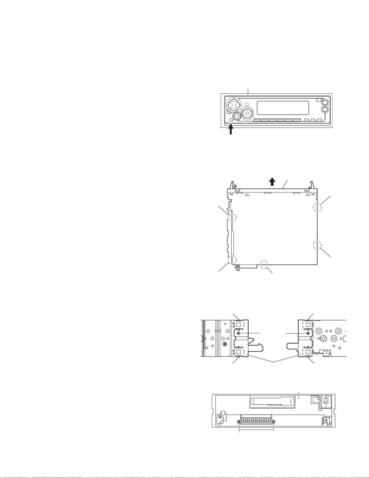
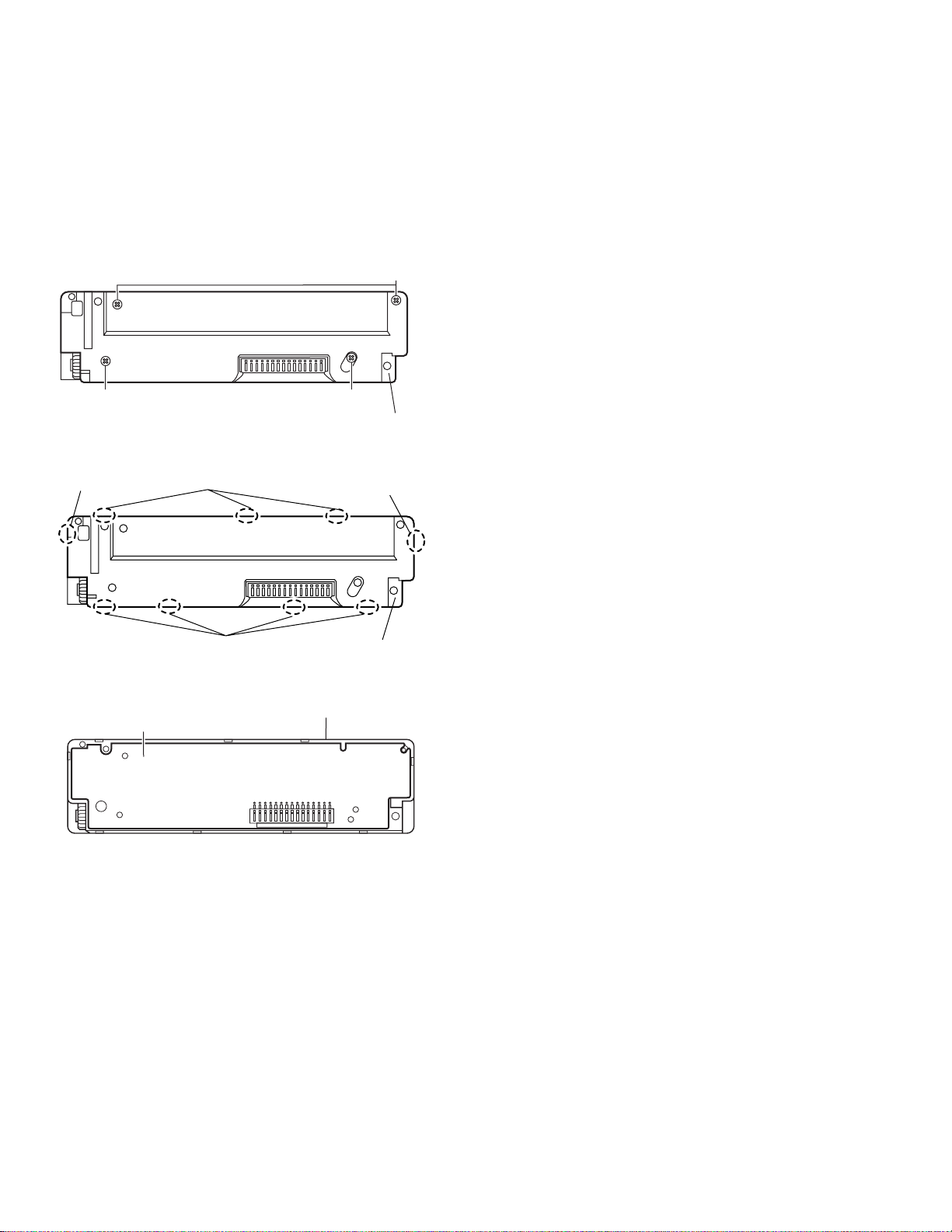
3.1 Main body
3.1.1 Removing the front panel assembly
(See Fig.1)
(1) Press the release button and remove the front panel as-
sembly.
3.1.2 Removing the bottom cover
(See Fig.2)
• Prior to performing the following procedures, remove the front
panel assembly.
(1) Turn the main body upside down.
(2) Insert a screwdriver under the joints to release the two
joints a on th e left side, two joints b on the right side and
joint c on the back side of the main body, then remove the
bottom cover from the main body.
CAUTION:
When releasing the joints using a screwdriver, do not damage
the main board.
Front panel assembly
Release button
Fig.1
Front chassis assembly
Joint b
Joint a
3.1.3 Removing the front chassis assembly
(See Figs.3 and 4)
• Prior to performing the following procedures, remove the front
panel assembly and bottom cover.
(1) Remove the two screws A on the both sides of the main
body. (See Fig.3.)
(2) Remove the two screws B on the front side of the main
body. (See Fig.4.)
(3) Release the two joints d and two joints e on the both sides
of the main body, then remove the front chassis assembly
toward the front. (See Fig.3.)
Joint a
Joint d
Joint d
Joint c
Fig.2
A
Front chassis assembly
A
Fig.3
Front chassis assembly
Joint b
Joint e
Joint e
B
Fig.4
(No.49875)1-5
Page 6

3.1.4 Removing the heat sink
(See Fig.5)
• Prior to performing the following procedure, remove the fro nt
panel assembly as required.
(1) Remove the two screws C and screw D attaching the heat
sink on the left side of the main body, and remove the heat
sink.
3.1.5 Removing the rear panel
(See Fig.6)
• Prior to performing the following procedure, remove the fro nt
panel assembly and bottom cover.
(1) Remove the two screws E, screw F and three screws G at-
taching the rear panel on the back side of the main body.
E
C
D
Heat sink
Rear bracket
Fig.5
G
F
C
G
E
3.1.6 Removing the main board
(See Fig.7)
• Prior to performing the following procedures, remove the front
panel assembly, bottom cover, front chassis assembly, heat
sink and rear panel.
(1) Remove the two screws H attaching the main board on the
top chassis.
(2) Disconnect the connector CP401 on the main board from
the cassette mechanism assembly.
H
Fig.6
Main board
H
CP401
Fig.7
1-6 (No.49875)
Page 7
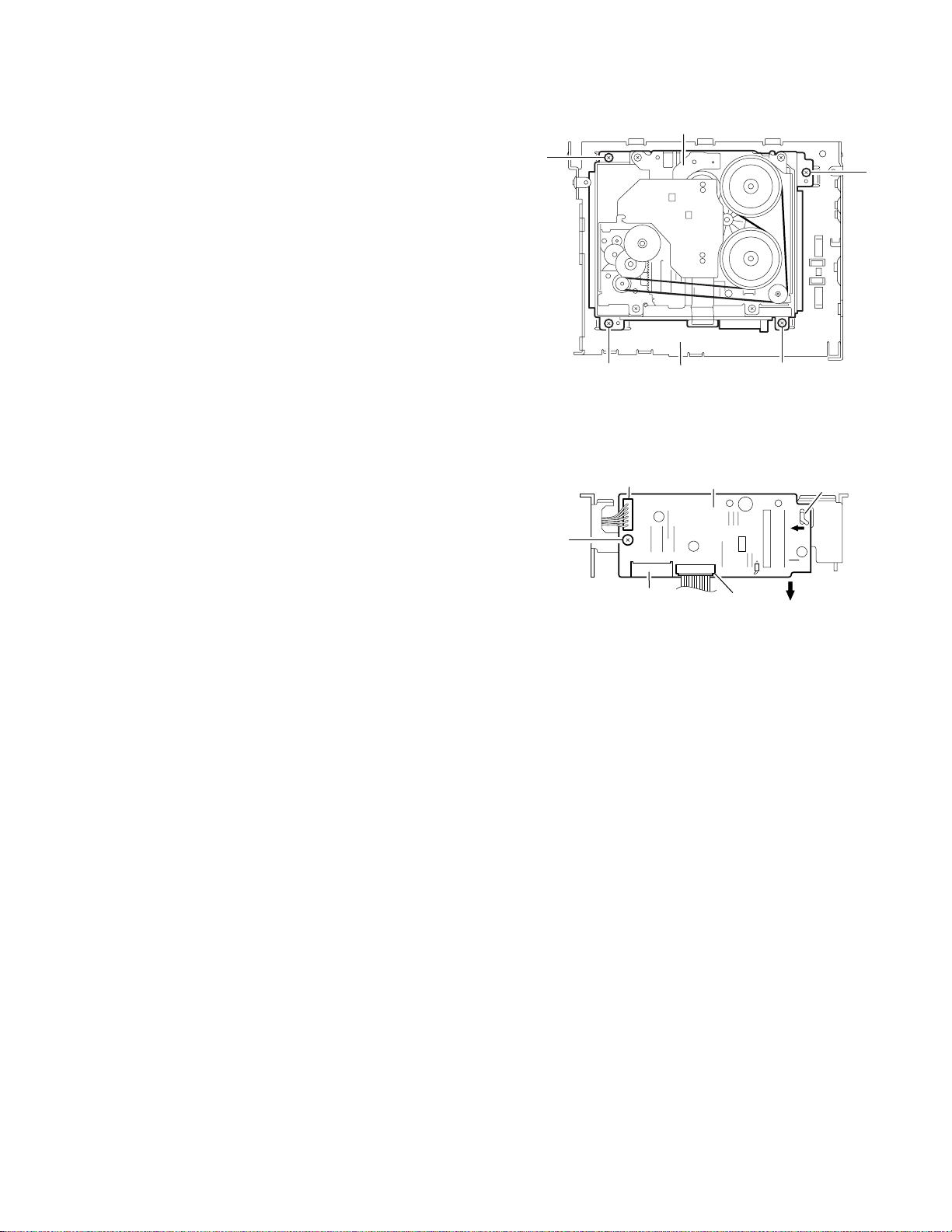
3.1.7 Removing the cassette mechanism assembly
(See Fig.8)
• Prior to performing the following procedures, remove the front
panel assembly, bottom cover, front chassis assembly, heat
sink, rear panel and main board.
(1) Disconnect the wire from the connector CN402 on the
mecha board.
(2) Disconnect the card wire from the connector CN403 on the
mecha board.
(3) Remove the four screws J attaching th e cassette mecha-
nism assembly to the top chassis, take out the cassette
mechanism assembly.
Cassette mechanism assembly
J
J
3.1.8 Removing the mecha bo ar d
(See Fig.9)
• Prior to performing the following procedures, remove the front
panel assembly, bottom cover, front chassis assembly, heat
sink, rear panel and main board.
(1) Disconnect the wire from the connector CN402 on the
mecha board.
(2) Disconnect the card wire from the connector CN403 on the
mecha board.
(3) Remove the screw K attaching the mecha board.
(4) Bend the hook f in the direction of the arrow 1 and move the
mecha board in the direction of the arrow 2.
(5) Remove the mecha board from the mecha bracket (L) of
the top chassis.
K
CN401
Top chassis
Fig.8
Mecha board
CN403
Fig.9
J J
CN402
hook f
1
2
(No.49875)1-7
Page 8
3.1.9 Removing the front board
(See Figs.10 to 12)
• Prior to performing the following procedures, remove the front
panel assembly.
(1) Remove the four screws L attaching the rear cover on the
back side of the front panel assembly. (See Fig.10.)
(2) Release the nine joints g, the front panel assembly and
rear cover become separate. (See Fig.11.)
(3) Remove the front board from the front panel assembly.
(See Fig.12.)
L
L
Joints g
Front board
Joints g
Joints g
L
Rear cover
Fig.10
Joints g
Rear cover
Fig.11
Front panel assembly
Fig.12
1-8 (No.49875)
Page 9

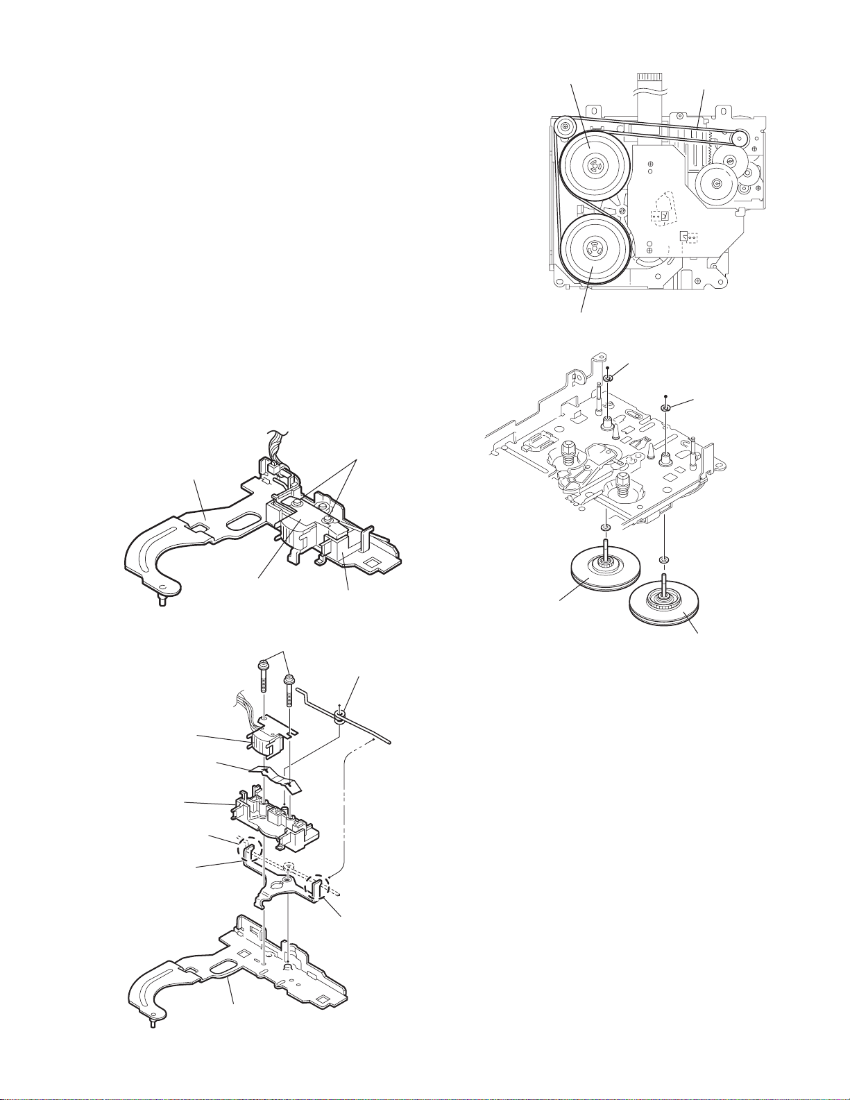
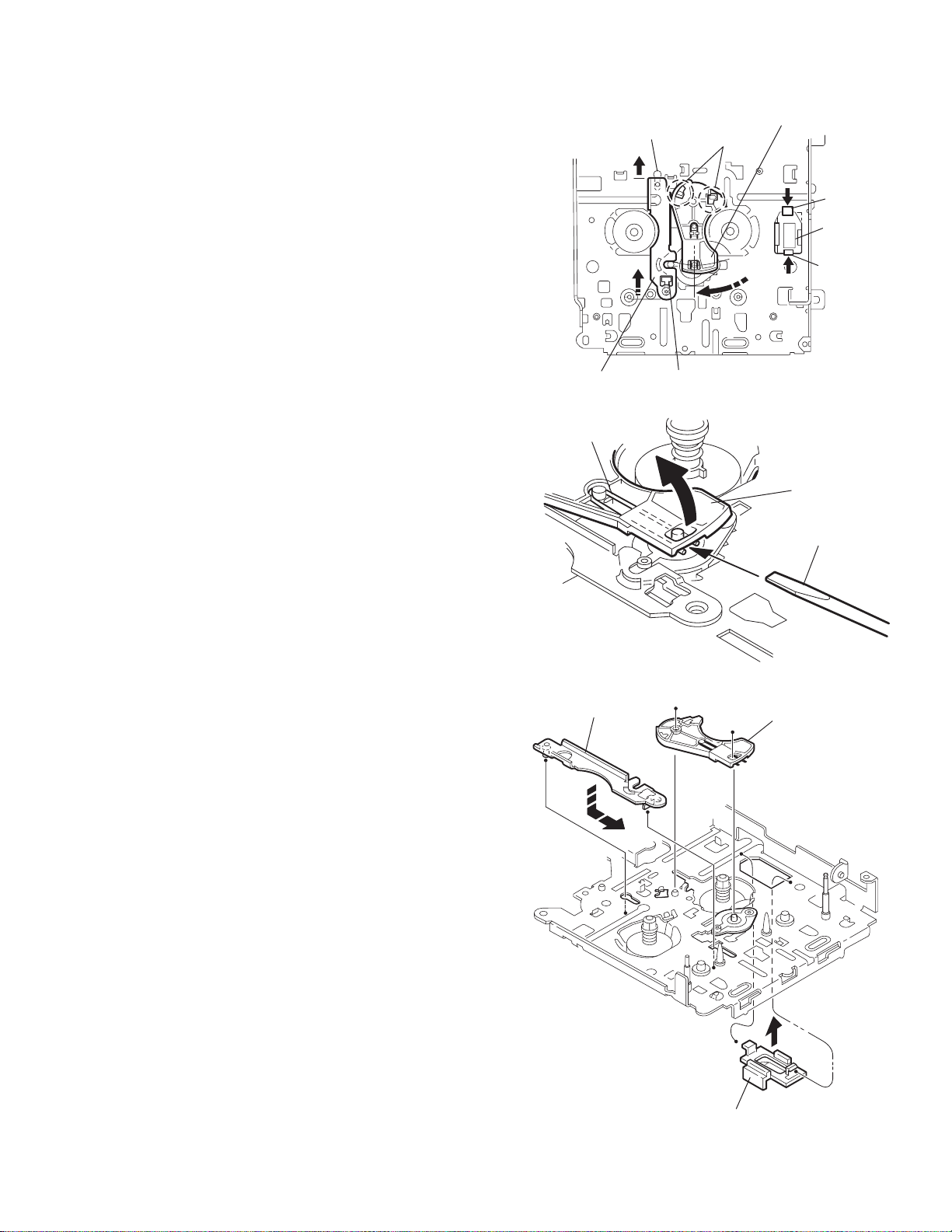
3.2 Cassette mechanism assembly
r
REFERENCE:
Prior to performing the following procedures, turn the mode
gear on the bottom of the body until the respective part comes
to the EJECT position (Refer to Fig.1).
3.2.1 Removing the cassette guide
(See Fig.2)
(1) Turn the mode gear to set to RVS play or subsequent
mode.
(2) Remove the cassette guide from the main chassis while re-
leasing each two joint tabs a in the direction of the arrow.
Mode gea
Fig.1
Cassette guide
3.2.2 Removing the load arm
(See Fig.3)
(1) Remove the E-washer attaching the load arm.
(2) Move the load arm in the direction of the arrow and release
the joint b on the cassette catch.
Load arm
E-washer
Tab a
Tab a
Fig.2
Joint b
Fig.3
(No.49875)1-9
Page 10

3.2.3 Removing the cassette hanger assembly / cassette holder
r
(See Fig.4 to 7)
(1) Check the mode is set to EJECT. Push down the front part
of the cassette holder and move in the direction of the arrow to release the joint c.
(2) Move the rear part of the cassette hanger assembly in the
direction of the arrow to release it from the two joint bosses
d.
(3) Release the holder stabilizer spring fro m the hooks e and
f, then pull out from the cassette hanger assembly.
(4) Bring up the rear side of the cassette hanger asse mbly to
release the joint g and h.
(5) Pull out the cassette catch from the cassette hanger as-
sembly.
Cassette holder assembly
Side bracket
Joints c
Cassette holder assembly
Fig.4
Boss d
Cassette hanger
assembly
Boss d
Cassette stabilizer spring
Hook e
Cassette holder
assembly
Hook g
Cassette hange
assembly
Hook f
Fig.5
Cassette hanger
assembly
Hook h
Fig.6
Cassette hanger assembly
1-10 (No.49875)
Cassette catch
Cassette holder assembly
Fig.7
Page 11
3.2.4 Removing the side bracket assembly
(See Fig.8 to 10)
(1) Remove the screw A attaching the side bracket assembly.
(2) Detach the front side of the side bracket assembly upward
and pull out forward to release the joint i and j in the rear.
CAUTION:
When reassembling, make sure that the boss k of the
main chassis is set in the notch of the load rack under the
side bracket assembly. Do not reattach the load rack on
the boss k.
CAUTION:
After reattaching the side bracket assembly, confirm operation.
Side bracket assembly
Joint i
Joint j
A
Side bracket assembly
Fig.8
Side bracket assembly
Joint i
Joint j
Load rack
Load rack
Boss k
Fig.9
Boss k
Fig.10
(No.49875)1-11
Page 12

3.2.5 Removing the pinch arm (F) assembly
r
(See Fig.11 and 12)
(1) Remove the polywasher and pull out the pinch arm (F) as-
sembly.
(2) Remove the compulsion spring.
3.2.6 Removing the pinch arm (R) assembly
(See Fig.11 and 12)
(1) Remove the polywasher and pull out the pinch arm (R) as-
sembly.
3.2.7 Removing the slide chassis assembly
(See Fig.13 and 14)
REFERENCE:
It is not necessary to remove the head and the tape guide.
(1) Move the slide chassis assembly in the direction of the ar-
row to release the two joints l and remove from the main
chassis.
(2) Remove the rack link.
CAUTION:
When reassembling, first reattach the rack link, and next
fit the boss m and hook n of the slide chassis assembly
to the hole of the main chassis, and engage the two joints
l.
Joint l
Joint l
Slide chassis assembly
Fig.13
Head
Tape guide
Boss m
Rack link
Hook n
Polywasher
Polywasher
Compulsion
spring
Pinch arm
(R) assembly
Pinch arm
(F) assembly
Fig.11
Pinch arm (F) assembly
Pinch arm
(R) assembly
Polywashe
Fig.14
Polywasher
1-12 (No.49875)
Fig.12
Page 13
3.2.8 Removing the head / tape guide
(See Fig.16 and 17)
REFERENCE:
It is not necessary to remove the slide chassis assembly.
(1) Remove the band attaching the wire to the head.
(2) Remove the two screws B, the head and the head support
spring.
(3) Remove the pinch arm spring from the tape guide.
(4) Remove the tape guide and the pinch spring arm.
CAUTION:
When reattaching the pinch arm spring, set both end of
it to the pinch spring arm (remarked o).
CAUTION:
When reattaching the head, set the wires into the groove
of the tape guide (Fig.16).
3.2.9 Removing the flywheel assembly (F) & (R)
(See Fig.18 and 19)
REFERENCE:
It is not necessary to remove the slide chassis assembly.
(1) Remove the belt at the bottom.
(2) Remove the two polywashers on the upper side.
(3) Pull out each flywheel assembly downward.
B
Slide chassis assembly
Flywheel assembly (F)
Flywheel assembly (R)
Belt
Fig.17
Polywasher
Polywasher
Head
Head support spring
Tape guide
o
Pinch spring arm
Head
Fig.15
Tape guide
B
Pinch arm spring
Flywheel assembly (F)
Flywheel assembly (R)
Fig.18
o
Slid chassis assembly
Fig.16
(No.49875)1-13
Page 14
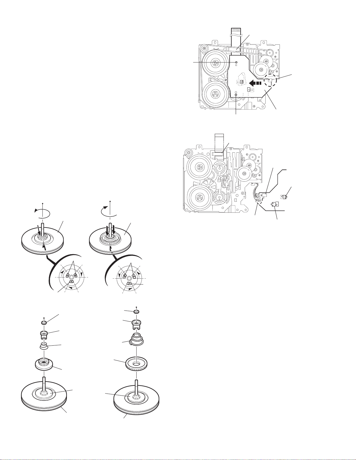
3.2.10 Disassembling the flywheel assembly (F)
r
(See Fig.19 and 20)
(1) Push and turn counterclockwise the spring holder (F) to re-
lease the three joints p on the bottom of the flywheel.
(2) The spring holder (F), the TU spring and the friction gear
play come off.
(3) Remove the polywasher and felt.
3.2.11 Disassembling the flywheel assembly (R)
(See Fig.19 and 20)
(1) Push and turn clockwise the spring h older (R) to release
the three joints q on the bottom of the flywheel.
(2) The spring holder (R), the FF spring and the friction gear
FF come off.
(3) Remove the polywasher and the felt.
3.2.12 Removing the reel board
(See Fig.21 and 22)
(1) Remove the two screws C attaching the reel board.
(2) Move the reel board in the direction of the arrow to release
the joint r.
(3) Unsolder the wires if necessary.
CAUTION:
When reattaching, confirm operation of the MODE
switch and the ST-BY switch.The mode position between EJECT and ST-BY is optimum for reattaching.Connect the card wire extending from the reel board
to the FFC pad before reattaching the reel board.
FFC pad
C
Joint
Reel board
C
Fig.21
FFC pad
CT-1 switch
MODE switch
Flywheel
assembly (F)
Joint p
Joints p
Fig.19
Polywasher
Spring holder (R)
Spring holder (F)
TU spring
Friction gear FF
Friction gear play
Polywasher
FF spring
Flywheel
assembly (R)
Joints q
Joint q
Soldering
ST-BY switch
Fig.22
Flywheel assembly (F)
1-14 (No.49875)
Felt
Felt
Flywheel assembly (R)
Fig.20
Page 15
3.2.13 Removing the gear base arm / gear base link assembly
(See Fig.23 to 25)
(1) Move the gear base arm in the direction of the arrow.
(2) Insert a slotted screwdriver to the gear base spring under
the gear base arm, and release the gear base arm upward
from the boss on the gear base assembly.
(3) Remove the gear base arm from the main chassis while re-
leasing the two joints s.
(4) Move the gear base link assemby in the direction of the ar-
row to release the two joints t.
REFERENCE:
When reattaching the gear base arm, make sure that the
boss on the gear base assembly is inside the gear base
spring.
3.2.14 Removing the FFC pad
(See Fig.25 and 27)
(1) Push each joint hook u of the FFC pad and remove toward
the bottom.
Gear base
link assembly
Gear base spring
Joint t
Gear base arm
Joints s
Hook u
FFC pad
Hook u
Joint t
Fig.23
Gear base arm
Gear base link
assembly
Screwdriver
Fig.24
Gear base arm
FFC pad
Fig.25
(No.49875)1-15
Page 16

3.2.15 Removing the mode gear
r
r
(See Fig.26 and 29)
(1) Remove the polywasher on the bottom and pull out the
mode gear.
3.2.16 Removing the mode switch actuator
(See Fig.26, 27 and 29)
(1) Pull out the mode switch actuator at the bottom.
REFERENCE:
When reattaching the mode switch actuator to the main
chassis, make sure to set on the shaft and insert v into
the slot w.
3.2.17 Removing the direction link / direction plate
(See Fig.27 to 29)
(1) Remove the polywasher attaching the direction link.
(2) Bring up the direction link to release the thre e joints x, y
and z at a time.
(3) Move the direction plate in the direction of the arrow to re-
lease the two joints a’.
REFERENCE:
When reattaching the direction plate, engage the two
joints a’ and move in the direction of the arrow (Refer to
Fig.28).
REFERENCE:
When reattaching the direction link, move the direction
plate in the direction of the arrow and engage the three
joint x, y and z at a time (Refer to Fig.29).
3.2.18 Removing the mode rack assembly
(See Fig.27 and 28)
(1) Move the mode rack assembly in the direction of the arrow
to release the two joints b’ and the joint c’.
REFERENCE:
When reattaching, set the two b’ on the bottom of the
mode rack assembly into the slots of the main chassis
and move in the direction of the arrow (See Fig.28).
Direction plate
Direction plate
Joints a'
Joint z
Direction link
Direction plate
Mode switch actuator
Direction link
Fig.26
Slot w
Joint y
Polywasher
Fig.27
Mode rack assembly
Joint b'
Mode gear
Polywashe
Mode rack assembly
Joint x
Joint b'
Joint c'
1-16 (No.49875)
Joints a'
Fig.28
Direction link
Mode switch actuator
Polywasher
v
Mode gea
Direction plate
Mode rack assembly
Fig.29
Page 17

3.2.19 Removing the gear base assembly / take up gear / reflector gear
r
(See Fig.30 to 32)
(1) Push in the pin d’ of the gear base assembly on the upper
side of the body and move the reflector gear toward the
bottom, then pull out.
(2) Remove the polywasher on the bottom and pull out the
take up gear.
(3) Move the gear base assembly in the direction o f the arrow
to release it from the two slots e’ of the main chassis.
REFERENCE:
The parts are damaged when removed. Please replace
with new ones.
3.2.20 Removing the reel driver / reel spindle
(See Fig.32)
(1) Draw out the reel driver from the shaft on the main chassis
and remove the reel driver spring and the reel spindle respectively.
CAUTION:
The reel driver is damaged when remo ved. Please replace with a new one.
Gear base assembly
Pin d'
Polywasher
Slot e'
Slot e'
Fig.30
Take up gear
Reflector gear
Reel driver
Reel driver spring
Reel spindle
Main chassis
Reflector gear
Fig.31
Reel driver
Reel driver spring
Reel spindle
Gear base assembly
Slots e’
Take up gea
Polywasher
Fig.32
(No.49875)1-17
Page 18

3.2.21 Removing the side bracket assembly
(See Fig.33 to 37)
(1) Remove the eject cam plate spring.
(2) Push the joint f’ through the slot to remove the load rack
downward.
(3) Move the eject cam limiter in the direction of the arrow to
release it from the boss g’ of the side bracket assembly and
from the two joints h’.
(4) Move the eject cam plate in the direction of the arrow to re-
lease the joint i’.
CAUTION:
When reassembling, confirm operation of each part before reattaching the eject cam plate spring.
Joint f'
Side bracket assembly
Boss g'
Eject cam plate
Fig.36
Side bracket assembly
Joint i'
Eject cam plate spring
Side bracket assembly
Joint h'
Side bracket
assembly
Boss g'
Boss g'
Load rack
Fig.33
Eject cam limiter
Joint f'
Fig.34
Eject cam limiter
Eject cam plate
Joint i'
Fig.37
Joint h'
Load rack
Joint h'
1-18 (No.49875)
Eject cam plate
Fig.35
Joint h'
Page 19

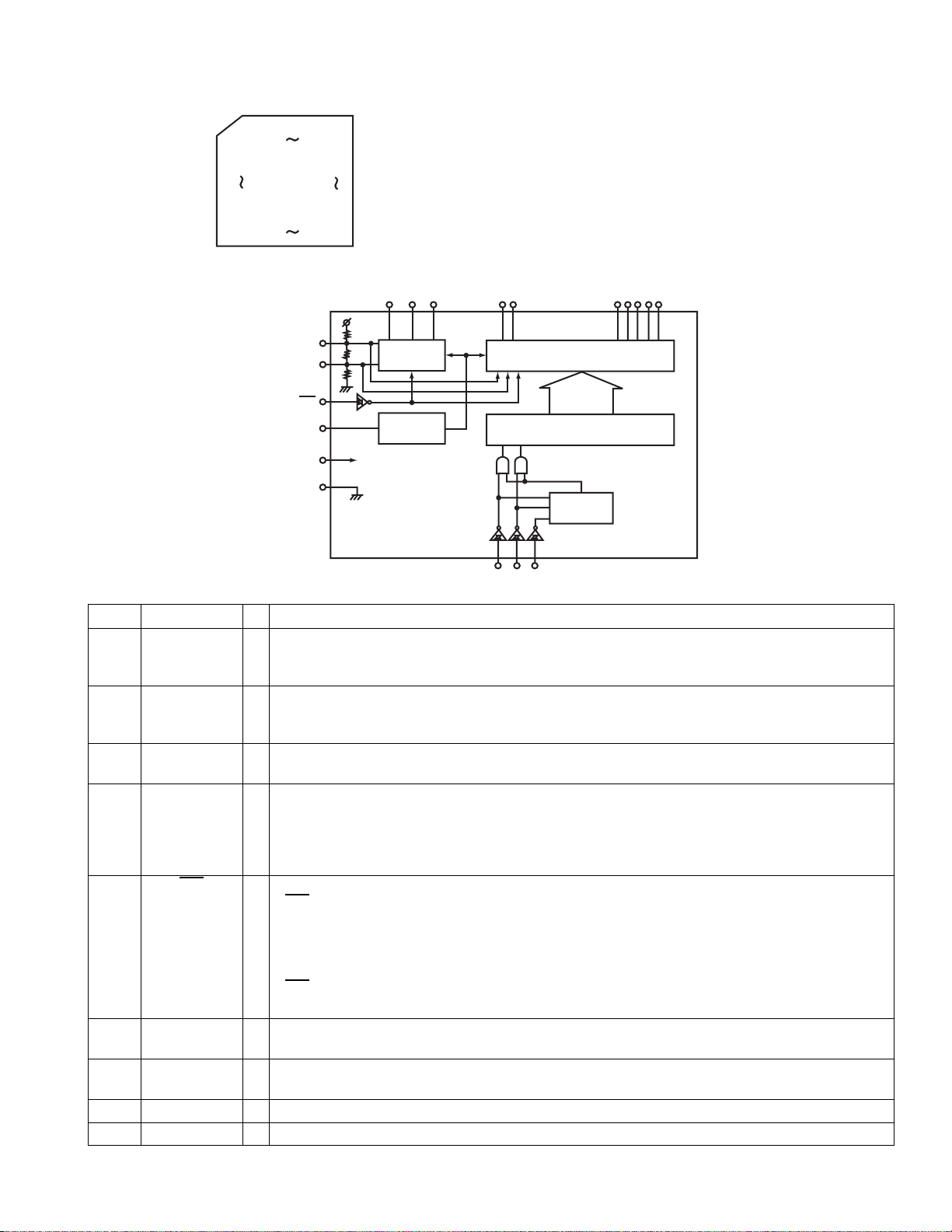
3.2.22 Removing the main motor assembly / sub motor assembly
r
r
r
(See Fig.38 to 40)
(1) Remove the belt at the bottom.
(2) Remove the polywasher and pull out the mode gear.
(3) Pull out the reduction gear (B).
(4) Remove the polywasher and pull ou t the reduction gear
(A).
(5) Remove the two screws attaching the main motor assem-
bly.
(6) Remove the two screws E attaching the sub motor assem-
bly.
(7) Unsolder the wires on the reel board if necessary.
CAUTION:
When reassembling, adjust the length of the wires extending from the sub motor asswmbly by attaching them
to the side of the sub motor assembly with the wires extending from the main motor assembly using a spacer.
Belt
Reduction gear (B)
Reduction gear (B)
E
Mode gear
Polywasher
Fig.38
Main motor
D
assembly
Reduction
gear (A)
Polywashe
Sub moto
assembly
E
Polywasher
Reduction gear (A)
D
Spacer
Main motor assembly
Sub motor assembly
Fig.39
Main motor assembly
Sub motor assembly
Fig.40
Space
(No.49875)1-19
Page 20

SECTION 4
ADJUSTMENT
4.1 Adjustment method
Test instruments required for adjustment
(1) Digital oscilloscope (100MHz)
(2) Frequency counter meter
(3) Electric voltmeter
(4) Wow & flutter meter
(5) Test tapes
• VT724...........................For DOLBY level measurement
• VT739..............For playback frequency measurement
• VT712....For wow flutter & tape speed measurement
• VT703........................For head azimuth measurement
(6) Torque gauge............................Cassette type for CTG-N
Measuring conditions (Amplifier section)
• Power supply voltage.............. DC14.4V (11V to 16V allowance)
• Load impedance............ 4Ω (4Ω to 8Ω allowance)
• Line out level/Impedance..............1.0V/20k load (250 nWb/m)
Standard volume position
Balance and Bass, Treble volume, Fader : Center (Indication "0")
Loudness, Dolby NR, Sound, Cruise : Off
Volume position is about 2V at speaker output with following
conditions, Playback the test tape VT721.
AM mode 999kHz/62dB, INT/400Hz, 30%
modulation signal on receiving.
FM mono mode 97.9MHz/66dB, INT/400Hz, 22.5kHz
deviation pilot off mono
FM stereo mode 1kHz, 67.5kHz dev. pilot 7.5kHz dev.
Output level 0dB (1µV,50Ω/open terminal)
1-20 (No.49875)
Page 21

Information for using a car audio service jig
(1) We're advancing efforts to make our extension cords common for all car audio products.
Please use this type of extension cord as follows.
(2) As a U-shape type top cover is employed, this type of extension cord is needed to check operation of the mechanism assembly
after disassembly.
(3) Extension cord : EXTKSRT002-18P ( 18 pin extension cord ) For connection between mechanism assemblyand main board.
(4) Check for mechanism driving section such as motor ,etc.
Disassembly method
(1) Remove the front panel assembly.
(2) Remove the bottom cover.
(3) Remove the front chassis.
(4) Remove the heat sink.
(5) Remove the rear panel
(6) Remove the main board.
(7) Reattach the heat sink with the two screws B. (Refer to Disassembly method.)
(8) Reattach the rear panel with the screw E. (Refer to Disassembly method.)
(9) Reattach the front panel assembly.
(10) Confirm that current is being carried by connecting an extension cord ji g.
NOTE:
Available to connect to the CJ601
CAUTION :
Be sure to attach the heat sink and rear pa nel on the power ampl ifier IC and regulator I C of a main board when su pplying
the power.If voltage is applied without attaching those parts, the power amplifier IC and regulator IC will be destroyed
by heat.
connector when installing the front panel.
To
Cassette mechanism
EXTKSRT002-18P
Extension cord
EXTKSRT002-18P
To
Main board
Front panel assembly
Cassette mechanism
Main board
(No.49875)1-21
Page 22
Arrangement of adjusting & test points
A
Cassette mechanism
(Surface)
Motor assembly
Tape speed adjust
Azimuth screw
(Forward)
Playback head
Azimuth screw B
(Reverse)
Head section view
Azimuth screw B
(Reverse)
Playback head
Azimuth screw A
(Forward)
1-22 (No.49875)
Page 23

Item Conditions Adjustment and Confirmation methods S.Values Adjust
1. Head azimuth adjustment
Test tape:
SCC-1659
VT703 (10kHz)
Head height adjustment
Adjust the azimuth directly. When you adjust the height
using a mirror tape, remove the cassette housing from
the mechanism chassis. After installing the cassette
housing, perform the azimuth adjustment.
(1) Load the SCC-1659 mirror tape. Adjust with height
adjustment screw A and azimuth adjustment screw
B so that line A of the mirror tape runs in the center
between Lch and Rch in the reverse play mode.
(2) After switching from REV to FWD then to REV,
check that the head position set in procedure 1 is not
changed. (If the position has shifted, adjust again
and check.)
(3) Adjust with azimuth adjustment screw B so that line
B of the mirror tape runs in the center between Lch
and Rch in the forward play mode.
Head shield
The head is at low position
during.
Head shield
The head is at High position
during REV.
A line
B line
2. Tape speed
and wow flutter confirmation
3. Play back
frequency response confirmation
Test tape:
VT724 (1kHz)
VT703 (10kHz)
VT721 (315Hz)
Test tape:
VT712 (3kHz)
Test tape:
VT724 (1kHz)
VT739 (63Hz /
1kHz / 10kHz)
Head azimuth adjustment
(1) Load VT724 (1kHz) and play it back in the reverse
play mode. Set the Rch output level to max.
(2) Load VT703 (10kHz) and play it ba ck in the fo rward
play mode. Adjust the Rch and Lch output levels to
max, with azimuth adjustment screw B. In this case,
the phase difference should be within 45 .
(3) Engage the reverse mode and adjust the output lev-
el to max, with azimuth adjustment screw C.(The
phase difference should be 45 or more.)
(4) When switching between forward and reverse
modes, the difference between channels should be
within 3dB. (Between FWD L and R, REV L and R.)
(5) When VT721 (315Hz) is played back, the level differ-
ence between channels should be within 1.5dB.
(1) Check to see if the reading of the F, counter / wow
flutter meter is within 3015Hz to 3045Hz (FWD/
REV), and less than 0.35% (JIS RMS).
(2) In case of out of specification, adjust the motor with
a built-in volume resistor.
(1) Play test tape VT724, and set the volume position at
2V.
(2) Play test tape VT739 and confirm.1kHz / 10kHz: -1
±3dB,1kHz / 63Hz: 0 ±3dB,
(3) When 10kHz is out of specification, it will be neces-
sary to read adjust the azimuth.
Output
level:
Maximum
PBHead
FWD Adj B
REV Adj C
(0 ) (45 )
Tape speed:
3015Hz to 3045Hz
Wow flutter:
less than 0.35%
Speaker out
1kHz / 63Hz: 0 ±3dB
1kHz / 10kHz: -1 ±3dB
HEIGHT Adj A
phase
Built-in volume
resistor
The tuner section is of an adjustment-freedesign. In case the tuner is in trouble, replace the tuner pack.
(No.49875)1-23
Page 24

SECTION 5
TROUBLE SHOOTING
This service manual does not describe TROUBLE SHOOTING.
1-24 (No.49875)
Page 25

SECTION 6
A
DESCRIPTION OF MAJOR ICs
6.1 BR24L16F-W-X (IC771) : EEPROM
•Pin layout •Pin function
VCC WP SCL SDA
A0 A1 A2 GND
• Block diagram
Symbol I/O Function
VCC - Power supply.
GND - GND
A0,A1,A2 I No use conn ect to GND.
SCL I Serial clock input.
SDA I/O Serial data I/O of slave and ward address.
WP I Write protect terminal.
A0 1
11bit
A1 2
A2 3
GND 4
High voltage osc circuit
Address
decoder
6.2 IC-PST600M/G/-W (IC702) : System reset
Co1
16kbit EEPROM allay
11bit
START
Control circuit
Slave Ward
Address resister
STOP
Power supply
voltage det.
OP1
ACK
8bit
Data
resister
8 Vcc
7 WP
6 SCL
5 SD
1
IN
3
Vout
6.3 LB1641 (IC402) : DC Motor driver
•Pin layout •Truth table
Input Output Mode
IN1 IN2 OUT1 OUT2
0000 Brake
1 2 3 4 5 6 7 8 9
GND OUT1 P1
VZ IN1 IN2
VCC1
VCC2 P2
10
OUT2
1 0 1 0 CLOCKWISE
0 1 0 1 COUNTER-CLOCKWISE
1100 Brake
2
GND
(No.49875)1-25
Page 26

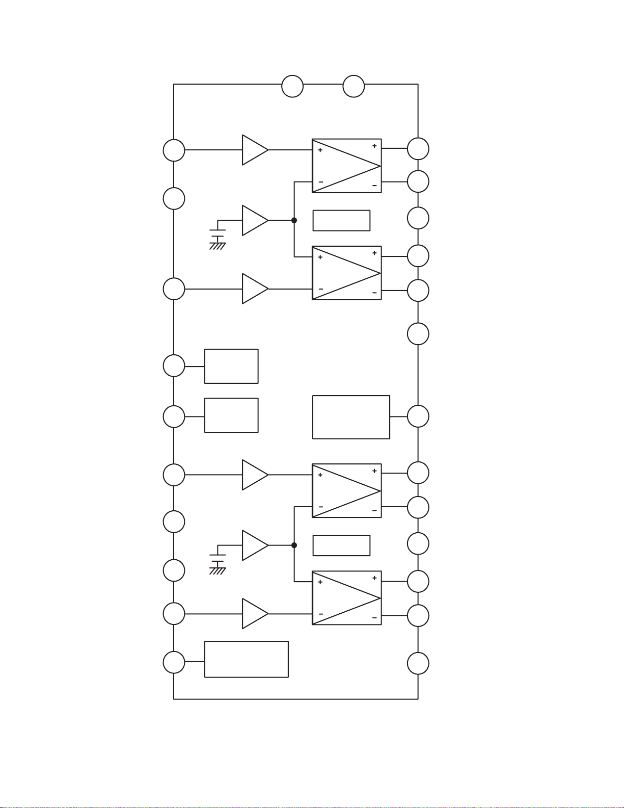
6.4 CXA2560Q (IC4 01) : Dolby B typ e no ise reduction system with play back equalizer amp.
• Pin layout & block diagram
PBFB2
PBRIN2
PBGND
PBFIN2
VCT
PBREF
PBFIN1
PBGND
PBRIN1
PBFB1
PBTC2
30 29 28
7k/12k
31
32
33
34
35
45k
36
37
38
39
40
12345
PBTC1
300k
30k
30k
300k
7k/12k
PBOUT2
+
F2
F1
+
-
PBOUT1
OUTREF2
TAPEIN2
27
100k
70 /120
T2
1
1
T1
100k
70 /120
TAPEIN1
OUTREF1
GND
26
Vcc
DIREF
25
BIAS
MUTE
TAPE EQ
FWD/RVS
Vcc
LPF
6
NC
LINEOUT2
23 22 21
24
OFF/B
+
-
+
-
F3
OFF/B
-
+
7
LINEOUT1
TCH2
NC
MSSW
NR
MS MODE
NR MODE
MS ON/
OFF
DET
NR
8910
NC
TCH1
MSLPF
20
19
18
17
16
15
14
13
12
• Pin function
Pin No. Symbol I/O Function
1 PBTC1 - Playback equalize r ampl ifier
capacitance
2 PBOUT1 O Playback equalizer amplifier
output
3 OUTREF1 O Output reference
4 TAPEIN1 I TAPE input
5 Vcc - Power su pply
6NC7 LINEOUT1 O Line output
8 TCH1 - Time constant for the HLS
9NC-
10 MSLPF - Cut-off frequency adjustment
of the music sensor LPF
11 G2FB - Music signal interval detection
12 G1FB - Music signal interval detection
13 MSTC - Time constant for detecting
music signal interval
14 MSOUT O Music sensor out
15 NC - No use
16 NRSW I Dolby NR control
17 MUTESW I Mute function control
18 TAPESW I Playback equalizer amplifier
control
19 DRSW I Head select control
20 MSMODE I Music sensor mode control
21 MSSW I Music sensor control
22 NC 23 TCH2 - Time constant for the HLS
MSMODE
DRSW
TAPESW
MUTESW
NRSW
NC
MSOUT
MSTC
G1FB
G2FB
11
Pin No. Symbol I/O Function
24 LINEOUT2 O Line output
25 DIREF - Resistance for setting the
reference
26 GND - Ground
27 TAPEIN2 I TAPE input
28 OUTREF2 O Output reference
29 PBOUT2 O Playback equalizer amplifier
output
30 PBTC2 - Playback equalizer amplifier
capacitance
31 PBFB2 I Playback equalizer amplifier
feedback
32 PBRIN2 I Playback equalizer amplifier
input
33 PBGND - Playback equalizer amplifier
ground
34 PBFIN2 I Playback equalizer amplifier
input
35 VCT O Center
36 PBREF O Playback equalizer amplifier
reference
37 PBFIN1 I Playback equalizer amplifier
input
38 PBGND - Playback equalizer amplifier
ground
39 PBRIN1 I Playback equalizer amplifier
input
40 PBFB1 I Playback equalizer amplifier
feedback
1-26 (No.49875)
Page 27

6.5 HA13164A (IC901) : Regulator
• Terminal layout
123456789101112131415
• Block diagram
ANT OUT
EXT OUT
ANT CTRL
CTRL
CD OUT
AUDIO OUT
C3
0.1u
C4
0.1u
C5
0.1u
C6
10u
2
1
7
11
12
10
VCC ACC
8
Surge Protector
BIAS TSD
15
3
TAB
C1
100u
C2
0.1u
13
ILM AJGND GND
+B
ACC
BATT.DET OUT
9
COMPOUT
6
VDD OUT
4
SW5VOUT
5
ILMOUT
14
R1
C7
0.1u
0.1u
C8
UNIT R:
C:F
note1) TAB (header of IC)
connected to GND
• Pin function
Pin No. Symbol Function
1 EXTOUT Output voltage is VCC-1 V when M or H level applied to CTRL pin.
2 ANTOUT Output voltage is VCC-1 V when M or H level to CTRL pin and H level to ANT-CTRL.
3 ACCIN Connected to ACC.
4 VDDOUT Regular 5.7V.
5 SW5VOUT Output voltage is 5V when M or H level applied to CTRL pin.
6 COMPOUT Output for ACC detector.
7 ANT CTRL L:ANT output OFF H:ANT output ON
8 VCC Connected to VCC.
9 BATT DET Low battery detect.
10 AUDIO OUT Output voltage is 9V when M or H level applied to CTRL pin.
11 CTRL L:BIAS OFF M:BIAS ON H:CD ON
12 CD OUT Output voltage is 8V when H level applied to CTRL pin.
13 ILM AJ Adjustment pin for ILM output voltage.
14 ILM OUT Output voltage is 10V when M or H level applied to CTRL pin.
15 GND Connected to GND.
(No.49875)1-27
Page 28

6.6 HD74HC126FP-X (IC801) : Buffer
• Pin layout • Pin function
Input Output
CA Y
LX Z
HL H
HH L
Note:
H:High level
L:Low level
X:Irrelevant
Z:Off(High-impedance)
State a 3-state input
• Block diagram
1C
1A
1Y
2C
2A
2Y
GND
1
2
3
4
5
6
7
14
13
12
11
10
9
8
VCC
4C
4A
4Y
3C
3A
3Y
Vcc Vcc
1k
Input
Note:
CL includes probe and jig capacitance
See Function Table
1A
2A
3A
4A
1C
2C
3C
4C
1Y
2Y
3Y
4Y
Output
Output
Output
Output
S1
CL
1k
Sample as Load Circuit 1
Sample as Load Circuit 1
Sample as Load Circuit 1
1-28 (No.49875)
Page 29
6.7 LC75873NW (IC601):LCD Driver
•Pin layout
60 41
61
40
80
21
1 20
• Block diagram
S5
S4/P4
S3/P3
S2/P2
S62
S66
L
DI
SEGMENT DRIVER
SHIFT REGISTOR
ADDRESS
DETECTOR
E
• Pin function
VDD1
VDD2
INH
OSC
VDD
VSS
COM2
COM3
COMON
DRIVER
CLOCK
GENERATOR
COM1
Pin No. Pin name I/O Description
79,80
1,2,3
S1/P1 to S4/P4
S5 to S68
O Segment outouts for displaying the display data transferred by serial data input.
The S1/P1 to S4/P4 pins can be used as generalpurpose output ports under serial data control.
to 66
67
78
69
COM1
COM2
COM3
O Common drive r ou tp u ts.
The frame frequency f0 is given by :
f0 = (FOSC/384)Hz.
74 OSC I/O Oscillator connection
An oscillator circuit is formed by connecting an external resistor and capacitor to this pin.
76
77
78
CE
CL
DI
I
Serial data transfer inputs.
I
Connected to the controller.
I
CE:Chip enable
CL:Synchronization clock
DI:Transfer data
75 INH
I Display off control input
•INH
= "L"(VSS) ---Display forced off
S1/P1 to S4/P4 = "L"
(These pins are forcibly set to the segment output port function and held at the low level.)
S5 to S68 = "L"
COM1 to COM3"L"
= "H"(HDD)---Display on
•INH
However, serial data transfer is possible when the display is forced off by this pin.
71 VDD1 I Used for applying the LCD drive 2/3 bias voltage externally. Must be connected to VDD2 when a 1/2
bias drive scheme is used.
72 VDD2 I Used for applying the LCD drive 1/3 bias voltage externally. Must be connected to VDD1 when a 1/2
bias drive scheme is used.
70 VDD - Power supply connection. Provide a voltage of between 3.0 and 6.0V.
73 VSS - Power supply connection. Connect to ground.
S1/P1
(No.49875)1-29
Page 30
6.8 LA47505 (IC 301) : Power amp.
• Terminal layout
206
11
1
12
10
9
7
Protective
circuit
8
5
3
2
4
Stand by
Switch
Ripple
Filter
Mute
circuit
22
15
25
13
14
16
Muting &
On Time Control
Circuit
protective
circuit
17
19
18
21
23
24
1-30 (No.49875)
Page 31

• Terminal layout
AC CONT1
GND1
OUTFR-
STBY
OUTFR+
Vcc1/2
OUTRR-
GND2
OUTRR+
VREF
INRR
INFR
SGND
INFL
INRL
ONTIME
OUTRL+
GND3
OUTRL-
Vcc3/4
OUTFL+
MUTE
OUTFL-
GND4
NC
• Pin function
Pin No. Symbol Function
1 AC CONT1 Header of IC
2 GND1 Power GND
3 OUTFR- Outpur(-) for front Rch
4 STBY Stand by input
5 OUTFR+ Output (+) for front Rch
6 Vcc1/2 Power input
7 OUTRR- Output (-) for rear Rch
8 GND2 Power GND
9 OUTRR+ Output (+) for rear Rch
10 VREF Ripple filter
11 INRR Rear Rch input
12 INFR Front Rch input
13 SGND Signal GND
14 INFL Front Lch input
15 INRL Rear Lch input
16 ONTIME Power on time control
17 OUTRL+ Output (+) for rear Lch
18 GND3 Power GND
19 OUTRL- Output (-) for rear Lch
20 Vcc3/4 Power input
21 OUTFL+ Output (+) for front
22 MUTE Muting control input
23 OUTFL- Output (-) for front
24 GND4 Power GND
25 NC No connection
6.9 RPM6938-SV4 (IC602) : Remote sensor
• Pin diagram
1 2 3
• Block diagram
AMP
I/V
conversion
PD
magnetic shield
BPF
fo
trimming
circuit
AGC
Detector
Vcc
Comp
Vcc
22k
Rout
GND
(No.49875)1-31
Page 32

6.10 SAA6579T-X (IC71):RDS detecter
• Pin layout
QUAL
DATA
Vref
MUX
GND
CIN
SCOUT
1
2
3
4
V
dd
5
6
7
8
16
15
14
13
12
11
10
9
• Block diagram
CLK
T57
OSCO
OSCI
V
dd
GND
TEST
MODE
121413
4
8
7
CLOCKED
COMPARATOR
5
3
REFERENCE
VOLTAGE
ANTIALIASING
FILTER
6 11
VP1
57 kHz
BAND PASS
(8th ORDER)
COSTAS LOOP
VARIABLE AND
FIXED DIVIDER
CLOCK
REGERATION
AND SYNC
• Pin function
Pin No. Symbol Description
1 QUAL Quality indication output
2 DATA RDS data output
3 Vref Reference voltage output (0.5VDDA)
4 MUX Multiolex signal input
5 Vdd +5V supply voltage for anal og part
6 GND Ground for analog part (0V)
7 CIN Sub carrier input to comparator
8 SCOUT Sub carrier output of reconstruction filter
9 MODE Oscillator mode / test control input
10 TEST Test enable input
11 GND Ground for digital part (0V)
12 Vdd +5V supply voltage for digital part
13 OSCI Oscillator input
14 OSCO Oscillator output
15 T57 57 kHz clock signal output
16 CLK RDS clock output
RECONSTRUCTION
FILTER
TEST LOGIC AND OUTPUT
SELECTOR SWITCH
OSCILLATOR
AND
DIVIDER
BIPHASE
SYMBOL
DECODER
910
QUALITY BIT
GENERATOR
DIFFERENTIAL
DECODER
1
2
15
15
1-32 (No.49875)
Page 33

6.11 TB2118F-X (IC31) : PLL
• Terminal Layout
2423222120191817161514
13
• Block diagram
FM VCO
AMVCO
DIN
CK
DOUT
123456789
osc
XO
XI
IFC
CE
2
1
24
15
16
13
3
4
5
6
Buff.
ON/OFF
OSC circuit
AMP
AMP
AMP
Serial
Interface
0112
Prescaler
Reference Counter
4-bit
Swallow counter
Programmable counter
20-bit BINARY COUNTER
Resistor 1
Resistor 2
I/O PORT
OUTPUT PORT
Phase
Comparator
12-bit
22-bit
40bit shift register
Constant
power supply voltage
switch
Vdd
switch
Vcc
AM CP.
20
+
+
-
RF
22
19
Vt
18
FM cp
7
SL
8
9
I/O -2I/O -1
10 11
12
out-2out-1
vdd2
14
17
21
23
a-gnd
vccd-gndvdd
• Pin Function
Pin
Symbol I/O Function
No.
Pin
Symbol I/O Function
No.
1 XOUT O Crystal oscillator pin 13 IFC I IF signal input
2 OSC - Non connect 14 VDD - Power pins for digital block
3 CE I Chip enable input 15 FMIN I FM band local signal input
4 DI I Serial data input 16 AMIN I AM band local signal input
5 CK I Clock input 17 DGND - Connect to GND (for digital circuit)
6 DOUT O Serial data output 18 FMCP O Charge pump output for FM
7 SR O Register control pin 19 Vt - Tuning voltage biased to 2.5V.
8 I/01 I/O I/O ports 20 AMCP O Charge pump output for AM
9 I/02 I/O I/O ports 21 VCC - Power pi ns for analog block
10 OUT1 - Non connect 22 RF I Ripple filter connecting pin
11 OUT2 - Non connect 23 AGND - Connect to GND (for analog circuit)
12 VDD2 - Single power supply for REF. freque ncy block 24 XIN I Crystal oscillator pin
(No.49875)1-33
Page 34

6.12UPD784215AGC209 (IC701) : CPU
• Pin layout
75 51
76
50
100
125
26
• Pin function
Pin No Symbol I/O Function
1 TAPE IN I Cassette tape inside signal H:Inside L:Outside
2 STAND BY I Stand-by position detection signal input H:Loading L:Eject side
3 to 8 NC - Not use
9 VDD - Micon power supply
10 X2
11 X1
12 VSS - GND
13 XT2
14 XT1
15 RESET I System reset
16 Steering I Steering remocon input
17 BUS-INT I J-BUS INT
18 PS2 I Power save2 H means STOP mode
19 NC - Not use
20 RDS-SCK I RDS clock input
21 RDS DA I RDS data input
22 REMOCON I Remocon input
23 AVDD - A/D converter power supply
24 AVREF0 - A/D reference voltage
25 VOL1 I Volume encoder pulse input 1
26 VOL2 I Volume encoder pulse input 2
27 KEY0 I Key input 0
28 KEY1 I Key input 1
29 KEY2 I Key input 2
30 LEVEL I Level meter input
31 NC I S.Quality level input
32 SM I S.METER input
33 AVSS - GND
34,35 NC - Not use
36 AVREF
37 BUS-SI I J-BUS data input
38 BUS-SO O J-BUS data output
39 BUS-SCK I/O J-BUS clock input/output
40 BUS-I/O O J-BUS-I/O selection output:HÅEinput:L
41 LCD-DA O Data output for LCD driver
42 LCD-SCK O CLK output for LCD driver
43 LCD-CE O CE for LCD driver
44 BUZZER O BEEP signal output
45 E2PROM-DI I I2C data input
46 E2PROM-DA I/O E.VOL I2C data input/output
1-34 (No.49875)
Page 35

Pin No Symbol I/O Function
47 E2PROM-CLK O E.VOL I2C clock output
48 OPEN I DOOR OPEN SW
49,50 NC - Not use
51,52 NC - Not use
53 SD/ST I Station detector or stereo indicator input ;
H means a station is there. L means the program is stereo.
54 NC - Not use
55 MONO O Monaural selection output ; H means monaural
56 to 60 NC - Not use
61 DETACH I Detach detect input ; H means detaching
62 AFCK O AF check output
63 SEEK/STOP O Auto seek and stop selecting output ;
H means seeking L means receiving.
64 IFC CONT O IFC control output
65 FM/AM O FM AM band selecting output ; H = FM L= AM
66 PLL-CE O CE output for PLL IC
67 PLL-DO O Data output for PLL IC
68 PLL-CLK O Clock output for PLL IC
69 PLL-DI I Data input from PLL IC
70 TEL-MUTING I Telephone muting detection input ;
Active level can be selected H or L in PSM
71 NC - Not use
72 VSS - GND
73 DIMMER IN I Dimmer detector input L=dimmer on
74 PS1 I Power save1 L= ACC off
75 POWER O POWER ON/OFF control output H=power on
76 NC - Not use
77 MUTING O Muting output L=muting on
78 to 80 NC - Not use
81 VDD - Micon power supply
82 NC - Not use
83 VOL-DA O Data output for e-vol IC
84 VOL-CLK O Clock output for e-vol IC
85 to 89 NC - Not use
90 STAGE1 I Feature selection
91 MOTOR O Main motor control H:Motor drive
92 FF/R EW O Audio level control for MS H:Play mode L:FF/REW mode
93 HEAD SEL(F/R) O Audio signal selector for head amp H:REV L:FWD
94 TEST For rewriting flash memory
95 DOLBY O Dolby ON/OFF control H:Dolby on
96 MS IN I MS signal input L:no music
97 REEL I Reel pulse signal input (Pulse signal)
98 SUBMO- O Sub motor control. Eject direction
99 SUBMO+ O Sub motor control. Loading direction
100 MODE I Mecha position detection signal
(No.49875)1-35
Page 36

6.13 TEA6320T-X (IC161) : E.volume
• Pin layout
TAP E
32
31
30
29
28
27
26
25
24
23
22
21
20
19
18
17
SDA
GND
OUTLR
OUTLF
TL
B2L
B1L
IVL
ILL
QSL
IDL
MUTE
ICL
IMD
IBL
IAL
1
2
3
4
5
6
7
8
9
10
11
12
13
14
15
16
CD-CH
TUNER
• Block diagram
10 8 9 7 6
SCL
VCC
OUTRR
OUTRF
TR
B2R
B1R
IVR
ILR
QSR
IDR
Vref
ICR
CAP
IBR
IAR
5
12
21
31
2
19
POWER
SUPPLY
VOLUME 1
+20 to -31 dB
LOUDNESS
LEFT
16
15
13
11
14
22
20
SOURCE
SELECTOR
VOLUME 1
+20 to -31 dB
LOUDNESS
RIGHT
18
17
23 25 24 26 27 28
• Pin functions
Pin
No.
Symbol I/O Functions
1 SDA I/O Serial data input/output.
2 GND - Ground.
3 OUTLR O output left rear.
4 OUTLF O output left front.
5 TL I Treble control capacitor left channe l
or input from an external equalizer.
6 B2L - Bass control capacitor left channel or
output to an external equalizer.
7 B1L - Bass control capacitor left channel.
8 IVL I Input volume 1. left control part.
9 ILL I Input loudness. left control part.
10 QSL O Output source selector. left channel.
11 IDL - Not used
12 MUTE - Not used
13 ICL I Input C left source.
14 IMO - Not used
15 IBL I Input B left source.
16 IAL I Input A left source.
BASS
LEFT
+15 dB
LOGIC
BASS
RIGHT
+15 dB
VOLUME 2
0 to 55 dB
BALANCE
FENDER REAR
VOLUME 2
0 to 55 dB
BALANCE
FENDER FRONT
HC BUS
REC
3
4
32
TREBLE
LEFT
+12 dB
MUTE
FUNCTION
ZERO CROSS
DETECTOR
1
VOLUME 2
TREBLE
RIGHT
+12 dB
Pin
No.
Symbol I/O Functions
0 to -55dB
BALANCE
FENDER FRONT
VOLUME 2
0 to -55dB
BALANCE
FENDER REAR
29
30
17 IAR I Input A right source.
18 IBR I Input B right source.
19 CAP - Electronic filtering for supply.
20 ICR I Input C right source.
21 Vref - Reference voltage (0.5Vcc)
22 IDR - Not used
23 QSR O Output source selector right channel.
24 ILR I Input loudness right channel.
25 IVR I Input volume 1. right control part.
26 B1R - Bass control capacitor right channel
27 B2R O Bass control capacitor right channel
or output to an external equalizer.
28 TR I Treble control capacitor right channel
or input from an external equalizer.
29 OUTRF O Output right front.
30 OUTRR O Output right rear.
31 Vcc - Supply voltage.
32 SCL I Serial clock input.
1-36 (No.49875)
Page 37

(No.49875)1-37
Page 38

KS-FX945R
SCHEMATIC DIAGRAMS
CASSETTE RECEIVER
KS-FX945R
CD-ROM No.SML200306
Contents
Block diagram
Standard schematic diagrams
Printed circuit boards
SOUND
ATT
U
SOURCE
F
R
D
VOL
VOL
Area Suffix
EE --------- Russian Federation
2-1
2-2
2-5 to 7
COPYRIGHT 2003 VICTOR COMPANY OF JAPAN, LTD.
No.49875SCH
2003/06
Page 39

KS-FX945R
Safety precaution
!
Burrs formed during molding may be left over on some parts of the chassis. Therefore,
pay attention to such burrs in the case of preforming repair of this system.
2-4
Page 40

Block diagram
5
SWITCH
TAPE END.STANDBY
KS-FX945R
SUB
MOTOR
MAIN
MOTOR
HEAD
CN403
4
TO CD CHANGER
J801 CP901
SCK
SI/SO
IC801
3
2
J1
JVC BUS
CH.L
CH.R
JBUSSI
JBUSSO
JBUSIO
JBUSSCK
AM
FM
TU1
AM/FM TUNER PACK
1
Main amp section
SEEK/STOP
SD/ST,SM
FM/AM,MONO
AFCK
AM Vt,FM Vt
FM/AM OSC
TO SPEAKER
CONNECTOR TO REAR LINE OUT
L/R F
L/R R
LRO
RRO
IC301
POWER AMP.
OUTLR
OUTRR
OUTLF
OUTRF
IC161
E.VOLUME
TU.L
TU.R
TAPE.L
TAPE.R
IC701
MAIN SYSTEM
CONTROL CPU
IC31
PLL
PLL CE
PLL CL
PLL DA
PLL DI
J321
F/R
MODE
STANDBY
FF/REW
MOTOR
SUBMO
SUBMO
TAPEIN
DOLBY
MS
REEL
LCDDA
LCDCL
LCDCE
KEY 0 to 2
ENC1,ENC2
REMOCON
CP401
+
-
CN701
CN401
CN601
MOTOR
TAPEIN
MODE
STANDBY
PHOTO
REEL
F/R
MSOUT
LCH
RCH
FF/REW
SUBMO+
SUBMO-
LCDDA
LCDCL
LCDCE
ENC1,ENC2
EN601
ROTARY
ENCODER
CN402
SUBMO+
SUBMO-
IC601
DRIVER
FWD-L
FWD-R
REW-L
REW-R
IC401
PB EQ
IC402
DC MOTOR DRIVER
Head amp section
COM1 to COM3
LCD
S1 to S68
KEY0 to KEY2REMOCON
IC602
REMOCON
RECEIVER
LCD1
KEY MTRIX
S601 to S617
AB CD E F G
2-1
Page 41

Standard schematic diagrams
Main amp section
TU1
QAU0293-001
L1
GND
QAX0616-001Z
IC31
TB2118F-X
C33
47/6.3
14V
47/6.3
C76
C75
47p
UDZS6.2B-X
UDZS6.2B-X
D707
D706
C37
10p
R42
C77
0.01
C74
82p
UDZS6.2B-X
D708
47k
R802
4.7u
1SS355-X
D1
C40
10/16
C48
0.047
10
SW5V
R71
X71
QAX0263-001Z
UDZS6.2B-X
C716
D709
R805
100k
R804
22k
R803
100
C38
1000p
0.047
C41
C46
C47
R43
470
C32
47p
Q31
UN2211-X
2.2k
R72
2.2k
C717
0.1
D2
100
R38
0.01
C42
0.01
0.01
0.1
1SS355-X
39k
R40
C43
R44
220
C50
100p
SAA6579T-X
REMOCON
0.01
220/10
0.01
C7
C6
C8
C39
0.001
R39
0
R41
3.9k
6800
C45
0.047
C44
0.033
C49
0.001
100/10
C31
IC71
ENC1
ENC2
LCDCE
LCDDA
LCDCL
KEY2
KEY1
KEY0
R806
IC801
HD74HC126FP-X
22/16
C1
FM/AM
SD/ST
SQ
10k
J1
5
R37
PLLCE
R36
PLLDA
R35
PLLCL
R34
PLLDI
QNB0100-002
C36
7p
X31
C35
10p
2.2k
2.2k
2.2k
2.2k
4
R33
10k
R32
6.2K
C34
0.047
SW5V
9V
Q701
2SC2412K/R/-X
STANDBY
TAPEIN
MODE
SUBMO+
SUBMO-
REEL
MSIN
DOLBY
F/R
FF/REW
MOTOR
10V
68k
R718
CP401
QGB1214J1-18S
3
To
Head amp section
CN401
CN701
QNZ0007-002
2
To
LCD & Key control section
CN601
1
J801
QNZ0095-001
UDZS6.2B-X
UDZS6.2B-X
D701
D702
UDZS6.2B-X
UDZS6.2B-X
D703
D704
A.GND
CH.R
CH.L
B802
B801
UDZS6.2B-X
D705
0
0
C2
0.047
R9
68
2SB624/4/-X
R7
4.7K
10
R31
9V
C71
560p
C72
0.022
C73
2.2/50
220/10
C4
C10
22p
Q6
Q7
UN2211-X
R58
470
C55
0.47/50
2SC2412K/R/-X
C78
SI
R810
C801
0.047
KS-FX945R
1/50
C81
C91
1/50
C5
2SD601A/R/-X
0.01
C3
R6
47k
R57
15k
Q52
103
R808
330
100
0.001
0.012
0.012
0.001
Q1
UN2211-X
C84
C95
C85
C94
Q5
2SB709A/R/-X
R5
47k
D4
D5
1SS355-X
1SS355-X
R4
3.3k
R54
R53
10k
47k
C54
0.1
C52
0.01
R56
10k
R765
SO
R809
22k
C53
100
R74
2.2k
R73
A.GND
TAPE.L
TAPE.R
510
D718
SLR-56MC3F
R807
100k
INT
SCK
R801
47k
0.0047
SI
SO
I/O
SCK
R52
47k
2.2k
R55
Q51
2SC2412K/R/-X
C51
330P
SW5V
RDSDA
RDSCL
ACC5V
10V
MOTOR
FF/REW
F/R
DOLBY
MSIN
REEL
SUBMO-
SUBMO+
MODE
CN702
QGA2006F1-02
1/50
C9
4.7/25
R3
4.7k
Q3
UN2111-X
1SS355-X
R1
12
22k
R51
R760
R759
SM
ACC5V
MUTE
C706
0.047
VOLDA
VOLCL
R762
R761
47k
R713
47k
R712
C718
MONO
R716
R715
47k
R711
SEEK/STOP
uPD784215AGC209
R717
4.7K
4.7K
47k
47k
47k
47k
R714
56K
47k
47k
R708
R709
R710
D712
0.01
0
10K
47k
R707
1SS355-X
47k
R706
D711
B18
0
AFCK
IC701
VDD
VPP
47k
R705
Q2
UN2111-X
D84
R2
47k
R704
R703
Q84
SW5V
47k
STEERING
9.1k
R81
9.1k
R91
Q91
2SD601A/R/-X
R93
4.7k
C83
0.1
R8
10k
Q8
UN2211-X
R758
47k
PCT
10k
1k
R721
R722
47k
TAPEIN9VSTANDBY
X1
C705
DIMIN
0.047
33k
R92
33k
R95
UN2111-X
R94
0R0
TELMUTE
L702
1R0u
Q9
33k
Q81
2SD601A/R/-X
R83
4.7k
47k
R59
PLLDA
PLLCE
R754
X701
0
C704
8p
FM/AM
820
C703
R82
27p
33k
R85
AFCK
SEEK/STOP
10k
0
10k
R725
R723
R724
47k
R701
X702
27p
C702
C701
C92
0.0022
Q53
UN2211-X
VSS
PLLDI
PLLCL
10M
R755
R702
C714
0.047
QAX0617-001Z QAX0401-001
C82
0.0022
S702
QSW0451-001
2.2k
R719
STEERING
INT
47k
22p
R753
RDSCL
MONO
10k
R726
R751
RDSDA
TU.R
TU.L
SD/ST
10k
R728
10k
REMOCON
CH.L
TU.L
TAPE.L
A.GND
TAPE.R
TU.R
CH.R
A.GND
R750
ENC1
47k
R767
R162
R161
R729
47k
10k
RESET
R756
47k
KS-FX945R
C166
C165
0R0
C164
IC161
TEA6320T-X
0R00R0
R164R163
C163
0R0
C162
C161
270
270
C771
0.047
R771
R772
R730
10k
10k
R732
10k
R733
2.2k
R734
2.2k
R735
2.2k
R736
0
R737
4.7k
R738
R739
4.7k
4.7k
R740
RD
TD
UDZS5.6B-X
D714
10k
R741
10k
R742
10k
R743
10k
R744
10k
R745
R746
10k
S703
R720
22k
QSW0534-001
R764
100
D713
UDZS5.6B-X
1SS355-X
IC-PST600M/G/-W
0.01
D710
C709
2.2/50
1/50
1/50
1/50
1/50
2.2/50
IC771
BR24C16F-X
R731
47k
S701
QSW0451-001
IC702
C710
47/6.3
LCDCE
LCDCL
LCDDA
I/O
SCK
SO
SI
KEY2
KEY1
KEY0
ENC2
R747
R748
R749
R766
C167
47/16
BUZZER
LEVEL
4.7k
4.7k
4.7k
47k
SM
SQ
C245
0.22/50
C168
100/16
BUZZER
ACC5V
10V
9V
DIMIN
14V
PCT
TELMUTE
SW5V
R757
2.2k
R167
22K
C172
0.0082
C169
0.0082
CPU.VDD
R165
R249
220
C244
0.22
R168
2.2K
22K
2.2K
R166
C711
100/10
C713
0.01
C712
0.01
RB160M-30-X
D242
D241
R247
47K
C173
0.18
C174
0.22
C171
0.22
C170
0.18
L701
4.7u
C243
0.047
1SS355-X
1k
R246
C175
R891
47k
Q891
R245
47
C242
22/16
C176
0.033
0.033
UN2211-X
R243
12k
R244
22k
Q241
2SD601A/R/-X
R169 D161
220K 1SS355-X
R170
220K
C178
0.0056
C179
0.082
0.0056
C177
R892
1k
D892
1SS355-X
D891
C891
0.1
R242
180k
C241
1/50
R241
47k
D162
1SS355-X
C180
R978
0R0
0R0
R979
1SS355-X
R240
0
R171
100/16
9V
SW5V
R976
27k
R977
12k
HA13164A
IC901
10
C882
22/16
R881
47k
R248
D781
1SS355-X
C781
47/6.3
C909
2200/6.3
C181
C183
C184
C182
Q976
UN2211-X
Q977
2SA1037AK/RS/-X
Q881
UN2211-X
C881
0.1
4.7/25
4.7/25
D902
1SS355-X
C908
220/10
4.7/25
4.7/25
R882
4.7k
R999
270
R173
R172
MUTE
Q781
UN2111-X
D782
1SS355-X
UN2111-X
QAN0023-001Z
2SA1037AK/RS/-X
LEVEL
270
Q784
BZ841
R841
2.2K
D903
1SS355-X
UN2211-X
VOLDA
VOLCL
Q904
Q903
9V
IC301
LA47505
R301
C308
27K
R302
27K
R311
27K
R312
27K
1SS355-X
1SS355-X
1SS355-X
1SS355-X
R332
R322
D343
D353
D323
D333
0.047
R352
C902
0.22/50
C318
0.22/50
C309
0.22/50
390p
C303
390p
C313
C319
0.22/50
R305
1K
R342
1K
R343
2.2k
R353
2.2k
R333
2.2k
R323
2.2k
1K
1K
R901
47
C901
10/16
RB160M-30-X
1K
100
R331
0
B12
390p
C304
390p
C314
Q351
Q341
2SD1781K/QR/-X
Q331
2SD1781K/QR/-X
100
R321
C982
10/16
C981
D982
QNN0489-001
C328
0.47/25
C301
4.7/25
2SD1781K/QR/-X
Q321
2SD1781K/QR/-X
100
R351
0.1
J321
C904
C903
100
1N5401-F64
R341
L901
QQR0703-001
RB160M-30-X
2.2k
2.2k
R982
D981
R981
CN901
QNZ0112-001
Tuner signal
TAPE signal
CD changer signal
Front signal
D901
C302
0.047
3300/16V
47/16
C311
C329
0.47/25
0.22
22/16
QMFZ047-150-T
C306
C305
0.22
0.22
0.10.10.10.1
C323C324C325C326
F1
C911
C307
C327
1.0/50
2.2
RR
RL
FL
FR
RL
FL
PCT
RR
FR
R781
10K
Q782
UN2211-X
D783
UDZS11B-X
Q841
UN2211-X
C907
1/50
2SA1855/RST/-T
R909
47K
R908
2.2K
UN2211-X
Q901
Q902
R782
47K
0.1/50
R783
10k
100/16
C841
C782
R907
47K
R906
1K
R306
R308
47k
47k
0.1/50
C905
R910
R309
47k
R307
4.7K
100/16
C906
47k
R902
10K
4.7k
R903
10K
R905
Rear signal
R904
18K
Parts are safety assurance parts.
When replacing those parts make
sure to use the specified one.
2-2
HAB C DE FG
Page 42

KS-FX945R
LCD & Key control section
5
S28
S27
S26
S32
S31
S30
S29
S38
S37
S36
S35
S34
S33
S44
S43
S42
S41
S40
S39
S50
S49
S48
S47
S46
S45
S56
S55
S54
S53
S52
S51
S62
S61
S60
S59
S58
S57
S68
S67
S66
S65
S64
S63
COM1
COM2
COM3
LCD1
4
IC602
RPM6938-SV4
ACC5V
REMOCON
10V
ENC1
ENC2
LCDCE
LCDDA
LCDCL
KEY2
KEY0
L-CH
A.GND
R-CH
470
R670
J601
QNS0215-001
QNZ0006-001
R662
R663
R664
0.047
0
R681
C607
CN601
3.3k
3.3k
3.3k
To
Main amp section
CN701
R660
C606
4.7/6.3
UDZS5.6B-X
0
R666
10k
R661
470
R667
R669R668
LCD1
S1
QLD0257-001
S25
S24
S23
S22
S21
S20
S19
S18
S17
S16
S15
S14
S13
S8
S12S9S11
S10
3
R601R602R603R604
8208201.2k1.8k
S601
S602S603S604S605
820
R610
R609 R608 R605
S612
R606R607
8201.2k3.9k 2.7k 1.8k 820
S608
S609S610S611
S607
S606
R612R613R614
R611
820
8201.2k1.8k
S615S616S617
S614
S613
2
D601
R620
820
R621
SML-310LT/MN/-X
R622
1.2K
1.2K
1k
1k
820
R624
R623
R625
R626
R627
D602
D603
D606
D607
D608
S2
S3
S4
S5S6S7
560
560
560
560
1.2K
910
910
R628
D609
D610
D611
R629
R630
D612
D613
D614
R631
1.2K
R632
D615
D616
R633
R634
D617
R635
820
820
8200820
1.8K
1.8K
R636
R637
R639
R638
D619
D618
D620
R640
D604
D605
R680
S68
0
R641
430
D641
NSPW310BS/BRS/
EN601
QSW0976-001
R642
R643
430
D642
NSPW310BS/BRS/
0
R650
C608
C609
0.01 0.01
R644
470
Q641
430
2SB815/7/-X
1k
R646
D643
UN2211
Q642
NSPW310BS/BRS/
R652
R651
S42
S43
S44
S45
S46
S47
S48
S49
S50
S51
S52
S53
S54
S55
S56
S57
S58
S59
S60
S1
S61
S3
S2
S4S5S6S7S8S9S10
D659
S41
S40
S39
S38
S37
S36
S35
S34
S33
S32
S31
S30
S29
S28
S27
S26
S25
S24
S23
S22
S11
S12
S13
S14
S15
S16
S17
S18
S19
S20
S21
IC601
LC75873NW
ENC2
ENC1
47k
47k
KEY1
KEY2
KEY0
10V
ACC5V
47k
R645
LCDCE
LCDCL
LCDDA
1SS355-X
D653
1SS355-X
D656
1SS355-X
D654
1SS355-X
D657
R653
1k
1SS355-X
D655
1SS355-X
D658
D651
R655
R654
220
UDZS5.1B-X
330k
R656
390k
4.7/6.3
C601
C602
0.01
220P
C603
1SS355-X
D652
S62 KEY1
S63
S64
S65
S66
S67
COM1
COM2
COM3
R659R658R657
10k10k10k
C605
0.22
C604
0.22
1
AB CD E F G
2-3
Page 43

Head amp section
KS-FX945R
KS-FX945R
5
680
CN403
QGF1219F1-10S
4
3
CN402
QGA2001C1-06
2
R401
100P
C401
100K
R402
100P
C402
100K
R403
100P
C403
100K
R404
100P
C404
100K
R405
C409
100P
100P
22/16
100P
100P
C408
C407
C406
C405
180 180
R406 R407
0.015
C411
0.015
C410
R408
24K
R409
12K
24K
R410
R411
12K
33K
VR402
33K
VR401
0.10.1
22/16
C414
18K
C413C412
R413
IC401
CXA2560Q
100
R412
0.1
C417
0.1
C416
220P
C418
R414
3.9K
0.47/50
C419
R417
10K
Q403
2SB1322/RS/-T
1A3G-T1
D402
R418
15k
22K
R415
C421
0.018
3.3K
R422
47K
Q402
UN2211-X
R416
1.5M
0.1
C422
R423
C415
0.01
IC402
LB1641
MA3047/H/-X
D401
3.3K
R424
10/16
C423
C425
0.01
0.1
C424
33
R425
CN401
QGB1214K1-18S
To
Main amp section
CP401
TAPE signal
1
2-4
HAB C DE FG
Page 44

Printed circuit boards
Main board
5
KS-FX945R
Forward side
IC901
C905
B9
L901
4
CN901
IC301
B5
B6
B1
C302
3
Q902
R891
R892
D891
D892
C909
2
C903
BZ841
S702
B21
C319
C328
Q891
B7
B8
C891
C841
B2
B3
C308
C318
C882
C309
C307
C908
C782
C301
C245
CN702
R882
C329
Q881
C881
R881
C184
C183
C241
C242
C781
PP2
C327
C982
D781
CN701
C182
IC161
D901
D161
C181
D162
R720
R719
C180
R169
X702
D714
R170
R766
R901
R767
IC702
C901
C906
C705
X701
C710
C168
C709
R704
R701
R736
R735
R755
C163
R703
R705
C164
R706
R707
R754
C704
C167
C703
R734
C161
C907
C166
R760
R762
IC701
CP401
R733
IC801
C162
C165
IC771
C771
R715
R716
D718
C713
C714
L702
IC71
R34
R35
R36
R37
B802
B801
C712
L701
C711
X71
J801
R758
R722
C78
C40
C33
C76
X31
J321
S703
C8
Q84
Q331
C55
C35
Q321
C41
C37
Q3
D333
Q91
PP1
IC31
C73
C77
Q351
D323
R74
C31
Q81
R83
Q2
Q51
C43
B17
D353
C1
C4
Q31
C81
R2
R3
J1
Q341
R343
D343
L1
TU1
Q7
R43
C50
C32
C48
R32
C34
C91
C9
C5
S701
R55
R52
R59
R57
R58
R53
C52 C53
1
AB C
2-5
Page 45

KS-FX945R
Main board
5
J1
J321
B15
R341
R342
R351
R352
R321
R331
R322
B14
R353
4
TU1
Q5
C2
C6
C3
C10
3
C95
C84
C85
C51
R51
C94
C7
S701
R44
C49
R9
R38
B13
Q6
C38
Q1
2
C81
C9
R323
PP1
Q9
R54
Q52
R91
R92
R81
Q53
R5
C47
C46
D1
R39
C42
R40
C92
S703
C73
R95
D2
D84
R93
C72
C71
C1
C4
D4
C43
C82
L1
R7
R6
R41
C45
C44
C91
R94
C5
C83
R56
C54
R333
R82
C77
D5
C39
R1
C31
C36
R85
J801
R332
B16
R718
Q701
R31
R4
C8
R979
C40
Q976
Q977
R42
C33
Q8
R723
C55
X31
R33
R8
X71
C74
C75
R72
R73
D713
R724
R726
R728
L701
C711
VDD
R71
R809
R801
Reverse side
IC901
R910
CP401
R978
R161
R163
R164
R976
R977
R162
R759
R761
R725
R729
R731
R730
R771
R732
R772
D718
R765
R810
R740
R739
R802
R803
R805
C165
R742
R738
R713
R747
C162
R712
R743
RD
R807
R714
R804
C166
VPP
TD
R168
R808
C801
B11
C907
R167
C161
R748
R741
R737
C172
R711
R745
R749
C174
R710
R744
R902
C163
C164
R717
R721
B10
C173
R806
C176
R708
C701
C905
C178
C906
R172
X1
R173
C167
R709
R756
R903
B9
R751
R764
D710
C702
R757
R750
R746
X701
C902
R240
RESET
CN701
R248
D902
C168
R166
X702
C904
C706
R165
D901
R901
C901
C170
C180
VSS
C710
R753
D701
C169
R241
D702
C171
L901
C175
PP2
C982
C177
R246
B18
C179
C182
R245
Q784
R171
C181
D241
R981
C183
R982
R308 R309
C244
Q781
D703
R301
R311
C242
R249
C781
D704
C184
R306
R244
C241
D712
C718
D705
R302
D706
R307
D782
D707
D982
C327
R312
R242
D708
D981
R243
C981
C308
C318
C309
Q782
C717
C911
C326
Q241
R904
R247
R783
C716
C301
D242
C329
D903
CN702
C325
R905
C782
R305
C245
CN901
D783
D709
R781
C841
Q841
C319
R782
B8
C243
C908
C307
B7
C328
C882
C903
B19
BZ841
R841
B6
Q902
B5
C313
B12
C304
C314
B20
C303
Q903
C909
S702
Q901
R908
C305
R906
C306
C302
R907
R909
IC301
C323
C324
C311
Q904
2-6
1
AB CD
Page 46

Front board
KS-FX945R
Forward side
S607
LCD1
EN601
D607
D609
R606
S608
D610
R607
D611
S609
R608
S610
D612
R609
S611
D613
R610
S601
R601
D614
S612
D615
D641
R635
R636
R604
D642
R602
D643
J601
D616 D617
S603
S602
R637
R638
R603
D618
D620
S605
D619
S604
S614
D601
S617
D603
R614
S613
D602
R611
S606
R612
D604
D605
S615
D606
5
S616
R605
IC602
R613
D608
4
Reverse side
R621
Q641
EN601
R627
R650
R628
C609
R629
C606
R622
R630
R620
R623
R624
R639
R640
D651
R653
R681
D660
D653
D656
D654
D655
R651
R652
R654
R664
R663
R662
R631
R632
R633
3
D658
D652
J601
R634
R668
D657
R669
D642
R655
D643
D641
R643
R642
R667
R666
C603
C602
R641
R656
R680
C601
R658
C607
C604
C605
R659
R670
R657
IC601
CN601
R645
R644
R661
IC602
R660
D659
R646
Q642
R625
C608
R626
2
Mecha board
R411
VR402
B409
R426
C423
R425
D401
R424
IC402
C413
B407
C425
R410
Q401
C424
B406
D402
R401
R416
C419
C422
C414
B408
C421
B403
C416
R420
Q403
B413
R417
R415
C415
B410
B411
C418
R414
R418
C417
R412
R413
B404
CJ403
C412
B412
IC401
B405
R409
C411
B402
R423
VR401
C410
CJ401
R408
B401
C409
C405
R407
C406
C408
C402
R406
C407
R403
R405
C403
R402
C404
R404
C401
R422
Q402
1
AB C
2-7
Page 47

KS-FX945R
VICTOR COMPANY OF JAPAN, LIMITED
AV & MULTIMEDIA COMPANY 10-1,1Chome,Ohwatari-machi,Maebashi-city,371-8543,Japan
(No.49875SCH)
Printed in Japan
2003/06
Page 48

PARTS LIST
[ KS-FX945R ]
* All printed circuit boards and its assemblies are not available as service parts.
Area suffix
EE --------- Russian Federation
49875
- Contents -
Exploded view of general assembly and parts list (Block No.M1)
Cassette mechanism assembly and parts list (Block No.MP)
Electrical parts list (Block No.01~03)
Packing materials and accessories parts list (Block No.M3)
3- 2
3- 4
3- 6
3-12
3-1
Page 49

Exploded view of general assmbly and parts list
14
71
13
74
75
72
14
73
Block No.
A
11
M
10
M
1
M
61
77
70
15
27
76
9
16
13
B
Main board
34
20
21
26
33
15
32
28
30
37
35
23
29
25
36
22
19
58
69
66
68
63
65
64
67
24
31
38
59
59
57
62
42
51
78
42
46
54
45
53
41
12
17
60
Front board
18
19
4
A
59
3
7
6
12
C
43
40
47
50
C
12
1
5
44
5
Mecha control
board
8
56
55
B
5
39
49
2
52
48
5
12
3-2
Page 50

General assembly
Block No. [M][1][M][M]
Symbol No.
1 FSYH4036-050 SHEET
2 GE20136-001A MECHA BKT(L)
3 FSKL2002-002 MECHA BKT(R)
4 QYSDST2606Z SCREW 2.6mm x 6mm
5 QYSDST2606Z SCREW 2.6mm x 6mm(x4)
6 LV40847-002A SPACER
7 GE10043-011A TOP CHASIS
8 GE40135-001A EARTH PLATE
9 GE30938-003A HEAT SINK
10 GE30393-001A BOTTOM COVER
11 FSMA3005-001 INSULATOR
12 QYSDST2604Z SCREW 2.6mm x 4mm(x4)
13 FSKZ4005-001 SCREW (x2)
14 QYSDST2604Z SCREW 2.6mm x 4mm(x2)
15 QYSDST2606Z SCREW 2.6mm x 6mm(x2)
16 QYSDST2610Z SCREW 2.6mm x 10mm
17 QYSDSF2006M SCREW 2mm x 6mm(x2)
18 GE10064-001A FRONT CHASSIS
19 QYSDST2004M MINI SCREW 2mm x 4mm(x2)
20 VJK3707-001 LIGHT LENS
21 QYSPSGU1745N MINI SCREW
22 GE30378-002A OPEN LEVER
23 FSKS3015-001 LOCK LEVER(O.L)
24 VKS3798-002 RELEASE LEVER
25 GE30379-001A LOCK LEVER(TOP)
26 VKS3794-003 LOCK LEVER(L)
27 VKS3795-002 LOCK LEVER(R)
28 VKS5563-001 GEAR
29 VKZ4786-002 OIL DAMPER
30 FSKW4012-001 T.SPRING
31 GE40144-003A T.SPRING
32 VKW5262-001 T.SPRING
33 QYSDSF2006M SCREW 2mm x 6mm
34 VKW5263-002 T.SPRING
35 VKZ4777-001 MINI SCREW
36 GE40164-001A T.SPRING
37 FSJC3014-001 CASS LID
38 VKW4947-002 DOOR SPRING
39 GE10041-008A FRONT PANEL
40 GE30369-025A FINDER ASSY
41 GE20104-004A PRESET BUTTON
42 FSYH4036-069 SHEET (x4)
43 GE30535-001A POWER BUTTON
44 FSYH4036-074 SHEET
45 GE30374-002A SND FUNC BTN
46 GE30370-004A D.FUNC BUTTON
47 GE30371-005A NAVIGAT ION BTN
48 GE30372-002A VOL KNOB
49 GE40127-001A KNOB SPRING
50 GE40129-004A SEL BUTTON
51 GE30373-001A RIM LENS
52 GE20148-001A RIM COVER
53 GE40128-001A EJECT BUTTON
54 VKW3001-330 COMP.SPRING
55 GE30116-001A DETACH BUTTON
56 VKW3001-330 COMP.SPRING
57 GE10042-003A REAR COVER
58 FSYH4036-078 SHEET
59 VKZ4777-001 MINI SCREW (x3)
60 VKZ4777-001 MINI SCREW
61 GE30687-001A NAME PLATE
62 GE30375-001A LCD CASE
63 FSJK3028-001 LCD LENS
64 FSYH4061-001 LIGHTING SHEET
65 FSYH4061-002 LIGHTING SHEET
66 FSKS3013-001 LENS CASE
67 QLD0257-001 LCD MODULE
68 QNZ0450-001 RUBBER CONNE
69 QNZ0449-001 RUBBER CONNE
70 QMFZ047-150-T FUSE 15A
71 GE30912-001A REAR BRACKET
72 QYSDST2606Z SCREW 2.6mm x 6mm
73 QYSDST2606Z SCREW 2.6mm x 6mm
Part No. Part Name Description Local
1.7mm x
4.5mm(x2)
Symbol No.
74 QYSDSF2606Z SCREW 2.6mm x 6mm
75 QYSDST2606Z SCREW 2.6mm x 6mm
76 GE40172-002A IC BRACKET
77 GE40124-001A REG BRACKET
78 FSKS3017-002 LED HOLDER
Part No. Part Name Description Local
3-3
Page 51

Cassette mechanism assembly and parts list
94
24
CDS-802JE3
116
Block No.
4
M
M
M
P
28
59
17
64
34
108
3
46
27
50
23
63
33
93
65
106
16
39
66
38
32
66
67
91
38
114
25
5
96
73
62
117
35
75
11
7
44
1
114
26
82
10
45
87
84
107
83
86
111
107
37
111
43
40
114
85
47
111
22
51
21
13
110
31
42
61
49
74
113
109
6
109
2
113
41
60
48
72
12
71
3-4
Page 52

Cassette mechanism
Block No. [M][P][M][M]
Symbol No.
1 X-0802-1009S MAIN CHASSIS AS
2 X-0802-1002S SLIDE CHASSIS A
3 X-0802-1003S SIDE BKT ASSY
4 X-0802-1004S CASSETTE HANGER
5 X-0802-1005S PINCH ARM F ASS
6 X-0802-1006S PINCH ARM R ASS
7 X-0802-1007S GEARBASE LINK A
10 X-0802-2001S MODE RACK ASSY
11 X-0802-2002S GEAR BASE ASSY
12 1-0802-6001S FLYWHEEL ASSY F
13 1-0802-6002S FLYWHEEL ASSY R
16 X-0802-7002S SUB MOTOR ASSY
17 X-0802-7004S MAIN MOTOR ASSY
21 1-0802-1002S DIRECTION PLATE
22 1-0802-1005S DIRECTION LINK
23 1-0802-1006S CASSETTE HOLDER
24 1-0802-1011S EJECT CAM LIMIT
25 1-0802-1012S HEAD SUPT SPG
26 1-0802-1013S PINCH SPG ARM
27 1-0802-1014S LOAD ARM
28 1-0802-1015S EJECT CAM PLATE
31 1-0101-2056S IDLE PULLEY(A1)
32 1-0802-2001S CASSETTE GUIDE
33 1-0802-2004S GEAR BASE ARM
34 1-0802-2006S LOAD RACK
35 1-0802-2007S TA PE GUIDE
37 1-0802-2009S REDUCTION GEARA
38 1-0802-2010S REEL SPINDLE (x2)
39 1-0802-2011S REEL DRIVER (x2)
40 1-0802-2012S REDUCTION GEARB
41 1-0802-2013S SPG HOLDER F
42 1-0802-2014S SPG HOLDER R
43 1-0802-2015S MODE GEAR
44 1-0802-2016S TAKE UP GEAR
45 1-0802-2017S REFLECTOR GEAR
46 1-0802-2018S RACK LINK
47 1-0802-2019S MODE SW ACTUATR
48 1-0802-2020S FRICTION GEARPL
49 1-0802-2021S FRICTION GEARFF
50 1-0802-2022S CASSETTE CATCH
51 1-0802-2026S FFC P AD
59 1-0802-4001S EJECT CAM PL SP
60 1-0802-4002S TU SPG
61 1-0802-4003S FF SPG
62 1-0802-4004S PINCH ARM SPG
63 1-0802-4005S HOLDER ST AB SPG
64 1-0802-4006S HOLDER CUSH SPG
65 1-0802-4007S GEAR BASE SPG
66 1-0802-4008S REEL DRIVER SPG (x2)
67 1-0802-4013S COMPULSION SPG
71 1-0802-5001S BEL T
72 1-0802-5002S FEL T 7.5*18.5*1
73 1-0802-5003S AZIMUTH SCREW (x2)
74 1-0802-5004S FEL T 11*18.5*1
75 1-0050-5023S WTRE CLAMPER
82 1-0802-7001S REEL PCB DL
83 1-0802-7010S
84 1-0802-7003S SW(MICMPU1 1750)
85 1-0802-7016S FLAT CABLE 10P
86 1-0801-7024S PHOTO SENSOR
87 1-0802-7009S SW(MICMPU12370)
91 1-0802-7007S
93 1-0801-7009-0S M.MOTOR WIRE B
94 1-0801-7009-1S M.MOTOR WIRE R
96 1-0802-7017S JOINT WIRE ASSY
106 2-1032-0025-C2S SCREW (x2)
107 2-13S2-0025-P2S +PLAIN SCR M2 (x2)
108 2-1112-6035-C2S +PLAIN SCR M2.6
109 2-1816-0032-E8S MYLAR WASHER(S) (x2)
110 2-1812-0032-D2S PSW-S 1.2
111 1-0036-5024S PSW(REEL) (x3)
113 2-1821-0040-D1S POLY WASHER (x2)
Part No. Part Name Description Local
SW(MATSUCHITA
ESE22)
HEAD(MITSUMI P-
5344)
Symbol No.
114 2-1821-0040-D2S PSW-S 2.1 (x3)
116 2-1711-5040-16S E RING
117 2-1031-7030-C2S SCREW (x2)
Part No. Part Name Description Local
3-5
Page 53

Grease point 1/2
FG-84M
MEA-512R
MEN-223
SW-902
CFD-409
CFD-250H
EP-56
SW-474B
1
3-6
2
5
4
3
6
Page 54

Grease point 2/2
7
10
21
27
11
24
28
12
13
33
35
41
39
44
46
42
62
3-7
Page 55

Electrical parts list
Main board
Block No. [0][1][0][0]
Symbol No.
IC31 TB2118F-X PLL IC PLL
IC71 SAA6579T-X IC RDS detecter
IC161 TEA6320T-X IC E.volume
IC301 LA47505 IC Power amp.
IC701 UPD784215AGC209
IC702 IC-PST600M/G/-W IC
IC771 BR24L16F-W-X IC EEPROM
IC801 HD74HC126FP-X IC Buffer
IC901 HA13164A IC Regulator
Q1 UN2211-X TRANSISTOR
Q2 2SD601A/R/-X TRANSISTOR
Q3 UN2111-X TRANSISTOR
Q5 2SB709A/R/-X TRANSISTOR
Q6 2SB624/4/-X TRANSISTOR
Q7 UN2211-X TRANSISTOR
Q8 UN2211-X TRANSISTOR
Q31 UN2211-X TRANSISTOR
Q51 2SC2412K/R/-X TRANSISTOR
Q52 2SC2412K/R/-X TRANSISTOR
Q53 UN2211-X TRANSISTOR
Q81 2SD601A/R/-X TRANSISTOR
Q84 UN2111-X TRANSISTOR
Q91 2SD601A/R/-X TRANSISTOR
Q241 2SD601A/R/-X TRANSISTOR
Q321 2SD1781K/QR/-X TRANSISTOR
Q331 2SD1781K/QR/-X TRANSISTOR
Q341 2SD1781K/QR/-X TRANSISTOR
Q351 2SD1781K/QR/-X TRANSISTOR
Q701 2SC2412K/R/-X TRANSISTOR
Q781 UN2111-X TRANSISTOR
Q782 UN2211-X TRANSISTOR
Q784 UN2111-X TRANSISTOR
Q841 UN2211-X TRANSISTOR
Q881 UN2211-X TRANSISTOR
Q891 UN2211-X TRANSISTOR
Q901 UN2211-X TRANSISTOR
Q902 2SA1855/RST/-T TRANSISTOR
Q976 UN2211-X TRANSISTOR
Q977 2SA1037AK/RS/-X TRANSISTOR
D1 1SS355-X SI DIODE
D2 1SS355-X SI DIODE
D4 1SS355-X SI DIODE
D5 1SS355-X SI DIODE
D84 1SS355-X SI DIODE
D161 1SS355-X SI DIODE
D162 1SS355-X SI DIODE
D241 1SS355-X SI DIODE
D242 RB160M-30-X SB DIODE
D323 1SS355-X SI DIODE
D333 1SS355-X SI DIODE
D343 1SS355-X SI DIODE
D353 1SS355-X SI DIODE
D701 UDZS6.2B-X Z DIODE
D702 UDZS6.2B-X Z DIODE
D703 UDZS6.2B-X Z DIODE
D704 UDZS6.2B-X Z DIODE
D705 UDZS6.2B-X Z DIODE
D706 UDZS6.2B-X Z DIODE
D707 UDZS6.2B-X Z DIODE
D708 UDZS6.2B-X Z DIODE
D709 UDZS6.2B-X Z DIODE
D710 1SS355-X SI DIODE
D713 UDZS5.6B-X Z DIODE 1.5kΩ 1/10W J
D714 UDZS5.6B-X Z DIODE 1.5k
D718 SLR-56MC3F LED
D781 1SS355-X SI DIODE
D782 1SS355-X SI DIODE
D783 UDZS11B-X Z DIODE
D891 1SS355-X SI DIODE
D892 1SS355-X SI DIODE
Part No. Part Name Description Local
Ω
1/10W J
Symbol No.
D901 1N5401-F64 DIODE
D902 1SS355-X SI DIODE
D903 1SS355-X SI DIODE
D981 RB160M-30-X SB DIODE
D982 RB160M-30-X SB DIODE
C1 QERF1CM-226Z E CAPACITOR 22uF 16V M
C2 NCB31EK-473X C CAPACITOR 0.047uF 25V K
C3 NCB31EK-103X C CAPACITOR 0.01uF 25V K
C4 QERF1AM-227Z E CAPACITOR 220uF 10V M
C5 QERF1HM-105Z E CAPACITOR 1uF 50V M
C6 NCB31HK-103X C CAPACITOR 0.01uF 50V K
C8 QERF1AM-227Z E CAPACITOR 220uF 10V M
C9 QERF1EM-475Z E CAPAC ITOR 4.7uF 25V M
C31 QERF1AM-107Z E CAPACITOR 100uF 10V M
C32 NCS31HJ-470X C CAPACITOR 47pF 50V J
C33 QERF0JM-476Z E CAPACITOR 47uF 6.3V M
C34 NCB31EK-473X C CAPACITO R 0.047uF 25V K
C35 NDC31HJ-100X C CAPACITOR 10pF 50V J
C36 NDC31HJ-7R0X C CAPA CITOR 7pF 50V J
C37 NDC31HJ-100X C CAPACITOR 10pF 50V J
C38 NCB31HK-102X C CAPACITOR 1000pF 50V K
C39 NCB31HK-102X C CAPACITOR 1000pF 50V K
C40 QERF1CM-106Z E CAPACITOR 10uF 16V M
C41 NCB31EK-473X C CAPACITO R 0.047uF 25V K
C42 NCB31HK-103X C CAPACITOR 0.01uF 50V K
C43 QFV61HJ-473Z MF CAPACITOR 0.047uF 50V J
C44 NCB31EK-333X C CAPACITO R 0.033uF 25V K
C45 NCB31HK-682X C CAPACITOR 6800pF 50V K
C46 NCB31HK-103X C CAPACITOR 0.01uF 50V K
C47 NCB31HK-103X C CAPACITOR 0.01uF 50V K
C48 NCB31EK-473X C CAPACITO R 0.047uF 25V K
C49 NCB31HK-102X C CAPACITOR 1000pF 50V K
C50 NCS31HJ-101X C CAPACITOR 100pF 50V J
C51 NCS31HJ-331X C CAPACITOR 330pF 50V J
C52 NCB31HK-103X C CAPACITOR 0.01uF 50V K
C53 NCB31EK-472X C CAPACITOR 4700pF 25V K
C54 NCB31EK-104X C CAPACITO R 0.1uF 25V K
C55 QERF1HM-474Z E CAPACITOR 0.47uF 50V M
C71 NCS31HJ-561X C CAPACITOR 560pF 50V J
C72 NCB31EK-223X C CAPACITO R 0.022uF 25V K
C73 QERF1HM-225Z E CAPACITOR 2.2uF 50V M
C74 NDC31HJ-820X C CAPACITOR 82pF 50V J
C75 NDC31HJ-470X C CAPACITOR 47pF 50V J
C76 NCB31HK-103X C CAPACITOR 0.01uF 50V K
C77 QERF0JM-476Z E CAPACITOR 47uF 6.3V M
C78 NCB31HK-103X C CAPACITOR 0.01uF 50V K
C81 QERF1HM-105Z E CAPACITOR 1uF 50V M
C82 NCB31HK-222X C CAPACITOR 2200pF 50V K
C83 NCB31EK-104X C CAPACITO R 0.1uF 25V K
C84 NCB31HK-123X C CAPACITOR 0.012uF 50V K
C85 NCB31HK-102X C CAPACITOR 1000pF 50V K
C91 QERF1HM-105Z E CAPACITOR 1uF 50V M
C92 NCB31HK-222X C CAPACITOR 2200pF 50V K
C94 NCB31HK-123X C CAPACITOR 0.012uF 50V K
C95 NCB31HK-102X C CAPACITOR 1000pF 50V K
C161 QERF1HM-225Z E CAPACITOR 2.2uF 50V M
C162 QERF1HM-105Z E CAPACITOR 1uF 50V M
C163 QERF1HM-105Z E CAPACITOR 1uF 50V M
C164 QERF1HM-105Z E CAPACITOR 1uF 50V M
C165 QERF1HM-105Z E CAPACITOR 1uF 50V M
C166 QERF1HM-225Z E CAPACITOR 2.2uF 50V M
C167 QERF1CM-476Z E CAPACITOR 47uF 16V M
C168 QERF1CM-107Z E CAPACITOR 100uF 16V M
C169 NCB31HK-822X C CAPACITOR 8200pF 50V K
C170 NCB21CK-184X C CAPACITOR 0.18uF 16V K
C171 NCB21CK-224X C CAPACITOR 0.22uF 16V K
C172 NCB31HK-822X C CAPACITOR 8200pF 50V K
C173 NCB21CK-184X C CAPACITOR 0.18uF 16V K
C174 NCB21CK-224X C CAPACITOR 0.22uF 16V K
C175 NCB31EK-333X C CAPACITOR 0.033uF 25V K
C176 NCB31EK-333X C CAPACITOR 0.033uF 25V K
C177 NCB31HK-562X C CAPACITOR 5600pF 50V K
C178 NCB31HK-562X C CAPACITOR 5600pF 50V K
C180 QERF1CM-107Z E CAPACITOR 100uF 16V M
C181 QERF1EM-475Z E CAPACITOR 4.7uF 25V M
Part No. Part Name Description Local
3-8
Page 56

Symbol No.
Part No. Part Name Description Local
Symbol No.
Part No. Part Name Description Local
C182 QERF1EM-475Z E CAPA CITOR 4.7uF 25V M
C183 QERF1EM-475Z E CAPA CITOR 4.7uF 25V M
C184 QERF1EM-475Z E CAPA CITOR 4.7uF 25V M
C241 QERF1HM-105Z E CAPACITOR 1uF 50V M
C242 QERF1CM-226Z E CAPACITOR 22uF 16V M
C243 NCB31EK-473X C CAPACITOR 0.047uF 25V K
C244 NCB31AK-224X C CAPACITOR 0.22uF 10V K
C301 QERF1EM-475Z E CAPA CITOR 4.7uF 25V M
C302 QERF1CM-476Z E CAPACITOR 47uF 16V M
C303 NCS31HJ-391X C CAPACITOR 390pF 50V J
C304 NCS31HJ-391X C CAPACITOR 390pF 50V J
C305 NCB21EK-224X C CAPACITOR 0.22uF 25V K
C306 NCB21EK-224X C CAPACITOR 0.22uF 25V K
C307 QERF1HM-105Z E CAPACITOR 1uF 50V M
C308 QFVD1HJ-224Z MF CAPACIT OR 0.22uF 50V J
C309 QFVD1HJ-224Z MF CAPACIT OR 0.22uF 50V J
C313 NCS31HJ-391X C CAPACITOR 390pF 50V J
C314 NCS31HJ-391X C CAPACITOR 390pF 50V J
C318 QFVD1HJ-224Z MF CAPACIT OR 0.22uF 50V J
C319 QFVD1HJ-224Z MF CAPACIT OR 0.22uF 50V J
C323 NCB31EK-104X C CAPACITOR 0.1uF 25V K
C324 NCB31EK-104X C CAPACITOR 0.1uF 25V K
C325 NCB31EK-104X C CAPACITOR 0.1uF 25V K
C326 NCB31EK-104X C CAPACITOR 0.1uF 25V K
C327 QERF1CM-226Z E CAPACITOR 22uF 16V M
C328 QERF1HM-474Z E CAPACITOR 0.47uF 50V M
C329 QERF1HM-474Z E CAPACITOR 0.47uF 50V M
C701 NDC31HJ-220X C CAPACITOR 22pF 50V J
C702 NDC31HJ-270X C CAPACITOR 27pF 50V J
C703 NDC31HJ-270X C CAPACITOR 27pF 50V J
C704 NDC31HJ-8R0X C CAPACITOR 8pF 50V J
C706 NCB31EK-473X C CAPACITOR 0.047uF 25V K
C709 NCB31HK-103X C CAPACITOR 0.01uF 50V K
C710 QERF0JM-476Z E CAPACITOR 47uF 6.3V M
C711 QERF1AM-107Z E CAPA CITOR 100uF 10V M
C713 NCB31HK-103X C CAPACITOR 0.01uF 50V K
C714 NCB31EK-473X C CAPACITOR 0.047uF 25V K
C716 NCB31EK-104X C CAPACITOR 0.1uF 25V K
C717 NCB31EK-104X C CAPACITOR 0.1uF 25V K
C771 NCB31EK-473X C CAPACITOR 0.047uF 25V K
C781 QERF0JM-476Z E CAPACITOR 47uF 6.3V M
C782 QERF1CM-107Z E CAPACITOR 100uF 16V M
C801 NCB31EK-473X C CAPACITOR 0.047uF 25V K
C841 QERF1HM-104Z E CAPACITOR 0.1uF 50V M
C881 NCB31EK-104X C CAPACITOR 0.1uF 25V K
C882 QERF1CM-226Z E CAPACITOR 22uF 16V M
C891 NCB31EK-104X C CAPACITOR 0.1uF 25V K
C901 QERF1CM-106Z E CAPACITOR 10uF 16V M
C902 NCB31EK-473X C CAPACITOR 0.047uF 25V K
C903 QEZ0622-338 E CAPACITOR 3300uF
C905 QERF1HM-104Z E CAPACITOR 0.1uF 50V M
C906 QERF1CM-107Z E CAPACITOR 100uF 16V M
C907 QERF1HM-105Z E CAPACITOR 1uF 50V M
C908 QERF1AM-227Z E CAPA CITOR 220uF 10V M
C909 QETN0JM-228Z E CAPACITOR 2200uF 6.3V M
C981 NCB31EK-104X C CAPACITOR 0.1uF 25V K
C982 QERF1CM-106Z E CAPACITOR 10uF 16V M
R1 NRS181J-120X MG RESISTOR 12Ω 1/8W J
R2 NRSA63J-473X MG RESISTOR 47k
R3 NRSA63J-472X MG RESISTOR 4.7k
R4 NRSA02J-332X MG RESISTOR 3.3kΩ 1/10W J
R5 NRSA63J-473X MG RESISTOR 47k
R6 NRSA63J-473X MG RESISTOR 47k
R7 NRSA63J-472X MG RESISTOR 4.7kΩ 1/16W J
R8 NRSA63J-103X MG RESISTOR 10k
R9 NRSA63J-680X MG RESISTOR 68
R31 NRS181J-100X MG RESISTOR 10
R32 NRSA63J-622X MG RESISTOR 6.2k
R33 NRSA63J-103X MG RESISTOR 10kΩ 1/16W J
R34 NRSA63J-222X MG RESISTOR 2.2k
R35 NRSA63J-222X MG RESISTOR 2.2k
R36 NRSA63J-222X MG RESISTOR 2.2kΩ 1/16W J
R37 NRSA63J-222X MG RESISTOR 2.2k
R38 NRSA63J-101X MG RESISTOR 100
R39 NRSA63J-0R0X MG RESISTOR 0Ω 1/16W J
R40 NRSA63J-393X MG RESISTOR 39k
R41 NRSA63J-392X MG RESISTOR 3.9k
Ω
1/16W J
Ω
1/16W J
Ω
1/16W J
Ω
1/16W J
Ω
1/16W J
Ω
1/16W J
Ω
1/8W J
Ω
1/16W J
Ω
1/16W J
Ω
1/16W J
Ω
1/16W J
Ω
1/16W J
Ω
1/16W J
Ω
1/16W J
R42 NRS181J-100X MG RESISTOR 10Ω 1/8W J
R43 NRSA63J-471X MG RESISTOR 470Ω 1/16W J
R44 NRSA63J-221X MG RESISTOR 220Ω 1/16W J
R51 NRSA63J-223X MG RESISTOR 22kΩ 1/16W J
R52 NRSA63J-473X MG RESISTOR 47kΩ 1/16W J
R53 NRSA63J-473X MG RESISTOR 47k
R54 NRSA63J-103X MG RESISTOR 10k
R55 NRSA63J-222X MG RESISTOR 2.2kΩ 1/16W J
R56 NRSA63J-103X MG RESISTOR 10kΩ 1/16W J
R57 NRSA63J-153X MG RESISTOR 15kΩ 1/16W J
R58 NRSA63J-471X MG RESISTOR 470Ω 1/16W J
R59 NRSA63J-473X MG RESISTOR 47kΩ 1/16W J
R71 NRSA63J-222X MG RESISTOR 2.2kΩ 1/16W J
R72 NRSA63J-222X MG RESISTOR 2.2kΩ 1/16W J
R73 NRSA63J-222X MG RESISTOR 2.2kΩ 1/16W J
R74 NRSA02J-101X MG RESISTOR 100Ω 1/10W J
R81 NRSA63J-912X MG RESISTOR 9.1kΩ 1/16W J
R82 NRSA63J-333X MG RESISTOR 33kΩ 1/16W J
R83 NRSA63J-472X MG RESISTOR 4.7kΩ 1/16W J
R85 NRSA63J-333X MG RESISTOR 33kΩ 1/16W J
R91 NRSA63J-912X MG RESISTOR 9.1k
R92 NRSA63J-333X MG RESISTOR 33k
R93 NRSA63J-472X MG RESISTOR 4.7kΩ 1/16W J
R94 NRSA63J-0R0X MG RESISTOR 0Ω 1/16W J
R95 NRSA63J-333X MG RESISTOR 33kΩ 1/16W J
R161 NRSA63J-0R0X MG RESISTOR 0Ω 1/16W J
R162 NRSA63J-0R0X MG RESISTOR 0Ω 1/16W J
R165 NRSA63J-223X MG RESISTOR 22kΩ 1/16W J
R166 NRSA63J-222X MG RESISTOR 2.2kΩ 1/16W J
R167 NRSA63J-223X MG RESISTOR 22kΩ 1/16W J
R168 NRSA63J-222X MG RESISTOR 2.2kΩ 1/16W J
R169 NRSA63J-224X MG RESISTOR 220kΩ 1/16W J
R170 NRSA63J-224X MG RESISTOR 220kΩ 1/16W J
R171 NRS181J-100X MG RESISTOR 10Ω 1/8W J
R172 NRSA63J-271X MG RESISTOR 270Ω 1/16W J
R173 NRSA63J-271X MG RESISTOR 270Ω 1/16W J
R240 NRSA63J-0R0X MG RESISTOR 0Ω 1/16W J
R241 NRSA63J-473X MG RESISTOR 47kΩ 1/16W J
R242 NRSA63J-184X MG RESISTOR 180kΩ 1/16W J
R243 NRSA63J-123X MG RESISTOR 12kΩ 1/16W J
R244 NRSA63J-223X MG RESISTOR 22kΩ 1/16W J
R245 NRSA63J-470X MG RESISTOR 47Ω 1/16W J
R246 NRSA63J-102X MG RESISTOR 1kΩ 1/16W J
R247 NRSA63J-473X MG RESISTOR 47kΩ 1/16W J
R249 NRSA63J-221X MG RESISTOR 220Ω 1/16W J
R301 NRSA63J-273X MG RESISTOR 27kΩ 1/16W J
R302 NRSA63J-273X MG RESISTOR 27kΩ 1/16W J
R305 NRSA02J-102X MG RESISTOR 1kΩ 1/10W J
R306 NRSA63J-473X MG RESISTOR 47kΩ 1/16W J
R307 NRSA63J-473X MG RESISTOR 47k
R308 NRSA63J-473X MG RESISTOR 47kΩ 1/16W J
R309 NRSA63J-473X MG RESISTOR 47k
R311 NRSA63J-273X MG RESISTOR 27k
R312 NRSA63J-273X MG RESISTOR 27kΩ 1/16W J
R321 NRSA02J-101X MG RESISTOR 100
R322 NRSA02J-102X MG RESISTOR 1k
R323 NRSA63J-222X MG RESISTOR 2.2kΩ 1/16W J
R331 NRSA02J-101X MG RESISTOR 100
R332 NRSA02J-102X MG RESISTOR 1kΩ 1/10W J
R333 NRSA63J-222X MG RESISTOR 2.2k
R341 NRSA02J-101X MG RESISTOR 100
R342 NRSA02J-102X MG RESISTOR 1kΩ 1/10W J
R343 NRSA63J-222X MG RESISTOR 2.2k
R351 NRSA02J-101X MG RESISTOR 100
R352 NRSA02J-102X MG RESISTOR 1kΩ 1/10W J
R353 NRSA63J-222X MG RESISTOR 2.2k
R701 NRSA63J-473X MG RESISTOR 47k
R703 NRSA63J-473X MG RESISTOR 47k
R704 NRSA63J-473X MG RESISTOR 47k
R705 NRSA63J-473X MG RESISTOR 47kΩ 1/16W J
R706 NRSA63J-473X MG RESISTOR 47k
R707 NRSA63J-473X MG RESISTOR 47k
R708 NRSA63J-563X MG RESISTOR 56kΩ 1/16W J
R709 NRSA63J-473X MG RESISTOR 47k
R710 NRSA63J-473X MG RESISTOR 47k
R711 NRSA63J-473X MG RESISTOR 47kΩ 1/16W J
R713 NRSA63J-473X MG RESISTOR 47k
R714 NRSA63J-103X MG RESISTOR 10k
Ω
1/16W J
Ω
1/16W J
Ω
1/16W J
Ω
1/16W J
Ω
1/16W J
Ω
1/16W J
Ω
1/16W J
Ω
1/10W J
Ω
1/10W J
Ω
1/10W J
Ω
1/16W J
Ω
1/10W J
Ω
1/16W J
Ω
1/10W J
Ω
1/16W J
Ω
1/16W J
Ω
1/16W J
Ω
1/16W J
Ω
1/16W J
Ω
1/16W J
Ω
1/16W J
Ω
1/16W J
Ω
1/16W J
Ω
1/16W J
3-9
Page 57

Symbol No.
Part No. Part Name Description Local
Symbol No.
Part No. Part Name Description Local
R717 NRSA63J-0R0X MG RESIST O R 0Ω 1/16W J
R718 NRSA02J-683X MG RESISTOR 68kΩ 1/10W J
R721 NRSA63J-102X MG RESISTOR 1kΩ 1/16W J
R722 NRSA63J-103X MG RESISTOR 10kΩ 1/16W J
R723 NRSA63J-103X MG RESISTOR 10kΩ 1/16W J
R724 NRSA63J-0R0X MG RESIST O R 0
R725 NRSA63J-103X MG RESISTOR 10k
R726 NRSA63J-103X MG RESISTOR 10kΩ 1/16W J
R728 NRSA63J-103X MG RESISTOR 10kΩ 1/16W J
R729 NRSA63J-473X MG RESISTOR 47kΩ 1/16W J
R730 NRSA63J-103X MG RESISTOR 10kΩ 1/16W J
R731 NRSA63J-473X MG RESISTOR 47kΩ 1/16W J
R732 NRSA63J-103X MG RESISTOR 10kΩ 1/16W J
R733 NRSA63J-103X MG RESISTOR 10kΩ 1/16W J
R734 NRSA63J-222X MG RESISTOR 2.2kΩ 1/16W J
R735 NRSA63J-222X MG RESISTOR 2.2kΩ 1/16W J
R736 NRSA63J-222X MG RESISTOR 2.2kΩ 1/16W J
R737 NRSA63J-0R0X MG RESIST O R 0Ω 1/16W J
R738 NRSA63J-472X MG RESISTOR 4.7kΩ 1/16W J
R739 NRSA63J-472X MG RESISTOR 4.7kΩ 1/16W J
R740 NRSA63J-472X MG RESISTOR 4.7k
R741 NRSA63J-103X MG RESISTOR 10k
R742 NRSA63J-103X MG RESISTOR 10kΩ 1/16W J
R743 NRSA63J-103X MG RESISTOR 10kΩ 1/16W J
R744 NRSA63J-103X MG RESISTOR 10kΩ 1/16W J
R745 NRSA63J-103X MG RESISTOR 10kΩ 1/16W J
R746 NRSA63J-103X MG RESISTOR 10kΩ 1/16W J
R747 NRSA63J-472X MG RESISTOR 4.7kΩ 1/16W J
R748 NRSA63J-472X MG RESISTOR 4.7kΩ 1/16W J
R749 NRSA63J-472X MG RESISTOR 4.7kΩ 1/16W J
R750 NRSA63J-103X MG RESISTOR 10kΩ 1/16W J
R751 NRSA63J-103X MG RESISTOR 10kΩ 1/16W J
R753 NRSA63J-473X MG RESISTOR 47kΩ 1/16W J
R754 NRSA63J-821X MG RESISTOR 820Ω 1/16W J
R755 NRSA63J-106X MG RESISTOR 10MΩ 1/16W J
R756 NRSA63J-473X MG RESISTOR 47kΩ 1/16W J
R757 NRSA63J-222X MG RESISTOR 2.2kΩ 1/16W J
R758 NRSA63J-473X MG RESISTOR 47kΩ 1/16W J
R760 NRSA63J-473X MG RESISTOR 47kΩ 1/16W J
R761 NRSA63J-473X MG RESISTOR 47kΩ 1/16W J
R764 NRSA63J-101X MG RESISTOR 100Ω 1/16W J
R765 NRS181J-511X MG RESISTOR 510Ω 1/8W J
R771 NRSA63J-271X MG RESISTOR 270Ω 1/16W J
R772 NRSA63J-271X MG RESISTOR 270Ω 1/16W J
R783 NRSA63J-103X MG RESISTOR 10kΩ 1/16W J
R801 NRSA63J-473X MG RESISTOR 47kΩ 1/16W J
R802 NRSA63J-473X MG RESISTOR 47kΩ 1/16W J
R803 NRSA63J-101X MG RESISTOR 100Ω 1/16W J
R804 NRSA63J-223X MG RESISTOR 22kΩ 1/16W J
R805 NRSA63J-104X MG RESISTOR 100k
R806 NRSA63J-103X MG RESISTOR 10kΩ 1/16W J
R807 NRSA63J-104X MG RESISTOR 100k
R808 NRSA63J-331X MG RESISTOR 330
R809 NRSA63J-223X MG RESISTOR 22kΩ 1/16W J
R810 NRSA63J-101X MG RESISTOR 100
R841 NRSA63J-222X MG RESISTOR 2.2k
R881 NRSA63J-473X MG RESISTOR 47kΩ 1/16W J
R882 NRSA63J-472X MG RESISTOR 4.7k
R891 NRSA63J-473X MG RESISTOR 47kΩ 1/16W J
R892 NRSA63J-102X MG RESISTOR 1k
R901 QRE142J-470X C RESISTOR 47
R902 NRSA02J-103X MG RESISTOR 10kΩ 1/10W J
R903 NRSA02J-472X MG RESISTOR 4.7k
R904 NRSA63J-183X MG RESISTOR 18k
R905 NRSA63J-103X MG RESISTOR 10kΩ 1/16W J
R906 NRSA63J-102X MG RESISTOR 1k
R907 NRSA63J-473X MG RESISTOR 47k
R976 NRSA02J-273X MG RESISTOR 27k
R977 NRSA02J-123X MG RESISTOR 12k
R981 NRS181J-222X MG RESISTOR 2.2kΩ 1/8W J
R982 NRS181J-222X MG RESISTOR 2.2k
L1 QQL244J-4R7Z COIL 4.7uH J
L701 QQL244K-4R7Z COIL 4.7uH K
L702 NQL114M-1R0X COIL 1uH M
L901 QQR0703-001 CHOKE COIL
BZ841 QAN0023-001Z BUZZER
Ω
1/16W J
Ω
1/16W J
Ω
1/16W J
Ω
1/16W J
Ω
1/16W J
Ω
1/16W J
Ω
1/16W J
Ω
1/16W J
Ω
1/16W J
Ω
1/16W J
Ω
1/16W J
Ω
1/4W J
Ω
1/10W J
Ω
1/16W J
Ω
1/16W J
Ω
1/16W J
Ω
1/10W J
Ω
1/10W J
Ω
1/8W J
CN701 QNZ0007-002 CAR CONNECTOR
CN901 QNZ0112-001 CAR CONNECTOR
CP401 QGB1214J1-18S CONNECTOR B-B (1-18)
J1 QNB0100-002 CAR ANT JACK
J321 QNN0489-001 SURROUND JACK
J801 QNZ0095-001 CONNECTOR
S701 QSW0451-001 DETECT SW
S702 QSW0451-001 DETECT SW
S703 QSQ1A11-V06Z TACT SW I/M
TU1 QAU0293-001 TUNER
X31 QAX0616-001Z CRYSTAL 10.250MHz
X71 QAX0263-001Z CRYSTAL 4.332MHz
X701 QAX0617-001Z CRYSTAL 12.500MHz
X702 QAX0401-001 CRYSTAL 32.768KHz
Mecha control board
Block No. [0][2][0][0]
Symbol No.
IC401 CXA2560Q IC
IC402 LB1641 IC DC Motor driver
Q402 UN2211-X TRANSISTOR
Q403 2SB1322/RS/-T TRANSISTOR
D401 MA3047/H/-X Z DIODE
D402 1A3G-T1 SI DIODE
C401 NDC31HJ-101X C CAPACITOR 100pF 50V J
C402 NDC31HJ-101X C CAPACITOR 100pF 50V J
C403 NDC31HJ-101X C CAPACITOR 100pF 50V J
C404 NDC31HJ-101X C CAPACITOR 100pF 50V J
C405 NDC31HJ-101X C CAPACITOR 100pF 50V J
C406 NDC31HJ-101X C CAPACITOR 100pF 50V J
C407 NDC31HJ-101X C CAPACITOR 100pF 50V J
C408 NDC31HJ-101X C CAPACITOR 100pF 50V J
C409 QEKJ1CM-226Z E CAPACITOR 22uF 16V M
C410 QFV61HJ-153Z MF CAPACITOR 0.015uF 50V J
C411 QFV61HJ-153Z MF CAPACITOR 0.015uF 50V J
C412 NCB31EK-104X C CAPACITOR 0.1uF 25V K
C413 NCB31EK-104X C CAPACITOR 0.1uF 25V K
C414 QEKJ1CM-226Z E CAPACITOR 22uF 16V M
C415 NCB31EK-103X C CAPACITOR 0.01uF 25V K
C416 QFVD1HJ-104Z MF CAPACIT OR 0.1uF 50V J
C417 QFVD1HJ-104Z MF CAPACIT OR 0.1uF 50V J
C418 NDC31HJ-221X C CAPACITOR 220pF 50V J
C419 QEKJ1HM-474Z E CAPACITOR 0.47uF 50V M
C421 NCB31HK-183X C CAPACITOR 0.018uF 50V K
C422 NCB31EK-104X C CAPACITOR 0.1uF 25V K
C423 QERF1CM-106Z E CAPACITOR 10uF 16V M
C424 NCB31EK-104X C CAPACITOR 0.1uF 25V K
C425 NCB31HK-103X C CAPACITOR 0.01uF 50V K
R401 NRS181J-681X MG RESISTOR 680W 1/8W J
R402 NRSA63J-104X MG RESISTOR 100kW 1/16W J
R403 NRSA63J-104X MG RESISTOR 100kW 1/16W J
R404 NRSA63J-104X MG RESISTOR 100kW 1/16W J
R405 NRSA63J-104X MG RESISTOR 100kW 1/16W J
R406 NRSA63J-181X MG RESISTOR 180W 1/16W J
R407 NRSA63J-181X MG RESISTOR 180W 1/16W J
R412 NRSA02J-101X MG RESISTOR 100W 1/10W J
R413 NRSA63J-183X MG RESISTOR 18kW 1/16W J
R414 NRSA63J-392X MG RESISTOR 3.9kW 1/16W J
R415 NRSA63J-223X MG RESISTOR 22kW 1/16W J
R416 NRSA63J-155X MG RESISTOR 1.5MW 1/16W J
R417 NRSA63J-103X MG RESISTOR 10kW 1/16W J
R418 NRSA63J-153X MG RESISTOR 15kW 1/16W J
R422 NRSA02J-332X MG RESISTOR 3.3kW 1/10W J
R423 NRS181J-473X MG RESISTOR 47kW 1/8W J
R424 NRSA02J-332X MG RESISTOR 3.3kW 1/10W J
R425 NRS181J-330X MG RESISTOR 33W 1/8W J
Part No. Part Name Description Local
Dolby B type noise
reduction system
with play back
equalizer amp.
3-10
Page 58

Symbol No.
Part No. Part Name Description Local
Symbol No.
Part No. Part Name Description Local
VR401 QVP0009-333Z TRIM RESISTOR 33kW
VR402 QVP0009-333Z TRIM RESISTOR 33kW
CN401 QGB1214K1-18S CONNECTOR B-B (1-18)
CN402 QGA2001C1-06 CONNECTOR W-B (1-6)
CN403 QGF1219F1-10S CONNECTOR FFC/FPC (1-10)
Front board
Block No. [0][3][0][0]
Symbol No.
IC601 LC75873NW IC LCD Driver
IC602 RPM6938-SV4 IC Remote sensor
Q641 2SB624/4/-X TRANSISTOR
Q642 UN2211-X TRANSISTOR
D601 SML-310LT/MN/-X LED
D602 SML-310VT/JK/-X LED
D603 SML-310VT/JK/-X LED
D604 SML-310VT/JK/-X LED
D605 SML-310VT/JK/-X LED
D606 SML-310VT/JK/-X LED
D607 SML-310VT/JK/-X LED
D608 SML-310VT/JK/-X LED
D609 SML-310VT/JK/-X LED
D610 SML-310VT/JK/-X LED
D611 SML-310VT/JK/-X LED
D612 SML-310VT/JK/-X LED
D613 SML-310VT/JK/-X LED
D614 SML-310VT/JK/-X LED
D615 SML-310VT/JK/-X LED
D616 SML-310VT/JK/-X LED
D617 LNJ308G81/1-3/X LED
D618 SML-310VT/JK/-X LED
D619 SML-310VT/JK/-X LED
D620 SML-310VT/JK/-X LED
D641 NSPW310BS/BRS/ LED
D642 NSPW310BS/BRS/ LED
D643 NSPW310BS/BRS/ LED
D651 UDZS5.1B-X Z DIODE
D652 1SS355-X SI DIODE
D653 1SS355-X SI DIODE
D654 1SS355-X SI DIODE
D655 1SS355-X SI DIODE
D656 1SS355-X SI DIODE
D657 1SS355-X SI DIODE
D658 1SS355-X SI DIODE
D659 UDZS5.6B-X Z DIODE 1.5k
C601 NBE20JM-475X TA E CAPACITOR 4.7uF 6.3V M
C602 NCB31HK-103X C CAPACITOR 0.01uF 50V K
C603 NDC31HJ-221X C CAPACITOR 220pF 50V J
C604 NCB31AK-224X C CAPACITOR 0.22uF 10V K
C605 NCB31AK-224X C CAPACITOR 0.22uF 10V K
C606 NBE20JM-475X TA E CAPACITOR 4.7uF 6.3V M
C608 NCB31HK-103X C CAPACITOR 0.01uF 50V K
C609 NCB31HK-103X C CAPACITOR 0.01uF 50V K
Part No. Part Name Description Local
Ω
1/10W J
R620 NRS181J-821X MG RESISTOR 820Ω 1/8W J
R621 NRSA02J-821X MG RESISTOR 820Ω 1/10W J
R622 NRSA02J-821X MG RESISTOR 820Ω 1/10W J
R623 NRSA02J-102X MG RESISTOR 1kΩ 1/10W J
R624 NRSA02J-102X MG RESISTOR 1kΩ 1/10W J
R625 NRSA02J-122X MG RESISTOR 1.2k
R626 NRSA02J-122X MG RESISTOR 1.2k
R627 NRSA02J-561X MG RESISTOR 560Ω 1/10W J
R628 NRSA02J-561X MG RESISTOR 560Ω 1/10W J
R629 NRSA02J-561X MG RESISTOR 560Ω 1/10W J
R630 NRSA02J-561X MG RESISTOR 560Ω 1/10W J
R631 NRSA02J-122X MG RESISTOR 1.2kΩ 1/10W J
R632 NRSA02J-122X MG RESISTOR 1.2kΩ 1/10W J
R633 NRSA02J-911X MG RESISTOR 910Ω 1/10W J
R634 NRSA02J-911X MG RESISTOR 910Ω 1/10W J
R635 NRSA02J-182X MG RESISTOR 1.8kΩ 1/10W J
R636 NRSA02J-182X MG RESISTOR 1.8kΩ 1/10W J
R637 NRSA02J-821X MG RESISTOR 820Ω 1/10W J
R638 NRSA02J-821X MG RESISTOR 820Ω 1/10W J
R639 NRSA02J-821X MG RESISTOR 820Ω 1/10W J
R640 NRSA02J-821X MG RESISTOR 820
R641 NRS181J-431X MG RESISTOR 430
R642 NRS181J-431X MG RESISTOR 430Ω 1/8W J
R643 NRS181J-431X MG RESISTOR 430Ω 1/8W J
R644 NRS181J-471X MG RESISTOR 470Ω 1/8W J
R645 NRSA63J-473X MG RESISTOR 47kΩ 1/16W J
R646 NRS181J-102X MG RESISTOR 1kΩ 1/8W J
R650 NRSA63J-0R0X MG RESISTOR 0Ω 1/16W J
R651 NRSA63J-473X MG RESISTOR 47kΩ 1/16W J
R652 NRSA63J-473X MG RESISTOR 47kΩ 1/16W J
R653 NRS181J-102X MG RESISTOR 1kΩ 1/8W J
R654 NRSA63J-221X MG RESISTOR 220Ω 1/16W J
R655 NRSA63J-394X MG RESISTOR 390kΩ 1/16W J
R656 NRSA63J-334X MG RESISTOR 330kΩ 1/16W J
R657 NRSA63J-103X MG RESISTOR 10kΩ 1/16W J
R658 NRSA63J-103X MG RESISTOR 10kΩ 1/16W J
R659 NRSA63J-103X MG RESISTOR 10kΩ 1/16W J
R660 NRSA63J-103X MG RESISTOR 10kΩ 1/16W J
R661 NRSA63J-471X MG RESISTOR 470Ω 1/16W J
R662 NRSA63J-332X MG RESISTOR 3.3kΩ 1/16W J
R663 NRSA63J-332X MG RESISTOR 3.3kΩ 1/16W J
R664 NRSA63J-332X MG RESISTOR 3.3kΩ 1/16W J
CN601 QNZ0006-001 CAR CONNECTOR
EN601 QSW0976-001 ROTARY ENCODER
S601 NSW0124-001X TACT SW
S602 NSW0124-001X TACT SW
S603 NSW0124-001X TACT SW
S604 NSW0124-001X TACT SW
S605 NSW0124-001X TACT SW
S606 NSW0124-001X TACT SW
S607 NSW0124-001X TACT SW
S608 NSW0124-001X TACT SW
S609 NSW0124-001X TACT SW
S610 NSW0124-001X TACT SW
S611 NSW0124-001X TACT SW
S612 NSW0124-001X TACT SW
S613 NSW0124-001X TACT SW
S614 NSW0124-001X TACT SW
S615 NSW0124-001X TACT SW
S616 NSW0124-001X TACT SW
S617 NSW0124-001X TACT SW
Ω
1/10W J
Ω
1/10W J
Ω
1/10W J
Ω
1/8W J
R601 NRSA63J-821X MG RESISTOR 820
R602 NRSA63J-821X MG RESISTOR 820
R603 NRSA63J-122X MG RESISTOR 1.2k
R604 NRSA63J-182X MG RESISTOR 1.8k
R605 NRSA63J-821X MG RESISTOR 820
R606 NRSA63J-821X MG RESISTOR 820Ω 1/16W J
R607 NRSA63J-122X MG RESISTOR 1.2k
R608 NRSA63J-182X MG RESISTOR 1.8k
R609 NRSA63J-272X MG RESISTOR 2.7kΩ 1/16W J
R610 NRSA63J-392X MG RESISTOR 3.9k
R611 NRSA63J-821X MG RESISTOR 820
R612 NRSA63J-821X MG RESISTOR 820Ω 1/16W J
R613 NRSA63J-122X MG RESISTOR 1.2k
R614 NRSA63J-182X MG RESISTOR 1.8k
Ω
1/16W J
Ω
1/16W J
Ω
1/16W J
Ω
1/16W J
Ω
1/16W J
Ω
1/16W J
Ω
1/16W J
Ω
1/16W J
Ω
1/16W J
Ω
1/16W J
Ω
1/16W J
3-11
Page 59

Packing materials and accessories parts list
P1
A1 A2 A4 A5
A3
P7
Block No.
M
3
M
M
P6
P7
A12
A13
KIT:A6 A7 A8
P2
A9 A10
A16
P4
P5
A14
A15
P3
3-12
A11
Page 60

Packing and accessories
Block No. [M][3][M][M]
Symbol No.
A 1 GET0122-001A INST BOOK ENG RUS
A 2 GET0122-002A INSTALL MANUAL ENG RUS
A 3 LV40978-001A CAUTION SHEET
A 4 BT-54013-6 WARRANTY CARD
A 5 VND3046-001 SERIAL TICKET
A 6 VKZ4027-202 PLUG NUT
A 7 VKH4871-001SS MOUNT BOLT
A 8 VKZ4328-001 LOCK NUT
A 9 WNS5000Z WASHER
A 10 GE40130-001A HOOK (x2)
A 11 FSJB3002-00C HARD CASE
A 12 GE20137-003A MOUNTING SLEEVE
A 13 GE20149-005A TRIM PLATE
A 14 QAM0176-002 POWER CORD
A 15 RM-RK50 REMOCON UNIT
A 16 ------------ BATTERY
KIT KSFX480K-SCREW1 SCREW PARTS KIT A6 to A10
P 1 FSPG4002-001 POLY BAG
P 2 QPA00801205 POLY BAG 8cm x 12cm
P 3 FSYH4036-068 SHEET
P 4 QPA01003003 POLY BAG 10cm x 30cm
P 5 QPC03004315P POLY BAG 30cm x 43cm
P 6 GE30688-001A CARTON
P 7 GE10070-001A EPS CUSHION
Part No. Part Name Description Local
3-13
Page 61

CASSETTE RECEIVER
РЕСИВЕР С КАССЕТНЫМ ПРОИГРЫВАТЕЛЕМ
KS-FX945R
SOUND
ATT
U
SOURCE
F
R
D
VOL
VOL
В соответствии с Законом Российской Федерации “О защите прав
потребителей” срок службы (годности) данного товара “по истечении
которого он может представлять опасность для жизни, здоровья
потребителя, причинять вред его имуществу или окружающей среде”
составляет семь (7) лет со дня производства. Этот срок является
временем, в течение которого потребитель данного товара может
безопасно им пользоваться при условии соблюдения инструкции по
эксплуатации данного товара, проводя необходимое обслуживание,
For installation and
connections, refer to the
separate manual.
Указания по установке
и выполнению
соединений
приводятся в
отдельной
инструкции.
включающее замену расходных материалов и/или соответствующее
ремонтное обеспечение в специализированном сервисном центре.
Дополнительные косметические материалы к данному товару,
поставляемые вместе с ним, могут храниться в течение двух (2) лет со дня
его производства.
Срок службы (годности), кроме срока хранения дополнительных
косметических материалов, упомянутых в предыдущих двух пунктах, не
затрагивает никаких других прав потребителя, в частности, гарантийного
свидетельства JVC, которое он может получить в соответствии с законом
о правах потребителя или других законов, связанных с ним.
ENGLISH
РУCCKИЙ
INSTRUCTIONS
ИНСТРУКЦИИ ПО ЭКСПЛУАТАЦИИ
GET0122-001A
[EE]
Page 62

Как перенастроить Ваше устройство
После отсоединения панели управления нажмите кнопку возврата в исходное положение в
контейнере панели, используя шариковую ручку или аналогичный инструмент.
В результате этого встроенный микрокомпьютер будет перенастроен.
РУCCKИЙ
Примечание:
Ваши запрограммированные настройки—такие как запрограммированные каналы или настройки
звука—также сотрутся.
Как пользоваться Кнопка MODE
Если Вы нажмете кнопку переключения режима MODE, устройство перейдет в режим
настройки функций (в верхней части дисплея будет мигать надпись “MODE”). В режиме
настройки функций нумерованные кнопки выполняют другие функции.
• При подключении устройства автоматической смены компакт-дисков компании JVC,
совместимого с MP3: после нажатия MODE кнопки 5/∞ будут функционировать как
кнопки +10/–10.
Пример.: нумерованная кнопка 2 работает как кнопка МО (монофонический).
Светится индикатор
MO (монофонический).
Чтобы снова вернуть первоначальные функции этих кнопок после нажатия кнопки
переключения режима MODE, подождите 5 секунд, не нажимая кнопок, пока режим
функций не будет сброшен. (надпись “MODE” исчезает с дисплея).
• Если нажать на MODE еще раз, также выключается режим функций.
Индикатор
обратного отсчета
времени
2
Page 63

Благодарим Вас за приобретение изделия JVC. Перед тем, как приступать к эксплуатации,
пожалуйста, внимательно прочитайте все инструкции с тем, чтобы полностью изучить и
обеспечить оптимальную работу этого устройства.
СОДЕРЖАНИЕ
Как перенастроить Ваше устройство ... 2
Как пользоваться Кнопка MODE .......... 2
РАСПОЛОЖЕНИЕ КНОПОК........ 4
Панель управления ................................. 4
Устройство дистанционного
управления........................................... 5
Подготовка устройства
дистанционного управления ............... 6
ОСНОВНЫЕ ОПЕРАЦИИ ............. 7
Включение ............................................... 7
Установка часов ..................................... 8
ОПЕРАЦИИ С
РАДИОПРИЕМНИКОМ .............. 9
Прослушивание радио ............................ 9
Сохранение радиостанций в памяти ..... 10
Настройка на запрограммированную
радиостанцию ....................................... 11
ОПЕРАЦИИ С RDS ........................ 12
Что Вы можете делать с помощью
RDS ........................................................ 12
Другие полезные функции и настройка
RDS ....................................................... 16
ОПЕРАЦИИ С
МАГНИТОФОНОМ ...................... 19
Прослушивание кассеты ........................ 19
Нахождение начала мелодии ................ 20
Другие полезные функции
магнитофона ........................................ 21
Предотвращение выскакивания
кассеты ................................................ 22
НАСТРОЙКА ЗВУКА .................... 23
Выбор запрограммированных режимов
звучания (C-EQ: специализированный
эквалайзер) ...........................................
Настройка звука ..................................... 24
23
ДРУГИЕ ГЛАВНЫЕ ФУНКЦИИ ... 25
Изменение общих параметров
настройки (PSM) ................................... 25
Отсоединение панели управления .......... 29
ОПЕРАЦИИ С
ПРОИГРЫВАТЕЛЕМАВТОМАТОМ КОМПАКТ-
ДИСКОВ....................................... 30
О дисках MP3............................................. 30
Воспроизведение компакт-дисков .......... 30
Выбор режимов воспроизведения........... 34
ОПЕРАЦИИ С ВНЕШНИМ
КОМПОНЕНТОМ ......................... 35
В
оспроизведение внешнего
компонента ........................................... 35
ОПЕРАЦИИ С ТЮНЕРОМ DAB .... 36
Настройка на группу и одну из служб ..... 36
Сохранение служб DAB в памяти ............ 37
Настройка на запрограммированную
службу DAB ........................................... 38
Что Вы можете еще делать с помощью
DAB ........................................................ 39
ВЫЯВЛЕНИЕ
НЕИСПРАВНОСТЕЙ ................... 40
ТЕХНИЧЕСКОЕ
ОБСЛУЖИВАНИЕ ...................... 42
ТЕХНИЧЕСКИЕ
ХАРАКТЕРИСТИКИ .................... 43
РУCCKИЙ
ПЕРЕД ТЕМ, КАК ПРИСТУПАТЬ К ЭКСПЛУАТАЦИИ
*Для Вашей безопасности....
• Не повышайте слишком сильно громкость,
поскольку в результате этого заглушаются
внешние звуки, что делает опасным управление
автомобилем.
• Остановите автомобиль перед тем, как
выполнять любые сложные операции.
*Температура внутри автомобиля....
Если Вы припарковали Ваш автомобиль на
длительное время в жаркую или холодную погоду,
перед тем, как включать это устройство,
подождите до тех пор, пока температура в
автомобиле не придет в норму.
3
Page 64

РАСПОЛОЖЕНИЕ КНОПОК
Панель управления
Окно на экране дисплея
s d
f g h
j
РУCCKИЙ
k l
1 243
w9 q r a;u i op
1
Кнопка (резервный/включено/аттенюатор)
2 Кнопка 5 (вверх)
Кнопка 23 (направление
воспроизведения кассеты)
3 Кнопки 4 /¢
4 Дистанционный датчик
5 Окно на экране дисплея
6 Кнопка 0 (выталкивание)
7 Кнопка FM AM (DAB)
8 Кнопка TAPE CD-CH (проигрыватель-
автомат компакт-дисков)
9
Кнопка (освобождение панели управления)
p Кнопка ∞ (вниз)
q Кнопка SEL (выбор)
w Диск управления
e Кнопка EQ (эквалайзер)
r Кнопка MO (монофонический)
t Кнопка (Dolby B)
y Нумерованные кнопки
u Кнопка RPT (повторное)
i Кнопка RND (произвольное)
•
Функционирует только при подключении к
устройству автоматической смены компакт-дисков.
o Кнопка MODE
• Также функционирует в качестве кнопок SSM
при нажатии вместе с кнопкой DISP (дисплей).
; Кнопка DISP (дисплей)
• Также функционирует в качестве кнопок SSM
при нажатии вместе с кнопкой MODE.
a Кнопка TP PTY (программа движения
транспорта/тип программы)
Окно на экране дисплея
s Индикаторы информации диска
TAG (метка ID3), (папка), (дорожка/файл)
4
e
z
5
y
t
d Индикатор “кассета вставлена”
f Главный дисплей
g Индикаторы элементов воспроизведения
h Дисплей часов/источника звука
j Индикатор RND (произвольное)
k Индикатор EQ (эквалайзер)
l Индикаторы режимов звучания
/ Индикатор (Dolby B)
z Индикаторы приема тюнера
x Индикатор LOUD (компенсация)
c Индикаторы RDS
v Индикатор MP3
b Индикатор уровня громкости (или
n Индикатор RPT (повторное)
v
•
Загорается только при воспроизведении диска MP3
или CD-текста в устройстве автоматической смены
компакт-дисков компании JVC, совместимом с MP3.
(диск)
• Загорается только при подключении к устройству
автоматической смены компакт-дисков.
(папка)
• Загорается только при воспроизведении
дисков MP3 в проигрывателе компакт-дисков
JVC, поддерживающем формат MP3.
• Загорается только при подключении к устройству
автоматической смены компакт-дисков.
(C-EQ: специализированный эквалайзер)
ROCK, CLASSIC, POPS, HIP HOP, JAZZ, USER
MO (монофонический), ST (стерео)
AF, REG, TP, PTY
• Загорается только при воспроизведении
дисков MP3 в проигрывателе компакт-дисков
JVC, поддерживающем формат MP3.
звукового сопровождения)
Индикатор шаблона эквалайзера
b
6 7
ncx/
8
Page 65

Устройство
дистанционного
управления
SOUND
ATT
U
SOURCE
R
VOL
1 •
Включает данное устройство, если нажать,
когда данное устройство выключено.
•
Выключает данное устройство, если
нажать и держать до тех пор, пока на
экране дисплея не появится надпись “SEE
YOU” (“ДО ВСТРЕЧИ”).
•
Моментально понижает уровень громкости,
если ее нажать и тут же отпустить.
Нажмите еще раз, чтобы восстановить
громкость.
2 •
Выбирает полосу частот во время
прослушивания радио (или тюнера DAB).
При каждом нажатии этой кнопки полоса
частот меняется.
•
Изменение направления воспроизведения
во время прослушивания кассеты.
При каждом нажатии кнопки направление
воспроизведения кассеты поочередно
меняется.
•
При воспроизведении диска MP3 на
проигрывателе компакт-дисков,
поддерживающем формат MP3;
–
Переход к следующему диску при
кратковременном нажатии.
–
Переход к следующей папке принажатии
и удерживании нажатой.
Примечание:
F
D
VOL
При воспроизведении компактдиска на проигрывателе
компакт-дисков используется
для перехода к следующему диску.
3 • Выбирает запрограммированные
радиостанции во время прослушивания
радио (или тюнера DAB).
При каждом нажатии этой кнопки номер
запрограммированной радиостанции
возрастает, и приемник настраивается на
запрограммированную радиостанцию
(или службу).
• При воспроизведении диска MP3 на
проигрывателе компакт-дисков,
поддерживающем формат MP3;
– Переход к предыдущему диску при
кратковременном нажатии.
– Переход к предыдущей папке при
нажатии и удерживании нажатой.
Примечание:
4 Функционирует так же, как диск
управления на главном устройстве.
Примечание: Данная кнопки не функционирует
для настройки режима
рекомендуемой регулировки.
5 Выбирает режим звучания (C-EQ:
специализированный эквалайзер).
При каждом нажатии этой кнопки режим
звучания (C-EQ) меняется.
6 Выбирает источник звука.
При каждом нажатии этой кнопки
источник звука меняется.
7 • Ведет поиск станций во время
прослушивания радио.
•
Выбирает службы во время прослушивания
тюнера DAB, если нажать и тут же отпустить.
• Ведет поиск групп во время
прослушивания тюнера DAB, если
нажимать в течение более 1 секунды.
• Функционируют как кнопки быстрой
перемотки вперед или назад при
нажатии и удерживании нажатыми во
время прослушивания кассеты.
Для отмены данной операции и
возобновления воспроизведения
нажмите кнопку 2.
• При нажатии во время прослушивания
кассеты функционируют как кнопки Multi
Music Scan. Для отмены данной операции
и возобновления воспроизведения
нажмите кнопку 2.
• Быстрая перемотка вперед или назад
дорожки или файла при нажатии и
удерживании нажатой во время
прослушивания устройства
автоматической смены компакт-дисков.
• Переход к следующей дорожке/файлу
или возврат в начало текущих (или
предыдущих) дорожек или файлов при
кратковременном нажатии во время
прослушивания устройства
автоматической смены компакт-дисков.
При воспроизведении компактдиска на проигрывателе
компакт-дисков используется
для перехода к предыдущему диску.
РУCCKИЙ
5
Page 66

Подготовка устройства
дистанционного
управления
Перед тем, как пользоваться устройством
дистанционного управления:
• Направьте устройство дистанционного
управления прямо на дистанционный
датчик, расположенный на главном
устройстве. Убедитесь, что между ними нет
никакого препятствия.
РУCCKИЙ
•
Не подвергайте дистанционный датчик
воздействию сильного света (прямого солнечного
света или искусственного освещения).
Установка батарейки
Когда расстояние, с которого можно управлять,
уменьшается или снижается эффективность
работы устройства дистанционного управления,
замените батарейку.
1. Снимите держатель батарейки.
1) Выталкивайте держатель батарейки в
2) Снимите держатель батарейки.
Дистанционный датчик
направлении, указанном стрелкой, с
помощью шариковой авторучки или
аналогичного инструмента.
(задняя
сторона)
3. Поставьте держатель батарейки на
место.
Всовывайте обратно держатель батарейки
до тех пор, пока не услышите щелчок.
(задняя
сторона)
ПРЕДОСТЕРЕЖЕНИЕ:
• Храните батарейку в месте, не доступном
для детей.
Если ребенок случайно проглотит батарейку,
немедленно обратитесь за консультацией к
врачу.
• Не перезаряжайте, не укорачивайте, не
разбирайте, не нагревайте батарейку и не
бросайте ее в огонь.
Все это может привести к тому, что
батарейка начнет выделять тепло, треснет
или начнется пожар.
• Не оставляйте батарейку вместе с другими
металлическими материалами.
Это может привести к тому, что
батарейка начнет выделять тепло, треснет
или начнется пожар.
•
При выбрасывании или сохранении батарейки
заверните ее в пленку и изолируйте; иначе
батарейка может начать выделять тепло,
треснет, или начнется пожар.
• Не протыкайте батарейку пинцетом или
аналогичными инструментами.
Это может привести к тому, что
батарейка начнет выделять тепло, треснет
или начнется пожар.
2. Поставьте батарейку.
Всуньте батарейку в держатель со стороной +,
направленной вверх, таким образом, чтобы
батарейка закрепилась в держателе.
Литиевая
батарейка в
форме монеты
(номер изделия:
CR2025)
6
ПРЕДУПРЕЖДЕНИЕ:
Не оставляйте устройство дистанционного
управления в месте (таком как приборные
доски), подвергающемся воздействию прямого
солнечного света в течение длительного
времени. Иначе его можно повредить.
Page 67

ОСНОВНЫЕ ОПЕРАЦИИ
31
Включение
1
Включите устройство.
Примечание в отношении управления
в одно касание:
Когда Вы выбираете источник сигнала в
пункте 2 ниже, устройство автоматически
включается. Вам не нужно нажимать эту
кнопку для того, чтобы включить
устройство.
2
Выберите источник сигнала.
О том, как пользоваться тюнером
(FM или АМ), смотрите на страницах
9 – 18.
О том, как воспроизводить запись на
кассете,
смотрите на страницах 19 – 22.
Порядок управления проигрывателем-
автоматом компакт-дисков
смотрите на страницах 30 – 34.
Порядок управления внешним
компонентом (LINE IN) смотрите на
странице 35.
Порядок управления тюнером DAB
смотрите на страницах 36 – 39.
2
3
Настройте громкость.
Чтобы повысить
громкость
Чтобы понизить
громкость
Появляется уровня громкости.
Индикатор уровня громкости (или звукового
сопровождения) (смотрите страницу 27)
4
Отрегулируйте звук так, как Вам
хочется. (Смотрите на страницах
23 и 24).
Чтобы моментально понизить
громкость
Кратко нажмите во время
прослушивания любого источника сигнала.
На экране дисплея начнет мигать надпись
“АТТ”, и уровень громкости моментально
понизится.
Для того, чтобы восстановить предыдущий
уровень громкости, еще раз кратко нажмите
на эту кнопку.
• При повороте диска управления Вы также
можете восстановить звук.
Чтобы выключить устройство
Нажмите и держите
1 секунды.
Появляется надпись “SEE YOU” (до свидания),
затем данное устройство выключается.
в течение более
РУCCKИЙ
7
Page 68

РУCCKИЙ
Установка часов
Вы можете также установить систему часов
либо на 24 часа, либо на 12 часов.
1
Нажмите и держите кнопку SEL
(выбор) в течение более 2 секунд с
тем, чтобы на экране дисплея
появился один из параметров PSM.
(PSM: Смотрите страницаy 26).
2
Установите час.
1 Выберите “CLOCK H” (час на часах),
если это не показано на экране
дисплея.
2 Поставьте час.
12
3
Установите минуту.
1 Выберите “CLOCK M” (минута на
часах).
2 Поставьте минуту.
12
4
Установите систему часов.
1 Выберите “24H/12H” (24ч/12ч).
2 Выберите “24H” (24 часа) или “12H”
(12 часов).
12
5
Закончите настройку.
Примечание:
Для отображения времени на дисплее см. стр. 27.
Для просмотра во время воспроизведения
другой информации, нажмите DISP
(дисплей).
При каждом нажатии кнопки в верхней части
дисплея будет отображаться другая
информация. (Подробнее см. на стр. 27).
• При нажатии кнопки DISP (дисплей) на
отключенном устройстве будет
отображаться время в течение 5 секунд.
8
Page 69

ОПЕРАЦИИ С РАДИОПРИЕМНИКОМ
Прослушивание радио
Вы можете использовать автоматический или
ручной поиск при настройке на конкретную
радиостанцию.
Автоматический поиск
радиостанции:
Автоматический поиск
1
Выберите диапазон (FM1 – 3, AM).
Появляется выбранный диапазон*.
Данный индикатор отображается при
приеме стереосигнала FM-передачи
достаточной силы.
*
Если для функции “CLOCK” (часы) задано
значение “ON” (вкл.) (см. стр. 27), вместо
текущей индикации вскоре будет показано время.
Примечание:
Этот приемник работает на трех
диапазонах FM (FM1, FM2, FM3).
• FM1/FM2: 87,5 МГц до 108,0 МГц
• FM3: 65,00 МГц до 74,00 МГц
2
Начинайте поиск радиостанции.
При каждом нажатии этой
кнопки полоса частот
меняется следующим
образом:
FM 1
(F1)
FM 2
(F2)
Для поиска
радиостанций,
работающих на более
высоких частотах
FM 3
(F3)
A M
После того, как радиостанция найдена,
поиск прекращается.
Чтобы прекратить поиск до того, как
найдена радиостанция, нажмите на ту же
кнопку, на которую Вы нажимали для того,
чтобы начать поиск.
Поиск радиостанции вручную:
Ручной поиск
1
Выберите диапазон (FM1 – 3, AM).
Примечание:
Этот приемник работает на трех
диапазонах FM (FM1, FM2, FM3).
• FM1/FM2: 87,5 МГц до 108,0 МГц
• FM3: 65,00 МГц до 74,00 МГц
2
Нажмите и держите кнопку ¢
или 4 до тех пор, пока на
экране дисплея не начнет мигать
надпись “MANU” (ручной).
При каждом нажатии этой
кнопки полоса частот
меняется следующим
образом:
FM 1
(F1)
FM 2
(F2)
FM 3
(F3)
A M
РУCCKИЙ
Для поиска радиостанций,
работающих на более
низких частотах
ПРОДОЛЖЕНИЕ НА СЛЕДУЮЩЕЙ СТРАНИЦЕ
9
Page 70

3
Настройтесь на радиостанцию,
которую Вы хотите слушать, пока
мигает буква “MANU” (ручной).
Чтобы настроиться
на радиостанции с
более высокими
частотами
Чтобы настроиться
на радиостанции с
РУCCKИЙ
•
• Если Вы будете продолжать нажимать
Если Вы снимите палец с кнопки,
ручной режим автоматически
выключится через 5 секунд.
на эту кнопку, частота будет
продолжать меняться: с интервалами в
50 кГц (87,5 МГц – 108,0 МГц на
частотах FM 1 и FM 2), с интервалами в
30 кГц (65,00 МГц – 74,00 МГц на
частотах FM 3) и с интервалами в 9 кГц
на частотах AM—MW/LW, пока Вы не
отпустите эту кнопку.
более низкими
частотами
Когда затруднен прием
стереофонического
радиовещания на частотах FM:
1
Нажмите на MODE, чтобы
войти в режим функций во
время прослушивания
стереовещания FM.
В верхней части дисплея
будет мигать надпись “MODE”.
Сохранение
радиостанций в памяти
Вы можете воспользоваться одним из
следующих двух методов сохранения
радиовещательных станций в памяти:
• Автоматическое программирование
радиостанций FM: SSM (последовательная
память радиостанции с сильным сигналом)
• Ручное программирование радиостанций,
работающих как на частотах FM, так и на
частотах АМ
Автоматическое
программирование
радиостанций FM: SSM
Вы можете запрограммировать 6 местных
радиостанций FM в каждом диапазоне FM
(FM1, FM2 и FM3).
1
Выберите тот диапазон FM
(FM1 – 3), в котором Вы хотите
сохранить в памяти радиостанции
FM.
2
Нажмите и держите обе кнопки в
течение более 2 секунд.
При каждом нажатии этой
кнопки полоса частот
меняется следующим
образом:
FM 1
(F1)
FM 2
(F2)
FM 3
(F3)
A M
2
Когда на дисплее мигает
надпись “MODE”, нажмите MO
(монофонический), чтобы на
дисплее загорелся индикатор
MO.
При каждом нажатии этой
кнопки индикатор MO
поочередно то зажигается, то
гаснет.
Индикатор MO (монофонический)
Когда на экране дисплея загорается
индикатор MO, звук, который Вы слышите,
становится монофоническим, но качество
приема улучшается.
10
Появляется надпись “- -SSM- -”, затем она
исчезает, когда заканчивается
автоматическое программирование.
Местные радиостанции FM с самым сильным
сигналом находятся и запоминаются
автоматически в том диапазоне, который Вы
выберите (FM1, FM2 или FM3). Эти станции
программируются на нумерованных кнопках
—от № 1 (самая низкая частота) до № 6
(самая высокая частота).
По завершении автоматического
программирования радиоприемник
автоматически настраивается на
радиостанцию, сохраненную в памяти на
нумерованной кнопке 1.
Page 71

Ручное программирование
Вы можете запрограммировать до 6
радиостанций в каждом диапазоне (FM1,
FM2, FM3 и AM) вручную.
Пример.: Для того, чтобы запомнить
1
2
3
радиостанцию FM с частотой
92,5 МГц на кнопке
программирования под номером 1
диапазона FM1.
Выберите тот диапазон (FM1 – 3,
AM), в котором Вы хотите
сохранить в памяти радиостанции
(в данном примере—FM1).
При каждом нажатии этой
кнопки полоса частот
меняется следующим
образом:
FM 1
(F1)
Настройтесь на радиостанцию
(в данном примере—на частоте
92,5 МГц).
Нажмите и держите
нумерованную кнопку (в данном
примере—1) в течение более 2
секунд.
FM 2
(F2)
FM 3
(F3)
Чтобы настроиться
на радиостанции с
более высокими
частотами
Чтобы настроиться
на радиостанции с
более низкими
частотами
A M
На время поочередно
появляются выбранный
номер диапазона частот и
надпись “MEMO” (память).
4
Повторите приведенную выше
процедуру для того, чтобы
сохранить в памяти другие
радиостанции под другими
запрограммированными номерами.
Примечания:
•
Ранее запрограммированная радиостанция
стирается, когда под тем же запрограммированным
номером запоминается новая радиостанция.
•
Запрограммированные радиостанции стираются,
когда прерывается питание запоминающей схемы
(например, во время замены батарейки). Если это
произойдет, снова запрограммируйте эти станции.
Настройка на
запрограммированную
радиостанцию
Вы можете легко настроиться на
запрограммированную радиостанцию.
Помните, что Вы должны сначала сохранить
станции в памяти. Если Вы еще не сохранили
их в памяти, смотрите “Сохранение
радиостанций в памяти” на страницах 10 и 11.
1
Выберите диапазон (FM1 – 3, AM).
При каждом нажатии этой
кнопки полоса частот
меняется следующим образом:
FM 1
(F1)
FM 2
(F2)
FM 3
(F3)
A M
РУCCKИЙ
2
Выберите номер (1 – 6) для той
запрограммированной радиостанции,
которую Вы хотите запомнить.
11
Page 72

ОПЕРАЦИИ С RDS
Что Вы можете делать с
помощью RDS
RDS (система радиоданных) дает
возможность радиостанциям FM посылать
дополнительный сигнал наряду с сигналами
их регулярной программы. Например,
радиостанции посылают свои названия, а
также информацию о том, какой тип
программ они вещают, например, спорт или
музыка и т.д.
Другим преимуществом RDS является
РУCCKИЙ
функция, называемая “Enhanced Other
Networks” (“Усиленные другие сети”). С
помощью данных Усиленных других сетей,
посылаемых радиостанцией, Вы можете
настроиться на другую станцию другой сети,
передающей в эфир Вашу любимую
программу или сообщение о движении
транспорта, в то время, когда Вы слушаете
другую программу или другой источник
сигнала, такой как кассета.
Благодаря получению данных RDS это
устройство может делать следующее:
• Отслеживать ту же самую программу
автоматически (сеть-отслеживающий
прием)
• Резервный прием TA (сообщение о
движении транспорта) или Вашей любимой
программы
• Поиск PTY (тип программы)
• Поиск программы
• И ряд других функций
Отслеживание той же самой
программы автоматически
(сеть-отслеживающий прием)
Когда Вы ведете автомобиль в районе с
плохим приемом частот FM, имеющийся в
этом устройстве тюнер автоматически
настраивается на другую станцию RDS,
передающую в эфир ту же самую программу
с более сильным сигналом. Поэтому Вы
можете продолжать слушать ту же самую
программу с самым высоким качеством
приема, независимо от того, где Вы едите.
(Смотрите иллюстрацию на следующей
странице 18).
Для обеспечения правильной работы
функции Сеть-отслеживающий прием
используются два типа данных RDS—PI
(идентификация программы) и AF
(альтернативная частота).
Без правильного получения этих данных от
той радиостанции RDS, которую Вы
слушаете, функция Сеть-отслеживающий
прием работать не будет.
12
Для того, чтобы использовать
Сеть-отслеживающий прием
Вы можете выбрать различные режимы
приема сеть-отслеживание для того, чтобы
продолжать слушать ту же самую программу
с самым лучшим качеством приема.
При отгрузке с завода выбирается “AF”.
• AF: Сеть-отслеживающий прием
включается, когда
Регионализация стоит на “off”
(выключено).
При такой настройке устройство
переключается на другую
станцию в той же самой сети,
когда принимаемые сигналы,
поступающие с текущей станции,
становятся слабыми. (В этом
режиме программа может
отличаться от той, которая
принимается в данный
конкретный момент).
Индикатор AF загорается, а
индикатор REG – нет.
• AF REG: Сеть-отслеживающий прием
включается при Регионализации,
установленной на “on” (включено).
При такой настройке устройство
переключается на другую
станцию в той же самой сети,
передающую ту же самую
программу, когда принимаемые
сигналы, поступающие с текущей
станции, становятся слабыми.
Загораются как индикатор AF, так
и индикатор REG.
• OFF: Сеть-отслеживающий прием
отключен.
Не включаются ни индикатор AF,
ни индикатор REG.
Индикатор AF Индикатор REG
Примечание:
Если подключается тюнер DAB и включается
Альтернативный прием (для служб DAB), Сетьотслеживающий прием также автоматически
включается AF. С другой стороны, Сетьотслеживающий прием нельзя выключить, не
выключив Альтернативный прием. (Смотрите
страницу 39).
Page 73

1
Нажмите и держите кнопку SEL
(выбор) в течение более 2 секунд
с тем, чтобы на экране дисплея
появился один из параметров
PSM. (PSM: смотрите страницy 26).
2
Выберите “AF-REG” (прием
альтернативная частота/
регионализация) если это не
показано на экране дисплея.
3
Выберите требуемый режим
—“AF”, “AF REG” или “OFF”.
4
Закончите настройку.
Использование резервного
прием ТА
Резервный прием ТА дает возможность
данному устройству временно переключиться
на Сообщение о движении транспорта (ТА) с
текущего источника сигнала (другая
радиостанция FM, магнитофон или другие
подключенные компоненты).
• Резервный прием ТА не будет работать, если Вы
слушаете радиостанцию, работающую на
частотах АМ.
7 Когда текущим источником звука
является FM, индикатор ТР загорается или
мигает.
• Если индикатор ТР загорается,
Резервный прием ТА включен.
Если какая-либо радиостанция начинает
передавать сообщение о движение
транспорта, на экране дисплея
появляется надпись “TRAFFIC”
(движение транспорта), и данное
устройство автоматически настраивается
на такую станцию. Громкость меняется на
запрограммированный уровень громкости
ТА (смотрите страницу 17), и можно
прослушать сообщение о движении
транспорта.
• Если индикатор ТР мигает, Резервный
прием ТА еще не включен, поскольку
принимаемая радиостанция не
обеспечивает связь, используемую для
Резервного приема ТА.
Чтобы включить Резервный прием ТА,
Вам нужно настроиться на другую
радиостанцию, обеспечивающую такую
связь. Нажмите на кнопку ¢ или
4 , чтобы найти такую
радиостанцию.
После настройки на радиостанцию,
обеспечивающую такую связь, индикатор
ТP перестает мигать и продолжает
светиться. Теперь Резервный прием ТА
включен.
7 Когда текущим источником звука
является не FM, индикатор ТР загорается.
Если какая-либо радиостанция начинает
передавать сообщение о движение
транспорта, на экране дисплея появляется
надпись “TRAFFIC” (движение транспорта),
и данное устройство автоматически меняет
источник звука и настраивается на такую
станцию.
Чтобы выключить Резервный прием ТА,
снова нажмите TP PTY. Индикатор TP гаснет.
РУCCKИЙ
Нажмите TP PTY чтобы включить Резервный
прием ТА.
13
Page 74

Использование резервного
прием PTY
Резервный прием PTY дает возможность
данному устройству временно
переключиться на Вашу любимую программу
(PTY: тип программы) с текущего источника
сигнала (другая радиостанция FM,
магнитофон или другие подключенные
компоненты).
• Резервный прием PTY не будет работать, если
Вы слушаете радиостанцию, работающую на
РУCCKИЙ
частотах АМ.
Вы можете выбрать Ваш любимый тип
программы для резервного приема PTY.
При отгрузке с завода резервный прием PTY
выключен. (Для резервного приема PTY
выбрано “OFF” (выключено)).
1
Нажмите и держите кнопку SEL
(выбор) в течение более 2 секунд
с тем, чтобы на экране дисплея
появился один из параметров
PSM. (PSM: смотрите страницy 26).
2
Выберите “PTY STBY”
(резервный), если это не показано
на экране дисплея.
3
Выберите один из двадцати
девяти кодов PTY. (Смотрите
страницу 18).
Выбранное название
кода появляется на
экране дисплея и
сохраняется в памяти.
4
Закончите настройку.
7 Когда текущим источником звука
является FM, индикатор PTY загорается
или мигает.
• Если индикатор PTY загорается,
Резервный прием PTY включен.
Если какая-либо радиостанция начинает
передавать выбранную программу PTY,
данное устройство автоматически
настраивается на такую станцию.
• Если индикатор PTY мигает, Резервный
прием PTY еще не включен, поскольку
принимаемая радиостанция не
обеспечивает связь, используемую для
Резервного приема PTY. Чтобы включить
Резервный прием PTY, Вам нужно
настроиться на другую радиостанцию,
обеспечивающую такую связь. Нажмите
на кнопку ¢ или 4 , чтобы
найти такую радиостанцию.
После настройки на радиостанцию,
обеспечивающую такую связь, индикатор
PTY перестает мигать и продолжает
светиться. Теперь Резервный прием PTY
включен.
7 Когда текущим источником звука
является не FM, индикатор PTY
загорается.
Если какая-либо радиостанция начинает
передавать выбранную программу PTY,
данное устройство автоматически меняет
источник звука и настраивается на такую
станцию.
Чтобы выключить Резервный прием PTY,
выберите “OFF” (выключено) в пункте 3 в
левой колонке. Индикатор PTY гаснет.
14
Page 75

Поиск Вашей любимой
программы
Вы можете искать любой из кодов PTY.
В дополнение к этому Вы можете сохранить в
памяти 6 Ваших любимых типов программ на
нумерованных кнопках.
При отгрузке с завода следующие 6 типов
программ сохранены в памяти на
нумерованных кнопках (1 – 6).
Чтобы запомнить Ваши любимые типы
программ, смотрите ниже.
Чтобы найти Ваш любимый тип программ,
cмотрите страницу 16.
1
POP M
45
CLASSICS
2
ROCK M EASY M
AFFAIRS
Чтобы запомнить Ваши любимые
типы программ
1
Нажмите и держите кнопку
TP PTY в течение более
2 секунд с тем, когда слушаете
радиостанцию FM.
3
6
VARIED
2
Выберите один из двадцати
девяти кодов PTY. (Смотрите
страницу 18).
Выбранное название
кода появляется на
экране дисплея.
3
Нажмите и держите
нумерованную кнопку в течение
более 2 секунд с тем, чтобы
запомнить выбранный код PTY на
том запрограммированном
номере, который Вы выбрали.
Поочередно появляются
запрограммированный номер и надпись
“MEMO” (память).
4
Для выхода из этого режима
нажмите кнопку программы
движения транспорта/типа
программы TP PTY и удерживайте
ее нажатой более
2 секунд.
РУCCKИЙ
Появляется выбранный последним код
PTY.
15
Page 76

Чтобы найти Ваш любимый тип
программ
1
Нажмите и держите кнопку TP PTY
в течение более 2 секунд с тем,
когда слушаете радиостанцию FM.
• Если есть радиостанция, передающая в
эфир программу того же кода PTY, который
Вы выбрали, радиоприемник
настраивается на такую станцию.
• Если нет радиостанции, передающий в
эфир программу того же кода PTY, который
Вы выбрали, радиостанция не меняется.
Примечание:
В некоторых районах поиск PTY нормально не работает.
РУCCKИЙ
Появляется выбранный последним код PTY.
2
Для выбора одной из любимых
программ
или
Для выбора какого-либо из
двадцати девяти кодов PTY
Установленный номер появляется только
в том случае, если Вы выбрали код PTY
с помощью нумерованных кнопок.
3
Нажмите ¢ или 4 , чтобы
начать поиск PTY Вашей любимой
программы.
16
Пример.: Когда выбран “ROCK M”
Другие полезные
функции и настройка RDS
Автоматический выбор
станции с помощью
нумерованных кнопок
Обычно когда Вы нажимаете на
нумерованную кнопку, радиоприемник
настраивается на запрограммированную
станцию.
Однако, когда запрограммированная станция
является станцией RDS, происходит нечто
иное.
Если поступающие от такой
запрограммированной станции сигналы
недостаточно сильные для хорошего качества
приема, это устройство с помощью данных AF
настраивается на вещание на другой частоте
той же самой программы, что и
первоначальная запрограммированная
станция. (Поиск программы)
•
Устройству требуется определенное время,
чтобы настроиться на другую радиостанцию
с помощью Поиска программы.
Для того, чтобы включить поиск
программы, выполните приводимую ниже
процедуру.
•
Смотрите также “Изменение общих
параметров настройки (PSM)” на страницу
25.
1
Нажмите и держите кнопку SEL (выбор) в
течение более 2 секунд с тем, чтобы на
экране дисплея появился один из
параметров PSM.
2
Нажмите на кнопку
чтобы выбрать “P(Программа)-SEARCH”.
3
Поверните диск управления по часовой
стрелке, чтобы выбрать “ON” (включено).
Теперь поиск программы включен.
4
Нажмите на кнопку SEL (выбор), чтобы
завершить установку.
Чтобы отменить поиск программы,
повторите ту же самую процедуру и выберите
“OFF” (выключено) в пункте 3 повернув диск
управления против часовой стрелки.
¢
или
4
,
Page 77

Изменение режима работы
дисплея во время
прослушивания радиостанции FM
Вы можете изменить первоначальную
индикацию на экране дисплея на название
радиостанции (PS NAME) или частоту
радиостанции (FREQ) в то время, когда
слушаете какую-либо радиостанцию FM RDS.
•
Смотрите также “Изменение общих
параметров настройки (PSM)” на страницy
25.
1
Нажмите и держите кнопку SEL (выбор) в
течение более 2 секунд с тем, чтобы на
экране дисплея появился один из
параметров PSM.
2 Нажмите кнопку ¢ или 4 для
того, чтобы выбрать “TU DISP” (Режим
отображения тюнера).
3
Поверните диск управления, чтобы
установить на требуемую индикацию
(“PS NAME” (название радиостанции) или
“FREQ” (частота).
4
Нажмите на кнопку SEL (выбор), чтобы
завершить установку.
Примечание:
Нажимая кнопку DISP (дисплей), можно изменить
дисплей при прослушивании радиостанции FM
RDS. При каждом нажатии кнопки на основном
дисплее появляется следующая информация:
Название станции
(PS NAME)
Частота станции
(FREQ)
Тип программы
(PTY)
•
Затем через несколько секунд дисплей возвращается
к первоначальной индикации.
• Более подробную информацию см. в разделе
“Чтобы установить часы на экране дисплея —
CLOCK” на странице 27.
Установка уровня громкости ТА
Вы можете запрограммировать уровень
громкости для резервного приема ТА. Когда
приемник принимает программу движения
транспорта, уровень громкости автоматически
меняется на запрограммированный уровень.
•
Смотрите также “Изменение общих
параметров настройки (PSM)” на страницу
25.
1
Нажмите и держите кнопку SEL (выбор) в
течение более 2 секунд с тем, чтобы на
экране дисплея появился один из
параметров PSM.
2
Нажмите на кнопку
того, чтобы выбрать “TA VOL” (громкость TA).
3
Поверните диск управления, чтобы выбрать
желаемую громкость.
Вы можете установить ее от “VOL 00” до
“VOL 50”.
4
Нажмите на кнопку SEL (выбор), чтобы
завершить установку.
¢
или
4
для
Автоматическая регулировка
часов
При отгрузке с завода встроенные в данное
устройство часы устанавливаются таким
образом, чтобы они автоматически
настраивались с помощью данных CT (время
часов) в сигнале RDS.
Если Вы не хотите использовать
автоматическую регулировку часов,
выполните приведенную ниже процедуру.
•
Смотрите также “Изменение общих
параметров настройки (PSM)” на страницу
25.
1
Нажмите и держите кнопку SEL (выбор) в
течение более 2 секунд с тем, чтобы на
экране дисплея появился один из
параметров PSM.
2
Нажмите на кнопку
того, чтобы выбрать “AUTO ADJ”
(автоматическая настройка).
3
Поверните диск управления против часовой
стрелки, чтобы выбрать“OFF” (выключено).
Теперь автоматическая регулировка часов
отменена.
4
Нажмите на кнопку SEL (выбор), чтобы
завершить установку.
Чтобы вновь включить регулировку часов,
повторите ту же самую процедуру и выберите
“ON” (включено) в пункте 3, повернув диск
управления по часовой стрелке.
Примечание:
Вы должны оставаться настроенными на ту же
самую радиостанцию в течение более 2 минут после
того, как поставите “AUTO ADJ” (автоматическая
настройка) на “ON” (включено). Иначе время на часах
не будет установлено. (Это происходит потому, что
данному устройству требуется до 2 минут на то,
чтобы поймать данные CT в сигнале RDS).
¢
или
4
для
РУCCKИЙ
17
Page 78

Коды PTY
NEWS: Новости
AFFAIRS: Тематические программы,
INFO: Программы, в которых даются
SPORT: Спортивные события
EDUCATE: Познавательные программы
DRAMA: Радиопостановки
CULTURE: Программы по национальной
РУCCKИЙ
SCIENCE: Программы по естественным
VARIED: Другие программы, такие как
POP M: Поп-музыка
ROCK M: Рок-музыка
EASY M: Развлекательная музыка
LIGHT M: Легкая музыка
CLASSICS: Классическая музыка
OTHER M: Другая музыка
WEATHER: Информация о погоде
FINANCE: Репортажи по коммерции,
CHILDREN: Развлекательные программы
подробно излагающие
текущие новости или события
советы по широкому кругу тем
или региональной культуре
наукам и технологии
комедии или церемонии
торговле, фондовому рынку и
т.д.
для детей
SOCIAL: Программы по культурно-
просветительным
мероприятиям
RELIGION: Программы, касающиеся
любых аспектов веры, или
природы существования, или
этики
PHONE IN: Программы, в которых люди
могут высказать свое мнение
либо по телефону, либо во
время публичного
обсуждения
TRAVEL: Программы о маршрутах
путешествий, турпоездках с
полным обслуживанием, а
также новых идеях и
возможностях путешествий
LEISURE: Программы, касающиеся
таких видов отдыха и
развлечений, как
садоводство, приготовление
пищи, рыбная ловля и т.д.
JAZZ: Джазовая музыка
COUNTRY: Деревенская музыка
NATION M: Современная популярная
музыка из другой страны или
региона на языке той страны
OLDIES: Классическая поп-музыка
FOLK M: Народная музыка
DOCUMENT: Программы, касающиеся
реальных событий,
представленные в виде
расследований
18
Одну и ту же программу можно принимать на разных частотах.
Программа 1,
передаваемая в
эфир на частоте A
Программа 1,
передаваемая в
эфир на частоте B
Программа 1,
передаваемая в
эфир на частоте C
Программа 1,
передаваемая в
эфир на частоте E
Программа 1,
передаваемая в
эфир на частоте D
Page 79

ОПЕРАЦИИ С МАГНИТОФОНОМ
Прослушивание кассеты
Вы можете проигрывать магнитные ленты
типа I (нормальные).
1
Откройте панель управления.
Примечание в отношении управления
в одно касание:
Если кассета находится в кассетоприемнике,
включите устройство, нажав кнопку TAPE
CD-CH; воспроизведение кассеты начнется
автоматически.
2
Вставьте кассету в
кассетоприемник.
3
Закройте панель управления
вручную.
4
Выберите направление
воспроизведения кассеты.
Устройство
включается, и
воспроизведение
кассеты начинается
автоматически.
Каждый раз при нажатии
кнопки 23 направление
воспроизведения кассеты
поочередно меняется—
вперед ( ) и
назад ( ).
Чтобы остановить воспроизведение
и кнопкой выбросить кассету
Нажмите на кнопку 0.
Воспроизведение кассеты прекращается,
панель управления открывается. Кассета
автоматически извлекается из
кассетоприемника. Источник сигнала меняется
на ранее выбранный источник сигнала.
Если Вы меняете источник сигнала,
воспроизведение кассеты также
останавливается (в данном случае кассета
не выскакивает).
• Вы также можете кнопкой выбросить
кассету из кассетоприемника, нажав на
кнопку 0, когда устройство выключено.
Ускоренная перемотка вперед и
перемотка назад ленты кассеты
Нажимайте на кнопку
¢
в течение более 1
секунды для того, чтобы
быстро перемотать ленту
вперед.
Когда лента доходит до
конца, она начинает
двигаться в другую сторону, и
воспроизведение начинается
с начала другой стороны.
Нажимайте на кнопку 4 в течение более 1
секунды для того, чтобы перемотать пленку назад.
Когда лента доходит до конца, начинается
воспроизведение той же самой стороны.
Чтобы остановить ускоренную перемотку
вперед и перемотку назад в любом месте
пленки, нажмите на кнопку 23.
Воспроизведение кассеты начинается с того
же места на пленке.
Примечания:
• Когда одна сторона кассеты достигает своего
конца во время воспроизведения, автоматически
начинает воспроизводиться ее другая сторона.
(Aвтоматический реверс)
• Когда пленка кассеты доходит до конца во время
ускоренной перемотки вперед, направление
движения пленки меняется автоматически.
РУCCKИЙ
19
Page 80

Чтобы воспроизвести кассеты,
записанные с Dolby B NR*
1 Нажмите на кнопку MODE, чтобы войти
в режим функций во время
прослушивания кассеты.
В верхней части дисплея будет мигать
надпись “MODE”.
2 Нажмите на кнопку (Dolby B), пока
на экране дисплея все еще есть
надпись “MODE”, с тем, чтобы загорелся
индикатор (Dolby B).
РУCCKИЙ
Надпись “DOLBY B” также появляется
на несколько секунд на экране дисплея.
Для отмены режима Dolby B NR
повторите действия 1 и 2, чтобы погас
индикатор (Dolby B).
* Изготовлено по лицензии фиpмы Dolby
Laboratories.
Долби, “Dolby” и символ с двойным “D”товаpные знаки фиpмы Dolby
Laboratories.
Нахождение начала
мелодии
Функция Multi Music Scan (MMS) (поиск
музыки) дает Вам возможность автоматически
начать воспроизведение кассеты с начала
определенной мелодии. Вы можете установить
до 9 мелодий после или до текущей мелодии.
Во время воспроизведения
Укажите мелодию, к которой
необходимо перейти (на сколько
мелодий вперед или назад
относительно текущей мелодии).
Нажмите на кнопку
¢ , чтобы найти
мелодию до текущей
мелодии на кассете.
Нажмите на кнопку
4 , чтобы найти
мелодию после текущей
мелодии на кассете.
Пример.: При переходе на три мелодии
вперед относительно текущей
мелодии
При каждом нажатии на эти кнопки номер
меняется вплоть до ±9.
Когда начало заданной мелодии найдено,
воспроизведение начинается автоматически.
Примечания:
• Во время поиска заданной мелодии:
– Если пленка перекручена к началу,
воспроизведение начинается с начала этой
стороны.
– Если пленка перекручена вперед до конца, она
начинает двигаться в противоположную
сторону и воспроизводится с начала другой
стороны.
• В следующих случаях функция Multi Music Scan
(поиск музыки) может работать неправильно:
– Кассеты с мелодиями, имеющими длинные
пассажи пианиссимо (очень тихие места) или
незаписанные участки между мелодиями.
– Кассеты с короткими незаписанными
участками.
– Кассеты с высоким уровнем шума или гудения
между мелодиями.
– Кассеты с мелодиями, записанными при
низких уровнях записи.
– Установка Dolby NR не совпадает. Например,
если Dolby B NR включена, а кассета записана
без Dolby NR.
20
Page 81

Другие полезные
функции магнитофона
Пропуск пустых участков на
кассете
Вы можете пропускать пустые участки между
мелодиями (Пропуск пустых участков).
Когда эта функция включена, устройство
пропускает пустые участки в 15 секунд и
более, ускоренно перематывает пленку
вперед до следующей мелодии и затем
начинает ее воспроизводить.
• Смотрите также “Изменение общих
параметров настройки (PSM)” на страницy
25.
1
Нажмите и держите кнопку SEL
(выбор) в течение более 2 секунд
с тем, чтобы на экране дисплея
появился один из параметров
PSM. (PSM: смотрите страницу 26).
2
Нажмите кнопку ¢ или
4
(Пропуск пустых участков).
, чтобы выбрать “B.SKIP”
3
Поверните диск управления по
часовой стрелке и выберите “ON”.
4
Закончите настройку.
Для отмены режима пропуска пустых
участков повторите ту же процедуру и
выберите “OFF” в действии 3, повернув диск
управления против часовой стрелки.
Теперь функция
Пропуск пустых
участков включена.
РУCCKИЙ
21
Page 82

Повторное воспроизведение
текущей мелодии
Вы можете воспроизвести текущую мелодию
повторно (Повторное воспроизведение).
1 Нажмите MODE, чтобы
перейти в режим настройки
функций во время
воспроизведения мелодии,
которую необходимо
прослушать повторно.
РУCCKИЙ
Загорается, когда функция Повторное
воспроизведение включена.
После воспроизведения мелодии пленка
автоматически перематывается назад к
началу этой мелодии, и снова
воспроизводится та же самая мелодия.
Для отмены режима повторного
воспроизведения повторите действия 1 и 2,
чтобы погас индикатор RPT.
Примечание:
В следующих случаях функции Пропуск пустых
участков и Повторное воспроизведение могут
работать неправильно:
– Кассеты с мелодиями, имеющими длинные
пассажи пианиссимо (очень тихие места) или
незаписанные участки внутри мелодий.
– Кассеты с короткими незаписанными
участками.
– Кассеты с высоким уровнем шума или гудения
между мелодиями.
– Кассеты с мелодиями, записанными при низких
уровнях записи.
– Установка Dolby NR не совпадает. Например,
если Dolby B NR включена, а кассета записана без
Dolby NR.
В верхней части дисплея
будет мигать надпись “MODE”.
2 Пока на дисплее
отображается надпись
“MODE”, нажмите RPT
(повторное), чтобы появилась
надпись “REPEAT”.
Предотвращение
выскакивания кассеты
Вы можете предотвратить выброс кассеты и
заблокировать ее в кассетоприемнике.
Нажимая на TAPE CD-CH, нажмите и
держите кнопку
более 2 секунд.
На дисплее в течение 5 секунд будет мигать
индикатор “NO EJECT” (извлечение
запрещено), а кассета блокируется и не
может быть извлечена.
Для отмены запрета и снятия блокировки
кассеты
Нажимая на TAPE CD-CH, снова нажмите и
держите кнопку в течение более 2
секунд.
На дисплее в течение 5 секунд мигает
индикатор “EJECT OK” (извлечение
разрешено), а блокировка кассеты
снимается.
Примечание:
Если извлечение кассеты запрещено, при нажатии
кнопки 0 панель управления открывается, но
воспроизведение кассеты продолжается, и ее
извлечение невозможно.
в течение
22
Page 83

НАСТРОЙКА ЗВУКА
Выбор
запрограммированных
режимов звучания
(C-EQ:
специализированный
эквалайзер)
Вы можете выбрать запрограммированный
режим звучания (C-EQ: специализированный
эквалайзер), подходящий для конкретного
музыкального жанра.
• Установлен временной предел выполнения
нижеследующей процедуры. Если
настройка отменяется до того, как Вы ее
закончите, снова начинайте с пункта 1.
1
Нажмите MODE в режиме
воспроизведения, чтобы вызвать
режим настройки функций.
В верхней части дисплея будет
мигать надпись “MODE”.
2
Нажмите EQ (эквалайзер), когда
на дисплее мигает надпись
“MODE”.
Для текущего источника
устанавливается и
применяется последний
выбранный режим звучания.
USER
Индикатор режима звучания мигает.
Пример.: Когда Вы выбрали “ROCK” (рок)
Индикация
USER (Бемольный 00 00 OFF
ROCK Рок- или +03 +01 ON
CLASSIC
POPS Легкая +04 +01 OFF
HIP HOP Фанк- или +02 00 ON
JAZZ Джазовая +02 +03 OFF
звук) (выкл)
диско (вклю
-музыка чено)
Классическа
музыка (выкл)
музыка (выкл)
рэп-музыка (вклю
музыка (выкл)
ROCK
Для: Запрограммиро-
CLASSIC
POPSHIP HOPJAZZ
ванные значения
BAS TRE LOUD
+01 –02 OFF
-чено)
РУCCKИЙ
Индикатор режима звучания мигает.
Пример.: Если Вы ранее выбрали “USER”
3
Выберите тот режим звучания,
который Вы хотите.
(пользователь)
При каждом нажатии кнопки
режим звучания меняется
следующим образом:
Примечание:
Каждый режим звучания можно настроить по
своему желанию. Как только настройка выполнена,
она автоматически сохраняется для текущего
выбранного режима звучания. См. раздел
“Настройка звука” на стр. 24.
23
Page 84

Настройка звука
Вы можете настроить характеристики звука
по Вашему вкусу.
1
Выберите тот параметр, который
Вы хотите настроить.
При каждом нажатии кнопки
регулируемые параметры
меняются следующим
BAS
VOL
образом:
TRE
(высокие
частоты)
(компенсация)
уровня сигнала)
LOUD
FAD
(регулятор
BAL
(баланс)
РУCCKИЙ
частоты)
(громкость)
(низкие
*1При настройке верхних и нижних частот или
громкости выполненная настройка сохраняется
для текущего выбранного режима звучания
(C-EQ), включая режим “USER”
(пользовательский).
*2Если Вы используете систему с двумя
громкоговорителями, установите уровень
регулятора уровня сигнала на “00”.
*3Обычно диск управления выполняет функции
регулятора громкости. Поэтому нет
необходимости выбирать “VOL” (громкость)
для настройки уровня громкости.
2
Настройте уровень.
Повышение уровня
или включение звука
Индикация
BAS*
(низкие низкие частоты. |
частоты) +06 (макс.)
TRE*
(высокие высокие |
частоты) частоты. +06 (макс.)
FAD*
(регулятор
уровня
сигнала) F06 (Только
передние)
BAL
(баланс)
LOUD*1Усильте низкие и
(компенсация)
VOL*
(громкость)
Для того, чтобы: Диапазон
1
Настроить –06 (мин.)
1
Настроить –06 (мин.)
2
Настроить баланс
передних и задних
громкоговорителей.
Настроить баланс
левых и правых
громкоговорителей.
высокиечастоты,
чтобы обеспечить
хорошо
сбалансированное
звучание при
низком уровне
громкости.
3
Настроить 00 (мин.)
громкость. |
R06 (Только
задние)
|
L06 (Только
левые)
|
R06(Только
правые)
LOUD ON
|
LOUD OFF
50 (макс.)
Понижение уровня или
выключение звука
Режим коррекции меняется, когда Вы
настраиваете низкие или высокие частоты.
Пример. 1: Когда Вы настраиваете
3
Повторите пункты 1 и 2 чтобы
“TRE” (высокие частоты)
Пример. 2: Включение звука
настроить другие параметры.
Чтобы вернуться к заводской установке,
повторите ту же самую процедуру и
переназначьте запрограммированные
значения, перечисленные в таблице на
странице 23.
24
Page 85

ДРУГИЕ ГЛАВНЫЕ ФУНКЦИИ
Изменение общих
параметров настройки
(PSM)
Вы можете изменить параметры,
перечисленные на следующей странице с
помощью регулировки PSM
(предпочтительный режим установки).
Основная процедура
1
Нажмите и держите кнопку SEL
(выбор) в течение более 2 секунд
с тем, чтобы на экране дисплея
появился один из параметров
PSM. (Смотрите страницy 26).
2
Выберите тот параметр PSM,
который Вы хотите настроить.
3
Настройте выбранный параметр
PSM.
Пример.: Kогда Вы выбрали “AUDIO 2”
4
Если требуется, повторите
2
пункты
другие параметры PSM.
5
Закончите настройку.
и 3, чтобы настроить
РУCCKИЙ
Пример.: Kогда Вы выбрали “LEVEL”
(уровень)
25
Page 86

Параметры предпочтительного режима установки (PSM)
• Для получения подробной информации по каждому из элементов PSM см. страницы,
перечисленные в таблице.
Индикация Выбираемые значения/
CLOCK H Настройка часа
CLOCK M Настройка минуты
24H/12H 24/12-часовое время
РУCCKИЙ
на экране дисплея
AUTO ADJ Автоматическая
установка часов
CLOCK Отображение часов
TU DISP
Режим отображения тюнера
AF-REG Прием альтернативная
частота/регионализация
PTY STBY Резервный PTY
элементы
0 – 23 (1 – 12)
00 – 59
12H 24H
OFF ON
PS NAME
AF AF REG
1
OFF*
OFF
29 типов программ
(смотрите страницу 18)
FREQ
Запрограммированная Смо
00 (0:00)
PS NAME
заводская -трите
настройка
0 (0:00)
страницу
8
8
24H
ON
ONONOFF
8
17
27
17
AF
OFF
12, 13
14
TA VOL Громкость передачи
сообщений о движении
VOL 00 – VOL 50 VOL 20
транспорта
P-SEARCH Поиск программы
DAB AF*2Поиск альтернативной
DAB VOL*2Настройка уровня
LEVEL Показ уровня на экране
DIMMER Режим регулятора
TEL Приглушение звука
частоты
громкости DAB
дисплея
подсветки
телефон
BEEP Звук сенсорной кнопки
SCROLL Режим прокрутки экрана
B.SKIP Пропуск пустых участков
3
EXT IN*
Внешний компонент
TAG DISP Изображение тега на
экране дисплея
OFF ON
AF OFF AF ON
VOL –12 VOL 12
AUDIO 1 AUDIO 2
OFF
AUTO OFF
ON
OFF MUTING 1
MUTING 2
OFF ON ON
ONCE AUTO
OFF
OFF ON OFF 21
CHANGER LINE IN CHANGER
TAG OFF TAG ON TAG ON
OFF
AF ON
VOL 00
AUDIO 2
AUTO
OFF
ONCE
*1Отображается только в том случае, когда переключатель “DAB AF” установлен в положение “AF OFF”.
*2Появляется на экране дисплея, только когда подключен тюнер DAB (цифровое радиовещание).
*3Появляется на экране дисплея, только когда выбран один из следующих источников звука—FM, AM и TAPE.
26
17
16
39
39
27
27
27
28
28
28
28
Page 87

Чтобы установить часы на экране
дисплея—CLOCK
Вы можете установить часы так, чтобы они
показывались на экране дисплея при
включенном устройстве.
При отгрузке с завода часы устанавливаются
так, чтобы они показывались на экране
дисплея.
• ON: Показ часов на экране дисплея
включен.
• OFF: Отображение часов отключено.
Когда выбрано значение “OFF”,
вместо часов на дисплее
появляется другая информация
(см. таблицу ниже) (за
исключением случая, когда в
качестве источника выбран
внешний компонент “LINE IN”).
Выбор изображения уровня на
экране дисплея—LEVEL (уровень)
Вы можете выбрать изображение уровня на
экране дисплея по Вашему вкусу.
При отгрузке с завода выбирается “AUDIO 2”.
• AUDIO 1: Отображение индикатора
уровня звука.
• AUDIO 2: Чередуется настройка “AUDIO
1” и освещение дисплея.
• OFF (выключено):
Очистка индикатора уровня звука.
Чтобы выбрать режим регулятора
подсветки—DIMMER
Когда Вы включаете передние фары
автомобиля, экран дисплея автоматически
тускнеет (Автоматический регулятор подсветки).
При отправке с завода режим Автоматический
регулятор подсветки включен.
РУCCKИЙ
Когда для функции CLOCK установлено
значение OFF:
Источник
Тюнер Диапазон
(FM/AM/ частот
DAB)
TAPE “TAPE” или
или номер
CD-CH диска
Когда для функции CLOCK установлено
значение ON:
Источник
Тюнер Часы Появляются диапазон
(FM/AM/ частот на 5 секунд.
DAB)
TAPE Часы На 5 секунд
CD-CH Часы При каждом нажатии
Исходная При нажатии DISP
индикация (дисплей)
Появляются часы на 5
секунд.
Исходная При нажатии DISP
индикация (дисплей)
появляется надпись
“TAPE”.
кнопки поочередно
появляются номер
диска и номер
дорожки или файла.
• AUTO (автоматический):
• OFF (выключено):
• ON (включено):
Примечание:
Автоматический регулятор подсветки, установленный
на этом устройстве, может не работать правильно на
некоторых автомобилях, особенно на тех, на которых
установлен диск управления для уменьшения силы света.
В таком случае установите режим регулятора
подсветки на “ON” (включено) или “OFF” (выключено).
Включает Автоматический
регулятор подсветки.
Отменяет Автоматический
регулятор подсветки.
Всегда затемняет экран дисплея.
Для выбора приглушения звука
при телефонном звонке—TEL
Этот режим используется, когда подсоединена
система сотового телефона. В зависимости от
используемой телефонной системы выберите
“MUTING 1” или “MUTING 2” в зависимости от того,
какой из них подавляет звук этого устройства. При
отгрузке с завода этот режим отключен.
• MUTING 1:
• MUTING 2:
• OFF (выключено):
Данный режим выбирается в том
случае, если с помощью этой
настройки можно отключить
звук во время использования
мобильного телефона.
Данный режим выбирается в том
случае, если с помощью этой
настройки можно отключить
звук во время использования
мобильного телефона.
Отменяет приглушение звука
при телефонном звонке.
27
Page 88

Чтобы включить/выключить звук
сенсорной кнопки—BEEP
Вы можете выключить звук сенсорной
кнопки, если не хотите, чтобы он раздавался
каждый раз, когда Вы нажимаете какую-либо
кнопку. При отправке с завода звук
сенсорной кнопки включен.
• ON (включен): Включает звук сенсорной
• OFF (выключен):Выключает звук
РУCCKИЙ
кнопки.
сенсорной кнопки.
Чтобы выбрать режим прокрутки
экрана—SCROLL
Вы можете выбрать режим прокрутки для
информации диска (когда весь текст не
помещается на экране сразу).
При отправке с завода режим прокрутки
экрана установлен на “ONCE”.
• ONCE (один раз):
• AUTO (автоматически):
• OFF (выключено):
Примечание:
Даже если режим прокрутки экрана установлен на
“OFF” (выключено), Вы можете прокрутить экран
дисплея, нажимая кнопку DISP (дисплей) в течение
более 1 секунды.
Прокручивает экран только
один раз.
Повторяет прокрутку экрана
(с интервалом в 5 секунд).
Отменяет автоматическую
прокрутку экрана.
Чтобы выбрать внешний
компонент для использования
—EXT IN
Вы можете подключить внешний компонент к
контактному гнезду проигрывателя-автомата
компакт-дисков на задней панели с помощью
Адаптера входной линии KS-U57 (не включен
в комплект поставки).
Для того, чтобы использовать внешний
компонент в качестве источника
воспроизведения через Ваше устройство,
Вам нужно выбрать, какой компонент—
проигрыватель-автомат компакт-дисков или
внешний компонент—использовать.
При отгрузке с завода проигрывательавтомат компакт-дисков выбирается в
качестве внешнего компонента.
• CHANGER (проигрыватель-автомат):
Чтобы использовать
проигрыватель-автомат
компакт-дисков.
• LINE IN (входная линия):
Чтобы использовать внешний
компонент помимо
проигрывателя-автомата
компакт-дисков.
Примечание:
Порядок соединения Адаптера входной линии
KS-U57 и внешнего компонента смотрите в
Руководство по установке/подключению
(отдельный том).
Чтобы включить или выключить
изображение тега на экране
дисплея—TAG DISP
Данная функция действует только при
подключении устройства
автоматической смены компакт-дисков
компании JVC, совместимого с MP3.
В файле МР3 может содержаться
информация о файле, которая называется
“ID3 Tag”, в котором записаны название
альбома, исполнитель, название трека и т.д.
Существуют две версии–ID3v1 (версия 1, тег
ID3) и ID3v2 (версия 2, тег ID3). Данное
устройство совместимо только с ID3v1.
При отгрузке с завода выбирается “TAG ON”.
• TAG ON: Включает изображение тега ID3
на экране дисплея во время
воспроизведения файлов МР3.
• Если файл МР3 не содержит
никаких тегов ID3,
появляются название
каталога и название файла.
Примечание:
Если Вы меняете настройку с
“TAG OFF” на “TAG ON” во время
воспроизведения файла МР3,
включается изображение тега на
экране дисплея, когда начинает
воспроизводиться следующий файл.
• TAG OFF: Выключает изображение тега
ID3 на экране дисплея во время
воспроизведения файлов МР3.
(Могут быть показаны только
название каталога и название
файла).
28
Page 89

Отсоединение панели
управления
Вы можете отсоединить панель управления,
когда выходите из машины.
При отсоединении или установке панели
управления соблюдайте осторожность, чтобы
не повредить разъемы на задней стороне
панели управления и на держателе панели.
Как присоединить панель
управления
1
Вставьте правую сторону панели
управления в паз на держателе
панели.
Как отсоединить панель
управления
Перед отсоединением панели управления не
забудьте выключить питание.
1
Освободите панель управления.
2
Вытащите панель управления из
устройства.
3
Положите отсоединенную панель
управления в предусмотренный
для нее футляр.
2
Нажмите на левую сторону
панели управления для того,
чтобы закрепить ее на держателе
панели.
Примечание в отношении чистки
разъемов:
При частом снятии панели управления разъемы
могут испортиться.
Для того, чтобы свести до минимума такую
возможность, периодически протирайте
разъемы ватным тампоном или тканью,
смоченными в спирте, стараясь не повредить
разъемы.
РУCCKИЙ
Разъемы
29
Page 90

ОПЕРАЦИИ С ПРОИГРЫВАТЕЛЕМ
-АВТОМАТОМ КОМПАКТ-ДИСКОВ
РУCCKИЙ
Рекомендуется использовать с Вашим
устройством cовместимое с MP3 устройство
автоматической смены компакт-дисков компании
JVC.
Проигрыватель компакт-дисков позволяет
воспроизводить компакт-диски однократной и
многократной записи, записанные в аудиоформате
или MP3-формате.
•
Кроме того, можно подключать одно из
устройств автоматической смены компактдисков серии CH-X (кроме CH-X99 и CH-X100).
Однако эти устройства несовместимы с дисками
MP3, поэтому невозможно воспроизводить
диски MP3.
•
С данным устройством нельзя использовать
устройства автоматической смены компактдисков серии KD-MK.
Перед тем, как приступать к эксплуатации
Вашего проигрывателя-автомата компактдисков:
•
Прочитайте также Инструкции, которые
прилагаются к Вашему проигрывателюавтомату компакт-дисков.
•
Если в накопителе проигрывателя-автомата
компакт-дисков нет дисков или диски
вставлены не той стороной, на экране
дисплея появляется надпись “NO DISC” (нет
диска). Если такое произойдет, вытащите
накопитель и вставьте диски правильно.
•
Если в проигрыватель-автомат компактдисков не вставлен накопитель, на экране
дисплея появляется надпись “NO MAG” (нет
накопителя). Если это произойдет, вставьте
накопитель в проигрыватель-автомат
компакт-дисков.
•
Если на экране дисплея появляется надпись
“RESET 1” – “RESET 8” (“возврат в исходное
положение 1” – “возврат в исходное
положение 8”), это означает, что что-то не
так в соединении между этим устройством и
проигрывателем-автоматом компакт-дисков.
Если такое случается, проверьте соединение
и убедитесь, что провода плотно
подсоединены. Затем нажмите на кнопку
возврата в исходное положение
проигрывателя-автомата компакт-дисков.
30
О дисках MP3
“Файлы (треки)” МР3 можно записывать в
“каталогах”—по терминологии персональных
компьютеров.
Во время записи файлы и каталоги можно расположить
путем, аналогичным тому, с помощью которого
располагаются файлы и каталоги/папки компьютерных
данных.
“Корень” похож на корень дерева. Каждый файл и
каталог можно связать с и иметь к ним доступ от корня.
01
05
Иеpаpхия
1
2
02 03
3
10
11
04
12
5
6
4
5
7
8
9
Уpовень 1Уpовень 2Уpовень 3Уpовень 4Уpовень
КОРЕНБ
:
Папки и порядок их воспроизведения
01
:
Файлы MP3 и порядок их воспроизведения
1
Воспроизведение
компакт-дисков
Выберите проигрыватель-автомат
компакт-дисков (CD).
1
TAPE
*1Если Вы изменили настройку “EXT IN” на “LINE
IN” (см. стр. 28), Вы не можете выбрать
устройство автоматической смены компактдисков.
CD*
Page 91

• Если текущий диск имеет формат MP3:
воспроизведение начнется с первой папки
на текущем диске после завершения
проверки файлов.
Номер выбранного диска*
Примечания:
•
Когда Вы нажимаете на кнопку
TAPE CD-CH
питание автоматически включается. Вам не
2
нужно нажимать
включить питание.
кнопку, чтобы
• Если Вы меняете источник звука или
выключаете данное устройство, воспроизведение
компакт-диска также прекращается. Когда Вы
снова выберете устройство автоматической
смены компакт дисков в качестве источника
звука, воспроизведение начнется с того места,
где оно было остановлено.
• Когда Вы начинаете воспроизведение CD-текста
или диска MP3, информация о диске
автоматически появляется на дисплее. (См.
пояснение далее).
,
РУCCKИЙ
Имя папки или название альбома*
Индикатор (папка)
Индикатор MP3
3
*2Если для функции “CLOCK” (часы) задано значение
“ON” (вкл.) (см. стр. 27), вместо текущего
отображения вскоре будет показано время.
*3Если некоторые файлы MP3 записаны без включения
в папку, они воспроизводятся в первую очередь; в
качестве имени папки появляется “ROOT”.
• Если текущий диск является компактдиском:
воспроизведение начнется с первой
дорожки текущего диска.
Номер выбранного диска*
Истекшее время
воспроизведения
Номер текущей
дорожки
Изменение отображаемой информации
При воспроизведении файла МР3 или CDтекста можно изменять отображаемую на
дисплее информацию.
Для дисков MP3
• Если для параметра “TAG DISP”
установлено значение “TAG ON” (начальное
значение: см. стр. 28)
Название альбома / исполнитель
4
Название трека (имя файла* )
Истекшее время воспроизведения и
*5Если в файле MP3 нет тегов ID3, появляется имя
папки и имя файла. В этом случае индикатор TAG
не будет отображаться на экране дисплея.
При каждом нажатии кнопки
DISP
(дисплей), на дисплее
отображается следующая
информация:
(имя папки* )
на экране дисплея загорается
(
индикатор TAG
на экране дисплея загорается
(
индикатор TAG
5
)
)
номер текущего файла
5
*4Если для функции “CLOCK” (часы) задано значение
“ON” (вкл.) (см. стр. 27), вместо текущей
индикации вскоре будет показано время.
ПРОДОЛЖЕНИЕ НА СЛЕДУЮЩЕЙ СТРАНИЦЕ
31
Page 92

• Если для параметра “TAG DISP”
установлено значение “TAG OFF”
Имя папки
(
на экране дисплея
загорается индикатор )
Имя файла
(на экране дисплея
загорается индикатор
РУCCKИЙ
Истекшее время
воспроизведения
и номер текущего файла
Для дисков с CD-текстом
При каждом нажатии этой
кнопки экран дисплея меняется
следующим образом:
Название диска / Исполнитель
Название трека
(на экране дисплея
загорается индикатор )
Истекшее время
воспроизведения и
№ текущего трека
Примечания:
• На дисплее может быть отображено
одновременно не более 8 символов, поэтому для
отображения большего количества символов
используется режим прокрутки.
См. также “Чтобы выбрать режим прокрутки
экрана—SCROLL” на стр. 28.
Некоторые символы не будут отображаться
(пустое место) на дисплее.
(Пример. “ABCå!d#” ]“ABCA D ”)
• Когда Вы нажимаете на кнопку DISP (дисплей)
во время воспроизведения обычного компактдиска, появляется надпись “NO NAME”
(названия нет) в отношении названия диска/
исполнителя и названия трека.
Чтобы перейти непосредственно
на определенный диске
Нажмите на нумерованную кнопку,
соответствующую номеру такого диска,
чтобы начать его воспроизведение (во время
работы проигрывателя-автомата компактдисков).
32
• Чтобы выбрать номер диска от 1 – 6:
Нажмите и тут же отпустите кнопки
1 (7) – 6 (12).
• Чтобы выбрать номер диска от 7 – 12:
)
Нажмите и держите в течение более 1
секунды кнопки 1 (7) – 6 (12).
Для ускоренного перехода вперед
или перехода назад к треку/
файлов
Нажмите и удерживайте
кнопку ¢ в режиме
воспроизведения для
перемотки вперед треки
или файлов.
Нажмите и удерживайте
кнопку 4 в режиме
воспроизведения для
перемотки назад треки
Примечание:
Во время воспроизведения диска MP3 звук будет
прерываться. (Время от начала воспроизведения на
дисплее также будет периодически меняться).
или файлов.
Для того, чтобы перейти на
следующие или предшествующие
треки/файлов
Краткое нажатие кнопки
¢ в режиме
воспроизведения
осуществляет переход
вперед к началу
следующей трека или
файла.
При каждом
последовательном
нажатии кнопки
выполняется поиск
начала следующих треки
или файлов и их
воспроизведение.
Краткое нажатие кнопки 4 во время
воспроизведения осуществляет переход
назад к началу текущей трека или файла.
При каждом последовательном нажатии
кнопки выполняется поиск начала
предыдущих треки или файлов и их
воспроизведение.
Page 93

Данная операция возможна только при
использовании проигрывателяавтомата компакт-дисков компании
JVC, совместимого с MP3 (CH-X1500).
Для быстрого перехода к трека
или файлу
1 В режиме воспроизведения диска нажмите
кнопку MODE для перехода в режим
настройки функций.
В верхней части дисплея
будет мигать надпись “MODE”.
Быстрый переход к необходимой треки
или файлу
•
Пример. 1: выбор дорожки 32 или файла
Tрека/ \ 10 \ 20 \ 30 \ 31 \ 32
файла 6
32 при воспроизведении
трека
6 или файла 6
(Три раза) (Дважды)
РУCCKИЙ
2 В режиме настройки функций нажмите
кнопку 5 (вверх) или ∞ (вниз).
Переход на 10 треки или
файлов* вперед к
последней треки/файлу
Переход на 10 треки или
файлов* назад к первой
треки/файлу
* При однократном нажатии кнопки
5 (вверх) или ∞ (вниз) осуществляется
переход с текущей трека или файла на
ближайшую трека или файл с большим
или меньшим номером, кратным 10,
(Пример, 10, 20 или 30).
Каждый раз при нажатии кнопки
осуществляется переход на 10 треки или
файлов (см. раздел “Быстрый переход к
необходимой треки или файлу” в правом
столбце).
• После последней трека или файла будет
выбрана первая трека или файл и
наоборот.
Примечание:
Если текущим проигрываемым диском является
диск в формате MP3, пропускаются файлы,
находящиеся в одной папке.
• Пример. 2: выбор дорожки 8 или файла
8 при воспроизведении трека
36 или файла 36
(Три раза) (Дважды)
Tрека/ \ 30 \ 20 \ 10 \ 9 \ 8
файла 36
Переход к следующей или
предыдущей папке (только для
дисков MP3)
При воспроизведении диска
MP3 нажмите кнопку 5 (вверх)
чтобы перейти к следующей
папке.
При каждом последующем
нажатии кнопки выполняется
поиск следующей папки, и
начинается воспроизведение
первого файла этой папки.
При воспроизведении диска MP3 нажмите
кнопку ∞ (вниэ) чтобы перейти к
предыдущей папке.
При каждом последующем нажатии кнопки
выполняется поиск предыдущей папки, и
начинается воспроизведение первого файла
этой папки.
33
Page 94

Выбор режимов
воспроизведения
Воспроизведение дорожек или
файлов в произвольном режиме
(произвольное воспроизведение
папок/дисков/нескольких дисков)
1
Нажмите кнопку MODE в режиме
воспроизведения для перехода в
режим настройки функций.
РУCCKИЙ
Для дисков MP3:
Для компакт-дисков:
Пример.: Экран дисплея при выборе “MAG RND”
Примечание:
Индикатор MP3 также загорается, если текущий
воспроизводимый диск имеет формат MP3.
Режим
FLDR RND*
DISC RND
MAG RND Загорается
*
“FLDR RND” используется только для дисков MP3.
34
В верхней части дисплея будет
мигать надпись “MODE”.
2
Нажмите RND (произвольное),
когда на дисплее мигает надпись
“MODE”.
При каждом нажатии кнопки режим
произвольного воспроизведения
меняется следующим образом:
DISC RNDFLDR RND
Otmeheho
MAG RND
MAG RNDDISC RND
Otmeheho
Индикатор RND
Активный
индикатор
и RND
загораются. текущей папки,
и RND Все дорожки или
загораются. файлы текущего
индикатор
RND
.
Воспроизводятся
произвольном
режиме
Все
файлы
затем файлы
следующей
папки и т.д.
(или выбранного)
диска.
Все дорожки или
файлы вставленных
дисков.
Повторное воспроизведение
дорожек или файлов
(повторное воспроизведение
дорожек/папок/дисков)
1 Нажмите кнопку MODE в режиме
воспроизведения для перехода в
режим настройки функций.
В верхней части дисплея будет
мигать надпись “MODE”.
2
Нажмите RPT (повторное), когда на
дисплее мигает надпись “MODE”.
При каждом нажатии кнопки режим
повторного воспроизведения
меняется следующим образом:
Для дисков MP3:
TRK RPT
Otmeheho
Для компакт-дисков:
Индикаторы (диск) и RPT
Пример.: Экран дисплея при выборе
Примечание:
Индикатор MP3 также загорается, если текущий
воспроизводимый диск имеет формат MP3.
Режим
TRK RPT Загорается Текущая
FLDR RPT* и RPT Все файлы
DISC RPT и RPT Все дорожки
*
“FLDR RPT” используется только для дисков MP3.
“DISC RPT”
Активный
индикатор
индикатор (или выбранная)
RPT. дорожка/файл.
загораются. текущей
загораются. или файлы
FLDR RPT
DISC RPT
DISC RPTTRK RPT
Otmeheho
Повторное
воспроизведение
(или выбранной)
папки текущего
диска.
текущего (или
выбранного)диска.
Page 95

ОПЕРАЦИИ С ВНЕШНИМ КОМПОНЕНТОМ
Воспроизведение
внешнего компонента
Вы можете подключить внешний компонент к
контактному гнезду проигрывателя-автомата
компакт-дисков на задней панели с помощью
Адаптера входной линии KS-U57 (не включен
в комплект поставки).
Подготовка:
• Порядок соединения Адаптера входной линии
KS-U57 и внешнего компонента смотрите в
Руководство по установке/подключению
(отдельный том).
• Перед тем, как приступать к эксплуатации
внешнего компонента с помощью нижеследующей
процедуры, выберите правильный внешний вход.
Смотрите “Чтобы выбрать внешний
компонент для использования—EXT IN” на
странице 28.
1
Выберите внешний компонент
(LINE IN).
TAPE LINE IN*
2
Включите подсоединенный
компонент и начинайте
воспроизводить источник звука.
3
Настройте громкость.
4
Настройте звуковые
характеристики так, как Вам
хочется. (Смотрите страницах
23 и 24).
РУCCKИЙ
• Если на экране дисплея не появляется
надпись “LINE IN”*, просмотрите страницу
28 и выберите внешний вход (“LINE IN”).
* Появляется на экране дисплея, только когда
выбран один из следующих источников—FM, AM
и TAPE.
Примечание в отношении управления в
одно касание:
Когда Вы нажимаете на кнопку TAPE CD-CH,
питание автоматически включается. Вам не
нужно нажимать кнопку, чтобы
включить питание.
35
Page 96

ОПЕРАЦИИ С ТЮНЕРОМ DAB
FM/AMDAB
РУCCKИЙ
Мы рекомендуем Вам использовать с Вашим
устройством тюнер DAB (цифровое
радиовещание) KT-DB1500 или KT-DB1000.
Если у Вас другой тюнер DAB,
проконсультируйтесь у Вашего дилера
аппаратуры JVC для прослушивания
развлекателыных передач в автомобиле.
• Смотрите также Инструкции, прилагаемые
к Вашему тюнеру DAB.
Что представляет собой
система DAB?
DAB является одной из имеющихся в
настоящее время систем цифрового
радиовещания. Она может обеспечить
высококачественное звучание компактдисков без раздражающих помех и искажения
сигнала. Более того, она может переносить
текст, изображения и данные.
В отличие от радиовещания FM, при котором
каждая программа передается на своей
собственной частоте, DAB позволяет
объединить несколько программ (называемых
“службами”) с целью создания одной “группы”.
Кроме того, каждая программа, т.е.
“трансляция”, именуемая также “Первичной
трансляцией”, может быть разделена на
отдельные компоненты, именуемые
“вторичными трансляциями”.
С подключенным к Вашему устройству
тюнером DAB Вы можете получать
удовольствие от прослушивания этих служб
DAB.
Примечание:
Когда прием переключается между DAB и FM, уровень
громкости прослушивания может неприятно
повышаться или понижаться. Такое изменение уровня
громкости происходит в результате неравных уровней
нагнетания звука на радиовещательной станции, а не в
результате неправильной работы данного устройства.
Для того, чтобы предотвратить это неудобство, Вы
можете настроить уровень входного сигнала DAB. (См.
раздел “Чтобы настроить уровень громкости DAB” на
стр. 39).
36
Настройка на группу и
одну из служб
Типичная группа состоит из 6 или более
программ (служб), передаваемых
одновременно. После настройки на группу Вы
можете выбрать ту службу, которую Вы
хотите слушать.
Перед тем, как начать....
Нажмите и тут же отпустите кнопку FM AM
(DAB), если магнитофон, проигрывательавтомат компакт-дисков или внешний
компонент являются текущим источником
сигнала.
1
Выберите тюнер DAB.
Каждый раз, когда Вы
нажимаете и удерживаете
эту кнопку, поочередно
выбираются тюнер DAB и
тюнер FM/AM.
2
Выберите полосу частот DAB
(DAB1, DAB2 или DAB3).
При каждом нажатии этой
кнопки полоса частот DAB
меняется следующим
образом:
DAB1
(D1)
Примечание:
На этом приемнике имеется три полосы
частот DAB (DAB1, DAB2, DAB3). Вы можете
использовать любую из них для настройки на
любую группу.
DAB2
(D2)
DAB3
(D3)
Page 97

3
FM/AMDAB
Начинайте поиск группы.
Поиск групп более
высокой частоты
Поиск групп более
низкой частоты
После того, как группа найдена, поиск
прекращается.
Чтобы прекратить поиск до того как
найдена группа, нажмите на ту же
кнопку на которую Вы нажимали для
того чтобы начать поиск.
4
Выберите трансляцию
(первичную или вторичную),
которую Вы хотите слушать.
Выбор следующей
службы (Если основная
служба имеет несколько
дополнительных служб,
они выбираются перед
выбором следующей
основной службы).
Выбор предыдущей службы (основной
или дополнительной)
Чтобы изменить информацию на
экране дисплея во время
настройки на какую-либо группу
Обычно название службы показано на
экране дисплея. Если Вы хотите проверить
название группы или ее частоту, нажмите на
кнопку DISP (дисплей).
При каждом нажатии этой
кнопки на некоторое время на
экране дисплея появляется
следующая информация.
Название службы
Название группы
Частота
Номер канала
Чтобы настроиться на
определенную группу без поиска:
Перед тем, как начать....
Нажмите и тут же отпустите кнопку FM AM
(DAB), если магнитофон, проигрыватель-автомат
компакт-дисков или внешний компонент
являются текущим источником сигнала.
1 Нажмите и держите кнопку FM AM (DAB),
чтобы выбрать тюнер DAB в качестве
источника сигнала.
2 Несколько раз нажмите на кнопку FM AM
(DAB), чтобы выбрать полосу частот DAB
(DAB1, DAB2 или DAB3).
3
Нажмите и держите кнопку ¢ или
4
в течение более 1 секунды. На экране
дисплея появляется надпись “MANU” (ручной).
4
Несколько раз нажмите на кнопку
или
4
до той группы, которую Вы хотите.
•
Если Вы нажимаете и удерживаете эту
кнопку, частота продолжает меняться до
тех пор, пока Вы не отпустите эту кнопку.
5
Нажмите кнопку
для выбора той трансляции (первичной или
вторичной), которую Вы хотите слушать.
до тех пор, пока не доберетесь
5
(вверх) или
∞
¢
(вниз)
Чтобы восстановить тюнер FM/AM
Нажмите и держите кнопку FM AM (DAB).
Сохранение служб DAB
в памяти
Вы можете запрограммировать до 6 служб
DAB в каждой полосе частот DAB (DAB1,
DAB2 и DAB3) вручную.
Перед тем, как начать....
Нажмите и тут же отпустите кнопку FM AM
(DAB), если магнитофон, проигрыватель-автомат
компакт-дисков или внешний компонент
являются текущим источником сигнала.
1
Выберите тюнер DAB.
2
Выберите полосу частот DAB
(DAB1, DAB2 или DAB3).
ПРОДОЛЖЕНИЕ НА СЛЕДУЮЩЕЙ СТРАНИЦЕ
Каждый раз, когда Вы
нажимаете и удерживаете
эту кнопку, поочередно
выбираются тюнер DAB и
тюнер FM/AM.
При каждом нажатии этой
кнопки полоса частот DAB
меняется следующим образом:
DAB1
(D1)
DAB2
(D2)
DAB3
(D3)
РУCCKИЙ
37
Page 98

3
FM/AMDAB
Настройтесь на ту группу, которую
Вы хотите.
4
Выберите услугу, с помощью
которой необходимо выполнять
РУCCKИЙ
прослушивание.
5
Нажмите и держите
нумерованную кнопку (в данном
примере—1), на которой Вы
хотите запомнить выбранную
службу, в течение более 2 секунд.
На время поочередно появляются
выбранный номер диапазона частот и
надпись “MEMO” (память).
Выбор следующей
службы
Выбор предыдущей
службы
Настройка на
запрограммированную
службу DAB
Вы можете легко настроиться на
запрограммированную службу DAB. Помните,
что Вы должны сначала запомнить службы.
Если Вы еще не запомнили их, “Сохранение
служб DAB в памяти” cмотрите на страницах
37 и 38.
Перед тем, как начать....
Нажмите и тут же отпустите кнопку FM AM
(DAB), если магнитофон, проигрыватель-автомат
компакт-дисков или внешний компонент
являются текущим источником сигнала.
1
Выберите тюнер DAB.
2
Выберите полосу частот DAB
(DAB1, DAB2 или DAB3).
Каждый раз, когда Вы
нажимаете и удерживаете
эту кнопку, поочередно
выбираются тюнер DAB и
тюнер FM/AM.
При каждом нажатии этой
кнопки полоса частот DAB
меняется следующим
образом:
DAB1
(D1)
DAB2
(D2)
DAB3
(D3)
6
Повторите приведенную выше
процедуру, чтобы запомнить
другие службы DAB под другими
запрограммированными номерами.
Примечания:
•
Вы можете записать в качестве заранее заданных
лишь первичные трансляции стандарта DAB. Если
Вы попытаетесь записать в память какую-либо
вторичную трансляцию, вместо нее запишется
соответствующая ей первичная трансляция.
• Ранее запрограммированная служба DAB
стирается, когда под тем же
запрограммированным номером запоминается
новая служба DAB.
• Запрограммированные службы DAB стираются,
когда прерывается подача питания к
запоминающей схеме (например, во время замены
батарейки). Если такое случается, снова
запрограммируйте службы DAB.
38
3
Выберите номер (1 – 6) для той
запрограммированной службы
DAB (первичная) которую Вы
хотите.
Примечание:
Если выбранная Вами первичная трансляция
содержит несколько вторичных трансляций, Вы
сможете настроиться на нужную Вам вторичную
трансляцию, нажав несколько раз на кнопку с тем
же самым номером, что и номер первичной
трансляции.
Page 99

Что Вы можете еще
делать с помощью DAB
Отыскивать ту же самую
программу автоматически
(Альтернативный прием)
Вы можете продолжать слушать ту же самую
программу.
• Пока принимаете службу DAB:
Когда Вы едите на автомобиле в районе,
где не принимается какая-либо служба,
данное устройство автоматически
настраивается на другую группу или
станцию FM RDS, передающую ту же
самую программу.
• Пока принимаете станцию FM RDS:
Когда Вы едите на автомобиле в районе,
где служба DAB передает ту же самую
программу, что и станция FM RDS, данное
устройство автоматически настраивается
на службу DAB.
Примечание:
Когда прием переключается между DAB и FM,
уровень громкости прослушивания может
неприятно повышаться или понижаться. Такое
изменение уровня громкости происходит в
результате неравных уровней нагнетания звука на
радиовещательной станции, а не в результате
неправильной работы данного устройства.
Чтобы не допустить этого, Вы можете
настроить уровень громкости DAB (правом
столбце).
Чтобы пользоваться
Альтернативным приемом
При отправке с завода Альтернативный
прием включен.
• Смотрите также “Изменение общих
параметров настройки (PSM)” на страницу
25.
1 Нажмите и держите кнопку SEL (выбор) в
течение более 2 секунд с тем, чтобы на
экране дисплея появился один из
параметров PSM.
2 Нажмите на кнопку ¢ или 4
для того, чтобы выбрать “DAB AF”
(альтернативная частота).
3 Поверните диск управления, чтобы
выбрать требуемый режим.
• AF ON (альтерн. частота включена):
Отыскивает программу среди
служб DAB и станций FM RDS
—Альтернативный прием.
Индикатор AF загорается на
экране дисплея (смотрите
страницу 12).
• AF OFF (альтерн. частота выключена):
Выключает Альтернативный
прием.
4 Нажмите на кнопку SEL (выбор), чтобы
завершить установку.
Примечание:
Когда Альтернативный прием (для служб DAB)
включен, Сеть-отслеживающий прием (для
станций RDS: смотрите страницу 12) также
автоматически включается. С другой стороны,
Сеть-отслеживающий прием нельзя выключить,
не выключив Альтернативный прием.
Чтобы настроить уровень
громкости DAB
Вы можете настроить входной уровень
тюнера DAB и сохранить его в памяти.
Благодаря правильной настройки входного
уровня до уровня звука FM Вам не нужно
настраивать уровень громкости каждый раз,
когда Вы меняете источник звука.
При отправке с завода уровень громкости
DAB установлен на “00”.
• Смотрите также “Изменение общих
параметров настройки (PSM)” на страницу
25.
1 Нажмите и держите кнопку SEL (выбор) в
течение более 2 секунд с тем, чтобы на
экране дисплея появился один из
параметров PSM.
2 Нажмите на кнопку ¢ или 4
для того, чтобы выбрать “DAB VOL”
(уровень DAB).
3 Поверните диск управления, чтобы
выбрать желаемую громкость.
Вы можете установить ее от “VOL –12” до
“VOL 12”.
4 Нажмите на кнопку SEL (выбор), чтобы
завершить установку.
РУCCKИЙ
39
Page 100

ВЫЯВЛЕНИЕ НЕИСПРАВНОСТЕЙ
То, что может вначале показаться неисправностью, не всегда представляет собой серьезную проблему.
Перед тем, как обращаться в центр технического обслуживания, проверьте следующие пункты.
• Громкоговорители не
РУCCKИЙ
• Это устройство совсем не
Общее
• Автоматическое
FM/AM
• Статические помехи при
• Невозможно извлечь
Симптомы
издают звуков.
работает.
программирование SSM
(последовательная
память радиостанции с
сильным сигналом) не
работает.
прослушивании радио.
кассету.
Причины
Громкость поставлена на
минимальный уровень.
Соединения неправильные.
Возможно, произошел сбой
встроенного
микрокомпьютера,
вызванный шумами,
помехами и иными
подобными причинами.
Сигналы слишком слабые.
Ненадежно подсоединена
антенна.
Извлечение кассеты
запрещено.
Способ устранения
Отрегулируйте ее до
оптимального уровня.
Проверьте провода и
соединения.
Нажмите кнопку сброса в
контейнере панели после
отсоединения панели
управления. (Установка часов
и запрограммированные
радиостанции, сохраненные в
памяти, стираются).
(Смотрите страницу 2).
Сохраните радиостанции в
памяти вручную.
Надежно подсоедините
антенну.
Разблокируйте кассету.
(См. стр. 22).
• Невозможно вставить
кассету.
• Кассета нагревается.
• Кассета воспроизводится
Воспроизведение записи
очень тихо, и качество
звучания ухудшается.
40
Вы пытались вставить
кассету не той стороной.
Это не является
неисправностью.
Загрязнилась головка.
Вставляйте кассету так,
чтобы незащищенная сторона
пленки была обращена
вправо.
Очистите ее с помощью
чистящей кассеты.
 Loading...