

Page 1
SERVICE MANUAL
CD RECEIVER
KD-SX885
SOUND
ATT
U
SOURCE
F
R
D
VOL
VOL
COMPACT
DIGITAL AUDIO
KD-SX885
Contents
Safety precaution
Preventing static electricity
Disassembly method
Adjustment method
1-2
1-3
1-4
1-18
Flow of functional
operation unit TOC read
Maintenance of laser pickup
Replacement of laser pickup
Description of major ICs
COPYRIGHT 2002 VICTOR COMPANY OF JAPAN, LTD.
U --------------------- Other Areas
Area Suffix
1-19
1-21
1-21
1-22~35
No.49735
Apr. 2002
Page 2

KD-SX885
Safety precaution
CAUTION
!
CAUTION
!
Burrs formed during molding may be left over on some parts of the chassis. Therefore,
pay attention to such burrs in the case of preforming repair of this system.
Please use enough caution not to see the beam directly or touch it in case of an
adjustment or operation check.
1-2
Page 3

KD-SX885
Preventing static electricity
1.Grounding to prevent damage by static electricity
Electrostatic discharge (ESD), which occurs when static electricity stored in the body, fabric, etc. is discharged,
can destroy the laser diode in the traverse unit (optical pickup). Take care to prevent this when performing repairs.
2.About the earth processing for the destruction prevention by static electricity
Static electricity in the work area can destroy the optical pickup (laser diode) in devices such as CD players.
Be careful to use proper grounding in the area where repairs are being performed.
2-1 Ground the workbench
Ground the workbench by laying conductive material (such as a conductive sheet) or an iron plate over
it before placing the traverse unit (optical pickup) on it.
2-2 Ground yourself
Use an anti-static wrist strap to release any static electricity built up in your body.
(caption)
Anti-static wrist strap
Conductive material
(conductive sheet) or iron plate
3. Handling the optical pickup
1. In order to maintain quality during transport and before installation, both sides of the laser diode on the
replacement optical pickup are shorted. After replacement, return the shorted parts to their original condition.
(Refer to the text.)
2. Do not use a tester to check the condition of the laser diode in the optical pickup. The tester's internal power
source can easily destroy the laser diode.
4.Handling the traverse unit (optical pickup)
1. Do not subject the traverse unit (optical pickup) to strong shocks, as it is a sensitive, complex unit.
2. Cut off the shorted part of the flexible cable using nippers, etc. after replacing the optical pickup. For specific
details, refer to the replacement procedure in the text. Remove the anti-static pin when replacing the traverse
unit. Be careful not to take too long a time when attaching it to the connector.
3. Handle the flexible cable carefully as it may break when subjected to strong force.
4. It is not possible to adjust the semi-fixed resistor that adjusts the laser power. Do not turn it
CD mechanism ass’y
Damper bracket
Attention when traverse unit is decomposed
*Please refer to "Disassembly method" in the text for pick-up and how to
detach the substrate.
1.Solder is put up before the card wire is removed from connector on
the CD substrate as shown in Figure.
(When the wire is removed without putting up solder, the CD pick-up
assembly might destroy.)
2.Please remove solder after connecting the card wire with
when you install picking up in the substrate.
Front bracket
Feed motor ass’y
FD screw
CD mechanism
control board
Soldering
FD gear
Pickup unit
1-3
Page 4
KD-SX885
Disassembly method
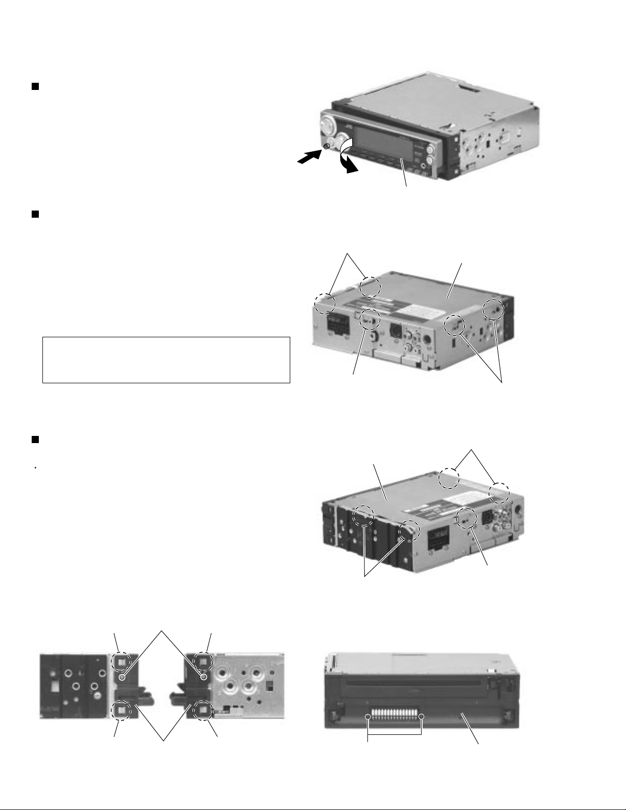
Removing the front panel unit
(See Fig.1)
1.
Press the release switch and remove the front panel
unit in the direction of the arrow.
Front panel unit
Removing the bottom cover
(See Fig.2,3)
1.
Turn the body upside down.
2.
Insert a screwdriver to the two joints a and two joints
b on both sides of the body and the joint c on the
back of the body, then detach the bottom cover from
the body.
CAUTION:
When disengaging the joint c using a
screwdriver, do not damage or break the
board.
Removing the front chassis (See Fig.4,5)
Prior to performing the following procedure, remove
the bottom cover.
1.
Remove the two screws A attaching the front
chassis.
Fig.1
Joint a
Bottom cover
Joint c
Joint b
Fig. 2
Joint b
Bottom cover
2.
Remove the two screws B on each side of the body.
3.
Release the two joints d and the two joints e on the
sides. remove the front chassis toward the front.
Joint d
Joint d
1-4
B
Front chassis
Fig. 5
Joint e
Joint e
Joint a
A
Joint c
Fig. 3
Front chassis
Fig.4
Page 5
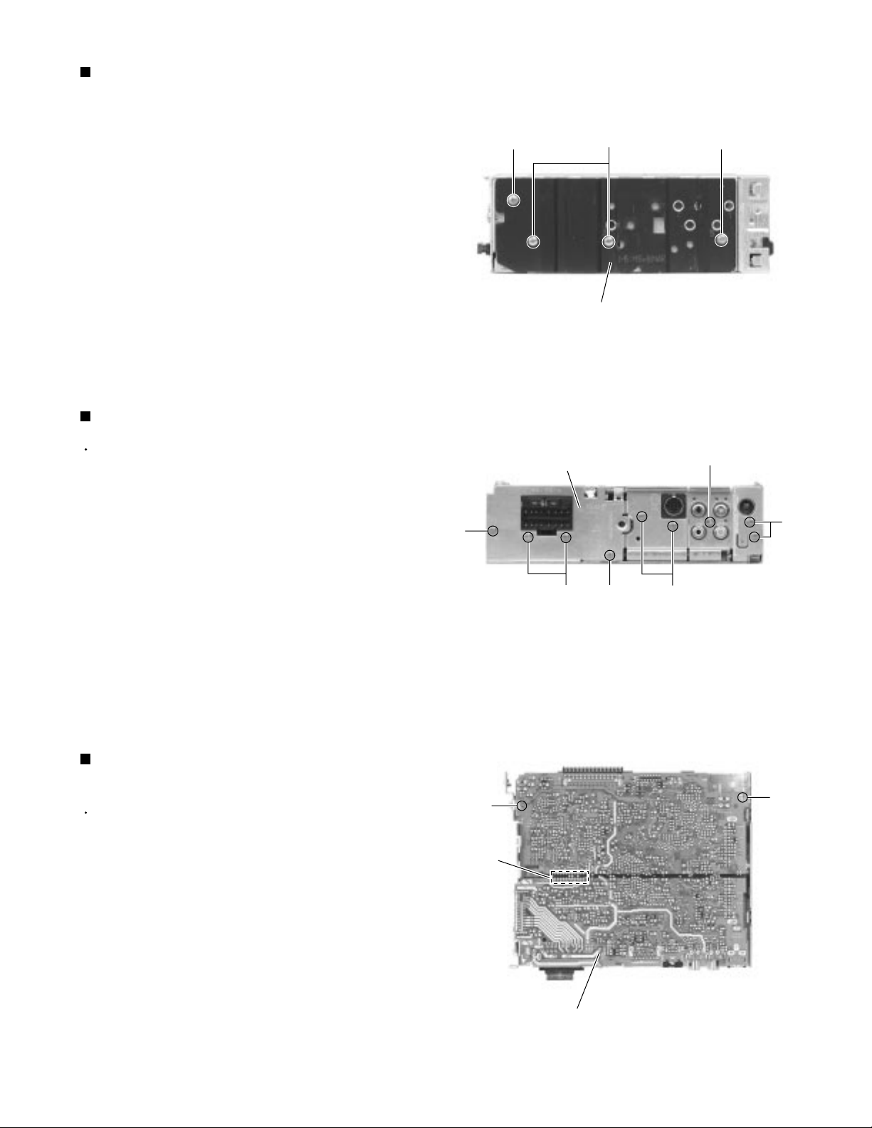
Removing the heat sink (See Fig.6)
1.
Remove the four screws C attaching the heat sink
on the left side of the body, and remove the heat
sink.
Removing the rear panel (See Fig.7 )
C
C
Heat sink
Fig. 6
KD-SX885
C
Prior to performing the following procedure, remove
the front chassis, the heat sink and bottom cover.
1.
Remove the eight screws D attaching the rear panel
and one screw E attaching the pine jack on the back
of the body.
D
Rear panel
Removing the main amplifier board assembly
(See Fig.8)
Prior to performing the following procedure, remove
the front chassis, the heat sink, bottom cover and the
rear panel.
1.
Remove the two screws F attaching the main
amplifier board assembly on the top cover.
F
CN501
D D
E
D
D
Fig. 7
F
2.
Disconnect connector CN501 on the main amplifier
board assembly from the cassette mechanism
assembly.
Main board assembly
Fig. 8
1-5
Page 6
KD-SX885
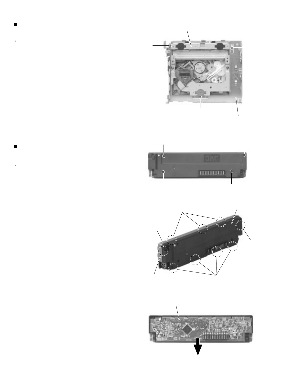
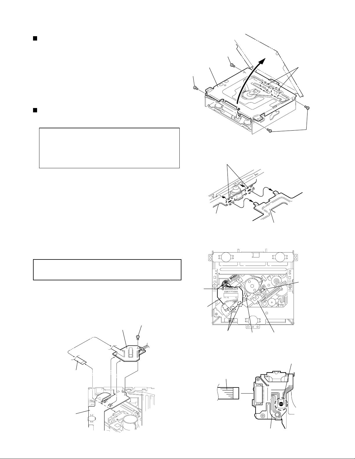
Removing the CD mechanism assembly
CD mechanism assembly
(See Fig.9)
Prior to performing the following procedure, remove
the front chassis, the heat sink, bottom cover and the
main amplifier board assembly.
1.
Remove the three screws G attaching the cassette
mechanism assembly from the top cover.
G
H
Removing the (LCD & key) control switch
board (See Fig.10
Prior to performing the following procedure, remove
the front panel assembly.
~ 12)
G
G
Top cover
Fig. 9
H
1.
Remove the four screws H attaching the rear cover
on the back of the front panel assembly.
2.
Unjoint the nine joints f with the front panel and the
rear cover.
3.
Remove the control switch board on the back of the
front panel.
H
Joint f
Front panel
Joint f
LCD & Key control board
H
Fig. 10
Rear cover
Joint f
Joint f
Fig. 11
1-6
Fig. 12
Page 7
< CD mechanism section >
Removing the top cover
(See Fig.1 and 2)
1.
Remove the two screws A on each side of the body.
2.
Lift the front side of the top cover and move the
cover backward to release the two joints a.
Removing the connector board
(See Fig.3 to 5)
Top cover
A
KD-SX885
A
Joints a
CAUTION:
1.
Remove the screw B fixing the connector board.
2.
Solder the short-circuit point on the connector board.
Disconnect the flexible wire from the pickup.
3.
Move the connector board in the direction of the
arrow to release the two joints b.
4.
Unsolder the wire on the connector board if
necessary.
CAUTION:
Before disconnecting the flexible wire
from the pickup, solder the short-circuit
point on the pickup. No observance of
this instruction may cause damage of
the pickup.
Unsolder the short-circuit point after
reassembling.
A
Fig.1
Joints a
Top cover
Fig.2
DET switch
B
Flexible wire
Frame
Connector board
B
Connector board
Joints b
Flexible wire
Short-circuit
Fig.3
Fig.4Fig.5
Pickup
Short-circuit point
(Soldering)
Pickup
1-7
Page 8
KD-SX885
Removing the DET switch
(See Fig.3 and 6)
1.
Extend the two tabs c of the feed sw. holder and pull
out the switch.
2.
Unsolder the DET switch wire if necessary.
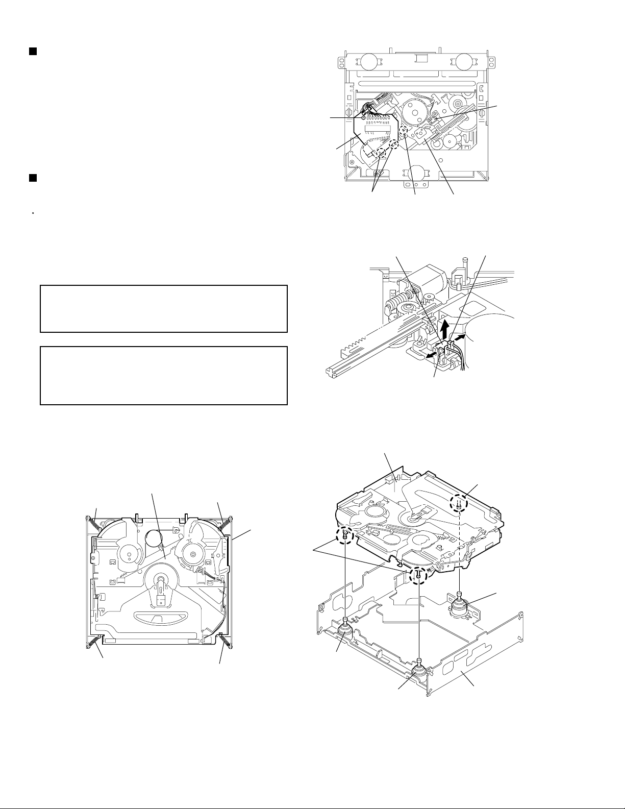
Removing the chassis unit
(See Fig.7 and 8)
Prior to performing the following procedure, remove
the top cover and the connector board.
B
Connector board
Joints b
Short-circuit
Fig.3
DET switch
Pickup
1.
Remove the two suspension springs (L) and (R)
attaching the chassis unit to the frame.
CAUTION:
The shape of the suspension spring (L)
and (R) are different. Handle them with
care.
CAUTION:
When reassembling, make sure that the
three shafts on the underside of the
chassis unit are inserted to the dampers
certainly.
Chassis unit
Suspension spring (R)
Suspension spring (L)
Frame
DET switch
Chassis unit
Tab c
Feed sw. holder
Tab c
Fig.6
Shaft
1-8
Suspension spring (R)
Suspension spring (L)
Shafts
Damper
Damper
Damper
Frame
Fig.8Fig.7
Page 9
Removing the clamper assembly
(See Fig.9 and 10)
KD-SX885
Prior to performing the following procedure, remove
the top cover.
1.
Remove the clamper arm spring.
2.
Move the clamper assembly in the direction of the
arrow to release the two joints d.
Removing the loading / feed motor
assembly (See Fig.11 and 12)
Prior to performing the following procedure, remove
the top cover, the connector board and the chassis
unit.
1.
Remove the screw C and move the loading / feed
motor assembly in the direction of the arrow to
remove it from the chassis rivet assembly.
Clamper arm
spring
Joint d
Joint d
Clamper assembly
Fig.9
Clamper arm spring
Chassis rivet
assembly
Joint d
Clamper assembly
Joint d
2.
Disconnect the wire from the loading / feed motor
assembly if necessary.
CAUTION:
When reassembling, connect the wire
from the loading / feed motor assembly
to the flame as shown in Fig.11.
Chassis rivet assembly
Fig.10
Loading / feed motor assembly
C
Loading / feed motor assembly
Fig.12Fig.11
1-9
Page 10
KD-SX885
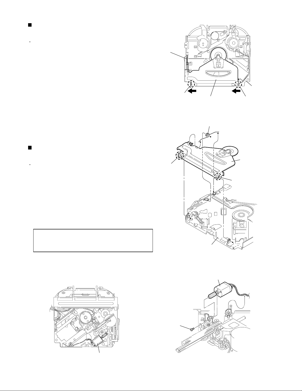
Removing the pickup unit
(See Fig.13 to 17)
Prior to performing the following procedure, remove
the top cover, the connector board and the chassis
unit.
1.
Remove the screw D and pull out the pu. shaft
holder from the shaft.
2.
Remove the screw E attaching the feed sw. holder.
3.
Move the part e of the pickup unit upward with the
shaft and the feed sw. holder, then release the joint f
of the feed sw. holder in the direction of the arrow.
The joint g of the pickup unit and the feed rack is
released, and the feed sw. holder comes off.
4.
Remove the shaft from the pickup unit.
5.
Remove the screw F attaching the feed rack to the
pickup unit.
Reattaching the pickup unit
(See Fig.13 to 16)
Joint f
Shaft
D
Joint e
Pu. shaft holder
Feed sw. holder
Pickup unit
Fig.13
Pickup unit
E
Joint f
Joint e
1.
Reattach the feed rack to the pickup unit using the
screw F.
2.
Reattach the feed sw. holder to the feed rack while
setting the joint tab g to the slot of the feed rack and
setting the part f of the feed rack to the switch of the
feed sw. holder correctly.
3.
As the feed sw. holder is temporarily attached to the
pickup unit, set to the gear of the joint g and to the
bending part of the chassis (joint h) at a time.
CAUTION:
4.
Reattach the feed sw. holder using the screw E.
5.
Reattach the shaft to the pickup unit. Reattach the
pu. shaft holder to the shaft using the screw D.
Make sure that the part i on the underside
of the feed rack is certainly inserted to the
slot j of the change lock lever.
F
Feed rack
Feed rack
E
Joint g
Feed sw. holder
Part i
Pickup unit
Slot j
Joint g
Feed sw. holder
Fig.14
Shaft
Joint f
Joint h
Fig.15
D
Pu. shaft holder
Pickup unit
1-10
Pickup unit
Feed rack
Joint f
Feed sw. holder
Fig.17Fig.16
Page 11
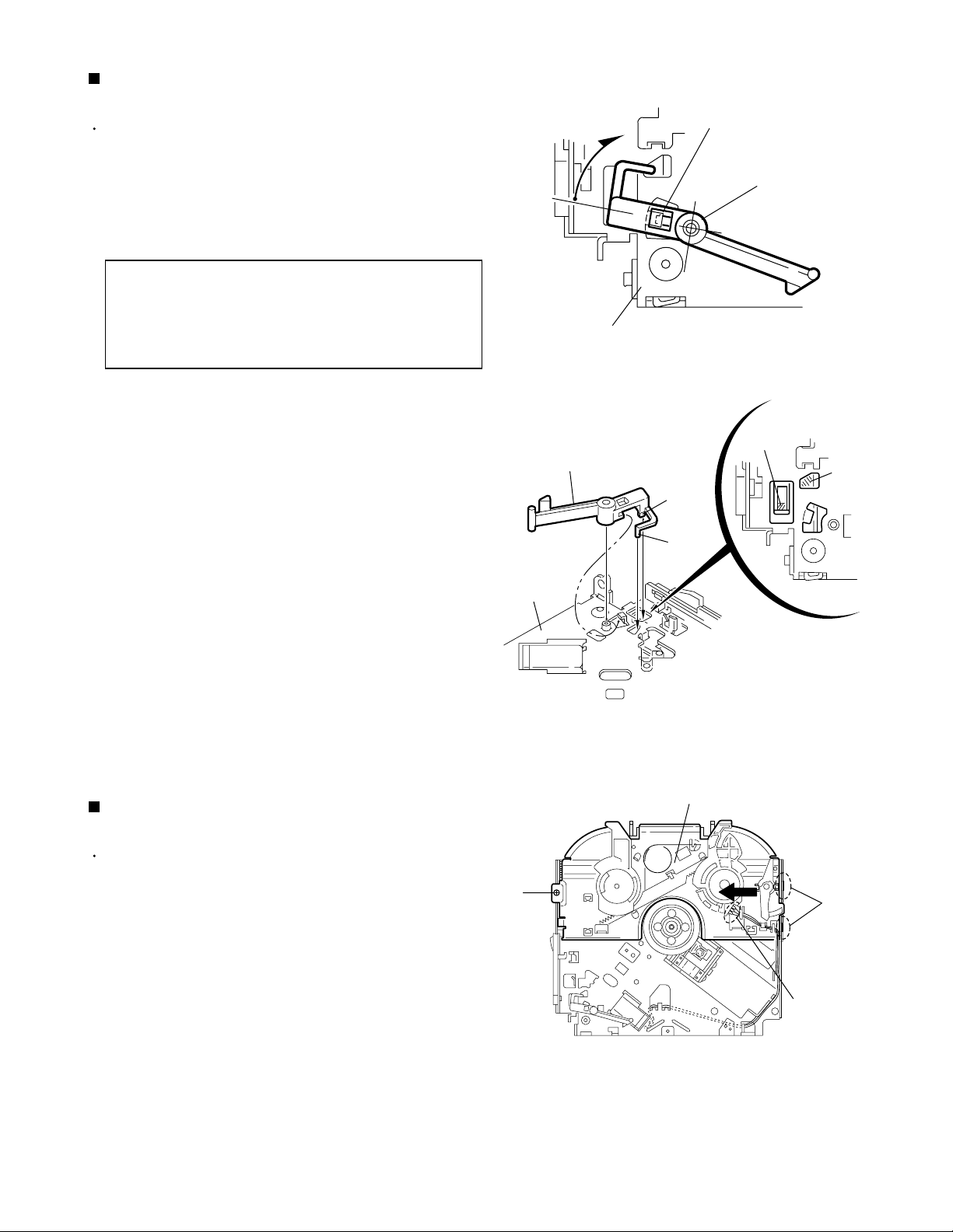
Removing the trigger arm
(See Fig.18 and 19)
Prior to performing the following procedure, remove
the top cover, the connector board and the clamper
unit.
1.
Turn the trigger arm in the direction of the arrow to
release the joint k and pull out upward.
KD-SX885
Joint k
Trigger arm
CAUTION:
When reassembling, insert the part l and
m of the trigger arm into the part n and
o at the slot of the chassis rivet
assembly respectively and join the joint
k at a time.
Chassis rivet assembly
Chassis rivet assembly
Trigger arm
Fig.18
Part n
Part o
Part l
Part m
Fig.19
Removing the top plate assembly
(See Fig.20)
Prior to performing the following procedure, remove
the top cover, the connector board, the chassis unit,
and the clamper assembly.
1.
Remove the screw H.
2.
Move the top plate assembly in the direction of the
arrow to release the two joints p.
3.
Unsolder the wire marked q if necessary.
H
Top plate assembly
Joints p
q
Fig.20
1-11
Page 12

KD-SX885
Removing the select arm (L) / select lock
arm (See Fig.21 and 22)
Prior to performing the following procedure, remove
the top plate assembly.
1.
Bring up the select arm (L) to release from the link
plate (joint r) and turn in the direction of the arrow to
release the joint s.
2.
Unsolder the wire of the select arm (L) marked q if
necessary.
3.
Turn the select lock arm in the direction of the arrow
to release the two joints t.
The select lock arm spring comes off the select lock
arm at the same time.
Reassembling the select arm (L) / select
lock arm (See Fig.23 to 25)
Select arm (R)
Joint z
Link plate spring
Top plate
Joint a'
Joint y
Link plate
Joint z
Joint s
Fig.21
Select lock arm
Select lock arm
Joint b'
Joint r
Select arm (L)
Select lock arm
q
Top plate
Hook u
Select lock
arm spring
Joints t
REFERENCE:
1.
Reattach the select lock arm spring to the top plate
Reverse the above removing procedure.
and set the shorter end of the select lock arm spring
to the hook u on the top plate.
2.
Set the other longer end of the select lock arm spring
to the boss v on the underside of the select lock arm,
and join the select lock arm to the slots (joint t). Turn
the select lock arm as shown in the figure.
3.
Reattach the select arm (L) while setting the part r to
the first peak of the link plate gear, and join the joint
s.
CAUTION:
When reattaching the select arm (L),
check if the points w and x are correctly
fitted and if each part operates properly.
Joint r
Link plate
Link plate
Select lock arm spring
Boss v
Select arm (R)
Joint a'
Fig.22
Hook u
Joint t
Joint t
Select lock arm
Fig.23
Link plate spring
Select arm (L)
Joint b'
1-12
Joint r
Fig.25Fig.24
Joint s
Select
lock arm
Point x
Page 13

KD-SX885
Removing the select arm (R) / link plate
(See Fig.21 and 22)
Prior to performing the following procedure, remove
the top plate assembly.
1.
Bring up the select arm (R) to release from the link
plate (joint y) and turn as shown in the figure to
release the two joints z and joint a’.
2.
Move the link plate in the direction of the arrow to
release the joint b’. Remove the link plate spring at
the same time.
REFERENCE:
Before removing the link plate, remove
the select arm (L).
Reattaching the Select arm (R) / link
plate (See Fig.25 and 26)
REFERENCE:
Reverse the above removing procedure.
Select arm (R)
Joint z
Link plate spring
Top plate
Joint a'
Part y
Link plate
Joint z
Joint s
Fig.21
Select lock arm
Select lock arm
Joint b'
Joint r
Select arm (L)
Select lock arm
q
Top plate
Hook u
Select lock
arm spring
1.
Reattach the link plate spring.
2.
Reattach the link plate to the link plate spring while
joining them at joint b’.
3.
Reattach the part y of the select arm (R) to the first
peak of the link plate while joining the two joints z
with the slots. Then turn the select arm (R) as shown
in the figure. The top plate is joined to the joint a’.
CAUTION:
When reattaching the select arm (R),
check if the part c’ is correctly fitted and
if each part operates properly.
Select arm (R)
Joint z
Link plate
Link plate spring
Joint a'
Part y
Part y
Fig.22
Joint b'
Joint z
Fig.25
Joints t
Select arm (L)
Select
lock arm
Point x
Fig.26
Link plate
1-13
Page 14

KD-SX885
Removing the loading roller assembly
(See Fig.27 to 29)
Prior to performing the following procedure, remove
the clamper assembly and the top plate assembly.
1.
Push inward the loading roller assembly on the gear
side and detach it upward from the slot of the joint d’
of the lock arm rivet assembly.
Detach the loading roller assembly from the slot of
the joint e’ of the lock arm rivet assembly.
The roller guide comes off the gear section of the
loading roller assembly.
Remove the roller guide and the washer from the
shaft of the loading roller assembly.
2.
Remove the screw I attaching the lock arm rivet
assembly.
3.
Push the shaft at the joint f’ of the lock arm rivet
assembly inward to release the lock arm rivet
assembly from the slot of the slide plate. Extend the
lock arm rivet assembly outward and release the
joint g’ from the boss of the chassis rivet assembly.
The roller guide springs on both sides come off.
Roller guide
Washer
Loading roller assembly
Roller guide
Joint e'
Roller guide spring
Roller guide spring
Joint d'
Loading roller assembly
Roller guide spring
Lock arm rivet assembly
Fig.27
Loading roller assembly
Roller guide
spring
CAUTION:
When reassembling, reattach the left
and right roller guide springs to the lock
arm rivet assembly before reattaching
the lock arm rivet assembly to the
chassis rivet assembly. Make sure to fit
the part h’ of the roller guide spring (L)
inside of the roller guide (Refer to
Fig.30).
Roller guide
Washer
Roller shaft assembly
Joint h'
Loading roller assembly
Roller guide
spring
Fig.28-1
Fig.28-2
Chassis rivet assembly
Boss
Slide plate
Roller guide spring
I
1-14
Frame
Loading roller
Roller guide spring
Lock arm rivet assembly
Joint f'
Part g'
Fig.29Fig.30
Page 15

KD-SX885
Removing the loading gear (5), (6) and
(7) (See Fig.31 and 32)
Prior to performing the following procedure, remove
the top cover, the chassis unit and the top plate
assembly.
1.
Remove the screw J attaching the loading gear
bracket. The loading gear (6) and (7) come off the
loading gear bracket.
2.
Pull out the loading gear (5).
Loading gear bracket
J
Loading gear (6)
Loading gear (5)
Loading gear (3)
Fig.31
J
Loading gear bracket
Loading gear (5)
Loading gear (6)
Loading gear (7)
Fig.32
1-15
Page 16

KD-SX885
Removing the gears (See Fig.33 to 36)
Prior to performing the following procedure, remove
the top cover, the chassis unit, the top plate
assembly and the pickup unit.
1.
Pull out the feed gear.
Slot j'
Slide plate
2.
Move the loading plate assembly in the direction of
the arrow to release the slide plate from the two slots
j’ of the chassis rivet assembly.
3.
Detach the loading plate assembly upward from the
chassis rivet assembly while releasing the joint k’.
Remove the slide hook and the loading plate spring
from the loading plate assembly.
4.
Pull out the loading gear (2) and remove the change
lock lever.
5.
Remove the E-washer and the washer attaching the
changer gear (2).
6.
The changer gear (2), the changer gear spring and
the adjusting washer come off.
7.
Remove the loading gear (1).
8.
Move the hang plate rivet assembly in the direction
of the arrow to release from the three shafts of the
chassis rivet assembly upward.
9.
Detach the loading gear plate rivet assembly from
the shaft of the chassis rivet assembly upward while
releasing the joint l’.
Feed gear
Change plate
rivet assembly
Shafts
E-washer
Loading plate assembly
Joint k'
Slot j'
Fig.33
Joint l'
Loading gear (4)
Loading gear plate
rivet assembly
Loading gear (2)
Loading gear (1)
Change gear (2)
10.
Pull out the loading gear (4).
Loading plate assembly
Loading plate spring
Chassis rivet assembly
1-16
Slot j'
Joint k'
Slide hook
Slide plate
Slot j'
E-washer
Washer
Loading gear (2)
Loading plate spring
Adjusting washer
Change plate
rivet assembly
Chassis rivet assembly
Fig.34
Loading gear (1)
Loading gear (2)
Change lock lever
Loading gear (4)
Loading gear plate rivet assembly
Fig.36Fig.35
Page 17

KD-SX885
Removing the turn table / spindle motor
(See Fig.37 and 38)
Prior to performing the following procedure, remove
the top cover, the connector assembly and the
chassis / clamper assembly.
1.
Remove the two screws K attaching the spindle
motor assembly through the slot of the turn table on
top of the body.
2.
Unsolder the wire on the connector board if
necessary.
K
Turn table
Fig.37
K
Turn table
Spindle motor
Fig.38
1-17
Page 18

KD-SX885
Adjustment method
Test instruments required adjustment
1.Digital oscilloscope (100MHz)
2.AM Standard signal generator
3.FM Standard signal generator
4.Stereo modulator
5.Electric voltmeter
6.Digital tester
7.Test disc(CTS-1000)
8.Extension cable for check
EXTGS004-22P
Standard measuring conditions
Power supply voltage DC 14.4V(11V to 16V allowance)
Load impedance 4 (4 to 8 allowance)
Line-out Level/Impedance
: 2.0 V/20k load(full scale)
Output impedance : 1k
Standard volume position
Balance and Bass & Treble volume : Indication "0"
Loudness : OFF
Frequency Band
FM 87.5kHz - 108.0 kHz
531kHz - 1602kHz
AM
Dummy load
Exclusive dummy load should be used for AM, and FM.
For FM dummy load, there is a loss of 6dB between SSG output
and antenna input. The loss of 6dB need not be considered
since direct reading of figures are applied in this workingo
standard.
How to connect the extension cable for adjusting
CN501
CD Mechanism
Extension cables
EXTGS004-22P
1-18
Front panel ass'y
Page 19

Flow of functional operation unit TOC read
Power ON
When the pickup correctly moves
v
to the inner area of the disc
Set Function CD
KD-SX885
When the laser diode correctly
emits
Microprocessor
commands
FMO
TC94A14FA" 40"
FEED MOTOR
+TERMINAL
IC561"4"
REST SW
When correctly focused
FEO
TA2157" 15"
Focus Servo Loop ONo
$83
$82
$81
3.3V
Hi-Z
0V
6V
4V
2V
OFF
ON
Pickup feed to the inner area
2.2V
RF signal eye-patternn
remains closed
RF signal eye-pattern
opens
Disc inserted
YES
Laser emitted
Focus search
Disc rotates
Tracking loop closed
TOC read out
YES
Microprocessor
commands
SEL
TC94A14FA"38"
LD
CN501"15"
"No disc"
display
When the disc correctly rotates
Microprocessor
commands
DMO
TC94A14FA"41"
Spindle
motor(-)
IC561"1"
$84 $86 $ A200
Acceleration Servo CLV
Rough
Servo
0.5 Sec 0.5 Sec
$84
3.3V
0V
4V
0V
3.3V
2.2V
0V
6V
3.2
2V
Jump to the first track
Play
Tracking Servo Loop ON
RF signal
Rough Servo Modev
CLV Servo Mode
(Program Area)
CLV Servo Mode
(Lead-In Area;
Digital :0)
1-19
Page 20

KD-SX885
Feed section
Is the voltage output at
IC521 pin "40" 5V or 0V?
Is 4V present at both
sides of the feed motor?
YES
YES
NO YES NO
NO
Is the wiring for IC521
(56)~(64) correct?
NO
Is 6V or 2V present at
IC561 "4" and "5"?
NO
Is 3.3V present at IC561
pin "20"?
Check the vicinity of
IC521.
YES
Check the feed motor
connection wiring.
YES
Check CD 8V
and 5V.
Check the feed motor.
Focus section
When the lens is
moving:
4V
Does the S-search
waveform appear at
IC561 pins "8" and "9"?
Spindle section
Is the disk rotated?
YES
Does the RF signal
appear at TP1?
YES
Is the RF waveform at TP1
distorted?
YES
Proceed to the Tracking
section
Check IC561.
NO
YES
NO
NO
NO
Check the circuits in
the vicinity of IC561
pins "8","9"and"15".
Check the pickup and
its connections
Is 4V present at IC561
pins "6" and "7"?
Check the spindle motor
and its wiring
Check the circuits in the
vicinity of IC501 "19"~
"24" or the pickup
YES
YES
NO
Is 4V present at IC521
pins "41" ?
Check the vicinity of
IC561.
NO
YES
Check IC521 and
IC501.
Tracking section
1-20
When the disc is rotated
at first:
Approx. 1.2V
Is the tracking error signal
output at IC501 "11"?
YES
Check IC521.
YES YES
Check the circuit in the
vicinity of IC501 pins
"2"~"12".
Check the pickup and
its connections
Page 21

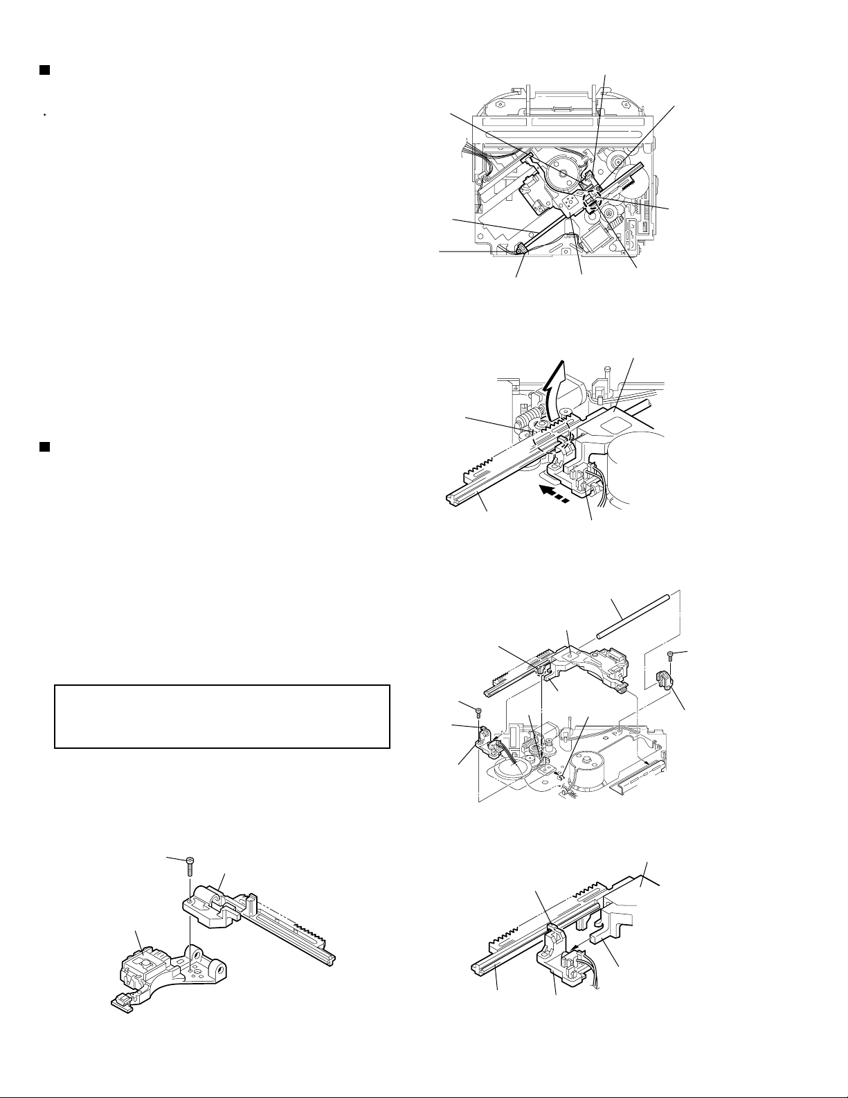
Maintenance of laser pickup
(1) Cleaning the pickup lens
Before you replace the pickup,please try to
clean the lens with a alcohol soaked cotton
swab.
(2) Life of the laser diode
When the life of the laser diode has expired.
the following symptoms will appear..
(1) The level of RF output (EFM output:amplitude
of eye patterrn) will be low.
KD-SX885
Is RF output
1.3 0.4Vp-p?
YES
O.K
(3) Semi-fixed resistor on the APC PC board
The semi-fixed resistor on the APC printed
circuit board which is attached to the pickup
is used to adjust the laser power.Since this.
adjustment should be performed to match the
characteristics of the whole optical block,
do not touch the semi-fixed resistor..
If the laser power is lower than the specified
value, the laser diode is almost worn out, and
the laser pickup should be replaced.
If the semi-fixed resistor is adjusted while
the pickup is functioning normally, the laser
pickup may be damaged due to excessive current.
NO
Replace it.
Replacement of laser pickup
Turn of the power switch and, disconnect the
power cord.
Replace the pickup with a normal one.(Refer
to "Pickup Removal" on the previous page)
Plug the power cord in, and turn the power on.
At this time, check that the laser emits for
about 3seconds and the objective lens moves
up and down.
Note: Do not observe the laser beam directly..
Play a disc.
Check the eye-pattern at TP1.
Finish.
1-21
Page 22

KD-SX885
Description of major ICs
UPD784214AGC149 (IC701) : MAIN CPU
1.Pin layout
75 51
76
50
100
125
26
Pin No. Symbol I/O Function
1
2
3
4
5
6
7
8
9
10
11
12
13
14
15
16
17
18
19
20
21
22
23
24
25
26
27
28
29
30
31
32
33
34
35
36
37
38
39
40
41
42
43
44
45
46
47
48
49
50
NC
NC
SW2
PSW
LM
MOTOR SEL
NC
ANT CONT
VDD
X2
X1
VSS
XT2
XT1
RESET
SW1
BUSINT
PS2
NC
NC
NC
REMOCON
AVDD
AVREF0
VOL1
VOL2
KEY0
KEY1
KEY2
LEVEL
PULL DOWN
SM
AVSS
NC
NC
AVRE F
BUSSI
BUSSO
BUSSCK
BUSI/O
LCDDA
LCDCK
LCDCE
BUZZER
NC
NC
NC
OPEN
NC
NC
O
Non connected
O
Non connected
I
Detection switch of CD mechanism
I
CD mecha position setting SW
O
Loading motor control signal output
O
Loading /feed motor selecting output
O
Non connected
O
Antenna remote output
-
5V connection
-
Sub-clock 32.738MHz
I
Sub-clock 32.738MHz
-
GND connection
-
Sub-clock 12.5MHz
I
Sub-clock 12.5MHz
I
Reset detection terminal
I
Detection switch of CD mechanism
I
J-BUS signal interrupt input
I
POWER SAVE2 BACK UP synchronization. It is H input and stop mode.
O
Non connected
O
Non connected
O
Non connected
I
Remote control signal input
-
5V connction
-
5V connection
I
Input for rotation volume detection pulse judgment to relation V1
I
Input for rotation volume detection pulse judgment to relation V2
I
Key control signal input 0
I
Key control signal input 1
I
Key control signal input 2
I
Level meter input
I
Pul down
I
S.METER level input
-
GND connection
O
Non connected
O
Non connected
-
5V connection
I
J-BUS data input
O
J-BUS data output
I/O
J-BUS clock I/O
I/O
J-BUS data I/O terminal.
O
Data output for LCD driver.
O
Clock output for LCD driver.
O
Chipenable output to LCD driver
O
Buzzer output
O
Non connected
O
Non connected
O
Non connected
O
CD tray open control signal output
O
Non connected
O
Non connected
UPD784214AGC149(1/2)
1-22
Page 23

Pin No. Symbol I/O Function
51
52
53
NC
NC
SD/ST
Non connected
O
Non connected
O
Station detector and stereo signal input.
I
It is H and there is a bureau.It is L and a stereo.
54
55
NC
MONO
Non connected
O
Monaural ON/OFF switch output.
O
At the time of the MONO ON :H.
56
57
58
59
60
61
NC
NC
NC
NC
NC
DETACH
Non connected
O
Non connected
O
Non connected
O
Non connected
O
Non connected
O
Detach signal input. It is L of 200ms or more and an
I
operatio mode. H:POWER SAVE
62
63
64
65
66
67
68
69
70
NC
SEEK/STOP
NC
FM/AM
PLLCE
PLLDA
PLLCLK
PLLDI
TELMUTE
Non connected
O
Auto seek stop switch output. At SEEK:H. At STOP:L
O
Non connected
O
FM,AM switch output
O
CE output for IC control for PLL
O
Data output for IC control for PLL
O
Clock output for IC control PLL
O
Data input for IC control for PLL
I
Telephone mute detection input.
I
It is L or H and MUTE(ACTIVE depends on the PSM setting)
71
72
73
74
NC
VSS
DIMIN
PS1
Non connected (ex:AMP-KILL output)
O
GND connection
Dimmer detection input. At L:dimmer ON.
I
POWER SAVE 1. ACC and syschronization
I
POWER SAVE : L. At operation:H
75
76
77
78
79
80
81
82
83
84
85
86
87
88
89
90
91
92
93
94
95
96
97
98
99
100
POWER
CDON
MUTE
NC
NC
NC
VDD
NC
VOLDA
VOLCL
EVOLCE
SUB.MUTE
SUB.CE
NC
STAGE2
STAGE1
BUCK
CCE
RST
TEST
BUS0
BUS1
BUS2
BUS3
NC
CD-RW
O
O
O
O
O
O
-
O
O
O
O
O
O
O
I
I
O
O
O
I/O
I/O
I/O
I/O
O
-
POWER ON/OFF switch outut. At POWER ON:H
The CD power supply control signal output. At CD :H
Mute output. At mute ON:L
Non connected
Non connected
Non connected
5V connection
Non connect
Data output by which IC for electronic volume is controlled
Clock output by which IC for electronic volume is controlled
E-volume output
Mute control putput for subwoofer
CE output for subwoofer
Non connected
L: for 780J H: for 8250J
H:For 991R / L:For 911R
Clock output for data communication with CDLSI
CE output for data communication with CDLSI
CDLSI reset signal output
connects GND with 10k pull down (For flash switch)
Data communication input output port 0 with CDLSI
Data communication input output port 1 with CDLSI
Data communication input output port 2 with CDLSI
Data communication input output port 3 with CDLSI
Non connected
RF gain control L=CD-RW, H= CD-DA
KD-SX885
UPD784214AGC149(2/2)
1-23
Page 24

KD-SX885
HA13164 (IC961) : Regulator
1.Pin layout
EXT OUT
ANT OUT
ACC IN
1 2 3 4 5 6 7 8 9 10111213 1415
2.Block diagram
VDD5V
SW5V
ACC5V
ANT CTRL
MEMORY IN
BATT DET9VCTRL
CD8VAJ10V
GND
3.Pin function
11
12
10
8
2
1
7
Surge Protector
BIAS TSD
15
3
note1) TAB (header of IC)
connected to GND
13
9
6
4
5
14
UNIT R:
C:F
1-24
Pin No. Symbol Function
1
2
EXT OUT
ANT OUT
Output voltage is VCC-1 V when M or H level applied to CTRL pin.
Output voltage is VCC-1 V when M or H level to CTRL pin and H level
to ANT-CTRL.
3
4
5
6
7
8
9
10
11
12
13
14
15
ACC IN
VDD 5V
SW5V
ACC5V
ANT CTRL
MEMORY IN
BATT DET
9V
CTRL
CD8V
AJ
10V
GND
Connected to ACC.
Regular 5.7V.
Output voltage is 5V when M or H level applies to CTRL pin.
Output for ACC detector.
L:ANT output OFF , H:ANT output ON
Connected to VCC.
Low battery detect.
Output voltage is 9V when M or H level applied to CTRL pin.
L:BIAS OFF, M:BIAS ON, H:CD ON
Output voltage is 8V when H level applied to CTRL pin.
Adjustment pin for ILM output voltage.
Output voltage is 10V when M or H level applies to CTRL pin.
Connected to GND.
Page 25

HD74HC126FP-X (IC771) : Buffer
KD-SX885
1.Terminal layout
1C
1
1A
2
3
1Y
4
2C
5
2A
6
2Y
GND
2.Block diagram
7
Input
Vcc
14
3C
13
12
3A
11
3Y
10
4C
9
4A
8
4Y
Vcc Vcc
1A
2A
3A
4A
1C
2C
3C
See Function Table
4C
3.Pin function
Output
1Y
Output
2Y
Output
3Y
Output
4Y
Input Output
C
A
L
X
H
L
H
H
Note:
1k
CL
Sample as Load Circuit 1
Sample as Load Circuit 1
Sample as Load Circuit 1
Y
Z
H
L
H : High
L : Low
X : H and L
Z : H.L.X
S1
1k
IC-PST600M/G/-W (IC702) : System reset
Co1
OP1
1
3
2
IN
OUT
GND
1-25
Page 26

KD-SX885
LA47503 (IC351) : Power amp.
1.Terminal layout
206
11
1
12
4
10
Stand by
Switch
Ripple
Filter
Protective
circuit
Mute
circuit
9
7
8
5
3
2
22
1-26
15
25
13
14
16
Muting &
On Time Control
Circuit
protective
circuit
17
19
18
21
23
24
Page 27

2.Terminal layout
AC CONT1
GND1
OUTFR-
STBY
OUTFR+
Vcc1/2
OUTRR-
GND2
OUTRR+
VREF
INRR
INFR
SGND
INFL
INRL
ONTIME
OUTRL+
GND3
OUTRL-
Vcc3/4
OUTFL+
MUTE
OUTFL-
GND4
KD-SX885
NC
3.Pin function
1
2
3
4
5
6
7
8
9
10
11
12
13
14
15
16
17
18
19
20
21
22
23
24
25
SymbolPin No. Function
AC CONT1
GND1
OUTFRSTBY
OUTFR+
Vcc1/2
OUTRRGND2
OUTRR+
VREF
INRR
INFR
SGND
INFL
INRL
ONTIME
OUTRL+
GND3
OUTRLVcc3/4
OUTFL+
MUTE
OUTFLGND4
NC
Header of IC
Power GND
Outpur(-) for front Rch
Stand by input
Output (+) for front Rch
Power input
Output (-) for rear Rch
Power GND
Output (+) for rear Rch
Ripple filter
Rear Rch input
Front Rch input
Signal GND
Front Lch input
Rear Lch input
Power on time control
Output (+) for rear Lch
Power GND
Output (-) for rear Lch
Power input
Output (+) for front
Muting control input
Output (-) for front
Power GND
No connection
LA47503
1-27
Page 28

KD-SX885
TC94A14FA (IC521) : DSP&DAC
1.Terminal layout & block daiagram
49
50
51
52
53
54
55
56
57
58
59
60
61
62
63
48 47 46 45 44 43 42 41 40 39
Clock
LPF
generator
Micro-
controller
interface
1-bit
DAC
Audio out
circuit
Address
circuit
circuit
Correction
Digital
output
16 k
RAM
PWM
Servo
control
ROM
RAM
CLV servo
Synchronous
guarantee
EFM
decoder
Sub code
decoder
38 37 36 35 34 33
D/A
A/D
Digital equalizer
automatic
adjustment circuit
Data
slicer
VCO
PLL
TMAX
32
31
30
29
28
27
26
25
24
23
22
21
20
19
18
64
2.Pin function
Pin
Symbol I/O Descroption
No
1
BCK
2
LRCK
O
Bit clock output pin.32fs,48fs,or 64fs selectable by command.
O
L/R channel clock output pin."L" for L channel and "H" for R channel. Output polarity
can be inverted by command.
3
AOUT
4
DOUT
5
IPF
O
Audio data output pin. MSB-first or LSB-first selectable by command.
O
Digital data output pin.Outputs up to double-speed playback.
O
Correction flag output pin. When set to "H", AOUT output cannot be corrected by C2
correction processing.
6
V
7
8
9
10
11
12
13
14
15
DD3
VSS3
SBOK
CLCK
DATA
SFSY
SBSY
HSO
UHSO
PVDD3
-
Digital 3.3V power supply voltage pin.
-
Digital GND pin.
O
Subcode Q data CRCC result output pin. "H" level when result is OK.
O
Subcode P-W data read I/O pin. I/O polarity selectable by command.
O
Subcode P-W data output pin.
O
Playback frame sync signal output pin.
O
Subcode block sync signal output pin. "H" level at S1 when subcode sync is detected.
I/O
General-purpose input / output pins.
Input port at reset.
-
PLL-only 3.3V power supply voltage pin.
17
161514131211101 2 3 4 5 6 7 8 9
1-28
Page 29

Pin
Symbol I/O Description
No
16
17
PDO
TMAX
EFM and PLCK phase difference signal output pin.
O
TMAX detection result output pin.
O
KD-SX885
TC94A14FA
18
19
20
21
22
23
24
25
26
27
28
29
30
31
32
33
34
35
36
37
38
39
40
41
42
43
44
45
46
47
48
49
50
51
52
53
54
55
56
57
58
59
60
61
62
63
64
LPFN
LPFO
REF
PV
VCOF
AV
SS3
SLCO
RFI
AV
DD3
RFCT
RFZI
RFRP
FEI
SBAD
TEI
TEZI
FOO
TRO
V
REF
RFGC
TEBC
SEL
AV
DD3
FMO
DMO
V
SS3
V
DD3
TESIN
SS3
XV
XI
XO
XV
DD3
DV
SS3R
RO
DV
DD3
DVR
LO
DV
SS3L
ZDET
VSS5
BUS0
BUS1
BUS2
BUS3
BUCK
/CCE
/RST
V
DD5
TMAX Detection Result
Longer than fixed period
Within fixed period
Shorter than fixed period
Inverted input pin for PLL LPF amp.
I
Output pin for PLL LPF amp.
O
REF
PLL-only V
VCO filter pin.
O
Analog GND pin.
DAC output pin for data slice level generation.
O
RF signal input pin. Zin selectable by command.
I
Analog 3.3V power supply voltage pin.
RFRP signal center level input pin.
I
RFRP signal zero-cross input pin.
I
RF ripple signal input pin.
I
Focus error signal input pin.
I
Sub-beam adder signal input pin.
I
Tracking error input pin. Inputs when tracking servo is on.
I
Tracking error signal zero-cross input pin.
I
Focus equalizer output pin.
O
Tracking equalizer output pin.
O
Analog reference power supply voltage pin.
RF amplitude adjustment control signal output pin.
O
Tracking balance control signal output pin.
O
APC circuit ON/OFF signal output pin. At laser on, high impedance with UHS="L",
O
pin.
TMAX Output
DD3
"PV
"
"HiZ"
SS3
"AV
"
H output with UHS="H".
Analog 3.3V power supply voltage pin.
Feed equalizer output pin.
O
Disc equalizer output pin.
O
Digital GND pin.
Digital 3.3V power supply voltage pin.
Test input pin. Normally, fixed to "L".
I
System clock oscillator GND pin.
System clock oscillator input pin.
I
System clock oscillator output pin.
O
System clock oscillator 3.3V power supply voltage pin.
DA converter GND pin.
R-channel data forward output pin.
O
DA converter 3.3V power supply pin.
Reference voltage pin.
L-channel data forward output pin.
O
DA converter GND pin.
1 bit DA converter zero detection flag output pin.
O
Microcontroller interface GND pin.
-
Microcontroller interface data I/O pins.
I/O
Microcontroller interface clock input pin.
I
Microcontroller interface chip enable signal input pin.At "L", BUS0 to BUS3 are active.
I
Reset signal input pin. At reset, "L".
I
Microcontroller interface 5V power supply pin.
-
1-29
Page 30

KD-SX885
LC75412W(IC301):E.VOLUME
1.Terminal layout & block daiagram
48 47 46 45 44 43 42 41 40 39 38 37 36 35 34 33
47k
1M
32
31
30
29
28
27
26
25
24
23
22
21
20
19
18
17
49
50
51
52
53
54
55
56
57
58
59
60
61
62
63
64
LVref
LVref
LVref
RVref
RVref
RVref
LVref
RVref
Multiplexer
Multiplexer
CONTROL
CIRCUIT
ZERO CROSSDET
LOGIC CIRCUITVA
ZERO CROSSDET
LVref
CCB
INTERFACE
NO SIGNAL
TIMMER
RVref
2.Function
Pin No.
54
53
52
51
55
59
60
61
62
58
50
49
63
64
48
1
46
3
47
2
91011121314151612345678
Symbol Function
L1
Single end input terminal
L2
L3
L4
L6
R1
R2
R3
R4
R6
L5M
Differential motion input terminal
L5P
R5M
R5P
LSELO
Input selector output terminal
RSELO
LCT
RCT
LVRIN
Then terminal for roudness.CR for a high region amends is connected for LCT(RCT) and
LVRIN(RVRIN),and CR for a low region amends is connected between LCT(RCT) and GND.
Volume + equalizer input terminal.
RVRIN
1-30
Page 31

Pin No.
42
41
40
7
8
9
36
35
34
13
14
15
45
44
43
39
38
37
21
10
11
12
5
4
6
28
33
16
32
17
31
30
18
19
57
56
27
29
22
23
20
26
25
24
Symbol Function
LF1C1
LF1C2
The capacitor connection terminal of the filter composition for the F1 stap of the equalizer.
LF1C1(RF1C1)~LF1C2(RF1C2),Connect the capacitor for LF1C2(RF1C2)~LF1C3(RF1C3).
LF1C3
RF1C1
RF1C2
RF1C3
LF3C1
LF3C2
LF3C3
Capacitor connection terminal of filter composition for F3 strap of equalizer.
Connect the capacitor for LF3C1(RF3C1)~ LF3C2(RF3C2)
LF3C2(RF3C2)~LF3C3(RF3C3).
RF3C1
RF3C2
RF3C3
NC
TEST
LTOUT
No connected
The terminal only fot the test of LSI.Connects with GND and uses usually.
Equalizer output terminal.
RTOUT
LFIN
RFIN
LFOUT
LROUT
RFOUT
The fader block input terminal.
Drive by low impedance.
The fader output terminal.A rear reception desk side / side can be separately narrowed
respectively.
L/R of the amount of attenuation is the same.
RROUT
Vref
VDD/2voltage generation part.
Connect the capacitor of about several 10 F as a counter measure for ripple of power
supply between Vref~AVSS for (VSS).
VDD
DVSS
LAVSS
Power supply terminal.
System logic grand terminal.
Analog grand terminal.
RAVSS
MUTE
External control mute terminal.
When this terminal is made VSS level,fader volume block is set in compulsory-
TIM
CL
Timer terminal at no signal of 0 crossing circuit.
Cereal data and clock input terminal for control.
DI
CE
chip enable terminal.
[H]data is written in an internal latch in the timing which becomes [L]and an analog
each switch moves.[H] The data transfer becomes enable at the level.
KD-SX885
LC75412W
1-31
Page 32

KD-SX885
LC75873NW (IC601) : LCD Driver
1.Pin layout
60 41
61
80
1 20
3.Pin function
Pin No.
79,80
1 to 66
67
68
69
40
21
Pin name
DIMMER,S1
S2 to S66
COM1
COM2
COM3
2.Block diagram
VDD1
VDD2
INH
OSC
VDD
VSS
I/O
O
O
S5
S4/P4
S3/P3
S2/P2
COM2
COM3
COMON
DRIVER
CLOCK
GENERATOR
COM1
S68
S67
DI
CL
SEGMENT DRIVER
SHIFT REGISTOR
ADDRESS
DETECTOR
CE
S1/P1
Description
Segment outouts for displaying the display data
transferred by serial data input.
The S1/P1 to S4/P4 pins can be used as generalpurpose output ports under serial data control.
Common driver outputs.
The frame frequency f0 is given by :
f0 = (FOSC/384)Hz.
74
76
77
78
75
71
72
70
OSC
CE
CL
DI
INH
VDD1
VDD2
VDD
I/O
I
I
I
I
I
I
-
Oscillator connection
An oscillator circuit is formed by connecting an
external resistor and capacitor to this pin.
Serial data transfer inputs.
Connected to the controller.
CE:Chip enable
CL:Synchronization clock
DI:Transfer data
Display off control input
INH= "L"(VSS) Display forced off
S1/P1 to S4/P4 = "L"
(These pins are forcibly set to the
segment output port function and held
at the low level.)
S5 to S68 = "L"
COM1 to COM3"L"
INH = "H"(HDD) Display on
However, serial data transfer is possible when
the display is forced off by this pin.
Used for applying the LCD drive 2/3 bias voltage
externally. Must be connected to VDD2 when a
1/2 bias drive scheme is used.
Used for applying the LCD drive 1/3 bias voltage
externally. Must be connected to VDD1 when a
1/2 bias drive scheme is used.
Power supply connection.
Provide a voltage of between 3.0 and 6.0V.
1-32
73
VSS
Power supply connection. Connect to ground.
-
Page 33

TB2118F-X (IC21) : PLL
1.Terminal Layout
2423222120191817161514
KD-SX885
13
2.Block diagram
osc
2
1
XO
24
XI
FM IN
AMIN
IFC
DIN
CK
DOUT
CE
15
16
13
3
4
5
6
123456789
Buff.
ON/OFF
OSC circuit
AMP
AMP
AMP
Serial
Interface
101112
Reference Counter
Prescaler
20-bit BINARY COUNTER
Resistor 1
Resistor 2
I/O PORT
Phase
Comparator
4-bit
Swallow counter
12-bit
Programmable counter
22-bit
40bit shift register
OUTPUT PORT
Constant
power supply voltage
switch
Vdd
switch
Vcc
AM CP.
20
+
+
-
RF
22
19
vt
18
FM cp
3.Pin Function
Pin
Symbol I/O Function
No.
XOUT
10
11
12
1
2
3
4
5
6
7
8
9
OSC
CE
DI
CK
DOUT
SR
I/O1
I/O2
OUT1
OUT2
VDD2
Crystal oscillator pin
O
Non connect
Chip enable input
I
Serial data input
I
Clock input
I
Serial data output
O
Register control pin
O
I/O ports
I/O
I/O ports
I/O
Non connect
Non connect
Single power supply for REF. frequency block
-
7
SR
8
9
I/O -2I/O -1
10 11
12
out-2out-1
vdd2
Pin
Symbol I/O Function
No.
IFC
13
VDD
14
FMIN
15
AMIN
16
DGND
17
FMCP
18
VT
19
AMCP
20
VCC
21
RF
22
AGND
23
XIN
24
17
14
IF signal input
I
Power pins for digital block
FM band local signal input
I
AM band local signal input
I
Connect to GND (for digital circuit)
Charge pump output for FM
O
Tuning voltage biased to 2.5V.
Charge pump output for AM
O
Power pins for analog block
Ripple filter connecting pin
I
Connect to GND (for analog circuit)
Crystal oscillator pin
I
21
23
a-gnd
vccd-gndvdd
1-33
Page 34

KD-SX885
TA2157FN-X (IC501) : RF amp
1.Terminal layout
2.Block diagram
24 ~ 13
1 ~ 12
13
14
15
16
17
18
19
20
21
10pF
40k30k
20k 20k
20k
20k
BOTTOM
15k
50 A
12k
12k
PEAK
20k
20k
20k
PEAK
1.3V
40k
240k
15pF
240k
15pF
40k
50k
2k
20k
50k
14k
K
1
15k
x0.5
x2
x0.5
x2
1k
2k
1.75k
10pF
12
11
10
9
8
7
6
5
4
1-34
22
23
24
PIN SEL
VCTRLPIN
VCC
HiZ
GND
3k
3k
(APC SW)
APC ON
APC ON
APC OFF
(LDO=H)
180k
40pF
TEB
(TE BAL)
-50%
0%
+50%
180k
40pF
60k
60k
94k
22k
94k
22k
RFGC
(AGC Gian)
+12dB
+6dB
0dB
3
2
1
TEB
(TE BAL)
Normal mode
(0dB)
Normal mode
(0dB)
CD-RW mode
(+12dB)
Page 35

3.Pin function
Pin No. Symbol I/O Function
1
VCC
2
FNI
3
FPI
4
TPI
5
TNI
6
MDI
7
LDO
8
SEL
-
3.3V power supply pin
I
Main-beam amp input pin
I
Main-beam amp input pin
I
Sub-beam amp input pin
I
Sub-beam amp input pin
I
Monitor photo diode amp input pin
O
Laser diode amp output pin
I
APC circuit ON/OFF control signal, laser diode (LDO) control signal input
or bottom/peak detection frequency change pin.
KD-SX885
TA2175FN-X
9
10
11
12
13
TEBC
TEN
TEO
RFDC
GVSW
SEL
GND
Hiz
VCC
I
Tracking error balance adjustment signal input pin
APC
circuit
LCD
OFF Connected VCC through 1k resistor
ON
Control signal output
ON Control signal output
Adjusts TE signal balance by ellminating carrier component from PWM
signal (3-state output,PWM carrier = 88.2kHz) output from TC94A14F/FA
TEBC pin using RC-LPF and inputting DC.
TEBC input voltage:GND~VCC
I
Tracking error signal genaration amp negative-phase input pin
O
Tracking error signal generation amp output pin.
Combining TEO signal RFRP signal with TC94A14F/FA configures tracking
search system.
O
RF signal peak detection output pin
I
AGC/FE/TE amp gain change pin
GVSW Mode
GND
Hiz
CD-RW
Normal
VCC
14
15
16
17
18
19
20
21
22
23
24
VRO
FEO
FEN
RFRP
RFRPIN
RFGO
RFGC
AGCIN
RFO
RFN
GND
O
Reference voltage (VRO) output pin
VRO=1/2VCC When VCC=3.3V
O
Focus error signal generation amp output pin
I
Focus error signal generation amp negative-phase input pin
O
Signal amp output pin for track count
Combining RFRP signal and TEO signal with TC94A14F/FA configures
tracking search system.
I
Signal generation amp input pin for track count
O
RF signal amplitude adjustment amp output pin
I
RF amplitude adjustment control signal input pin
Adjusts RF signal amplitude by eliminating carrier component from PWM
signal (3-state output,PWM carrier=88.2kHz)output fromTC94A14F/14FA
RFGC pin using RC-LPF and inputting DC.
RFGC input voltage:GND~VCC
I
RF signal amplitude adjustment amp input pin
O
RF signal generation amp output pin
I
RF signal generation amp input pin
-
GND pin
1-35
Page 36

KD-SX885
VICTOR COMPANY OF JAPAN, LIMITED
MOBILE ELECTRONICS DIVISION
PERSONAL & MOBILE NETWORK BUSINESS UNIT. 10-1,1Chome,Ohwatari-machi,Maebashi-city,371-8543,Japan
(No.49735)
200204
 Loading...